Novel Cu–Cu Bonding Technique: The Insertion Bonding Approach
Upload
khangminh22Category
view
3download
0
KARAN MENON CHARACTERISTICS OF SILANE BONDING TO STAINLESS STEEL Master of Science Thesis
Examiner: Professor Toivo Lepistö Examiner and topic approved in the Faculty of Automation, Mechanical and Materials Engineering faculty council meeting on 3 December 2008

I
ABSTRACT TAMPERE UNIVERSITY OF TECHNOLOGY Master’s Degree Programme in Materials Science MENON, KARAN: Characteristics of Silane Bonding to Stainless Steel Master of Science Thesis, 63 pages November 2011 Major subject: Materials Research Examiner: Professor Toivo Lepistö Keywords: silane, stainless steel, bond, scanning electron microscope, x-ray photoelectron spectroscopy, casino program simulation
Today products need to have high functionality but low manufacturing costs. Integration of different materials together to make the final product is the demand at present. Hybrid technology is the answer for the queries and interests sighted above. Preparation of metal-plastic hybrids by insert injection moulding offers a manufacturing route for multi-functional components in a few processing steps. Nowadays, bonds be-tween metal and plastic are basically established using mechanical methods. However, bonding by chemical method is needed but it is difficult because metals and plastics exhibit different physical and chemical characteristics. Hence coupling agents are used to improve bonding between metal and plastic. Silanes are the most commonly used coupling agents for metal-plastic bonding.
The main objective of this thesis was to study the bonding characteristic between steel substrate and silane layer. Different parameters of the silane treatment process affect the structure, uniformity and thickness of silane layer present on the metal surface. Therefore, variations in parameters for silane treatment like pH and concentra-tions of the silane solution and rinsing methods for maintaining the thickness of silane layer on the metal substrate were tested. Planar and cross-sectional samples were pre-pared in order to test the bonding characteristics. These samples were observed under optical microscope and scanning electron microscope. Certain samples were observed in X-ray photoelectron spectrometer and the results were computed. In order to aid these kinds of tests in future a simulation program was designed using CASINO simulation software.
The results obtained from scanning electron microscope were consistent with the earlier published results. Developing a method to observe cross-sectional sam-ples in a scanning electron microscope was difficult because of instability of the silane layer and previously used sample preparation methods. X-ray photoelectron spectrosco-py confirmed the results obtained using scanning electron microscope. Simulation of experimental conditions was helpful to determine the conditions to be used in experi-ments.

Preface
The research work for this thesis was carried out in the Department of Materials Sci-ence, Tampere University of Technology, during the period of 2009-2010. I would express my sincerest gratitude to Professor Toivo Lepistö for the guidance and support. I express immense gratitude to M.Sc. Mari Honkanen and M.Sc. Maija Hoik-kanen for their technical expertise, guidance and valuable comments. Professor Mika Valden, Dr. Tech. Petri Jussila, Dr. Tech. Markus Lampimäki and M.Sc. Harri Ali-Löytty from the Surface Science Laboratory are thanked for their co-operation and ex-pertise. I am grateful for the help and guidance to the staff and colleagues in the De-partment of Materials Science. Special thanks to M.Sc. Kauko Östman and Project Manager Kati Valtonen for helping with various equipments and sample preparation during this thesis. Finally, I want to give my sincere thanks to my family and to my friends for all their encouragement and support given to me. Tampere 17.10.2011 Karan Menon Insinöörinkatu 60 D 357 33720 Tampere

Table of Contents
Abbreviations and notations…………………………………………………………..I
1. Introduction .............................................................................................................. 1
2. Theoretical Background .......................................................................................... 2
2.1 Hybrid Technology ............................................................................................. 2
2.2 Coupling Agents ................................................................................................. 4
2.3.1. Wetting and Surface Energy Effects ........................................................... 5
2.3.2. Chemistry of Silane Coupling Agents ........................................................ 6
2.3.3. Silane – Inorganic Substrate Bond .............................................................. 7
2.3.4. Other Coupling Agents ............................................................................... 9
2.3 Substrate ........................................................................................................... 10
2.3.1. Stainless Steel ........................................................................................... 10
2.3.2. Surface treatment for stainless steel inserts .............................................. 14
2.4 Plastic ............................................................................................................... 18
2.5 Silane treatment ................................................................................................ 20
2.6 Interfacial Bonding Analysis ............................................................................ 23
2.6.1. X-ray photoelectron spectroscopy ............................................................ 23
2.6.2. Scanning electron microscope................................................................... 27
3. Research methods and materials .......................................................................... 28
3.1. Main aim of the study ....................................................................................... 28
3.2. Materials ........................................................................................................... 28
3.2.1. Stainless Steel ........................................................................................... 28
3.2.2. Silane ......................................................................................................... 30

3.3. Sample preparation ........................................................................................... 32
3.3.1. Optical microscope and scanning electron microscope studies ................ 32
3.3.2. Sample preparation for X-ray Photoelectron Spectroscopy ...................... 32
3.3.3. Preparation of cross-sectional samples ..................................................... 33
3.4. Characterization ................................................................................................ 33
3.4.1. Microscopic Characterization ................................................................... 33
3.4.2. X-ray photoelectron spectroscopy ............................................................ 35
3.5. Simulation ........................................................................................................ 37
4. RESULTS AND DISCUSSION ............................................................................ 40
4.1. Optical microscope Study................................................................................. 40
4.2. Scanning Electron Microscope study ............................................................... 45
4.3. SEM study of silanized stainless steel cross-section ........................................ 48
4.4. XPS analysis ..................................................................................................... 52
4.5. Simulation using CASINO ............................................................................... 56
5. Conclusion .............................................................................................................. 58
6. References ............................................................................................................... 60

I
Abbreviations and Notation
γc Critical surface tension γ-APS Gamma aminopropyltriethoxysilane γ-GPS Gamma glycidoxypropyltrimethoxysilane ϕs Spectrometer work function BE Binding Energy BEA Binding energy of initial hole level BEB Binding energy of level from which the initial hole is filled BEC Binding energy of level from which the auger electron is released KE Kinetic Energy
XPS X-ray photoelectron spectroscopy SEM Scanning electron microscope EDS Electron dispersive spectrometer LEEIXS Low energy electron induced x-ray spectrometry ESCA Electron spectroscopy for chemical analysis BSE Backscattered electrons SE Secondary electrons SDD Silicon drift x-ray detector AR As-received stainless steel UHV Ultra high vacuum

1
1. Introduction
Today products need to have high functionality but low manufacturing costs. Integration of different materials together to make a single final product is the demand at present. Hybrid technology is the answer for the queries and interests sighted above. Preparation of metal-plastic hybrids by insert injection moulding offers a manufacturing route for multi-functional components in a few processing steps. Nowadays, bonds between metal and plastic are basically established using mechanical methods. However, bonding by chemical method is needed but it is difficult because metals and plastics exhibit different physical and chemical characteristics. Hence coupling agents are used to improve bonding between metal and plastic. Silanes are the most commonly used coupling agents for metal-plastic bonding.
The main goal was to study the bonding characteristic between stainless steel substrate and silane layer. Different parameters of the silane treatment process affect the structure, uniformity and thickness of silane layer present on the metal surface. Therefore, variations in parameters for silane treatment like pH and concentrations of the silane solution and rinsing methods for maintaining the thickness of silane layer on the metal substrate were tested.
Optical microscope and scanning electron microscope was used to study variously silanized metal surfaces. Cross-sectional sample preparation method of silanized stainless steels was developed in order to study the uniformity and thickness of the formed silane layer and its bonding to the stainless steel surface. X-ray photoelectron analysis was carried out to study the structure of silane layer and surface of stainless steel. Simulation of the thickness of the silane layer was done using CASINO program.
2
2. Theoretical Background
2.1 Hybrid Technology
Plastic-Metal Hybrid technology is a pioneering approach which gives designers more freedom to combine multifunctional parts and lower production costs in relatively fewer steps [1, 2]. Hybrid technology, in principle, combines the properties of two different materials in order to create a synergistic effect which could not have been achieved by the respective materials alone. These hybrid parts have applications in various industries such as automotive, information technology (for e.g. laptops, hand held devices), aircraft, sporting goods and recreation/agriculture vehicles [1-3].
Following is the list of advantages of hybrid parts [1-5]:
• Cost reductions
• Weight reductions
• Number of parts reduction
• High function integration
• Dimensional stability at high temperatures
• Reduction in assembly time due to part reduction
• Little warpage
• Corrosion resistant
• Good damping behaviour
• Easy to recycle
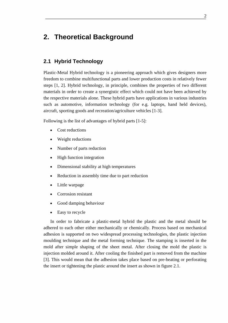
In order to fabricate a plastic-metal hybrid the plastic and the metal should be adhered to each other either mechanically or chemically. Process based on mechanical adhesion is supported on two widespread processing technologies, the plastic injection moulding technique and the metal forming technique. The stamping is inserted in the mold after simple shaping of the sheet metal. After closing the mold the plastic is injection molded around it. After cooling the finished part is removed from the machine [3]. This would mean that the adhesion takes place based on pre-heating or perforating the insert or tightening the plastic around the insert as shown in figure 2.1.

3
Figure 2.1 Metal-plastic hybrid based on the mechanical adhesion process [3]
Metals and plastics not only differ physically but chemically also they are very different from each other. Hence, adhering plastic to metal chemically would have the following difficulties: poor adhesion between a metal insert and plastic; shrinkage of plastic; residual stresses and hence bending of the hybrid [1, 5].
Coupling agents are used to improve the adhesion between two or more materials which are so different from each other, for example, plastic and metal. The coupling agents act as the intermediate layer between planar metal and planar plastic in a metal/plastic hybrid as shown in the figure 2.2.
Figure 2.2 A model of metal/plastic hybrid [5]
There are certain applications where it would be beneficial to have planar metal and plastic layers which is not possible to have with the mechanically adhered technique. For example, it could be possible that in mobile phone parts a planar metal layer is needed for conductivity purposes. In such cases, a chemically adhered metal/plastic hybrid would be perfectly applicable and it would also lead to a considerable weight reduction.
Plastic: ̴2mm
Coupling agent: ̴ 0-5 µm
Surface-treated insert: 0.5mm (oxide layer: ̴ 3-20 nm)

4
2.2 Coupling Agents
Plato, The Greek Philosopher, in his “Timaeus” says, [8]
It is not possible for two things to be fairly united without a third, for they need a bond between them which shall join them both, that as the first is to the middle, so is the middle to the last, then since the middle becomes the first and the last, and the last and the first both become middle, of necessity, all will come to be the same, and being with one another, all will be a unity.
“Organofunctional silanes are hybrid organic-inorganic compounds that are used as coupling agents across the organic-inorganic interface in order to help overcome the obstacles of bond disruption due to water wettability and reduce the stresses across the interface due to mismatch in the thermal expansion coefficients of the two totally different phases.” [8] Organofunctional silicones are hybrids of silica and of organic materials related to resins. It is not surprising that they were tested as coupling agents to improve the bonding of organic resins to mineral surfaces. [8, 15] Although any polar functional group in a polymer may contribute to improved adhesion to mineral surfaces, only a methylacrylate – chrome complex (Volan A R) and various organofunctional silanes have shown promise as true coupling agents. [8]
Silane as an adhesive – an adhesive is a gap – filling polymer used to bond solid adherents such as metals, ceramics or wood, whose solid surfaces cannot conform to each other on contact. Pure silanes are rarely used as adhesives; rather they are used to modify gap filling polymers or polymer precursors to improve surface adhesion.[8] The range of silanes available commercially is large and ever expanding. In Table 2.1 some of the commercially available silanes are listed. [17] Silane monomers may be used in integral blends of fillers and liquid resins in the preparation of composites. The modified “adhesive” in this case is termed as matrix resin. Although the coupling agent may perform the several useful functions at the interface in mineral – reinforced composites, the coupling agent, is expected, first of all, to improve the adhesion between resin and mineral, and improve retention of properties in the presence of moisture. [8,15]
The chemical bond theory for glass/resin hybrid – The chemical bonding theory is the oldest, and is still the best known, of the theories. Coupling agents contain chemical functional groups that can react with silanol groups on glass. Attachment to the glass can thus be made by covalent bonds. It can be seen from some previous studies that trialkoxysilane groups chemically bond to silanols on the mineral surface by reaction of the hydrolyzed alkoxy group forming interfacial bonds of 50-100 kcal/mol to 50-250 kcal/mol. [16] In addition, the coupling agents contain at least one other, different functional group which could coreact with the laminating resin during cure. Assuming

5
that all this occurs the coupling agent may act as a bridge to bond the glass to the resin with a chain of primary bonds. This could be expected to lead to the strongest interfacial bond. In terms of strength properties, vinlytrichlorosilane – finished gives polyester laminates with dry and wet strengths about 60% greater than those of laminates of ethyltrichlorosilane – finished glass. [8]
Table 2.1 Commercial silane adhesion promoters [17]
2.3.1. Wetting and Surface Energy Effects
Good wetting of adherend by liquid resin was of prime importance in preparation of composites. Complete wetting of a surface can be obtained if initially the adhesive is of low viscosity and has a surface tension lower than the critical surface tension γc of the mineral surface. All solid surfaces have very high γc but many hydrophilic minerals are covered with a layer of water when in equilibrium with atmospheric moisture. Hence, when in contact with the moist surface of a polar adherent in a humid atmosphere, a nonpolar adhesive would cause poor wetting and spreading, whereas a polar adhesive would either absorb the water or displace it through surface – chemical reaction. Hence addition of polar additives to adhesives enhances this mechanism. [8]

6
2.3.2. Chemistry of Silane Coupling Agents
In the periodic table, carbon and silicon belong to the same family of elements. Silicon and carbon will conveniently bond to four other atoms in their most stable state. However, silicon-based chemicals, when compared to analogous carbon-based chemicals, exhibit significant physical and chemical differences. Silicon’s electropositivity is higer than carbon, is incapable of forming double bonds and is efficient in very special and useful reactions. [9]
Figure 2.3 Carbon vs Silicon chemistry [9]
Several types of monomeric and polymeric materials are silicon-based chemicals.
Silanes are the monomeric silicon chemicals. A silane structure and an analogous carbon based structure are shown in figure 2.3. Organosilane is a silane with at least one carbon-silicon bond (CH3-Si-) structure. The carbon-silicon bond gives rise to low surface energy, non-polar, hydrophobic effects because it is very stable and non-polar. Similar effects can be achieved with carbon based compounds but it is enhanced with silanes [9]. In compounds of the structure X3SiRY, the “coupling” mechanism depends on a stable link between the organofunctional group (Y) and hydrolysable groups (X) [8].
The silicon hydride (-Si-H) structure being very reactive reacts with water to yield reactive silanol (-Si-OH) species. In the basic structure of silanes i.e. X3SiRY for reactivity and compatibility organofunctional groups (Y) are chosen while the hydrolysable groups (X) are mere intermediates in formation of silanol bonds for bonding to mineral surfaces. Hydrolytic stability of organofunctional groups attached to silicon through alkoxy or acyloxy linkages is not sufficient enough to provide

7
environmentally stable bonds between resin and reinforcement. Hence, silanes with glycidoxy or methacryloxy substituents on silicon or allyoxysilanes are not useful as coupling agents. But functional alkoxysilanes having a negative substituent on the second carbon of the alkoxy group may have an exception. Compounds of germanium, tin, titanium and zirconium when compared to silicon compounds were much less effective as coupling agents. [8]
When chlorine, nitrogen, methoxy, ethoxy or acetoxy are directly attached to silicon then it yields chlorosilanes, silylamines (silazanes), alkoxysilanes and acyloxysilanes respectively. Such molecules are very reactive and exhibit a unique inorganic activity [9]. Hydrolysis of trialkoxysilanes, RSi(OR)3, in water takes place in a stepwise manner in order to give the corresponding silanols, ultimately condensing to siloxanes. Hydrolysis and condensation reaction rates strongly depends on pH, but under optimum conditions the hydrolysis is relatively fast (minutes), while the condensation reaction is much slower (several hours). Both the hydrolysis and condensation reactions are shown in the equation below [9]
Equation 2.1 Hydrolysis and condensation reactions of silane [9] In order to make organofunctional groups function between organic resins and mineral fillers, silanol groups are necessary. Importance of silanol groups could be illustrated by the following example; methacrylate-functional siloxanes applied to glass fibers from toluene solution were not effective coupling agents in polyester laminates, while methacrylate-functional silanols are among the most effective coupling agents for polyesters. [8]
While selecting a silane coupling agent following factors must be taken care of [9]: 1. All silane coupling agents with three hydrolysable groups on silicon should bond
equally well with an inorganic substrate. 2. Organofunctional group on silicon should be matched with the resin polymer
type to be bonded in order to make sure about the type of silane coupling agent to be used in a particular application.
2.3.3. Silane – Inorganic Substrate Bond
The bond between silane coupling agents containing three organic reactive groups on silicon (usually methoxy, ehoxy or acetoxy) and metal hydroxyl groups on most inorganic substrates will be good, especially if silicon, aluminum or a heavy metal is
Hydrolysis Condensation

8
present in the substrate’s structure. As shown in the Figure 2.4 (a) silane undergoes hydrolysis either through addition of water or by residual water on the inorganic surface and gives out corresponding silanols. These silanols further coordinate with metal hydroxyl groups on the inorganic surface and undergo condensation to form an oxane bond and give out water as shown in figure 2.4 (b). [9]
Figure 2.4 (a) Hydrolysis and condensation (b) Bonding to inorganic surface [9]
Silicon is less electronegative than carbon on the Pauling scale [11]. The silicon-
carbon bond is 12% ionic in character, whereas the silicon-oxygen bond has 50% ionic character. The ionic character of the oxane bonds between silicon and most metals is even higher. There is a bridge of organic covalent bonds between silane coupling agents and organic resins meanwhile there are typically inorganic with high degree of ionic character bonds between silane coupling agents and mineral surfaces. In organic chemistry covalent bond formation is determined by thermodynamics and kinetics of possible competing reactions in a competitive environment. [8, 9] The process of forming and breaking of bonds is not reversible. Bonds will prevail on a strong influence that the catalyst may have. But in case of ionic bonds in organic chemistry, it is the equilibrium constants and not kinetics on which it is based on. Bonds are formed and broken in reversible reactions and are determined by concentrations and equilibrium constants. Catalyst may change the rates of reaction but might have no influence in determining the final concentrations. In case of the coupling agent and the resin a hydrolysis-resistant bridge is readily formed. The water resistance of a hybrid/composite is largely dependent on the equilibrium conditions of bonds between coupling agent and hydroxyl groups of the mineral in the presence of water. [9, 16]
Silane molecules, give a multimolecular structure of bound silane coupling agent on the surface, by reacting with each other. Ideally, a monolayer of silane applied to the inorganic surface would result in a tight siloxane network close to the inorganic surface. But practically applying a monolayer of silane would be difficult, hence giving rise to diffusion due to the presence of more than one layer. [8, 15]
(a) (b)
9
2.3.4. Other Coupling Agents
Silanes have predominated as coupling agents but titanate, zirconate and other coupling agents are also used as coupling agents. These coupling agents, like silane, react with surface hydroxyl groups, but there is no condensation polymersization in order to produce a polymer network at the interface. [17]
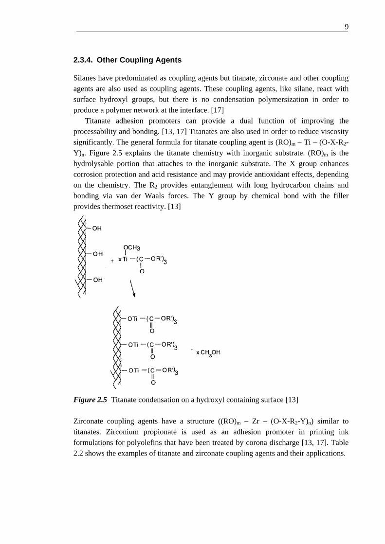
Titanate adhesion promoters can provide a dual function of improving the processability and bonding. [13, 17] Titanates are also used in order to reduce viscosity significantly. The general formula for titanate coupling agent is (RO)m – Ti – (O-X-R2-Y)n. Figure 2.5 explains the titanate chemistry with inorganic substrate. (RO)m is the hydrolysable portion that attaches to the inorganic substrate. The X group enhances corrosion protection and acid resistance and may provide antioxidant effects, depending on the chemistry. The R2 provides entanglement with long hydrocarbon chains and bonding via van der Waals forces. The Y group by chemical bond with the filler provides thermoset reactivity. [13]
Figure 2.5 Titanate condensation on a hydroxyl containing surface [13] Zirconate coupling agents have a structure ((RO)m – Zr – (O-X-R2-Y)n) similar to titanates. Zirconium propionate is used as an adhesion promoter in printing ink formulations for polyolefins that have been treated by corona discharge [13, 17]. Table 2.2 shows the examples of titanate and zirconate coupling agents and their applications.

10
Table 2.2 Properties of zirconate and titanate coupling agents [13]
2.3 Substrate
2.3.1. Stainless Steel
Stainless steels (Fe based alloy with a minimum of 10.5% Cr by mass) are utilized in many fields of technology due to their excellent corrosion resistance, physical and mechanical properties. The traditional and well established applications of stainless steel would include construction, transportation and process industry, whereas the upcoming developments would include medical application (implants) and energy industries (power plants and solar thermal collectors) and many other fields. [20-22]

11
In stainless steels the main purpose of adding Cr is to improve their corrosion resistance. In order to enhance the bulk and surface properties other alloying elements could be added. Based on their microstructure, stainless steels are divided into five main groups: ferritic, austenitic, martensitic, duplex (austeno-ferrictic), and precipitation hardening stainless steels. [23]
It is the complex interaction of oxygen with the alloy surface results in a protective oxide film which makes stainless steel so useful. In order to attach the oxygen atoms to the metal by a chemical bond it is essential to break in the reaction with the surface the internal bonding of oxygen-containing molecules. This process is called dissociative chemisorption and it is the first step in the process of surface oxidation of metals. Under normal conditions the oxidation is due to O2 which dissociates at room temperature on all metals except gold. [24] The chemisorption stage’s kinetics is affected by temperature as well as surface structure and composition although it is not usually limiting to the overall oxidation process. For example, surface segregation of sulphur may compete for free adsorption sites with oxygen, which obstructs oxidation of steels at high temperature. [25] In oxidizing conditions, the surface coverage of oxygen continues to increase until at some point the incorporation takes place via the place exchange mechanism resulting into the interchange in positions of adsorbed oxygen anions and adjacent metal cations. [26] This process leads to oxide nucleation and the transformation of the chemisorbed layer into metal oxide begins, where the place exchanged cations continue to provide sites for further adsorption. Also, the nucleation is helped by low metal-metal bond strength and high metal-oxygen bond strength. [24] After nucleation the lateral growth of an oxide island continues until it finds another oxide island, and the surface is covered with two-dimensional oxide structure. This intermediate oxide phase occurs before the growth of the three-dimensional protective oxide film, which is limited by diffusion of metal ions and oxygen across the oxide film. [26] The oxidation proceeds via field enhanced transport of ions through the oxide layer. Eventually the oxidation rate becomes negligible as the layer thickness increases and the field strength decreases, signifying the onset of protective oxide layer formation.
The general-purpose grades of stainless chromium-nickel (Cr-Ni) steels provide with good resistance to atmospheric corrosion and many organic and inorganic chemicals. The following grades of steel would fall in this category of general-purpose Cr-Ni steels: EN 1.4318, EN 1.4301, EN 1.4307, EN 1.4311, EN 1.4541 and EN 1.4306. They are suitable for processing, storing and transporting foodstuffs and beverages. It is with their good formability and that they are supplied with a wide range of functional and aesthetic surfaces, makes them suitable for use in a variety of applications [6].
The plastic and stainless steel hybrid gives the best combination of properties and favourable processing conditions. The material properties of stainless steel are

12
independent of temperature over a wide range. Steel contributes to the following advantages in a hybrid: higher Young’s modulus, high ductility, low thermal expansion coefficient, high stiffness and favourable failure behaviour in crash events for example in a car door [1].
The standard Cr-Ni stainless steel grades are non-magnetic in the annealed condition but may become slightly magnetic as a result of phase transformation to martensite or ferrite after cold working and welding respectively. [6, 7]
The versatile corrosion resistance property of the Cr-Ni standard steels make them suitable for a wide range of general-purpose applications. A uniform crack on the stainless steel surface that has come into contact with a corrosive medium signifies uniform corrosion. If the corrosion rate is less than 0.1 mm/year then the corrosion resistance is generally regarded as good. An example of grades’ EN 1.4301 and EN 1.4436 corrosion resistance is shown in the figure below. [6, 7]
Figure 2.5 Isocorrosion diagram for 4301 (EN 1.4301), 4436 (EN 1.4436) and 904L (EN 1.4539) in stagnantsulphuric acid. The curves represent a corrosion rate of 0.1 mm/year. The dashed line represents the boiling point. [6, 7]
These grades are sufficiently resistant to most of the environments except marine and coastal, where EN 1.4401 or higher grades must be used. The above mentioned resistance pertains to the appearance only. Washing should be done to prevent the formation of deposits, which could lead to corrosion, in heavy industrial or polluted areas. The resistance to pitting and crevice corrosion, typically occurring in acidic, neutral or slightly alkaline solutions, provided by these grades is moderate compared to other high alloy stainless steels. All these grades are vulnerable to stress corrosion cracking but are more or less immune to intergranular corrosion because it is not

13
regarded as a common problem in the modern stainless steel as the carbon content is generally kept low in them [6].
In case of hot forming it could be carried out between 850 - 1150°C but in order to achieve maximum corrosion resistance, forgings should be annealed at 1050°C and should be immediately cooled in air or water. All these grades can be readily formed and fabricated by a full range cold working operations. Any of the cold working operations would elevate the strength and hardness of the material but will also make the material slightly magnetic (Figure 2.6). Partial transformation of the austenite phase to hard martensite phase emphasises work hardening. The stability of austenite decreases at lower contents of alloying elements. During cold working more martensite is formed making the cold working operation difficult and leading to embrittlement of the product. Hence for cold working operations a grade with more stable austenite structure is preferable, e.g. 1.4306 [6].
Figure 2.6 EN 1.4301 work hardening at cold working [6]
In order to perform quench annealing, the temperature should be 1000 - 1100°C and followed by rapid cooling in water or air. Stress relief treatment should be done for the applications where high residual stresses cannot be accepted. In order to harden these grades cold working is suitable and not heat treatment [6].
The machinability of these austenitic grades is more difficult than ordinary carbon steels but easier than high alloyed stainless steel grades. The machinability index gives the machinability of these grades when compared to other stainless steels (Figure 2.7).

14
Figure 2.7 Relative machinability of some stainless steel grades in comparison with EN 1.4436 [6]
This index is based on compounded evaluation of test data from several different machining operations and it rises with increased machinability.
These grades can be welded using conventional welding methods such as [6]:
1. Shielded metal arc welding (SMAW)
2. Gas tungsten arc welding, TIG (GTAW)
3. Gas metal arc welding, MIG (GMAW)
4. Flux-cored arc welding (FCAW)
5. Plasma arc welding (PAW)
6. Submerged arc welding (SAW)
2.3.2. Surface treatment for stainless steel inserts
Silanes arrange themselves in layers with a high degree of order, influenced to a great extent by the surface of the substrate. Table 2.2 shows the relative influence of the type of substrate on the effectiveness of silane coupling agents in improving the adhesion. Silanes have a tendency of arranging themselves perpendicular to the metal surface. A rough surface can break up the first ordered layer, preventing the formation of second. [13]

15
Table 2.2 Influence of type of substrate on effectiveness of silane coupling agents [13]
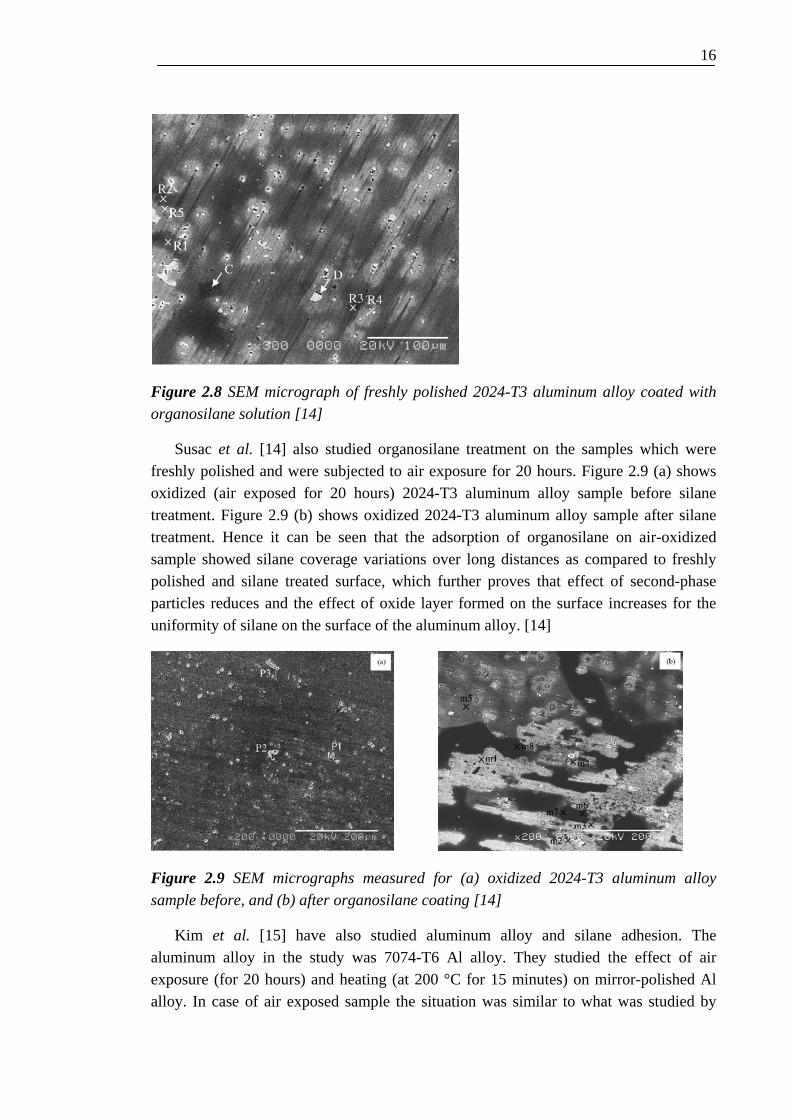
Adhesion of the silane to the metal surface can be influenced by the modification of the metal surface. Susac et al. [14] confirmed that this is true especially in case of aluminum, when they studied the adhesion of organosilane on 2024-T3 Al alloy. Mechanically polished fresh and air exposed (20 h) samples were used for the silane treatment. Figure 2.8 shows the deposition of organosilane on a freshly polished 2024-T3 Al alloy sample, most likely having a thin oxide layer on it, resulted in an uneven coverage which was strongly influenced by the presence and distribution of the underlying second-phase particles. According to Susac et al [14], the chemistry behind the fact that the freshly polished 2024-T3 alloy sample is strongly influenced by the microstructure at the alloy surface depends on several factors. As suggested by Plueddemann [8], the formation of direct M-O-Si bonding depends on a condensation reaction between the silane molecule and OH groups on the oxidized film at the metal surface. A range of factors including oxide composition and structure, the amount of atmospheric exposure and the nature and level of impurities decide the density and acidity of the hydroxyl groups [8]. In this particular case discussed by Susac et al. [14] the process of silane adsorption is expected to start with some etching of the thin oxide film present because the pH of the organosilane is just outside the stability range of Al2O3. Finally it is believed that a local pH change would occur due to the galvanic coupling between the second-phase particle and its surrounding matrix and this pH change would affect the rate of matrix etching in a zone around the particle compared to more distant areas. All these points clearly suggest that silane adsorption would have a significant effect due to the variations in distribution and composition of the surface microconstituents. [14]
16
Figure 2.8 SEM micrograph of freshly polished 2024-T3 aluminum alloy coated with organosilane solution [14]
Susac et al. [14] also studied organosilane treatment on the samples which were freshly polished and were subjected to air exposure for 20 hours. Figure 2.9 (a) shows oxidized (air exposed for 20 hours) 2024-T3 aluminum alloy sample before silane treatment. Figure 2.9 (b) shows oxidized 2024-T3 aluminum alloy sample after silane treatment. Hence it can be seen that the adsorption of organosilane on air-oxidized sample showed silane coverage variations over long distances as compared to freshly polished and silane treated surface, which further proves that effect of second-phase particles reduces and the effect of oxide layer formed on the surface increases for the uniformity of silane on the surface of the aluminum alloy. [14]
Figure 2.9 SEM micrographs measured for (a) oxidized 2024-T3 aluminum alloy sample before, and (b) after organosilane coating [14]
Kim et al. [15] have also studied aluminum alloy and silane adhesion. The aluminum alloy in the study was 7074-T6 Al alloy. They studied the effect of air exposure (for 20 hours) and heating (at 200 °C for 15 minutes) on mirror-polished Al alloy. In case of air exposed sample the situation was similar to what was studied by
17
Susac et al. [14]. Second-phase particles and matrix (surface microstructure) contributed to adhesion of silane to the alloy. Meanwhile, in case of heat treatment of the Al alloy at 200 °C for 15 minutes oxides grew on the second-phase particles and matrix resulting into an even layer of silane after silane treatment on the heat treated Al alloy. [15]
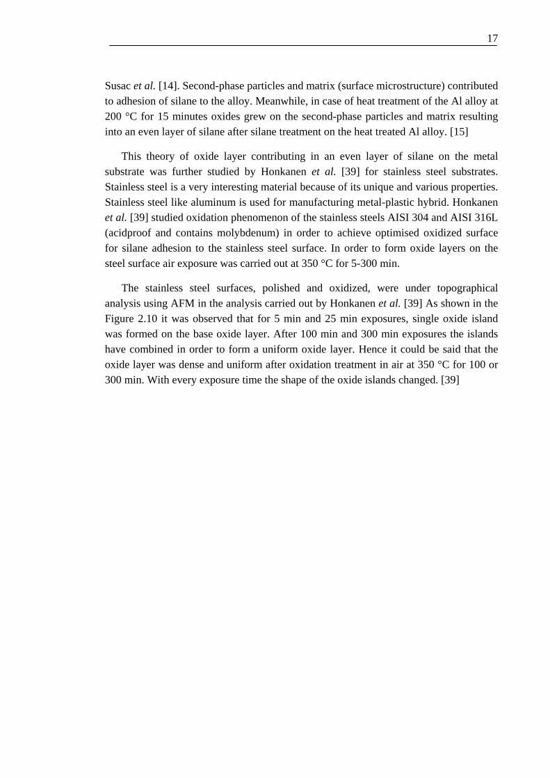
This theory of oxide layer contributing in an even layer of silane on the metal substrate was further studied by Honkanen et al. [39] for stainless steel substrates. Stainless steel is a very interesting material because of its unique and various properties. Stainless steel like aluminum is used for manufacturing metal-plastic hybrid. Honkanen et al. [39] studied oxidation phenomenon of the stainless steels AISI 304 and AISI 316L (acidproof and contains molybdenum) in order to achieve optimised oxidized surface for silane adhesion to the stainless steel surface. In order to form oxide layers on the steel surface air exposure was carried out at 350 °C for 5-300 min.
The stainless steel surfaces, polished and oxidized, were under topographical analysis using AFM in the analysis carried out by Honkanen et al. [39] As shown in the Figure 2.10 it was observed that for 5 min and 25 min exposures, single oxide island was formed on the base oxide layer. After 100 min and 300 min exposures the islands have combined in order to form a uniform oxide layer. Hence it could be said that the oxide layer was dense and uniform after oxidation treatment in air at 350 °C for 100 or 300 min. With every exposure time the shape of the oxide islands changed. [39]

18
Figure 2.10 AFM images of (a) fresh, industrially polished AISI 304, (b) 5 min oxidised at 350 °C, (c) 25 min oxidised at 350 °C, (d) 100 min oxidised at 350 °C and (e) 300 min oxidised at 350 °C [39]
Therefore, from the studies of Susac et al., [14] Kim et al. [15] and Honkanen et al., [39] it can be concluded that in order to have an optimal surface for metal-hybrid adhesion the metal surface should undergo the process of oxidation as a pre-treatment step.
2.4 Plastic
The main objective of this thesis was to characterize the metal-silane interface in order to provide an optimal silanised metal substrate for manufacturing a metal-plastic hybrid. Manufacturing of the hybrid is out of the scope of this study. But still in this section the

19
possibility of using certain compatible plastics would be discussed. Basically the bonding of silanes with polymers is complex and the reactivity and solubility of polymers should match to those of the silane used.
Silane has a general formula, X3SiRY where the silicon functional group X is the hydrolysable group which is chosen to react with the surface hydroxyl groups of the substrate (stainless steel in this case) to be used in the metal-plastic hybrid in order to produce a stable bond. The organofunctional group Y is tightly bound to silicon via a short carbon chain and it also links with the polymer. This group has to make sure of the complete compatibility to the resin system. Bonding in the polymer takes place chemical reactions or physicochemical interactions such as hydrogen bonding, acid base interaction and interpenetration of polymer network (entanglement) or electrostatic attraction. Table 2.3 shows a list of polymers and recommended silanes for them. The list is non-exhaustive and variations are possible. [17]
Table 2.3 Types of polymers and recommended silanes [17]
Hence, plastic and silane selection is dependent on their compatibility with each other and the product that would be desirable. The schematic diagram of the final hybrid part with various component thicknesses is shown in the Figure 2.11.

20
Figure 2.11 Schematic preparation of the hybrid part and thicknesses of various components in the hybrid [5]
2.5 Silane treatment
The rate at which the hydrolysis and condensation reactions mentioned earlier proceed depend on various parameters such as the nature of the R group (i.e. the organofunctionality), concentration of silane solution, pH, aging time of the solution, curing time and temperature for the formation of the silane layer on the substrate. Hence in order to improve the silane/substrate interface it requires optimization of the silanization process by accelerating the hydrolysis process and minimizing the condensation step. [12] Apart from the factors effecting the hydrolysis and condensation reactions there are factors which affect the overall stability and uniformity of the silane layer on the substrate. Electrolytical polishing and oxidation of the stainless steel inserts improved significantly the stainless steel insert adhesion to silane solution is one such factor which was discussed in the earlier section. [18] The angle at which the metal substrate is kept after removing it from the silane solution and before allowing it to cure in the oven or at room temperature is another such factor.
In this section more about the parameters that are concerned with silane solution preparation would be discussed. These parameters (concentration of silane solution, pH, aging time of the solution, curing time and temperature for the formation of the silane layer on the substrate) influence the kinetics of hydrolysis and condensation reactions on one hand and on structure and adhesion-promoting properties of the so-formed interphase on the other hand. [12, 28] The basic reaction and bonding mechanism of alkoxysilane is shown in the Figure 2.4. The parameters that will be discussed in this section would influence all these reactions. Chovelon et al. [12] have discussed some of the parameters for γ-APS on AISI 304 L stainless steel panels. The general procedure followed by them was as follows, the stainless steel substrates were cut into coupons of size 10 x 50 mm. prior to silane deposition, these coupons were cleaned ultrasonically in acetone for 5 min at room temperature then dipped in acetone at 60°C for 5 min, were chemically treated in sulfochromic bath at 60°C for 10 min, rinsed with distilled water and blown dry with nitrogen. The substrates were dipped into silane solution 1 min after pretreatment and cleaning. In all the cases the dipping time was 1 min because in such conditions the solution remains mainly constituted with silane monomers partially and/or entirely hydrolyzed and not at all with oligomers resulting from condensation
21
reaction. After silanisation the silane films were blown dry with nitrogen and heated for 1 hour at 100°C in air. After curing step the silane film was rinsed with distilled water for 2 min in order to remove any weakly bound or physisorbed species. On analyzing, it was shown that the influence of the silane concentration was significant. It was seen that the thickness of the silane layer gradually increased till the concentration of the silane went to 0.3% and then started decreasing. From the results of Ishida et al. [18] and their own results, Chovelon et al. concluded that, for same immersion conditions and low γ-APS concentrations, the silane film deposited on the substrate surface has grown in an ordered manner. It was possible for many hydroxyl groups originating from the hydrolysis of ethoxy groups to react with the sites available at the material surface. But when the γ-APS concentration was more than 0.3% then defect formation and disruption of the silane film occurs. Figure 2.12 below represents the XPS survey scan recorded from the stainless steel surface after the chemical treatment and from the same surface either with thin silane films or with thicker ones (thick films were obtained as the final washing was skipped). The intensity of Si2p photopeaks is quite weak and the corresponding signals are hardly visible owing to a very low ionization cross-section of SiL shells. But the decreasing substrate signal (Cr2p and Fe2p photopeaks) indicates the presence of silane layer on the substrate. It can be estimated, based on the hypothesis that the silane layer is uniform, that the layer thickness is few nanometers till the substrate signal does not disappear completely.

22
Figure 2.12 XPS survey scan of stainless steel surfaces: (a) chemically treated, (b) and (c) covered with a thin γ-APS layer, and (d) covered with a thick and unwashed γ-APS layer. [12] Several literature proofs are available to indicate the fact that pH of the silane solution could influence the nature of the solution in terms of its chemical behavior. Abel et al. [19] have described this effect of pH of γ-GPS (1% solution) on 2024-T3 unclad aluminum alloy. They have varied the pH from 3 to 11 by controlling it with acid (acetic) and alkali (sodium hydroxide). Depending on the silane used, the substrate and the polymer/adhesive adhered on the silane layer pH 5 was suitable for the process. [19] While in case of Chovelon et al. [12] the silane solution being γ-APS and substrate being stainless steel the suitable pH turned out to be the natural pH of γ-APS (10.6). This helps the process because hydroxysilanes are formed at alkaline pH because of hydrolysis of γ-APS and are stabilized in the solution by hydrogen bonding. The condensation delay here promotes the chemical reaction of monomers with the surface sites. Also, surface potential of the surface varies with pH of the applied solution which

23
would ultimately affect the nature of the silane layer on the substrate. [12] Figure 2.13 shows the LEEIXS measurements for the effect of aging time of the silane solution on the film thickness on the substrate surface. It is seen that the silane film thickness increases up to 800 seconds of aging. In this period partial condensation reactions take place in the solution and hence the solution remains essentially constituted of monomeric silanols which are prone to react easily with the sites available on the material surface. For longer aging times the condensation reactions are more advanced and they behave in a similar way as in high γ-APS concentration described earlier.
Figure 2.13 LEEIXS measurements of the effect of the γ-APS solution aging on the thickness of the silane film deposited [12] Curing/drying temperature is another factor that enhances silane layer adhesion to the materials surface. Chovelon et al. concluded that the best performance for γ-APS on stainless steel was obtained at temperature between 100 and 150°C. Above this temperature the interdiffusion of silane and epoxy adhesive (polymer) is lower. [12] It could also be seen from previous studies that curing time at a particular curing temperature is very critical. Curing time before the silanized surface is kept in oven and curing time in the oven. Both these parameters are not discussed in detail in literature but they are critical parameters.
2.6 Interfacial Bonding Analysis
In the literature related to silane and metal bonding the interfacial bonding studies are carried out using SEM and XPS techniques.
2.6.1. X-ray photoelectron spectroscopy
In nanophase materials research the use of surface science methods has been widely and successfully employed. This is because of the limitation of the surface science methods

24
by their physical operation principle to provide information exclusively from the topmost atomic layers of the surface. It is the recent development of novel atomic resolution imaging and spectroscopic methods that are capable of operating not only under vacuum but also in high-pressure environments have made it possible to reach new insights to the molecular level understanding of materials science and engineering. [27]
X-ray photoelectron spectroscopy (XPS) is a quantitative technique that measures the elemental composition, empirical formula, chemical state and electronic state of the elements that exist within the material. XPS can be performed using either a commercially built XPS system, a privately built XPS system or a synchrotron based light source combined with a custom designed electron analyzer. In case of XPS the surface analysis is based on the photoelectric effect. In photoelectric effect the emission of photoelectrons from a solid surface is achieved by irradiating it with known energies of soft X-rays. [28, 31] This phenomenon could be seen in the Figure 2.15 (a) and is known as photoemission. The kinetic energies (KE) of the photoelectrons are given by:
KE = hv – BE – ϕs
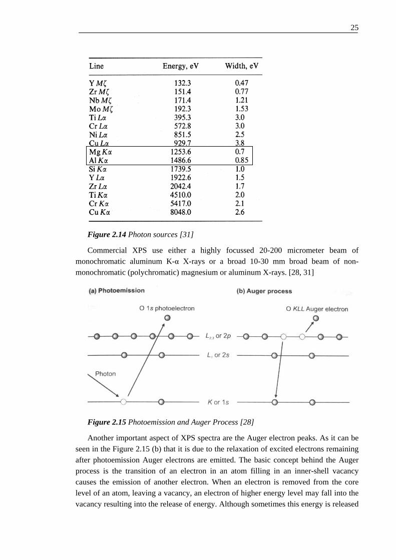
hv is the photon energy, BE is the characteristic Binding energy of the atomic orbital from which the electron originates, and ϕs the spectrometer work function. It is true that any photon whose energy exceeds the work function of the solid (hv > ϕ) can be used for photoelectron spectroscopy which simply eliminates the near ultraviolet, visible and higher wavelength radiation. In practice, nearly all photoelectron spectroscopy has been performed in two relatively narrow energy ranges defined by convenient intense laboratory sources. The first range is provided by light from gas discharge sources and particularly the intense line emission from He and other inert gases: for He the main lines have photon energies of 21.2 and 40.8 eV. For other inert gases the main emissions have somewhat lower energies. It is not possible to access the significant core levels with these sources. The second readily available photon energy range is usually restricted to two lines, the Aluminum (Al) and Magnesium (Mg) Kα X-ray emissions at 1486.6eV and 1253.6eV respectively which is also mentioned in Figure 2.14 [32]
25
Figure 2.14 Photon sources [31]
Commercial XPS use either a highly focussed 20-200 micrometer beam of monochromatic aluminum K-α X-rays or a broad 10-30 mm broad beam of non-monochromatic (polychromatic) magnesium or aluminum X-rays. [28, 31]
Figure 2.15 Photoemission and Auger Process [28]
Another important aspect of XPS spectra are the Auger electron peaks. As it can be seen in the Figure 2.15 (b) that it is due to the relaxation of excited electrons remaining after photoemission Auger electrons are emitted. The basic concept behind the Auger process is the transition of an electron in an atom filling in an inner-shell vacancy causes the emission of another electron. When an electron is removed from the core level of an atom, leaving a vacancy, an electron of higher energy level may fall into the vacancy resulting into the release of energy. Although sometimes this energy is released

26
in form of an emitted photon, the energy can also be transferred to another electron, which is ejected from the atom. This second ejected electron is called an Auger electron. [28, 33] The Auger electron’s kinetic energy is given by,
KE = BEA – BEB – BEC – S
BEA is the energy of the initial hole level, BEB the energy of the level from which the initial hole is filled and BEC the binding energy of the level from which the auger electron is released. It is with the X-ray notation of the levels involved, like for example O KL23L23 that the Auger peaks are labelled [34]
In an XPS spectrum which is measured from a mixture of elements has features from each of the individual constituents. The first step in analysis of the characteristic peaks would be to identify the elements present by the characteristic energies of their photoelectron and Auger electron peaks. In order to obtain their relative atomic concentrations synthetic components from integrated peaks are fitted to the data and the cross-section of each transition is taken into account. [28, 35] It is from the peak positions and the separations, as well as from certain spectral features that the chemical states and compounds could be identified and this justifies the acronym ESCA (Electron Spectroscopy for Chemical Analysis) that is also associated with XPS [36].
Using the XPS technique it is possible to study nanoscale surface structures, such as protective oxide film on stainless steel surface without any intense and obscuring signals from the bulk of the material. This is possible because although the X-ray radiation can penetrate several micrometers into the solid, there is a very short mean free path of the emitted electrons. The mean free path is actually of the order of few nanometers. Hence, it is only from the topmost atomic layers of the surface that the electrons detected by XPS originate.[28, 31, 34]
There have been some groups which were involved in order to study the behaviour of silane on inorganic substrates. Moses et al. [36] studied the adsorption of γ-APS (γ- aminopropyltriethoxysilane) onto metal oxide electrodes. There were two components that they observed for N (1s) peak of γ-APS absorbed on SnO2 electrodes at 400.3 and 401.9 eV which were attributed to free and protonated amino groups respectively. It is by rinsing the films with acidic or basic solutions that the free and the protonated groups could be interchanged. However, some of the groups were irreversibly protonated and some irreversibly free. They also suggested that the irreversibly protonated amino groups were associated with hydrogen bonding between the amino groups and the silanol groups or the hydroxyl groups on the oxidized metal surfaces.
Horner et al. [37] have reported their findings using XPS in order to determine the molecular structure of thin films formed by the adsorption of γ-APS onto the oxidized surfaces of metals having a range of isoelectric points. They show that some of the

27
amino groups are protonated when γ-APS is deposited on the oxidized surfaces of metals and also that the extent of protonation is greatest on acidic surfaces such as silicon, titanium and aluminum; intermediate on the surfaces with intermediate acidity such as iron and nickel, and least on basic surfaces such as magnesium. Their results show that the protonation is more on aluminum that has been pretreated by etching than on aluminum that has been mechanically polished.
2.6.2. Scanning electron microscope
A scanning electron microscope (SEM) is a type of a microscope which images a sample with a high-energy beam of electrons in a raster scan pattern. [29] The electrons interact with the atoms that form the sample and produce signals that contain information of topography, composition and in this study interfacial bond. The type of signals produced by a SEM include secondary electrons (SE), backscattered electrons (BSE), characteristic x-rays, cathodoluminescence, specimen current and transmitted electrons. Different detectors are used in order to detect the above mentioned signals. Usually, a secondary electron and a BSE detector is used and installed with the microscope. [29]
As a result of the interaction between high energy electrons and a sample under investigation in an electron microscope, the atoms of this sample are caused to emit X-rays. An EDS (Energy dispersive x-ray spectroscopy) system makes use of the fact that atoms of different chemical elements emit X-rays of different, characteristic energy. The evaluation of the energy spectrum collected by an energy dispersive Si(Li) or silicon drift X-ray detector (SDD) allows the determination of the qualitative and quantitative chemical sample composition at the current beam position. This technique provides a very high spatial resolution since the information is obtained from a very small sample volume in the order of only a few microns. It is therefore also referred to as X-ray microanalysis. [29]

28
3. Research methods and materials
3.1. Main aim of the study
The experimental part of the thesis consists of silane/stainless-steel sample preparation in order to facilitate the process of plastic/metal hybrid in further studies. There are certain procedures that are followed in order to achieve the above mentioned target. The materials were selected and chosen with reference to the previous studies. Various parameters were tested in order to obtain an even and a thin layer of silane on the stainless steel insert. These tests were concentrated on the silane solution’s stability, stainless steel insert and for the stability of silane on the stainless steel insert. Stainless steel was pre-treated in order to form an oxide layer on it prior to treating it with silane. This oxide layer enhanced the bonding of silane on the stainless steel insert. The aim of this study was to characterize the silane layer on the stainless steel substrate. The uniformity and thickness of the silane layer on the stainless steel insert will have a very important role in contributing to form a strong hybrid between stainless steel and plastic. The silane used in this study is an aminofunctional silane which is well known for its coupling properties.
The primary goal of the experiments was to test various parameters affecting to the uniformity and thickness of the silane layer on the stainless steel insert. Optical microscope and scanning electron microscope were used to visualize the silane layer, x-ray photoelectron spectroscopy to study the bonds between stainless steel and silane. In order to visualize the thickness of the silane layer on the stainless steel insert, cross-sectional analysis method was used.
3.2. Materials
3.2.1. Stainless Steel
As a substrate material, stainless steel 4301 (AISI 304) from Outokumpu Tornio Works, Finland was used. Its chemical composition and nomenclature are given in the Table 3.1. In the experiment the stainless steel insert used was as-received and polished stainless steel surface. Steel inserts were cold rolled, heat treated and pickled by Outokumpu Tornio Works. These steel inserts were as-received inserts. The stainless steel inserts were cut with dimensions 99.5 mm × 11.8 mm × 0.5 mm. The edges of the
29
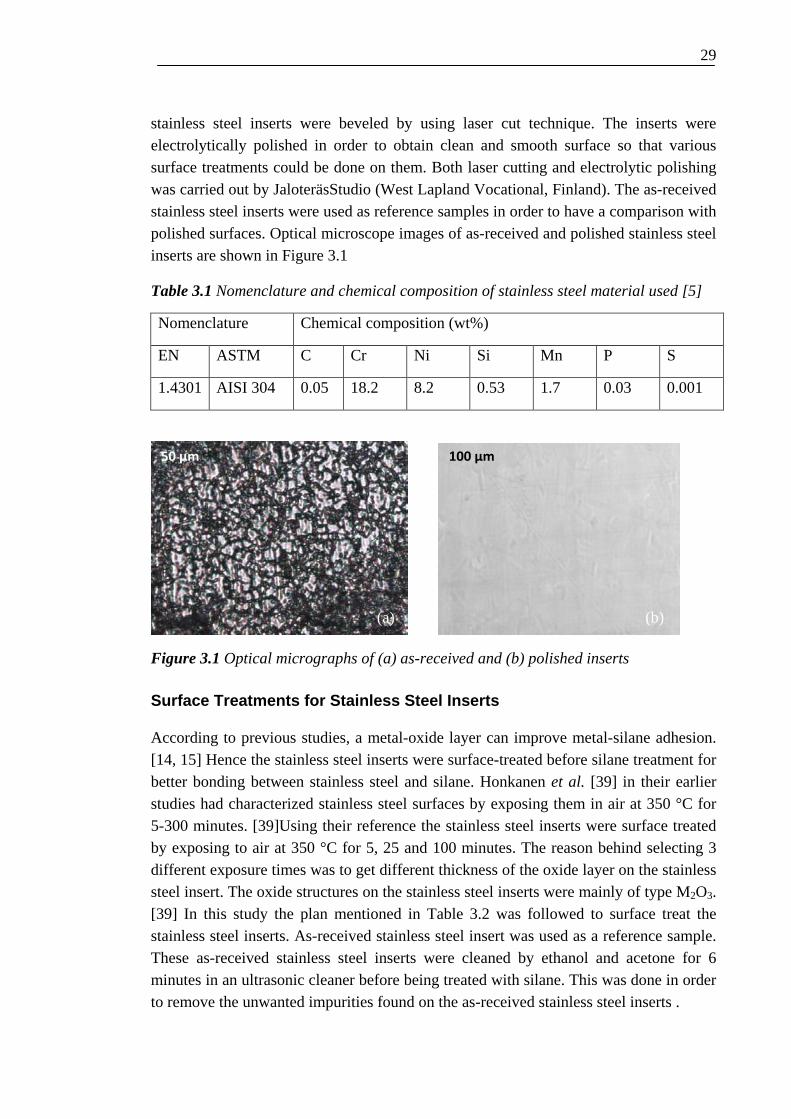
stainless steel inserts were beveled by using laser cut technique. The inserts were electrolytically polished in order to obtain clean and smooth surface so that various surface treatments could be done on them. Both laser cutting and electrolytic polishing was carried out by JaloteräsStudio (West Lapland Vocational, Finland). The as-received stainless steel inserts were used as reference samples in order to have a comparison with polished surfaces. Optical microscope images of as-received and polished stainless steel inserts are shown in Figure 3.1
Table 3.1 Nomenclature and chemical composition of stainless steel material used [5]
Nomenclature Chemical composition (wt%)
EN ASTM C Cr Ni Si Mn P S
1.4301 AISI 304 0.05 18.2 8.2 0.53 1.7 0.03 0.001
Figure 3.1 Optical micrographs of (a) as-received and (b) polished inserts
Surface Treatments for Stainless Steel Inserts
According to previous studies, a metal-oxide layer can improve metal-silane adhesion. [14, 15] Hence the stainless steel inserts were surface-treated before silane treatment for better bonding between stainless steel and silane. Honkanen et al. [39] in their earlier studies had characterized stainless steel surfaces by exposing them in air at 350 °C for 5-300 minutes. [39]Using their reference the stainless steel inserts were surface treated by exposing to air at 350 °C for 5, 25 and 100 minutes. The reason behind selecting 3 different exposure times was to get different thickness of the oxide layer on the stainless steel insert. The oxide structures on the stainless steel inserts were mainly of type M2O3. [39] In this study the plan mentioned in Table 3.2 was followed to surface treat the stainless steel inserts. As-received stainless steel insert was used as a reference sample. These as-received stainless steel inserts were cleaned by ethanol and acetone for 6 minutes in an ultrasonic cleaner before being treated with silane. This was done in order to remove the unwanted impurities found on the as-received stainless steel inserts .
50 µm 100 µm
(a) (b)

30
Table 3.2 Details of different surface treatments on stainless steel inserts
1. As received
2. Electrolytically polished
3. Electrolytically polished + 5 min oxidation (350°C)
4. Electrolytically polished + 25 min oxidation (350°C)
5. Electrolytically polished + 100 min oxidation (350°C)
3.2.2. Silane
Silane (Dow Corning Z-6020, N-(beta aminoethyl)-gamma -aminopropyltrimethoxysilane) which is used as a coupling agent to make stainless steel/plastic hybrids was used as a substrate solution in this study. The as-received and surface-treated stainless steel inserts were treated with silane solution in order to test the behaviour of silane on the stainless steel surfaces. The concentration of silane in the solution and the pH of the final solution were varied in order to test and get best results. [30] Different silane concentrations and different pH of the final solution that were used in the experiment are mentioned in the Table 3.3. Using the study carried out by Hoikkanen et al. the parameters that were to be varied to make silane solution were formulated. [37]
Table 3.3 Silane solutions used in studies
pH of the silane solution Concentration of Silane in the Solution (vol%)
4-5
7-8
9
0.25% (Water Based)
0.5% (Water Based)
1% (Water Based)
0.5% (Water+ethanol based)
Different silane solutions were prepared using the parameters mentioned in the Table 3.3. The method followed to make these different solutions was to vary the pH of the solution and keep the concentration constant and vice versa. All these different solutions were applied on the stainless steel inserts in order to determine the parameters which would result into a solution that would give a uniform silane layer on the stainless steel insert. All the solutions were stirred for 1 hour.

31
After preparing these different silane solutions the as-received and surface-treated stainless steel inserts were dipped into these solutions for 5 min. After 5 min the samples were taken out of the solution and kept at an angle of 30°. These samples were kept in this state for 2 min and the curing was done. The process of curing was performed in a convection oven in air at 110 °C. Curing time was varied. Two curing times were used; 10 min and 20 min. Once curing was completed the silane layer was rinsed with water or ethanol in order to remove the excess of silane, loosely bonded to the stainless steel inserts. The rinsing parameters are mentioned in Table 3.4.
Table 3.4 Rinsing Methods
Rinsing methods for excess silane on stainless steel inserts (Done post curing)
By leaving the inserts in water for 3 hours
By rinsing it immediately with ethanol
After initial studies certain parameters were kept constant for microscopic analysis. These parameters are mentioned below:
1. Silane Preparation time - 60 minutes
Constant Parameters:
2. pH of the solution - 9
3. Dipping time - 5 min
4. Time before allowing the layer to cure in the oven (i.e. in open air) (precuring stage) - ~2min
5. Angle of the sample when in this pre-curing stage - ~ 30°
6. Curing time and temperature : 10 min and 110° C

32
3.3. Sample preparation
3.3.1. Optical microscope and scanning electron microscope studies
In order to examine the samples using Optical Microscope and Scanning Electron microscope sample preparation procedure indicated in the Table 3.5 was used.
Table 3.5 Sample Preparation for Optical Microscope and Scanning Electron Microscope study
No.
Oxidation Condition (at 350°C) (In min.)
Concentration (%)
Rinsing Method (Deionised water for 2 min. before
curing) A.R* 5 25 100 0.25 0.5 1
*A.R. – as-received
3.3.2. Sample preparation for X-ray Photoelectron Spectroscopy
Based on previous studies [5, 38], samples were prepared for X-ray photoelectron spectroscope studies as described in the Table 3.6.
Table 3.6 Sample preparation for XPS studies
Samples to be studied by X-ray Photoelectron Spectroscope
Observations made from the samples
1. As-received Oxide Structure
2. Electrolytically Polished Oxide Structure
3. Electrolytically Polished + oxidized (100 min/350 °C )
Oxide Structure
4. Electrolytically Polished + oxidized (100 min/350 °C ) + Silane (0.5% vol.)
Oxide Structure + Silane layer
5. Electrolytically Polished + oxidized (100 min/350 °C ) + Silane (0.5% vol. rinsed using water)
Oxide Structure + Silane layer
6. Electrolytically Polished + oxidized (100 min/350 °C ) + Silane (1% vol.)
Oxide Structure + Silane layer
33
3.3.3. Preparation of cross-sectional samples
One of the goals of this study was to determine the thickness of the silane layer on the stainless steel surface. In order to achieve this goal cross-sectional analysis method was employed. In this method the length of the stainless steel insert was reduced to 50 mm from 99.5 mm using an ISOMET low speed saw. This was done to all the samples mentioned in the plan in Table 3.5. The samples were cold moulded in such a way that the cross section could be analyzed. These samples were then ground using silicon carbide grinding papers P320, P800, P2500 and P4000 at 300 rpm with 150N force and for 1 min. They were polished using MD-DAC followed by Diapro NAP-B solutions for 5 min at 150 rpm speed and force of 150 N. The samples were then cleaned using ethanol. Microstructural studies of the interface were done using Leica DM 2500 M optical microscope. Selected cross-sections were examined using a scanning electron microscope (SEM, model Zeis ULTRAplus).
3.4. Characterization
The following research methods described below were used for both, surface study of the stainless steel inserts with and without silane and cross-sectional study of stainless steel inserts with silane. The planar samples were analyzed using an optical microscope in order to determine the presence of silane on the surface. After that scanning electron microscope and an energy dispersive spectrometer (EDS) was used to determine the amount of silane on the planar surface. The silane layer was later on in detail characterized using an x-ray photoelectron spectroscope. The cross –sectional samples were analyzed first using an optical microscope in order to find out the thickness of the silane layer and then the interface was further analyzed using scanning electron microscope equipped with EDS.
3.4.1. Microscopic Characterization
Optical microscope observation
Optical Microscope (Leica DM 2500, Leica Microsysytems CMS GmbH, Germany), Figure 3.2, with polarizator and analyzator was used in order to study the microstructures in case of the planar samples and the interface in case of cross-sectional samples. The polarized light reveals the microstructure and distinguishes different phases. Also, the spread of silane over the surface could be distinguished because of the colour identification. The green drops present on the stainless steel surface are silane drops. In case of cross-sections, the thickness of silane layer could be identified when the layer was thicker than 2 µm and the uniformity over the whole cross section was studied as well.

34
Figure 3.2 Optical microscope Leica DM 2500 [41]
Scanning electron microscope observation
Scanning electron microscope (SEM) observations were done to selected planar and cross-sectional samples. In case of planar sample the presence of silane over the whole planar surface was examined whereas in cross-sectional samples the amount of silane at the cross-section and the uniformity and thickness of the silane layer was studied. Zeis ULTRAplus was the SEM that was used in the study Figure 3.3. The SEM was operated at an acceleration voltage of 15 kV and was also equipped with an energy dispersive spectrometer (EDS, INCA Energy 350, INCAx-act detector), secondary electron (SE) detector and back-scattering electron (BSE) detector. EDS analysis was done in order to confirm the presence of silane in the areas of interest in the samples. In EDS studies, silicon was used to identify the existence and distribution of silane.

35
Figure 3.3 Scanning electron microscope [42]
3.4.2. X-ray photoelectron spectroscopy
Silane layer was characterized by XPS employing non-monochromated Al Kα radiation (1486.6eV). Spectra were recorded at normal emission geometry using fixed analyser transmission mode of the CLAM4 MCD LNo5 hemispherical analyzer (VG Microtech) with 20 eV pass energy. All the data presents an average over the analyzed area, which was 600 µm in diameter. The oxidized surfaces and silane thin films were found to remain unchanged under X-ray irrardiation in UHV for duration of the measurements (approximately for few hours). Figure 3.4 shows the diagrammatic representation of the whole UHV surface analysis system in detail. Figure 3.5 shows the XPS assembly that was used in these studies at Tampere University of Technology.
The chemical states of the elements were determined from XPS spectra by least-squares fitting of asymmetric Gaussian-Lorentzian lineshapes to the main photoelectron peaks after subtracting a Shirley background. The analysis was carried out using CasaXPS software (version 2.3.13). [40] All binding energy values were referenced to the metallic Fe 2p3/2
peak at 707.0 eV. [41]

36
Figure 3.4 Overview of the UHV surface analysis system Analysis chamber: (1) x-ray gun, (2) electron gun, (3) electron flood gun, (4) UV lamp, (5) hemispherical analyzer with a detector assembly consisting of nine channeltrons, (6) hot cathode rastering ion gun, (7) x, y , z ,θ manipulator with a LN2 cooling in addition to feedthroughs for a thermocouple and a filament for electron beam heating, (8) gas line with an all-metal leak valve, (9) gate valve, (10) Bayard Albert ion gauge, and (11) ion pump with a titanium sublimation pump (TSP). Preparation chamber: (12) cold cathode ion gun, (13) evaporator for physical vapour deposition, (14) sample transfer carousel, (15) argon/nitrogen line with an all-metal leak valve, (16)–(18) gate valves, (19) Bayard Albert ion gauge, and (20) turbomolecular pump and rotary vane pump. STM chamber: (21) scanner head, (22) side heater filament, (23) storage elevator for sample holders and tip transfer holders, (24) STM stage with heater lamp and cryostat, (25) cooling air/LN2 feedthrough to cryostat, (26) thermocouple feedthroughs to sample, (27) gas line with an all-metal leak valve, (28) gate valve, (29) Bayard Albert ion gauge, and (30) ion pump with TSP. FEAL: (31) gate valve, (32) Bayard Albert ion gauge, (33) cold cathode ion gauge, and (34) turbomolecular pump and rotary vane pump. Microchamber: (35) halogen lamp for sample heating, (36) thermocouple feedthrough, (37) gas line with an all-metal leak valve, and (38) Baratron pressure gauge. Other parts: (39) air legs for damping low frequency vibrations and (40) bakeout heaters [27]

37
Figure 3.5 UHV surface analysis system at Tampere University of Technology
3.5. Simulation
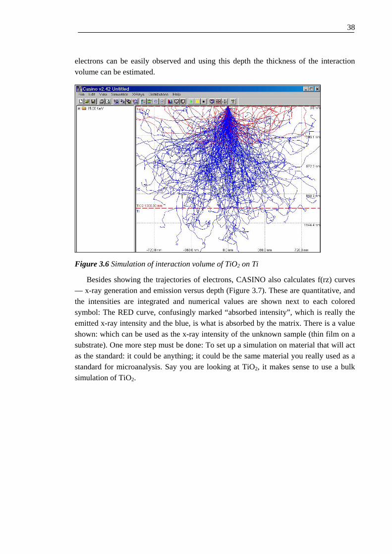
Thickness of the silane layer, being one of the important parameter, can be simulated using a Monte Carlo Simulation program called CASINO. [42] Monte Carlo simulations have been widely used by microscopists for the last few decades. In the beginning it was a tedious and slow process, requiring a high level of computer skills from users and long computational times. Recent progress in the microelectronics industry now provides researchers with affordable desktop computers with clock rates greater than 3 GHz. With this type of computing power routinely available, Monte Carlo simulation is no longer an exclusive or long process. On the basis of a single-scattering algorithm, this software is specially designed for modeling low-energy beam interactions in bulk and thin foil samples.
It can be helpful to run Monte Carlo simulations of thin films. For example in the Figure 3.6 Casino software is used to model 15 keV electrons hitting a 1 mm layer of TiO2 on Ti. From Figure 3.6 it can be seen that the depth of the penetration of primary
38
electrons can be easily observed and using this depth the thickness of the interaction volume can be estimated.
Figure 3.6 Simulation of interaction volume of TiO2 on Ti
Besides showing the trajectories of electrons, CASINO also calculates f(rz) curves — x-ray generation and emission versus depth (Figure 3.7). These are quantitative, and the intensities are integrated and numerical values are shown next to each colored symbol: The RED curve, confusingly marked “absorbed intensity”, which is really the emitted x-ray intensity and the blue, is what is absorbed by the matrix. There is a value shown: which can be used as the x-ray intensity of the unknown sample (thin film on a substrate). One more step must be done: To set up a simulation on material that will act as the standard: it could be anything; it could be the same material you really used as a standard for microanalysis. Say you are looking at TiO2, it makes sense to use a bulk simulation of TiO2.

39
Figure 3.7 f(rz) curve for TiO2 on Ti
In case of silanized stainless steel inserts, the data would be taken from the experiment itself as this software would be tested for the first time to simulate the thickness of silane layer on stainless steel insert. After standardizing the software it would be used to simulate the thickness and then confirm it with the experimental values. The standard used here is a Silicon standard.

40
4. RESULTS AND DISCUSSION
In this chapter, results obtained from microscopic characterization of the planar surface and the cross-sectional surface of silanized stainless steel inserts is discussed. Apart from microscopic characterization, the results obtained using x-ray photoelectron spectroscopy about the various bonds in the silane layer and on the stainless steel surface are discussed. Finally the simulated results are compared with the experimental results in order to prove the applicability of the software CASINO for estimating the thickness of the silane layer on the stainless steel insert.
4.1. Optical microscope Study
Optical microscope studies helped in finding optimal parameters for silane treatment. By observing the silane treated stainless steel insert using different parameters under the microscope, the most appropriate parameters to be used in order to observe it under scanning electron microscope were selected. Following Table 3.7 explains how the optical microscope observation helped in finding optimal parameters. This table is made based on the experimental plan mentioned in Table 3.5. The optical micrographs (Figure 4.1 to 4.6) following the table 3.7 are to support the observations made in the table 4.1.

41
Table 4.1 Observations made using Optical Microscope
Experimental Conditions Observations
As-received stainless steel insert with 0.5% silane treated
The green colour on the surface indicates the presence of silane almost all over the surface.
2 stainless steel inserts were polished and then oxidized for 25 min and finally silane treated with 0.5% silane concentration. The difference between both the samples was rinsing conditions. First sample was not rinsed and the second one was rinsed using deionized water for 2 min before curing.
From the optical micrographs it can be observed that on the rinsed surface there is either no silane or a very thin layer of silane when compared to un-rinsed surface. If the silane is thin then it is an ideal situation. But this can be confirmed using scanning electron microscope.
Concentration of the silane solution was altered in three inserts i.e. 0.25%, 0.5% and 1% concentration of silane was used. While doing this other parameters where kept constant. The surfaces was under oxidation for 100 min.
From the optical micrographs it can be observed that as the concentration of silane increased the density of silane increased on the surface. Also, the layer on silane became darker indicating that the layer was very thick when it came to 1% concentration.
pH of the silane solution changed from acidic (4-5) to neutral (7-8) to basic (9) in order to find out the ideal value of pH
This was a part of the initial studies where elimination process was carried out to come to pH 9. The reason for this choice was at alkaline pH the hydrolysis of alkoxy groups leading to the formation of silanols is rapid, but the silanols tend to condensate and form oligosiloxanes. [39]

42
Figure 4.1 As-received stainless steel treated with 0.5% silane solution
Figure 4.2 Polished, oxidized for 25 min stainless steel insert treated with 0.5% silane solution (no rinsing)
43
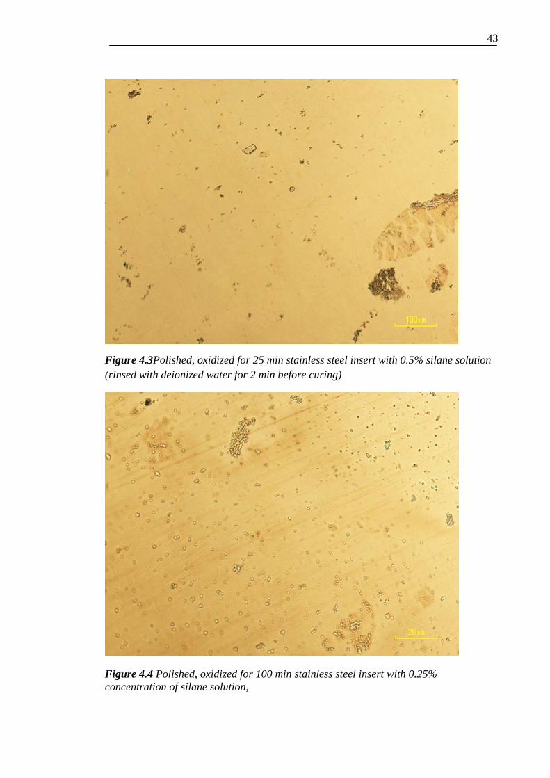
Figure 4.3Polished, oxidized for 25 min stainless steel insert with 0.5% silane solution (rinsed with deionized water for 2 min before curing)
Figure 4.4 Polished, oxidized for 100 min stainless steel insert with 0.25% concentration of silane solution,

44
Figure 4.5 Polished, oxidized for 100 min stainless steel insert with 0.5% concentration of silane solution
Figure 4.6 Polished, oxidized for 100 min stainless steel insert with 1% concentration of silane solution

45
4.2. Scanning Electron Microscope study
The silane topography on the stainless steel inserts is affected by the oxide layer as can be seen in the SEM micrographs shown in Figure 4.7. This fact is also in agreement with the literature study. [14, 15] In the SEM micrographs in Figure 4.8 it can be seen that the layer is more uniform in case of 100 min oxidized stainless steel insert when compared to 25 min oxidized stainless steel insert. Silane concentration in both cases is 1%. In case of 25 min oxidation the rings are prominent and segregated which shows the non-uniformity of the layer. In case of 5 min oxidation (not shown) the layer was again non-uniform and the rings were far from each other. With reference to earlier studies and after observing in SEM it was concluded that after 5 min and 25 min air exposure at 350ºC separate oxide islands formed on the base oxide layer whereas after 100 min exposure they coalesced into a uniform oxide layer. [16] Hence, it could be concluded that a uniform oxide layer is required on the stainless steel before silane treatment in order to produce a uniform silane layer on the stainless steel surface. From the literature it can be seen that good bonding of silane layer requires a smooth substrate as the silane layer formation could be prevented because of a rough surface. [13] It has been studied in this study that the smoothest surface of stainless steel is formed after a 100 min oxidation treatment. This factor was also studied before by Honkanen et al. [16]
Figure 4.7 100 min oxidized 1% concentration
Uniform Silane Layer
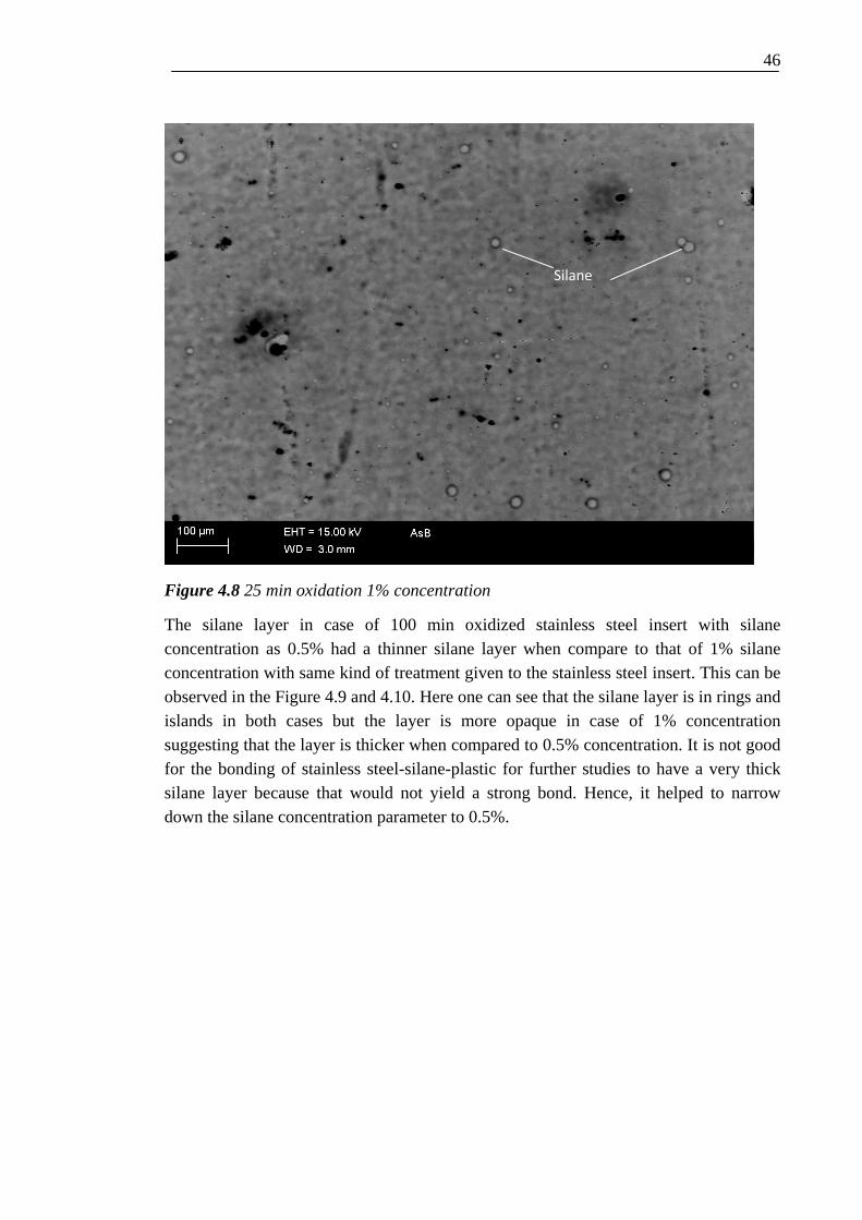
46
Figure 4.8 25 min oxidation 1% concentration
The silane layer in case of 100 min oxidized stainless steel insert with silane concentration as 0.5% had a thinner silane layer when compare to that of 1% silane concentration with same kind of treatment given to the stainless steel insert. This can be observed in the Figure 4.9 and 4.10. Here one can see that the silane layer is in rings and islands in both cases but the layer is more opaque in case of 1% concentration suggesting that the layer is thicker when compared to 0.5% concentration. It is not good for the bonding of stainless steel-silane-plastic for further studies to have a very thick silane layer because that would not yield a strong bond. Hence, it helped to narrow down the silane concentration parameter to 0.5%.
Silane

47
Figure 4.9 100 min oxidation 0.5% silane concentration
Figure 4.10 100 min oxidation 1% silane concentration
Silane
Silane
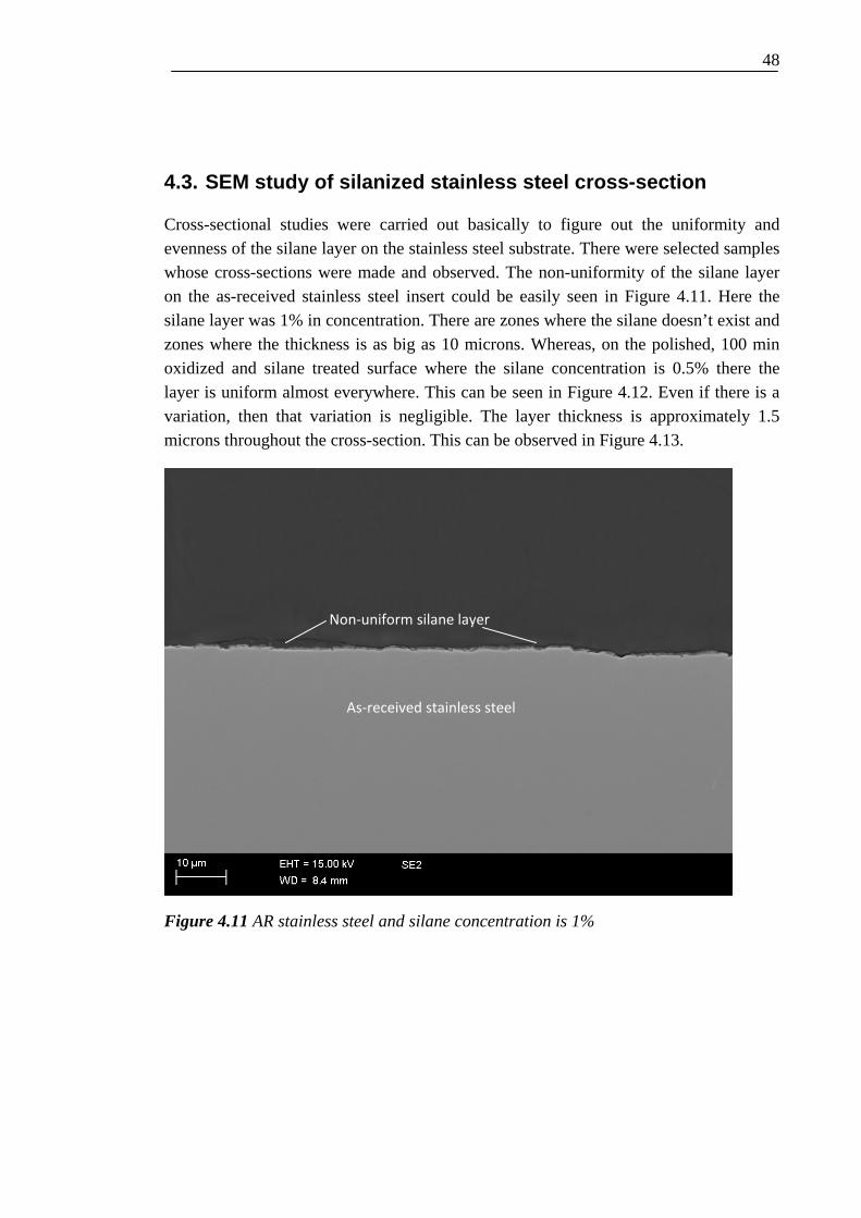
48
4.3. SEM study of silanized stainless steel cross-section
Cross-sectional studies were carried out basically to figure out the uniformity and evenness of the silane layer on the stainless steel substrate. There were selected samples whose cross-sections were made and observed. The non-uniformity of the silane layer on the as-received stainless steel insert could be easily seen in Figure 4.11. Here the silane layer was 1% in concentration. There are zones where the silane doesn’t exist and zones where the thickness is as big as 10 microns. Whereas, on the polished, 100 min oxidized and silane treated surface where the silane concentration is 0.5% there the layer is uniform almost everywhere. This can be seen in Figure 4.12. Even if there is a variation, then that variation is negligible. The layer thickness is approximately 1.5 microns throughout the cross-section. This can be observed in Figure 4.13.
Figure 4.11 AR stainless steel and silane concentration is 1%
Non-uniform silane layer
As-received stainless steel

49
Figure 4.12 100 min oxidation 0.5% concentration of silane
A very important reason to carry out the cross-sectional analysis apart from determining the thickness and uniformity was to understand the strength of the bonds between silane and stainless steel insert. Figure 4.13 and Figure 4.14 explain the phenomenon of good bonding between the stainless steel insert and silane layer. The silane layer in Figure 4.14 is in the same plane as stainless steel and so the bonding can be seen clearly. Also, the silane layer is very dense which also helps in the bonding with stainless steel insert and then with the plastic in order to fabricate a hybrid.
Figure 4.15 shows the EDS results of the same sample shown in Figure 4.13. The EDS results are also accompanied with EDS Maps, Figure 4.16, showing the presence of silane throughout the cross-section and proving the uniformity of the layer. The silicon percentage indicates the presence of silane at the cross-section interface. Different color codes are used in order to separate the elements in the maps.
Uniform silane layer
Polished, 100 min oxidized stainless steel

50
Figure 4.13 100 min oxidation and 0.5% silane concentration
Figure 4.14 The encircled zone in Figure 4.13
Uniform silane layer
Bonding between steel and silane (magnified in fig. 4.14)
Thickness of the silane layer = 1.5 µm
Polished, 100 min oxidized stainless steel
silane layer

51
Figure 4.15 EDS spectra for the sample in Figure 3.20
Figure 4.16 EDS Maps for the sample in the SEM micrograph above the maps
Si Ka1 Fe Ka1
C Ka1_2 O Ka1
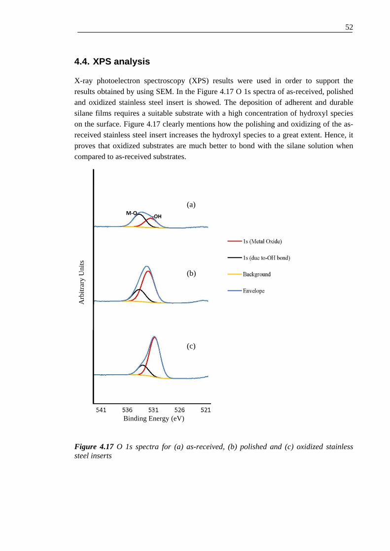
52
4.4. XPS analysis
X-ray photoelectron spectroscopy (XPS) results were used in order to support the results obtained by using SEM. In the Figure 4.17 O 1s spectra of as-received, polished and oxidized stainless steel insert is showed. The deposition of adherent and durable silane films requires a suitable substrate with a high concentration of hydroxyl species on the surface. Figure 4.17 clearly mentions how the polishing and oxidizing of the as-received stainless steel insert increases the hydroxyl species to a great extent. Hence, it proves that oxidized substrates are much better to bond with the silane solution when compared to as-received substrates.
Figure 4.17 O 1s spectra for (a) as-received, (b) polished and (c) oxidized stainless steel inserts
M-O -OH
Arb
itrar
y U
nits
Binding Energy (eV)
(a)
(c)
(b)
53
Figure 4.18 shows the XPS survey scans of all the samples that were used in XPS study. The carbon peak shift indicates that the carbon in silanized inserts is contributed by silane and not stainless steel. Because of the presence of impurities and oxide layer on the as-received stainless steel insert the Fe 3p peak is non-existent. But after polishing the peak is seen very clearly. Silane content varies when the parameters of silane change, i.e. amount of silane in case of even layer of silane, uneven layer both with 0.5% concentration and 1% concentration silane layer vary. This variation helps to choose the right parameter in order to have an even and uniformly thick silane layer. Table 4.2 shows the position and binding energy of all the elements and also all the possible compounds that could exist at that binding energy with that particular element. When we compare the as-received stainless steel and polished, 100 min oxidized stainless steel then the amount of silane has a significant rise. The presence of Si-O-Si bonds is also confirmed from, table 4.2, which in turn helps in the stainless steel and silane bond.

54
Figure 4.18 Survey scans for all the samples used for XPS study
Arb
itrar
y U
nits
Binding Energy (eV)
As-received steel
Polished steel
Polished + 100 min oxidized steel
(0.5% vol. Non-uniform, thick) Silane layer on polished + 100 min oxidized steel
(0.5% vol. rinsed using water) Silane layer on polished + 100 min oxidized steel
(1% vol) Silane layer on polished + 100 min oxidized steel
(0.5% uniform) Silane layer on polished + 100 min oxidized steel
O K
LL
Fe 2
p
Cr 2
p O 1
s
C 1
s C
a 2p
N 1
s
Si 2
p Si
2s
O 2
s
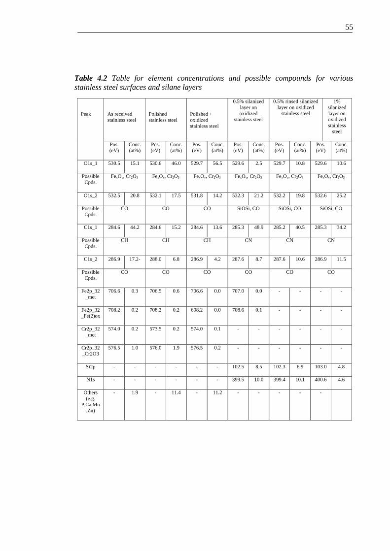
55
Table 4.2 Table for element concentrations and possible compounds for various stainless steel surfaces and silane layers
Peak
As received stainless steel
Polished stainless steel
Polished + oxidized stainless steel
0.5% silanized layer on oxidized
stainless steel
0.5% rinsed silanized layer on oxidized
stainless steel
1% silanized layer on oxidized stainless
steel
Pos. (eV)
Conc. (at%)
Pos. (eV)
Conc. (at%)
Pos. (eV)
Conc. (at%)
Pos. (eV)
Conc. (at%)
Pos. (eV)
Conc. (at%)
Pos. (eV)
Conc. (at%)
O1s_1 530.5 15.1 530.6 46.0 529.7 56.5 529.6 2.5 529.7 10.8 529.6 10.6
Possible Cpds.
FexOy, Cr2O3 FexOy, Cr2O3 FexOy, Cr2O3 FexOy, Cr2O3 FexOy, Cr2O3 FexOy, Cr2O3
O1s_2 532.5 20.8 532.1 17.5 531.8 14.2 532.3 21.2 532.2 19.8 532.6 25.2
Possible Cpds.
CO CO CO SiOSi, CO SiOSi, CO SiOSi, CO
C1s_1 284.6 44.2 284.6 15.2 284.6 13.6 285.3 48.9 285.2 40.5 285.3 34.2
Possible Cpds.
CH CH CH CN CN CN
C1s_2 286.9 17.2- 288.0 6.8 286.9 4.2 287.6 8.7 287.6 10.6 286.9 11.5
Possible Cpds.
CO CO CO CO CO CO
Fe2p_32_met
706.6 0.3 706.5 0.6 706.6 0.0 707.0 0.0 - - - -
Fe2p_32_Fe(2)ox
708.2 0.2 708.2 0.2 608.2 0.0 708.6 0.1 - - - -
Cr2p_32_met
574.0 0.2 573.5 0.2 574.0 0.1 - - - - - -
Cr2p_32_Cr2O3
576.5 1.0 576.0 1.9 576.5 0.2 - - - - - -
Si2p - - - - - - 102.5 8.5 102.3 6.9 103.0 4.8
N1s - - - - - - 399.5 10.0 399.4 10.1 400.6 4.6
Others (e.g.
P,Ca,Mn,Zn)
- 1.9 - 11.4 - 11.2 - - - - -
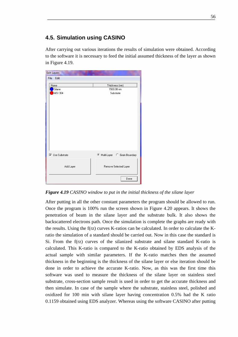
56
4.5. Simulation using CASINO
After carrying out various iterations the results of simulation were obtained. According to the software it is necessary to feed the initial assumed thickness of the layer as shown in Figure 4.19.
Figure 4.19 CASINO window to put in the initial thickness of the silane layer
After putting in all the other constant parameters the program should be allowed to run. Once the program is 100% run the screen shown in Figure 4.20 appears. It shows the penetration of beam in the silane layer and the substrate bulk. It also shows the backscattered electrons path. Once the simulation is complete the graphs are ready with the results. Using the f(rz) curves K-ratios can be calculated. In order to calculate the K-ratio the simulation of a standard should be carried out. Now in this case the standard is Si. From the f(rz) curves of the silanized substrate and silane standard K-ratio is calculated. This K-ratio is compared to the K-ratio obtained by EDS analysis of the actual sample with similar parameters. If the K-ratio matches then the assumed thickness in the beginning is the thickness of the silane layer or else iteration should be done in order to achieve the accurate K-ratio. Now, as this was the first time this software was used to measure the thickness of the silane layer on stainless steel substrate, cross-section sample result is used in order to get the accurate thickness and then simulate. In case of the sample where the substrate, stainless steel, polished and oxidized for 100 min with silane layer having concentration 0.5% had the K ratio 0.1159 obtained using EDS analyzer. Whereas using the software CASINO after putting
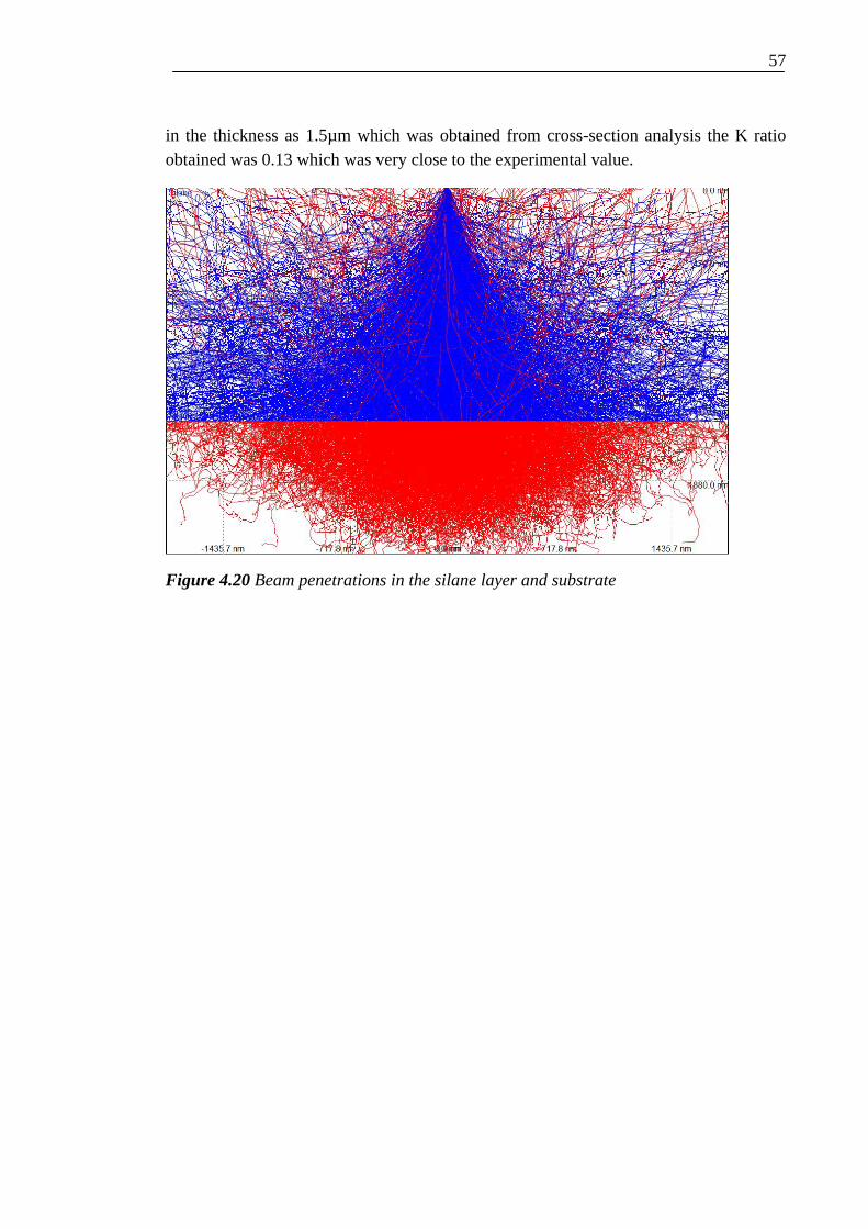
57
in the thickness as 1.5µm which was obtained from cross-section analysis the K ratio obtained was 0.13 which was very close to the experimental value.
Figure 4.20 Beam penetrations in the silane layer and substrate

58
5. Conclusion
The characterization of the interfacial zone between stainless steel insert and silane is a lot dependent on the various parameters of stainless steel and silane solution. In the experiment part it was made sure to test all the possible parameters. In case of stainless steel polishing and oxidizing the substrate were important parameters. It was important for the surface to be very smooth because a smooth surface bonds well with silane. Oxidation times in air at 350ºC were 5 min, 25 min and 100 min. Silane solution was prepared varying many parameters. Silane solution’s concentrations were 0.25%, 0.5% and 1%. These solutions were water based or ethanol based. Once the solutions were made and applied on the stainless steel insert, just before curing the samples are kept at an angle of 30º for the excess silane to drain off.
Optical microscope was the technique used to eliminate the parameters which were not suitable. The presence of silane on the surface of the stainless steel substrate was observed under the optical microscope and the effect silane had on the grain boundaries was also made note of. Scanning electron microscope was used in order to analyze the spread of the silane layer over the planar surface. Various concentrations of silane were tested in this manner and it could be concluded that 0.5% concentration of silane has a better bonding to the stainless steel inserts when compared to other concentration values. 1% concentration formed a very thick layer which would not form a strong bond with the stainless steel insert because the ideal situation would be Si-O-M but it would not be possible with a thick layer.
Cross-sectional analysis was an important part of the experimental part because it allowed knowing the thickness of the silane layer and its uniformity over the stainless steel substrate. It was observed that as-received stainless steel had a very uneven silane layer on its surface, whereas, polished and oxidized surfaces had a very even and uniform layer. Hence, it could be concluded that the surface needs to be smooth enough for the silane to bond on it. Cross-sectional analysis also showed that 0.5% concentration silane formed a denser layer when compared to 0.25% and 1%. In case of polished, 100 min oxidized stainless steel surface with 0.5 %, pH=9 silane solution the layer thickness was 1.5µm. This layer thickness could prove to be ideal for further adhesion with plastic.
XPS analysis was carried out in order to characterize the silane layer in detail. XPS analysis also characterized the stainless steel substrate without silane on it. The carbon shift was identified when the spectra for silanized stainless steel were compared with non-silanized stainless steel. This carbon shift indicated that the in case of silanized stainless steel the carbon was contributed by silane solution and in case of non-silanized

59
stainless steel it was from the stainless steel surface. From the XPS spectra of silanized stainless steel it could be concluded that the Si-O-Si bonds were present on the surface. Also, the amount of silane detected on polished, oxidized stainless steel substrate was more than that on the as-received silanized stainless steel substrate. By XPS survey scans it could be easily concluded that the smoother surface had better bonding with silane when compared to the uneven surface (in case of as-received stainless steel).
Simulation using CASINO program was done to simulate the thickness of the silane layer on the stainless steel substrate. Using the method of iterations the thickness of the silane layer was simulated. The comparison of K-ratios from the simulated results and the experimental results was done in order to compute the thickness.

60
6. References
[1] Zoellner, O., Evans, J. Plastic-metal hybrid – A new development in the injection molding technology, ANTEC, Volume 3: Special Areas, 5.-9. May (2002), San Fransisco, USA
[2] Palmer, T. More mettle for sheet metal, Machine Design 76, 2004, pp.76-80.
[3] Internet: http://techcenter.lanxess.com (26.05.2009)
[4] Rectenwald, D. Advanced adhesives foster hybrid structures, Machine Design 77, 2005, pp. 124-125.
[5] Honkanen, M., Hoikkanen, M., Vippola, M., Vuorinen, J. and Lepistö, T.
Metal-
Plastic Adhesion in Injection-Molded Hybrids, Journal of Adhesion Science and Technology, Volume 23, Numbers 13-14, 2009, pp. 1747-1761
[6] Internet: http://www.outokumpu.com/33392.epibrw (09.09.2009)
[7] Internet: http://www.outokumpu.com/35976.epibrw (10.09.2009)
[8] Plueddemann, E. Silane coupling agents , Plenum Press, New York, 1982.
[9] Internet: A guide to silane solutions, http://www.dowcorning.com (14.04.2008)
[10] Boerio, F. and Shah, P. Adhesion of injection moulded PVC to Stell Substrates, The Journal of Adhesion, 81, 645, 2005
[11] Pauling, The nature of the chemical bond. 2nd edition, cornell university press, Ithaca. N.Y., 1948, p. 69
[12] Chovelon, J. M., Aarch L. E., Charbonnier M. and Romand M. Silanization of Stainless Steel Surfaces : Influence of Application Parameters, The Journal of Adheshion, Volume 50, 1995, pp. 43-58
[13] Petrie, E.M., Handbook of Adhesives and Sealants, McGraw-Hill, New York, 2000.
[14] Susac, D., Sun, X. and Mitchell, K. Adsorption of BTSE and γ-APS organosilanes on different microstructural regions of 2024-T3 aluminum alloy, Applied Surface Science Volume 207, 2003, pp. 40-50.
61
[15] Kim, J., Wong, P., Wong, K., Sodhi, R. and Mitchell, K. Adsorption of BTSE and γ-GPS organosilanes on different microstructural regions of 7075-T6 aluminum alloy, Applied Surface Science, Volume 253, Issue 6, 2007, pp. 3133-3143.
[16] Hoikkanen, M., Honkanen, M., Vippola, M., Lepistö, T. and Vuorinen J., Effect of Silane Treatment Parameters on the Silane Layer Formation and Bonding to Thermoplastic Urethane, Progress in Organic Coatings, 2011, DOI 10.1016/j.porgcoat.2011.08.002
[17] Xanthos, M., Weissenbach, K. and Mack, H. Functional Fillers for Plastics, Chapter 4, Wiley-VCH, 2005, pp.69-82.
[18] Ishida, H., Naviroj, S., Tripathy, S., Fitzgerald, J. and Koenig, J. The structure of an aminosilane coupling agent in aqueous solutions and partially cured solids, Journal of Polymer Science Part B: Polymer Physics, Volume 20, Issue 4, 1982, pp.701-718
[19] Abel, M., Allington, R., Digby, R., Porritt, N. and Shaw, S. Understanding the relationship between silane application conditions, bond durability and locus of failure, International Journal of Adhesion and Adhesives, Volume 26, Issues 1-2, 2006, pp. 2-15.
[20] Bautista, A., Velasco, F., Campos, M., Rabanal, M., and Torralba, J. Oxidation Behavior at 900°C of Austenitic, Ferritic, and Duplex Stainless Steels Manufactured by Powder Metallurgy, Oxidation of Metals, Volume 59, 2003, pp. 373-393.
[21] Klueh, R., Hashimoto, N. and Maziasz, P., Development of new nano-particle-strengthened martensitic steels, Scripta Materialia, Volume 53, Issue 3, 2005, pp. 275-280
[22] Taneike, M., Abe, F. and Sawada, K. Creep-strengthening of steel at high temperatures using nano-sized carbonitride dispersions, Nature, 424, 2003, pp. 294-296.
[23] Grubb, J., DeBold, T. and Fritz, J. Corrosion of Wrought Stainless Steels, ASM Handbook, Volume 13B, Corrosion: Materials, ASM International, 2005.
[24] Oudar, J. Introduction to Surface Reactions: Adsorption from Gas Phase, P Marcus (Ed.), Corrosion Mechanisms in Theory and Practice, Marcel Dekker Inc., New York, 2002, pp. 19-51.

62
[25] Greef, A., Louw, C., Terblans, J. and Swart, H., The influence of sulphur segregation on the oxidation of industrial FeCrMo steel, Corrosion Science Volume 42, Issue 6, 2000, pp. 991-1004.
[26] Fehlner, F. and Graham, M., Thin Oxide Film formation on Metals, P Marcus (Ed.), Corossion Mechanisms in Theory and Practice, Marcel Dekker Inc., New York, 2002, pp. 171-187.
[27] Lahtonen, K., Lampimäki, M., Jussila, P., Hirsimäki, M. and Valden, M. Instrumentation and analytical methods of an x-ray photoelectron spectroscopy–scanning tunneling microscopy surface analysis system for studying nanostructured materials, Review of Scientific Instruments, Volume 77, Issue 8, 2006.
[28] Jussila, P., Doctoral Thesis: Advances in Nanoscale Functionalization of Stainless Steel Surfaces, Tampere University of Technology, Publication 851, 2009.
[29] Goldstein, G., Newbury, D., Echlin, P., Joy, D., Fiori, C. and Lifshin, E. Scanning electron microscopy and x-ray microanalysis, Plenum Press. Newyork, ISBN 030640768X. 1981
[30] Gizdavic-Nikolaidis, M., Edmonds, N., Bolt, C. and Easteal, A., Structure and properties of GPTMS/DETA and GPTMS/EDA hybrid polymers, Current Applied Physics, Volume 8, Issues 3-4, 2008, pp. 300-303.
[31] Briggs, D. and Grant, J., Surface Analysis by Auger and X-ray Photoelectron Spectroscopy, Surface Spectra, Manchester, UK, 2003.
[32] Woodruff, D. and Delchar, R., Modern techniques in Surface Science, Cambridge University Press, 1994.
[33] Burhop, E., The Auger Effect and other radiationless transitions, University Press in Cambridge, 1952.
[34] Kolasinski, K., Surface science: Foundations of Catalysis and Nanoscience, John Wiley & Sons Ltd, Chichester, 2002.
[35] Nordling, C. Dr., ESCA: Electron Spectroscopy for Chemical Analysis, Angewandte Chemie International Edition in English, Volume 11, Issue 2, 1972, pp.83-92.
[36] Moses, P., Weir, L., Lennox, J., Finklea, H., Lenhard, J. and Murray, R., Anal. Chem. 50, 576 (1978)
63
[37] Horner, M., Boerio, F. and Clearfield, Howard M., An XPS investigation of the adsorption of aminosilanes onto metal substrates, Journal of Adhesion Science and Technology, Volume 6, Number 1, 1992, pp. 1-22.
[38] Hoikkanen, M., Honkanen, M., Luukkonen, A., Vippola, M., Vuorinen, J. and Lepistö, T., Thermoplastic urethane-steel hybrids: Relationship between steel surface structure and macroscopic properties. IRC ´08 International Rubber Conference & Exhibition, Kuala Lumpur, Malaysia, 20.-23. October 2008 11 p.
[39] Honkanen, M., Vippola, M. and Lepistö, T., Characterisation of stainless steel surfaces ‐ modified in air at 350°C, Surface Engineering, Volume 27, 2011, pp. 325-331.
[40] Fairley, N., CasaXPS: Spectrum Processing Software for XPS, AES and SIMS (Version 2.3.13), Casa Software Ltd, Cheshire, 2006, http://www.casaxps.com/
[41] Wagner, C., Naumkin, A., Kraut-Vass, A., Allison, J., Powell, C. and Rumble Jr., J., NIST XPS Database, Version 3.5 (Web Version), National Institute of Standards and Technology, 2007 http://sedata.nist.gov/xps/.
[42] Drouin, D., Couture, A., Joly, D., Tastet, X., Aimez, V. and Gauvin, R., CASINO V2.42—A Fast and Easy-to-use Modeling Tool for Scanning Electron Microscopy and Microanalysis Users, Scanning, Volume 29, Issue 3, 2007, pp. 92-101.
Copyright © 2022 FDOKUMEN