Thermal conductivity of highly porous Si in the temperature range 4.2 to 20 K
6
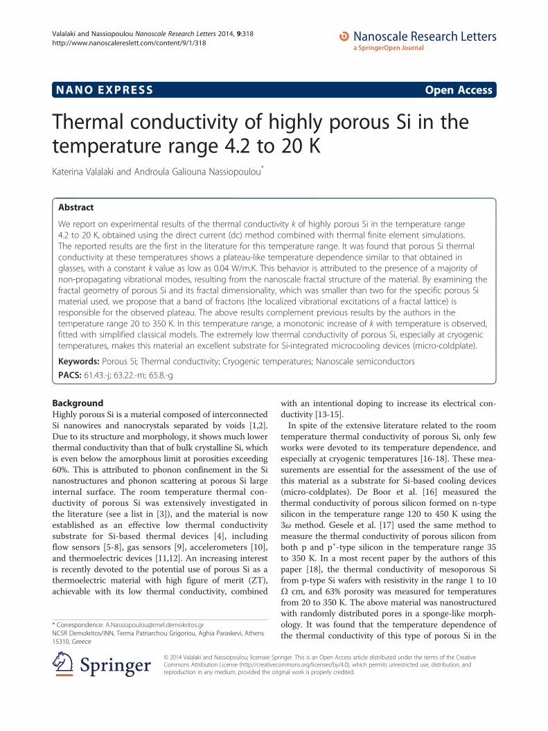
NANO EXPRESS Open Access Thermal conductivity of highly porous Si in the temperature range 4.2 to 20 K Katerina Valalaki and Androula Galiouna Nassiopoulou * Abstract We report on experimental results of the thermal conductivity k of highly porous Si in the temperature range 4.2 to 20 K, obtained using the direct current (dc) method combined with thermal finite element simulations. The reported results are the first in the literature for this temperature range. It was found that porous Si thermal conductivity at these temperatures shows a plateau-like temperature dependence similar to that obtained in glasses, with a constant k value as low as 0.04 W/m.K. This behavior is attributed to the presence of a majority of non-propagating vibrational modes, resulting from the nanoscale fractal structure of the material. By examining the fractal geometry of porous Si and its fractal dimensionality, which was smaller than two for the specific porous Si material used, we propose that a band of fractons (the localized vibrational excitations of a fractal lattice) is responsible for the observed plateau. The above results complement previous results by the authors in the temperature range 20 to 350 K. In this temperature range, a monotonic increase of k with temperature is observed, fitted with simplified classical models. The extremely low thermal conductivity of porous Si, especially at cryogenic temperatures, makes this material an excellent substrate for Si-integrated microcooling devices (micro-coldplate). Keywords: Porous Si; Thermal conductivity; Cryogenic temperatures; Nanoscale semiconductors PACS: 61.43.-j; 63.22.-m; 65.8.-g Background Highly porous Si is a material composed of interconnected Si nanowires and nanocrystals separated by voids [1,2]. Due to its structure and morphology, it shows much lower thermal conductivity than that of bulk crystalline Si, which is even below the amorphous limit at porosities exceeding 60%. This is attributed to phonon confinement in the Si nanostructures and phonon scattering at porous Si large internal surface. The room temperature thermal con- ductivity of porous Si was extensively investigated in the literature (see a list in [3]), and the material is now established as an effective low thermal conductivity substrate for Si-based thermal devices [4], including flow sensors [5-8], gas sensors [9], accelerometers [10], and thermoelectric devices [11,12]. An increasing interest is recently devoted to the potential use of porous Si as a thermoelectric material with high figure of merit (ZT), achievable with its low thermal conductivity, combined with an intentional doping to increase its electrical con- ductivity [13-15]. In spite of the extensive literature related to the room temperature thermal conductivity of porous Si, only few works were devoted to its temperature dependence, and especially at cryogenic temperatures [16-18]. These mea- surements are essential for the assessment of the use of this material as a substrate for Si-based cooling devices (micro-coldplates). De Boor et al. [16] measured the thermal conductivity of porous silicon formed on n-type silicon in the temperature range 120 to 450 K using the 3ω method. Gesele et al. [17] used the same method to measure the thermal conductivity of porous silicon from both p and p + -type silicon in the temperature range 35 to 350 K. In a most recent paper by the authors of this paper [18], the thermal conductivity of mesoporous Si from p-type Si wafers with resistivity in the range 1 to 10 Ω cm, and 63% porosity was measured for temperatures from 20 to 350 K. The above material was nanostructured with randomly distributed pores in a sponge-like morph- ology. It was found that the temperature dependence of the thermal conductivity of this type of porous Si in the * Correspondence: [email protected] NCSR Demokritos/INN, Terma Patriarchou Grigoriou, Aghia Paraskevi, Athens 15310, Greece © 2014 Valalaki and Nassiopoulou; licensee Springer. This is an Open Access article distributed under the terms of the Creative Commons Attribution License (http://creativecommons.org/licenses/by/4.0), which permits unrestricted use, distribution, and reproduction in any medium, provided the original work is properly credited. Valalaki and Nassiopoulou Nanoscale Research Letters 2014, 9:318 http://www.nanoscalereslett.com/content/9/1/318
-
Upload
independent -
Category
Documents
-
view
2 -
download
0
Transcript of Thermal conductivity of highly porous Si in the temperature range 4.2 to 20 K
Valalaki and Nassiopoulou Nanoscale Research Letters 2014, 9:318http://www.nanoscalereslett.com/content/9/1/318
NANO EXPRESS Open Access
Thermal conductivity of highly porous Si in thetemperature range 4.2 to 20 KKaterina Valalaki and Androula Galiouna Nassiopoulou*
Abstract
We report on experimental results of the thermal conductivity k of highly porous Si in the temperature range4.2 to 20 K, obtained using the direct current (dc) method combined with thermal finite element simulations.The reported results are the first in the literature for this temperature range. It was found that porous Si thermalconductivity at these temperatures shows a plateau-like temperature dependence similar to that obtained inglasses, with a constant k value as low as 0.04 W/m.K. This behavior is attributed to the presence of a majority ofnon-propagating vibrational modes, resulting from the nanoscale fractal structure of the material. By examining thefractal geometry of porous Si and its fractal dimensionality, which was smaller than two for the specific porous Simaterial used, we propose that a band of fractons (the localized vibrational excitations of a fractal lattice) isresponsible for the observed plateau. The above results complement previous results by the authors in thetemperature range 20 to 350 K. In this temperature range, a monotonic increase of k with temperature is observed,fitted with simplified classical models. The extremely low thermal conductivity of porous Si, especially at cryogenictemperatures, makes this material an excellent substrate for Si-integrated microcooling devices (micro-coldplate).
Keywords: Porous Si; Thermal conductivity; Cryogenic temperatures; Nanoscale semiconductors
PACS: 61.43.-j; 63.22.-m; 65.8.-g
BackgroundHighly porous Si is a material composed of interconnectedSi nanowires and nanocrystals separated by voids [1,2].Due to its structure and morphology, it shows much lowerthermal conductivity than that of bulk crystalline Si, whichis even below the amorphous limit at porosities exceeding60%. This is attributed to phonon confinement in the Sinanostructures and phonon scattering at porous Si largeinternal surface. The room temperature thermal con-ductivity of porous Si was extensively investigated inthe literature (see a list in [3]), and the material is nowestablished as an effective low thermal conductivitysubstrate for Si-based thermal devices [4], includingflow sensors [5-8], gas sensors [9], accelerometers [10],and thermoelectric devices [11,12]. An increasing interestis recently devoted to the potential use of porous Si as athermoelectric material with high figure of merit (ZT),achievable with its low thermal conductivity, combined
* Correspondence: [email protected] Demokritos/INN, Terma Patriarchou Grigoriou, Aghia Paraskevi, Athens15310, Greece
© 2014 Valalaki and Nassiopoulou; licensee SprCommons Attribution License (http://creativecoreproduction in any medium, provided the orig
with an intentional doping to increase its electrical con-ductivity [13-15].In spite of the extensive literature related to the room
temperature thermal conductivity of porous Si, only fewworks were devoted to its temperature dependence, andespecially at cryogenic temperatures [16-18]. These mea-surements are essential for the assessment of the use ofthis material as a substrate for Si-based cooling devices(micro-coldplates). De Boor et al. [16] measured thethermal conductivity of porous silicon formed on n-typesilicon in the temperature range 120 to 450 K using the3ω method. Gesele et al. [17] used the same method tomeasure the thermal conductivity of porous silicon fromboth p and p+-type silicon in the temperature range 35to 350 K. In a most recent paper by the authors of thispaper [18], the thermal conductivity of mesoporous Sifrom p-type Si wafers with resistivity in the range 1 to 10Ω cm, and 63% porosity was measured for temperaturesfrom 20 to 350 K. The above material was nanostructuredwith randomly distributed pores in a sponge-like morph-ology. It was found that the temperature dependence ofthe thermal conductivity of this type of porous Si in the
inger. This is an Open Access article distributed under the terms of the Creativemmons.org/licenses/by/4.0), which permits unrestricted use, distribution, andinal work is properly credited.
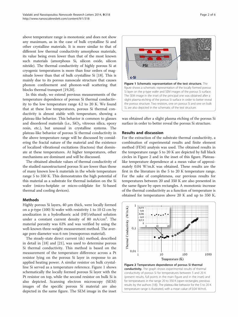
Figure 1 Schematic representation of the test structure. Thefigure shows a schematic representation of the locally formed porousSi layer on the p-type wafer and SEM images of the porous Si surface.The SEM image in the inset of the principal one was obtained after aslight plasma etching of the porous Si surface in order to better revealthe porous structure. Two resistors, one on porous Si and one on bulkSi, are also depicted in the schematic of the test structure.
Figure 2 Temperature dependence of porous Si thermalconductivity. The graph shows experimental results of thermalconductivity of porous Si for temperatures between 5 and 20 K(present results, full points in the main figure and in the inset) andfor temperatures in the range 20 to 350 K (open rectangles; previousresults by the authors [18]). The plateau-like behavior for the 5 to 20 Ktemperature range is illustrated, with a mean value of 0.04 W/m.K.
Valalaki and Nassiopoulou Nanoscale Research Letters 2014, 9:318 Page 2 of 6http://www.nanoscalereslett.com/content/9/1/318
above temperature range is monotonic and does not showany maximum, as in the case of bulk crystalline Si andother crystalline materials. It is more similar to that ofdifferent low thermal conductivity amorphous materials,its value being even lower than that of the most knownsuch materials (amorphous Si, silicon oxide, siliconnitride). The thermal conductivity of highly porous Si atcryogenic temperatures is more than four orders of mag-nitude lower than that of bulk crystalline Si [18]. This ismainly due to its porous nanoscale structure that causesphonon confinement and phonon-wall scattering thatblocks thermal transport [19,20].In this study, we extend previous measurements of the
temperature dependence of porous Si thermal conductiv-ity to the low temperature range 4.2 to 20 K. We foundthat at these low temperatures, porous Si thermal con-ductivity is almost stable with temperature, showing aplateau-like behavior. This behavior is common to glassesand disordered materials (i.e., SiO2, vitreous silica, epoxyresin, etc.), but unusual in crystalline systems. Theplateau-like behavior of porous Si thermal conductivity inthe above temperature range will be discussed by consid-ering the fractal nature of the material and the existenceof localized vibrational excitations (fractons) that domin-ate at these temperatures. At higher temperatures, othermechanisms are dominant and will be discussed.The obtained absolute values of thermal conductivity of
the studied nanostructured porous Si are lower than thoseof many known low-k materials in the whole temperaturerange 5 to 350 K. This demonstrates the high potential ofthis material as a substrate for thermal isolation on the Siwafer (micro-hotplate or micro-coldplate for Si-basedthermal and cooling devices).
MethodsHighly porous Si layers, 40 μm thick, were locally formedon a p-type (100) Si wafer with resistivity 1 to 10 Ω cm byanodization in a hydrofluoric acid (HF)/ethanol solutionunder a constant current density of 80 mA/cm2. Thematerial porosity was 63% and was verified by using thewell-known three-weight measurement method. The aver-age pore diameter was 6 nm (mesoporous material).The steady-state direct current (dc) method, described
in detail in [18] and [21], was used to determine porousSi thermal conductivity. This method is based on themeasurement of the temperature difference across a Ptresistor lying on the porous Si layer in response to anapplied heating power. A similar resistor on bulk crystal-line Si served as a temperature reference. Figure 1 showsschematically the locally formed porous Si layer with thePt resistor on top, while the second resistor on bulk Si isalso depicted. Scanning electron microscopy (SEM)images of the specific porous Si material are alsodepicted in the same figure. The SEM image in the inset
was obtained after a slight plasma etching of the porous Sisurface in order to better reveal the porous Si structure.
Results and discussionFor the extraction of the substrate thermal conductivity, acombination of experimental results and finite elementmethod (FEM) analysis was used. The obtained results inthe temperature range 5 to 20 K are depicted by full blackcircles in Figure 2 and in the inset of this figure. Plateau-like temperature dependence at a mean value of approxi-mately 0.04 W/m.K was obtained. These results are thefirst in the literature in the 5 to 20 K temperature range.For the sake of completeness, our previous results fortemperatures between 20 and 350 K are also presented inthe same figure by open rectangles. A monotonic increaseof the thermal conductivity as a function of temperature isobtained for temperatures above 20 K and up to 350 K,

Valalaki and Nassiopoulou Nanoscale Research Letters 2014, 9:318 Page 3 of 6http://www.nanoscalereslett.com/content/9/1/318
without any maximum as that obtained, in the case ofbulk crystalline Si.Plateau-like behavior of the temperature dependence of
thermal conductivity at low temperatures is commonlyobserved in glasses and disordered materials and is attrib-uted to different mechanisms [22], including phonon scat-tering by enhanced densities of tunnelling systems, elasticscattering by density fluctuations, dimensional crossoverof the vibrational density of states, phonon localization,and fractons. Porous Si material is also characterized bydisorder and has been described by several authors as afractal network with specific fractal geometry. The fractalnetworks were extensively studied in the literature tounderstand the thermodynamics and transport propertiesof random physical systems. In [23] and [24], the authorsconsidered the dynamics of a percolating network and de-veloped a fundamental model for describing geometricalfeatures of random systems. By taking a self-similar fractalstructure, they evaluated the density of states for vibra-tions of a percolation network with the introduction of
the fracton dimension ~d :
~d ¼ 2� �d2þ θð Þ ð1Þ
where �d is the so-called Hausdorff dimensionality and θis a positive exponent giving the dependence of the dif-fusion constant on the distance. More details about theproblem of fracton excitations in fractal structures, andgenerally the dynamical properties of fractal networks,are found in [25].Rammal and Toulouse [23] showed that fractons are
spatially localized vibrational excitations of a fractal lat-
tice, obtained in materials with fracton dimension ~d < 2.In general, fractal geometry is observed in porous mate-
rials. Several works were devoted to the investigation ofthe fractal geometry of porous Si [26,27] and the use ofthe fractal nature of this material to explain its differentphysical properties, as for example its alternating current(ac) electrical conductivity [26]. Porous Si constitutes aninteresting system for the study of fundamental propertiesof disordered nanostructures. There are no grain boundar-ies as in crystalline solids and no sizable bond angledistortions as those found in disordered non-crystallinesystems, e.g., in amorphous materials. Porous silicon isthus considered as a simple mathematical ‘percolation’model system, which is created by randomly removingmaterial from a homogeneous structure, but still main-taining a network between the remaining atoms. Percola-tion theory has been recently used in the literature todescribe thermal conduction in porous silicon nanostruc-tures [28], amorphous and crystalline Si nanoclusters [29],nanotube composites [30], and other materials.
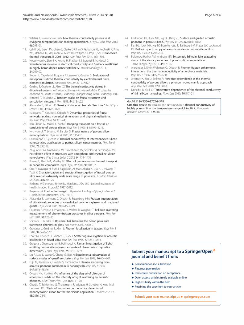
We derived the Hausdorff dimension �d of our porous Simaterial using scanning electron microscopy (SEM) imagesand the box counting algorithm [31]. The SEM images re-flect the fractal microstructure of the material. The boxcounting dimension is then defined, which is a type of frac-tal dimension and is based on the calculation of a scalingrule (using the negative limit of the ratio of the log of thenumber of boxes at a certain scale over the log of thatscale). The open-access software ‘ImageJ’ [32] was used forthe SEM image processing, while the open-access software‘FracLac’ [33] was used to calculate the Hausdorff dimen-sion of our SEM images using the standard non-overlapping box counting method. We used the maximumpossible different grid positions for every image in order toensure the accuracy of the calculation, while we calculatedthe box counting dimension for both cross-sectional andtop view SEM images of different magnifications. The re-sults were similar from both top-view and cross-sectionalimages. We also used SEM images from different samplesthat were prepared with the same electrochemical condi-tions. In all cases, the calculated Hausdorff dimension wasfound to be less than two, including the standard error.Some examples of the images used and their correspond-ing binary ones are shown in Figure 3. The average of �dvalues was approximately 1.822 ± 0.084. Since �d is less thantwo, it is evident from expression (1) that �d is also lowerthan two, since θ is a positive quantity. The condition forthe existence of fractons in our system is thus fulfilled.From the above, it results that our specific porous Si
material used in this work shows Hausdorff dimensional-ity smaller than 2 and consequently (see above) a fractondimension also smaller than 2. This last condition isconsidered as a necessary condition for the existence offractons in the material. The observed plateau-like behav-ior of porous Si thermal conductivity at temperatures inthe range 5 to 20 K can thus be attributed to the domin-ance of fractons, as in the case of other disordered mate-rials [34,35].The fracton formalism is also supported by the existence
of the so-called ‘Boson peak’ in the Raman spectra and bythe Brillouin spectra of porous Si, observed by differentgroups in the literature. The Boson peak is considered as asignature of the existence of localized vibrational modes inamorphous materials. For example, Shintani and Tanaka[36] correlated the Boson peak for glasses with the Ioffe-Regel frequency, which is the frequency reached when themean free path for phonons approaches their wavelengthand is a limit above which transverse phonon modes nolonger propagate [37]. Foret et al. [38] investigated acousticlocalization in fused silica and claimed that the states nearthe Boson peak are localized and satisfy the Ioffe-Regel cri-terion. In a fractal geometry, the non-propagating phononmodes are called fractons [24]. Therefore, in a fractal
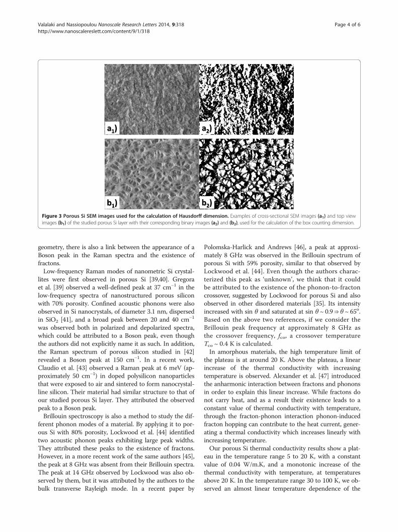
Figure 3 Porous Si SEM images used for the calculation of Hausdorff dimension. Examples of cross-sectional SEM images (a1) and top viewimages (b1) of the studied porous Si layer with their corresponding binary images (a2) and (b2), used for the calculation of the box counting dimension.
Valalaki and Nassiopoulou Nanoscale Research Letters 2014, 9:318 Page 4 of 6http://www.nanoscalereslett.com/content/9/1/318
geometry, there is also a link between the appearance of aBoson peak in the Raman spectra and the existence offractons.Low-frequency Raman modes of nanometric Si crystal-
lites were first observed in porous Si [39,40]. Gregoraet al. [39] observed a well-defined peak at 37 cm−1 in thelow-frequency spectra of nanostructured porous siliconwith 70% porosity. Confined acoustic phonons were alsoobserved in Si nanocrystals, of diameter 3.1 nm, dispersedin SiO2 [41], and a broad peak between 20 and 40 cm−1
was observed both in polarized and depolarized spectra,which could be attributed to a Boson peak, even thoughthe authors did not explicitly name it as such. In addition,the Raman spectrum of porous silicon studied in [42]revealed a Boson peak at 150 cm−1. In a recent work,Claudio et al. [43] observed a Raman peak at 6 meV (ap-proximately 50 cm−1) in doped polysilicon nanoparticlesthat were exposed to air and sintered to form nanocrystal-line silicon. Their material had similar structure to that ofour studied porous Si layer. They attributed the observedpeak to a Boson peak.Brillouin spectroscopy is also a method to study the dif-
ferent phonon modes of a material. By applying it to por-ous Si with 80% porosity, Lockwood et al. [44] identifiedtwo acoustic phonon peaks exhibiting large peak widths.They attributed these peaks to the existence of fractons.However, in a more recent work of the same authors [45],the peak at 8 GHz was absent from their Brillouin spectra.The peak at 14 GHz observed by Lockwood was also ob-served by them, but it was attributed by the authors to thebulk transverse Rayleigh mode. In a recent paper by
Polomska-Harlick and Andrews [46], a peak at approxi-mately 8 GHz was observed in the Brillouin spectrum ofporous Si with 59% porosity, similar to that observed byLockwood et al. [44]. Even though the authors charac-terized this peak as ‘unknown’, we think that it couldbe attributed to the existence of the phonon-to-fractoncrossover, suggested by Lockwood for porous Si and alsoobserved in other disordered materials [35]. Its intensityincreased with sin θ and saturated at sin θ ~ 0.9⇒ θ ~ 65ο.Based on the above two references, if we consider theBrillouin peak frequency at approximately 8 GHz asthe crossover frequency, fco, a crossover temperatureTco ~ 0.4 K is calculated.In amorphous materials, the high temperature limit of
the plateau is at around 20 K. Above the plateau, a linearincrease of the thermal conductivity with increasingtemperature is observed. Alexander et al. [47] introducedthe anharmonic interaction between fractons and phononsin order to explain this linear increase. While fractons donot carry heat, and as a result their existence leads to aconstant value of thermal conductivity with temperature,through the fracton-phonon interaction phonon-inducedfracton hopping can contribute to the heat current, gener-ating a thermal conductivity which increases linearly withincreasing temperature.Our porous Si thermal conductivity results show a plat-
eau in the temperature range 5 to 20 K, with a constantvalue of 0.04 W/m.K, and a monotonic increase of thethermal conductivity with temperature, at temperaturesabove 20 K. In the temperature range 30 to 100 K, we ob-served an almost linear temperature dependence of the

Valalaki and Nassiopoulou Nanoscale Research Letters 2014, 9:318 Page 5 of 6http://www.nanoscalereslett.com/content/9/1/318
thermal conductivity, as that discussed by Alexander et al.[47] for amorphous materials. For higher temperatures,the temperature dependence deviates from linearity andfractons cannot be considered as the dominant mechan-ism. Our experimental results for highly porous Si at tem-peratures higher than 100 K [18] were fitted by modelsconsidering a simplified porous Si structure, as for ex-ample the phonon diffusion model by Gesele et al. [17]and the phonon hydrodynamic model by Alvarez et al.[48]. A comparison of our experimental results with theabove models was made in [18]. Very good agreementwith the phonon diffusion model was obtained for tem-peratures in the range 200 to 350 K, while a better qualita-tive description of the temperature dependence of k in alarger temperature range (100 to 350 K) was obtained withthe phonon hydrodynamic approach. We have to notehere that discrepancies between the experimental resultsand the different theoretical models as the ones above aremainly due to the very complicated structure of porous Si,which is not fully taken into account by the models. Nano-structured porous Si is composed of interconnected Sinanowires and nanocrystals, covered by a native oxideshell and separated by voids. The ratio of the native oxidecompared to the Si core plays a critical role in the deter-mination of the mechanism of thermal conduction in thedifferent temperature ranges, especially at cryogenic tem-peratures [49]. This is because of the different temperaturedependence of vibrational modes in the two systems (theSi backbone and the shell oxide).
ConclusionsThe thermal conductivity of 63% porosity nanostructuredporous Si was measured for the first time in the cryogenictemperature range 5 to 20 K. A stable value as low as0.04 W/m.K was obtained in this temperature range. Weattribute the plateau-like behavior of our porous Si mater-ial at cryogenic temperatures to the presence of fractons,which are localized anomalous vibrational modes accord-ing to the scaling theory of localization of Rammal andToulouse. We discussed in detail the specific fractal geom-etry of our porous Si system and its fractal dimensionalitythat supports the adoption of the fracton formalism. Lit-erature results demonstrated the existence of the so-calledBoson peak in the micro-Raman spectra of porous Si witha similar porosity than that of the porous Si layer used inthis work. The existence of this peak in a material is ingeneral considered as a signature of the presence of local-ized vibrational modes (‘fractons’ in a fractal lattice). Inaddition, literature results of Brillouin spectra of porous Sialso showed localized vibrational modes that support ourinterpretation. Above the plateau and up to approximately100 K, an almost linear increase with temperature was ob-tained for our highly porous Si material, as that obtainedin amorphous materials and attributed to the anharmonic
interaction between fractons and phonons. Above 100 K,other mechanisms are dominant, introduced into differentmodels, like the phonon diffusion model that describesnicely well our results in the temperature range 200 to350 K.
Competing interestsThe authors declare that they have no competing interests.
Authors' contributionsKV made the experiments and wrote a first draft of the manuscript whileAGN supervised the work and fully revised the paper. Both authors read andapproved the final manuscript.
AcknowledgementsThis work was supported by the EU Network of Excellence Nanofunctionthrough the EU Seventh Framework Programme for Research under ContractNo 257375.
Received: 2 May 2014 Accepted: 2 June 2014Published: 25 June 2014
References1. Canham LT: Silicon quantum wire array fabrication by electrochemical
and chemical dissolution of wafers. Appl Phys Lett 1990, 57:1046–1048.2. Cullis AG: Structure and crystallinity of porous silicon. In Properties of
Porous Silicon, Volume 18. Edited by L.T.Canham. UK: Emis Datareviews, IEE,an INSPEC Publ; 1997.
3. Nassiopoulou AG: Thermal isolation of porous Si. In Handbook of Porous Si.Edited by Canham L. Springer Publ; in press.
4. Nassiopoulou AG, Kaltsas G: Porous silicon as an effective material forthermal isolation on bulk crystalline silicon. Phys Status Solidi (a) 2000,182:307–311.
5. Kaltsas G, Nassiopoulou AG: Novel C-MOS compatible monolithic silicongas flow sensor with porous silicon thermal isolation. Sensors andActuators A 1999, 76:133–138.
6. Kaltsas G, Nassiopoulos AA, Nassiopoulou AG: Characterization of a siliconthermal gas-flow sensor with porous silicon thermal isolation. IEEE Sens J2002, 2:463–475.
7. Pagonis DN, Kaltsas G, Nassiopoulou AG: Fabrication and testing of anintegrated thermal flow sensor employing thermal isolation by a poroussilicon membrane over an air cavity. J Micromechanics Microengineering2004, 14:793–797.
8. Hourdakis E, Sarafis P, Nassiopoulou AG: Novel air flow meter for anautomobile engine using a Si sensor with porous Si thermal isolation.Sensors 2012, 12:14838–50.
9. Tsamis C, Tsoura L, Nassiopoulou AG, Travlos A, Salmas CE, Hatzilyberis KS,Androutsopoulos GP: Hydrogen catalytic oxidation reaction on Pd-dopedporous silicon. IEEE Sens J 2002, 2:89–95.
10. Goustouridis D, Kaltsas G, Nassiopoulou AG: A silicon thermalaccelerometer without solid proof mass using porous silicon thermalisolation. IEEE Sens J 2007, 7:983–989.
11. Hourdakis E, Nassiopoulou AG: A thermoelectric generator using porous sithermal isolation. Sensors 2013, 13:13596–608.
12. Lucklum F, Schwaiger A, Jakoby B: Development and investigation ofthermal devices on fully porous silicon substrates. IEEE Sens J 2014,14:992–997.
13. Lee J-H, Galli GA, Grossman JC: Nanoporous Si as an efficient thermoelectricmaterial. Nano Lett 2008, 8:3750–4.
14. Ci P, Shi J, Wang F, Xu S, Yang Z, Yang P, Wang L, Chu PK: Novelthermoelectric materials based on boron-doped silicon microchannelplates. Mater Lett 2011, 65:1618–1620.
15. Lee J-H: Significant enhancement in the thermoelectric performance ofstrained nanoporous Si. Phys Chem Chem Phys 2014, 16:2425–9.
16. De Boor J, Kim DS, Ao X, Hagen D, Cojocaru A, Föll H, Schmidt V:Temperature and structure size dependence of the thermal conductivityof porous silicon. EPL (Europhysics Lett 2011, 96:16001.
17. Gesele G, Linsmeier J, Drach V, Fricke J, Arens-Fischer R: Temperature-dependent thermal conductivity of porous silicon. J Phys D Appl Phys1997, 30:2911–2916.
Valalaki and Nassiopoulou Nanoscale Research Letters 2014, 9:318 Page 6 of 6http://www.nanoscalereslett.com/content/9/1/318
18. Valalaki K, Nassiopoulou AG: Low thermal conductivity porous Si atcryogenic temperatures for cooling applications. J Phys D Appl Phys 2013,46:295101.
19. Cahill DG, Braun PV, Chen G, Clarke DR, Fan S, Goodson KE, Keblinski P, KingWP, Mahan GD, Majumdar A, Maris HJ, Phillpot SR, Pop E, Shi L: Nanoscalethermal transport. II. 2003–2012. Appl Phys Rev 2014, 1:011305.
20. Neophytou N, Zianni X, Kosina H, Frabboni S, Lorenzi B, Narducci D:Simultaneous increase in electrical conductivity and Seebeck coefficientin highly boron-doped nanocrystalline Si. Nanotechnology 2013,24:205402.
21. Siegert L, Capelle M, Roqueta F, Lysenko V, Gautier G: Evaluation ofmesoporous silicon thermal conductivity by electrothermal finiteelement simulation. Nanoscale Res Lett 2012, 7:427.
22. Golding B, Graebner JE, Allen LC: The thermal conductivity plateau indisordered systems. In Phonon Scattering in Condensed Matter V. Edited byAnderson AC, Wolfe JP. Berlin, Heidelberg: Springer Verlag Berlin Heidelberg; 1986.
23. Rammal R, Toulouse G: Random walks on fractal structures andpercolation clusters. J Phys 1983, 44:L13–L22.
24. Alexander S, Orbach R: Density of states on fractals: “fractons.”. Le J Phys -Lettres 1982, 43:L625–L631.
25. Nakayama T, Yakubo K, Orbach R: Dynamical properties of fractalnetworks: scaling, numerical simulations, and physical realizations.Rev Mod Phys 1994, 66:381–443.
26. Ben-Chorin M, Möller F, Koch F: Hopping transport on a fractal: acconductivity of porous silicon. Phys Rev B 1995, 51:2199–2213.
27. Nychyporuk T, Lysenko V, Barbier D: Fractal nature of porous siliconnanocrystallites. Phys Rev B 2005, 71:115402.
28. Chantrenne P, Lysenko V: Thermal conductivity of interconnected siliconnanoparticles: application to porous silicon nanostructures. Phys Rev B2005, 72:035318.
29. Zhigunov DM, Emelyanov AV, Timoshenko VY, Sokolov VI, Seminogov VN:Percolation effect in structures with amorphous and crystalline siliconnanoclusters. Phys Status Solidi C 2012, 9:1474–1476.
30. Kumar S, Alam MA, Murthy JY: Effect of percolation on thermal transportin nanotube composites. Appl Phys Lett 2007, 90:104105.
31. Ono Y, Mayama H, Furó I, Sagidullin AI, Matsushima K, Ura H, Uchiyama T,Tsujii K: Characterization and structural investigation of fractal porous-silica over an extremely wide scale range of pore size. J Colloid InterfaceSci 2009, 336:215–25.
32. Rasband WS: ImageJ. Bethesda, Maryland, USA: U.S. National Institutes ofHealth. imagej.nih.gov/ij/; 1997–2012.
33. Karperien A: FracLac for ImageJ. http://rsb.info.nih.gov/ij/plugins/fraclac/FLHelp/Introduction.htm. 1999–2013.
34. Alexander S, Laermans C, Orbach R, Rosenberg HM: Fracton interpretationof vibrational properties of cross-linked polymers, glasses, and irradiatedquartz. Phys Rev B 1983, 28:4615–4619.
35. Courtens E, Pelous J, Phalippou J, Vacher R, Woignier T: Brillouin-scatteringmeasurements of phonon-fracton crossover in silica aerogels. Phys RevLett 1987, 58:128–131.
36. Shintani H, Tanaka H: Universal link between the boson peak andtransverse phonons in glass. Nat Mater 2008, 7:870–7.
37. Graebner J, Golding B, Allen L: Phonon localization in glasses. Phys Rev B1986, 34:5696–5701.
38. Foret M, Courtens E, Vacher R, Suck J: Scattering investigation of acousticlocalization in fused silica. Phys Rev Lett 1996, 77:3831–3834.
39. Gregora I, Champagnon B, Halimaoui A: Raman investigation of light-emitting porous silicon layers: estimate of characteristic crystallitedimensions. J Appl Phys 1994, 75:3034–3039.
40. Liu F, Liao L, Wang G, Cheng G, Bao X: Experimental observation ofsurface modes of quasifree clusters. Phys Rev Lett 1996, 76:604–607.
41. Fujii M, Kanzawa Y, Hayashi S, Yamamoto K: Raman scattering fromacoustic phonons confined in Si nanocrystals. Phys Rev B 1996,54:R8373–R8376.
42. Ovsyuk NN, Novikov VN: Influence of the degree of disorder ofamorphous solids on the intensity of light scattering by acousticphonons. J Exp Theor Phys 1998, 87:175–178.
43. Claudio T, Schierning G, Theissmann R, Wiggers H, Schober H, Koza MM,Hermann RP: Effects of impurities on the lattice dynamics ofnanocrystalline silicon for thermoelectric application. J Mater Sci 2012,48:2836–2845.
44. Lockwood DJ, Kuok MH, Ng SC, Rang ZL: Surface and guided acousticphonons in porous silicon. Phys Rev B 1999, 60:8878–8882.
45. Fan HJ, Kuok MH, Ng SC, Boukherroub R, Baribeau J-M, Fraser JW, LockwoodDJ: Brillouin spectroscopy of acoustic modes in porous silicon films.Phys Rev B 2002, 65:165330.
46. Polomska-Harlick AM, Andrews GT: Systematic Brillouin light scatteringstudy of the elastic properties of porous silicon superlattices.J Phys D Appl Phys 2012, 45:075302.
47. Alexander S, Entin-Wohlman O, Orbach R: Phonon-fracton anharmonicinteractions: the thermal conductivity of amorphous materials.Phys Rev B 1986, 34:2726–2734.
48. Alvarez FX, Jou D, Sellitto A: Pore-size dependence of the thermalconductivity of porous silicon: a phonon hydrodynamic approach.Appl Phys Lett 2010, 97:033103.
49. Donadio D, Galli G: Temperature dependence of the thermal conductivityof thin silicon nanowires. Nano Lett 2010, 10:847–51.
doi:10.1186/1556-276X-9-318Cite this article as: Valalaki and Nassiopoulou: Thermal conductivity ofhighly porous Si in the temperature range 4.2 to 20 K. NanoscaleResearch Letters 2014 9:318.
Submit your manuscript to a journal and benefi t from:
7 Convenient online submission
7 Rigorous peer review
7 Immediate publication on acceptance
7 Open access: articles freely available online
7 High visibility within the fi eld
7 Retaining the copyright to your article
Submit your next manuscript at 7 springeropen.com