Thermal-Aware 3D Placement
42
Chapter 5 Thermal-Aware 3D Placement Jason Cong and Guojie Luo Abstract Three-dimensional IC technology enables an additional dimension of freedom for circuit design. Challenges arise for placement tools to handle the through-silicon via (TS via) resource and the thermal problem, in addition to the optimization of device layer assignment of cells for better wirelength. This chapter introduces several 3D global placement techniques to address these issues, including partitioning-based techniques, quadratic uniformity modeling techniques, multilevel placement techniques, and transformation-based techniques. The legalization and detailed placement problems for 3D IC designs are also briefly introduced. The effects of various 3D placement techniques on wirelength, TS via number, and tem- perature, and the impact of 3D IC technology to wirelength and repeater usage are demonstrated by experimental results. 5.1 Introduction Placement is an important step in the physical design flow. The performance, power, temperature and routability are significantly affected by the quality of placement results. Three-dimensional IC technology brings even more challenges to the ther- mal problem: (1) the vertically stacked multiple layers of active devices cause a J. Cong (B ) UCLA Computer Science Department, California NanoSystems Institute, Los Angeles, CA 90095, USA e-mail: [email protected] This chapter includes portions reprinted with permission from the following publications: (a) J. Cong, G. Luo, J. Wei, and Y. Zhang, Thermal-aware 3D IC placement via transformation, Proceedings of the 2007 Conference on Asia and South Pacific Design Automation, Yokohama, Japan, pp. 780–785, 2007, © 2007 IEEE. (b) J. Cong, and G. Luo, A multilevel analytical placement for 3D ICs, Proceedings of the 2009 Conference on Asia and South Pacific Design Automation, Yokohama, Japan, pp. 361–366, 2009, © 2009 IEEE. (c) B. Goplen and S. Sapatnekar, Placement of 3D ICs with thermal and interlayer via considerations, Proceedings of the 44th annual conference on Design automation, pp. 626–631, 2007, © 2007 IEEE. 103 Y. Xie et al. (eds.), Three-Dimensional Integrated Circuit Design, Integrated Circuits and Systems, DOI 10.1007/978-1-4419-0784-4_5, C Springer Science+Business Media, LLC 2010
Transcript of Thermal-Aware 3D Placement

Chapter 5Thermal-Aware 3D Placement
Jason Cong and Guojie Luo
Abstract Three-dimensional IC technology enables an additional dimension offreedom for circuit design. Challenges arise for placement tools to handle thethrough-silicon via (TS via) resource and the thermal problem, in addition to theoptimization of device layer assignment of cells for better wirelength. This chapterintroduces several 3D global placement techniques to address these issues, includingpartitioning-based techniques, quadratic uniformity modeling techniques, multilevelplacement techniques, and transformation-based techniques. The legalization anddetailed placement problems for 3D IC designs are also briefly introduced. Theeffects of various 3D placement techniques on wirelength, TS via number, and tem-perature, and the impact of 3D IC technology to wirelength and repeater usage aredemonstrated by experimental results.
5.1 Introduction
Placement is an important step in the physical design flow. The performance, power,temperature and routability are significantly affected by the quality of placementresults. Three-dimensional IC technology brings even more challenges to the ther-mal problem: (1) the vertically stacked multiple layers of active devices cause a
J. Cong (B)UCLA Computer Science Department, California NanoSystems Institute, Los Angeles,CA 90095, USAe-mail: [email protected]
This chapter includes portions reprinted with permission from the following publications: (a)J. Cong, G. Luo, J. Wei, and Y. Zhang, Thermal-aware 3D IC placement via transformation,Proceedings of the 2007 Conference on Asia and South Pacific Design Automation, Yokohama,Japan, pp. 780–785, 2007, © 2007 IEEE. (b) J. Cong, and G. Luo, A multilevel analyticalplacement for 3D ICs, Proceedings of the 2009 Conference on Asia and South Pacific DesignAutomation, Yokohama, Japan, pp. 361–366, 2009, © 2009 IEEE. (c) B. Goplen and S. Sapatnekar,Placement of 3D ICs with thermal and interlayer via considerations, Proceedings of the 44th annualconference on Design automation, pp. 626–631, 2007, © 2007 IEEE.
103Y. Xie et al. (eds.), Three-Dimensional Integrated Circuit Design,Integrated Circuits and Systems, DOI 10.1007/978-1-4419-0784-4_5,C© Springer Science+Business Media, LLC 2010

104 J. Cong and G. Luo
rapid increase in power density; (2) the thermal conductivity of the dielectric layersbetween the device layers is very low compared to silicon and metal. For instance,the thermal conductivity at room temperature (300 K) for SiO2 is 1.4 W/mK [28],which is much smaller than the thermal conductivity of silicon (150 W/mK) andcopper (401 W/mK). Therefore, the thermal issue needs to be considered duringevery stage of 3D IC designs, including the placement process. Thus, a thermal-aware 3D placement tool is necessary to fully exploit 3D IC technology. Thereader may refer to Section 3.2 for a detailed introduction to thermal issues andmethodologies on thermal analysis and optimization.
5.1.1 Problem Formulation
Given a circuit H = (V , E), the device layer number K, and the per-layer place-ment region R = [0, a] × [0, b], where V is the set of cell instances (representedby vertices) and E is the set of nets (represented by hyperedges) in the circuitH (represented by a hypergraph), a placement (xi, yi, zi) of the cell vi ∈ V sat-isfies that (xi, yi) ∈ R and zi ∈ {1, 2, ..., K}. The 3D placement problem is tofind a placement (xi, yi, zi) for every cell vi ∈ V , so that the objective function ofweighted total wirelength is minimized, subject to constraints such as overlap-freeconstraints, performance constraints and temperature constraints. In this chapter wefocus on temperature constraints, as the performance constraints are similar to thatof 2D placement. The reader may refer to [18, 35] for a survey and tutorial of 2Dplacement.
5.1.1.1 Wirelength Objective Function
The quality of a placement solution can be measured by the performance, power,and routability, but the measurement is not trivial. In order to model these aspectsduring optimization, the weighted total wirelength is a widely accepted metric forplacement qualities [34, 35]. Formally, the objective function is defined as
OBJ =∑
e ∈ E
(1+ re) · (WL(e)+ αTSV · TSV(e)) (5.1)
The objective function depends on the placement {(xi, yi, zi)}, and it is a weightedsum of the wirelength WL(e) and the number of through-silicon vias (TS vias)TSV(e) over all the nets. The weight (1 + re) reflects the criticality of the net e,which is usually related to performance optimization. The unweighted wirelengthis represented by setting re to 0. This weight is able to model thermal effects byrelating it to the thermal resistance, electronic capacitance, and switching activity ofnet e [27].
The wirelength WL(e) is usually estimated by the half-perimeter wirelength[27, 19]:
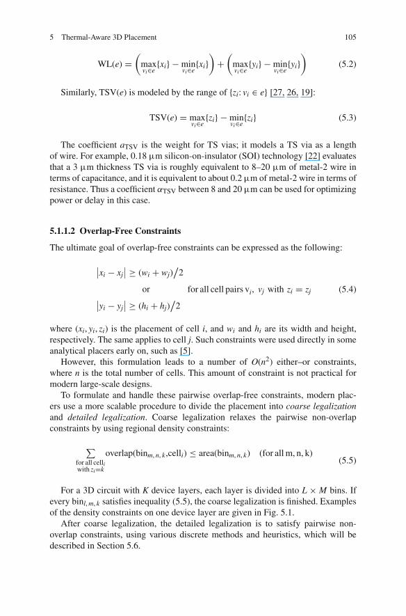
5 Thermal-Aware 3D Placement 105
WL(e) =(
maxvi∈e{xi} −min
vi∈e{xi})+(
maxvi∈e{yi} −min
vi∈e{yi})
(5.2)
Similarly, TSV(e) is modeled by the range of {zi: vi ∈ e} [27, 26, 19]:
TSV(e) = maxvi∈e{zi} −min
vi∈e{zi} (5.3)
The coefficient aTSV is the weight for TS vias; it models a TS via as a lengthof wire. For example, 0.18 μm silicon-on-insulator (SOI) technology [22] evaluatesthat a 3 μm thickness TS via is roughly equivalent to 8–20 μm of metal-2 wire interms of capacitance, and it is equivalent to about 0.2 μm of metal-2 wire in terms ofresistance. Thus a coefficient αTSV between 8 and 20 μm can be used for optimizingpower or delay in this case.
5.1.1.2 Overlap-Free Constraints
The ultimate goal of overlap-free constraints can be expressed as the following:
∣∣xi − xj∣∣ ≥ (wi + wj)
/2
or∣∣yi − yj∣∣ ≥ (hi + hj)
/2
for all cell pairs vi, vj with zi = zj (5.4)
where (xi, yi, zi) is the placement of cell i, and wi and hi are its width and height,respectively. The same applies to cell j. Such constraints were used directly in someanalytical placers early on, such as [5].
However, this formulation leads to a number of O(n2) either–or constraints,where n is the total number of cells. This amount of constraint is not practical formodern large-scale designs.
To formulate and handle these pairwise overlap-free constraints, modern plac-ers use a more scalable procedure to divide the placement into coarse legalizationand detailed legalization. Coarse legalization relaxes the pairwise non-overlapconstraints by using regional density constraints:
∑for all celliwith zi=k
overlap(binm, n, k,celli) ≤ area(binm, n, k) (for all m, n, k)(5.5)
For a 3D circuit with K device layers, each layer is divided into L × M bins. Ifevery binl, m, k satisfies inequality (5.5), the coarse legalization is finished. Examplesof the density constraints on one device layer are given in Fig. 5.1.
After coarse legalization, the detailed legalization is to satisfy pairwise non-overlap constraints, using various discrete methods and heuristics, which will bedescribed in Section 5.6.

106 J. Cong and G. Luo
(a) (b)
bin
bin
Fig. 5.1 (a) Densityconstraint is satisfied;(b) density constraint is notsatisfied
5.1.1.3 Thermal Awareness
In existing literature, temperature issues are not directly formulated as constraints.Instead, a thermal penalty is appended to the wirelength objective function to con-trol the temperature. This penalty can either be the weighted temperature penaltythat is transformed to thermal-aware net weights [27], or the thermal distributioncost penalty [41], or the distance from the cell location to the heat sink duringlegalization [19].
In this chapter we will describe the thermal-aware net weights in Section 5.2,thermal distribution cost function in Section 5.3.3, and thermal-aware legalizationin Section 5.6.2.2.
5.1.2 Overview of Existing 3D Placement Techniques
The state-of-the-art algorithms for 2D placement could be classified into flat place-ment techniques, top-down partitioning-based techniques, and multilevel placementtechniques [35]. These techniques exhibit scalability for the growing complexityof modern VLSI circuits. In order to handle the scalability issues, these techniquesdivide the placement problem into three stages of global placement, legalization,and detailed placement. Given an initial solution, the global placement refines thesolution until the cell area in every pre-defined region is not greater than the capacityof that region. These regions are handled in a top-down fashion from coarsest levelto finest level by the partitioning-based techniques and the multilevel placementtechniques, and are handled in a flat fashion at the finest level by the flat placementtechniques. After the global placement, legalization proceeds to determine the spe-cific location of all cells without overlaps, and the detailed placement performs localrefinements to obtain the final solution.
As the modern 2D placement techniques evolve, a number of 3D placement tech-niques are also developed to address the issues of 3D IC technology. Most of theexisting techniques, especially at the global placement stage, could be viewed asextensions of 2D placement techniques. We group the 3D placement techniquesinto the following categories:
• Partitioning-based techniques [21, 1, 3, 27] insert the partition planes that areparallel to the device layers at some suitable stages in the traditional partition-based process. The cost of partitioning is measured by a weighted sum ofthe estimated wirelength and the TS via number, where the nets are further

5 Thermal-Aware 3D Placement 107
weighted by thermal-aware or congestion-aware factors to consider temperatureand routability.
• Flat placement techniques are mostly quadratic placements and their varia-tions, including the force-directed techniques, cell-shifting techniques, and thequadratic uniformity modeling techniques. Since the unconstrained quadraticplacement will introduce a great amount of cell overlaps, different variations aredeveloped for overlap removal. The minimization of a quadratic function couldbe transformed to the problem of solving a linear system. The force-directed tech-niques [26, 33] append a vector, which is called the repulsive force vector, to theright-hand side of the linear system. These repulsive force vectors are equivalentto the electric field force where the charge distribution is the same as the cellarea distribution. The forces are updated each iteration until the cell area in everypre-defined region is not greater than the capacity of that region. The cell-shiftingtechniques [29] are similar to the force-directed techniques, in the sense that theyalso append a vector to the right-hand side of the linear system. This vector is aresult of the net force from pseudo pins, which are added according to the desiredcell locations after cell shifting. The quadratic uniformity modeling techniques[41] append a density penalty function to the objective function, and it locallyapproximates the density penalty function by another quadratic function at eachiteration, so that the whole global placement could be solved by minimizing asequence of quadratic functions.
• The multilevel technique [13] constructs a physical hierarchy from the originalnetlist, and solves a sequence of placement problems from the coarsest level tothe finest level.
• In addition to these techniques, the 3D placement approach proposed in [19]makes use of existing 2D placement results and constructs a 3D placement bytransformation.
In the remainder of this chapter, we shall discuss these techniques in more detail.The legalization and detailed placement techniques specific to 3D placement arealso introduced.
5.2 Partitioning-Based Techniques
Partitioning-based techniques [21, 1, 3, 27] can efficiently reduce TS via numberswith their intrinsic min-cut objective. These are constructive methods and can obtaingood placement results even when I/O pad connectivity information is missing.
Partitioning-based placement techniques use a recursive two-way partitioning(bisection) approach applied to 3D circuits. At each step of bisection, a partition(V0, R0) consists of a subset of cells V0 ⊆ V in the netlist and a certain physicalportion R0 of the placement region R. When a partition is bisected, two new parti-tions (V1, R1) and (V2, R2) are created from the bisected list of cells V0 = V1 ∪ V2and the bisected physical regions R0 = R1 ∪ R2, where the section plane is usu-ally orthogonal to the axis of x, y, or z. A balanced bisection of the cell list V0into V1 ∪ V2 is usually preferred, which satisfies a balance criterion on the area

108 J. Cong and G. Luo
Wi = ∑v ∈ Viarea(v) for i = 1, 2 such that |W1 −W2| ≤ τ (W1 +W2) with tol-
erance τ . The area ratio between R1 and R2 relates to the cell area ratio betweenV1 and V2. After a certain amount of bisection steps, the regional density con-straints defined in Section 5.1.1.2 are automatically satisfied due to the nature ofthe bisection process.
The placement solution of partitioning-based techniques is determined by theobjective function of bisection and the choice of bisection direction, which aredescribed below.
The idea of min-cut-based placement is to minimize the cut size between parti-tions, so that the cells with high connectives tend to stay in the same partition andstay close to each other for shorter wirelength.
For a bisection of (V0, R0) into (V1, R1) ∪ (V2, R2), a net is cut if it has bothcells in R1 and R2. The total weighted cut size is
∑e is cut (1+ re). The objective
during bisection is to minimize the total weighted cut size, which can be solvedusing Fiduccia–Mattheyses (FM) heuristics [24] with a multilevel scheme hMetis[32].
Terminal propagation [23] is a successful technique for considering the externalconnections to the partition. A cell outside a partition is modeled by a fixed terminalon the boundary of this partition, where the location of the terminal is calculated asthe closest location to the net center.
However, the cut size function does not directly reflect the wirelength objectivefunction of the 3D placement problem defined in Section 5.1.1.1, where the cut sizeis unaware of the weights αTSV. When the cut plane is orthogonal to the x-axis or they-axis, the minimization of cut size only has an implicit effect on the 2D wirelength∑
e ∈ E (1+ re)WL(e); when the cut plane is orthogonal to the z axis, the cut size isequal to
∑e ∈ E (1+ re)αTSVTSV(e). The only way to trade-off these two objectives
is to control the order of bisection directions. The studies in [21] note that the trade-off between total wirelength and TS via number could be achieved by varying theorder of when the circuit is partitioned into device layers. Intuitively, partitioningin z dimension first will minimize the TSV number, while partitioning in x and ydimensions will minimize the total wirelength. References [21, 27] use the weight-ing factor αTSV to determine the order of bisection direction. Assume the physicalregion is R, the cut direction for each bisection is selected as orthogonal to thelargest of the width |xU − xL|, height |yU − yL|, or weighted depth αTSV |zU − zL|of the region. By doing this, the min-cut objective minimizes the number of connec-tions in the most costly direction at the expense of allowing higher connectivity inthe less costly orthogonal directions.
Equation (5.6) shows a thermal awareness term [27] appended to the unweightedwirelength objective function. We will show that this function could be replaced bya weighted total wirelength.∑
e ∈ E
(WL(e)+ αTSVTSV(e))+ αTEMP
∑vi ∈ V
T (5.6)
where Tj is the temperature of cellj, and the temperature awareness αTEMP∑
vi ∈ V Ti
is considered during partitioning. However, using the temperature term directly in

5 Thermal-Aware 3D Placement 109
the objective function can result in expensive recalculations for each individual cellmovement. Therefore, simplification needs to be made for enhanced efficiency. Thetotal thermal resistance from cell vi to ambient can be calculated as
Ri =(
R−1left,i + R−1
right,i + R−1front,i + R−1
rear,i + R−1bottom,i + R−1
top,i
)−1(5.7)
where Rleft, i, Rright, i, Rfront, i, Rrear, i, Rbottom, i, Rtop, i are the approximated thermalresistances analyzed by finite difference method (FDM, Section 3.2.2.1) consid-ering only heat conduction in that direction. For example, Rleft, i is computed as thethermal resistance from the cell location (xi, yi, zi) to the left boundary (x = 0) ofthe 3D chip with cross-sectional area equal to cell width times cell thickness.
Thus the objective used in practice is
∑e ∈ E
(WL(e)+ αTSVTSV(e))+ αTEMP∑
vi ∈ V�Ti
=∑
e ∈ E(WL(e)+ αTSVTSV(e))+ αTEMP
∑vi ∈ V
Ri Pi(5.8)
where �Tj is the temperature contribution of vi and it is a dominant term ofTj; Ri is the thermal resistance from vi to ambient; Pi is the power dissipationof vi. In order to achieve thermal awareness, the optimizations of Pi and Ri areperformed.
The dynamic power associated with net e is
Pe = 0.5aefV2DD
(Cper WLWL(e)+ Cper TSVTSV(e)+ Cper pinninput pins
e
)(5.9)
where ae is the activity factor, f is the clock frequency, VDD is the supply voltage,Cper WL is the capacitance per unit wirelength, Cper TSV is the capacitance per TS via,
Cper pin is the capacitance per input pin, and ninput pinse is the number of cell input pins
that net e drives. Because the inherent resistance of a cell is usually much larger thanthe wire resistance [27], the power Pe dissipates at the driver cell i and contributesto Pi. The sum of these power contributions is the total power dissipation of cell vi:
Pi = ∑net e
driven by vi
Pe
= ∑net e
driven by vi
0.5aefV2DD
(Cper WLWL(e)+ Cper TSVTSV(e)+ Cper pinninput pins
e
)
(5.10)If dropping the terms Cperpinninput pins
e , which are constant during optimization,and replacing Cper TSV by Cper WLαTSV, where αTSV is as defined in Section 5.1.1.1,Equation (5.8) can be expressed as

110 J. Cong and G. Luo
∑e ∈ E
(WL(e)+ αTSVTSV(e))+ αTEMP∑
vi ∈ VRiPi
=∑
e ∈ E(WL(e)+ αTSVTSV(e))+ αTEMP
∑vi ∈ V
Ri
· ∑net e
driven by vi
0.5aefV2DDCper WL (WL(e)+ αTSVTSV(e))
=∑
e ∈ E(WL(e)+ αTSVTSV(e))+ αTEMP
∑e ∈ E∑
cell vidriving net e
Ri · 0.5aefV2DDCper WL (WL(e)+ αTSVTSV(e))
=∑
e ∈ E
⎛⎜⎝1+ αTEMP
∑cell vi
driving net e
Ri · 0.5aefV2DDCper WL
⎞⎟⎠ (WL(e)+ αTSVTSV(e))
(5.11)
Compared to the general weighted wirelength defined in Equation (5.1), thesethermal-aware net weights can be implemented by setting
re = αTEMP
∑cell vi
driving net e
Ri · 0.5aefV2DDCper WL (5.12)
The thermal-aware net weight re is not a constant during the partitioning process.Instead, the thermal resistance Ri is determined by the distance between the cell vi
and the chip boundaries. A simple calculation [27] can be done by assuming thatthe heat flows in straight paths from the cell location toward the chip boundariesin all three directions, and the overall thermal resistance is calculated from theseseparated directional thermal resistances. These thermal resistances are evaluatedduring the partitioning process for the computation of the gain by moving a cellfrom one partition to another.
In addition to the thermal-aware net-weighting objective function, the tempera-ture is also optimized by pseudo-nets that pull the cells to the heat sink [27].
5.3 Quadratic Uniformity Modeling Techniques
Different from the discrete partitioning-based techniques, the quadratic placement-based techniques are continuous. The idea is to relax the device layer assignmentof a cell z ∈ {1, ..., K} by a weaker constraint, where z ∈ [1, K]. The 3D place-ment problem is solved by minimizing a quadratic cost function, or finding thesolution to a derived linear system. The regional density constraints are handled byappending a force vector to the linear system (force-directed techniques [26, 33] andcell-shifting techniques [29]) or appending a quadratic penalty to the quadratic costfunction (quadratic uniformity modeling techniques [41]). The 3D global placement

5 Thermal-Aware 3D Placement 111
is solved by minimizing a sequence of quadratic cost functions. In this section, wewill discuss the quadratic uniformity modeling techniques.
The complete placement flow is shown in Fig. 5.2. The flow is divided intoglobal placement and detailed placement, where global placement is solved by thequadratic uniformity modeling technique, and the detailed placement can be solvedwith simple layer-by-layer 2D detailed placement or other advanced legalizationand detailed placement techniques discussed in Section 5.6.
Global
Compute Quadratic Formsof DIST and TDIST
Update Coefficients β and γSolve Quadratic Programming
SolutionOptimization
Legalization andDetailed Placement
Initial Solution
Final Solution
Fig. 5.2 Quadratic placement flow
The unified quadratic cost function is defined as
OBJ+= OBJ+β×DIST+γ×TDIST (5.13)
where OBJ is the wirelength objective defined in Section 5.1.1.1; DIST is the celldistribution cost; β is the weight of the cell distribution cost; TDIST is the thermaldistribution cost; and γ is the thermal distribution cost. Moreover, all these functionsOBJ, DIST, and TDIST are expressed in quadratic forms as in Equation (5.14),which will be explained in the following sections.
OBJ =n∑
i = 1
(n∑
j = 1qx, ijxixj + px, ixi
)+
n∑i = 1
(n∑
j = 1qy, ijyiyj + py, iyi
)
+n∑
i = 1
(n∑
j = 1qz, ijzizj + pz, izi
)+ r
DIST ≈n∑
i = 1(ax, ix2
i + bx, ixi)+n∑
i = 1(ay, iy2
i + by, iyi)
+n∑
i = 1(az, iz2
i + bz, izi)+ C
TDIST ≈n∑
i = 1(a(T)
x, i x2i + b(T)
x, i xi)+n∑
i = 1(a(T)
y, i y2i + b(T)
y, i yi)
+n∑
i = 1(a(T)
z, i z2i + b(T)
z, i zi)+ C(T)
(5.14)

112 J. Cong and G. Luo
5.3.1 Wirelength Objective Function
In order to construct a quadratic wirelength function to approximate the wirelengthobjective defined in Section 5.1.1.1, the multiple-pin nets are decomposed to two-pin nets by either the star model or clique model. In the resulting graph, the quadraticwirelength is defined as
OBJ =∑
e ∈ Evi, vj ∈ e
(1+ re)((
se, x(xi − xj)2 + se, y(yi − yj)
2)+ αTSVse, z(zi − zj)
2)
(5.15)
where (1+re) is the net weight, and αTSV is the TS via coefficient defined in Section5.1.1.1; net e is the decomposed two-pin net connecting vi at (xi, yi, zi) and vj at(xj, yj, zj). The coefficients se, x, se, y, se, z could linearize the quadratic wirelength toapproximate the HPWL wirelength and the TS via number defined in Equations(5.2) and (5.3) [38].
It is obvious that this quadratic function OBJ can be rewritten in the matrix form:
OBJ =n∑
i = 1
(n∑
j = 1qx, ijxixj + px, ixi
)+
n∑i = 1
(n∑
j = 1qy, ijyiyj + py, iyi
)
+n∑
i = 1
(n∑
j = 1qz, ijzizj + pz, izi
)+ r
(5.16)
where xi, yi, zi are the problem variables and the coefficients qx, ij, px, i, qy, ij, py, i,qz, ij, pz, i, and r can be directly computed from Equation (5.15). The coefficientspx, i, py, i, pz, i and r are related to the locations of I/O pins and fixed cells in thecircuit.
5.3.2 Cell Distribution Cost Function
The original idea of using discrete cosine transformation (DCT) to evaluate celldistribution and help spread cells is from [42] in 2D placement. This idea is extendedand applied to 3D placement.
Similar to the bin density defined in Section 5.1.1.2, another bin density for therelaxed problem with continuous variables (zi) is defined as
dm, n, l =
∑for all cell i
intersection(binm, n, l, celli)
volume(binm, n, l)(5.17)
Assuming a 3D circuit has K device layers, with die width W and die height H,the relaxed placement region [0, W]× [0, H]× [0, K] is divided into M×N×L bins,where celli at (xi, yi, zi) is mapped to the region [xi− wi
2 , xi+ wi2 ]× [yi− hi
2 , yi+ hi2 ]×
[zi, zi + 1].

5 Thermal-Aware 3D Placement 113
The 3D DCT transformation of {fp, q, v} = DCT({dm, n, l}
)is defined as
fp, q, v =√
8
MNLC(p)C(q)C(v)
M−1∑m = 0
N−1∑n = 0
L−1∑l = 0
dm, n, l cos
((2m+ 1)pπ
2 M
)
cos
((2n+ 1)qπ
2 N
)cos
((2 l+ 1)vπ
2L
) (5.18)
where m, n, l are the coordinates in the spatial domain, and p, q, v are coordinates in
the frequency domain. The coefficients are C(v) ={
1/√
2 t = 0
1 otherwiseThe cell distribution cost is defined as
DIST =∑p, q, t
up, q, tf2p, q, t (5.19)
where up, q, t = 1/
(p+ q+ t + 1) is set heuristically.Note that (5.19) is not a quadratic function with respect to the placement variables
(xi, yi, zi). In order to construct a quadratic form, approximation is made as follows:
DIST ≈n∑
i = 1(ax, ix2
i + bx, ixi)+n∑
i = 1(ay, iy2
i + by, iyi)
+n∑
i = 1(az, iz2
i + bz, izi)+ C(5.20)
Although the coefficients ax, i, bx, i, ay, i, by, i, az, i, bz, i depend on the intermediateplacement, they are assumed to be constant in this quadratic function. These coeffi-cients are updated when the intermediate placement changes. Since the variables aredecoupled well in this approximation, the coefficients can be computed one by one.To compute ax, i, bx, i all the variables except xi can be fixed, thus the cost functionis a quadratic function of xi:
DIST(xi) ≈ ax, ix2i + bx, ixi + C′i, x (5.21)
The three coefficients ax, i, bx, i, and C′i, x are computed from the three costsDIST(xi), DIST(xi−δ), and DIST(xi+δ). Through the computation, we can see thatthe first-order and second-order derivatives of the quadratic approximation satisfy
2ax, ixi + bx, i = DIST(xi + δ)− DIST(xi − δ)
2δ≈ ∂DIST(xi)
∂xi
2ax, i = DIST(xi + δ)− 2DIST(xi)+ DIST(xi − δ)
δ2≈ ∂2DIST(xi)
∂x2i
(5.22)

114 J. Cong and G. Luo
so that the first-order and second-order derivatives of this quadratic function locallyapproximates the first-order and second-order derivatives of the area distributioncost function DIST, respectively.
The computation of multiple DIST functions avoids 3D DCT transformation bypre-computations [42]. It spends O(M2 N2L2) space for O(n) runtime during thecomputation of matrix coefficients in Equation (5.20).
5.3.3 Thermal Distribution Cost Function
The thermal cost is treated like cell distribution cost, by replacing the cell densities{dm, n, l} with thermal densities {tm, n, l}. The thermal density is defined as
tm, n, l = Tm, n, l/
Tavg (5.23)
where Tm, n, l is the average temperature in binm, n, l, and Tavg is the averagetemperature of the whole chip.
As the cell distribution cost, the thermal distribution is transformed by 3D DCT,and the distribution cost function is approximated by a quadratic form.
Besides the computation of matrix coefficients in the quadratic approximationof thermal distribution function TDIST, another significant cost of runtime is thecomputation of thermal densities {tm, n, l}, because an accurate computation requiresthermal analysis. To save runtime from the thermal analysis during computingTDIST(xi), TDIST(xi − δ), TDIST(xi + δ), etc., approximation is made in com-puting a new {tm, n, l}. The work in [41] uses two methods of approximation, both ofwhich may be lack of accuracy but are fast to be integrated in the distribution costcomputation.
The first approximation makes use of thermal contribution of cells. Let Pbin(i)and Tbin(i) be the power and average temperature in binm(i), n(i), l(i), the thermalcontribution of a cell in this bin is defined as
Tcell = Pcell
Pbin(i)· Tbin(i) (5.24)
When the cell is moved from binm(i), n(i), l(i) to binm(j), n(j), l(j), the temperature ofbins are updated as
Tbin(i)← Tbin(i)− β · TcellTbin(j)← Tbin(j)− β · Tcell
(5.25)
where β = l(j)/
l(i) is the influence of the cell on bin temperature.The second approximation updates the bin temperature in the same ratio as the
power density updates as
T ′bin(i) = P′bin(i)
Pbin(i)· Tbin(i) (5.26)

5 Thermal-Aware 3D Placement 115
5.4 Multilevel Placement Technique
Multilevel heuristics [15] have proved to be effective in large-scale designs. Theapplication of multilevel heuristics to the partitioning problem [32] also shows thatit could also improve the solution quality; this is also implicated by the partitioning-based techniques discussed in Section 5.2. Moreover, the solvers of the quadraticplacement-based problem usually apply the multigrid method, which is the originof multilevel heuristics.
In this section, we will introduce an analytical 3D placement engine thatexplicitly makes use of multilevel heuristics.
5.4.1 3D Placement Flow
The overall placement flow is shown in Fig. 5.3. The global placement starts fromscratch or takes in the given initial placement. The global placement incorporatesthe analytical placement engine (Section 5.4.2) into the multilevel framework thatis used in [15]. The global placement is then processed layer-by-layer with the 2Ddetailed placer [16] to obtain the final placement.
Minimize the Penalized Objective
Initialize/Update Penalty Factor
Converge?
Layer-by-layer Detailed Placement
Y
N
InitialNetlist
Final Placement
Relaxation
Coarsening
Finest Net-list
CoarsestNetlist
Finest LevelDone?
Interpolation
Y
N
Fig. 5.3 Multilevelanalytical 3D placement flow
5.4.2 Analytical Placement Engine
Analytical placement is not a unique engine for multilevel heuristics. In fact, anyflat 3D placement technique like the one introduced in Section 5.3 can also be used.

116 J. Cong and G. Luo
In this section, we focus on the analytical engine [13] which was the first work toapply multilevel heuristics for 3D placement.
The analytical placement engine solves 3D global placement problem by trans-forming the non-overlap constraints to density penalties.
minimize∑
e ∈ E(WL(e)+ αTSV · TSV(e))
subject to Penalty (�x, �y, �z) = 0
(5.27)
The wirelength WL(e) (Section 5.4.2.2), the TS via number TSV(e) (Section5.4.2.3), and the density penalty function Penalty (�x, �y, �z) (Section 5.4.2.4) will bedescribed in the following sections in detail.
In order to solve this constrained problem, penalty methods [37] are usuallyapplied:
OBJ(�x, �y, �z) =∑
e ∈ E
(WL(e)+ αTSV · TSV(e))+ μ · Penalty (�x, �y, �z) (5.28)
This penalized objective function is minimized by each iteration, with a graduallyincreasing penalty factor μ to reduce the density violations. It can be shown that theminimizer of Equation (5.28) is equivalent to problem (5.27) when μ → ∞ if thepenalty function is non-negative.
5.4.2.1 Relaxation of Discrete Variables
As mentioned in Section 5.1.1, the placement variables are represented by triples(xi, yi, zi), where zi is a discrete variable in {1, 2, ..., K}. The range of zi is relaxedfrom the set {1, 2, . . . , K} to a continuous interval [1, K]. After relaxation, a nonlin-ear analytical solver can be used in our placement engine. The relaxed solution ismapped back to the discrete values before the detailed placement phase.
5.4.2.2 Log-Sum-Exp Wirelength
The half-perimeter wirelength WL(e) defined in Equation (5.2) is replaced by adifferentiable approximation with the log-sum-exp function [4], which is introducedto placement by [36]
WL(e) ≈ η( log∑
vi ∈ eexp (xi/η)+ log
∑vi ∈ e
exp (− xi/η)
+ log∑
vi ∈ eexp (yi/η)+ log
∑vi ∈ e
exp (− yi/η))(5.29)
5 Thermal-Aware 3D Placement 117
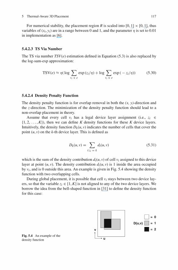
For numerical stability, the placement region R is scaled into [0, 1]× [0, 1], thusvariables of (xi, yi) are in a range between 0 and 1, and the parameter η is set to 0.01in implementation as [6].
5.4.2.3 TS Via Number
The TS via number TSV(e) estimation defined in Equation (5.3) is also replaced bythe log-sum-exp approximation:
TSV(e) ≈ η( log∑
vi ∈ e
exp (zi/η)+ log∑
vi ∈ e
exp (− zi/η)) (5.30)
5.4.2.4 Density Penalty Function
The density penalty function is for overlap removal in both the (x, y)-direction andthe z-direction. The minimization of the density penalty function should lead to anon-overlap placement in theory.
Assume that every cell vi has a legal device layer assignment (i.e., zi ∈{1, 2, . . . , K}), then we can define K density functions for these K device layers.Intuitively, the density function Dk(u, v) indicates the number of cells that cover thepoint (u, v) on the k-th device layer. This is defined as
Dk(u, v) =∑
i:zi = k
di(u, v) (5.31)
which is the sum of the density contribution di(u, v) of cell vi assigned to this devicelayer at point (u, v). The density contribution di(u, v) is 1 inside the area occupiedby vi, and is 0 outside this area. An example is given in Fig. 5.4 showing the densityfunction with two overlapping cells.
During global placement, it is possible that cell vi stays between two device lay-ers, so that the variable zi ∈ [1, K] is not aligned to any of the two device layers. Weborrow the idea from the bell-shaped function in [31] to define the density functionfor this case:
= 0
= 2
= 1
u
v
D(u,v)
Fig. 5.4 An example of thedensity function

118 J. Cong and G. Luo
Dk(u, v) =∑
i
η(k, zi)di(u, v), for 1 ≤ k ≤ K (5.32)
where
η(k, z) =⎧⎨⎩
1− 2(z− k)2 |z− k| ≤ 1/
22( |z− k| − 1)2 1
/2 < |z− k| ≤ 1
0 otherwise(5.33)
We call (5.33) the bell-shaped density projection function, which extends thedensity function (5.31) from integral layer assignments to the definition (5.32) forrelaxed layer assignments. It is obvious that (5.32) is consistent with (5.31) whenthe layer assignments {zi} are integers.
An example of how this extension works for a four-layer 3D placement is given inFig. 5.5. The x-axis is the relaxed layer assignment in z-direction, while the y-axisindicates the amount of area to be projected in the actual device layers. The fourcurves, the dash-dotted curve, the dotted curve, the solid curve and the dashed curve,represent the functions η(1, z), η(2, z), η(3, z) and η(4, z) for device layers 1, 2, 3,and 4, respectively. In this example, a cell is temporarily placed at z = 2.316 (thetriangle on the x-axis) between layer 2 and layer 3. The bell-shaped density projec-tion functions project 80% of its area to layer 2 (the upper triangle on the y-axis) and20% of its area to layer 3 (the lower triangle on the y-axis). In this way, we establisha mapping from a relaxed 3D placement to the area distributions in discrete layers.
Fig. 5.5 An example of thebell-shaped densityprojections
Inspired by the quadratic penalty terms in 2D placement methods [6, 31, 9], wedefine this density penalty function to measure the amount of overlaps:
P(�x, �y, �z) =K∑
k = 1
∫ 1
0
∫ 1
0(Dk(u, v)− 1)2 dudv (5.34)

5 Thermal-Aware 3D Placement 119
Lemma 1 Assume the total area of cells equals the placement area (i.e.,∑i area(vi) = K, no empty space), every legal placement (�x∗, �y∗, �z∗), which sat-
isfies Dk(u, v) = 1 for every k and (u, v) without any non-integer z∗i , is a minimizerof P(�x, �y, �z).
The proof of Lemma 1 is trivial and thus is omitted. Therefore, minimizingP(�x, �y, �z) provides a necessary condition for a legal placement. However, there existminimizers that cannot form a legal placement. An example is shown in Fig. 5.6where placement (b) also minimizes the density penalty function but it is not legal.
Fig. 5.6 Two placementswith the same densitypenalties
To avoid reaching such minimizers, we introduce the interlayer density function:
Ek(u, v) =∑
i
η(k + 0.5, zi)di(u, v), for 1 ≤ k ≤ K − 1 (5.35)
and also the interlayer density penalty function:
Q(�x, �y, �z) =K−1∑k = 1
∫ 1
0
∫ 1
0(Ek(u, v)− 1)2 dudv (5.36)
Similar to the density penalty function P(�x, �y, �z), the following Lemma 2 is alsotrue.
Lemma 2 Assume the total area of cells equals the placement area, every legalplacement is a minimizer of Q (�x, �y, �z).
Combining the density penalty functions P(�x, �y, �z) and Q(�x, �y, �z), we define thefollowing density penalty function:
Penalty (�x, �y, �z) = P(�x, �y, �z)+ Q(�x, �y, �z) (5.37)
Theorem 1 Assume the total area of cells equals the placement area, every legalplacement (�x∗, �y∗, �z∗) is a minimizer of Penalty (�x, �y, �z), and vice versa.
Proof It is obvious that every legal placement is a minimizer of Penalty (�x, �y, �z)by combining Lemma 1 and Lemma 2. We shall prove that every minimizer

120 J. Cong and G. Luo
(�x∗, �y∗, �z∗) of Penalty (�x, �y, �z) is a legal placement. From the proof of Lemma 1 andLemma 2, we know the minimum value of Penalty (�x, �y, �z) is achieved if and onlyif Dk(u, v) = 1 and Ek(u, v) = 1 for every k and (u, v). First, if all the componentsof �z∗ are integers, it is easy to see that the placement is legal, because all the cellsare assigned to a certain device layer, and for any point (u, v) on any device layer kthere is only one cell covering this point (no overlaps).
Next, we show that there does not exist a z∗i with a non-integer value (proofby contradiction). If a cell vi has a non-integer z∗i , we know that there are Kcells covering (x∗i , y∗i ) because
∑Kk = 1 Dk(x∗i , y∗i ) = K. According to the pigeon-
hole principal, among these K cells there are at least two cells vi1, vi2 with thez-direction distance
∣∣z∗i1 − z∗i2∣∣ < 1, since all the variables {z∗i } are in the range
of [1, K]. Without loss of generality we may assume z∗i1 ≤ z∗i2, therefore thereexists an integer k ∈ {1, 2, . . . K} such that either z∗i1 ∈ (k, k + 0.5] and z∗i2 ∈(k, k + 1.5), or z∗i1 ∈ (k − 0.5, k] and z∗i2 ∈ (k − 0.5, k + 1). It is easy to verifythat in the former case
∣∣z∗i1 − (k + 0.5)∣∣ + ∣∣z∗i2 − (k + 0.5)
∣∣ < 1 and Ek(x∗i , y∗i ) ≥η(k + 0.5, z∗i1)+ η(k + 0.5, z∗i2) > 1; in the latter case
∣∣z∗i1 − k∣∣+ ∣∣z∗i2 − k
∣∣ < 1 andDk(x∗i , y∗i ) ≥ η(k, z∗i1) + η(k, z∗i2) > 1. Both cases lead to either Ek(x∗i , y∗i ) > 1 orDk(x∗i , y∗i ) > 1, which conflict with the assumption that (�x∗, �y∗, �z∗) is a minimizer ofPenalty (�x, �y, �z).
Therefore there does not exist a non-integer z∗i , and every minimizer ofPenalty (�x, �y, �z) is a legal placement in the z-dimension. �
In the analytical placement engine, the densities Dk(u, v) and Ek(u, v) are replaced
by smoothed densities �Dk(u, v) and �
Ek(u, v) for differentiability. As in [6], thedensities are smoothed by solving Helmholtz equations:
�Dk(u, v) = −
(∂2
∂u2+ ∂2
∂v2− ε
)−1
Dk(u, v)
�Ek(u, v) = −
(∂2
∂u2+ ∂2
∂v2− ε
)−1
Ek(u, v)
(5.38)
and the smoothed density penalty function
Penalty (�x,�y,�z) =K∑
k = 1
∫ 10
∫ 10
(�Dk(u, v)− 1
)2dudv
+K−1∑k = 1
∫ 10
∫ 10
(�Ek(u, v)− 1
)2dudv
(5.39)
is used in our implementation, whose gradient is computed efficiently with themethod in [12].

5 Thermal-Aware 3D Placement 121
5.4.3 Multilevel Framework
The optimization problem below summarizes our analytical placement engine:
⎧⎪⎪⎪⎪⎪⎪⎪⎪⎨⎪⎪⎪⎪⎪⎪⎪⎪⎩
minimize
∑e ∈ E
(WL(e)+ αTSVTSV(e))
+μ
(K∑
k = 1
∫ 10
∫ 10
(�Dk(u, v)− 1
)2dudv
+K−1∑k = 1
∫ 10
∫ 10
(�Ek(u, v)− 1
)2dudv
)
increase μ until the density penalty is small enough
(5.40)
This analytical engine is incorporated into the multilevel framework in [15],which consists of coarsening, relaxation, and interpolation.
The purpose of coarsening is to build a hierarchy for the multilevel diagram,where we use the best-choice hypergraph clustering [2].
After the hierarchy is set up, multiple placement problems are solved from thecoarsest level to the finest level. In a coarser level, clusters are modeled as cells andthe connections between clusters are modeled as nets, so that there is one placementproblem for each level. The placement problem at each level is solved (relaxed) bythe analytical engine (5.40).
These placement problems are solved in the order from the coarsest level to thefinest level, where the solution at a coarser level is interpolated to obtain an initialsolution of the next finer level. The cell with highest degree in a cluster is placed inthe center of this cluster (C-points), while the other cells are placed at the weightedaverage locations of their neighboring C-points, where the weights are proportionalto the connectivity to those clusters.
5.5 Transformation-Based Techniques
The basic idea of transformation-based approaches [19] is to generate 3D thermal-aware placement from existing 3D placement results in a two-step procedure: 3Dtransformation and refinement through layer reassignment. In this section we willintroduce 3D transformation, including local stacking transformation, folding-basedtransformation, and the window-based stacking/folding transformation. The refine-ment through layer reassignment is general to all techniques and will be introducedin Section 5.6.3.
The framework of transformation-based 3D placement techniques is shown inFig. 5.7. The components with a dashed boundary are the existing 2D placementtools that the transformation-based approaches make use of. A 2D wirelength-drivenand/or thermal-driven placer is first used to generate a 2D placement for the targetdesign, in a placement region with area equal to the total 3D placement areas. Thequality of the final 3D placement highly depends on this initial placement. The 2Dplacement is then transformed into a legalized 3D placement according to the given
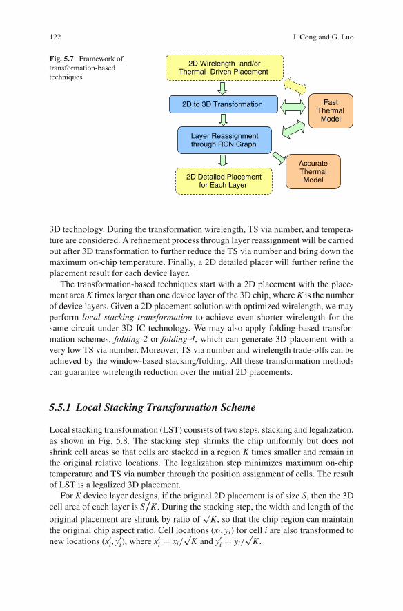
122 J. Cong and G. Luo
2D Wirelength- and/orThermal- Driven Placement
2D to 3D Transformation
Layer Reassignmentthrough RCN Graph
2D Detailed Placementfor Each Layer
FastThermalModel
AccurateThermalModel
Fig. 5.7 Framework oftransformation-basedtechniques
3D technology. During the transformation wirelength, TS via number, and tempera-ture are considered. A refinement process through layer reassignment will be carriedout after 3D transformation to further reduce the TS via number and bring down themaximum on-chip temperature. Finally, a 2D detailed placer will further refine theplacement result for each device layer.
The transformation-based techniques start with a 2D placement with the place-ment area K times larger than one device layer of the 3D chip, where K is the numberof device layers. Given a 2D placement solution with optimized wirelength, we mayperform local stacking transformation to achieve even shorter wirelength for thesame circuit under 3D IC technology. We may also apply folding-based transfor-mation schemes, folding-2 or folding-4, which can generate 3D placement with avery low TS via number. Moreover, TS via number and wirelength trade-offs can beachieved by the window-based stacking/folding. All these transformation methodscan guarantee wirelength reduction over the initial 2D placements.
5.5.1 Local Stacking Transformation Scheme
Local stacking transformation (LST) consists of two steps, stacking and legalization,as shown in Fig. 5.8. The stacking step shrinks the chip uniformly but does notshrink cell areas so that cells are stacked in a region K times smaller and remain inthe original relative locations. The legalization step minimizes maximum on-chiptemperature and TS via number through the position assignment of cells. The resultof LST is a legalized 3D placement.
For K device layer designs, if the original 2D placement is of size S, then the 3Dcell area of each layer is S
/K. During the stacking step, the width and length of the
original placement are shrunk by ratio of√
K, so that the chip region can maintainthe original chip aspect ratio. Cell locations (xi, yi) for cell i are also transformed tonew locations (x′i, y′i), where x′i = xi/
√K and y′i = yi/
√K.

5 Thermal-Aware 3D Placement 123
Stacking Legalization
a,b,c,db
d c
a
a b
c d
Fig. 5.8 Local stacking transformation
After such a transformation, the initial 2D placement is turned into a 2D place-ment of size S
/K with an average cell density of K, which later will be distributed
to K device layers in the legalization step. The Tetris-style legalization (Section5.6.2.2) could be applied to determine the layer assignment, which may also opti-mize the TS via number and temperature. As shown in Fig. 5.8, a group ofneighboring cells stacking on each other are distributed to different device layersafter the transformation process.
5.5.2 Folding Transformation Schemes
LST achieves short wirelength by stacking the neighboring cells together. However,a great number of TS vias will be generated when the cells of local nets are put ontop of one another. If the target 3D IC technology allows only limited TS via density,transformations that generate fewer TS vias are required.
Folding-based transformation folds the original 2D placement like a piece ofpaper without cutting off any parts of the placement. The distance between any twocells will not increase and the total wirelength is guaranteed to decrease. TS viasare only introduced to the nets crossing the folding lines (shown as the dashed linesin Fig. 5.9). With an initial 2D placement of minimized wirelength, the number ofsuch long nets should be fairly small, which implies that the connections betweenthe folded regions should be limited, resulting in much fewer TS vias (comparedto that of the LST transformation, where many dense local connections cross dif-ferent device layers). Figure 5.9a shows one way of folding, named folding-2, byfolding once at both x- and y-directions. Figure 5.9 b shows another way of folding,
(a) folding-2 transformation (b) folding-4 transformation
Fig. 5.9 Two folding-based transformation schemes

124 J. Cong and G. Luo
named folding-4, by folding twice at both x and y-directions. The folding results arelegalized 3D placements, so no legalization step is necessary.
After folding-based transformations, only the lengths of the global nets thatgo across the folding lines (dotted lines in Fig. 5.9) get reduced. Therefore,folding-based transformations cannot achieve as much wirelength reduction asLST. Furthermore, if we want to maintain the original aspect ratio of the chip,folding-based transformations are limited to even numbers of device layers.
5.5.3 Window-Based Stacking/Folding Transformation Scheme
As stated above, LST achieves the greatest wirelength reduction at the expense of alarge amount of TS vias, while folding results in a much smaller TS via number butlonger wirelength and possibly high via density along the folding lines.
An ideal 3D placement should have short wirelength with TS via density satisfy-ing what the vertical interconnection technology can support. Moreover, we prefereven TS via density for routability reason. Therefore, we propose a window-basedstacking/folding method for better TS via density control.
In this method, 2D placement is first divided into N × N windows. Then thestacking or folding transformation is applied in every window. Each window can usedifferent stacking/folding orders. Figure 5.10 shows the cases for N = 2. The circuitis divided into 2×2 windows (shown with solid lines). Each window is again dividedinto four squares(shown with dotted lines). The number in each square indicates thelayer number of that square after stacking/folding. The four-layer placements ofeach window are packed to form the final 3D placement.
Wirelength reduction is due to the following reasons: the wirelength of the netsinside the same square is preserved; the wirelength of nets inside the same windowis most likely reduced due to the effect of stacking/folding; and the wirelength ofnets that cross the different windows is reduced. Therefore the overall wirelengthquality is improved.
Meanwhile, the TS vias are distributed evenly among different windows and canbe reduced by choosing proper layer assignments. TS vias are introduced by the netsthat cross the boundaries between neighboring squares with different layer numbers,and we call this boundary between two neighboring squares a transition. Fewer tran-sitions result in fewer TS vias. Intra-window transitions cannot be reduced becausewe need to distribute intra-window squares to different layers, so we focus on reduc-ing inter-window transitions. Since the sequential layer assignment in Fig. 5.10a
3 2 3 2 3 2 2 34 1 4 1 4 1 1 43 2 3 2 4 1 1 44 1 4 1 3 2 2 3
(a) sequential (b) symmetricFig. 5.10 2×2 windows withdifferent layer assignments

5 Thermal-Aware 3D Placement 125
creates lots of transitions, we use another layer assignment as in Fig. 5.10b, calledsymmetric assignment, to reduce the amount of inter-window transitions to zero. Sothis layer assignment generates the smallest TS via number, while the wirelength issimilar.
The wirelength versus TS via number trade-offs can be controlled by the numberof windows.
5.6 Legalization and Detailed Placement Techniques
A final location for any cell is not desired in the global placement stage. The legal-ization is in charge of removing the remaining overlaps between cells, and thedetailed placement performs further refinement for the placement quality.
Coarse legalization (Section 5.6.1) bridges the gap between global placementand detailed placement. Even for the discrete partitioning-based techniques dis-cussed in Section 5.2, overlap exists after recursive bisection if the device layernumber K is not a power of two. The other continuous techniques discussed inSections 5.3 and 5.4 usually stop before the regional density constraints are strictlysatisfied for purpose of runtime reduction. The coarse legalization distributes cellsmore evenly, so that the latter detailed legalization stage (Section 5.6.2) can assumethat local displacement of cells is enough to obtain a legal placement. Anotherlegalization technique called Tetris-style legalization will also be described inSection 5.6.2.2.
The detailed placement performs local swapping of cells to further refine theobjective function. If the swapping is inside a device layer, it is not differentfrom that of the 2D detail placement. The swapping between device layers isnew in the context of 3D placement. A swapping technique that uses RelaxedConflict Net (RCN) graph to reduce the TS via number will be introduced inSection 5.6.3.
5.6.1 Coarse Legalization
Placements produced after coarse legalization still contains overlaps, but the cellsare evenly distributed over the placement area so that the computational intensivelocalized calculations used in detailed legalization are prevented from acting overexcessively large areas. Coarse legalization [27] utilizes a spreading heuristic calledcell shifting to prepare a placement for detailed legalization and refinement.
To utilize the cell-shifting heuristic, the placement region [0, W]× [0, H]× [0, K]is divided into M × N × L bins, where celli at (xi, yi, zi) is mapped to the region[xi − wi
2 , xi + wi2 ]× [yi − hi
2 , yi + hi2 ]× [zi − 1, zi]. During cell shifting, the cells are
shifted in one direction at a time, and are shifted three times in three directions.A demonstration of cell shifting in the x-direction is shown in Fig. 5.11. In this
example, the boundaries of the bins in the row with gray color are shifted according

126 J. Cong and G. Luo
Fig. 5.11 Cell shifting in x-direction [27]
to the bin densities. The numbers labeled inside the bins are the bin densities, wherethe dold and dnew are the densities before and after cell shifting, respectively. Theratios W ′b
/Wb between the new bin width W ′b and the old bin width Wb are approx-
imately 0.9, 1.4, 1.0, 0.8, 1.3, and 0.5, respectively for the bins from left to rightin this row. Thus the cells inside these bins are also shifted in the x-direction andthe bin densities are adjusted to meet the density constraints. The ratio W ′b
/Wb is
related to the bin density d, which is visualized in Fig. 5.12. In this figure, the x-axis is for the bin density d, and the y-axis is for the ratio W ′b
/Wb. The coefficients
aU , aL, and b are the same for each row (like the one in gray color), but may be dif-ferent for different rows, which are adjusted to keep the total bin widths in a row beconstant.
Fig. 5.12 Cell-shifting binwidth versus density [27]
After cell shifting, the cell density in every bin is guaranteed not to exceedits volume. But this heuristic does not consider the objective function that shouldbe optimized. Therefore, cell-moving and cell-swapping operations are done after

5 Thermal-Aware 3D Placement 127
cell shifting; this optimizes the objective function (5.8) and maintains the densityunderflow properties inside every bin.
5.6.2 Detailed Legalization
Detailed legalization puts cells into the nearest available space that produces theleast degradation in the objective function. We describe two detailed legalizationtechniques that perform this task. The DAG-based legalization assumes that thecell distribution has already been evened with coarse legalization and tries to movecells only locally. The Tetris-style legalization only assumes that the cell distribu-tion is even in the projection on the (x, y) plane, and is able to determine the layerassignments if they are not given, or to minimize the displacement if initial layerassignments are given.
5.6.2.1 DAG-Based Legalization
This detailed legalization process creates a much finer density mesh than what wasused with coarse legalization and consists of bins similar in size to the averagecell. Bin densities are calculated in a more fine-grained fashion by dividing theprecise amount of cell width (rather than area) in the bin by the bin width. Toensure that densities are precisely balanced between different halves of the place-ment, the amount of space available or the amount of space lacked is calculated foreach side of the dividing planes formed by the bin boundaries. A directed acyclicgraph (DAG) is constructed in which directed edges are created from bins havingan excess amount of cell area to adjacent bins that can accept additional cell area.From this DAG, the dependencies on the processing order of bins can be derived,and cells are placed into their final position in this order. In addition, an estimate ofthe objective function’s sensitivity to cell movement is also used in determining thecell processing order. Using this processing order, the algorithm looks for the bestavailable position for each cell within a target region around its original position.The objective function is used to determine which available position in the targetregion produces the best results. If an available position is not found, the targetregion is gradually expanded until enough free space is found within the row seg-ments that it contains. If already processed cells need to be moved apart to legallyplace the cell, the effect of their movement on the objective function is included inthe cost for placing the cell in that position.
5.6.2.2 Tetris-Style Legalization
The Tetris-style legalization technique [19] is applicable to 3D global placementswhere the projection of cell areas on the (x, y) plain is well distributed. To preparefor the legalization, all the cells are sorted by their x-coordinates in the increasingorder. Starting from the leftmost cell, the location of cells is determined one by onein a way similar to the method used in 2D placement legalization [30]. Each time,

128 J. Cong and G. Luo
the leftmost legal position of every row at every layer is considered. We pick oneposition by minimizing the relocation cost R:
R = α · d + β · v+ γ · t (5.41)
where d is the cell displacement from the global placement result, v is the TS vianumber, and t is the thermal cost. Coefficients α, β, γ are predetermined weights.The cost d is related to the (x, y) locations of the cells, and the costs v and t arerelated to the layer assignment of the cells.
In this legalization procedure, temperature optimization is considered throughthe layer assignment of the cells. Under the current 3D IC technologies [40], theheat sink(s) are usually attached at the bottom (and/or top) side(s) of the 3D ICstack, with other boundaries being adiabatic. So the main dominant heat flow withinthe 3D IC stack is vertical toward the heat sink. The study in [17] shows that the zlocation of a cell will have a larger influence on the final temperature than the (x, y)location of the cell. However, the lateral heat flow can be considered if the initial 2Dplacement is thermal-aware, so that hot cells will be evenly distributed to avoid hotspots.
The full resistive thermal model is used for the final temperature verification.During the inner loops of the optimization process, a much simpler and faster ther-mal model [17] is used for the temperature optimization to speedup the placementprocess. Each tile stack is viewed as an independent thermal-resistive chain. Themaximum temperature of such a tile stack then can be written as follows:
T =k∑
i = 1
⎛⎝Ri
k∑j = i
Pj
⎞⎠+ Rb
k∑i = 1
Pi =k∑
i = 1
Pi
⎛⎝ i∑
j = 1
Rj + Rb
⎞⎠ (5.42)
Besides the fast speed, such a simple close-form equation can also provide adirect guide to thermal-aware cell layer assignment. Equation (5.42) tells us that themaximum temperature of a tile stack is the weighted sum of the power number ateach layer, while the weight of each layer is the sum of the resistances below thatlayer. Device layers that are closer to the heat sink will have smaller weights.
The thermal cost ti, j of assigning cell j to layer i in Equation (5.41) can bewritten as
ti, j = Pj
(i∑
k = 1
Rk + Rb
)(5.43)
This thermal cost of layer assignment is also used both in Equation (5.41) andduring placement refinement, which will be presented in Section 5.6.3.

5 Thermal-Aware 3D Placement 129
5.6.3 Layer Reassignment Through RCN Graph
During the 3D transformations proposed in Section 5.5, layer assignment of cells isbased on simple heuristics. To further reduce the TS via number and the temperature,a novel layer assignment algorithm to reassign the cell layers is proposed in [19].
5.6.3.1 Conflict-Net Graph
The metal wire layer assignment algorithm proposed in [8] is extended for cell layerassignment in 3D placement. For a given legalized 3D placement, a conflict-net(CN) graph is created, as shown in Fig. 5.13, where both the cells and the vias arenodes. One via node is assigned for each net. There are two types of edges: net edgesand conflicting edges. Within each net, all cells are connected to the via node by netedges in a star mode. A conflict edge is created between cells that overlap with eachother if they are placed in the same layer.
b
acd
e
f
g
h
i
j
k
l
mn
o
Layer 2
a b c d
l m n o
i j k
e f g h
Layer 1
net edge conflict edge
cell via
Fig. 5.13 Relaxed conflict-net graph
A layer assignment of each cell node in the graph is preferred, with which thetotal costs, including edge costs and node costs, are minimized. Cost 0 is assignedfor all net edges. If two cells connected by a conflicting edge are assigned to thesame layer, the cost of the conflicting edge is set to +∞; otherwise, the cost is setto 0. The cost of a via node is the height of that via, which represents the total TSvia number in that net. The heights of the vias are determined by the layers of thecells connecting them. The cost of a cell node vj is the thermal cost ti, j of assigningvj to layer i. The cost of a path is the sum of the edge costs and the node costs alongthat path.
The resulting graph is a directional acyclic graph. A dynamic programming opti-mization method can be used to find the optimal solution for each induced sub-treeof the graph in linear time. An algorithm that constructs a sequence of maximalinduced sub-trees from the CN graph is then used to cover a large portion of theoriginal graph. It turns out that average node number of the induced sub-trees canbe as many as 40–50% of the total nodes in the graph. After the iterative optimiza-tion of the sub-trees, we can achieve a globally optimized solution. Please refer to[8] for the detailed algorithm for solving the layer assignment problem with the CNgraph.

130 J. Cong and G. Luo
5.6.3.2 Relaxed Non-overlap Constraint
To further reduce the TS via number and the maximum on-chip temperature, thenon-overlap constraints can be relaxed so that a small amount of overlap r is allowedin exchange for more freedom in layer reassignment of the cells.
The relaxed non-overlap is defined as follows:
overlap(i, j) =
⎧⎪⎨⎪⎩
false, ifo(i, j)
s(i)+ s(j)≤ r
true, ifo(i, j)
s(i)+ s(j)> r
(5.44)
where o(i, j) is the area of the overlapped region of cell vi and cell vj and s(i) isthe area of cell i. The relaxation r is a positive real number between 0 and 0.5.This is illustrated in Fig. 5.14. However, with the relaxed non-overlap constraint,the layer assignment result is no longer a legalized 3D placement and another roundof legalization is needed to eliminate the overlap.
Fig. 5.14 Relaxation ofnon-overlap constraint
5.7 3D Placement Flow
The 3D placement is divided into stages of global placement, coarse legalization,and detailed legalization, where we focus on global placement techniques in mostof previous sections.
We may use partitioning-based techniques, quadratic uniformity modeling tech-niques, analytical techniques (introduced as an example engine of multileveltechniques), or transformation-based techniques discussed in Sections 5.2–5.6 forglobal placement. To speedup the runtime and to achieve better qualify, multileveltechniques may be applied, where either of the above global placement techniquescan be used as the placement engine.
The coarse legalization is not always necessary, and its application dependson the requirements of detailed legalization. The DAG-based detailed legalizationrequires a roughly even distribution of density in the given bins, so that coarse legal-ization is necessary if the global placement results cannot meet the area distributionrequirements. The Tetris-style legalization works for any given placement, but stillprefer an evenly optimized global placement for better legalized placement quality.
After detailed legalization, RCN-based layer assignment refinement may beapplied, as well as the layer-by-layer 2D detailed placement. Legalization may need

5 Thermal-Aware 3D Placement 131
to be performed if overlaps (e.g., 10%) are allowed during the RCN-based refine-ment. Several iterations of RCN refinement and legalization can be performed if theplacement quality keeps improving. The entire 3D placement flow terminates whena legalized 3D placement is reached.
5.8 Effects of Various 3D Placement Techniques
In this section we shall summarize the experimental results for the various 3Dplacement techniques.
Section 5.8.1 includes the experimental results on the wirelength and TS viaoptimization. The ability to trade-off between wirelength and TS via number in thetransformation-based techniques and the multilevel analytical placement techniquesis demonstrated and they are compared to each other. The results of partitioning-based techniques are also extracted from [27] and are converted for comparisons,and readers may refer to [41] for the results of uniformity quadratic modeling place-ment techniques. During detailed placement, RCN graph-based refinement also haseffects on the trade-offs between wirelength and TS via number, and thus the resultsare also shown.
Section 5.8.2 focuses on the thermal optimization during 3D placement. Theexperimental results for the thermal net weights and the thermal-aware Tetris-stylelegalization are presented in this section.
5.8.1 Trade-Offs Between Wirelength and TS Via Number
Table 5.1 lists the statistics of the 18 circuits in the benchmark [43], which is usedfor testing 3D placers [26, 27, 42, 19, 13]. We shall use this benchmark to comparethe 3D placement results without thermal awareness. The geometric averages arecomputed to measure and compare the overall results.
We first compare the results of various transformation-based placement tech-niques (Section 5.5) without thermal awareness, as shown in Table 5.2. The resultsare generated from different transformation schemes, including local-stacking trans-formation “LST,” window-based transformation “LST (8 × 8 win),” and a foldingtransformation “Folding-2.” The LST and Folding-2 are the same as described inSections 5.5.1 and 5.5.2, and the LST (8 × 8 win) is the window-based transforma-tion arrived at by dividing the placement region into 8 × 8 windows and runningLST in each window. Compared to Folding-2, LST can reduce the wirelength by44% with the cost of a 17X increase in TS via number; LST (8 × 8 win) canreduce the wirelength by 20% with the cost of a 5X increase in TS via number.These results show the capability of transformation-based methods in the trade-offs between wirelength and TS via number, which can be achieved by varyingthe number of windows in the hybrid window-based transformation. The selection

132 J. Cong and G. Luo
Table 5.1 Benchmark characteristics and 2D placement results by mPL6 [7]
Circuit #cell #net 2D WL (×107)
ibm01 12282 11507 0.47ibm02 19321 18429 1.35ibm03 22207 21621 1.23ibm04 26633 26163 1.50ibm05 29347 28446 3.50ibm06 32185 33354 1.84ibm07 45135 44394 2.87ibm08 50977 47944 3.14ibm09 51746 50393 2.61ibm10 67692 64227 5.50ibm11 68525 67016 3.88ibm12 69663 67739 6.62ibm13 81508 83806 4.92ibm14 146009 143202 11.15ibm15 158244 161196 12.51ibm16 182137 181188 16.22ibm17 183102 180684 25.76ibm18 210323 200565 18.35
Geo-mean – – 4.15
Table 5.2 Three-dimensional placement results by transformation-based techniques
LST LST (8 × 8 win) Folding-2
Circuit WL (×107) #TSV (×103) WL (×107) #TSV (×103) WL (×107) #TSV (×103)
ibm01 0.24 21.03 0.34 6.69 0.43 1.57ibm02 0.66 33.31 0.85 14.60 1.25 3.09ibm03 0.61 36.38 0.79 12.73 1.03 3.38ibm04 0.76 44.95 1.01 15.63 1.35 3.63ibm05 2.36 50.67 2.63 25.85 3.99 8.17ibm06 0.94 57.91 1.28 18.61 1.69 3.26ibm07 1.46 77.60 2.03 25.16 2.65 5.81ibm08 1.59 83.50 2.21 26.00 2.91 5.03ibm09 1.34 87.44 2.03 22.92 2.41 4.33ibm10 2.80 116.92 4.22 32.52 5.08 5.67ibm11 2.00 117.03 3.05 29.25 3.55 6.01ibm12 3.36 124.61 4.78 39.67 6.19 6.49ibm13 2.53 144.73 3.83 34.26 4.55 6.61ibm14 5.70 247.46 8.93 56.67 10.34 9.45ibm15 6.40 284.74 9.91 59.55 11.29 12.07ibm16 8.30 326.99 13.38 73.66 15.04 12.53ibm17 13.16 332.80 19.51 92.66 24.21 14.53ibm18 9.37 359.07 14.81 75.27 16.43 14.19
Geo-mean 2.14 101.44 3.07 29.65 3.84 5.95
5 Thermal-Aware 3D Placement 133
of transformation schemes depends on the importance of total wirelength and themanufacturing cost of TS vias.
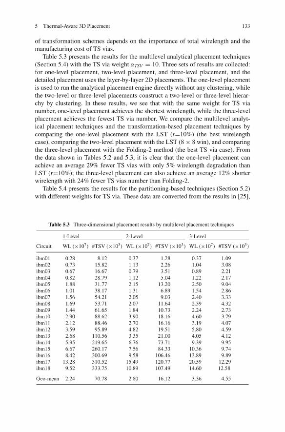
Table 5.3 presents the results for the multilevel analytical placement techniques(Section 5.4) with the TS via weight αTSV = 10. Three sets of results are collected:for one-level placement, two-level placement, and three-level placement, and thedetailed placement uses the layer-by-layer 2D placements. The one-level placementis used to run the analytical placement engine directly without any clustering, whilethe two-level or three-level placements construct a two-level or three-level hierar-chy by clustering. In these results, we see that with the same weight for TS vianumber, one-level placement achieves the shortest wirelength, while the three-levelplacement achieves the fewest TS via number. We compare the multilevel analyt-ical placement techniques and the transformation-based placement techniques bycomparing the one-level placement with the LST (r=10%) (the best wirelengthcase), comparing the two-level placement with the LST (8× 8 win), and comparingthe three-level placement with the Folding-2 method (the best TS via case). Fromthe data shown in Tables 5.2 and 5.3, it is clear that the one-level placement canachieve an average 29% fewer TS vias with only 5% wirelength degradation thanLST (r=10%); the three-level placement can also achieve an average 12% shorterwirelength with 24% fewer TS vias number than Folding-2.
Table 5.4 presents the results for the partitioning-based techniques (Section 5.2)with different weights for TS via. These data are converted from the results in [25],
Table 5.3 Three-dimensional placement results by multilevel placement techniques
1-Level 2-Level 3-Level
Circuit WL (×107) #TSV (×103) WL (×107) #TSV (×103) WL (×107) #TSV (×103)
ibm01 0.28 8.12 0.37 1.28 0.37 1.09ibm02 0.73 15.82 1.13 2.26 1.04 3.08ibm03 0.67 16.67 0.79 3.51 0.89 2.21ibm04 0.82 28.79 1.12 5.04 1.22 2.17ibm05 1.88 31.77 2.15 13.20 2.50 9.04ibm06 1.01 38.17 1.31 6.89 1.54 2.86ibm07 1.56 54.21 2.05 9.03 2.40 3.33ibm08 1.69 53.71 2.07 11.64 2.39 4.32ibm09 1.44 61.65 1.84 10.73 2.24 2.73ibm10 2.90 88.62 3.90 18.16 4.60 3.79ibm11 2.12 88.46 2.70 16.16 3.19 4.07ibm12 3.59 95.89 4.82 19.51 5.80 4.59ibm13 2.68 110.56 3.35 21.00 4.05 4.12ibm14 5.95 219.65 6.76 73.71 9.39 9.95ibm15 6.67 260.17 7.56 84.33 10.36 9.74ibm16 8.42 300.69 9.58 106.46 13.89 9.89ibm17 13.28 310.52 15.49 120.77 20.59 12.29ibm18 9.52 333.75 10.89 107.49 14.60 12.58
Geo-mean 2.24 70.78 2.80 16.12 3.36 4.55

134 J. Cong and G. Luo
Table 5.4 Three-dimensional placement results by partitioning-based placement techniques
8.00E-07 2.00E-04 1.30E-02
Circuit WL (×107) #TSV (×103) WL (×107) #TSV (×103) WL (×107) #TSV (×103)
ibm01 0.30 20.50 0.39 5.39 0.52 0.49ibm02 0.85 32.44 0.97 11.98 1.51 0.86ibm03 0.81 34.87 0.95 9.97 1.23 1.95ibm04 1.02 42.43 1.13 14.24 1.61 2.05ibm05 2.18 49.78 2.29 20.29 3.07 5.92ibm06 1.34 55.35 1.47 20.29 2.09 2.47ibm07 1.91 74.51 2.15 24.77 3.23 2.85ibm08 2.06 80.86 2.32 26.39 3.35 2.59ibm09 1.78 83.96 2.10 24.97 2.94 1.79ibm10 3.33 115.48 3.82 35.25 5.80 2.39ibm11 2.60 112.90 3.01 33.59 4.31 2.69ibm12 4.44 121.39 4.89 44.50 7.52 3.97ibm13 3.26 139.26 3.78 41.85 5.63 2.63ibm14 7.16 238.96 7.82 80.71 12.23 4.16ibm15 8.29 275.91 9.10 91.86 13.20 6.40ibm16 10.43 319.76 11.52 105.99 18.44 5.58ibm17 15.20 327.27 16.37 125.42 26.13 7.59ibm18 11.21 350.36 12.41 110.94 19.98 4.58
Geo-mean 2.70 98.27 3.04 32.32 4.48 2.80
which are based on a modified version of the benchmark [43]. In [25], the row spac-ing is set to 25% of the row height, while the row spacing equals the row heightin the original benchmark. To obtain comparable data with Tables 5.2 and 5.3, weassume that the wirelength in [25] has equal amount of x-direction wires and y-direction wires and use the factor 50% + 50% · 2/(1 + 25%) = 1.3 to scale thewirelength. The three columns in Table 5.4 are with increasing weights for TS vias,where also show the trade-offs between wirelength and TS via. The rightmost col-umn with best TS via number shows 40% reduction in TS via number with 33%wirelength degradation compared with the three-level placement in Table 5.3. Butthe leftmost column with best wirelength costs 20% longer wirelength and 39%more TS vias compared with one-level placement in Table 5.3. The middle columnalso does not work as well as two-level placement in Table 5.3. These data indicatethat partitioning-based techniques are good at TS via reduction due to the partition-ing nature, but they may not as suitable as the multilevel techniques for the caseswhere more TS vias are manufacturable to achieve shorter wirelength.
As mentioned in Section 5.6.3, the RCN graph-based layer assignment process[19] is used to further optimize the TS via number of the 3D circuits. Tables 5.5and 5.6 show the effects of the RCN graph-based layer assignment algorithm onthe placement by local stacking transformation (Section 5.5.1) and flat analyticaltechnique (Section 5.4.2), respectively. The results of RCN refinement with over-laps r = 0 and 10% allowed are reported, where r = 0% is a strict non-overlapconstraint, and r = 10% allows 10% overlap between neighboring cells during

5 Thermal-Aware 3D Placement 135
Table 5.5 Local stacking results and RCN refinement with r = 0 and 10%
LST After RCN with r = 0% After RCN with r = 10%
Circuit WL (×107) #TSV (×103) WL (×107) #TSV (×103) WL (×107) #TSV (×103)
ibm01 0.24 21.03 0.24 20.73 0.24 18.63ibm02 0.66 33.31 0.66 32.75 0.66 28.87ibm03 0.61 36.38 0.62 35.38 0.62 30.49ibm04 0.76 44.95 0.76 43.44 0.77 38.07ibm05 2.36 50.67 2.36 48.82 2.36 44.37ibm06 0.94 57.91 0.94 57.29 0.95 50.26ibm07 1.46 77.60 1.46 74.35 1.47 64.85ibm08 1.59 83.50 1.59 78.42 1.59 70.46ibm09 1.34 87.44 1.33 82.79 1.35 73.13ibm10 2.80 116.92 2.80 112.62 2.81 99.59ibm11 2.00 117.03 2.00 112.29 2.02 98.77ibm12 3.36 124.61 3.37 121.31 3.38 107.89ibm13 2.53 144.73 2.53 138.41 2.54 122.95ibm14 5.70 247.46 5.70 234.24 5.73 210.08ibm15 6.40 284.74 6.40 267.28 6.41 248.06ibm16 8.30 326.99 8.30 311.33 8.34 283.10ibm17 13.16 332.80 13.16 320.34 13.15 286.26ibm18 9.37 359.07 9.39 337.12 9.40 300.87
Geo-mean 2.14 101.44 2.14 97.46 2.15 86.73
Table 5.6 Flat analytical results and RCN refinement with r = 0 and 10%
1-Level After RCN with r= 0% After RCN with r= 10%
Circuit WL (×107) #TSV (×103) WL (×107) #TSV (×103) WL (×107) #TSV (×103)
ibm01 0.28 8.12 0.28 8.03 0.29 7.87ibm02 0.73 15.82 0.73 15.69 0.76 15.59ibm03 0.67 16.67 0.67 16.45 0.69 16.10ibm04 0.82 28.79 0.82 27.99 0.84 26.56ibm05 1.88 31.77 1.88 30.94 1.89 30.20ibm06 1.01 38.17 1.01 37.24 1.04 35.58ibm07 1.56 54.21 1.56 52.82 1.59 49.57ibm08 1.69 53.71 1.69 52.66 1.71 50.97ibm09 1.44 61.65 1.44 59.88 1.47 56.37ibm10 2.90 88.62 2.90 86.26 2.97 81.19ibm11 2.12 88.46 2.12 85.39 2.15 79.63ibm12 3.59 95.89 3.59 93.51 3.64 87.73ibm13 2.68 110.56 2.68 106.74 2.71 99.67ibm14 5.95 219.65 5.95 209.11 5.92 188.71ibm15 6.67 260.17 6.67 246.45 6.62 224.01ibm16 8.42 300.69 8.42 288.13 8.35 261.84ibm17 13.28 310.52 13.28 297.61 13.18 267.90ibm18 9.52 333.75 9.52 318.80 9.45 286.02
Geo-mean 2.24 70.78 2.24 68.67 2.27 64.61

136 J. Cong and G. Luo
refinement. In Table 5.5, the average TS via reduction is 4% without any wirelengthdegradation when r = 0%, and the average TS via reduction is 15% with rare wire-length degradation when r = 10%. In Table 5.6, the average TS via reduction is 3%without wirelength degradation when r = 0%, and the average TS via reduction is9% with 1% wirelength degradation when r = 10%. From these results, we see thatthe placement by local stacking transformation has more room to be improved thanthe flat analytical placement, which also imply that analytical placement approachesproduce better solutions than transformation-based placement.
5.8.2 Effects of Thermal Optimization
5.8.2.1 Effects of the Thermal-Aware Net Weights on Temperature
The thermal-aware term defined in Equation (5.6) is for control of temperatureduring wirelength optimization. A large thermal coefficient αTEMP provides moreemphasis on the temperature reduction in the cost of longer wirelength and larger TSvia number. The thermal-aware net weights defined in Equation (5.12) are an equiv-alent way to implement thermal awareness, which is proportional to the thermalcoefficient αTEMP.
The thermal-aware net weights are implemented in the partitioning-based 3Dplacer [27], whose effect on the temperature reduction and the impact on the wire-length and TS via number are shown in Fig. 5.15. Experiments are also performedon the benchmark [43] with minor modification. With the TS via coefficient αTSVset to 10(μm), the impact of the thermal coefficient αTEMP to the TS via number(inter-layer via count), wirelength, total power, average temperature, and maximumtemperature are computed, and the percentage of change in these aspects is the aver-age percentage change for ibm01 to ibm18 in the benchmark when compared to theunweighted results. When the average temperatures are reduced by 19%, wirelengthis increased by only 1% and the TS via number is increased by 10%.
Fig. 5.15 Average percent change as the thermal coefficients are varied [27]

5 Thermal-Aware 3D Placement 137
5.8.2.2 Effects of the Legalization on Temperature
Here we compare the two Tetris-style legalization processes, one without thermalawareness and the other with thermal awareness. Cell power dissipation is gener-ated randomly by assigning cell power densities ranging from 105 to 106 W/m2
[39]. The temperature evaluation adopts the thermal-resistive network model andthe thermal resistance values in [40]. The initial placement is generated by applyingthe local stacking (LST) scheme of the transformation-based techniques (Section5.5). The results are shown in Table 5.7, and the temperatures reported are the dif-ference between the maximum on-chip temperature and the heat sink temperature.Compared to the legalization without thermal awareness, the thermal-aware legal-ization can reduce the maximum on-chip temperature by 39% on average with 8%longer wirelength but 5% fewer TS vias.
Table 5.7 Thermal-aware results of Tetris-style legalization
Tetris-style legalization without thermalawareness
Tetris-style legalization with thermalawareness
Circuit WL (×107) #TSV (×103) Temp. (◦C) WL (×107) #TSV (×103) Temp. (◦C)
ibm01 0.24 21.03 279.002 0.29 19.67 150.422ibm02 0.66 33.31 207.802 0.72 31.83 117.516ibm03 0.61 36.38 205.766 0.67 34.13 120.487ibm04 0.76 44.95 163.279 0.85 42.05 94.648ibm05 2.36 50.67 138.501 2.44 48.59 78.607ibm06 0.94 57.91 165.881 1.05 52.12 101.269ibm07 1.46 77.60 108.015 1.57 72.93 68.382ibm08 1.59 83.50 101.04 1.68 78.86 61.897ibm09 1.34 87.44 96.899 1.47 83.35 59.7815ibm10 2.80 116.92 58.335 3.01 112.95 36.3501ibm11 2.00 117.03 283.705 2.18 108.96 172.396ibm12 3.36 124.61 206.811 3.65 120.89 122.211ibm13 2.53 144.73 254.684 2.76 134.61 157.983ibm14 5.70 247.46 128.623 6.07 235.17 83.4365ibm15 6.40 284.74 137.455 6.76 274.44 87.672ibm16 8.30 326.99 98.5005 8.74 318.43 62.428ibm17 13.16 332.80 84.73 13.62 324.44 52.954ibm18 9.37 359.07 89.203 9.76 348.26 57.089
Geo-mean 2.14 101.44 141.88 2.32 96.30 86.11
5.9 Impact of 3D Placement on Wirelength and Repeater Usage
In this section we present the quantitative studies [20] of the impact of 3D ICtechnology on the wirelength and repeater usage. The wirelength is reported inhalf-perimeter wirelength, and the repeater usage is estimated by the interconnectoptimizer IPEM [14] in the post-placement/pre-routing stage, where the 2D and 3Dplacement are generated by state-of-the-art 2D placer mPL6 [7] and a multilevel

138 J. Cong and G. Luo
analytical 3D placer [13]. Experiments on a placement benchmark suite [43] showthat the total number of repeaters can be reduced by 22 and 50% on average withthree-layer and four-layer 3D circuits, respectively, compared to 2D circuits.
5.9.1 2D/3D Placers and Repeater Estimation
mPL6 [7] is a large-scale mixed-size placement package which combines a multi-level analytical placer and a robust legalizer and detailed placer. It is designed forwirelength-driven placement and is density sensitive. The results in the ISPD 2006placement contest [34] show that mPL6 achieves the best wirelength among all theparticipating placers.
To explore the advantage of the 3D technology, we use the multilevel analytical3D placer (Section 5.4). It is a 3D placer providing trade-offs between wirelengthand TS via number, and shows better trade-off abilities than transformation- andpartitioning-based techniques. Please refer Section 5.8.1 for more experimentalresults.
IPEM [14] is developed to provide a set of procedures that estimate inter-connect performance under various performance optimization algorithms for deepsubmicron technology. These optimization algorithms include OWS (optimal wiresizing), SDWS (simultaneous driver and wire sizing), BIWS (buffer insertion andwire sizing), and BISWS (buffer insertion, sizing, and wire Sizing). While thereare extensive interconnect layout optimization tools such as Trio [11], IPEM istargeted at providing fast and accurate estimation of the optimized interconnectdelay and area to enable the design convergence as early as possible through usingsimple closed-form computational procedures. Experimental results [14] show thatIPEM has an accuracy of 90% on average with a running speed of 1000× fasterthan Trio.
5.9.2 Experimental Setup and Results
The experiments are performed on the IBM-PLACE benchmarks [43]. Since thesebenchmarks do not have source/sink pin information, to obtain relatively moreaccurate information of the net wirelength, we use the length of the minimum-wirelength-tree of a net to estimate the optimal number of repeaters required inthis net.
The rectilinear Steiner minimal tree has been widely used in early design stagessuch as physical synthesis, floorplanning, interconnect planning, and placement toestimate wirelength, routing congestion, and interconnect delay. It uses the mini-mum wirelength edges to connect nodes in a given net. A rectilinear Steiner treeconstruction package FLUTE [10] is used to calculate the Steiner wirelength treein order to estimate the repeater insertion without performing the detailed routing.FLUTE is based on a pre-computed lookup table to make the Steiner minimum tree

5 Thermal-Aware 3D Placement 139
construction fast and accurate for low-degree nets. For high-degree nets, the net isdivided into several low-degree nets until the table can be used.
To accurately estimate the delay and area of the TS via resistance and capaci-tance, the approach in [22] is used to model the TS via as a length of wire. Becauseof its large size, the TS via has a great self-capacitance. By simulations on eachvia and the lengths of metal-2 wires in each layer, the authors in [22] approximatethe capacitance of a TS via with 3 μm thickness as roughly 8–20 μm of wire. Theresistance is less significant because of the large cross-sectional area of each TS via(about 0.1 � per TS via), which is equivalent to about 0.2 μm of a metal-2 wire.We use 3D IC technology developed by MIT Lincoln lab and the minimum distancebetween adjacent layers is 2–3.45 μm. Thus, we can approximately transform allthe TS vias between adjacent layers as 14 μm wires (an average value of 8–20 μm).This value is doubled when the TS via is going through two layers.
Since FLUTE can only generate a 2D minimum wirelength tree, in order totransform it to a 3D tree for our 3D designs, the following assumptions are made:(1) assume that all the tree wires are placed in a middle layer of the 3D stack layers,(2) the pins in other layers use TS vias to connect to the tree on the middle layer.This assumption minimizes the total traditional wires in a net but overestimates thetotal number of TS vias. However, it can provide us with more accurate informationconcerning the total net wirelength compared to the 3D via and wirelength estima-tion method used in [19], where the number of vias is simply set as the number ofthe layers the net spans.
The experiments are performed under 32 nm technology. The technology param-eters we used to configure IPEM are listed in Table 5.8. We run FLUTE and IPEMfor each net in each benchmark.
Table 5.9 shows the comparison of results between 2D designs, 3D designs withthree-device layers, and 3D designs with four-device layers for the IBM-PLACEbenchmarks. The wirelength (WL, in μm) and repeater number (#repeater) of eachcircuit are presented in this table, and the overall geometric mean and the normalizedgeometric mean are also presented. As can be seen, by applying a 3D design withthree-device layers, the total wirelength can be reduced by 17%, and the number ofrepeaters used in interconnection can be reduced by 22% on average compared to
Table 5.8 Technology parameters
Technology 32 nmClock frequency 2 GHzSupply voltage (VDD) 0.9 VMinimum sized repeater’s transistor size (wmin) 70 nmTransistor output resistance (rg) 5 KOhmTransistor output capacitance (cp) 0.0165 fFTransistor input capacitance (cg) 0.105 fFMetal wire resistance per unit length (r) 1.2 Ohm/μmMetal wire area capacitance (ca) 0.148 fF/μm2
Metal wire effective-fringing capacitance (cf) 0.08 fF/μm

140 J. Cong and G. Luo
Table 5.9 Results of the wirelength/repeaters for IBM-PLACE benchmarks
2D design3D design with 3 devicelayers
3D design with 4 devicelayers
Circuit WL (×107)#Repeater(×103) WL (×107)
#Repeater(×103) WL (×107)
#Repeater(×103)
ibm01 0.54 5.26 0.52 4.80 0.37 2.85ibm02 1.58 18.36 1.62 18.81 0.96 9.49ibm03 1.40 15.65 1.11 11.52 0.85 7.75ibm04 1.65 17.69 1.40 14.04 1.02 8.83ibm05 4.08 51.81 3.09 37.80 2.35 27.21ibm06 2.16 23.72 1.89 19.72 1.33 12.13ibm07 3.18 35.61 2.72 29.01 1.94 17.88ibm08 3.71 42.95 3.22 35.54 2.23 21.80ibm09 2.94 31.54 2.58 26.07 1.84 15.85ibm10 6.09 72.10 5.27 60.09 3.52 35.48ibm11 4.22 45.33 3.83 39.36 2.58 22.09ibm12 7.42 89.33 6.29 73.05 4.37 46.05ibm13 5.50 60.63 4.26 42.51 3.34 29.97ibm14 12.22 141.59 9.36 101.05 7.04 68.48ibm15 13.88 162.04 10.27 110.37 8.03 80.01ibm16 18.25 219.26 13.26 147.95 10.21 105.23ibm17 28.26 358.37 21.31 258.89 15.32 173.60ibm18 20.75 248.70 14.73 162.79 11.62 120.13
Geo-mean 4.67 53.43 3.87 41.76 2.79 26.74
the case of 2D design. Furthermore, when four layers are used in the 3D design,the wirelength can be further reduced by 40%, and the number of repeaters can bereduced by 50%.
As shown in Table 5.9, the reduction in the number of repeaters through 3DIC compared to that of the 2D cases is always more than the reduction of thetotal wirelength. This is because increasing the number of layers will efficientlydecrease the length of the nets with a large minimum wirelength tree, and nets witha very small minimum wirelength tree always do not need repeaters. As can beseen in the IPEM results, wires less than 500 μm usually result in zero repeaters.Therefore, by reducing the nets with a large length of the minimum wirelength tree,we can significantly reduce the number repeaters and the area/power of the on-chipinterconnection.
5.10 Summary and Conclusion
Three-dimensional IC technology enables an additional dimension of freedom forcircuit design. It enhances device-packing density and shortens the length of globalinterconnects, thus benefiting functionality, performance, and power of 3D circuits.

5 Thermal-Aware 3D Placement 141
However, this technology also challenges placement tools. The manufacturing ofTS vias is not trivial, thus the placement tools should be aware of TS via cost andperform trade-offs to avoid eliminating the benefits from the shortened wirelength.The thermal issues are also key challenges of 3D circuits due to the stacking of heatsources and the long thermal dissipating path.
In this chapter we give a formulation of the thermal-aware 3D placement prob-lem, and an overview of 3D placement techniques existing in the literatures. Weespecially describe the details of several representative 3D placement techniques,including the partitioning-based techniques, uniformity quadratic modeling tech-niques, multilevel placement techniques, and transformation-based techniques. Thelegalization and detailed placement techniques specific to 3D placement are alsointroduced.
The partitioning-based techniques are presented in Section 5.2. Thesepartitioning-based techniques insert the partition planes that are parallel to thedevice layers at some suitable stages in the traditional partition-based process. Thecost of partitioning is measured by a weighted sum of the estimated wirelengthand the TS via number, where the nets are further weighted by thermal-aware orcongestion-aware factors to consider temperature and routability.
The uniformity quadratic modeling techniques belong to the category ofquadratic placements techniques, of which the flat placement techniques consist.Since the unconstrained quadratic placement will introduce a great amount of celloverlaps, different variations are developed for overlap removal. The quadratic uni-formity modeling techniques [41] append a density penalty function to the objectivefunction, and it approximates the density penalty function by another quadraticfunction at each iteration, so that the whole global placement could be solved byminimizing a sequence of quadratic functions.
The multilevel technique [13] presented in Section 5.4 constructs a physical hier-archy from the original netlist, and solves a sequence of placement problems fromthe coarsest level to the finest level.
Besides these techniques above, the transformation-based techniques presentedin Section 5.5 make use of existing 2D placement results and construct a 3Dplacement by transformation.
In addition to various 3D global placement techniques, the legalization anddetailed placement techniques that are specific in the 3D placement context arediscussed in Section 5.10.
Finally, experimental data are presented to demonstrate the effectiveness of var-ious 3D placement techniques on wirelength, TS via number and temperature, andthe impact of 3D IC technology on wirelength and repeater usage. These experi-mental data indicate that partitioning-based 3D placement techniques are good atTS via minimization, but are not as effective as the multilevel analytical techniquesfor wirelength optimization for the cases where more TS vias are manufacturable.For the multilevel analytical placement technique, going through more levels forplacement optimization leads to fewer TS vias at a cost of increase of wirelength.Finally, the RCN graph-based layer assignment process is effective for both TS viaand thermal optimization.

142 J. Cong and G. Luo
Acknowledgment This study was partially supported by the Gigascale Silicon Research Center,by IBM under a DARPA subcontract, and by the National Science Foundation under CCF-0430077and CCF-0528583.
References
1. C. Ababei, H. Mogal, and K. Bazargan, Three-dimensional place and route for FPGAs,Proceedings of the 2005 Conference on Asia South Pacific Design Automation, pp. 773–778,2005.
2. C. Alpert, A. Kahng, G.-J. Nam, S. Reda, and P. Villarrubia, A semi-persistent clusteringtechnique for VLSI circuit placement, Proceedings of the 2005 International Symposium onPhysical Design, pp. 200–207, 2005.
3. K. Balakrishnan, V. Nanda, S. Easwar, and S. K. Lim, Wire congestion and thermal aware3D global placement, Proceedings of the 2005 Conference on Asia South Pacific DesignAutomation, pp. 1131–1134, 2005.
4. D. P. Bertsekas, Approximation procedures based on the method of multipliers, Journal ofOptimization Theory and Applications, 23(4), 487–510, 1977.
5. T. F. Chan, J. Cong, T. Kong, and J. R. Shinnerl, Multilevel optimization for large-scale circuitplacement, Proceedings of the 2000 IEEE/ACM International Conference on Computer-aidedDesign, pp. 171–176, 2000.
6. T. F. Chan, J. Cong, and K. Sze, Multilevel generalized force-directed method for circuitplacement, Proceedings of the 2005 International Symposium on Physical Design, pp. 185–192, 2005.
7. T. F. Chan, J. Cong, J. R. Shinnerl, K. Sze, and M. Xie, mPL6: enhancement multilevel mixed-size placement with congestion control, in Modern Circuit Placement, G.-J. Nam and J. Cong,Eds., Springer, New York, NY, 2007.
8. C.-C. Chang and J. Cong, An efficient approach to multilayer layer assignment with anapplication to via minimization, IEEE Transactions on Computer-Aided Design of IntegratedCircuits and Systems, 18(5): 608–620, 1999.
9. T.-C. Chen, Z.-W. Jiang, T.-C. Hsu, H.-C. Chen, and Y.-W. Chang, A high-quality mixed-sizeanalytical placer considering preplaced blocks and density constraints, Proceedings of the2006 IEEE/ACM International Conference on Computer-Aided Design, pp. 187–192, 2006.
10. C. Chu and Y. Wong, FLUTE: Fast lookup table based rectilinear steiner minimal tree algo-rithm for VLSI design, IEEE Transactions on Computer-Aided Design of Integrated Circuitsand Systems, 27(1): 70–83, 2008.
11. J. Cong and L. He, Theory and algorithm of local refinement based optimization with appli-cation to device and interconnect sizing, IEEE Transactions on Computer-Aided Design,pp. 1–14, 1999.
12. J. Cong and G. Luo, Highly efficient gradient computation for density-constrained analyticalplacement methods, Proceedings of the 2008 International Symposium on Physical Design,pp. 39–46, 2008.
13. J. Cong and G. Luo, A multilevel analytical placement for 3D ICs, Proceedings of the 2009Conference on Asia and South Pacific Design Automation, Yokohama, Japan, pp. 361–366,2009.
14. J. Cong and D. Z. Pan, Interconnect estimation and planning for deep submicron designs,Proceedings of the 26th ACM/IEEE Design Automation Conference, New Orleans, LA,pp. 507–510,\, 1999.
15. J. Cong and J. Shinnerl, Multilevel Optimization in VLSICAD, Kluwer Academic Publishers,Boston, MA, 2003.
16. J. Cong and M. Xie, A robust mixed-size legalization and detailed placement algorithm, IEEETransactions on Computer-Aided Design of Integrated Circuits and Systems, 27(8): 1349–1362, 2008.

5 Thermal-Aware 3D Placement 143
17. J. Cong and Y. Zhang, Thermal via planning for 3-D ICs, Proceedings of the 2005 IEEE/ACMInternational Conference on Computer-Aided Design, pp. 745–752, 2005.
18. J. Cong, J. R. Shinnerl, M. Xie, T. Kong, and X. Yuan, Large-scale circuit placement, ACMTransactions on Design Automation Electronic Systems, 10(2): 389–430, 2005.
19. J. Cong, G. Luo, J. Wei, and Y. Zhang, Thermal-aware 3D IC placement via Transformation,Proceedings of the 2007 Conference on Asia and South Pacific Design Automation, pp. 780–785, 2007.
20. J. Cong, C. Liu, and G. Luo, Quantitative studies of impact of 3D IC design on repeater usage,Proceedings of the International VLSI/ULSI Multilevel Interconnection Conference, 2008.
21. S. Das, Design Automation and Analysis of Three-Dimensional Integrated Circuits, PhDDissertation, Massachusetts Institute of Technology, Cambridge, MA, 2004.
22. W. R. Davis, J. Wilson, S. Mick, J. Xu, H. Hua, C. Mineo, A. M. Sule, M. Steer, and P. D.Franzon, Demystifying 3D ICs: The pros and cons of going vertical, IEEE Design & Test ofComputers, 22(6): 498–510,\, 2005.
23. A. E. Dunlop and B. W. Kernighan, A procedure for placement of standard-cell VLSI circuits,IEEE Transactions on Computer-Aided Design of Integrated Circuits and Systems, 4(1): 92–98, 1985.
24. C. M. Fiduccia and R. M. Mattheyses, A linear-time heuristic for improving network parti-tions, Proceedings of the 19th ACM/IEEE Conference on Design Automation, pp. 175–181,1982.
25. B. Goplen, Advanced Placement Techniques for Future VLSI Circuits, PhD Dissertation,University of Minnesota, Minneapolis, MN, 2006.
26. B. Goplen and S. Sapatnekar, Efficient thermal placement of standard cells in 3D ICs usinga force directed approach, Proceedings of the 2003 IEEE/ACM International Conference onComputer-Aided design, p. 86, 2003.
27. B. Goplen and S. Sapatnekar, Placement of 3D ICs with thermal and interlayer via consid-erations, Proceedings of the 44th Annual Conference on Design Automation, pp. 626–631,2007.
28. A. S. Grove, Physics and Technology of Semiconductor Devices, John Wiley & Sons, Inc.,Hoboken, NJ, 1967.
29. R. Hentschke, G. Flach, F. Pinto, and R. Reis, 3D-vias aware quadratic placement for 3DVLSI circuits, IEEE Computer Society Annual Symposium on VLSI, pp. 67–72, 2007.
30. D. Hill, Method and system for high speed detailed placement of cells within an integratedcircuit design, US Patent 6370673, 2001.
31. A. B. Kahng, S. Reda, and Q. Wang, Architecture and details of a high quality, large-scaleanalytical placer, Proceedings of the 2005 IEEE/ACM International Conference on Computer-Aided Design, pp. 891–898, 2005.
32. G. Karypis and V. Kumar, Multilevel k-way hypergraph partitioning, Proceedings of the 36thACM/IEEE Conference on Design Automation, pp. 343–348, 1999.
33. I. Kaya, S. Salewski, M. Olbrich, and E. Barke, Wirelength reduction using 3-D physicaldesign, Proceedings of the 14th International Workshop on Power and Timing Optimizationand Simulation, pp. 453–462, 2004.
34. G.-J. Nam, ISPD 2006 placement contest: benchmark suite and results, Proceedings of the2006 International Symposium on Physical Design, pp. 167–167, 2006.
35. G.-J. Nam and J. Cong (Eds.), Modern Circuit Placement: Best Practices and Results,Springer, New York, NY, 2007.
36. W. C. Naylor, R. Donelly, and L. Sha, Non-linear optimization system and method for wirelength and delay optimization for an automatic electric circuit placer, US Patent 6301693,2001.
37. J. Nocedal and S. J. Wright, Numerical Optimization, 2nd ed., Springer, New York, NY, 2006.38. P. Spindler and F. M. Johannes, Fast and robust quadratic placement combined with an exact
linear net model, Proceedings of the 2006 IEEE/ACM International Conference on Computer-Aided Design, pp. 179–186, 2006.

144 J. Cong and G. Luo
39. C.-H. Tsai and S.-M. Kang, Cell-level placement for improving substrate thermal distribution,IEEE Transactions on Computer-Aided Design of Integrated Circuits and Systems, 19(2):253–266, 2000.
40. P. Wilkerson, A. Raman, and M. Turowski, Fast, automated thermal simulation of three-dimensional integrated circuits, Proceedings of the 9th Intersociety Conference on Thermaland Thermomechanical Phenomena in Electronic Systems, Las Vegas, Nevada, 2004.
41. H. Yan, Q. Zhou, and X. Hong, Thermal aware placement in 3D ICs using quadraticuniformity modeling approach, Integration, the VLSI Journal, 42(2): 175–180,\, 2009.
42. B. Yao, H. Chen, C.-K. Cheng, N.-C. Chou, L.-T. Liu, and P. Suaris, Unified quadraticprogramming approach for mixed mode placement, Proceedings of the 2005 InternationalSymposium on Physical Design, pp. 193–199, 2005.
43. http://er.cs.ucla.edu/benchmarks/ibm-place/