The Upgraded Outer Tracker for the CMS Detector at the ... - IIHE
301
V RIJE U NIVERSITEIT B RUSSEL FACULTEIT WETENSCHAPPEN EN B IO- INGENIEURSWETENSCHAPPEN DEPARTEMENT NATUURKUNDE The Upgraded Outer Tracker for the CMS Detector at the High Luminosity LHC, and Search for Composite Standard Model Dark Matter with CMS at the LHC J ARNE D E C LERCQ P ROMOTER P ROF.DR .S TEVEN L OWETTE Proefschrift ingediend met het oog op het behalen van de academische graad van Doctor in de Wetenschappen January 2020
-
Upload
khangminh22 -
Category
Documents
-
view
0 -
download
0
Transcript of The Upgraded Outer Tracker for the CMS Detector at the ... - IIHE

VRIJE UNIVERSITEIT BRUSSEL
FACULTEIT WETENSCHAPPEN ENBIO-INGENIEURSWETENSCHAPPEN DEPARTEMENT
NATUURKUNDE
The Upgraded Outer Tracker for theCMS Detector at the
High Luminosity LHC, and Search forComposite Standard Model Dark Matter
with CMS at the LHC
JARNE DE CLERCQ
PROMOTER
PROF. DR. STEVEN LOWETTE
Proefschrift ingediend met het oog op het behalen vande academische graad van Doctor in de Wetenschappen
January 2020

ii
Doctoral examination commission:
Prof. Dr. Krijn De Vries (Vrije Universiteit Brussel, secretary)Prof. Dr. Jorgen D’Hondt (Vrije Universiteit Brussel, chair)Prof. Dr. Steven Lowette (Vrije Universiteit Brussel, supervisor)Prof. Dr. Nadia Pastrone (INFN, Torino)Prof. Dr. ir. Gerd Vandersteen (Vrije Universiteit Brussel)Prof. Dr. Pascal Vanlaer (Université Libre de Bruxelles)
Cover illustration: Patrick De Clercq
Printed byCrazy Copy Center ProductionsVUB Pleinlaan 2, 1050 BrusselTel : +32 2 629 33 [email protected]: 9789493079571NUR: 924, 926, 987
c©2020 Jarne De Clercq
All rights reserved. No parts of this book may be reproduced or transmitted in any formor by any means, electronic, mechanical, photocopying, recording, or otherwise, withoutthe prior written permission of the author.

iii
Contents
Summary ix
Samenvatting xi
Author’s Contribution xiii
I Setting the Stage 1
1 Preamble 3
2 Introduction to Particle Physics 52.1 Introduction . . . . . . . . . . . . . . . . . . . . . . . . . . . . . . . . . . . 52.2 The Standard Model of particle physics . . . . . . . . . . . . . . . . . . . . 52.3 The mathematical framework of the Standard Model . . . . . . . . . . . . 62.4 Dark matter . . . . . . . . . . . . . . . . . . . . . . . . . . . . . . . . . . . . 9
2.4.1 Introduction . . . . . . . . . . . . . . . . . . . . . . . . . . . . . . . . 92.4.2 Evidence for dark matter . . . . . . . . . . . . . . . . . . . . . . . . 92.4.3 Dark matter candidates . . . . . . . . . . . . . . . . . . . . . . . . . 112.4.4 Experimental searches for the nature of dark matter . . . . . . . . . 13
2.5 Summary . . . . . . . . . . . . . . . . . . . . . . . . . . . . . . . . . . . . . 13
3 Detector Techniques in Particle Physics 153.1 Introduction . . . . . . . . . . . . . . . . . . . . . . . . . . . . . . . . . . . 153.2 Particle interactions with matter . . . . . . . . . . . . . . . . . . . . . . . . 15
3.2.1 Heavy charged particle interactions with matter . . . . . . . . . . . 153.2.2 Electron interactions with matter . . . . . . . . . . . . . . . . . . . . 183.2.3 Photon interactions with matter . . . . . . . . . . . . . . . . . . . . 183.2.4 Heavy neutral particle interactions with matter . . . . . . . . . . . 19
3.3 Charged particle detector techniques . . . . . . . . . . . . . . . . . . . . . 193.4 Silicon based detectors for tracking . . . . . . . . . . . . . . . . . . . . . . 20
3.4.1 Introduction . . . . . . . . . . . . . . . . . . . . . . . . . . . . . . . . 203.4.2 Silicon doping and the pn-junction . . . . . . . . . . . . . . . . . . . 203.4.3 Layout and operation of a position sensitive silicon sensor . . . . . 223.4.4 Radiation damage in silicon sensors . . . . . . . . . . . . . . . . . . 23
3.5 Integrated circuits . . . . . . . . . . . . . . . . . . . . . . . . . . . . . . . . 243.6 Readout chips for silicon detectors . . . . . . . . . . . . . . . . . . . . . . 253.7 Radiation effects in integrated circuits . . . . . . . . . . . . . . . . . . . . 27
3.7.1 Introduction . . . . . . . . . . . . . . . . . . . . . . . . . . . . . . . . 27
iv
3.7.2 Total ionizing dose . . . . . . . . . . . . . . . . . . . . . . . . . . . . 283.7.2.1 Introduction . . . . . . . . . . . . . . . . . . . . . . . . . . 283.7.2.2 Total ionizing dose mechanism . . . . . . . . . . . . . . . 283.7.2.3 Total ionizing dose hardening techniques . . . . . . . . . 293.7.2.4 Total ionizing dose testing . . . . . . . . . . . . . . . . . . 29
3.7.3 Single-event effects . . . . . . . . . . . . . . . . . . . . . . . . . . . . 303.7.3.1 Introduction . . . . . . . . . . . . . . . . . . . . . . . . . . 303.7.3.2 Single-event upset mechanism . . . . . . . . . . . . . . . . 303.7.3.3 Single-event upset hardening techniques . . . . . . . . . . 323.7.3.4 Single-event upset testing . . . . . . . . . . . . . . . . . . 33
3.8 Summary . . . . . . . . . . . . . . . . . . . . . . . . . . . . . . . . . . . . . 33
4 The LHC and the CMS Experiment 354.1 Introduction . . . . . . . . . . . . . . . . . . . . . . . . . . . . . . . . . . . 354.2 The LHC and the LHC experiments . . . . . . . . . . . . . . . . . . . . . . 354.3 The CMS experiment . . . . . . . . . . . . . . . . . . . . . . . . . . . . . . 38
4.3.1 Introduction . . . . . . . . . . . . . . . . . . . . . . . . . . . . . . . . 384.3.2 The tracker system and track reconstruction . . . . . . . . . . . . . 40
4.3.2.1 The tracker detector system . . . . . . . . . . . . . . . . . 404.3.2.2 Charged particle track reconstruction . . . . . . . . . . . . 41
4.3.3 The calorimeter system . . . . . . . . . . . . . . . . . . . . . . . . . 444.3.4 The muon system . . . . . . . . . . . . . . . . . . . . . . . . . . . . . 454.3.5 The trigger system . . . . . . . . . . . . . . . . . . . . . . . . . . . . 46
4.4 The HL-LHC upgrade . . . . . . . . . . . . . . . . . . . . . . . . . . . . . . 474.5 The CMS Phase-2 upgrade . . . . . . . . . . . . . . . . . . . . . . . . . . . 484.6 Summary . . . . . . . . . . . . . . . . . . . . . . . . . . . . . . . . . . . . . 52
II The Upgraded Outer Tracker for the CMS Detector at the High Lu-minosity LHC 53
5 The CMS Phase-2 Outer Tracker 555.1 Introduction . . . . . . . . . . . . . . . . . . . . . . . . . . . . . . . . . . . 555.2 pT module concept and design . . . . . . . . . . . . . . . . . . . . . . . . . 56
5.2.1 The PS module . . . . . . . . . . . . . . . . . . . . . . . . . . . . . . 595.2.2 The 2S module . . . . . . . . . . . . . . . . . . . . . . . . . . . . . . 59
5.3 Outer Tracker geometry . . . . . . . . . . . . . . . . . . . . . . . . . . . . . 605.4 Silicon sensors . . . . . . . . . . . . . . . . . . . . . . . . . . . . . . . . . . 605.5 pT module ASICs . . . . . . . . . . . . . . . . . . . . . . . . . . . . . . . . 61
5.5.1 Commonalities between the SSA, MPA, CBC and CIC ASICs . . . . 635.5.2 The SSA chip . . . . . . . . . . . . . . . . . . . . . . . . . . . . . . . 65
5.5.2.1 Introduction . . . . . . . . . . . . . . . . . . . . . . . . . . 655.5.2.2 SSA front-end . . . . . . . . . . . . . . . . . . . . . . . . . 655.5.2.3 SSA sampling logic . . . . . . . . . . . . . . . . . . . . . . 665.5.2.4 SSA stub data path and format . . . . . . . . . . . . . . . . 675.5.2.5 SSA full-event data path and format . . . . . . . . . . . . 67
5.5.3 The MPA chip . . . . . . . . . . . . . . . . . . . . . . . . . . . . . . . 685.5.3.1 Introduction . . . . . . . . . . . . . . . . . . . . . . . . . . 685.5.3.2 MPA front-end . . . . . . . . . . . . . . . . . . . . . . . . . 68
v
5.5.3.3 MPA sampling logic . . . . . . . . . . . . . . . . . . . . . . 695.5.3.4 MPA stub data path and format . . . . . . . . . . . . . . . 705.5.3.5 MPA full-event data path and format . . . . . . . . . . . . 70
5.5.4 MPA and SSA single-event effect tolerant design strategy . . . . . . 725.5.5 The CBC chip . . . . . . . . . . . . . . . . . . . . . . . . . . . . . . . 73
5.5.5.1 Introduction . . . . . . . . . . . . . . . . . . . . . . . . . . 735.5.5.2 CBC front-end . . . . . . . . . . . . . . . . . . . . . . . . . 735.5.5.3 CBC sampling logic . . . . . . . . . . . . . . . . . . . . . . 745.5.5.4 CBC stub data path and format . . . . . . . . . . . . . . . 765.5.5.5 CBC full-event data path and format . . . . . . . . . . . . 775.5.5.6 The CBC2 chip . . . . . . . . . . . . . . . . . . . . . . . . . 78
5.5.6 The CIC chip . . . . . . . . . . . . . . . . . . . . . . . . . . . . . . . 785.5.6.1 Introduction . . . . . . . . . . . . . . . . . . . . . . . . . . 785.5.6.2 Phy ports . . . . . . . . . . . . . . . . . . . . . . . . . . . . 795.5.6.3 CIC stub data path and formats . . . . . . . . . . . . . . . 805.5.6.4 CIC full-event data path and formats . . . . . . . . . . . . 825.5.6.5 The CIC2 chip . . . . . . . . . . . . . . . . . . . . . . . . . 83
5.5.7 The optical link . . . . . . . . . . . . . . . . . . . . . . . . . . . . . . 835.6 pT module data path . . . . . . . . . . . . . . . . . . . . . . . . . . . . . . 855.7 Module assembly and testing during production . . . . . . . . . . . . . . 865.8 Data, trigger and control system . . . . . . . . . . . . . . . . . . . . . . . . 885.9 L1 track finding . . . . . . . . . . . . . . . . . . . . . . . . . . . . . . . . . 885.10 Phase-2 tracker expected performance . . . . . . . . . . . . . . . . . . . . 885.11 Summary . . . . . . . . . . . . . . . . . . . . . . . . . . . . . . . . . . . . . 89
6 Firmware Development for Phase-2 Tracker Prototypes 936.1 Introduction . . . . . . . . . . . . . . . . . . . . . . . . . . . . . . . . . . . 936.2 FPGAs . . . . . . . . . . . . . . . . . . . . . . . . . . . . . . . . . . . . . . . 936.3 Scope of the µDTC test-bench . . . . . . . . . . . . . . . . . . . . . . . . . 946.4 Hardware platform . . . . . . . . . . . . . . . . . . . . . . . . . . . . . . . 96
6.4.1 The µTCA standard . . . . . . . . . . . . . . . . . . . . . . . . . . . 966.4.2 The IPbus protocol . . . . . . . . . . . . . . . . . . . . . . . . . . . . 976.4.3 The FC7 AMC card . . . . . . . . . . . . . . . . . . . . . . . . . . . . 976.4.4 Example of a typical µDTC set-up . . . . . . . . . . . . . . . . . . . 98
6.5 µDTC firmware structure . . . . . . . . . . . . . . . . . . . . . . . . . . . . 996.5.1 Introduction . . . . . . . . . . . . . . . . . . . . . . . . . . . . . . . . 996.5.2 The Physical Interface Abstraction Layer . . . . . . . . . . . . . . . 101
6.5.2.1 Fast commands . . . . . . . . . . . . . . . . . . . . . . . . 1016.5.2.2 Slow control . . . . . . . . . . . . . . . . . . . . . . . . . . 1016.5.2.3 Phase tuning of the incoming data . . . . . . . . . . . . . 1026.5.2.4 Front-end data acquisition . . . . . . . . . . . . . . . . . . 102
6.5.3 Data Readout Block . . . . . . . . . . . . . . . . . . . . . . . . . . . 1036.5.4 Command Processor Block . . . . . . . . . . . . . . . . . . . . . . . 1046.5.5 Fast Command Block . . . . . . . . . . . . . . . . . . . . . . . . . . . 1046.5.6 Firmware testing . . . . . . . . . . . . . . . . . . . . . . . . . . . . . 105
6.6 Summary . . . . . . . . . . . . . . . . . . . . . . . . . . . . . . . . . . . . . 1066.7 Author’s contribution . . . . . . . . . . . . . . . . . . . . . . . . . . . . . . 106

vi
7 2S Prototype Testing 1077.1 Introduction . . . . . . . . . . . . . . . . . . . . . . . . . . . . . . . . . . . 1077.2 Specific firmware development for 2S based systems . . . . . . . . . . . . 107
7.2.1 Introduction . . . . . . . . . . . . . . . . . . . . . . . . . . . . . . . . 1077.2.2 Use cases . . . . . . . . . . . . . . . . . . . . . . . . . . . . . . . . . . 107
7.3 CBC3 test pulse injection testing . . . . . . . . . . . . . . . . . . . . . . . . 1097.3.1 Introduction . . . . . . . . . . . . . . . . . . . . . . . . . . . . . . . . 1097.3.2 Procedure . . . . . . . . . . . . . . . . . . . . . . . . . . . . . . . . . 1107.3.3 Results . . . . . . . . . . . . . . . . . . . . . . . . . . . . . . . . . . . 110
7.4 Summary . . . . . . . . . . . . . . . . . . . . . . . . . . . . . . . . . . . . . 1167.5 Author’s contribution . . . . . . . . . . . . . . . . . . . . . . . . . . . . . . 116
8 PS Prototype Testing 1178.1 Introduction . . . . . . . . . . . . . . . . . . . . . . . . . . . . . . . . . . . 1178.2 Specific firmware development for PS based systems . . . . . . . . . . . . 117
8.2.1 Introduction . . . . . . . . . . . . . . . . . . . . . . . . . . . . . . . . 1178.2.2 MPA/SSA debug firmware and PS specific test features . . . . . . . 1178.2.3 MPA/SSA DAQ firmware . . . . . . . . . . . . . . . . . . . . . . . . 1198.2.4 Use cases . . . . . . . . . . . . . . . . . . . . . . . . . . . . . . . . . . 120
8.3 Single chip testing . . . . . . . . . . . . . . . . . . . . . . . . . . . . . . . . 1208.3.1 MPA . . . . . . . . . . . . . . . . . . . . . . . . . . . . . . . . . . . . 1228.3.2 SSA . . . . . . . . . . . . . . . . . . . . . . . . . . . . . . . . . . . . . 122
8.4 MPA and SSA single-event upset testing . . . . . . . . . . . . . . . . . . . 1238.4.1 Introduction . . . . . . . . . . . . . . . . . . . . . . . . . . . . . . . . 1238.4.2 Heavy ion facility . . . . . . . . . . . . . . . . . . . . . . . . . . . . . 1238.4.3 Test set-up . . . . . . . . . . . . . . . . . . . . . . . . . . . . . . . . . 1248.4.4 SEU cross section calculation . . . . . . . . . . . . . . . . . . . . . . 1278.4.5 Results . . . . . . . . . . . . . . . . . . . . . . . . . . . . . . . . . . . 129
8.4.5.1 SEU triggered configuration and control upsets . . . . . . 1298.4.5.2 SEU cross section and bit upset rates on data paths . . . . 129
8.5 Single-MaPSA test beam . . . . . . . . . . . . . . . . . . . . . . . . . . . . 1358.5.1 Introduction . . . . . . . . . . . . . . . . . . . . . . . . . . . . . . . . 1358.5.2 Beam area . . . . . . . . . . . . . . . . . . . . . . . . . . . . . . . . . 135
8.5.2.1 Beam parameters . . . . . . . . . . . . . . . . . . . . . . . 1358.5.2.2 Telescope . . . . . . . . . . . . . . . . . . . . . . . . . . . . 135
8.5.3 Single-MaPSA . . . . . . . . . . . . . . . . . . . . . . . . . . . . . . 1368.5.4 Single-MaPSA set-up . . . . . . . . . . . . . . . . . . . . . . . . . . . 1378.5.5 MPA data streams . . . . . . . . . . . . . . . . . . . . . . . . . . . . 1378.5.6 Commissioning of the single-MaPSA . . . . . . . . . . . . . . . . . 1388.5.7 Results . . . . . . . . . . . . . . . . . . . . . . . . . . . . . . . . . . . 140
8.5.7.1 Assembly #1 and #2: DUT only . . . . . . . . . . . . . . . 1418.5.7.2 Assembly #1: combined results of threshold scans . . . . 1458.5.7.3 Assembly #1: threshold scan . . . . . . . . . . . . . . . . . 1498.5.7.4 Assembly #1: bias scan . . . . . . . . . . . . . . . . . . . . 1558.5.7.5 Assembly #2 . . . . . . . . . . . . . . . . . . . . . . . . . . 159
8.6 Summary . . . . . . . . . . . . . . . . . . . . . . . . . . . . . . . . . . . . . 1598.7 Author’s contribution . . . . . . . . . . . . . . . . . . . . . . . . . . . . . . 160

vii
9 CIC1 Related Testing 1639.1 Introduction . . . . . . . . . . . . . . . . . . . . . . . . . . . . . . . . . . . 1639.2 CIC stand-alone testing . . . . . . . . . . . . . . . . . . . . . . . . . . . . . 163
9.2.1 Introduction . . . . . . . . . . . . . . . . . . . . . . . . . . . . . . . . 1639.2.2 Reference model . . . . . . . . . . . . . . . . . . . . . . . . . . . . . 1659.2.3 Front-end data player . . . . . . . . . . . . . . . . . . . . . . . . . . 1669.2.4 CIC decoder blocks . . . . . . . . . . . . . . . . . . . . . . . . . . . . 168
9.2.4.1 Full-event data . . . . . . . . . . . . . . . . . . . . . . . . . 1689.2.4.2 Stub data . . . . . . . . . . . . . . . . . . . . . . . . . . . . 170
9.2.5 Data quality monitoring . . . . . . . . . . . . . . . . . . . . . . . . . 1749.2.6 Data processing test results . . . . . . . . . . . . . . . . . . . . . . . 1759.2.7 Irradiation testing . . . . . . . . . . . . . . . . . . . . . . . . . . . . 176
9.2.7.1 EP-ESE irradiation system . . . . . . . . . . . . . . . . . . 1769.2.7.2 Test set-up . . . . . . . . . . . . . . . . . . . . . . . . . . . 1769.2.7.3 Results . . . . . . . . . . . . . . . . . . . . . . . . . . . . . 178
9.3 8CBC3 + CIC1 testing . . . . . . . . . . . . . . . . . . . . . . . . . . . . . . 1809.3.1 Introduction . . . . . . . . . . . . . . . . . . . . . . . . . . . . . . . . 1809.3.2 Running 8CBC3 + CIC1 . . . . . . . . . . . . . . . . . . . . . . . . . 182
9.4 Summary . . . . . . . . . . . . . . . . . . . . . . . . . . . . . . . . . . . . . 1849.5 Author’s contribution . . . . . . . . . . . . . . . . . . . . . . . . . . . . . . 185
III Search for Composite Standard Model Dark Matter with CMSat the LHC 187
10 Sexaquarks 18910.1 Introduction . . . . . . . . . . . . . . . . . . . . . . . . . . . . . . . . . . . 18910.2 Exotic hadrons . . . . . . . . . . . . . . . . . . . . . . . . . . . . . . . . . . 18910.3 The H-dibaryon . . . . . . . . . . . . . . . . . . . . . . . . . . . . . . . . . 19010.4 Properties of the Sexaquark . . . . . . . . . . . . . . . . . . . . . . . . . . . 19110.5 Sexaquarks as a dark matter candidate . . . . . . . . . . . . . . . . . . . . 19210.6 Sexaquark search channels . . . . . . . . . . . . . . . . . . . . . . . . . . . 193
10.6.1 Search channels at B-factories . . . . . . . . . . . . . . . . . . . . . . 19410.6.2 Search channels at hadron colliders . . . . . . . . . . . . . . . . . . 194
10.7 Adopted search strategy . . . . . . . . . . . . . . . . . . . . . . . . . . . . 19510.8 Datasets . . . . . . . . . . . . . . . . . . . . . . . . . . . . . . . . . . . . . . 19610.9 Physics objects and signal reconstruction . . . . . . . . . . . . . . . . . . . 19810.10 Signal simulation . . . . . . . . . . . . . . . . . . . . . . . . . . . . . . . . 200
10.10.1 Introduction . . . . . . . . . . . . . . . . . . . . . . . . . . . . . . . . 20010.10.2 S kinematics . . . . . . . . . . . . . . . . . . . . . . . . . . . . . . . . 20210.10.3 S-neutron interaction . . . . . . . . . . . . . . . . . . . . . . . . . . . 20210.10.4 Influence of neutron Fermi momentum . . . . . . . . . . . . . . . . 20410.10.5 Reconstructability . . . . . . . . . . . . . . . . . . . . . . . . . . . . 20910.10.6 V0 and final state particles kinematics . . . . . . . . . . . . . . . . . 211
10.11 Signal reconstruction efficiency . . . . . . . . . . . . . . . . . . . . . . . . 21510.12 Background rejection . . . . . . . . . . . . . . . . . . . . . . . . . . . . . . 22110.13 Systematic uncertainties . . . . . . . . . . . . . . . . . . . . . . . . . . . . 226
10.13.1 Signal reconstruction efficiency . . . . . . . . . . . . . . . . . . . . . 22610.13.2 Number of pp collisions . . . . . . . . . . . . . . . . . . . . . . . . . 234
viii
10.13.3 S as background reference . . . . . . . . . . . . . . . . . . . . . . . . 23410.14 Limit setting and results . . . . . . . . . . . . . . . . . . . . . . . . . . . . 235
10.14.1 Limit setting introduction . . . . . . . . . . . . . . . . . . . . . . . . 23510.14.2 Results . . . . . . . . . . . . . . . . . . . . . . . . . . . . . . . . . . . 236
10.15 Summary and outlook . . . . . . . . . . . . . . . . . . . . . . . . . . . . . 24010.16 Author’s contribution . . . . . . . . . . . . . . . . . . . . . . . . . . . . . . 242
A MPA and SSA SEU cross sections 245A.1 SSA high latency . . . . . . . . . . . . . . . . . . . . . . . . . . . . . . . . . 245A.2 SSA low latency . . . . . . . . . . . . . . . . . . . . . . . . . . . . . . . . . 246A.3 MPA high latency . . . . . . . . . . . . . . . . . . . . . . . . . . . . . . . . 247A.4 MPA low latency . . . . . . . . . . . . . . . . . . . . . . . . . . . . . . . . . 248
B Full CIC start-up sequence 249
C CBC configurations for CBC-CIC start-up 251
D S events: reconstruction efficiencies 253
E Input variables to the Sexaquark BDT: pre-BDT 259
F Input variables to the Sexaquark BDT: post-BDT 265
List of Abbreviations 271
Acknowledgements 275
Bibliography 277

ix
Summary
The Standard Model of particle physics describes the interactions between particles at thesmallest known scale. The Standard Model has passed many tests with flying colours, butseveral observations, such as the need for dark matter, do not find an explanation in thisframework. The Large Hadron Collider (LHC) at CERN is an excellent tool to study theStandard Model and to try and find answers to the open questions. The LHC collidesprotons resulting in a center of mass energy of 13 TeV, the highest energies ever attainedat a particle collider. This enables physicists to study matter at an energy scale which isnormally not accessible and which reflects the energy density in our Universe a fractionof a second after the Big Bang.
At one of the four interaction points along the LHC, the Compact Muon Solenoid(CMS) experiment is located. This general purpose experiment is designed to give an asgood as possible measurement of the kinematic properties of the particles produced ina collision. CMS does this by using several subdetectors, one of which is the trackingsystem. The CMS tracker is based on silicon technology and consists of a pixel and astrip detector, designed to reconstruct the tracks of charged particles. The strip detectorhas been taking data since the start of the operation of the LHC in 2010 and will continueto do so until 2024. During the 2025-2027 Long Shutdown of the LHC, the acceleratorcomplex will be upgraded to start the High Luminosity LHC (HL-LHC) phase at theend of 2027, which will provide the experiments with higher luminosities by increasingthe number of proton-proton collisions per bunch crossing (pileup). In order to keeptracking performance at pre-HL-LHC levels in this harsher HL-LHC environment, thestrip tracker will be replaced by an Outer Tracker, consisting of pixel-strip (PS) and strip-strip (2S) modules. These modules have local track reconstruction logic. The output ofthis logic is used as input to the L1 trigger system.
This thesis consists of a hardware part, focussing on the testing of Outer Tracker pro-totypes, and a search for new physics using the data collected by the CMS experiment.
The Upgraded Outer Tracker for the CMS Detector at the High Luminosity LHC:
Over the past years, Outer Tracker prototype ASICs and modules have become avail-able. These require a dedicated test bench for characterization. This thesis discussesin detail the Phase-2 Outer Tracker and the structure and scope of the firmwareproject (µDTC) set up to read out ASIC and module prototypes of this new detector.The test bench is designed to test both 2S and PS modules and components. Severaltests, to which the author contributed, are presented, going from bench-top testingof single ASICs, through radiation hardness testing of these chips and operatingmodule prototypes in test beams.
Search for Composite Standard Model Dark Matter with CMS at the LHC:
The Sexaquark (S), composed of uuddss quarks, is a hypothetical particle that wasproposed to be stable and a potential dark matter candidate. S particles could be pro-duced in the proton-proton collision and could subsequently annihilate on a neutronin the beampipe or detector material. This annihilation could result in a K0
S and Λ0
which in turn can decay to charged products which are reconstructable with the CMS

x
tracker. This is the signal used in this thesis to look for the S in the CMS 2016 datasetby reconstructing the S kinematic properties and its annihilation vertex. The difficul-ties of reconstructing such a low momentum, displaced and off-pointing signaturewith the default CMS reconstruction algorithms will be studied and a first-ever limiton the [σ(p + p→ S)× σ(S + n→ K0
S + Λ0)] cross section will be presented.

xi
Samenvatting
Het Standaardmodel van de deeltjesfysica beschrijft de interactie tussen deeltjes op dekleinste schaal. Dit model heeft reeds vele testen doorstaan. Toch vinden verschillendeobservaties - zoals de nood aan donkere materie - geen verklaring in dit framework. DeLarge Hadron Collider (LHC) aan het CERN is een excellent platform om het Standaard-model te bestuderen en om antwoorden te vinden op onbeantwoorde vragen. De LHCversnelt protonen om ze nadien te laten botsen bij een massamiddelpuntsenergie van13 TeV. Dit is de hoogste energie ooit bereikt in een laboratorium en daardoor stelt deLHC fysici in staat om materie te bestuderen bij een energieschaal die normaal niet toe-gankelijk is en die de energiedichtheid van ons universum reflecteert een fractie van eenseconde na de Big Bang.
Aan één van de vier interactiepunten van de LHC bevindt zich het Compact MuonSolenoid (CMS) experiment. Dit experiment is ontworpen om een zo goed mogelijkemeting te maken van de kinematische eigenschappen van de deeltjes die geproduceerdworden bij een botsing. CMS doet dit door gebruik te maken van verschillende subde-tectoren. Een van deze subdetectoren is de sporendetector. De CMS-sporendetector isgebaseerd op siliciumtechnologie en bestaat uit een pixel- en een stripdetector. Deze de-tectoren zijn ontworpen om het pad van geladen deeltjes te reconstrueren. De huidigestripdetector is in gebruik sinds het begin van de LHC-exploitatie in 2010 en zal verderoperationeel zijn tot 2024. Tijdens de Long Shutdown in 2025-2027 zal het versneller-complex geüpgraded worden om de hogeluminositeitsfase (HL-LHC) van de LHC aante vatten eind 2027. De HL-LHC zal de experimenten voorzien van hogere luminositeitdoor het aantal proton-proton botsingen per bundelkruising te verhogen. Om de perfor-mantie van de sporenreconstructie te garanderen in deze moeilijke omstandigheden zalde stripdetector vervangen worden door een nieuwe Outer Tracker. Deze subdetector zalbestaan uit twee soorten detectormodules: pixel-strip (PS) en strip-strip (2S) modules.Deze modules hebben logica om lokaal sporen te reconstrueren. De output van dezelogica wordt gebruikt als input voor het L1-trigger-systeem.
Deze thesis bestaat uit een hardware-gedeelte, dat focust op het testen van OuterTracker-prototypes, en een zoektocht naar nieuwe fysica, gebruikmakend van data verza-meld door het CMS-experiment:
De Upgrade van de Buitenste Sporendetector van de CMS-detector voor de Hoge LuminositeitLHC:
De prototype ASICs en modules voor de Outer Tracker vereisen een specifieke testop-stelling voor karakterisatie. Deze thesis beschrijft in detail de Outer Tracker en hetdoel en de structuur van het firmware-project (µDTC) dat werd opgezet om proto-types van ASICs en modules van deze nieuwe detector uit te lezen. De testopstellingis ontworpen om zowel 2S als PS modules en componenten te testen. Verschillendetesten, waaraan de auteur heeft bijgedragen, worden voorgesteld: testen van stan-dalone chips, testen van chips onder straling en de kwalificatie van prototype mod-ules in test beams.

xii
Zoektocht naar Samengestelde Standaardmodel Donkere Materie met CMS aan de LHC:
Het Sexaquark-deeltje (S), met uuddss quark-inhoud, is een hypothetisch deeltje datstabiel kan zijn. Mits de juiste eigenschappen is het deeltje ook een donkerema-teriekandidaat. S deeltjes kunnen geproduceerd worden bij proton-proton botsin-gen en kunnen nadien annihileren op neutronen in de bundelpijp of detectorma-teriaal. Deze annihilatiereactie kan aanleiding geven tot de vorming van een K0
Sen een Λ0 die kunnen vervallen naar geladen dochterdeeltjes. Deze geladen deelt-jes kunnen gereconstrueerd worden met behulp van de CMS-sporendetector. Ditis het signaal dat gebruikt wordt in deze thesis om te zoeken naar S in de CMS2016 dataset door de kinematische eigenschappen en de annihilatievertex van de Ste reconstrueren. De moeilijkheid van het reconstrueren van een dergelijk signaalmet de standaard CMS-reconstructiealgoritmes wordt onderzocht en een limiet op[σ(p + p→ S)× σ(S + n→ K0
S + Λ0)] wordt afgeleid.

xiii
Author’s Contribution
The author contributed to the development and use of the test system for CMS Phase-2Outer Tracker ASICs and module prototypes and was the main developer of a first searchfor Sexaquarks at the CMS experiment. The contributions of the author are specified atthe end of the chapters where the work is described and are summarised briefly below.
The work on the test system consisted of development, testing and maintenance offirmware blocks. The author then contributed to the testing of single chips, ASIC irra-diation tests, integration tests and test beams with prototype modules and analysed theresults of these tests. This work resulted in the following, two of which are still to bepublished, papers:
• CMS Tracker Collaboration, "Test beam demonstration of silicon microstrip mod-ules with transverse momentum discrimination for the future CMS tracking detec-tor", JINST 13 (2018) no.03, P03003, (2018-03-06), DOI: 10.1088/1748-0221/13/03/P03003
• CMS Tracker Collaboration, "Beam Test Performance of Prototype Silicon Detectorsfor the Outer Tracker for the Phase-2 Upgrade of CMS", CERN-CMS-NOTE-2019-006, submitted to JINST
• CMS Tracker Collaboration, "Performance of the Prototype CBC3-based Outer TrackerModules for the Phase II Upgrade of CMS before and after neutron irradiation", inpreparation
and following proceedings:
• T. Gadek et al., "Quality Control Considerations for the Development of the FrontEnd Hybrid Circuits for the CMS Outer Tracker Upgrade", TWEPP2017, POS pro-ceeding, Volume 313, DOI: https://doi.org/10.22323/1.313.0061
• D. Ceresa et al., "Characterization of the MPA prototype, a 65 nm pixel readoutASIC with on-chip quick transverse momentum discrimination capabilities", TWEPP2018, POS proceeding, Volume 343, DOI: https://doi.org/10.22323/1.343.0166
• A. Caratelli et al., "Characterization of the first prototype of the Silicon-Strip read-out ASIC (SSA) for the CMS Outer-Tracker phase-2 upgrade", TWEPP2018, POSproceeding, Volume 343, DOI: https://doi.org/10.22323/1.343.0159
• A. Caratelli et al.,"Low-power SEE hardening techniques and error rate evaluationin 65nm readout ASICs", TWEPP2019, POS proceeding, submitted
• B. Nodari et al., "First results of CIC data aggregation ASIC for the future CMStracker", TWEPP2019, POS proceeding, submitted
• M. Kovacs et al., "A High Throughput Production Scale Front-End Hybrid Test Sys-tem for the CMS Phase-2 Tracker Upgrade", TWEPP2019, POS proceeding, submit-ted

xiv
• J. De Clercq et al., "OT-µDTC, a test bench for testing CMS Outer Tracker Phase-2module prototypes", EPS-HEP2019, POS proceeding, submitted
The work on this test system was recognized by the CMS collaboration by awarding a2018 CMS detector award to the author for "Significant contributions to the baseline DAQfor the Phase-2 Outer Tracker, and for µDTC firmware design and implementation".
The author was the main developer for the Sexaquark search. Extracting a limit on[σ(pp → S) × σ(S + n → K0
S + Λ0)] required setting up the signal reconstruction al-gorithm using dedicated vertexing and kinematic fitting techniques, implementing thesimulation chain for this unique signal in the CMS simulation framework, including anon-standard encoding of its interaction using the GEANT toolkit, evaluating systematicuncertainties, investigating the background and using multivariate discrimination tech-niques to suppress it. Throughout this, several obstacles were tackled in searching for theSexaquark signal with the CMS detector. The observations from these in-depth studiesare key to guide the next Sexaquark search towards a more competitive result.

xv
“In a distant and second-hand set of dimensions, in an astral plane that was never meant to fly,the curling star-mists waver and part... See... Great A’Tuin the turtle comes, swimming slowlythrough the interstellar gulf, hydrogen frost on his ponderous limbs, his huge and ancient shellpocked with meteor craters. Through sea-sized eyes that are crusted with rheum and asteroid dustHe stares fixedly at the Destination. In a brain bigger than a city, with geological slowness, Hethinks only of the Weight. Most of the weight is of course accounted for by Berilia, Tubul, GreatT’Phon and Jerakeen, the four giant elephants upon whose broad and startanned shoulders thedisc of the World rests, garlanded by the long waterfall at its vast circumference and domed bythe baby-blue vault of Heaven. Astropsychology has been, as yet, unable to establish what theythink about. The Great Turtle was a mere hypothesis until the day the small and secretive king-dom of Krull, whose rim-most mountains project out over the Rimfall, built a gantry and pulleyarrangement at the tip of the most precipitous crag and lowered several observers over the Edgein a quartzwindowed brass vessel to peer through the mist veils. The early astrozoologists, hauledback from their long dangle by enormous teams of slaves, were able to bring back much informa-tion about the shape and nature of A’Tuin and the elephants but this did not resolve fundamentalquestions about the nature and purpose of the universe. For example, what was Atuin’s actualsex? This vital question, said the Astrozoologists with mounting authority, would not be an-swered until a larger and more powerful gantry was constructed for a deep-space vessel. In themeantime they could only speculate about the revealed cosmos. There was, for example, the theorythat A’Tuin had come from nowhere and would continue at a uniform crawl, or steady gait, intonowhere, for all time. This theory was popular among academics. An alternative, favoured bythose of a religious persuasion, was that A’Tuin was crawling from the Birthplace to the Time ofMating, as were all the stars in the sky which were, obviously, also carried by giant turtles. Whenthey arrived they would briefly and passionately mate, for the first and only time, and from thatfiery union new turtles would be born to carry a new pattern of worlds. This was known as theBig Bang hypothesis.”
Terry PratchettThe Colour of Magic


1
Part I
Setting the Stage

3
Chapter 1
Preamble
If you do not measure, you do not know and the Universe might as well be existing ofgiant tortoises...
The world as pictured in the quote at the start of this thesis from Terry Pratchet’snovel "The Colour of Magic" is perhaps not physically exactly correct (at least not forour Universe), but it does exemplify the need for fundamental research, which wouldotherwise make the professions of astrozoologist and astropsychologist not completelyredundant.
The Large Hadron Collider (LHC) at CERN (European Organization for Nuclear Re-search) together with the CMS (Compact Muon Solenoid) experiment allow physiciststo study, in a laboratory environment, the laws of physics at a new energy frontier. Atthe LHC two beams of protons are accelerated in opposite direction and are made tocollide at four interaction points along the accelerator ring. At one of these interactionpoints the CMS experiment is located. By detecting the particles which are created dur-ing a collision, already known processes can be studied in more detail or signatures ofundiscovered particles might be found. The discovery potential of the LHC was alreadyproven by experimentally confirming the existence of the Higgs boson.
The Higgs particle and its properties fit within current accuracy in the Standard Modelof particle physics. Astronomical and cosmological observations, as well as theoreticalconsiderations, hint however at physics beyond the Standard Model. The data takenby the CMS experiment already allowed for putting tight limits on several beyond theStandard Model models, but other searches as well as high precision Standard Modelmeasurements could benefit from a larger dataset. Therefore, the LHC will run at a higherluminosity from 2026 onwards1. This requires the experiments, such as CMS, to upgradetheir detectors. One of the foreseen upgrades is a full replacement of the CMS Tracker.
Performing better Standard Model measurements or experimentally investigating phys-ics beyond the Standard Model requires a long process to be followed. From a bird’s eyeview this process consists of following steps: theoretical predictions, experiment designoften including detector R&D and prototyping, experiment construction, detector op-eration, data analysis and hopefully at the end discovery. This thesis essentially splitsup into and touches upon two parts of the aforementioned process applied to the CMSexperiment:
• Detector prototyping: data acquisition development for, and testing of, CMS Phase-2 Outer Tracker prototype ASICs and module prototypes.
• Data analysis: search for the Sexaquark particle, a Standard Model composite darkmatter candidate of which the anti-particle could initiate a signal in the CMS tracker.
1This thesis, with the exception of the Summary, adopts the pre-December 2019 LHC schedule with LongShutdown 3 planned from 2024 until 2026. According to the latest schedule of the LHC, the Long Shutdown 3is planned from 2025 until 2027.

4 Chapter 1. Preamble
The above two parts are stand-alone research subjects with as commonality the CMSexperiment and more specifically the CMS tracker subdetector. This thesis is thereforebuilt up as follows: the first part is a general introduction to the thesis and contains use-ful introductory information for both research topics. It gives an introduction to particlephysics, detector techniques for particle physics experiments and the CMS experiment.More details are provided on the outstanding problem of dark matter, silicon based de-tectors and on the CMS tracker subdetector as these topics are particularly relevant forthe rest of the work. A good understanding of the full CMS detector is essential to un-derstand the role of the tracker subdetector in the full experiment and the reason for theupgrade of this subdetector. This upgrade is the topic of the second part of the thesiswhich starts with an introduction on the CMS Phase-2 Outer Tracker upgrade and pro-ceeds with the tests performed on several prototypes. The third, and last part of thisthesis, introduces the Sexaquark particle and discusses the search for this particle using2016 RunG and RunH data from the CMS experiment.

5
Chapter 2
Introduction to Particle Physics
2.1 Introduction
Elementary particle physics tries to explain the nature and interaction of matter at thesmallest scales. Decades of experiments have contributed to the development of theStandard Model of particle physics which classifies the elementary particles and describesthe fundamental forces which act between them. This chapter gives an overview of theStandard Model (section 2.2), an introduction to its theoretical basis (section 2.3) and adescription of one of its shortcomings: explaining the nature of dark matter (section 2.4).
2.2 The Standard Model of particle physics
Figure 2.1 shows the building blocks of the Standard Model of particle physics. As far aswe know, all known matter is built up of fermions which are particles with half-integerspin. The fermions are divided in leptons and quarks and both of these particle typesare arranged into three generations which have increasing masses. Particles belonging tohigher generations are heavier and unstable and when they are produced they eventuallydecay back to particles from the first generation. Each of the fermions has an anti-mattercounterpart which has all the charges reversed.
The fermions interact through the exchange of particles with integer spin, the bosons.Each one of the bosons can be linked to a fundamental force. The most familiar boson isthe photon (γ) which mediates the electromagnetic force. The W± and Z bosons mediatethe weak force and are apparent for example in nuclear decays. The gluon (g) is linkedto the strong force, which e.g. binds quarks in nuclei and keeps protons and neutronstogether in the atomic nucleus. The fourth fundamental force, gravity, has not yet beendescribed in the Standard Model.
There are six different flavours of quarks in the Standard Model: up, down, charm,strange, top and bottom. Quarks have a colour charge and they cannot exist isolated, aproperty of the strong interaction called confinement, which only allows colour neutralstates to propagate freely. A whole spectrum of bound states of quarks, so-called hadrons,has been discovered. Hadrons built up from an even number of valence quarks1 (e.g. K0
S)are referred to as mesons whilst particles consisting of an odd number of valence quarks(e.g. Λ0) are referred to as baryons. Next to a colour charge, the quarks have a weakcharge (flavour) and a fractional electric charge which makes them also interact throughthe electroweak interaction.
Leptons on the other hand are not subject to the strong interaction. Leptons come inpairs: each charged lepton is associated with a neutrino. Neutrinos are massless in theStandard Model. They also do not have an electric charge and therefore only interact
1The quarks and anti-quarks which give rise to the quantum numbers of the hadron.

6 Chapter 2. Introduction to Particle Physics
FIGURE 2.1: Elementary particles of the Standard Model [1].
through the weak interaction which makes them notoriously difficult to detect experi-mentally.
Fermions and massive bosons get their mass through interaction with the Brout-Englert-Higgs (BEH) field [2, 3], or in short Higgs field, of which the Higgs bosons are theexcitations. The BEH mechanism will be discussed in more detail in section 2.3. The in-teraction between the fundamental particles is described using a Quantum Field Theory(QFT), which is the subject of the next section.
2.3 The mathematical framework of the Standard Model
The interactions between elementary particles happen at the smallest distance scales withenergies typically higher or comparable to the particle’s mass. Using a QFT approach,both quantum mechanics and relativity are included to describe the particle interactions.The solutions of the relativistic Schrödinger equations in the QFT are fields and the quan-tization of these fields are linked to particles in the Standard Model. An extensive discus-sion on QFT and the Standard Model can be found for example in Ref. [4].
The QFT description starts with a Lagrangian (L), describing the field, from whichthe equation of motion can be extracted by minimising the action (S) defined as:
S =∫L(x) d4x, (2.1)
where x is the space-time coordinate. The Standard Model Lagrangian comprises specificterms for each of the fundamental interactions.
The Lagrangian of a free fermion contains a kinetic and a mass term:
LDirac = iψγµ∂µψ−mψψ, (2.2)

2.3. The mathematical framework of the Standard Model 7
where the Einstein convention is adopted of summation over repeated indices, m is thefermion’s mass, γµ are the Dirac matrices (γµγν + γνγµ = 2gµν with gµν the Minkowskimetric) and ψ and ψ (= ψ†γ0) represent the fermion and anti-fermion fields respectively.The modulus |ψ|2 as well as the Lagrangian are required2 to be invariant under localphase transformations:
ψ→ ψ′ = U(x)ψ = ei~α(x)·~τ2 ψ, (2.3)
with ~τ the generators of a Lie group and~α(x) rotation parameters. To get the first termin the Lagrangian in Equation (2.2) invariant under this gauge symmetry, the derivativecan be replaced by its covariant form:
Dµ = ∂µ + ig~τ
2· ~Aµ, (2.4)
where ~Aµ is a vector field which couples to the fermions with a coupling strength g andwhich transforms according to Aµ → A′µ = Aµ− ∂µα. Combining Equation (2.2) and (2.4)gives a new Lagrangian:
LDirac = iψγµDµψ−mψψ, (2.5)
which is indeed invariant (Lψ = Lψ′ ) under the local gauge symmetry (Equation (2.3)).The above principle naturally gives rise to a new field (~Aµ) which is the gauge field asso-ciated to the gauge transformation which was performed. This field allows informationto be propagated from one matter field to another.
The same principle can be applied using other symmetry groups than the one usedin Equation (2.3) and can be extended to the full Standard Model Lagrangian which isinvariant under the symmetry group3 GSM:
GSM = SU(3)× SU(2)×U(1). (2.6)
SU(3) represents the symmetry of the theory describing the strong force, quantum chro-modynamics (QCD) with coupling strength gs, whilst SU(2)×U(1) describes the sym-metry of the electroweak theory which combines the weak and the electromagnetic in-teraction. The covariant derivative leaving the full Standard Model Lagrangian invariantunder the transformation GSM is:
Dµ = ∂µ + igsλa
2Ga
µ + igσi2
Wiµ + ig′
Y2
Bµ, (2.7)
where the second term represents the strong force and its SU(3) symmetry, with theGell-Man matrices λa (a = 1...8) as generators. It introduces eight gluon fields of whichthe massless gluons are excitations. The third and fourth term are associated to the elec-troweak interaction. The electroweak SU(2)×U(1) symmetry group, with generators σi(i=1...3), the Pauli matrices, and Y the hypercharge, introduces 3 gauge fields Wα
µ and onegauge field Bµ. The electroweak coupling strengths g and g′ are linked through the weak
2The argument for introducing this requirement is that if there is no way for fields to communicate throughspace and time, a local change in their phase should not change the physics of the problem.
3SU(n) are the groups of n× n unitary matrices of determinant 1. The dimension of a group is given by n2
for U(n) groups and n2-1 for SU(n).

8 Chapter 2. Introduction to Particle Physics
FIGURE 2.2: Mexican hat potential [5].
mixing angle
tan θW =g′
g(2.8)
and the physically observed bosons W−µ , W+µ , Zµ and Aµ (the photon) are formed by
mixing the Wiµ fields, associated to the SU(2) symmetry, and the Bµ field, associated to
the U(1) symmetry:
W±µ =
√12
(W1
µ ∓ iW2µ
)(2.9)
Zµ = W3µ cos θW − Bµ sin θW (2.10)
Aµ = W3µ sin θW + Bµ cos θW . (2.11)
The above theory is however unable to assign a non-zero mass to the gauge bosonswithout breaking the gauge invariance. The mechanism introduced to explain the parti-cle masses without breaking the gauge invariance of the Standard Model Lagrangian isthe Brout-Englert-Higgs mechanism. This mechanism introduces a complex scalar dou-blet (φ) which has a non-zero vacuum expectation value v. The Higgs field Lagrangianis:
LH = (Dµφ)† (Dµφ)−V(φ), (2.12)
with the potential V(φ):
V(φ) = µ2φ†φ− λ(
φ†φ)2
, (2.13)
where λ represents the self coupling strength and µ is a mass parameter. If µ2 < 0 andλ < 0 this potential is known as the Mexican-hat potential which is depicted in Figure 2.2.
The BEH mechanism allows for the three observable massive weak gauge bosons toacquire a mass whilst the photon can remain massless. The excitations of the scalar field φintroduced here are the Higgs bosons. Fermions acquire mass by the addition of Yukawaterms, of the form gyψφψ, to the Standard Model Lagrangian where gy represents thecoupling strength of the scalar field to the fermion.
The Standard Model as introduced in the previous section and its mathematical ba-sis depicted in this section describe high energy physics experiments to high accuracy.

2.4. Dark matter 9
FIGURE 2.3: Image of 1E0657-558 [7]. The black contours are the mass contoursextracted from weak lensing. Each contour represents a change in the surfacemass density of 2.8 × 10⁸ M/kpc2. The grey-scale is the X-ray image of the hotgas obtained from the Chandra Observatory. The so-called bullet cluster is visible
on the right in the grey-scale.
Experimental observations however suggest that extensions of the Standard Model areneeded as the Standard Model for example does not explain the difference in the elec-troweak and gravitational scale (hierarchy problem), the neutrino masses, the matter-anti-matter asymmetry in the Universe nor does it predict the existence of dark matter. Thelatter will be discussed in more detail in the next section as the dark matter problem isrelevant for the search described in Chapter 10.
2.4 Dark matter
2.4.1 IntroductionThe nature of dark matter, together with e.g. baryon asymmetry, the hierarchy problemand the neutrino masses is one of the main mysteries in particle physics. All of these donot find a place in the Standard Model. Dark matter does not appear to interact via theelectromagnetic force and thus would not absorb, reflect or emit any light, hence its name.Until today, only gravitational evidence for the existence of dark matter is available andthis through astronomical and cosmological observations. Measurements show that ourUniverse is built up of roughly 5% known matter, ≈ 27% dark matter and ≈ 68% darkenergy [6].
2.4.2 Evidence for dark matterA particularly instructive example of evidence for the existence of dark matter is 1E 0657-558 [7], also known as the bullet cluster, which is shown in Figure 2.3. In this figure thegrey-scale shows the mass distribution derived from X-ray measurements of hot gas,

10 Chapter 2. Introduction to Particle Physics
which represents the majority of the baryonic matter in the cluster. It reveals the shape ofa large galaxy cluster on the left and a smaller cluster which demonstrates a shock-waveon the right. The right cluster obtained this specific shape (a bullet) by passing throughthe large cluster. Using the effect of gravitational lensing, the total mass distribution ofboth clusters can be extracted. The obtained mass distributions are shown as the contoursin Figure 2.3. Comparing the distribution of the hot gas with the total mass distributionshows a clear offset. This is a smoking gun for the existence of dark matter: the gas inthe clusters is slowed down due to frictional electromagnetic forces. The dark matteron the other hand is not affected by this friction and travels further on its path, in thisway splitting off from the gas. Similar observations were done in other colliding galaxyclusters such as MACS J0025.4-1222 [8].
These colliding clusters are historically not the first evidence for dark matter. It wasF. Zwicky whom in 1933 measured the velocity of galaxies in clusters and found that thevisible mass in the clusters could not deliver the gravitational pull to keep the galaxieson their orbit [9]. He therefore conjectured that additional matter needs to be present inthe cluster to deliver the extra mass. This type of matter he called dark matter. Similarobservations can be done on a smaller scale by looking at stars within a galaxy.
Besides colliding galaxy clusters and galaxy rotation curves, evidence for dark mat-ter was also found in the Cosmic Microwave Background (CMB) [10, 11]. The CMB isa remnant from the photon decoupling which happened when the Universe was about379,000 years old. The decoupling took place when the energy density after the Big Bangdropped below the energy threshold for the photons to ionize hydrogen and maintain ahydrogen plasma. Hydrogen atoms could now stay combined and photons could movefreely. These photons can still be observed today, although as less energetic ones due tothe expansion of the Universe. This relic radiation, having a thermal black body spec-trum, can be observed using radio telescopes. Small perturbations in the CMB, measuredover the full sky, reflect, amongst others, information on the small anisotropies in matterdensity at the time of decoupling.
One of the most important results of the study of the CMB are the measurements ofthe mass density of several types of matter in our Universe. The Planck collaboration forexample quotes [6] a dark matter density and baryon density of respectively Ωch2 = 0.120± 0.001 and Ωbh2 = 0.0224 ± 0.0001. Here ΩX = ρX/ρcrit for a component X with ρcritthe critical mass density which means that the total mass density Ωtot = 1 corresponds toa flat Universe and h is the Hubble constant in units of 100 km/(s.Mpc).
The observation of old galaxies at a redshift of ≈ 10 together with the small densityperturbations seen in the CMB also require extra matter, besides the visible component,in order for these old galaxies to could have formed [10]. Without dark matter the densityperturbations would not start to grow into galaxies at such an early stage. Furthermorethis dark matter should be cold which means that it should have been non-relativisticat the start of galaxy formation. This implies for example that neutrinos cannot be thedark matter: neutrinos were kept in equilibrium with photons and electrons throughγ↔ e+ + e− ↔ νi + νi. This reaction stopped at around 3 MeV, leaving behind a relic rel-ativistic population of neutrinos. An upper bound on the contribution of light neutrinosto the dark matter can be extracted from analysis of structure formation: Ωνh2 ≤ 0.0062(at 95% CL) [10].

2.4. Dark matter 11
2.4.3 Dark matter candidatesMany candidates for dark matter have already been proposed. Some of them are hard todetect Standard Model particles, but most are completely new exotic particles. The con-straints on dark matter candidates are numerous. M. Taoso, G. Bertone and A. Masierosummarise in Ref. [12] a 10-point test for a dark matter candidate:
1. Does it match the appropriate relic density? Non-relativistic dark matter, first beingin thermodynamic equilibrium with the plasma in the early Universe freezes-outwhen its interaction rate drops below the expansion rate of the Universe. The re-maining relic density today can be calculated for a given dark matter candidate andshould be within the bounds of the limits set by CMB measurements.
2. Is it cold? This constraint was already explained in the previous section. Only asmall part of the dark matter content of the Universe is allowed to be hot darkmatter in order not to jeopardize the early onset of galaxy formation.
3. Is it neutral? Most dark matter candidates have to be neutral to explain the fact thatthey do not interact through the electromagnetic interaction. Only in specific mod-els the dark matter candidate is allowed to have an electric charge. These modelswill not be discussed here.
4. Is it consistent with Big Bang nucleosynthesis? A set of Boltzmann equations canexplain the measured abundances of light nuclei in the context of Big Bang nucle-osynthesis (BBN) to very high accuracy. A dark matter candidate should thereforenot introduce stress on the BBN model which is described very well by StandardModel processes. E.g. introducing dark matter which in decays would generatephotons which in turn could alter the formation process of light nuclei would be adirect constraint on this type of dark matter.
5. Does it leave stellar evolution unchanged? Dark matter candidates can be producedin the center of stars and if the candidates only interact weakly they can furthermoreleave the star. This would represent an energy loss channel which could possiblyalter the evolution of the star. Several measurements, for example the measurementof the neutrino flux, neutrino energy and the duration of supernova SN1987A putlimits on these additional channels.
6. Is it compatible with constraints on self-interactions? Multiple observations putconstraints on the self-interaction cross section of dark matter particles. One exam-ple of these measurements are the colliding clusters described in the previous sec-tion from which an upper limit on the dark matter self-interaction can be extracted.Another observation is the core-cusp problem, which is the discrepancy seen in ma-terial distribution between the cuspy dark matter haloes predicted in cold dark mat-ter N-body simulations and the actual observed distribution in e.g. dwarf galaxies.Self-interacting dark matter could alleviate this problem by smoothing the cuspyprofile. Recent measurements [13] show however that the core-cusp problem canalso be resolved by taking into account the effect of bursty star formation which cankinematically heat up dark matter at the center of galaxies through fluctuations inthe gravitational potential.

12 Chapter 2. Introduction to Particle Physics
7. Is it consistent with direct DM searches? As will be discussed in section 2.4.4, directdetection of dark matter through detection of nuclear recoils has put several con-straints on the dark matter interaction cross section versus mass of the dark matterparticle.
8. Is it compatible with gamma-ray constraints? As will be discussed in section 2.4.4,another way to look for dark matter candidates is by detection of their annihila-tion products. A good candidate product to look for are high energy photons. Formass ranges of the dark matter candidate in the GeV-TeV region this results in γ-rays. Non-observation of clear evidence of dark matter annihilation can put severalconstraints on dark matter candidates.
9. Is it compatible with other astrophysical bounds? Besides photons, also neutrinoscan be formed directly or indirectly in annihilation of the dark matter particles.These neutrinos can subsequently be detected in high-energy neutrino telescopesthrough the detection of Cherenkov light from secondary muons produced whenthe neutrino interacts with the material. Other messengers such as positrons, an-tiprotons or X-rays could also give more information and put further limits on darkmatter models.
10. Can it be probed experimentally? This is not a fundamental requirement for a gooddark matter candidate, but it is a requirement to affirm the hypothesis.
A few candidates for dark matter were already mentioned above. Two other interest-ing examples of possible candidates are:
• Massive astrophysical compact halo objects (MACHOs): these are a natural so-lution to the dark matter problem as they do not require introducing any exoticparticle. MACHOs are astronomical bodies composed of normal baryonic matterwith typical masses of 0.001–0.1 solar masses. These objects emit only little or noradiation at all. Examples of MACHOs are (primordial) black holes and neutronstars. Major sky surveys have been set up to discover these objects through micro-lensing4 without positive result [11].
• Weakly interacting massive particles (WIMPs): WIMPs are particles with massesroughly between 10 GeV/c2 and a few TeV/c2 and with cross sections comparableto the weak interaction. WIMPs freeze out once the rate of reactions which changeWIMPs to Standard Model particles and vice versa becomes smaller than the Hub-ble expansion rate of the Universe. It is rather remarkable that when WIMPs arerequested to explain the energy density of dark matter one naturally arrives at aninteraction cross section which is in the order of magnitude range of the weak in-teraction. WIMPs therefore form a preferred solution to the dark matter problem.An example of a WIMP is the lightest superparticle in supersymmetric models withR-parity conservation [11].
It is of course not required that dark matter consists out of a single type of particle.Therefore e.g. combinations of the different possibilities listed above are also possible.
4If the object acting as a lens has a small mass (compared to normal lensing where galaxies or clusters arethe lensing object) it is not possible to distinguish multiple images of the lensed object. An amplification of thelight can however be measured. MACHO events can be distinguished from variable stars using the fact thatthe amplification is the same for red and blue light.

2.5. Summary 13
Furthermore it is possible that dark matter is actually not required to explain the obser-vations discussed in section 2.4.2. These observations rely on our current understandingof physics which might not be applicable at cosmological scales. Alternative theories canbe postulated which rely on modifications to the laws of gravity to explain for examplethe rotation curves of stars in galaxies. Indeed, there is a valid basis for such theoriesas the acceleration of stars in the outer radius of galaxies is extremely small. This is aregime in which Newtonian dynamics has never been tested. It proves difficult howeverto reconcile all observations, in particular the CMB measurements, in such theories.
2.4.4 Experimental searches for the nature of dark matterBesides specific experiments designed to detect a certain type of dark matter, such asexperiments looking for MACHOs, most dark matter experiments can be categorisedinto one of the following three types:
• Direct detection: the dark matter particles present in our galaxy are expected tointeract with Standard Model particles through e.g. nuclear recoil interactions. Therecoil nuclei can be recorded for example by detecting emitted scintillation light,induced charge or phonons.
• Indirect detection: dark matter particles can annihilate on their anti-matter partnerand can result in e.g. γ-rays or neutrinos which can be detected with dedicated ex-periments. Regions with high mass density, such as the galactic center or the centerof the Earth and the Sun are particularly interesting to study. Detection of γ-rays ismost conveniently done in space based observatories because γ-rays do not pene-trate the atmosphere (e+e− pair production) to reach ground based telescopes. In-direct detection of γ-rays is however possible using ground based telescopes whichare sensitive to the Cherenkov light and secondary particles in a cosmic shower ini-tiated by a γ-ray. As discussed in the previous section, also neutrinos, positrons,anti-protons, anti-nuclei, X-rays and measurements of radio emission can be usedto either do independent searches or to complement measurements in any otherchannel.
• Production at particle colliders: dark matter particles can also be produced at col-lider experiments through the collision of two Standard Model particles. The pro-duced dark matter particle could pass through the detector without leaving a sig-nal, but it can be produced in association with other Standard Model particles. In ahermetic detector, the presence of the dark matter particle can then be inferred fromthe momentum imbalance in the total transverse5 momentum.
2.5 Summary
The Standard Model of particle physics and its mathematical foundations which can befound in Quantum Field Theory describe particle physics phenomena to high accuracy.The known matter around us is built up of fermions which interact through the exchangeof bosons. The mass of the bosons and fermions can be explained by interaction withthe Higgs field. Astronomical, cosmological and theoretical considerations point at theexistence of physics beyond the Standard Model. One of the outstanding problems is the
5This is the plane transverse to the beam direction.

14 Chapter 2. Introduction to Particle Physics
nature of dark matter. The evidence for dark matter is eclectic: colliding galaxies, rotationcurves of stars in galaxies, CMB measurements,... The fact that dark matter is needed toexplain these observations also implies that a dark matter model is constrained frommany angles. Particle accelerators, such as the LHC, are a good platform to test severalof these theories through the potential production of dark matter particles in high energycollisions.

15
Chapter 3
Detector Techniques in Particle Physics
3.1 Introduction
A good understanding of particle interactions with matter is required to both understandparticle detection techniques and the radiation damage which these interactions can in-duce on detector components. An overview of particle interactions with matter is there-fore given in section 3.2. The actual detection of charged particles will then be discussedin section 3.3 and the usage of silicon sensors for charged particle tracking detectors isdescribed in section 3.4, which includes a brief summary on the effects of radiation onsilicon sensors. An introduction to the basics on integrated circuits is provided in section3.5 and more detail is given on readout ASICs (Application-Specific Integrated Circuits)for silicon tracking detectors in section 3.6. The effects of radiation on ICs (IntegratedCircuits) is discussed in section 3.7.
3.2 Particle interactions with matter
Particles can interact in many different ways with matter. These interactions form thebasis of particle detection. The particle interaction with matter depends on the type ofparticle which interacts. For the following discussion four particle categories are identi-fied:
• Heavy charged particles
• Electrons
• Photons
• Heavy neutral particles
where the adjective heavy is used to distinguish other charged particles and neutral par-ticles from electrons and photons respectively. The following sections will give a briefoverview [14] of all four categories, going a bit more into depth on heavy charged parti-cles as these are of importance for the rest of the work.
3.2.1 Heavy charged particle interactions with matterHeavy charged particles interact through the Coulomb force with the orbital electronsfrom the material. As a result of these interactions they excite orbital electrons or electron-ion pairs are formed. In several particle detectors the latter forms the basis for the detectorresponse. In interactions where a lot of energy is transferred to the orbital electron, theorbital electron can gain enough energy to also create secondary ionization. In thosecases the electrons are referred to as δ-rays. Interactions of the incoming particle with

16 Chapter 3. Detector Techniques in Particle Physics
FIGURE 3.1: LET divided by the material density for positive muons in copper asa function of the muon momentum and βγ (=p/(Mc)). In the central region, theBethe-Bloch approximation is valid. For lower (βγ / 0.1) and higher (1000 / βγ)
momenta other effects need to be taken into account [10].
the nuclei, such as Rutherford scattering, are also possible but are less probable thanionization interactions and are normally not exploited in radiation detectors.
The Linear Energy Transfer (LET):
LET = −dEdx
(3.1)
describes the energy loss (dE) over a path length (dx). The LET for a muon is depicted inFigure 3.1 for nine orders of magnitude of the muon’s energy.
The average LET for particles with 0.1 / βγ / 1000 (with β = v/c and γ = 1/√
1− β2)can be calculated using the relativistic Bethe-Bloch formula [14]:
−⟨
dEdx
⟩=
4π
mec2 ·nz2
β2 ·(
e2
4πε0
)2
·[
ln(
2mec2β2
I · (1− β2)
)− β2
], (3.2)
with
n =NA · Z · ρ
A ·Mu, (3.3)
where v is the speed of the particle, z its charge, E its energy, n, I and ρ respectively theelectron density, the mean ionization potential and density of the material, c the speed oflight, ε0 the vacuum permittivity and e and me the charge and the mass of the electron,Z and A respectively the atomic number and the relative atomic mass of the material,NA the Avogadro number and Mu the molar mass constant. Important to note is that theLET scales quadratically with the charge of the incident particle and increases with theelectron density of the absorber material. The LET reaches a minimum around βγ = 3.Particles with this energy are called Minimum Ionizing Particles (MIPs). At low energies(βγ / 0.1) the above equation is not valid any more and correction terms have to be

3.2. Particle interactions with matter 17
FIGURE 3.2: The energy loss for several heavy ions passing through aluminium.ρ is the density of aluminium, Z the ion’s atomic number, and m is the mass of
the ion expressed in atomic mass units [14].
added [10] to take into account atomic binding of electrons and the fact that the incidentparticle starts to carry atomic electrons with it. The latter reduces the incoming particle’seffective charge and thus LET. The larger the charge of the incoming particle the moreimportant this effect becomes and it becomes apparent at higher energies as shown inFigure 3.2. At high energies (1000 / βγ) radiative losses, e.g. due to bremsstrahlung,need to be taken into account.
It is interesting to look at a few values and distributions for one specific material:silicon. Silicon is used as detection material, and is furthermore the main component ofelectronics. A good understanding of the energy deposition in silicon is thus importantto understand both detection mechanisms and radiation damage.
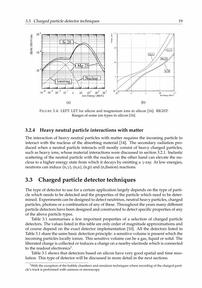
For high energy physics the tracking of charged particles with silicon detectors relieson the use of thin layers of silicon in which the particle deposits energy due to ionization,leaving behind electron-hole (e−h+) pairs. The average mean energy loss of a MIP insilicon is 388 eV/µm but corrections have to be taken into account for thin layers fromwhich part of the secondaries can escape the volume [15]. These correction terms togetherwith the evolution of the LET with the particle’s energy are illustrated in Figure 3.3a. Fora silicon sensor with a typical thickness of ≈ 300 µm this gives a most probable valueof 76 e−h+/µm for the number of electron-hole pairs formed along the path of the MIP(3.6 eV is required to generate an e−h+ pair in silicon). The distribution of the depositedenergy by a MIP in silicon is illustrated in Figure 3.3b and shows the typical skewedLandau distribution where the upper tails are due to δ-rays.
Low energy heavy ions are an important particle type to consider for the effects theycan have on the operation of ICs (section 3.7.3). Low energy heavy ions are producedin material by an incoming particle, mostly neutrons, protons or pions, undergoing anuclear interaction and producing a shower of particles and a nuclear recoil. The nuclearrecoil is a heavy ion and typically has an energy below 10 MeV. Figure 3.4a shows the LETversus energy for a silicon and a magnesium recoil and shows that a silicon recoil with anenergy of 10 MeV deposits O(2 MeV/µm), which is far above the O(100 eV/µm) rangefor MIPs. As a result of this high LET the range of these heavy ions is short as shown inFigure 3.4b, where the range is the penetration depth of the particle in the material beforecoming to rest. Figure 3.4b shows that silicon ions with an energy below 10 MeV have a

18 Chapter 3. Detector Techniques in Particle Physics
(a) (b)
FIGURE 3.3: LEFT: Most probable energy loss in silicon layers of different thick-ness, scaled to the mean energy loss at minimum ionization (388 eV/µm) [10].RIGHT: Normalized distribution of the energy deposit per µm for a 500 MeV/c
pion in silicon layers of different thicknesses [10].
range of less than 10 µm in silicon.A last important type of heavy charged particles to consider are muons. Muons do
not interact through the strong interaction, they have a much higher mass than electronswhich makes them lose only a small fraction of their energy in ionization and radiativeenergy losses are furthermore suppressed due to their high mass. As a result high energymuons can have ranges of many meters through dense material.
3.2.2 Electron interactions with matterDue to the low mass of the electron compared to the particles discussed in the previoussection the electron requires some special attention. The electron interacts with orbitalelectrons when it enters the material and therefore large fractions of its energy can be lostand its direction largely changed by single encounters. Besides interactions with orbitalelectrons the impinging electrons can also lose energy through interactions with nucleiand by radiative processes such as bremsstrahlung. For heavy charged particles, radia-tive corrections are only of importance at the highest energies (βγ ≈ 1000). For highenergy electrons (E > O(10 MeV)) however, radiative processes are the main reason forenergy loss. The mean distance over which a high-energy electron loses all but 1/e of itsenergy by bremsstrahlung is referred to as the radiation length (X0). For detection tech-niques, ionizing interactions of electrons play an important role. In silicon, for electronswith γ = 3.3 (p = 1.6 MeV/c), the electron loses 348 eV/µm due to ionization, which isclose to the value for heavy MIPs [10].
3.2.3 Photon interactions with matterInteraction of photons with material are dominated by three mechanisms: photoelectricabsorption, Compton scattering and pair production [14]. In all of these mechanismsthe photon’s energy is conveyed (partially) to electrons. For high energy photons pairproduction is by far the most important mechanism for energy loss. The radiation lengthfor high energy photons is defined by: 7/9 of the mean free path for pair production.
3.3. Charged particle detector techniques 19
(a) (b)
FIGURE 3.4: LEFT: LET for silicon and magnesium ions in silicon [16]. RIGHT:Ranges of some ion types in silicon [16].
3.2.4 Heavy neutral particle interactions with matterThe interaction of heavy neutral particles with matter requires the incoming particle tointeract with the nucleus of the absorbing material [14]. The secondary radiation pro-duced when a neutral particle interacts will mostly consist of heavy charged particles,such as heavy ions, whose material interactions were discussed in section 3.2.1. Inelasticscattering of the neutral particle with the nucleus on the other hand can elevate the nu-cleus to a higher energy state from which it decays by emitting a γ-ray. At low energies,neutrons can induce (n,γ), (n,α), (n,p) and (n,fission) reactions.
3.3 Charged particle detector techniques
The type of detector to use for a certain application largely depends on the type of parti-cle which needs to be detected and the properties of the particle which need to be deter-mined. Experiments can be designed to detect neutrinos, neutral heavy particles, chargedparticles, photons or a combination of any of these. Throughout the years many differentparticle detectors have been designed and constructed to detect specific properties of anyof the above particle types.
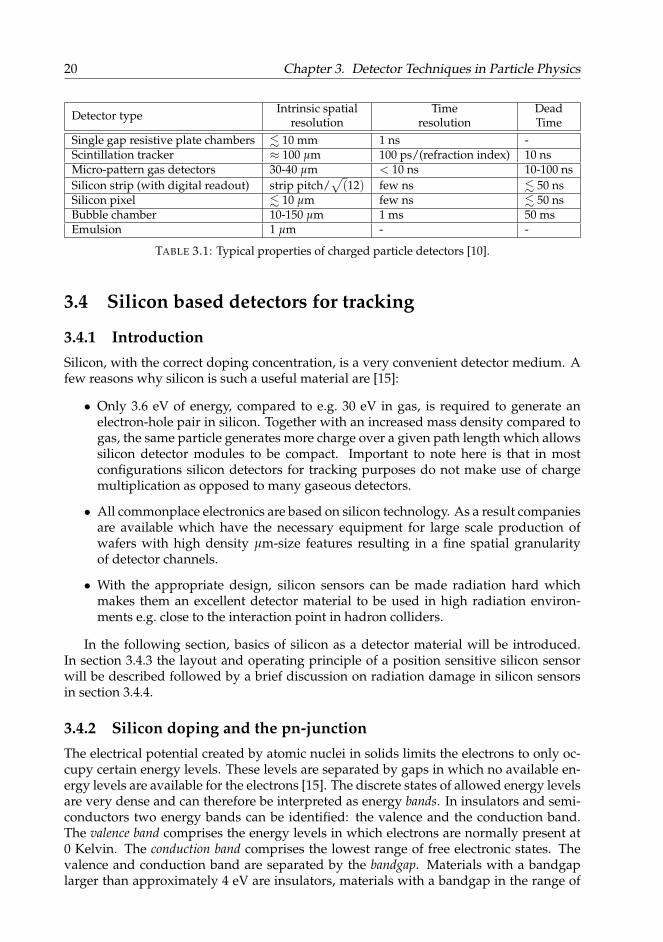
Table 3.1 summarises a few important properties of a selection of charged particledetectors. The values listed in this table are only order of magnitude approximations andof course depend on the exact detector implementation [10]. All the detectors listed inTable 3.1 share the same basic detection principle: a sensitive volume is present which theincoming particles locally ionize. This sensitive volume can be a gas, liquid or solid. Theliberated charge is collected or induces a charge on a nearby electrode which is connectedto the readout electronics1.
Table 3.1 shows that detectors based on silicon have very good spatial and time reso-lution. This type of detector will be discussed in more detail in the next sections.
1With the exception of the bubble chambers and emulsion techniques where recording of the charged parti-cle’s track is performed with cameras or microscopy.
20 Chapter 3. Detector Techniques in Particle Physics
Detector type Intrinsic spatialresolution
Timeresolution
DeadTime
Single gap resistive plate chambers . 10 mm 1 ns -Scintillation tracker ≈ 100 µm 100 ps/(refraction index) 10 nsMicro-pattern gas detectors 30-40 µm < 10 ns 10-100 nsSilicon strip (with digital readout) strip pitch/
√(12) few ns . 50 ns
Silicon pixel . 10 µm few ns . 50 nsBubble chamber 10-150 µm 1 ms 50 msEmulsion 1 µm - -
TABLE 3.1: Typical properties of charged particle detectors [10].
3.4 Silicon based detectors for tracking
3.4.1 IntroductionSilicon, with the correct doping concentration, is a very convenient detector medium. Afew reasons why silicon is such a useful material are [15]:
• Only 3.6 eV of energy, compared to e.g. 30 eV in gas, is required to generate anelectron-hole pair in silicon. Together with an increased mass density compared togas, the same particle generates more charge over a given path length which allowssilicon detector modules to be compact. Important to note here is that in mostconfigurations silicon detectors for tracking purposes do not make use of chargemultiplication as opposed to many gaseous detectors.
• All commonplace electronics are based on silicon technology. As a result companiesare available which have the necessary equipment for large scale production ofwafers with high density µm-size features resulting in a fine spatial granularityof detector channels.
• With the appropriate design, silicon sensors can be made radiation hard whichmakes them an excellent detector material to be used in high radiation environ-ments e.g. close to the interaction point in hadron colliders.
In the following section, basics of silicon as a detector material will be introduced.In section 3.4.3 the layout and operating principle of a position sensitive silicon sensorwill be described followed by a brief discussion on radiation damage in silicon sensorsin section 3.4.4.
3.4.2 Silicon doping and the pn-junctionThe electrical potential created by atomic nuclei in solids limits the electrons to only oc-cupy certain energy levels. These levels are separated by gaps in which no available en-ergy levels are available for the electrons [15]. The discrete states of allowed energy levelsare very dense and can therefore be interpreted as energy bands. In insulators and semi-conductors two energy bands can be identified: the valence and the conduction band.The valence band comprises the energy levels in which electrons are normally present at0 Kelvin. The conduction band comprises the lowest range of free electronic states. Thevalence and conduction band are separated by the bandgap. Materials with a bandgaplarger than approximately 4 eV are insulators, materials with a bandgap in the range of
3.4. Silicon based detectors for tracking 21
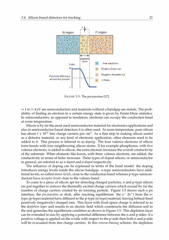
FIGURE 3.5: The pn-junction [17].
≈ 1 to≈ 4 eV are semiconductors and materials without a bandgap are metals. The prob-ability of finding an electron in a certain energy state is given by Fermi-Dirac statistics.In semiconductors, as opposed to insulators, electrons can occupy the conduction bandat room temperature.
Silicon is by far the most used semiconductor material for electronics applications andalso in semiconductor based detectors it is often used. At room temperature, pure siliconhas about 1 x 10¹¹ free charge carriers per cm3. As a first step in making silicon usefulas a detector material, or any kind of electronic application, other elements need to beadded to it. This process is referred to as doping. The four valence electrons of siliconform bonds with four neighbouring silicon atoms. If for example phosphorus, with fivevalence electrons, is added to silicon, the extra electron increases the overall conductivityof the substrate. When elements like boron, with three valence electrons, are added, theconductivity in terms of holes increases. These types of doped silicon, or semiconductorin general, are referred to as n-doped and p-doped respectively.
The influence of doping can be expressed in terms of the band model: the dopingintroduces energy levels inside the silicon bandgap. n-type semiconductors have addi-tional levels, so-called donor levels, close to the conduction band whereas p-type semicon-ductors have acceptor levels close to the valence band.
To come to a piece of silicon apt for detecting charged particles, n and p-type siliconare put together to remove the thermally excited charge carriers which exceed by far thenumber of charge carriers created by an ionizing particle. Figure 3.5 shows such a pninterface, the pn-junction or diode, after reaching equilibrium: the e− (h+) from the n-type (p-type) material have diffused to the p-type (n-type) material, leaving behind fixedpositively (negatively) charged ions. This layer with fixed space charge is referred to asthe depletion layer and results in an electric field which counteracts the diffusion and inthe end generates the equilibrium condition as shown in Figure 3.5. This depletion layercan be extended in size by applying a potential difference between the n and p sides: if apositive voltage is applied on the n-side with respect to the p-side then both n and p-sidewill be evacuated from free charge carriers. In this reverse-biasing scheme, the depletion

22 Chapter 3. Detector Techniques in Particle Physics
FIGURE 3.6: Layout of an n-in-p AC coupled silicon strip sensor [18].
layer, if the biasing voltage is high enough, extends across the full device and the volumeis depleted from free charge carriers. In this way the doped silicon material becomes anexcellent active volume for capturing charge deposited by ionizing particles.
Due to constantly produced e−h+ pairs the depletion region is never completely evac-uated from free charge carriers and this results in a constant current through the device.This current is referred to as leakage current and needs to be minimised to e.g. not stressthe power supply system and reduce the heat generated by the sensor.
3.4.3 Layout and operation of a position sensitive silicon sensorFigure 3.6 shows the typical layout of an AC-coupled position sensitive silicon strip sensorfor the n-in-p configuration. The main components are the p-bulk (shown in orange inFigure 3.6) and the n+-implants (the green structures in Figure 3.6) forming a diode struc-ture [15]. The diode is reverse biased by applying a high potential difference between thealuminium backplane (negative in this case and at the bottom of the volume in Figure3.6) and the bias ring (positive in this case). The aluminium DC pads then receive thispositive voltage through the polysilicon resistors2 (shown in white in Figure 3.6) whichare connected through a via with the n+-implants whilst for the rest of the surface then+-implants and surface structures (such as the strips) are separated from each other bya SiO2 layer. This biasing scheme results in the depletion of the p-bulk from free chargecarriers. Due to the applied potential, highly mobile electrons are also drained from theSiO2 leaving behind a slightly polarised oxide layer which attracts electrons from thebulk which concentrate at the Si-SiO2 layer and can form a conductive path between then+-implants. This conductive path can affect the spatial resolution of the sensor by short-ening the strips together or even shielding them from the bulk. In order to resolve this,local p+-implants, so-called p-stop structures (shown in red in Figure 3.6), are introduced
2These resistors are needed to ensure a high ohmic path between the DC pad and the bias ring. A low ohmicpath would result in all the induced charge going to the bias ring rather than to the readout electronics.

3.4. Silicon based detectors for tracking 23
between the n+-implants. These implants capture electrons and this results in a localnegative space charge which repels other electrons and ensures the inter-strip isolation.
When a charged particle passes through the sensor most of the charge will be de-posited in the p-bulk. The electrons will start to drift to the positive n+-implants whilstholes follow an opposite path towards the backplane. The drifting electrons induce acurrent on the n+-implants which are capacitively coupled to aluminium readout strips(Strips in Figure 3.6). A very homogeneous, well defined and preferentially thin SiO2layer is thus required between the implants and the strips to guarantee a uniform capac-itance along and for all strips. The AC pad is then connected to a readout chip throughwire bonds. This AC coupling scheme, where the capacitor is implemented on the sensor,has the advantage that the leakage current does not need to be drained by the readoutchip, as opposed to the DC coupling scheme where the aluminium pad is directly con-nected to the implants and the readout chip thus needs to cope with a free bulk chargeflow. In the DC coupling scheme the capacitor is then implemented in the readout chip.
The fact that these n+-implants are localised (in the example in Figure 3.6 as strips)give the spatial resolution to the sensor. Other segmentations of the implants, such aspixels, can also be used. In that case the connection to the readout chip is performed bybump bonding the pixel to the readout chip’s front-end.
The pixel dimensions or the strip pitch, defined as the distance between strip centres, isa very important design parameter of the sensor. It basically drives the spatial resolutionof the sensor. The strip number where the signal is measured tells where the particlepassed the sensor, when applying corrections for Lorentz drift of the e−h+ pair whenthe sensor is placed in a magnetic field. In case the signal spreads over more than onestrip and the readout electronics provide information on the pulse height of the signal,the center of gravity of the signal can be calculated. When the readout electronics adopta binary readout then the variance on the position resolution of a single strip cluster isgiven by [15]:
< ∆x2 >=1p
∫ p/2
−p/2x2dx =
p2
12, (3.4)
where p is the strip pitch and x is the dimension orthogonal to the strip direction.
3.4.4 Radiation damage in silicon sensorsOperating sensors in a radiation environment can greatly affect their performance. Ingeneral, the radiation damage introduced in silicon sensors can be split up in surfacedamage and bulk damage [15].
Surface damage is most important for AC-coupled sensors as it manifests at the SiO2layer or Si-SiO2 interface and the fundamental principle is comparable to the total ionizingdose effect on MOSFETs described in section 3.7.2: ionizing particles generate charge inthe SiO2 layer, the electrons are drained by the strip electrode and the holes start to driftto the Si-SiO2 interface where they accumulate and attract electrons formed in the bulk.This results in a negative space charge which can result in shorts between the strips.These can be alleviated using p-stop techniques, which were already discussed in section3.4.3.
Bulk damage is largely the result of non-ionizing interactions which affect the latticestructure of the silicon. Non-ionizing energy loss (NIEL) happens when a particle in-teracts with the atomic bodies via the electromagnetic or strong force and displaces theatomic body, like this creating a Frenkel pair: a vacancy and an interstitial. Also more
24 Chapter 3. Detector Techniques in Particle Physics
complex defects can be created. A commonly used unit for NIEL is the 1 MeV neutronequivalent: the non-ionizing radiation damage introduced by radiation of different typeand energy can in first order be normalized to the radiation damage induced by 1 MeVneutrons. This is referred to as the NIEL hypothesis [19] which allows to compare NIELirradiation tests performed with different particle types and/or energies.
The changes to the silicon lattice structure introduced by non-ionizing interactionsresult in additional energy levels in the silicon band gap which manifest as:
• Higher leakage current due to extra energy levels in the middle of the bandgapwhich facilitate generation and recombination of free charge carriers.
• Change in depletion voltage due to extra energy levels close to the valence andconduction band which effectively change the doping concentration.
• Lower charge collection efficiency due to defects capturing free charge carriers.
The bulk damage induced by radiation can change over time, even when the sensoris not irradiated: displaced atoms are able to move from their displaced position andthe defect can either be cured or the movement can introduce new defects. This effectis referred to as annealing and has both positive and negative consequences. A positiveimplication is that the leakage current of a sensor, when no longer irradiated, typicallygoes down over time and this effect accelerates with temperature as the mobility of dis-placed atoms increases. As annealing changes the concentration of bulk defects it affectsthe effective doping concentration, which in turn modifies the depletion voltage and thecharge collection efficiency of the sensor. The effect of annealing on the depletion voltageand the charge collection efficiency is positive at first (beneficial annealing), but over timereverse annealing takes over and results in a higher depletion voltage and lower chargecollection efficiency. This reverse annealing can be slowed down by cooling the sensorsto sub-zero temperatures [15].
The induced surface damage is typically not fully reversible and the recovery dependsfor example on the oxide quality. Furthermore emission of captured charge carriers fromexisting defects is suppressed due to the large band gap in the oxide. Annealing of thesurface damage only sets in at high temperatures (around 100-400 C).
3.5 Integrated circuits
An IC (Integrated Circuit) or a chip is a small, usually silicon, wafer which can hold mil-lions of micro scale structures such as resistors, capacitors, transistors,... for use in ana-logue or digital applications. The main building blocks of integrated circuits are transis-tors which come in two main families: bipolar junction transistors and field-effect transistors(FETs). The latter have become the preferred type for use in very large-scale integrated(VLSI) circuits thanks to their small dimensions and the possibility they offer to createcircuits with low power consumption [20]. The two most important types of FETs arejunction-gate FETs and insulated-gate FETs. The latter are also more widely known as MOS-FETs (metal–oxide–semiconductor FETs) and form the preferred type of FETs usuallyfound in VLSI circuits due to e.g. easier fabrication, higher input resistance and smallerleakage current than junction-gate FETs. Throughout the years, channel lengths of MOSdevices have substantially decreased. This scaling of the devices nowadays culminates inthe 5 nm technology node being commercially available.

3.6. Readout chips for silicon detectors 25
17.3 INSULATED-GATE FIELD-EFFECT TRANSISTORS 337
··
supply connected to the source are VSS and ISS. In many cases, VSS is takenas the zero-volts reference (or ground) of the circuit. Passive componentsconnected to the various terminals are often given corresponding labels, so thata resistor connected to the gate of an FET might be labelled RG. This nota-tion is illustrated in Figure 17.2.
In FETs, conduction between the drain and source electrodes takes placethrough a channel of semiconductor material. Insulated-gate FETs are socalled because their metal gate electrode is insulated from the conductingchannel by a layer of insulating oxide. Such devices are often referred to asinsulated-gate field-effect transistors (IGFETs), but are more com-monly described as metal oxide semiconductor field-effect transistors(MOSFETs). Digital circuits constructed using such techniques are usuallydescribed as using MOS technology. Here we refer to insulated-gatedevices as MOSFETs.
The channel in a MOSFET can be made of either n-type or p-type semi-conductor material, leading to two polarities of transistor, termed n-channeland p-channel devices. Figure 17.3 illustrates the construction of each formof device. The behaviour of these two forms is similar, except that the polar-ities of the various currents and voltages are reversed. To avoid duplication,we will concentrate on n-channel devices in this section.
Figure 17.2 Labelling ofvoltages and currents in FETcircuits.
Insulated-gate field-effect transistors
17.3
Figure 17.3 Insulated-gatefield-effect transistors –MOSFETs.
ELEA_C17.qxd 2/10/09 2:25 PM Page 337
FIGURE 3.7: n-type channel (LEFT) and p-type channel (RIGHT) MOSFET [20].The figures illustrate a depletion MOSFET or an enhancement MOSFET in the
ON state.
Figure 3.7 illustrates the layout of an n-type channel (NMOS) and p-type channel (PMOS)MOSFET. The metal gate terminal of the transistor is separated from the body by an insu-lating layer, in this way creating the metal-oxide-semiconductor (MOS) sandwich. Thevoltage on the gate regulates the conductivity of the semiconductor body between thedrain and source. In the NMOS configuration a positive voltage (with respect to the body)at the gate will attract electrons and make the n-type channel wider resulting in a higherconductivity between the n-type source and drain. By applying a negative voltage thechannel becomes thinner and conductivity decreases. Other types of MOSFETs also ex-ist. These enhancement MOSFETs do not have a manufactured n-type channel and canonly operate in enhancement mode [20]. Enhancement MOSFETs are the transistor imple-mentation used in complementary MOS (CMOS) devices.
NMOS and PMOS devices can be combined within a single circuit to form CMOSdevices. These devices have the advantage that in a static configuration one of the tran-sistors is always in the OFF state, which greatly reduces power consumption as the onlycurrent which flows is the one drawn by the load. Only during switching both transistorsare conducting which results in a small burst of current from supply to ground.
CMOS transistors form the basis of nearly all electronic systems. They can be usedas amplifiers in a huge variety of applications and as switches, logical gates, memorycells, etc. in digital systems. Figure 3.8a for example shows how NMOS and PMOStransistors are used to form a logic NAND gate. The implementation as shown in thisfigure, without a sampling clock, is referred to as static logic. Figure 3.8b shows theNAND gate implemented in dynamic logic, where the signal is evaluated only during acertain part of the clock cycle and where the output is stored on the capacitor X at theoutput.
3.6 Readout chips for silicon detectors
For particle physics experiments ICs are extremely interesting as they can provide an on-detector signal amplification, first-level data reduction and/or data buffering. The smalldimensions of an IC and their low power consumption make them also suitable for use intracking detectors. The ICs developed as on-detector electronics are mostly designed tomeet one specific application and are therefore referred to as Application-Specific IntegratedCircuits or ASICs.
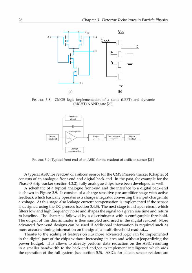
26 Chapter 3. Detector Techniques in Particle Physics
25.3 LOGIC FAMILIES 641
··
Figure 25.20 Two-inputCMOS gates.
Figure 25.21 A simpleBiCMOS inverter.
ELEA_C25.qxd 2/10/09 2:29 PM Page 641
(a) (b)
FIGURE 3.8: CMOS logic implementation of a static (LEFT) and dynamic(RIGHT) NAND gate [20].
FIGURE 3.9: Typical front-end of an ASIC for the readout of a silicon sensor [21].
A typical ASIC for readout of a silicon sensor for the CMS Phase-2 tracker (Chapter 5)consists of an analogue front-end and digital back-end. In the past, for example for thePhase-0 strip tracker (section 4.3.2), fully analogue chips have been developed as well.
A schematic of a typical analogue front-end and the interface to a digital back-endis shown in Figure 3.9. It consists of a charge sensitive pre-amplifier stage with activefeedback which basically operates as a charge integrator converting the input charge intoa voltage. At this stage also leakage current compensation is implemented if the sensoris designed using the DC process (section 3.4.3). The next stage is a shaper circuit whichfilters low and high frequency noise and shapes the signal to a given rise time and returnto baseline. The shaper is followed by a discriminator with a configurable threshold.The output of this discriminator is then sampled and used in the digital readout. Moreadvanced front-end designs can be used if additional information is required such asmore accurate timing information on the signal, a multi-threshold readout,...
Thanks to the scaling of features on ICs more advanced logic can be implementedin the digital part of the chips without increasing its area and without jeopardizing thepower budget. This allows to already perform data reduction on the ASIC resultingin a smaller bandwidth to the back-end and/or to implement intelligence which aidsthe operation of the full system (see section 5.5). ASICs for silicon sensor readout are
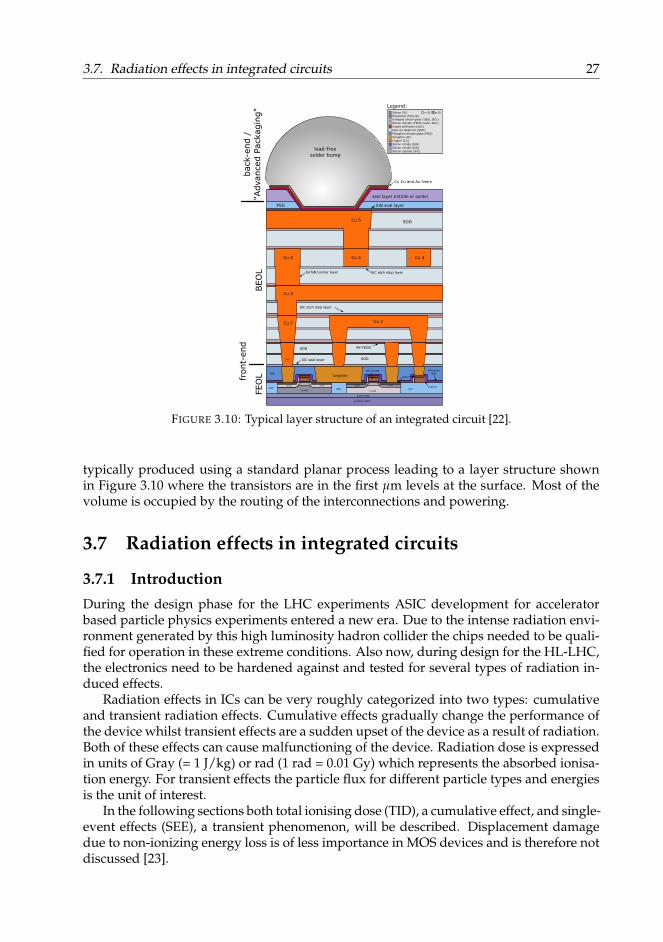
3.7. Radiation effects in integrated circuits 27
FEO
Lbac
k-en
d /
"Adva
nce
d P
acka
gin
g"
BEO
L
Cr, Cu and Au liners
lead-freesolder bump
poly-Si gate
STIp-wellUSG
tungsten
buried SiO2
p-silicon wafer
n-wellUSG
SOD
SODCu1
PSGSiN barrier
layer
CoSi2
SiC seal layer
PE-TEOS
Cu 2
SiC etch stop layer
Ta/TaN barrier layer
SiN seal layer
seal layer (nitride or oxide)
PSG
Cu 5 SOD
SOD
n-Si n-Si p-Si p-Si
Cu 4 Cu 4Cu 4
Cu 5
SiC etch stop layer
spacer
front-
end
Cu 3
Cu 2 Cu 2
Legend:Silicon (Si)Polysilicon (Poly-Si)
Cobalt disilicide (CoSi2)Silicon dioxide (TEOS oxide, SiO2)
n-Si p-Si
Spin-on dielectric (SOD)Phosphor-silicate glass (PSG)Tungsten (W)Copper (Cu)Silicon nitride (SiN)Silicon nitride (SiN)Silicon carbide (SiC)
Undoped silicon glass (USG, SiO2)
FIGURE 3.10: Typical layer structure of an integrated circuit [22].
typically produced using a standard planar process leading to a layer structure shownin Figure 3.10 where the transistors are in the first µm levels at the surface. Most of thevolume is occupied by the routing of the interconnections and powering.
3.7 Radiation effects in integrated circuits
3.7.1 IntroductionDuring the design phase for the LHC experiments ASIC development for acceleratorbased particle physics experiments entered a new era. Due to the intense radiation envi-ronment generated by this high luminosity hadron collider the chips needed to be quali-fied for operation in these extreme conditions. Also now, during design for the HL-LHC,the electronics need to be hardened against and tested for several types of radiation in-duced effects.
Radiation effects in ICs can be very roughly categorized into two types: cumulativeand transient radiation effects. Cumulative effects gradually change the performance ofthe device whilst transient effects are a sudden upset of the device as a result of radiation.Both of these effects can cause malfunctioning of the device. Radiation dose is expressedin units of Gray (= 1 J/kg) or rad (1 rad = 0.01 Gy) which represents the absorbed ionisa-tion energy. For transient effects the particle flux for different particle types and energiesis the unit of interest.
In the following sections both total ionising dose (TID), a cumulative effect, and single-event effects (SEE), a transient phenomenon, will be described. Displacement damagedue to non-ionizing energy loss is of less importance in MOS devices and is therefore notdiscussed [23].

28 Chapter 3. Detector Techniques in Particle Physics
(a) (b)
FIGURE 3.11: LEFT: The result of ionising radiation in the gate oxide of a tran-sistor. The holes can be transported to the Si-SiO2 interface where they can betrapped by defects. The holes can interact with defects containing hydrogen.The liberated proton can introduce dangling silicon bonds at the interface [24].RIGHT: Extreme result of TID in an NMOS transistor: the localised positivecharge in the gate oxide can keep the channel turned on without application of a
gate voltage.
3.7.2 Total ionizing dose
3.7.2.1 Introduction
A good understanding of TID effects [24] is important for devices which need to operatein a high radiation environment such as inside CMS. TID effects are also of importance inspace applications although it is important to note that most electronics in earth satellites(in low earth orbit) receive a TID(SiO2) of O(50 Gy/year) [25], whereas the most innerlevels of the CMS detector are expected to aggregate up to 12 MGy at the HL-LHC. Inthe next sections the physical mechanism behind TID effects will be discussed at transis-tor level (section 3.7.2.2) after which TID hardening techniques (section 3.7.2.3) and themethodology behind TID testing (section 3.7.2.4) will be introduced.
3.7.2.2 Total ionizing dose mechanism
When an ionising particle passes through a MOS transistor it can generate electron-holepairs in the SiO2 layer. About 17 eV of energy is required to create an electron-hole pairin SiO2. Figure 3.11a illustrates the effect of ionising radiation in a MOSFET: the electronsproduced by the passage of the ionizing particle have high mobility and are evacuatedvia the positive voltage on the gate or recombine with holes. The holes which do notrecombine are forced away from the gate, but have a lower mobility than the electrons.The hole transport towards the Si-SiO2 interface happens on localised oxygen vacanciesuntil they reach the Si-SiO2 interface where they can be trapped by defects. These defectsare introduced in the production process and are e.g. caused by the lattice mismatches atthe Si-SiO2 interface. The trapped holes result in a layer of fixed positive charge, which,as illustrated in the transversal cross section of an NMOS transistor in Figure 3.11b, can inextreme cases result in the transistor being on without an applied gate voltage. The latteris an extreme case but exemplifies the influence of TID on the operation of a transistor.
Besides the direct generation of a localised positive charge near the Si-SiO2 interfacethe ionizing radiation can also indirectly introduce defects: the holes on their way to the
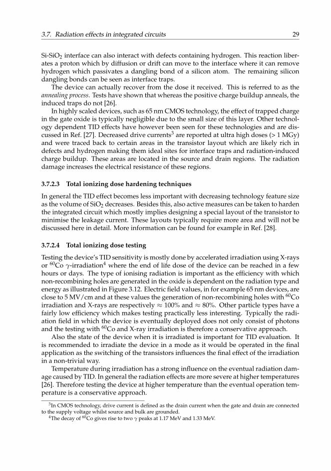
3.7. Radiation effects in integrated circuits 29
Si-SiO2 interface can also interact with defects containing hydrogen. This reaction liber-ates a proton which by diffusion or drift can move to the interface where it can removehydrogen which passivates a dangling bond of a silicon atom. The remaining silicondangling bonds can be seen as interface traps.
The device can actually recover from the dose it received. This is referred to as theannealing process. Tests have shown that whereas the positive charge buildup anneals, theinduced traps do not [26].
In highly scaled devices, such as 65 nm CMOS technology, the effect of trapped chargein the gate oxide is typically negligible due to the small size of this layer. Other technol-ogy dependent TID effects have however been seen for these technologies and are dis-cussed in Ref. [27]. Decreased drive currents3 are reported at ultra high doses (> 1 MGy)and were traced back to certain areas in the transistor layout which are likely rich indefects and hydrogen making them ideal sites for interface traps and radiation-inducedcharge buildup. These areas are located in the source and drain regions. The radiationdamage increases the electrical resistance of these regions.
3.7.2.3 Total ionizing dose hardening techniques
In general the TID effect becomes less important with decreasing technology feature sizeas the volume of SiO2 decreases. Besides this, also active measures can be taken to hardenthe integrated circuit which mostly implies designing a special layout of the transistor tominimise the leakage current. These layouts typically require more area and will not bediscussed here in detail. More information can be found for example in Ref. [28].
3.7.2.4 Total ionizing dose testing
Testing the device’s TID sensitivity is mostly done by accelerated irradiation using X-raysor 60Co γ-irradiation4 where the end of life dose of the device can be reached in a fewhours or days. The type of ionising radiation is important as the efficiency with whichnon-recombining holes are generated in the oxide is dependent on the radiation type andenergy as illustrated in Figure 3.12. Electric field values, in for example 65 nm devices, areclose to 5 MV/cm and at these values the generation of non-recombining holes with 60Coirradiation and X-rays are respectively ≈ 100% and ≈ 80%. Other particle types have afairly low efficiency which makes testing practically less interesting. Typically the radi-ation field in which the device is eventually deployed does not only consist of photonsand the testing with 60Co and X-ray irradiation is therefore a conservative approach.
Also the state of the device when it is irradiated is important for TID evaluation. Itis recommended to irradiate the device in a mode as it would be operated in the finalapplication as the switching of the transistors influences the final effect of the irradiationin a non-trivial way.
Temperature during irradiation has a strong influence on the eventual radiation dam-age caused by TID. In general the radiation effects are more severe at higher temperatures[26]. Therefore testing the device at higher temperature than the eventual operation tem-perature is a conservative approach.
3In CMOS technology, drive current is defined as the drain current when the gate and drain are connectedto the supply voltage whilst source and bulk are grounded.
4The decay of 60Co gives rise to two γ peaks at 1.17 MeV and 1.33 MeV.
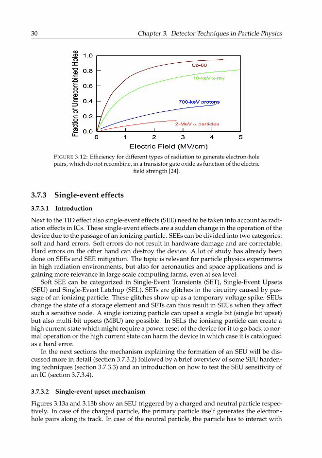
30 Chapter 3. Detector Techniques in Particle Physics
FIGURE 3.12: Efficiency for different types of radiation to generate electron-holepairs, which do not recombine, in a transistor gate oxide as function of the electric
field strength [24].
3.7.3 Single-event effects
3.7.3.1 Introduction
Next to the TID effect also single-event effects (SEE) need to be taken into account as radi-ation effects in ICs. These single-event effects are a sudden change in the operation of thedevice due to the passage of an ionizing particle. SEEs can be divided into two categories:soft and hard errors. Soft errors do not result in hardware damage and are correctable.Hard errors on the other hand can destroy the device. A lot of study has already beendone on SEEs and SEE mitigation. The topic is relevant for particle physics experimentsin high radiation environments, but also for aeronautics and space applications and isgaining more relevance in large scale computing farms, even at sea level.
Soft SEE can be categorized in Single-Event Transients (SET), Single-Event Upsets(SEU) and Single-Event Latchup (SEL). SETs are glitches in the circuitry caused by pas-sage of an ionizing particle. These glitches show up as a temporary voltage spike. SEUschange the state of a storage element and SETs can thus result in SEUs when they affectsuch a sensitive node. A single ionizing particle can upset a single bit (single bit upset)but also multi-bit upsets (MBU) are possible. In SELs the ionising particle can create ahigh current state which might require a power reset of the device for it to go back to nor-mal operation or the high current state can harm the device in which case it is cataloguedas a hard error.
In the next sections the mechanism explaining the formation of an SEU will be dis-cussed more in detail (section 3.7.3.2) followed by a brief overview of some SEU harden-ing techniques (section 3.7.3.3) and an introduction on how to test the SEU sensitivity ofan IC (section 3.7.3.4).
3.7.3.2 Single-event upset mechanism
Figures 3.13a and 3.13b show an SEU triggered by a charged and neutral particle respec-tively. In case of the charged particle, the primary particle itself generates the electron-hole pairs along its track. In case of the neutral particle, the particle has to interact with
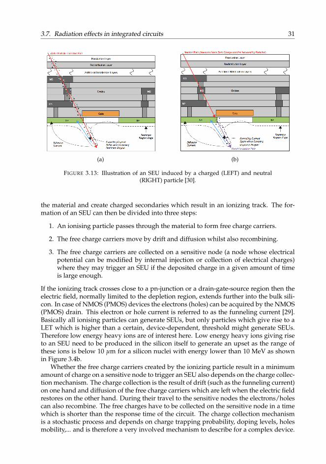
3.7. Radiation effects in integrated circuits 31
(a) (b)
FIGURE 3.13: Illustration of an SEU induced by a charged (LEFT) and neutral(RIGHT) particle [30].
the material and create charged secondaries which result in an ionizing track. The for-mation of an SEU can then be divided into three steps:
1. An ionising particle passes through the material to form free charge carriers.
2. The free charge carriers move by drift and diffusion whilst also recombining.
3. The free charge carriers are collected on a sensitive node (a node whose electricalpotential can be modified by internal injection or collection of electrical charges)where they may trigger an SEU if the deposited charge in a given amount of timeis large enough.
If the ionizing track crosses close to a pn-junction or a drain-gate-source region then theelectric field, normally limited to the depletion region, extends further into the bulk sili-con. In case of NMOS (PMOS) devices the electrons (holes) can be acquired by the NMOS(PMOS) drain. This electron or hole current is referred to as the funneling current [29].Basically all ionising particles can generate SEUs, but only particles which give rise to aLET which is higher than a certain, device-dependent, threshold might generate SEUs.Therefore low energy heavy ions are of interest here. Low energy heavy ions giving riseto an SEU need to be produced in the silicon itself to generate an upset as the range ofthese ions is below 10 µm for a silicon nuclei with energy lower than 10 MeV as shownin Figure 3.4b.
Whether the free charge carriers created by the ionizing particle result in a minimumamount of charge on a sensitive node to trigger an SEU also depends on the charge collec-tion mechanism. The charge collection is the result of drift (such as the funneling current)on one hand and diffusion of the free charge carriers which are left when the electric fieldrestores on the other hand. During their travel to the sensitive nodes the electrons/holescan also recombine. The free charges have to be collected on the sensitive node in a timewhich is shorter than the response time of the circuit. The charge collection mechanismis a stochastic process and depends on charge trapping probability, doping levels, holesmobility,... and is therefore a very involved mechanism to describe for a complex device.
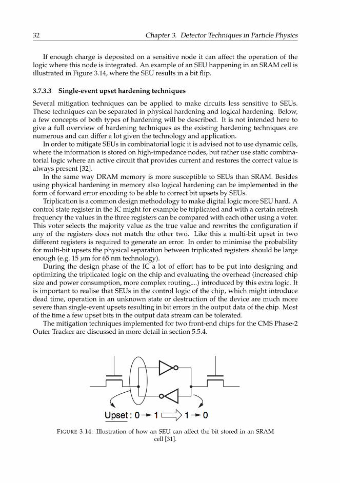
32 Chapter 3. Detector Techniques in Particle Physics
If enough charge is deposited on a sensitive node it can affect the operation of thelogic where this node is integrated. An example of an SEU happening in an SRAM cell isillustrated in Figure 3.14, where the SEU results in a bit flip.
3.7.3.3 Single-event upset hardening techniques
Several mitigation techniques can be applied to make circuits less sensitive to SEUs.These techniques can be separated in physical hardening and logical hardening. Below,a few concepts of both types of hardening will be described. It is not intended here togive a full overview of hardening techniques as the existing hardening techniques arenumerous and can differ a lot given the technology and application.
In order to mitigate SEUs in combinatorial logic it is advised not to use dynamic cells,where the information is stored on high-impedance nodes, but rather use static combina-torial logic where an active circuit that provides current and restores the correct value isalways present [32].
In the same way DRAM memory is more susceptible to SEUs than SRAM. Besidesusing physical hardening in memory also logical hardening can be implemented in theform of forward error encoding to be able to correct bit upsets by SEUs.
Triplication is a common design methodology to make digital logic more SEU hard. Acontrol state register in the IC might for example be triplicated and with a certain refreshfrequency the values in the three registers can be compared with each other using a voter.This voter selects the majority value as the true value and rewrites the configuration ifany of the registers does not match the other two. Like this a multi-bit upset in twodifferent registers is required to generate an error. In order to minimise the probabilityfor multi-bit upsets the physical separation between triplicated registers should be largeenough (e.g. 15 µm for 65 nm technology).
During the design phase of the IC a lot of effort has to be put into designing andoptimizing the triplicated logic on the chip and evaluating the overhead (increased chipsize and power consumption, more complex routing,...) introduced by this extra logic. Itis important to realise that SEUs in the control logic of the chip, which might introducedead time, operation in an unknown state or destruction of the device are much moresevere than single-event upsets resulting in bit errors in the output data of the chip. Mostof the time a few upset bits in the output data stream can be tolerated.
The mitigation techniques implemented for two front-end chips for the CMS Phase-2Outer Tracker are discussed in more detail in section 5.5.4.
FIGURE 3.14: Illustration of how an SEU can affect the bit stored in an SRAMcell [31].
3.8. Summary 33
3.7.3.4 Single-event upset testing
Characterising the IC’s sensitivity to SEUs and other SEE effects is typically done at par-ticle accelerators such as cyclotrons. The die can be irradiated with different kinds of ion-izing particles. Typically low energy protons or heavy ions are used for their large LET.During the testing the irradiation is changed so that the LET changes. This is achievedby changing the particle energy, type or incident angle. In the end the SEU cross section:
σ =#SEU
φ, (3.5)
needs to be determined for different LET. φ in Equation (3.5) is the particle fluence onthe device. In theory the SEU cross section versus LET would show a step function be-haviour, as a minimal LET is required to generate the critical charge on a node. In realitythis step function is smoothed and can be represented by a cumulative Weibull distribu-tion function [16]:
σ = σ0
1− exp
[−(Edep − E0
W
)s], (3.6)
with W and s as shape parameters and with Edep the energy deposited by the ionizingparticle in a sensitive volume. The smoothing can be explained by the variation in thecharge collection efficiency across the sensitive area and by junctions with different sen-sitivities. The critical value (E0) then represents the minimal energy deposit to upset themost sensitive part of the design. MBUs, more probable for higher LETs, can increasethe saturation threshold (σ0). Once the SEU cross section as a function of LET is knownthe bit error rate due to SEU for a particular radiation environment can be predicted byconvoluting the SEU cross section as function of LET with the probability distribution tohave a certain energy deposit in a certain sensitive volume for a given particle spectrumand multiplying this with the particle flux. This will be explained in more detail andapplied in section 8.4.
3.8 Summary
Understanding the particle interactions with matter is indispensable for describing bothparticle detection mechanisms and the radiation damage which these particles can inducein detector components. The interaction of a particle with material strongly depends onthe particle’s properties such as its mass, energy and charge. In silicon sensors, the signalgeneration happens in the bulk of the sensor material which is depleted from free chargecarriers by applying a bias voltage over the pn-junction. Charged particles passing thesensor will deposit energy, which results in the production of e−h+ pairs (≈ 76 e−h+/µmfor a 300 µm thick sensor) in the silicon bulk and their charge flow induces a signal onthe readout strips which are connected to the readout ASICs.
For silicon sensors, both radiation damage induced by non-ionizing and ionizing in-teractions are important. The former is linked to bulk damage, whereas the latter is linkedto surface damage in the sensor. Bulk damage mainly results in higher leakage current,change in depletion voltage and a lower charge collection efficiency. Surface damage onthe other hand can affect for example the interstrip resistivity. The surface damage mech-anism in sensors is comparable to the TID effect introduced by radiation on ICs. ASICsin the CMS Outer Tracker will aggregate a dose up to 600 kGy [33] and without careful

34 Chapter 3. Detector Techniques in Particle Physics
design choices this could have severe effects on the operation of the ASICs. The TID ef-fect is greatly dependent on the exact technology which is used for the ASIC and testingthe ASIC’s TID sensitivity by accelerated irradiation with ionizing radiation is impera-tive in the ASIC’s validation procedure. Besides TID effects also SEUs are a consequenceof operating ASICs in a radiation field. Highly ionizing particles, such as low energyheavy ions, induce these effects as they can deposit a large charge in the sensitive vol-ume around a sensitive node. SEUs can cause malfunctioning of the device if the deviceis not properly designed. Design techniques such as triplication are therefore critical tomitigate SEU effects. The mitigation strategy can be evaluated by testing for SEE andmeasuring the SEU rate at heavy ion facilities.
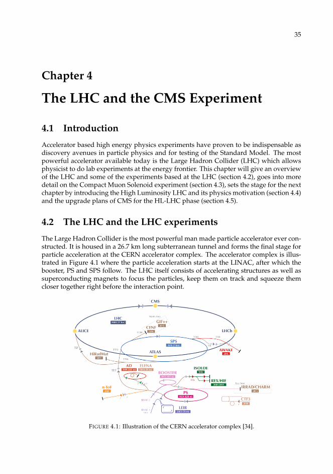
35
Chapter 4
The LHC and the CMS Experiment
4.1 Introduction
Accelerator based high energy physics experiments have proven to be indispensable asdiscovery avenues in particle physics and for testing of the Standard Model. The mostpowerful accelerator available today is the Large Hadron Collider (LHC) which allowsphysicist to do lab experiments at the energy frontier. This chapter will give an overviewof the LHC and some of the experiments based at the LHC (section 4.2), goes into moredetail on the Compact Muon Solenoid experiment (section 4.3), sets the stage for the nextchapter by introducing the High Luminosity LHC and its physics motivation (section 4.4)and the upgrade plans of CMS for the HL-LHC phase (section 4.5).
4.2 The LHC and the LHC experiments
The Large Hadron Collider is the most powerful man made particle accelerator ever con-structed. It is housed in a 26.7 km long subterranean tunnel and forms the final stage forparticle acceleration at the CERN accelerator complex. The accelerator complex is illus-trated in Figure 4.1 where the particle acceleration starts at the LINAC, after which thebooster, PS and SPS follow. The LHC itself consists of accelerating structures as well assuperconducting magnets to focus the particles, keep them on track and squeeze themcloser together right before the interaction point.
FIGURE 4.1: Illustration of the CERN accelerator complex [34].
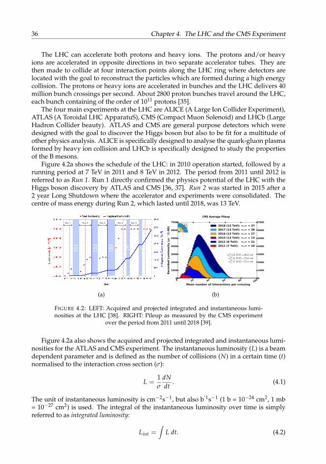
36 Chapter 4. The LHC and the CMS Experiment
The LHC can accelerate both protons and heavy ions. The protons and/or heavyions are accelerated in opposite directions in two separate accelerator tubes. They arethen made to collide at four interaction points along the LHC ring where detectors arelocated with the goal to reconstruct the particles which are formed during a high energycollision. The protons or heavy ions are accelerated in bunches and the LHC delivers 40million bunch crossings per second. About 2800 proton bunches travel around the LHC,each bunch containing of the order of 1011 protons [35].
The four main experiments at the LHC are ALICE (A Large Ion Collider Experiment),ATLAS (A Toroidal LHC ApparatuS), CMS (Compact Muon Solenoid) and LHCb (LargeHadron Collider beauty). ATLAS and CMS are general purpose detectors which weredesigned with the goal to discover the Higgs boson but also to be fit for a multitude ofother physics analysis. ALICE is specifically designed to analyse the quark-gluon plasmaformed by heavy ion collision and LHCb is specifically designed to study the propertiesof the B mesons.
Figure 4.2a shows the schedule of the LHC: in 2010 operation started, followed by arunning period at 7 TeV in 2011 and 8 TeV in 2012. The period from 2011 until 2012 isreferred to as Run 1. Run 1 directly confirmed the physics potential of the LHC with theHiggs boson discovery by ATLAS and CMS [36, 37]. Run 2 was started in 2015 after a2 year Long Shutdown where the accelerator and experiments were consolidated. Thecentre of mass energy during Run 2, which lasted until 2018, was 13 TeV.
Run 1 Run 2 Run 3 Run 4 Run 5
(a)
0 20 40 60 80 100
0ean number Rf LnteractLRnV per crRVVLng
0
1000
2000
3000
4000
5000
6000
7000
5ecRrded /umLnRVLty (pb−1/1.00)
σppin (13 TeV) )8(.( mb
σppin (8 TeV) )73.( mb
σppin (7 TeV) )71.5 mb
2018 (13 7eV): <µ> 37
2017 (13 7eV): <µ> 38
2016 (13 7eV): <µ> 27
2015 (13 7eV): <µ> 13
2012 (8 7eV): <µ> 21
2011 (7 7eV): <µ> 10
0
1000
2000
3000
4000
5000
6000
7000
CMS Average PileuS
(b)
FIGURE 4.2: LEFT: Acquired and projected integrated and instantaneous lumi-nosities at the LHC [38]. RIGHT: Pileup as measured by the CMS experiment
over the period from 2011 until 2018 [39].
Figure 4.2a also shows the acquired and projected integrated and instantaneous lumi-nosities for the ATLAS and CMS experiment. The instantaneous luminosity (L) is a beamdependent parameter and is defined as the number of collisions (N) in a certain time (t)normalised to the interaction cross section (σ):
L =1σ
dNdt
. (4.1)
The unit of instantaneous luminosity is cm−2s−1, but also b¯1s−1 (1 b = 10−24 cm2, 1 mb= 10−27 cm2) is used. The integral of the instantaneous luminosity over time is simplyreferred to as integrated luminosity:
Lint =∫
L dt. (4.2)

4.3. The CMS experiment 37
FIGURE 4.3: Layout of the CMS detector [40].
At the end of 2018, about 192 fb−1 [39] of proton-proton (pp) collisions were deliv-ered to CMS. The gradual increase in instantaneous luminosity is a direct consequenceof improvements in the beam quality and intensity which results in a higher number ofproton-proton collisions happening during one bunch crossing (BX). The latter numberis referred to as pileup (PU). The distribution of the pileup measured at CMS is shown,for each running year, in Figure 4.2b, from which it is clear that the LHC surpassed itsoriginal design value of <PU> ≈ 25. This larger pileup extends the physics reach of theexperiments due to the higher probability of occurrence of an interesting collision, but onthe other hand forms a challenge as most of the PU interactions are soft and in generalless interesting to test new physics models. The detectors should therefore be able to dis-entangle every proton-proton collision. A significant increase in luminosity is foreseenby 2026 as a result of an upgrade of various parts of the accelerator complex. This is animportant milestone in the LHC schedule and is referred to as the High Luminosity LHC(HL-LHC). As a result of this upgrade, many of the detectors at the LHC will need to beupgraded to cope with the increased pileup. The average expected pileup at HL-LHC isexpected to be 150, or even 200 if the ultimate design prospects are achieved [33]. Thepreparation for HL-LHC started already in 2019 during Long Shutdown 2. After thisLong Shutdown, another 3 year run at 14 TeV is scheduled, followed by a 3rd Long Shut-down from 2024 to mid 2026 where the main upgrades for the HL-LHC will be put inplace. After this 3rd Long Shutdown the HL-LHC will provide collisions to the experi-ments for another 10 to 15 years. Section 4.4 will give more information on the HL-LHC.
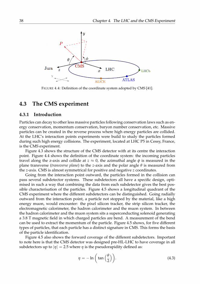
38 Chapter 4. The LHC and the CMS Experiment
FIGURE 4.4: Definition of the coordinate system adopted by CMS [41].
4.3 The CMS experiment
4.3.1 IntroductionParticles can decay to other less massive particles following conservation laws such as en-ergy conservation, momentum conservation, baryon number conservation, etc. Massiveparticles can be created in the reverse process where high energy particles are collided.At the LHC’s interaction points experiments were build to study the particles formedduring such high energy collisions. The experiment, located at LHC P5 in Cessy, France,is the CMS experiment.
Figure 4.3 shows the structure of the CMS detector with at its centre the interactionpoint. Figure 4.4 shows the definition of the coordinate system: the incoming particlestravel along the z-axis and collide at z ≈ 0, the azimuthal angle φ is measured in theplane transverse (transverse plane) to the z-axis and the polar angle θ is measured fromthe z-axis. CMS is almost symmetrical for positive and negative z coordinates.
Going from the interaction point outward, the particles formed in the collision canpass several subdetector systems. These subdetectors all have a specific design, opti-mised in such a way that combining the data from each subdetector gives the best pos-sible characterisation of the particles. Figure 4.5 shows a longitudinal quadrant of theCMS experiment where the different subdetectors can be distinguished. Going radiallyoutward from the interaction point, a particle not stopped by the material, like a highenergy muon, would encounter: the pixel silicon tracker, the strip silicon tracker, theelectromagnetic calorimeter, the hadron calorimeter and the muon system. In betweenthe hadron calorimeter and the muon system sits a superconducting solenoid generatinga 3.8 T magnetic field in which charged particles are bend. A measurement of the bendcan be used to extract the momentum of the particle. Figure 4.5 shows, for five differenttypes of particles, that each particle has a distinct signature in CMS. This forms the basisof the particle identification.
Figure 4.5 also shows the forward coverage of the different subdetectors. Importantto note here is that the CMS detector was designed pre-HL-LHC to have coverage in allsubdetectors up to |η| = 2.5 where η is the pseudorapidity defined as:
η = − ln(
tan( θ
2
)). (4.3)
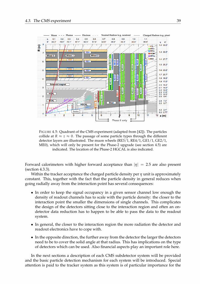
4.3. The CMS experiment 39
Tracker
Muon Photon Electron Neutral Hadron (e.g. neutron) Charged Hadron (e.g. pion)
xx
x
x
x
xx
xxx
x
xxx
x xx
xx
x
xx x
xx
x xxxxx
FIGURE 4.5: Quadrant of the CMS experiment (adapted from [42]). The particlescollide at R ≈ z ≈ 0. The passage of some particle types through the differentdetector layers are illustrated. The muon wheels (RE3/1, RE4/1, GE1/1, GE2/1,ME0), which will only be present for the Phase-2 upgrade (see section 4.5) are
indicated. The location of the Phase-2 HGCAL is also indicated.
Forward calorimeters with higher forward acceptance than |η| = 2.5 are also present(section 4.3.3).
Within the tracker acceptance the charged particle density per η unit is approximatelyconstant. This, together with the fact that the particle density in general reduces whengoing radially away from the interaction point has several consequences:
• In order to keep the signal occupancy in a given sensor channel low enough thedensity of readout channels has to scale with the particle density: the closer to theinteraction point the smaller the dimensions of single channels. This complicatesthe design of the detectors sitting close to the interaction region and often an on-detector data reduction has to happen to be able to pass the data to the readoutsystem.
• In general, the closer to the interaction region the more radiation the detector andreadout electronics have to cope with.
• In the opposite direction, the further away from the detector the larger the detectorsneed to be to cover the solid angle at that radius. This has implications on the typeof detectors which can be used. Also financial aspects play an important role here.
In the next sections a description of each CMS subdetector system will be providedand the basic particle detection mechanism for each system will be introduced. Specialattention is paid to the tracker system as this system is of particular importance for the

40 Chapter 4. The LHC and the CMS Experiment
rest of the work. The system deciding which events to keep for offline storage, the CMStrigger system, will be introduced in section 4.3.5.
4.3.2 The tracker system and track reconstruction
4.3.2.1 The tracker detector system
The tracking system at CMS performs precise reconstruction of charged particle trajecto-ries inside the 3.8 T magnetic field. It does this using silicon sensor technology to performthe particle detection as discussed in section 3.4. The tracker system plays an importantdirect role in electron, muon, hadron, tau, jet and primary vertex reconstruction and con-tributes to vetoes for neutral particles. The CMS tracker is split up in two subdetectors:the pixel and strip tracker.
In the 2016 extended year-end technical stop the first pixel detector, the Phase-0 pixeldetector, was replaced by the Phase-1 pixel detector. This replacement was needed inorder to guarantee an efficient running for the remainder of Run 2 and for Run 3. Withoutthis upgrade significant loss in tracking performance due to radiation damage or due tolimited buffering capabilities in the readout chip were expected. Figure 4.6a and 4.6brespectively show a longitudinal cut of the Phase-0 full tracker system and a quadrant ofboth pixel detectors.
(a)
102mm73mm
43mm355mm 485mm
(b)
FIGURE 4.6: LEFT: CMS Phase-0 pixel and strip tracker geometry [43]. The mod-ules indicated in blue are the stereo-modules. RIGHT: One quarter of the CMSPhase-1 pixel detector. The dashed orange lines represent the Phase-0 geometry
[44].
The Phase-0 pixel detector has 66 million 100 µm × 150 µm and 285 µm thick pixelsspread over 3 barrel layers, at radii of 4.3, 7.3 and 10.2 cm, and 2 endcap disks at bothsides at a longitudinal distance of 35.5 and 48.5 cm from the interaction point. The pixelsare read out using the PSI46 ASIC.
The Phase-1 pixel detector consists of 4 barrel layers and 3 endcap disks at both z sidessumming up to a total of 124 million pixels. Besides the increased hit coverage the Phase-1 pixel detector is also lighter than the Phase-0 pixel detector due to several mechanicalimprovements and relocation of services. The sensor design is identical to the Phase-0sensors, but the readout chip is improved with increased buffer stages and an increasedoutput bandwidth: the PSIDIG chip was used for all layers except for the innermostlayer where an improved high rate version, the PROC600 was used. The operation ofall three chips is similar: each chip is bump bonded to 52×80 pixels, the chip performszero-suppression and the full pulse height information of a hit channel is passed to the

4.3. The CMS experiment 41
readout boards. The main difference between the PSI46 on one hand and the PSIDIGand PROC600 chip on the other hand is that the PSIDIG and PROC600 digitise the pulseheight using an ADC (analogue to digital converter) and send this information out digi-tised whereas an analogue output is used in case of the PSI46 [15]. In both the Phase-0and Phase-1 pixel detector, the modules are oriented to provide the best resolution in therφ bending plane.
The strip tracker consists of a barrel region (TIB and TOB) where the modules are par-allel to the beampipe and endcaps (TIDs and TECs) where the modules are perpendicularto the beampipe. Each line in the strip tracker region in Figure 4.6a represent a detectormodule. The modules are oriented in such a way that the strip direction provides thebest resolution in the rφ plane. An example of such a strip tracker module is shown inFigure 4.7a.
In total, the strip tracker has 9.3 million channels on 320 µm or 500 µm thick siliconsensors with a strip pitch varying from 80 to 184 µm. The layers indicated in blue inFigure 4.6a are instrumented with a second module which is mounted back-to-back toanother module at a stereo angle of 100 mrad. These stereo-modules allow to measure thehit position along the strip direction. The strip sensors are read out by the APV analoguechip [45], each APV receiving the signal of 128 channels.
(a)
y
x
d0
l0P
A
ParticletrajectoryB
(b)
FIGURE 4.7: LEFT: An example of a CMS Phase-0 strip tracker module [46].RIGHT: The definition of the d0 parameter and l0 parameter of a track originat-ing from point A. The point P is the reference point and could for example be thebeamspot or a primary vertex. The point B is the reference point of the track and
is the point of closest approach in xy of the track to P.
4.3.2.2 Charged particle track reconstruction
The combination of pixel and strip information allows for very precise charged particletrack reconstruction, referred to as tracking, which basically boils down to a complexexercise of connecting the hits in several tracker layers. Tracking starts with the recon-struction of hits, followed by generation of seeds, track finding, track fitting and trackselection. These different steps will be discussed briefly below. More information can befound in Ref. [47].
The pixel detector ASIC performs zero-suppression with an adjustable threshold perpixel. In the offline reconstruction, clusters are formed from this zero-suppressed data.
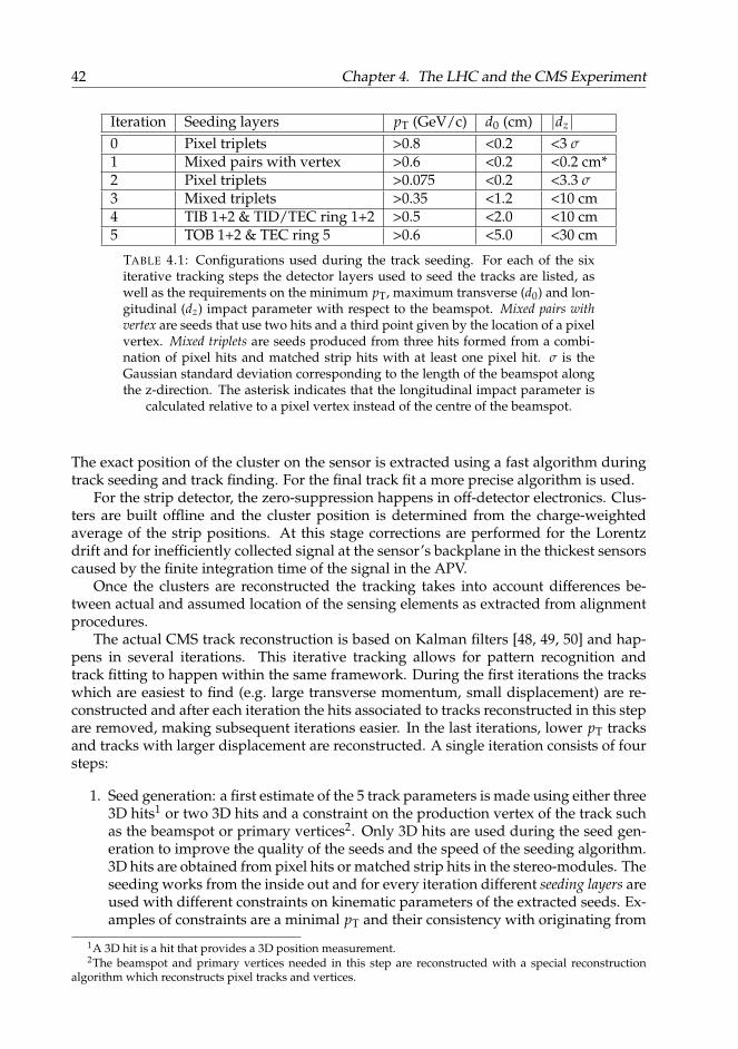
42 Chapter 4. The LHC and the CMS Experiment
Iteration Seeding layers pT (GeV/c) d0 (cm) |dz|0 Pixel triplets >0.8 <0.2 <3 σ1 Mixed pairs with vertex >0.6 <0.2 <0.2 cm*2 Pixel triplets >0.075 <0.2 <3.3 σ3 Mixed triplets >0.35 <1.2 <10 cm4 TIB 1+2 & TID/TEC ring 1+2 >0.5 <2.0 <10 cm5 TOB 1+2 & TEC ring 5 >0.6 <5.0 <30 cm
TABLE 4.1: Configurations used during the track seeding. For each of the sixiterative tracking steps the detector layers used to seed the tracks are listed, aswell as the requirements on the minimum pT, maximum transverse (d0) and lon-gitudinal (dz) impact parameter with respect to the beamspot. Mixed pairs withvertex are seeds that use two hits and a third point given by the location of a pixelvertex. Mixed triplets are seeds produced from three hits formed from a combi-nation of pixel hits and matched strip hits with at least one pixel hit. σ is theGaussian standard deviation corresponding to the length of the beamspot alongthe z-direction. The asterisk indicates that the longitudinal impact parameter is
calculated relative to a pixel vertex instead of the centre of the beamspot.
The exact position of the cluster on the sensor is extracted using a fast algorithm duringtrack seeding and track finding. For the final track fit a more precise algorithm is used.
For the strip detector, the zero-suppression happens in off-detector electronics. Clus-ters are built offline and the cluster position is determined from the charge-weightedaverage of the strip positions. At this stage corrections are performed for the Lorentzdrift and for inefficiently collected signal at the sensor’s backplane in the thickest sensorscaused by the finite integration time of the signal in the APV.
Once the clusters are reconstructed the tracking takes into account differences be-tween actual and assumed location of the sensing elements as extracted from alignmentprocedures.
The actual CMS track reconstruction is based on Kalman filters [48, 49, 50] and hap-pens in several iterations. This iterative tracking allows for pattern recognition andtrack fitting to happen within the same framework. During the first iterations the trackswhich are easiest to find (e.g. large transverse momentum, small displacement) are re-constructed and after each iteration the hits associated to tracks reconstructed in this stepare removed, making subsequent iterations easier. In the last iterations, lower pT tracksand tracks with larger displacement are reconstructed. A single iteration consists of foursteps:
1. Seed generation: a first estimate of the 5 track parameters is made using either three3D hits1 or two 3D hits and a constraint on the production vertex of the track suchas the beamspot or primary vertices2. Only 3D hits are used during the seed gen-eration to improve the quality of the seeds and the speed of the seeding algorithm.3D hits are obtained from pixel hits or matched strip hits in the stereo-modules. Theseeding works from the inside out and for every iteration different seeding layers areused with different constraints on kinematic parameters of the extracted seeds. Ex-amples of constraints are a minimal pT and their consistency with originating from
1A 3D hit is a hit that provides a 3D position measurement.2The beamspot and primary vertices needed in this step are reconstructed with a special reconstruction
algorithm which reconstructs pixel tracks and vertices.
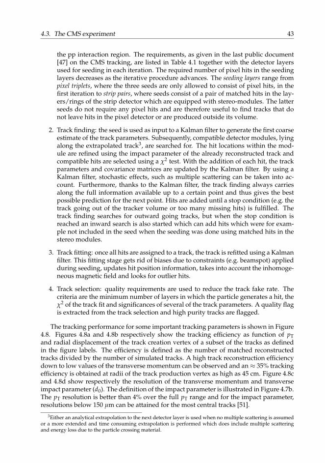
4.3. The CMS experiment 43
the pp interaction region. The requirements, as given in the last public document[47] on the CMS tracking, are listed in Table 4.1 together with the detector layersused for seeding in each iteration. The required number of pixel hits in the seedinglayers decreases as the iterative procedure advances. The seeding layers range frompixel triplets, where the three seeds are only allowed to consist of pixel hits, in thefirst iteration to strip pairs, where seeds consist of a pair of matched hits in the lay-ers/rings of the strip detector which are equipped with stereo-modules. The latterseeds do not require any pixel hits and are therefore useful to find tracks that donot leave hits in the pixel detector or are produced outside its volume.
2. Track finding: the seed is used as input to a Kalman filter to generate the first coarseestimate of the track parameters. Subsequently, compatible detector modules, lyingalong the extrapolated track3, are searched for. The hit locations within the mod-ule are refined using the impact parameter of the already reconstructed track andcompatible hits are selected using a χ2 test. With the addition of each hit, the trackparameters and covariance matrices are updated by the Kalman filter. By using aKalman filter, stochastic effects, such as multiple scattering can be taken into ac-count. Furthermore, thanks to the Kalman filter, the track finding always carriesalong the full information available up to a certain point and thus gives the bestpossible prediction for the next point. Hits are added until a stop condition (e.g. thetrack going out of the tracker volume or too many missing hits) is fulfilled. Thetrack finding searches for outward going tracks, but when the stop condition isreached an inward search is also started which can add hits which were for exam-ple not included in the seed when the seeding was done using matched hits in thestereo modules.
3. Track fitting: once all hits are assigned to a track, the track is refitted using a Kalmanfilter. This fitting stage gets rid of biases due to constraints (e.g. beamspot) appliedduring seeding, updates hit position information, takes into account the inhomoge-neous magnetic field and looks for outlier hits.
4. Track selection: quality requirements are used to reduce the track fake rate. Thecriteria are the minimum number of layers in which the particle generates a hit, theχ2 of the track fit and significances of several of the track parameters. A quality flagis extracted from the track selection and high purity tracks are flagged.
The tracking performance for some important tracking parameters is shown in Figure4.8. Figures 4.8a and 4.8b respectively show the tracking efficiency as function of pTand radial displacement of the track creation vertex of a subset of the tracks as definedin the figure labels. The efficiency is defined as the number of matched reconstructedtracks divided by the number of simulated tracks. A high track reconstruction efficiencydown to low values of the transverse momentum can be observed and an≈ 35% trackingefficiency is obtained at radii of the track production vertex as high as 45 cm. Figure 4.8cand 4.8d show respectively the resolution of the transverse momentum and transverseimpact parameter (d0). The definition of the impact parameter is illustrated in Figure 4.7b.The pT resolution is better than 4% over the full pT range and for the impact parameter,resolutions below 150 µm can be attained for the most central tracks [51].
3Either an analytical extrapolation to the next detector layer is used when no multiple scattering is assumedor a more extended and time consuming extrapolation is performed which does include multiple scatteringand energy loss due to the particle crossing material.
44 Chapter 4. The LHC and the CMS Experiment
(GeV)T
Simulated track p1−10 1 10 210
Tra
ckin
g ef
ficie
ncy
0
0.1
0.2
0.3
0.4
0.5
0.6
0.7
0.8
0.9
1
2016
2017
13 TeVCMS Simulation preliminary
=35)⟩PU⟨ event tracks (tt < 3.5 cm0d| < 2.5, η|
(a) (b)
(GeV)T
Simulated track p1−10 1 10 210
T r
esol
utio
n / p
Tp
0
0.005
0.01
0.015
0.02
0.025
0.03
0.035
0.04
0.045
0.05
2016
2017
13 TeVCMS Simulation preliminary
=35)⟩PU⟨ event tracks (tt
(c) (d)
FIGURE 4.8: TOP: Tracking efficiency versus pT (LEFT) and displacement(RIGHT) for both the 2016 and 2017 configuration of the tracker [51]. BOTTOM:Resolution of the transverse momentum (LEFT) and transverse impact parameter
(RIGHT) for both the 2016 and 2017 configuration of the tracker [51].
4.3.3 The calorimeter systemAs the name suggests the calorimeter system is designed to measure the energy of theparticles. In contrast to the tracking system, which is designed as light as possible notto change the particle’s track the calorimeters need to fully stop the particle inside theirvolume in order to measure the particle’s energy. The CMS calorimeter system consistsof the electromagnetic (ECAL) and hadronic calorimeter (HCAL).
The electromagnetic calorimeter [52] is specifically designed to measure the energy of

4.3. The CMS experiment 45
photons and electrons. The ECAL is build up of 75,948 lead tungstate (PbWO4) crystalswhich are very dense and form a good scintillating material with fast timing characteris-tics and an emission peak at 425 nm which is in a good range for photon detectors. TheECAL is organised in a barrel (EB) and two endcap (EC) sections. The crystals used inthe barrel (endcap) have a length of 23 (22) cm and a frontal surface of ≈ 2.2 × 2.2 cm2
(2.68 × 2.68 cm2), resulting in a ∆η × ∆φ coverage of 0.0175 × 0.0175 in the barrel whilein the endcap it varies from 0.0175 × 0.0175 to 0.05 × 0.05.
The scintillation light is detected by two avalanche photodiodes per crystal in the bar-rel and by one vacuum photo-triode per crystal in the endcaps. Amplified and digitisedpulse information are stored in a pipeline, which sits on a dedicated front-end readoutcard, for 256 bunch crossings awaiting readout triggered by an L1A (Level1-accept) trig-ger (see section 4.3.5). The front-end readout card receives data corresponding to 5×5crystals and performs transverse energy sums at BX (bunch crossing) frequency4. Thesetransverse energy sums are used in the L1 (Level1) trigger system (see section 4.3.5) andin trigger terminology such a detector unit is referred to as a tower.
The hadron calorimeter [53] is also build up of barrel (HB) and two endcap (HE)sections. Most of the HCAL is located inside the magnet, but there is also a part outsidethe magnet (outer HCAL (HO)) to increase the coverage for high energy hadrons and aforward (HCAL forward (HF)) calorimeter (2.9 < η < 4.1) is also present. HB and HEare sampling calorimeters made of brass absorber material interleaved with 17 layers ofscintillator as active material. Each scintillator is read out by a wavelength shifting fibre.The wavelength shifting fibres from HB and HE as well as the ones connected to thescintillators which constitute HO are read out by photodiodes.
HF is build of steel and quartz fibres, with two different lengths, parallel to the beamdirection. The fibres conduct the Cherenkov light, created in their volume by the passageof charged shower particles, out of the HF where the light is read out using PMTs (photomultiplier tube). The ∆η × ∆φ segmentation of HCAL decreases from 0.087 × 0.087to 0.175 × 0.35. The signal from photodiodes or PMTs is integrated and digitised in acustom made chip which sits on the detector.
HCAL also provides input data to the L1 trigger system from which transverse en-ergy sums are calculated. The L1 information from ECAL and HCAL are then combinedbefore input to the Global Trigger system (see section 4.3.5).
4.3.4 The muon systemThe muon system [54] is split up into a barrel and two endcap sections. The systemconsists of three types of detectors: drift tubes (DTs) in the barrel region, cathode stripchambers (CSCs) in the endcap region and resistive plate chambers (RPCs) in both theendcap and the barrel region. The entire muon system has an area of ≈ 25,000 m2. Adetailed view of the configuration is shown in Figure 4.5. CMS uses the fact that muonsare deeply penetrating particles by placing the muon detectors at different stages insidean iron return yoke which guides the magnetic field lines. This return yoke allows CMS todo performant muon reconstruction up to high muon momenta whilst still maintaininga compact design.
All three CMS muon detectors are based on the localised ionisation of a gas volumeinside the detector chamber due to the passage of an ionising particle. The DTs and CSCs
4The term BX will be used in this work not only to refer to an actual crossing of bunches at the LHC, butalso as a unit of time, being the time between bunch crossings.
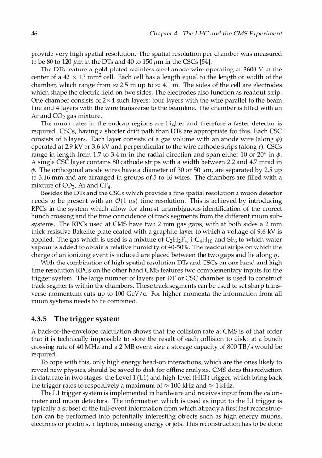
46 Chapter 4. The LHC and the CMS Experiment
provide very high spatial resolution. The spatial resolution per chamber was measuredto be 80 to 120 µm in the DTs and 40 to 150 µm in the CSCs [54].
The DTs feature a gold-plated stainless-steel anode wire operating at 3600 V at thecenter of a 42 × 13 mm2 cell. Each cell has a length equal to the length or width of thechamber, which range from ≈ 2.5 m up to ≈ 4.1 m. The sides of the cell are electrodeswhich shape the electric field on two sides. The electrodes also function as readout strip.One chamber consists of 2×4 such layers: four layers with the wire parallel to the beamline and 4 layers with the wire transverse to the beamline. The chamber is filled with anAr and CO2 gas mixture.
The muon rates in the endcap regions are higher and therefore a faster detector isrequired. CSCs, having a shorter drift path than DTs are appropriate for this. Each CSCconsists of 6 layers. Each layer consists of a gas volume with an anode wire (along φ)operated at 2.9 kV or 3.6 kV and perpendicular to the wire cathode strips (along r). CSCsrange in length from 1.7 to 3.4 m in the radial direction and span either 10 or 20 in φ.A single CSC layer contains 80 cathode strips with a width between 2.2 and 4.7 mrad inφ. The orthogonal anode wires have a diameter of 30 or 50 µm, are separated by 2.5 upto 3.16 mm and are arranged in groups of 5 to 16 wires. The chambers are filled with amixture of CO2, Ar and CF4.
Besides the DTs and the CSCs which provide a fine spatial resolution a muon detectorneeds to be present with an O(1 ns) time resolution. This is achieved by introducingRPCs in the system which allow for almost unambiguous identification of the correctbunch crossing and the time coincidence of track segments from the different muon sub-systems. The RPCs used at CMS have two 2 mm gas gaps, with at both sides a 2 mmthick resistive Bakelite plate coated with a graphite layer to which a voltage of 9.6 kV isapplied. The gas which is used is a mixture of C2H2F4, i-C4H10 and SF6 to which watervapour is added to obtain a relative humidity of 40-50%. The readout strips on which thecharge of an ionizing event is induced are placed between the two gaps and lie along η.
With the combination of high spatial resolution DTs and CSCs on one hand and hightime resolution RPCs on the other hand CMS features two complementary inputs for thetrigger system. The large number of layers per DT or CSC chamber is used to constructtrack segments within the chambers. These track segments can be used to set sharp trans-verse momentum cuts up to 100 GeV/c. For higher momenta the information from allmuon systems needs to be combined.
4.3.5 The trigger systemA back-of-the-envelope calculation shows that the collision rate at CMS is of that orderthat it is technically impossible to store the result of each collision to disk: at a bunchcrossing rate of 40 MHz and a 2 MB event size a storage capacity of 800 TB/s would berequired.
To cope with this, only high energy head-on interactions, which are the ones likely toreveal new physics, should be saved to disk for offline analysis. CMS does this reductionin data rate in two stages: the Level 1 (L1) and high-level (HLT) trigger, which bring backthe trigger rates to respectively a maximum of ≈ 100 kHz and ≈ 1 kHz.
The L1 trigger system is implemented in hardware and receives input from the calori-meter and muon detectors. The information which is used as input to the L1 trigger istypically a subset of the full-event information from which already a first fast reconstruc-tion can be performed into potentially interesting objects such as high energy muons,electrons or photons, τ leptons, missing energy or jets. This reconstruction has to be done
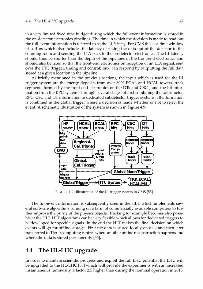
4.4. The HL-LHC upgrade 47
in a very limited fixed time budget during which the full-event information is stored inthe on-detector electronics pipelines. The time in which the decision is made to read outthe full-event information is referred to as the L1 latency. For CMS this is a time windowof ≈ 4 µs which also includes the latency of taking the data out of the detector to thecounting room and sending the L1A back to the on-detector electronics. The L1 latencyshould thus be shorter than the depth of the pipelines in the front-end electronics andshould also be fixed so that the front-end electronics on reception of an L1A signal, sentover the TTC (trigger, timing and control) link, can respond by outputting the full datastored at a given location in the pipeline.
As briefly mentioned in the previous sections, the input which is used for the L1trigger system are the energy deposits from over 8000 ECAL and HCAL towers, tracksegments formed by the front-end electronics on the DTs and CSCs, and the hit infor-mation from the RPC system. Through several stages of first combining the calorimeter,RPC, CSC and DT information in dedicated subdetector trigger systems, all informationis combined in the global trigger where a decision is made whether or not to reject theevent. A schematic illustration of the system is shown in Figure 4.9.
FIGURE 4.9: Illustration of the L1 trigger system in CMS [55].
The full-event information is subsequently used in the HLT, which implements sev-eral software algorithms running on a farm of commercially available computers to fur-ther improve the purity of the physics objects. Tracking for example becomes also possi-ble at the HLT. HLT algorithms can be very flexible which allows for dedicated triggers tobe developed for specific signals. In the end the HLT makes the final decision on whichevents will go for offline storage. First the data is stored locally on disk and then latertransferred to Tier-0 computing centres where another offline reconstruction happens andwhere the data is stored permanently [55].
4.4 The HL-LHC upgrade
In order to maintain scientific progress and exploit the full LHC potential the LHC willbe upgraded to the HL-LHC [38] which will provide the experiments with an increasedinstantaneous luminosity, a factor 2.5 higher than during the nominal operation in 2018.
48 Chapter 4. The LHC and the CMS Experiment
The goal of the HL-LHC is to deliver to the experiments an integrated luminosity of250 fb−1/year, compared to for example the ≈ 68 fb−1 delivered to CMS in 2018. Thiswill be obtained by increasing the pileup, from nominal mean values around 37 forthe 2018 run to values of 150 at the HL-LHC. This will result in a peak luminosity of5×1034 cm−2s−1 and an end of life total integrated luminosity of 3000 fb−1. In the ul-timate performance scenario the HL-LHC could deliver a pileup of 200 resulting in aninstantaneous luminosity of 7-7.5×1034 cm−2s−1 and an integrated luminosity of up to300-350 fb−1 per year which, by the end of life of HL-LHC could result in a total inte-grated luminosity of 4000 fb−1.
All this will be achieved technically by several upgrades. Most of these upgradesare related to making existing systems robust against longer operation in an increasedradiation field, preparing the accelerator optics for higher beam intensities, upgradingcryogenic systems,... Other upgrades are new concepts specifically engineered for theHL-LHC. Two of the latter are listed here:
• In contrast to the LHC, where the instantaneous luminosity continuously dropsduring a run due to the decrease of particle density in the bunches, the HL-LHC willmake use of luminosity levelling where in the first part of the run the luminosity willbe kept constant by changing the focussing of the beam at the interaction points.Like this the maximum workable pileup for the experiments can be maintained fora longer time.
• A new optics scheme will allow for a reduction of the β∗ of the LHC beam. Thisrequires even stronger quadrupole magnets with a larger aperture. In this configu-ration the flattened bunches collide under an angle which would result in a decreasein luminosity simply due to geometrical reasons. Specific radio-frequency cavities,so-called crab cavities, are being designed which use electrical fields to rotate thebunches right before collision, so that their geometrical overlap is maximised rightat the interaction point.
Due to the increase in luminosity the experiments will be more sensitive to rare andstatistically limited Standard Model signals [56]. An example of such a Standard Modelmeasurement is the measurement of the Higgs self coupling which can be probed inevents where Higgs bosons are produced in pairs. This measurement needs high statisticsas the cross section of these events is about a factor of 1000 smaller than for single Higgsboson production. Furthermore the determination of the Higgs boson coupling to muons,τ, b and t quarks and W and Z bosons will also benefit from larger dataset.
Also beyond the standard model searches will reach higher significance with largerdatasets. Due to increased statistics the searches will be able to probe smaller couplingswith increased significance. Furthermore, rare channels with low production cross sec-tion or small branching ratios will become available.
4.5 The CMS Phase-2 upgrade
CMS subdetector upgrades and replacements will be performed in order to guaranteegood quality physics data taking during the HL-LHC phase. Furthermore, several sub-detector systems will be extended and new detectors such as the MIP Timing Detector(MTD) and Gas Electron Multipliers (GEMs) will be installed. Below, the major upgradesto the CMS subdetectors will be described. This upgraded version of CMS is referred toas CMS Phase-2.
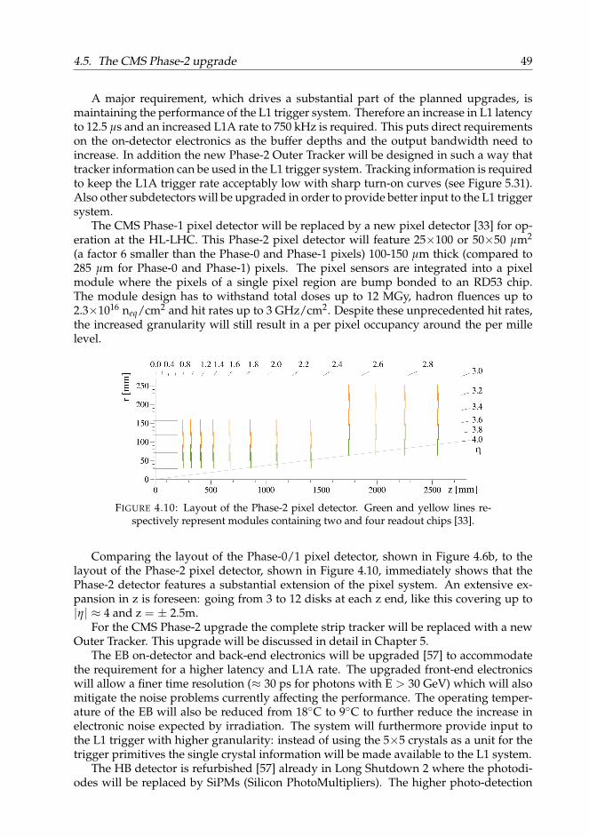
4.5. The CMS Phase-2 upgrade 49
A major requirement, which drives a substantial part of the planned upgrades, ismaintaining the performance of the L1 trigger system. Therefore an increase in L1 latencyto 12.5 µs and an increased L1A rate to 750 kHz is required. This puts direct requirementson the on-detector electronics as the buffer depths and the output bandwidth need toincrease. In addition the new Phase-2 Outer Tracker will be designed in such a way thattracker information can be used in the L1 trigger system. Tracking information is requiredto keep the L1A trigger rate acceptably low with sharp turn-on curves (see Figure 5.31).Also other subdetectors will be upgraded in order to provide better input to the L1 triggersystem.
The CMS Phase-1 pixel detector will be replaced by a new pixel detector [33] for op-eration at the HL-LHC. This Phase-2 pixel detector will feature 25×100 or 50×50 µm2
(a factor 6 smaller than the Phase-0 and Phase-1 pixels) 100-150 µm thick (compared to285 µm for Phase-0 and Phase-1) pixels. The pixel sensors are integrated into a pixelmodule where the pixels of a single pixel region are bump bonded to an RD53 chip.The module design has to withstand total doses up to 12 MGy, hadron fluences up to2.3×1016 neq/cm2 and hit rates up to 3 GHz/cm2. Despite these unprecedented hit rates,the increased granularity will still result in a per pixel occupancy around the per millelevel.
FIGURE 4.10: Layout of the Phase-2 pixel detector. Green and yellow lines re-spectively represent modules containing two and four readout chips [33].
Comparing the layout of the Phase-0/1 pixel detector, shown in Figure 4.6b, to thelayout of the Phase-2 pixel detector, shown in Figure 4.10, immediately shows that thePhase-2 detector features a substantial extension of the pixel system. An extensive ex-pansion in z is foreseen: going from 3 to 12 disks at each z end, like this covering up to|η| ≈ 4 and z = ± 2.5m.
For the CMS Phase-2 upgrade the complete strip tracker will be replaced with a newOuter Tracker. This upgrade will be discussed in detail in Chapter 5.
The EB on-detector and back-end electronics will be upgraded [57] to accommodatethe requirement for a higher latency and L1A rate. The upgraded front-end electronicswill allow a finer time resolution (≈ 30 ps for photons with E > 30 GeV) which will alsomitigate the noise problems currently affecting the performance. The operating temper-ature of the EB will also be reduced from 18C to 9C to further reduce the increase inelectronic noise expected by irradiation. The system will furthermore provide input tothe L1 trigger with higher granularity: instead of using the 5×5 crystals as a unit for thetrigger primitives the single crystal information will be made available to the L1 system.
The HB detector is refurbished [57] already in Long Shutdown 2 where the photodi-odes will be replaced by SiPMs (Silicon PhotoMultipliers). The higher photo-detection

50 Chapter 4. The LHC and the CMS Experiment
FIGURE 4.11: Layout of the HGCAL endcap calorimeter system for the CMSPhase-2 upgrade [58]. Both the electromagnetic (CE-E) and hadronic calorime-ter (CE-H) are shown. The colour codes show the technology used: silicon sen-sors for the innermost part and scintillators for the more outward part. The full
system will be operated at -30C.
efficiency of the SiPMs with respect to the currently used photodiodes will compensatethe loss in scintillator signal due to radiation. Also, to manage the higher rates an up-grade to the back-end electronics will be performed.
A complete replacement of the endcap calorimeter system is foreseen for Phase-2 [58].Both the current EE and the HE will suffer too much radiation damage to provide goodphysics data at HL-LHC with the current detector. Therefore a new calorimeter willbe installed, the so-called HGCAL (high granularity calorimeter). A detailed layout ofthe HGCAL system is shown in Figure 4.11. Hexagonal silicon sensors with a width of163 mm will constitute the active material for the innermost part of the upgraded detec-tor whilst the part of the HGCAL at higher z and smaller |η|, subject to lower radiationlevels, will be equipped with plastic scintillator tiles read out by SiPMs. The longitudinalstructure of the calorimeter is fairly complex and is a stacking of different layers of cool-ing, sampling and readout. In total there will be 28 and 24 longitudinal samplings for theelectromagnetic and the hadronic part respectively. The silicon cell size is 0.5 to 1 cm2
and the plastic scintillators have a segmentation of 4 to 30 cm2. Together with the highresolution timing information (30-40 ps for hadrons with pT > 5 GeV/c) that the silicondetectors bring, a highly segmented calorimeter like this will allow for accurate showerreconstruction, pileup rejection and vertex identification.
The current design of the CMS muon detectors were tested at HL-LHC conditions andwere still found to be adequately functioning, despite the higher hit rates and possibleageing effects. As a result no major replacements of detectors have to happen, but elec-tronics upgrades and extension of the muon system are planned and summarised brieflybelow [59].
The on-detector electronics of the DTs will be replaced by more performant oneswhich will allow higher latency and trigger rates up to 750 kHz. Radiation hardness
4.5. The CMS Phase-2 upgrade 51
of some of the electronic components will be increased. Furthermore, most of the logicwhich generates input for the L1 trigger system will be moved from the on-detector tothe back-end electronics so it becomes easily accessible and more advanced triggeringalgorithms can be implemented.
The CSCs, located in the endcaps, cope with even higher radiation levels than the DTs.Parts of the on-detector electronics will be replaced to make them more radiation hard.Higher speed output optical links will be implemented to handle the higher L1A rate andchamber occupancies and buffer sizes will be increased to allow for larger latencies. Theback-end DAQ (Data AcQuisition) board will also be upgraded to cope with the higherrates.
The RPC system’s off-detector link system, which synchronises and compresses thedata from the on-detector electronics and forwards it to the L1 trigger system, will bereplaced. This upgrade will result in a higher time resolution for input to the L1 trigger.Besides the upgraded electronics, the RPC system will be extended towards higher η(from |η| < 1.8 to |η| < 2.4), which is a challenging region for muon reconstruction due tohigh backgrounds and where until now only CSCs provide information to the L1 trigger.An improved RPC (iRPC) design has been developed using High Pressure Laminate aselectrodes and a smaller gap and electrode thickness compared to the current RPCs. Theon-detector electronics for these iRPCs are also custom tuned to these new chamber’sproperties and allow to read out the strips at both ends which gives access to the timedifference between the hits so that a higher spatial resolution can be attained. In additionto the iRPCs, GEM (Gas Electron Multiplier) detectors will be installed in the forwardregion. The location of the iRPC and GEM chambers is illustrated in Figure 4.5.
A completely new subdetector, the MIP timing detector [60], is also foreseen to beinstalled for the HL-LHC operation. The basic idea behind this detector is to exploit thefact that not all pp interactions during a single BX happen at exactly the same time: thereis a time window with an RMS spread of approximately 180-200 ps wherein the pileupinteractions happen. It is the goal of the MTD to measure timing of hits from MIPs witha time resolution of 30 ps. Like this the beamspot can be sliced in consecutive exposuresof 30 ps, which would bring down the maximum pileup of 200 to values close to the cur-rent mean pileup. This will greatly ease the assignment of tracks and energy deposits tothe correct primary vertex. The upgraded EB and HGCAL also provide timing informa-tion, but do not provide this information for MIPs. The MTD will be implemented as adedicated detector layer in between tracker and calorimeters consisting of a barrel (|η| <1.5) part and two endcap (up to |η| = 3) parts. The barrel layer will be equipped withcrystal scintillators (12×12 mm2) read out by SiPMs whilst LGAD (Low-Gain-Avalanche-Diodes) silicon sensors will be used in the endcaps. The baseline is that the MTD will beread out on reception of an L1A. Full read out of the MTD for use in the L1 trigger is notfeasible due to bandwidth constraints, but it is considered that MTD regions of specialinterest could be pre-triggered by a so-called Level 0 request from the track, calorimeteror muon trigger. In this scheme timing information could be used in a later step of the L1decision.
The event size going to the HLT for the full CMS Phase-2 detector is 7.4 MB [61],compared to 2 MB during Run 2. At a trigger rate of 750 kHz this requires an eventbuilder that can maintain a throughput of 44 Tb/s in order for the HLT to reduce theoffline storage rate from 750 kHz to 7.5 kHz in the end resulting in 5.3 PB of stored dataper day of operation.

52 Chapter 4. The LHC and the CMS Experiment
4.6 Summary
CMS is a general purpose detector located at one of the four interaction points alongthe LHC ring. CMS consists of several subdetector systems, sitting in a magnetic field,which provide an as complete as possible picture of an event. One of these subdetectorsis the tracking system, which is positioned closest to the interaction point and whichis designed to measure the tracks of charged particles. This detector has to be light inorder to reduce multiple scattering. The CMS tracker consists of several layers of siliconmodules, of which the hit information is used by the tracking software to reconstructthe tracks. The subsequent calorimeter and muon system are respectively designed tomeasure the particle’s energy and to reconstruct tracks from high energy muons. Thelatter two subdetectors provide input to the L1 trigger system which decides in a shortand fixed time whether the event is interesting. If the event is considered interesting,the full-event data is requested from the on-detector electronics and used in the HLTsystem which decides if the event is kept for offline storage. This two-level trigger systemreduces the event rate from 40 MHz to ≈ 1 kHz.
To maintain scientific progress, the full LHC potential will be exploited by the HL-LHC upgrade. Several improvements will be made to the accelerator complex whichwill allow LHC to deliver a significantly higher luminosity to the experiments. This hassevere implications on the operation of CMS as it will have to cope with an even harsherradiation environment and higher pileup. A major challenge will be to guarantee sharptrigger turn-on curves so that low enough trigger rates can be maintained.
To assure performant operation of CMS throughout the full HL-LHC running, CMSis preparing to perform several upgrades: on-detector electronics will be improved toallow for a larger L1 latency and trigger rate, subdetector systems will be replaced andeven completely new subdetectors will be installed to help mitigate the harsh pileupconditions. One of the major upgrades is the replacement of the full strip tracker system.This upgrade is the topic of the next chapter.
53
Part II
The Upgraded Outer Tracker forthe CMS Detector at theHigh Luminosity LHC

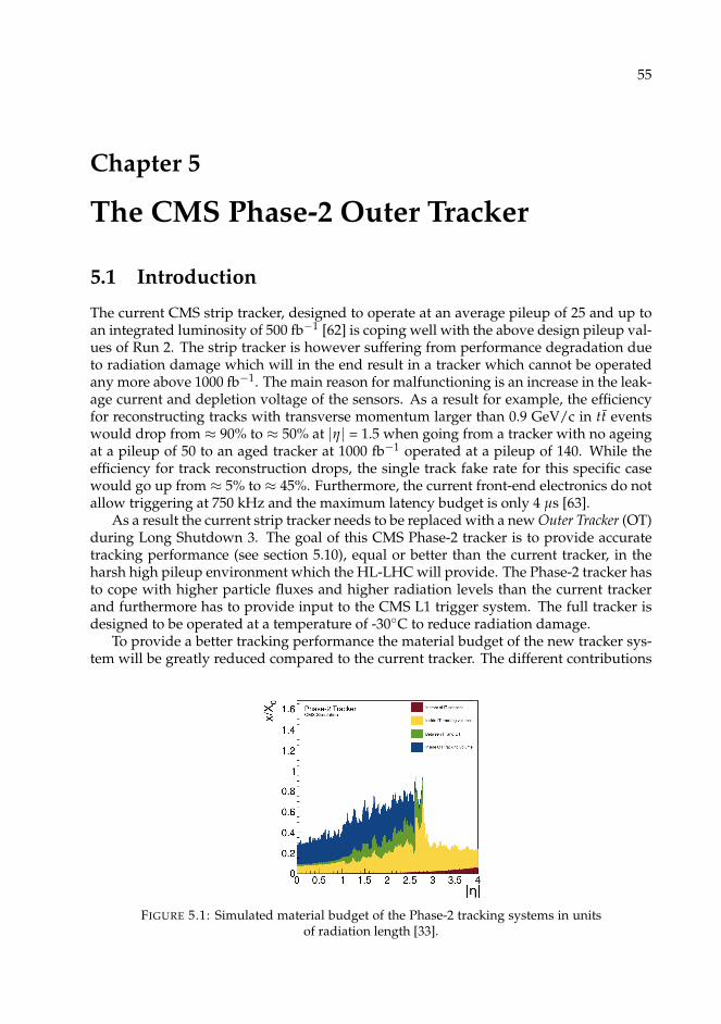
55
Chapter 5
The CMS Phase-2 Outer Tracker
5.1 Introduction
The current CMS strip tracker, designed to operate at an average pileup of 25 and up toan integrated luminosity of 500 fb−1 [62] is coping well with the above design pileup val-ues of Run 2. The strip tracker is however suffering from performance degradation dueto radiation damage which will in the end result in a tracker which cannot be operatedany more above 1000 fb−1. The main reason for malfunctioning is an increase in the leak-age current and depletion voltage of the sensors. As a result for example, the efficiencyfor reconstructing tracks with transverse momentum larger than 0.9 GeV/c in tt eventswould drop from ≈ 90% to ≈ 50% at |η| = 1.5 when going from a tracker with no ageingat a pileup of 50 to an aged tracker at 1000 fb−1 operated at a pileup of 140. While theefficiency for track reconstruction drops, the single track fake rate for this specific casewould go up from ≈ 5% to ≈ 45%. Furthermore, the current front-end electronics do notallow triggering at 750 kHz and the maximum latency budget is only 4 µs [63].
As a result the current strip tracker needs to be replaced with a new Outer Tracker (OT)during Long Shutdown 3. The goal of this CMS Phase-2 tracker is to provide accuratetracking performance (see section 5.10), equal or better than the current tracker, in theharsh high pileup environment which the HL-LHC will provide. The Phase-2 tracker hasto cope with higher particle fluxes and higher radiation levels than the current trackerand furthermore has to provide input to the CMS L1 trigger system. The full tracker isdesigned to be operated at a temperature of -30C to reduce radiation damage.
To provide a better tracking performance the material budget of the new tracker sys-tem will be greatly reduced compared to the current tracker. The different contributions
FIGURE 5.1: Simulated material budget of the Phase-2 tracking systems in unitsof radiation length [33].

56 Chapter 5. The CMS Phase-2 Outer Tracker
(a) (b)
FIGURE 5.2: Expected integrated particle fluence (LEFT) and total integrateddose (RIGHT) for the CMS tracker environment after 3000 fb−1 of pp collisions
at 14 TeV centre of mass energy [33].
to the material budget, extracted from simulation, are shown in function of η in Fig-ure 5.1. Both track reconstruction and calorimeter performance will greatly benefit fromthis reduction in material budget. An important factor in reducing the material budget isthe new geometry of the Outer Tracker, described in section 5.3.
The requirement for tracking information for the L1 trigger requires a unique OTmodule design with on-module transverse momentum measurement capabilities. Theseso-called pT modules will be described in sections 5.2. The pT modules will be able todiscriminate between particles with a pT lower and higher than a given threshold. Thenominal threshold pT is 2 GeV/c and in this baseline configuration only track primitives,so called stubs, from particles passing the 2 GeV/c threshold are passed on to the detectorback-end, at BX frequency, to be used in the L1 track finder. Like this the fact that only 3%of the tracks at 14 TeV pp collisions have a pT larger than 2 GeV/c is exploited to keep theOuter Tracker L1 bandwidth within limits [64]. The full Outer Tracker comprises≈ 200Mchannels which is a substantial increase compared to the ≈ 10M channels in the Phase-0strip tracker.
The expected integrated particle fluence and total integrated dose for the Outer Trackerenvironment at 3000 fb−1 HL-LHC operation are shown in Figure 5.2a and 5.2b respec-tively. The upgraded Outer Tracker is designed to be fully efficient up to 3000 fb−1, witha 50% margin, without the need for maintenance interventions. The radiation levels inthe Outer Tracker volume, going up to 1015 neq/cm2 integrated fluence and 600 kGy in-tegrated dose, form a particular challenge for the operation of the silicon sensors andthe front-end electronics. The sensors and the front-end electronics will be the subject ofsection 5.4 and 5.5 respectively. The on-module electronics will be discussed in detail, asa good understanding of their operation and how they are implemented on the module(section 5.6) is important for the rest of this work.
How the pT modules are planned to be built and qualified is briefly described in sec-tion 5.7. A basic understanding of the assembly procedure and qualification is essentialto frame the work described in later chapters. How the DAQ and the L1 track triggerof the final system will look is introduced in section 5.8 and section 5.9. Some expectedperformance results of the Phase-2 tracker are discussed in section 5.10.
5.2 pT module concept and design
The requirement for an L1 track trigger necessitates a module design with on-moduletrack reconstruction capabilities. This will be accomplished using the pT module design.The basic idea is to use two parallel silicon sensors, separated by a few mm, in one single
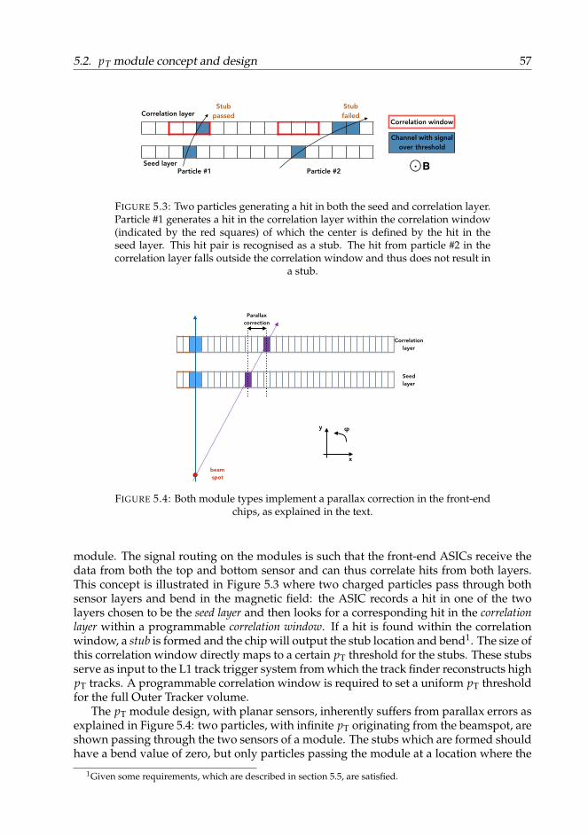
5.2. pT module concept and design 57
. B
Correlation window
Channel with signal over threshold
Correlation layer
Seed layer
Stub passed
Stub failed
Particle #1 Particle #2
FIGURE 5.3: Two particles generating a hit in both the seed and correlation layer.Particle #1 generates a hit in the correlation layer within the correlation window(indicated by the red squares) of which the center is defined by the hit in theseed layer. This hit pair is recognised as a stub. The hit from particle #2 in thecorrelation layer falls outside the correlation window and thus does not result in
a stub.
Correlation layer
beam spot.
y
x
φ
Parallax correction
Seed layer
FIGURE 5.4: Both module types implement a parallax correction in the front-endchips, as explained in the text.
module. The signal routing on the modules is such that the front-end ASICs receive thedata from both the top and bottom sensor and can thus correlate hits from both layers.This concept is illustrated in Figure 5.3 where two charged particles pass through bothsensor layers and bend in the magnetic field: the ASIC records a hit in one of the twolayers chosen to be the seed layer and then looks for a corresponding hit in the correlationlayer within a programmable correlation window. If a hit is found within the correlationwindow, a stub is formed and the chip will output the stub location and bend1. The size ofthis correlation window directly maps to a certain pT threshold for the stubs. These stubsserve as input to the L1 track trigger system from which the track finder reconstructs highpT tracks. A programmable correlation window is required to set a uniform pT thresholdfor the full Outer Tracker volume.
The pT module design, with planar sensors, inherently suffers from parallax errors asexplained in Figure 5.4: two particles, with infinite pT originating from the beamspot, areshown passing through the two sensors of a module. The stubs which are formed shouldhave a bend value of zero, but only particles passing the module at a location where the
1Given some requirements, which are described in section 5.5, are satisfied.
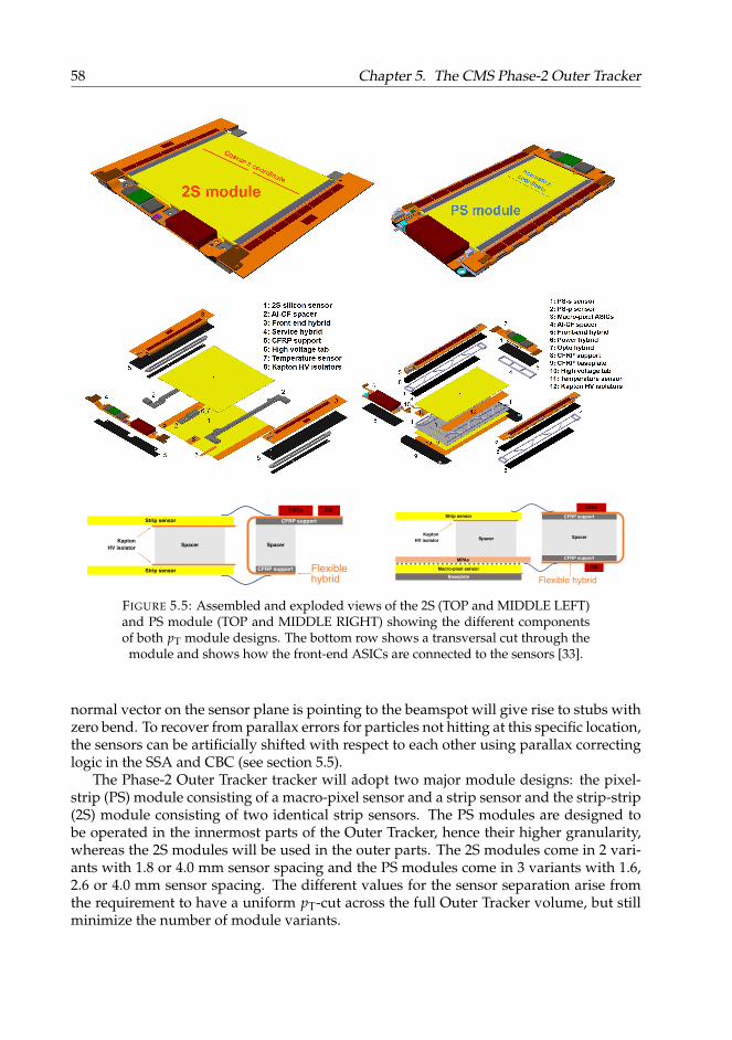
58 Chapter 5. The CMS Phase-2 Outer Tracker
3.1. Overview and layout 29
Table 3.1: Main parameters of the 2S module and the PS module of the CMS tracker.2S module PS module
2 90 cm2 active area 2 45 cm2 active area2 1016 strips: 5 cm 90 µm 2 960 strips: 2.4 cm 100 µm2 1016 strips: 5 cm 90 µm 32 960 macro-pixels: 1.5 mm 100 µm
Front-end power 5 W Front-end power 8 WSensor power (20 C) 1.0 W Sensor power (20 C) 1.4 W
CIC
Spacer
Strip sensor
Strip sensor
Spacer
CFRP support Flexiblehybrid
CBCs
CFRP support
KaptonHV isolator
Spacer
Baseplate Flexible hybrid
MPAs
SSAs
CFRP support
CFRP support
Spacer
CIC
Strip sensor
Macro-pixel sensor
KaptonHV isolator
Figure 3.6: The 2S module (left) and PS module (right) of the Outer Tracker. Shown are viewsof the assembled modules (top), details of the module parts (centre) and sketches of the front-end hybrid folded assembly and connectivity (bottom). Details are given in the text, and in thefollowing sections.
in the line density on the readout hybrid for the 2S module and on the bump density of theC4 technology for the PS module. The strip sensors are wire bonded directly to the front-endhybrids, thus avoiding heavy pitch adapters.
In both modules the desired gap between the two sensors is achieved by gluing them ontospacers made of aluminium / carbon fibre composite (Al-CF). The spacers provide mechanical
FIGURE 5.5: Assembled and exploded views of the 2S (TOP and MIDDLE LEFT)and PS module (TOP and MIDDLE RIGHT) showing the different componentsof both pT module designs. The bottom row shows a transversal cut through the
module and shows how the front-end ASICs are connected to the sensors [33].
normal vector on the sensor plane is pointing to the beamspot will give rise to stubs withzero bend. To recover from parallax errors for particles not hitting at this specific location,the sensors can be artificially shifted with respect to each other using parallax correctinglogic in the SSA and CBC (see section 5.5).
The Phase-2 Outer Tracker tracker will adopt two major module designs: the pixel-strip (PS) module consisting of a macro-pixel sensor and a strip sensor and the strip-strip(2S) module consisting of two identical strip sensors. The PS modules are designed tobe operated in the innermost parts of the Outer Tracker, hence their higher granularity,whereas the 2S modules will be used in the outer parts. The 2S modules come in 2 vari-ants with 1.8 or 4.0 mm sensor spacing and the PS modules come in 3 variants with 1.6,2.6 or 4.0 mm sensor spacing. The different values for the sensor separation arise fromthe requirement to have a uniform pT-cut across the full Outer Tracker volume, but stillminimize the number of module variants.
5.2. pT module concept and design 59
5.2.1 The PS moduleThe PS module is shown on the right in Figure 5.5. It shows the PS-pixel (PS-p) sensorand the PS-strip (PS-s) sensor. Both sensors have an active area of ≈ 5 × 10 cm2. The32× 960 macro-pixels of the PS-p sensor are bump bonded to a total of 2× 8 Macro PixelASICs (MPA2) together forming a so-called Macro Pixel Sub Assembly (MaPSA). Eachmacro-pixel has a size of 1.5 mm × 100 µm.
The 2 × 960 2.5 cm long PS-s strips are wire bonded to 2 × 8 Short Strip ASICs (SSA)which sit alongside both sides of the sensor on the front-end hybrids (FEH) together withthe CIC (Concentrator Integrated Circuit) chips. The strip pitch of 100 µm matches thewidth of the macro pixels. The neighbouring SSA chips on a hybrid are interconnectedin order to pass hit data from one chip to the other, thus making the sensor continuousfor stub finding.
Spacing of the sensor is done with Al-CF spacers with a thin kapton layer on bothsides to which the sensors are glued. Different spacer thicknesses will be used for thedifferent sensor separations and the thickness of the FEHs will be matched accordingly.
How the interconnection of chips is achieved in the module is shown in the transver-sal cut at the bottom of Figure 5.5: the SSA, receiving the sensor signal over wire bonds,sends data to the MPA chip over the hybrid and wire bonds. The MPA receives the sig-nals from the pixels, forms the stubs by correlating them with the SSA clusters, formatsthe full-event data package and sends the data over another set of wire bonds to the CICchip. The full module data path will be discussed in section 5.6.
Both front-end hybrids are connected to two additional hybrids. One hybrid, thepower hybrid, carries a DCDC converter providing the correct LV (low voltage) power lev-els for the front-end ASICs and also facilitates the HV (high voltage) connection. Theother hybrid, the opto hybrid, carries the lpGBT (low-power GigaBit Transceiver) andVTRx+ (Versatile Link Plus) chip for serialisation and conversion from the electrical tothe optical domain.
The cooling of this module will be done using a cooled baseplate to which the moduleis glued.
5.2.2 The 2S moduleThe 2S modules, shown on the left in Figure 5.5, consist of two identical strip sensors(10 × 10 cm2) with 2 × 10¹⁶ 5 cm long strips on each sensor. The strips, with a pitchof 90 µm, are wire bonded to the CBCs (CMS Binary Chips) which sit on two front-endhybrids along the sensor. In total 16 CBC chips, 8 on each FEH, are used to read outthe full 2S sensor. Each CBC chip receives data from 127 top and bottom channels bypassing the signal over the flexible hybrid as illustrated at the bottom left in Figure 5.5.The CBCs also receive data from their neighbours in order to make the module uniformfor stub finding. The CBC data is then sent to the CIC chip which sends the data to theservice hybrid (SEH), which carries all the components for LV and HV powering and datatreatment. The components (DCDC converter, lpGBT, VTRx+) on this service hybrid arethe same as used in the PS module.
As in the design of the PS module, the sensors are separated using an Al-CF spacerwith kapton isolator. Different spacer thicknesses will be used for the different sensorseparations and the thickness of the FEHs will be matched accordingly.
2The front-end chips of both PS and 2S modules are discussed in more detail in section 5.5.

60 Chapter 5. The CMS Phase-2 Outer Tracker
FIGURE 5.6: Layout of one quarter of the Phase-2 Outer Tracker. The blue andred lines represent respectively the PS and 2S modules [33].
The cooling of this module is obtained through five mounting points at the sides ofthe sensor spacers.
5.3 Outer Tracker geometry
How the 7680 2S and 5616 PS modules are arranged to form the Outer Tracker is illus-trated with a cross section view in Figure 5.6. The Outer Tracker consists of a barrel regionand two endcaps. Three distinct parts are defined:
• TBPS: the barrel region equipped with 3 layers of PS modules. A tilted modulegeometry is used for modules at larger z. The tilting of the modules reduces thetotal number of modules required for the Outer Tracker and also eliminates stubinefficiencies introduced by particles which pass module or sensor edges.
• TB2S: the barrel region equipped with 3 layers of 2S modules.
• TEDD: the endcap regions consisting of 5 double discs carrying both PS and 2Smodules.
The different modules, with different sensor spacings, will be distributed across the OuterTracker as shown in Figure 5.7. The correlation window configuration resulting in auniform pT cut of 2 GeV/c is also illustrated in this figure.
In both the barrel and endcap regions the layout was carefully designed to mitigatedead areas by letting modules overlap by slightly staggering them on different surfaceswithin the layer. This guarantees hermetic coverage of each layer. The modules are ar-ranged in plank (TBPS) and ladder (TB2S) structures parallel to the beam as shown inFigure 5.8a. The orientation of the strips and macro-pixels are also illustrated in this fig-ure. In the endcaps, illustrated in Figure 5.8b, the modules are arranged in double discswhere each disk has modules on both sides.
5.4 Silicon sensors
After an extensive R&D [65] project, n-in-p sensors were found to be more radiation hardthan p-in-n sensors. As a result, n-in-p sensors, with electron readout, and a thickness of320 µm will be used to equip the pT modules. P-spray and p-stop structures will ensuresufficient inter-strip isolation [65].
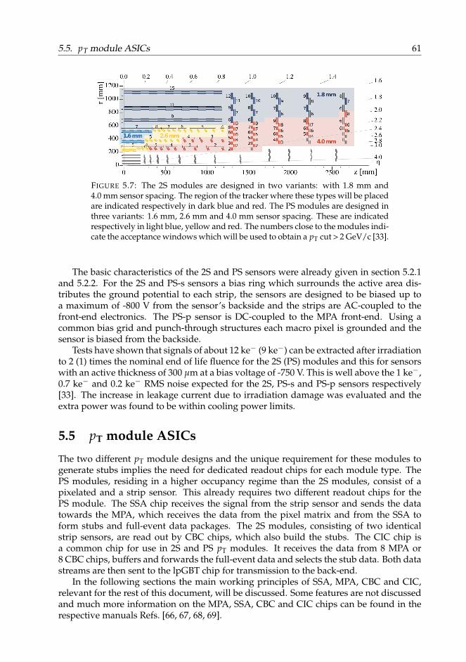
5.5. pT module ASICs 61
FIGURE 5.7: The 2S modules are designed in two variants: with 1.8 mm and4.0 mm sensor spacing. The region of the tracker where these types will be placedare indicated respectively in dark blue and red. The PS modules are designed inthree variants: 1.6 mm, 2.6 mm and 4.0 mm sensor spacing. These are indicatedrespectively in light blue, yellow and red. The numbers close to the modules indi-cate the acceptance windows which will be used to obtain a pT cut > 2 GeV/c [33].
The basic characteristics of the 2S and PS sensors were already given in section 5.2.1and 5.2.2. For the 2S and PS-s sensors a bias ring which surrounds the active area dis-tributes the ground potential to each strip, the sensors are designed to be biased up toa maximum of -800 V from the sensor’s backside and the strips are AC-coupled to thefront-end electronics. The PS-p sensor is DC-coupled to the MPA front-end. Using acommon bias grid and punch-through structures each macro pixel is grounded and thesensor is biased from the backside.
Tests have shown that signals of about 12 ke− (9 ke−) can be extracted after irradiationto 2 (1) times the nominal end of life fluence for the 2S (PS) modules and this for sensorswith an active thickness of 300 µm at a bias voltage of -750 V. This is well above the 1 ke−,0.7 ke− and 0.2 ke− RMS noise expected for the 2S, PS-s and PS-p sensors respectively[33]. The increase in leakage current due to irradiation damage was evaluated and theextra power was found to be within cooling power limits.
5.5 pT module ASICs
The two different pT module designs and the unique requirement for these modules togenerate stubs implies the need for dedicated readout chips for each module type. ThePS modules, residing in a higher occupancy regime than the 2S modules, consist of apixelated and a strip sensor. This already requires two different readout chips for thePS module. The SSA chip receives the signal from the strip sensor and sends the datatowards the MPA, which receives the data from the pixel matrix and from the SSA toform stubs and full-event data packages. The 2S modules, consisting of two identicalstrip sensors, are read out by CBC chips, which also build the stubs. The CIC chip isa common chip for use in 2S and PS pT modules. It receives the data from 8 MPA or8 CBC chips, buffers and forwards the full-event data and selects the stub data. Both datastreams are then sent to the lpGBT chip for transmission to the back-end.
In the following sections the main working principles of SSA, MPA, CBC and CIC,relevant for the rest of this document, will be discussed. Some features are not discussedand much more information on the MPA, SSA, CBC and CIC chips can be found in therespective manuals Refs. [66, 67, 68, 69].
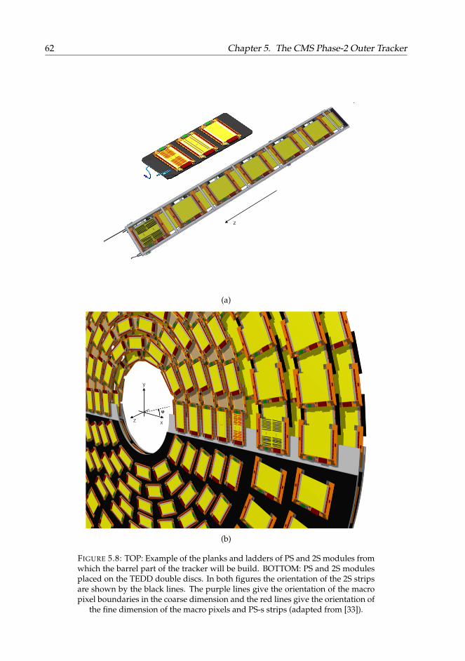
62 Chapter 5. The CMS Phase-2 Outer Tracker
……
…
…
…
z
(a)
x
y
zφ
…
… …
… …
(b)
FIGURE 5.8: TOP: Example of the planks and ladders of PS and 2S modules fromwhich the barrel part of the tracker will be build. BOTTOM: PS and 2S modulesplaced on the TEDD double discs. In both figures the orientation of the 2S stripsare shown by the black lines. The purple lines give the orientation of the macropixel boundaries in the coarse dimension and the red lines give the orientation of
the fine dimension of the macro pixels and PS-s strips (adapted from [33]).
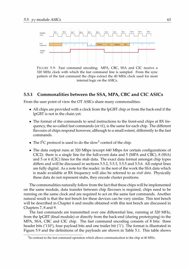
5.5. pT module ASICs 63
Bit 7 Bit 6 Bit 5 Bit 4 Bit 3 Bit 2 Bit 1 Bit 0 Bit 7 Bit 6Bit 0Bit 1320MHzclock
Fastcommand
40MHzclock
1 1 1 1 1 10 ReSync L1A CalPulse BC0
FIGURE 5.9: Fast command encoding: MPA, CBC, SSA and CIC receive a320 MHz clock with which the fast command line is sampled. From the syncpattern of the fast command the chips extract the 40 MHz clock used for most
internal logic on the ASICs.
5.5.1 Commonalities between the SSA, MPA, CBC and CIC ASICsFrom the user point of view the OT ASICs share many commonalities:
• All chips are provided with a clock from the lpGBT chip or from the back-end if thelpGBT is not in the chain yet.
• The format of the commands to send instructions to the front-end chips at BX fre-quency, the so-called fast commands (or t1), is the same for each chip. The differentflavours of chips respond however, although to a small extent, differently to the fastcommands.
• The I2C protocol is used to do the slow3 control of the chip.
• The data output runs at 320 Mbps (except 640 Mbps for certain configurations ofCIC2): there is a single line for the full-event data and 5 (MPA and CBC), 8 (SSA)and 5 or 6 (CIC) lines for the stub data. The exact data format amongst chip typesdiffers and will be discussed in sections 5.5.2, 5.5.3, 5.5.5 and 5.5.6. All output linesare fully digital. As a note for the reader: in the rest of the work the SSA data whichis made available at BX frequency will also be referred to as stub data. Physicallythese data do not represent stubs, they encode cluster positions.
The commonalities naturally follow from the fact that these chips will be implementedon the same module, data transfer between chip flavours is required, chips need to berunning on the same clock and are required to act on the same fast commands. Anothernatural result is that the test bench for these devices can be very similar. This test benchwill be described in Chapter 6 and results obtained with this test bench are discussed inChapters 7, 8 and 9.
The fast commands are transmitted over one differential line, running at 320 MHz,from the lpGBT (final module) or directly from the back-end (during prototyping) to theMPA, SSA, CBC and CIC chip. The fast command encoding consists of 8 bits: threeheader bits (’110’), four payload bits and one trailer bit (’1’). The format is illustrated inFigure 5.9 and the definitions of the payloads are shown in Table 5.1. This table shows
3In contrast to the fast command operation which allows communication to the chip at 40 MHz.
64 Chapter 5. The CMS Phase-2 Outer Tracker
Fast command(t1)
Bit 7(MSB) Bit 6 Bit 5 Bit 4 Bit 3 Bit 2 Bit 1 Bit 0
(LSB)ReSync (Fast Reset) 1 1 0 1 0 0 0 1
L1A Trigger 1 1 0 0 1 0 0 1Test Pulse Trigger (CalPulse) 1 1 0 0 0 1 0 1
BC0 (Orbit Reset) 1 1 0 0 0 0 1 1BC0 & ReSync 1 1 0 1 0 0 1 1
BC0 & L1A Trigger 1 1 0 0 1 0 1 1BC0 & Test Pulse Trigger 1 1 0 0 0 1 1 1
TABLE 5.1: Definitions of the fast command. The header and trailer are indicatedin blue. All seven allowed fast command payloads are shown. The table also
states some commonly used other terminology for the fast commands (t1).
all the allowed combinations of fast commands which can be sent to the chips. The ac-tion taken by each chip on reception of a fast command can be slightly different4, but ingeneral the purpose of the fast commands is as follows:
• ReSync: resets the FIFOs and the state machines, and except for the CBC the bunchcrossing counter and the L1 counter are also reset.
• L1A trigger (or L1A): the SSA, MPA and CBC chip will respond by outputting thefull-event data present at a certain location, corresponding to the latency setting, inthe memory to the output FIFO.
• CalPulse: triggers the discharge of the test pulse capacitor in the chip’s front-end.This feature is not relevant for the CIC. For the MPA and SSA there is also thepossibility to inject data into the digital logic.
• BC0: resets the bunch crossing counter and the L1 counter, except for the CBCwhere only the L1 counter is reset.
From the header of the fast command the chips also extract the 40 MHz clock, as shownin Figure 5.9, which is used for most internal chip logic.
The I2C is implemented according to the Philips Semiconductors I2C v2.1 specifica-tions with a general call address within a chip family and a maximal I2C clock frequencyof 1 MHz. In the final module there will be two I2C buses, one for each hybrid. ThelpGBT chip will be the master of both buses. One bus connects to 8 MPAs, 8 SSAs and1 CIC chip in the PS case and 8 CBCs and 1 CIC in the 2S case. Each chip on the bus has aspecific address which allows to address the chips separately. The I2C protocol is a widespread protocol and will therefore not be discussed in detail here. The full slow controlspecifications for the OT module ASICs can be found in Ref. [70]. One thing to note how-ever is that the MPA, SSA and CIC implement 16-bit register addressing whereas the CBCimplements 8-bit register addressing. The CBC makes use of a paging system to cope withthe large amount of registers.
The CBC chip is implemented in 130 nm CMOS technology. The MPA, SSA and CIC1are implemented in 65 nm CMOS technology. The CBC operates at a nominal voltage of1.2 V. The MPA and SSA chip will be operated at 1 V for the digital power supply and1.2 V for the analogue and the I/O (Input/Output). The CIC will operate at two digital
4For the MPA and SSA the interpretation of the fast commands also depends on the mode (synchronous orasynchronous) the chip is configured in (see section 5.5). The L1A marks the start of the counting for the ripplecounters, whereas the BC0 marks the end. The sending of a BC0 together with a ReSync starts the read out ofthe counters, the combination of a BC0 and L1A resets all the counters.

5.5. pT module ASICs 65
voltages: 1 V in the PS mode and 1.2 V in the 2S mode. The I/O of the CIC is poweredwith 1.2 V in both cases.
The data pads with which the back-end interfaces are all according to the differentialSLVS (Scalable Low-Voltage Signaling) standards. Also the clock and fast command lineare implemented as differential SLVS. The I2C and hard reset pad are implemented inCMOS standard. Of course there are many more pads on the chips and the full specifica-tion list can be found in the chip manuals.
5.5.2 The SSA chip
5.5.2.1 Introduction
Each SSA chip [67] is designed to: read out 120 strips of a PS-s sensor using a specificallydesigned front-end, digitize the sensor signal, provide full-event data on reception of atrigger and synchronous centroid data at 40 MHz to the MPA chip. In section 5.5.2.2 thefront-end of the SSA chip will briefly be introduced. In section 5.5.2.3 the transition to thedigital domain is explained and the digital part is then discussed in sections 5.5.2.4 and5.5.2.5. Figure 5.10 shows the top-level architecture of the SSA chip.
SSA specification document V1.0
5
Figure 2.1. SSA top level architecture
The encoded coordinates of the hit clusters are sent at the 40 MHz bunch crossing (BX) rate, with a bandwidth of 2.560 Gbps. In the L1 data path, the complete raw sensor image is internally stored and transmitted only when requested by Level-1 trigger system. The internal memory and FIFOs are de-signed to support trigger rates up to 1MHz. For testing and calibration purposes, a 8-bits ripple coun-ter connects to the discriminator of each channel and can be serially readout when the ASIC is set in calibration mode. Configuration registers accessible via a slow-control serial interface, allow to define the operating modes and calibrate front-end parameters like the values for threshold equalization. Figure 2.1 summarise the SSA ASIC architecture.
FIGURE 5.10: Top-level architecture of the SSA chip [67].
5.5.2.2 SSA front-end
120 separate front-ends are present in the SSA and are AC-coupled to one of the 120 PS-ssensor strips. Each front-end consists of a pre-amplifier, a booster and two discriminatorstages. Two discriminator stages are present to provide the possibility to set a HIP thresh-old next to the detection threshold. A 5-bit trimming DAC (digital to analogue converter)is present to compensate for the channel-to-channel discriminator offset. Each channelinput is connected to a 52 fF calibration capacitor. The amplitude of the calibration pulsegenerated by this circuit can be controlled by an 8-bit DAC. An edge sensitive circuitforms the transition to the digital logic of the chip and is described in the next section.

66 Chapter 5. The CMS Phase-2 Outer Tracker
Analogue pulse
Shaper Output
Discriminator Output
Threshold
Edge Sensitive readout
Level Sensitive readout
40MHz rising sampling clock edges
40MHz falling sampling clock edges
Input to ripple counter
FIGURE 5.11: Illustration of the sampling logic of the SSA and MPA.
5.5.2.3 SSA sampling logic
The SSA uses a clock signal, the so-called sampling clock, to sample the incoming signal.The phase of the sampling clock with respect to the chip’s 40 MHz internal clock can beconfigured over the full 25 ns range with a resolution of 200 ps using an internal DLL(delay-locked loop) and a coarse shift, based on the 320 MHz clock.
The discriminator output is then sampled in three different ways, as illustrated inFigure 5.11:
• Ripple counter: this asynchronous counter counts the number of pulses from thecomparator stage during a user controlled window. A counter is present for eachchannel. This mode is especially useful for calibration purposes. These 15-bit coun-ters can be accessed over I2C or the SSA can be configured to output them on thestub data lines. In the latter case the 8 LSBs (Least Significant Bits) are transmittedon the first stub data line whilst the 7 MSBs (Most Significant Bits) are transmittedon the second stub data line. The counters are transmitted every 8th BX.
• Edge sensitive: in this mode comparator transitions which are non synchronouswith the sampling clock are registered which guarantees no blind cycles. In thismode the output pulse has a fixed length of 1 BX.
• Level sensitive: the signal is sampled at the rising edge of the sampling clock. Incase the discriminator output is longer than a single acquisition clock cycle theoutput of this sampling stage will also last multiple clock cycles. The maximumduration can however be configured and the output is forced to zero after the setmaximum number of clock cycles.
The two latter modes or a logic OR or XOR of the two is used to feed into the digitallogic (see section 5.5.2.4 and 5.5.2.5) and signifies the time of arrival of the analogue pulsewith respect to the acquisition clock. The sampling setting is configurable for each front-end, but usually all front-ends are configured in the same mode. The masking of channelsis also implemented at this level: a switch per channel is implemented to disconnect thefront-end from the sampling logic.
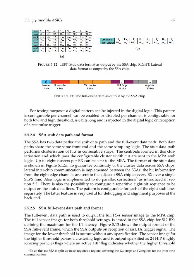
5.5. pT module ASICs 67
(a)
(b)
FIGURE 5.12: LEFT: Stub data format as output by the SSA chip. RIGHT: Lateraldata format as output by the SSA chip.
FIGURE 5.13: The full-event data as output by the SSA chip.
For testing purposes a digital pattern can be injected in the digital logic. This patternis configurable per channel, can be enabled or disabled per channel, is configurable forboth low and high threshold, is 8 bits long and is injected in the digital logic on receptionof a test pulse trigger.
5.5.2.4 SSA stub data path and format
The SSA has two data paths: the stub data path and the full-event data path. Both datapaths share the same same front-end and the same sampling logic. The stub data pathperforms clusterisation of hits in consecutive strips. The centroids formed in this clus-terisation and which pass the configurable cluster width cut are sent to the MPA stublogic. Up to eight clusters per BX can be sent to the MPA. The format of the stub datais shown in Figure 5.12a. To guarantee continuity of the cluster data across SSA chips,lateral inter-chip communication is implemented between the SSAs: the hit informationfrom the eight edge channels are sent to the adjacent SSA chip at every BX over a singleSLVS line. Also logic is implemented to do parallax corrections5 as introduced in sec-tion 5.2. There is also the possibility to configure a repetitive eight-bit sequence to beoutput on the stub data lines. The pattern is configurable for each of the eight stub linesseparately. The latter feature is very useful for debugging and alignment purposes at theback-end.
5.5.2.5 SSA full-event data path and format
The full-event data path is used to output the full PS-s sensor image to the MPA chip.The full sensor image, for both threshold settings, is stored in the SSA chip for 512 BXsdefining the maximum for the L1 latency. Figure 5.13 shows the output format of theSSA full-event frame, which the SSA outputs on reception of an L1A trigger signal. Theimage for the lower threshold is output without any sparsification. The sensor image forthe higher threshold passes a clustering logic and is output sparsified as 24 HIP (highlyionizing particle) flags where an active HIP flag indicates whether the higher threshold
5To do this the SSA is split up in six regions: 4 regions covering the 120 strips and 2 regions for the inter-stripcommunication.

68 Chapter 5. The CMS Phase-2 Outer Tracker
FIGURE 5.14: The dimensions of the MPA chip and the pixel array [66]. Thecoordinate system shown here is not the one used in CMS and is included here
for later reference in section 8.5.
was passed for at least one strip within the cluster. It takes 18 bunch crossings to out-put the full-event data package. 16 consecutive triggers can however be sent thanks tothe presence of a FIFO which can store up to 16 full-event packages. The minimal timebetween the end of the package end the start of the next package is 2 clock cycles.
5.5.3 The MPA chip
5.5.3.1 Introduction
The MPA chip [66] is designed to read out 1888 (118×16) macro-pixels from a PS-p sensor.The layout of a single MPA chip is shown in Figure 5.14 which shows the dimensions ofthe chip and macro-pixel matrix. The signal from the pixels is processed by the MPA’scustom designed front-ends and digitised in the MPA’s sampling logic.
Besides the input from the pixel matrix, the MPA receives input data from the SSAchip. On reception of a trigger, the MPA outputs the sparsified full-event data from thepixel matrix and the sparsified full-event data from the SSA. Besides this asynchronousfull-event data stream, the MPA chip also provides stub information at BX rate. Stubs areformed in the dedicated MPA stub logic by correlating clusters in the pixel matrix withthe centroid data received from the SSA.
In section 5.5.3.2, the front-end of the MPA chip will briefly be introduced. In section5.5.3.3 the transition to the digital logic is discussed. The digital logic is then described insections 5.5.3.4 and 5.5.3.5. Figure 5.15 shows the top-level architecture of the MPA chip.
5.5.3.2 MPA front-end
Each macro-pixel has its own front-end and is DC-coupled to it. Compared to the SSA,the MPA front-end has an extra stage at the start which provides leakage current compen-sation up to 200 nA for the macro-pixels. The remainder of the front-end acts as an ampli-fier, integrator and threshold stage. The common threshold is set using an 8-bit thresholdDAC, whilst a second trimming DAC, present for each front-end, is used to equalize the
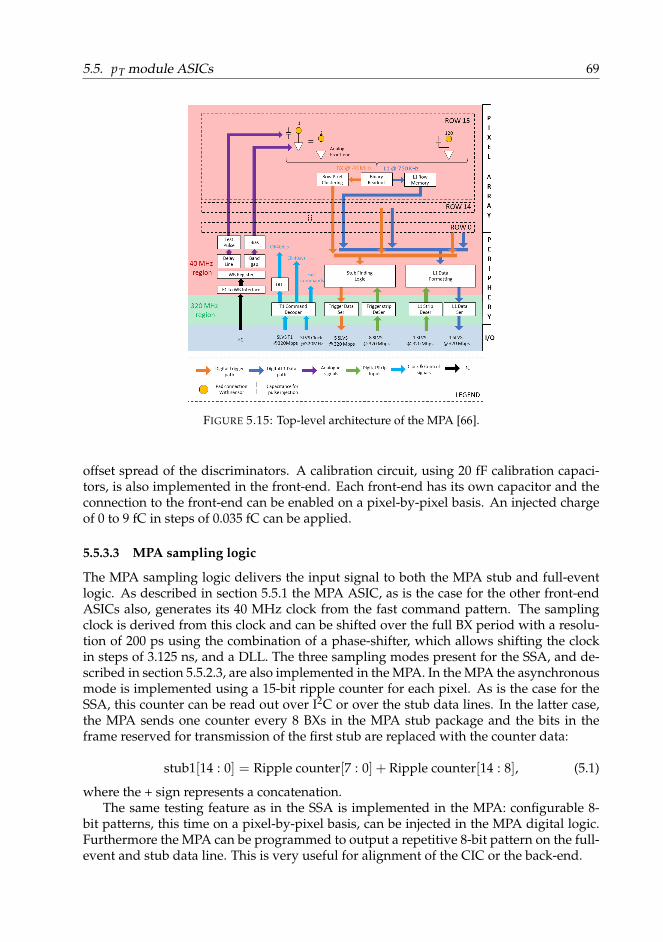
5.5. pT module ASICs 69MPA User Manual V 0.1
5 | P a g e
3 OVERVIEW AND ORGANIZATION
The MPA design implements the top-level architecture shown in Figure 1:
Figure 1 Top Level Architecture
The MPA is the pixel readout ASIC for the hybrid Pixel-Strip module of the Phase-II CMS Outer Tracker upgrade at the High Luminosity LHC (HL-LHC). It employs a novel technique for identifying high transverse momentum particles and provides this information at a 40 MHz rate to the L1-trigger system. The chip also comprises a binary pipeline buffer for the L1-trigger latency, and a data path to support the readout of full events with a maximum trigger rate of 1 MHz and a latency of 12.8 us.
FIGURE 5.15: Top-level architecture of the MPA [66].
offset spread of the discriminators. A calibration circuit, using 20 fF calibration capaci-tors, is also implemented in the front-end. Each front-end has its own capacitor and theconnection to the front-end can be enabled on a pixel-by-pixel basis. An injected chargeof 0 to 9 fC in steps of 0.035 fC can be applied.
5.5.3.3 MPA sampling logic
The MPA sampling logic delivers the input signal to both the MPA stub and full-eventlogic. As described in section 5.5.1 the MPA ASIC, as is the case for the other front-endASICs also, generates its 40 MHz clock from the fast command pattern. The samplingclock is derived from this clock and can be shifted over the full BX period with a resolu-tion of 200 ps using the combination of a phase-shifter, which allows shifting the clockin steps of 3.125 ns, and a DLL. The three sampling modes present for the SSA, and de-scribed in section 5.5.2.3, are also implemented in the MPA. In the MPA the asynchronousmode is implemented using a 15-bit ripple counter for each pixel. As is the case for theSSA, this counter can be read out over I2C or over the stub data lines. In the latter case,the MPA sends one counter every 8 BXs in the MPA stub package and the bits in theframe reserved for transmission of the first stub are replaced with the counter data:
stub1[14 : 0] = Ripple counter[7 : 0] + Ripple counter[14 : 8], (5.1)
where the + sign represents a concatenation.The same testing feature as in the SSA is implemented in the MPA: configurable 8-
bit patterns, this time on a pixel-by-pixel basis, can be injected in the MPA digital logic.Furthermore the MPA can be programmed to output a repetitive 8-bit pattern on the full-event and stub data line. This is very useful for alignment of the CIC or the back-end.
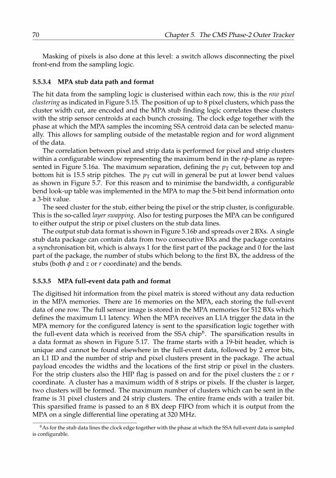
70 Chapter 5. The CMS Phase-2 Outer Tracker
Masking of pixels is also done at this level: a switch allows disconnecting the pixelfront-end from the sampling logic.
5.5.3.4 MPA stub data path and format
The hit data from the sampling logic is clusterised within each row, this is the row pixelclustering as indicated in Figure 5.15. The position of up to 8 pixel clusters, which pass thecluster width cut, are encoded and the MPA stub finding logic correlates these clusterswith the strip sensor centroids at each bunch crossing. The clock edge together with thephase at which the MPA samples the incoming SSA centroid data can be selected manu-ally. This allows for sampling outside of the metastable region and for word alignmentof the data.
The correlation between pixel and strip data is performed for pixel and strip clusterswithin a configurable window representing the maximum bend in the rφ-plane as repre-sented in Figure 5.16a. The maximum separation, defining the pT cut, between top andbottom hit is 15.5 strip pitches. The pT cut will in general be put at lower bend valuesas shown in Figure 5.7. For this reason and to minimise the bandwidth, a configurablebend look-up table was implemented in the MPA to map the 5-bit bend information ontoa 3-bit value.
The seed cluster for the stub, either being the pixel or the strip cluster, is configurable.This is the so-called layer swapping. Also for testing purposes the MPA can be configuredto either output the strip or pixel clusters on the stub data lines.
The output stub data format is shown in Figure 5.16b and spreads over 2 BXs. A singlestub data package can contain data from two consecutive BXs and the package containsa synchronisation bit, which is always 1 for the first part of the package and 0 for the lastpart of the package, the number of stubs which belong to the first BX, the address of thestubs (both φ and z or r coordinate) and the bends.
5.5.3.5 MPA full-event data path and format
The digitised hit information from the pixel matrix is stored without any data reductionin the MPA memories. There are 16 memories on the MPA, each storing the full-eventdata of one row. The full sensor image is stored in the MPA memories for 512 BXs whichdefines the maximum L1 latency. When the MPA receives an L1A trigger the data in theMPA memory for the configured latency is sent to the sparsification logic together withthe full-event data which is received from the SSA chip6. The sparsification results ina data format as shown in Figure 5.17. The frame starts with a 19-bit header, which isunique and cannot be found elsewhere in the full-event data, followed by 2 error bits,an L1 ID and the number of strip and pixel clusters present in the package. The actualpayload encodes the widths and the locations of the first strip or pixel in the clusters.For the strip clusters also the HIP flag is passed on and for the pixel clusters the z or rcoordinate. A cluster has a maximum width of 8 strips or pixels. If the cluster is larger,two clusters will be formed. The maximum number of clusters which can be sent in theframe is 31 pixel clusters and 24 strip clusters. The entire frame ends with a trailer bit.This sparsified frame is passed to an 8 BX deep FIFO from which it is output from theMPA on a single differential line operating at 320 MHz.
6As for the stub data lines the clock edge together with the phase at which the SSA full-event data is sampledis configurable.

5.5. pT module ASICs 71
(a)(b)
FIGURE 5.16: LEFT: Example of hit correlation between the pixel and strip sensorresulting in a stub if the bend is smaller than a configurable window [66]. RIGHT:stub data format as output by the MPA chip. A single stub data package spans
2 BXs and can contain data from two consecutive BXs.
FIGURE 5.17: The full-event data as output by the MPA chip.
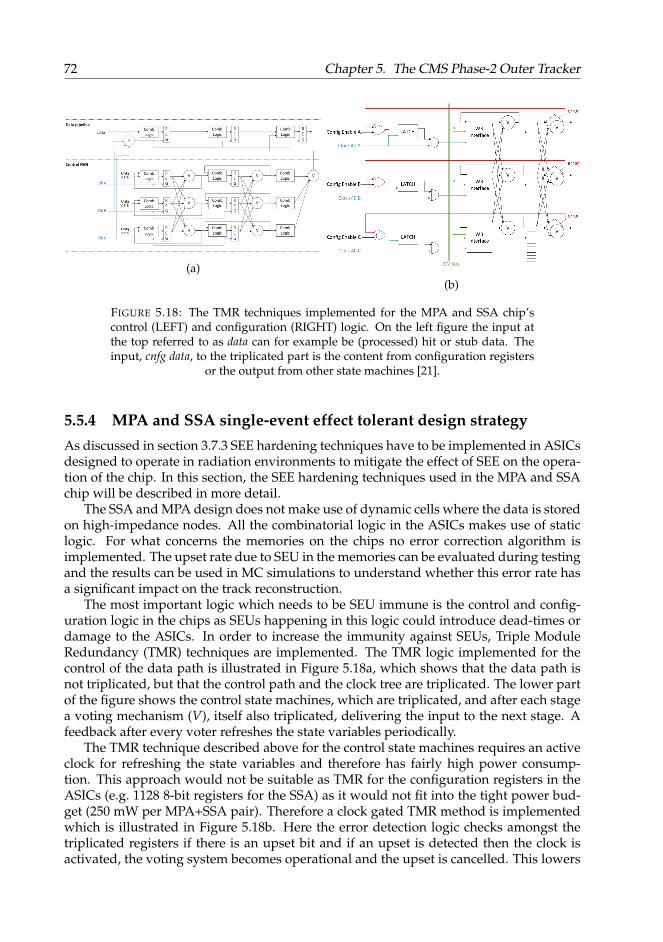
72 Chapter 5. The CMS Phase-2 Outer Tracker
(a)
Chapter 4. From the studies to the design of the SSA ASIC
Figure 4.25. Triple module redundancy with self-refresh feedback. Thisapproach was developed for the SSA and MPA configuration registers.
overhead with an impact on the power during the write operations. On another hand,
the latter requires a deep OR-tree in the error detection logic to generate the enable
pulse. The probability of having an upset within the register cluster increase with
the number of registers. For every upset in any bit of the register cluster, the clock is
enabled for all the registers. The usage of a triplicated set of configuration registers,
gated with asynchronous refresh and split into clusters of 32 registers was selected as
the best compromise for the power consumption.
Standard cell placement
TMR can protect from SEUs only if the distance among triplicated registers is sufficient
to guarantee that the charge collected from a ionizing particle traversing the substrate
could not upset more than one node at the same time. Specific constraints were
developed for synthesis and standard cell placement in order to guarantee a minimum
distance. Based on the the measurements of the RD53SEU [240] 65nm test-chip, a
15 µm distance is considered to be large enough to reduce the probability of multiple
register upset to few percents when a ionizing particle crosses the die.
A possible approach could consist in spatially separate the three instances of the state
machine by constraining the placement. This solution may drastically complicate the
routing and the timing closure. The solution implemented in the SSA instead consists
118
(b)
FIGURE 5.18: The TMR techniques implemented for the MPA and SSA chip’scontrol (LEFT) and configuration (RIGHT) logic. On the left figure the input atthe top referred to as data can for example be (processed) hit or stub data. Theinput, cnfg data, to the triplicated part is the content from configuration registers
or the output from other state machines [21].
5.5.4 MPA and SSA single-event effect tolerant design strategyAs discussed in section 3.7.3 SEE hardening techniques have to be implemented in ASICsdesigned to operate in radiation environments to mitigate the effect of SEE on the opera-tion of the chip. In this section, the SEE hardening techniques used in the MPA and SSAchip will be described in more detail.
The SSA and MPA design does not make use of dynamic cells where the data is storedon high-impedance nodes. All the combinatorial logic in the ASICs makes use of staticlogic. For what concerns the memories on the chips no error correction algorithm isimplemented. The upset rate due to SEU in the memories can be evaluated during testingand the results can be used in MC simulations to understand whether this error rate hasa significant impact on the track reconstruction.
The most important logic which needs to be SEU immune is the control and config-uration logic in the chips as SEUs happening in this logic could introduce dead-times ordamage to the ASICs. In order to increase the immunity against SEUs, Triple ModuleRedundancy (TMR) techniques are implemented. The TMR logic implemented for thecontrol of the data path is illustrated in Figure 5.18a, which shows that the data path isnot triplicated, but that the control path and the clock tree are triplicated. The lower partof the figure shows the control state machines, which are triplicated, and after each stagea voting mechanism (V), itself also triplicated, delivering the input to the next stage. Afeedback after every voter refreshes the state variables periodically.
The TMR technique described above for the control state machines requires an activeclock for refreshing the state variables and therefore has fairly high power consump-tion. This approach would not be suitable as TMR for the configuration registers in theASICs (e.g. 1128 8-bit registers for the SSA) as it would not fit into the tight power bud-get (250 mW per MPA+SSA pair). Therefore a clock gated TMR method is implementedwhich is illustrated in Figure 5.18b. Here the error detection logic checks amongst thetriplicated registers if there is an upset bit and if an upset is detected then the clock isactivated, the voting system becomes operational and the upset is cancelled. This lowers

5.5. pT module ASICs 73
FIGURE 5.19: CBC simplified front-end schematic [68].
the error signal which activated the clock. In this way the clock is deactivated until a nextupset happens [21].
5.5.5 The CBC chip
5.5.5.1 Introduction
The CBC chip [68] is designed to read out 127 strips from the top 2S sensor and 127channels from the bottom 2S sensor. The signal from the strips is processed in the CBC’scustom designed front-ends and digitised in the sampling stage. The CBC correlatesthe hits in the top and the bottom sensor and forms stubs. It outputs this stub dataevery BX. On reception of an L1A trigger, the CBC outputs the full unsparsified eventinformation. In section 5.5.5.2 the CBC front-end will briefly be introduced. In section5.5.5.3 the sampling logic is discussed and the digital logic is the topic of section 5.5.5.4and 5.5.5.5. Figure 5.19 and 5.20 show the CBC’s front-end and top-level architecturerespectively.
The CBC version which will be described in the following sections is CBC3. The CBC2chip, being the predecessor of the CBC3, has many similarities with the CBC3 version. Insection 5.5.5.6 a few differences between CBC2 and CBC3 will be pointed out.
5.5.5.2 CBC front-end
Each CBC input channel has its own front-end stage and the front-end is specifically de-signed to read out AC-coupled n-in-p type silicon sensors. As shown in Figure 5.19, theCBC’s front-end consists of a pre-amplifier, post-amplifier and comparator stage. Theinput charge from the strip is read out by the pre-amplifier and integrated on the 100 fFcapacitor. This capacitor is discharged through the resistive feedback network, whichuses a 100 kΩ resistor, into the post-amplifier. The pre-amplifier and post-amplifier aredesigned to result in a combined gain of 50 mV/fC. The shaping of the input signal isdesigned to give a rise time of less than 20 ns and a return to baseline within 50 ns. Thepost-amp’s offset can be adjusted on a front-end to front-end basis using an 8-bit DAC.This setting allows for correction of channel-to-channel mismatches in the amplifiers andthe comparator stage due to process variations. The last part in the front-end is the com-parator stage, with configurable hysteresis, which outputs a fixed amplitude signal forthe time that the input signal crosses a configurable threshold. This threshold setting isthe same for each front-end and represents the actual threshold at which the chip is op-erated. The configurable hysteresis logic is added to the comparator stage to make thecomparator stage less sensitive to small input variations: when the input is lower than achosen threshold, the output is low, whereas when the input is above a different higher
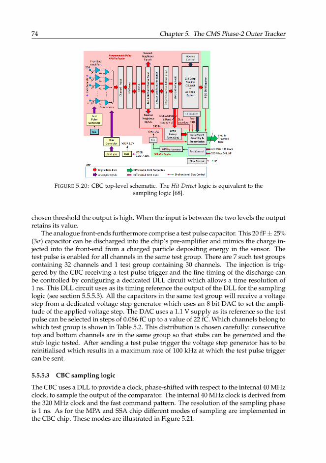
74 Chapter 5. The CMS Phase-2 Outer Tracker
FIGURE 5.20: CBC top-level schematic. The Hit Detect logic is equivalent to thesampling logic [68].
chosen threshold the output is high. When the input is between the two levels the outputretains its value.
The analogue front-ends furthermore comprise a test pulse capacitor. This 20 fF± 25%(3σ) capacitor can be discharged into the chip’s pre-amplifier and mimics the charge in-jected into the front-end from a charged particle depositing energy in the sensor. Thetest pulse is enabled for all channels in the same test group. There are 7 such test groupscontaining 32 channels and 1 test group containing 30 channels. The injection is trig-gered by the CBC receiving a test pulse trigger and the fine timing of the discharge canbe controlled by configuring a dedicated DLL circuit which allows a time resolution of1 ns. This DLL circuit uses as its timing reference the output of the DLL for the samplinglogic (see section 5.5.5.3). All the capacitors in the same test group will receive a voltagestep from a dedicated voltage step generator which uses an 8 bit DAC to set the ampli-tude of the applied voltage step. The DAC uses a 1.1 V supply as its reference so the testpulse can be selected in steps of 0.086 fC up to a value of 22 fC. Which channels belong towhich test group is shown in Table 5.2. This distribution is chosen carefully: consecutivetop and bottom channels are in the same group so that stubs can be generated and thestub logic tested. After sending a test pulse trigger the voltage step generator has to bereinitialised which results in a maximum rate of 100 kHz at which the test pulse triggercan be sent.
5.5.5.3 CBC sampling logic
The CBC uses a DLL to provide a clock, phase-shifted with respect to the internal 40 MHzclock, to sample the output of the comparator. The internal 40 MHz clock is derived fromthe 320 MHz clock and the fast command pattern. The resolution of the sampling phaseis 1 ns. As for the MPA and SSA chip different modes of sampling are implemented inthe CBC chip. These modes are illustrated in Figure 5.21:

5.5. pT module ASICs 75
Channel group Stimulated channels
0 242, 241, 226, 225, 210, 209, 194, 193, 178, 177, 162, 161, 146, 145, 130, 129,114, 113, 98, 97, 82, 81, 66, 65, 50, 49, 34, 33, 18, 17, 2, 1
1 244, 243, 228, 227, 212, 211, 196, 195, 180, 179, 164, 163, 148, 147, 132, 131,116, 115, 100, 99, 84, 83, 68, 67, 52, 51, 36, 35, 20, 19, 4, 3
2 246, 245, 230, 229, 214, 213, 198, 197, 182, 181, 166, 165, 150, 149, 134, 133,118, 117, 102, 101, 86, 85, 70, 69, 54, 53, 38, 37, 22, 21, 6, 5
3 248, 247, 232, 231, 216, 215, 200, 199, 184, 183, 168, 167, 152, 151, 136, 135,120, 119, 104, 103, 88, 87, 72, 71, 56, 55, 40, 39, 24, 23, 8, 7
4 250, 249, 234, 233, 218, 217, 202, 201, 186, 185, 170, 169, 154, 153, 138, 137,122, 121, 106, 105, 90, 89, 74, 73, 58, 57, 42, 41, 26, 25, 10, 9
5 252, 251, 236, 235, 220, 219, 204, 203, 188, 187, 172, 171, 156, 155, 140, 139,124, 123, 108, 107, 92, 91, 76, 75, 60, 59, 44, 43, 28, 27, 12, 11
6 254, 253, 238, 237, 222, 221, 206, 205, 190, 189, 174, 173, 158, 157, 142, 141,126, 125, 110, 109, 94, 93, 78, 77, 62, 61, 46, 45, 30, 29, 14, 13
7Top Dummy, 240, 239, 224, 223, 208, 207, 192, 191, 176, 175, 160, 159, 144,143, 128, 127, 112, 111, 96, 95, 80, 79, 64, 63, 48, 47, 32, 31, 16, 15, Bottom
Dummy
TABLE 5.2: Mapping of the CBC test pulse groups to the channel numbers.
• Fixed pulse width mode: in this case the output of the comparator is latched. Asin this mode the input to the latch is the direct output of the comparator this modeis able to detect comparator pulses which are non-overlapping with the samplingclock. Hits in consecutive clock cycles in the same channel will only be captured ifthe signal returns below the comparator threshold for each hit. The output signal inthis mode has a fixed pulse duration of 25 ns for each detected comparator outputtransition.
• Sampled mode: in this mode the sampling of the comparator output is performedsynchronously. For the sampling logic to therefore output a hit, the comparatoroutput needs to be high at the time of sampling. Comparator outputs being high formore than a single BX, either due to consecutive hits or due to single hits generatinga signal above the threshold lasting more than one clock cycle, will result in theoutput of the sampling logic to be high also for several clock cycles. The outputwill only return low again on the clock cycle succeeding the comparator output’sreturn to zero. In this mode comparator outputs which are high only in betweenthe sampling clock edges will not result in an output from the hit detect logic.
• Logical OR mode: the logical OR of the fixed pulse width and sampled mode.
• HIP suppressed mode: in this mode either the output of the sampled mode or theLogical OR mode is used, but extra logic forces the output of the hit detect logic lowin this way limiting the maximum number of consecutive clock cycles where theoutput of the sampling logic can be high. This extra logic can be used to eliminatethe effect of highly ionizing particles generating an active output of the samplinglogic for several clock cycles.
The output of the sampling logic is used as input to the digital part of the chip. There aretwo types of digital logic on the chip: full-event logic and stub logic. Which output fromthe sampling stage is used can be configured for the full-event and stub logic separately.The channel masking is implemented right before the sampling logic: there is the possi-bility for each channel to disconnect the output from the front-end to the sampling logicas shown in Figure 5.20.

76 Chapter 5. The CMS Phase-2 Outer Tracker
FIGURE 5.21: CBC sampling modes [68].
5.5.5.4 CBC stub data path and format
The CBC receives the sampled data from the top and the bottom channel and is thereforeable to correlate clusters in both sensors to generate stubs. Inter-chip communicationguarantees that this correlation can be performed across chips. The stub data path isrepresented in Figure 5.20. The full sampled sensor image is passed into a logical ORnetwork which produces an active high output (OR254) if any of the channels are hit.This bit is passed along in the stub data output package. Subsequently the hit data fromthe full sensor is passed to the layer swapping logic which allows for swapping of thetop and bottom channels so that the user can choose which layer to use as seed layer.The cluster width discrimination then filters out clusters which have a width larger than aprogrammable value7. Clusters surviving this filter are passed to the offset correction andcluster correlation logic which allows for programming an offset of the correlation layerwith respect to the seed layer to correct for parallax errors. Four separate regions perCBC chip are defined for which an offset of the correlation window can be programmed.The offset is programmable up to ±3 channels with half strip resolution. The CBC thentries, for every cluster in the seed layer, to find a cluster in the correlation layer, withina programmable window, as close as possible to the center of the seed cluster’s location.The maximum size of this window is ±7 channels from the center of the seed clusterand the window is configurable with a resolution of half a channel. If the CBC finds acorrelation between a seed cluster and a correlation cluster within this window, a stubis formed. This window therefore defines the pT cut. The definition of the correlationwindow and the offset are shown in Figure 5.22a. When a stub is found the location ofthe seed cluster is decoded as the location of the center of the cluster in the stub gatheringlogic. Half strip resolution is thus possible for clusters of size larger than 1. Also the offsetbetween the cluster in the seed and correlation layer is calculated and this represents thebend. Given the maximum correlation window of ±7 strips and a half strip resolutionfor the bend, the bend can be represented by a 5-bit number. The 5-bit bend informationis however only used internally on the chip. In order to reduce the output bandwidth ofthe chip, the 5-bit bend is translated to a 4-bit bend code in the configurable bend LUT.The CBC outputs the location and the bend of up to 3 stubs per BX using 5 lines running
7With a maximum of 4 strips.
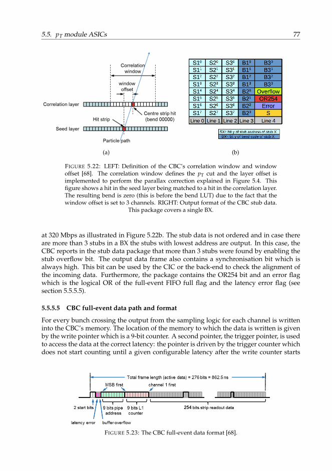
5.5. pT module ASICs 77
(a) (b)
FIGURE 5.22: LEFT: Definition of the CBC’s correlation window and windowoffset [68]. The correlation window defines the pT cut and the layer offset isimplemented to perform the parallax correction explained in Figure 5.4. Thisfigure shows a hit in the seed layer being matched to a hit in the correlation layer.The resulting bend is zero (this is before the bend LUT) due to the fact that thewindow offset is set to 3 channels. RIGHT: Output format of the CBC stub data.
This package covers a single BX.
at 320 Mbps as illustrated in Figure 5.22b. The stub data is not ordered and in case thereare more than 3 stubs in a BX the stubs with lowest address are output. In this case, theCBC reports in the stub data package that more than 3 stubs were found by enabling thestub overflow bit. The output data frame also contains a synchronisation bit which isalways high. This bit can be used by the CIC or the back-end to check the alignment ofthe incoming data. Furthermore, the package contains the OR254 bit and an error flagwhich is the logical OR of the full-event FIFO full flag and the latency error flag (seesection 5.5.5.5).
5.5.5.5 CBC full-event data path and format
For every bunch crossing the output from the sampling logic for each channel is writteninto the CBC’s memory. The location of the memory to which the data is written is givenby the write pointer which is a 9-bit counter. A second pointer, the trigger pointer, is usedto access the data at the correct latency: the pointer is driven by the trigger counter whichdoes not start counting until a given configurable latency after the write counter starts
FIGURE 5.23: The CBC full-event data format [68].

78 Chapter 5. The CMS Phase-2 Outer Tracker
counting. On reception of an L1A trigger, the CBC chip accesses the memory locationto which the trigger pointer points. The maximum L1 latency, defined by the depth ofthe memory, is the same as for the MPA and SSA chips and is 512 BXs. The full-eventdata from the memory is passed on to an output FIFO with a depth of 32 from whichit is serialised, foreseen of a header, and output over one differential line at 320 Mbpstowards the back-end. The output full-event data frame is shown in Figure 5.23. Thefull-event frame starts with a header of two bits, followed by a field for two error bits,representing the latency error and the buffer overflow error. The latency error is raisedwhen there is discrepancy between the trigger pointer and the write pointer on one endand the programmed latency on the other end. The buffer overflow error bit represents aFIFO full condition of the 32 deep output FIFO. After the error bits follows a 9-bit pipelinecounter and a 9-bit L1 counter which increments every time an L1A trigger is received.This is followed by 254 bits which represent the sensor image. Including 3 BX of deadtime between two consecutive full-event data packages, the time required to output asingle full-event data package is 950 ns. This allows for a maximum sustainable full-event data rate of 1 MHz. The first bit of the full-event package at the output of the CBCis in sync with the output of the sync bit in the stub data package.
5.5.5.6 The CBC2 chip
From the user’s point of view the CBC3 and CBC2 chip are fairly similar. There arehowever a few important differences, which are summarised below:
• A few tweaks have been made to the CBC’s front-end when going to the CBC3version. The CBC2 has the possibility to read out signals with both polarities asat the time of the CBC2 design it was not decided yet whether n-bulk or p-bulksensors were going to be used.
• In the CBC2’s full-event frame no L1 counter is implemented.
• The stub data information in the CBC2 is very basic: there is a single 40 Mbps lineper CBC which flags the presence of a stub in that BX. No stub location or bendinformation is output.
5.5.6 The CIC chip
5.5.6.1 Introduction
In this section the CIC1 chip will be introduced. The CIC1 is a prototype and the finalversion will be the CIC2, discussed briefly in section 5.5.6.5. Most of the functionalities ofthe final CIC are however already implemented in the CIC1 design, so from a user pointof view both versions are fairly similar. Due to the familiarity between both versions,the CIC1 and CIC2 will often be referred to as CIC in this work when the discussion isapplicable for both.
The CIC ASIC [69] receives full-event and stub data from eight MPA chips in the PSmodule and eight CBC chips in the 2S module. The task of the CIC chip is to group thedata from a module and to reduce the amount of data output by a module. The CICdoes this by selecting the stub data with the lowest bend and by sparsifying the full-event data in case of the CBC. The CIC is a fully digital chip and is not a readout chipas the ASICs which were described until now. The CIC can therefore be seen more asa hub where the data gets concentrated: 48 differential input lines running at 320 Mbps

5.5. pT module ASICs 79
FIGURE 5.24: Top-level representation of the CIC1 [69].
are concentrated to 6 or 7 differential lines8 at 320 Mbps. This results in a reduction inbandwidth with a factor of ≈ 8. For the CIC2 there will also be the possibility to outputthe data at 640 Mbps. This mode will be used for PS modules in the highest occupancyregions where the higher bandwidth is required to limit the stub losses.
From the user point of view the CIC is therefore quite transparent as to first order thechip only changes the data format. The only caveat to this is that the CIC also drops data:
• Stub data is dropped when the number of stubs received from the front-end chipsis larger than the number of stubs which can be output by the CIC. The stubs whichare dropped are the ones with the largest bend.
• Full-event data is dropped when the L1A trigger rate is too high and the FIFOs onthe CIC get filled up.
• Clusters can be dropped in the sparsified full-event readout if the cluster occupancyis too high.
In the next sections the full-event and stub data path in the CIC chip will be discussed,but first the phy ports, common to both the full-event and stub path, will be described.
5.5.6.2 Phy ports
As shown in the CIC top-level schematic in Figure 5.24, the first logic the input dataencounters are the CIC’s phy ports. These blocks phase align the incoming data withrespect to the CIC’s internal 320 MHz clock. This is required, because all the ASICs onthe module run on the same clock, directly provided by the lpGBT (section 5.5.7), sothe CIC knows the exact sampling frequency, but it does not know the sampling phase.A phase alignment mechanism is thus required to sample the bit at the optimal phase,i.e. away from the bit transitions.
8Depending on the CIC mode.
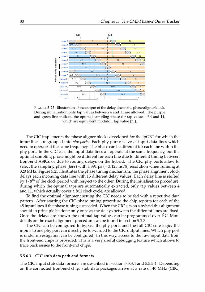
80 Chapter 5. The CMS Phase-2 Outer Tracker
Allo
wed
dur
ing
initi
alisa
tion
T/8 T/8
FIGURE 5.25: Illustration of the output of the delay line in the phase aligner block.During initialisation only tap values between 4 and 11 are allowed. The purpleand green line indicate the optimal sampling phase for tap values of 4 and 11,
which are equivalent modulo 1 tap value [71].
The CIC implements the phase aligner blocks developed for the lpGBT for which theinput lines are grouped into phy ports. Each phy port receives 4 input data lines whichneed to operate at the same frequency. The phase can be different for each line within thephy port. In the CIC case the input data lines all operate at the same frequency, but theoptimal sampling phase might be different for each line due to different timing betweenfront-end ASICs or due to routing delays on the hybrid. The CIC phy ports allow toselect the sampling phase (taps) with a 391 ps (= 3.125 ns/8) resolution when running at320 MHz. Figure 5.25 illustrates the phase tuning mechanism: the phase alignment blockdelays each incoming data line with 15 different delay values. Each delay line is shiftedby 1/8th of the clock period with respect to the other. During the initialisation procedure,during which the optimal taps are automatically extracted, only tap values between 4and 11, which actually cover a full clock cycle, are allowed.
To find the optimal alignment setting the CIC needs to be fed with a repetitive datapattern. After starting the CIC phase tuning procedure the chip reports for each of the48 input lines if the phase tuning succeeded. When the CIC sits on a hybrid this alignmentshould in principle be done only once as the delays between the different lines are fixed.Once the delays are known the optimal tap values can be programmed over I2C. Moredetails on the exact alignment procedure can be found in section 9.2.3.
The CIC can be configured to bypass the phy ports and the full CIC core logic: theinputs to one phy port can directly be forwarded to the CIC output lines. Which phy portis under investigation can be configured. In this way, access to the raw input data fromthe front-end chips is provided. This is a very useful debugging feature which allows totrace back issues to the front-end chips.
5.5.6.3 CIC stub data path and formats
The CIC input stub data formats are described in section 5.5.3.4 and 5.5.5.4. Dependingon the connected front-end chip, stub data packages arrive at a rate of 40 MHz (CBC)
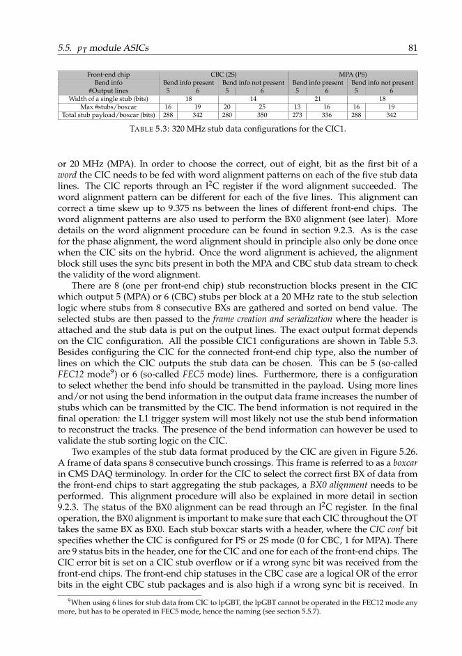
5.5. pT module ASICs 81
Front-end chip CBC (2S) MPA (PS)Bend info Bend info present Bend info not present Bend info present Bend info not present
#Output lines 5 6 5 6 5 6 5 6Width of a single stub (bits) 18 14 21 18
Max #stubs/boxcar 16 19 20 25 13 16 16 19Total stub payload/boxcar (bits) 288 342 280 350 273 336 288 342
TABLE 5.3: 320 MHz stub data configurations for the CIC1.
or 20 MHz (MPA). In order to choose the correct, out of eight, bit as the first bit of aword the CIC needs to be fed with word alignment patterns on each of the five stub datalines. The CIC reports through an I2C register if the word alignment succeeded. Theword alignment pattern can be different for each of the five lines. This alignment cancorrect a time skew up to 9.375 ns between the lines of different front-end chips. Theword alignment patterns are also used to perform the BX0 alignment (see later). Moredetails on the word alignment procedure can be found in section 9.2.3. As is the casefor the phase alignment, the word alignment should in principle also only be done oncewhen the CIC sits on the hybrid. Once the word alignment is achieved, the alignmentblock still uses the sync bits present in both the MPA and CBC stub data stream to checkthe validity of the word alignment.
There are 8 (one per front-end chip) stub reconstruction blocks present in the CICwhich output 5 (MPA) or 6 (CBC) stubs per block at a 20 MHz rate to the stub selectionlogic where stubs from 8 consecutive BXs are gathered and sorted on bend value. Theselected stubs are then passed to the frame creation and serialization where the header isattached and the stub data is put on the output lines. The exact output format dependson the CIC configuration. All the possible CIC1 configurations are shown in Table 5.3.Besides configuring the CIC for the connected front-end chip type, also the number oflines on which the CIC outputs the stub data can be chosen. This can be 5 (so-calledFEC12 mode9) or 6 (so-called FEC5 mode) lines. Furthermore, there is a configurationto select whether the bend info should be transmitted in the payload. Using more linesand/or not using the bend information in the output data frame increases the number ofstubs which can be transmitted by the CIC. The bend information is not required in thefinal operation: the L1 trigger system will most likely not use the stub bend informationto reconstruct the tracks. The presence of the bend information can however be used tovalidate the stub sorting logic on the CIC.
Two examples of the stub data format produced by the CIC are given in Figure 5.26.A frame of data spans 8 consecutive bunch crossings. This frame is referred to as a boxcarin CMS DAQ terminology. In order for the CIC to select the correct first BX of data fromthe front-end chips to start aggregating the stub packages, a BX0 alignment needs to beperformed. This alignment procedure will also be explained in more detail in section9.2.3. The status of the BX0 alignment can be read through an I2C register. In the finaloperation, the BX0 alignment is important to make sure that each CIC throughout the OTtakes the same BX as BX0. Each stub boxcar starts with a header, where the CIC conf bitspecifies whether the CIC is configured for PS or 2S mode (0 for CBC, 1 for MPA). Thereare 9 status bits in the header, one for the CIC and one for each of the front-end chips. TheCIC error bit is set on a CIC stub overflow or if a wrong sync bit was received from thefront-end chips. The front-end chip statuses in the CBC case are a logical OR of the errorbits in the eight CBC stub packages and is also high if a wrong sync bit is received. In
9When using 6 lines for stub data from CIC to lpGBT, the lpGBT cannot be operated in the FEC12 mode anymore, but has to be operated in FEC5 mode, hence the naming (see section 5.5.7).
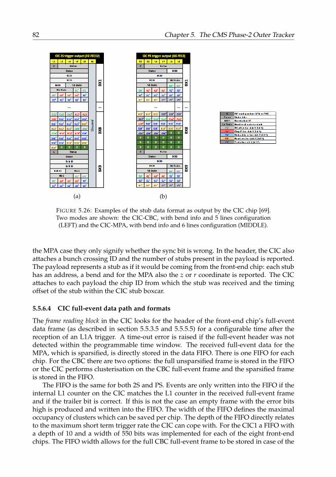
82 Chapter 5. The CMS Phase-2 Outer Tracker
(a) (b)
FIGURE 5.26: Examples of the stub data format as output by the CIC chip [69].Two modes are shown: the CIC-CBC, with bend info and 5 lines configuration(LEFT) and the CIC-MPA, with bend info and 6 lines configuration (MIDDLE).
the MPA case they only signify whether the sync bit is wrong. In the header, the CIC alsoattaches a bunch crossing ID and the number of stubs present in the payload is reported.The payload represents a stub as if it would be coming from the front-end chip: each stubhas an address, a bend and for the MPA also the z or r coordinate is reported. The CICattaches to each payload the chip ID from which the stub was received and the timingoffset of the stub within the CIC stub boxcar.
5.5.6.4 CIC full-event data path and formats
The frame reading block in the CIC looks for the header of the front-end chip’s full-eventdata frame (as described in section 5.5.3.5 and 5.5.5.5) for a configurable time after thereception of an L1A trigger. A time-out error is raised if the full-event header was notdetected within the programmable time window. The received full-event data for theMPA, which is sparsified, is directly stored in the data FIFO. There is one FIFO for eachchip. For the CBC there are two options: the full unsparsified frame is stored in the FIFOor the CIC performs clusterisation on the CBC full-event frame and the sparsified frameis stored in the FIFO.
The FIFO is the same for both 2S and PS. Events are only written into the FIFO if theinternal L1 counter on the CIC matches the L1 counter in the received full-event frameand if the trailer bit is correct. If this is not the case an empty frame with the error bitshigh is produced and written into the FIFO. The width of the FIFO defines the maximaloccupancy of clusters which can be saved per chip. The depth of the FIFO directly relatesto the maximum short term trigger rate the CIC can cope with. For the CIC1 a FIFO witha depth of 10 and a width of 550 bits was implemented for each of the eight front-endchips. The FIFO width allows for the full CBC full-event frame to be stored in case of the

5.5. pT module ASICs 83
(a)
(b)
(c)
FIGURE 5.27: The full-event data frame format output by the CIC chip: TOP: CIC-2S in unsparsified mode; MIDDLE: CIC-2S in sparsified mode; BOTTOM: CIC-
PS mode.
CBC unsparsified mode and allows for events with 17 pixel clusters and 17 strip clustersto be stored in case of the PS mode.
The frame creation block reads from the FIFOs and forms the full-event data packagewhich represents the sensor image of half a module. The output formats are shown inFigure 5.27. The full-event data is serialised and put on a single line out of the CIC. Themaximum number of clusters in the CIC package is 127 [33]. This occupancy is howevernot sustainable by the CIC bandwidth. The bandwidth allows a continuous occupancyof ≈ 25 clusters per CIC and per L1A trigger when the CIC is operated in the 320 MHzmode.
5.5.6.5 The CIC2 chip
An improved version of the CIC1 chip has recently been developed and includes severalchanges. The most important changes are the triplication of the logic and the additionof the configuration where the CIC is operated in the 640 MHz mode. This mode will beused for the PS modules in the regions with highest stub occupancy. For these moduleshigher bandwidths are required as can be seen from Figure 5.28 where the stub rates permodule (so 2 CICs) are shown per BX at an average pileup of 200. In the 640 MHz modewith stub data on 6 lines, each CIC boxcar, which integrates data of 8 consecutive BXs,can contain up to 35 (bend info included) or 40 (no bend info included) stubs in the datastream.
5.5.7 The optical linkThe lpGBT chip [71] in cooperation with the VTRx+ is designed to provide a high speedoptical link in radiation environments. The lpGBT is a multi-purpose radiation hard chipto be used by several LHC experiments. A typical use case of the lpGBT is shown inFigure 5.29 where a single bidirectional link is used between the FPGA in the countingroom and the on-detector electronics. The optical link embeds all configuration, controland data information into a single downlink (towards the detector) and single uplink
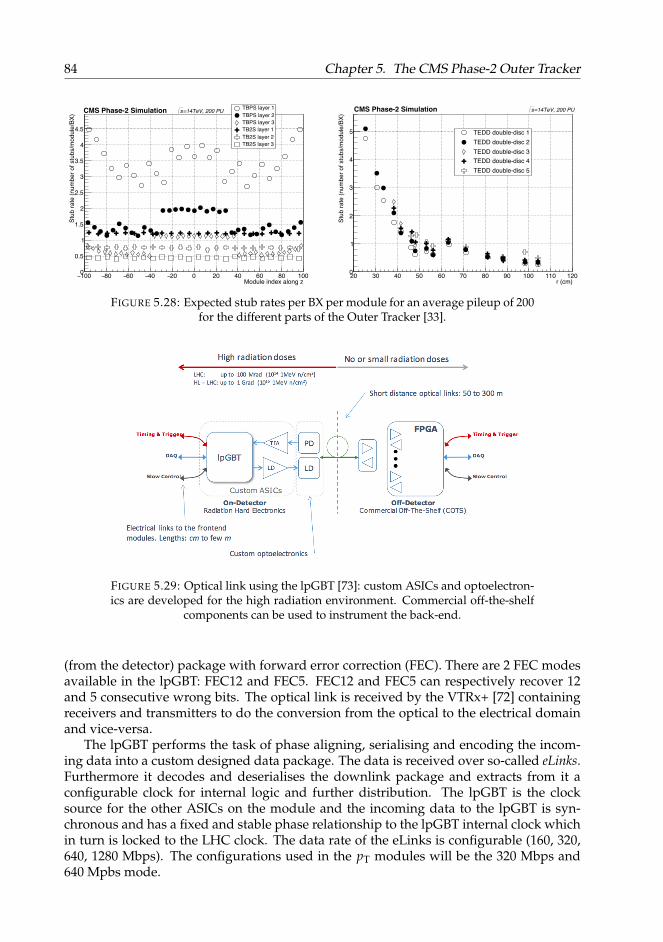
84 Chapter 5. The CMS Phase-2 Outer Tracker
280 Chapter 12. Additional Information on Material Budget, Local Reconstruction, and Tracking
Module index along z100− 80− 60− 40− 20− 0 20 40 60 80 100
Stub
rate
(num
ber o
f stu
bs/m
odul
e/BX
)0
0.5
1
1.5
2
2.5
3
3.5
TBPS layer 1TBPS layer 2TBPS layer 3TB2S layer 1TB2S layer 2TB2S layer 3
CMS Phase-2 Simulation =14TeV, 140 PUs
r (cm)20 30 40 50 60 70 80 90 100 110 120
Stub
rate
(num
ber o
f stu
bs/m
odul
e/BX
)
0
0.5
1
1.5
2
2.5
3
3.5
4
4.5
TEDD double-disc 1TEDD double-disc 2TEDD double-disc 3TEDD double-disc 4TEDD double-disc 5
CMS Phase-2 Simulation =14TeV, 140 PUs
Module index along z100− 80− 60− 40− 20− 0 20 40 60 80 100
Stub
rate
(num
ber o
f stu
bs/m
odul
e/BX
)
0
0.5
1
1.5
2
2.5
3
3.5
4
4.5
TBPS layer 1TBPS layer 2TBPS layer 3TB2S layer 1TB2S layer 2TB2S layer 3
CMS Phase-2 Simulation =14TeV, 200 PUs
r (cm)20 30 40 50 60 70 80 90 100 110 120
Stub
rate
(num
ber o
f stu
bs/m
odul
e/BX
)
0
1
2
3
4
5 TEDD double-disc 1TEDD double-disc 2TEDD double-disc 3TEDD double-disc 4TEDD double-disc 5
CMS Phase-2 Simulation =14TeV, 200 PUs
Module index along z100− 80− 60− 40− 20− 0 20 40 60 80 100
Stub
rate
(num
ber o
f stu
bs/m
odul
e/BX
)
0
1
2
3
4
5
TBPS layer 1TBPS layer 2TBPS layer 3TB2S layer 1TB2S layer 2TB2S layer 3
CMS Phase-2 simulation =14TeV, 250 PUs
r (cm)20 30 40 50 60 70 80 90 100 110 120
Stub
rate
(num
ber o
f stu
bs/m
odul
e/BX
)
0
1
2
3
4
5
6
TEDD double-disc 1TEDD double-disc 2TEDD double-disc 3TEDD double-disc 4TEDD double-disc 5
CMS Phase-2 Simulation =14TeV, 250 PUs
Figure 12.5: Average stub multiplicity per module per bunch crossing for 140 (top), 200 (mid-dle), and 250 (bottom) PU events. The left plots show the stub rates in the barrel as a functionof the modules’ z positions (in arbitrary units), while the right plots show the stub rates in theendcap as a function of the modules’ radial positions.
FIGURE 5.28: Expected stub rates per BX per module for an average pileup of 200for the different parts of the Outer Tracker [33].
FIGURE 5.29: Optical link using the lpGBT [73]: custom ASICs and optoelectron-ics are developed for the high radiation environment. Commercial off-the-shelf
components can be used to instrument the back-end.
(from the detector) package with forward error correction (FEC). There are 2 FEC modesavailable in the lpGBT: FEC12 and FEC5. FEC12 and FEC5 can respectively recover 12and 5 consecutive wrong bits. The optical link is received by the VTRx+ [72] containingreceivers and transmitters to do the conversion from the optical to the electrical domainand vice-versa.
The lpGBT performs the task of phase aligning, serialising and encoding the incom-ing data into a custom designed data package. The data is received over so-called eLinks.Furthermore it decodes and deserialises the downlink package and extracts from it aconfigurable clock for internal logic and further distribution. The lpGBT is the clocksource for the other ASICs on the module and the incoming data to the lpGBT is syn-chronous and has a fixed and stable phase relationship to the lpGBT internal clock whichin turn is locked to the LHC clock. The data rate of the eLinks is configurable (160, 320,640, 1280 Mbps). The configurations used in the pT modules will be the 320 Mbps and640 Mpbs mode.

5.6. pT module data path 85
The lpGBT provides a bandwidth of 2.56 Gb/s for the downlink and 5.12 or 10.24 Gb/sfor the uplink. The bandwidth available for uplink detector data depends on the oper-ating mode and forward error encoding which is used: 3.84 Gb/s and 4.48 Gb/s for5.12 Gb/s mode for FEC12 and FEC5 respectively and 7.68 Gb/s and 8.96 Gb/s for the10.24 Gb/s mode for FEC12 and FEC5 respectively.
The decoding and encoding of the lpGBT frames in the back-end happens in thelpGBT-FPGA block implemented on the FPGA sitting on the DAQ card in the count-ing room. This firmware block is provided by the lpGBT team and the combination oflpGBT and lpGBT-FPGA essentially makes the optical link transparent to the user.
5.6 pT module data path
Figures 5.30a and 5.30b show respectively the main lines which are important for con-trol and data transmission on the 2S and PS modules. Note that not all connections areshown here. Power lines, ground lines,... are not included for clarity reasons. A goodunderstanding of the control and chip interconnections is important in the developmentof a test bench to read out module prototypes and final modules, which is the topic ofChapter 6.
Figure 5.30a shows the interconnections on a 2S module where physically three mainblocks can be identified: the two front-end hybrids carrying the CBCs and the SEH which,from a data transmission and control point of view, carries the lpGBT and VTRx+ chips.In case of the PS module the inter-chip connectivity (Figure 5.30b) is more complicatedthan the 2S case due to the fact that the MPAs, physically located on the MaPSA, haveto receive data from the SSAs which sit on a separate front-end hybrid and the MPAs inturn have to send data back to the CIC on the FEH.
For both the 2S and PS module there is a single fast command line which goes from thelpGBT to each CBC, SSA and CIC chip. The 320 MHz clock is generated by the lpGBT andthere is a separate clock line for each front-end hybrid. In the PS module the MPA chipsreceive the clock and the fast commands buffered and forwarded by the SSA chip. Forthe PS module there is also the possibility to run the CIC in the 640 MHz mode, thereforea separate clock line from the lpGBT to the CICs is present. Besides the fast commandsand the clock the lpGBT also controls the reset lines. There is a dedicated reset line foreach chip flavour. The configuration of the front-end chips and the CIC happens overI2C. For the 2S module there is one I2C bus for each FEH and for the PS module there isone I2C bus per left/right side of the module. Other I2C buses are routed from the lpGBTto the DCDC converter and the VTRx+.
The data flow was already explained in the sections dedicated to the front-end ASICs.To summarise: in case of the 2S module each CBC receives input from 254 sensor channelsand sends 5 lines of stub data and 1 line of full-event data at 320 Mbps to the CIC. In thePS module, the SSAs receive data from 120 sensor channels and send 8 lines of stub dataand 1 line of full-event data at 320 Mbps to the MPA. In addition, the MPA acquires thedata from 1920 macro pixels. Each MPA sends 5 lines of stub data and 1 line of full-eventdata at 320 Mbps to the CIC.
In both modules, the CIC thus receives data on 48 lines at 320 Mbps and concentratesthe data on 5 or 6 stub data lines and 1 full-event data line and sends it to the lpGBTat 320 Mbps. In the PS case there is the possibility to also run the CIC in the 640 MHzmode which essentially doubles the bandwidth from each side of the module. The lpGBTthus receives 2 lines of full-event data and 10 or 12 lines of stub data, either at 320 Mbps
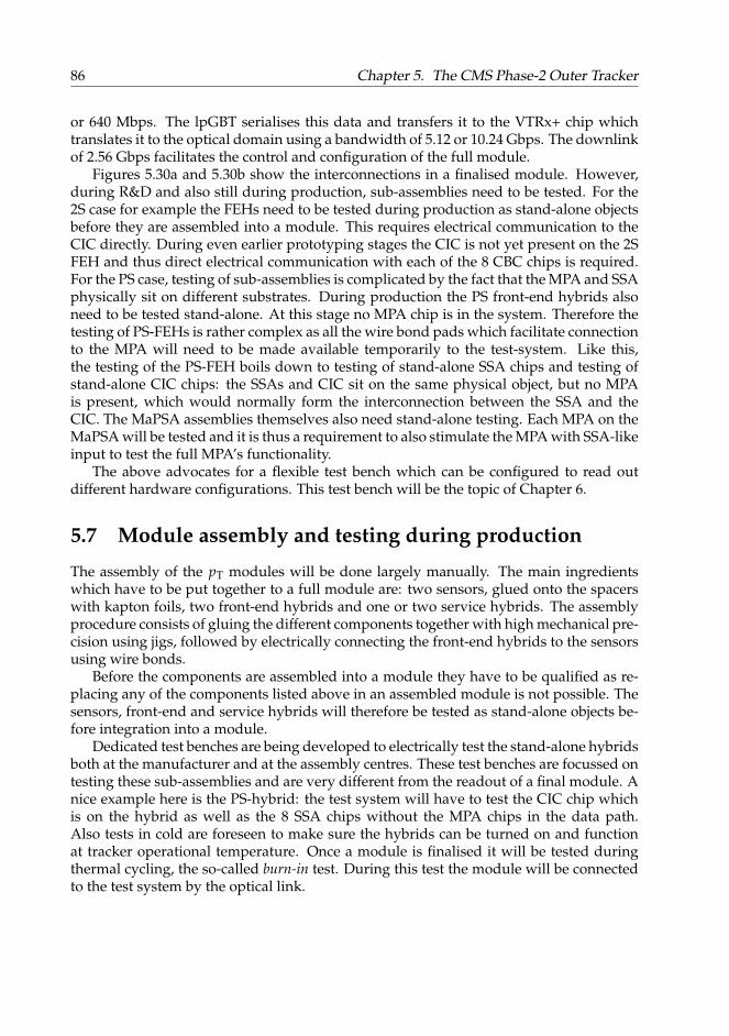
86 Chapter 5. The CMS Phase-2 Outer Tracker
or 640 Mbps. The lpGBT serialises this data and transfers it to the VTRx+ chip whichtranslates it to the optical domain using a bandwidth of 5.12 or 10.24 Gbps. The downlinkof 2.56 Gbps facilitates the control and configuration of the full module.
Figures 5.30a and 5.30b show the interconnections in a finalised module. However,during R&D and also still during production, sub-assemblies need to be tested. For the2S case for example the FEHs need to be tested during production as stand-alone objectsbefore they are assembled into a module. This requires electrical communication to theCIC directly. During even earlier prototyping stages the CIC is not yet present on the 2SFEH and thus direct electrical communication with each of the 8 CBC chips is required.For the PS case, testing of sub-assemblies is complicated by the fact that the MPA and SSAphysically sit on different substrates. During production the PS front-end hybrids alsoneed to be tested stand-alone. At this stage no MPA chip is in the system. Therefore thetesting of PS-FEHs is rather complex as all the wire bond pads which facilitate connectionto the MPA will need to be made available temporarily to the test-system. Like this,the testing of the PS-FEH boils down to testing of stand-alone SSA chips and testing ofstand-alone CIC chips: the SSAs and CIC sit on the same physical object, but no MPAis present, which would normally form the interconnection between the SSA and theCIC. The MaPSA assemblies themselves also need stand-alone testing. Each MPA on theMaPSA will be tested and it is thus a requirement to also stimulate the MPA with SSA-likeinput to test the full MPA’s functionality.
The above advocates for a flexible test bench which can be configured to read outdifferent hardware configurations. This test bench will be the topic of Chapter 6.
5.7 Module assembly and testing during production
The assembly of the pT modules will be done largely manually. The main ingredientswhich have to be put together to a full module are: two sensors, glued onto the spacerswith kapton foils, two front-end hybrids and one or two service hybrids. The assemblyprocedure consists of gluing the different components together with high mechanical pre-cision using jigs, followed by electrically connecting the front-end hybrids to the sensorsusing wire bonds.
Before the components are assembled into a module they have to be qualified as re-placing any of the components listed above in an assembled module is not possible. Thesensors, front-end and service hybrids will therefore be tested as stand-alone objects be-fore integration into a module.
Dedicated test benches are being developed to electrically test the stand-alone hybridsboth at the manufacturer and at the assembly centres. These test benches are focussed ontesting these sub-assemblies and are very different from the readout of a final module. Anice example here is the PS-hybrid: the test system will have to test the CIC chip whichis on the hybrid as well as the 8 SSA chips without the MPA chips in the data path.Also tests in cold are foreseen to make sure the hybrids can be turned on and functionat tracker operational temperature. Once a module is finalised it will be tested duringthermal cycling, the so-called burn-in test. During this test the module will be connectedto the test system by the optical link.
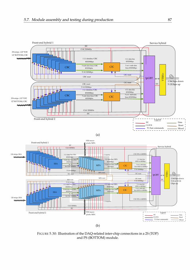
5.7. Module assembly and testing during production 87
CBC CIC
Front-end hybrid 1
5 stub data lines/CBC@320Mpbs
CLK 320MHz
T1 @ 320Mbps
Service hybrid
lpGBT
CBC CIC
Front-end hybrid 2
CLK 320MHz
VTR
X+
I2C
254 strips (127 TOP,
127 BOTTOM)/CBC
CIC reset
CIC reset
I2C
CBC reset
CBC reset
254 strips (127 TOP,
127 BOTTOM)/CBC
1 L1 data line@320Mbps
5 or 6 stub datalines @320Mbps
T1 @ 320Mbps
1 L1 dataline/CBC
@320Mbps
1 L1 dataline/CBC
@320Mbps
1 L1 data line@320Mbps
5 or 6 stub datalines @320Mbps
5 stub data lines/CBC@320Mpbs
2.56Gbps down5.12Gbps upI2C
LegendI2C
CLOCK
T1 Fast commands
DataResetMixed
(a)
SSACIC
8 stub data lines/SSA@320Mpbs
CLK 320MHz
T1 @ 320Mbps
Service hybrid
lpGBT
SSACIC
CLK 320MHz
VTR
X+
I2C
CIC reset
CIC reset
I2C
SSA reset
SSA reset
120 strips/SSA
1 L1 data line@320 or 640Mbps
5 or 6 stub datalines @320 or 640Mbps
T1 @ 320Mbps
1 L1 data line/SSA
@320Mbps
1 L1 data line/SSA
@320Mbps
1 L1 data line@320 or 640Mbps
5 or 6 stub datalines @320 or 640Mbps
8 stub data lines/SSA@320Mpbs
2.56Gbps down5.12 or 10.24Gbps up
I2C
LegendI2C
CLOCK
T1 Fast commands
120 strips/SSACLK 320 or 640MHz
CLK 320 or 640MHz
MPA
1 L1 data line/MPA
@320Mbps
5 stub data lines/MPA@320Mpbs
MPA reset
MPA reset
1920 macro-pixels/MPA
8x T1
8x CLK 320MHz
Data
Reset
8x CLK 320MHz8x T1 MPA
1920 macro-pixels/MPAFront-end hybrid 1
1 L1 data line/MPA
@320Mbps
5 stub data lines/MPA@320Mpbs
Mixed
Front-end hybrid 2
1/2 MaPSA
1/2 MaPSA
T1 @ 320Mbps
T1 @ 320Mbps
(b)
FIGURE 5.30: Illustration of the DAQ-related inter-chip connections in a 2S (TOP)and PS (BOTTOM) module.
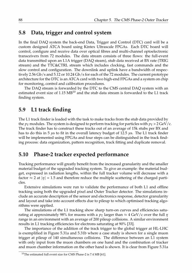
88 Chapter 5. The CMS Phase-2 Outer Tracker
5.8 Data, trigger and control system
In the final DAQ system the back-end Data, Trigger and Control (DTC) card will be acustom designed ATCA board using Kintex Ultrascale FPGAs. Each DTC board willcontrol, configure and receive data over optical fibres and multi-channel optoelectronictransceivers from 72 modules. The data stream consists of three flows: the full-eventdata transmitted upon an L1A trigger (DAQ steam), stub data received at BX rate (TRIGstream) and the TTC&CTRL stream which includes clocking, fast commands and theslow control and configuration. The downlink and uplink have a bandwidth of respec-tively 2.56 Gb/s and 5.12 or 10.24 Gb/s for each of the 72 modules. The current prototypearchitecture for the DTC is an ATCA card with two high-end FPGAs and a system on chipfor monitoring, control and calibration procedures.
The DAQ stream is forwarded by the DTC to the CMS central DAQ system with anestimated event size of 1.15 MB10 and the stub data stream is forwarded to the L1 trackfinding system.
5.9 L1 track finding
The L1 track finder is loaded with the task to make tracks from the stub data provided bythe pT modules. The system is designed to perform tracking for particles with pT > 2 GeV/c.The track finder has to construct these tracks out of an average of 15k stubs per BX andhas to do this in 5 µs to fit in the overall latency budget of 12.5 µs. The L1 track finderwill be implemented using FPGAs and four steps can be distinguished in the track find-ing process: data organization, pattern recognition, track fitting and duplicate removal.
5.10 Phase-2 tracker expected performance
Tracking performance will greatly benefit from the increased granularity and the smallermaterial budget of the upgraded tracking system. To give an example: the material bud-get, expressed in radiation lengths, within the full tracker volume will decrease with afactor ≈ 2 at |η| = 1.5 and therefore reduce the multiple scattering of the charged parti-cles.
Extensive simulations were run to validate the performance of both L1 and offlinetracking using both the upgraded pixel and Outer Tracker detector. The simulations in-clude an accurate description of the sensor and electronics response, detector granularityand layout and take into account effects due to pileup to which optimised tracking algo-rithms were applied.
The simulations of the L1 tracking show sharp turn-on curves and efficiencies satu-rating at approximately 98% for muons with a pT larger than ≈ 4 GeV/c over the full ηrange in an environment with an average of 200 pileup collisions. A similar environmentresults in L1 tracking efficiencies for electrons saturating at 90% [33].
The importance of the addition of the track trigger to the global trigger at HL-LHCis exemplified in Figure 5.31a and 5.31b where a case study is shown for a single muontrigger at pileup of 140 simultaneous collisions. The difference between an L1 systemwith only input from the muon chambers on one hand and the combination of trackerand muon chamber information on the other hand is shown. It is clear from Figure 5.31a
10The estimated full event size for CMS Phase-2 is 7.4 MB [61].
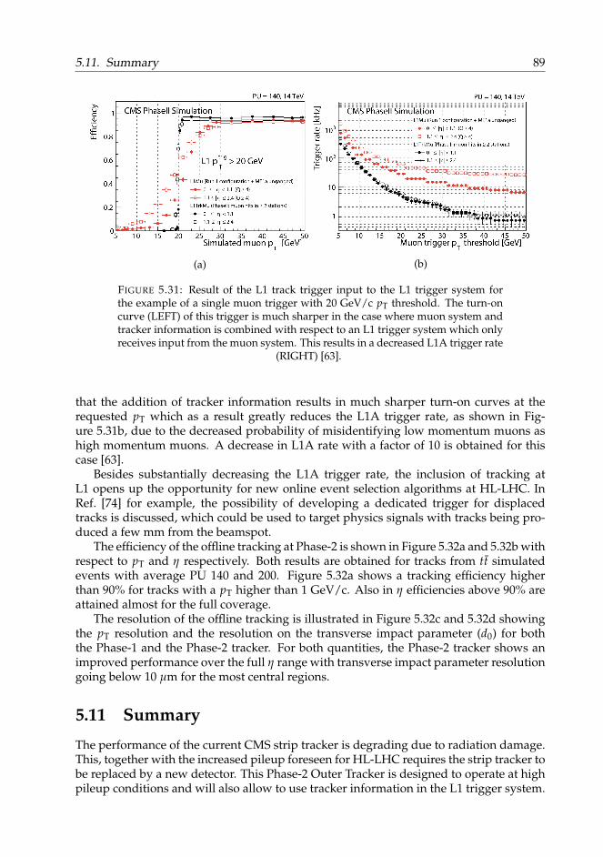
5.11. Summary 89
(a) (b)
FIGURE 5.31: Result of the L1 track trigger input to the L1 trigger system forthe example of a single muon trigger with 20 GeV/c pT threshold. The turn-oncurve (LEFT) of this trigger is much sharper in the case where muon system andtracker information is combined with respect to an L1 trigger system which onlyreceives input from the muon system. This results in a decreased L1A trigger rate
(RIGHT) [63].
that the addition of tracker information results in much sharper turn-on curves at therequested pT which as a result greatly reduces the L1A trigger rate, as shown in Fig-ure 5.31b, due to the decreased probability of misidentifying low momentum muons ashigh momentum muons. A decrease in L1A rate with a factor of 10 is obtained for thiscase [63].
Besides substantially decreasing the L1A trigger rate, the inclusion of tracking atL1 opens up the opportunity for new online event selection algorithms at HL-LHC. InRef. [74] for example, the possibility of developing a dedicated trigger for displacedtracks is discussed, which could be used to target physics signals with tracks being pro-duced a few mm from the beamspot.
The efficiency of the offline tracking at Phase-2 is shown in Figure 5.32a and 5.32b withrespect to pT and η respectively. Both results are obtained for tracks from tt simulatedevents with average PU 140 and 200. Figure 5.32a shows a tracking efficiency higherthan 90% for tracks with a pT higher than 1 GeV/c. Also in η efficiencies above 90% areattained almost for the full coverage.
The resolution of the offline tracking is illustrated in Figure 5.32c and 5.32d showingthe pT resolution and the resolution on the transverse impact parameter (d0) for boththe Phase-1 and the Phase-2 tracker. For both quantities, the Phase-2 tracker shows animproved performance over the full η range with transverse impact parameter resolutiongoing below 10 µm for the most central regions.
5.11 Summary
The performance of the current CMS strip tracker is degrading due to radiation damage.This, together with the increased pileup foreseen for HL-LHC requires the strip tracker tobe replaced by a new detector. This Phase-2 Outer Tracker is designed to operate at highpileup conditions and will also allow to use tracker information in the L1 trigger system.
90 Chapter 5. The CMS Phase-2 Outer Tracker
(a) (b)
(c) (d)
FIGURE 5.32: TOP: Track reconstruction efficiency as function of pT (LEFT) andη (RIGTH) in tt events at a pileup of 140 and 200 for tracks produced with atransverse impact parameter smaller than 3.5 cm. For the η dependence trackswith pT ≤ 0.9 GeV/c were discarded. BOTTOM: Comparison between the Phase-1 and Phase-2 tracker for the resolution on the transverse momentum (LEFT) andtransverse impact parameter (RIGHT) for muons with a transverse momentum
of 10 GeV/c [33].

5.11. Summary 91
To accomplish the latter, the CMS Outer Tracker will adopt a unique pT module designwhich will allow for on-module generation of high pT track primitives (stubs) which canbe sent from the module to the back-end at BX rate. Two types of pT modules will beused to equip the Outer Tracker volume. The different silicon sensor designs used inthese modules require three specific readout ASICs to process the analogue signal, formthe stubs and store the full-event information. A concentrator ASIC will be used to groupand to select the highest pT stubs and to process and buffer the full-event information permodule side. In the end this results in two data streams to the back-end: the stub data andthe full-event data. During prototyping and construction, single chips, chip assembliesand prototype modules need to be tested. These devices all need a test bench to validatetheir operation and a good understanding of the ASICs’ functionalities and the data andcontrol paths on the module is indispensable when designing such a test system.

93
Chapter 6
Firmware Development for Phase-2Tracker Prototypes
6.1 Introduction
In order to qualify the CMS Phase-2 Outer Tracker module prototypes, a test system wasset up which covers the readout of all possible DUTs (Device Under Test). This test sys-tem will be one of the main test benches for testing during R&D and module production.Therefore, this system has to cover a fairly large number of devices, starting from bench-top testing of single chips to multi-module testing in beam or during burn-in and this forboth 2S and PS flavours. The readout system consists of a firmware part, the so-calledµDTC, running on an FC7 [75] AMC (Advanced Mezzanine Card) card and the Ph2 ACF(Phase-2 Acquisition and Control Framework) C++ software package which controls thefirmware to run the calibration routines and data taking. A top level view of the readoutframework is shown in Figure 6.1: at the lowest level the hardware prototypes whichneed to be configured, controlled and read out are located. They communicate over adedicated link to the FC7 readout board. This link can be electrical or optical dependingon the type of prototype which is connected. The FC7 runs the hardware specific µDTCfirmware which makes use of the system firmware provided by the FC7 team. This sys-tem firmware implements, amongst others, the firmware blocks for communication withthe FC7 board peripherals and an IPbus core (see section 6.4.2) for communication to theback-end. The back-end is a Linux machine running the µHAL library which is a lowlevel library to operate the IPbus communication over the machine’s Ethernet port. DUTspecific and firmware specific settings and routines are coded into the Ph2 ACF’s Mid-dleware layer which makes the User Routines layer as agnostic as possible of changes infirmware or chip versions. Examples of user routines are latency scans and tuning of thefront-ends of the ASICs.
This chapter will describe in more detail the layer connecting the DUT with the soft-ware: the µDTC system, with as its backbone the FC7 card carrying a Kintex7 FPGA.This chapter contains an introduction on FPGAs (section 6.2), a word on the scope ofthe µDTC project (section 6.3), an overview of the hardware platform (section 6.4) and adetailed description of the firmware blocks designed for the µDTC (section 6.5).
6.2 FPGAs
Field Programmable Gate Arrays (FPGAs) are chips consisting of a matrix of configurablelogic blocks (CLBs). Each CLB contains the same elementary logic (LUTs, Digital SignalProcessing (DSP) units, multiplexers, flip-flops). The interconnection between the CLBsand connection to other FPGA resources is performed using a reprogrammable switching
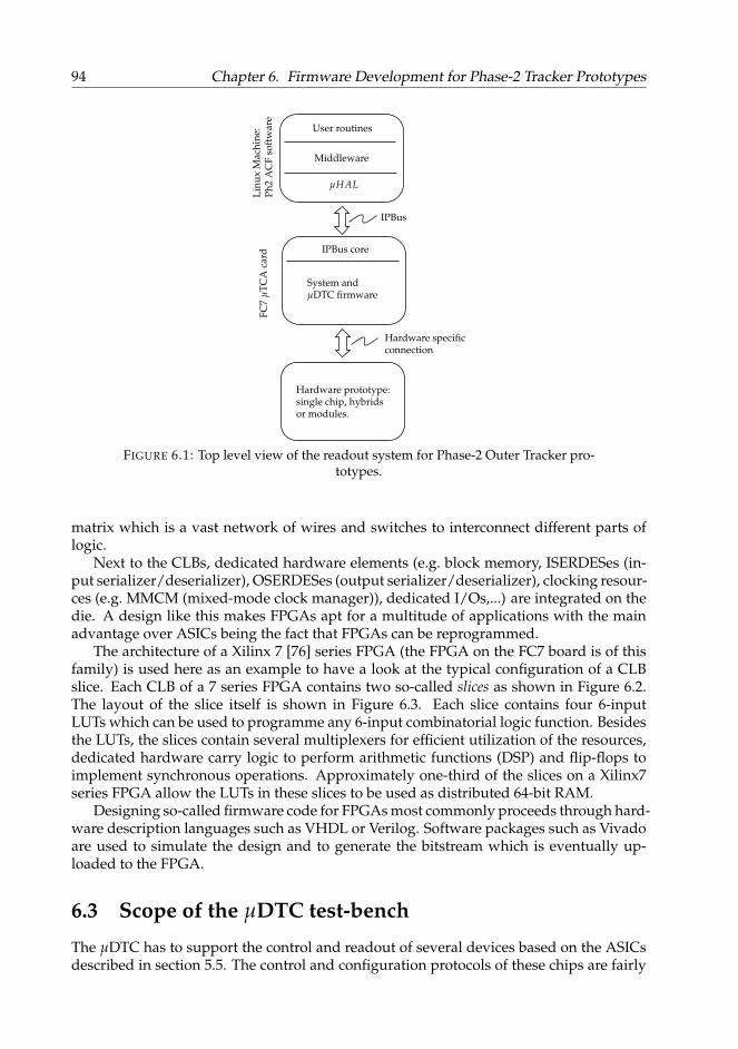
94 Chapter 6. Firmware Development for Phase-2 Tracker Prototypes
User routines
Middleware
µHAL
IPBus core
System andµDTC firmware
Hardware prototype:single chip, hybridsor modules.
IPBus
Hardware specificconnection
Linu
xM
achi
ne:
Ph2
AC
Fso
ftw
are
FC7
µTC
Aca
rd
FIGURE 6.1: Top level view of the readout system for Phase-2 Outer Tracker pro-totypes.
matrix which is a vast network of wires and switches to interconnect different parts oflogic.
Next to the CLBs, dedicated hardware elements (e.g. block memory, ISERDESes (in-put serializer/deserializer), OSERDESes (output serializer/deserializer), clocking resour-ces (e.g. MMCM (mixed-mode clock manager)), dedicated I/Os,...) are integrated on thedie. A design like this makes FPGAs apt for a multitude of applications with the mainadvantage over ASICs being the fact that FPGAs can be reprogrammed.
The architecture of a Xilinx 7 [76] series FPGA (the FPGA on the FC7 board is of thisfamily) is used here as an example to have a look at the typical configuration of a CLBslice. Each CLB of a 7 series FPGA contains two so-called slices as shown in Figure 6.2.The layout of the slice itself is shown in Figure 6.3. Each slice contains four 6-inputLUTs which can be used to programme any 6-input combinatorial logic function. Besidesthe LUTs, the slices contain several multiplexers for efficient utilization of the resources,dedicated hardware carry logic to perform arithmetic functions (DSP) and flip-flops toimplement synchronous operations. Approximately one-third of the slices on a Xilinx7series FPGA allow the LUTs in these slices to be used as distributed 64-bit RAM.
Designing so-called firmware code for FPGAs most commonly proceeds through hard-ware description languages such as VHDL or Verilog. Software packages such as Vivadoare used to simulate the design and to generate the bitstream which is eventually up-loaded to the FPGA.
6.3 Scope of the µDTC test-bench
The µDTC has to support the control and readout of several devices based on the ASICsdescribed in section 5.5. The control and configuration protocols of these chips are fairly
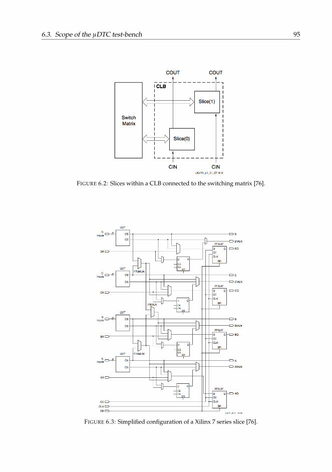
6.3. Scope of the µDTC test-bench 95
FIGURE 6.2: Slices within a CLB connected to the switching matrix [76].
FIGURE 6.3: Simplified configuration of a Xilinx 7 series slice [76].
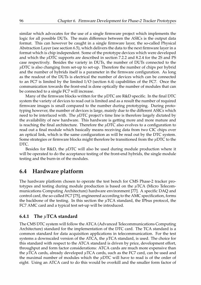
96 Chapter 6. Firmware Development for Phase-2 Tracker Prototypes
similar which advocates for the use of a single firmware project which implements thelogic for all possible DUTs. The main difference between the ASICs is the output dataformat. This can however be caught in a single firmware layer, the so-called PhysicalAbstraction Layer (see section 6.5), which delivers the data to the next firmware layer in aformat which is chip independent. Some of the prototype devices which were developedand which the µDTC supports are described in section 7.2.2 and 8.2.4 for the 2S and PScase respectively. Besides the variety in DUTs, the number of DUTs connected to theµDTC is also changing from set-up to set-up. Therefore the number of chips per hybridand the number of hybrids itself is a parameter in the firmware configuration. As longas the readout of the DUTs is electrical the number of devices which can be connectedto an FC7 is limited by the limited I/O (section 6.4) capabilities of the FC7. Once thecommunication towards the front-end is done optically the number of modules that canbe connected to a single FC7 will increase.
Many of the firmware blocks written for the µDTC are R&D specific. In the final DTCsystem the variety of devices to read out is limited and as a result the number of requiredfirmware images is small compared to the number during prototyping. During proto-typing however, the number of devices is large, mainly due to the different ASICs whichneed to be interfaced with. The µDTC project’s time line is therefore largely dictated bythe availability of new hardware. This hardware is getting more and more mature andis reaching the final architecture. Therefore the µDTC also evolves to a configuration toread out a final module which basically means receiving data from two CIC chips overan optical link, which is the same configuration as will be read out by the DTC system.Some strategies or firmware blocks might therefore be transitioned from the µDTC to theDTC.
Besides for R&D, the µDTC will also be used during module production where itwill be operated to do the acceptance testing of the front-end hybrids, the single moduletesting and the burn-in of the modules.
6.4 Hardware platform
The hardware platform chosen to operate the test bench for CMS Phase-2 tracker pro-totypes and testing during module production is based on the µTCA (Micro Telecom-munications Computing Architecture) hardware environment [77]. A specific DAQ andcontrol card, the so-called FC7 [75], engineered according to the AMC specification, formsthe backbone of the testing. In this section the µTCA standard, the IPbus protocol, theFC7 AMC card and a typical test set-up will be introduced.
6.4.1 The µTCA standardThe CMS DTC system will follow the ATCA (Advanced Telecommunications ComputingArchitecture) standard for the implementation of the DTC card. The TCA standard is acommon standard for data acquisition applications in telecommunication. For the testsystems a downscaled version of the ATCA, the µTCA standard, is used. The choice forthis standard with respect to the ATCA standard is driven by price, development effort,throughput and form factor considerations: ATCA cards are much more expensive thanthe µTCA cards, already developed µTCA cards, such as the FC7 card, can be used andthe maximal number of modules which the µDTC will have to read is of the order ofeight. Using an ATCA card to do this would be overkill and the smaller form factor of
6.4. Hardware platform 97
the µTCA cards (73.8 × 181.5 mm2 for single width or 148.8 × 181.5 mm2 for doublewidth) with respect to the ATCA card (280 ×322 mm2) makes them much more practicalfor use during R&D and module production.
Multiple µTCA blades can be operated in µTCA crates (see for example Figure 6.9b)which also house powering modules and a shelf manager, the so-called MCH (MicroTCACarrier Hub). This MCH controls the powering, cooling, hot swap and failure scenariosof the AMCs in the crate. The shelf manager and the AMC cards are interconnected overthe µTCA crate’s backplane. The MCH is also used as data hub to the AMCs. MCHs im-plementing different kinds of protocols (Gigabit Ethernet, PCI Express,...) are available.External systems can connect to the MCH via e.g. front panel Ethernet ports.
Besides using the FC7 µTCA card in a crate, the card can also be used in a bench topconfiguration, as illustrated in Figure 6.5. In this case the backplane is simply replacedby a dedicated PCB (Printed Circuit Board) which enables connection to the back-sideadapter on the FC7.
6.4.2 The IPbus protocolThe IPbus protocol [78] is a reliable and high performance control link specifically de-signed for use in particle physics systems as a control link for µTCA and ATCA basedsystems. The IPbus suite consists of a software interface (µHAL) and a firmware blockwhich can be adopted by users. The IPbus protocol operates over a bus with 32-bit ad-dressing, which is more than sufficient for most applications, and 32-bit data transfer.The IPbus packet is packed into a UDP, IP and Ethernet packet. The IPbus packet itselfconsists of a header, followed by a number of IPbus transactions, which each consist of aheader and a body. The header specifies the request (read or write) and the size of the re-quest, specifying the depth of the transaction. FIFO read and write are also implementedwhere the address stays the same. On the target side the IPbus protocol is decoded bya master which forwards commands to IPbus slaves which each cover a certain addressrange and can handle the decoded IPbus requests the way they like (configure a setting,start a state machine,...) and respond with an acknowledge and data in case of a read.
Most efficient transfer of data happens if there are many IPbus transactions in onepackage, as this limits the relative contribution of the headers to the transferred data.Through a combination of packet IDs, a protocol between client and target to retrieveinformation on the target and resends of lost packages the IPbus protocol ensures reliabletransactions.
The IPbus throughput, defined as the amount of user data transferred or received perunit of time, was measured to be around 0.5 Gb/s [78] for 1-to-1 block transfers withblocks containing a payload larger than 1 MB. This is for the case where the softwarecontrols a single hardware device.
6.4.3 The FC7 AMC cardThe FC7 AMC card, shown in Figure 6.4, is a custom designed DAQ and system controlcard for applications in the CMS collaboration. It is the successor of the CMS GLIB AMCcard and was designed initially for usage in for example the CMS Pixel Front-End Driverwhich performs the DAQ of the CMS Phase-1 Pixel detector. The central component onthe FC7 is a Kintex7 XC7K420T FPGA which is programmable by the user to implementthe experiment specific DAQ and control logic. Some of the available resources on thisspecific FPGA are summarised in Table 6.1. The FC7 also hosts a 4 Gb (128M×32b) DDR3
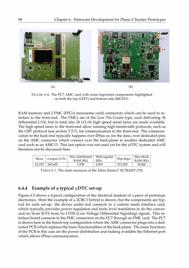
98 Chapter 6. Firmware Development for Phase-2 Tracker Prototypes
(a) (b)
FIGURE 6.4: The FC7 AMC card with some important components highlightedon both the top (LEFT) and bottom side (RIGHT).
RAM memory and 2 FMC (FPGA mezzanine card) connectors which can be used to in-terface to the front-end. The FMCs are of the Low Pin Count type, each delivering 34differential I/Os, but in total also 20 (12+8) high speed serial lanes are made available.The high speed lanes to the front-end allow running high bandwidth protocols, such asthe GBT protocol (see section 5.5.7), for communication to the front-end. The communi-cation to the back-end typically happens over IPbus or, for the data, over dedicated pinson the AMC connector which connect over the back-plane to another dedicated AMCcard such as an AMC13. This last option was not used yet for the µDTC system and willtherefore not be discussed here.
Slices 6-input LUTs Max distributedRAM (Kb)
Shift register(Kb) Flip-flops Max block
RAM (Kb)65,150 260,600 5,938 2,969 521,200 30,060
TABLE 6.1: The main resources of the Xilinx Kintex7 XC7K420T [79].
6.4.4 Example of a typical µDTC set-upFigure 6.5 shows a typical configuration of the electrical readout of a piece of prototypeelectronics. Here the example of a 2CBC3 hybrid is shown, but the components are typ-ical for each set-up: the device under test connects to a custom made interface card,which typically provides power regulation and hosts level translators to do the conver-sion to/from SLVS from/to LVDS (Low-Voltage Differential Signaling) signals. This in-terface board connects to the FMC connectors on the FC7 through an FMC card. The FC7is shown here in the bench-top configuration where the AMC connector plugs into a ded-icated PCB which replaces the basic functionalities of the back-plane. The main functionsof the PCB in this case are the power distribution and making available the Ethernet portwhich allows IPbus communication.
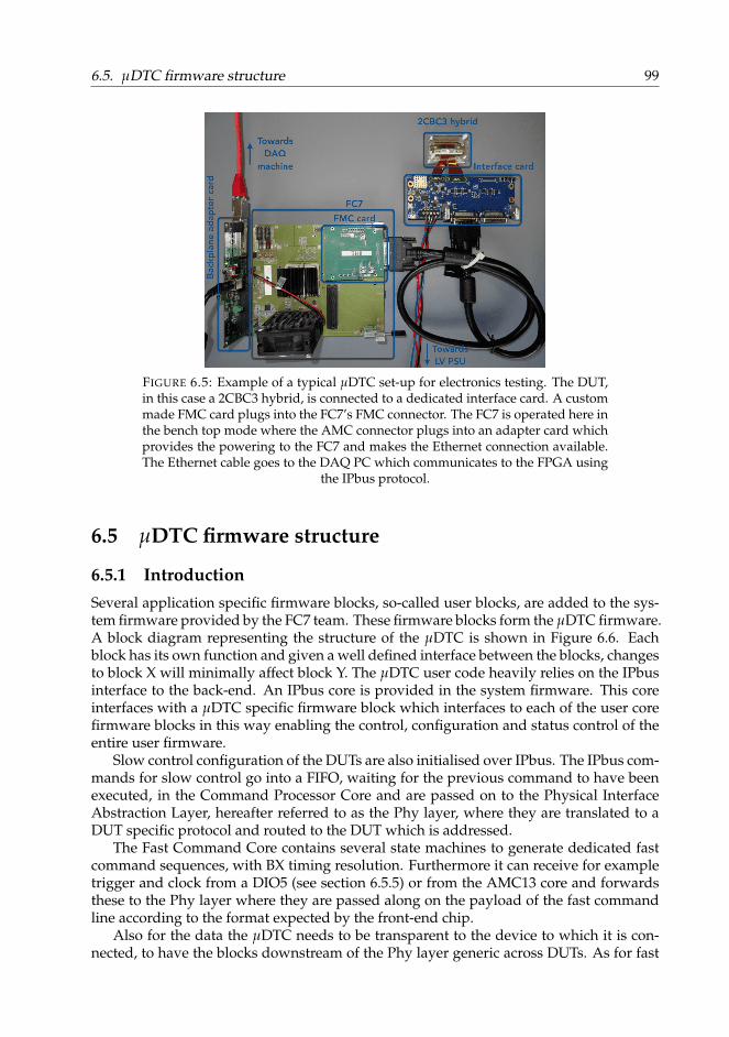
6.5. µDTC firmware structure 99
FIGURE 6.5: Example of a typical µDTC set-up for electronics testing. The DUT,in this case a 2CBC3 hybrid, is connected to a dedicated interface card. A custommade FMC card plugs into the FC7’s FMC connector. The FC7 is operated here inthe bench top mode where the AMC connector plugs into an adapter card whichprovides the powering to the FC7 and makes the Ethernet connection available.The Ethernet cable goes to the DAQ PC which communicates to the FPGA using
the IPbus protocol.
6.5 µDTC firmware structure
6.5.1 IntroductionSeveral application specific firmware blocks, so-called user blocks, are added to the sys-tem firmware provided by the FC7 team. These firmware blocks form the µDTC firmware.A block diagram representing the structure of the µDTC is shown in Figure 6.6. Eachblock has its own function and given a well defined interface between the blocks, changesto block X will minimally affect block Y. The µDTC user code heavily relies on the IPbusinterface to the back-end. An IPbus core is provided in the system firmware. This coreinterfaces with a µDTC specific firmware block which interfaces to each of the user corefirmware blocks in this way enabling the control, configuration and status control of theentire user firmware.
Slow control configuration of the DUTs are also initialised over IPbus. The IPbus com-mands for slow control go into a FIFO, waiting for the previous command to have beenexecuted, in the Command Processor Core and are passed on to the Physical InterfaceAbstraction Layer, hereafter referred to as the Phy layer, where they are translated to aDUT specific protocol and routed to the DUT which is addressed.
The Fast Command Core contains several state machines to generate dedicated fastcommand sequences, with BX timing resolution. Furthermore it can receive for exampletrigger and clock from a DIO5 (see section 6.5.5) or from the AMC13 core and forwardsthese to the Phy layer where they are passed along on the payload of the fast commandline according to the format expected by the front-end chip.
Also for the data the µDTC needs to be transparent to the device to which it is con-nected, to have the blocks downstream of the Phy layer generic across DUTs. As for fast

100 Chapter 6. Firmware Development for Phase-2 Tracker Prototypes
FMCconnector 1
FMCconnector 2
To/FromDUT
Use
rco
re
System core
Back
-pla
ne
DDR3 interface IPBus core
IPBus configuration, control and status
DataReadout
Block
Physical Interface Abstratcion Layer
DDR3 memory
FPG
A
CommandProcessorCore
FastCommandCore AMC13
Core
DIO5 Core
ClockGeneratorandDistribution
FC7
Clock Firmware configuration Fast commands
Data DUT slow control
Legend
FIGURE 6.6: Top level view of the µDTC firmware showing only the most rele-vant blocks.
6.5. µDTC firmware structure 101
and slow control communication, the changes in data format due to a change in hard-ware type are mostly caught in the Phy layer. In this layer, the data from the front-end isreceived and formatted to a more generic form. A more detailed description of the PhyLayer is given in section 6.5.2. The formatted data from the Phy Layer is sent to the DataReadout Block (section 6.5.3) where the data is buffered and awaiting readout over IPbusor is sent to the DDR3 memory on the FC7.
All the blocks are clocked from the Clock Generator and Distribution block whichuses the FC7’s oscillator or an external clock as a reference. Most of the firmware runsat a frequency of 40 MHz. There are some exceptions where higher clock frequencies areused to save on logic utilisation.
The following sections give a bird’s eye view on the µDTC firmware. Some specificblocks, which are dedicated for specialised tests will be described in later chapters wherethe testing is also explained.
6.5.2 The Physical Interface Abstraction LayerThe Physical Interface Abstraction Layer forms the interface to the front-end. It alsoabstracts the incoming and outgoing data formats for different front-ends in order tominimise the changes which need to be done on the downstream part of the firmware.The Physical Interface Abstraction Layer interfaces the fast commands, the slow controlcommands and the data from the front-end with the other blocks of the firmware. Moreinformation on these data streams can be found in the following sections.
6.5.2.1 Fast commands
For the fast command, the Physical Interface Abstraction Layer forms the transition fromthe 40 MHz regime to the 320 MHz regime using an OSERDES. The 110XXXX1 patternis continuously sent whilst a 4-bit bus at 40 MHz is received from the Fast CommandBlock which holds the fast commands to be transmitted to the front-end. The phase, withrespect to the 320 MHz clock, of the fast command going to the chip is configurable.
6.5.2.2 Slow control
The slow control part of the Phy layer is illustrated in Figure 6.7. The input slow con-trol command from the Command Processor Block to the Physical Interface AbstractionLayer specifies: whether a broadcast to all chips is requested, the hybrid id (4 bits), thechip id (5 bits), the page (only for CBC chips), read/write bit, the register address (up to 2bytes to support 16-bit addressing for the MPA and SSA) and the data to be sent (multiplebytes to support the sequential read/write).
The hybrid id is used in the multiplexer which forwards the slow control commandto the correct hybrid’s master and waits for an acknowledge from this master signifyingthe acknowledge from the front-end chip. When a command is forwarded to a hybrid,the multiplexer requires an acknowledge within a specified time and if not received itgenerates a time-out error. This time-out error is propagated to the Command ProcessorBlock.
For each hybrid the wrapper handles for example the register paging system whichis used in the CBC chips. It also translates the chip id (5 bits) to the chip address (7 bits).The exact translation can be configured over IPbus. Furthermore it handles the sendingof the correct chip address in case a broadcast to all chips is requested.
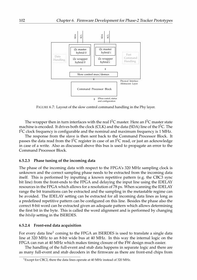
102 Chapter 6. Firmware Development for Phase-2 Tracker Prototypes
Command Processor Block
Physical InterfaceAbstracion Layer
DataHandling
FastCommandHandling
Slow control mux/demux
i2c wrapperhybrid 0
i2c masterhybrid 0
...
SDA
SCL
SDA
SCL
i2c wrapperhybrid i
i2c masterhybrid i
IPbus contol, statusand configuration
FIGURE 6.7: Layout of the slow control command handling in the Phy layer.
The wrapper then in turn interfaces with the real I2C master. Here an I2C master statemachine is encoded. It drives both the clock (CLK) and the data (SDA) line of the I2C. TheI2C clock frequency is configurable and the nominal and maximum frequency is 1 MHz.
The response from the slave is then sent back to the Command Processor Block. Itpasses the data read from the I2C register in case of an I2C read, or just an acknowledgein case of a write. Also as discussed above this bus is used to propagate an error to theCommand Processor Block.
6.5.2.3 Phase tuning of the incoming data
The phase of the incoming data with respect to the FPGA’s 320 MHz sampling clock isunknown and the correct sampling phase needs to be extracted from the incoming dataitself. This is performed by inputting a known repetitive pattern (e.g. the CBC3 syncbit line) from the front-ends to the FPGA and delaying the input line using the IDELAYresources in the FPGA which allows for a resolution of 78 ps. When scanning the IDELAYrange the bit transitions can be extracted and the sampling in the metastable regime canbe avoided. The IDELAY setting can be extracted for all incoming data lines as long asa predefined repetitive pattern can be configured on this line. Besides the phase also thecorrect 8-bit word can be extracted given an adequate pattern which allows determiningthe first bit in the byte. This is called the word alignment and is performed by changingthe bitslip setting in the ISERDES.
6.5.2.4 Front-end data acquisition
For every data line1 coming to the FPGA an ISERDES is used to translate a single dataline at 320 MHz to an 8-bit wide bus at 40 MHz. In this way the internal logic on theFPGA can run at 40 MHz which makes timing closure of the FW design much easier.
The handling of the full-event and stub data happens in separate logic and there areas many full-event and stub decoders in the firmware as there are front-end chips from
1Except for CBC2, there the data lines operate at 40 MHz instead of 320 MHz.
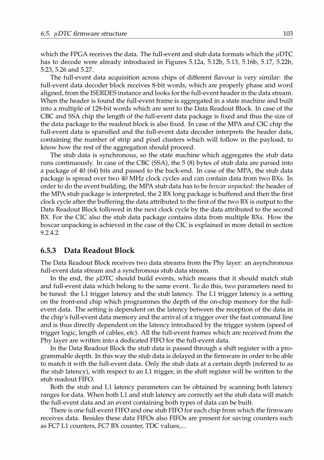
6.5. µDTC firmware structure 103
which the FPGA receives the data. The full-event and stub data formats which the µDTChas to decode were already introduced in Figures 5.12a, 5.12b, 5.13, 5.16b, 5.17, 5.22b,5.23, 5.26 and 5.27.
The full-event data acquisition across chips of different flavour is very similar: thefull-event data decoder block receives 8-bit words, which are properly phase and wordaligned, from the ISERDES instance and looks for the full-event header in the data stream.When the header is found the full-event frame is aggregated in a state machine and builtinto a multiple of 128-bit words which are sent to the Data Readout Block. In case of theCBC and SSA chip the length of the full-event data package is fixed and thus the size ofthe data package to the readout block is also fixed. In case of the MPA and CIC chip thefull-event data is sparsified and the full-event data decoder interprets the header data,containing the number of strip and pixel clusters which will follow in the payload, toknow how the rest of the aggregation should proceed.
The stub data is synchronous, so the state machine which aggregates the stub dataruns continuously. In case of the CBC (SSA), the 5 (8) bytes of stub data are parsed intoa package of 40 (64) bits and passed to the back-end. In case of the MPA, the stub datapackage is spread over two 40 MHz clock cycles and can contain data from two BXs. Inorder to do the event building, the MPA stub data has to be boxcar unpacked: the header ofthe MPA stub package is interpreted, the 2 BX long package is buffered and then the firstclock cycle after the buffering the data attributed to the first of the two BX is output to theData Readout Block followed in the next clock cycle by the data attributed to the secondBX. For the CIC also the stub data package contains data from multiple BXs. How theboxcar unpacking is achieved in the case of the CIC is explained in more detail in section9.2.4.2.
6.5.3 Data Readout BlockThe Data Readout Block receives two data streams from the Phy layer: an asynchronousfull-event data stream and a synchronous stub data stream.
In the end, the µDTC should build events, which means that it should match stuband full-event data which belong to the same event. To do this, two parameters need tobe tuned: the L1 trigger latency and the stub latency. The L1 trigger latency is a settingon the front-end chip which programmes the depth of the on-chip memory for the full-event data. The setting is dependent on the latency between the reception of the data inthe chip’s full-event data memory and the arrival of a trigger over the fast command lineand is thus directly dependent on the latency introduced by the trigger system (speed oftrigger logic, length of cables, etc). All the full-event frames which are received from thePhy layer are written into a dedicated FIFO for the full-event data.
In the Data Readout Block the stub data is passed through a shift register with a pro-grammable depth. In this way the stub data is delayed in the firmware in order to be ableto match it with the full-event data. Only the stub data at a certain depth (referred to asthe stub latency), with respect to an L1 trigger, in the shift register will be written to thestub readout FIFO.
Both the stub and L1 latency parameters can be obtained by scanning both latencyranges for data. When both L1 and stub latency are correctly set the stub data will matchthe full-event data and an event containing both types of data can be built.
There is one full-event FIFO and one stub FIFO for each chip from which the firmwarereceives data. Besides these data FIFOs also FIFOs are present for saving counters suchas FC7 L1 counters, FC7 BX counter, TDC values,...
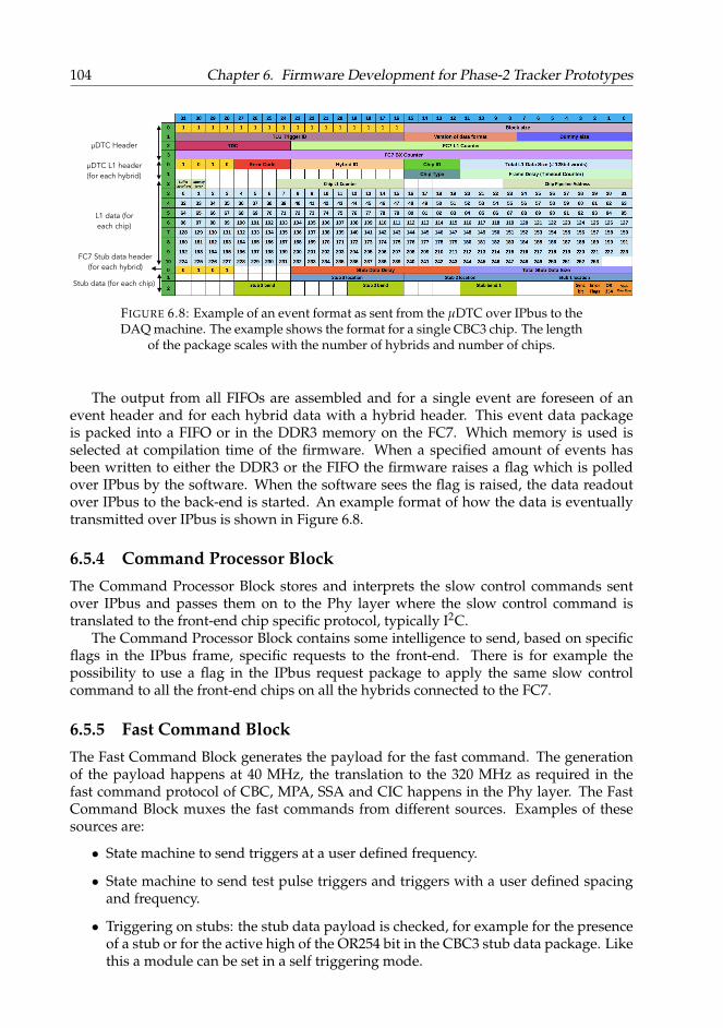
104 Chapter 6. Firmware Development for Phase-2 Tracker Prototypes
μDTC Header
L1 data (for each chip)
FC7 Stub data header (for each hybrid)
μDTC L1 header (for each hybrid)
Stub data (for each chip)
FIGURE 6.8: Example of an event format as sent from the µDTC over IPbus to theDAQ machine. The example shows the format for a single CBC3 chip. The length
of the package scales with the number of hybrids and number of chips.
The output from all FIFOs are assembled and for a single event are foreseen of anevent header and for each hybrid data with a hybrid header. This event data packageis packed into a FIFO or in the DDR3 memory on the FC7. Which memory is used isselected at compilation time of the firmware. When a specified amount of events hasbeen written to either the DDR3 or the FIFO the firmware raises a flag which is polledover IPbus by the software. When the software sees the flag is raised, the data readoutover IPbus to the back-end is started. An example format of how the data is eventuallytransmitted over IPbus is shown in Figure 6.8.
6.5.4 Command Processor BlockThe Command Processor Block stores and interprets the slow control commands sentover IPbus and passes them on to the Phy layer where the slow control command istranslated to the front-end chip specific protocol, typically I2C.
The Command Processor Block contains some intelligence to send, based on specificflags in the IPbus frame, specific requests to the front-end. There is for example thepossibility to use a flag in the IPbus request package to apply the same slow controlcommand to all the front-end chips on all the hybrids connected to the FC7.
6.5.5 Fast Command BlockThe Fast Command Block generates the payload for the fast command. The generationof the payload happens at 40 MHz, the translation to the 320 MHz as required in thefast command protocol of CBC, MPA, SSA and CIC happens in the Phy layer. The FastCommand Block muxes the fast commands from different sources. Examples of thesesources are:
• State machine to send triggers at a user defined frequency.
• State machine to send test pulse triggers and triggers with a user defined spacingand frequency.
• Triggering on stubs: the stub data payload is checked, for example for the presenceof a stub or for the active high of the OR254 bit in the CBC3 stub data package. Likethis a module can be set in a self triggering mode.
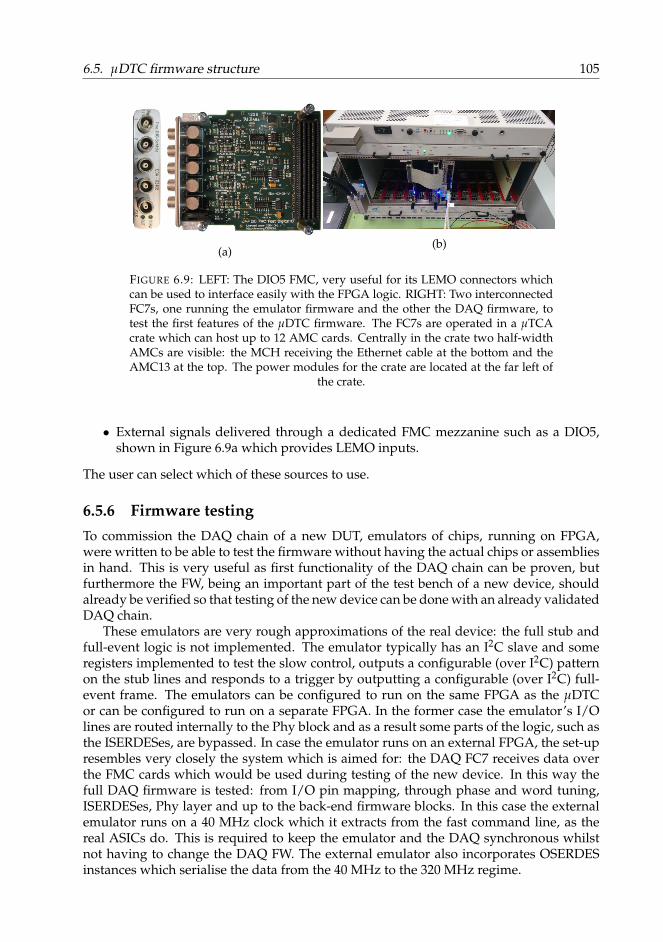
6.5. µDTC firmware structure 105
(a)(b)
FIGURE 6.9: LEFT: The DIO5 FMC, very useful for its LEMO connectors whichcan be used to interface easily with the FPGA logic. RIGHT: Two interconnectedFC7s, one running the emulator firmware and the other the DAQ firmware, totest the first features of the µDTC firmware. The FC7s are operated in a µTCAcrate which can host up to 12 AMC cards. Centrally in the crate two half-widthAMCs are visible: the MCH receiving the Ethernet cable at the bottom and theAMC13 at the top. The power modules for the crate are located at the far left of
the crate.
• External signals delivered through a dedicated FMC mezzanine such as a DIO5,shown in Figure 6.9a which provides LEMO inputs.
The user can select which of these sources to use.
6.5.6 Firmware testingTo commission the DAQ chain of a new DUT, emulators of chips, running on FPGA,were written to be able to test the firmware without having the actual chips or assembliesin hand. This is very useful as first functionality of the DAQ chain can be proven, butfurthermore the FW, being an important part of the test bench of a new device, shouldalready be verified so that testing of the new device can be done with an already validatedDAQ chain.
These emulators are very rough approximations of the real device: the full stub andfull-event logic is not implemented. The emulator typically has an I2C slave and someregisters implemented to test the slow control, outputs a configurable (over I2C) patternon the stub lines and responds to a trigger by outputting a configurable (over I2C) full-event frame. The emulators can be configured to run on the same FPGA as the µDTCor can be configured to run on a separate FPGA. In the former case the emulator’s I/Olines are routed internally to the Phy block and as a result some parts of the logic, such asthe ISERDESes, are bypassed. In case the emulator runs on an external FPGA, the set-upresembles very closely the system which is aimed for: the DAQ FC7 receives data overthe FMC cards which would be used during testing of the new device. In this way thefull DAQ firmware is tested: from I/O pin mapping, through phase and word tuning,ISERDESes, Phy layer and up to the back-end firmware blocks. In this case the externalemulator runs on a 40 MHz clock which it extracts from the fast command line, as thereal ASICs do. This is required to keep the emulator and the DAQ synchronous whilstnot having to change the DAQ FW. The external emulator also incorporates OSERDESinstances which serialise the data from the 40 MHz to the 320 MHz regime.
106 Chapter 6. Firmware Development for Phase-2 Tracker Prototypes
6.6 Summary
The µDTC test bench, based on the FC7 AMC card, is used to qualify prototype ASICsand modules for the Phase-2 Outer Tracker and will also be used for qualification ofcomponents and modules during module construction. The µDTC is used to configure,control and acquire data from the DUT. The firmware’s block structure allows most ofthe firmware to be left unchanged when going to a different flavour of DUT. Most of thechanges in data format are caught in the µDTC’s Physical Interface Abstraction Layer.Validation of the test bench is required before actual testing with the real hardware canstart. This is mostly done by developing emulations of the DUT which can run on asecond FC7.
6.7 Author’s contribution
The author was one of the main contributors to the OT µDTC firmware since the startof the development. Experience had to be gained on how to structure the code and asignificant effort was made to make the code generic for different devices. The authormainly contributed to the development of the Phy Layer in the firmware and to testingof the firmware’s operation by using emulators developed by the author. The testing alsorequires a thorough understanding of the front-ends and the other firmware blocks andrequires some dedicated software. The author also contributed to the latter.
Once the firmware was tested with emulators and with a first real device, the testbench was made available to the community. The author also provided support for theuse of the test-bench, most importantly during test beam activities.

107
Chapter 7
2S Prototype Testing
7.1 Introduction
CBC chips were the first Phase-2 Outer Tracker readout chips to become available. As aresult, the first goal of the µDTC project was to be able to read out and control devicesbased on these ASICs. This chapter will briefly discuss the specificities of this µDTCflavour and its use cases (section 7.2). In section 7.3, a study of cross-talk between CBCchannels is discussed which exemplifies the usability of the µDTC for bench-top testing.
7.2 Specific firmware development for 2S based systems
7.2.1 IntroductionµDTC firmware blocks developed for the readout of CBC based devices are fairly straight-forward: no boxcar unpacking of the stub data needs to be performed and the full-eventdata package has a fixed length. Furthermore the µDTC test bench was not used to per-form the initial single chip qualification. The initial testing of the CBC chips was alreadyperformed with another set-up and during the design of the µDTC for CBC readout itcould be trusted upon that e.g. the data formats were exactly the ones provided in thedocumentation. The µDTC was used during later stages of the development to test andqualify the CBC based prototypes which are listed in the next section and to perform testbeams with CBC based prototype modules.
7.2.2 Use casesThe µDTC was used to test the following CBC-based devices:
• 2CBC2 hybrid and 2CBC2 mini-module.
• 8CBC2 hybrid and 8CBC2 full size module.
• PS-MCK FEH hybrid: a hybrid with the form factor of a PS front-end hybrid, butwith two CBC2 chips as active components.
• CBC3 stand-alone: used for initial verification of the CBC3 µDTC.
• 2CBC3 hybrid and 2CBC3 mini-module.
• 8CBC3 hybrid.
These devices are illustrated in Figure 7.1.

108 Chapter 7. 2S Prototype Testing
(a)
(b)
(c)
(d)
(e)
(f)
(g)
(h)
(i)
FIG
UR
E7.
1:(a
)2C
BC2
hybr
id.
(b)
8CBC
2hy
brid
.(c
)2C
BC2
min
i-m
odul
e.(d
)Fu
ll-si
zem
odul
ew
ith
prot
otyp
e2S
sens
ors
and
8CBC
2hy
brid
s,on
eof
whi
chis
conn
ecte
dto
anin
terf
ace
boar
d.(e
)Si
ngle
CBC
3ch
ipon
carr
ier
card
conn
ecte
dto
anin
terf
ace
boar
d.(f
)2C
BC3
hybr
id.(
g)2C
BC3
min
i-m
odul
eco
nnec
ted
toit
sin
terf
ace
card
.(h)
PS-M
CK
hybr
id.(
i)8C
BC3
hybr
id.
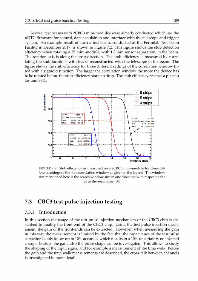
7.3. CBC3 test pulse injection testing 109
Several test beams with 2CBC3 mini-modules were already conducted which use theµDTC firmware for control, data acquisition and interface with the telescope and triggersystem. An example result of such a test beam, conducted at the Fermilab Test BeamFacility in December 2017, is shown in Figure 7.2. This figure shows the stub detectionefficiency when rotating a 2S mini-module, with 1.8 mm sensor separation, in the beam.The rotation axis is along the strip direction. The stub efficiency is measured by corre-lating the stub locations with tracks reconstructed with the telescope in the beam. Thefigure shows the stub efficiency for three different settings of the correlation window fit-ted with a sigmoid function. The larger the correlation window the more the device hasto be rotated before the stub efficiency starts to drop. The stub efficiency reaches a plateauaround 99%.
FIGURE 7.2: Stub efficiency as measured on a 2CBC3 mini-module for three dif-ferent settings of the stub correlation window as given in the legend. The windowsize mentioned here is the search window size in one direction with respect to the
hit in the seed layer [80].
7.3 CBC3 test pulse injection testing
7.3.1 IntroductionIn this section the usage of the test pulse injection mechanism of the CBC3 chip is de-scribed to qualify the front-end of the CBC3 chip. Using the test pulse injection mech-anism, the gain of the front-ends can be extracted. However, when measuring the gainin this way the measurement is limited by the fact that the capacitance of the test pulsecapacitor is only know up to 10% accuracy which results in a 10% uncertainty on injectedcharge. Besides the gain, also the pulse shape can be investigated. This allows to studythe shaping of the input signal and for example a measurement of the time walk. Beforethe gain and the time walk measurements are described, the cross-talk between channelsis investigated in more detail.

110 Chapter 7. 2S Prototype Testing
Delay resolution 1 ns steps at 40 MHz Master ClockDelay range 25 ns at 40 MHz Master ClockDelay variation ± 100 ps in 25 ns or < ± 5 ps in 1 nsCharge step resolution 1 test pulse LSB = 0.086 fC = 536.7 e−
Charge step dynamic range 255 test pulse LSB = 22 fC = 137.3 ke−
Charge step variance due to calibrationcapacitor variation 0.0086 fC = 53.7 e− (±10%)
Test groups
32 (except for the last test group whichhas 30 instead of 32 channels)channels are pulsed at the same time,resulting in 8 test groups for the full chip.
Connectivity 1 test capacitor per channel
TABLE 7.1: Summary of the main properties of the CBC test pulse injection mech-anism [68].
7.3.2 ProcedureThe reconstruction of a full pulse shape with the CBC3 digital readout is fairly involved.The procedure described here uses the CBC3’s internal test pulse injection mechanism,described in section 5.5.5.2 and summarised in Table 7.1, and is as follows:
1. Set-up:
(a) Tune the front-ends of the chips so that a common threshold can be applied toall channels.
(b) Configure the firmware to send test pulse trigger fast commands followed byL1A triggers and find the correct L1 latency setting for the chip. In this spe-cific case the L1 latency is known as it is the time between the sending of thetest pulse trigger and the L1A trigger, which is a setting of the firmware statemachine.
2. Run:
(a) Make an S-curve for all the CBC3 channels whilst injecting charge. Making anS-curve consists of scanning the threshold range: at each threshold setting anumber of triggers has to be sent in order to extract the average occupancy,with sufficient statistical precision, from the full-event data.
(b) Extract the pedestals from the S-curve and save the pedestals of these S-curvesfor all the channels. The pedestals are defined as the threshold for which theoccupancy is 50%.
(c) Delay the test pulse using the on chip DLL which has a resolution of 1 ns anda range of 25 ns. If it is required to go beyond this range, change the L1 latencyto make a 25 ns step.
(d) Start over at 2.(a).
In the end this two dimensional scan in threshold and time will result in the recon-structed test pulses for all the channels if the pedestal, deduced from the S-curve, is plot-ted as function of time.
7.3.3 ResultsFigure 7.3a shows an example of a reconstructed pulse shape, when injecting a chargerepresenting a MIP (30 test pulse LSB = 30× 0.086 fC = 2.58 fC = 30× 536.7 e− = 16.1 ke−)
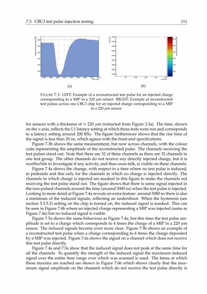
7.3. CBC3 test pulse injection testing 111
4960 4980 5000 5020 5040 5060 5080 5100 5120time (ns)
500
520
540
560
580
600
Ped
esta
l [T
hres
hold
(LS
B)]
(a)
50 100 150 200 250channel
4960
4980
5000
5020
5040
5060
5080
5100
5120
time
[ns]
500
520
540
560
580
600
ped
esta
l [T
hres
hold
(LS
B)]
(b)
FIGURE 7.3: LEFT: Example of a reconstructed test pulse for an injected chargecorresponding to a MIP in a 220 µm sensor. RIGHT: Example of reconstructedtest pulses across one CBC3 chip for an injected charge corresponding to a MIP
in a 220 µm sensor.
for sensors with a thickness of ≈ 220 µm (extracted from Figure 3.3a). The time, shownon the x-axis, reflects the L1 latency setting at which these tests were run and correspondsto a latency setting around 200 BXs. The figure furthermore shows that the rise time ofthe signal is less than 20 ns, which agrees with the front-end specifications.
Figure 7.3b shows the same measurement, but now across channels, with the colourcode representing the amplitude of the reconstructed pulse. The channels receiving thetest pulses stand out. Note that there are 32 of these channels as there are 32 channels inone test group. The other channels do not receive any directly injected charge, but it isworthwhile to investigate if any activity, and thus cross-talk, is visible on these channels.
Figure 7.4a shows the change, with respect to a time where no test pulse is induced,in pedestals and this only for the channels in which no charge is injected directly. Thechannels in which charge is injected are masked in this figure to make the channels notreceiving the test pulse stand out. The figure shows that there is some signal injected inthe non-pulsed channels around the time (around 5000 ns) when the test pulse is injected.Looking in more detail at Figure 7.4a reveals an extra feature: around 5080 ns there is alsoa minimum of the induced signals, reflecting an undershoot. When the hysteresis (seesection 5.5.5.2) setting on the chip is turned on, the induced signal is masked. This canbe seen in Figure 7.4b where an injected charge representing a MIP was injected (same asFigure 7.4a) but no induced signal is visible.
Figure 7.5a shows the same behaviour as Figure 7.4a, but this time the test pulse am-plitude is set to a charge which corresponds to 4 times the charge of a MIP in a 220 µmsensor. The induced signals become even more clear. Figure 7.5b shows an example ofa reconstructed test pulse when a charge corresponding to 4 times the charge depositedby a MIP was injected. Figure 7.6a shows the signal on a channel which does not receivethis test pulse directly.
Figure 7.4a and 7.5a show that the induced signal does not peak at the same time forall the channels. To quantify the strength of the induced signal the maximum inducedsignal over the entire time range over which was scanned is used. The times at whichthese maxima are reached are shown in Figure 7.6b which shows clearly that the max-imum signal amplitude on the channels which do not receive the test pulse directly is
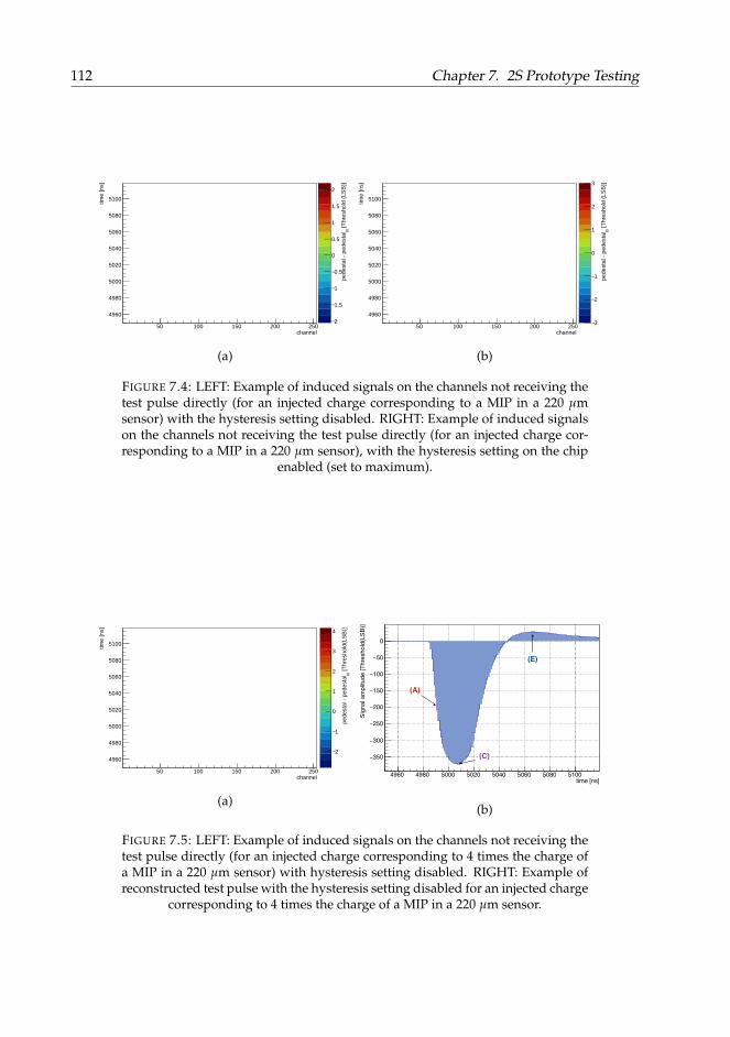
112 Chapter 7. 2S Prototype Testing
50 100 150 200 250channel
4960
4980
5000
5020
5040
5060
5080
5100
time
[ns]
2−
1.5−
1−
0.5−
0
0.5
1
1.5
2
[Thr
esho
ld (
LSB
)]t0
pede
stal
- p
edes
tal
(a)
50 100 150 200 250channel
4960
4980
5000
5020
5040
5060
5080
5100
time
[ns]
3−
2−
1−
0
1
2
3
[Thr
esho
ld (
LSB
)]t0
pede
stal
- p
edes
tal
(b)
FIGURE 7.4: LEFT: Example of induced signals on the channels not receiving thetest pulse directly (for an injected charge corresponding to a MIP in a 220 µmsensor) with the hysteresis setting disabled. RIGHT: Example of induced signalson the channels not receiving the test pulse directly (for an injected charge cor-responding to a MIP in a 220 µm sensor), with the hysteresis setting on the chip
enabled (set to maximum).
50 100 150 200 250channel
4960
4980
5000
5020
5040
5060
5080
5100
time
[ns]
2−
1−
0
1
2
3
4
[Thr
esho
ld(L
SB
)]t0
pede
stal
- p
edes
tal
(a)
4960 4980 5000 5020 5040 5060 5080 5100time [ns]
350−
300−
250−
200−
150−
100−
50−
0
Sign
al a
mpl
itude
[Thr
esho
ld(L
SB)]
(A)
(C)
(E)
(b)
FIGURE 7.5: LEFT: Example of induced signals on the channels not receiving thetest pulse directly (for an injected charge corresponding to 4 times the charge ofa MIP in a 220 µm sensor) with hysteresis setting disabled. RIGHT: Example ofreconstructed test pulse with the hysteresis setting disabled for an injected charge
corresponding to 4 times the charge of a MIP in a 220 µm sensor.

7.3. CBC3 test pulse injection testing 113
(A) Time at which the derivative of the test pulse amplitude with respectto time reaches the maximum.
(B) Time at which the induced signal amplitude reaches a maximum.(C) Time at which the test pulse amplitude reaches a minimum.(D) Time at which the induced signal amplitude reaches a minimum.(E) Time at which the test pulse amplitude reaches a maximum.
TABLE 7.2: Definitions of the moments in time used in Figure 7.6b.
4960 4980 5000 5020 5040 5060 5080 5100time (ns)
1.5−
1−
0.5−
0
0.5
1
1.5
2
2.5
Sign
al a
mpl
itude
(VC
TH)
Example of induced signal for an injected charge representing 4*MIP
(B)
(D)
(a)
20 40 60 80 100 120 [ns]0t - t
5
10
15
20
25
30
35
40
45
# ch
anne
ls
derivative wrt time reaches a maximum(A) Time for which the test pulse amplitude
amplitude reaches a maximum(B) Time for which the induced signal
amplitude reaches a minimum(C) Time for which the test pulse
amplitude reaches a minimum(D) Time for which the induced signal
amplitude reaches a maximum(E) Time for which the test pulse
(b)
FIGURE 7.6: LEFT: Example of induced signals on a channel not receiving thetest pulse directly (for an injected charge corresponding to 4 times the charge ofa MIP in a 220 µm sensor) with hysteresis disabled. RIGHT: Timing of test pulse
signals and of the induced signals.
indeed correlated with the time of test pulse injection. The figure shows some other spe-cific moments in time for the different channels. The definitions of these specific momentsin time are illustrated in Figure 7.5b and 7.6a and summarised in Table 7.2. The red dis-tribution in Figure 7.6b shows the distribution of the times where the reconstructed testpulse has the largest negative slope. This is followed by the green distribution whichshows the time when the induced signal is peaking. The purple distribution gives thetime distribution for which the test pulse reaches the minimum. The black and the bluedistributions give the times of the overshoot of respectively the induced signal and theinjected signal.
Figure 7.7a shows the strength of the induced signal for different amplitudes of thetest pulse. It shows that the hysteresis setting masks the effect of induced signal andcomparison with Figure 7.7b, which shows the actual measured amplitude of the testpulse, learns that the induced signal is of the order of 1% of the injected charge. This is arather small effect and it can be concluded that this cross-talk behaviour can be tolerated.In the tracker collaboration a set-up was developed to inject external signals in the front-ends by using photodiodes connected to the wire bond pads on the hybrid [81]. Thephotodiodes are illuminated with light pulses from LEDs driven by a pattern generatoron FPGA. In this way, up to 48 CBC channels can be stimulated at the same time, butmore interestingly for cross-talk studies is the fact that single channels can be pulsed.The latter is not possible when using the internal test pulse mechanism. With this set-upalso cross-talk of the order of 1% is measured on neighbouring channels.
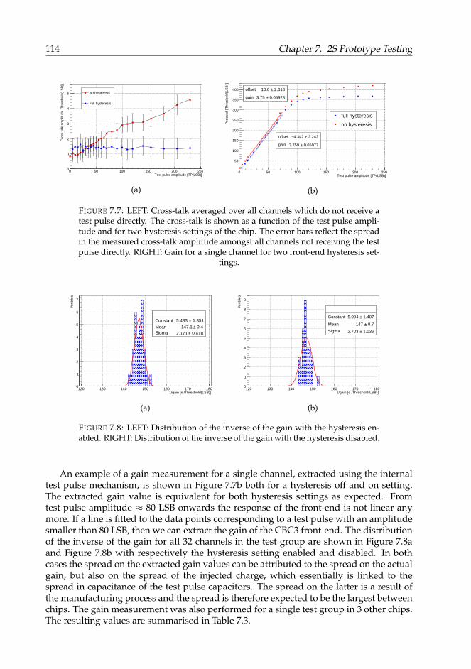
114 Chapter 7. 2S Prototype Testing
0 50 100 150 200 250Test pulse amplitude [TP(LSB)]
0
1
2
3
4
5
Cro
ss ta
lk a
mpl
itude
[Thr
esho
ld(L
SB
)]
No hysteresis
Full hysteresis
(a)
0 50 100 150 200 250Test pulse amplitude [TP(LSB)]
50
100
150
200
250
300
350
400
Ped
esta
l [T
hres
hold
(LS
B)]
offset 2.242±4.342 −
gain 0.05077± 3.759
offset 2.618± 10.6
gain 0.05928± 3.75
offset 2.618± 10.6
gain 0.05928± 3.75
full hysteresis
no hysteresis
(b)
FIGURE 7.7: LEFT: Cross-talk averaged over all channels which do not receive atest pulse directly. The cross-talk is shown as a function of the test pulse ampli-tude and for two hysteresis settings of the chip. The error bars reflect the spreadin the measured cross-talk amplitude amongst all channels not receiving the testpulse directly. RIGHT: Gain for a single channel for two front-end hysteresis set-
tings.
Constant 1.351± 5.483 Mean 0.4± 147.1 Sigma 0.418± 2.171
120 130 140 150 160 170 180/Threshold(LSB)]
-1/gain [e
0
1
2
3
4
5
6
7
#ent
ries
Constant 1.351± 5.483 Mean 0.4± 147.1 Sigma 0.418± 2.171
(a)
Constant 1.407± 5.094
Mean 0.7± 147
Sigma 1.036± 2.703
120 130 140 150 160 170 180/Threshold(LSB)]
- 1/gain [e
0
1
2
3
4
5
6
7
8
9
#ent
ries
Constant 1.407± 5.094
Mean 0.7± 147
Sigma 1.036± 2.703
(b)
FIGURE 7.8: LEFT: Distribution of the inverse of the gain with the hysteresis en-abled. RIGHT: Distribution of the inverse of the gain with the hysteresis disabled.
An example of a gain measurement for a single channel, extracted using the internaltest pulse mechanism, is shown in Figure 7.7b both for a hysteresis off and on setting.The extracted gain value is equivalent for both hysteresis settings as expected. Fromtest pulse amplitude ≈ 80 LSB onwards the response of the front-end is not linear anymore. If a line is fitted to the data points corresponding to a test pulse with an amplitudesmaller than 80 LSB, then we can extract the gain of the CBC3 front-end. The distributionof the inverse of the gain for all 32 channels in the test group are shown in Figure 7.8aand Figure 7.8b with respectively the hysteresis setting enabled and disabled. In bothcases the spread on the extracted gain values can be attributed to the spread on the actualgain, but also on the spread of the injected charge, which essentially is linked to thespread in capacitance of the test pulse capacitors. The spread on the latter is a result ofthe manufacturing process and the spread is therefore expected to be the largest betweenchips. The gain measurement was also performed for a single test group in 3 other chips.The resulting values are summarised in Table 7.3.

7.3. CBC3 test pulse injection testing 115
4960 4980 5000 5020 5040 5060 5080 5100 5120time [ns]
400−
350−
300−
250−
200−
150−
100−
50−
0
Test
pul
se a
mpl
itude
[Thr
esho
ld(L
SB)]
aEntries 828− Mean 0Std Dev 0
aEntries 828− Mean 0Std Dev 0
Test pulse amplitude 120 TP(LSB)
Test pulse amplitude 15 TP(LSB)
aEntries 828− Mean 0Std Dev 0
aEntries 828− Mean 0Std Dev 0
aEntries 828− Mean 0Std Dev 0
Time-walk
Threshold ~1fC
(a)
0 50 100 150 200 250Test pulse amplitude [TP(LSB)]
16−
14−
12−
10−
8−
6−
4−
2−
0
2
Tim
e w
alk
[ns]
full hysteresis
no hysteresis
(b)
FIGURE 7.9: LEFT: Reconstructed test pulses for injected charges of 1.25 and 10 fCas reference for the time walk measurement. RIGHT: Comparator firing time fordifferent settings of test pulse amplitude with the hysteresis enabled and dis-abled. The reference time is chosen to be the comparator (at a 1 fC threshold)
firing time when a 1.25 fC signal in the full hysteresis setting is applied.
The manufacturer quotes a maximum spread of 10% (1σ) on the capacitor values,which limits the use of the internal test pulse mechanism to extract an accurate measure-ment of the absolute gain. In order to do a more accurate measurement an external, wellcalibrated signal could be injected in the front-end.
Hybrid CBCMean inverse gain no
hysteresis(e−/Threshold(LSB))
Spread inverse gain nohysteresis
(e−/Threshold(LSB))
Mean inverse gain fullhysteresis
(e−/Threshold(LSB))
Spread inverse gain fullhysteresis
(e−/Threshold(LSB))
1 0 146.7±0.7 2.70±0.77 149.0±0.4 1.82±0.401 147.0±0.7 2.70±1.04 147.1±0.4 2.17±0.42
2 0 154.2±0.2 3.19±0.78 151.9±0.7 2.91±0.771 152.4±0.7 2.69±0.71 152.4±0.4 2.07±0.36
TABLE 7.3: Gain measurements performed on four CBC3 chips from two 2CBC3hybrids. The gain measurement was performed for hysteresis on and hysteresis
off setting.
From the reconstructed test pulse also the time walk can be extracted. The time walkis defined here as the difference in firing time of the comparator for an injected signalof 1.25 fC (≈ 15 test pulse LSB) and 10 fC (≈ 120 test pulse LSB) when the comparatorthreshold is set at 1 fC (≈ 42 Threshold LSB). An example of reconstructed test pulses forthese two values of injected charge are shown in Figure 7.9a where also the definition oftime walk is illustrated. The time walk values for both settings of hysteresis are shownin Figure 7.10a and 7.10b. For both settings the measured time walk is well within thespecified maximum of 16 ns [68]. To have a more global view on the time walk thecomparator firing time is shown in Figure 7.9b for a range of test pulse amplitudes andfor both hysteresis on and off setting. The reference time in this figure is chosen to be thecomparator firing time when a 1.25 fC signal in the full hysteresis setting is applied witha 1 fC threshold setting. The figure shows that, the higher the amplitude, the faster thesignals goes over threshold. Also, as expected, disabling the hysteresis makes the signalgo over threshold faster.

116 Chapter 7. 2S Prototype Testing
Constant 3.88± 15.43
Mean 0.2± 11
Sigma 0.1403± 0.7876
7 8 9 10 11 12 13 14 15 16 17 time walk [ns]
0
2
4
6
8
10
12
14#ent
ries
Constant 3.88± 15.43
Mean 0.2± 11
Sigma 0.1403± 0.7876
(a)
Constant 67.07± 23.98
Mean 0.1± 8
Sigma 2.5988± 0.5557
5 6 7 8 9 10 11 time walk (ns)
5
10
15
20
25
#ent
ries
Constant 67.07± 23.98
Mean 0.1± 8
Sigma 2.5988± 0.5557
(b)
FIGURE 7.10: LEFT: Time walk for all the channels in the same test group withfull hysteresis (LEFT) and no hysteresis (RIGHT).
7.4 Summary
The µDTC firmware blocks developed for readout and control of CBC chips can be usedto test several devices based on these ASICs. The configurability and modularity of theµDTC is very convenient at this point and the readout of CBC based objects was actuallya first milestone in the development of the µDTC. Bench-top testing of the CBC3 chip,using the on-chip test pulse injection mechanism, revealed a 1% cross-talk between thechannels. The µDTC also allows for testing of module prototypes in test beams wheree.g. the stub reconstruction logic can be exercised.
7.5 Author’s contribution
The CBC2 and CBC3 based devices were the first devices to be read out and controlled bythe µDTC. The testing with real devices allowed for tuning and improvement of severalblocks of the firmware. The author contributed to having the µDTC configurable and op-erational to read out the multitude of CBC based devices which are shown in Figure 7.1.This required an intense collaboration with the colleagues developing specific tests andthe system was used in real-life conditions during several test beams in which the authoralso participated and of which an important result is shown in Figure 7.2. The bench-topmeasurements, which are discussed in this chapter, were carried out by the author.
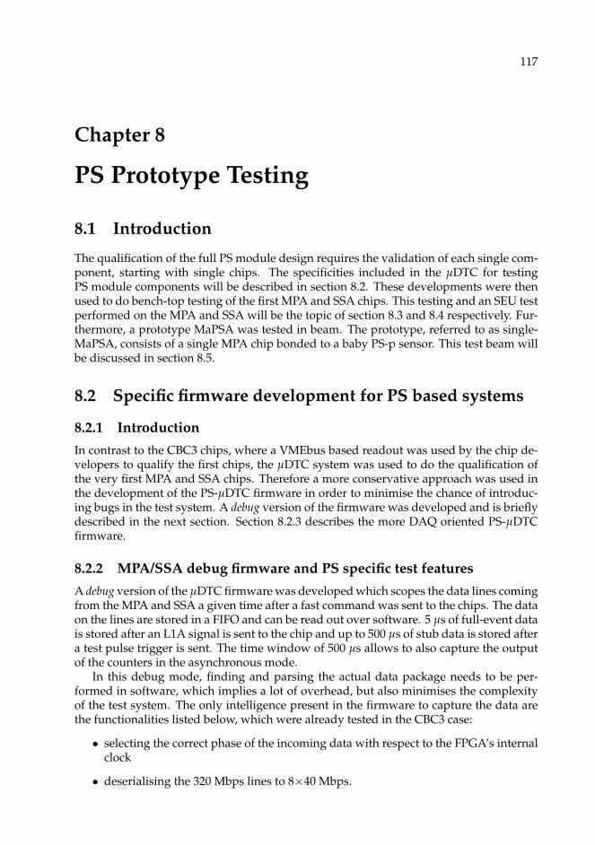
117
Chapter 8
PS Prototype Testing
8.1 Introduction
The qualification of the full PS module design requires the validation of each single com-ponent, starting with single chips. The specificities included in the µDTC for testingPS module components will be described in section 8.2. These developments were thenused to do bench-top testing of the first MPA and SSA chips. This testing and an SEU testperformed on the MPA and SSA will be the topic of section 8.3 and 8.4 respectively. Fur-thermore, a prototype MaPSA was tested in beam. The prototype, referred to as single-MaPSA, consists of a single MPA chip bonded to a baby PS-p sensor. This test beam willbe discussed in section 8.5.
8.2 Specific firmware development for PS based systems
8.2.1 IntroductionIn contrast to the CBC3 chips, where a VMEbus based readout was used by the chip de-velopers to qualify the first chips, the µDTC system was used to do the qualification ofthe very first MPA and SSA chips. Therefore a more conservative approach was used inthe development of the PS-µDTC firmware in order to minimise the chance of introduc-ing bugs in the test system. A debug version of the firmware was developed and is brieflydescribed in the next section. Section 8.2.3 describes the more DAQ oriented PS-µDTCfirmware.
8.2.2 MPA/SSA debug firmware and PS specific test featuresA debug version of the µDTC firmware was developed which scopes the data lines comingfrom the MPA and SSA a given time after a fast command was sent to the chips. The dataon the lines are stored in a FIFO and can be read out over software. 5 µs of full-event datais stored after an L1A signal is sent to the chip and up to 500 µs of stub data is stored aftera test pulse trigger is sent. The time window of 500 µs allows to also capture the outputof the counters in the asynchronous mode.
In this debug mode, finding and parsing the actual data package needs to be per-formed in software, which implies a lot of overhead, but also minimises the complexityof the test system. The only intelligence present in the firmware to capture the data arethe functionalities listed below, which were already tested in the CBC3 case:
• selecting the correct phase of the incoming data with respect to the FPGA’s internalclock
• deserialising the 320 Mbps lines to 8×40 Mbps.
118 Chapter 8. PS Prototype Testing
MPA
1xSSA-like full-eventdata @320Mbps
8xSSA-likestub data@320Mbps
µDTC1xMPA full-eventdata @320Mbps
5xMPA stubdata @320Mbps
SSA
2xSSA-likelateral data@320Mbps
1xSSAfull-event
data@320Mbps
8xSSA stubdata @320Mbps
µDTC
FIGURE 8.1: The data streams for stand-alone testing of the MPA (LEFT) andSSA (RIGHT). Only the full-event and stub data is shown, the fast command,
slow control and clocking is not shown in this figure.
As the MPA and SSA chips are designed to operate together, but will at first be testedas stand-alone objects, the input data to the chips needs to be provided by the µDTC.Functionality is implemented on the µDTC to send SSA-like full-event and stub data tothe MPA and to send lateral data to the SSA. The data streams are illustrated in Figure 8.1.The sending of this emulated data needs to be synchronised in time and therefore thetransmission of this emulated data is triggered by certain fast commands. The content ofthe data can be configured over software. In order to make sure that the emulated dataarrives at the chip at the correct time the sending of the data can be delayed in steps of25 ns after the reception of the fast command which triggers the output of the data. Alsothe phase of this data, with respect to the clock sent to the chips, can be configured oversoftware. This phase-shift was implemented in the firmware by clocking the OSERDES(see section 6.2) with a phase-shifted 320 MHz clock generated by a separate MMCM.The phase of this clock is configurable at runtime with a resolution of ≈ 18 ps.
The same I2C master is used as in the case of the CBC testing, with some minor mod-ifications such as 16-bit instead of 8-bit register addresses. The logic for sending the fastcommands is the same as in the CBC3 case.
As the test system had to be fully operational when the chips became available, itneeded to be tested without actual DUT. Therefore a basic emulation of an MPA chip wascoded to run on FPGA. The firmware block responsible for the MPA emulation residesin the same µDTC firmware project. The output lines of the emulator block, which arethe full-event and stub data lines, can be connected internally to the Phy layer to test thefirmware blocks, for receiving MPA data, in simulation.
The MPA emulation block can also be compiled stand-alone. In that case a set-up with2 FC7s can be used: one FC7 running the DAQ and the other FC7 running the emulator.The data sent back and forth between the two FC7s has the same format as in the case ofa real chip. The emulated chip receives the fast commands and the 320 MHz clock fromwhich it generates a 40 MHz clock for its internal logic. It acts on the fast commands bysending MPA-like stub and full-event data. Also an I2C slave is present and is used totest the I2C communication and to let the user change the content of the emulated stuband full-event data. This set-up allowed the testing of the new firmware blocks and thesoftware provided to run the tests. An emulation of the SSA chip was not prepared as all
8.2. Specific firmware development for PS based systems 119
the relevant features of the firmware could be tested with the MPA emulation.Operating the test system using the debug blocks to acquire the data introduces a
large overhead in data transmission to the back-end. This slows down the data takingand needs to be optimised by building events into a data package similar to the oneillustrated in Figure 6.8, rather than reading out the raw data. A DAQ firmware, similarto the CBC3 firmware, was implemented and is discussed in the following section.
8.2.3 MPA/SSA DAQ firmwareAdding the MPA and SSA chips to the µDTC firmware exemplifies the usefulness of thePhysical Interface Abstraction Layer. The parsing of the data formats is performed in thislayer.
The MPA full-event data, illustrated in Figure 5.17, is of non-fixed length and is spar-sified. The maximum number of S-clusters and P-clusters which can be sent is 24 and 31respectively. The manual of the MPA specifies that after the transmission of a full-eventdata package there are at least three 40 MHz clock cycles where the full-event data is 0. Asthe data is sparsified and of non-fixed length, the state machine processing the full-eventdata in the Physical Interface Abstraction Layer layer has to interpret the header infor-mation which specifies how many strip and pixel clusters are to follow in the payloadand tells how to split the payload data into S-clusters and P-clusters.
The MPA stub data also requires some special attention compared to the CBC3 andSSA stub data. For the MPA, as can be seen in Figure 5.16b, the stub data is spread over2 BXs. In order to attain a fixed stub latency the Phy layer foresees an 80-bit wide busto the Data Readout Block: one 25 ns clock cycle carries the data from BX n, and thesubsequent 25 ns clock cycle carries data from BX n+1. This is the boxcar unpacking ofthe MPA stub data.
The time it takes the full-event data package to travel through the Phy layer is a func-tion of the length of the data package, so it does not arrive a fixed time after the triggersignal in the Data Readout Block. On the other hand, there is the stub data package whichis boxcar unpacked in the Phy layer and from then on is synchronous again. Like this thestub data can still be delayed in a similar way as was done in the CBC3 case and onlythe stub data with a certain time offset (stub latency) with respect to the L1A trigger iswritten to the Data Readout Block. In this way the event building for the MPA case isguaranteed.
The MPA emulator, described in section 8.2.2 was also used to validate the aboveevent building. In order to test this, a self triggering on stubs was implemented. The testroutine is as follows:
1. Send a test pulse trigger.
2. The emulator will respond on the test pulse trigger by outputting non-zero stubdata.
3. The firmware notices that there is non-zero stub data and when configured correctlywill generate a trigger.
4. The emulator responds to this trigger with full-event data.
5. One can now check that for different stub data patterns (only stub data in the evenBX, only stub data in the odd BX, stub data in both even and odd BX (this will resultin 2 consecutive triggers)) the stub latency is indeed fixed and that it is possible toset the L1 and stub latency to one fixed value in order to read the data.
120 Chapter 8. PS Prototype Testing
8.2.4 Use casesThe following list gives an overview for which devices and tests the PS-µDTC firmwarewas used and the pictures in Figure 8.2 show the hardware:
• MPA stand-alone: initial verification (see section 8.3.1), wafer probing and TID andSEU testing. The latter required specific firmware development (see section 8.4.3)and this firmware was also used to characterise the power consumption of the MPAat high trigger rates.
• SSA stand-alone: initial verification (see section 8.3.2), wafer probing and TID andSEU testing. As for the MPA also special firmware was designed (see section 8.4.3)to run the SSA SEU test and this firmware was also used to characterise the powerconsumption of the SSA at high trigger rates.
• Single-MaPSA assembly: tested in beam (see section 8.5).
• 2SSA mini-module: the first operation of SSA chips with a sensor.
• MPA-SSA board: first implementation of an MPA and SSA chip on a common car-rier. After stand-alone testing of the single MPA and SSA chip this board was devel-oped as proof that the MPA and SSA chip can talk to each other. From the firmwarepoint of view the system is similar to reading out a stand-alone MPA chip.
The PS-µDTC firmware will also be used to test PS hybrids. A dedicated test system isbeing developed to test PS front-end hybrids as stand-alone objects. This test is requiredbefore assembly of the hybrid into a module in order to guarantee the functionality of thehybrid and thus the full functionality of an assembled module. The test system is basedon plug-in cards which carry a single PS hybrid. These plug-in cards are operated in acrate system, housing several plug-in cards1, and the µDTC is connected to the backplaneof the crate. Each plug-in card makes the I/Os of the SSAs available by temporarilyconnecting, with spring-loaded sockets, to the wire-bond pads. Also the I/Os to the CICare made available. In the end the system is limited to simultaneous access to only twoSSAs due to the limited number of lines available as input to the FC7. A multiplexingscheme on the plug-in card is used to select 2 SSA chips on a specific hybrid. As a resultit appears to the firmware that 2 SSA chips are connected and the same firmware version(modulo a new pin assignment) can be used as for the 2SSA mini-module. The CICchip on the PS-hybrid can be tested with a similar test firmware as the one described insection 9.2.
8.3 Single chip testing
The debug firmware allows for testing of all the digital features on the MPA and SSAchips. Also the functionality of the front-end can be assessed by taking S-curves bothwith and without the test pulse injection. The below sections list the functionalities whichwere tested. Most of these tests were performed short after the first prototypes of theMPA and SSA became available in January 2018.
1Selection of the plug-in card, and thus hybrid, under test is performed using a multiplexing system on thebackplane.
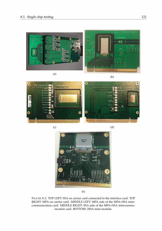
8.3. Single chip testing 121
(a)(b)
(c) (d)
(e)
FIGURE 8.2: TOP LEFT: SSA on carrier card connected to the interface card. TOPRIGHT: MPA on carrier card. MIDDLE LEFT: MPA side of the MPA+SSA inter-communication card. MIDDLE RIGHT: SSA side of the MPA+SSA intercommu-
nication card. BOTTOM: 2SSA mini-module.

122 Chapter 8. PS Prototype Testing
8.3.1 MPAThe following functionalities were tested and validated to be working on the MPA chip:
• I2C communication
• Alignment of the output lines
• Pixel masking
• Stub logic: correlation window, cluster cut
• Strip-strip mode: the MPA sends out the strip centroids on the stub data lines
• Pixel-pixel mode: the MPA sends out the pixel centroids on the stub data lines
• Hit detect logic
• Asynchronous mode
• Digital test pulse injection
• Analogue test pulse injection
• Digital pattern generation
• Full-event frame and full-event memory
• Verification of the analogue front-end (e.g. gain measurements using the test pulseinjection)
8.3.2 SSAThe following functionalities were tested and validated to be working on the SSA chip:
• I2C communication
• Alignment of the output lines
• Strip masking
• Stub logic: cluster cut
• Hit detect logic
• Asynchronous mode
• Lateral communication
• HIP flags
• Digital test pulse injection
• Analogue test pulse injection
• Digital pattern generation
• Full-event frame and full-event memory
• Verification of the analogue front-end (e.g. gain measurements using the test pulseinjection)
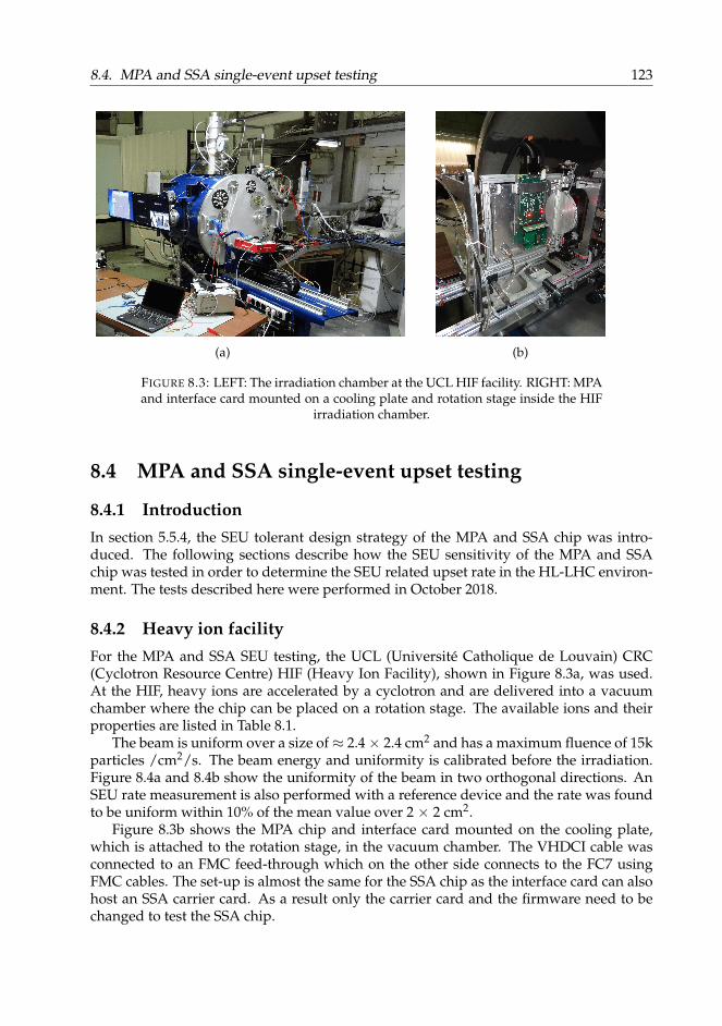
8.4. MPA and SSA single-event upset testing 123
(a) (b)
FIGURE 8.3: LEFT: The irradiation chamber at the UCL HIF facility. RIGHT: MPAand interface card mounted on a cooling plate and rotation stage inside the HIF
irradiation chamber.
8.4 MPA and SSA single-event upset testing
8.4.1 IntroductionIn section 5.5.4, the SEU tolerant design strategy of the MPA and SSA chip was intro-duced. The following sections describe how the SEU sensitivity of the MPA and SSAchip was tested in order to determine the SEU related upset rate in the HL-LHC environ-ment. The tests described here were performed in October 2018.
8.4.2 Heavy ion facilityFor the MPA and SSA SEU testing, the UCL (Université Catholique de Louvain) CRC(Cyclotron Resource Centre) HIF (Heavy Ion Facility), shown in Figure 8.3a, was used.At the HIF, heavy ions are accelerated by a cyclotron and are delivered into a vacuumchamber where the chip can be placed on a rotation stage. The available ions and theirproperties are listed in Table 8.1.
The beam is uniform over a size of≈ 2.4× 2.4 cm2 and has a maximum fluence of 15kparticles /cm2/s. The beam energy and uniformity is calibrated before the irradiation.Figure 8.4a and 8.4b show the uniformity of the beam in two orthogonal directions. AnSEU rate measurement is also performed with a reference device and the rate was foundto be uniform within 10% of the mean value over 2 × 2 cm2.
Figure 8.3b shows the MPA chip and interface card mounted on the cooling plate,which is attached to the rotation stage, in the vacuum chamber. The VHDCI cable wasconnected to an FMC feed-through which on the other side connects to the FC7 usingFMC cables. The set-up is almost the same for the SSA chip as the interface card can alsohost an SSA carrier card. As a result only the carrier card and the firmware need to bechanged to test the SSA chip.

124 Chapter 8. PS Prototype Testing
Ion M/Q Energy on device [MeV] Range on device [µm] LET on device [MeV/mg/cm2]13C4+ 3.25 131 269.3 1.322Ne7+ 3.14 238 202.0 3.327Al8+ 3.37 250 131.2 5.740Ar12+ 3.33 379 120.5 10.053Cr16+ 3.31 513 107.6 16.058Ni18+ 3.22 582 100.5 20.484Kr25+ 3.35 769 94.2 32.4103Rh31+ 3.32 972 88.7 45.8124Xe35+ 3.45 995 73.1 62.5
TABLE 8.1: Properties of the ions (with mass M and charge Q) available at theHIF facility. The range is defined in silicon. Values as provided by the facility.
(a) (b)
FIGURE 8.4: Uniformity of the HIF beam in two orthogonal directions.
8.4.3 Test set-upIn order to catch every possible SEU induced error on the data stream and thus extractthe best value for the SEU cross sections, ideally all full-event and stub data coming outof the chip has to be checked within the time slot available at the irradiation facility. Thisrequires online checks of both the stub and full-event data. The stub data are producedby the chip every BX, whilst the L1A trigger can be sent up to 1 MHz. Checking thestub data every BX and the full-event package at a rate of 1 MHz has to happen on theFPGA as the IPbus bandwidth is too limited to send all this data to the back-end, where acomparison in software would be possible. Furthermore a large amount of storage wouldbe needed. To give an example: storing the full data stream output by a single SSA chiptriggered at 1 MHz for a single second would require ≈ 2.7 Gb of storage.
The MPA and SSA chips can be configured to output full-event and stub data frameswith a fixed payload. This is achieved by using the digital test pulse injection mechanismwhich inputs digital patterns into the digital part of the chips each time a test pulse triggeris received (see section 5.5.2 and 5.5.3). In this way the full digital logic on the chip is usedwhich is the SEU sensitive part of the ASIC.
Three state machines were added to the firmware, each dedicated for online checkingof the incoming data:
• Full-event data check for the MPA and SSA
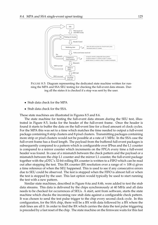
8.4. MPA and SSA single-event upset testing 125
Idle
Waiting for header
Start receivedand FIFO ready
Header found
Buffering data
Full-event frame received
Compare tocheck pattern
-Compare with the configurable check pattern.-Compare shadow L1 counter to chip L1 counter,update mirror L1 counter to chip L1 counter if mismatch.
Write toFIFO
-Store the full-event data for a fixed # clock cycles.-Increment mirror L1 counter.
Nomismatch
Mismatch
FIFO full
Awaitingread out
FIFO not full
FIFO was read
FIGURE 8.5: Diagram representing the dedicated state machine written for run-ning the MPA and SSA SEU testing for checking the full-event data stream. Dur-
ing all the states it is checked if a stop was sent by the user.
• Stub data check for the MPA
• Stub data check for the SSA.
These state machines are illustrated in Figures 8.5 and 8.6.The state machine for testing the full-event data stream during the SEU test, illus-
trated in Figure 8.5, looks for the header of the full-event frame. Once the header isfound it starts to buffer the data on the full-event line for a fixed amount of clock cycles.For the MPA this was set to a time which matches the time needed to output a full-eventpackage containing 8 strip clusters and 8 pixel clusters. Transmitting packages containingmore strip or pixel clusters would not be possible at a rate of 1 MHz. In the SSA case thefull-event frame has a fixed length. The payload from the buffered full-event packages issubsequently compared to a pattern which is configurable over IPbus and the L1 counteris compared to a mirror counter which increments on the FPGA every time a full-eventheader was found. In case of a mismatch between the check pattern and the payload or amismatch between the chip L1 counter and the mirror L1 counter, the full-event packagetogether with the µDTC’s 32-bit rolling BX counter is written to a FIFO which can be readout after stopping the test. This BX counter (BX resolution over a range of ≈ 108 s) givesa time reference of when the SEU happened. This is used to see if any consecutive errorsdue to SEU could be observed. The test is stopped when the FIFO is almost full or whenthe test is stopped by the user. This last option would typically be used to start runningthe test with a new pattern.
Similar state machines, described in Figure 8.6a and 8.6b, were added to test the stubdata streams. This data is delivered by the chips synchronously at 40 MHz and all dataneeds to be checked for occurrences of SEUs. A start, sent from software, starts the statemachine which checks the incoming raw stub data against a configurable check pattern.It was chosen to send the test pulse trigger to the chip every second clock cycle. In thisconfiguration, for the SSA chip, there will be a BX with data followed by a BX where thestub lines are all 0. In order to find the BX which carries the data the test pulse triggeringis preceded by a fast reset of the chip. The state machine on the firmware waits for this fast

126 Chapter 8. PS Prototype Testing
Idle
Checking sync bit
Start receivedand FIFO ready
Check for odd stubdata package
Comparing MPA
FIFO almost fullor stop received
In even package: buffer the data.In odd package: compare current andbuffered data to configurable check patternand write to FIFO if mismatched.If wrong value for sync bit: write to FIFO.
Waiting for FIFOto be read by user.
Awaitingread out
FIFO wasread
(a)
Idle
Waiting ReSync
Start receivedand FIFO ready
ReSync fast commandsend to SSA
Waiting after ReSync
Wait configurableamount of clk cycles
Compairing SSACompare to the configurable pattern in 1 clockcycle and to all 0’s in the other clk cycle.
Stop received orFIFO almost full
Awaitingread out
Waiting for FIFOto be read by user.
FIFO wasread
(b)
FIGURE 8.6: Diagrams representing the dedicated state machines written for run-ning the MPA and SSA SEU testing for the MPA stub data (LEFT) and SSA stub
data (RIGHT). During all the states it is checked if a stop was sent by the user.
reset being sent and then waits a configurable number of clock cycles before interpretingthe data. By tuning this waiting time manually, it is possible to find the BX which carriesdata.
For the MPA this way of sending the test pulse trigger can still result in data on thestub lines in both odd and even BXs as the MPA sends stub data in packages spanning2 BXs. The MPA has the advantage of the presence of the sync bit to synchronise thecomparison to the check pattern. During the BX where the sync bit is high (referred to asthe even BX) the data is buffered on the FPGA and during the next BX (referred to as theodd BX) the buffered data together with the current data on the stub lines is compared tothe check pattern and the data together with the BX counter is written to a FIFO in caseof mismatch. Furthermore, if the sync bit is not present an error is raised and the data iswritten to the FIFO.
In order to test the complete digital logic against SEUs also the data inputs to theASICs have to be stimulated. This means that during the MPA testing, the MPA needsto receive SSA-like full-event and stub data from the FPGA. In a similar fashion, the SSAneeds to receive lateral SSA-like input data. These input data streams have to be syn-chronised with the data generation on chip. This input data to the chip is therefore alsotriggered by the L1A trigger (MPA full-event data input) and the test pulse trigger (MPAstub data input and SSA lateral data input). The exact tuning can be done manually.As discussed before, it is possible to both delay the data in steps of 25 ns and to shift itsphase. In this configuration it is possible to choose the arrival time of the input data at thechip carefully in order for it to result in data in the same data package as the digital testpulse injection. The L1 counter in the SSA full-event data package going to the MPA hasto be synchronised with the L1 counter on the MPA as well. This is required because theMPA does a check for the alignment between these two counters. In case of mismatch,an error bit is raised in the full-event frame of the MPA.
In order to maximise the amount of data checked during the SEU test, the full-event
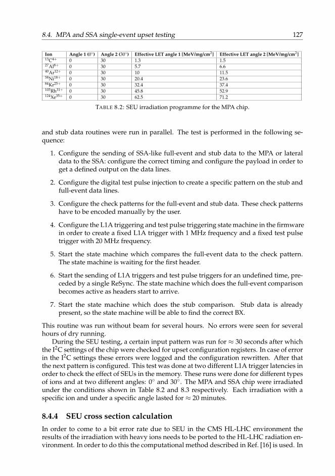
8.4. MPA and SSA single-event upset testing 127
Ion Angle 1 (0) Angle 2 (30) Effective LET angle 1 [MeV/mg/cm2] Effective LET angle 2 [MeV/mg/cm2]13C4+ 0 30 1.3 1.527Al8+ 0 30 5.7 6.640Ar12+ 0 30 10 11.558Ni18+ 0 30 20.4 23.684Kr25+ 0 30 32.4 37.4103Rh31+ 0 30 45.8 52.9124Xe35+ 0 30 62.5 71.2
TABLE 8.2: SEU irradiation programme for the MPA chip.
and stub data routines were run in parallel. The test is performed in the following se-quence:
1. Configure the sending of SSA-like full-event and stub data to the MPA or lateraldata to the SSA: configure the correct timing and configure the payload in order toget a defined output on the data lines.
2. Configure the digital test pulse injection to create a specific pattern on the stub andfull-event data lines.
3. Configure the check patterns for the full-event and stub data. These check patternshave to be encoded manually by the user.
4. Configure the L1A triggering and test pulse triggering state machine in the firmwarein order to create a fixed L1A trigger with 1 MHz frequency and a fixed test pulsetrigger with 20 MHz frequency.
5. Start the state machine which compares the full-event data to the check pattern.The state machine is waiting for the first header.
6. Start the sending of L1A triggers and test pulse triggers for an undefined time, pre-ceded by a single ReSync. The state machine which does the full-event comparisonbecomes active as headers start to arrive.
7. Start the state machine which does the stub comparison. Stub data is alreadypresent, so the state machine will be able to find the correct BX.
This routine was run without beam for several hours. No errors were seen for severalhours of dry running.
During the SEU testing, a certain input pattern was run for ≈ 30 seconds after whichthe I2C settings of the chip were checked for upset configuration registers. In case of errorin the I2C settings these errors were logged and the configuration rewritten. After thatthe next pattern is configured. This test was done at two different L1A trigger latencies inorder to check the effect of SEUs in the memory. These runs were done for different typesof ions and at two different angles: 0 and 30. The MPA and SSA chip were irradiatedunder the conditions shown in Table 8.2 and 8.3 respectively. Each irradiation with aspecific ion and under a specific angle lasted for ≈ 20 minutes.
8.4.4 SEU cross section calculationIn order to come to a bit error rate due to SEU in the CMS HL-LHC environment theresults of the irradiation with heavy ions needs to be ported to the HL-LHC radiation en-vironment. In order to do this the computational method described in Ref. [16] is used. In
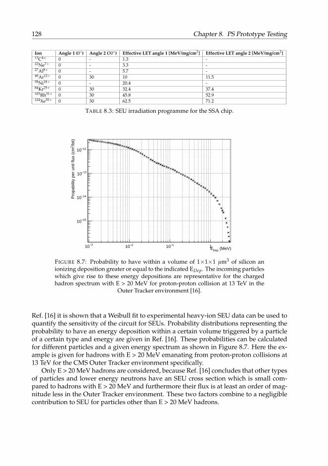
128 Chapter 8. PS Prototype Testing
Ion Angle 1 (0) Angle 2 (30) Effective LET angle 1 [MeV/mg/cm2] Effective LET angle 2 [MeV/mg/cm2]13C4+ 0 - 1.3 -22Ne7+ 0 - 3.3 -27Al8+ 0 - 5.7 -40Ar12+ 0 30 10 11.558Ni18+ 0 - 20.4 -84Kr25+ 0 30 32.4 37.4103Rh31+ 0 30 45.8 52.9124Xe35+ 0 30 62.5 71.2
TABLE 8.3: SEU irradiation programme for the SSA chip.
3−10 2−10 1−10 1 (MeV)DepE
15−10
14−10
13−10
12−10
/bit)
2P
ropa
bilit
y pe
r un
it flu
x (c
m
FIGURE 8.7: Probability to have within a volume of 1×1×1 µm3 of silicon anionizing deposition greater or equal to the indicated EDep. The incoming particleswhich give rise to these energy depositions are representative for the chargedhadron spectrum with E > 20 MeV for proton-proton collision at 13 TeV in the
Outer Tracker environment [16].
Ref. [16] it is shown that a Weibull fit to experimental heavy-ion SEU data can be used toquantify the sensitivity of the circuit for SEUs. Probability distributions representing theprobability to have an energy deposition within a certain volume triggered by a particleof a certain type and energy are given in Ref. [16]. These probabilities can be calculatedfor different particles and a given energy spectrum as shown in Figure 8.7. Here the ex-ample is given for hadrons with E > 20 MeV emanating from proton-proton collisions at13 TeV for the CMS Outer Tracker environment specifically.
Only E > 20 MeV hadrons are considered, because Ref. [16] concludes that other typesof particles and lower energy neutrons have an SEU cross section which is small com-pared to hadrons with E > 20 MeV and furthermore their flux is at least an order of mag-nitude less in the Outer Tracker environment. These two factors combine to a negligiblecontribution to SEU for particles other than E > 20 MeV hadrons.
8.4. MPA and SSA single-event upset testing 129
8.4.5 ResultsIn the next two paragraphs the results of the SEU testing will be discussed. The resultsare divided in two sections: particular upsets seen in the configuration and control ofthe ASICs in section 8.4.5.1 and the calculation of the SEU cross sections based on the bitupsets seen in the data in section 8.4.5.2.
8.4.5.1 SEU triggered configuration and control upsets
For the MPA chip only two configuration errors, not corrected by the triplication logic,were observed during the testing. To see an upset in the MPA configuration, a multi-bitupset is required where two out of the three registers get upset and as a result the wrongvalue is forced also on the third one. These multi-bit single-event upsets were tracedback to happen on a register where the spacing of the triplicated registers was smallerthan 15 µm. Normally the design tool ensures that the spacing is larger than 15 µm todecrease the SEU sensitivity, however successive place and route steps sometimes movethe registers closer again. This will be fixed for the production of the next version of theMPA chip. Single bit upsets are counted in the SEU counter which counts the number ofcorrections that need to be applied to the chip’s configuration. For design reasons notall the MPA registers are connected to the SEU counter. For the MPA 3×1181 flip-flopsand for the SSA 3×256 flip-flops2 from the configuration logic are connected. The actualvalues for the SEU counter are given in Appendix A where it can be seen that, dependingon the type of ion which is used, the SEU counter rate can go up to ≈ 2 Hz.
For the SSA, in 3 out of 128 runs the strip configuration registers got reset and inone case also the periphery configuration was reset. This was traced back to a problemin the triplication of the reset tree. In the next version of the SSA a constraint will beimplemented in the design to force triplication of the reset tree and also the physical resetpad will be triplicated. Dedicated SEU tests of the corrected versions of the MPA andSSA will be performed to extract a final upset rate for the configuration registers.
8.4.5.2 SEU cross section and bit upset rates on data paths
By counting the number of SEU (# SEU) in a given time slot of length t, the SEU crosssection σ can be calculated as:
σ =#SEU
φ.t, (8.1)
where φ is the heavy ion flux.Figure 8.8 and 8.9 show the SEU cross section for the different kinds of logic at dif-
ferent LETs for the MPA and SSA chips respectively. The data are fitted with a Weibulldistribution:
σ = σ0
1− exp
[−(
EDep − E0
W
)s], (8.2)
where σ0 is the saturation value of the SEU cross section and E0 is the SEU thresholdenergy. W and s are shape parameters. To calculate the deposited energy from the LET,the following formula is applied:
EDep = LET × d× ρSi = LET × 0.2328mgcm2 , (8.3)
2The factor 3 is for the triplication.
130 Chapter 8. PS Prototype Testing
where ρSi (= 2.32 g/cm3) is the density of silicon and d is the sensitive depth which washere assumed to be 1 µm.
Figure 8.8 and 8.9 show for both chips the SEU cross sections for the stub data pathand the full-event data path for two latency settings. For the MPA (SSA) low latencycorresponds to a latency setting of 40 BX (100 BX) and high latency corresponds to alatency setting of 500 BX (500 BX). Due to the low statistics for the SSA data at low latency,a fit with a Weibull distribution is hard and therefore not shown. It can be seen howeverthat the data points for the low L1 latency of the SSA measurements are all below thedata for high latency. The high latency value for the error rate can thus be used as anupper limit for the SSA low L1 latency setting. Anyway, the high latency setting is amore representative value for the application in the CMS experiment. Also for the MPAchip the dependency on the latency setting is clear: when the chip is configured for ahigher latency the data resides longer in the memory and therefore the probability forupset data being present at the output is larger for the high latency setting. Important tonote for the full-event data is that the L1A rate was 1 MHz. The SEU cross section whichis calculated below, and as a result the upset rates, are a function of the L1A trigger rate.1 MHz is the upper limit for the L1A trigger rate and as such the cross section and upsetrates extracted here are the worst expected. In order to evaluate the bit upset rate, dueto SEU, coming off a module, this SEU rate should be downscaled to a L1A rate which issustainable by the CIC chip. This will be done later in this section.
Comparing the SEU cross sections of the MPA and SSA chip, it can be concluded thatthe MPA is more SEU sensitive than the SSA chip. This is a direct consequence of thehigher number of logic cells on the MPA.
In Figure 8.8 and 8.9, the uncertainty on the cross section values is attributed to thePoisson uncertainty on the counts, the uncertainty on the fluence value (taken to be100 particles/s/cm2) and the uncertainty on the duration of the test (taken to be 1 s).
In order to extract the SEU cross sections for the CMS Outer Tracker environment at13 TeV proton-proton collisions the Weibull fits need to be convoluted with the probabil-ities in Figure 8.7:
Γ = ∑Ei
Pi∆σiσ0
A= ∑
Ei
Pi(σi+1 − σi)
A. (8.4)
Here Γ is the SEU cross section under specific conditions, Pi are the probabilities repre-sented in Figure 8.7, A is the sensitive area which is assumed here to be 1 × 1 µm2, ac-cording to the recommendations from Ref. [16], and the sum runs over the energy rangein Figure 8.7.
The results of these calculations are shown in Table 8.4. The relative uncertainties(originating from the uncertainty on the fit) on these values are typically of the order of10%. All these values should however be interpreted as an order of magnitude calcula-tion due to the approximations used in the computational method. For both chips andfor the different logic the SEU cross section can be estimated to be around 10−10 cm2.

8.4. MPA and SSA single-event upset testing 131
FIGURE 8.8: SEU cross sections at different LET for the MPA chip
FIGURE 8.9: SEU cross sections at different LET for the SSA chip
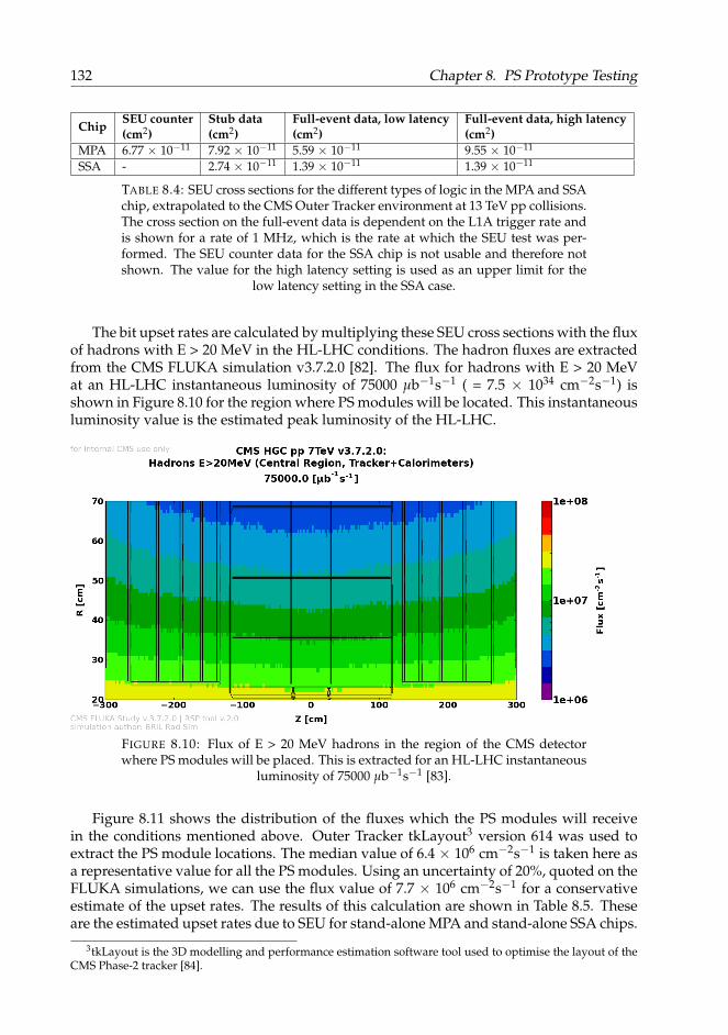
132 Chapter 8. PS Prototype Testing
ChipSEU counter(cm2)
Stub data(cm2)
Full-event data, low latency(cm2)
Full-event data, high latency(cm2)
MPA 6.77 × 10⁻¹¹ 7.92 × 10⁻¹¹ 5.59 × 10⁻¹¹ 9.55 × 10⁻¹¹
SSA - 2.74 × 10⁻¹¹ 1.39 × 10⁻¹¹ 1.39 × 10⁻¹¹
TABLE 8.4: SEU cross sections for the different types of logic in the MPA and SSAchip, extrapolated to the CMS Outer Tracker environment at 13 TeV pp collisions.The cross section on the full-event data is dependent on the L1A trigger rate andis shown for a rate of 1 MHz, which is the rate at which the SEU test was per-formed. The SEU counter data for the SSA chip is not usable and therefore notshown. The value for the high latency setting is used as an upper limit for the
low latency setting in the SSA case.
The bit upset rates are calculated by multiplying these SEU cross sections with the fluxof hadrons with E > 20 MeV in the HL-LHC conditions. The hadron fluxes are extractedfrom the CMS FLUKA simulation v3.7.2.0 [82]. The flux for hadrons with E > 20 MeVat an HL-LHC instantaneous luminosity of 75000 µb−1s−1 ( = 7.5 × 1034 cm−2s−1) isshown in Figure 8.10 for the region where PS modules will be located. This instantaneousluminosity value is the estimated peak luminosity of the HL-LHC.
FIGURE 8.10: Flux of E > 20 MeV hadrons in the region of the CMS detectorwhere PS modules will be placed. This is extracted for an HL-LHC instantaneous
luminosity of 75000 µb−1s−1 [83].
Figure 8.11 shows the distribution of the fluxes which the PS modules will receivein the conditions mentioned above. Outer Tracker tkLayout3 version 614 was used toextract the PS module locations. The median value of 6.4 × 106 cm−2s−1 is taken here asa representative value for all the PS modules. Using an uncertainty of 20%, quoted on theFLUKA simulations, we can use the flux value of 7.7 × 106 cm−2s−1 for a conservativeestimate of the upset rates. The results of this calculation are shown in Table 8.5. Theseare the estimated upset rates due to SEU for stand-alone MPA and stand-alone SSA chips.
3tkLayout is the 3D modelling and performance estimation software tool used to optimise the layout of theCMS Phase-2 tracker [84].
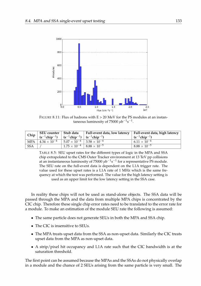
8.4. MPA and SSA single-event upset testing 133
FIGURE 8.11: Flux of hadrons with E > 20 MeV for the PS modules at an instan-taneous luminosity of 75000 µb−1s−1.
ChipSEU counter(s−1chip−1)
Stub data(s−1chip−1)
Full-event data, low latency(s−1chip−1)
Full-event data, high latency(s−1chip−1)
MPA 4.34 × 10⁻⁴ 5.07 × 10⁻⁴ 3.58 × 10⁻⁴ 6.11 × 10⁻⁴
SSA / 1.75 × 10⁻⁴ 8.88 × 10⁻⁵ 8.88 × 10⁻⁵
TABLE 8.5: SEU upset rates for the different types of logic in the MPA and SSAchip extrapolated to the CMS Outer Tracker environment at 13 TeV pp collisionsat an instantaneous luminosity of 75000 µb−1s−1 for a representative PS module.The SEU rate on the full-event data is dependent on the L1A trigger rate. Thevalue used for these upset rates is a L1A rate of 1 MHz which is the same fre-quency at which the test was performed. The value for the high latency setting is
used as an upper limit for the low latency setting in the SSA case.
In reality these chips will not be used as stand-alone objects. The SSA data will bepassed through the MPA and the data from multiple MPA chips is concentrated by theCIC chip. Therefore these single chip error rates need to be translated to the error rate fora module. To make an estimation of the module SEU rate the following is assumed:
• The same particle does not generate SEUs in both the MPA and SSA chip.
• The CIC is insensitive to SEUs.
• The MPA treats upset data from the SSA as non-upset data. Similarly the CIC treatsupset data from the MPA as non-upset data.
• A strip/pixel hit occupancy and L1A rate such that the CIC bandwidth is at thesaturation threshold.
The first point can be assumed because the MPAs and the SSAs do not physically overlapin a module and the chance of 2 SEUs arising from the same particle is very small. The
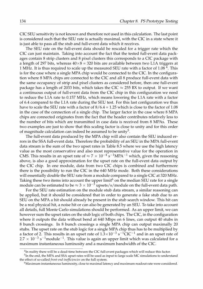
134 Chapter 8. PS Prototype Testing
CIC SEU sensitivity is not known and therefore not used in this calculation. The last pointis considered such that the SEU rate is actually maximal, with the CIC in a state where itis just able to pass all the stub and full-event data which it receives.
The SEU rate on the full-event data should be rescaled for a trigger rate which theCIC can just maintain. Taking into account the fact that the tested full-event data pack-ages contain 8 strip clusters and 8 pixel clusters this corresponds to a CIC package witha length of 297 bits, whereas 40×8 = 320 bits are available between two L1A triggers at1 MHz. It is thus required to scale up the measured SEU rate with a factor of 1.08 4. Thisis for the case where a single MPA chip would be connected to the CIC. In the configura-tion where 8 MPA chips are connected to the CIC and all 8 produce full-event data withthe same occupancy of strip and pixel clusters as considered before, then one full-eventpackage has a length of 2033 bits, which takes the CIC ≈ 255 BX to output. If we wanta continuous output of full-event data from the CIC chip in this configuration we needto reduce the L1A rate to 0.157 MHz, which means lowering the L1A rate with a factorof 6.4 compared to the L1A rate during the SEU test. For this last configuration we thushave to scale the SEU rate with a factor of 8/6.4 = 1.25 which is close to the factor of 1.08in the case of the connection of a single chip. The larger factor in the case where 8 MPAchips are connected originates from the fact that the header contributes relatively less tothe number of bits which are transmitted in case data is received from 8 MPAs. Thesetwo examples are just to show that this scaling factor is close to unity and for this orderof magnitude calculation can indeed be assumed to be unity5.
The full-event data produced by the MPA chip will also contain the SEU induced er-rors in the SSA full-event data. Therefore the probability of an SEU in the MPA full-eventdata stream is the sum of the two upset rates in Table 8.5 where we use the high latencyvalue as the most conservative and also most representative value for the operation inCMS. This results in an upset rate of ≈ 7 × 10⁻⁴ s−1MPA−1 which, given the reasoningabove, is also a good approximation for the upset rate on the full-event data output bythe CIC chip. In one module, data from two CIC chips is combined and furthermorethere is the possibility to run the CIC in the 640 MHz mode. Both these considerationswill essentially double the SEU rate from a module compared to a single CIC at 320 MHz.Taking these two items into account the upper limit6 on the median SEU rate for a singlemodule can be estimated to be ≈ 3 × 10⁻³ upsets/s/module on the full-event data path.
For the SEU rate estimation on the module stub data stream, a similar reasoning canbe applied, but it should be considered that in order to generate a fake stub due to anSEU on the MPA a hit should already be present in the stub search window. This hit canbe a real physical hit, a noise hit or can also be generated by an SEU. To take into accountall details, full Monte Carlo simulations should be performed. As an upper limit, we canhowever sum the upset rates on the stub logic of both chips. The CIC, in the configurationwhere it outputs the data without bend at 640 Mbps on 6 lines, can output 40 stubs in8 bunch crossings. In 8 bunch crossings a single MPA chip can output maximally 20stubs. The upset rate on the stub logic for a single MPA chip thus has to be multiplied bya factor of 2. This results in an upset rate of 1.3×10⁻³ s−1CIC−1 and in an upset rate of2.7 × 10−3 s−1module−1. This value is again an upper limit which was calculated for amaximum instantaneous luminosity and a maximum bandwidth of the CIC.
4In reality there will be a dead-time between the CIC full-event packages which will reduce this factor.5In the end, the MPA and SSA upset rates will be used as input to large scale MC simulations to understand
the effect of so-called front-end inefficiencies on the full system.6Maximum instantaneous luminosity, close to maximal latency and maximum readout rate were considered.

8.5. Single-MaPSA test beam 135
Given the fact that there will be 5616 PS modules in the Phase-2 CMS Outer Trackerthe above upset rates result in≈ 15 upset bits in the stub data stream every second for allthe PS modules, this is ≈ 1 bit every 2.6× 10⁶ collisions. For the full-event data the upsetrate is ≈ 17 upset bits every second at a L1A rate of 1 MHz. This corresponds to an upsetapproximately every 60,000th triggered event.
The measured single chip SEU induced upset rates should be used in Monte Carlosimulations of the full tracker to evaluate their effect on the track trigger and tracking.The above estimation learns however that the upset rates due to SEU induced upsets inMPA and SSA can most likely be tolerated.
8.5 Single-MaPSA test beam
8.5.1 IntroductionA baby PS-p sensor bump bonded to an MPA chip, a so-called single-MaPSA (MacroPixel Sub Assembly), was tested in beam at the CERN H6 North test beam area in April2018. It was the first time such an assembly was tested in beam. Different configura-tions (depletion voltages, thresholds, beam incident angles) were tested. A telescope waspresent in the beam area and was used to do the track reconstruction. The following sec-tions will give more information on the beam area, the set-up, the tested assembly andthe results.
8.5.2 Beam area
8.5.2.1 Beam parameters
The CERN H6 North area is provided with 400 GeV protons from the SPS from which asecondary beam of hadrons is extracted for the test beam areas. Typically charged pionsare delivered during an extraction. During the single-MaPSA test beam the momentumof the charged pions was 120 GeV/c. An extraction lasts for ≈ 4 seconds and occursabout every minute. During the extraction the beam can be considered to be continuous,there is no specific timing of the particles within a single extraction.
8.5.2.2 Telescope
The AIDA telescope, shown in Figure 8.12a, present in the beam area, was used to dothe track reconstruction. This telescope consists of 6 planes of MIMOSA26 chips, a chipdeveloped for the ILC project. 1 MIMOSA26 chip has an active area of≈ 10.6× 21.2 mm2
and contains 576 × 1152 pixels with a pitch of 18.4 µm. The chips are read out witha rolling shutter at a rate of ≈ 8.68 kHz, which is slow compared to the 40 MHz rateof the DUT DAQ. As a result the MIMOSA26 chips integrate many tracks during a fullreadout cycle. To be able to unravel this pileup and to match the tracks to hits on theDUT an extra timing reference is included in the telescope: the FE-I4 plane. The FE-I4 plane, developed for the ATLAS tracking system, has the required time resolution of25 ns and has an active area of 16.8× 20.0 mm2 (336 rows× 80 columns). The telescope ispart of the EUTELESCOPE project and the EUDAQ software is available to do the trackreconstruction.
The passage of particles through the telescope is indicated by the coincidence sig-nal coming from 2x2 (2 downstream and 2 upstream of the telescope) scintillators. This
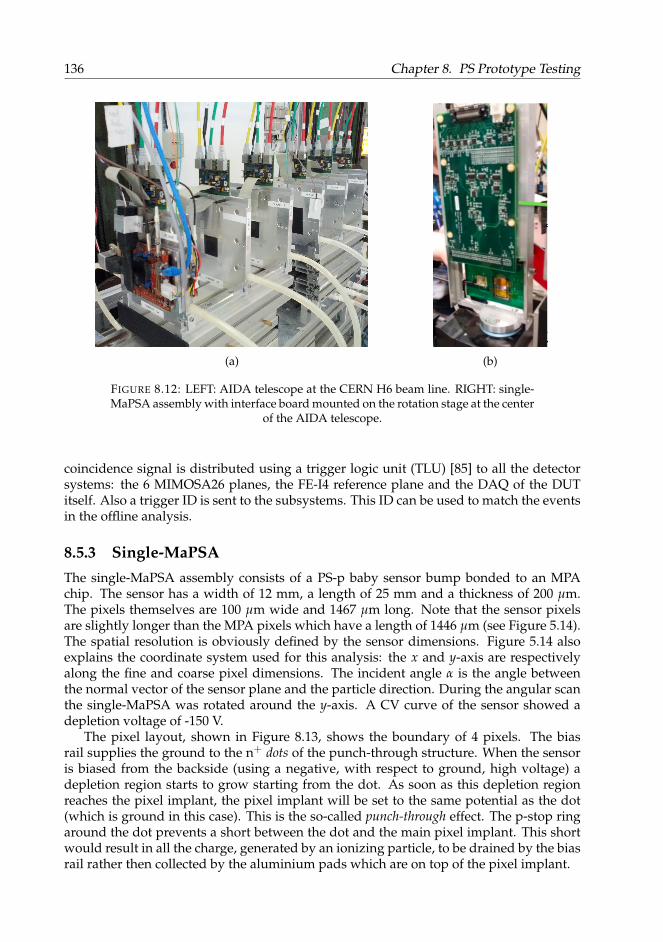
136 Chapter 8. PS Prototype Testing
(a) (b)
FIGURE 8.12: LEFT: AIDA telescope at the CERN H6 beam line. RIGHT: single-MaPSA assembly with interface board mounted on the rotation stage at the center
of the AIDA telescope.
coincidence signal is distributed using a trigger logic unit (TLU) [85] to all the detectorsystems: the 6 MIMOSA26 planes, the FE-I4 reference plane and the DAQ of the DUTitself. Also a trigger ID is sent to the subsystems. This ID can be used to match the eventsin the offline analysis.
8.5.3 Single-MaPSAThe single-MaPSA assembly consists of a PS-p baby sensor bump bonded to an MPAchip. The sensor has a width of 12 mm, a length of 25 mm and a thickness of 200 µm.The pixels themselves are 100 µm wide and 1467 µm long. Note that the sensor pixelsare slightly longer than the MPA pixels which have a length of 1446 µm (see Figure 5.14).The spatial resolution is obviously defined by the sensor dimensions. Figure 5.14 alsoexplains the coordinate system used for this analysis: the x and y-axis are respectivelyalong the fine and coarse pixel dimensions. The incident angle α is the angle betweenthe normal vector of the sensor plane and the particle direction. During the angular scanthe single-MaPSA was rotated around the y-axis. A CV curve of the sensor showed adepletion voltage of -150 V.
The pixel layout, shown in Figure 8.13, shows the boundary of 4 pixels. The biasrail supplies the ground to the n+ dots of the punch-through structure. When the sensoris biased from the backside (using a negative, with respect to ground, high voltage) adepletion region starts to grow starting from the dot. As soon as this depletion regionreaches the pixel implant, the pixel implant will be set to the same potential as the dot(which is ground in this case). This is the so-called punch-through effect. The p-stop ringaround the dot prevents a short between the dot and the main pixel implant. This shortwould result in all the charge, generated by an ionizing particle, to be drained by the biasrail rather then collected by the aluminium pads which are on top of the pixel implant.

8.5. Single-MaPSA test beam 137
FIGURE 8.13: Layout of the single-MaPSA pixel sensor matrix [18]. The biasstructure (A) distributes the ground to the dots (B) of the punch-throughs using avia connection (C). These dots are a small n+ implant with the same donor con-centration as the pixel implant. They are separated from the main pixel implant(D) using p-stop isolation (E) around the punch-through structure. The chargeis collected on the Al pad (F) on top of the pixel implant. The pixel implant isconnected to the aluminium pad using a via (H) (DC process). The pixels are
physically separated using p-stop isolation (G).
8.5.4 Single-MaPSA set-upThe single-MaPSA assembly was placed at the center of the telescope on a rotation stageas shown in Figure 8.12b. The MPA was read out with the same hardware as used for thesingle chip testing: the MPA, wire bonded to a dedicated carrier card was connected tothe same interface board, as used for the bench top tests. The interface board regulatesthe power to the chip and does the level translation to and from the back-end (µDTCsystem), which is connected with a 1 m VHDCI cable. The trigger signal was providedto the VHDCI-FMC, which hosts a LEMO connector. The µDTC exerts back pressure tothe TLU. This back pressure is raised from software whenever a run is not ongoing. Theback pressure can also be raised from the firmware when the data buffers on the FC7are almost full. In this case the back pressure signal is raised and the triggers to all thesubsystems are suppressed.
The clock that drives the MPA chip is generated on the FC7 and is uncorrelated withthe arrival time of the particles. Therefore the arrival of the trigger signal from the TLU isnot always happening at the same phase with respect to the clock, and thus the samplingtime, on the chip. A time to digital converter (TDC) with a resolution of 3.125 ns wasimplemented in the firmware to give a better resolution on the arrival time of the triggersignal from the scintillators. The TDC value is passed on to the back-end in the event’sdata package.
8.5.5 MPA data streamsThe MPA chip was operated in two modes during this test beam: the asynchronous andthe synchronous mode (see section 5.5.3). In case of the asynchronous mode the shutter isopened for some time during which the ripple counter for each pixel counts the numberof times a signal above threshold was detected. After closing the shutter the counters areread out over the stub lines.
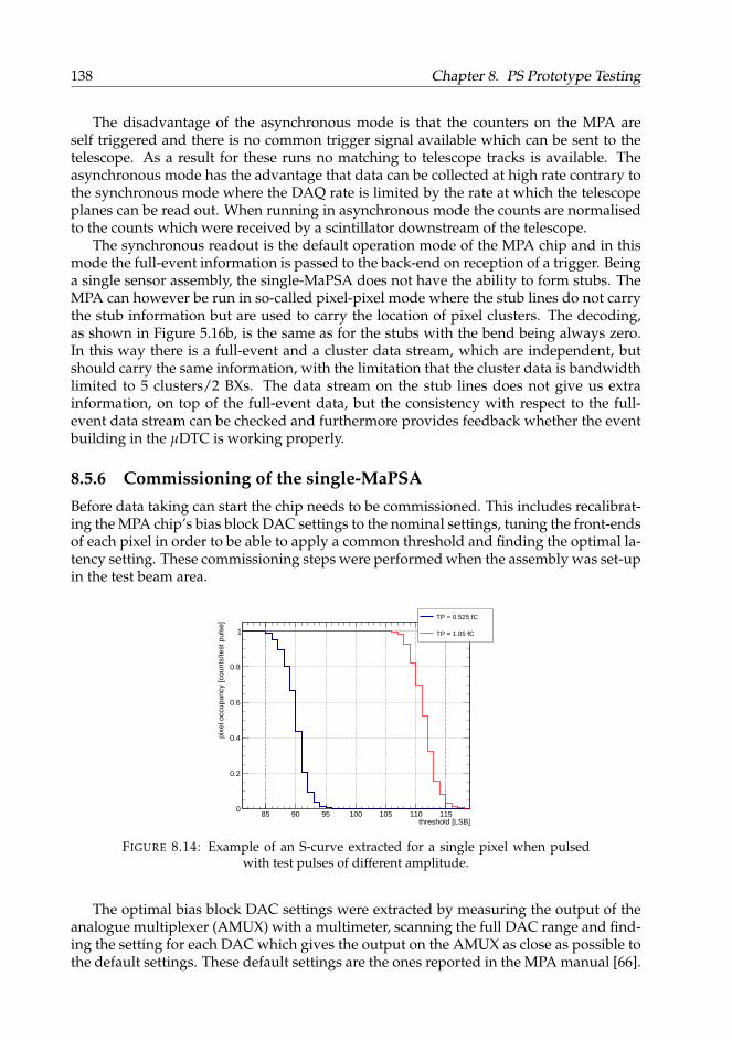
138 Chapter 8. PS Prototype Testing
The disadvantage of the asynchronous mode is that the counters on the MPA areself triggered and there is no common trigger signal available which can be sent to thetelescope. As a result for these runs no matching to telescope tracks is available. Theasynchronous mode has the advantage that data can be collected at high rate contrary tothe synchronous mode where the DAQ rate is limited by the rate at which the telescopeplanes can be read out. When running in asynchronous mode the counts are normalisedto the counts which were received by a scintillator downstream of the telescope.
The synchronous readout is the default operation mode of the MPA chip and in thismode the full-event information is passed to the back-end on reception of a trigger. Beinga single sensor assembly, the single-MaPSA does not have the ability to form stubs. TheMPA can however be run in so-called pixel-pixel mode where the stub lines do not carrythe stub information but are used to carry the location of pixel clusters. The decoding,as shown in Figure 5.16b, is the same as for the stubs with the bend being always zero.In this way there is a full-event and a cluster data stream, which are independent, butshould carry the same information, with the limitation that the cluster data is bandwidthlimited to 5 clusters/2 BXs. The data stream on the stub lines does not give us extrainformation, on top of the full-event data, but the consistency with respect to the full-event data stream can be checked and furthermore provides feedback whether the eventbuilding in the µDTC is working properly.
8.5.6 Commissioning of the single-MaPSABefore data taking can start the chip needs to be commissioned. This includes recalibrat-ing the MPA chip’s bias block DAC settings to the nominal settings, tuning the front-endsof each pixel in order to be able to apply a common threshold and finding the optimal la-tency setting. These commissioning steps were performed when the assembly was set-upin the test beam area.
85 90 95 100 105 110 115threshold [LSB]
0
0.2
0.4
0.6
0.8
1
pix
el o
ccup
ancy
[cou
nts/
test
pul
se]
TP = 0.525 fC
TP = 1.05 fC
FIGURE 8.14: Example of an S-curve extracted for a single pixel when pulsedwith test pulses of different amplitude.
The optimal bias block DAC settings were extracted by measuring the output of theanalogue multiplexer (AMUX) with a multimeter, scanning the full DAC range and find-ing the setting for each DAC which gives the output on the AMUX as close as possible tothe default settings. These default settings are the ones reported in the MPA manual [66].
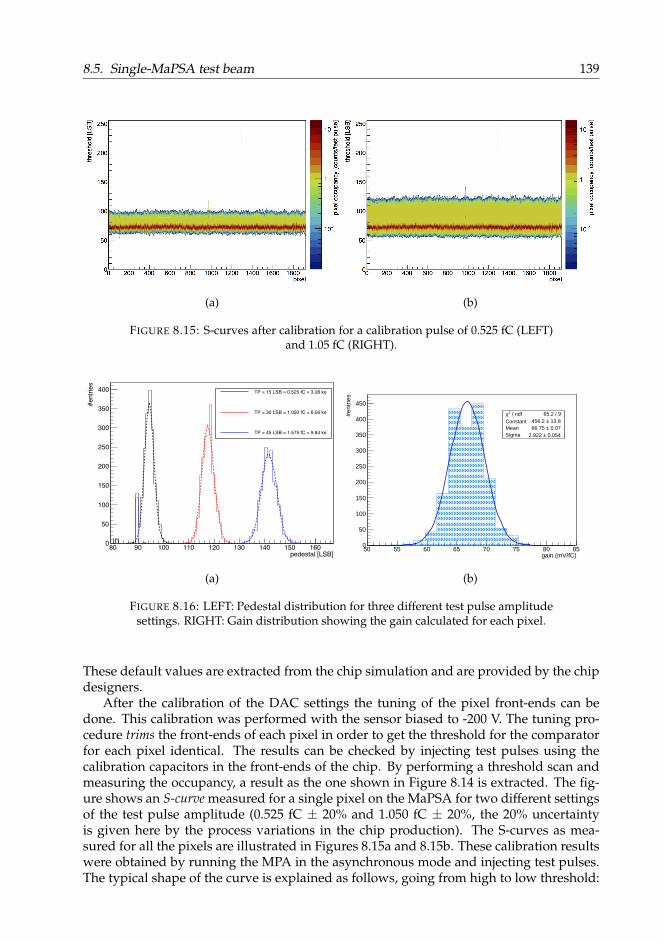
8.5. Single-MaPSA test beam 139
(a) (b)
FIGURE 8.15: S-curves after calibration for a calibration pulse of 0.525 fC (LEFT)and 1.05 fC (RIGHT).
80 90 100 110 120 130 140 150 160pedestal [LSB]
0
50
100
150
200
250
300
350
400
#en
tries
-TP = 15 LSB = 0.525 fC = 3.28 ke
-TP = 30 LSB = 1.050 fC = 6.56 ke
-TP = 45 LSB = 1.575 fC = 9.84 ke
80 90 100 110 120 130 140 150 160pedestal [LSB]
0
50
100
150
200
250
300
350
400
#en
tries
-TP = 15 LSB = 0.525 fC = 3.28 ke
-TP = 30 LSB = 1.050 fC = 6.56 ke
-TP = 45 LSB = 1.575 fC = 9.84 ke
(a)
/ ndf 2χ 65.2 / 9Constant 13.8± 456.2 Mean 0.07± 66.75 Sigma 0.054± 2.922
50 55 60 65 70 75 80 85gain (mV/fC)
0
50
100
150
200
250
300
350
400
450
#en
trie
s
/ ndf 2χ 65.2 / 9Constant 13.8± 456.2 Mean 0.07± 66.75 Sigma 0.054± 2.922
(b)
FIGURE 8.16: LEFT: Pedestal distribution for three different test pulse amplitudesettings. RIGHT: Gain distribution showing the gain calculated for each pixel.
These default values are extracted from the chip simulation and are provided by the chipdesigners.
After the calibration of the DAC settings the tuning of the pixel front-ends can bedone. This calibration was performed with the sensor biased to -200 V. The tuning pro-cedure trims the front-ends of each pixel in order to get the threshold for the comparatorfor each pixel identical. The results can be checked by injecting test pulses using thecalibration capacitors in the front-ends of the chip. By performing a threshold scan andmeasuring the occupancy, a result as the one shown in Figure 8.14 is extracted. The fig-ure shows an S-curve measured for a single pixel on the MaPSA for two different settingsof the test pulse amplitude (0.525 fC ± 20% and 1.050 fC ± 20%, the 20% uncertaintyis given here by the process variations in the chip production). The S-curves as mea-sured for all the pixels are illustrated in Figures 8.15a and 8.15b. These calibration resultswere obtained by running the MPA in the asynchronous mode and injecting test pulses.The typical shape of the curve is explained as follows, going from high to low threshold:

140 Chapter 8. PS Prototype Testing
Run # Assem-bly Type Threshold
(LSB)Biasvoltage (V)
Incidentangle α ()
MPASynchronous/Asynchronous
Telescopedataavailable?
Samplingmode
1 1 Thresholdscan
70, 72, ...,250 -200 0 Asynchronous No Ripple
counter
2 2 Thresholdscan
70, 71,...,251 -200 0 Asynchronous No Ripple
counter
3 1 Latencyscan
90, 110,250 -200 0 Synchronous No Level
4 1 Latencyscan
100, 120,..., 240 -200 0 Synchronous No Edge
5 1 Angularscan 110 -200
-15, -10,-5, 0, 10,20, 30,40
Synchronous No Level
6 1 Bias scan 110 -200,-150,-100, -50 0 Synchronous No Level
7 1 Thresholdscan
90, 110,150 -200 0 Synchronous Yes Level
8 1 Biasscan 110 -200, -150,
-100 0 Synchronous Yes Level
9 2 Samplingmodes 110 -200 0 Synchronous Yes Level
and Edge
TABLE 8.6: List of scans performed during the single-MaPSA test beam.
at high threshold the comparator never switches, so no counts are registered. Then atlower threshold (e.g. threshold ≈ 100 for Figure 8.15a) the comparator starts to switchand 1 count per test pulse is registered. The middle (50% occupancy) of the S-curve is re-ferred to as the pedestal. At even lower thresholds the threshold is low enough so that thecomparator also triggers on noise (e.g. threshold ≈ 70 for Figure 8.15a). For even lowerthresholds the pixel occupancy per test pulse drops again to zero as there will be no morecomparator transitions because the noise will always be above threshold.
The distribution of the pedestals for all pixels are shown for three different test pulsesettings in Figure 8.16a and the distributions of the gains, as calculated for each pixel isshown in Figure 8.16b. An average gain of 66.75 mV/fC and a baseline7 of 106 mV areextracted.
After calibration of the DACs and tuning of the front-ends a threshold can be chosenabove the noise in order to do the latency scan. Two latency values need to be extractedto set up the system for data taking: the L1 latency and the stub latency. It has to be keptin mind that the stub data in this specific configuration are actually pixel clusters. Theresults from the latency scans will be discussed in section 8.5.7.1
After calibration of the DACs, the tuning of the offsets and the latency scans, thesystem is ready for data taking.
8.5.7 ResultsDuring the single-MaPSA test beam, two assemblies were tested. The scans which wereperformed are summarised in Table 8.6 and will be discussed in the next sections.
7Pedestal at zero injected charge.

8.5. Single-MaPSA test beam 141
8.5.7.1 Assembly #1 and #2: DUT only
A fine threshold scan in asynchronous mode at perpendicular incidence and a bias volt-age of -200 V was performed for both assembly #1 and assembly #2. The results are shownin Figure 8.17 and 8.18 respectively. The integrated counts on the ripple counter from thefull MPA, normalised to the number of hits recorded by a downstream scintillator8 areshown in Figure 8.17a and 8.18a. The derivative of these distributions are shown in Fig-ure 8.17b and 8.18b respectively and show the signal distribution. The signal distributionin the signal region is fitted with a convoluted Gaussian and Landau.
60 80 100 120 140 160 180 200 220 240 260Threshold[LSB]
5
10
15
20
25
30
Nor
mal
ised
num
ber
of M
PA
hits
(a)
Landau Width 10.94
Most Probable Value Landau 188.6
Area (normalization) 2.762
Gaussian Spread 17.33
0 50 100 150 200 250Threshold [LSB]
0.04−
0.03−
0.02−
0.01−
0
d(T
hres
hold
[LS
B])
d(N
orm
alis
ed n
umbe
r of
MP
A h
its)
Landau Width 10.94
Most Probable Value Landau 188.6
Area (normalization) 2.762
Gaussian Spread 17.33
Signal distribution
Landau-Gaus convolution fit
Signal distribution
Landau-Gaus convolution fit
(b)
FIGURE 8.17: LEFT: Number of hits recorded on the ripple counter of all the MPApixels normalised to the number of hits recorded by a downstream scintillator infunction of the threshold. RIGHT: The derivative with respect to threshold ofFigure 8.17a gives the signal distribution. The signal distribution is fitted with aconvolution of a Landau and a Gaussian. The result for values lower than 135 LSB
are not shown. These results are for assembly #1.
For assembly #1 this results in a most probable value for the signal of 188.6 thresholdLSB. Together with the baseline at 72 threshold LSB, a most probable signal of ≈ 14 ke−
(70 e−h+/µm, from Figure 3.3a for a 200 µm thick sensor) and the fact that 1 thresholdLSB corresponds to 1.456 mV [66] a gain of 75.7 mV/fC can be extracted which is closeto the 66.75 mV/fC extracted using the test pulse measurement. The discrepancy canbe explained by the uncertainty of the injected charge when using the test pulse and theunknown charge collection efficiency of the sensor.
For assembly #2 a similar calculation, using a most probable value for the signal of215.5 LSB and a baseline at 97 LSB, leads to a gain of 76.6 mV/fC. The gain values,calculated with the data from the beam particles, is coherent when comparing the twoassemblies.
For the threshold settings which were used during this test beam the physical thresh-old values obtained with the gain values calculated above are given in Table 8.7.
Figure 8.19a and 8.19b show the L1 latency scan performed for assembly #1 in thelevel and edge sampling mode (see Figure 5.11) respectively. For both modes it can beseen that the higher the threshold, the smaller becomes the latency window to operatein. For the level sensitive mode a single latency value can be chosen which will result in
8The disconnected pixels (see later) were masked for the analysis.
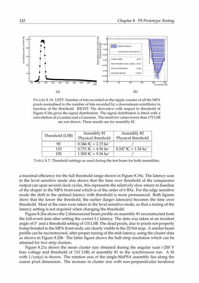
142 Chapter 8. PS Prototype Testing
60 80 100 120 140 160 180 200 220 240 260Threshold[LSB]
10
20
30
40
50
Nor
mal
ised
num
ber
of M
PA
hits
(a)
Landau Width 14.62
Most Probable Value Landau 215.5
Area (normalization) 2.588
Gaussian Spread 0.4311
0 50 100 150 200 250Threshold [LSB]
0.04−
0.035−
0.03−
0.025−
0.02−
0.015−
0.01−
0.005−
0
d(T
hres
hold
[LS
B])
d(N
orm
alis
ed n
umbe
r of
MP
A h
its)
Landau Width 14.62
Most Probable Value Landau 215.5
Area (normalization) 2.588
Gaussian Spread 0.4311
Signal distribution
Landau-Gaus convolution fit
Signal distribution
Landau-Gaus convolution fit
(b)
FIGURE 8.18: LEFT: Number of hits recorded on the ripple counter of all the MPApixels normalised to the number of hits recorded by a downstream scintillator infunction of the threshold. RIGHT: The derivative with respect to threshold ofFigure 8.18a gives the signal distribution. The signal distribution is fitted with aconvolution of a Landau and a Gaussian. The result for values lower than 175 LSB
are not shown. These results are for assembly #2.
Threshold (LSB) Assembly #1Physical threshold
Assembly #2Physical threshold
90 0.346 fC = 2.15 ke− /110 0.731 fC = 4.56 ke− 0.247 fC = 1.54 ke−
150 1.500 fC = 9.36 ke− /
TABLE 8.7: Threshold settings as used during the test beam for both assemblies.
a maximal efficiency for the full threshold range shown in Figure 8.19a. The latency scanin the level sensitive mode also shows that the time over threshold of the comparatoroutput can span several clock cycles, this represents the relatively slow return to baselineof the shaper in the MPA front-end which is of the order of 6 BXs. For the edge sensitivemode the shift in the optimal latency with threshold is more pronounced. Both figuresshow that the lower the threshold, the earlier (larger latencies) becomes the time overthreshold. Most of the runs were taken in the level sensitive mode, so that a tuning of thelatency setting is not required when changing the threshold.
Figure 8.20a shows the 2 dimensional beam profile on assembly #1 reconstructed fromthe full-event data after setting the correct L1 latency. The data was taken at an incidentangle of 0 and a threshold setting of 110 LSB. The dead pixels, due to pixels not properlybump bonded to the MPA front-ends, are clearly visible in the 2D hit map. A similar beamprofile can be reconstructed, after proper tuning of the stub latency, using the cluster dataas shown in Figure 8.20b. The latter figure shows the half-strip resolution which can beattained for two strip clusters.
Figure 8.21a shows the mean cluster size obtained during the angular scan (-200 Vbias voltage and threshold of 110 LSB) of assembly #1 in the synchronous run. A fitwith 1/cos(α) is shown. The rotation axis of the single-MaPSA assembly lies along thecoarse pixel dimension. The increase in cluster size with non-perpendicular incidence
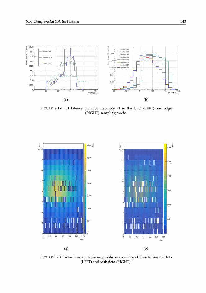
8.5. Single-MaPSA test beam 143
56 58 60 62 64 66latency [BX]
0
0.005
0.01
0.015
0.02
0.025
0.03
0.035
0.04
0.045
nor
mal
ised
#l1
clu
ster
s
threshold 90
threshold 110
threshold 250
threshold 90
threshold 110
threshold 250
threshold 90
threshold 110
threshold 250
(a)
61 61.5 62 62.5 63 63.5latency [BX]
0
0.02
0.04
0.06
0.08
0.1
nor
mal
ised
#l1
clu
ster
s
threshold 100
threshold 120
threshold 140
threshold 160
threshold 180
threshold 200
threshold 220
threshold 240
threshold 100
threshold 120
threshold 140
threshold 160
threshold 180
threshold 200
threshold 220
threshold 240
threshold 100
threshold 120
threshold 140
threshold 160
threshold 180
threshold 200
threshold 220
threshold 240
threshold 100
threshold 120
threshold 140
threshold 160
threshold 180
threshold 200
threshold 220
threshold 240
threshold 100
threshold 120
threshold 140
threshold 160
threshold 180
threshold 200
threshold 220
threshold 240
threshold 100
threshold 120
threshold 140
threshold 160
threshold 180
threshold 200
threshold 220
threshold 240
threshold 100
threshold 120
threshold 140
threshold 160
threshold 180
threshold 200
threshold 220
threshold 240
threshold 100
threshold 120
threshold 140
threshold 160
threshold 180
threshold 200
threshold 220
threshold 240
(b)
FIGURE 8.19: L1 latency scan for assembly #1 in the level (LEFT) and edge(RIGHT) sampling mode.
0 20 40 60 80 100 120
Row
0
2
4
6
8
10
12
14
16Col
umn
0
500
1000
1500
2000
2500
3000
3500
#hits
(a)
0 20 40 60 80 100 120
Row
0
2
4
6
8
10
12
14
16Col
umn
0
500
1000
1500
2000
2500
3000 #hits
(b)
FIGURE 8.20: Two-dimensional beam profile on assembly #1 from full-event data(LEFT) and stub data (RIGHT).

144 Chapter 8. PS Prototype Testing
20− 10− 0 10 20 30 40 [deg]α
1.1
1.2
1.3
1.4
1.5
1.6
1.7
mea
n cl
uste
r si
ze
A 0.005931± 1.881
B 0.006032±0.7751 − C 0.04383±0.2651 −
A 0.005931± 1.881
B 0.006032±0.7751 − C 0.04383±0.2651 −
Data
+ C - B)αcos(
A
(a) (b)
FIGURE 8.21: LEFT: Mean cluster size distribution for single cluster events onthe single-MaPSA versus incident angle. The distribution follows a 1/cos(α) be-haviour, representing the increase in charge sharing between pixels due to theparticle crossing more of the active volume when the incidence is not perpendic-ular. RIGHT: Explanation of the charge sharing with rotation: d is the thicknessof the sensor, α the incident angle and L the path length of the particle through
the sensor.
200− 180− 160− 140− 120− 100− 80− 60− 40−Bias voltage (V)
1.08
1.082
1.084
1.086
1.088
1.09
1.092
1.094
1.096
1.098
mea
n cl
uste
r si
ze
FIGURE 8.22: Mean cluster size distribution for single cluster events on thesingle-MaPSA versus bias voltage for assembly #1.
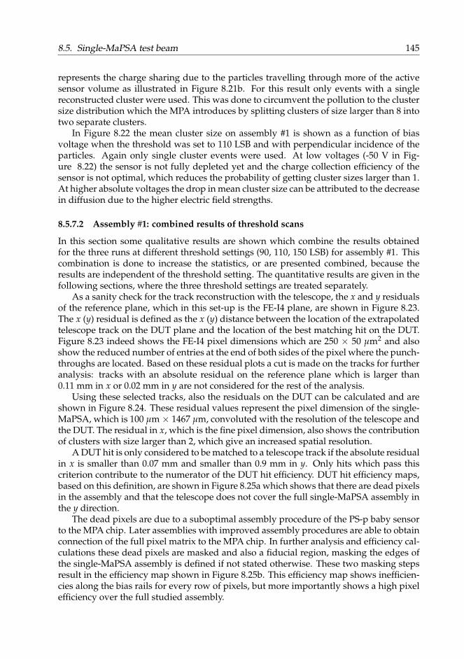
8.5. Single-MaPSA test beam 145
represents the charge sharing due to the particles travelling through more of the activesensor volume as illustrated in Figure 8.21b. For this result only events with a singlereconstructed cluster were used. This was done to circumvent the pollution to the clustersize distribution which the MPA introduces by splitting clusters of size larger than 8 intotwo separate clusters.
In Figure 8.22 the mean cluster size on assembly #1 is shown as a function of biasvoltage when the threshold was set to 110 LSB and with perpendicular incidence of theparticles. Again only single cluster events were used. At low voltages (-50 V in Fig-ure 8.22) the sensor is not fully depleted yet and the charge collection efficiency of thesensor is not optimal, which reduces the probability of getting cluster sizes larger than 1.At higher absolute voltages the drop in mean cluster size can be attributed to the decreasein diffusion due to the higher electric field strengths.
8.5.7.2 Assembly #1: combined results of threshold scans
In this section some qualitative results are shown which combine the results obtainedfor the three runs at different threshold settings (90, 110, 150 LSB) for assembly #1. Thiscombination is done to increase the statistics, or are presented combined, because theresults are independent of the threshold setting. The quantitative results are given in thefollowing sections, where the three threshold settings are treated separately.
As a sanity check for the track reconstruction with the telescope, the x and y residualsof the reference plane, which in this set-up is the FE-I4 plane, are shown in Figure 8.23.The x (y) residual is defined as the x (y) distance between the location of the extrapolatedtelescope track on the DUT plane and the location of the best matching hit on the DUT.Figure 8.23 indeed shows the FE-I4 pixel dimensions which are 250 × 50 µm2 and alsoshow the reduced number of entries at the end of both sides of the pixel where the punch-throughs are located. Based on these residual plots a cut is made on the tracks for furtheranalysis: tracks with an absolute residual on the reference plane which is larger than0.11 mm in x or 0.02 mm in y are not considered for the rest of the analysis.
Using these selected tracks, also the residuals on the DUT can be calculated and areshown in Figure 8.24. These residual values represent the pixel dimension of the single-MaPSA, which is 100 µm× 1467 µm, convoluted with the resolution of the telescope andthe DUT. The residual in x, which is the fine pixel dimension, also shows the contributionof clusters with size larger than 2, which give an increased spatial resolution.
A DUT hit is only considered to be matched to a telescope track if the absolute residualin x is smaller than 0.07 mm and smaller than 0.9 mm in y. Only hits which pass thiscriterion contribute to the numerator of the DUT hit efficiency. DUT hit efficiency maps,based on this definition, are shown in Figure 8.25a which shows that there are dead pixelsin the assembly and that the telescope does not cover the full single-MaPSA assembly inthe y direction.
The dead pixels are due to a suboptimal assembly procedure of the PS-p baby sensorto the MPA chip. Later assemblies with improved assembly procedures are able to obtainconnection of the full pixel matrix to the MPA chip. In further analysis and efficiency cal-culations these dead pixels are masked and also a fiducial region, masking the edges ofthe single-MaPSA assembly is defined if not stated otherwise. These two masking stepsresult in the efficiency map shown in Figure 8.25b. This efficiency map shows inefficien-cies along the bias rails for every row of pixels, but more importantly shows a high pixelefficiency over the full studied assembly.
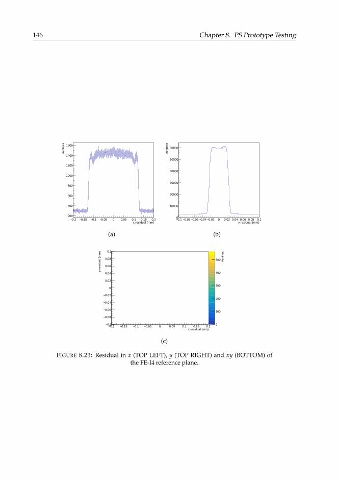
146 Chapter 8. PS Prototype Testing
0.2− 0.15− 0.1− 0.05− 0 0.05 0.1 0.15 0.2 x residual (mm)
200
400
600
800
1000
1200
1400
1600
#en
trie
s
(a)
0.1− 0.08− 0.06− 0.04− 0.02− 0 0.02 0.04 0.06 0.08 0.1 y residual (mm)
0
10000
20000
30000
40000
50000
60000
#en
trie
s
(b)
0.2− 0.15− 0.1− 0.05− 0 0.05 0.1 0.15 0.2 x residual (mm)
0.1−
0.08−
0.06−
0.04−
0.02−
0
0.02
0.04
0.06
0.08
0.1
y r
esid
ual (
mm
)
0
100
200
300
400
500
#en
trie
s
(c)
FIGURE 8.23: Residual in x (TOP LEFT), y (TOP RIGHT) and xy (BOTTOM) ofthe FE-I4 reference plane.
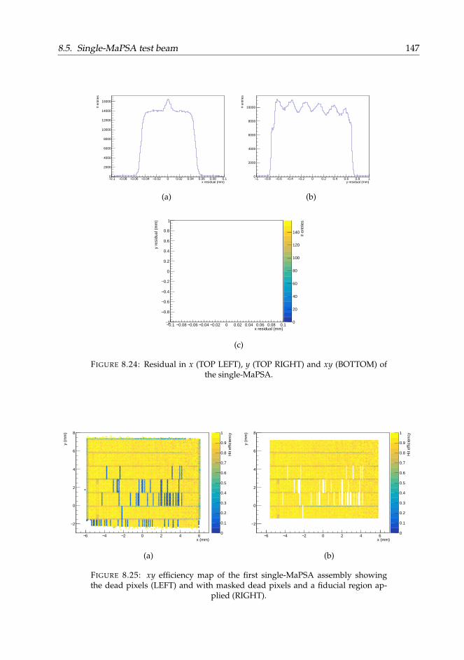
8.5. Single-MaPSA test beam 147
0.1− 0.08− 0.06− 0.04− 0.02− 0 0.02 0.04 0.06 0.08 0.1 x residual (mm)
0
2000
4000
6000
8000
10000
12000
14000
16000
# e
ntrie
s
(a)
1− 0.8− 0.6− 0.4− 0.2− 0 0.2 0.4 0.6 0.8 1 y residual (mm)
0
2000
4000
6000
8000
10000 # e
ntrie
s
(b)
0.1− 0.08− 0.06− 0.04− 0.02− 0 0.02 0.04 0.06 0.08 0.1 x residual (mm)
1−
0.8−
0.6−
0.4−
0.2−
0
0.2
0.4
0.6
0.8
1
y r
esid
ual (
mm
)
0
20
40
60
80
100
120
140
# e
ntrie
s
(c)
FIGURE 8.24: Residual in x (TOP LEFT), y (TOP RIGHT) and xy (BOTTOM) ofthe single-MaPSA.
6− 4− 2− 0 2 4 6 x (mm)
2−
0
2
4
6
8
y (
mm
)
0
0.1
0.2
0.3
0.4
0.5
0.6
0.7
0.8
0.9
1
Hit
effic
ienc
y
(a)
6− 4− 2− 0 2 4 6 x (mm)
2−
0
2
4
6
8
y (
mm
)
0
0.1
0.2
0.3
0.4
0.5
0.6
0.7
0.8
0.9
1
Hit
effic
ienc
y
(b)
FIGURE 8.25: xy efficiency map of the first single-MaPSA assembly showingthe dead pixels (LEFT) and with masked dead pixels and a fiducial region ap-
plied (RIGHT).

148 Chapter 8. PS Prototype Testing
0200
m)
µ x (
0
500
1000
1500
2000
2500
m)µ y (
0 0.1
0.2
0.3
0.4
0.5
0.6
0.7
0.8
0.9
1
Hit efficiency
FIGURE 8.26: Inpixel efficiency for 4 pixels. This is obtained by folding the datafrom the studied part of the first single-MaPSA assembly to increase the statistics
inside the pixels.
0 20 40 60 80 100 120 140 160 180 200m)µ x (
1360
1380
1400
1420
1440
1460
1480
1500
1520
1540m)
µ y
(
0.1
0.2
0.3
0.4
0.5
0.6
0.7
0.8
0.9
1
Hit
effic
ienc
y
FIGURE 8.27: Zoom on the bias rail and punch-through region for the data shownin Figure 8.26.
To better study the inefficiencies due to the bias structure, so-called inpixel efficiencymaps can be extracted by overlapping the data from different pixels on the same set of 4pixels. This set of 4 pixels is the unit of the layout of the pixel matrix, as represented inFigure 8.13. An inpixel efficiency map is shown in Figure 8.26 with a zoom on the biasand punch-through region in Figure 8.27.
Besides the efficiencies, also the cluster size distributions can be studied. Probabilitydistributions for clusters of size 1 and 2 will be discussed later (see section 8.5.7.3). Thefocus here will be on clusters with sizes larger than 2. The study of this type of clustersrequires the combination from the data of all three threshold settings due to the lowprobability for this type of clusters to occur. Figure 8.28a shows the probability for clustersize 3 as function of the hit location of the particle. It can be seen that when the particlehits close to the pixel borders the probability of creating a cluster of size 3 increases. Itmust be noted however that the probability of clusters of size 3 is very low. The only size 3clusters which were included in Figure 8.28a are clusters which have 3 hits in consecutivepixels along the fine pixel dimension.
Cluster distributions can also be studied along the coarse pixel dimension. Here theoverall probability of clusters spanning multiple pixels is smaller due to the larger pixel

8.5. Single-MaPSA test beam 149
0 20 40 60 80 100 120 140 160 180 200 220m)µ x(
0.001
0.002
0.003
0.004
0.005
0.006
Clu
ster
size
= 3
pro
babi
lity
(a)
(b)
FIGURE 8.28: LEFT: Probability of cluster size 3 along the fine pixel dimensioncombining data from the three threshold settings used for the first assembly.RIGHT: Definition of cluster types where the coloured pixel represents the centralpixel which is hit and the pixel filled with an ’x’ the neighbouring pixel(s) whichis (are) hit. The two leftmost columns show the standard 2 and 3 pixel clustersalong x and y, simply for completeness. The two right columns introduce the
new cluster types type 1 and type 4.
size in this dimension. Furthermore the MPA does not perform clusterisation along y, soclusters in this dimension will not add to an improved spatial resolution, unless recon-structed offline. The probability for cluster sizes 1 and 2 in function of y can be found insection 8.5.7.3. The probability for clusters spanning 3 consecutive pixels in the y direc-tion was found to be zero.
Two other cluster types were also studied. These will be referred to as type 1 and type 4and are defined in Figure 8.28b9. A non-zero probability for these clusters was found andtheir probability as function of x and y are shown in Figure 8.29 and 8.30 for type 1 andtype 4 respectively. It must be noted that the probability for these cluster types is verylow, around the per mille level, but nevertheless a higher probability for these clusters isobserved along the pixel boundaries in y.
8.5.7.3 Assembly #1: threshold scan
After a more qualitative discussion in the previous section, the exact efficiency valuesfor the different threshold settings will be discussed in more detail in this section byprojecting the 2D efficiency maps along x and y. This will be done for the three thresholdsettings with which assembly #1 was operated. Figure 8.31 shows the TDC dependenceof the overall efficiency. It shows that for the highest threshold settings the efficiency
9Type 4 clusters contain type 1 clusters, but no entry is made in the numerator of the probability for type 1clusters if a type 4 cluster was found.

150 Chapter 8. PS Prototype Testing
0 20 40 60 80 100 120 140 160 180 200 220m)µ x(
0.4
0.5
0.6
0.7
0.8
0.9
3−10×
Clu
ster
type
1 p
roba
bilit
y
(a)
0 500 1000 1500 2000 2500 3000m)µ y(
0.0005
0.001
0.0015
0.002
0.0025
0.003
Clu
ster
type
1 p
roba
bilit
y
(b)
FIGURE 8.29: Probability of clusters of type 1 (defined in Figure 8.28b) alongthe fine (LEFT) and coarse (RIGHT) pixel dimension obtained by combining data
from the three threshold settings used for the first assembly.
0 20 40 60 80 100 120 140 160 180 200 220m)µ x(
0
0.02
0.04
0.06
0.08
0.1
0.12
3−10×
Clu
ster
type
4 p
roba
bilit
y
(a)
0 500 1000 1500 2000 2500 3000m)µ y(
0
0.05
0.1
0.15
0.2
0.25
3−10×
Clu
ster
type
4 p
roba
bilit
y
(b)
FIGURE 8.30: Probability of clusters of type 4 (defined in Figure 8.28b) alongthe fine (LEFT) and coarse (RIGHT) pixel dimension obtained by combining data
from the three threshold settings used for the first assembly.

8.5. Single-MaPSA test beam 151
0 1 2 3 4 5 6 7 8 TDC value [3.125 ns]
0.75
0.8
0.85
0.9
0.95
Hit
effic
ienc
y
Threshold = 90
Threshold = 110
Threshold = 150
FIGURE 8.31: TDC dependence of the efficiency for the three tested thresholdsettings with the first single-MaPSA assembly.
6− 4− 2− 0 2 4 6 x(mm)
0.82
0.84
0.86
0.88
0.9
0.92
0.94
0.96
0.98
Hit
effic
ienc
y
Threshold = 90
Threshold = 110
Threshold = 150
(a)
2− 0 2 4 6 8 y(mm)
0
0.1
0.2
0.3
0.4
0.5
0.6
0.7
0.8
0.9
1
Hit
effic
ienc
y
Threshold = 90
Threshold = 110
Threshold = 150
(b)
FIGURE 8.32: Efficiency along the fine (x) and coarse (y) pixel dimensions forthe three threshold settings used during the test beam for the first single-MaPSA
assembly.
strongly depends on the TDC phase. Therefore for the rest of the results in this sectiononly events which end up in TDC bins 6 and 7 will be used for the efficiency calculations.
Projections of the efficiency along x and y for the three studied threshold settings canbe found in Figure 8.32. Figure 8.32a shows, for the lowest thresholds an efficiency higherthan 94%. Also a decrease in efficiency with increasing values of x is visible. The reasonfor this dependency is not understood and was also observed for the second assembly(see section 8.5.7.5). Figure 8.32b shows that the efficiency drops to as low as 20% at thebias rails, even for the lowest threshold setting. The decrease in efficiency due to the biasrail can be recovered by tilting the assembly so that the particles do not enter the siliconexactly perpendicular.
The inpixel efficiencies can be found in Figure 8.33 for both pixel dimensions. Figure8.33a shows that also along x there are inefficiencies along the pixel boundaries. These in-efficiencies can partly be attributed to charge sharing between pixels. For the two lowestthresholds these inefficiencies are rather small (≈ 2% compared to the central regions).
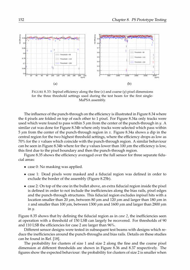
152 Chapter 8. PS Prototype Testing
0 20 40 60 80 100 120 140 160 180 200 220m)µ x(
0.6
0.65
0.7
0.75
0.8
0.85
0.9
0.95
Hit
Effi
cien
cy
Threshold = 90
Threshold = 110
Threshold = 150
(a)
0 500 1000 1500 2000 2500 3000m)µ y(
0.2
0.3
0.4
0.5
0.6
0.7
0.8
0.9
1
Hit
Effi
cien
cy
Threshold = 90
Threshold = 110
Threshold = 150
(b)
FIGURE 8.33: Inpixel efficiency along the fine (x) and coarse (y) pixel dimensionsfor the three threshold settings used during the test beam for the first single-
MaPSA assembly.
The influence of the punch-through on the efficiency is illustrated in Figure 8.34 wherethe 4 pixels are folded on top of each other to 1 pixel. For Figure 8.34a only tracks wereused which were found to pass within 5 µm from the center of the punch-through in y. Asimilar cut was done for Figure 8.34b where only tracks were selected which pass within5 µm from the center of the punch-through region in x. Figure 8.34a shows a dip in thecentral region for the two highest threshold settings, where the efficiency drops as low as70% for the x values which coincide with the punch-through region. A similar behaviourcan be seen in Figure 8.34b where for the y values lower than 100 µm the efficiency is low,this first due to the pixel boundary and then the punch-through region.
Figure 8.35 shows the efficiency averaged over the full sensor for three separate fidu-cial areas:
• case 0: No masking was applied.
• case 1: Dead pixels were masked and a fiducial region was defined in order toexclude the border of the assembly (Figure 8.25b).
• case 2: On top of the one in the bullet above, an extra fiducial region inside the pixelis defined in order to not include the inefficiencies along the bias rails, pixel edgesand the punch-through structures. This fiducial region excludes inpixel hits with alocation smaller than 20 µm, between 80 µm and 120 µm and larger than 180 µm inx and smaller than 100 µm, between 1300 µm and 1600 µm and larger than 2800 µmin y.
Figure 8.35 shows that by defining the fiducial region as in case 2, the inefficiencies seenat operation with a threshold of 150 LSB can largely be recovered. For thresholds of 90and 110 LSB the efficiencies for case 2 are larger than 96%.
Different sensor designs were tested in subsequent test beams with designs which re-duce the inefficiencies around the punch-throughs and bias rails. Details on these studiescan be found in Ref. [18].
The probability for clusters of size 1 and size 2 along the fine and the coarse pixeldimension at different thresholds are shown in Figure 8.36 and 8.37 respectively. Thefigures show the expected behaviour: the probability for clusters of size 2 is smaller when
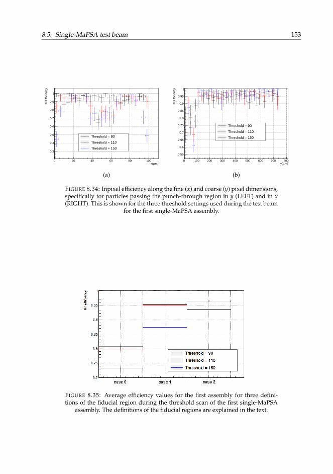
8.5. Single-MaPSA test beam 153
0 20 40 60 80 100m)µ x(
0.3
0.4
0.5
0.6
0.7
0.8
0.9
1
Hit
Effi
cien
cy
Threshold = 90
Threshold = 110
Threshold = 150
(a)
0 100 200 300 400 500 600 700 800m)µ y(
0.55
0.6
0.65
0.7
0.75
0.8
0.85
0.9
0.95
1
Hit
Effi
cien
cy
Threshold = 90
Threshold = 110
Threshold = 150
(b)
FIGURE 8.34: Inpixel efficiency along the fine (x) and coarse (y) pixel dimensions,specifically for particles passing the punch-through region in y (LEFT) and in x(RIGHT). This is shown for the three threshold settings used during the test beam
for the first single-MaPSA assembly.
FIGURE 8.35: Average efficiency values for the first assembly for three defini-tions of the fiducial region during the threshold scan of the first single-MaPSA
assembly. The definitions of the fiducial regions are explained in the text.

154 Chapter 8. PS Prototype Testing
0 20 40 60 80 100 120 140 160 180 200 220m)µ x(
0.5
0.6
0.7
0.8
0.9
1
Clu
ster
size
= 1
pro
babi
lity
Threshold = 90
Threshold = 110
Threshold = 150
(a)
0 500 1000 1500 2000 2500 3000m)µ y(
0.97
0.975
0.98
0.985
0.99
0.995
1
Clu
ster
size
= 1
pro
babi
lity
Threshold = 90
Threshold = 110
Threshold = 150
(b)
FIGURE 8.36: Inpixel probability for clusters of size 1 along the fine (x) and coarse(y) pixel dimensions for the three threshold settings used during the test beam
with the first single-MaPSA assembly.
0 20 40 60 80 100 120 140 160 180 200 220m)µ x(
0.1
0.2
0.3
0.4
0.5
Clu
ster
size
= 2
pro
babi
lity
Threshold = 90
Threshold = 110
Threshold = 150
(a)
0 500 1000 1500 2000 2500 3000m)µ y(
0
0.005
0.01
0.015
0.02
0.025
0.03
0.035
0.04
Clu
ster
size
= 2
pro
babi
lity
Threshold = 90
Threshold = 110
Threshold = 150
(b)
FIGURE 8.37: Inpixel probability for clusters of size 2 along the fine (x) and coarse(y) pixel dimensions for the three threshold settings used during the test beam
with the first single-MaPSA assembly.
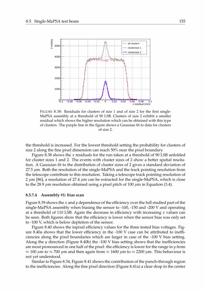
8.5. Single-MaPSA test beam 155
0.1− 0.08− 0.06− 0.04− 0.02− 0 0.02 0.04 0.06 0.08 0.1 x residual (mm)
0
1000
2000
3000
4000
5000
# e
ntrie
s
all clusters
clustersize 1
clustersize 2
FIGURE 8.38: Residuals for clusters of size 1 and of size 2 for the first single-MaPSA assembly at a threshold of 90 LSB. Clusters of size 2 exhibit a smallerresidual which shows the higher resolution which can be obtained with this typeof clusters. The purple line in the figure shows a Gaussian fit to data for clusters
of size 2.
the threshold is increased. For the lowest threshold setting the probability for clusters ofsize 2 along the fine pixel dimension can reach 50% near the pixel boundary.
Figure 8.38 shows the x residuals for the run taken at a threshold of 90 LSB unfoldedfor cluster sizes 1 and 2. The events with cluster sizes of 2 show a better spatial resolu-tion. A Gaussian fit to the distribution of cluster sizes of 2 gives a standard deviation of27.5 µm. Both the resolution of the single-MaPSA and the track pointing resolution fromthe telescope contribute to this resolution. Taking a telescope track pointing resolution of2 µm [86], a resolution of 27.4 µm can be extracted for the single-MaPSA, which is closeto the 28.9 µm resolution obtained using a pixel pitch of 100 µm in Equation (3.4).
8.5.7.4 Assembly #1: bias scan
Figure 8.39 shows the x and y dependence of the efficiency over the full studied part of thesingle-MaPSA assembly when biasing the sensor to -100, -150 and -200 V and operatingat a threshold of 110 LSB. Again the decrease in efficiency with increasing x values canbe seen. Both figures show that the efficiency is lower when the sensor bias was only setto -100 V, which is below depletion of the sensor.
Figure 8.40 shows the inpixel efficiency values for the three tested bias voltages. Fig-ure 8.40a shows that the lower efficiency in the -100 V case can be attributed to ineffi-ciencies along the pixel boundaries which are larger in case of the -100 V bias setting.Along the y direction (Figure 8.40b) the -100 V bias setting shows that the inefficienciesare most pronounced in one half of the pixel: the efficiency is lower for the range in y from≈ 100 µm to ≈ 700 µm and then again from ≈ 1600 µm to ≈ 2200 µm. This behaviour isnot yet understood.
Similar to Figure 8.34, Figure 8.41 shows the contribution of the punch-through regionto the inefficiencies. Along the fine pixel direction (Figure 8.41a) a clear drop in the center

156 Chapter 8. PS Prototype Testing
6− 4− 2− 0 2 4 6 x(mm)
0.84
0.86
0.88
0.9
0.92
0.94
0.96
0.98
Hit
effic
ienc
y
Bias voltage = -100V
Bias voltage = -150V
Bias voltage = -200V
(a)
2− 0 2 4 6 8 y(mm)
0.2
0.3
0.4
0.5
0.6
0.7
0.8
0.9
1
Hit
effic
ienc
y
Bias voltage = -100V
Bias voltage = -150V
Bias voltage = -200V
(b)
FIGURE 8.39: Efficiency along the fine (x) and coarse (y) pixel dimensions for thethree bias settings used during the test beam for the first single-MaPSA assembly.
0 20 40 60 80 100 120 140 160 180 200 220m)µ x(
0.75
0.8
0.85
0.9
0.95
Hit
Effi
cien
cy
Bias voltage = -100V
Bias voltage = -150V
Bias voltage = -200V
(a)
0 500 1000 1500 2000 2500 3000m)µ y(
0.2
0.3
0.4
0.5
0.6
0.7
0.8
0.9
1
Hit
Effi
cien
cy
Bias voltage = -100V
Bias voltage = -150V
Bias voltage = -200V
(b)
FIGURE 8.40: Inpixel efficiency along the fine (x) and coarse (y) pixel dimensionsfor the three bias settings used during the test beam for the first single-MaPSA
assembly.
of the pixel is visible for all three bias settings. What is apparent is that for the lowest volt-age setting the inefficiencies along the pixel boundaries are more significant compared tothe other two bias settings. In Figure 8.41b the contribution of the pixel boundary andthe punch-through region to the inefficiency is visible in the first ≈ 100 µm.
Figure 8.42 clearly shows the fact that these inefficiencies along the pixel boundariesare more pronounced in the setting with the lowest bias. The figure shows the averageefficiency of the single-MaPSA assembly for the three fiducial regions which were usedin Figure 8.35 and described in section 8.5.7.3. When going from fiducial region case 1 tocase 2, which excludes the pixel boundaries, we recover the efficiency for the lowest biasvoltage setting to values which are comparable to the other two bias voltage settings.
For completeness, the probability for clusters of size 1 and 2 along both pixel dimen-sions are given in Figure 8.43 and 8.44 respectively. No strong dependence on the biassetting can be observed for the cluster size distributions.
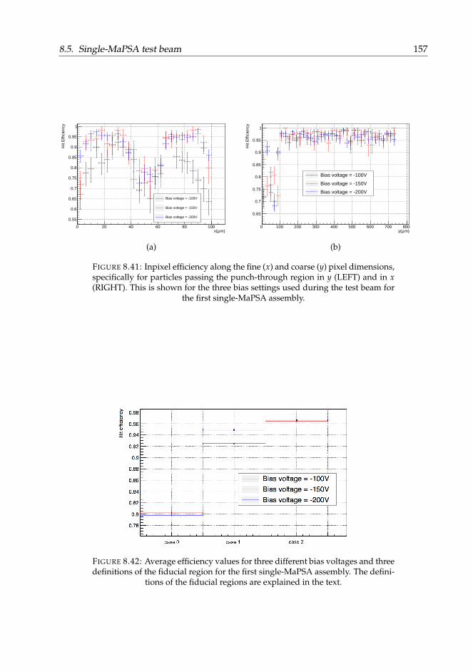
8.5. Single-MaPSA test beam 157
0 20 40 60 80 100m)µ x(
0.55
0.6
0.65
0.7
0.75
0.8
0.85
0.9
0.95
1
Hit
Effi
cien
cy
Bias voltage = -100V
Bias voltage = -150V
Bias voltage = -200V
(a)
0 100 200 300 400 500 600 700 800m)µ y(
0.65
0.7
0.75
0.8
0.85
0.9
0.95
1
Hit
Effi
cien
cy
Bias voltage = -100V
Bias voltage = -150V
Bias voltage = -200V
(b)
FIGURE 8.41: Inpixel efficiency along the fine (x) and coarse (y) pixel dimensions,specifically for particles passing the punch-through region in y (LEFT) and in x(RIGHT). This is shown for the three bias settings used during the test beam for
the first single-MaPSA assembly.
FIGURE 8.42: Average efficiency values for three different bias voltages and threedefinitions of the fiducial region for the first single-MaPSA assembly. The defini-
tions of the fiducial regions are explained in the text.
158 Chapter 8. PS Prototype Testing
0 20 40 60 80 100 120 140 160 180 200 220m)µ x(
0.75
0.8
0.85
0.9
0.95
1
Clu
ster
size
= 1
pro
babi
lity
Bias voltage = -100V
Bias voltage = -150V
Bias voltage = -200V
(a)
0 500 1000 1500 2000 2500 3000m)µ y(
0.965
0.97
0.975
0.98
0.985
0.99
0.995
1
Clu
ster
size
= 1
pro
babi
lity
Bias voltage = -100V
Bias voltage = -150V
Bias voltage = -200V
(b)
FIGURE 8.43: Inpixel probability for clusters of size 1 along the fine (x) and coarse(y) pixel dimensions for the three bias settings used during the test beam for the
first single-MaPSA assembly.
0 20 40 60 80 100 120 140 160 180 200 220m)µ x(
0.05
0.1
0.15
0.2
0.25
Clu
ster
size
= 2
pro
babi
lity
Bias voltage = -100V
Bias voltage = -150V
Bias voltage = -200V
(a)
0 500 1000 1500 2000 2500 3000m)µ y(
0
0.005
0.01
0.015
0.02
0.025
0.03
0.035
Clu
ster
size
= 2
pro
babi
lity
Bias voltage = -100V
Bias voltage = -150V
Bias voltage = -200V
(b)
FIGURE 8.44: Inpixel probability for clusters of size 2 along the fine (x) and coarse(y) pixel dimensions for the three bias settings used during the test beam for the
first single-MaPSA assembly.
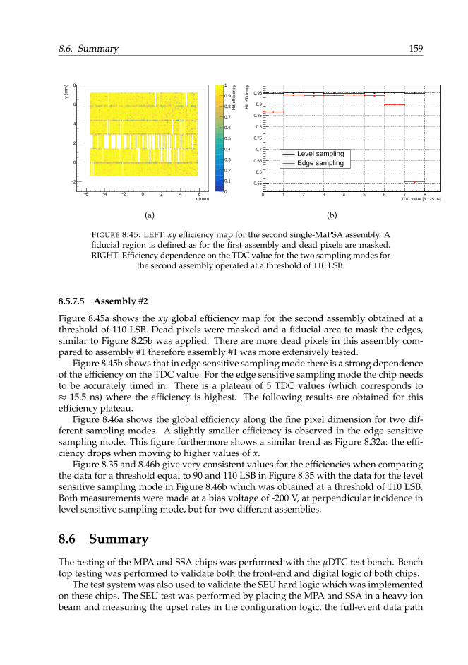
8.6. Summary 159
6− 4− 2− 0 2 4 6 x (mm)
2−
0
2
4
6
8
y (
mm
)
0
0.1
0.2
0.3
0.4
0.5
0.6
0.7
0.8
0.9
1
Hit
effic
ienc
y
(a)
0 1 2 3 4 5 6 7 8 TDC value [3.125 ns]
0.55
0.6
0.65
0.7
0.75
0.8
0.85
0.9
0.95
Hit
effic
ienc
y
Level samplingEdge sampling
(b)
FIGURE 8.45: LEFT: xy efficiency map for the second single-MaPSA assembly. Afiducial region is defined as for the first assembly and dead pixels are masked.RIGHT: Efficiency dependence on the TDC value for the two sampling modes for
the second assembly operated at a threshold of 110 LSB.
8.5.7.5 Assembly #2
Figure 8.45a shows the xy global efficiency map for the second assembly obtained at athreshold of 110 LSB. Dead pixels were masked and a fiducial area to mask the edges,similar to Figure 8.25b was applied. There are more dead pixels in this assembly com-pared to assembly #1 therefore assembly #1 was more extensively tested.
Figure 8.45b shows that in edge sensitive sampling mode there is a strong dependenceof the efficiency on the TDC value. For the edge sensitive sampling mode the chip needsto be accurately timed in. There is a plateau of 5 TDC values (which corresponds to≈ 15.5 ns) where the efficiency is highest. The following results are obtained for thisefficiency plateau.
Figure 8.46a shows the global efficiency along the fine pixel dimension for two dif-ferent sampling modes. A slightly smaller efficiency is observed in the edge sensitivesampling mode. This figure furthermore shows a similar trend as Figure 8.32a: the effi-ciency drops when moving to higher values of x.
Figure 8.35 and 8.46b give very consistent values for the efficiencies when comparingthe data for a threshold equal to 90 and 110 LSB in Figure 8.35 with the data for the levelsensitive sampling mode in Figure 8.46b which was obtained at a threshold of 110 LSB.Both measurements were made at a bias voltage of -200 V, at perpendicular incidence inlevel sensitive sampling mode, but for two different assemblies.
8.6 Summary
The testing of the MPA and SSA chips was performed with the µDTC test bench. Benchtop testing was performed to validate both the front-end and digital logic of both chips.
The test system was also used to validate the SEU hard logic which was implementedon these chips. The SEU test was performed by placing the MPA and SSA in a heavy ionbeam and measuring the upset rates in the configuration logic, the full-event data path
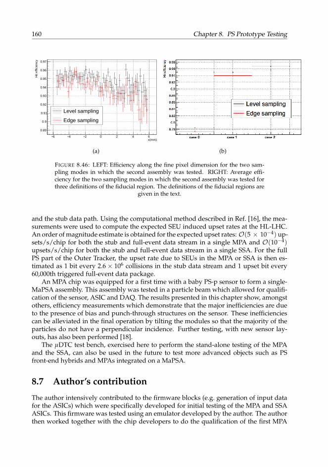
160 Chapter 8. PS Prototype Testing
6− 4− 2− 0 2 4 6 x(mm)
0.89
0.9
0.91
0.92
0.93
0.94
0.95
0.96
0.97
Hit
effic
ienc
y
Level sampling
Edge sampling
(a) (b)
FIGURE 8.46: LEFT: Efficiency along the fine pixel dimension for the two sam-pling modes in which the second assembly was tested. RIGHT: Average effi-ciency for the two sampling modes in which the second assembly was tested forthree definitions of the fiducial region. The definitions of the fiducial regions are
given in the text.
and the stub data path. Using the computational method described in Ref. [16], the mea-surements were used to compute the expected SEU induced upset rates at the HL-LHC.An order of magnitude estimate is obtained for the expected upset rates: O(5 × 10⁻⁴) up-sets/s/chip for both the stub and full-event data stream in a single MPA and O(10−4)upsets/s/chip for both the stub and full-event data stream in a single SSA. For the fullPS part of the Outer Tracker, the upset rate due to SEUs in the MPA or SSA is then es-timated as 1 bit every 2.6× 10⁶ collisions in the stub data stream and 1 upset bit every60,000th triggered full-event data package.
An MPA chip was equipped for a first time with a baby PS-p sensor to form a single-MaPSA assembly. This assembly was tested in a particle beam which allowed for qualifi-cation of the sensor, ASIC and DAQ. The results presented in this chapter show, amongstothers, efficiency measurements which demonstrate that the major inefficiencies are dueto the presence of bias and punch-through structures on the sensor. These inefficienciescan be alleviated in the final operation by tilting the modules so that the majority of theparticles do not have a perpendicular incidence. Further testing, with new sensor lay-outs, has also been performed [18].
The µDTC test bench, exercised here to perform the stand-alone testing of the MPAand the SSA, can also be used in the future to test more advanced objects such as PSfront-end hybrids and MPAs integrated on a MaPSA.
8.7 Author’s contribution
The author intensively contributed to the firmware blocks (e.g. generation of input datafor the ASICs) which were specifically developed for initial testing of the MPA and SSAASICs. This firmware was tested using an emulator developed by the author. The authorthen worked together with the chip developers to do the qualification of the first MPA

8.7. Author’s contribution 161
and SSA ASICs. The µDTC allowed for testing of most of the MPA’s and SSA’s function-ality in a bench-top set-up as described in section 8.3. The specific firmware blocks forthe MPA and SSA SEU test were largely developed by the author and the author partici-pated in running the tests and eventually performed the analysis of the data to estimatethe expected SEU induced upset rate in MPA and SSA data streams in the HL-LHC envi-ronment. For operation during test beams, a more DAQ-apt firmware was required andthe author contributed to this by developing the MPA and SSA specific firmware blocksin the µDTC’s Phy Layer. Several test beams with single-MaPSA devices have been op-erated in the meantime and the author participated to the first of these. In this test beam,the sensor, ASIC and readout system were all operated for a first time in a beam. Theanalysis of the test beam data, performed by the author, was presented in section 8.5.


163
Chapter 9
CIC1 Related Testing
9.1 Introduction
After having discussed tests for the CBC, MPA and SSA chip in the previous two chap-ters, the testing of the CIC will be the topic of this chapter. The CIC is different fromthe front-end chips as it is not a readout chip, but can be seen rather as a data hub. Thischapter will discuss results on testing of the CIC as a stand-alone object (section 9.2) and afirst-ever test of the CIC with real front-ends (section 9.3). The stand-alone tests start withthe validation of the CIC readout blocks developed for the µDTC. The readout blocks andthe validation are thoroughly described in section 9.2.1-9.2.6. These tests were performedshort after the first availability of CIC1 chips (February 2019).
In the final modules the output data of two CIC ASICs will go to an lpGBT chip andthe data from the lpGBT will then be decoded in the lpGBT-FPGA firmware block. Inthis way the lpGBT-FPGA makes the GBT link essentially transparent to the user. As aconsequence the firmware blocks developed for the electrical readout of the CIC can alsobe used for the optical readout. The electrical readout test of the CIC is therefore closeto an optical readout of a pT module, what concerns the OT specific firmware blockswhich need to be developed. This configuration is therefore also representative to whatthe DTC will need to deal with. A good understanding of the FPGA resource utilizationfor handling CIC data can therefore be relevant for the design of the DTC. Section 9.2.7shows how the framework, set up for testing the readout blocks, is used in a TID (totalionizing dose) test of the CIC and section 9.3 then describes the operation of the CIC with8CBC3.1 chips.
9.2 CIC stand-alone testing
9.2.1 IntroductionThe CIC chip is designed to receive data from either 8 MPA chips or 8 CBC chips. Veryroughly, as a reminder, the CIC performs the following tasks:
• Phase and word alignment of the incoming data.
• Buffering full-event data from the eight front-end chips and outputting the full-event data over 1 serial line.
• Selecting stub data based on bend and outputting this data over 5 or 6 serial lines.
Before actually connecting the CIC to real front-ends, it needs to be tested as a stand-alone object to validate its operation and the correctness of the µDTC decoder blocksdeveloped for handling CIC data. Having a test bench where a CIC can be tested stand-alone has a few major advantages:
164 Chapter 9. CIC1 Related Testing
• One has full control over the input data as this data can be stored on FPGA andplayed to the CIC chip. Furthermore the input can be changed on a BX-by-BX basis,as opposed to a configuration where the input data is coming from real CBCs orMPAs where the test patterns can only be configured by changing the CBC or MPAconfiguration over I2C, which does not allow for BX-by-BX control.
• The CIC chip can be put on a dedicated carrier card, therefore eliminating the over-head of testing the CIC chip on a complex carrier such as a front-end hybrid.
A test bench like this furthermore allows for doing CIC specific studies such as irradiationtests. Also during construction of the Outer Tracker, CICs will still need to be tested asstand-alone objects. Indeed, on the PS front-end hybrids (as described in section 8.2.4)the CIC can be seen as a stand-alone object as it is not connected yet to the MPA ASICs.
Compared to the MPA, SSA and CBC chip, the CIC testing is different as the CIC is amostly digital chip which actually makes data input from an FPGA to the CIC straight-forward. Logic blocks were developed for the µDTC Phy layer to decode both the stubdata and the full-event data in order to build an event in the Data Readout Block. Theend goal of the CIC stand-alone testing, described in section 9.2.2 until 9.2.6, is to verifythese firmware blocks and is very straightforward: the data which is played to the CICchip should also be the data which is output by the CIC decoding blocks in firmware,modulo the data which the CIC is supposed to drop. The tests described in these sectionsare devoted to testing the CIC stub data decoding blocks on the firmware rather thanfocussing on testing the functionalities of the CIC1 chip. Implicitly the CIC1 is of coursebenchmarked against its validation model.
To summarise, in order to perform these tests the following ingredients are required:
• A reference model (section 9.2.2): the input data to this reference model comes froman emulated CBC chip or from the model of the MPA + SSA chip. This data func-tions as input to the CIC1 model of which the output is used to compare to theoutput of the CIC data decoder blocks in the µDTC.
• Front-end data player (section 9.2.3): a firmware block which stores data from thereference model and plays it to the CIC chip.
• A full CIC1 hardware set-up (section 9.2.6).
• CIC FW decoder blocks for full-event and stub data (section 9.2.4):
– Full-event data: the full-event data needs to be aggregated and stored for read-out.
– Stub data: the CIC aggregates stubs from 8 consecutive BXs and orders thestubs on bend. As a result the data is not ordered in time when it goes outof the CIC. In order to match the full-event with the correct stub data thefirmware block needs to reorder the stub data so it is ordered in time.
• A DQM (data quality monitoring) tool (section 9.2.5) to compare the output fromthe CIC decoder to the output of the CIC model.
Results from the testing are discussed in section 9.2.6 and how this framework was usedto evaluate the CIC’s TID sensitivity is described in section 9.2.7.

9.2. CIC stand-alone testing 165
FIGURE 9.1: Schematic of the front-end chip validation framework [21].
9.2.2 Reference modelA framework for the validation of the CBC+CIC1 and SSA+MPA+CIC1 systems is devel-oped at CERN [21] and illustrated in Figure 9.1 for the PS case. The main purposes ofthis framework are: evaluate design choices for the ASICs, show that each chip’s RTL1
(register-transfer level) implementation is flawless, validate the interfacing of differentASIC types and investigate data losses and bandwidth limitations of the system.
The validation framework can be stimulated by two different types of generators:random generated stimuli or stimuli extracted from physics MC simulations of the OuterTracker. The signal injection happens at the front-end level where a 32-bit signal rep-resents the charge injected from the pixel or the strip to the front-end. The validationframework can thus also be used to study the effect of time of arrival, time walk andother front-end related causes of inefficiency. The random generator stimuli can be setup to generate runs with different configurable parameters. Examples of these param-eters are: hit occupancy, hit distribution across the sensor, transverse momentum dis-tribution,... Another generator takes care of handling the generation of clock and fastcommand signals. The hit stimuli are injected in the chip front-ends on one hand andinto a reference model on the other hand. The reference model is a high level descriptionof the CMS Outer Tracker readout functionalities and does not implement any inefficien-cies. In the end the output of the reference model and the full ASIC chain are comparedin the scoreboard which can be used to investigate inefficiencies in the ASIC chain.
What is important for the CIC stand-alone testing is the digital part of the simulationframework which is used to provide reference data. The validation framework offers thedata streams pre- and post-CIC for both stub and full-event data. These are the two datastreams which are required for the testing of the CIC data decoder blocks in firmware: theinput data to the CIC which has to be played from the front-end data player and the out-put data of the CIC to check that what the firmware decoder blocks deliver, correspondsto the output data from the CIC model.
1Abstraction for the modelling of digital logic. The modelling is performed in terms of the flow of digitalsignals and the logic operations performed on these signals.
166 Chapter 9. CIC1 Related Testing
9.2.3 Front-end data playerThe CBC or MPA data from the reference model needs to be loaded on the FC7 cardand played to the CIC chip. The data needs to be stored on-board as online playing ofdata from the DAQ machine to the FC7 is not possible due to the limited bandwidthbetween the FC7 and the DAQ computer: the data input to the CIC is 8(chips)×6(data-lines/chip)× 320Mbps + 1(t1 line)× 160 Mbps, which results in a total of 15.52 Gbps, andwould require a dedicated link from DAQ machine to FC7.
The FPGA which plays the data to the CIC also receives the data back from the CIC.This implies that the DAQ firmware blocks need to be present on the same FPGA as thefront-end data player block. Given the fact that the DAQ uses the external DDR3 memoryon the FC7 board, the front-end data player has to use the internal FPGA BRAM resourcesto store the data which is to be played. In this way the data playing interferes as little aspossible with the DAQ firmware blocks and represents a test as closest as possible to thefinal configuration.
Each entry in the BRAM contains one BX of data:
• 4 bits of fast command payload (the header and trailer is sent by default)
• 8 bits (1 word) × 5 (5 stub lines/front-end chip) × 8 (8 front-end chips) = 320 bitsof stub data
• 8 bits (1 word) × 1 (1 full-event line/front-end chip) × 8 (8 front-end chips) = 64bits of full-event data
summing up to 388 bits of data to be sent every BX. The fast command needs to be sentby the data player as proper timing is mandatory in this application.
Before sending the actual data to the CIC chip the CIC needs to phase and word aligneach line of incoming data. This is referred to as the CIC start-up sequence. In order toperform a test with the stand-alone CIC which is representative of the scenario with realfront-ends the front-end data player mimics this start-up sequence as close as possible.For this reason the state machine shown in Figure 9.2, where the specific case of the front-end data player emulating CBC chips is shown, is adopted.
A full overview of the start-up sequence can be found in Appendix B. There are ba-sically five different main stages in this synchronisation exercise to set up the CIC andDAQ for data taking:
1. Locking of the fast command: the CIC can be configured to sample the fast com-mand on the rising or falling edge of the 320 MHz clock.
2. Phase alignment of all the CIC data input lines: a ’...1010...’ repetitive pattern needsto be sent on each CIC data input line in order for the CIC to find, for each input line,the correct phase at which to sample. When a start is sent from software the front-end data player starts to send these phase alignment patterns. The state machinegoes to the next state when the software reads from the dedicated CIC I2C registerthat the phase alignment has locked on all the data lines driven with a phase align-ment pattern. In reality the MPA can be configured in a mode where the data onthe lines is the output of a configurable 8-bit deep shift register. Therefore for theCIC phase alignment, when MPAs are connected, the phase alignment pattern is aperiodic pattern of ’10101010’ on all lines. In the CBC case such a shift register is notpresent and the chip therefore has to be put in a special configuration to generate
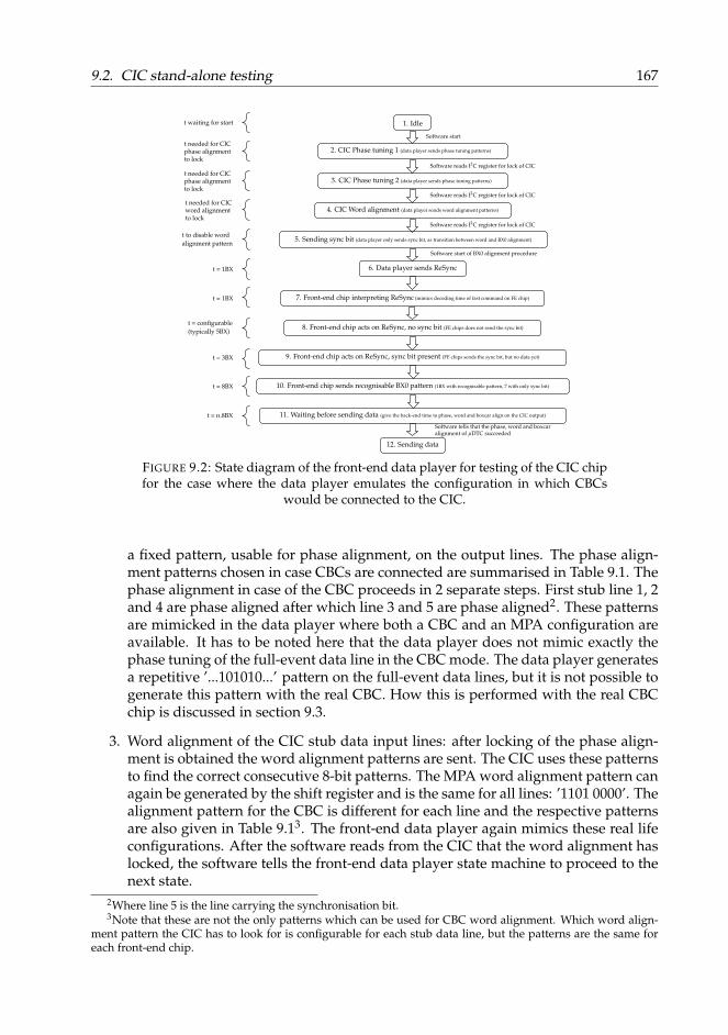
9.2. CIC stand-alone testing 167
1. Idle
2. CIC Phase tuning 1 (data player sends phase tuning patterns)
Software start
Software reads I2C register for lock of CIC
3. CIC Phase tuning 2 (data player sends phase tuning patterns)
Software reads I2C register for lock of CIC
4. CIC Word alignment (data player sends word alignment patterns)
Software reads I2C register for lock of CIC
5. Sending sync bit (data player only sends sync bit, as transition between word and BX0 alignment)
Software start of BX0 alignment procedure
6. Data player sends ReSync
7. Front-end chip interpreting ReSync (mimics decoding time of fast command on FE chip)
8. Front-end chip acts on ReSync, no sync bit (FE chips does not send the sync bit)
9. Front-end chip acts on ReSync, sync bit present (FE chips sends the sync bit, but no data yet)
10. Front-end chip sends recognisable BX0 pattern (1BX with recognisable pattern, 7 with only sync bit)
11. Waiting before sending data (give the back-end time to phase, word and boxcar align on the CIC output)
12. Sending data
Software tells that the phase, word and boxcaralignment of µDTC succeeded
t = 8BX
t = n.8BX
t = 3BX
t = configurable(typically 5BX)
t = 1BX
t to disable wordalignment pattern
t needed for CICphase alignmentto lock
t waiting for start
t needed for CICphase alignmentto lock
t needed for CICword alignmentto lock
t = 1BX
FIGURE 9.2: State diagram of the front-end data player for testing of the CIC chipfor the case where the data player emulates the configuration in which CBCs
would be connected to the CIC.
a fixed pattern, usable for phase alignment, on the output lines. The phase align-ment patterns chosen in case CBCs are connected are summarised in Table 9.1. Thephase alignment in case of the CBC proceeds in 2 separate steps. First stub line 1, 2and 4 are phase aligned after which line 3 and 5 are phase aligned2. These patternsare mimicked in the data player where both a CBC and an MPA configuration areavailable. It has to be noted here that the data player does not mimic exactly thephase tuning of the full-event data line in the CBC mode. The data player generatesa repetitive ’...101010...’ pattern on the full-event data lines, but it is not possible togenerate this pattern with the real CBC. How this is performed with the real CBCchip is discussed in section 9.3.
3. Word alignment of the CIC stub data input lines: after locking of the phase align-ment is obtained the word alignment patterns are sent. The CIC uses these patternsto find the correct consecutive 8-bit patterns. The MPA word alignment pattern canagain be generated by the shift register and is the same for all lines: ’1101 0000’. Thealignment pattern for the CBC is different for each line and the respective patternsare also given in Table 9.13. The front-end data player again mimics these real lifeconfigurations. After the software reads from the CIC that the word alignment haslocked, the software tells the front-end data player state machine to proceed to thenext state.
2Where line 5 is the line carrying the synchronisation bit.3Note that these are not the only patterns which can be used for CBC word alignment. Which word align-
ment pattern the CIC has to look for is configurable for each stub data line, but the patterns are the same foreach front-end chip.
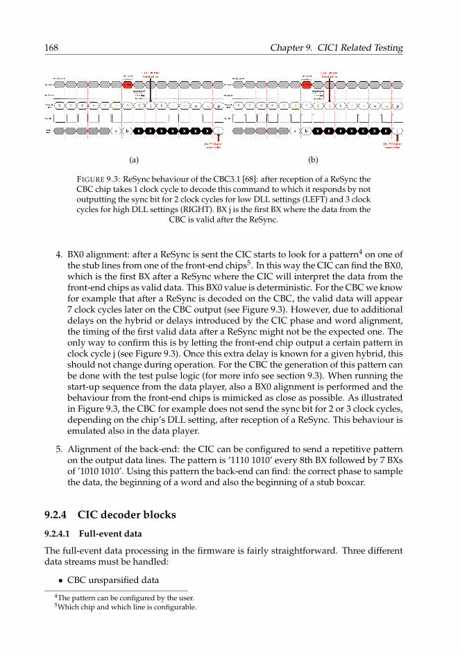
168 Chapter 9. CIC1 Related Testing
(a) (b)
FIGURE 9.3: ReSync behaviour of the CBC3.1 [68]: after reception of a ReSync theCBC chip takes 1 clock cycle to decode this command to which it responds by notoutputting the sync bit for 2 clock cycles for low DLL settings (LEFT) and 3 clockcycles for high DLL settings (RIGHT). BX j is the first BX where the data from the
CBC is valid after the ReSync.
4. BX0 alignment: after a ReSync is sent the CIC starts to look for a pattern4 on one ofthe stub lines from one of the front-end chips5. In this way the CIC can find the BX0,which is the first BX after a ReSync where the CIC will interpret the data from thefront-end chips as valid data. This BX0 value is deterministic. For the CBC we knowfor example that after a ReSync is decoded on the CBC, the valid data will appear7 clock cycles later on the CBC output (see Figure 9.3). However, due to additionaldelays on the hybrid or delays introduced by the CIC phase and word alignment,the timing of the first valid data after a ReSync might not be the expected one. Theonly way to confirm this is by letting the front-end chip output a certain pattern inclock cycle j (see Figure 9.3). Once this extra delay is known for a given hybrid, thisshould not change during operation. For the CBC the generation of this pattern canbe done with the test pulse logic (for more info see section 9.3). When running thestart-up sequence from the data player, also a BX0 alignment is performed and thebehaviour from the front-end chips is mimicked as close as possible. As illustratedin Figure 9.3, the CBC for example does not send the sync bit for 2 or 3 clock cycles,depending on the chip’s DLL setting, after reception of a ReSync. This behaviour isemulated also in the data player.
5. Alignment of the back-end: the CIC can be configured to send a repetitive patternon the output data lines. The pattern is ’1110 1010’ every 8th BX followed by 7 BXsof ’1010 1010’. Using this pattern the back-end can find: the correct phase to samplethe data, the beginning of a word and also the beginning of a stub boxcar.
9.2.4 CIC decoder blocks
9.2.4.1 Full-event data
The full-event data processing in the firmware is fairly straightforward. Three differentdata streams must be handled:
• CBC unsparsified data
4The pattern can be configured by the user.5Which chip and which line is configurable.

9.2. CIC stand-alone testing 169
stub line 1 stub line 2 stub line 3 stub line 4 stub line 5(with sync bit)
phase alignment 1 0b0101 0101location 1 = 0d85
0b1010 1010location 2 = 0d170
0b0000 0000location 3 = 0d00
0b1010 1010bend code 2 = 0d10bend code 1 = 0d10
0b1010 0000error bit = 0
OR254 bit = 1overflow bit = 0
bend code 3 = 0d00
phase alignment 2 0b0011 0010location 1 = 0d50
0b0110 0100location 2 = 0d100
0b1010 1010location 3 = 0d170
0b1010 1010bend code 2 = 0d10bend code 1 = 0d10
0b1010 1010error bit =0
OR254 bit = 1overflow bit = 0
bend code 3 = 0d10
word alignment 0b0111 1010location 1 = 0d122
0b1011 1100location 2 = 0d188
0b1101 0100location 3 = 0d212
0b0011 0001bend code 2 = 0d03bend code 1 = 0d01
0b1010 0001error bit = 0
OR254 bit = 1overflow bit = 0
bend code 3 = 0d01
BX0 alignment 0b0001 0010location 1 = 0d18
0b0010 0010location 2 = 0d34
0b0100 0010location 3 = 0d66
0b0010 0010bend code 2 = 0d02bend code 1 = 0d02
0b1000 0010error bit = 0
OR254 bit = 0overflow bit = 0
bend code 3 = 0d02
TABLE 9.1: Table summarising the phase and word alignment patterns forCBC+CIC. The highlighted cells show in which state the CIC is locking on whichline. For the BX0 alignment, in the configuration shown here, data is generatedon all five lines so that the user can choose which of the five lines to use. Theactual payload is also shown in decimal format and decoded to show that theseconfigurations are indeed possible with the CBC: the addresses on the stub linesincrement with line number, bends can be programmed by offsetting the maskedchannels, the OR254 bit will be high when enabled due to the presence of data, theoverflow bit is low because in all configurations exactly 3 stubs are programmedand the error bit is zero. In case the latter one would cause trouble a fast reset canclear it. To program the CBC in these states the values of the register settings aregiven in Appendix C. It should be noted here that the above table gives one ofthe configurations to run the CBC+CIC start-up sequence. Other configurations
are possible.

170 Chapter 9. CIC1 Related Testing
• CBC sparsified data
• MPA sparsified data
The handling of the full-event data stream is very similar to how the data is handled incase of MPA readout as explained in section 6.5.2.4 and briefly explained again here: astate machine looks for the full-event data header and when it is found transitions to astate where it buffers the data. In case of the sparsified stream the information in theheader is interpreted and the state machine handles the acquisition of the remainder ofthe package accordingly after which it sends the data out to the Data Readout Block overa similar bus as described in section 6.5.2.4.
9.2.4.2 Stub data
As explained in section 5.5.6.3 the CIC aggregates the stub data from the front-end chipsover 8 BXs and selects from these stubs the ones with the lowest bend to send to the back-end. Handling CIC stub data is therefore fairly different from handling stub data fromthe readout chips:
• The firmware needs to buffer the 8 BXs long CIC boxcar before being able to processit.
• The firmware needs to resort the payload on the offset value, available for eachstub in the payload, which encodes the time offset of the stub within the 8 BX longboxcar.
For the latter item a bitonic sorting network was implemented which sorts the stubswithin one boxcar based on the offset value. The concept of a bitonic sorting networkis illustrated in Figure 9.4. This sorting algorithm is a commonly used technique forsorting data in parallel: in Figure 9.4 every arrow represents a comparator stage whichsimply makes a decision on which of the two inputs is largest. The largest input goes tothe end of the arrow. By pipelining several of these blocks, the data is sorted after a givenamount of clock cycles. The number of clock cycles (nstages) required to do the sorting isdependent on the number of inputs n (which here is equal to the number of stubs to sort)and is given by:
nstages = log2(n)log2(n) + 1
2. (9.1)
At the output of this block the stubs will be sorted on the offset value. In addition it isrequired to pass the stub data on to the readout block separated by BX. If the full CICstub package would be input to the bitonic sorter, the output package would still containdata from all 8 BXs. So somehow the now sorted data needs to be output BX-by-BX. Thissequence of resorting the data and separating it on BX is referred to as boxcar unpacking.
Besides boxcar unpacking the data, the data also needs to go to the readout block rightaligned6. All of this can be accomplished in two ways, both based on the bitonic sorting:the first one will be referred to as the hot-bit-map + bitonic-sorter and the second one as thebitonic-sorter+shifter approach. These approaches are described in the next two sections.
6Aligned towards the LSB end of the bus.
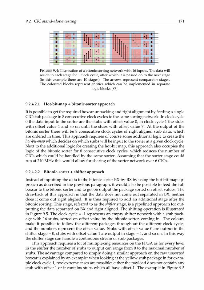
9.2. CIC stand-alone testing 171
FIGURE 9.4: Illustration of a bitonic sorting network with 16 inputs. The data willreside in each stage for 1 clock cycle, after which it is passed on to the next stage(in this example there are 10 stages). The arrows represent comparator stages.The coloured blocks represent entities which can be implemented in separate
logic blocks [87].
9.2.4.2.1 Hot-bit-map + bitonic-sorter approach
It is possible to get the required boxcar unpacking and right alignment by feeding a singleCIC stub package in 8 consecutive clock cycles to the same sorting network. In clock cycle0 the data input to the sorter are the stubs with offset value 0, in clock cycle 1 the stubswith offset value 1 and so on until the stubs with offset value 7. At the output of thebitonic sorter there will be 8 consecutive clock cycles of right aligned stub data, whichare ordered in time. This approach requires of course some additional logic to create thehot-bit-map which decides on which stubs will be input to the sorter at a given clock cycle.Next to the additional logic for creating the hot-bit map, this approach also occupies thelogic of the bitonic sorter for 8 consecutive clock cycles, which reduces the number ofCICs which could be handled by the same sorter. Assuming that the sorter stage couldrun at 240 MHz this would allow for sharing of the sorter network over 6 CICs.
9.2.4.2.2 Bitonic-sorter + shifter approach
Instead of inputting the data to the bitonic sorter BX-by-BX by using the hot-bit-map ap-proach as described in the previous paragraph, it would also be possible to feed the fullboxcar to the bitonic sorter and to get on output the package sorted on offset values. Thedrawback of this approach is that the data does not come out separated in BX, neitherdoes it come out right aligned. It is thus required to add an additional stage after thebitonic sorting. This stage, referred to as the shifter stage, is a pipelined approach for out-putting the data separated on BX and right aligned. The shifting operation is illustratedin Figure 9.5. The clock cycle = -1 represents an empty shifter network with a stub pack-age with 16 stubs, sorted on offset value by the bitonic sorter, coming in. The coloursmake it possible to follow the different packages throughout the different clock cyclesand the numbers represent the offset value. Stubs with offset value 0 are output in theshifter stage = 0, stubs with offset value 1 are output in stage = 1, and so on. In this waythe shifter stage can handle a continuous stream of stub packages.
This approach requires a lot of multiplexing resources on the FPGA as for every levelin the shifter the number of stubs to output can range from 0 to the maximal number ofstubs. The advantage compared to simply doing a similar approach on the raw unsortedboxcar is explained by an example: when looking at the yellow stub package in for exam-ple clock cycle 1, two extreme cases are possible: either the payload does not contain anystub with offset 1 or it contains stubs which all have offset 1. The example in Figure 9.5

172 Chapter 9. CIC1 Related Testing
FIGURE 9.5: Representation of the shifter stage for 9 consecutive clock cycles.The colour code represents the different CICs and the numbers in the payload and
output data represent the offset value of the stub within the boxcar.
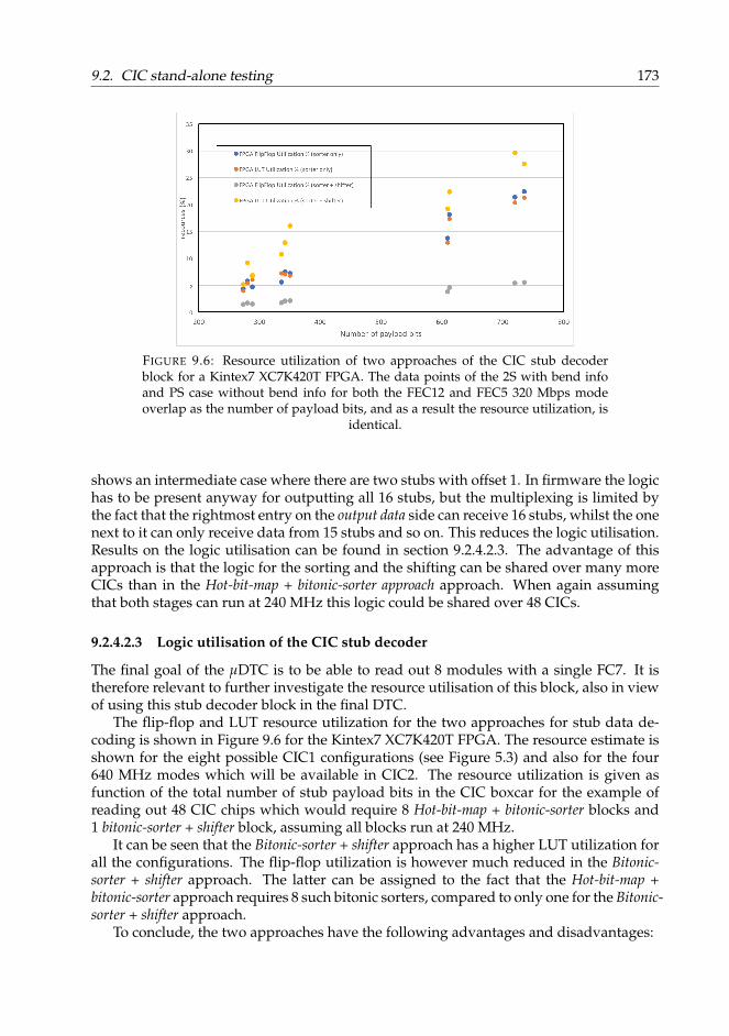
9.2. CIC stand-alone testing 173
FIGURE 9.6: Resource utilization of two approaches of the CIC stub decoderblock for a Kintex7 XC7K420T FPGA. The data points of the 2S with bend infoand PS case without bend info for both the FEC12 and FEC5 320 Mbps modeoverlap as the number of payload bits, and as a result the resource utilization, is
identical.
shows an intermediate case where there are two stubs with offset 1. In firmware the logichas to be present anyway for outputting all 16 stubs, but the multiplexing is limited bythe fact that the rightmost entry on the output data side can receive 16 stubs, whilst the onenext to it can only receive data from 15 stubs and so on. This reduces the logic utilisation.Results on the logic utilisation can be found in section 9.2.4.2.3. The advantage of thisapproach is that the logic for the sorting and the shifting can be shared over many moreCICs than in the Hot-bit-map + bitonic-sorter approach approach. When again assumingthat both stages can run at 240 MHz this logic could be shared over 48 CICs.
9.2.4.2.3 Logic utilisation of the CIC stub decoder
The final goal of the µDTC is to be able to read out 8 modules with a single FC7. It istherefore relevant to further investigate the resource utilisation of this block, also in viewof using this stub decoder block in the final DTC.
The flip-flop and LUT resource utilization for the two approaches for stub data de-coding is shown in Figure 9.6 for the Kintex7 XC7K420T FPGA. The resource estimate isshown for the eight possible CIC1 configurations (see Figure 5.3) and also for the four640 MHz modes which will be available in CIC2. The resource utilization is given asfunction of the total number of stub payload bits in the CIC boxcar for the example ofreading out 48 CIC chips which would require 8 Hot-bit-map + bitonic-sorter blocks and1 bitonic-sorter + shifter block, assuming all blocks run at 240 MHz.
It can be seen that the Bitonic-sorter + shifter approach has a higher LUT utilization forall the configurations. The flip-flop utilization is however much reduced in the Bitonic-sorter + shifter approach. The latter can be assigned to the fact that the Hot-bit-map +bitonic-sorter approach requires 8 such bitonic sorters, compared to only one for the Bitonic-sorter + shifter approach.
To conclude, the two approaches have the following advantages and disadvantages:

174 Chapter 9. CIC1 Related Testing
• Given that both stages can be clocked at 240 MHz, a single Bitonic-sorter + shifterapproach can be used for 48 CICs. A single Hot-bit-map + bitonic-sorter approachcan be used for 6 CICs. In case less than 48 CICs would be connected to the DAQ,resources would not be used in the Bitonic-sorter + shifter approach. In that sensethe Hot-bit-map + bitonic-sorter is more suitable for scaling down.
• In the case of 48 CICs the Hot-bit-map + bitonic-sorter approach has a lower LUTutilization, but a higher flip-flop utilization. What is most attractive must be de-cided by looking at the overall resource utilization of the full µDTC. It should benoted that these flip-flops and LUTs are contained in the same slice on the FPGA,so in case one wants to exploit the smaller flip-flop utilization of the Bitonic-sorter +shifter approach one has to remember that slice resources would have to be sharedbetween different blocks, which would complicate the routing for the compilationtool.
What is not included yet in this estimate is the fan-in (from the ISERDESes) and fan-out (to the Data Readout Blocks) of the data to and from the sorting networks. Similarresources will however be needed in both approaches to accomplish this.
For now the Hot-bit-map + bitonic-sorter approach was implemented in the µDTC asthis is the most applicable for reading out the limited number of modules that will beconnected to a single FC7.
9.2.4.2.4 Test bench
Given the fact that the stub decoder block is a completely new and rather complicatedblock, this block was carefully reviewed in simulation. Data from the CIC1 referencemodel was fed to the CIC1 stub decoder block using a Vivado test bench and the outputdata was checked against the input data in software. In this way the decoder block wasverified before testing with real hardware.
9.2.5 Data quality monitoringA dedicated stand-alone and small scale DQM was set up to mainly compare the dataoutput of the CIC1 validation model against the output from the µDTC CIC data decoderblocks. As a starting point the input and output CIC1 data, delivered by the validationmodel, were compared to get acquainted with the data streams. Assessing the input datato the CIC also gives a better feeling on how the CIC is stressed (trigger rate, stub occu-pancy,...). Investigating the data streams unveiled three problems in the ASIC designs:
• When the CIC1 full-event output FIFO is full, due to a high trigger rate, the FIFO isnot properly reset for the subsequent events, therefore subsequent full-event datapackages are lost. This will be fixed in CIC2.
• The front-end error bits are not correctly timed in into the CIC1 stub boxcar: theCBC error bits are reported in the previous CIC stub boxcar’s header if stubs havea time offset of 0 or 1 within the boxcar. This will be fixed in CIC2. For an offsetstarting at 2 the front-end status bits are reported in the same boxcar as the actualstub.
• The MPA full-event frame extends, with meaningless data, beyond the trailer bit.This is due to an error in the MPA RTL model and will be fixed for the next submis-sion of the chip. The full-event frame itself is however not affected by this bug.
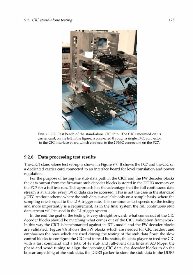
9.2. CIC stand-alone testing 175
FIGURE 9.7: Test bench of the stand-alone CIC chip. The CIC1 mounted on itscarrier card, on the left in the figure, is connected through a single FMC connectorto the CIC interface board which connects to the 2 FMC connectors on the FC7.
9.2.6 Data processing test resultsThe CIC1 stand-alone test set-up is shown in Figure 9.7. It shows the FC7 and the CIC ona dedicated carrier card connected to an interface board for level translation and powerregulation.
For the purpose of testing the stub data path in the CIC1 and the FW decoder blocksthe data output from the firmware stub decoder blocks is stored in the DDR3 memory onthe FC7 for a full test run. This approach has the advantage that the full continuous datastream is available: every BX of data can be accessed. This is not the case in the standardµDTC readout scheme where the stub data is available only on a sample basis, where thesampling rate is equal to the L1A trigger rate. This continuous test speeds up the testingand more importantly is a requirement, as in the final system the full continuous stubdata stream will be used in the L1 trigger system.
In the end the goal of the testing is very straightforward: what comes out of the CICdecoder blocks should be matching what comes out of the CIC1 validation framework.In this way the CIC1 is benchmarked against its RTL model and the FW decoder blocksare validated. Figure 9.8 shows the FW blocks which are needed for CIC readout andemphasises the ones which are used during the testing of the stub data flow: the slowcontrol blocks to configure the CIC and to read its status, the data player to feed the CICwith a fast command and a total of 48 stub and full-event data lines at 320 Mbps, thephase and word tuning to align the incoming CIC data, the decoder blocks to do theboxcar unpacking of the stub data, the DDR3 packer to store the stub data in the DDR3
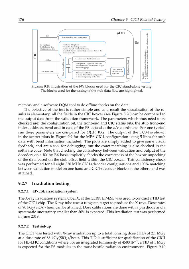
176 Chapter 9. CIC1 Related Testing
CIC
I2CSlow control-for start up sequence
Front-end data player• handles the start-up sequence• plays the full-event and stub data• controls the fast commands (also sends them to thefirmware blocks)
Debug block - scope data lines for acertain time after a fast command (forintial debugging)
1 L1A line
5 or 6 stub lines
8x5 stub lines,8x1 full-event line,
1 fast command line
L1A decorder - 3 different modes
Stub decoder block:• many different CIC configurations• boxcar unpacking of the data
Phas
ean
dw
ord
tuni
ng
Dat
aR
eado
utBl
ock
DDR3 packer -for acces to fullstub data
µDTC
IPBus
DA
QPC
:•
Toco
ntro
lsta
rt-u
p,lo
adin
gof
data
,...
•D
QM
toco
mpa
reou
tput
data
toda
tafr
omva
lidat
ion
mod
el
FIGURE 9.8: Illustration of the FW blocks used for the CIC stand-alone testing.The blocks used for the testing of the stub data flow are highlighted.
memory and a software DQM tool to do offline checks on the data.The objective of the test is rather simple and as a result the visualisation of the re-
sults is elementary: all the fields in the CIC boxcar (see Figure 5.26) can be compared tothe output data from the validation framework. The parameters which thus need to bechecked are: the configuration bit, the front-end and CIC status bits, the stub front-endindex, address, bend and in case of the PS data also the z/r coordinate. For one typicalrun these parameters are compared for O(1k) BXs. The output of the DQM is shownin the scatter plots in Figure 9.9 for the MPA-CIC1 configuration using 5 lines for stubdata with bend information included. The plots are simply added to give some visualfeedback, and are a tool for debugging, but the exact matching is also checked in thesoftware code. Note that checking the consistency between validation and output of thedecoders on a BX-by-BX basis implicitly checks the correctness of the boxcar unpackingof the data based on the stub offset field within the CIC boxcar. This consistency checkwas performed for all eight 320 MHz CIC1+decoder configurations and 100% matchingbetween validation model on one hand and CIC1+decoder blocks on the other hand wasattained.
9.2.7 Irradiation testing
9.2.7.1 EP-ESE irradiation system
The X-ray irradiation system, ObeliX, at the CERN EP-ESE was used to conduct a TID testof the CIC1 chip. The X-ray tube uses a tungsten target to produce the X-rays. Dose ratesof 90 kGy(SiO2)/hour can be attained. Dose calibrations are done with a pin diode and asystematic uncertainty smaller than 30% is expected. This irradiation test was performedin June 2019.
9.2.7.2 Test set-up
The CIC1 was tested with X-ray irradiation up to a total ionising dose (TID) of 2.1 MGyat a dose rate of 88 kGy(SiO2)/hour. This TID is sufficient for qualification of the CIC1for HL-LHC conditions where, for an integrated luminosity of 4500 fb−1, a TID of 1 MGyis expected for the PS modules in the most hostile radiation environment. Figure 9.10
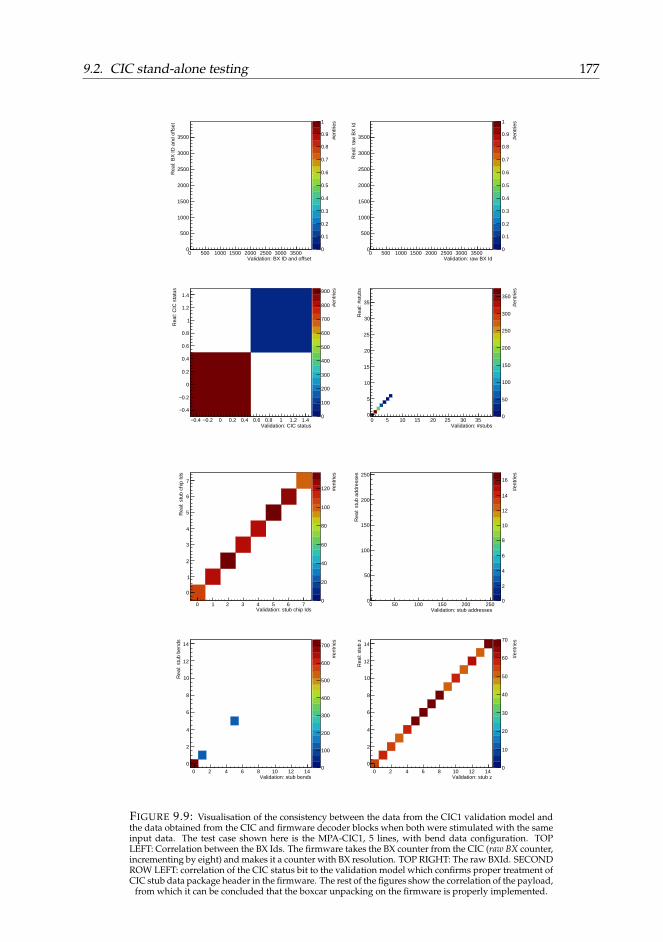
9.2. CIC stand-alone testing 177
0 500 1000 1500 2000 2500 3000 3500 Validation: BX ID and offset
0
500
1000
1500
2000
2500
3000
3500
Rea
l: B
X ID
and
offs
et
0
0.1
0.2
0.3
0.4
0.5
0.6
0.7
0.8
0.9
1
#en
trie
s
0 500 1000 1500 2000 2500 3000 3500 Validation: raw BX Id
0
500
1000
1500
2000
2500
3000
3500
Rea
l: ra
w B
X Id
0
0.1
0.2
0.3
0.4
0.5
0.6
0.7
0.8
0.9
1
#en
trie
s
0.4− 0.2− 0 0.2 0.4 0.6 0.8 1 1.2 1.4 Validation: CIC status
0.4−
0.2−
0
0.2
0.4
0.6
0.8
1
1.2
1.4
Rea
l: C
IC s
tatu
s
0
100
200
300
400
500
600
700
800
900
#en
trie
s
0 5 10 15 20 25 30 35 Validation: #stubs
0
5
10
15
20
25
30
35
Rea
l: #s
tubs
0
50
100
150
200
250
300
350
#en
trie
s
0 1 2 3 4 5 6 7 Validation: stub chip Ids
0
1
2
3
4
5
6
7
Rea
l: st
ub c
hip
Ids
0
20
40
60
80
100
120 #en
trie
s
0 50 100 150 200 250 Validation: stub addresses
0
50
100
150
200
250
Rea
l: st
ub a
ddre
sses
0
2
4
6
8
10
12
14
16
#en
trie
s
0 2 4 6 8 10 12 14 Validation: stub bends
0
2
4
6
8
10
12
14
Rea
l: st
ub b
ends
0
100
200
300
400
500
600
700
#en
trie
s
0 2 4 6 8 10 12 14 Validation: stub z
0
2
4
6
8
10
12
14
Rea
l: st
ub z
0
10
20
30
40
50
60
70
#en
trie
s
FIGURE 9.9: Visualisation of the consistency between the data from the CIC1 validation model andthe data obtained from the CIC and firmware decoder blocks when both were stimulated with the sameinput data. The test case shown here is the MPA-CIC1, 5 lines, with bend data configuration. TOPLEFT: Correlation between the BX Ids. The firmware takes the BX counter from the CIC (raw BX counter,incrementing by eight) and makes it a counter with BX resolution. TOP RIGHT: The raw BXId. SECONDROW LEFT: correlation of the CIC status bit to the validation model which confirms proper treatment ofCIC stub data package header in the firmware. The rest of the figures show the correlation of the payload,
from which it can be concluded that the boxcar unpacking on the firmware is properly implemented.
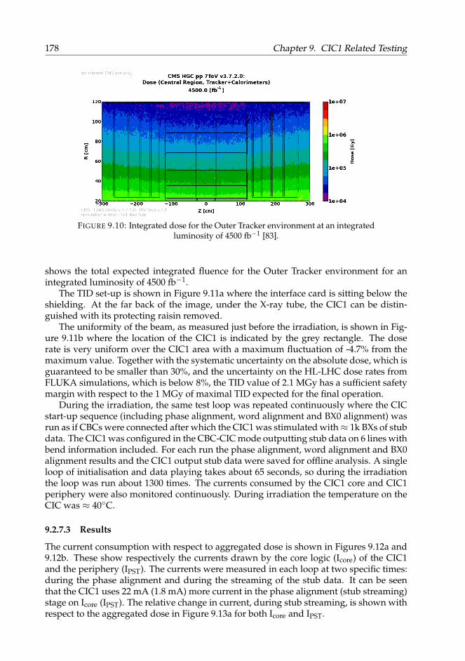
178 Chapter 9. CIC1 Related Testing
FIGURE 9.10: Integrated dose for the Outer Tracker environment at an integratedluminosity of 4500 fb−1 [83].
shows the total expected integrated fluence for the Outer Tracker environment for anintegrated luminosity of 4500 fb−1.
The TID set-up is shown in Figure 9.11a where the interface card is sitting below theshielding. At the far back of the image, under the X-ray tube, the CIC1 can be distin-guished with its protecting raisin removed.
The uniformity of the beam, as measured just before the irradiation, is shown in Fig-ure 9.11b where the location of the CIC1 is indicated by the grey rectangle. The doserate is very uniform over the CIC1 area with a maximum fluctuation of -4.7% from themaximum value. Together with the systematic uncertainty on the absolute dose, which isguaranteed to be smaller than 30%, and the uncertainty on the HL-LHC dose rates fromFLUKA simulations, which is below 8%, the TID value of 2.1 MGy has a sufficient safetymargin with respect to the 1 MGy of maximal TID expected for the final operation.
During the irradiation, the same test loop was repeated continuously where the CICstart-up sequence (including phase alignment, word alignment and BX0 alignment) wasrun as if CBCs were connected after which the CIC1 was stimulated with≈ 1k BXs of stubdata. The CIC1 was configured in the CBC-CIC mode outputting stub data on 6 lines withbend information included. For each run the phase alignment, word alignment and BX0alignment results and the CIC1 output stub data were saved for offline analysis. A singleloop of initialisation and data playing takes about 65 seconds, so during the irradiationthe loop was run about 1300 times. The currents consumed by the CIC1 core and CIC1periphery were also monitored continuously. During irradiation the temperature on theCIC was ≈ 40C.
9.2.7.3 Results
The current consumption with respect to aggregated dose is shown in Figures 9.12a and9.12b. These show respectively the currents drawn by the core logic (Icore) of the CIC1and the periphery (IPST). The currents were measured in each loop at two specific times:during the phase alignment and during the streaming of the stub data. It can be seenthat the CIC1 uses 22 mA (1.8 mA) more current in the phase alignment (stub streaming)stage on Icore (IPST). The relative change in current, during stub streaming, is shown withrespect to the aggregated dose in Figure 9.13a for both Icore and IPST.
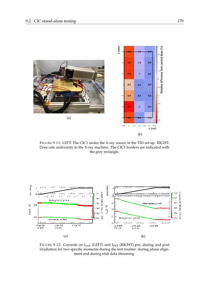
9.2. CIC stand-alone testing 179
(a) -3.8 -0.3 -1.5
-4.7 -1 -0.4
-2.9
-2.5 -0.3
-4.2 -1
-4.2 -1.2
-3.8 -1.2 -0.6
0.05 0.1 0.15 0.2 0.25 0.3 0.35
x (mm)
0.3−
0.2−
0.1−
0
0.1
0.2
0.3
y (m
m)
4.5−
4−
3.5−
3−
2.5−
2−
1.5−
1−
0.5−
0
Rel
ativ
e di
ffere
nce
from
cen
tral d
ose
(%)
0.0
0.0 0.0
0.0
0.0
(b)
FIGURE 9.11: LEFT: The CIC1 under the X-ray source in the TID set-up. RIGHT:Dose rate uniformity in the X-ray machine. The CIC1 borders are indicated with
the grey rectangle.
(a) (b)
FIGURE 9.12: Currents on Icore (LEFT) and IPST (RIGHT) pre, during and postirradiation for two specific moments during the test routine: during phase align-
ment and during stub data streaming.
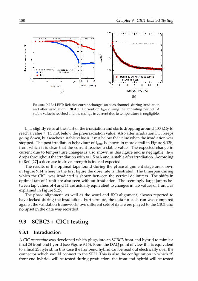
180 Chapter 9. CIC1 Related Testing
(a)(b)
FIGURE 9.13: LEFT: Relative current changes on both channels during irradiationand after irradiation. RIGHT: Current on Icore during the annealing period. Astable value is reached and the change in current due to temperature is negligible.
Icore slightly rises at the start of the irradiation and starts dropping around 400 kGy toreach a value ≈ 1.5 mA below the pre-irradiation value. Also after irradiation Icore keepsgoing down, but reaches a stable value≈ 2 mA below the value when the irradiation wasstopped. The post irradiation behaviour of Icore is shown in more detail in Figure 9.13b,from which it is clear that the current reaches a stable value. The expected change incurrent due to temperature changes is also shown in this figure and is negligible. IPSTdrops throughout the irradiation with≈ 1.5 mA and is stable after irradiation. Accordingto Ref. [27] a decrease in drive strength is indeed expected.
The results of the optimal taps found during the phase alignment stage are shownin Figure 9.14 where in the first figure the dose rate is illustrated. The timespan duringwhich the CIC1 was irradiated is shown between the vertical delimiters. The shifts inoptimal tap of 1 unit are also seen without irradiation. The seemingly large jumps be-tween tap values of 4 and 11 are actually equivalent to changes in tap values of 1 unit, asexplained in Figure 5.25.
The phase alignment, as well as the word and BX0 alignment, always reported tohave locked during the irradiation. Furthermore, the data for each run was comparedagainst the validation framework: two different sets of data were played to the CIC1 andno upset in the data was recorded.
9.3 8CBC3 + CIC1 testing
9.3.1 IntroductionA CIC mezzanine was developed which plugs into an 8CBC3 front-end hybrid to mimic afinal 2S front-end hybrid (see Figure 9.15). From the DAQ point of view this is equivalentto a final 2S hybrid. In this case the front-end hybrid can be read out electrically over theconnector which would connect to the SEH. This is also the configuration in which 2Sfront-end hybrids will be tested during production: the front-end hybrid will be tested

9.3. 8CBC3 + CIC1 testing 181
FIGURE 9.14: Optimal tap values found by the CIC phase alignment procedureduring TID testing. The results are separated by Phy port. In the first figure the
integrated dose over time is shown.
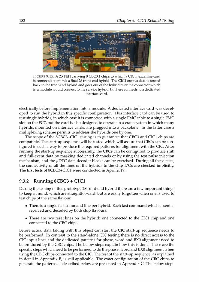
182 Chapter 9. CIC1 Related Testing
FIGURE 9.15: A 2S FEH carrying 8 CBC3.1 chips to which a CIC mezzanine cardis connected to mimic a final 2S front-end hybrid. The CIC1 output data is routedback to the front-end hybrid and goes out of the hybrid over the connector whichin a module would connect to the service hybrid, but here connects to a dedicated
interface card.
electrically before implementation into a module. A dedicated interface card was devel-oped to run the hybrid in this specific configuration. This interface card can be used totest single hybrids, in which case it is connected with a single FMC cable to a single FMCslot on the FC7, but the card is also designed to operate in a crate system in which manyhybrids, mounted on interface cards, are plugged into a backplane. In the latter case amultiplexing scheme permits to address the hybrids one by one.
The scope of the 8CBC3+CIC1 testing is to guarantee that CBC3 and CIC1 chips arecompatible. The start-up sequence will be tested which will assure that CBCs can be con-figured in such a way to produce the required patterns for alignment with the CIC. Afterrunning the start-up sequence successfully, the CBCs can be configured to produce stuband full-event data by masking dedicated channels or by using the test pulse injectionmechanism, and the µDTC data decoder blocks can be exercised. During all these tests,the connectivity of all the lines on the hybrids to the chip I/Os are checked implicitly.The first tests of 8CBC3+CIC1 were conducted in April 2019.
9.3.2 Running 8CBC3 + CIC1During the testing of this prototype 2S front-end hybrid there are a few important thingsto keep in mind, which are straightforward, but are easily forgotten when one is used totest chips of the same flavour:
• There is a single fast command line per hybrid. Each fast command which is sent isreceived and decoded by both chip flavours.
• There are two reset lines on the hybrid: one connected to the CIC1 chip and oneconnected to the CBC chips.
Before actual data taking with this object can start the CIC start-up sequence needs tobe performed. In contrast to the stand-alone CIC testing there is no direct access to theCIC input lines and the dedicated patterns for phase, word and BX0 alignment need tobe produced by the CBC chips. The below steps explain how this is done. These are thespecific steps which need to be performed to do the phase, word and BX0 alignment whenusing the CBC chips connected to the CIC. The rest of the start-up sequence, as explainedin detail in Appendix B, is still applicable. The exact configuration of the CBC chips togenerate the patterns as described below are presented in Appendix C. The below steps
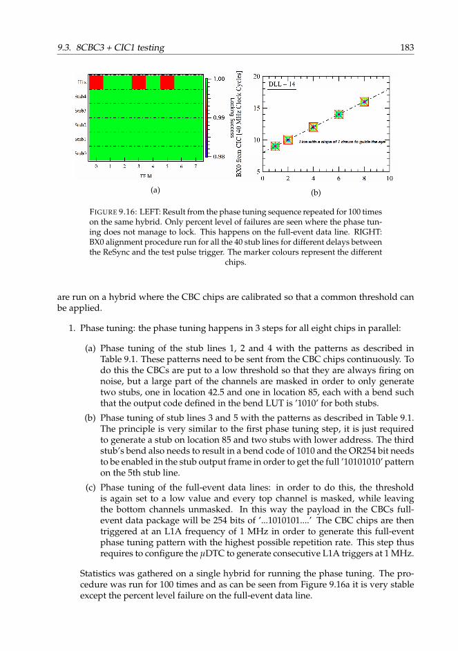
9.3. 8CBC3 + CIC1 testing 183
(a) (b)
FIGURE 9.16: LEFT: Result from the phase tuning sequence repeated for 100 timeson the same hybrid. Only percent level of failures are seen where the phase tun-ing does not manage to lock. This happens on the full-event data line. RIGHT:BX0 alignment procedure run for all the 40 stub lines for different delays betweenthe ReSync and the test pulse trigger. The marker colours represent the different
chips.
are run on a hybrid where the CBC chips are calibrated so that a common threshold canbe applied.
1. Phase tuning: the phase tuning happens in 3 steps for all eight chips in parallel:
(a) Phase tuning of the stub lines 1, 2 and 4 with the patterns as described inTable 9.1. These patterns need to be sent from the CBC chips continuously. Todo this the CBCs are put to a low threshold so that they are always firing onnoise, but a large part of the channels are masked in order to only generatetwo stubs, one in location 42.5 and one in location 85, each with a bend suchthat the output code defined in the bend LUT is ’1010’ for both stubs.
(b) Phase tuning of stub lines 3 and 5 with the patterns as described in Table 9.1.The principle is very similar to the first phase tuning step, it is just requiredto generate a stub on location 85 and two stubs with lower address. The thirdstub’s bend also needs to result in a bend code of 1010 and the OR254 bit needsto be enabled in the stub output frame in order to get the full ’10101010’ patternon the 5th stub line.
(c) Phase tuning of the full-event data lines: in order to do this, the thresholdis again set to a low value and every top channel is masked, while leavingthe bottom channels unmasked. In this way the payload in the CBCs full-event data package will be 254 bits of ’...1010101....’ The CBC chips are thentriggered at an L1A frequency of 1 MHz in order to generate this full-eventphase tuning pattern with the highest possible repetition rate. This step thusrequires to configure the µDTC to generate consecutive L1A triggers at 1 MHz.
Statistics was gathered on a single hybrid for running the phase tuning. The pro-cedure was run for 100 times and as can be seen from Figure 9.16a it is very stableexcept the percent level failure on the full-event data line.
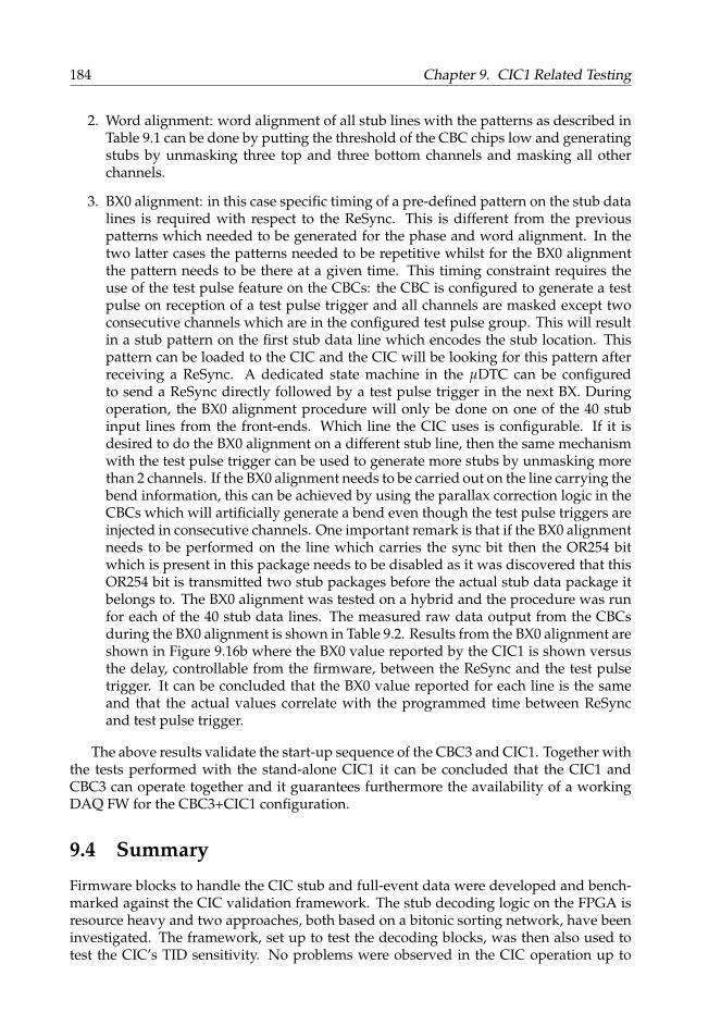
184 Chapter 9. CIC1 Related Testing
2. Word alignment: word alignment of all stub lines with the patterns as described inTable 9.1 can be done by putting the threshold of the CBC chips low and generatingstubs by unmasking three top and three bottom channels and masking all otherchannels.
3. BX0 alignment: in this case specific timing of a pre-defined pattern on the stub datalines is required with respect to the ReSync. This is different from the previouspatterns which needed to be generated for the phase and word alignment. In thetwo latter cases the patterns needed to be repetitive whilst for the BX0 alignmentthe pattern needs to be there at a given time. This timing constraint requires theuse of the test pulse feature on the CBCs: the CBC is configured to generate a testpulse on reception of a test pulse trigger and all channels are masked except twoconsecutive channels which are in the configured test pulse group. This will resultin a stub pattern on the first stub data line which encodes the stub location. Thispattern can be loaded to the CIC and the CIC will be looking for this pattern afterreceiving a ReSync. A dedicated state machine in the µDTC can be configuredto send a ReSync directly followed by a test pulse trigger in the next BX. Duringoperation, the BX0 alignment procedure will only be done on one of the 40 stubinput lines from the front-ends. Which line the CIC uses is configurable. If it isdesired to do the BX0 alignment on a different stub line, then the same mechanismwith the test pulse trigger can be used to generate more stubs by unmasking morethan 2 channels. If the BX0 alignment needs to be carried out on the line carrying thebend information, this can be achieved by using the parallax correction logic in theCBCs which will artificially generate a bend even though the test pulse triggers areinjected in consecutive channels. One important remark is that if the BX0 alignmentneeds to be performed on the line which carries the sync bit then the OR254 bitwhich is present in this package needs to be disabled as it was discovered that thisOR254 bit is transmitted two stub packages before the actual stub data package itbelongs to. The BX0 alignment was tested on a hybrid and the procedure was runfor each of the 40 stub data lines. The measured raw data output from the CBCsduring the BX0 alignment is shown in Table 9.2. Results from the BX0 alignment areshown in Figure 9.16b where the BX0 value reported by the CIC1 is shown versusthe delay, controllable from the firmware, between the ReSync and the test pulsetrigger. It can be concluded that the BX0 value reported for each line is the sameand that the actual values correlate with the programmed time between ReSyncand test pulse trigger.
The above results validate the start-up sequence of the CBC3 and CIC1. Together withthe tests performed with the stand-alone CIC1 it can be concluded that the CIC1 andCBC3 can operate together and it guarantees furthermore the availability of a workingDAQ FW for the CBC3+CIC1 configuration.
9.4 Summary
Firmware blocks to handle the CIC stub and full-event data were developed and bench-marked against the CIC validation framework. The stub decoding logic on the FPGA isresource heavy and two approaches, both based on a bitonic sorting network, have beeninvestigated. The framework, set up to test the decoding blocks, was then also used totest the CIC’s TID sensitivity. No problems were observed in the CIC operation up to
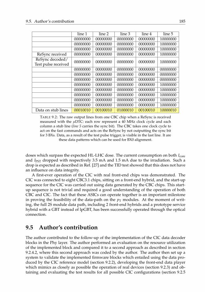
9.5. Author’s contribution 185
line 1 line 2 line 3 line 4 line 500000000 00000000 00000000 00000000 1000000000000000 00000000 00000000 00000000 1000000000000000 00000000 00000000 00000000 10000000
ReSync received 00000000 00000000 00000000 00000000 10000000ReSync decoded/Test pulse received 00000000 00000000 00000000 00000000 10000000
00000000 00000000 00000000 00000000 0000000000000000 00000000 00000000 00000000 0000000000000000 00000000 00000000 00000000 0000000000000000 00000000 00000000 00000000 1000000000000000 00000000 00000000 00000000 1000000000000000 00000000 00000000 00000000 1000000000000000 00000000 00000000 00000000 1000000000000000 00000000 00000000 00000000 10000000
Data on stub lines 00010010 00100010 01000010 00100010 10000010
TABLE 9.2: The raw output lines from one CBC chip when a ReSync is receivedmeasured with the µDTC: each row represent a 40 MHz clock cycle and eachcolumn a stub line (line 5 carries the sync bit). The CBC takes one clock cycle toact on the fast commands and acts on the ReSync by not outputting the sync bitfor 3 BXs. Data, as a result of the test pulse trigger, is visible in the last line. It are
these data patterns which can be used for BX0 alignment.
doses which surpass the expected HL-LHC dose. The current consumption on both Icoreand IPST dropped with respectively 3.5 mA and 1.5 mA due to the irradiation. Such adrop is expected as described in Ref. [27] and the TID test showed that this does not havean influence on data integrity.
A first-ever operation of the CIC with real front-end chips was demonstrated. TheCIC was connected to eight CBC3.1 chips, sitting on a front-end hybrid, and the start-upsequence for the CIC was carried out using data generated by the CBC chips. This start-up sequence is not trivial and required a good understanding of the operation of bothCBC and CIC. The fact that these ASICs can operate together is an important milestonein proving the feasibility of the data-path on the pT modules. At the moment of writ-ing, the full 2S module data path, including 2 front-end hybrids and a prototype servicehybrid with a GBT instead of lpGBT, has been successfully operated through the opticalconnection.
9.5 Author’s contribution
The author contributed to the follow-up of the implementation of the CIC data decoderblocks in the Phy layer. The author performed an evaluation on the resource utilizationof the implemented block and compared it to a second approach as described in section9.2.4.2, where this second approach was coded by the author. The author then set up asystem to validate the implemented firmware blocks which entailed using the data pro-duced by the CIC reference model (section 9.2.2), developing the front-end data playerwhich mimics as closely as possible the operation of real devices (section 9.2.3) and ob-taining and evaluating the test results for all possible CIC configurations (section 9.2.5

186 Chapter 9. CIC1 Related Testing
and 9.2.6). The author then set up this system to be used in the TID testing of the CIC andcontributed to analysing the results of this test. The author used the experience gainedwith the front-end data player and the stand alone CIC set-up to contribute to the run-ning of the initialization sequence of the CIC with CBCs, which makes a 2S front-endhybrid ready for data taking.
187
Part III
Search for CompositeStandard Model Dark Matter with
CMS at the LHC

189
Chapter 10
Sexaquarks
10.1 Introduction
G. Farrar introduces in Ref. [88] the possibility that a compact state of uuddss quarkscould be deeply bound and have low enough mass to be stable or essentially stable1. Thisparticle is referred to as the Sexaquark (S). Particles consisting of more quarks than thecommonly known baryons are allowed by QCD (quantum chromodynamics) and parti-cles with four and five quarks have indeed been experimentally discovered as discussedin section 10.2. The quark content of the S reflects the hypothesis of the H-dibaryon,which was proposed by R. Jaffe [89] in 1976. The H-dibaryon proposal and negativesearches for this particle will be discussed in section 10.3, followed by a description ofthe S (section 10.4) and the possibility for it being a dark matter particle (section 10.5).Farrar proposes two discovery channels in Ref. [88] which are explained in section 10.6.One of the discovery channels is looking for S which are produced in pp-collisions at theLHC and which can subsequently annihilate on material. The products of this annihila-tion reaction can be charged particles which can be reconstructed.
Such a search, using the CMS tracker detector, is introduced in more detail in sec-tion 10.7. Section 10.8 and 10.9 describe which datasets are used for this search and howthe signal is reconstructed. Section 10.10 explains the signal simulation which was setup to outline the search strategy and investigate the signal reconstruction efficiency. Re-sults obtained with this simulation are presented in section 10.11. How the backgroundsuppression is performed is described in section 10.12. The evaluation of the system-atic uncertainties is the topic of section 10.13 and finally the results and a summary andoutlook can be found in section 10.14 and 10.15 respectively.
10.2 Exotic hadrons
Hadrons which do not consist of two or three valence quarks fall outside the conventionalquark model and are referred to as exotic hadrons. The Belle experiment at the KEKBe+e− collider was the first experiment to observe such an exotic state in 2003 [90]. Thisexcited state is referred to as X(3872) and was found in the decay of B± mesons.
The Belle result marked the onset of the discovery of many exotic hadron states, byseveral experiments, which proceeds until today reaching to the order of 50 claimeddiscoveries. Most of these states are considered to be tetraquark states of the qqQQtype where q and Q represent a light (u or d) and heavy (c, s or b) quark respectively.Pentaquark states were recently observed by the LHCb collaboration [91]: Λ0
b(udb) →J/Ψ(cc)p(uud)K−(us) gives indirect evidence for the existence of two pentaquark states(P+
c (4380) and P+c (4450)) with quark content ccuud.
1Lifetime larger than the lifetime of the Universe.

190 Chapter 10. Sexaquarks
In many cases the quark content and the exact configuration of the quarks in theseexotic hadrons is still an open question. Quarks can be organised in tightly bound states,or a tetraquark or pentaquark can be built like a molecule of two loosely bound mesonsor a loosely bound meson and baryon respectively. Other, even more exotic multi-quarkstates are also allowed by QCD.
10.3 The H-dibaryon
In 1976 R. Jaffe [89] proposed the existence of a light dibaryon (H) with quark contentuuddss as a bound state of two Λ0s (uds). Jaffe found that the potential of the Λ0s canbe such that they are lightly attractive which would make this dibaryon’s mass lie belowthe threshold, 2 × mΛ0 (= 2231 MeV/c2), for strong decay. Jaffe calculated a mass of2150 MeV/c2 for the H. As a result this H-dibaryon would decay weakly to e.g. Λ0pπ.Several experiments were set up in the decades after this prediction to look for the H.Many of these experiments were located at Brookhaven National Laboratory [92]. Alsoother experiments at KEKB (Belle) [93], SPS (NA 3) [94], FNAL [95] and LHC (ALICE)[96] started looking for the H-dibaryon or were probing its parameter space implicitly.
Several experiments with different lengths of the decay region were designed to in-vestigate production of Hs in a target sitting in a kaon, pion or proton beam with sub-sequent decays (e.g. to Λ0pπ−) of the potentially produced H in the extracted neutralbeam. These experiments were sensitive to several orders of magnitude of lifetimes ofthe H with masses around the Λ0Λ0 threshold. No evidence for the existence of an H-dibaryon with a typical weak lifetime was seen. Some of the experiments operating withthis principle also had to restrict their search range to a mass > 2 GeV/c2 to eliminate theneutron background [92].
At Belle, the production of the H+X could also be foreseen in Υ decay, very similarto the observed Υ decay mode to anti-deuterons + X. No evidence for this decay (withH→ Λ0pπ or H→ Λ0Λ0 (the latter above the mΛ0Λ0 threshold)) mode of the Υ was seen.This search was restricted however to a fairly small mass region (O(10 MeV/c2)) aroundthe Λ0Λ0 threshold.
Stable Hs living in a nuclear potential of a host nucleus were also looked for. At KEKfor example an event was recorded in nuclear emulsion which is linked to the formationand decay of a 6
Λ0Λ0He nucleus2. This double strange hypernucleus is formed by placinga target in a K− beam. Ξ− particles can be formed in the target which, when they come torest can interact with a proton in the nucleus and form a Λ0 pair, like this giving rise to adouble strange hypernucleus. By studying the kinematics of the recorded event in detailthe binding energy of the Λ0Λ0 system could be calculated as BEΛ0Λ0 = 7.13 MeV whichshows this system is lightly attractive. A lower mass limit for the H could be extractedas: mH > 2 × mΛ0 - BEΛ0Λ0 = 2223.7 MeV/c2 (at 90% CL) [97], which excluded Jaffe’soriginal prediction. Other counter-experiments (e.g. Ref. [98]) also claim the observationof double strange hypernuclei through detection of a charged pion in each of the reactionswhere ∆s = +1.
The observation of unstable double strange hypernuclei can be interpreted as evi-dence against the existence of a strong-interaction stable H where the binding force re-sembles the nuclear force. There are however claims against this conclusion, as presentedin Ref. [99] where it is proven that the coupling strength needed for the H to bind to light
2A 6He nucleus with 2 neutrons replaced by 2 Λ0s

10.4. Properties of the Sexaquark 191
nuclei would be unphysically large and that therefore current limits extracted from dou-ble strange hypernuclei are not relevant to extract conclusions on the existence of theH.
Besides a fairly loosely bound H-dibaryon, for which no experimental evidence exists,the possibility that the uuddss quark combination is actually not a loosely bound state oftwo baryons, but a strongly bound state of six quarks, as in the Sexaquark model, is stillviable. This idea will be discussed in the next section.
10.4 Properties of the Sexaquark
Considerations regarding the stability of the S can be summarised as follows for differentvalues of the S mass [100]:
• mp + mn - me - 2 × BE ≈ 1860 MeV/c2 < mS < 2 × (mp + me) ≈ 1878 MeV/c2:where BE is the binding energy of nucleons in the nucleus and mp, mn and meare respectively the mass of the proton, neutron and electron. The lower limit isneeded to guarantee nuclear stability against the formation of an S in a nucleus.If the S mass also lies below the stated upper limit then it would be stable againstdecay to two protons. For the latter to hold, 16% binding energy, compared to twoΛ0s, is required.
• 2 × (mp + me) ≈ 1878 MeV/c2 < mS < mp + me + mΛ0 ≈ 2055 MeV/c2: if the Slies within this mass range it can decay through a double weak process and formS < 1890 MeV/c2 its lifetime is larger than the age of the Universe.
• mp + me + mΛ0 ≈ 2055 MeV/c2 < mS < 2 × mΛ0 ≈ 2232 MeV/c2: the S can decaythrough a single weak interaction and it would not be stable.
• 2 × mΛ0 ≈ 2232 MeV/c2 < mS: the S can undergo a strong decay to two Λ0s and itwould thus not be stable.
Therefore for nuclei and Sexaquarks to be stable on a cosmological timescale it is requiredthat the S mass lies in the 1860-1890 MeV/c2 range.
Lattice QCD could render an exact calculation of the S mass. Most recent calculations[101] are however still far from a realistic six-quark state but they show the existence ofa deeply bound state for the uuddss combination. In literature several calculations ofthe S mass can be found. Results range from 1130 MeV/c2 [102] to 2240 MeV/c2 [103].It would therefore be beneficial if an experimental search for the S could probe this fullmass range.
An important consideration [88] is that one could end up with a high mass for the Swhen naively using the constituent quark model. Indeed, if one uses the effective massesof the quarks as in the constituent quark model one arrives at 4 × 300 MeV/c2 + 2 ×450 MeV/c2 = 2100 MeV/c2. A mass for which the S cannot be stable. Other hadronmasses e.g. π0,± can also not be predicted using this model. So it is fair to say that theintuition from the constituent quark model is not a good guideline for predicting masses.
In Refs. [99, 104] it is estimated that the limits on the H-dibaryon obtained from doublestrange hypernuclei decays (see section 10.3) are not applicable for a strongly bound S asthe S has isospin/flavour symmetry and would therefore not exchange pions. This givesit a much smaller physical size compared to other baryons where pions account for thelong range of the nucleon-nucleon interaction. The pions extend the size of the baryons

192 Chapter 10. Sexaquarks
beyond their Compton radius. If the S radius is smaller than 0.24-0.41 fm, it is calculatedin Ref. [88] that the formation time of the S in a strangeness = -2 hypernucleus is largerthan≈ 10−9 s due to the small wavefunction overlap between the S and two baryons. TheS would therefore not have the time to get formed in these hypernuclei. This would makelimits from double strange hyperon decays inapplicable. It should be noted howeverthat the arguments in Ref. [99, 104] are approximations, as first principle approaches forcalculating the binding energy of standard nucleons, let alone Sexaquarks, in nuclei donot exist.
Whether the small wavefunction overlap between two baryons and an S could alsomake nucleons in nuclei insensitive to decay to S on the timescale of the Universe couldbe investigated by e.g. Super-Kamiokande in the n + n → S + π0 channel, where denotes that these neutrons belong to the same nucleus.
Assuming that the S-nucleon interaction goes through the exchange of an f0 allowsfor a crude estimation [105] of the physical size of the S: given that the typical size of anucleon (rN) is 0.9 fm and 0.2 fm is its Compton wavelength (λN), the formula:
rN ≈ λN +12
λπ (10.1)
can be put forward with λπ = 1.4 fm the Compton wavelength of the pion. Given thatthe S does not couple to pions but to the f0 gives:
rS ≈ λS + (0→ 12)λf0 = 0.1→ 0.3 fm, (10.2)
when using λS = 0.1 fm and λf0 = 0.4 fm. This is a compact object compared to the morecommon baryons.
10.5 Sexaquarks as a dark matter candidate
Besides being an interesting new type of matter, the S can also be a good dark mattercandidate. It should therefore essentially pass all the requirements which were discussedin section 2.4.3.
The study of the S could benefit from knowledge on several S interactions: S-nucleon,S-S and S-S scattering; all accompanied with a certain interaction cross section which isvelocity dependent. In the literature [88, 99, 105, 106, 107], several estimates and limits onthese cross sections can be found. It is clear that their is no unambiguous result, thereforeexact values will be avoided below. Some findings will be discussed which will showthat evaluating limits for these cross sections is not so straightforward. This will givea feeling that with a proper cross section the dark matter under the form of S particlesmight have evaded detection.
With the correct S-nucleon cross section the S could have evaded detection in directdetection experiments as the S would thermalize on its way through the atmosphere. Theenergy it would consequently deposit in direct detection experiments could be below thedetection threshold [107].
In Ref. [106] it is shown that the thermalisation could even happen on interstellar gas.This thermalisation would only occur at relatively small radii from the galactic center dueto the gas density being larger there. This could even make balloon based direct detectionsearches inapplicable.

10.6. Sexaquark search channels 193
The interaction of the S with the baryonic matter would result in an extra sourceof heating for the baryonic matter. This extra heating could explain the star formationquenching problem of non-interacting cold dark matter models which do not explain thestar formation rate coherently by only including supernova and active galactic nuclei assources of heating [107].
In Ref. [107] the implications of self-interacting dark matter are discussed. Makingthe dark matter candidates interact results in heat transfer from dynamic parts of thedark matter halo to less dynamic parts which can result in a smoothing of the halo. IfσDM−DM/M is in the range of 8× 10⁻²⁵ − 1× 10⁻²³ cm2GeV−1c2 self-interacting darkmatter (with dark matter-dark matter interaction cross section σDM−DM and mass of thecandidate M) would be a natural solution for e.g. the core-cusp problem. In Ref. [107] it ishowever shown that the most interesting part of the mass range (O(GeV/c2)) is excludedby direct detection experiments for the most natural interaction cross section of σDM−p
(dark matter proton interaction cross section) ≈ 10−24 cm2. It should however be notedthat these are limits on the σDM−p cross section, but it is hard to imagine a process whichcould make σDM−p lie several orders of magnitude from σDM−DM for a Standard Modeldark matter particle such as the Sexaquark.
As explained in section 10.4, the small probability of S to nucleon binding would alsoexplain why the S would not affect Big Bang nucleosynthesis and the S would further-more not get accumulated in stars hence not affecting stellar evolution [107].
One of the main requirements for a dark matter candidate is for it to be able to ex-plain the relic abundance. In Ref. [105] it is shown that Sexaquarks in the mass range of1870-1880 MeV/c2 can quite naturally explain ΩDM/Ωb ≈ 5.3. The production of the S issupposed to happen at the QCD phase transition where the Universe goes from a quarkgluon plasma (QGP) to hadrons. This transition happens when the temperature dropsfrom 170 MeV to 140 MeV. The timescale of the interactions which form the hadrons(O(10−23 s)) is much smaller than the duration of the phase transition (the lifetime ofthe Universe at this stage is given by: 7.3 × 10⁻⁵( 100 MeV
T )2 s). Equilibrium equationscan thus be used to estimate the abundance of the S at the end of the QCD phase transi-tion. The Sexaquarks produced at this stage are supposed to be maintained until today[105] as the expected small size of the S makes it insensitive to break-up reactions suchas π + S → Σ + Λ0 or K+ + S → p + Λ0. The results for the S relic abundance obtainedin Ref. [105] are however in thus far unresolved contrast with the results from Ref. [100]where, also using equilibrium statistics during the QCD phase transition, the relic abun-dance of Sexaquarks is calculated, after freeze-out, to beO(10−12) the fraction of baryons.
It is thus still debated if the S could explain all or even a significant fraction of thedark matter. Also the actual form in which the S would contribute to the dark matteris under debate, as besides being particulate dark matter it could also be contained inprimordial black holes [105]. Nevertheless, the S remains an interesting type of matterwhich deserves a dedicated search.
10.6 Sexaquark search channels
In Ref. [88] G. Farrar points out two possible discovery channels for the S: one based onproduction of S in Υ decays and the other based on production of S at hadron collidersand subsequent interaction of the S with beampipe or detector material. Both channelswill be discussed below.

194 Chapter 10. Sexaquarks
10.6.1 Search channels at B-factoriesVery similar to the Belle search discussed in section 10.3 for the H-dibaryon, the S couldbe looked for in the decay of the Υ. Both the Belle and BABAR experiments would be wellsuited for this. The Belle search for the H-dibaryon does not exclude the existence of theS as the search window in Ref. [93] was only O(10 MeV/c2) around the Λ0Λ0 threshold.The proposed discovery channel for the S at B-factories would be:
Υ→ SΛ0Λ0 + πs and/or γs, (10.3)
for which all the decay products, except the S, can be reconstructed. The S can thereforebe searched for in the invariant missing-mass spectrum. The decay channel to S Λ0Λ0Xis of course also a possibility.
In Ref. [108] results are discussed of such a search performed by the BABAR collab-oration where the mass range 0 < mS < 2.05 GeV/c2 is probed using the SΛ0Λ0 channel.For the full mass range, limits could be set for the branching fraction of Υ(2S) and Υ(3S)to the SΛ0Λ0 channel of (1.2-1.4) × 10−7 (at 90 % CL) which is a branching fraction twoorders of magnitude below the branching fraction for decay to the channels containingan anti-deuteron [10].
10.6.2 Search channels at hadron collidersThe S could also be produced in hadron collisions. In order to find this needle-in-the-haystack a large dataset is required. This automatically leads to a search at the LHC. TheS and S production rate can be estimated [88] to be of the order of 10−4-10−6 relative tothe production rate of pions. As a result S and S could be routinely produced at the LHC.
The proposed methodology is to look for S produced in the proton-proton collision.The S could subsequently annihilate on nucleons in the beampipe or detector material,which could lead to any of the below signals:
S(uuddss) + p(uud)→ Λ0(uds) + K+(us)
Λ0(uds)→ p(uud) + π+(ud)(10.4)
S(uuddss) + n(udd)→ Ξ+0 (dss) + π−(ud)
Ξ+0 (dss)→ Λ0(uds) + π+(ud)
Λ0(uds)→ p(uud) + π+(ud)
(10.5)
S(uuddss) + n(udd)→ Λ0(uds) + K0S(
ds− ds√2
)
Λ0(uds)→ p(uud) + π+(ud)
K0S(ds− ds)√
2→ π+(ud) + π−(ud)
(10.6)

10.7. Adopted search strategy 195
In the above reactions all the final state particles can be reconstructed and therefore theinvariant mass of the S-nucleon system as well as the interaction vertex of the S with thenucleon can be extracted.
The formed S will have a transverse momentum comparable to other hadrons formedat LHC pp-collisions, which is O(GeV/c). This implies that the final state products willalso have low transverse momenta. This, together with the fact that the annihilation crosssection of the S with material is low, and the fact that final state products are producedsignificantly displaced from the luminous region makes this a challenging signal to lookfor.
10.7 Adopted search strategy
The next sections describe a first-ever search for the Sexaquark particle at the LHC. Thesignal which is considered in this search is the one described in Equation (10.6) and theCMS detector is used to look for S annihilating on neutrons in the CMS beampipe. In casethe search is negative, an upper limit can be placed on the product of the S productioncross section (σ(pp→ S)) and the cross section for S annihilation on a neutron resulting ina K0
S and an Λ0 (σ(S + n→ KS + Λ0)). This will be performed by applying the followingformula:
[σ(pp→ S)× σ(S + n→ K0s + Λ0)]UL
=NUL
Nev×<PU>×(1−C)σpp
× εreco × εfid × εBkgCuts × Nn. (10.7)
Here NUL is the upper limit on the number of signal events after all selection cuts, Nevthe total number of pp interactions in the considered dataset, <PU> the average pileupin this dataset, C the overlap rate between datasets, σpp the proton-proton inelastic crosssection, εreco the S reconstruction efficiency, εfid the efficiency for the signal to be con-tained in a fiducial region in which systematic uncertainties are controlled, εBkgCuts theefficiency with which the S candidates survive the background cuts and Nn the neutroncolumn density of the beampipe. In the sections which follow all these terms will beevaluated.
Due to the low momenta of the final state particles, no dedicated trigger can be usedand the strategy adopted here is to look for the S signal in all the available datasets. TheS could as well be formed in pileup interactions and all pp collisions within an event aretherefore potentially interesting. The datasets which are used in this search are discussedand listed in section 10.8. Data in CMS is categorised in primary datasets. Each primarydataset has a list of triggers which are linked to it. In this way a certain dataset con-tains a certain type of physics. Triggers linked to different primary datasets can howevertrigger on the same event and as a result the same event might end up in different pri-mary datasets leading to overlap between datasets. This overlap rate was measured (seesection 10.8) and used to calculate the number of unique pp interactions in the datasets.
The decay of the K0S and Λ0 can happen within the CMS tracker volume as the c.τ of
the K0S and Λ0 are respectively ≈ 2.7 cm and ≈ 7.9 cm. The overall branching fraction
of the decay of the K0S and Λ0 to the final state considered in this search is 44.2% (69.2%
for K0S → π+ π− and 63.9% for Λ0 → π+ p) [10]. These charged final state particles can
196 Chapter 10. Sexaquarks
be reconstructed with the CMS tracker and actually the K0S, Λ0 and Λ0, referred to as V0
particles, are part of the standard reconstruction in CMS [109]. This so-called V0 fittinghad to be adapted however to fit the kinematics of the V0s from the signal as describedin section 10.9.
To outline the analysis and evaluate the reconstruction efficiency and the backgroundrejection, a dedicated signal simulation is required. The generation of the S is performedwith the EPOS-LHC [110] event generator and the S-neutron interaction is implementedin GEANT4 [111] which is part of the standard CMS simulation software. More detailson the signal simulation and how it was used to estimate the reconstruction efficiencycan be found in sections 10.10 and 10.11 respectively.
To evaluate the background, reconstructed S candidates are used. S, as opposed to S,will not annihilate on neutrons and reconstructed S candidates can therefore be used asa background control sample. The reconstructed S only differ from the S by the chargeof the decay products of the Λ0/Λ0. To achieve a performant signal to background dis-crimination, a boosted decision tree (BDT) is used. Section 10.12 explains in detail howthe background rejection is performed and shows what is the source of this background.
Several sources of systematic uncertainties are described in section 10.13. Taking theseinto account, an upper limit on the product of cross sections is then evaluated in section10.14.
As can be expected from a first-ever search, the analysis described below is not opti-mised yet in every possible way. Several fundamental, although sometimes non-antici-pated nor intuitive, insights and difficulties for this specific signal will be discussed. Theoutlook (section 10.15) will then review the possible improvements for this analysis.
10.8 Datasets
Due to the low momenta of the final state particles no dedicated trigger can be used forthis signal. For this reason, the signal is searched for in all existing primary datasets andthe pileup interactions are also considered. This is a unique feature of the analysis: to ourknowledge no analysis so far has used all recorded pp collisions in a beyond the StandardModel search.
The data considered here is the data collected in 2016 by CMS. In early 2016 runs(until RunF) the CMS tracker was coping with a problem introduced by the smaller inter-bunch crossing time, higher peak luminosity and the change in detector temperature withrespect to Run 1. This resulted in a saturation effect of the APV chip’s pre-amplifier whichled to decreased hit efficiencies severely impacting tracking performance. No simulationwas available which accurately describes this so-called APV saturation effect and thereforeit was not possible to evaluate a robust systematic uncertainty on tracking efficiencies (seesection 10.13) for early 2016 data. The search was thus limited to the second half of the2016 data taking.
The primary datasets which were analysed are listed in Table 10.1, where the numberof events for each run and dataset are shown together with the average number of validprimary vertices (PVs) per event. Valid PVs are defined here and in the following sectionsby requesting the number of degrees of freedom of the vertex to be larger than 4, its |z|location to be smaller than 24 cm and its radial displacement to be smaller than 2 cm.
The datasets listed in Table 10.1 contain a total number of≈ 2.01× 10⁹ recorded events(Nev) with on average 18.2 reconstructed valid primary vertices per event. The conver-sion from valid reconstructed PVs to the true number of inelastic interactions in the event

10.8. Datasets 197
Dataset Number of events Average numberof valid PVs
/BTagCSV/Run2016G-07Aug17-v1/AOD 100,014,471 18.1/BTagCSV/Run2016H-07Aug17-v1/AOD 64,209,667 19.1/BTagMu/Run2016G-07Aug17-v1/AOD 27,342,838 16.8/BTagMu/Run2016H-07Aug17-v1/AOD 28,329,985 17.6/Charmonium/Run2016G-07Aug17-v1/AOD 61,398,862 17.2/Charmonium/Run2016H-07Aug17-v1/AOD 70,124,218 18.1/DisplacedJet/Run2016G-07Aug17-v1/AOD 18,006,002 17.6/DisplacedJet/Run2016H-07Aug17-v1/AOD 19,433,403 19.1/DoubleEG/Run2016G-07Aug17-v1/AOD 76,538,905 17.7/DoubleEG/Run2016H-07Aug17-v1/AOD 82,569,062 18.9/DoubleMuon/Run2016G-07Aug17-v1/AOD 44,182,144 18.2/DoubleMuonLowMass/Run2016G-07Aug17-v1/AOD 44,835,919 17.4/DoubleMuonLowMass/Run2016H-07Aug17-v1/AOD 52,461,380 18.3/HTMHT/Run2016G-07Aug17-v1/AOD 30,133,219 18.2/HTMHT/Run2016H-07Aug17-v1/AOD 33,060,229 19.9/JetHT/Run2016G-07Aug17-v1/AOD 118,152,949 17.2/JetHT/Run2016H-07Aug17-v1/AOD 120,597,407 18.3/MET/Run2016G-07Aug17-v1/AOD 25,726,953 19.6/MET/Run2016H-07Aug17-v1/AOD 37,033,146 22.2/MuOnia/Run2016G-07Aug17-v2/AOD 34,955,119 16.7/MuOnia/Run2016H-07Aug17-v1/AOD 37,575,978 17.8/MuonEG/Run2016G-07Aug17-v1/AOD 33,573,015 18.1/MuonEG/Run2016H-07Aug17-v1/AOD 28,812,785 18.7/SingleElectron/Run2016G-07Aug17-v1/AOD 152,098,617 17.5/SingleElectron/Run2016H-07Aug17-v1/AOD 127,093,812 18.7/SingleMuon/Run2016G-07Aug17-v1/AOD 147,945,745 17.6/SingleMuon/Run2016H-07Aug17-v1/AOD 171,137,991 18.7/SinglePhoton/Run2016G-07Aug17-v1/AOD 31,884,899 17.2/SinglePhoton/Run2016H-07Aug17-v1/AOD 33,674,739 18.1/Tau/Run2016G-07Aug17-v1/AOD 78,733,260 17.7/Tau/Run2016H-07Aug17-v1/AOD 75,409,819 19.0
Total= 2,007,046,538
Average, weighedby number of events
= 18.2
TABLE 10.1: Number of events and valid primary vertices in the primary datasetswhich were analysed.
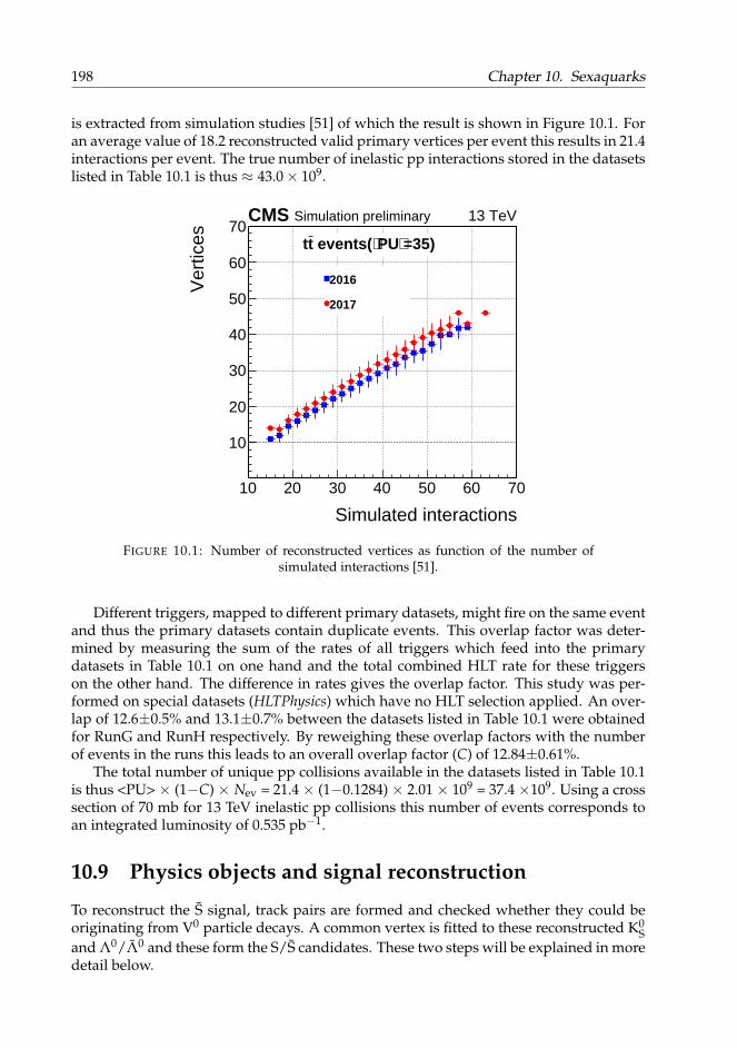
198 Chapter 10. Sexaquarks
is extracted from simulation studies [51] of which the result is shown in Figure 10.1. Foran average value of 18.2 reconstructed valid primary vertices per event this results in 21.4interactions per event. The true number of inelastic pp interactions stored in the datasetslisted in Table 10.1 is thus ≈ 43.0× 10⁹.
Simulated interactions
10 20 30 40 50 60 70
Ver
tices
10
20
30
40
50
60
70
2016
2017
13 TeVCMS Simulation preliminary
=35)⟩PU⟨ events(tt
FIGURE 10.1: Number of reconstructed vertices as function of the number ofsimulated interactions [51].
Different triggers, mapped to different primary datasets, might fire on the same eventand thus the primary datasets contain duplicate events. This overlap factor was deter-mined by measuring the sum of the rates of all triggers which feed into the primarydatasets in Table 10.1 on one hand and the total combined HLT rate for these triggerson the other hand. The difference in rates gives the overlap factor. This study was per-formed on special datasets (HLTPhysics) which have no HLT selection applied. An over-lap of 12.6±0.5% and 13.1±0.7% between the datasets listed in Table 10.1 were obtainedfor RunG and RunH respectively. By reweighing these overlap factors with the numberof events in the runs this leads to an overall overlap factor (C) of 12.84±0.61%.
The total number of unique pp collisions available in the datasets listed in Table 10.1is thus <PU> × (1−C) × Nev = 21.4 × (1−0.1284) × 2.01 × 109 = 37.4 ×10⁹. Using a crosssection of 70 mb for 13 TeV inelastic pp collisions this number of events corresponds toan integrated luminosity of 0.535 pb−1.
10.9 Physics objects and signal reconstruction
To reconstruct the S signal, track pairs are formed and checked whether they could beoriginating from V0 particle decays. A common vertex is fitted to these reconstructed K0
Sand Λ0/Λ0 and these form the S/S candidates. These two steps will be explained in moredetail below.
10.9. Physics objects and signal reconstruction 199
K0S, Λ0 and Λ0 reconstruction is part of the standard CMS reconstruction [109]. This
standard V0 reconstruction was modified slightly to be able to reconstruct the S signal,but the standard algorithm is maintained: the V0 reconstruction module takes all recon-structed tracks as input but only uses tracks which pass the following quality criteria: thesignificance of their transverse impact parameter should be larger than 2, the normalised3
χ2 should be smaller than 10, the track should have at least 7 hits and a pT larger than0.35 GeV/c.
The vertexing of track pairs to a V0 candidate uses oppositely charged tracks whichsatisfy the requirements in the previous paragraph and which have a point of closestapproach in rφ not larger than 2 cm. This point of closest approach should lie within thetracker volume and the scalar product of the 3D track momentum vectors at this pointof closest approach should not be negative. The invariant mass of the track pair is thencalculated under the assumption that both tracks are pion tracks and track pairs with aninvariant mass larger than 0.6 GeV/c2 are excluded.
Track pairs which fulfil the above requirements then serve as input to a Kalman vertexfit [112]. For track pairs for which the vertex-fit succeeds the reconstruction proceeds. Thenormalised χ2 of the vertex-fit is required not to be larger than 15 and the significance ofthe transverse distance of the vertex with respect to the beamspot is required to be largeror equal to 10. The refitted tracks from the Kalman vertex-fit are subsequently used tocalculate the energy of the V0 using the three hypotheses whether the V0 is a K0
S, Λ0 or Λ0.The distinction between Λ0 and Λ0 is made by looking at the charge of the track with thehighest momentum, which is taken to be the (anti-)proton track. As a last constraint thecandidate V0s are required to pass mass cuts constraining them within ±0.070 GeV/c2
(±0.050 GeV/c2) from 0.498 GeV/c2 (1.116 GeV/c2) for the K0S (Λ0 and Λ0).
In contrast to the standard V0 reconstruction the one modified for the S reconstruc-tion does not request the V0 candidate to be pointing to the luminous region. This cutis applied in the standard V0 reconstruction module to eliminate background from ran-dom combinations of tracks. However the K0
S and Λ0 resulting from the S annihilationare not necessarily pointing to the luminous region. This means that the reconstructedK0
S and Λ0 present in the standard CMS collections cannot be used as input to the S re-construction, but that the V0 reconstruction has to be rerun on the full dataset. The latteris a computationally heavy operation. For this adapted reconstruction, no requirementis placed on the impact parameter of the V0s and the mass constraints are tightened inorder to decrease the background. Mass constraints of ± 0.03 GeV/c2 (± 0.015 GeV/c2)around the masses stated in the previous paragraph are used for the K0
S (Λ0 and Λ0).Mass distributions of K0
S, Λ0 and Λ0, reconstructed with this algorithm, are shownin Figure 10.2. These V0s were reconstructed in SingleMuon_Run2016H-07Aug17 data.The K0
S invariant mass distribution shows a significant background contribution. Thisbackground can be rejected by requiring the K0
S to point to the luminous region, as will beillustrated in section 10.13, but as explained before, accepting non-pointing K0
S is essentialfor reconstructing the S signal.
The output K0S, Λ0 and Λ0 of this adapted V0Fitter are used as input to the S and
S reconstruction. This reconstruction makes use of kinematic fitting. Kinematic fitting[113] is a technique commonly applied for signal reconstruction. This technique allowsto add physical constraints to the fitting problem. These additional constraints result insmaller uncertainties on the fitted parameters. For signal reconstruction using tracks,examples of constraints are the invariant mass of combinations of tracks or constraining
3χ2 divided by the number of degrees of freedom.

200 Chapter 10. Sexaquarks
0.46 0.47 0.48 0.49 0.5 0.51 0.52 0.53 mass (GeV)s K
0
500
1000
1500
2000
2500
3000
3500
4000
#en
trie
s/M
eV
(a)
1.095 1.1 1.105 1.11 1.115 1.12 1.125 1.13 m (GeV)Λ or Λ
0
500
1000
1500
2000
2500
#en
trie
s/1M
eV
(b)
FIGURE 10.2: K0S, Λ0 and Λ0 masses as reconstructed with the adapted V0Fitter in
SingleMuon_Run2016H-07Aug17 data.
multiple tracks to a common vertex. The constraints are applied by the use of Lagrangemultipliers.
In the S/S reconstruction K0S and Λ0/Λ0 are kinematically refitted to their world av-
erage mass [10] and the V0 pairs are fitted to a common vertex using a Kalman vertex-fit.This vertex would in the signal case represent the annihilation vertex of the S. The vertexof the two V0s is required to have a normalised χ2 not larger than 10.
10.10 Signal simulation
10.10.1 IntroductionThe following sections describe the signal simulation which was set up to shape the anal-ysis and to extract the S reconstruction efficiency. The signal simulation uses a specialtuned version of the EPOS-LHC minimum bias event generator which implements a pro-duction process for S and S particles. The generated events are then input to the CMSsimulation software where a dedicated S interaction with matter was implemented in theGEANT4 framework (section 10.10.3). The GEANT4 software also performs the simula-tion of the particle interactions with matter for all the particles in the event. Consequently,the default CMS software is used to simulate the detector response and apply the digiti-sation of the signal, superimpose pileup on the signal event and run the reconstructionalgorithms. The simulation is very important here to understand the full topology of thesignal, which due to the material interaction, is fairly uncommon. The simulation showsthat the neutron momentum in the target nucleus actually has a non-negligible influenceon the reconstruction of the S kinematical parameters (section 10.10.4) and gives an ideaabout the acceptance of the signal (section 10.10.5). The kinematics of the signal V0s andfinal state particles are discussed in section 10.10.6, which sets the stage for investigat-ing the reconstruction efficiencies for the signal as described in section 10.11. In section10.10.2 the kinematics of S with different masses as obtained with EPOS-LHC are shown.In the successive sections the focus is on S with a mass of 1.8 GeV/c2.
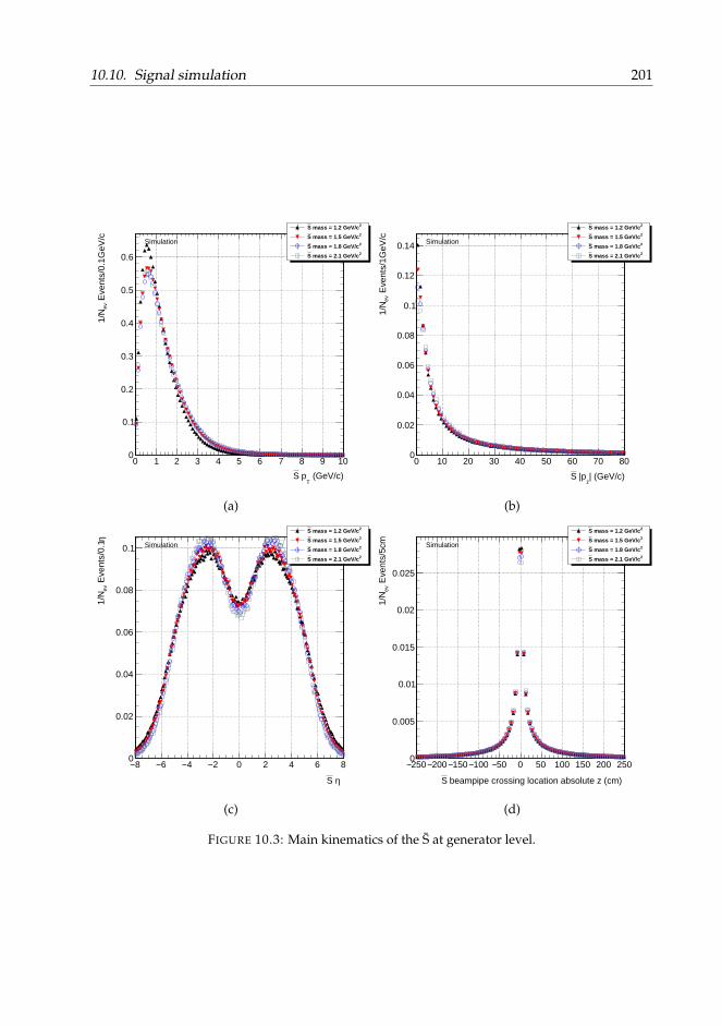
10.10. Signal simulation 201
(GeV/c)T
pS
0 1 2 3 4 5 6 7 8 9 10
Eve
nts/
0.1G
eV/c
ev 1
/N
0
0.1
0.2
0.3
0.4
0.5
0.6
2 mass = 1.2 GeV/cS
2 mass = 1.5 GeV/cS
2 mass = 1.8 GeV/cS
2 mass = 2.1 GeV/cS
Simulation
(a)
| (GeV/c)z
|pS
0 10 20 30 40 50 60 70 80
Eve
nts/
1GeV
/cev
1/N
0
0.02
0.04
0.06
0.08
0.1
0.12
0.14
2 mass = 1.2 GeV/cS
2 mass = 1.5 GeV/cS
2 mass = 1.8 GeV/cS
2 mass = 2.1 GeV/cS
Simulation
(b)
η S
8− 6− 4− 2− 0 2 4 6 8
η E
vent
s/0.
1ev
1/N
0
0.02
0.04
0.06
0.08
0.1
2 mass = 1.2 GeV/cS
2 mass = 1.5 GeV/cS
2 mass = 1.8 GeV/cS
2 mass = 2.1 GeV/cS
Simulation
(c)
beampipe crossing location absolute z (cm) S
250− 200− 150− 100− 50− 0 50 100 150 200 250
Eve
nts/
5cm
ev 1
/N
0
0.005
0.01
0.015
0.02
0.025
2 mass = 1.2 GeV/cS
2 mass = 1.5 GeV/cS
2 mass = 1.8 GeV/cS
2 mass = 2.1 GeV/cS
Simulation
(d)
FIGURE 10.3: Main kinematics of the S at generator level.

202 Chapter 10. Sexaquarks
10.10.2 S kinematics
The starting point for the signal simulation is a special tuned4 version of EPOS-LHC [110]which includes the production of S and S in the pp-collision. EPOS-LHC is mostly usedas event generator for heavy-ion collisions, but as Ref. [110] shows it is also an excellenttool to describe strangeness production in LHC pp collisions.
The pT and pz distribution of the generated S are shown in Figure 10.3 for S masses of1.2, 1.5, 1.8 and 2.1 GeV/c2. These distributions show the typicalO(GeV/c) range for thepT of hadrons produced at LHC collisions. The final state particles will therefore havelow transverse momenta as well, which will complicate their reconstruction. Figure 10.3furthermore shows the pseudorapidity distribution of the S, which shows that the ma-jority of the S are produced forward. The last figure in Figure 10.3 shows the z location5
of where the S would cross the CMS beampipe using a beampipe radius of 2.21 cm (seesection 10.10.3).
The distribution of the z location of the valid primary vertices and the number ofvalid primary vertices per event are different in simulation and data. Since an accuratedescription of these variables is important for this analysis a reweighing procedure is ap-plied to reweigh the simulation to data. In this procedure, an event with a primary vertexwhich is more comparable to a primary vertex in data is given a larger weight.
Figure 10.4 illustrates the result of this two-dimensional reweighing procedure whichcorrects for the different z locations of the PVs as well as the number of primary verticesin the event. The figures show that the reweighed MC (Monte Carlo) distributions indeedcoincide with the distributions for data. The distributions which were used here for dataare extracted from all the events used in this search (listed in Table 10.1) in order to havean as representative as possible reweighing of simulation to data. This event-by-eventreweighing of the simulation is always applied to obtain the results which are shownhereafter.
For the next sections only the case of S candidates with a mass of 1.8 GeV/c2 wasconsidered. The simulated sample includes a total of ≈ 1.3 × 10⁸ S in ≈ 3.4 × 10⁷ events.
10.10.3 S-neutron interaction
The actual interaction of the S with a neutron was implemented specifically for this signalin GEANT4 [111]. The S was added as a new particle to the GEANT framework and itsneutron interaction was implemented as a hadronic interaction and a two body particledecay of the S-neutron system to a K0
S and an Λ0. No angular preference due to potentialspin effects were included in this reaction. The annihilation reaction leaves behind anucleus with a neutron less.
The interaction cross section of the S with material is very small. To simulate this, theinteraction cross section could indeed be put very low in GEANT which would guaranteethat the S has a uniform interaction probability along its passage through the material.This approach would unavoidably lead to many S escaping the beampipe volume with-out interacting. To guarantee an economic simulation whilst maintaining a low interac-tion cross section and thus a uniform interaction probability, a looping mechanism, whichiterates the transport of the S through the sensitive volume, was implemented. This was
4Private version provided by the EPOS-LHC author which has S and S production included.5Coordinates are referred to in some figures as absolute in order to distinguish from coordinates calculated
with respect to other reference points (e.g. beamspot or center of the beampipe) than the absolute origin.
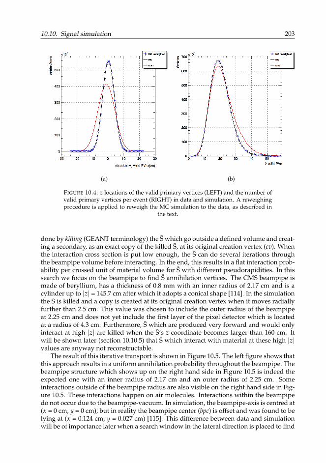
10.10. Signal simulation 203
(a) (b)
FIGURE 10.4: z locations of the valid primary vertices (LEFT) and the number ofvalid primary vertices per event (RIGHT) in data and simulation. A reweighingprocedure is applied to reweigh the MC simulation to the data, as described in
the text.
done by killing (GEANT terminology) the S which go outside a defined volume and creat-ing a secondary, as an exact copy of the killed S, at its original creation vertex (cv). Whenthe interaction cross section is put low enough, the S can do several iterations throughthe beampipe volume before interacting. In the end, this results in a flat interaction prob-ability per crossed unit of material volume for S with different pseudorapidities. In thissearch we focus on the beampipe to find S annihilation vertices. The CMS beampipe ismade of beryllium, has a thickness of 0.8 mm with an inner radius of 2.17 cm and is acylinder up to |z| = 145.7 cm after which it adopts a conical shape [114]. In the simulationthe S is killed and a copy is created at its original creation vertex when it moves radiallyfurther than 2.5 cm. This value was chosen to include the outer radius of the beampipeat 2.25 cm and does not yet include the first layer of the pixel detector which is locatedat a radius of 4.3 cm. Furthermore, S which are produced very forward and would onlyinteract at high |z| are killed when the S’s z coordinate becomes larger than 160 cm. Itwill be shown later (section 10.10.5) that S which interact with material at these high |z|values are anyway not reconstructable.
The result of this iterative transport is shown in Figure 10.5. The left figure shows thatthis approach results in a uniform annihilation probability throughout the beampipe. Thebeampipe structure which shows up on the right hand side in Figure 10.5 is indeed theexpected one with an inner radius of 2.17 cm and an outer radius of 2.25 cm. Someinteractions outside of the beampipe radius are also visible on the right hand side in Fig-ure 10.5. These interactions happen on air molecules. Interactions within the beampipedo not occur due to the beampipe-vacuum. In simulation, the beampipe-axis is centred at(x = 0 cm, y = 0 cm), but in reality the beampipe center (bpc) is offset and was found to belying at (x = 0.124 cm, y = 0.027 cm) [115]. This difference between data and simulationwill be of importance later when a search window in the lateral direction is placed to find

204 Chapter 10. Sexaquarks
interaction vertex (cm)S xy absolute l
2.16 2.17 2.18 2.19 2.2 2.21 2.22 2.23 2.24 2.25 2.26
Eve
nts/
0.1m
m
0
2000
4000
6000
8000
10000
12000
(a)
interaction vertex (cm)S x absolute v
3− 2− 1− 0 1 2 3 in
tera
ctio
n ve
rtex
(cm
)S y
abs
olut
e v
3−
2−
1−
0
1
2
3
Eve
nts/
(0.1
mm
x 0
.1m
m)
0
2
4
6
8
10
12
14
16
18
20
22Simulation
(b)
FIGURE 10.5: Coordinates of the S interaction vertices at generator level.
S particles.Figure 10.6 and 10.7 show two simulated events in which the S got reconstructed (see
section 10.11). Figure 10.6 shows an event where the S has a fairly high pseudorapiditywhereas Figure 10.7 shows a more central event.
The iterative transport guarantees that all S will interact with the beampipe. In realityhowever, not all S have the same interaction probability. The interaction probability ofthe S is a function of the S pseudorapidity as S with larger |η| will have a larger pathlength through the beampipe. An additional event-by-event weight parameter is there-fore introduced and defined as 1/ sin θS. The weight parameter is shown as function of ηof the S and z location of the S interaction vertex in Figure 10.8.
From now on all results which are shown have this weight parameter applied. Thereweighed distribution of the S transverse and longitudinal momentum, pseudorapidityand z location of its interaction vertex are shown in Figure 10.96. Comparison with Fig-ure 10.3 shows that the S signal is significantly enhanced in the forward region and the Saverage pT is significantly reduced.
10.10.4 Influence of neutron Fermi momentum
The neutron on which the S annihilates is not stationary but is moving around in the nu-cleus with a certain Fermi momentum of the order of 200 MeV/c [116]. The fact that thisneutron is not at rest spoils the accuracy with which the S properties, such as its invariantmass and its direction of propagation, can be reconstructed. The exact interaction vertexposition of the S can however still be extracted.
6The z location of the interaction vertex was calculated using the pseudorapidity of the S and a radius of thebeampipe of 2.21 cm, as in Figure 10.3.
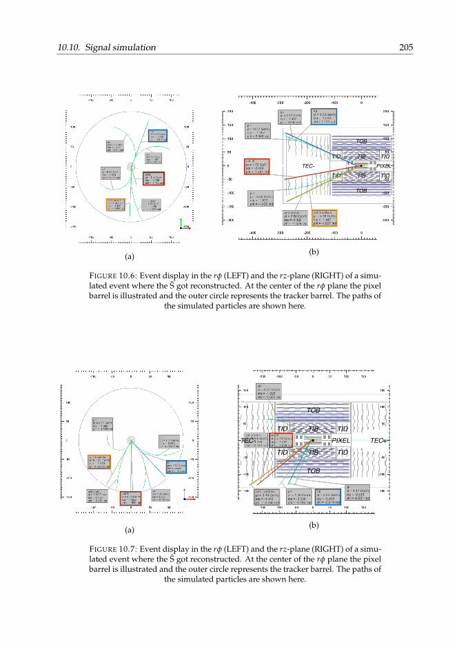
10.10. Signal simulation 205
(a)
TEC-
TOB
TOB
TIB
TIB
TID
TIDTID
TIDPIXEL
-1000
1000
1200
(b)
FIGURE 10.6: Event display in the rφ (LEFT) and the rz-plane (RIGHT) of a simu-lated event where the S got reconstructed. At the center of the rφ plane the pixelbarrel is illustrated and the outer circle represents the tracker barrel. The paths of
the simulated particles are shown here.
(a)
TEC+TEC-
TOB
TOB
TIB
TIB
TID
TIDTID
TIDPIXEL
(b)
FIGURE 10.7: Event display in the rφ (LEFT) and the rz-plane (RIGHT) of a simu-lated event where the S got reconstructed. At the center of the rφ plane the pixelbarrel is illustrated and the outer circle represents the tracker barrel. The paths of
the simulated particles are shown here.
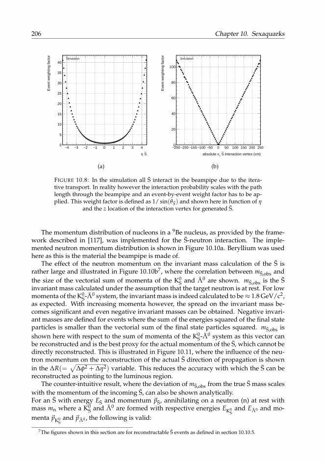
206 Chapter 10. Sexaquarks
S η
4− 3− 2− 1− 0 1 2 3 4
Eve
nt w
eigh
ting
fact
or
0
5
10
15
20
25
30
35
40Simulation
(a)
interaction vertex (cm)S z absolute v
250− 200− 150− 100− 50− 0 50 100 150 200 250
Eve
nt w
eigh
ting
fact
or
0
20
40
60
80
100
Simulation
(b)
FIGURE 10.8: In the simulation all S interact in the beampipe due to the itera-tive transport. In reality however the interaction probability scales with the pathlength through the beampipe and an event-by-event weight factor has to be ap-plied. This weight factor is defined as 1/ sin(θS) and shown here in function of η
and the z location of the interaction vertex for generated S.
The momentum distribution of nucleons in a 9Be nucleus, as provided by the frame-work described in [117], was implemented for the S-neutron interaction. The imple-mented neutron momentum distribution is shown in Figure 10.10a. Beryllium was usedhere as this is the material the beampipe is made of.
The effect of the neutron momentum on the invariant mass calculation of the S israther large and illustrated in Figure 10.10b7, where the correlation between mS,obs andthe size of the vectorial sum of momenta of the K0
S and Λ0 are shown. mS,obs is the Sinvariant mass calculated under the assumption that the target neutron is at rest. For lowmomenta of the K0
S-Λ0 system, the invariant mass is indeed calculated to be≈ 1.8 GeV/c2,as expected. With increasing momenta however, the spread on the invariant mass be-comes significant and even negative invariant masses can be obtained. Negative invari-ant masses are defined for events where the sum of the energies squared of the final stateparticles is smaller than the vectorial sum of the final state particles squared. mS,obs isshown here with respect to the sum of momenta of the K0
S-Λ0 system as this vector canbe reconstructed and is the best proxy for the actual momentum of the S, which cannot bedirectly reconstructed. This is illustrated in Figure 10.11, where the influence of the neu-tron momentum on the reconstruction of the actual S direction of propagation is shownin the ∆R(=
√∆φ2 + ∆η2) variable. This reduces the accuracy with which the S can be
reconstructed as pointing to the luminous region.The counter-intuitive result, where the deviation of mS,obs from the true S mass scales
with the momentum of the incoming S, can also be shown analytically.For an S with energy ES and momentum ~pS, annihilating on a neutron (n) at rest withmass mn where a K0
S and Λ0 are formed with respective energies EK0S
and EΛ0 and mo-menta ~pK0
Sand ~pΛ0 , the following is valid:
7The figures shown in this section are for reconstructable S events as defined in section 10.10.5.
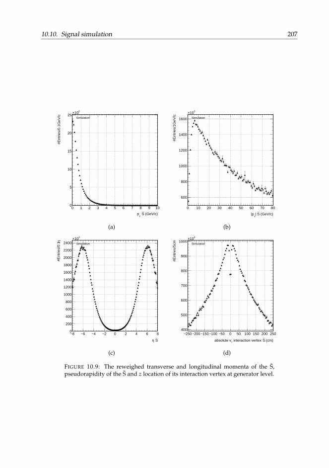
10.10. Signal simulation 207
(GeV/c)S T
p
0 1 2 3 4 5 6 7 8 9 10
#E
ntrie
s/0.
1GeV
/c
0
5
10
15
20
25610×
Simulation
(a)
(GeV/c)S| z
|p
0 10 20 30 40 50 60 70 80
#E
ntrie
s/1G
eV/c
600
800
1000
1200
1400
1600
310×Simulation
(b)
S η
8− 6− 4− 2− 0 2 4 6 8
η #
Ent
ries/
0.1
0
200
400
600
800
1000
1200
1400
1600
1800
2000
2200
2400
310×Simulation
(c)
(cm)S interaction vertex z absolute v
250− 200− 150− 100− 50− 0 50 100 150 200 250
#E
ntrie
s/5c
m
400
500
600
700
800
900
1000310×
Simulation
(d)
FIGURE 10.9: The reweighed transverse and longitudinal momenta of the S,pseudorapidity of the S and z location of its interaction vertex at generator level.
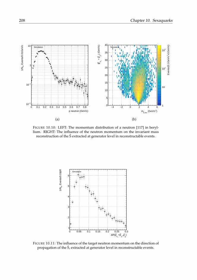
208 Chapter 10. Sexaquarks
p neutron (GeV/c)
0 0.1 0.2 0.3 0.4 0.5 0.6 0.7 0.8
Eve
nts/
0.01
GeV
/cev
1/N
2−10
1−10
1
10Simulation
(a)
)2 (GeV/c,obsS
m
4− 2− 0 2 4 6
| (G
eV/c
)0
Λp
+
sK
p |
0
5
10
15
20
25
30
35
40
x1G
eV/c
)2
Eve
nts/
(0.1
GeV
/c
1
10
210
310Simulation
(b)
FIGURE 10.10: LEFT: The momentum distribution of a neutron [117] in beryl-lium. RIGHT: The influence of the neutron momentum on the invariant mass
reconstruction of the S extracted at generator level in reconstructable events.
)S
p,0Λ
p+sK
pR(∆ 0 0.05 0.1 0.15 0.2 0.25 0.3
R∆ E
vent
s/0.
01ev
1/N
1
2
3
4
5
6
Simulation
FIGURE 10.11: The influence of the target neutron momentum on the direction ofpropagation of the S, extracted at generator level in reconstructable events.

10.10. Signal simulation 209
(ES,~pS) + (mn, 0) =(
EΛ0 + EK0S,~pΛ0 + ~pK0
S
), (10.8)
which results in an invariant mass of the S:
mS,obs =
√(EΛ0 + EK0
S
)2+ m2
n − 2mn
(EΛ0 + EK0
S
)− (~pΛ0 + ~pK0
S)2. (10.9)
In reality, the neutron is not at rest and is moving with a momentum ~pn in the nucleus.Equation (10.8) then becomes:
(ES,~pS) + (En,~pn) =(
EΛ0 + EK0S,~pΛ0 + ~pK0
S
), (10.10)
which leads to an invariant mass of the S:
mS =√(EΛ0 + EK0
S
)2+ m2
n − 2En
(EΛ0 + EK0
S
)− (~pΛ0 + ~pK0
S)2 + 2~pn(~pΛ0 + ~pK0
S). (10.11)
If we assume that the momenta of the K0S and Λ0 are collinear and substitute m2
S,obs fromEquation (10.9) in Equation (10.11), we get:
m2S,obs = m2
S + 2 (En −mn)(
EΛ0 + EK0S
)− 2pn
(pΛ0 + pK0
S
)= m2
S + 2 (En −mn) (ES + En)− 2pn (pS + pn), (10.12)
which shows that (m2S,obs −m2
S) is a function of the S momentum.The fact that the neutron momentum smears the invariant mass peak of the S vouches
for a zero background analysis as it will not be possible to extract a narrow mass-peak.
10.10.5 ReconstructabilityWhen discussing the reconstruction efficiency for the signal, it is interesting to try tofactorise the efficiency losses due to detector acceptance on the one hand and detectorinefficiencies and algorithmic limitations on the other hand. Three factors are thereforeidentified which contribute to the signal reconstruction efficiency:
1. Detector acceptance: all four final state particles should fall in the tracker accep-tance. This requirement can be evaluated by counting the number of hits that theparticle would generate in the tracker modules. A number of hits equal or largerthan 7 is required to evaluate this acceptance criteria. This condition is used as it isthe same number of hits that is required for tracks entering the V0 reconstructionmodule (section 10.9).
2. Branching fraction: as stated in section 10.7 the branching fraction for K0S→ π+ π−
is 69.2% and for Λ0 → π+ p is 63.9%. The combined branching fraction of K0S and
Λ0 to charged particles is thus 44.2%. K0S → π0 π0 and Λ0 → nπ0 complement

210 Chapter 10. Sexaquarks
(GeV/c)S T
p
0 2 4 6 8 10
Rec
onst
ruct
abili
ty
0
0.005
0.01
0.015
0.02
0.025
Simulation
(a)
(GeV/c)S| z
|p
0 10 20 30 40 50 60 70 80
Rec
onst
ruct
abili
ty
0
0.01
0.02
0.03
0.04
0.05
0.06
0.07Simulation
(b)
S η
8− 6− 4− 2− 0 2 4 6 8
Rec
onst
ruct
abili
ty
0
0.01
0.02
0.03
0.04
0.05
0.06
0.07
0.08
0.09 Simulation
(c)
interaction vertex (cm)S z absolute v
150− 100− 50− 0 50 100 150
Rec
onst
ruct
abili
ty
0
0.01
0.02
0.03
0.04
0.05
0.06
0.07
0.08
0.09Simulation
(d)
FIGURE 10.12: Reconstructability of generated S as function of the S transversemomentum, longitudinal momentum, pseudorapidity and z coordinate of the
interaction vertex.

10.10. Signal simulation 211
the K0S and Λ0 decay modes used in this analysis almost completely with respec-
tive branching fractions of 30.7% and 35.8%. Other charged final states are thusnegligible.
3. Detection efficiency: it is not guaranteed that an S event which satisfies the abovetwo requirements will be reconstructed. These reconstruction inefficiencies will bethe subject of section 10.11.
From now on, the acceptance requirement, as in point 1 above, and the branching frac-tion, as in point 2 above, will be combined and an S fulfilling these requirements will bereferred to as reconstructable.
Figure 10.12 shows the reconstructability of the S, i.e. the probability for an S to bereconstructable, with respect to the S transverse momentum, longitudinal momentum,pseudorapidity and z coordinate of its interaction vertex. It shows that the reconstructabil-ity of S vanishes for S with |η| ' 4.5 and |z| ' 140 cm. Also a minimal transverse mo-mentum is required in order for the S to be reconstructable. The overall reconstructabilitywas found to be 0.75% which shows that acceptance criteria are indeed an important in-efficiency factor. The results shown in the rest of this section are for reconstructable S.
10.10.6 V0 and final state particles kinematicsBefore studying actual signal reconstruction efficiencies, it is instructive to look at thekinematics of the final state particles in reconstructable events. In this section it will be-come clear that the S annihilation produces final state particles which have a very unusualtopology compared to final states in typical CMS analyses.
The transverse and longitudinal displacement of the K0S and Λ0 decay vertices are
shown in Figure 10.13 and in two dimensions in Figures 10.14 and 10.15 for the K0S and Λ0
respectively. These figures basically represent a convolution of the S interaction verticeswith the decay lengths of the K0
S and the Λ0.The actual momentum distributions of the K0
S and Λ0 and their respective daughtersare shown in Figure 10.16 and 10.17 respectively. Important to note here is the low pTof the final state particles and especially the low momentum of the soft pion in the Λ0
decay. For the π+ in the Λ0 decay, the transverse and longitudinal momentum are alsoshown in Figure 10.18 as function of the pseudorapidity of the particle. It shows that themajority of the π+ are produced forward.
Besides being produced displaced and having low momenta, the final state particlesare also not necessarily pointing to the luminous region as shown in Figures 10.19 wherethe transverse (d0) and longitudinal (dz) impact parameters with respect to the beamspot(bs) are shown calculated at the creation vertex of the final state particles. The sign of d0is given by the scalar product of the track momentum vector and the vector connectingthe beamspot and the track creation vertex.
The above discussion shows that the final state particles have low momenta, are pro-duced mainly at high |z| and they do not necessarily point to the luminous region. Thesefacts imply that the final state particles do not necessarily benefit from the tracker layoutwhich was optimised to have particles, created at the primary vertex with a significantpT pass as many tracker and seeding layers as possible.

212 Chapter 10. Sexaquarks
cv (cm)0,bpcl
0 10 20 30 40 50 60 70 80
Eve
nts/
cm
ev1/
N
0
0.02
0.04
0.06
0.08
0.1
0.12
daughters0SK
daughters0
ΛSimulation
(a)
cv (cm)zabsolute v
250− 200− 150− 100− 50− 0 50 100 150 200 250
Eve
nts/
10cm
ev1/
N0
0.001
0.002
0.003
0.004
0.005
0.006
daughters0SK
daughters0
ΛSimulation
(b)
FIGURE 10.13: Displacement of the decay vertices of the V0s (creation vertices(cv) of the final state particles) with respect to the beam pipe center (bpc) andz = 0 respectively. This is obtained at generator level in reconstructable events.
(cm)0
S decay vertex Kxabsolute v
80− 60− 40− 20− 0 20 40 60 80
(cm
)0 S
dec
ay v
erte
x K
yab
solu
te v
80−
60−
40−
20−
0
20
40
60
80 2E
vent
s/cm
1
10
210
310
Simulation
(a)
(cm)0
S decay vertex Kzabsolute v
250− 200− 150− 100− 50− 0 50 100 150 200 250
(cm
)0 S
dec
ay v
erte
x K
0,bp
cl
0
10
20
30
40
50
60
70
80 2E
vent
s/cm
1
10
210
Simulation
(b)
FIGURE 10.14: Decay vertices of the K0S (creation vertices of the final state parti-
cles) at generator level in reconstructable events.
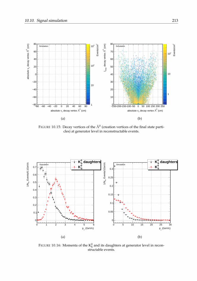
10.10. Signal simulation 213
(cm)0
Λ decay vertex xabsolute v
80− 60− 40− 20− 0 20 40 60 80
(cm
)0
Λ d
ecay
ver
tex
y a
bsol
ute
v
80−
60−
40−
20−
0
20
40
60
80 2E
vent
s/cm
1
10
210
310Simulation
(a)
(cm)0
Λ decay vertex zabsolute v
250− 200− 150− 100− 50− 0 50 100 150 200 250 (
cm)
0Λ
dec
ay v
erte
x 0,
bpc
l0
10
20
30
40
50
60
70
80 2E
vent
s/cm
1
10
210
Simulation
(b)
FIGURE 10.15: Decay vertices of the Λ0 (creation vertices of the final state parti-cles) at generator level in reconstructable events.
(GeV/c)T
p
0 1 2 3 4 5 6
Eve
nts/
0.1G
eV/c
ev1/
N
0
0.1
0.2
0.3
0.4
0.5
0.6
0.7
daughters0SK0SK
Simulation
(a)
(GeV/c)z
p
0 5 10 15 20 25 30
Eve
nts/
1GeV
/cev
1/N
0
0.05
0.1
0.15
0.2
0.25
0.3
daughters0SK0SK
Simulation
(b)
FIGURE 10.16: Momenta of the K0S and its daughters at generator level in recon-
structable events.
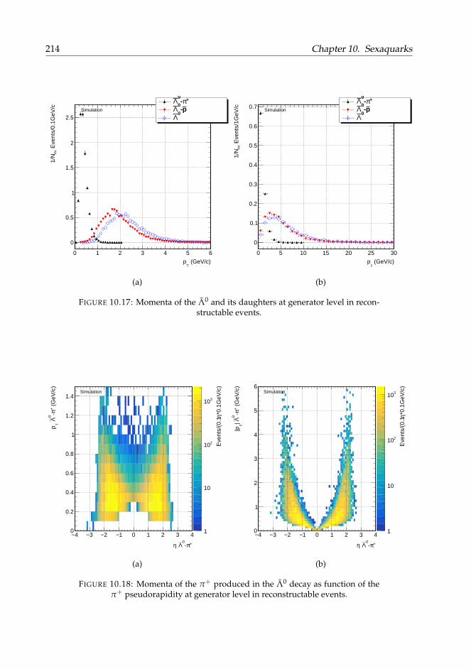
214 Chapter 10. Sexaquarks
(GeV/c)T
p
0 1 2 3 4 5 6
Eve
nts/
0.1G
eV/c
ev1/
N
0
0.5
1
1.5
2
2.5
+π-0
Λp-
0Λ
0Λ
Simulation
(a)
(GeV/c)z
p
0 5 10 15 20 25 30
Eve
nts/
1GeV
/cev
1/N
0
0.1
0.2
0.3
0.4
0.5
0.6
0.7+π-
0Λ
p-0
Λ0
ΛSimulation
(b)
FIGURE 10.17: Momenta of the Λ0 and its daughters at generator level in recon-structable events.
+π-0
Λ η
4− 3− 2− 1− 0 1 2 3 4
(G
eV/c
)+ π-
0Λ
Tp
0
0.2
0.4
0.6
0.8
1
1.2
1.4
*0.1
GeV
/c)
η E
vent
s/(0
.1
1
10
210
310
Simulation
(a)
+π-0
Λ η
4− 3− 2− 1− 0 1 2 3 4
(G
eV/c
)+ π-
0Λ| z
|p
0
1
2
3
4
5
6
*0.1
GeV
/c)
η E
vent
s/(0
.1
1
10
210
310Simulation
(b)
FIGURE 10.18: Momenta of the π+ produced in the Λ0 decay as function of theπ+ pseudorapidity at generator level in reconstructable events.
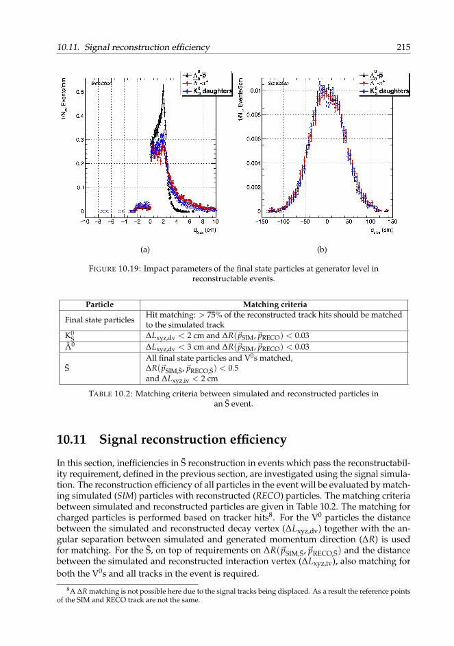
10.11. Signal reconstruction efficiency 215
(a) (b)
FIGURE 10.19: Impact parameters of the final state particles at generator level inreconstructable events.
Particle Matching criteria
Final state particlesHit matching: > 75% of the reconstructed track hits should be matchedto the simulated track
K0S ∆Lxyz,dv < 2 cm and ∆R(~pSIM,~pRECO) < 0.03
Λ0 ∆Lxyz,dv < 3 cm and ∆R(~pSIM,~pRECO) < 0.03
SAll final state particles and V0s matched,∆R(~pSIM,S,~pRECO,S) < 0.5and ∆Lxyz,iv < 2 cm
TABLE 10.2: Matching criteria between simulated and reconstructed particles inan S event.
10.11 Signal reconstruction efficiency
In this section, inefficiencies in S reconstruction in events which pass the reconstructabil-ity requirement, defined in the previous section, are investigated using the signal simula-tion. The reconstruction efficiency of all particles in the event will be evaluated by match-ing simulated (SIM) particles with reconstructed (RECO) particles. The matching criteriabetween simulated and reconstructed particles are given in Table 10.2. The matching forcharged particles is performed based on tracker hits8. For the V0 particles the distancebetween the simulated and reconstructed decay vertex (∆Lxyz,dv) together with the an-gular separation between simulated and generated momentum direction (∆R) is usedfor matching. For the S, on top of requirements on ∆R(~pSIM,S,~pRECO,S) and the distancebetween the simulated and reconstructed interaction vertex (∆Lxyz,iv), also matching forboth the V0s and all tracks in the event is required.
8A ∆R matching is not possible here due to the signal tracks being displaced. As a result the reference pointsof the SIM and RECO track are not the same.
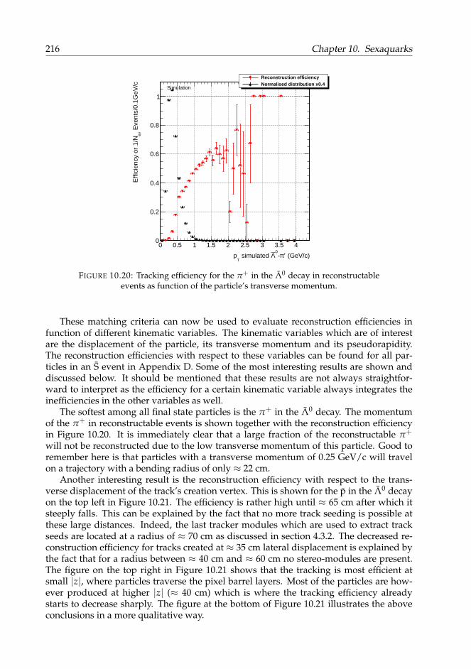
216 Chapter 10. Sexaquarks
(GeV/c)+π-0
Λ simulated T
p
0 0.5 1 1.5 2 2.5 3 3.5 4
Eve
nts/
0.1G
eV/c
evE
ffici
ency
or
1/N
0
0.2
0.4
0.6
0.8
1
Reconstruction efficiencyNormalised distribution x0.4
Simulation
FIGURE 10.20: Tracking efficiency for the π+ in the Λ0 decay in reconstructableevents as function of the particle’s transverse momentum.
These matching criteria can now be used to evaluate reconstruction efficiencies infunction of different kinematic variables. The kinematic variables which are of interestare the displacement of the particle, its transverse momentum and its pseudorapidity.The reconstruction efficiencies with respect to these variables can be found for all par-ticles in an S event in Appendix D. Some of the most interesting results are shown anddiscussed below. It should be mentioned that these results are not always straightfor-ward to interpret as the efficiency for a certain kinematic variable always integrates theinefficiencies in the other variables as well.
The softest among all final state particles is the π+ in the Λ0 decay. The momentumof the π+ in reconstructable events is shown together with the reconstruction efficiencyin Figure 10.20. It is immediately clear that a large fraction of the reconstructable π+
will not be reconstructed due to the low transverse momentum of this particle. Good toremember here is that particles with a transverse momentum of 0.25 GeV/c will travelon a trajectory with a bending radius of only ≈ 22 cm.
Another interesting result is the reconstruction efficiency with respect to the trans-verse displacement of the track’s creation vertex. This is shown for the p in the Λ0 decayon the top left in Figure 10.21. The efficiency is rather high until ≈ 65 cm after which itsteeply falls. This can be explained by the fact that no more track seeding is possible atthese large distances. Indeed, the last tracker modules which are used to extract trackseeds are located at a radius of ≈ 70 cm as discussed in section 4.3.2. The decreased re-construction efficiency for tracks created at ≈ 35 cm lateral displacement is explained bythe fact that for a radius between ≈ 40 cm and ≈ 60 cm no stereo-modules are present.The figure on the top right in Figure 10.21 shows that the tracking is most efficient atsmall |z|, where particles traverse the pixel barrel layers. Most of the particles are how-ever produced at higher |z| (≈ 40 cm) which is where the tracking efficiency alreadystarts to decrease sharply. The figure at the bottom of Figure 10.21 illustrates the aboveconclusions in a more qualitative way.
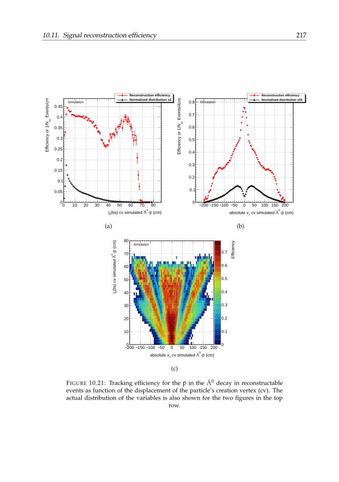
10.11. Signal reconstruction efficiency 217
(cm)p-0
Λ(bs) cv simulated 0l
0 10 20 30 40 50 60 70 80
Eve
nts/
cmev
Effi
cien
cy o
r 1/
N
0
0.05
0.1
0.15
0.2
0.25
0.3
0.35
0.4
0.45
Reconstruction efficiencyNormalised distribution x2
Simulation
(a)
(cm)p-0
Λ cv simulated zabsolute v
200− 150− 100− 50− 0 50 100 150 200
Eve
nts/
4cm
evE
ffici
ency
or
1/N
0
0.1
0.2
0.3
0.4
0.5
0.6
0.7
0.8
Reconstruction efficiencyNormalised distribution x25
Simulation
(b)
(cm)p-0
Λ cv simulated zabsolute v
200− 150− 100− 50− 0 50 100 150 200
(cm
)p-
0Λ
(bs)
cv
sim
ulat
ed
0l
0
10
20
30
40
50
60
70
80
Effi
cien
cy
0
0.1
0.2
0.3
0.4
0.5
0.6
0.7
Simulation
(c)
FIGURE 10.21: Tracking efficiency for the p in the Λ0 decay in reconstructableevents as function of the displacement of the particle’s creation vertex (cv). Theactual distribution of the variables is also shown for the two figures in the top
row.
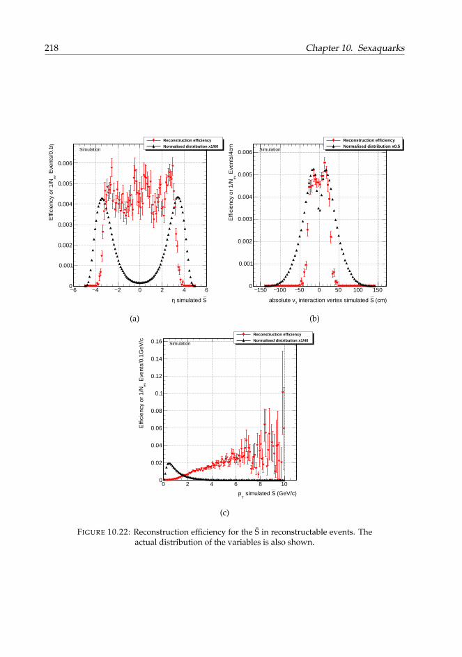
218 Chapter 10. Sexaquarks
S simulated η
6− 4− 2− 0 2 4 6
η E
vent
s/0.
1ev
Effi
cien
cy o
r 1/
N
0
0.001
0.002
0.003
0.004
0.005
0.006
Reconstruction efficiency
Normalised distribution x1/60Simulation
(a)
(cm)S interaction vertex simulated zabsolute v
150− 100− 50− 0 50 100 150
Eve
nts/
4cm
evE
ffici
ency
or
1/N
0
0.001
0.002
0.003
0.004
0.005
0.006
Reconstruction efficiencyNormalised distribution x0.5
Simulation
(b)
(GeV/c)S simulated T
p
0 2 4 6 8 10
Eve
nts/
0.1G
eV/c
evE
ffici
ency
or
1/N
0
0.02
0.04
0.06
0.08
0.1
0.12
0.14
0.16Reconstruction efficiency
Normalised distribution x1/40Simulation
(c)
FIGURE 10.22: Reconstruction efficiency for the S in reconstructable events. Theactual distribution of the variables is also shown.

10.11. Signal reconstruction efficiency 219
S reconstructability 0.751%
K0S-π+ reconstruction efficiency in reconstructable events 31.1%
K0S-π− reconstruction efficiency in reconstructable events 31.3%
Λ0-π+ reconstruction efficiency in reconstructable events 12.9%Λ0-p reconstruction efficiency in reconstructable events 39.2%K0
S reconstruction efficiency in reconstructable events 6.54%Λ0 reconstruction efficiency in reconstructable events 2.78%S reconstruction efficiency in reconstructable events 0.194%
Overall S reconstruction efficiency (εreco) 0.0014%
TABLE 10.3: Reconstructability and reconstruction efficiencies for the track, V0
and S reconstruction.
The reconstruction efficiencies for the V0 particles, shown in Figure D.5 and D.6 forthe Λ0 and the K0
S respectively, show similar features as at the tracking level. Figure 10.22shows the eventual reconstruction efficiency for the S. It is clear from both the first andsecond figure that a significant part of the S is produced too forward and thus interactsat too high |z| to get reconstructed. The third figure shows that, as expected, S with asignificant transverse momentum have the highest reconstruction efficiency.
The breakdown of the overall reconstruction efficiency into reconstructability and re-construction efficiencies of reconstructable objects is given in Table 10.3. The overall re-construction efficiency of the S, of 0.0014%, is thus very low and implies that, although alarge dataset is available to look for the S, the discovery potential is significantly reducedby this inefficient reconstruction.
Important for the background suppression is the accuracy with which the S inter-action vertex can be reconstructed. The location of reconstructed interaction verticesare shown in the top row in Figure 10.23. The reconstruction indeed gives us back thebeampipe radius and Figure 10.23 furthermore shows that no S are reconstructed whichinteract at |z| larger than 50 cm. The actual accuracy of the reconstruction is shown onthe bottom row of Figure 10.23 where Monte Carlo truth is compared to reconstructedobjects. O(1 mm) accuracy can be attained on both the transverse and longitudinal dis-placement.
Figure 10.24 shows the distribution of the estimated invariant mass of the S. It showsthat also S with negative invariant mass can be reconstructed, and shows the large spreadon the invariant mass introduced by the neutron momentum.
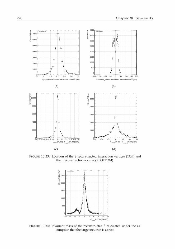
220 Chapter 10. Sexaquarks
(cm)S(bpc) interaction vertex reconstructed 0l
1.9 2 2.1 2.2 2.3 2.4 2.5
Eve
nts/
0.2m
m
0
1000
2000
3000
4000
5000
6000
7000Simulation
(a)
(cm)S interaction vertex reconstructed zabsolute v
200− 150− 100− 50− 0 50 100 150 200
Eve
nts/
4cm
0
500
1000
1500
2000
2500
3000
3500
4000Simulation
(b)
(iv, bs) (cm)S0, reco
(iv, bs) - lS0, sim
l0.5− 0.4− 0.3− 0.2− 0.1− 0 0.1 0.2 0.3 0.4 0.5
Eve
nts/
0.2m
m
0
2000
4000
6000
8000
10000
(c)
(iv, bs) (cm)Sz, reco
(iv, bs) - vSz, sim
v0.6− 0.4− 0.2− 0 0.2 0.4 0.6
Eve
nts/
0.2m
m
0
1000
2000
3000
4000
5000
(d)
FIGURE 10.23: Location of the S reconstructed interaction vertices (TOP) andtheir reconstruction accuracy (BOTTOM).
)2 RECO (GeV/c,obsS
m
6− 4− 2− 0 2 4 6 8 10 12
2E
vent
s/0.
1GeV
/c
0
500
1000
1500
2000
2500
Simulation
FIGURE 10.24: Invariant mass of the reconstructed S calculated under the as-sumption that the target neutron is at rest.

10.12. Background rejection 221
10.12 Background rejection
The background for the S signal is evaluated by looking at reconstructed S particles.This collection does not contain signal since S, as opposed to S, do not annihilate in thebeampipe. Throughout this section, five background samples are compared to each other:
• S reconstructed in the DYJets MC sample, which was also used for the systematicsstudy on tracking efficiencies (see section 10.13).
• S reconstructed in the DYJets MC sample, which was also used for the systematicsstudy on tracking efficiencies (see section 10.13).
• Reconstructed S from SingleMuon_Run2016H. This is the default background sam-ple.
• Reconstructed S from SingleMuon_Run2016H where it is guaranteed that this isbackground by placing a maximum on the value of the BDT classifier.
• S which are reconstructed across events: Λ0 are fitted to a common vertex with K0S
from the previous event to form S candidates.
The first four background samples are compared to validate that the S background can-didates, reconstructed in data, form a good reference for the S background in data. Thiscomparison will be made for all the kinematic variables shown in this section. The lastbackground sample is used to show that the background is due to random combinationsof K0
S and Λ0/Λ0 which form S/S candidates. The fact that the background is indeedcombinatorial will be discussed later in this section, but it is relevant to already be awareof this fact when interpreting the background distributions shown in this section.
The background suppression is achieved by first introducing three background rejec-tion cuts which show an obvious difference between the signal and the background. Tofurther eliminate the background, a BDT is used. An overview of the introduced cutswhich will be introduced below can be found in the cut flow table (Table 10.4) for the sig-nal simulation and the background extracted from data9. In what follows, reconstructedS and S candidates are investigated that have the parameters of their final state particleswithin a fiducial region, which will be introduced in section 10.13, for which trackingefficiencies are well described in simulation.
The first background rejection cut is applied to remove the hard component in theevent by requesting the absolute angular difference in φ of the K0
S and the Λ0 or Λ0
(|∆φ(K0S, Λ0/Λ0)|) to be larger than 0.5. The distribution of this variable is shown on
the left in Figure 10.25 for events which have their final state particles in the fiducial re-gion as defined in section 10.13. The |∆φ(K0
S, Λ0/Λ0)| > 0.5 has an efficiency of 97.9%for signal and 48.9% for background.
To further suppress the background, the fact that the S reconstructed interaction ver-tex location should be compatible with the beampipe position can be exploited. It shouldbe noted here that this distance is calculated differently in simulation and data as thecenter of the beampipe is at a different location for both. For simulation this distance iscalculated with respect to the absolute origin, whereas for data this distance is calculatedwith respect to (x = 0.124 cm, y = 0.027 cm) which is the measured beampipe center [115].
9No check for duplicate events due to overlaps in primary datasets was performed when constructing thistable.
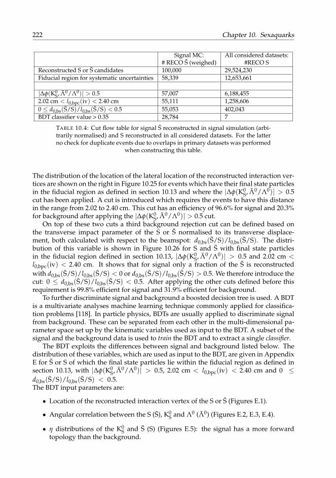
222 Chapter 10. Sexaquarks
Signal MC:# RECO S (weighed)
All considered datasets:#RECO S
Reconstructed S or S candidates 100,000 29,524,230Fiducial region for systematic uncertainties 58,339 12,653,661
|∆φ(K0S, Λ0/Λ0)| > 0.5 57,007 6,188,455
2.02 cm < l0,bpc(iv) < 2.40 cm 55,111 1,258,6060 ≤ d0,bs(S/S)/l0,bs(S/S) < 0.5 55,053 402,043BDT classifier value > 0.35 28,784 7
TABLE 10.4: Cut flow table for signal S reconstructed in signal simulation (arbi-trarily normalised) and S reconstructed in all considered datasets. For the latterno check for duplicate events due to overlaps in primary datasets was performed
when constructing this table.
The distribution of the location of the lateral location of the reconstructed interaction ver-tices are shown on the right in Figure 10.25 for events which have their final state particlesin the fiducial region as defined in section 10.13 and where the |∆φ(K0
S, Λ0/Λ0)| > 0.5cut has been applied. A cut is introduced which requires the events to have this distancein the range from 2.02 to 2.40 cm. This cut has an efficiency of 96.6% for signal and 20.3%for background after applying the |∆φ(K0
S, Λ0/Λ0)| > 0.5 cut.On top of these two cuts a third background rejection cut can be defined based on
the transverse impact parameter of the S or S normalised to its transverse displace-ment, both calculated with respect to the beamspot: d0,bs(S/S)/l0,bs(S/S). The distri-bution of this variable is shown in Figure 10.26 for S and S with final state particlesin the fiducial region defined in section 10.13, |∆φ(K0
S, Λ0/Λ0)| > 0.5 and 2.02 cm <l0,bpc(iv) < 2.40 cm. It shows that for signal only a fraction of the S is reconstructedwith d0,bs(S/S)/l0,bs(S/S) < 0 or d0,bs(S/S)/l0,bs(S/S) > 0.5. We therefore introduce thecut: 0 ≤ d0,bs(S/S)/l0,bs(S/S) < 0.5. After applying the other cuts defined before thisrequirement is 99.8% efficient for signal and 31.9% efficient for background.
To further discriminate signal and background a boosted decision tree is used. A BDTis a multivariate analyses machine learning technique commonly applied for classifica-tion problems [118]. In particle physics, BDTs are usually applied to discriminate signalfrom background. These can be separated from each other in the multi-dimensional pa-rameter space set up by the kinematic variables used as input to the BDT. A subset of thesignal and the background data is used to train the BDT and to extract a single classifier.
The BDT exploits the differences between signal and background listed below. Thedistribution of these variables, which are used as input to the BDT, are given in AppendixE for S or S of which the final state particles lie within the fiducial region as defined insection 10.13, with |∆φ(K0
S, Λ0/Λ0)| > 0.5, 2.02 cm < l0,bpc(iv) < 2.40 cm and 0 ≤d0,bs(S/S)/l0,bs(S/S) < 0.5.The BDT input parameters are:
• Location of the reconstructed interaction vertex of the S or S (Figures E.1).
• Angular correlation between the S (S), K0S and Λ0 (Λ0) (Figures E.2, E.3, E.4).
• η distributions of the K0S and S (S) (Figures E.5): the signal has a more forward
topology than the background.
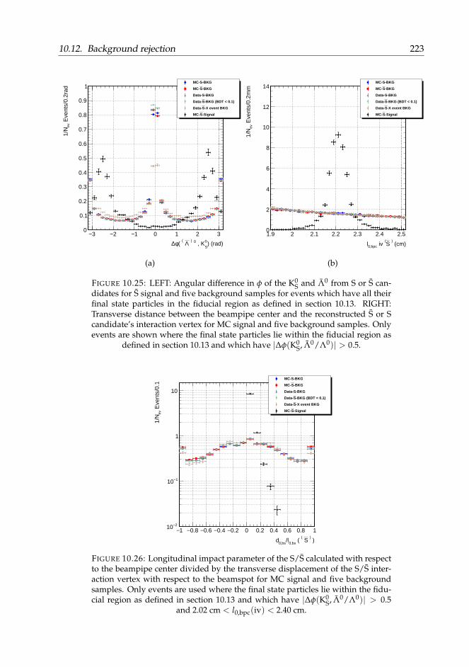
10.12. Background rejection 223
) (rad)0
S , K0
) Λ (( φ∆
3− 2− 1− 0 1 2 3
Eve
nts/
0.2r
adev
1/N
0
0.1
0.2
0.3
0.4
0.5
0.6
0.7
0.8
0.9
1MC-S-BKG
-BKGSMC-
Data-S-BKG
-BKG (BDT < 0.1) SData-
-X event BKGSData-
-SignalSMC-
(a)
(cm))
S(
iv 0,bpc l
1.9 2 2.1 2.2 2.3 2.4 2.5
Eve
nts/
0.2m
mev
1/N
0
2
4
6
8
10
12
14MC-S-BKG
-BKGSMC-
Data-S-BKG
-BKG (BDT < 0.1) SData-
-X event BKGSData-
-SignalSMC-
(b)
FIGURE 10.25: LEFT: Angular difference in φ of the K0S and Λ0 from S or S can-
didates for S signal and five background samples for events which have all theirfinal state particles in the fiducial region as defined in section 10.13. RIGHT:Transverse distance between the beampipe center and the reconstructed S or Scandidate’s interaction vertex for MC signal and five background samples. Onlyevents are shown where the final state particles lie within the fiducial region as
defined in section 10.13 and which have |∆φ(K0S, Λ0/Λ0)| > 0.5.
))
S (
( 0,bs
/l0,bs
d
1− 0.8− 0.6− 0.4− 0.2− 0 0.2 0.4 0.6 0.8 1
Eve
nts/
0.1
ev 1
/N
2−10
1−10
1
10
MC-S-BKG
-BKGSMC-
Data-S-BKG
-BKG (BDT < 0.1) SData-
-X event BKGSData-
-SignalSMC-
FIGURE 10.26: Longitudinal impact parameter of the S/S calculated with respectto the beampipe center divided by the transverse displacement of the S/S inter-action vertex with respect to the beamspot for MC signal and five backgroundsamples. Only events are used where the final state particles lie within the fidu-cial region as defined in section 10.13 and which have |∆φ(K0
S, Λ0/Λ0)| > 0.5and 2.02 cm < l0,bpc(iv) < 2.40 cm.

224 Chapter 10. Sexaquarks
0.6− 0.4− 0.2− 0 0.2 0.4 0.6BDT classifier/BDT class.
4−10
3−10
2−10
1−10
1
Eve
nts
ev1/
N
Signal (test sample)
Signal (trainging sample)
Background (test sample)
Background (training sample)
(a)
0.6− 0.4− 0.2− 0 0.2 0.4 0.6BDT classifier
5−10
4−10
3−10
2−10
1−10
1
Effi
cien
cy
Signal efficiency
Background efficiency
(b)
FIGURE 10.27: LEFT: BDT response for the background and signal training andtesting sample. RIGHT: Data and background efficiency with respect to the BDT
classifier.
• Pointing of the S (S), K0S and Λ0 (Λ0) to the primary vertex (Figures E.6 and Figures
E.7): the reconstructed signal S point to the luminous region whereas the K0S and
Λ0 originating from an S +n annihilation on average do not. The reconstructedbackground S are less probable to point back to the luminous region as they canbe the result of randomly vertexed K0
S and Λ0s. The background K0S and Λ0s in
their turn do point back to the luminous region, the main origin of K0S and Λ0. This
topology can be exploited by calculating the transverse impact parameters of theK0
S, Λ0/Λ0 and S/S with respect to the beamspot and their longitudinal impactparameter with respect to the valid primary vertex that minimises this longitudinalimpact parameter.
• The transverse momentum of the K0S (Figure E.8 left): the K0
S from signal have aharder spectrum than the background.
• The transverse displacement of the Λ or Λ0 decay vertex (Figure E.8 right).
• The fit quality of the S or S vertex (Figure E.9): vertices of background S, if fromrandom overlaps, are expected to have a larger χ2/ndof.
Figures E.1-E.9 indeed show that in all kinematic variables the S background extractedfrom data follows the MC background samples. This vouches for the use of the S back-ground sample extracted from data as reference for the S background. The use of the Ssample from data as reference for the S background allows for a high statistics sample fortraining of the BDT.
The resulting BDT classifier is shown for both signal and background in Figure 10.27a.For training a signal MC sample of ≈ 12,600 (sum of weights ≈ 53,000) reconstructed Swas used and for background ≈ 27,000 S reconstructed in the SingleMuon_Run2016Hdataset. The signal and background efficiencies as function of the BDT classifier areshown in Figure 10.27b as obtained with the BDT testing sample.
As an extra validation, the variables used as input to the BDT are evaluated for back-ground events of which the BDT classifier value is in the tail of the distribution towardsthe signal region. These distributions are given in Appendix F and again show that there

10.12. Background rejection 225
)2 (GeV/c ,obs
) S
(
m
5− 4− 3− 2− 1− 0 1 2 3 4 5
2 E
vent
s/0.
25G
eV/c
ev 1
/N
0
0.1
0.2
0.3
0.4
0.5
0.6
0.7
0.8
0.9
MC-S-BKG
-BKGSMC-
Data-S-BKG
-BKG (BDT < 0.1) SData-
-X event BKGSData-
-SignalSMC-
(a)
)2 (GeV/c ,obs
) S
(
m
5− 4− 3− 2− 1− 0 1 2 3 4 5
2 E
vent
s/0.
25G
eV/c
ev 1
/N
0
0.1
0.2
0.3
0.4
0.5
0.6
0.7
0.8
0.9
MC-S-BKG
-BKGSMC-
Data-S-BKG
-BKG (BDT < 0.1) SData-
-X event BKGSData-
-SignalSMC-
(b)
FIGURE 10.28: Invariant mass distribution of S and S reconstructed in thefive background samples and the signal MC sample for particles which havetheir final state particles within the fiducial region as defined in section10.13, with |∆φ(K0
S, Λ0/Λ0)| > 0.5, 2.02 cm < l0,bpc(iv) < 2.40 cm and0 ≤ d0,bs(S/S)/l0,bs(S/S) < 0.5. In the right figure the BDT classifier value
is furthermore requested to be ≥ -0.15.
is no strong difference between the data background sample and the MC backgroundsamples.
The invariant mass of the reconstructed S and S is explicitly not used in the BDTin order to keep this as a free parameter in the search. The invariant mass distribu-tions are shown in Figure 10.28. The left figure shows the invariant mass distributionfor S or S of which the final state particles lie within the fiducial region as defined insection 10.13, with |∆φ(K0
S, Λ0/Λ0)| > 0.5, 2.02 cm < l0,bpc(iv) < 2.40 cm and 0 ≤d0,bs(S/S)/l0,bs(S/S) < 0.5. In the right figure the BDT classifier value is furthermorerequested to be ≥ -0.15.
Figure 10.25 and 10.26 and the figures in Appendix E and Appendix F show that the Swhich are reconstructed across events indeed show the same behaviour as the other fourbackground samples. The discrepancy between the S which are reconstructed acrossevents and the other background samples on the left figure in Figure 10.25 is due tothe S/S candidates being reconstructed in the hard event. These S/S candidates have∆φ(K0
S, Λ0/Λ0) ≈ 0. When constructing S/S across events this type of S and S candidatesdisappear as hard events are not correlated from one event to the other. Indeed, afterapplying the |∆φ(K0
S, Λ0/Λ0)| > 0.5 requirement, the cross-event background samplecoincides with the other background samples as shown in Figure 10.29. The fact that thiscross-event sample follows the other background samples shows that the background inthis search is purely combinatorial and provides robustness to the background estimate.
Figure 10.30 shows the distribution of the BDT classifier applied to the S reconstructedin all datasets which are considered here. It shows that the background in the dif-ferent datasets is comparable and that the background in the SingleMuon_Run2016H
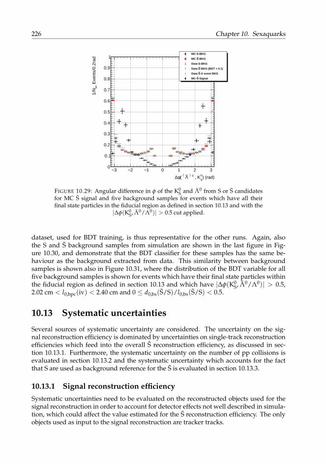
226 Chapter 10. Sexaquarks
) (rad)0
S , K0
) Λ (( φ∆
3− 2− 1− 0 1 2 3
Eve
nts/
0.2r
adev
1/N
0
0.1
0.2
0.3
0.4
0.5
0.6
0.7
0.8
0.9
1MC-S-BKG
-BKGSMC-
Data-S-BKG
-BKG (BDT < 0.1) SData-
-X event BKGSData-
-SignalSMC-
FIGURE 10.29: Angular difference in φ of the K0S and Λ0 from S or S candidates
for MC S signal and five background samples for events which have all theirfinal state particles in the fiducial region as defined in section 10.13 and with the
|∆φ(K0S, Λ0/Λ0)| > 0.5 cut applied.
dataset, used for BDT training, is thus representative for the other runs. Again, alsothe S and S background samples from simulation are shown in the last figure in Fig-ure 10.30, and demonstrate that the BDT classifier for these samples has the same be-haviour as the background extracted from data. This similarity between backgroundsamples is shown also in Figure 10.31, where the distribution of the BDT variable for allfive background samples is shown for events which have their final state particles withinthe fiducial region as defined in section 10.13 and which have |∆φ(K0
S, Λ0/Λ0)| > 0.5,2.02 cm < l0,bpc(iv) < 2.40 cm and 0 ≤ d0,bs(S/S)/l0,bs(S/S) < 0.5.
10.13 Systematic uncertainties
Several sources of systematic uncertainty are considered. The uncertainty on the sig-nal reconstruction efficiency is dominated by uncertainties on single-track reconstructionefficiencies which feed into the overall S reconstruction efficiency, as discussed in sec-tion 10.13.1. Furthermore, the systematic uncertainty on the number of pp collisions isevaluated in section 10.13.2 and the systematic uncertainty which accounts for the factthat S are used as background reference for the S is evaluated in section 10.13.3.
10.13.1 Signal reconstruction efficiencySystematic uncertainties need to be evaluated on the reconstructed objects used for thesignal reconstruction in order to account for detector effects not well described in simula-tion, which could affect the value estimated for the S reconstruction efficiency. The onlyobjects used as input to the signal reconstruction are tracker tracks.
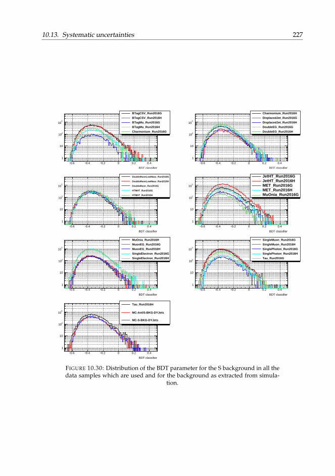
10.13. Systematic uncertainties 227
0.6− 0.4− 0.2− 0 0.2 0.4
BDT classifier
1
10
210
310
BTagCSV_Run2016G
BTagCSV_Run2016H
BTagMu_Run2016G
BTagMu_Run2016H
Charmonium_Run2016G
0.6− 0.4− 0.2− 0 0.2 0.4
BDT classifier
1
10
210
310
Charmonium_Run2016H
DisplacedJet_Run2016G
DisplacedJet_Run2016H
DoubleEG_Run2016G
DoubleEG_Run2016H
0.6− 0.4− 0.2− 0 0.2 0.4
BDT classifier
1
10
210
310
DoubleMuonLowMass_Run2016G
DoubleMuonLowMass_Run2016H
DoubleMuon_Run2016G
HTMHT_Run2016G
HTMHT_Run2016H
0.6− 0.4− 0.2− 0 0.2 0.4
BDT classifier
1
10
210
310
JetHT_Run2016G JetHT_Run2016H MET_Run2016G MET_Run2016H MuOnia_Run2016G
0.6− 0.4− 0.2− 0 0.2 0.4
BDT classifier
1
10
210
310
MuOnia_Run2016H
MuonEG_Run2016G
MuonEG_Run2016H
SingleElectron_Run2016G
SingleElectron_Run2016H
0.6− 0.4− 0.2− 0 0.2 0.4
BDT classifier
1
10
210
310
SingleMuon_Run2016G
SingleMuon_Run2016H
SinglePhoton_Run2016G
SinglePhoton_Run2016H
Tau_Run2016G
0.6− 0.4− 0.2− 0 0.2 0.4
BDT classifier
1
10
210
310
Tau_Run2016H
MC-AntiS-BKG-DYJets
MC-S-BKG-DYJets
FIGURE 10.30: Distribution of the BDT parameter for the S background in all thedata samples which are used and for the background as extracted from simula-
tion.

228 Chapter 10. Sexaquarks
BDT classifier
1− 0.8− 0.6− 0.4− 0.2− 0 0.2 0.4 0.6 0.8 1
Eve
nts/
0.05
BD
T c
lass
.ev
1/N
3−10
2−10
1−10
1
10
MC-S-BKG
-BKGSMC-
Data-S-BKG
-BKG (BDT < 0.1) SData-
-X event BKGSData-
-SignalSMC-
FIGURE 10.31: Distribution of the BDT classifier for MC S signal andthe five background samples for events which have their final state par-ticles within the fiducial region as defined in section 10.13 and whichhave |∆φ(K0
S, Λ0/Λ0)| > 0.5, 2.02 cm < l0,bpc(iv) < 2.40 cm and0 ≤ d0,bs(S/S)/l0,bs(S/S) < 0.5.
Figure 10.32 shows the distribution of six kinematic variables used here to parametrisethe tracks associated to final state particles in reconstructed S events:
• Transverse (pT) and longitudinal (pz) momentum.
• Transverse (l0) and longitudinal (vz) displacement of the track’s creation vertex withrespect to the beamspot and the absolute origin respectively.
• The impact parameters d0 and dz in the transverse and longitudinal plane respec-tively. The impact parameter is evaluated at the track’s creation vertex and calcu-lated relative to the beamspot for d0 and closest valid PV for dz, where the closestvalid PV is the valid primary vertex amongst all valid primary vertices minimisingthe dz.
These six parameters reflect what is specific for the signal tracks: low momenta, large dis-placed production and not necessarily pointing to the luminous region. These distribu-tions are important as they show the parameter space for which systematic uncertaintieson the track reconstruction efficiency has to be well controlled.
The strategy adopted here is to use a data control sample consisting of a track collec-tion which has similar properties, and for which the production process is known to bewell described at the generator level in simulation. In this way data-to-MC discrepanciesare restricted to differences in tracking reconstruction efficiencies. Such a sample is pro-vided by the tracks produced in the decay of K0
S produced in the underlying event (UE):in events where the product of the hard collision is found along one axis, the underly-ing event can be studied in the two azimuthal transversal regions defined in Figure 10.33where the ∆φ angle is calculated relative to the direction of the leading object. K0
S pro-duction in the UE is indeed known to be well described by simulation for certain Pythiatunes, as shown in Refs. [119] and [120].
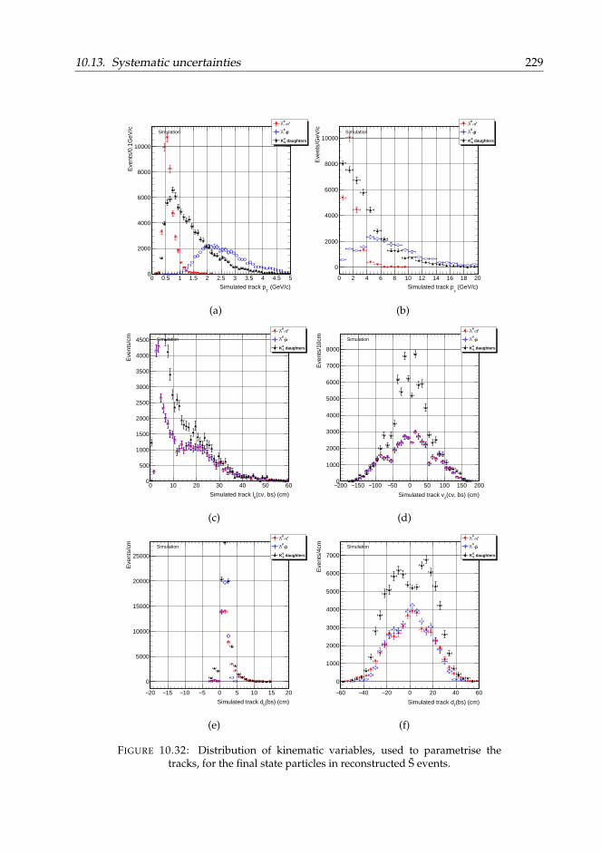
10.13. Systematic uncertainties 229
(GeV/c)T
Simulated track p
0 0.5 1 1.5 2 2.5 3 3.5 4 4.5 5
Eve
nts/
0.1G
eV/c
0
2000
4000
6000
8000
10000
+π-0
Λ
p-0
Λ
daughters 0SK
Simulation
(a)
(GeV/c)z
Simulated track p
0 2 4 6 8 10 12 14 16 18 20
Eve
nts/
GeV
/c
0
2000
4000
6000
8000
10000
+π-0
Λ
p-0
Λ
daughters 0SK
Simulation
(b)
(cv, bs) (cm)0
Simulated track l
0 10 20 30 40 50 60
Eve
nts/
cm
0
500
1000
1500
2000
2500
3000
3500
4000
4500
+π-0
Λ
p-0
Λ
daughters 0SK
Simulation
(c)
(cv, bs) (cm)zSimulated track v
200− 150− 100− 50− 0 50 100 150 200
Eve
nts/
10cm
0
1000
2000
3000
4000
5000
6000
7000
8000
+π-0
Λ
p-0
Λ
daughters 0SK
Simulation
(d)
(bs) (cm)0
Simulated track d
20− 15− 10− 5− 0 5 10 15 20
Eve
nts/
cm
0
5000
10000
15000
20000
25000
+π-0
Λ
p-0
Λ
daughters 0SK
Simulation
(e)
(bs) (cm)zSimulated track d
60− 40− 20− 0 20 40 60
Eve
nts/
4cm
0
1000
2000
3000
4000
5000
6000
7000
+π-0
Λ
p-0
Λ
daughters 0SK
Simulation
(f)
FIGURE 10.32: Distribution of kinematic variables, used to parametrise thetracks, for the final state particles in reconstructed S events.

230 Chapter 10. Sexaquarks
Eur. Phys. J. C (2016) 76:155 Page 3 of 52 155
the data-theory fitting procedure, to determine independentdirections in parameter space that provide a specific mod-ification in the goodness of the fit, χ2 (Sect. 2). All ofthe CMS UE and DPS tunes are provided with eigentunes.In Sect. 4, predictions using the CMS UE tunes are com-pared to other UE measurements not used in determiningthe tunes, and we examine how well Drell–Yan, MB, andmultijet observables can be predicted using the UE tunes.In Sect. 5, predictions of the new tunes are shown for UEobservables at 13 TeV, together with a comparison to the firstMB distribution measured. Section 6 has a brief summaryand conclusions. The appendices contain additional compar-isons between the pythia6 and herwig++ UE tunes and thedata, information about the tune uncertainties, and predic-tions for some MB and DPS observables at 13 TeV.
2 The CMS UE tunes
Previous UE studies have used the charged-particle jet withlargest pT [24,25] or a Z boson [11,26] as the leading (i.e.highest pT) objects in the event. The CDF and CMS data,used for the tunes, select the charged particle with largestpT in the event (pmax
T ) as the “leading object”, and use justthe charged particles with pT > 0.5 GeV and |η| < 0.8 tocharacterize the UE.
On an event-by-event basis, the leading object is used todefine regions of pseudorapidity-azimuth (η-φ) space. The“toward” region relative to this direction, as indicated inFig. 1, is defined by |∆φ| < π/3 and |η| < 0.8, and the“away” region by |∆φ| > 2π/3 and |η| < 0.8. The charged-particle and the scalar-pT sum densities in the transverseregion are calculated as the sum of the contribution in the tworegions: “Transverse-1” (π/3 < ∆φ < 2π/3, |η| < 0.8) and
“Transverse-2” (π/3 < −∆φ < 2π/3, |η| < 0.8), dividedby the area inη-φ space,∆η∆φ = 1.6×2π/3. The transverseregion is further separated into the “TransMAX” and “Trans-MIN” regions, also shown in Fig. 1. This defines on an event-by-event basis the regions with more (TransMAX) and fewer(TransMIN) charged particles (Nch), or greater (TransMAX)or smaller (TransMIN) scalar-pT sums (psum
T ). The UE par-ticle and pT densities are constructed by dividing by the areain η-φ space, where the TransMAX and TransMIN regionseach have an area of ∆η∆φ = 1.6 × 2π/6. The transversedensity (also referred to as “TransAVE”) is the average of theTransMAX and the TransMIN densities. For events with hardinitial- or final-state radiation, the TransMAX region oftencontains a third jet, but both the TransMAX and TransMINregions receive contributions from the MPI and beam-beamremnant components. The TransMIN region is very sensitiveto the MPI and beam-beam remnant components of the UE,while “TransDIF” (the difference between TransMAX andTransMIN densities) is very sensitive to ISR and FSR [27].
The new UE tunes are determined by fitting UE observ-ables, and using only those parameters that are mostsensitive to the UE data. Since it is not possible to tune allparameters of a MC event generator at once, the parame-ters that affect, for example, the parton shower, the frag-mentation, and the intrinsic-parton pT are fixed to the valuesgiven by an initially established reference tune. The initialreference tunes used for pythia8 are Tune 4C [28] and theMonash Tune [29]. For pythia6, the reference tune is TuneZ2*lep [25], and for herwig++ it is Tune UE-EE-5C [30].
2.1 The PYTHIA8 UE tunes
Taking as the reference tune the set of parameters ofpythia8 Tune 4C [28], we construct two new UE tunes,
Fig. 1 Left Illustration of theazimuthal regions in an eventdefined by the ∆φ angle relativeto the direction of the leadingobject [11]. Right Illustration ofthe topology of a hadron–hadroncollision in which a hardparton–parton collision hasoccurred, and the leading objectis taken to be the chargedparticle of largest pT in theevent, pmax
T
123
FIGURE 10.33: Definition of the azimuthal regions with respect to the leadingobject in the event [121]. The transversal regions are indicated in green.
The leading object in Figure 10.33 can be a Z boson. We use the 2016 RunG andRunH DoubleMuon dataset to reconstruct events with Drell-Yan (DY) Z production andwill compare the tracks from K0
S decay products in the UE to the same track collectionobtained from DYJets MC simulation. The latter MC sample was produced with Pythia8,TuneCUETP8M1-amcatnloFXFX. This approach has the advantage that in DY Z produc-tion the leading object and thus the UE are straightforwardly defined. Considering K0
Sproduced in the UE provides a sample of K0
S, and thus decay products, which are kine-matically similar for data and simulation.
For the Z reconstruction, only TightMuons are used with a pT > 20 GeV/c, |η| < 2.4and a longitudinal impact parameter within 0.01 cm from the z location of the first PV.Furthermore, the muons need to satisfy the isolation requirement as in Equation (10.13),where a cone of ∆R = 0.4 is built around the muons to compute the flux of particle flowcandidates. In Equation (10.13), Ich is the sum of the pT of the charged hadrons in thecone, Inh the sum of the transverse energy (ET) of the neutral hadrons in the cone, Ig thesum of the ET of the photons in the cone and IchPU the sum of the pT of charged particlesin the cone from particles not originating from the primary vertex.
Iµrel =
1pT
(Ich + max(Inh + Ig − 0.5 · IchPU, 0)) < 0.15. (10.13)
Event selection is performed by requiring both data and MC simulated events to passone of the below triggers:
• HLT_Mu17_TrkIsoVVL_Mu8_TrkIsoVVL_DZ
• HLT_Mu17_TrkIsoVVL_TkMu8_TrkIsoVVL_DZ.
Z candidates are then formed from oppositely charged muons of which the invariantmass has to lie within ± 7.5 GeV/c2 from the known Z mass [10]. Events where morethan 2 LooseMuons are found are vetoed. The underlying event is defined here by lookingat activity in the transversal region with respect to the Z: the two regions which have anazimuthal angular difference larger than π/3 from both the Z and back-to-back directionof the Z. Only K0
S in this transversal region are considered. Furthermore it is requestedthat no jet activity is seen in this transversal region by requiring no jets with energy larger
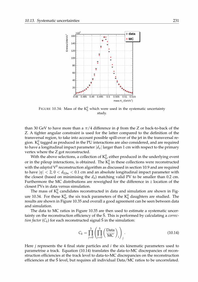
10.13. Systematic uncertainties 231
)2 (GeV/csmass K
0.48 0.485 0.49 0.495 0.5 0.505 0.51 0.515
2E
ntrie
s/1M
eV/c
0
20
40
60
80
100
120
140
160
310× data
MC
FIGURE 10.34: Mass of the K0S which were used in the systematic uncertainty
study.
than 30 GeV to have more than a π/4 difference in φ from the Z or back-to-back of theZ. A tighter angular constraint is used for the latter compared to the definition of thetransversal region, to take into account possible spill-over of the jet in the transversal re-gion. K0
S tagged as produced in the PU interactions are also considered, and are requiredto have a longitudinal impact parameter |dz| larger than 1 cm with respect to the primaryvertex where the Z got reconstructed.
With the above selections, a collection of K0S, either produced in the underlying event
or in the pileup interactions, is obtained. The K0S in these collections were reconstructed
with the adapted V0 reconstruction algorithm as discussed in section 10.9 and are requiredto have |η| < 2, 0 < d0,bs < 0.1 cm and an absolute longitudinal impact parameter withthe closest (based on minimising the dz) matching valid PV to be smaller than 0.2 cm.Furthermore the MC distributions are reweighed for the difference in z location of theclosest PVs in data versus simulation.
The mass of K0S candidates reconstructed in data and simulation are shown in Fig-
ure 10.34. For these K0S, the six track parameters of the K0
S daughters are studied. Theresults are shown in Figure 10.35 and overall a good agreement can be seen between dataand simulation.
The data to MC ratios in Figure 10.35 are then used to estimate a systematic uncer-tainty on the reconstruction efficiency of the S. This is performed by calculating a correc-tion factor (Ck) for each reconstructed signal S in the simulation:
Ck =3
∏j=0
(5
∏i=0
(DataMC
)i
)j
. (10.14)
Here j represents the 4 final state particles and i the six kinematic parameters used toparametrise a track. Equation (10.14) translates the data-to-MC discrepancies of recon-struction efficiencies at the track level to data-to-MC discrepancies on the reconstructionefficiencies at the S level, but requires all individual Data/MC ratios to be uncorrelated.

232 Chapter 10. Sexaquarks
(GeV)t
daughter 1 and 2 track ps K0 1 2 3 4 5 6 7 8 9
Dat
a/M
C
0.5
1
1.5
(GeV)t
daughter 1 and 2 track ps K0 1 2 3 4 5 6 7 8 9
Ent
ries/
GeV
210
310
410
510
610
710 MC
data
(a)
(GeV)z
daughter 1 and 2 track ps K40− 30− 20− 10− 0 10 20 30
Dat
a/M
C
0.5
1
1.5
(GeV)z
daughter 1 and 2 track ps K
40− 30− 20− 10− 0 10 20 30
Ent
ries/
GeV
1
10
210
310
410
510
610 MC
data
(b)
(cm)0,bs
daughter 1 and 2 track lsK0 10 20 30 40 50 60 70 80
Dat
a/M
C
0.5
1
1.5
(cm)
0,bs daughter 1 and 2 track lsK
0 10 20 30 40 50 60 70 80
Ent
ries/
cm
10
210
310
410
510
MC
data
(c)
(cm)z
daughter 1 and 2 absolute track vsK150− 100− 50− 0 50 100
Dat
a/M
C
0.5
1
1.5
(cm)
z daughter 1 and 2 absolute track vsK
150− 100− 50− 0 50 100
Ent
ries/
cm
10
210
310
410
510MC
data
(d)
(cm) 0,bs
daughter 1 and 2 track dsK0 2 4 6 8 10 12 14 16
Dat
a/M
C
0.5
1
1.5
(cm) 0,bs
daughter 1 and 2 track dsK0 2 4 6 8 10 12 14 16
Ent
ries/
cm
210
310
410
510
610
MC
data
(e)
) (cm) s
(best PV Kz
daughter 1 and 2 track dsK40− 30− 20− 10− 0 10 20 30 40
Dat
a/M
C
0.5
1
1.5
) (cm) s
(best PV Kz
daughter 1 and 2 track dsK
40− 30− 20− 10− 0 10 20 30 40
Ent
ries/
cm
1
10
210
310
410
510
610 MC
data
(f)
FIGURE 10.35: Data-MC ratios for several kinematic track parameters used in thesystematic uncertainty study on tracking efficiencies.
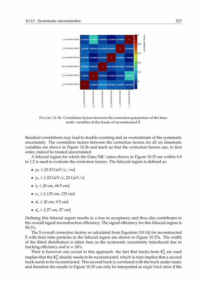
10.13. Systematic uncertainties 233
1 -0.025642 0.0837424 0.0287896 0.024785 -0.0114323
-0.025642 1 -0.0082606 -0.118562 0.0035132 0.257642
0.0837424 -0.0082606 1 -0.001794220.0134999 -0.0298962
0.0287896 -0.118562-0.00179422 1 0.0256683 -0.161948
0.024785 0.0035132 0.0134999 0.0256683 1 -0.0196822
-0.0114323 0.257642 -0.0298962 -0.161948 -0.0196822 1
cor
rect
ion
fact
ortp
cor
rect
ion
fact
orzp
cor
rect
ion
fact
or0d
cor
rect
ion
fact
orzd
cor
rect
ion
fact
or0l
cor
rect
ion
fact
orz
v
correction factort
p
correction factorz
p
correction factor0d
correction factorzd
correction factor0l
correction factorzv
0
0.2
0.4
0.6
0.8
1
corr
elat
ion
fact
or
FIGURE 10.36: Correlation factors between the correction parameters of the kine-matic variables of the tracks of reconstructed S.
Residual correlations may lead to double counting and an overestimate of the systematicuncertainty. The correlation factors between the correction factors for all six kinematicvariables are shown in Figure 10.36 and teach us that the correction factors can, to firstorder, indeed be treated uncorrelated.
A fiducial region for which the Data/MC ratios shown in Figure 10.35 are within 0.8to 1.2 is used to evaluate the correction factors. The fiducial region is defined as:
• pT ∈ [0.33 GeV/c, +∞[
• pz ∈ [-22 GeV/c, 22 GeV/c]
• l0 ∈ [0 cm, 44.5 cm]
• vz ∈ [-125 cm, 125 cm]
• d0 ∈ [0 cm, 9.5 cm]
• dz ∈ [-27 cm, 27 cm]
Defining this fiducial region results in a loss in acceptance and thus also contributes tothe overall signal reconstruction efficiency. The signal efficiency for this fiducial region is58.3%.
The S overall correction factors as calculated from Equation (10.14) for reconstructedS with final state particles in the fiducial region are shown in Figure 10.37a. The widthof the fitted distribution is taken here as the systematic uncertainty introduced due totracking efficiency and is ≈ 24%.
Their is however one caveat to this approach: the fact that tracks from K0S are used
implies that the K0S already needs to be reconstructed, which in turn implies that a second
track needs to be reconstructed. This second track is correlated with the track under studyand therefore the results in Figure 10.35 can only be interpreted as single track ratios if the
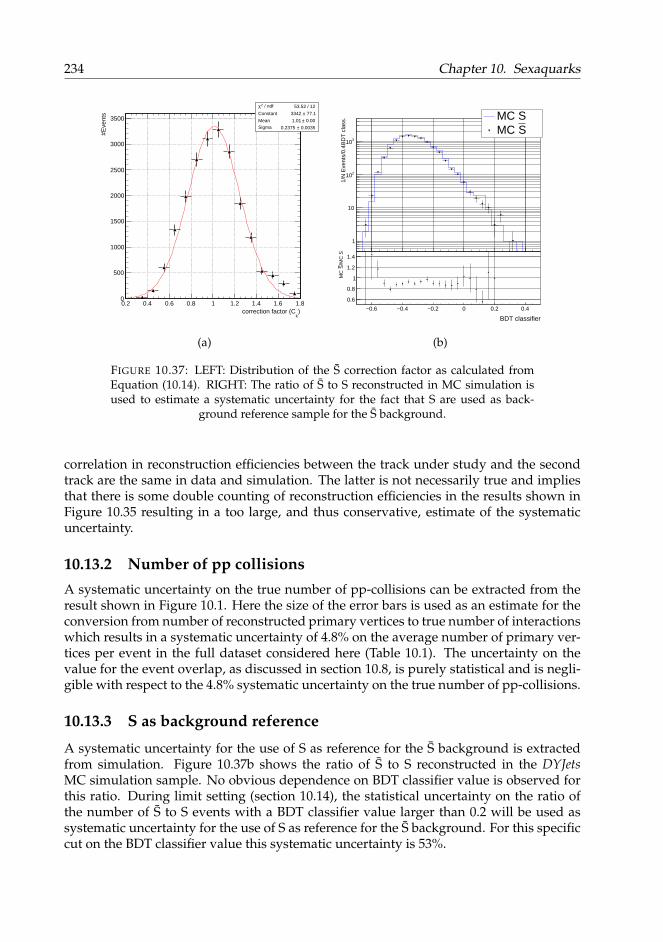
234 Chapter 10. Sexaquarks
/ ndf 2χ 53.52 / 12
Constant 77.1± 3342
Mean 0.00± 1.01 Sigma 0.0035± 0.2375
0.2 0.4 0.6 0.8 1 1.2 1.4 1.6 1.8)
kcorrection factor (C
0
500
1000
1500
2000
2500
3000
3500
#Eve
nts
/ ndf 2χ 53.52 / 12
Constant 77.1± 3342
Mean 0.00± 1.01 Sigma 0.0035± 0.2375
(a)
0.6− 0.4− 0.2− 0 0.2 0.4
BDT classifier
0.6
0.8
1
1.2
1.4
/MC
SS
MC
BDT classifier
1
10
210
310
1/N
Eve
nts/
0.4B
DT
cla
ss. MC S
SMC
(b)
FIGURE 10.37: LEFT: Distribution of the S correction factor as calculated fromEquation (10.14). RIGHT: The ratio of S to S reconstructed in MC simulation isused to estimate a systematic uncertainty for the fact that S are used as back-
ground reference sample for the S background.
correlation in reconstruction efficiencies between the track under study and the secondtrack are the same in data and simulation. The latter is not necessarily true and impliesthat there is some double counting of reconstruction efficiencies in the results shown inFigure 10.35 resulting in a too large, and thus conservative, estimate of the systematicuncertainty.
10.13.2 Number of pp collisionsA systematic uncertainty on the true number of pp-collisions can be extracted from theresult shown in Figure 10.1. Here the size of the error bars is used as an estimate for theconversion from number of reconstructed primary vertices to true number of interactionswhich results in a systematic uncertainty of 4.8% on the average number of primary ver-tices per event in the full dataset considered here (Table 10.1). The uncertainty on thevalue for the event overlap, as discussed in section 10.8, is purely statistical and is negli-gible with respect to the 4.8% systematic uncertainty on the true number of pp-collisions.
10.13.3 S as background reference
A systematic uncertainty for the use of S as reference for the S background is extractedfrom simulation. Figure 10.37b shows the ratio of S to S reconstructed in the DYJetsMC simulation sample. No obvious dependence on BDT classifier value is observed forthis ratio. During limit setting (section 10.14), the statistical uncertainty on the ratio ofthe number of S to S events with a BDT classifier value larger than 0.2 will be used assystematic uncertainty for the use of S as reference for the S background. For this specificcut on the BDT classifier value this systematic uncertainty is 53%.

10.14. Limit setting and results 235
10.14 Limit setting and results
10.14.1 Limit setting introduction
If no significant S signal excess is observed, an upper limit can still be placed on [σ(pp→S)× σ(S + n → K0
S + Λ0)], referred to in the following loosely as the signal cross section.This limit setting is performed by comparing the background only hypothesis with thesignal plus background hypothesis for a certain discriminating variable. A test statistic isbuilt using this variable and the distribution of this test statistic is obtained by generatingpseudo-experiments for the signal plus background and background only hypothesis, or,in case the number of background events is large, by using the asymptotic approximation[122].
In order to then obtain an upper limit, at a certain confidence level (CL), on the signalcross section, the CLs method [123] is used. The LHC test statistic [124], which is usedhere, is defined as:
qµ = −2 lnL(data |µ, θµ
)L(data |µ, θ)
, with constraint : 0 ≤ µ ≤ µ, (10.15)
with L the likelihood, µ the signal strength, θ representing the full suite of nuisanceparameters, θµ the maximum likelihood estimator of θ for a given µ and (pseudo) data,and the pair of parameter estimators µ and θ correspond to the global maximum of thelikelihood. The expected number of events in a certain bin i with si signal events andbi background events is given by: µsi + bi. With this definition, µ = 1 corresponds tothe signal plus background hypothesis with the nominal cross section and µ = 0 to thebackground only hypothesis.
Two p-values ps+b and pb are now defined for an observation qobsµ :
ps+b =∫ ∞
qobsµ
f(
qµ|µ, θobsµ
)dqµ, (10.16)
1− pb =∫ ∞
qobsµ=0
f(
qµ|µ = 0, θobsµ=0
)dqµ, (10.17)
with f(
qµ|µ, θobsµ
)and f
(qµ|µ = 0, θobs
µ=0
)respectively the probability density function
of the test statistic qµ for the signal plus background hypothesis and background onlyhypothesis as constructed from the pseudo-experiments with the nuisance parameters,best describing the experimentally observed data, fixed to θobs
µ (signal+background) andθobs
µ=0 (background-only). The signal is then excluded at 1 - α confidence level if
CLs =ps+b
1− pb≤ α. (10.18)
When extracting an upper limit at 95% CL the smallest signal strength is searched forwhich has CLs ≤ 0.05. The signal cross section corresponding to this signal strength isthen quoted as the upper limit on the signal cross section.
To accomplish the limit evaluation the Higgs Combine Tool [125] is used which imple-ments the above method, and is the common approach in CMS for limit evaluation.
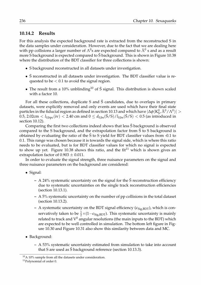
236 Chapter 10. Sexaquarks
10.14.2 ResultsFor this analysis the expected background rate is extracted from the reconstructed S inthe data samples under consideration. However, due to the fact that we are dealing herewith pp collisions a larger number of Λ0s are expected compared to Λ0 s and as a resultmore S background is expected compared to S background. This is shown in Figure 10.38where the distribution of the BDT classifier for three collections is shown:
• S background reconstructed in all datasets under investigation.
• S reconstructed in all datasets under investigation. The BDT classifier value is re-quested to be < 0.1 to avoid the signal region.
• The result from a 10% unblinding10 of S signal. This distribution is shown scaledwith a factor 10.
For all these collections, duplicate S and S candidates, due to overlaps in primarydatasets, were explicitly removed and only events are used which have their final stateparticles in the fiducial region as defined in section 10.13 and which have |∆φ(K0
S, Λ0/Λ0)| >0.5, 2.02cm < l0,bpc(iv) < 2.40 cm and 0 ≤ d0,bs(S/S)/l0,bs(S/S) < 0.5 (as introduced insection 10.12).
Comparing the first two collections indeed shows that less S background is observedcompared to the S background, and the extrapolation factor from S to S background isobtained by evaluating the ratio of the S to S yield for BDT classifier values from -0.1 to0.1. This range was chosen because it is towards the signal side, which is where this rationeeds to be evaluated, but is for BDT classifier values for which no signal is expectedto show up yet. Figure 10.38 shows this ratio, and the fit11 which is shown gives anextrapolation factor of 0.903 ± 0.011.
In order to evaluate the signal strength, three nuisance parameters on the signal andthree nuisance parameters on the background are considered:
• Signal:
– A 24% systematic uncertainty on the signal for the S reconstruction efficiencydue to systematic uncertainties on the single track reconstruction efficiencies(section 10.13.1).
– A 5% systematic uncertainty on the number of pp collisions in the total dataset(section 10.13.2).
– A systematic uncertainty on the BDT signal efficiency (εSig,BDT), which is con-servatively taken to be 1
2×(1−εSig,BDT). This systematic uncertainty is mainlyrelated to track and V0 angular resolutions (the main inputs to the BDT) whichare expected to be well controlled in simulation. The bottom left figure in Fig-ure 10.30 and Figure 10.31 also show this similarity between data and MC.
• Background:
– A 53% systematic uncertainty estimated from simulation to take into accountthat S are used as S background reference (section 10.13.3).
10A 10% sample from all the datasets under consideration.11Polynomial of order 0.

10.14. Limit setting and results 237
0.6− 0.4− 0.2− 0 0.2 0.4 BDT classifier
0.6
0.8
1
1.2
1.4
/dat
a S
Sda
ta BDT classifier
1
10
210
310
410
1/N
Eve
nts/
0.2
BD
T c
lass
.
data S
BDT class. < 0.1 Sdata
x 10 Sdata
FIGURE 10.38: Distribution of the BDT classifier for: S reconstructed in alldatasets under consideration, S with a BDT classifier value < 0.1 reconstructed inall datasets under consideration and S with a BDT classifier value > 0.1 for 10%of the datasets under consideration. The latter distribution was scaled with a fac-tor 10. Duplicate S and S, due to overlaps in datasets, were explicitly removed.Only events are shown which have their final state particles within the fidu-cial region as defined in section 10.13 and which have |∆φ(K0
S, Λ0/Λ0)| > 0.5,2.02 cm < l0,bpc(iv) < 2.40 cm and 0 ≤ d0,bs(S/S)/l0,bs(S/S) < 0.5.

238 Chapter 10. Sexaquarks
– A systematic uncertainty on the extrapolation factor from S background to Sbackground. This systematic uncertainty is evaluated by fitting the ratio inFigure 10.38 with a polynomial of order 1 for BDT classifier values from -0.1to 0.1 and taking the relative difference between the polynomial of order 0 fit(shown in Figure 10.38) and polynomial of order 1 fit at a BDT classifier valueof 0.35 as uncertainty on events in the eventually selected signal region (BDT> 0.35). As the background is steeply falling, most events are expected justabove that threshold. This introduces an 8% systematic uncertainty.
– A nuisance parameter which takes into account the limited statistics in the Sdata control sample used to estimate the S background. This nuisance param-eter is thus dependent on where the cut on the BDT classifier value is placed.
These nuisance parameters, as well as expected signal and background rates serve asinput to the combine tool which provides an upper limit on the signal strength r:
r =number of signal events
number of expected signal events. (10.19)
The signal strength is evaluated for a range of cuts on the BDT classifier value and theresult is shown in Figure 10.39. For this specific result an arbitrary number of 100 eventswas used as the signal rate. This signal rate scales with the signal cross section.
A cut on the BDT classifier value of 0.35 is chosen in order to maximize the sensitivityof the search. At this BDT classifier value, the expected number of background events is6.3 ± 2.5 (stat) ± 0.5 (syst), the BDT signal efficiency is 51% and the expected upper limiton the signal strength is 0.21. The expected upper limit on the number of signal events isthus 10.9+6.1
−3.3.An expected upper limit on [σ(pp→ S)× σ(S+ n→ K0
S + Λ0)] can now be extracted,expressing the upper limit on the product of the S production cross section in LHC ppcollisions and the cross section of S particles from such pp collisions producing a K0
S-Λ0
pair in an interaction with a neutron in material at rest, for S with a mass of 1.8 GeV/c2.The expected upper limit on this product of cross sections is calculated as introduced insection 10.7:
[σ(pp→ S)× σ(S + n→ K0s + Λ0)]UL
exp
=NUL
expNev×<PU>×(1−C)
σpp× εreco × εfid × εBkgCuts × Nn
, (10.20)
with NULexp the expected upper limit on the number of signal events after all selection cuts,
Nev the total number of pp-interactions in the considered dataset, <PU> the averagepileup in this dataset, C the overlap rate between datasets, σpp the proton-proton inelasticcross section, εreco the S reconstruction efficiency, εfid the signal efficiency for the fiducialregion defined in section 10.13, εBkgCuts the efficiency with which the S candidates survivethe background cuts and Nn the neutron column density of the beampipe for η = 0 12.
12The value at η = 0 must be used here, as reweighing for the S path length through the beampipe wasalready performed in the reconstruction efficiency calculation.

10.14. Limit setting and results 239
0 0.1 0.2 0.3 0.4 0.5 BDT classifier cut
1
10
Exp
ecte
d lim
it on
sig
nal s
tren
gth
(r)
FIGURE 10.39: Expected limits on the signal strength for several cut values onthe BDT classifier value.
NULexp 10.9
Number of pp-collisions (Nev) 2.007× 10⁹
Average pileup (<PU>) 21.4Dataset overlap rate (C) 12.84%pp inelastic cross section (σpp) 70 mbSignal reconstruction efficiency (εreco) 0.0014%Signal efficiency for fiducial region systematic uncertainty (εfid) 58.3%Efficiency of signal for background suppression (εBkgCuts) 48.2%Neutron column density of CMS beampipe (Nn) 4.97 × 10⁻⁵mb−1
TABLE 10.5: Summary of values used in Equation (10.20) to calculate the ob-served limit.
This neutron column density is given by:
Nn =Nneutron,Be × ρBe × d
mBe
=5× 1.85× 10−3 kg
cm3 × 0.08 cm
14.9× 10⁻²⁷ kg= 4.97× 10⁻⁵ mb−1, (10.21)
with Nneutron,Be the number of neutrons in a beryllium nucleus, ρBe the mass density ofberyllium, d the thickness of the beampipe and mBe the mass of a beryllium nucleus.
The values listed in Table 10.5 are used to calculate the expected upper limit. Thevalue for εBkgCuts shown in this table also takes into account the 94.4% combined sig-nal efficiency for the three background cuts applied before the BDT. This results in anexpected upper limit on [σ(pp→ S)× σ(S + n→ K0
S + Λ0)] of 105+57.8−32.4 mb2.
For a partial unblinding, 10% of the studied dataset was used to extract an observedupper limit on [σ(pp → S) × σ(S + n → K0
S + Λ0)]. At a BDT classifier value cut of0.35, with an expected background rate of 0.632 ± 0.795 (stat) ± 0.051 (syst), a similarcalculation as performed for the expected limit with the full dataset results in an expectedlimit on [σ(pp → S)× σ(S + n → K0
S + Λ0)] of 309+273−136 mb2. The observed background

240 Chapter 10. Sexaquarks
for this requirement on the BDT classifier value is 0 and the observed limit on the productof cross sections is calculated to be 237 mb2.
10.15 Summary and outlook
Sexaquarks were proposed in Ref. [88] as a strongly bound state of six quarks. If its massis in the correct range, the S is a dark matter candidate. CMS, with its excellent trackingdetector, and the high luminosity provided by the LHC present an attractive possibilityto search for this elusive particle.
The strategy adopted in this first-ever Sexaquark search at the LHC, was to look for Sproduced in pp collisions and annihilating on neutrons in the CMS beampipe, resultingin the production of Λ0 and K0
S:
S + n→ Λ0 + K0S → p + π+ + π− + π+. (10.22)
The final state particles in this channel can be reconstructed with the CMS tracker. Thevertex of the V0s gives the annihilation vertex and the invariant mass of the S can beapproximately reconstructed.
The search strategy which was adopted for this signal is non-standard compared totypical CMS analyses, for the following reasons:
• The S needs to be produced and subsequently needs to annihilate on material. Asa result, the combination of the production cross section and the annihilation crosssection are probed.
• The fact that the S first needs to travel from its production vertex before it can in-teract with material and the fact that the K0
S and Λ0 have decay lengths of a fewcentimetres implies that the final state particles are displaced. This is not beneficialfor the track reconstruction, which in CMS is optimised for particles produced inthe luminous region. On top of that, the majority of the S are produced forwardand the signal is furthermore enhanced in the forward region due to the increase ofthe S path length through the beampipe.
• Due to the low momenta of the final state particles, no dedicated trigger is availablefor this signal. The S was therefore searched for in all existing datasets, where inparticular the production of S in pileup interactions was considered.
The special signal topology required a dedicated signal simulation to develop thesearch strategy and to estimate the signal reconstruction efficiency. To do so, the S-neutron interaction was added to the CMS simulation framework. For this simulationand the rest of the work an S with a mass of 1.8 GeV/c2 was investigated. An important,non intuitive, result from this simulation is that the Fermi momentum of the target neu-tron has a significant effect on the reconstructed invariant mass of the S. This essentiallymeans that, despite accurate reconstruction of the final state products, no sharp S invari-ant mass peak can be extracted for this channel. On the plus side, it was shown that thelocation of the neutron-S annihilation vertex can be reconstructed with O(mm) accuracy,which is not straightforward as it requires the vertexing of two neutral particles.
Using an adequate signal simulation, it was shown that the reconstruction efficiencyfor this signal is very low, and estimated to be 0.0014%. Both acceptance and reconstruc-tion effects contribute to this inefficiency, where for the latter the soft pion in the Λ0 decayproved to be a bottleneck for the reconstruction.
10.15. Summary and outlook 241
The background study for this signal showed that S candidates can be used as refer-ence sample for the S background. Furthermore, the origin of the background was foundto be combinatorial. This was proven by reconstructing S candidates combining K0
S andΛ0 from different events. Thanks to the special topology of this signal, the backgroundcould very efficiently be eliminated using three background rejection cuts and a multi-variate classifier.
An expected upper limit (at 95% CL) on [σ(pp → S) × σ(S + n → K0S + Λ0)] was
extracted and found to be 105+57.8−32.4 mb2. This expresses the upper limit on the product
of the S production cross section in LHC pp collisions and the cross section of S parti-cles from such pp collisions producing a K0
S-Λ0 pair in an interaction with a neutron inmaterial at rest, for S with a mass of 1.8 GeV/c2. A 10% unblinding of the dataset underconsideration did not lead to the observation of any signal and an observed upper limit(at 95% CL) on the product of cross sections was set at 237 mb2.
Mainly due to the inefficient signal reconstruction, this analysis does not provide theneeded sensitivity to exclude or confirm the existence of the S. Indeed, in Ref. [88], Farrarestimates the S production cross section to be at most 10−4 of the pion production crosssection. From EPOS-LHC simulations, normalised to the charged hadron yield presentedin Ref. [126], the expected average charged pion yield in one pp collision is ≈ 80 over thefull η range. Furthermore, Farrar projects the S-neutron interaction cross section to beat most 10−6σpp for proton lab momenta in the 10 GeV range. In this momentum rangeσpp is around 40 mb. This leads to a product of production and interaction cross sectionswhich is at most: 80× 70 mb× 10−4 × 40 mb× 10−6 = 2.24× 10⁻⁵ mb2. This shows thatthe observed limit, extracted from this search, is not sensitive for the considered S model.
By considering Equation (10.20), several optimisations can be envisaged to make thissearch more sensitive: more data can be used, the reconstruction efficiency can be im-proved, and the search region could be extended from the beampipe volume to includeS production on detector material as well.
The use of the full 2015, 2016, 2017, 2018 and B-parking [127] dataset would result inan estimated O(200) increase13 in the number of pp interactions. It is clear that simplyusing more data will not bring the large improvement which is required to make thisanalysis competitive. The effect of the upgraded pixel detector on acceptance and recon-struction efficiency in 2017 and 2018 data should however be evaluated. Track seedingbeing possible up to larger radii and longitudinal displacement due to the extra detectorlayers could have a significant effect.
The largest sensitivity gain could be achieved by improving the signal reconstructionefficiency. Whilst a significant inefficiency due to acceptance in the forward region seemsinevitable, dedicated tracking algorithms for highly displaced low momentum tracks orV0s could be developed to augment the reconstruction efficiency for events within accep-tance. A complication for these algorithms can be foreseen in performant seeding at highdisplacement, which relies on stereo-modules in the standard CMS track reconstruction.On the plus side, the high displacement for this signal implies that the track reconstruc-tion for the final state particles in this search is performed in a region of the tracker wherethe track occupancy is modest compared to the region closer to the luminous region. Theimplications of modified track reconstruction on track fake rates should of course be eval-uated. Efficiently discriminating the background from the signal, as was possible in thissearch, might become challenging.
13Taking into account that only 10% of 2016 Run G and RunH data was used for the partial unblindingperformed here.
242 Chapter 10. Sexaquarks
A third approach to boost the sensitivity would be to include more material to searchfor S annihilation on neutrons. Considering also S annihilation on for example the pixeldetector and its services would have a significant impact on the Nn factor in Equation (10.20).Furthermore, for this type of more central events the inefficiency due to detector accep-tance will implicitly be reduced. Including the pixel detector layers could increase thematerial budget, in terms of nuclear interaction lengths, with a factor O(10) [128]. Lowerreconstruction efficiency due to the potential loss of these detector layers for seeding andtracking of course needs to be evaluated, but even for the standard CMS track recon-struction, this loss seems to be manageable as illustrated by the top left figures in FigureD.2-D.4.
It is hard to predict if the improvements described above could push the sensitivityinto the required range. From the performed analysis it is clear that a dedicated signalsimulation is required to evaluate the reconstruction efficiency for a convoluted signal asthe one investigated here.
For LHC Run 3, it could be considered to design a dedicated HLT trigger for this signalwhich could exploit the displacement of this signal and/or use the HLT pixel trackingwhich will come online for Run 3. If the latter is feasible, an increase of a factor 100 in thedata sample could be envisaged if the HLT trigger could be run for each L1 event.
Looking even more ahead, the prospect of the Phase-2 upgrade of the CMS trackingsystem could add a significant improvement on both the signal acceptance and the track-ing efficiency. Indeed, as shown in Figure 4.10, the η range of the current pixel detectorand its z coverage will be significantly enlarged. This, together with the vast volumeequipped with PS modules (see Figure 5.6), will essentially allow more continuous trackseeding up to much larger radii and z. Furthermore, the higher luminosity will providea larger dataset to look for this signal, but without a dedicated trigger the increase inluminosity will not provide the needed gain.
Other completely different search strategies might also be considered for future Sex-aquark searches. Strategies where the production of S or S can be probed in a direct wayrather than through the succession of production and annihilation are favoured. The lat-ter after all adds an estimated factor 10−6 to the product of production and annihilationcross section. A discovery channel which does not have this limitation is the one de-scribed in section 10.6.1, where the S and S could be searched for in the decay of the Υ.This search furthermore has the advantage that the invariant missing-mass peak is notpolluted by the target neutron’s Fermi motion as is the case for the channel investigatedhere. The search performed by BABAR, described in Ref. [108], could be extended tomore inclusive channels14. The latter is indeed a necessity if a narrow missing-mass peakneeds to be extracted. A search at Belle II, taking advantage of the higher luminositycompared to BABAR and Belle, might also be warranted. Of course, the projected factor50 in integrated luminosity for Belle II compared to Belle will only be attained by 2025.
10.16 Author’s contribution
The author was the main developer for this analysis. The author evaluated the recon-struction algorithm for V0s and developed the reconstruction of S and S objects. Startingfrom the EPOS-LHC package, a signal simulation was set up by the author which in-cluded the addition of the neutron-S interaction in GEANT and a method to efficiently
14Υ→S Λ0 Λ0 X instead of Υ→S Λ0 Λ0.

10.16. Author’s contribution 243
simulate the S low interaction cross section. The author then used this simulation to esti-mate the signal reconstruction efficiency. Subsequently the author performed a study ofthe background to be able to suppress it in the most efficient way and to set a limit on[σ(pp→ S)× σ(S + n→ K0
S + Λ0)] with an evaluation of the systematic uncertainties.


245
App
endi
xA
MPA
and
SSA
SEU
cros
sse
ctio
ns
This
appe
ndix
prov
ides
the
raw
data
from
the
MPA
and
SSA
SEU
test
desc
ribe
din
sect
ion
8.4.
A.1
SSA
high
late
ncy
Ion
Ang
leEf
fect
ive
LET
Flue
nce
Dur
a-ti
onSE
Uco
unte
r
Dur
a-ti
onFu
ll-ev
ent
Dur
a-ti
onst
ub
Lat-
ency
Full-
even
tEr
ror
Ups
et
Stub
Erro
rFu
ll-ev
entS
EUcr
oss
sect
ion
Erro
rfu
ll-ev
entS
EUcr
oss
sect
ion
Stub
SEU
cros
sse
ctio
n
Erro
rSt
ubSE
Ucr
oss
sect
ion
[]
[MeV
/(m
g/cm
2 )]
[par
t/s×
cm2 ]
[s]
[s]
[s]
[#of
cycl
es]
[#]
[#]
[cm
2 ][c
m2 ]
[cm
2 ][c
m2 ]
13C
4+0
1.3
1422
030
240
240
500
13
2.93
015E
-07
2.93
024E
-07
8.79
044E
-07
5.07
567E
-07
22N
e7+
03.
314
986
3024
024
050
017
134.
7266
3E-0
61.
1469
8E-0
63.
6144
8E-0
61.
0028
8E-0
627
Al8
+0
5.7
1200
030
600
600
500
2012
2.77
778E
-06
6.21
578E
-07
1.66
667E
-06
4.81
334E
-07
40A
r10+
010
1525
830
240
240
500
3829
1.03
771E
-05
1.68
531E
-06
7.91
934E
-06
1.47
187E
-06
40A
r10+
3011
.513
339
3021
021
050
021
327.
4968
1E-0
61.
6372
9E-0
61.
1423
7E-0
52.
0219
9E-0
658
Ni1
8+0
20.4
1471
630
210
210
500
5040
1.61
793E
-05
2.29
204E
-06
1.29
435E
-05
2.04
936E
-06
84K
r25+
032
.415
870
3024
024
050
082
812.
1529
1E-0
52.
3830
5E-0
62.
1266
5E-0
52.
3684
E-06
84K
r25+
3037
.413
613
3024
024
050
013
067
3.97
904E
-05
3.50
599E
-06
2.05
074E
-05
2.51
135E
-06
103R
h31+
045
.815
553
3018
018
050
085
743.
0362
1E-0
53.
3033
3E-0
62.
6432
9E-0
53.
0809
6E-0
610
3Rh3
1+30
52.9
1422
630
240
210
500
166
104
4.86
199E
-05
3.79
449E
-06
3.48
122E
-05
3.42
639E
-06
124X
e35+
062
.515
080
3024
021
050
015
689
4.31
034E
-05
3.46
751E
-06
2.81
041E
-05
2.98
785E
-06
124X
e35+
3071
.17
1392
530
150
9050
098
304.
6918
E-05
4.76
168E
-06
2.39
378E
-05
4.38
188E
-06

246 Appendix A. MPA and SSA SEU cross sectionsA
.2SS
Alo
wla
tenc
y
Ion
Ang
leEf
fect
ive
LET
Flue
nce
Dur
a-ti
onSE
Uco
unte
r
Dur
a-ti
onfu
ll-ev
ent
Dur
a-ti
onst
ub
Lat-
ency
Full-
even
tEr
ror
Ups
et
Stub
Erro
rFu
ll-ev
entS
EUcr
oss
sect
ion
Erro
rfu
ll-ev
entS
EUcr
oss
sect
ion
Stub
SEU
cros
sse
ctio
n
Erro
rSt
ubSE
Ucr
oss
sect
ion
[]
[MeV
/(m
g/cm
2 )]
[par
t/s×
cm2 ]
[s]
[s]
[s]
[#of
cycl
es]
[#]
[#]
[cm
2 ][c
m2 ]
[cm
2 ][c
m2 ]
13C
4+0
1.3
1422
030
210
210
100
16
3.34
874E
-07
3.34
886E
-07
2.00
924E
-06
8.20
447E
-07
22N
e7+
03.
314
986
3021
021
010
03
139.
5327
1E-0
75.
5042
7E-0
74.
1308
4E-0
61.
1461
9E-0
627
Al8
+0
5.7
1200
030
570
570
100
616
8.77
193E
-07
3.58
19E-
072.
3391
8E-0
65.
8513
5E-0
740
Ar1
0+0
1015
258
3021
021
010
08
252.
4967
4E-0
68.
8296
2E-0
77.
8023
1E-0
61.
5617
4E-0
640
Ar1
0+30
11.5
1333
930
210
210
100
1124
3.92
69E-
061.
1845
2E-0
68.
5677
9E-0
61.
7505
5E-0
658
Ni1
8+0
20.4
1471
630
180
210
100
554
1.88
759E
-06
8.44
319E
-07
1.74
737E
-05
2.38
228E
-06
84K
r25+
032
.415
870
3021
021
010
026
937.
8014
8E-0
61.
5312
4E-0
62.
7905
3E-0
52.
9020
3E-0
684
Kr2
5+30
37.4
1361
330
210
210
100
2747
9.44
475E
-06
1.81
952E
-06
1.64
409E
-05
2.40
246E
-06
103R
h31+
045
.815
553
3021
021
010
044
851.
3471
6E-0
52.
0337
8E-0
62.
6024
7E-0
52.
8304
4E-0
610
3Rh3
1+30
52.9
1422
630
150
9010
034
381.
5933
3E-0
52.
7368
9E-0
62.
9679
6E-0
54.
8304
6E-0
612
4Xe3
5+0
62.5
1508
030
210
210
100
4168
1.29
468E
-05
2.02
471E
-06
2.14
728E
-05
2.60
985E
-06
124X
e35+
3071
.17
1392
530
210
210
100
4288
1.43
627E
-05
2.21
966E
-06
3.00
932E
-05
3.21
841E
-06
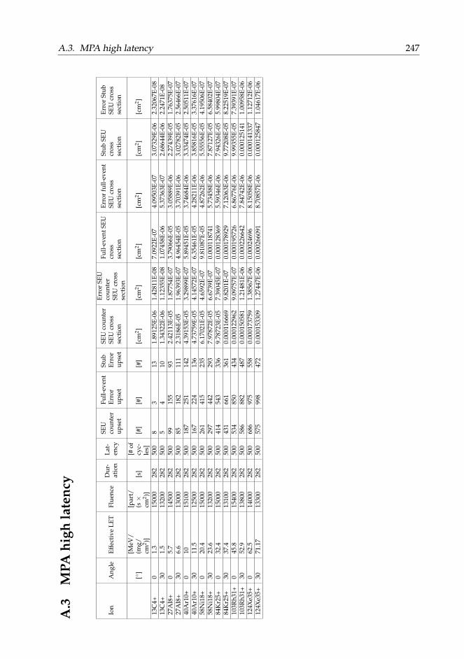
A.3. MPA high latency 247
A.3
MPA
high
late
ncy
Ion
Ang
leEf
fect
ive
LET
Flue
nce
Dur
-at
ion
Lat-
ency
SEU
coun
ter
upse
t
Full-
even
tEr
ror
upse
t
Stub
Erro
rup
set
SEU
coun
ter
SEU
cros
sse
ctio
n
Erro
rSE
Uco
unte
rSE
Ucr
oss
sect
ion
Full-
even
tSEU
cros
sse
ctio
n
Erro
rfu
ll-ev
ent
SEU
cros
sse
ctio
n
Stub
SEU
cros
sse
ctio
n
Erro
rSt
ubSE
Ucr
oss
sect
ion
[]
[MeV
/(m
g/cm
2 )]
[par
t/(s×
cm2 )]
[s]
[#of
cyc-
les]
[#]
[#]
[#]
[cm
2 ][c
m2 ]
[cm
2 ][c
m2 ]
[cm
2 ][c
m2 ]
13C
4+0
1.3
1500
028
250
08
313
1.89
125E
-06
1.42
811E
-08
7.09
22E-
074.
0950
3E-0
73.
0732
9E-0
62.
3206
7E-0
813
C4+
301.
513
200
282
500
54
101.
3432
2E-0
61.
1235
5E-0
81.
0745
8E-0
65.
3736
3E-0
72.
6864
4E-0
62.
2471
E-08
27A
l8+
05.
714
500
282
500
9915
593
2.42
113E
-05
1.87
754E
-07
3.79
066E
-05
3.05
889E
-06
2.27
439E
-05
1.76
375E
-07
27A
l8+
306.
613
000
282
500
8518
211
12.
3186
E-05
1.96
393E
-07
4.96
454E
-05
3.70
391E
-06
3.02
782E
-05
2.56
466E
-07
40A
r10+
010
1510
028
250
018
725
114
24.
3915
3E-0
53.
2989
9E-0
75.
8945
1E-0
53.
7468
4E-0
63.
3347
4E-0
52.
5051
1E-0
740
Ar1
0+30
11.5
1250
028
250
016
722
413
64.
7375
9E-0
54.
1457
2E-0
76.
3546
1E-0
54.
2821
1E-0
63.
8581
6E-0
53.
3761
6E-0
758
Ni1
8+0
20.4
1500
028
250
026
141
523
56.
1702
1E-0
54.
6592
E-07
9.81
087E
-05
4.87
262E
-06
5.55
556E
-05
4.19
506E
-07
58N
i18+
3023
.613
200
282
500
297
442
293
7.97
872E
-05
6.67
39E-
070.
0001
1874
15.
7345
8E-0
67.
8712
7E-0
56.
5840
2E-0
784
Kr2
5+0
32.4
1500
028
250
041
454
333
69.
7872
3E-0
57.
3904
5E-0
70.
0001
2836
95.
5934
6E-0
67.
9432
6E-0
55.
9980
4E-0
784
Kr2
5+30
37.4
1310
028
250
043
166
136
10.
0001
1666
99.
8201
E-07
0.00
0178
929
7.12
063E
-06
9.77
208E
-05
8.22
519E
-07
103R
h31+
045
.815
400
282
500
534
850
434
0.00
0122
962
9.09
757E
-07
0.00
0195
726
6.86
776E
-06
9.99
355E
-05
7.39
391E
-07
103R
h31+
3052
.913
800
282
500
586
882
487
0.00
0150
581
1.21
481E
-06
0.00
0226
642
7.84
742E
-06
0.00
0125
141
1.00
958E
-06
124X
e35+
062
.514
000
282
500
686
975
558
0.00
0173
759
1.38
567E
-06
0.00
0246
968.
1505
8E-0
60.
0001
4133
71.
1271
2E-0
612
4Xe3
5+30
71.1
713
300
282
500
575
998
472
0.00
0153
309
1.27
447E
-06
0.00
0266
091
8.70
857E
-06
0.00
0125
847
1.04
617E
-06

248 Appendix A. MPA and SSA SEU cross sectionsA
.4M
PAlo
wla
tenc
y
Ion
Ang
leEf
fect
ive
LET
Flue
nce
Dur
-at
ion
Lat-
ency
SEU
coun
ter
upse
t
Full-
even
tEr
ror
upse
t
Stub
Erro
rup
set
SEU
coun
ter
SEU
cros
sse
ctio
n
Erro
rSE
Uco
unte
rSE
Ucr
oss
sect
ion
Full-
even
tSEU
cros
sse
ctio
n
Erro
rfu
ll-ev
ent
SEU
cros
sse
ctio
n
Stub
SEU
cros
sse
ctio
n
Erro
rSt
ubSE
Ucr
oss
sect
ion
[]
[MeV
/(m
g/cm
2 )]
[par
t/(s×
cm2 )]
[s]
[#of
cyc-
les]
[#]
[#]
[#]
[cm
2 ][c
m2 ]
[cm
2 ][c
m2 ]
[cm
2 ][c
m2 ]
13C
4+0
1.3
1500
028
240
52
241.
1820
3E-0
68.
9256
6E-0
94.
7281
3E-0
73.
3434
9E-0
75.
6737
6E-0
64.
2843
2E-0
813
C4+
301.
513
700
282
406
118
1.55
304E
-06
1.26
03E-
082.
5883
9E-0
72.
5884
8E-0
74.
6591
1E-0
63.
7808
9E-0
827
Al8
+0
5.7
1450
028
240
9911
088
2.42
113E
-05
1.87
754E
-07
2.69
014E
-05
2.57
342E
-06
2.15
212E
-05
1.66
893E
-07
27A
l8+
306.
613
000
282
4010
311
610
02.
8096
E-05
2.37
982E
-07
3.16
421E
-05
2.95
01E-
062.
7277
7E-0
52.
3105
1E-0
740
Ar1
0+0
1015
100
282
4014
114
412
93.
3112
6E-0
52.
4874
7E-0
73.
3817
1E-0
52.
8295
2E-0
63.
0294
5E-0
52.
2757
7E-0
740
Ar1
0+30
11.5
1250
028
240
129
180
164
3.65
957E
-05
3.20
239E
-07
5.10
638E
-05
3.83
221E
-06
4.65
248E
-05
4.07
125E
-07
58N
i18+
020
.415
000
282
4026
326
623
06.
2174
9E-0
54.
6949
E-07
6.28
842E
-05
3.88
48E-
065.
4373
5E-0
54.
1058
E-07
58N
i18+
3023
.613
200
282
4031
328
725
68.
4085
5E-0
57.
0334
4E-0
77.
7100
8E-0
54.
5965
8E-0
66.
8772
8E-0
55.
7525
9E-0
784
Kr2
5+0
32.4
1500
028
240
399
342
338
9.43
262E
-05
7.12
268E
-07
8.08
511E
-05
4.41
435E
-06
7.99
054E
-05
6.03
375E
-07
84K
r25+
3037
.413
100
282
4041
439
536
40.
0001
1206
89.
4327
7E-0
70.
0001
0692
45.
4547
1E-0
69.
8532
8E-0
58.
2935
4E-0
710
3Rh3
1+0
45.8
1440
028
240
552
526
458
0.00
0135
934
1.05
994E
-06
0.00
0129
531
5.73
743E
-06
0.00
0112
786
8.79
44E-
0710
3Rh3
1+30
52.9
1280
028
240
457
464
355
0.00
0126
607
1.08
624E
-06
0.00
0128
546
6.06
866E
-06
9.83
488E
-05
8.43
796E
-07
124X
e35+
062
.514
200
282
4059
160
848
50.
0001
4758
81.
1636
8E-0
60.
0001
5183
36.
2729
4E-0
60.
0001
2111
79.
5496
7E-0
712
4Xe3
5+30
71.1
713
300
282
4065
854
550
20.
0001
7543
91.
4584
3E-0
60.
0001
4531
6.34
053E
-06
0.00
0133
845
1.11
266E
-06

249
Appendix B
Full CIC start-up sequence
Detailed CIC start-up sequence as used in section 9.3:
Star
t-up
step
Act
ion
Not
e
Prep
arat
ion
Pow
erFC
7an
dlo
adFW
.Th
ede
faul
tsta
teof
the
firm
war
esh
ould
send
noth
ing
onth
eou
putl
ines
,exc
eptf
orth
eha
rdre
setw
hich
shou
ldbe
enab
led.
Pow
erin
terf
ace
card
.En
able
CIC
.La
unch
320M
Hz
cloc
kge
nera
tion
for
the
CIC
.D
isab
leth
eha
rdre
set.
Sett
hesc
DllC
onfir
mC
ount
Sele
ctto
the
max
imum
.Th
isre
gist
erse
tsth
eti
me
limit
the
DLL
sar
eal
low
edto
lock
.Thi
sne
eds
tobe
setf
oral
lPhy
Port
s.Th
ede
faul
tval
ueis
togi
veth
eC
IC4
cloc
kcy
cles
tolo
ck,b
yse
ttin
gth
em
axim
umth
isis
incr
ease
dto
31cl
ock
cycl
es.
Fast
com
man
dlo
ckin
g
Star
tthe
send
ing
ofth
efa
stco
mm
and
fram
eto
the
CIC
.Se
ndin
gon
lyth
ehe
ader
and
trai
ler
ofth
efa
stco
mm
and
fram
e,th
eC
ICus
esth
ishe
ader
toge
nera
tean
inte
rnal
40M
Hz
cloc
k.
Che
ckth
efa
stco
mm
and
lock
ing
stat
e.If
notl
ocke
dit
mea
nsth
eC
ICdi
dno
tfind
the
fast
com
man
dhe
ader
.As
ther
eis
noph
ase
alig
nmen
tfea
ture
onth
efa
stco
mm
and
line
itis
poss
ible
that
this
happ
ens.
Ther
efor
eit
ispo
ssib
leto
sele
ctth
e32
0MH
zcl
ock
edge
onw
hich
the
CIC
sam
ples
man
ually
.Se
nda
ReS
ync
fast
com
man
d
Che
ckre
cept
ion
ofR
eSyn
cfa
stco
mm
and
Toch
eck
ifth
eC
ICpr
oper
lyin
terp
rets
fast
com
man
dpa
yloa
d.If
notc
orre
ctth
eot
her
320M
Hz
cloc
ked
geca
nbe
trie
d.
Phas
eal
ignm
ent
Con
figur
eth
ePh
yPor
tsin
’aut
ost
artu
p’m
ode.
The
othe
rop
tion
wou
ldbe
the
use
ofth
e’fi
xed’
mod
e,w
hich
can
beus
edon
esth
eph
ase
and
wor
dal
ignm
entp
atte
rns
are
know
nfr
oma
prev
ious
alig
nmen
t.Th
isw
ould
for
exam
ple
beth
eca
sew
hen
the
CIC
sits
ona
hybr
idan
dis
conn
ecte
dto
the
fron
t-en
dch
ips
dire
ctly
,the
dela
ybe
twee
nth
elin
esw
ould
beco
nsta
ntin
that
case
.Se
nda
soft
rese
tto
the
CIC
and
rele
ase
it.
This
rese
tsth
eC
ICch
ipex
cept
for
the
slow
cont
rolb
lock
and
regi
ster
s.
Che
cklo
ckin
gof
DLL
s.Th
ere
is1
stat
usbi
tfor
each
PhyP
ort.
Send
phas
etu
ning
patt
erns
from
the
FC7
toth
eC
IC.
The
FC7
send
son
allt
heda
talin
esth
e10
1010
10re
peti
tive
patt
erns
.Thi
sal
low
sth
eC
ICto
find
the
corr
ect
phas
efo
rsa
mpl
ing.
Che
ckfo
rph
ase
tuni
nglo
ckon
allt
hein
putc
hann
els.
Ther
eis
ast
atus
bitf
orea
chof
the
48da
tain
putl
ines
for
the
CIC
.
Wor
dal
ignm
ent
Con
figur
ew
ord
alig
nmen
tpa
tter
nsin
CIC
Prog
ram
me
the
wor
dtu
ning
patt
erns
whi
chth
eC
ICw
illbe
expe
ctin
gfr
omth
efr
ont-
end
chip
sin
toth
eC
IC.O
neby
teca
nbe
spec
ified
per
stub
line,
ther
efor
eth
ere
are
40bi
tsin
tota
lto
confi
gure
.
Dis
able
usag
eof
the
exte
rnal
alig
nmen
tval
ue
Byde
faul
tthe
CIC
isco
nfigu
red
tous
eth
eal
ignm
entv
alue
sw
hich
are
stor
edin
tern
ally
onth
ech
ipan
dw
hich
are
spec
ific
for
ace
rtai
nco
nfigu
rati
on(e
.g.o
na
hybr
id)t
his
will
beth
ede
faul
tcon
figur
atio
nin
the
final
appl
icat
ion
whe
reth
ese
valu
esw
illbe
stor
edin
ada
taba
se.N
oww
ew
antt
oru
nth
eal
ignm
entp
roce
dure
,so
dono
tuse
the
inte
rnal
ones
.Thi
sph
iloso
phy
issi
mila
rto
the
first
step
ofth
eph
ase
tuni
ng.
Enab
leth
eau
tom
atic
wor
dal
ignm
entp
roce
dure
This
isan
I2C
com
man
dto
the
chip
.
Send
aR
eSyn
cfa
stco
mm
and
Che
ckfo
rw
ord
tuni
nglo
ckon
allt
hest
ubda
talin
esTh
ere
is1
bitf
orth
est
atus
ofth
ew
ord
alig
nmen
t.
Dis
able
the
auto
mat
icw
ord
alig
nmen
tpro
cedu
re
BX0
alig
nmen
t
Sele
ctth
est
ublin
eto
perf
orm
the
BX0
alig
nmen
tTh
isis
ace
rtai
nlin
eon
ace
rtai
nfr
ont-
end
chip
.
Dis
able
the
usag
eof
the
exte
rnal
alig
nmen
tval
ueTh
ere
ason
for
this
issi
mila
rto
the
disa
blin
gof
the
usag
eof
the
exte
rnal
alig
nmen
tval
ues
ofth
eph
ase
and
wor
dal
ignm
ent.
Enab
leth
eau
toBX
0al
ignm
ent
proc
edur
eSe
nda
ReS
ync
fast
com
man
dTh
efr
ont-
end
chip
shou
ldse
nda
reco
gnis
able
patt
ern
aco
nsta
ntam
ount
ofcl
ock
cycl
esaf
ter
the
ReS
ync.
Che
ckif
the
reco
gnis
able
patt
ern
was
seen
byth
eC
ICTh
ere
isan
I2C
stat
usbi
tto
chec
kth
is.I
fiti
sfa
lse
itm
eans
that
the
patt
ern
was
nots
een
onth
elin
eaf
ter
agi
ven
tim
ein
terv
al.
Dis
able
the
auto
BX0
alig
nmen
tpr
oced
ure
Back
-end
alig
nmen
t
Enab
leth
eC
ICou
tput
tran
smit
ters
Enab
leth
eSL
VS
pads
for
data
tobe
sent
ofth
eC
ICch
ip.
Enab
leth
eou
tput
ofth
eda
tapa
tter
nsou
toft
heC
ICTh
ese
data
patt
erns
are
used
for
the
phas
e,w
ord
and
pack
age
alig
nmen
t.Th
epa
tter
nw
hich
isse
ntis
1110
1010
ever
y8t
hBX
follo
wed
by7
BXs
of10
1010
10pa
tter
nsfo
rth
est
ublin
esan
d...
1010
...fo
rth
efu
ll-ev
entl
ine.
Che
ckif
phas
ean
dw
ord
tuni
ngsu
ccee
ded
onth
eD
AQ
Ther
ear
est
atus
regi
ster
inth
eµ
DTC
whi
chsp
ecif
yif
the
phas
ean
dw
ord
tuni
ngsu
ccee
ded.
The
phas
etu
ning
isdo
neon
the
...01
0101
...w
here
asth
ew
ord
tuni
ngis
done
onth
eco
nsec
utiv
eth
ree
1’s
whi
char
ese
nt.
Send
toµ
DTC
stub
deco
der
that
the
phas
ean
dw
ord
tuni
ngsu
ccee
ded.
This
tells
the
µD
TCst
ubde
code
rth
atth
eby
tes
whi
char
rive
from
the
ISER
DES
ESar
eco
rrec
tly
phas
ean
dw
ord
alig
ned.
The
µD
TCca
npr
ocee
dno
wto
look
for
the
cons
ecut
ive
thre
e1’
sto
find
the
star
tofa
stub
pack
age,
this
isth
ela
stpa
rtof
the
sync
hron
isat
ion
and
isre
ferr
edto
asth
epa
ckag
eal
ignm
ent.
Dis
able
the
outp
utof
the
CIC
outp
utpa
tter
ns


251
Appendix C
CBC configurations for CBC-CIC start-up
This appendix provides the CBC3 configurations which should be applied during thestart-up sequence for the CBC+CIC as explained in section 9.3.
Register name Page AddressPhasealignment1
Phasealignment2
Phasealignment3
Wordalignment
BX0alignment
TestPulsePotNodeSel 0x00 0x000D 0xEA 0xEA 0xEA 0xEA 0xC0MiscTestPulseCtrl&AnalogMux 0x00 0x000F 0x20 0x20 0x20 0x20 0x60CoincWind&Offset34 0x00 0x0013 0x00 0x00 0x00 0x00 0xCCCoincWind&Offset12 0x00 0x0014 0x00 0x00 0x00 0x00 0xCC40MhzClk&Or254 0x00 0x001C 0xEE 0xEE 0xEE 0xEE 0xAEMaskChannel-008-to-001 0x00 0x0020 0x00 0x00 0xAA 0x00 0x00MaskChannel-016-to-009 0x00 0x0021 0x00 0x00 0xAA 0x00 0x00MaskChannel-024-to-017 0x00 0x0022 0x00 0x00 0xAA 0x00 0x03MaskChannel-032-to-025 0x00 0x0023 0x00 0x00 0xAA 0x00 0x00MaskChannel-040-to-033 0x00 0x0024 0x00 0x20 0xAA 0x00 0x03MaskChannel-048-to-041 0x00 0x0025 0x00 0x00 0xAA 0x00 0x00MaskChannel-056-to-049 0x00 0x0026 0x00 0x01 0xAA 0x00 0x00MaskChannel-064-to-057 0x00 0x0027 0x00 0x00 0xAA 0x00 0x00MaskChannel-072-to-065 0x00 0x0028 0x80 0x00 0xAA 0x00 0x03MaskChannel-080-to-073 0x00 0x0029 0x02 0x00 0xAA 0x00 0x00MaskChannel-088-to-081 0x00 0x002A 0x14 0x80 0xAA 0x00 0x00MaskChannel-096-to-089 0x00 0x002B 0x00 0x00 0xAA 0x00 0x00MaskChannel-104-to-097 0x00 0x002C 0x00 0x04 0xAA 0x00 0x00MaskChannel-112-to-105 0x00 0x002D 0x00 0x00 0xAA 0x00 0x00MaskChannel-120-to-113 0x00 0x002E 0x00 0x00 0xAA 0x00 0x00MaskChannel-128-to-121 0x00 0x002F 0x00 0x00 0xAA 0x09 0x00MaskChannel-136-to-129 0x00 0x0030 0x00 0x00 0xAA 0x00 0x00MaskChannel-144-to-137 0x00 0x0031 0x00 0x00 0xAA 0x00 0x00MaskChannel-152-to-145 0x00 0x0032 0x00 0x00 0xAA 0x00 0x00MaskChannel-160-to-153 0x00 0x0033 0x20 0x20 0xAA 0x00 0x00MaskChannel-168-to-161 0x00 0x0034 0x00 0x00 0xAA 0x00 0x00MaskChannel-176-to-169 0x00 0x0035 0x01 0x01 0xAA 0x00 0x00MaskChannel-184-to-177 0x00 0x0036 0x00 0x00 0xAA 0x00 0x00MaskChannel-192-to-185 0x00 0x0037 0x00 0x00 0xAA 0x04 0x00MaskChannel-200-to-193 0x00 0x0038 0x00 0x00 0xAA 0x02 0x00MaskChannel-208-to-201 0x00 0x0039 0x00 0x00 0xAA 0x00 0x00MaskChannel-216-to-209 0x00 0x003A 0x00 0x00 0xAA 0x24 0x00MaskChannel-224-to-217 0x00 0x003B 0x00 0x00 0xAA 0x00 0x00MaskChannel-232-to-225 0x00 0x003C 0x00 0x00 0xAA 0x00 0x00MaskChannel-240-to-233 0x00 0x003D 0x00 0x00 0xAA 0x00 0x00MaskChannel-248-to-241 0x00 0x003E 0x00 0x00 0xAA 0x00 0x00MaskChannel-254-to-249 0x00 0x003F 0x00 0x00 0xAA 0x00 0x00VCth1 0x00 0x004F 0x20 0x20 0x20 0x20 0x3AVCth2 0x00 0x0050 0x03 0x03 0x03 0x03 0x02


253
Appendix D
S events: reconstruction efficiencies
This appendix gives the reconstruction efficiency for the final state particles, the V0s andthe S in reconstructable (section 10.10.5) simulated S events. Efficiencies are provided asfunction of transverse and longitudinal displacement, transverse momentum and pseu-dorapidity. The actual distribution of these variables are also shown. A discussion onthese results is given in section 10.11.
(cm)S(bpc) interaction vertex simulated 0l
2.15 2.2 2.25 2.3 2.35 2.4 2.45 2.5
Eve
nts/
0.1m
mev
Effi
cien
cy o
r 1/
N
0
0.002
0.004
0.006
0.008
0.01
0.012
0.014
Reconstruction efficiency
Normalised distribution x1/4700Simulation
(a)
(cm)S interaction vertex simulated zabsolute v
150− 100− 50− 0 50 100 150
Eve
nts/
4cm
evE
ffici
ency
or
1/N
0
0.001
0.002
0.003
0.004
0.005
0.006
Reconstruction efficiencyNormalised distribution x0.5
Simulation
(b)
(GeV/c)S simulated T
p
0 2 4 6 8 10
Eve
nts/
0.1G
eV/c
evE
ffici
ency
or
1/N
0
0.02
0.04
0.06
0.08
0.1
0.12
0.14
0.16Reconstruction efficiency
Normalised distribution x1/40Simulation
(c)
S simulated η
6− 4− 2− 0 2 4 6
η E
vent
s/0.
1ev
Effi
cien
cy o
r 1/
N
0
0.001
0.002
0.003
0.004
0.005
0.006
Reconstruction efficiency
Normalised distribution x1/60Simulation
(d)
FIGURE D.1: Reconstruction efficiency for the S in reconstructable events. Theactual distribution of the variables is also shown.
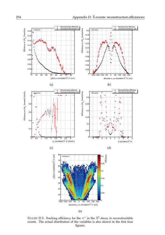
254 Appendix D. S events: reconstruction efficiencies
(cm)+π-0
Λ(bs) cv simulated 0l
0 10 20 30 40 50 60 70 80
Eve
nts/
cmev
Effi
cien
cy o
r 1/
N
0
0.02
0.04
0.06
0.08
0.1
0.12
0.14
0.16
0.18
Reconstruction efficiencyNormalised distribution x2
Simulation
(a)
(cm)+π-0
Λ cv simulated zabsolute v
200− 150− 100− 50− 0 50 100 150 200
Eve
nts/
4cm
evE
ffici
ency
or
1/N
0
0.02
0.04
0.06
0.08
0.1
0.12
0.14
0.16
0.18
0.2
Reconstruction efficiencyNormalised distribution x25
Simulation
(b)
(GeV/c)+π-0
Λ simulated T
p
0 0.5 1 1.5 2 2.5 3 3.5 4
Eve
nts/
0.1G
eV/c
evE
ffici
ency
or
1/N
0
0.2
0.4
0.6
0.8
1
Reconstruction efficiencyNormalised distribution x0.4
Simulation
(c)
+π-0
Λ simulated η
4− 3− 2− 1− 0 1 2 3 4 5
η E
vent
s/0.
1ev
Effi
cien
cy o
r 1/
N
0
0.05
0.1
0.15
0.2
0.25
0.3
Reconstruction efficiencyNormalised distribution
Simulation
(d)
(cm)+π-0
Λ cv simulated zabsolute v
200− 150− 100− 50− 0 50 100 150 200
(cm
)+ π-
0Λ
(bs)
cv
sim
ulat
ed
0l
0
10
20
30
40
50
60
70
80
Effi
cien
cy
0
0.05
0.1
0.15
0.2
0.25
0.3Simulation
(e)
FIGURE D.2: Tracking efficiency for the π+ in the Λ0 decay in reconstructableevents. The actual distribution of the variables is also shown in the first four
figures.
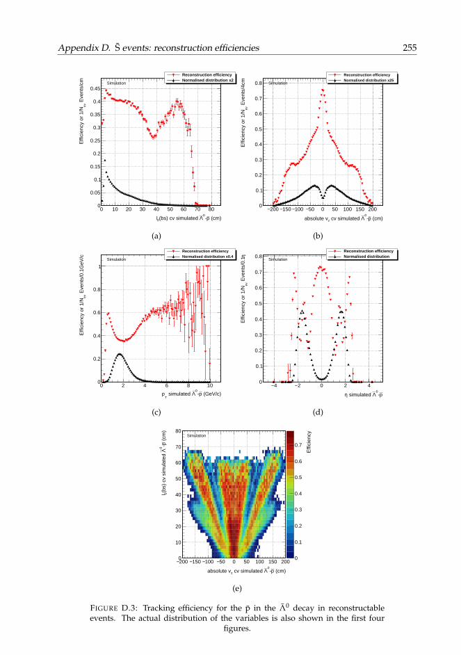
Appendix D. S events: reconstruction efficiencies 255
(cm)p-0
Λ(bs) cv simulated 0l
0 10 20 30 40 50 60 70 80
Eve
nts/
cmev
Effi
cien
cy o
r 1/
N
0
0.05
0.1
0.15
0.2
0.25
0.3
0.35
0.4
0.45
Reconstruction efficiencyNormalised distribution x2
Simulation
(a)
(cm)p-0
Λ cv simulated zabsolute v
200− 150− 100− 50− 0 50 100 150 200
Eve
nts/
4cm
evE
ffici
ency
or
1/N
0
0.1
0.2
0.3
0.4
0.5
0.6
0.7
0.8
Reconstruction efficiencyNormalised distribution x25
Simulation
(b)
(GeV/c)p-0
Λ simulated T
p
0 2 4 6 8 10
Eve
nts/
0.1G
eV/c
evE
ffici
ency
or
1/N
0
0.2
0.4
0.6
0.8
1
Reconstruction efficiencyNormalised distribution x0.4
Simulation
(c)
p-0
Λ simulated η
4− 2− 0 2 4
η E
vent
s/0.
1ev
Effi
cien
cy o
r 1/
N
0
0.1
0.2
0.3
0.4
0.5
0.6
0.7
0.8Reconstruction efficiencyNormalised distribution
Simulation
(d)
(cm)p-0
Λ cv simulated zabsolute v
200− 150− 100− 50− 0 50 100 150 200
(cm
)p-
0Λ
(bs)
cv
sim
ulat
ed
0l
0
10
20
30
40
50
60
70
80
Effi
cien
cy
0
0.1
0.2
0.3
0.4
0.5
0.6
0.7
Simulation
(e)
FIGURE D.3: Tracking efficiency for the p in the Λ0 decay in reconstructableevents. The actual distribution of the variables is also shown in the first four
figures.

256 Appendix D. S events: reconstruction efficiencies
daughters (cm)0
S(bs) cv simulated K0l
0 10 20 30 40 50 60 70 80
Eve
nts/
cmev
Effi
cien
cy o
r 1/
N
0
0.05
0.1
0.15
0.2
0.25
0.3
0.35
Reconstruction efficiencyNormalised distribution x2
Simulation
(a)
daughters (cm)0S
cv simulated Kzabsolute v
200− 150− 100− 50− 0 50 100 150 200
Eve
nts/
4cm
evE
ffici
ency
or
1/N
0
0.1
0.2
0.3
0.4
0.5
Reconstruction efficiencyNormalised distribution x25
Simulation
(b)
daughters (GeV/c)0S
simulated KT
p
0 2 4 6 8 10
Eve
nts/
0.1G
eV/c
evE
ffici
ency
or
1/N
0
0.2
0.4
0.6
0.8
1
Reconstruction efficiencyNormalised distribution x0.4
Simulation
(c)
daughters0
S simulated Kη
4− 2− 0 2 4
η E
vent
s/0.
1ev
Effi
cien
cy o
r 1/
N
0
0.1
0.2
0.3
0.4
0.5
0.6
Reconstruction efficiencyNormalised distribution
Simulation
(d)
daughters (cm)0S
cv simulated Kzabsolute v
200− 150− 100− 50− 0 50 100 150 200
dau
ghte
rs (
cm)
0 S(b
s) c
v si
mul
ated
K0l
0
10
20
30
40
50
60
70
80
Effi
cien
cy
0
0.1
0.2
0.3
0.4
0.5
0.6Simulation
(e)
FIGURE D.4: Tracking efficiency for the pions in the K0S decay in reconstructable
events. The actual distribution of the variables is also shown in the first fourfigures.
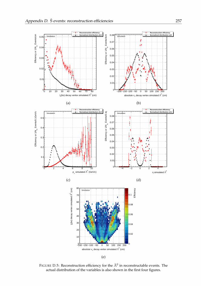
Appendix D. S events: reconstruction efficiencies 257
(cm)0
Λ(bs) decay vertex simulated 0l
0 10 20 30 40 50 60 70 80
Eve
nts/
cmev
Effi
cien
cy o
r 1/
N
0
0.01
0.02
0.03
0.04
0.05
Reconstruction efficiencyNormalised distribution x0.5
Simulation
(a)
(cm)0
Λ decay vertex simulated zabsolute v
200− 150− 100− 50− 0 50 100 150 200
Eve
nts/
4cm
evE
ffici
ency
or
1/N
0
0.01
0.02
0.03
0.04
0.05
0.06
0.07
0.08Reconstruction efficiencyNormalised distribution x10
Simulation
(b)
(GeV/c)0
Λ simulated T
p
0 2 4 6 8 10
Eve
nts/
0.1G
eV/c
evE
ffici
ency
or
1/N
0
0.1
0.2
0.3
0.4
0.5
Reconstruction efficiencyNormalised distribution x0.4
Simulation
(c)
0Λ simulated η
4− 2− 0 2 4
η E
vent
s/0.
1ev
Effi
cien
cy o
r 1/
N
0
0.01
0.02
0.03
0.04
0.05
0.06
0.07
0.08
Reconstruction efficiencyNormalised distribution x0.1
Simulation
(d)
(cm)0
Λ decay vertex simulated zabsolute v
200− 150− 100− 50− 0 50 100 150 200
(cm
)0
Λ(b
s) d
ecay
ver
tex
sim
ulat
ed
0l
0
10
20
30
40
50
60
70
80
Effi
cien
cy
0
0.02
0.04
0.06
0.08
0.1
Simulation
(e)
FIGURE D.5: Reconstruction efficiency for the Λ0 in reconstructable events. Theactual distribution of the variables is also shown in the first four figures.
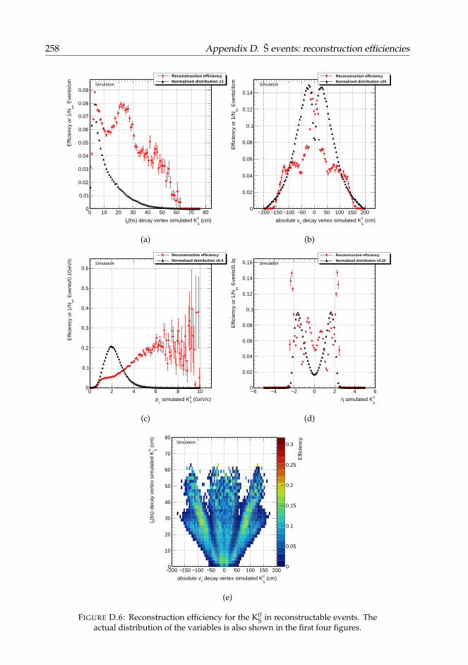
258 Appendix D. S events: reconstruction efficiencies
(cm)0
S(bs) decay vertex simulated K0l
0 10 20 30 40 50 60 70 80
Eve
nts/
cmev
Effi
cien
cy o
r 1/
N
0
0.01
0.02
0.03
0.04
0.05
0.06
0.07
0.08
0.09
Reconstruction efficiencyNormalised distribution x1
Simulation
(a)
(cm)0
S decay vertex simulated Kzabsolute v
200− 150− 100− 50− 0 50 100 150 200
Eve
nts/
4cm
ev E
ffici
ency
or
1/N
0
0.02
0.04
0.06
0.08
0.1
0.12
0.14
Reconstruction efficiencyNormalised distribution x25
Simulation
(b)
(GeV/c)0S
simulated KT
p
0 2 4 6 8 10
Eve
nts/
0.1G
eV/c
ev E
ffici
ency
or
1/N
0
0.1
0.2
0.3
0.4
0.5
0.6
Reconstruction efficiencyNormalised distribution x0.4
Simulation
(c)
0
S simulated Kη
6− 4− 2− 0 2 4 6
η E
vent
s/0.
1ev
Effi
cien
cy o
r 1/
N
0
0.02
0.04
0.06
0.08
0.1
0.12
0.14
0.16
Reconstruction efficiency
Normalised distribution x0.25Simulation
(d)
(cm)0
S decay vertex simulated Kzabsolute v
200− 150− 100− 50− 0 50 100 150 200
(cm
)0 S
(bs)
dec
ay v
erte
x si
mul
ated
K0l
0
10
20
30
40
50
60
70
80
Effi
cien
cy
0
0.05
0.1
0.15
0.2
0.25
0.3Simulation
(e)
FIGURE D.6: Reconstruction efficiency for the K0S in reconstructable events. The
actual distribution of the variables is also shown in the first four figures.
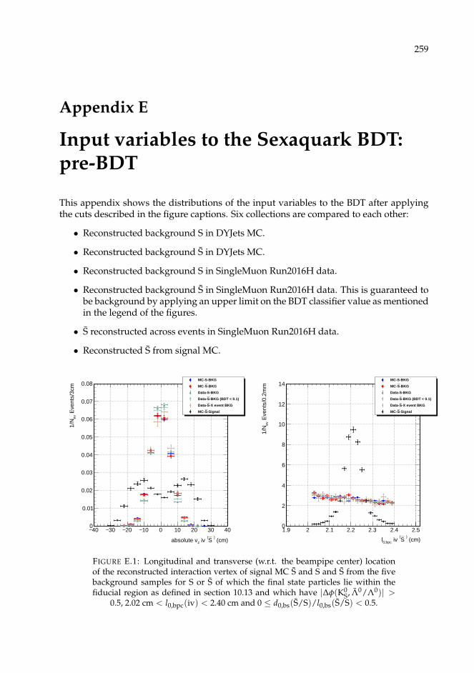
259
Appendix E
Input variables to the Sexaquark BDT:pre-BDT
This appendix shows the distributions of the input variables to the BDT after applyingthe cuts described in the figure captions. Six collections are compared to each other:
• Reconstructed background S in DYJets MC.
• Reconstructed background S in DYJets MC.
• Reconstructed background S in SingleMuon Run2016H data.
• Reconstructed background S in SingleMuon Run2016H data. This is guaranteed tobe background by applying an upper limit on the BDT classifier value as mentionedin the legend of the figures.
• S reconstructed across events in SingleMuon Run2016H data.
• Reconstructed S from signal MC.
(cm))
S(
iv z absolute v
40− 30− 20− 10− 0 10 20 30 40
Eve
nts/
3cm
ev 1
/N
0
0.01
0.02
0.03
0.04
0.05
0.06
0.07
0.08MC-S-BKG
-BKGSMC-
Data-S-BKG
-BKG (BDT < 0.1) SData-
-X event BKGSData-
-SignalSMC-
(cm))
S(
iv 0,bpc l
1.9 2 2.1 2.2 2.3 2.4 2.5
Eve
nts/
0.2m
mev
1/N
0
2
4
6
8
10
12
14MC-S-BKG
-BKGSMC-
Data-S-BKG
-BKG (BDT < 0.1) SData-
-X event BKGSData-
-SignalSMC-
FIGURE E.1: Longitudinal and transverse (w.r.t. the beampipe center) locationof the reconstructed interaction vertex of signal MC S and S and S from the fivebackground samples for S or S of which the final state particles lie within thefiducial region as defined in section 10.13 and which have |∆φ(K0
S, Λ0/Λ0)| >0.5, 2.02 cm < l0,bpc(iv) < 2.40 cm and 0 ≤ d0,bs(S/S)/l0,bs(S/S) < 0.5.
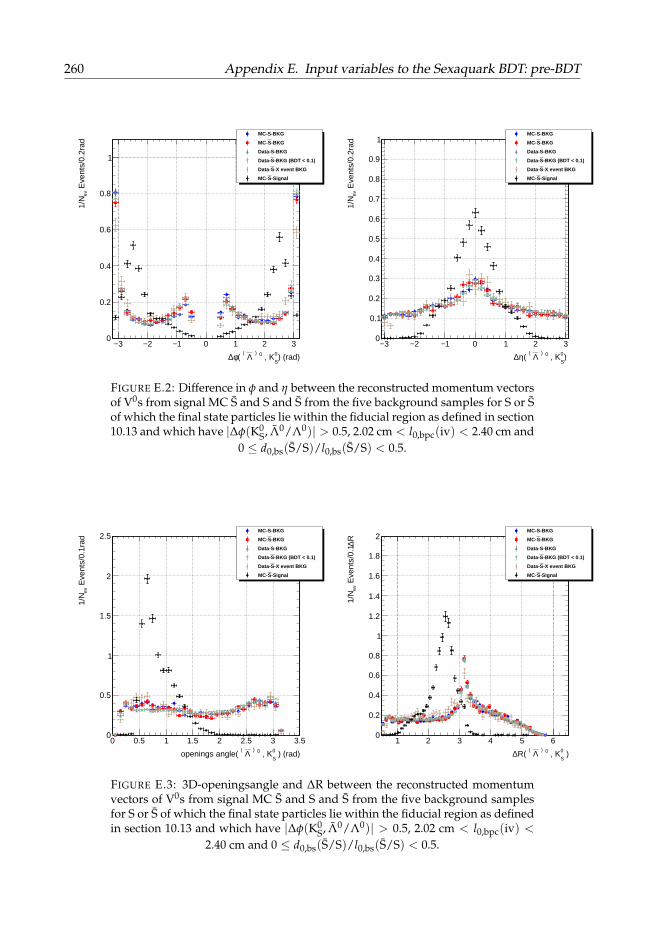
260 Appendix E. Input variables to the Sexaquark BDT: pre-BDT
) (rad)0
S , K0
) Λ (( φ∆
3− 2− 1− 0 1 2 3
Eve
nts/
0.2r
adev
1/N
0
0.2
0.4
0.6
0.8
1
MC-S-BKG
-BKGSMC-
Data-S-BKG
-BKG (BDT < 0.1) SData-
-X event BKGSData-
-SignalSMC-
) 0
S , K0
) Λ (( η∆
3− 2− 1− 0 1 2 3 E
vent
s/0.
2rad
ev 1
/N0
0.1
0.2
0.3
0.4
0.5
0.6
0.7
0.8
0.9
1MC-S-BKG
-BKGSMC-
Data-S-BKG
-BKG (BDT < 0.1) SData-
-X event BKGSData-
-SignalSMC-
FIGURE E.2: Difference in φ and η between the reconstructed momentum vectorsof V0s from signal MC S and S and S from the five background samples for S or Sof which the final state particles lie within the fiducial region as defined in section10.13 and which have |∆φ(K0
S, Λ0/Λ0)| > 0.5, 2.02 cm < l0,bpc(iv) < 2.40 cm and0 ≤ d0,bs(S/S)/l0,bs(S/S) < 0.5.
) (rad)0
S , K0
) Λ ( openings angle(
0 0.5 1 1.5 2 2.5 3 3.5
Eve
nts/
0.1r
adev
1/N
0
0.5
1
1.5
2
2.5MC-S-BKG
-BKGSMC-
Data-S-BKG
-BKG (BDT < 0.1) SData-
-X event BKGSData-
-SignalSMC-
)0
S , K0
) Λ (R( ∆
1 2 3 4 5 6
R∆ E
vent
s/0.
1ev
1/N
0
0.2
0.4
0.6
0.8
1
1.2
1.4
1.6
1.8
2MC-S-BKG
-BKGSMC-
Data-S-BKG
-BKG (BDT < 0.1) SData-
-X event BKGSData-
-SignalSMC-
FIGURE E.3: 3D-openingsangle and ∆R between the reconstructed momentumvectors of V0s from signal MC S and S and S from the five background samplesfor S or S of which the final state particles lie within the fiducial region as definedin section 10.13 and which have |∆φ(K0
S, Λ0/Λ0)| > 0.5, 2.02 cm < l0,bpc(iv) <
2.40 cm and 0 ≤ d0,bs(S/S)/l0,bs(S/S) < 0.5.

Appendix E. Input variables to the Sexaquark BDT: pre-BDT 261
) (rad)0
S , K
) S
( openings angle(
0 0.2 0.4 0.6 0.8 1 1.2 1.4 1.6 1.8 2
Eve
nts/
0.1r
adev
1/N
0
0.2
0.4
0.6
0.8
1
1.2
1.4
1.6
1.8
2MC-S-BKG
-BKGSMC-
Data-S-BKG
-BKG (BDT < 0.1) SData-
-X event BKGSData-
-SignalSMC-
) (rad))
S ( , 0 )
Λ ( openings angle(
0 0.2 0.4 0.6 0.8 1 1.2 1.4 1.6 1.8 2
Eve
nts/
0.1r
adev
1/N
0
0.5
1
1.5
2
2.5
3
3.5
4
4.5MC-S-BKG
-BKGSMC-
Data-S-BKG
-BKG (BDT < 0.1) SData-
-X event BKGSData-
-SignalSMC-
FIGURE E.4: 3D-openingsangles between the reconstructed momentum vectorsof signal MC S and the V0s and background S or S and the V0s. Only S or S areused of which the final state particles lie within the fiducial region as defined insection 10.13 and which have |∆φ(K0
S, Λ0/Λ0)| > 0.5, 2.02 cm < l0,bpc(iv) <
2.40 cm and 0 ≤ d0,bs(S/S)/l0,bs(S/S) < 0.5.
))
S (
( η
5− 4− 3− 2− 1− 0 1 2 3 4 5
η E
vent
s/0.
5ev
1/N
0
0.1
0.2
0.3
0.4
0.5
0.6MC-S-BKG
-BKGSMC-
Data-S-BKG
-BKG (BDT < 0.1) SData-
-X event BKGSData-
-SignalSMC-
) 0
S(Kη
5− 4− 3− 2− 1− 0 1 2 3 4 5
η E
vent
s/0.
5ev
1/N
0
0.1
0.2
0.3
0.4
0.5
0.6MC-S-BKG
-BKGSMC-
Data-S-BKG
-BKG (BDT < 0.1) SData-
-X event BKGSData-
-SignalSMC-
FIGURE E.5: Pseudorapidities of the reconstructed S or S and K0S from MC
signal and the five background samples for S or S of which the final stateparticles lie within the fiducial region as defined in section 10.13 and whichhave |∆φ(K0
S, Λ0/Λ0)| > 0.5, 2.02 cm < l0,bpc(iv) < 2.40 cm and 0 ≤d0,bs(S/S)/l0,bs(S/S) < 0.5.

262 Appendix E. Input variables to the Sexaquark BDT: pre-BDT
))
S (
( 0,bs
/l0,bs
d
1− 0.8− 0.6− 0.4− 0.2− 0 0.2 0.4 0.6 0.8 1
Eve
nts/
0.1
ev 1
/N
2−10
1−10
1
10
MC-S-BKG
-BKGSMC-
Data-S-BKG
-BKG (BDT < 0.1) SData-
-X event BKGSData-
-SignalSMC-
)0
S (K
0,bs/l
0,bs d
1− 0.8− 0.6− 0.4− 0.2− 0 0.2 0.4 0.6 0.8 1
Eve
nts/
0.1
ev 1
/N
2−10
1−10
1
10MC-S-BKG
-BKGSMC-
Data-S-BKG
-BKG (BDT < 0.1) SData-
-X event BKGSData-
-SignalSMC-
) 0 )
Λ ( ( 0,bs
/l0,bs
d
1− 0.8− 0.6− 0.4− 0.2− 0 0.2 0.4 0.6 0.8 1
Eve
nts/
0.1
ev 1
/N
2−10
1−10
1
10
MC-S-BKG
-BKGSMC-
Data-S-BKG
-BKG (BDT < 0.1) SData-
-X event BKGSData-
-SignalSMC-
FIGURE E.6: Transverse impact parameter divided by the transverse displace-ment of the interaction (S/S) or decay vertex (V0s), both calculated with respectto the beamspot of reconstructed S or S, K0
S and Λ0 or Λ0 from MC S signal andthe five background samples for S or S of which the final state particles lie withinthe fiducial region as defined in section 10.13 and which have |∆φ(K0
S, Λ0/Λ0)| >0.5, 2.02 cm < l0,bpc(iv) < 2.40 cm and 0 ≤ d0,bs(S/S)/l0,bs(S/S) < 0.5.
(cm))
S (
z,bs
min d
10− 8− 6− 4− 2− 0 2 4 6 8 10
Eve
nts/
cmev
1/N
5−10
4−10
3−10
2−10
1−10
1
MC-S-BKG
-BKGSMC-
Data-S-BKG
-BKG (BDT < 0.1) SData-
-X event BKGSData-
-SignalSMC-
(cm)0S K
z,bs min d
30− 20− 10− 0 10 20 30
Eve
nts/
cmev
1/N
5−10
4−10
3−10
2−10
1−10
1
10MC-S-BKG
-BKGSMC-
Data-S-BKG
-BKG (BDT < 0.1) SData-
-X event BKGSData-
-SignalSMC-
(cm)0 )
Λ ( z,bs
min d
30− 20− 10− 0 10 20 30
Eve
nts/
cmev
1/N
5−10
4−10
3−10
2−10
1−10
1MC-S-BKG
-BKGSMC-
Data-S-BKG
-BKG (BDT < 0.1) SData-
-X event BKGSData-
-SignalSMC-
FIGURE E.7: Longitudinal impact parameter calculated with respect to the validPV which minimises this longitudinal impact parameter for reconstructed S or S,K0
S and Λ0 or Λ0 from MC signal and the five background samples for S or S ofwhich the final state particles lie within the fiducial region as defined in section10.13 and which have |∆φ(K0
S, Λ0/Λ0)| > 0.5, 2.02 cm < l0,bpc(iv) < 2.40 cm and0 ≤ d0,bs(S/S)/l0,bs(S/S) < 0.5.

Appendix E. Input variables to the Sexaquark BDT: pre-BDT 263
(GeV/c)0S K
t p
0 1 2 3 4 5 6 7 8
Eve
nts/
0.4G
eV/c
ev 1
/N
0
0.2
0.4
0.6
0.8
1
1.2MC-S-BKG
-BKGSMC-
Data-S-BKG
-BKG (BDT < 0.1) SData-
-X event BKGSData-
-SignalSMC-
decay vertex (cm)0 )
Λ ( 0 l
2 4 6 8 10 12 14 16 18 20
Eve
nts/
cmev
1/N
0
0.02
0.04
0.06
0.08
0.1
0.12
0.14
0.16
0.18
0.2MC-S-BKG
-BKGSMC-
Data-S-BKG
-BKG (BDT < 0.1) SData-
-X event BKGSData-
-SignalSMC-
FIGURE E.8: Transverse momenta of the K0S and transverse displacement of the
Λ0 or Λ0 decay vertex from MC S signal and S and S from the five backgroundsamples for S or S of which the final state particles lie within the fiducial regionas defined in section 10.13 and which have |∆φ(K0
S, Λ0/Λ0)| > 0.5, 2.02 cm <l0,bpc(iv) < 2.40 cm and 0 ≤ d0,bs(S/S)/l0,bs(S/S) < 0.5.
annihilation vertex)
S(
/ndof 2χ
0 2 4 6 8 10
Eve
nts
ev 1
/N
3−10
2−10
1−10
1
10MC-S-BKG
-BKGSMC-
Data-S-BKG
-BKG (BDT < 0.1) SData-
-X event BKGSData-
-SignalSMC-
FIGURE E.9: χ2/ndo f of the S or S reconstructed vertex of the MC S andS and S from the five background samples for S or S of which the finalstate particles lie within the fiducial region as defined in section 10.13 andwhich have |∆φ(K0
S, Λ0/Λ0)| > 0.5, 2.02 cm < l0,bpc < 2.40 cm and 0 ≤d0,bs(S/S)/l0,bs(S/S) < 0.5.


265
Appendix F
Input variables to the Sexaquark BDT:post-BDT
This appendix shows the distributions of the input variables to the BDT after applying thecuts described in the figure captions. The difference with Appendix E is that the resultsshown here are only for events which pass a certain cut on the BDT classifier value (asmentioned in the captions). Six collections are compared to each other:
• Reconstructed background S in DYJets MC.
• Reconstructed background S in DYJets MC.
• Reconstructed background S in SingleMuon Run2016H data.
• Reconstructed background S in SingleMuon Run2016H data. This is guaranteed tobe background by applying an upper limit on the BDT classifier value as mentionedin the legend of the figures.
• S reconstructed across events in SingleMuon Run2016H data.
• Reconstructed S from signal MC.

266 Appendix F. Input variables to the Sexaquark BDT: post-BDT
(cm))
S(
iv z absolute v
40− 30− 20− 10− 0 10 20 30 40
Eve
nts/
3cm
ev 1
/N
0
0.01
0.02
0.03
0.04
0.05
0.06
0.07
0.08MC-S-BKG
-BKGSMC-
Data-S-BKG
-BKG (BDT < 0.1) SData-
-X event BKGSData-
-SignalSMC-
(cm))
S(
iv 0,bpc l
1.9 2 2.1 2.2 2.3 2.4 2.5 E
vent
s/0.
2mm
ev 1
/N
0
2
4
6
8
10
12
14MC-S-BKG
-BKGSMC-
Data-S-BKG
-BKG (BDT < 0.1) SData-
-X event BKGSData-
-SignalSMC-
FIGURE F.1: Longitudinal and transverse (w.r.t. the beampipe center) locationof the reconstructed interaction vertex of signal MC S and S and S from the fivebackground samples for S or S of which the final state particles lie within thefiducial region as defined in section 10.13 and which have |∆φ(K0
S, Λ0/Λ0)| >0.5, 2.02 cm < l0,bpc(iv) < 2.40 cm and 0 ≤ d0,bs(S/S)/l0,bs(S/S) < 0.5 and with
the BDT classifier value ≥ -0.15.
) (rad)0
S , K0
) Λ (( φ∆
3− 2− 1− 0 1 2 3
Eve
nts/
0.2r
adev
1/N
0
0.2
0.4
0.6
0.8
1
MC-S-BKG
-BKGSMC-
Data-S-BKG
-BKG (BDT < 0.1) SData-
-X event BKGSData-
-SignalSMC-
) 0
S , K0
) Λ (( η∆
3− 2− 1− 0 1 2 3
Eve
nts/
0.2r
adev
1/N
0
0.1
0.2
0.3
0.4
0.5
0.6
0.7
0.8
0.9
1MC-S-BKG
-BKGSMC-
Data-S-BKG
-BKG (BDT < 0.1) SData-
-X event BKGSData-
-SignalSMC-
FIGURE F.2: Difference in φ and η between the reconstructed momentum vectorsof V0s from signal MC S and S and S from the five background samples for S or Sof which the final state particles lie within the fiducial region as defined in section10.13 and which have |∆φ(K0
S, Λ0/Λ0)| > 0.5, 2.02 cm < l0,bpc(iv) < 2.40 cm and0 ≤ d0,bs(S/S)/l0,bs(S/S) < 0.5 and with the BDT classifier value ≥ -0.15.
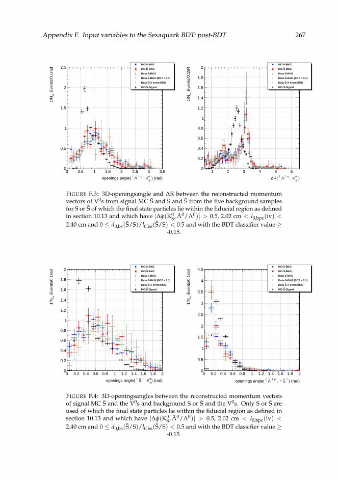
Appendix F. Input variables to the Sexaquark BDT: post-BDT 267
) (rad)0
S , K0
) Λ ( openings angle(
0 0.5 1 1.5 2 2.5 3 3.5
Eve
nts/
0.1r
adev
1/N
0
0.5
1
1.5
2
2.5MC-S-BKG
-BKGSMC-
Data-S-BKG
-BKG (BDT < 0.1) SData-
-X event BKGSData-
-SignalSMC-
)0
S , K0
) Λ (R( ∆
1 2 3 4 5 6
R∆ E
vent
s/0.
1ev
1/N
0
0.2
0.4
0.6
0.8
1
1.2
1.4
1.6
1.8
2MC-S-BKG
-BKGSMC-
Data-S-BKG
-BKG (BDT < 0.1) SData-
-X event BKGSData-
-SignalSMC-
FIGURE F.3: 3D-openingsangle and ∆R between the reconstructed momentumvectors of V0s from signal MC S and S and S from the five background samplesfor S or S of which the final state particles lie within the fiducial region as definedin section 10.13 and which have |∆φ(K0
S, Λ0/Λ0)| > 0.5, 2.02 cm < l0,bpc(iv) <
2.40 cm and 0 ≤ d0,bs(S/S)/l0,bs(S/S) < 0.5 and with the BDT classifier value ≥-0.15.
) (rad)0
S , K
) S
( openings angle(
0 0.2 0.4 0.6 0.8 1 1.2 1.4 1.6 1.8 2
Eve
nts/
0.1r
adev
1/N
0
0.2
0.4
0.6
0.8
1
1.2
1.4
1.6
1.8
2MC-S-BKG
-BKGSMC-
Data-S-BKG
-BKG (BDT < 0.1) SData-
-X event BKGSData-
-SignalSMC-
) (rad))
S ( , 0 )
Λ ( openings angle(
0 0.2 0.4 0.6 0.8 1 1.2 1.4 1.6 1.8 2
Eve
nts/
0.1r
adev
1/N
0
0.5
1
1.5
2
2.5
3
3.5
4
4.5MC-S-BKG
-BKGSMC-
Data-S-BKG
-BKG (BDT < 0.1) SData-
-X event BKGSData-
-SignalSMC-
FIGURE F.4: 3D-openingsangles between the reconstructed momentum vectorsof signal MC S and the V0s and background S or S and the V0s. Only S or S areused of which the final state particles lie within the fiducial region as defined insection 10.13 and which have |∆φ(K0
S, Λ0/Λ0)| > 0.5, 2.02 cm < l0,bpc(iv) <
2.40 cm and 0 ≤ d0,bs(S/S)/l0,bs(S/S) < 0.5 and with the BDT classifier value ≥-0.15.
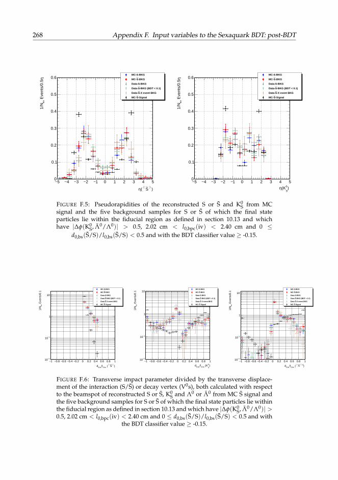
268 Appendix F. Input variables to the Sexaquark BDT: post-BDT
))
S (
( η
5− 4− 3− 2− 1− 0 1 2 3 4 5
η E
vent
s/0.
5ev
1/N
0
0.1
0.2
0.3
0.4
0.5
0.6MC-S-BKG
-BKGSMC-
Data-S-BKG
-BKG (BDT < 0.1) SData-
-X event BKGSData-
-SignalSMC-
) 0
S(Kη
5− 4− 3− 2− 1− 0 1 2 3 4 5η
Eve
nts/
0.5
ev 1
/N0
0.1
0.2
0.3
0.4
0.5
0.6MC-S-BKG
-BKGSMC-
Data-S-BKG
-BKG (BDT < 0.1) SData-
-X event BKGSData-
-SignalSMC-
FIGURE F.5: Pseudorapidities of the reconstructed S or S and K0S from MC
signal and the five background samples for S or S of which the final stateparticles lie within the fiducial region as defined in section 10.13 and whichhave |∆φ(K0
S, Λ0/Λ0)| > 0.5, 2.02 cm < l0,bpc(iv) < 2.40 cm and 0 ≤d0,bs(S/S)/l0,bs(S/S) < 0.5 and with the BDT classifier value ≥ -0.15.
))
S (
( 0,bs
/l0,bs
d
1− 0.8− 0.6− 0.4− 0.2− 0 0.2 0.4 0.6 0.8 1
Eve
nts/
0.1
ev 1
/N
2−10
1−10
1
10
MC-S-BKG
-BKGSMC-
Data-S-BKG
-BKG (BDT < 0.1) SData-
-X event BKGSData-
-SignalSMC-
)0
S (K
0,bs/l
0,bs d
1− 0.8− 0.6− 0.4− 0.2− 0 0.2 0.4 0.6 0.8 1
Eve
nts/
0.1
ev 1
/N
2−10
1−10
1
10MC-S-BKG
-BKGSMC-
Data-S-BKG
-BKG (BDT < 0.1) SData-
-X event BKGSData-
-SignalSMC-
) 0 )
Λ ( ( 0,bs
/l0,bs
d
1− 0.8− 0.6− 0.4− 0.2− 0 0.2 0.4 0.6 0.8 1
Eve
nts/
0.1
ev 1
/N
2−10
1−10
1
10
MC-S-BKG
-BKGSMC-
Data-S-BKG
-BKG (BDT < 0.1) SData-
-X event BKGSData-
-SignalSMC-
FIGURE F.6: Transverse impact parameter divided by the transverse displace-ment of the interaction (S/S) or decay vertex (V0s), both calculated with respectto the beamspot of reconstructed S or S, K0
S and Λ0 or Λ0 from MC S signal andthe five background samples for S or S of which the final state particles lie withinthe fiducial region as defined in section 10.13 and which have |∆φ(K0
S, Λ0/Λ0)| >0.5, 2.02 cm < l0,bpc(iv) < 2.40 cm and 0 ≤ d0,bs(S/S)/l0,bs(S/S) < 0.5 and with
the BDT classifier value ≥ -0.15.
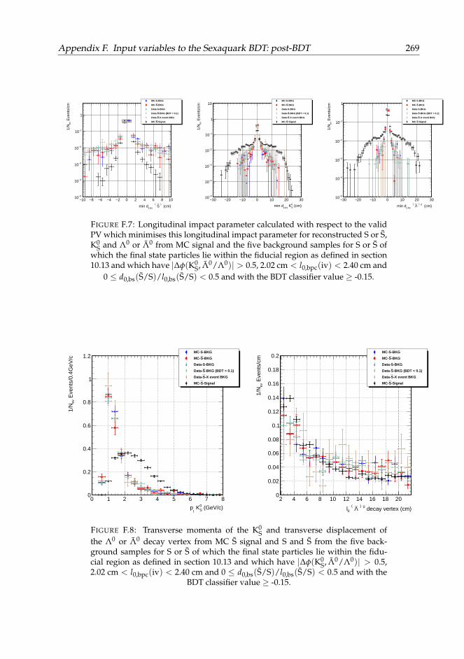
Appendix F. Input variables to the Sexaquark BDT: post-BDT 269
(cm))
S (
z,bs
min d
10− 8− 6− 4− 2− 0 2 4 6 8 10
Eve
nts/
cmev
1/N
5−10
4−10
3−10
2−10
1−10
1
MC-S-BKG
-BKGSMC-
Data-S-BKG
-BKG (BDT < 0.1) SData-
-X event BKGSData-
-SignalSMC-
(cm)0S K
z,bs min d
30− 20− 10− 0 10 20 30 E
vent
s/cm
ev 1
/N5−10
4−10
3−10
2−10
1−10
1
10MC-S-BKG
-BKGSMC-
Data-S-BKG
-BKG (BDT < 0.1) SData-
-X event BKGSData-
-SignalSMC-
(cm)0 )
Λ ( z,bs
min d
30− 20− 10− 0 10 20 30
Eve
nts/
cmev
1/N
5−10
4−10
3−10
2−10
1−10
1MC-S-BKG
-BKGSMC-
Data-S-BKG
-BKG (BDT < 0.1) SData-
-X event BKGSData-
-SignalSMC-
FIGURE F.7: Longitudinal impact parameter calculated with respect to the validPV which minimises this longitudinal impact parameter for reconstructed S or S,K0
S and Λ0 or Λ0 from MC signal and the five background samples for S or S ofwhich the final state particles lie within the fiducial region as defined in section10.13 and which have |∆φ(K0
S, Λ0/Λ0)| > 0.5, 2.02 cm < l0,bpc(iv) < 2.40 cm and0 ≤ d0,bs(S/S)/l0,bs(S/S) < 0.5 and with the BDT classifier value ≥ -0.15.
(GeV/c)0S K
t p
0 1 2 3 4 5 6 7 8
Eve
nts/
0.4G
eV/c
ev 1
/N
0
0.2
0.4
0.6
0.8
1
1.2MC-S-BKG
-BKGSMC-
Data-S-BKG
-BKG (BDT < 0.1) SData-
-X event BKGSData-
-SignalSMC-
decay vertex (cm)0 )
Λ ( 0 l
2 4 6 8 10 12 14 16 18 20
Eve
nts/
cmev
1/N
0
0.02
0.04
0.06
0.08
0.1
0.12
0.14
0.16
0.18
0.2MC-S-BKG
-BKGSMC-
Data-S-BKG
-BKG (BDT < 0.1) SData-
-X event BKGSData-
-SignalSMC-
FIGURE F.8: Transverse momenta of the K0S and transverse displacement of
the Λ0 or Λ0 decay vertex from MC S signal and S and S from the five back-ground samples for S or S of which the final state particles lie within the fidu-cial region as defined in section 10.13 and which have |∆φ(K0
S, Λ0/Λ0)| > 0.5,2.02 cm < l0,bpc(iv) < 2.40 cm and 0 ≤ d0,bs(S/S)/l0,bs(S/S) < 0.5 and with the
BDT classifier value ≥ -0.15.
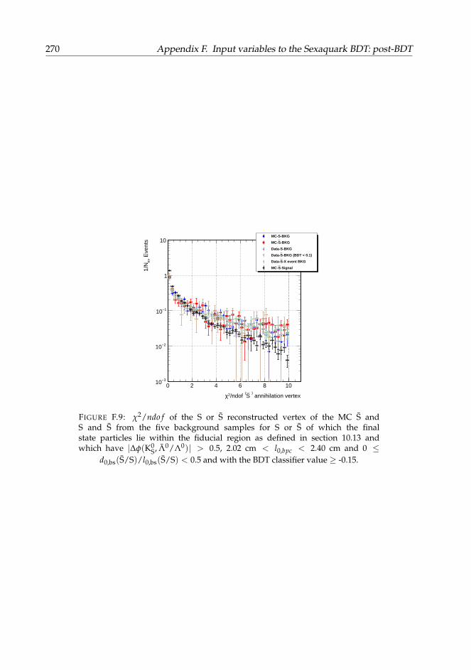
270 Appendix F. Input variables to the Sexaquark BDT: post-BDT
annihilation vertex)
S(
/ndof 2χ
0 2 4 6 8 10
Eve
nts
ev 1
/N
3−10
2−10
1−10
1
10MC-S-BKG
-BKGSMC-
Data-S-BKG
-BKG (BDT < 0.1) SData-
-X event BKGSData-
-SignalSMC-
FIGURE F.9: χ2/ndo f of the S or S reconstructed vertex of the MC S andS and S from the five background samples for S or S of which the finalstate particles lie within the fiducial region as defined in section 10.13 andwhich have |∆φ(K0
S, Λ0/Λ0)| > 0.5, 2.02 cm < l0,bpc < 2.40 cm and 0 ≤d0,bs(S/S)/l0,bs(S/S) < 0.5 and with the BDT classifier value ≥ -0.15.

271
List of Abbreviations
2S Strip-StripAC Alternating CurrentADC Analogue to Digital ConverterALICE A Large Ion Collider ExperimentAMC Advanced Mezzanine CardAMUX Analogue MUltipleXerAPV Front-end Readout Chip: Analogue Pipeline (Voltage mode)ASIC Application-Specific Integrated CircuitATCA Advanced Telecommunications Computing ArchitectureATLAS A Toroidal LHC ApparatuSBBN Big Bang NucleosynthesisBDT Boosted Decision TreeBE Binding EnergyBEH Brout-Englert-HiggsBRAM Block Random-Access MemoryBX Bunch CrossingCBC CMS Binary ChipCE-E HGCAL Electromagnetic sectionCE-H HGCAL Hadronic sectionCE HGCALCIC Concentrator Integrated CircuitCL Confidence LimitCLB Configurable Logic BlockCMB Cosmic Microwave BackgroundCMOS Complementary Metal-Oxide-SemiconductorCMS Compact Muon SolenoidCRC Cyclotron Resource CentreCSC Cathode Strip ChamberDAC Digital to Analogue ConverterDAQ Data AcQuisitionDC Direct CurrentDDR3 Double Data Rate 3DIO5 5-bit port digital IO card in FMC form factorDLL Delay-Locked LoopDM Dark MatterDQM Data Quality MonitoringDRAM Dynamic Random-Access MemoryDSP Digital Signal ProcessingDT Drift TubeDTC Data, Trigger and ControlDUT Device Under TestDY Drell-YanEB ECAL Barrel

272 List of Abbreviations
EC ECAL EndcapECAL Electromagnetic CALorimterEP-ESE Experimental Physics-Electronic Systems for ExperimentsFEC Forward Error CorrectionFEH Front-End HybridFET Field-Effect TransistorFIFO First In, First OutFLUKA FLUktuierende KAskadeFMC FPGA Mezzanine CardFPGA Field-Programmable Gate ArrayFW FirmWareGBT GigaBit TransceiverGEM Gas Electron MultiplierHB HCAL BarrelHCAL Hadronic CALorimeterHE HCAL EndcapHF HCAL ForwardHGCAL High Granularity CalorimeterHIF Heavy Ion FacilityHIP Highly Ionizing ParticleHL-LHC High Luminosity-Large Hadron ColliderHLT High-Level TriggerHO HCAL OuterHV High VoltageI/0 Input/OutputI2C Inter-Integrated CircuitIC Integrated CircuitIDELAY Input DelayILC International Linear ColliderIP Internet ProtocoliRPC improved RPCISERDES Input SERializer/DESerializerL1 Level1L1A L1-AcceptLED Light Emitting DiodeLET Linear Energy TransferLGAD Low-Gain-Avalanche-DiodeLHC Large Hadron ColliderLHCb Large Hadron Collider beautyLINAC LINear ACceleratorlpGBT low-power GigaBit TransceiverLSB Least Significant BitLUT Look-Up TableLV Low VoltageLVDS Low-Voltage Differential SignalingMACHO Massive Astrophysical Compact Halo ObjectMaPSA Macro-Pixel Sub-AssemblyMBU Multi-Bit UpsetMC Monte Carlo
List of Abbreviations 273
MCH MicroTCA Carrier HubMIP Minimum Ionizing ParticleMMCM Mixed-Mode Clock ManagerMOS Metal-Oxide-SemiconductorMOSFET Metal-Oxide-Semiconductor Field-Effect TransistorMPA Macro-Pixel ASICMPV Most Probable ValueMSB Most Significant BitMTD MIP Timing DetectorNIEL Non-Ionizing Energy LossNMOS N-type channel Metal-Oxide-SemiconductorOSERDES Output SERializer/DESerializerOT Outer TrackerPCB Printed Circuit BoardPh2 ACF Phase-2 Acquisition and Control FrameworkPMOS P-type channel Metal-Oxide-SemiconductorPMT Photo Multiplier Tubepp proton-protonPS-MCK Pixel-Strip Mock-UpPS-p Pixel-Strip pixelPS-s Pixel-Strip stripPS Proton Synchrotron or Pixel-StripPU PileUpPV Primary VertexQCD Quantum ChromoDynamicsQFT Quantum Field TheoryQGP Quark Gluon PlasmaRAM Random-Access MemoryRECO RECOnstruction levelRMS Root Mean SquareRPC Resistive Plate ChamberRTL Register-Transfer LevelSEE Single-Event EffectSEH SErvice HybridSEL Single-Event LatchupSET Single-Event TransientSEU Single-Event UpsetSIM SIMulation levelSiPM Silicon PhotoMultierSLVS Scalable Low-Voltage SignallingSPS Super Proton SynchrotronSRAM Static Random-Access MemorySSA Short Strip ASICSW SoftWareTB2S Tracker Barrel with 2S modulesTBPS Tracker Barrel with PS modulesTDC Time to Digital ConverterTEC Tracker EndCapTEDD Tracker Endcap Double-Discs

274 List of Abbreviations
TIB Tracker Inner BarrelTID Total Ionizing Dose or Tracker Inner DiskTLU Trigger Logic UnitTMR Triple Module RedundancyTOB Tracker Outer BarrelTTC Trigger, Timing and ControlUCL Université Catholique de LouvainUDP User Datagram ProtocolµDTC micro Data, Trigger and ControlUE Underlying EventµTCA micro Telecommunications Computing ArchitectureVHDCI Very-High-Density Cable InterconnectVHDL Very High Speed Integrated Circuit Hardware Description LanguageVLSI Very Large Scale IntegratedVMEbus Versa Module Europa or Versa Module Eurocard busVTRX+ Versatile TRansceiver plusWIMP Weakly Interacting Massive Particle
275
Acknowledgements
First of all, I would like to thank Steven for giving me the opportunity to perform theresearch described in this thesis, for his patient guidance and availability to meet up anddiscuss work, despite a packed agenda. A little over four years ago, you managed to getme excited about the tracker project at the IIHE when we were trying to communicateover a lousy Skype connection whilst being at opposite sides of the globe. This fact is justone of the examples of the enthusiasm you put in your work.
Besides Steven, I would like to thank Prof. P. Vanlaer for the many fruitful discussionsand the advice, both on the tracker project and on the Sexaquark analysis. I would alsolike to thank Prof. G. De Lentdecker for kindly making hardware available any time weasked for something and Prof. J. D’Hondt and Prof. L. Favart for actively supportingthe tracker Phase-2 project at the IIHE. Also thanks to the jury members for reading thismanuscript in great detail, for the interesting questions, discussions and relevant com-ments.
During the four years I spent at the IIHE I had two offices, which are referred to be-low as the upstairs-greenhouse-sandwich-eating-office and downstairs-greenhouse-warm-meal-eating-office. These offices have two thing in common: steep temperature gradients, but,more importantly, warm people.
The upstairs-greenhouse-sandwich-eating-office:
Many thanks to Annik, Isabelle, Kevin, Isis, Lieselotte, Karen, Kirill, Doug,Simon, Emil, Petra, Shimaa, Dom, Seth, Dennys, Giannis, Annemie, Audrey,Merel and Quentin whom I shared the floor/office with during the first twoyears of my thesis. Thanks for all the nice lunch breaks, the absurd humour andthe two cherry tomatoes from the indoor garden (it was a successful harvest,indeed). Special thanks also to Marleen for the generous support you providedevery day.
The downstairs-greenhouse-warm-meal-eating-office:
The last two years of my time at the IIHE I spent in the office with Jelena andsubsequently Inna, Yannick and Wendi. Thanks for all the candy and choco-late, both got me through quite a few energy glitches. Big thanks as well toAlexandre, Thomas, Barbara, Yifan, Michael, Bugra, David, Hugo, Diego, Qun,Gwen, Louis, Florian, Anastasia, Amandeep, Laurent, Andrey, Olivier, Denis,Stéphane, Romain, Shkelzen, Adriano and all the other members of the com-puting team.
I am grateful to several colleagues outside of the IIHE as well: Mykyta, Sarah, Da-vide and Davide, Alessandro, Simone, Mark and Tomasz for sharing many, often long,hours of debugging set-ups or performing tests in some noisy or hot lab at CERN or else-where. Furthermore, I am thankful to Prof. G. Farrar and Prof. T. Pierog, respectively forthe stimulating discussions on Sexaquarks and for making available a special version ofEPOS-LHC to us.
Many thanks to all members of the teaching team which I joined the last four years,especially to Stefan for coordinating the activities and accommodating for my agenda.

276
Thanks to the Belgian rail company for getting me to work every day! (Calculationsshow that approximately a quarter of this thesis was written on the train. Whether or notdelays had a significant impact on this is still to be investigated.)
Besides work, there was also a bit of personal life in the past four years. I deeplyadmire Elien for encouraging me when work went stiff, for spending quite some solitaryevenings and weekends when I was writing this manuscript and for reminding me, eachtime I came home, why I took the train back to Ghent every evening. People say thatit’s only possible to concentrate on work when one is happy ... for sure you had a majorimpact on that.
Furthermore, thanks to my sister, mother, father and other family members for theencouragement and the food packages. Thanks also to the travelling-friends (for remind-ing me of the outside world), cycling- and football-friends (for reminding me of thoseother two limbs called ’legs’), roommates (for reminding me to do the dishes), old study-friends (for reminding me of irrelevant physics paradoxes) and all the other friends fromGhent (for not complaining they did not get a separate category).
277
Bibliography
[1] A. Purcell. “Go on a particle quest at the first CERN webfest.” In: BUL-NA-2012-269. 35/2012 (2012), p. 10. URL: https://cds.cern.ch/record/1473657.
[2] F. Englert and R. Brout. “Broken Symmetry and the Mass of Gauge Vector Mesons”.In: Phys. Rev. Lett. 13 (9 1964), pp. 321–323. DOI: 10.1103/PhysRevLett.13.321.
[3] P.W. Higgs. “Broken symmetries, massless particles and gauge fields”. In: PhysicsLetters 12.2 (1964), pp. 132 –133. ISSN: 0031-9163. DOI: 10.1016/0031-9163(64)91136-9.
[4] M. D. Schwartz. Quantum Field Theory and the Standard Model. Cambridge Univer-sity Press, 2014. ISBN: 1107034736, 9781107034730. URL: http://www.cambridge.org/us/academic/subjects/physics/theoretical-physics-and-mathematical-physics/quantum-field-theory-and-standard-model.
[5] J. Ellis, M. K. Gaillard, and D. V. Nanopoulos. “A Historical Profile of the HiggsBoson. An Updated Historical Profile of the Higgs Boson”. In: arXiv:1504.07217(2015), 22 p. DOI: 10.1142/9789814733519_0014.
[6] Planck Collaboration. “Planck 2018 results. VI. Cosmological parameters”. In: arXive-prints (2018). arXiv: 1807.06209 [astro-ph.CO].
[7] D. Clowe, A. Gonzalez, and M. Markevitch. “Weak-Lensing Mass Reconstructionof the Interacting Cluster 1E 0657-558: Direct Evidence for the Existence of DarkMatter”. In: The Astrophysical Journal 604.2 (2004), pp. 596–603. DOI: 10.1086/381970.
[8] N. Cibirka et al. “RELICS: Strong Lensing Analysis of the Galaxy Clusters AbellS295, Abell 697, MACS J0025.4-1222, and MACS J0159.8-0849”. In: The Astrophysi-cal Journal 863.2 (2018), p. 145. DOI: 10.3847/1538-4357/aad2d3.
[9] F. Zwicky. “On the Masses of Nebulae and of Clusters of Nebulae”. In: apj 86(1937), p. 217. DOI: 10.1086/143864.
[10] M. Tanabashi et al. “Review of Particle Physics”. In: Phys. Rev. D 98 (3 2018),p. 030001. DOI: 10.1103/PhysRevD.98.030001.
[11] D. H. Perkins. Particle Astrophysics. Oxford University Press, 2009. ISBN: 978–0–19–954546–9.
[12] M. Taoso, G. Bertone, and A. Masiero. “Dark matter candidates: a ten-point test”.In: Journal of Cosmology and Astroparticle Physics 2008.03 (2008), p. 022. DOI: 10.1088/1475-7516/2008/03/022.
[13] J. I. Read, M. G. Walker, and P. Steger. “Dark matter heats up in dwarf galaxies”.In: Monthly Notices of the Royal Astronomical Society 484.1 (Jan. 2019), pp. 1401–1420.ISSN: 0035-8711. DOI: 10.1093/mnras/sty3404.
[14] G. F. Knoll. Radiation Detection and Measurement. John Wiley and Sons, Inc, 1999.ISBN: 978-0-273-71918-2.
[15] F. Hartmann. Evolution of Silicon Sensor Technology in Particle Physics. Springer,2009. ISBN: 978-3-540-25094-4.
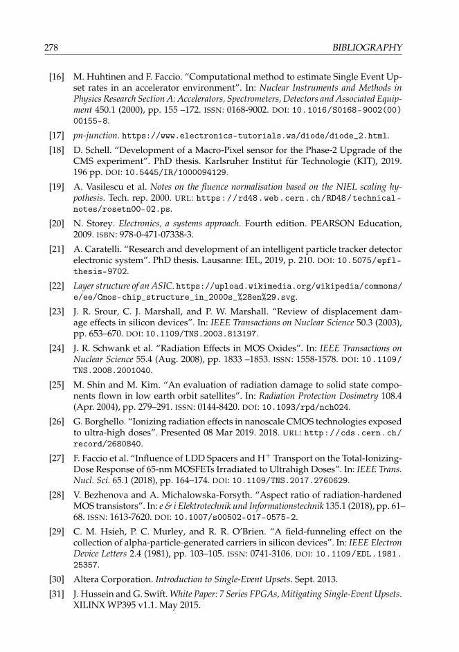
278 BIBLIOGRAPHY
[16] M. Huhtinen and F. Faccio. “Computational method to estimate Single Event Up-set rates in an accelerator environment”. In: Nuclear Instruments and Methods inPhysics Research Section A: Accelerators, Spectrometers, Detectors and Associated Equip-ment 450.1 (2000), pp. 155 –172. ISSN: 0168-9002. DOI: 10.1016/S0168-9002(00)00155-8.
[17] pn-junction. https://www.electronics-tutorials.ws/diode/diode_2.html.
[18] D. Schell. “Development of a Macro-Pixel sensor for the Phase-2 Upgrade of theCMS experiment”. PhD thesis. Karlsruher Institut für Technologie (KIT), 2019.196 pp. DOI: 10.5445/IR/1000094129.
[19] A. Vasilescu et al. Notes on the fluence normalisation based on the NIEL scaling hy-pothesis. Tech. rep. 2000. URL: https://rd48.web.cern.ch/RD48/technical-notes/rosetn00-02.ps.
[20] N. Storey. Electronics, a systems approach. Fourth edition. PEARSON Education,2009. ISBN: 978-0-471-07338-3.
[21] A. Caratelli. “Research and development of an intelligent particle tracker detectorelectronic system”. PhD thesis. Lausanne: IEL, 2019, p. 210. DOI: 10.5075/epfl-thesis-9702.
[22] Layer structure of an ASIC. https://upload.wikimedia.org/wikipedia/commons/e/ee/Cmos-chip_structure_in_2000s_%28en%29.svg.
[23] J. R. Srour, C. J. Marshall, and P. W. Marshall. “Review of displacement dam-age effects in silicon devices”. In: IEEE Transactions on Nuclear Science 50.3 (2003),pp. 653–670. DOI: 10.1109/TNS.2003.813197.
[24] J. R. Schwank et al. “Radiation Effects in MOS Oxides”. In: IEEE Transactions onNuclear Science 55.4 (Aug. 2008), pp. 1833 –1853. ISSN: 1558-1578. DOI: 10.1109/TNS.2008.2001040.
[25] M. Shin and M. Kim. “An evaluation of radiation damage to solid state compo-nents flown in low earth orbit satellites”. In: Radiation Protection Dosimetry 108.4(Apr. 2004), pp. 279–291. ISSN: 0144-8420. DOI: 10.1093/rpd/nch024.
[26] G. Borghello. “Ionizing radiation effects in nanoscale CMOS technologies exposedto ultra-high doses”. Presented 08 Mar 2019. 2018. URL: http://cds.cern.ch/record/2680840.
[27] F. Faccio et al. “Influence of LDD Spacers and H+ Transport on the Total-Ionizing-Dose Response of 65-nm MOSFETs Irradiated to Ultrahigh Doses”. In: IEEE Trans.Nucl. Sci. 65.1 (2018), pp. 164–174. DOI: 10.1109/TNS.2017.2760629.
[28] V. Bezhenova and A. Michalowska-Forsyth. “Aspect ratio of radiation-hardenedMOS transistors”. In: e & i Elektrotechnik und Informationstechnik 135.1 (2018), pp. 61–68. ISSN: 1613-7620. DOI: 10.1007/s00502-017-0575-2.
[29] C. M. Hsieh, P. C. Murley, and R. R. O’Brien. “A field-funneling effect on thecollection of alpha-particle-generated carriers in silicon devices”. In: IEEE ElectronDevice Letters 2.4 (1981), pp. 103–105. ISSN: 0741-3106. DOI: 10.1109/EDL.1981.25357.
[30] Altera Corporation. Introduction to Single-Event Upsets. Sept. 2013.
[31] J. Hussein and G. Swift. White Paper: 7 Series FPGAs, Mitigating Single-Event Upsets.XILINX WP395 v1.1. May 2015.
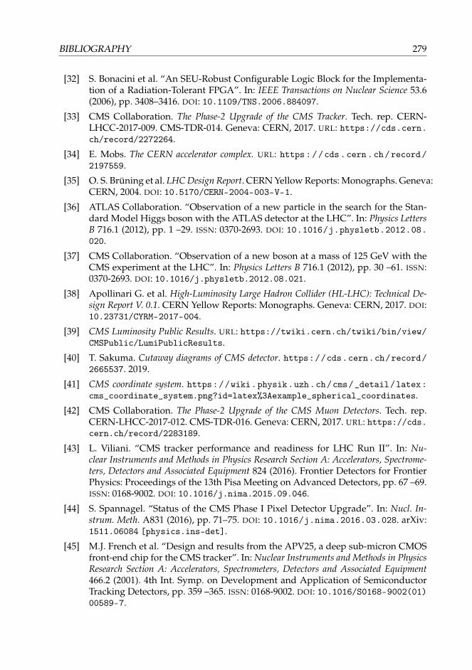
BIBLIOGRAPHY 279
[32] S. Bonacini et al. “An SEU-Robust Configurable Logic Block for the Implementa-tion of a Radiation-Tolerant FPGA”. In: IEEE Transactions on Nuclear Science 53.6(2006), pp. 3408–3416. DOI: 10.1109/TNS.2006.884097.
[33] CMS Collaboration. The Phase-2 Upgrade of the CMS Tracker. Tech. rep. CERN-LHCC-2017-009. CMS-TDR-014. Geneva: CERN, 2017. URL: https://cds.cern.ch/record/2272264.
[34] E. Mobs. The CERN accelerator complex. URL: https://cds.cern.ch/record/2197559.
[35] O. S. Brüning et al. LHC Design Report. CERN Yellow Reports: Monographs. Geneva:CERN, 2004. DOI: 10.5170/CERN-2004-003-V-1.
[36] ATLAS Collaboration. “Observation of a new particle in the search for the Stan-dard Model Higgs boson with the ATLAS detector at the LHC”. In: Physics LettersB 716.1 (2012), pp. 1 –29. ISSN: 0370-2693. DOI: 10.1016/j.physletb.2012.08.020.
[37] CMS Collaboration. “Observation of a new boson at a mass of 125 GeV with theCMS experiment at the LHC”. In: Physics Letters B 716.1 (2012), pp. 30 –61. ISSN:0370-2693. DOI: 10.1016/j.physletb.2012.08.021.
[38] Apollinari G. et al. High-Luminosity Large Hadron Collider (HL-LHC): Technical De-sign Report V. 0.1. CERN Yellow Reports: Monographs. Geneva: CERN, 2017. DOI:10.23731/CYRM-2017-004.
[39] CMS Luminosity Public Results. URL: https://twiki.cern.ch/twiki/bin/view/CMSPublic/LumiPublicResults.
[40] T. Sakuma. Cutaway diagrams of CMS detector. https://cds.cern.ch/record/2665537. 2019.
[41] CMS coordinate system. https://wiki.physik.uzh.ch/cms/_detail/latex:cms_coordinate_system.png?id=latex%3Aexample_spherical_coordinates.
[42] CMS Collaboration. The Phase-2 Upgrade of the CMS Muon Detectors. Tech. rep.CERN-LHCC-2017-012. CMS-TDR-016. Geneva: CERN, 2017. URL: https://cds.cern.ch/record/2283189.
[43] L. Viliani. “CMS tracker performance and readiness for LHC Run II”. In: Nu-clear Instruments and Methods in Physics Research Section A: Accelerators, Spectrome-ters, Detectors and Associated Equipment 824 (2016). Frontier Detectors for FrontierPhysics: Proceedings of the 13th Pisa Meeting on Advanced Detectors, pp. 67 –69.ISSN: 0168-9002. DOI: 10.1016/j.nima.2015.09.046.
[44] S. Spannagel. “Status of the CMS Phase I Pixel Detector Upgrade”. In: Nucl. In-strum. Meth. A831 (2016), pp. 71–75. DOI: 10.1016/j.nima.2016.03.028. arXiv:1511.06084 [physics.ins-det].
[45] M.J. French et al. “Design and results from the APV25, a deep sub-micron CMOSfront-end chip for the CMS tracker”. In: Nuclear Instruments and Methods in PhysicsResearch Section A: Accelerators, Spectrometers, Detectors and Associated Equipment466.2 (2001). 4th Int. Symp. on Development and Application of SemiconductorTracking Detectors, pp. 359 –365. ISSN: 0168-9002. DOI: 10.1016/S0168-9002(01)00589-7.
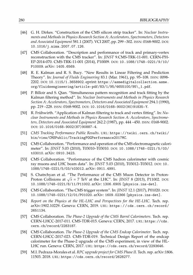
280 BIBLIOGRAPHY
[46] G. H. Dirkes. “Construction of the CMS silicon strip tracker”. In: Nuclear Instru-ments and Methods in Physics Research Section A: Accelerators, Spectrometers, Detectorsand Associated Equipment 581.1 (2007). VCI 2007, pp. 299 –302. ISSN: 0168-9002. DOI:10.1016/j.nima.2007.07.126.
[47] CMS Collaboration. “Description and performance of track and primary-vertexreconstruction with the CMS tracker”. In: JINST 9.CMS-TRK-11-001. CERN-PH-EP-2014-070. CMS-TRK-11-001 (2014), P10009. DOI: 10.1088/1748-0221/9/10/P10009. arXiv: 1405.6569.
[48] R. E. Kalman and R. S. Bucy. “New Results in Linear Filtering and PredictionTheory”. In: Journal of Fluids Engineering 83.1 (Mar. 1961), pp. 95–108. ISSN: 0098-2202. DOI: 10.1115/1.3658902. eprint: https://asmedigitalcollection.asme.org/fluidsengineering/article-pdf/83/1/95/4655100/95\_1.pdf.
[49] P. Billoir and S. Qian. “Simultaneous pattern recognition and track fitting by theKalman filtering method”. In: Nuclear Instruments and Methods in Physics ResearchSection A: Accelerators, Spectrometers, Detectors and Associated Equipment 294.1 (1990),pp. 219 –228. ISSN: 0168-9002. DOI: 10.1016/0168-9002(90)91835-Y.
[50] R. Frühwirth. “Application of Kalman filtering to track and vertex fitting”. In: Nu-clear Instruments and Methods in Physics Research Section A: Accelerators, Spectrome-ters, Detectors and Associated Equipment 262.2 (1987), pp. 444 –450. ISSN: 0168-9002.DOI: 10.1016/0168-9002(87)90887-4.
[51] CMS Tracking Performance Public Results. URL: https://twiki.cern.ch/twiki/bin/view/CMSPublic/TrackingPOGPerformance2017MC.
[52] CMS Collaboration. “Performance and operation of the CMS electromagnetic calori-meter”. In: JINST 5.03 (2010), T03010–T03010. DOI: 10.1088/1748-0221/5/03/t03010. arXiv: 0910.3423.
[53] CMS Collaboration. “Performance of the CMS hadron calorimeter with cosmicray muons and LHC beam data”. In: JINST 5.03 (2010), T03012–T03012. DOI: 10.1088/1748-0221/5/03/t03012. arXiv: 0911.4991.
[54] S. Chatrchyan et al. “The Performance of the CMS Muon Detector in Proton-Proton Collisions at
√s = 7 TeV at the LHC”. In: JINST 8 (2013), P11002. DOI:
10.1088/1748-0221/8/11/P11002. arXiv: 1306.6905 [physics.ins-det].
[55] CMS Collaboration. “The CMS trigger system”. In: JINST 12.1 (2017), P01020. DOI:10.1088/1748-0221/12/01/P01020. arXiv: 1609.02366 [physics.ins-det].
[56] Report on the Physics at the HL-LHC and Perspectives for the HE-LHC. Tech. rep.arXiv:1902.10229. Geneva: CERN, 2019. URL: https://cds.cern.ch/record/2651134.
[57] CMS Collaboration. The Phase-2 Upgrade of the CMS Barrel Calorimeters. Tech. rep.CERN-LHCC-2017-011. CMS-TDR-015. Geneva: CERN, 2017. URL: https://cds.cern.ch/record/2283187.
[58] CMS Collaboration. The Phase-2 Upgrade of the CMS Endcap Calorimeter. Tech. rep.CERN-LHCC-2017-023. CMS-TDR-019. Technical Design Report of the endcapcalorimeter for the Phase-2 upgrade of the CMS experiment, in view of the HL-LHC run. Geneva: CERN, 2017. URL: https://cds.cern.ch/record/2293646.
[59] M.I. Pedraza-Morales et al. RPC upgrade project for CMS Phase II. Tech. rep. arXiv:1806.11503. 2018. URL: https://cds.cern.ch/record/2628277.
BIBLIOGRAPHY 281
[60] CMS Collaboration. Technical Proposal for a MIP Timing Detector in the CMS Exper-iment Phase 2 Upgrade. Tech. rep. CERN-LHCC-2017-027. LHCC-P-009. Geneva:CERN, 2017. URL: https://cds.cern.ch/record/2296612.
[61] J. G. Hegeman. The CMS Data Acquisition System for the Phase-2 Upgrade. Tech. rep.CMS-CR-2018-099. Geneva: CERN, 2018. URL: http://cds.cern.ch/record/2629375.
[62] CMS Collaboration. The CMS tracker system project: Technical Design Report. Tech-nical Design Report CMS. Geneva: CERN, 1997. URL: http://cds.cern.ch/record/368412.
[63] D. Contardo et al. Technical Proposal for the Phase-II Upgrade of the CMS Detector.Tech. rep. CERN-LHCC-2015-010. LHCC-P-008. CMS-TDR-15-02. Geneva, 2015.URL: https://cds.cern.ch/record/2020886.
[64] CMS Collaboratio. The Phase-2 Upgrade of the CMS L1 Trigger Interim TechnicalDesign Report. Tech. rep. CERN-LHCC-2017-013. CMS-TDR-017. Geneva: CERN,2017. URL: https://cds.cern.ch/record/2283192.
[65] A. Dierlamm. Characterisation of silicon sensor materials and designs for the CMSTracker Upgrade. Tech. rep. AIDA-CONF-2014-006. Geneva: CERN, 2012. URL: https://cds.cern.ch/record/1693190.
[66] D. Ceresa et al. Macro Pixel ASIC User Manual v0.1. URL: https://espace.cern.ch/CMS-MPA/SiteAssets/SitePages/Documents/MPA_UserManual_V0.pdf.
[67] A. Caratelli et al. Short Strip ASIC Specification Document v1. URL: https://espace.cern.ch/CMS-MPA/SiteAssets/SitePages/Documents/SSA_Manual_V1.0.pdf.
[68] M. Prydderch. CBC3.1 User Manual. URL: http://www.hep.ph.ic.ac.uk/ASIC/cbc3.1/CBC3p1_User_Manual_V1p3.pdf.
[69] L. Caponetto et al. CIC1 technical specification. URL: https://espace.cern.ch/Tracker-Upgrade/Electronics/CIC/Shared%20Documents/Specifications/CIC_specs_v3.pdf.
[70] I2C bus specifications for the CMS tracker 2S and PS modules, v2.0, 21/4/2016. CMSinternal document.
[71] P. Moreira. Inside the LpGBT. Ecole IN2P3 de Microélectronique. May 2017.
[72] J. Troska et al. The VTRx+, an Optical Link Module for Data Transmission at HL-LHC.TWEPP proceeding. 2018. DOI: 10.22323/1.313.0048.
[73] lpGBT Manual. URL: https://lpgbt.web.cern.ch/lpgbt/manual/.
[74] Y. Gershtein. “CMS Hardware Track Trigger: New Opportunities for Long-LivedParticle Searches at the HL-LHC”. In: Phys. Rev. D96.3 (2017), p. 035027. DOI: 10.1103/PhysRevD.96.035027. arXiv: 1705.04321 [hep-ph].
[75] M. Pesaresi et al. “The FC7 AMC for generic DAQ & control applications in CMS”.In: JINST 10.3 (2015), pp. C03036–C03036. DOI: 10.1088/1748- 0221/10/03/C03036.
[76] XILINX 7 Series FPGAs Configurable Logic Block, UG474. URL: https://www.xilinx.com/support/documentation/user_guides/ug474_7Series_CLB.pdf.
[77] MicroTCA Application Guide, A Modular Open Systems Approach for Computer Archi-tecture. Version 1.1, August 2012. URL: https://www.picmg.org/wp-content/uploads/MicroTCA_Application_Guide_final-_rev1_1.pdf.

282 BIBLIOGRAPHY
[78] C. G. Larrea et al. “IPbus: a flexible Ethernet-based control system for xTCA hard-ware”. In: JINST 10 (2015), p. C02019. DOI: 10.1088%2F1748-0221%2F10%2F02%2Fc02019.
[79] XILINX 7 Series FPGAs Data Sheet: Overview. URL: https://www.xilinx.com/support/documentation/data_sheets/ds180_7Series_Overview.pdf.
[80] CMS Tracker Collaboration. Performance of the Prototype CBC3-based Outer TrackerModules for the Phase II Upgrade of CMS before and after neutron irradiation. in prepa-ration.
[81] Update of System Test Activities at KIT. URL: https://indico.cern.ch/event/818273 / contributions / 3422488 / attachments / 1843406 / 3023409 / 190513 _System_Test_Meeting_-_XTalk.pdf.
[82] A. Ferrari et al. FLUKA: A multi-particle transport code (Program version 2005). 2005.DOI: 10.2172/877507.
[83] S. Mallows et al. “Monte Carlo simulations of the radiation environment for theCMS experiment”. In: Nuclear Instruments and Methods in Physics Research SectionA: Accelerators, Spectrometers, Detectors and Associated Equipment 824 (2016). Fron-tier Detectors for Frontier Physics: Proceedings of the 13th Pisa Meeting on Ad-vanced Detectors, pp. 30 –32. ISSN: 0168-9002. DOI: 10.1016/j.nima.2015.11.044.
[84] G Bianchi et al. “tkLayout: a design tool for innovative silicon tracking detec-tors”. In: JINST 9.03 (2014), pp. C03054–C03054. DOI: 10.1088/1748-0221/9/03/c03054.
[85] D. Cussans. Description of the JRA1 Trigger Logic Unit (TLU), v0.2c. EUDET-Memo-2009-4.
[86] H. Perrey. “An EUDET / AIDA pixel beam telescope for detector development ”.In: IEEE Nuclear Science Symposium and Medical Imaging Conference Record (NSS/MIC)(Oct. 2012). DOI: 10.1109/NSSMIC.2012.6551461.
[87] Bitonic sorting. https://commons.wikimedia.org/wiki/File:BitonicSort1.svg.
[88] G. R. Farrar. “Stable Sexaquark”. In: arXiv e-prints (2017). arXiv: 1708.08951 [hep-ph].
[89] R. L. Jaffe. “Perhaps a Stable Dihyperon”. In: Phys. Rev. Lett. 38 (1977). [Erratum:Phys. Rev. Lett.38,617(1977)], pp. 195–198. DOI: 10.1103/PhysRevLett.38.617,10.1103/PhysRevLett.38.195.
[90] Belle Collaboration. “Observation of a Narrow Charmoniumlike State in Exclu-sive B± → K±π+π− J/ψ Decays”. In: Phys. Rev. Lett. 91 (26 2003), p. 262001. DOI:10.1103/PhysRevLett.91.262001.
[91] LHCb Collaboration. “Observation of J/ψp Resonances Consistent with PentaquarkStates in Λ0
b → J/ψK−p Decays”. In: Phys. Rev. Lett. 115 (2015), p. 072001. DOI:10.1103/PhysRevLett.115.072001. arXiv: 1507.03414 [hep-ex].
[92] R. E. Chrien. “H particle searches at Brookhaven”. In: Nuclear Physics A 629.1(1998). Quark Lepton Nuclear Physics, pp. 388 –397. ISSN: 0375-9474. DOI: 10.1016/S0375-9474(97)00714-8.
[93] Belle Collaboration. “Search for an H-Dibaryon with a Mass near 2mΛ in Υ(1S)and Υ(2S) Decays”. In: Phys. Rev. Lett. 110 (22 2013), p. 222002. DOI: 10.1103/PhysRevLett.110.222002.
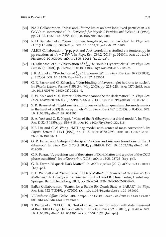
BIBLIOGRAPHY 283
[94] NA 3 Collaboration. “Mass and lifetime limits on new long-lived particles in 300GeV/c π- interactions”. In: Zeitschrift für Physik C Particles and Fields 31.1 (1986),pp. 21–32. ISSN: 1431-5858. DOI: 10.1007/BF01559588.
[95] R. H. Bernstein et al. “Search for new, long-lived, neutral particles”. In: Phys. Rev.D 37 (11 1988), pp. 3103–3106. DOI: 10.1103/PhysRevD.37.3103.
[96] ALICE Collaboration. “p-p, p-Λ and Λ-Λ correlations studied via femtoscopy inpp reactions at
√s = 7 TeV”. In: Phys. Rev. C99.2 (2019), p. 024001. DOI: 10.1103/
PhysRevC.99.024001. arXiv: 1805.12455 [nucl-ex].
[97] H. Takahashi et al. “Observation of a 6ΛΛHe Double Hypernucleus”. In: Phys. Rev.
Lett. 87 (21 2001), p. 212502. DOI: 10.1103/PhysRevLett.87.212502.
[98] J. K. Ahn et al. “Production of 4ΛΛ H Hypernuclei”. In: Phys. Rev. Lett. 87 (13 2001),
p. 132504. DOI: 10.1103/PhysRevLett.87.132504.
[99] G. R. Farrar and G. Zaharijas. “Non-binding of flavor-singlet hadrons to nuclei”.In: Physics Letters, Section B 559.3-4 (May 2003), pp. 223–228. ISSN: 0370-2693. DOI:10.1016/S0370-2693(03)00331-9.
[100] E. W. Kolb and M. S. Turner. “Dibaryons cannot be the dark matter”. In: Phys. Rev.D 99."arXiv:1809.06003" (6 2019), p. 063519. DOI: 10.1103/PhysRevD.99.063519.
[101] S. R. Beane et al. “Light nuclei and hypernuclei from quantum chromodynamicsin the limit of SU(3) flavor symmetry”. In: Phys. Rev. D 87 (3 2013), p. 034506. DOI:10.1103/PhysRevD.87.034506.
[102] S. A. Yost and C. R. Nappi. “Mass of the H dibaryon in a chiral model”. In: Phys.Rev. D 32 (3 1985), pp. 816–818. DOI: 10.1103/PhysRevD.32.816.
[103] K.F. Liu and C.W. Wong. “MIT bag model with center-of-mass correction”. In:Physics Letters B 113.1 (1982), pp. 1 –5. ISSN: 0370-2693. DOI: 10 . 1016 / 0370 -2693(82)90096-X.
[104] G. R. Farrar and Gabrijela Zaharijas. “Nuclear and nucleon transitions of the Hdibaryon”. In: Phys. Rev. D 70 (1 2004), p. 014008. DOI: 10.1103/PhysRevD.70.014008.
[105] G. R. Farrar. “A precision test of the nature of Dark Matter and a probe of the QCDphase transition”. In: arXiv e-prints (2018). arXiv: 1805.03723 [hep-ph].
[106] G. R. Farrar. “6-quark Dark Matter”. In: arXiv e-prints (2017). arXiv: 1711.10971[hep-ph].
[107] B. D. Wandelt et al. “Self-Interacting Dark Matter”. In: Sources and Detection of DarkMatter and Dark Energy in the Universe. Ed. by David B. Cline. Berlin, Heidelberg:Springer Berlin Heidelberg, 2001, pp. 263–274. ISBN: 978-3-662-04587-9.
[108] BaBar Collaboration. “Search for a Stable Six-Quark State at BABAR”. In: Phys.Rev. Lett. 122 (7 2019), p. 072002. DOI: 10.1103/PhysRevLett.122.072002.
[109] V0Producer Offline Guide. URL: https : / / twiki . cern . ch / twiki / bin / view /CMSPublic/SWGuideV0Producer.
[110] T. Pierog et al. “EPOS LHC: Test of collective hadronization with data measuredat the CERN Large Hadron Collider”. In: Phys. Rev. C92.3 (2015), p. 034906. DOI:10.1103/PhysRevC.92.034906. arXiv: 1306.0121 [hep-ph].
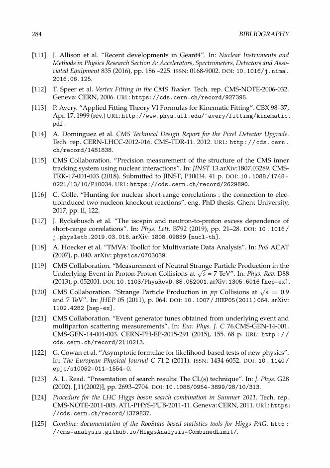
284 BIBLIOGRAPHY
[111] J. Allison et al. “Recent developments in Geant4”. In: Nuclear Instruments andMethods in Physics Research Section A: Accelerators, Spectrometers, Detectors and Asso-ciated Equipment 835 (2016), pp. 186 –225. ISSN: 0168-9002. DOI: 10.1016/j.nima.2016.06.125.
[112] T. Speer et al. Vertex Fitting in the CMS Tracker. Tech. rep. CMS-NOTE-2006-032.Geneva: CERN, 2006. URL: https://cds.cern.ch/record/927395.
[113] P. Avery. “Applied Fitting Theory VI Formulas for Kinematic Fitting”. CBX 98–37,Apr. 17, 1999 (rev.) URL: http://www.phys.ufl.edu/~avery/fitting/kinematic.pdf.
[114] A. Dominguez et al. CMS Technical Design Report for the Pixel Detector Upgrade.Tech. rep. CERN-LHCC-2012-016. CMS-TDR-11. 2012. URL: http://cds.cern.ch/record/1481838.
[115] CMS Collaboration. “Precision measurement of the structure of the CMS innertracking system using nuclear interactions”. In: JINST 13.arXiv:1807.03289. CMS-TRK-17-001-003 (2018). Submitted to JINST, P10034. 41 p. DOI: 10.1088/1748-0221/13/10/P10034. URL: https://cds.cern.ch/record/2629890.
[116] C. Colle. “Hunting for nuclear short-range correlations : the connection to elec-troinduced two-nucleon knockout reactions”. eng. PhD thesis. Ghent University,2017, pp. II, 122.
[117] J. Ryckebusch et al. “The isospin and neutron-to-proton excess dependence ofshort-range correlations”. In: Phys. Lett. B792 (2019), pp. 21–28. DOI: 10.1016/j.physletb.2019.03.016. arXiv: 1808.09859 [nucl-th].
[118] A. Hoecker et al. “TMVA: Toolkit for Multivariate Data Analysis”. In: PoS ACAT(2007), p. 040. arXiv: physics/0703039.
[119] CMS Collaboration. “Measurement of Neutral Strange Particle Production in theUnderlying Event in Proton-Proton Collisions at
√s = 7 TeV”. In: Phys. Rev. D88
(2013), p. 052001. DOI: 10.1103/PhysRevD.88.052001. arXiv: 1305.6016 [hep-ex].
[120] CMS Collaboration. “Strange Particle Production in pp Collisions at√
s = 0.9and 7 TeV”. In: JHEP 05 (2011), p. 064. DOI: 10.1007/JHEP05(2011)064. arXiv:1102.4282 [hep-ex].
[121] CMS Collaboration. “Event generator tunes obtained from underlying event andmultiparton scattering measurements”. In: Eur. Phys. J. C 76.CMS-GEN-14-001.CMS-GEN-14-001-003. CERN-PH-EP-2015-291 (2015), 155. 68 p. URL: http : / /cds.cern.ch/record/2110213.
[122] G. Cowan et al. “Asymptotic formulae for likelihood-based tests of new physics”.In: The European Physical Journal C 71.2 (2011). ISSN: 1434-6052. DOI: 10.1140/epjc/s10052-011-1554-0.
[123] A. L. Read. “Presentation of search results: The CL(s) technique”. In: J. Phys. G28(2002). [,11(2002)], pp. 2693–2704. DOI: 10.1088/0954-3899/28/10/313.
[124] Procedure for the LHC Higgs boson search combination in Summer 2011. Tech. rep.CMS-NOTE-2011-005. ATL-PHYS-PUB-2011-11. Geneva: CERN, 2011. URL: https://cds.cern.ch/record/1379837.
[125] Combine: documentation of the RooStats based statistics tools for Higgs PAG. http://cms-analysis.github.io/HiggsAnalysis-CombinedLimit/.

BIBLIOGRAPHY 285
[126] CMS Collaboration. “Pseudorapidity distribution of charged hadrons in proton-proton collisions at
√s = 13 TeV”. In: Phys. Lett. B751 (2015), pp. 143–163. DOI:
10.1016/j.physletb.2015.10.004. arXiv: 1507.05915 [hep-ex].
[127] G. Landsberg. private communication. Dec. 4, 2019.
[128] Studies of Tracker Material. Tech. rep. CMS-PAS-TRK-10-003. 2010. URL: http://cds.cern.ch/record/1279138.