The Design of High Frequency True Single Phase Clocking Divider-by-3 Circuit
10
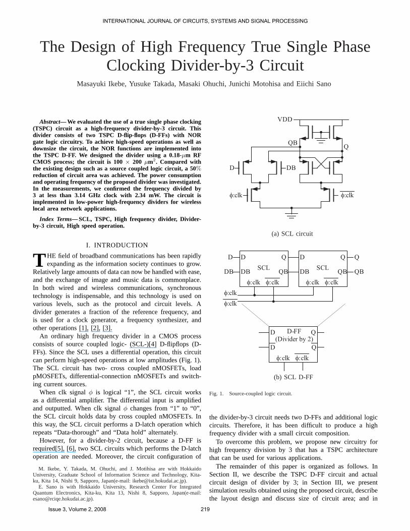
The Design of High Frequency True Single Phase Clocking Divider-by-3 Circuit Masayuki Ikebe, Yusuke Takada, Masaki Ohuchi, Junichi Motohisa and Eiichi Sano Abstract— We evaluated the use of a true single phase clocking (TSPC) circuit as a high-frequency divider-by-3 circuit. This divider consists of two TSPC D-flip-flops (D-FFs) with NOR gate logic circuitry. To achieve high-speed operations as well as downsize the circuit, the NOR functions are implemented into the TSPC D-FF. We designed the divider using a 0.18-μm RF CMOS process; the circuit is 100 × 200 μm 2 . Compared with the existing design such as a source coupled logic circuit, a 50% reduction of circuit area was achieved. The power consumption and operating frequency of the proposed divider was investigated. In the measurements, we confirmed the frequency divided by 3 at less than 3.14 GHz clock with 2.34 mW. The circuit is implemented in low-power high-frequency dividers for wireless local area network applications. Index Terms—SCL, TSPC, High frequency divider, Divider- by-3 circuit, High speed operation. I. INTRODUCTION T HE field of broadband communications has been rapidly expanding as the information society continues to grow. Relatively large amounts of data can now be handled with ease, and the exchange of image and music data is commonplace. In both wired and wireless communications, synchronous technology is indispensable, and this technology is used on various levels, such as the protocol and circuit levels. A divider generates a fraction of the reference frequency, and is used for a clock generator, a frequency synthesizer, and other operations [1], [2], [3]. An ordinary high frequency divider in a CMOS process consists of source coupled logic- (SCL-)[4] D-flipflops (D- FFs). Since the SCL uses a differential operation, this circuit can perform high-speed operations at low amplitudes (Fig. 1). The SCL circuit has two- cross coupled nMOSFETs, load pMOSFETs, differential-connection nMOSFETs and switch- ing current sources. When clk signal φ is logical “1”, the SCL circuit works as a differential amplifier. The differential input is amplified and outputted. When clk signal φ changes from “1” to “0”, the SCL circuit holds data by cross coupled nMOSFETs. In this way, the SCL circuit performs a D-latch operation which repeats “Data-thorough” and “Data hold” alternately. However, for a divider-by-2 circuit, because a D-FF is required[5], [6], two SCL circuits which performs the D-latch operation are needed. Moreover, the circuit configuration of M. Ikebe, Y. Takada, M. Ohuchi, and J. Motihisa are with Hokkaido University, Graduate School of Information Science and Technology, Kita- ku, Kita 14, Nishi 9, Sapporo, Japan(e-mail: [email protected]). E. Sano is with Hokkaido University, Research Center For Integrated Quantum Electronics, Kita-ku, Kita 13, Nishi 8, Sapporo, Japan(e-mail: [email protected]). VDD QB Q D DB φ:clk φ:clk (a) SCL circuit SCL QB Q D DB φ:clk φ:clk SCL QB Q D DB φ:clk φ:clk D DB QB Q φ:clk φ:clk D-FF (Divider by 2) Q Q D φ:clk φ:clk D (b) SCL D-FF Fig. 1. Source-coupled logic circuit. the divider-by-3 circuit needs two D-FFs and additional logic circuits. Therefore, it has been difficult to produce a high frequency divider with a small circuit composition. To overcome this problem, we propose new circuitry for high frequency division by 3 that has a TSPC architecture that can be used for various applications. The remainder of this paper is organized as follows. In Section II, we describe the TSPC D-FF circuit and actual circuit design of divider by 3; in Section III, we present simulation results obtained using the proposed circuit, describe the layout design and discuss size of circuit area; and in INTERNATIONAL JOURNAL OF CIRCUITS, SYSTEMS AND SIGNAL PROCESSING Issue 3, Volume 2, 2008 219
Transcript of The Design of High Frequency True Single Phase Clocking Divider-by-3 Circuit
The Designof High Frequency True Single PhaseClocking Divider-by-3 Circuit
Masayuki Ikebe, Yusuke Takada, Masaki Ohuchi, Junichi Motohisa and Eiichi Sano
Abstract— We evaluated the use of a true single phase clocking(TSPC) circuit as a high-frequency divider-by-3 circuit. Thisdivider consists of two TSPC D-flip-flops (D-FFs) with NORgate logic circuitry. To achieve high-speed operations as well asdownsize the circuit, the NOR functions are implemented intothe TSPC D-FF. We designed the divider using a 0.18-µm RFCMOS process; the circuit is 100× 200 µm2. Compared withthe existing design such as a source coupled logic circuit, a 50%reduction of circuit area was achieved. The power consumptionand operating frequency of the proposed divider was investigated.In the measurements, we confirmed the frequency divided by3 at less than 3.14 GHz clock with 2.34 mW. The circuit isimplemented in low-power high-frequency dividers for wirelesslocal area network applications.
Index Terms— SCL, TSPC, High frequency divider, Divider-by-3 circuit, High speed operation.
I. INTRODUCTION
T HE field of broadband communications has been rapidlyexpanding as the information society continues to grow.
Relatively large amounts of data can now be handled with ease,and the exchange of image and music data is commonplace.In both wired and wireless communications, synchronoustechnology is indispensable, and this technology is used onvarious levels, such as the protocol and circuit levels. Adivider generates a fraction of the reference frequency, andis used for a clock generator, a frequency synthesizer, andother operations [1], [2], [3].
An ordinary high frequency divider in a CMOS processconsists of source coupled logic- (SCL-)[4] D-flipflops (D-FFs). Since the SCL uses a differential operation, this circuitcan perform high-speed operations at low amplitudes (Fig. 1).The SCL circuit has two- cross coupled nMOSFETs, loadpMOSFETs, differential-connection nMOSFETs and switch-ing current sources.
When clk signalφ is logical “1”, the SCL circuit worksas a differential amplifier. The differential input is amplifiedand outputted. When clk signalφ changes from “1” to “0”,the SCL circuit holds data by cross coupled nMOSFETs. Inthis way, the SCL circuit performs a D-latch operation whichrepeats “Data-thorough” and “Data hold” alternately.
However, for a divider-by-2 circuit, because a D-FF isrequired[5], [6], two SCL circuits which performs the D-latchoperation are needed. Moreover, the circuit configuration of
M. Ikebe, Y. Takada, M. Ohuchi, and J. Motihisa are with HokkaidoUniversity, Graduate School of Information Science and Technology, Kita-ku, Kita 14, Nishi 9, Sapporo, Japan(e-mail: [email protected]).
E. Sano is with Hokkaido University, Research Center For IntegratedQuantum Electronics, Kita-ku, Kita 13, Nishi 8, Sapporo, Japan(e-mail:[email protected]).
VDD
QBQ
D DB
φ:clk φ:clk
(a) SCL circuit
SCLQB
QD
DB
φ:clk φ:clk
SCLQB
QD
DB
φ:clk φ:clk
D
DB QB
Q
φ:clk
φ:clk
D-FF
(Divider by 2)
Q
QD
φ:clk φ:clk
D
(b) SCL D-FF
Fig. 1. Source-coupled logic circuit.
the divider-by-3 circuit needs two D-FFs and additional logiccircuits. Therefore, it has been difficult to produce a highfrequency divider with a small circuit composition.
To overcome this problem, we propose new circuitry forhigh frequency division by 3 that has a TSPC architecturethat can be used for various applications.
The remainder of this paper is organized as follows. InSection II, we describe the TSPC D-FF circuit and actualcircuit design of divider by 3; in Section III, we presentsimulation results obtained using the proposed circuit, describethe layout design and discuss size of circuit area; and in
INTERNATIONAL JOURNAL OF CIRCUITS, SYSTEMS AND SIGNAL PROCESSING
Issue 3, Volume 2, 2008 219

VDD
QD φ
φ
φ
φ Q
D-FF
(Divider by 2)
Q
QD
φ:clk
Fig. 2. True-single-phase-clocking circuit.
Section IV, we present measurement result.
II. TRUE SINGLE PHASE CLOCKING DIVIDER
A. Operation of TSPC logic circuit
A TSPC logic circuit alternately generates“ Data-fetchingstate” and“ Hold state” operations by switching betweenCMOS devices (in Fig. 2). Like a dynamic logic circuit thatalternately performs“Pre-charge”and“Evaluate”operationsin parasitic capacitance, the TSPC circuit operates a data fetchby using the pre-charge and data hold performed by the highimpedance switching at the clock-signal timing[7], [8], [9],[10], [11], [12].
Figure 3 shows the D-FF operation of a TSPC circuit. Whenφ = L, the first stage of the circuit runs as an inverter andoutputs next stateData[t + 1] asthe input of the second stage.Because the bottom nMOSFET of the second stage turns off,the output of the second stage is always logical “1”. Thereforethe n- and p-MOSFET in the output part simultaneously turnoff, and Data[t] is held in the parasitic capacitance of thethird stage output line.
Whenφ → H, the state ofData[t + 1] is determined andthen the circuit outputs it. At that time, ifData[t + 1] =1 and the input changes toData[t + 2] = 0, because themiddle pMOSFET of the first stage turns off, the output data“Data[t + 1] = 0” doesn’t change. If theData[t + 1] = 0and the input changes toData[t + 2] = 1, the first stageoutput changes fromData[t + 1] = 1 to Date[t + 2] = 0.However, whenφ→H, the parasitic capacitance of the secondstage output is discharged. In this case, although the secondstage input changes, the second stage output doesn’t change.Therefore the third stage output also doesn’t change. In thisway, the TSPC circuit performs the D-FF operation.
D[t+2]
D[t+1]
VDD
φ
φ
φ
φD[t+2]
φ = Η,
input: D[t+1] = L => D[t+2] = H
Value of this node doesn't change.
D[t+1]
D[t+1]
VDD
φ
φ
φ
φD[t+2]
φ = Η,
input: D[t+1] = H => D[t+2] = L
Value of this node doesn't change.
D[t+1]
D[t+1]
VDD
φ
φ
φ
φD[t+1]
φ −> Η
D[t+1]
D[t]
VDD
φ
φ
φ
φD[t+1]
φ = L
Fig. 3. D-FF operation of TSPC circuit.
INTERNATIONAL JOURNAL OF CIRCUITS, SYSTEMS AND SIGNAL PROCESSING
Issue 3, Volume 2, 2008 220

VDD
Q
D
φ φ
φ
Q:T3T2T1
T1
T2
T3
φ
Direct path from supply voltage to ground is established
Fig. 4. ExtendedTSPC circuit and dividing-by-2 operation.
B. Extended TSPC logic circuit
The TSPC DFF is useful divide-by-2 unit in the high-speed frequency divider design. However, to increase theoperating frequency, an extended-TSPC (E-TSPC) DFF wasproposed[13], [14], [15]. Figure 4 shows the circuitry of anE-TSPC DFF and timing chart of dividing-by-2 operation,respectively. The E-TSPC logic circuit also alternately gen-erates“ Data-fetching state”and“ Hold state”operationsby switching MOSFETs. It operates a data fetch by using thepre-charge and data hold performed by the high impedanceswitching at the clock-signal timing, too.
Performing the D-FF function by the E-TSPC circuit, theoutput of the third stage is inverted. The D-FF operation isshown in Fig. 5. Whenφ = L, the nMOSFETs in the first-and the second stages simultaneously turn off. If theData[t]= “1”, the pMOSFET of the first stage also turns off, theboth MOSFETs of the first stage make the high-impedancecondition at the output node, andData[t] is held in theparasitic capacitance of the first stage-output line. Thereforethe pMOSFET of the second stage turns on and the outputnode is precharged, and the output of the third stage doesn’tchange. At that time, if the input changes toData[t+1] = 0,because the pMOSFET of the second stage turns off and thesecond stage output is already precharged, the second- andthe third stage output data “Data[t] = 0 and Data[t] = 1 ”doesn’t change.
If the Data[t] = “0”, the pMOSFET of the first stage turnson, the first stage output is precharged. The both MOSFETsof the second stage make the high-impedance condition atthe output node, andData[t] is also held in the parasitic
φ = L
VDD
φ φ
φD[t+1]
D[t] D[t]D[t]D[t+1]
φ−> Η
VDD
φ φ
φD[t+1]
D[t+1] D[t+1]D[t+1]D[t+1]
φ
φ
φ = Η,
input: D[t+1] = H => D[t+2] = L
VDD
φ φ
φD[t+2]
D[t+2]
VDD
φ φ
φD[t+2]
D[t+2] D[t+1]D[t+2]D[t+2]
φ
φ
D[t+2] D[t+1]D[t+1]
Value of this node doesn't change.
Value of this node doesn't change.
φ = Η,
input: D[t+1] = L => D[t+2] = H
Fig. 5. D-FF operation of E-TSPC circuit.
INTERNATIONAL JOURNAL OF CIRCUITS, SYSTEMS AND SIGNAL PROCESSING
Issue 3, Volume 2, 2008 221

TSPCQ1B
Q1D
φ:clk
TSPCQ2B
Q2D
φ:clk
φ:clk
2ANDQ1[t]=0 Q2[t]=0
Q1[t+1]=1 Q2[t+1]=0
Q1[t+2]=1 Q2[t+2]=1
Q1[t+3]=0 Q2[t+3]=0
TSPC
Q1BD
φ:clk
TSPCQ2B
Q2D
φ:clk
φ:clk
2NOR
(a) TSPC-divider-by-3 circuitry
VDD
Q1
φ
φ
φ
φ
Q2
φ
φ
φ
φQ2
Output buffer
Q2
VDD
φ
φ
φ
φ Q1 φ
φ
φ
φ Q2 Q2Q2Q1
(b) Actual TSPC-divider-by-3 circuitFig. 6. TSPC-divider-by-3 circuit.
capacitance of the second stage-output line. Therefore theoutput of the third stage also doesn’t change. At that time, ifthe input changes toData[t+1] = 1, because the pMOSFETof the first stage turns off and the first stage output isalready precharged, the second- and the third stage output data“Data[t] = 1 andData[t] = 0 ” doesn’t change.
Whenφ → H, the first stage of the circuit runs as a quasipMOSFET-logic inverter and outputs current stateData[t + 1]as the input of the second stage. The second stage of thecircuit also runs as a quasi pMOSFET-logic one. Because thepMOSFET of the third stage turns off, output of the third stageis evaluated by the second stage output.
At that time, if Data[t + 1] = 1 and the input changes to
Data[t + 2] = 0, because the nMOSFET of the third stageturns off, the output data “Data[t + 1] = 0” doesn’t change.If the Data[t + 1] = 0 and the input changes toData[t +2] = 1, the third stage output changes fromData[t + 1] = 1to Date[t + 2] = 0. However, whenφ → H, the parasiticcapacitance of the final stage output is discharged. In this case,although the third stage input changes, the final stage outputdoesn’t change. In this way, the E-TSPC circuit performs theD-FF operation.
The propagation delay of the E-TSPC unit is smaller thanthat of the TSPC unit because of the reduction of loadcapacitance. However, according to the timing chart of the E-TSPC circuit (in Fig. 4), all stage of the circuit runs as quasi
INTERNATIONAL JOURNAL OF CIRCUITS, SYSTEMS AND SIGNAL PROCESSING
Issue 3, Volume 2, 2008 222

pMOSFET-andnMOSFET logic inverters, respectively.When the circuit performs the D-FF function, because of
the above inverter operations, there is a period during whicha direct path from supply voltage to ground is established.The crossed areas in Fig. 4 mark the transition during whichthe short circuit takes place. The short current of the E-TSPCcircuit is larger than the driving current of the TSPC one.Therefore it has been reported that the TSPC circuit had anadvantage in the total power dissipation[16], [17], [18], [19].
C. TSPC divider-by-3 circuit
The proposed divider-by-3 circuit consists of sequentialcircuits based on the TSPC D-FFs and 2-AND gate logic.Figure 6 shows the proposed circuit and its truth table.
This circuit achieves frequency division by using logicoperations. By AND logic, when onlyQ1[t] = 1 andQ2[t] =0, Q2[t + 1] becomes “1”. In other condition,Q2 becomes“0”. The sequence of the truth table is performed repeatedlyat each clock cycle. Therefore the circuit as shown in Fig. 3performs frequency dividing by 3.
However this circuit is not suitable for high frequencyuses. In the circuit configuration, the cascade connectionbetween the D-FF and the AND gate degrades the frequencycharacteristic by adding additional delay to the circuitry[20],[21]. Therefore the technique of improving the high frequencycharacteristic is required. Here, using De Morgan’s law, thebinary logic of the connection can be transformed as followequation.
Q1 ·Q2 = Q1 ·Q2 = Q1 + Q2 (1)
The NOR logic can be obtained from the AND one, andinput of the logic function changed fromD[t+1] to D[t + 1].Thus, we implemented the NOR function into the TSPC D-FF without using the optional AND gate circuit and reducedadditional delay to the whole circuitry.
Because of the high-impedance condition, the third stageoutput of the TSPC circuit cannot be used for a differentialoutput. The differential output is achieved by using an addi-tional inverter. The inverter also optimizes duty of the outputsignal.
III. CIRCUIT DESIGN AND ITS SIMULATION
We designed the divider by using a 0.18-µm mixed sig-nal/RF CMOS process with one poly and six metal layers. Inthis design, the output-impedance matching was not set to 50Ω terminated, because we assume that the next stage circuit isa conventional logic circuit that has a high input impedance.The ratio of the size of the p- and n-MOSFET was set to 3:1due to the mobility of the MOSFETs, but the actual sizes weredetermined by the operating frequency. By the MOSFETs sizeof the additional output inverter, we control the signal duty.
Figure 7 shows the size depending on the operating fre-quency. The power dissipation for a 3-GHz operation was 2.7mW under typical conditions. The 4 GHz operation can beachieved over the scale factor “2”. The operating frequencyalso increased as the MOSFET size became large, but over
1.5 mA: current
2.5 mA
4 mA
5 mA
6 mA
3.6
3.7
3.8
3.9
4
4.1
4.2
4.3
0 1 2 3 4 5 6
Scale factor
Fre
qu
ency
(G
Hz)
1.5 mA: current
2.5 mA
4 mA
5 mA
6 mA
3.6
3.7
3.8
3.9
4
4.1
4.2
4.3
0 1 2 3 4 5 6
Scale factor
Fre
qu
ency
(G
Hz)
Fig. 7. Operatingfrequency vs. MOSFET size for current dissipation ofproposed divider.
2.0
mA
mA
3.62.3
3.8
4
4.6
4.2
4.4
1.9
Fre
qu
ency
(G
Hz)
1.5 : current
1.7 2.1
Supply voltage
Fre
qu
ency
(G
Hz)
4.8
2.2 mA
2.5 mA
3.0 mA
3.5 mA
Fig. 8. Operatingfrequency vs. supply voltage for current dissipation ofproposed divider.
the scale factor “5” it was saturated. The main reason forthis saturation is the load capacitance of the circuit. Theload capacitance depends on the MOSFET size. Therefore,although the driving power increases, the propagation delayalso becomes large and the operating frequency is saturated.
Figure 8 shows the supply voltage depending on the op-erating frequency. In this simulation, the load capacitancedoesn’t change. Therefore the operation frequency increasedas the supply voltage increased. The 4.8 GHz operation canbe achieved at the supply voltage 2.3 V.
The result of transition simulation is shown in Fig. 9. Weconfirmed that the circuit could convert the frequency from3 GHz into 1 GHz. Based on the measurement setup, wealso include the result for 50Ω terminated configuration.Although the output amplitude was small, we were able toconfirm division operations up to 3.6 GHz using our designby conducting circuit simulations under typical conditions.
Figure 10 and 11 shows the layout of the circuit and theSCL-divider-by-2 circuit. The SCL divider was designed for3 GHz operation. Both of circuit sizes were almost the same.When compared to a standard SCL configuration, becausethe SCL-divider-by-2 circuit included one D-FF circuit, we
INTERNATIONAL JOURNAL OF CIRCUITS, SYSTEMS AND SIGNAL PROCESSING
Issue 3, Volume 2, 2008 223

Volt
age
(V)
1.8
0
2.0 2.22.1
Time (nsec)
(a) Open
Volt
age
(V)
1.8
0
2.0 2.1
Time (nsec)
2.2
(b) 50 Ω terminated.
Fig. 9. Transition simulation results.
decreased the circuit area by 50%using the SCL D-FF basis.Our circuit was 100× 120 µm2. Figure 12 shows the chipmicrograph of our circuit.
IV. MESUREMENT RESULT
Figure 13 shows the measurement setup. One of the fab-ricated chips was placed on a probe station. The transitioncharacteristic and the frequency characteristic were measuredwith an oscilloscope and a spectrum analyzer. The signalgenerator port was connected to the divider input. The biasvoltageV DD/2 was given to the divider thorough a Bias-T.
In this measurement, an input signal with 7 dBm was ap-plied to the divider through a cable with 50 -Ωcharacteristic-impedance configuration. The measured results are shown inFig. 14, 15, 16 and 17. We confirmed the operation of dividingby 3 at less than 3.14 GHz with 2.34 mW. Moreover, whensupply voltage VDD = 2.3 V was given, operation frequencyincreased up to 4 GHz with 4.78 mW.
Since the measurement setup was a 50 -Ωtermination, theoutput amplitude was small. This result was same as that in
VDDVDD
CLK
100 µm
OUT
12
0µ
m
Fig. 10. Layout of proposed divider by 3.
100µm
130µm
Fig. 11. Layout of SCL divider by 2.
simulation one. However, during the measurement, when aninput signal of more than 3.14 GHz was given to the circuit,it worked as a divider by 4. The main reason for this unusualoperation is the parasitic capacitance of the feedback line. Ifa signal delay occurs, the updating of the next stage also fallsbehind.
V. APPLICATION EXAMPLES
The following are a few applications of the high-frequencydivider by 3 circuits. A prescaler of a phase locked loop(PLL)[22] is stated as the first application. For the pro-grammable prescaler, a switching controller between the divid-ing by 2 and 3 is required. In our method, implementing logicfunction, it is easy to achieve the above circuit configuration(in Fig. 18).
Next, a frequency synthesizer for MB-OFDM UWB systemis stated as the application of our circuit[23]. Band group
INTERNATIONAL JOURNAL OF CIRCUITS, SYSTEMS AND SIGNAL PROCESSING
Issue 3, Volume 2, 2008 224

Fig. 12. Chip micrograph of proposed divider by 3.
Signal
generator
Bias TVoltage supply
(VDD/2)
DUT
Probe station
DC cut
Voltage supply
(VDD)
50 Ω
50 Ω
50 Ω
50 Ω
Spectrum
analyzerOscilloscope
Fig. 13. Measurementsetup.
allocation for MB-OFDM band plan from 3.1 GHz to 10.6GHzis shown in Fig. 19. In MB-OFDM system, 14 frequenciessynthesis by a few oscillators is required. Therefore thefrequency dividing operation is very important. The bandwidthof each band of MB-OFDM system is 528 MHz. The OFDMmodulation consists of 128 sub channels with 4.125 MHz. Forreduction of propagation degradation by multi-path problem,fast frequency hopping is performed in a band group (ex.band“1” → band“2” → band“3” → band“1”). With LSIprocess development, the MB-OFDM system has shifted tocomposition applicable also to the band group 1 of mandatoryand other band groups of high frequency.
Covering all frequencies of the MB-OFDM, we considerthat synthesis of center frequency in band groups from a10.296 GHz oscillator[24] and a 6.336 GHz one. Accordingto the group 1: 3.960 GHz, it can be obtained by difference-frequency mixing the base frequency 10.296 GHz and thetemporal frequency 6,336GHz through LPF. About the group3 and 4, by the dividing by 2 and 4, the other temporal
AC
vo
ltag
e (V
)
0.5
-0.5
0 2.01.0
Time (nsec)
0
AC
vo
ltag
e (V
)
0.5
-0.5
0 2.01.0
Time (nsec)
0
Fig. 14. Measurementresults of proposed circuit.
3
3.2
3.4
3.6
3.8
4
4.2
1.7 1.9 2.1 2.3
Supply voltage (V)
1.29 mA: current
1.34 mA
1.58 mA
1.68 mA
1.86 mA
2.08 mA
Fig. 15. Maximum Operating frequency vs. supply voltage for currentdissipation.
frequencies 3.168 GHz and 1.584 GHz are synthesized fromthe frequency 6.336 GHz. Obtained two frequencies are mixedwith 10.296 GHz for generating the center frequencies of theband group 7.128 GHz and 8.172 GHz through LPF. Upperside band of obtained frequency from 10.296 GHz and 6.336GHz is more than 10 GHz. Therefore demand for the LPF ismoderated.
Here, considering synthesis of subband in each band group,because the subband frequency 0.528 GHz is required, this fre-quency is obtained from the temporal frequency 3.168 GHz bydividing-by-6 function. At that time, the dividing-by-3 circuitis important for above operation. Using the frequency 0.528GHz, all subband can be synthesized from center frequenciesin each band group. In this way, the multi-frequencies ofMB-OFDM system are obtained by mixers, oscillators, and
INTERNATIONAL JOURNAL OF CIRCUITS, SYSTEMS AND SIGNAL PROCESSING
Issue 3, Volume 2, 2008 225

C enter
1.000G Hz
Fig. 16. Power spectrum of 3 GHz conversion.
Fig. 17. Power spectrum of 4 GHz conversion.
dividers.
VI. CONCLUSION
We designed a high-frequency-TSPC divider-by-3 circuit.This divider, which has two TSPC D-FFs, converted a 3-GHzreference signal into a 1 GHz one with only a 2.7 mW. Thecircuit was 100× 120 µm2 and was constructed using a0.18-µm mixed signal/RF CMOS process. We fabricated andmeasured the designed divider. A 3-GHz operation of dividingby 3 with 2.34 mW was confirmed by measurement.
ACKNOWLEDGMENT
This work is supported by VLSI Design and EducationCenter (VDEC), the University of Tokyo in collaborationwith Cadence Design Systems, Inc. and Agilent TechnologiesJapan, Ltd.
REFERENCES[1] S. Pellerano, S. Levantino, C. Samori, and A. L. Lacaita, “A 13.5-mW 5-
GHz frequency synthesizer with dynamic-logic frequency divider,” IEEEJ. Solid-State Circuits, vol. 39, no. 2, pp. 378?383, Feb. 2004.
[2] Q. Huang and R. Rogenmoser, “Speed optimization of edge-triggeredCMOS circuits for gigahertz single-phase clocks,” IEEE J. Solid-StateCircuits, vol. 31, pp. 456?465, Mar. 1996.
[3] X. P. Yu, M. A. Do, L. Jia, J. G. Ma, and K. S. Yeo, “Design of alowpower wideband high resolution programmable frequency divider,”IEEE Trans. Very Large Scale Integr. (VLSI) Syst., vol. 13, no. 9, pp.1098?1103, Sep. 2005.
[4] Sayfe Kiaei, San-Hwa Chee and Dave Allstot, “CMOS Source-CoupledLogic for Mixed-Mode VLSI,” 1990 IEEE International Symposium onCircuits and Systems, vol. 2, pg. 1608-1611, IEEE, 1990.
[5] Behzad Razavi, Kwing F. Lee, and Ran H. Yan, “Design of High-Speed, Low-Power Frequency Dividers and Phase-Locked Loops inDeep Submicron CMOS” IEEE Journal of Solid-State Circuits, VOL.30, NO. 2, pp. 101-109, 1995
[6] L. Lin, L. Tee, and P. R. Gray, “A 1.4 GHz differential low-noise CMOSfrequency synthesizer using a wideband PLL architecture,” in IEEE Int.Solid-State Circuits Conf. Dig. Tech. Papers, Feb. 2000, pp. 204?205
[7] Y. Ji-ren, I. Karsson, and C. Svenson “A True Single-Phase-Clock Dy-namic CMOS Circuit Tectilque,” IEEE Journal of Solid-State Circuits,VOL. SC-22,NO. 5, pp. 899-901, 1987.
[8] R. Sundblad and C. Svensson, “A True Single-Phase-Clock DynamicCMOS Circuit Tectilque,” IEEE Trans. Computer-A zded Des., vol.CAD-6, pp. 282-289, 1987.
[9] N. Krishnapura and P. R. Kinget, “A 5.3-GHz programmable divider forHiPerLAN in 0.25-µm CMOS,” IEEE J. Solid State Circuits, vol. 35,pp.1019?1024, July 2000
[10] J. Yuan and C. Svensson, “High-speed CMOS circuit technique,” IEEEJ. Solid-State Circuits, vol. 24, pp. 62?70, Feb. 1989
[11] W. S. T. Yan and H. C. Luong, “A 2-V 900- MHz monolithic CMOSdual-loop frequency synthesizer for GSM receivers,” IEEE J. Solid StateCircuits, vol. 36, pp. 204?216, Feb. 2001.
[12] H. Heinspan and M. Soyuer, “A fully-integrated 5-GHz frequencysynthesizer in SiGe BiCMOS,” in Proc. Bipolar/BiCMOS Circuits andTechnology Meeting, Minneapolis, MN, Sept.1999, pp. 165?168
[13] Xiao Peng Yu, Manh Anh Do, Wei Meng Lim, Kiat Seng Yeo, andJian-Guo Ma “Design and Optimization of the Extended True Single-Phase Clock-Based Prescaler” IEEE Trans. on Microwave Theory andTechniques, Vol. 54, No.11, pp.3828-3835, 2006.
[14] Ali Rahnamaei, Adel Akbarimajd, Asadollah Torabi,and Mina Vajdi“Design and Optimization of 8/9 Divider in PLL Frequency Synthesizerwith Dynamic Logic (E-TSPC)” Proceedings of the 6th WSEAS Int.Conf. on Electronics, Hardware, Wireless and Optical Communications,Corfu Island, Greece, pp.46-50, February 16-19, 2007
[15] J. N. Soares, Jr. and W. A. M. Van Noije, “A 1.6-GHz dual modulusprescaler using the extended true-single-phase-clock CMOS circuittechnique (E-TSPC),” IEEE J. Solid-State Circuits, vol. 34, no. 1, pp.97?102, Jan. 1999.
[16] R. X. Gu, K. M. Sharaf, and M. I. Elmasry, “High-Performance DigitalVLSI Circuit Design.” Norwell, MA: Kluwer, 1996.
[17] J. M. Rabaey, A. Chandrakasan, and B. Nikolic, “Digital IntegratedCircuits, A Design Perspective, ser. Electron. and VLSI, 2nd ed.” UpperSaddle River, NJ: Prentice-Hall, 2003.
[18] A. P. Chandrakasan and R. W. Brodersen, “Minimizing power consump-tion in digital CMOS circuits,” Proc. IEEE, vol. 83, no. 4, pp. 498?523,Apr. 1995.
[19] R. Rogenmoser, “The Design of High-Speed Dynamic CMOS Circuitsfor VLSI, ser. Microelectron., 1. Aufl ed.” Konstanz, Germany: Hartung-Gorre, 1996.
[20] C. Lam and B. Razavi, “A 2.6-GHz/5.2-GHz frequency synthesizer in0.4-µm CMOS technology,” IEEE J. Solid-State Circuits, vol. 35, no.5, pp. 788?794, May 2000.
[21] J. M. Hsu, G. K. Dehng, C. Y. Yang, C. Y. Yang, and S. I. Liu, “Lowvoltage CMOS frequency synthesizer for ERMES pager application,”IEEE J. Solid-State Circuits, vol. 48, pp. 826?834, Sept. 2001
[22] Shiwei Cheng, Ke Zhang, Shengguo Cao, Xiaofang Zhou, Dian Zhou“A 2.4-GHz ISM Band Delta-Sigma Fractional-N Frequency Synthesizerwith Automatic Calibration Technique” WSEAS TRANSACTIONS onCircuits Systems, Issue 10, Volume 7, pp.859-868, October 2008.
[23] I. Jivet, B. Dragoi “Performance Analysis of Direct Digital SynthesizerArchitecture with Amplitude Sequencing” WSEAS TRANSACTIONSon Circuits Systems Issue 1, Volume 7, pp.1-6, January 2008
[24] Jiun-Wei Horng, Chun-Li Hou, Chun-Ming Chang, Shih-Ting ChengAnd Hsin-Yu Su “Current Or/And Voltage-Mode Quadrature OscillatorsWith Grounded Capacitors And Resistors Using FDCCIIs” Issue 3,Volume 7, pp.129-138, March 2008.
INTERNATIONAL JOURNAL OF CIRCUITS, SYSTEMS AND SIGNAL PROCESSING
Issue 3, Volume 2, 2008 226

VDD
φ
φ
φ
φ Q1 φ
φ
φ
φ Q2 Q2Q2
Ctrl Divider by 2 (Ctrl = 0),
by 3 (Ctrl = 1)
Phase
detector
Reference
signal Charge
Pump
Loop
filterVCO
2/3
PrescalerCounter
Fig. 18. Prescalerof PLL.
10.296 GHz
6.336 GHz
3.168 GHz 1.584 GHz
0.528 GHz
MIXER
MIXER
DIV2 DIV2 DIV3
MIXER
8.712 GHz
LPF
LPF
LPF 7.128 GHz
3.960 GHz
Fig. 19. Bandallocation and frequency synthesizer of MB-OFDM.
Masayuki Ik ebe received B.S., M.S. and Ph.D. de-grees in electrical engineering from Hokkaido Uni-versity, Hokkaido, Japan, in 1995, 1997 and 2000,respectively. During 2000-2004, he worked for theElectronic device Laboratory, Dai Nippon PrintingCorporation, Akabane, Japan, where he was engagedin the research and development of wireless com-munication system and image processing system.Presently, he is a Associate Professor of GraduateSchool of Information Science and Technology atHokkaido University. His current research includes
CMOS-image sensor and RF analog circuits. Dr. Ikebe is a member of IEEEand IEICE.
Yusuke Takada received B.S. degrees in electricalengineering from Hokkaido University, Hokkaido,Japan, in 2008, respectively. His current research isWireless communication system and Mixer design.
INTERNATIONAL JOURNAL OF CIRCUITS, SYSTEMS AND SIGNAL PROCESSING
Issue 3, Volume 2, 2008 227

Masaki Ohuno received B.S. degrees in electricalengineering from Hokkaido University, Hokkaido,Japan, in 2007, respectively. His current research isWireless communication system and LNA design.
Junichi Motohisa received B.S., M.S. and Ph.Ddegrees in electrical engineering from University ofTokyo, Japan, in 1986, 1988, and 1993, respectively.During 1991-1993, he worked as a researcher inERATO Project supported by Research and Devel-opment Corporation of Japan. In 1993, he becamea Lecturer (later, Associate Professor) at ResearchCenter of Interface Quantum Electronics (from 2001,Research Center for Integrated Quantum Electron-ics), Hokkaido University,where he was engaged inthe growth and characterization of semiconductor
quantum nanostructures including quantum dots and quantum wires. Presently,he is a Professor of Graduate School of Information Science and Technologyat Hokkaido University.His current interest includes device and circuit appli-cation of nanostructures as well as their fabrication and characterization. Dr.Motohisa is a member of JSAP.
Eiichi Sano wasborn in Shizuoka, Japan, in 1952.He received the B. S., M. S., and Ph. D degreesfrom the University of Tokyo, Tokyo, Japan, in 1975,1977, and 1998, respectively. From 1977 to 2001,he was with NTT laboratories, where he workedon MOS device physics, mixed analog/digital MOSULSIs, ultrafast MSM photodetectors, electroopticsampling, high-speed electronic and optoelectronicICs. In 2001, he joined the Research Center for In-tegrated Quantum Electronics, Hokkaido University,Japan, as a Professor. His current research interests
include high-speed devices, circuits and systems. He has published over 150papers in major journals and conference proceedings related to these researchareas. Dr. Sano is a member of the IEEE and the Japan Society of AppliedPhysics.
INTERNATIONAL JOURNAL OF CIRCUITS, SYSTEMS AND SIGNAL PROCESSING
Issue 3, Volume 2, 2008 228