The 8086 Hardware Specifications
59
1 The 8086 Hardware Specifications The 8086 was the first 16-bit microprocessor introduced by Intel Corporation in 1978. The 8086 is manufactured using high-performance metal-oxide semiconductor (HMOS) technology, and the circuitry on their chips is equivalent to approximately 29,000 transistors. They are housed in a 40-pin dual in-line package (DIP), 32-pin common & 8-pin (MIN-MAX) Modes. Figure (1-1) shows the pin layout of 8086 microprocessor. Figure (1-1): The pin layout of 8086 microprocessor.
-
Upload
khangminh22 -
Category
Documents
-
view
0 -
download
0
Transcript of The 8086 Hardware Specifications

1
The 8086 Hardware Specifications
The 8086 was the first 16-bit microprocessor introduced by Intel Corporation in
1978. The 8086 is manufactured using high-performance metal-oxide
semiconductor (HMOS) technology, and the circuitry on their chips is equivalent
to approximately 29,000 transistors. They are housed in a 40-pin dual in-line
package (DIP), 32-pin common & 8-pin (MIN-MAX) Modes. Figure (1-1) shows
the pin layout of 8086 microprocessor.
Figure (1-1): The pin layout of 8086 microprocessor.

2
Minimum mode 8086 system is typically smaller and contains a
single processor. All control signals for memory & I/O devices are
generated by the microprocessor.
In maximum mode 8086 system, some of the control signals must
be externally generated. This requires the addition of an external IC
(8288 bus controller). Maximum mode is used only when the system
contains external coprocessor such as the 8087 arithmetic coprocessor.
Electrical characteristics of 8086 Microprocessor:

3
1- Pin Connections (common): The signals pinned out of 8086 are shown in
Figure (1-1). Many pins have multiple functions:
1) VCC (1-pin): the power supply input provides a +5 V, ±10% signal to the
microprocessor.
2) GND (2pins): the ground connection is return for power supply. Note that the
8086 microprocessor have two pins labeled GND both must be connected to
ground for proper operation.
3) AD0-AD15 (16-pin): the 8086 Address/Data bus lines. These lines contain
address bits A0-A15 whenever ALE is logic 1, and D0-D15 when ALE is logic 0.
These pins are at their high-impedance state during a hold acknowledged.
4) A16/S3-A19/S3 (4-pin): the Address/Status bits are multiplexed to provide
address signals A16-A19 and also status bits S3-S6. These pins are at their high-
impedance state during a hold acknowledged. Status bit S6 always remains logic
0, bit S5 indicates the condition of IF flag bit. S4 and S3 show which segment is
accessed during the current bus cycle as shown in Table (1-1). These two bits can
be used to address four separate 1 M byte memory by decoding them as A21 and
A20.
Table (1-1): Function of status bits S3and S4.
S4 S3 Function
0 0 Extra Segment
0 1 Stack Segment
1 0 Code Segment
1 1 Data Segment

4
5) / S7 (1-pin): the Bus High Enable pin is used in the 8086 to enable the
most significant data bus bits (D8-D16) during a read or a write operation. The
state of S7 is always logic 1.
6) (1-pin): whenever the read signal is logic 0, the data bus is receptive to
data from the memory or I/O devices connected to the system. This pin floats
to its high-impedance state during a hold acknowledge.
7) READY (1-pin): if the READY pin is placed at logic 0 level, the
microprocessor enters into wait state and remains idle.
8) INTR (1-pin): Interrupt request is used to request hardware interrupts. If INTR
is held high when IF=1, the 8086 enters an interrupts acknowledge cycle
( become active) after the current instruction has complete execution.
9) NMI (1-pin): the non-maskable interrupt input is similar to INTR except that
the NMI does not check to see whether the IF bit is logic 1. If NMI is activated,
this interrupt input uses interrupt vector2.
10) (1-pin): the test pin is an input that is tested by the WAIT instruction.
If is logic 0, the WAIT instruction functions as a NOP. If is logic
1, the WAIT instruction waits for to become logic 0. This pin is most
often connected to the 8087 numeric coprocessor.
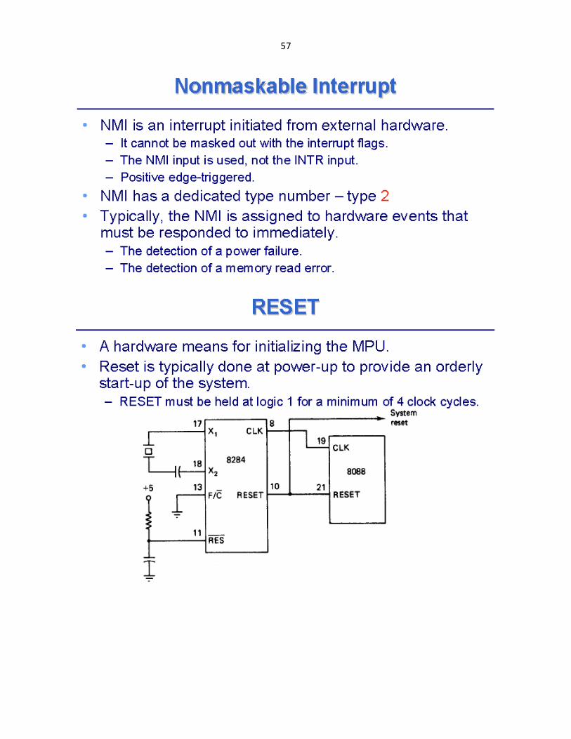
11) RESET (1-pin): the reset input causes the microprocessor to reset itself if
this pin is held high for a minimum of four clocking periods. Whenever the
8086 is reset, it begins executing instructions at memory location FFFF0H and
disable future interrupts by clearing the IF bit.
12) CLK (1-pin): the clock pin provides the basic timing signal to the
microprocessor. The clock signal must have a duty cycle of 33% (high for one-
third of the clocking period and low for two-thirds) to provide proper internal
timing for the 8086.

5
13) MN/ (1-pin): the minimum/maximum mode pin selects either minimum
mode or maximum mode operation for the microprocessor. If minimum mode is
selected, the MN/ pin must be connected directly to +5V.
Figure (1-2) shows the block diagram of minimum mode 8086 Microprocessor.

6
Figure (1-2): The block diagram of minimum mode 8086 MP.

7
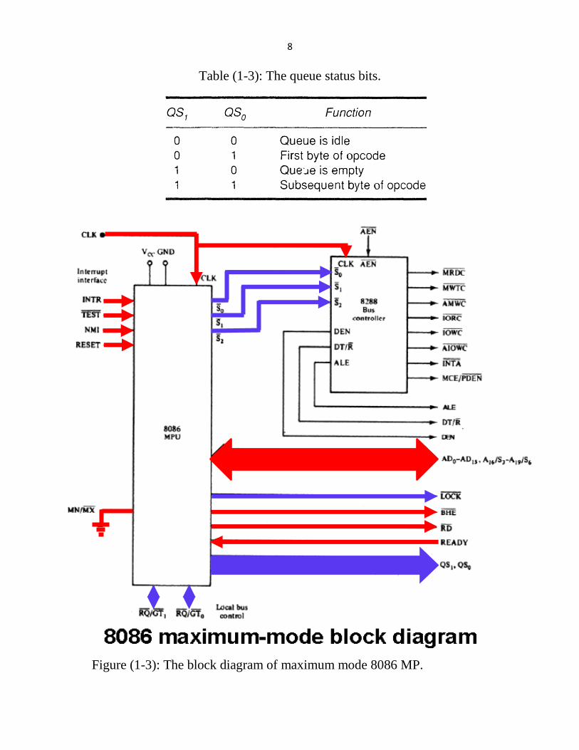
Figure (1-3) shows the block diagram of maximum mode 8086 Microprocessor.
Table (1-2): the Function of status bits ( ) in maximum mode.
Bus cycle status (decoded by 8288 bus controller)
CPU cycle 8288 command
0 0 0
0 0 1
0 1 0
0 1 1
1 0 0
1 0 1
1 1 0
1 1 1
Interrupt acknowledge
I/O read
I/O write
Halt
Opcode fetch
Memory read
Memory write
passive
𝑰𝑵𝑻𝑨
𝑰𝑶𝑹𝑪
𝑰𝑶𝑾𝑪 , 𝑨𝑰𝑶𝑾𝑪 None
𝑴𝑹𝑫𝑪 𝑴𝑹𝑫𝑪 𝑴𝑾𝑻𝑪 , 𝑨𝑴𝑾𝑪
None
(1-2)
(1-3)
8
Table (1-3): The queue status bits.
Figure (1-3): The block diagram of maximum mode 8086 MP.

9
2-
Figure (1-4): The pin layout of 8284A clock generator.

10

11
Figure (1-5): The internal logic diagram of 8284A clock generator.

12
Figure (1-6): The connection of 8284A clock generator with 8086 MP.

13
3-Bus Cycle and Time States
A bus cycle defines the basic operation that a microprocessor performs to
communicate with external devices. Example of bus cycles are the memory read,
memory write, input/output read, and input output write.
As shown in Figure (1-7), a bus cycle start with an address being output on
the system bus followed by a read or write data transfer. During these operations,
the MP produces series of control signals to control the direction and timing of the
bus. The bus cycle of the 8086 MP consists of at least four clock periods. These
four time states are called T1, T2, T3, and T4. During T1, the MP put an address
on the bus. For a write memory cycle, data are put on the bus during state T2 and
maintained through T3and T4. When a read cycle is to be performed, the bus is
first put in the high-Z state during T2 and then the data to be read must be available
on the bus during T3 and T4, These four clock state gives a bus cycle duration of
200 ns *4=800ns in a 5 MHz 8086 system. If no bus cycles are required, the
microprocessor performs what are known as idle state. Idle states are performed if
the instruction queue inside the microprocessor is full and it does not need to read
or write operands from memory. Wait states can also be inserted into a bus cycle.
Figure (1-7): a – Bus cycle clock periods. b- Bus cycle with idle states
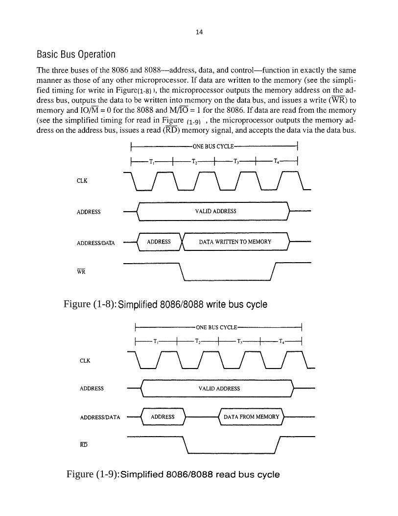
14
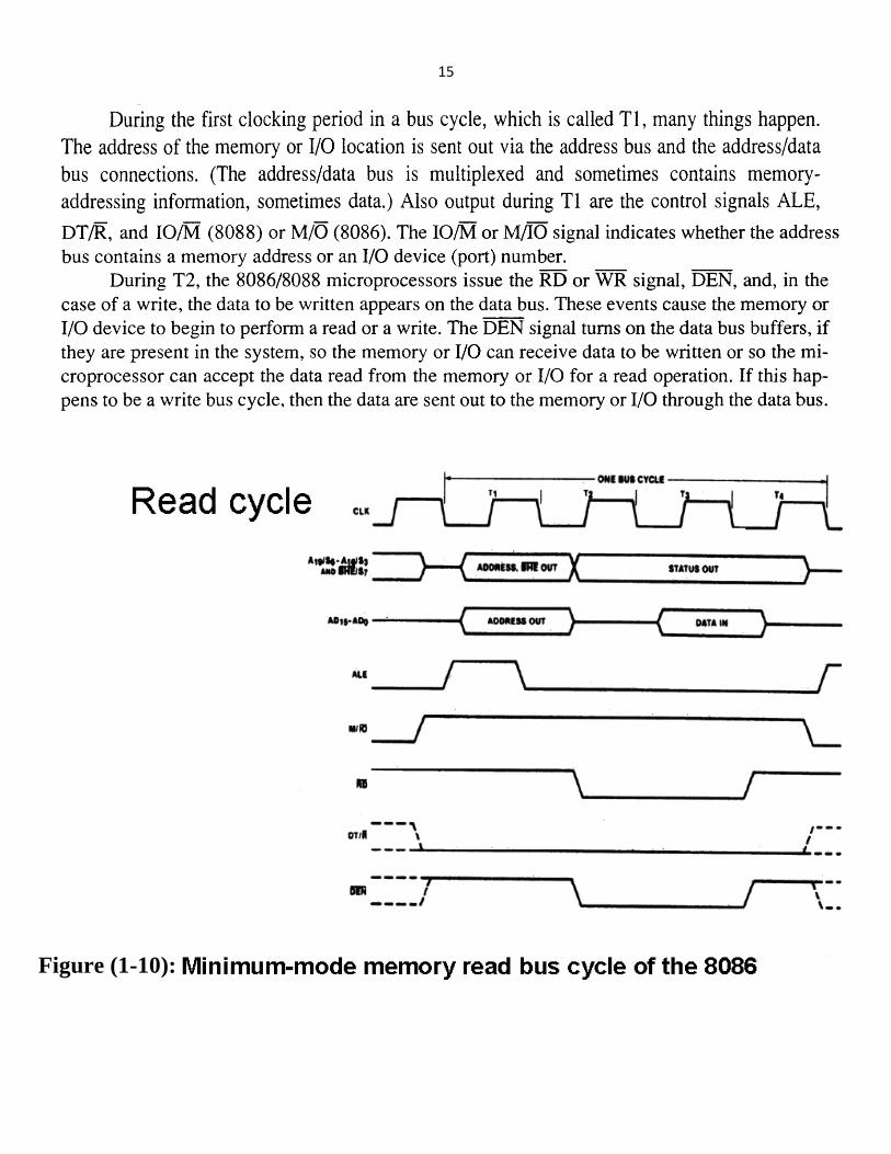
Figure (1-9):
Figure (1-8):
(1-9)
(1-8)
15
Figure (1-10):
16
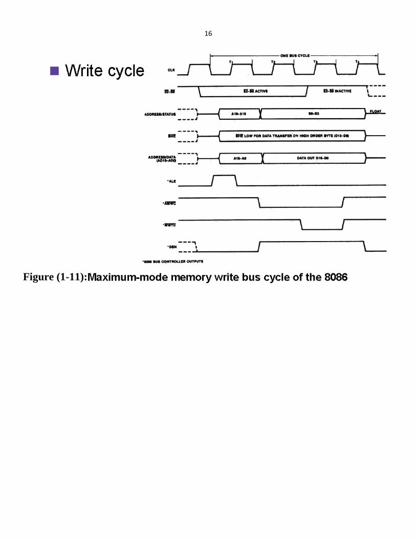
Figure (1-11):

17
Figure (1-12): Input bus cycle of 8086 MP.
18
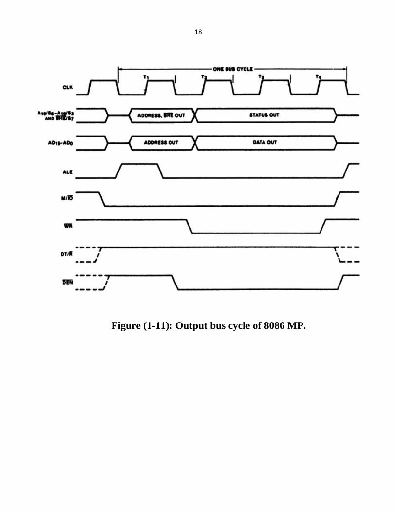
Figure (1-11): Output bus cycle of 8086 MP.

19
(1-14)
(1-14)
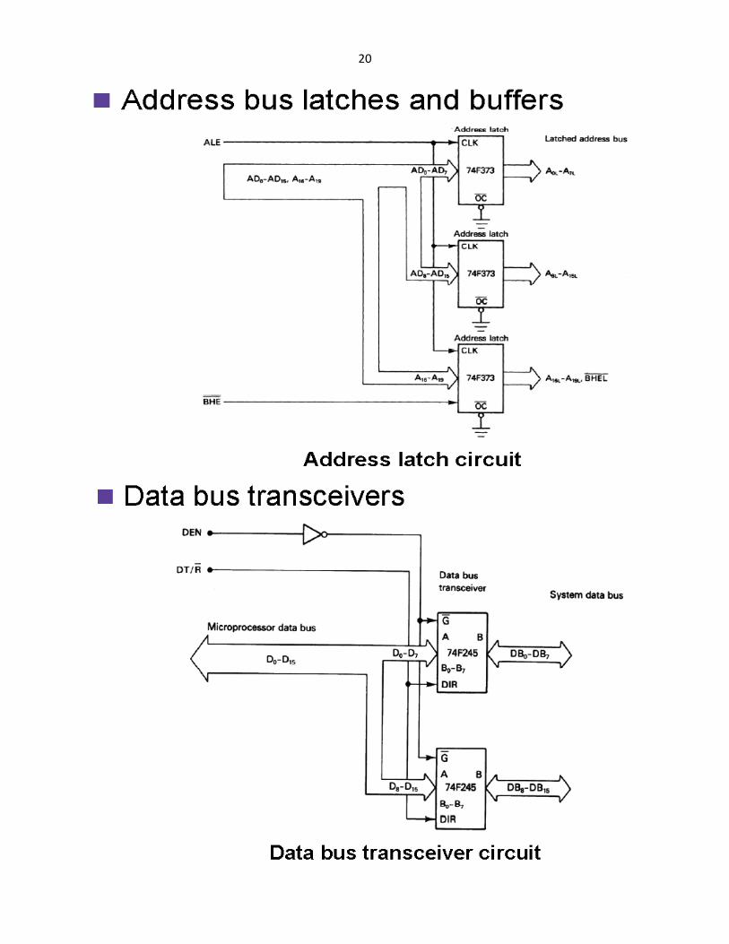
4-
20

21
Figure (1-14): A demultiplexed address bus and fully buffered of 8086 MP buses

22
5-
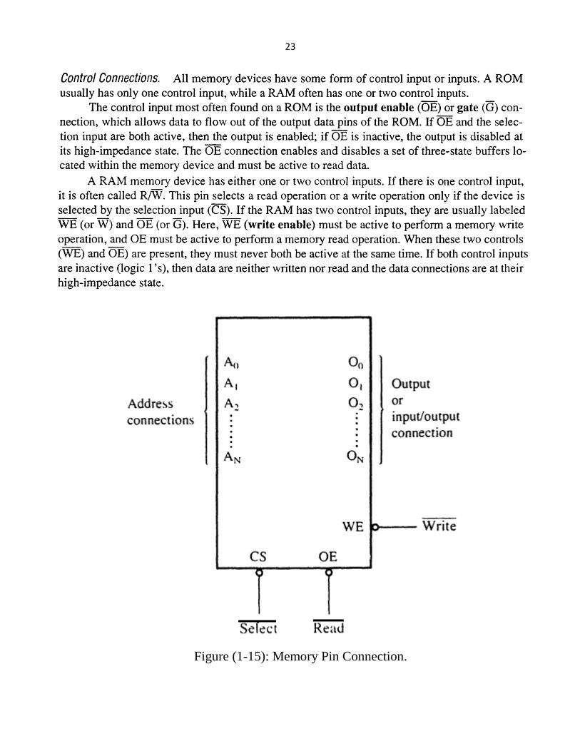
23
Figure (1-15): Memory Pin Connection.

24
25
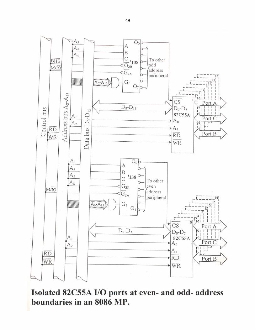
Memory Organization of 8086 MP:
Figure (1-16) shows that the 8086’s 1M byte memory address space is
implemented as two independent 512k byte banks: the low (even) bank and the
high (odd) bank. Data bytes associated with an even address (0000016,0000216, etc)
reside in the high bank.
A1-A19 selects the storage location that is to be accessed. They are applied to
both banks in parallel.
A0 and are used as bank-select signals.
The lower bank transfers bytes of data over data lines D0-D7, while data
transfer for a high bank use D8-D15.

26
Figure (1-16): High and low memory banks of the 8086 MP.

27
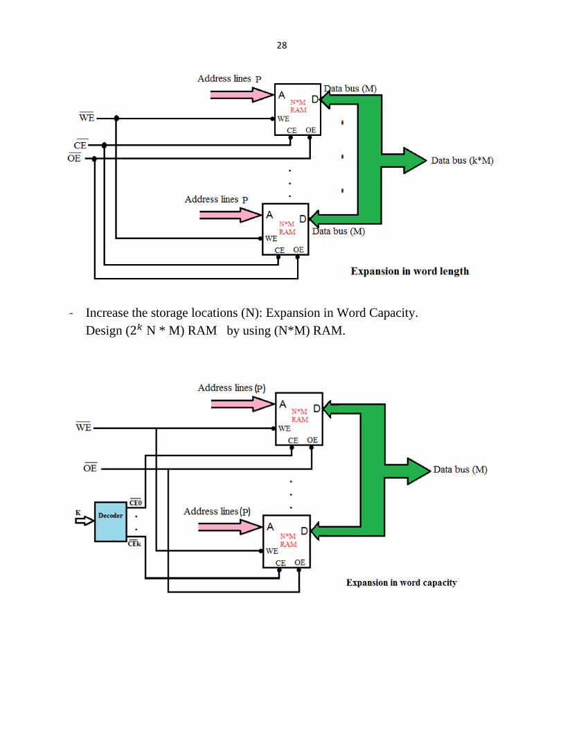
Memory System Design:
ICs are organized as N*M bits array (Memory size = N*M bits arrays).
Where N is no. of Storage Location (Word Capacity) and M is no. of Bits (Word
Length). It is possible to increase the storage locations N or increase number of bits
M or increase both.
- Increase No. of Bits (M): Expansion in Word Length Design (N * k M) RAM
by using (N*M) RAM.
28
- Increase the storage locations (N): Expansion in Word Capacity.
Design ( N * M) RAM by using (N*M) RAM.
29

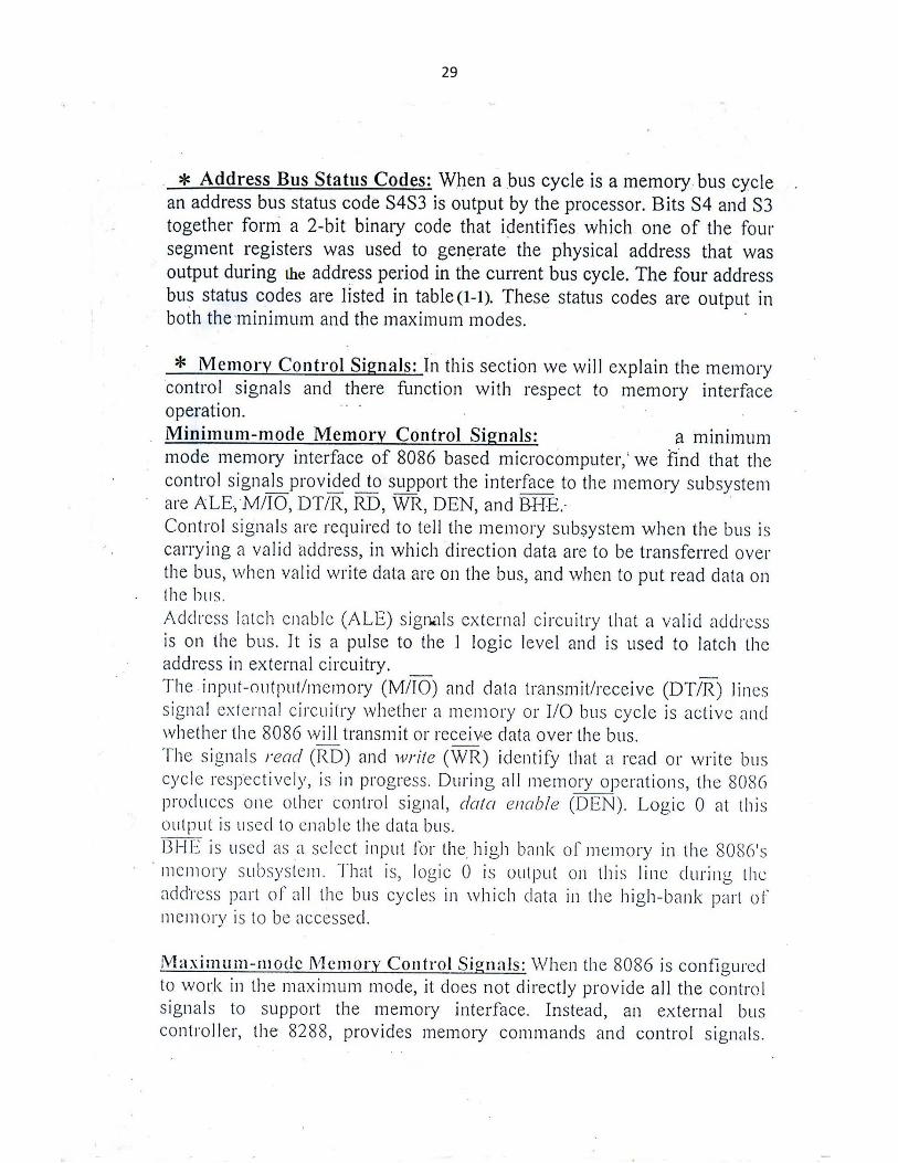
30
31
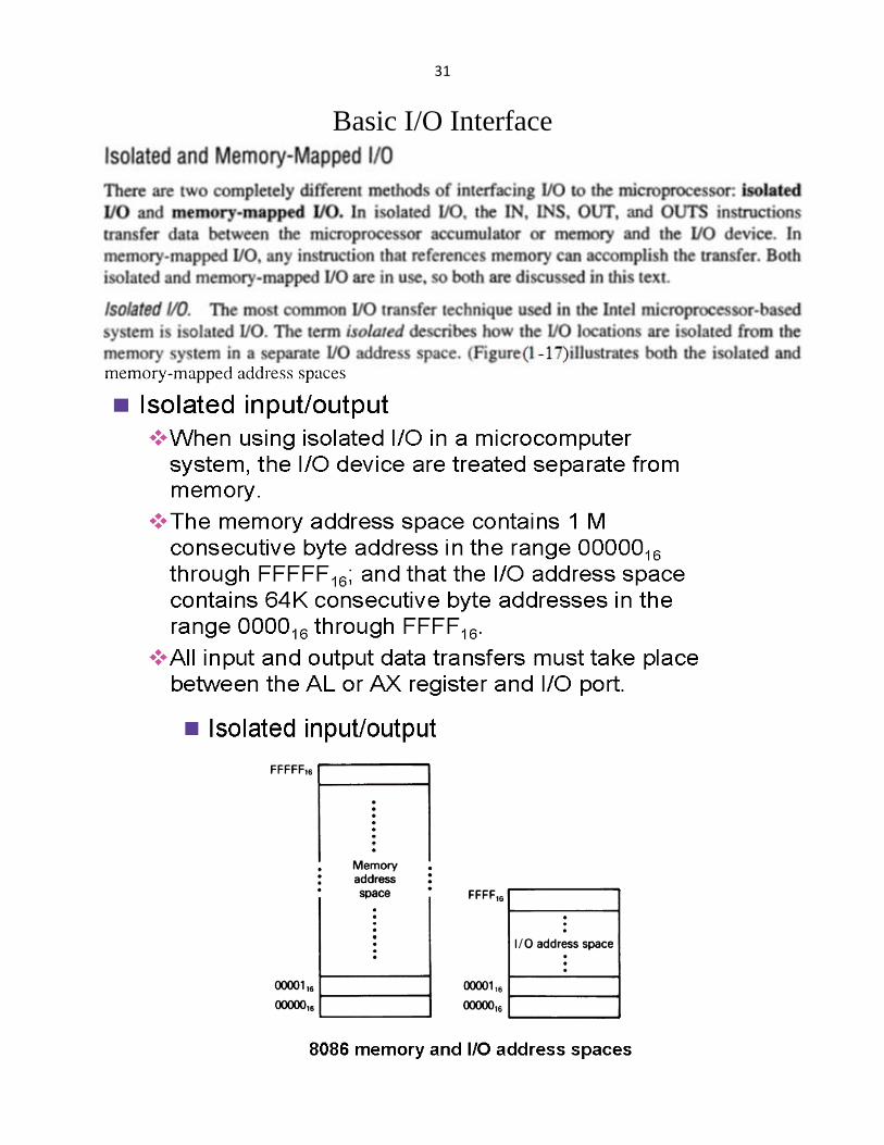
Basic I/O Interface

32
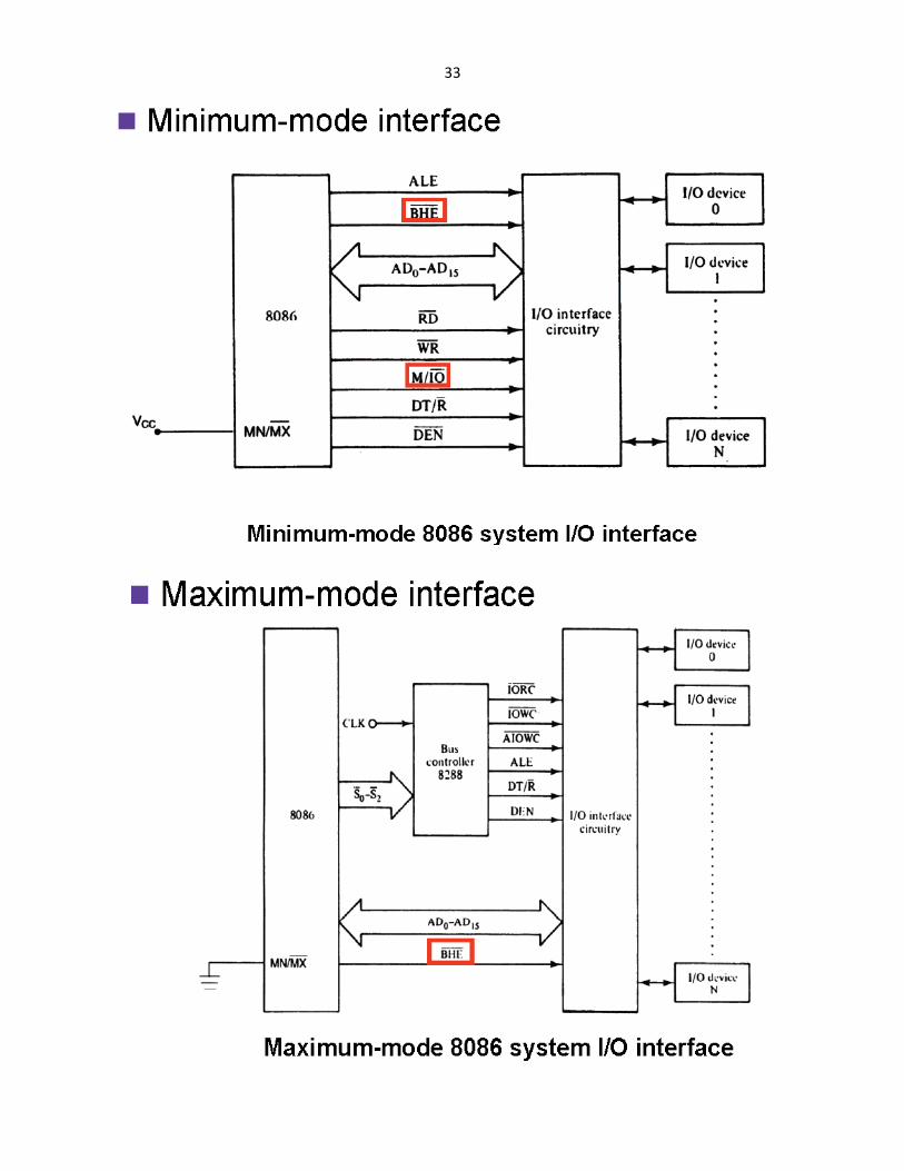
33

34

35
The parallel input-output port chip 8255 is also called as programmable
peripheral input-output port. The Intel’s 8255 is designed for use with Intel’s 8-
bit, 16-bit and higher capability microprocessors. It has 24 input/output lines which
may be individually programmed in two groups of twelve lines each, or three
groups of eight lines. The pin configuration of 8255 is shown in figure above.
The two groups of I/O pins are named as Group A and Group B. Each of these
two groups contains a subgroup of eight I/O lines called as 8-bit port and another
subgroup of four lines or a 4-bit port. Thus Group A contains an 8-bit port A along
with a 4-bit port C upper.
The port A lines are identified by symbols PA0-PA7 while the port C lines are
identified as PC4-PC7. Similarly, Group B contains an 8-bit port B, containing
lines PB0-PB7 and a 4-bit port C with lower bits PC0- PC3. The port C upper and
port C lower can be used in combination as an 8-bit port C.

36
Both the port C are assigned the same address. Thus one may have either three
8-bit I/O ports or two 8-bit and two 4-bit ports from 8255. All of these ports can
function independently either as input or as output ports. This can be achieved by
programming the bits of an internal register of 8255 called as control word register
(CWR).
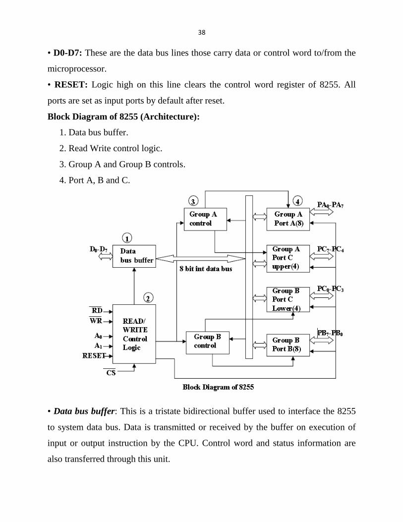
The internal block diagram and is shown in figure below. The 8-bit data bus
buffer is controlled by the read/write control logic. The read/write control logic
manages all of the internal and external transfers of both data and control words.
RD, WR, A1, A0 and RESET are the inputs provided by the microprocessor to
the READ/ WRITE control logic of 8255. The 8-bit, 3-state bidirectional buffer is
used to interface the 8255 internal data bus with the external system data bus. This
buffer receives or transmits data upon the execution of input or output instructions
by the microprocessor. The control words or status information is also transferred
through the buffer.
Signals of 8255
The signals descriptions of 8255 are briefly presented as follows:

37
• PA7-PA0: These are eight port A lines that acts as either latched output or
buffered input lines depending upon the control word loaded into the control word
register.
• PC7-PC4: Upper nibble of port C lines. They may act as either output latches or
input buffers lines.
• This port also can be used for generation of handshake lines in mode 1 or mode 2.
• PC3-PC0: These are the lower port C lines; other details are the same as PC7-
PC4 lines.
• PB0-PB7: These are the eight port B lines which are used as latched output lines
or buffered input lines in the same way as port A.
• RD: This is the input line driven by the microprocessor and should be low to
indicate read operation to 8255.
• WR: This is an input line driven by the microprocessor. A low on this line
indicates write operation.
• CS: This is a chip select line. If this line goes low, it enables the 8255 to respond
to RD and WR signals, otherwise RD and WR signal are neglected.
• A1-A0: These are the address input lines and are driven by the microprocessor.
These lines A1-A0 with RD, WR and CS form the following operations for
8255. These address lines are used for addressing any one of the four registers, i.e.
three ports and a control word register as given in table below.
38
• D0-D7: These are the data bus lines those carry data or control word to/from the
microprocessor.
• RESET: Logic high on this line clears the control word register of 8255. All
ports are set as input ports by default after reset.
Block Diagram of 8255 (Architecture):
1. Data bus buffer.
2. Read Write control logic.
3. Group A and Group B controls.
4. Port A, B and C.
• Data bus buffer: This is a tristate bidirectional buffer used to interface the 8255
to system data bus. Data is transmitted or received by the buffer on execution of
input or output instruction by the CPU. Control word and status information are
also transferred through this unit.
buffer
39
• Read/Write control logic: This unit accepts control signals (RD, WR) and also
inputs from address bus and issues commands to individual group of control blocks
(Group A, Group B). It has the following pins:
a) CS – Chip select: A low on this PIN enables the communication between CPU
and 8255.
b) RD (Read): A low on this pin enables the CPU to read the data in the ports or
the status word through data bus buffer.
c) WR (Write): A low on this pin, the CPU can write data on to the ports or on to
the control register through the data bus buffer.
d) RESET: A high on this pin clears the control register and all ports are set to the
input mode
e) A0 and A1 (Address pins): These pins in conjunction with RD and WR pins
control the selection of one of the three ports.
• Group A and Group B controls: These blocks receive control from the CPU and
issues commands to their respective ports.
• Group A - PA and PCU (PC7 –PC4)
• Group B - PCL (PC3 – PC0)
• Control word register can only be written into no read operation of the CW
register is allowed.
a) Port A: This has an 8 bit latched/buffered O/P and 8 bit input latch. It can be
programmed in three modes – mode 0, mode 1, and mode 2.
b) Port B: This has an 8 bit latched / buffered O/P and 8 bit input latch. It can be
programmed in mode 0, mode1.
c) Port C: This has an 8 bit latched input buffer and 8 bit output latched/buffer.
This port can be divided into two 4 bit ports and can be used as control signals for
port A and port B. it can be programmed in mode 0.

40
To communicate with peripherals through the 82C55A, three steps are
necessary:
1. Determine the addresses of ports A, B, and C and the control word of the
control register according to Chip select logic and address lines A0 and A1.
2. Write a control word in the control register.
3. Write I/O instruction to communicate with peripherals through ports A, B,
and C.
Modes of Operation of 8255
These are two basic modes of operation of 8255, I/O mode and Bit Set-Reset
mode (BSR). In I/O mode, the 8255 ports work as programmable I/O ports, while
in BSR mode only port C (PC0-PC7) can be used to set or reset its individual port
bits. Under the I/O mode of operation, further there are three modes of operation of
8255, so as to support different types of applications, mode 0, mode 1 and mode 2.
All these modes can be selected by programming a register internal to 8255
known as CWR. The control word register has two formats. The first format is

41
valid for I/O modes of operation, i.e. modes 0, mode 1 and mode 2 while the
second format is valid for bit set/reset (BSR) mode of operation.
BSR Mode: In this mode any of the 8-bits of port C can be set or reset
depending on D0 of the control word. The bit to be set or reset is selected by bit
select flags D3, D2 and D1 of the CWR as given in table.
BSR mode control word register format is shown in following figure.
I/O Modes:
a) Mode 0 (Basic I/O mode): This mode is also called as basic input/output mode.
This mode provides simple input and output capabilities using each of the three
ports. Data can be simply read from and written to the input and output ports
respectively, after appropriate initialization. The salient features of this mode are as
listed below:

42
1. Two 8-bit ports (port A and port B) and two 4-bit ports (port C upper and lower)
are available. The two 4-bit ports can be combined used as a third 8-bit port.
2. Any port can be used as an input or output port.
3. Output ports are latched. Input ports are not latched.
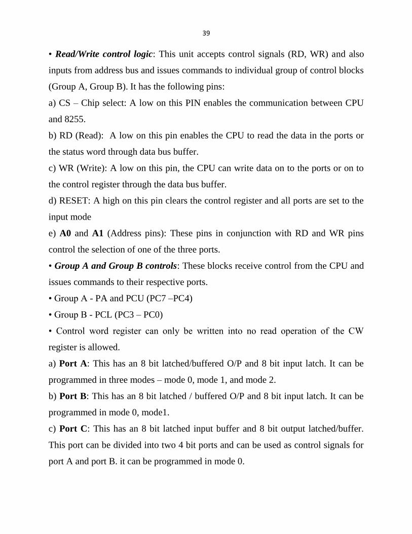
b) Mode 1(Strobed input/output mode): in this mode the handshaking control the
input and output action of the specified port. Port C lines PC0-PC2; provide strobe
or handshake lines for port B. This group which includes port B and PC0-PC2 is
called as group B for Strobed data input/output. Port C lines (PC3-PC5) provide
strobe lines for port A.
This group is including port A and PC3-PC5 from group A. Thus port C is
utilized for generating handshake signals. The salient features of mode 1 are listed
as follows:
1. Two groups – group A and group B are available for strobed data transfer.
2. Each group contains one 8-bit data I/O port and one 4-bit control/data port.
3. The 8-bit data port can be either used as input and output port. The inputs and
outputs both are latched.
4. Out of 8-bit port C, PC0-PC2 are used to generate control signals for port B and
PC3-PC5 are used to generate control signals for port A. The lines PC6, PC7 may
be used as independent data lines.
The control signals for both the groups in input and output modes are
explained as follows:
Input control signal definitions (mode 1):
• STB(Strobe input) – If this lines falls to logic low level, the data available at 8-bit
input port is loaded into input latches.

43
• IBF (Input buffer full) – If this signal rises to logic 1, it indicates that data has
been loaded into latches, i.e. it works as an acknowledgement. IBF is set by a low
on STB and is reset by the rising edge of RD input.
• INTR (Interrupt request) – This active high output signal can be used to interrupt
the CPU whenever an input device requests the service. INTR is set by a high STB
pin and a high at IBF pin. INTE is an internal flag that can be controlled by the bit
set/reset mode of either PC4 (INTEA) or PC2 (INTEB) as shown in the figure.
INTR is reset by a falling edge of RD input. Thus an external input device
can be request the service of the processor by putting the data on the bus and
sending the strobe signal.
Output control signal definitions (mode 1):
• OBF (Output buffer full) – This status signal, whenever falls to low, indicates
that CPU has written data to the specified output port. The OBF flip-flop will be
set by a rising edge of WR signal and reset by a low going edge at the ACK input.
• ACK (Acknowledge input) – ACK signal acts as an acknowledgement to be
given by an output device. ACK signal, whenever low, informs the CPU that the
data transferred by the CPU to the output device through the port is received by the
output device.
• INTR (Interrupt request) – Thus an output signal that can be used to interrupt the
CPU when an output device acknowledges the data received from the CPU. INTR
is set when ACK, OBF and INTE are 1. It is reset by a falling edge on WR input.
The INTEA and INTEB flags are controlled by the bit set-reset mode of PC6 and
PC2 respectively.
44

45
c) Mode 2 (Strobed bidirectional I/O): This mode of operation of 8255 is also
called as strobed bidirectional I/O. This mode of operation provides 8255 with an
additional features for communicating with a peripheral device on an 8-bit data
bus. Handshaking signals are provided to maintain proper data flow and
synchronization between the data transmitter and receiver. The interrupt generation
and other functions are similar to mode 1. In this mode, 8255 is a bidirectional 8-
bit port with handshake signals. The Rd and WR signals decide whether the 8255
is going to operate as an input port or output port.
The Salient features of Mode 2 of 8255 are listed as follows:
1. The single 8-bit port in group A is available.
2. The 8-bit port is bidirectional and additionally a 5-bit control port is available.
3. Three I/O lines are available at port C (PC2 – PC0).
4. Inputs and outputs are both latched.
5. The 5-bit control port C (PC3-PC7) is used for generating / accepting handshake
signals for the 8-bit data transfer on port A.
Control signal definitions in mode 2:
• INTR – (Interrupt request) as in mode 1, this control signal is active high and is
used to interrupt the microprocessor to ask for transfer of the next data byte
to/from it. This signal is used for input (read) as well as output (write) operations.
-Control Signals for Output operations:
• OBF (Output buffer full): this signal, when falls to low level, indicates that the
CPU has written data to port A.
• ACK (Acknowledge): this control input, when falls to logic low level,
acknowledges that the previous data byte is received by the destination and next
byte may be sent by the processor. This signal enables the internal tristate buffers
to send the next data byte on port A.

46
• INTE1 (A flag associated with OBF): this can be controlled by bit set/reset mode
with PC6.
-Control signals for input operations:
• STB (Strobe input): a low on this line is used to strobe in the data into the input
latches of 8255.
• IBF (Input buffer full): when the data is loaded into input buffer, this signal rises
to logic ‘1’. This can be used as an acknowledge that the data has been received by
the receiver.
Mode 2 Bidirectional Data Transfer:
The following figure shows a schematic diagram containing an 8-bit
bidirectional port, 5-bit control port and the relation of INTR with the control pins.
Port B can either be set to Mode 0 or 1 with port A (Group A) is in Mode 2. Mode
2 is not available for port B. The following figure shows the control word. The
INTR goes high only if IBF, INTE2, STB and RD go high or OBF, INTE1, ACK
and WR go high. The port C can be read to know the status of the peripheral
device, in terms of the control signals, using the normal I/O instructions.

47
The Table below shows a summary of the port connections for the 82C55A
PPI.

48
Example1: what is the mode and I/O configuration for ports A, B and C of an
82C55A after its control register is loaded with 82 H.
Example2: In the isolated parallel input/output ports of 82C55A implementation,
assume that PPI 15 is configured so that port A is an output port, both port B and C
are input ports, and all three ports are set up for mode 0 operation. Write a program
that will input the data at port B and C, find the difference (port C)-(port B), and
output this difference to port A.
Example3: In memory mapped parallel input/output ports of 82C55A
implementation, assume that PPI0 is configured so that port A is an output port,
both port B and C are input ports, and all three ports are set up for mode 0
operation. Write a program to perform the following:
1- initialize the control register of PPI0.
2- input the contents of port B and C, AND them together, and output the result to
port A.
Example4: Write a BSR program to set bits PC7 and PC3 and reset them after
(10ms). Use PPI0 of parallel input/output ports of 82C55A implementation, and
assume that a delay subroutine is available.
49

50
51
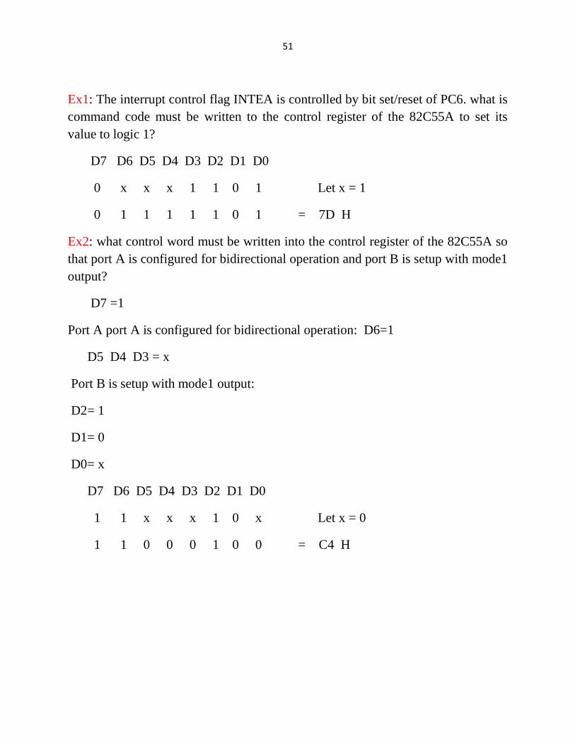
Ex1: The interrupt control flag INTEA is controlled by bit set/reset of PC6. what is
command code must be written to the control register of the 82C55A to set its
value to logic 1?
D7 D6 D5 D4 D3 D2 D1 D0
0 x x x 1 1 0 1 Let x = 1
0 1 1 1 1 1 0 1 = 7D H
Ex2: what control word must be written into the control register of the 82C55A so
that port A is configured for bidirectional operation and port B is setup with mode1
output?
D7 =1
Port A port A is configured for bidirectional operation: D6=1
D5 D4 D3 = x
Port B is setup with mode1 output:
D2= 1
D1= 0
D0= x
D7 D6 D5 D4 D3 D2 D1 D0
1 1 x x x 1 0 x Let x = 0
1 1 0 0 0 1 0 0 = C4 H

52

53
Interrupts
The processor has the following interrupts:
•INTR is a maskable hardware interrupt. The interrupt can be enabled/disabled
using STI/CLI instructions or using more complicated method of updating the
FLAGS register with the help of the POPF instruction.
•When an interrupt occurs, the processor stores FLAGS register into stack, disables
further interrupts, fetches from the bus one byte representing interrupt type, and
jumps to interrupt processing routine address of which is stored in location 4 *
<interrupt type>. Interrupt processing routine should return with the IRET
instruction.
•NMI is a non-maskable interrupt. Interrupt is processed in the same way as the
INTR interrupt. Interrupt type of the NMI is 2, i.e. the address of the NMI
processing routine is stored in location 0008h. This interrupt has higher priority
than the maskable interrupt.
•Software interrupts can be caused by:
•INT instruction - breakpoint interrupt. This is a type 3 interrupt.
•INT <interrupt number> instruction - any one interrupt from available 256
interrupts.
•INTO instruction - interrupt on overflow
•Single-step interrupt - generated if the TF flag is set. This is a type 1 interrupt.
When the CPU processes this interrupt it clears TF flag before calling the interrupt
processing routine.
•Processor exceptions: Divide Error (Type 0), Unused Opcode (type 6) and
Escape opcode (type 7).
•Software interrupt processing is the same as for the hardware interrupts.

54

55
56
57

58
59