Bridging between micro- and macroscales of materials by mesoscopic models
Upload
khangminh22Category
view
3download
0
1
Technology and Applications of 2D Materials
in Micro- and Macroscale Electronics
by
Marek Hempel
B.S., RWTH Aachen University (2010)
M.S., RWTH Aachen University (2013)
Submitted to the Department of Electrical Engineering and Computer Science
in Partial Fulfillment of the Requirements for the Degree of
Doctor of Philosophy
at the
MASSACHUSETTS INSTITUTE OF TECHNOLOGY
May 2020
© Massachusetts Institute of Technology 2020. All rights reserved.
Author ………………………………………………………………………………………………………………………………………………………
Department of Electrical Engineering and Computer Science
May 15, 2020
Certified by ……………………………………………………………………………………………………………………………………………….
Tomás Palacios
Professor of Electrical Engineering and Computer Science
Thesis Supervisor
Certified by ……………………………………………………………………………………………………………………………………………….
Jing Kong
Professor of Electrical Engineering and Computer Science
Thesis Supervisor
Accepted by ………………………………………………………………………………………………………………………………………………
Leslie A. Kolodziejski
Professor of Electrical Engineering and Computer Science
Chair, Department Committee on Graduate Students

2

3
Technology and Applications of 2D-Materials
in Micro- and Macroscale Electronics
by
Marek Hempel
Submitted to the Department of Electrical Engineering and Computer Science
on May 15, 2020, in Partial Fulfillment of the Requirements for the Degree of
Doctor of Philosophy
Abstract:
Over the past 50 years, electronics has truly revolutionized our lives. Today, many everyday objects rely on electronic circuitry from gadgets such as wireless earbuds, smartphones and laptops to larger devices like household appliances and cars. However, the size range of electronic devices is still rather limited from the millimeter to meter scale. Being able to extend the reach of electronics from the size of a red blood cell to a skyscraper would enable new applications in many areas including energy production, entertainment, environmental sensing, and healthcare. 2D-materials, a new class of atomically thin materials with a variety of electric properties, are promising for such electronic systems with extreme dimension due to their flexibility and ease of integration. On the macroscopic side, electronics produced on thin films by roll-to-roll fabrication has great potential due to its high throughput and low production cost. Towards this end, this thesis explores the transfer of 2D-materials onto flexible EVA/PET substrates with hot roll lamination and electrochemical delamination using a custom designed roll-to-roll setup. The transfer process is characterized in detail and the lamination of multiple 2D material layers is demonstrated. As exemplary large-scale electronics application, a flexible solar cell with graphene transparent electrode is discussed. On the microscopic side, this thesis presents a 60x60 µm2 microsystem platform called synthetic cells or SynCells. This platform offers a variety of building blocks such as chemical sensors and transistors based on molybdenum disulfide, passive germanium timers, iron magnets for actuation, as well as gallium nitride LEDs and solar cells for communication and energy harvesting. Several system-level applications of SynCells are explored such as sensing in a microfluidic channel or spray-coating SynCells on arbitrary surfaces.
Thesis Supervisor: Tomás Palacios Title: Professor of Electrical Engineering and Computer Science Thesis Supervisor: Jing Kong Title: Professor of Electrical Engineering and Computer Science

4

5
Acknowledgements
This thesis would not have been possible without the help, guidance, and support of so many people that I would like to acknowledge.
Firstly, I would like to sincerely thank my research advisors Prof. Jing Kong and Prof. Tomás Palacios for their mentorship and support. Jing always provided me insightful suggestions and ideas when I faced challenges, especially for the roll-to-roll transfer part of my thesis. Her thoughtful and patient way to interrogate every detail in a figure, manuscript or presentation greatly helped me identify gaps in my thinking and my explanations. Her kind and warm personality also made me feel especially welcome in the group. Tomas has been my other essential pillar of support during this thesis. His inventive ideas and guidance were especially important for my second research project on electronic microsystems. I deeply appreciate Tomas’s positive attitude when encountering research challenges, his creative thinking approach to solving problems and his ability to connect me with the right people at the right time.
Furthermore, I would like to thank my third committee member Prof. Michael Strano for his discussions and suggestions for my thesis. His abundant knowledge in realm of chemical engineering gave me an insightful and complementary perspective towards the applications of intelligent microsystems. I would also like to express my gratitude to Prof. Millie Dresselhaus for discussions about my research and her guidance during the first years of my PhD.
As part of my time at MIT, I had the fortune to visit other academic and industry partners to expand my knowledge and perspective. I specifically want to say thank you to Prof. Mario Hoffman and Prof. Ya-Ping Hsieh for inviting me to their groups for a short research stay. Furthermore, I want to thank my advisors Stanton Ashburn and Jens Lohse as well as the rest of the process integration group for giving me a unique glimpse into the operations of a state-of-the-art silicon fab during my internship at the Richardson Fab of Texas Instruments.
My research relied heavily on the lab-space of RLE and the cleanroom facilities of NSL, MTL, and MIT.nano. In this regard, I want to warmly thank everyone involved who helped maintain these complex facilities and provided help for fabrication issues. I particular, I want to thank Bernard Alamariu, Bob Bicchieri, Daniel Adams, Dave Terry, Dennis Ward, Donal Jamieson, Eric Lim, Gary Riggott, Jim Daley, Jorg Scholvin, Kris Payer, Kurt Broderick, Mark Mondol, Paudely Zamora, Paul Tierney, Paul McGrath, Ryan O'Keefe, Scott Poesse, Tim Turner, Vicky Diadiuk and Whitney Hess, who I had the pleasure to work with directly, be it for tool trainings, trouble-shooting tools or discussing fabrication processes.
I am very grateful for the administrative help I received from the staff at MTL and RLE to advance my research goals. Firstly, I would like to sincerely thank Joseph Baylon for his exceptional help in supporting my work in the Palacios group. Furthermore, I want to acknowledge Mike Hobbs, Bill Maloney and Michael McIlrath for their help with computer issues and MTL’s CAD services. I also had the pleasure to interact with Debroah Hodges-Pabon, Elizabeth Kubicki, Jami Mitchell, Katrina Mounlavongsy, Luda Leopardi, Mara Karapetian, Mary O’Neil, Sam Crooks, Shereece Beckford, Stacy McDaid, Steven O'Hearn and Valerie DiNardo for various logistic tasks such as organizing MARC2015 and MTL cookie socials.
My research projects would also not have succeeded without my collaborators that I am genuinely appreciative off. With respect to my roll-to-roll project, I would like to thank Yi Song, Wenjing Fan, Fei Hui and Ang-Yu Lu for helping me with the 2D material synthesis and Mahdi Tavakoli and Giovanni Azzellino for their help with the solar cell fabrication and characterization. I also want to acknowledge Libby Shaw for her support with XPS measurements. Regarding the SynCell project, I am thankful to Vera Schroeder

6
in Prof. Timothy Swager group at MIT for helping me with the chemical exposure experiments and the fruitful discussions on the concept of SynCells. I am indebted to Albert Lui in Prof. Michael Strano’s group for trying out several MoS2 sensor functionalizations and in-depth discussions and to Volodymyr Koman in Prof. Michael Strano’s group for his assistance with SynCell spraying experiments, data modeling and manuscript preparation. I want to express my gratitude to Pin-Chun Shen, Chibeom Park and Prof. Jiwoong Park for providing MoS2 films. Furthermore, I thank Prof. Marisa Lopez-Vallejo and Javier De Mena for their outstanding diligence and creativity designing a CMOS chip and Mohamed Ibrahim for sharing his experience and thoughts on this design process. Lastly, I am grateful to Kohei Yoshizawa and DOWA Electronics Materials Co., Ltd. for providing GaAs LED wafers and Noelia Vico Trivino and Jori Lemettinen for providing the GaN LED wafers and helping me develop a GaN LED process, respectively.
My time at MIT was so much more pleasant and enjoyable because of the support of my peer and colleagues. I would like to thank all the students in RLE and MTL that I have interacted with for making me feel at home, helping me with my research quests, or just socializing to get a much-needed break. This is especially true for my fellow students on the 6th floor of building 39, the MTL cookie social regulars and so many encounters at MTL’s Annual Research Conferences. I want to express my gratitude to the current and past members of the Kong and Palacios group for making MIT such an enjoyable workplace. In particular, I want to thank Ahmad Zubair for his experience and infinite patience when debugging processes or electric measurements with me. Thank you to Elaine McVay and Mantian Xue for being great partners of our MURI-FATE sub-team. I furthermore want to thank Amir Nourbakhsh, Charles Mackin, Cosmi Lin, Daniel Piedra, Josh Perozek, Kohei Yoshizawa, Lili Yu, Min Sun, Winston Chern, Xu Zhang, Wenjing Fang, Yi Song that I had the pleasure to learn from in one way or another.
The technical work in this thesis would have not happened without the support of the funding agencies Eni S.p.A. under the Eni-MIT Solar Frontiers Center, the Air Force Office of Scientific Research under the MURI-FATE program (Grant No. FA9550-15-1-0514) monitored by Dr. Harold Weinstock and Dr. Kenneth Caster, and the Army Research Office under the project W911NF-19-10372, monitored by Dr. Joe Qiu. I am grateful they provided the financial means to make my research ideas come to life.
I am very thankful to all my dear friends at MIT that I’ve met outside of the lab and for the fun times we had, especially Affi, Alin, Aloni, Ari, Colm, Curtis, Deborah, Eva, Gautam, Gus, James, Jonas, Joy, Lindsay, Michel, Mike, Pavel, Sara, Tobi and Twan.
I feel a deep sense of gratitude for my family, especially my mom. You all have made me into the person I am today and encouraged me every step of the way. Your guidance and trust made me chase my dreams and believe in my abilities. I’m only standing where I am today because of your unwavering love and support.
Finally, I am eternally thankful to my partner and fiancée Danielle Pace for supporting me over all these years. Her love, compassion and friendship has helped me overcome moments of doubt or difficulty and sharing my moments of joy and accomplishment with her made them taste even sweeter.
7
Table of Contents
Introduction ........................................................................................................................................ 25
1.1 Extending the Reach of Electronics ............................................................................................. 25
1.2 The Potential of Two-Dimensional Materials ............................................................................. 28
1.3 Film-based Macroscale Electronics ............................................................................................. 30
1.4 Autonomous Microsystems ........................................................................................................ 32
1.5 Thesis Outline .............................................................................................................................. 34
Fundamentals of 2D Materials ............................................................................................................ 37
2.1 Properties and Applications of 2D Materials .............................................................................. 37
2.1.1 Graphene ............................................................................................................................ 37
2.1.2 Hexagonal Boron Nitride ..................................................................................................... 41
2.1.3 Molybdenum Disulfide ........................................................................................................ 43
2.2 Synthesis of 2D Materials ........................................................................................................... 46
2.2.1 Graphene ............................................................................................................................ 46
2.2.2 Hexagonal Boron Nitride ..................................................................................................... 49
2.2.3 Molybdenum Disulfide ........................................................................................................ 51
2.3 Transfer of 2D Materials ............................................................................................................. 52
2.3.1 Wet Etching of Substrate .................................................................................................... 54
2.3.2 Electrochemical Delamination ............................................................................................ 55
2.3.3 Delamination on Water ....................................................................................................... 57
Large scale 2D Material Transfer ........................................................................................................ 59
3.1 Roll-to-Roll Transfer Setup .......................................................................................................... 60
3.2 Transfer Process Optimization .................................................................................................... 61
3.3 Single Graphene Transfer............................................................................................................ 64
3.4 Double Graphene Transfer ......................................................................................................... 70
3.5 Graphene/hBN Transfer .............................................................................................................. 72
3.6 Applications ................................................................................................................................. 77
3.7 Conclusion ................................................................................................................................... 78
SynCell Building Blocks ........................................................................................................................ 81
8
4.1 Sensing Building Block ................................................................................................................. 83
4.2 Timer Building Block.................................................................................................................... 86
4.3 Computation Building Blocks ...................................................................................................... 91
4.3.1 MoS2 Transistors ................................................................................................................. 94
4.3.2 CMOS Silicon Chip ............................................................................................................... 97
4.4 Communication and Energy Harvesting Building Blocks .......................................................... 101
4.4.1 Literature Review of Microscale Communication ............................................................. 102
4.4.2 Literature Review on Microscale Energy Harvesting and Storage .................................... 104
4.4.3 Design Considerations for Microscale Communication and Energy Harvesting ............... 108
4.4.4 GaAs-based LEDs and Solar Cells ...................................................................................... 109
4.4.5 GaN-based LED and Solar Cell ........................................................................................... 111
4.5 Magnetic Actuation Building Block ........................................................................................... 114
4.6 Conclusion ................................................................................................................................. 116
SynCell Demonstrations .................................................................................................................... 119
5.1 Design and Concept .................................................................................................................. 119
5.2 Fabrication and Lift-Off ............................................................................................................. 121
5.3 Amplifier Demonstration .......................................................................................................... 128
5.4 Microfluidic Channel Demonstration ........................................................................................ 131
5.5 Spraying Demonstrations .......................................................................................................... 134
5.6 Conclusion ................................................................................................................................. 136
Summary and Future Work ............................................................................................................... 139
6.1 Thesis Contributions ................................................................................................................. 139
6.2 Future Work .............................................................................................................................. 141
6.2.1 Roll-to-Roll Transfer of 2D Materials ................................................................................ 141
6.2.2 Optimizing SynCell Building Blocks ................................................................................... 142
6.2.3 Heterogeneous SynCell Integration with CMOS and III-V Chips ....................................... 143
Appendix ........................................................................................................................................... 149
7.1 Acronyms .................................................................................................................................. 149
7.2 Metal Contact Patterning .......................................................................................................... 151
7.2.1 Lift-off Optimization with AZ5214 .................................................................................... 152
9
7.2.2 Optimization of PMMA/MMA Lift-Off Using Deep UV Light ............................................ 156
7.3 Undercutting and Lift-off Techniques ....................................................................................... 159
7.3.1 First Generation Lift-Off System ....................................................................................... 160
7.3.2 Second Generation Lift-Off System ................................................................................... 162
7.3.3 Third Generation Lift-Off System ...................................................................................... 165
7.4 Processes ................................................................................................................................... 167
7.4.1 LPCVD Graphene Growth on Copper Foil ......................................................................... 167
7.4.2 Wet Etch Graphene Transfer in FeCl3 ............................................................................... 168
7.4.3 Wet Etch MoS2 Transfer in HF ........................................................................................... 170
7.4.4 Electrochemical Transfer of hBN or Graphene in NaOH solution ..................................... 172
7.4.5 Water Delamination of MoS2 ............................................................................................ 175
7.4.6 SPR700-PMMA A3 Deep UV Photo Lithography for Mesa Etching ................................... 177
7.4.7 SPR700-PMMA-MMA Deep UV Photo Lithography for Lift-Off ........................................ 178
7.4.8 GaAs LED Fabrication ........................................................................................................ 180
7.4.9 GaN LED Fabrication ......................................................................................................... 181
7.4.10 SynCell Fabrication Protocol ............................................................................................. 184
7.4.11 SynCell Lift-Off Protocol .................................................................................................... 188
7.4.12 Microfluidic Channel Fabrication ...................................................................................... 189
7.5 Additional Data and Analysis .................................................................................................... 190
7.5.1 Analyte Diffusion in the Microfluidic Channel .................................................................. 190
7.5.2 Theoretical Communication Limits by Light ...................................................................... 192
References ........................................................................................................................................ 197

10
11
List of Figures
Figure 1-1: Length scale of electronic systems. Conventional electronics roughly ranges from the
millimeter to the meter scale. Extending electronics to the microscale (size of a red blood cell) and
macroscale (size of a skyscraper) opens up new opportunities. ................................................................ 25
Figure 1-2: Graph of various 2D materials according to their band gap, ranging from semi-metallic
graphene to insulating boron nitride. Reproduced with permission from [33]. ........................................ 29
Figure 1-3: Macroscale applications of film-based electronics. a) Solar cell films could be applied to
building facades for energy harvesting. b) Display films could be applied to walls and ceilings for
entertainment, decoration or advertising purposes. c) Large sensors films could be useful for robotic skin.
.................................................................................................................................................................... 30
Figure 1-4: Examples of future applications for microscale electronics. a) Microscale electronic sensors
could be dissolved in liquid and then be sprayed onto industrial equipment to add a dense sensor
networks for recording temperature and vibration. b) Microscale sensors could be embedded into
polymer fibers to produce smart clothing. c) Microelectronic systems may interact with or go inside of
biological cells to measure relevant biological parameters. d) More advanced versions of autonomous
microsystems (about 10 µm) could travel in the blood stream to detect diseases inside the human body
such as cancer and transmit diagnostic data wirelessly. ............................................................................ 32
Figure 2-1: a) Schematic of graphene honeycomb lattice. b) 3D electronic band structure of conduction
(top) and valance band (bottom) in graphene. The inset shows the energy bands intersect at the K points
in Brillouin zone. Adapted with permission from [76]. ............................................................................... 37
Figure 2-2: Types of graphene doping. a) Graphene can be electrostatically doped by creating a plate-
capacitor with graphene as one electrode and applying a voltage. b) Substitutional doping is achieved
through the replacement of carbon atoms with other atoms in the lattice, for example nitrogen for n-type
doping. c) Graphene can be doped by the adsorption of molecules on the surface through direct charge
transfer. Additionally, close contact to metals or dielectrics also lead to the doping of graphene and
depends on the relative material work function with respect to graphene. ............................................. 38
Figure 2-3: Transparency of graphene. a) Transmittance of suspended mono and bilayer graphene on a
carrier under white light. The contrast of the three regions is clearly visible. b) Transmittance of graphene
as a function of wavelength and compared to theoretical modeling. Inset: Transmittance as a function of
graphene layers. Adapted with permission from [82]. ............................................................................... 39

12
Figure 2-4: a) Honeycomb lattice structure of a hexagonal boron nitride. b) UV-visible absorption spectrum
of a hBN monolayer on quartz with a strong absorption peak at 200 nm. The inset shows the extraction of
the optical band gap by plotting (αE)2 versus E according to [114]. Reproduced with permission from [108].
.................................................................................................................................................................... 42
Figure 2-5: Polytypes of monolayer MoS2. The trigonal prismatic 1T polytype is metastable and metallic.
It does not occur naturally. The hexagonal 2H phase is semiconducting and thermodynamically favorable.
It has two offset layers in a unit cell. The rhombohedral 3R phase with three staggered layers in a unit cell
and is also semiconducting. Reproduced with permission from [123]. ..................................................... 43
Figure 2-6: Band structure evolution of 2H MoS2. In its bulk form MoS2 is an indirect semiconductor with
a bandgap of 1.29 eV. When thinned down to a monolayer it becomes a direct semiconductor with a
bandgap of 2.4 eV. Adapted with permission from [128]. ......................................................................... 44
Figure 2-7: Graphene growth on copper foil. a) Bent copper foil positioned in a quartz tube placed in a
clamshell furnace. b) Temperature profile and gas flow for graphene growth with 5 regions. ................. 47
Figure 2-8: Copper foil after graphene growth. a) Image of 38x150 mm2 copper foil after graphene growth
showing large copper grains. b) SEM image of graphene on copper foil. The dark lines indicate graphene
wrinkles that are formed during sample cool-down due to the thermal expansion mismatch between
graphene and copper. ................................................................................................................................. 48
Figure 2-9: hBN growth on platinum foil. a) Platinum foil is positioned in a quartz tube placed in a clamshell
furnace. b) Temperature profile and gas flow for hBN growth with 5 regions. ......................................... 49
Figure 2-10: a) Several platinum foils after hBN growth (the wrinkled foils have already been used in the
roll-to-roll transfer setup). b) SEM image of hBN on platinum. The platinum grains are easily visible and
result in different brightness levels depending on their crystal orientation. ............................................. 50
Figure 2-11: Schematic of MoS2 growth on a Si/SiO2 wafer in a 4” quartz tube. The growth takes place at
600°C and uses metal-organic precursors (molybdenum hexacarbonyl and diethyl sulfide). Adapted with
permission from [154]. ............................................................................................................................... 51
Figure 2-12: a) MoS2 film grown on 3x10 cm substrates of Si/SiO2. b) Optical micrograph of monolayer
film. The MoS2 grain size is about 1 µm. ..................................................................................................... 52
Figure 2-13: Generalized steps of a non-aligned 2D material transfer process. a) Synthesize 2D material on
growth substrate. b) Spin coat PMMA as temporary support material. c) Separate 2D material from growth
substrate in aqueous medium. d) Scoop up floating 2D film with target substrate. e) Blow dry 2D film on
target substrate. f) Remove PMMA support layer in acetone.................................................................... 53
13
Figure 2-14: Wet etching of copper substrate to transfer graphene. a) PMMA-coated copper foil with
graphene on the surface of a ferric chloride solution etched for about 5 min. The copper is already partially
etched. b) PMMA/Gr film after 15 min of etching. The copper is completely removed. ........................... 54
Figure 2-15: Schematic of electrochemical or ‘bubble transfer’. a) Setup at the beginning of the process.
b) Metal foil with 2D material is partially lowered into the NaOH electrolyte solution. The generated
hydrogen bubbles at the interface between metal foil and 2D material gently delaminate the PMMA/2D
material from the growth substrate. .......................................................................................................... 56
Figure 2-16: Electrochemical delamination of graphene from copper foil. ............................................... 57
Figure 2-17: Water delamination of MoS2. a) Scraping away PMMA around the edge as well as one corner
of the PMMA/MoS2. b) Dip sample in water to delaminate PMMA/MoS2 film. ........................................ 58
Figure 3-1: Roll-to-roll (R2R) transfer setup. a) Schematic of R2R setup consisting of hot roll lamination
unit, electrochemical delamination unit and rewind unit. b) Actual implementation of transfer setup.
Adapted with permission from [169]. ......................................................................................................... 61
Figure 3-2: Determining minimum viable lamination temperature for EVA/PET film. Temperatures from
80-130°C were tested at a roller force of 50 N and a lamination speed of 2 mm/s. Reproduced with
permission from [169]. ............................................................................................................................... 62
Figure 3-3: Transfer process flow starting with growing the 2D material on a metal film, laminating it in
between plastic substrates on top and bottom by applying pressure and heat, electrochemically
separating the 2D layers from the metal surface, rinsing the plastic substrates and gluing them on glass
slides for further characterization. Adapted with permission from [169]. ................................................. 63
Figure 3-4: Raman spectrum of graphene on SiO2/Si using a standard wet etching transfer (left) and Raman
spectrum of roll-to-roll transferred graphene on EVA/PET (right). Reproduced with permission from [169].
.................................................................................................................................................................... 64
Figure 3-5: Surface characterization of a graphene transfer process with SEM images at the top and three-
dimensional AFM images at the bottom. Areas outlined by white dashed boxes in the SEM images (top)
correspond to the regions scanned by AFM (bottom). a) Surface of copper foil after 90 sec nickel etchant
clean, b) copper surface after graphene growth, c) EVA/PET surface after lamination onto copper film and
electrochemical delamination (the SEM in c) was mirrored along the y-axis and AFM image was rotated
along y-axis by 180° for an easier comparison to b)). Reproduced with permission from [169]. .............. 65
Figure 3-6: Crack and defect density analysis of Gr/EVA/PET. a-c) SEM images of Gr/EVA/PET. d-f) Fully
increased contrast of images a-c). Reproduced with permission from [169]. ........................................... 66
14
Figure 3-7: Electrical characterization of graphene on EVA/PET and graphene on SiO2/Si as reference. a)
Comparison of sheet resistance distribution of Gr/EVA/PET vs. reference samples. b) Sheet resistance
decomposition into Hall mobility and effective carrier concentration of data points in a). Adapted with
permission from [169]. ............................................................................................................................... 68
Figure 3-8: Electrical characterization of doped graphene on EVA/PET and graphene on SiO2/Si. a) Effects
of nitric acid vapor doping on average sheet resistance of Gr/EVA/PET and Gr/SiO2/Si. b) Sheet resistance
decomposition into Hall mobility and effective carrier concentration of data points in a). Adapted with
permission from [169]. ............................................................................................................................... 69
Figure 3-9: Process flow of transferring two graphene layers by laminating and delaminating twice onto
the same substrate. Adapted with permission from [169]. ........................................................................ 70
Figure 3-10: Roll-to-roll transfer of 1 and 2 graphene layers. a) Sheet resistance of 1 and 2 layers of
graphene on EVA/PET doped and undoped. b) Carrier concentration and mobility of data points from a).
.................................................................................................................................................................... 71
Figure 3-11: SEM picture of single graphene layer a) and two graphene layers b) on EVA/PET. ............... 72
Figure 3-12: hBN material analysis on Si/SiO2. a) Optical micrograph of hBN on SiO2. Multiple grains with
different thickness are visible. b) AFM image from defect area in a). c) Cross-section along dashed line in
b) to determine hBN step height. A thick hBN region is about 4 nm in thickness, which is about 8 layers. d)
Raman spectrum of hBN taken on SiO2. Reproduced with permission from [169]. ................................... 73
Figure 3-13: XPS spectra of hBN on SiO2 and EVA/PET after successful transfer. Reproduced with
permission from [169]. ............................................................................................................................... 74
Figure 3-14: SEM analysis of Gr/hBN/EVA/PET film after transfer. a) High-quality transfer region. The
image shows features of both graphene and hBN films. b) Poor-quality transfer region. The bright artifacts
indicate defects in the transferred graphene film. Reproduced with permission from [169]. .................. 74
Figure 3-15: Electrical characterization of hBN/Gr films on EVA/PET and comparison to Gr/EVA/PET film.
Reproduced with permission from [169]. ................................................................................................... 75
Figure 3-16: AFM analysis of poor performance of Gr/hBN/EVA/PET. a) Electrochemically delaminated
graphene on SiO2 with an average surface roughness of 0.4 nm. b) Surface morphology of Gr/EVA/PET
after R2R transfer. c) Surface morphology of Gr/Gr/EVA/PET after second R2R transfer. d) Electro-
chemically transferred hBN on SiO2 with an average surface roughness of 1.18 nm, three times as high as
graphene on SiO2. e) Surface morphology of hBN/EVA/PET after R2R transfer. f) Surface morphology of
Gr/hBN/EVA/PET after second R2R transfer. Reproduced with permission from [169]. ........................... 76
15
Figure 3-17: Flexible perovskite solar cell based on R2R transferred graphene. a) Image of fabricated
flexible solar cell on EVA/PET substrate. b) Solar cell structure with thicknesses of respective layers. c) IV
solar cell characteristic with and without incident light. ............................................................................ 78
Figure 4-1: Building blocks needed for a useful and autonomous microsystem........................................ 82
Figure 4-2: MoS2-based chemical sensor characterization in liquid. a) MoS2 conductance of 12 sensors and
12 reference sensors before, right after, and 18h after 100 mg/L putrescine in water. b) Boxplot of 9 MoS2
sensors and 9 MoS2 reference resistors before and after exposure to 100 mg/L putrescine for 4 min and a
subsequent 1 min soaking in DI water. c) MoS2 conductance of 12 sensors and 12 reference resistors
before and after exposure to pure DI water for 5 min. d) Transfer characteristic of a back-gated chemical
sensor before and after exposure to putrescine in DI water. .................................................................... 84
Figure 4-3: Setup for putrescine gas exposure. a) FlexStream™ Base Module from KIN-TEK in a fume hood.
b) PTFE chamber for the gas exposure with a chip full of chemical sensors in it. ...................................... 85
Figure 4-4: MoS2-based chemical sensor characterization in nitrogen. a) MoS2 conductance of 10 sensors
and 10 reference sensors before, right after, and 18h after putrescine gas exposure. b) MoS2 conductance
of 10 sensors and 10 reference resistors before and after 20 min air exposure. ...................................... 86
Figure 4-5: Cross-sections of germanium timer designs with gold contacts. a) First design: bottom-
contacted Ge film. b) Second design: top-contacted Ge film. .................................................................... 87
Figure 4-6: AFM analysis of first germanium timer design. a) 3D AFM scans of a Ge resistor that consists
of two partially overlapping patches, one is 50 nm thick, and the other one is 100 nm thick. The scans
were taken after etching for 0, 5, 10 and 15 min in 60°C warm water. b) Cross-section plot of a Ge timer
from one gold contact to the other across the 100 nm thick region from a). ............................................ 88
Figure 4-7: Electrical analysis of first germanium timer design. a) Exemplary IV characteristic of a 100 nm
thick Ge timer after 0, 5, 10, and 15 min in water. b) Scatter plot of timer current over time for 10 Ge
timers with a thickness of 50, 100, and 150 nm each. ............................................................................... 89
Figure 4-8: Analysis of second germanium timer design. a) Optical micrographs of an 80 nm thick Ge timer
after 0, 4, 8, and 16 minutes of etching in 60°C warm DI water. b) Evolution of the conductance of 15 Ge
timers in 20°C DI water. The time constant from initial state to open circuit is approximately 15 minutes.
c) Exemplary IV characteristic of an 80 nm thick Ge timer after 0, 1, 2, 3, and 4 min in water. The
conductance decreases over time. d) Timer conductance evolution of 20 timers over time in 60°C DI water.
.................................................................................................................................................................... 90
Figure 4-9: Chip area evolution of desktop and laptop CPUs, systems-on-chip for smartphones and
microcontrollers over time. ........................................................................................................................ 92
16
Figure 4-10: Dielectric strength of SU-8. a) Layout of a 20x20 µm2 Au/SU-8/Au capacitor. b) IV
characteristic of capacitor indicating leakage through SU-8 dielectric. The 800 nm thick SU-8 layer did not
break, even at 200 V. .................................................................................................................................. 95
Figure 4-11: Electrical characterization of MoS2 transistors. a) Transfer characteristic 53 MoS2 transistors
showing an on/off ratio of 106. b) Output characteristic of a typical MoS2 transistor with 800 nm SU-8
dielectric. c) Distribution of threshold voltages extracted from the set of transfer curves in a). d)
Distribution of carrier mobility extracted from the set of transfer characteristics in a). ........................... 96
Figure 4-12: Gate-induced stress measurement with transfer characteristics of a device under test in a)
logarithmic and b) linear scale. The threshold voltage shifts positively under stress. ............................... 97
Figure 4-13: Simplest possible circuit to communicate a resistive sensor value with an LED. .................. 98
Figure 4-14: Concept of CMOS chip for converting a sensor signal into light pulses. a) Block diagram of
CMOS chip with on-chip and externally connected components. b) Schematic of chip with 5 available
ports. ........................................................................................................................................................... 99
Figure 4-15: Simulation results of designed and laid-out voltage-controlled oscillator. a) Schematic of one
stage of the thyristor-based ring oscillator. b) Plot of output period as a function of input voltage of the
ring oscillator. c) Simulated plot of input and output signal over time. The chip design and simulation were
done in collaboration with Javier De Mena and Prof. Marisa López-Vallejo from UPM. ......................... 101
Figure 4-16: Overview of four communication modalities. a) Light sources such as light emitting diodes
can be used for optical communication. b) Electromagnetic communication can be achieved by using small
coils that either actively emit EM waves or backscatter the sender’s signal. c) Ultrasound can be employed
for communication. The simplest way is to use piezo crystals that interact with the waves and can
backscatter the signal from the sender selectively. d) Molecular diffusion may be used transmitting
information by controlling the amount and type of specific molecules................................................... 102
Figure 4-17: GaAs-based LEDs and solar cells. a) SEM cross-section image showing the epi-structure of a
single quantum well red LED with an AlAs buffer layer. b) Fabricated LEDs (25, 50, 100, 200 µm length and
width) with gold contacts. ........................................................................................................................ 110
Figure 4-18: Electrical results of red GaAs heterostructure. a) Schematic of typical current-voltage curve
(IV) of a pn-diode under illumination. b) IV-curves of a 50x50 µm2 mesa with a 40x40 µm2 active area
under three different levels of illumination: dark, halogen light (0.53 mW/mm2), UV laser (70 mW/mm2).
.................................................................................................................................................................. 111
Figure 4-19: GaN-based LEDs and solar cells. a) Epitaxial structure of GaN multi-quantum well (MQW)
heterostructure. b) Optical micrograph of LEDs and solar cells with different dimensions fabricated on the
17
GaN LED substrate. c) Zoomed-in micrograph of the smallest fabricated LED with dimensions of
4.5x8.5 µm2. d) Optical micrograph of a solar cell panel with dimensions of 20x40 µm2. ....................... 112
Figure 4-20: Electrical characterization of GaN LED and solar cell. a) IV curve of a 4.5x8.5 µm2 LED. b) IV-
curves of a 20x40 µm2 solar cell panel under three different levels of illumination: dark, halogen light
(0.53 mW/mm2), UV laser (70 mW/mm2). ................................................................................................ 113
Figure 4-21: First test of magnetic dummy microsystems. a) Magnetic disks with 1.5 µm thick PMMA top
layer and 500 nm thick Ni pads. b) Microsystems after lift-off and drop-casting onto a glass slide. Many
disks are broken and lost their wedge-shaped magnetic pads. Due to their magnetization, these pads
cluster together. ....................................................................................................................................... 114
Figure 4-22: Dummy microsystems with encapsulated magnetic layers. a) Lifted-off 100 µm magnetic
microsystem on a glass slide. b) 60x60 µm2 magnetic SU-8 microsystems with embedded 100 nm Fe pads
on sacrificial copper layer. ........................................................................................................................ 115
Figure 5-1: SynCell concept and structure. a) Cross-section schematic of a typical SynCell. The SynCells are
built on silicon with a 10/100 nm layer of Ni/Cu film as sacrificial release layer. In total, the SynCells consist
of 9 layers, all patterned by photolithography. b) A SynCell placed on a one-cent coin for size comparison.
c) Top-view schematic of a SynCell with MoS2-based transistor and chemical sensor, Ge-based timer,
buried iron pads for magnetic actuation, optical ID tag, and measurement pads for evaluation, with optical
image shown in b). .................................................................................................................................... 120
Figure 5-2: Process flow of fabricating SynCells with a cross-sectional schematic view on the left, top
schematic view in the center and actual fabricated SynCell on the right for each of the 10 layers (a-j). 125
Figure 5-3: The SynCell lift-off process flow. a) SynCells are built on a copper release layer. b) 500 nm of
MMA 8.5 EL 11 co-polymer is spin-coated and patterned into a mesh with 10 µm small holes in between
the SynCells using deep UV light. c) MMA coated SynCell chips are undercut in FeCl3. d) floating MMA film
with SynCells in transferred onto a similar sized silicon die coated with PMMA A6 950, blow-dried and
baked. e) The MMA copolymer is flood exposed in deep UV light. f) The MMA top layer is developed and
removed. g) The SynCells are measured on a probe station. h) The SynCells are released by immersing the
chip into acetone. i) The solvent is swapped to DI water. ........................................................................ 126
Figure 5-4: SynCell lift-off process images. a) As-fabricated SynCells on Cu release layer. b) SynCells with
patterned MMA mesh on top with 10 µm holes between SynCells. c) Undercutting Cu/Ni release layer in
FeCl3. d) SynCells with MMA mesh after undercutting and transfer on PMMA/Si e) SynCells after flood
DUV exposure and development. f) Measuring SynCells on probe station. g) Lifting off individual SynCells

18
in acetone, after approximately 1 min the solvent. h) SynCells lifted-off in acetone after soaking them for
5 min and shaking once to remove them from the silicon substrate. i) SynCells dispersed in DI water. 128
Figure 5-5: Amplifier SynCell as first system-level demonstration of a microsystem. a) Circuit of a simple
voltage divider with a chemical sensor and a reference sensor to convert the change of sensor
conductance into a voltage signal. b) Amplifier circuit using two transistors that feed back into each other
to lower the output voltage if no exposure occurred and raise it if one occurred. c) Plot of output voltage
Vsense versus supply voltage VDD. d) Comparison of 4 voltage divider SynCells and 4 amplifier SynCells before
and after exposure to 100 mg/L of putrescine in DI water for 5 min. The circuit amplifies the chemical
sensor signal. e) Simulated plot of output voltage versus relative sensor resistance based on assuming
different channel resistance modulation of the transistor. ...................................................................... 130
Figure 5-6: Maze-like microfluidic channel. a) Image of fabricated microfluidic channel with four in and
outlets on a 150 µm thick glass slide. b) Test procedure for detecting putrescine in the microfluidic
channel. The SynCells are inserted in the green opening at the top-left, transported with a magnet to the
red top-right opening, which contains putrescine. After staying in this position for a fixed amount of time
they are transported to the blue bottom-right opening, extracted and drop-cast onto a glass slide. .... 131
Figure 5-7: Sensing putrescine at a specific location in a microfluidic channel. a) SynCell being measured
on a glass slide after it was extracted from microfluidic channel. b) Current-voltage curve of two timers.
The first round of SynCells stayed in wafer for roughly 10 min, while the second round of SynCells stayed
for 30 min. The Ge timer resistance supports that timing. c) Sensor conductance of 4 SynCells from round
1 with just DI water in the channel and 10 SynCells from round 2 with 100 mg/L of putrescine in the red
opening. d) Transfer characteristic of an un-passivated transistor showing that putrescine exposure
caused a threshold-voltage shift. .............................................................................................................. 133
Figure 5-8: Setup for SynCell spraying demonstration. a) Schematic of spray setup. b) Image of actual spray
setup implementation composed of an airbrush and cylindric chamber (L = 0.6 m, D = 0.25 m). .......... 134
Figure 5-9: Spraying of SynCells onto glass slides. a) Distribution of SynCells at the back of the spray
chamber. b) SynCells on a glass slide from the back of the chamber after spraying. c) Zoomed-in
micrograph of b). Micrographs of sprayed SynCells under high magnification. ...................................... 135
Figure 5-10: Electrical measurements of spray deposited SynCells. a) Conductance of sensors from 13
spray-deposited SynCells and 9 spray-deposited SynCells after spraying putrescine. The channel
conductance increases after putrescine exposure demonstrating the proper functionality of the sensors
after spraying. b) Transfer characteristic of un-passivated transistors before spraying, after spraying and
19
after spraying putrescine (100 mg/L in DI water) onto the spray deposited SynCells. The threshold voltage
strongly decreases after putrescine exposure. ......................................................................................... 136
Figure 6-1: Wired versus wireless microsystem communication. a) Microscope image of SynCell being
contacted by four 10 µm probe tips. b) Wireless power and communication scheme for SynCells. A laser
beam provides power to the solar cells abord the microsystem while an LED sends light pulses with varying
frequency back to a detector. ................................................................................................................... 144
Figure 6-2: Schematic of wireless SynCell with CMOS logic chip, solar cells, LED, sensor and reference
sensor. a) Top view with components on CMOS chip. b) Cross-section along white dashed line in a). .. 144
Figure 6-3: Deterministic dry transfer of III-V solar cells and LEDs onto a CMOS chip. a) Spin coat PMMA
on patterned LEDs and solar cells. b) Lift-off PMMA/III-V film by wet or dry etching and place it on a dish
filled with water. c) Pick up PMMA/III-V film with a glass slide and dry. d) Prepare CMOS chip by spin
coating and patterning a thin adhesive layer of SU-8. e) Attach glass slide to a micropositioner with Z, Y,
Z, and Θ control and place on CMOS chip sitting on a hotplate. The heat softens the PMMA so that the
glass slide can be gently lifted while the SU-8 glues the components to the CMOS chip. f) Rinse off PMMA
in acetone to finish transfer. ..................................................................................................................... 146
Figure 7-1: Three main methods of patterning metal films. a) Deposit metal first and wet etch the
unmasked area. b) Deposit metal first and dry etch the metal in the unmasked area. c) Create an inverse
photomask with an undercut and then deposit metal. The metal on top of the photoresist can be lifted off
in a solvent bath. ....................................................................................................................................... 151
Figure 7-2: Optimization of exposure dose for AZ5214 resist in order to achieve good pattern fidelity and
undercut at the sides of the resist. The images show a cross-section view of a metal line and photoresist
on either side of it with varying exposure dose. All lines were designed to be 2 µm wide. .................... 153
Figure 7-3: Optimization of AZ5214 resist profile by laser focus adjustment. The laser has a negligible
impact on the resist profile. ...................................................................................................................... 153
Figure 7-4: Optimization of post exposure bake temperature of AZ5214. Three temperatures and 4
exposure doses have been tested. All metal lines were designed to be 2 µm in width. The actual width and
resist side profile vary greatly depending on post exposure bake temperature and exposure dose. ..... 154
Figure 7-5: Examples of the minimum feature size achievable with AZ5214 photoresist. a) SEM cross-
section image of minimum achievable gap and minimum wire width. b) Optical micrograph of SD pads and
minimal wire width after lift-off in acetone. ............................................................................................ 155
Figure 7-6: Process flow to pattern PMMA/MMA using UV patternable photoresist as “hard mask”. ... 156

20
Figure 7-7: Calibration of DUV dose to expose PMMA and MMA copolymer with a 1 mW/cm2 strong light
source. a) and c) Are optical images of developing PMMA and MMA after different exposure times,
respectively. b) and d) plot the develop resist step height in PMMA and MMA as a function of time. .. 157
Figure 7-8: Optimization of ratio of IPA to MIBK developer ratio. A 2:1 ratio leads to residue on the edges
of developed areas. Increasing the MIBK in the developer mix addresses this problem. ........................ 158
Figure 7-9: Optimized SPR700/PMMA/MMA lift-off process to make SD pads separated by a small gap. a)
Cross-section SEM image of gap between SD pads after metal deposition but before lift-off. b) Optical
micrograph of these SD pads after lift-off. ............................................................................................... 159
Figure 7-10: First-generation lift-off concept. First, a microsystem protected by SiN and PI is fabricated.
The entire substrate is then coated with PMMA and the SiO2 sacrificial layer is undercut in HF. Lastly, the
membrane with microsystems is transferred into acetone to dissolve the PMMA. ................................ 160
Figure 7-11: Result of first-generation lift-off process. The polyimide top layer a) was lifted off while the
metal layer and partially etched silicon nitride protective film remained, see b). ................................... 161
Figure 7-12: Experiment to illustrate HF diffusion through polymers. a) Cross-sectional schematic of
dummy structure before HF undercutting. b) Optical micrograph of dummy structures on substrate. c)
Dummy structures after undercutting in 49% HF for 10 min. The HF has diffused through the entire dummy
stack and caused pits in the underlying silicon oxide. .............................................................................. 162
Figure 7-13: Second-generation lift-off system with low-adhesion layer and peeling. First, 300 nm thick
germanium disks are deposited and patterned on a 300 nm SiO2 release layer. The SiO2 film in undercut
in HF, which makes the Ge disks sink onto the Si substrate and adhere only by Van der Waals forces.
Afterwards, the microsystem was built on the Ge low-adhesion layer and finally peeled off with tape. 163
Figure 7-14: Optical micrographs from low-adhesion peeling lift-off process. a) Ge disks on SiO2 sacrificial
layer. b) Ge disks on Si after undercutting SiO2 layer. c) Complete microsystem fabricated on Ge disk. d)
Fabrication substrate after peeling off tape. e) Transparent tape from the front side after peeling. f) Sticky
back side of tape after peeling. ................................................................................................................. 164
Figure 7-15: Changes for third generation lift-off system. a) New microsystem structure with 2 µm SU-8
layer at the bottom and 2D electronics at the top. b) Fabrication substrate after HF lift-off. c) Lifted-off
SU-8 membrane on temporary substrate. ................................................................................................ 165
Figure 7-16: Third-generation lift-off process for 2D material microsystems. a) Build microsystems on a
100 nm copper sacrificial layer and 2 µm SU-8 supporting substrate. b) Coat microsystems with MMA
copolymer and pattern into a mesh. c) Undercut copper in ferric chloride acid. d) Clean MMA film and
dissolve in acetone. ................................................................................................................................... 166

21
Figure 7-17: Putrescene concentration profiles for various diffusion time. ............................................ 191
Figure 7-18: Schematic of assumed wireless SynCell powering and communication scheme. ............... 192
Figure 7-19: Plot of maximum possible communication distance as a function of SynCell diameter, given
all of the assumptions stated above. ........................................................................................................ 195

22

23
List of Tables
Table 4-1: Microsystems with silicon chips for computation. .....................................................................93
Table 4-2: Examples of communication systems for electronic microsystems. …………….………………………104
Table 4-3: Comparison of different energy storage technologies. ………………………………………………………..105
Table 4-4: Comparison of different energy harvesting devices employed in microscale sensor systems. 107

24

25
Introduction
1.1 Extending the Reach of Electronics
Electronic systems are ubiquitous in our lives. We interact with them daily, for example, when using our
smartphones or computers, running the dishwasher or driving our cars. Electronics has become an
indispensable building block of modern life, as we know it. Virtually any system that requires electric
power has some degree of electronics embedded for things like power management, control, signal
processing, communication or user interaction. However, the number of intelligent devices we use today
is still rather small compared to all the non-electronic objects we interact with. Conventional electronics
is roughly limited in size somewhere between wireless earbuds and a modern electric car, see Figure 1-1.
However, imagine we could extend the reach of electronics from something as small as a red blood cell
to as large as a skyscraper. Being able to build such tiny and huge electronic systems could enable many
new systems with the potential of changing our lives.
Figure 1-1: Length scale of electronic systems. Conventional electronics roughly ranges from the
millimeter to the meter scale. Extending electronics to the microscale (size of a red blood cell) and
macroscale (size of a skyscraper) opens up new opportunities.

26
Towards very large systems, electronics in the form of wallpaper or adhesive films is very appealing. These
electronic films could be produced large-scale on rolls and may be used for example to convert ordinary
surfaces like building facades and windows into solar cells for energy production. In a similar way, they
can be imagined that turn walls and other surfaces into displays and use them as large electronic canvases
for entertainment, decoration or advertising. Lastly, electronic films covered with a variety of sensors to
detect inputs like heat or magnetic fields could be used as cheap electronic skin for robotics. While
promising work along this vision is being pursued, for example for roll-to-roll fabricated solar cells [1, 2],
organic LEDs [3, 4] or electrochromic windows [5], a lot more work is needed to scale up fabrication,
improve device stability and lower production cost.
On the other hand, enabling electric systems on the microscale also has major advantages. Systems about
10 – 100 µm in size for example, would be small enough to interact with individual biological cells. They
could be used to determine basic physiological parameters such as temperature, pH value or blood
pressure in a very localized manner or circulate within the body to detect early stages of cancer. Another
advantage of autonomous microsystems smaller than a grain of sand is that they are small and light
enough to be potentially carried by the wind, which allows for new ways of environmental monitoring.
Lastly, microscale electric systems could be mixed into solutions and then sprayed or painted on surfaces
to form distributed sensor networks or even be embedded into polymers to create intelligent fibers for
smart clothing. Also for this emerging field of microscale electronics, there has been a recent body of
initial research targeting applications such as recording neural activity [6-8], sensing glucose [9], acquiring
images[10], measuring temperature [11], or authenticating banknotes [12]. However, all these microscale
systems are still much larger than the size of a red blood cell and hence new approaches are needed to
reduce their size further.
To help advance the fields of microscale and macroscale electronics, materials with the right set of
properties are essential. To make large-scale electronic systems affordable, very low cost and high
throughput are required, which can best be achieved with roll-to-roll (R2R) type processing. This requires
flexible materials and substrates that can be produced at large scale. For microscale electronic systems,
flexibility is also desirable for example to conform to biological cells or to fold up electronic devices to
minimize space. Additionally, flexible electronics applications mostly rely on polymer substrates because
of their inherently low stiffness. In order to be compatible with those substrates, prospective materials
need to be able to be fabricated at low temperature. Furthermore, for both ends of the size spectrum,
mechanical and chemical stability is important to minimize the encapsulation and substrate thickness
27
needed and enable systems with micrometer form factors. Lastly, potential materials need to offer a large
variety of electronic properties to be used for building blocks such as light-emitting devices, solar cells,
digital logic and sensors.
After decades of research, many groups of materials are available today that excel in a subset of the
mentioned requirements. Silicon for example is the prime material to make high-performance integrated
electronics and solar cells. Because of its indirect band gap, however it cannot be used to build LEDs and
its wafer-based fabrication with the need for high temperature steps excludes the use of cheap and
scalable R2R processing [13]. III-V compound semiconductors, on the other hand, are ideal for
optoelectronic applications and power electronics because of their direct band gap that can be tuned by
material composition [14]. On the downside, III-V wafers are small, expensive, also need high processing
temperatures and hence do not lend themselves for large-scale or flexible electronics. A more recently
explored material system are organics materials to build electronics [15]. Organic semiconductors are
inherently flexible and can be fabricated using low-temperature, solution-based processing such as ink-
jet printing. This makes them ideal for large-scale and flexible electronics. They are increasingly popular
for high-quality lighting and displays but struggle with degradation due to water, oxygen and UV
irradiation, which makes extensive encapsulation necessary. Additionally, this degradation makes it
difficult to build nanoscale electric devices using conventional top-down techniques. Metal oxides are
another promising material group for macroscale electronics, due to their ability to be produced on large-
area and flexible substrates. They are particularly interesting for applications like solar cells, memory or
transparent electronics [16, 17]. However, mechanical stability and high annealing temperatures are
concerns that still need to be addressed for this technology.
A newly discovered class of materials that has the potential to fulfill all of the above requirements are so-
called two-dimensional (2D) materials [18]. In their bulk form, they exist as stacks of atomically thin sheets
that are held together by Van der Waals forces to form crystals. Individual layers can be created by either
splitting bulk crystals apart until only one layer remains or by synthesizing single layers directly on a carrier
substrate. 2D materials such as graphene (Gr), molybdenum disulfide (MoS2) and hexagonal boron nitride
(hBN) exhibit a wide variety of electronic properties, including metallic, semiconducting and insulating
behavior [18]. This means, they can be combined to make devices and circuits entirely made of 2D
materials, which allows for the thinnest electronics possible and is very promising for microscale systems.
So far, a variety of electronic devices has been demonstrated, for example field effect transistors [19],
memristors [20] and sensors [21]. Furthermore, 2D materials are transparent, flexible and mechanically
28
robust, which makes them ideal for building large-scale flexible and optoelectronic applications such as
wearable electronics [22-24], solar cells [25-27] and light-emitting devices [28, 29]. In summary, 2D
materials could perform well on the above requirements, which makes them very promising for both
macroscale and microscale electronics.
1.2 The Potential of Two-Dimensional Materials
The intense investigation of 2D materials started with the successful isolation of graphene in 2004 [30], a
single atomic layer of graphite, which was later honored with the Nobel prize in Physics in 2010. Since
then, the scope of 2D materials has expanded quickly with additions like hexagonal boron, molybdenum
disulfide, phosphorene and many others. Today, more than 50 materials belonging to the 2D material
family have been synthesized or exfoliated [31], while more than a thousand stable 2D materials have
been predicted theoretically [32]. Together, they span a large spectrum of electronic properties including
metallic, semi-metallic, semiconducting, and insulating behavior. One way to visualize this broad range of
properties is to map each material according to their bandgap, as shown in Figure 1-2 [33]. Additionally,
some of them possess useful phenomena such as superconductivity, direct or indirect bandgaps, strong
piezoelectric responses or enhanced thermoelectric behavior [34].
The interest in 2D materials over the past decade has been exceptional, which is underscored by the
exponential increase in the number of publications over time. This excitement is founded in several
outstanding characteristics that set apart 2D materials from common bulk materials. First, 2D materials
generally have a high Young’s modulus and strength, with graphene even being the strongest material
ever known [35, 36]. Additionally, they are intrinsically flexible and transparent due to their atomic
thickness. All these properties make them very interesting for flexible electronics and optoelectronics
applications such as sensors, displays or solar cells. Furthermore, 2D materials do not have any dangling
out-of-plane bonds and adhere to their substrate or other 2D layers only with Van der Waals forces. This
is very beneficial for electronic device applications such as making ultra-scaled transistor devices [37, 38].
In the case of conventional transistors made in bulk materials, the downscaling of dimensions increases
the surface-to-volume ratio of the channel, especially with fin-geometries. This lowers the mobility of
charge carriers since the surfaces usually have defects and act as scattering centers. 2D materials on the
other hand do not have of dangling out-of-plane bonds, which explains their higher carrier mobilities at

29
comparable thicknesses [38]. These advantages make 2D materials promising candidates for the next
generation of integrated electronics. Because of their Van der Waals interactions, 2D materials are also
easy to peel off or otherwise remove from their growth substrate and transfer onto arbitrary substrates.
This is advantageous to create electronic devices such as transistors or solar cells on low melting point
polymeric substrates for flexible applications. Additionally, it allows to create sophisticated
heterostructures with one to few-atom layer thickness, atomically sharp layer transitions, and large
possible combination of materials, which would be very difficult to obtain with any other growth method
[34]. Such heterostructures could then be used to design metamaterials with special physical properties.
In this thesis, three of the most common 2D materials have been explored for micro- and macroscale
electronic systems: graphene, molybdenum disulfide (MoS2) and hexagonal boron nitride (h-BN).
Chapter 2 further discusses the growth and transfer of these material, highlights their most important
properties and discusses promising applications.
Figure 1-2: Graph of various 2D materials according to their band gap, ranging from semi-metallic
graphene to insulating boron nitride. Reproduced with permission from [33].
30
1.3 Film-based Macroscale Electronics
Macroscale electronics are systems larger than a few meters in size, exceeding the dimensions of
conventional electronics. Examples of macroscale systems currently in use include large-scale solar cell
installations on roofs and fields, outdoor LED screens for advertising, or pressure sensitive floors for
interactive art installations. While affordable to enterprises, such large-scale electronics are still expensive
and are rarely encountered in everyday life.
One way to significantly reduce the cost of large-area electronics in to build them by roll-to-roll (R2R)
techniques. R2R processing is well established for film- or foil-based products such as aluminum foil, cling
wrap or toilet paper but is also used for example in the production of newspapers. In an electronics
context, roll-to-roll processing is based on the use of rollers or reels to direct a continuous film-based
substrate through several fabrication steps such as material deposition and patterning [39]. Due to this
nature, R2R manufacturing can be easily scaled up by increasing the film width or increasing the film
velocity. This makes it an increasingly popular method to produce electronics at low cost [39] with an
estimated market volume of 7.2 billion dollars in 2020 [40] for R2R fabricated electronics.
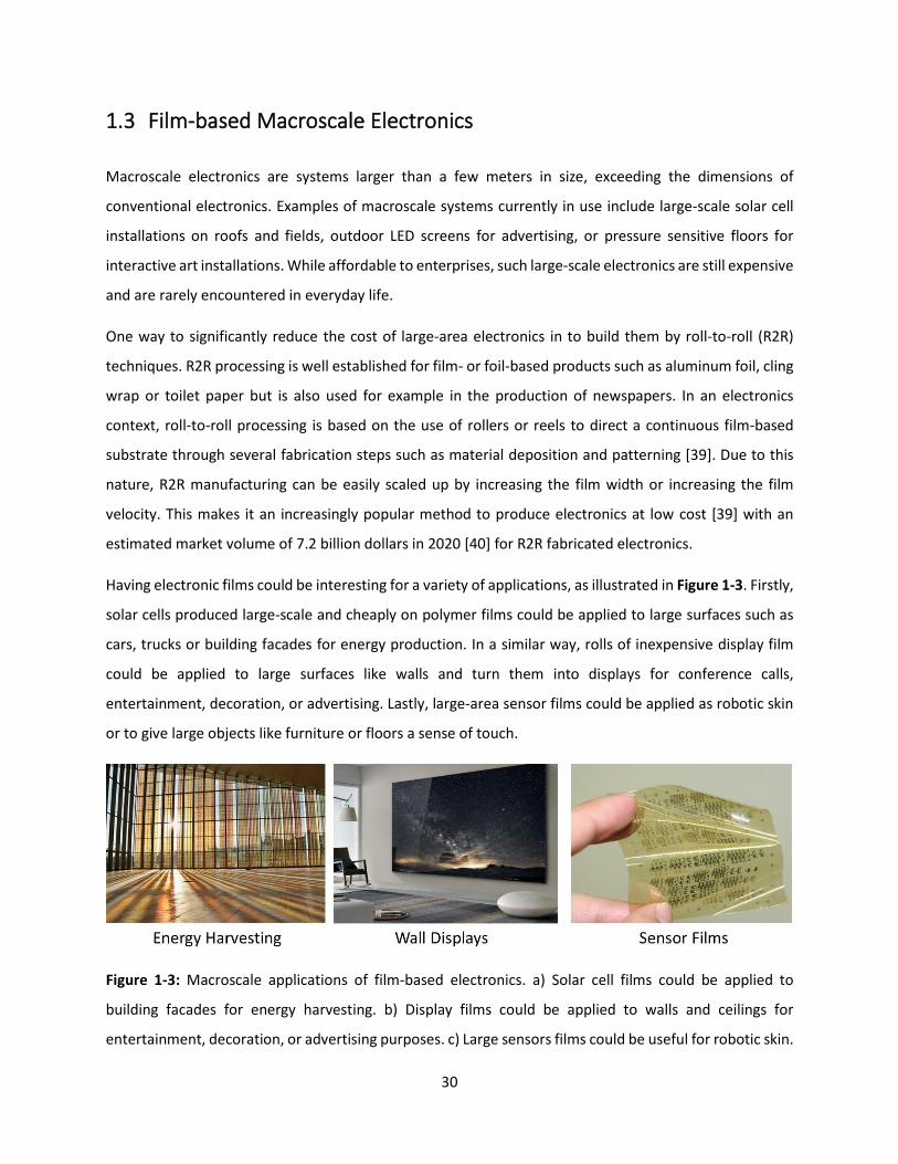
Having electronic films could be interesting for a variety of applications, as illustrated in Figure 1-3. Firstly,
solar cells produced large-scale and cheaply on polymer films could be applied to large surfaces such as
cars, trucks or building facades for energy production. In a similar way, rolls of inexpensive display film
could be applied to large surfaces like walls and turn them into displays for conference calls,
entertainment, decoration, or advertising. Lastly, large-area sensor films could be applied as robotic skin
or to give large objects like furniture or floors a sense of touch.
Figure 1-3: Macroscale applications of film-based electronics. a) Solar cell films could be applied to
building facades for energy harvesting. b) Display films could be applied to walls and ceilings for
entertainment, decoration, or advertising purposes. c) Large sensors films could be useful for robotic skin.
31
While these film-based applications are not widely available yet, there has been significant progress in the
development of R2R-fabricated electronics [39], especially in the field of flexible solar cells [1, 2] and
organic LED (OLED) panels [3, 4], with even some industrial production in place. Konica Minolta, for
example, in 2014 built a roll-to-roll production facility that can produce 1 million flexible OLED panels per
month [41]. Solliance, a European research and development organization, in 2017 demonstrated
perovskite solar cells with an efficiency of 12.6% that can be produced at speeds of 5 m/min on a 30-cm
wide conventional ITO/PET foil [42].
Despite this impressive progress, several technological challenges need to be overcome to enable truly
ubiquitous R2R-fabricated electronics at low cost. On the one hand, the degradation of organic materials
often used in R2R electronics due to humidity, oxygen and light needs to be improved further, for instance
by advanced barrier layers and encapsulation [39, 43]. On the other hand, more complex electronic
circuitry will be necessary to expand the palette of available electronics beyond solar cells and OLEDs.
Organic semiconductors and metal oxides have been heavily investigated for this purpose because they
are easy to deposit in a R2R fashion by solution processing or sputtering [43]. However, the mobility of
organic semiconductors is commonly below 1 cm2/Vs [44], which limits the expected performance of
circuits with these materials. Additionally, oxide-based materials are inherently brittle and are
incompatible with bending radii below several millimeters [16].
Using 2D materials could alleviate some of these issues. 2D materials like graphene, molybdenum disulfide
(MoS2) or hexagonal boron nitride are chemically stable, mechanically robust and very flexible due to their
atomic thickness. Because of their polycrystalline nature, they also offer intrinsically high carrier mobilities
and their lack of out-of-plane bonds makes them easy to integrate onto various surfaces. Several flexible
electronics applications have already been demonstrated using 2D materials such as 4-layer graphene
films on PET as resistive touchscreen [45], flexible OLED displays with MoS2 thin-film transistors [46], or
active pressure sensor matrices using MoS2 as sensor and transistor material [47].
However, most 2D material-based flexible electronics prototypes have been built using wafer-based
fabrication, which ultimately limits the price point of those applications. To fabricate them with R2R-based
methods, the R2R growth and transfer of 2D materials is essential. Some progress in this area has already
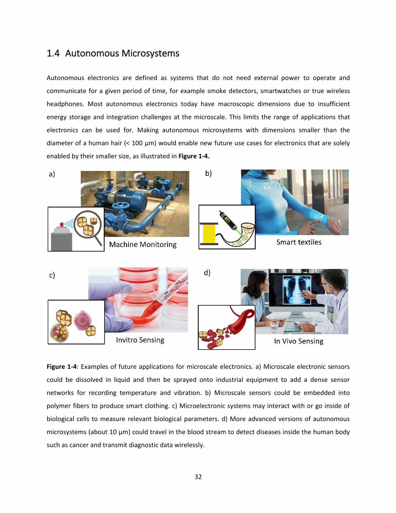
been made, especially regarding R2R graphene growth and transfer [48-55]. Important research directions
to further advance the state of R2R-based 2D material electronics include: (1) the better understanding
of the transfer mechanics and (2) the development of a general transfer strategy for arbitrary 2D materials
from metal foils onto plastic substrates. Both topics are highlighted in Chapter 3.
32
1.4 Autonomous Microsystems
Autonomous electronics are defined as systems that do not need external power to operate and
communicate for a given period of time, for example smoke detectors, smartwatches or true wireless
headphones. Most autonomous electronics today have macroscopic dimensions due to insufficient
energy storage and integration challenges at the microscale. This limits the range of applications that
electronics can be used for. Making autonomous microsystems with dimensions smaller than the
diameter of a human hair (< 100 µm) would enable new future use cases for electronics that are solely
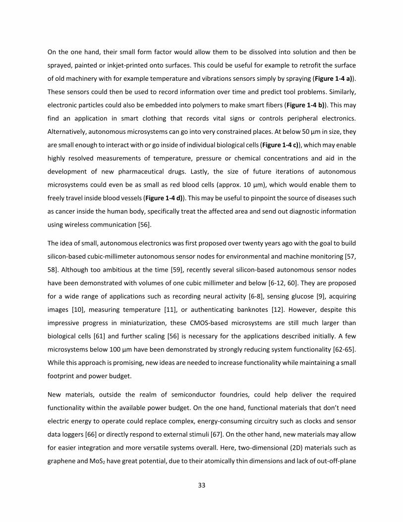
enabled by their smaller size, as illustrated in Figure 1-4.
Figure 1-4: Examples of future applications for microscale electronics. a) Microscale electronic sensors
could be dissolved in liquid and then be sprayed onto industrial equipment to add a dense sensor
networks for recording temperature and vibration. b) Microscale sensors could be embedded into
polymer fibers to produce smart clothing. c) Microelectronic systems may interact with or go inside of
biological cells to measure relevant biological parameters. d) More advanced versions of autonomous
microsystems (about 10 µm) could travel in the blood stream to detect diseases inside the human body
such as cancer and transmit diagnostic data wirelessly.
33
On the one hand, their small form factor would allow them to be dissolved into solution and then be
sprayed, painted or inkjet-printed onto surfaces. This could be useful for example to retrofit the surface
of old machinery with for example temperature and vibrations sensors simply by spraying (Figure 1-4 a)).
These sensors could then be used to record information over time and predict tool problems. Similarly,
electronic particles could also be embedded into polymers to make smart fibers (Figure 1-4 b)). This may
find an application in smart clothing that records vital signs or controls peripheral electronics.
Alternatively, autonomous microsystems can go into very constrained places. At below 50 µm in size, they
are small enough to interact with or go inside of individual biological cells (Figure 1-4 c)), which may enable
highly resolved measurements of temperature, pressure or chemical concentrations and aid in the
development of new pharmaceutical drugs. Lastly, the size of future iterations of autonomous
microsystems could even be as small as red blood cells (approx. 10 µm), which would enable them to
freely travel inside blood vessels (Figure 1-4 d)). This may be useful to pinpoint the source of diseases such
as cancer inside the human body, specifically treat the affected area and send out diagnostic information
using wireless communication [56].
The idea of small, autonomous electronics was first proposed over twenty years ago with the goal to build
silicon-based cubic-millimeter autonomous sensor nodes for environmental and machine monitoring [57,
58]. Although too ambitious at the time [59], recently several silicon-based autonomous sensor nodes
have been demonstrated with volumes of one cubic millimeter and below [6-12, 60]. They are proposed
for a wide range of applications such as recording neural activity [6-8], sensing glucose [9], acquiring
images [10], measuring temperature [11], or authenticating banknotes [12]. However, despite this
impressive progress in miniaturization, these CMOS-based microsystems are still much larger than
biological cells [61] and further scaling [56] is necessary for the applications described initially. A few
microsystems below 100 µm have been demonstrated by strongly reducing system functionality [62-65].
While this approach is promising, new ideas are needed to increase functionality while maintaining a small
footprint and power budget.
New materials, outside the realm of semiconductor foundries, could help deliver the required
functionality within the available power budget. On the one hand, functional materials that don’t need
electric energy to operate could replace complex, energy-consuming circuitry such as clocks and sensor
data loggers [66] or directly respond to external stimuli [67]. On the other hand, new materials may allow
for easier integration and more versatile systems overall. Here, two-dimensional (2D) materials such as
graphene and MoS2 have great potential, due to their atomically thin dimensions and lack of out-off-plane

34
bonds. This allows them to be transferred onto almost any substrate and makes them a promising
candidate for highly heterogeneous electronic systems. Additionally, they have a wide range of electronic
properties and can be used for a variety of devices such as chemical sensors [68], transistors [18], memory
elements [69], light-emitting diodes [70] and solar cells [71]. These advantages of 2D materials were
recently highlighted by Koman and colleagues [65], who built a 100 x 100 µm-small state machine with
chemical sensor, photodetector and memory all made from 2D materials. Their microsystems are also
flexible and neutrally buoyant, which may be advantageous for fluidic and biological applications.
However, while this work is an important proof of concept, additional building blocks such as transistors
for simple circuits or locomotion for precise positioning will be necessary to provide more complex
functionality. The development of these and other building blocks are highlighted in Chapter 4. Lastly,
reducing the footprint even further and finding effective schemes for integrating several building blocks
is presented in Chapter 5.
1.5 Thesis Outline
The goal of this thesis is to explore the use of 2D materials for macroscopic and microscopic electronic
applications. As explained in Section 1.2, 2D materials cover a large spectrum of electronic properties
from insulator to conductor and have remarkable properties such as being atomically thin, flexible,
transparent and easy to integrate onto various substrates. For macroscopic electronics, such materials are
interesting especially for film-based electronics because of their flexibility and transparency for example
to make flexible, transparent electrodes. Microscale electronics benefit mostly from the easy integration
of 2D materials onto tiny form factors for instance to build sensors and transistors. To understand the
challenges of 2D materials in both regimes, this thesis focuses on the experimental implementation of
prototype macro- and microscale electronic devices as well as their characterization with the aim to
advance the knowledge of what is technically feasible.
Chapter 2 provides an overview of the 2D materials utilized in this work, that is graphene, molybdenum
disulfide and hexagonal boron nitride. It first covers their properties and discusses possible applications
based on works reported in the literature. Secondly, the synthesis of these 2D materials by chemical vapor
deposition is explained. Lastly, this chapter presents several approaches on how to transfer 2D materials
from their growth substrate to a target substrate.
35
Chapter 3 focuses on the use of 2D materials for macroscale electronics. In particular, the large-area
transfer of 2D materials via roll-to-roll (R2R) processing is discussed. For this purpose, a custom transfer
setup with hot-roll lamination and electrochemical delamination was developed. Its construction and
capabilities are explained and the transfer process itself is discussed. As center piece, Chapter 3 details
the single and repeated transfer of graphene onto flexible polymer substrates and discusses the electrical
characterization of the resulting films. Lastly, an application of R2R-transferred graphene as transparent
electrode for solar cells is presented.
Chapter 4 discusses building blocks for an electronic microsystem called synthetic cell or SynCells for
short. SynCells are a sensing platform on a 60x60 µm2 polymer substrate and consist of various types of
devices. As first building block, this chapter examines the use of MoS2 to build chemical sensors for
polyamines. It also discusses a timer building block based on germanium thin films that can measure time
passively, that is without the need of electric power. Regarding computational abilities, Chapter 0 covers
MoS2 field-effect transistors, which form the basis of making electronic circuits on SynCells. As an
alternative approach, the design of a 50x50 µm2 CMOS chip for logic task is presented. A section on LEDs
and solar cells illuminates the strategies and challenges in providing energy harvesting and optical
communication to SynCells. Lastly, the fabrication of magnetic pads is covered, which enable the remote
manipulation and locomotion of SynCells in liquid environments.
Chapter 5 builds upon the individual building blocks presented in Chapter 4 and describes how to
integrate them onto a 60x60 µm2 polymer substrate. Specifically, it highlights how to fabricate timers,
transistors, magnets, and sensors on this form factors into multifunctional microsystems. Furthermore,
two SynCell demonstrations are discussed. For one, SynCells are introduced into a microfluidic channel to
show their sensing capabilities in constrained environments. Additionally, the spraying of SynCells onto
glass slides is described, which shows the ability to coat sensor networks onto arbitrary surfaces.
Chapter 6 summaries this thesis and discusses future work. First, the main contributions of this work are
drawn. Additionally, an outlook is provided that discusses open questions and next courses of actions for
improving the roll-to-roll transfer of 2D materials and realizing SynCells with energy harvesting and
wireless communication.

36

37
Fundamentals of 2D Materials
2.1 Properties and Applications of 2D Materials
2.1.1 Graphene
Graphene was the first 2D material to be discovered in 2004 [30] and has been intensely studied since
then. With a thickness of 0.355 nm, a Young’s modulus of 1 TPa and a carrier mobility of up to
200,000 Vs/cm2, it is the thinnest [72], strongest [73] and most conductive [74] material known so far.
Graphene is a single atomic layer of a graphite crystal. Its carbon atoms are arranged in a honeycomb with
a bond length of 141 pm [75], see Figure 2-1 a). This creates a 3D electronic band structure as shown in
Figure 2-1 b) [76]. As can be seen in the diagram, the valence and conduction band are intersecting at the
K and K’ points in Brillouin zone, also called Dirac points, which makes graphene a semi-metal. The linear
dispersion relation between carrier momentum and energy at these Dirac points also means that charge
carriers effectively behave as massless fermions, explaining the ultra-high and symmetric mobility of
electrons and holes in this material.
Figure 2-1: a) Schematic of graphene honeycomb lattice. b) 3D electronic band structure of conduction
(top) and valance band (bottom) in graphene. The inset shows the energy bands intersect at the K points
in Brillouin zone. Adapted with permission from [76].
One of the advantages of graphene is that its electronic properties can be modulated externally, which is
useful for applications like chemical sensors, photo detectors or solar cells [77]. In its intrinsic state and in

38
the absence of other materials, pristine graphene is undoped and its Fermi level lies at the intersection of
the two cones. However, graphene is a semimetal and can be easily doped n-type or p-type by
substitutional doping in the lattice, electrostatic doping, or surface doping [77, 78], as illustrated in Figure
2-2. Substitutional doping replaces carbon atoms with other elements such as nitrogen or boron, which
leads to n-type or p-type doping, respectively. However, such dopants in the lattice act as scattering
centers and strongly reduce the carrier mobility, which is why it is seldomly used. Electrostatic doping
relies on plate capacitor-like structures where a graphene layer forms one of the two plates. The doping
concentration in graphene can be modulated by the voltage applied between the two plates. Lastly,
graphene doping can be achieved by surface doping through molecules, thin films or the substrate itself
[77-80]. In the case of p-type molecular doping, the donation of electrons from graphene to the adsorbed
molecule occurs if the lowest unoccupied molecular orbital (LUMO) of the dopant is lower in energy than
the Fermi Level in graphene. In contrast, if the highest occupied molecular orbital (HOMO) of the dopant
is higher in energy than the Fermi Level of graphene, the adsorbed molecule donates an electron to the
graphene lattice (n-type doping) [78]. Doping also occurs when graphene is in contact with metals or
oxides [79-81], where the doping generally depends on the difference in work function between graphene
and the other material.
Figure 2-2: Types of graphene doping. a) Graphene can be electrostatically doped by creating a plate-
capacitor with graphene as one electrode and applying a voltage. b) Substitutional doping is achieved
through the replacement of carbon atoms with other atoms in the lattice, for example nitrogen for n-type
doping. c) Graphene can be doped by the adsorption of molecules on the surface through direct charge
transfer. Additionally, close contact to metals or dielectrics also lead to the doping of graphene and
depends on the relative material work function with respect to graphene.

39
In terms of optical properties, graphene absorbs about 2.3 % of light per layer, see Figure 2-3 [82]. This
absorption is almost constant across the visible light spectrum. As a result of its high transparency and
conductivity, one of the first suggested applications for graphene has been as a transparent, conductive
electrode (TCE). TCEs are important in optoelectronic applications such as solar cells, displays or touch
screens. Numerous optoelectronic devices with graphene electrodes have been fabricated [83] or have
even been implemented commercially [21]. Song et. al., for example, fabricated semi-transparent organic
solar cells with the bottom and top electrode made out of graphene [84]. In another work, Bae and others
demonstrated the roll-to-roll transfer of graphene transferred onto 30-inch PET films and turned them
into a touch screen [45]. They achieved a sheet resistance of about 30 Ohms/sq. for a stack of four doped
graphene layers (90% transmittance). At such levels of conductance, it is almost comparable with indium
tin oxide, the current material often used for transparent electrode, which commonly reaches 10
Ohms/sq. for a transmittance of 90% [85].
Figure 2-3: Transparency of graphene. a) Transmittance of suspended mono and bilayer graphene on a
carrier under white light. The contrast of the three regions is clearly visible. b) Transmittance of graphene
as a function of wavelength and compared to theoretical modeling. Inset: Transmittance as a function of
graphene layers. Adapted with permission from [82].
Due to its extremely high mobility, graphene is also interesting for RF transistor applications, since it is
correlated with high switching frequencies. However, because it is a zero-gap material, transistor devices
have a low on/off ratio of < 10, which disqualifies it from being used for digital electronics. Several groups
40
fabricated RF graphene transistors [86] and were able to achieve intrinsic cut-off frequencies of above
300 GHz [87]. Furthermore, Han et. al. demonstrated a 3-stage integrated graphene circuit for wireless
communication that operated on a 4.3 GHz carrier frequency [88]. Besides all this progress, however,
more work regarding the fabrication and design of graphene devices is needed to live up to theoretical
predictions and to surpass existing technologies.
One of the most explored applications of graphene is in the area of sensing, especially as chemical and
biological sensors. Graphene combines several desirable properties such as highest possible surface-to-
volume ratio, low electronic noise, biocompatibility, and a multitude of functionalization methods, which
makes it a very promising platform for highly sensitive and selective sensors. As one of the first kinds of
sensors, it has been explored for detecting gases. Graphene’s extreme surface-to-volume ratio makes it
very susceptible to the environment such as molecules adsorbing on the surface, which leads to a charge
transfer and dopes the channel with electrons or holes. This principle has been exploited by Schedin et.
al. [89], who in 2007 demonstrated the first graphene gas sensor based on simple hall bars. With an
optimized design and the intrinsically low noise level of their devices, they were able to detect individual
molecule ad- and desorption events, which is the ultimate sensitivity limit. Later, Chen et. al. simplified
the sensor design to a two-terminal chemically sensitive resistor, or chemiresistor, and added UV-
illumination for continuous cleaning of the graphene surface. This way they were able to demonstrate an
even lower detection limit of 0.16 parts-per-trillion for nitric oxide gas molecules [90]. More details about
graphene-based gas sensors can be found in comprehensive literature review papers by Yuan and Shi or
Verghese et. al [91, 92].
Additionally, graphene has been popular in the construction of biological sensors to measure pH,
determine blood sugar levels or detect bacteria and cancer cells. Graphene electrolyte gated FETs
(EGFETs) can be employed as pH sensor with a sensitivity of 99 mV/ pH, as demonstrated for example by
Ang et. al. [93]. Through the addition of specific molecules or compounds on the surface of graphene, also
called functionalization, graphene can be made specifically sensitive to various biomolecules and even
cells. Huang et. al. for example, demonstrated a graphene chemiresistor that can sense E Coli bacteria
concentrations as low as 10 colony-forming cells per milliliter (cfu/ml) and also showed high selectivity
against other bacteria [94] by functionalizing the graphene surface with anti-E. Coli antibodies.
Furthermore, a group around Jiang et. al. fabricated hemin-functionalized graphene chemFETs with
nanomolar sensitivity to nitric oxide and a sensor areas of 0.25-1 µm2, which is similarly sensitive but much
smaller than state-off-the-art technology [95] and enables monitoring the metabolism of individual cells.

41
Lastly, Hunag et. al used graphene chemFETs decorated with glucose oxidase to sense glucose in solution
down to a level of 100 µM which is comparable to common electrochemical sensors. A more
comprehensive overview of graphene biosensors is provided by Lui et. al [96] and Moldovan [97].
Lastly, graphene can also be employed as electromechanical sensor [98] to measure strain, pressure or
force. Pristine sheets of graphene have a strain sensitivity, also called gauge factor, of 6.1, which is higher
than metals (0.3) but still much lower than silicon (50-100). On the one hand, the gauge factor can be
drastically increased by creating a film with overlapping or touching graphene flakes, where the change
in resistance originates from the change in contact area of the flakes. For such devices, gauge factors of
150-300 and more have been reported [99, 100].
2.1.2 Hexagonal Boron Nitride
Hexagonal boron nitride, or hBN, is another 2D material that has been studied extensively for electronic
applications. Boron nitride exists in three lattice configuration some of which are isomorphic to carbon: a
rare wurtzite form, a cubic form analogous to diamond and a hexagonal form similar to graphite [101].
Bulk hBN consists of Van der Waals stacked sheets with a honey comb lattice arrangement of boron and
nitrogen atoms in each layer similar to graphene, see Figure 2-4 a). The bond length between boron and
nitrogen is 144 pm [102], which is very close to graphene and results in a lattice mismatch of only about
1.7% between the two materials. Regarding its mechanical properties, hBN in its mono or few-layer form
is very strong with a Young’s modulus of 0.865 TPa [103] and has a very high measured in-plane thermal
conductance of about 400 W/mK [104], which is higher than most metals. Additionally, it is very chemically
inert and thermally stable [105]. From an electrical perspective, hBN has a large bandgap of about 6 eV
[106], which makes it an insulator. It has a breakdown field of 0.8 V/nm [107], similar to silicon oxide or
aluminum oxide (0.5 V/nm), and a low dielectric constant of 3-4 [107]. Because of its large bandgap, hBN
is also transparent in the visible spectrum with a absorption of less than 1% in the range from 400-800 nm
wavelength [108], see Figure 2-4 b).
The properties of hBN make it an interesting material for a variety of applications. Its insulating nature
combined with its ultra-smooth, chemically inert and highly temperature stable surface is for passivation
or encapsulation. CVD-grown hBN films on nickel, for example, protected the substrate from oxidation in
an oxygen-rich environment up to 1100°C [109]. Additionally, hBN coatings may be suitable as diffusion
barrier for copper interconnects [110]. Especially regarding other 2D materials such as graphene and

42
MoS2, hBN encapsulation is effective in reducing carrier scattering and boosting carrier mobility. Dean et.
al demonstrated a carrier mobility of 40,000 cm2/Vs at room temperature for graphene on an hBN
substrate [111], which is three times higher than their baseline devices on silicon oxide. By additionally
protecting graphene with hBN at the top and using edge contacts, Wang and collaborators were even able
to achieve mobilities above 100,000 cm2/Vs [112]. Similarly, MoS2 field effect transistors with hBN
encapsulation have resulted in carrier mobilities of up to 153 cm2/Vs [113], which is much better than
state-of-the-art ALD passivated transistors.
Figure 2-4: a) Honeycomb lattice structure of a hexagonal boron nitride. b) UV-visible absorption spectrum
of a hBN monolayer on quartz with a strong absorption peak at 200 nm. The inset shows the extraction of
the optical band gap by plotting (αE)2 versus E according to [114]. Reproduced with permission from [108].
Furthermore, hexagonal boron nitride can be employed as a dielectric [115]. Mono or few layer hBN has
been incorporated for example as gate dielectric in MoS2-based FETs [113, 116] and even yields flexible
and transparent devices when using a polymer substrate and graphene as a gate electrode [116]. Lastly,
hBN can be used as a dielectric in non-volatile memory applications, as documented by many reports
[117-121]. Lanza and collaborators for instance have shown how few layer hBN between a titanium and
copper electrode acts as resistive memory by creating and erasing metal filaments through the dielectric
[118]. Using such devices, they were able to achieve set and reset voltages below 1 V, high on/off ratios
of 106 and retention times above 10 hours. This device concept was further scaled down by Zhao et. al,
who fabricated a resistive memory device with a 0.9 nm thick oxidized hexagonal boron nitride film and

43
silver/graphene as electrode pair. Their devices require an ultra-low switching current and voltage of
down to a few picoamperes and less than a volt, which is much better than state-of the-art resistive
memory devices [122].
2.1.3 Molybdenum Disulfide
Molybdenum disulfide (MoS2) is a 2D material from the transition metal dichalcogenide family or TMDs
for short. Like graphite and hBN, TMDs in their bulk form consist of layered sheets held together by Van
der Waals forces. TMDs come in the form of MX2 where M is a transition metal such as molybdenum or
tungsten and X is a chalcogen atom like sulfur, selenium or tellurium. MoS2 is arguably the most studied
TMD due to its chemical stability, robustness, and straight-forward synthesis methods. It exists in three
polytypes: a metallic 1T form, a semiconducting 2H form and a semiconducting 3R form [123], as shown
in Figure 2-5.
Figure 2-5: Polytypes of monolayer MoS2. The trigonal prismatic 1T polytype is metastable and metallic.
It does not occur naturally. The hexagonal 2H phase is semiconducting and thermodynamically favorable.
It has two offset layers in a unit cell. The rhombohedral 3R phase with three staggered layers in a unit cell
and is also semiconducting. Reproduced with permission from [123].

44
The 2H polytype is thermodynamically favorable and is commonly obtained for exfoliated and vapor
deposited MoS2. It consists of 3-atom-thick sheets arranged in a hexagonal lattice with congruent sulfur
atoms at the top and bottom and molybdenum atoms in the middle, all of which are connected by
covalent bonds. The 2H unit cell is composed of two slightly offset MoS2 sheets each of which has a
thickness of approximately 0.65 nm [124]. For the remainder of this thesis, the 2H phase is assumed as
the default if not mentioned otherwise. The 3R polytype has similar crystallographic sheets as the 2H
form, however a unit cell is made up of three staggered layers rather than two. The MoS2 sheets of the 1T
polytype are metastable and do not occur naturally. They differ from 2H form in that one plane of sulfur
atoms is shifted with respect to the other sulfur plane and a unit cell is composed of only one layer. 2H
MoS2 can be transformed into the metallic 1T phase by treatments such as alkali metal ion intercalation
or electron beam irradiation [125]. This transformation is especially useful to fabricate high performance
electrical devices by selectively converting contact regions into this metallic phase to obtain low-resistive
contacts. Regarding electrical properties of 2H MoS2, from now on just referred to as MoS2, a monolayer
has a direct optical bandgap of 2.4 eV [126]. When increasing the number of layers however, it slowly
shifts towards an indirect bandgap of 1.29 eV [127], similar to the properties of bulk MoS2. This evolution
of the band structure with number of layers is depicted in Figure 2-6.
Figure 2-6: Band structure evolution of 2H MoS2. In its bulk form MoS2 is an indirect semiconductor with
a bandgap of 1.29 eV. When thinned down to a monolayer it becomes a direct semiconductor with a
bandgap of 2.4 eV. Adapted with permission from [128].

45
MoS2 is typically n-type doped [123]. Similar to graphene, it’s doping concentration can be easily adjusted
for example by a chemical surface treatments or electrostatic doping [129]. In respect to optical
properties, monolayer MoS2 absorbs between 5-10% of light above its bandgap depending on the
wavelength [130]. From a mechanical perspective, it has an in-plane stiffness of ~180 N/m (about half that
of graphene) and a Young’s modulus of ~270 GPa (slightly higher than steel) [131].
The properties highlighted above, make MoS2 a promising material for a variety of applications. One of
the main interests lies in using MoS2 as channel material for ultra-scaled field-effect transistors (FETs) due
to its high mobility and favorable electrostatics at atomically thin channel thicknesses [132]. In fact, many
groups have explored MoS2 in this respect [133]. With optimized device structures and high-K dielectrics,
carrier mobilities in the range of 50-200 cm2/Vs at room temperature with on/off ratios of above 106 and
subthreshold voltage swings close to the theoretical limit of 60 mV per decade can be achieved [134-137].
Additionally, MoS2 can be grown or transferred sequentially on stacked oxide layers [138], which could
lead the way towards multiple monolithically integrated transistor layers on one chip. Lastly, the flexible
and robust nature of MoS2 has been used to create flexible transistors. Pu and collaborators, for example,
demonstrated a flexible MoS2 transistor on a polyimide substrate that can be bent to a radius of 0.75 mm
with no signs of degradation [139]. Using the same substrate, Chang et. al. built a flexible RF transistor
with a cutoff frequency of 5.6 GHz that remained electrically viable after 10,000 bending cycles [140].
Besides transistor applications, MoS2 has also been proposed for multiple kinds of memory devices [133].
Bertolazzi and other for example, built a flash memory with graphene as the floating gate and MoS2 as
channel material that has a 104 times difference in conductance between the program and erase state
[141]. Additionally, MoS2 has memristive properties [142, 143]. Wang and collaborators used this aspect
to demonstrate a vertical memory structure made of multilayer MoS2 with graphene electrodes that can
switch up to 107 times and is based on the migration of oxygen atoms [143]. Such memory element also
could prove useful for new computing schemes such as neuromorphic architectures [144].
The direct bandgap of MoS2 is ideal for solar cells and photodetectors. Bernardi et. al. used the intrinsically
high absorption of monolayer MoS2 to construct a solar cell with up to 1% efficiency, which translates into
a power density of at least 10 times more than conventional thin-film solar devices [130]. On the other
hand, a team around Lopez-Sanchez demonstrated a visible light phototransistor based on exfoliated
MoS2 that easily outperform commercial silicon devices. It has a noise equivalent power of 1.8×10⁻¹⁵ W
Hz−1/2 (10 times better than state-of-the-art Si avalanche detectors) and a photoresponsivity of up to 880
A/W, which also exceeds commercial silicon devices.
46
Lastly MoS2 is promising as sensor material to detect gases, biomolecules or physical parameters [47, 125,
145, 146]. Late et. al. showed that MoS2 chemFETs change resistance upon exposure to ammonia and
nitrogen dioxide gas and can detect concentrations down to 100 ppm. Furthermore, they found that
applying a gate bias helped to increase the device sensitivity by electrostatically changing the carrier
concentration in the channel to an optimal point [147]. In a related study by Perkins et. al., the authors
demonstrated single-layer MoS2 chemiresistors that are sensitive to different organic compounds such as
triethylamine (TEA) or acetone with a detection limit of 10 ppb and 500 ppm, respectively [148]. Like
graphene, the selectivity of MoS2 to specific analytes can be increased by adding a functionalization layer.
Using exfoliated MoS2, Lee at. el. used this approach to demonstrate a prostate specific antigen biosensor,
which is an important tool to detect prostate cancer. The group functionalized the MoS2 transistors using
PSA anti-bodies that nonspecifically physiosorbed on the sensor surface, which lead to a reduced
transistor current upon analyte binding. With this approach, they were able to show a detection limit of
1 pg/ml of the antigen, three orders of magnitude below the clinical cut-off level [149]. In term of
mechanical sensors, Ahn and his group used the piezoelectric properties of MoS2 to build a wearable
pressure sensor array that can be worn like a tattoo. MoS2 has a strong piezoelectric response that results
in a gauge factor of 70-200 and allows the group to detect pressures between 0-120 kPa. Additionally,
they also use the 2D materials for transistors to reduce crosstalk in the array [47].
2.2 Synthesis of 2D Materials
2.2.1 Graphene
Monolayer graphene can be generated in various ways such as mechanical exfoliation from a graphite
crystal, thermal decomposition of silicon carbide or chemical vapor deposition (CVD) [150]. Mechanical
exfoliation usually results in flakes of high quality, but flake sizes are small (on the order of 100 µm) and
labor-intensive to obtain. Thermal decomposition of SiC gives high quality, single crystal graphene sheets
that are just limited by the silicon carbide wafer size. With respect to high-quality, large scale graphene
films, CVD-grown graphene is the best option and is most used because it can be synthesized up to meter-
scale, with large domain sizes and on inexpensive growth substrates.
All graphene used in this thesis was synthesized by low pressure chemical vapor deposition on copper
foils. Copper acts as a catalytic material in the CVD process and breaks down the methane gas, which

47
serves as the carbon source [151]. The generated active carbon species form islands of graphene on the
copper surface that grow into a continuous film over a time span of tens of minutes. Some diffusion of
active carbon species under existing graphene islands also leads to the formation of bilayer islands [151].
After a continuous layer of graphene is formed, the growth automatically stops due to the covered
catalytic copper surface, which prevents the growth of additional graphene layers. The growth process
used in this work is as follows (further details see appendix in Section 7.4.1). Thin copper film (25µm thick,
Alfa Aesar Product # 13882) is cut into strips of about 38x150 mm2. Before growth, the surface of a strip
is lightly etched in nickel etchant (Transene, Nickel Etchant TFB) for 90 seconds to remove any surface
oxide and impurities, followed by a thorough rinse under deionized water. Next, the strip is bent along
the short side and is positioned in the middle of a 25mm inner diameter quartz tube, which is placed in a
clamshell-type furnace (Thermo Scientific, Lindberg Blue TF55035A-1), see Figure 2-7 a). The temperature
profile and gas concentrations for graphene growth are depicted in Figure 2-7 b) and are divided into five
steps.
Figure 2-7: Graphene growth on copper foil. a) Bent copper foil positioned in a quartz tube placed in a
clamshell furnace. b) Temperature profile and gas flow for graphene growth with 5 regions.
First, the copper is gradually heated from room temperature to 1000°C in 20 min with a hydrogen flow 8
sccm (Airgas, HY UHP300) at a pressure of 0.38 Torr (Varian, SH-110). Next, the copper is annealed for
30 min while maintaining the gas flow to increase the grain size of the copper foil. For growing the
graphene layer, the gas flow is increased to 60 sccm of hydrogen and 3.5 sccm of methane (Airgas, ME
UHP300), which raises the pressure to pressure to 1.95 Torr. The growth time is 30 min.
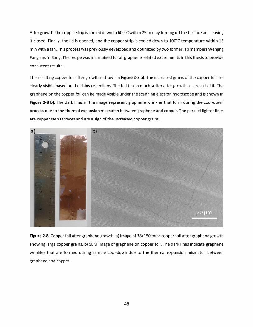
48
After growth, the copper strip is cooled down to 600°C within 25 min by turning off the furnace and leaving
it closed. Finally, the lid is opened, and the copper strip is cooled down to 100°C temperature within 15
min with a fan. This process was previously developed and optimized by two former lab members Wenjing
Fang and Yi Song. The recipe was maintained for all graphene related experiments in this thesis to provide
consistent results.
The resulting copper foil after growth is shown in Figure 2-8 a). The increased grains of the copper foil are
clearly visible based on the shiny reflections. The foil is also much softer after growth as a result of it. The
graphene on the copper foil can be made visible under the scanning electron microscope and is shown in
Figure 2-8 b). The dark lines in the image represent graphene wrinkles that form during the cool-down
process due to the thermal expansion mismatch between graphene and copper. The parallel lighter lines
are copper step terraces and are a sign of the increased copper grains.
Figure 2-8: Copper foil after graphene growth. a) Image of 38x150 mm2 copper foil after graphene growth
showing large copper grains. b) SEM image of graphene on copper foil. The dark lines indicate graphene
wrinkles that are formed during sample cool-down due to the thermal expansion mismatch between
graphene and copper.
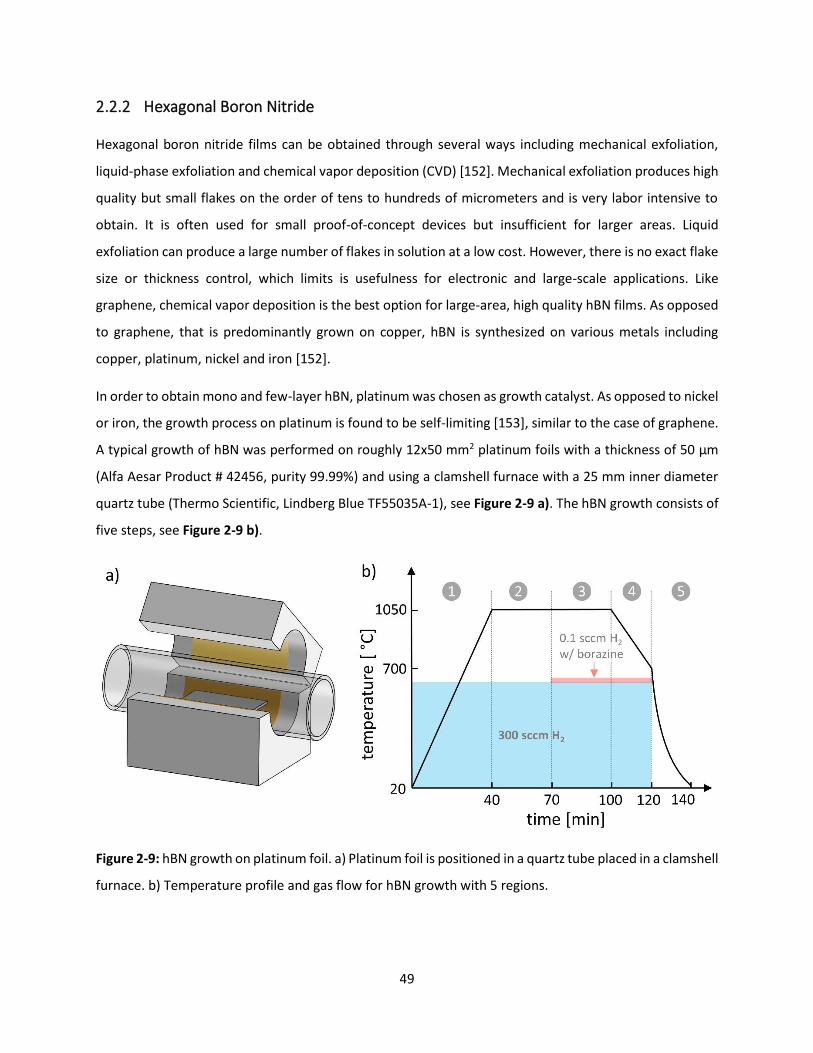
49
2.2.2 Hexagonal Boron Nitride
Hexagonal boron nitride films can be obtained through several ways including mechanical exfoliation,
liquid-phase exfoliation and chemical vapor deposition (CVD) [152]. Mechanical exfoliation produces high
quality but small flakes on the order of tens to hundreds of micrometers and is very labor intensive to
obtain. It is often used for small proof-of-concept devices but insufficient for larger areas. Liquid
exfoliation can produce a large number of flakes in solution at a low cost. However, there is no exact flake
size or thickness control, which limits is usefulness for electronic and large-scale applications. Like
graphene, chemical vapor deposition is the best option for large-area, high quality hBN films. As opposed
to graphene, that is predominantly grown on copper, hBN is synthesized on various metals including
copper, platinum, nickel and iron [152].
In order to obtain mono and few-layer hBN, platinum was chosen as growth catalyst. As opposed to nickel
or iron, the growth process on platinum is found to be self-limiting [153], similar to the case of graphene.
A typical growth of hBN was performed on roughly 12x50 mm2 platinum foils with a thickness of 50 µm
(Alfa Aesar Product # 42456, purity 99.99%) and using a clamshell furnace with a 25 mm inner diameter
quartz tube (Thermo Scientific, Lindberg Blue TF55035A-1), see Figure 2-9 a). The hBN growth consists of
five steps, see Figure 2-9 b).
Figure 2-9: hBN growth on platinum foil. a) Platinum foil is positioned in a quartz tube placed in a clamshell
furnace. b) Temperature profile and gas flow for hBN growth with 5 regions.

50
(1) First, the platinum is gradually heated from room temperature to 1050°C in 40 min while flowing 300
sccm of hydrogen (Airgas, HY UHP300) at low pressure using a vacuum pump (Varian, SH-110). (2) Next,
the platinum foil is annealed for 30 min at continued hydrogen flow to clean the surface and increase the
metal grains of the foil. (3) For forming the hBN layer 0.1 sccm of hydrogen flown through a borazine
bubbler (set to -4°C) is added and maintained for 30 min. (4) After growth and while maintaining a
hydrogen and borazine-rich gas flow, the temperature is slowly reduced to 700°C over the course of
20 min. (5) Finally, all gases are shut off and the clam shell furnace is opened and cooled down to room
temperature within 20 min with a fan.
The hBN samples on platinum for this thesis were kindly provided by two lab members Fei Hui and Ang-
Yu Lu. Wenjing Fang, another former lab member, was responsible for setting up the growth system. The
resulting hBN film on platinum foil is shown in Figure 2-10. The platinum foil looks smooth and shiny after
growth, as depicted in Figure 2-10 a). An SEM micrograph of few layer film hBN on platinum is shown in
Figure 2-10 b). The image clearly shows the platinum grains that have an average size of about 50-100 µm.
The brightness of each grain is different and depends on its crystallographic orientation. These different
orientations typically lead to different growth rates of hBN, which is why the grain pattern of the foil is
still visible in the transferred hBN films.
Figure 2-10: a) Several platinum foils after hBN growth (the wrinkled foils have already been used in the
roll-to-roll transfer setup). b) SEM image of hBN on platinum. The platinum grains are easily visible and
result in different brightness levels depending on their crystal orientation.

51
2.2.3 Molybdenum Disulfide
Mono or few-layer MoS2 can be prepared in a variety of ways for example by mechanical exfoliation,
chemical exfoliation and chemical vapor deposition [123], similar to graphene and hBN, and equal trade-
offs hold true. To obtain large-area and high-quality MoS2, chemical vapor deposition was chosen in this
thesis. The MoS2 samples were kindly provided by Prof. Jiwoong Park’s group at the University of Chicago
and were grown by Chibeom Park. The synthesis was conducted in their home-made metal-organic
chemical vapor deposition (MOCVD) system, which consists of a hot-wall type 4-inch quartz tube reactor
with a 3-zone furnace. To grow MoS2, molybdenum hexacarbonyl (MHC) and diethyl sulfide (DES) were
selected as chemical precursor for Mo and S, respectively, and were injected into the quartz tube reactor
as a gas phase together with N2 and H2, see Figure 2-11. The injection of precursors and carrier gases were
individually regulated with mass flow controllers (MFCs) at room temperature (25°C). It should be noted
that the injection of MHC was assisted by the N2 carrier gas that kept the bubbler pressure at 800 Torr
while DES was injected as a pure vapor form. Once introduced into the tube, the metal-organic precursors
thermally decompose due to a constant furnace temperature of 600°C and start nucleating on the silicon
oxide surface. By keeping the partial pressure of the molybdenum precursor low, the film is steered
towards a layer-by-layer growth, where new atomic sulfur and molybdenum attaches to the edges of
existing islands [154]. This produces a high-quality film with a monolayer yield of greater than 99%.
Figure 2-11: Schematic of MoS2 growth on a Si/SiO2 wafer in a 4” quartz tube. The growth takes place at
600°C and uses metal-organic precursors (molybdenum hexacarbonyl and diethyl sulfide). Adapted with
permission from [154].
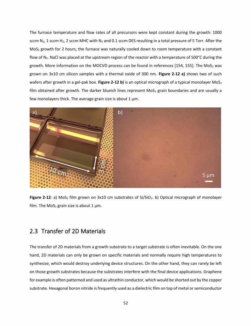
52
The furnace temperature and flow rates of all precursors were kept constant during the growth: 1000
sccm N2, 1 sccm H2, 2 sccm MHC with N2 and 0.1 sccm DES resulting in a total pressure of 5 Torr. After the
MoS2 growth for 2 hours, the furnace was naturally cooled down to room temperature with a constant
flow of N2. NaCl was placed at the upstream region of the reactor with a temperature of 500°C during the
growth. More information on the MOCVD process can be found in references [154, 155]. The MoS2 was
grown on 3x10 cm silicon samples with a thermal oxide of 300 nm. Figure 2-12 a) shows two of such
wafers after growth in a gel-pak box. Figure 2-12 b) is an optical micrograph of a typical monolayer MoS2
film obtained after growth. The darker blueish lines represent MoS2 grain boundaries and are usually a
few monolayers thick. The average grain size is about 1 µm.
Figure 2-12: a) MoS2 film grown on 3x10 cm substrates of Si/SiO2. b) Optical micrograph of monolayer
film. The MoS2 grain size is about 1 µm.
2.3 Transfer of 2D Materials
The transfer of 2D materials from a growth substrate to a target substrate is often inevitable. On the one
hand, 2D materials can only be grown on specific materials and normally require high temperatures to
synthesize, which would destroy underlying device structures. On the other hand, they can rarely be left
on those growth substrates because the substrates interfere with the final device applications. Graphene
for example is often patterned and used as ultrathin conductor, which would be shorted out by the copper
substrate. Hexagonal boron nitride is frequently used as a dielectric film on top of metal or semiconductor

53
regions and hence also needs transferring. Even MoS2, which is grown on an insulating silicon oxide layer
normally needs transferring because the electrical properties of the oxide degrade during the growth and
becomes prone to leakage. This section highlights three 2D material transfer methods: wet etching
transfer, electrochemical wet transfer, and water delamination. All these methods share a similar
framework and only differ in the way the 2D material is separated from its respective growth substrate.
All methods are furthermore un-aligned techniques, which means that the position of the 2D film cannot
be precisely controlled on the target substrate. For that reason, if patterning of the 2D material is
necessary, it is done after the transfer is complete. The generalized steps of a 2D material transfer process
are illustrated in Figure 2-13.
Figure 2-13: Generalized steps of a non-aligned 2D material transfer process. a) Synthesize 2D material on
growth substrate. b) Spin coat PMMA as temporary support material. c) Separate 2D material from growth
substrate in aqueous medium. d) Scoop up floating 2D film with target substrate. e) Blow dry 2D film on
target substrate. f) Remove PMMA support layer in acetone.
The process starts with a 2D film grown on a substrate such as a metal foil or Si/SiO2 piece. Next, a 300-
500 nm thick film of PMMA photo resist is spin coated on top as a temporary support layer, however many
other polymers may equally be used depending on preference [156]. Subsequently, the 2D material is
separated from the growth substrate in an aqueous medium such as an acid, a base or pure water. This
step differs widely depending on which exact transfer method and which growth substrate is used. After
separation, the film floats on the surface of the aqueous medium due to the surface tension of water.
From here it can be scooped up with any flat object such as a glass slide or silicon wafer. To transfer the

54
2D film, it is first picked up and transferred into a dish with deionized (DI) water to clean the bottom
surface from remaining acid or other chemicals. Subsequently, the film is scooped up using the target
substrate and then blow dried on a flat surface to remove any water under the 2D film. Afterwards, the
sample is baked for 15 min to an hour to remove any trace of water left under the film. Lastly, the PMMA
support layer is rinsed off with acetone. The following subsections will discuss the different strategies of
how to separate 2D materials from their growth substrates and briefly discuss the pros and cons of each
approach.
2.3.1 Wet Etching of Substrate
The simplest way to detach a PMMA-supported 2D film from its growth substrate is to undercut or wet
etch it. This technique has mainly been used to transfer graphene from copper foil by completely
dissolving the foil in ferric chloride acid (FeCl3). In particular, the PMMA-coated copper foil with graphene
is gently placed with a pair of tweezers into a dish filled with Transcene CE-100 Iron chloride etch. The
sample floats due to the surface tension of the solution. For at 25 µm thick copper foil, the etch time is
about 10-15 min. An example of this process is shown in Figure 2-14.
Figure 2-14: Wet etching of copper substrate to transfer graphene. a) PMMA-coated copper foil with
graphene on the surface of a ferric chloride solution etched for about 5 min. The copper is already partially
etched. b) PMMA/Gr film after 15 min of etching. The copper is completely removed.
55
In Figure 2-14 a), the copper film has been etched for about 5 min. First pits around the edges are visible.
The copper foil also has a thin frame of adhesive foil around it to help stabilize the PMMA film, which is
optional. After about 15 min of etch time the copper substrate is completely removed, as shown in Figure
2-14 b). Now the 300-500 nm thin PMMA film becomes visible. After fully etching the copper substrate,
the PMMA/Gr film is transferred into two consecutive dishes filled with DI water to wash off any excess
ferric chloride acid. Finally, the transfer can be completed as outlined above. A full step-by-step transfer
process for transferring graphene using ferric chloride acid is provided in Section 7.4.2. Additionally, wet
etching can also be used to separate MoS2 by undercutting the thermal oxide on top of the silicon growth
substrate with hydrofluoric acid (HF). As opposed to the graphene transfer, the sample here is submersed
in the HF solution to ensure that the hydrofluoric acid can etch the silicon oxide layer from the side. More
details are given in the appendix, see Section 7.4.3.
2.3.2 Electrochemical Delamination
Electrochemical delamination is a method to separate a polymer-supported 2D material film from its
metallic growth substrate without wet etching or otherwise consuming the substrate in the process. For
that reason, it is specifically used for detaching hBN grown on platinum foil because of the foil’s high
material cost. However, it can be used equally well for delaminating graphene from copper foil, which it
was first designed for by the inventors of this method [157]. As the name suggests, electrochemical
delamination separates the 2D material from its substrate by an electrochemical process that is similar to
splitting water. In particular, the polymer-supported 2D material on a metal film is connected to the
negative potential of a power supply, as shown in the schematic in Figure 2-15 a). The positive potential
is applied to a platinum mesh that is already immersed in a sodium hydroxide (NaOH) electrolyte solution.
The sodium hydroxide in this solution is dissociated into positive sodium ions Na+ and negative hydroxide
ions OH-. To separate the PMMA/hBN from the platinum foil, the entire stack is slowly lowered into the
electrolyte solution, see Figure 2-15 b).
Once the platinum foil touches the solution, a current between the two electrodes starts to flow and an
electrolysis reaction sets in. This reaction attracts the OH- ions to the positive electrode, namely the
platinum mesh, and oxidizes it into water and oxygen gas, with the following half reaction:
4 OH- → 2 H2O + O2 + 4 e-.

56
Figure 2-15: Schematic of electrochemical or ‘bubble transfer’. a) Setup at the beginning of the process.
b) Metal foil with 2D material is partially lowered into the NaOH electrolyte solution. The generated
hydrogen bubbles at the interface between metal foil and 2D material gently delaminate the PMMA/2D
material from the growth substrate.
Because platinum is a noble metal is does not oxidize itself and the oxygen gas bubbles up on the platinum
mesh. On the other side, the metal foil with 2D material, which is connected to the negative potential,
invokes a water splitting reaction. Water is reduced to form hydroxide ions and hydrogen gas in this half
reaction:
H2O + 2 e- → 2 OH- + H2.
In particular, the hydrogen bubbles form on the surface of the metal foil, which includes the interface to
the 2D materials. These bubbles gently delaminate the PMMA/hBN or PMMA/Gr film from the metal
surface. Due to surface tension and the hydrophobicity of graphene and hBN, the delaminated films float
on the surface and sheers off from the metal foil. To delaminate an entire film, the metal foil is slowly
lowered into the electrolyte solution until the entire film is delaminated. From there, the PMMA/2D
material film is picked up with a glass slide and transferred into a dish with pure DI water to clean it. The
rest of the transfer process is similar to the general process flow outlined above. An actual electrochemical
transfer example for the delamination of PMMA/Gr is shown in Figure 2-16. The gradual lowering of the
metal foil into the electrolyte solution is done with a manual vertical translation stage. To improve the
process, PMMA is spin coated on both sides of the copper foil to make the bubble formation symmetric
on both sides, as seen in the picture. The zoomed-in picture clearly shows hydrogen bubbles trapped
under the delaminated film. The full process flow for transferring graphene or hBN using electrochemical
delamination is described in Section 7.4.4.
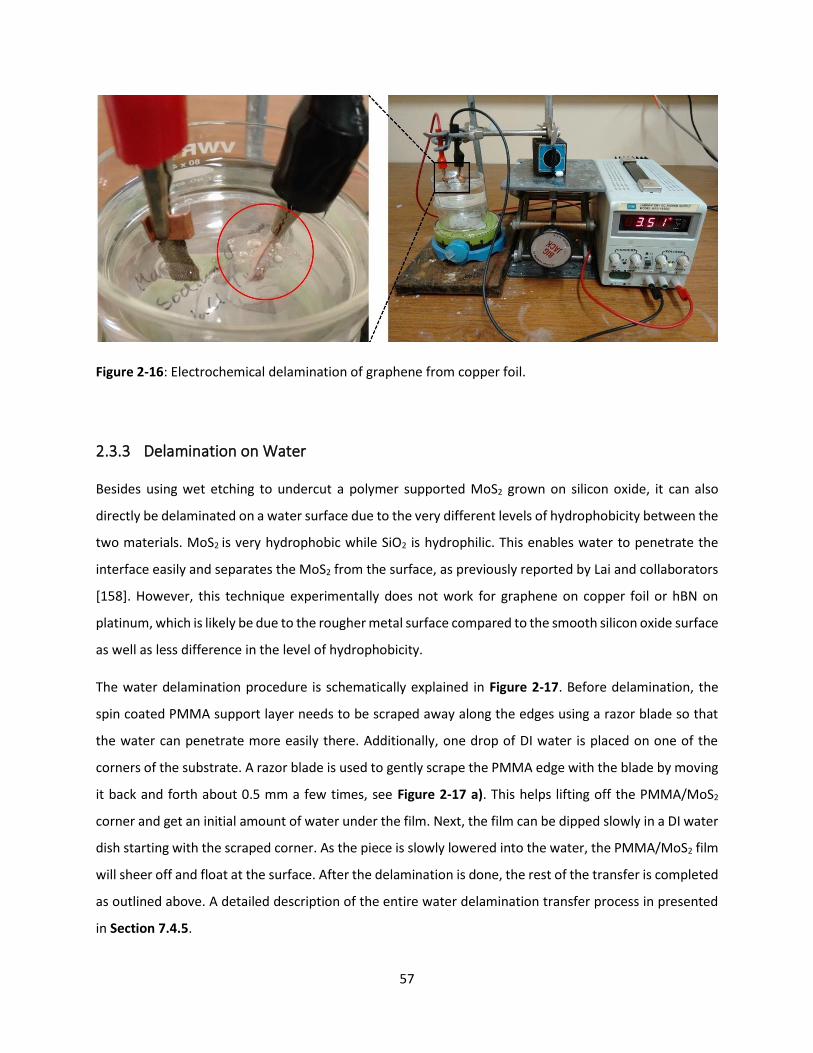
57
Figure 2-16: Electrochemical delamination of graphene from copper foil.
2.3.3 Delamination on Water
Besides using wet etching to undercut a polymer supported MoS2 grown on silicon oxide, it can also
directly be delaminated on a water surface due to the very different levels of hydrophobicity between the
two materials. MoS2 is very hydrophobic while SiO2 is hydrophilic. This enables water to penetrate the
interface easily and separates the MoS2 from the surface, as previously reported by Lai and collaborators
[158]. However, this technique experimentally does not work for graphene on copper foil or hBN on
platinum, which is likely be due to the rougher metal surface compared to the smooth silicon oxide surface
as well as less difference in the level of hydrophobicity.
The water delamination procedure is schematically explained in Figure 2-17. Before delamination, the
spin coated PMMA support layer needs to be scraped away along the edges using a razor blade so that
the water can penetrate more easily there. Additionally, one drop of DI water is placed on one of the
corners of the substrate. A razor blade is used to gently scrape the PMMA edge with the blade by moving
it back and forth about 0.5 mm a few times, see Figure 2-17 a). This helps lifting off the PMMA/MoS2
corner and get an initial amount of water under the film. Next, the film can be dipped slowly in a DI water
dish starting with the scraped corner. As the piece is slowly lowered into the water, the PMMA/MoS2 film
will sheer off and float at the surface. After the delamination is done, the rest of the transfer is completed
as outlined above. A detailed description of the entire water delamination transfer process in presented
in Section 7.4.5.

58
Figure 2-17: Water delamination of MoS2. a) Scraping away PMMA around the edge as well as one corner
of the PMMA/MoS2. b) Dip sample in water to delaminate PMMA/MoS2 film.
59
Large scale 2D Material Transfer
As discussed in Chapter 1.2, two-dimensional (2D) materials such as graphene (Gr), molybdenum disulfide
(MoS2) and hexagonal boron nitride (hBN) exhibit a wide variety of electronic properties, including
metallic, semiconducting and insulating behavior. This allows their combination to build up electronic
devices entirely made of 2D materials, such as field effect transistors [19], memristors [143] and sensors
[20]. Furthermore, 2D materials are transparent, flexible and mechanically robust, which makes them
ideal for building flexible and optoelectronic applications such as wearable electronics [22-24], solar cells
[25-27] and light-emitting devices [29, 159].
Roll-to-roll (R2R) processing is widely used in the flexible electronics industry to fabricate large-scale solar
cells, flexible displays and sensors, and has grown to a multi-billion-dollar industry in recent years [160].
Being able to leverage R2R fabrication for 2D materials could enable inexpensive, large-scale electronics
in the form of flexible films. However, the use of R2R processing of 2D materials is just starting. Two
aspects must be developed to process 2D materials in a roll-to-roll fashion: continuous synthesis and
continuous transfer. (1) Continuous synthesis of graphene, the most prominent member of the 2D
material family, has been readily demonstrated on Cu foil using chemical vapor deposition [48, 49, 161].
Although the continuous growth of other 2D materials has not been shown yet, important preliminary
steps have been demonstrated thanks to the development of chemical vapor deposition (CVD) growth on
metal foils of, for example, MoS2 or WS2 on Au foils [162-164], and hBN on Fe, Cu or Pt foils [153, 165,
166]. (2) The other important step towards the use of R2R technology in 2D materials is the roll-to-roll
transfer onto flexible substrates. The first R2R transfer was reported by Bae et al. [45] in 2010 who
transferred graphene from a Cu foil onto polyethylene terephthalate (PET) using thermal release tape.
Since then, several other groups demonstrated R2R transfers of graphene [48-55] onto flexible substrates
using either direct lamination on the target substrate [50-55] or epoxy gluing [49]. However, these
approaches mostly use wet etching of the Cu substrate, which is not economical for large-scale production
due to the high consumption, and large cost of ultra-pure copper. Furthermore, chemical etching
potentially deteriorates the graphene film quality, degrading its electronic properties [167]. To circumvent
these problems, electrochemical delamination of graphene and other 2D materials [157, 166, 168] have
been shown to gently lift off the 2D layer from the metal foil without the need of chemical etching. This
approach reduces waste, allows the metal catalyst to be reused and preserves the material’s intrinsic
properties. More recently, electrochemical delamination has been integrated in a R2R graphene transfer

60
system [53, 54] in combination with metal nanowires to achieve a remarkably low sheet resistance of
8 Ω/ for transparent electrode applications. However, more work is needed to better understand the
factors limiting R2R transfer, such as surface topology and roughness. Furthermore, it is desirable to
extend this technique to transfer other 2D materials. This chapter explores the R2R transfer of graphene
and hBN onto plastic substrates by hot roll lamination and electrochemical delamination. To do that, an
entire transfer system was designed and built that allows for fine control of lamination process
parameters, including the applied heat and pressure, as well as control of the lamination and delamination
speed. Furthermore, the stacking of multiple 2D layers by repeated lamination will be discussed in the
sections below. This chapter is based the paper “Repeated roll-to-roll transfer of two-dimensional
materials by electrochemical delamination” published in the journal Small by the Royal Society of
Chemistry [169].
3.1 Roll-to-Roll Transfer Setup
The 2D material transfer processes reported in this work were carried out using a custom designed R2R
system. It took approximately 9 months of construction and testing with two prototypes for the final
transfer setup design to emerge, as displayed in Figure 3-1 b). As shown in Figure 3-1 a), the setup consists
of three parts: a lamination unit, an electrochemical delamination unit and a rewind unit. The lamination
unit is made up of two stainless steel cylinders (25 mm diameter, 65 mm length) that are filled with Teflon
for thermal isolation and are mounted on aluminum shafts. The rollers are heated by two aluminum heat
shoes with 100W cartridge heaters and thermocouples inside to control the temperature between 80 -
250°C with two off-the-shelf relay-based PID temperature controllers. Clips are used to lightly press the
heat shoes onto the steel rollers, which are slipping under the shoes as the rotate. The lamination speed
can be altered between 0.7 – 5 mm/s by a PWM controlled DC motor that is connected to the roller shafts
by nylon gears. Additionally, the force with which the two rollers press together can be adjusted between
0 – 400 N. The pressure can be changed by compressing the four 8 cm long springs, which push the
vertically movable bottom roller up against the clamped-down top roller. The applied force of the rollers
can be considered approximately constant for laminated stacks of approximately 1 mm in thickness or
less, which was never exceeded in the experiments described below. The electrochemical delamination
unit consists of a stationary Teflon cylinder that is immersed halfway into an electrolyte-filled Pyrex glass
dish. The delamination process is based on an electrochemical transfer first presented by Wang et. al

61
[157]. In short, a voltage is applied between the metal foil and a platinum counter electrode that are
immersed in the electrolyte. This generates oxygen gas at the platinum electrode, and hydrogen bubbles
at the interface of the metal foil and 2D material, which gently separate them. Lastly, the rewind unit is
responsible to pick up the delaminated films on separate spools. All spools are connected by gears and
are powered another PWM controlled DC motor that can wind up films with a similar speed range of 0.7
– 5 mm/s. A typical transfer of a 7.5 cm long substrate takes approximately 40 seconds for the lamination
and 60 seconds for the delamination, which is significantly faster than an etch-based process.
Figure 3-1: Roll-to-roll (R2R) transfer setup. a) Schematic of R2R setup consisting of hot roll lamination
unit, electrochemical delamination unit and rewind unit. b) Actual implementation of transfer setup.
Adapted with permission from [169].
3.2 Transfer Process Optimization
After completing the roll-to-roll setup, the transfer process was optimized. For all experiments in this
chapter, polyethylene terephthalate (PET) films coated with ethylene-vinyl acetate (EVA) with a total
thickness of 75 µm (McMaster Product # 6927825) were used as flexible substrates. As most important
parameter, the lamination temperature was roughly calibrated as follows. Two strips of EVA/PET film were
placed together (with the EVA sides facing each other) in a paper sleeve (Aspen 30, 75 g/m²) to catch EVA
that is oozing out from the sides. Subsequently, 5 different temperatures at a roller pressure of 50 N and
lamination speed of 2 mm/s were tested: 80°C, 100°C, 110°C, 120°C, and 130°C with the optical results

62
given in Figure 3-2. It shows that the EVA film completely melts at 120°C as indicated by the film turning
completely transparent. Furthermore, no trapped air bubbles are observed for this temperature and
above. After further tests with a dummy copper strip in between, the standard lamination temperature
was chosen to 135°C.
Figure 3-2: Determining minimum viable lamination temperature for EVA/PET film. Temperatures from
80-130°C were tested at a roller force of 50 N and a lamination speed of 2 mm/s. Reproduced with
permission from [169].
With the lamination temperature determined, a standard transfer flow was developed based on the
transfer of graphene from copper foil. The available process parameters to tune are the exact lamination
temperature, speed, and pressure as well as the delamination speed, voltage and electrolyte
concentration. These parameters were optimized to yield a consistent and low graphene sheet resistance
on the transferred substrate, which is important for transparent electrode applications.
The transfer routine is illustrated in Figure 3-3 and discussed below. It starts with the synthesis of the 2D
material on a metal foil by chemical vapor deposition (Cu for graphene growth or Pt for hBN growth), as
further described in Chapter 2.2 and shown in Figure 3-3 a). The resulting 2D materials are grown fully
continuous over the entire metal foil. No missing area of graphene on copper were observable.
Next, the 2D-material covered metal foil is laminated on both sides with flexible EVA/PET polymer
substrates, as illustrated in Figure 3-3 b). In preparation of the lamination, the two EVA coated PET films
(19x89 mm2) and 2D material-covered metal strip (12.7x75 mm2 for Cu or 12.7x25 mm2 for Pt) are rinsed
in IPA and blow dried with a nitrogen blow gun. The 50 mm wide rollers of the lamination unit are heated
to 135°C and the bottom roller is set to press against the top roller with 75 N. Similar to the temperature
calibration, the PET/EVA/2D/metal/2D/EVA/PET stack is placed in a paper sleeve to catch EVA that may
be oozing out from the sides. The speed of the lamination is set to 2 mm/s. After the lamination, the
complete stack is trimmed with a paper guillotine to the dimensions of the copper strip.

63
Subsequently, an electrochemical delamination process in an electrolyte bath is used to separate the 2D
layers from the metal surface, see Figure 3-3 c). Before performing the delamination, the bottom EVA/PET
film, top EVA/PET film as well as the copper or platinum film and were extended by a PET and a copper
strip, respectively, and then connected to rewind rollers. The PET/EVA/2D/metal/2D/EVA/PET stack is
delaminated with 1.3 mm/s in a 1 mol/l sodium hydroxide solution (NaOH, Macron Chemicals Product
7708-12). A voltage of 3.5 V is applied to the copper extension as cathode and a platinum gauze
(25x25 mm2, Alfa Aesar #10283) as anode, which results in a DC current of 100 mA for a typical
delamination process. The delamination happens continuously as the individual ends of the three films
are pulled and rolled up by the rewind unit. After separating the entire strip, the rolled-up flexible
substrates are taken off the spools, rinsed under deionized water, blow dried with nitrogen gas and
adhered to a glass slide by double-sided tape (3M, 666). On the glass slide, the strip are cut into pieces
measuring 1x1 cm each, as shown in Figure 3-3 d) for further electrical or material characterization, which
is outlined in the sections below.
Figure 3-3: Transfer process flow starting with growing the 2D material on a metal film, laminating it in
between plastic substrates on top and bottom by applying pressure and heat, electrochemically
separating the 2D layers from the metal surface, rinsing the plastic substrates and gluing them on glass
slides for further characterization. Adapted with permission from [169].
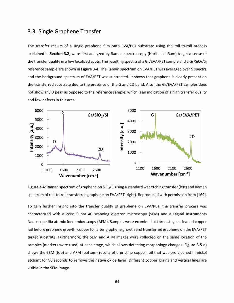
64
3.3 Single Graphene Transfer
The transfer results of a single graphene film onto EVA/PET substrate using the roll-to-roll process
explained in Section 3.2, were first analyzed by Raman spectroscopy (Horiba LabRam) to get a sense of
the transfer quality in a few localized spots. The resulting spectra of a Gr/EVA/PET sample and a Gr/SiO2/Si
reference sample are shown in Figure 3-4. The Raman spectrum on EVA/PET was averaged over 5 spectra
and the background spectrum of EVA/PET was subtracted. It shows that graphene is clearly present on
the transferred substrate due to the presence of the G and 2D band. Also, the Gr/EVA/PET samples does
not show any D peak as opposed to the reference sample, which is an indication of a high transfer quality
and few defects in this area.
Figure 3-4: Raman spectrum of graphene on SiO2/Si using a standard wet etching transfer (left) and Raman
spectrum of roll-to-roll transferred graphene on EVA/PET (right). Reproduced with permission from [169].
To gain further insight into the transfer quality of graphene on EVA/PET, the transfer process was
characterized with a Zeiss Supra 40 scanning electron microscopy (SEM) and a Digital Instruments
Nanoscope IIIa atomic force microscopy (AFM). Samples were examined at three stages: cleaned copper
foil before graphene growth, copper foil after graphene growth and transferred graphene on the EVA/PET
target substrate. Furthermore, the SEM and AFM images were collected on the same location of the
samples (markers were used) at each stage, which allows detecting morphology changes. Figure 3-5 a)
shows the SEM (top) and AFM (bottom) results of a pristine copper foil that was pre-cleaned in nickel
etchant for 90 seconds to remove the native oxide layer. Different copper grains and vertical lines are
visible in the SEM image.

65
Figure 3-5: Surface characterization of a graphene transfer process with SEM images at the top and three-
dimensional AFM images at the bottom. Areas outlined by white dashed boxes in the SEM images (top)
correspond to the regions scanned by AFM (bottom). a) Surface of copper foil after 90 sec nickel etchant
clean, b) copper surface after graphene growth, c) EVA/PET surface after lamination onto copper film and
electrochemical delamination (the SEM in c) was mirrored along the y-axis and AFM image was rotated
along y-axis by 180° for an easier comparison to b)). Reproduced with permission from [169].
The lines in Figure 3-5 a) are typical for metal foils and stem from the production process when the Cu foil
is thinned down. The AFM image also illustrates these deep vertical groves, which create an average
surface roughness of 75 nm. After graphene growth, the copper surface smoothens out significantly and
the average surface roughness decreases to 23 nm, as shown in the AFM image in Figure 3-5 b). The
surface becomes wavy and now exhibits steps, which are attributed to the release of strain at the copper
surface during the cooling process [170]. The SEM image in Figure 3-5 b) shows the same copper steps as
in the AFM. It also shows graphene wrinkles that result from the thermal expansion mismatch between
Cu and graphene as the sample cools down after growth (at 1000°C). Next, the Gr/Cu sample was
laminated onto an EVA/PET target substrate. Previous reports found that the adhesion energy of
graphene to EVA is 0.6 J/m2 [171], which is slightly lower than the adhesion energy of graphene to copper
with 0.72 J/m2 [172]. Hence, electrochemical delamination is used to assist the separation of graphene
from the copper surface and enable a clean transfer. The AFM image collected on the graphene/EVA/PET
sample, displayed in Figure 3-5 c), indicates that the waviness of the copper substrate was imprinted onto

66
the EVA surface and identical copper steps can be found. This exact negative replication is not surprising
because the EVA film melts during the lamination above 120°C and is hence able to be molded easily. Also,
the SEM image in Figure 3-5 c) shows identical graphene wrinkles compared to Figure 3-5 b), which
confirms the exact transfer and good adhesion of graphene onto the EVA/PET film (both images in Figure
3-5 c)) where mirrored to enable an easier comparison). Lastly, the SEM image in Figure 3-5 c) reveals
local defects in the graphene sheet (that show up as spots with a dark, blurry perimeter due to charging
effects).
When considering the origin of defects in the transferred graphene film in general terms, they may
originate from either the graphene synthesis due to incomplete growth or from the transfer process itself.
Bases on the analysis of dozens of SEM images of graphene on copper at low and high magnification, no
missing areas were identified, which would be recognizable by eye above a few hundred nanometers. As
part of the analysis, particles on the copper surface were occasionally found, typically under 1 µm in size,
however graphene is assumed to be present under these particles. As a result, all found defects on the
transferred graphene, especially above a micrometer in size, are ascribed to the transfer process. The
density of defects in the transferred graphene film was analyzed in more detail by looking at low-
magnification SEM images of three typical graphene films on EVA/PET, as depicted in Figure 3-6 a) to c).
Figure 3-6: Crack and defect density analysis of Gr/EVA/PET. a-c) SEM images of Gr/EVA/PET. d-f) Fully
increased contrast of images a-c). Reproduced with permission from [169].
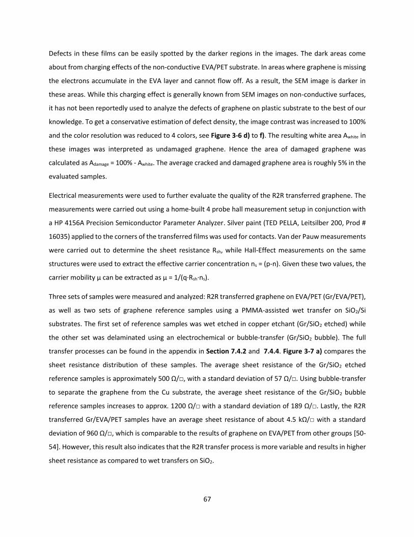
67
Defects in these films can be easily spotted by the darker regions in the images. The dark areas come
about from charging effects of the non-conductive EVA/PET substrate. In areas where graphene is missing
the electrons accumulate in the EVA layer and cannot flow off. As a result, the SEM image is darker in
these areas. While this charging effect is generally known from SEM images on non-conductive surfaces,
it has not been reportedly used to analyze the defects of graphene on plastic substrate to the best of our
knowledge. To get a conservative estimation of defect density, the image contrast was increased to 100%
and the color resolution was reduced to 4 colors, see Figure 3-6 d) to f). The resulting white area Awhite in
these images was interpreted as undamaged graphene. Hence the area of damaged graphene was
calculated as Adamage = 100% - Awhite. The average cracked and damaged graphene area is roughly 5% in the
evaluated samples.
Electrical measurements were used to further evaluate the quality of the R2R transferred graphene. The
measurements were carried out using a home-built 4 probe hall measurement setup in conjunction with
a HP 4156A Precision Semiconductor Parameter Analyzer. Silver paint (TED PELLA, Leitsilber 200, Prod #
16035) applied to the corners of the transferred films was used for contacts. Van der Pauw measurements
were carried out to determine the sheet resistance Rsh, while Hall-Effect measurements on the same
structures were used to extract the effective carrier concentration ns = (p-n). Given these two values, the
carrier mobility µ can be extracted as µ = 1/(q∙Rsh∙ns).
Three sets of samples were measured and analyzed: R2R transferred graphene on EVA/PET (Gr/EVA/PET),
as well as two sets of graphene reference samples using a PMMA-assisted wet transfer on SiO2/Si
substrates. The first set of reference samples was wet etched in copper etchant (Gr/SiO2 etched) while
the other set was delaminated using an electrochemical or bubble-transfer (Gr/SiO2 bubble). The full
transfer processes can be found in the appendix in Section 7.4.2 and 7.4.4. Figure 3-7 a) compares the
sheet resistance distribution of these samples. The average sheet resistance of the Gr/SiO2 etched
reference samples is approximately 500 Ω/, with a standard deviation of 57 Ω/. Using bubble-transfer
to separate the graphene from the Cu substrate, the average sheet resistance of the Gr/SiO2 bubble
reference samples increases to approx. 1200 Ω/ with a standard deviation of 189 Ω/. Lastly, the R2R
transferred Gr/EVA/PET samples have an average sheet resistance of about 4.5 kΩ/ with a standard
deviation of 960 Ω/, which is comparable to the results of graphene on EVA/PET from other groups [50-
54]. However, this result also indicates that the R2R transfer process is more variable and results in higher
sheet resistance as compared to wet transfers on SiO2.
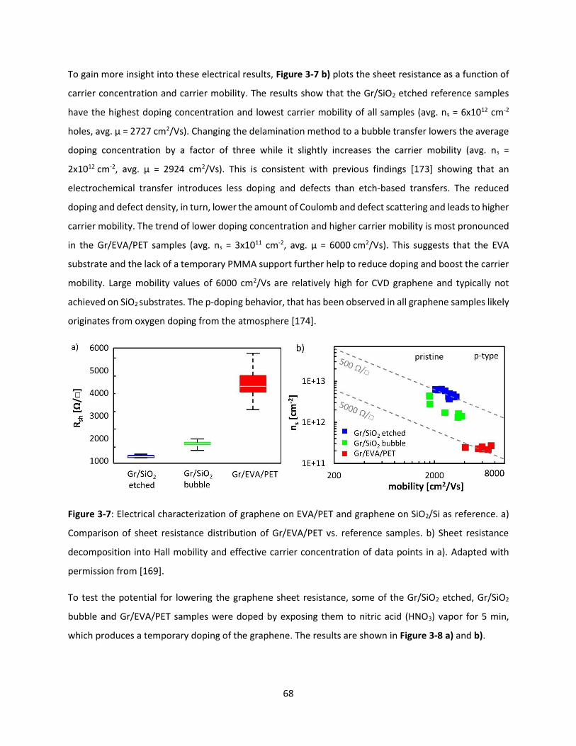
68
To gain more insight into these electrical results, Figure 3-7 b) plots the sheet resistance as a function of
carrier concentration and carrier mobility. The results show that the Gr/SiO2 etched reference samples
have the highest doping concentration and lowest carrier mobility of all samples (avg. ns = 6x1012 cm-2
holes, avg. µ = 2727 cm2/Vs). Changing the delamination method to a bubble transfer lowers the average
doping concentration by a factor of three while it slightly increases the carrier mobility (avg. ns =
2x1012 cm-2, avg. µ = 2924 cm2/Vs). This is consistent with previous findings [173] showing that an
electrochemical transfer introduces less doping and defects than etch-based transfers. The reduced
doping and defect density, in turn, lower the amount of Coulomb and defect scattering and leads to higher
carrier mobility. The trend of lower doping concentration and higher carrier mobility is most pronounced
in the Gr/EVA/PET samples (avg. ns = 3x1011 cm-2, avg. µ = 6000 cm2/Vs). This suggests that the EVA
substrate and the lack of a temporary PMMA support further help to reduce doping and boost the carrier
mobility. Large mobility values of 6000 cm2/Vs are relatively high for CVD graphene and typically not
achieved on SiO2 substrates. The p-doping behavior, that has been observed in all graphene samples likely
originates from oxygen doping from the atmosphere [174].
Figure 3-7: Electrical characterization of graphene on EVA/PET and graphene on SiO2/Si as reference. a)
Comparison of sheet resistance distribution of Gr/EVA/PET vs. reference samples. b) Sheet resistance
decomposition into Hall mobility and effective carrier concentration of data points in a). Adapted with
permission from [169].
To test the potential for lowering the graphene sheet resistance, some of the Gr/SiO2 etched, Gr/SiO2
bubble and Gr/EVA/PET samples were doped by exposing them to nitric acid (HNO3) vapor for 5 min,
which produces a temporary doping of the graphene. The results are shown in Figure 3-8 a) and b).
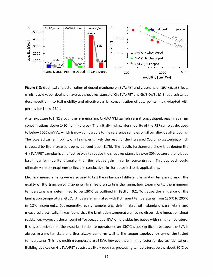
69
Figure 3-8: Electrical characterization of doped graphene on EVA/PET and graphene on SiO2/Si. a) Effects
of nitric acid vapor doping on average sheet resistance of Gr/EVA/PET and Gr/SiO2/Si. b) Sheet resistance
decomposition into Hall mobility and effective carrier concentration of data points in a). Adapted with
permission from [169].
After exposure to HNO3, both the reference and Gr/EVA/PET samples are strongly doped, reaching carrier
concentrations above 1x1013 cm-2 (p-type). The initially high carrier mobility of the R2R samples dropped
to below 2000 cm2/Vs, which is now comparable to the reference samples on silicon dioxide after doping.
The lowered carrier mobility of all samples is likely the result of the increased Coulomb scattering, which
is caused by the increased doping concentration [175]. The results furthermore show that doping the
Gr/EVA/PET samples is an effective way to reduce the sheet resistance by over 80% because the relative
loss in carrier mobility is smaller than the relative gain in carrier concentration. This approach could
ultimately enable graphene as flexible, conductive film for optoelectronic applications.
Electrical measurements were also used to test the influence of different lamination temperatures on the
quality of the transferred graphene films. Before starting the lamination experiments, the minimum
temperature was determined to be 130°C as outlined in Section 3.2. To gauge the influence of the
lamination temperature, Gr/Cu strips were laminated with 8 different temperatures from 130°C to 200°C
in 10°C increments. Subsequently, every sample was delaminated with standard parameters and
measured electrically. It was found that the lamination temperature had no discernable impact on sheet
resistance. However, the amount of “squeezed out” EVA on the sides increased with rising temperature.
It is hypothesized that the exact lamination temperature over 130°C is not significant because the EVA is
always in a molten state and thus always conforms well to the copper topology for any of the tested
temperatures. This low melting temperature of EVA, however, is a limiting factor for devices fabrication.
Building devices on Gr/EVA/PET substrates likely requires processing temperatures below about 80°C so

70
the EVA adhesive does not melt. However, this problem can be circumvented by integrating the Gr/EVA
layer last in a device. This way, flexible solar cells [27], triboelectric generators [176] and touch screens
[177] using Gr/EVA have been demonstrated. The use of PET as substrate is well suited for flexible
electronics due to its mechanical strength and transparency [178].
3.4 Double Graphene Transfer
The previous section examined the limits of achievable sheet resistance of one graphene layer on EVA/PET
by optimizing the transfer and doping of the film. Another way to improve the sheet resistance of
Gr/EVA/PET besides chemical doping is by stacking multiple graphene layers. This section explores how
two layers of graphene can be stacked by hot roll lamination and electrochemical delamination, which
reduces the sheet resistance by 70%.
Figure 3-9 illustrates the process flow. EVA/PET films were laminated on both sides of a graphene-covered
Cu strip and delaminated using the standard parameters described above. Then, the Gr/EVA/PET films
were laminated onto a new Cu strip with graphene grown on it and delaminated a second time.
Furthermore, monolayer, and bi-layer samples were also subjected to 5 min of nitric acid vapor to dope
them. The stacking of multiple graphene layers is more challenging that a simple lamination of graphene
onto EVA from an adhesion energy perspective. The binding energy of graphene to graphite is roughly 0.2
J/m2 [179, 180], which is much less than the adhesion energy of 0.72 J/m2 reported for graphene to copper
[171]. As a result, the electrochemical delamination process is more important now to offset this
difference.
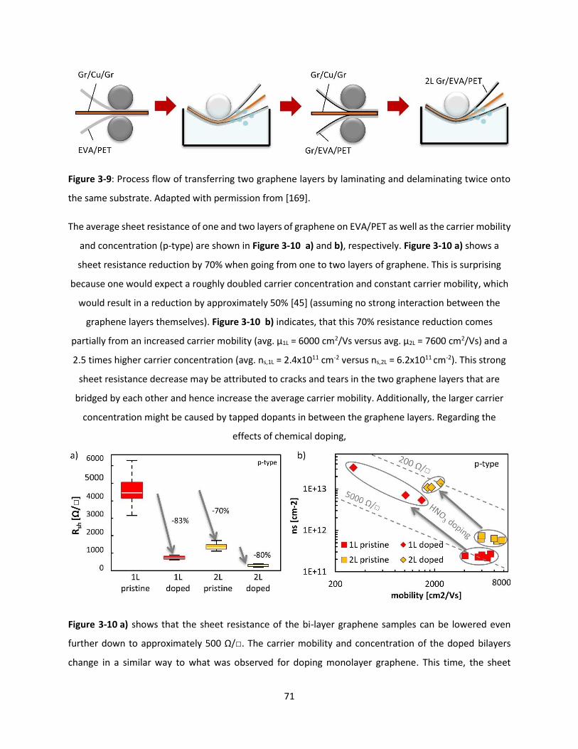
71
Figure 3-9: Process flow of transferring two graphene layers by laminating and delaminating twice onto
the same substrate. Adapted with permission from [169].
The average sheet resistance of one and two layers of graphene on EVA/PET as well as the carrier mobility
and concentration (p-type) are shown in Figure 3-10 a) and b), respectively. Figure 3-10 a) shows a
sheet resistance reduction by 70% when going from one to two layers of graphene. This is surprising
because one would expect a roughly doubled carrier concentration and constant carrier mobility, which
would result in a reduction by approximately 50% [45] (assuming no strong interaction between the
graphene layers themselves). Figure 3-10 b) indicates, that this 70% resistance reduction comes
partially from an increased carrier mobility (avg. µ1L = 6000 cm2/Vs versus avg. µ2L = 7600 cm2/Vs) and a
2.5 times higher carrier concentration (avg. ns,1L = 2.4x1011 cm-2 versus ns,2L = 6.2x1011 cm-2). This strong
sheet resistance decrease may be attributed to cracks and tears in the two graphene layers that are
bridged by each other and hence increase the average carrier mobility. Additionally, the larger carrier
concentration might be caused by tapped dopants in between the graphene layers. Regarding the
effects of chemical doping,
Figure 3-10 a) shows that the sheet resistance of the bi-layer graphene samples can be lowered even
further down to approximately 500 Ω/. The carrier mobility and concentration of the doped bilayers
change in a similar way to what was observed for doping monolayer graphene. This time, the sheet
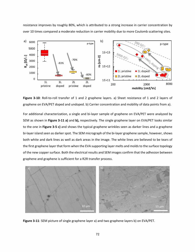
72
resistance improves by roughly 80%, which is attributed to a strong increase in carrier concentration by
over 10 times compared a moderate reduction in carrier mobility due to more Coulomb scattering sites.
Figure 3-10: Roll-to-roll transfer of 1 and 2 graphene layers. a) Sheet resistance of 1 and 2 layers of
graphene on EVA/PET doped and undoped. b) Carrier concentration and mobility of data points from a).
For additional characterization, a single and bi-layer sample of graphene on EVA/PET were analyzed by
SEM as shown in Figure 3-11 a) and b), respectively. The single graphene layer on EVA/PET looks similar
to the one in Figure 3-5 c) and shows the typical graphene wrinkles seen as darker lines and a graphene
bi-layer island seen as darker spot. The SEM micrograph of the bi-layer graphene sample, however, shows
both white and dark lines as well as dark areas in the image. The white lines are believed to be tears of
the first graphene layer that form when the EVA supporting layer melts and molds to the surface topology
of the new copper surface. Both the electrical results and SEM images confirm that the adhesion between
graphene and graphene is sufficient for a R2R transfer process.
Figure 3-11: SEM picture of single graphene layer a) and two graphene layers b) on EVA/PET.
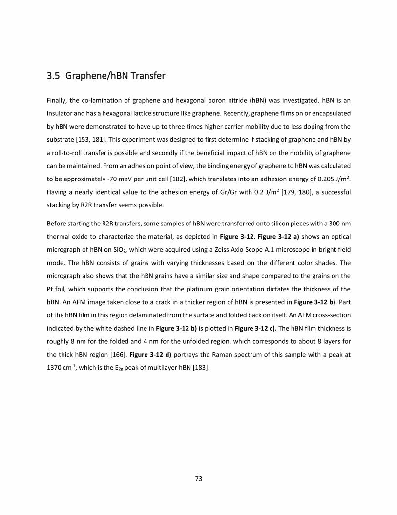
73
3.5 Graphene/hBN Transfer
Finally, the co-lamination of graphene and hexagonal boron nitride (hBN) was investigated. hBN is an
insulator and has a hexagonal lattice structure like graphene. Recently, graphene films on or encapsulated
by hBN were demonstrated to have up to three times higher carrier mobility due to less doping from the
substrate [153, 181]. This experiment was designed to first determine if stacking of graphene and hBN by
a roll-to-roll transfer is possible and secondly if the beneficial impact of hBN on the mobility of graphene
can be maintained. From an adhesion point of view, the binding energy of graphene to hBN was calculated
to be approximately -70 meV per unit cell [182], which translates into an adhesion energy of 0.205 J/m2.
Having a nearly identical value to the adhesion energy of Gr/Gr with 0.2 J/m2 [179, 180], a successful
stacking by R2R transfer seems possible.
Before starting the R2R transfers, some samples of hBN were transferred onto silicon pieces with a 300 nm
thermal oxide to characterize the material, as depicted in Figure 3-12. Figure 3-12 a) shows an optical
micrograph of hBN on SiO2, which were acquired using a Zeiss Axio Scope A.1 microscope in bright field
mode. The hBN consists of grains with varying thicknesses based on the different color shades. The
micrograph also shows that the hBN grains have a similar size and shape compared to the grains on the
Pt foil, which supports the conclusion that the platinum grain orientation dictates the thickness of the
hBN. An AFM image taken close to a crack in a thicker region of hBN is presented in Figure 3-12 b). Part
of the hBN film in this region delaminated from the surface and folded back on itself. An AFM cross-section
indicated by the white dashed line in Figure 3-12 b) is plotted in Figure 3-12 c). The hBN film thickness is
roughly 8 nm for the folded and 4 nm for the unfolded region, which corresponds to about 8 layers for
the thick hBN region [166]. Figure 3-12 d) portrays the Raman spectrum of this sample with a peak at
1370 cm-1, which is the E2g peak of multilayer hBN [183].
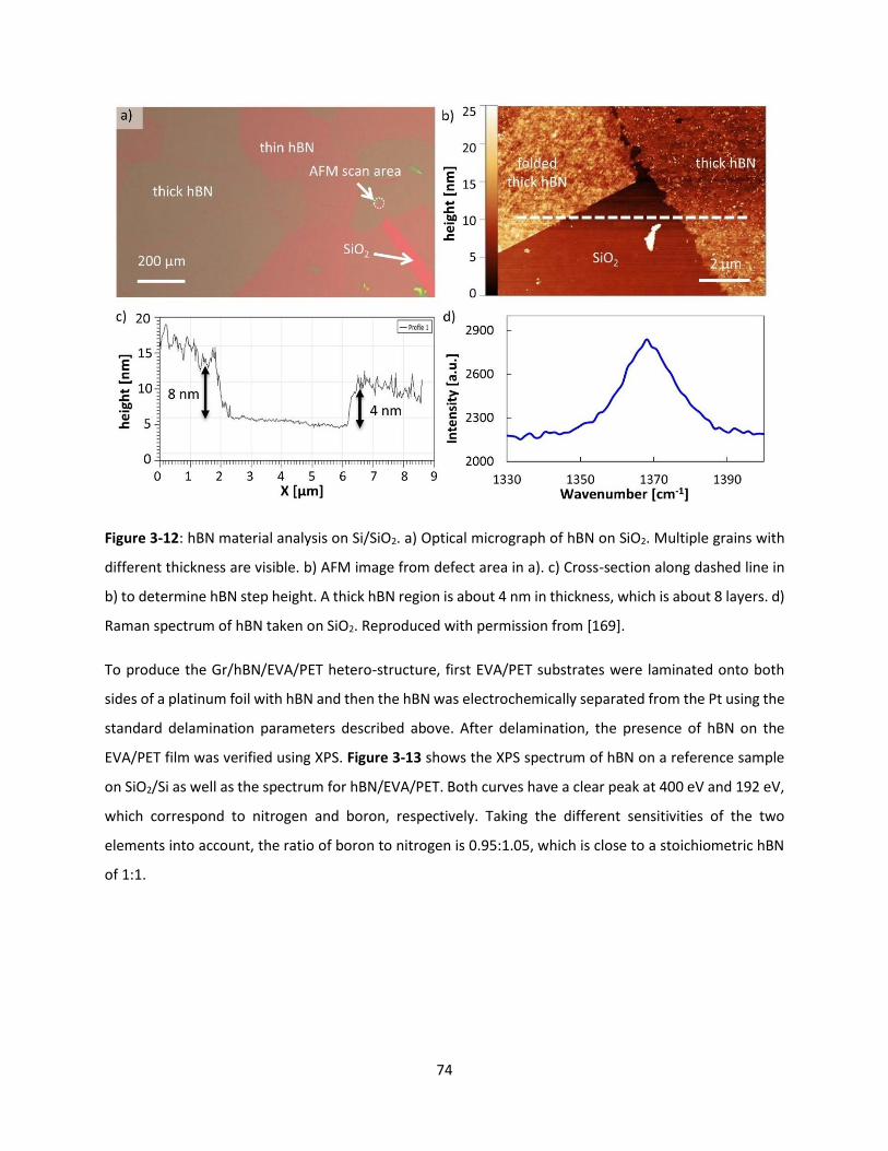
74
Figure 3-12: hBN material analysis on Si/SiO2. a) Optical micrograph of hBN on SiO2. Multiple grains with
different thickness are visible. b) AFM image from defect area in a). c) Cross-section along dashed line in
b) to determine hBN step height. A thick hBN region is about 4 nm in thickness, which is about 8 layers. d)
Raman spectrum of hBN taken on SiO2. Reproduced with permission from [169].
To produce the Gr/hBN/EVA/PET hetero-structure, first EVA/PET substrates were laminated onto both
sides of a platinum foil with hBN and then the hBN was electrochemically separated from the Pt using the
standard delamination parameters described above. After delamination, the presence of hBN on the
EVA/PET film was verified using XPS. Figure 3-13 shows the XPS spectrum of hBN on a reference sample
on SiO2/Si as well as the spectrum for hBN/EVA/PET. Both curves have a clear peak at 400 eV and 192 eV,
which correspond to nitrogen and boron, respectively. Taking the different sensitivities of the two
elements into account, the ratio of boron to nitrogen is 0.95:1.05, which is close to a stoichiometric hBN
of 1:1.

75
Figure 3-13: XPS spectra of hBN on SiO2 and EVA/PET after successful transfer. Reproduced with
permission from [169].
In a final step the hBN/EVA/PET substrates were laminated to a Gr/Cu/Gr film and the Gr/Cu interface
was then electrochemically separated. Figure 3-14 shows two SEM micrographs of a resulting
Gr/hBN/EVA/PET sample.
Figure 3-14: SEM analysis of Gr/hBN/EVA/PET film after transfer. a) High-quality transfer region. The
image shows features of both graphene and hBN films. b) Poor-quality transfer region. The bright artifacts
indicate defects in the transferred graphene film. Reproduced with permission from [169].
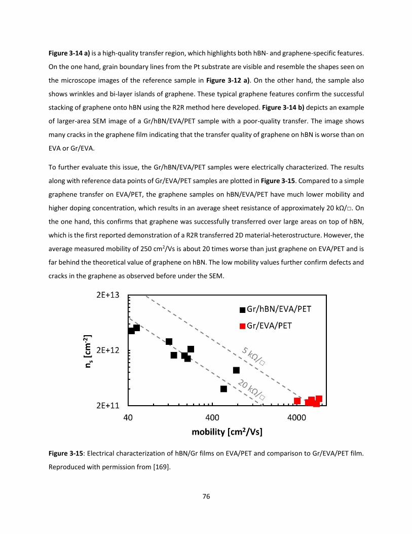
76
Figure 3-14 a) is a high-quality transfer region, which highlights both hBN- and graphene-specific features.
On the one hand, grain boundary lines from the Pt substrate are visible and resemble the shapes seen on
the microscope images of the reference sample in Figure 3-12 a). On the other hand, the sample also
shows wrinkles and bi-layer islands of graphene. These typical graphene features confirm the successful
stacking of graphene onto hBN using the R2R method here developed. Figure 3-14 b) depicts an example
of larger-area SEM image of a Gr/hBN/EVA/PET sample with a poor-quality transfer. The image shows
many cracks in the graphene film indicating that the transfer quality of graphene on hBN is worse than on
EVA or Gr/EVA.
To further evaluate this issue, the Gr/hBN/EVA/PET samples were electrically characterized. The results
along with reference data points of Gr/EVA/PET samples are plotted in Figure 3-15. Compared to a simple
graphene transfer on EVA/PET, the graphene samples on hBN/EVA/PET have much lower mobility and
higher doping concentration, which results in an average sheet resistance of approximately 20 kΩ/. On
the one hand, this confirms that graphene was successfully transferred over large areas on top of hBN,
which is the first reported demonstration of a R2R transferred 2D material-heterostructure. However, the
average measured mobility of 250 cm2/Vs is about 20 times worse than just graphene on EVA/PET and is
far behind the theoretical value of graphene on hBN. The low mobility values further confirm defects and
cracks in the graphene as observed before under the SEM.
Figure 3-15: Electrical characterization of hBN/Gr films on EVA/PET and comparison to Gr/EVA/PET film.
Reproduced with permission from [169].
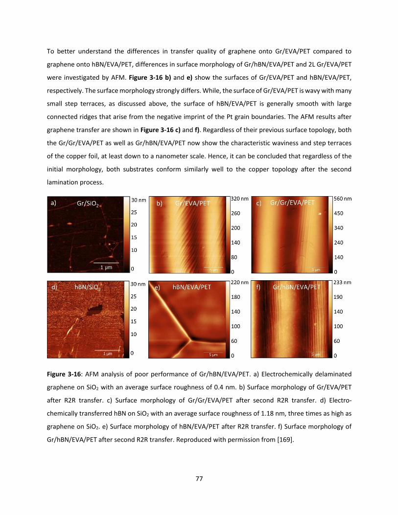
77
To better understand the differences in transfer quality of graphene onto Gr/EVA/PET compared to
graphene onto hBN/EVA/PET, differences in surface morphology of Gr/hBN/EVA/PET and 2L Gr/EVA/PET
were investigated by AFM. Figure 3-16 b) and e) show the surfaces of Gr/EVA/PET and hBN/EVA/PET,
respectively. The surface morphology strongly differs. While, the surface of Gr/EVA/PET is wavy with many
small step terraces, as discussed above, the surface of hBN/EVA/PET is generally smooth with large
connected ridges that arise from the negative imprint of the Pt grain boundaries. The AFM results after
graphene transfer are shown in Figure 3-16 c) and f). Regardless of their previous surface topology, both
the Gr/Gr/EVA/PET as well as Gr/hBN/EVA/PET now show the characteristic waviness and step terraces
of the copper foil, at least down to a nanometer scale. Hence, it can be concluded that regardless of the
initial morphology, both substrates conform similarly well to the copper topology after the second
lamination process.
Figure 3-16: AFM analysis of poor performance of Gr/hBN/EVA/PET. a) Electrochemically delaminated
graphene on SiO2 with an average surface roughness of 0.4 nm. b) Surface morphology of Gr/EVA/PET
after R2R transfer. c) Surface morphology of Gr/Gr/EVA/PET after second R2R transfer. d) Electro-
chemically transferred hBN on SiO2 with an average surface roughness of 1.18 nm, three times as high as
graphene on SiO2. e) Surface morphology of hBN/EVA/PET after R2R transfer. f) Surface morphology of
Gr/hBN/EVA/PET after second R2R transfer. Reproduced with permission from [169].
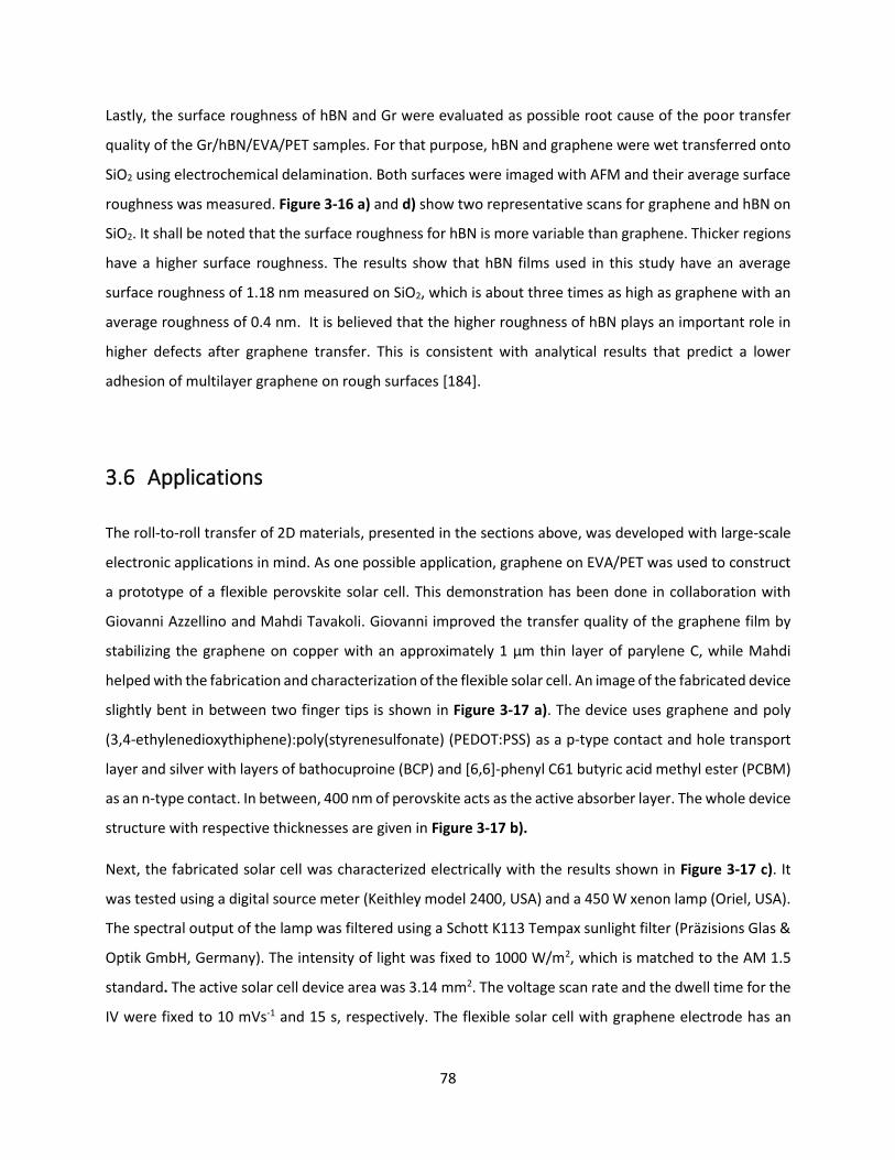
78
Lastly, the surface roughness of hBN and Gr were evaluated as possible root cause of the poor transfer
quality of the Gr/hBN/EVA/PET samples. For that purpose, hBN and graphene were wet transferred onto
SiO2 using electrochemical delamination. Both surfaces were imaged with AFM and their average surface
roughness was measured. Figure 3-16 a) and d) show two representative scans for graphene and hBN on
SiO2. It shall be noted that the surface roughness for hBN is more variable than graphene. Thicker regions
have a higher surface roughness. The results show that hBN films used in this study have an average
surface roughness of 1.18 nm measured on SiO2, which is about three times as high as graphene with an
average roughness of 0.4 nm. It is believed that the higher roughness of hBN plays an important role in
higher defects after graphene transfer. This is consistent with analytical results that predict a lower
adhesion of multilayer graphene on rough surfaces [184].
3.6 Applications
The roll-to-roll transfer of 2D materials, presented in the sections above, was developed with large-scale
electronic applications in mind. As one possible application, graphene on EVA/PET was used to construct
a prototype of a flexible perovskite solar cell. This demonstration has been done in collaboration with
Giovanni Azzellino and Mahdi Tavakoli. Giovanni improved the transfer quality of the graphene film by
stabilizing the graphene on copper with an approximately 1 µm thin layer of parylene C, while Mahdi
helped with the fabrication and characterization of the flexible solar cell. An image of the fabricated device
slightly bent in between two finger tips is shown in Figure 3-17 a). The device uses graphene and poly
(3,4-ethylenedioxythiphene):poly(styrenesulfonate) (PEDOT:PSS) as a p-type contact and hole transport
layer and silver with layers of bathocuproine (BCP) and [6,6]-phenyl C61 butyric acid methyl ester (PCBM)
as an n-type contact. In between, 400 nm of perovskite acts as the active absorber layer. The whole device
structure with respective thicknesses are given in Figure 3-17 b).
Next, the fabricated solar cell was characterized electrically with the results shown in Figure 3-17 c). It
was tested using a digital source meter (Keithley model 2400, USA) and a 450 W xenon lamp (Oriel, USA).
The spectral output of the lamp was filtered using a Schott K113 Tempax sunlight filter (Präzisions Glas &
Optik GmbH, Germany). The intensity of light was fixed to 1000 W/m2, which is matched to the AM 1.5
standard. The active solar cell device area was 3.14 mm2. The voltage scan rate and the dwell time for the
IV were fixed to 10 mVs-1 and 15 s, respectively. The flexible solar cell with graphene electrode has an
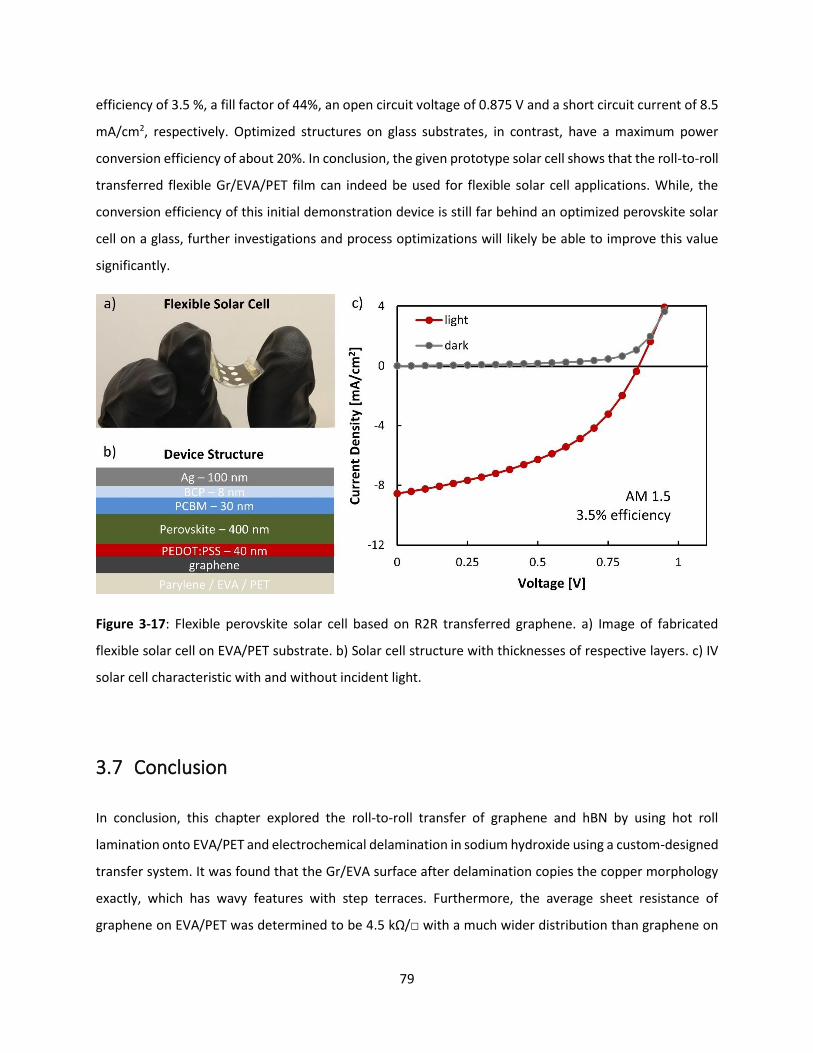
79
efficiency of 3.5 %, a fill factor of 44%, an open circuit voltage of 0.875 V and a short circuit current of 8.5
mA/cm2, respectively. Optimized structures on glass substrates, in contrast, have a maximum power
conversion efficiency of about 20%. In conclusion, the given prototype solar cell shows that the roll-to-roll
transferred flexible Gr/EVA/PET film can indeed be used for flexible solar cell applications. While, the
conversion efficiency of this initial demonstration device is still far behind an optimized perovskite solar
cell on a glass, further investigations and process optimizations will likely be able to improve this value
significantly.
Figure 3-17: Flexible perovskite solar cell based on R2R transferred graphene. a) Image of fabricated
flexible solar cell on EVA/PET substrate. b) Solar cell structure with thicknesses of respective layers. c) IV
solar cell characteristic with and without incident light.
3.7 Conclusion
In conclusion, this chapter explored the roll-to-roll transfer of graphene and hBN by using hot roll
lamination onto EVA/PET and electrochemical delamination in sodium hydroxide using a custom-designed
transfer system. It was found that the Gr/EVA surface after delamination copies the copper morphology
exactly, which has wavy features with step terraces. Furthermore, the average sheet resistance of
graphene on EVA/PET was determined to be 4.5 kΩ/ with a much wider distribution than graphene on

80
silicon dioxide reference samples. Two layers of graphene were successfully stacked by repeated
lamination and delamination onto fresh graphene on copper foil. In this way, the sheet resistance was
lowered by 70% to 1.35 kΩ/ with respect to one layer of graphene, which indicates the bridging of cracks
and defects by the two graphene films. Additionally, nitric acid vapor doping was shown to reduce the
sheet resistance further down to 500 Ω/. The stacking of graphene onto hBN by a sequential roll-to-roll
transfer has been demonstrated. However, besides expectations of increased graphene carrier mobility
and hence lower sheet resistance, the resulting graphene quality was lower than for Gr/EVA/PET samples.
This lower quality is a result of graphene cracks and defects after the transfer on hBN, which are believed
to be caused by the rough hBN surface as compared to Gr/EVA. Lastly, a flexible perovskite solar cell with
a 3.4% power conversion efficiency was demonstrated on a roll-to-roll transferred graphene film on
EVA/PET substrate.

81

82
SynCell Building Blocks
Recent developments in nanofabrication technologies, advanced functional materials [67], and
microsystem design [185] present the opportunity to build electronic systems the size of biological cells
(<100 µm) that can sense their environment at unprecedented length scales, process these inputs, and
respond in a pre-programmed way. As discussed in the introduction in Section 1.4, such autonomous
microsystems could be used, for example, to detect chemicals or molecules in very confined spaces like
blood vessels [56]. Alternatively, they are small enough to be dispersed in solutions and sprayed or printed
on surfaces to form distributed sensor networks [65] or even be embedded into polymers to create
intelligent fibers for smart clothing.
For any of those applications to work, however, a high degree of autonomy is required. Microsystems
below 100 µm in size are too small to be tethered to wires for energy supply or communication.
Additionally, their size makes it exceedingly difficult to handle or manipulate such systems mechanically.
To be generally useful, autonomous microsystems need to have a subset or all the following building
blocks, as illustrated in Figure 4-1. Firstly, sensors are necessary to collect physical, chemical, or biological
information from the microsystem’s environment, such as temperature, chemical concentration, or the
presence of certain biomarkers. Secondly, clocks or timers are helpful to keep track of the microsystem’s
deployment time or to generate time stamps for sensor information. A central processing unit is necessary
to perform computations on the collected data and for data storage. Additionally, the capability to
communicate wirelessly with the outside world is essential to send and receive information such as sensor
data or instructions. An on-board energy source (harvesting and/or storage) is needed to power the
previous building blocks. Lastly, it could be desirable to have components for actuation or locomotion
present for the microsystems to maneuver and interact with their environment.
This chapter discusses the design and characterization of individual building blocks that cover each of
those capabilities. In the next chapter, some of these developed building blocks are then integrated into
60x60 µm2 small microsystems and applied in different scenarios. Due to their size, which are similar to
biological cells, the microsystems are called synthetic cells or SynCells for short.
The development of feasible building blocks was guided by three design principles. First, ultra-low power
consumption was pursued for each capability. As further elucidated in Section 4.4, having enough energy
to perform functions on a microsystem smaller than 100 µm is very challenging. To date, no practical

83
solutions exist to store meaningful amounts of energy on such tiny footprints. Even the generation of
energy from the environment through energy harvesting only yields between tens of nanowatts and a
few microwatts at best. In this regard, the use of functional materials that consume no energy at all to
perform a specific function was specifically investigated because it simplifies the microsystem design.
Furthermore, possible device implementations for each building block need to take up as little area as
possible and must have the ability to be integrated together easily. Hence, it is important to select device
implementations that are modular and choose a microsystem substrate that can merge components side-
by-side or vertically stacked. Additionally, this constraint encourages the simplest possible concept for
each building block as they tend to be the smallest.
Lastly, all developed components must be able to be fabricated using standard cleanroom toolsets on
silicon wafers, enabling a repeatable mass-fabrication of these microsystems. This mandates the use of
thin films below about two micrometers in thickness for the devices and the microsystem substrate, which
is necessary for the photolithographic patterning to work properly.
Figure 4-1: Building blocks needed for a useful and autonomous microsystem.

84
4.1 Sensing Building Block
As first building block, a chemical sensor was also developed to be part of the SynCell platform. The
sensors have a chemi-resistive behavior, which change resistance as a function of chemical exposure. The
active sensing area consists of a 1.5x8 µm2 channel of MOCVD-grown MoS2 on an SU-8/SiO2 substrate
with 100 nm Au contacts. Additionally, reference sensors were developed, which are identical to the
regular sensors, but are covered by SU-8 to shield them from the outside to monitor for possible sensor
drift. The fabrication of entire sensor/reference sensor arrays has a device yield above 95% using an
optimized process flow and takes about two day in the cleanroom.
The use of MoS2 as sensor materials is well documented [68] and has been used before for example for
gas sensing of ammonia or triethylamine [65, 148]. In this work, MoS2 is specifically used to detect
putrescine in both water and air, which is a polyamine that is generated for example by the decomposition
of meat or fish but is also found in fermented foods like pickles. Putrescine sensors are highly relevant in
food quality monitoring [186] with levels above 10-100 mg/kg for instance indicating likely meat spoilage
in vacuum packed beef [187]. For this purpose of meat spoilage detection, putrescine gas sensors have
been implemented using carbon nanotubes before [188]. Additionally, putrescine is an important
polyamine indicative of cell proliferation and cell growth [189].
First, the sensor response to putrescine in water was characterized. The sensors were tested in pure DI
water as well as DI water with 100 mg/L of putrescine dissolved in it (1,4-diaminobutane 98+% 25 g, Fisher
Scientific), which is a relevant concentration for food spoilage monitoring [187, 190] or for stimulating cell
growth [191]. For a standard experiment, the chemical sensors on a silicon piece were first measured in
their initial state. Next, the chip was dipped into either DI water or DI water with putrescine for 5 min.
Subsequently, the chip was taken out and blow-dried for about 15 seconds with nitrogen. Afterwards,
they were baked for 5 min at 60°C to remove any remaining water and were measured electrically again.
The electrical results of the sensors before and after exposure are presented in Figure 4-2. As can be seen
in Figure 4-2 a), the sensor conductance increases by on average 90 times compared to the initial
measurement, which is higher than other putrescine biosensors [189]. The sensor conductance is still 10
times higher even after 18 hours in ambient air, showing that the sensor retains this more conductive
state for many hours. The increased sensor conductance even persists if the sensors are soaked in DI
water for 1 min right after exposure to 100 mg/L putrescine for 4 min. Figure 4-2 b) shows a boxplot of
sensors and reference resistors before and after exposure for this experiment. The sensor conductance is
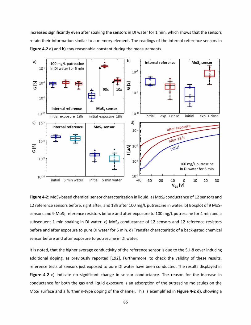
85
increased significantly even after soaking the sensors in DI water for 1 min, which shows that the sensors
retain their information similar to a memory element. The readings of the internal reference sensors in
Figure 4-2 a) and b) stay reasonable constant during the measurements.
Figure 4-2: MoS2-based chemical sensor characterization in liquid. a) MoS2 conductance of 12 sensors and
12 reference sensors before, right after, and 18h after 100 mg/L putrescine in water. b) Boxplot of 9 MoS2
sensors and 9 MoS2 reference resistors before and after exposure to 100 mg/L putrescine for 4 min and a
subsequent 1 min soaking in DI water. c) MoS2 conductance of 12 sensors and 12 reference resistors
before and after exposure to pure DI water for 5 min. d) Transfer characteristic of a back-gated chemical
sensor before and after exposure to putrescine in DI water.
It is noted, that the higher average conductivity of the reference sensor is due to the SU-8 cover inducing
additional doping, as previously reported [192]. Furthermore, to check the validity of these results,
reference tests of sensors just exposed to pure DI water have been conducted. The results displayed in
Figure 4-2 c) indicate no significant change in sensor conductance. The reason for the increase in
conductance for both the gas and liquid exposure is an adsorption of the putrescine molecules on the
MoS2 surface and a further n-type doping of the channel. This is exemplified in Figure 4-2 d), showing a

86
transfer characteristic of an un-passivated transistor before and after exposure to 100 mg/L of putrescine
in DI-water. The threshold voltage of this device shifts negatively, which indicates strong n-type doping.
This is also consistent with earlier findings of carbon nanotube-based sensors that are commonly p-type
doped and decreased in conductance with exposure to putrescine [188]. In principle, the semiconducting
nature of MoS2 also offers an easy way to increase the sensor’s sensitivity by biasing it in the subthreshold
regime [193], which is advantageous compared to other materials such graphene or carbon nanotubes
but has not been further explored in this work.
Secondly, the chemical sensor response to putrescine in air was characterized. For a standard experiment,
chemical sensors on a silicon substrate were first measured in their initial state. For the putrescine gas
exposure, the sensor chip was placed into a PTFE chamber with an approximate volume of 2 liters, as
depicted in Figure 4-3 a). 10 ppm of putrescine was flown in with nitrogen as carrier gas for 5 min,
generated by a FlexStream™ Base Module from KIN-TEK, see Figure 4-3 b). The putrescine dilution from
the FlexStream was generated by first heating up putrescine to 40°C in a glass tube, turning it into a liquid.
60 sccm of nitrogen were flown through the glass tube to pick up putrescine into the gas phase. This gas
stream was diluted with 976 sccm of nitrogen to dilute the putrescine concentration to 10 ppm. After
exposure, the chamber was purged with 2000 sccm of pure nitrogen for 5 min. The control samples were
left open in the ambient air for the same time. About 30 minutes passed between taking out the samples
from the gas chamber and characterizing them electrically. The gas exposures system is part of the
laboratory space of Prof. Timothy Swager in the Chemistry Department at MIT. The gas exposures were
done by of Vera Schroeder and Lennon Shaoxiong Luo, who were in his research group at the time.
Figure 4-3: Setup for putrescine gas exposure. a) FlexStream™ Base Module from KIN-TEK in a fume hood.
b) PTFE chamber for the gas exposure with a chip full of chemical sensors in it.

87
The electrical results of the sensors before and after gas exposure are presented in Figure 4-4. As shown
in Figure 4-4 a), the sensor conductance after exposure increased on average 65 times compared to their
initial value, which compares favorably to functionalized carbon nanotube sensors [188], however the
tested MoS2 devices were exposed for a longer time due to a larger chamber size and lack of in-situ
monitoring. Similar to the liquid exposure case, 18 hours after exposure the sensor’s channel conductance
was still 12 times larger than their starting value. This highlights that the sensors not just strongly react to
the putrescine gas but also retain that information for a period of hours. In an envisioned use case,
microsystems would measure their environment for minutes up to an hour, effectively turning the sensor
into a 1-bit memory for this time span. The internal reference sensors remained constant over all three
measurements. Again, to exclude other effects causing this conductance change, a second experiment
was conducted with simply exposing the chemical sensors to air for 20 min. The results, which are shown
in Figure 4-4 b), indicate no significant change in resistance for both the sensors and reference devices in
this case.
Figure 4-4: MoS2-based chemical sensor characterization in nitrogen. a) MoS2 conductance of 10 sensors
and 10 reference sensors before, right after, and 18h after putrescine gas exposure. b) MoS2 conductance
of 10 sensors and 10 reference resistors before and after 20 min air exposure.
4.2 Timer Building Block
A sense of time is essential for microsystems to properly interface with the real world. Time information
is valuable for example to know how long microsystems have been deployed in their environment.
Furthermore, it is helpful to log when sensing events have occurred or to control events that only happen

88
sporadically, such as collecting data every 5 minutes. The timers developed in this thesis are passive and
require no power supply. As a result, this allows the SynCells to keep track of time without being reliant
on light for energy harvesting for example. The timers consist of germanium (Ge) thin films that are used
to estimate the time microsystems will spend in water by leveraging a slow erosion process. The idea of
using chemical reactions to measure time has been proposed before, for example using lead chromate
[66], which records a lead ion concentration in water over time by changes in color. Also, the erosion of
metals has been proposed for transient electronics that disintegrate over time [194]. However, this
process seems not to have been used to make electrically readable, passive timers yet. The timers use a
layer of germanium (Ge) contacted by two gold (Au) pads to estimate the time spent in water. Germanium
oxidizes in the presence of dissolved oxygen [195] or small amounts of hydrogen peroxide [196]. The
formed germanium oxide readily dissolves in water [195, 196]. This oxidation and subsequent etching
process thin down the Ge film over time and manifests in an increasing resistance over time. After timer
deployment and retrieval, the film resistance is an analog electric representation of how much time the
sensor has been dispersed in an aqueous solution.
Two kinds of Ge timer designs have been explored, as shown in Figure 4-5. A first tested iteration consists
of two 100 nm thick gold pads and a gap of 2 µm that contact a 6 µm wide and 7 µm long germanium
channel from the bottom. For this experiment, three different germanium thickness were used: 50, 100,
and 150 nm. For the second iteration of germanium timers, a 6x8 µm2 Ge film with a thickness of 80 nm
was contacted with 100 nm gold pads from the top. All timers were built on a SU-8/Si substrate and took
about two days to fabricate in the cleanroom. The fabrication yield of functional timers for several batches
was close to 100 %.
Figure 4-5: Cross-sections of germanium timer designs with gold contacts. a) First design: bottom-
contacted Ge film. b) Second design: top-contacted Ge film.
To better understand the germanium erosion process, the bottom-contacted timers were put in 60°C
warm DI water for 3 times 5 min. One identical timer was scanned by AFM initially and after every water
bath. The results of this time series are presented in Figure 4-6 a) as 3D renderings. The specific timer
consists of an overlapping film of 50 nm and 100 nm thick germanium film so that the erosion of all three
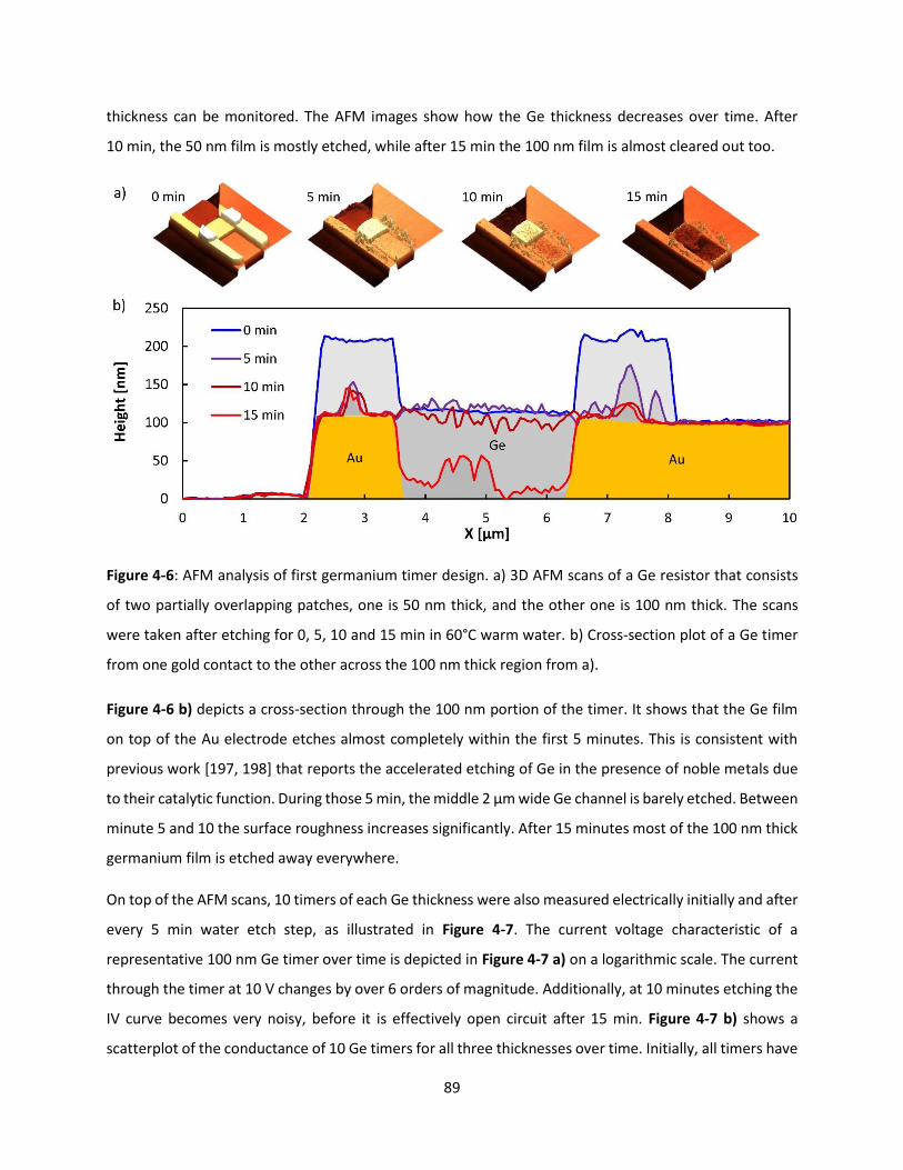
89
thickness can be monitored. The AFM images show how the Ge thickness decreases over time. After
10 min, the 50 nm film is mostly etched, while after 15 min the 100 nm film is almost cleared out too.
Figure 4-6: AFM analysis of first germanium timer design. a) 3D AFM scans of a Ge resistor that consists
of two partially overlapping patches, one is 50 nm thick, and the other one is 100 nm thick. The scans
were taken after etching for 0, 5, 10 and 15 min in 60°C warm water. b) Cross-section plot of a Ge timer
from one gold contact to the other across the 100 nm thick region from a).
Figure 4-6 b) depicts a cross-section through the 100 nm portion of the timer. It shows that the Ge film
on top of the Au electrode etches almost completely within the first 5 minutes. This is consistent with
previous work [197, 198] that reports the accelerated etching of Ge in the presence of noble metals due
to their catalytic function. During those 5 min, the middle 2 µm wide Ge channel is barely etched. Between
minute 5 and 10 the surface roughness increases significantly. After 15 minutes most of the 100 nm thick
germanium film is etched away everywhere.
On top of the AFM scans, 10 timers of each Ge thickness were also measured electrically initially and after
every 5 min water etch step, as illustrated in Figure 4-7. The current voltage characteristic of a
representative 100 nm Ge timer over time is depicted in Figure 4-7 a) on a logarithmic scale. The current
through the timer at 10 V changes by over 6 orders of magnitude. Additionally, at 10 minutes etching the
IV curve becomes very noisy, before it is effectively open circuit after 15 min. Figure 4-7 b) shows a
scatterplot of the conductance of 10 Ge timers for all three thicknesses over time. Initially, all timers have
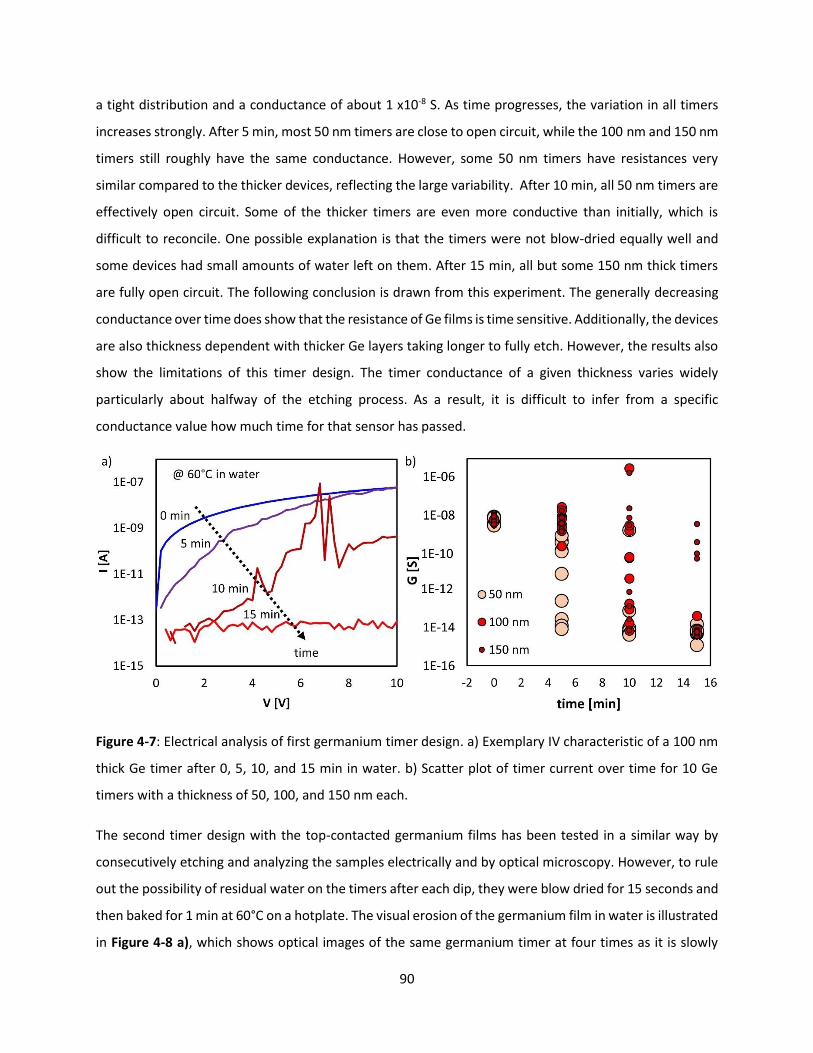
90
a tight distribution and a conductance of about 1 x10⁻⁸ S. As time progresses, the variation in all timers
increases strongly. After 5 min, most 50 nm timers are close to open circuit, while the 100 nm and 150 nm
timers still roughly have the same conductance. However, some 50 nm timers have resistances very
similar compared to the thicker devices, reflecting the large variability. After 10 min, all 50 nm timers are
effectively open circuit. Some of the thicker timers are even more conductive than initially, which is
difficult to reconcile. One possible explanation is that the timers were not blow-dried equally well and
some devices had small amounts of water left on them. After 15 min, all but some 150 nm thick timers
are fully open circuit. The following conclusion is drawn from this experiment. The generally decreasing
conductance over time does show that the resistance of Ge films is time sensitive. Additionally, the devices
are also thickness dependent with thicker Ge layers taking longer to fully etch. However, the results also
show the limitations of this timer design. The timer conductance of a given thickness varies widely
particularly about halfway of the etching process. As a result, it is difficult to infer from a specific
conductance value how much time for that sensor has passed.
Figure 4-7: Electrical analysis of first germanium timer design. a) Exemplary IV characteristic of a 100 nm
thick Ge timer after 0, 5, 10, and 15 min in water. b) Scatter plot of timer current over time for 10 Ge
timers with a thickness of 50, 100, and 150 nm each.
The second timer design with the top-contacted germanium films has been tested in a similar way by
consecutively etching and analyzing the samples electrically and by optical microscopy. However, to rule
out the possibility of residual water on the timers after each dip, they were blow dried for 15 seconds and
then baked for 1 min at 60°C on a hotplate. The visual erosion of the germanium film in water is illustrated
in Figure 4-8 a), which shows optical images of the same germanium timer at four times as it is slowly

91
eroding in DI water. The water bath was kept again at 60°C to accelerate the etching. The germanium very
close to the gold pads is already gone after 4 min but the middle remains. After about 16 minutes the
entire thin film has been etched. This is consistent with previous work [197, 198] that reports the
accelerated etching of Ge in the presence of noble metals due to their catalytic function, as also seen in
the first timer design.
Figure 4-8: Analysis of second germanium timer design. a) Optical micrographs of an 80 nm thick Ge timer
after 0, 4, 8, and 16 minutes of etching in 60°C warm DI water. b) Evolution of the conductance of 15 Ge
timers in 20°C DI water. The time constant from initial state to open circuit is approximately 15 minutes.
c) Exemplary IV characteristic of an 80 nm thick Ge timer after 0, 1, 2, 3, and 4 min in water. The
conductance decreases over time. d) Timer conductance evolution of 20 timers over time in 60°C DI water.
Figure 4-8 b) shows the typical electrical behavior of one of those Ge thin films over time. The timer
current through the devices decreases by over five orders of magnitude from 58 nA to 0.3 pA in the span
of 4 minutes. This confirms the findings from the optical images that the Ge thin film at the gold contacts
is already completely etched at that time. Compared to the bottom contacted timer design, the IV curves

92
have notably less noise, which hints that this design yields less variable electrical results. Furthermore,
Figure 4-8 d) plots the conductance of 20 Ge thin films etching in 60°C warm DI water over time. Similar
to Figure 4-8 c), it can be seen that the timer conductance exponentially drops over time and is effectively
open circuit after 4 min. Additionally, the box plot shows that the conductance distribution widens after
etching in water for 1-2 min and then narrows again towards the end. Compared to first timer design, the
distribution is significantly less wide, now allowing a coarse assignment of etch time given a specific
conductance value. The time span of how long it takes the timer to reach open circuit is also a function of
water temperature with lower temperature resulting in a slowed etching process. This connection is
illustrated in Figure 4-8 b), which plots the resistance of 15 Ge timers over time while being etched in 20°C
warm water. The same updated test procedure as for the other top-contacted timers with a 1 minute long
bakes at 60°C has been used. The time scale that it takes the timers to reach an open circuit has expanded
from 4 min for 60°C warm water to 15 min for 20°C warm water. Given that the exact time scale depends
on germanium thickness and water temperature, a large range of time constants can be implemented.
Additionally, the time constant can likely be further enhanced by covering the timers with a layer of SU-8
from the top and only allowing the etching to occur from the sides.
4.3 Computation Building Blocks
Computation is at the core of any electronic microsystem. It processes input signals, such as from sensors,
stores relevant information and generates output signals in response. To better understand the size and
power limitations, this section first reviews the state-of-the-art of computational hardware and provides
relevant examples of computing chips for microscale electronics systems. Afterwards, two approaches on
how to bring computational abilities onto the SynCell platform are discussed in Sections 4.3.1 and 4.3.2.
Computation nowadays is done overwhelmingly in integrated circuits based on digital processing,
although analog computing is growing thanks to the need for ultra-low power, low-latency signal
processing and machine learning. Silicon is the main material for integrated circuits and had a market
volume of 360 billion US dollar in 2017 [199]. It is the cheapest, most reliable, and smallest option to build
integrated circuits. Transistors form the basis of any integrated circuit. They can be used to implement
various functions like information storage or digital logic functions and are the foundation of modern
processors from microcontrollers to desktop CPUs.
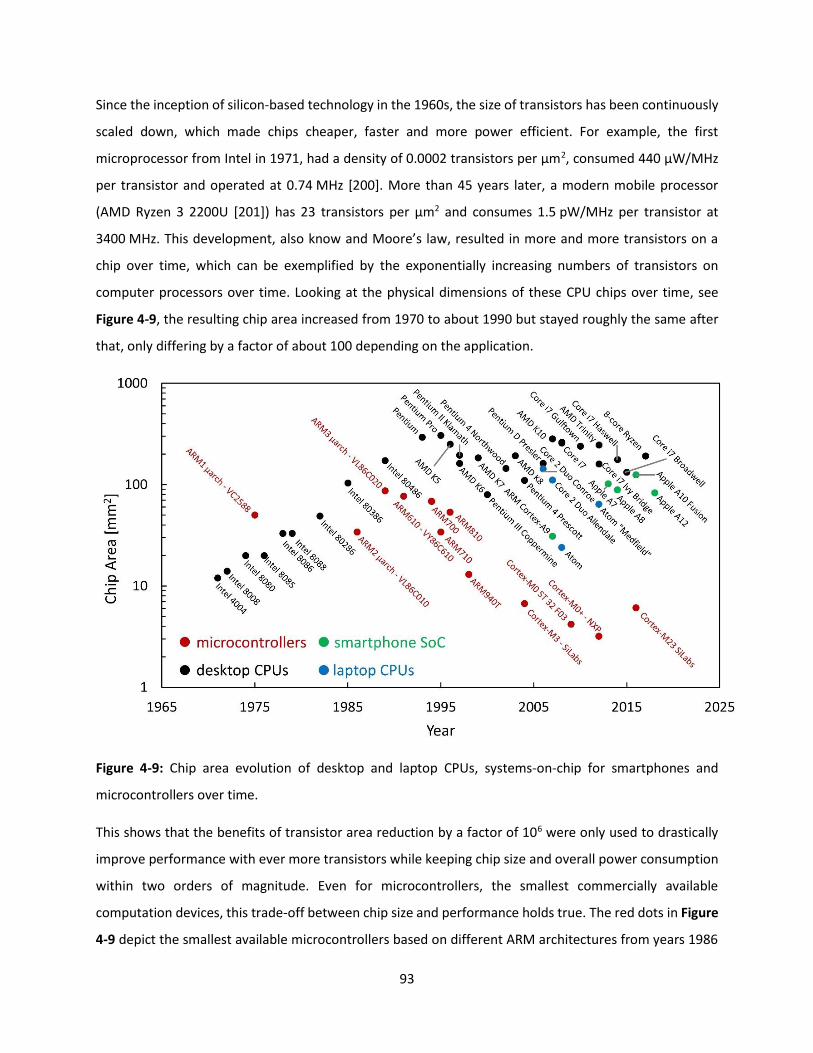
93
Since the inception of silicon-based technology in the 1960s, the size of transistors has been continuously
scaled down, which made chips cheaper, faster and more power efficient. For example, the first
microprocessor from Intel in 1971, had a density of 0.0002 transistors per µm2, consumed 440 µW/MHz
per transistor and operated at 0.74 MHz [200]. More than 45 years later, a modern mobile processor
(AMD Ryzen 3 2200U [201]) has 23 transistors per µm2 and consumes 1.5 pW/MHz per transistor at
3400 MHz. This development, also know and Moore’s law, resulted in more and more transistors on a
chip over time, which can be exemplified by the exponentially increasing numbers of transistors on
computer processors over time. Looking at the physical dimensions of these CPU chips over time, see
Figure 4-9, the resulting chip area increased from 1970 to about 1990 but stayed roughly the same after
that, only differing by a factor of about 100 depending on the application.
Figure 4-9: Chip area evolution of desktop and laptop CPUs, systems-on-chip for smartphones and
microcontrollers over time.
This shows that the benefits of transistor area reduction by a factor of 106 were only used to drastically
improve performance with ever more transistors while keeping chip size and overall power consumption
within two orders of magnitude. Even for microcontrollers, the smallest commercially available
computation devices, this trade-off between chip size and performance holds true. The red dots in Figure
4-9 depict the smallest available microcontrollers based on different ARM architectures from years 1986

94
to 2016. While the area of these chips decreased by a factor of approximately 10 times over the past 40
years, the transistor scaling (3 µm down to 90 nm) results in an area scaling benefit of over 103, which
shows that microcontrollers have used most of the scaling benefits to increase performance. In
conclusion, while advanced CMOS technology is capable of building microsystems smaller than 100 µm in
size containing even complex electronics, no such devices are commercially available.
For research purposes, however, several microsystems approaching a length scale of 100 µm have been
demonstrated using silicon chips for computation with several examples summarized in Table 4-1. They
target biomedical applications [6, 9, 11, 202], environmental sensing [11, 62] and object verification [12,
203] and vary largely in power consumption, complexity and size. The lowest-power chip was
demonstrated by Funke et. al., composed of a simple state machine with two sensor inputs and two
outputs, consuming as low as 0.4 nW at 20 Hz [62]. A microsystem with one of the most complex
computational capabilities is a precise temperature sensor node developed by Wu and colleges, which
has a custom Cortex-M0+ microprocessor integrated and has an average power consumption of 13 nW
[11]. The smallest microsystem (57x250 µm2) with a CMOS chip for computation was designed by Lee and
co-workers for neural recording. It measures voltages down to tens of microvolts and encodes them
digitally to drive an LED [8].
Year Dimensions [µm] Node Complexity Avg. Power Application
2004 400 x 400 x 60 180 nm medium 1.5 µW RFID [12]
2013 250 x 500 x ? 65 nm medium 10.5 µW Neural sensor [6]
2016 200 x 100 x 10 180 nm low 0.4 nW Chemical sensing [62]
2017 200 x 200 x 100 65 nm medium 63 nW Bio sensor [9]
2018 200 x 200 x 100 130 nm medium 27 µW Neural stimulation [202]
2018 360 x 400 x 280 55 nm high 16 nW Temp. sensor [11]
2018 57 x 250 x 330 180 nm medium 1 µW Neural sensor [8]
Table 4-1: Microsystems with silicon chips for computation.
In the remainder of this section, two approaches to equip SynCells with computational abilities are
presented. MoS2 transistors are discussed as one option, that can be easily integrated onto SynCells to
build basic circuits, as later shown in Section 5.3. Secondly, to enable more complex computation, the
design and simulation of a 50x50 µm2 CMOS chip based on a 65 nm technology node is presented.
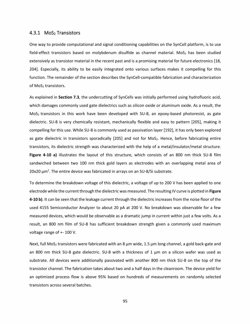
95
4.3.1 MoS2 Transistors
One way to provide computational and signal conditioning capabilities on the SynCell platform, is to use
field-effect transistors based on molybdenum disulfide as channel material. MoS2 has been studied
extensively as transistor material in the recent past and is a promising material for future electronics [18,
204]. Especially, its ability to be easily integrated onto various surfaces makes it compelling for this
function. The remainder of the section describes the SynCell-compatible fabrication and characterization
of MoS2 transistors.
As explained in Section 7.3, the undercutting of SynCells was initially performed using hydrofluoric acid,
which damages commonly used gate dielectrics such as silicon oxide or aluminum oxide. As a result, the
MoS2 transistors in this work have been developed with SU-8, an epoxy-based photoresist, as gate
dielectric. SU-8 is very chemically resistant, mechanically flexible and easy to pattern [205], making it
compelling for this use. While SU-8 is commonly used as passivation layer [192], it has only been explored
as gate dielectric in transistors sporadically [205] and not for MoS2. Hence, before fabricating entire
transistors, its dielectric strength was characterized with the help of a metal/insulator/metal structure.
Figure 4-10 a) illustrates the layout of this structure, which consists of an 800 nm thick SU-8 film
sandwiched between two 100 nm thick gold layers as electrodes with an overlapping metal area of
20x20 µm2. The entire device was fabricated in arrays on an SU-8/Si substrate.
To determine the breakdown voltage of this dielectric, a voltage of up to 200 V has been applied to one
electrode while the current through the dielectric was measured. The resulting IV curve is plotted in Figure
4-10 b). It can be seen that the leakage current through the dielectric increases from the noise floor of the
used 4155 Semiconductor Analyzer to about 20 pA at 200 V. No breakdown was observable for a few
measured devices, which would be observable as a dramatic jump in current within just a few volts. As a
result, an 800 nm film of SU-8 has sufficient breakdown strength given a commonly used maximum
voltage range of +- 100 V.
Next, full MoS2 transistors were fabricated with an 8 µm wide, 1.5 µm long channel, a gold back-gate and
an 800 nm thick SU-8 gate dielectric. SU-8 with a thickness of 1 µm on a silicon wafer was used as
substrate. All devices were additionally passivated with another 800 nm thick SU-8 on the top of the
transistor channel. The fabrication takes about two and a half days in the cleanroom. The device yield for
an optimized process flow is above 95% based on hundreds of measurements on randomly selected
transistors across several batches.
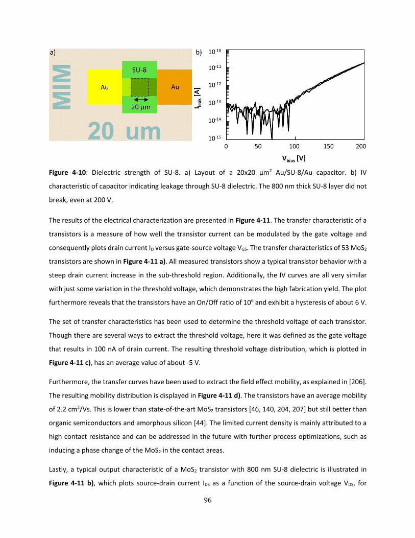
96
Figure 4-10: Dielectric strength of SU-8. a) Layout of a 20x20 µm2 Au/SU-8/Au capacitor. b) IV
characteristic of capacitor indicating leakage through SU-8 dielectric. The 800 nm thick SU-8 layer did not
break, even at 200 V.
The results of the electrical characterization are presented in Figure 4-11. The transfer characteristic of a
transistors is a measure of how well the transistor current can be modulated by the gate voltage and
consequently plots drain current ID versus gate-source voltage VGS. The transfer characteristics of 53 MoS2
transistors are shown in Figure 4-11 a). All measured transistors show a typical transistor behavior with a
steep drain current increase in the sub-threshold region. Additionally, the IV curves are all very similar
with just some variation in the threshold voltage, which demonstrates the high fabrication yield. The plot
furthermore reveals that the transistors have an On/Off ratio of 106 and exhibit a hysteresis of about 6 V.
The set of transfer characteristics has been used to determine the threshold voltage of each transistor.
Though there are several ways to extract the threshold voltage, here it was defined as the gate voltage
that results in 100 nA of drain current. The resulting threshold voltage distribution, which is plotted in
Figure 4-11 c), has an average value of about -5 V.
Furthermore, the transfer curves have been used to extract the field effect mobility, as explained in [206].
The resulting mobility distribution is displayed in Figure 4-11 d). The transistors have an average mobility
of 2.2 cm2/Vs. This is lower than state-of-the-art MoS2 transistors [46, 140, 204, 207] but still better than
organic semiconductors and amorphous silicon [44]. The limited current density is mainly attributed to a
high contact resistance and can be addressed in the future with further process optimizations, such as
inducing a phase change of the MoS2 in the contact areas.
Lastly, a typical output characteristic of a MoS2 transistor with 800 nm SU-8 dielectric is illustrated in
Figure 4-11 b), which plots source-drain current IDS as a function of the source-drain voltage VDS, for
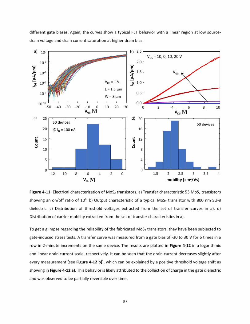
97
different gate biases. Again, the curves show a typical FET behavior with a linear region at low source-
drain voltage and drain current saturation at higher drain bias.
Figure 4-11: Electrical characterization of MoS2 transistors. a) Transfer characteristic 53 MoS2 transistors
showing an on/off ratio of 106. b) Output characteristic of a typical MoS2 transistor with 800 nm SU-8
dielectric. c) Distribution of threshold voltages extracted from the set of transfer curves in a). d)
Distribution of carrier mobility extracted from the set of transfer characteristics in a).
To get a glimpse regarding the reliability of the fabricated MoS2 transistors, they have been subjected to
gate-induced stress tests. A transfer curve was measured from a gate bias of -30 to 30 V for 6 times in a
row in 2-minute increments on the same device. The results are plotted in Figure 4-12 in a logarithmic
and linear drain current scale, respectively. It can be seen that the drain current decreases slightly after
every measurement (see Figure 4-12 b)), which can be explained by a positive threshold voltage shift as
showing in Figure 4-12 a). This behavior is likely attributed to the collection of charge in the gate dielectric
and was observed to be partially reversible over time.
98
Figure 4-12: Gate-induced stress measurement with transfer characteristics of a device under test in a)
logarithmic and b) linear scale. The threshold voltage shifts positively under stress.
4.3.2 CMOS Silicon Chip
The first approach to enable computation as a building block for SynCells was to explore the use of
molybdenum disulfide for FET transistors. Such devices have the prospect to yield flexible, transparent,
and potentially foldable logic circuitry. Currently, however, this technology is still in its infancy and
significant progress in many areas from material synthesis, to integration and circuit design will be
necessary to bring it to maturity, which will likely take a long period of time. In the short term, the best
solution to obtain advanced computational circuitry in the smallest possible volume is to use silicon CMOS
technology. As discussed in the introduction of Section 4.3, state-of-the-art CMOS transistors have
dimension on the order of 10 nm and consume about a 1 pW/MHz. While this latest technology node is
in production for the most recent chips in smartphones and laptops, the technology nodes available to
university research are a few generations behind. In the case of this thesis, a 65 nm CMOS technology
from TSMC was chosen because it represents the best tradeoff between cost, availability, and ease of
design.
In this section, the design of a CMOS chip for an electronic microsystem will be discussed. The goal of the
chip is to be the brains of a useful microsystem, that is as small as technically possible. A useful
microsystem is defined as being able to provide information from a sensory signal such as temperature or
chemical concentration, while also being completely independent, untethered, and hence able to operate
autonomously. As will be presented in Section 4.4, the most promising direction to power and

99
communicate with a sub-100 µm small microsystem, is to use light absorbed by solar cells to supply energy
and to use light emitted by LEDs to communicate information. Hence, the silicon chip discussed in this
section will be powered by a solar cell and the information of the sensor will be communicated by light
through an LED. In general, the smallest possible chip design will be one that has few components and a
simple principle of operation. To that end, the simplest approach to communicate a resistive sensor value
is to use a series connection of a solar cell, a resistive sensor, as discussed in Section 4.1, and an LED, see
Figure 4-13. As soon as the resistance of the sensor changes, for example due to an exposure with the
target analyte, the light intensity would change.
Figure 4-13: Simplest possible circuit to communicate a resistive sensor value with an LED.
Such a solution can be achieved even without a CMOS chip but is highly impractical. Besides being
dependent on the concentration of the chemical exposure, the LED brightness will also depend on the
exact distance to the detector because the light density decreases with the distance from the light source.
Additionally, the LED brightness will change with the exact solar cell illumination because this parameter
affects the voltage generated by the photovoltaic device.
A better, yet simple solution is to create a CMOS chip that can transform an analog input voltage into a
series of continuous pulses, the period of which is proportional to the input signal. These pulses are then
used to turn on and off an LED. Having such a computational ability can be considered a basic information
encoding scheme, where the sensor value is encoded in the pulse frequency. This approach does not
suffer from any of the draw backs of the brightness modulation scheme because the information is
encoded in the difference between On and Off brightness of the LED rather than the specific brightness
level itself.
In conclusion, the goal is to design a CMOS chip in 65 nm technology that is as small as possible and
requires the least amount of energy possible. The design of this CMOS chip was done in collaboration with
Prof. Marisa López-Vallejo running the Integrated Systems Laboratory at the Polytechnical University of
Madrid and her PhD student Javier De Mena, who was in charge of the chip design, layout and simulation
using the circuit design software Cadence.
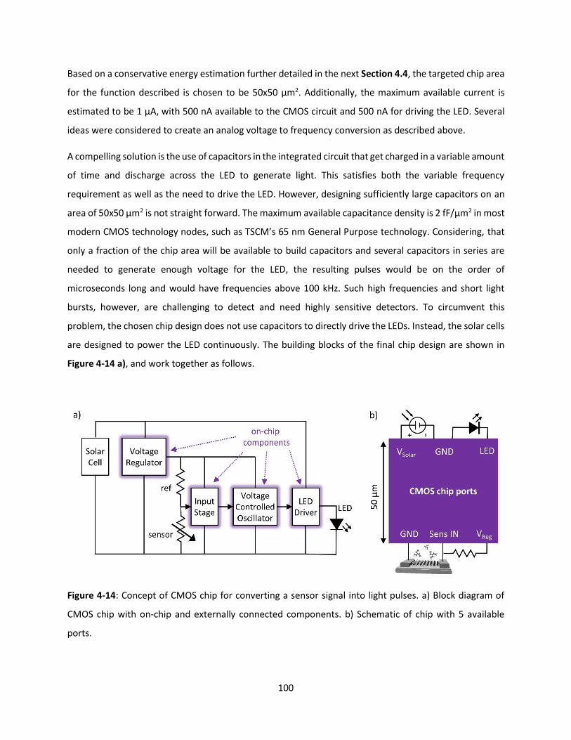
100
Based on a conservative energy estimation further detailed in the next Section 4.4, the targeted chip area
for the function described is chosen to be 50x50 µm2. Additionally, the maximum available current is
estimated to be 1 µA, with 500 nA available to the CMOS circuit and 500 nA for driving the LED. Several
ideas were considered to create an analog voltage to frequency conversion as described above.
A compelling solution is the use of capacitors in the integrated circuit that get charged in a variable amount
of time and discharge across the LED to generate light. This satisfies both the variable frequency
requirement as well as the need to drive the LED. However, designing sufficiently large capacitors on an
area of 50x50 µm2 is not straight forward. The maximum available capacitance density is 2 fF/µm2 in most
modern CMOS technology nodes, such as TSCM’s 65 nm General Purpose technology. Considering, that
only a fraction of the chip area will be available to build capacitors and several capacitors in series are
needed to generate enough voltage for the LED, the resulting pulses would be on the order of
microseconds long and would have frequencies above 100 kHz. Such high frequencies and short light
bursts, however, are challenging to detect and need highly sensitive detectors. To circumvent this
problem, the chosen chip design does not use capacitors to directly drive the LEDs. Instead, the solar cells
are designed to power the LED continuously. The building blocks of the final chip design are shown in
Figure 4-14 a), and work together as follows.
Figure 4-14: Concept of CMOS chip for converting a sensor signal into light pulses. a) Block diagram of
CMOS chip with on-chip and externally connected components. b) Schematic of chip with 5 available
ports.

101
The entire CMOS chip as well as the LED are powered by a solar cell, which is about 40x40 µm2 and will be
placed on top of the CMOS chip during the assembly. The solar cell is based on a III-V heterostructure and
provides between 1.5 – 2.5 V, which is further discussed in Section 4.4 below. Since, the regular CMOS
transistors can only handle up to 1.2 V in the given technology, a voltage regulator lowers this voltage to
1.1 V for the rest of the circuit. The analog input voltage is generated by a simple voltage divider of a
reference sensor and a chemiresistor, similar to the one discussed in Section 4.1. Both elements together
are designed to be smaller than 15x8 µm2 and are also be integrated on the silicon chip. The voltage
divider produces an analog voltage that depends on the chemical concentration of the target analyte and
consumes about 1-10 nA based on previous experiments.
The signal is fed into an input stage with a very high input resistance above 1 GΩ so that no current is
drawn. The buffered input signal then goes into the main building block of the CMOS chip, a voltage-
controlled oscillator (VCO). As the name suggests, this sub-circuit generates a pulse train with varying
frequency depending on the input voltage. The VCO output signal is connected to an LED driver, which is
essentially a transistor that can switch the LED on and off. It is also used to limit the current of the LED to
about 500 nA. The LED driver uses the full voltage provided by the solar cell to control the LED because
more voltage is needed to drive it. The ports of the circuit and the external circuit elements (solar cell,
LED, sensor, reference sensor) are illustrated in Figure 4-14 b).
The results of the circuit design and simulation are shown in Figure 4-15. A delay circuit, which is the main
part of the voltage-controlled oscillator, is shown in Figure 4-15 a) and is based on a slow thyristor-based
oscillator presented by Funke et. al. [62]. The VCO consists of three of these delay circuits connected in a
circle forming a ring oscillator. This ring oscillator produces a pulse train with a frequency of 280 Hz – 450
Hz depending on its input voltage, as plotted in Figure 4-15 b). Such a low frequency is very advantageous
because it allows to use long integration times on the order of milliseconds for the photodetector. Since
the photodetector signal is a function of the overall light collected, i.e. the product of light intensity and
integration time, this frequency range should enable the detection of weak light signals from the
microsystem.
Lastly, Figure 4-15 c) illustrates a simulated LED driver signal before and after an input signal change over
time. The simulated circuit consumes less than 400 nA for all building blocks and fits into an area of roughly
30x50 µm2, which meets all design goals. As remaining steps, the chip design must be verified, taped-out
and produced by TSMC before the integration of all components can be tested.
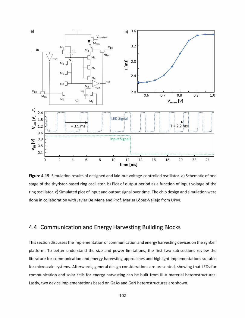
102
Figure 4-15: Simulation results of designed and laid-out voltage-controlled oscillator. a) Schematic of one
stage of the thyristor-based ring oscillator. b) Plot of output period as a function of input voltage of the
ring oscillator. c) Simulated plot of input and output signal over time. The chip design and simulation were
done in collaboration with Javier De Mena and Prof. Marisa López-Vallejo from UPM.
4.4 Communication and Energy Harvesting Building Blocks
This section discusses the implementation of communication and energy harvesting devices on the SynCell
platform. To better understand the size and power limitations, the first two sub-sections review the
literature for communication and energy harvesting approaches and highlight implementations suitable
for microscale systems. Afterwards, general design considerations are presented, showing that LEDs for
communication and solar cells for energy harvesting can be built from III-V material heterostructures.
Lastly, two device implementations based on GaAs and GaN heterostructures are shown.
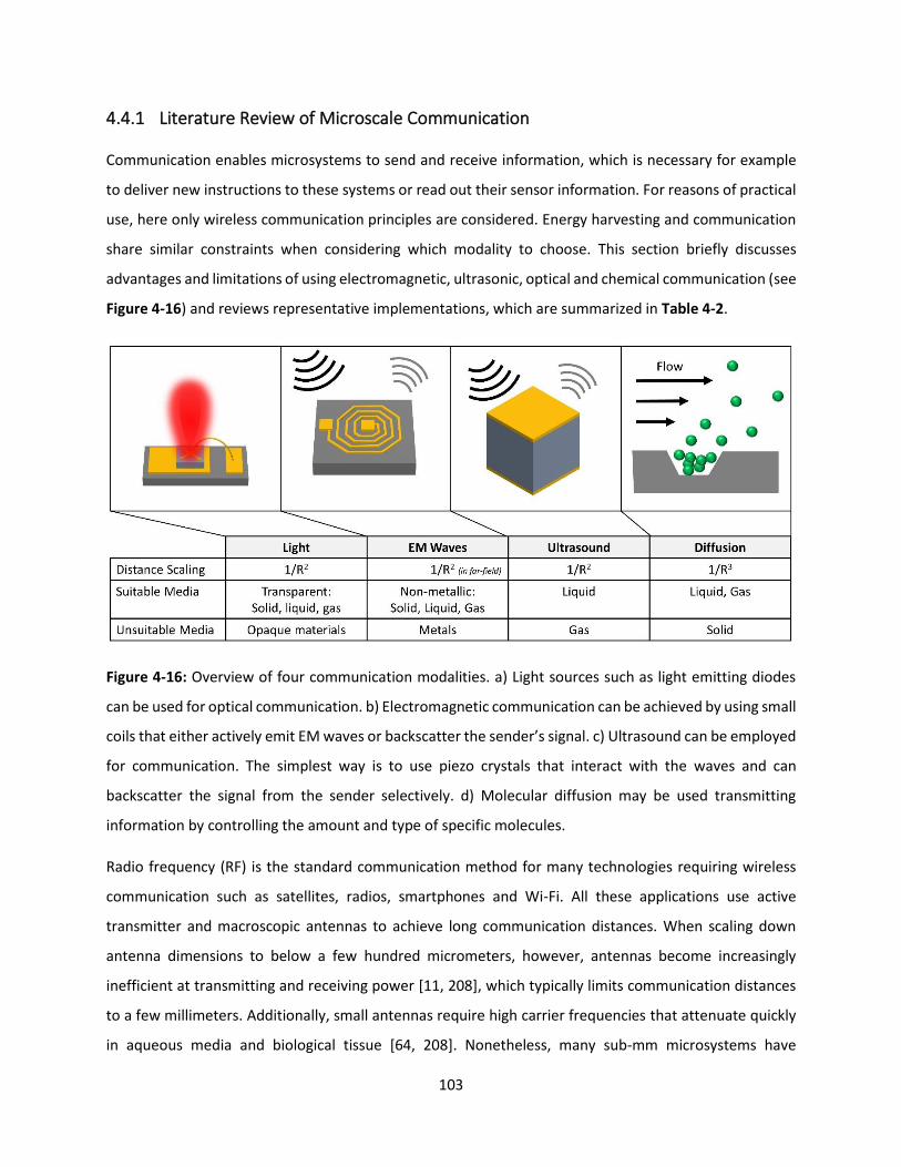
103
4.4.1 Literature Review of Microscale Communication
Communication enables microsystems to send and receive information, which is necessary for example
to deliver new instructions to these systems or read out their sensor information. For reasons of practical
use, here only wireless communication principles are considered. Energy harvesting and communication
share similar constraints when considering which modality to choose. This section briefly discusses
advantages and limitations of using electromagnetic, ultrasonic, optical and chemical communication (see
Figure 4-16) and reviews representative implementations, which are summarized in Table 4-2.
Figure 4-16: Overview of four communication modalities. a) Light sources such as light emitting diodes
can be used for optical communication. b) Electromagnetic communication can be achieved by using small
coils that either actively emit EM waves or backscatter the sender’s signal. c) Ultrasound can be employed
for communication. The simplest way is to use piezo crystals that interact with the waves and can
backscatter the signal from the sender selectively. d) Molecular diffusion may be used transmitting
information by controlling the amount and type of specific molecules.
Radio frequency (RF) is the standard communication method for many technologies requiring wireless
communication such as satellites, radios, smartphones and Wi-Fi. All these applications use active
transmitter and macroscopic antennas to achieve long communication distances. When scaling down
antenna dimensions to below a few hundred micrometers, however, antennas become increasingly
inefficient at transmitting and receiving power [11, 208], which typically limits communication distances
to a few millimeters. Additionally, small antennas require high carrier frequencies that attenuate quickly
in aqueous media and biological tissue [64, 208]. Nonetheless, many sub-mm microsystems have
104
implemented RF communication [6, 9, 12, 64, 209], especially for medical applications. Most of these
systems communicate data passively by backscattering the incoming signal [210]. Hu and collaborators
developed the smallest RF communication system, which is an RFID tag with a size of only 25 µm for
biological cell monitoring [64]. The micro-RFID tag can be used to sense its environment by detecting
resonance shifts of its LC circuit. Due to the extremely small antenna size, the tags operate at 60 GHz and
have a maximum communication distance of about 25 µm. Discroll et. al., demonstrated a 200x200 µm2
implantable glucose sensor [9]. It has a multi-turn coil around its perimeter and can communicate up to
1.2 mm away through backscattering the transmitter signal.
Ultrasound (US) is another modality that can be used for communication. It is commonly found in medical
applications for imaging, or for localization and communication under water. Similar to electromagnetic
waves, ultrasound frequency depends on the size of the receiver to achieve a maximum efficiency [208].
Using US for communication is best suited for aqueous media such as water or biological tissue. The signal
attenuation and insertion losses in air are too large [211, 212]. Just like with RF signals, the lowest power
consumption is achieved when information is transmitted back passively by modulating the amount of
backscattering of the incoming signal. This approach has been used by Seo et. al. to build a neural
recording device [7], which is capable of recording neural activity and transmit this data to a receiver
9 mm away. Their probe used a 750 µm piezoelectric cube as energy harvester and transceiver. It had a
transistor attached to it in parallel that modulated the backscattering based on the nerve potential at the
transistor gate.
Light is a very promising way to communicate to tiny microsystems. This can be achieved either by active
light emission using solid-state devices [8, 11] or organic light emitting diodes (OLED), or through indirect
means such as modulating fluorescence [213] or reflection of light [214]. In contrast to RF, optical systems
scale down well to the 1 to 100 µm range, are much simpler and require very few components. However,
communication via light is only possible in transparent media such as water or air. There are some
examples of sub-mm microsystems that use optical communication [8, 11, 214]. Lee and collaborators
developed a neural sensor with a footprint of only 57x250 µm that is designed to communicate neural
activity through 3 mm of bone and tissue by sending short infrared light pulses. The feasibility of such
optical in-vivo communication has been demonstrated before and makes use of the relatively high
transparency of biological tissue to IR light [215]. For temperature measurements, Wu et. al.
demonstrated at 0.04 mm3 sensor node that can transmit its data to a base station up to 15.6 cm away
using an LED [11].
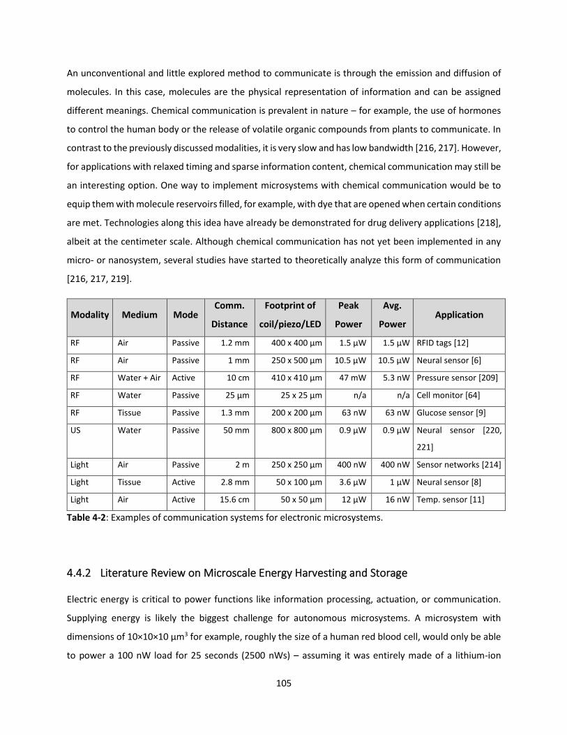
105
An unconventional and little explored method to communicate is through the emission and diffusion of
molecules. In this case, molecules are the physical representation of information and can be assigned
different meanings. Chemical communication is prevalent in nature – for example, the use of hormones
to control the human body or the release of volatile organic compounds from plants to communicate. In
contrast to the previously discussed modalities, it is very slow and has low bandwidth [216, 217]. However,
for applications with relaxed timing and sparse information content, chemical communication may still be
an interesting option. One way to implement microsystems with chemical communication would be to
equip them with molecule reservoirs filled, for example, with dye that are opened when certain conditions
are met. Technologies along this idea have already be demonstrated for drug delivery applications [218],
albeit at the centimeter scale. Although chemical communication has not yet been implemented in any
micro- or nanosystem, several studies have started to theoretically analyze this form of communication
[216, 217, 219].
Modality Medium Mode Comm.
Distance
Footprint of
coil/piezo/LED
Peak
Power
Avg.
Power Application
RF Air Passive 1.2 mm 400 x 400 µm 1.5 µW 1.5 µW RFID tags [12]
RF Air Passive 1 mm 250 x 500 µm 10.5 µW 10.5 µW Neural sensor [6]
RF Water + Air Active 10 cm 410 x 410 µm 47 mW 5.3 nW Pressure sensor [209]
RF Water Passive 25 µm 25 x 25 µm n/a n/a Cell monitor [64]
RF Tissue Passive 1.3 mm 200 x 200 µm 63 nW 63 nW Glucose sensor [9]
US Water Passive 50 mm 800 x 800 µm 0.9 µW 0.9 µW Neural sensor [220,
221]
Light Air Passive 2 m 250 x 250 µm 400 nW 400 nW Sensor networks [214]
Light Tissue Active 2.8 mm 50 x 100 µm 3.6 µW 1 µW Neural sensor [8]
Light Air Active 15.6 cm 50 x 50 µm 12 µW 16 nW Temp. sensor [11]
Table 4-2: Examples of communication systems for electronic microsystems.
4.4.2 Literature Review on Microscale Energy Harvesting and Storage
Electric energy is critical to power functions like information processing, actuation, or communication.
Supplying energy is likely the biggest challenge for autonomous microsystems. A microsystem with
dimensions of 10×10×10 µm3 for example, roughly the size of a human red blood cell, would only be able
to power a 100 nW load for 25 seconds (2500 nWs) – assuming it was entirely made of a lithium-ion
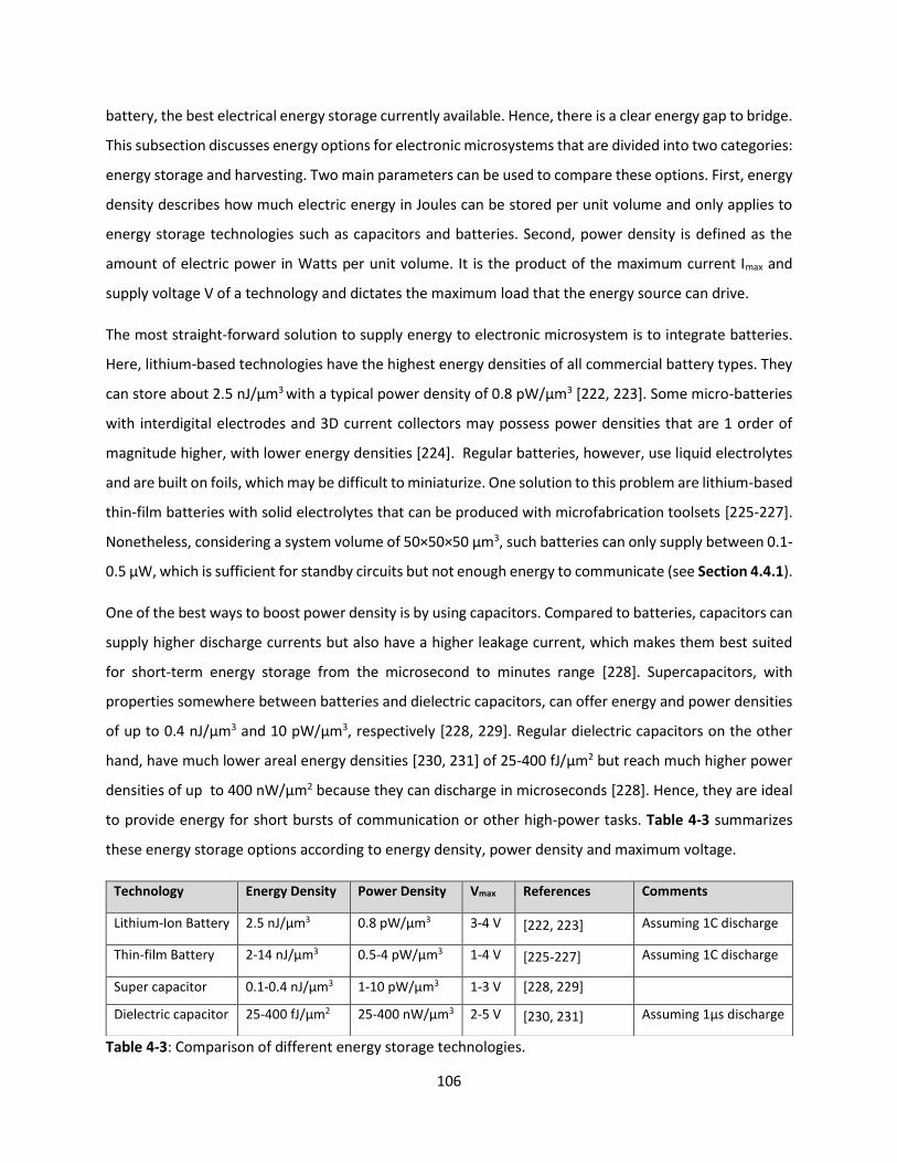
106
battery, the best electrical energy storage currently available. Hence, there is a clear energy gap to bridge.
This subsection discusses energy options for electronic microsystems that are divided into two categories:
energy storage and harvesting. Two main parameters can be used to compare these options. First, energy
density describes how much electric energy in Joules can be stored per unit volume and only applies to
energy storage technologies such as capacitors and batteries. Second, power density is defined as the
amount of electric power in Watts per unit volume. It is the product of the maximum current Imax and
supply voltage V of a technology and dictates the maximum load that the energy source can drive.
The most straight-forward solution to supply energy to electronic microsystem is to integrate batteries.
Here, lithium-based technologies have the highest energy densities of all commercial battery types. They
can store about 2.5 nJ/µm3 with a typical power density of 0.8 pW/µm3 [222, 223]. Some micro-batteries
with interdigital electrodes and 3D current collectors may possess power densities that are 1 order of
magnitude higher, with lower energy densities [224]. Regular batteries, however, use liquid electrolytes
and are built on foils, which may be difficult to miniaturize. One solution to this problem are lithium-based
thin-film batteries with solid electrolytes that can be produced with microfabrication toolsets [225-227].
Nonetheless, considering a system volume of 50×50×50 µm3, such batteries can only supply between 0.1-
0.5 µW, which is sufficient for standby circuits but not enough energy to communicate (see Section 4.4.1).
One of the best ways to boost power density is by using capacitors. Compared to batteries, capacitors can
supply higher discharge currents but also have a higher leakage current, which makes them best suited
for short-term energy storage from the microsecond to minutes range [228]. Supercapacitors, with
properties somewhere between batteries and dielectric capacitors, can offer energy and power densities
of up to 0.4 nJ/µm3 and 10 pW/µm3, respectively [228, 229]. Regular dielectric capacitors on the other
hand, have much lower areal energy densities [230, 231] of 25-400 fJ/µm2 but reach much higher power
densities of up to 400 nW/µm2 because they can discharge in microseconds [228]. Hence, they are ideal
to provide energy for short bursts of communication or other high-power tasks. Table 4-3 summarizes
these energy storage options according to energy density, power density and maximum voltage.
Table 4-3: Comparison of different energy storage technologies.
Technology Energy Density Power Density Vmax References Comments
Lithium-Ion Battery 2.5 nJ/μm3 0.8 pW/μm3 3-4 V [222, 223] Assuming 1C discharge
Thin-film Battery 2-14 nJ/μm3 0.5-4 pW/μm3 1-4 V [225-227] Assuming 1C discharge
Super capacitor 0.1-0.4 nJ/µm3 1-10 pW/µm3 1-3 V [228, 229]
Dielectric capacitor 25-400 fJ/µm2 25-400 nW/µm3 2-5 V [230, 231] Assuming 1µs discharge
107
Batteries and capacitors can only store a limited amount of energy. To extend the battery lifetime or make
microsystems energy independent, prior demonstrations of microsystems often rely on external energy
harvesting. Many phenomena can be exploited to generate energy including heat, chemical reactions,
vibrations, RF, and light. Besides the conversion efficiency, the power density of the energy harvester also
depends on transmit power, distance, and surrounding medium (see Section 4.4.1). Table 4-4 summarizes
a few microsystem implementations with RF, ultrasound, and photovoltaic energy harvesting in different
environments, while the following paragraphs briefly discuss the trade-off of several harvester options.
Bio-fuel cells are a potential energy harvesting solution for microsystems operating inside the human body
or other bio-fluidic environment. They use two enzymes as catalysts to oxidize glucose at the anode and
reduce oxygen to water at the cathode [232, 233]. Biofuel cells could provide a typical power density of
0.6 pW/µm3 and a supply voltage of 0.4 V [234]. The biggest challenges of enzymatic biofuel cell are the
stability of enzymes to environmental changes, and the compatibility with semiconductor fabrication
processes.
Another way to harvest energy in microscale electronic systems is by using RF coils to turn electromagnetic
waves into energy, as previously demonstrated [6, 12, 202]. As advantage, RF coils can be easily integrated
on top of silicon chips using the backend metallization layers. Furthermore, RF energy harvesters can
deliver a high power density of 10-400 pW/µm2 at a few millimeters distance and total transmit powers
in the range of 50-2000 mW. However, these numbers are only for rough guidance since they were
achieved with sub-mm scale coils. Smaller coils (< 100 µm) will require higher carrier frequencies and will
likely have lower power transfer efficiencies since coil size and frequency are linked [11, 208].
Ultrasound can be converted into electricity using piezoelectric crystals and can be used well for
applications in aqueous media. Such microsystems are commonly aimed towards medical applications
and can output about 0.3 pW/µm3 of power density [220, 221, 235]. This is significantly lower than RF and
solar energy harvesting but works at longer distances.
The photovoltaic effect is a long-distance alternative to electromagnetic wave harvesting and has been
used extensively in autonomous microsystems for ambient and in-vivo applications [8, 9, 11, 209, 215].
Given a 10x10x10 µm3 microsystem (600 µm2 surface area), about 60 nW of power could be generated,
assuming a 10% efficient solar cell and direct sun light (approx. 1 nW/µm2). For indoor applications, light
sources are about 200 times less [236] and would result in a usable power of 0.3 nW for the same device.
However, that power can be easily boosted using a scanning laser beam to achieve light intensities several
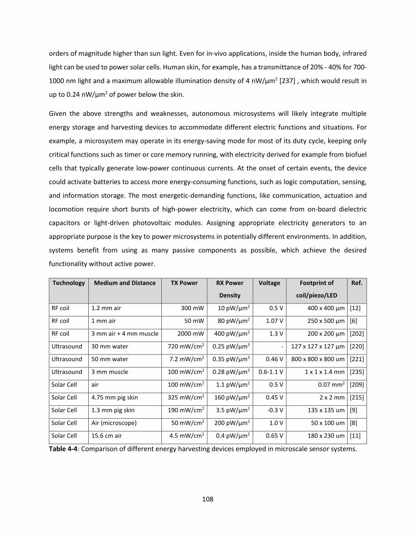
108
orders of magnitude higher than sun light. Even for in-vivo applications, inside the human body, infrared
light can be used to power solar cells. Human skin, for example, has a transmittance of 20% - 40% for 700-
1000 nm light and a maximum allowable illumination density of 4 nW/µm2 [237] , which would result in
up to 0.24 nW/µm2 of power below the skin.
Given the above strengths and weaknesses, autonomous microsystems will likely integrate multiple
energy storage and harvesting devices to accommodate different electric functions and situations. For
example, a microsystem may operate in its energy-saving mode for most of its duty cycle, keeping only
critical functions such as timer or core memory running, with electricity derived for example from biofuel
cells that typically generate low-power continuous currents. At the onset of certain events, the device
could activate batteries to access more energy-consuming functions, such as logic computation, sensing,
and information storage. The most energetic-demanding functions, like communication, actuation and
locomotion require short bursts of high-power electricity, which can come from on-board dielectric
capacitors or light-driven photovoltaic modules. Assigning appropriate electricity generators to an
appropriate purpose is the key to power microsystems in potentially different environments. In addition,
systems benefit from using as many passive components as possible, which achieve the desired
functionality without active power.
Technology Medium and Distance TX Power RX Power
Density
Voltage Footprint of
coil/piezo/LED
Ref.
RF coil 1.2 mm air 300 mW 10 pW/µm2 0.5 V 400 x 400 μm [12]
RF coil 1 mm air 50 mW 80 pW/µm2 1.07 V 250 x 500 μm [6]
RF coil 3 mm air + 4 mm muscle 2000 mW 400 pW/µm2 1.3 V 200 x 200 μm [202]
Ultrasound 30 mm water 720 mW/cm2 0.25 pW/µm3 - 127 x 127 x 127 μm [220]
Ultrasound 50 mm water 7.2 mW/cm2 0.35 pW/µm3 0.46 V 800 x 800 x 800 um [221]
Ultrasound 3 mm muscle 100 mW/cm2 0.28 pW/µm3 0.6-1.1 V 1 x 1 x 1.4 mm [235]
Solar Cell air 100 mW/cm2 1.1 pW/µm2 0.5 V 0.07 mm2 [209]
Solar Cell 4.75 mm pig skin 325 mW/cm2 160 pW/µm2 0.45 V 2 x 2 mm [215]
Solar Cell 1.3 mm pig skin 190 mW/cm2 3.5 pW/µm2 -0.3 V 135 x 135 um [9]
Solar Cell Air (microscope) 50 mW/cm2 200 pW/µm2 1.0 V 50 x 100 um [8]
Solar Cell 15.6 cm air 4.5 mW/cm2 0.4 pW/µm2 0.65 V 180 x 230 um [11]
Table 4-4: Comparison of different energy harvesting devices employed in microscale sensor systems.
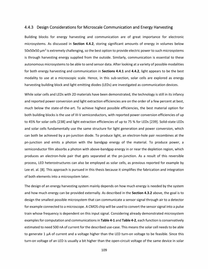
109
4.4.3 Design Considerations for Microscale Communication and Energy Harvesting
Building blocks for energy harvesting and communication are of great importance for electronic
microsystems. As discussed in Section 4.4.2, storing significant amounts of energy in volumes below
50x50x50 µm3 is extremely challenging, so the best option to provide electric power to such microsystems
is through harvesting energy supplied from the outside. Similarly, communication is essential to these
autonomous microsystems to be able to send sensor data. After looking at a variety of possible modalities
for both energy harvesting and communication in Sections 4.4.1 and 4.4.2, light appears to be the best
modality to use at a microscopic scale. Hence, in this sub-section, solar cells are explored as energy
harvesting building block and light emitting diodes (LEDs) are investigated as communication devices.
While solar cells and LEDs with 2D materials have been demonstrated, the technology is still in its infancy
and reported power conversion and light extraction efficiencies are on the order of a few percent at best,
much below the state-of-the-art. To achieve highest possible efficiencies, the best material option for
both building blocks is the use of III-V semiconductors, with reported power conversion efficiencies of up
to 45% for solar cells [238] and light extraction efficiencies of up to 75 % for LEDs [239]. Solid-state LEDs
and solar cells fundamentally use the same structure for light generation and power conversion, which
can both be achieved by a pn-junction diode. To produce light, an electron-hole pair recombines at the
pn-junction and emits a photon with the bandgap energy of the material. To produce power, a
semiconductor film absorbs a photon with above-bandgap energy in or near the depletion region, which
produces an electron-hole pair that gets separated at the pn-junction. As a result of this reversible
process, LED heterostructures can also be employed as solar cells, as previous reported for example by
Lee et. al. [8]. This approach is pursued in this thesis because it simplifies the fabrication and integration
of both elements into a microsystem later.
The design of an energy harvesting system mainly depends on how much energy is needed by the system
and how much energy can be provided externally. As described in the Section 4.3.2 above, the goal is to
design the smallest possible microsystem that can communicate a sensor signal through air to a detector
for example connected to a microscope. A CMOS chip will be used to convert the sensor signal into a pulse
train whose frequency is dependent on this input signal. Considering already demonstrated microsystem
examples for computation and communications in Table 4-1 and Table 4-2, each function is conservatively
estimated to need 500 nA of current for the described use-case. This means the solar cell needs to be able
to generate 1 µA of current and a voltage higher than the LED turn-on voltage to be feasible. Since this
turn-on voltage of an LED is usually a bit higher than the open-circuit voltage of the same device in solar

110
cell operation, two solar cell panels in series will be needed to drive the LED. The area of the solar cell can
now be derived knowing the conversion efficiency of a typical LED and the maximum illumination under
a microscope. Conservatively estimating, an LED structure should be able to achieve a power conversion
efficiency of 5% for above bandgap light illumination [8]. Similarly, using focused laser beams in a
microscope setup, light intensities of 7 µW/µm2 can be achieved [65]. Full sunlight in comparison has an
intensity of 1 nW/µm2, which is 7000 times weaker. As a result, the minimum necessary area to provide
1 µA of current using a red (650 nm) or blue (456 nm) LED with twice the open-circuit voltage is 10.8 µm2
and 15.5 µm2, respectively. To have extra margin, the solar cell area will be increased significantly to
40x40 µm2 = 1600 µm2. This extra area provides room to use less strong laser light or to compensate
fabrication-related deteriorations of the LED or solar cell efficiency. The following sections discuss the
fabrication of solar cells and LEDs based GaAs and GaN heterostructures.
4.4.4 GaAs-based LEDs and Solar Cells
As first material system, a red GaAs LED with a single quantum well was explored as LED and solar cell
structure. Using a red LED (605 nm) has several advantages. The bandgap required to produce red light,
results in an effectively usable open circuit voltage between 1-1.5 V depending on the illumination
brightness and exact device fabrication. This voltage range is ideal for directly powering CMOS chips with
advanced technology nodes (90-28 nm). Additionally, the range of red to infrared light is absorbed least
by human skin, which could be useful for the in-vivo applications of electronic microsystems. The specific
epi-structure for the GaAs LED was adopted from the work of Park et. al. on the print assembly of inorganic
LEDs [240]. As part of their developed process, they undercut and transferred their patterned LEDs onto
flexible substrates. A similar process will be required to assemble microsystems with LEDs and solar cells.
The adapted GaAs heterostructure is displayed in Figure 4-17 a), six 3” wafers of which were generously
provided by the Japanese LED manufacturer DOWA Electronics Materials Co., Ltd. through the help Kohei
Yoshizawa, an employee of the company and visiting scientist in the Palacios group at the time. The cross-
section image shows the typical layers of a single quantum well LED including n and p contact layers,
current spreading layers for electrons and holes as well as a thin cladding and well regions, which confine
the carriers to improve the light generation efficiency. The entire LED stack is about 2.4 µm thick and is
grown on top of a 1.4 µm thick AlAs sacrificial layer. Aluminum arsenide can be etched with high selectivity
using highly diluted hydrofluoric acid, which will be used as release process [240].

111
Figure 4-17 b) shows an optical micrograph of fabricated LEDs using the given GaAs wafers. Square LEDs
ranging from 25 to 200 µm length and width were fabricated with a combination of dry and wet etching
to pattern the mesa area and Ni/Au as contact metals. The fabrication took about one and a half days in
the cleanroom and the diodes have a yield above 90% with defective devices mainly at the edges due to
etch non-uniformities. The exact fabrication process is described in the appendix in Section 7.4.8.
Figure 4-17: GaAs-based LEDs and solar cells. a) SEM cross-section image showing the epi-structure of a
single quantum well red LED with an AlAs buffer layer. b) Fabricated LEDs (25, 50, 100, 200 µm length and
width) with gold contacts.
The 50x50 µm2 mesa areas with 30x30 µm2 top p-contact have been characterized electrically as LED and
solar cell. The results are plotted in Figure 4-18 b) on a logarithmic current scale. To test the structure as
LED, all lights were turned off, the bias voltage across the diode was swept from 0-2 V and the current
was recorded. Additionally, the LED was observed by eye to see when light emission becomes visible. The
IV curve in dark conditions shows that the current increases exponentially until about 1.7 V when the
increase in currents starts to slow down. From the visual examination, light was visible at about 15 µA.
Such a current level is too high to provide by the solar cell, however, scaling the LED down to a level of
about 5x10 µm2 would result in an estimated 300 nA of current to see a scaled down version of the LED,
which would be feasible. Next, the GaAs mesa was test as solar cell by repeating the IV measurement but
with illumination. Exposing a pn-diode to light results in a negative current through the device under
forward bias due to the generation of carriers, as illustrated in Figure 4-18 a), which plots the shape of a
typical diode IV curve under illumination. At zero bias this current is referred to as short-circuit current
(ISC). With rising positive bias across the diode, the negative photo current eventually decreases since the
applied outside voltage source competes with the internally generated voltage. At a certain voltage, also

112
called open circuit voltage (VOC), the current through the device becomes zero and turns positive at higher
bias. The absolute diode current under illumination is plotted in the dashed line in Figure 4-18 a). It has a
characteristic V-shape pointing towards the open circuit voltage and intersects the Y-axis at ISC. The results
of the 50x50 µm2 GaAs mesa under illumination are plotted in Figure 4-18 b) on a logarithmic scale to
show the drastically different current levels more easily. Since part of the mesa is covered by the top
contact, the active area contributing to power generation is 1600 µm2. Under illumination with a yellow
halogen light (intensity of 0.53 mW/mm2) the diode produces a short circuit current of 16 pA and an open
circuit voltage of 1.05 V. Using a UV laser with an estimated intensity of 70 mW/mm2, the short circuit
current increases to 36 nA and the open circuit voltage rises to 1.45 V. Comparing the generated short-
circuit current to the required target current of 1 µA, it becomes evident that the GaAs structure’s power
conversion efficiency is inadequate by over 50 times. This result is far behind theoretical expectation.
However, a more detailed analysis of the heterostructure and the fabrication process are needed to
understand the root cause.
Figure 4-18: Electrical results of red GaAs heterostructure. a) Schematic of typical current-voltage curve
(IV) of a pn-diode under illumination. b) IV-curves of a 50x50 µm2 mesa with a 40x40 µm2 active area
under three different levels of illumination: dark, halogen light (0.53 mW/mm2), UV laser (70 mW/mm2).
4.4.5 GaN-based LED and Solar Cell
Since the previously discussed red GaAs LED heterostructure was not able to achieve the required power
conversion efficiency in solar cell operation, a blue GaN LED heterostructure was investigated as
alternative. The blue LED wafers were provided by the Chinese LED manufacturer LatticePower and stem
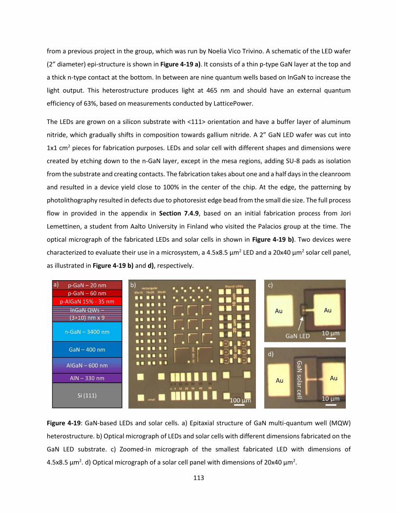
113
from a previous project in the group, which was run by Noelia Vico Trivino. A schematic of the LED wafer
(2” diameter) epi-structure is shown in Figure 4-19 a). It consists of a thin p-type GaN layer at the top and
a thick n-type contact at the bottom. In between are nine quantum wells based on InGaN to increase the
light output. This heterostructure produces light at 465 nm and should have an external quantum
efficiency of 63%, based on measurements conducted by LatticePower.
The LEDs are grown on a silicon substrate with <111> orientation and have a buffer layer of aluminum
nitride, which gradually shifts in composition towards gallium nitride. A 2” GaN LED wafer was cut into
1x1 cm2 pieces for fabrication purposes. LEDs and solar cell with different shapes and dimensions were
created by etching down to the n-GaN layer, except in the mesa regions, adding SU-8 pads as isolation
from the substrate and creating contacts. The fabrication takes about one and a half days in the cleanroom
and resulted in a device yield close to 100% in the center of the chip. At the edge, the patterning by
photolithography resulted in defects due to photoresist edge bead from the small die size. The full process
flow in provided in the appendix in Section 7.4.9, based on an initial fabrication process from Jori
Lemettinen, a student from Aalto University in Finland who visited the Palacios group at the time. The
optical micrograph of the fabricated LEDs and solar cells in shown in Figure 4-19 b). Two devices were
characterized to evaluate their use in a microsystem, a 4.5x8.5 µm2 LED and a 20x40 µm2 solar cell panel,
as illustrated in Figure 4-19 b) and d), respectively.
Figure 4-19: GaN-based LEDs and solar cells. a) Epitaxial structure of GaN multi-quantum well (MQW)
heterostructure. b) Optical micrograph of LEDs and solar cells with different dimensions fabricated on the
GaN LED substrate. c) Zoomed-in micrograph of the smallest fabricated LED with dimensions of
4.5x8.5 µm2. d) Optical micrograph of a solar cell panel with dimensions of 20x40 µm2.

114
The electrical results of those two building blocks are plotted in Figure 4-20. First the LED has been
characterized by an IV measurement, while observing the onset of light emission by eye. The result is
plotted in Figure 4-20 a) on a logarithmic current scale. Like the GaAs based LEDs, the current through the
diode structure increases exponentially at first but starts to low down at about 2.7 V. Light is barely visible
by naked eye at a level of 60 nA and is easily recognizable at 100 nA. This means, the fabricated LED
certainly meets the requirement to emit a visible amount of light at a current of 500 nA. Next, the
20x40 µm2 GaN mesa was characterized under illumination to determine its potential as solar cell. Similar
to the GaAs mesas, the structure was test by performing IV measurements at three different illumination
levels: dark, halogen light (0.53 mW/mm2) and UV laser light (70 mW/mm2). The results are plotted in
Figure 4-20 b). While the halogen light only results in a short circuit current of 66 pA, the maximum
attainable current increases to about 5 µA with the UV laser light source. The open circuit voltage at that
illumination level is 2.5 V. As a result, the solar cell panel exceeds the required amount of generated
current by 400%. Considering the device area and power density of the light, the estimated power
conversion efficiency is approximately 10%.
Figure 4-20: Electrical characterization of GaN LED and solar cell. a) IV curve of a 4.5x8.5 µm2 LED. b) IV-
curves of a 20x40 µm2 solar cell panel under three different levels of illumination: dark, halogen light
(0.53 mW/mm2), UV laser (70 mW/mm2).
In conclusion, the fabricated LEDs and solar cells based on the blue GaN MQW heterostructure are more
than enough to be used in an electric microsystem with dimensions of 50x50 µm2. As next steps, the
release process of lifting off these building blocks from the surface needs to be investigated.
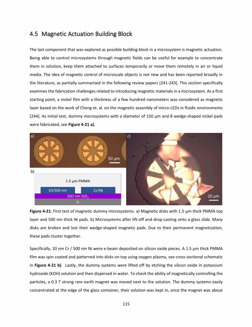
115
4.5 Magnetic Actuation Building Block
The last component that was explored as possible building block in a microsystem is magnetic actuation.
Being able to control microsystems through magnetic fields can be useful for example to concentrate
them in solution, keep them attached to surfaces temporarily or move them remotely in air or liquid
media. The idea of magnetic control of microscale objects is not new and has been reported broadly in
the literature, as partially summarized in the following review papers [241-243]. This section specifically
examines the fabrication challenges related to introducing magnetic materials in a microsystem. As a first
starting point, a nickel film with a thickness of a few hundred nanometers was considered as magnetic
layer based on the work of Cheng et. al. on the magnetic assembly of micro-LEDs in fluidic environments
[244]. As initial test, dummy microsystems with a diameter of 150 µm and 8 wedge-shaped nickel pads
were fabricated, see Figure 4-21 a).
Figure 4-21: First test of magnetic dummy microsystems. a) Magnetic disks with 1.5 µm thick PMMA top
layer and 500 nm thick Ni pads. b) Microsystems after lift-off and drop-casting onto a glass slide. Many
disks are broken and lost their wedge-shaped magnetic pads. Due to their permanent magnetization,
these pads cluster together.
Specifically, 10 nm Cr / 500 nm Ni were e-beam deposited on silicon oxide pieces. A 1.5 µm thick PMMA
film was spin coated and patterned into disks on top using oxygen plasma, see cross-sectional schematic
in Figure 4-21 b). Lastly, the dummy systems were lifted off by etching the silicon oxide in potassium
hydroxide (KOH) solution and then dispersed in water. To check the ability of magnetically controlling the
particles, a 0.3 T strong rare earth magnet was moved next to the solution. The dummy systems easily
concentrated at the edge of the glass container, their solution was kept in, once the magnet was about
116
10 cm away, which confirms the ability magnetically actuate the microsystems. However, when drop-
casting the microsystem solution onto a glass slide and looking at specific magnetic disks, many PMMA
disks were broken or had partially lost their wedge-shaped magnetic pads. These pads in turn aggregated
together on other dummy microsystems, as shown in Figure 4-21 c). In conclusion, the initial testing of
nickel films for magnetically actuating microsystems proved successful. However, the magnetic layer must
be adhered better to the rest of the microsystem.
To increase the stability of the magnetic pads to the microsystem, an encapsulation between two layers
was investigated. In Figure 4-22 a) a lifted-off dummy microsystem is shown that has eight 500 nm thick
nickel pads between a 7 µm thick polyimide layer at the top and 30 nm of aluminum oxide at the bottom.
The design proved to be more mechanically robust, based on very few broken dummy microsystems after
lift-off. Like the first experiment, the dummy microsystems responded well to external magnetic fields.
Keeping a magnetic disk in a droplet of water on a glass slide it could be turned left or right with the same
0.3 T magnet (25 mm diameter, 12 mm height) from about 50 cm away, as indicated by the arrows in
Figure 4-22 a).
Figure 4-22: Dummy microsystems with encapsulated magnetic layers. a) Lifted-off 100 µm magnetic
microsystem on a glass slide. b) 60x60 µm2 magnetic SU-8 microsystems with embedded 100 nm Fe pads
on sacrificial copper layer.
However, with only 30 nm of protective film on one side, the dummy systems tended to stick to one-
another after magnetization. As a result, a final design with a magnetic layer integrated in an SU-8
substrate was developed. The magnetic layer was introduced in the middle of a 2 µm thick SU-8 octagon,
by first patterning a 1 µm bottom SU-8 film, then e-beam depositing the magnetic layer and patterning it
by lift-off and lastly encapsulating it with another 1 µm SU-8 layer at the top. However, as compared to

117
silicon oxide and aluminum oxide, SU-8 generally has a weak adhesion energy to metals [245]. Since,
e-beam evaporated Ni has a large residual stress after deposition, it immediate delaminates from the SU-8
surface at a thickness of 500 nm. One way to avoid this problem is to lower the film thickness, which also
results in less magnetic material. Instead, the 500 nm nickel film was replaced with a 100 nm iron film,
which has a saturation magnetization roughly 4 times as large as nickel [246] and leads to a larger
attractive force given the same film thickness [247]. The resulting SU-8 microsystems now contain
2.8 vol% and 18.9 wt% of iron, which results in an overall microsystem density of 1.37 g/cm3. The
fabricated iron-based dummy microsystems are illustrated in Figure 4-22 b) on a copper release layer. As
with the nickel film, the iron film thickness is limited based on the residual stress which increases with
film thickness. Based on several experiments, the iron film pads start to delaminate at a large fraction at
a film thickness of 150 nm. Additionally, a 10 nm thick nickel adhesion layer is used under the iron film for
best results. The fabricated iron-based dummy microsystems were lifted-off in ferric chloride acid and
dispersed in water. They could be easily manipulated with the 0.3 T magnet (25 mm diameter, 12 mm
height) from about 50 cm away. These results above show that magnetic actuation can be easily
integrated into polymer-based microsystems.
4.6 Conclusion
Chapter 4 explores a broad variety of components that are needed to build autonomous electronic
microsystems smaller than 100 µm in size. Six types of building blocks are covered: sensors, timers, logic,
energy harvesters, communication devices and remote actuators. Due to the breath of covered functions,
the described building blocks should be regarded as an initial case study for how to create different
functionalities for a micron-scale electronic system. Since one main goal of this thesis is the fabrication of
a complete microsystem with several functions, the fabrication challenges and general feasibility of each
building block were prioritized. For each building block a viable prototype was developed. Regarding
sensors, an MoS2 based chemical sensor is presented that can detect the polyamine putrescine at
concentrations of 100 mg/L in water and 10 ppm in air by changing its resistance by over 60 times.
Additionally, this resistance change subsides over the course of tens of hours, effectively rendering it a
short-term memory element as well. Additionally, the erosion of germanium based thin films was shown
to be useful as timer for microsystems in water with a measurement range of 15 minutes at room
temperature. In respect to computational capabilities, MoS2 transistors with a mobility of 2.2 cm2/Vs and
118
very high fabrication yield have been demonstrated. Furthermore, the design of a CMOS circuit was
described that can convert an analog sensor signal into pulses of varying frequencies. Using a 65 nm TSCM
technology, the chip was laid out in an area of only 30x50 µm. Simulations indicate a peak power
consumption of no more than about 400 nW. For energy harvesting, a roughly 10% efficient solar cell
panel based on a GaN MQW heterostructure is presented. At a size of 20x40 µm2 this solar cell can
produce 2.9 µA at 2.35 V. Using the same GaN MQW heterostructure, a 4.5x8.5 µm2 small LED was
demonstrated that is easily visible at a current of just 100 nA by eye. Lastly, in respect to magnetic
actuation, the fabrication of magnetic microsystems is demonstrated using embedded iron and nickel
films that can be turned and pivoted by a 0.3 T magnet from 50 cm away, demonstrating the ability of
remote actuation.

119
120
SynCell Demonstrations
Chapter 4 has described several building blocks that can be used for electronic microsystems, covering six
general types of functionality: sensing, timing, computation, communication, energy harvesting and
actuation. This chapter explores how to integrate several of these components on a 60x60x2 µm2
microsystem called synthetic cell or SynCell since its size is similar to biological cells. The next sections
specifically discuss the design, fabrication, and characterization of SynCells. Several components are
integrated on this microsystem platform including molybdenum disulfide-based (MoS2) transistors and
chemical sensors, analog timers based on eroding Germanium (Ge) films, and magnetic iron pads. These
building blocks represent a broad set of capabilities and enable functions like computation, sensing, time
tracking and remote actuation, respectively, and leverage both electronic and functional material devices
to reduce power.
5.1 Design and Concept
Designing simple and task specific SynCells is critical to reduce system size and power budget as much as
possible. Rather than adding all functionality onto one larger SynCell, multiple types of SynCells have been
designed with different layouts and functions. This way, a complex task can still be addressed through a
diversity of SynCell types. Additionally, this helps exploring different designs for each building block.
Specifically, four types of SynCells were fabricated: (1) a Sensor SynCell with two sensor designs and a
reference resistor, (2) a Timer SynCell with three different timer designs, (3) an Amplifier SynCell with two
sensors and two transistors and (4) a General SynCell with a sensor, a transistor and a timer. All key
components of these SynCells operate passively while they are dispersed in either liquid or air. After
chemical exposure, the chemi-resistive sensors strongly change their resistance and only go back to their
original state very slowly hence also serving as analog memory. Furthermore, the Ge timing sensors slowly
erode in water, by first forming germanium oxide, which is then soluble in water [196]. Additionally, each
type of SynCell has a 10/100 nm nickel (Ni) /iron (Fe) film embedded inside the SU-8 substrate that allows
the SynCells to be manipulated remotely by external magnetic fields, such as permanent magnets or more
advanced setups [248]. As a result, the SynCell can travel and measure without any constrains, such as
requiring light or other energy sources. Once the SynCells are captured, the sensor and timer resistances
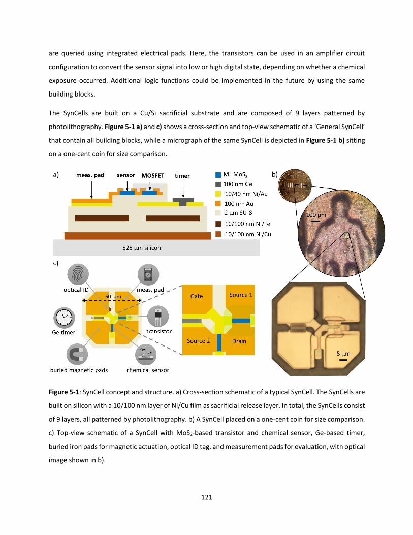
121
are queried using integrated electrical pads. Here, the transistors can be used in an amplifier circuit
configuration to convert the sensor signal into low or high digital state, depending on whether a chemical
exposure occurred. Additional logic functions could be implemented in the future by using the same
building blocks.
The SynCells are built on a Cu/Si sacrificial substrate and are composed of 9 layers patterned by
photolithography. Figure 5-1 a) and c) shows a cross-section and top-view schematic of a ‘General SynCell’
that contain all building blocks, while a micrograph of the same SynCell is depicted in Figure 5-1 b) sitting
on a one-cent coin for size comparison.
Figure 5-1: SynCell concept and structure. a) Cross-section schematic of a typical SynCell. The SynCells are
built on silicon with a 10/100 nm layer of Ni/Cu film as sacrificial release layer. In total, the SynCells consist
of 9 layers, all patterned by photolithography. b) A SynCell placed on a one-cent coin for size comparison.
c) Top-view schematic of a SynCell with MoS2-based transistor and chemical sensor, Ge-based timer,
buried iron pads for magnetic actuation, optical ID tag, and measurement pads for evaluation, with optical
image shown in b).
122
Mechanical stability is provided to the SynCells through a 2-µm thin SU-8 polymer film. SU-8 is an ideal
substrate material because it is flexible, chemically inert, biocompatible [249] and stable at high
temperature [250]. This makes it useful for diverse environments including biological applications. On top,
thin films of gold, germanium, SU-8 and monolayer MOCVD-grown MoS2 make up the transistors, sensors,
analog timers, and measurement pads with the SU-8 also acting as dielectric layer. One pad is shaped
differently for each SynCell type to create a unique optical identification (ID) label to distinguish them
under the microscope. In total, over 11,300 SynCells are fabricated on each 8x8 mm2 die.
5.2 Fabrication and Lift-Off
The fabrication and lift-off of SynCell microsystems integrates several of the building blocks discussed in
Chapter 4. The following section covers the details of the fabrication process and discusses related
challenges. The full SynCell fabrication protocol is given in appendix in Section 7.4.10. It is the result of
five generations of SynCells that were improved and optimized over several years. The entire SynCell
process flow takes about 5-6 days to complete. This is less compared to the sum of fabrication times of
the individual building blocks because some layers can be used for multiple building blocks at once. MoS2
on the SynCells is used to form the transistors and sensors at once for example.
Integrating multiple components together and increasing the number of fabrication steps increases the
risk of failure. With the goal to have all components on a SynCell working properly, the cumulative risk of
defective SynCells can be roughly estimated as the sum of process failures for each individual component.
It took about three started batches of SynCells for every fully functional batch of SynCells due to failed
process steps that render the entire batch useless. However, once all fabrication steps succeed, the overall
yield of fully functional SynCells on a die is commonly above 95%.
This issue of lower SynCell batch yield with the increasing number of building blocks, however, is mainly
related to processing mistakes and process variations from a university-level cleanroom. Modern silicon-
based chips offer over a hundred different electronic components in a certain technology node and can
contain more than a billion connected devices on a chip. They require several hundred fabrication and
metrology steps to produce and often achieve chip yields above 95%. Even with all this complexity, high-
end chips like desktop CPUs cost less than $1 per mm2 based on available retail prices. As a result, the
challenges in SynCell complexity, yield and cost are easily manageable if scaled to industrial toolsets.

123
The SynCell fabrication process consists of 10 layers and is depicted in Figure 5-2. It shows the top view
and cross-sectional schematic of a ‘General SynCell’ as well as an optical image for each layer of the
fabrication process. The fabrication starts with bare 4” silicon wafer that is cleaned in pre-mixed piranha
solution (Nanostrip, KMG) and 10% HCl for 5 min each to remove organic and metallic contamination,
respectively. The cleanliness of the wafer is important because it affects the spin-coating quality of the
SU-8 layers to follow. It was experimentally observed that small amounts of residue eventually cause small
bubbles, less than a micrometer in size, when spinning SU-8 on un-cleaned surfaces.
As first layer a 10 nm Ni / 100 nm Cu film is e-beam evaporated onto the wafes as a sacrificial release
layer, see Figure 5-2 a). Later this layer will be etched in ferric acid to release the SynCells built on top.
The copper layer will oxide and change color over the time span of the fabrication, which are not a
problem. In fact, an initial oxidation step is necessary to improve the adhesion of the SU-8 layers to follow.
As bottom layer of the SynCells, SU-8 6000.5 is spin-coated on the wafer, patterned by photolithography
and post exposure baked, resulting a film thickness of 800 nm, see Figure 5-2 b). A high-enough dose for
the photolithography is critical to fully cross-link the SU-8 film. Having doses that are too low will result in
lines from the MLA lithography tool. The necessary dose has been found to shift depending on the age of
the photoresist and the cleanroom environment, e.g. the humidity. To ensure a smooth and well adhering
film, a dose test is recommended for every batch of fabrication.
For magnetic actuation, a 10 nm Ni /100 nm Fe film is e-beam evaporated and patterned by a lift-off
process with PMGI and SPR 700, see Figure 5-2 c). As discussed in Section 4.5, e-beam deposited iron has
a high residual stress level, which can cause the iron pads to peel off during the lift-off process in NMP.
Hence, no additional agitation such as ultrasound is advised for this step.
To complete the SynCell base, another layer of SU-8 6001.5 is spin-coated on the wafer, patterned by
photolithography and hard baked, resulting a total SynCell thickness of 2000 nm, see Figure 5-2 d). To
ensure a good encapsulation, the top SU-8 layer is slightly larger than the bottom one, which helps
compensate for small alignment errors, which cannot be avoided below an accuracy of 500 nm.
To form the electronic circuits, a 10 nm Ni / 40 nm Au gate layer is deposited by e-beam evaporation and
patterned using a lift-off process with PMGI and SPR 700, see Figure 5-2 e). As the SynCell base is about
2 µm thick, a margin of 4 µm has been added between the edge of the SynCell and the edge of the pads.
This helps ensure a proper lift-off, since the PGMI undercutting layer thins down at the edge of any raised
feature during the spin-coating process.
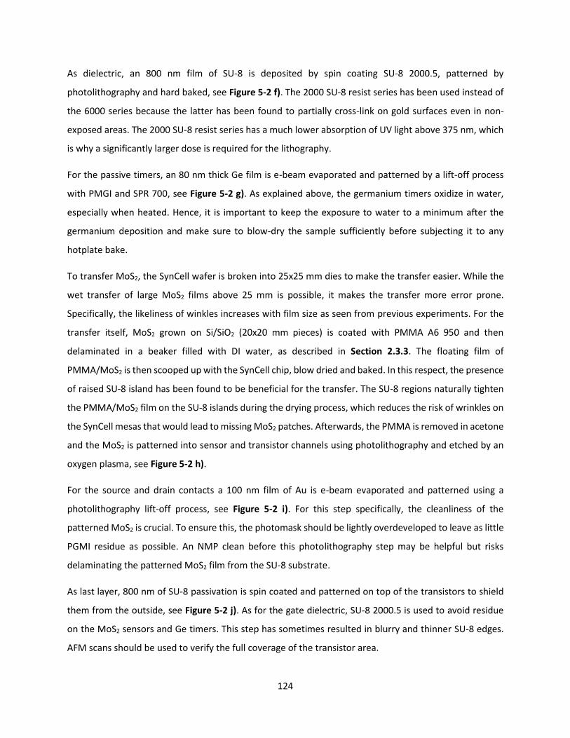
124
As dielectric, an 800 nm film of SU-8 is deposited by spin coating SU-8 2000.5, patterned by
photolithography and hard baked, see Figure 5-2 f). The 2000 SU-8 resist series has been used instead of
the 6000 series because the latter has been found to partially cross-link on gold surfaces even in non-
exposed areas. The 2000 SU-8 resist series has a much lower absorption of UV light above 375 nm, which
is why a significantly larger dose is required for the lithography.
For the passive timers, an 80 nm thick Ge film is e-beam evaporated and patterned by a lift-off process
with PMGI and SPR 700, see Figure 5-2 g). As explained above, the germanium timers oxidize in water,
especially when heated. Hence, it is important to keep the exposure to water to a minimum after the
germanium deposition and make sure to blow-dry the sample sufficiently before subjecting it to any
hotplate bake.
To transfer MoS2, the SynCell wafer is broken into 25x25 mm dies to make the transfer easier. While the
wet transfer of large MoS2 films above 25 mm is possible, it makes the transfer more error prone.
Specifically, the likeliness of winkles increases with film size as seen from previous experiments. For the
transfer itself, MoS2 grown on Si/SiO2 (20x20 mm pieces) is coated with PMMA A6 950 and then
delaminated in a beaker filled with DI water, as described in Section 2.3.3. The floating film of
PMMA/MoS2 is then scooped up with the SynCell chip, blow dried and baked. In this respect, the presence
of raised SU-8 island has been found to be beneficial for the transfer. The SU-8 regions naturally tighten
the PMMA/MoS2 film on the SU-8 islands during the drying process, which reduces the risk of wrinkles on
the SynCell mesas that would lead to missing MoS2 patches. Afterwards, the PMMA is removed in acetone
and the MoS2 is patterned into sensor and transistor channels using photolithography and etched by an
oxygen plasma, see Figure 5-2 h).
For the source and drain contacts a 100 nm film of Au is e-beam evaporated and patterned using a
photolithography lift-off process, see Figure 5-2 i). For this step specifically, the cleanliness of the
patterned MoS2 is crucial. To ensure this, the photomask should be lightly overdeveloped to leave as little
PGMI residue as possible. An NMP clean before this photolithography step may be helpful but risks
delaminating the patterned MoS2 film from the SU-8 substrate.
As last layer, 800 nm of SU-8 passivation is spin coated and patterned on top of the transistors to shield
them from the outside, see Figure 5-2 j). As for the gate dielectric, SU-8 2000.5 is used to avoid residue
on the MoS2 sensors and Ge timers. This step has sometimes resulted in blurry and thinner SU-8 edges.
AFM scans should be used to verify the full coverage of the transistor area.

125
a)
b)
c)
d)
e)
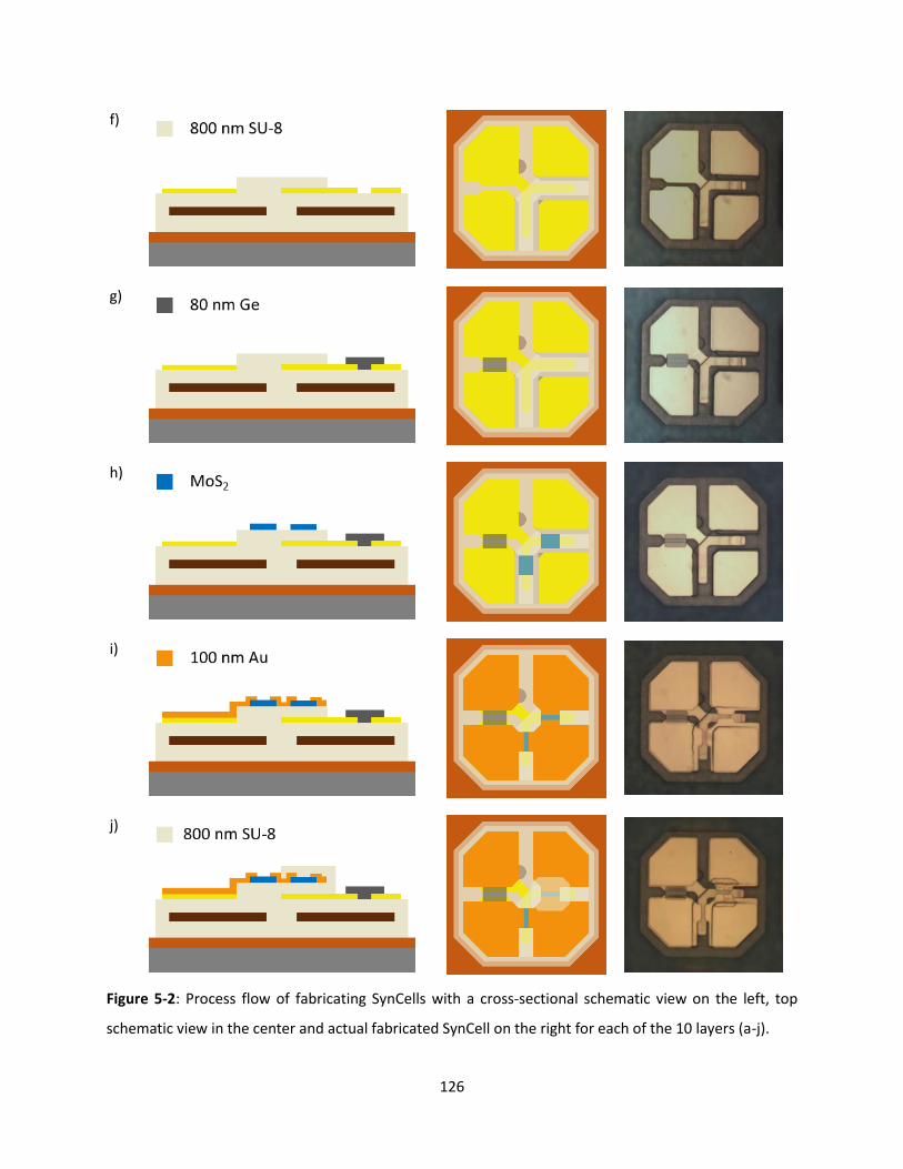
126
f)
g)
h)
i)
j)
Figure 5-2: Process flow of fabricating SynCells with a cross-sectional schematic view on the left, top
schematic view in the center and actual fabricated SynCell on the right for each of the 10 layers (a-j).

127
After the fabrication of the SynCells is done, they need to be lifted off into solution such as water or IPA.
This way they can be used to sense in constrained spaces like microfluidic channels or be sprayed onto
surfaces like glass slides. The release process uses ferric acid to undercut the copper sacrificial layer as
described in Section 7.3.3 and could deteriorate the SynCell performance. As a result, the simple release
process discussed in Section 7.3.3 was amended to include a transfer onto PMMA as another sacrificial
layer that is easy to remove by acetone. This enables electric measurements after the lift-off from the
fabrication substrate, which is important to verify the SynCell functionality after this step. The full release
process is illustrated schematically in Figure 5-3 while accompanying images are shown in Figure 5-4. The
entire process flow is described in the appending in Section 7.4.11.
Figure 5-3: The SynCell lift-off process flow. a) SynCells are built on a copper release layer. b) 500 nm of
MMA 8.5 EL 11 co-polymer is spin-coated and patterned into a mesh with 10 µm small holes in between
the SynCells using deep UV light. c) MMA coated SynCell chips are undercut in FeCl3. d) floating MMA film
with SynCells in transferred onto a similar sized silicon die coated with PMMA A6 950, blow-dried and
baked. e) The MMA copolymer is flood exposed in deep UV light. f) The MMA top layer is developed and
removed. g) The SynCells are measured on a probe station. h) The SynCells are released by immersing the
chip into acetone. i) The solvent is swapped to DI water.

128
After fabricating the SynCells, the 25x25 mm2 die is first coated with a 500 nm MMA co-polymer film.
Using the DUV exposure described in Section 7.2.2, the MMA is patterned into a mesh with 10 µm holes
between the SynCells. The film helps keep all the SynCells together while the copper release layer is
undercut in ferric chloride acid. The holes ensure that the acid can easily penetrate, which results in an
overall etching time of less than 7 minutes to release the MMA/SynCell film. Without the holes, the ferric
chloride would need to laterally etch several millimeters, depending on the exact sample size, which
would take hours to over a day. The MMA copolymer is specifically used as temporary substrate because
of its strong mechanical properties (PMMA also works). Replacing it with other polymers such as SPR700
or AZ5214 photoresist does not work and results in the breaking of the film into many pieces after lift-off.
After the MMA/SynCell film has been fully undercut in FeCl3, it starts buckling up, as shown in Figure
5-4 c). From there it can be scooped up with a glass slide and transferred into two consecutive DI water
baths, like a 2D-material transfer. Due to the surface tension of the water, the MMA/SynCell film floats
on top. Next, the film is transferred onto a silicon piece of similar or larger size coated with PMMA, blow
dried and baked. Since the film has 10 µm holes throughout it dries on the PMMA immediately after blow-
drying. To access the metal pads of the SynCells, the MMA temporary layer must be removed by again
using a DUV exposure and development. Depending on the exposure time, the PMMA on the silicon piece
is removed completely except under the SynCells. At this point, the SynCells can be tested electrically, as
illustrated in Figure 5-4 f). The advantage of the developed transfer method is that all SynCells stay
perfectly ordered in an array shape, which makes measuring many them easy. After electrical
characterization, the SynCells can be stored on the silicon die until they are needed.
To disperse the SynCells into solution, the silicon carrier is immersed in acetone. Within a few minutes
the SynCells start to detach from the surface, since the PMMA is now dissolved in acetone, as depicted in
Figure 5-4 g) and h). Some shaking accelerates this process but is not necessary. After lift-off, the silicon
die is removed with tweezers. For most applications it is useful to disperse the SynCells in water, ethanol
or isopropyl alcohol. To change the solvent, the vial with SynCells and acetone is first left to rest for a few
minutes until all SynCells settle to the ground. Since acetone has a low density, this happens within 1-2
minutes. Afterwards, about 95% of the acetone is removed with a pipette and filled back up with acetone
to wash the SynCells and remove any PMMA in the solution. This process is repeated one more time with
acetone and then two times with IPA or water depending on the desired final solvent. For water or IPA
the precipitation time is significantly longer due to the higher density. It takes about 10 min for all the
SynCells to settle to the bottom of the vial in these cases.
129
Figure 5-4: SynCell lift-off process images. a) As-fabricated SynCells on Cu release layer. b) SynCells with
patterned MMA mesh on top with 10 µm holes between SynCells. c) Undercutting Cu/Ni release layer in
FeCl3. d) SynCells with MMA mesh after undercutting and transfer on PMMA/Si e) SynCells after flood
DUV exposure and development. f) Measuring SynCells on probe station. g) Lifting off individual SynCells
in acetone, after approximately 1 min the solvent. h) SynCells lifted-off in acetone after soaking them for
5 min and shaking once to remove them from the silicon substrate. i) SynCells dispersed in DI water.
5.3 Amplifier Demonstration
As first system-level SynCell demonstration, several amplifier SynCells were characterized. This type of
SynCell consists of a chemical sensor and MoS2 transistors that convert the resistance changes of the
sensor into a digital high or low state, depending on whether the target analyte was present. As a result,
this Syncell combines two functions sensing and amplification on a 60x60 µm2 substrate. To explain how
130
the amplification circuit works, let’s first consider a simple voltage divider circuit of a chemical sensor at
the top and a reference sensor at the bottom, as depicted in Figure 5-5 a). Before chemical exposure the
sensor has a resistance that is roughly 4 times higher than the reference sensor because the latter is doped
by the SU-8 on top of its MoS2 channel. As a result, the output of this voltage divider is about 2 V when
applying 10 V as VDD. Once the sensor is exposed to putrescine, its resistance decreases to about a third
or less of the reference sensor, resulting in an output voltage of about 7 V. Figure 5-5 b) shows a simple
circuit that uses transistors to amplify the sensor signal by adding a feedback mechanism. In particular,
the circuit lowers the output voltage if there is no chemical exposure and increases it otherwise compared
to the simple voltage divider. This is similar to the function of a CMOS inverter but without the inverting
behavior. The circuit consists of two voltage dividers where the bottom two devices are transistors that
are gated from the midpoint of the opposite branch. To get an inverse behavior between the two voltage
dividers, the left branch has a sensor at the top with the transistor underneath acting as a gate-tunable
reference sensor. The right branch has a reference resistor at the top and a gate-tunable chemical sensor
at the bottom. This circuit is implemented as a separate SynCell type with a micrograph of the actual
SynCell shown in the inset of Figure 5-5 c). The difference when measuring both the voltage divider and
amplifier circuits is shown in Figure 5-5 c). While the simple voltage divider has an initial output voltage
of about 2 V, the amplifier design has an output voltage of 1 V, which represents a low state meaning that
the sensor is not exposed. It also shows that the midpoint voltage on the other branch is about 9 V, which
is inverse to the left branch as intended. Both voltage curves were recorded using the same SynCell. For
the simple voltage divider, the feedback wire was simply removed.
Figure 5-5 d) compares the results of the simple voltage divider to the amplifier circuit for 4 SynCells that
have been exposed to 100 mg/L of putrescine in water for 5 min. The SynCells have been left on the
silicon/PMMA after the copper release process to simplify the measurement. The amplifier circuit has a
lower average output voltage of 1.4 V compared to 1.8 V on the voltage divider. After putrescine exposure
the output voltage of the amplifier is 8.2 V versus 6.5 V for the regular voltage divider. This exemplifies
that the circuit successfully amplifies the sensor signal by approximately 66% and brings it closer to a
digital high and low state of 0 and 10 V. The amplification behavior can further be improved by thinning
down the gate dielectric, which will modulate the transistor resistance to a greater extent and saturates
the output close to 0 and 10 V for the unexposed and exposed state, respectively. This has been tested by
a simulation, with the results shown in Figure 5-5 e). The simulation calculated the output voltage of Vsense
of the circuit shown in Figure 5-5 b) considering different channel resistance modulations of the
transistors and the resulting feedback.

131
Figure 5-5: Amplifier SynCell as first system-level demonstration of a microsystem. a) Circuit of a simple
voltage divider with a chemical sensor and a reference sensor to convert the change of sensor
conductance into a voltage signal. b) Amplifier circuit using two transistors that feed back into each other
to lower the output voltage if no exposure occurred and raise it if one occurred. c) Plot of output voltage
Vsense versus supply voltage VDD. d) Comparison of 4 voltage divider SynCells and 4 amplifier SynCells before
and after exposure to 100 mg/L of putrescine in DI water for 5 min. The circuit amplifies the chemical
sensor signal. e) Simulated plot of output voltage versus relative sensor resistance based on assuming
different channel resistance modulation of the transistor.
The transistors were modeled in the sub-threshold regime with an exponential increase in current over a
range from 0-10 V. Having no gate modulation is equal to a regular voltage divider circuit, plotted as blue
line, which is almost a straight line in this semi-log plot of Vout over sensor resistance. Improving the ratio
of minimum to maximum channel resistance of the transistor from a factor of 3x (orange line) to a factor
of 100x (dark red line) improves this amplification behavior significantly. In practice, this behavior is equal
to an increased gate modulation and can be achieved by thinning down the gate oxide, which creates
higher electric fields for the same gate input range for 0-10 V.
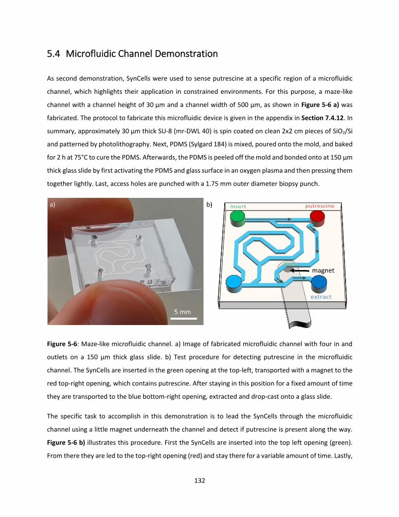
132
5.4 Microfluidic Channel Demonstration
As second demonstration, SynCells were used to sense putrescine at a specific region of a microfluidic
channel, which highlights their application in constrained environments. For this purpose, a maze-like
channel with a channel height of 30 µm and a channel width of 500 µm, as shown in Figure 5-6 a) was
fabricated. The protocol to fabricate this microfluidic device is given in the appendix in Section 7.4.12. In
summary, approximately 30 µm thick SU-8 (mr-DWL 40) is spin coated on clean 2x2 cm pieces of SiO2/Si
and patterned by photolithography. Next, PDMS (Sylgard 184) is mixed, poured onto the mold, and baked
for 2 h at 75°C to cure the PDMS. Afterwards, the PDMS is peeled off the mold and bonded onto at 150 µm
thick glass slide by first activating the PDMS and glass surface in an oxygen plasma and then pressing them
together lightly. Last, access holes are punched with a 1.75 mm outer diameter biopsy punch.
Figure 5-6: Maze-like microfluidic channel. a) Image of fabricated microfluidic channel with four in and
outlets on a 150 µm thick glass slide. b) Test procedure for detecting putrescine in the microfluidic
channel. The SynCells are inserted in the green opening at the top-left, transported with a magnet to the
red top-right opening, which contains putrescine. After staying in this position for a fixed amount of time
they are transported to the blue bottom-right opening, extracted and drop-cast onto a glass slide.
The specific task to accomplish in this demonstration is to lead the SynCells through the microfluidic
channel using a little magnet underneath the channel and detect if putrescine is present along the way.
Figure 5-6 b) illustrates this procedure. First the SynCells are inserted into the top left opening (green).
From there they are led to the top-right opening (red) and stay there for a variable amount of time. Lastly,
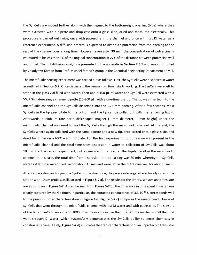
133
the SynCells are moved further along with the magnet to the bottom-right opening (blue) where they
were extracted with a pipette and drop cast onto a glass slide, dried and measured electrically. This
procedure is carried out twice, once with putrescine in the channel and once with just DI water as a
reference experiment. A diffusion process is expected to distribute putrescine from the opening to the
rest of the channel over a long time. However, even after 30 min, the concentration of putrescine is
estimated to be less than 1% of the original concentration at 27% of the distance between putrescine well
and outlet. The full diffusion analysis is presented in the appendix in Section 7.5.1 and was contributed
by Volodymyr Koman from Prof. Michael Strano’s group in the Chemical Engineering Department at MIT.
The microfluidic sensing experiment was carried out as follows. First, the SynCells were dispersed in water
as outlined in Section 5.2. Once dispersed, the germanium timer starts working. The SynCells were left to
settle in the glass vial filled with water. Then about 100 µL of water and SynCell were extracted with a
VWR Signature single channel pipette (20-200 µL) with a one-time use tip. The tip was inserted into the
microfluidic channel and the SynCells dispersed into the 1.75 mm opening. After a few seconds, most
SynCells in the tip precipitate to the bottom and the tip can be pulled out with the remaining liquid.
Afterwards, a niobium rare earth disk-shaped magnet (1 mm diameter, 1 mm height) under the
microfluidic channel was used to lead the SynCells through the microfluidic channel. At the end, the
SynCells where again collected with the same pipette and a new tip, drop casted onto a glass slide, and
dried for 5 min on a 60°C warm hotplate. For the first experiment, no putrescine was present in the
microfluidic channel and the total time from dispersion in water to collection of SynCells was about
10 min. For the second experiment, putrescine was introduced at the top-left well in the microfluidic
channel. In this case, the total time from dispersion to drop-casting was 30 min, whereby the SynCells
were first left in a water filled vial for about 15 min and were left in the putrescine well for about 5 min.
After drop-casting and drying the SynCells on a glass slide, they were interrogated electrically on a probe
station with 10 µm probes, as illustrated in Figure 5-7 a). The results for the timers, sensors and transistor
are also shown in Figure 5-7. As can be seen from Figure 5-7 b), the difference in time spent in water was
clearly captured by the Ge timer. In particular, the extracted conductance of 3.3·10-11 S corresponds well
to the previous timer characterization in Figure 4-8. Figure 5-7 c) compares the sensor conductance of
SynCells that went through the microfluidic channel with just DI water and with putrescine. The sensors
of the latter SynCells are close to 1000 times more conductive than the sensors on the SynCell that just
went through DI water, which successfully demonstrates the SynCells ability to sense chemicals in
constrained spaces. Lastly, Figure 5-7 d) illustrates the transfer characteristic of an unprotected transistor
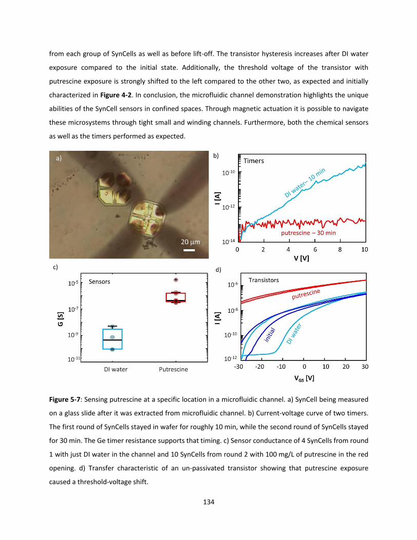
134
from each group of SynCells as well as before lift-off. The transistor hysteresis increases after DI water
exposure compared to the initial state. Additionally, the threshold voltage of the transistor with
putrescine exposure is strongly shifted to the left compared to the other two, as expected and initially
characterized in Figure 4-2. In conclusion, the microfluidic channel demonstration highlights the unique
abilities of the SynCell sensors in confined spaces. Through magnetic actuation it is possible to navigate
these microsystems through tight small and winding channels. Furthermore, both the chemical sensors
as well as the timers performed as expected.
Figure 5-7: Sensing putrescine at a specific location in a microfluidic channel. a) SynCell being measured
on a glass slide after it was extracted from microfluidic channel. b) Current-voltage curve of two timers.
The first round of SynCells stayed in wafer for roughly 10 min, while the second round of SynCells stayed
for 30 min. The Ge timer resistance supports that timing. c) Sensor conductance of 4 SynCells from round
1 with just DI water in the channel and 10 SynCells from round 2 with 100 mg/L of putrescine in the red
opening. d) Transfer characteristic of an un-passivated transistor showing that putrescine exposure
caused a threshold-voltage shift.
135
5.5 Spraying Demonstrations
Another advantage of microelectronic systems besides fitting into constrained spaces like microfluidic
channels is that they can be applied to surfaces in ways not possible with conventional larger electronics.
One opportunity is the spraying of SynCells directly onto surfaces, which is a simple way to retrofit plain
surfaces with sensing capabilities and could be useful for example to add temperature or vibration sensors
to industrial equipment. To demonstrate this possibility, SynCells have been suspended into solution and
sprayed onto glass slides using an airbrush and a cylindric chamber, as shown in a schematic view Figure
5-8 a). The actual setup is portrayed in Figure 5-8 b). The spray experiments were done in collaboration
and Dr. Volodymyr Koman from Prof. Michael Strano’s group, who constructed the spray setup,
performed the spray-coating onto glass slides and characterized the spray pattern. For the spray
deposition, SynCells were first dispersed in a solution of 80/20% DI water/ethanol. The addition of ethanol
helps with the evaporation of the solution on the glass slides. The spraying was done with a Master
Airbrush G22 nebulizer in a closed tube in the laminar flow hood and onto glass slides attached to the
other end of the chamber. The gas pressure was 2–15 psi from a 300 µm nozzle.
Figure 5-8: Setup for SynCell spraying demonstration. a) Schematic of spray setup. b) Image of actual spray
setup implementation composed of an airbrush and cylindric chamber (L = 0.6 m, D = 0.25 m).
Figure 5-9 a) shows the distribution of SynCells at the back of the chamber with each dot indicating the
location of one SynCell. The SynCells are densely deposited in the center and less dense toward the edges
of the chamber. It further illustrates that the SynCells fly through the chamber nearly horizontally with no
visible downward component due to their small size and weight. The sprayed SynCells on a glass slide are
shown in Figure 5-9 b) with a magnified view in Figure 5-9 c). Even though they are only 60x60 µm2 in size,

136
the SynCells can be seen when holding the glass slide against a light source. Furthermore, exemplary
microscope images of sprayed SynCells as illustrated in Figure 5-9 d) show no signs of physical damage
after spraying and no folding of any kind, which is an indication of their mechanical robustness.
Figure 5-9: Spraying of SynCells onto glass slides. a) Distribution of SynCells at the back of the spray
chamber. b) SynCells on a glass slide from the back of the chamber after spraying. c) Zoomed-in
micrograph of b). Micrographs of sprayed SynCells under high magnification.
To test their electric functionality, a glass slide with sprayed SynCells was taken out and measured.
Additionally, other glass slides with spray deposited SynCells have been kept in the setup and have been
sprayed with water containing 100 mg/L of putrescine in the same chamber and left to dry. The results of
these two sets, illustrated in Figure 5-10 a), show an increase in sensor conductance by nearly 1000 times,
indicating a strong exposure of putrescine. The response is stronger than in the previous sensor
characterization in Section Error! Reference source not found., because the putrescine containing water h
as been left to dry on the sensor surface without blow-drying or rinsing it. Additionally, Figure 5-10 b)

137
compares the transfer characteristic of an un-passivated transistor at three points: before spraying, after
spraying and after spraying putrescine on the SynCells. After spraying the hysteresis widens significantly
and the threshold voltage of the SynCells increases resulting in a 10 timer lower on-current. This is likely
attributed to the prolonged exposure to DI water while being dispersed in solution. After spraying
putrescine on the spray-deposited SynCells, the un-passivated transistors are heavily n-doped and the
threshold voltage decreases strongly, which is in line with the sensor characterization. In summary,
SynCells dispersed in solution can be sprayed onto surfaces without observable physical damage. After
deposition, the chemical sensors were fully functional and easily detected sprayed putrescine. The
transistors were also still functional after spraying; however, the drain current was degraded like due to
being dispersed in solution for a prolonged period of time.
Figure 5-10: Electrical measurements of spray deposited SynCells. a) Conductance of sensors from 13
spray-deposited SynCells and 9 spray-deposited SynCells after spraying putrescine. The channel
conductance increases after putrescine exposure demonstrating the proper functionality of the sensors
after spraying. b) Transfer characteristic of un-passivated transistors before spraying, after spraying and
after spraying putrescine (100 mg/L in DI water) onto the spray deposited SynCells. The threshold voltage
strongly decreases after putrescine exposure.
5.6 Conclusion
This chapter demonstrates a pathway to autonomous electronic microsystems (< 100 µm) by combining
electronic devices with functional materials, which lowers power consumption and minimizes system size.

138
As a prototype, a 60x60 µm2 sensing platform called SynCells is presented that heterogeneously integrates
MoS2-based sensors and transistors with functional materials such as iron or germanium, that have been
introduced as building blocks in Chapter 4. Combining a chemical sensor and transistors, an amplifier
SynCells can detect putrescine and amplify this sensor signal by 66%. Additionally, the experimental
results show that SynCells can detect polyamine at a specific location in a microfluidic channel using
magnetic actuation and measuring the elapsed time with the Ge timer. Lastly, SynCells were spray-coated
onto glass slides with no observable damage. They were fully functional after deposition and able to
detect putrescine sprayed on them. In the future these results may be useful to directly probe individual
cells helping to better understand biological cells and potentially aid in the development of new drugs.
The spraying of microsystems is a first step towards making inks or solutions containing electronic
particles that can be printed or sprayed onto arbitrary surfaces to form distributed sensor networks.

139
140
Summary and Future Work
This thesis has explored the use of two-dimensional materials for macroscopic and microscopic electronic
applications. In the former area, a roll-to-roll transfer system was developed that allows for the transfer
of 2D materials onto flexible plastic substrates and even the stacking of multiple 2D layers in a sequential
fashion. With respect to the microscale, several building blocks from sensing to computation and
communication have been developed that can be used to build autonomous electronic microsystems for
sensing applications. Using these building blocks, several 60x60 µm2 large microsystems have been
fabricated and applied for sensing in confined spaces and as spray-coated films. The sections below first
highlight the key contribution of this thesis. Secondly, future work in both areas is discussed.
6.1 Thesis Contributions
The following key contributions have been made in the scope of this thesis:
1. The mechanics of a roll-to-roll transfer process of 2D materials has been investigated in great
detail for the first time [169]. Through the simultaneous AFM and SEM characterization of a
specific region on a copper foil with graphene, it could be shown that 2D materials transfer onto
EVA/PET in a way that replicates the surface morphology of the growth catalyst down to the
nanometer. Furthermore, the generation of defects in the transferred 2D material through
particles on the growth substrate could be observed. The distribution of defects in larger area
films of 500 µm has been made visible and analyzed by SEM imaging.
2. The ability to stack two layers of graphene or graphene and hexagonal boron nitride by roll-to-roll
lamination and electrochemical delamination has also been demonstrated for the first time [169].
This is relevant because it opens the possibility to stack various 2D materials in a cost-effective
and high-throughput manner for low-cost 2D electronics. It also highlights the fact that the low
adhesion energy between 2D materials is enough to facilitate the transfer from the growth
substrate given the support of the electrochemical delamination. Through the comparison of
surface roughness it was shown that this stacking of 2D materials ideally needs monolayers to
guarantee a high-quality transfer.
141
3. In the realm of microsystems, two sensors with zero energy consumption were developed.
Previous developed microsystems often use wake-up routines to only measure at certain times
and save energy. However, when designing even smaller microsystems, this may not be feasible
anymore. Instead, in this thesis highlights the use of functional materials to carry out tasks.
Erosion-based germanium thin films can be used as passive timers that increase in resistance
while they are submersed in water, allowing to measure times spans up to 15 minutes.
Additionally, molybdenum-disulfide chemical sensors were developed that change their channel
resistance after exposure to a target analyte and maintain this change for several hours. As a
result, they can detect analytes in inaccessible places without any onboard power and store the
sensor information until they are queried electronically.
4. In this thesis, building blocks for a sub-50 µm electronic microsystem have been designed [251]
including a 20x40 µm2 solar cell panel, a 4.5x8.5 µm2 LED and a 50x50 µm2 CMOS chip. While
several groups have developed electronic microsystems for various applications, the smallest
autonomous system still has a footprint of 57x250 µm2 [8]. Planning a microsystem of 50x50 µm2
cannot be done by just shrinking larger designs because certain components such as on-chip
capacitors does not scale. As a result, a different approach with a simplified circuit is necessary. A
voltage-controlled oscillator based on CMOS thyristor delay elements was designed that can
encode analog voltages into pulses with frequencies between 250-450 Hz. Such low frequencies
will make it easier to detect small amounts of light pulses with long detector integration times.
The overall circuit was simulated to consume less than 400 nW. Additionally, a 20x40 µm2 solar
cell with an estimated 10% efficiency and an output power of 6.8 µW was fabricated. Lastly, a
4.5x8.5 µm2 micro-LED was built that is easily visible by eye at 250 nW of power consumption.
With the size and power requirements fulfilled, these building blocks form the basis of a sub-50
µm sensing microsystem.
5. Towards the assembly of electronic microsystems, a fabrication and lift-off process were
developed that allow for the integration of a diverse set of electronic building blocks on a
60x60 µm2 footprint [251]. One of the strengths of this process flow is the use of SU-8 as substrate,
dielectric and isolation material. It has been demonstrated for the first time in the context of
electronic microsystems, that SU-8 can be used to stack layers with different functionality. In the
future, this could helpful to assemble microsystems with 5-10 layers connected vertically by vias.
Accompanying the fabrication, various kinds of lift-off processes have been tested and their
influence on electrical devices was evaluated. Copper was identified as reliable release layer with
142
ferric chloride acid as easy-to-use undercutting agent. Additionally, a system was developed to
test the lifted-off microsystems in their original array after release from the fabrication substrate,
which helps evaluate the impact of this undercutting process.
6. Several types of microsystems called synthetic Cells or SynCells have been fabricated and tested
in microfluidic channels to show their potential for sensing in constrained environments [251].
Specifically, SynCells with integrated MoS2 chemical sensors, germanium timers and magnetic
pads were navigated remotely through magnetic interactions to a specific location inside a
microfluidic channel to detect putrescine. After extraction from the microchannel, the SynCells
clearly indicated the presence of the target chemical and the Ge timers accurately reflected the
time they were in an aqueous environment. Such detection with mobile electronic sensors using
remote actuation and of this scale has not been implemented before.
6.2 Future Work
6.2.1 Roll-to-Roll Transfer of 2D Materials
The results presented in Chapter 3 provide insight into the fundamental principles and challenges of
transferring 2D materials onto flexible substrates as well as creating 2D heterostructures by R2R
processing. However, in order to achieve truly low-cost and scalable 2D electronics on flexible substrates
with roll-to-roll processing, several challenges must be addressed. Regarding the synthesis of 2D
materials, more work is needed to achieve high-quality and flat 2D materials on their growth substrate.
One way to achieve this is by improving the metal foil flatness, for example through electrochemical
polishing, prolonged annealing or the growth of single-crystal metals foils. This is especially relevant for
hBN films, which suffered from rough surfaces in this work that are subpar to reported state-of-art films.
Additionally, the availability of roll-to-roll grown materials (other than graphene) such as MoS2 or hBN is
desirable. This would open the possibility to explore the roll-to-roll assembly and patterning of 2D
material-based sensors, transistors and circuits.
On the hardware side, several improvements in the roll-to-roll setup could be considered. Firstly, the
setup could be scaled up to cover wider films. To make the transfer results more consistent, a setup with
industrial grade “professional” components should be explored. Such components can actively control
the tilt and pressures of rollers and can further control the tension in the processed film. All these

143
parameters will likely lead to better repeatability in the quality of transferred films. From a conceptual
point of view, a vertical delamination unit could provide a more symmetric separation of the 2D materials
from the metal foil, which should result in more consistent results between the top and bottom film.
6.2.2 Optimizing SynCell Building Blocks
The building blocks demonstrated in Chapter 4 are designed to be functional and easy to fabricate.
However, they do not reflect the best state-of-the art results in each field. With the goal of creating a well-
working and useful microsystem out of these building blocks in mind, several improvements can be
considered.
For the chemical sensors it is desirable to improve the selectivity of the sensor. Since only bare MoS2 is
used as chemiresistor so far, the exposure to other chemicals will also trigger a resistance change. In the
long run, MoS2 may be replaced with graphene for this purpose because it is easier to functionalize.
Regarding the germanium timers, other geometries could be considered that increase the time span.
Additionally, finding ways to reduce the resistance variation among devices at equal time will help make
the projection of resistance to elapsed time more accurate.
While the presented MoS2-based transistors have an average performance compared to the literature, it
will be important to lower the operation voltage from tens of volts to a few volts. This is most easily
achieved by replacing the thick SU-8 dielectric by a thin ALD oxide such as aluminum oxide. Further
shrinking the transistor dimensions and lowering the variation in threshold voltages will be essential to
creating larger circuits based on MoS2 transistors.
Using CMOS circuits for logic and computational task will be more feasible than MoS2-based logic in the
short term. To that end, it is important to verify the discussed chip design by taping it out and measuring
it. Additionally, the integration of the silicon chip with other components will be a technological challenge
that needs to be overcome. Specially, the handing of a 1 mm2 chip in the cleanroom, the thinning of the
chip to less than 20 µm thickness, the patterning into 50x50 µm2 chiplets and the transfer of those chiplets
onto the target microsystems will need to be explored experimentally.
With respect to the presented LEDs and solar cells, more work needs to be done to comprehensively
characterize the material system. This is especially true of the disappointingly low power conversion
efficiencies in the GaAs system. Additionally, a better understanding of LED and solar cell efficiency as a
144
function of total area are important to determine the scaling limits for these components. For the
fabrication, a suitable transfer technique for GaAs or GaN LEDs and solar cell needs to be tested and
optimized.
Lastly, the further exploration of magnetic films in microsystems will be helpful with the goal of controlled
remote actuation of individual or multiple microsystems in a liquid environment. To achieve this task, a
magnetic setup could be constructed that can guide microsystems in a controlled fashion. In this context,
it would be important to co-design the shape, thickness and arrangement of the metallic film in the
microsystem to achieve the most precise control possible. Other forms of local actuation, for example in
connection with the formation of gas bubbles in liquid, are also worth exploring.
6.2.3 Heterogeneous SynCell Integration with CMOS and III-V Chips
The integration scheme presented in Chapter 5 illustrates how to combine iron, germanium and MoS2 to
make multifunctional SynCell microsystems with sensors, timers, transistors and magnets. However, the
electrical readout of the sensor values on the SynCells relies on the direct probing of on-board 20x20 µm2
measurement pad with 10 µm diameter test probes, as illustrated in Figure 6-1 a). This means the SynCells
must be captured from their environment, especially if they have been sensing in a solution. Additionally,
contacting the test pads with micrometer precision can only be done manually and is time intensive.
Using wireless communication on the SynCells instead, would remove this limitation and enable fast
communication in liquid media and air. To achieve this goal, a SynCell needs to combine the following
building blocks: a CMOS logic chip, solar cells, a micro-LED and a sensor. The desired communication setup
is illustrated in Figure 6-1 b). First, the SynCells are either sprayed on a surface or dispersed in a solution.
A laser beam is used to provide energy to solar cells (see Section 4.4.5) on the SynCell that power the
circuitry. The designed CMOS chip, discussed in Section 4.3.2, would convert the on-board sensor signal
into pulses with varying frequency, depending on the input signal. This pulse train is then used to drive a
micro-LED on the SynCell, which emits light pulses with the same frequency. The light will be picked up by
a photodetector that is right next to the laser. Analyzing the received light pulses will allow to estimate
the sensor value on the SynCell. The maximum achievable communication distance using this approach is
calculated in the appendix in Section 7.5.2. Assuming a dark background, a strong laser source, and an
extremely sensitive detector such as a photomultiplier tube, this distance can be on the order of 100
meters for a SynCell with a diameter of 50 µm.
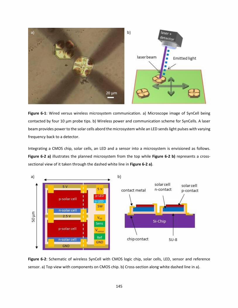
145
Figure 6-1: Wired versus wireless microsystem communication. a) Microscope image of SynCell being
contacted by four 10 µm probe tips. b) Wireless power and communication scheme for SynCells. A laser
beam provides power to the solar cells abord the microsystem while an LED sends light pulses with varying
frequency back to a detector.
Integrating a CMOS chip, solar cells, an LED and a sensor into a microsystem is envisioned as follows.
Figure 6-2 a) illustrates the planned microsystem from the top while Figure 6-2 b) represents a cross-
sectional view of it taken through the dashed white line in Figure 6-2 a).
Figure 6-2: Schematic of wireless SynCell with CMOS logic chip, solar cells, LED, sensor and reference
sensor. a) Top view with components on CMOS chip. b) Cross-section along white dashed line in a).
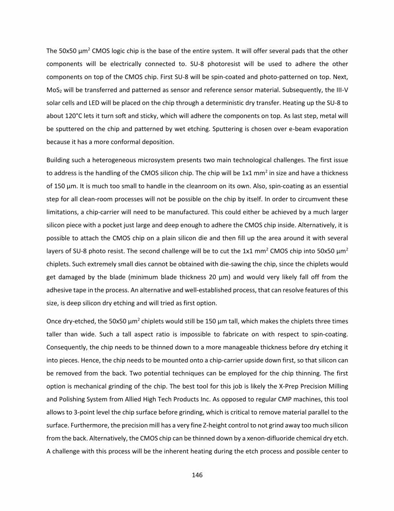
146
The 50x50 µm2 CMOS logic chip is the base of the entire system. It will offer several pads that the other
components will be electrically connected to. SU-8 photoresist will be used to adhere the other
components on top of the CMOS chip. First SU-8 will be spin-coated and photo-patterned on top. Next,
MoS2 will be transferred and patterned as sensor and reference sensor material. Subsequently, the III-V
solar cells and LED will be placed on the chip through a deterministic dry transfer. Heating up the SU-8 to
about 120°C lets it turn soft and sticky, which will adhere the components on top. As last step, metal will
be sputtered on the chip and patterned by wet etching. Sputtering is chosen over e-beam evaporation
because it has a more conformal deposition.
Building such a heterogeneous microsystem presents two main technological challenges. The first issue
to address is the handling of the CMOS silicon chip. The chip will be 1x1 mm2 in size and have a thickness
of 150 µm. It is much too small to handle in the cleanroom on its own. Also, spin-coating as an essential
step for all clean-room processes will not be possible on the chip by itself. In order to circumvent these
limitations, a chip-carrier will need to be manufactured. This could either be achieved by a much larger
silicon piece with a pocket just large and deep enough to adhere the CMOS chip inside. Alternatively, it is
possible to attach the CMOS chip on a plain silicon die and then fill up the area around it with several
layers of SU-8 photo resist. The second challenge will be to cut the 1x1 mm2 CMOS chip into 50x50 µm2
chiplets. Such extremely small dies cannot be obtained with die-sawing the chip, since the chiplets would
get damaged by the blade (minimum blade thickness 20 µm) and would very likely fall off from the
adhesive tape in the process. An alternative and well-established process, that can resolve features of this
size, is deep silicon dry etching and will tried as first option.
Once dry-etched, the 50x50 µm2 chiplets would still be 150 µm tall, which makes the chiplets three times
taller than wide. Such a tall aspect ratio is impossible to fabricate on with respect to spin-coating.
Consequently, the chip needs to be thinned down to a more manageable thickness before dry etching it
into pieces. Hence, the chip needs to be mounted onto a chip-carrier upside down first, so that silicon can
be removed from the back. Two potential techniques can be employed for the chip thinning. The first
option is mechanical grinding of the chip. The best tool for this job is likely the X-Prep Precision Milling
and Polishing System from Allied High Tech Products Inc. As opposed to regular CMP machines, this tool
allows to 3-point level the chip surface before grinding, which is critical to remove material parallel to the
surface. Furthermore, the precision mill has a very fine Z-height control to not grind away too much silicon
from the back. Alternatively, the CMOS chip can be thinned down by a xenon-difluoride chemical dry etch.
A challenge with this process will be the inherent heating during the etch process and possible center to

147
edge non-uniformities. After the chip thinning, the CMOS chip will need to be flipped onto another carrier
for support.
A second fabrication challenge revolves around the undercutting and transfer of the III-V LEDs and solar
cells. As previously discussed in Section 4.4.4, the GaAs components can be undercut with diluted HF.
Similar, to the lift-off of SynCells, the individual solar cell panels and LEDs could be held together with a
PMMA film. For the GaN LEDs, a dry undercutting of the silicon substrate with xenon-difluoride or a wet
undercutting of the AlN buffer layer in KOH are possible. The individual elements could again be held
together by PMMA. As opposed to a 2D material transfer on SynCells, the exact orientation of the
III-V/PMMA film on the SU-8/CMOS chip needs to be controlled with micrometer precision. This
eliminates the use of a simple “scooping-up” of the film with the CMOS substrate. To solve this problem,
an aligned transfer can be performed with a polymer stamp. This technique is widely used for the
assembly of electronic devices with exfoliated 2D material flakes [252] and has positional accuracies down
to the micrometer level. The process flow of a deterministic dry transfer adapted for III-V LEDs is portrayed
in Figure 6-3 a)-f).
Figure 6-3: Deterministic dry transfer of III-V solar cells and LEDs onto a CMOS chip. a) Spin coat PMMA
on patterned LEDs and solar cells. b) Lift-off PMMA/III-V film by wet or dry etching and place it on a dish
filled with water. c) Pick up PMMA/III-V film with a glass slide and dry. d) Prepare CMOS chip by spin
coating and patterning a thin adhesive layer of SU-8. e) Attach glass slide to a micropositioner with Z, Y,
Z, and Θ control and place on CMOS chip sitting on a hotplate. The heat softens the PMMA so that the
glass slide can be gently lifted while the SU-8 glues the components to the CMOS chip. f) Rinse off PMMA
in acetone to finish transfer.
148
The transfer process starts with fabricating the LEDs and solar cells on their growth substrate and coating
the entire surface with PMMA. Next, the LEDs and solar cells are wet or dry undercut and the film is placed
on a water surface, like a 2D material transfer. The PMMA/III-V film is now picked up with a glass-slide
that is coated with a thin layer of PDMS, which makes the surface sticky and hydrophobic. In parallel, the
CMOS chip is prepared by spin-coating and patterning a thin layer of SU-8 that will be used as adhesive.
For the actual transfer, the glass slide is flipped around and positioned precisely over the CMOS chip, that
is placed on a hotplate with controllable temperature. To achieve a good alignment, the whole process is
performed under a microscope and the glass slide is attached to a micro-positioner with micrometer-level
translation accuracy in X, Y, Z direction and Θ rotation. Once the LEDs and solar cells are aligned to the
pads of the CMOS chip, the glass slide is lowered to make physical contact with the SU-8 layer and the hot
plate temperature is increased to above 100°C. This makes the SU-8 soft and sticky and should result in
the bonding to the optical components to the CMOS chiplets. At the same time, the higher temperature
is expected to weaken the bond between the PDMS on the glass slide and the PMMA film. As a result, the
glass slide can be slowly retracted while the PMMA/III-V film stays on the chip surface. Lastly, the PMMA
film is rinsed away in acetone and the transfer is complete.
This described transfer process is likely the best option to assemble LEDs and solar cells on top of the
thinned down CMOS chip but will likely take some optimization of parameters to work smoothly. One
question that remains to be seen is if the alignment can be guaranteed for many chiplets in an array at
once. If not, an alternative route could be the development of a PDMS coated silicon micro-cantilever that
uses the same stamping idea but would transfer individual building blocks rather than an entire film. Once
fully assembled, the wireless SynCells would need to be characterized electrically and optically. Some of
the key questions to answer are: (1) the power efficiency of the entire system and (2) from how far away
the light signal can be picked up with a detector.
In the near term, two specific applications for the wireless SynCells appear feasible and are worth
exploring. In one scenario, the SynCells could measure a chemical concentration in a liquid environment
under a microscope. This could be useful for example for examining biological cells or sensing in a
microfluid channel, which could be pursued as part of a collaboration with biology research groups. A
second application would be the use of wireless SynCells as sprayable sensor coating. Specifically, SynCells
would be sprayed onto a surface of interest for example to monitor temperature. To read out the
temperature, a photodetector and light source are pointed at a specific location on that surface and the
light signal form the deposited SynCells is collected. Ultimately, the goal would be to integrate the light

149
source and detector into a small handheld device or possible even an add-on that can be attached to
smartphones.
In a broader sense, wireless SynCells have the potential to address any of the applications introduced in
Chapter 1.4, such as in vivo sensing, smart textile or sprayable electronics in a practical manner.
Additionally, the chosen microscale system architecture is inherently scalable, which means that wireless
SynCells smaller than 50x50 µm2 should be possible to achieve in the future, even opening the possibility
to use them inside the human body. Wireless SynCells represent a fundamentally different formfactor of
electronics than is available today. With more research and exploration, additional functions can be
imagined to be incorporated into this formfactor such as microscale grippers or entire microcontroller
units. If such multifunctional SynCells can be successfully fabricated at low cost and high volumes, other
applications may follow in the future, that one can only dream of today, such as reconfigurable and smart
meta-materials or biological-electrical hybrid organisms.

150
Appendix
7.1 Acronyms
2D two-dimensional
AlAs aluminum arsenide
AlGaAs aluminum gallium arsenide
AlGaN aluminum gallium nitride
AlN aluminum nitride
AM air mass (1.5)
Ar argon
Au gold
BCP bathocuproine
CH4 methane
CMOS complementary metal oxide semiconductor
Cu copper
CVD chemical vapor deposition
DES diethyl sulfide
DI deionized water
DUV deep ultraviolet (light)
e- electron
e-beam electron beam (lithography or deposition)
EVA ethylene-vinyl acetate
Fe iron
FeCl3 ferric chloride acid, also called iron chloride
GaAs gallium arsenide
GaN gallium nitride
Gr graphene
H2 hydrogen gas
H2O water

151
hBN hexagonal boron nitride
HCl hydrochloric acid
HF hydrofluoric acid
InAlP indium aluminum phosphide
InGaN indium gallium nitride
LED light emitting diode
MFC mass flow controller
MHC molybdenum hexacarbonyl
MIBK methyl isobutyl ketone
MMA methylmethacrylate (copolymer)
MoS2 molybdenum disulfide
MQW multi-quantum well
N2 nitrogen
Na+ positive sodium ion
NaOH sodium hydroxide
OH- negative hydroxide ion
PCBM [6,6]-phenyl C61 butyric acid methyl ester
PEDOT:PSS poly (3,4-ethylenedioxythiphene): poly(styrenesulfonate))
PET poly(ethylene terephthalate)
PI polyimide
PMMA polymethylmethacrylate
PR photoresist
Pt platinum
R2R roll-to-roll
sccm standard cubic centimeter
SEM scanning electron microscopy
Si silicon
SiC silicon carbide
SiNx silicon nitride
SiO2 silicon oxide
SQW single quantum well

152
7.2 Metal Contact Patterning
The patterning of metal contacts is vital to the fabrication of any electronic device. There are three main
ways to shape metal films into contacts, see Figure 7-1. First, the metal film can be deposited first and
afterwards patterned by photolithography and wet etching. This approach works well for big patterns but
yields in poor and non-controllable openings once the features size is below a few micrometers due to
undercutting under the photomask, see Figure 7-1 a). Alternatively, metal films can be deposited first and
then be dry etched. This method has an excellent fidelity of maintaining intricate pattern much below the
1 µm range, see Figure 7-1 b). However, etching noble metal such as gold is very challenging. Since gold
is often used at least as part of the contact metal stack due to its non-oxidizing nature, patterning metal
by dry etching is impractical. Lastly, metal contacts can be created by a so-called lift-off process. In this
case, an inverted photoresist mask with a thickness larger than the metal film is patterned on the
substrate before metal is deposited (Figure 7-1 c)). Once the photoresist mask is dissolved in a solvent
bath, the unwanted metal regions simply lift off from the surface and are removed without the need for
etching. Because of its ease of use, lift-off processing is the standard way to pattern metal contacts in
university-level research and was predominantly used in this work. Additionally, it is also capable of
creating patterns with minimum features sizes of 100 nm and below.
Figure 7-1: Three main methods of patterning metal films. a) Deposit metal first and wet etch the
unmasked area. b) Deposit metal first and dry etch the metal in the unmasked area. c) Create an inverse
photomask with an undercut and then deposit metal. The metal on top of the photoresist can be lifted off
in a solvent bath.
Two requirements need to be fulfilled to achieve a good lift-off process. (1) The patterned photoresist
needs to be significantly thicker (at least two times) than the deposited metal film so that the two metal
areas are not connected. (2) The edge profile of the photomask needs to provide an undercut, which again
avoids the unwanted metal regions to connect to the desired regions, see Figure 7-1 c). The following two
subsection discuss the optimization of two photoresists for lift-off patterning metal contacts.

153
7.2.1 Lift-off Optimization with AZ5214
AZ5214 is a negative or image reversal resist that lends itself well for metal lift-off processes. However, in
order to achieve a good lift-off, all process parameters need to be well controlled. Only this way, a
sufficient undercut can be guaranteed. The photolithography process of AZ5214 is as follows. First the
resist is spin coated on the substrate at 3000 rpms for 30 seconds, which produces a 1.5 µm thick film.
Next, the coated film is soft baked at 90°C for 1 min to remove any remaining solvent. UV light is used to
expose all areas that will remain after development.
After exposure, the resist is post exposure baked on a hotplate for 2 min. This step cross-links the polymer
in the exposed regions and makes them insoluble to the developer. Subsequently, the entire sample is
flood exposed with UV light (250 mJ/cm2). The previously unexposed areas are now easily dissolved in
AZ422 developer within 90 seconds while the cross-linked regions remain. The resulting resist profile is
strongly dependent on the exact UV dose in the first exposure step and the post exposure bake
temperature to follow. Those two parameters have been optimized in conjunction with the Heidelberg
Maskless Aligner Lithography tool (MLA 150).
First, the influence of the exposure dose was explored. The best way to evaluate the impact of the
exposure dose is to look at a cross-section image of the photoresist with both developed and undeveloped
areas. This helps best examine the side profile of the resist, which ideally possess a fair amount of
undercut to facilitate an easy lift-off. Figure 7-2 shows cross-section SEM images of a metal line before
lifting off the excess metal. The lines were written with 5 doses from 5-24 mJ/cm2 using a coarsely
optimized post exposure bake temperature of 110°C. For all images the line in the digital mask file was
2 µm wide.
Two main observations can be made. Firstly, the exposure dose strongly correlates with the printed line
width with low exposure doses leading to wider than designed features and high doses resulting in smaller
line widths. Secondly, the lower the exposure dose is the larger the resulting undercut. From a pattern
fidelity point of view, a dose of 16 mJ/cm2 is ideal because it almost exactly reproduces the designed 2 µm
line width. To achieve the best possible lift-off, however, a dose of 8 mJ/cm2 is the better option because
the top and bottom metal areas are clearly disjoint, even though it results in an overall line width of 3 µm.
In addition, the line edges of the metal line in this case are very clean and do not have any foot of
photoresist touching them.
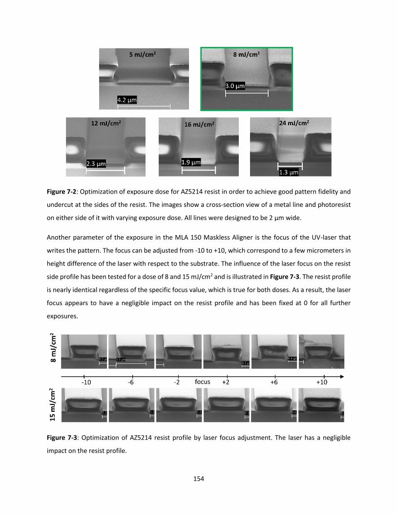
154
Figure 7-2: Optimization of exposure dose for AZ5214 resist in order to achieve good pattern fidelity and
undercut at the sides of the resist. The images show a cross-section view of a metal line and photoresist
on either side of it with varying exposure dose. All lines were designed to be 2 µm wide.
Another parameter of the exposure in the MLA 150 Maskless Aligner is the focus of the UV-laser that
writes the pattern. The focus can be adjusted from -10 to +10, which correspond to a few micrometers in
height difference of the laser with respect to the substrate. The influence of the laser focus on the resist
side profile has been tested for a dose of 8 and 15 mJ/cm2 and is illustrated in Figure 7-3. The resist profile
is nearly identical regardless of the specific focus value, which is true for both doses. As a result, the laser
focus appears to have a negligible impact on the resist profile and has been fixed at 0 for all further
exposures.
Figure 7-3: Optimization of AZ5214 resist profile by laser focus adjustment. The laser has a negligible
impact on the resist profile.

155
The second important parameter that determines the AZ5214 photo resist behavior is the post bake
temperature. This step is responsible for crosslinking the exposed areas of the resist and is heat-activated.
A coarse bake temperature optimization suggests the optimal bake temperature to be at or below 110°C.
To find the ideal bake temperature, three temperatures (100°C, 105°C, 110°C) have been tested at four
doses (8, 12, 16, 20 mJ/cm2). The results are shown in Figure 7-4. Like before, lines with a designed width
of 2 µm were written in all cases. The post exposure bake temperature affects the resulting line width
with higher temperatures leading to narrower lines. Higher doses again lead to narrower lines and less
undercut. Judging by the merits of (1) sufficient undercut and (2) accurate size reproduction, the best
process conditions for the AZ5214 photoresist are an exposure dose between 12-16 mJ/cm2, a focus
setting of 0 and a post exposure bake temperature of 105°C. With these settings the resist profile has
sufficient undercut to leave a small gap between the edge of the metal line and the foot of the photoresist
and at the same time only enlarges written features by about 500 nm.
Figure 7-4: Optimization of post exposure bake temperature of AZ5214. Three temperatures and 4
exposure doses have been tested. All metal lines were designed to be 2 µm in width. The actual width and
resist side profile vary greatly depending on post exposure bake temperature and exposure dose.

156
With these determined optimal process parameters, minimum feature sizes of 1 µm were tested. Two
kinds of edge cases are important. On the one hand lines with a minimum width of 1 µm are useful as
possible metal wiring to connect devices in tight spaces. On the other hand, metal pads with a minimum
gap in between are necessary for example as the source and drain (SD) contacts of a transistor where the
gap represents the transistor channel. The smaller this channel is the more current the transistor can
switch. The results of writing SD contacts with a designed gap of 1 µm and metal wires with a designed
width of 1 µm are shown in Figure 7-5. As can be seen in the cross-section SEM micrograph in Figure 7-5
a) on the left, leaving a photoresist beam of 1 µm to produce a gap between two pads, results a thin wire
of only 560 nm due to the slightly widening features as discussed above. This wire has been completely
undercut at the bottom whereas the top half is still intact and sagged down. Such a result represents the
absolute limit of achievable metal gaps using the AZ5214 resist. For a stable and reproducible process, a
minimum drawn gap of 1.5 µm is recommended, which should result in an actual gap of about 1 µm.
Additionally, the cross-section image shows that metal wires with 1 µm designed line width are feasible
and result in actual lines of 1.1 µm width. The achieved undercut in this case is sufficient but a small resist
foot at the bottom is present, which indicates that this process is marginal. For more process stability and
a good lift-off across the sample, a minimum line width of 1.5 µm is recommended. Lastly, the optical
micrograph in Figure 7-5 b) shows both a minimum width gap and minimum width wires after lift-off.
Both patterns have clean edges and are very uniform.
Figure 7-5: Examples of the minimum feature size achievable with AZ5214 photoresist. a) SEM cross-
section image of minimum achievable gap and minimum wire width. b) Optical micrograph of SD pads and
minimal wire width after lift-off in acetone.
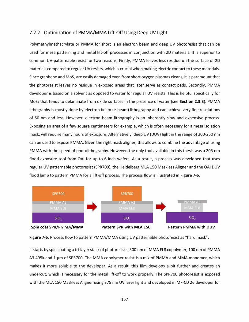
157
7.2.2 Optimization of PMMA/MMA Lift-Off Using Deep UV Light
Polymethylmethacrylate or PMMA for short is an electron beam and deep UV photoresist that can be
used for mesa patterning and metal lift-off processes in conjunction with 2D materials. It is superior to
common UV-patternable resist for two reasons. Firstly, PMMA leaves less residue on the surface of 2D
materials compared to regular UV resists, which is crucial when making electric contact to these materials.
Since graphene and MoS2 are easily damaged even from short oxygen plasmas cleans, it is paramount that
the photoresist leaves no residue in exposed areas that later serve as contact pads. Secondly, PMMA
developer is based on a solvent as opposed to water for regular UV resists. This is helpful specifically for
MoS2 that tends to delaminate from oxide surfaces in the presence of water (see Section 2.3.3). PMMA
lithography is mostly done by electron beam (e-beam) lithography and can achieve very fine resolutions
of 50 nm and less. However, electron beam lithography is an inherently slow and expensive process.
Exposing an area of a few square centimeters for example, which is often necessary for a mesa isolation
mask, will require many hours of exposure. Alternatively, deep UV (DUV) light in the range of 200-250 nm
can be used to expose PMMA. Given the right mask aligner, this allows to combine the advantage of using
PMMA with the speed of photolithography. However, the only tool available in this thesis was a 205 nm
flood exposure tool from OAI for up to 6-inch wafers. As a result, a process was developed that uses
regular UV patternable photoresist (SPR700), the Heidelberg MLA 150 Maskless Aligner and the OAI DUV
flood lamp to pattern PMMA for a lift-off process. The process flow is illustrated in Figure 7-6.
Figure 7-6: Process flow to pattern PMMA/MMA using UV patternable photoresist as “hard mask”.
It starts by spin coating a tri-layer stack of photoresists: 300 nm of MMA EL8 copolymer, 100 nm of PMMA
A3 495k and 1 µm of SPR700. The MMA copolymer resist is a mix of PMMA and MMA monomer, which
makes it more soluble to the developer. As a result, this film develops a bit further and creates an
undercut, which is necessary for the metal lift-off to work properly. The SPR700 photoresist is exposed
with the MLA 150 Maskless Aligner using 375 nm UV laser light and developed in MF-CD 26 developer for

158
90 seconds. All these steps do not affect the PMMA/MMA layers underneath. Next, the whole sample is
flood exposed in 205 nm deep UV light, which breaks the PMMA polymer chains and makes them soluble
to the MIBK developer. The patterned SPR700 layer absorbs the UV completely and hence acts as a
protective shield for the PMMA/MMA underneath. Subsequently, the whole sample is developed in a
mixture of methyl isobutyl ketone (MIBK) and isopropanol alcohol (IPA), which dissolves the SPR700 resist
as well as the exposed PMMA/MMA regions. To finish the lift-off process, a metal thin film is evaporated
on top and lifted-off in acetone. The process was optimized by first calibrating the needed DUV light dose
for both the PMMA and MMA copolymer resist, as shown in Figure 7-7.
Figure 7-7: Calibration of DUV dose to expose PMMA and MMA copolymer with a 1 mW/cm2 strong light
source. a) and c) Are optical images of developing PMMA and MMA after different exposure times,
respectively. b) and d) plot the develop resist step height in PMMA and MMA as a function of time.

159
Figure 7-7 a) and c) show optical micrographs of developed PMMA and MMA, respectively with different
times of DUV exposure. The PMMA film has a film thickness of about 200 nm (PMMA A4 495k, 3000 rpm
30 sec), while the MMA layer is about 500 nm thick (MMA EL11, 3000 rpm 30 sec). The PMMA and MMA
layer were completely exposed after 45 min and 20 min, respectively, based on the appearance of the
purple SiO2 substrate color in those cases. The exact correlation of exposure time to developed resist
thickness was obtained with DEKTAK step height measurements of the partially developed PMMA and
MMA films, as displayed in Figure 7-7 b) and d). The graphs show that developed thickness of photoresist
depends linearly on the exposure time with longer exposure times resulting in a thicker layer of developed
material. Based on these curves, a film combination of 100 nm PMMA/ 300 nm MMA is chosen as ideal
lift-off stack. Both layers combined should be exposed all the way in about 35 min. To add some buffer
time, the overall exposure time is set to 45 min.
The ratio of IPA:MIBK developer was also optimized. The standard ratio for developing PMMA is 2 parts
IPA to 1 part MIBK. However, this developer ratio leads to residue along the edges of developed areas, as
visualized in the optical micrograph top view and SEM micrograph side view in Figure 7-8. Changing the
developer ratio to 1:1 IPA/MIBK results in a much cleaner development. The complete process conditions
for the SPR/PMMA/MMA lift-off process as well as a SPR700/PMMA mesa etch process are outlined in
Sections 7.4.6 and 7.4.7.
Figure 7-8: Optimization of ratio of IPA to MIBK developer ratio. A 2:1 ratio leads to residue on the edges
of developed areas. Increasing the MIBK in the developer mix addresses this problem.
Lastly, the optimized process parameters were used to create metal pads with a minimum possible gap,
shown in Figure 7-9. Two 7x3 µm pads with a gap of 1.6 µm were written in SPR700 using the process
outline above. Figure 7-9 a) shows an SEM cross-section image of the gap after metal deposition but

160
before lift-off. The undercut due to the MMA resist layer is clearly visible. The undercut is much more
pronounced at the top as compared to the bottom of the MMA layer, which is likely due to the lowered
UV light intensity as the light propagates through the film because of absorption. The actual gap distance
is 830 nm, which is very helpful to make well performing transistors. An optical top view image of the two
pads after lift-off is given in Figure 7-9 b). The pads are clearly defined and the surface is clean. In
summary, the developed DUV-based PMMA/MMA lift-off process is a viable alternative to patterning
metal contacts on 2D materials without the need for e-beam lithography.
Figure 7-9: Optimized SPR700/PMMA/MMA lift-off process to make SD pads separated by a small gap. a)
Cross-section SEM image of gap between SD pads after metal deposition but before lift-off. b) Optical
micrograph of these SD pads after lift-off.
7.3 Undercutting and Lift-off Techniques
The last section of Chapter Error! Reference source not found. focuses on undercutting techniques to lift-o
ff 2D material-based microsystems from their fabrication substrate. Such a lift-off is most often achieved
by building the desired microsystem on a sacrificial layer such as an oxide or metal film that is undercut
as the last processing step and releases the above structures from the substrate. When designing a lift-off
mechanism for a microelectronic system, two aspects need to be considered. (1) The chosen release layer
material needs to withstand all following fabrication steps in terms of temperature and chemical stability
without degradation. For example, a silicon oxide release layer does not work in case the future processing

161
involves etching with hydrofluoric acid whereas an aluminum release layer would get etched away in
conjunction with piranha cleaning. (2) The release process itself cannot damage the microsystem
mechanically or chemically either. Using hydrofluoric acid, for example prohibits the use of silicon oxide,
silicon nitride or aluminum oxide, even if those films are protected by photoresist or other deposited film,
as further discussed below. In the frame of this thesis, several combinations of sacrificial layers, lift-off
methods and microsystem substrate layers have been tested. The following sections briefly discuss the
lift-off process optimization that has occurred in three generations of material systems.
7.3.1 First Generation Lift-Off System
The first lift-off system was designed to use 300 nm thermal silicon oxide as sacrificial layer and
hydrofluoric acid as undercutting agent. A protective 50 nm bottom layer of silicon nitride (SiN) and a top
7 µm thick polyimide (PI) were chosen to protect the 2D material-based electronics with aluminum oxide
dielectric in between. The entire release process is illustrated in Figure 7-10. To lift-off the microsystems,
they are first coated with a thin layer of PMMA to keep them all together once they detach from the
surface. Next, the silicon oxide sacrificial layer is undercut in 10% HF solution. Lastly, the PMMA
membrane with microsystems is scooped out with a silicon wafer and transferred into acetone to dissolve
the PMMA and release the microsystems.
Figure 7-10: First-generation lift-off concept. First, a microsystem protected by SiN and PI is fabricated.
The entire substrate is then coated with PMMA and the SiO2 sacrificial layer is undercut in HF. Lastly, the
membrane with microsystems is transferred into acetone to dissolve the PMMA.
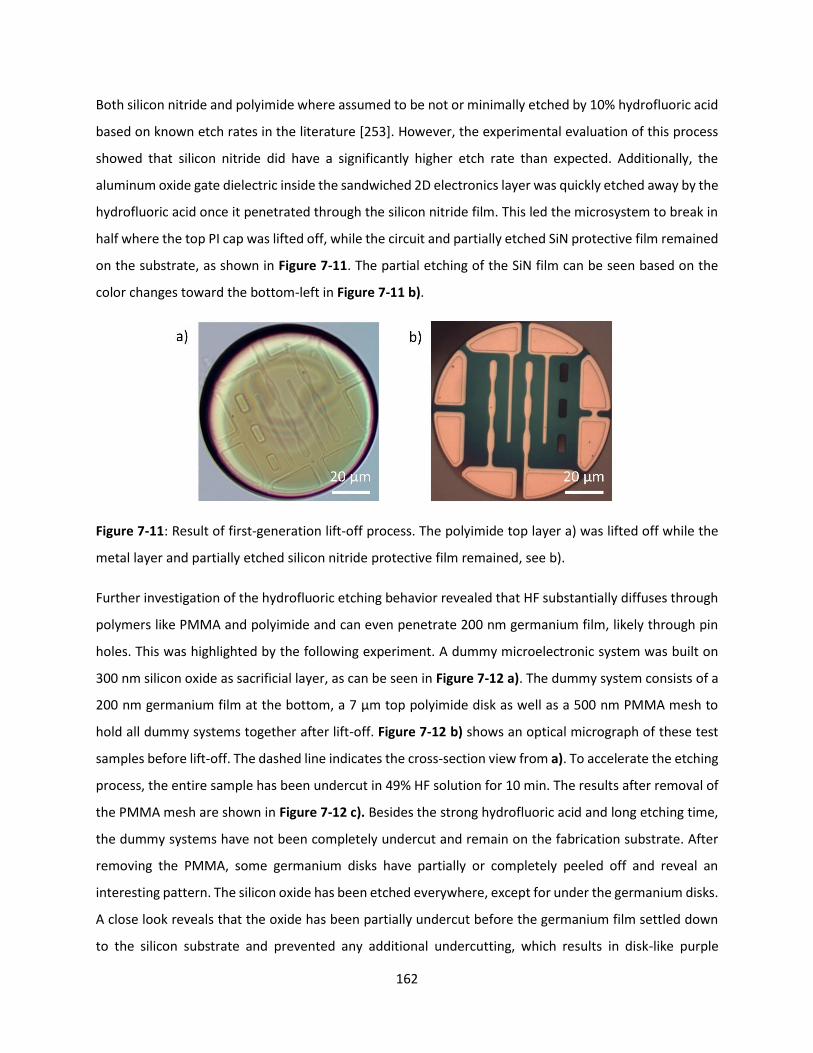
162
Both silicon nitride and polyimide where assumed to be not or minimally etched by 10% hydrofluoric acid
based on known etch rates in the literature [253]. However, the experimental evaluation of this process
showed that silicon nitride did have a significantly higher etch rate than expected. Additionally, the
aluminum oxide gate dielectric inside the sandwiched 2D electronics layer was quickly etched away by the
hydrofluoric acid once it penetrated through the silicon nitride film. This led the microsystem to break in
half where the top PI cap was lifted off, while the circuit and partially etched SiN protective film remained
on the substrate, as shown in Figure 7-11. The partial etching of the SiN film can be seen based on the
color changes toward the bottom-left in Figure 7-11 b).
Figure 7-11: Result of first-generation lift-off process. The polyimide top layer a) was lifted off while the
metal layer and partially etched silicon nitride protective film remained, see b).
Further investigation of the hydrofluoric etching behavior revealed that HF substantially diffuses through
polymers like PMMA and polyimide and can even penetrate 200 nm germanium film, likely through pin
holes. This was highlighted by the following experiment. A dummy microelectronic system was built on
300 nm silicon oxide as sacrificial layer, as can be seen in Figure 7-12 a). The dummy system consists of a
200 nm germanium film at the bottom, a 7 µm top polyimide disk as well as a 500 nm PMMA mesh to
hold all dummy systems together after lift-off. Figure 7-12 b) shows an optical micrograph of these test
samples before lift-off. The dashed line indicates the cross-section view from a). To accelerate the etching
process, the entire sample has been undercut in 49% HF solution for 10 min. The results after removal of
the PMMA mesh are shown in Figure 7-12 c). Besides the strong hydrofluoric acid and long etching time,
the dummy systems have not been completely undercut and remain on the fabrication substrate. After
removing the PMMA, some germanium disks have partially or completely peeled off and reveal an
interesting pattern. The silicon oxide has been etched everywhere, except for under the germanium disks.
A close look reveals that the oxide has been partially undercut before the germanium film settled down
to the silicon substrate and prevented any additional undercutting, which results in disk-like purple
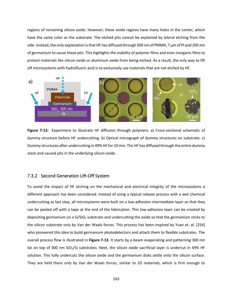
163
regions of remaining silicon oxide. However, these oxide regions have many holes in the center, which
have the same color as the substrate. The etched pits cannot be explained by lateral etching from the
side. Instead, the only explanation is that HF has diffused through 500 nm of PMMA, 7 µm of PI and 200 nm
of germanium to cause these pits. This highlights the inability of polymer films and even inorganic films to
protect materials like silicon oxide or aluminum oxide from being etched. As a result, the only way to lift
off microsystems with hydrofluoric acid is to exclusively use materials that are not etched by HF.
Figure 7-12: Experiment to illustrate HF diffusion through polymers. a) Cross-sectional schematic of
dummy structure before HF undercutting. b) Optical micrograph of dummy structures on substrate. c)
Dummy structures after undercutting in 49% HF for 10 min. The HF has diffused through the entire dummy
stack and caused pits in the underlying silicon oxide.
7.3.2 Second Generation Lift-Off System
To avoid the impact of HF etching on the mechanical and electrical integrity of the microsystems a
different approach has been considered. Instead of using a typical release process with a wet chemical
undercutting as last step, all microsystems were built on a low-adhesion intermediate layer so that they
can be peeled off with a tape at the end of the fabrication. This low-adhesion layer can be created by
depositing germanium on a Si/SiO2 substrate and undercutting the oxide so that the germanium sticks to
the silicon substrate only by Van der Waals forces. This process has been inspired by Yuan et. al. [254]
who pioneered this idea to build germanium photodetectors and attach them to flexible substrates. The
overall process flow is illustrated in Figure 7-13. It starts by e-beam evaporating and patterning 300 nm
Ge on top of 300 nm SiO2/Si substrates. Next, the silicon oxide sacrificial layer is undercut in 49% HF
solution. This fully undercuts the silicon oxide and the germanium disks settle onto the silicon surface.
They are held there only by Van der Waals forces, similar to 2D materials, which is firm enough to
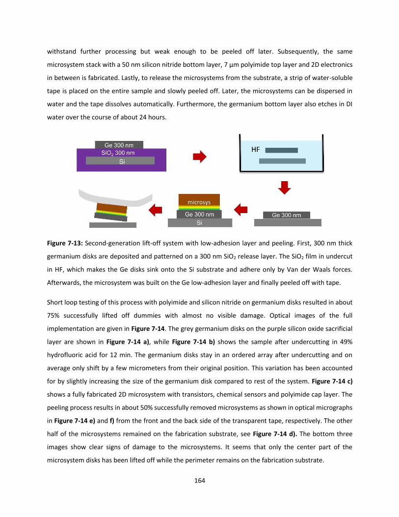
164
withstand further processing but weak enough to be peeled off later. Subsequently, the same
microsystem stack with a 50 nm silicon nitride bottom layer, 7 µm polyimide top layer and 2D electronics
in between is fabricated. Lastly, to release the microsystems from the substrate, a strip of water-soluble
tape is placed on the entire sample and slowly peeled off. Later, the microsystems can be dispersed in
water and the tape dissolves automatically. Furthermore, the germanium bottom layer also etches in DI
water over the course of about 24 hours.
Figure 7-13: Second-generation lift-off system with low-adhesion layer and peeling. First, 300 nm thick
germanium disks are deposited and patterned on a 300 nm SiO2 release layer. The SiO2 film in undercut
in HF, which makes the Ge disks sink onto the Si substrate and adhere only by Van der Waals forces.
Afterwards, the microsystem was built on the Ge low-adhesion layer and finally peeled off with tape.
Short loop testing of this process with polyimide and silicon nitride on germanium disks resulted in about
75% successfully lifted off dummies with almost no visible damage. Optical images of the full
implementation are given in Figure 7-14. The grey germanium disks on the purple silicon oxide sacrificial
layer are shown in Figure 7-14 a), while Figure 7-14 b) shows the sample after undercutting in 49%
hydrofluoric acid for 12 min. The germanium disks stay in an ordered array after undercutting and on
average only shift by a few micrometers from their original position. This variation has been accounted
for by slightly increasing the size of the germanium disk compared to rest of the system. Figure 7-14 c)
shows a fully fabricated 2D microsystem with transistors, chemical sensors and polyimide cap layer. The
peeling process results in about 50% successfully removed microsystems as shown in optical micrographs
in Figure 7-14 e) and f) from the front and the back side of the transparent tape, respectively. The other
half of the microsystems remained on the fabrication substrate, see Figure 7-14 d). The bottom three
images show clear signs of damage to the microsystems. It seems that only the center part of the
microsystem disks has been lifted off while the perimeter remains on the fabrication substrate.

165
The following conclusion were drawn from this alternative peeling lift-off approach. While short loop
testing of the peeling process resulted in no to very little damage to the disks, the fully microsystems are
decidedly more damaged around the perimeter, which likely is a result of the additional fabrication steps.
The achieved lift-off yield of 50% is tolerable but values closer to 100% are desirable. As a result, a new
approach is needed.
Figure 7-14: Optical micrographs from low-adhesion peeling lift-off process. a) Ge disks on SiO2 sacrificial
layer. b) Ge disks on Si after undercutting SiO2 layer. c) Complete microsystem fabricated on Ge disk. d)
Fabrication substrate after peeling off tape. e) Transparent tape from the front side after peeling. f) Sticky
back side of tape after peeling.
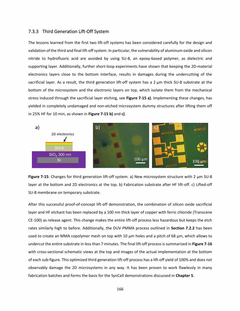
166
7.3.3 Third Generation Lift-Off System
The lessons learned from the first two lift-off systems has been considered carefully for the design and
validation of the third and final lift-off system. In particular, the vulnerability of aluminum oxide and silicon
nitride to hydrofluoric acid are avoided by using SU-8, an epoxy-based polymer, as dielectric and
supporting layer. Additionally, further short-loop experiments have shown that keeping the 2D-material
electronics layers close to the bottom interface, results in damages during the undercutting of the
sacrificial layer. As a result, the third generation lift-off system has a 2 µm thick SU-8 substrate at the
bottom of the microsystem and the electronic layers on top, which isolate them from the mechanical
stress induced through the sacrificial layer etching, see Figure 7-15 a). Implementing these changes, has
yielded in completely undamaged and non-etched microsystem dummy structures after lifting them off
in 25% HF for 10 min, as shown in Figure 7-15 b) and c).
Figure 7-15: Changes for third generation lift-off system. a) New microsystem structure with 2 µm SU-8
layer at the bottom and 2D electronics at the top. b) Fabrication substrate after HF lift-off. c) Lifted-off
SU-8 membrane on temporary substrate.
After this successful proof-of-concept lift-off demonstration, the combination of silicon oxide sacrificial
layer and HF etchant has been replaced by a 100 nm thick layer of copper with ferric chloride (Transcene
CE-100) as release agent. This change makes the entire lift-off process less hazardous but keeps the etch
rates similarly high to before. Additionally, the DUV PMMA process outlined in Section 7.2.2 has been
used to create an MMA copolymer mesh on top with 10 µm holes and a pitch of 68 µm, which allows to
undercut the entire substrate in less than 7 minutes. The final lift-off process is summarized in Figure 7-16
with cross-sectional schematic views at the top and images of the actual implementation at the bottom
of each sub-figure. This optimized third generation lift-off process has a lift-off yield of 100% and does not
observably damage the 2D microsystems in any way. It has been proven to work flawlessly in many
fabrication batches and forms the basis for the SynCell demonstrations discussed in Chapter 5.
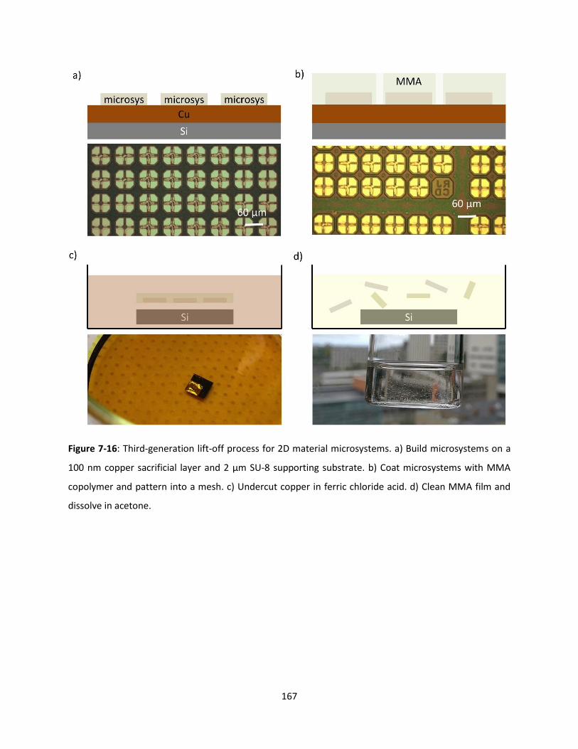
167
Figure 7-16: Third-generation lift-off process for 2D material microsystems. a) Build microsystems on a
100 nm copper sacrificial layer and 2 µm SU-8 supporting substrate. b) Coat microsystems with MMA
copolymer and pattern into a mesh. c) Undercut copper in ferric chloride acid. d) Clean MMA film and
dissolve in acetone.

168
7.4 Processes
7.4.1 LPCVD Graphene Growth on Copper Foil
Step 1 Turn on Pump
Turn on pump Turn on vacuum pump of graphene growth line 1h prior to growth to warm
up and achieve a good base pressure.
Step 2 Prepare Cu Foil
Cut Cu foil Cut copper foil (25 µm thick) into strips of 1.5”x6”.
Clean Cu foil Clean copper foil in beaker with nickel etchant (Transcene, TFB nickel etch)
for 60 seconds while sonicating the beaker. The ultrasound helps remove gas
bubble that form during the light surface etching.
Step 3 Load Tube
Bend foil Bend cleaned copper foil along the short side into and arc and place in 25 mm
ID quartz tube.
Connect flanges Place tube in a clamshell furnace and connect vacuum flanges.
Step 4 Graphene Growth
Evacuate tube Open all vacuum valves, fully evacuate the quartz tube and check base
pressure, should be about 10-20 mTorr.
Program furnace Program the furnace temperature profile according to Figure 2-7 in Chapter
2.
Set initial gas flow Set the gas flow to 10 sccms hydrogen.
Start furnace Start the furnace program.
Change gases Change the gas flows after 1 h to 60 sccm hydrogen and 3 sccm methane.

169
Wait Wait for the growth to finish
Cool down Let the furnace cool down to 600°C without opening it. Once 600°C is reached
open the lid and turn on fan to cool down to 100°C.
Turn off gasses Turn off all gas flows and wait for line to reach base pressure again.
Turn off vacuum Turn off all valves and then turn off the vacuum pump.
Step 5 Unload Tube
Disconnect flanges Open one of the vacuum flanges on the quartz tube carefully, the vacuum will
break automatically, and the tube will slowly fill with air. Open the other
flange, take out the quartz tube and tilt to slide out the copper foil.
Take out graphene Place on a clean sheet of paper and bend flat by lightly touching the edges.
Cut graphene Cut flattened copper foil with graphene into needed size, e.g. 1x1 cm.
7.4.2 Wet Etch Graphene Transfer in FeCl3
Step 1 Spin Coat PMMA
PET support film Cut out a 2x2 cm piece of roughly 250 µm thick PET film.
Attach Cu on PET Place copper with graphene on the PET film to add support during the spin
coating. Attach copper film to PET film by taping it with scotch tape along all
edges. This prevents from getting PMMA on the back side of the copper
during spin coating.
Spin coat PMMA Spin coat PMMA A6 950 on the copper foil with graphene at 2500 rpms for 60
seconds.
Bake Dry PET/Cu/Gr/PMMA stack in oven set to 130°C for 15 min.

170
Remove PET Take sample out of the oven and remove scotch tape.
Step 2 Etch Copper Back Side (Optional)
ash the back side of the PMMA/Gr/Cu/Gr sample in an oxygen plasma to
remove the graphene on the back side of the Cu foil. This can be done for
example in the asher on the Onelab (etch time about 15 seconds).
Step 3 Etch Cu foil
Etch Cu in FeCl3 Place Cu/Gr/PMMA film onto a dish filled with copper etchant (Transcene, CE-
100 Cu etch). The 25 µm thick copper foil etches in about 10 to 15 min. After
the etching is done, the Gr/PMMA film should be completely transparent and
floating on the copper etchant solution.
Clean PMMA/Gr Transfer the Gr/PMMA film with a glass slide into two consecutive dishes
filled with DI water to clean of any copper etchant from the film. Leave them
in each dish for about 1 min.
HCl etch Transfer the Gr/PMMA film into a dish filled with 10% hydrochloric acid to
further clean the bottom surface of the graphene and leave it there for 10
min.
Rinse PMMA/Gr Transfer the Gr/PMMA film with a glass slide into two more DI water dishes
and let them soak for 1 min and 5 min respectively.
Step 4 Transfer Graphene
Scoop up PMMA/Gr Pick up the Gr/PMMA film with the target substrate. This needs some practice
to do well. Make sure that the Gr/PMMA film is on the target substrate
without any wrinkles.
Blow Dry PMMA/Gr Blow dry the Gr/PMMA film on top of the target sample with nitrogen to
remove water from under the film. Start blow drying very gently. Keep the
gun nozzle about 2-5 cm away from the surface and exactly perpendicular to

171
it. Increase the nitrogen flow to its maximum after about 5 seconds and keep
blow drying for 20-30 seconds.
Bake at 80°C Bake the sample first for 15 min in an oven at 80°C to remove any additional
water. After the first bake, the PMMA should show rainbow colors due to
interference effects, which shows that all water is gone.
Bake at 130°C Bake the sample for 15 min in an oven at 130°C to soften the PMMA. This
helps with a more conformal transfer of graphene.
Cool down sample Take out the sample and let it cool down for 5 min.
Remove PMMA Immerse the sample in a beaker of acetone for 5 min. Do not add any
agitation. This is a critical step where the graphene may break.
Rinse sample with IPA Take out the sample from the acetone bath and immediately and very lightly
squirt it with isopropanol to remove the acetone before it dries.
Blow dry and inspect Gently blow dry the sample with nitrogen. Now the transfer quality can be
evaluated under the microscope.
Anneal Anneal the graphene film on the target substrate for 2h at 360°C in 200 sccm
of Argon and 200 sccm of hydrogen. This will remove organic residues on the
surface and improve the electrical performance of the graphene film.
7.4.3 Wet Etch MoS2 Transfer in HF
Step 1 Spin Coat PMMA
Cleave to size Cleave Si/SiO2/MoS2 pieces into desired size, for example 2x2 cm.
Spin coat PMMA Spin coat PMMA A6 950 on piece at 3000 rpm for 30 seconds and bake for 1
min at 150°C.

172
Scrape off edges Scrape off about 1 mm of PMMA along the edges with a razor blade
Step 2 Undercut in HF
Grab sample Grab samples with a pair of tweezers on the sides of the sample so that the
top surface is unobstructed.
Etch in HF Immerse sample into a plastic beaker filled with 10% HF in DI water for 30
seconds. The sample should be held parallel to the water surface and should
be immersed about 10 mm. The HF acid now rapidly undercuts the silicon
oxide at the interface between the SiO2 and MoS2. This happens faster than
the whole silicon oxide layer takes to etch.
Take out sample After 30 seconds slowly and vertically pull up the sample out of the solution.
The film should be already fully detached from the surface and show some
wrinkles.
Rinse in DI water Gently place it in another beaker filled with DI water. The MoS2/PMMA will
automatically come off from the sample and float on the water surface.
Transfer MoS2/PMMA with a piece of a silicon water into three consecutive
beakers filled with DI water to clean the sample and let it soak for 1 min each.
Step 3 Transfer MoS2
Scoop up film Pick up the MoS2/PMMA film with the target substrate. This needs some
practice to do well. Make sure that the MoS2/PMMA film is on the target
substrate without any wrinkles.
Blow-dry PMMA/MoS2 Blow dry the MoS2/PMMA film on top of the target sample with nitrogen to
remove water from under the film. Start blow drying very gently. Keep the
gun nozzle about 2-5 cm away from the surface and exactly perpendicular to
it. Slowly increase the nitrogen flow to its maximum after about 5 seconds
and keep blow drying for 20-30 seconds.

173
Bake at 80°C Bake the sample first for 30 min on a hotplate at 80°C to remove any
additional water. After the first bake, the PMMA should show rainbow colors
due to interference effects, which shows that all water is gone.
Bake at 150°C Bake the sample on a hotplate for 15 min at 150°C to soften the PMMA. This
helps with a more conformal transfer of graphene.
Cool down Take off the sample and let it cool down for 5 min.
Remove PMMA Immerse the sample in a beaker of acetone for 5 min. Don’t add any
agitation. This is a critical step where the graphene may break.
Rinse with IPA Take out the sample from the acetone bath and immediately and very lightly
squirt it with isopropanol to remove the acetone before it dries.
Blow dry sample Gently blow dry the sample with nitrogen. Now the transfer quality can be
evaluated under the microscope.
Anneal Anneal the MoS2 film on the target substrate for 1h in at 360°C in nitrogen or
argon if permitted by the substrate. This will remove organic residues on the
surface and improve the electrical performance of the MoS2 film.
7.4.4 Electrochemical Transfer of hBN or Graphene in NaOH solution
Step 1 Spin Coat PMMA
PET support film Cut out a 2x2 cm piece of roughly 250 µm thick PET film.
Attach Cu on PET Place copper foil with graphene or platinum foil with hBN on the PET film to
add support during the spin coating. Attach metal film to PET film by taping it
with scotch tape along all edges. This prevents from getting PMMA on the
back side of the copper during spin coating.

174
Spin coat PMMA Spin coat PMMA A6 950 on the metal foil at 2500 rpms for 60 seconds.
Bake Dry PET/Cu/Gr/PMMA or PET/Pt/hBN/PMMA stack in oven set to 130°C for
15 min.
Remove PET Take sample out of the oven and remove scotch tape.
Coat back side with PMMA
Repeat steps to coat PMMA on the opposite side of the copper or platinum
foil. Graphene or hBN grow on both sides of the metal foil so both films can
be used later.
Step 2 Electrochemically delaminate 2D material
Soak Place the double-coated metal foil in a beaker filled with 1 mol/liter sodium
hydroxide (NaOH) solution and soak for 30 min. This helps improve the
delamination later.
Attach power supply and turn on
Take out the foil and attach it to the black alligator clip connected to ground.
Attach a platinum mesh to the red alligator clip connected to the positive
potential. Immerse the platinum mesh electrode in a beaker with the 1 mol
NaOH solution as shown in Figure 2-15. Turn on the power supply and set the
voltage to 3.5 V. Switch the display over to monitor the current.
Lower metal foil Slowly lower the metal foil with PMMA on both sides into the solution so that
the metal foil touches the solution and is just at the level where the PMMA
film begins. The initial current should be around 50 mA for a 1x2 cm sample.
Adjust the voltage as necessary to get this current. You should see bubble
forming at both the platinum mesh and the copper or platinum foil.
Delaminate Once the PMMA/2D material film on both sides starts to delaminate continue
to slowly lower the metal foil into the solution by using the vertical
translation stage. If the film gets stuck or does not move any further, try
pulling out the metal foil a little and lower it back down. As the foil is lowered
into the electrolyte solution, the current will increase.
175
Raise Cu or Pt foil Once both films are fully delaminated from the solution, carefully raise up the
copper or platinum foil and turn off the power supply.
Rinse PMMA/2D film Transfer the Gr/PMMA or hBN/PMM film with a glass slide into two
consecutive DI water dishes and let them soak for 1 min and 5 min,
respectively, to clean them from the NaOH solution.
Step 3 Transfer Graphene or hBN
Scoop up Pick up the Gr/PMMA or hBN/PMM film with the target substrate. This needs
some practice. Make sure that film is on the target substrate without any
wrinkles.
Blow Dry Blow dry the Gr/PMMA film on top of the target sample with nitrogen to
remove water from under the film. Start blow drying very gently. Keep the
gun nozzle about 2-5 cm away from the surface and exactly perpendicular to
it. Increase the nitrogen flow to its maximum after about 5 seconds and keep
blow drying for 20-30 seconds.
Bake at 80°C Bake the sample first for 15 min in an oven at 80°C to remove any additional
water. After the first bake, the PMMA should show rainbow colors due to
interference effects, which shows that all water is gone.
Bake at 130°C Bake the sample for 15 min in an oven at 130°C to soften the PMMA. This
helps with a more conformal transfer of graphene.
Cool down sample Take out the sample and let it cool down for 5 min.
Remove PMMA Immerse the sample in a beaker of acetone for 5 min. Don’t add any
agitation. This is a critical step where the graphene may break.
Rinse in IPA Take out the sample from the acetone bath and immediately and very lightly
squirt it with isopropanol to remove the acetone before it dries.

176
Blow dry and inspect Gently blow dry the sample with nitrogen. Now the transfer quality can be
evaluated under the microscope.
Anneal Lastly, anneal the graphene or hBN film on the target substrate for 2h at
360°C in 200 sccm of Argon and 200 sccm of hydrogen. This will remove
organic residues on the surface and improve the electrical performance of the
graphene film.
7.4.5 Water Delamination of MoS2
Step 1 Spin Coat PMMA
Cleave to size Cleave Si/SiO2/MoS2 pieces into desired size, for example 2x2 cm.
Spin coat PMMA Spin coat PMMA A6 950 on piece at 3000 rpm for 30 seconds and bake for 1
min at 150°C.
Scrape off edges Scrape off about 1 mm of PMMA along the edges with a razor blade
Step 2 Delaminate PMMA/MoS2
Lift PMMA edge Take a pipette and add a small water droplet to one of the four edges of the
PMMA/MoS2 film. Use a sharp razor blade and very gently scrape this edge of
the film back and forth (about 0.5 mm) to lift up the PMMA/MoS2 film.
Grab sample Grab samples with tweezers on the sides so that the top is unobstructed.
Delaminate film Immerse sample into a plastic beaker filled DI at a 45° angle and with the
edge that has been scraped. Keep the edge of the PMMA/MoS2 film just at
about water level until it lifts up. Slowly lower the sample into the DI water
beaker while the PMMA/MoS2 film sheers off onto the water surface. If the

177
film gets stuck take out the sample, poke the corresponding point gently with
the razor blade and continue the delamination.
Step 3 Transfer MoS2
Scoop up film Once the PMMA/MoS2 film is floating on the surface, pick it up with the
target substrate. This needs some practice to do well. Make sure that the film
is on the target substrate without any wrinkles.
Blow-dry PMMA/MoS2 Blow dry the MoS2/PMMA film on top of the target sample with nitrogen to
remove water from under the film. Start blow drying very gently. Keep the
gun nozzle about 2-5 cm away from the surface and exactly perpendicular to
it. Slowly increase the nitrogen flow to its maximum after about 5 seconds
and keep blow drying for 20-30 seconds.
Bake at 80°C Bake the sample first for 30 min on a hotplate at 80°C to remove any
additional water. After the first bake, the PMMA should show rainbow colors
due to interference effects, which shows that all water is gone.
Bake at 150°C Bake the sample on a hotplate for 15 min at 150°C to soften the PMMA. This
helps with a more conformal transfer of graphene.
Cool down Take off the sample and let it cool down for 5 min.
Remove PMMA Immerse the sample in a beaker of acetone for 5 min. Don’t add any
agitation. This is a critical step where the graphene may break.
Rinse with IPA Take out the sample from the acetone bath and immediately and very lightly
squirt it with isopropanol to remove the acetone before it dries.
Blow dry sample Gently blow dry the sample with nitrogen. Now the transfer quality can be
evaluated under the microscope.
Anneal Anneal the MoS2 film on the target substrate for 1h in at 360°C in N2 or Ar.
This removes organic residues and improve the electrical performance.

178
7.4.6 SPR700-PMMA A3 Deep UV Photo Lithography for Mesa Etching
The recipe below works as a two-step lithography and development process. First, PMMA and SPR700 are
spin-coated one after the other and backed. Second, a regular photolithography tool, such as the MLA-
150, is used to pattern the SPR resist and develop it in MF-CD-26. This now created a polymer-based hard
mask that is used for a PMMA flood exposure with deep UV light. PMMA is not sensitive to regular UV-
wavelengths such as 375 or 405 nm. However, a wavelength of 205 nm can expose PMMA sufficiently.
NSL possess a flood exposure tool with a 205 nm wavelength (talk to James Daley for training). After a
long flood exposure, the PMMA/SPR700 stack can be developed in a mixture of MIBK and IPA. This
developer naturally dissolves the SPR700 resist as well as the exposed regions of the PMMA. However,
residue formation (likely from the SPR700) has sometimes been observed along the perimeter of all
features. To prevent this, a light agitation with a pipette during the development process is
recommended. The fully developed samples can now be used for mesa etching. Finally, the PMMA can
simply be removed by rinsing it in acetone. The recipe details are given below.
Step 1 Transfer 2D Material
Clean Clean substrate surface
Transfer Transfer 2D materials such as graphene or MoS2
Step 2 Spin Coating, Exposure, Development
Spin coat PMMA Spin coat PMMA 495 A4 at 3 krpm for 30 sec (thickness – 200 nm)
Bake at 150°C for 1 min (set coater hotplate to 170)
Spin coat SPR Spin coat SPR700 at 3 krpm for 30 sec
Develop SPR Expose SPR with 100 mJ/cm2 using MLA-150
Post Exposure bake at 115°C PEB for 1min (hotplate 1)
Develop in MF-CD-26 for 75 sec, rinse with DI water and blow dry
179
Flood expose PMMA Flood expose sample for 45 min under 205 nm deep UV light in NSL (1 mW/cm2)
Develop PMMA Develop in 1:1 MIBK/IPA for 90 sec and agitate with pipette
Rinse Rinse in IPA and blow dry
Step 3 Etch 2D Material
Etch Etch 2D materials for 5 min at 800 W
Remove acetone Soak sample in acetone for 5 min to remove PMMA
IPA rinse Take out sample and rinse gently with IPA
Blow dry and inspect Blow dry sample and inspect
7.4.7 SPR700-PMMA-MMA Deep UV Photo Lithography for Lift-Off
The recipe below works by a two-step lithography and development process. First, MMA, PMMA and
SPR700 are spin-coated one after the other and backed. Second, a regular photolithography tool, such as
the MLA-150, can be used to pattern the SPR resist and develop it in MF-CD-26. This created a polymer-
based hard mask that is used for an MMA/PMMA flood exposure with deep UV light. Both MMA and
PMMA are not sensitive to regular UV-wavelengths such as 375 or 405 nm. However, a wavelength of 205
nm can expose PMMA sufficiently. NSL possess a flood exposure tool with a 205 nm wavelength (talk to
James Daley for training). After a long flood exposure, the MMA/PMMA/SPR700 stack can be developed
in a mixture of MIBK and IPA. This developer naturally dissolves the SPR700 resist as well as the exposed
regions of the MMA and PMMA. However, residue formation (likely from the SPR700) has sometimes
been observed along the perimeter of all features. To prevent that, a light agitation with a pipette during
the development process is recommended. The MMA layer is developed slightly more than the PMMA,
which creates an undercut. The fully developed samples can now be used to evaporate metal and lift them
off in acetone. The recipe details are given below.

180
Step 1 Spin Coating, Exposure, Development
Spin coat MMA
copolymer
Spin coat MMA 8.5 EL8 at 3 krpm for 30 sec (thickness – 300 nm)
Bake at 150°C for 1 min (set coater hotplate to 170)
Spin coat PMMA Spin coat PMMA 495 A3 at 3 krpm for 30 sec (thickness – 100 nm)
Bake at 150°C for 1 min (set coater hotplate to 170)
Spin coat SPR Spin coat SPR700 at 3 krpm for 30 sec
Develop SPR Expose SPR with 100 mJ/cm2 using MLA-150
Post Exposure bake at 115°C PEB for 1min (hotplate 1)
Develop in MF-CD-26 for 75 sec, rinse with DI water and blow dry
Flood expose PMMA Flood expose sample for 40 min under 205 nm deep UV light in NSL (1 mW/cm2)
Develop PMMA Develop in 1:1 MIBK/IPA for 90 sec and agitate with pipette
Rinse Rinse in IPA and blow dry
Step 3 Etch 2D Material
Deposit metal E-beam evaporate metal up to 150 nm in thickness
Lift-off Lift-off metal film in acetone for several hours or over night
IPA rinse Take out sample and rinse gently with IPA
Blow dry and inspect Blow dry sample and inspect
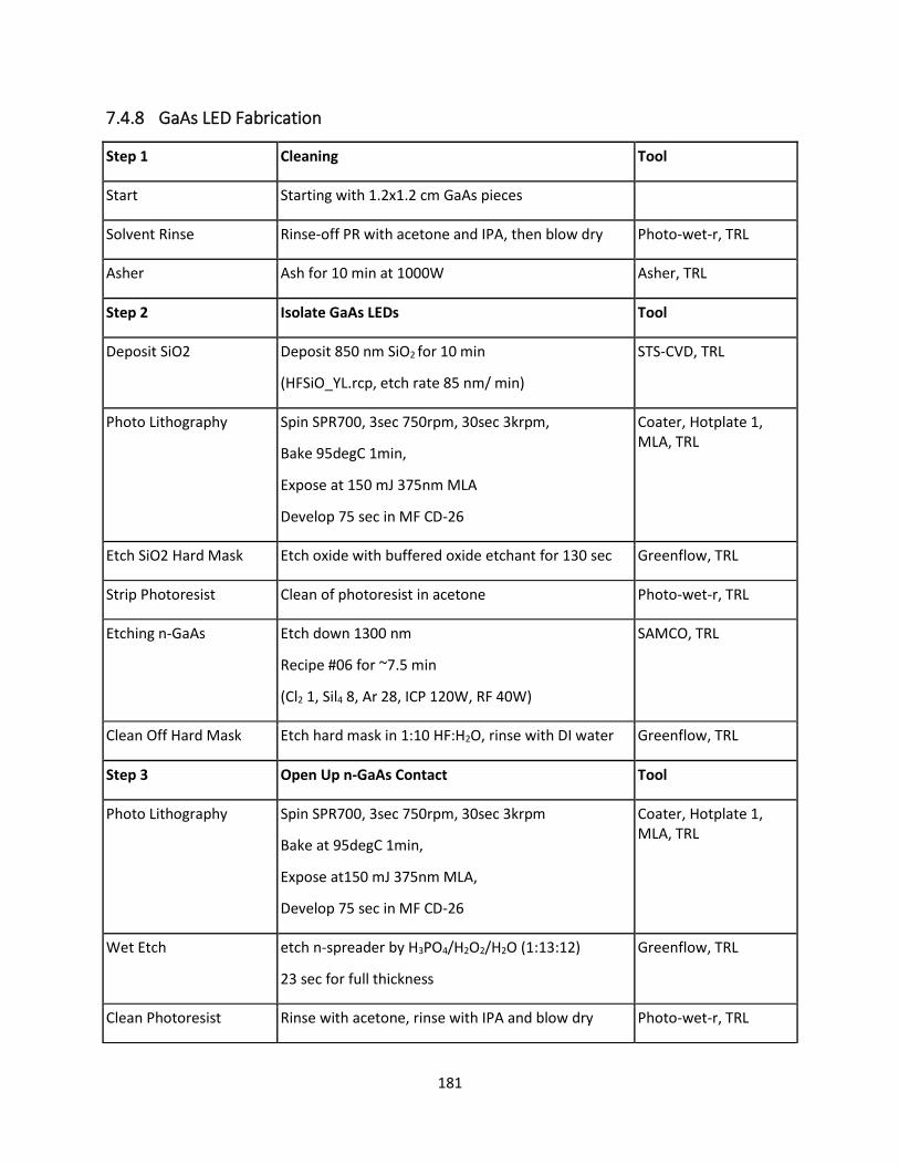
181
7.4.8 GaAs LED Fabrication
Step 1 Cleaning Tool
Start Starting with 1.2x1.2 cm GaAs pieces
Solvent Rinse Rinse-off PR with acetone and IPA, then blow dry Photo-wet-r, TRL
Asher Ash for 10 min at 1000W Asher, TRL
Step 2 Isolate GaAs LEDs Tool
Deposit SiO2 Deposit 850 nm SiO2 for 10 min
(HFSiO_YL.rcp, etch rate 85 nm/ min)
STS-CVD, TRL
Photo Lithography Spin SPR700, 3sec 750rpm, 30sec 3krpm,
Bake 95degC 1min,
Expose at 150 mJ 375nm MLA
Develop 75 sec in MF CD-26
Coater, Hotplate 1, MLA, TRL
Etch SiO2 Hard Mask Etch oxide with buffered oxide etchant for 130 sec Greenflow, TRL
Strip Photoresist Clean of photoresist in acetone Photo-wet-r, TRL
Etching n-GaAs Etch down 1300 nm
Recipe #06 for ~7.5 min
(Cl2 1, Sil4 8, Ar 28, ICP 120W, RF 40W)
SAMCO, TRL
Clean Off Hard Mask Etch hard mask in 1:10 HF:H2O, rinse with DI water Greenflow, TRL
Step 3 Open Up n-GaAs Contact Tool
Photo Lithography Spin SPR700, 3sec 750rpm, 30sec 3krpm
Bake at 95degC 1min,
Expose at150 mJ 375nm MLA,
Develop 75 sec in MF CD-26
Coater, Hotplate 1, MLA, TRL
Wet Etch etch n-spreader by H3PO4/H2O2/H2O (1:13:12)
23 sec for full thickness
Greenflow, TRL
Clean Photoresist Rinse with acetone, rinse with IPA and blow dry Photo-wet-r, TRL
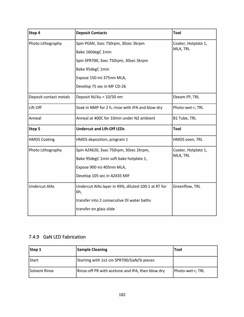
182
Step 4 Deposit Contacts Tool
Photo Lithography Spin PGMI, 3sec 750rpm, 30sec 3krpm
Bake 160degC 1min
Spin SPR700, 3sec 750rpm, 30sec 3krpm
Bake 95degC 1min
Expose 150 mJ 375nm MLA,
Develop 75 sec in MF CD-26
Coater, Hotplate 1, MLA, TRL
Deposit contact metals Deposit Ni/Au = 10/50 nm Ebeam FP, TRL
Lift-Off Soak in NMP for 2 h, rinse with IPA and blow dry Photo-wet-r, TRL
Anneal Anneal at 400C for 10min under N2 ambient B1 Tube, TRL
Step 5 Undercut and Lift-Off LEDs Tool
HMDS Coating HMDS deposition, program 1 HMDS oven, TRL
Photo Lithography Spin AZ4620, 3sec 750rpm, 30sec 2krpm,
Bake 95degC 1min soft bake hotplate 1,
Expose 900 mJ 405nm MLA,
Develop 105 sec in AZ435 MIF
Coater, Hotplate 1, MLA, TRL
Undercut AlAs Undercut AlAs layer in 49%, diluted 100:1 at RT for 6h,
transfer into 2 consecutive DI water baths
transfer on glass slide
Greenflow, TRL
7.4.9 GaN LED Fabrication
Step 1 Sample Cleaning Tool
Start Starting with 1x1 cm SPR700/GaN/Si pieces
Solvent Rinse Rinse-off PR with acetone and IPA, then blow dry Photo-wet-r, TRL
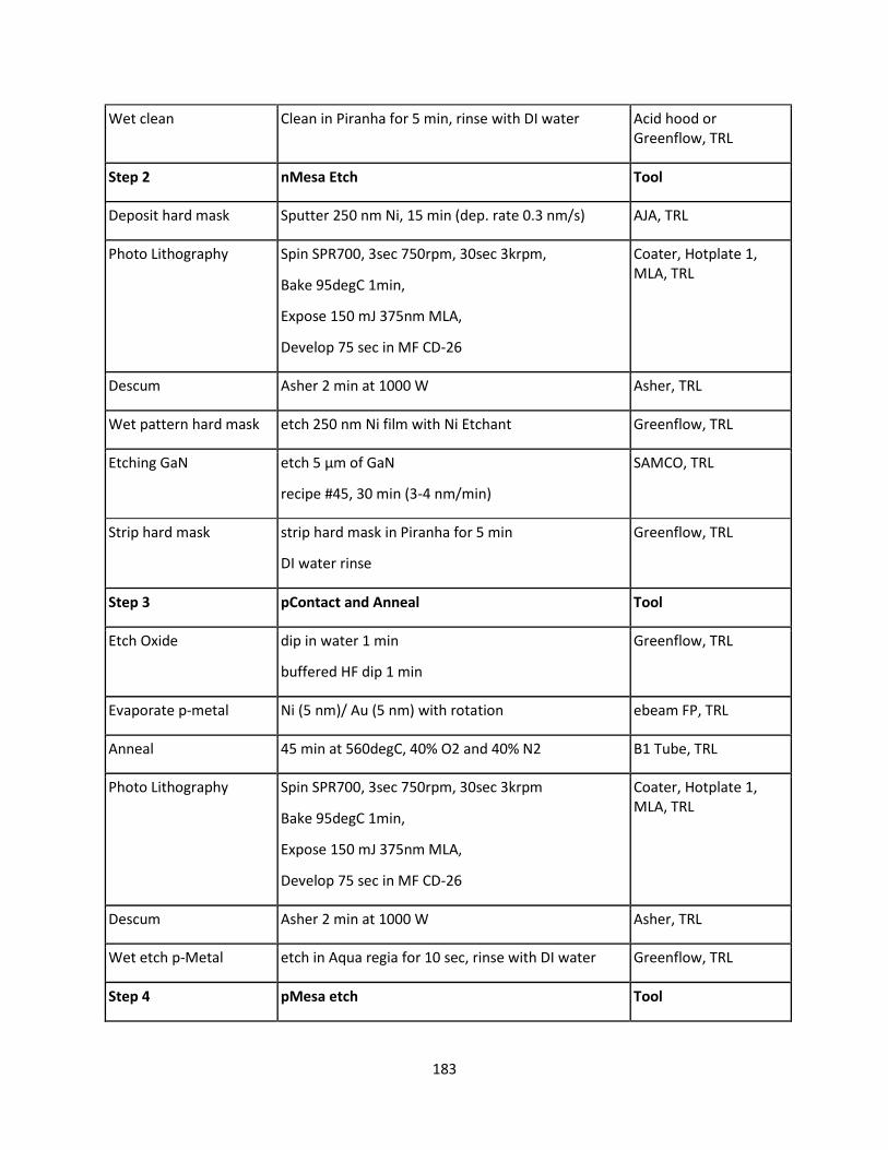
183
Wet clean Clean in Piranha for 5 min, rinse with DI water Acid hood or Greenflow, TRL
Step 2 nMesa Etch Tool
Deposit hard mask Sputter 250 nm Ni, 15 min (dep. rate 0.3 nm/s) AJA, TRL
Photo Lithography Spin SPR700, 3sec 750rpm, 30sec 3krpm,
Bake 95degC 1min,
Expose 150 mJ 375nm MLA,
Develop 75 sec in MF CD-26
Coater, Hotplate 1, MLA, TRL
Descum Asher 2 min at 1000 W Asher, TRL
Wet pattern hard mask etch 250 nm Ni film with Ni Etchant Greenflow, TRL
Etching GaN etch 5 µm of GaN
recipe #45, 30 min (3-4 nm/min)
SAMCO, TRL
Strip hard mask strip hard mask in Piranha for 5 min
DI water rinse
Greenflow, TRL
Step 3 pContact and Anneal Tool
Etch Oxide dip in water 1 min
buffered HF dip 1 min
Greenflow, TRL
Evaporate p-metal Ni (5 nm)/ Au (5 nm) with rotation ebeam FP, TRL
Anneal 45 min at 560degC, 40% O2 and 40% N2 B1 Tube, TRL
Photo Lithography Spin SPR700, 3sec 750rpm, 30sec 3krpm
Bake 95degC 1min,
Expose 150 mJ 375nm MLA,
Develop 75 sec in MF CD-26
Coater, Hotplate 1, MLA, TRL
Descum Asher 2 min at 1000 W Asher, TRL
Wet etch p-Metal etch in Aqua regia for 10 sec, rinse with DI water Greenflow, TRL
Step 4 pMesa etch Tool

184
Etching p-GaN Etch 250 nm pGaN, recipe #45, 90 sec (3-4nm/min) SAMCO, TRL
Cleaning Rinse with acetone, IPA, water, Asher 30 min, 1000W Photo-wet-Au, Asher, TRL
Step 5 SU-8 Isolation Tool
SU-8 Lithography 1 Spin SU-8 6005 3krpm, 30 sec,
Bake for 5 min at 110degC (with wafer),
Expose wit h500 mJ dose
Bake for 2 min at 110 degC (with wafer),
Develop for 2 min in PGMEA
Coater, Hotplate 1, MLA, TRL
Hard Bake bake samples for 15 min at 160 degC Hotplate 1 or 2, TRL
SU-8 Lithography 2 Spin SU-8 6000.5 2krpm, 30 sec,
Bake for 1 min at 110degC (with wafer),
Expose with300 mJ dose,
Bake for 2 min at 110 degC (with wafer),
Develop for 2 min in PGMEA
Coater, Hotplate 1, MLA, TRL
Hard Bake bake samples for 15 min at 160 degC Hotplate 1 or 2, TRL
Step 6 nContact Tool
Photo Lithography Spin PGMI, 3sec 750rpm, 30sec 3krpm,
Bake at 160degC 1min
Spin SPR700, 3sec 750rpm, 30sec 3krpm,
Bake at 95degC 1min,
Expose at150 mJ 375nm MLA,
Develop 75 sec in MF CD-26
Coater, Hotplate 1, MLA, TRL
Descum Asher 2 min at 1000 W Asher, TRL
Etch Oxide dip in water 1 min, dip in HCl:H2O (1:3) 1 min Greenflow, TRL
Evaporate metal Ti (20 nm)/ Au (50 nm) Ebeam FP, TRL
Lift-off lift-off in NMP for 4 hours, sonicate in IPA, Photo-wet-Au, TRL

185
7.4.10 SynCell Fabrication Protocol
Step 1 Cleaning
Start start with 4” bare Si wafer
Wet clean clean in pre-mixed piranha solution (Nanostrip) for 5 min
rinse with DI water
clean in 10% HCl for 5min
rinse in DI water
blow dry wafer
Step 2 Ni/Cu Sacrificial Layer (10/100 nm)
E-beam deposition E-beam evaporate 10 nm Ni, 100 nm Cu
Step 3 SU-8 Base Layer (800 nm)
SU-8 lithography dehydrate wafer for 5 min on 105°C warm hotplate
spin coat SU-8 6000.5 - 3 sec 750 rpm, 30 sec 2000 rpm
soft bake for 1 min on 105°C warm hotplate
expose with MLA-150 with 400 mJ/cm2 dose using 375 nm laser
post-exposure bake for 2 min on 105°C warm hotplate
develop in PGMEA for 2 min while periodically agitating solution
hard bake SU-8 at 160°C for 15 min, cool down slowly for 5 min
Step 4 Ni/Fe Magnetic Pads (10/100 nm)
Photo lithography spin coat PMGI SF5 - 750 rpm 3 sec, 1000 rpm 30 sec
soft bake for 5 min on 160°C warm hotplate
spin coat SPR 700 - 750 rpm 3 sec, 3000 rpm 30 sec
soft bake for 1 min on 95°C warm hotplate
expose with MLA-150 with 150 mJ/cm2 dose using 375 nm laser
post-exposure bake for 1 min on 115°C warm hotplate
develop in MF-CD-26 for 75 sec with periodic agitation
Ash ash wafer for 3 min in O2 plasma (800 W)

186
E-beam deposition E-beam evaporate 10 nm Ni, 100 nm Fe
Lift-Off soak in NMP at 20°C for approx. 1h
rinsed with IPA and blow dry wafer
Step 5 SU-8 Top Layer (1200 nm)
SU-8 lithography dehydrate wafer for 5 min on 105°C warm hotplate
spin coat SU-8 6001.5 - 3 sec 750 rpm, 30 sec 3000 rpm
soft bake for 3 min on 105°C warm hotplate
expose with MLA-150 with 400 mJ/cm2 dose using 375 nm laser
post-exposure bake for 2 min on 105°C warm hotplate
develop in PGMEA for 2 min while periodically agitating solution
hard bake SU-8 at 160°C for 15 min, cool down slowly for 5 min
Step 6 Ni/Au Gate Layer (10/40 nm)
Photo lithography spin coat PMGI SF5 - 750 rpm 3 sec, 1000 rpm 30 sec
soft bake for 5 min on 160°C warm hotplate
spin coat SPR 700 - 750 rpm 3 sec, 3000 rpm 30 sec
soft bake for 1 min on 95°C warm hotplate
expose with MLA-150 with 150 mJ/cm2 dose using 375 nm laser
post-exposure bake for 1 min on 115°C warm hotplate
develop in MF-CD-26 for 75 sec with periodic agitation
Ash ash wafer for 3 min in O2 plasma (800 W)
E-beam deposition E-beam evaporate 10 nm Ni, 40 nm Au
Lift-off soak in NMP at 20°C for approx. 4h
rinsed with IPA and blow dry wafer
Step 7 SU-8 Dielectric (800 nm)
SU-8 lithography dehydrate wafer for 5 min on 95°C warm hotplate
spin coat SU-8 2000.5 - 3 sec 750 rpm, 30 sec 2000 rpm
soft bake for 4 min on 95°C warm hotplate

187
expose with MLA-150 with 2000 mJ/cm2 dose using 375 nm laser
post-exposure bake for 6 min on 95°C warm hotplate
develop in PGMEA for 10 sec while agitating solution
hard bake SU-8 at 160°C for 15 min, cool down slowly for 5 min
Step 8 Ge Timer Layer (80 nm)
Photo lithography spin coat PMGI SF5 - 750 rpm 3 sec, 1000 rpm 30 sec
soft bake for 5 min on 160°C warm hotplate
spin coat SPR 700 - 750 rpm 3 sec, 3000 rpm 30 sec
soft bake for 1 min on 95°C warm hotplate
expose with MLA-150 with 150 mJ/cm2 dose using 375 nm laser
post-exposure bake for 1 min on 115°C warm hotplate
develop in MF-CD-26 for 75 sec with periodic agitation
Ash ash wafer for 3 min in O2 plasma (800 W)
E-beam deposition E-beam evaporate 80 nm Ge
Lift-off soak in NMP at 20°C for approx. 1h
rinsed with IPA and blow dry wafer
Step 9 MoCVD MoS2
Cleave Cleave 4” wafer into 25x25 mm dies
Prepare wet transfer spin PMMA 950 A6 – 3 sec 750 rpm, 30 sec 2000 rpm on MoS2 on SiO2 pieces of 25x25 mm dies
soft bake PMMA for 1 min on 160°C warm hotplate
Transfer MoS2 water delaminate PMMA/MoS2 in a petri dish of DI water
scooped out delaminated film onto die with SynCells
gently blow dry for about a minute and let dry over night
place sample on hotplate and ramp from 20°C to 150degC in 10 min, bake at 150°C for 5 min, cool down for 10 min
rinsed off PMMA in room temperature acetone cold for 5 min
rinse with IPA and blow dry the die
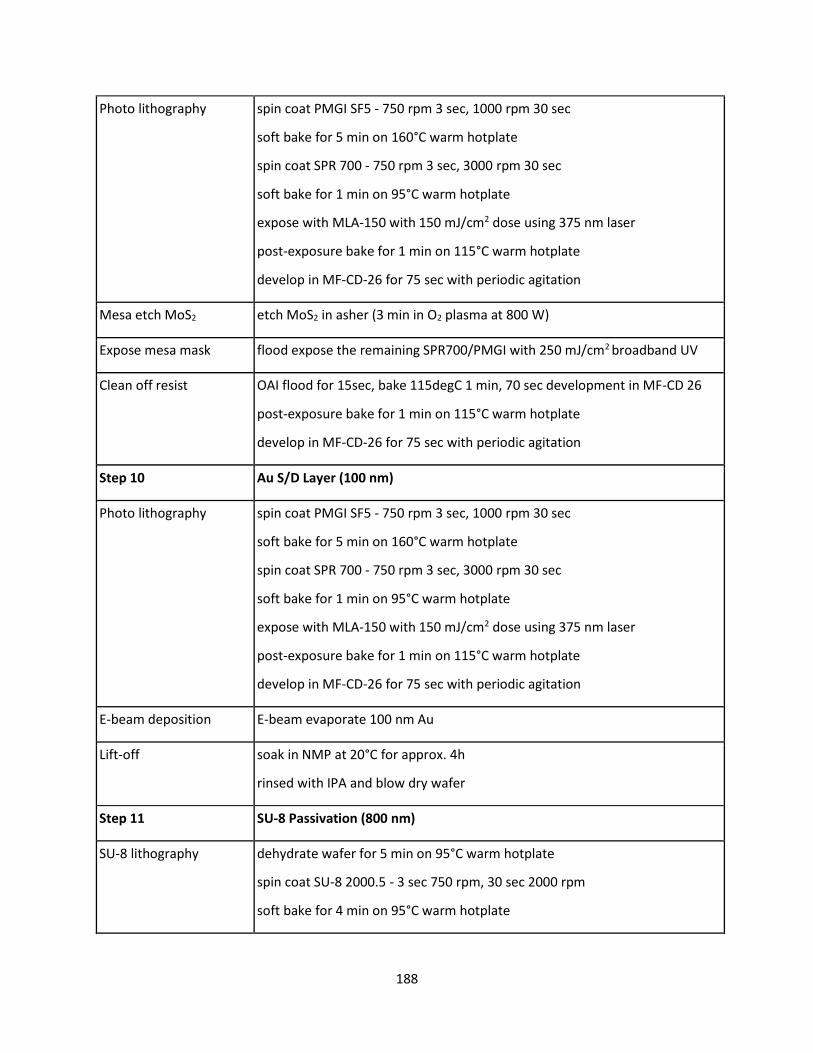
188
Photo lithography spin coat PMGI SF5 - 750 rpm 3 sec, 1000 rpm 30 sec
soft bake for 5 min on 160°C warm hotplate
spin coat SPR 700 - 750 rpm 3 sec, 3000 rpm 30 sec
soft bake for 1 min on 95°C warm hotplate
expose with MLA-150 with 150 mJ/cm2 dose using 375 nm laser
post-exposure bake for 1 min on 115°C warm hotplate
develop in MF-CD-26 for 75 sec with periodic agitation
Mesa etch MoS2 etch MoS2 in asher (3 min in O2 plasma at 800 W)
Expose mesa mask flood expose the remaining SPR700/PMGI with 250 mJ/cm2 broadband UV
Clean off resist OAI flood for 15sec, bake 115degC 1 min, 70 sec development in MF-CD 26
post-exposure bake for 1 min on 115°C warm hotplate
develop in MF-CD-26 for 75 sec with periodic agitation
Step 10 Au S/D Layer (100 nm)
Photo lithography spin coat PMGI SF5 - 750 rpm 3 sec, 1000 rpm 30 sec
soft bake for 5 min on 160°C warm hotplate
spin coat SPR 700 - 750 rpm 3 sec, 3000 rpm 30 sec
soft bake for 1 min on 95°C warm hotplate
expose with MLA-150 with 150 mJ/cm2 dose using 375 nm laser
post-exposure bake for 1 min on 115°C warm hotplate
develop in MF-CD-26 for 75 sec with periodic agitation
E-beam deposition E-beam evaporate 100 nm Au
Lift-off soak in NMP at 20°C for approx. 4h
rinsed with IPA and blow dry wafer
Step 11 SU-8 Passivation (800 nm)
SU-8 lithography dehydrate wafer for 5 min on 95°C warm hotplate
spin coat SU-8 2000.5 - 3 sec 750 rpm, 30 sec 2000 rpm
soft bake for 4 min on 95°C warm hotplate

189
expose with MLA-150 with 2000 mJ/cm2 dose using 375 nm laser
post-exposure bake for 6 min on 95°C warm hotplate
develop in PGMEA for 10 sec while agitating solution
hard bake SU-8 at 160°C for 15 min, cool down slowly for 5 min
7.4.11 SynCell Lift-Off Protocol
Step 1 MMA Mesh
Photo lithography spin MMA 8.5 EL 11 - 750 rpm 3 sec, 1000 rpm 30 sec (500 nm)
soft bake for 1 min on 160°C warm hotplate
spin coat SPR 700 - 750 rpm 3 sec, 3000 rpm 30 sec
soft bake for 1 min on 95°C warm hotplate
expose with MLA-150 with 150 mJ/cm2 dose using 375 nm laser
post-exposure bake for 1 min on 115°C warm hotplate
develop in MF-CD-26 for 75 sec with periodic agitation
Develop SPR/MMA develop in 1:1 MIBK/IPA for 90 sec and agitate with pipette
Step 2 Transfer
Cu wet etch immerse MMA/SynCell/Si chips into FeCl3 (Transcene CE-100)
etch Cu for 10 min
Transfer scoop out MMA/SynCell film with glass slide and place in dish with DI water
repeat once more to clean film even further
scoop out film with PMMA/Si die (PMMA A6 950)
blow-dry MMA/SynCell film on PMMA/Si
bake sample for 20 min at 70°C, 1 min at 160°C
Remove MMA expose MMA/SPR stack for 40 min in 220 nm deep UV light (1 mW/cm2)
develop in 1:1 MIBK/IPA for 90 sec and agitate with pipette
Step 3 Electric Testing

190
Probe station measure SynCells in array and characterize them
Step 4 Dispersion in DI Water
Lift-off put SynCells on PMMA into a vial filled with acetone for 5 min
SynCells now lift off into acetone
Remove silicon chip with tweezers from vial
Wash in acetone Let SynCells settle to the ground of vial
Carefully remove 90% of acetone with a pipette
Refill acetone to 100%
Carefully remove 90% of acetone with a pipette
Disperse in DI water Carefully remove 90% of acetone with a pipette
Refill with DI water to 100%
Carefully remove 90% of DI water/ acetone solution with a pipette
Refill with DI water to 100%
7.4.12 Microfluidic Channel Fabrication
Step 1 Cleaning
Start start with 2x2 cm pieces of 285 nm SiO2 / Si
Wet clean clean in pre-mixed piranha solution (Nanostrip) for 5 min
rinse with DI water
clean in 10% HCl for 5min
rinse in DI water
blow dry wafer
Step 2 SU-8 Mold (29 µm)
SU-8 lithography dehydrate sample for 1min on 100°C warm hotplate
spin coat SU-8 (mr-DWL 40) - 3sec 750 rpm, 30sec 3000 rpm
soft bake for 30 min on 90°C war m hotplate
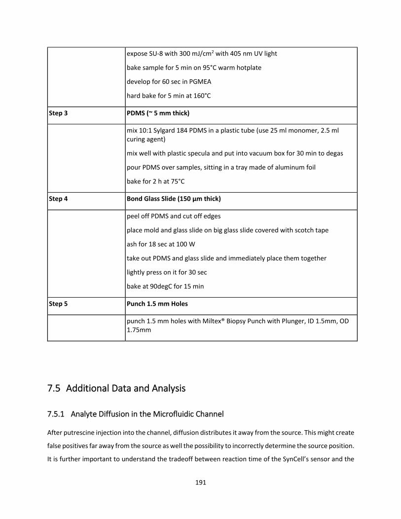
191
expose SU-8 with 300 mJ/cm2 with 405 nm UV light
bake sample for 5 min on 95°C warm hotplate
develop for 60 sec in PGMEA
hard bake for 5 min at 160°C
Step 3 PDMS (~ 5 mm thick)
mix 10:1 Sylgard 184 PDMS in a plastic tube (use 25 ml monomer, 2.5 ml curing agent)
mix well with plastic specula and put into vacuum box for 30 min to degas
pour PDMS over samples, sitting in a tray made of aluminum foil
bake for 2 h at 75°C
Step 4 Bond Glass Slide (150 µm thick)
peel off PDMS and cut off edges
place mold and glass slide on big glass slide covered with scotch tape
ash for 18 sec at 100 W
take out PDMS and glass slide and immediately place them together
lightly press on it for 30 sec
bake at 90degC for 15 min
Step 5 Punch 1.5 mm Holes
punch 1.5 mm holes with Miltex® Biopsy Punch with Plunger, ID 1.5mm, OD 1.75mm
7.5 Additional Data and Analysis
7.5.1 Analyte Diffusion in the Microfluidic Channel
After putrescine injection into the channel, diffusion distributes it away from the source. This might create
false positives far away from the source as well the possibility to incorrectly determine the source position.
It is further important to understand the tradeoff between reaction time of the SynCell’s sensor and the
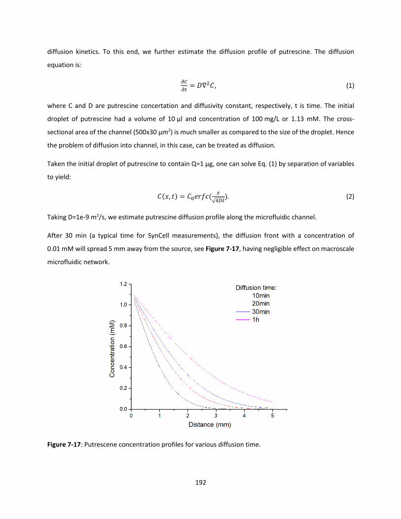
192
diffusion kinetics. To this end, we further estimate the diffusion profile of putrescine. The diffusion
equation is:
𝜕𝐶
𝜕𝑡= 𝐷∇2𝐶, (1)
where C and D are putrescine concertation and diffusivity constant, respectively, t is time. The initial
droplet of putrescine had a volume of 10 µl and concentration of 100 mg/L or 1.13 mM. The cross-
sectional area of the channel (500x30 µm2) is much smaller as compared to the size of the droplet. Hence
the problem of diffusion into channel, in this case, can be treated as diffusion.
Taken the initial droplet of putrescine to contain Q=1 µg, one can solve Eq. (1) by separation of variables
to yield:
𝐶(𝑥, 𝑡) = 𝐶0𝑒𝑟𝑓𝑐(𝑥
√4𝐷𝑡). (2)
Taking D=1e-9 m2/s, we estimate putrescine diffusion profile along the microfluidic channel.
After 30 min (a typical time for SynCell measurements), the diffusion front with a concentration of
0.01 mM will spread 5 mm away from the source, see Figure 7-17, having negligible effect on macroscale
microfluidic network.
Figure 7-17: Putrescene concentration profiles for various diffusion time.
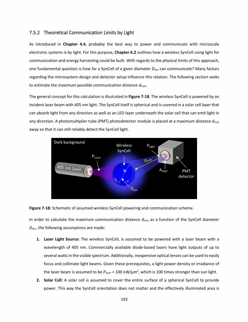
193
7.5.2 Theoretical Communication Limits by Light
As introduced in Chapter 4.4, probably the best way to power and communicate with microscale
electronic systems is by light. For this purpose, Chapter 6.2 outlines how a wireless SynCell using light for
communication and energy harvesting could be built. With regards to the physical limits of this approach,
one fundamental question is how far a SynCell of a given diameter DSyn can communicate? Many factors
regarding the microsystem design and detector setup influence this relation. The following section seeks
to estimate the maximum possible communication distance dmax.
The general concept for this calculation is illustrated in Figure 7-18. The wireless SynCell is powered by an
incident laser beam with 405 nm light. The SynCell itself is spherical and is covered in a solar cell layer that
can absorb light from any direction as well as an LED layer underneath the solar cell that can emit light in
any direction. A photomultiplier tube (PMT) photodetector module is placed at a maximum distance dmax
away so that it can still reliably detect the SynCell light.
Figure 7-18: Schematic of assumed wireless SynCell powering and communication scheme.
In order to calculate the maximum communication distance dmax as a function of the SynCell diameter
DSyn, the following assumptions are made:
1. Laser Light Source: The wireless SynCell, is assumed to be powered with a laser beam with a
wavelength of 405 nm. Commercially available diode-based lasers have light outputs of up to
several watts in the visible spectrum. Additionally, inexpensive optical lenses can be used to easily
focus and collimate light beams. Given these prerequisites, a light power density or irradiance of
the laser beam is assumed to be Plaser = 100 nW/µm2, which is 100 times stronger than sun light.
2. Solar Cell: A solar cell is assumed to cover the entire surface of a spherical SynCell to provide
power. This way the SynCell orientation does not matter and the effectively illuminated area is
194
defined as πDSyn2/4, which is the cross-sectional area of the SynCell with diameter DSyn. Using GaN
as solar cell material, a power conversion efficiency of ηSolar = 25% is assumed for a wavelength of
420 nm and below, easily absorbing the 405 nm laser beam. This is a reasonable assumption given
that GaN solar cells with 63% efficiency have already been demonstrated [255].
3. CMOS Chip: A CMOS chip is assumed to provide sensor data such as temperature values and drive
an LED to send light pulses representing this data digitally. The entire sensing and computation
but excluding the LED power is estimated to consume PCMOS = 16 nW, which is best average power
consumption demonstrated by a complex microscale sensor system with a full ARM Cortex M0+
processor [11]. The pules are assumed to be 100 µs long and are sent out continuously, which
would be equal to a data rate of 10 kbits/sec.
4. LED: The SynCells is assumed to have an LED layer covering the entire spherical SynCell surface
under the solar cell layer. Using GaN as material, the LED is modeled to have an emission
wavelength of 450 nm and a light conversion efficiency of ηLED = 50%, which is routinely achieved
for such blue GaN LEDs. The solar cell is assumed to be completely transparent in this wavelength.
As a result, the LED is modeled as emitting light omnidirectional with equal intensity, which means
the relative orientation of the SynCell to the detector does not matter.
5. Background: The SynCell and detector system are assumed to be in complete darkness except for
the light coming from the laser beam to power the SynCell and the light emitted from the LED.
The scattering of light in air is neglected. No photons in the range of 450 nm are expected to be
spontaneously emitted from the background environment. This is a reasonable assumption
considering that the black body radiance for a surface at room temperature is 4.5x10⁻³⁵ W/m2/sr
in the range of 400-500 nm, which is equivalent to a 1 m2 surface emitting one photon in that
range every 22 million years.
6. Photodetector: A photosensor with high light sensitivity and low noise is required to detects small
amounts of light accurately. Likely the best option for this application is a photomultiplier tube
(PMT), such as the ThorLabs PMM01 Photomultiplier Module. This detector has a circular
detection area of APMT = 380 mm2, a quantum efficiency of 25%, a gain factor of about 7x10⁶, and
a minimum dark current of 0.3 nA, which is equivalent to a dark count rate of 100 photons per
second. The connected transimpedance amplifier amplifies this photocurrent with a gain of
106 V/A and a 6 dB bandwidth of 20 kHz but adds a root-mean-square (RMS) noise of 2 mV. To
generate an output signal of 20 mV (10 times larger than the RMS amplifier noise) a photon flux
of 80,000 photons per second is needed, which is equal to an incident light power of

195
PPMT,min = 35.3 fW at 450 nm LED light. The photodetector is also assumed to have a spectral light
filter only transparent to 445-455 nm wavelength light. Such filters are readily available at low
cost, for example from Thorlabs.
7. Scalability: It is assumed that all components of the SynCell, i.e. the solar cell, LED, and CMOS chip
are scalable. For the LED and solar cell, the efficiency is assumed to be constant irrespective of
physical size or light density. The CMOS chips is assumed to consume 16 nW irrespective of SynCell
volume and shall also be able to perform the necessary functions irrespective of the physical
SynCell volume. This is a reasonable assumption given that the microsystem in [11] was realized
using a 55 nm CMSO technology node. In 2020, the state-of-the-art technology node for CMOS
circuits in mass production is 7 nm. Additionally, with CMOS scaling, the required power for the
described function is only expected to decrease.
Talking the above assumptions into consideration, the light power PPMT arriving at the photomultiplier
tube photodetector as a function of the distance d is equal to:
𝑃𝑃𝑀𝑇 = (𝑃𝐿𝑎𝑠𝑒𝑟 ∙𝜋
4𝐷𝑆𝑦𝑛
2 ∙ 𝜂𝑠𝑜𝑙𝑎𝑟 − 𝑃𝐶𝑀𝑂𝑆) ∙ 𝜂𝐿𝐸𝐷 ∙𝐴𝑃𝑀𝑇
4𝜋𝑑2 .
After rearranging this equation for distance d, the maximum communication distance dmax can be
computed by setting the incident photodetector light power PPMT to the minimum viable input power
PPMT,min, as shown in the following expression:
𝑑max. = √(𝑃𝐿𝑎𝑠𝑒𝑟 ∙𝜋
4𝐷𝑆𝑦𝑛
2 ∙ 𝜂𝑠𝑜𝑙𝑎𝑟 − 𝑃𝐶𝑀𝑂𝑆) ∙ 𝜂𝐿𝐸𝐷 ∙𝐴𝑃𝑀𝑇
4𝜋 ∙ 𝑃𝑃𝑀𝑇,min. .
Adding in all values, the maximum communication distance dmax can be expressed as a function of the
SynCell diameter DSyn as follows:
𝑑max. =√
(100𝑛𝑊𝜇𝑚2 ∙
𝜋4 𝐷𝑆𝑦𝑛
2 ∙ 25% − 16 𝑛𝑊) ∙ 50% ∙ 380 𝑚𝑚2
4𝜋 ∙ 35.3 𝑓𝑊
This equation is plotted in Figure 7-19. It reveals that assuming a SynCell diameter of for example 50 µm,
the maximum possible communication distance is 145 meters, assuming a 100 nW/µm2 incident light
power, no background noise and a Thorlabs PMM01 photomultiplier tube as detector. This is a remarkable
result considering that the SynCell diameter is 2.9x10⁶ times smaller than this distance.
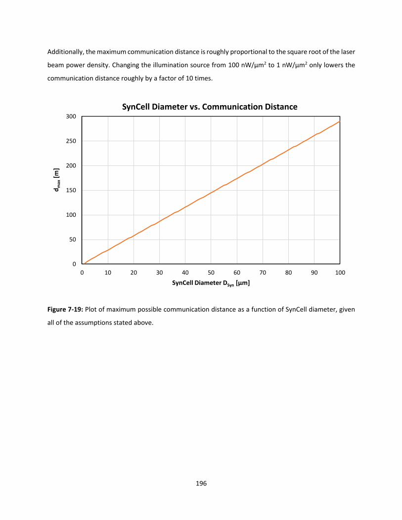
196
Additionally, the maximum communication distance is roughly proportional to the square root of the laser
beam power density. Changing the illumination source from 100 nW/µm2 to 1 nW/µm2 only lowers the
communication distance roughly by a factor of 10 times.
Figure 7-19: Plot of maximum possible communication distance as a function of SynCell diameter, given
all of the assumptions stated above.
0
50
100
150
200
250
300
0 10 20 30 40 50 60 70 80 90 100
dm
ax[m
]
SynCell Diameter DSyn [µm]
SynCell Diameter vs. Communication Distance

197
198
References
1. Griffith, M.J., et al., Combining Printing, Coating, and Vacuum Deposition on the Roll-to-Roll Scale: A Hybrid Organic Photovoltaics Fabrication. IEEE Journal of Selected Topics in Quantum Electronics, 2016. 22(1): p. 112-125.
2. Jung, Y.-S., et al., Progress in Scalable Coating and Roll-to-Roll Compatible Printing Processes of Perovskite Solar Cells toward Realization of Commercialization. Advanced Optical Materials, 2018. 6(9): p. 1701182.
3. Hast, J., et al., 18.1: Invited Paper: Roll-to-Roll Manufacturing of Printed OLEDs. SID Symposium Digest of Technical Papers, 2013. 44(1): p. 192-195.
4. Minakata, T., et al. Challenges for ultra-thin and highly flexible OLEDs fabricated by roll to roll process. in 2016 Compound Semiconductor Week (CSW) [Includes 28th International Conference on Indium Phosphide & Related Materials (IPRM) & 43rd International Symposium on Compound Semiconductors (ISCS). 2016.
5. Pastorelli, F., et al., The Organic Power Transistor: Roll-to-Roll Manufacture, Thermal Behavior, and Power Handling When Driving Printed Electronics. Advanced Engineering Materials, 2016. 18(1): p. 51-55.
6. Biederman, W., et al., A Fully-Integrated, Miniaturized (0.125 mm²) 10.5 µW Wireless Neural Sensor. IEEE Journal of Solid-State Circuits, 2013. 48(4): p. 960-970.
7. Seo, D., et al., Wireless Recording in the Peripheral Nervous System with Ultrasonic Neural Dust. Neuron, 2016. 91(3): p. 529-539.
8. Lee, S., et al., A 250 μm × 57 μm Microscale Opto-Electronically Transduced Electrodes (MOTEs) for Neural Recording. IEEE Transactions on Biomedical Circuits and Systems, 2018: p. 1-1.
9. Driscoll, S.O., et al. A 200µm × 200µm × 100µm, 63nW, 2.4GHz injectable fully-monolithic wireless bio-sensing system. in 2017 IEEE Radio Frequency Integrated Circuits Symposium (RFIC). 2017.
10. Lee, Y., et al., A Modular 1 mm3 Die-Stacked Sensing Platform With Low Power I2C Inter-Die Communication and Multi-Modal Energy Harvesting. IEEE Journal of Solid-State Circuits, 2013. 48(1): p. 229-243.
11. Wu, X., et al. A 0.04MM<sup>3</sup>16NW Wireless and Batteryless Sensor System with Integrated Cortex-M0+ Processor and Optical Communication for Cellular Temperature Measurement. in 2018 IEEE Symposium on VLSI Circuits. 2018.
12. Usami, M. An ultra-small RFID chip: /spl mu/-chip. in Proceedings of 2004 IEEE Asia-Pacific Conference on Advanced System Integrated Circuits. 2004.
13. Franssila, S., Introduction to Microfabrication. 2010: John Wiley & Sons, Ltd. 14. Scholz, F., Compound Semiconductors: Physics, Technology, and Device Concepts. 2017 Jenny
Stanford Publishing 15. Ogawa, S., Organic Electronics Materials and Devices. 2015: Springer. 16. Petti, L., et al., Metal oxide semiconductor thin-film transistors for flexible electronics. Applied
Physics Reviews, 2016. 3(2): p. 021303. 17. Satishchandra Balkrishna Ogale , T.V.V., Mark Blamire, Functional Metal Oxides: New Science and
Novel Applications. 2013: Wiley. 18. Zeng, M., et al., Exploring Two-Dimensional Materials toward the Next-Generation Circuits: From
Monomer Design to Assembly Control. Chemical Reviews, 2018. 118(13): p. 6236-6296. 19. Jariwala, D., et al., Emerging Device Applications for Semiconducting Two-Dimensional Transition
Metal Dichalcogenides. Acs Nano, 2014. 8(2): p. 1102-1120.

199
20. Varghese, S.S., et al., Two-Dimensional Materials for Sensing: Graphene and Beyond. Electronics, 2015. 4(3): p. 651-687.
21. Akinwande, D., et al., Large-Area Graphene Electrodes Using CVD to facilitate applications in commercial touchscreens, flexible nanoelectronics, and neural interfaces. Ieee Nanotechnology Magazine, 2015. 9(3): p. 6-14.
22. Wang, Y., et al., Wearable and Highly Sensitive Graphene Strain Sensors for Human Motion Monitoring. Advanced Functional Materials, 2014. 24(29): p. 4666-4670.
23. Jang, H., et al., Graphene-Based Flexible and Stretchable Electronics. Advanced Materials, 2016. 28(22): p. 4184-4202.
24. Park, M., et al., MoS2-Based Tactile Sensor for Electronic Skin Applications. Advanced Materials, 2016. 28(13): p. 2556-+.
25. Dong, P., et al., Graphene on Metal Grids as the Transparent Conductive Material for Dye Sensitized Solar Cell. Journal of Physical Chemistry C, 2014. 118(45): p. 25863-25868.
26. Park, H., et al., Flexible Graphene Electrode-Based Organic Photovoltaics with Record-High Efficiency. Nano Letters, 2014. 14(9): p. 5148-5154.
27. Song, Y., et al., Visibly-Transparent Organic Solar Cells on Flexible Substrates with All-Graphene Electrodes. Advanced Energy Materials, 2016. 6(20).
28. Lim, J.T., et al., Flexion bonding transfer of multilayered graphene as a top electrode in transparent organic light-emitting diodes. Scientific Reports, 2015. 5.
29. Withers, F., et al., Light-emitting diodes by band-structure engineering in van der Waals heterostructures. Nature Materials, 2015. 14(3): p. 301-306.
30. Novoselov, K.S., et al., Electric Field Effect in Atomically Thin Carbon Films. Science, 2004. 306(5696): p. 666.
31. Maździarz, M., Comment on ‘The Computational 2D Materials Database: high-throughput modeling and discovery of atomically thin crystals’. 2D Materials, 2019. 6(4): p. 048001.
32. Mounet, N., et al., Two-dimensional materials from high-throughput computational exfoliation of experimentally known compounds. Nature Nanotechnology, 2018. 13(3): p. 246-252.
33. Castellanos-Gomez, A., Why all the fuss about 2D semiconductors? Nature Photonics, 2016. 10(4): p. 202-204.
34. Novoselov, K.S., et al., 2D materials and van der Waals heterostructures. Science, 2016. 353(6298): p. aac9439.
35. Akinwande, D., et al., A review on mechanics and mechanical properties of 2D materials—Graphene and beyond. Extreme Mechanics Letters, 2017. 13: p. 42-77.
36. Kim, J.H., et al., Mechanical properties of two-dimensional materials and their applications. Journal of Physics D: Applied Physics, 2018. 52(8): p. 083001.
37. Chhowalla, M., D. Jena, and H. Zhang, Two-dimensional semiconductors for transistors. Nature Reviews Materials, 2016. 1(11): p. 16052.
38. Akinwande, D., et al., Graphene and two-dimensional materials for silicon technology. Nature, 2019. 573(7775): p. 507-518.
39. Roll-to-Roll Manufacturing, ed. G.P. Jehuda Greener, Mika Cakmak. 2018: Wiley. 40. Roll-to-Roll Printing Market for flexible electronics by Printing Technology (Screen, Inkjet, Gravure,
Flexographic), Application (Displays, Sensors, Batteries, RFID, Lighting), Material, End-use Industry, and Geography - Global Forecast to 2025. 2020.
41. Konica Minolta Constructs Plant for World's First Mass Production of Plastic Substrate Flexible OLED Lighting Panels. 2014 [cited 2020 4/14/2020]; Available from: https://www.konicaminolta.com/about/releases/2014/0318_01_01.html.
42. Solliance sets world record for roll-to-roll produced perovskite-based solar cells with a stabilized efficiency of 12,6%. 2017 [cited 2020 4/14/2020]; Available from:

200
https://www.solliance.eu/2017/solliance-sets-world-record-for-roll-to-roll-produced-perovskite-based-solar-cells-with-a-stabilized-efficiency-of-126/.
43. Flexible Electronics, ed. A.S. William S. Wong. 2009: Springer. 44. Street, R.A., Thin-Film Transistors. Advanced Materials, 2009. 21(20): p. 2007-2022. 45. Bae, S., et al., Roll-to-roll production of 30-inch graphene films for transparent electrodes. Nature
Nanotechnology, 2010. 5(8): p. 574-578. 46. Choi, M., et al., Flexible active-matrix organic light-emitting diode display enabled by
MoS<sub>2</sub> thin-film transistor. Science Advances, 2018. 4(4): p. eaas8721. 47. Park, Y.J., et al., All MoS2-Based Large Area, Skin-Attachable Active-Matrix Tactile Sensor. ACS
Nano, 2019. 13(3): p. 3023-3030. 48. Yamada, T., et al., A roll-to-roll microwave plasma chemical vapor deposition process for the
production of 294 mm width graphene films at low temperature. Carbon, 2012. 50(7): p. 2615-2619.
49. Kobayashi, T., et al., Production of a 100-m-long high-quality graphene transparent conductive film by roll-to-roll chemical vapor deposition and transfer process. Applied Physics Letters, 2013. 102(2): p. 023112.
50. Juang, Z.-Y., et al., Graphene synthesis by chemical vapor deposition and transfer by a roll-to-roll process. Carbon, 2010. 48(11): p. 3169-3174.
51. Han, G.H., et al., POLY(ETHYLENE CO-VINYL ACETATE)-ASSISTED ONE-STEP TRANSFER OF ULTRA-LARGE GRAPHENE. Nano, 2011. 06(01): p. 59-65.
52. Vlassiouk, I., et al., Large scale atmospheric pressure chemical vapor deposition of graphene. Carbon, 2013. 54: p. 58-67.
53. Chandrashekar, B.N., et al., Roll-to-Roll Green Transfer of CVD Graphene onto Plastic for a Transparent and Flexible Triboelectric Nanogenerator. Advanced Materials, 2015. 27(35): p. 5210-5216.
54. Deng, B., et al., Roll-to-Roll Encapsulation of Metal Nanowires between Graphene and Plastic Substrate for High-Performance Flexible Transparent Electrodes. Nano Letters, 2015. 15(6): p. 4206-4213.
55. Mafra, D.L., T. Ming, and J. Kong, Facile graphene transfer directly to target substrates with a reusable metal catalyst. Nanoscale, 2015. 7(36): p. 14807-14812.
56. Georgiou, S.C.a.P., Body Dust: Miniaturized Highly-integrated Low Power Sensing for Remotely Powered Drinkable CMOS Bioelectronics. ArXiv, 2018.
57. Pister, K.S.J. Smart Dust. 1997; Available from: https://people.eecs.berkeley.edu/~pister/SmartDust/SmartDustBAA97-43-Abstract.pdf.
58. Warneke, B., et al., Smart Dust: communicating with a cubic-millimeter computer. Computer, 2001. 34(1): p. 44-51.
59. Warneke, B.A., et al. An autonomous 16 mm/sup 3/ solar-powered node for distributed wireless sensor networks. in SENSORS, 2002 IEEE. 2002.
60. Chen, G., et al. A cubic-millimeter energy-autonomous wireless intraocular pressure monitor. in 2011 IEEE International Solid-State Circuits Conference. 2011.
61. Ron Milo, R.P., Size and Geometry, in Cell Biology by the Numbers, R.P. Ron Milo, Editor. 2016, Garland Science. p. 358.
62. Funke, D.A., et al. A 200 μm by 100 μm Smart Dust system with an average current consumption of 1.3 nA. in 2016 IEEE International Conference on Electronics, Circuits and Systems (ICECS). 2016.
63. Gómez-Martínez, R., et al., Silicon chips detect intracellular pressure changes in living cells. Nature Nanotechnology, 2013. 8: p. 517.
64. Hu, X., et al., Micrometer-Scale Magnetic-Resonance-Coupled Radio-Frequency Identification and Transceivers for Wireless Sensors in Cells. Physical Review Applied, 2017. 8(1): p. 014031.
201
65. Koman, V.B., et al., Colloidal nanoelectronic state machines based on 2D materials for aerosolizable electronics. Nature Nanotechnology, 2018. 13(9): p. 819-827.
66. Gerber, L.C., et al., Time capsule: an autonomous sensor and recorder based on diffusion–reaction. Lab on a Chip, 2014. 14(22): p. 4324-4328.
67. Palagi, S. and P. Fischer, Bioinspired microrobots. Nature Reviews Materials, 2018. 3(6): p. 113-124.
68. Anichini, C., et al., Chemical sensing with 2D materials. Chemical Society Reviews, 2018. 47(13): p. 4860-4908.
69. Bertolazzi, S., et al., Nonvolatile Memories Based on Graphene and Related 2D Materials. Advanced Materials, 2019. 31(10): p. 1806663.
70. Wang, Z., et al., Two-dimensional light-emitting materials: preparation, properties and applications. Chemical Society Reviews, 2018. 47(16): p. 6128-6174.
71. Das, S., et al., The Role of Graphene and Other 2D Materials in Solar Photovoltaics. Advanced Materials, 2019. 31(1): p. 1802722.
72. Ni, Z.H., et al., Graphene Thickness Determination Using Reflection and Contrast Spectroscopy. Nano Letters, 2007. 7(9): p. 2758-2763.
73. Lee, C., et al., Measurement of the Elastic Properties and Intrinsic Strength of Monolayer Graphene. Science, 2008. 321(5887): p. 385.
74. Bolotin, K.I., et al., Ultrahigh electron mobility in suspended graphene. Solid State Communications, 2008. 146(9): p. 351-355.
75. Warner, J.H., et al., Dislocation-Driven Deformations in Graphene. Science, 2012. 337(6091): p. 209.
76. Castro Neto, A.H., et al., The electronic properties of graphene. Reviews of Modern Physics, 2009. 81(1): p. 109-162.
77. Lee, H., K. Paeng, and I.S. Kim, A review of doping modulation in graphene. Synthetic Metals, 2018. 244: p. 36-47.
78. Markevich, H.P.a.A., Electronic and electrochemical doping of graphene by surface adsorbates. Beilstein J. Nanotechnol., 2014. 5: p. 1842–1848.
79. Giovannetti, G., et al., Doping Graphene with Metal Contacts. Physical Review Letters, 2008. 101(2): p. 026803.
80. Dahal, A., et al., Charge doping of graphene in metal/graphene/dielectric sandwich structures evaluated by C-1s core level photoemission spectroscopy. APL Materials, 2013. 1(4): p. 042107.
81. Shi, X., et al., Selective n-type doping in graphene via the aluminium nanoparticle decoration approach. Journal of Materials Chemistry C, 2014. 2(27): p. 5417-5421.
82. Nair, R.R., et al., Fine Structure Constant Defines Visual Transparency of Graphene. Science, 2008. 320(5881): p. 1308.
83. Xu, Y. and J. Liu, Graphene as Transparent Electrodes: Fabrication and New Emerging Applications. Small, 2016. 12(11): p. 1400-1419.
84. Song, Y., et al., Visibly-Transparent Organic Solar Cells on Flexible Substrates with All-Graphene Electrodes. Advanced Energy Materials, 2016. 6(20): p. 1600847.
85. De, S., et al., Silver Nanowire Networks as Flexible, Transparent, Conducting Films: Extremely High DC to Optical Conductivity Ratios. ACS Nano, 2009. 3(7): p. 1767-1774.
86. Liao, L. and X. Duan, Graphene for radio frequency electronics. Materials Today, 2012. 15(7): p. 328-338.
87. Wu, Y., et al., State-of-the-Art Graphene High-Frequency Electronics. Nano Letters, 2012. 12(6): p. 3062-3067.
88. Han, S.-J., et al., Graphene radio frequency receiver integrated circuit. Nature Communications, 2014. 5(1): p. 3086.
202
89. Schedin, F., et al., Detection of individual gas molecules adsorbed on graphene. Nature Materials, 2007. 6(9): p. 652-655.
90. Chen, G., T.M. Paronyan, and A.R. Harutyunyan, Sub-ppt gas detection with pristine graphene. Applied Physics Letters, 2012. 101(5): p. 053119.
91. Yuan, W. and G. Shi, Graphene-based gas sensors. Journal of Materials Chemistry A, 2013. 1(35): p. 10078-10091.
92. Varghese, S.S., et al., Recent advances in graphene based gas sensors. Sensors and Actuators B: Chemical, 2015. 218: p. 160-183.
93. Ang, P.K., et al., Solution-Gated Epitaxial Graphene as pH Sensor. Journal of the American Chemical Society, 2008. 130(44): p. 14392-14393.
94. Huang, Y., et al., Graphene-based biosensors for detection of bacteria and their metabolic activities. Journal of Materials Chemistry, 2011. 21(33): p. 12358-12362.
95. Jiang, S., et al., Real-time electrical detection of nitric oxide in biological systems with sub-nanomolar sensitivity. Nature Communications, 2013. 4: p. 2225.
96. Liu, Y., X. Dong, and P. Chen, Biological and chemical sensors based on graphene materials. Chemical Society Reviews, 2012. 41(6): p. 2283-2307.
97. Moldovan, O., et al., Graphene electronic sensors - review of recent developments and future challenges. Iet Circuits Devices & Systems, 2015. 9(6): p. 446-453.
98. Zhao, J., G.-Y. Zhang, and D.-X. Shi, Review of graphene-based strain sensors. Chinese Physics B, 2013. 22(5): p. 057701.
99. Hempel, M., et al., A Novel Class of Strain Gauges Based on Layered Percolative Films of 2D Materials. Nano Letters, 2012. 12(11): p. 5714-5718.
100. Zhao, J., et al., Ultra-sensitive strain sensors based on piezoresistive nanographene films. Applied Physics Letters, 2012. 101(6): p. 063112.
101. Mukasyan, A.S., Boron Nitride, in Concise Encyclopedia of Self-Propagating High-Temperature Synthesis, I.P. Borovinskaya, et al., Editors. 2017, Elsevier: Amsterdam. p. 45-47.
102. Li, L.H., et al., Large-scale mechanical peeling of boron nitride nanosheets by low-energy ball milling. Journal of Materials Chemistry, 2011. 21(32): p. 11862-11866.
103. Falin, A., et al., Mechanical properties of atomically thin boron nitride and the role of interlayer interactions. Nature Communications, 2017. 8(1): p. 15815.
104. Lindsay, L. and D.A. Broido, Enhanced thermal conductivity and isotope effect in single-layer hexagonal boron nitride. Physical Review B, 2011. 84(15): p. 155421.
105. Li, L.H., et al., Strong Oxidation Resistance of Atomically Thin Boron Nitride Nanosheets. ACS Nano, 2014. 8(2): p. 1457-1462.
106. Watanabe, K., T. Taniguchi, and H. Kanda, Direct-bandgap properties and evidence for ultraviolet lasing of hexagonal boron nitride single crystal. Nature Materials, 2004. 3(6): p. 404-409.
107. Young, A.F., et al., Electronic compressibility of layer-polarized bilayer graphene. Physical Review B, 2012. 85(23): p. 235458.
108. Wang, H., et al., Synthesis of Large-Sized Single-Crystal Hexagonal Boron Nitride Domains on Nickel Foils by Ion Beam Sputtering Deposition. Advanced Materials, 2015. 27(48): p. 8109-8115.
109. Liu, Z., et al., Ultrathin high-temperature oxidation-resistant coatings of hexagonal boron nitride. Nature Communications, 2013. 4(1): p. 2541.
110. Lo, C.-L., et al., Studies of two-dimensional h-BN and MoS2 for potential diffusion barrier application in copper interconnect technology. npj 2D Materials and Applications, 2017. 1(1): p. 42.
111. Dean, C.R., et al., Boron nitride substrates for high-quality graphene electronics. Nature Nanotechnology, 2010. 5(10): p. 722-726.

203
112. Wang, L., et al., One-Dimensional Electrical Contact to a Two-Dimensional Material. Science, 2013. 342(6158): p. 614.
113. Lee, G.-H., et al., Highly Stable, Dual-Gated MoS2 Transistors Encapsulated by Hexagonal Boron Nitride with Gate-Controllable Contact, Resistance, and Threshold Voltage. ACS Nano, 2015. 9(7): p. 7019-7026.
114. Baronian, W., The optical properties of thin boron nitride films. Materials Research Bulletin, 1972. 7(2): p. 119-124.
115. Ji, Y., et al., Boron nitride as two dimensional dielectric: Reliability and dielectric breakdown. Applied Physics Letters, 2016. 108(1): p. 012905.
116. Lee, G.-H., et al., Flexible and Transparent MoS2 Field-Effect Transistors on Hexagonal Boron Nitride-Graphene Heterostructures. ACS Nano, 2013. 7(9): p. 7931-7936.
117. Qian, K., et al., Hexagonal Boron Nitride Thin Film for Flexible Resistive Memory Applications. Advanced Functional Materials, 2016. 26(13): p. 2176-2184.
118. Pan, C., et al., Coexistence of Grain-Boundaries-Assisted Bipolar and Threshold Resistive Switching in Multilayer Hexagonal Boron Nitride. Advanced Functional Materials, 2017. 27(10): p. 1604811.
119. Hui, F., et al., Synthesis of large-area multilayer hexagonal boron nitride sheets on iron substrates and its use in resistive switching devices. 2D Materials, 2018. 5(3): p. 031011.
120. Lin, W., et al., Oxygen-assisted synthesis of hBN films for resistive random access memories. Applied Physics Letters, 2019. 115(7): p. 073101.
121. Wu, X., et al., Thinnest Nonvolatile Memory Based on Monolayer h-BN. Advanced Materials, 2019. 31(15): p. 1806790.
122. Zhao, H., et al., Atomically Thin Femtojoule Memristive Device. Advanced Materials, 2017. 29(47): p. 1703232.
123. Song, I., C. Park, and H.C. Choi, Synthesis and properties of molybdenum disulphide: from bulk to atomic layers. RSC Advances, 2015. 5(10): p. 7495-7514.
124. Li, X. and H. Zhu, Two-dimensional MoS2: Properties, preparation, and applications. Journal of Materiomics, 2015. 1(1): p. 33-44.
125. Canton-Vitoria, R., et al. Gas Sensing Using Monolayer MoS2. in Nanoscale Materials for Warfare Agent Detection: Nanoscience for Security. 2019. Dordrecht: Springer Netherlands.
126. Huang, Y.L., et al., Bandgap tunability at single-layer molybdenum disulphide grain boundaries. Nature Communications, 2015. 6(1): p. 6298.
127. Mak, K.F., et al., Atomically Thin MoS2: A New Direct-Gap Semiconductor. Physical Review Letters, 2010. 105(13): p. 136805.
128. Splendiani, A., et al., Emerging Photoluminescence in Monolayer MoS2. Nano Letters, 2010. 10(4): p. 1271-1275.
129. Manzeli, S., et al., 2D transition metal dichalcogenides. Nature Reviews Materials, 2017. 2(8): p. 17033.
130. Bernardi, M., M. Palummo, and J.C. Grossman, Extraordinary Sunlight Absorption and One Nanometer Thick Photovoltaics Using Two-Dimensional Monolayer Materials. Nano Letters, 2013. 13(8): p. 3664-3670.
131. Bertolazzi, S., J. Brivio, and A. Kis, Stretching and Breaking of Ultrathin MoS2. ACS Nano, 2011. 5(12): p. 9703-9709.
132. Fiori, G., et al., Electronics based on two-dimensional materials. Nature Nanotechnology, 2014. 9: p. 768.
133. Zhu, W., et al., Nanoscale electronic devices based on transition metal dichalcogenides. 2D Materials, 2019. 6(3): p. 032004.
134. Radisavljevic, B., et al., Single-layer MoS2 transistors. Nature Nanotechnology, 2011. 6(3): p. 147-150.

204
135. Krasnozhon, D., et al., MoS2 Transistors Operating at Gigahertz Frequencies. Nano Letters, 2014. 14(10): p. 5905-5911.
136. Shao, P.-Z., et al., Enhancement of carrier mobility in MoS2 field effect transistors by a SiO2 protective layer. Applied Physics Letters, 2016. 108(20): p. 203105.
137. Yu, Z., et al., Realization of Room-Temperature Phonon-Limited Carrier Transport in Monolayer MoS2 by Dielectric and Carrier Screening. Advanced Materials, 2016. 28(3): p. 547-552.
138. Kang, K., et al., High-mobility three-atom-thick semiconducting films with wafer-scale homogeneity. Nature, 2015. 520: p. 656.
139. Pu, J., et al., Highly Flexible MoS2 Thin-Film Transistors with Ion Gel Dielectrics. Nano Letters, 2012. 12(8): p. 4013-4017.
140. Chang, H.-Y., et al., Large-Area Monolayer MoS2 for Flexible Low-Power RF Nanoelectronics in the GHz Regime. Advanced Materials, 2016. 28(9): p. 1818-1823.
141. Bertolazzi, S., D. Krasnozhon, and A. Kis, Nonvolatile Memory Cells Based on MoS2/Graphene Heterostructures. ACS Nano, 2013. 7(4): p. 3246-3252.
142. Ge, R., et al., Atomristor: Nonvolatile Resistance Switching in Atomic Sheets of Transition Metal Dichalcogenides. Nano Letters, 2018. 18(1): p. 434-441.
143. Wang, M., et al., Robust memristors based on layered two-dimensional materials. Nature Electronics, 2018. 1(2): p. 130-136.
144. Yu, S., D. Kuzum, and H.P. Wong. Design considerations of synaptic device for neuromorphic computing. in 2014 IEEE International Symposium on Circuits and Systems (ISCAS). 2014.
145. Choi, W., et al., Recent development of two-dimensional transition metal dichalcogenides and their applications. Materials Today, 2017. 20(3): p. 116-130.
146. Akbari, E., et al., Brief review of monolayer molybdenum disulfide application in gas sensor. Physica B: Condensed Matter, 2018. 545: p. 510-518.
147. Late, D.J., et al., Sensing Behavior of Atomically Thin-Layered MoS2 Transistors. ACS Nano, 2013. 7(6): p. 4879-4891.
148. Perkins, F.K., et al., Chemical Vapor Sensing with Monolayer MoS2. Nano Letters, 2013. 13(2): p. 668-673.
149. Lee, J., et al., Two-dimensional Layered MoS2 Biosensors Enable Highly Sensitive Detection of Biomolecules. Scientific Reports, 2014. 4: p. 7352.
150. Wu, Y., S. Wang, and K. Komvopoulos, A review of graphene synthesis by indirect and direct deposition methods. Journal of Materials Research, 2020. 35(1): p. 76-89.
151. Fang, W., et al., Asymmetric Growth of Bilayer Graphene on Copper Enclosures Using Low-Pressure Chemical Vapor Deposition. ACS Nano, 2014. 8(6): p. 6491-6499.
152. Sun, J., et al., Recent progress in the tailored growth of two-dimensional hexagonal boron nitride via chemical vapour deposition. Chemical Society Reviews, 2018. 47(12): p. 4242-4257.
153. Kim, S.M., et al., Synthesis of large-area multilayer hexagonal boron nitride for high material performance. Nature Communications, 2015. 6(1): p. 8662.
154. Kang, K., et al., High-mobility three-atom-thick semiconducting films with wafer-scale homogeneity. Nature, 2015. 520(7549): p. 656-660.
155. Xie, S., et al., Coherent, atomically thin transition-metal dichalcogenide superlattices with engineered strain. Science, 2018. 359(6380): p. 1131.
156. Park, H., et al., Optimized poly(methyl methacrylate)-mediated graphene-transfer process for fabrication of high-quality graphene layer. Nanotechnology, 2018. 29(41): p. 415303.
157. Wang, Y., et al., Electrochemical Delamination of CVD-Grown Graphene Film: Toward the Recyclable Use of Copper Catalyst. ACS Nano, 2011. 5(12): p. 9927-9933.
158. Lai, S., et al., Water-penetration-assisted mechanical transfer of large-scale molybdenum disulfide onto arbitrary substrates. RSC Advances, 2016. 6(62): p. 57497-57501.
205
159. Tae Lim, J., et al., Flexion bonding transfer of multilayered graphene as a top electrode in transparent organic light-emitting diodes. Scientific Reports, 2015. 5: p. 17748.
160. Gagliardi, M., Global Markets for Roll-to-Roll Technologies for Flexible Devices. 2019, BBC Research.
161. Hesjedal, T., Continuous roll-to-roll growth of graphene films by chemical vapor deposition. Applied Physics Letters, 2011. 98(13).
162. Shi, J., et al., Controllable Growth and Transfer of Monolayer MoS2 on Au Foils and Its Potential Application in Hydrogen Evolution Reaction. ACS Nano, 2014. 8(10): p. 10196-10204.
163. Gao, Y., et al., Large-area synthesis of high-quality and uniform monolayer WS2 on reusable Au foils. Nature Communications, 2015. 6(1): p. 8569.
164. Yun, S.J., et al., Synthesis of Centimeter-Scale Monolayer Tungsten Disulfide Film on Gold Foils. ACS Nano, 2015. 9(5): p. 5510-5519.
165. Kim, K.K., et al., Synthesis of Monolayer Hexagonal Boron Nitride on Cu Foil Using Chemical Vapor Deposition. Nano Letters, 2012. 12(1): p. 161-166.
166. Park, J.H., et al., Large-Area Monolayer Hexagonal Boron Nitride on Pt Foil. Acs Nano, 2014. 8(8): p. 8520-8528.
167. Yang, S.Y., et al., Metal-Etching-Free Direct Delamination and Transfer of Single-Layer Graphene with a High Degree of Freedom. Small, 2015. 11(2): p. 175-181.
168. Gao, L., et al., Repeated growth and bubbling transfer of graphene with millimetre-size single-crystal grains using platinum. Nature Communications, 2012. 3: p. 699.
169. Hempel, M., et al., Repeated roll-to-roll transfer of two-dimensional materials by electrochemical delamination. Nanoscale, 2018. 10(12): p. 5522-5531.
170. Wang, Z.-J., et al., Direct Observation of Graphene Growth and Associated Copper Substrate Dynamics by in Situ Scanning Electron Microscopy. ACS Nano, 2015. 9(2): p. 1506-1519.
171. Yoon, T., et al., Direct Measurement of Adhesion Energy of Monolayer Graphene As-Grown on Copper and Its Application to Renewable Transfer Process. Nano Letters, 2012. 12(3): p. 1448-1452.
172. Kang, M.H., et al., Mechanical Robustness of Graphene on Flexible Transparent Substrates. Acs Applied Materials & Interfaces, 2016. 8(34): p. 22506-22515.
173. Wong, C.H.A. and M. Pumera, Electrochemical Delamination and Chemical Etching of Chemical Vapor Deposition Graphene: Contrasting Properties. The Journal of Physical Chemistry C, 2016. 120(8): p. 4682-4690.
174. Ryu, S., et al., Atmospheric Oxygen Binding and Hole Doping in Deformed Graphene on a SiO2 Substrate. Nano Letters, 2010. 10(12): p. 4944-4951.
175. Chen, F., J. Xia, and N. Tao, Ionic Screening of Charged-Impurity Scattering in Graphene. Nano Letters, 2009. 9(4): p. 1621-1625.
176. Kim, M., et al., Direct transfer of wafer-scale graphene films. 2D Materials, 2017. 4(3): p. 035004. 177. Anagnostopoulos, G., et al., Mechanical Stability of Flexible Graphene-Based Displays. ACS Applied
Materials & Interfaces, 2016. 8(34): p. 22605-22614. 178. Zardetto, V., et al., Substrates for Flexible Electronics: A Practical Investigation on the Electrical,
Film Flexibility, Optical, Temperature, and Solvent Resistance Properties. Journal of Polymer Science Part B-Polymer Physics, 2011. 49(9): p. 638-648.
179. Wang, J., et al., Atomic intercalation to measure adhesion of graphene on graphite. Nature Communications, 2016. 7.
180. Liu, Z., et al., Interlayer binding energy of graphite: A mesoscopic determination from deformation. Physical Review B, 2012. 85(20).
181. Lee, K.H., et al., Large-Scale Synthesis of High-Quality Hexagonal Boron Nitride Nanosheets for Large-Area Graphene Electronics. Nano Letters, 2012. 12(2): p. 714-718.
206
182. Sachs, B., et al., Adhesion and electronic structure of graphene on hexagonal boron nitride substrates. Physical Review B, 2011. 84(19).
183. Gao, Y., et al., Repeated and Controlled Growth of Monolayer, Bilayer and Few-Layer Hexagonal Boron Nitride on Pt Foils. ACS Nano, 2013. 7(6): p. 5199-5206.
184. Gao, W. and R. Huang, Effect of surface roughness on adhesion of graphene membranes. Journal of Physics D-Applied Physics, 2011. 44(45).
185. Oh, S., D. Blaauw, and D. Sylvester, The Internet of Tiny Things: Recent Advances of Millimeter-Scale Computing. IEEE Design & Test, 2019. 36(2): p. 65-72.
186. Gardini, F., et al., Technological Factors Affecting Biogenic Amine Content in Foods: A Review. Frontiers in Microbiology, 2016. 7: p. 1218.
187. Edwards, R.A., R.H. Dainty, and C.M. Hibbard, Putrescine and cadaverine formation in vacuum packed beef. Journal of Applied Bacteriology, 1985. 58(1): p. 13-19.
188. Liu, S.F., et al., Single-Walled Carbon Nanotube/Metalloporphyrin Composites for the Chemiresistive Detection of Amines and Meat Spoilage. Angewandte Chemie International Edition, 2015. 54(22): p. 6554-6557.
189. Chen, X.-F., et al., Engineering tunable biosensors for monitoring putrescine in Escherichia coli. Biotechnology and Bioengineering, 2018. 115(4): p. 1014-1027.
190. Rauscher-Gabernig, E., et al., Dietary exposure assessment of putrescine and cadaverine and derivation of tolerable levels in selected foods consumed in Austria. European Food Research and Technology, 2012. 235(2): p. 209-220.
191. Farriol, M., et al., Role of putrescine in cell proliferation in a colon carcinoma cell line. Nutrition, 2001. 17(11): p. 934-938.
192. Kung, Y.-C., et al., Air and Water-Stable n-Type Doping and Encapsulation of Flexible MoS2 Devices with SU8. Advanced Electronic Materials, 2019. 5(1): p. 1800492.
193. Nam, H., et al., Multiple MoS2 Transistors for Sensing Molecule Interaction Kinetics. Scientific Reports, 2015. 5: p. 10546.
194. Yin, L., et al., Dissolvable Metals for Transient Electronics. Advanced Functional Materials, 2014. 24(5): p. 645-658.
195. Harvey, W.W. and H.C. Gatos, The Reaction of Germanium with Aqueous Solutions: I . Dissolution Kinetics in Water Containing Dissolved Oxygen. Journal of The Electrochemical Society, 1958. 105(11): p. 654-660.
196. Sioncke, S., et al., Etch Rates of Ge, GaAs and InGaAs in Acids, Bases and Peroxide Based Mixtures. ECS Transactions, 2008. 16(10): p. 451-460.
197. Kawase, T., et al., Catalytic behavior of metallic particles in anisotropic etching of Ge(100) surfaces in water mediated by dissolved oxygen. Journal of Applied Physics, 2012. 111(12): p. 126102.
198. Kawase, T., et al., Metal-assisted chemical etching of Ge(100) surfaces in water toward nanoscale patterning. Nanoscale research letters, 2013. 8(1): p. 151-151.
199. ICinsight, Fabless/system company and integrated device manufacturer (IDM) IC sales worldwide from 1999 to 2017 (in billion U.S. dollars). 2018, Staticita.
200. Faggin, F., The Making of the First Microprocessor. IEEE Solid-State Circuits Magazine, 2009. 1(1): p. 8-21.
201. AMD. AMD Ryzen™ 3 2200U Mobile Processor with Radeon™ Vega 3 Graphics. 2018 12/07/2018]; Available from: https://www.amd.com/en/products/apu/amd-ryzen-3-2200u.
202. Khalifa, A., et al., The Microbead: A Highly Miniaturized Wirelessly Powered Implantable Neural Stimulating System. IEEE Transactions on Biomedical Circuits and Systems, 2018. 12(3): p. 521-531.
203. Usami, M., et al. A 0.05×0.05mm2 RFID Chip with Easily Scaled-Down ID-Memory. in 2007 IEEE International Solid-State Circuits Conference. Digest of Technical Papers. 2007.

207
204. Yu, L., et al. High-yield large area MoS2 technology: Material, device and circuits co-optimization. in 2016 IEEE International Electron Devices Meeting (IEDM). 2016.
205. Tetzner, K., R.I. Bose, and K. Bock, Organic Field-Effect Transistors Based on a Liquid-Crystalline Polymeric Semiconductor using SU-8 Gate Dielectrics onFlexible Substrates. Materials, 2014. 7(11).
206. Schroder, D.K., Semiconductor Material and Device Characterization. 2006: Wiley-Interscience. 207. Chang, H.-Y., W. Zhu, and D. Akinwande, On the mobility and contact resistance evaluation for
transistors based on MoS2 or two-dimensional semiconducting atomic crystals. Applied Physics Letters, 2014. 104(11): p. 113504.
208. Dongjin Seo, J.M.C., Jan M. Rabaey, Elad Alon, Michel M. Maharbiz, Neural Dust: An Ultrasonic, Low Power Solution for Chronic Brain-Machine Interfaces. ArXiv, 2013.
209. Ghaed, M.H., et al., Circuits for a Cubic-Millimeter Energy-Autonomous Wireless Intraocular Pressure Monitor. IEEE Transactions on Circuits and Systems I: Regular Papers, 2013. 60(12): p. 3152-3162.
210. Weinstein, R., RFID: a technical overview and its application to the enterprise. IT Professional, 2005. 7(3): p. 27-33.
211. Bond, L.J., C.H. Chiang, and C.M. Fortunko, Absorption of ultrasonic waves in air at high frequencies (10–20 MHz). The Journal of the Acoustical Society of America, 1992. 92(4): p. 2006-2015.
212. Vladišauskas, A. and L. Jakevičius, Absorption of ultrasonic waves in air. Ultragarsas, 2004. 50(1): p. 46-49.
213. Withey, P.A., et al., Strain Paint: Noncontact Strain Measurement Using Single-Walled Carbon Nanotube Composite Coatings. Nano Letters, 2012. 12(7): p. 3497-3500.
214. Chu, P.B., et al. Optical communication using micro corner cube reflectors. in Proceedings IEEE The Tenth Annual International Workshop on Micro Electro Mechanical Systems. An Investigation of Micro Structures, Sensors, Actuators, Machines and Robots. 1997.
215. Sankaragomathi, K., et al. A 27μW subcutaneous wireless biosensing platform with optical power and data transfer. in Proceedings of the IEEE 2014 Custom Integrated Circuits Conference. 2014.
216. Shojaie, A., M.D. Takhtfooladi, and M. Safaeinezhad. Bio-Inspired Diffusion Based Molecular Communication in Long-range. in 2012 12th International Conference on Computational Science and Its Applications. 2012.
217. Park, J., et al. Trend and challenges of the diffusion-based molecular communication for nanonetworks. in 2015 International Conference on Information and Communication Technology Convergence (ICTC). 2015.
218. Farra, R., et al., First-in-Human Testing of a Wirelessly Controlled Drug Delivery Microchip. Science Translational Medicine, 2012. 4(122): p. 122ra21.
219. Wang, J., B. Yin, and M. Peng, Diffusion based molecular communication: principle, key technologies, and challenges. China Communications, 2017. 14(2): p. 1-18.
220. Seo, D., et al., Model validation of untethered, ultrasonic neural dust motes for cortical recording. Journal of Neuroscience Methods, 2015. 244: p. 114-122.
221. Seo, D., et al. Ultrasonic beamforming system for interrogating multiple implantable sensors. in 2015 37th Annual International Conference of the IEEE Engineering in Medicine and Biology Society (EMBC). 2015.
222. Manthiram, A., An Outlook on Lithium Ion Battery Technology. ACS Central Science, 2017. 3(10): p. 1063-1069.
223. Placke, T., et al., Lithium ion, lithium metal, and alternative rechargeable battery technologies: the odyssey for high energy density. Journal of Solid State Electrochemistry, 2017. 21(7): p. 1939-1964.
208
224. Pikul, J.H., et al., High-power lithium ion microbatteries from interdigitated three-dimensional bicontinuous nanoporous electrodes. Nature Communications, 2013. 4: p. 1732.
225. Pereira-Ramos, J.-P. and R. Baddour-Hadjean, Thin-Film Metal-Oxide Electrodes for Lithium Microbatteries. Lithium Ion Rechargeable Batteries, 2010.
226. Matsuda, Y., N. Kuwata, and J. Kawamura, Thin-film lithium batteries with 0.3–30 μm thick LiCoO2 films fabricated by high-rate pulsed laser deposition. Solid State Ionics, 2018. 320: p. 38-44.
227. Mukanova, A., et al., A mini-review on the development of Si-based thin film anodes for Li-ion batteries. Materials Today Energy, 2018. 9: p. 49-66.
228. González, A., et al., Review on supercapacitors: Technologies and materials. Renewable and Sustainable Energy Reviews, 2016. 58: p. 1189-1206.
229. Choi, J.-H., et al., High capacitance and energy density supercapacitor based on biomass-derived activated carbons with reduced graphene oxide binder. Carbon, 2018. 132: p. 16-24.
230. Mondon, F. and S. Blonkowski, Electrical characterisation and reliability of HfO2 and Al2O3–HfO2 MIM capacitors. Microelectronics Reliability, 2003. 43(8): p. 1259-1266.
231. Chiu, P.-Y. and M.-D. Ker, Metal-layer capacitors in the 65nm CMOS process and the application for low-leakage power-rail ESD clamp circuit. Microelectronics Reliability, 2014. 54(1): p. 64-70.
232. Hansen, B.J., et al., Hybrid Nanogenerator for Concurrently Harvesting Biomechanical and Biochemical Energy. Acs Nano, 2010. 4(7): p. 3647-3652.
233. Pan, C.F., et al., Generating Electricity from Biofluid with a Nanowire-Based Biofuel Cell for Self-Powered Nanodevices. Advanced Materials, 2010. 22(47): p. 5388-+.
234. Sakai, H., et al., A high-power glucose/oxygen biofuel cell operating under quiescent conditions. Energy & Environmental Science, 2009. 2(1): p. 133-138.
235. Charthad, J., et al., A mm-Sized Implantable Medical Device (IMD) With Ultrasonic Power Transfer and a Hybrid Bi-Directional Data Link. IEEE Journal of Solid-State Circuits, 2015. 50(8): p. 1741-1753.
236. Jean, J., et al., Pathways for solar photovoltaics. Energy & Environmental Science, 2015. 8(4): p. 1200-1219.
237. Sankaragomathi, K., et al. A 27μW subcutaneous wireless biosensing platform with optical power and data transfer. in Custom Integrated Circuits Conference (CICC), 2014 IEEE Proceedings of the. 2014. IEEE.
238. Geisz, J.F., et al., Building a Six-Junction Inverted Metamorphic Concentrator Solar Cell. IEEE Journal of Photovoltaics, 2018. 8(2): p. 626-632.
239. Yao, Y.-C., et al., Enhanced external quantum efficiency in GaN-based vertical-type light-emitting diodes by localized surface plasmons. Scientific Reports, 2016. 6(1): p. 22659.
240. Park, S.-I., et al., Printed Assemblies of Inorganic Light-Emitting Diodes for Deformable and Semitransparent Displays. Science, 2009. 325(5943): p. 977.
241. Xu, T., et al., Magnetic Actuation Based Motion Control for Microrobots: An Overview. Micromachines, 2015. 6(9).
242. Ceylan, H., et al., Mobile microrobots for bioengineering applications. Lab on a Chip, 2017. 17(10): p. 1705-1724.
243. Sitti, M. and D.S. Wiersma, Pros and Cons: Magnetic versus Optical Microrobots. Advanced Materials, 2020. n/a(n/a): p. 1906766.
244. Cheng, D.I., et al., Use of patterned magnetic films to retain and orient micro-components during fluidic assembly. Journal of Applied Physics, 2009. 105(7): p. 07C123.
245. Ashraf, S., et al., Surface modification of SU-8 for metal/SU-8 adhesion using RF plasma treatment for application in thermopile detectors. Materials Research Express, 2015. 2(8): p. 086501.
246. Danan, H., A. Herr, and A.J.P. Meyer, New Determinations of the Saturation Magnetization of Nickel and Iron. Journal of Applied Physics, 1968. 39(2): p. 669-670.
209
247. Fonstad, C.G. Magnetically-Assisted Statistical Assembly - a new heterogeneous integration technique. 2002.
248. Schuerle, S., et al., Synthetic and living micropropellers for convection-enhanced nanoparticle transport. Science Advances, 2019. 5(4): p. eaav4803.
249. Nemani, K.V., et al., In vitro and in vivo evaluation of SU-8 biocompatibility. Materials Science and Engineering: C, 2013. 33(7): p. 4453-4459.
250. Feng, R. and R.J. Farris, Influence of processing conditions on the thermal and mechanical properties of SU8 negative photoresist coatings. Journal of Micromechanics and Microengineering, 2002. 13(1): p. 80-88.
251. gMarek Hempel, V.S., Chibeom Park, Volodymyr B. Koman, Mantian Xue, Elaine McVay, Sarah Spector, Madan Dubey, Michael S. Strano, Jiwoong Park, Jing Kong, Tomás Palacios, SynCells – A 60 x 60 µm Electronic Platform for Sensing Applications in Constrained Environments. 2020: In preparation.
252. Frisenda, R., et al., Recent progress in the assembly of nanodevices and van der Waals heterostructures by deterministic placement of 2D materials. Chemical Society Reviews, 2018. 47(1): p. 53-68.
253. Williams, K.R., K. Gupta, and M. Wasilik, Etch rates for micromachining processing-Part II. Journal of Microelectromechanical Systems, 2003. 12(6): p. 761-778.
254. Yuan, H.-C., et al., Flexible photodetectors on plastic substrates by use of printing transferred single-crystal germanium membranes. Applied Physics Letters, 2009. 94(1): p. 013102.
255. Neufeld, C.J., et al., High quantum efficiency InGaN/GaN solar cells with 2.95 eV band gap. Applied Physics Letters, 2008. 93(14): p. 143502.
Copyright © 2022 FDOKUMEN