Annals 20 20 - Α' Παιδιατρική Κλινική – Πανεπιστημίου Αθηνών
Upload
khangminh22Category
view
0download
0
SYSTOOLS
SYSTOOLS
SYSTOOLS

SYSTOOLS
SYSTOOLS
SYSTOOLS

SYSTOOLS
SYSTOOLS
SYSTOOLS
THE·VIC-20 . CONNECTION
.... ,

SYSTOOLS
SYSTOOLS
SYSTOOLS
) :. )
I.

SYSTOOLS
SYSTOOLS
SYSTOOLS
THE VIC-20TM CONNECTION
JAMES W. COFFRON
Berkeley • Paris'· DUsseldorf
- .. j

SYSTOOLS
SYSTOOLS
SYSTOOLSCover design by Daniel Le Noury Book layout and design by Sharon Leong Technical Illustration by Sharon Leong
Vic-20 is a trademark of Commodore Electronics, Ltd. LM135, 235, and 335 are trademarks of National Semiconductor Corporation. AD558 and AD570 are trademarks of Analog Devices. Votrax is a registered trademark of Votrax, Division of Federal Screw Works.
Sybex is not affiliated with any manufacturer.
The illustration on p.71 is adapted from The VIC-20 Programmer's Reference Guide, which is copyrighted by Commodore Business Machines, Inc. This excerpt may not be copied without the express written permission of Commodore Business Machines.
Every effort has been made to supply complete and accurate information. However, Sybex assumes no responsibility for its use, nor for any infringements of patents of other rights or third parties which would result.
©1983 SYBEX Inc. 2344 Sixth Street, Berkeley, CA 94710. World rights reserved. No part of this publication may be stored in a retrieval system, transmitted, or reproduced in any way, including but not limited to photocopy, photograph, magnetic or other record, without the prior agreement and written permission of the publisher.
Library of Congress Card Number: 83-50227 ISBN 0-89588-128-4 First Edition 1983 Printed in the United States of America 10 9 8 7 6 5 4 3 2 1

SYSTOOLS
SYSTOOLS
SYSTOOLS
for the Spiesmans: John, Mary, Bill and Anne.

SYSTOOLS
SYSTOOLS
SYSTOOLS
/

SYSTOOLS
SYSTOOLS
SYSTOOLS
ACKNOWLEDGEMENTS
I wish to thank my wife Carol, for preparing the original diagrams; and Jim Compton, for editing the manuscript. Finally, a hearty thanks to the entire staff at Sybex for their splendid efforts.
SYSTOOLS
SYSTOOLS
SYSTOOLS
(
l
CONTENTS
1
2
PREFACE INTRODUCTION
INTRODUCTION TO COMPUTER CONTROL
1.1 What is Computer Control? 1 1.2 A Practical Example of the Two Basic Concepts 4 1.3 Some New Vocabulary 6 1.4 Summary 14
SOFTWARE FOR OUTPUT FROM THE VIC-20 COMPUTER
2.1 Installing the CMS lID System 17 2.2 The POKE Instruction 20 2.3 Forming the Address for the POKE 24 2.4 Calculating Data for the POKE 26 2.5 Experiments With the CMS I/O System 32 2.6 Example 1: Lighting a Single LED 32 2.7 Example 2: Lighting a Combination of LEOs 36 2.8 Example 3: A Counting Program 36 2.9 Example 4: A Traveling-Light Program 39 2.10 Summary 41
xii xv
1
17

SYSTOOLS
SYSTOOLS
SYSTOOLS
ix
3 INPUTTING DATA TO THE VIC·20 COMPUTER 43
3.1 Overview of Inputting Data 43 3.2 The CMS Input Board for the VIC-20 Personal
Computer 45 3.3 Input Software 46 3.4 Interpreting the Input Information 47 3.5 Calculating the Bits from the Input Variable 51 3.6 Hands-on Example 1: Calculating the Weight of the Input
Word 59 3.7 Example 2: Read a Byte and Determine Which Bits Were
a Logical 1 60 3.8 Example 3: Read a Word and Perform an Action 62 3.9 Example 4: A Combination Lock 64 3.10 Summary 67
4 INPUT AND OUTPUT HARDWARE FOR THE VIC-20 COMPUTER 69
4.1 Beginning Output Electronics for the VIC-20 70 4.2 The Enable Circuit 70 4.3 The READIWRITE 'YRiW) Line 72 4.4 The External Output Strobe 74 4.5 The Output Latches 75 4.6 The Light-Emitting Diodes 77 4.7 Hardware for Inputting Data tothe VIC-20 81 4.8 Enabling the Tri-State Buffer 86 4.9 Summary of Input and Output 87
5 \
AN APPLICATION OF COMPUTER INTERFACING: A HOME SECURITY SYSTEM 91
5.1 Definition of the Problem 92 5.2 Drawing the House with the Computer 93

SYSTOOLS
SYSTOOLS
SYSTOOLS
x
5.3 Physical Connections to the Doors and Windows 96 5.4 Connecting the Hardware to the Computer 100 5.5 Software for Interpretation of the Input Lines 104 5.6 Simulation of all Windows and Doors for Program
Development 109 5.7 Masking Off the Alarms with Software 113 5.8 The Complete System 114 5.9 Summary 123
6 ADDING A VOICE TO THE VIC-20 COMPUTER 127
6.1 Phoneme Speech Synthesis 128 6.2 The Set of Phonemes 128 6.3 How are the Correct Phonemes Chosen? 130 6.4 VOTRAX SC-01 Phoneme Speech Synthesizer 131 6.5 Connecting the SC-01 to the VIC-20 PC 136 6.6 Controlling the SC-01 with the VIC-20
Computer 138 6.7 Example 1: Outputting a Single Phoneme 140 6.8 Example 2: Outputting a Word with the Speech
Chip 143 6.9 Example 3: Outputting a Sentence with the
SC-01 147 6.10 Summary 150
7 ANALOG VS. DIGITAL AND TRANSDUCERS 153
7.1 Analog Events 154 7.2 Digital Events 155 7.3 Purely Digital Events 157 7.4 Analog and Digital Electronics 157 7.5 Transducers 159 7.6 Summary 161
I \~.

SYSTOOLS
SYSTOOLS
SYSTOOLS
8 ANALOG-TO-DIGITAL CONVERSION FOR THE VIC-20 COMPUTER
8.1 Block Diagram of the Problem 164 8.2 The Analog-to-Digital Converter 166 8.3 Calculating the Digital Outputs of the ADC 170 8.4 Connecting the ADC to the VIC-20 Personal
Computer 174 8.5 Software for Analog-ta-Digital Conversion 178
163
8.6 A Temperature-Measuring Circuit (Transducer) 182
9
8.7 The Complete System for Temperature Measurement 185
8.8 Some Practical ADC Applications 187 8.9 Summary 188
DIGITAL-TO-ANALOG CONVERSION FOR THE VIC-20 COMPUTER
9.1 What is Digital-ta-Analog Conversion? 193 9.2 An Actual Digital-ta-Analog Converter 197 9.3 Connecting the DAC to the VIC-20 203 9.4 Setting any Output Voltage on the DAC 204 9.5 Controlling the DAC with a BASIC Program 209 9.6 Increasing the Output Drive Capability of the
DAC 210 9.7 Summary 213 9.8 Further Study 214
APPENDICES
A Manufacturers' Data Sheets 217 B Tips on Reading a Schematic Diagram 235 C Glossary of Selected Terms 243 D List of Vendors 249 E The Votrax Phonetic Speech Dictionary 251
INDEX
191
217
270
xi

SYSTOOLS
SYSTOOLS
SYSTOOLS
PREFACE
If you have recently purchased a VIC-20 Personal Computer™, or are thinking of purchasing one, many questions about the system have probably arisen in your mind. Many new computer owners are curious about the potential extent of their computer's overall usefulness. While it is true that a specific use for the system is probably the reason you bought it in the first place, you may wonder what else it can do.
It is safe to say that there are more potential futu re uses of the system than any purchaser can dream of at present. As you sit in front of the computer, you can look forward to many hours of enjoyment using the numerous available applications programs, and the various "off-the-shelf" games that can be played on the system. If you are a beginner in home computers, these games and programs may seem difficult to master at first, but this difficulty will soon pass, so do not fear.
At first you may be hesitant to use the system. A "fear of the unknown" surfaces as you testthe machine's reactions to your nimble (or not-so-nimble) touches on the keys. Then, your boldness and confidence improve as you discover it is OK to make mistakes. Nothing drastic happens when you press the wrong key. The VIC-20 computer is a very forgiving instrument.

SYSTOOLS
SYSTOOLS
SYSTOOLS
xiii
Before long, you are deftly running, modifying, and writing programs. The once-formidable task of using a home computer has diminished. Soon you find yourself looking for new challenges and new applications for the computer. At this point you may start to wonder, "Can I use the computer around the home? Is it possible to control my appliances, heating, or security systems with my computer?"
You know these things are possibilities, because you have read about them. However, you may feel it is far beyond your ability to accomplish them. If you think that, you will soon see that you are wrong. The realization of these controls with your VIC-20 is not beyond your capabilities. The information required may be different from that which you use everyday, but making the VIC-20 Connection is a straightforward process, and not very complex.
The designers of the VIC-20 computer have used valuable foresight in anticipating that system users who do not know or care much about hardware may want to create new interfaces between their system and the outside world. With that in mind, the VIC-20 was designed to make the interfacing job an easy one. You do not have to be a computer expert to construct the hardware for controlling external devices or to write the software for control. You wi II see how easy it is as you progress through the examples outlined in the text.
The low cost and flexibility of the VIC-20 make this machine especially suitable for applications that require a computer to be "dedi-
I cated" to a single task and left in place, monitoring temperature, for example. Several VIC-20 computers can be bought for the price of one more expensive machine, and at least one can be saved for routine computing tasks.
So if you are ready to enter the world of computer control, this book is the first step. It will open the door and provide you with the essential information needed to connect your computer to a variety of peripheral devices.
Without any further hesitation, turn the pages and learn to make the VIC-20 Connection.
_.-J'

SYSTOOLS
SYSTOOLS
SYSTOOLS

SYSTOOLS
SYSTOOLS
SYSTOOLS
INTRODUCTION
This book is written for everyone who wants to understand how the VIC-20 Personal Computer, as well as other home computers, can be interfaced to the outside world. Specific examples are shown, using the VIC-20 to illustrate the essential concepts of computer control and interfacing. However, the information and ideas presented here can be readily adapted to most home computer systems.
Interfacing and controlling external devices with the VIC-20 will involve the use of both software and hardware. To that end, this text assumes the reader can write simple programs in VIC BASIC; an extensive knowledge of BASIC is not required to get the maximum value from this text. The hardware concepts are presented with the understanding that many readers may not be familiar with digital electronics. You do not have to be a software or hardware expert to make good use of the information given in this text.
This book is organized so as to enable the reader to understand how all the pieces of the interfacing and control puzzle fit together. The path is not complicated, but you will have to learn some new information and concepts. All the essential information for interfacing and controlling external devices with the VIC-20 PC is given in the pages that follow.

SYSTOOLS
SYSTOOLS
SYSTOOLS
xvi
Chapter 1 starts off with an introduction to, and a definition of, the concept of computer control, and presents some new vocabulary.
Chapter 2 discusses the software required to output information from the VIC-20 computer to an external device. The programming language used is BASIC.
Chapter 3 discusses the software required to input information into the VIC-20 computerfrom an external device. Again, BASIC is used as the programming language.
Chapter 4 introduces the basic hardware concepts necessary to input and output information to and from the VIC-20 computer. This chapter is designed for readers who are unfamiliar with digital electronics, and want to learn only as much about it as they need for practical purposes.
Chapter 5 presents an application of computer control in the design of a home security system. It starts with a definition of the problem and works through the software and hardware concepts necessary to have a working home security system. After reading this chapter, you will have a good general idea of how to use the computer in a home security application.
Chapter 6 shows how to make the VIC-20 computer produce speech. The discussion starts with an introduction to speech synthesis using phoneme speech techniques, and then goes over the software and hardware required to let your VIC-20 speak, saying whatever you want, whenever you want.
Chapter 7 discusses the difference between the concepts analog and digital, using examples comparing how various real-world events each would appear in an analog or digital environment. This chapter concludes with an explanation of the term transducer.
Chapter 8 shows how to perform analog-to-digital conversion with the computer. General concepts applicable to most home computers are discussed. An actual analog-to-digital converter is connected to the VIC-20 computer, with all important software and hardware details shown. The chapter concludes with a complete hardware and software system for measuring temperature with the VIC-20.
Chapter 9 presents the opposite of analog-to-digital conversion, digital-to-analog conversion. The basic concepts are introduced, and

SYSTOOLS
SYSTOOLS
SYSTOOLS
xvii
an actual digital-to-analog converter is connected to the computer. All of the important aspects of the software and hardware for digital-toanalog conversion are covered.
Finall~ the Appendices present some useful reference information: a glossa~ instructions for reading schematic diagrams, manufacturers' data sheets, and a list of vendors for the equipment described in this book.
The use of computers to control and monitor the environment around the home is increasing and will continue to increase in the future. If you want to become involved in the exciting field of computer control, this book is a good starting point.

SYSTOOLS
SYSTOOLS
SYSTOOLS
IN 1I1988S liON 10 SOMP8 I Ell SON IIIOE

SYSTOOLS
SYSTOOLS
SYSTOOLS
1
Before we begin the detailed discussions of computer control that start in Chapter 2, let us take some time to explore the meaning of the term "computer controL" To some, this term may call up images of futuristic robots, huge, automated factories, and complex spacecraft. To others, computer control may seem like something that only scientists use-inevitable, but too complicated for them to understand. In fact, scientists and industrial designers do use computer control in spacecraft and automated factories, and these applications are quite complex, but the term can also be applied to much simpler home applications, such as those described in this book.
1.1 WHAT IS COMPUTER CONTROL?
The overall objective of this book is to enable you to understand computer control. With this understanding will come new insight, allowing persons not directly involved with scientific applications of the computer to see many ways the computer can be applied in the home. As these home applications of the computer are developed, you will lose whatever fear you may have of automation and gain

SYSTOOLS
SYSTOOLS
SYSTOOLS
2 THE VIC-20 CONNECTION
respect for what computer control can do and how it can help you. Another major objective of this book is to show that computer control does not have to be complicated.
We use the VIC-20 Personal Computer in this text as the means of control. However, the concept of computer control is applicable to almost any home computer. Further, if you have a VIC-20 at home, you have already used computer control and may not have been aware of it.
To answer the question of what is meant by computer control, we will show several examples of how a home computer is used. The concept of computer control is quite simple, and is graphically illustrated in Figure 1.1. In this diagram the computer is connected in some way to direct the action of another piece of hardware. This, in essence, is what computer control is all about: The computer is directing the physical or electrical action of an external hardware device.
In almost any computer control application, the computer must have a way of understanding how the external hardware is responding to its control. Therefore, the computer must not only direct the
COMPUTER
CABLE LINK
EXTERNAL INSTRUMENT
Flgure1.1-The main concept of computer control is that the computer will direct the action of an external piece of hardware. The link shown he/e is made by a cable. However, the link may also be made by transmission at radio frequencies, without a physical connection.

SYSTOOLS
SYSTOOLS
SYSTOOLS
INTRODUCTION TO COMPUTER CONTROL 3
action of the external hardware, but monitor it also. I n Figure 1.2 we see that the computer will receive information from the external hardware. Based on that information, the computer can modify the directions it gives to the external device.
This simple example illustrates the basic elements of computer con~ trol. The two processes-sending directions to the external hardware from the computer, and receiving information from the external device-are the essential concepts of computer control. At this point in our discussion, it may be valuable to list these two important concepts:
1. The computer sends directions to the external hardware.
2. The computer receives information from the external hardware.
These two ideas are the basis for computer control. The purpose of this book is to explain how these two tasks are performed.
COMPUTER
- - - - Denotes Information flow.
Data Is sent to the external Instrument. . } Data Is received from the external Instrument.
EXTERNAL INSTRUMENT
Figure 1.2-The computer will send information to the external device to control the device's actions. Information can also be sent by the external device to be read by the computer.

SYSTOOLS
SYSTOOLS
SYSTOOLS
,~
4 THE VIC-20 CONNECTION
1.2 A PRACTICAL EXAMPLE OF THE TWO BASIC CONCEPTS
An example of computer control that most of us can imagine ourselves using is a home security system. With the help of diagrams, we will see that this goal can be achieved using only the two concepts we have outlined. We will return to this example in Chapter 5 and develop such a system in detail.
Let us start by defining what we want the security system to do. In short, we want our home safe from intruders. Unfortunately, this type of statement is useless for our purpose, because the word "safe" conjures up entirely different meanings to different people. For this example, let us define the function of our security system a little more precisely: the system will detect any window or door being opened. When this occurs, the system will indicate which door or window it is. Finally, the system will sound an alarm if any door or window is open. This is the definition of exactly what we wish the system to do. In Chapter 5 we will expand on this system to show many new ideas for a home security system that is computer-controlled.
Using this definition will require that the doors and windows be capable of sending information to the computer, as shown in Figure 1.3. This will involve the second concept that was given in Section 1.1. That is, the computer receives information from an external device.
If the computer detects that one of the windows or doors has been opened, an alarm must be set off. This is shown in Figure 1.4. In order for the computer to set off the alarm, information from the computer must be sent to the alarm to direct the external hardware to emit the noise. This type of computer action was shown as concept number 1 in Section 1.1, where the computer sends information to an external device.
Looking at Figures 1.3 and 1.4, we can see that all of the functions we requ i re ou r system to perform can be done by the computer usi ng only the two concepts outlined. It is true that we have, so to speak, "waved our hands" over some important points. For example, how does a door or window send electrical information to a computer? How does a computer sound an alarm? These points were deliberately ignored. It is possible for a door or window to be made to send electrical information to the computer and for the computer to sound an alarm. How that is done is what this book is all about. We will

SYSTOOLS
SYSTOOLS
SYSTOOLS
INTRODUCTION TO COMPUTER CONTROL 5
COMPUTER
Data is sent to the computer from the doors and windows being monitored.
o
OPEN DOOR
OPEN WINDOW
Figure 1.3-Ooors and windows send information to the computer to report their status, either "open" or "closed. "
COMPUTER
Data Is sent from the computer to turn on an alarm. ALARM
Figure 1.4-A computer will send information to the alarm to inform the user that a window or door has been opened.

SYSTOOLS
SYSTOOLS
SYSTOOLS
6 THE VIC·20 CONNECTION
show exactly how to do these things in later chapters. It is too early in the discussion to approach these details yet; we must first understand where we are heading. From our first example, we can see that the entire subject of computer control can be reduced to the repeated application of the two basic concepts. These two concepts are what should be understood at this time. You may be assured that this text will cover in detail how to achieve the points glossed over in this first example.
1.3 SOME NEW VOCABULARY
When we enter a new area of study, a major obstacle we face is learning the vocabulary essential to the area. Interfacing a computer so as to control an external device is no exception. This section will discuss some of the new words that you are likely to encounter when reading or talking about the topic. If you are reading this book, and own or have access to a VIC-20 computer, you are probably also beginningto read some of the magazines and books now available on the subject. You may also have friends or associates who talk "computerese." All the new terms you may encounter cannot be defined here, but as the topics in the text require it, new vocabulary will be introduced. The new words defined in this section are meant to help the beginner to understand the literature (including the VIC·20 docu· mentation) as quickly as possible.
The two major concepts we have introduced, sending information from a computer to an external device, and receiving information from an external device to be used by a computer, are referred to as output and input respectively. These terms are applied both to the act or event of communicating information between a computer and an external device, and to the information itself. Thus, output is both the transfer of information from the computer to the external device and the information sent, and input is both the transfer of information from an external source into the computer, and the information entered.
If you have ever used a VIC-20 Personal Computer, you have made use of input and output. Whenever you press a key on the keyboard, the computer is inputting the information you send. When the letter

SYSTOOLS
SYSTOOLS
SYSTOOLS
INTRODUCTION TO COMPUTER CONTROL 7
you pressed on the keyboard appears on the screen of your video monitor, the computer is outputting information. We do not usually think of the VIC-20's keyboard or video monitor as devices for input and output, because they are integral parts of the computer system. In fact, although these components are part of the . system , they are external to the computer's central processing unit, or CPU. Ordinarily, we think of input and output as being performed through external devices connected to the computer by, say, a cable. These devices might include the special applications we will be developing in this book, or commercially available peripherals.
Consider the case of a printer attached to a system. When the VIC-20 computer gives a printout, the printer is operating under the control of the computer. During the time the printer is printing and causing the paper to scroll, the computer is outputting information to the printer. If you have a disk-drive or cassette tape recorder attached to your VIC-20, the computer is controlling these devices. When the computer writes your program onto the disk or the tape cassette, it is outputting information. When the computer reads a program from the floppy disk or the tape cassette, it is inputting information.
Figure 1.5 illustrates the general concept of input and output. These two terms are sometimes combined and abbreviated to the single term /10. Whenever the computer is controlling an external device or performing input and output events, it is said to be "doing I/O."
The next term we will discuss is transducer. This word is often used in discussing computer 1/0. To illustrate what a transducer is, let us return to our example of a home security system. In this case we constructed a means by which the computer would receive input information concerning the physical position of a door or a window. The information that wou Id be inputto the computer is electrical. The door or window gives out information only in the form of physical movement. That is, all the door or window can do is move. We therefore need some type of device that changes the physical movement of the door or window into electrical information that can be input to the computer. The device that does this is called a transducer.
This example is one type of transducer. As we will see in Chapter 5, the device used is a simple switch, open when the window is open and closed when it is closed. In general, a transducer is a device or piece of hardware that produces an electrical output when given a physical input, translating one form of energy or information into

SYSTOOLS
SYSTOOLS
SYSTOOLS
8 THE VIC-20 CONNECTION
another. In the examplejust given, the transducer must be capable of converting movement into electrical information. Other examples of transducers are a temperature transducer, a pressure transducer, or a revolutions-per-minute transducer. As you can see, transducers are classified by the type of information they translate into electricity. Figure 1.6 shows how a transducer would fit into the input path between a computer and an external source.
At this time you may wonder if a transducer is used when the computer is outputting information. In the example of the home security system, the computer would sound an alarm if an open window or door were detected. The alarm would be a loud bell or siren. This type of device receives electrical signals from the computer and produces a physical effect-the motion of air, or sound. Broadly, any
COMPUTER
COMPUTER
EXTERNAL .INSTRUMENT
EXTERNAL INSTRUMENT
Figure 1.5-a) This is an example of output. The computer is sending information to the external device. b) This is an example of input. The computer is receiving information from the external device.

SYSTOOLS
SYSTOOLS
SYSTOOLS
COMPUTER
COMPUTER
INTRODUCTION TO COMPUTER CONTROL 9
(a)
TRANSDUCER converts movement
into electrical Information.
o ELECTRICAL
INFORMATION
(b)
ELECTRICAL INFORMATION
DOOR can open or close.
PHYSICAL EXTERNAL INFORMATION SOURCE: DOOR
Figure 1.8-a) A transducer will transform the physicel movement of the door into electrical information, which can then be input to the computer. b) This block diagram shows where a transducer fits in the computer input path. The transducer will have a physical event input to it. That is, it will measure or record a physical event. The output of the transducer will be an electrical signal related to the physical event being input to it.

SYSTOOLS
SYSTOOLS
SYSTOOLS
10 THE VIC-20 CONNECTION
device that translates one form of energy into another (including electricity into sound) can be called a transducer. In the context of computer control, however, these types of devices are not generally classified as transducers. Instead, they are grouped together generally as output devices, or simply known by their specific names: bell, motor, relay, fan, heater, and lights. Figure 1.7 shows how a relay is used to activate these devices to output information from the computer.
The next term to discuss is digital. Many people are already familiar with this particular word. In a general sense, the term means that there are discrete values that a particular event can equal. For example, the television channels are assigned certain frequencies, out of an infinite number of possible frequencies. We can say that selecting a TV station is a digital process, because the channel values can only be those specified and nothing in between. We do not have channel 2.5, for example, we have channel 2 or 3.
The term digital is usually contrasted with the term analog. Digital
COMPUTER
The outputs signal to close the relay. The relay CIOS88 and turns on the light.
-- - .,
,..-......... -...1/ : RELAY ""---1 (:)
=O~<'---~_-""_--""_; ---J> ~ 120V ~ • ACPOWER 120V
LIGHT
FlgU18 1.7-A physical device that will transform the electrical output of the computer into a physical event. This device, a relay, will transform the electrical output of the computer into movement of the relay contacts.

SYSTOOLS
SYSTOOLS
SYSTOOLS
INTRODUCTION TO COMPUTER CONTROL 11
systems count discrete units; analog systems measure over a continuous range. This topic is discussed at greater length in Chapter 7.
When applied to a computer, the term digital means there are discrete voltage levels present in the information. All information sent out (or output) by the computer or received (input) by the computer must be made up of two voltage levels. All information that is used by the VIC-20 consists of these two voltages. This is the reason the VIC-20 is called a digital computer. There are discrete values for the information; further, there are only two discrete values.
The two voltage levels for the information used in the VIC-20 are given the labels 0 and 1. These are the only choices each digit may take in base 2, the binary notation used in almost all computers. All information processed by a computer is expressed in combinations of these two digits. Also, a logic in which every statement is either IItruell
or IIfalsell is a binary logic. In computer logic, the digits 0 and 1 are assigned to these two values, and are called Illogical ~ and Illogical 1.11 For these reasons, the two terms IIbinaryll and IIdigitalli are often used almost interchangeably in the computer field. In digital electronics, the actual voltage value of a logical 0 or 1 may vary among different types of digital equipment. In some digital systems, a 0 may be equal to -1.9 volts and a 1 may be equal to -1.5 volts. In other digital systems, a 0 may be equal to 0.0 volts and a 1 equal to 9.0 volts. The voltage values for the VIC-20 are called TTL (Transistor-Transistor Logic) voltage levels. These voltage levels are approximately 0.0 to 0.8 volts for a logical 0, and 2.4 to 5.0 volts for a logical 1. We will discuss exactly what is meant by these voltage levels in Chapter 4. For now it is important to understand that there are only two distinct voltage levels present in the VIC-20 when information is output or input.
The next term to discuss is data. This term is used in many different ways when discussing digital computers. For our purposes the term data will refer to the digital information that will be input to, or output from, the VIC-20 computer. Physically, data in a computer can be thought of as a series of electrical pulses occurring at specified times.
Since the information processed by the VIC-20 is digital, it can be referred to as digital data. That is, the VIC-20 will output and input digital data only. No other type of data is acceptable. If you are a beginner in computers, other types of data may not occur to you at this point. However, as we proceed in this text, we will see other meanings for the term data.

SYSTOOLS
SYSTOOLS
SYSTOOLS
12 THE VIC-20 CONNECTION
Let us now discuss the term bit. To define this term, we must first look at how digital data will appear in the VIC-20. Figure 1.8 shows what one typical piece of data would look like to the VIC-20. The data is composed of eight single 1 s, Os or any combination of the two. Each unit of digital data is called a bit. The word is short for IIbinary digit." There are eight bits in the data shown in Figure 1.8.
The next new term is byte. A byte consists of eight bits that are communicated at the same time; the bits are said to be inparal/e/. We can therefore describe the digital data output and input by the VIC-20 as data bytes. The VIC-20 computer will output and input digital data in units of eight bits. This information will become important when we discuss how to select exactly how many ls and Os will be present in each data byte. Figure 1.9 shows some different data bytes.
As we will see, the position of bits in a byte is significant, because a byte represents a number in base 2. Just as the position of numerals in a base 10 number determines their values as powers of 10, the position of numerals in a base 2 number (or bits in a byte) determines their values as powers of 2. For example, in the base 10 number 357, the
VIC·20 COMPUTER
8 DATA LINES
10011.010
Data lines can be any combination of logical 1 s and Os.
FIgure 1.8-Data output lines can be set to any combination of logical1s or Os.

SYSTOOLS
SYSTOOLS
SYSTOOLS
INTRODUCTION TO COMPUTER CONTROL 13
0 0 0 0 0 0 0 0 BYTE 1
1 0 0 1 0 BYTE 2
0 0 0 0 BYTE 3
1 0 0 0 1 1 1 BYTE 4
1 1 1 1 BYTES
" .............. J
Eight bits per unit of output or input
Rgure f.B-Exampies of different data bytes. Each byte consists of a combination of eight digits. either logical 1 or logical D. called bits.
numeral 3 represents 3 x 10². In the number 35, the same numeral represents 3 x 10'. Likewise, in the base 2 number 100, the numeral 1 represents 1 x 22, and in the base 2 number 10, it represents 1 x 2'. In both number systems, the rightmost numeral represents a power of zero. As data bytes, all base 2 numbers are filled out to eight places by adding zeroes. Our examples above would thus be represented as 00000100 and 0000001 O. Of these eight bits, the leftmost bit represents the highest power of 2 (or weight), 27, and is called the most significant bit (M58). The rightmost bit, 2°, is called the least significant bit (L58).
Sometimes, when discussing data input and output, people will refer to the data as "data words." A data word is the number of bits the computer treats as a unit and processes simultaneously. For the VIC-20 and other eight-bit computers, the data word will be eight bits, and so data byte and data word are synonymous. For other types of computers, the data word may be larger than eight bits.
Another term that is used often in computer interfacing and computer control is nibble. A nibble consists of four bits of digital data. We won't be discussing data as nibbles in this book, but you may run across the term in the literature. Figure 1.10 shows some examples of data nibbles. In the VIC-20 , the data byte will consist of two parallel nibbles, as shown in Figure 1.11.

SYSTOOLS
SYSTOOLS
SYSTOOLS
14 THE VIC-20 CONNECTION
0 0 0 0 NIBBLE 1
1 0 1 0 NIBBLE 2
0 1 0 1 NIBBLE 3
0 0 NIBBLE 4
0 0 1 1 NIBBLES
~
4 BITS = NIBBLE
FIgure 1.10-Examp/es of different data nibbles. Each nibble consists of four bits.
o 0 1 1 ~
NIBBLE
1 1 0 0 ~
NIBBLE
~~-----------~-----------~/
BYTE = 2 NIBBLES = 8 BITS
FIgure 1.11-A data byte consists of two parallel nibbles.
1.4 SUMMARY
In this chapter we have introduced the topics that will be covered in this text. The chapters to come will show how to correctly input and output information from the VIC-20 in order to control external devices. We next discussed the two basic concepts of computer control, using the example of a home security system. In this example it

SYSTOOLS
SYSTOOLS
SYSTOOLS
INTRODUCTION TO COMPUTER CONTROL 15
was shown that the computer must send information out to the external device, and it must be capable of getting information back from the external device.
The next section of the chapter was devoted to introducing some new vocabulary that is used when discussing computer control. This vocabulary is used in the industry and in the literature. It is presented here to help you learn the language that is common to computer control. We will use most of these terms in this text. The definitions given are summarized below for your convenience.
Words Defined in This Chapter
1. Input: The computer receives information from an external device.
2. Output: The computer sends information to an external device.
3. Transducer: Any device that converts a physical event into electrical information.
4. Digital: Having discrete output values. The selection of a television station is digital, because the channels that can be tuned in have a certain preset value. In a digital computer there are discrete voltage values for the information.
5. Binary: Having two possible states or values. In a digital computer there are only two voltage levels associated with the information processed. Binary refers to this fact.
6. Data: This is the information that is output, input, or processed by the VIC-20.
7. Bit: A bit is one ofthe eight places in a digital data word used by the VIC-20 computer. A bit will be either a logical 1 or a logical O.
8. Byte: A byte consists of eight parallel bits.
9. Nibble: A nibble consists of four parallel bits. Two parallel nibbles equal one byte.

SYSTOOLS
SYSTOOLS
SYSTOOLS
SOE I WAllE FOil 081 PSI EIIOM II IE '11&20 (JOMP81 Ell

SYSTOOLS
SYSTOOLS
SYSTOOLS
In this chapter we will discuss the programming necessary to output digital information from the VIC-20 computer to the outside world. We start the discussion assuming the reader is familiar with VIC BASIC, the version ofthe BASIC programming language used on the VIC-20. No other assumptions are made. Each new topic will be dearly discussed, and examples will be given.
The examples given in this chapter are designed to be used with the Creative Microprocessor Systems (CMS) 110 system. The CMS I/O board is a visual means of testing your VIC-20 input and output programs. It will install directly into the VIC-20, and data can be output and input with it. You do not have to purchase this board to benefit from this chapter, but you will learn more about writing this kind of program if you use the CMS I/O board (or an equivalent device) while studying the examples given. Information regarding availability of the CMS 110 system for the VIC-20 is given in Appendix D.
2.1 INSTALLING THE eMS I/O SYSTEM
Before we start learning the software required for inputting and outputting data with the VIC-20, we must first learn how to install the

SYSTOOLS
SYSTOOLS
SYSTOOLS
18 THE VIC-20 CONNECTION
hardware into the computer. This discussion will bring out some important general information about the physical connections necessary to perform computer control with the VIC-20.
The CMS I/O system comprises two printed-circuit boards and an interconnecting cable. One of the circuit boards plugs directly into the VIC-20; the second circuit board connects to the first board via a 24-pin ribbon cable. See Figure 2.1 for a diagram of these two boards. Let us now go over the details of how to connect the first board directly to the VIC-20 computer.
Plugs Into VIC·20 ....- expansion slot.
8LEDS ...---.....
D7 DO 00000000
D7 DO
100000000 I ....
8 SPST SWITCHES
24-pln ribbon cable comes out of the rear of theVIC-20.
Figure 2.f-Diagram showing the two printed-circuit boards that constitute the CMS I/O system. One board plugs directly into the VIC·20. while the other board sits alongside the computer for easy viewing by the user.

SYSTOOLS
SYSTOOLS
SYSTOOLS
SOFTWARE FOR OUTPUT FROM THE VIC-20 COMPUTER 19
Figure 2.2 shows the expansion connector for a VIC-20 Personal Computer. It is through this connector that external instruments are controlled by the VIC-20. The VIC-20 also has a connector labeled "USER PORT." We will not use this connector, because using the expansion port will show a more general technique for connecting your computer to the outside world.
Figure 2.2-Photograph of the VIC-20 computer with the I/O connector shown in the rear.
It should be mentioned before we begin that static electricity is easily generated, and can seriously damage a computer's circuitry. Rodnay Zaks' DON'T! (or How to Care for Your Computer) (Sybex, 1981) describes ways of avoiding this problem.
The procedure for installing the CMS 110 system is as follows:
1. Turn off the power on your computer and any other peripherals. Always turn off the power when installing any hardware into the computer.
2. Place the VIC-20 with the rear of the computer facing you to expose the expansion I/O connector. This is a 44-pin, 22/22 (22 pins on top, 22 pins on bottom) connector. The connector is located on the left with the rear of the system facing you.
3. Install the 24-pin ribbon cable into the 24-pin socket on the

SYSTOOLS
SYSTOOLS
SYSTOOLS
20 THE VIC-20 CONNECTION
CMS I/O board labeled "CMS VIC-2D1." It is important to install the 24-pin connector with pin 1 in the correct place. See Figure 2.3 for a diagram showing how to physically install the cable into the respective circuit boards.
4. Install the circuit board labeled "CMS VIC-202" into the expansion connector. It is important to install the circuit board correctly, so that the ICs (integrated circuits) are on top. Figure 2.4 shows a diagram of how the circuit board is to be physically installed in the VIC-20.
5. Run the ribbon cable around the back of the VIC-20. The cable will then connect to the second circuit board,labeled "CMS VIC-202."
6. Connect the remaining end of the 24-pin ribbon cable into the second circuit Qoard. Care should be taken to insure that pin 1 of the cable is connected to pin 1 of the socket on the second circuit board.
7. At this time your system will appear as shown in Figure 2.5. Your computer is now ready for use with the CMS I/O system.
8. Turn on the system power.
2.2 THE POKE INSTRUCTION
It was stated earlier that the reader is assumed to be familiar with BASIC. You are not expected to be an expert programmer, but you should know enough to be able to write simple BASIC software and run programs using the VIC-20 computer. We will introduce new information based on that assumption.
To get started, you must know how to direct digital information from a BASIC program out to the CMS I/O board. If you can direct information to the CMS I/O board, then you can direct information to any type of I/O board. The CMS I/O system is used as a tool to promote understanding. After this initial discussion, several examples and problems will be given. They are designed to let the reader get "hands-on" experience using the software necessary for outputting information from the VIC-20. The CMS I/O board will allow the user

SYSTOOLS
SYSTOOLS
SYSTOOLS
SOFTWARE FOR OUTPUT FROM THE VIC-20 COMPUTER 21
CMSVIC-201
Plugs Into the VIC-20 computer. ----..
Pin 1 will be marked on the cable header.
24-PIN RIBBON CABLE
Figure 2.3-The CMS VlC-201 board will plug directly into the expansion connector in the rear of the computer. A 24-pin Cable will connect to this printed-circuit board.
EXPANSION SLOT
, CMS VIC-201
~------------------------------~+===~ c
II J I I I I I I I II J lill I ~ 1 I 1 1 1 1 1 1 1 1 I 1 1 I I [ I I I I I I I I I [I ; I 1 1 I 1 I I I [I I I :1
FRONT OF COMPUTER
FIgure 2.4-Pictorial diagram showing exactly how the eMS-201 board is installad into the VlC-20.

SYSTOOLS
SYSTOOLS
SYSTOOLS
22 THE VIC-20 CONNECTION
11111111) II)) lill § I III II II) I I I II111 III I [II [I[ I I 11111111[11 I
PC BOARD plugs into expansion connector of
VIC-20.
CMSVIC·202
PC BOARD located in a conven· ient place 80 you can see it while you use
the computer.
FIgure 2.S-When both boards are connected properly, the complete system will appear as shown.
to instantly verify whether or not the software written is operating correctly.
Let's Get Started
To output digital information from a BASIC program, we will use an instruction that may be new to some VIC-20 computer users: POKE. A full description of the POKE instruction is given in the VIC-20 user's manual, which comes with your system when you purchase it. We will describe this instruction in enough detail here so that you will feel comfortable in its use.
The form of the POKE instruction is:
POKE address, data
Let us discuss the two parts of the POKE instruction, address and data. The address used by the POKE instruction will indicate the physical
space in the computer where the information will be sent out from the program. More than one number may be specified for a POKE address. The VIC-20 has over 65,535 memory addresses. However, the complexities of 1/0 addressing are beyond the scope of this book.

SYSTOOLS
SYSTOOLS
SYSTOOLS
SOFTWARE FOR OUTPUT FROM THE VIC-20 COMPUTER 23
Therefore, we will use only a few of the 65,535 available address numbers in this text. Once you understand how to use these addresses, it will be much easier to understand how other POKE addresses are used.
An address in computer programming can be likened to the address of a house. The only way the mail carrier knows where to deliver a letter is by matching the address on the envelope with the address on the house. To extend this analogy, think ofthe address on the envelope as the address specified in the POKE instruction. The address of the house will be the address we specify for our CMS 1/0 circuit. A VIC-20 PC will match the address of the HenvelopeH (POKE address) with the address ofthe HhouseH (1/0 slot address) and deliver the information. (See Figure 2.6.)
10A - 150 20 FOR T - HO 50 30 POKE address, data
CMSVIC·201
Data is sent to this address.
I I
I I I I I I I I 1 I I I I I I I l I I I I I I I I I I I I
I I I I I I I l I I I I
Rgure 2.6-When a POKE instruction is used, the address specified will select the expansion connector for communication.

SYSTOOLS
SYSTOOLS
SYSTOOLS
,
24 THE VIC-20 CONNECTION
The second element in the POKE instruction is the data. This will be the actual digital information to be sent to the address specified. In our analogy of the address and the mail carrier, we may think of the data as the actual letter that was delivered.
The address specifies where in the entire system to send the information. The data is the information. With this broad overview of the POKE instruction, let us get into some specifics.
2.3 FORMING THE ADDRESS FOR THE POKE
We have discussed the concept of the address in the POKE instruction, but we have not shown exactly how to use the address. In this section we will show how to determine the correct address. It should be noted that determining an address can be much more complicated than we will show. However, if you are just starting to learn the interfacing of a computer, you will find this introduction to be a good entry point. What we will show here will work and work well. Only when you begin to tackle more sophisticated interfacing problems will a greater understanding of address calculation be required.
In the expansion connector on the VIC-20 there are two I/O enable lines, labeled 1/02 and 1/03. Each of these two lines has 1024 unique addresses associated with it. 1/02 has addresses from 38912 to 39935, inclusive. 1103 has addresses from 39936 to 40959, inclusive.
Using this information, we can select the proper address for the POKE instruction simply by knowing what the address is on the CMS I/O circuit. This is true of any POKE instruction. The hardware we wish to communicate with must have an output address or addresses. In order to send information to this hardware we must know the proper address. The CMS I/O circuit will connect to the 1/02 line of the expansion connector. We will use the first available address that asserts this enable line, 38912, as the POKE address of the CMS I/O system.
To send data to the CMS I/O circuit you would use the instruction:
POKE 38912,data
Notice that in this example of the POKE instruction, only the address was specified. The content of the data is not important to us yet. The data will be sent to whichever output device "resides" at the

SYSTOOLS
SYSTOOLS
SYSTOOLS
SOFTWARE FOR OUTPUT FROM THE VIC-20 COMPUTER 25
specified address. In this case, it is the CMS 1/0 board. You may want the flexibility of using your program regardless of the
output address of the hardware being communicated with. If your BASIC program includes a POKE statement with a specific address, then that address will need to be altered ifthe address ofthe hardware changes. Remember that the hardware address and the POKE address must match for proper communication.
To allow your program to run when the address of the hardware circuit changes, you can let your program determine the POKE address. This could be done by following the flowchart shown in Figure 2.7. The BASIC program prints a message asking the user which 1/0 address the user wishes to communicate with. Based on that answer, the POKE instruction sends data to the appropriate address.
Figure 2.8 shows one way a program could be written to realize the flowchart of Figure 2.7. Notice that the address of the POKE instruction has been made a BASIC variable, S1. After the address has been
REQUEST 1/0 ADDRESS TO COMMUNICATE WITH
GOTO MAIN PROGRAM
Figure 2.7-Flowchart showing the major steps involved in entering the POKE address as a BASIC variable.

SYSTOOLS
SYSTOOLS
SYSTOOLS
26 THE VIC-20 CONNECTION
entered into the program, the form ofthe POKE instruction would be:
POKE S1 ,data
where Sl corresponds to the address of a particular 1/0 circuit.
10 PRINT "INPUT 1/0 ADDRESS "; 20 INPUTS1 30 GOTO "MAIN PROGRAM"
FIgure f.B-BASIC program to enter the 110 address as a numeric variable.
2.4 CALCULATING DATA FOR THE POKE
Before we examine the calculation of the data portion of the POKE instruction in detail, let us discuss exactly what the data will do. The output section of the VIC-20 will use byte (or B-bit) output. This means that there are eight physical, electrical lines over which information is passed from the VIC-20 to the external output circuits; each of these lines can communicate one bit. (See Figure 2.9.)
It is not really important to know why there are only eight lines. To perform computer interfacing and computer control, we simply make use of this fact. When the POKE instruction is executed in a BASIC program, the data that is output is contained in eight bits.
All of the information that can be transferred to the output device in a single POKE instruction is included in the eight bits. This means that you must keep in mind what each of the eight bits being transferred does, whenever you use the POKE instruction to send information from the VIC-20 to an external device.
For example, one of the eight bits might turn on a light, another might sound an alarm, yet another might open a door, etc. Further, all eight bits may be used together to form a unique combination to which the output device may respond. To use the POKE instruction, you must be able to generate any information you want, by controlling each of the eight bits.
We will concentrate, in these early discussions, on showing how to set any bit that will be used in the POKE instruction to a logical 1 or a logical O. These terms were introduced in Chapter 1, but if you are

SYSTOOLS
SYSTOOLS
SYSTOOLS
SOFTWARE FOR OUTPUT FROM THE VIC-20 COMPUTER 27
VIC-20 COMPUTER
DO
01
t-__ .........;;0~2~ 8 BITS or BYTE. Each line has a label. The position of the lines is important, because each line represents a bit of data, and each bit has a different numerical weight.
03
04
05
06
07
/ 8 DATA
OUTPUT LINES
Figure 2.9-Block diagram showing that there are eight physical output lines over which data will be transferred from the VIC·20 computer to the external output device. The output lines originate from the expansion connector of the VIC-20.
new to the field of digital logic, they still may not mean much. However, if you are interested in learning how to electrically control hardware with a computer, then you must become aware of exactly what these terms mean. For now, we will define logical 1 and logical 0 as precisely as possible, and use the terms in our explanation. When the examples of outputting information are given, you will have a good idea of exactly how to set any of the eight bits to a logical 1 or a logical O. This will be true even if you do not yet fully understand exactly what a logical 1 or logical 0 means to the external device.
Logical 1 and 0 can be defined by the ranges of voltage levels they correspond to. These definitions will apply to the VIC-20, and to most other home computers. A logical 1 is a voltage level greater than 2.4 volts and less than 5.0 volts. Any time a digital line is set to a logical 1 , the voltage on that line will be within these limits. A logical 0 is a voltage level of less than 0.8 volts and greater than 0.0 volts.
These definitions will help you relate physical actions to the logical definitions we will deal with in computer control. For example, suppose we say that all eight bits or lines are a logical 1. This means that all of the lines are set to a voltage that falls within the range specified for a logica I 1.

SYSTOOLS
SYSTOOLS
SYSTOOLS
28 THE VIC-20 CONNECTION
With this brief introduction, let us discuss how any of the eight output lines can be set to a logical 1 or a logical 0 under software control. There are two key facts to keep in mind atthistime. First, we must remember that all eight bits are output to the VIC-20 expansion connector at the same time. That is, all eight bits are output in "paralleL" This was illustrated in Figure 2.9. The other important point to note is that the position of the lines within the 8-bit parallel output is significant. The lines are labeled DO- D7. The D stands for data, and the number 0- 7 stands for the position of the line within the eight parallel bits. D7 is the most significant bit (MSB), and DO is the least significant bit (LSB).
Using these two pieces of information, let us examine the eight bits or lines. Remember from Chapter 1 that when eight bits are taken together at the same time, they are called a "byte." We will use this definition throughout the remainder of the text. In a single byte there are eight individual bits.
Since the bits are parallei, or independent of each other, we can use software to set any of the bits to a logical 1 or a logical 0, regardless of the logical state or value of any other bit. In fact, we must be able to do this to achieve computer control. To accomplish this, the software must have some means of logically setting any bit to a 1 or a O. Each bit position in the byte is assigned a number or weight equal to a power of 2. (Remember that a byte represents a binary number.) Each bit position n is weighted 2n. The weight of DO, 1, is equal to 2°. The weight of D7, 128, is equal to 27. The bit positions and their corresponding weights are shown in Figure 2.10.
Bit Position Weight
DO 1 01 2 02 4 03 8 04 16 05 32 06 64 07 128
FIgure 2.10-The position of each bit is assigned a numerical weight. corresponding to its value as a power of 2.

SYSTOOLS
SYSTOOLS
SYSTOOLS
SOFTWARE FOR OUTPUT FROM THE VIC-20 COMPUTER 29
When we wish to set a particular data bit to a logical 1 , the weight of the bit is summed and used as the data in a POKE instruction. For example, suppose bits 00 and 02 were set to a logical 1. The weights of these bits would be summed, giving the following results:
00= 1,02=4: SUM = 1 +4 = 5
The resulting value to be used in the POKE instruction as data would be 5. The POKE instruction would appear as
POKE address,5
As we have seen, the address is set according to the specific I/O slot where data is to be sent.
If we were to look at the logical conditions of the data byte to be output with the sum equal to 5, the result would appear as shown in Figure 2.11. Notice, in this diagram, that all the data bits that were used in the summation are set to a logical 1. All other data bits are set to a logical O.
In short, the smallest data byte is output when no weights are summed; that is, when all the bits in the byte are set to a logical o. This weight is O. The largest data byte is output when all the weights are
VIC-20 COMPUTER
03 02 01 DO
o 0 000 0 ~~ ______________________ ~ _____________________ -JJ
Logical value of the data output lines.
110 .-- SLOT
Figure 2. 11-Diagram showing the logical conditions qf the eight output lines that would result if the POKE data were equal to 5.

SYSTOOLS
SYSTOOLS
SYSTOOLS
30 THE VIC-20 CONNECTION
summed; when all the bits are set to logical 1. This summation is equal to 1 + 2 + 4 + 8 + 16 + 32 + 64 + 128, or 255. All possible valid weights are within the 0- 255 range, and each number represents a unique combination of weights.
Let us try some examples of setting the correct data bits to a logical 1 by summing the appropriate weights. We wish to set data bits 00, 04, and D7 to a logical 1. To do this, the weights of the bits we want are summed: 00= 1, 04= 16, 07= 128. The resulting summation would be 1 + 16 + 128 = 145. A POKE instruction would appear as follows:
POKE address, 145
One more example: Suppose we wish to set the data bits 02, OS, and 06 to a logica I 1. We wou Id agai n su m the weights of the bits we want: 02=4, 05=32, and 06=64. The resulting summation would be 4 + 32 + 64 = 100. A POKE instruction would appear thus:
. POKEaddress,100
By combining the proper choice of data and the correct address, we can set any bit at any output slot to a logical 1 or logical O. Further, we can accomplish this using only software. We will discuss the hardware in Chapter 4. For now, you can simply assume the hardware will respond correctly if the software is correct.
Before starting to experiment with the CMS 1/0 board, let us examine one more aspect of setting the correct data. A program similar to the one that was written to input any address can be written to allow any bit to be set to a logical 1 or a logical O. A flowchart for this program is shown in Figure 2.12.
Let us examine this flowchart in some detail. The first two steps, (a) and (b), will initialize the variables for the starting sum, Vl, and the starting weight, N1. The flowchart then enters a loop, starting with step (c). The loop variable will be I. In step (d) the program will ask the user for the logical value of each data bit. If a bit is to be set to a logical 1, then its weight will be added to the variable Vl in step (g). The resultofthe addition is stored in the current value ofV1. In step (h) the starting weight (N1) is multiplied by 2. This will set the weight equal to the next bit to betested. After the final value of V1 is computed, the POKE instruction will appear as:
POKE address, V1

SYSTOOLS
SYSTOOLS
SYSTOOLS
(a)
(b)
(e)
(d)
(e)
(f)
(g)
(h)
(I)
(j)
(k)
SOFTWARE FOR OUTPUT FROM THE VIC-20 COMPUTER 31
LET STARTING SUM V1 ~ 0
LET STARTING WEIGHT N1 - 1
PRINT "DO YOU WANT DATA LINE (I) - 1 ORO·
INPUT DATA LINE (I)
YES
LETSUMV1 ~ V1 + N1
V1 - TOTAL DATA TO BE OUTPUT
FIgure 2. 12-Flowchart showing the sequence of events necessary to set any of the data output lines to a logical 1 or a logical O. The sequence begins with DO (the lowest weight) and ends with D7 (the highest weight).

SYSTOOLS
SYSTOOLS
SYSTOOLS
32 THE VIC-20 CONNECTION
A program to realize the flowchart of Figure 2.12 is given in Figure 2.13.
10 V1 = 0 20 N1 = 1 30 FORI = OT07 40 PRINT "WHAT IS THE VALUE OF 0";1;" 1 OR 0" 50 INPUT 0(1) 60 IF 0(1) = 0 THEN 90 70 V1 = V1 + N1 80 N1 = N1*2 90 NEXT I
FIgure 2.fS-BASIC program to raalize the flowchart given in Figure 2. 12.
2.5 EXPERIMENTS WITH THE eMS I/O SYSTEM
In this section, we will actually write and execute programs that perform output using the· POKE instruction. These programs are designed to show exactly how to use the POKE instruction with the VIC-20. All of the following experiments assume that the user has installed the CMS I/O system into the VIC-20 according to the procedure described at the beginning of the chapter.
The CMS output board (VIC-202) has eight light-emitting diodes. These LEOs are labeled 00, 01, 02, 03, 04, D5, 06, and 07. (See Figure 2.14.) When an LEO is lit, it indicates that the corresponding bit position in the data byte was set to a logical 1. When an LEO is not lit, the corresponding bit position is a logical O.
For example, Figure 2.15 (a) shows a diagram of three LEOs that are lit. (The darkened LEOs are lit.) In this diagram, bits 03, OS, and 06 are set to a logical 1. The data byte would appear as shown in Figure 2.15 (b).
2.6 EXAMPLE 1: LIGHTING A SINGLE LED
In this first IIhands-onll example of VIC-20 output, we will write a program that will turn on any of the eight LEOs located on the

SYSTOOLS
SYSTOOLS
SYSTOOLS
SOFTWARE FOR OUTPUT FROM THE VIC-20 COMPUTER 33
WEIGHTS - ~ 128 64 32 16 8 4 2 1
0000 000 0 ..... - LEOS
LABELS ----. 07 06 05 04 03 02 01 DO
Figure 2. 14-The output section of the eMS 110 board has eight LEOs. The weight and data-line label of each LEO are also shown.
LEOS LIT
• ~ • 128 64 32 16 8 4 2
0 • • 0 .0 0 0
07 06 05 D4 03 02 01 DO ,-,h ........ k
(a)
07 06 05 04 03 02 01 DO 0 0 0 0 0
(b)
Figure 2. 15-a) LEOs 06, 05 and 03 are lit. All other LEOs are off. The number input to produce this combination was 104.
b) Corresponding logical levels of the data lines needed to produce the LEO pattern shown in (a).

SYSTOOLS
SYSTOOLS
SYSTOOLS
34 THE VIC·20 CONNECTION
CMS 110 board. The program we are about to write will assume that the output address is 38912. With this assumption, the program will then ask you which LED you want lit. Finally, the program will light the selected LED on the CMS I/O board.
A flowchart for the program is shown in Figure 2.16. Let us discuss the steps in the flowchart. After this discussion we will show the actual program listing.
Steps 1,2. The user will enter the correct output address.
( START ) I ,
(1) ASK USER WHAT IJOADDRESS
+ (2) INPUT ADDRESS (S) I (S) ~ INPUT VARIABLE
t (3) ASK USER WHAT
LED TO LIGHT
t (4) I INPUT LED (L) I (L)-IN PUT VARIABLE
-, (5) SET L 1 - CORRECT
WEIGHT BASED ON L
+ (6) SET S1 - CORRECT
ADDRESS BASED ON S
+ (7) OUTPUT L 1 TO S1 I
I
Figura 2.1l-Flowchart for Inputting the 110 address and the LED to be turned on at the external 110 device.

SYSTOOLS
SYSTOOLS
SYSTOOLS
SOFTWARE FOR OUTPUT FROM THE VIC-20 COMPUTER 35
Step 3. The program will write a message asking which LED to light. Step 4. The user will input the LED number. Steps 5,6,7. In these steps the program will setthe output byte and address to the correct value corresponding to the LED that the user wants to light. Step 8. The software will now output the correct byte to the I/O address. In examining the program listed in Figure 2.17, note that if a valid LED number in the range from 0 to 7 is not input in step 4, all of the LEDs on the eMS I/O board will light, because in line 100 the data was set to 255 and will not be changed if there is an error. This will be an error indication. As an alternative, we could change the program to look for this error condition in software. To do this, we would simply write another loop to check for this condition. A program to realize the flowchart of Figure 2.16 is presented in Figure 2.17.
10 REM THIS PROGRAM WILL OUTPUT A BYTE TO THE CMS I/O BOARD 20 REM THAT IS INSTALLED IN A VIC-20 COMPUTER. 50 REM START OF THE PROGRAM 60 PRINT "WHAT I/O ADDRESS? "; 70 INPUTS 80 PRINT "WHICH LED ON THE CMS 1/0 BOARD DO YOU WANT LIT? "; 90 INPUTL
100 L1 =255 110 IFL=OTHEN L1 =1 120 IF L = 1 THEN L 1 = 2 130 IF L = 2 THEN L 1 = 4 140 IFL=3THENL1 =8 150 IF L = 4 THEN L 1 = 16 160 IF L = 5 THEN L 1 = 32
170 IF L=6 THEN L1 =64 180 IF L=7THEN L1 = 128 190 REM 200 POKE S,L 1 210 PRINT 220 GOT080
Figure 2. 17-BAS/C program to realize the flowchart given in Figure 2. 16.

SYSTOOLS
SYSTOOLS
SYSTOOLS
36 THE VIC-20 CONNECTION
2.7 EXAMPLE 2: LIGHTING A COMBINATION OF LEOS
The second hands-on example will allow the user to light any combination of the LEOs on the eMS 1/0 board. You are asked to determine which LEOs you want lit, and then calculate the output variable weight necessary to accomplish this.
For example, suppose you wished to turn on LEOs 0,5, and 7 on the eMS 1/0 board. The POKE weight to be output would be equal to the weight of 00 plus the weight of 05 plus the weight of 07. This equals 00=1 + 05=32 + 07=128 = 161. Ifthe number 161 is output to the correct address, LEOs 00, 05 and 07 will be set to a logical 1 in the output data byte.
A flowchart forthe program to be written is shown in Figure 2.18. A program to realize the flowchart is given in Figure 2.19.
With the eMS 1/0 system installed in the computer, try out the program given in Figure 2.19. This system is simply a means of visually verifying the calculated results. Use the LEO patterns (a- g) shown and calculate the weight to be input. Verify your answer by executing the program. The answers to the patterns are given at the end of pat- . tern (g).
a. LEOs 00, 04, 07 are lit.
b. LEOs 00, 03, OS, 06 are lit.
c. All LEOs are lit.
d. No LEOs are lit.
e. LEO 06 is lit.
f. LEOs 01, 03, OS, 07 are lit.
g. LEOs 00, 02, 04, 06 are lit.
Answers to the LEO patterns:
a = 145, b = 105, c = 255, d = 0, e = 64, f = 170, g = 85
2.8 EXAMPLE 3: A COUNTING PROGRAM
In this third hands-on example, we will write a program to light up the LEOs on the eMS 1/0 board in the following specified sequence.

SYSTOOLS
SYSTOOLS
SYSTOOLS
SOFTWARE FOR OUTPUT FROM THE VIC-20 COMPUTER 37
At first, all of the LEOs will be turned off. Next, the number 1 will be output from the computer to the JlO board. This will turn on the LED that corresponds to a weight of 1. Only the LED labeled DO will be lit.
The program will delay long enough for the user to see that the correct LED is lit. Next, the program will output the number 2 from the computer to the JlO board. This will turn on the LED that corresponds to a weight of 2. The LED labeled 01 will be lit at this time. Again, the program will delay long enough for the user to see the LED pattern on the I/O board.
PRINT "INPUT YOUR CALCULATED WEIGHT"
POKE address, W1
Figure 2. 18-Flowchart for inputting the weight to POKE at the output connector.
20 REM FIRST INPUT THE CALCULATED WEIGHT 30 PRINT "INPUT THE CALCULATED WEIGHT" 40 INPUTW1 50 POKE 38912, W1 60 GOT030
Figure 2. 19-BAS/C program to realize the flowchart given in Figure 2. 18.

SYSTOOLS
SYSTOOLS
SYSTOOLS
38 THE VIC·20 CONNECTION
The program now outputs the number 3. This will turn on the LEOs corresponding to a weight of 3. LEOs 00 and 01 will be lit. As before, the program will now delay to give the user time to see the LEO pattern.
This process is repeated, each time incrementing by 1 the number to be output. The result will be the turning on and off of the LEOs in a manner that will show the output weight increasing by 1 for each POKE statement.
The flowchart for this program is shown in Figure 2.20. A BASIC program to realize this flowchart is given in Figure 2.21.
If you know a little more BASIC than we have tested so far, you might try the following variations. After you have had a chance to load and run the program of Figure 2.21, try to realize the program using fewer BASIC statements. Next, try speeding up and slowing down the wait time for the program. Note the effect on the output display LEOs.
LET POKE data W1 - 0
POKE address. W1
Delay to allow LED to stay lit.
Increment W1 by 1
Figure 2.20-Flowchart for a counting program.

SYSTOOLS
SYSTOOLS
SYSTOOLS
SOFTWARE FOR OUTPUT FROM THE VIC-20 COMPUTER 39
20 REM COUNTING PROGRAM FOR THE VIC-20 PC 30 REM SET THE FIRST POKE DATA EQUAL TO 0 40 W1=0 50 POKE 38912,W1
60 REM 70 FORI=1 TO 1000 80 NEXT I
90 REM WE JUST DELAYED FOR A WHILE 100 W1 =W1 +1
110 IFW1>255THENW1 =0 120 GOT050 130 END
Figure 2.2f-BASIC program to realize the flowchart of Figure 2.20.
2.9 EXAMPLE 4: A TRAVELING-LIGHT PROGRAM
In our final example, a program will be written to make the LEOs turn on and off in a different sequence from that of example 3. This sequence will give the visual illusion that the light on the CMS I/O board is traveling. This is the same effect one encounters in a marquee sign, where it appears thatthe light is movingaround the outside of the sign.
This program will be verysimilartothe one presented in example 3. That is, we will output a byte to the CMS I/O board and then delay for a while before outputting another. The program starts by outputting a byte that will light only LEO 00. An output number of 1 will accom': plish this. Next, a byte is output that will light 01. This isthe number 2. The number 4 is output next, as it will light only 02. The idea is to output a number that corresponds to a single bit weight only. The remaining numbers to be output will be 8, 16, 32, 64 and 128. A flowchart for this program is shown in Figure 2.22. Figure 2.23 shows a BASIC program to realize the flowchart.

SYSTOOLS
SYSTOOLS
SYSTOOLS
40 THE VIC-20 CONNECTION
( START)
t LET POKE data W1 - 1
I , POKE address, W1
+ DELAY to allow the
LEOs to stay lit
+ LETW1 = W1 * 2
J
Figure 2.22-Flowchart for a traveling·light program.
20 REM TRAVELING LIGHT PROGRAM
30 REM SET FIRST POKE DATA EQUAL TO 1
40 W1 =1
50 POKE 38912,W1
60 REM NOW TO DELAY
70 FOR I = 1 TO 1000
80 NEXT I
90 REM NOW TO SHIFT THE DATA BIT LEFT
100 W1 =W1 *2 110 IF W1 >128 THEN W1 = 1
120 GOT050
130 END
Figure 2.23-BASIC program to realize the flowchart of Figure 2.22.

SYSTOOLS
SYSTOOLS
SYSTOOLS
SOFTWARE FOR OUTPUT FROM THE VIC-20 COMPUTER 41
Load the program and run it. Verify that the LEOs turn on and off in the specified sequence. After the program has run correctl~ try these four variations:
a. Make the light travel backwards from the way it is now goi ng.
b. Make the light "bounce." That is, when it gets to 07, make it travel back to ~O. When it gets to ~O, make it travel back to 07.
c. Make the light travel from the center LEOs to each edge. That is, start byturningon LEOs 03 and 04. Next, turn on LEOs 02 and 05. Then, turn on LEOs 01 and 06. Finall~ turn on LEOs DO and 07.
d. Make the light bounce from the center to the edges and back to the center again.
2.10 SUMMARY
In this chapter we have covered the basics of outputting information with the VIC-20 Personal Computer. We began by plugging a simple output device into the VIC-20. The language we used for outputting was BASIC. The POKE instruction was discussed in detail, and we covered how to calculate the address needed for the POKE. Data to be output was shown, and we discussed how to set any bit in the output byte to a logical 1 or a logical O. Finall~ four hands-on examples were given to enable you to verify your understanding of the main points of outputting information with the VIC-20 computer.
When you have mastered the information presented in this chapter, half of the VIC-20 connection has been made. Chapter 3 will discuss the second half of this connection, how to input information to the VIC-20 from an external source.

SYSTOOLS
SYSTOOLS
SYSTOOLS
INPSI liNG 8AIA I B II IE \"IC-20 CSMPSI Ell

SYSTOOLS
SYSTOOLS
SYSTOOLS
In this chapter we will discuss how to input digital information to the VIC-20 Personal Computer from an external device connected to the expansion socket, by means of a BASIC program. After the information is input to the program, we will show ways of interpreting it using software.
3.1 OVERVIEW OF INPUTTING DATA
To begin our discussion of inputting information to the VIC-20, let us review exactly what our goal is, by referring to the block diagram in Figure 3.1. We see in this diagram that an external device sends digital information (data) to the VIC-20. In order to electrically input the data, the computer must be able to accept the information and then interpret what was accepted.
As you look at Figure 3.1, certain questions may come to mind. For example, UHow does the computer electrically know that the external device is ready to send information?" The answer to that question is covered in the broad topic called "handshaking." Handshaking refers to the process by which data is exchanged between a computer and an external device in an organized fashion. In general, when the external device has information or data ready to send to the

SYSTOOLS
SYSTOOLS
SYSTOOLS
44 THE VIC-20 CONNECTION
computer, another line connected to the computer will electrically indicate that the data is ready. At that time, the computer will input, or accept, the information. If the computer is outputting data, another "handshake" line will electrically inform the external device that data is ready to send.
There are other types of handshaking that may be performed, including interrupts and Direct Memory Access (DMA). Those types of handshaking systems are beyond the scope of this book, but they are discussed elsewhere in the literature. However, in Chapter 8 we discuss a handshaking system in detail. For our purposes here, we can assume that the data from the external device is always present when the computer requests it.
Using this assumption, we can concentrate our efforts on how to transfer the information into the VIC-2D, using a BASIC program. In review, ourtask in this chapter will be to understand how data is input from an external source to a program running in BASIC on the VIC-2D. Once the data is input, ways of processing it with software to make logical decisions will be shown.
VIC-20 COMPUTER Data is sent to the VIC·20 computer from the external device.
EXTERNAL DEVICE
Figure 3. 1-The object of inputting data is to send information from an external device to the VIC-20 computer. The information must be in an electrical form the computer will understand.
SYSTOOLS
SYSTOOLS
SYSTOOLS
INPUTTING DATA TO THE VIC-20 COMPUTER 45
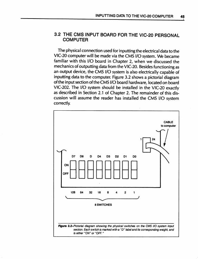
3.2 THE CMS INPUT BOARD FOR THE VIC·20 PERSONAL COMPUTER
The physical connection used for inputting the electrical data to the VIC-20 computer will be made via the CMS I/O system. We became familiar with this 110 board in Chapter 2, when we discussed the mechanics of outputting data from the VIC-20. Besides functioning as an output device, the CMS I/O system is also electrically capable of inputting data to the computer. Figure 3.2 shows a pictorial diagram ofthe input section ofthe CMS 110 board hardware, located on board VIC-202. The 110 system should be installed in the VIC-20 exactly as described in Section 2.1 of Chapter 2. The remainder of this discussion will assume the reader has installed the CMS 110 system correctly.
07 06 0 04 03 02 01 DO
128 64 32 16 8 4 2
~~----------- -----------~) - ............... 8 SWITCHES
CABLE to computer
FIgure 3.2-Plctorlal diagram showing the physical switches on the CMS I/O system input section. Each switch Is marked with a "D" label and Its corresponding weight. and Is either "ON" or "OFF . ..
I

SYSTOOLS
SYSTOOLS
SYSTOOLS
46 THE VIC·20 CONNECTION
Notice, in Figure 3.2, that there are eight switches on the CMS 1/0 board input section. These switches will be set to an OFF or ON posi· tion. When the switch is OFF, it corresponds to a setting of logical 0 on a particular input line. When the switch is ON, it corresponds to a setting of logical 1 on a particular input line.
Each of the switches in Figure 3.2 is assigned a unique label: 00, 01,02,03,04, OS, 06, and 07. The label corresponds to the physi· cal signal line that will be input to the VIC·20.
It is important to know that the switches in the CMS 1/0 system input section operate in parallel. That is, any signal line, DO through D7, can be set to a logical 1 or a logical O. Each line is set indepen· dently of any other signa/line.
3.3 INPUT SOFTWARE
The CMS 1/0 system will allow us to physically set the input lines to any desired logical state. Now we will turn our attention to the problem of how the programmer can electrically request information from the external device. The instruction used to input information is PEEK. Like the POKE instruction we used in Chapter 2, PEEK is explained fully in your user's manual and elsewhere, but we will briefly summarize its operation here. A PEEK instruction will appear in a BASIC program like this:
A 1 = PEEK (address)
Let us discuss exactly what each part of this instruction does. The variable name "A 1" could be any BASIC numeric variable. We used "Al" here only as an arbitrary example; it could have been replaced by Tl, ZS, C(3) or any valid BASIC numeric variable name. The important point is that when information is input using the PEEK instruction, variable A 1 will be set equal to it.
The (address) part of the PEEK instruction will electrically inform the VIC-20 PC which 1/0 address the data will be input from. The definition of this address is exactly the same as the address definition used for the POKE instruction, which we discussed in Chapter 2. Remember from that discussion that we can input information from any I/O circuit simply by using the correct 1/0 address. The CMS I/O system will have an address of 38912. In a BASIC program, an instruction that

SYSTOOLS
SYSTOOLS
SYSTOOLS
INPUTTING DATA TO THE VIC-20 COMPUTER 47
would allow you to input information from the CMS system would appear as:
A1 = PEEK(38912)
After this instruction is executed, the variable A 1 will be equal to the information that was input from address 38912.
Let us take another example. Suppose the 1/0 slot address is a variable itself. That is, the BASIC program will pr()mpt the user and ask for the I/O address. The 1/0 address will be stored in a BASIC variable. In this example, we will assume that the 1/0 address was stored in the variable S3. The form of the PEEK instruction would be:
A 1 = PEEK (S3)
This will set A 1 equal to the numerical value of the information read from the I/O address S3. Figure 3.3 shows a BASIC program that will operate in the way described for this example.
10 PRINT "INPUT THE I/O ADDRESS FOR COMMUNICATION";
20 INPUTS3
30 A 1 = PEEK(S3) 40 END
FlgUf8 3.3- BASIC program to ask the user whIch I/O address to Input data from.
3.4 INTERPRETING THE INPUT INFORMATION
Up to this point in our discussion of inputting data, we have shown the software required to get the input information into a BASIC program, where it will reside in a valid BASIC variable. This section will focus on ways to interpret the information that was input to the BASIC variable. During this discussion we'will be building on the information that was presented in Section 2.4 of Chapter 2.
When the VIC-20 inputs data from an 1/0 address, it is electrically inputting the logical voltage levels of eight separate signal lines. These signal lines are labeled DO, D1, D2, D3, D4, D5, D6, and D7. (See Figure 3.4.)

SYSTOOLS
SYSTOOLS
SYSTOOLS
48 THE VIC-20 CONNECTION
VIC-20 COMPUTER
00
01
02
D3 8 OATA INPUT LINES .. ---~ from external device. D4
05
D6
07
Figure 3.4-Eight separate signa/lines are connected to the V/C·20 computer expansion connector slot in order to input external information.
Each physical signal line is assigned a numerical weight by the computer. Since each line corresponds to a bit position, these weights are the same as those discussed in Chapter 2 and listed in Figure 2.11. (Again, it should be remembered that these weights are not arbitrarily assigned, but correspond to powers of two; that is, to binary numbers. A few minutes spent familiarizing yourself with the binary numbering system will be of great value in understanding how your computer works.) When an input signal line is a logical 1, its corresponding weight is summed. When an input signal line is a logical 0, its corresponding weight is not summed. The resulting sum is the value that will be stored into the BASIC variable used in the PEEK instruction.
For example, suppose the external hardware was connected to I/O address 38956. We would use this address in the PEEK instruction. It is further assumed that the external hardware is sending data that has lines DO, 04, 05, and 07 set to a logical 1. The remaining lines, 01, 02, 03, and 06, are set to a logical 0. The external input lines are set by the device sending the data to the computer. (See Figure 3.5.)
When we wish to obtain the information from the external device used in this example, the PEEK instruction will appear as:
A 1 = PEEK (38956)

SYSTOOLS
SYSTOOLS
SYSTOOLS
INPUTTING DATA TO THE VIC-20 COMPUTER 49
VIC-20 COMPUTER
DO
01
02
03
04
05
06
07
t Lines are set to a logical 1 or a logical 0 by
the external device.
EXTERNAL DEVICE
This device will output the logic levels of the
data lines.
Rgure 3.5-The external input device controls the logical voltage levels of the input lines to the VIC-20 computer.
After this instruction is executed, the BASIC variable A 1 will be equal to the summation of the weights of all the data input lines at I/O address 38956. (Notice that this address is not the one we have used previously; however, it is within the range of addresses assigned to the expansion connector, 38912 - 39935.) The summation will include the weights of all the input lines that were set to a logical 1 during the execution of the PEEK instruction.
In our example, the weights that will be summed are 07 = 128, 05 = 32, 04 = 16 and 00 = 1. The resulting summation would yield 128 + 32 + 16 + 1 = 177. The value of the variable A 1 would be equal to 177 after the execution of the PEEK instruction.
We can expect the variable used in the PEEK instruction to be greater than or equal to 0 and less than or equal to 255. A value of 0 is returned when no input lines are set to a logical 1 at the 110 address, and a value of 255 is returned when all of the input lines are set to a logical 1 at the 110 address.

SYSTOOLS
SYSTOOLS
SYSTOOLS
50 THE VIC-20 CONNECTION
To further illustrate this point, let us consider another example. In this example it is assumed that the input device is setting data lines 06, 05, 04 and 01 to a logical 1. All other data input lines are set to a logical O. (See Figure 3.6.) The input device is physically connected to 1/0 address 38960. Input information is read using the PEEK instruction. The BASIC instruction for this example will appear as:
R = PEEK (38960)
What will be the value of R after the PEEK instruction is executed? Recall that R will be equal to the sum of the weights of all input lines set to a logical 1 during the execution of the PEEK instruction. These weights will be as follows: 06 = 64, 05 = 32, D4 = 16, and 01 = 2. The resulting sum would be 64 + 32 + 16 + 2 = 114. Variable R would equal 114 after execution ofthe PEEK instruction. If we were to print the value of R at this time, the number 114 would appear. By using the PEEK instruction, we now have a means of inputting data from an external device. Furthermore, the data is stored in a BASIC variable. By using software, we can then operate on the variable in exactly the same way as any other BASIC variable.
VIC·20 COMPUTER
DO 0
01
02 0
03 0 Data lines are set to a logical 1 and a
D4 logical 0 by the
05 external device.
06
07 0
Lines are connected to computer.
FIgure 3.S-External data-input lines 01, 04, 05, and D6 are set to a logical 1 by the external device.

SYSTOOLS
SYSTOOLS
SYSTOOLS
INPUTTING DATA TO THE VIC-20 COMPUTER 51
3.5 CALCULATING THE BITS FROM THE INPUT VARIABLE
In the preceding section we discussed how to calculate the value of the input variable used in the PEEK instruction. That calculation was based on the assumption that we knew the logical level of the data input lines at the selected 1/0 address. However, in many computer control applications, we do not know which data input lines were a logical 1 and which were a logical 0 at the time of the PEEK instruction, and we need to know. The reason we need to know the logical state of the input lines is that each line input by the external device can mean something different. For example, 00 might logically inform the user that the temperature is too high, 01 might be used to indicate that some lights in a home were left on, and so on. Therefore, we need to examine the logical condition (lor 0) of each data line input during the PEEK instruction. This can be accomplished using software.
There are several ways of doing this in a BASIC program; we will present only one method here. This technique is designed to help you understand exactly what is needed and what is occurring, rather than to operate as efficiently as possible. However, as a BASIC program, it does work. As you become more familiar with this type of programming, new and more efficient ways of performing the transformation and testing will become apparent.
Here is one way to do it. We can start by applying our knowledge of how the PEEK variable was originally formed to the problem of "deciphering" it. Recall that the variable was formed by summing the weights of the data input lines that were a logical 1 during execution of the PEEK instruction. What we will do is discover, by a process of subtraction, which individual weights were used to obtain the sum. Once these weights are known, the corresponding input lines that were set to a logical 1 are also known. All other input lines must have been a logical 0 during the execution of the PEEK instruction.
For example, suppose we executed this PEEK instruction:
A = PEEK(38912)
After this instruction was executed, the variable A would have a value between 0 and 255, inclusive. The value would depend on which of the eight data input lines, DO- 07, were set to a logical 1. For purposes of illustration, we can assume that the variable A was equal to

SYSTOOLS
SYSTOOLS
SYSTOOLS
52 THE VIC-20 CONNECTION
183 after the PEEK instruction. At the outset, we can see that at least one of the data input lines was set to a logical 1 , because the value of A is not O. We also know that at least one of the data input lines is a logical 0, because the value of A is not 255. But we do not know which input lines were set to a logical 1 and which input lines were set to a logical 0 during the PEEK instruction. That is precisely the problem we are going to solve.
Our job now is to determine which of the data input lines was a logical 1 during the input instruction. This can be done in the following way. Subtract from the variable A the weight of each input line, starting with the weight of 07. If the result of the subtraction is less than 0, we know the weight subtracted was not used to obtain the sum. Let's go through some examples to show exactly what is meant.
Suppose a variable returned from the PEEK instruction was equal to 125. Using our plan, the weight of 07 is subtracted from 125. This would yield a subtraction of 125 - 128, which is less than o. Therefore, we know that the weight of 07 was not used to obtain the original sum, and that 07 is a logical O.
We then proceed with the next weight in line, the weight of 06. The weight of 06 is subtracted from 125. The result would be 125 - 64 = 61. The result of this subtraction is not less than o. Therefore, the weight of 06 was used in the original summation, and 06 is a logical 1.
When we find that a weight was used in the summation, its value is subtracted from the starting number and the resulting value is tested against the next weight in the line. In this case the next weight in the line after 06 is 05. The weight of 05 is subtracted from the new value, 61, not the original value, 125. This will give 61 - 32 = 29. This value is not less than o. Therefore, the weight of 05 was used to obtain the original sum, and 05 is also a logical 1.
At this time we know that the weights of 06 and 05 were used in obtaining the original sum of 125. Proceeding further, we test the next weight, 04, against the new value, 29. (fhe value 29 is equal to the original number, 125, minus the known weights, 06 and 05.) Subtracting 16 from 29, we get a result of 13. This result is not less than o. Therefore, the weight of D4 was used in obtaining the original sum. We continue the process by subtracting the next weight from the new value, 13.
The next weight in line is 03. The subtraction 13 - 8 = 5 yields a

SYSTOOLS
SYSTOOLS
SYSTOOLS
INPUTIING DATA TO THE VIC-20 COMPUTER 53
number greater than O. From this we know that the weight of 03 was used in obtaining the original sum. The next weight, 02, is tested against the new value,S.
The resulting subtraction,S - 4 = 1, gives a number that is not less than O. Again, we know that the weight of 02 was used to obtain the original sum. At this point we know that the weights of 06, OS, 04, 03, and 02 were used to obtain the original sum.
We next test against the weight of 01. This subtraction would yield 1 - 2 = -1. This result is less than O. Because of this, we know that the weight of 01 was not used to obtain the original sum. Finally, we proceed to test against the weight of DO.
Since the subtraction of the weight of 01 yielded a negative result, the testing value, 1, is not changed. Subtracting the weight of 00 would give 1 - 1 = O. This result is not less than 0, so we know that 00 was used to obtain the original sum of 125. At the conclusion of this process, we know that the weights of the data lines 06, OS, 04, 03, 02, and 00 were used to obtain the original sum. Therefore, these input data lines were a logical 1 during the execution of the PEEK instruction. Further, we know that the data input lines 07 and 01 were a logical 0 during the execution of the PEEK instruction.
The procedure described above is, essentially, how the weights of the data lines are tested. If at any point in the testing the result is 0, then we can stop and test no further, because all the remaining data lines must be a logical O.
To further illustrate this procedure, let us consider another example, detailing the steps in outline form. We will assume that the variable returned from the PEEK instruction this time was 183. We need to know which data lines were a logical 1 and which were a logical O. The procedure is outlined below:
1. Subtract the weight of 07 from the original variable, 183. This gives
183 - 128 = 55
The result is greater than O. Therefore, the bit weight of 07 was used to obtain the original sum. 07 was a logical 1 during the PEEK instruction. We set the variable A2 equal to 55.
2. We now subtract the bit weight of 06 from the new value of variable A2.
55 - 64 = -9

SYSTOOLS
SYSTOOLS
SYSTOOLS
54 THE VIC-20 CONNECTION
The result is less than O. This tells us that the bit weight of 06 was not used to obtain the original sum of 183, and that 06 was a logical 0 during the PEEK instruction.
3. We next subtract the weight of 05 from the variable A2. Note that A2 was not changed in step 2, because the result of the subtraction was less than O.
55-32=23
Since the result of the subtraction is not less than 0, we know that this weight was used to obtain the original sum. Therefore, 05 was a logical 1 during the PEEK instruction. The variable A2 is now set to 23, because the result of the subtraction was not negative. Notice that as a weight is used to obtain the sum, it is subtracted from the current value of the variable A2.
4. Next we subtract the bit weight of 04 from the variable A2.
23 - 16 = 7
The result is not less than O. Therefore, the bit weight of 04 was used to obtain the original sum. Data input line D4 was a logical 1 during the PEEK instruction. The variable A2 is now equal to 7.
Let us stop at this point to examine what information we have concerning the input data lines. From steps 1-4, we know that bit 07 = 1, 06 = 0, 05 = 1, and 04 = 1. The checking is resumed starting with the weight of 03.
5. We subtract the bit weight of 03 from the new variable A2.
7 - 8 = -1
The result is a number less than O. Therefore, we know that the weight of 03 was not used in obtaining the original sum of 183. This means 03 was a logical 0 during the PEEK instruction.
6. Testing the next bit weight, 02, we obtain the result:
7-4=3
The result is a number that is not less than O. Therefore, input line 02 was a logical 1 during the PEEK instruction. The variable A2 becomes 3.

SYSTOOLS
SYSTOOLS
SYSTOOLS
INPUTTING DATA TO THE VIC-20 COMPUTER 55
7. Now test bit 01. The result of this subtraction is
3-2=1
We see that the 01 input line was a logical 1 during the PEEK instruction.
8. The final bit to test is ~O. The result of this test is:
1 - 1 = 0
Since the result of the subtraction was not less than 0, we know that the weight of DO was used to obtain the original' sum.
The results of the bit testing can be summarized thus:
07 06 05 04 03 02 01 DO bit labels 1 0 1 1 0 1 1 1 logical values
These results are easy to check, as we can simply sum the weights of all the bits that are a logical 1. The result of this summation should be the number we started with, 183.
128 = 07 + 32 = 05 + 16 = 04 + 4= 02 + 2 = 01 + 1 = DO
183 The result checks.
When we read through the steps required to make these tests by hand, the procedure seems quite tedious. Fortunately, we have the computer to make these checks for us. Since we know what tasks the computer has to perform, the first step in writing a computer program to perform these checks is to design a task flowchart outlining the steps of the procedure. Such a flowchart is shown in Figure 3.7.
A BASIC program to realize this flowchart on the VIC-20 computer is given in Figure 3.8. A second example of a BASIC program that will implement the flowchart of Figure 3.7 is given in Figure 3.9. The difference between the two programs is in the second program's use of FOR/NEXT loops to test the individual weights. In Figure 3.8 each weight is tested in a sequential fashion. Figure 3.9, on the other hand, tests each weight by reducing the variable A3 by half at each pass

SYSTOOLS
SYSTOOLS
SYSTOOLS
56 THE VIC-20 CONNECTION
A11S0RIGINALNUMBER
07 TESTED
06 TESTED
05 TESTED
D4 TESTED
..---------,
03 TESTED
02 TESTED
01 TESTED
}oo TESTED
Figure 3. 7-Flowchart for checking the logical value (1 or 0) of the external data input lines to the VIC-20 computer. The data was input by using a PEEK instruction.

SYSTOOLS
SYSTOOLS
SYSTOOLS
INPUTTING DATA TO THE VIC-20 COMPUTER 57
through the loop. In Figure 3.B we simply wrote a statement that set up the new test value.
Using the testing technique described above, we will be able to tell exactly which data input lines were a logical 1 and which data input lines were a logical 0 during the execution of a POKE instruction. We are now ready to practice inputting data to the VIC-20.
10 PRINT "INPUT THE ORIGINAL NUMBER BETWEEN 0 - 255 "; 20 INPUTA1 30 A2=A1 35 REM SET ALL D VALUES EQUAL TO ZERO (LINES 40-110) 40 DO=O 50 D1 =0 60 D2=0 70 03=0 80 D4=0 90 D5=0
100 D6=0 110 D7=0 195 REM D7 TESTED (LINES 200-220) 200 IF A2 -128 < 0 THEN 230 210 A2=A2-128 220 D7=1 225 REM D6 TESTED (LINES 230-250) 230 IF A2 - 64 < 0 THEN 260 240 A2=A2-64 250 D6=1 255 REM D5 TESTED (LINES 260:-280) 260 IF A2 - 32 < 0 THEN 290 270 A2=A2-32 280 D5=1 285 REM D4 TESTED (LINES 290-310) 290 IFA2-16<OTHEN320 300 A2=A2-16 310 D4=1 315 REM D3 TESTED (LINES 320-340)
Figure a .• -BASIC program to realize the flowchart of Figure 3. 7 (continues).

SYSTOOLS
SYSTOOLS
SYSTOOLS
58 THE VIC-20 CONNECTION
320 IFA2-8<OTHEN350 330 A2=A2-8 340 03=1 345 REM 02 TESTEO (LINES 350-370) 350 IFA2-4<OTHEN 380 360 A2=A2-4 370 02=1 375 REM 01 TESTEO (LINES 380-400) 380 IFA2-2<OTHEN410 390 A2=A2-2 400 01 =1 405 REM 00 TESTEO (LINES 410-420) 410 IFA2-1 <OTHEN43O 420 00=1 430 PRINT "ORIGINAL NUMBER WAS ";A1 440 PRINT 450 PRINT "BINARY VALUE IS ";07;06;05;04;03;02;01;00 460 END
Figure 3.8 (continued).
10 DIM 0(8) 20 PRINT "INPUT THE ORIGINAL NUMBER BETWEEN 0 ANO
255"; 30 INPUTA1 35 REM SET ALL 0 VALUES EQUAL TO ZERO (LINES 40-60) 40 FORI=OT07 50 0(1)=0 60 NEXT I 70 A2=A1 80 A3=128 85 REM LOOP TO TEST ALL 0 VALUES (LINES 90-140) 90 FORI= 7TO 0 STEP -1
Figure 3.9-A shorter BASIC program to realize the flowchart of Figure 3. 7. In lines 80 - 130, the variable A3 is the weight of each data line. A3 will start at 128, which is the weight of 07. This variable is then reduced by half in each pass through the FOR/NEXT loop (continues).

SYSTOOLS
SYSTOOLS
SYSTOOLS
INPUTTING DATA TO THE VIC-20 COMPUTER 59
100 IFA2-A3<OTHEN 130 110 A2=A2-A3 120 0(1)= 1 130 A3=A3I2 140 NEXT I 150 PRINT "ORIGINAL NUMBER WAS ";A1 160 PRINT 170 PRINT "THE BINARY VALUE IS OJ;
180 FORI= 7TOOSTEP-1
190 PRINT 0(1) 200 NEXT I 210 PRINT 220 END
Figure 3.9 (continued).
3.6 HANDS-ON EXAMPLE 1: CALCULATING THE WEIGHT OF THE INPUT WORD
In this first hands-on example of inputting data to the VIC-20 computerfrom the CMS I/O board, we will ca Icu late the value of the input weights by hand. The input weight will be calculated according to the method described in this chapter. After calculating manually the weight, you should set the switches on the CMS I/O board to the correct value and run the program.
The program will print out the weight calculated by the computer. You can then verify whether your manual calculation was correct. Let us go over an example to see how this works. First, set the input switches on the CMS I/O board so that 00 and D4 are a logical 1. All other switches are set to a logical o. Remember that when the switch is in the OFF position it is a logical 0, and when it is in the ON position it is a logical 1.
Now calculate the input weightthe VIC-20 will see when this data is read. In this example the computer will electrically input 04 and 00 as a logical 1. This will correspond to a weight of (04 = 16)+ (DO = 1) = (16+ 1)= 17.

SYSTOOLS
SYSTOOLS
SYSTOOLS
60 THE VIC-20 CONNECTION
After the computer has read this data it will print outthe number 17. At this point we can check our calculated results against the actual computer results. In this way you can quickly verify that you understand how the input lines are weighted.
Try the program shown in Figure 3.10, using the different switch settings, a-f. The switches will be set to a logical O. The correct weight for each switch setting is given after setting (f).
a. 01 and 07 are set to 1
b. 00 and 05 are set to 1
c. 04, 06, and 07 are set to 1
d. 01, 02, 03, 04, 06, 07 are set to 1
e. All switches are set to a logical 1
f. All switches are set to a logical 0
Answers: a = 130, b = 33, c = 208, d = 222, e = 255, f = O.
10 PRINT "INPUT THE 1/0 ADDRESS FOR COMMUNICATION";
20 INPUTS3
30 A 1 = PEEK(S3) . 40 PRINT "THE DATA READ FROM 1/0 ADDRESS # ";S3;" = ";A1
50 END
Figure 3.10-A BASIC program to read the input data from the requested 110 address and then print the data on the screen of the VIC-20.
3.7 EXAMPLE 2: READ A BYTE AND DETERMINE WHICH BITS WERE A LOGICAL 1
In this example, the computer will read an input word from the CMS 110 board and print out which data lines were equal to a logical 1 and which data lines were equal to a logical O. This is exactly the same type of operation we discussed in Section 3.5. A general program to perform this function with the VIC-20 PC is shown in Figure 3.11. Run this program and verify that the computer will print out the correct data lines that you have set on the CMS 110 board switches. Use the switch settings given in Section 3.6.

SYSTOOLS
SYSTOOLS
SYSTOOLS
INPUTTING DATA TO THE VIC-20 COMPUTER 61
10 PRINT "INPUT THE I/O ADDRESS FOR THE CMS BOARD "; 20 INPUTS3 30 A 1 = PEEK(S3) 40 A2=A1 50 REM INITIALIZE THE VARIABLES 60 00=0:01 =0:02=0:03=0:04=0:05=0:06=0:07=0 70 IF A2 - 128 < 0 THEN 100 80 A2=A2-128 90 07=1
100 IFA2-64<OTHEN 130 110 A2=A2-64 120 06=1 130 IFA2-32<OTHEN 160 140 A2=A2-32 15005=1 160 IFA2-16<OTHEN 190 170 A2=A2-16 180 04=1 190 IFA2-8<OTHEN 220 200 A2=A2-8 210 03=1 220 IF A2-4<OTHEN 250 230 A2=A2-4 240 02=1 250 IFA2-2<OTHEN 280 260 A2=A2-2 270 01 = 1 280 IFA2-1 <OTHEN300 290 00=1 300 PRINT 310 PRINT "THE BINARY VALUES OF THE INPUT WERE " 320 PRINT 330 PRINT "07 = ";07
Figure 3. 11-A BASIC program to read the input data and then print out the logical value of each data line, DO - D7 (continues).

SYSTOOLS
SYSTOOLS
SYSTOOLS
I~
62 THE VIC-20 CONNECTION
340 PRINT "06 = ";06 350 PRINT "05 = ";05 360 PRINT "04 = ";04 370 PRINT "03 = ";03 380 PRINT "02 = ";02 390 PRINT "01 = ";01 400 PRINT "00 = ";00 410 END
Rllure 3.11 (continued).
After you have run the program and verified that it works, make certain you understand each part of it. Now write a similar program using fewer BASIC statements. Use this new program to print out only the input lines that are a logical 1. For example, if switches DO and 04 are set to a logical 1 position on the CMS 110 board, have the computer print out NOO, 04.N
Now reverse the sense of the problem. Have the computer print out the input lines that are set to a logical 0 instead of a logical 1.
3.8 EXAMPLE 3: READ A WORD AND PERFORM AN ACTION
In this example we will input a byte from the CMS 110 board to the VIC-20 computer. If the byte we are inputting is equal to a certain value, we will perform a particular action; we will print a message. If the byte is not equal to that value, we will perform a different action; we will print a different message.
This type of example is very similar in principle to the process of monitoring an input device with the VIC-20 (or any other) computer. When the input condition is true, the computer will automatically perform some action based on this input. Of course, in a real application, the input would come from some piece of external hardware the computer was controlling or monitoring.
In our example, the inputs will be generated by the user from the CMS 110 board. When the data word that is input is equal to 12, the computer will print the message, nrHE INPUTWORO IS EQUAL TO 12.N If the input word is not equal to 12, then the computer will print

SYSTOOLS
SYSTOOLS
SYSTOOLS
INPUTTING DATA TO THE VIC-20 COMPUTER 63
the message, "THE INPUT WORD IS NOT EQUAL TO 12 AT THIS TIME."
A flowchart for this problem is shown in Figure 3.12, and a BASIC program to realize the flowchart is given in Figure 3.13.
INPUT THE 8-BIT CODE
YES
PRINT "INPUT WORD - 12"
NO
PRINT "INPUT WORD. IS NOT EQUAL TO 12
AT THIS TIME"
Rgure 3. 12-A task flowchart for the solution to the problem given in Section 3.8.
10 PRINT "INPUT THE I/O ADDRESS FOR THE CMS BOARD ";
20 INPUTS3
30 A 1 = PEEK(S3) 40 IFA1=12THEN70 50 PRINT "THE INPUT WORD IS NOT EQUAL TO 12 AT THIS TIME" 60 STOP 70 PRINT "THE INPUT WORD IS EQUAL TO 12" 80 END
FIgure 3.13-A BASIC program to realize the flowchart of Figure 3. 12.

SYSTOOLS
SYSTOOLS
SYSTOOLS
64 THE VIC-20 CONNECTION
Try this program out with your VIC-20. Set the switches on the CMS I/O board to a number other than 12, and be sure that the computer will print out the error message. Now set the input word equal to 12 (that is, set 03 and 02 to a logical 1 ), and check to see ifthe computer will print out the correct message.
When you have the program running, try the following variations:
a. Have the computer check for an even number of ones in the input word. If the number of ones is even, the computer will print, "THERE ARE AN EVEN NUMBER OF ONES." If the number of ones in the input word is odd, the computer will print, "THE NUMBER OF ONES IS ODD."
b. Input a number, and have the computer subtract 25 from it; then print out the results. The output should be both your original number and the new number. Remember that it is possible to get a number that is less than 0 in this program. If the result is less than 0, print out the message, "THE RESULT WAS LESS THAN ZERO."
3.9 EXAMPLE 4: A COMBINATION LOCK
In this example we will make the VIC-20 Personal Computer into a combination lock. The lock will have three unique numbers that must be entered in sequence. If any of the numbers (or their sequence) is not correct, the lock will not open.
The three numbers will be 64, 128, and 7. Here is how the lock will work. A BASIC computer program will ask you to enter the first number by setting the switches corresponding to that numerical weight on the CMS I/O board. When the number is set, you will enter "L" on the computer. This signals the computer that you have entered the number and are ready for the computer to read it.
If the computer detects a wrong number, the message, "I WILL NEVER OPEN FOR YOU" will be printed. If the number is correct, the computer will print the message, "SO FAR SO GOOD." When you enter the last number correctly, the computer will print, "YOU OPENED THE LOCK." Enter an "R" to reset the combination lock. This ·will allow you to start over.
A flowchart of this problem is shown in Figure 3.14. Figure 3.15

SYSTOOLS
SYSTOOLS
SYSTOOLS
INPUTTING DATA TO THE VIC·20 COMPUTER 65
PRINT "I WILL NEVER OPEN THE LOCK FOR YOU"
SET INTERNAL COMBINATION 64,128,7
ASK USER TO ENTER "L" OR "R"
NO
NO
PEEK AT 1/0 SLOT FOR NUMBER
PRINT "YOU OPENED THE LOCK"
NO
figure 3.14-A task flowchart showing the general steps for controlling an external device that acts as a combination lock.

SYSTOOLS
SYSTOOLS
SYSTOOLS
66 THE VIC-20 CONNECTION
shows one BASIC program that will realize this flowchart. Try this program out with your VIC-20 computer. Once you have this program running, try putting in the following variations:
a. Change the combination of the lock to 2, 4, 8.
b. Realize the program using fewer BASIC statements than shown in the example.
10 DIM N(3),L(3),A$(5) 20 REM THESE ARE THE COMBINATION NUMBERS 30 N(1)=64 40 N(2)=128 50 N(3)=7 60 REM THESE ARE THE INPUT COMBINATION NUMBERS 70 L(1)=0 80 L(2)=0 90 L(3)=0
100 REM START OF COMBINATION INPUTIING 110 1=1 120 PRINT "PUT SETIING # ";1;" ON CMS INPUT SWITCHES" 130 PRINT "INPUT 'L' WHEN READY, OR 'R' TO RESET" 140 INPUTA$ 150 IFA$="L"THEN180 160 IF A$ = "R" THEN 70 170 GOT0120 180 L(I) = PEEK(38912)
. 190 IF L(I) = N(I) THEN 220 200 PRINT "I WILL NEVER OPEN THE LOCK FOR YOU III"
210 GOT0240 220 IF I = 3 THEN 260 230 PRINT "SO FAR, SO GOOD" 240 1=1+1 250 GOT0120 255 REM THE LOCK WILL NOW OPEN 260 PRINT "YOU OPENED THE LOCK" 270 END
Figure 3. 15-A BASIC program to realize the flowchart of Figure 3. 14.

SYSTOOLS
SYSTOOLS
SYSTOOLS
INPUTTING DATA TO THE VIC-20 COMPUTER 67
3.10 SUMMARY
In this chapter we have discussed in detail howto input information into a BASIC program from an external device. This device will be monitored by the VIC-20 Personal Computer.
Once the information was input into the BASIC program, we discussed different methods of interpreting what the input number meant. A technique was described that will enable you to determine which input lines were a logical 1 and which input lines were a logical O.
At the end of this chapter we presented some hands-on examples. These examples were designed to allow you to practice inputting information to a BASIC program, and to test your understanding of the methods outlined.
If you understand the solution to these examples, then you understand the principles of inputting data. In Chapter 4 we will present the hardware for this task, and describe how the software will interact with it. Now you are ready for the next step along the path toward making the VIC-20 Connection. That step is to actually connect the hardware to allow the computer to communicate with an external device.

SYSTOOLS
SYSTOOLS
SYSTOOLS
INP8 1 ANB 08 1 P8 1
IIAIIBWAIIE E811 II IF \,'16-20 60MP81 FB

SYSTOOLS
SYSTOOLS
SYSTOOLSIn this chapter we will discuss the hardware, internal and external,
necessary to input and output data to and from the VIC-20. It should be noted that this discussion is meant for the beginner in computer interfacing and control. These discussions are centered around the input and output hardware architecture ofthe VIC-20 Personal Computer's expansion connector.
The designs shown in this chapter work, but they are not presented as the most elegant or efficient, Hleast-parts-count," circuits. Instead, their main function is to instruct. They are designed to enable a person who has little or no experience in digital hardware to understand the major concepts involved in the input and output of electrical information between the VIC-20 and an external device. In the chapters that follow, we will make use of the information presented here.
If this is your first exposure to any digital hardware, you may feel apprehensive about the difficulties of the subject. Furthermore, you may not want to learn about the hardware of the computer in any great detail. But if you can grasp the essential facts and concepts presented in this chapter, understanding how other peripheral hardware

SYSTOOLS
SYSTOOLS
SYSTOOLS
70 THE VIC-20 CONNECTION
is interfaced to the VIC-20 will be much easier. That will be true even if you never actually design a computer interface for the VIC-20 computer. Using the information given in this chapter, you will better understand other manufacturers' interfaces to the VIC-20. As we proceed through the discussion, relationships will be pointed out between the hardware described here and the software given in Chapters 2 and 3.
4.1 BEGINNING OUTPUT ELECTRONICS FOR THE VIC-20
Four main digital electronic sections are of concern when discussing output hardware for the VIC-20. They are:
1. The enable circuit for the external device.
2. The READ/WRITE signal.
3. The write strobe for the circuit.
4. The output storage latches.
These four sections operate together to perform the output function. If anyone of them fails to operate correctly, the output operation will not work. Let us discuss the function each section performs in an output operation. As each section is discussed, we will show how it can be realized with common digital electronic circuits for the VIC-20.
4.2 THE ENABLE CIRCUIT
To start, we concentrate on the function of the enable circuit in an output operation for the VIC-20. When an enable circuit is active, it means the computer will be electrically addressing the output circuit. The computer is capable of communicating with over 64,000 different circuits. Therefore, it must have some means of electrically informing any particular output circuit that it has been selected to communicate with. This communication is accomplished via the internal computer lines called address lines. These lines are output on the pins of the expansion I/O connector in the VIC-20 Pc. Figure 4.1 shows the pinout of the expansion connector with the pin number and signal name of each pin.

SYSTOOLS
SYSTOOLS
SYSTOOLS
INPUT AND OUTPUT HARDWARE FOR THE VIC-20 COMPUTER 71
I ~ : :: : : : : : : : : : : : : : : : : : : I ABCDEFHJ KlMNPRSTUVWXYZ
PINtI TYPE· PINtI TYPE
1 GND 12 BLKi 2 COO 13 BlK5 3 CD1 14 RAM1 4 CO2 15 RAM2 5 CDS 16 RAMs 6 CD4 17 vRiii 7 CD5 18 CR/W 6 CD6 19 IRQ 9 CD7 20 NC 10 BlK1 21 +5V 11 BOO 22 GND
PINtI TYPE PINtI TYPE
A GND N CA10 B CAO P CA11 C CA1 R CA12 0 CA2 S CA13 E CAS T 1102 F CM U 1103 H CAS V S02 J CA6 W NMI K CA7 X RESET l CAB Y NC M CAB Z GND
Figure 4.1-Pinout of the VIC20 computer's 44-p/n expansion connector. Reproducei:J by permission of Commodore Business Machines, Inc.

SYSTOOLS
SYSTOOLS
SYSTOOLS
72 THE VIC-20 CONNECTION
The enable signals we are interested in are called 1/02 and 1/03. They are output on pins T and U of the I/O connector shown in Figure 4.1. The bar over the top of the signal name indicates that when the signal is active, doing its electrical job, its logical state is O. At all other times this signal will be in the logical 1 state.
Whenever the computer selects the 1/02 or the 1/03 address to communicate with, the 1/02 or 1/03 line on the I/O expansion connector will be set to a logical o. Either of these two select lines can be activated under software control, using the PEEK and POKE instructions. Recall that these two BASIC instructions each include an address. The logical state of the I/O output signal depends on the address specified in the PEEK or POKE instruction. For example, if we want the 1/02 line on the I/O connector to go to a logical 0, we can PEEK or POKE addresses 38912 through 39935 (38912+ 1023). To activate the 1/03 line we can specify an address from 39936 through 40959 (39936+ 1023). We will use the 1/02 line in our examples, but from this discussion you can relate the information to the 1/03 line.
The 1/02 line is activated directly by the VIC-20 computer. Let us assume that our computer is operating correctl~ and that the PEEK or POKE address is correct to generate the 1/02 signal. Further, let us assume that this line will go to a logical 0 whenever we wish to output information from the computer to the output circuit to which the active signal is applied.
4.3 THE READIWRITE C'JR/W) LINE
Another hardware signal that we must make use of when performing computer output is the READ/WRITE or VRIW line. This signal is output on pin 17 ofthe I/O connector shown in Figure 4.1. The VRIW signal is a logical 1 whenever the VIC-20 computer is reading data from the I/O slot, and a logical 0 whenever the computer is writing data to the slot. During a PEEK instruction, therefore, the VRIW line is a logical l,because the computer is reading data. During a POKE instruction, the VRIW line is a logical 0, because the computer is writing data. The VRIW line must be electrically qualified in order for an output circuit to make use of it. By that we mean that the circuit must not only electrically examine the logical state of the VRIW line to

SYSTOOLS
SYSTOOLS
SYSTOOLS
\ ~\) ... 't ~ Q"" f\4T
\ \ \ J ... l 0 I
0 \ ,
<:> 0 0
j: )--t o tl. GF\IE:
INPUT AND OUTPUT HARDWARE FOR THE VIC-20 COMPUTER 73
determine whether our circuit will be read or written to, but it must also examine the logical state of the 1/02 line mentioned earlier. That is, the VRIW line must be "qualified" by the 1/02 select line before we can use it in the external circuit. Figure 4.2 shows a block diagram of exactly what we mean.
QUALIFYING ELECTRONICS
• 1102 SELECT
vAiN 1 110 SLOT WRITE
This line Is a logical o only when the
, I VIC-20 computer Is outputting data to the addressed I/O slot.
Signals from the VIC·20 computer
110 slot.
FIgure 4.2-Block diagram showing how the VRiW line must be qualified by the 7K52 select line to generate the 110 SLOT WRITE signal.
Figure 4.3 shows a hardware realization for the qualification of the VRIW line to be used by an output circuit. In this schematic diagram we see thatthe 1/02 signal is inputto pin 1 ofthe 74LS32, an OR gate. The 74LSOO family of integrated circuits is widely available and will be used throughout this book. An OR gate is a digital logic device that will produce a logical 1 at its output when either input A or input B is a logical 1, or when they are both logical 1. When both inputs are a logical 0, the output is a logical 0. Input A and input B are shown as pin 1 and pin 2 in Figure 4.3. The 74LS32 integrated circuit contains

SYSTOOLS
SYSTOOLS
SYSTOOLS
74 . THE VIC-20 CONNECTION
rOO2 3 I/O BOARD STROBE
17 vRiiii
74LS32
Figure 4.3-Schematic diagram showing how to raalize the block diagram of Figure 4.2.
four individual OR gates. The VR/W signal is input to pin 2 of the same OR gate. The output line ofthe OR gate, pin 3, will be a logical 0 only when both the VRIW and the 1/02 line are a logical O. That is, we have now IIqualified" the vRNJ line. The output of the OR gate in Figure 4.3 is given the name BOARD STROBE. This line is a logical 0 only when the VIC-20 computer is outputting data to the external circuit connected to 1/02.
4.4 THE EXTERNAL OUTPUT STROBE
The next output signal we will discuss is the signal which will strobe or write the data to the output circuit. This signal is generated by combining the 1/02 and VRIW signals discussed in the previous two sections. When both of these signals are a logical 0, we generate a new signal, labeled BOARD STROBE. This circuit was shown in Figure 4.3.
This strobe will become active when the computer executes the POKE instruction to the address of 1/02. All timing of the computer signals is taken care of by the internal hardware of the VIC-20. All we need do is use the signals provided by the manufacturer for our circuit.

SYSTOOLS
SYSTOOLS
SYSTOOLS
INPUT AND OUTPUT HARDWARE FOR THE VIC·20 COMPUTER 75
4.5 THE OUTPUT LATCHES
The final section of the output hardware we will discuss comprises the output latches. Output latches have the very important function of temporarily storing the data sent by the computer to an external circuit. Recall that the POKE instruction included an address and data. The address will select the 1/0 circuit, and the data specified will be sent to the external circuit. The output latches will store this data.
The computer will present the data to the input pins of the output latches. (See Figure 4.4.) At this time, the BOARD STROBE signal will provide a write input pulse to the latches. After the data has been writ· ten into the latches, it will remain stored there until the computer is instructed to write other data to the circuit. To put it another way, when data is output into the storage latches, it will remain there until another POKE instruction directs new data to the same address .
RY TEMPORA STORAGE~
lCH ~
Data from the VIC-20 computer
to the 110 slot.
DO
01
02
03 --. D4 --"
05 --"
06
07
t All 110
slota use these data linea.
....- IIOSLOT WRITE STROBE
LDO
L01
L02
L03
LD4
LOS
L06
L07
t "L" ~ LATCHED
Toextemal device the computer will control.
FlgUIfJ 4.4-Block diagram showing how tha data output lines from the VIC20 computer will connect to the temporary storage latches located in the 110 expansion slot output Circuit.

SYSTOOLS
SYSTOOLS
SYSTOOLS
76 THE VIC-20 CONNECTION
The data at the output latches can now be used to control any hardware that we desire. At this point, you may not have a clear picture of exactly what hardware can be controlled. Don't worry. We will introduce some examples in later chapters. The point is that we now have a means of forcing any single logical line to switch between a logical 0 and a logical 1 level under computer control. We have achieved an important objective in the interfacing problem. When you understand how this was done, a major step has been completed.
Now let us take a closer look at the hardware of the output latch circuits. Figure 4.5 shows the latch device we will use and the pin numbers that incoming and outgoing data lines will connect to. The latch used is an 8-bit 74LS374. The VIC-20 computer will transfer eight bits of data during every output operation, so this device matches perfectly. Data from the computer is input to the latch from the VIC-20 data lines D7 - DO.
74LS32 o"tL-ii02 c..'-/
vRiW 2 ,,(,(,. I 74LS374
loa 11 DO 3 2 LDO
01 4 5 L01
02 7 6 L02 Data lines 03 8 9 L03 LATCHED
from D4 DATA
13 12 LD4 OUTPUTS VIC-20. 05 14 15 L05
OS 17 16 LOS
07 18 19 L07
• OUT e{llABLE • , ...... .. _ .....
Figure 4.5-Schematic diagram showing the connection of the 74LS374 latch to the VlC-20 expansion connector pins.

SYSTOOLS
SYSTOOLS
SYSTOOLS
INPUT AND OUTPUT HARDWARE FOR THE VIC-20 COMPUTER 77
Data from the VIC-20 PC will be applied to the data input pins of the 74LS374. Pin 11 of the latch is the strobe input. When this line is active, it goes from a logical 0 to a logical 1. The data present at the input of the latch is NcapturedN and stored internally in the latch. Recall that when the strobe line is activated, it is in a logical 0 state. When this line returns to the logical 1 state, the data is latched.
We have now followed the data, along with the VRIW and 1/02 from the pins of the VIC-20 expansion connector and into the latches of an I/O circuit. The data is now latched, and we are ready to use this data to control an output device.
4.6 THE LIGHT-EMITTING DIODES
The output device that we will be controlling in this first example will be a series of light-emitting diodes, or LEOs. Eight LEOs are used, one for each data output line. By using LEOs, we can gain experience in turning on and off selected bits ofthe output device. We did this in Chapters 2 and 3 by using the CMS I/O system. At this time, you may choose to construct your own I/O system using the schematics given in this chapter.
When we turn on and off selected LEOs, we are performing exactly the same function as when we control most types of external devices. We will now concentrate on how the hardware does its part of the job.
Figure 4.6 shows a schematic diagram of how an LED is electrically driven to light. We see in this diagram that the LED has approximately the same electrical symbol as a standard diode. The difference is that the LED symbol has some arrows drawn out from it, an indication that the diode is emitting light.
The LED performs approximately the same electrical function as a standard diode. That is, it will pass current when connected as shown in Figure 4.6 (forward-biased). The LED will not pass current when connected as shown in Figure 4.7 (reverse-biased). The important difference is that when the LED is forward-biased, it will emit light. The color of the light is determined by the materials used to fabricate the LED. Typical LED colors are red, green and yellow. In Figure 4.6 we see that the anode of the LED is connected to + 5 volts. The anode is the positive (+ ) side of the device. The cathode, or negative (- ) side

SYSTOOLS
SYSTOOLS
SYSTOOLS
78 THE VIC-20 CONNECTION
of the LED, is connected to one end of a resistor. To turn on the LED, the other side of the resistor must be connected to ground potential, or approximately 0.0 volts.
If you have never used an LED before, it might be fun and instructive to construct the circuit shown in Figure 4.6 and manually turn the diode on and off. This is done by connecting the anode to + 5 volts and then disconnecting it. When you do this, try reversing the connection by interchanging the diode leads, and note what happens. That is, connect the cathode (-) side of the LED to + 5 volts and the anode (+) side of the LED to the resistor. (See Figure 4.7.) Connect the other side of the resistor to ground again. The LED should not light under these conditions, because it is now connected in a reversebiased mode.
Here is how the circuit of Figure 4.6 works. With the anode of the LED connected to + 5 volts, the cathode must be connected to ground potential to light the diode. There must not be a direct connection of the cathode to ground. If there were, too much current would be passed through the LED, and it would burn up. Therefore, a current-limiting resistor, Rl, is required. The function of Rl is to limit
+5V
~~+ \\ LED
LED ~ Is forward· blased,and emits light.
330Q 114 WATT
RgUI8 4.8-Schematic diagram of a typical LED connected in the forward-biased mode.

SYSTOOLS
SYSTOOLS
SYSTOOLS
INPUT AND OUTPUT HARDWARE FOR THE VIC-20 COMPUTER 79
the current to a safe value in the LED when it is connected in the forward-biased mode. Typical LED currents are around 10 milliamperes, or .01 amperes. This amount of current will usually give a nice degree of brightness.
Multiplying a single LED by eight, we have the circuit shown in Figure 4.8. In this schematic diagram, the resistors Rl- R8 are connected at one end to the LEOs, and at the other end to the outputs of a 7406 integrated circuit. The 7406 will act as a switch to connect the resistors to ground potential. For example, when the input pin 1 of the 7406 shown in Figure 4.8 is a logical 1 , the output pin 2 is connected to ground potential. Under these conditions, the LED is turned on, or forward-biased.
When the input pin 1 of the 7406 is a logical 0, the output pin 2 is not connected to ground. The output is essentially an open circuit; that is, no current is passing through it. Under this condition the LED is turned off. From these two conditions, we see that all we need to do to turn the LED on and off is to place a logical 1 or a logical 0 at the input of the 7406. As long as the input stays at a logical 1 or a logical 0, the LED will remain either on or off.
+5
\~ LED ,,~\ Is reverse-'4\ biased and will
&.....,-..a not emit light.
+
33OQ1/4WATT
FIgure 4.7-5chematic diagram of an LED connected In the reverse-biased mode.

SYSTOOLS
SYSTOOLS
SYSTOOLS
80 THE VIC-20 CONNECTION
From 74LS175 R1 - R8 = 330Q 1/4 W latch outputs 7408 5%
(Figure 4.5) r - -- - -- ., LEOS
LOO 2 R,
L01 3 4
R2
L02 5 6
R3
L03 9 8
R4
LD4 11 10
R5
L05 13 12
Rs
L ...J
r ..., 1 I
L08 1 I 12
I I R7
1 I , , L07 31 , 4
1 1 As I I L - -- - -- ...J
7408 +5V
Figura 4.8-5chematic diagram of the driving circuits for eight LEOs.

SYSTOOLS
SYSTOOLS
SYSTOOLS
INPUT AND OUTPUT HARDWARE FOR THE VIC-20 COMPUTER 81
What we have described and discussed in the preceding sections is the essential idea of output-hardware interfacing. The problem we solved was how to get any amount of information from a specific place to another specific place, with every bit under precisely planned control in order to accomplish a particular task. We placed a logical 1 or a logical 0 on a digital input line, and the result was an action taking place in the output device. In the case just discussed, the action was simply turning on and off an LED. Although this action is simple, it accurately reflects the basic principles of output interfacing.
The inputs to the 7406 shown in Figure 4.8 will come from the outputs of the 74LS374 latch (shown in Figure 4.5) that we discussed earlier. Latched outputs, once set, will remain at a logical 1 or a logical 0 until we write another byte to the device using the POKE instruction. In this way we can turn on and off the LEOs under computer control. A BASIC program can be generated that will write data to the output device, causing the hardware to respond in the manner described. We discussed this type of software in Chapter 2.
The overall result will be to turn on and off different LEOs under our control via the program written. Simple as it appears, this experiment is an excellent place to begin addressing the problem of interfacing different types of external hardware, because it embodies typical elements involved in all present-day computer output transfers of information.
4.7 HARDWARE FOR INPUTTING DATA TO THE VIC-20
In the preceding discussion, we examined the hardware for outputting data from the VIC-20 computer. Now, we will turn our attention to inputting data to the VIC-20 from an outside source. That is, some external device will output data; this data will be input to the computer, which can make decisions based on the input data, store the data, or alter the data in any manner we desire. We discussed these operations in Chapter 3. Let us now discuss how to design the hardware that will allow the input of external data to the VIC-20.
The same general comments we made about the output hardware at the beginning of this chapter apply here. This hardware is presented mainly for its educational value, to illustrate the basic concepts

SYSTOOLS
SYSTOOLS
SYSTOOLS
82 THE VIC-20 CONNECTION
involved in computer interfacing. The hardware shown is very simple, and it does work. Like the output hardware discussed earlier, it has been designed to use standard lIoff-the-shelf" integrated circuits, so you can actually construct and experiment with it. In fact, experimentation of this type is highly recommended prior to designing any interface circuits.
To input data to a BASIC program, we will use the PEEK instruction described in Chapter 3. The PEEK instruction will use an address to input from. This address will be logically decoded to enable the 1/02 select line, which we discussed in detail in the output section. That is, whenever the software is performing a PEEK at the correct address for the 1/0 circuit, the 1/02 select line will be an active logical o.
The PEEK instruction will be performing a read function and the VR/W line on the I/O expansion connector will therefore be a logical 1. Recall that the VRIW line was a logical 0 during the POKE instruction. This line will be a logical 1 during the PEEK. It will therefore be logically inverted with a 74LS04, as shown in Figure 4.9. The vR/W and the 1702 select line are logically combined to generate the BOARD ENABLE line. This is shown in Figure 4.9.
During the time the VIC-20 is reading the data from the selected 1/0 circuit, data from that circuit is electrically enabled onto the VIC-20 data lines DO- D7, as shown in Figure 4.10.
Figure 4.11 is a complete schematic diagram of a circuit that will
rii02
'-..:.:VRIW~-~ 17 r
74LS04
74LS32
3 BOARD ENABLE
Figure 4.9-Schematic diagram of the hardware necessary to qualify the VRiW line during an input read operation from the I/O expansion connector.

SYSTOOLS
SYSTOOLS
SYSTOOLS
INPUT AND OUTPUT HARDWARE FOR THE VIC·20 COMPUTER 83
input data to the VIC-20 from an external source. This circuit will employ the circuits of Figures 4.9 and 4.10. As you can see from this schematic, there is very little hardware required. Further, the hardware is simple in its operation. Let us discuss exactly how the hardware shown in Figure 4.11 operates.
Atthe center of Figure 4.11 is the 74LS240 tri-state buffer. This buffer takes input on pins 2, 4, 6, 8, 11, 13, 15 and 17. These inputs are labeled XCDO- XCD7. (The XCD stands for External Card Data,
DATA to be Input
to the VIC-20
computer.
DO
01
02
03
D4
05
06
... _07
t DATA LINES used by all 1/0 slots.
1I0BOAROENA BlE (from Figure 4.9)
\
DATA output from an external device, to be input to theVIC-20.
TRI-8TATE BUFFERS (switches) under control of the 1/0 BOARD ENABLE line.
FIgure 4.10-Block diagram indicating that external data is Input to a tri-state buffer. The buffer outputs are connected to the data lines of the VlC-20 computer. The BOARD ENABLE-line shown in Figure 4.9 will enable the buffer outputs onto the VIC-20 data bus at the correct time.

SYSTOOLS
SYSTOOLS
SYSTOOLS
84 THE VIC-20 CONNECTION
which is the information present on the data lines to be input to the VIC-20.) These inputs are held at either a logical 1 or a logical 0 level. The input pins can hold any digital information desired.
We are not now interested in what data might be input, but for the purpose of discussion we will assume that these input lines actually represent some digital information to be sent to the VIC-20 computer.
+5V
( DO 2 18 2 XCOO
01 3 18 4 XC01
02 4 14 6 XC02
ToVIC·20 03 5 12 8 XC03 External data input data lines. from switches in Figure
04 6 9 11 XC04 4.12.
05 7 7 13 XC05
08 8 5 15 XC06
07 9 3 17 XC07
1 19
74LS32
T -:;.;;;.;;;....-----4
17
74LS04
Figure 4. ,,-Complete schematic of the hardware necessary to input an external data byte to the VIC20 computer from the expansion connector.

SYSTOOLS
SYSTOOLS
SYSTOOLS
INPUT AND OUTPUT HARDWARE FOR THE VIC-20 COMPUTER 85
The objective of this discussion is to show how that information can be input to the computer. You must be able to master this hardware before proceeding on to the next step in the interfacing process.
In our circuit the lines XCDO- XCD7 will be connected to a DIP switch. DIP stands for Dual In-line Package. A schematic of this type of switch is shown in Figure 4.12. We see in this diagram that one side
TO 74LS240 INPUTS
XCDO
XCD1
XCD2
XCD3
XCD4
XCD5
XCD6
XCD7
T his will be used to set the input data shown in Figure 4.11.
16 PIN DIP SWITCH
figure 4. 12-Schematic diagram of eight switches used to set the logical level of the eight external input lines at the 110 slot.

SYSTOOLS
SYSTOOLS
SYSTOOLS
86 THE VIC-20 CONNECTION
of the switch is connected to ground. The other side of the switch is connected to the XCO input lines of the 74LS240 tri-state buffer shown in Figure 4.11. When the switch is closed, the input to the 74LS240 is a logical O. When it is open, the input to the 74LS240 is a logical 1. We are making use of the fact that an open, or floating, TTL (fransistor-Transistor Logic) input is a logical 1. (fTL is a family of digital electronic circuits. The VIC-20 uses TTL for some of its internal circuits.) A 74LS240 will logically invert the information input prior to outputting data to the VIC-20 data lines.
By using the switch, we can force any ofthe eight inputs to a logical lora logical O. This data will be sent to the VIC-20. Note that this is exactly how the CMS 1/0 system we described in Chapter 3 operated.
The outputs of the 74LS240 shown in Figure 4.11 are connected to the VIC-20 computer data bus lines, 00- 07. The outputs of the 74LS240 must not be enabled or turned on unless the computer is electrically requesting the data from the input circuit. At all other times, the data outputs from the buffers are set into a tri-state, or off, mode. This mode will electrically remove the 74LS240 outputs from the VIC-20 data bus lines. The only time the outputs of the latch will be placed on the data bus is when the input pins 1 and 19 are set to a logical O. These two pins are connected to the output of the OR gate, and thus will be controlled by the VRIW and 1/02 lines.
4.8 ENABLING THE TAl-STATE BUFFEA
The output of the 74LS240 buffer will be electrically placed on the data bus only when pins 1 and 19 (the enable pins) are a logical O. When this occurs, it is because the VIC-20 is electrically requesting data from the selected 1/0 addresses. This will occur during a PEEK instruction. Let us examine how the enable pins are set to a logical 0 under control of the computer.
When the computer sends out an address that is equal to the address for the 1/0 circuit, the 1/02 line will become active, as we saw in our discussion of the mechanics of output. This line is input to pin 1 of the 74LS32 of Figure 4.11. Remember that this line is active during a write or POKE operation also. Therefore, we must use the VRIW line as a qualifier. When the VRIW line is a logical 1 , the VIC-20

SYSTOOLS
SYSTOOLS
SYSTOOLS
INPUT AND OUTPUT HARDWARE FOR THE VIC-20 COMPUTER 87
is electrically expecting some external device to send data to it. In Figure 4.11, the VR/W line is connected to pin 2 of the 74LS32. With both pins 1 and 2 ofthe 74LS32 a logical 0, pin 3, the output, is also a logical O. This pin is connected to the enable input pins 1 and 19 of the 74LS240.
In review, the following events will occur during a read or PEEK operation from an I/O circuit:
1. The VIC-20 will output the correct address that will enable the proper 1/02 line.
2. The VRIW line will go to a logical 1. This action will electrically inform the system hardware that the computer is expecting an external device to place data on the system data bus. When the 1/02 line goes to a logical 0, the enable input pins 1 and 19 of the 74LS240are setto a logical O. Atthis time, the data at the inputs of the buffer are placed on the VIC-20 computer's data bus.
3. During the time the external data is enabled onto the system data bus, the VIC-20 will automatically read the data. In Chapter 3 we discussed how the software will use the data that was read.
4. After a fixed period of time (approximately 1 millionth of a second), the 1/02 select line will go to a logical 1 state. This event is performed automatically by the circuits in the VIC-20; the user need not be concerned about forcing this event to occur. When it does occur, the enable input pins 1 and 19 of the 74LS240 will be setto a logical 1. This action will tri-state, or turn off, the 74LS240 buffer outputs, which will electrically remove them from the VIC-20 data bus lines.
4.9 SUMMARY OF INPUT AND OUTPUT
In this chapter we have presented the essential details of inputting and outputting data with the VIC-20 Personal Computer. The schematic diagrams for the actual hardware used were shown and discussed, and you can build this circuit if you want to.

SYSTOOLS
SYSTOOLS
SYSTOOLS
88 THE VIC-20 CONNECTION
If you understand the information presented in this chapter, you have taken an important step in the interfacing process. The next step will be to connect the input and output lines to different types of external hardware. This will allow the computer to control other hardware besides the LEDs shown here.
I n the next chapter we make use of the hardware and software concepts we have explored to design a home security system. In Chapter 6 we will discuss how to use the digital outputs to control a voice for the VIC-20. However, before you attempt to accomplish these tasks, you must have a good understanding of the information presented in this chapter. It is recommended that the beginner in computer interfacing take the time to construct the circuits presented here. All of the hardware components are readily available from many suppliers (see Appendix D), and there are circuit boards available for wiring up circuits that will plug directly into the VIC-20 computer's 1/0 expansion slots.

SYSTOOLS
SYSTOOLS
SYSTOOLS

SYSTOOLS
SYSTOOLS
SYSTOOLS
AN APPLISAIIBN BE SBMPS I Ell IN I EIIFASIN6: A I IBME SESSIIII ¥ SYS I EM

SYSTOOLS
SYSTOOLS
SYSTOOLSI n this chapter we will present the complete hardware and software
necessary for a possible home security system. The controlling software for this application will again be written in BASIC, and we will use information that was given in Chapters 1- 4. This chapter will help to bring together all of the important points covered in the first four chapters of this text.
The system to be discussed does work, but like the simple circuits presented earlier, its primary purpose is instruction. The intention is to show you one way such a system can be designed. Once the problem has been solved in some manner, adapting the solution to a particular case will be much easier. It is hoped that, after you have been shown one way the VIC-20 can be used to monitor and secure a home, applying this information to your own home will be straightforward, exciting, and fun. You can use this chapter as a starting point for designing other external systems to be controlled by the VIC-20. By the conclusion of the chapter, you will see that this is not too difficult a task, and is a rather enjoyable challenge.

SYSTOOLS
SYSTOOLS
SYSTOOLS
92 THE VIC-20 CONNECTION
5.1 DEFINITION OF THE PROBLEM
Let us start this overall design with a definition of the problem. The first step in any design problem is to define exactly what the system is to do. If the problem is clearly defined at the outset, then we have a direct path to follow, If we do not know exactly what we want from the beginning, it will be extremely difficult to decide as we go along.
A first, general definition is this: The system to be designed and realized will monitor the status of all doors and windows in a home. Already we see a problem: there may be some windows that cannot be opened. These windows will not be monitored. Also, there are many doors in a home that do not directly lead to the outside. So let us refine our definition thus: The system will monitor the status of any door that leads to the outside of the home and any window that can be opened. Unfortunately, this system definition is still too vague. What exactly is meant by "monitoring the status" of something? In this case, it means indicating whether the door or window is open or closed.
The security system will determine whether a window or door is open or closed. If the system determines that a door or window is open, what action will be taken? That is the next part of the problem we must define. If a door or window is open, the system will indicate visually on the VIC-20 screen which door or window it is.
Here, now, is the complete definition of the system.
1. The system will monitor every door in the house that opens directly to the outside.
2. The system will monitor every window in the house that can be opened.
3. If the system detects an open window or door, it will visually indicate this on the CRT screen of the VIC-20.
There are certainly more functions you could design into the system. It depends on how complex you wish the system to become. Some systems have been designed to incorporate a modem and a voice synthesizer to call the police if one of the windows or door is tampered with. This example is given only as an illustration of what can be done. The definition of the system that we have given will enable us to highlight the important details of interfacing and computer control with the VIC-20, without making the task needlessly complex.

SYSTOOLS
SYSTOOLS
SYSTOOLS
A HOME SECURITY SYSTEM 93
5.2 DRAWING THE HOUSE WITH THE COMPUTER
Part of the definition of the problem is to indicate on the screen of the VIC-20 PC if any of the doors or windows being monitored is open. This can be done in any number of ways. The technique we will use starts with an outline of the house, similar to an architect's blueprint. This outline will be displayed on the screen of the computer. Each window or door being monitored will be shown. Figure 5.1 shows exactly what we will draw on the screen of the CRT.
Shown in Figure 5.1 is the location of each window and door that is being monitored. Each door and window is given a label. When the system detects that a door or window is open, the label associated
W1 W2 01
W 3
W4
o W-WINOOW '--__ mJ D-~
Figure S.1-0utline of the house that will be drawn by the VIC·20 computer,

SYSTOOLS
SYSTOOLS
SYSTOOLS
94 THE VIC-20 CONNECTION
with that door or window will be highlighted in a special color on the screen. This will give a quick visual indication of the exact status of any door or window in the house.
Another feature of the program we will write is that the user will have the option of ignoring any open window or door. For example, suppose it is very hot, and you are purposely leaving a window in the bedroom open. The program will ask which windows or doors you wish to ignore. The display on the screen will show that the door or window is open but not generating an alarm. This will be accomplished by highlighting the door or window differently than if it was causing an alarm by being open.
Figure 5.2 shows the first section of the complete BASIC program we will write. This part of the program draws the outline of the house shown in Figure 5.1 on the TV or monitor screen. To do so, it uses some of the special graphics characters available on the VIC-20 computer. Consult your VIC-20 Programmer's Reference Guide (Copyright © 1982, Commodore Business Machines, Inc.) for a complete discussion of the use of the VIC-20's graphics characters. You may also want to skip ahead to Figure 5.18 to see a grid of the memory locations used in this program.
170 REM DRAW THE SCREEN NOW 180 PRINTCHR$(147) 190 REM SET COLOR OF EACH SCREEN CELL BLACK 200 FOR I = 38400 TO 38884 + 22 210 POKE 1,0 220 NEXT I 230 REM TOP LINE OF SCREEN 240 FOR 1=7681 TO 7700 250 POKE 1,99 260 NEXT I 270 REM CORNERS 280 POKE 7680,79 290 POKE 7701 ,80 300 REM SIDES OF HOUSE
Figure 5.2-BASIC program that will draw the outline of the house shown in Figure 5. 1. Special graphics characters of the VIC·20 were used in this program (continues).

SYSTOOLS
SYSTOOLS
SYSTOOLS
A HOME SECURITY SYSTEM 95
310 FOR I = 7702 TO 7944 STEP 22
320 POKE 1,101
330 POKE I + 22,103
340 NEXT I
350 REM CORNER + SIDE
360 POKE 7966,101
370 POKE 7987,122
380 REM FIRST BOnOM LINE
390 FOR I = 7976 TO 7980
400 POKE 1,100
410 NEXT I
420 REM SMALLER SIDES
430 FOR 1= 7988 TO 8142 STEP 22
440 POKE 1,101
450 POKE 1+9,103
460 NEXT I
470 REM CORNERS
480 POKE 8164,76
490 POKE 8173,122
500 REM BOnOM LINE
510 FOR I =8165 TO 8172
520 POKE 1,100
530 NEXT I
540 REM SCREEN IS NOW DRAWN, NO LABELS IN YET
900 REM WRITE W = WINDOWS, 0 = DOORS
910 FOR I = 8067 TO 8067 + 7
920 READV1
930 POKE 1,v1
940 NEXT I
950 FOR I = 8089 TO 8089 + 5
960 READV1
970 POKEI,V1
980 NEXT I
1100 DATA 23,61 ,23,9,14,4,15,23
1110 DATA 4,61,4,15,15,18
Figure 5.2 (continued).

SYSTOOLS
SYSTOOLS
SYSTOOLS
96 THE VIC-20 CONNECTION
5.3 PHYSICAL CONNECTIONS TO THE DOORS AND WINDOWS
We have now drawn a layout of the house on the screen of the computer. Next, let us discuss how the physical and electrical connection to the windows and doors is made. We need a device that will transform the motion or position of a window or door into an electrical signal. A common switch will do this.
Various types of switches can be used. The type we will use is installed so that the window or door position will open or close the switch. Figure 5.3 shows a schematic diagram of the type of switch to be used.
We see in Figure 5.3 that when the window or door is closed, its switch will be closed. When the window or door is open, the switch will be open. We now have a device that will transform a physical event, a change in position, into an electrical event, the signal to the computer.
I
Window or door pressure will keep the switch closed.
L ___ .1
Figure 5.3-Diagram showing one type of switch that can be used to monitor doors and windows. The pressure of the door or window will keep the switch closed.

SYSTOOLS
SYSTOOLS
SYSTOOLS
A HOME SECURITY SYSTEM 97
The electrical quantity the switch uses is resistance. When the switch is closed, corresponding to a closed door or window, the resistance of the switch is approximately zero ohms. When the switch is open, corresponding to an open door or window, the resistance is infinite ohms.
We will use the characteristics of a switch to generate a digital voltage signal that can be input directly to the VIC-20 computer. Figure 5.4 shows how this will be accomplished. One side of the switch will be connected to the ground of the computer. rNe will explain exactly how to do this later in the chapter.) The other side of the switch is connected to an input circuit on the VIC-20, exactly like the circuit described in Chapter 4.
+5V
CABLE or WIRE DIGITAL INPUT
4.7K I from the computer to the door or window. to the VIC·20
computer. \ .. --... --~ )
SWITCH on a window or door. When switch is
, ~\ open, door or
_ window is ~,._______ open.
+ 5 volts - Door or window is open.
0.0 volts - Door or window is closed.
Flgu,. 5.4-Schematic diagram showing how the switch will be wired. One side of the switch will be connected to the VIC·20 computer ground, and the other side will be connected to a 4.7K-ohm resistor. It does not matter which side of the switch is connected to ground.

SYSTOOLS
SYSTOOLS
SYSTOOLS
98 THE VIC-20 CONNECTION
When the switch in Figure 5.4 is open, there will be no electrical path to ground through the switch. This will allow the input line connected to the 4.7K-ohm resistor to be pulled up to + 5 volts. This voltage level corresponds to a logical 1 voltage level in the VIC-20. When the window or door is closed, the switch will close. This forces the input line connected to the resistor to ground. Now there is an electrical path established through the switch to ground. A voltage of ground potential is equal to a logical 0 in the VIC-20. Another way of saying this is that when the door or window is open, the digital input line to the VIC-20 computer is equal to + 5 volts, which is a logical 1. When the door or window is closed, the digital input line to the computer will equal 0.0 volts, or a logical O.
Knowing this will enable us to examine the status of each door or window under software control. We can do this using the PEEK instruction and the software discussed in Chapter 3. Later, we will give the complete program for controlling the system.
We have discussed in general terms how the switch will be placed on the door or window to be either opened or closed by its position. Unfortunately, we cannot give an exact, detailed description of how to install these switches in your home, because everyone's windows and doors, and the type of switches used, may be slightly different.
However, there is a positive side to this. It gives you, the user, complete freedom to decide exactly how you want to install the system in your home. It has been the author's experience that the end user will usually improve on any method described in a text. Therefore, this book will give general guidelines to get you started in the correct direction.
If you have a number of doors and windows that you wish to monitor, there will need to be quite a few electrical connections to the VIC-20. The voltages and currents in the circuits are very low, so you can use a light gauge of wire in the connections. What is sold as Hspeaker wire" has been used very successfully in an application such as this.
Figure 5.5 shows a block diagram of exactly what is occurring when one connects the switches to the doors and windows. We see in this diagram that each switch requires two wires connected to it. This means that for every switch installed, you will have two wires runni'ng back to the computer. This could be a bit cumbersome.
Figure 5.6 shows one way to reduce the number of wires that need to be connected to the computer. The idea behind this diagram is to

SYSTOOLS
SYSTOOLS
SYSTOOLS
A HOME SECURITY SYSTEM 99
connect the ground lines of all of the switches together. After the grounds are connected, a single ground wire can be connected back to the computer. It should be noted that it makes no electrical difference which side of the switch is connected to ground.
6 WIRES
6WIRES )..oII!!-..j.......- SWITCH
WINDOW ---..
VIC-20 COMPUTER
4 WIRES
}.+-I- SWITCH
2 WIRES
J .... ,---- SWITCH
WINDOW ---..
Figure 5.5-Pictorial diagram indicating that each switch to be monitored will require two wires sent back to the VIC·20 computer. There are three switches shown here.

SYSTOOLS
SYSTOOLS
SYSTOOLS
100 THE VIC-20 CONNECTION
5.4 CONNECTING THE HARDWARE TO THE COMPUTER
We now have a bundle of wires from the various door and window switches ready to be inputtothecomputer. The next step would seem to be to electrically connect the wires to the VIC-20 computer. However, before we discuss how to do that, we should examine how to verify that all the wiring to the switches is correct. We want to be sure that all of the switches will open and close, and we want to determine whether or not the wiring from the switches to the computer is complete.
~
4 SWITCH LINES
to computer
to computer. All grounds are connected.
SWITCH 1
SWITCH 2
SWITCH 3
SWITCH 4
Figure S.6-A method of reducing the number of wires that must be connected to the VIC-20 computer. In this scheme we use only a single ground wire for all the switches.

SYSTOOLS
SYSTOOLS
SYSTOOLS
A HOME SECURITY SYSTEM 101
This verification procedure involves using either an ohmmeter or a continuity light. An ohmmeter is an instrument that measures the resistance in a circuit. In this application, a closed connection will be approximately zero ohms and an open connection will be (theoretically) infinite ohms. A continuity light is a light bulb that will turn on when the resistance is approximately zero ohms, indicating a closed connection. The light will remain off for an open connection. With either device, the test leads ar~ placed across the two wires that are connected to any of the switches just installed. When the door or window is opened and then closed, the ohmmeter or continuity light will visually inform you if the switch located at the door or window is opening and closing at the correct time. Figure 5.7 shows in pictorial form what we are accomplishing.
If the preceding verification is valid for every switch, we know that everything is operational up to the point where the lines are connected to the computer. We will now discuss how these lines are input to the VIC-20 computer. Figure S.B shows the electrical connections and the digital electronics necessary to input the signal lines to the computer.
Let us discuss this schematic diagram in detail. On the right-hand side of Figure S.B are the electrical input wires from all of the switches, labels W1 - W6 (the windows) and D1 - D3 (the doors). One side of each switch is connected to a particular input pin of one of the two 74LS244 buffers, labeled IC3 and IC4. Remember that"this line is also connected to a 4.7K-ohm resistor, as shown in Figure 5.4. The other side of each switch wire is connected to the ground pins on the VIC-20 computer expansion slot.
Let us now concentrate on exactly how the "W" and "D" input lines are read by the computer. In Chapter 4 we discussed the hardware necessary to allow data to be input to the VIC-20 computer. We have essentially duplicated those circuits given in Chapter 4 twice for this application.
The data will be read into the computer with the PEEK instruction. One main difference between this circuit and the circuit discussed in ~hapter 4 is that two lines, labeled Aland A2, have been added. The lines are input to 74LSOO NAND gates, IC1 of Figure 5.B. These two lines are called address lines. They allow us to have several addresses associated with each I/O circuit in the VIC-20. These lines were not used in Chapter 4, because at that time we only used one address per

SYSTOOLS
SYSTOOLS
SYSTOOLS
102 THE VIC-20 CONNECTION
OHMMETER or
CONTINUITY LIGHT
Connect meter / to switch leads.
CABLE of wires.
WIRES from switches.
SWITCHES
• •
Figure 5.7-The physical and electrical connections to the switches can be verified by using an ohmmeter or a continuity light.

SYSTOOLS
SYSTOOLS
SYSTOOLS
•
+5V - 21 GNO - 1,A,22,Z To VIC-20 computer
(17) vRiW
(C)A1'
74LSOO
(0)
(T) 1/02
2
3
4
5
6
7
8
9
+5V
20 IC3
18
14
IC2
CDO
CD1
CD2
CDS
CD4
CDS
CD6
CD7
DATA BUS to VIC-20.
A HOME SECURITY SYSTEM 103
10
2
4
6
8
11
13
15
2
4
6
8
11
13
15
+5V
- 4.7Kg
~ ~LS2r W1
W2
W3
W4
W5
W6
01
02
74LS244
/ 03
One side of switch from windows and doors.
One aide of awltchfrom door.
Ground side ofawltch from all windows and doors.
Figure 5.B-Complete schematic for the I/O circuit used to connect the VIC-20 computer to the external switches on the doors and windows.

SYSTOOLS
SYSTOOLS
SYSTOOLS
104 THE VIC-20 CONNECTION
I/O circuit. Now we have two buffers, and we need two addresses. The new address for enabling IC3 of Figure 5.8 will be equal to:
PEEK address = 1/0 address + 2
Adding 2 sets address line A 1 to a logical 1. To enable IC4 of Figure 5.8, the PEEK address will be equal to:
PEEK address = 1/0 address + 4
Adding 4 sets address line A2 to a logical 1. For example, if we want to read the logica I level of the input Ii nes connected to IC3 of Figu re 5.8, we could do it as follows. 0/Ve will assume the circuit has an I/O address of 38912.) In BASIC the instruction would be:
81 = PEEK (38912 + 2)
or
81 = PEEK(38914)
To read the logical levels of the input lines connected to IC4, we would use the BASIC statement:
82 = PEEK (38912 + 4)
or
82 = PEEK (38916)
At the conclusion of these two instructions, the variables B 1 and B2 would be equal to the input weights associated with the open and closed position of each door and window. What must be done now is to write the BASIC language software that will examine the position of each door and window individually.
5.5 SOFTWARE FOR INTERPRETATION OF THE INPUT LINES
Now that we have an electrical means of entering the logical conditions of the windows and doors into the program, what do we do next? We must pause here and realize exactly where we stand. At this point in the design of our security system, we are able to input into a BASIC variable the logical condition of each switch in the home. That is, we are able to determine with software whether a window or door is open or closed.

SYSTOOLS
SYSTOOLS
SYSTOOLS
A HOME SECURITY SYSTEM 105
From this point on, what is done with that information depends on the imagination of the user. In our case, we want to inform the user whether any particular window or door is open or closed. The point to be stressed at this time is that you are free to do with the data what you please. This fact leaves the territory wide open for applying any of the software graphics and clever tricks you may know how to do.
Figure 5.9 shows a block diagram flowchart of exactly what the software to be written next will do. In this flowchart the tasks shown are large ones, corresponding to the subroutines we will write. In the first block, the outline of the house is drawn on the screen. In the second, the PEEK instruction is used to read the status of the digital signals connected to the windows and doors into the VIC-20 computer.
In the following block (step 3), an array called "DATA ARRAY" will be filled. Each element of this array will have a 1 or 0 in it, based on
-, 2 READ PEEKS OF DOORS I
AND WINDOWS
3 FILL DATA ARRAY I GOBACKTO I NUMBER2
4 DISPLAY OPEN DOORS AND WINDOWS
I L.-;. __ _J
Figure 5.t-Task flowchart for the major jobs that must be accomplished with the control software.

SYSTOOLS
SYSTOOLS
SYSTOOLS
106 THE VIC-20 CONNECTION
the logical value of the corresponding window or door that is being monitored. In our data array there will be 16 elements, 0(1) to 0(16), of which only 9 are used at this time. The hardware allows 16, in the event that you wish to expand your system. Each element will correspond to the logical input value of the signal line shown in Figure 5.8. For example, 0(1) equals the logical value of the W1 input from the external window monitor, 0(2) equals the logical value of the W2 input, 0(3) equals the logical value of the W3 input, and so on.
Finally, the software will display the status of each window and door on the screen.
These are the major software tasks that need to be accomplished in order to complete the design of our system. In this section we will discuss the software to implement the second and third blocks of the flowchart in Figure 5.9. We have already discussed how to draw the house on the screen of the computer. The two blocks to be discussed will read the data at the 110 circuit and then fill the data array with the proper 1 s and Os.
We have already seen in Section 4.7 how to read data into the computer from an external 110 circuit. However, it might be a good idea to summarize the important points of that discussion here. The BASIC instruction used to input the data is· PEEK. There will be two PEEK instructions necessary to read the entire 16 data lines that were shown in Figure 5.8. (Recall, however, that we are only using 9 of the possible 16 in this application.)
The data read into the computerfrom the input slot will be stored in an array. We will name the array "A" in order to allow for any future expansion of the number of input lines for the system. Array A will have only two elements at this time, A(l) and A(2).
A(l) will store the summed weight of the data lines from IC3 of Figure 5.8, and A(2) will store the summed weight of the data lines from IC4 of Figure 5.8. (These integrated circuits are 74LS244s, octal buffers with eight output lines each.) Recall that the summed weight can be any number from 0 to 255, inclusive.
You should also remember that the PEEK address is dependent on the address of the 110 circuit. In the program we are writing, we will use the more general name °1/0 add" to mean the number that corresponds to the 110 address of a particular circuit in the VIC-20 PC. For the program to actually work, of course, you would need to use a real address. The two PEEK instructions used are:

SYSTOOLS
SYSTOOLS
SYSTOOLS
A HOME SECURITY SYSTEM 107
A(1) = PEEK (1/0 add + 2)
and
A(2) = PEEK(I/O add + 4)
These two instructions will store the summed weight of the 16 data input lines in the array A.
Data has now been entered into the BASIC program. The next step will be to fill the data array D with the proper 1 s and Os. The list of the corresponding D array elements and the window or door each represents is shown in Figure 5.10.
The section of software for filling the data array with the correct values is shown in Figure 5.11. We will first show the entire routine and then break each instruction down and provide further explanation where it is required.
Data Arral Value Window or Door
0(1) W1 0(2) = W2
0(3) W3
0(4) W4
0(5) = W5
0(6) W6
0(7) = 01
0(8) 02
0(9) 03 0(10) NOTUSEO
0(11) NOTUSEO
0(12) = NOTUSEO
0(13) = NOTUSEO
0(14) NOTUSEO 0(15) NOTUSEO 0(16) = NOTUSEO
RflUt8 5. 10-Ust of the "D" (data) array elements and the corresponding "W" or "D" input line each one represents with software.

SYSTOOLS
SYSTOOLS
SYSTOOLS
108 THEVIC-20CONNECTION
In lines 500 and 510the variable R2 will be set equal to the number of the A array element set by the value of T. T will determine which array element, 1 or 2, we are using. This subroutine will be called for each element of the A array. In our program this subroutine will be called twice: once with T equal to 1, and again with T equal to 2.
The instruction:
520 FORI = FTOF + 7
will be the start of the FOR/N EXT loop. The variable F will be set prior to calling this subroutine, and will determine the starting element of the data array. Each time the subroutine is called, eight elements of the data array are filled. The first call or GOSUB will be with F equal to 1, the next GOSUB will be with F equal to 9.
530 IF R2 - R1 < 0 THEN 560
540 R2 = R2 - R1
550 0(1) = 1
The value of 0(1) was origi nally set to zero. It wi II be changed by the weight of any 0 array element tested, if that weight was used in the summation. This is exactly the same type of operation we described in section 3.5. A program similar to this was shown in Figure 3.9.
560 R1 = Rl/2
570 NEXT I
580 RETURN
500 R1 =128 510 R2=A(T) 520 FORI=FTOF+7 530 IF R2 - R1< 0 THEN 560 540 R2=R2-R1 550 0(1)= 1 560 R1 =Rl/2 570 NEXT I 580 RETURN
Figure 5. 11-This subroutine will fill the data array_

SYSTOOLS
SYSTOOLS
SYSTOOLS
A HOME SECURITY SYSTEM 109
Line 560 will compute a new value of R1, which will be the weight ofthe next lower data input line to test. R1 will start at 128, which is the weight of D7. R1 is set to 128 in line 500 of the subroutine.
The way in which the subroutine just described will be called by the main program is shown in Figure 5.12.
At this time the data has been input and the data array D is filled with the corresponding 1 s and Os for the logical inputs of the windows and doors being monitored by the computer.
5.6 SIMULATION OF ALL WINDOWS AND DOORS FOR PROGRAM DEVELOPMENT
Now we are ready to start writing the software to display the results on the screen. This type of software development is an empirical, trial-and-error process. That is, we make a first pass at what we think the output display should look like, then, based on what we see, we adjust the program to make the output more visually pleasing.
When we are doing this type of program development, it is useful to be able to simulate the condition being monitored-in this case, the
95 REM READ WINDOWS AND DOORS (LINES 100 -11 0)
100 A(1) = PEEK(I/O add + 2) 110 A(2) = PEEK(I/O add + 4)
115 REM SET 0 ARRAY EQUAL TO ZERO (LINES 120 -140)
120 FORI = 1 TO 16
·.130 . 0(1)=0 140 NEXT I
150 T = 1
160 F = 1 170 GOSUB 500·REM CALL THE SUBROUTINE 180 T = 2 190 F = 9 200 GOSUB 500 REM CALL THE SUBROUTINE AGAIN
Figure S.12-A section of the main program with the subroutine calls.

SYSTOOLS
SYSTOOLS
SYSTOOLS
110 THEVIC-20CONNECTION
opening and closing of any combination of doors and windows. Of course, we could simply go into the room where the door or window is and open or close it. However, the computer is usually located away from the site being monitored. It would be tedious and frustrating to have to get up from the computer each time we wanted to try a different combination of settings.
There are two possible ways to remedy this situation; one involves hardware, and the other involves software. The objective of each technique is to fill the data arra~ D, with any combination of ls or Os that we wish. This will simulate any combination of windows or doors being open or closed.
The hardware technique involves building a switch box that will connect to the lID circuit in place of the cable from the switches located in the doors and windows. This method is shown in Figure 5.13. Using this technique, we can simply run the existing program and flip a switch on the box to change the status of any door or window being monitored.
COMPUTER
This CABLE plugs Into slot where actual
cable was removed.
CABLE of wires from actual window and door switches.
=r 061 ~
SIMULATION BOX (Box of switches that will simulate the opening and closing of different doors and windows.)
figure 5. 13-The cable from the external window and door switches can be dlsconnactad from the VIC-20 computer and a simulation "switch" box can be connactad in its place. This type of hardware box can be usad for software development. and for system debugging.

SYSTOOLS
SYSTOOLS
SYSTOOLS
A HOME SECURITY SYSTEM 111
The software technique for simulation can be as exotic as you wish. However, it should be kept in mind that this is a short-term effort. The program will not be used much, if at all, once the system is developed. let this fact guide you in the amount of time spent on its creation.
The program we will show asks the user what the value of each element of the D array is to be. The user will enter the value 1 or 0 for each element. In some cases the user will want to change only one of the array values. This program has the ability to do this also. After the D array values are set, the program will jump ·directly to the section of the main program that will output the display. This program is appended to the main program during the software development stage. When the development is complete, the simulation program may be deleted. This program is shown in Figure 5.14.
10 DIM 0(16) 20 PRINT "00 YOU WANT TO CHANGE ALL OF THE VALUES" 30 INPUTG$ 40 IF G$ = "Y" THEN 1 00 50 PRINT "ENTER THE OATA ARRAY NUMBER TO TOGGLE" 60 INPUTY 70 IF O(Y) = 1 THEN 85 75 O(y)= 1 80 GOT0200 85 0(y)=0 90 GOT0200
100 FORI=1 T016 110 PRINT "00 YOU WANT 0(";1;") = 1" 120 INPUTG$ 130 IFG$="Y" THEN 160 140 0(1)=0 150 . GOTO 170 160 0(1)= 1 170 NEXT I 200 REM GOTO main program
Flflure 5.14-This subroutine will simulate the opening and closing of various doors and windows. When software development is completed, you can delete these lines.

SYSTOOLS
SYSTOOLS
SYSTOOLS
112 THE VIC-20 CONNECTION
At line 200, the final GOIO, you would jump to the location in the main program where the system is outputting the screen information based on the values in the data array.
If you choose to perform the simulation using hardware, you can follow the schematic shown in Figure 5.15. We see in this diagram
SWITCH BOX
r- ..., W1 ~ 0 03
W2 ~ 0
W3 ~ 0
W4 ~ 0 INPUT INPUT LINES
~ LINES
toVIC-20. 0 toVIC·20.
~ 0
01 I cr;: 0
02 cr;: 0
GNO I toVIC-20. L ______ ..J
FIgure S.Hi-Schematic diagram of a hardware switch box.

SYSTOOLS
SYSTOOLS
SYSTOOLS10 DIM M(16)
A HOME SECURITY SYSTEM 113
that each switch corresponds to one of the windows or doors being examined in the system. This type of simulation also has the advantage that it can be used as a debugging tool in the event your system become defective. The simulation box can be installed and used to verify that all of the interface hardware in the I/O slot is operational.
5.7 MASKING OFF THE ALARMS WITH SOFTWARE
Sometimes, you will not want the fact that a window or door is open to set off an alarm. For example, when it is very hot, you may wish to leave a window or door open. It is possible to mask off any window or door that you do not wish to cause an alarm. (If you design a more elaborate security system with a sound alarm, or even a connection to the police, the masking capability will be especially important.) In this section we will write the software to do that.
The program will ask the user which window or door number to mask off. The results of these questions will reside in an array labeled M. This array will have as many elements as the data array we discussed earlier. If an element of the mask, or M, array is equal to a logical 0 (that is, ifthe user types liN"), then the alarm is not masked. Ifthe entry is equal to a logical 1 , then the alarm is masked. For example, if we wanted to mask the alarm on door D1, then M(7) = 1. The program is shown in Figure 5.16.
15 REM INITIALIZE THE MASK ARRAY TO ZERO (UNMASK ALL ALARMS) 20 FOR 1=1 TO 16 30 M(I) =0 40 NEXT I 50 FOR 1=1 TO 16 60 PRINT "DO YOU WANT TO MASK OFF M(";I;")" 70 INPUTA$ 80 IFA$="N" THEN 100 90 M(I) = 1
100 NEXT I
FIgure 5.18-This routine will mask off any alarm you choose.

SYSTOOLS
SYSTOOLS
SYSTOOLS
114 THEVIC-20CONNECTION
At the end of this program, all of the masks will be set. Remember that if the entry into the M array is a logical 1, then the mask is set. If the entry is a logical 0, then the mask is cleared. This array will be used when the computer generates the correct display on the VIC-20 computer screen.
5.8 THE COMPLETE SYSTEM
So far in this chapter, we have separately presented most elements of the software and hardware for the system. In this section we will bring all of these elements together and show the software for the entire system. The software will be broken into its functional parts. Each part will be nearly the same as a previous section we have presented. The new sections of the program will be explained fully. The program shown in Figure 5.20 comprises the software to complete the entire system. First, let us look at the program so far, shown in Figure 5.17. Statements 10- 640 will ask for masked alarms to be input, and then draw the outline of the house on the screen. Finally, in lines 650- 750, the system will input the status of the windows and doors. This will be the print section to fill in the display outline for the screen.
10 DIM A(5),D(16),M(16),A$(3) 20 PRINTCHR$(147) 30 FOR I = 1 TO 16 40 0(1)=0 50 M(I)=O 60 NEXT I 70 REM THE ABOVE ZEROED OUT ARRAYS 80 PRINT "DO YOU WANT TO MASK ANY DOOR OR WINDOW?" 90 INPUTA$
100 IFA$= "N" THEN 180 110 FORI=1T016 120 PRINT "DO YOU WANT TO MASK M(";I;")"; 130 INPUTA$
Figure 5. 17· The program so far (continues).

SYSTOOLS
SYSTOOLS
SYSTOOLS
A HOME SECURITY SYSTEM 115
140 IF A$ = uN" THEN 180 150 M(I) = 1 160 NEXT I 170 REM DRAW THE SCREEN NOW 180 PRINT CHR$(147) 190 REM SET COLOR OF EACH SCREEN CELL BLACK 200 FOR 1= 38400 TO 38884 + 22 210 POKE 1,0 220 NEXT I 230 REM TOP LINE OF SCREEN 240 FOR 1=7681 TO noo 250 POKE 1,99 260 NEXT I 270 REM CORNERS 280 POKE 7680,79 290 POKE n01 ,80 300 REM SIDES OF HOUSE 310 FOR 1= 7702 TO 7944 STEP 22 320 POKE 1,101 330 POKE I + 22,1 03 340 NEXT I 350 REM CORNER + SIDE 360 POKE 7966,101 370 POKE 7987,122 380 REM FIRST BOTTOM LINE 390 FOR 1= 7976 TO 7980 400 POKE 1,100 410 NEXT I 420 REM SMALLER SIDES 430 FOR 1= 7988 TO 8142 STEP 22 440 POKE 1,101 450 POKEI+9,103 460 NEXT I 470 REM CORNERS 480 POKE 8164,76
FIgure 5.17 (continued).

SYSTOOLS
SYSTOOLS
SYSTOOLS
116 THEVIC-20CONNECTION
490 POKE 8173,122
500 REM BOTTOM LINE 510 FOR I =8165 TO 8172
520 POKE 1,100
530 NEXT I 540 REM SCREEN IS NOW DRAWN, NO LABELS IN YET 550 REM NOW TO GET THE PEEK DATA
560 A(1)=PEEK(38912 +2) 570 A(2) = PEEK (38912 + 4) 580 T=1 590 F=1 600 GOSUB670 610 T=2 620 F=9
630 GOSUB670 640 GOTOnO 650 REM SUBROUTINE TO FILL DATA ARRAY 660 REM 670 R1 = 128 680 R2=A(T) 690 FORI=FTOF+7 700 IFR2-R1 < o THEN 730 710 R2=R2-R1 720 0(1)= 1 730 R1 =R1/2 740 NEXT I 750 RETURN
Figure 5.17 (conUnued).
The following will be a new section of code. This section will compare the logical input data from the windows and doors with the mask data and, based on this comparison, will write the appropriate information to the screen. There are three possible conditions to write to

SYSTOOLS
SYSTOOLS
SYSTOOLS
A HOME SECURITY SYSTEM 117
the display:
1. ALARM. The display will show the window or door label in red.
2. ALARM but MASKED. The display will show the window or door label in yellow.
3. NO ALARM. The display will show the window or door num-ber in green.
To set up this new section of code, several details must be taken care of. First, we have not yet labeled the various doors and windows on our screen display of the outline of the house. We must now assign the letters and numbers that will define the labels for each door or window. In our system we have used two lettersforthis purpose: windows are labeled W1, W2, etc., and doors are labeled D1, D2, and D3. These labels will be incorporated into data statements.
It should be pointed out that the method we will describe is only one of many ways to accomplish this labeling. The data statements for each label will be formatted like this:
DATA 23 7684 49 7685
+ + + + W mem 1 mem
add add where each label has four data parts, two for each character in the label. The first part is the decimal equivalent of the first character; this will be a W or D. Following this will be the memory address of the video location of the letter. Figure 5.18 shows the memory locations and layout of the VIC-20 video memory. The second character also has two numbers associated with it. These four values will be used to POKE the data into the screen memory. The above data statement thus stores in memory the label W1, and its locations, the fourth and fifth columns of the top row of the screen.
There are nine labels: W1- W6 and D1, D2, and D3. Therefore, we will use nine data statements. Each statement will contain the information necessary for one label. You do not have to use nine data statements, but it makes the organization of the data much simpler in this case.
After the label is written into the screen location, we must set the correct color. The colors used for this application are green, red, and

SYSTOOLS
SYSTOOLS
SYSTOOLS
118 THE VIC-20 CONNECTION
MEMORY ADDRESS
~ o 1 2 3 4 5 6 7 8 9 10 11 12 13 14 16 16 17 18 17 18 19 20 21
7880 ~-+~~+-~~-+-r~+-~-+~~+-+-r;-r~
7702~+-4-~~-+~ __ ~+-+-4-~-+-+~ __ ~t-+-;--r-t-1-; __ r-1 7724~+-~~~-+-4 __ ~+-+-~~-+-+-4 __ ~+-;-~~-t-1-; __ ~ 7746
~~~~~~~~~~-+-+-+-+-+-r-r-r-r-r~;-1-1
7788~+-~~~-+-4~~+-+-~~-+-+~~~+-;-~~-t-1-; __ ~
FIgure 5. 18-Grid layout of the video screen. The screen on the VIG-20 is 22 characters wide by 23 lines deep.
yellow. To display the label in the correct color, we will fill the color array for the screen with the appropriate color number: green = 5, red = 2, and yellow = 7. The color memory grid looks exactly like the grid in Figure 5.18, except that all address numbers are offset by 30720.

SYSTOOLS
SYSTOOLS
SYSTOOLS
A HOME SECURITY SYSTEM 119
In order to put the correct color into the color memory array, we must check to see if there was an alarm at the specified window or door. Figure 5.19 shows the software necessary to write the correct color labels to the screen of the VIC-20 computer. Figure 5.20 shows the complete program for controlling the home security system.
760 REM THIS WILL PUT IN LABELS OF CORRECT COLOR 770 RESTORE 780 FORI=1 T09 790 REM MAX NUMBER OF LINES TO CHECK 800 READV1,V2 810 READ V3,V4 820 IF 0(1) = 0 THEN 01 = 5: REM NO ALARM 830 IF 0(1) = 1 AND M(I) = 0 THEN 01 = 2: REM ALARM 840 IF 0(1) = 1 AND M(I) = 1 THEN 01 = 7: REM ALARM BUT
MASKED 850 POKEV2,V1 860 POKEV4,V3 870 POKE V2 + 30720,01 880 POKE V4 + 30720,01 890 NEXT I 900 REM WRITE W = WINDOWS, 0 = DOORS 910 FORI=8067T08067+7 920 READV1 930 POKE I,V1 940 NEXT I 950 FOR 1=8089 TO 8089 + 5 960 READV1 970 POKE I,V1 980 NEXT I 990 REM FINISHED WITH A SINGLE PASS
1000 GOTO 560 1010 DATA23,7684,49,7685 1020 DATA 23,7690,50,7691 1030 DATA 4,7698,49,7699
Figure 5.19-This routine will examine the D and M arrays to see if an alarm is present. Further. the code will print the labels in their correct colors. based on the alarm conditions (continues).

SYSTOOLS
SYSTOOLS
SYSTOOLS
120 THE VIC-20 CONNECTION
1040 DATA 23,7877 ,51, 7899
1050 DATA 23,7922,52,7944
1060 DATA 23,7979,53,7980 1070 DATA 4,7963,50,7985
1080 DATA 4,8084,51,8085 1090 DATA 23,8167,54,8168 1100 DATA 23,61,23,9,14,4,15,23 1110 DATA 4,61,4,15,15,18 1120 END
Figure 5.19 (continued).
10 DIM A(5),D(16),M(16),A$(3) 20 PRINT CHR$(147) 30 FOR I = 1 TO 16 40 0(1)=0
50 M(I)=O 60 NEXT I 70 REM THE ABOVE ZEROED OUT ARRAYS 80 PRINT "DO YOU WANT TO MASK ANY DOOR OR WINDOW?" 90 INPUTA$
100 IFA$="N"THEN180 110 FOR I = 1 TO 16 120 PRINT "DO YOU WANT TO MASKM(";I;")"; 130 INPUTA$ 140 IFA$="N" THEN 180 150 M(I) = 1 160 NEXTI 170 REM DRAW THE SCREEN NOW 180 PRINT CHR$(147) 190 REM SET COLOR OF EACH SCREEN CELL BLACK 200 FOR I = 38400 TO 38884 + 22 210 POKE 1,0
Figure 5.20-Complete program for the home security system presented in this chapter (continues).

SYSTOOLS
SYSTOOLS
SYSTOOLS
A HOME SECURITY SYSTEM 121
220 NEXT I
230 REM TOP LINE OF SCREEN
240 FOR 1=7681 TO noo 250 POKE 1,99
260 NEXT I
270 REM CORNERS
280 POKE 7680,79
290 POKEn01,80
300 REM SIDES OF HOUSE
310 FOR 1= 7702 TO 7944 STEP 22
320 POKE 1,101
330 POKE I +22,103
340 NEXT I
350 REM CORNER + SIDE
360 POKE 7966,101
370 POKE 7987,122
380 REM FIRST BOTTOM LINE
390 FOR 1= 7976 TO 7980
400 POKE 1,100
410 NEXT I
420 REM SMALLER SIDES
430 FOR I = 7988 TO 8142 STEP 22
440 POKE 1,101
450 POKEI+9,103
460 NEXT I
470 REM CORNERS
480 POKE 8164,76
490 POKE 8173,122
500 REM BOTTOM LINE
510 FOR I =8165 TO 8172
520 POKE 1,100
530 NEXT I
540 REM SCREEN IS NOW DRAWN, NO LABELS IN YET
550 REM NOW TO GET THE PEEK DATA
560 A(1) = PEEK (38912 + 2)
FIgure 5.20 (continued).

SYSTOOLS
SYSTOOLS
SYSTOOLS
122 THE VIC-20 CONNECTION
570 A(2) = PEEK (38912 + 4) 580 T=1 590 F=1 600 GOSUB 670 610 T=2 620 F=9 630 GOSUB 670 640 GOT0770 650 REM SUBROUTINE TO FILL DATA ARRAY
660 REM 670 R1 =128 680 R2=A(T) 690 FORI=FTOF+7 700 IF R2 - R1 < 0 THEN 730 710 R2=R2-R1 720 0(1)=1 730 R1 =R1/2 740 NEXT I 750 RETURN 760 REM THIS WILL PUT IN LABELS OF CORRECT COLOR no RESTORE 780 FOR I = 1 TO 9 790 REM MAX NUMBER OF LINES TO CHECK 800 READV1,v2 810 READV3,V4 820 IF 0(1) = 0 THEN 01 = 5 830 IF 0(1) = 1 AND M(I) = 0 THEN 01 = 2 840 IF 0(1) = 1 AND M(I) = 1 THEN 01 = 7 850 POKEV2,V1 860 POKE V4,V3 870 POKE V2 + 30720,01 880 POKE V4 + 30720,01 890 NEXT I 900 REM WRITE W = WINDOWS, 0 = DOORS 910 FOR I =8067 TO 8067+7
Figure 5.20 (conUnued).

SYSTOOLS
SYSTOOLS
SYSTOOLS
A HOME SECURITY SYSTEM 123
920 READV1 930 POKEI,V1
940 NEXT I 950 FOR I = 8089 TO 8089 + 5 960 READV1 970 POKEI,V1
980 NEXT I
990 REM FINISHED WITH A SINGLE PASS 1000 GOT0560
1010 DATA 23,7684,49,7685 1020 DATA 23,7690,50,7691 1030 DATA 4,7698,49,7699 1040 DATA 23,78n,51 ,7899 1050 DATA 23,7922,52,7944
1060 DATA 23,7979,53,7980 1070 DATA 4,7963,50,7985 1080 DATA 4,8084,51 ,8085 1090 DATA 23,8167,54,8168
1100 DATA 23,61 ,23,9,14,4,15,23 1110 DATA 4,61 ,4,15,15,18
1120 END
Figure 5.20 (conUnu8d).
5.9 SUMMARY
In this chapter we have presented the complete design of a home security system using the VIC-20 computer as the system controller. The chapter started with a clear definition of the design. From there we discussed the hardware necessary to realize the interface, and after the hardware was shown, the software was presented.
The details presented in this chapter are very typical of computercontrolled sy~tems. That is, once the hardware interface is designed and connected, the problem becomes one of writing the software to control it.

SYSTOOLS
SYSTOOLS
SYSTOOLS
124 THE VIC-20 CONNECTION
We have also presented some guidelines for program development, which is a useful step when the external hardware is cumbersome to use or is not complete. The system shown in this chapter was designed to illustrate general principles, and its primary use is for instruction. However, if you can understand the major parts of this system, then construction of another, more elaborate system will be much easier.

SYSTOOLS
SYSTOOLS
SYSTOOLS

SYSTOOLS
SYSTOOLS
SYSTOOLS
A881NG A 'yUI8E 18 II IE \/18-20 e6MP8 I FR

SYSTOOLS
SYSTOOLS
SYSTOOLSIn this chapter we will discuss how to add a computer voice to the VIC computer. This topic falls under the broad category of HVoice Synthesis.H We first show and discuss a general block diagram of a speech circuit. From there we present the hardware for a speech synthesizer. Do not be alarmed! The hardware for this circuit is extremely simple and easy to use with VIC-20.
After the hardware is discussed, we concentrate on the topic of writing software for voice control. We will give examples of programs written in BASIC for generating words, phrases, or commands. The speech synthesizer circuit will allow an unlimited vocabulary of words to be used. You will see for yourself just how easy it is to control the hardware that produces speech. Even if you are not experienced wth hardware, the circuit shown is very easy to construct. Once it is constructed, you will have a pleasant time making your system talk when you want and say what you want. What's more, this chapter will allow you to understand how speech synthesis can be used for robotics and machine control.

SYSTOOLS
SYSTOOLS
SYSTOOLS
128 THE VIC-20 CONNECTION
6.1 PHONEME SPEECH SYNTHESIS
The type of speech synthesis we will use in this chapter is called phoneme speech synthesis. Phoneme is defined as a language's smallest fundamental unit of sound. When we speak, each word spoken comprises a set of phonemes strung together. Each word consists of a few sounds that, whe'n spoken in succession, produce the entire word.
Let us take an example of a word and show the different phonemes that combine to produce it. Of course, the exact sounds will depend on which area of the country you are from and what accent you may have in your speech. Using phonemes, you can tailor a particular word to suit your individual taste. The word we will use as an example is baby.
This word is made of four individual phonemes. The first of these phonemes is "B," which is sounded like the two letters "BI," with the I being a short I. Next the phoneme with the sound 1/ AY" is used. This sound is like the long A sound in the word made. Third, the "BI" phoneme again, followed by the phoneme "EE." This is the long "E" sound, as in the word eat. By stringing these four sounds together (BIAY-BI-EE) the complete word baby can be formed.
The preceding example simply described how different phonemes can be combined to pronounce the word baby. Any word can be broken down into its respective phonemes. To reproduce the word, we need only to output its phonemes in the correct sequence. The speed at which the phonemes are output will change the pitch of the word.
6.2 THE SET OF PHONEMES
Figure 6.1 shows a set of 64 phonemes that are available for the Votrax phoneme synthesizer chip, the device that we will use in generating a voice for our computer. Each item in Figure 6.1 consists of a hexadecimal code, a phoneme symbol, an output duration, and an example word. We will use all of the information shown in these four categories during this chapter. However, at this point we can concentrate on the phoneme symbol and the example word.

SYSTOOLS
SYSTOOLS
SYSTOOLS
ADDING A VOICE TO THE VIC-20 COMPUTER 129
Phoneme Phoneme Duration Example Code Symbol (ms) Word
8(1 EH3 59 jack~t ,,1 EH2 71 ~nlist _2 EH1 121 heavy (i3 PA~ 47 no sound _4 OT 47 butter rI5 A2 71 made fI6 A1 103 made 07 ZH 90 azure ~8 AH2 71 hQnest 119 13 55 inhibit 0A 12 80 inhibit "8 11 121 inhibit SC M 103 mat So N 80 sun SE 8 71 £ag "F V 71 van 1~ CH* 71 chip 11 SH 121 shop 12 Z 71 zoo 13 AW1 146 lawful 14 NG 121 thi!!,S 15 AH1 146 father 16 001 103 looking 17 00 185 book 18 L 103 land 19 K 80 trick 1A J* 47 iu~e 18 H 71 hello 1C G 71 aet 10 F 103 .!.ast 1E 0 55 pai.Q. 1F S 90 pal!!
fTI must precede ICHI to produce CH sound. 101 must precede IJI to produce J sound.
Phoneme Phoneme Duration Example Code Symbol (ms) Word
2~ A 185 d~ 21 AY 65 day 22 Y1 80 lard 23 UH3 47 mission 24 AH 250 m~p
25 P 103 past 26 0 185 cold 27 I 185 p!n 28 U 185 move 29 Y 103 any 2A T 71 tap 28 R 90 red 2C E 185 meet 20 W 80 win 2E AE 185 dad 2F AE1 103 ,!fter 30 AW2 90 S!!ity 31 UH2 71 !bout 32 UH1 103 uncle 33 UH 185 c~p
34 02 80 fQr 35 01 121 aboard 36 IU 59 you 37 U1 90 yQ,!;! 38 THV 80 the 39 TH 71 thin 3A ER 146 bird 38 EH 185 g~t 3C E1 121 be 3D AW 253 call 3E PA1 185 no sound 3F STOP 47 no sound
RgUf8 6.1-A list of the 64 phoneme codes that can be produced by the Votrax SC·01 chip. Reproduced by permission of Votrax, a division of Federal Screw Works.

SYSTOOLS
SYSTOOLS
SYSTOOLS
130 THE VIC-20 CONNECTION
The example words shown in Figure 6.1 indicate how a phoneme will sound when generated electronically. Notice that there are phonemes listed in the table that produce no sound. These phonemes can be used for pauses between words. We will show examples of this concept as we proceed in the discussion.
6.3 HOW ARE THE CORRECT PHONEMES CHOSEN?
One of the most complicated aspects of phoneme speech synthesis (PSS) is choosing the correct phonemes for a particular word. There are usually reference tables that will help you get started. If you want to tailor the words to suit your individual taste, the selection of phonemes could become more difficult.
The best source for selecting the correct phonemes for a particular word is a ready-made list of words and their component phonemes, usually supplied by the manufacturer of the particular PSS chip you are using. Figure 6.2 shows two examples of phonemes supplied by Votrax for their chip. A more complete list of these words is given in Appendix E.
Another technique for selecting the correct phonemes, for words that are not included in the ready-made list, is to make your new word from "pieces" of ready-made words. This technique will usually get you "in the ball park." An example of this would be the following.
ACTIVE = 2/AE1, 2/EH3, 11K, (HEX DATA) AF 80 59
1/PAO, 43
BACK = 3/B, 2/AE1, lIEH3, 11K (HEX DATA) CE AF 40 59
3/B
1 IT, 1112, 1N SA 4A 4F
PITCH1 ~PHONEME SYMBOL 12,11
Figure 6.2-Two examples of words that are produced by stringing phonemes together. The number in front of the phoneme indicates the pitch code, 0-3, that is used.

SYSTOOLS
SYSTOOLS
SYSTOOLS
ADDING A VOICE TO THE VIC-20 COMPUTER 131
Suppose you wanted the phonemes for the word Saturn. This word is not included in the ready-made lists. We can make up this word from parts of the two words Saturday and return. The first part of Saturday and the latter part of return are used .. Figure 6.3 shows the pieces of phoneme lists for Saturday and return that will be used to produce the phonemes for Saturn.
SATURDAY PHONEME 2/S, 1/AE1, 2/EH3, 1IDT, 1/R, 1ID, 1IA1, AlAY HEX DATA 9F 6F 80 44 68 5E 46 61
\ ~
I
"SAT" RETURN PHONEME 1/R, 1/E1, 31T, 1/ER, 1/R 1IN (HEX DATA) 68 78 EA 7A 68 4D ~
"URN"
SATURN PHONEME 2/S, 1/AE1, 2/EH3, 1IDT, 1IER 1IR 1IN
(HEX DATA) 9F 6F 80 44 7A 68 4D
Figure 6.3-The word SATURN can be made of parts of two words, SATURDAY and RETURN. This is one way new words can be formed.
6.4 VOTRAX SC-01 PHONEME SPEECH SYNTHESIZER
Up to this point we have discussed the concept of phoneme speech synthesis. We can now show how it can be realized. The main idea behind the realization is to electrically produce the selected phonemes in the correct order with the correct timing. Fortunately, the development of the SC-01 phoneme speech chip by Votrax has dramatically simplified this task. Figure 6.4 shows a flowchart of the events necessary to produce a word using phonemes.
Figure 6.5 shows a flow diagram and pinout of the Votrax SC-01 speech synthesizer chip. Let us review this flow diagram and show how the chip would be interfaced to a control device. We will discuss

SYSTOOLS
SYSTOOLS
SYSTOOLS
132 ADDING A VOICE TO THE VIC-20 COMPUTER
the SC-01 chip at the user level only. The intent in this discussion is to allow you to use the SC-01 chip to generate phoneme speech. To accomplish that end we need not discuss in detail how the device operates internally.
GET FIRST PHONEME CODE
OUTPUT CODE TO CHIP
GET NEXT SEQUENTIAL PHONEME CODE
PHONEME SOUND IS PRODUCED HERE
Rgure 6.4-Flowchart of the steps necessary to produce speech with the SC-01 chip.

SYSTOOLS
SYSTOOLS
SYSTOOLS
ADDING A VOICE TO THE VIC-20 COMPUTER 133
PHONEME 6 BITS CODE
2 BITS
LATCH (t) PHONEME CODE
ACKNOWLEDGE! REQUEST NEW PHONEME DATA
vp
Vp MCRC
PO-P5 MCX
11-12
SC-01
AF STB
AO
AIR VG
CB
(a)
NC - NO CONNECTION TPX - NO CONNECTION
(b)
Figure 6.S-Pinout and flowchart of the SC·Ot device.
Vp
R
I C
AUDIO OUTPUT
22

SYSTOOLS
SYSTOOLS
SYSTOOLS
134 THE VIC-20 CONNECTION
Power Supply (VP,VG)
VP is the positive supply voltage applied to the device. The value is between 7 and 14 volts; normal operating voltage is equal to 12 volts. VG is connected to ground, or zero potential.
Phoneme Code (PO- P5)
These six input bits define the phoneme you wish the SC-01 to output. The SC-01 can output 64 different phonemes. Recall from Figure 6.1 the column labeled "Phoneme Code." This phoneme code represents the logical condition of the six input bits PO- P5. In hexadecimal, the phoneme codes are from OOh to 3F. The computer that will control the SC-01 device supplies the phoneme code at the correct time. This will be discussed when we show the circuit for controlling the device. The term hexadecimal refers to a number in base 16. Our decimal number system is base 10. The digits in hexadecimal are 0-9,A,B,C,D,E,F. For this discussion you need only know that the phoneme codes are represented in hexadecimal notation. When the hexadecimal codes are used you will simply enter them into the computer as two keystrokes. For example, the hexadecimal code OA would be entered as O(keystroke) then A(keystroke).
Pitch (11 ,12)
These two input bits determine the pitch of the selected phoneme, with 00 being the lowest pitch and 11 being the highest pitch. 11 is the least significant bit of the two.
STB (Strobe for Phoneme Code)
This input signal is the strobe to the SC-01 that indicates when the . external controller has applied the phoneme code and inflection bits to PO- P5 and 11,12. When the signal goes from a logical Oto a logical 1, the SC-01 will operate on the applied inputs.
It should be noted that the phoneme code bits (PO- P5) are latched· with the strobe input. The 11 ,12 bits, however, must be latched externally to the device. This is not a major drawback, and we will discuss

SYSTOOLS
SYSTOOLS
SYSTOOLS
ADDING A VOICE TO THE VIC-20 COMPUTER 135
this further when the actual circuit for using the SC-01 is shown. We further note that the STB input must remain low for a minimum
time specified as 72 times the Master Clock Frequency. This means that at a clock frequency of 720 kilohertz, the period is equal to 1/720,000, or 1.40 microsecond. The STB must remain low for a time greater than 72 x 1.4 microseconds, or 100 microseconds. This time may not mean much to you, but it is an important consideration in designing the controllerforthe SC-01. We will use a circuitthat meets this specification easily.
AIR (Acknowledge/Request)
This output line is the handshake between the SC-01 and the control circuit. When a new phoneme code is strobed into the SC-01, signaled by the STB input going from a logical 0 to a logical 1, this output is set to a logica I O. After the SC-01 has processed the phoneme code, the NR line is set to a logical 1, indicating that the device is electrically prepared to accept a new phoneme code.
The control hardware will monitor the logical level of this line to determine when a new phoneme is to be input to the device. We will give examples of how this line can be used in a polled or interrupt mode for a controlling microprocessor.
MCRC (Master Clock Resistor-Capacitor)
This input determines the internal master clock frequency. ResistorCapacitor (R-C) values are selected for an operating frequency of 720 Kilohertz. The frequency of the master clock is approximately equal to 1.2S/RC. Note thatthe maximum resistance value is specified at 6.8 Kohms. When this R-C network is used as the clock frequenc~ the MCX input is connected to the MCRC input. If an external clock input is used, the MCRC input is connected to ground.
MCX (Master Clock External)
This input allows an external clock to determine the operating frequency ofthe SC-01. If an external clock is not used, then this input is connected to the MCRC input line.

SYSTOOLS
SYSTOOLS
SYSTOOLS
136 THE VIC-20 CONNECTION
AO (Audio Output)
This signal supplies the analog signal to an audio output device.
AF (Audio Feedback)
This output signal is used with a class A or class B transistor audio amplifier.
CB (Current Source for Class B)
This output is used as a current source for a Class B amplifier.
6.5 CONNECTING THE SC-01 TO THE VIC-20 PC
In this section we will discuss how the SC-Ol can be connected to perform as a phoneme speech synthesizer. The circuit shown is very universal and can be connected to most home or business computers as well as any microprocessor-controlled system.
Figure 6.6 shows one way in which the SC-Ol can be connected to the VIC-20 to produce speech. Note in this figure that we have shown a general connection to an output latch (a 74LS374) from some type of microprocessor system. This could be a personal computer or stand-alone microprocessor system. Let us now review Figure 6.6, highlighting the important points.
We first see in Figure 6.6 that the power supply, pin 1, or uVp," for the SC-Ol chip is connected to + 12 volts. The uVG" pin (18) of the device is connected to ground. A .1 microfarad capacitor is placed between the VP and VG pins. The oscillator RC is equal to 6.8 Kohms and approximately 330 picofarads.
The Po- PS, 11 and 12 pins are connected to output lines from a microprocessor-controlled system. The STB input is also connected to an output line from a microprocessor-controlled system. We note that the NR output from the SC-Ol will be connected back to the computer as an inputto be monitored (polled), or as an external interrupt.
Audio output from the SC-Ol is connected to a simple audio amplifier. The SC-Ol output AO must be current-buffered prior to driving a

SYSTOOLS
SYSTOOLS
SYSTOOLS
74LS374
From / VIC·20 Computer 7407
r .., DO
3 2 11 21
I I 01
4 5 13 41
021 I I
7 6 15 61
031 I I 19 81
8 9
041 I I
13 12 111 10 I
051 I I
14 15 113 121
Ic L -l 7407
06 I ri 21 17 16
1071 I I
19 13 41
I 1 5 15 61
Q
L 3 -l +5 4.7K
4 3 2
07 1 ~
A
, } ~---------~-----------------~
From Figure 6.6 (b)
ADDING A VOICE TO THE VIC-20 COMPUTER 137
+12V
• = ~ 4.7K
i 14 PO
13 P1
12 P2
11 P3
10 P4
9 P5
3 II
2 12
7 STB
8
74LS125
16
15
Vp
Vg
+12V
4.7K
~ 330pf
.- VOTRAX SC-01
1
18
+12
.1/lf
+12
PNP = 2N3906 NPN = 2N3904
Figure 6.6-a, b) Complete schematic for connecting the SC-01 device to the VIC-20 computer (continues).

SYSTOOLS
SYSTOOLS
SYSTOOLS
138 THE VIC-20 CONNECTION
speaker. This amplifier circuit will do the job nicely. However, if you have a favorite amplifier drcuit, do not hesitate to experiment with it in place of the one shown.
Using the circuit shown in Figure 6.6, the SC-01 is capable of an unlimited vocabulary of speech. In the next section we will discuss the interface to the microprocessor-controlled system. Once this topic is covered, the discussion will focus on different software to control the SC-01.
6.6 CONTROLLING THE SC-01 WITH THE VIC-20 COMPUTER
As we begin this discussion, let us assume the PO- PS and 11, 12 lines are connected to an output latch of the VIC-20. This is shown
(T) 1102 ----=-l
(17) vrWi __ -4
2
(e) ...:e:::.A:.:..1 ___ .-....;~
(D) ...:e:::;:A2=--____ -I
(e) (8) (A)
38914
\
38916
(T) 1I02 ___ .......;;:~ ............
(17) vrWi I>-__ ..:..:R=EA.:.;:O~_---,
t 38912
(b)
Figure 6.6 (continued).

SYSTOOLS
SYSTOOLS
SYSTOOLS
ADDING A VOICE TO THE VIC-20 COMPUTER 139
in Figure 6.7. The 5TB line will also be connected to an output latch of the computer.
Let us concentrate on the NR output line from the 5C-01 device. This line is an input line to the VIC-20 computer.
With the NR line connected in this configuration, the computer will electrically examine the logical state of the input. When the input line goes from a logical 0 to a logical 1 , the next phoneme is input to the 5C-01. The NR output is set to a logical 0 when the 5TB line goes from a logical 0 to a logical 1.
Figure 6.8 shows a flowchart of the step that must be repeated to input phonemes to the 5C-01 device with the NR line connected as an input line to the computer. As each phoneme is input to the 5C-01, the NR line is electrically examined.
00-07 from computer
~ ----y/
PORT STROBE 38914
PORT STROBE 38916
=> PORT ENABLE 38912
...... -~
8-BITLATCH
PO-P5, 11,12
STB
AIR
To and from SC-01 chip.
Figure 6. 7-Block diagram showing the addresses for communicating with the Po-P5. STB and AIR pins.

SYSTOOLS
SYSTOOLS
SYSTOOLS
140 THE VIC-20 CONNECTION
6.7 EXAMPLE 1: OUTPUTTING A SINGLE PHONEME
In this section, we will write a program that will output a single phoneme code to the SC-01 device. With this program you will be able to hear exactly what each phoneme will sound like. Once this program is understood, we will begin stringing the phonemes together to produce some words.
The programming language will again be BASIC. This language was chosen because it is widely understood, and because the VIC-20 uses it. All programs will be well documented with comments, so you will clearly understand the function of each statement in the program. Figure 6.6 showed the schematic diagram of the electrical connection between the VIC-20 and the SC-01 device. It is important to note the POKE and PEEK addresses for the PO- PS, 11, 12, STB and AIR lines. These numbers are shown in Figure 6.7 as 38912 for the AIR line, 38914 for the PO-PS, 11, and 12 lines, and 38916 for the STB line.
The flowchart for this first program is shown in Figure 6.9. Let us discuss this flowchart and then write a BASIC program to realize the sequence of events.
MORE PROCESSING
Figure 8.8-Flowchart of the sequence of events required to input phonemes to the SC-01 device.

SYSTOOLS
SYSTOOLS
SYSTOOLS
ADDING A VOICE TO THE VIC-20 COMPUTER 141
Step 1: Program lines 40 and 50
The first event to occur in the program will be to input two hexadecimal digits. These digits will represent one of the 64 phoneme codes, with 11 and 12 set. In this step you can input your hexadecimal data as a two character string. That is, two keystrokes will be necessary to enter the two-character stri ng.
Step 2: line 60
In this step we will decide whether to terminate the program or not. If the data word you entered in Step 1 is equal to - 1, then the flow
(1)
(2)
(3)
(4)
(5)
(6)
INPUT 2·DIGIT HEX STRING PHONEME CODE
YES
CONVERT HEX DIGITS TO BINARY
OUTPUT PHONEME CODE TO PORT 8
SET STROBE (STB) ~ 1
SET STROBE (STB) ~ 0
Rgure &.fl-Flowchart for the first software example.

SYSTOOLS
SYSTOOLS
SYSTOOLS
142 THE VIC-20 CONNECTION
of the program will proceed to Step 7 (STOP). If any other data was entered, then the flow will proceed to Step 3. Please note that you may use any symbol you desire to terminate your program; we chose - 1 simply as an example.
Step 3: lines 190-280
We now convert the hexadecimal string data entered in Step 1 into 8 bits of binary data, to be output to the SC-01, using the subroutine shown in lines 190-280. In this subroutine, we convert each twocharacter string into a decimal equivalent, one at a time.
Step 4: line 110
We are now ready to output the phoneme code to the SC-01 chip. The schematic diagram of Figure 6.6 showed that the output address of the phoneme code was equal to 38914. The code may be output using a POKE instruction.
Step 5: line 130
The phoneme code is present on the PO- PS and the 11 and 12 inputs to the SC-01 chip. We now apply the STB input. This step will set the STB input to the SC-01 to a logical 1. When this input goes to a logical 1 , the SC-01 device starts to process the input data and output the desired phoneme. The AIR output line will go to a logical 0 when the STB output goes to a logical 1. The address of the STB output line is equal to 38916.
Step 6: line 140
We now set the STB line to the SC-01 to a logical O. Steps 5 and 6 are used together to apply a logical 1 pulse to the STB input line. When the SC-01 has finished processing the phoneme that was input, the AIR line will go to a logical O. We do not need to examine the logical state of the AIR line in this program, because we are inputting only one phoneme at a time.
When the program has finished with Step 6, it will jump back to Step 1 and input another phoneme code from the keyboard. Figure 6.10 shows a BASIC program to realize the flowchart of Figure 6.9.

SYSTOOLS
SYSTOOLS
SYSTOOLS
ADDING A VOICE TO THE VIC-20 COMPUTER 143
6.8 EXAMPLE 2: OUTPUTTING WORDS WITH THE SPEECH CHIP
In this example, we will output different complete words with the 5C-01 device. The main idea is this: We will input the hexadecimal codes of all the phonemes required to synthesize a particular word. These hexadecimal codes will be stored in an array. The last byte of
10 DIMT$(2) 30 REM INPUT THE 2-DIGIT HEX STRING
40 PRINT "INPUT THE HEX VALUE FOR EACH CHARACTER. -1 = END"
50 INPUTT$ 60 IFT$="-1"THEN290 70 REM IF INPUT = -1 THEN STOP 80 GOSUB190 90 REM SUBROUTINE TO CONVERT HEX TO DECIMAL
100 REM NOW TO OUTPUT PHONEME CODE TO THE SC-01 110 POKE38914,T1 120 REM NOW TO PULSE THE STB INPUT TO THE SC.Q1 130 POKE 38916,1 140 POKE 38916,0 150 REM DO IT AGAIN
160 GOT040 170 REM THIS ROUTINE WILL CONVERT ASCII TO DECIMAL 180 REM EACH DIGIT IS CONVERTED ONE AT A TIME 190 C$ = MID$(T$,1 ,1) 200 M1 =48 210 IFC$>="A"THENM1=55 220 X=16*(ASC(C$)-M1) 230 C$ = MID$(T$,2,2) 240 M1 =48 250 IFC$>="A" THEN M1 =55 260 Y = ASC(C$) - M1 270 T1=X+Y 280 RETURN 290 STOP
Figure 8.10-BAS/C program to realize the flowchart of Figura 6.9.

SYSTOOLS
SYSTOOLS
SYSTOOLS
144 THEVIC-20CONNECTION
data in the array will again be - 1; this will be a signal that the input is complete.
When you enter the string" - 1" from the keyboard, the program will output all of the phonemes to the SC-01 chip in the order you entered them. Ifthe phoneme codes were correct, then you will hear the word you entered being output from the chip over and over. It is best to let the chip repeat the word several times, so you can hear it. If the word is output only once, you may miss it. However, the number of times you need to hear it depends on how you input the word in the first place. Try it different ways to find the way you like it.
The flowchart for the program is shown in Figure 6.11. Let us discuss some of the important points of this flowchart. Some of the steps will not be discussed in detail, because we discussed them in the preceding example.
Steps 1 - 5 are used to input the phoneme codes that make up the entire word. When all phoneme codes are entered, you will enter a -1. For example, the phoneme codes for the word second are SF, 82, 59, 71,40, and 6A. You could enter these phonemes into the computer using this program, in the order shown. However, we will add two more codes, 3E and - 1. The 3E will pause with no sound for approximately 185 milliseconds, between repetitions of the word. The -1 will logically inform the program that the last phoneme code has been entered. The complete data entry for this program to generate the word second will therefore be SF, 82, 59, 71, 40, 6A, 3E, and -1. When the -1 is entered, the program will jump to Step 6. The phoneme data will be output to the SC-01 in Steps 7 and 7a.
In Step 8 the logical level ofthe NR output will be tested. Ifthis output is a logical 0, the SC-01 has not finished processing the phoneme. In this case we will continue to loop on the test, waiting for the line to go to a logical 1.
When the NR output equals a logical 1 , the program will go to Step 10, where it will prepare to output the next phoneme. In Step 11 the program will test the output code for a - 1. If the output code does equal - 1, then the entire word has been output. I n this case the program will go back to Step 6 and output the word again. If the code does not equal - 1, the program will go to Step 7 to output the next sequential phoneme code you had entered.
Figure 6.12 shows a complete BASIC program to realize the flowchart shown in Figure 6.11.

SYSTOOLS
SYSTOOLS
SYSTOOLS
INPUT ALL
PHONEMES; TERMINATE
WITHA"-l"
OUTPUT ALL
PHONEMES
(1)
(2)
(3)
(4)
(5)
(6)
(7)
(7A)
(8)
(9)
ADDING A VOICE TO THE VIC-20 COMPUTER 145
OUTPUT ARRAY (COUNT) PHONEME CODE
YES (OUTPUT WORD)
(10)
(11)
NO
Figure '.ff-Flowchart for a program that will output the same word on the So.01 chip rapeatedly.

SYSTOOLS
SYSTOOLS
SYSTOOLS
146 THE VIC·20 CONNECTION
10 DIM T$(2),V1(100)
20 C1 = 1
30 REM INPUT THE 2 DIGIT HEX STRING 40 PRINT "INPUT THE HEX VALUE FOR EACH
CHARACTER -1 = END" 50 INPUTT$
60 IFT$=" -1" THEN 110
70 REM IF INPUT = -1 THEN END OF STRING 80 GOSUB320
90 REM SUBROUTINE TO CONVERT HEX TO DECIMAL 100 GOT040
110 V1(C1)=-1
120 REM SET LAST ELEMENT OF ARRAY EQUAL TO -1 130 REM NOW TO OUTPUT THE PHONEME CODES IN THE ARRAY
140 C1 =1
150 POKE 38914,V1(C1)
160 REM NOW TO PULSE THE STB INPUT TO THE SC-01 170 POKE 38916,1 180 POKE38916,O
190 REM INPUT THE LOGICAL VALUE OF AIR 200 A=PEEK(38912)
210 REM AIR IS CONNECTED TO D7INPUT,< 128 = 0 220 IF A < 128 THEN 200 230 REM CHECK FOR LAST ELEMENT OF ARRAY 240 C1 =C1 +1
250 IF V1(C1) = -1 THEN C1 = 1
260 REM IF LAST ELEMENT, THEN START OVER IN ARRAY
270 REM IF NOT LAST ELEMENT, THEN OUTPUT NEXT ELEMENT 280 GOT0150
290 REM SUBROUTINE FOR HEX TO DECIMAL
300 REM THIS ROUTINE WILL CONVERT ASCII TO DECIMAL 310 REM EACH DIGIT IS CONVERTED ONE AT A TIME 320 C$ = MID$(T$,1,1) 330 M1 =48
340 IFC$>="A"THENM1 =55 350 X=16*(ASC(C$)-M1)
':'Sure 8. 12-BAS/C program to realize the flowchart of Figure 6. 11 (continues).

SYSTOOLS
SYSTOOLS
SYSTOOLS
ADDING A VOICE TO THE VIC-2O COMPUTER 147
360 C$ = MID$(T$,2,2) 370 M1 =48 380 IF C$ > = "A" THEN M1 = 55 390 Y = ASC(C$) - M1 400 T1 =X+Y 410 V1(C1)=T1 420 C1 =C1 +1 430 RETURN
Figure 6.12 (continued).
6.9 EXAMPLE 3: OUTPUITING A SENTENCE WITH THESC-01
We have output single phonemes and words in the first two examples; now we are ready to output complete sentences or commands. This program will be very similar to the second example. Each word will have all of the phonemes input. Between words a 3E phoneme code will be entered; this will allow a pause between words. At the end of the sentence a -1 will again signal that the string is completed.
Most sentences require many hexadecimal phoneme codes. Therefore, we will place the codes into DATA statements in BASIC, instead of inputting them during the program run, as we did before. For example, the command "TODAY IS SATURDAY" will require the phoneme codes shown below:
M, A8, SE, 46, 61, 3E, 67, 92, 3E, 9F, 6F, 80, 44, 6B, SE, 46, 61, 3E, - 1
~
TODAY
~ ~~----------~----------~'
IS SATURDAY
In this phoneme-code string, notice the 3E between each word and the -1 atthe end ofthe sentence.
Figure 6.13 shows the flowchart for the program to output a sentence with the SC-01 synthesizer. Notice in Figure 6.13 thatthe data is treated as string data. The program will process the entire string, converting it to decimal data prior to outputting it to the SC-Ol. Figure 6.14 shows a BASIC program to realize the flowchart of Figure 6.13.

SYSTOOLS
SYSTOOLS
SYSTOOLS
148 THE VIC-20 CONNECTION
NO
YES
READ STRING DATA
CONVERT DATA TO DECIMAL
OUTPUT PHONEME DATA CODE
STROBE (STB) ONSC-01
PUT ALL PHONEME CODES INTO AN ARRAY
GET NEXT PHONEME CODE
RESET TO FIRST PHONEME CODE
NO
OUTPUT ALL PHONEMES TO PRODUCE SENTENCE
Figure 8.13-Flowchart for a program that will aI/ow the SC.01 device to output a single sentence or phrase over and over.

SYSTOOLS
SYSTOOLS
SYSTOOLS
10 DIM T$(2),V1(300) 20 C1 =1 30 RESTORE
ADDING A VOICE TO THE VIC·20 COMPUTER 149
40 REM CONVERT STRING DATA TO DECIMAL DATA AND PLACE IN ARRAY
50 READT$ 60 IF T$ = " -1 " THEN 100 70 GOSUB290 80 REM SUBROUTINE WILL CONVERT STRING DATA TO DECIMAL
90 GOT050
100 V1 (C1) = - 1 110 REM SET LAST VALUE IN ARRAY EQUAL TO-1
120 C1 =1 130 REM OUTPUT FIRST PHONEME CODE IN DATA LIST
140 POKE 38914,V1(C1) 150 REM PULSE THE STB INPUT TO THE SC-01 160 POKE 38916,1 170 POKE 38916,0 180 REMCHECKTHELOGICALVALUEOFTHEAlROUTPUT
190 A = PEEK(38912) 200 IF A < 128 THEN 190 210 REM IF AIR = 0 THEN KEEP TESTING 220 C1 =C1 +1 230 IFV1(C1)= -1 THENC1 =1 240 REM CHECK FOR LAST ELEMENT OF THE ARRAY 250 REM IF NOT LAST ELEMENT THEN OUTPUT NEXT 260 REM IF LAST ELEMENT, RESET COUNT AND DO IT AGAIN 270 GOTO 140 280 REM SUBROUTINE FOR HEXTO DECIMAL 290 C$ = MID$(T$, 1,1) 300 M1 =48 310 IFC$>="A"THEN M1 =55 320 X=16*(ASC(C$)-M1) 330 C$ = MID$(T$,2,2) 340 M1 =48 350 IF C$ >= "A" THEN M1 =55
Figure 6. t4-BASIC program to realize the flowchart of Figure 6. 13 (continues).

SYSTOOLS
SYSTOOLS
SYSTOOLS
150 THE VIC-20 CONNECTION
360 Y = ASC(C$) - M 1
370 T1 =X+ Y 380 V1(C1) = T1 390 C1 =C1 +1 400 RETURN 410 REM THIS IS THE DATA TO OUTPUT. 3E SEPARATES WORDS, -1 IS END 420 DATA AA,A8,5E,46,61 ,3E,67,92,3E,9F,6F,80,44,6B,5E,46,61 ,3E,-1 430 REM DATA IS "TODAY IS SATURDAY" 440 REM
Figure 6.14 (continued).
6.10 SUMMARY
In this chapter we have discussed voice synthesis using the phoneme technique. This technique was chosen because it will allow you unlimited vocabulary that is easy to generate. We started by explaining how phoneme speech works, and then showed how to connect the SC-01 chip to a VIC-20 computer.
The chapter closed by giving three complete software examples of how the SC-01 chip can be used to generate vocabulary. If you would like to give your system a voice, phoneme speech synthesis may be employed quite easily. With a little experimentation, you will have your voice speaking whenever, and saying whatever, you desire.

SYSTOOLS
SYSTOOLS
SYSTOOLS
\ .... -

SYSTOOLS
SYSTOOLS
SYSTOOLS
ANAE9S \lS. 91SIIAL AN9 IilANS9UCEIIS
SYSTOOLS
SYSTOOLS
SYSTOOLSIn this chapter we will examine two related concepts: 1) the differ
ence between analog and digital events, and 2) the transducer. This discussion is intended to give the reader who is not familiar with these concepts a good understanding of them. If you are already familiar with the difference between analog and digital events, and with the concept of the transducer, you may want to skip this chapter.
However, it is important for anyone who wishes to learn about computer control to understand the difference between analog and digital events and the importance of transducers. As we will see, external devices are mostly analog in their operations, and some conversion is needed before they can operate under digital control.

SYSTOOLS
SYSTOOLS
SYSTOOLS
154 THE VIC-20 CONNECTION
7.1 ANALOG EVENTS
Briefly, an anal.og event is one whose output is variable. The following examples will illustrate this idea and demonstrate that we live in an analog world.
Nearly everyone is familiar with the common mercury thermometer, which, of course, measures temperature. A typical thermometer scale is shown in Figure 7.1. As we see, the temperature reading may vary anywhere on the scale: 98.6, 98.4, 98.2, 97.1, 100.3, 100.6, etc.
FIgure 7.1-Typical thermometer showing the temperature scale In degrees Fahrenheit. The reading can be anywhere on the scale shown; there are an infinite number of potential output values on this continuous scale.

SYSTOOLS
SYSTOOLS
SYSTOOLS
ANALOG VS. DIGITAL AND TRANSDUCERS 155
The thermometer is an analog device because its output (the temperature reading) can have virtually any value. The range of values is limited by the scale on the thermometer (97 -103° F), but within these limits there are an infinite number of possible readings. That is, the range is continuous. The point is that the temperature reading, like any analog output, can be anywhere between these limits.
A point of confusion may arise at this time. The term "digital" has been applied to thermometers that display numbers (digits) and use digital electronics in their display circuitry. In that sense (now the most common use of the term), they are indeed "digital" devices. As measuring instruments, however, these thermometers are analog devices, just as mercury thermometers are, because temperature is an analog phenomenon.
Sense perceptions may be thought of as analog events; consider the feeling of hunger. There are varying degrees of hunger, which seem to merge into each other. We can be full, almost full, a little bit hung~ very hung~ famished, or any number of different states in between, but we cannot tell where one state ends and another begins. Because the range of sensations is apparently continuous, hunger can be considered an analog event.
7.2 DIGITAL EVENTS
Digital events are not continuous but discrete. Their outputs are not infinitely variable within a range, but instead are limited to a finite number of predefined states. To illustrate this idea, let us re-examine our examples of analog events and consider what they would be like as digital events. In the two events we will describe, the number of discrete states or output values will be limited to two. We could have specified more values, but we have chosen only two, because that is the number of states possible in the binary logic used in digital electronics.
First, let's examine the thermometer. If this device were limited in the way we have described, it would have only two temperature output readings. The scale would appear as it does in Figure 7.2, where the temperature reading is either 70° F or 80° F. These two numbers were chosen at random to illustrate the point. A thermometer such as

SYSTOOLS
SYSTOOLS
SYSTOOLS
156 THE VIC-20 CONNECTION
this would be quite useless to us, because temperature is an analog event. It cannot be measured using a digital scale, because it varies. It would be a strange world indeed if there were only two possible values for temperature.
Now let's examine hunger as if it were a digital event, again limited to the two possible states we have specified. You would either feel full or hungry. This might not seem so bad, but the change from one to the other would be immediate, and it would be absolute. One second you would feel Nstuffed,N the next you would feel Nfamished.N Fortunately, hunger is an analog event and actually varies in imperceptible stages.
-
FIgure 7.2-A thermometer with a binary scale. The temperature reading can only be 70° F or BooF.

SYSTOOLS
SYSTOOLS
SYSTOOLS
ANALOG VS. DIGITAL AND TRANSDUCERS 157
The preceding examples were intended to show that a digital event has discrete output values. The contrast between digital and analog phenomena can also be illustrated by comparing a staircase and a ramp. The staircase represents digital phenomena and the ramp represents analog. On a staircase we must ascend or descend by fjxed, predefined steps. On a ramp we can move any "amount we desire. The closer the stairs are to one another, the smaller the steps we proceed by, and the closer we can come to some desired level. However, as the size of the steps decreases, the number of steps required to reach the same level must increase. If there were an infinite number of stairs in the staircase, we would have an analog event again. We will return to this analogy in Chapter 9 (see Figure 9.7).
7.3 PURELY DIGITAL EVENTS
Although most events in the real world are analog, some common digital events occur. Let's examine some.
One of the most common digital events is the turning on and off of a light. The light output has only two possible values: completely on, or completely off. (Of course, if you have dimmer switches installed in your home, the light output will vary, because you are using an analog device, a rheostat.)
A home furnace fan in a forced-air heating system is another digital event. Either the fan is on, running at a fixed, constant RPM, or it is off, not spinning at all. With a thermostat (another analog device) we can vary the temperature at which the fan will turn on. However, when it does turn on it will always run at the same speed. A further example of a digital, binary device is the ON-OFF switch used in television sets and home computers. The switch has two positions, ON or OFF. Television channel selectors and fans with more than one speed, however, are digital but not binary. There are a finite number of possible states, but more than two.
7.4 ANALOG AND DIGITAL ELECTRONICS
So far in this chapter, we have illustrated the difference between analog and digital events with examples from everyday life. Let us

SYSTOOLS
SYSTOOLS
SYSTOOLS
158 THE VIC-20 CONNECTION
now examine what the terms analog and digital mean when applied to electronics. In electronics, the terms refer to electrical quantities, such as resistance, current, and voltage. The quantity you may be most familiar with is voltage. For example, the output of a car battery is an analog voltage. A battery rated at 12 volts may actually produce 12.02 V, 12.1 V, 11.9 V, 12.6 V or any value near 12 volts. As the battery ages, the voltage output may drop: 11.9 V, 10.88 V, 10.73 V. The voltage output of the battery is analog, not digital, because it varies. A digital voltage output would have a finite number of po~sible values. A battery would have to produce exactly 12.0 V, 12.5 V, or 12.75 V. A battery does not meet these conditions; it is an analog device.
Home computers are called digital because there are a finite number of possible voltage levels for the electrical information being processed within the system. We saw what these levels were when discussing input and output in Chapters 2 and 3 of this text; there were only two possible voltage levels in the system. All digital circuits used in computers have this characteristic, but they may not use the same actual voltage levels to process information. A power supply (battery) of different voltages may be used to run the digital system, but the digital circuits will output and input data at only two different voltages. (See Figure 7.3.)
LOGICAL 0 OR
LOGICAL 1
+ 10V
INPUT
Voltage higher than logical 1 or 0 /Ievel required to power the digital
circuit.
LOGICAL 0 OR
DIGITAL LOGICAL 1 OUTPUT
CIRCUIT
FIgure 7.3-A block diagram showing that non·logica/-/evel voltages may be required to power the digital circuits. However, the digital circuit will only process input and output at the logical 0 or logical 1 voltage levels.

SYSTOOLS
SYSTOOLS
SYSTOOLS
ANALOG VS. DIGITAL AND TRANSDUCERS 159
In a digital electronic circuit, the two possible output levels are called "logical 1" and "logical 0." Because there are only two states, digital circuits are designed to follow the logic of binary (or Boolean) mathematics, a number system that has only two digits, 0 and 1. CINe normally work in the decimal number system, which has ten digits, 0-9.)
Home computers and personal computers are digital, binary machines. They will operate on digital information only. Most of the events that occur in the physical world are analog. If we wish to control and monitor these analog events with a digital computer, there is a conflict. For a graphic illustration of this conflict, see Figure 7.4. If you can understand the difference between analog and digital events, you will learn to resolve the incompatibility between them more easily.
7.5 TRANSDUCERS
In the remaining chapters of this text we will discuss how to bridge the gap between the analog events typical of the real world and the
DIGITAL COMPUTER
DIGITAL .. INPUT
Not compatible
ANALOG EVENT: HEAT
Heatouqputcannot be Input to the
digital computer.
Figure 7.4-An analog event. such as heat or temperature. is not directly compatible with a digital computer; it cannot be measured or monitored without some intermediate davica.

SYSTOOLS
SYSTOOLS
SYSTOOLS
160 THE VIC-20 CONNECTION
digital electronics used to control or monitor them. Before we can begin to explore this problem, another piece of the puzzle must be explained. That remaining piece is the transducer.
We introduced the transducer in Chapter 1 and mentioned it again in Chapter 5. We return to it here to discuss this device in the context of ana log-to-d igita I conversion. At this point you probably have a better understanding of how the transducer fits into the computer control problem, and of what such a device should do.
It has been stated that most of the phenomena we wish to monitor and control are analog, or continuous. That is, they can be measured anywhere on a continuous scale of values. However, these values represent different physical characteristics. For example, the various scales of temperature measure the physical form of energy, heat. There are an infinite number of different temperature readings, but the form of energy they all represent is heat. Pressure is another physical quality, another form of energy, that we sometimes wish to monitor with the digital computer. It is also an analog event, because there are an infinite number of pressure outputs.
What we need is some way to transform the various different physical forms of energy into one that can be used in an electronic environment. That new form should be some electrical quantity: voltage, current, resistance, capacitance, or inductance. After the physical form of energy has been changed into electricity, it can be further processed using electronic techniques. Finally, we will need to input the energy, processed into electronic information, into a digital computer. The entire process is shown in the block diagram of Figure 7.5.
The device that transforms the physical quantity into an electrical quantity is called a transducer. Transducers are generally classified according to the physical form of energy that they transform into an electrical quantity. For example, a transducer that will transform pressure into an electrical form is called a pressure transducer. One that will transform temperature into an equivalent electrical quantity is called a temperature transducer, and so on. Often, however, the qualifying term, "pressure" or "temperature," is omitted in the literature, since it is generally known what type of energy has to be measured. The reader must infer the type of transducer from the surrounding text.
In Chapter 8 we will describe a temperature transducer and use it to enable the computer to measure an analog quantity, temperature.

SYSTOOLS
SYSTOOLS
SYSTOOLS
ANALOG VS. DIGITAL AND TRANSDUCERS 161
DIGITAL COMPUTER
ELECTRONIC FORM RELATED
rOHEAT
ELECTRONIC PROCESSING
J
TEMPERATURE TRANSDUCER
ANALOG EVENT: HEAT
Figure 7.5-The flow of information in the monitoring system is from the analog event. heat. into the physical transducer. The transducer will transform the temperature output into its electrical equivalent. The electrical signal can then be processed electronically and. finally. input to the digital computer.
7.6 SUMMARY
In this chapter we have discussed the meaning of the terms analog and digital, illustrating them with common events that occur in the world. After this introduction, we applied these concepts to electronics, and discussed digital and analog electrical quantities. Finally, we saw what a transducer is, and discussed how it fits into an automatic computer control environment.
When we undertake the job of designing or using a computercontrolled system, we will need to know the difference between analog and digital quantities, and how each of the external devices being controlled or monitored outputs information. Sometimes the output is analog, and sometimes it is digital. If the external device produces an analog output, some type of conversion will be necessary. In the following chapter, we will discuss analog-to-digital conversion, and show how to input a physical quantity, temperature, to the VIC-20 Pc. In doing so, we will use information presented in this chapter.

SYSTOOLS
SYSTOOLS
SYSTOOLS
ANALOG-I GBIGII}\[ CaN'JEIISlaN Fell II IE VIC-20 CaMPS I Ell

SYSTOOLS
SYSTOOLS
SYSTOOLSIn this chapter we will show how to use the VIC-20 Personal Computer to monitor any external instrument that outputs an analog voltage. The discussion starts off by showing a block diagram of the overall concept involved in this type of computer monitoring. From there, the discussion focuses on how an analog-to-digital converter operates. The discussion will be basic enough to allow the beginner to understand the principles of analog-to-digital conversion.
After the analog-to-digital converter is presented, this chapter will show how to electrically connect an analog-to-digital converter to the VIC-20 via the expansion connector slot. Finally, a complete system for monitoring temperature will be explained. At the conclusion of this chapter, you will have a good understanding of how devices that output analog voltages may be monitored using a digital computer like the VIC-20.

SYSTOOLS
SYSTOOLS
SYSTOOLS
164 THE VIC-20 CONNECTION
8.1 BLOCK DIAGRAM OF THE PROBLEM
Figure 8.1 shows a block diagram of the overall concept that we must use. In this diagram there are three major blocks:
1. Block 1 is the digital monitoring device. In this case it will be the VIC-20.
2. Block 2 will transform the analog voltage output from the external device into an equivalent digital word.
3. Block 3 is the external device itself. This device is a transducer of some sort. The transducer will output a voltage that has an amplitude dependent on the physical event being monitored.
In the last chapter we discussed what was meant by an analog event. In review, an analog event is one that can be measured at an infinite number of possible output levels (within a given range). An example was pressure. Pressure can be measured at any value from a few pounds per square inch (psi) to many hundreds of psi. Further, the value can be any number of psi between these two limits.
If the event to be monitored by the digital computer is analog, a transducer capable of accurately reporting the analog changes is necessary. For example, as the pressure being measured changes, the
DIGITAL.: DIGITAL BUS MONITORING
DEVICE
(V1C-20 computer)
ANALOG-TODIGITAL
CONVERTER
ANALOG VOLTAGE
External device outputs
an analog voltage.
EXTERNAL INSTRUMENT
BEING MONITORED
Figure B.f-Block diagram showing an overall view of the concepts involved in monitoring an analog voltage with a digital system.

SYSTOOLS
SYSTOOLS
SYSTOOLS
ANALOG-TO-DIGITAL CONVERSION FOR THE VIC-20 COMPUTER 165
transducer must reflect this change in its output. Whenever the pressure changes a little, either increasing or decreasing, the voltage output from the pressure transducer must increase or decrease in proportion. (See Figure 8.2.)
These changes are in contrast to a HdigitalH transducer. The switches we used in Chapter 5 for the home security system are an example of such a transducer. We needed these transducers to indicate whether the windows and doors were open or closed. Although it is true that a window or door can be wide open or just cracked open, in the example of Chapter 5 we did not need to distinguish between the degrees of openness; the event we were monitoring was Hdigital." That is, for our purposes, the door or window was either open or closed.
PRESSURE INPUT = 10psi
PRESSURE INPUT - 10.2psi
PRESSURE INPUT = 9.4 psi
PRESSURE TRANSDUCER
(a)
PRESSURE TRANSDUCER
(b)
PRESSURE TRANSDUCER
(c)
ANALOG OUTPUT VOLTAGE ~ 1.5
ANALOG OUTPUT VOLTAGE ~ 1.8
ANALOG OUTPUT VOLTAGE ~ 1.1
Figure 8.2-a,b,c) Each of these block diagrams shows the analog voltage output from a given pressure input. Note that as the pressure changes at the input of the transducer, the analog voltage must change in proportion.
SYSTOOLS
SYSTOOLS
SYSTOOLS
166 THE VIC-20 CONNECTION
The transducers we are concerned with now are analog output transducers. This means the transducer's output will vary in voltage anywhere from a low voltage, 0.0 volts, to a high voltage, approximately 5.0 volts. We use this voltage range simply as an example. Typically, the outputs of transducers are variable from any negative voltage to any positive voltage. Voltage variations depend on the type of transducer used. An example of an actual analog voltage transducer will be presented later in this chapter.
For the present, let us assume that an analog transducer will output a certain range of voltage. This analog voltage will be input to the second block of Figure 8.1, labeled Uanalog-to-digital converter.U The digital output of the analog-to-digital converter is then input to the VIC-20 block.
The VIC-20 will electrically input digital information being output from the analog-to-digital converter. As we will see, this digital information will be equivalent to the analog voltage that is input to the analog-to-digital converter.
8.2 THE ANALOG-TO-OIGITAL CONVERTER
Let us now define exactly what is meant by the term Uanalogto-digital conversion,n and discuss how we can make use of this principle. In general terms, the function of analog-to-digital conversion is to transform (or convert) an analog input voltage into the digital output word that is its mathematical representation.
This function must be performed before a digital computer can input the analog voltage. A device that performs this type of function is called an ana/og-to-digital converter or simply ADC. The remainder of this section will be devoted to explaining how a typical ADC operates. After this discussion, we will present some examples of how the ADC device operates in a digital system environment.
We can begin the discussion by looking at Figure 8.3, a block diagram of a typical ADC. This diagram shows general ADC inputs and outputs. Let us concentrate on the function of each input and output shown in Figure 8.3, beginning with the power inputs. The ADC consists of electronic circuits, which require a source of Direct Current (DC) power. The power input lines are shown at the top of Figure 8.3.

SYSTOOLS
SYSTOOLS
SYSTOOLS
ANALOG-TO-DIGITAL CONVERSION FOR THE VIC-20 COMPUTER 167
Typical power connections will be + and -12 or 15 volts, +5 volts, and ground.
The + and - 12-to-15 volt DC supplies are used to power some of the internal circuits, such as operational amplifiers and voltage comparators, located inside the ADC package. A + 5 volt supply will usually power the digital electronics inside the ADC package. Data sheets on any particular ADC will specify the DC power required for proper electrical operation.
In Figure 8.3 we also see the input line labeled NANALOG VOLTAGE." This is the analog voltage that will be transformed into its equivalent digital word. Any analog-to-digital converter has a specified range of analog voltages it can accept as input. Typical ADC analog input voltage ranges are 0 to +5 volts, -5 to +5 volts, -10 to +10 volts, and 0 to +10 volts. These are just a few of the many different voltage ranges that are commonly available. Refer to the manufacturer's data sheet for exact specifications on the analog input voltage range for a particular ADC.
ANALOG INPUT VOLTAGE
V+ v-
ANALOG· TO-DIGITAL
CONVERTER
START CONVERSION END CONVERSION
--------DIGITAL CONTROL
LINES
Figure 8.3-Block diagram of a typical analog-to<ligital convertsr.

SYSTOOLS
SYSTOOLS
SYSTOOLS
168 THE VIC-20 CONNECTION
Some of the input voltage ranges listed are both negative (-) and positive (+), while some are only positive. If the input voltage to the ADC can range from positive to negative, the ADC is said to be bipolar, meaning that it has two electrical poles. If the input voltage range is from zero to a positive value, the ADC is said to be unipolar, meaning that it has only one pole. The ADC we will use later in the chapter is unipolar.
The next section of Figure 8.3 to examine shows eight digital output lines. The number of digital output lines on an ADC will vary. Typical numbers of output lines are 6,8, 10, 12 and 16. In general, the greater the number of output lines, the more expensive the ADC.
The digital output lines on the ADC will be set to a logical 1 or a logical 0 as determined by the analog input voltage. Later in the discussion, it will be shown how to calculate which digital outputs will be a logical 1 and which will be a logical O. For now, think of the digital output lines as the physical connections to the digital monitoring system. In our case, the connections are to the VIC-20.
Finally, in Figure 8.3, we see two digital control lines, labeled "START CONVERSION" and "END CONVERSION." Each line has a unique function. The HSTART CONVERSION" input control line is a digital signal that will electrically inform the ADC to start converting the analog input to a digital output word. This signal is generated by the digital monitoring device (in this case, the VIC-20). When the VIC-20 is electrically prepared to accept the digital output word from the ADC, the HSTART CONVERSION" input control line to the device is asserted; that is, the input signal will be placed into the logical state that will start the action. Since that logical state could be either a 1 or 0, the term "asserted" is used to generalize.
The "END CONVERSION" output line shown in Figure 8.3 will be used to electrically inform the digital monitoring device that an analog-to-digital conversion is complete. Notice that the ADC is itself a small electronic system. It will take a short time for the ADC to adjust the digital outputs to new values based on the analog input voltage. The exact time required will vary from ADC to ADC, but typical times are between 10 and 200 microseconds, or .000010 and .000200 seconds.
When the computer electrically requests an analog-to-digital conversion, it must electrically monitor the "END OF CONVERSION" output line during the conversion. This monitoring will electrically

SYSTOOLS
SYSTOOLS
SYSTOOLS
ANALOG-TO-OIGITAL CONVERSION FOR THE VIC-20 COMPUTER 169
determine when the conversion is complete. Figure 8.4 shows a flowchart of how a computer electrically communicates with an ADC
In Figure 8.4 we see that the analog-to-digital conversion will be started when the VIC-20 asserts the NSTART CONVERSIONN input line to the ADC Once the hardware is connected, this assertion will be accomplished using software. After the conversion is started, the VIC-20 will electrically monitor the NEND OF CONVERSIONN line from the ADC When this line is true, the VIC-20 will read (input) the digital output lines ofthe ADC This flowchart will be realized later in this chapter when the ADC is electrically connected to the VIC-20.
You have probably noticed that the discussion thus far has not gone
NO
DIGITAL COMPUTER (VIC-20) ASSERTS THE
·START CONVERSION" SIGNAL
READ DIGITAL OUTPUT WORD
FIgure 8.4-Flowchart showing the sequence of events required for electrical communication wlthanADC.

SYSTOOLS
SYSTOOLS
SYSTOOLS
170 THE VIC-20 CONNECTION
into the details of how the ADC internally performs the analog-todigital conversion. That topic is beyond the scope of this text. We present the ADC at the user's level, treating it as a Nblack box" that will perform a certain function in a certain prescribed manner. This is precisely the way ADCs are used. All of the electronics that actually perform the conversion are usually out of the user's control or access. This chapter, therefore, simply discusses how to make the ADC perform its prescribed function. Understanding this introduction to the ADC inputs and outputs has been our first step toward using this type of device with the VIC-20 computer.
8.3 CALCULATING THE DIGITAL OUTPUTS OF THE ADC
In this section we will discuss how to determine the relationship between the logical conditions of the digital outputs and the voltage level ofthe analog input. Forthis discussion we will use an ADC that is unipolar. The acceptable voltage input range will be from 0.0 volts to + 10.0 volts. There will be eight digital output lines. A block diagram of this type of device was shown in Figure 8.3.
The digital outputs will be labeled DO- D7. These outputs will be assigned the same numerical weights we have given to bit positions in data bytes elsewhere in this text. A table ofthe digital output lines and the corresponding weights is shown in Figure 8.5.
Digital Output Line Weight
DO 01 2 02 4 03 8 04 16 05 32 06 64 07 128
Figure 8.5-The AOC's output lines have the same numerical weights as the VIC-20 data bus lines.

SYSTOOLS
SYSTOOLS
SYSTOOLS
ANALOG·TO·DIGITAL CONVERSION FOR THE VIC·20 COMPUTER 171
As we have see,n before, the minimum weight at the digital outputs will occur when all lines are a logical 0, and the maximum weight at the digital outputs will occur when all are a logical 1. The minimum and maximum weights are 0 and 255, respectively.
The minimum analog voltage input to the ADC is 0.0 volts. The maximum analog input voltage to the ADC is 10.0 volts. If we relate the maximum and minimum input voltage to the maximum and minimum digital output weights, we have:
0.0 volts input = weight 0 output
10.0 volts input = weight 255 output
All input voltages between 0 and 10 volts will have a corresponding digital weight between 0 and 255.
There are 256 different weights available for the input voltages, because there are eight digital outputs. The number of different weights available with a particular ADC is calculated by the following equation:
number of digital weights = 2 raised to the power of (number of digital output lines)
In our case we had eight digital output lines, so the number of digital weights was equal to 28, or 256. If we had an ADC with 10 digital output lines, the number of digital weights would equal 210, or 1024.
Since we know how many unique digital weights are available for the analog input voltage range, we can divide that range into equal increments. In our example we have 255 available digital weights. (One weight must be subtracted because of the 0 at the start.) Therefore, the range between 0 and 10 volts will be divided into 255 equal pieces by the following equation:
voltage range = .03921569 255
Using this information, we can generate a list of input voltages and their corresponding digital output weights. This list is shown in Figure 8.6; it should be read across, rather than down.
We see in Figure 8.6 that the equivalent input voltage increases in discrete steps of approximately .04 volts. For example, suppose an input voltage to the ADC is equal to 1.5 volts. There is no digital out· put weight exactly equivalent to 1.5 volts, so from the list of Figure 8.6

SYSTOOLS
SYSTOOLS
SYSTOOLS
172 THE VIC-20 CONNECTION
we must choose an output weight that will yield the voltage closest to 1.5 volts. We see that 1.5 volts is between 1.49 volts (a weight of 38) and 1.53 volts (a weight of 39). The weight of the ADC digital outputs for an input voltage of 1.5 volts is closest to 38, so we can use that number. However, it is not an exact representation of the analog input voltage.
The point is that the ADC can only digitally represent analog voltages between 0 and 10 volts to a resolution of approximately .04 volts. This error is dependent on the number of digital output lines and the analog voltage input range. If the value of .04 volts is too great a range, then a different ADC, with more digital output lines and a finer resolution, must be chosen.
When using the ADC, we do not want to have to look up the equivalent voltage each time a conversion takes place. It would be much easier if the voltage could be calculated, based on the digital output word. This would lend itself well to computer control. These calculations can be accomplished by the following equation: The analog voltage is equal to the digital output weight multiplied by the resolution of the ADC.
Digital Weights and Voltages
D v D V D V D V
0 0.00 1 0.04 2 0.08 3 0.12 5 0.20 6 0.24 7 0.27 8 0.31
10 0.39 11 0.43 12 0.47 13 0.51 15 0.59 16 0.63 17 0.67 18 0.71 20 0.78 21 0.82 22 0.66 23 0.90 25 0.98 26 1.02 27 1.06 28 1.10 30 1.18 31 1.22 32 1.25 33 1.29 35 1.37 36 1.41 37 1.45 38 1.49 40 1.57 41 1.61 42 1.65 43 1.69 45 1.76 46 1.80 47 1.84 48 1.68 50 1.96 51 2.00 52 2.04 53 2.08 65 2.16 56 2.20 57 2.24 66 2.27 60 2.35 61 2.39 82 2.43 63 2.47 65 2.65 66 2.59 67 2.63 68 2.67 70 2.75 71 2.78 72 2.82 73 2.66
D = DIGITAL WEIGHT v- VOLTAGE
D
4 9
14 19 24 29 34 39 44 49 54 59 84 69 74
Figure 8.8-Ust of digital ouput weights and corresponding analog input voltages they represent (continues).
V
0.18 0.35 0.65 0.75 0.94 1.14 1.33 1.53 1.73 1.92 2.12 2.31 2.51 2.71 2.90

SYSTOOLS
SYSTOOLS
SYSTOOLS
D
75 80 85 90 95
100 105 110 115 120 125 130 135
140 145 150 155 160 165 170 175 180 185 190 195 200 205 210 215 220 225 230 235 240 245 250
V
2.94 3.14 3.33 3.53 3.73 3.91 4.12 4.31 4.51 4.71 4.90 5.10 5.29
5.49 5.69 5.88 6.08 6.27 6.47 6.67 6.86 7.06 7.25 7.45 7.85 7.84 8.04 8.24 8.43 8.63 8.82 9.02 9.22 9.41 9.61 9.80
255 10.00
D Q DIGITAL WEIGHT V- VOLTAGE
Figure 8.8 (continued).
ANALOG-TO-DIGITAL CONVERSION FOR THE VIC-20 COMPUTER 173
D
78 81 88 91 96
101 106 111 116 121 126 131 136 141 146 151 156 161 166 171 176 181 188 191 196 201 206 211 216 221 226 231 236 241 246 251
Digital Weights and VoHages
V
2.98 3.18 3.37 3.57 3.76 3.96 4.16 4.35 4.55 4.75 4.94 5.14 5.33 5.53 5.73 5.92 6.12 6.31 8.51 6.71 6.90 7.10 7.29 7.49 7.69 7.88 8.08 8.27 8.47 8.67 8.86 9.06 9.25 9.45 9.65 9.84
D
77 82 87 92 97
102 107 112 117 122 127 132 137 142 147 152 157 162 167 172 177 182 187 192 197 202 207 212 217 222 227 232 237 242 247 252
V
3.02 3.22 3.41 3.61 3.80 4.00 4.20 4.39 4.59 4.78 4.96 5.18 5.37 5.57 5.76 5.96 6.16 6.35 6.55 6.75 6.94 7.14 7.33 7.53 7.73 7.92 8.12 8.31 8.51 8.71 8.90 9.10 9.29 9.49 9.69 9.88
D
78 83 88 93 96
103 108 113 118 123 128 133 138 143 146 153 158 163 166 173 178 183 188 193 198 203 208 213 218 223 228 233 238 243 246 253
V
3.08 3.25 3.45 3.65 3.84 4.04 4.24 4.43 4.63 4.82 5.02 5.22 5.41 5.61 5.80 6.00 6.20 6.39 6.59 6.78 6.98 7.18 7.37 7.57 7.76 7.96 8.16 8.35 8.55 8.75 8.94 9.14 9.33 9.53 9.73 9.92
D
79 84 89 94 99
104 109 114 119 124 129 134 139 144 149 154 159 184 169 174 179 184 189 194 199 204 209 214 219 224 229 234 239 244 249 254
V
3.10 3.29 3.49 3.69 3.88 4.08 4.27 4.47 4.67 4.86 5.06 5.25 5.45 5.85 5.84 6.04 6.24 6.43 6.63 6.82 7.02 7.22 7.41 7.61 7.80 8.00 8.20 8.39 8.59 8.78 8.98 9.18 9.37 9.57 9.76 9.96

SYSTOOLS
SYSTOOLS
SYSTOOLS
174 THE VIC-20 CONNECTION
analog voltage = digital weight * ( 10/255 )
For example, suppose the weight read from the ADC was equal to 125. This would equal an input voltage of:
125 * (10/255) = 4.9 volts
Remember that this voltage may actually equal 4.9 volts or slightly less than 4.94 volts, because of the resolution of the ADC.
In its present form, our equation is dependent on the input voltage range and the number of digital output lines on the ADC. These values must be modified in order for the equation to fit a particular application.
8.4 CONNECTING THE ADC TO THE VIC-20 PERSONAL COMPUTER
Figure 8.7 shows a complete schematic for connecting an actual ADC, Analog Devices' model AD570, to the VIC-20. In this section we will discuss exactly how each part of Figure 8.7 operates. The AD570 is very similar in its operating characteristics to the general example we gave in Figure 8.3. A data sheet for this device is i neluded in Appendix A.
The analog-to-digital converter is labeled IC6 in Figure 8.7. The device is powered by ~ 12-volt and ~-volt lines, which must be output from an external source, as the VIC-20 only outputs + 5 volts on the expansion connector.
On the right side of the ADC (IC6) is the analog input voltage to be converted. This is the voltage input from an external source, between o and 10 volts. The digital outputs of the ADC are input to a tri-state buffer, a 74LS244, labeled IC7. We discussed how this type of buffer operated in Chapter 4, and a similar circuit was shown in Chapter 5.
The outputs of the buffer (IC7) are connected directly to the VIC-20 data bus lines, DO- D7. The buffer will become enabled when the VIC-20 electrically reads the data at the ADC outputs. The VIC-20 will read the data using the PEEK instruction, as described in Chapter 3.
In order to start the analog-to-digital conversion, the input pin 11 of IC6 in Figure 8.7 must be set to a logical 1 and then resetto a logical O. This is the "START CONVERSION" input signal for this particular

SYSTOOLS
SYSTOOLS
SYSTOOLS
ANALOG-TO-DIGITAL CONVERSION FOR THE VIC-20 COMPUTER 175
~ .... \')..11
74LS244
07 9 16
a 15
7 14
ANALOG 6 13 INPUT
5 0-10V
4 AD570
3
217 11 IC6
~
DATA "-READY BLK&CONV
Vee GND ICl - 74LSOO 14 7 IC2 = 74LS32 14 7 IC3 - 74LS04 14 7
VIC·20 IC4 = 74LS74 14 7
DATA IC5 = 74LS125 14 7
BUS lca = AD570 IC7 = 74LS244 20 10
IC2 IC2
ICl IC2
1/0 CONNECTOR 2
IC3
Figure 8.7-Comp/ete schematic for an ADC interface to the VIC-20 computer via the expansion connector.

SYSTOOLS
SYSTOOLS
SYSTOOLS
176 THE VIC-20 CONNECTION
ADC. When input pin 11 is reset to a logical 0, the analog-to-digital conversion will start. This is graphiCally shown by the wave form next to the signal line at IC6.
Input pin 11 of the ADC is connected to the Q output of a 74lS74 D flip-flop, IC4. This flip-flop acts as a single-bit latch. The data input to the flip-flop is connected to the DO data line on the VIC-20 computer. Whenever the user wishes to set the Q output to a logical 1 , the DO line must be set to a logical 1. At the same time, the flip-flop will be clocked.
We can perform all the steps necessary to start the conversion by using the POKE instruction in BASIC. When we wish to set the Q output of the flip-flop to a logical 1 , we use the weight of DO in the POKE instruction. For example, ~.he following instruction:
POKE address, 1
will set the Q output of the D flip-flop to a logical 1. likewise, the instruction:
POKE address, 0
will set the Q output of the D flip-flop to a logical O. later in the chapter we will discuss how the address of these two instructions is computed. The important point here is that we can control an individual hardware line with a software instruction. Specifically, we can assume that the input pin 11 of IC6 can be set to a logical 1 , or a logical 0, under software control.
To know when the analog-to-digital conversion is complete, the VIC-20 PC must electrically monitor the output pin 17 of IC6. This pin is the "END OF CONVERSION" signal for the ADC. Output pin 17 of IC6 in Figure 8.7 is connected to input pin 2 of IC5, a 74lS125 tri-state buffer. The data sheet for the 74LS125 is given in Appendix A. Pin 17 of the ADC will be set to a logical 0 when the analog-to-digital conversion is complete. At all other times it will be a logical 1.
The 74lS125 will perform a function similar to that ofthe 74lS244 mentioned earlier. That is, when the VIC-20 executes a PEEK instruction to the correct address, the 74LS125 will become enabled. This will allow the logical state of the output pin 17 of IC6 to be enabled onto the VIC-20 data bus. At that time, the VIC-20 will electrically input the logical level into a BASIC program.
We have now seen how the "EN D OF CONVERSION" signal is

SYSTOOLS
SYSTOOLS
SYSTOOLS
ANALOG-TO-DIGITAL CONVERSION FOR THE VIC-20 COMPUTER 177
monitored by the computer. We have also seen how the computer will set the input pin 11 of IC6 to a logical 1 or a under control of the software.
Each of these events will be accomplished using either a PEEK or a POKE instruction. A major part of both of these instructions is the address. We will now discuss how the address of the PEEK or POKE instruction is related to the schematic diagram given in Figure 8.7.
For the computer to read the data from the ADC, the outputs of IC7 of Figure 8.7 must be enabled. This means pins 1 and 19 of IC7 must be held at a logical a voltage level. If we follow the connection from pi ns 1 and 19 of IC7, we can see that they are con nected to the output pin 6 of IC2. Output pin 6 will be a logical a when the 1/02 line is a logical a and pin 6 of IC1 is a logical a. Pin 6 of IC1 will be a logical a when the VRIW line is a logical 1 and the A2 address line is a logical 1. Therefore, the logical conditions that will enable IC7 pins 1 and 19 are the following:
VRIW = logical 1 (PEEK)
A2 = logical 1 (1/02 + 4)
1/02 = logical a
The 1/0 circuit has a PEEK address equal to 38912. The PEEK instruction needed to read the data from the ADC will thus be:
A = PEEK(38912 + 4)
To read the logical conditions of output pin 17 of IC6, the address line A 1 (instead of address line A2) must be a logical 1. The PEEK instruction to read this line will be:
A = PEEK (38912 + 2)
The last signal we must control is the Q output of the 0 flip-flop, IC4 in Figure 8.7. To write a logical 1 or a logical a to the flip-flop, a POKE instruction is used. If we follow the clock (C) input line from the 0 flipflop, we can see that it will connect to the output pin 8 of IC2. Whenever pin 8 of IC2 goes from a logical ato a logical 1, the information at the 0 input of the flip-flop will be latched at the Q output.
Address decoding of the clock line for the flip-flop is shown in the lower-right corner of Figure 8.7. Let us follow the logic of this decoding. IC2 pin 9 will become a logical a when A 1 is set to a logical 1 via the inverter, IC3. Pin 1 a of IC2 will be a logical a when 1/02 and VRIW

SYSTOOLS
SYSTOOLS
SYSTOOLS
178 THE VIC-20 CONNECTION
are both equal to a logical O. When pins 9 and 10 are a logical 0, pin 8 of IC2 will be setto a logical O. Pin 8 is connected to the clock input of the D flip-flop.
All of the preceding hardware conditions will be true when the POKE instruction is used as follows:
POKE38912 + 2, data
The data will be a 1 if we wish to set the Q output to a logical 1 , and a o if we wish to set the Q output to a logical O.
We have discussed the hardware action taking place in the schematic shown in Figure 8.7 in some detail, to relate hardware events to software instructions. The discussion was meant for those who wished to know exactly how the hardware of the interface operates.
8.5 SOFTWARE FOR ANALOG-TO-OIGITAL CONVERSION
Now that we have the ADC connected to the VIC-20, let's control it with the software. We will show the BASIC software required to input a digital value from the ADC. A flowchart for the steps ofthis program is shown in Figure 8.8.
The following discussion will realize the flowchart of Figure 8.8 with BASIC programming statements. It is assumed that the ADC 1/0 device is located at address 38912 in the VIC-20.
Step 1
The first step is to write a logical 1 to the flip-flop on the ADC I/O circuit. We can accomplish this using a POKE instruction that sets address line A 1 equal to a logical 1.
POKE 38912 + 2,1
The value of 2 added to the 1/0 address will set address line A 1 to a logical 1.
Step 2
In this step the Q output of the flip-flop is reset to a logical O. This

SYSTOOLS
SYSTOOLS
SYSTOOLS
ANALOG-TO·OIGITAL CONVERSION FOR THE VIC-20 COMPUTER 179
can be accomplished in the same way as in step 1, except that the data is now a 0 instead of a 1:
POKE 38912 + 2,0
The analog-to-digital conversion has now started.
Step 3
We must now read the logical level of pin 17 of le6 to determine if the conversion is complete. This can be accomplished by using the following instruction:
R1 = PEEK(38912 + 2)
SET D FLIP·FLOp, IC5 Q
OUTPUT, TO A LOGICAL 1
SET D FLIP·FLOp, IC5 Q OUTPUT, TO A LOGICAL 0
NO
READ DIGITAL VALUE OF VOLTAGE
CONVERT INTO VOLTAGE READING V - DIGITAL VALUE x .039
Conversion has started.
Figure 8.8-Flowchart showing the sequence of events required to electrically communicate with the circuit of Figure 8. 7.

SYSTOOLS
SYSTOOLS
SYSTOOLS
180 THE VIC-20 CONNECTION
Notice that when we read R1, its weight will be the summation of the data lines, 00- 07. However, as we see in Figure 8.7, we are physically controlling the logical level of only one input line during this PEEK instruction. The other input lines can be either a logical 1 or a logical o. Further, the other input lines may not show the same value during each PEEK instruction. The actual logical level will depend on many factors, most of which are out of the user's control.
Therefore, we would like to logically ignore data lines 00- 06 during the PEEK instruction. Although we cannot electrically do this, it can be done using software. In the system software, we can ignore data lines 00- D6 by testing for a value greater than 127. (Ifthevalue of R1 is at least 128, we know that 07 must have been a logical 1.) It can be done as follows:
IF R1 > 127 THEN GOTO (line number of PEEK instruction above)
The value of R1 will be greater than 127 if 07 is equal to 1, and will be less than or equal to 127 if 07 equals a logical O. Here is the reason why:
When R1 was read into the computer, by means of a PEEK instruction, it was made up of eight data input lines. Only one ofthese lines is of importance, 07. The input data will logically appear in one of two ways:
or
07 06 05 1 X X
07 06 05 o X X
04 03 02 X X X
01 X
04 03 X X
02 01 X X
00 X
00 X
In these two cases the logical state of 07 was either a 1 or a O. The other data input lines are shown as "X"; this means we do not care what their logical state is. However, their logical state is important, as it will affect the overall computed weight of the input byte.
By testing whether R1 is greater than 127 or not, we can effectively ignore all the other data lines. If those lines were all a logical 1 and 07 was a logical 0, R1 would be equal to 127. Therefore, it will not matter if lines 00- 06 are a logical 1 for this test. If R1 is a 1, then the analogto-digital conversion is not complete and the program must loop, waiting until it is.

SYSTOOLS
SYSTOOLS
SYSTOOLS
ANALOG-TO-DIGITAL CONVERSION FOR THE VIC-20 COMPUTER 181
Step4
If the conversion is complete, the value of R1 will be less than or equal to 127. The digital outputs of the ADC can now be read by the computer. This will be done by the following statement:
V1 = PEEK(38912 +4)
The variable V1 will be assigned the combined weight of the input data lines.
StepS
The final operation is to compute the analog voltage that was input. This is accomplished by multiplying the weight of V1 by the constant (10/255). We discussed this procedure earlier in the chapter; the instructions that will do this calculation are the following:
V2 = V1 * (1 0/255) PRINT"WEIGHT = ";V1;" VOLTAGE IN VOLTS= ";V2
If we now put the entire set of instructions together, they will appear as shown in Figure 8.9. (It is assumed that the starting line number for this routine is 100.) The RETURN statement in line 170 was used on the assumption that all ofthe statements, 100-170, were contained in a BASIC subroutine. This would allow us to access the ADC at any time during a program by executing a GOSUB 100 statement.
100 POKE38912+2, 1 110 POKE38912+2,0 120 R1 = PEEK (38912 + 2) 130 IF R1 = 1 THEN 120 140 V1 = PEEK(38912+4) 150 V2 = V1 * (10/255) 160 PRINT "WEIGHT = ";V1 ;" VOLTAGE = ";V2 170 RETURN
Figure 8.9-BASIC program for an analog-to-digital conversion. This routine implements the flowchart shown in Figure 8. 8.

SYSTOOLS
SYSTOOLS
SYSTOOLS
182 THE VIC-20 CONNECTION
8.6 A TEMPERATURE-MEASURING CIRCUIT (TRANSDUCER)
In this section we will discuss a circuitthat can be used to sense
temperature. The circuit will produce an analog output voltage that is a function of the temperature. To put it another way, the voltage produced by the temperature-sensing device will be mathematically related to the temperature measured.
The circuit we will use is shown in Figure 8.10 parts (a) and (b). Part (a) shows the device pinout, and part (b) shows how to connect the devices as a temperature-sensing transducer. The device is a National Semiconductor LM135, LM235, or LM335. Each device will work; the difference is in the temperature range (and the price) of each one.
The specified temperature ranges are:
LM135H -55 to + 150° C
LM235H -40to +125° C
LM335H -10 to + 100° C
The "H" denotes that the device is packaged in metal. A model number ending in "Z" would indicate that the device was packaged in ceramic. Either of these packages will work equally well for this application.
All of the circuit components shown in Figure 8.1 O(b), such as the resistors R1 and R2, are located at distance from the transducer, as shown in Figure 8.11. The reason for taking this precaution is simply that resistors may change their value as a function of heat, which could affect the accuracy of the temperature sensor's reading if the two devices are placed too close together.
The voltage out (V0 u1 in Figure 8.10(b)) is connected to the ADC circuit we discussed in Section 8.4. The mathematical relationship between V0 u1 and the temperature to be measured is quite simple:
T (in degrees Kelvin)= v 100 OUT
where degrees Kelvin = 273.2 + degrees Centigrade. Using this equation, we can calculate the voltages of some known temperatures, as shown in Figure 8.12. This table is presented to show you the relationship that exists between the different units that we must work

SYSTOOLS
SYSTOOLS
SYSTOOLS
ANALOG·TO·DIGITAL CONVERSION FOR THE VIC·20 COMPUTER 183
Bottom View (a)
+15V
6KQ
LM135, 235, or, 355(H)
... ---------,---..... VOUTtoADC
LMX35(H) X = 1,2,3.
Figure 8.1O-a) Pinout of the LM335.
ADJ.
(b)
10K POTENTIOMETER
R2
b) Schematic diagram showing how the LM335 can be connected to act as a temperature transducer.

SYSTOOLS
SYSTOOLS
SYSTOOLS
184 THE VIC-20 CONNECTION
with in this application. When the temperature is measured, converted, and input to the VIC-20 computer, we will know the digital weight. From this, the output voltage of the transducer can be calculated as shown in the previous section of this chapter.
Once the voltage is calculated, the temperature can be calculated in degrees Centigrade using the following set of equations:
a. 273.2 + degrees Centigrade _ \ I - VOUT
100
b. 100 * VOUT = 273.2 + degrees Centigrade
c. (100 * VOUT) -273.2 = degrees Centigrade
d. VOUT = (digital word) * (10/255)
e. Degrees Centigrade = (100 * (digital word ) * 10/255)
- 273.3
This type of mathematical calculation is very simple to perform using BASIC on the VIC-20. In fact, as we will see, only the last equation and a PRINT statement must be added to our subroutine to display the temperature.
EXTERNAL + 12V 12V>-------...,
LM335H VOUT .... -------1 GND>--------L-~----J ,
SIGNALS to VIC-20 computer A-to-D board
TRANSDUCER is physically located at temperature site.
Rgut8 8. ff-Block diagram showing how the circuit components of Figure 8. 10(b) are located at a distance away from the actual tamperature measuring site. This keeps the temperature being monitored from affecting the external components of the circuit.

SYSTOOLS
SYSTOOLS
SYSTOOLS
ANALOG-TO-DIGITAL CONVERSION FOR THE VIC-20 COMPUTER 185
8.7 THE COMPLETE SYSTEM FOR TEMPERATURE MEASUREMENT
We are now ready to connect the entire system together to perform the function of automatic temperature measurement. When the system is connected via the hardware, the software will enable you to measure and record any temperature in degrees Centigrade. Some examples oftemperature monitoring are given atthe end ofthis chapter.
Figure 8.13 shows the block diagram of the complete hardware system. We have already discussed each major block of Figure 8.13. Using this block diagram, let us write a complete BASIC program that will accept the data from the ADC, and calculate and finally print the temperature in degrees Centigrade. This program is presented in Figure 8.14.
It should be pointed out that no attempt has been made to minimize the number of BASIC statements in the program. The program is intended simply to instruct. In that light, it is written in a very straightforward manner, and documented at each step with REM lines. The subroutine at line 200 may be called whenever a temperature is needed.
TEMPERATURE
DEGREES CENTIGRADE DEGREES KELVIN
o . 25
50 75
100
273.2 298.2 323.2 348.2 373.2
VOLTAGE Vour
2.73 2.98 3.23
.3.48 3.73
FlgU1'8 8.12-This table illustrates the relationship between the temperature measured. and the voltage output. by the temperature transducer.

SYSTOOLS
SYSTOOLS
SYSTOOLS
186 THEVIC-20CONNECTION
VIC-20 COMPUTER
DIGITAL OUTPUTS
to the computer
ELECTRONICS for the
temperature sensor
ANALOG VOLTAGE OUTPUT
Figure 8.13 -Block diagram of the complete system required to automatically measure temperature with the VIC-20 computer.
10 GOSUB200 20 PRINT "TEMPERATURE IN DEGREES CENTIGRADE = ";T1 30 STOP 40 REM THE SUBROUTINE FOR TEMPERATURE MEASURING
200 POKE 38912 + 2,1 210 POKE 38912 + 2,0 215 REM THE ABOVE WILL START THE ADC CONVERSION
220 R1 = PEEK (38912 + 2) 230 R1 =R1 + 1 240 IF R1 = 1 THEN 220 245 REM THE ABOVE WILL WAIT UNTIL CONVERSION IS COMPLETE
250 V1 = PEEK(38912 + 4) 255 REM THE ABOVE WILL READ THE DIGITAL WEIGHT
260 V2 = V1 * (10/255)
265 REM THE ABOVE WILL CALCUALTE THE VOLTAGE INPUT
270 T1 = (100 * V2) - 273.2 280 RETURN 290 REM THE ABOVE CALCULATES THE TEMP IN DEGREES CENTIGRADE
Figure 8.14-This program will accept an input voltage from an ADC. and calculate and finally print the corresponding temperature in degrees Centigrade.

SYSTOOLS
SYSTOOLS
SYSTOOLS
ANALOG-TO-DIGITAL CONVERSION FOR THE VIC-20 COMPUTER 187
8.8 SOME PRACTICAL ADC APPLICATIONS
One application for monitoring temperature in your home is to chart a temperature profile of the house. This will allow you to better determine where problem areas of heat escape are located. To accomplish this you can connect one or more temperature probes to the VIC-20. Each probe can be placed in a certain area of the home. When the probes are in place, you can program the computer to monitor the temperature for a 24-hour period.
The temperature could be sampled at 1 O-minute intervals, with the computer storing the resulting values on a disk or cassette. At the end of the 24-hour period, the computer could be programmed to plot the temperature against the time of day (or any other meaningful axis). When all of the important rooms and areas in the home have been profiled, you could then make whatever physical adjustments are necessary to maintain the desired temperature.
A second application for a temperature probe would be to monitor the temperature outside the home vs. the temperature inside the home. If the desired inside temperature were cooler than the outside temperature, the computer could be made to let the warmer outside air heat up the home instead of the furnace.
Besides the temperature probe, there are many home computer . applications for using analog-to-digital conversion. Some of these applications are listed below:
1. Sound detection. Sound could be converted into an analog voltage by a microphone (another kind of transducer). If the sound reached a certain level, the computer could take some action. This could be part of a security system that detected the noise of an intruder.
2. Wind direction. You could make a transducer that would produce an analog voltage directly proportional to the direction of the wind. For example, 5.0 volts = north, 3.75 volts = east, 2.5 volts = south and 1.25 volts = west. All other compass directions would be scaled accordingly.
3. A barometer. You could connect a transducer that would produce an analog voltage proportional to the barometric pressure.

SYSTOOLS
SYSTOOLS
SYSTOOLS
188 THE VIC-20 CONNECTION
4. Moisture measurement. Using the correct transducer, the moisture of the soil could produce an equivalent analog voltage. This would allow the computer to determine when the sprinkler system should be turned on.
These are just a few of the many applications for temperature measurement and analog-ta-digital conversion that can be accomplished with the home computer.
8.9 SUMMARY
In this chapter we have discussed the details of analog-to-digital conversion. The discussion started by explaining the need for analogto-digital conversion. Next we discussed conceptually how it is accomplished. This discussion was at the user's level; we did not attempt to explain the details of how an ADC operates internally.
Next we proceeded to connect a real ADC, the Analog Devices AD570, to the VIC-20 Personal Computer. Actual circuits were designed and discussed. It was shown how to calculate the input voltage based on the digital word or weight read from the ADC. A temperature transducer was then connected to the ADC. A complete temperature-monitoring system was presented, along with the software for controlling the system. Finally, we suggested a few practical applications for a system involving an ADC and a VIC-20.
The main focus of this chapter was to show how to perform analogto-digital conversion using a VIC-20 computer. The example of inputting a temperature was meant only as a single illustration of how ADC may be employed in computer control. Whatever they measure, all transducers generate electricity, and whenever an analog voltage needs to be monitored by a digital computer, it can be done in a manner similar to that shown in this chapter.

SYSTOOLS
SYSTOOLS
SYSTOOLS
\ .... -

SYSTOOLS
SYSTOOLS
SYSTOOLS
BISIIAL-I u-ANAESS CON'JEIISION FOR II IE VIC-20 CaMPS I Ell

SYSTOOLS
SYSTOOLS
SYSTOOLSCertain peripheral devices that can be controlled by a home computer require an analog input voltage in order to operate. (We discussed what is meant by an analog voltage in Chapter 7.) A home computer system is completely digital, which presents us with an interfacing problem similar to the one we discussed in the last chapter. What we need now is a means of producing an analog voltage from a digital source or controller. Such a process is called digita/-toanalog conversion, or more simply, DAC. Figure 9.1 shows a block diagram of this concept. Digital-to-analog conversion is the mirror image of analog-to-digital. They are similar but exactly opposite concepts.
One type of external device that might require an analog input voltage would be a direct current (DC) motor. Most DC motors have the operating characteristic of rotating faster when a higher voltage is applied to the input. A simple schematic of a DC motor, along with its analog input, is shown in the block diagram of Figure 9.2.

SYSTOOLS
SYSTOOLS
SYSTOOLS
192 THE VIC-20 CONNECTION
HOME COMPUTER
Peripheral device requires an analog
~ r---' /VOltagelnput.
I r------~~I REMOTE - -, DEVICE DIGITAL D-TO-A
SOURCE I
I L ___ J
/ Interface will transform the digital outputs from the home computer Into an equivalent analog voltage.
Figure S.1-Block diagram showing the interfacing problem that occurs when a comp/etely digital source needs to control a peripheral device that requires an analog voltage input. A DAC will solve this interfacing problem.
DC ANALOG VOLTAGE SOURCE
~ DC MOTOR
Figure S.2-Diagram showing a DC motor being controlled by an analog voltage. When the voltage increases. the motor will increase in speed. This is only one type of peripheral device that can be controlled by an analog Input voltage.

SYSTOOLS
SYSTOOLS
SYSTOOLS
DIGITAL-TO-ANALOG CONVERSION FOR THE VIC-20 COMPUTER 193
We have shown only a single example of an external device that would require an analog voltage, but there are many other applications using devices that require an analog voltage for control. For instance, communications and recording systems utilize digital-toanalog conversion and analog-to-digital conversion at their input and output. Electronic music and waveform-generation systems also use digital-to-analog conversion as a part of the overall system. These systems are growing in popularity. In short, any device whose output (speed, musical pitch, brightness, etc.) is variable will need digital-toanalog conversion to be controlled by digital electronics.
The intention of this chapter is to show how you can control and set an analog output voltage from a digital source, such as the VIC-20 computer. Our discussions will cover the basics of digital-to-analog conversion. We will design and discuss the hardware and software necessary to allow the VIC-20 to automatically control an analog output voltage from an output connector. The circuits shown are inexpensive and available from many suppliers. These circuits will show one way to achieve digital-to-analog conversion. Nothing in this chapter will be left up to the reader; no important detail will be omitted. All pin numbers, connecting lines and types of devices will be labeled.
9.1 WHAT IS DIGITAL-TO-ANALOG CONVERSION?
Before we design and discuss a digital-to-analog conversion interface in detail, let us examine the overall concept. In the introduction to this chapter a very informal definition was given. This section will bring that definition into sharper focus.
Figure 9.3 shows a general block diagram of a digital-to-analog converter. In this diagram the block labeled "B1 0 is the electrical interface to the digital source that will input data to, and control, the converter. In our case the source will be the digital output lines from the VIC-20 computer. Block B1 will control the block labeled °B2" in Figure 9.3.
Block B2 is the precision scaling network. The job ofthe scaling network is to electrically determine how much of the reference voltage or current will appear at the converter output. For example, suppose the reference voltage is equal to 8.00 volts. The scaling network

SYSTOOLS
SYSTOOLS
SYSTOOLS
194 THE VIC-20 CONNECTION
is capable of setting the output voltage to an exact portion of the reference, say 2.04 volts. The reference could also be a smaller voltage than the output device requires, such as 1.5 volts. In this case, the scaling network would select a portion of the 1.5 volts, and this would be amplified before being output from the DAC.
Digital inputs from the computer will electrically control the scaling network, determining how much of the reference will be applied to the output. By setting the proper digital information on the DAC inputs, we could force the DAC output voltage to be equal to exactly half of the 8.00-volt reference, or 4.00 volts. We cannot give a formal, general definition of what voltage will appear at the output as a function of the digital inputs, because different digital-to-analog converters may have different specifications.
Using what we know about digital-to-analog conversion, let us take
DIGITAL INPUTS TODAC
+V
r---L I I B1
I I
I : I : I • I
I I
DIGITAL INTERFACE
--
B2
SCALING NETWORK
BUFFER AMPLIFIER
L ___ ~ _______ _
-1
I I I I ANALOG I VOLTAGE
OUTPUT I
I I I I
_ -1
Figure 9.3-Block diagram of a general digita/-to-analog converter. Most DACs will have a block diagram similar to this ana.

SYSTOOLS
SYSTOOLS
SYSTOOLS
DIGITAL-TO-ANALOG CONVERSION FOR THE VIC-20 COMPUTER 195
an example and show how to set the analog output voltage as a function of the digital inputs. Suppose we have a digital-to-analog converter that will output 10.00 volts when all of its digital inputs are set to a logical 1; that is, suppose we have a DAC whose reference voltage is 10.00 volts. Mle use this as an illustration only. Every DAC has a unique set of specifications.) Let us further assume that the DAC will output 0.0 volts when all ofthe digital inputs are a logical o. Figure 9.4 shows these two conditions. A DAC with this type of voltage
All digital Inputs equal a loglcalO.
All digital Inputs equal a logical 1.
(a)
DAC
DAC
(b)
} v~-o~~m r
r } v~- .'MI/OLTS
Figure 9.4-11) When all digital inputs to the DAC are a logical O. the output voltage will equal 0.00 volts. b) When all digital inputs to the DAC are a logical 1. the output voltage will equal 10.00 volts. These are the extreme ranges of this DAC's output voltage swing.

SYSTOOLS
SYSTOOLS
SYSTOOLS
196 THE VIC-20 CONNECTION
output specification is called unipolar. The output voltage will swing in one direction (toward one electrical pole) only. In this case the swing is from 0.0 volts to +10.0 volts. The term "unipolar" also describes an analog-to-digital converter with the same voltage characteristics.
Next we need to know how many digital inputs the DAC has. We will assume that this DAC has 10 digital inputs. There are therefore 210, or 1024, different input combinations that can be used. (See Figure 9.5.) From this number we can calculate the minimum voltage swing, the increment by which the voltage will change for each unique digital combination on the input.
To calculate how much the DAC output voltage will change when the digital input combination changes by only one least significant bit, we can use the following formula:
1. Minimum output voltage change = maximum output voltage change/maximum number of states.
2. Maximum output voltage change = VOUT max - VOUT min
3. VOUT min = 0.0 volts, VOUT max = 10.0 volts
Maximum output voltage change = 10.0 -0.0 = 10.0
10 DIGITAL INPUTS
--------r"'----- ------\ D9 D8 D7 D6 D5 D4 D3 D2 D2 D1 DO o 0 0 0 0 0 000 0 0 o 0 0 0 0 0 0 0 0 0 1 o 0 0 0 0 0 000 0
• • • • •
1 1 1 1 1 111 1 1
1024 DIFFERENT COMBINATIONS
Figure 9.5-With 10 digital inputs to the DAC. there are 1024 different combinations that may be applied. The number 1024 is derived from raising 2 to the tenth power.

SYSTOOLS
SYSTOOLS
SYSTOOLS
DIGITAL-TO-ANALOG CONVERSION FOR THE VIC-20 COMPUTER 197
4. Maximum number of unique digital combinations with 10 inputs = 210, or 1024. One of these combinations is used to output 0.0 volts. Therefore, we have actually 1024 - 1, or 1023 digital values that produce a voltage greater than O.
5. Minimum voltage swing = 10.0 volts!1023 = .009775 volts, or 10 millivolts.
This means the output voltage will change by 10 millivolts for each digital input bit that changes. (See Figure 9.6.) This DAC would be described as a unipolar, 1 O-bit, voltage DAC. (The term "voltage" indicates that the output is a voltage and not a current.) Suppose our hypothetical DAC had 12 inputs instead of 10. It would then have 212,
or 4096, possible digital input combinations. Using the formulas given, the minimum voltage change at the output would be equal to:
6. Minimum voltage change = 10.0 volts/(4096-1) = 10/4095 = .0024V
Let us now suppose thatthis same DAC had only 6 inputs. This would allow 26, or 64, different digital input combinations. The minimum voltage change at the output pin would be:
7. Minimum voltage change = 10.0 volts/(64 - 1) = 10/63 = .158V
Notice that, for a given output voltage range, the greater the number of digital inputs, the smaller the minimum voltage change at the DAC output. (See Figure 9.7.) In general, the greater the number of digital input lines, the better the output voltage "resolution"; that is, the DAC can resolve a smaller increment of voltage. This means we can come closer to obtaining the "smooth" staircase waveform shown at the top of Figure 9.7.
9.2 AN ACTUAL DIGITAL-TO-ANALOG CONVERTER
To illustrate the poi nts we have covered about digital-to-analog conversion, let us examine a real DAC that is available "off the shelf." The DAC chosen for this example is the AD558, manufactured by Analog Devices. A complete data sheet for this device is given in

SYSTOOLS
SYSTOOLS
SYSTOOLS
198 THE VIC-20 CONNECTION
VOLTAGE OUTPUT
10.00 V
9.99 V
9.98 V
0;05 V
0.04 V
0.03 V
0.02 V
0.01 V
0.00 V
DO
01
02
03
D4
05
06
07
08
09
0
0
0
0
0
0
0
0
0
0
\..
0
0
0 0
0 0
0 0
0 0
0 0
0 0
0 0
0 0
0 0
0 0 0
0
0 0 0
0 0 0 ....r-0 0 0
0 0 0
0 0 0
0 0 0
0 0 0
.............. )
DIGITAL WORD INPUT
Figure 9.6-The relationship between the digital Input values and the analog output voltage for a DAC with 10 Inputs and an output voltage swing between 0.00 and + 10.00 volts.

SYSTOOLS
SYSTOOLS
SYSTOOLS
DIGITAL-TO-ANALOG CONVERSION FOR THE VIC-20 COMPUTER 199
Appendix A of this text. A block diagram of the AD558 is shown in Figure 9.8; let us discuss it in detail.
In this figure we see the digital input block, labeled DBO- DB7. These digital inputs will connect to the data lines of the VIC-20. This DAC has built-in latches that allow the data output from the VIC-20 to be strobed and electrically stored withoutthe use of an external latch. (See Figure 9.9.) This is a very helpful feature ofthe AD558, because it reduces the total number of parts necessary. We will show exactly how to connect the data lines of the VIC-20 to the DAC digital inputs in a later section ofthis chapter.
DAC OUTPUT WITH 12 DIGITAL INPUTS
DAC OUTPUT WITH 10 DIGITAL INPUTS
S DACOUTPUTWITH S 8 DIGITAL INPUTS
Figure 9.7-Different "staircase"wave forms for the analog voltage output of the DAC. As the digital input word changes by a single count. the output will increase by the minimum voltage change. Notica that as the number of digital inputs to the DAC increases. the staircase more closely resembles the ideal ramp.

SYSTOOLS
SYSTOOLS
SYSTOOLS
200 THE VIC-20 CONNECTION
The next block shown in Figure 9.8 is the control logic. This logic block will provide the strobe signal to the input storage latches at the correct time. The VIC-20 will output a strobe pulse to the control logic block.
Another important block of Figure 9.8 is the band-gap reference. This is the internal reference voltage for the DAC. With the reference voltage inside the package, we do not have to provide an external precision reference for the DAC. This feature is useful because it means that standard power supplies can be used to power the device. Most digital electronic systems have power supplies to suit this application. The VIC-20, however, does not have a + 12 volt supply available at its output connector. Therefore, an external + 12 volt supply must be used.
A large block of Figure 9.8 is the 8-bit voltage switching and D-to-A
CONTROL INPUTS ~
CONTROL LOGIC
BAND·GAP REFERENCE
DIGITAL INPUTS ~
DBD DB7(MSB)
LATCHES
8·BITVOLTAGE SWITCHING AND
0-TO-A CONVERTER
OUTPUT AMP
C>- Your
Figure 9.B-Block diagram for the AD558 digital-to-analog converter. Compare this to the general block diagram given in Figure 9.2.

SYSTOOLS
SYSTOOLS
SYSTOOLS
DIGITAL-TO-ANALOG CONVERSION FOR THE VIC-20 COMPUTER 201
converter. This block is the scaling network that applies a portion of the reference voltage to the output. I n this device the voltage is output to an external device (not shown) from an amplifier, labeled Houtput amp" in Figure 9.8. At this point in the discussion, you should compare the block diagram of Figure 9.8tothe general block diagram that was given in Figure 9.2.
AD558DAC
DATA from (a) VIC-20
(b)
computer I\.. -~-" -----,V
STROBE INPUT
DATA from VIC-20 computer I\.. ~~-'\
------,V
STROBE INPUT
EXTERNAL 8-bltLATCH
LATCHED DATA
...-_T_O_D_A_C_...,)
DAC
Figure 9.9-a) The AD558 will connect directly to the VIC-20 computer data lines. There is an . internal 8-bit storage latch on the device.
b) Other DACs may require an external storage latch to capture the logical state of the VIC-20 data lines at exactly the correct instant in time.

SYSTOOLS
SYSTOOLS
SYSTOOLS
202 THE VIC-20 CONNECTION
There are two modes of operation for the AD558. One mode allows the output voltage to swing between 0.00 volts and + 2.56 volts. The second mode allows the output voltage to swing between 0.00 volts and + 10.24 volts. Figure 9.10 shows how to connect the pins of the AD558 for an output voltage swing in each of the two
+Vee >4.5V
I 11
16t-.--.....
15 r-(a) VOUT - 0 to + 2.56V
14 r-
13 t--r---t ..
+ Vee> 11.4V
I 11
16 U 15
(b) VOUT - 0 to + 10.24V 14 r-
131-+---t ..
Figure 9.10-a) Wiring diagram for using the AD558 with a maximum output voltage of 2.56 volts.
b) Wiring diagram for using the AD558 with a maximum output voltage of 10.24 volts.

SYSTOOLS
SYSTOOLS
SYSTOOLS
DIGITAL-TO-ANALOG CONVERSION FOR THE VIC-20 COMPUTER 203
modes. The 10.24-volt mode requires the Vee input voltage pin to have a potential between 11.4 and 16.5 volts. The 2.56-volt mode requires a minimum potential of 4.6 volts.
9.3 CONNECTING THE CAC TO THE VIC-20
Let us now discuss how to connect the AD558 to the VIC-20 PC for automatic contro/. This discussion will describe how to physically wire the AD558 to a VIC-20 output expansion connector. The information presented can be applied to connecting the VIC-20 computer to most other DACs as well. Figure 9.11 shows the complete schematic diagram for connecting the AD558 to a VIC-20.
We see in Figure 9.11 that the data lines from the computer, DO- D7, are connected directly to the data input pins of the device. We can do this because of the AD558's built-in B-bit latch, which will store the logical conditions of the data lines at the correct time. Other DACs may not have this feature. Digital-ta-analog converters without built-in storage latches require an external 8-bit latch, used as shown in Figure 9.12.
To strobe the data into the DAC circuit shown in Figure 9.11 or 9.12, the VIC-20 will execute a POKE instruction. The use of the POKE instruction was described in Chapter 2. Timing considerations for latching the data during a POKE instruction were discussed in Chapter 4. When the POKE instruction is executed, the data specified by the instruction will be placed at the AD558 data inputs via the eight VIC-20 data lines.
At this time the 1/02 line, as well as the VRIW control line, will go to a logical O. When this occurs, the CS input pin 10 of the AD558 will be set to a logical O. After the POKE instruction is complete, the CS input line to the AD558 will be set to a logical 1, because the VRIW control line will go to a logical 1 as well as the 1102 line. The operation of the 1/02 line and the VRIW control line was discussed in Chapter 4.
When the CS input line to the AD558 goes to a logical 1, the data at the input pins will be strobed into the internal8-bit latch. The output voltage at pin 16 will depend on the data written to the DAC during the execution of the POKE instruction. By using the POKE instruction and the circuit shown in Figure 9.11, we can set any digital input combination between 0 and 255 at the DAC input pins. Now we need to

SYSTOOLS
SYSTOOLS
SYSTOOLS
204 THE VIC-20 CONNECTION
know how to calculate exactly what data should be written to set any voltage at the DAC output.
9.4 SETIING ANY OUTPUT VOLTAGE ON THE DAC
We will assume that the VIC-20 computer system can control the digital inputs to the DAC as discussed in Section 9.3. The DAC will be
+12V
+12V
EXTERNALPO~RSUPPLY
Vee
,-(2) 11 DO 1 -16
(3) 01 2
(4) 02 3 15 f--
(5) 03 4 VOUT- 0 .0 to 10.24 V
(6) 04 5 A0558 14
(7) 05 6
(8) 06 7 13 -0 (9) 07 8
10 CS 12 -0 9
(1) ~}GNO CE
(22) Z + 1102 1
3 2
74LS32 vRfii
FIgure 9.11-Complete schematic for Interfacing the AD558 to the V/C20 computer via the expansion connector.

SYSTOOLS
SYSTOOLS
SYSTOOLS
DIGITAL-TO-ANALOG CONVERSION FOR THE VIC-20 COMPUTER 205
(2) DO
(3) 01
(4) 02
(5) 03
(6) 04
(7) 05
(8) 06
(9) 07
(1) Art GNO
(22) Z +
(T) 1102 1
~74LS32 (17) VRiW
IC2
+5
74LS374
20 IC1
3 2
4 5
7 6
8 9
13 12
14 15
17 16
18 19
11 1 )
LOO
L01
L02
L03
L04
L05
L06
L07
..!.L-
LATCHED DATA toOAC
Figure 9. 12-Schematic diagram showing how an external latch could be connected to the VIC-20 computer for use with a DAC that. unlike the AD558. does not have an internal storage latch.

SYSTOOLS
SYSTOOLS
SYSTOOLS
206 THE VIC·20 CONNECTION
physically connected to the system as shown in Figure 9.11. If the VIC·20 can control the digital inputs to the DAC, how can we calcu· late the digital byte needed to set the correct voltage output? That is the question we will answer in this section.
In Section 9.1 we discussed briefly how to calculate the minimum voltage change that will occur at the output of the DAC. That discus· sion assumed there were 10 digital inputs to the device, but the AD558 has only 8 inputs. Therefore, the equations given in Section 9.1 will need to be modified slightly to handle the differences in the two examples. We could interface a 10-bit DAC to the VIC·20 com· puter, but it would require additional hardware, because the VIC-20 data bus handles only 8 bits at a time. DACs or ADCs handling any number of bits can be used with the VIC·20, but we have used 8·bit DACs and ADCs here to illustrate the concepts, because these devices interface directly to an 8·bit data bus.
Our objective in this section is to calculate the total weight of the digital inputs required to output a certain voltage from the DAC. For example, suppose we wish the DAC's output voltage to be equal to 4.8 volts. The computer will be programmed to output a certain com· bination of logical 1 s and Os to obtain the correct DAC output voltage. The digital output byte in this case would be equal to 120. Let us go through the steps needed to perform this calculation. We will be using the AD558 DAC as the example. However, you can easily modify the equations given to fit any DAC with a different number of digital inputs and a different output voltage swing.
The first step is to calculate the minimum voltage change at the DAC output. This can be accomplished using the procedure outlined in Section 9.1, and the appropriate specifications for the AD558.
M · . It . Maximum voltage swing Immum vo age sWing = ---------""------= Total number of digital input combinations - 1
The maximum voltage swing on the AD558 will be equal to 10.24 volts. There are eight digital inputs to the AD558. ([hat is why it is called an 8·bit DAC.) With eight digital inputs there are a total of 256 different input combinations. One of these combinations is used to set the DAC to its lowest value, so we use 255 (256 - 1) combinations to generate the output voltage swing.

SYSTOOLS
SYSTOOLS
SYSTOOLS
DIGITAL·TO·ANALOG CONVERSION FOR THE VIC·20 COMPUTER 207
Minimum voltage swing = 10.24/255 = .040 volts (40 millivolts)
This means that if the digital input byte to the DAC were 00000001, the output voltage would be 40 millivolts.
Given the digital input word, we can calculate the DAC output voltage by the equation:
VOUT = (Digital input word) x .040 volts
For example, let us suppose we have a digital input word equal to 65. The output voltage is calculated as 65 x .040 = 2.60 volts.
However, we are interested in the converse of the preceding case: Given a voltage needed, what digital input word is required by the DAC? To calculate this, we use the relationship between the voltage desired and the known voltage output change for each digital input change. The analog output voltage for the DAC will change .040 volts for each digital count. Therefore, we can divide the voltage needed or desired at the DAC output by .040. The result will be the digital value needed to produce the output voltage.
For example, suppose we wished the DAC output voltage to be equal to 8.00 volts. To find out what digital word is needed by the DAC, we set up the relationship:
VOUT wanted Digital word = ---
.040
In our example the equation would be:
Digital word = 8.00 = 200 .040
If we input the digital weight of 200 to the DAC data input lines, the DAC output voltage will be equal to 8.00 volts. This type of calcula· tion is quite easy to do with the VIC-20. We will present a program in the next section that will perform this calculation.
Let us suppose that we wished the DAC to output a voltage equal to 5.25 volts. To calculate the digital word we would need to use the equation:
5.25 25 Digital word = -- = 131 . . 040
Notice that the digital word is not an integer, but a real number. That

SYSTOOLS
SYSTOOLS
SYSTOOLS
208 THE VIC·20 CONNECTION
is, the number has some digits that are not zero after the decimal point. To control the DAC with the VIC·20 computer, we must output digital words as integers: 1, 2, 234, 179, etc. The exact voltage we require at the output of the DAC cannot be obtained. We must choose whether we wish the output voltage to be a little larger than 5.25 or a little less than 5.25. (See Figure 9.13.)
The integer numbers that we must choose between are 131 and 132. Neither of these two numbers will give the exact output voltage of 5.25 volts. The number 131 will give an output voltage equal to 131 x .040 = 5.24 volts. The number 132 will give an output voltage equal to 132 x .040 = 5.28 volts. It is clear that the integer 131 gives an output voltage value closer to 5.25 volts than does 132.
As a general rule, we can round off to the closest whole number and use the rounded-off value as the digital word to be output. If the decimal part ofthe required digital word is less than .5, use the smaller integer. If the decimal part of the digital word is greater than or equal to .5, use the greater integer as the output word.
To illustrate, let us suppose the required digital word was equal to 156.34. The decimal part of this word is equal to .34, so we will use the smaller integer, 156, as the output word. If the required digital word was equal to 156.67, we would use the greater integer, 157, as the output word. This process, testing the decimal value and output·
_ _______ POSSIBLE DAC 5.28 OUTPUT VOLTAGE
5.25- - - - - - - - -___ VOLTAGE
DESIRED
POSSIBLE DAC 5.24 -------- OUTPUT VOLTAGE
FIgUM'. f3-The desired output voltage is 5.25 volts. The DAC will output a voltage of either 5.24 volts or 5.28 volts. We must choose which of these two output voltages is the most desirable for the application.

SYSTOOLS
SYSTOOLS
SYSTOOLS
DIGITAL-TO-ANALOG CONVERSION FOR THE VIC-20 COMPUTER 209
ting the nearest integer, can be accomplished quite easily with the VIC-20, using BASIC's INT function. The program given in the next section, which calculates the digital value needed, uses this function. The same type of calculations for the digital input word and the rounding-off of the word to integer values may be applied to a DAC with any number of input lines and any output voltage swing.
9.5 CONTROLLING THE CAC WITH A BASIC PROGRAM
In this section we will present a BASIC program that will allow the AD558 to be programmed to any output voltage between 0.00 and 10.24 volts. The program will perform the calculations described in Section 9.4, using the information presented there. The program is shown in Figure 9.14.
10 REM THIS PROGRAM WILL INPUT A NUMBER FROM THE KEYBOARD 20 REM AND POKE THE FORMATTED DATA TO THE 1/0 SLOT. 30 REM
40 REM
50 REM
60 PRINT"INPUT THE VOLTAGE FOR THE DAC" 70 PRINT"IT MUST BE BETWEEN 0 AND 10.24 VOLTS" 80 PRINT 90 INPUTV1
100 REM
110 REM NOW TO CHECK FORA VALID INPUT VOLTAGE 120 REM
130 IF V1 < 0 OR V1 >10.24 GOTO 1000 140 REM 150 REM NOW TO CALCULATE THE DIGITAL WORD FOR THE DAC 160 REM 170 X= V1/.040 180 REM 190 REM NOW TO ROUND OFF THE NUMBER
Flgu18 '.14-This program will calculate and output the digital value necessary (or the DAC to produce a given voltage.

SYSTOOLS
SYSTOOLS
SYSTOOLS
210 THE VIC-20 CONNECTION
200 REM 210 X=INT(X+.5) 220 REM
230 REM NOW TO OUTPUT THE WORD TO THE DAC 240 REM 38912.X 250 POKE 38912.X 260 REM 270 REM THE DAC VOLTAGE IS NOW SET. LOOP BACK TO START 280 REM 290 GOTOSO 800 REM 810 REM THIS SECTION PRINTS AN ERROR STATEMENT FOR A 820 REM VOLTAGE THAT WAS NOT BETWEEN 0.00 AND + 10.24 830 REM
1000 PRINT 1010 PRINT"THEVOLTAGE "Vl;" WAS NOT BETWEEN 0.00 AND 10.24 V" 1020 PRINT 1030 GOT080
Figure 9.14 (continued).
9.6 INCREASING THE OUTPUT DRIVE CAPABILITY OF THE DAC
If we want the DAC output voltage to drive a heavy current load, the current required may be greater than the rated output of the device. (See Figure 9.15.) The AD558 can output 5 milliamperes to a load with no electrical problems. In this section we will show how to increase the output current drive capability of the DAC from 5 milliamperes to several hundred milliamperes. In music applications the current required by the DAC is usually less than 5 milliamperes. For motor control applications, the current will be in the range from 100 to several hundred milliamperes.
One way to boost the output current is by using the circuit shown in Figure 9.16. In this circuit we take advantage of the current gain of

SYSTOOLS
SYSTOOLS
SYSTOOLS
DIGITAL-TO-ANALOG CONVERSION FOR THE VIC-20 COMPUTER 211
AD558
VOUT
RL = Load for DAC output to drive. It may be larger than the device can deliver.
F1gUI8 9. 15-ln some applications, the DAC output voltage will be required to drive a load that needs more output current than the DAC output pin can deliver. Usually, DACs will output only a few milliamperes of current to a load.
AD558
VOUT
SMALL CONTROL CURRENT
+12V
LARGE CURRENT
VOUT L-------~~~~LOAD
FIgul8 9.1e-One way to increase the output drive current of the DAC is by using the circuit shown above. The heavy current Is controlled by the smaller current in the base of the transistor. This base current is output by the DAC.

SYSTOOLS
SYSTOOLS
SYSTOOLS
212 THE VIC-20 CONNECTION
a transistor, the 2N2222, manufactured by many companies. A disadvantage of this technique is that we do not know exactly what the output voltage at the load will be, because some voltage will drop across the base-emitter junction of the transistor (see Figure 9.17).
Another technique that can be used to increase the current drive capability of the AD558 is shown in Figure 9.18. This circuit makes use of an operational amplifier (or op amp) in addition to the transistor, to compensate for any voltage drop across the base-emitter junction. At this point we should briefly describe the function of an operational amplifer. The output of the op amp will automatically adjust itself so the two inputs are at the same voltage. This will allow the emitter of the transistor to be at the desired voltage potential, and let the transistor handle the heavy current. This circuit is a current amplifier with a voltage gain of 1. The voltage at the load in Figure 9.17 will be equal to the output voltage of the DAC.
+12V
... --- VOUTLOAD
VOUT LOAD 2! VOUT DAC - .6V
Figure 9. 17-ln the circuit of Figure 9. 15, we do not know exactly what voltage will be delivered to the load. This is due to the voltage drop across the base-emitter junction of the transistor. The voltage drop is approximately .6 volts.

SYSTOOLS
SYSTOOLS
SYSTOOLS
DIGITAL-TO-ANALOG CONVERSION FOR THE VIC-20 COMPUTER 213
+12V +12V
AD558
Vour DAC +
RL
-12V
VourLOAD = Your DAC
Figure 9.1S-Schematic diagram of a circuit that will increase the output current drive of the DAC and compensate for the base-emitter voltage drop.
9.7 SUMMARY
In this chapter we began by explaining the nature of digital-toanalog conversion (DAC). We showed that the number of unique output voltages of a converter depends on the number of digital input lines and the converter's range of output voltage levels. Also shown in this chapter was a general block diagram of a DAC. When you encounter a DAC for the first time, it will be helpful to keep in mind this general block diagram.
From this general discussion of the DAC, a formula was derived for calculating the minimum voltage change for a DAC with any number of digital inputs and any maximum output voltage swing. We then discussed how to determine what digital word to POKE to the DAC in order to set a desired output voltage.

SYSTOOLS
SYSTOOLS
SYSTOOLS
214 THE VIC-20 CONNECTION
The chapter finished by showing a sample program for controlling a DAC with the VIC-2D and giving general schematics for increasing the output drive capability of the device. Digital-to-analog converters are becoming quite popular in many home computer peripheral devices. If you understand the information given in this chapter, then using and controlling the peripheral devices that use DACs will be a much easier task.
Now that you have finished this text, the prospect of controlling external hardware with the VIC-2D computer should seem a much simpler problem than it did at first. We have presented and discussed many examples of interfacing the computer to peripheral equipment. Important timing and control signals used by the VIC-2D were clearly outlined, and you learned exactly how to use these signals. Throughout this text, the two prevailing concepts were those stated in Chapter 1. That is, computer control is made up of hardware and software that will:
1. Send electrical information to an external device, and
2. Receive electrical information from an external device.
At this point you know enough about controlling peripheral equipment with the VIC-2D to make your own VIC-2D connection. This will open the door to the applications described in this text as well as many others you may be able to imagine. Good luck and have fun making the V/C-20 connection.
9.8 FURTHER STUDY
In this text we have covered the basic topics involved in computer control with the VIC-2D computer. If you are interested in going deeper into the subject, there are other important topics to explore. (A good source to read for some of these topics is Microprocessor Interfacing Techniques, by R. Zaks and A. Lesea, Sybex, 3rd ed. 1979.)
One area we have not discussed which is used often in computer interfacing is that of interrupts. Using interrupts, the peripheral device can request service from the computer only when necessary. At all other ti mes, the computer wi II perform other tasks and wi II not service the external device at all.

SYSTOOLS
SYSTOOLS
SYSTOOLS
DIGITAL-TO-ANALOG CONVERSION FOR THE VIC-20 COMPUTER 215
Direct memory access (DMA) is another area that may be useful for further study. DMA is an electrical mode in which the computer's internal microprocessor is electrically removed from the system, allowing the peripheral device to control the system. In this way, the peripheral device can directly access the system's memory circuits without first going through the computer's central processing unit.
The last topic of study we should mention in the context of computer control is the use of different standard buses with external devices. Examples of these standard buses are IEEE-488 and RS-232. These buses will allow you to directly connect your computer to a peripheral device with no hardware modifications or special designs, which enables you to concentrate on software development.
These are some of the main topics you may want to study now that you are familiar with the essential elements of interfacing and computer control.

SYSTOOLS
SYSTOOLS
SYSTOOLS
MANBFAS IBIIEII'S BAIA SliFE IS

SYSTOOLS
SYSTOOLS
SYSTOOLS74LSOO SERIES INTEGRATED CIRCUITS
LM135/LM235 TEMPERATURE SENSOR
AD570 ANALOG-TO-DIGITAL CONVERTER
AD558 DIGITAL-TO-ANALOG CONVERTER

SYSTOOLS
SYSTOOLS
SYSTOOLS
218 THE VIC-20 CONNECTION
54n4 FAMILIES OF COMPATIBLE nL CIRCUITS
QUADRUPLE 2-INPUT POSITIVE-NAND GATES
00
politi .. logic:
V· Aii
HEX INVERTERS
04
politi .. logic:
V-A
HEX INVERTER BUFFERSIDRIVERS WITH OP,EN-COLLECTOR HIGH-VOLTAGE OUTPUTS
06 pooIti •• logic:
V-A
PIN ASSIGNMENTS (TOP VIEWS)
SN5400 IJI SN54HOOIJI SN54LOO IJI SN54LSOO IJ. WI SN54S00 IJ. WI
SN5404 IJI SN54H04 IJI SN54L04 IJI SN54LS04 IJ. WI SN54S04 IJ. WI
SN7400 IJ. NI SN74HOO IJ. NI SN74LOO IJ. NI SN74LSOO IJ. NI SN74SOO IJ. NI
SN7404 IJ. NI SN74H04 IJ. NI SN74L04 IJ. NI SN74LS04 IJ. NI SN74S04 IJ. NI
From TTL Data Book for Design Engineers copyright @ 1981 Texas Instruments Incorporated.
1A 18 lY Yee 2'1 2A 28
SN5400IWI SN54HOOIWI SN54LOO ITI
SN5404 IWI SN54H04IWI SN54L04 ITI
SN5406 IJ. WI SN7408 IJ. NI

SYSTOOLS
SYSTOOLS
SYSTOOLS
54n4 FAMILIES OF COMPATIBLE nL CIRCUITS
QUADRUPLE Z·INPUT PDSITIVE·OR GATES
32
pooitlvelogl.:
YaA+B
PIN ASSIGNMENTS (TOP VIEWS)
DUAL D·TYPE POSITIVE·EDGE,TRIGGERED FLlP·FLOPS WITH PRESET AND CLEAR
74. FUNCTION TABLE
INPUTS OUTPUTS
PRESET CLEAR CLOCK D 0 Q L H X X H L H L X X L H
L L X X H" H'
H H f H H L
H H I L L H
H H L X 00 00 SN5474 (JI SN7474 (J. NI SN54H74 (JI SN74H74 (J, NI SN54L74 (JI SN74L74 (J, NI
APPENDIX A 219
SN5432 (J, WI SN7432 (J, NI SN54LS3Z (J, WI SN74LS32 (J, NI SN54S32 (J, WI SN74S32 (J, NI
SN5474 (WI SN54H74 (WI SN54L74 (T!
SN54LS74A (J, WI SN74LS74A (J, NI SN54S74 (J, WI SN74S74 (J, NI
QUADRUPLE BUS BUFFER OATES WITH THREE-BTATE OUTPUTS
125
pOIitl.e logi.:
YaA Output is off Idisabledl when C i. high,
SN&41Z5 (J. WI SN741Z& IJ. NI SN&4LS1Z&AIJ. WI SN74LS1Z&AIJ. NI
From TTL Data Book for Design Eng/nears copyright ® 1981 Texas Instruments Incorporated.

SYSTOOLS
SYSTOOLS
SYSTOOLS
220 THE VIC·20 CONNECTION
54n4 FAMILIES OF COMPATIBLE nL CIRCUITS PIN ASSIGNMENTS (TOP VIEWS»
QUAD D·TYPE FLlP·FLOPS
175 COMPLEMENTARY OUTPUTS COMMON DIRECT CLEAR
OCTAL BUFFERS/LINE DRIVERS/LINE RECEIVERS
240 INVERTED :!-STATE OUTPUTS
OCTAL BUFFERS/LINE DRIVERS/LINE RECEIVERS
244 NONINVERTED :!-STATE OUTPUTS
From TTL Data Book for Design Engineet8 copyright @ 1981 Texas Instruments Incorporated.
SN54175 (J. WI SN54LSI75 (J. WI SN54S175 (J. WI
SN74176 (J. NI SN74LS176 (J. NI SN74S176 (J. NI
SN54LS240 (JI SN54S240 (JI
SN74LS240 CJ. NI SN74S240 (J. NI
SN54LS244 (JI SN74LS244 CJ. NI

SYSTOOLS
SYSTOOLS
SYSTOOLS
APPENDIX A 221
~Natlonal ~ Semiconductor
November 1980
LM1351LM2351LM335, LM135A1LM235A1LM335A Precision Temperature Sensors General Description The LM135 series are precision, easily·calibrated. inte· grated circuit temperature sensors. Operating as a 2·terminal zener. the LM135 has a breakdown voltage directlY'Proportionalto absolute temperature at +10 mVl oK. With Ie .. than III dynamic impedance the device operates over a current range of 400 "A to 5 mA with virtually no change in performance. When calibrated at 25·e the LM135 has typically Ie .. than I·e error over a 100°C temperature range. Unlike other sensors the LM135 has a linear output.
Application. for the LM135 include almo.t any type of temperature sensing over a -5SoC to +l50"'C temper· ature range. The low impedance and linear output make interfacing to readout or control Circuitry espe· ciallyeasy.
The LM135 operate. over a -55·e 10 +150·e lemper· alure range while Ihe LM235 operale. over a -40·e
Schematic Diagram
lYpical Applications
to +125·e temperature range. The LM335 operate. from -40·e 10 +loo·e. The LM136/LM235/LM336 are available packaged in hermetic T0-46 tran.i.tor packages while the LM335 i. also available in plastic TO·92 package •.
Features • Directly calibrated in °Kelvin
• I·e inilial accuracy available • Operates from 400 "A 10 5 mA • Le .. than HI dynamic impedance • Easily calibrated • Wide operating temperature range
• 200°C overrange • LoweDsl
Ba.ic Temperature Sensor Calibrated Sensor Wida Operating Supply
OUtfUT II_V'" f-"" ,.,,, ~"" ~ .. -
aUTPUT 1I.vl" UUII •
UdJI I.- ....... ""'"
• Calibrate for 2.982V at 250C UAII
CopyrIghl@ 1979 National SemiConduclorCorporelion.

SYSTOOLS
SYSTOOLS
SYSTOOLS
222 THE VIC-20 CONNECTION
",ANALOG .... OEVICES
OACPORT™ Low Cost Complete /LP-Compatible 8-Bit OAC
FEATURES Complete 8-Bit DAC Voltage Output - 2 Calibrated Rangel I nternal Precision Band-Gap Reference Single-Supply Operation: +5V to +15V Full MicroprocellOr Interface Fast: 1J11 Voltage Settling to ±1/2LSB L_ '-'r: 7BmW No User Trims Guaranteed Monotonic Over Temperature All Errors Specified T min to T mIX Small 16.pin DIP Package Single Laser-Wafer-Trimmed Chip for Hybrids L_Cost
PRODUCT DESCRIPTION The ADSS8 DACPORT is a complete voltage-output 8-bit digital-to-analog converter, including output amplifier, full microprocessor interface and precision voltage reference on a single monolithic chip. No external components or trims are required to interface, with full accuraC)', an 8-bit data bus to an analog system.
The performance and versatility of the DACPORT is a result of several recently-developed monolithic bipolar technologies. The complete microprocessor interface and control logic is implemented with integrated injection logic (l2L), an extremely dense and low-power logic structure that is process-compatible with linear bipolar fabrication. The internal precision voltage reference is the patented low-voltage band-gap circuit which permits full-accuracy performance on a single +SV to +ISV power supply. Thin-fiim silicon-chromium resistors provide the stability required for guaranteed monotonic operation over the entire operating temperature range (all grades), whiie recent advances in laser-wafer-trimming of these thinfilm resistors permit absolute calibration at the factory to within ±ILSB; thus no user-trims for gain or offset are required. A new circuit design provides voltage settling to ±1/2LSB for a full-scale step in 800ns.
The AD5S8 is available in four performance grades. The ADSS8} and K are specified for use over the 0 to +70·C temperature ranle, whiie the ADS 58S and T grades are specified for -55 C to +125·C operation. The hermetically-sealed ceramic package is standard. Processing to MI L-STD-883, Class B is optional on S and T grades.
PRODUCT HIGHLIGHTS 1. The 8-bit 12 L input register and fully microprocessor
compatible control logic allow the ADS 58 to be directly connected to 8- or 16-bit data buses and operated with standard control signals. The latch may be disabled for direct DAC interfacing.
Reprinledwilh permission of Analog Devices. Inc .• NOIWOOdMA02062.
A0558 * ADSS8 FUNCTIONAL BLOCK DIAGRAM
TO-116
2. The laser-trimmed on-chip SiCr thin-film resistors are calibrated for absolute accuracy and linearity at the factoty. Therefore, no uter trims are necessaty for full rated accuracy over the operating temperature range.
3. The inclusion of a precision low-voltage band-gap reference eliminates the need to specify and apply a separate reference source.
4. The voltagc-switching structure of the AD558 DAC section along with a high-speed output amplifier and laser-trimmed resistors give the user a choice of OV to +2.S6V or OV to + 10V output ranges, selectable by pin-strapping. Circuitry is internally compensated for minimum senling time on both ranges; typically settling to ±1/2LSB for a full-scale 2.55 volt step in 800ns.
5. The AD558 is designed and specified to operate from a single +4.5V to +16.5V power supply.
6. Low digital input currents, lOOIlA max, minimize bus loading. Input thresholds arc Tl'Lllow voltage CMOS compatible over the entire operating Vee range.
7. The single-chip, low power 12L design of the AD558 is inherendy more reliable than hybrid multi-chip or conventional single-chip bipolar designs. The AD558S and T grades, which are specified over the -SSoC to +125·C temperature range. are available processed toMIL-STD-883. Class B,
8. All ADS58 grades are avaiiable in chip form with guaranteed specifications from +25·C to TmlX• MIL-STD-883, Cass B visual inspection is standard on Analog DeviceS bipolar chips. Contact the factory for additional chip information.

SYSTOOLS
SYSTOOLS
SYSTOOLS
APPENDIX A 223
SPECIFICATIONS (typical @TA"+2S"C, VCC" +SV to +lSVunless otherwise specified)
MODEL AD558J AD558K AD558S' AD558T'
RESOLUTION 8 Biu
RELATIVE ACCURACy2
o to +70"C ±II2LSB max ±1I4LSB max -SS"C to +12S"C ±3/4LSB max ±3/8LSB max
OUTPUT Ranges OV to +2.S6V
OV to +IOV 3
Current, Source +SmA +SmAmin Sink Internal Passive
Pull-Down to Ground4
OUTPUT SETTLING TIMES o to 2.S6 volt ra~e 0.8115 (1.SlIs max) o to 10 volt range 2.0115 (3.0115 max)
FULL SCALE ACCURACY @2S"C ±1.SLSB (±0.6%) max to.SLSB (to.2%) max Tmin toTmax ±2.5LSB (±1.0%) max tlLSB (±0.4%) max
ZERO ERROR @2S"C tlLSB max t1l2LSB max Tmin to Tmax t2LSB max tlLSB max
MONOTONICITY' Tmin toTmax Guaranteed
DIGITAL INPUTS Tmin toTmax Input Current ±100jlAmax Data Inputs, Voltage
Bit On - Logic "1" 2.0Vmin Bit Off - Logic "0" 0.8Vmax
Control Inputs, Voltage On - Logic "I" 2.0Vmin Off - Logic "0" 0.8Vmax
Input Capacitance 4pF
TIMING' Tmin to Tmax tw (Strobe Pulse Width) lOOns min tDH (Data Hold Time) IOns min tos (Data Set-Up Time) lOOns min
POWER SUPPLY Operating Voltage Range (Vee)
2.S6 Volt Range +4.SV to +16.SV 10 Volt Range +11.4V to +16.SV Current (Icc) 15mA typ, 2SmA max Rejection Ratio 0.03%1% max
POWER DISSIPATION,Vee" SV 7SmW (1 25mW max) Vee" 15V 22SmW (37SmW max)
OPERATING TEMPERATURE RANGE
Tmin O"C -SS"C Tmax +70"C +12S"C
Reprintedwith pennission 01 Analog Devioes, Inc.. Norwood MA 02062.

SYSTOOLS
SYSTOOLS
SYSTOOLS
224 THE VIC-20 CONNECTION
ABSOLUTE MAXIMUM RATINGS
Vee to Ground ........................ OV to + 18V ILsal 080 You,
Digital Inputs (Pins HO) ................. 0 to +7.0V 081 VOUT stNSE
VOUT .................. , Indefinite Shon to Ground DBZ
Momentary Shan to Vee YOUT SELlCT
Power Dissipation ........................ 4S0mW DB3 GND
Storage Temperature Range DB4 GND
D (ceramic) Package ............. -SS'C to +lSO'C 0" 'Vee
Lead Temperature (soldering. 10 second) .......... 300'C 0" a Thermal Resistance
IMsel DBl ff Junction to Ambient/Junction to Case
D (ceramic) Package ................ 100/30'CIW
Figure 1. AD558 Pin Configuration
ADSS8 ORDERING GUIDE
Relative Accuracy Full-Scale EtTor Max Error. Max P..,k,,=
Model Package Temperature Tmin to TmlX Tmin [0 Tmax Style
ADSS8JN Plastic Oto +70'C ±1/2LSB ±2.SLSB NI6A' AD558KN Plastic o to +70'C ±1!4LSB ±ILSB NI6A' ADSS8JD Ceramic o to +70'C ±1/2LSB ±2.SLSB DI6A ADSS8KD Ceramic o to +70'C ±1!4LSB ±ILSB DI6A ADSS8SD Ceramic -5S'C to + 12S'C ±314LSB ±2.SLSB D16A AD558SD/883B Ceramic _55°C to + 125°C ±3/4LSB ±2.5LSB DI6A AD558TD Ceramic -5S'C to .125'C ±3/8I.SB ±ILSB DI6A AD558TD/883B Ceramic _55°(: to + 125'C ±3/81.SB ±ILSB D16A 1 See Section 20 for packq:c oudine information. ~To be: available Junc. 1982.
CIRCUIT DESCRIPTION The ADSS8 consists of four major functional blocks. fabricated on a single monolithic chip (see Figure 2). The main D to A converter section uses eight equally-weighted laser-trim med current sources switched into a silicon-chromium thinfilm R/2R resistor ladder network to give a direct but unbuffered OmV to 400mV OUtPUt range. The transistors that form the DAC switches are PNPs; this allows direct positive-voltage logic interface and a .ero-based output range.
CONTROL ''''UTS
~ Ci Er
DIGITAL INPUT DATA
LS8 "'58
'Vet GND GND
)' ~ ~
VO<>.
You, SENSE
Youl S[lEeT
Figure 2. AD558 Functional Block Diagram
Reprinted with permission at Analog Devices, Inc .• Norwood MA02062.
The high-speed OUtput buffer amplifier is operated in the noninverting mode with gain determined by the user-connections at the OUtput range select pin. The gain-setting application resistors are thin-film laser-trimmed to match and track the DAC resistors and to assure precise initial calibration of the two output ranges. OV to 2.S6V and OV to 10V. The amplifier output stage is an NPN transistor with passive pull-down for .ero-based output capability with a single power supply.
The internal precision voltage reference is of the patented band-gap type. This design produces a reference voltage of 1.2 volts and thus. unlike 6.3 volt temperature-compensated .eners. may be operated from a single, low-voltage logic power supply. The microprocessor interface logic consists of an 8-bit data latch and control circuitry. Low-power. small geometry and high-speed are advantages of the 12L design as applied to this section. 12L is bipolar process compatible so that the performance of the analog sections need not be compromised to provide on-chip logic capabilities. The control logic allows the latches to be operated from a decoded microprocessor address and write signal. .!!.,.the a~c.tion does not involve a IJP or data bus. wiring CS and CE to ground renders the latches "transparent" for direct DAC access.

SYSTOOLS
SYSTOOLS
SYSTOOLS
CONNECTING THE AD558 The AD558 has been configured for case of application. All reference. output amplifier and logic connections arc made internally. In addition. all calibration trims are performed at the factory assuring specified accutacy without user trims. The o"ly connection decision that must be made by the user is a single jumper to select output voltage range. Clean circuit· board layout is facilitated by isolating all digital bit inputs on one side ofthe package, analog outputS arc on the opposite side.
Figure 3 shows the two alternative output r~gc connections. The OV to 2.56V range may be selected for use with any power supply between +4.5V and +16.5V. The OV to 10V range requires a power supply of +11.4V to +16.5V.
Because of its precise factory calibration. the AD558 is intended to be operated without user trims for gain and offset, therefore no provisions have been made for such user-trims. If a small increase in scale is required. however. it may be accomplished by slightly altering the effective gain of the output buffer. A resistor in series with VOUT SENSE will increase the outpUt range.
For example if a OV to 10.24Voutput range is desired (4OmV = I LSB). a nominal resistance of 850n is required. It must be remembered that. although the internal resistors all ratiomatch and track. the absoillte tolerance of these resistors is typically ±20'1f0 and the absoillte TC is typicall)' -50ppm/'C (0 to -IOOppml"C). That must be considered when re-scalinll is performed. Figure 4 shows the recommended circuitry for a fuUcale output range of 10.24 volts. Internal resistance values shown are nominal.
NOTE, Decreasi"g tbe scale by p"tti"g a rrsisto, i" se,ies witb GND will "ot wo,k p,operly dlle to tbe code-depe"d .. ", ,'11',..nts in GND. Adjllsting oJfset by injectinll dc at GND is not ,ecommended fo, tbe same ,ellson.
II. OV 10 2.56V Output Rllnge
b. OV 10 10V Output RIIfIIItI
F/guIw J. ConntIctIon DIIIt/rnI
APPENDIX A 225
AD558 Applications
>-UiM---~" Yo •• .... ,
Fiflflnl 4. 10.24V Full-$calll Contl/lCtion
GROUNDING AND BYPASSING· All precision converter products require careful application of good grounding practices to maintain full rated performance. Because the AD558 is intended for application in microcomputer systems where digital noise is prevalent. special care mUSt be taken to assure that ilS inherent precision is realized.
The AD5S8 has two ground (common) pins, this minimizes ground drops and noise in the analog signal path. Figure 5 shows how the ground connections should be made.
It is often advisable to maintain separate analog and digital grounds through(lUt a complete system. tying them common in one place "nly. If the commlln tie·point is remote and ac· cidental disconnection of that one common tie-point occurs due to card removal with power on. a large differential \'oltage between the two commons clluld develop. To protect devices that interface til both digital and analog partS of the system. such as the AD558. it is recommended that commun ground tie·points should be pruvided at eacb such device. If onl~' onc s)'stem ground can be connected directly to the AD558. it is recommended that analog common be selected.
'1 Your SIN. ,. ~
k--t--.. TO IVITIM .aND
---~ TO SYITIM DOND 0 .... ' 1111 T£XTI
I!!.I~::'---_ TO IYITIMVcC
F/gunl 6. RecommendtId GnJUndlng /IIId B~,
POWER SUPPLY CONSIDERATIONS The AD558 is designed to operate from a single positive power supply voltlle. Specified performance is achieved for any supply voltlle between +4.5V and +16.5V. This makes the AD558 ideal for batlery-operated. ponable. automotive or digital main-frame applications.
The only consideration in selecting a supply voltlle is that. in order to be able to use the OV to 10V output range. the power supply volllle must be between +11.4Vand +l6.5V. If. however. the OV to ;Z.56V range is to be used. power consumption will be minimized by utilizing the lowest available supply volllle (above +4.5V).
Reprintadwilh permlsslonol Analog DIM_.Inc.. N..-MA02II62.

SYSTOOLS
SYSTOOLS
SYSTOOLS
226 THE VIC-20 CONNECTION
TIMING AND CONTROL The AD558 has data input latches that simplify interface to 8- and 16-bit data buses. Thesc latches are controlled by Chip Enable (CE) and Chip Select (<:5) inputs. pins 9 and 10 respectively. CE and CS arc internally "NORed" so that the latches transmit input data to the DAC section when both CE and CS are at Logic "0". If the application does not involve a data bus. a "00" condition allows for direct operation of the DAC. When either CE or CS go to Logic "1 ". the input data is latched into the registers and held until both CE and CS return
·to "0". (Unused CE or CS inputs should be tied to ground.) The truth table is given in Table I. The logic function is also shown in Figure 6.
Latch Input Data
o CE
0
CS
0
DACData Condition
0 "transparent"
1 o 1
o
X
X
Notes:
0 0 1 "transparent"
I 0 0 latching
I 0 latching
0 I 0 latching
0 I latching
1 X previous data latched
X previous data latched
x • Does not matter I a Logic Threshold at Positivc-Going Transition
TaMI 1_ AD55B Control Logic Truth Table
-~~~ I I}~-
o.c oATJr------{ I I~
Figure 6. AD558 Control Logic Function
Reprinted with permission 01 Analog Devices, Inc., Norwood MA 02082.
Figure 7 shows the timing for the data and control signals; CE and CS are identical in timing as well as in function.
, VALID VALID :
OATA INPUTS
tsOR C!
OAe V OUTPUT
1.-.,..."" ........ ,....",.....;.,-0_._' ·-mr..,....,"".,...""-.-"....,rir 0.0. TA :
,,, ~I-J "": --'-,---t", -----... ""'0" t ~ lOS
-----------:~--.~'~~:~ , . . , . ,
-----.--.~ ---._._--: ---j
I... . Strobe pul .. Width
10M • Oil. hold lime
lOS' Dllllelvpllrn.
~I .. """"--,,,,
1 ..... OAe output Mnhl'g lime 10 " "llSe
Figure 7. AD55B Timing
USE OF VOUT SENSE Separate access to the feedback resistor of the output amplifier allows additional application versatility. Figure 8a shows how I X R drops in long lines to remote loads may be cancelled by putting the drops "inside the loop". Figure 8b shows how the scparate sense may be used to provide a higher output current by feeding back around a simple current booster.
Your
"OU' SENSE
B. Compensation for I x R Drops in Output Lines
b. Output Current Booster
Figure B. Use of VOUTSen98

SYSTOOLS
SYSTOOLS
SYSTOOLS
OPTIMIZING SETTLING TIME In order to provide single-supply operation and zero-based
. output voltage ranges, the AD558 output stage has a passive "pull-down" to ground. As a result, settling time for negativegoing output steps may be longer than for positive-going output steps. The relative difference depends on load resistance and capacitance. If a negative power supply is available, the negative-going settling time may be improved by adding a pulldown resistor from the output to the negative supply as shown in Figure 9. The value of the resistor should be such that, at zero voltage out, current through that resistor is 0.5mA max.
A0558
Ap,o'l_lvu I NEGATIVE hn leU! SUPPLY VI(
Flguffl9. Improved S8ttling Time
BIPOLAR OUTPUT RANGES The ADS 58 was designed for operation from a single power supply and is thus capable of providing only unipolar (OV to +2.56 and OV to 10V) output ranges. If a negative supply is available, bipolar output ranges may be achieved by suitable output offsetting and sealing. Figure 10 shows how a ±1.28 volt output range may be achieved when a -5 volt power supply is available. The offset is provided by the ADS89 precision 1.2 volt reference which will operate from a +5 volt supply. The AD544 output amplifier can provide the necessary ±1.28 volt output swing from ±S volt supplies. Coding is complementary offset binary.
AOI58
INPUT CODE Your
00000000 "2ey 10000000 OV
0'. 11111111 121Y
Figure 10_ Bipolar Operation of A 0558 from ±5V Supplies
INTERFACING THE AD558 TO MICROPROCESSOR DATA BUSES· The ADS 58 is configured to act like a "write only" location in memory that may be made to coincide with a read only memory location or with a RAM location. The latter case allows data previously written into the DAC to be read back later via the RAM. Address decoding is partially complete for either ROM or RAM. Figure 11 shows interfaces for three popular microprocessor systems.
APPENDIX A 227
Applying the AD558 AODRESS8US
~~-----. r-------~y
VOUT
DATA BUS
A~ ·a GATED DECODED ADDRESS, a
a. 6800IA0558 Interlace
808.' AD ...
You,
DBO DB7
OArABUS
1ItIIW·", DECODED ADDRESS SElECT PULSE • ff
b. 8080AIA0558 Interface
COP '102: MWA • a DECODED ADDRESS SflEeT PULSE· eJ'
c. 18021A0558 Interface
Figure 11_ Intariacing the A0558ro Mlcropl'OCflt6OrS
-The microproassor-inurface capabilities of me AD' 58 are extensive. A co~rchcnlivc application notC'. "'nurfacing the ADS'S DACPORT 10 Microprocosso,," i. availab~ from any Analog Devices Sales Office upon reqursl, fret of charF.
Reprinted with permission of Analog Devices. Inc., Norwood MA 02062.

SYSTOOLS
SYSTOOLS
SYSTOOLS
228 THE VIC-20 CONNECTION
AD558 Performance (typical @+25°C, Vee = +5V to +15V unless otherwise noted I
FULL SCALE ERROR
LSB 1.75 1.50 1.25 1.DC 0.75 0.50 0.25
--- ALL AD558 - - - - AD558S. T
O--~----~----~~-----------0.25 -0.50 -0.75
'1.00
" ,
-55 -25 0 +25 +50 +75 .100 +125 ·c lLSB·0.39%OF FULL·SCALE
Figurtl '2. Full Scale AccufllCY lIS. Temperature Performance of AD558
LSB
1/2 ALL AD558 AD558S. T
OFFSET ZERO
0
Ice
1/4 ~~~ "
"'-.- I .. -55 -25 +25 +50 +75 +100 +125 C
-114
-1/2 lLSB'0.39%OF FULL SCALE
Figure '3. Zero Drift lIS. Temperature Performance ofAD558
mA
16
14
12
10
4 6 8 10 12 14 16 18 VOLTS
Vee
Figurtl '4. Ouiescent Current lIS. Power Supply VoltBflB for AD558
Reprlnlad w1lh parmlB810n of Analog DevI .... lnc.. Norwood MA02062.
DATA INPUT. TTL LEVELS
VOUT.
1 LSB/DIV
HORIZONTAL: 2OOn,/DIV
Figure '5. AD558 Settling Characteristic Detai OV to 2.56V Output Rangtl Full-scale Step
DATA INPUT. TTL LEVELS
VOUT.
1/2LSB/DIV
HORIZONTAL: SOOn,/DIV
Figure '6. AD558 Settling Chracteristic Detail OV to 'OV Output Range Full·Scale Step
cs AND ce STROBE PULSE
DATA IN. ALL BITS
VOUT. OV T02.56V
RANGE
HORIZONTAL: 100n,/DIV
Figure , 7. AD558 Logic Timing

SYSTOOLS
SYSTOOLS
SYSTOOLS
... ANALOG WDEVICES
FEATURES . Complete AID Converter with Reference and Clock Flit SuCClaive Approximation Conversion - 25,... No Mlalng Cod .. OVer Temperature
o to +70·C - ADS70J -SS·C to +125·C - ADS70S
Digital Multiplexing - 3 State OutpUts 1..,in DIP Low COlt M_litIIlc Construction
PRODUCT DESCRIPTION The ADs70 is an 80bit successive approximation AID converter consisting of a DAC, volt~ reference, clock, comparator, successive approximation register and output buffers - all fabricated on a single chip. No external components are required to perform a full accuracy 8-bit conversion in 2sps.
The ADs70 incorporates the most advanced integrated circuit design and processing technology available today. 12 L (integrated injection logic) processing in the fabrication of the SAR function along with laser trimming of the high stability SiCr thin film resistor ladder nerwork at the wafer stage (LWT) and a temperature compensated, subsurface Zener reference insures full 8-bit accuracy at low cOSt.
Operating on supplies of +SV and -lSV, the ADs70 will accept analog inputs of 0 to + 10V unipolar or :tsV bipolar, externally selectable. As the BLANK and CONVERT input is driven low, the three state outputs will be open and a conversion wiD commence. Upon completion of the conversion, the DATA READY line will go low and the data will appear at the output. Pulling the BLANK and CONVERT input high blanks the outputs and readies the device for the next conversion. The ADs70 executes a true 8-bit conversion with no missing codes in approximately 2sps.
The ADs70 is available in two versions; the AD570J is specified for the 0 to 70·C temperature range, the ADS 70S for -SS·C to +12s·C. Both guarantee full 8-bit accuracy and no missing codes over their respective temperature ranges. The ADs70J is also offered in an 18-pin plastic DIP .
..... teen by ....... No .. '940760, 42U806 and 4U6J4'.
APPENDIX A 229
Low Cost, Complete IC 8-Bit A to 0 Converter
AD570*1 AD5~0 FUNCTIONAL BLOCK DIAGRAM
_ ... P-;r-f- r.5- ::-- · · ~ 'r-
r.l~ .. ,
CUll .... ' "..:' w_, ., - · ~'I'U" ,---, · ,., I , _. ICUX., L._.J
~ ..... ::-'-_ ...
" .. ---- .... ~ " ... ~ ..
IS-PIN DUAL IN UNE PACKAGE
PRODUCT HIGHUGHTS 1. The ADS70 is a complete 8-bit AID converter. No
external components are required to perform a conversion. Full scale calibration accuracy of :to.8% (2LSB of 8 bits) is achieved without external trims.
2. The ADS 70 is a single chip device employing the most advanced IC processing techniques. Thus, the user has at his disposal a truly precision component with the reliability and low cost inherent in monolithic construction.
3. The ADS70 accepts either unipolar (0 to + lOY) or bipolar (-SV to +5V) analog inputs by simply grounding or opening a single pin.
4. The device offers true 8-bit accuracy and exhibits no missing codes over its entire operating temperature range.
5. Operation is guaranteed with -15V and +SV supplies. The device will also operate with a -12V supply.
6. The ADS70S is also available with processing to MILSTD-883, Class B. The single chip construction and functional completeness make the AD570 especially attractive for high reliability applications.
Rep1nted";lh permiSsion 01 Anslog Devices. Inc.. Norwood MA02062.

SYSTOOLS
SYSTOOLS
SYSTOOLS
230 THE VIC-20 CONNECTION
SPECIFICATIONS (typical @+25°C with V+ ; +5V. V-; -15V. all voltages measured with respect to digital common, unless otherwise indicated)
MODEL
RESOLUTION1
RELATIVE ACCURACY @ 25°C1,3,4
Tmin to Tmax
FULL SCALE CALlBRATlO~'s (With ISO Resistor In Series With
Analog Input
UNIPOLAR OFFSET (max)4
BIPOLAR OFFSET (max)4
DIFFERENTIAL NONLINEARITY (Resolution for Which no Missing
Codes are Guaranteed) +2SoC
Tmin to Tmax
TEMPERATURE RANGE
TEMPERATURE COEFFICIENTS4 Guaranteed max Change
Tmin to Tmax
Unipolar Offset Bipolar Offset Full Scale Calibration6
(With ISO Fixed Resistor or 2000 Trimmer)
POWER SUPPLY REJECTlO~ Max Change In Full Scale Calibration
TTL Positive Supply +4.SV';;V+';;+S.SV
Negative Supply -16.0Vo;;;v-"-13. 5 V
ANALOG INPUT RESISTANCE
ANALOG INPUT RANGES (Analog Input to Analog Common)
Unipolar Bipolar
OUTPUT CODING Unipolar Bipolar
LOGIC OUTPUT Bit Outputs and Data Ready
Output Sink Current (VOUT ; O,4V max, Tmin to TmlX )
Output Source Current (Bit Outputs) 7
(VOUT ; 2,4V min, Tmin to TmlX ) Output Leakage When Blanked
LOGIC INPUT Blank and Convert Input
O';;Vin o;;;v + Blank - Logic "I" Convert - Logic "0"
CONVERSION T1M~:
AD570J
8 Bits
±1I2LSB max ±1I2LSB max
±2LSB (typ)
±1I2LSB
±1I2LSB
8 Bits 8 Bits
o to +70°C
±ILSB (88ppmi"C) ±ILSB (88ppmi"C) ±2LSB (176ppmi"C)
±2LSB max
±2LSB max
lkO min SkU lyp 7kO max
o to +IOV -SV to +SV
Positive True Binary Positive True Offset Binary
1.2mA min (2TT L Loads)
O.SmA min ±40IlA max
±401lA max 2.0V min 0.8V max
HIlS min 25115 typ 40llsmax
Reprinted with permission of Analog Devices. Inc., Norwood MA 02062.
AD570S1
-ssOC to +12SoC
±ILSB (40ppm/oC) ±lLSB (4Oppm/oC) ±2LSB (80ppmi"C)

SYSTOOLS
SYSTOOLS
SYSTOOLS
APPENDIX A 231
NOTES
ALL MODELS
POWER SUPPLY Absolute Maximum
V+ V-
Specified Operating - Rated Performance V+ V-
Operating Range V+ V-
Operating Current Blank Mode
V+ = +SV V- = -lSV
Convert Mode V+ = +SV V- = -ISV
·Specificadons sune IS ADS70J
Specifications subject to chanp without notice.
+7V -16.SV
+SV -ISV
+4.SV to +S.SV -12.0V to -16.SV
2mA typ (lOmA max) 9mA typ (lSmA max)
SmA IOmA
I Th. AD570S is .vaUobl. proc .... d .nd screen.d 10 Ih. r.quirements of MIL·STD-883B. CI .. B. Wh.n orderi .... specify Ih. AD57OSDI883B.
'The AD570 is. selected version of the ADS?! IO-bit A to D converter. As such, some devices may exhibit 9 or 10 bits of reladye accuracy or resolution. but that is neither [Cited nor guaranteed. Only TTL 108ic inputs should be connected to pins 1 and 18 (or no connection made) or damage may .. sull.
S Relative accuracy i5 defined l!i the deviation of the code transition poinu from the ideal transfer point: on a straight line from the :teto to the full scale of the device .
• Specifications .iven in LSB's refer to Ihe wei.hl of a leaSl: siBnificanl bit at the 8·bil level. which is 0.39'" of full .... I •.
, Full scale calibration is guaranteed trimm.ble to zero wilh an external 200n potentiometer in place of the lSn fixed resistor. Full scale is defined as 10 volts minus 1 LSB. or 9.961 vollS.
I Full Scale C.libralion Temper.lure Coefficienl includes effeen of unipolar off SCI drift as well as pin drifl.
'Th. D ... OUlpullin .. hlv. aClive pulI ... pslo sourc. O.SmA. Th. DATA READY lin. is op.n colleclor wilh a nominal6kO inlernal pull~up resistor.
ABSOLUTE MAXIMUM RATINGS
V+ to Digital Common ..................... 0 to +7V
v- to Digital Cornmon ................... 0 to -16.SV
Analog Commun to Digital ConmlCln ............... ± I V
Analog Input to Analug Common ................. t\5V
Control Inputs . . . . . . . . . . . . . . . . . . . . . . . . . . 0 III V +
Digital Outputs (Blank Mude) ............•...••.. (J 10 V. Puwer Dis.~ipati()n. . . . . . . . . . . . . . . . . . . . . . . . IIUUmW
Model
ADS70JN ADS70JD ADS70SD ADS7OSD/883B
ADS70 ORDERING GUIDE
Package Number·
18-Pin Plastic DIP (NI8A)2 18-Pin Ceramic DIP (D28A) IS-Pin Ceramic DIP (DI8A) 18-Pin Ceramic DIP (DI8A)
Temperature Range
o to +70·C o to +70·C -SS·C to +12S·C -SS·C to +12S·C
• See Section 20 for pack. oudine informadon. 'To b. avaUobl. Jun. 1982.
BIT 7 DIGITAL COM
BIPOLAR OFF
BIT 5 ANALOG COM
BIT4 ANALOG IN
v- (_ Il,,,_)
BLK&emQV.
MS8 BIT 1 v· l +'5v. )
·SEE NOTE 2. SPEC TABLE
Figure t. AD510Pin Connections
Reprlnledwith permission of Analog Devices. Inc., Norwood MA02062.

SYSTOOLS
SYSTOOLS
SYSTOOLS
232 THE VIC·20 CONNECTION
CONNECTING THE AD570 FOR STANDARD OPERATION The ADS 70 contains all the active components required to perform a complete AID conversion. Thus, for most situations, all that is necessary is connection of the power sup' ply (+S and -IS), the analog input, and the conversion SWt pulse. But, there are some features and special conneedons which should be considered for achievinl optimum performance. The funcdonal pin-out is shown in Fipre 1.
FULL SCALE CALIBRATION The Skn thin film input resistor is laser trimmed to produce a current which matches the full scale current of the internal DAC-plus about 0.3%-when a full scale analog input voltage of 9.961 volts (10 volts - lLSB) is applied at the input. The input resiltor is trimmed in this way so that if a fine trimminl potentiometer is insened in seraes with the input silnal. the input current at the full scale input voltaic can be trimmed down to match the DAC full scale current as precisely as desired. However. for many applications the nominal 9.961 volt full scale can be achieved to sufficient accuracy by simply insenins a un resistor in series with the analog input to pin 14. Typical full Kale calibration error will then be about :l:2LSB or :1:0.8%. If a more precise calibration is desired a 200n trimmer should be used instead. Set the analog input at 9.961 volts. and set the trimmer so that the output code is just at the transition between 11111110 and 11111111. Each LSB will then have a weight of 39.06mV. If a nominal full Kale of 10.24 volts is desired (which makes the LSB have weilht of exactly 4O.00mV). a 50n resistor in series with a 200n trimmer (or a 500n trimmer with 100d tesolution) should be used. Of course. la'ler full Kale ranses can be a .... ranled by using a l&!Jer input resistor. but linearity and full scale temperature coefficient may be compromised if the external resistor becomes a sizeable percentase of Skn.
Figute 2. Standard A 0670 ConnactlOfl8
BIPOLAR OPERATION The standard unipolar 0 to + IOV range is obtained by shorting the bipolar offsct control pin to digital common. If the pin is left open. the bipolar offset current will be switched into the comparator summing node. giving a -SV to +SV range with an offset binary output code. (-5.00 volts in will give a 8-bit
Reprinted with permission of Analog Device •• Inc.. NorwoodMA 02062.
code of 00000000; an input of 0.00 volts results in an output code of 10000000 and 4.96 volts at the input yields the 11111111 code.)
ZERO OFFSET The apparent zero point of the AD570 can be adjusted by inserting an offset voltase between the Analog Common of the device and the actual sipal retum or signal common. Fipre 3 illustrates two methods of providing this offset. Fipre 3A shows how the convener zero may be offset by up to:l:3 bits to correct the device initial offset andlor input signal offsets. As shown. the circuit gives approximately symmetrical ad· justment in unipolar mode. In bipolar mode R2 should be omitted to obtain a symmetrical range.
. Fipre 3B shows how to offset the zero code by 1/2LSB to provide a code uansitioll ~een the nominal bit weight&.
.--------~A,N
AD570
.--... - ..... ---1 AtOM
R. 3911
A. 4.7k
A. 10k
.,6V -tiV
ZERO OFFSET ADJ ,38ITRANGE
Flgute3A.
.-------iA,N
AD570
..--'IIW--IAcoM A,
SIGNAL COMMON
lOS! OR 2011 POT.
.. BIT ZEAO OFFSET
Flgute3B.
CONTROL AND TIMING OF THE AD570 There are several important timins and control features on the ADS70 which must be undmtood precisely to allow optimal interfacing to microprocessor or other types of control systems. All of these features are shown in the timing diasram in Fipre 4.
The normal stand-by situation is shown at the left end of the drawing. The BLANK and CONVERT (B & C) line is held hiJ!!. the output lines will be "open". and the DA'i'A READY (DR) line will be high. This mode is the lowest power state

SYSTOOLS
SYSTOOLS
SYSTOOLS
of the device (typically lSOmW). When the (B & C) line is brought low, the conversion cycle is initiated; but the DR and Data lines do not change state. When the conversion cycle is complete (typically 25ps), the DR line goes low, and within SOOns, JIIe Data lines become active with the new data.
About Ups after the B & Cline is again brought high, the DR line will go high and the Data lines will go open. When the B & Cline is again brought low, a new conversion will begin. The minimum pulse width for the B & E line to blank previous data and start a new conversion is zps. If the B & Cline is bro~t high during a conversion, the conversion will stop, and the DR and Data lines will not change. If a 2ps or longer pulse is applied to the B &'C line during a conversion, the converter will clear and start a new conversion cycle.
APPENDIX A 233
Figure 4. AD570 nming and Control SilquaflCe
Reprinted with permission of Anatog Devices. Inc .• Norwood MA 02062.

SYSTOOLS
SYSTOOLS
SYSTOOLS
liPS ON IIEA81NS A SCIIEMAIIC 81ASIIAM

SYSTOOLS
SYSTOOLS
SYSTOOLS
--~-----------------------------------~~-
In this text we use a number of schematic diagrams to illustrate certain aspects of connecting the VIC-20 computer to the outside world. For those readers who are not familiar with electronic schematics, the following tips are given to help you understand what information is being presented.
To start, the symbols used in schematic diagrams represent physical devices. They are not meant to resemble the components they represent. Instead, they are standard, stylized symbols meant to be understood by convention as standing for their devices. The lines that interconnect the symbols represent physical wires. In Figure B.l , the symbol shown represents a transistor connected to a resistor. Each physical device has a a companion schematic symbol.
In digital logic many different symbols are used to represent the components of a circuit. We will discuss only those symbols that will aid you in reading the schematics presented in this text. However, if you understand these symbols it will be much easier to read schematics presented elsewhere. Let us discuss the schematic shown in Figure B.2 and explain all of its important points.

SYSTOOLS
SYSTOOLS
SYSTOOLS
236 THE VIC-20 CONNECTION
The first point to notice in Figure B.2 is that the schematic should be read from left to right, just like the words on a printed page. That is, digital information, in the form of electricity, flows from the components on the left to those on the right. This is true of most schematics. On the left side of Figure B.2 are the inputs to the circuit. These inputs are given a signal name so they may be identified wherever they are used in the schematic.
Each signal input in Figure B.2 also has a point of origin, indicating where the signal starts from. In this case, the inputs to the schematic will start from the edge connector pins of a VIC-20 110 expansion slot. The edge connector pin number is shown in parentheses next to the signal name. For example, the data lines, 00- 07, originate from edge connector pin numbers 42-49, inclusive. The signals and pin numbers are listed in the VIC-20 documentation.
Following the signals 00- 07 farther to the right of the schematic, we see that they will connect to a rectangle. This rectangle represents a single integrated circuit. In this case the integrated circuit is a latch, labeled 74LS374. Each data line is shown connected to a specific
TRANSISTOR SYMBOL
+5V
RESISTOR
PHYSICAL WIRE
t PHYSICAL
CONNECTION
Figure B.1-Schematic diagram of a transistor connected to a resistor. Each element is identified.

SYSTOOLS
SYSTOOLS
SYSTOOLS
(25) ------~.
SIGNAL NAME
I (49) DO
(48) 01
(47) 02
(48) 03
INPUTS TO CIRCUIT (45) D4
(44) OS
(43) D6
(42) ....;0;.;7 ____ ~
;If Edge connector pin I's, point of origin for signal.
~
(41)
(18)
/RIW PIN IS
GNO
FIgure 8.2-.4 more complex schematic, with the elements identified.
APPENDIX B 237

SYSTOOLS
SYSTOOLS
SYSTOOLS
238 THE VIC-20 CONNECTION
number on the rectangle. The specific number corresponds to the physical pin number of the integrated circuit. The pinout of this Ie is shown in Figure B.3.
We see in this diagram that the integrated circuit has its pin numbers labeled in a NU" arrangement. Pin 1 will always be located at the upper left hand corner. Notice that Figure B.2 does not show the pin numbers in the same numerical order as Figure B.3. The pin numbers in Figure B.2 are obtained from Figure B.3, but the placement of the numbers in Figure B.2 does not represent numerical order; the numbers are arranged to allow the schematic to be drawn easily.
Let us now discuss another input line at the left of the schematic diagram B.2. This line is labeled 1/02. Notice the heavy line over the signal name. This is an indication that this signal will perform its specified function (in this case, selecting the I/O slot> when it is in the logical 0 state. When the 1/02 signal is in the logical 1 state, the I/O slot is not physically selected for electrical communication with the computer.
74LS374
1 OUT ENABLE Vee 20
2 1a 8a 19
3 10 80 18
4 20 70 17
5 2a 7a 16
6 3a· sa 15
7 3D 60 14
8 40 50 13
9. 4Q sa 12
10 GNO CLOCK 11
Rgure B.3-The pins on this integrated circuit are shown in their correct numerical order. In Figure B.2. the layout was altered to simplify the drawing and make it more legible.

SYSTOOLS
SYSTOOLS
SYSTOOLS
APPENDIX B 239
The 1/02 select line originates from edge connector pin T. It is then connected to the symbol for a logical OR gate, shown in Figure B.2. Pin 1 of the OR gate represents the physical pin number of the integrated circuit package.
A single integrated circuit package may contain up to four logical OR gates as shown in Figure B.4.
74LS32
Vee 14
13
2 12
3 11
4 10
5 9
6 8
7 GND
Figure B.II-AII four OR gates are located in the same device package.

SYSTOOLS
SYSTOOLS
SYSTOOLS
240 THE VIC-20 CONNECTION
----II )-NAND GATE
INVERTER IN
-D~ OR GATE
kRESET (SEa a OUT PUT - 1)
0 a
CLOCK a " -ICLEAR (SET a OUTP UT - 0)
LATCH
Figure 8.5-The logic symbols used in this book.
TRI·STATE BUFFER
CONTROL
Logical 1 electrically
disconnects output from
circuit.
OUT

SYSTOOLS
SYSTOOLS
SYSTOOLS
APPENDIX B 241
In Figure B.2, the output pin 3 of the OR gate is connected to pin 4 of another OR gate. Both ofthese OR gates are contained in the same integrated-circuit package. We know this because both of the OR gates are labeled IC2. The OICO stands for Integrated Circuit. This method of labeling is often used to denote gates that reside in the same physical package on the circuit board. Many schematics in this book show several components with the same IC number.
Output pin 6 of the OR gate is connected to input pin 11 of the 74lS374 integrated circuit we discussed previously. The outputs of the 74lS374 are not connected to anything in Figure B.2. If they were, the lines would be connected to some other symbol in the drawing. Instead, they lead off the page, sending latched data to, say, a DAC. Notice that the flow of the schematic is from left to right, input to output, as stated before.
Using the information presented here, you should be able to read and comprehend the schematic diagrams shown in this text. All ofthe special symbols used, like the symbol for a light-emitting diode, are discussed in the section of the text where they are used. This text uses only a few of the many logic symbols available. The ones used are shown in Figure B.S. The pinouts for each of the physical integrated circuits used in this text are given in the data sheets contained in Appendix A.

SYSTOOLS
SYSTOOLS
SYSTOOLS
SESSSAIIY SF SFEFS I Fe I FilMS

SYSTOOLS
SYSTOOLS
SYSTOOLS
--------------------------------~---
AC Appliance AC is an abbreviation for Alternating Current. This description is given to any home appliance that can be plugged into a wall socket. A toaster, a desk lamp, an electric can opener, and a coffee maker are all examples of AC appliances.
Analog event An event in nature that can have any value for its output. Some common analog events are temperature, pressure and brightness.
Analog-to-Digital Conversion (ADC) An electrical process by which an analog voltage is converted into its digital equivalent, so it can be input to a home computer (or any type of digital computer).
Analog voltage An analog voltage is a voltage output from any source that can take on any numeric value. For example, 15.2345 V is an analog voltage.

SYSTOOLS
SYSTOOLS
SYSTOOLS
244 THE VIC-20 CONNECTION
BASIC (Beginner's All-purpose Symbolic Instruction Code) A computer programming language used by the VIC-20 computer and most other home computers.
Binary A description given to a set of values that may have two, and only two, possible outcomes. For example, the binary number system uses only two digits, 1 and O.
Bit A single binary digit in a computer word. A bit may have the values 1 orO.
Black box This colloquial term is used to describe any electronic circuit that performs a certain function, but whose internal operation need not be understood by the user, and usually isn't. A black box is inherently mysterious to its user.
Board An abbreviation for the term circuit board.
Byte A group of eight bits. An example of a byte would be 00101100. For an 8-bit computer like the VIC-20, byte and (data) word are synonymous.
Card Another way of saying board.
Circuit A collection of electronic components wired together to perform a certain function, orthe electrical path between the components. A circuit may consist of resistors, capacitors, transistors, digitallC's, or any other electronic elements.
Computer control The operation of a device or system under the direction of a computer.
Data Information output from or input to the computer. It takes the physical form of electrical pulses at one oftwo possible voltage levels.
Digital-to-Analog Conversion (DAC) An electrical process by which an analog output voltage is produced by a specific combination of binary inputs to a piece of hardware called a digital-toanalog converter.
DIP An abbreviation for Dualln-/ine Package, an electronic package used to mount integrated circuits. It is rectangular and has leads (or "pins") extending from both of its long sides in a symmetrical pattern.
SYSTOOLS
SYSTOOLS
SYSTOOLS
APPENDIX C 245
Flip-flop A group of digital electronic components that have the characteristic of storing information. Flip-flops are bistahle; that is, they have two stable states, 1 and O.
Flowchart A visual representation of the logical paths a computer program will follow as the instructions are executed.
4.7 KQ An abbreviation for 4700 ohms, a resistance used in some circuits in this book. The letter K is the metric symbol for 1000. Omega is the symbol for ohm, the unit of resistance.
Ground The point in a system that has a voltage potential of 0.0 volts.
Ground potential A voltage potential of approximately 0.0 volts. Potential is the difference in voltage between two points.
I/O Abbreviation for Input/Output.
I/O address A logical memory address that is assigned to a specific peripheral device.
1/021ine A single logical line that will become active when the expansion connector on the VIC-20 computer is selected with the software.
Input A signal sent to a computer or other device, or the act of sending a signal. During an 1/0 operation the computer can input, or take in, data.
Integrated Circuit (10· An electronic component consisting of one or more circuit elements fabricated on a single chip of silicon, and usually packaged in a DIP.
Latch An electronic device capable of storing a single bit of binary information when electrically instructed to do so. An 8-bit latch will store eight bits of binary information at the same time.
Light-Emitting Diode (LED) An electronic device that has the physical property of emitting a certain wavelength of light when current is passed through it in the forward direction.
LogicalO One ofthe two possible binary states that a digital logic circuit can reside in. For the Vic-20 computer, a logical 0 is equivalent to a voltage level of less than or equal to .8 volts.

SYSTOOLS
SYSTOOLS
SYSTOOLS
246 THE VIC-20 CONNECTION
Logical1 The second of the two possible binary states that a digital logic circuit can reside in. In the Vic-20 computer, a logical 1 is equivalent to a voltage output greater than 2.0 volts.
Logic gate A digital hardware element that will perform one of the Boolean logical fu nctions, such as AN D or OR.
Nibble A group of four bits. 0011 is an example of a nibble. A byte consists of two nibbles.
Output I nformation sent from a computer to another device, or the action of sending it. When the computer is sending data to a peripheral device for control, it is performing output. Broadly, an electrical quantity produced by a circuit or the physical action that results. The output of a lamp is light; the output of a loudspeaker is sound.
Output port Any output address that the computer can send data to.
PEEK An instruction in BASIC that will allow data to be input from a valid memory address.
PEEK address The address used in a PEEK instruction.
POKE An instruction in BASIC that allows data to be output to a valid memory address.
POKE address The memory address that is specified during the execution of the POKE instruction.
Resistance An electrical property that impedes the flow of electrons.
Resistor A physical element that has the electrical property of resistance. It is usually tubular, with leads extending from both ends.
Schematic diagram A drawing using electronic symbols to represent the component interconnections of a circuit.
74LS_ A numeric label given to a family of integrated circuits used in this book. LS is an abbreviation for Low-power Schottky, a type of design technology. The blank in the label can be any 2- or 3-digit number. This number makes it possible to look up the integrated circuit in a data book.

SYSTOOLS
SYSTOOLS
SYSTOOLS
APPENDIX C 247
Solid-State Relay (SSR) An electronic device that will open and close two electronic contacts without any mechanical parts.
Transducer An electronic device that will change a physical action into an electrical equivalent, or vice-versa. For example, a temperature transducer will change the temperature it senses into an equivalent electrical value.
Transistor An electronic component that can be made to amplify electronic signals.
Transistor-Transistor Logic (TTL) The type of logic family used in the circuits of the VIC-20 computer.
VRIW line A signal line that is used to electrically inform th~ 1/0 circuits whether the computer is reading or writing during this memory cycle.

SYSTOOLS
SYSTOOLS
SYSTOOLS
[IS I SF 'JENSSRS

SYSTOOLS
SYSTOOLS
SYSTOOLS
Information concerning the prices and availability of various hardware devices described in this book can be obtained by writing to the outlets listed below. The list is not meant to be exhaustive.
lTL components (logic gates, inverters, latches, etc.):
Jameco Electronics 1355 Shoreway Rd. Belmont, CA 94002
Quest Electronics PO Box 4430 Santa Clara, CA 95054
Analog-to-digital and digital-to-analog converters, along with several different peripheral devices for microcomputer I/O:
Microprocessor Training Inc. 14 East Eighth St. New York, N.Y. 10003
CMS I/O board for the VIC-20 computer:
Creative Microprocessor Systems, Inc. PO Box 1538 Los Gatos, CA 95030
409-)S4-2.0~1 ()O d"y,)

SYSTOOLS
SYSTOOLS
SYSTOOLS
II IE 'J8IIIA>< PI18NE lie SPEEel1 81611SNAR¥

SYSTOOLS
SYSTOOLS
SYSTOOLSGENERAL DESCRIPTION OF THE SC-01 CHIP
The SC-01 Speech Synthesizer is a completely self-contained solidstate device. This single chip phonetically synthesizes continuous speech of unlimited vocabulary from low data-rate inputs.
Speech is synthetized by combining phonemes (the building blocks of speech) in the appropriate sequence. The SC-01 Speech Synthesizer contains 64 different phonemes which are accessed by a 6-bit code. It is the proper sequential combination on these phoneme codes that creates continuous speech.

SYSTOOLS
SYSTOOLS
SYSTOOLS
252 THE VIC-20 CONNECTION
PHONEME DESCRIPTION
Figure 6.1 lists the 64 phonemes produced by the SC01. Each sound is represented by its VotraX® phoneme code and is accompanied by its phoneme symbol and an example. The underlined segment of the example word demonstrates the phoneme use, i.e., the sound to be pronounced.
Table 1 provides the phoneme sequences used to produce vowels in the group called diphthongs, (2 vowel sounds in sequence, identified as a single sound, e.g., the long "i" vowel).
Table 2 lists approximately 1400 words and the sequences of phonemes that produce them.
TABLE 1: DIPHTHONG CHART
Phoneme Combination KeyWords
A1-AY-Y f,!te, m.!!d AH1-EH3-Y find, wide UH3-AH2-Y fIght, Wh!te AH1-13-UH3-L file, smile 01-UH3-Y foy, boy 01-I3-UH3-L foil, spoil AH1-02·U1 found, c~ UH3-AH2·U1 foust, house 01·U1 float, note Y1-IU·U1 few, you, m~sic AY-11 fear, b~r
Adapted from Phonetic Speech Dictionary (or theSe·OJ Speech Synrhetizer, copyright VotraxC 1981. Reproduced by permission.

SYSTOOLS
SYSTOOLS
SYSTOOLS
APPENDIX E 253
Word Phonetic Program Word Phonetic Program
A A1, AV, V angle AE1,EH3,NG,G, UH3, L a-2 UH2,UH3 another UH1,N,UH1,UH3, THV,ER able A1, V, B,UH3, L answer AE1, EH3,N,S,ER abort UH1, B, 02, 02, R, T any EH2, EH2,N, V about UH1,B,UH2,AH2,U1,T apostrophe UH1, P,AH1, UH3,S, T, R, above UH1, B, UH1, UH3, V UH3, F, V accept EH1,K,PAO,S,EH1,EH3,P,T approach UH1, P, R,Ol, U1, T,CH access AE1,EH3, K, PAO,S,EH1, approve UH1, P, R,IU, U1, U1, V
EH3,S approximate UH1, P, R, AH1, K, PAO, S, account UH1,K,AH1,UH3,W,N, T EH3, M,I3, T acid AE1, EH3, S, 11 0 approxlmate-2 UH1, P, R, AH1, K, PAO, S, act AE1,EH3, K, T EH3, M, A2, Y, T active AE1, EH3, K, T, 11, V april A1, Y,P,R, UH2,L actual AE1,EH3,K, T,CH,U1,UH3,L architect AH1,R, K, UH2, T, EH3, EH2, add AE1,EH3,O K, T address AE1,EH3, 0, R, EH1, EH3,S are (see "R" program) ade (use "aid" program) area EH1,EH3,R, Y,UH1 adjust UH1,O,J,UH1,UH3,S, T arrive UH1,R,AH1, EH3, V, V adjucent UH1,O,J,A1,AV,S,EH3,N, T arrow EH1, EH3, R, 01, U1 advance AE1, EH3,O, V,AE1, EH3, N, article AH1,R, T, EH3, K, UH3, L
T,S as AE1,EH3,Z advise AE1,EH3,O,V,AH1,EH3, Y,Z ASCII AE1,EH3,S, K, Y affect UH1,F, EH1,EH3, K, T ask AE1, EH3,S, K after AE1,EH3,F, T,ER assemble UH1,S,EH1,EH3,M,B, UH3,L again UH1, G, A2, EH1, N asset AE1, EH3, S, EH1, T age A1, AY, Y, 0, J assign UH1,S, AH1, EH3, Y, N agent A1, V, O,J,EH3,N, T assist UH1, S, 11, 13, S, T ahead UH1, H, EH1, EH3, 0 associate UH1,S,Ol,SH, Y,A1, y, T aid A1, AY, Y, 0 assoclate-2 UH1, S, 01, SH, Y, 12, T air EH2,EH2,R assume UH1, S, IU, U1, M alarm UH1, L, AH1, R, M at AE1, EH3, T alert UH1, L, ER, R, T ate (see "eight" program) all AW, L attach UH1, T,AE1,EH3, T,CH allocate AE1, UH3,L, UH2, K, A1, y, T attempt UH1, T, EH1, EH3, M, P, T allow UH1,L,AH1, UH3, U1 attend UH1, T,EH1, EH3,N, 0 alpha AE1, AW2, L, F, UH1 audio AW, 0, y, 01, U1 already AW, L, R, EH1, EH3, 0, Y august AW2,AW2,G,EH2,S,T also AW, L, S, 01, U1 authorize AW2, AW2, TH, ER,AH1, V,Z altitude AE1, UH3, L, T, 12, T, IU, Ul, automatic AW2, AW2, OT, UH3, M, AE1,
U1,O EH3, OT, 13, K aluminum UH1,~ru,U1,M,~,N,UH1,M available UH1,V,A1, V, L, UH3,B, am AE1,EH3,M UH3,L america UH1, M, EH1, R, 13, K, UH2, average AE1, EH3, V, R, 11, 0, J
UH3 avoid UH1, V, 01, UH3, 13, AY, 0 amount UH1,M,AH1,UH3,W,N,T amp AE1, EH3, M, P B B,E1, V amplify AE1, EH3, M, P, L, 13, F, AH1, back B,AE1,AE1, K
EH3, AY bad B, AE1,AE1, 0 an AE1,EH3,N badge B,AE1,AE1,O,J and AE1, EH3, N, 0 bag B,AE1,AE1,G
Adapted from Phonetic Speech Dictionary lor the SeDI Synthesizer, copyright Votr .... 1981. Reproduced with permls.ion.

SYSTOOLS
SYSTOOLS
SYSTOOLS
254 THE VIC-20 CONNECTION
Word Phonetic Program Word Phonetic Program
balance B. AE1. AH2. L. 13. N. DT. S box B. AH1. UH3. K. PAO.S ball B. AW2. AW1. L brace B. R.A1. Y.S band B.AE1.EH3.N. D brain B. R.A1. Y.N bank B. AE1. 13. NG. K brake B.R.A1. Y.K bar B.AH1.UH3.R branch B. R. AE1.EH3.N. T.CH base B. A1. AY. Y. S bravo B.R.AH1.UH3.V.01.U1 basic B. A1. Y. S. 12. K break (use "brake" program) bat B.AE1.EH3. T bridge B. R. 11. 13. D. J batch B. AE1. EH3. T, CH brief B. R. AY. Y. F bath B, AE1. AE1, EH3, TH bright B.R.UH3.AH2.Y.T battery . B,AE1, EH3, T, ER, Y bring B. R. 11.13. NG be (use "B" program) broke B. R. 01. U1. K bed B. EH1.EH3.D brought B. R. AW. T been B.EH1.EH3. N brown B.R.AH1.UH3.U1.N beep B. E1. Y.P bubble B.UH1.UH2.B.UH3.L before B. Y. F. 02. 02. R budget B. UH1. UH3. D. J. 12. T begin B. Y. G. 11. 13. N bug B.UH1.UH2.G bell B.EH1.UH3. L build B. 12. 12. L. D below B. Y.L.UH3.02. U1 bus B.UH1.UH2.S band B. EH1.EH3.N.D business B. 13. 13. Z. N. EH2. S best B.EH1.EH3.S. T busy B. 13. 12. Z. Y beta B.A2.A2.AY. T.UH2 but B.UH1.UH2.T better B. EH1.EH3. T.ER button . B. UH1. UH3. T. EH3. N between B. Y. T. W. E1. Y. N buy B. AH1. EH3. 13. Y bid B. 11. 13. D by B. AH1. EH3. 13. Y big B. 11. 13. G bye B. AH1. EH3. 13. Y bill B. 11. 13. L byte (use "bite" program) billion B. 11. 13. L. Y. UH3. N bin B. 11. 13. N C S. E1. Y binary B.AH1. Y.N. EH3. EH3.ER. Y cable K. A1. Y. B.UH3. L birthday B. ER; R. TH. D. A1. 13. Y calendar K. AE1. UH3. L. 13. N. D .. ER bit B. 11. 13. T calibrate K.AE1.UH3. L. UH3. B.R. bite B.UH3.AH2. Y. T A1. Y. T black B.L.AE1.EH3.K call K. AW2. AW1. L blank B. L.AE1.EH3. NG. K came K. A1. AY. Y. M blew (use "blue" program) can K. AE1. EH3. N blind B. L.AH1.EH3. Y.N.D cancel K. AE1.EH3.N.S. UH3. L block B.L.AH1.UH3.K capable K.A1. Y. p. UH3. B. UH3. L blown B. L. 01. U1. N capacitor K.UH2. P.AE1.EH3.S. EH3. blue B. L.IU. U1. U1 T. ER blur B.L.ER.R capacity K. UH2. p. AE1. EH3. S. 13. board B.01.02.R.D DT. Y bolt B. 02. 02. L. T car K.AH1.UH3.R bond B.AH1.UH3. N.D card K.AH1.R.D book B. 001. 001. K care K. EH3. EH3. ER bored (use "board" program) carpenter K. AH1. R; p. 13. N. D, ER boss B, AW1, AW2, S carriage K, EH2, EH3, R, 11, D, J bother B,AH1, UH3, THV,ER carry K, EH2, EH3, R, Y bottom B,AH1,UH3, T,UH1,M carton K, AH1, R, T, 13, N bought B, AW1, AW2, T case K, A 1, AY, Y, S
Adap!ed from PhoneIJc Speech Dlcflonary for /he Sc.ol Synlheelzer. copyright Vatrax" 1981. Reproduced _ permlaslon.

SYSTOOLS
SYSTOOLS
SYSTOOLS
APPENDIX E 255
Word Phonetic Program Word Phonetic Program
cash K,AE1, EH3,SH company K,UH1,UH3,M,P,EH3,N,V cassette K,UH1,S,EH1,EH3, T compare K,UH1, UH3, M, P, EH3, EH3, cassette-2 K,A2,AV,S,EH1,EH2, T ER category K,AE1,EH3,DT,UH3,G,01, compile K, UH1, UH3,M,P,AH1,EH3,
R, V 13, UH3, L catalog K, AE1, EH3, DT, UH3, L, complete K, UH1, UH3, M, P, L,AV, V, T
AW2, AW2, G comply K, UH1, UH3, M, P, L, AH1, caution K,AW2,AW1,SH,UH3,N EH3, V cent S,EH1, EH3, N, T component K, UH2, M. P, 02, 01, N, EH2, center S,EH1,EH3,N, T,ER N, T cent! S, EH1. EH3, N, T, 11, 13 computer K, UH1, M, P, V1,IU, U1, T, ER centigrade S, EH1, N, T,I3, G, R, A1, V, D conceal K,UH1,N,S,E1,AV,L certify S, R, R, T, 13, F, AH1, V condense K,UH1,N,D,EH1,EH3,N,S change T,CH,A1,AV, V,N,D,J condition K, UH1, N, D, 11, 13, SH, UH3, N character K,EH1,R,EH1,K, T,ER confirm K,UH1,N,F,ER,R,M charge T, CH, AH1, R. D, J confuse K, UH1, N, F, V1, IU, U1, U1, Z charlie T,CH,AH1,R,L, V confusion K, UH1, N, F',V1,IU, U1, U1, chart T,CH,AH1,R,T ZH,UH3,N check T,CH,EH1,EH3,K congratulations K, UH1, N, G, R, AE1, D, J, cheer T, CH, AV, 12, R UH3, L,A1,AV, SH, UH3,N,Z chip T, CH, 11, 13, P connect K, UH1, N, EH1, EH3, K, T choice T, CH, 01, UH3, 13, AV, S console K,AH1,UH3,N,S,01,U1,L circle S,ER,R,K,UH3,L console-2 K,UH1,N,S,01,02,L circuit S, R, R, K, 12, T consult K,UH1,N,S,UH1,UH2,L, T city S,I1, T, V consume K, UH1, N, S,IU, U1, U1, M claim K, L, A1, AV, V, M contain K,UH3, UH3, N,T,A1,AV, V, N class K,L,AE1,EH3,S continue K, UH1, N, T,I1,I3, N, V1,IU, clean K, L, E1, AV, N U1 clear K, L, AV, 13, R contract K, AH1, UH3, N, T, R, AE1, clerk K,L,ER,K EH3,K, T clip K, L, 11, 13, P contrast K, AH1, UH3, N, T, R, AE1, clock K,L,AH1,UH3,K EH3,S, T close K, L, UH3, 01, U1, Z control K,UH1,N,T,R,01,02,L c1088-2 K, L, UH3, 02, U1, S convenient K, UH2, N, V, E1,N, AV, EH3, cloud K, L, AH1, UH3, W, D N. T coarse K, 01, 02, R, S copper K,AH1,UH3.P,ER code K, 001, 02, U1, D copy K,AH1. UH3, P, V coin K, 01, UH3, 13, AV, N correct K,02,02,R. EH1, EH3. K, T collar K,AH1,UH3,L,ER correspond K, 01. R.13, S, p. AH1, AH2, collect K,UH1,L,EH1.K, T N,D colon K, 001, 02, U1, L, 12, N cosine K.01,U1.S.AH1,V.N color K, UH2,UH2, L, ER cost K. AW2. AW1. S. T column K,AH1,UH3,L, UH3, M could K. IU. IU. 001. D combine K,UH2.M,B,AH1,EH3,V,N count K, AH1 • UH3. W, N. T comma K,AH1, UH3, M. UH1 country K. UH1, N. T.R. V command K,UH2,M,AE,EH3,N,D couple K,UH3,UH1,P,UH3.L commerce K,AH1,UH3,M,ER.S courage K. ER, R, 13, D. J commercial K, UH1, UH3, M, ER, SH, UH3, course K. '01. 02. R, S
L court K. 01, 02, R, T communicate K, UH2, M, V1, IU. U1, N, 13, K, cover K, UH1, UH3, V.ER
A1, V, T crane K, R, A1, AV, V, N
Adapladlrom _ Speech DIctional}' lor the SCOt SynIhesIzor. copyright Vat .... 1981. Reproduced with permission.

SYSTOOLS
SYSTOOLS
SYSTOOLS
256 THE VIC-20 CONNECTION
Word Phonetic Program Word Phonetic Program
crash K,R,AE1,EH3,8H delay D,I1, L, EH3, A1, V creaae K,R,E1, V,8 delete D,E1,L, E1, V, T create K,R, V,A1, V, T deliver D, V, L,I1, V, ER creation K,R, V,A1, V,8H, UH3,N delta D,EH2, EH3,L, T, UH1 credit K, R, EH1, EH3, D, 11, T demand D, V,M,AE1, EH3,N, D crew K, R, IU, U1, U1 demonstrate D,EH1, M,UH3, N,8, T,R, critical K, R, 11, T, 13, K, UH3, L A1, V, T cross K, R, AW, 8 deny D, V,N,AH1,EH3, V crowd K, R, AH.1, UH3, U1, D destroy D, V, 8, T, R, 01, UH3, 13, AV cry K, R, AH1, EH3, 13, V detail D, E, T, EH3, A 1, 13, UH3, L cue (use "0" program) determine D, V, T, ER, M,I1, N cup K,UH1,UH2,P device D, V,V, UH3,AH2, V,8 curious K, V,ER, V,UH1,8 dew (use "do" program) current K,ER,R,EH3,N, T diagnostic D, AH1, AV, 13, G, N, AH1, currency K, ER, R, 12, N, DT, 8, V UH3, 8, T, 13, K curse K,ER,R,8 dial D, AH1, EH3, 13, UH3, L curve K,ER,R,V dictionary D, 11, 13, K, 8H, UH3, N, EH3, customer K,UH1,UH2,8, T, UH1,M, ER EH3, ER, V cut K,UH1,UH2, T did D, 11,13, D cycle 8,UH3,AH2, V, K, UH3, L die D,AH1,EH3,V
diet D, AH1, EH3, AV, 12, T D D, E1, V differ D, 11, 13, F, ER dally D, A1, AV, V, L, V difference D, 11, F, R, EH3, N, DT, 8 damage D, AE1, EH3, M,I1, D, J different D, 11, F, R, EH3, N, T danger D,A1,AV, V, N,D,J,ER digit D, 11, D, J,I1, T dark D,AH1,R,K digital D, 11, D, J, 13, T, UH3, L dash D,AE1,EH3,8H dime D,AH1, EH3, V, M data D,A1, V,DT, UH1 diode D,AH1, EH3, AV,01, U1,D date D, A1, AV, V, T direct D, ER,EH1, EH3, K, T day D, A1,I3, V directory D, ER,EH1, EH3, K, T, ER, V dead D, EH1, EH3,F dirt D, ER,R, T dealer D, E1, AV, L, ER disagree D,I1, 8, UH1, G, R, E1, V dear D, AV,I3, R disappear D,I1, 8, UH1, P, AV, 13, R debit D, EH1, EH3, B, 12, T disconnect D, 11, 8, K, UH1, N, EH1, EH3, debt D,EH1,EH3, T K, T december D, V,8,EH1, EH3,M,B, ER discuss D, 11, 13, 8, K, UH1, UH2, 8 decide D, V,8, AH1, EH3, V,D disk D,I1,I3, 8, K decimal D, EH1, 8, M, UH3, L display D, 11,13, 8, P, L, A1,I3, V decision D, V, 8, 11, ZH, UH3, N distance D, 11,8, T, EH3, N, T, 8 decline D, V,K,L,AH1,EH3, V,N divide D,I1, V, AH1, EH3, V, D decrease D, V,K,R, E1, V,8 dividend D,I1, V,I1, D, EH1, EH3, N, D deduct D, V,D,UH1, UH2, K, T division D, 11, V, 11, ZH, UH3, N deep D,E1, V,P do D,IU, U1, U1 deer (use "dear" program) dock D,AH1,UH3,K defeat D, V, F, E1, AV, T doctor D,AH1, UH3,K, T,ER defend D, V,F, EH1, EH3,N,D document D, AH1, K, V1, UH3, M, EH3, defensive D, V, F, EH1, EH3, N, 8,11, V N, T defer D, E1,F,ER,R does D, UH2, UH1,Z deficit D, EH1, F, 13, 8, 11, T dollar D,AH1,UH3, L,ER degree D, V,G,R,E1, V done D,UH1,UH3,N
Adapted frem PhoneIIc Speech DIctIonary lor /he seal Synlhaslzet, copyright Vat .... 1981. Repmduced with permission.

SYSTOOLS
SYSTOOLS
SYSTOOLS
APPENDIX E 257
Word Phonetic Program Word Phonetic Program
door 0,01,02, R empty EH1, EH3, M, P, T, V double D,UH3,UH1,B,UH3,L enable EH1, N, A1, V, B, UH3, L doubt D,UH3,AH2, U1, T enclose EH1, EH3, N, K, L, 01,U1,Z down D,AH1, UH3, U1,N end EH1,EH3,N, D draft D,R,AE1,EH3, F, T engine EH1, EH3, N, D, J, 11, N draw D,R,AW engineer EH1, N, D, J, 12, N, AV, 11, R drill 0, R, 11, 13, L endorse EH1,EH3,N,D,02,02,R,S drink 0, R,I1,I3, NG, K english 11, NG, G, L, 12, SH drive 0, R,AH1, EH3, V, V enter EH1, EH3, N, T, ER drop D,R,AH1,UH3,P entry EH1, EH3,N, T,R, Y drum D,R,UH1,UH2,M epsilon EH1,P,S, UH3,L, AH1, UH3,N dry D, R, AH1, EH3, 13, V equal V, K, W, UH3, L due (use "do" program) equipment E1, K, W, IL, P, M, EH3, N, T dump D,UH1,UH2,M,P erase E1,R, A1, V,S duration D,ER,R,A1, V,SH, UH3, N error EH3, EH3, EH3,R, ER during 0, ER, R, 11, NG escape EH1, EH3,S, K, A1, AY, Y, P duty D,IU, U1, U1, T, V escrow EH1,EH3,S, K,R,01,U1 dwell 0, W, EH1, EH3, L establish UH1, S, T, AE1, EH3, B, L, 12,
SH E E1', V estate EH1,EH3,S, T,A1, AV, y, T each E1, AV, T, CH estimate EH1, S, T, EH3, M, 13, T ear E1, 12, R exact EH1, EH3,G, PAO,Z, AE1, early ER, R, L, V EH3, K, T earn ER,R,N examine EH1, EH3, G, PAO, Z, AE1, east E1, AV, S, T EH3, M, 11, N easy E1, AV, Z, V exceed EH1, EH3, K, PAO, S, E1, Y, 0 echo EH1, EH3,K,01,U1 except EH1, EH3, K, PAO, S, EH1, edge EH1, EH3,D,J EH3, P, T edit EH1, EH3, 0, 12, T exchange EH1, EH3, K, PAO, S, T,CH, educate EH1, D,J, U1, K,A1, V, T A1, AV, y, N, D, J effect UH1,F, EH1, EH3, K, T execute EH1, EH3,K, PAO, S, UH3, K, efficient E1, F,I1, SH, EH3, N, T V1, IU, U1, T effort EH2, EH3, F, ER, T exempt EH1, EH3, G, PAO, Z, EH1, eight A2,A2, V, T EH3, M, P, T eighth A2,A2, V,DT, DT, TH exit EH1, EH3, G, PAO, Z, 11, 13, T eighty A2,A2, V, T, V expect EH1, EH3, K, PAO, S, P, EH1, either E1, V, THV, ER EH3, K, T electric EH3, L, EH1, K, T, R, 12, K expedite EH1, EH3, K, PAO, S, P, EH1, electrician EH3, L, EH1, K, PAO, T, R, 11, EH3,0, UH3,AH2,V, T
SH,UH3,N expend EH1, EH3, K, PAO, S, P, EH1, electronic EH3, L, EH1, K, T, R, AH1,N, EH3, N, D
12, K experiment EH1, K, PAO,S, p, EH1, R, elevator EH1, L, UH3, V, A2, AV, 0, ER UH3, M, EH3, N, T eleven EH1, L, EH1, EH3, V, 12, N exponent EH1, K, PAO,S,P,02,02,N, eligible EH1, L, UH3, D,J, EH3, B, EH3, N, T
UH3,L express EH1, EH3, K, PAO, S, P, R, eliminate EH1, L, 11, M, 11, N, A1, V, T EH1, S else EH1, EH3, L, S extension EH1, EH3, K, PAO, S, T, EH1, emit V, M,I1, 13, T EH3,N,SH,UH3,N employ EH1, EH3, M, p, L, 01, UH3,
13, AV F EH1, EH2,F AdaPled from Phone/ic Speech DlcUon.ty for the SCOI Synlhes;z8I, copyright VoI,ax" 1981. Reproduced with permission,
SYSTOOLS
SYSTOOLS
SYSTOOLS
258 THE VIC-20 CONNECTION
Word Phonetic Program Word Phonetic Program
face F.A1.AY.Y,S foot F, 001, 001, T facility F, UH2, S, 11, L, 13, T, Y for (use "four" program) fact F, AE1, EH3, K, T fore (use "four" program) fahrenheit F, EH1, R, 12, N, H, UH3, AH2, force F, 02, 02, R, S
y, T foreman F,02, 02,R, M, EH2, N fail F, A1, AY, 13, UH3, L forget F,02,02,R,G, EH1, EH3, T fall F, AW, L forgive F, 02, 02, R, G, 11, 13, V false F, AW, L, S form F, 02, 02, R, M familiar F, UH1, M, 11, L, Y1, ER format F,02,02,R,M,AE1,EH3, T far F, AH1, UH3, R forty F, 02, 02, R, T, Y farad F, EH3, EH3, ER, AE1, EH3, 0 forward F,02,02,R.W,ER,0 fast F, AE1, EH3,S, T found F, AH1, UH3, W, N, 0 fault F, AW, L, T four F, 01, 02, R feat (use "feet" program) fourth F, 01, 02, R, TH feature F, E1, AY, T, CH, ER fox trot F, AH1, UH3, K, PAO, S, february F, EH1, B, Y1, IU, W, EH1, R, Y T, R,AH1,UH3, T federal F, EH1, EH3, 0, R, UH3, L frame F, R, A1, AY, Y, M fee F, E1, Y fraud F, R, AW, 0 feed F, E1, Y, 0 free F, R, E1, Y feet F, E1, y, T french F, R, EH1,EH3,N, T,CH fern ale F, AY, Y, M, A1,AY, UH3, L frequency F,R, E1,K,W, EH3,N, OT,S, Y field F, E1, AY, UH3, L, 0 frequent F,R,E1,K,W, EH3,N,T fifteen F, 11, 13, F, T, E1, y, N friday F, R, AH1, EH3, Y, 0, A1,I3, Y fifth F, 11, 13, F, TH fright F,R,UH3,AH2, Y, T fifty F, 11, 13, F, T, Y from F, R, UH1, UH3, M file F,AH1, EH3,~,UH3,L front F,R,UH3,UH1,N,T fill F, 11, 13, L fruit F, R, IU, U1, T final F, AH1, Y, N, UH3, L fuel F, Y1,IU, U1, UH3, L finance F,AH1, EH3, Y,N, AE1, EH3, full F, 001, L
N,S function F,UH1, UH2,N,K,SH,UH3, N find F, AH1, EH3, Y,N, 0 fund F,UH1,UH2,N,O finger F, 11, 13, NG, G, ER furnace F, ER, R, N, EH3,S finish F, 11, N, 11, SH further F, ER,R, THV,ER fire F, AH1, EH3, AY, R future F, Y1, IU, U1, T, CH, ER first F, ER, R,S, T fit F, 11, 13, T G O,J,E1, Y five F,AH1, EH3, Y,V gage (use "gauge" program) fix F, 11, 13, K, PAO, S gain G, A1, AY, Y, N fixture F, 11, 13, K, PAO, S, T, CH, ER gait (use "gate" program) flash F, L, AE1, EH3,SH gallon G,AE1,AH2, L, UH3,N flat F, L, AE1, EH3, T game G, A1, AY, Y, M flight F, L, UH3, AH2, Y, T gamma G,AE1,EH3,M, UH2, UH3 flip F, L, 11, 13, P gap G,AE1, EH3, P floor F, L, 01, 02, R garage G, UH1, R,AH1, UH3,ZH flop F, L, AH1, UH3, P gas G, AE1, EH3, S flow F, L, 01, U1 gate G, A1, AY, Y, T fly F, L, AH1, EH3, Y gauge G, A1, AY, Y, 0, J fold F, 02, 02, L, L, 0 general O,J, EH1,EH3, N, ER, UH3, L follow F,AH1, AW2, L,01, U1 generate O,J, EH1,N, ER,A1, Y, T food F,U1,U1,0 gentlemen 0, J, EH1, EH3, N, T, L, M, 12, N
Adapted from Phonetic Speech Dictionary lor fhe seol Synfhe.lzer. copyright Votr." 1991. Reproducad with permission.

SYSTOOLS
SYSTOOLS
SYSTOOLS
APPENDIX E 259
Word Phonetic Program Word Phonetic Program
german O.J.ER. R. M.EH2.N hello H.EH1.UH3.L.UH3.01.U1 get G.EH1.EH3. T help H. EH1. EH3. L. P girl G. ER. R. L henry H.EH1.EH3.N.R. Y give G. 11. 13. V her H. ER glass G. L. AE1.EH3.S here (use "hear" program) glitch G. L. 11. 13. T. CH hertz H. R. R. T.S globe G. L. 01. U1. B hex H.EH1. EH3.K.PAO.S go G. 001. 01. U1 high H. AH1. EH3. Y golf G.AW2.AW2. UH3.L. F his H. 11. 13. Z good G. 001. 001. 0 hold H. 02. 02. L. L. 0 govern G. UH1.UH3.V.ER.N hole H. 01. U1. L grade G. R. A1. AY. Y. 0 home H. 01. U1. M gram G.R.AE1.EH3.M hook H. 001. 001. K grand G.R.AE1. EH3. N. 0 host H. 01. U1. S. T graph G. R. AE1. EH3. F hot H.AH1.UH3.T grate (use "great" program) hotel H. 01. U1. T. EH2. EH2. L gray (use "grey" program) hour AH1. UH3. W. ER great G. R. A1. Y. T house H.UH3.AH2. U1.S green G. R. E1. Y.N how H. AH1. 02. U1 greet G. R. E1. Y. T human H. Y1. IU. U1, U1. M, EH2. N grey G. R. A1. AY. Y hundred H.UH1.UH2.N. O. R,~. 0 grind G. R.AH1. EH3. Y. N. 0 hungry H.UH1.UH2.NG.G.R. Y grocery G. R,01. U1.S. ER. Y ground G.R,AH1. UH3. W.N.O AH1. EH3. 13. Y group G.R,U1.U1. P idle AH1. Y.0.UH3.L grow G. R. 01. U1 idol (use "idle" program) guard G.AH1.R.0 if 11,13. F guarantee G. EH1. R.~. N.~ E1. Y immediate 11.13. M, E1. O. Y. EH3, T guess G. EH1, EH3.S important 11.13. M, P, 02, 02, R. T, EH3,
N, T H A1. AY, y, T, CH improper 11, 13. M, P, R, AH1, UH3, P, ER had H,AE1, EH3, 0 improve 11,13, M, P, R,IU, U1, U1, V half H, AE1, EH3, F in 11,13, N halt H, AW, L, T inch 11,13, N, T, CH hammer H,AE1, EH3,M,ER include 11, 13, N, K, L, IU, U1, U1, 0 hand H, AE1, EH3, N,O income 11, 13, N, K, UH1, UH3, M handle H, AE1, EH3, N, 0, UH3, L independent 11, N, 0, E1, P, EH2, EH3, N, 0, hang H, AE1, 13. NG EH3, N, T happy H,AE1, EH3, p, Y index 11, 13, N, 0, EH1, EH3, K, PAO, S hard H, AH1, R, 0 india 12, 13, N, 0, y, UH2 has H, AE1, EH3,Z indicate 11, N, 0,13, K, A1, Y, T have H, AE1, EH3, V industrial 11, 13, N, 0, UH1, UH2, S, T, R, he H, E1, Y AY, UH3, L head H, EH1,EH3,0 inform 11, 13, N, F, 02, 02, R, M hear H, AY, 13, R initial 11, 13, N, 11, SH, UH3, L heart H, AH1, UH3, R, T inn (use "in" program) heat H, E1, AY, T input 11, 13, N, P, 001, 001, T heavy H, EH1, V, Y inquire 11,13, N, K, W, AH1, EH3, AY, R height H, UH3, AH2, Y, T insert 11, N, S, R, R, T held H, EH1, UH3, L, 0 inspect 11, 13, N, S, p, EH1, EH3, K, T
Adapted from Phonalic Speech Dk;Uonary lor the S(;oI Synthesizer, copyright VOirax'> 1981. Reproduced with permission.

SYSTOOLS
SYSTOOLS
SYSTOOLS
260 THE VIC-20 CONNECTION
Word Phonetic Progrem Word Phonetic Program
Install 11,13, N, S, T, AW, L language L, AE1, EH3, NG, G, W, 11, 0, J Instead 11, 13, N, S, T, EH1, EH3, ° lapse L, AE1, EH3, P,S Instruct 11, 13, N, S, T, R, UH1 , UH2, K, T large L, AH1, R, 0, J Instrument 11, 13, N, S, T, R, UH1, M, EH1, last L, AE1, EH3,S, T
EH3,N, T late L, A1, AY, Y, T Insufficient 11, N, S, UH2, F, 11, SH, EH3, law L, AW
N, T lead L,E1,Y,D Insurance 11, 13, N, SH, ER, R, EH3, N, T, S led L, EH1, EH3, ° Interest 11, N, T, R, EH1, S, T left L, EH1, EH3, F, T Interface 11,13, N, T, ER, F, A1, AY, Y, S leg L, EH1, EH3,G Interpret 11, 13, N, T, ER, P, R, EH3, T legal L, E1, G, UH3, L Interupt 11, N, T, ER, UH3, UH1, p, T lend L, EH1, EH3,N, ° Intrude 11, 13, N, T, R, IU, U1, U1, ° length L, EH1, EH3,NG, TH Invalid 11,13, N, V, AE1, AW2, L, 11, ° less L, EH1, EH3, S Invent 11, 13, N, V, EH1, EH3, N, T let L, EH1, EH3, T Inventory 11,N, V,EH1, N, T,01, R, Y letter L, EH1, EH3, T, ER Invest 11, 13, N, V, EH1, EH3, S, T level L, EH1, EH3, V, UH3, L Invoice 11,13, N, V, 01, UH3, 13, AY, S life L, UH3, AH2, Y, F Irregular 11, R, EH1, G, Y1, UH3, L, ER light L, UH3,AH2, Y, T Is 11,13, Z like L, UH3, AH2, Y, K It 11,13, T lima L, AY, Y, M, UH1 Item AH2,UH3, Y,D,UH3,M limit L, 11, M 11, T
J 0, J, EH3, A1, AY, Y line L,AH1, EH3, Y, N
jack D,J,AE1,EH3,K linear L, 12, 13, N, AY, Y, ER
january 0, J, AE1, EH3, N, Y1, UI, link L, 11, 13, NG, K
EH3, EH3, ER, Y lip L, 11, 13, P
job 0, J, AH1, UH3, B liquid L, 11, K, W, 11, ° join 0, J, 01, UH3, 13, AY, N list L, 11, 13, S, T
jolt 0, J, 02, 02, L, T listen L, 11, 13, S, 12, N little L, 11, 13, T, UH3, L
joy 0, J, 01, UH3, 13, AY load L, UH3, 01, U1, ° judge 0, J, UH1, UH2, 0, J loan L, UH3, 01, U1, N juliet 0, J, IU, U1, L, Y, EH2, EH3, T local L, 02, 02, K, UH3, L july D,J,UH1, L,AH1,EH3, Y lock L,AH1, UH3, K jump 0, J, UH1, UH2, M, P log L, AW, G june 0, J, IU, U1, U1, N long L, AW, NG
K K, EH3, A1, AY, Y look L, 001, 001, K
keep K, E1, Y,P loss L, AW, S
key K,E1, Y lost L, AW, S, T
keyboard K,AY,Y,B,01,02,R,D lot L,AH1, UH3, T
kill K, 11, 13, L low L, 01, U1
kilo K, E1, AY, L, UH3, 02, U1 knew (use "new" program) M EH1,EH2,M knot (use "not" program) machine M,UH2,SH,E1,Y,N know (use "no" program) mail (use "male" program)
knowledge N, AH1, UH3, ~~, D,J maintenance M, A1, Y, N, T, EH2, N, EH3, N, DT, S
L EH1,EH3,UH3, L make M, A1, AY, Y, K lab L, AE1, EH3, B male M, A2, A2, AY UH3, L labor L, A1, Y,B, ER man M, AE1, EH3, N
Adapted from Phonetic Speech Dictionary 10f the Se01 Synthesizer, copyright VotraxC 1981. Reproduced with permission.

SYSTOOLS
SYSTOOLS
SYSTOOLS
APPENDIX E 261
Word Phonetic Program Word Phonetic Program
manage M, AE1, EH3, N, 11, 0, J module M, AH1, UH3, 0, J, IU, U1, manual M,AE1,EH3,N, Y1,U1,UH3,L UH3, L manufacture M, AE1, EH3, N, Y1, U1, F, monday M, UH3, UH1, N,D,A1,~,Y
AE1,EH3, K, T,CH, ER money M,UH3,UH1,N,AY,Y many M, EH2, EH2, N, Y month M,UH3,UH1,N, TH map M,AE1,EH3,P more M,02,02,R march M,AH1,R, T,CH morning M, 02, 02, R, N, 11, 13, NG margin M, AH1, UH3, R, 0, J, 12, N most M, 01, U1, S, T mark M,AH1,R,K motor M, 01, U1, T, ER market M,AH1,R,K, EH3, T mount M, AH1, UH3, W, N, T match M, AE1, EH3, T, CH move M, U1, U1, V mature M, UH1, T, CH, IU, ER Mr. M, 11, S, T, ER maximum M, AE1, EH3, K, PAO, S, EH3, Mrs. M, 11, S, 12, Z
M, UH2, M Ms. M,I1,I3, Z may M, A1,I3, Y much M, UH1, UH2, T, CH me M, E1, Y multi M, UH2, UH3, L, T, Y measure M,EH3, EH1,ZH, ER multiple M, UH1, L, T, EH3, P, UH3, L meat M, E1, AY, T multiply M, UH1, L, T,I3, p, L, AH1, Y mechanical M, UH1, K, AE1, EH3, N, 13, K,
UH3,L N EH1,EH2, N media M, E1, AY, 0, Y, UH1 name N, A1, AY, Y, M medicine M, EH2, EH3, 0, 13, S, 11, N nano N,AE1,EH3,N,01,U1 medium M, E1, 0, AY, UH1, M national N,AE1, EH3,SH, UH3,N, meet (use "meat" program) UH3, L mega M, EH1, EH3,G, UH2,UH3 native N, A1, Y, T, 11, V member M,EH1, EH3,M, B,ER near N, AY, 11, R memory M,EH1,EH3, M, ER, Y neat N, E1,AY, T men M,EH1,EH3,N neck N, EH1, EH3, K merchandise M,ER, T,CH, EH3,N, D,AH1, need N, E1, Y,D
EH3, Y,Z negative N, EH1, G, EH3, T, 11, V merge M, ER, R, 0, J net N, EH1, EH3, T message M, EH1, EH3, S, 12, 0, J neutral N, IU, U1, T, R, UH2, L metal. M, EH1, EH3, T, UH3,L new N, IU, U1, U1 meter M, E1, y, T, ER next N,EH1, EH3, K,PAO,S, T micro M,UH3,AH2, AY, K,R,01,U1 nice N, UH3,AH2, Y,S middle M, 11, 13, 0, UH3, L nickel N, 11, 13, K, UH3, L mike M,UH3,AH2,Y,K night N, UH3, AH2, y, T mile M,AH1,EH3,~,UH3,L nine N,AH1,EH3, Y,N mill M, 11, 13, L ninety N, AH1, EH3, y, N, T, Y milli M, 11, 13, L, UH3 nineth N, AH1, Y, N, DT, TH million M, 11, 13, L, Y, UH3, N no N, 001,01, U1 mini M, 12, 12, N, Y noise N, 01, UH3, 13, AY, Z minus M,AH1, Y,N, EH3,S none N, UH1, UH3, N minute M, 11, N, EH3, T noon N,IU, U1, U1, N miscellaneous M, 11, S, UH3, L, A1, AY, N, Y, normal N,02, 02, R, M, UH3, L
UH3, S north N,02,02, R, TH miss M,I1,I3, S not N,AH1, UH3,T mistake M, 11,13, S, T, A1, AY, Y, K note N,01,U1,T mode M, 01, U1, 0 nothing N, UH1, TH, 11, 13, NG model M,AH1,UH3,D,UH3,L notice N, 01, U1, T, 11, S
Adapted from Phonetic Speech Dictionary for the SC01 Synthesizer, copyright Votra,x411 1981. Reproduced with permission.

SYSTOOLS
SYSTOOLS
SYSTOOLS
262 THE VIC-20 CONNECTION
Word Phonetic Program Word PhoneUc Program
notify N, 01, U1, T,I1, F, AH1, EH3, Y own 01,U1,N november N, 01, U1, V, EH1, EH3, M, B, ER P P,E1,Y
now N,AH1,UH3,U1 pack P,AE1,EH3,K number N,UH1,UH2,M,B,ER package P, AE1, EH3, K, 11, 0, J nurse N,ER,R,S paid p, A1, AY, Y, 0 nut N,UH1,UH2,T pain P, A1, AY, Y, N
pane (use "pain" program) 0 02,01,U1 panel P,AE1,EH3,N,UH3,L oar (use "or" program) papa P,AH1,UH3,P,UH3,UH3 object UH1, B,D,J, EH1, EH3, K, T paper P,A1, Y,P, ER object-2 AH1, UH3, B,D,J,EH2,EH2, parcel P,AH1,R,S, UH3,L
K, T paren P, EH3, EH3, ER, 12, N obligation AH1, B, L, 13, G, A1, Y, SH, part P,AH1,R, T
UH3,N partial P,AH1,R,SH, UH2, L obsolete AH1, UH3, B,S,UH3,L,AY,Y,T pass P,AE1,EH3,S october AH1, UH3, K, T,01, U1,B, ER passed (use "past" program) odd AH1,UH3,D past P,AE1, EH3,S,T of UH1,UH3,V pat P,AE1,EH3, T off AW, F pattern P,AE1, EH3, T,ER,N office AW, F,I1, S pause p, AW,Z official UH1,~11,SH,UH3, L pay P, A2, A2, AY, Y often AW2, AW2, F, 13, N pea (use "P" program) ohm 02,02, U1, M peace (use "piece" program) oil 01, EH3, 13, UH3, L peak P, E1, AY, K old 02, 02, L, L, 0 peek (use "peak" program) omega 01,U1,M,A1,Y,G,UH2 percent P,ER,S,EH1,EH3,N,T omit 01, U1, M,I1,I3, T period p, 11, R, Y, UH2, 0 on AH1,UH3,N permanent P, ER,M,EH2,N, EH1,N, T once W, UH1, N, T, S person P,ER,S,UH1,N one W, UH1, UH2, N personal P,ER,S,UH3,N,UH2,L only 01,02, N, L, Y personality P, ER,S,UH3,N,AE1,UH3, open 01, P,I2, N L,I3, T, Y operable AH1, UH3, p, ER, UH3, B, UH3, phase F, A1, AY, Y, Z
L phone F, 01, U1, N operate AH1, UH3, P, ER, A1, y, T pick P, 11,13, K operator AH1,UH3,P, ER,A1, Y, T,ER plco P,E1, y, K,02,U1 option AH1,UH3,P,SH,UH3,N piece P,E1, Y,S or 02,02, R pint P,AH1, Y,N, T orange 02,02, R, 11, N, D, J pipe P,UH3,AH2, Y,P order 02,02,R,D,ER piece P, L, A1, AY, Y, S ore (use "or" program) . plain (use "plane" program) original 02, R, 12, 13, D, J, 13, N, UH3, L plan P,L,AE1,EH3,N oscar AH1, UH3,S, K, ER plane P, L, A1, AY, Y, N other UH1, UH3, THV, ER plant P, L,AE1,EH3,N, T ounce AH1, UH3, W, N, S play p, L, A1, 13, Y out UH3, AH2, U1, T please P, L, E1, Y,Z oven UH1, V,I2, N plot p, L,AH1,UH3, T over 01,02, V, EA plus P,L,UH1,UH2,S oxygen AH1, UH3, K, PAO, S. 13. D, J, pocket P,AH1,UH3,K,EH3,T
12, N point P, 01, UH3, 13, AY, N, T
Adapted from' PhonefJc Speech OicIIonary far fheSCOI Synfheslzer. copyright VOl"" 1981. Reproduced with permission.

SYSTOOLS
SYSTOOLS
SYSTOOLS
APPENDIX E 263
Word Phonetic Program Word Phonetic Program
poke P, 01, U1, K progress P,R,AH1,UH3,G,R,EH1,S police P, UH1, L, AV, V, S profession P, R,UH1,F, EH1, EH3,SH, plain (use "plane" program) UH3,N plan P,L,AE1,EH3,N profit P, R, AH1, UH3, F, 11, T plane P, L, A1, AV, V, N program P,R,01,G,R,AE1,EH3, M plant P,L,AE1,EH3,N, T project P,R,AH1,UH3,D,J, EH2, play P, L, A1,I3, V EH2, K, T pleese P,L,E1, V,Z PROM P,R,AH1,UH3,M plot P, L,AH1,UH3, T promote P,R,UH1,M,01,U1,T plus P,L,UH1,UH2,S propose P,R,UH1,P,01,U1,Z pocket P,AH1,UH3,K,EH3, T protect P,R,UH1, T,EH1, EH3, K, T point P, 01, UH3, 13, AV, N, T public P, UH1, UH3, B, L, 13, K poke P,01,U1,K pull P,001,001,L police P, UH1, L, AV, V, S pulse P,UH1,UH2, L,S policy P, AH1, UH3, L, 13, S, V punch P,UH1,UH2,N, T,CH poor (use "pour" program) purpose P,R,R,P, EH2,S pop P,AH1,UH3,P purchase P, R, R, DT, CH, 12, S port P,02,02,R, T pure P, V1,IU, ER poSition P, UH1, Z, 11, SH, UH3, N push P, 001, IU, SH positive P, AH1, UH3, Z,I1, T,I1, V put P,001, 001, T possible P,AH1,UH3,S,UH3,B,UH2,L post P,01,U1,S, T Q K, V1, IU, U1, U1 potential P,01, T,EH1,EH3,N, T,CH, qualify K, W, AW1, L, 11, F, AH1, EH3, V
UH3,L quantity K, W, AH1, N, T, 13, T, V pound P, AH1, UH3, W, N, 0 quart K, W, 01, R, T pour P,01,02,R quarter K, W, 01, R, T, ER power P, AH1, UH3, W, ER quebec K, W,I1, B, EH1, EH3, K practice P, R, AE1, EH3, K, T,I1, S question K, W, EH1, EH3, S, T, CH, premium P,R,AV,V,M,V,UH1,M UH3,N prepare P, R,E1, P,EH1,EH3,R quick K, W, 11, 13, K press P,R,EH1,EH3,S quiet K, W, AH1, EH3, AV, 12, T pressure P,R,EH1,SH, ER quit K, W, 11, 13, T prevent P,R, V, V,EH1,EH3,N, T quiz K, W, 11, 13, Z previous P,R, V,V,V,UH1,S quota K, W, 01, 02, T, UH1 price P,R, UH3,AH2, V,S quote K, W, 01, U1, T principal (use "principle" program) principle P, R, 11, N, DT, S, UH3, p, R AH1,UH2,ER
UH3,L rail R, A1, AV, 13, UH3, L print P, R, 11, 13, N, T rain R,A1,AV, V,N prior P,R,AH1, V, ER raise R,A1,AV, V,Z priority P, R, AH1, V, 01, R,I3, DT, V range R, A1, AV, V, N, 0, J private P, R, AH1, EH3, V, V, 13, T radiO R,A1, V,D, V,01, U1 probe P,R,01,U1,B rate R, A1, AV, V, T problem P,R,AH1,UH3,B,L,UH3,M ratio R,A1, V,SH, V,01,U1 procedure P,R,UH1,S,E1,D,J,ER reach R, E1,V, T,CH proceed P,R,01,S,E1, V, 0 read R, E1, V,D proCess P,R,AH1,UH3,S,EH1,EH3,S ready R, EH1, EH3,D, V produce P, R, UH1, D,IU, U1, U1, S real R, E1, AV, L product P,R,AH1,UH3,D,UH1,UH2, reasOn R, E1, V,Z, UH1, N
K, T rebate R,E1,B,A1, V, T
Marxe<! from _Speech DIc/lOtllJty /or the SCOI8ynUresIzer. copyright Vol_ 1981. Ropraclucod wtth pormlsalon.

SYSTOOLS
SYSTOOLS
SYSTOOLS
264 THE VIC-20 CONNECTION
Word Phonetic Program Word Phonetic Program
recall R, E1,K,AW2,AW1,L root R, U1, U1, T receipt R, E1, S, AV, V, T round R, AH1, UH3, W, N, D receive R,E1,S, E1, V,V route R,UH2,AH2,U1,T record R, E1, K, 02,02, R, D row R,01,U1 record-2 R, EH1,EH3, K, ER, D run R,UH1,UH3,N red R, EH1,EH3, D rush R,UH1,UH2,SH reel (use "real" program) refer R, E1, F,UH1, UH2,N, D S EH1,EH2,S refuse R, E1, F, V1, IU, U1 U1, Z safe S, A1, AV, V, F register R, EH1, D, J, 11, S, T, ER sail (use "sale" program) regular R, EH1, G, V1, IU, L, .ER salary S,AE1,AH2, L, UH3,R, V rein (use "rain" program) sale S,A1,A2,AV,UH3, L reject R, E1, D,J, EH1, EH3, K, T same S, A1, AV, V, M relay R, E1, L, A 1, 13, V saturday S,AE1,EH3, T,ER, D,A1, V release R, E1, L, E1, AV, S save S, A1, AV, V, V remain R, E1,M,A1,AV, V, N say S, A1, 13, V remove R, E1, M, U1, U1, V scan S, K,AE1,EH3,N repair R, E1,P,EH2,EH2, R scent (use "cent" program) repeat R, E1, P, E1, AV, T schedule S, K, EH1, EH3, D, J, IU, U1, L replace R, E1,P, L,A1,AV, V,S school S,K, U1,U1,L report R, E1,P,02,02, R, T science S, AH1, 13, V, EH3, N, DT, S represent R, EH1, P, R, 12, Z, EH1, EH3, score S,K,02,02,R
N, T scrap S, K,R,AE1,EH3,P request R, E1,K,W, EH1, EH3,S, T screw S, K, R, IU, U1, U1 require R, E1,K,W,AH1, EH3,AV, R sea (use "C" program) requisition R, EH1, K, W, 12, Z, 11, SH, seat S, E1, AV, T
UH3,N second S,EH1,EH3,K,UH1,N,D rescue R, EH1, EH3, S, K, V1, IU, U1 secret S, E1, K, R, 13, T resemble R,E1,Z, EH1,EH3,M,e, section S, EH1, EH3, K,SH, UH3,N
UH3, L security S, EH1, EH3, K, V, ER, 11, T, V reset R,E1,S, EH1,EH3, T see (use "C" program) resistor R, E1, Z, 11, S, T, ER seize S, E1, V,Z respect R,E1,S,P,EH1,EH3, K, T select S, UH1, L,EH1, EH2, K, T respond R, E1,S, P,AH1,UH3,N, D seil S,EH1, EH3,L responsible R, 12, S, P, AH1, UH3, N, DT, semi S, EH1, M, AH1, V
S,UH3,e,UH3,L semicolon S, EH1, M, AH1, V, K, 001, rest R,EH1,EH3,S, T 01, L, 12, N restrict R, E1, S, T, R, 11, 13, K, T send S,EH1,EH3,N, D result R, E1,Z,UH1,UH2,L, T sent (use "cent" program) resume R,E1,~ru,U1,U1,M sentence S, EH1, N, T, 12, N, DT, S retail R, AV, E1, T, EH3, A1, 13, separate S, EH1, EH3, P, UH1,R,A1,
UH3, L AV, T retain R, E1, T,A1,AV, V,N separate-2 S, EH1, EH3, p, R, 12, T return R,E1, T,ER,R,N september S, EH1,EH3, p, T, EH1,EH3, revision R, E1, V, 11, ZH, UH3, N M,e,ER revolve R,E1,V,AH1,UH3,L, V sequence S,E1,K,W,EH1,EH3,N,S ribbon R, 12, 13, e, UH3, N serial S, 11, R, V, UH3, L right R, UH3,AH2, V, T series S, 11, R, V, Z romeo R,01,U1,M,V,01,U1 service S, ER, V, 11, S room R, U1, U1, M set S, EH1,EH3, T
Adapted from Phonetic Speech DIctionary /or the SCAlI Synthesizer, copyright Voirax'" 198/. Reproduced with permission.

SYSTOOLS
SYSTOOLS
SYSTOOLS
APPENDIX E 265
Word Phonetic Program Word Phonetic Program
seven S, EH1, EH3, V, 12, N speed S, P, El, V, D seventh S, EH1, EH3, V, 12, N, DT, TH speech S,P,El,V, T,CH seventy S, EH1, V,I2, N, D, V spell S,P, EH1,EH3,L several S, EH1, V,ER,UH3, L spend S,P, EH1,EH3,N, D sew (use "so" program) split S, P, L, 11,13, T share SH,EH3, EH3, ER spoon S,P,Ul,Ul,N sharp SH,AH1,R,P spring S, P, R, 11,13, NG shift SH, 11, 13, F, T square S, K, W, EH1, R ship SH, 11,13, P stack S, T,AE1,EH3, K shop SH,AH1,UH3,P stair (use "stare" program) short SH, 02, 02, R, T stand S, T,AE1,EH3,N, 0 should SH, IU, IU, IU, D standard S, T,AE1,EH3, N, D, ER, D shunt SH,UH1,UH2,N,T star S, T,AH1,UH3,R shut SH,UH1,UH2, T stare S, T,EH3,EH3,ER side S,AH1,EH3, V, D start S, T,AH1,R, T sierra S, El, 13, EH1, R, UHl state S, T, Al, AV, V, T Signal S, 11, 13, G, N, UH3, L station S, T,Al, V,SH, UH3, N sliver S,Il,I3, L, V, ER status S, T, AE1, EH3, T, 12, S single S, 11, 13, NG, G, UH3, L steal (use "steel" program) six S, 11, 13, K, PAO, S steel S, T,El, V, L sixth S, 11, 13, K, PAO, S, TH step S, T, EH1,EH3, P sixty S, 11, 13, K, PAO, T, V stick S, T, 11, 13, K size S,AH1,EH3, V,Z stock S, T,AH1,UH3,K skin S, K, 11, 13, N stop S, T, AH1,UH3, P sky S, K, AH1, EH3, 13, V store S, T, 02, 02, R slang S, L,AE1, EH3, NG strait (use "straight" program) slash S, L,AE1, EH3,SH straight S, T, R, Al, AV, V, T slave S,L,Al,AV, V,V street S, T, R, El, V, T slip S, L,Il,I3, P stress S, T, R, EH1, EH3,S slow S, L, 01, Ul string S, T, R, 11, 13, NG small S, M, AW, L structure S, T, R, UH1, K, T,CH, ER smell S,M, EH1, EH3, L style S, T,AH1,EH3, AV, UH3, L smile S, M, AH1, EH3, 13, UH3, L subject S, UH1, UH2, B, D, J, EH1, smoke S,M,Ol,Ul,K EH3, K, T snow S, N, 001, 02, Ul substitute S, UH1, UH3, B, S, T, 13, T, IU, so S, 001, 02, Ul Ul, T soft S, AW, F, T SUbtract S, UH1, UH2, B, T, R, AE1, sold S, 02, 02, L, L, D EH3,K, T solid S, AH1, UH3, L, 11, D sufficient a UH1, ~ 11, SH, EH3, N,T son (use "sun" program) suggest S, UH1, UH2, G, 0, J, EH1, some (use "sum" program) EH3,S, T sorry S, AW, R, V suit S, IU, Ul, T sort S, 02, 02, R, T suite S, W, AY, V, T sound S, AH1, UH3, W, N, D sum· S, UH1, UH2, M source S, 01, 02, R, S summary S,UH2, UH2, M,ER, V south S,AH1,UH3, Ul, TH summer S, UH1, UH2, M, ER space S, P, Al, AV, V, S sun S,UH1,UH2,N spark S, P, AH1,R, K sunday S, UH1, UH2, N, D, Al, ~,Y speak S, P, El, AV, K super S,IU, Ul, P, ER special S, P, EH1, EH3,SH, UH3, L supply S, UH2, P, L, AH1, V
Adapted from PhoneUC Spooch DicUonary lor tho SC()I Synfheslzer. copyright Voir .... 1981. R8~d with permission.

SYSTOOLS
SYSTOOLS
SYSTOOLS
266 THE VIC-20 CONNECTION
Word Phonetic Program Word Phonetic Program
surface S, ER, F, 12, S toilet T, 01, EH3, 13, L, 13, T surge S,ER,R,D,J toll T, 02, 02, 001, L surgery S,ER,D,J,ER,V tomorrow T,U1,M,AH1,R,01,U1 surgical S, ER, D,J,UH3, K, UH3, L ton T,UH1,UH2,N,N surplus S,ER,P, L,UH1,S tone T,01,U1,N suspend S,UH1,S,P, EH1,EH3,N, 0 too (use "two" program) sweep S,W,E1,V,P tool T, U1, U1, L sweet (use "suite" program) total T,01,U1,T,UH3,L switch S, W,I1,I3, T, CH touch T, UH1, UH3, T, CH syntax S, 11, N, T, AE1, EH3, K, PAO, S towel T, AH1, W, UH3, L system S, 11, S, T, UH3, M trace T, R, A1, AV, V, S
trade T, R, A1, AV, V, 0 T T, E1, AV, V train T, R, A1, AV, V, N table T,A1, V, B,UH3, L transact T,R,AE1,EH3,N,S,AE1, tall (use "tale" program) EH3,K, T tale T,A1, V,UH3, L transfer T,R,AE1,EH3,N,S,F,ER talk T, AW, K transistor T, R, AE1, N, Z, 11, S, T, ER tangent T,AE1, EH3,N, D,J, EH3,N,T transmit T, R, AE1, EH3, N, Z, M, 11, 13, T target T, AH1, UH3, R, G, 12, T transport T, R, AE1, EH3, N, S, P, 02, tea (use "T" program 02, R, T team T.E1,V,M transportation T,R,AE1,N,S,P, ER, T,A1, technical T, EH1, EH3, K, N, 13, K, UH3, L AV, SH, UH3, N tee (use "T" program) travel T,R,AE1,EH3,V,UH3,L temperature T, EH1, EH3, M, P, ER, UH1, T, triangle T, R, AH1, 13, AE1, EH3, NG,
CH,ER G, UH3, L ten T,EH1, EH3,N trouble T, R, UH3, UH1, B, UH3,L terminal T,ER,M,EH3,N,UH2,L truck T,R,UH1,UH2,K test T, EH1,EH3,S, T true T, R, IU, U1, U1 than THV,EH1,EH3,N trust T,R,UH1,UH2,S, T the THV,UH1,UH3 try T, R, AH1, EH3, 13, V then (use "than" program) tuesday ~IU,U1,U1,Z,D,A1,V
theory TH, AV, 12, R, V tune T, IU, U1, U1, N thin TH, 11,13, N tum T,ER,R,N thing TH, 11, 13, NG twelve T,W,EH1,EH3,UH3,L,V think TH, 11, 13, NG, K twenty T,W,EH1,EH3,N, T, V third TH,ER,R,D two T, IU, U1, U1 thirteen TH,ER, T, T, E1, V, N type T,UH3, AH2, V,P thirty TH,ER, R, 0, V thousand TH,AH1,UH3,U1,Z,EH3,N,D U V1,IU, U1, U1 three TH,R, E1, V ultra UH3, UH2,L, T,R, UH1 threw (use "through" program) under UH2, UH2,N,D,ER through TH, R, IU, U1 uniform V1,IU, U1, N, 13, F, 01, R, M thursday TH, ER, R, Z, 0, A1, 13, V until UH2, UH2, N, T, 11, 13, L ticket T, 11, 13, K, EH3, T up UH1,UH2,P till T, 11,13, L urgent R, R, 0, J, 13, N, T time T,AH1, EH3, V,M us UH1, UH2, S tire T, AH1, EH3, AV, R use V1,IU, U1, U1, Z title T,UH3,AH2, V, T,UH3,L use-2 V1,IU, U1, S to (use "two" program) today T, U1, 0, A1,I3, V V V, E1, AV, V
Adapted from _ Speech DIctIonary IOf /he 50.01 Syn/h88lzer, copyright Vat,'" 1981. Reproduced wfth permleelon.

SYSTOOLS
SYSTOOLS
SYSTOOLS
APPENDIX E 267
Word Phonetic Program Word Phonetic Program
vacant V,A1, V,K,EH3, N, T wire W, AH1, EH3, AV, R valid V, AE1, UH3, L, 11, D with W, 11, 13, TH vary (use "very" program) withdraw W, 11, 13, TH, D, R, AW value V, AE1, EH3, L, V1, IU, U1 without W, 11, 13, TH, UH2, AH2, U1, T vendor V,EH1,EH3,N,D,ER won (use "one" program) vent V,EH1,EH3,N, T word W, ER, R, D verify V, EH1, R, 13, F, AH1, EH3, V work W, ER, R, K very V, EH1,R, V write (use "right" program) via V, E1, AV, UH2, UH3 wrong R, AW, NG victor V, 11, 13, K, T, ER voice V, 01, UH3, 13, AV, S X EH1, EH2, K, PAO, S void V, 01, UH3, 13, AV, D x-ray EH1, EH2, K, PAO, S, R, A1, volt V, 02, 02, L, T 13. V volume V, AH1, UH3, L, V1, IU, U1, M
V W, AH1, EH3, 13, Y W D, UH1, B, UH3, L, V1, IU, U1 yankee V1,AE1,EH3,NG,K,E1, Y wage W, A1, AV, V, D, J yard V1, AH1, R, D wait W, A1, AV, V, T year V1, AV, 13, R want W, AH1, UH3, N, T yellow Y1,EH1,EH3, L,01, U1 was W, UH1, UH3, Z yes V1, EH3,EH1,S wash W,AW,SH yesterday V1, EH3,EH1,S, T, ER, D,A1, water W, AH1, UH3, T, ER 13, V watt W, AH1, UH3, T yet V1, EH1, EH3, T wave W, A1, AV, V, V you (use "U" program) way (use "weigh" program) your V, 02. 02, R we W, E1, V you're (use "your" program) weak (use "week" program) weapon W,EH2, EH2, P,UH1,N Z Z, E1, V wear (use "where" program) zap Z,AE1, EH3,P wednesday W,EH1,N,Z,~A1,~,V zero Z, AV, 11, R, 01, U1 week W,E1,V,K zone Z, 01, U1, N weigh W, A2, A2, V zulu Z, IU, U1, L, IU, U1 weight (use ''wait'' program) went W, EH1, EH3, N, T west W, EH1, EH3, S, T Prefixes wet W, EH1, EH3, T con ... K,UH1,N what W, UH3, UH1, T dis ... D, 11, S wheel W, E1, V, L en ... EH1,N when W, EH1, EH3, N in ... 11, N where W, EH3, A2, EH3, R non ... N,AH1,UH3,N which W, 11, 13, T, CH pre ... P, R, E1 while W, AH1, EH3, 11, UH3, L re ... R,E1
whiskey W, 11, 13, S, K, AV, V un ... UH1,N
white W, UH3, AH2, V, T Suffixes who H, IU, U1, U1
... d D whole (use "hole" program)
... ed 12, D why (use "Y" program) ... er ER will W, 11, 13, L ... es 12, Z window W, 11, N, D, 01, U1 .. .ful F,UH3, L winter W, 11, 13, N, T, ER .. .ing 12, NG
Adapted from PhOll<lfiCSpeech Dlclklllaty lor theSOOl Synthesizer. copyright Vat .... 1981. Reproduced with permiaalon,

SYSTOOLS
SYSTOOLS
SYSTOOLS
268 THE VIC-20 CONNECTION
Word
, .. less ... Iy ... ment ... ness ... s ... t ( ... ed) ... Iion ( ... sion) ... teen , .. ward ... y ... z ( ... es)
Phonetic Program
L, EH2,S L, Y M, EH3, N, T N, EH3,S S T SH,UH3,N T,E1, Y, N W, ER, 0 Y Z
Adapted Irom Phonetic Speech DicUonary tor Ihe seol Synlhesizer, copyright Votrax" 1981. Reproduced with permission.

SYSTOOLS
SYSTOOLS
SYSTOOLS

SYSTOOLS
SYSTOOLS
SYSTOOLS
INDEX ADC, 162-89
applications for, 187, 188 connecting to the VIC-20,
174-78 definition of, 166-70 software for, 178-82
ADC outputs, 170-74 Address for POKE instruction,
24-26 AD558, 198-203 Alarms, masking off, 113, 114 Analog electronics, 157-59 Analog events, 154, 155 Analog-to-digital conversion,
162-89 Analog-to-digital converter
applications for, 187, 188 block diagram of, 164 definition of, 166-70 software for, 178-82
NR output line, SC-01, 135 Audio output, SC-01, 136
Bit, definition of, 12, 13 Board enable signal, 82, 83 Buffer, tri-state, 84, 85 Byte, definition of, 12
CMS (Creative Microprocessor Systems) 110 system, 17-20 Calculating data for POKE, 26-
32 Calculating bits from input data,
51-59
Choosing the correct phonemes, 130-31
Computer control, definition of, 1-6 example of, 4-6
Connecting the ADC to the VIC-lO, 174-78
Connecting the cable to the computer, 100-104
Controlling the SC-01 with the VIC-20, 138-40
Conversion, analog-to-digital, 162-89
Conversion, digital-to-analog, 190-215
D-to-A (see Digital-to-analog conversion, converter)
Data, definition of, 11, 12 input, 42-67
interpretation of, 47-51 overview of, 43-45
outputti ng, 17-41 Data word, definition of, 13 Devices, output (definition of),
10 Diagram, schematic of SC-01 ,
137 Digital, definition of, 10, 11 Digital electronics, 157-59 Digital events, 155-57 Digital outputs of ADC, 170-74 Digital-to-analog conversion,
190-215

SYSTOOLS
SYSTOOLS
SYSTOOLS
block diagram of, 194 definition of, 193-97
Digital-to-analog converter, AD558, 198-203
connecting to the VIC-20, 203,204
increase output drive of 210-13
output voltage ca Icu lation for, 206-08
resolution of, 197 software for control, 209, 210
Doors, connecting to, 96-100
Electronics, analog, 157-59 digital, 157-59
Enable logic for 1/0,70-72 Enable, tri-state buffer, 86, 87 Events,
analog, 154, 155 digital, 155-57
Expansion port pinout, 71
Further study, 214, 215
Grid layout of VIC-20 screen, 118
Hardware for SC-01, 136-38 inputting data to, 81-86 1/0,68-88 simulation with, 109-13
Home security, 78 Home security system, 92-126
I/O, definition of, 6, 7
INDEX 271
I/O enable logic, 70-72 I/O hardware, 68-88
summary of, 87, 88 I/O system, CMS, 17-20 Input, definition of, 6, 7 Input data,
calculating bits for, 51-59 example of, 59-67 interpretation of 47-51
Input software, 46, 47 Inputting data, 42-67
hardware for, 81-86 overview of, 43-45
Instruction, POKE, 20-24
Latches, output, 75-77 LEOs, hardware operation,
77-81 . Light-Emitting Diodes (LEOs),
77-81 Lighting an LED, program for,
32-36 LM135H, 182, 183 LM235H, 182, 183 LM335H, 182, 183 Logical 0 and logical 1,
definition of, 11
Masking off alarms, 113, 114 . MCRC input to SC01, 135 MCX input to SC-01, 135, 136
Nibble, definition of, 13, 14
Output, definition of, 6, 7 Output devices, definition of,
10 Output latches, 75-77 Output strobe, 74

SYSTOOLS
SYSTOOLS
SYSTOOLS
r
272 THE VIC-20 CONNECTION
Output voltage calculation, Dto-A, 206-08
Outputti ng data, 17-41 Outputting sentence with
SC-01,147-50 Outputting single phoneme,
140-43 Outputting words with SC-01,
143-47
PEEK instruction, 46, 47 Phoneme code inputs, PO-P5,
134 Phoneme output, 140-43 Phonemes, 128
choosing correct, 130-31 definition of, 128 set of, 129
Physical connection to doors, 96-100
Pinout of expansion port, 71 Pitch control, SC-01, 134 POKE instruction, 20-24
address for, 24-26 data for, 26-32
Program examples, counting program, 36-37 lighting combinations of
LEDs,36 lighting single LED, 32-36 traveling light, 39-41
Programs for controlling D-to-A
converter, 209-210 for home security system,
114-23
Read/write (RIW) line, 72, 73 Resolution, D-to-A, 197
SC-01 speech synthesizer, 131-36
block diagram of, 133 connecting to computer,
136-38 controlling with the VIC-20,
138-40 Schematic for home security
system, 103 Schematic for SC-01, 137 Schematic of ADC connected
to VIC-20, 175 Schematic of D-to-A converter,
204 Screen layout, 118 Security system, 92-126 Sentence output with the
SC-01,147-50 Simulation, 109-13 Software for temperature
measuring system, 186 Speech synthesizer, SC-01,
131-36 Speech output with the SC-01,
143-47 STB (strobe input), 134, 35 Strobe, output, 74 Summary of I/O hardware, 87,
88 System, temperature
measuring, 185-87
Temperature-measuring circuit, 182-85
Temperature-measuring system, 182-87
Transducer, definition of, 7, 8 Transducers, 159-61 Traveling light, programming

SYSTOOLS
SYSTOOLS
SYSTOOLS
example, 39-41 Tri-state buffer, 84, 85 TIL (transistor-transistor-Iogic),
11 Vp, VG (power supply), 134 VR/W line, 72, 73 Vocabulary, 15, 16
INDEX 273
Voice, adding a, 126-52 Votrax SC-01, phonemes for,
129
Windows, connecting to, 96-100
Write and Read line, 72, 73

SYSTOOLS
SYSTOOLS
SYSTOOLS
The SYBEX Library
INTRODUCTION TO COMPUTERS
DON'T (or How to Care for Your Computer) by Rodnay Zaks 214 pp., 100 illustr., Ref. 0-065 The correct way to handle and care for all elements of a computer system, including what to do when something doesn't work.
YOUR FIRST COMPUTER by Rodnay Zaks 258 pp., 150 illustr., Ref. 0-045 The most popular introduction to small computers and their peripherals: what they do and how to buy one.
INTERNATIONAL MICROCOMPUTER DICTIONARY 120 pp., Ref. 0-067 All the definitions and acronyms of microcomputer jargon defined in a handy pocket-size edition. Includes translations of the most popular terms into ten languages.
FROM CHIPS TO SYSTEMS: AN INTRODUCTION TO MICROPROCESSORS by Rodnay Zaks 552 pp., 400 illustr., Ref. 0-063 A simple and comprehensive introduction to microprocessors from both a hardware and software standpoint: what they are, how they operate, how to assemble them into a complete system.
FOR YOUR COMMODORE 64IVIC-20
THE COMMODORE 84™IVIC-20TM BASIC HANDBOOK by Douglas Hergert, 144 pp., Ref. 0-116 A complete listing with descriptions and instructive examples of each of the Commodore 64 BASIC keywords and functions. A handy reference guide, organized like a dictionary.
THE EASY GUIDE TO YOUR COMMODORE 84™ by Joseph Kascmer 160 pp., illustr., Ref. 0-0126 A friendly introduction to using the Commodore 64.
YOUR FIRST VIC-20™ PROGRAM by Rodnay Zaks 150 pp. illustr., Ref. 0-129 A fully illustrated, easy-to-use, introduction to VIC-20 BASIC programming. Will have the reader programming in a matter of hours.
BASIC
YOUR FIRST BASIC PROGRAM by Rodnay Zaks 150pp. illustr. in color, Ref. 0-129 A "how-ta-program" book for the first time computer user, aged 8 to 88.

SYSTOOLS
SYSTOOLS
SYSTOOLS
FIFTY BASIC EXERCISES by J. P. Lamoitier 232 pp., 90 illustr., Ref. ()'()56 Teaches BASIC by actual practice, using graduated exercises drawn from everyday applications. All programs written in Microsoft BASIC.
INSIDE BASIC GAMES by Richard Mateosian 348 pp., 120 illustr., Ref. ()'()55 Teaches interactive BASIC programming through games. Games are written in Microsoft BASIC and can run on the TR8-80, Apple II and PET/CBM.
BASIC FOR BUSINESS by Douglas Hergert 224 pp., 15 illustr., Ref. ().()80 A logically organized, no-nonsense introduction to BASIC programming for business applications. Includes many fully-explained accounting programs, and shows you how to write them.
EXECUTIVE PLANNING WITH BASIC by X. T. Bui 196 pp., 19 illustr., Ref. ().()83 An important collection of business management decision models in BASIC, including Inventory Management (EOQ), Critical Path Analysis and PERT, Financial Ratio Analysis, Portfolio Management, and much more.
BASIC PROGRAMS FOR SCIENTISTS AND ENGINEERS by Alan R. Miner 318 pp., 120 illustr., Ref. ()'()73 This book from the "Programs for Scientists and Engineers" series provides a library of problem-solving programs while developing proficiency in BASIC.
ASSEMBLY LANGUAGE PROGRAMMING
PROGRAMMING THE 6502 by Rodnay Zaks 386 pp., 160 illustr., Ref. ().()46 Assembly language programming for the 6502, from basic concepts to advanced data structures.
6502 APPLICATIONS by Rodnay Zaks 278 pp., 200 illustr., Ref. ()'()15 Real-life application techniques: the input/output book for the 6502.
ADVANCED 6502 PROGRAMMING by Rodnay Zaks 292 pp., 140 illustr., Ref. ().()89 Third in the 6502 series. Teaches more advanced programming techniques, using games as a framework for learning.
PROGRAMMING THE Z60 by Rodnay Zaks 624 pp., 200 illustr., Ref. ()'()69 A complete course in programming the Z80 microprocessor and a thorough introduction to assembly language.
Z60 APPLICATIONS by James W. Coffron 288 pp., illustr., Ref. ()'()94 Covers techniques and applications for using peripheral devices with a zeo based system.

SYSTOOLS
SYSTOOLS
SYSTOOLS
S·COM PUTER BOOKS
ARE 01 FFERENT.
Here is why ... At SYBEX, each book is designed with you in mind. Every manuscript is carefully selected and supervised by our editors, who are themselves computer experts. Programs are thoroughly tested for accuracy by our technical staff. Our computerized production department goes to great lengths to make sure that each book is designed as well as it is written. We publish the finest authors, whose technical expertise is matched by an ability to write clearly and to communicate effectively.
In the pursuit of timeliness, SYBEX has achieved many publishing firsts. SYBEX was among the first to integrate personal computers used by authors and staff into the publishing process. SYBEX was the first to publish books on the CP/M operating system, microprocessor interfacing techniques, word processing, and many more topics.
Expertise in computers and dedication to the highest quality in book publishing have made SYBEX a world leader in microcomputer education. Translated into fourteen languages, SYBEX books have helped millions of people around the world to get the most from their computers. We hope we have helped you, too.
FOR A COMPLETE CATALOG OF OUR PUBLICATIONS U.S.A. 2344 Sixth Street Berkeley, California 94710 Tel: (415) 848-8233 Telex: 336311
SYBEX-EUROPE 4 Place F6lix-Ebou6 75583 Paris Cedex 12 France Tel: 1/347-30-20 Telex: 211801
SYBEX-VERLAG Heyestr.22 4000 DUsseldorf 12 West Germany Tel: (0211) 287066 Telex: 08 588 163

SYSTOOLS
SYSTOOLS
SYSTOOLS

SYSTOOLS
SYSTOOLS
SYSTOOLS
Copyright © 2022 FDOKUMEN