
REAGENTS FOR TRANSITION METAL COMPLEX AND ORGANOMETALLIC SYNTHESES INORGANIC SYNTHESES
Upload
khangminh22Category
view
0download
0
Universidade Federal do Rio Grande do Sul
Programa de Pós-Graduação em Física
Syntheses and Characterizations of Ta3N5 Thin Films and Nanotubes for
Photoelectrochemical Applications under Visible Light Irradiation
By
Sherdil Khan
Institute of Physics
Thesis submitted to the Universidade
Federal do Rio Grande do Sul, Brazil as a
partial requirement to obtain the degree of
Doctor in Sciences, under the supervision
of Prof. Dr. Sérgio Ribeiro Teixeira
(Institute of Physics-UFRGS) and co-
supervision of Prof. Marcos José Leite
Santos (Institute of Chemistry-UFRGS).
November, 2015

ii
“In the name of ALLAH, most Gracious, most Compassionate”
Al-Quran (Surah, An-Nahl, Verse 10 –15)
"He it is Who sends down water from the sky for you; from it you drink, and by it (grows)
trees on which you pasture your cattle (10). Therewith He causes to grow for you herbage,
and the olives, and the palm trees, and the grapes, and of all the fruits. Verily there is a sign
in this for a people who give thought (11). And He has subjected for you the night and day
and the sun and moon, and the stars are subjected by His command. Indeed in that are signs
for people who reason (12). And [He has subjected] whatever He multiplied for you on the
earth of varying colors. Indeed in that is a sign for people who remember (13). And He it is
Who has made the sea subservient that you may eat fresh meat from it and bring forth from
it ornaments which you wear, and you see the ships cleaving through it, and that you may
seek of His bounty, and that you may be grateful (14). And He has cast firm mountains in
the earth that it does not quake with you, and streams and roads that you may be guided
aright (15).”

iii
They call it “water” we call it fuel; God make it we break it.

iv
ACKNOWLEDGMENTS
I would like to thank ALMIGHTY ALLAH for blessing me the opportunity to study PhD
(Physics) in Federal University of Rio Grande South, Brazil. I would like to thank Institute of
Physics, (IF-UFRGS) for the lab facilities and National Council for Scientific and
Technological Development (CNPq), Brazil for providing funds. I would like to express my
heartiest gratitude to my supervisor Dr. Sergio Ribeiro Teixeira of his massive help and
advice throughout my studies. I gained a lot of knowledge by working with him. His patient
guidance and friendly behavior made me feel always “Brazil a home away from my home”.
May Allah bless him a great success in every walk of his life! Ameen.
Most of all, I would like to thank my co-supervisor Dr. Marcos José Leite Santos, for
his enthusiastic guidance on my work and particularly for his dedication to work even on
holidays. I would like to express heartiest thanks to Luana de Lucca for her care and support.
I would express my gratefulness to my research group mate Dr. Pedro Migowski for his help
in lab works. Also thanks to laboratory technician Mr. Silvio Kirst for his help with
laboratory issues and particularly, for the installation of nitridation system. Furthermore, I
would like to thank Dr. Rafael Latuada and Mr. Tao Hasse from C-Nano, Ms. Aline Tais and
Dr. Daniel Baptista for their kind help with operating the SEM/HRTEM instruments. Also my
friends and lab colleagues Dr. Jesum Fernandes, Dr. Renato Gonçalves, Dr. Irfan Qadir, Dr.
Dario Eberhardt, Hemerson Pablo, Mauricio Vaz, Maximilliao Zapata, Gustavo Lanes
Ariadne Koche, Luana Muller, Flavia Sonaglio, Guilherme Rosa, Guilherme Machado, Tiago
Cassol, Wellington Dougless, Nisar Khan, Aasim Khurshid, Muhammad Farhan for offering
their support and encouragement during the whole PhD course. Most of all I appreciate Mr.
Otelo Macahdo and Mr. Andre Vargas (PUCRs) for their help in XRD measurements, Dr.
Antonio Marcos and Mr. Julio Schoffen for their help in magnetron sputtering, Dr. Claudio
Radtke, Fabiano Bernardi for XPS measurements, Dr. Henry Boudinov and Dr. Denise
Azambuja for their useful discussions and Dr. Marcelo Pereira and Dr. Ricardo Rego for the
optical measurements, Dr. Jacqueline Ferreira for chemical reagents and electrolytes
preparation and Dr. Jairton Dupont for his continuous support.
Last, but not the least I send my great gratitude to my father; Safdar Zaman Khan
Jadoon, my mother; Shamshad Bibi, both of my sisters Zainab Jadoon and Shumaila Shahzad
and my uncle Badiul-Zaman Khan Jadoon for their decision to send me here and also for
their care and emotional support for all turns of my life. I love them all; they are a great
source of inspiration in my life.

v
TABLE OF CONTENTS
Acknowledgments ..................................................................................................................... iv
List of Figures .......................................................................................................................... viii
List of Tables ............................................................................................................................. xi
Abstract ....................................................................................................................................... 1
Resumo ....................................................................................................................................... 2
INTRODUCTION AND OVERVIEW ...................................................................................... 3
Publications from the current project ......................................................................................... 6
CHAPTER 1 ............................................................................................................................... 7
SEMICONDUCTOR–ELECTROLYTE INTERFACE FOR PHOTOELECTROCHEMICAL
WATER SPLITTING ................................................................................................................. 7
1.1 Photoelectrochemical cell ..................................................................................................... 7
1.2. N–type semiconductor in dark ............................................................................................. 8
1.3. N–type semiconductor under applied voltage (Biasing) .................................................. 12
1.4. N–type semiconductor under light irradiation and biasing ............................................... 14
1.5. Photoelectrolysis and surface states .................................................................................. 16
1.6. Photoelectrochemical water splitting ................................................................................ 19
1.7. Ta3N5 Photoanode ............................................................................................................. 22
1.7.1. Crystalline Structure of Ta3N5 ........................................................................................ 24
1.7.2. Electronic structure of Ta3N5 .......................................................................................... 27
1.7.3 Ta3N5 as a Photocatalyst .................................................................................................. 27
1.8 Anodization of tantalum ..................................................................................................... 27
1.8.1. Ta3N5 nanotubes ...................................................................................................... 31
CHAPTER 2 ............................................................................................................................. 32
EXPERIMENTAL METHODS ............................................................................................... 32
2.1. Reagents ............................................................................................................................ 32
2.2. Anodization of Ta .............................................................................................................. 32
2.3 Preparation of Ta2O5 Thin films by magnetron sputtering ................................................. 33

vi
2.3 Nitridation process .............................................................................................................. 34
2.4. Electrochemical and Photoelectrochemical measurements ............................................... 36
2.4.1 Thin films ................................................................................................................. 36
2.4.2. Nanotubes ................................................................................................................ 36
2.5. Characterizations ............................................................................................................... 38
2.5.1. Scanning Electron Microscopy ............................................................................... 38
2.5.2. High resolution transmission electron microscopy ................................................. 39
2.5.3. UV –Vis spectrophotometry.................................................................................... 39
2.5.4. XRD (X-ray diffraction spectroscopy) .................................................................... 39
2.5.5. X-ray photoelectron spectroscopy (XPS) ................................................................ 40
2.6. Spectroscopic Ellipsometry ............................................................................................... 41
2.6.1 Rotating Polarizer Technique ................................................................................... 42
CHAPTER 3 ............................................................................................................................. 46
OPTICAL AND PHOTOELECTROCHEMICAL PROPERTIES OF MONOCLINIC Ta3N5
THIN FILMS ............................................................................................................................ 46
3.1 Objectives ........................................................................................................................... 46
3.2 Results and Discussion ....................................................................................................... 47
3.2.1 Surface and structure of Ta3N5 thin films ................................................................ 47
3.2.2 Optical constants of Ta3N5 thin film ........................................................................ 50
3.2.3 Photoelectrochemical properties of Ta3N5 thin film ............................................... 54
3.3 Partial Conclusions ............................................................................................................. 56
CHAPTER 4 ............................................................................................................................. 57
THE PRESENCE OF TRAPS IN THE STRUCTURE OF Ta3N5 NANOTUBES ................. 57
4.1 Objectives ........................................................................................................................... 57
4.2 Results and discussion ........................................................................................................ 58
4.2.1. Morphology and structure ....................................................................................... 58
4.2.2. Linear sweep voltammetry and Chronoamperometry ............................................. 65

vii
4.2.3. Cyclic voltammetry ................................................................................................. 68
4.2.4. Electrochemical Impedance Spectroscopy .............................................................. 71
4.3. Partial conclusions ............................................................................................................. 77
CHAPTER 5 ............................................................................................................................. 78
EFFECT OF THERMAL NITRIDATION ON THE PROPERTIES OF Ta3N5
NANOTUBULAR PHOTOANODES ..................................................................................... 78
5.1. Objectives .......................................................................................................................... 78
5.2 Results and Discussion ....................................................................................................... 79
5.2.1. Morphology ............................................................................................................. 79
5.2.2 Crystalline structure of Ta3N5 nanotubes ................................................................. 81
5.2.3 Optical characterization............................................................................................ 87
5.3.4 Electrochemical impedance spectroscopy (EIS) ...................................................... 88
5.3.5 PEC activity of Ta3N5 NTs....................................................................................... 91
5.3. Partial Conclusions ............................................................................................................ 93
CHAPTER 6 ............................................................................................................................. 95
GENERAL CONCLUSIONS AND FUTURE PERSPECTIVES ........................................... 95
APPENDIX 1 ........................................................................................................................... 98
PUBLISHED ARTICLES ........................................................................................................ 98
Article No. 1 ............................................................................................................................. 98
Effect of Oxygen Content on the Photoelectrochemical Activity of Crystallographically
Preferred Oriented Porous Ta3N5 Nanotubes ........................................................................... 98
Article No. 2 ............................................................................................................................. 99
Structural, optical and photoelectrochemical characterizations of monoclinic Ta3N5 thin films
.................................................................................................................................................. 99
Article No .3 ........................................................................................................................... 100
Photoelectrochemical study of Ta3N5 nanotubes for water splitting ...................................... 100
REFERENCES ....................................................................................................................... 101

viii
List of Figures
Fig.1. 1 A typical three electrodes photoelectrochemical cell. 18
............................................... 7
Fig.1. 2 Energy levels in semiconductor (LHS) and electrolyte (RHS) w.r.t vacuum level
where Φ, χ, λ represents work function, electron affinity, solvent re-organization energy
respectively. Semiconductor-electrolyte interface before (a) and after (b) equilibrium. 20
........ 8
Fig.1. 3 A simplified equivalent circuit for a semiconductor–electrolyte interface.22a
.............. 9
Fig.1. 4 Semiconductor–electrolyte interface in terms of formed regions. 20
.......................... 10
Fig.1. 5 Semiconductor/liquid interface at (a) equilibrium, (b) reverse biasing, (c) forward
biasing.22a
.................................................................................................................................. 12
Fig.1. 6 Reduction and Oxidation at the interface under applied biasing. 25
........................... 13
Fig.1. 7 n–type semiconductor in dark and under light irradiation. 26a
.................................... 15
Fig.1. 8 Energy level diagram for the photoelectrolysis of water proceeded without external
biasing by using SrTiO3.26a
....................................................................................................... 16
Fig.1. 9 Role of surface states for TiO2-liquid interface. HL represents Helmholtz layer. 43
.. 17
Fig.1. 10 Role of surface states in Hematite/liquid interface. 34
.............................................. 18
Fig.1. 11 Recombination and charge transfer via surface states.22a
......................................... 18
Fig.1. 12 Band gap energies of some selected semiconductors. 48
........................................... 21
Fig.1. 13 Band positions of Ta3N5 estimated at pH (11). 53
..................................................... 23
Fig.1. 14 Projection of Ta3N5 structure onto (100).(a) The b axis are horizontal and c axis are
vertical. The dark shaded octahedral are displayed by a/2 from the lighter ones. Dark circles
represent the four coordinated N atoms, while the lighter circles represent the three-
coordinated N atoms. Larger circles represent Ta atoms within the octahedral. (b)
Emphasizing anion coordination. The edge-sharing tetrahedral are centered by N atoms. The
shading of the circles indicates displacement by a/2. 66
........................................................... 26
Fig.1. 15 Characteristic I-t anodization curve. 79
..................................................................... 29
Fig.1. 16 Growth of Ta2O5 NTs via electrochemical Anodization. 77,75
.................................. 30
Fig.2. 1 Anodization setup used in the current study; comprising of DC power supply,
homemade Teflon reactor having refrigeration facility, sonication bath and digital system to
monitor and control the anodization parameters. ..................................................................... 33
Fig.2. 2 AJA Orion 8 sputtering system used to deposit thin films. ........................................ 34
Fig.2. 3 Nitridation setup comprising of quartz tube furnace, flow meter, ammonia cylinder
and ammonia neutralization chamber. Once the gas was neutralized; the gas flow was
measured from the outlet valve by using glass flow meter. ..................................................... 35

ix
Fig.2. 4 (Photo)electrochemical setup comprising of potentiostat, Xe lamp and Faraday cage.
.................................................................................................................................................. 37
Fig.2. 5 Experimental setup for Ellipsometry. ........................................................................ 42
Fig.2. 6 Intensity of light reflected by the sample as a function of the polarizer angle (Pol)
and the 4 polarizer regions........................................................................................................ 45
Fig.3. 1 SEM images of (a) as-deposited Ta2O5 and (b) Ta3N5 thin films. TEM (c) and
HRTEM images (d) of Ta3N5 thin films. .................................................................................. 47
Fig.3. 2 XPS (a) survey and (b) deconvoluted Ta4f and (c) N1s spectra of the as-nitrided
films. ......................................................................................................................................... 48
Fig.3. 3 XRD patterns of as-sputtered Ta2O5 thin films, substrate nitrided at 900°C and the
Ta3N5 thin films. ....................................................................................................................... 49
Fig.3. 4 Absorbance spectrum of Ta3N5 thin film (a). Real and Imaginary dispersion curves
obtained for the Ta3N5 film assuming bulk model (b) and Cauchy model (c). ........................ 50
Fig.3. 5 Dielectric constants (real and imaginary) of Ta3N5 film, assuming bulk model (left)
and Cauchy model (right). ........................................................................................................ 52
Fig.3. 6 Variations of α with wavelength (a) and (αh)1/2
with energy (b). ............................. 53
Fig.3. 7 Mott-Schottky plots obtained at pH 4, 8 and 12 for Ta3N5 thins films. ...................... 55
Fig.3. 8 Chopped LSVcurves obtained at pH (a) 4 (b) 8 and (c) 12. ....................................... 56
Fig.4. 1 J-t curves of 50V of anodization under (a) different scan rates at fixed anodization
time of 20 min, (b) fixed scan rate of 10V/s for different times of anodization. ..................... 59
Fig.4. 2 SEM (a) and TEM (b) images of as – anodized Ta2O5 nanotubes/Ta obtained by a
voltage ramping of 10 V/s to a constant value of 50 V during 20 minutes. ............................. 60
Fig.4. 3 SEM images of Ta2O5 NTs obtained by (a) 10 min and (b) 5 min of anodization time
by 10 V/s ramp to constant voltage of 50 V. ............................................................................ 60
Fig.4. 4 Variation of length, diameter and wall thickness of Ta2O5 NTs with anodization time.
.................................................................................................................................................. 61
Fig.4. 5 SEM image of nano-dimples formed on the Ta surface at ramping of 1 V/s. ............ 62
Fig.4. 6 SEM images; (a) and (b). TEM image (c) and HRTEM micrograph viewed along [1-
10] zone axis (d) for Ta3N5 NTs. .............................................................................................. 63
Fig.4. 7 Grazing angle XRD diffractogram ofTa3N5 NTs (a), UV-Vis spectra of Ta2O5 and
Ta3N5 NTs (b) and Chronoamperometry of Ta3N5 NTs obtained as a function of applied
biasing and monochromatic irradiation in Water (c). ............................................................... 64

x
Fig.4. 8 LSV curves of pristineTa3N5 NTs obtained in Water (a) and (b) [Fe(CN)6]3-/4-
(aq).
Chronoamperometry of pristine Ta3N5 NTs obtained in Water (c) and their decay constants
(obtained by double exponential curve fittings) vs applied potential against RHE. ................ 66
Fig.4. 9 Cyclic voltammetry curves of pristineTa3N5 NTs (a) in Water under dark, (b) under
AM 1.5G (1 Sun) continuous illumination and (c) 1.5G (1 Sun) Chopping at 10 mV/s scan
rate and (d) in Fe(CN)6 3-/4-
(aq) under dark. ........................................................................... 69
Fig.4. 10 Mott-Schottky plots of pristineTa3N5 NTs in (a) Water and (b) Fe(CN)6 3-/4-
(aq). ... 72
Fig.4. 11 Nyquist plots for pristineTa3N5 NTs in Water as a function of applied potentials.* 75
Fig.4. 12 LSV curves of pristineTa3N5 NTs in (a) Water and (b) Fe(CN)63-/4-
(aq). ................ 76
Fig.4. 13 Schematic representation of the energetics for pristine Ta3N5 NTs for (a) efficient
hole scavenging in Fe(CN)63-/4-
(aq) and (b) hole trapping in Water. ....................................... 76
Fig.5. 1 SEM (Top) and TEM (Bottom) images of the samples prepared at (a) 650°C (b)
800°C and (c) 900°C for a time of 10h. .................................................................................... 79
Fig.5. 2 SEM images of the samples prepared at (a) 850°C (b) 900°C and (c) 1000°C for a
time of 3h. ................................................................................................................................. 81
Fig.5. 3 XRD patterns of (a) as-anodized Ta2O5 NTs/Ta, (b) and (c) Ta3N5 NTs/Ta, (d) Ta3N5
NTs removed from the substrate and (e) the substrate of which the Ta3N5 NTs are scratched
off. ............................................................................................................................................ 82
Fig.5. 4 XRD patterns of the samples prepared at 650°C and 800°C ...................................... 84
Fig.5. 5 XRD patterns of Ta3N5 NTs prepared by thermal nitridation. .................................... 84
Fig.5. 6 Rietveld refinement profile for Ta3N5 NTs; (•) observed Yobs, (red solid lines)
calculated Ycalc, (blue solid lines) Yobs – Ycalc difference of phase. ......................................... 85
Fig.5. 7 Absorption spectra (a). Direct bandgap obtained from [K.M (R)hν]2 vs hν and
Indirect bandgap obtained from [K.M (R)hν]0.5
vs hν for Ta3N5 NTs (b). ............................... 88
Fig.5. 8 Nyquist plots obtained under dark for Ta3N5 NTs prepared at different nitridation
conditions. ................................................................................................................................ 89
Fig.5. 9 Mott-Schottky plots of Ta3N5 NTs synthesized at various nitridation conditions. ..... 91
Fig.5. 10 LSV curves of Ta3N5 NTs obtained by chopping AM 1.5 (1 Sun) illumination. ..... 92

xi
List of Tables
Table 1. 1 Reported values of the flat band potential of some Ta3N5 photoelectrodes. .......... 23
Table 1. 2 Bond distances (in Å) and angles (in degree) for Ta3N5. 51
.................................... 26
Table 4. 1 Comparison of PEC parameters and Mott-Schottky analyses of Ta3N5 NTs in
Water and Fe(CN)6 3-/4-
(aq). ..................................................................................................... 74
Table 5. 1 Estimated geometrical dimensions of Ta3N5 nanotubes as a function of nitridation
temperature and time. ............................................................................................................... 80
Table 5. 2 Percentages of vacancies (vac), occupancies (occ), substitutions (sub) in the
Wyckoff positions, cell parameters and agreement factors deduced from the Rietveld
refinements. .............................................................................................................................. 86
Table 5. 3 Grain size, lattice strain and nominal stoichiometry obtained by the refinements. 87
Table 5. 4 (Photo)electrochemical parameters of Ta3N5 NTs obtained under various
conditions of temperatures and nitridation times. .................................................................... 93

1
ABSTRACT
In this work thin films and nanotubes (NTs) of Ta3N5 have been synthesized by thermal
nitridation of amorphous Ta2O5 starting materials. Ta2O5 thin films were prepared by radio
frequency magnetron sputtering; whereas Ta2O5 NTs were prepared by electrochemical
anodization. With the aim to investigate electronic, optical structural, surface, and particularly
photoelectrochemical properties; the Ta3N5 samples were studied employing thorough
characterization techniques. X-ray diffraction and high resolution electron microscopy
analyses have shown that Ta3N5 thin films exhibit monoclinic phase whereas Ta3N5 NTs
present orthorhombic crystalline structure of Ta3N5. Utilizing Ta3N5 thin films the optical
constants were obtained by spectroscopic ellipsometry. The obtained dielectric constant of
Ta3N5 thin film was in the range of 7–9 in the visible spectral region (3.1–1.7 eV). After
studying Ta3N5 thin films the investigations were focused on the NTs. To preserve the tubular
morphology of Ta3N5 NTs at higher nitridation temperatures the anodization was optimized
by fine-tuning the adherence and the wall thickness of Ta2O5 NTs. The Rietveld refinement
has confirmed that in addition to oxygen substitutional defects the nitridation process results
in Schottky defects of nitrogen and tantalum within the crystalline structure. Utilizing cyclic
voltammetry, chronoamperometry and electrochemical impedance spectroscopy it was
observed for the first time that lower photoelectrochemical performance of pristine T3N5 NTs
is attributed to the presence of trapping states associated with T3N5 NTs–electrolyte interface
in standard electrolyte. Even highly crystalline pristine Ta3N5 NTs could not cope with these
trapping states. These states devastate the performance of the photoanode and present the
necessity of applying higher biasing (> 1.23 V vs RHE); which is a major drawback of using
pristine Ta3N5 NTs for water splitting. These were not observed in the electrolyte containing
sacrificial reagent due to its efficient hole scavenging ability. Electrochemical Impedance
spectroscopy has shown that the charge transportation at the Semiconductor–Electrolyte
interface is highly influenced by the nitridation conditions; however, the flat band of pristine
Ta3N5 NTs remained unchanged. It was found that for improved photoelectrochemical
performance of Ta3N5 NTs the nitridation temperature should be high enough to improve
crystallinity but the time should be short enough to preserve the tubular morphology. The
improved photoelectrochemical performance was related to low oxygen content, high
crystallinity, low defects formation and low interfacial charge transfer at Semiconductor–
Electrolyte interface, obtained at optimum anodization and nitridation conditions.

2
RESUMO
Neste trabalho, filmes finos e nanotubos (NTs) de Ta3N5 foram sintetizados por termo-
nitretação a partir de Ta2O5 amorfo. Filmes finos de Ta2O5 foram preparados por rádio
frequência magnetron sputtering e os nanotubos foram preparados por anodização
electroquímica. Foram investigadas as propriedades eletrônicas, ópticas, estruturais,
superfíciais e, particularmente, as propriedades fotoeletroquímicas dos amostras de Ta3N5.
Difração de raios-X e análises de microscopia eletrônica de alta resolução mostraram que
filmes finos de Ta3N5 apresentam fase monoclínica, enquanto nanotubos de Ta3N5 estrutura
cristalina ortorrômbica. Para os filmes finos de Ta3N5 foram obtidos constantes ópticas por
elipsometria espectroscópica. O valor obtido para a constante dielétrica foi de 7–9 na região
espectral visível (3,1-1,7 eV). Após o estudo dos filmes finos de Ta3N5 as investigações
centraram-se nos nanotubos. Para preservar a morfologia tubular em altas temperaturas de
nitretação, o processo de anodização foi otimizado para aumentar a aderência e a espessura da
parede dos nanotubos de Ta2O5.O refinamento Rietveld mostrou que o processo de nitretação
resulta em defeitos Schottky de nitrogênio e tântalo, além de isso, a amostra apresenta
defeitos substitucionais do oxigênio. Utilizando voltametria cíclica, cronoamperometria e
espectroscopia de impedância electroquímica foi observado que o desempenho
fotoeletroquímico inferior dos nanotubos puros de Ta3N5 é atribuído à presença de estados
aprisionados associados a interface dos nanotubos de Ta3N5–electrólito com electrólito
padrão. Ainda, mesmo altamente cristalinos os nanotubos puros de Ta3N5 não podem suportar
os estados de aprisionamento mencionados, que prejudicam o desempenho do fotoanodo e,
assim, necessitam a aplicação de maior polarização externa (> 1,23 V vs RHE). Estes
resultados não foram observados no electrólito contendo reagente de sacrifício. A
espectroscopia de impedância electroquímica mostrou que o transporte de carga na interface
de semicondutores–eletrólito é altamente influenciada pelas condições de nitretação. No
entanto, a banda plana de nanotubos de Ta3N5 puro mantem-se inalterada. Verificou-se que
para um melhor desempenho fotoelectroquímico das nanotubos de Ta3N5 a temperatura de
nitretação deve ser suficientemente elevada para melhorar a cristalinidade, mas o tempo deve
ser curto o suficiente para preservar a morfologia tubular. A melhora do desempenho
fotoeletroquímico foi relacionada com baixo teor de oxigênio, alta cristalinidade, baixa
formação de defeitos e baixa transferência de carga na interface do semicondutor com o
eletrólito, obtidos em condições de anodização e nitretação ideais.

3
INTRODUCTION AND OVERVIEW
The global population growth coupled with industrial developments will pose an enormous
challenge in meeting current rising energy demand in the near future. The old fashioned fossil
fuels widely used as energy source all over the world have a life time. The energy demand,
combined with environmental issues, as well as the higher prices of fossil fuels have
motivated scientific society to seek alternative, environmentally-friendly low-carbon energy
sources.1 Continuing this line of thought, the challenge remains to find a source of energy that
is abundant, free and sustainable. The most interesting idea is to harvest the energy of the sun,
which is constantly bombarding the Earth with enough energy to sustain society over any
foreseeable future.2,3
Sunlight radiates typically ca. 700 W m–2
in the Sunbelt regions which is
a huge amount of energy. Sun energy at the top of earth´s atmosphere consists of is 50% infra
red (IR), 40% visible region (VR), and 10% ultra violet (UV). Radiation passing through the
atmosphere is attenuated by molecules (O3, H2O, CO2) and suspended particulates that can
scatter or absorb portions of the spectrum.4 The consumed energy per year on the planet Earth
is (4.1 × 10²⁰
J in 2001) and the energy from the sun striking the Earth for every 1 h is (4.3 ×
1020
J).5 Therefore, harnessing solar energy would definitely fulfill all of the electrical and
chemical energy demands of the modern civilization.2 According to the report "A Sun Bath to
Brazil" by Instituto of Vitae Civilis; Brazil receives solar energy of about 1013 MWh (mega
watt hours) per year, which corresponds to 50 thousand times the annual electricity
consumption in the country. With that intense solar radiation, Brazil possesses enormous
potential for research in solar energy harvesting.
To utilize sunlight as a clean energy source one should consider the process to capture,
convert and distribute the energy. In this regard, a lot of techniques have been developed to
use sun as a source of energy.6 An interesting choice to avoid the environment contamination
is to utilize hydrogen as a green fuel because hydrogen produces water as a byproduct.
However, this argument would have a significant meaning, only if the hydrogen is produced
by a clean way. Currently, industry uses steam methane reforming (SMR) to produce
hydrogen, this process generates typically 5 kg CO2/kg of H2 by an annual discharge of about
240 mega tons CO2 in the atmosphere. Therefore hydrogen would be considered as a clean
fuel if and only if it is produced by a clean source under clean mechanisms.1
Hydrogen produced by a clean mechanism offers a great potential to fulfill the clean
energy requirements, as we can consider water as the greatest reservoir of hydrogen on earth.
The most potential choice is to utilize certain mechanism to produce hydrogen by harvesting

4
sunlight result into splitting the chemical bond between hydrogen and oxygen. These
mechanisms are photolysis and photoelectrolysis. Both of these techniques utilize a suitable
semiconductor as a catalyst. In recent years, photoelectrolysis has emerged as a phenomenal
route to perform water splitting under light irradiation. In photoelectrolysis, a suitable
semiconductor is used as a photoelectrode separated by a counter electrode and both are
immersed in water; sunlight light is irradiated on the semiconductor generating charge
carriers. The minority carriers diffuse to the semiconductor–water interface; whereas the
majority carriers are transferred to the counter electrode. Depending on the type of the
semiconductor; hydrogen is produced on one electrode and oxygen at the other. Several
semiconductors have been studied to produce hydrogen by photoelectrochemical (PEC) water
splitting. 7 For solar PEC water splitting the semiconductor should fulfill certain requirements
such as visible light absorbance, efficient charge separation and transportation and long time
stability. Furthermore, the development of the semiconductor at the nanoscale has been
featured in the forefront of materials science because of their great potential for applications
in the clean energy application.
Ta3N5 has emerged as a promising semiconductor for water splitting applications.
Within the context of improved performance, several nano-morphologies of Ta3N5 such as
nanoparticles (NPs), 8 Nanorods (NRs),
9 Nano urchins (NUs) 10
and Nanotubes (NTs) 11
have
been developed to achieve water splitting. For PEC applications 1D nature of NTs that helps
the facile charge transportation and their large surface area make them promising for PEC
applications. For PEC water splitting nanotubes of Ta3N5 have been firstly synthesized in
2010 by Feng et al by nitridation of Ta2O5 NTs prepared by anodization.12
Later on, Bard´s
group has shown further progress by loading oxidation co-catalysts. 13
Furthermore,
enhancement in the photocurrent has been shown by Schumki´s group; reason of that was
proposed to be modified anodization process for the synthesis of Ta2O5 NTs and loading
catalyst on Ta3N5 NTs. 14
In addition, they have shown barium and tungsten doping of Ta3N5
NTs separately in two different reports for water splitting that resulted in to enhanced PEC
performance. 15,16
Zhang et al. have proposed the mechanism of bridging the NTs by lowering
the anodization temperature for the synthesis of Ta2O5 NTs to transform them in to pristine
Ta3N5 NTs. 17
Based on the previous literature on the Ta3N5 NTs; only improving the PEC
activities have been reported by utilizing co-catalysts and/or doping, etc. Therefore, it is more
reasonable to highlight that the pristine Ta3N5 NTs need further fundamental investigations
for tailoring their physico-chemical properties for efficient water splitting.

5
Aiming to contribute this research to study the PEC properties of Ta3N5, we have
synthesized, characterized and applied Ta3N5 thin films and Ta3N5 NTs for
photoelectrochemical applications under the visible light irradiation. Thin films have helped
to determine the dielectric constant of Ta3N5 that was utilized in Mott-Schottky curves to get
the insight to the band structure of Ta3N5 for PEC applications.
This research work is divided into six chapters. Chapter 1 reviews the fundamental
concepts and focuses on the understanding of photoelectrochemical processes and water
splitting performed by photoelectrochemical routes, by using semiconductors–electrolyte
interfaces. Chapter 2 deals with the experimental part, and characterizations; detailed
descriptions of equipments and experimental setup are given. Chapter 3 deals with the
determination of the optical constants of Ta3N5 thin films. In addition, photoelectrochemical
properties of Ta3N5 thin films photoelectrodes are studied in phosphate buffer electrolytes set
to pH 4, 8 and 12. Further details on thin films can be seen in Appendix 1. Hereafter, we have
focused on the Ta3N5 nanotubular samples prepared by the nitridation of precursor Ta2O5
nanotubes. Chapter 4 describes the insight to the trapping states driven higher external
potential requirement for the pristine Ta3N5 nanotubes applied in photoelectrochemical water
splitting. In this chapter we have used two electrolytes; one standard electrolyte for water
oxidation and the other that contains sacrificial reagent. From the comparison of the
photoelectrochemical experiments we have observed the major drawback of using pristine
Ta3N5 nanotubes that hinders the water splitting reaction and further we discussed the
methodologies to circumvent that obstacle of Ta3N5 nanotubes for water splitting. Chapter 5
emphasizes the effect of thermal nitridation on the structural and photoelectrochemical
properties of Ta3N5 nanotubular photoelctrodes. In this chapter, we have compared the Ta3N5
samples as a function of different nitridation conditions by varying time and temperature and
optimized the nitridation for improved photoelectrochemical activity. Lastly; Chapter 6
highlights the general conclusions of this thesis.
Besides the work presented here, we have published two full articles (mentioned below)
from the current project and one conference proceeding that published in IOP Science on the
basis of Bernhard Gross award for the best work oral presentation in renewable energy
research symposium (L) SBPMAT Joao Pessoa meeting, 2014, Brazil.

6
Publications from the current project
KHAN, SHERDIL ; ZAPATA, MAXIMILIANO J. M. ; BAPTISTA, D. ;
GONÇALVES, RENATO V. ; FERNANDES, JESUM A. ; DUPONT, JAIRTON ;
SANTOS, MARCOS J. L. ; TEIXEIRA, SERGIO R. Effect of Oxygen Content on
Photoelectrochemical Activity of Crystallographically Preferential Oriented Porous Ta3N5
Nanotubes. Journal of Physical Chemistry C (Print), C 2015, 119, 19906−19914
KHAN, SHERDIL ; PEREIRA, M. B. ; ZAPATA, MAXIMILIANO J. M. ;
SANTOS, MARCOS J. L. ; TEIXEIRA, SERGIO R. ;DUPONT, JAIRTON. Structural,
Optical and Photoelectrohcemical Characterizations of Monoclinic Ta3N5 Thin Films. PCCP.
Physical Chemistry Chemical Physics (Print), 2015, 17, 23952 –23962.
KHAN, SHERDIL ; DUPONT, JAIRTON ; SANTOS, MARCOS J. L. ; TEIXEIRA,
SERGIO R. Photoelectrochemical Study of Ta3N5 Nanotubes for Water Splitting. IOP Conf.
Ser.: Mater. Sci. Eng. 2015, 97, 012007.

7
CHAPTER 1
SEMICONDUCTOR–ELECTROLYTE INTERFACE FOR
PHOTOELECTROCHEMICAL WATER SPLITTING
1.1 Photoelectrochemical cell
A typical photoelectrochemical cell is a setup of three electrodes, working electrode
(WE), counter electrode (CE) and reference electrode (RE) immersed in an aqueous solution
(Fig. 1.1).18
Light is irradiated on the working electrode which is known as photoelectrode. In
a two electrode system when current flows through the cell the interfacial potential of the
counter electrode may vary due to the interaction of solution species. This problem can be
solved by introducing a reference electrode for which the potential is well defined in
electrochemical scale. This ensures the potential is reproducible and is controlled between the
WE and RE and current passes through the CE.
Fig.1. 1 A typical three electrodes photoelectrochemical cell. 18
Usually, reversed biasing is applied for a semiconductor used for Photoelectrolysis. Under
illumination hydrogen is generated at one electrode and oxygen at the other. The direction of
the flow of charge carriers determines which electrode produces oxygen and which produces
hydrogen.19
Under light irradiation, n-type semiconductor is used for oxidation reactions;
meanwhile p-type semiconductor is used for the reduction. Generally, photoelectrochemical

8
water splitting using n-type semiconductors is favored in basic media; meanwhile p-type
semiconductors are favored in acidic conditions.
1.2. N–type semiconductor in dark
Fig. 1.2 shows an ideal n–type semiconductor/liquid junction in dark. When a semiconductor
is immersed in solution; in order to reach electric equilibrium charges must flow across the
semiconductor/liquid junction. 20
,21
Considering the equilibrium process under dark, charge
for the equilibrium process originates from the donor impurities not from the bonded
electrons in the semiconductor lattice. In case, if it originates from the bonded electrons then
the decomposition of the semiconductor can be inferred.
Fig.1. 2 Energy levels in semiconductor (LHS) and electrolyte (RHS) w.r.t vacuum level
where Φ, χ, λ represents work function, electron affinity, solvent re-organization energy
respectively. Semiconductor-electrolyte interface before (a) and after (b) equilibrium. 20
The equilibrium process is actually an electrostatic adjustment between the semiconductor
and liquid interface. There is a specific region in the semiconductor from which charges are
removed for the equilibrium process; beyond that boundary the semiconductor is neutral as a
whole. 22
The space where the majority carriers are depleted is named as depletion region or
space charge region. The Fermi level in the semiconductor hops down and process stops
(a) (b)

9
unless the Fermi levels are aligned on both sides of the interface. This equilibrium process
generates band bending across the interface shown in Fig.1.2b. If we consider electrostatic
adjustment phenomena on the potential space; we would observe a potential distribution
across the interface which is represented along with a simplified equivalent circuit in Fig. 1.3.
The potential drop across the depletion region is represented by Vsc which can be calculated
by;
Where W, ND and ϵs , represent width of depletion region, doping density and static dielectric
constant of the semiconductor. Furthermore the capacitance of the depletion region is known
as depletion region capacitance CSC. From equation (1.1) it should be noted that the depletion
region would be wide for low doped semiconductor and vice versa. Nominal dimensions of W
are in 10 nm to 100 nm range.22
Fig.1. 3 A simplified equivalent circuit for a semiconductor–electrolyte interface.22a
Adjacent to the depletion layer there forms a space due to adsorbed species e.g. , for water
(H+ or OH
-) and oppositely charged solvated ions in the solution, this space is called
Helmholtz region. 20
The water species from the electrolyte form inner Helmholtz layer while
the solvated ions inside the solution form an outer layer and the potential difference across

10
these layers is known as VH and its capacitance is known as Helmholtz capacitance CH.
Typical dimensions of Helmholtz region are 0.3–0.5 nm. 19, 22b,
23 The capacitance of the
Helmholtz region is higher than that of the depletion region. Generally on inner Helmholtz
region one of the two water species (H+ or OH
-) dominates depending on the pH of the
solution. However, for photoelectrochemical water spitting usually, acidic conditions are used
for p-type semiconductors and alkaline conditions are used for n-type semiconductors.
Fig.1. 4 Semiconductor–electrolyte interface in terms of formed regions. 20
The adsorbed ions (H+ or OH
-) on the surface of the semiconductor cannot be compensated by
the attracted solvated positive ions therefore next to the Helmholtz region another double
layer consisting of solvated ions majority of which is positive is formed called Guoy region.
20 This region is a result of residual electric field normal to the surface of semiconductor.
Potential drop across this layer is VG and capacitance of this region is CG. All of the three
regions are depicted in Fig. 1.4. The thicknesses of the space charge layer and Gouy layer
decrease with increasing concentrations of charge carriers in the photoelectrode and
electrolyte, respectively. For example, the thickness range of the Gouy layer is between 10
and 100 nm in aqueous ionic solutions with low ion concentrations, while it decreases to
about a mono-molecular layer in 1 M concentrated ionic solutions. Accordingly, it can be
omitted in PEC cells, because one uses electrolytes with high ion concentrations that is why
the Gouy region is not mentioned in the equivalent circuit of Fig. 1.3. 23
However it has a

11
considerable role for a low concentration electrolyte. By considering all of the potential drops
across the interface the total potential drop can be written as;
Vt = VSC + VH + VG (1.2)
Consider now the space charge potential VSC. The potential and charge distribution within the
space-charge layer can be described by a one dimensional Poisson equation for the
semiconductor/liquid interface presented in Fig.1. 3:
Where ” represents the potential, ϵ and are the relative permittivity of the semiconductor
and the permittivity of vacuum, respectively, and is the volume charge density. After
solving equation (1.3) by two successive integrations assuming = qN (q is the elementary
charge; N is the doping concentration) and applying some boundary conditions one obtains
the following relation for the width of the depletion region (x = W): 20
where Vsc is potential drop in the space charge layer. The Vsc is actually the maximum open-
circuit potential. It is the difference between the semiconductor flat band potential (Efb) and
Fermi level of the electrolyte. Along with describing Vsc by equation (1.1) a simple way to
calculate that or (Voc)MAX is as follows:20
24
(Voc)MAX = Vsc = Efb-Ef,redox (1.5)
The position of the flat band potential is of fundamental significance as it gives direct
information of the conduction band of the semiconductor, which then determines the
reduction ability of the semiconductor that it would be active with or without external biasing.
The flat band potential can be defined as the potential of the electrode with respect to a
reference electrode in solution at which the bands are flat, or at which space charge is absent.
There are electrochemical techniques to determine the flat band; including photocurrent onset,

12
variable intensity light illumination, Mott-Schottky plots etc. From the knowledge of the flat
band it is easy to estimate the CB of the semiconductor that further describes the maximum
reduction ability of the semiconductor on the energy scale.
1.3. N–type semiconductor under applied voltage (Biasing)
At equilibrium, semiconductor-liquid interface exhibit an equivalent Fermi level i.e EF, redox
shown in Fig. 1.5a. At that instance forward and reverse currents balance each other, the
arrows in Fig 1.5a represent equal charge transfer across the interface. Consider now the
application of bias potential across the interface. The biasing can be reverse or forward. Both
of the situations are displayed in Fig.1.5. Under reverse biasing Fig 1.5b, band bending
increases and current flows due to minority carriers. Similarly under forward biasing, Fig
1.5c, the band bending decreases and current flows due to majority carriers. 25
Fig.1. 5 Semiconductor/liquid interface at (a) equilibrium, (b) reverse biasing, (c) forward
biasing.22a
The charge transfer process under forward and reverse biasing can be understood in terms of
electron or hole exchange with the solution species under dark. Fig. 1.6 presents these
phenomena in a simple way;

13
Fig.1. 6 Reduction and Oxidation at the interface under applied biasing. 25
In Fig. 1.6a under forward bias the net cathodic current can result from electron transfer from
the CB to an oxidized molecule or by injection of a hole from the molecule into the VB.
Similarly, under reverse bias the net anodic current can be resulted by hole transfer from the
VB to a reduced molecule or electron injection from a molecule to the CB. In the preceding
section we may assume that all of the applied potential drops across the space charge layer i.e
there is no potential drop across Helmholtz layer. In other words, the interface is in depletion
conditions. Intuitively, this situation reveals the band edges are pinned and there is no Fermi
level pinning. 22a
At more negative applied potentials for n-type semiconductors, majority
carriers accumulate at the surface, on the other hand for n-type electrodes for more positive
biasing the conditions of extreme depletion or carrier inversion exist. Current flow is usually
irreproducible in these situations and likely to be dominated by tunneling processes through
the Helmholtz layer. Moreover, it should be noted that the Helmholtz potential strictly
depends upon the applied biasing voltage. This dependence becomes negligible when CSC is
much smaller than CH that is, the semiconductor is depleted (Nadsorbed >> ND). Therefore, in
case of depleted semiconductor all applied potential will be dropped across the semiconductor
and VH will be unaffected due to the assumption Csc << CH. The depletion region condition is
by far the most important parameter to be considered in photoelectrochemical measurements
related to the charge transfer whereas information related to the conduction band can be found
in accumulation region. 11, 25,
22a, 26

14
1.4. N–type semiconductor under light irradiation and biasing
The bandgap of a semiconductor is the energy difference between its CBM (conduction band
minimum) and VBM (valence band maximum). The CB and the VB for an ideal
semiconductor can be defined as; the maximum reduction power of excited electrons and the
maximum oxidization power of photogenerated holes, respectively. 24
The optical bandgap
(Eg) of a semiconductor defines its light absorption behavior. For a direct transition a photon
having energy hʋ > Eg absorbed by the semiconductor results in a transition by which an
electron from the VB jumps to the CB. 27
The optical transitions are of two types “Direct and
Indirect” transitions. In the direct transition, the momentum is conserved and the top of VB
and bottom of CB are located at k = 0 (k is electron wave vector). The indirect transition
involves phonon modes and the value of k ≠ 0. A given material can exhibit a direct or
indirect band-band transition depending on its crystalline structure. It should be remarked
that the light absorption depth (1/α) for direct and indirect transitions are vastly different. For
direct transition the absorption depth span 10-100 nm range while for indirect transition it
may be as large as 104 nm.
28 Optical transition in semiconductor can also involve localized
states within the band gap. For nanocrytalline semiconductor these sub-band transitions can
be probed with photon having energy less than the band gap. For an n-type semiconductor,
photon having energy hʋ > Eg incident on the semiconductor, excites the electron from the
VB to the CB, the photogenerated electron is driven to the counter electrode/liquid interface
while the holes generated within the diffusion length transfers to the
semiconductor/electrolyte interface.27
The photogenerated electrons reduce the electrolyte
species at the counter electrode whereas photogenerated holes oxidize the solution species at
the semiconductor surface. Under intense light irradiation sufficient carriers are
photogenerated resulting in decreasing the band bending and further increasing light intensity
can flatten the band bending. Interestingly, varying light intensity for higher values can
predict the flat band of the semiconductor and it is a widely used technique for the prediction
of the flat band position. In this technique, the open circuit potential can be plotted against the
varying light intensity, the potential at which the open circuit potential does not change
further is the flat band potential of the semiconductor under stake. 20
An important parameter
of a semiconductor that should be considered for photoelectrochemical applications is its bulk
Fermi level. If the bulk Fermi level is higher than the counter electrode Fermi level the
electrons from the conduction band of the semiconductor will flow through the counter
electrode to the solution which will initiate the reduction at the electrode/electrolyte interface.

15
Similarly, if the valence band edge is lower than oxidizing potential of the solution the holes
will accept the electrons from the solution and Oxidation will begin at semiconductor/liquid
interface. Fig. 1.7 depicts the above situation for an n-type semiconductor under illumination
with and without any external bias.26a
Fig.1. 7 n–type semiconductor in dark and under light irradiation. 26a
The oxidation and reduction w.r.t to the redox potentials of H2O are depicted along with
energy level diagram of the semiconductor. If Efb is below H+/H2 potential, even sufficient
light intensity would not initiate the reduction of H+. The external bias provides the
overvoltage at the metal cathode; in addition, it will elevate the Ef of the counter electrode
which then sustain the current flow and maintains the charge separation driven by electric
field by increasing the band bending. Further the Efb lies below the H+/H2 level, the greater
would be the external bias. Biasing can be provided either by external power source or by
immersing semiconductor into basic solution and counter electrode into the acidic solution.
26a. As an example, a simplified mechanism explained above for photoelectrolysis of water
without any external can be visualized in Fig. 1.8 for SrTiO3 for which the Efb position is
appropriate. UV light is irradiated on the SrTiO3–electrolyte interface that excites electron
from VB to CB of the semiconductor. Efb of the semiconductor is appropriate enough that the
photoexcited electron will pass through a relatively lower energy barrier to reduce the water
on the counter electrode.

16
Fig.1. 8 Energy level diagram for the photoelectrolysis of water proceeded without external
biasing by using SrTiO3.26a
1.5. Photoelectrolysis and surface states
The solid-state properties of a semiconductor are generally modeled by the band theory where
VB and CB are separated by a forbidden region; the band gap. At the interface of the solid
with a solution, the crystal structure is physically and chemically different than within the
bulk. These inhomogeneities can produce discrete energy levels within the band gap. 29,30,31
These intermediate levels may be derived from the “dangling bonds” of unfilled valencies on
surface atoms, defects in the crystal structure, formation of oxide layers, adsorbed chemical
species or heterogeneity caused by different exposed crystalline planes. 25
These states may
mediate charge transfer, provide recombination centers, and allow applied potential drop to
occur at the surface rather than the space-charge region. Unfortunately, quantitative
determination of these states and understanding their precise nature is complicated and the
data is usually open to various interpretations. However, there have been numerous reports on
quantifying and identifying these states employing variety of techniques including
photocurrent transient,32
dynamic PEC measurements,33
impedance spectroscopy,34
photoluminescence 35. As an example, for nano-structured TiO2 these states are associated
with low coordinated Ti sites,36,37,38
grain boundaries,39
oxygen vacancies.40
For hematite they
are proposed to be FeIII–OH/Fe
IVO
41 and for GaN they are related to the morphology.
42 The
presence of these levels limits theoretical treatments of the electrochemical systems due to

17
significant contributions from intermediate processes. It is therefore desirable to circumvent
these levels within the system for the fundamental analyses of the semiconductor/liquid
interface. Nevertheless, the situation becomes more complicated when semiconductor is
illuminated. 34
For some materials they act as current charge-transfer pathway 43
and for
others; recombination centers.41
However, the exact nature of these states remains
controversial.
As an example; consider TiO2 –electrolyte interface for which the surface states level
is located close to the H2O/O2 redox level, (Fig. 1.9); where Et represents the surface states
potential. 43
In the far left of the Fig. 1.9, the Fermi level EFs of the semiconductor before
contact with the electrolyte is assumed to be pinned to the surface states level Et. These are
the preexisting surface states, presenting equilibrium between the surface states and
semiconductor bulk. Upon contact with the electrolyte (Fig. 1.9 (middle)) the semiconductor
Fermi level is released from the pinning. It is expected that the surface states can be
significantly occupied by electrons in the electrolyte, while the band bending in the surface
barrier region of the semiconductor is small. For far right figure, the whole of a bias voltage
appears across the semiconductor space-charge region.
Fig.1. 9 Role of surface states for TiO2-liquid interface. HL represents Helmholtz layer. 43
The hole emission from the surface states to the VB can be neglected, it follows that all holes
reaching the semiconductor surface are captured by the surface states and then tunnel through
the Helmholtz layer with higher transfer probability; since Et (2.3 eV from VB) for TiO2 is
located close to the H2O/O2 redox level (1.8 eV from VB), as a result the Efw (water femi
level) will be close to the Et and hence surface states are proposed to act as current flow sites
for holes.43
In case of Hematite surface states acted as a recombination centers. 34, 44
Proposed
physical model for the charge carriers’ dynamics, showing their generation, G, by light

18
absorption, surface state trapping, and interfacial charge-transfer reactions is presented in Fig
1. 10. 45
The central role of a surface state in Hematite is to act as a recombination center that
affects the charge transfer of holes to the donor species in electrolyte.34
Fig.1. 10 Role of surface states in Hematite/liquid interface. 34
Fig. 1.11 presents a general photoelectrochemical process governed by intermediate states
under illuminated n-type photoanode. The possible mechanism for the charge transfer
mediated by the surface states can be understood. The photogenerated electron jumps to the
CB and due to the presence of intermediate states the hole is trapped in the surface states (Ess).
Fig.1. 11 Recombination and charge transfer via surface states.22a

19
If the position of Ess is adequate as shown in Fig. 1.10 the electron from the solution species
will reduce that hole. Otherwise, electrons from the CB will recombine to reduce the trapped
hole as a result such type of trap levels would be harmful for photoelectrochemical reactions.
1.6. Photoelectrochemical water splitting
“Yes my friends, I believe that water will one day be employed as fuel, that hydrogen and
oxygen which constitute it, used singly or together, will furnish an inexhaustible source of
heat and light, of an intensity of which coal is not capable.... When the deposits of coal are
exhausted we shall heat and warm ourselves with water. Water will be the coal of the future.”
— Jules Verne, The Mysterious Island (1874–5)
They call it water, we call it a fuel. God make it, we break it.
Every language has a word for water; no living thing exists without water. It soothes the
spirit, its beauty inspires art and music. Salty or fresh, it’s everywhere – falling from the skies,
rushing to the sea, lapping the shores, deep within the Earth. It cycles from the air to the land
to the sea and back again. Simply, water is life. Humans put water to hundreds of purposes,
raising animals and crops, generating power, keeping lawns green. There is no life without
water.
It has been discussed earlier in this chapter that using sunlight for water splitting in
order to produce hydrogen has a potential to fulfill the modern civilization demands for clean
energy. In this context, the development of an efficient and cost-effective photoelectrolysis of
water into hydrogen and oxygen using sunlight has been the goal of many researchers since
the early 1970s. 46
The net electrically assisted water splitting reaction can be written as
follows;
Under standard temperature pressure (STP), the change in the Gibb´s free energy for water
splitting is positive. For the reaction to occur external energy should be provided which would
be equal to the difference of the Gibb´s free energy. The minimum potential difference,
derived from that difference for water splitting is equal to 1.23 V. Therefore, in an

20
electrocatalytic system a minimum of 1.23 V should be applied across the electrodes in order
to split water into hydrogen and oxygen. In an electrochemical system, generally three
electrodes configuration is used to split water (Section. 1.1). In the current work we used
Ag/AgCl as a reference electrode. For the sake of ease we converted the Ag/AgCl potential
into reversible hydrogen electrode (RHE). According to RHE scale, water reduction occurs at
0 V vs RHE and oxidation occurs at 1.23 V vs RHE which is independent of pH of the
aqueous solution. The well-known Nernst equation provides the conversion of Ag/AgCl
reference electrode to RHE which is as follows;
VRHE = VAg/AgCl + (0.059) × pH + 0.197 V (1.7)
As mentioned earlier, the production of clean energy demands the synthesis of hydrogen from
a clean source and in case of pure electrolysis we need electric energy that definitely is not be
a good choice. Therefore, we should use a photoelectrochemical system that utilizes the
sunlight by decreasing the need of external electric energy for the water splitting reaction or
even replacing completely the electric energy input with the sunlight. An efficient solar
harvesting photoelectrochemical system would be the one which uses the electric energy as
lowest as possible. To date, the photoelectrochemical systems used for the water splitting
have been inspired from the earlier work of Honda and Fujishima. In their
photoelectrochemical system the water splitting was stimulated by using semiconductor
(TiO2) / liquid junction under UV-radiation.46
The simplest description of
photoelectrochemical water splitting using an n-type semiconductor is as follows; under
irradiation with the energy greater than the bandgap of the semiconductor photoanode,
electrons of the VB are excited into the CB. The electric-field at the depletion region
separates the photogenerated electrons-holes pair and its direction is such that the holes
migrate to the interface where they oxidize water to oxygen and on the other hand the
photogenerated electrons reduce water to hydrogen. To achieve the overall water splitting the
energy requirements imposes some limitations on the optical window of the semiconductor;
such as the CBM must be located at more negative potentials than the reduction potential of
water or hydrogen ion (0 V vs RHE) and VBM must be positioned more positive than the
oxidation potential of water (1.23 V vs RHE). In other words, water oxidation and reduction
potentials should be sandwiched between the CBM and VBM of the semiconductor.
Theoretical value of the photon energy for water splitting is 1.23 eV (1010 nm) indicating that
visible light possesses enough energy for water decomposition. For photoelectrochemical

21
water splitting, the photoelectrode is the main component of the cell; it´s material and
structure play critical roles in the device performance. There are many oxides and non-oxide
semiconductors that fulfill the condition of straddling the oxidation and reduction of water in
the bandgap. Besides bandgap, a key challenge in photoelectrochemical solar conversion is
the stability at the reactive electrolyte interface.2 23
An ideal semiconductor would be the one
that resists the chemical degradation by electrochemical corrosion; photo-corrosion etc. 47
Fig.
1.12 displays bandgap and band edges of some photoelctrodes w.r.t normal hydrogen
electrode (NHE) along with water oxidation/reduction potentials
Fig.1. 12 Band gap energies of some selected semiconductors. 48
It can be seen that many of them sandwich the water oxidation/reduction potentials like TiO2,
ZrO2, SrTiO3 and Ta2O5; unfortunately, they are active only in UV region. However, Fe2O3
(Hematite), WO3 etc cannot reduce water due to inappropriate band edges. Besides, CdS,
CdSe are unstable in aqueous solution.
Apart from improving the electronic properties of a semiconductor, nanostructuring
can benefit to lessen the distance that minority carriers have to travel toward the reactive site
i.e increasing the active surface area. Aside from lessening these distances, it can help
separating the photogenerated e-–h
+ pairs. Therefore, nanostructuring enhances the
photoelectrochemical activity of the applied photoelctrodes. 23
Among many nanostructures,
NTs have been studied widely for photoelectrochemical applications. 49
The vertically
oriented nature and higher surface area of the NTs offer high charge transportation to the

22
collecting electrode. Therefore, a visible light driven semiconductor that is nanostuctured in
the form of NTs would be a great choice for photoelctrochemical applications. 50
1.7. Ta3N5 Photoanode
In Section. 1.6 we described the photoelectrochemical water splitting and some
bandgap limitations for a semiconductor to be utilized for photoelectrolysis. Several oxide
semiconductors such as SrTiO3, KTaO3, and ZrO2 have Efb above the H+/H
2 potential.
Unfortunately, oxides have large band gaps (3.4–3.5 eV), result of that is very low solar
absorptivity; hence, they are inefficient (<1%) in systems for solar energy conversion. 26a
Therefore, strategies are needed to fine tune the energetics of oxide semiconductors for visible
light activation. As an example, we have observed in Fig. 1.12, semiconductor like TiO2
straddle the water oxidation/reduction potential. TiO2 has a bandgap of 3.0 eV therefore; it
would be activated in UV region (4% of solar spectrum) of the electromagnetic spectrum.
Similarly, other oxide semiconductors such as Ta2O5 present wide bandgaps that make them
active only within the UV region. Therefore, these semiconductors are not ideal for solar
applications because the photoanode should absorb a wide range of visible light and contain
appropriate band edges w.r.t water oxidation and reduction potentials. An ideal semiconductor
material for the photoelectrode should have a band gap large enough ( > 1.6 eV) to split water
and, at the same time, small enough ( < 2.2 eV) to absorb a wide range of the solar spectrum
and lastly, the semiconductor should be stable. In this regard, several efforts have been made
to fine tune the bandgap of oxide semiconductors so that it can absorb visible light and can be
used as a photoanode for photoelectrochemical water splitting. One reason for the wide band
gap of metal oxides is the composition of VBM which is O2p orbitals. An interesting way to
narrow the oxide band gap for visible light response is to hybridize the O2p orbitals with N2p
orbitals e.g. doping TiO2 with nitrogen (N).51
This approach would move up the VBM due to
the O2-
substitution with N3-
and material would be responsive under visible light irradiation.
Moreover, the oxidation-reduction of H+/H2 (0 Vs RHE) and O2/H2O (1.23 V vs RHE) must
be straddled within the band gap of the semiconductor.
Among many nitrides, Ta3N5 has emerged as a promising photoelectrode candidate for
PEC water splitting in recent years. Its band gap is 2.1 eV and it absorbs light up to ~ 600 nm.
Theoretical value of STH (solar to hydrogen) efficiency is 15.9% at AM 1.5G illumination. 52
The isoelectric point for Ta3N5 has been found to be at pH 1. Therefore, it can be utilized
above pH 1 for PEC applications.41
Energy level diagram of Ta3N5 is shown in Fig. 1.13.

23
Fig.1. 13 Band positions of Ta3N5 estimated at pH (11). 53
Clearly, water redox potentials are straddled in the bandgap of Ta3N5 and this
semiconductor is capable of generating H2 and O2 from H2O. Table 1.1 summarizes the flat
band potential of Ta3N5 photoelectrodes with different morphologies that clearly presents the
ideal flat band positions of Ta3N5 photoelectrodes for water splitting applications. In addition,
the flat band positions seem to be independent of morphology of Ta3N5.
Table 1. 1 Reported values of the flat band potential of some Ta3N5 photoelectrodes.
Sample Technique Freq/Amp Solution (pH) Efb Ref
Drop coating
film
Mott-
Shottky
0.5kHz, 1kHz,
3kHz/5mV
0.1M Na2SO4
(11)
-0.95V vs
Ag/AgCl
54
Nanotubes Mott-
Shottky
200Hz, 500Hz,
1000Hz/5mV
0.1M Na2SO4
(11)
-0.93V vs
Ag/AgCl
13
RBD film Mott-
Shottky
500Hz, 1000Hz,
3000Hz/-
1M KOH
(13.6)
-1.05V vs
Ag/AgCl
55
Thermally
grown film
Mott-
Shottky
- 0.5M K2SO4
(13)
-1.0 V vs
Ag/AgCl
56
For the formation of Ta3N5 a precursor of Ta2O5 or TaCl5 is heated under NH3 flow
(generally, Ta2O5 is the starting material). From Ta2O5 it is transformed to Ta3N5 by the
following reaction scheme;57

24
The ammonothermal conditions (temperature, NH3 flow rate, and heat treatment time) define
the phase transformation. Mild condition nitridation forms TaON, severe condition produces
Ta3N5. It is widely accepted that upon heating under ammonia environment T2O5 is
transformed to TaON followed by Ta3N5:58
Ta2O5→TaON→ Ta3N5
Under extreme conditions Ta3N5 decomposes into other nitride phases which are as follows:
Ta3N5→Ta4N5→Ta5N6 (→TaN→Ta2N)
The N/Ta ratio decreases as 1.67 → 1.35 →1.2 and valence of Ta ions decreases from +5 →
+4 → +3. The nitridation progresses from the surface to the core of the Ta2O5 that probably
forms lattice defects and grain boundaries due to the crystal structure from oxide to nitride
transformation. Additionally, the covalent character generated by substituting O with N makes
the lattice more rigid so defects formation is most likely to happen on the surface, until
nitrogen diffuses to the bottom of Ta2O5. Similarly, long time heating forms N vacancies
through thermal reduction of Ta3N5. 59
Using high pressure nitridation 60
for synthesizing
Ta3N5 and/or incorporating suitable co-catalyst to Ta3N5 have been suggested to improve the
photocatalytic activities of Ta3N5. 9
1.7.1. Crystalline Structure of Ta3N5
The vermillion (red colored) Ta3N5 was synthesized by H. Funk and H. Bohland in 1964 by
heating Ta2O5 powder under flowing NH3. 61
In 1966, Ta3N5 was proposed to be tetragonal
and diamagnetic having a density of 9.85 g.cm-3
. According to the literature, by heating Ta3N5
in vacuum it starts loosing nitrogen at 500°C and decomposes to TaN. 62

25
In 1973, Ta3N5 was proposed to be orthorhombic with a space group Cmcm. 63
Ta3N5 was
synthesized by CVD (Chemical Vapor Deposition) and was suggested to be monoclinic and
the resistivity of Ta3N5 was measured to be 6 Ω cm. 64
In 1977, space group C 2/m with
monoclinic crystalline structure was introduced for Ta3N5. 65
In 1991, monoclinic
transformation of orthorhombic model was applied but space group C2/m did not give better
refinement statistically. Therefore, it was accepted that for Ta3N5 monoclinic and
orthorhombic are too close to discern. The orthorhombic structure of Ta3N5 is composed of 5
atoms namely Ta(1), Ta(2), N(3),N(4) and N(5) with Wyckoff positions, 4(c), 8(f), 4(c), 8(f),
and 8(f), respectively. Furthermore it consists of octahedral N atoms centered by Ta atoms.
The octahedra are irregular because N atoms are three and four coordinated. The bond lengths
are given in Table. 1.2. Both Ta atoms have six Ta–Ta contacts shorter than 3.8 Å (the next
nearest neighbor distance). For tantalum based materials, the shortest Ta–Ta metal-metal
bonds the distance is less than 3 Å; however, in case of oxynitrides or oxides that is almost
3.3 Å. In case of Ta3N5 it is 3.0 Å. 66

26
Table 1. 2 Bond distances (in Å) and angles (in degree) for Ta3N5. 51
Fig. 1.14 displays the crystalline structure of Ta3N5 projected on (100).
Fig.1. 14 Projection of Ta3N5 structure onto (100).(a) The b axis are horizontal and c axis are
vertical. The dark shaded octahedral are displayed by a/2 from the lighter ones. Dark circles
represent the four coordinated N atoms, while the lighter circles represent the three-
coordinated N atoms. Larger circles represent Ta atoms within the octahedral. (b)
Emphasizing anion coordination. The edge-sharing tetrahedral are centered by N atoms. The
shading of the circles indicates displacement by a/2. 66

27
1.7.2. Electronic structure of Ta3N5
In 2001, Fang et al used density functional theory (DFT) to study the electronic structure of
Ta3N5. Orthorhombic Ta3N5 crystalline structure was used for the DFT calculations. It has
been shown that the VB of Ta3N5 is mainly composed of N 2p states. The bottom of the CB is
mainly composed of Ta 5d states. The density of Ta 5d is high all over the VB indicating a
strong covalent interaction between Ta and N. The theoretically estimated direct and indirect
band gaps for ideal Ta3N5 were 1.4 eV and 1.1 eV, respectively. However, experimentally the
optical bandgap of Ta3N5 has been found to be 2.1 eV. 67
The reason to the discrepancy has
been proposed to be the existence of oxygen content in Ta3N5 structure.68
1.7.3 Ta3N5 as a Photocatalyst
Ta3N5 was used as a visible light driven photocatalyst for the first time in 2003. It has been
observed that Ta3N5 is better for oxidation of water as compared to the reduction in Photolysis
system.69
Later, while using Ta3N5 in Photolysis many efforts have been made to improve the
water reduction as well as its oxidation ability by using different nanostructures and loading
different cocatatlysts, etc. Ta3N5 semiconductor films as photoanode for photoelectrochemical
water splitting were used for the first time in 2004.53
Promising water splitting activities have
been observed by using Ta3N5 as a catalyst in Photoelectrolysis. 7
8
10
70
71
72
73
74 Later,
nanostructures of Ta3N5 like nanorods,9 NTs,
13 nano-urchins,
10 have been reported as
photoanodes for water oxidation. In recent years Domen´s group has presented the best PEC
performance of Ta3N5 photoanodes by Ba doping resulting in to 1.5% solar energy conversion
efficiency.9 Based on the PEC results obtained by Ta3N5 it seems to be interesting to
investigate the materials physico-chemical properties to fine-tune them for the improved PEC
performance.
1.8 Anodization of tantalum
Anodization is an electrochemical process that produces a protective or decorative oxide layer
on a metal. 75
Electrochemical anodization has proven to be a powerful tool to fabricate self-
ordered oxide nanostructured patterns. To form different nano-architectures various metals
such as Ti, Al, Ta have been anodized successfully.76
77
Generally, anodization is performed
in a two electrode configuration containing the oxide precursor metal as anode and Pt or Cu as
cathode immersed in an electrolyte; all of them are mounted in a cell that is placed in an

28
ultrasound bath. A suitable DC voltage is applied across the two electrodes. The morphology,
size and adherence of the anodized nano-structures can be controlled by tuning the electrolyte
concentration and the type of species in the electrolyte, in addition to anodization time,
applied voltage and temperature. 49, 78- 55
In recent years Ta2O5 has emerged as a promising candidate for photocatalytic
hydrogen production. Among many other nanostructures Ta2O5 nanotubes (NTs) synthesized
by anodization have been studied extensively,19, 42-46
as they present high aspect ratio (length
to diameter) that makes them suitable for application in systems where favored electron flow
across the nanostructure is an important factor.79
Various reports have suggested the facile
and controllable formation of highly ordered and vertically oriented NTs arrays of Ta2O5 over
Tantalum foils immersed in organic and non-organic solutions. Recently, we have synthesized
Ta2O5 NTs in a non-organic fluoride based electrolyte. 80
49
Generally, anodization is
performed at potentials lower than the dielectric breakdown. The formation of NTs by
anodization in fluoride based electrolyte is the result of three simultaneously occurring
phenomena: (a) Field assisted oxidation of the metal to form the oxide (b) Field assisted
dissolution of metal ions in the electrolyte and (c) Chemical etching of metal and its oxide by
fluorine ions.75
Typically, the anodization process can be monitored by using current density-
time data for the given voltage as shown in Fig. 1.15. During anodization due to electrostatic
field, the oxygen ions inside the solution migrate to the metal end and similarly metal ions
migrate through the oxide layer towards the oxygen ion, where they react to form thicker
oxide layer and hence the resistivity of the surface increases, that is why in the beginig large
amount of current flows an then suddenly decays due to the formation of the oxide barrier on
the metal.79
81
In addition, flourine ions present in the electrolyte act as a drill for the oxide
layer simultaniously with the formation of the oxide barrier due to electrochemical etching of
the respective oxide layer. It is widely accepted that competition between oxide growth and
dissolutions leads to the formation of porous oxide films.7

29
Fig.1. 15 Characteristic I-t anodization curve. 79
Formation of Ta2O5 NTs in aqueous H2SO4/HF electrolyte follows two reaction schemes;
2Ta + 5H2O → Ta2O5 + 10H++10e
- (1.7)
Ta2O5 + 10H+ + 14F
- → 2[TaF7]
2- + 5H2O (1.8)
Reaction (1.7) is a pore based reaction where oxide film is thin enough for the applied field to
traverse ions through it, while reaction (1.8) is the chemical dissolution occuring at the oxide
surface (pore wall and pore base). The rate of Ta2O5 dissolution (reaction: 1.8) is expected to
be much higher at the pore base versus the walls due to field focusing effect. Therefore,
formation of high aspect ratio Ta2O5 NTs is related to the increase in dissolution rate of Ta2O5
at the pore base. Fig. 1.16 shows the Ta2O5 NTs growth steps. The NTs grows from top to the
bottom. In the first stage of anodization Ta2O5 grows on Ta without any significant fluoride
incorporation. After some time, fluoride incorporation starts at oxide/solution interface and
moves toward the Ta/Ta oxide interface. The incorporation of fluorine ions on the oxide layer
forms localized dissolution of the oxide film as a result pits are generated on the oxide top
surface.

30
Fig.1. 16 Growth of Ta2O5 NTs via electrochemical Anodization. 77,75
These pits grow further into scallop shaped pores. The pores grow deeper and electric field
increases inside the pores which increases the oxide growth and oxide dissolution. Therefore,
along with well-defined pores voids start growing. For further anodization time Ta2O5 layer
becomes fully incorporated with fluorine ions. Now, voids and tubes grow in equilibrium. The
NTs length increases if the electrochemical etch rate is equal to the chemical dissolution rate
of the NTs top surface. In the next stage fluorine ions start to accumulate and form a TaF5
layer at Ta/Ta oxide interface. For long anodization times the oxide film detaches from the
substrate and a thin fluoride-rich layer (TaF5) remains on the substrate surface. 77
To avoid the
detachment of Ta2O5 NTs membrane, the anodization can be carried out in low concentration
HF solution and low temperature. We have observed that the adherence of Ta2O5 NTs
increases upon decreasing the electrolyte temperature. Therefore, anodizing Ta in low
temperature produces adhered NTs that can be used as a phtoanode for photoelectrochemical
applications. Furthermore, high temperature anodization produces free standing NTs
membrane that can be used in Photolysis. 77
75
Thus, anodization is a robust way to control the
thickness, length, pore diameter and adherence of the NTs on the Ta substrate.

31
1.8.1. Ta3N5 nanotubes
The as-anodized Ta2O5 NTs are always amorphous. Therefore, annealing must be
performed to crystallize them. However, to obtain Ta3N5 NTs, the as anodized Ta2O5 NTs are
doped with nitrogen by replacing the oxygen in the Ta2O5 NTs lattice. Doping oxide NTs into
nitride NTs can be performed by annealing Ta2O5 NTs in NH3 environment. This process
provides crystallization and phase transformation simultaneously. To date, there have been
few reports on the synthesis of Ta3N5 NTs for photoelectrochemical water splitting.17,
14
Ta3N5 NTs have been synthesized at 800°C for 3 hours 13
and 700°C for 10 hours.12
At what
temperature Ta2O5 NTs transforms to Ta3N5 and what could be the optimum annealing
condition to obtain highly nanocrystalline Ta3N5 NTs are of great interest for enhancing water
splitting activity. In this context, a detailed study for the phase transformation and
crystallization for Ta3N5 NTs is warranted. In the current work we have comprehensively
studied different nitridation conditions to obtain Ta3N5 NTs photoanodes that can be utilized
in PEC cells.

32
CHAPTER 2
EXPERIMENTAL METHODS
2.1. Reagents
To clean the samples and reactors, isopropanol, (F. Maia Industry and Trade LTD, 99.5%
min), acetone and distilled water were used. For Anodization, Ta foil was purchased from
Alfa Aesar, (purity 99.95%) with dimensions 200 mm × 200 mm × 0.25 mm. H2SO4 (95.0 to
98.0%) and HF (38.0 to 42.0%) were purchased from Lab-Synth Products Laboratory LTD,
and Modern Chemical Industry and Trade LTD, respectively. For photoelectrochemical
measurements Na2SO4 (99.0% min), K3Fe(CN)6/K4Fe(CN)6 , were purchased from F. Maia
Industry and Trade LTD, Merck's Reagenzien, respectively. For phosphate buffer solutions;
Na2HPO4 (99.0% min), NaH2PO4 (99.0%) and NaOH (98.0% min) were purchased from
Sigma Aldrich. All of the reagents were analytical graded and used as received without
further purification.
2.2. Anodization of Ta
For the anodization Ta foil was cut into 2 cm × 2 cm pieces and a modified way was used to
clean the Ta substrate because we observed that the adherence of NTs is very sensitive to the
cleaning process of the Ta foil. Firstly, the Ta discs were mechanically polished on both sides
by (Pantec, poliplan 2) using silicon carbide adhesive paper. The mirror like Ta discs were
soaked in HF (40%) for 1 min rinsed with water and after cleaned in distilled water mixed
with detergent for 1 hour in ultrasound. After the Ta discs were again ultrasonically cleaned in
Isopropanol and distilled water for 30 min. The ultraclean discs were removed from the
ultrasound bath and immediately dried under nitrogen flow and then loaded to the home made
Teflon reactor that was immersed in a mixed solution of H2SO4 + 1 vol% of HF and 4 vol%
of distilled water and anodized in a conventional two electrode configuration cell.49
The
temperature was kept constant by immersing the reactor in a homemade Teflon cup with
water circulation controlled by a Thermo Neslab-RTE7 (Electron Corp.). The anodization was
carried out for 50 V fixed DC voltage by ramping the voltage from 1 to 50 V/s for different
anodization times (5–20 min) under a temperature of 10°C. A polished Cu disc was used as
cathode. The distance between the anode and cathode was maintained fixed at 1 cm. Both
electrodes were connected to a DC power supply. The anodization I–V curves were monitored
by the software (Ideial, Dalton Vidor) incorporated with the DC power supply. After
anodization, the samples were removed from the reactor, the excess of acid residue from the
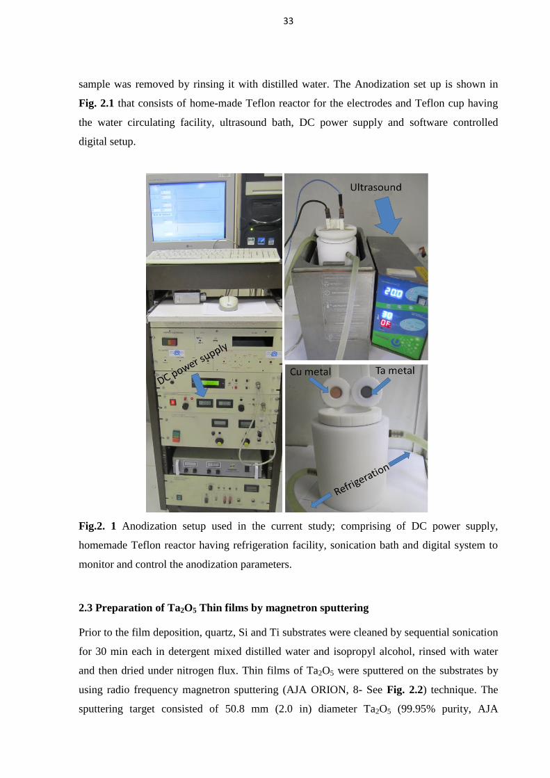
33
sample was removed by rinsing it with distilled water. The Anodization set up is shown in
Fig. 2.1 that consists of home-made Teflon reactor for the electrodes and Teflon cup having
the water circulating facility, ultrasound bath, DC power supply and software controlled
digital setup.
Fig.2. 1 Anodization setup used in the current study; comprising of DC power supply,
homemade Teflon reactor having refrigeration facility, sonication bath and digital system to
monitor and control the anodization parameters.
2.3 Preparation of Ta2O5 Thin films by magnetron sputtering
Prior to the film deposition, quartz, Si and Ti substrates were cleaned by sequential sonication
for 30 min each in detergent mixed distilled water and isopropyl alcohol, rinsed with water
and then dried under nitrogen flux. Thin films of Ta2O5 were sputtered on the substrates by
using radio frequency magnetron sputtering (AJA ORION, 8- See Fig. 2.2) technique. The
sputtering target consisted of 50.8 mm (2.0 in) diameter Ta2O5 (99.95% purity, AJA

34
International, Inc). The base pressure of the sputtering chamber was 3.2 × 10⁻¹¹
mbar. The
argon flow rate was 20 sccm such that the chamber pressure was maintained at 2.6 × 10⁻³
mbar during the sputtering process. The substrate temperature was kept 21 °C and RF power
of 150 W with DC self-bias voltage around 2–10 V was used for deposition. The distance
between the target and substrate was kept at 14.7 cm and the substrate holder was rotated at a
frequency of 20 rpm. Before the deposition process, a pre-sputtering of 5 min was made to
clean the target and afterwards the films were deposited for a deposition time of 300 min. The
sputtering rate was 3 nm min–1
Fig.2. 2 AJA Orion 8 sputtering system used to deposit thin films.
2.3 Nitridation process
Prior to nitridation, the as-anodized samples were etched in HF: H2O (1: 9 vol/vol) for
few seconds and subsequently rinsed with water and dried under nitrogen flux. For nitridation

35
process the samples were placed first on an alumina boat and then inserted into a quartz tube
at the middle of the furnace and the flux of the gas was kept as 100 mL min–1
. Nitridation was
carried out at temperatures ranging from 650–1000 °C for time of 1–10 h. A special gas
mixture of NH3:Ar in a volume ratio of (1:9) was used as a reaction gas. The pressure of the
gas from the cylinder was kept at 5 bar (500 kPa). For all samples the heating and cooling
rates of the furnace were maintained at 5°C/min under ammonia flow. A glass flow meter was
used to estimate the flow rate of NH3. The ammonia gas was allowed to enter from one side of
the tube, after passing through the tube it was bubbled into aqueous HCl solution that
neutralizes the gas and further the gas was allowed to exhaust in the environment. To
synthesize Ta3N5 thin films nitridation was carried out at 900°C for 24 h. The nitridation set-
up is shown in the Fig. 2.3.
Fig.2. 3 Nitridation setup comprising of quartz tube furnace, flow meter, ammonia cylinder
and ammonia neutralization chamber. Once the gas was neutralized; the gas flow was
measured from the outlet valve by using glass flow meter.

36
2.4. Electrochemical and Photoelectrochemical measurements
2.4.1 Thin films
For Ta3N5 thin films four types of samples were prepared using different substrates;
Ta3N5/Pt/Ti/quartz, Ta3N5/Pt/Ti/Si, Ta3N5/Pt/Ti/SiO2/Si and Ta3N5/Pt/Ti. Ti and Pt
were deposited by DC Magnetron sputtering whereas SiO2 was thermally grown on Si
wafer under controlled oxygen flux. The thickness of Pt, Ti and SiO2 layers was, 200,
7.2 and 150 nm, respectively. Ti layer helped for the adhesion and Pt served as electric
contact.24
Prior to each measurement the samples were etched to possibly clean the
surface by HF/H2O droplets on Ta3N5 part of the film and after 10 sec the samples
were cleaned by distilled water and dried under nitrogen flux. The wires and the
exposed conductive parts of the samples were sealed with an epoxy adhesive. We
found that the using variety of substrates do not influence the PEC results; therefore, in
this work we have applied Ta3N5/Pt/Ti/quartz for the measurements.
The photoelectrochemical measurements were performed in a three electrode
configuration employing Ta3N5/Pt/Ti/quartz as working electrode, Pt wire as counter
electrode and Ag/AgCl as a reference electrode. 0.1 M sodium phosphate buffer
solutions adjusted to pH 4, 8 and 12 were used. The potentials of the working electrode
were controlled by using Auto-lab. AM 1.5 filter was used to simulate the solar
spectrum. The light intensity was calibrated using a silicon photodiode with known
responsivity of 100 mW.cm–2
(1 Sun). Linear sweep voltammetry (LSV) curves were
obtained at a scan rate of 10 mV/s. The Mott-Shottky plots were obtained at a
frequency of 1k Hz with 10 mV of the signal amplitude for a range of applied
potentials.
2.4.2. Nanotubes
Prior to the experiments the Ta3N5 NTs photoanodes were cleaned by immersing into
HF:H2O (1:9) for 30 seconds, rinsing with distilled water and drying under nitrogen flux to
remove surface contamination. The photoelectrochemical measurements were performed in a
three electrode configuration with Ta3N5 as working electrode, Pt wobbling as counter
electrode and Ag/AgCl (3.5 M) as a reference electrode. For preparing Ta3N5 NTs working
electrode the sample was capsulated, except from the front, by a homemade Teflon reactor.
An O ring was used to seal the front side of reactor to prevent any leakage. A copper disc was
placed behind the Ta3N5 photoanode where a thin copper wire was utilized as path for the

37
current flow. The backside of the reactor was screwed tightly with the Teflon screw to prevent
electrolyte entrance from the backside of the reactor to the Ta3N5 NTs/Ta photoanode. The
electrodes were immersed in a homemade Pyrex cell having a quartz window. As a source of
electromagnetic radiation Xe lamp (300W) was utilized. AM 1.5G filter was used to obtain
solar spectrum. The electrolytes used for Photoelectrochemical measurements were 0.1 M
Na2SO4 pH (7.85), 11
and redox couple of 0.1 M K4[Fe(CN)6] and 0.1 mM K3[Fe(CN)6] pH
(7.5).82
The solution pHs were recorded by digital pH meter. Prior to each
photoelectrochemical measurement the electrolytes were purged by the argon gas flow. The
Auto-lab (PGSTAT100/AUT 84503) potentiostat incorporated with software (GPES, V 4.9)
was used as a power supply. Linear sweep voltammetry (LSV) curves in dark and under
illumination (1 Sun) were obtained under scan rate of 10 mV/s. Similarly, hand light chopping
with a 5 sec periodic interval was performed to record LSV curves. Cyclic voltammetry was
performed under dark and illumination for the varying scan rates (10 mV/s to 200 mV/s).
Fig.2. 4 (Photo)electrochemical setup comprising of potentiostat, Xe lamp and Faraday cage.
The light intensity was calibrated by using a silicon photodiode with known responsivity.
Chronoamperometry experiments were performed under different values of constant applied
potentials, under light and under dark which helped us to approximate the flatband of Ta3N5
NTs photoanode. Furthermore, impedance measurements were performed in a Faraday cage,
by using the software FRA (frequency response analysis). Nyquist plots were obtained in a
frequency range of 100 kHz–100 mHz at fixed amplitude of 5 mV by using different fixed

38
potentials. Circuit fitting was complied by NOVA software. Mott-Shottky plots were obtained
at 5 mV of amplitude for a range of frequencies and applied potentials. Fig.2.4a. shows the
setup for LSV, CV, chronoamperometry experiments while Fig. 2.4b displays the setup used
for EIS.
Note: Solar radiation reaching the earth's surface varies significantly with location,
atmospheric conditions including cloud cover, aerosol content and ozone layer, and time of
the day, earth/sun distance, solar and ozone layer conditions etc. The irradiance of the sun on
the outer atmosphere when the sun and earth are spaced at 1 astronomical unit (AU) is called
solar constant, i.e mean earth/sun distance of 149,597,890 km and the radiation intensity at 1
AU is 1360 W m–2
. Air Mass (AM) represents how much atmosphere the solar radiation has
to pass through before reaching the Earth s’ surface. The AM number can be determined from
the zenith angle of the Sun by the following expression:
AM = 1/ cos Өzenith
AM 0 is defined as the spectrum outside the Earth’s atmosphere at 1 AU from the Sun, and
AM 1 represents sunlight reaching the Earth’s surface (at sea level) when the Sun is directly
overhead. AM 1.5 is defined as the irradiance arriving on a flat plate tilted at 37° from
horizontal toward the Sun. Because Өzenith = 48.2° for AM 1.5 and the tilt angle is 37°, the
angle of incidence is 11.2°. An intensity is specified, as well as the spectral distribution of
illumination, the accepted total irradiance (intensity) of AM 1.5 is being 1000 W/m2 (100
mW/cm2). For PEC experiments AM 1.5 is simulated in the lab by using appropriate filter in
front of the radiation source, because it is standardized and represents approximately the
average annual AM value available at locations within the continental US. 83
Depending on
the application utilizing AM 1.5 filter, the intensity of light can be calibrated to ½ Sun (50
mW/cm2), 1 Sun (100 mW/cm
2), 2 Sun (200 mW/cm
2), 3 Sun (300 mW/cm
2) etc. However,
for PEC applications mostly 1 Sun (100 mW/cm2) is used.
2.5. Characterizations
2.5.1. Scanning Electron Microscopy
Surface structure and morphology of Ta3N5 thin films, as-anodized Ta2O5 NTs and Ta3N5
NTs were characterized by using a Scanning Electron Microscope (Zeiss, EVO 50) operated
at 10 kV. The side view images of the NTs were obtained from the scratched off area of the
sample. Where necessary, the samples were metalized by sputtering.
39
2.5.2. High resolution transmission electron microscopy
For Ta3N5 thin films; the samples were prepared in plan view and analyzed by JOEL
JEM 2010 microscope.
For Ta3N5 NTs; the samples were prepared by scratching off the NTs to dissolve in
acetone and later loaded onto carbon grid. For the TEM imaging JEM 1200 EXll was used.
Scanning transmission electron microscopy (STEM), HRTEM, SAED, spatial-energy
Dispersive X-ray (EDX) were performed using an XFEG Cs-corrected FEI Titan 80/300
microscope at INMETRO operated at 300 kV. High Z-contrast images were acquired through
STEM using a high-angle annular dark-field detector (HAADF). The typical lateral resolution
was greater than 0.01 nm. To simulate HRTEM spectra the software “CrystalKit” was used.
For EDX spectra the intensity was normalized to the Ta signal.
2.5.3. UV –Vis spectrophotometry
UV-Vis spectrophotometry was performed by using CARY 5000. The absorption spectra of
Ta3N5 NTs were obtained by diffuse reflectance by converting to the Kubelka-Munk function:
For Ta3N5 thin films deposited over quartz substrate, total reflectance and transmittance were
obtained. The light absorption from the Ta3N5 film was calculated using the expression:
%Abs = 100 – (%T + %R) (2.2)
2.5.4. XRD (X-ray diffraction spectroscopy)
Conventional diffratograms of Ta3N5 NTs were obtained by using Rigaku, Ultima IV
diffractometer with Cu Kα radiation (λ = 1.54 Å) at a 2θ range from 10° to 90° with a 0.05°
step size and measuring time of 1s per step. Grazing angle XRD was recorded by Shimadzu,
Maxima XRD-7000 diffractometer with an incident angle of 0.3° with Cu Kα radiation (λ =
1.54 Å) at a 2θ range from 10° to 70° with a 0.05° step size and measuring time of 5s per step.
The powder XRD for free standing Ta3N5 powder and Ta3N5 sputtering film was obtained by
using a Siemens, D500 diffractometer with Cu Kα radiation (λ = 1.54 Å) at a 2θ range from

40
10° to 70° with a 0.05° step size and measuring time of 5 s per step. All of the XRD patterns
were recorded under “Bragg-Brentano geometry”.
Data processing was performed by the Rietveld method using FullProf software.84
The
instrumental resolution function (IRF) of the diffractometer was obtained from the LaB6
standard. The pseudo-Voigt profile function of Thompson, Cox and Hastings was used with
an asymmetry correction at low angles.85
Corrections to the preferred orientation were
performed using the Modified March’s function.86
87
88
The anisotropic size broadening
effects, related to the coherence volume of diffraction, were simulated using a model of
spherical harmonics.84
To understand the crystalline structure of Ta3N5, Rietveld refinement
were performed. The grain size has been calculated by modified Scherrer equation (2.3)
considering the microstrain as minimum as possible.
(2.3)
where βh is the size contribution to the integral breadth of reflection h, are the
real spherical harmonics with normalization.89
The arguments are the polar angles of the
vector h with respect to the Cartesian crystallographic frame. After refinement of the
coefficients the program calculates the apparent size (in angstroms) along each reciprocal
lattice vectors if the IRF is provided in a separate file. The preferential orientation has been
identified by using the modified March´s function (equation, 2.4):
(2.4)
where G1 corresponds to the Bragg−Brentano geometry, G2 represents the fraction of the
sample without orientation, and αh is the acute angle between the scattering vector and the
normal to the crystallites. From the analysis of the Rietveld refinement, the grain size along
different directions and the nominal stoichiometry were calculated.
2.5.5. X-ray photoelectron spectroscopy (XPS)
Chemical composition of the surface was studied by X-ray photoelectron spectroscopy
(XPS) performed in an Omicron-SPHERA station using Al Kα radiation (1486.6 eV). The
anode was operated at 225 W (15 kV, 15 mA). Survey spectra were recorded with 50 eV pass

41
energy. The Ta 4f, O1s and N1s regions were recorded with a higher resolution (pass energy
of 10 eV). The detection angle of the photoelectrons (Θ) with respect to the sample surface
(take-off angle) was fixed at 53° for all measurements. The C 1s signal from adventitious
carbon was used as an internal energy reference. During the synthesis and transferring the
samples into the spectrometer, the surface of the sample was exposed to air prior to the
measurement (as were all of the samples) and, therefore, contained surface oxide. For the
deconvolution of Ta4f, the spin-orbit doublet separation of 1.9 eV and the intensity ratio
(Ta4f7/2/Ta4f5/2) of 4/3 were used in all peak assignments). The surface composition N/Ta was
calculated by using relative sensitivity factor (RSF) method as follows:
N/Ta = (Area of N1s / RSF) ÷ (Area of Ta4f / RSF)
Similar procedure was followed for O/Ta and N/O composition ratios. Although, the Ta 4f
signal is known to overlap with the minor O 2s signal and the ratio of the total cross section
for the Ta 4f / O 2s is around 66. Therefore, the contribution from O 2s was neglected in this
study.
For Ta3N5 thin films similar procedure was followed.
2.6. Spectroscopic Ellipsometry
Ellipsometry is one of the most powerful tools to investigate optical properties of
materials, 90
the technique usually performs analysis of the reflected light polarization state,
which is related to the optical properties of the material by the expression (the Ellipsometry
fundamental equation):
, (2.5)
where tan() and are the amplitude ratio and phase shift difference, respectively, between
values associated with the p and s polarization components of light (parallel and perpendicular
to the plane of incidence). The rp and rs are the correspondent Fresnel coefficients when a
unique interface reflects the light under study 91
and they depend on: the angle of incidence
() and wavelength () of the light and the dispersion curves of air N0() and bulk material
N(). In the case of thin films, rp and rs are the correspondent Drude reflection coefficients

42
and are dependent of: the angle of incidence () and wavelength () of the light, film
thickness (d) and dispersion curves of air N0(), substrate Ns() and film Nf(). 91
The
dispersion curves present the form N() = n() + ik(), where n() and k() are the real and
imaginary parts of the refractive index, respectively. Fig.2.5 displays the experimental setup
normally used for the Ellipsometry in which the s and p polarised lights are incident on the
sample; thereby they reflect and becomes elliptically polarized.
Fig.2. 5 Experimental setup for Ellipsometry.
Upon reflection from the sample, the phase difference between the two incident lights and the
tanΨ that are the characteristic of the sample under study are determinate. Experimental data
are modeled according to the suitable parameterization that reflects the physical characteristic
of the sample under study.
2.6.1 Rotating Polarizer Technique
There are many different experimental configurations of Ellipsometers as, for
example, the ellipsometers of light extinction.90
However, the Ellipsometer used in this work
has a different approach to characterize the optical constants of a material; it uses the rotating
polarizer technique, where only two optical components are used: one polarizer (rotating with
a fixed frequency of 5Hz) and an adjustable polarizer (analyzer) that is employed to maximize
the intensity of the light reflected from the sample. The amplitude of the electric field of light

43
is split into the s and p components and it is possible to represent the effects of each element
of the ellipsometer over these fields by the Muller Matrix notation 92
:
Lamp:
(2.6)
Polarizer:
(2.7)
Theta angle rotation (polarizer):
(2.8)
Sample:
(2.9)
Analyzer:
(2.10)
On the detector, the electric field amplitude assumes the value:
(2.11)
Finally, the intensity registered on the detector can be expressed by:
(2.12)
with
(2.13)
(2.14)
(2.15)

44
Pol and Ana are, respectively, the angle between the transmission axis of the polarizer, and
analysis polarizer, and the light incidence plane. The coefficients and do not depend on
the lamp intensity, so there is no necessity of a reference measurement for the intensity and
the ellipsometric parameters can be expressed as:
(2.16)
(2.17)
To analyze the signal and extract the two components ( and ), the Hadamard method 93
is
used and the signal is integrated every quarter of polarizer period and each sum can be
calculated as follow (it is considered a complete turn of the polarizer, two regions of the sums
S1 to S4), as showed in Fig. 6.2:
(2.18)
(2.19)
(2.20)
(2.21)

45
Fig.2. 6 Intensity of light reflected by the sample as a function of the polarizer angle (Pol)
and the 4 polarizer regions.
Then the parameters of the signal can be expressed versus the sums as follow:
(2.22)
(2.23)
(2.24)
The equipment used was an ellipsometer SOPRA GES-5E with a special microspot accessory
for thin films: two sets of lenses (numerical apertures of 30), one is used to focus the light
beam in a small region of the film surface (an ellipse area of approximately 365 m × 270
m) and the second one is used to collect the reflected light that will be analyzed. The
ellipsometer employs one rotating polarizer (frequency of 5Hz) and one analysis polarizer to
maximize the reflected light by the sample to obtain the ellipsometric parameters and ,.
More details can be seen in references. 90,
93
. The ellipsometry measurements were performed
in the wavelength range from 215 to 800 nm and at an angle of incidence 0 = 680. The
collected data in the measurements (the state of polarization) was analyzed by the
equipment’s software WinElli 2.2.0.6 using a model that will be described in details in
chapter 3.

46
CHAPTER 3
OPTICAL AND PHOTOELECTROCHEMICAL PROPERTIES OF
MONOCLINIC Ta3N5 THIN FILMS
3.1 Objectives
Recently, RF magnetron sputtering has attracted much attention as a clean route to
synthesize materials.50
The direct sputtering of Ta2O5 for its transformation to Ta3N5 has not
been reported in the literature. The literature reports that Ta3N5 presents two different
crystalline phases, monoclinic (JPCDS file 89-5200) and orthorhombic (JPCDS file 79-1533).
The phases are very close to each other as their unit cell parameters (a, b and c) present almost
the same magnitudes; therefore, their diffraction patterns look very similar and a special
attention is necessary to assign the crystalline phases of Ta3N5. The easiest approach to assign
any of these phases from the XRD patterns is to observe the relative intensity between the 2θ
peaks of 24.52° and 36.16°which are different for both of the phases.66
The crystalline phases
of Ta3N5, largely depend on the route of synthesis, choice of precursor and the underlying
substrate. The orthorhombic phase of Ta3N5 has been widely reported, but there are few
reports regarding the monoclinic phase. 94
65
95
The dielectric constant of a material plays an
important role in many physical processes. Technical applications such as capacitors,
insulating coatings transducers are strongly determined by the dielectric properties. In
addition, to calculate the density of states by Mott-Schottky curves, there is a need of reliable
data on dielectric constants of a material.9 96
After searching the literature, we have not found
any work describing the experimental determination of the dielectric constant of Ta3N5.
Herein, thin films of Ta2O5 have been deposited on quartz substrate by RF magnetron
sputtering and thermally nitrided to obtain Ta3N5 thin films, which exhibited monoclinic
crystalline phase. Using Spectroscopic Ellipsometry technique, the light absorption coefficient
and the dielectric constants of Ta3N5 films were experimentally determinate. Using Mott-
Schottky analyses flat band and effective density of states were calculated for monoclinic
Ta3N5 thin films.

47
3.2 Results and Discussion
3.2.1 Surface and structure of Ta3N5 thin films
The SEM images of the samples before and after the nitridation are shown in Fig.3.1 It
can be seen that as-deposited Ta2O5 film presents a smooth, homogenous and flat surface.
However, after annealing, the film was cracked and some patches appeared on the entire
surface (Fig. 3.1b). The diameters of these patches were calculated by estimating the average
of longest and shortest distance inside each patch, which was ~10.4 µm and the average
spacing between them was approximately ~24 nm. The cracks observed in the films at higher
temperature are attributed to the interfacial stress caused by the difference in thermal
expansion of the film and substrate.97
Besides, the surface of Ta3N5 is rough (Fig. 3.1 c),
which is related to the density difference between Ta2O5 and Ta3N5.98
The HRTEM (Fig. 3.1
d) image shows the interplanar distance of 0.512 nm in agreement with the monoclinic
crystalline structure of Ta3N5. The grain size from the HRTEM image was estimated to be 46
nm. In addition, some amorphous layer can be observed on the edges of the grain.
Fig.3. 1 SEM images of (a) as-deposited Ta2O5 and (b) Ta3N5 thin films. TEM (c) and
HRTEM images (d) of Ta3N5 thin films.

48
The XPS spectra of the as-nitrided thin films are presented in Fig. 3.2 One can observe
the presence of oxygen on the surface of the films, which is a natural impurity in Ta3N5.68
The
O1s and N1s peaks were observed at 529.8 eV and 395.5 eV, respectively (Fig. 3.2a). The
deconvoluted Ta 4f doublet and N1s region of the film are shown in Fig. 3.2b & c,
respectively. The Ta4f7/2 and Ta4f5/2 appeared at 25.3 eV and 27.2eV which are closed to the
previously reported values for oxynitride species of tantalum99
In addition, high-energy-side
small doublet was also detected; suggesting the presence of low energy states (Ta4+
, Ta3+
) of
Ta.100,101
The formation of reduced tantalum species in Ta3N5 obtained by thermal nitridation,
has been reported earlier. 102
Subtracting the area of the small Ta4f doublet and considering
the sensitivity factors for N1s and Ta4f, the nominal surface composition from the XPS
analysis was found to be Ta2.66N4.32O0.17 which indicates the surface of film does not possess
complete stoichiometry of Ta3N5.103
Fig.3. 2 XPS (a) survey and (b) deconvoluted Ta4f and (c) N1s spectra of the as-nitrided
films.

49
From the results shown above, we infer that the defective nature of the surface and the
amorphism around the grain should be considered carefully if Ta3N5 is used as a photocatalyst
as they can act as recombination centers for photogenerated carriers. We suggest a proper
surface cleaning before applying Ta3N5 thin films in photoelectrochemical applications.
The XRD patterns of as-sputtered Ta2O5 and Ta3N5 films are shown in Fig. 3.3. It can
be seen that Ta2O5 thin films are amorphous. However, after thermal nitridation at 900°C for
24 hours under 100 mL/min of NH3 flow, clear changes in the XRD patterns can be observed.
Fig.3. 3 XRD patterns of as-sputtered Ta2O5 thin films, substrate nitrided at 900°C and the
Ta3N5 thin films.
The amorphous Ta2O5 is transformed into Ta3N5 presenting very sharp diffraction peaks. This
result indicates that the nitridation condition used was sufficient to transform Ta2O5 thin film
into Ta3N5. All peaks observed in the XRD diffractograms are in a good agreement with the
monoclinic phase of Ta3N5 (JPCDS file 89-5200). The average grain size calculated through
the Scherrer´s equation from the most intense peak was approximated to 43 nm. Furthermore,
in the XRD patterns of Ta3N5 film a wide background at ca. 22° was observed that is related
to the substrate nitridation as shown in the figure (blue color line).

50
3.2.2 Optical constants of Ta3N5 thin film
The absorbance of the Ta3N5 thin film was determined by the equation 2.2 using
experimental data from total transmittance and reflectance measurements. The calculated film
absorbance is shown in Fig. 3.4a. One can observe a strong absorption band between 200 and
557 nm and a dramatic drop from 558 to 800 nm, displaying an oscillatory pattern, which may
be related to the light interference in thin films. In order to obtain the optical constants of the
Ta3N5 thin film all these optical behaviors were taken into account to build the model in the
ellipsometer analysis software,. Within the region presenting strong absorption (215 to
557 nm), a bulk like behavior is assumed, so the refractive indices are directly related to
ellipsometric parameters by the expression:
, (3.1)
where n() and κ() are the real and imaginary parts of the refractive index, respectively, and
is the angle of incidence. The calculated dispersion curves for n() and κ() using the bulk
model are represented in Fig. 3.4b.
Fig.3. 4 Absorbance spectrum of Ta3N5 thin film (a). Real and Imaginary dispersion curves
obtained for the Ta3N5 film assuming bulk model (b) and Cauchy model (c).
51
In the wavelength range of 558 to 800 nm, it was assumed that the sample is an isotropic and
homogeneous film with dispersion curves (Fig. 3.4c) following the well-known Cauchy
model, as follow: 104
(3.2)
κ
, (3.3)
where A, B, C, D, E and F are constants which are adjusted by the analysis software to
perform the fitting to the experimental data. The optical constants from the film (dispersion
curves and physical thickness) were obtained through the equation 2.5 with the terms given
by equation 2.16 and 2.17 following the above proposed model. These constants were
obtained by curve adjusting with the fitting of R2 = 0.928158, where R
2 = 1 represents a
perfect fitting and their values can be seen below:
A = 3.170 0.005 B = -0.324 0.002 C = 0.0929 0.0003
D = 0.2071 0.0003 E = -0.165 0.001 F = 0.0371 0.0004
As a result, the calculated film thickness was 890.1 0.2 nm. Furthermore, from the
dispersion curves of Fig. 3.4 (b & c), the dielectric constants (real and imaginary) from the
film were calculated using the following relations:91
κ (3.4)
κ (3.5)
Plugging the values of n() and κ() obtained from both models in equations 3.4 and 3.5 the
dielectric constants were calculated and presented in Fig. 3.5.

52
Fig.3. 5 Dielectric constants (real and imaginary) of Ta3N5 film, assuming bulk model (left)
and Cauchy model (right).
A slight divergence within the region where the models merge together (at 558 nm) can be
observed and is attributed to the combined effects of bulk and film behavior. As observed for
other substances, the dielectric constants change with the wavelength. This frequency
dependence ignites from the different polarizability which arises from different mechanisms
driven by the change in the frequency.96
From Fig.3.5, the dielectric constant presents values
between 7 and 9. Interestingly, these values match the theoretically measured dielectric
constant of Ta3N5 where the presence of oxygen impurities were taken into account.68
According to the Beer-Lambert law, the absorption coefficient “” of a material is
related to the imaginary part of the refractive index κ() by the following expression:

53
κ
λ (3.6)
From the values of κ () obtained from the two models as shown in Fig. 3.4 (b, c), the
values were calculated by equation 3.6 and shown in Fig. 3. 6a. According to the literature,
for the theoretical dispersion energy bands obtained for Ta3N5, the top of the valence band
was found to be along the Γ–X line and the bottom of the conduction band was located at Y in
the BZ, which indicates that Ta3N5 is an indirect semiconductor.67
By using the values of ,
the indirect bandgap considering the Tauc´s plots have been estimated as ~1.92 eV, which is
smaller than the theoretically predicted value. The corresponding spectrum is shown in Fig.
3.6b. The difference between theoretical and experimental bandgap is related to the presence
of oxygen in the structure of Ta3N5. 68
Fig.3. 6 Variations of α with wavelength (a) and (αh)
1/2 with energy (b).

54
3.2.3 Photoelectrochemical properties of Ta3N5 thin film
The bandgap energy of Ta3N5 overcomes the endothermic 1.23 eV requirement for the
water splitting.68
However, the positions of band edges relative to the water redox
potentials influence the water splitting activity. The flat band position that helps to find
the conduction band position can be calculated by the Mott-Schottky equation. The
Mott-Schottky equation is 105
Where C, e, , 0, V, Kb and Vf are the space charge capacitance, the electronic charge, the
dielectric constant i.e 8 (Fig. 3.5), vacuum permittivity, applied potential, Boltzmann constant
and the flat band potential, respectively. The intersection of the linear dependence of 1/C2
versus V provides the flat band and the slope of the curve contains the information on the
effective donor density (ND). Fig 3.7 compares the Mott-Schottky plots of the Ta3N5 thin
films measured in phosphate buffer electrolytes adjusted to pH 4, 8 and 12. It can be seen that
Vf is strongly influenced by the pH of the solution, as pH is increased, the Vf is shifted toward
more negative potentials. In addition, the positive slope of observed in the Mott-Schottky
curves clearly indicate that monoclinic Ta3N5 is an n-type semiconductor. Using equation 3.7
the values of ND were also calculated and were found to be 1.2 ×10¹⁸
, 5.1 ×10¹⁹
and 1.3 ×10²⁰
cm–3
for pH 4, 8 and 12, respectively.

55
Fig.3. 7 Mott-Schottky plots obtained at pH 4, 8 and 12 for Ta3N5 thins films.
For an n-type semiconductor when negative biasing is applied the band bending decreases.
For higher negative biasing a blocking potential arrives, where the space charge region is
absent or more likely the semiconductor responds like a metal once the Helmholtz layer
dominates the interface and the system under stake exhibits a lack of electrochemical
dependence on the light illumination. At that instance the photocurrent onset is achieved and
the applied potential is called flat band potential (Vf).20
It can be seen from Fig. 3.8, the
photocurrent onset i.e Vf strongly depends on the pH. In addition, the values estimated from
the photocurrent onset corroborate the values obtained by Mott-Schottky curves of Fig.3.7.

56
Fig.3. 8 Chopped LSVcurves obtained at pH (a) 4 (b) 8 and (c) 12.
Furthermore, compared to other electrolytes, pH 12 presents an enhanced photocurrent. The
conduction band minimum (CBM) of an n-type semiconductor is 0.1 0.3V more negative
than the Vf. 106
Therefore, adding –0.25V, the positions of CBM are calculated that were
–0.46V, –0.70V and –0.89V at pH 4, 8 and 12, respectively.
3.3 Partial Conclusions
In this work, we described that Monoclinic Ta3N5 thin films can be synthesized by
thermal nitridation of directly sputtered Ta2O5 thin films deposited by RF-magnetron
sputtering on quartz substrate. From optical characterization, the dielectric constant of Ta3N5
film was found to be in between 7 and 9; which is in accordance to the previously reported
theoretical values. Using the value of the dielectric constant, the effective density of states
was calculated from the Mott- Schottky curves. The photoelectrochemical analyses revealed
that the band structure of Ta3N5 strongly depends on the pH of the electrolyte. It was found
that the enhanced photocurrent was observed in alkaline conditions.

57
CHAPTER 4
THE PRESENCE OF TRAPS IN THE STRUCTURE OF Ta3N5
NANOTUBES
4.1 Objectives
The solid state properties of an ideal semiconductor are modeled by the band theory
where the forbidden region called bandgap separates the valence band (maximum oxidization
power of photogenerated holes) and the conduction band (maximum reduction power of
excited electrons). However, at semiconductor–electrolyte interface the electrode structure is
different chemically and physically from the bulk. These inhomogeneities give rise to another
density of states within the bandgap.29,30,31
There have been numerous reports on quantifying
and identifying these states employing variety of techniques including photocurrent
transient,32
dynamic PEC measurements,33
impedance spectroscopy,34
photoluminescence 35.
As an example, for nano-structured TiO2 these states are associated with low coordinated Ti
sites,36,37,38
grain boundaries,39
oxygen vacancies.40
For hematite they are proposed to be FeIII–
OH/FeIVO
41 and for GaN they are related to the morphology.
42 For some materials they act
as current flow sites43
and for others; recombination centers.41
However, the exact nature of
these states remains controversial.
Using semiconductor–electrolyte interface for overall water splitting, the
semiconductor should straddle the redox potentials of water. It should be stable in aqueous
electrolytes, absorb large fraction of visible light, separate the photogenerated charge carriers
and collect them efficiently.2,107
Apart from meliorating the optical and electronic properties,
nanostructuring a semiconductor benefits the charge separation through lessening the
distances that the minority carriers have to travel to the reactive sites.108
In this regard,
nanotubular semiconductors possess enormous potential for improved photocatalysis.80,49
Nanotubes (NTs) of Ta3N5 have been employed for photoelectrochemical (PEC) water
splitting.13,12
However, the pristine Ta3N5 NTs have required the external biasing > 1.23V vs
RHE to drive water oxidation.14,17
In addition, not only the NTs but also the pristine Ta3N5
photoelectrodes have been adversely affected without co-doping and loading co-catalysts.9,
16,109 In standard electrolytes such as Na2SO4 and NaOH; the photocurrent overshoot to spikes
and decreased momentarily presenting instability and sluggish water oxidation.110,111
On the
other hand, Ta3N5 photoelectrodes when used in Fe(CN)6 3-/4-
(aq) presented an improved as
well as stable PEC activity.112,113,53
Furthermore, for other devices such as hematite the
Fe(CN)63-/4-
has been found to be efficient sacrificial agent.41
Now, the question arises why

58
pristine Ta3N5 photoelectrodes utilized in standard electrolytes without adding a sacrificial
reagent result in a poor PEC activity. Therefore, a detailed investigation is warranted to
understand the Ta3N5 NTs-electrolyte interface.
Herein, we study and compare semiconductor–electrolyte interfacial properties of
pristine Ta3N5 nanotubes in standard Na2SO4 (aq) electrolyte 13
and the one containing
sacrificial reagent of Fe(CN)6 3-/4-
(aq). Thorough photoelectrochemical investigations are
provided to understand the necessity of higher onset potential for improved water splitting. To
compare our findings to the literature, we have focused our study on the pristine Ta3N5 NTs
obtained at 800°C for a nitridation time of 3 h or otherwise noted.13
Henceforth, for the sake
of simplicity we will name standard Na2SO4 (aq) electrolyte as Water and the sacrificial
reagent as Fe(CN)6 3-/4-
(aq).
4.2 Results and discussion
4.2.1. Morphology and structure
4.2.1.1 The as-anodized Ta2O5 nanotubes prepared in the current study
Fig.4.1a shows J-t curves obtained during anodization carried out for voltage ramps of
1, 5, 10, 25 and 50 V/s to a constant value of 50 V during 20 minutes. The temperature during
the anodization was kept constant at 10°C. In the J–t curves (Fig.4.1) one can observe a
maximum current of ca. 200 mA/cm2 at the beginning of the process, followed by a sudden
drop to a constant current density of 8 mA/cm2, which is a characteristic behavior of
anodization process. This behavior is related to the formation of a Ta2O5 barrier on the Ta
substrate due to Ta oxidation in the acidic solution. In fact, all the J-t curves presented similar
feature, except for anodization carried out by ramping of 1 V/s (Fig.4.1a) that will be
explained later. It can be seen that J-t curves for ramping of 5 – 50 V/s are simply overlapped
from which it can be inferred that the morphology of the NTs obtained under these conditions
can not differ from each other. Fig. 4.1b shows the anodization curves obtained by using
10 V/s of ramping until 50 V during 5, 10 and 20 minutes and the overlapping can be
confirmed too for the NTs obtained for different times of anodization.

59
Fig.4. 1 J-t curves of 50V of anodization under (a) different scan rates at fixed anodization
time of 20 min, (b) fixed scan rate of 10V/s for different times of anodization.
It can be seen that the J-V curves present the same current densities. SEM images of as-
anodized samples were obtained from the scratched area of the oxide layer. From the SEM
images (not shown); the magnitudes of diameter, length and wall thickness of the NTs
prepared at different ramping rate from 5 V/s to 50 V/s were not influenced by the ramping.
Fig. 4.2 displays the SEM and TEM images of the nanotubes obtained during anodization
carried out for voltage ramps of 10 V/s to a constant value of 50 V during 20 minutes. The
NTs are vertically oriented and the average length, outer diameter and wall thickness are
1.60 µm, 130 nm and 34 nm, respectively. It can be seen that the walls of the NTs are smooth
The J–t curve and the geometric parameters of the Ta2O5 NTs prepared at 10 V/s to a constant
voltage of 50 V during 20 minutes are consistent with the literature. 49

60
Fig.4. 2 SEM (a) and TEM (b) images of as – anodized Ta2O5 nanotubes/Ta obtained by a
voltage ramping of 10 V/s to a constant value of 50 V during 20 minutes.
Fig.4.3 displays the SEM images of the Ta2O5 NTs anodized for 5 and 10 min, presenting
length of ca. 460 nm and ca. 900 nm, respectively and the wall thickness and the tube length
were almost the same as been observed for 20 min of anodization time. These results are in
line to the literature where the length of the Ta2O5 nanotubes in H2SO4/HF electrolyte was
found increased upon increasing the anodization time.79
Fig.4. 3 SEM images of Ta2O5 NTs obtained by (a) 10 min and (b) 5 min of anodization time
by 10 V/s ramp to constant voltage of 50 V.
(b)

61
The estimated geometrical parameters of the nanotubes are displayed in Fig. 4.4 that shows
the average length of nanotube increases with increasing anodization time, but the average
outer diameter and wall thickness of nanotube are not affected for experiments conducted
with the same applied anodization voltage. These results corroborate the literature.114
Fig.4. 4 Variation of length, diameter and wall thickness of Ta2O5 NTs with anodization time.
As mentioned earlier in this section, the J-t curve for anodization performed under 1 V/s of
ramping presented a different behavior as compared to the other curves (Fig. 4.1a). In order to
further investigate this result we have obtained SEM images of the sample (Fig.4.5). It can be
seen that under the applied conditions the nanotubes could not be formed, instead one can
observe the formation of nanodimples on the tantalum surface.79
As we have discussed earlier
in Section 1.8, during anodization process the high etching rates will not favor the growth of
regular NTs instead the forming oxide layer will be dissolved into the acidic electrolyte. For
1 V/s ramp it takes 50 seconds to reach 50 V, which results in a very slow growth of the
Ta2O5 layer in the first step of the anodization process, due to low electric field. When the
applied potential reaches the value of 50 V, the templates for the nanodimples will already be
formed on Ta surface and these templates will hinder the growth of oxide layer. 77
Therefore,
further anodization process will be dominated by etching rates as compared to oxide
formation rates, resulting into the conversion of the templates into the dimples (Fig.4.5).

62
Fig.4. 5 SEM image of nano-dimples formed on the Ta surface at ramping of 1 V/s.
The anodization time will enable the dimples to grow in diameter and due to the strong stress
among the neighbor dimples the diameter would be equalized. In simple words 1 V/s ramping
of anodization results into the electropolishing of the Ta surface in the form highly regular
dimpled surface. Moreover, it has been reported that the dimpled tantalum is ductile, highly
melting, and chemically inert, and they can easily be used as a mold for nanostructure
synthesis. 77,81
One of the most important parameters to be considered when applying
nanotubes as photoanodes for photoelectrochemical cells is their adherence on the substrate.
According to the literature, for the anodization of Ta2O5 nanotubes conducted in H2SO4/HF
electrolyte, the adherence of the nanotubes on the substrate can be controlled by the
temperature of the electrolyte during the synthesis.49
Ta2O5 NTs start to adhere at 20°C and
further increase in adherence is obtained by decreasing the medium temperature. Along with
the adherence, decreasing the temperature increases the wall thickness of the nanotubes. In
addition for TiO2 NTs the literature describes an enhancement in photoelectrochemical
activity from samples anodized at low temperatures.115
According to previous work for the
transformation of Ta2O5 nanorods into Ta3N5 under high temperature during nitridation, the
morphology was preserved due to their strong adherence on the substrate.9 Based on the
above discussion, we can assume that Ta2O5 NTs should be well adhere to the substrate in
order to obtain Ta3N5 NTs conserving the tubular morphology at higher temperatures. Hence,
we might expect that the Ta2O5 NTs prepared at low temperature of 10°C that are vertically

63
oriented, well adhere and thick walled would withstand to higher temperatures under
ammonia flow, resulting in Ta3N5 NTs with improved crystallinity and enhanced
photoelectrochemical performance. 13, 49
4.2.1.2 The Ta3N5 nanotubes prepared by nitridation at 800°C for 3h
Fig. 4. 6 displays the morphology of the Ta3N5 nanotubes (NTs) synthesized at the nitridation
temperature of 800°C for 3h. The average length and pore size of the NTs are 1.4 µm and 30
nm; respectively. Furthermore, the HRTEM image displays the d–spacing of 3.6 Å in
agreement with the (110) plane of the orthorhombic Ta3N5 crystalline structure. The XRD
patterns of Fig. 4. 7a match with the JCPDS card no: 79-1533 i.e. orthorhombic crystalline
phase of Ta3N5 corroborating the HRTEM results. From Rietveld refinement (See Section
5.2.2) the average overall grain size was found to be 19.7 nm. It was found that the nitridation
results in to nitrogen vacancies in the crystalline structure of Ta3N5 NTs. In addition, 3-
coordinated nitrogen atoms have shown oxygen substitutions; and the nominal stoichiometry
estimated from the Rietveld refinement for the sample was found to be Ta2.89N4.18O0.84. These
results clearly indicate that the nitridation is a defect generative process. These defects can
influence the water splitting activity of the photoelectrode.
Fig.4. 6 SEM images; (a) and (b). TEM image (c) and HRTEM micrograph viewed along [1-
10] zone axis (d) for Ta3N5 NTs.

64
Furthermore, thermal nitridation has red-shifted the band edge from Ta2O5 NTs (ca. 320 nm)
to Ta3N5 NTs (ca. 600 nm) (Fig. 4. 7b). One can observe a broad absorption mode above ca.
600 nm for Ta3N5 NTs which is attributed to the formation of defects such as reduced
tantalum species Ta4+
.73a,8
Dabirian and Van de Krol have attributed this region to the ionic
defects.59
In addition, along with the main transition; the UV-Vis spectrum of Ta3N5 NTs
displays a shoulder at ca. 540 nm related to the oxygen content in the Ta3N5 structure. It may
be expected that the presence of these defects give rise to the recombination centers for
photogenerated carriers. The optical bandgap for Ta3N5 NTs is 2.1 eV consistent with the
previous report.56
To further confirm the bandgap, we have performed chronoamperometry
under monochromatic irradiation in Water (Fig. 4. 7c).
Fig.4. 7 Grazing angle XRD diffractogram ofTa3N5 NTs (a), UV-Vis spectra of Ta2O5 and
Ta3N5 NTs (b) and Chronoamperometry of Ta3N5 NTs obtained as a function of applied
biasing and monochromatic irradiation in Water (c)*.
65
* For Chronoamperometry, the sample was left under dark for 25 sec and chopped to
irradiation for 25 sec each consecutively; the wavelengths (in nm) of the incident radiations
are displayed next to each chopped curve.
The sample has started to respond for the photocurrent at ca. 590 nm (Inset of Fig 4.7c). This
result shows that the photon of 2.1 eV is energetic enough to excite the electron from valence
to the conduction band of Ta3N5 NTs thereby resulting in to photocurrent corroborating the
optical bandgap value obtained by UV-Vis analysis. Furthermore, for each applied potential
similar bandgap was observed; however, the photocurrent increases with increasing biasing.
In addition, for lower potentials prominent spikes can be observed that presents higher
recombination of the photogenerated carriers. These results suggest the application of higher
biasing for improved photocurrent; however, the bandgap is the same at all applied potentials.
44,116,117
4.2.2. Linear sweep voltammetry and Chronoamperometry
Fig. 4. 8a & 8b contrasts the linear sweep voltammetry (LSV) curves of pristine Ta3N5 NTs
photoanode obtained by chopping AM 1.5G (1 Sun) illumination in Water and Fe(CN)6 3-/4-
(aq). Compared to Fe(CN)6 3-/4-
(aq) larger biasing potential is applied in Water; however,
enhanced photocurrent can only be observed in Fe(CN)6 3-/4-
(aq). These results suggest low
hole transfer ability of Water to sustain the Faradic current for pristine Ta3N5 NTs. In
addition, upon turning the light On one can observe “overshoot” transient anodic spikes,
decaying momentarily (Fig. 4. 8a) resulted from the recombination of photogenerated
electron-hole pairs. Furthermore, upon light interruption, sharp transient cathodic spikes are
also observed that are more prominent at lower potentials. These results agree in essence with
the earlier reports; as the cathodic spikes have been observed at lower biasing in J-V curves
for pristine Ta3N5 photoanodes in standard electrolytes; however, origin of these spikes was
not explained. 111,118,119,120,121
Under illumination the migration of photogenerated holes to the
interface decreases the band bending and in the presence of intermediates the photogenerated
holes will be trapped.44
Immediately after light interruption, the electrons from the conduction
band overcome relatively low energy barrier; thereby, reducing the trapped holes and produce
transient cathodic peaks. The cathodic spikes have been observed for other semiconductors
such as hematite,44
n-TiO2116
and n-CdTe 117
and have been attributed to the reduction of the
trapped holes. Interestingly, under higher positive potentials, the appearance of cathodic
spikes is minimized since the applied potential is high enough to induce a strong electric field
at the interface to increase bulk/surface energy improving electrons transportation. Therefore,

66
higher positive biasing separates the photogenerated charge carriers and decreases the hole
trapping; thereby promoting water oxidation. In addition, in Fe(CN)63-/4-
(aq) (Fig. 4. 8b) the
absence of anodic and cathodic spikes show that the hole collection efficiency of Fe(CN)6 4-
is
very high. The result of hole trapping in Water is the non-reproducibility of photocurrent
since the LSV curves obtained with and without light chopping do not overlap (Fig. 4. 8a).
On the other hand, these curves overlap in Fe(CN)6 3-/4-
(aq) (Fig. 4. 8b). The discrepancy of
photocurrent compared to Fe(CN)6 4-
and the non-reproducibility of LSV curves in Water
absolutely indicate the presence of trapping states at Ta3N5–Water interface. The scanning
voltage perturbation in LSV measurements offer a continuous band bending at the
semiconductor–electrolyte interface. To obtain further insight towards water oxidation the
photocurrent transient decay was deconvoluted using Chronoamperometry method in Water.
Fig.4. 8 LSV curves of pristineTa3N5 NTs obtained in Water (a) and (b) [Fe(CN)6]3-/4-
(aq).
Chronoamperometry of pristine Ta3N5 NTs obtained in Water (c) and their decay constants
(obtained by double exponential curve fittings) vs applied potential against RHE*.
*The photoanode was left under dark for 10 seconds at fixed applied potential vs RHE, and
after illuminating (AM 1.5G) for 10 s the light pulse was chopped off.
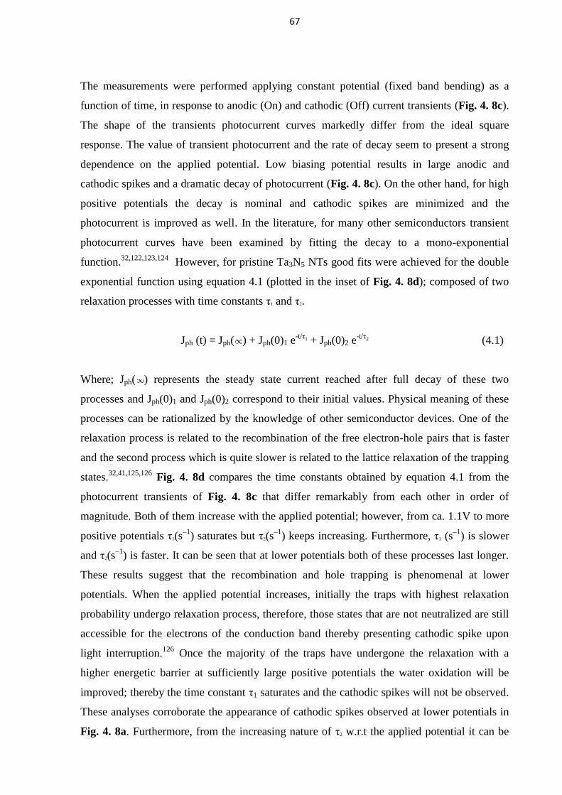
67
The measurements were performed applying constant potential (fixed band bending) as a
function of time, in response to anodic (On) and cathodic (Off) current transients (Fig. 4. 8c).
The shape of the transients photocurrent curves markedly differ from the ideal square
response. The value of transient photocurrent and the rate of decay seem to present a strong
dependence on the applied potential. Low biasing potential results in large anodic and
cathodic spikes and a dramatic decay of photocurrent (Fig. 4. 8c). On the other hand, for high
positive potentials the decay is nominal and cathodic spikes are minimized and the
photocurrent is improved as well. In the literature, for many other semiconductors transient
photocurrent curves have been examined by fitting the decay to a mono-exponential
function.32,122,123,124
However, for pristine Ta3N5 NTs good fits were achieved for the double
exponential function using equation 4.1 (plotted in the inset of Fig. 4. 8d); composed of two
relaxation processes with time constants τ1 and τ2.
Jph (t) = Jph( ) + Jph(0)1 e-t/τ1 + Jph(0)2 e
-t/τ2 (4.1)
Where; Jph( ) represents the steady state current reached after full decay of these two
processes and Jph(0)1 and Jph(0)2 correspond to their initial values. Physical meaning of these
processes can be rationalized by the knowledge of other semiconductor devices. One of the
relaxation process is related to the recombination of the free electron-hole pairs that is faster
and the second process which is quite slower is related to the lattice relaxation of the trapping
states.32,41,125,126
Fig. 4. 8d compares the time constants obtained by equation 4.1 from the
photocurrent transients of Fig. 4. 8c that differ remarkably from each other in order of
magnitude. Both of them increase with the applied potential; however, from ca. 1.1V to more
positive potentials τ1(s–1
) saturates but τ2(s–1
) keeps increasing. Furthermore, τ1 (s–1
) is slower
and τ2(s–1
) is faster. It can be seen that at lower potentials both of these processes last longer.
These results suggest that the recombination and hole trapping is phenomenal at lower
potentials. When the applied potential increases, initially the traps with highest relaxation
probability undergo relaxation process, therefore, those states that are not neutralized are still
accessible for the electrons of the conduction band thereby presenting cathodic spike upon
light interruption.126
Once the majority of the traps have undergone the relaxation with a
higher energetic barrier at sufficiently large positive potentials the water oxidation will be
improved; thereby the time constant τ1 saturates and the cathodic spikes will not be observed.
These analyses corroborate the appearance of cathodic spikes observed at lower potentials in
Fig. 4. 8a. Furthermore, from the increasing nature of τ2 w.r.t the applied potential it can be

68
inferred that the recombination of the photogenerated carriers is not completely inhibited;
matching the appearance of anodic spikes obtained at all applied potentials in Fig. 4. 8a;
however, at lower potentials recombination is high as the anodic spikes are bigger too. Hence,
from the LSV and transient photocurrent curves; hole accumulation can be confirmed in
Water upon light irradiation. On the other hand, in case of [Fe(CN)6]3-/4-
(aq) i.e efficient hole
scavenger; the photocurrent is not only improved but also the anodic as well as cathodic
spikes do not appear (Fig. 4. 8b). Therefore, for Ta3N5 NTs, efficient hole scavenging from its
surface is a key factor to improve its PEC activity. Hence, it can be inferred that first step for
actual water oxidation using pristine Ta3N5 NTs is the relaxation of the traps and higher
positive biasing is necessary to comply that. Unfortunately, necessary voltage drop for these
trapping events is not feasible as the applied biasing should not rise above 1.23 V vs RHE for
the efficient solar energy conversion.
4.2.3. Cyclic voltammetry
To investigate the location of these traps; the cyclic voltammetry (CV) runs were
performed in Water and [Fe(CN)6]3-/4-
(aq) at various scan rates. For cathodic scans in Water
from ca. 0.7 V toward more negative potentials, the current starts to increase along with the
appearance of peaks; a small local peak at ca. 0.5 V (Peak I) followed by a distinctive peak at
ca. 0.2 V (Peak II) (Fig. 4. 9a). Once the scan direction is reversed two peaks appear; Peak III
at ca. –0.1V followed by an anodic peak (Peak IV) at 0.25 V. The heights of the peaks as well
as their positions change with the scan rates except for peak III for which the respective
cathodic peak is not observed during the cathodic scan. Therefore, it’s no merely be related to
the water redox process (water reduction at 0 V vs RHE) but also to the charging of
distribution of states.127
Peak II and Peak IV appear to be filling and depopulation of the
trapping states. When the CV is performed under illumination the peak I hardly visible under
dark becomes more distinctive (Fig. 4. 9b). The Peak IV gets broader under illumination and
the other peaks have been shifted from their previous positions under dark showing light
activation dependence of the trapping states. It has been known that when cathodic scan is
carried out Fermi level shifts up and gets closer to the conduction band and traps that exist on
the semiconductor will be filled by electrons inducing the first cathodic peak.128,129 Under
dark slight invisibility of Peak I implies that the trapping states are partially filled with
electrons, while under illumination, these traps are depopulated by holes allowing higher
charge accumulation that makes it more distinctive. If the trapping is fast and detrapping is

69
slow the respective anodic peak will not appear that is the case of Peak I.59
Its shape after
illumination indicates not only the slow charge transfer from the traps, but also shows a
sluggish detrapping thereby actuating recombination centers to limit oxygen evolution and
implying higher biasing potential.42, 130
Fig.4. 9 Cyclic voltammetry curves of pristineTa3N5 NTs (a) in Water under dark, (b) under
AM 1.5G (1 Sun) continuous illumination and (c) 1.5G (1 Sun) Chopping at 10 mV/s scan
rate and (d) in Fe(CN)6 3-/4-
(aq) under dark.
Therefore, this process is not desirable for PEC devices because it implies higher
applied potential. The case where the detrapping is comparable to the velocity of charging the
trapping states, reversible peaks appear that is the case of Peak II with its counterpart (Peak
IV) where the traps are more likely in equilibrium with the conduction band.130
Furthermore,
the intensity of peak I, Peak II and Peak IV present a quasi–linear dependency to the scan rate
under illumination; suggesting an additional circuit component related to the trapping states
for pristine Ta3N5 NTs under water oxidation conditions.44
The findings on the trapping states

70
are further confirmed by CV runs of Fig. 4. 9c performed in a novel fashion at 10 mV/s of the
scan rate, the red colored dotted line is the anodic scan. Once the cathodic scan starts, a high
frequency light chopping was performed. It can be seen that at lower applied biasing the
spikes are highest in magnitude, on the other hand at higher applied potentials they decreases
and water oxidation improves. These results further confirm that at lower potentials the
trapping states are highly activated and to depopulate them higher biasing is needed
corroborating the analyses of Fig. 4.7c and Fig. 4.8 (a & c). A striking feature of Fig. 4. 9c is
the photocurrent onset that was observed at ca. –0.05 V highlighted in the figure by blue
colored dotted box at the negative vertex of the CV; that yields the flat band (Efb) position of
Ta3N5. And same Efb position was observed by deconvolution of the potentials applying
chronoamperometry as the Light dependence PEC activity almost disappears for the potentials
that lie in between –0.05 and 1 V (Inset of Fig. 4. 9c).
By considering the above discussion it can be suggested that due to the presence of
trapping states the holes accumulation on Ta3N5 NTs will result in sluggish water oxidation.
Under water oxidation conditions for long time irradiation these holes will induce self-
oxidation of pristine Ta3N5 NTs due to releasing the lattice nitrogen thereby devastating the
PEC activity. 131
Therefore, the photocurrents will not be reproducible for the new scans in
LSV curves (Fig. 4. 8a).When the CV runs were performed in Fe(CN)6 3-/4-
(aq) for pristine
Ta3N5 NTs; no distinctive peaks are observed that further confirms the trapping states are
related to water oxidation conditions. From the two peaks observed in the CV runs in Water it
can be suggested that there are two types of species that act as trapping states for Ta3N5 NTs
and one of which offers large recombination centers and these states present a strong
dependence on illumination. However, what exactly are these species; demands further
investigations. The suitable candidate species seem to be related to the formation of Water
intermediates that are incorporated to the reduced Ta species such as Ta4+
, 132
and/or with
oxygen content in the lattice and around the NTs borders, ,95,68
. In the literature, for TiO2 the
species such as Ti4+
presented just the cathodic peak in CV, however, respective anodic peak
was not observed.38
On the other hand for Ta3N5 the incorporated Co ions have proposed to
decrease the Ta4+
defects that not only enhanced the gap-transition absorption but also
improved the PEC performance of Ta3N5.132
Therefore, we suggest that Peak I is related to the
reduced Ta species and Peak II is more reasonably related to the oxygen content in Ta3N5. 68

71
4.2.4. Electrochemical Impedance Spectroscopy
The defects originated due to thermal nitridation play an important role in the PEC
activity of Ta3N5 NTs. Schottky defects of nitrogen confirm the n-type semiconducting
behavior as well as resulting in to reduced Ta species in the adjacent sites. For
photoelectrochemical water splitting, the flat band position of the semiconductor is one of the
most important parameter that helps to predict whether semiconductor should be biased
externally or not. One of the most widely used technique to estimate the flat band of a
semiconductor is the Mott-Shottky plot. 133
The Mott-Schottky plots not only confirm the
type of the semiconductor but also provide the doping density.26a
20
134 According to the Mott-
Shottky approximation under depletion conditions, the extrapolation of 1/C-2
vs V gives the
flat band of the semiconductor at the X-intercept where 1/C-2
is zero. Positive slope of the
Mott-Shottky is a characteristic of an n-type semiconductor; whereas the negative slope
presents a p-type semiconductor. Another important parameter extracted from the Mott-
Shottky plot is the density of states ND. The Mott-Shottky relationship is as follows;
Where:
C = space charge capacitance.
e = electronic charge = 1.6 × 10 -19
C
= dielectric constant of the semiconductor = 8 for Ta3N5. (see Fig. 3.5 )
0 = vacuum permittivity = 8.85 × 10⁻¹⁴
C V−1
cm-1
V = applied potential
Kb = Boltzmann constant = 1.38 × 10⁻²³
m2 kg s
-2 K
-1
A = area shown to the electrolyte.
Vfb = flat band potential.
Fig. 4. 10 contrasts the Mott-Schottky plots obtained for pristine Ta3N5 NTs in Water and
Fe(CN)6 3-/4-
(aq) at various frequencies. From the positive slope of the plots; n-type
semiconducting behavior can be confirmed. On each graph the flat band potential (Efb) was
obtained by extrapolation of the linear region presented as a bordeaux red colored solid line.

72
Fig.4. 10 Mott-Schottky plots of pristineTa3N5 NTs in (a) Water and (b) Fe(CN)6 3-/4-
(aq).
It can be seen in Fig. 4. 10 that the intercepts for the flat band (Efb) potentials do not
converge at one point in Water. Previously in the literature; for pristine Ta3N5 NTs in Water
the Mott-Schottky plots presented frequency dispersion and origin of that was not explained.13
From the analyses of LSV and CV curves the frequency dependence of Efb in Water can be
clearly related to the trapping states.135
In addition, the position of the Efb obtained by Mott-
Schottky curves is different than the photocurrent onset observed in Fig. 4. 9c. These results
show that for pristine Ta3N5 NTs immersed in Water; utilizing simplified equivalent circuit
(Rs–Cs) for Mott-Schottky curves do not generate reliable values of the Efb. Therefore, further
investigations are required to obtain the correct values of the Efb for Ta3N5 NTs immersed in
Water. On the other hand, for Fe(CN)6 3-/4-
(aq) the Efb potentials seem to be independent of the
applied frequencies and almost converge to one value i.e. –0.05±0.03 V corroborating the
obtained Efb by photocurrent onset in CV run of Fig. 4. 9c.
If we consider the tubular morphology of a sample it is important to note that the real
surface area of the nanotubes is different than the area in contact with the electrolyte. As the
nanotubes are attached to the Ta substrate, it is difficult to do Brunauer Emmett Teller (BET)
measurements for the surface area. Therefore, we have estimated the effective surface area
utilizing the geometric parameters of the NTs. Assuming an idealized nanotubular structure
with inner diameter D, wall thickness W, and tubular length L, the roughness factor can be
calculated as; 136
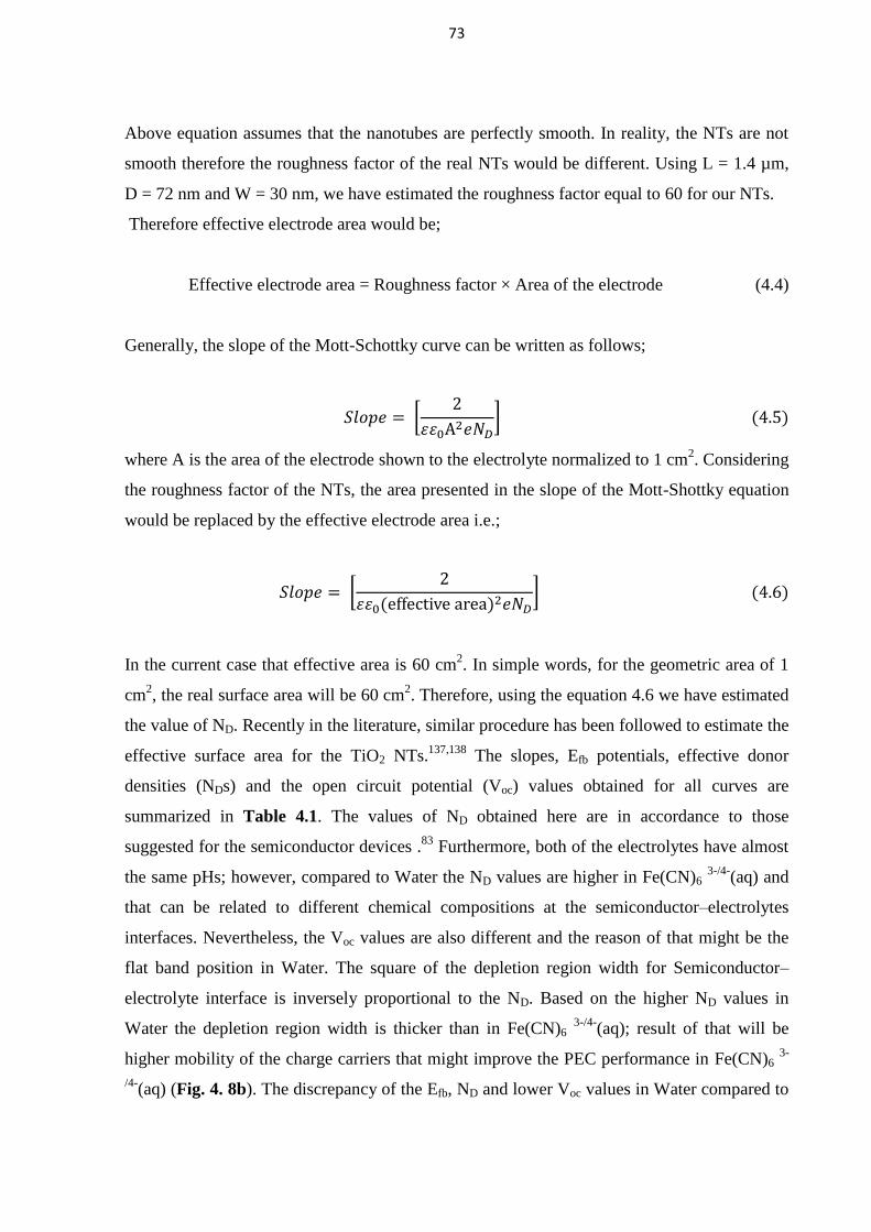
73
Above equation assumes that the nanotubes are perfectly smooth. In reality, the NTs are not
smooth therefore the roughness factor of the real NTs would be different. Using L = 1.4 µm,
D = 72 nm and W = 30 nm, we have estimated the roughness factor equal to 60 for our NTs.
Therefore effective electrode area would be;
Effective electrode area = Roughness factor × Area of the electrode (4.4)
Generally, the slope of the Mott-Schottky curve can be written as follows;
where A is the area of the electrode shown to the electrolyte normalized to 1 cm2. Considering
the roughness factor of the NTs, the area presented in the slope of the Mott-Shottky equation
would be replaced by the effective electrode area i.e.;
In the current case that effective area is 60 cm2. In simple words, for the geometric area of 1
cm2, the real surface area will be 60 cm
2. Therefore, using the equation 4.6 we have estimated
the value of ND. Recently in the literature, similar procedure has been followed to estimate the
effective surface area for the TiO2 NTs.137,138
The slopes, Efb potentials, effective donor
densities (NDs) and the open circuit potential (Voc) values obtained for all curves are
summarized in Table 4.1. The values of ND obtained here are in accordance to those
suggested for the semiconductor devices .83
Furthermore, both of the electrolytes have almost
the same pHs; however, compared to Water the ND values are higher in Fe(CN)6 3-/4-
(aq) and
that can be related to different chemical compositions at the semiconductor–electrolytes
interfaces. Nevertheless, the Voc values are also different and the reason of that might be the
flat band position in Water. The square of the depletion region width for Semiconductor–
electrolyte interface is inversely proportional to the ND. Based on the higher ND values in
Water the depletion region width is thicker than in Fe(CN)6 3-/4-
(aq); result of that will be
higher mobility of the charge carriers that might improve the PEC performance in Fe(CN)6 3-
/4-(aq) (Fig. 4. 8b). The discrepancy of the Efb, ND and lower Voc values in Water compared to

74
Fe(CN)6 3-/4-
(aq) (Table 4.1) can be attributed to the trapping states related to Ta3N5 NTs–
Water junction.
Table 4. 1 Comparison of PEC parameters and Mott-Schottky analyses of Ta3N5 NTs in
Water and Fe(CN)6 3-/4-
(aq).
Analyses Water Fe(CN)6 3-/4-
(aq)
Voc (dark)/ V vs
Ag/AgCl 0.01 0.10
Voc (1 Sun)/ V vs Ag/AgCl
–0.23 –0.36
Frequency Efb/ V vs RHE Slope ND*/ cm–3 Efb/ V vs RHE Slope ND*/ cm–3
200 Hz 0.20 4.4×10¹¹
7.7×10¹⁵
–0.05 1.1×10¹¹
3.1×10¹⁶
500 Hz 0.18 9.3×10¹¹
3.7×10¹⁵
–0.05 1.8×10¹¹
1.9×10¹⁶
1000 Hz 0.16 1.5×10¹²
2.3×10¹⁵
–0.05 2.8×10¹¹
1.2×10¹⁶
1500 Hz 0.13 1.9×10¹²
1.8×10¹⁵
–0.05 3.6×10¹¹
9.4×10¹⁵
3000 Hz 0.05 2.8×10¹²
1.2×10¹⁵
–0.06 5.3×10¹¹
6.4×10¹⁵
* To measure the ND from Mott-Schottky equation; the dielectric constant of equation 4.6
was taken as 8, and the effective area of the nanotubes was estimated by the geometric
roughness factor of the nanotubes considering that the NTs are perfectly smooth; however in
actual it’s not the case and the effective area of the electrode might be different.
To elucidate the mechanism of charge transfer across the Ta3N5 NTs-Water interface
as a function of applied potential, Nyquist plots were obtained in Water (Fig. 4. 11). It can be
seen that increasing biasing potential has decreased the charge transfer resistance (Rct) across
the Ta3N5 NTs–Water interface (Inset of Fig. 4. 11). As discussed earlier, applying more
positive potentials in Water, photocurrent was improved as well as the cathodic transient
spikes were overcome (Fig. 4. 8a & 9c). The Nyquist plots clearly indicate that low charge
transfer resistance is obtained at higher applied potential and that can be one another reason to
drive water oxidation at higher external potentials for pristine Ta3N5 NTs in Water. In
addition, the poor fill factor of the LSV curves of Fig. 4. 8a can be further related to the Rct
values.

75
Fig.4. 11 Nyquist plots for pristineTa3N5 NTs in Water as a function of applied potentials.*
* Inset: The equivalent circuit and Rct vs applied potential graphs extracted from circuit
fitting.
For the analyses discussed above we have used Ta3N5 NTs synthesized for 20 min of
anodization and nitrided at 800°C for 3 h. 13
To investigate if decreasing the length of the NTs
influence the photocurrent to compensate for the hole trapping; length of the NTs is decreased
by anodization of 5 min and further nitriding them at 800°C for 3 h. The LSV curve obtained
for this sample in Water is shown in Fig. 4. 12a (red color solid line). Comparing the
photocurrent with the longer length Ta3N5 NTs obtained at the same nitridation conditions
(Fig. 4. 8a, highlighted potential window), no significant improvement can be observed.
Therefore, short length NTs; that are expected to present lower resistance to the back contact
thereby decreasing the recombination could not compete with the trapping states. To study if;
higher temperature nitridation that decrease the oxygen content and improves the crystallinity;
could cope with these trapping events to improve the photocurrent, we have obtained LSV
curves of the sample anodized for 20 min and nitrided at 900°C for 3 h (Fig. 4. 12a - blue
color line). The cathodic and anodic spikes can be observed clearly and the photocurrent is
still not improved within water splitting potential window. However, a slight improvement
was obtained at higher potentials > 1.23 V vs RHE. Therefore, the trapping states are
independent of the length and the crystallinity of the NTs and application of large biasing for
improved charge transfer is necessary. On the other hand, when these samples are tested in

76
[Fe(CN)6]3-/4-
(aq); compare to Fig. 4. 8b dramatic enhancement in the photocurrent can be
observed.
Fig.4. 12 LSV curves of pristineTa3N5 NTs in (a) Water and (b) Fe(CN)63-/4-
(aq).
The photocurrent discrepancy for the same samples measured in two different electrolytes
clearly indicates the critical role of the trapping states on the photogenerated carriers.
Therefore, pristine Ta3N5 NTs are not suitable without the presence of efficient hole
scavenging species in the electrolyte. Based on the Table 4.1 and the CV analyses shown
above; the band structure of pristine Ta3N5 NTs is constructed in Fig. 4. 13 showing the
energetics when holes are scavenged efficiently by Fe(CN)63-/4-
(aq) and when they are
trapped in Water.
Fig.4. 13 Schematic representation of the energetics for pristine Ta3N5 NTs for (a) efficient
hole scavenging in Fe(CN)63-/4-
(aq) and (b) hole trapping in Water.

77
Now the question arises how to improve Ta3N5 NTs electrodes for PEC devices? One of the
main circumventing approach is to incorporate suitable oxidizing co-catalysts, such as Co3O4,
Co(OH)x, IrO2, Co-Pi etc.9, 112,
111, 121
119
We suggest that for Ta3N5 NTs, the hole scavenger
should be in the form of redox specie or a co-catalyst to avoid hole trapping. Therefore,
avoiding the hole accumulation to accelerate the water oxidation kinetics are pivotal to
improve PEC performance of the Ta3N5 NTs.
4.3. Partial conclusions
In summary, the insight to the PEC performance of pristine Ta3N5 NTs is provided by
studying the semiconductor–electrolyte interface in Water and competitive sacrificial reagent.
It was found that in Water the pristine photoanode presents large anodic and cathodic spikes
upon light chopping; of that the later was more prominent at lower biasing potentials. On the
other hand, the photocurrent was not only improved in the sacrificial agent but also the anodic
and as well as the cathodic spikes were not observed demonstrating simple outer sphere
valence band hole scavenging. By thorough investigations, it was confirmed that the PEC
activity of pristine Ta3N5 NTs is highly dependent on the interfacial hole scavenging. We
observed for the first time that pristine Ta3N5 NTs are highly affected by the trapping states
related to Ta3N5 NTs–Water junction. It was observed that these trapping states are activated
under light illumination and photogenerated holes are either recombine or trapped in these
states and higher biasing potential is required to improve the photocurrent, albeit very little. It
has been suggested that these trapping states are the Water intermediates with reduced
tantalum species and/or the oxygen content in the tubular matrix. In the literature, for pristine
Ta3N5 NTs higher external biasing (> 1.23V vs RHE) has been reported for improved water
oxidation 14,17
and we found that the large onset potential required in Water for pristine
Ta3N5 NTs is related to these trapping events. Furthermore, when the anodization and
nitridation conditions were modified; the conditions of large applied biasing were still
required; showing that the trapping states are intrinsic drawback of pristineTa3N5 NTs–Water
junction. Therefore, for improved PEC activity at lower external biasing efficient hole
scavenger or suitable water oxidation co-catalysts should be used. Thus, in addition to
providing new insight into the water oxidation process for pristine Ta3N5 NTs photoanode, the
investigation methodology presented in this work, will be of great utility in further studies on
other semiconductor electrodes, aiming to understand their charge transportation and
photocatalytic properties.

78
CHAPTER 5
EFFECT OF THERMAL NITRIDATION ON THE PROPERTIES OF
Ta3N5 NANOTUBULAR PHOTOANODES
5.1. Objectives
In recent years, much more efforts have been devoted to the development of technologies
to generate and store clean energy. The search for new materials is constantly growing and
semiconductors have been the focus of intensive study.9,139,140,50
Tantalum nitride (Ta3N5) has
received an increasing attention for application in water splitting, mainly due to its near
optimal band structure. 17,8
In addition, Ta3N5 nanotubes (NTs) have been found to present an
enormous potential for applications in photoelectrochemical (PEC) devices.12,11,14
To
synthesize Ta3N5 that presents tubular morphology at high temperature nitridation; the
precursor (Ta2O5 NTs) should be synthesized in conditions that result in thick walled
nanotubes with increased adherence to the Ta substrate. For Ta3N5 presenting tubular
morphology, a thorough investigations on lower and higher temperature nitridation at which
pristine Ta3N5 with tubular morphology can be obtained and conditions at which it presents
improved crystallinity are warranted.
Electrochemical impedance spectroscopy (EIS) is a powerful tool to study the
semiconductor–electrolyte interface. The equivalent circuit (EC) analogy simplify the
elucidation of electrochemical systems; provided the particular arrangement of circuit
elements in a network possesses physical meaning.41,141
Using EIS and EC to investigate the
interfacial charge transportation of Ta3N5 NTs synthesized under different nitridation
conditions are interesting to understand their PEC activity and to optimize them for improved
performance.
In this part of the work, we study the effect of nitridation temperature and time on the
morphology, crystalline structure, interfacial charge transfer, PEC activity and flat band
potential of Ta3N5 NTs. Samples were obtained at nitridation temperature ranging from 650°C
to 1000°C and nitridation times from 1 to 10 h. Three sets of samples have been synthesized:
i) performing nitridation for 10 h at the temperatures of 650°C, 700°C, 750°C, 800°C and
900°C, ii) at constant nitridation temperature of 800°C during nitridation times of 1, 2, 3, 5
and 10 h and iii) performing nitridation for 3 h at the temperatures of 800°C, 850°C, 900°C
and 1000°C. For simplicity, the samples will be denoted following the format T°C-time, e.g.
the sample nitrided at 800°C for 1 hour is represented as 800°C-1h.

79
5.2 Results and Discussion
5.2.1. Morphology
Fig. 5. 1 displays the SEM and TEM images of the samples synthesized by nitridation for 10
h at 650°C, 800°C and 900°C. One can observe an increase in roughness on the walls of the
NTs with the temperature. However, upon thermal nitridation for 10 h at 900°C; a remarkable
collapse in the tubular morphology is observed as the nanotubes are shrunk and turn into an
urchin–like structure (Fig. 5. 1c). As most of the literature on Ta3N5 describes the synthesis at
800°C, we have obtained nanotubes at this temperature and varied the nitridation times for; 1,
2, 3, 5 and 10 h.11,113
Fig.5. 1 SEM (Top) and TEM (Bottom) images of the samples prepared at (a) 650°C (b)
800°C and (c) 900°C for a time of 10h.
As tubular morphology is observed for 800°-10h; therefore, regardless the nitridation time all
the samples maintained tubular morphology. Fig. 5.2 compares the morphology of the
samples prepared at 850°C, 900°C and 1000°C obtained for the nitridation time of 3 h. It can
be seen that the tubular morphology is only sustained at the temperature as high as 900°C,

80
once at 1000°C the nanotubes collapsed and the walls are cracked. The nitridation
temperatures and times have changed the geometrical dimensions of the Ta3N5 NTs compared
to the anodized NTs (Table 5.1) that is related to the density difference between Ta2O5 and
Ta3N5.98
Table 5. 1 Estimated geometrical dimensions of Ta3N5 nanotubes as a function of nitridation
temperature and time.*
Sample Wall thickness/nm * Diameter/nm * Length/µm †
As-Anodized 34 130 1.60
650°C-10h 34 128 1.58
700°C-10h 33 125 1.52
750°C-10h 32 110 1.40
800°C-2h 33 120 1.50
800°C-3h 30 100 1.40
800°C-5h 28 95 1.35
800°C-10h 28 90 1.20
850°C-3h 28 90 1.25
900°C-3h 25 75 1.10
900°C-10h - - -
1000°C-3h - - -
* Wall thicknesses and Diameters of the NTs were calculated from TEM images taken from different
locations.
† Lengths of the NTs were calculated from SEM images.
The key to preserve the morphology of the Ta3N5 NTs for nitridation at higher temperatures
lies in the low temperature anodization to prepare Ta2O5 NTs; resulting in strong adhesion to
the Ta substrate and presenting thick walls.,80
The results show that for both conditions of
long nitridation time of 10 h at 900°C (Fig. 5. 1c) and for short periods of 3 h at 1000°C (Fig.
5. 2) the nanotubes collapsed. Therefore, to preserve the tubular morphology low temperature
anodization of the precursor is beneficial for sufficiently high nitridation temperature applied
for short enough time. Hereafter, we will discuss the structural characterization for the
samples that preserved tubular morphology; however, for comparison the PEC performances
of all synthesized samples have been studied.

81
Fig.5. 2 SEM images of the samples prepared at (a) 850°C (b) 900°C and (c) 1000°C for a
time of 3h.
5.2.2 Crystalline structure of Ta3N5 nanotubes
Studying the crystalline structure of Ta3N5 NTs adhere to the Ta substrate by XRD is a
challenge task as the Ta foil presents plastic deformation. From the XRD patterns recorded by
three different approaches; we have provided a comprehensive methodology to study this
system (Fig. 5.3). For comparison, the XRD of the precursor Ta2O5 is displayed in Fig. 5. 3a.
Only diffraction peaks characteristic of Ta can be observed as expected; as the as–anodized
Ta2O5 NTs are amorphous.80
After thermal nitridation the grey colored Ta2O5 NTs turns into
red colored Ta3N5 NTs.11
To investigate the Ta3N5 we firstly performed conventional XRD of
the NTs adhere to the Ta substrate (Fig. 5. 3b). One can observe three different species in the
samples; Ta3N5 (PDF# 79-1533), sub–nitride TaN0.1 (PDF# 25-1278) and Ta (PDF# 4-788);
their corresponding peaks are marked as *, Δ and ʘ; respectively. In addition, the relative
intensity of TaN0.1 peaks increases with the temperature suggesting the increase in the
concentration of sub–nitride phases at higher temperatures (Fig. 5. 3b).110
The presence of
sub–nitride phase has been earlier reported;11
however, no information is available on the
position or interface where it lies in the sample neither on how this phase is formed. The SEM
images in Fig. 5. 1 and 2 show that Ta3N5 NTs present a vertically oriented porous structure,
allowing the NH3 to diffuse from top to bottom to readily replace oxygen by nitrogen
resulting in Ta3N5 NTs over the entire nanotube. It has been earlier observed that for the NTs
of Ta3N5 the oxygen diffuses to the walls of the NTs and higher temperature nitridation
decreases oxygen content. Furthermore, according to the literature, pristine tantalum metal
cannot readily react under flowing ammonia to form any nitride of tantalum (XRD patterns of
pure Ta before and after nitridation under flowing ammonia for high temperatures were

82
exactly the same).131
Therefore, we suggest that the oxygen content that diffuses to the bottom
Ta substrate reacts with the Ta atoms forming non–stoichiometric oxides which then react
with the NH3 to transform into TaN0.1.
Fig.5. 3 XRD patterns of (a) as-anodized Ta2O5 NTs/Ta, (b) and (c) Ta3N5 NTs/Ta, (d) Ta3N5
NTs removed from the substrate and (e) the substrate of which the Ta3N5 NTs are scratched
off.
The Ta and TaN0.1 peaks have higher relative intensity compared to Ta3N5 phase; therefore, a
complete characteristic diffractograms for the whole 2θ range of Ta3N5 could not be observed,
instead; Ta3N5 peaks are visible up to 2θ ~36°. In order to remove the substrate contribution,
we have obtained the grazing angle XRD diffractograms of the nanotubes at a very small

83
grazing angle of 0.3° (Fig. 5.3c). The substrate contributions are almost completely removed
and the subnitride TaN0.1 (present in conventional XRD) is absent in the grazing angle XRD,
showing that TaN0.1 is in fact a substrate contribution. In addition, for 650°C-10h the Ta3N5
peaks visible in Fig. 5. 3b are nearly absent in Fig. 5. 3c that shows the presence of Ta3N5
crystalline grains in amorphous Ta2O5 tubular matrix. Grazing angle XRD helped to minimize
the contribution from the Ta substrate, however; at the same instant the signal resolution from
Ta3N5 NTs have been lost. Hence, the NTs were removed from the Ta substrate and powder
XRD diffractograms have been obtained for the scratched off NTs (Fig. 5. 3d). The signal
resolution is highly improved and all of the observed peaks correspond to Ta3N5. Finally,
XRD patterns obtained from the substrate of which the NTs were removed have shown just
the TaN0.1 and Ta characteristic peaks (Fig. 5. 3e) strongly confirming the presence of TaN0.1
at the substrate. Nevertheless, we found that TaN0.1 is metallic; however, we suggest
developing a certain strategy that can help to avoid these phases to synthesize Ta3N5 NTs for
PEC applications. With the aim to study pristine Ta3N5 NTs free from any other contribution
from now onward we will discuss the XRD patterns obtained from the scratched off powders.
To investigate the minimum nitridation conditions to obtain Ta3N5 NTs we started
thermal nitridation at 650 °C for 1 h and 3 h. However, at these conditions the presence of a
mixed structure of Ta2O5 (PDF# 25-922) and Ta3N5 (PDF# 79-1533) was observed and by
increasing the nitridation time from 3h to 6h at 650°C (Fig. 5.4), clear changes in the XRD
patterns are observed once pristine Ta3N5 phase is obtained at these conditions.
Nevertheless, for 650°C-6h one can observe a huge background in the spectrum along
with wide diffraction patterns presenting amorphism in the sample. Therefore, to further
improve the crystallinity, we have increased the nitridation time to 10 h at 650°C (Fig. 5. 3c).
The diffraction peaks are sharper when compared to 650°C-6 h; therefore, we fixed the
nitridation time for 10 h and varied the temperatures to 700°C, 750°C, 800°C and 900°C.
Furthermore, impurities were observed for 800°C-1h (Fig. 5.4); and by increasing the time to
2 h at 800°C pristine Ta3N5 NTs are obtained.

84
Fig.5. 4 XRD patterns of the samples prepared at 650°C and 800°C
Fig. 5.5 displays the XRD patterns of phase-pure orthorhombic Ta3N5 NTs;
corresponding to the PDF# 79-1533. Interestingly, when compared to commercial Ta2O5
powders which are crystalline in nature, the transformation from Ta2O5 NTs to Ta3N5 NTs is
found to take place at a lower temperature of 650°C.98
We may suggest that amorphous
nanotubular precursors of Ta2O5 are easy to transform to Ta3N5 at low temperature.
Fig.5. 5 XRD patterns of Ta3N5 NTs prepared by thermal nitridation.

85
Crystalline structures were refined by the Rietveld technique. Simulated patterns (Fig. 5.6)
and the respective parameters are shown in Table 5.2 and Table 5.3. For the set of samples
prepared for 10 h, in addition to slight increase in the grain size the strain is increased with the
temperature (Table 5.3).
Fig.5. 6 Rietveld refinement profile for Ta3N5 NTs; (•) observed Yobs, (red solid lines)
calculated Ycalc, (blue solid lines) Yobs–Ycalc difference of phase.
The increase in the strain might be related to the morphology preservation and increasing the
roughness on the walls of the NTs. The larger crystalline grains and improved crystallinity
were obtained from the 900°C-3h Ta3N5 NTs. Unlike earlier report on Ta3N5 thin films, the
grain size for Ta3N5 NTs found here presents a dependence on the nitridation conditions.94
This behavior can be rationalized on the basis of different crystal growth phenomena for thin
films and tubular morphology. Once thin films are compact and during the crystal growth; the
grains exhibit stress from their neighbor grains that may limit their further growth due to the
compact nature of thin films. Therefore, within the limit of stability of Ta3N5 phase the grains
become independent of the nitridation temperature.94

86
Table 5. 2 Percentages of vacancies (vac), occupancies (occ), substitutions (sub) in the
Wyckoff positions, cell parameters and agreement factors deduced from the Rietveld
refinements.
Sample Ta1 (4c) Ta2 (8f) N1
(4c)
N2/O2
(8f)
N3
(8f)
Rbragg-
factor
Rf-
factor Chi2
a
b
c
650°C-10h 97.98 occ
2.02 vac
99.89 occ
0.11 vac
71.33 occ
28.67 vac
0 – occ
100 subs
99.98 occ
0.02 vac 6.19 4.06 1.43
3.88516
10.16713
10.24118
700°C-10h
94.60 occ
5.40 vac
99.97occ
0.03 vac
69.71 occ
30.29 vac
37.10 occ
62.90 sub
100 occ
0 – vac 3.33 1.94 1.99
3.89520
10.19483
10.26891
800°C-3h 93.25 occ
6.744 vac
99.15 occ
0.846 vac
95.32 occ
4.68 vac
49.73 occ
50.27 sub
100 occ
0- vac 2.72 1.61 1.63
3.89551
10.21312
10.27800
800°C-5h 93.87 occ
6.128 vac
98.32 occ
1.68 vac
94.40 occ
5.60 vac
66.01 occ
33.99 sub
100 occ
0 – vac 2.70 1.45 1.51
3.89962
10.20950
10.27345
800°C-10h 94.58 occ
5.42 vac
98.39 occ
1.61 vac
95.03 occ
4.97 vac
80.01 occ
19.99 sub
100 occ
0 – vac 4.14 2.41 1.37
3.89325
10.20868
10.26509
850°C-3h 99.14 occ
0.852 vac
99.65 occ
0.35 vac
86.00 occ
14.00 vac
71.18 occ
28.82 sub
100 occ
0- vac 3.78 2.27 2.36
3.89547
10.21895
10.28788
900°C-3h 99.68 occ
0. 32 vac
100 occ
0- vac
89.83 occ
10.17 vac
86.81 occ
13.19 sub
100 occ
0 – vac 2.31 1.53 1.35
3.88879
10.21532
10.26565
On the other hand, NTs are isolated from their surrounding exhibiting lower stress from the
neighboring grains during the growth; thereby, high temperature nitridation facilitates to
increase their size. However, care must be taken for tubular morphology as the morphology
can be collapsed under very harsh nitridation conditions. The percentages of defects in the
crystalline structure of Ta3N5 NTs are calculated considering the occupation factors obtained
by Rietveld refinement (Table 5.2). At the Wyckoff sites Ta1(4c), Ta2(8f) and N1(8f)
Schottky defects were found. Following the methodology proposed by Henderson et al,95
the
refinements were improved when oxygen substitutional defects are incorporated at the 3-
coordinated Wyckoff site N2(4f). These results confirm that oxygen in the crystalline
structure of Ta3N5 cannot be completely removed by thermal nitridation.95,142
Based on the
refinements, nominal stoichiometries of the samples were calculated from the percentages of
site occupancy and vacancy (Table 5.2) obtained from the occupation factors; and are
displayed in Table 5.3.

87
Table 5. 3 Grain size, lattice strain and nominal stoichiometry obtained by the refinements.
Sample Av. Grain Size (nm) Strain(×10-4
) Stoichiometry
650°C-10h 29.59 12.15 Ta2.97N2.71O2.0
700°C-10h 32.56 19.93 Ta2.94N3.43O1.25
800°C-3h 19.71 13.85 Ta2.89N4.18O0.84
800°C-5h 31.53 18.67 Ta2.90N4.26O0.67
800°C-10h 37.46 22.00 Ta2.91N4.55O0.39
850°C-3h 34.03 32.43 Ta2.98N4.29O0.48
900°C-3h 43.51 36.90 Ta2.99N4.61O0.22
In the set of samples prepared for the nitridation of 10 h, one can observe a decrease in
oxygen content by increasing the temperature. However, for 650°C-10h the Ta stoichiometry
is “2.97” i.e greater than the other samples but oxygen content are highest; suggesting the
presence of large oxide content in the sample. Therefore, we may suggest; for sample 650°C-
10h, the Ta3N5 crystalline grains are distributed in the amorphous tubular matrix of Ta2O5. In
addition, the stoichiometry was not ideal even for 800°C-10h. These results strongly suggest
that indeed nitridation temperature of 800°C is not an optimum condition for the synthesis of
Ta3N5.11,113
Therefore, the temperature should be increased; however care must be taken to
choose an appropriate nitridation time, in order to preserve the tubular morphology. Further
details on the crystalline structure of the nanotublar samples prepared for 3 h of nitridation as
a function of nitridation temperature are discussed elsewhere (See Appendix 1).
5.2.3 Optical characterization
After nitridation a red color was visually observed for the samples indicating the formation of
Ta3N5 NTs.56,67
Fig. 5. 7 displays the UV–Vis diffuse reflectance spectra of Ta2O5 and some
selected samples of Ta3N5 NTs. The absorption edges of the Ta3N5 have been red shifted from
the Ta2O5 edge due to narrowing of the band gap.

88
Fig.5. 7 Absorption spectra (a). Direct bandgap obtained from [K.M (R)hν]2 vs hν and
Indirect bandgap obtained from [K.M (R)hν]0.5
vs hν for Ta3N5 NTs (b).
The direct and indirect band gaps were obtained by extrapolating the linear region on the UV-
Vis spectra and were found to ca. 2.1–2.2 and 1.93–1.98 eV, respectively consistent with the
reported values for Ta3N5.11,98
5.3.4 Electrochemical impedance spectroscopy (EIS)
To investigate the effect of nitridation conditions on the charge transfer across the
Ta3N5 NTs–electrolyte interface, we have performed EIS (Fig. 5. 8). For the set of samples
prepared for the nitridation time of 10 h (Fig. 5. 8a); incomplete semicircles can be observed
which are characteristic of capacitance systems exhibiting non ideal behavior. As observed in
the TEM images displayed in Fig. 5.1 (bottom), nitridation for longer time at high
temperatures results in a rougher structure; that can affect the charge transportation at the
interface. From the single semicircles (one time constant) shown in Fig.5. 8a EIS data was
fitted to an equivalent circuit (Fig. 5. 8d); consisting of a series resistance Rs and single CPE
(constant phase element) parallel with charge transfer Rct. The CPE in an electrochemical
system may arise from: (a) distribution of the relaxation times due to non-homogeneities
existing at the electrode– electrolyte interface, (b) porosity of the electrode, (c) the nature of
the electrode and (d) dynamic disorder associated with diffusion.143,144,145
The impedance of
CPE can be calculated by the following relationship;
1/Z(ω) = Q (jω) n
Where Q is the pre-factor of CPE and n is the exponential term. For pure capacitor its value is
1 whereas for pure resistor it is 0. Based on the nanotubular nature and structural non-

89
homogeneities (SEM and Rietveld refinements) adding CPE for the Ta3N5 NTs–electrolyte
interface is physically true. By fitting the Nyquist plots into the proposed equivalent circuit
the values of the components have been found and to better visualize the Rct as a function of
various nitridation temperatures and times; we have plotted Rct against different thermal
treatments shown in the inset of Nyquist plots in Fig. 5. 8.
Fig.5. 8 Nyquist plots obtained under dark for Ta3N5 NTs prepared at different nitridation
conditions.
The 650°C-10h sample presents the highest Rct (Fig. 8a). In the XRD patterns of the sample
some amorphism was observed (Fig. 5. 3d) and as observed in the Rietveld refinements
(Table 5.3), the sample consists of highest oxygen content. Therefore, it is reasonable to
propose that the amorphism and the highest oxygen content in the sample are the main
reasons for the highest Rct. Interestingly, 700°C-10h has exhibited the lowest Rct. The
stoichiometry of both 650°C-10h and 700°C-10h samples (Table 5.3) show the presence of
oxygen content and 700°C-10h is more crystalline than 650°C-10h and present a smaller Rct.

90
Also 800°C-10h presents slightly higher Rct compared to 900°C-10h, that might be related to
smaller concentration of defects as can be inferred from the stoichiometry of Ta2.99N4.61O0.22
obtained for sample prepared at 3h of nitridation time at 900° i.e 900°C-3h (Table 5.3). Now
evaluating the samples prepared at fixed temperature of 800°C and varying nitridation times
(Fig. 5. 8b); 800°C-1h (consisting of mixed phases of Ta3N5 and Ta2O5 as shown in Fig. 5. 4)
present the highest Rct while 800°C-5h presents the smallest Rct. Lastly, for the set of 3h
samples (Fig. 5. 8c), 900°C-3h evidently indicates the lowest interfacial charge transfer
resistance compared to all of the samples synthesized in the current work corroborating the
high crystallinity and phase purity as discussed earlier (Table 5.3). These results strongly
suggest that nitridation conditions alter the crystalline structure of Ta3N5 NTs that further
affects the interfacial charge transportation properties that are the functions of morphology,
crystallinity and phase purity of Ta3N5 NTs photoanodes and for the lowest Rct an optimum is
exhibited for 900°C-3h.
The flat band potential of the semiconductor is one of the most important parameters
for evaluating photoelectrochemical water splitting that helps to predict whether
semiconductor should be biased externally or not. One of the most widely used technique to
estimate the flat band of a semiconductor is the Mott-Shottky plot.133
Fig. 5. 9 displays the
Mott-Shottky plots of the Ta3N5 NTs that present n-type transition from the positive slopes of
the curves. On each graph the flat band potential (Efb) is obtained by extrapolating the linear
region which is presented as blue line intercepts. A very interesting result is that all of the
samples present almost the same flat band potential of ca. –0.05 vs RHE; therefore, for Ta3N5
NTs, the Efb is almost independent of nitridation temperature. In addition, samples 650°C-10h
and 700°C-10h present a lower transition along with the main transition (highlighted in Fig. 5.
9); that can be related to the presence of oxide content that are higher in 650°-10h than in
700°-10h.

91
Fig.5. 9 Mott-Schottky plots of Ta3N5 NTs synthesized at various nitridation conditions.
5.3.5 PEC activity of Ta3N5 NTs
Fig. 5. 10 shows the linear sweep voltammetry (LSV) curves of all samples. Among the set
of samples prepared for 10 h of nitridation, 650°C-10h has presented lowest PEC activity that
can be related to lower order crystallinity (Fig. 5. 3c) as well as highest interfacial Rct (Fig. 5.
8a). On the other hand the highest photocurrent was obtained from 900°C-10h. For the set of
samples prepared at fixed temperature of 800°C by varying nitridation time; the sample

92
800°C-1h has shown poor PEC performance. The XRD analysis presents the mixture of
Ta2O5 and Ta3N5 phases for 800°C-1h (Fig. 5.4). The trade-off between the sample chemical
composition and the electrolyte clearly affects the PEC performance. Therefore, the impure
phase and low crystallinity are the main reasons behind the poor performance of 800°C-1h.
Interestingly 800°C-5h presented the higher PEC activity even compared to 800°C-10h. This
result can be related to the thermal decomposition of the Ta3N5 at longer nitridation
periods.146
Although 800°C-5h present the higher photocurrent compared to other samples of
the set; however, the photocurrent is still low, that can be rationalized in terms of the
stoichiometries of the samples prepared at 800°C for varying nitridation times i.e, far away
from the ideal Ta3N5. Therefore, 800°C is not a good choice to synthesize Ta3N5 NTs.
Fig.5. 10 LSV curves of Ta3N5 NTs obtained by chopping AM 1.5 (1 Sun) illumination.
Considering now the nitridation of the samples for fixed time of 3h under varying
temperatures; clearly the 900°C-3h, presented improved photocurrent compared to all other
samples prepared in the current work and the one shown in the earlier reports.113,112
In
addition, it has presented nearly a 2–3 fold photocurrent compared to 900°C-10h and 1000°C-
3h. Therefore, the improved photocurrent from Ta3N5 nanotubular photoanodes is in fact a

93
synergistic combination of the tubular morphology, the controlled chemical composition and
the improved charge transfer across the interface. Table 5.4 contrasts the parameters obtained
during the LSV experiments for Ta3N5 NTs photoanodes synthesized in the current study. To
obtain the photocurrent, the dark current is subtracted from the current obtained under
illumination.
Table 5. 4 (Photo)electrochemical parameters of Ta3N5 NTs obtained under various
conditions of temperatures and nitridation times.
Sample Voc(dark)V vs
Ag/AgCl
Voc (AM 1.5)
V vs Ag/AgCl
Iph (0.64V vs RHE)
0 V vs Ag/AgCl
Iph (1.23V vs RHE)
0.6 V vs Ag/AgCl
650°C-10h 0.10 –0.32 70 μA 180 μA
700°C-10h 0.10 –0.32 151 μA 328 μA
750°C-10h 0.11 –0.36 251 μA 710 μA
800°C-01h 0.08 –0.26 107 μA 98 μA
800°C-02h 0.10 –0.34 251 μA 556 μA
800°C-03h 0.10 –0.36 430 μA 900 μA
800°C-05h 0.10 –0.36 940 μA 2.6 mA
800°C-10h 0.11 –0.33 280 μA 2.4 mA
850°C-03h 0.10 –0.32 1.5 mA 3.2 mA
900°C-03h 0.10 –0.34 4 mA 7.4 mA
900°C-10h 0.11 –0.35 1.8 mA 3.9 mA
1000°C-3h 0.10 –0.34 600 μA 2.8 mA
The Voc values are almost independent of the nitridation conditions for pristine Ta3N5 NTs
photoanodes that might be related to the same flat band position obtained for pristine Ta3N5
NTs, however, 800°C-1h presented a slightly different Voc under dark related to the presence
of impurities in the sample.
5.3. Partial Conclusions
In summary, we have performed a thorough study on the effect of nitridation temperature
and time on the syntheses of Ta3N5 NTs by thermal nitridation of the anodized precursor
Ta2O5 NTs. We observed that amorphous Ta2O5 NTs are easier to transform to Ta3N5 by
nitridation at low temperatures; however the samples obtained at lower temperatures present
low crystallinity and poor photoelectrochemical performance. To synthesize Ta3N5 NTs by
thermal nitridation; the temperature should be high enough to obtain higher crystallinity and
time should be short enough to preserve the tubular morphology. The combined effect of high

94
crystallinity, tubular morphology and low charge transfer resistance across Ta3N5 NTs-
electrolyte interface presents an optimized nitridation condition. Based on Rietveld
refinement, EIS and LSV curves the sample 900°C-3h presents optimum features of a
promising photoelectrode prepared in the current study.

95
CHAPTER 6
GENERAL CONCLUSIONS AND FUTURE PERSPECTIVES
In summary, we have successfully synthesized Ta3N5 thin films and nanotubes by thermal
nitridation starting from Ta2O5 materials. Firstly, thin films were characterized to understand
their optical and photoelectrochemical (PEC) properties comprehensively (See Appendix 1
also); and later the study was focused on optimizing Ta3N5 nanotubes to enhance their PEC
performance.
Ta3N5 thin films have presented monoclinic phase. It was found that thermal
nitridation results into nitrogen and tantalum Schottky defects and substitutional oxygen in 3-
coordinated N atoms. The surface of the monoclinic Ta3N5 thin films presented different
chemical composition compared to the underlying film. Real ε1 and imaginary ε2 parts of
dielectric functions of the film were analyzed by the spectroscopic ellipsometry (SE) within a
broad spectral range of 0.54–4.6 eV. The optical parameterization of SE data was carried out
utilizing the Tauc-Lorentz and Lorentz oscillators. Concerning the application of the
semiconductor in PEC water splitting, the dielectric constant ε1 of Ta3N5 film in the visible
spectral region (3.1–1.7 eV) was found within the range of 7–9; matching the theoretically
reported value. The PEC analyses revealed that the band structure of Ta3N5 is strongly
influenced by the pH of the employed electrolyte. Enhanced PEC activity was observed in
alkaline condition that is attributed to the shorter depletion region width and the lower
recombination life time.
After the investigations on Ta3N5 thin films we have provided the insight to the
photoelectrochemical (PEC) performance of pristine Ta3N5 NTs by studying the
semiconductor–electrolyte interface in Water and competitive sacrificial reagent. It was found
that in Water the pristine photoanode presents large anodic and cathodic spikes upon light
chopping; of that the later was more prominent at lower biasing potentials. On the other hand,
the photocurrent was not only improved in the sacrificial agent but also the anodic and as well
as the cathodic spikes were not observed demonstrating simple outer sphere valence band hole
scavenging. By thorough investigations, it was confirmed that the PEC activity of pristine
Ta3N5 NTs is highly dependent on the interfacial hole scavenging. We observed for the first
time that pristine Ta3N5 NTs are highly affected by the trapping states related to Ta3N5 NTs–
Water junction. It was observed that these trapping states are activated under light
illumination and photogenerated holes are either recombine or trapped in the these states and
higher biasing potential is required to improve the photocurrent, albeit very little. It has been

96
suggested that these trapping states are the Water intermediates with reduced tantalum species
and/or the oxygen content in the tubular matrix. In the literature, for pristine Ta3N5 NTs
higher external biasing (> 1.23V vs RHE) has been reported for improved water oxidation
14,17 and we found that the large onset potential required in Water for pristine Ta3N5 NTs is
related to these trapping events. Furthermore, when the anodization and nitridation conditions
were modified; the conditions of large applied biasing were still required; showing that the
trapping states are intrinsic drawback of pristineTa3N5 NTs–Water junction. Therefore, for
improved PEC activity at lower external biasing efficient hole scavenger or suitable water
oxidation co-catalysts should be used. Thus, in addition to providing new insight into the
water oxidation process for Ta3N5 NTs photoanode, the investigation methodology presented
in this work, will be of great utility in further studies on other semiconductor electrodes,
aiming to understand their charge transportation and photocatalytic properties.
As we found that Ta3N5 NTs when used without sacrificial reagent have poisoned by
the trapping states related to the Ta3N5 NTs–Water junction; therefore we used sacrificial
reagent to study the effect of nitridation on the properties of Ta3N5 NTs. A thorough study on
the effect of nitridation temperature and time on the syntheses of Ta3N5 NTs by thermal
nitridation of the anodized precursor Ta2O5 NTs have been provided. We observed that
amorphous Ta2O5 NTs are easier to transform to Ta3N5 by nitridation at low temperatures;
however the samples obtained at lower temperatures present low crystallinity and poor
photoelectrochemical performance. To synthesize Ta3N5 NTs by thermal nitridation; the
temperature should be high enough to obtain higher crystallinity and time should be short
enough to preserve the tubular morphology. The combined effect of high crystallinity, tubular
morphology and low charge transfer resistance across Ta3N5 NTs-electrolyte interface
presents an optimized nitridation condition. Based on Rietveld refinement, EIS and LSV
curves the sample 900°C-3h presents optimum features of a promising photoelectrode
prepared in the current study.
From the effect of nitridation temperature and time on the syntheses of Ta3N5 NTs for
PEC activities we found that higher nitridation temperatures for the shorter time as beneficial
to improve the structural and PEC properties of Ta3N5 NTs. Therefore, we have focused on
the short time nitridations of 3 h at higher temperatures to investigate the effect of oxygen
content on the PEC activities of Ta3N5 NTs (See Appendix 1). The morphological, structural,
surface and charge transportation properties of the porous Ta3N5 NTs were investigated.
Performing anodization in a lower electrolyte temperature helped to preserve the tubular
morphology at a higher nitridation temperature. X-ray diffraction and high resolution

97
transmission electron microscopy analyses revealed that nitridation has controlled the
preferential orientation along the (110) plane of orthorhombic Ta3N5. The oxygen content is
one limiting source that influences the PEC activity of the photoanode. Increasing the
nitridation temperature increased the grain size, decreased the oxygen substitution defects and
Schottky defects in the crystalline structure and removed the amorphous layer on the walls of
the NTs. Crystallographically oriented along (110), highly crystalline, larger grain size and
lower oxygen containing 900°C-3h demonstrated enhanced photocurrent, which was 3.4-
times and 25-fold higher than the Ta3N5 film prepared in this study and the literature reported
values, respectively. These results show that porous Ta3N5 NTs with crystallographically
preferential orientation along (110) and low oxygen content can improve PEC activity.
The work presented here evidently demonstrated that Ta3N5 nanotubes strongly adhere
to Ta substrate are promising photoelectrodes for PEC devices. However, we have used
oxidation sacrificial reagent of Fe(CN)6 3-/4-
(aq) to scavenge the photogenerated holes due to
the presence of traps under water oxidation conditions. Furthermore, we found that the
nanotubes synthesized at 900°C for 3 h of nitridation have presented enhanced PEC activity in
Fe(CN)6 3-/4-
(aq) compared to all other samples prepared in the current study. To enhance
actual water oxidation, Ta3N5 NTs needs further modifications. We suggest to incorporate
doping elements in the structure of Ta3N5 that can help to avoid the trapping states and
nitridation should be done at 900°C for 3 hours. Furthermore, in the literature loading suitable
oxidizing co-catalysts, such as Co3O4, Co(OH)x, IrO2, Co-Pi etc have shown improvements.9,
112, 111, 121
119
Therefore, it would be interesting to investigate new doping elements and further
co-catalysts for Ta3N5. We also suggest a suitable route to synthesize Ta3N5 in the form of p-
type semiconductor that may help for its long time durability in the aqueous solutions.

98
APPENDIX 1
PUBLISHED ARTICLES
Article No. 1
Effect of Oxygen Content on the Photoelectrochemical Activity of
Crystallographically Preferred Oriented Porous Ta3N5 Nanotubes
Sherdil Khan†, Maximiliano J. M. Zapata†, Daniel L. Baptista†, Renato V. Gonçalves‡, Jesum A.
Fernandes∥, Jairton Dupont⊥, Marcos J. L. Santos§, and Sérgio R. Teixeira*† † Instituto de Física, UFRGS, Av Bento Goncalves 9500 PO Box -15051 91501-970, POA-RS, Brazil ‡ Instituto de Física de São Carlos, Universidade de São Paulo, CP 369, São Carlos 13560−970, SP Brazil § Instituto de Quimica, UFRGS, Av Bento Goncalves 9500 PO Box -15051 91501-970, POA-RS, Brazil ∥ Department of Chemistry, University of Victoria, Victoria, BC V8W 3 V6, Canada ⊥ School of Chemistry, University of Nottingham, University Park, Nottingham NG7 2RD, U.K. J. Phys. Chem. C, 2015, 119 (34), pp 19906–19914
DOI: 10.1021/acs.jpcc.5b05475
Publication Date (Web): July 31, 2015
Copyright © 2015 American Chemical Society
*E-mail: [email protected]. Phone: +55-51-33086498
Abstract
Crystallographically preferred oriented porous Ta3N5 nanotubes (NTs) were synthesized by thermal
nitridation of vertically oriented, thick-walled Ta2O5 NTs, strongly adhered to the substrate. The
adherence on the substrate and the wall thickness of the Ta2O5 NTs were fine-tuned by anodization,
thereby helping to preserve their tubular morphology for nitridation at higher temperatures. Samples
were studied by scanning electron microscopy, high-resolution electron microscopy, X-ray
diffraction, Rietveld refinements, ultraviolet−visible spectrophotometry, X-ray photoelectron
spectroscopy, photoluminescence spectra, and electrochemical techniques. Oxygen content in the
structure of porous Ta3N5 NTs strongly influenced their photoelectrochemical activity. Structural
analyses revealed that the nitridation temperature has crystallographically controlled the preferential
orientation along the (110) direction, reduced the oxygen content in the crystalline structure and the
tubular matrix, and increased the grain size. The preferred oriented porous Ta3N5 NTs optimized by
the nitridation temperature presented an enhanced photocurrent of 7.4 mA cm−2
at 1.23 V vs RHE
under AM 1.5 (1 Sun) illumination. Hydrogen production was evaluated by gas chromatography,
resulting in 32.8 μmol of H2 in 1 h from the pristine porous Ta3N5 NTs. Electrochemical impedance
spectroscopy has shown an effect of nitridation temperature on the interfacial charge transport
resistance at the semiconductor−liquid interface; however, the flat band of Ta3N5 NTs remained
unchanged.

99
Article No. 2
Structural, optical and photoelectrochemical characterizations of
monoclinic Ta3N5 thin films
Sherdil Khan,a Maximiliano J. M. Zapata,a Marcelo B. Pereira,a Renato V. Gonçalves,b Lukas Strizik,c Jairton
Dupont,d Marcos J. L. Santose and Sérgio R. Teixeira*a
*Corresponding authors
a Institute of Physics, Universidade Federal do Rio Grande do Sul, Av Bento Goncalves 9500, P.O. Box – 15051, POA-RS,
Brazil
E-mail: [email protected]
bInstituto de Física de São Carlos, Universidade de São Paulo, CP 369, São Carlos 13560–970, Brazil
cDepartment of General and Inorganic Chemistry, Faculty of Chemical Technology, University of Pardubice, Studentska 573,
Pardubice, Czech Republic
dSchool of Chemistry, University of Nottingham, University Park, Nottingham, UK
eInstitute of Chemistry, Universidade Federal do Rio Grande do Sul, Av Bento Goncalves 9500, POA-RS, Brazil
Phys. Chem. Chem. Phys., 2015,17, 23952-23962
DOI: 10.1039/C5CP03645C
Abstract
Monoclinic Ta3N5 thin films were synthesized by thermal nitridation of amorphous Ta2O5 films directly sputtered by radio frequency magnetron sputtering. The samples were studied by high resolution transmission electron microscopy, X-ray photoelectron spectroscopy, UV-Vis-NIR spectrophotometry, Rietveld refinements, spectroscopic ellipsometry (SE) and electrochemical techniques. The surface composition of Ta3N5 thin film was found different than the underlying film, affecting the optical properties of the material. The Rietveld refinement has confirmed that nitridation process results in Schottky and oxygen substitutional defects within the crystalline structure of monoclinic Ta3N5 thin film. The optical constants of the film were obtained by SE within a spectral range of 4.60–0.54 eV, i.e. 270–2 300 nm. The suitable parameterization was found to consist of three Tauc-Lorentz and one Lorentz oscillators. The conduction band, valence band and the flat band positions were determined by photoelectrochemical (PEC) techniques, presenting a strong dependence on pH of the eletrolyte. Improved photocurrent was obtained in alkaline condition and attributed to the shorter depletion region width measured by Mott-Schottky and the lower recombination life time measured by open circuit potential decay analyses.

100
Article No .3
(Conference proceeding “IOP Conference Series: Materials Science and Engineering” on the basis of
best oral work presentation in SBPMAT meeting, 2014 Joao Pessoa, Brazil)
Photoelectrochemical study of Ta3N5 nanotubes for water
splitting
Sherdil Khan1, Marcos J. Leite Santos *
2, Jairton Dupont
2, Sergio R. Teixeira*
1
1 Instituto de Física, Universidade Federal do Rio Grande do Sul, Av Bento Gonçalves
9500 POBox - 15051 CEP 91501-970, POA-RS, Brazil.
2 Instituto de Química, Universidade Federal do Rio Grande do Sul, Av Bento
Gonçalves 9500 POBox 15003, CEP 91501-970, POA-RS, Brazil.
E-mail address: [email protected]
IOP Conf. Ser.: Mater. Sci. Eng. 2015, 97, 012007
Abstract. Nanotubes (NTs) of Ta3N5 were synthesized by nitridation of Ta2O5 NTs.
The samples were studied by scanning electron microscopy, UV-VIS
spectrophotometry, x-ray diffraction and photoelectrochemical (PEC) measurements
carried out in aqueous solutions of Na2SO4 and Fe(CN)6 3-/4-
. The results show the
presence of trapping states on illuminated pristine Ta3N5 NTs in Na2SO4 (aq). These
trapping states act as recombination center for photogenerated holes, affecting the
photocatalytic performance of Ta3N5 NTs. On the other hand, by using Fe(CN)6 3-/4-
(aq) the photogenerated holes were scavenged efficiently without giving rise to the
trapping states at Ta3N5 NTs/solution interface. The results obtained by cyclic
voltammetry, linear sweep voltammetry and electrochemical impedance spectroscopy
have shown that the presence of these trapping states is a limiting step for water
oxidation using pristine Ta3N5 NTs.

101
REFERENCES
1. Nowotny, J. V., T. Nejat, Impact of hydrogen on the environment. Int. J. Hydrog.
Energy 2011, (36), 13218-13224.
2. Navarro, R. M.; Alvarez-Galvan, M. C.; Villoria de la Mano, J. A.; Al-Zahrani, S. M.;
Fierro, J. L. G., A framework for visible-light water splitting. Energ. Environ. Sci. 2010, 3
(12), 1865-1882.
3. Photoelectrochemical Water Splitting Materials, Processes and Architectures. Hans-
Joachim Lewerenz, L. P., Ed. England, 2013.
4. https://windowfilmonline.wordpress.com/2008/07/04/infrared-rejection/. 2008.
5. United Nations Development Program, World Energy Assessment Report, Energy and
the challenge of Sustainabilty. United Nations, Newyork. 2003.
6. Turner, J. A., A realizable renewable energy future. Science 1999, 285 (5428), 687-
689.
7. Salamat, A.; Hector, A. L.; Kroll, P.; McMillan, P. F., Nitrogen-rich transition metal
nitrides. Coordination Chemistry Reviews 2013, 257 (13-14), 2063-2072.
8. Maeda, K.; Nishimura, N.; Domen, K., A precursor route to prepare tantalum (V)
nitride nanoparticles with enhanced photocatalytic activity for hydrogen evolution under
visible light. Appl. Catal. A-Gen. 2009, 370 (1-2), 88-92.
9. Li, Y.; Zhang, L.; Torres-Pardo, A.; Gonzalez-Calbet, J. M.; Ma, Y.; Oleynikov, P.;
Terasaki, O.; Asahina, S.; Shima, M.; Cha, D.; Zhao, L.; Takanabe, K.; Kubota, J.; Domen,
K., Cobalt phosphate-modified barium-doped tantalum nitride nanorod photoanode with 1.5%
solar energy conversion efficiency. Nature Communications 2013, 4, 1-4.
10. Wang, Z.; Hou, J.; Yang, C.; Jiao, S.; Huang, K.; Zhu, H., Hierarchical Metastable γ-
TaON Hollow Structures for Efficient Visible-Light Water Splitting. Energ. Environ. Sci.
2013, 6, 2134-2144.
11. Cong, Y.; Park, H. S.; Wang, S.; Dang, H. X.; Fan, F.-R. F.; Mullins, C. B.; Bard, A.
J., Synthesis of Ta3N5 Nanotube Arrays Modified with Electrocatalysts for
Photoelectrochemical Water Oxidation. J. Phys. Chem. C 2012, 116 (27), 14541-14550.
12. Feng, X. J.; LaTempa, T. J.; Basham, J. I.; Mor, G. K.; Varghese, O. K.; Grimes, C.
A., Ta3N5 Nanotube Arrays for Visible Light Water Photoelectrolysis. Nano Letters 2010, 10
(3), 948-952.

102
13. Cong, Y. Q.; Park, H. S.; Wang, S. J.; Dang, H. X.; Fan, F. R. F.; Mullins, C. B.; Bard,
A. J., Synthesis of Ta3N5 Nanotube Arrays Modified with Electrocatalysts for
Photoelectrochemical Water Oxidation. J. Phys. Chem. C 2012, 116 (27), 14541-14550.
14. Wang, L.; Nguyen, N. T.; Zhou, X.; Hwang, I.; Killian, M. S.; Schmuki, P., Enhanced
Charge Transport in Tantalum Nitride Nanotube Photoanodes for Solar Water Splitting.
ChemSusChem 2015, 8, 2615–2620.
15. Grigorescu, S.; Bärhausen, B.; Wang, L.; Mazare, A.; Yoo, J. E.; Hahn, R.; Schmuki,
P., Tungsten doping of Ta3N5-nanotubes for band gap narrowing and enhanced
photoelectrochemical water splitting efficiency. Electrochemistry Communications 2015, 51,
85-88.
16. Su, Z.; Grigorescu, S.; Wang, L.; Lee, K.; Schmuki, P., Fast fabrication of Ta2O5
nanotube arrays and their conversion to Ta3N5 for efficient solar driven water splitting.
Electrochemistry Communications 2015, 50, 15-19.
17. Zhang, P.; Wang, T.; Zhang, J.; Chang, X.; Gong, J., Bridging the transport pathway
of charge carriers in a Ta3N5 nanotube array photoanode for solar water splitting. Nanoscale
2015, 7 (31), 13153-13158.
18. Zhebo Chen, E. M., Huyen N. Dinh, Photoelectrochemical Water Splitting (Standards,
Experimental Methods, and Protocols), Springer New York Heidelberg Dordrecht London.
2013.
19. Krishnan, R., Fundamentals of Semiconductor Electrochemistry and
Photoelectrochemistry. In Encyclopedia of Electrochemistry, Wiley-VCH Verlag GmbH &
Co. KGaA: 2007.
20. Beranek, R., (Photo)electrochemical Methods for the Determination of the Band Edge
Positions of TiO2-Based Nanomaterials. Advances in Physical Chemistry 2011, 2011, 1-20.
21. Grimes, C. A.; Mor, G. K., TiO2 Nanotube Arrays - Synthesis, Properties, and
Applications. Springer: New York, 2009; p 1-345.
22. (a) Allen J Bard, M. S., Stuart Licht., Encyclopedia of Electrochemistry:
Semiconductor Electrodes and Photoelectrochemistry. 2002.
23. Li, Z.; Luo, W.; Zhang, M.; Feng, J.; Zou, Z., Photoelectrochemical cells for solar
hydrogen production: current state of promising photoelectrodes, methods to improve their
properties, and outlook. Energ. Environ. Sci. 2013, 6 (2), 347.
24. The Concept of Fermi Level Pinning at Semiconductor/Liquid Junctions.
Consequences for Energy Conversion Efficiency and Selection of Useful Solution Redox
Couples in Solar Devices, J. Am. Chem. Soc., 1980, 102 (11), pp 3671–3677.

103
25. CARL A. KOVAL, J. N. H., Electron Transfer at Semiconductor Electrode-Liquid
Electrolyte Interfaces, . Chem. Rev. 1992, 92, 411-433.
26. (a) Arthur J. Nozik, R. M., Physical Chemistry of Semiconductor-Liquid Interfaces. .
J. Phys. Chem. 1996, 100, 13061-13078; (b) Allen J. Bard, L. R. F., Electrochemical
Methods: Fundamentals and Applications, . 2000.
27. Morisaki, H.; Hariya, M.; Yazawa, K., Anomalous photoresponse of n-TiO2 electrode
in a photoelectrochemical cell. Appl. Phys. Lett. 1977, 30 (1), 7.
28. L M Peter, D. V., Advances in Electrochemical Science and Engineering. 1999, (6),
77.
29. Gerischer, H., The role of semiconductor structure and surface properties in
photoelectrochemical processes. Journal of Electroanalytical Chemistry and Interfacial
Electrochemistry 1983, 150 (1–2), 553-569.
30. Koval, C. A.; Howard, J. N., Electron transfer at semiconductor electrode-liquid
electrolyte interfaces. Chemical Reviews 1992, 92 (3), 411-433.
31. Gratze, A. H. a. M., Light-Induced Redox Reactions in Nanocrystalline Systems.
Chem. Rev. 1995, 95, 49-68 1995.
32. Le Formal, F.; Sivula, K.; Graetzel, M., The Transient Photocurrent and Photovoltage
Behavior of a Hematite Photoanode under Working Conditions and the Influence of Surface
Treatments. J. Phys. Chem. C 2012, 116 (51), 26707-26720.
33. Jennings, J. R.; Ghicov, A.; Peter, L. M.; Schmuki, P.; Walker, A. B., Dye-Sensitized
Solar Cells Based on Oriented TiO2 Nanotube Arrays: Transport, Trapping, and Transfer of
Electrons. J. Am. Chem. Soc. 2008, 130 (40), 13364-13372.
34. Klahr, B.; Gimenez, S.; Fabregat-Santiago, F.; Hamann, T.; Bisquert, J., Water
Oxidation at Hematite Photoelectrodes: The Role of Surface States. J. Am. Chem. Soc. 2012,
134 (9), 4294-4302.
35. Mercado, C. C.; Knorr, F. J.; McHale, J. L., Observation of Charge Transport in Single
Titanium Dioxide Nanotubes by Micro-Photoluminescence Imaging and Spectroscopy. Acs
Nano 2012, 6 (8), 7270-7280.
36. Howe, R. F.; Gratzel, M., EPR observation of trapped electrons in colloidal titanium
dioxide. The Journal of Physical Chemistry 1985, 89 (21), 4495-4499.
37. Wang, H.; He, J.; Boschloo, G.; Lindström, H.; Hagfeldt, A.; Lindquist, S.-E.,
Electrochemical Investigation of Traps in a Nanostructured TiO2 Film. The Journal of
Physical Chemistry B 2001, 105 (13), 2529-2533.

104
38. Palmas, S.; Da Pozzo, A.; Mascia, M.; Vacca, A.; Ricci, P. C.; Matarrese, R., On the
redox behaviour of glycerol at TiO2 electrodes. J. Solid State Electrochem. 2012, 16 (7),
2493-2502.
39. Jankulovska, M.; Berger, T.; Wong, S. S.; Gómez, R.; Lana-Villarreal, T., Trap States
in TiO2 Films Made of Nanowires, Nanotubes or Nanoparticles: An Electrochemical Study.
ChemPhysChem 2012, 13 (12), 3008-3017.
40. Mercado, C. C.; Knorr, F. J.; McHale, J. L.; Usmani, S. M.; Ichimura, A. S.; Saraf, L.
V., Location of Hole and Electron Traps on Nanocrystalline Anatase TiO2. The Journal of
Physical Chemistry C 2012, 116 (19), 10796-10804.
41. Klahr, B.; Gimenez, S.; Fabregat-Santiago, F.; Bisquert, J.; Hamann, T. W.,
Electrochemical and photoelectrochemical investigation of water oxidation with hematite
electrodes. Energ. Environ. Sci. 2012, 5 (6), 7626-7636.
42. Schäfer, S.; Koch, A. H. R.; Cavallini, A.; Stutzmann, M.; Sharp, I. D., Charge
Transfer across the n-Type GaN–Electrolyte Interface. The Journal of Physical Chemistry C
2012, 116 (42), 22281-22286.
43. Nishida, M., A theoretical treatment of charge-transfer via surface-states at a
semiconductor-electrolyte interface - analysis of the water photoelectrolysis process. J. Appl.
Phys. 1980, 51 (3), 1669-1675.
44. Klahr, B.; Gimenez, S.; Fabregat-Santiago, F.; Bisquert, J.; Hamann, T. W.,
Electrochemical and photoelectrochemical investigation of water oxidation with hematite
electrodes. Energ. Environ. Sci. 2012, 5 (6), 7626.
45. Reichman, J., The current‐voltage characteristics of semiconductor‐electrolyte junction
photovoltaic cells. Appl. Phys. Lett. 1980, 36 (7), 574-577.
46. Fujishima, A.; Honda, K., Electrochemical photolysis of water at a semiconductor
electrode. Nature 1972, 238 (5358), 37.
47. Lewerenz, H. J.; Heine, C.; Skorupska, K.; Szabo, N.; Hannappel, T.; Vo-Dinh, T.;
Campbell, S. A.; Klemm, H. W.; Munoz, A. G., Photoelectrocatalysis: principles, nanoemitter
applications and routes to bio-inspired systems. Energ. Environ. Sci. 2010, 3 (6), 748-760.
48. Ndiege, N.; Chandrasekharan, R.; Radadia, A. D.; Harris, W.; Mintz, E.; Masel, R. I.;
Shannon, M. A., Synthesis, Characterization, and Photoactivity of Ta2O5-Grafted SiO2
Nanoparticles. Chemistry – A European Journal 2011, 17 (27), 7685-7693.
49. Renato V. Gonçalves, e. a., Ta2O5 Nanotubes Obtained by Anodization: Effect of
Thermal Treatment on the Photocatalytic Activity for Hydrogen Production, J. Phys. Chem.
C, 2012, 116 (26), pp 14022–14030.

105
50. Fernandes, J. A.; Migowski, P.; Fabrim, Z.; Feil, A. F.; Rosa, G.; Khan, S.; Machado,
G. J.; Fichtner, P. F. P.; Teixeira, S. R.; Santos, M. J. L.; Dupont, J., TiO2 nanotubes
sensitized with CdSe via RF magnetron sputtering for photoelectrochemical applications
under visible light irradiation. Phys. Chem. Chem. Phys. 2014, (16), 9148-9153.
51. Seddon, M. J. E. a. K. R., Ionic liquids. Green solvents for the future, Pure Appl.
Chem. 2000, 72, 1391-1398.
52. Welton, T., Room-Temperature Ionic Liquids. Solvents for Synthesis and Catalysis.
Chem. Rev. 1999, 99 (8), 2071-2084.
53. Ishikawa, A.; Takata, T.; Kondo, J. N.; Hara, M.; Domen, K., Electrochemical
behavior of thin Ta3N5 semiconductor film. Journal of Physical Chemistry B 2004, 108 (30),
11049-11053.
54. Cong, Y. Q.; Park, H. S.; Dang, H. X.; Fan, F. R. F.; Bard, A. J.; Mullins, C. B.,
Tantalum Cobalt Nitride Photocatalysts for Water Oxidation under Visible Light. Chem
Mater 2012, 24 (3), 579-586.
55. Dang, H. X.; Hahn, N. T.; Park, H. S.; Bard, A. J.; Mullins, C. B., Nanostructured
Ta3N5 Films as Visible-Light Active Photoanodes for Water Oxidation. J. Phys. Chem. C
2012, 116 (36), 19225-19232.
56. Chun, W. J.; Ishikawa, A.; Fujisawa, H.; Takata, T.; Kondo, J. N.; Hara, M.; Kawai,
M.; Matsumoto, Y.; Domen, K., Conduction and valence band positions of Ta2O5, TaON, and
Ta3N5 by UPS and electrochemical methods. Journal of Physical Chemistry B 2003, 107 (8),
1798-1803.
57. Swisher, J. H.; Read, M. H., Thermodynamic properties and electrical conductivity of
Ta3N5 and TaON. Metallurgical Transactions 1972, 3 (2), 489-&.
58. Stampfl, C.; Freeman, A. J., Stable and metastable structures of the multiphase
tantalum nitride system. Physical Review B 2005, 71 (2).
59. Dabirian, A.; van de Krol, R., Resonant optical absorption and defect control in Ta3N5
photoanodes. Appl. Phys. Lett. 2013, 102 (3), 033905.
60. Lee, Y.; Nukumizu, K.; Watanabe, T.; Takata, T.; Hara, M.; Yoshimura, M.; Domen,
K., Effect of 10 MPa ammonia treatment on the activity of visible light responsive Ta3N5
photocatalyst. Chem. Lett. 2006, 35 (4), 352-353.
61. H. Funk, H. Boehland “Zur Darstellung von Metallnitriden aus
Ammonium?uorometallaten und Ammoniak,” Z. Anorg. Allg. Chem. 1964 334, pp. 155—
162.

106
62. Brauer, G.; Weidlein, J. R., Synthesis and properties of red tantalum nitride Ta3N5.
Angewandte Chemie-International Edition 1965, 4 (3), 241-&.
63. Strahle, J., Crystal-structure of tantalum(v) nitride Ta3N5. Zeitschrift Fur
Anorganische Und Allgemeine Chemie 1973, 402 (1), 47-57.
64. Hieber, K., Structural and electrical properties of Ta and Ta nitrides deposited by
chemical vapour deposition. Thin Solid Films 1974, 24 (1), 157-164.
65. Terao, N., Electron-diffraction study of structure of tantalum nitride Ta3N5. Comptes
Rendus Hebdomadaires Des Seances De L Academie Des Sciences Serie B 1977, 285 (1), 17-
20.
66. Brese, N. E.; Okeeffe, M.; Rauch, P.; Disalvo, F. J., Structure of Ta3N5 at 16-k by
time-of-flight neutron-diffraction. Acta Crystallographica Section C-Crystal Structure
Communications 1991, 47, 2291-2294.
67. Fang, C. M.; Orhan, E.; de Wijs, G. A.; Hintzen, H. T.; de Groot, R. A.; Marchand, R.;
Saillard, J. Y.; de With, G., The electronic structure of tantalum (oxy)nitrides TaON and
Ta3N5. Journal of Materials Chemistry 2001, 11 (4), 1248-1252.
68. Wang, J. J.; Fang, T.; Zhang, L.; Feng, J. Y.; Li, Z. S.; Zou, Z. G., Effects of oxygen
doping on optical band gap and band edge positions of Ta3N5 photocatalyst: A GGA plus U
calculation. J Catal 2014, 309, 291-299.
69. Hara, M.; Hitoki, G.; Takata, T.; Kondo, J. N.; Kobayashi, H.; Domen, K., TaON and
Ta3N5 as new visible light driven photocatalysts. Catalysis Today 2003, 78 (1-4), 555-560.
70. Lu, D. L.; Hitoki, G.; Katou, E.; Kondo, J. N.; Hara, M.; Domen, K., Porous single-
crystalline TaON and Ta3N5 particles. Chemistry of Materials 2004, 16 (9), 1603-1605.
71. Hisatomi, T.; Otani, M.; Nakajima, K.; Teramura, K.; Kako, Y.; Lu, D. L.; Takata, T.;
Kondo, J. N.; Domen, K., Preparation of Crystallized Mesoporous Ta3N5 Assisted by
Chemical Vapor Deposition of Tetramethyl Orthosilicate. Chem Mater 2010, 22 (13), 3854-
3861.
72. Tabata, M.; Maeda, K.; Higashi, M.; Lu, D. L.; Takata, T.; Abe, R.; Domen, K.,
Modified Ta3N5 Powder as a Photocatalyst for O2 Evolution in a Two-Step Water Splitting
System with an Iodate/Iodide Shuttle Redox Mediator under Visible Light. Langmuir 2010,
26 (12), 9161-9165.
73. (a) Yuliati, L.; Yang, J. H.; Wang, X. C.; Maeda, K.; Takata, T.; Antonietti, M.;
Domen, K., Highly active tantalum(v) nitride nanoparticles prepared from a mesoporous
carbon nitride template for photocatalytic hydrogen evolution under visible light irradiation. J.
Mater. Chem. 2010, 20 (21), 4295-4298; (b) Gao, R.; Zhou, S. X.; Chen, M.; Wu, L. M.,

107
Facile synthesis of monodisperse meso-microporous Ta3N5 hollow spheres and their visible
light-driven photocatalytic activity. Journal of Materials Chemistry 2011, 21 (43), 17087-
17090.
74. Ma, S. S. K.; Hisatomi, T.; Maeda, K.; Moriya, Y.; Domen, K., Enhanced Water
Oxidation on Ta3N5 Photocatalysts by Modification with Alkaline Metal Salts. J Am Chem
Soc 2012, 134 (49), 19993-19996.
75. Grimes, C. A.; Mor, G. K., TiO2 Nanotube Arrays: Synthesis, Properties, and
Applications. Springer: 2009.
76. (a) Roy, P.; Berger, S.; Schmuki, P., TiO2 Nanotubes: Synthesis and Applications.
Angewandte Chemie International Edition 2011, 50 (13), 2904-2939; (b) Aerts, T.;
Dimogerontakis, T.; De Graeve, I.; Fransaer, J.; Terryn, H., Influence of the anodizing
temperature on the porosity and the mechanical properties of the porous anodic oxide film.
Surf. Coat. Technol. 2007, 201 (16-17), 7310-7317.
77. El-Sayed, H. A.; Birss, V. I., Controlled Interconversion of Nanoarray of Ta Dimples
and High Aspect Ratio Ta Oxide Nanotubes. Nano Letters 2009, 9 (4), 1350-1355.
78. Barton, J. E.; Stender, C. L.; Li, P.; Odom, T. W., Structural control of anodized
tantalum oxide nanotubes. J. Mater. Chem. 2009, 19 (28), 4896-4898.
79. El-Sayed, H. A.; Birss, V. I., Controlled growth and monitoring of tantalum oxide
nanostructures. Nanoscale 2010, 2 (5), 793-798.
80. Goncalves, R. V.; Migowski, P.; Wender, H.; Feil, A. F.; Zapata, M. J. M.; Khan, S.;
Bernardi, F.; Azevedo, G. M.; Teixeira, S. R., On the crystallization of Ta2O5 nanotubes:
structural and local atomic properties investigated by EXAFS and XRD. Crystengcomm 2014,
16 (5), 797-804.
81. El-Sayed, H.; Singh, S.; Greiner, M. T.; Kruse, P., Formation of Highly Ordered
Arrays of Dimples on Tantalum at the Nanoscale. Nano Letters 2006, 6 (12), 2995-2999.
82. Kado, Y.; Lee, C.-Y.; Lee, K.; Müller, J.; Moll, M.; Spiecker, E.; Schmuki, P.,
Enhanced water splitting activity of M-doped Ta3N5 (M = Na, K, Rb, Cs). Chem Commun
2012, 48 (69), 8685.
83. Zhebo Chen, H. N. D., Eric Miller, Photoelectrochemical Water Splitting (Standards,
Experimental Methods, and Protocols). Springer New York Heidelberg Dordrecht London:
2013.
84. Rodríguez-Carvajal, J., Recent advances in magnetic structure determination by
neutron powder diffraction. Physica B: Condensed Matter 1993, 192 (1–2), 55-69.

108
85. Thompson, P.; Cox, D. E.; Hastings, J. B., Rietveld refinement of Debye-Scherrer
synchrotron X-ray data from Al2O3. Journal of Applied Crystallography 1987, 20 (2), 79-83.
86. Dollase, W., Correction of intensities for preferred orientation in powder
diffractometry: application of the March model. Journal of Applied Crystallography 1986, 19
(4), 267-272.
87. McCusker, L. B.; Von Dreele, R. B.; Cox, D. E.; Louer, D.; Scardi, P., Rietveld
refinement guidelines. Journal of Applied Crystallography 1999, 32 (1), 36-50.
88. Goncalves, R. V.; Migowski, P.; Wender, H.; Eberhardt, D.; Weibel, D. E.; Sonaglio,
F. C.; Zapata, M. J. M.; Dupont, J.; Feil, A. F.; Teixeira, S. R., Ta2O5 Nanotubes Obtained by
Anodization: Effect of Thermal Treatment on the Photocatalytic Activity for Hydrogen
Production. Journal of Physical Chemistry C 2012, 116 (26), 14022-14030.
89. Jarvinen, M., Application of symmetrized harmonics expansion to correction of the
preferred orientation effect. Journal of Applied Crystallography 1993, 26 (4), 525-531.
90. K.H. Zaininger, A. G. R., RCA Reviews. 1964, (25 (1)), 85.
91. M. Born, E. W., Principles of Optics: Electromagnetic Theory of Propagation
Interference and Diffraction of Light, . Cambridge University Press, Cambridge: 1997.
92. Muller, R. H., Definitions and Conventions in Ellipsometry", Surface Science. 1969.
93. M. Courdille, M. S., J.B. Thesten,, Demande de Brevet D’Invention (French). 1980.
94. Pinaud, B. A.; Vailionis, A.; Jaramillo, T. F., Controlling the Structural and Optical
Properties of Ta3N5 Films through Nitridation Temperature and the Nature of the Ta Metal.
Chemistry of Materials 2014, 26 (4), 1576-1582.
95. Henderson, S. J.; Hector, A. L., Structural and compositional variations in Ta3N5
produced by high-temperature ammonolysis of tantalum oxide. Journal of Solid State
Chemistry 2006, 179 (11), 3518-3524.
96. Young, K. F.; Frederikse, H. P. R., Compilation of the Static Dielectric Constant of
Inorganic Solids. Journal of Physical and Chemical Reference Data 1973, 2 (2), 313-410.
97. Mohamed, S. H.; Kappertz, O.; Niemeier, T.; Drese, R.; Wakkad, M. M.; Wuttig, M.,
Effect of heat treatment on structural, optical and mechanical properties of sputtered TiOxNy
films. Thin Solid Films 2004, 468 (1-2), 48-56.
98. Zhang, Q. H.; Gao, L., Ta3N5 nanoparticles with enhanced photocatalytic efficiency
under visible light irradiation. Langmuir 2004, 20 (22), 9821-9827.
99. Chun, W.-J.; Ishikawa, A.; Fujisawa, H.; Takata, T.; Kondo, J. N.; Hara, M.; Kawai,
M.; Matsumoto, Y.; Domen, K., Conduction and Valence Band Positions of Ta2O5, TaON,

109
and Ta3N5 by UPS and Electrochemical Methods. The Journal of Physical Chemistry B 2003,
107 (8), 1798-1803.
100. Satoshi Hashimoto, C. T., Aki Murata, and Tsuguo Sakurada, Formulation for XPS
Spectral Change of oxides by Ar Ion Bombardment: Application of the Formulation to Ta2O5
System. Journal of Surface Analysis 2006, Vol.13 (No. 1) 14 - 18
101. Goncalves, R. V.; Wojcieszak, R.; Uberman, P. M.; Teixeira, S. R.; Rossi, L. M.,
Insights into the active surface species formed on Ta2O5 nanotubes in the catalytic oxidation
of CO. Phys. Chem. Chem. Phys. 2014, 16 (12), 5755-5762.
102. (a) Feng, W.; Chen, G.; Li, L.; Lv, G.; Zhang, X.; Niu, E.; Liu, C.; Yang, S.-z.,
Characteristics of (Ti,Ta)N thin films prepared by using pulsed high energy density plasma.
Journal of Physics D: Applied Physics 2007, 40 (14), 4228-4233; (b) Li, M.; Luo, W.; Cao,
D.; Zhao, X.; Li, Z.; Yu, T.; Zou, Z., A Co-catalyst-Loaded Ta3N5 Photoanode with a High
Solar Photocurrent for Water Splitting upon Facile Removal of the Surface Layer.
Angewandte Chemie International Edition 2013, 52 (42), 11016-11020.
103. Nurlaela, E.; Ould-Chikh, S.; Harb, M.; del Gobbo, S.; Aouine, M.; Puzenat, E.;
Sautet, P.; Domen, K.; Basset, J.-M.; Takanabe, K., Critical Role of the Semiconductor–
Electrolyte Interface in Photocatalytic Performance for Water-Splitting Reactions Using
Ta3N5 Particles. Chemistry of Materials 2014, 26 (16), 4812-4825.
104. Soave, P. A. D., R. A. F.; Becker, M. R.; Pereira, M. B.; Horowitz, F., Refractive
index control in bicomponent polymer films for integrated thermo-optical applications.
Optical Engineering (Bellingham. Print) 48, 12460.
105. Degryse, R.; Gomes, W. P.; Cardon, F.; Vennik, J., Interpretation of mott-schottky
plots determined at semiconductor-electrolyte systems. J Electrochem Soc 1975, 122 (5), 711-
712.
106. Matsumoto, Y., Energy positions of oxide semiconductors and photocatalysis with
iron complex oxides. Journal of Solid State Chemistry 1996, 126 (2), 227-234.
107. Abe, R., Recent progress on photocatalytic and photoelectrochemical water splitting
under visible light irradiation. J. Photochem. Photobiol. C-Photochem. Rev. 2010, 11 (4),
179-209.
108. Tilley, S. D.; Cornuz, M.; Sivula, K.; Grätzel, M., Light-Induced Water Splitting with
Hematite: Improved Nanostructure and Iridium Oxide Catalysis. Angewandte Chemie
International Edition 2010, 49 (36), 6405-6408.

110
109. Li, M.; Luo, W.; Cao, D.; Zhao, X.; Li, Z.; Yu, T.; Zou, Z., A Cocatalyst-Loaded
Ta3N5 Photoanode with a High Solar Photocurrent for Water Splitting upon Facile Removal of
the Surface Layer. Angewandte Chemie International Edition 2013, 52, 1 – 6.
110. Li, Y. B.; Takata, T.; Cha, D.; Takanabe, K.; Minegishi, T.; Kubota, J.; Domen, K.,
Vertically Aligned Ta3N5 Nanorod Arrays for Solar-Driven Photoelectrochemical Water
Splitting. Advanced Materials 2013, 25 (1), 125-131.
111. Liao, M.; Feng, J.; Luo, W.; Wang, Z.; Zhang, J.; Li, Z.; Yu, T.; Zou, Z., Co3O4
Nanoparticles as Robust Water Oxidation Catalysts Towards Remarkably Enhanced
Photostability of a Ta3N5 Photoanode. Advanced Functional Materials 2012, 22 (14), 3066-
3074.
112. Yokoyama, D.; Hashiguchi, H.; Maeda, K.; Minegishi, T.; Takata, T.; Abe, R.;
Kubota, J.; Domen, K., Ta3N5 photoanodes for water splitting prepared by sputtering. Thin
Solid Films 2011, 519 (7), 2087-2092.
113. Kado, Y.; Lee, C. Y.; Lee, K.; Muller, J.; Moll, M.; Spiecker, E.; Schmuki, P.,
Enhanced water splitting activity of M-doped Ta3N5 (M = Na, K, Rb, Cs). Chemical
Communications 2012, 48 (69), 8685-8687.
114. Wang, W. Y.; Chen, B. R., Characterization and Photocatalytic Activity of TiO2
Nanotube Films Prepared by Anodization. International Journal of Photoenergy 2013.
115. Mor, G. K.; Shankar, K.; Paulose, M.; Varghese, O. K.; Grimes, C. A., Enhanced
photocleavage of water using titania nanotube arrays. Nano Letters 2005, 5 (1), 191-195.
116. Salvador, P., Kinetic approach to the photocurrent transients in water photoelectrolysis
at n-TiO2 electrodes .1. analysis of the ratio of the instantaneous to steady-state photocurrent.
J. Phys. Chem. 1985, 89 (18), 3863-3869.
117. Lincot, D.; Vedel, J., Recombination and charge-transfer at the illuminated n-cdte
electrolyte interface - simplified kinetic-model. Journal of Electroanalytical Chemistry 1987,
220 (2), 179-200.
118. Hou, J.; Wang, Z.; Yang, C.; Cheng, H.; Jiao, S.; Zhu, H., Cobalt-bilayer catalyst
decorated Ta3N5 nanorod arrays as integrated electrodes for photoelectrochemical water
oxidation. Energ. Environ. Sci. 2013, 6 (11), 3322.
119. Zhen, C.; Wang, L.; Liu, G.; Lu, G. Q.; Cheng, H.-M., Template-free synthesis of
Ta3N5 nanorod arrays for efficient photoelectrochemical water splitting. Chem. Commun.
2013, 49 (29), 3019.

111
120. Higashi, M.; Domen, K.; Abe, R., Fabrication of efficient TaON and Ta3N5
photoanodes for water splitting under visible light irradiation. Energy & Environmental
Science 2011, 4 (10), 4138-4147.
121. Li, Y.; Takata, T.; Cha, D.; Takanabe, K.; Minegishi, T.; Kubota, J.; Domen, K.,
Vertically Aligned Ta3N5 Nanorod Arrays for Solar-Driven Photoelectrochemical Water
Splitting. Advanced Materials 2013, 25 (1), 125-131.
122. Abrantes, L. M.; Peter, L. M., Transient photocurrents at passive iron electrodes.
Journal of Electroanalytical Chemistry and Interfacial Electrochemistry 1983, 150 (1–2),
593-601.
123. Ghicov, A.; Tsuchiya, H.; Macak, J. M.; Schmuki, P., Annealing effects on the
photoresponse of TiO2 nanotubes. physica status solidi (A) 2006, 203 (4), R28-R30.
124. Tsuchiya, H.; Macak, J. M.; Ghicov, A.; Räder, A. S.; Taveira, L.; Schmuki, P.,
Characterization of electronic properties of TiO2 nanotube films. Corrosion Science 2007, 49
(1), 203-210.
125. Reemts, J.; Kittel, A., Persistent photoconductivity in highly porous ZnO films. J Appl
Phys 2007, 101 (1), 013709.
126. Covington, L. R.; Moore, J. C., Photoconductivity and transient response of
Al:ZnO:Al planar structures fabricated via a thermal oxidation process. Thin Solid Films
2013, 540 (0), 106-111.
127. Fabregat-Santiago, F.; Randriamahazaka, H.; Zaban, A.; Garcia-Ca?adas, J.; Garcia-
Belmonte, G.; Bisquert, J., Chemical capacitance of nanoporous-nanocrystalline TiO2 in a
room temperature ionic liquid. Phys. Chem. Chem. Phys. 2006, 8 (15), 1827.
128. Fabregat-Santiago, F.; Mora-Sero, I.; Garcia-Belmonte, G.; Bisquert, J., Cyclic
voltammetry studies of nanoporous semiconductors. Capacitive and reactive properties of
nanocrystalline TiO2 electrodes in aqueous electrolyte. J. Phys. Chem. B 2003, 107 (3), 758-
768.
129. Bisquert, J.; Fabregat-Santiago, F.; Mora-Seró, I.; Garcia-Belmonte, G.; Barea, E. M.;
Palomares, E., A review of recent results on electrochemical determination of the density of
electronic states of nanostructured metal-oxide semiconductors and organic hole conductors.
Inorg. Chim. Acta 2008, 361 (3), 684-698.
130. Bertoluzzi, L.; Badia-Bou, L.; Fabregat-Santiago, F.; Gimenez, S.; Bisquert, J.,
Interpretation of Cyclic Voltammetry Measurements of Thin Semiconductor Films for Solar
Fuel Applications. J. Phys. Chem. Lett. 2013, 4 (8), 1334-1339.

112
131. Hara, M.; Chiba, E.; Ishikawa, A.; Takata, T.; Kondo, J. N.; Domen, K., Ta3N5 and
TaON thin films on Ta foil: Surface composition and stability. Journal of Physical Chemistry
B 2003, 107 (48), 13441-13445.
132. Wang, Y.-C.; Chang, C.-Y.; Yeh, T.-F.; Lee, Y.-L.; Teng, H., Formation of internal p-
n junctions in Ta3N5 photoanodes for water splitting. Journal of Materials Chemistry A 2014,
2 (48), 20570-20577.
133. Djellal, L.; Bouguelia, A.; Trari, M., Physical and photoelectrochemical properties of
p-CuInSe2 bulk material. Mater. Chem. Phys. 2008, 109 (1), 99-104.
134. Nishida, M., Charge-transfer by surface-states in the photoelectrolysis of water using a
semiconductor electrode. Nature 1979, 277 (5693), 202-203.
135. Dutoit, E. C.; van Meirhaeghe, R. L.; Cardon, F.; Gomes, W. P., Investigation on the
frequency-dependence of the impedance of the nearly ideally polarizable semiconductor
electrodes CdSe, CdS and TiO2. Berichte der Bunsengesellschaft für physikalische Chemie
1975, 79 (12), 1206-1213.
136. Shankar, K.; Basham, J. I.; Allam, N. K.; Varghese, O. K.; Mor, G. K.; Feng, X.;
Paulose, M.; Seabold, J. A.; Choi, K.-S.; Grimes, C. A., Recent Advances in the Use of TiO2
Nanotube and Nanowire Arrays for Oxidative Photoelectrochemistry. J. Phys. Chem. C 2009,
113 (16), 6327-6359.
137. Kim, H.-i.; Monllor-Satoca, D.; Kim, W.; Choi, W., N-doped TiO2 nanotubes coated
with a thin TaOxNy layer for photoelectrochemical water splitting: dual bulk and surface
modification of photoanodes. Energ. Environ. Sci. 2015, 8 (1), 247-257.
138. Mohamed, A. M.; Aljaber, A. S.; AlQaradawi, S. Y.; Allam, N. K., TiO2 nanotubes
with ultrathin walls for enhanced water splitting. Chem. Commun. 2015, 51 (63), 12617-
12620.
139. Sabat, R. G.; Santos, M. J. L.; Rochon, P., Surface Plasmon-Induced Band Gap in the
Photocurrent Response of Organic Solar Cells. Int. J. Photoenergy 2010, 2010, 5.
140. Santos, M. J. L.; Rubira, A. F.; Pontes, R. M.; Basso, E. A.; Girotto, E. M.,
Electrochromic properties of poly(alkoxy-terthiophenes): an experimental and theoretical
investigation. J. Solid State Electrochem. 2006, 10 (2), 117-122.
141. Hou, J. G.; Wang, Z.; Yang, C.; Cheng, H. J.; Jiao, S. Q.; Zhu, H. M., Cobalt-bilayer
catalyst decorated Ta3N5 nanorod arrays as integrated electrodes for photoelectrochemical
water oxidation. Energ. Environ. Sci. 2013, 6 (11), 3322-3330.

113
142. Wang, J.; Feng, J.; Zhang, L.; Li, Z.; Zou, Z., Role of oxygen impurity on the
mechanical stability and atomic cohesion of Ta3N5 semiconductor photocatalyst. Physical
Chemistry Chemical Physics 2014, 16 (29), 15375-15380.
143. Dubal, D. P.; Lee, S. H.; Kim, J. G.; Kim, W. B.; Lokhande, C. D., Porous polypyrrole
clusters prepared by electropolymerization for a high performance supercapacitor. J. Mater.
Chem. 2012, 22 (7), 3044-3052.
144. Jorcin, J.-B.; Orazem, M. E.; Pébère, N.; Tribollet, B., CPE analysis by local
electrochemical impedance spectroscopy. Electrochim. Acta 2006, 51 (8-9), 1473-1479.
145. Shoar Abouzari, M. R.; Berkemeier, F.; Schmitz, G.; Wilmer, D., On the physical
interpretation of constant phase elements. Solid State Ionics 2009, 180 (14-16), 922-927.
146. Dabirian, A.; van de Krol, R., Resonant optical absorption and defect control in Ta3N5
photoanodes. Applied Physics Letters 2013, 102 (3).
Copyright © 2022 FDOKUMEN