Syeda Amber Yousaf_Phy_2019_GCU(L)_PRR.pdf
145
Organic-Inorganic Hybrid Solar Cells based on Conducting Polymers and Metal Oxide/Sulfide Nanoparticles Since 1864 DOCTOR OF PHILOSOPHY In PHYSICS By Syeda Amber Yousaf 2010-2018 57-GCU-PHD-PHY-10 DEPARTMENT OF PHYSICS GC UNIVERSITY LAHORE
-
Upload
khangminh22 -
Category
Documents
-
view
0 -
download
0
Transcript of Syeda Amber Yousaf_Phy_2019_GCU(L)_PRR.pdf

Organic-Inorganic Hybrid Solar Cells based on Conducting
Polymers and Metal Oxide/Sulfide Nanoparticles
Since 1864
DOCTOR OF PHILOSOPHY
In
PHYSICS
By
Syeda Amber Yousaf
2010-2018
57-GCU-PHD-PHY-10
DEPARTMENT OF PHYSICS
GC UNIVERSITY LAHORE

A THESIS TITLED
Organic-Inorganic Hybrid Solar Cells based on Conducting
Polymers and Metal Oxide/Sulfide Nanoparticles
Submitted to GC University Lahore
in partial fulfillment of the requirements
for the award of degree of
Doctor of Philosophy
IN
PHYSICS
By
Syeda Amber Yousaf
(2010-2018)
Registration No.
57-GCU-PHD-PHY-10
DEPARTMENT OF PHYSICS
GC UNIVERSITY LAHORE

A THESIS TITLED
Organic-Inorganic Hybrid Solar Cells based on Conducting
Polymers and Metal Oxide/Sulfide Nanoparticles
Syeda Amber Yousaf
(2010-2018)
Registration No.
57-GCU-PHD-PHY-10
DEPARTMENT OF PHYSICS
GC UNIVERSITY LAHORE


Dedicated
To my parents who spark the
beacon of knowledge in me.
To my husband for his patience,
love and friendship.
To my son, who makes world a
happier place.

Page i

Page ii

Page iii

Page iv

Page v
Acknowledgement
First of all, I am grateful to Almighty ALLAH, who blessed me with serenity, endurance, strength and
countless wisdom to enlighten my research work with positive comportment to justify my work.
“O Allah, benefits me with what You have taught me, and teach me that which benefit me, and
increase me in knowledge” Ibn Majah 1/92
I express my exceptional acknowledgements to Dr. Salamat Ali, Professor GC University Lahore, for
his unmatched support, guidance, knowledge, motivation and optimum resource arrangements
throughout the course. During the research phase, he directed me with multi scientific approaches,
arranged experimental labs (both in country and abroad), ready to help at any time. His swift responses
and advice has always been of great help indeed. His continuous belief in me to achieve the goals made
me felt better during times of adversity. More specifically, he has been a beacon, a mentor and a guiding
light who made me confident and stand out with assurance for my final PhD thesis. Thank you Sir.
I am indebted to Prof. Iian McColluch for allowing me to conduct my research in Imperial College,
London and additional work in King Abdullah University of Science and Technology, Saudi Arabia.
Sincere appreciation to Dr. Shahid Ashraf for his entire co-operation in supervising me in this group.
I do acknowledge Professor Dr. Hassan Ali Shah (VC, GC University Lahore), Dr. Riaz Ahmed
(Professor, Chairman of Physics Dept. GC University Lahore) for providing a pleasant working
environment, continuous encouragement and directive professional career orientation.
I am deeply indebted to Dr. Farrah Aziz for continuous encouragement, moral support, and valuable
advices while I was writing my thesis.
My Special thanks to Sir Saleem Safeer, who enlightened and nurtured me to the world of physics
through his way of teaching.
My thanks are due to Dr. Uzma Ikhlaq Baloch (Department of Physics, GCU Lahore) for quick XRD
characterization.
I am also highly obliged to Dr. Ikram for his special outstanding subject direction and professional
leadership during my publication work. Exceptional thanks to Dr. Alvina Butt who has always been
ready to help. She has a big contribution in compilation of my work. Nevertheless, my friends and

Page vi
study colleagues who vitalizes the motivation brings a major factor to endeavor my course work-life
balance. I owe thanks to my lab-mats Ms. Tahira Shuja, Mr. Khalid Rashid, M. Nafees and Ms Asma
Rafique.
I endeavor great wishes and prayers from Mr. Tajammal Hussain, who is a legend banker and Chairman
Kokab Mir Trust. He is like a family member who has been a courage, inspiration and support to
achieve this goal.
Finally, nobody has been more significant during the course of wandering research work more than
each member of my family. I would like to thank my parents, especially my father, Mr. Yousaf Shah
whose love and guidance is with me in whatever I pursue. My mother’s prayers, tireless home support
and her deep love made me achieve the extensive goals. My brother, sister in law, sisters, brother in
laws and all the kids as they constitute most cheering world around me. Special thanks to my sister
Sumaira Shah and her family for their hospitality and love during my Imperial College, London visit.
Words cannot thank my parents in law for being so kind and understanding.
Most importantly, I wish to thank my brave and encouraged son Mahdi, who has been persistent and
patience for his little age and waited anxiously for a Mother’s time for him.
This acknowledgment would be incomplete without thanking my husband M. Abu Bakr Azeem who
balances my life. This work is the result of his unending efforts to achieve my goal and it would not
have been possible without his support and love.
I would like to thank all people who imparted and made even a little support for my thesis course work.
Bless You All – (Amen).
Syeda Amber Yousaf

Table of Contents
Page vii
Table of Contents
1 Chapter 1……………………………..Introduction ............................................................ 3
1.1 Introduction to Solar Cells ............................................................................................... 3
1.2 Evolution of Solar Cells ................................................................................................... 6
1st Generation Solar Cells (1G) ................................................................................ 7
2nd Generation Solar Cells (2G) ................................................................................ 7
3rd Generation Solar Cells (3G) ................................................................................ 8
1.3 Fundamentals of Organic and Hybrid Solar Cells ........................................................... 9
Polymer Solar Cells ................................................................................................ 10
Hybrid Solar Cells................................................................................................... 11
Perovskite Solar Cells ............................................................................................. 11
1.4 General Working Principle of Solar Cells...................................................................... 12
Conversion of Light into Electricity ....................................................................... 12
Photovoltaic Characteristic parameters of solar cells ............................................. 16
1.5 Device Structure ............................................................................................................. 22
1.6 Challenges ...................................................................................................................... 25
Low Fabrication Cost .............................................................................................. 25
Power conversion efficiencies ................................................................................ 25

Table of Contents
Page viii
Stability ................................................................................................................... 26
1.7 Enhancement in Device Performance ............................................................................ 27
1.8 Motivation ...................................................................................................................... 28
1.9 Outline of Thesis ............................................................................................................ 29
2 Chapter 2…………………………….Literature Survey .................................................. 30
2.1 Review ............................................................................................................................ 30
3 Chapter 3……………………….....Experimental Methods .......................... ……………37
3.1 Materials ......................................................................................................................... 37
P3HT ....................................................................................................................... 37
PTB7 ....................................................................................................................... 38
PCBM ..................................................................................................................... 39
3.2 Experimental Procedure ................................................................................................. 39
Co-Precipitation Process ......................................................................................... 39
Substrate preparation .............................................................................................. 41
Spin coating ............................................................................................................ 41
Thermal Evaporation .............................................................................................. 41
3.3 Synthesis of nanoparticles and Device Fabrication........................................................ 42
Cr2O3 nanoparticles ................................................................................................. 42
Co3O4 nanoparticles ................................................................................................ 43

Table of Contents
Page ix
NiS nanoparticles .................................................................................................... 45
CdS nanoparticles ................................................................................................... 47
ZnO/ Al:ZnO nanoparticles in Peroskvite Solar Cells ............................................ 47
3.4 Characterizations Techniques ........................................................................................ 49
X-Ray Diffraction ................................................................................................... 49
Field Emission Scanning Electron Microscope ...................................................... 51
Atomic Force Microscopy ...................................................................................... 52
UV-VIS Spectrophotometer .................................................................................... 52
Solar Simulator for Current density Vs Voltage (J-V) measurements ................... 53
External Quantum Efficiency (EQE) ...................................................................... 54
4 Chapter 4………………………..Results and Discussions ............................................... 56
4.1 Compositional Engineering of Acceptors for Highly Efficient Bulk Heterojunction
Hybrid Organic Solar Cells ....................................................................................................... 56
4.2 Significantly improved the efficiency of organic solar cells incorporating Co3O4 NPs in
the active layer .......................................................................................................................... 69
5 Chapter 5………………………..Results and Discussions ............................................... 83
5.1 Synergetic Effect of Metal Oxide as Electron Transport Layers on the Performance of
Perovskite Solar Cell................................................................................................................. 83
6 Chapter 6……………..Conclusions and Future Recommendations ............................. 92
6.1 Conclusions .................................................................................................................... 92

Table of Contents
Page x
6.2 Future Recommendations ............................................................................................... 93

List of Figures
Page vii
List of Figures
Figure 1.1: Wide-ranging spectrum of sun (electro-magnetic) radiation. ...................................... 5
Figure 1.2: Solar Spectrum ............................................................................................................. 6
Figure 1.3: Classification of solar cells[15]. ................................................................................... 9
Figure 1.4: A Cartoon of OSC. ..................................................................................................... 10
Figure 1.5: Charge carrier generation in OPVs. ........................................................................... 14
Figure 1.6: General working principle of PrSCs demonstrating energy levels. ........................... 15
Figure 1.7: Typical J-V curve depicting important parameters for solar cells. ............................ 16
Figure 1.8: Equivalent circuit diagram (a) ideal (b) typical solar cells. ....................................... 17
Figure 1.9: Device Structure (a) Conventional (b) Inverted OSC. ............................................... 23
Figure 1.10: Device Structure (a) mesoporous (b) conventional (n-i-p) (c) inverted (p-i-n) PrSCs
[52]. ............................................................................................................................................... 23
Figure 3.1: Structure of P3HT ...................................................................................................... 38
Figure 3.2: Structure of PTB7 ...................................................................................................... 38
Figure 3.3: Structure of (a) PC70BM (b) PC60BM ........................................................................ 39
Figure 3.4: Flow Chart for NPs synthesis. .................................................................................... 40
Figure 3.5: FESEM image of NiS particels. ................................................................................. 46
Figure 3.6: EDX of NiS particles. ................................................................................................. 46
Figure 3.7: : Schematic diagram of fabrication of perovskite active layer ................................... 48

List of Figures
Page viii
Figure 3.8: PANalytical XPert PRO X-Ray Diffractometer ......................................................... 50
Figure 3.9: JEOL JSM 7600F Field Emission Scanning Electron Microscope ............................ 51
Figure 3.10: JEOL JSPM-5200 Atomic Force Microscope. ......................................................... 52
Figure 3.11: GENESYS 10S UV/VIS Spectrophotometer. .......................................................... 53
Figure 3.12: CT 100AAA solar simulator with a Keithley 2420 source meter. ........................... 54
Figure 3.13: Schematic of EQE system. ....................................................................................... 55
Figure 4.1: (a) XRD pattern (b) FESEM image of synthesized Cr2O3 NPs .................................. 57
Figure 4.2: (c) UV-Vis spectrograph (d) Bandgap of Cr2O3 nanoparticles. ................................. 59
Figure 4.3:Energy diagram (left) device structure (right) of fabricated devices. ........................ 60
Figure 4.4: J-V graphs of inverted devices (a) P3HT:Cr2O3:PCBM (b) PTB7:Cr2O3:PCBM. .... 62
Figure 4.5: FESEM images of P3HT:Cr2O3:PC60BM (D1,D4,D5) and PTB7:Cr2O3:PC70BM
(D6,D8,D10). ................................................................................................................................ 64
Figure 4.6: AFM images (a-e) P3HT: Cr2O3:PCBM and (f-h) PTB7: Cr2O3:PCBM active films.
....................................................................................................................................................... 65
Figure 4.7: UV-Vis absorption spectra (a) P3HT:Cr2O3:PCBM (b) PTB7:Cr2O3:PCBM films .. 67
Figure 4.8: EQE profile of (a) P3HT:Cr2O3:PCBM (b) PTB7: Cr2O3:PCBM devices. ............... 68
Figure 4.9: (a) XRD pattern (b) FESEM image ............................................................................ 70
Figure 4.10: (a)UV-Vis absorption spectra (b) band gap calculation of Co3O4 NPs .................... 72
Figure 4.11: (a) cartoon of inverted device architecture utilized in study (b) energy band diagram
of P3HT:PC60BM:Co3O4 (c) PTB7:PC70BM:Co3O4. ................................................................. 73

List of Figures
Page ix
Figure 4.12: J-V graphs (a) P3HT:PCBM:Co3O4 (b) PTB7:PCBM:Co3O4 based inverted devices.
....................................................................................................................................................... 75
Figure 4.13: FESEM images of (D11-D15) P3HT:PC60BM:Co3O4 and (D16-D20)
PTB7:PC70BM:Co3O4. ................................................................................................................. 77
Figure 4.14: AFM images (D11-D15) P3HT:Co3O4:PCBM and (D16-D19) PTB7:Co3O4:PCBM.
....................................................................................................................................................... 79
Figure 4.15: UV-Vis absorption spectra of inverted devices (a) P3HT:Co3O4: PCBM (b)
PTB7:Co3O4:PCBM ...................................................................................................................... 80
Figure 4.16: EQE profile of inverted devices (a) P3HT:Co3O4:PCBM (b) PTB7:Co3O4:PCBM 81
Figure 5.1: (a) device configuration (b) Energy level diagram ............................................... 84
Figure 5.2: (a) J-V graphs of inverted devices D1, D2 and D3 (b) Distribution of PCEs values as
obtained from 20 pixels (c) Stability study for D1,D2 and D3 ..................................................... 85
Figure 5.3: (a) UV-Vis absorption spectra of D1, D2 and D3 layers. (b) EQE plot of inverted
devices D1, D2 and D3 ................................................................................................................. 88
Figure 5.4: (a-c) AFM (d-f) FESEM images of inverted films D1, D2 and D3. .......................... 89
Figure 5.5: Cross section of D1, D2 and D3 respectively ............................................................ 90

List of Tables
Page x
List of Tables
Table 4.1: Fabricated Device’s table ............................................................................................ 56
Table 4.2: The peak list and hkl values of Cr2O3. ......................................................................... 58
Table 4.3: Electric performance parameters of P3HT: Cr2O3: PCBM and PTB7: Cr2O3: PCBM
based inverted devices extracted from Fig. 4.3(a-b) ..................................................................... 63
Table 4.4: Fabricated device’s table ............................................................................................. 69
Table 4.5: The peak list and hkl values of Co3O4 JCPDS card no. 01-080-1545 ........................ 71
Table 4.6: J-V data of P3HT:Co3O4:PCBM and PTB7:Co3O4:PCBM based inverted devices.... 76
Table 5.1: Fabricated device’s table ............................................................................................. 83
Table 5.2: J-V data of inverted devices with PCBM, PCBM/ZnO and PCBM/Al:ZnO as electron
transport layers. ............................................................................................................................. 86

List of Abbreviations
xi
List of Abbreviations
1G 1st Generation Solar Cells 2G 2nd Generation Solar Cells
3G 3rd Generation Solar Cells
A Acceptor Ag Silver
A.M Air Mass Al Aluminium
AFM Atomic Force Microscope Al:ZnO Aluminum Doped Zinc Oxide
a-Si Amorphous Silicon Solar Cells
BHJ Bulk Heterojunction
CB Chlorobenzene cm Centimeter
CdTe Cadmium Telluride Solar Cells CoCl3 Cobalt Chloride
CIGSe Copper Indium Selenide Solar Cells CrCl3 Chromium Chloride
D Donor DCB Dichlorbenze
DSSCs Dye Sensitized Solar Cells DMSO Dimethyl Sulfoxide
e- Electrons Eg Energy Bandgap
ECD Equivalent Circuit Diagram EQE External Quantum Efficiency
ETL Electron Transport Layer eV Electron Volts
FESEM Field Emission Scanning Electron Microscope
FF Fill Factor
h+ Holes HSCs Hybrid Solar Cells
HOMO Highest Occupied Molecular Orbit HTL Hole Transport Layer
HOMOdonor HOMO Of Donor
IPA Iso-Propanol Iph Photon Generated Current

List of Abbreviations
xii
Isc Short circuit current ITO Indium Doped Tin Oxide
IPCE Incident Photon To Current Efficiency
Jmax Current density at Pmax
Jsc Short Circuit Current Density J-V Current Density Vs. Voltage
K Plank’s Constant
LUMO Lowest Unoccupied Molecular Orbit LUMOdonor LUMO of donor
LUMOacceptor LUMO of acceptor
MAI Methylammonium Iodide
MCSi Monocrystalline Silicon Solar Cells mp Mesoporous
MJSCs Multi-Junction Solar Cells
nm Nanometer NaOH Sodium Hydroxide
Nphotons No. Of Photons Incident Ncharges No. of Charges Collected
NPs Nanoparticles
OSCs Organic Solar Cells
P3HT Poly 3-Hexylthiophene PbI2 Lead Iodide
Pin Incident Light Intensity Pout Generated Power at Pmax
Pmax Maximum Power Output PrSCs Perovskite Solar Cells
PCSi Polycrystalline Silicon Solar Cells PCE Power Conversion Efficiency
PC60BM [6,6]-phenyle-C60-butyric acid methyl ester
PC70BM [6,6]-phenyle-C70-butyric acid methyl ester
PEDOT:PSS poly(3,4 ethylene dioxythiophene polystyrenesulfonate)
PTB7 poly[[4,8-bis[(2-ethylhexyl)oxy]benzo[1,2-b:4,5-b']dithiophene-2,6-diyl][3-fluoro-
2-[(2-ethylhexyl)carbonyl]thieno[3,4-b] thiophenediyl]][6,6])

List of Abbreviations
xiii
RMS Root Mean Square Rs Series Resistance
Rsh Shunt Resistance
T Absolute Temperature
Uv-Vis Ultraviolet Visible
Vmax Voltage at Pmax Voc Open Circuit Voltage
W Tungsten W.F Work Function
XRD X-Ray Diffraction

List of Publications
xiv
List of Publications (as principal author)
[1]. S. Amber Yousaf, M. Ikram, S. Ali, “Significantly improved efficiency of
organic solar cells incorporating Co3O4 NPs in the active layer.” Applied
Nanoscience, March 2018, 8(3), 489–497.
DOI: 10.1007/s13204-018-0726-8
[2]. S. Amber Yousaf, M. Ikram, S. Ali, “Compositional Engineering of
Acceptors for Highly Efficient Bulk Heterojunction Hybrid Organic Solar
Cells” Journal of Colloid And Interface Science May 2018, 527, 172–179.
DOI: 10.1016/j.jcis.2018.05.027
[3]. S. Amber Yousaf, M. Ikram, S. Ali, “The Critical Role of Metal Oxide
Electron Transport Layer for Perovskite Solar Cell” Applied Nanoscience,
August 2018, 8(6), 1515–1522.
DOI: https://doi.org/10.1007/s13204-018-0836-3
Other Publications
[1]. M. Imran, M. Ikram, S. Dilpazir, S. Amber Yousaf, S. Ali, J. Geng, H. Yong, “High-
Performance Solution Based CdS Conjugated Hybrid Polymer Solar Cells” RSC advances
April 2018,8, 18051-18058
DOI: 10.1039/C8RA01813H
[2]. Kealan J. Fallon, Nilushi Wijeyasinghe, Eric F. Manley, Stoichko D. Dimitrov, Syeda
A. Yousaf, Raja S. Ashraf, Warren Duffy, Anne A. Y. Guilbert, David M. E. Freeman,
Mohammed Al-Hashimi, Jenny Nelson, James R. Durrant, Lin X. Chen, Iain McCulloch,

List of Publications
xv
Tobin J. Marks, Tracey M. Clarke, Thomas D. Anthopoulos, and Hugo Bronstein, “Indolo-
naphthyridine-6,13-dione Thiophene Building Block for Conjugated Polymer Electronics:
Molecular Origin of Ultrahigh n‑Type Mobility,” Chem. Mater. 2016, 28, 8366−8378
DOI: 10.1021/acs.chemmater.6b03671
[3]. Sarah Holliday, Raja Shahid Ashraf, Andrew Wadsworth, Derya Baran, Syeda Amber
Yousaf, Christian B. Nielsen, Ching-Hong Tan, Stoichko D. Dimitrov, Zhengrong
Shang, Nicola Gasparini, Maha Alamoudi, Fre´de´ric Laquai, Christoph J. Brabec, Alberto
Salleo, James R. Durrant & Iain McCulloch, “High-efficiency and air-stable P3HT-based
polymer solar cells with a new non-fullerene acceptor,” Nature Communications 7:11585
DOI: 10.1038/ncomms11585
[4]. Wan Yue , Raja Shahid Ashraf, Christian B. Nielsen, Elisa Collado-Fregoso, Muhammad
R. Niazi, Syeda Amber Yousaf, Mindaugas Kirkus, Hung-Yang Chen, Aram
Amassian, James R. Durrant, and Iain McCulloch, “A Thieno[3,2- b ][1]benzothiophene
Isoindigo Building Block for Additive- and Annealing-Free High-Performance Polymer
Solar Cells,” Adv. Mater. 2015, 27, 4702–4707
DOI: 10.1002/adma.201501841

List of Publications
xvi

Abstract
1
Abstract
Organic-inorganic hybrid solar cells (HSCs) have the potential to be economical and
portable energy source. Semiconducting nanocrystals are attractive for solar cells as they have
tune-able bandgaps and can improve charge separation when blended with the conjugated
polymers. This dissertation advances the field of HSCs by documenting device fabrication and
physics employing cobalt oxide (Co3O4), chromium oxide (Cr2O3) for the first time in bulk
heterojunction active layer.
Two main device structures, bulk heterojunction HSCs and perovskite solar cells (PrSCs)
were investigated in this research. In both cases the effect of metal oxide nanoparticles (NPs) on
morphology, opto-electronic properties and lifetimes was systematically studied.
The NPs were synthesized using co-precipitation technique and the average particle size of
29.3-36.7 nm and 10-13 nm was obtained for Co3O4 and Cr2O3 respectively. The active layer of
HSCs primarily composed of 3-hexylthiophene (P3HT), [6,6]-phenyle-C60-butyric acid methyl
ester (PC60BM) and poly[[4,8-bis[(2-ethylhexyl)oxy]benzo[1,2-b:4,5-b']dithiophene-2,6-diyl][3-
fluoro-2-[(2-ethylhexyl)carbonyl]thieno[3,4-b] thiophenediyl]][6,6]) (PTB7), [6,6]-phenyle-C70-
butyric acid methyl ester (PC70BM) blended with Co3O4 and Cr2O3 separately. An orderly
incorporation of NPs in both blends was found to increase the open circuit voltage, short circuit
current density, fill factor and conclusively power conversion efficiency (PCE).
In PrSCs, methylammonium lead iodide (CH3NH3PbI3) was used as main absorber and
ZnO and Al:ZnO NPs were used as electron transport layer in addition with PCBM. The NPs
interlayer between PCBM and metal electrode increased the overall device performance i.e. PCE
and stability.
Various characterizations techniques such as short circuit current density vs voltage, field
emission scanning electron microscopy (FESEM), atomic force microscopy (AFM), UV-Vis

Abstract
2
spectrophotometry, external quantum efficiency (EQE) and x-ray diffraction (XRD) have been
utilized to fully understand the effect of NPs.
A substantial increase in absorption and EQE was observed for the devices with metal
oxide NPs. The inclusion of NPs also increased the film roughness and was found to form
percolation network with in the active layer in case of HSCs that facilitates charge transport.

Introduction
3
1 Chapter 1
Introduction
This chapter briefly presents basics and history of solar cells, fundamentals of organic and
hybrid solar cells and their characteristic parameters. Research objective and structure of
thesis are also described.
1.1 Introduction to Solar Cells
During the last century, progress of countries has been totally related to the amount of fossil
fuel energy consumption. Learning from the majority of past societies, only energy sustainable
cultures have avoided collapsing [1]. Nevertheless, we have consumed more fossil energy in one
century as civilization, than the total energy consumed since the beginning of the homo-sapiens
gender. Indeed, most of the countries are currently, totally energy unsustainable in the long term.
This out-breaking energy consumption has enabled a never-seen economic growth but, at the same
time, it has brought a wide range of negative consequences. Global warming, energy
unsustainability and geo-political tensions between countries motivated the signature of Paris
Agreement, ratified by 197 countries as per February 2018, which set the goals of limiting global
temperature increase to 2 ºC [2]. With current technology, this agreement can only be fulfilled
with a higher energy efficiency for transport, industrial processes and homes, a significant
reduction of our energy consumption and with remarkable integration of renewable energies as
substitution of traditional fossil fuel sources. Regarding renewables, the potential resource in our
planet in terms of solar, wind, biomass, hydro, geothermal and tidal allows to achieve high levels
of energy sustainability in most of the regions [3].
Nowadays, both wind and photovoltaic technologies lead the race of renewables in terms
of levelized cost of electricity (LCOE). Indeed in many countries these technologies are more
competitive in terms of LCOE than traditional sources. As a result, a massive development of wind

Introduction
4
and solar photovoltaic is happening worldwide, with a global installed capacity of 487 GW and
303 GW at the end of 2016, respectively [4].
Globally, more capacity is being installed of these two renewable sources than the sum of
the rest of technologies, being solar photovoltaic the leading the technology in terms of new
installed capacity. Thus, solar photovoltaic has changed from being an anecdotic source in the
2000’s, to contributions in energy consumption in the range of 10% in Italy and Germany. Saudi
Arabia, Spain, China and India recently announced groundbreaking solar plans to integrate
photovoltaics in much higher percentages, i.e. Saudi Arabia 200 GW by 2030, India 200 GW by
2050 or Spain is currently integrating 20 GW and 61 GW by 2030 [4].
All this positive news for photovoltaics and for renewables in general should be
accompanied by some challenges that need to be addressed in order to achieve higher penetrations.
First, the fact that wind and photovoltaic technologies are intermittent and not “manageable”
energy sources constitutes a serious issue, with variations of power of up to 80% in matter of
minutes [5]. However, throughout the improvement of yield forecasts [6] and energy storage in
batteries -currently with a drop in costs more steep than the historical curve of solar panels cost
[7], we are in the process of solving the challenge of manageable dispatching. Second, the
improvement in solar cell efficiency is nowadays a critical topic in order to achieve a lower LCOE
and at the same time a better usage of land for energetic purposes. A wide range of different
techniques have been proposed in the last years with promising results trying to respond to other
questions such as recycling, life expectancy, rate of decay and behavior under dusty and hot
environments [8].
The fuel of solar cells i.e. solar energy is free and abundant. The solar spectrum
characteristically outspreads from the ultraviolet to infrared region (Fig. 1.1). For solar cell’s
education, three characteristic properties of solar spectrum are important [9]
Irradiance
“The amount of power incident on a surface per unit area”.

Introduction
5
Spectral characteristics of the light
“Photons from visible region of the spectrum can free the electron (e-) to produce
current”.
Air mass Coefficient
“The path length which light takes through the atmosphere normalized to the
shortest possible path length (i.e. when the sun is directly overhead)”.
Figure 1.1: Wide-ranging spectrum of sun (electro-magnetic) radiation.
For standard solar cell measurements AM 1.5 (θ=48.19°) is used and the irradiance is
normalized to 1000Wm-2 (after being filtered through earth’s atmosphere) as displayed in Fig. 1.2.

Introduction
6
As it is widely explained in this thesis, our solar energy future is very promising and it is
on our hands to research, develop and use solar technologies to achieve energy sustainability and
learning from the past avoid the decadence of our society.
1.2 Evolution of Solar Cells
Since the development of first solar cells at Bell Labs in 1954, numerous advancements
have taken place in photovoltaic technologies. There are three focuses in the research and
development of solar cell technologies i.e. increasing efficiency, reducing cost and device stability.
A variety of solar cell technologies exist today and can be categorized on the basis of absorbing
material (Fig. 1.3) and cost as well. The solar cells are traditionally classified in three generations
as follows:
Figure 1.2: Solar Spectrum

Introduction
7
1st Generation Solar Cells (1G)
The 1G solar cells are based on silicon wafers and account for 80% of commercial
production market. The device structure is a typical p-n junction made from doped silicon crystals.
1G is further categorized in two categories
Mono Crystalline Silicon (MCSi) Solar Cells
Poly Crystalline Silicon (PCSi) Solar Cells
MCSi solar cells mark record efficiency of 21-22% in real world module [10]. Although
the typical solar cells have high efficiency and lifetime but the manufacturing process require
sophisticated technology and expensive labor input. High production cost have led to the use of
poly-crystalline silicon solar cells. These include number of silicon crystals coupled to form a
single device. PCSi solar cells are ~ 45% cheaper than the single crystals and have efficiency of
15-20% [10].
2nd Generation Solar Cells (2G)
Indirect band gap and low absorption coefficient of silicon solar cells steered the evolution
of second generation solar cells. 2G classifies all thin films devices i.e.
Amorphous silicon (a-Si) solar cells
Cadmium Telluride (CdTe) solar cells
Copper Indium Gallium di-Selenide (CIGS) solar cells.
Materials with good photovoltaic properties make possible the use of ~1 µm thick in
contrast to the ~300 µm of crystalline silicon. The technology offers cost reduction due to material
saving and low temperature fabrication provides potential of using flexible substrates. a-Si offers
commercial PV module efficiency of ~ 4 - 8% that is unstable. The champion efficiency of ~ 21%
is reported for CIGS type solar cells but limited lifetime and difficult module technology offer a
small market share [11]. Whereas, CdTe is the second largest commercial technology after silicon
with the efficiency of ~14%. However toxicity and environmental hazards associated with Cd are

Introduction
8
the main issues of these types of solar cells [12]. 2G solar cells could not partake commercial
market because of technological glitches and instability.
3rd Generation Solar Cells (3G)
2G dealt with the cost issues but the poor performance (efficiency + stability) pushed the
researchers to the discovery of 3G solar cells. 3G technologies have limited commercial success
but offer potential alternatives to 1st and 2nd generations. It uses organic materials i.e. conjugated
polymers, dyes or small molecules for light absorption, charge transport and encompasses broad
range of different technologies i.e.
Organic Solar Cells (OSCs)
Dye Sensitized Solar Cells (DSSCs)
Multi-junction solar Cells (MJSCs)
MJSCs comprise of several cells stacked on one other to maximize performance. These
devices can break the Shockley and Queisser limit and have the record highest efficiency of ~46%
[11]. But the extremely high production cost relegates the commercialization of this technology.
On the contrary, organic and dye sensitized solar cells offer inexpensive materials and large scale
production. The highest reported efficiencies for OSCs and DSSCs are 11.2 and 11.9%
respectively [11]. Although the efficiencies of these type of devices are low but reduced production
cost and plausible application in real world (such as fabrics, portable electronics) make them
appealing.
Although, 3rd generation solar cells offer variety of advantages but low efficiency and
stability of the devices require more research. Hybrid solar cells (HSCs) use metal or metal
oxide/sulfide nanoparticles in conjugation with organic materials. HSCs integrate unique
properties of both type of materials. Inorganic component of the device offer improved charge
transport and enhanced stability in some cases [13].
Since last few years solar cells research is mainly concentrated on perovskite solar cells
(PrSCs) that show efficiency as high as 22% and are expected to reach 50% in future [14,15].

Introduction
9
Figure 1.3: Classification of solar cells[15].
However, various barriers stance in the way of its industrial production such as limited stability.
1.3 Fundamentals of Organic and Hybrid Solar Cells
OSCs are thin film devices that have managed to gain significant research attention for
number of reasons. The main reason is the low cost, low temperature and large volume solution
processability that allow flexible photovoltaic production. These devices are termed as OSCs as
the photoactive materials used are organic only. The conjugated polymers used offer high
absorption coefficient (~107/m) that allow the absorption of light at their absorption maximum
wavelengths in a layer of a few hundred nanometers [16,17].
OSCs and HSCs are further categorized into the following different types that are based on
the method by which the p-type donor (D) and n type acceptor (A) interface, where charge
separation occurs, is created.

Introduction
10
Dye sensitized solar cells (Graetzel cell)* [18]
Polymer solar cells
Hybrid solar cells [19,20]
Perovskite solar cells
*Dye sensitized solar cells aren’t discussed here as it miles beyond scope of the work.
Polymer Solar Cells
The active materials used in polymer solar cells are soluble in common organic solvents
that realize the need of low cost and low temperature device processing. In polymer/organic solar
cells, there are three different ways in which active layer can be designed, single layer, bi layer or
bulk heterojunction (shown in Fig. 1.4).
Figure 1.4: A Cartoon of OSC.
In single layer OSCs the active layer is composed of polymer and excitons are separated at
interface between polymer and electrodes. The conjugated polymers used in polymer solar cells
have high hole (h+) and low electron (e-) mobilities. The imbalance in mobilities lowers the charge
collection efficiencies at electrodes and can be overcome by advent of another material that serves
as electron acceptor. In bilayer technology discovered by Tang, the D and A layers are separated
and the generated excitons dissociates into free carriers at D/A interface. However, the

Introduction
11
recombination tendency of these charges is very strong as columbic attraction is present across the
interface. A breakthrough that improved performance of OSCs was the introduction of bulk
heterojunction (BHJ). Mixing of D and A materials forms a 3-D heterojunction and ensures
efficient charge generation owed to increase in active surface area. The efficiencies of bulk
heterojunction OSCs has exceeded 11% but persisted development in the field is rather challenging
related to short exciton diffusion length, low charge mobility and recombination losses. The weak
absorption (visible region) and stability of the devices also restricts further advancement.
Hybrid Solar Cells
The introduction of the concept of organic-inorganic HSCs has fascinated pronounced
research attention as they link the exclusive properties of organic and inorganic materials. The
photoactive layer of bulk heterojunction HSCs is composed of conjugated polymer and inorganic
semiconductor nanocrystals (NCs) blend. HSCs coalesce the low cost solution processability,
flexibility, wide rage absorption of organic materials and enhanced stability, high carrier mobility
of inorganic phase. The inorganic NCs employed, possess ideal band gap and can participate to
improve absorption [21]. These NCs can facilitate charge transport and assist to overcome photo-
degradation of the device [22]. The energy levels of NCs i.e. conduction band (Ec) and valance
band (Ev) can also be tuned by varying the size and quantum confinement can enhance the
absorption coefficient resulting in an increased absorption of the system [23,24]. Many of these
inorganic NCs have energy levels that align well with D. In case of P3HT: PCBM system, the
difference between energy levels is 0.5 V higher than it is required to transfer electron and this 0.5
V is wasted as heat [25]. In literature HSCs are comprised of binary (polymer D: NCs), ternary
(polymer D: organic A: NCs) and quaternary (polymer D: organic A: 2 types of NCs) blends. Si,
Au, TiO2, CuO, ZnO, SnO2, PbS , PbSe, CdTe, CdS and CdSe have been employed in HSCs. A
detailed review of HSCs is presented in chapter 2.
Perovskite Solar Cells
In 1958, Moller named structures of CsPbBr3 and CsPbI3 as perovskite and also identified
their photoconductive nature [26]. Weber replaced Cs with methylammonium cation (CH3NH3)
and a lot of work was done to understand structural and electronic properties [27–29]. But it was

Introduction
12
not until last couple of years that organic-inorganic lead halide perovskite gained attention for its
remarkable photovoltaic performance.
The enthralling opto-electronic properties of CH3NH3PbI3 i.e. narrow band gap (1.5 eV)
[30] and high carrier diffusion length (up to 1 µm) [31,32] make it a perfect photo active material.
Perovskite materials offer high absorption coefficient (~10-5 cm-1) [33], in close proximity to
organic materials, but their high dielectric constant restrict exciton binding energy to as low as 30
meV [34].
In summary, the exclusive combination of excellent light absorption properties of OSCs
and supreme charge transport properties of inorganic thin film solar cells have made perovskite
solar cells (PrSCs) efficiencies to climb from 3.8% to 22.7% in 8 years [35,36]. The capacity to
produce such high efficiencies, low cost materials and solution processable technology make
PrSCs to become commercially workable.
1.4 General Working Principle of Solar Cells
Conversion of Light into Electricity
The main criteria that differentiates the working principle of the OSCs from inorganic solar
cells is the generation of charge carriers upon light absorption. The basic operational mechanism
of OSCs is picturized in Fig. 1.5 and can be illustrated in four following steps [21]:
Eq.1.1

Introduction
13
A photon with energy larger than the energy bandgap (Eg) of active material is absorbed to
excite e- from highest occupied molecular orbit (HOMO) to lowest unoccupied molecular orbit
(LUMO). Unlike inorganic semiconductor materials, these charge carriers are not free but a
strongly bound electron-hole pair with binding energy 200-500 meV and is termed as exciton
[37,38]. The excitons diffuse across the active layer and reach D/A interface.
Being neutral entities, excitons are not influenced by electric field but diffuse through irregular
hops induced by concentration gradient. The classic lifetime of an exciton in organic materials is
~ hundreds of picoseconds and can diffuse up to ~ 10 nm [39–41]. Dissociation of excitons into
free charges require about 100 - 300 meV of energy that is sufficiently supplied by the energy level
offset of LUMO of the A and LUMO of the D [42].
𝛥𝐸𝑠𝑐 = 𝐿𝑈𝑀𝑂(𝑎𝑐𝑐𝑒𝑝𝑡𝑜𝑟) − 𝐿𝑈𝑀𝑂(𝑑𝑜𝑛𝑜𝑟)
Where ΔEsc is the excited state energy offset used to dissociate exciton (Fig. 1.5)
If the distance that exciton has to cover to reach D/A interface is smaller than the exciton
diffusion length, then it is likely to break up into free carriers at the interface. If these liberated
charge carriers are not collected, they are likely to recombine as they are still bound by the
columbic attraction (0.3 eV-0.4 eV) across the interface called as geminate pair [43,44]. The charge
transfer from conjugated polymer to A is efficient way of charge generation and is reported to take
place in femtoseconds [45].
The LUMO and HOMO of acceptors is lower than that of donor. The offsets in both energy
levels must be larger than the exciton binding energy minus the columbic binding energy of the
separated charges [46]. Separated charges then travel to the respective electrodes driven by
chemical potential. Once reach, they are collected by the electrodes and provide current.
Eq.1.2

Introduction
14
Figure 1.5: Charge carrier generation in OPVs.
The working principle of HSCs is whole lot just like OSCs, the mere variance being organic
A is replaced or used along with inorganic NCs [42]. These NCs are dispersed in polymer matrix
as quantum dots, nanoparticles, nanorods, nanowires or nanotrapods.
In PrSCs, the absorption onset of about 800 nm of perovskite material guarantees efficient
light harvesting and generate photo-excited charges within small thickness of perovskite based
photoactive layer [47]. Unlike OSCs, the absorption of photons here does not generate long
Introduction
15
lifetime excitons. The small exciton binding energy of perovskite absorber leads to free charge
generation upon absorption [48,49]. The one step generation of e-s and h+s is the main difference
in working from the OSCs and it is also the most advantageous as major energy losses in OSCs
occur due to exciton dissociation and migration [50].
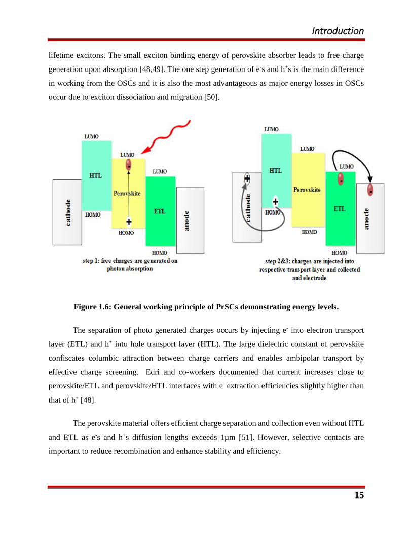
Figure 1.6: General working principle of PrSCs demonstrating energy levels.
The separation of photo generated charges occurs by injecting e- into electron transport
layer (ETL) and h+ into hole transport layer (HTL). The large dielectric constant of perovskite
confiscates columbic attraction between charge carriers and enables ambipolar transport by
effective charge screening. Edri and co-workers documented that current increases close to
perovskite/ETL and perovskite/HTL interfaces with e- extraction efficiencies slightly higher than
that of h+ [48].
The perovskite material offers efficient charge separation and collection even without HTL
and ETL as e-s and h+s diffusion lengths exceeds 1µm [51]. However, selective contacts are
important to reduce recombination and enhance stability and efficiency.

Introduction
16
Photovoltaic Characteristic parameters of solar cells
J-V curves represent detailed valued information for solar cell performance. The dark
curves of the most efficient devices resemble with a typical diode response. Upon illuminating
the cell, electrons are generated that produce reverse current.
Figure 1.7: Typical J-V curve depicting important parameters for solar cells.
The most essential figure of merit of solar cell is PCE that can be calculated through the
parameters extracted from J-V curves as displayed in Fig. 1.7.
1.4.2.1 Equivalent Circuit Diagram
To understand the various parameters involved in solar cells, it is necessary to have an
overview of general solar cell equation. The detailed preview of electric response of solar cell can

Introduction
17
be established through equivalent circuit diagram (ECD). The ECD for an ideal solar cell is merely
a diode connected to a light source but typically it includes both Rs and Rsh.
The following figure is classically used for inorganic solar cells. Despite the fact that
physical process involved in organic and inorganic solar cells are considerably different but the
same ECD can be used for organic solar cells as loss mechanism are basically same.
Figure 1.8: Equivalent circuit diagram (a) ideal (b) typical solar cells.
The various components of ECD displayed in the Fig. 1.8 can be described as
1. A current source that produces current on photon absorption. Upon irradiation,
excitons are generated and current is produced that flows in opposite direction as
that of the diode. This current is independent of any losses and depends entirely on
charge carrier creation efficiency.
2. A diode that illustrates asymmetric conductivity in the device. For OSCs it is
explained as built in field resultant of D/A interface.
3. Rsh is the shunt resistance that represents leakage current. It is the recombination
that occur before significant charge transport near exciton dissociation sites.
4. Rs arises from the polymer/metal contact and resistivity of the active materials. It is
influenced by the temperature, light and photoactive layer thickness.

Introduction
18
For maximum solar cell performance, Rsh should be infinitely large and Rs should be zero.
Increasing light intensity/temperature and decreased thickness, lowers the Rs.
Using Shockley’s theory, the current density of the diode is written off as
𝐽𝑑 = 𝐽𝑜[exp (𝑞𝑉
𝑘𝐵𝑇) − 1]
Where
Jd = dark current density
Jo = reverse saturation current density (minority carriers)
kB = Boltzman coefficient
T = absolute temperature
Under illumination
𝐽 = 𝐽𝑜 [exp (𝑞𝑉
𝑘𝐵𝑇) − 1] − 𝐽𝑝ℎ
Where
Jph = photocurrent generated by incident photons (opposite to diode current)
The above equation is for ideal conditions. However, in reality, the effects of series and
shunt resistances are non-negligible. Therefore, by applying Kirchhoff’s rule to ECD (Fig. 1.8)
and including Rs and Rsh , the current density can be written as
𝐽 =𝑅𝑠ℎ
𝑅𝑠ℎ + 𝑅𝑠[𝐽𝑝ℎ − 𝐽𝑜 exp (
𝑞𝑉 − 𝐽𝑅𝑠
𝑛𝑘𝐵𝑇) − 1 −
𝑉
𝑅𝑠ℎ]
Where n is ideality factor and ranges between 1 and 2.
Eq.1.3
Eq.1.4
Eq.1.5

Introduction
19
1.4.2.2 Open Circuit Voltage (Voc)
Maximum output voltage that solar cell can deliver is called open circuit voltage (Voc). It
corresponds to the voltage at which no current flows through the circuit i.e. J=0. Solving Eq. 1.5
for Vo with the assumption that Rsh >> Rs
𝑉𝑜𝑐 = 𝑛𝑘𝐵𝑇
𝑞ln(
𝐽𝑝ℎ
𝐽𝑜+ 1)
Eq. 1.6 express that saturation current density i.e. Jo is one of the important parameter that influence
Voc.
Postcavage et al. used pentacene/C60 device and determined that Jo depends exponentially on
temperature and dark current originates from the thermally activated injection of carrier at donor
acceptor interface.
𝐽𝑜 = 𝐽𝑜𝑜exp (−∅𝐵
𝑘𝐵𝑇)
Here
Joo = pre-factor determined by carrier generation and recombination rate
∅𝐵 = activation energy
𝐽𝑜 = 𝐽𝑜𝑜exp (−∆𝐸𝐷𝐴
2𝑛𝑘𝐵𝑇)
Substituting Eq. 1.8 in Eq. 1.6 for Voc
𝑉𝑜𝑐 =𝑛𝑘𝐵𝑇
𝑞ln (
𝐽𝑠𝑐
𝐽𝑜) +
∆𝐸𝐷𝐴
2𝑞
Eq.1.6
Eq.1.7
Eq.1.8

Introduction
20
However, these relations are obtained for small molecules and acceptor system
where interface is relatively simple. There are many factors that affect the Voc of bulk
organic solar cells. Considering disorder induced loss and recombination loss, Voc is expressed as
𝑉𝑜𝑐 =1
𝑞(∆𝐸𝐷𝐴 −
𝜎2
𝑘𝐵𝑇− 𝑘𝐵𝑇𝑙𝑛(
𝑁𝐴𝑁𝐷
𝑛𝑝)
Where
ΔEDA =LUMOacceptor –HOMOdonor (effective band gap)
𝜎2
𝑘𝐵𝑇 = disorder induced Voc loss
𝑘𝐵𝑇𝑙𝑛(𝑁𝐴𝑁𝐷
𝑛𝑝) = carrier recombination induced Voc loss
NA = electron density in acceptor domians
ND = hole density in polymer domains
Nc = density of states at the conduction band edge of donor and acceptor
The above equation explains that the generally expected value of Voc i.e. Voc = LUMOacceptor
– HOMOdonor is valid only at T= 0K. For many polymer and fullerene BHJ systems Voc has given
a drop of 0.3 eV.
In bulk heterojunction OSCs, Voc is linked with the energy difference between the
HOMOdonor and LUMOacceptor and merely influenced by the electrode work function.
1.4.2.3 Short Circuit Current (Isc)
Isc correspond to maximum current that a device can produce under illumination at V=0.
At this point no power is produced but Isc does mark the onset of power generation and attained by
Eq.1.9
Eq.1.10

Introduction
21
substituting V = 0 in Eq. 1.4. In ideal devices, Isc = Iph but several effects can lower value of Isc
from its ideal value.
I is usually not suitable to represent electrical response of solar cells as current is dependent
on area. Therefore, current density is used instead of I. From now on I is replaced with J where
J=I/A
1.4.2.4 Maximum Power Output (Pmax)
Pmax is the maximum obtainable power from the solar cells and is marked in Fig. 1.7. It can
be described as a point where product of J and V maximize.
𝑷𝒎𝒂𝒙 = 𝑱𝒎𝒂𝒙 ∗ 𝑽𝒎𝒂𝒙
Because of device resistance and recombination loses, Jmax and Vmax are always less than
the Jsc and Voc.
1.4.2.5 Fill Factor (FF)
FF pronounces the quality of solar cells. In ideal cases FF is ~1 but the typical values of
FF obtained range 0.50-0.70 for OSCs. The difference originates from the internal losses as stated
earlier. FF describes these differences as
𝑭𝑭 =𝑱𝒎𝒂𝒙 ∗ 𝑽𝒎𝒂𝒙
𝐽𝒔𝒄 ∗ 𝑽𝒐𝒄
FF indicates how close Jmax and Vmax are to the Jsc and Voc. Devices with higher Jsc and Voc
and low FF indicates that quality of device need to be improved.
1.4.2.6 Incident Photon to Current Efficiency (IPCE)
IPCE is the ratio of no. of incident photons (Nphotons) to no. of generated charge carriers
(Ncharge) that can be collected at electrodes. IPCE takes into consideration the losses
through reflection, scattering and recombination.
Eq.1.11
Eq.1.12
Eq.1.13

Introduction
22
𝑰𝑷𝑪𝑬 =𝑵𝒑𝒉𝒐𝒕𝒐𝒏𝒔
𝑵𝒄𝒉𝒂𝒓𝒈𝒆
1.4.2.7 Power Conversion Efficiency (PCE)
The PCE of solar cells is calculated using
PCE =𝑃𝑜𝑢𝑡
𝑃𝑖𝑛=
𝐹𝐹 ∗ 𝐽𝑠𝑐 ∗ 𝑉𝑜𝑐
𝑃𝑖𝑛
Where
1.5 Device Structure
A typical substrate for OSCs is plastic/glass sheet coated with “indium doped tin oxide
(ITO)”. The cathode and anode buffer layers are carefully selected according to the active material
and device structure. The active layer is composed of a D (conjugated polymer) and A (fullerene,
fullerene derivative or small molecules). Some low work function (WF) metals are usually
deployed as back contacts.
The device configuration of OSCs is divided into conventional and inverted architectures
as displayed in Fig. 1.9. The conventional OSC architecture uses Ca or LiF as cathode buffer layer
for efficient charge collection. However, the employment with chemically reactive materials
features a drawback and also restrain industrial production of OSCs, The solution processable n
type metal oxides is also required. Thus OSCs with standard structures typically contain metal
oxides layer at cathode facet. The OSCs with inverted architecture are designed to advance the
device performance. In inverted geometry ITO serves as cathode and metal back contact as anode.
The inverted OSCs exhibit better stability as compared to the conventional OSCs.
Eq.1.14

Introduction
23
Figure 1.9: Device Structure (a) Conventional (b) Inverted OSC.
In conventional devices, ITO is modified with PEDOT:PSS to serve as HTL. However, the
acidic nature of PEDOT:PSS can damage the interfacial contact property thus compromising the
long term stability. Also, the environmental exposure of conventional devices can lead to the
conversion of Al (metal back contact) to Al oxide that is non-conducting. On the other hand
inverted geometry usually utilizes molybdenum oxide (MoO3) as HTL and ZnO as ETL that are
more stable. The top electrode used in inverted devices is Ag. On oxygen exposure it converts into
Ag oxide which is also conducting and does not affect the device performance.
Figure 1.10: Device Structure (a) mesoporous (b) conventional (n-i-p) (c) inverted (p-i-n)
PrSCs [52].

Introduction
24
Typically, PrSCs are heterojunction devices with perovskite layer sandwiched between
ETL and HTL. The device configuration, as shown in Fig. 1.10, is catalogued into mesoscopic and
planar architectures based on the selective contact and arrangement of perovskite layer.
In mesoporous (mp) devices, mp metal oxide (Al2O3,TiO2) is applied onto which the
perovskite is infiltrated. The mp scaffold lets the perovskite material to adhere to the metal oxide
and ensures maximum interfacial area required to produce maximal photocurrent. The mp metal
oxide works as ETL, inhibits the recombination losses and provides required diffusion length for
effective collection of charges [53].
Even though the champion power conversion efficiency (PCE) attained is for mp TiO2
scaffold but inhomogeneous infiltration of perovskite and high sintering temperature (~500°C)
precludes large scale fabrication as well as use of plastic [54,55].
The planar heterojunction PrSCs are further divided into n-i-p (conventional) and p-i-n
(inverted) configurations depending on the type of interfacial layer applied on transparent
electrode. In planar architecture, mp metal oxide layer is removed and perovskite layer forms
planar junctions with ETL and HTL [53]. The planar structure is similar to that of OSCs’ but here
charges are generated and dissociated within the perovskite layer (explained in section 1.4.1). A
careful selection of interfacial layers ensures efficient charge extraction and transportation at
electrodes. This method yields better uniformity of perovskite layer. The p-i-n configuration
employing fullerene derivatives as ETL are of prodigious research interest. These devices are
encouraging since they offer negligible hysteresis, long term stability and shows possibility to
prepare multi-junction devices over large area [56,57].
The reported long term stability is the main reason because of which inverted geometry has
been opted for this work.
Introduction
25
1.6 Challenges
Three key features must be addressed in order to commercialize solar cells to market
1.6.1. Low fabrication cost
1.6.2. Power conversion efficiencies
1.6.3. Stability
Low Fabrication Cost
The 3rd generation solar cells i.e. OSCs, bulk heterojunction HSCs and PrSCs involve low
cost materials and fabrication. The lab scale solar cells that have achieved record efficiencies
utilize spin coating which is not scalable approach. Thus transferring the manufacturing to roll to
roll be inevitable for commercialization. The requirement of low processing temperature also put
an upper limit for large scale manufacturing.
Power conversion efficiencies
Rigorous research has been engrossed on increasing PCE of solar cells and results are
promising. The current record efficiency for OSCs is 11.2% and for PrSCs is 22.7% [36,58].
However, commercial success of these devices require increased PCEs, stability and low
temperature synthesis. The main factors that hinder the PCEs reach theoretical values are [59]
Optical Losses
Incident light absorbed by the material does not generate excitons.
Exciton Losses
Generated excitons recombine before reaching D/A interface.
Recombination Losses
Recombination of free charge carriers arises at defects sites
Collection Losses
Charge carriers cannot reach at electrodes due to low mobility and imbalanced
electron-hole motilities.

Introduction
26
Another challenge for commercialization is that the highest efficiencies are achieved for
small area. As the size of device increases, sheer resistance of the devices and defects in active
layer increase as well [60].
Stability
Another challenge to be considered is stability of these devices. The first generation solar
cells have lifespan with only 10 % degradation which is 10 times higher the OSCs [14,61]. In
2015, Krebs et. al. reported organic devices with stability of 2 years and Gratzel et. al. reported
perovskite solar cells with 1 year life time [61]. The improvement in device stability is undoubtedly
promising but it is still a serious concern for large scale production.
The degradation of OSCs is basically triggered by the oxygen, water and electrode reaction
with active materials. The ITO can etch active layer of the devices and oxygen/water diffuse
through microscopic pin holes of metal electrode and degrade it [62,63]. Therefore, selection of
air stable polymer and high W.F metal electrode can significantly limit the degradation. The
inverted device structure for OSC offers high W.F metal electrode, metal oxide buffer layer on
ITO and photoactive layer that aid to overcome etching and hence degradation. Hau and co-
workers presented that inverted device reserved 80 % of the original PCE even after 960 hrs while
conventional cell died in only 96 hrs [64].
The effect of oxygen on hybrid solar cells is not clear. The life time of HSCs using
semiconducting metal oxides depends on the presence of O2 and UV light in a devious way. As an
exemplar, photo catalytic properties of TiO2 can cause the degradation (oxidation) of polymer
materials adsorbed to the surface. For ZnO based devices few researches attained the better
performance by annealing in air while others documented good device performance in absence of
air [65].
PrSCs have revealed momentous progress in terms of PCE but the device stability still
remains a challenge. The source of the instability can be ascribed to intrinsic structural properties
of perovskite material and interfaces of the device. The perovskite material inclines to decompose
under air, moisture, long term light exposure and thermal stress [52,66]. The interfacial interaction

Introduction
27
is another major degradation cause that has drawn considerable attention. In case of inverted planar
PrSCs, the commonly used HTL is PEDOT:PSS and its hydroscopicity can induce moisture into
active perovskite layer causing it to decompose [67]. However, the role of ETL is more critical
and influences the device stability in several ways. For example, the incomplete coverage of
perovskite active layer by ETL leads the metal electrode to reach and react with the perovskite
resulting in swift device degradation [68]. Also, the most commonly used ETL material PCBM
can absorb oxygen and water that can speed up degradation of perovskite. In addition, the direct
contact of PCBM and metal electrode leads to increase contact resistance on air exposure. Hence,
the inverted PrSCs with PCBM as ETL are viable to degradation on air revelation [69].
In case of PrSCs, anomalous J-V hysteresis is another issue. The three possible reasons for
hysteresis are hypothesized to be ferroelectric polarization with perovskite, ion migration, charge
trapping and de-trapping at defects acting as trap sites, unbalanced electron and hole flux, scan
rate and device architecture [70–72]. The inverted PrSCs with PCBM on top show negligible
hysteresis [73,74]
1.7 Enhancement in Device Performance
The efficiency of organic PVs would be enhanced by specific modifications in the features
as described below
1. Selected material should have control over morphology to yield optimal exciton
dissociation and provide percolation network to the separated charges.
2. Materials with small bandgap and high charge mobilities are required.
3. Device design to ensure maximum light harvesting and electron-hole blocking
4. The materials should have the ability to adjust HOMO and LUMO levels to maximize
device performance.
In context to improve absorption of OSCs, small band gap materials e.g. PbSe ,PbS and
CdSe NPs are used as absorber as well as charge transporter [75]. Olson et. al. used ZnO nanowires
along with PCBM in P3HT:PCBM active layer. The resulting devices showed higher efficiencies

Introduction
28
and established that ZnO acts as an electron acceptor [76]. The high mobilities of ZnO also speed
up the charge transfer [77].
The Voc of OSCs effectively depends on the energy offset of heterojunction. The present
system limits the Voc to 0.6 V or less, therefore new materials require to enlarge bandgap that effect
the Voc [78]. Likewise, the inclusion of TiO2 as optical spacer, shifts the absorption spectra and
increases Jsc up to 50% [79]. Therefore, use of NPs seems to be a promising option to produce
efficient, stable and cost effective solar cells.
Various approaches have been followed to improve the PrSCs performances. Many new
perovskite materials by replacing organic cation, or anion halide and lead free perovskite materials
have been introduced [80]. In addition to the material’s modification, the interface engineering is
vital to the device performance. The interface engineering ensures reduced recombination and
also influences device degradation without effecting exciton formation [81]. Several organic and
inorganic HTL have been developed and the best results are obtained for NiO [80]. As mentioned
earlier, that in inverted structure degradation caused by ETL is critical. For that purpose modified
PCBM have been employed and encapsulation of ETL by coating with some stable metal oxide is
used [66].
1.8 Motivation
Organic-inorganic HSCs have seen significant advancement in last decade but further
research in different areas is required to realize the commercialization. As HSCs are still
developing, this Ph.D work aims to observe that how NCs in HSCs affect the performance
parameters. The target is to improve and balance the carrier mobility within the system. Cobalt
oxide (Co3O4) and chromium oxide (Cr2O3) NPs were first time incorporated in the P3HT: PCBM
and PTB7: PCBM active layer blends. These NPs have ideal bandgap (1.3, 2.0 eV for Co3O4 and
2.9 eV for Cr2O3) for photovoltaic applications and their optimal energy levels were believed to
participate in performance enhancement of devices. As discussed, the direct exposure of PCBM to
environment in case of inverted PrSCs can degrade the devices. Therefore, ZnO and Al:ZnO were
employed as capping layer in inverted PrSCs. The inclusion of nanoparticles improved the device
efficiency and stability in both cases. The increase in efficiency for bulk heterojunction hybrid and

Introduction
29
perovskite solar cells is mainly owed to decrease in values of series resistance. The use of NPs
enhanced the Voc and FF as compared to the control devices. A comprehensive description on the
influence of metal oxides on the device performance will be conferred. From this a promising new
inorganic materials for bulk heterojunction devices and inorganic ETL that also acts as protective
layer for perovskite material is introduced.
1.9 Outline of Thesis
The first chapter introduced history of solar cells, fundamentals of OSCs/HSCs and their
characteristic parameters. Chapter 2 documents brief literature review of bulk heterojunction
hybrid and perovskite solar cells. Chapter 3 outlines the materials, experimental setup and
characterization techniques used in the course of the research. Synthesis of Co3O4 and Cr2O3 NPs
and their application in PTB7/P3HT:PCBM bulk heterojunction active layer is also stated in
chapter 3. Chapter 4 provides a detailed study of Cr2O3 and Co3O4 NPs based devices. Different
characterization techniques such as I-V, EQE, UV,FESEM and AFM have been utilized to study
the incorporation effects. Chapter 5 discusses perovskite solar cells and the effect of ZnO and
Al:ZnO NPs as capping layer. Chapter 6 concludes the research outcomes with future
recommendations.

Literature Survey
30
2 Chapter 2
Literature Survey
2.1 Review
The cumulative concern about the global warming caused by fossil fuel dependence of
energy resources has led to the dramatic growth in the solar cell research. Solar cells represent a
class of auspicious candidate that can supply clean, cheap and continuous energy. A projected
increase has been witnessed in the research field after the invention of first solar cell from Bell
labs [82]. Among the vast library of solar cells, OSCs have engrossed excessive research
consideration owing to supreme properties to other technologies such as flexibility, easy & low
cost fabrication, high absorption coefficient, abundant and non-toxic raw materials[83–85]. Since
the first report on molecular thin film devices by Tang et al. [86] in 1975, PCE’s have considerably
increased from 0.001% to 10.5% for bulk heterojunction [58] and 11% for tandem architecture
[87].
The OSCs are generally based on conjugated D polymer and fullerene derivative or small
molecule A [88–90]. Amid the numerous architectures of OSCs, the extensively investigated is
bulk heterojunction based structure. In BHJ structured solar cells polymeric donor is blended with
electron acceptor (fullerene derivative or small molecule). BHJ composed of bi-continuous
interpenetrating network of D and A provides large interfacial area and facilitates efficient e--h+
dissociation[91]. Although OSC technology is a promising competitive alternative to other
inorganic solar cells but continuous progress in the field is rather challenging. Short exciton
diffusion length, low charge mobility, recombination losses, amorphous nature of organic
materials, degradation and limited life time renders their availability on commercial scale[92,93].
“In principle, to increase the PCE of single junction cells, Voc, Jsc, and FF should be
enhanced. However, there is a tradeoff between the Voc and Jsc since both of them are limited by
the energy levels of D and A. Thus, it is challenging to further enhance these single-junction cells

Literature Survey
31
due to insufficient photon harvesting of active layers with the relatively narrow absorption
window.”
In order to overcome these issues, bulk heterojunction HSCs are widely investigated as
promising route towards long-term stable, more efficient and low cost photovoltaic power
generation. Inorganic metal oxide/sulfides nanoparticles have ideal band gap, high electron
mobility and greater environmental stability. HSCs combine the advantageous attributes of
nanostructures and polymers. So far, a variety of nanomaterials (Au, Ag, CdSe, CdS, ZnO, TiO2,
etc.)[94–98] have been employed with many conjugated polymers (P3HT, PTB7 P3OT, MEHPPV
etc.)[99–103] in single layer, binary, ternary or quaternary based system.
Over the last decade, a lot of studies have been carried out to develop ideal amalgamations
of organic/ inorganic materials and optimal hybrid architectures. So far an efficiency of 6% have
been achieved for P3HT and PCBM based ternary HSCs but there is still room for improvement
by finding a good blend of components and well-designed hybrid structures. Here we briefly
review the progress witnessed in the field and summarize factors affecting the performance.
Cadmium Selenide (CdSe) Nanocrystals (NC) have been premediated in OSC by many
researchers with different morphologies. In 1996, Greenham et al.[104] reported first HSCs using
CdSe nano-dots and MEH-PPV with device efficiency of 0.01%. Further advancement involved
CdSe nanostructure with different morphologies[105–107] and the highest PCE was achieved for
CdSe nano-tetrapods i.e. 3.2% [108]. The results demonstrate that device performance is strongly
dependent on blend morphology[106].
Titanium dioxide (TiO2) has a rich history in organic solar cells. In 2012, Yu et al. [109]
incorporated TiO2 nanocrystals in P3HT and PCBM HSCs. The resulting devices exhibited
improved charge transfer, enhanced stability and higher PCEs. They proposed that in the ternary
blended active layer TiO2 participates in photon absorption and also enhance the interfacial area
between the components.
Yang et al.[110] achieved a 15% increase in PCE by adding TiO2 nanotube in photoactive
layer. Presence of TiO2 increased electron mobility from 5.71 × 10⁻⁵ to 7.22 × 10⁻⁵ cm2 V-1 s-1.

Literature Survey
32
Janssen and coworkers [22] fabricated 1st ever HSCs in 2004. The devices were based on
ZnO nanocrystals and MDMO-PPV and obtained PCEs was 1.6%. They further investigated effect
of ZnO geometry but the PCE did not exceed 1.6%.
Oh et al.[111] studied bulk heterojunction HSC by adding ZnO nanoparticles in P3HT,
PCBM based active layer and modified PEDOT:PSS buffer layer. The resulting devices exhibited
38% increase in PCE which was accredited to the low resistivity of modified buffer layer and
presence of ZnO NPs in active layer.
Duché et al. [112] also checked optical performance of polymer: ZnO based devices for
different polymers i.e. PTB7, P3HT and PCPDTBT concluding the colorful nature of the Hybrid
Solar Cells (HSC) for different composition of active layer.
Wanninayake et al.[113] examined the effect of CuO nanoparticles P3HT PCBM active
layer and observed a 24% upsurge in PCE owed to increase in absorption, electron mobility and
carrier collection. The ideal band gap of lead sulfide (PbS) can work with many polymers[114].
Yoon et al. [115] utilized PbS NP in ternary solar cells and obtained a 47% rise in the PCE.
M. Ikram et al. have utilized TiO2, ZnO, CuO NPs in P3HT: PCBM based conventional
and inverted systems. Blends of ZnO, TiO2 and CuO, ZnO have also been employed to substitute
PCBM and P3HT, PCBM respectively. Mixing plus Replacement of PCBM and P3HT, PCBM
with NPs increased the crystallinity and absorption of the devices which resulted in increased PCEs
of the devices up to optimum doping concentration[93,116–119].
Kerbs et al. [120] explained that in traditional device structure, upon contact with oxygen,
Al quickly reacts with it forming insulting aluminum oxide. O2 diffusing through the pinholes in
Al reach to the active layer and make BHJ with low W.F metal contact vulnerable to degradation.
Also, strong acidic nature of PEDOT:PSS also degrade the device performance over time
[121,122]. These issues can be resolved in inverted device structure where high work function
metal contact is used (Ag, Au) and acidic PEDOT:PSS is replaced with highly stable metal oxides
such as TiO2, ZnO and Cs2O3 etc. [64,123–126]. In inverted geometry, device is reversed and
charge collection and separation is inverted.

Literature Survey
33
The unique conducting and semiconducting properties of organic-inorganic hybrid
perovskite comprising of organic cation (CH3NH3+, FAI), metal cation (Pb2+, Sn2+) and a halide
(I-,Cl-,Br-) were widely studied during 1970-1990 [127]. The use of this material in photovoltaics
has fascinated ample research consideration because of the expeditious rise in PCE from 3.8% to
22% coupled with solution processing. This skyrocketed PCEs are accredit to the auspicious
optoelectronic properties of perovskite materials including broad range absorption (800nm), high
absorption coefficient (~1.5X10⁻⁴ cm-1), optimal and tunable bandgap (1.3-2.9 eV),long exciton
diffusion length (~0.1-1μm), low exciton binding energy, excellent carrier mobility and life time
(~100 ns), and thermal stability (up to 300°C)[128–132]. In 2009, Miysaka et al. deployed
CH3NH3PbI3 and CH3NH3PbBr3 as sensitizer in DSSC which gave PCEs of 3.81% and 3.13%
respectively[35]. Since then many individual laboratories altering the device structure, processing
parameters and different perovskite materials. The PCEs reached 6.5% in 2011, 12.2 in 2013,
20.1% in 2015, 21.1% in 2016, 22.1% in 2017 and are expected to reach 50% in future[15,133–
137].
Kim et al. deployed CH3NH3PbI3 in solid state mesoscopic heterojunction solar cell in
2012. They used CH3NH3PbI3 as primary photoactive layer, mesoscopic TiO2 and Spiro-MeOTAD
as ETL and HTL respectively, FTO and Au as contacts. The mesoporous (mp) material provides
large surface area that enhance / improve light receiving zone by depositing the perovskite absorber
in mp metal oxide framework The devices were prepared using one step solution process and
showed Voc of 0.8V, Jsc of 17.6mA/cm2 and FF of 62% and strikingly high PCE ~ 9.7% that proved
to be a breakthrough in photovoltaic research[138]. The PCE for the same device configuration
was upgraded to 15% by two step solution deposition method employed by Burschka et al. [139].
It was suggested that the sequential deposition provides better control over perovskite morphology
and ensures high efficiency and reproducibility.
Further research in field involved replacing TiO2 with Al2O3, ZrO2, SiO2 and using different
perovskite including mixed halides i.e. CH3NH3PbBr3, CH3NH3PbCl3, CH3NH3PbI3-xClx,
CH3NH3PbBr3-xClx[140–145] . In 2017 Yang et al. documented PCE of 22.1% for small area
devices using formamidium lead halide based perovskite highest to be testified for hybrid solar
cells[137].

Literature Survey
34
Planar heterojunction architecture can be divided into conventional (n-i-p) and (p-i-n)
architectures. In planar configuration, mesoporous metal oxide framework is removed and the
junction is formed between ETL/perovskite and perovskite/HTL. Here perovskite act as
photoactive layer and take on to charge generation and transport. The elimination of mesoporous
metal oxide simplifies fabrication process. Snaith et al. described first ever fully planar perovskite
using iodide and chloride based mixed halide and further study for the conventional planar device
structure increased the PCE to 15.7%[146,147]. It was studied that in order to achieve high PCEs,
a careful control over processing conditions is required and films with high perovskite coverage
can reduce recombination losses that leads to high open voltage and produce high photocurrents
[148,149].
Further research in subsequent years showed that high efficiencies are possible through
modification of the energetics. Baena et al. demonstrated that the unstablized PCEs of planar
PrSCs are due to the energy level misalignment and deep conduction level of SnO2 attains a barrier
free band alignment and exhibited high Voc i.e. 1.19V and PCE i.e. 18.4%[150]. For the same
purpose Zhou et al. used yttrium doped TiO2 (Y:TiO2) and yielded the PCEs 19.3%. They
suggested that use of (Y:TiO2) facilitates charge injection from transport layer to electrode[151].
In 2015 Fu et al. fabricated 14.2% efficient and 72% semi-transparent planar PrSC at room
temperature. Introduction of PCBM on top of sputtered ZnO ensured the growth of high quality
perovskite layer. Hydrogenated indium oxide was deployed as transparent rare electrode. Tandem
configuration of the cell coupled with CIGS demonstrated 20% PCE [152].
Moreover, Anarki et al used SnO2 as ESL in planar PrSC. The fabrication process
(combination of spin coating and chemical post treatment) yielded Voc of 1.2V and PCE of
20.8%[153]. In 2017, Chu and coworkers [56] documented the effect of stoichiometry of PbI2
content on device performance. They recommended that a moderate residual of PbI2 is favorable
for high performance of the devices. The resulting devices produced 21.6 % PCE which is
comparable to that of mesoscopic architecture.
In 2013, Jeng et al. first time reported planar heterojunction PrSCs in inverted architecture.
They used PEDOT:PSS as HTL deposited on top of ITO on which CH3NH3PbI3 photoactive layer

Literature Survey
35
was deposited. C60 and its derivatives i.e. PCBM and ICBA were used as ETL on top of perovskite
layer. The best working device gave PCE of 3.9%. The limiting factor was said to be low Jsc 10.32
mAcm-2. This study helped to use the advantages of OPV materials i.e. easy fabrication, low
temperature easy fabrication in perovskite technology[154].
As suggested in Jeng’s work, Sun and coworkers prepared inverted devices with thicker
photoactive layer. The device exhibited IQE of ~ 100% that indicate excellent exciton diffusion,
charge collection and transport[155]. Afterwards, various attempts have been made to boost
performance including casting methods, morphology control, interface engineering and various
contact materials.
As stated earlier that charge generation and transport to the respective electrode occur
within the perovskite but they can recombine before reaching to the contacts. To avoid
recombination, various studies have been carried out and among them interfacial engineering is
most important. The most common used HTL and ETL are PEDOT:PSS and PCBM respectively.
To further enhance solar cell performance, HTL should meet following merits: i) energy level
alignment with perovskite ii) efficient hole mobility iii) optical transmittance iv) low temperature
solution processability. Many research groups have used modified PEDOT:PSS. The modified
PEDOT:PSS exhibited high electric conductivity and better band alignment resulting in high
performance[156–158]. PEDOT:PSS has also been replaced with other organic semiconducting
materials such as Poly TPD, PTAA and PCDTBT. The PTAA based inverted device delivered
remarkable Voc of 1.3eV and PCE of 19.4%[67,159]. Inorganic hole transporting materials
including NiOx, CuOx, Cu2O, GO, CuSCN and PbS have also been used in inverted PrSCs. Liu et
al. has also reported use of Li, Cu doped NiO[160]. Replacement of PEDOT:PSS with p-type
inorganic materials resulted in superior energy level alignment and higher Voc was achieved that
pushed the PCEs as high as 18.3%. To the best of outcome of our informationi, Luo et. al. [161]
achieved best PCE for inverted PrSCs. They used mixed cation perovskite and dual source
precursor approach and obtained 20.15% PCE.
Although, the record efficiencies for different type of PrSCs architectures are reported to
reach close to that of silicon solar cells, photocurrent hysteresis and stability still remain an issue.
The difference in photocurrent for forward and reverse scan complicates PCE measurements [70].

Literature Survey
36
The three possible reasons for hysteresis are hypothesized to be ferroelectric polarization with
perovskite, ion migration, charge trapping and de-trapping at defects acting as trap sites and
unbalanced electron and hole flux [71,162,163]. Scan rate, light soaking and the device
architecture also affect the hysteresis [70,72,164]. Usually planar PrSC show hysteresis intense
than mp PrSCs. Hysteresis becomes severe in case of devices with no HTL or ETL. Typically
inverted architecture with PCBM on top shows negligible hysteresis [73]. Wu et al. testified a 18%
efficient inverted PrSC with no current hysteresis[74].
Another factor that is hindrance in commercialization of these devices is degradation. The
factors that affect the stability of PrSCs include degradation of perovskite due to oxygen, moisture,
thermal stress and interfacial degradation[165]. To modify the stability of PrSCs, many factors
must be considered, including the crystal structure and composition of the perovskite, the active
layer fabrication technique, interfacial engineering and electrode materials, encapsulation methods
and the module technology. Niu et al. suggested that exposure to oxygen and water alone can
introduce irreversible degradation of MAPbX3. A number of approaches have been adopted to
enhance the device stability that includes more stable perovskite structure and interface or
electrode engineering. In 2017, Grancini et al. reported a 1 year stable inverted PrSC by 2D/3D
interface engineering [14].

Experimental Methods
37
3 Chapter 3
Experimental Methods
This chapter outlines the materials, experimental procedures and characterization
techniques involved in this research.
3.1 Materials
“Indium tin oxide (ITO)” patterned on glass substrates with sheet resistance 8-12 Ω were
received from Delta Technologies, USA. 99.9% pure Sodium Hydroxide (NaOH) was obtained
from Panreac and Cobalt Chloride (CoCl3) and Chromium Chloride (CrCl3) from Sigma-Aldrich.
Poly(3-hexylthiophene-2,5-diyl) (P3HT) was bought from Ossila, UK and Poly[[4,8-bis[(2-
ethylhexyl)oxy]benzo[1,2-b:4,5-b']dithiophene-2,6-diyl][3-fluoro-2-[(2-ethylhexyl)carbonyl]
thieno[3,4-b] thiophenediyl]][6,6]) (PTB7) from 1- material. Phenyl-C-butyric acid methyl ester
(PCBM) was procured from Solenne and poly (3,4 ethylene dioxythiophene polystyrenesulfonate)
(PEDOT:PSS) from Heraeus Material Technology LLC, USA. From Sigma-Aldrich, N11 ZnO
NPs (8-16 nm), N10 Al:ZnO (< 50 nm), Methylammonium iodide (MAI) (98%), lead iodide (PbI2)
(99%), γ-buytrolacton (>= 99%) and dimethyl sulfoxide (DMSO), were also purchased.
P3HT
Poly (3-hexylthiophene-2, 5-diyl) commonly known as P3HT is a regioregular
semiconducting polymer. It is used in organic electronics primarily because of its regular end-to-
end arrangement of side chain, which allows efficient Π-Π stacking of the conjugated backbones.
High h+ mobility in combination with good solubility and partial air stability make P3HT a
reference material of choice for both fundamental and applied research in organic electronic,
physics and chemistry. The structure of P3HT is shown in Fig. 3.1.

Experimental Methods
38
PTB7
Poly[[4,8-bis[(2-ethylhexyl)oxy]benzo[1,2-b:4,5-b']dithiophene-2,6-diyl][3-fluoro-2-[(2-
ethylhexyl)carbonyl]thieno[3,4-b]thiophenediyl]], generally known as PTB7. OSCs based on
PTB7 and fullerene gives some of the highest reported PCEs because of its extended absorption
into the near infra-red and lower HOMO level [166].
Figure 3.1: Structure of P3HT
Figure 3.2: Structure of PTB7

Experimental Methods
39
PCBM
[6,6]-phenyl-C-butyric acid methyl ester commonly abbreviated as PCBM is a solubilized
version of buckminsterfullerene i.e. C60. Fullerenes are excellent electron acceptors and can be
chemically modified for improved solubility in organic solvents. The solubility qualifies PCBM
to be dissolved in solvents used for donor polymers. When used in a device with a donor polymer,
PCBM enables rapid and efficient exciton dissociation, charge transfer and has a high electron
mobility [45]. In this study, PC60BM is used with P3HT and PC70BM with PTB7.
Figure 3.3: Structure of (a) PC70BM (b) PC60BM
3.2 Experimental Procedure
Co-Precipitation Process
The chemical co-precipitation method was exploited to fabricate metal oxide NPs in which
metallic chloride salts (X-Cl; X= Co, Cr) as precursors were dissolved in distilled water and
sodium hydroxide (NaOH) as reducing agent was added into precursor aqueous solution thereby
yielding the precipitates of the desired metal oxide NPs.

Experimental Methods
40
Figure 3.4: Flow Chart for NPs synthesis.

Experimental Methods
41
Briefly, two separate solutions of chloride salts and NaOH of some appropriate amount
were prepared in distilled water. NaOH solution was added drop by drop into salt solution under
vigorous magnetic stirring (60 °C; 60 mins.). The obtained precipitates were collected by repeated
centrifugation and washing process in distilled water and dried up in an oven (60 °C; 48 hrs.).
The resulted hydroxide nanoparticles were annealed at suitable temperature i.e. Co (400
°C; 60 mins.) and Cr (450 °C; 60 mins.) to drive off H-OH contents and decompose into oxide
nanoparticles.
Substrate preparation
The ITO substrates had dimensions 25 × 25 × 7 mm. Each substrate was ultrasonically
cleaned prior to use. Cleaning steps included soap solution, water, acetone and Iso propanol (IPA)
in ultrasonic bath for 5-10 mins each. Each substrate was dried under N2 stream and placed in
plasma cleaner for 20 min.
Spin coating
Spin coating technique was used to coat buffer and active layer on ITO. Buffer layer (ZnO
in case of bulk heterojunction HSCs and PEDOT:PSS in case of PrSCs) was coated on pre cleaned
ITOs in fume hood. The edges of coated ITOs were wiped off with IPA for ZnO and water for
PEDOT:PSS. The layer was then heated on hot plate at 150 ºC for 15-20 min. Active layer was
also spin coated in fume hood while perovskite layer was carefully spin coated inside glove box.
The details for active layer for each set of device is given in next sections.
Thermal Evaporation
The thermal evaporator was utilized to evaporate back contact of the devices. Thermal
evaporation was performed by resistive heating of tungsten (W) filament and the desired materials
were directly in contact with it. The evaporation of back contact was completed by depositing a
10 nm layer of molybdenum oxide (MoO3) and 100 nm of back contact through a shadow mask.
The evaporation was carried out under high vacuum (10-7 mbar) and monitored with quartz micro

Experimental Methods
42
balance throughout the evaporation. Our shadow mask defines 6 devices on each substrate with
active area of 0.1 cm2.
3.3 Synthesis of nanoparticles and Device Fabrication
Cr2O3 nanoparticles
Among inorganic semiconductors, chromium oxide (Cr2O3) has a large bandgap of 3.0 –
3.3 eV and is one of the widely researched p-type metal oxide [167,168]. It is highly stable and
states high electrical conductivity with complete or partial e- transfer [167]. The large bandgap can
effectively block h+ and redistribute light in the active layer [169]. It had been utilized as dye and
pigments and in solar cell applications [170,171]. Wang et. al employed CrOx as HTL in OSCs
and observed a significant improvement in stability and PCE [169].
The wet chemical synthesis and application of Cr2O3 NPs in the active layer of inverted
BHJ-OSCs is documented in this section. To the best of our knowledge this work is first to
incorporate Cr2O3 NPs in active layers of P3HT:PC60BM and PTB7:PC70BM based devices. The
NPs were mixed with different weight ratios from 0 to 4% while the polymer to PCBM ratio was
maintained throughout the experiment.
3.3.1.1 Synthesis
The rhombohedral structured Cr2O3 NPs were synthesized by solution chemistry. 0.1M
solution of CrCl3 and 0.3M NaOH were prepared in distilled water. The prepared solutions were
mixed drop wise under vigorous stirring at room temperature.
Precipitates of Cr(OH)3 were obtained and collected after several centrifugation and
washing with distilled water.

Experimental Methods
43
The precipitates (washed) were aged at 60 °C/48 hrs and dried Cr(OH)3 was further treated
by heating in a muffle furnace at 450 °C/60 mins.
3.3.1.2 Device fabrication
P3HT:PC60BM (1:0.8) and PTB7:PC70BM (1:1.5) solutions were prepared in 1, 2 DCB and
CB respectively. To ensure complete dissolving of polymers in solvents, the prepared solutions
were stirred at 70 °C/24 hrs. Cr2O3 NPs were separately dispersed in DCB and CB to add into the
polymer solutions with different weight ratios (1, 2, 3, 4) %. Followings steps are included in
device fabrication.
Step I. First of all, a thin layer of ZnO was deposited on pre-cleaned ITO substrates. For
this purpose ZnO NPs were diluted (1:1) with IPA. The diluted NPs were then spin
coated at 5000 rpm/45sec and subsequently heated on hot plate at 150oC/20min.
Step II. The binary and ternary hybrid solutions were spin casted onto ZnO coated
substrates at 1500rpm/1min. The P3HT based devices were subsequently heated at
110 °C/20 min.
Step III. Thin layers of 10 nm -MoO3 and 100nm- Ag were thermally evaporated at high
vacuum (10-7 mbar).
Co3O4 nanoparticles
Co3O4 being p-type semiconductor and non-toxic in nature is one of the most promising
metal oxide for technological applications [172,173]. The two optical bandgaps of Co3O4 in visible
range i.e. 1.5 and 2.2 eV and optimal energy levels makes it a potential candidate for solar cell
research [174]. It is reported to be employed as a light absorber in all metal oxide PV and as h+
transporting material in OSCs [175,176]
Co3O4 are synthesized, characterized and mixed with PTB7:PC70BM and P3HT:PC60BM
based active layer solutions separately. Polymer to PCBM concentration was maintained

Experimental Methods
44
throughout the experiment and Co3O4 NPs were added with different weight ratios from 0 to 4%.
The Co3O4 NPs are first time utilized in the active layer of OSCs and show promising results
(discussed in chapter 4).
3.3.2.1 Synthesis
To synthesize Co3O4 NPs, 0.1 M solution of CoCl3 and 0.3 M solution of NaOH were
prepared in DI water [177,178]. The solutions were then vigorously stirred at room temperature
and dark green precipitates of Co(OH)2 were obtained. The precipitates were collected and washed
a number of times with distilled water to ensure removal of impurities. These washed precipitates
were then dried at 60 oC/48hrs.
Dried Co (OH)3 was transferred to muffle furnace and heated at 400 oC/60 min
3.3.2.2 Device fabrication
The active layer solutions based on polymer and fullerene derivative were prepared by
dissolving PTB7: PC70BM and P3HT: PC60BM in CB and DCB with 1:1.5 and 1:0.8 respectively.
Prior to device fabrication, the prepared solutions were kept under vigorous stirring at 70 oC/24hrs.
Co3O4 NPs were separately dispersed in CB and DCB and added to the prepared active layer
solutions with various weight ratios i.e. 1, 2, 3 and 4%.
These solutions were used to fabricate Co3O4 NPs based devices and the same experimental
steps were followed as mentioned above (section 3.3.1.2)

Experimental Methods
45
NiS nanoparticles
A variety of inorganic metal sulfide nanostructures such as FeS2, Ag2S, In2S3 and CdS have
been utilized in the BHJ-OSCs as discussed in chapter 2. NiS NPs were selected for application in
BHJ solar cells.. The NiS NPs have tune-able bandgap of 2.8 to 3.1 eV and have been utilized as
counter electrode in DSSC [179,180].
3.3.3.1 Synthesis
The NPs were fabricated via co-precipitation [177]. 1 M of the precursors Nickel Acetate
tetrahydrate (Ni(CH3COO)2.4H2O) and Sodium Sulphide (Na2S; were separately prepared in 50
ml of distilled water at 60 °C.
10 ml of Ni(CH3COO)2.4H2O was dissolved in 2 ml of triethanolamine (0.1 M) at 60 °C.
Under constant magnetic stirring of 30 mins, 10 ml of Na2S was dripped slowly into the prepared
solution. Later 1 hour stirring, the precipitated solution was washed several times with distilled
water and the resulting precipitates was oven dried (at 60 °C/ 48 hours). The NiS powder was
further heated at 450 °C/60 mins in a muffle furnace and analyzed under FESEM & EDX (Fig 3.5
and 3.6) to confirm the particle size and the purity of NiS material.
FESEM micrograph as shown in figure 3.5 showed the tubular structure of NiS particles at
scale bar of 30 µm under magnification 1600x. The particle size as observed from FESEM was
found in micro-region. In addition, EDX has not only confirmed the presence of Nickel and
Sulphur but also detected some impurities (Br, C, Na, O and N) in minor traces. These NPs could
not be used in the devices as the size of NPs was bigger than the film thickness.

Experimental Methods
46
Figure 3.5: FESEM image of NiS particels.
Figure 3.6: EDX of NiS particles.

Experimental Methods
47
CdS nanoparticles
CdS NPs have fascinated the solar cell research owed to its optimal bandgap and energy
levels. Sharma et. al have incorporated CdS NPs in PTB7:PCBM organic active layer and observed
~ 10% increase in PCE [100]. It has also been employed as ETL in OSCs and found its way in
PrSCs.
CdS NPs were also synthesized via co-precipitation route with the collaboration of our
group. These NPs were integrated in the active layer of P3HT:PCBM-based devices. The
incorporation of CdS NPs showed a PCE of 4.41% compared to 2.95 % for control devices. The
results were favorable and published in RSC advances. But since, this was a shared work so the
research outcomes are not included in the thesis.
Initially, the objective of this work was to find new metal oxide or sulfide NPs for BHJ
polymer acceptor system. But after further literature survey and initial experimentations we
decided to only include our work on metal oxide NPs in the thesis.
ZnO/ Al:ZnO nanoparticles in Peroskvite Solar Cells
As discussed in chapter 1, that PCBM degrade on direct exposure to oxygen and air. Also,
at thinner ETL sites metal contact can diffuse through PCBM and reach perovskite. To minimize
these issues, we used ZnO and Al:ZnO NPs as capping layer. As purchased ZnO and Al:ZnO NPs
were deposited as capping layer on top of PCBM in inverted structured perovskite solar cells.
3.3.5.1 Device Fabrication
Fig 3.7 illustrates a schematic diagram of experimental steps carried out in perovskite active
layer deposition.
Step I. The photoactive perovskite solution was prepared by dissolving MAI and PbI2 (1:1)
in a co-solvent of DMSO and GBL (4:6).

Experimental Methods
48
Step II. PEDOT:PSS was spun cast on pre-cleaned ITOs at 5000 rpm/30 sec and treated
on hot plate at 150°C/ 15 mins.
Step III. The active layer solution was spin coated on baked PEDOT:PSS film at 4000 rpm/
50 sec and quenched at 20 seconds by flushing with CB. These films were then
heated at 85 °C for 10 mins.
Step IV. Afterward, 30 mg/ml of PCBM was spin coated on “ITO/PEDOT:PSS/Perovskite
layer” at 1500 rpm followed by heating at 85°C for 2 min. On top of PCBM, ZnO
and Al:ZnO dissolved in IPA (2.5 wt%) were deposited at 3000 rpm.
Step V. Lastly, 100 nm thick Al was thermally evaporated (10-7 mbar) as back contact.
Figure 3.7: : Schematic diagram of fabrication of perovskite active layer

Experimental Methods
49
3.4 Characterizations Techniques
This section describes the techniques deployed for characterizations of synthesized NPs and
fabrication devices.
X-Ray Diffraction
The identification of phases at respective planes, crystalline behavior, formation of the
synthesized metallic oxides (X-O) and average crystallite size were studied under CuKα (λ =
1.5406 Å) radiation at scan rate 2θ ⇒ (0-80)° and voltage 40kV employing X’Pert PRO, X-ray
diffraction. The x-ray datas were patterned by following the Bragg’s condition i.e.
between counts of atoms vs diffraction angles.
The Debye Scherrer’s formula was utilized to calculate average crystallite size
𝒅 =𝑲𝝀
𝜷𝜽𝑪𝒐𝒔𝜽 Eq. 3.1

Experimental Methods
50
Figure 3.8: PANalytical XPert PRO X-Ray Diffractometer

Experimental Methods
51
Field Emission Scanning Electron Microscope
Surface morphology of X-O NPs and thin films were analyzed under different
magnifications. FESEM is a microscope that works with the e-s which are liberated by field
emission source. The sample is scanned by e-s according to zigzag pattern. For nanoparticles JEOL
JSM 7600F (Fig. 3.9) and for thin film analysis Hitachi S4160 was deployed.
Figure 3.9: JEOL JSM 7600F Field Emission Scanning Electron
Microscope

Experimental Methods
52
Atomic Force Microscopy
The micromorphology and surface roughness of active layer films were considered by
JEOL JSPM-5200 Japan atomic force microscopy (AFM) shown in Fig. 3.10. The data is obtained
through scanning sharp probe over the surface. The deflection produced in cantilever following
Hook’s Law by means of tip-sample interaction is compiled to yield AFM images.
Figure 3.10: JEOL JSPM-5200 Atomic Force Microscope.
UV-VIS Spectrophotometer
Genesys 10 S UV/Vis spectrophotometer was utilized to assess the absorption spectra of
colloidal solution of X-O NPs and active layer films. The spectrum is obtained against the
wavelength (250 nm-1000 nm) following Beer-Lambart Law:
𝐴𝑏𝑠𝑜𝑟𝑏𝑎𝑛𝑐𝑒 𝑖𝑠 ∝ 𝑐𝑜𝑛𝑐𝑒𝑛𝑡𝑟𝑎𝑡𝑖𝑜𝑛 𝑜𝑓 𝑎𝑏𝑠𝑜𝑟𝑏𝑖𝑛𝑔 𝑠𝑝𝑖𝑒𝑐𝑒𝑠 𝑎𝑛𝑑 𝑝𝑎𝑡ℎ 𝑙𝑒𝑛𝑔𝑡ℎ

Experimental Methods
53
For NPs, colloidal solution was prepared in IPA followed by sonication. The bandgap of
NPS was calculated by plotting Tauc’s graph of absorption spectra vs energy.
𝜶 =𝒌(𝒉𝒗−𝑬𝒈)𝒏
𝒉𝒗 Eq. 3.2
Where
α = absorption coefficient
k = constant
ℎ𝑣 = photon energy (eV)
Eg = bandgap
n = transition value (½ for
indirect, 2 for direct)
Solar Simulator for Current density Vs Voltage (J-V) measurements
J-V measurements were recorded using CT 100AAA solar simulator with a Keithley 2420
source meter. Solar simulator approximates natural sunlight to provide indoor testing facility.
Figure 3.11: GENESYS 10S UV/VIS Spectrophotometer.

Experimental Methods
54
Here, xenon lamp coupled with AM1.5 filter and calibrated to 100 mW/cm2 is used as artificial sun
to provide uninterrupted and continual light beam.
Figure 3.12: CT 100AAA solar simulator with a Keithley 2420 source meter.
The ITO and back contact were connected to the respective electrodes to give the important
parameters of devices i.e. Jsc, Voc, FF and conclusively PCE.
External Quantum Efficiency (EQE)
EQE gives information about current a solar cell can produce when illuminated with light.
The measurements were recorded using QEX 10PV. Fig. 3.13 shows a schematic of EQE system.

Experimental Methods
55
The spectral response is determined by irradiating the device with single color chopped light and
continuous bias of very large intensity. A lock-in amplifier is used for signal detection[181].
ƞ𝑬𝑸𝑬 =𝒆𝒍𝒆𝒄𝒕𝒓𝒐𝒏𝒔𝒐𝒖𝒕
𝒑𝒉𝒐𝒕𝒐𝒏𝒔𝒊𝒏 Eq. 3.3
Figure 3.13: Schematic of EQE system.

Results and Discussions
56
4 Chapter 4
Results and Discussion
The research outcomes as publications are described in this chapter. The first and second
section describes the hybrid organic solar cells integrated with nanoparticles of cobalt
and chromium oxides. To the best of our knowledge, we are the first to report chromium
and cobalt oxide conjugated active layers.
4.1 Compositional Engineering of Acceptors for Highly Efficient
Bulk Heterojunction Hybrid Organic Solar Cells
As discussed in chapter 3, various weight ratios of synthesized Cr2O3 NPs were mixed in
P3HT:PC60BM and PTB7:PC70BM based active layers separately. In this section, two set of
devices i.e.“ITO/ZnO/P3HT:PC60BM:Cr2O3/MoO3/Ag” and
“ITO/ZnO/PTB7:PC70BM:Cr2O3/MoO3/Ag” are discussed and the devices are labeled in table 4.1.
Device Donor: Acceptor: Cr2O3 NPS (wt. %)
D1 P3HT:PC60BM 0
D2 P3HT:PC60BM 1
D3 P3HT:PC60BM 2
D4 P3HT:PC60BM 3
D5 P3HT:PC60BM 4
D6 PTB7:PC70BM 0
D7 PTB7:PC70BM 1
D8 PTB7:PC70BM 2
D9 PTB7:PC70BM 3
D10 PTB7:PC70BM 4
Table 4.1: Fabricated Device’s table

Results and Discussions
57
Fig. 4.1(a) shows X-ray diffraction pattern acquired from the Cr2O3 powder. The observed
prominent peaks were indexed to the rhombohedral phase of Cr2O3 as JCPDS No. 38-1479 except
the peak at 2θ = 31.63˚ (200) plane has indexed to orthorhombic phase of CrO3 as in JCPDS No.
03-065-1388.
Figure 4.1: (a) XRD pattern (b) FESEM image of synthesized Cr2O3 NPs

Results and Discussions
58
The peaks at 2θ= 36.39, 45. 38, 58.39, 65.18 and 76.93 co-exist for both Cr2O3 and CrO3.
The characteristic peak intensity and position (indexed in XRD pattern and summarized in table
4.2) confirm the crystalline nature of material due to presence of Cr2O3 and CrO3 traces without
crystalline impurities [168,182].
Crystallite size was estimated via the Debye-Scherrer’s formula (Eq. 3.1) for all diffraction
peaks and the average crystallite sizes of Cr2O3 NPs were found to be in the range of 10-40 nm.
No. h k l 2Theta [deg]
1 0 1 2 24.7
2 1 0 4 33.7
3 1 1 0 36.29
4 1 1 3 41.59
5 2 0 2 45.38
6 0 2 4 50.3
7 1 1 6 54.70
8 2 1 4 63.37
9 3 0 0 65.18
10 1 1 9 73.09
11 2 2 0 76.9
Table 4.2: The peak list and hkl values of Cr2O3.
FESEM micrograph at magnification 20,000x in Fig. 4.1(b) shows a uniform and
homogenous distribution of NPs while inset is the magnified vision of nanostructures. Higher
resolution reveals the formation of NPs within the range 10- 13 nm.
Fig. 4.2 (a) shows the absorption spectrum of Cr2O3 NPs in UV-Vis range. As displayed,
Cr2O3 NPs have intense absorption in the ultraviolet region i.e. ~270 nm and 370 nm that is in
accordance with literature [182]. The absorption peaks are the d-d transitions of chromium ion in
octahedral environment [177].

Results and Discussions
59
The Tauc’s plost (section 3.4.4, Eq. 3.2) is shown in Fig. 4.2(b) and the calculated bandgap
of synthesized NPs is ~ 2.9 eV.
Figure 4.2: (c) UV-Vis spectrograph (d) Bandgap of Cr2O3 nanoparticles.

Results and Discussions
60
Fig. 4.3 presents energy diagram and device structure of the fabricated devices in inverted
geometry. The HOMO and LUMO of P3HT, PTB7 and PCBM are -3.2 – -5.2, -3.5 – -5.1 and -4.3
– -6.0 eV respectively [183]. The Ec of Cr2O3 ( -4.0 eV) [169] matches well with the polymer
acceptor system and lies between the corresponding values of P3HT/PTB7 and PCBM. This can
contribute to increase Voc (due to large energy difference HOMOdonor - LUMOacceptor) [184] and
assist charge transport alongside PCBM. When light strikes, photons are absorbed by the polymer
and excitons are generated. The charge separation might take place at polymer/NP and
polymer/PCBM interfaces [185].
Figure 4.3:Energy diagram (left) device structure (right) of fabricated devices.

Results and Discussions
61
The generated e-s can transfer from polymer (P3HT or PTB7 in this study) to Cr2O3 NPs,
from polymer to PCBM and to ITO. Before reaching ITO the e-s can also transfer from Cr2O3 to
PCBM and finally reach ITO. The hole transport is realized inversely to their respective electrode.
The deeper Ev of Cr2O3 NPs can efficiently block h+s resulting in reduced recombination losses.
Fig. 4.4(a-b) shows J-V curves of PTB7/P3HT:PCBM:Cr2O3 devices and the various
performance parameters extracted from these curves are summarized in Table 4.2. The electric
output parameters of control and hybrid devices are obtained through several experiments and
averaged over 10 devices. It is evident that the hybrid devices outperform the polymers blended
(PTB7/P3HT:PCBM) solar cells.
Significant increment between the electric parameters of organic and hybrid device was
observed. The control devices (D1, D6) reveal Jsc (8.77, 14.77 mAcm-2), Voc of (0.57, 0.701 V)
and FF of (50.2, 54.2 %) resulting in PCE of (2.51, 5.61%) for P3HT and PTB7 devices
respectively. As expected, incorporation of NPs enhanced electrical properties providing a
maximum Jsc of (9.94, 15.73 mAcm-2), Voc (0.59, 0.716 V) and FF of (62.6, 59.6 %) with PCE to
(3.67, 6.72 %) for P3HT & PTB7 based ternary devices (D4, D8) respectively.
The decreased values of Rs from D1 to D4 and D6 to D8 (Table 4.3) propose that initial
integration of NPs shortens the e- transportation path by introducing percolation network and
facilitates the charge transfer that subsequently upsurge FF and Jsc of hybrid active layers [186].
The increased values of Rsh indicate that the percolation network also suppresses leakage current.
The higher e- mobility of NPs can also accelerates e- transportation and collection to the respective
electrodes [187].
The Voc of P3HT based ternary devices increased from 0.57 to 0.59 V (D1 to D4) and for
PTB7 from 0.70 to 0.72 V (D6 to D8). This increase in Voc can be accredited to efficient charge
separation between PTB7/P3HT:PCBM, PTB7/P3HT:Cr2O3 and Cr2O3:PCBM interfaces [188] as
the difference between Ec of NPs and HOMO of PTB7/P3HT is greater than difference between
LUMO of PCBM and HOMO of PTB7/P3HT [115].

Results and Discussions
62
Figure 4.4: J-V graphs of inverted devices (a) P3HT:Cr2O3:PCBM (b) PTB7:Cr2O3:PCBM.
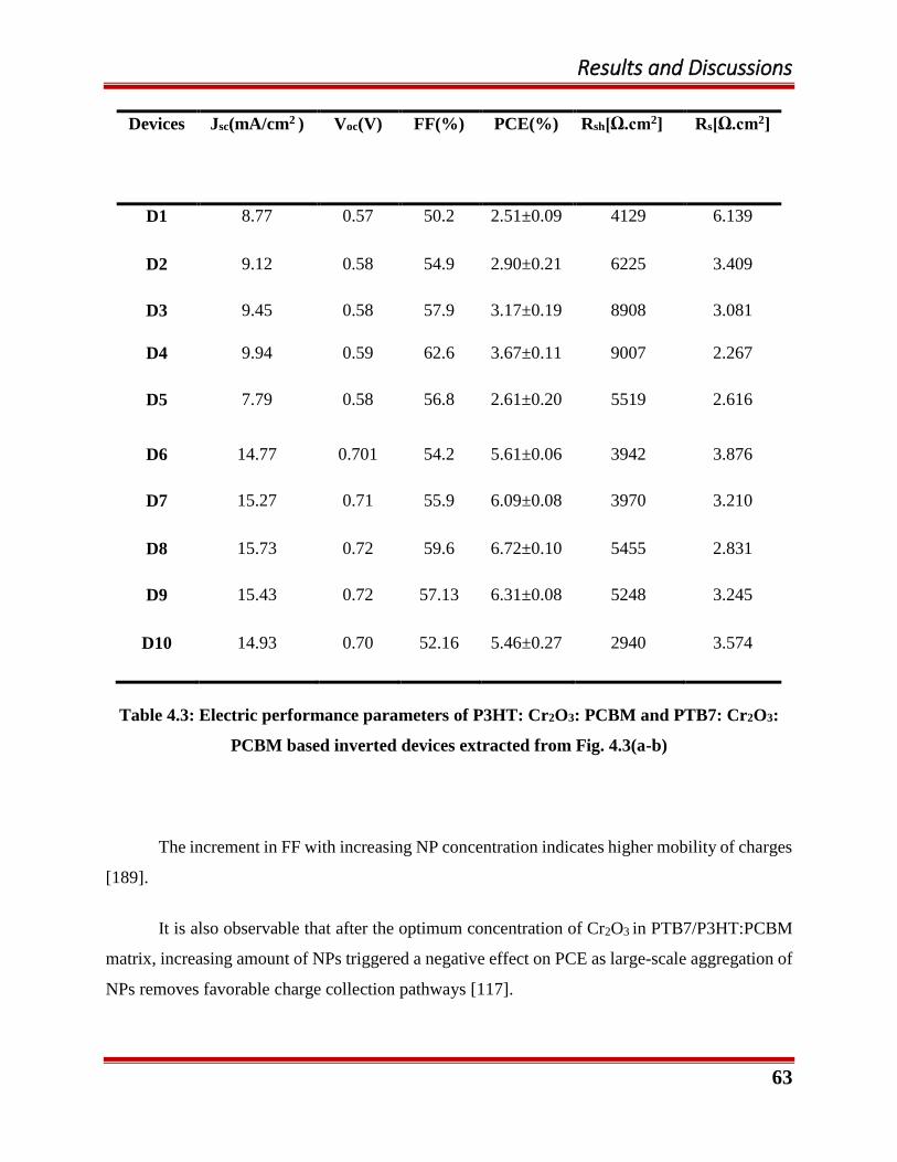
Results and Discussions
63
Devices
Jsc(mA/cm2 ) Voc(V) FF(%) PCE(%) Rsh[Ω.cm2]
Rs[Ω.cm2]
D1 8.77 0.57 50.2
2.51±0.09 4129 6.139
D2 9.12 0.58 54.9
2.90±0.21 6225 3.409
D3 9.45 0.58 57.9
3.17±0.19 8908 3.081
D4 9.94 0.59 62.6
3.67±0.11 9007 2.267
D5 7.79 0.58 56.8
2.61±0.20 5519 2.616
D6 14.77 0.701 54.2
5.61±0.06 3942 3.876
D7 15.27 0.71 55.9
6.09±0.08 3970 3.210
D8 15.73 0.72 59.6
6.72±0.10 5455 2.831
D9 15.43 0.72 57.13
6.31±0.08 5248 3.245
D10 14.93 0.70 52.16
5.46±0.27 2940 3.574
Table 4.3: Electric performance parameters of P3HT: Cr2O3: PCBM and PTB7: Cr2O3:
PCBM based inverted devices extracted from Fig. 4.3(a-b)
The increment in FF with increasing NP concentration indicates higher mobility of charges
[189].
It is also observable that after the optimum concentration of Cr2O3 in PTB7/P3HT:PCBM
matrix, increasing amount of NPs triggered a negative effect on PCE as large-scale aggregation of
NPs removes favorable charge collection pathways [117].
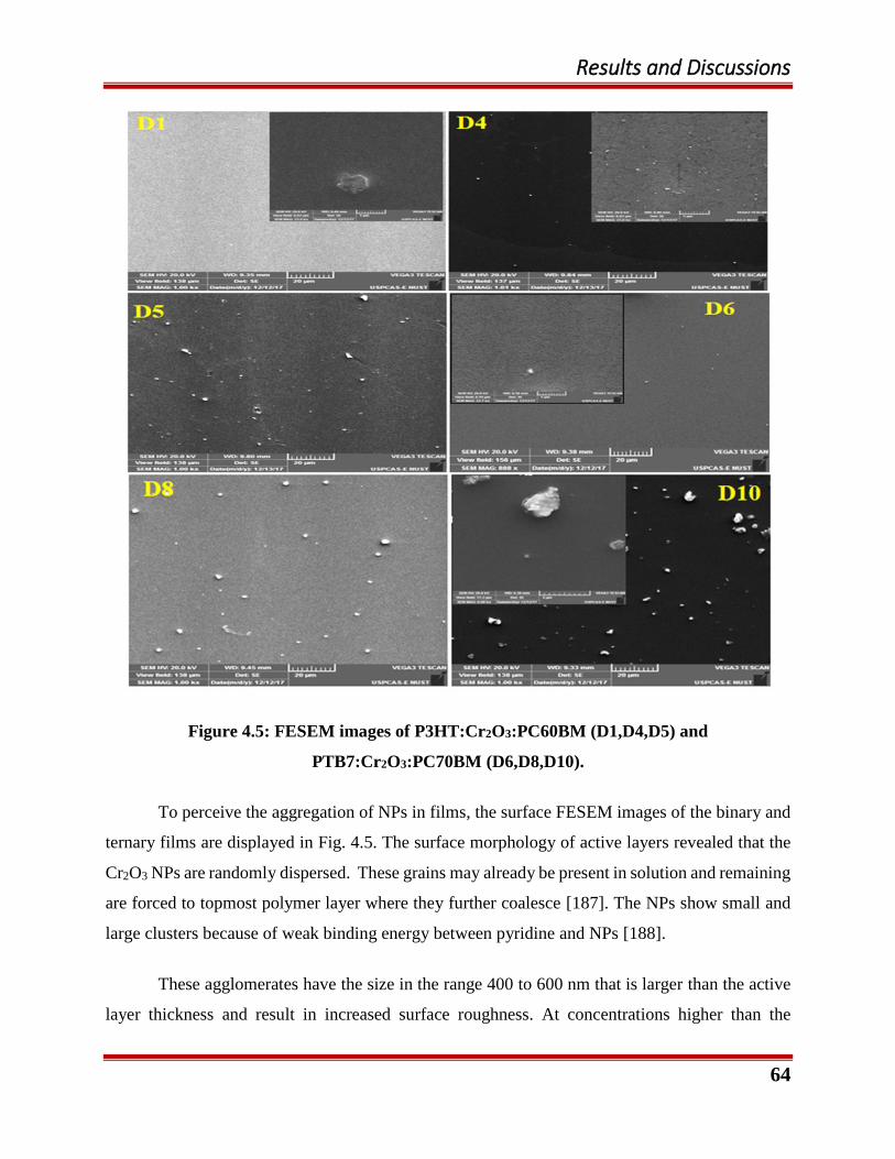
Results and Discussions
64
Figure 4.5: FESEM images of P3HT:Cr2O3:PC60BM (D1,D4,D5) and
PTB7:Cr2O3:PC70BM (D6,D8,D10).
To perceive the aggregation of NPs in films, the surface FESEM images of the binary and
ternary films are displayed in Fig. 4.5. The surface morphology of active layers revealed that the
Cr2O3 NPs are randomly dispersed. These grains may already be present in solution and remaining
are forced to topmost polymer layer where they further coalesce [187]. The NPs show small and
large clusters because of weak binding energy between pyridine and NPs [188].
These agglomerates have the size in the range 400 to 600 nm that is larger than the active
layer thickness and result in increased surface roughness. At concentrations higher than the

Results and Discussions
65
optimum, larger aggregates of nanoparticles removes the percolation pathways and breaks down
the favorable thin film morphology.
AFM was deployed to further study the influence of Cr2O3 NPs on micro morphology as
well as film roughness and micrographs are presented in Fig.4.6 (a-i).
Figure 4.6: AFM images (a-e) P3HT: Cr2O3:PCBM and (f-h) PTB7: Cr2O3:PCBM active
films.

Results and Discussions
66
The AFM images revealed that the surfaces of binary blend films (PTB7/P3HT:PCBM),
are relatively smooth (a and f) with root mean square-RMS values 0.639 and 2.39 nm respectively.
The film roughness was increased gradually by the inclusion of NPs. The RMS values of hybrid
films are 6.08 nm for D4 and 12.3 nm and D8.
The increased roughness is ascribed to the presence of large agglomerates of NPs. This
increment might originate diffused reflection between the active layer and top electrode that
subsequently lead to substantial harvesting of incident light and enhancement in absorption spectra
[111,190,191].
Fig. 4.7 (a-b) exhibits UV-Vis absorption spectra of organic and ternary films. The peaks
around 330 nm and 500 nm in Fig 4.7 (a) correspond to PCBM and P3HT respectively.
With Cr2O3 integration, absorption intensity increased in the visible region with slight red
shift and shoulders at 550 nm and 600 nm were distinguishable. The observed red shift and more
pronounced shoulder were attributed to the higher crystallinity of P3HT with the presence of NPs
[116].
With the small concentration of NPs, no substantial variation was observed in the
absorption spectra of PTB7:PCBM films because wide range absorption of PTB7:PCBM system
dominates Cr2O3. The increased area under the absorption spectra at different wavelengths of
ternary blends suggests that more photons are harvested [188].
As conversed earlier, this enhanced absorption could be associated to the increased
roughness as higher roughness might increase the light scattering in the active layer of ternary
blend films. [117]

Results and Discussions
67
Figure 4.7: UV-Vis absorption spectra (a) P3HT:Cr2O3:PCBM (b) PTB7:Cr2O3:PCBM
films

Results and Discussions
68
The EQE measurements as publicized in Fig. 4.8 (a-b) highlights the same behavior as Jsc
of the devices and photocurrent response agrees well with the device parameters of binary and
ternary blend systems.
Figure 4.8: EQE profile of (a) P3HT:Cr2O3:PCBM (b) PTB7: Cr2O3:PCBM devices.

Results and Discussions
69
The maximum EQE for P3HT and PTB7 based ternary devices (D4 and D8) is nearly 80%
and 74% respectively. The enhancement in EQE is accredited to the improved photon absorption
and charge mobility. Heterojunction electric field formed between NPs and organic materials also
contribute to the enhanced photoelectric conversion property [111].
4.2 Significantly improved the efficiency of organic solar cells
incorporating Co3O4 NPs in the active layer
As discussed in chapter 3, various weight ratios of Co3O4 NPs were incorporated in
P3HT:PC60BM and PTB7:PC70BM based active layer separately. In this section, the fabricated
solar cells with configuration “ITO/ZnO/P3HT:PC60BM:Co3O4/MoO3/Ag and
“ITO/ZnO/PTB7:PC70BM:Co3O4/MoO3/Ag” are discussed and the devices are labeled in table 4.4.
Device Polymer: Acceptor Co3O4 (wt. %)
D11 P3HT:PC60BM 0
D12 P3HT:PC60BM 1
D13 P3HT:PC60BM 2
D14 P3HT:PC60BM 3
D15 P3HT:PC60BM 4
D16 PTB7:PC70BM 0
D17 PTB7:PC70BM 1
D18 PTB7:PC70BM 2
D19 PTB7:PC70BM 3
D10 PTB7:PC70BM 4
Table 4.4: Fabricated device’s table
Fig. 4.9 (a) shows XRD pattern of synthesized Co3O4 NPs and the observed peaks matches
well with “JCPDS card no. 01-080-1545”. The cubic Co3O4 (α=β=γ 90, a=b=c= 8.1691 Å)
belongs to space group “Fd-3m” and is free from crystalline impurities. The peak positions and
corresponding planes are indexed on XRD pattern and summed up in Table 4.5.

Results and Discussions
70
Figure 4.9: (a) XRD pattern (b) FESEM image

Results and Discussions
71
The Debye Scherrer’s formula (Eq. 3.1) was used to calculate average crystallite size
associated to these peaks and was found to be 15-25 nm.
No. h k l 2Theta [deg]
1 2 2 0 31.29
2 3 1 1 36.82
3 4 0 0 44.81
4 4 2 2 55.62
5 5 1 1 59.32
6 4 4 0 65.25
Table 4.5: The peak list and hkl values of Co3O4 JCPDS card no. 01-080-1545
FESEM image (Fig. 4.9b) displays small and large clusters of Co3O4 NPs. The inset
identifies spherical NPs with particle size ranging from 29.3 nm to 36.7 nm.
The Uv-Vis absorption spectrum of Co3O4 NPs is shown in Fig. 4.10(a).The absorption
peaks observed around 485 nm and 780 nm are related to the charge transfer from O2- Co2+ and
O2- Co3+ respectively [192–194]. The Tauc plot (section 3.4.4, Eq.3.2) calculates the bandgap
of 1.3 and 2.0 eV (Fig. 4.10 b).

Results and Discussions
72
Figure 4.10: (a)UV-Vis absorption spectra (b) band gap calculation of Co3O4 NPs

Results and Discussions
73
Fig. 4.11 (a-b and c) shows the architecture and energy band diagram of the fabricated
devices with inverse geometry. It is well documented that the energy levels of active materials
must be well aligned for high exciton dissociation and charge transfer. [187].
In our scheme, the Co3O4 NPs were believed to contribute to improve device opto-
electronic parameters as its energy levels (Ec = 4.2 eV , Ev = 6.1 eV, Eg=1.3 eV) matches well with
the active layer organic materials [100,195–197].
Figure 4.11: (a) cartoon of inverted device architecture utilized in study (b) energy band
diagram of P3HT:PC60BM:Co3O4 (c) PTB7:PC70BM:Co3O4.

Results and Discussions
74
As already discussed in chapter 1, Voc of the OSCs strongly depends on the D and A band
position (HOMOdonor - LUMOacceptor) and the introduction of NPs in ternary devices, can effectually
modify the upper limit of Voc [198]. When light is incident, the excitons generated in active layer
are dissociated at D/A interface.
In the studied structure, h+ travel to MoO3/Ag whereas e-s have 2 pathways to reach ITO,
either travel through PCBM or higher e- mobility NPs. The probable paths for e-s
“PTB7/P3HT:PCBM”, “PTB7/P3HT:Co3O4” and “Co3O4:PCBM” might improve the charge
separation and transportation [119]. Once the e-s are injected into ETL, they are collected by ZnO
and the appropriate energy level of ZnO blocks h+ to enter. PTB7/P3HT:PCBM) and ternary
(PTB7/P3HT:PCBM:Co3O4) devices are displayed in Fig. 4.12 (a-b) and electrical parameters
extracted from these curves are summarized in Table 4.6. On addition of NPs in organic active
layer, an enhanced FF and Jsc was obtained that boost up PCEs from 2.91 to 3.39 % and 6.05 to
6.57 % for D11 to D13 and D16 to D18 respectively (Fig. 4.12
The Jsc vs V characteristics curves of binary ( (a-b)).
An increment in FF was observed with incorporation of Co3O4-NPs in the PTB7 and P3HT
based hybrid solar cells. The NPs proceduce percolation pathways in active layer and facilitates
charge transfer owed to high electron mobility at “D/A” interface initiating a decreased Rs and
enhanced Jsc [199–201]. For devices utilizing PTB7 as donor, Rs decreases but no considerable
change in Jsc was observed.
It suggests that the absorption corresponding to the higher concentration of PC70BM
relative to PTB7 (1.5:1) dominates NPs. Similarly, Ec of NPs tune the energy levels between
HOMOdonor and LUMOacceptor and increased Voc for devices D11 to D13 [117,202]. Contrary, no
change in Voc is observed for devices D16 to D20 (PTB7 based) as NPs might be acting only as e-
cascade [100].

Results and Discussions
75
Figure 4.12: J-V graphs (a) P3HT:PCBM:Co3O4 (b) PTB7:PCBM:Co3O4 based inverted
devices.

Results and Discussions
76
Devices
Jsc(mA/cm2 ) Voc(V) FF(%) PCE(%) Rs[Ω.cm2]
D11 8.82 0.56 59
2.91±0.11 2.855
D12 8.94 0.57 61
3.10±0.05 2.554
D13 9.29 0.58 63
3.39±0.07 2.373
D14 9.20 0.57 61
3.19±0.08 2.52
D15 8.66 0.55 58
2.76±0.22 4.253
D16 15.23 0.71 56
6.05±0.06 3.406
D17 15.39 0.71 57
6.22±0.13 3.295
D18 15.43 0.71 60
6.57±0.09 3.208
D19 15.17 0.71 57
6.13±0.04 2.748
D20 14.83 0.71 56
5.89±0.14 3.567
Table 4.6: J-V data of P3HT:Co3O4:PCBM and PTB7:Co3O4:PCBM based inverted
devices
The favorable reduction in Rs and increment in Jsc, FF and Voc were obtained with only
small concentration of Co3O4 i.e 2%, afterwards the trend reverse owing to agglomeration of NPs
which breaks down the BHJ and eliminates percolation network [117].
Active layer morphology plays a critical role in device performance. To check the effect
of Co3O4 NPs on surface morphology FESEM and AFM were utilized

Results and Discussions
77
Figure 4.13: FESEM images of (D11-D15) P3HT:PC60BM:Co3O4 and (D16-D20)
PTB7:PC70BM:Co3O4.

Results and Discussions
78
The FESEM images of binary and ternary blended active layer films are shows in Fig. 4.13
and a relatively smooth surface is perceived for active layer of binary system (Fig. 4.11, D11 and
D16).
Conjugation of NPs exhibits the formation of percolation network in ternary blend films as
indicated in Fig. 4.13 (D3 and D8). With the optimum amount, Co3O4 NPs link the PCBM domain
resulting in improved mobility and decreased resistance of the devices.
However, at higher concentrations, small and large aggregates of NPs are formed that are
randomly distributed on film surfaces as marked in Fig 4.13(D15 and D20).
The presence of aggregates terminates the auspicious percolation pathways and breaks
down the BHJ. These aggregates, at higher concentration, also act as charge trap sites or
recombination centers and limits the charge collection that result in decreased Jsc (Table 4.6) [116].
To further study the influence of Co3O4 NPs on the micromorphology and roughness of
binary and ternary films AFM was used and the images are displayed in Fig. 4.14.
The film surface of control devices D11 and D16, are smooth with RMS value of 3.21and
2.1nm respectively. The addition of NPs relatively increased film roughness with RMS values
7.16, 8.27, 10.84, 11.5 nm (D12 to D15) and 2.7, 3.04, 3.84 nm (D17 to D19) respectively.
This increased film roughness corresponds to the presence of small and large aggregates
of Co3O4 that effectively reduce the charge transport distance and conclusively increase the
photocurrent.

Results and Discussions
79
Figure 4.14: AFM images (D11-D15) P3HT:Co3O4:PCBM and (D16-D19)
PTB7:Co3O4:PCBM.
However, at higher NPs concentration, larger aggregates of NPs results in phase separation
and confiscates charge’s pathways Fig. 4.14 (D15) [203].
UV-Vis absorption spectra of active layer films, with and without NPs, is illustrated in Fig
4.15 (a-b). With the integration of Co3O4 NPs, enhanced absorption was witnessed for films D12

Results and Discussions
80
to D15 and D17 to D20. The higher surface roughness of ternary films leads to stronger scattering
of light in the active layer that results in increased absorption [204].
Figure 4.15: UV-Vis absorption spectra of inverted devices (a) P3HT:Co3O4: PCBM (b)
PTB7:Co3O4:PCBM

Results and Discussions
81
Compared to binary, ternary blended films indicate higher and wide range absorption but
for PTB7:PCB70M based films, strong absorption at 400-500 nm indicate that absorption of PCBM
dominates Co3O4NPs due to higher concentration.
Figure 4.16: EQE profile of inverted devices (a) P3HT:Co3O4:PCBM (b)
PTB7:Co3O4:PCBM

Results and Discussions
82
Consequently the absorption spectrum supports our argument that increase in Jsc is mainly
owed to superior morphology. Fig 4.16 (a-b) displays the EQE of binary and ternary devices.
In graphs, a broad and strong response appears for control devices D11 and D16 from 390
to 625 nm and 400 to 725 nm respectively. Upon Co3O4 NPs inclusion, enhanced EQE for both
PTB7:PC70BM and P3HT:PC60BM based systems was obtained. This improved EQE is accredited
to the enhanced charge collection with NPs integration.

Results and Discussions
83
5 Chapter 5
The chapter describes the perovskite solar cells employing ZnO and Al-ZnO nanoparticles
based capping layer that also serve as ETL.
5.1 Synergetic Effect of Metal Oxide as Electron Transport Layers
on the Performance of Perovskite Solar Cell
Although maximum PCEs attained in PrSCs are mainly for mp or standard planar
architecture but inverted configuration utilizing fullerene derivative (ICBA, PCBM) based ETL
are of enormous research interest. The inverted structures are fascinating owed to long term
stability, negligible hysteresis and possibility to be applied as rear cell in tandem devices [56,57].
However, the direct exposure of PCBM with oxygen/ water and the chemical reaction between
perovskite and metal back contact at thinner ETL sites result in poor stability of devices. Also, the
mismatch between energy levels of direct metal/PCBM contact diminishes carrier selectivity and
e- extraction. Hence, a n-type material which functions as charge transport layer and also avoid the
direct PCBM and metal contact is crucial for energy level alignment and device stability.
In this chapter, the effect of employing ZnO and Al:ZnO NPs on top of PCBM as capping
and electron transport layer has been studied.
Device name ETL
D1 PCBM
D2 PCBM+Al:ZnO NPs
D3 PCBM+ZnO NPs
Table 5.1: Fabricated device’s table

Results and Discussions
84
These NPs offer optical transparency, high carrier mobility, environmental stability,
appropriate W.F, offer larger interfacial area and can support to overcome degradation [69,205].
With the integration of thin layer of Al:ZnO/ZnO, a considerable enhancement in performance
parameters and stability of the devices was observed.
Fig. 5.1 exhibit HOMO and LUMO of each material involved in inverted PrSCs. The
suitable energy level alignment of PEDOT:PSS (-5.3 eV), CH3NH3PbI3 ( LUMO ~ -3.9, HOMO
~ -5.4) eV, PCBM (LUMO ~ -4.2, HOMO ~ -6.7) eV facilitate efficient e--h+ extraction at
interfaces [154].
Figure 5.1: (a) device configuration (b) Energy level diagram
On light absorption, excitons are generated and dissociate within CH3NH3PbI3 and are
collected at their respective electrodes. The deeper band edge of PEDOT:PSS prevents h+
leakage from ITO to active perovskite layer [206].

Results and Discussions
85
The energy level alignment of Al:ZnO and ZnO were believed to improve e- transport
efficiency at the interfaces between layers. Additionally, valance band of metal oxide NPs, deeper
than PCBM, can efficiently block holes to reach back contact.
Figure 5.2: (a) J-V graphs of inverted devices D1, D2 and D3 (b) Distribution of PCEs
values as obtained from 20 pixels (c) Stability study for D1,D2 and D3

Results and Discussions
86
J-V curves of PrSCs are presented in Fig.5.2 (a) and the device electric performance
parameters are summed up in Table 5.2.
Table 5.2: J-V data of inverted devices with PCBM, PCBM/ZnO and PCBM/Al:ZnO as
electron transport layers.
The control device D1 shows PCE of 7.41% with FF 54.21%, Jsc 17.61 mA/cm2 and Voc
0.777 V. Addition of ZnO and Al:ZnO NP layer on top of PCBM considerably improved device
parameters resulting in PCEs over 12%. The Voc of PrSCs is also affected by the W.F of charge
transport layers [207]. The increment in Jsc of D2 and D3 is credited to improved e- blocking and
reduced charge recombination [208]. The key factors influencing Jsc include light harvesting
efficiency, exciton dissociation, charge transfer and collection at the electrodes [209].
In inverted structure, the photo dissociated electrons require 0.4 ns to be collected at the Al
electrode after passing PCBM and holes travel through the PEDOT:PSS and reach ITO in less than
a nanosecond [210]. e-s in our devices have to travel through Al:ZnO/ ZnO layer along with PCBM
to be collected at back contact (Al). Deeper Ev and long carrier diffusion length of metal oxide
NPs increase Jsc of the devices owed to enhanced charge collection efficiency. Improved FF for
D2 and D3 is recognized by the balance between e- and h+ transfer to corresponding electrodes.
Addition of capping layer ensures balanced charge passage to the corresponding electrodes.

Results and Discussions
87
This balance results in decreased charge recombination and increased Jsc and FF [211]. The
metal oxide layer also acts as buffer layer and decreases the leakage current as specified by the
increased values of Rsh [69,212]. The. Fig. 5.2(b) demonstrates the histogram of three devices for
20 pixels. The performance of modified devices (D2 and D3) is averagely higher than the control
device.
The stability of devices with and without metal oxide interlayers were tested under ambient
conditions for 480hrs. Fig. 5.2(c) shows a radical diminution in PCE of D1 as it dropped down to
~ 0 in 48 hrs. The degradation can be ascribed to the adsorption of water/oxygen by PCBM. On
the contrary, Al:ZnO and ZnO are more environmentally stable and serve as a protecting layer for
PCBM and perovskite thus maintained the device performance and PCE for D2 and D3 dropped
down to only ~ 79% and 75 % (respectively) in 480 hrs.
The absorption profile of CH3NH3PbI3/PCBM films is shown in Fig. 5.3(a) demonstrating
strong absorption from 325-800 nm [213,214]. The absorption spectra confirms two distinct peaks
appearing round 475 and 760 nm. The 2.61 eV energy band relates to the direct transition from
lower valance band to conduction minimum and 1.63 eV corresponds to the direct transition from
the first valance band maximum to the conduction band minimum [215].
Below 450 nm , absorbance of D1 has less intensity than D2 and D3 films and marks the
presence of Al:ZnO and ZnO layers [216]. A Slight red shift perceived in D2 active layer film
(below 400 nm) is ascribed to the absorption of Al:ZnO.
In Fig. 5.2(b) EQE as function of wavelength for the devices is plotted. The devices D2
and D3 manifests enhanced EQE values than D1 that is in agreement with the values extracted
from J-V plots. As shown in Fig. 5.2(a), the light harvesting is similar for all devices, hence
improved EQE is accredited to the efficient charge transfer and collection owing to the presence
of Al:ZnO and ZnO [217].

Results and Discussions
88
Figure 5.3: (a) UV-Vis absorption spectra of D1, D2 and D3 layers. (b) EQE plot of
inverted devices D1, D2 and D3
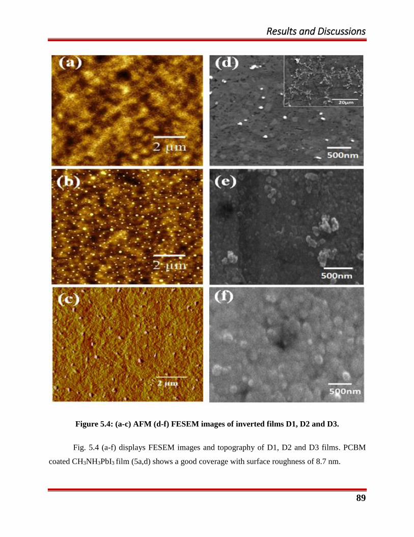
Results and Discussions
89
Figure 5.4: (a-c) AFM (d-f) FESEM images of inverted films D1, D2 and D3.
Fig. 5.4 (a-f) displays FESEM images and topography of D1, D2 and D3 films. PCBM
coated CH3NH3PbI3 film (5a,d) shows a good coverage with surface roughness of 8.7 nm.

Results and Discussions
90
The inclusion of ZnO/Al:ZnO layer, decreased the surface roughness to 5.8 and 6.4 nm
for D2 and D3 (respectively) layers suggesting that NPs forms a film without changing the surface
morphology of active layer. The reduced RMS values ensure excellent contact with Al (top
electrode) that intern reduces recombination at the interface and improves device reproducibility
(Fig. 5.2b) [218]. The FESEM image (5D) indicates that D1 active layer film have small and large
grains distribution morphology on the film surface. Conversely, the films with ZnO/AZO on top
(e-f) has the small quantity of grains indicating good coverage of film that protects the active layer
against metal sputtering.
Figure 5.5: Cross section of D1, D2 and D3 respectively

Results and Discussions
91
The cross sectional FESEM images of all three devices are displayed in Fig. 5.5. As
indicated by red circle (5 D1), PCBM does not give full perovskite coverage. Also, Al metal
sputtered directly on PCBM can penetrate as deep as 10 nm into the layer. These factors can result
in direct connection of metal back contact with perovskite at thinner PCBM sites [69,212]. When
a thin layer of NPs is deposited on PCBM it gives a homogeneous coverage and acts as a capping
layer to prevent direct contact of PCBM and Al. This results in enhanced device stability as shown
previously (Fig 5.2 c)

Conclusions and Future Recommendations
92
6 Chapter 6
Conclusions and Future Recommendations
6.1 Conclusions
The objective of this dissertation was to fabricate and electrically characterize novel
organic-inorganic hybrid solar cells. The bulk heterojunction and perovskite based hybrid solar
cells have been studied and a comprehensive discussion on the effects of NPs on the device
performance was conducted. This work studies, how the morphology and opto-electronic
properties changed during the process.
Co3O4, Cr2O3 NPs were synthesized using co-precipitation technique and the structures of
the NPs is confirmed by XRD. The XRD patterns reveals absence of any kind of impurity and
average particle size of 29-37 nm and 10-13 nm were obtained for Co3O4 and Cr2O3 respectively
as confirmed by FESEM. The optical properties of NPs demonstrate two bandgaps of 1.3 and 2.0
eV for Co3O4 and 2.9 eV for Cr2O3 calculated from Tauc’s plot.
Influence of mixing Co3O4 NPs in the active layer of P3HT:PC60BM and PTB7:PC70BM
bulk heterojunction solar cells is studied. The mixing shows an enhancement in PCEs of the
devices from 2.91 to 3.39% for P3HT and from 6.05 to 6.57% for PTB7 based device. The
increased PCE of ternary devices is credited to an increased absorption and reduced Rsc. The
incorporation of Co3O4 NPs introduced percolation pathways that facilitates charge transport. The
NPs agglomerated with increasing amount of Co3O4 in active layer and surface roughness of the
active layer increased. After optimum concentration larger agglomerates of NPs were formed that
broke down the favorable morphology and benefits reverse.
Bulk heterojunctions HSCs with various ratios of Cr2O3 NPs were fabricated while keeping
constant ratio of P3HT: PC60BM and PTB7: PC70BM. The results reveal an increase in PCE from
2.51 to 3.67% and from 5.61 to 6.72 % for P3HT and PTB7 based devices respectively. The
addition of NPs introduced red-shift in absorption spectra and improved the absorption in visible

Conclusions and Future Recommendations
93
region. With Cr2O3 optimum amount of NPs enhanced FF, Jsc and Voc was observed beyond which
the device performance was damaged due to formation of larger aggregates of NPs. AFM results
show that the inclusion of NPs increased film roughness from 0.639 to 6.08 nm for P3HT and from
2.39 to 12.3 nm for PTB7 based devices that lead to enhancement in light harvesting due to light
scattering. FESEM images show presence of aggregates that form percolation network within the
active layer and facilitate charge transport as supported by Rs trend. These pathways also aid to
suppress the leakage current and significantly increased Rsh from 4129 to 9007 Ω.cm2 for P3HT
and 3942 to 5248 Ω.cm2 for PTB7 based system.
The PrSCs performance in inverted planar structure have been investigated. CH3NH3PbI3
was used as perovskite absorber and two step solution deposition by spin coating was performed.
ZnO and Al:ZnO NPs were separately deposited on top of PCBM as a capping layer and both
materials have positive impact on PrSCs. The analysis on interfacial modification shows that the
devices with ZnO and Al:ZnO as capping material outperforms the reference device.. The PCEs
for PrSCs modified with interlayer increased by 7 % for ZnO and 11% for Al:ZnO based devices.
The control device degraded completely and PCE dropped down to 0 in 48 hrs. Whereas, efficiency
of devices modified with ZnO/Al:ZnO dropped down to only 25% even after 480 hrs. The best
device has PCE of 12.01% which is lower than the literature reported values but results are
reproducible as discussed in chapter 5. Many factors such as batch to batch difference of material’s
purity and experimental/environmental conditions can influence the PCE. Also, the high
efficiencies achieved are mostly for mixed halide or formamide based perovskite materials.
Since the main object in this work was to fabricate complete working HSC, the experiments
were conducted to already established recipes. For better conclusion, several devices of similar
kind was made to ensure reproducibility.
6.2 Future Recommendations
Despite the success of current experiments, several opportunities exists for the continuation
and improvement of the work in this thesis.

Conclusions and Future Recommendations
94
1. Co3O4 and Cr2O3 NPs can be tested to replace fullerene derivatives in bulk heterojunction
hybrid solar cells in order to reduce the device cost.
2. As morphology of the NPs also influence the efficiency of devices, different morphology
of Co3O4 and Cr2O3 can be employed.
3. Temperature dependent measurements are recommended to evaluate the carrier collection
efficiency and how the addition of NPs affect it.
4. The interface study is of particular importance for bulk heterojunction organic and hybrid
solar cells. The AFM and FESEM show the surface morphology but to study vertical phase
separation and nanoparticles at interface TEM cross-section is useful for more accurate
interface analysis of hybrid devices.
5. Due to the incorporation of NPs, the fundamental working mechanism of hybrid devices
require further investigation and understanding. Among them, tunable Voc require an in-
depth study and verification as it is altered by many factors. Therefore, Fourier Transform
Photocurrent Spectroscopy can be deployed to study the effect of charge transfer energy
and its absorption intensity on the Voc of ternary hybrid bulk heterojunction solar cells.
6. A series of experiment is required to be performed for a successful fabrication of NiS NPs
and their utilization in solar cells.
7. 0.5 M Cr2O3 NPs were utilized as HTL in perovskite solar cells but the devices did not
work. A detailed study is recommended for experimental optimization.
8. In this thesis, the most studied metal halide perovskite i.e.CH3NH3PbI3 is employed. The
limitations for the particular perovskite is toxicity of Pb and the bandgap of 1.5 to 1.6 eV.
Many research groups have replaced Pb with Sn and also used formamidinium lead halide
perovskite (FPbX3) that has tunable bandgap between 1.48 to 2.23 eV. The PrSCs based
on FPbX3 has shown promising PCEs. The double ETL can be tested for fomamidinium
mixed halide based devices.In case of perovskite solar cells mixed halides or formamide
based devices can be tested for double ETL.

References
95
References
[1] J.A. Tainter, Sustainability of complex societies, Futures. 27 (1995) 397–407.
doi:10.1016/0016-3287(95)00016-P.
[2] UNFCCC, Paris Agreement, Conf. Parties Its Twenty-First Sess. (2015) 32.
doi:FCCC/CP/2015/L.9/Rev.1.
[3] M. Child, O. Koskinen, L. Linnanen, C. Breyer, Sustainability guardrails for energy
scenarios of the global energy transition, Submitt. Publ. 91 (2017) 321–334.
doi:10.1016/j.rser.2018.03.079.
[4] REN21, Renewables 2017: global status report, 2017. doi:10.1016/j.rser.2016.09.082.
[5] J. Polo, S. Wilbert, J.A. Ruiz-Arias, R. Meyer, C. Gueymard, M. Súri, L. Martín, T.
Mieslinger, P. Blanc, I. Grant, J. Boland, P. Ineichen, J. Remund, R. Escobar, A. Troccoli,
M. Sengupta, K.P. Nielsen, D. Renne, N. Geuder, T. Cebecauer, Preliminary survey on site-
adaptation techniques for satellite-derived and reanalysis solar radiation datasets, Sol.
Energy. 132 (2016) 25–37. doi:10.1016/j.solener.2016.03.001.
[6] J. Antonanzas, N. Osorio, R. Escobar, R. Urraca, F.J. Martinez-de-Pison, F. Antonanzas-
Torres, Review of photovoltaic power forecasting, Sol. Energy. 136 (2016) 78–111.
doi:10.1016/j.solener.2016.06.069.
[7] Q. Li, Y. Liu, S. Guo, H. Zhou, Solar energy storage in the rechargeable batteries, Nano
Today. 16 (2017) 46–60. doi:10.1016/j.nantod.2017.08.007.
[8] P. Mandal, S. Sharma, Progress in plasmonic solar cell efficiency improvement: A status
review, Renew. Sustain. Energy Rev. 65 (2016) 537–552. doi:10.1016/j.rser.2016.07.031.
[9] K.T.. Grattan, Optoelectronics of solar cells, 2004. doi:10.1016/j.optlastec.2004.01.014.
[10] A. Pockett, Characterization of Perovskite Solar Cells Adam Pockett, (2016).

References
96
[11] M.A. Green, Y. Hishikawa, W. Warta, E.D. Dunlop, D.H. Levi, J. Hohl-Ebinger, A.W.H.
Ho-Baillie, Solar cell efficiency tables (version 50), Prog. Photovoltaics Res. Appl. 25
(2017) 668–676. doi:10.1002/pip.2909.
[12] S. Sharma, K.K. Jain, A. Sharma, Solar Cells: In Research and Applications—A Review,
Mater. Sci. Appl. 06 (2015) 1145–1155. doi:10.4236/msa.2015.612113.
[13] K.D.G.I. Jayawardena, L.J. Rozanski, C.A. Mills, M.J. Beliatis, N.A. Nismy, S.R.P. Silva,
‘Inorganics-in-Organics’: recent developments and outlook for 4G polymer solar cells,
Nanoscale. 5 (2013) 8411. doi:10.1039/c3nr02733c.
[14] G. Grancini, C. Roldán-Carmona, I. Zimmermann, E. Mosconi, X. Lee, D. Martineau, S.
Narbey, F. Oswald, F. De Angelis, M. Graetzel, M.K. Nazeeruddin, One-Year stable
perovskite solar cells by 2D/3D interface engineering, Nat. Commun. 8 (2017) 1–8.
doi:10.1038/ncomms15684.
[15] A.K. Chilvery, A.K. Batra, B. Yang, K. Xiao, P. Guggilla, M.D. Aggarwal, R. Surabhi, R.B.
Lal, J.R. Currie, B.G. Penn, Perovskites: transforming photovoltaics, a mini-review, J.
Photonics Energy. 5 (2015) 057402. doi:10.1117/1.JPE.5.057402.
[16] T.M. Clarke, J.R. Durrant, Charge photogeneration in organic solar cells, Chem. Rev. 110
(2010) 6736–6767. doi:10.1021/cr900271s.
[17] F. Gao, S. Ren, J. Wang, The renaissance of hybrid solar cells: progresses, challenges, and
perspectives, Energy Environ. Sci. 6 (2013) 2020. doi:10.1039/c3ee23666h.
[18] B. O’Regan, M. Gratzel, A Low-Cost, High-Efficiency Solar-Cell Based on Dye-Sensitized
Colloidal TiO2 Films, Nature. 353 (1991) 737–740. doi:10.1038/353737a0.
[19] W.U. Huynh, J.J. Dittmer, A.P. Alivisatos, Hybrid nanorod-polymer solar cells, Science
(80-. ). 295 (2002) 2425–2427. doi:10.1126/science.1069156.
[20] A. Goetzberger, J. Luther, G. Willeke, Solar cells: Past, present, future, Sol. Energy Mater.
Sol. Cells. 74 (2002) 1–11. doi:10.1016/S0927-0248(02)00042-9.

References
97
[21] M. Wright, A. Uddin, Organic-inorganic hybrid solar cells: A comparative review, Sol.
Energy Mater. Sol. Cells. 107 (2012) 87–111. doi:10.1016/j.solmat.2012.07.006.
[22] W.J.E. Beek, M.M. Wienk, R.A.J. Janssen, Efficient hybrid solar cells from zinc oxide
nanoparticles and a conjugated polymer, Adv. Mater. 16 (2004) 1009–1013.
doi:10.1002/adma.200306659.
[23] L.E. Brus, Electron-electron and electron-hole interactions in small semiconductor
crystallites: The size dependence of the lowest excited electronic state, J. Chem. Phys. 80
(1984) 4403–4409. doi:10.1063/1.447218.
[24] A.P. Alivisatos, Semiconductor Clusters, Nanocrystals, and Quantum Dots, Science (80-. ).
271 (n.d.) 933.
[25] A.J. Heeger, Plastic solar cells: Self-assembly of bulk heterojunction nano-materials by
spontaneous phase separation, AIP Conf. Proc. 1519 (2013) 47–50. doi:10.1063/1.4794707.
[26] C.K. MØLLER, Crystal Structure and Photoconductivity of Cæsium Plumbohalides,
Nature. 182 (1958) 1436–1436. doi:10.1038/1821436a0.
[27] J.L. Knutson, J.D. Martin, D.B. Mitzi, Tuning the band gap in hybrid tin iodide perovskite
semiconductors using structural templating, Inorg. Chem. 44 (2005) 4699–4705.
doi:10.1021/ic050244q.
[28] D.B. Mitzi, P. Brock, Structure and optical properties of several organic-inorganic hybrids
containing corner-sharing chains of bismuth iodide octahedra, Inorg. Chem. 40 (2001)
2096–2104. doi:10.1021/ic000622l.
[29] D.B. Mitzi, Organic − Inorganic Perovskites Containing Trivalent Metal Halide Layers :
The Templating Influence of the Organic Cation Layer Organic-Inorganic Perovskites
Containing Trivalent Metal Halide Layers : The Templating Influence of the Organic Cation
Layer, World. (2000) 6107–6113. doi:10.1021/ic000794i.
[30] T. Baikie, Y. Fang, J.M. Kadro, M. Schreyer, F. Wei, S.G. Mhaisalkar, M. Graetzel, T.J.

References
98
White, Synthesis and crystal chemistry of the hybrid perovskite (CH3NH3)PbI3 for solid-
state sensitised solar cell applications, J. Mater. Chem. A. 1 (2013) 5628.
doi:10.1039/c3ta10518k.
[31] G. Xing, N. Mathews, S. Sun, S.S. Lim, Y.M. Lam, M. Graẗzel, S. Mhaisalkar, T.C. Sum,
Long-range balanced electron-and hole-transport lengths in organic-inorganic
CH3NH3PbI3, Science (80-. ). 342 (2013) 344–347. doi:10.1126/science.1243167.
[32] S.D. Stranks, S.D. Stranks, G.E. Eperon, G. Grancini, C. Menelaou, M.J.P. Alcocer, T.
Leijtens, L.M. Herz, A. Petrozza, H.J. Snaith, Electron-Hole Diffusion Lengths Exceeding,
Science. 342 (2014) 341–344. doi:10.1126/science.1243982.
[33] M.A. Green, A. Ho-Baillie, H.J. Snaith, The emergence of perovskite solar cells, Nat.
Photonics. 8 (2014) 506–514. doi:10.1038/nphoton.2014.134.
[34] C.S. Ponseca, T.J. Savenije, M. a. Abdellah, K. Zheng, A.P. Yartsev, T.T. Pascher, T.
Harlang, P. Chabera, T. Pullerits, A. Stepanov, J.-P. Wolf, V. Sundstrom, C.S. Ponseca Jr.,
T.J. Savenije, M. a. Abdellah, K. Zheng, A.P. Yartsev, T.T. Pascher, T. Harlang, P. Chabera,
T. Pullerits, A. Stepanov, J.-P. Wolf, V. Sundstrom, Organometal halide perovskite solar
cell materials rationalized â\texteuro\textquotedblleft ultrafast charge generation,
high and microsecond-long balanced mobilities and slow recombination, J. Am. Chem. Soc.
136 (2014) 5189–5192. doi:10.1021/ja412583t.
[35] A. Kojima, K. Teshima, Y. Shirai, T. Miyasaka, Organometal halide perovskites as visible-
light sensitizers for photovoltaic cells, J. Am. Chem. Soc. 131 (2009) 6050–6051.
doi:10.1021/ja809598r.
[36] M.A. Green, Y. Hishikawa, E.D. Dunlop, D.H. Levi, J. Hohl-Ebinger, A.W.Y. Ho-Baillie,
Solar cell efficiency tables (version 51), Prog. Photovoltaics Res. Appl. 26 (2018) 3–12.
doi:10.1002/pip.2978.
[37] R.N. Marks, J.J.M. Halls, D.D.C. Bradley, R.H. Friend, A.B. Holmes, The Photovoltaic
Response in Poly(P-Phenylene Vinylene) Thin- Film Devices, J. Physics-Condensed

References
99
Matter. 6 (1994) 1379–1394.
[38] S. Barth, H. Bässler, Intrinsic photoconduction in PPV-type conjugated polymers, Phys.
Rev. Lett. 79 (1997) 4445–4448. doi:10.1103/PhysRevLett.79.4445.
[39] J. Shinar, J. Partee, On the nature of trapped polarons in π-conjugated polymers, Synth. Met.
84 (1997) 525–528. doi:10.1016/S0379-6779(97)80845-4.
[40] M. Harrison, J. Grüner, G. Spencer, Analysis of the photocurrent action spectra of MEH-
PPV polymer photodiodes, Phys. Rev. B - Condens. Matter Mater. Phys. 55 (1997) 7831–
7849. doi:10.1103/PhysRevB.55.7831.
[41] H.R. Kerp, H. Donker, R.B.M. Koehorst, T.J. Schaafsma, E.E. van Faassen, Exciton
transport in organic dye layers for photovoltaic applications, Chem. Phys. Lett. 298 (1998)
302–308. doi:Doi 10.1016/S0009-2614(98)01217-2.
[42] M. Wright, A. Uddin, Solar Energy Materials & Solar Cells Organic — inorganic hybrid
solar cells : A comparative review, Sol. Energy Mater. Sol. Cells. 107 (2012) 87–111.
doi:10.1016/j.solmat.2012.07.006.
[43] C. Deibel, T. Strobel, V. Dyakonov, Origin of the efficient polaron-pair dissociation in
polymer-fullerene blends, Phys. Rev. Lett. 103 (2009) 1–4.
doi:10.1103/PhysRevLett.103.036402.
[44] J.G. Müller, J.M. Lupton, J. Feldmann, U. Lemmer, M.C. Scharber, N.S. Sariciftci, C.J.
Brabec, U. Scherf, Ultrafast dynamics of charge carrier photogeneration and geminate
recombination in conjugated polymer:fullerene solar cells, Phys. Rev. B - Condens. Matter
Mater. Phys. 72 (2005) 1–10. doi:10.1103/PhysRevB.72.195208.
[45] N.S. Sariciftci, L. Smilowitz, A.J. Heeger, F. Wudl, Photoinduced Electron Transfer from
a Conducting Polymer to Buckminsterfullerene., Science (80-. ). 258 (1992) 1474–1476.
doi:10.1126/science.258.5087.1474.
[46] J.J.M. Halls, J. Cornil, D.A. dos Santos, R. Silbey, D.H. Hwang, A.B. Holmes, J.L. Brédas,

References
100
R.H. Friend, Charge- and energy-transfer processes at polymer/polymer interfaces: A joint
experimental and theoretical study, Phys. Rev. B - Condens. Matter Mater. Phys. 60 (1999)
5721–5727. doi:10.1103/PhysRevB.60.5721.
[47] S. de Wolf, J. Holovsky, S.-J. Moon, P. Löper, B. Niesen, M. Ledinsky, F. Haug, J. Yum,
C. Ballif, Organometallic Halide Perovskites: Sharp Optical Absorption Edge and, J. Phys.
Chem. C. 5 (2014) 1035–139. doi:10.1021/jz500279b.
[48] E. Edri, S. Kirmayer, S. Mukhopadhyay, K. Gartsman, G. Hodes, D. Cahen, Elucidating the
charge carrier separation and working mechanism of CH 3 NH 3 PbI 3-x Cl x perovskite
solar cells, Nat. Commun. 5 (2014) 1–8. doi:10.1038/ncomms4461.
[49] Q. Lin, A. Armin, R.C.R. Nagiri, P.L. Burn, P. Meredith, Electro-optics of perovskite solar
cells, Nat. Photonics. 9 (2015) 106–112. doi:10.1038/nphoton.2014.284.
[50] S. Collavini, S.F. Völker, J.L. Delgado, Understanding the Outstanding Power Conversion
Efficiency of Perovskite Based Solar Cells, Angew. Chemie Int. Ed. (2015) 1–5.
doi:10.1002/anie.201505321.
[51] A. Marchioro, J. Teuscher, D. Friedrich, M. Kunst, R. Van De Krol, T. Moehl, M. Grätzel,
J.E. Moser, Unravelling the mechanism of photoinduced charge transfer processes in lead
iodide perovskite solar cells, Nat. Photonics. 8 (2014) 250–255.
doi:10.1038/nphoton.2013.374.
[52] S. Yang, W. Fu, Z. Zhang, H. Chen, C.-Z. Li, Recent advances in perovskite solar cells:
efficiency, stability and lead-free perovskite, J. Mater. Chem. A. 5 (2017) 11462–11482.
doi:10.1039/C7TA00366H.
[53] D. Zhou, T. Zhou, Y. Tian, X. Zhu, Y. Tu, Perovskite-Based Solar Cells: Materials,
Methods, and Future Perspectives, J. Nanomater. 2018 (2018) 1–15.
doi:10.1155/2018/8148072.
[54] E. Ugur, A.D. Sheikh, R. Munir, J.I. Khan, D. Barrit, A. Amassian, F. Laquai, Improved
Morphology and Efficiency of n–i–p Planar Perovskite Solar Cells by Processing with

References
101
Glycol Ether Additives, ACS Energy Lett. (2017) 1960–1968.
doi:10.1021/acsenergylett.7b00526.
[55] M.M. Lee, J. Teuscher, T. Miyasaka, T.N. Murakami, H.J. Snaith, Efficient hybrid solar
cells based on meso-superstructured organometal halide perovskites, Science. 338 (2012)
643–647. doi:10.1126/science.1228604 [doi].
[56] Q. Jiang, Z. Chu, P. Wang, X. Yang, H. Liu, Y. Wang, Z. Yin, J. Wu, X. Zhang, J. You,
Planar-Structure Perovskite Solar Cells with Efficiency beyond 21%, Adv. Mater. 29 (2017)
1–7. doi:10.1002/adma.201703852.
[57] Y. Bai, H. Yu, Z. Zhu, K. Jiang, T. Zhang, N. Zhao, S. Yang, H. Yan, High performance
inverted structure perovskite solar cells based on a PCBM:polystyrene blend electron
transport layer, J. Mater. Chem. A. 3 (2015) 9098–9102. doi:10.1039/C4TA05309E.
[58] J. Zhang, Y. Zhang, J. Fang, K. Lu, Z. Wang, Z. Wei, Conjugated Polymer − Small
Molecule Alloy Leads to High E ffi cient Ternary Organic Solar Cells, (2015) 1–7.
doi:10.1021/jacs.5b03449.
[59] T. Kirchartz, K. Taretto, U. Rau, Efficiency limits of organic bulk heterojunction solar cells,
J. Phys. Chem. C. 113 (2009) 17958–17966. doi:10.1021/jp906292h.
[60] J. DeBloisblanc, Synthesis and Characterization of P3HT : PCBM Organic Solar Cells,
Thesis. (2010) 1–80.
[61] D. Angmo, F.C. Krebs, Over 2Years of Outdoor Operational and Storage Stability of ITO-
Free, Fully Roll-to-Roll Fabricated Polymer Solar Cell Modules, Energy Technol. 3 (2015)
774–783. doi:10.1002/ente.201500086.
[62] K. Norrman, F.C. Krebs, Chemical degradation mechanisms of organic photovoltaics
studied by TOF-SIMS and isotopic labeling, in: Z.H. Kafafi, P.A. Lane (Eds.), Org.
Photovoltaics VI, 2005: p. 59380D. doi:10.1117/12.613433.
[63] F.C. Krebs, K. Norrman, Analysis of the failure mechanism for a stable organic photovoltaic

References
102
during 10 000 h of testing, Prog. Photovoltaics Res. Appl. 15 (2007) 697–712.
doi:10.1002/pip.794.
[64] S.K. Hau, H.L. Yip, N.S. Baek, J. Zou, K. O’Malley, A.K.Y. Jen, Air-stable inverted
flexible polymer solar cells using zinc oxide nanoparticles as an electron selective layer,
Appl. Phys. Lett. 92 (2008) 1–4. doi:10.1063/1.2945281.
[65] W.J.E. Beek, M.M. Wienk, R.A.J. Janssen, Hybrid solar cells from regioregular
polythiophene and ZnO nanoparticles, Adv. Funct. Mater. 16 (2006) 1112–1116.
doi:10.1002/adfm.200500573.
[66] T. Liu, K. Chen, Q. Hu, R. Zhu, Q. Gong, Inverted Perovskite Solar Cells: Progresses and
Perspectives, Adv. Energy Mater. 6 (2016). doi:10.1002/aenm.201600457.
[67] D. Zhao, M. Sexton, H.Y. Park, G. Baure, J.C. Nino, F. So, High-efficiency solution-
processed planar perovskite solar cells with a polymer hole transport layer, Adv. Energy
Mater. 5 (2015) 1–5. doi:10.1002/aenm.201401855.
[68] J. You, L. Meng, Z. Hong, G. Li, Y. Yang, Inverted planar structure of perovskite solar
cells, Org. Halide Perovskite Photovoltaics From Fundam. to Device Archit. (2016) 307–
324. doi:10.1007/978-3-319-35114-8_12.
[69] J. You, L. Meng, T. Bin Song, T.F. Guo, W.H. Chang, Z. Hong, H. Chen, H. Zhou, Q. Chen,
Y. Liu, N. De Marco, Y. Yang, Improved air stability of perovskite solar cells via solution-
processed metal oxide transport layers, Nat. Nanotechnol. 11 (2016) 75–81.
doi:10.1038/nnano.2015.230.
[70] B. Chen, M. Yang, S. Priya, K. Zhu, Origin of J-V Hysteresis in Perovskite Solar Cells, J.
Phys. Chem. Lett. 7 (2016) 905–917. doi:10.1021/acs.jpclett.6b00215.
[71] Y. Wu, H. Shen, D. Walter, D. Jacobs, T. Duong, J. Peng, L. Jiang, Y.B. Cheng, K. Weber,
On the Origin of Hysteresis in Perovskite Solar Cells, Adv. Funct. Mater. 26 (2016) 6807–
6813. doi:10.1002/adfm.201602231.

References
103
[72] H.J. Snaith, A. Abate, J.M. Ball, G.E. Eperon, T. Leijtens, N.K. Noel, S.D. Stranks, J.T.W.
Wang, K. Wojciechowski, W. Zhang, Anomalous hysteresis in perovskite solar cells, J.
Phys. Chem. Lett. 5 (2014) 1511–1515. doi:10.1021/jz500113x.
[73] Y. Shao, Z. Xiao, C. Bi, Y. Yuan, J. Huang, Origin and elimination of photocurrent
hysteresis by fullerene passivation in CH3NH3PbI3planar heterojunction solar cells, Nat.
Commun. 5 (2014) 1–7. doi:10.1038/ncomms6784.
[74] C.-G. Wu, C.-H. Chiang, Z.-L. Tseng, M.K. Nazeeruddin, A. Hagfeldt, M. Grätzel, High
efficiency stable inverted perovskite solar cells without current hysteresis, Energy Environ.
Sci. 8 (2015) 2725–2733. doi:10.1039/C5EE00645G.
[75] W.U. Huynh, J.J. Dittmer, W.C. Libby, G.L. Whiting, A.P. Alivisatos, Controlling the
morphology of nanocrystal-polymer composites for solar cells, Adv. Funct. Mater. 13
(2003) 73–79. doi:10.1002/adfm.200390009.
[76] D.C. Olson, J. Piris, R.T. Collins, S.E. Shaheen, D.S. Ginley, Hybrid photovoltaic devices
of polymer and ZnO nanofiber composites, Thin Solid Films. 496 (2006) 26–29.
doi:10.1016/j.tsf.2005.08.179.
[77] L.E. Greene, M. Law, B.D. Yuhas, P. Yang, ZnO-TiO2 Core-Shell Nanorod/P3HT Solar
Cells, J. Phys. Chem. C. 111 (2007) 18451–18456. doi:10.1021/jp077593l.
[78] Peidong Yang, Semiconductor nanowires for energy conversion, 2010 3rd Int.
Nanoelectron. Conf. (2010) 49–49. doi:10.1109/INEC.2010.5424441.
[79] J.Y. Kim, S.H. Kim, H.H. Lee, K. Lee, W. Ma, X. Gong, A.J. Heeger, New architecture for
high-efficiency polymer photovoltaic cells using solution-based titanium oxide as an optical
spacer, Adv. Mater. 18 (2006) 572–576. doi:10.1002/adma.200501825.
[80] X. Qin, Z. Zhao, Y. Wang, J. Wu, Q. Jiang, J. You, Recent progress in stability of perovskite
solar cells, J. Semicond. 38 (2017). doi:10.1088/1674-4926/38/1/011002.
[81] H. Tang, S. He, C. Peng, A Short Progress Report on High-Efficiency Perovskite Solar

References
104
Cells, Nanoscale Res. Lett. 12 (2017). doi:10.1186/s11671-017-2187-5.
[82] R. Blandford, M. Watkins, This Month in Physics History: April 25, 1954: Bell Labs
Demonstrates the First Practical Silicon Solar Cell, APS News. 18 (2009) 2.
[83] H. Huang, L. Yang, B. Sharma, Recent advances in organic ternary solar cells, J. Mater.
Chem. A. 5 (2017) 11501–11517. doi:10.1039/C7TA00887B.
[84] W.P. Liao, S.C. Hsu, W.H. Lin, J.J. Wu, Hierarchical TiO 2 nanostructured array/P3HT
hybrid solar cells with interfacial modification, J. Phys. Chem. C. 116 (2012) 15938–15945.
doi:10.1021/jp304915x.
[85] S. Günes, H. Neugebauer, N.S. Sariciftci, Conjugated polymer-based organic solar cells,
Chem. Rev. 107 (2007) 1324–1338. doi:10.1021/cr050149z.
[86] C.W. Tang, A.C. Albrecht, Transient photovoltaic effects in metal-chlorophyll-a-metal
sandwich cells, J. Chem. Phys. 63 (1975) 953–961. doi:10.1063/1.431403.
[87] C.C. Chen, W.H. Chang, K. Yoshimura, K. Ohya, J. You, J. Gao, Z. Hong, Y. Yang, An
efficient triple-junction polymer solar cell having a power conversion efficiency exceeding
11%, Adv. Mater. 26 (2014) 5670–5677. doi:10.1002/adma.201402072.
[88] C. Liu, K. Wang, X. Gong, A.J. Heeger, Correction: Low bandgap semiconducting
polymers for polymeric photovoltaics, Chem. Soc. Rev. 45 (2016) 4847–4847.
doi:10.1039/C5CS90128F.
[89] P. Cheng, X. Zhan, Stability of organic solar cells: challenges and strategies, Chem. Soc.
Rev. 45 (2016) 2544–2582. doi:10.1039/C5CS00593K.
[90] W. Zhao, S. Li, H. Yao, S. Zhang, Y. Zhang, B. Yang, J. Hou, Molecular Optimization
Enables over 13% Efficiency in Organic Solar Cells, J. Am. Chem. Soc. 139 (2017) 7148–
7151. doi:10.1021/jacs.7b02677.
[91] B.R. Saunders, M.L. Turner, Nanoparticle-polymer photovoltaic cells, Adv. Colloid

References
105
Interface Sci. 138 (2008) 1–23. doi:10.1016/j.cis.2007.09.001.
[92] A. Khalil, Z. Ahmed, F. Touati, M. Masmoudi, Review on organic solar cells, 2016 13th
Int. Multi-Conference Syst. Signals Devices. (2016) 342–353.
doi:10.1109/SSD.2016.7473760.
[93] M. Ikram, S. Ali, R. Murray, A. Hussain, Islah-u-din, S.I. Shah, Influence of fullerene
derivative replacement with TiO2nanoparticles in organic bulk heterojunction solar cells,
Curr. Appl. Phys. 15 (2015) 48–54. doi:10.1016/j.cap.2014.10.026.
[94] T.L. Wang, C.H. Yang, Y.T. Shieh, A.C. Yeh, L.W. Juan, H.C. Zeng, Synthesis of new
nanocrystal-polymer nanocomposite as the electron acceptor in polymer bulk
heterojunction solar cells, Eur. Polym. J. 46 (2010) 634–642.
doi:10.1016/j.eurpolymj.2009.12.023.
[95] J.S. Huang, C.Y. Chou, M.Y. Liu, K.H. Tsai, W.H. Lin, C.F. Lin, Solution-processed
vanadium oxide as an anode interlayer for inverted polymer solar cells hybridized with ZnO
nanorods, Org. Electron. Physics, Mater. Appl. 10 (2009) 1060–1065.
doi:10.1016/j.orgel.2009.05.017.
[96] H. Hu, S.C. Kung, L.M. Yang, M.E. Nicho, R.M. Penner, Photovoltaic devices based on
electrochemical-chemical deposited CdS and poly3-octylthiophene thin films, Sol. Energy
Mater. Sol. Cells. 93 (2009) 51–54. doi:10.1016/j.solmat.2008.03.011.
[97] J.H. Lee, J.H. Park, J.S. Kim, D.Y. Lee, K. Cho, High efficiency polymer solar cells with
wet deposited plasmonic gold nanodots, Org. Electron. Physics, Mater. Appl. 10 (2009)
416–420. doi:10.1016/j.orgel.2009.01.004.
[98] W.J. Yoon, K.Y. Jung, J. Liu, T. Duraisamy, R. Revur, F.L. Teixeira, S. Sengupta, P.R.
Berger, Plasmon-enhanced optical absorption and photocurrent in organic bulk
heterojunction photovoltaic devices using self-assembled layer of silver nanoparticles, Sol.
Energy Mater. Sol. Cells. 94 (2010) 128–132. doi:10.1016/j.solmat.2009.08.006.
[99] A. Keawprajak, P. Piyakulawat, A. Klamchuen, P. Iamraksa, U. Asawapirom, Influence of

References
106
crystallizable solvent on the morphology and performance of P3HT:PCBM bulk-
heterojunction solar cells, Sol. Energy Mater. Sol. Cells. 94 (2010) 531–536.
doi:10.1016/j.solmat.2009.11.018.
[100] R. Sharma, S. Bhalerao, D. Gupta, Effect of incorporation of CdS NPs on performance of
PTB7: PCBM organic solar cells, Org. Electron. Physics, Mater. Appl. 33 (2016) 274–280.
doi:10.1016/j.orgel.2016.03.030.
[101] F. Peng, J. Wu, Q. Li, Y. Wang, G. Yue, Y. Xiao, Q. Li, Z. Lan, L. Fan, J. Lin, M. Huang,
Semiconducting polymer-incorporated nanocrystalline TiO2particles for photovoltaic
applications, Electrochim. Acta. 56 (2011) 5184–5188.
doi:10.1016/j.electacta.2011.03.045.
[102] S.S. Kim, J. Jo, C. Chun, J.C. Hong, D.Y. Kim, Hybrid solar cells with ordered
TiO2nanostructures and MEH-PPV, J. Photochem. Photobiol. A Chem. 188 (2007) 364–
370. doi:10.1016/j.jphotochem.2006.12.037.
[103] M.C. Arenas, N. Mendoza, H. Cortina, M.E. Nicho, H. Hu, Influence of poly3-
octylthiophene (P3OT) film thickness and preparation method on photovoltaic performance
of hybrid ITO/CdS/P3OT/Au solar cells, Sol. Energy Mater. Sol. Cells. 94 (2010) 29–33.
doi:10.1016/j.solmat.2009.04.013.
[104] N. Greenham, X. Peng, A. Alivisatos, Charge separation and transport in conjugated-
polymer/semiconductor-nanocrystal composites studied by photoluminescence quenching
and photoconductivity, Phys. Rev. B - Condens. Matter Mater. Phys. 54 (1996) 17628–
17637. doi:10.1103/PhysRevB.54.17628.
[105] Y. Zhou, Y. Li, H. Zhong, J. Hou, Y. Ding, C. Yang, Y. Li, Hybrid nanocrystal/polymer
solar cells based on tetrapod-shaped CdSe xTe1-x nanocrystals, Nanotechnology. 17 (2006)
4041–4047. doi:10.1088/0957-4484/17/16/008.
[106] I. Gur, N.A. Fromer, C.P. Chen, A.G. Kanaras, A.P. Alivisatos, Hybrid solar cells with
prescribed nanoscale morphologies based on hyperbranched semiconductor nanocrystals,

References
107
Nano Lett. 7 (2007) 409–414. doi:10.1021/nl062660t.
[107] B. Sun, E. Marx, N.C. Greenham, CdSe Nanoparticles and Conjugated Polymers
Photovoltaic Devices Using Blends of Branched CdSe Nanoparticles and Conjugated
Polymers, Nano Lett. 3 (2003) 961–963. doi:10.1021/nl0342895.
[108] S. Dayal, N. Kopidakis, D.C. Olson, D.S. Ginley, G. Rumbles, Photovoltaic devices with a
low band gap polymer and CdSe nanostructures exceeding 3% efficiency, Nano Lett. 10
(2010) 239–242. doi:10.1021/nl903406s.
[109] Y.Y. Yu, W.C. Chien, Y.H. Ko, Y.C. Chan, S.C. Liao, Enhancement of photovoltaic
performance in P3HT hybrid solar cell by blending colloidal TiO2nanocrystal, Curr. Appl.
Phys. 12 (2012) S7–S13. doi:10.1016/j.cap.2012.02.009.
[110] P. Yang, X. Zhou, G. Cao, C.K. Luscombe, P3HT:PCBM polymer solar cells with TiO2
nanotube aggregates in the active layer, J. Mater. Chem. 20 (2010) 2612.
doi:10.1039/b921758d.
[111] S.H. Oh, S.J. Heo, J.S. Yang, H.J. Kim, Effects of ZnO nanoparticles on P3HT:PCBM
organic solar cells with DMF-modulated PEDOT:PSS buffer layers, ACS Appl. Mater.
Interfaces. 5 (2013) 11530–11534. doi:10.1021/am4046475.
[112] D. Duché, F. Bencheikh, S. Ben Dkhil, M. Gaceur, N. Berton, O. Margeat, J. Ackermann,
J.J. Simon, L. Escoubas, Optical performance and color investigations of hybrid solar cells
based on P3HT:ZnO, PCPDTBT:ZnO, PTB7:ZnO and DTS(PTTh2)2:ZnO, Sol. Energy
Mater. Sol. Cells. 126 (2014) 197–204. doi:10.1016/j.solmat.2014.03.049.
[113] A.P. Wanninayake, S. Gunashekar, S. Li, B.C. Church, N. Abu-Zahra, Performance
enhancement of polymer solar cells using copper oxide nanoparticles, Semicond. Sci.
Technol. 30 (2015) 1–8. doi:10.1088/0268-1242/30/6/064004.
[114] J. Yuan, A. Gallagher, Z. Liu, Y. Sun, W. Ma, High-efficiency polymer–PbS hybrid solar
cells via molecular engineering, J. Mater. Chem. A. 3 (2015) 2572–2579.
doi:10.1039/C4TA03995E.

References
108
[115] S. Yoon, S.J. Heo, H.J. Kim, Hybrid polymer/inorganic nanoparticle blended ternary solar
cells, Phys. Status Solidi - Rapid Res. Lett. 7 (2013) 534–537. doi:10.1002/pssr.201307157.
[116] M. Ikram, R. Murray, M. Imran, S. Ali, S.I. Shah, Enhanced performance of
P3HT/(PCBM:ZnO:TiO2) blend based hybrid organic solar cells, Mater. Res. Bull. 75
(2016) 35–40. doi:10.1016/j.materresbull.2015.11.031.
[117] M. Ikram, R. Murray, A. Hussain, S. Ali, S. Ismat Shah, Hybrid organic solar cells using
both ZnO and PCBM as electron acceptor materials, Mater. Sci. Eng. B Solid-State Mater.
Adv. Technol. 189 (2014) 64–69. doi:10.1016/j.mseb.2014.08.005.
[118] M. Ikram, M. Imran, J.M. Nunzi, Islah-U-Din, S. Ali, Replacement of P3HT and PCBM
with metal oxides nanoparticles in inverted hybrid organic solar cells, Synth. Met. 210
(2015) 268–272. doi:10.1016/j.synthmet.2015.10.005.
[119] M. Ikram, M. Imran, J.M. Nunzi, S. Ali, Efficient inverted hybrid solar cells using both
CuO and P3HT as an electron donor materials, J. Mater. Sci. Mater. Electron. 26 (2015)
6478–6483. doi:10.1007/s10854-015-3239-1.
[120] A.K.K. Kyaw, X.W. Sun, C.Y. Jiang, G.Q. Lo, D.W. Zhao, D.L. Kwong, An inverted
organic solar cell employing a sol-gel derived ZnO electron selective layer and thermal
evaporated MoO3hole selective layer, Appl. Phys. Lett. 93 (2008) 1–4.
doi:10.1063/1.3039076.
[121] K.W. Wong, H.L. Yip, Y. Luo, K.Y. Wong, W.M. Lau, K.H. Low, H.F. Chow, Z.Q. Gao,
W.L. Yeung, C.C. Chang, Blocking reactions between indium-tin oxide and poly (3,4-
ethylene dioxythiophene):poly(styrene sulphonate) with a self-assembly monolayer, Appl.
Phys. Lett. 80 (2002) 2788–2790. doi:10.1063/1.1469220.
[122] M.P. De Jong, L.J. Van Ijzendoorn, M.J.A. De Voigt, Stability of the interface between
indium-tin-oxide and poly(3,4-ethylenedioxythiophene)/poly(styrenesulfonate) in polymer
light-emitting diodes, Appl. Phys. Lett. 77 (2000) 2255–2257. doi:10.1063/1.1315344.
[123] G. Li, C.W. Chu, V. Shrotriya, J. Huang, Y. Yang, Efficient inverted polymer solar cells,

References
109
Appl. Phys. Lett. 88 (2006) 1–4. doi:10.1063/1.2212270.
[124] C. Waldauf, M. Morana, P. Denk, P. Schilinsky, K. Coakley, S.A. Choulis, C.J. Brabec,
Highly efficient inverted organic photovoltaics using solution based titanium oxide as
electron selective contact, Appl. Phys. Lett. 89 (2006) 1–4. doi:10.1063/1.2402890.
[125] M.S. White, D.C. Olson, S.E. Shaheen, N. Kopidakis, D.S. Ginley, Inverted bulk-
heterojunction organic photovoltaic device using a solution-derived ZnO underlayer, Appl.
Phys. Lett. 89 (2006) 87–90. doi:10.1063/1.2359579.
[126] R. Steim, S.A. Choulis, P. Schilinsky, C.J. Brabec, Interface modification for highly
efficient organic photovoltaics, Appl. Phys. Lett. 92 (2008) 1–4. doi:10.1063/1.2885724.
[127] D. Weber, CH 3 NH 3 PbX 3 , ein Pb(II)-System mit kubischer Perowskitstruktur, 1445
(2015) 1443–1445.
[128] Y. Bai, Q. Dong, Y. Shao, Y. Deng, Q. Wang, L. Shen, D. Wang, W. Wei, J. Huang,
Enhancing stability and efficiency of perovskite solar cells with crosslinkable silane-
functionalized and doped fullerene, Nat. Commun. 7 (2016) 1–9.
doi:10.1038/ncomms12806.
[129] S. Pang, H. Hu, J. Zhang, S. Lv, Y. Yu, F. Wei, T. Qin, H. Xu, Z. Liu, G. Cui,
NH2CH=NH2PbI3: An alternative organolead iodide perovskite sensitizer for mesoscopic
solar cells, Chem. Mater. 26 (2014) 1485–1491. doi:10.1021/cm404006p.
[130] L.C. Chen, J.C. Chen, C.C. Chen, C.G. Wu, Fabrication and Properties of High-Efficiency
Perovskite/PCBM Organic Solar Cells, Nanoscale Res. Lett. 10 (2015) 2–6.
doi:10.1186/s11671-015-1020-2.
[131] K. Mahmood, S. Sarwar, M.T. Mehran, Current status of electron transport layers in
perovskite solar cells: materials and properties, RSC Adv. 7 (2017) 17044–17062.
doi:10.1039/C7RA00002B.
[132] J.Y. Jeng, K.C. Chen, T.Y. Chiang, P.Y. Lin, T. Da Tsai, Y.C. Chang, T.F. Guo, P. Chen,

References
110
T.C. Wen, Y.J. Hsu, Nickel oxide electrode interlayer in CH3NH3PbI3perovskite/PCBM
planar-heterojunction hybrid solar cells, Adv. Mater. 26 (2014) 4107–4113.
doi:10.1002/adma.201306217.
[133] J.-H. Im, C.-R. Lee, J.-W. Lee, S.-W. Park, N.-G. Park, 6.5% Efficient Perovskite Quantum-
Dot-Sensitized Solar Cell, Nanoscale. 3 (2011) 4088. doi:10.1039/c1nr10867k.
[134] Q. Chen, H. Zhou, Z. Hong, S. Luo, H.-S. Duan, H.-H. Wang, Y. Liu, G. Li, Y. Yang, Planar
heterojunction perovskite solar cells via vapor-assisted solution process., J. Am. Chem. Soc.
136 (2014) 622–625. doi:10.1021/ja411509g.
[135] M. Sciences, E. Division, R es e a rc h | r e po r ts, (n.d.).
[136] M. Saliba, T. Matsui, J.-Y. Seo, K. Domanski, J.-P. Correa-Baena, M.K. Nazeeruddin, S.M.
Zakeeruddin, W. Tress, A. Abate, A. Hagfeldt, M. Grätzel, Cesium-containing triple cation
perovskite solar cells: improved stability, reproducibility and high efficiency, Energy
Environ. Sci. 9 (2016) 1989–1997. doi:10.1039/C5EE03874J.
[137] W.S. Yang, B. Park, E.H. Jung, N.J. Jeon, Iodide management in formamidinium-lead-
halide – based perovskite layers for efficient solar cells, Science (80-. ). 356 (2017) 1376–
1379. doi:10.1126/science.aan2301.
[138] H.S. Kim, C.R. Lee, J.H. Im, K.B. Lee, T. Moehl, A. Marchioro, S.J. Moon, R. Humphry-
Baker, J.H. Yum, J.E. Moser, M. Grätzel, N.G. Park, Lead iodide perovskite sensitized all-
solid-state submicron thin film mesoscopic solar cell with efficiency exceeding 9%, Sci.
Rep. 2 (2012) 1–7. doi:10.1038/srep00591.
[139] J. Burschka, N. Pellet, S.J. Moon, R. Humphry-Baker, P. Gao, M.K. Nazeeruddin, M.
Grätzel, Sequential deposition as a route to high-performance perovskite-sensitized solar
cells, Nature. 499 (2013) 316–319. doi:10.1038/nature12340.
[140] J.M. Ball, M.M. Lee, A. Hey, H.J. Snaith, Low-temperature processed meso-
superstructured to thin-film perovskite solar cells, Energy Environ. Sci. 6 (2013) 1739.
doi:10.1039/c3ee40810h.

References
111
[141] D. Bi, S.-J. Moon, L. Häggman, G. Boschloo, L. Yang, E.M.J. Johansson, M.K.
Nazeeruddin, M. Grätzel, A. Hagfeldt, Using a two-step deposition technique to prepare
perovskite (CH3NH3PbI3) for thin film solar cells based on ZrO2 and TiO2 mesostructures,
RSC Adv. 3 (2013) 18762. doi:10.1039/c3ra43228a.
[142] S.H. Hwang, J. Roh, J. Lee, J. Ryu, J. Yun, J. Jang, Size-controlled SiO 2 nanoparticles as
scaffold layers in thin-film perovskite solar cells, J. Mater. Chem. A. 2 (2014) 16429–
16433. doi:10.1039/C4TA03087G.
[143] E. Edri, S. Kirmayer, D. Cahen, G. Hodes, High Open-Circuit Voltage Solar Cells Based
on Organic − Inorganic Lead Bromide Perovskite, J. Phys. Chem. Lett. 4 (2013) pp 897–
902. doi:Doi 10.1021/Jz400348q.
[144] S.N. Habisreutinger, T. Leijtens, G.E. Eperon, S.D. Stranks, R.J. Nicholas, H.J. Snaith,
Carbon nanotube / polymer composite as a highly stable charge collection layer in
perovskite solar cells, Nano Lett. 14 (2014) 5561. doi:10.1021/nl501982b.
[145] E. Edri, S. Kirmayer, M. Kulbak, G. Hodes, D. Cahen, J. Accepted, Chloride Inclusion and
Hole Transport Material Dop- ing Improve Methyl Ammonium Lead Bromide Per- ovskite-
based High Open-Circuit Voltage Solar Cells, (2014). doi:10.1021/jz402706q.
[146] D. Liu, T.L. Kelly, Perovskite solar cells with a planar heterojunction structure prepared
using room-temperature solution processing techniques, Nat. Photonics. 8 (2014) 133–138.
doi:10.1038/nphoton.2013.342.
[147] M. Liu, M.B. Johnston, H.J. Snaith, Efficient planar heterojunction perovskite solar cells by
vapour deposition, Nature. 501 (2013) 395–398. doi:10.1038/nature12509.
[148] G.E. Eperon, V.M. Burlakov, P. Docampo, A. Goriely, H.J. Snaith, Morphological control
for high performance, solution-processed planar heterojunction perovskite solar cells, Adv.
Funct. Mater. 24 (2014) 151–157. doi:10.1002/adfm.201302090.
[149] M.M. Tavakoli, L. Gu, Y. Gao, C. Reckmeier, J. He, A.L. Rogach, Y. Yao, Z. Fan,
Fabrication of efficient planar perovskite solar cells using a one-step chemical vapor
References
112
deposition method, Sci. Rep. 5 (2015) 1–9. doi:10.1038/srep14083.
[150] J.P. Correa Baena, L. Steier, W. Tress, M. Saliba, S. Neutzner, T. Matsui, F. Giordano, T.J.
Jacobsson, A.R. Srimath Kandada, S.M. Zakeeruddin, A. Petrozza, A. Abate, M.K.
Nazeeruddin, M. Grätzel, A. Hagfeldt, Highly efficient planar perovskite solar cells through
band alignment engineering, Energy Environ. Sci. 8 (2015) 2928–2934.
doi:10.1039/C5EE02608C.
[151] H. Zhou, Q. Chen, G. Li, S. Luo, T. -b. Song, H.-S. Duan, Z. Hong, J. You, Y. Liu, Y. Yang,
Interface engineering of highly efficient perovskite solar cells, Science (80-. ). 345 (2014)
542–546. doi:10.1126/science.1254050.
[152] F. Fu, T. Feurer, T. Jäger, E. Avancini, B. Bissig, S. Yoon, S. Buecheler, A.N. Tiwari, Low-
temperature-processed efficient semi-transparent planar perovskite solar cells for bifacial
and tandem applications, Nat. Commun. 6 (2015) 1–9. doi:10.1038/ncomms9932.
[153] E.H. Anaraki, A. Kermanpur, L. Steier, K. Domanski, T. Matsui, W. Tress, M. Saliba, A.
Abate, M. Grätzel, A. Hagfeldt, J.-P. Correa-Baena, Highly efficient and stable planar
perovskite solar cells by solution-processed tin oxide, Energy Environ. Sci. 9 (2016) 3128–
3134. doi:10.1039/C6EE02390H.
[154] J.Y. Jeng, Y.F. Chiang, M.H. Lee, S.R. Peng, T.F. Guo, P. Chen, T.C. Wen, CH3NH3PbI3
perovskite/fullerene planar-heterojunction hybrid solar cells, Adv. Mater. 25 (2013) 3727–
3732. doi:10.1002/adma.201301327.
[155] S. Sun, T. Salim, N. Mathews, M. Duchamp, C. Boothroyd, G. Xing, T.C. Sum, Y.M. Lam,
The origin of high efficiency in low-temperature solution-processable bilayer organometal
halide hybrid solar cells, Energy Environ. Sci. 7 (2014) 399–407.
doi:10.1039/C3EE43161D.
[156] J.C. Yu, J.A. Hong, E.D. Jung, D. Bin Kim, S.-M. Baek, S. Lee, S. Cho, S.S. Park, K.J.
Choi, M.H. Song, Highly efficient and stable inverted perovskite solar cell employing
PEDOT:GO composite layer as a hole transport layer, Sci. Rep. 8 (2018) 1070.

References
113
doi:10.1038/s41598-018-19612-7.
[157] K. Chen, Q. Hu, T. Liu, L. Zhao, D. Luo, J. Wu, Y. Zhang, W. Zhang, F. Liu, T.P. Russell,
R. Zhu, Q. Gong, Charge-Carrier Balance for Highly Efficient Inverted Planar
Heterojunction Perovskite Solar Cells, Adv. Mater. 28 (2016) 10718–10724.
doi:10.1002/adma.201604048.
[158] S. Pang, D. Chen, C. Zhang, Y. Hao, Improved PlannarPerovskite Solar Cells using the
modified hole transporting layer and solvent annealing, (2016) 15001. doi:10.1088/1742-
6596/864/1/012008.
[159] Y. Shao, Y. Yuan, J. Huang, Correlation of energy disorder and open-circuit voltage in
hybrid perovskite solar cells, Nat. Energy. 1 (2016) 1–6. doi:10.1038/nenergy.2015.1.
[160] M.I.N.G.U.A.L. Iu, Z.H.I.Z. Hou, P.A.N.A.N.Z. Hang, Q.I.N.G. En, T. Ian, W.E.N.U.I.Z.
Hou, D.O.N.G.I.N.G.K. Ou, S.I.W.U. In, layer for efficient planar perovskite solar cells p -
type Li , Cu-codoped NiO x hole-transporting, Opt. Express. 24 (2016) 128–132.
[161] D. Luo, L. Zhao, J. Wu, Q. Hu, Y. Zhang, Z. Xu, Y. Liu, T. Liu, K. Chen, W. Yang, W.
Zhang, R. Zhu, Q. Gong, Dual-Source Precursor Approach for Highly Efficient Inverted
Planar Heterojunction Perovskite Solar Cells, Adv. Mater. 29 (2017) 1–9.
doi:10.1002/adma.201604758.
[162] G.A. Nemnes, C. Besleaga, V. Stancu, D.E. Dogaru, L.N. Leonat, L. Pintilie, K. Torfason,
M. Ilkov, A. Manolescu, I. Pintilie, Normal and Inverted Hysteresis in Perovskite Solar
Cells, J. Phys. Chem. C. 121 (2017) 11207–11214. doi:10.1021/acs.jpcc.7b04248.
[163] V.W. Bergmann, S.A.L. Weber, F. Javier Ramos, M.K. Nazeeruddin, M. Grätzel, D. Li,
A.L. Domanski, I. Lieberwirth, S. Ahmad, R. Berger, Real-space observation of unbalanced
charge distribution inside a perovskite-sensitized solar cell, Nat. Commun. 5 (2014).
doi:10.1038/ncomms6001.
[164] H.J. Snaith, A. Abate, J.M. Ball, G.E. Eperon, T. Leijtens, N.K. Noel, S.D. Stranks, J.T.-W.
Wang, K. Wojciechowski, W. Zhang, Hysteresis in perovskite solar cells, J Phys Chem Lett.

References
114
5 (2014) 1511–1515.
[165] X. Zhao, N.-G. Park, Stability Issues on Perovskite Solar Cells, Photonics. 2 (2015) 1139–
1151. doi:10.3390/photonics2041139.
[166] C.H. To, A. Ng, Q. Dong, A.B. Djurišić, J.A. Zapien, W.K. Chan, C. Surya, Effect of PTB7
Properties on the Performance of PTB7:PC71BM Solar Cells, ACS Appl. Mater. Interfaces.
7 (2015) 13198–13207. doi:10.1021/am5085034.
[167] M.M. Abdullah, F.M. Rajab, S.M. Al-Abbas, Structural and optical characterization of
Cr2O3 nanostructures: Evaluation of its dielectric properties, AIP Adv. 4 (2014) 0–11.
doi:10.1063/1.4867012.
[168] K. Mohanapandian, A. Krishnan, Synthesis, structural, morphological and optical
properties of cu 2+ doped Сr2O3 nanoparticles, Int. J. Adv. Eng. Technol. E- Int J Adv
Engg Tech VII/Issue II. 7 (2016) 273–279.
[169] M. Wang, Q. Tang, J. An, F. Xie, J. Chen, S. Zheng, K.Y. Wong, Q. Miao, J. Xu,
Performance and stability improvement of P3HT:PCBM-based solar cells by thermally
evaporated chromium oxide (CrOx) interfacial layer, ACS Appl. Mater. Interfaces. 2 (2010)
2699–2702. doi:10.1021/am100541d.
[170] S.M. El-Sheikh, R.M. Mohamed, O.A. Fouad, Synthesis and structure screening of
nanostructured chromium oxide powders, J. Alloys Compd. 482 (2009) 302–307.
doi:10.1016/j.jallcom.2009.04.011.
[171] V. Teixeira, E. Sousa, M.F. Costa, C. Nunes, L. Rosa, M.J. Carvalho, M. Collares-Pereira,
E. Roman, J. Gago, Spectrally selective composite coatings of Cr-Cr2O3 and Mo-Al2O3
for solar energy applications, Thin Solid Films. 392 (2001) 320–326. doi:10.1016/S0040-
6090(01)01051-3.
[172] K.H. Mahmoud, Synthesis and spectroscopic investigation of cobalt oxide nanoparticles,
Polym. Compos. 37 (2016) 101–113. doi:10.1002/pc.23364.

References
115
[173] G. Allaedini, A. Muhammad, Study of influential factors in synthesis and characterization
of cobalt oxide nanoparticles, J. Nanostructure Chem. 3 (2013) 77. doi:10.1186/2193-8865-
3-77.
[174] K. Majhi, L. Bertoluzzi, D.A. Keller, H.N. Barad, A. Ginsburg, A.Y. Anderson, R. Vidal,
P. Lopez-Varo, I. Mora-Sero, J. Bisquert, A. Zaban, Co3O4 based all-oxide PV: A
numerical simulation analyzed combinatorial material science study, J. Phys. Chem. C. 120
(2016) 9053–9060. doi:10.1021/acs.jpcc.6b01164.
[175] B. Kupfer, K. Majhi, D.A. Keller, Y. Bouhadana, S. Rühle, H.N. Barad, A.Y. Anderson, A.
Zaban, Thin film Co3O4/TiO2 heterojunction solar cells, Adv. Energy Mater. 5 (2015) 2–
6. doi:10.1002/aenm.201401007.
[176] X. Wang, Q. Peng, W. Zhu, G. Lei, High performance of inverted polymer solar cells with
cobalt oxide as hole-transporting layer, Semicond. Sci. Technol. 30 (2015) 055001.
doi:10.1088/0268-1242/30/5/055001.
[177] T.I.Y. Allos, R.R. Birss, M.R. Parker, E. Ellis, D.W. Johnson, Ultraviolet absorption
spectrum of Cr2O3 from reflectivity measurements, Solid State Commun. 24 (1977) 129–
131. doi:10.1016/0038-1098(77)90583-X.
[178] J. Moon, T. Kyoung Kim, B. VanSaders, C. Choi, Z. Liu, S. Jin, R. Chen, Black oxide
nanoparticles as durable solar absorbing material for high-temperature concentrating solar
power system, Sol. Energy Mater. Sol. Cells. 134 (2015) 17–42.
doi:10.1016/j.solmat.2014.12.004.
[179] O.O. Balayeva, A.A. Azizov, M.B. Muradov, A.M. Maharramov, G.M. Eyvazova, R.M.
Alosmanov, Z.Q. Mamiyev, Z.A. Aghamaliyev, β-NiS and Ni3S4nanostructures:
Fabrication and characterization, Mater. Res. Bull. 75 (2016) 155–161.
doi:10.1016/j.materresbull.2015.11.037.
[180] H. Sun, D. Qin, S. Huang, X. Guo, D. Li, Y. Luo, Q. Meng, Dye-sensitized solar cells with
NiS counter electrodes electrodeposited by a potential reversal technique, Energy Environ.

References
116
Sci. 4 (2011) 2630–2637. doi:10.1039/c0ee00791a.
[181] S. Edition, Photovoltaic Science Handbook of Photovoltaic Science, 2011.
doi:10.1002/9780470974704.
[182] S. Ananda, N.M.M. Gowda, Synthesis of Chromium ( III ) Oxide Nanoparticles by
Electrochemical Method and Mukia Maderaspatana Decomposition and Antibacterial
Study, 2013 (2013) 127–135.
[183] G.D. Sharma, J.A. Mikroyannidis, R. Kurchania, K.R.J. Thomas, Organic bulk
heterojunction solar cells based on solution processable small molecules (A–π–A) featuring
2-(4-nitrophenyl) acrylonitrile acceptors and phthalimide-based π-linkers, J. Mater. Chem.
22 (2012) 13986. doi:10.1039/c2jm16915k.
[184] C. Liu, J. Li, X. Zhang, Y. He, Z. Li, H. Li, W. Guo, L. Shen, S. Ruan, Improving the
efficiency of inverted polymer solar cells by introducing inorganic dopants, Phys. Chem.
Chem. Phys. 17 (2015) 7960–7965. doi:10.1039/C5CP00417A.
[185] R. Liu, Hybrid organic/inorganic nanocomposites for photovoltaic cells, Materials (Basel).
7 (2014) 2747–2771. doi:10.3390/ma7042747.
[186] S. Chang, Y. Hsiao, T. Li, P3HT : PCBM Incorporated with Silicon Nanoparticles as
Photoactive Layer in Efficient Organic Photovoltaic Devices, 2013 (2013).
[187] M.M. Stylianakis, D. Konios, C. Petridis, G. Kakavelakis, E. Stratakis, E. Kymakis, Ternary
solution-processed organic solar cells incorporating 2D materials, 2D Mater. 4 (2017).
doi:10.1088/2053-1583/aa8440.
[188] H. Fu, M. Choi, W. Luan, Y.S. Kim, S.T. Tu, Hybrid solar cells with an inverted structure:
Nanodots incorporated ternary system, Solid. State. Electron. 69 (2012) 50–54.
doi:10.1016/j.sse.2011.12.009.
[189] A. Hennache, N. Mustapha, Z. Fekkai, Polymeric Solar Cells Efficiency Increase Using
Doped Conjugated Polymer Nanoparticles, 4 (2014) 604–616.

References
117
[190] T.G.U.O. Ã, L. Georgi, P. Akhomov, T.W. En, X.C. Hin, S.L. Iou, Effect of TiO2
Nanoparticles on Polymer-Based Bulk Heterojunction Solar Cells Effect of TiO 2
Nanoparticles on Polymer-Based Bulk Heterojunction Solar Cells, 1314 (n.d.) 12–15.
doi:10.1143/JJAP.45.L1314.
[191] D.H. Wang, D.Y. Kim, K.W. Choi, J.H. Seo, S.H. Im, J.H. Park, O.O. Park, A.J. Heeger,
Enhancement of Donor – Acceptor Polymer Bulk Heterojunction Solar Cell Power
Conversion Efficiencies by Addition of Au Nanoparticles **, (2011) 5519–5523.
doi:10.1002/anie.201101021.
[192] S. Farhadi, J. Safabakhsh, P. Zaringhadam, Synthesis , characterization , and investigation
of optical and magnetic properties of cobalt oxide ( Co 3 O 4 ) nanoparticles, J.
Nanostructure Chem. 3 (2013) 9. doi:10.1186/2193-8865-3-69.
[193] S.A. Makhlouf, Z.H. Bakr, K.I. Aly, M.S. Moustafa, Structural, electrical and optical
properties of Co3O4 nanoparticles, Superlattices Microstruct. 64 (2013) 107–117.
doi:10.1016/j.spmi.2013.09.023.
[194] M. Salavati-Niasari, A. Khansari, Synthesis and characterization of Co3O4 nanoparticles
by a simple method, Comptes Rendus Chim. 17 (2014) 352–358.
doi:10.1016/j.crci.2013.01.023.
[195] H. Zhang, S. Pokhrel, Z. Ji, H. Meng, X. Wang, S. Lin, C.H. Chang, L. Li, R. Li, B. Sun,
M. Wang, Y.-P. Liao, R. Liu, T. Xia, L. Mädler, A.E. Nel, PdO doping tunes band-gap
energy levels as well as oxidative stress responses to a Co₃O₄ p-type semiconductor in cells
and the lung., J. Am. Chem. Soc. 136 (2014) 6406–20. doi:10.1021/ja501699e.
[196] J. Wu, G. Yue, Y. Xiao, J. Lin, M. Huang, Z. Lan, Q. Tang, Y. Huang, L. Fan, S. Yin, T.
Sato, An ultraviolet responsive hybrid solar cell based on titania/poly(3-hexylthiophene),
Sci. Rep. 3 (2013) 1283. doi:10.1038/srep01283.
[197] J.Y. Kim, K. Lee, N.E. Coates, D. Moses, T. Nguyen, M. Dante, A.J. Heeger, Fabricated
by All-Solution Processing, (2007) 0–4.

References
118
[198] T. Gershon, Metal oxide applications in organic-based photovoltaics, Mater. Sci. Technol.
27 (2011) 1357–1371. doi:10.1179/026708311X13081465539809.
[199] M. Ikram, M. Imran, J.M. Nunzi, S.R. Bobbara, S. Ali, Islah-U-Din, Efficient and low cost
inverted hybrid bulk heterojunction solar cells, J. Renew. Sustain. Energy. 7 (2015).
doi:10.1063/1.4929603.
[200] J.-F. Lin, G.-Y. Tu, C.-C. Ho, C.-Y. Chang, W.-C. Yen, S.-H. Hsu, Y.-F. Chen, W.-F. Su,
Molecular structure effect of pyridine-based surface ligand on the performance of
P3HT:TiO₂ hybrid solar cell., ACS Appl. Mater. Interfaces. 5 (2013) 1009–16.
doi:10.1021/am302700c.
[201] S. Yang, Y. Hou, J. Xing, B. Zhang, F. Tian, X.H. Yang, H.G. Yang, Ultrathin SnO2
scaffolds for TiO2-based heterojunction photoanodes in dye-sensitized solar cells: Oriented
charge transport and improved light scattering, Chem. - A Eur. J. 19 (2013) 9366–9370.
doi:10.1002/chem.201300524.
[202] W. Feng, S. Rangan, Y. Cao, E. Galoppini, R. a. Bartynski, E. Garfunkel, Energy Level
Alignment of Polythiophene/ZnO Hybrid Solar Cells, J. Mater. Chem. A. 2 (2014) 7034.
doi:10.1039/c4ta00937a.
[203] M. Imran, M. Ikram, S. Dilpazir, M. Nafees, S. Ali, J. Geng, Towards efficient and cost-
effective inverted hybrid organic solar cells using inorganic semiconductor in the active
layer, Appl. Nanosci. (2017). doi:10.1007/s13204-017-0618-3.
[204] J.W. Lim, D.K. Hwang, K.Y. Lim, M. Kang, S.C. Shin, H.S. Kim, W.K. Choi, J.W. Shim,
ZnO-morphology-dependent effects on the photovoltaic performance for inverted polymer
solar cells, Sol. Energy Mater. Sol. Cells. 169 (2017) 28–32.
doi:10.1016/j.solmat.2017.04.046.
[205] S. Chang, G.D. Han, J.G. Weis, H. Park, O. Hentz, Z. Zhao, T.M. Swager, S. Gradečak,
Transition Metal-Oxide Free Perovskite Solar Cells Enabled by a New Organic Charge
Transport Layer, ACS Appl. Mater. Interfaces. 8 (2016) 8511–8519.

References
119
doi:10.1021/acsami.6b00635.
[206] W. Chen, Y. Wu, J. Liu, C. Qin, X. Yang, A. Islam, Y.-B. Cheng, L. Han, Hybrid interfacial
layer leads to solid performance improvement of inverted perovskite solar cells, Energy
Environ. Sci. 8 (2015) 629–640. doi:10.1039/C4EE02833C.
[207] C. Zuo, L. Ding, Modified PEDOT Layer Makes a 1.52 V Voc for Perovskite/PCBM Solar
Cells, Adv. Energy Mater. 7 (2017) 4–9. doi:10.1002/aenm.201601193.
[208] Z. Zhu, Y. Bai, T. Zhang, Z. Liu, X. Long, Z. Wei, Z. Wang, L. Zhang, J. Wang, F. Yan, S.
Yang, High-performance hole-extraction layer of sol-gel-processed nio nanocrystals for
inverted planar perovskite solar cells, Angew. Chemie - Int. Ed. 53 (2014) 12571–12575.
doi:10.1002/anie.201405176.
[209] C.-H. Chiang, C.-G. Wu, Bulk heterojunction perovskite–PCBM solar cells with high fill
factor, Nat. Photonics. 10 (2016) 196–200. doi:10.1038/nphoton.2016.3.
[210] G. Xing, N. Mathews, S. Sun, S.S. Lim, Y.M. Lam, M. Gratzel, S. Mhaisalkar, T.C. Sum,
Long-Range Balanced Electron- and Hole-Transport Lengths in Organic-Inorganic
CH3NH3PbI3, Science (80-. ). 342 (2013) 344–347. doi:10.1126/science.1243167.
[211] Z. Wu, S. Bai, J. Xiang, Z. Yuan, Y. Yang, W. Cui, X. Gao, Z. Liu, Y. Jin, B. Sun, Efficient
planar heterojunction perovskite solar cells employing graphene oxide as hole conductor,
Nanoscale. 6 (2014) 10505–10510. doi:10.1039/C4NR03181D.
[212] W. Qiu, M. Buffière, G. Brammertz, U.W. Paetzold, L. Froyen, P. Heremans, D. Cheyns,
High efficiency perovskite solar cells using a PCBM/ZnO double electron transport layer
and a short air-aging step, Org. Electron. Physics, Mater. Appl. 26 (2015) 30–35.
doi:10.1016/j.orgel.2015.06.046.
[213] R. Wu, J. Yang, J. Xiong, P. Liu, C. Zhou, H. Huang, Y. Gao, B. Yang, Efficient electron-
blocking layer-free planar heterojunction perovskite solar cells with a high open-circuit
voltage, Org. Electron. Physics, Mater. Appl. 26 (2015) 265–272.
doi:10.1016/j.orgel.2015.07.057.

References
120
[214] X. Yan, X. Yang, R. Wang, H. Li, C. Sheng, Effect on the morphology and optical properties
of CH3NH3PbI3 with additive of NH4Cl, Opt. Mater. (Amst). 64 (2017) 461–467.
doi:10.1016/j.optmat.2017.01.019.
[215] Y. A, B. M, B. X, W. J, Z. W, Investigation of Optical and Dielectric Constants of Organic-
Inorganic CH3NH3PbI3 Perovskite Thin Films, J. Nanomed. Nanotechnol. 07 (2016) 5–9.
doi:10.4172/2157-7439.1000407.
[216] W. Lai, K. Lin, T. Guo, P. Chen, Y. Wang, W. Lai, K. Lin, T. Guo, P. Chen, Conversion
efficiency improvement of inverted CH3NH3PbI3 perovskite solar cells with room
temperature sputtered ZnO by adding the C60 interlayer Conversion efficiency
improvement of inverted CH 3 NH 3 PbI 3 perovskite solar cells with room temperature
spu, 253301 (2015) 1–6. doi:10.1063/1.4938570.
[217] J.H. Heo, H.J. Han, D. Kim, T.K. Ahn, S.H. Im, Hysteresis-less inverted CH 3 NH 3 PbI 3
planar perovskite hybrid solar cells with 18.1% power conversion efficiency, Energy
Environ. Sci. 8 (2015) 1602–1608. doi:10.1039/C5EE00120J.
[218] A. Savva, I. Burgués-Ceballos, S.A. Choulis, Improved Performance and Reliability of p-i-
n Perovskite Solar Cells via Doped Metal Oxides, Adv. Energy Mater. 6 (2016) 1–8.
doi:10.1002/aenm.201600285.


![L-nnn-yy-[LICENSEE]-ELPAC-VVV AMBER Sensitive information ...](https://static.fdokumen.com/doc/165x107/6326029f6d480576770c9276/l-nnn-yy-licensee-elpac-vvv-amber-sensitive-information-.jpg)