SWITCHING THEORY AND LOGIC DESIGN - Bharat Institute ...
24
EEE II Yr II Sem 1 SWITCHING THEORY AND LOGIC DESIGN Subject Code : EC401ES Regulations : R16 - JNTUH Class : II Year B.Tech EEE II Semester Department of Electrical and Electronics and Engineering BHARAT INSTITUTE OF ENGINEERING AND TECHNOLOGY Ibrahimpatnam - 501 510, Hyderabad
-
Upload
khangminh22 -
Category
Documents
-
view
3 -
download
0
Transcript of SWITCHING THEORY AND LOGIC DESIGN - Bharat Institute ...

EEE II Yr II Sem 1
SWITCHING THEORY AND LOGIC
DESIGN Subject Code : EC401ES Regulations : R16 - JNTUH Class : II Year B.Tech EEE II Semester
Department of Electrical and Electronics and Engineering
BHARAT INSTITUTE OF ENGINEERING AND TECHNOLOGY
Ibrahimpatnam - 501 510, Hyderabad

EEE II Yr II Sem 2
SWITCHING THEORY AND LOGIC DESIGN
(EC401ES)
MOOCS SWAYAM NPTEL COURSE AS DIGITAL CIRCUITS
COURSE PLANNER I. COURSE OVERVIEW:
The course will make them learn the basic theory of switching circuits and their applications
in detail. Starting from a problem statement they will learn to design circuits of logic gates that have a
specified relationship between signals at the input and output terminals. They will be able to design
combinational and sequential circuits .They will learn to design counters, adders, sequence detectors.
This course provides a platform for advanced courses like Computer architecture, Microprocessors &
Microcontrollers and VLSI design. Greater Emphasis is placed on the use of programmable logic
devices and State machines.
II. PREREQUISITS:
1. The Pre-requisites for this Course is basic Boolean algebra for Digital Electronic Circuits.
III. COURSE OBJECTIVES:
IV. COURSE OUTCOMES:
1. To learn basic techniques for the design of digital circuits and fundamental concepts
used in the design of digital systems.
2. To understand common forms of number representation in digital electronic circuits
3. To be able to convert between different representations. To implement simple logical
operations using combinational logic circuits
4. To design combinational logic circuits, sequential logic circuits.
5. To impart to student the concepts of sequential circuits, enabling them to analyze
6. Sequential systems in terms of state machines. To implement synchronous state
machines using flip-flops.
S.No. Description Bloom’s
Taxonomy Level
1. Understand number systems, binary addition and
subtraction, 2’s complement representation and operations
with this representation and understand the different
binary codes.
Understand(Level2
)
2. Explain switching algebra theorems and apply them for
logic functions
Understand(Level2
)
3. Identify the importance of SOP and POS canonical forms
in the minimization or other optimization of Boolean
formulas in general and digital circuits. .
Understand(Level2
)

EEE II Yr II Sem 3
V. HOW PROGRAM OUTCOMES ARE ASSESSED:
Program Outcomes (PO) Level Proficiency
assessed by
PO1
Engineering knowledge: Apply the knowledge of
mathematics, science, engineering fundamentals,
and an engineering specialization to the solution of
complex engineering problems related to
Electronics & Communication and Engineering.
3
Lectures,
Assignments,
Exercises
PO2
Problem analysis: Identify, formulate, review
research literature, and analyze complex
engineering problems related to Electronics &
Communication Engineering and reaching
substantiated conclusions using first principles of
mathematics, natural sciences, and engineering
sciences.
3 Hands on Practice
Sessions
PO3
Design/development of solutions: Design solutions
for complex engineering problems related to
Electronics & Communication Engineering and
design system components or processes that meet
the specified needs with appropriate consideration
for the public health and safety, and the cultural,
societal, and environmental considerations.
3 Design
Exercises, Projects
PO4
Conduct investigations of complex problems: Use
research-based knowledge and research methods
including design of experiments, analysis and
interpretation of data, and synthesis of the
information to provide valid conclusions.
3 Lab sessions,
Exams
PO5
Modern tool usage: Create, select, and apply
appropriate techniques, resources, and modern
engineering and IT tools including prediction and
modeling to complex engineering activities with an
understanding of the limitations.
3 Design Exercises,
Oral discussions
PO6
The engineer and society: Apply reasoning
informed by the contextual knowledge to assess
societal, health, safety, legal and cultural issues and
the consequent responsibilities relevant to the
Electronics & Communication Engineering
professional engineering practice.
2 Discussions,
Exams
4. Discuss about digital logic gates and their properties.
Knowledge,
Understand
(Level1, Level2)
5. Evaluate functions using various types of minimizing
algorithms like Boolean algebra, Karnaugh map or
tabulation method.
Evaluate (Level 5)
6. Analyze the design procedures of Combinational &
sequential logic circuits.
Analyze , Create
(Level 4, Level 6)
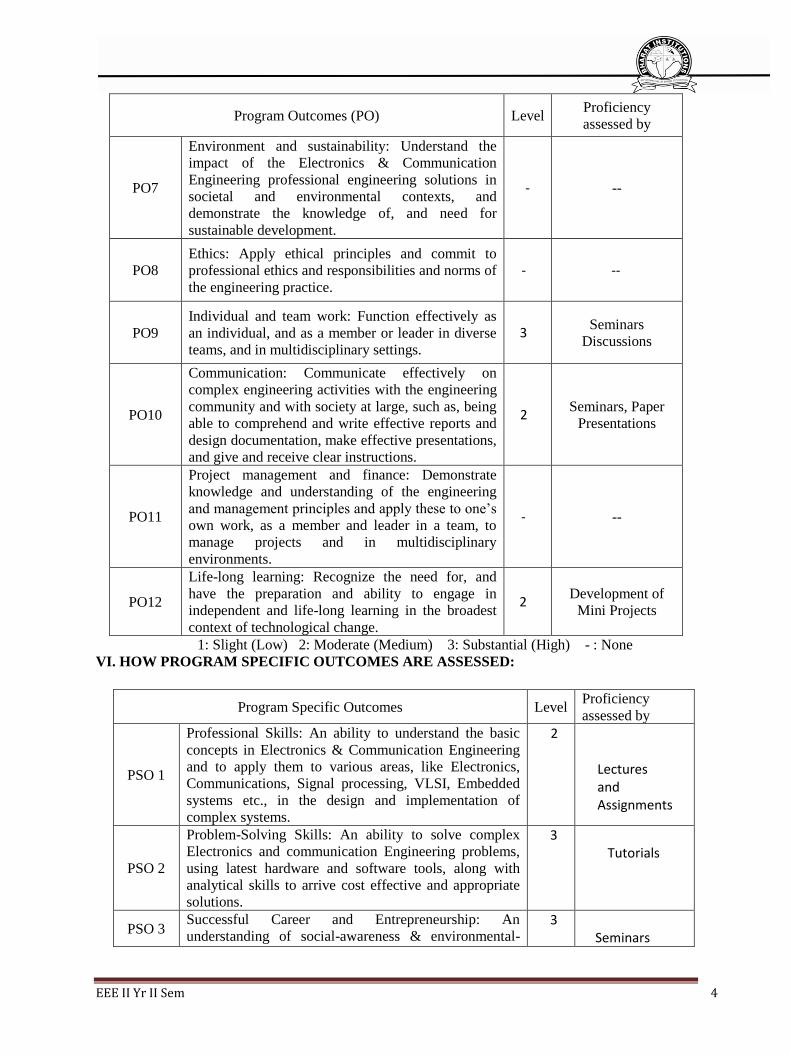
EEE II Yr II Sem 4
Program Outcomes (PO) Level Proficiency
assessed by
PO7
Environment and sustainability: Understand the
impact of the Electronics & Communication
Engineering professional engineering solutions in
societal and environmental contexts, and
demonstrate the knowledge of, and need for
sustainable development.
- --
PO8
Ethics: Apply ethical principles and commit to
professional ethics and responsibilities and norms of
the engineering practice.
- --
PO9
Individual and team work: Function effectively as
an individual, and as a member or leader in diverse
teams, and in multidisciplinary settings.
3 Seminars
Discussions
PO10
Communication: Communicate effectively on
complex engineering activities with the engineering
community and with society at large, such as, being
able to comprehend and write effective reports and
design documentation, make effective presentations,
and give and receive clear instructions.
2 Seminars, Paper
Presentations
PO11
Project management and finance: Demonstrate
knowledge and understanding of the engineering
and management principles and apply these to one’s
own work, as a member and leader in a team, to
manage projects and in multidisciplinary
environments.
- --
PO12
Life-long learning: Recognize the need for, and
have the preparation and ability to engage in
independent and life-long learning in the broadest
context of technological change.
2 Development of
Mini Projects
1: Slight (Low) 2: Moderate (Medium) 3: Substantial (High) - : None
VI. HOW PROGRAM SPECIFIC OUTCOMES ARE ASSESSED:
Program Specific Outcomes Level Proficiency
assessed by
PSO 1
Professional Skills: An ability to understand the basic
concepts in Electronics & Communication Engineering
and to apply them to various areas, like Electronics,
Communications, Signal processing, VLSI, Embedded
systems etc., in the design and implementation of
complex systems.
2
Lectures and Assignments
PSO 2
Problem-Solving Skills: An ability to solve complex
Electronics and communication Engineering problems,
using latest hardware and software tools, along with
analytical skills to arrive cost effective and appropriate
solutions.
3 Tutorials
PSO 3 Successful Career and Entrepreneurship: An
understanding of social-awareness & environmental-3
Seminars

EEE II Yr II Sem 5
1: Slight (Low) 2: Moderate (Medium) 3: Substantial (High) - : None
VII. SYLLABUS:
Course syllabus: (JNTU)
UNIT-I Number System and Boolean algebra And Switching Functions: Review of
number systems, Complements of Numbers, Codes- Binary Codes, Binary Coded Decimal Code and
its Properties, Unit Distance Codes, Error Detecting and Correcting Codes. Boolean Algebra: Basic
Theorems and Properties, Switching Functions, Canonical and Standard Form, Algebraic
Simplification of Digital Logic Gates, Properties of XOR Gates, Universal Gates, Multilevel
NAND/NOR realizations.
UNIT –II Minimization and Design of Combinational Circuits: Introduction, The
Minimization of switching function using theorem, The Karnaugh Map Method-Up to Five Variable
Maps, Don’t Care Map Entries, Tabular Method, Design of Combinational Logic: Adders,
Subtractors, comparators, Multiplexers, Demultiplexers, Decoders, Encoders and Code converters,
Hazards and Hazard Free Relations. UNIT-III Sequential Machines Fundamentals and Applications: Introduction: Basic
Architectural Distinctions between Combinational and Sequential circuits, The Binary Cell,
Fundamentals of Sequential Machine Operation, Latches, Flip Flops: SR, JK, Race Around Condition
in JK, JK Master Slave, D and T Type Flip Flops, Excitation Table of all Flip Flops, Design of a
Clocked Flip-Flop, Timing and Triggering Consideration, Clock Skew, Conversion from one type of
Flip-Flop to another. Registers and Counters: Shift Registers, Data Transmission in Shift Registers,
Operation of Shift Registers, Shift Register Configuration, Bidirectional Shift Registers, Applications
of Shift Registers, Design and Operation of Ring and Twisted Ring Counter, Operation Of
Asynchronous And Synchronous Counters.
UNIT - IV Sequential Circuits - I: Introduction, State Diagram, Analysis of Synchronous
Sequential Circuits, Approaches to the Design of Synchronous Sequential Finite State Machines,
Synthesis of Synchronous Sequential Circuits, Serial Binary Adder, Sequence Detector, Parity-bit
Generator, Design of Asynchronous Counters, Design of Synchronous Modulo N – Counters.
UNIT - V Sequential Circuits - II: Finite state machine-capabilities and limitations, Mealy and
Moore models-minimization of completely specified and incompletely specified sequential machines,
Partition techniques, and Merger chart methods-concept of minimal cover table.
TEXT BOOKS:
1.Switching and Finite Automata Theory- Zvi Kohavi & Niraj K. Jha, 3rdEdition,Cambridge .
2.Digital Design- Morris Mano, 5rd Edition, Pearson.
REFERENCE BOOKS: 1. 1. Fredriac J. Hill, Gerald R.Peterson, 3rd edition, Introduction to switching theory and logic
design.
2. 2. Thomas L.Floyd , Pearson 2013, Digital fundamentals – A Systems Approach
3. 3. Ye Brian and Holds Worth, Elsevier, Digital logic design
4. 4. John M. Yarbrough, Thomson publications 2006tld syllabus, Digital logic applications and
design.
5. 5. Roth (2004), Fundamentals of Logic Design, 5th edition, Thomson.
6. 6. Comer, 3rd, oxford 2013, Digital Logic and State machine Design
7. 7. Anand Kumar, Switching Theory and Logic Design
NPTEL Web Course: Digital Circuits
NPTEL Video Course: Digital Circuits
wisdom along with ethical responsibility to have a
successful career and to sustain passion and zeal for
real-world applications using optimal resources as an
Entrepreneur.
and Projects

EEE II Yr II Sem 6
GATE Syllabus: Digital Circuits, Number systems; Combinatorial circuits: Boolean algebra,
minimization of functions using Boolean identities and Karnaugh map, logic gates and
their static CMOS implementations, arithmetic circuits,code converters, multiplexers, decoders
and PLAs; Sequential circuits: latches and flip‐flops, counters, shift‐registers and finite state
machines;
IES Syllabus:Digital Circuits (Section:6)Boolean Algebra& uses; Logic gates, Digital IC families,
Combinatorial/sequential circuits; Basics of multiplexers, counters/registers/ memories
/microprocessors, design& applications.
VIII. COURSE PLAN (WEEK-WISE):
Lecture Week Topic Course
Learning
Outcome
Teaching
Methodol
ogy
Ref
UNIT 1
1
Week
– 1
Introduction
- Chalk
&
Board
T1,T2
2
Review of number systems,
Complements of Numbers
Understand
the arithmetic
operations
carried by
digital
systems.
Chalk
&
Board
3
Codes- Binary Codes, Binary Coded
Decimal Code and its Properties
Understand
the different
code
representations
in digital
systems.
Chalk
&
Board
4
Unit Distance Codes, Error Detecting
and Correcting Codes,*problems on
mantissa & exponent
Understand
the different
code
representations
in digital
systems.
Chalk
&
Board
5
Boolean Algebra: Basic Theorems and
Properties,*problems on tautology &
Fallacy
Learn
Boolean
algebra and
logical
operations in
Boolean
algebra.
Chalk
&
Board
6
Week
– 2 Switching Functions, Canonical and
Standard Form,
Learn
Boolean
algebra and
logical
operations in
Boolean
algebra.
Chalk
&
Board
7 Algebraic Simplification of Digital
Logic Gates
Apply
different logic
Chalk
&

EEE II Yr II Sem 7
gates to
functions and
simplify them.
Board
8
Properties of XOR Gates, Universal
Gates, Multilevel NAND/NOR
realizations
Apply
different logic
gates to
functions and
simplify them.
Chalk
&
Board
9
Revision
- Chalk
&
Board
10
Revision
- Chalk
&
Board
UNIT 2
11
Week
– 3
Introduction
- Chalk &
Board
T1,
T2
12
The Minimization of switching
function using theorem
Apply
different logic
gates to
functions and
simplify them.
Chalk &
Board
13
The Karnaugh Map Method-Up to
Five Variable Maps
Analyze the
redundant
terms and
minimize the
expression
using K-maps
Chalk &
Board
14
The Karnaugh Map Method-Up to
Five Variable Maps
Analyze the
redundant
terms and
minimize the
expression
using K-maps
Chalk &
Board
BRIDGE CLASS 1 -
15
Week
– 4
Don’t Care Map Entries
Analyze the
redundant
terms and
minimize the
expression
using K-maps
Chalk &
Board
16
Tabular Method
Identify the
redundant
terms and
minimize the
expression
using tabular
method
Chalk &
Board
17 Design of Combinational Logic:
Adders, Subtractors,
Apply the
logic gates and
Chalk &
Board

EEE II Yr II Sem 8
design of
combinational
circuits
18
comparators
Apply the
logic gates and
design of
combinational
circuits
Chalk &
Board
GUEST LECTURE - 1 -
19
Week-
5
Multiplexers, Demultiplexers
Apply the
logic gates and
design of
combinational
circuits
Chalk &
Board
T1,
T2
20
Decoders, Encoders
Apply the
logic gates and
design of
combinational
circuits
Chalk &
Board
21
Code converters
Design of
different
combinational
logic circuits
Chalk &
Board
22
Hazards and Hazard Free Relations
Design of
different
combinational
logic circuits
Chalk &
Board
BRIDGE CLASS 2 -
UNIT 3
23
Week-
6
Introduction: Basic Architectural
Distinctions between Combinational
and Sequential circuits
Understand
the clock
dependent
circuits and
identify the
differences
between
clocked and
clock less
circuits
Chalk &
Board
T1,
T2
24
The Binary Cell, Fundamentals of
Sequential Machine Operation
Understand
the clock
dependent
circuits and
identify the
differences
between
clocked and
clock less
circuits
Chalk &
Board
25 Latches, Flip Flops: SR Apply and Chalk &

EEE II Yr II Sem 9
design clock
dependent
circuits.
Board
26
JK, Race Around Condition in JK
Apply and
design clock
dependent
circuits.
Chalk &
Board
BRIDGE CLASS 4 -
27
Week-
7
JK Master Slave
Apply and
design clock
dependent
circuits.
Chalk &
Board
28
D and T Type Flip Flops
Apply and
design clock
dependent
circuits.
Chalk &
Board
29
Excitation Table of all Flip Flops
Apply and
design clock
dependent
circuits.
Chalk &
Board
30
Design of a Clocked Flip-Flop, Timing
and Triggering Consideration, Clock
Skew
Understand
how the flip-
flops are
synchronized.
Chalk &
Board
Week 8 (Mid-1)
Week-
9
BRIDGE CLASS 5 -
T1,
T2
31 GUEST LECTURE - 3 -
32
Conversion from one type of Flip-Flop
to another
Apply and
design clock
dependent
circuits.
Chalk &
Board
33
Registers and Counters: Shift
Registers
Apply the
sequential
circuits and
design the
different
memory
devices and
counting
circuits.
Chalk &
Board,ppt’
s
T1,
T2 34
Data Transmission in Shift Registers,
Operation of Shift Registers
Apply the
sequential
circuits and
design the
different
memory
devices and
counting
circuits.
Chalk &
Board,
ppt’s
35 Week- Shift Register Configuration Apply the Chalk & T1,

EEE II Yr II Sem 10
10 sequential
circuits and
design the
different
memory
devices and
counting
circuits.
Board,
ppt’s
T2
BRIDGE CLASS 6 -
36
Bidirectional Shift Registers,
Applications of Shift Registers
Apply the
sequential
circuits and
design the
different
memory
devices and
counting
circuits.
Chalk &
Board,
ppt’s
37
Design and Operation of Ring and
Twisted Ring Counter
Apply the
sequential
circuits and
design the
different
memory
devices and
counting
circuits.
Chalk &
Board
T1,
T2
38
Operation Of Asynchronous And
Synchronous Counters
Apply and
design clock
dependent
circuits.
Chalk &
Board
39
Week-
11
Operation Of Asynchronous And
Synchronous Counters
Apply and
design clock
dependent
circuits.
Chalk &
Board T1,
T2
40 MOCK TEST - II -
41 Revision -
UNIT 4
42
Introduction
- Chalk &
Board
T1,
T2
43
State Diagram
Analyze the
procedure to
reduce the
internal states
in sequential
circuits.
Chalk &
Board
44
Week
– 12
Analysis of Synchronous Sequential
Circuits, Approaches to the Design of
Synchronous Sequential Finite State
Machines
Analyze the
procedure to
reduce the
internal states
Chalk &
Board
T1,T
2

EEE II Yr II Sem 11
in sequential
circuits.
45
Analysis of Synchronous Sequential
Circuits, Approaches to the Design of
Synchronous Sequential Finite State
Machines
Analyze the
procedure to
reduce the
internal states
in sequential
circuits.
Chalk &
Board
BRIDGE CLASS 7 -
46
Synthesis of Synchronous Sequential
Circuits
Understand
how
synchronous
sequential
circuit works.
Chalk &
Board
47
Serial Binary Adder
Understand
how
synchronous
sequential
circuit works.
Chalk &
Board
48
Week
– 13
Sequence Detector
Understand
how
synchronous
sequential
circuit works.
Chalk &
Board
T
1,T2
49
Sequence Detector
Understand
how
synchronous
sequential
circuit works.
Chalk &
Board
BRIDGE CLASS 8 -
50
Parity-bit Generator
Understand
how
synchronous
sequential
circuit works.
Chalk &
Board
51
Design of Asynchronous Counters
Understand
how
Asynchronous
sequential
circuit works.
Chalk &
Board
52 Week
– 14 Design of Synchronous Modulo N
Counters
Understand
how
Asynchronous
sequential
circuit works.
Chalk &
Board
UNIT 5
53
Finite state machine-capabilities and
limitations
Understand
the FSM and
its design
principles.
Chalk &
Board
T1,
T2

EEE II Yr II Sem 12
54
Mealy and Moore models-
minimization of completely specified
and incompletely specified sequential
machines
Illustrate
minimization
of complete
and
incomplete
state machines
and to write a
minimal cover
table.
Chalk &
Board
55
Mealy and Moore models-
minimization of completely specified
and incompletely specified sequential
machines
Illustrate
minimization
of complete
and
incomplete
state machines
and to write a
minimal cover
table.
Chalk &
Board
56
Partition techniques
Illustrate
minimization
of complete
and
incomplete
state machines
and to write a
minimal cover
table.
Chalk &
Board
57
Week-
15
Partition techniques
Illustrate
minimization
of complete
and
incomplete
state machines
and to write a
minimal cover
table.
Chalk &
Board
58
Merger chart methods-concept of
minimal cover table
Illustrate
minimization
of complete
and
incomplete
state machines
and to write a
minimal cover
table.
Chalk &
Board
59
Merger chart methods-concept of
minimal cover table
Illustrate
minimization
of complete
and
incomplete
state machines
Chalk &
Board

EEE II Yr II Sem 13
IX. MAPPING COURSE OUTCOMES LEADING TO THE ACHIEVEMENT OF
PROGRAM OUTCOMES AND PROGRAM SPECIFIC OUTCOMES:
1: Slight (Low) 2: Moderate (Medium) 3: Substantial (High) - : None
X. QUESTION BANK (JNTUH) :
UNIT - I
Long Answer Questions: S.No. Question Blooms
Taxonomy
Level
Course
Outcome
1. Write the steps involved in unsigned binary subtraction using
complements with examples.
Remember 1
2.
a) Perform the subtraction with the following unsigned binary
numbers by taking the 2’s complement of the subtrahend:
i. 100-110000 ii. 11010-1101
(b) Construct a table for 4321 weighted code and
write 9154 using this code.
Apply 1
3. Find (3250-72532)10 using 10’s complement. Apply 1
4. (a) Perform arithmetic operation indicated below. Follow
signed bit notation
i. 001110 + 110010 ii. 101011-100110
Apply 1
5. (a)Divide 01100100 by 00011001 Apply 1
and to write a
minimal cover
table.
60 *Introduction to FPGA & CPLD -
BRIDGE CLASS 9 -
61
Week-
16
Revision of Unit-1 -
62 Revision of Unit-2 -
63 Revision of Unit-3 -
64 Revision of Unit-4 -
BRIDGE CLASS 10
-
Course
Outcomes
Program Outcomes Program Specific
Outcomes
PO1 PO2 PO3 PO4 PO5 PO6 PO7 PO8 PO9 PO10 PO111 PO12 PSO1 PSO2 PS
O3
CO1 3 2 2 2 2 2 - - 2 1 - 1 2 2 2
CO2 3 2 2 2 2 2 - - 2 1 - 2 1 2 3
CO3 2 3 3 3 3 2 - - 3 2 - 2 1 3 2
CO4 2 3 2 2 2 2 - - 3 2 - 1 2 2 2
CO5 3 3 3 3 3 2 - - 2 2 - 2 3 3 3
CO6 3 2 3 3 3 1 - - 3 1 - 1 1 3 3

EEE II Yr II Sem 14
(b)Given that (292)10=(1204)b determine ‘b’
6.
(a) What is the gray code equivalent of the Hex Number 3A7
(b)Find the binary number code for the decimal numbers
from 0 to 9
(c) Find 9’s complement (25.639)10
Understand 1
7.
(a)Find (72532-03250)using 9’s complement.
(b) Show the weights of three different 4 bit self
complementing codes whose only negative weight is -4
and write down number system from 0 to 9.
Apply 1
8.
Decimal system became popular because we have 10 fingers.
A rich person on Earth has decided to distribute Rs. One lakh
equally to the following persons from various planets. Find
out the amount each one of them will get in their respective
currencies:
A from planet VENUS possessing 8 fingers
B from planet MARS possessing 6 fingers
C from planet JUPITER possessing 14 fingers
D from MOON possessing 14 fingers
Apply 1
9. State and prove any 4 Boolean theorems with examples Understand 1
10. (a) Simplify to a sum of 3 terms: A’C’D’ + AC’ +BCD +
A’CD’ + A’BC + AB’C’
(b) Given AB’ + AB =C, show that AC’ + A’C =B
Apply 1
Short Answer Questions: S.No. Question Blooms
Taxonomy
Level
Course
Outcome
1. Write short notes on binary number systems. Remember 1
2. Discuss 1‟s and 2‟s complement methods of subtraction. Understand 1
3. Discuss octal number system. Understand 1
4. State and prove transposition theorem. Apply 1
5. Show how do you convert AND logic to NAND logic? Apply 1
6. Describe a short note on five bit bcd codes. Remember 1
7. Illustrate about unit –distance code? State where they are
used.
Understand 1
8. State about error correcting codes? Remember 1
9. When do you say that a signal is asserted? Understand 1
10. State about logic design and what do you mean by positive
logic system?
Understand 1
UNIT - II
Long Answer Questions: S.No. Question Blooms
Taxonomy
Level
Course
Outcome
1. A combinational circuit has 4 inputs (A,B,C,D) and three
outputs (X,Y,Z). XYZ represents a binary number whose
Evaluate 3
EEE II Yr II Sem 15
value equals the number of 1’s at the input
i. Find the minterm expansion for the X,Y, Z
ii. Find the maxterm expansion for the Y and Z.
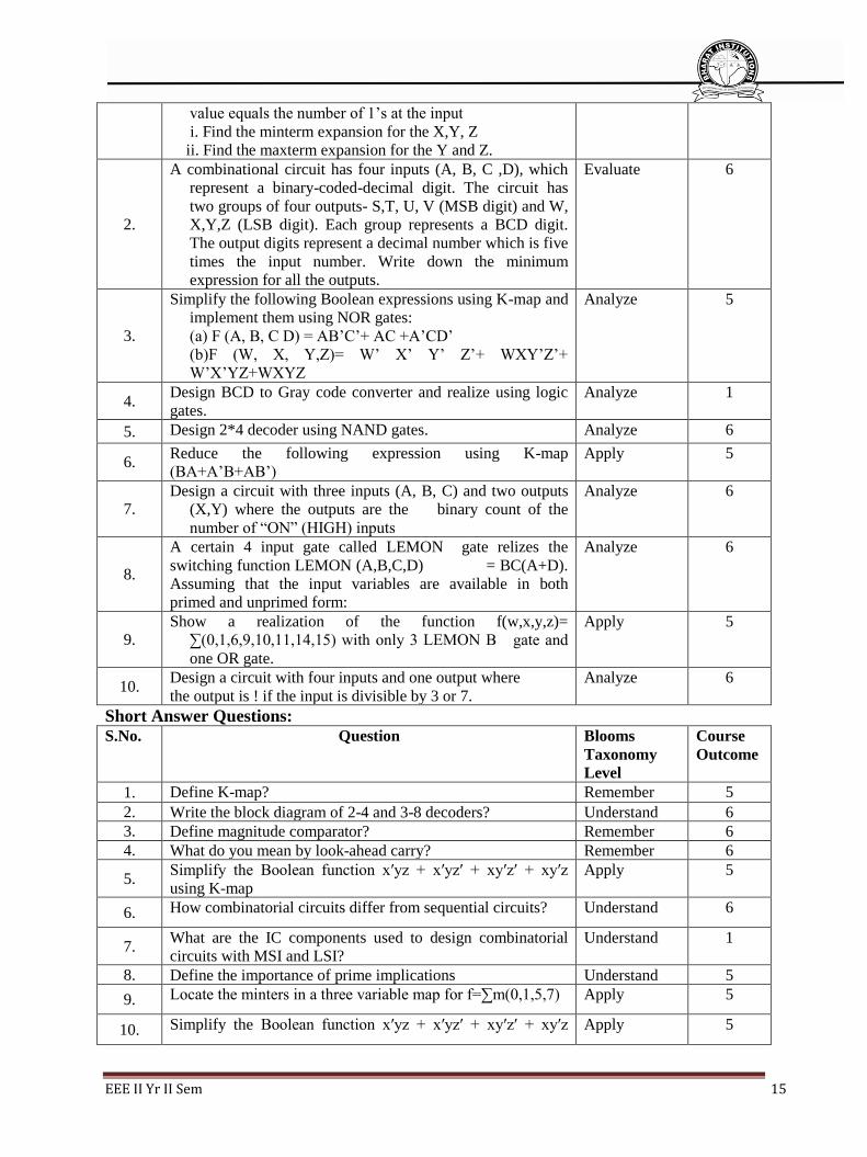
2.
A combinational circuit has four inputs (A, B, C ,D), which
represent a binary-coded-decimal digit. The circuit has
two groups of four outputs- S,T, U, V (MSB digit) and W,
X,Y,Z (LSB digit). Each group represents a BCD digit.
The output digits represent a decimal number which is five
times the input number. Write down the minimum
expression for all the outputs.
Evaluate 6
3.
Simplify the following Boolean expressions using K-map and
implement them using NOR gates:
(a) F (A, B, C D) = AB’C’+ AC +A’CD’
(b)F (W, X, Y,Z)= W’ X’ Y’ Z’+ WXY’Z’+
W’X’YZ+WXYZ
Analyze 5
4. Design BCD to Gray code converter and realize using logic
gates.
Analyze 1
5. Design 2*4 decoder using NAND gates. Analyze 6
6. Reduce the following expression using K-map
(BA+A’B+AB’)
Apply 5
7. Design a circuit with three inputs (A, B, C) and two outputs
(X,Y) where the outputs are the binary count of the
number of “ON” (HIGH) inputs
Analyze 6
8.
A certain 4 input gate called LEMON gate relizes the
switching function LEMON (A,B,C,D) = BC(A+D).
Assuming that the input variables are available in both
primed and unprimed form:
Analyze 6
9. Show a realization of the function f(w,x,y,z)=
∑(0,1,6,9,10,11,14,15) with only 3 LEMON B gate and
one OR gate.
Apply 5
10. Design a circuit with four inputs and one output where
the output is ! if the input is divisible by 3 or 7.
Analyze 6
Short Answer Questions: S.No. Question Blooms
Taxonomy
Level
Course
Outcome
1. Define K-map? Remember 5
2. Write the block diagram of 2-4 and 3-8 decoders? Understand 6
3. Define magnitude comparator? Remember 6
4. What do you mean by look-ahead carry? Remember 6
5. Simplify the Boolean function x′yz + x′yz′ + xy′z′ + xy′z
using K-map
Apply 5
6. How combinatorial circuits differ from sequential circuits? Understand 6
7. What are the IC components used to design combinatorial
circuits with MSI and LSI?
Understand 1
8. Define the importance of prime implications Understand 5
9. Locate the minters in a three variable map for f=∑m(0,1,5,7) Apply 5
10. Simplify the Boolean function x′yz + x′yz′ + xy′z′ + xy′z Apply 5

EEE II Yr II Sem 16
without using K-map
UNIT - III
Long Answer Questions:
S.No. Question Blooms
Taxonomy
Level
Course
Outcome
1. Compare RS and JK flip flop. Evaluate 6
2. Describe about T flip flop with the help of a logic diagram
and characteristic table. Derive a T-flip-flop from JK and D
flip flop.
Understand 6
3. Differentiate combinational and sequential circuits. Understand 6
4. Explain the working principle of JK flip flop in detail. Understand 6
5. Derive a JK-flip-flop from SR flip flop. Create 6
6. Explain serial transfer in 4-bit shift registers Understand 6
7. Explain about Binary Ripple counter. Understand 6
8. Define Latch. Explain different types of Latches in detail Understand 6
9. Examine with the help of a block diagram , the basic
components of a sequential circuit.
Understand 6
10. Explain the Ripple counter design. Mention its application Understand 6
Short Answer Questions: S.No. Question Blooms
Taxonomy
Level
Course
Outcome
1. Distinguish between a shift register and counter? Understand 6
2. What are the applications of shift registers? Understand 6
3. What are the applications of Flip-Flops? Understand 6
4. Discuss about a bidirectional shift register? Understand 6
5. How do you build a latch using universal gates? Analyze 6
6. What is the flip-flop memory characteristic? Understand 6
7. Distinguish between synchronous and asynchronous latch? Understand 6
8. What is meant by clocked flip-flop? Understand 6
9. Why a gated D latch is called a transparent latch? Understand 6
10. What are the two types of flip-flops? Understand 6
UNIT - IV
Long Answer Questions: S.No. Question Blooms
Taxonomy
Level
Course
Outcome
1. Explain the design of sequential circuit with an example.
Show the state reduction, State assignment.
Understand 6
2. Define BCD counter and Draw its state table. Remember 6
3.
Design a sequential circuit with two D flip flops A and B. and
one input x, when x=0, the
state of the circuit remains the same. When x=1, the circuit
Create 6
EEE II Yr II Sem 17
goes through the state transition from 00 to 11 to 11 to 10
back to 00 and repeats.
4. Design a Modulo 12 up Synchronous counter using T flip
flops and draw the circuit diagram
Create 6
5. Design a decade counter. Create 6
6. Design a left shift and riht shift for the following data
10110101
Create 6
7. Design a serial binary adder using state diagram. Create 6
8. Design a parity bit generator using state diagram. Create 6
9. Design a sequence detector for sequence 1110. Create 6
10. Design a 4-bit asynchronous counter using FSM. Create 6
Short Answer Questions: S.No. Question Blooms
Taxonomy
Level
Course
Outcome
1. What is state diagram? Give an example. Understand 6
2. Distinguish Synchronous and asynchronous counter. Understand 6
3. What are the approaches to the Design of Synchronous
Sequential Finite State Machines
Understand 6
4. Discuss about serial binary adder. Understand 6
5. Draw the state diagram of a sequence detector for sequence
1010.
Understand 6
6. Discuss about parity bit generator. Understand 6
7. Design a mod-3 counter. Create 6
8. What are the advantages and disadvantages of acynchronous
counters?
Understand 6
9. What do you mean by terminal count? Understand 6
10. State variable modulus counter? Understand 6
UNIT - V
Long Answer Questions: S.No. Question Blooms
Taxonomy
Level
Course
Outcome
1. Explain the operation of a microwave oven and
construct sequential machine.
Understand 6
2.
Design a synchronous state machine to generate following
sequence of states. Represent the machine by a state diagram
and display the onset of state 7 with the help of LED (use jk
flip flop)
Create 6
3.
Draw merger chart for a 2 bit binary counter having one
enable line E such that E= 1 (counting enabled) E=0
(counting disabled)
Create 6
4.
Show that 8 exit paths in merger chart emanating from the
decision boxes that check the eight possible binary value of
three control variables x,y,z.
Create 6
5. Draw the merger chart of binary multiplier and design the
control circuit using each of the following methods
Create 6

EEE II Yr II Sem 18
(a) JK FF and gates
(b) D FF and Decoder
6. Design control logic circuit using multiplexer Create 6
7. Draw the merger chart for 3 bit up down counter Create 6
8. Draw the merger chart for SR flip flop Create 6
9. Draw the merger chart for JK flip flop. Create 6
10. Design a mod-5 counter using multiplexer. Create 6
Short Answer Questions: S.No. Question Blooms
Taxonomy
Level
Course
Outcome
1. What are the capabilities and limitations of FSM ? Understand 6
2. Demonstrate about successor? Understand 6
3. Describe about terminal state? Understand 6
4. Define a strongly connected machine? Remember 5
5. List the advantage of having equivalent states ? Remember 6
6. State ‘state equivalence theorem’? Remember 6
7. Tell about distinguishing sequence? Remember 6
8. Define state compatibility? Remember 6
9. Describe a marger graph? Understand 6
10. State FSM compatibles? Remember 6
OBJECTIVE QUESTIONS:
UNIT-1
1. The fraction (0.68)10 is equal to [ ]
a) (0.010101)2 b) (0.101)2 c) (0.10101)2 d) (0.10111)2
2. The Hexadecimal number A0 has the decimal value [ ]
a)80 b) 256 c) 100 d) 160
3. Given two numbers A & B in sign magnitude representation in an eight bit format A=00011110 &
B=10011100, A XOR B gives [ ]
a)10000010 b) 00011111 c) 10011101 d) 11100001
4. The value of binary 1111 is [ ]
a) 23-1 b) 24-1 c) 24 d) none of these
5. The minimum number of bits required to represent negative numbers in the range of -1 to -11 using
2’s complement arithmetic is [ ]
(a) 2 (b) 3 (c) 4 (d) 5
6. The following code is not a BCD code. [ ]
a) Gray code (b) Xs-3 code (c) 8421 code (d) All of these
7. A 15-bit hamming code requires [ ]
(a) 4 parity bits (b) 5 parity bits (c) 15 parity bits (d) 7 parity bits
8. If=5, thebase (radix) of the number system is [ ]
a) 5 (b) 6 (c) 7 (d) 8
9. The hexadecimal number system is used in digital computers and digital systems to [ ]
(a) Perform arithmetic operations (b) Perform logic operations

EEE II Yr II Sem 19
(c) Perform arithmetic and logic operations (d) Input binary data into the sys
10. Determine the value of base x if: (211)x = (152)8 [ ]
(a) 2 (b) 10 (c) 8 (d) 7
11. Determine the value of base x, if (193)x = (623)8 [ ]
(a) 16 (b) 4 (c) 2 (d) 5
12. Which of the following are called Universal gates [ ]
(a) NAND, NOR (b) AND, OR (c) XOR XNOR (d) OR, XOR
13. Indicate which of the following logic gates can be used to realized all possible
combinational logic functions. GATE1989 [ ]
(A) OR gate (B)NAND gates only (C) EX-OR gate (D) NOR & NAND gates
14. Boolean expression for the output of XNOR logic gate with inputs A and B is GATE 1993 [ ]
(A) AB’ + A’B (B)(A(B)’ + AB (C) (A’ + (B)(A + B’) (D) (A’ + B’)(A + B)
15. The output of a logic gate is ‘1’ when all its inputs are at logic ‘0’. The gate is either
GATE 1994 [ ]
(A)a NAND or an EX-OR gate (B)a NOT or an EX-NOR gate
(C)an OR or an EX-NOR gate (D)an AND or an EX-OR gate
16.The output of the logic gate shown is GATE 1997 [ ]
(A) 0 (B) 1 (C) A
(D) A’
17. 2’s complement representation of a 16 bit number (one sign bit and 15 magnitude bits) is FFFF.
Its magnitude in decimal representation is GATE 1993[ ]
(A)0 (B) 1 (C) 32,767 (D) 65,535
18.Two 2’s complement numbers having sign bits x and y are added and the sign bit of the result is z.
Then, the occurrence of overflow is indicated by the Boolean function.
GATE 1998 [ ]
A) xyz (B) zyx (C) zxyzyx + (D)xy + yz + zx
19.4 – bit 2’s complement representation of a decimal number is 1000. The number is
GATE 2002[ ]
(A) +8 (B) 0 (C) -7 (D) -8
20.The number of bytes required to represent the decimal number 1856357 in packed BCD (Binary
Coded Decimal) form is _______. GATE 2014[ ]
(A) 4 (B) 3 (C)2 (D) 8
21. Cyclic codes are also called ________________codes
22. The basic two types of BCD codes are _______________and________ codes.
23. The distance between code words 10010 & 10101 is ________.
24. Convert the binary code (110110)2 to Gray code ______
25. Conversion of 0.1289062 decimal number to its hexa equivalent is _______
26. In b’s complement method, the carry is ______ and in(b-1)’s complement method the
carry is _______

EEE II Yr II Sem 20
27. The MSB of a binary number has a weight of 512, the number consists of _______ bits.
28. ______ are codes which represent letters of the alphabets and decimal numbers as a sequence of
0s and 1s.
UNIT-2
1.The short hand notation of min term m6 is [ ]
(a) (b) (c) ABC (d)
2. In Boolean algebra A+AB= _____
3. Boolean expression xy+yz+ = _______on reduction.
4. The given expression Y=A+AB+ABC in SOP form is ________
5. In K-map each of the cell represents one of the _________ possible products [ ]
(a)2n (b)2-n (c)n2 (d)All the above
6. The minimum number of bits required to represent negative numbers in the range of -1 to -11 using
2’s complement arithmetic is [ ]
(a)2 (b) 3 (c) 4 (d) 5
7. The following code is not a BCD code. [ ]
a)Gray code (b) Xs-3 code (c) 8421 code (d) All of these
8. A 15-bit hamming code requires [ ]
(a)4 parity bits (b) 5 parity bits (c) 15 parity bits (d) 7 parity bits
9. The logic expression (A+B)(+) can be implemented by giving the inputs A and B to a two-input [ ]
(a)NOR gate (b) NAND gate (c) X-OR gate (d) X-NOR gate
10. Which of the following Boolean algebraic expressions is incorrect? [ ]
(a)A+B=A+B (b) A+AB=B (c) (A+B)(A+C)=A+BC (d) (A+)(A+B)=A
11. The hexadecimal number system is used in digital computers and digital systems to []
(a) Perform arithmetic operations (b) Perform logic operations
(c) Perform arithmetic and logic operations (d) Input binary data into the system.
12. The logic expression A+B can be implemented by giving inputs A and B to a two-input [ ]
(a)NOR gate (b) NAND gate (c) X-OR gate (d) X-NOR gate
13. A gate is enabled when its enable input is at logic 0. The gate is []
(a)NOR (b) AND (c) NAND (d) None of these
14. The output of a logic gate is 1 , when all its inputs are at logic 0.The gate is either [ ]
(a)a NOR or an X-NOR (b) a NAND or an X-OR
(c) an OR or an X-NOR (d) an AND or an X-OR
15. In b’s complement method, the carry is ______ and in(b-1)’s complement method the
carry _______
16. The MSB of a binary number has a weight of 512,The number consists of ________
17._________ are codes which represent letters of the alphabets and decimal numbers as a sequence of
0s and 1s.
18. The interconnection of gates to perform a variety of logical operations is called______
19. The NOR gate can function as a NOT gate if ________

EEE II Yr II Sem 21
20. The implicants which will definitely occur in the final expression are called_______
21. The prime implicant mode of a bunch of 0s is called a ______
22. ______ is a process of converting familiar numbers or symbols into a coded format.
23. A decoder with 64 output lines has ______ select lines.
24. A decimal – to – BCD encoder is a ____ line to _____line encoder.
UNIT-3 1. The combinational circuits are______ than sequential circuits [ ]
A)slower B) faster C) same speed D) None
2. In combinational circuits the o/p depends on ________i/p [ ]
A)present B) past C) A & B D) None
3. Full adder circuit adds _______number of bits at a time [ ]
A) 5 B) 2 C) 5 D) 3
4. Half adder circuit adds _______number of bits at a time [ ]
A) 5 B) 2 C) 5 D) 3
5. Serial binary adder is a _______circuit [ ]
A)combinational B) sequential C) A or B D) None
6. A 4 bit parallel adder is designed using _______number of full adders [ ]
A) 2 B) 4 C) 5 D) 3
7. The logic expression for carry of half adder circuit is_____ [ ]
A) A’B B) AB C) AB’ D) None
8. The logic expression for sum of half adder circuit is_____ [ ]
A) A’B B) A xor B C) AB’ D) None
9. In a half subtractor circuit borrow expression is________ [ ]
A) A’B B) AB C) AB’ D) None
10. The logic expression for difference of half subtractor circuit is_____ [ ]
A) A xor B xor C B) B xor C C) A xor B D) None
11. The logic expression for sum of full adder circuit is_____ [ ]
A) A’BC B) A xor B xor C C) B xor C D) None
12. The logic expression for carry of full adder circuit is_____ [ ]
A) ABC B) A xor B xor C C) B xor C D) None
13. In a full subtractor circuit difference expression is________ [ ]
A) A xor B xor C B) B xor C C) A xor C D) B xor C
14. In a full subtractor circuit borrow expression is________ [ ]
A) A xor B xor C B) B xor C C) A xor C D) None
15. The full adder circuit is implemented using _____number of half adder circuits [ ]
A) 3 B) 1 C) 2 D) 4
16. The full subtractor circuit is implemented using _____number of half subtractor circuit
[ ]
A) 3 B) 1 C) 2 D) 4
17. Complement of a bit in adder - subtractor circuit is [ ]
A)inverter B) XOR C) AND D)None
18. Carry look ahead adder reduces _________ [ ]
A)carry propagation time B) carry generation time C) sum generation time D) None
19. For an n-bit adder there are _______ gate levels for the carry to propagate from input to output
[ ]
A)3n B) 4n C) 2n D) None

EEE II Yr II Sem 22
20. In carry look ahead adder C i+1=___________ [ ]
A)Gi+PiCi B) Gi+Pi+1Ci C) Gi+1+PiCi D)None
21. In magnitude comparison of A,B the output of a xor gate if they are equal is ---------
22. In magnitude comparison of A,B the output of a xnor gate if they are equal is --------
23. In magnitude comparison of A,B the output of a xor gate if they are unequal is --------
24. In magnitude comparison of A,B the output of a xnor gate if they are unequal is --------
25. Minimum number of half adders required for 2 bit multiplier is ----------
26. If A=1010 and B=0100 .Then output of a 4 bit parallel adder is______
27. A decoderwith n input provides _______minterms at the output.
28. A encoder has --------number of inputs and --------number of outputs
29. The number of output lines in 1X4 demultiplexer is_______
30. The number of AND gates required to implement 3 X 8 decoder along with 3 not gates is___
31. To implement full adder ---------size decoder is required
32. A 4X16 decoder can be designed using _____ number of 3x8 decoders
33. An octal to binary encoder is implemented using 3_____ gates
34. The number of select inputs in 32X1 multiplexer is_______
35. The binary variable (A=B) is equal to _____ only if all pairs of digits of the two numbers are
equal
36. In a 4X2 priority encoder with D3 with highest priority the output XY for input 1111 is_____\
37. The decimal adder is also known as ________adder
38. Multiplexer is also called as
39. Demultiplexer is also called as
40. The decimal adder is also known as ________adder
41. The number of 4X1 multiplexers required to design 16X1 multiplexer is ____
42. A 2bit multiplier can design using minimum of
43. A ripple counter's speed is limited by the propagation delay of -------
44. To operate correctly, starting a ring counter requires --------
UNIT-4 1. The output Y of a 2-bit comparator is logic 1 whenever the 2 bit input A is greater than the 2 bit
input B. The number of combinations for which the output is logic 1, is
A. 4 B. 6 C. 8 D. 10
GATE 2012 [ ]
2. A switch-tail ring counter is made by using a single D flip flop. The resulting circuit is a
GATE 1995 [ ]
A. SR flip flop B. JK flip flop C. D flip flop D. T flip flop
3. An SR latch is a GATE 1995 [ ]
A. Combinational circuit B. Synchronous sequential circuit
C. One bit memory element D. One clock delay element
4. The present output Qn of an edge triggered JK flip-flop is logic ‘0’. If j = 1, then Qn+1 is
GATE 2005 [ ]
A. Cannot be determined B. Will be logic ‘0’
C. Will be logic ‘1’ D. Will race around
5. A 4 bit modulo-16 ripple counter uses JK flip-flops. If the propagation delay of each flip-flop is
50 nsec, the maximum clock frequency that can be used is equal to ____.
GATE 1990 [ ]
A. 20 MHz B. 10 MHz C. 5 MHz D. 4 MHz
6. Synchronous counters are ________ than the ripple counters. GATE1994 [ ]
A. Slower B. Faster C. Moderate D. None

EEE II Yr II Sem 23
7. A 4 bit ripple counter and a 4 bit synchronous counter are made using flip flops having a
propagation delay of 10 ns each. If the worst case delay in the ripple counter and the synchronous
counter be R and S respectively, then GATE 2003 [ ]
A. R = 10 ns, S = 40 ns B. R = 40 ns, S = 10 ns
C. R = 10 ns, S = 30 ns D. R = 30 ns, S = 10 ns
8. In sequential Circuits, the output variable depends on ______of the input variable. []
A. Present State B. Past State C. Both D. None
9. The Serial adder is a _______Circuit. []
A. Combinational B. Sequential C. Both D. None
10. The outputs of any sequential circuit are always ______to each other.
A. Complementary B. Independent C. Pearson D. None
11. In S-R latch, if S=R=1, the present state of the latch is. [ ]
A. 1 B. 0 C. Undetermined D. None
12. The D- latch sometimes called as _____ Latch. [ ]
A. Flipflop B. Buffer C. Transparent D. None
13. _____ and______are building blocks of Sequential Circuits. [ ]
A. Flipflop B. Latches C. Both D. None
14. In ______Triggering, the output of Flipflop responds to the input changes only when its enable
input is Low. [ ]
A. Negative Level B. Positive Level C. Edge D. None
15. If S=0, R=1 and CP = 0 to which Qn= 0\1, the S-R Flipflop will be in __State. [ ]
A. No change B. 1 C. 0 D. Undetermined
16. The Basic building block of D- flipflop is ____Flipflop. [ ]
A. J-K B. Master-Slave C. S-R D. None
17. The output Qn+1is delayed by one clock period for an D- Flipflop to which it is called as
____Flipflop. []
A. J-K B. Master-Slave C.S-R D. Delay
18. For the Inputs J=0, K=0, the output Q will be in ____state. []
A. Reset B. Undertermined C.Nochange D. Delay
19. In JK flipflop, when J = K = 1, the output the Flipflop will be in ____state. []
A. Reset B. Undertermined C. Toggling D. Delay
20. _____will not be an clock input of the Master-slave Flipflop. [ ]
A. Edge Triggered B. Level Triggered C.Both D. None
21. The ____ Flipflop is a modification of JK Flipflop.
22. If P = C = 0, the flipflop will be in _____ State.
23. For Moore Sequential Circuit, the output depends on____ State.
24. The state reduction technique avoids ______states.
25. The Input and Output of a register can be controlled by connecting ____.
26. The _____ are used to transfer and storage of data in the registers.
27. The acronym of SIPO is______.
28. The _____ register has capability of both shifts and parallel load.
29. The______counters are simple in construction for more no. of states.
30. The Major limitation of Ripple counter is_____.
UNIT-5
1. Moore Machine is an application of:
a) Finite automata without input
b) Finite automata with output
c) Non- Finite automata with output
d) None of the mentioned
2. In Moore machine, output is produced over the change of:
EEE II Yr II Sem 24
a) transitions
b) states
c) Both
d) None of the mentioned
3. For a give Moore Machine, Given Input=’101010’, thus the output would be of length:
a) |Input|+1
b) |Input|
c) |Input-1|
d) Cannot be predicted
4. Statement 1: Null string is accepted in Moore Machine.
Statement 2: There are more than 5-Tuples in the definition of Moore Machine.
Choose the correct option:
a) Statement 1 is true and Statement 2 is true
b) Statement 1 is true while Statement 2 is false
c) Statement 1 is false while Statement 2 is true
d) Statement 1 and Statement 2, both are false
5. The total number of states and transitions required to form a moore machine that will produce
residue mod 3.
a) 3 and 6 b) 3 and 5 c) 2 and 4 d) 2 and 5
6. What is the output for the given language is --------
Language: A set of strings over ∑= {a, b} is taken as input and it prints 1 as an output “for every
occurrence of a, b as its substring. (INPUT: abaaab)
7. The output alphabet can be represented as --------
8. The O/P of Moore machine can be represented in the following format is --------
9.For n no. of Flipflops, the counter has ____no. of states.
10.The twisted counter is also called as ______Counter.
11.The __ Counter requires only half the no. of Flipflops compared to Standard counter.
12.For a counter of five-bit sequence, there are ____ states.
13.If all the Fliflops are triggered at the same time in an counter, then the counter is referred to as
______ Counter.
XIII. WEBSITES: 1. www.asic-world.com
2. www.nptel.ac.in
3. www.learnabout-electronics.org
XIV . MOOCS SWAYAM NPTEL COURSE AS DIGITAL CIRCUITS
(onlinecourses.nptel.ac.in/noc18_ee33) – 12week course.
XV. JOURNALS:
INTERNATIONAL 1. International journal of Analog and Digital Electronics
2. International journal of Digital Electronics
3. International journal of Electronic Security and Digital Forensics
XVI. CASE STUDIES / SMALL PROJECTS:
1. Digital Fan speed regulator
2. Traffic controller
3. Adaptive lighting system for automobiles
4. Automatic LED emergency light.