Advance Mathematics B.Tech. 2nd Year, III-Semester Branch ...

Branch- ECE, CS
Semester- III
Subject – Switching Theory, Digital Logic Design Subject code –NEC304, NEC309

Contents
Unit-1
Digital system and binary numbers
1.1 Signed binary numbers
1.2 Binary codes
Gate-level minimization
1.3 The map method up to four variable
1.4 Don’t care conditions
1.5 POS simplification
1.6 NAND and NOR implementation,
1.7 Quine Mc-Clusky method (Tabular method)
Unit-2
Combinational Logic
2.1 Combinational circuit
2.2 Analysis procedure
2.3 Design procedure
2.4 Binary adder-subtractor
2.5 Decimal adder
2.6 Binary multiplier
2.7 Magnitude comparator
2.8 Multiplexers
2.9 Decoders
2.10 Encoders
Unit-3 Synchronous Sequential logic
3.1 Sequential circuits
3.2 Storage elements: Latches
3.3 Storage elements: Flip flops
3.4 Analysis of clocked sequential circuits
3.5 State reduction and assignments
3.6 Design procedure
Asynchronous Sequential logic
3.7 Analysis procedure 3.8 Circuit with latches
3.9 Design procedure
3.10 Reduction of state and flow table
3.11 Race Free State assignment
3.12 Hazards.
Unit-4 Registers and counters:
4.1 Shift registers 4.2 Ripple counter
4.3 Synchronous Counter
4.4 Other counters

Memory and programmable logic
4.5 RAM
4.6 ROM
4.7 PLA
4.8 PAL

UNIT 1
DIGITAL SYSTEM, BINARY NUMBERS & GATE-LEVEL
MINIMIZATION
1.1 SIGNED BINARY NUMBERS
THE BINARY, DECIMAL, AND HEXADECIMAL NUMBER SYSTEMS
BASE DIGITS RADIX
BINARY (2) 0 , 1 b or B
DECIMAL (10) 0 , 1 , 2 , 3 , 4 , 5 , 6 , 7 , 8 , 9 d , D , or no radix
HEXADECIMAL 0,1, 2, 3, 4, 5, 6, 7, 8, 9, A, B, C, D, E, F (or a, b, c, h or H
(16) d, e, f)
Converting an unsigned or a positive number in base b to base 10
An unsigned or a positive integer in base b with n digits:
dn - 1dn - 2 . d2d1d0
has the decimal (base 10) value: n1
dn - 1 * bn - 1 + dn - 2 * b
n - 2 + + d2 * b
2 + d1 * b
1 + d0 * b
0 = di* bi
i0
where all the arithmetic is done in base 10.
Example: Convert each of the following unsigned numbers to decimal:
(a) 10110011B (b) 3BA4H
Solution:
(a) 1 * 27
+ 0 * 26
+ 1 * 25
+ 1 * 24
+ 0 * 23
+ 0 * 22
+ 1 * 21
+ 1 * 20
= 179D
(b) 3 * 163
+ 11 * 162
+ 10 * 161
+ 4 * 160
= 15268D
Converting an unsigned or a positive decimal number to base b
Repeatedly divide the number and then each succeeding quotient by b until a quotient of zero is
obtained. The remainders from the last to the first; but converted to base b, form the required
number. An appropriate number of leading zeroes is prefixed to obtain the required number of
bits.

Example#1: Convert 5876 into a 16-bit hexadecimal number.
Solution:
367 22 1 0 16 5876 16 367 16 22 161
- 5872 - 352 - 16 - 0
4 15 6 1
4 F 6 1
Thus the answer is 16F4H
Example#2: Convert 37D into (a) an 8-bit binary number, (b) a 16-bit binary number
Solution:
18 9 4 2 1 0 2 37 218 2 9 2 4 2 2 2 1
-36 - 18 - 8 - 4 - 2 - 0
1 0 1 0 0 1
(a) 00100101B
(b) 0000000000100101B
Spatial Units of Measure used in relation to computer storage capacities
UNIT SYMBOL POWER OF 2 BYTES
Byte 20
1
Kilobyte KB 210
1,024
Megabyte MB 220
1,048,576
Gigabyte GB 230
1,073,741,824
Terabyte TB 240
1,099,511,627,776
28
bytes = 256 bytes = 100H bytes
1 KB = 210
bytes = 1024 bytes = 400H bytes
64 KB = 216
bytes = 65536 bytes = 10000H bytes 1 MB = 2
20 bytes = 1048576 bytes = 100000H bytes

Hexadecimal binary conversions
Every hexadecimal digit corresponds to four binary digits. The conversion table for the same is
shown below:
8 4 2 1 weights
HEXADECIMAL BINARY
0 0 0 0 0
1 0 0 0 1
2 0 0 1 0
3 0 0 1 1
4 0 1 0 0
5 0 1 0 1
6 0 1 1 0
7 0 1 1 1
8 1 0 0 0
9 1 0 0 1
A 1 0 1 0
B 1 0 1 1
C 1 1 0 0
D 1 1 0 1
E 1 1 1 0
F 1 1 1 1
Example: Convert 3b8EH to binary
Solution: 0011 1011 1000 1110B
Example: Convert 0111 1010 0110 1111B to hexadecimal
Solution: 7A6FH (Note: Group the binary digits from right to left; append leading zeroes if
necessary)
BINARY AND HEXADECIMAL ADDITION
Binary addition rules: 0 + 0 = 0 , 0 + 1 = 1 , 1 + 0 = 1 , 1 + 1 = 0 with a carry of 1
Hexadecimal addition rule: Let Nb denote a number N converted to base b.
If X and Y are two hexadecimal digits and X10 + Y10 = Z 16 then
X + Y = (Z - 16)16 with a carry of 1; otherwise X + Y = Z16

Example: Solve (a) 00000111B + 11111111B (b) AFB7H + CFF6H
Solution:
(a) (b)
1 1 1 1 1 1 1 1 carry 1 1 1 carry
0 0 0 0 0 1 1 1 B A F B 7 H
+ 1 1 1 1 1 1 1 1 B + C F F 6 H
1 0 0 0 0 0 1 1 0 B 1 7 F A D H
BINARY AND HEXADECIMAL DIRECT SUBTRACTION
Binary subtraction: A borrow of 1 is worth 2 in decimal.
Hexadecimal subtraction: A borrow of 1 is worth 16 in decimal.
Example: (a) C B A 2 H (b) 2 A C 5 H
- A F D 3 H - F D 9 2 H
1 B C F H unsatisfied borrow (b) 2 E 3 3 H
FIXED-WIDTH ARITHMETIC
The CPU performs arithmetic in a specified, fixed number of bits. In a computer with 8086/8088
CPU, numbers are usually stored using 8 bits, 16 bits, or 32 bits. For 8086/8088 applications, a
group of 8 bits is called a byte, 16 bits (two bytes) is called a word, and 32 bits (four bytes) is
called a double word. These terms have been defined differently for other computer systems.
UNSIGNED NUMBERS AND UNSIGNED OVERFLOW
For an unsigned number of n bits, all the n bits are used in the representation of the number. Thus
the range of values for 8-bit and 16-bit unsigned numbers can be listed as:
MINIMUM MAXIMUM
Binary 0000 0000B 1111 1111B
8-bit Hexadecimal 00H FFH
Decimal 0 255
Binary 0000 0000 0000 1111 1111 1111
0000B 1111B
16-bit Hexadecimal 0000H FFFFH
Decimal 0 65535
Unsigned addition overflow
An n-bit, unsigned addition overflow occurs if the sum is outside the allowed range of values for an
n-bit number. Overflow condition is detected, computationally, for binary and hexadecimal addition
by the existence of a final carry. For decimal addition overflow is detected, computationally,
by the sum being outside the range. Since the CPU performs all additions in binary, decimal overflow
also result in a final carry.
In case of unsigned addition overflow, the value in the destination operand is the unsigned
number obtained by discarding the final carry. This value will not be the correct sum.

Example: For each of the 16-bit additions below determine whether unsigned addition overflow will
occur or not. If an overflow occurs find the value in the destination operand.
(a) 0001 1111B + 1100 1100B (b) EA9BH + FFF6H (c) 45789 + 30450
Solution: (a) 0001 1111B (b) EA9BH (c) 45689
+ 1100 1100B + FFF6H +30450
1110 1011B 1EA91H 76139 1296BH
No unsigned overflow. Unsigned overflow. Unsigned overflow, 76139 > 65535.
Value in destination is EA91H Value in destination is 296BH
Unsigned subtraction overflow
An unsigned subtraction overflow occurs if the subtrahend is greater than the minuend (For a
subtraction A - B = C, A is the minuend, B is the subtrahend, and D is the difference).
Thus overflow is detected by the presence of an unsatisfied borrow. In such a case the value in the destination operand is not correct; it is the unsigned number obtained by discarding the unsatisfied borrow.
Example: Find the unsigned value stored in the destination operand for the 8-bit unsigned
subtraction 72 - 235
Solution: 72 48H
- 235 - EBH (b)5DH
The required value is 5DH
r’s COMPLEMENT REPRESENTATION FOR SIGNED INTEGERS
A signed integer can be represented in one of the following representations: 1. Sign and magnitude.
2. One’s complement [ (r - 1)’s complement]
3. Two’s complement [ r’s complement]
4. Excess 2n - 1
Intel 8086/8088 uses two’s complement to represent signed numbers. In this representation the msb
(most significant bit) represents the sign; 0 for a positive sign and 1 for a negative sign. It follows that:
(i) every signed binary number starting with 0 is positive, and that starting with 1 is negative. (ii) every signed hexadecimal number starting with any of the hexadecimal digits 0, 1, 2, 3, 4,
5, 6, or 7 is positive, and that starting with any of the hexadecimal digits 8, 9, A, B, C, D, E, or F is negative.

The range of values for 8-bit and 16-bit signed numbers can be listed as:
MINIMUM MAXIMUM
Binary 1000 0000B 0111 1111B
8-bit Hexadecimal 80H 7FH
Decimal -128 +127
Binary 1000 0000 0000 0111 1111 1111
0000B 1111B
16-bit Hexadecimal 8000H 7FFFH
Decimal -32768 +32767
Using weights to convert a signed binary number to decimal
For a signed number, the most significant bit in a byte or word does not correspond to 27 or 2
15
respectively, but it corresponds to -27 or -2
15.
Example: Convert the following 8-bit signed numbers to decimal:
(a) 1000 0000B (b) 1011 0011B (c) 0011 0000B
Solution:
(a) 1 * (-27) + 0 * 2
6 + 0 * 2
5 + 0 * 2
4 + 0 * 2
3 + 0 * 2
2 + 0 * 2
1 + 0 * 2
0 = -128
(b) 1 * (-27) + 0 * 2
6 + 1 * 2
5 + 1 * 2
4 + 0 * 2
3 + 0 * 2
2 + 1 * 2
1 + 1 * 2
0 = -77
(c) 0 * (-27) + 0 * 2
6 + 1 * 2
5 + 1 * 2
4 + 0 * 2
3 + 0 * 2
2 + 0 * 2
1 + 0 * 2
0 = 48
The r’s complement of a signed number
The r’s complement of a negative number is its positive, and that of a positive number is its negative.
To find the r’s complement of a base r number with n digits
(i) subtract the number from a number with n digits all of which are the highest digit in base r. (ii)
add one to the result of (i).
Note: For binary numbers, (i) and (ii) above lead to the following rule:
To find the 2’s complement of a binary number, toggle each bit of the number and then add one to the
result.
Example: (a) Find the 16’s complement of 4FB6H, (b) Find the 2’s complement of 11010110B
Solution:
(a) FFFFH (b) 00101001B
- 4FB6H + 1B
B049H 00101010B
+ 1H B04AH
Note: If we try to find the 16’s complement of the 8-bit number 80H we get:
(FFH - 80H) + 1H = 80H

which is clearly wrong. The reason for this is that 80H = -128. Thus trying to find the
complement of 80H will result in +128 which is greater than the maximum 8-bit signed number,
namely +127. Similarly the 16-bit number 8000H does not have a 16-bit complement.
Note: For 8086/8088 processor the NEG instruction whose syntax is: NEG operand
converts the value in a memory or register operand to its 2’s complement.
Converting signed binary and hexadecimal numbers to decimal by using r’s complement n1
Positive numbers are converted by the formula: di* bi
i0
Negative numbers are converted by: (i) Finding the r’s complement of the number.
n1
(ii) Converting the complement to decimal by the formula: di* bi
i0
(iii) Appending a negative sign to the converted complement.
Example: Convert F4H to decimal if the number is (a) unsigned , (b) signed
Solution: (a) 15 * 161
+ 4 * 160
= 244D
(b) The number is negative because its sign bit is 1:
(FFH - F4H) + 1H = 0CH = 12D
Hence, F4H = -12D
Example: Convert 7BA4H to decimal if the number is (a) unsigned , (b) signed
Solution: (a) 7 * 163
+ 11 * 162
+ 10 * 161
+ 4 * 160
= 31652D
(b) The number is positive because its sign bit is 0:
Hence, 7BA4H = +31652D
Example: Convert the signed number 11111111B to decimal.
Solution: The number is negative because its sign bit is 1:
00000000B + 1B = 00000001B = 1D
Hence, 11111111B = -1D
Example: Convert -25D to an 8-bit hexadecimal value.
Solution: 25D = 19H (by dividing 25 then the resulting quotient by 16)
The complement of 19H is (FFH - 19H) + 1H = E7H
Thus, -25D = E7H
Note: the signed numbers 80H and 8000H cannot be converted to decimal by using r’s
complement, because each has no complement in the range of values for 8-bit and 16-bit signed
numbers respectively. The two numbers can be converted to decimal using the weights method:
80H = 10000000B = 0
* 20 = -128
1 * (-27) + 0 * 2
6 + 0 * 2
5 + 0 * 2
4 + 0 * 2
3 + 0 * 2
2 + 0 * 2
1 +
8000H = 1000 0000 0000 0000B = 1 * (-215
) + 0 + . . . + 0 = -32768
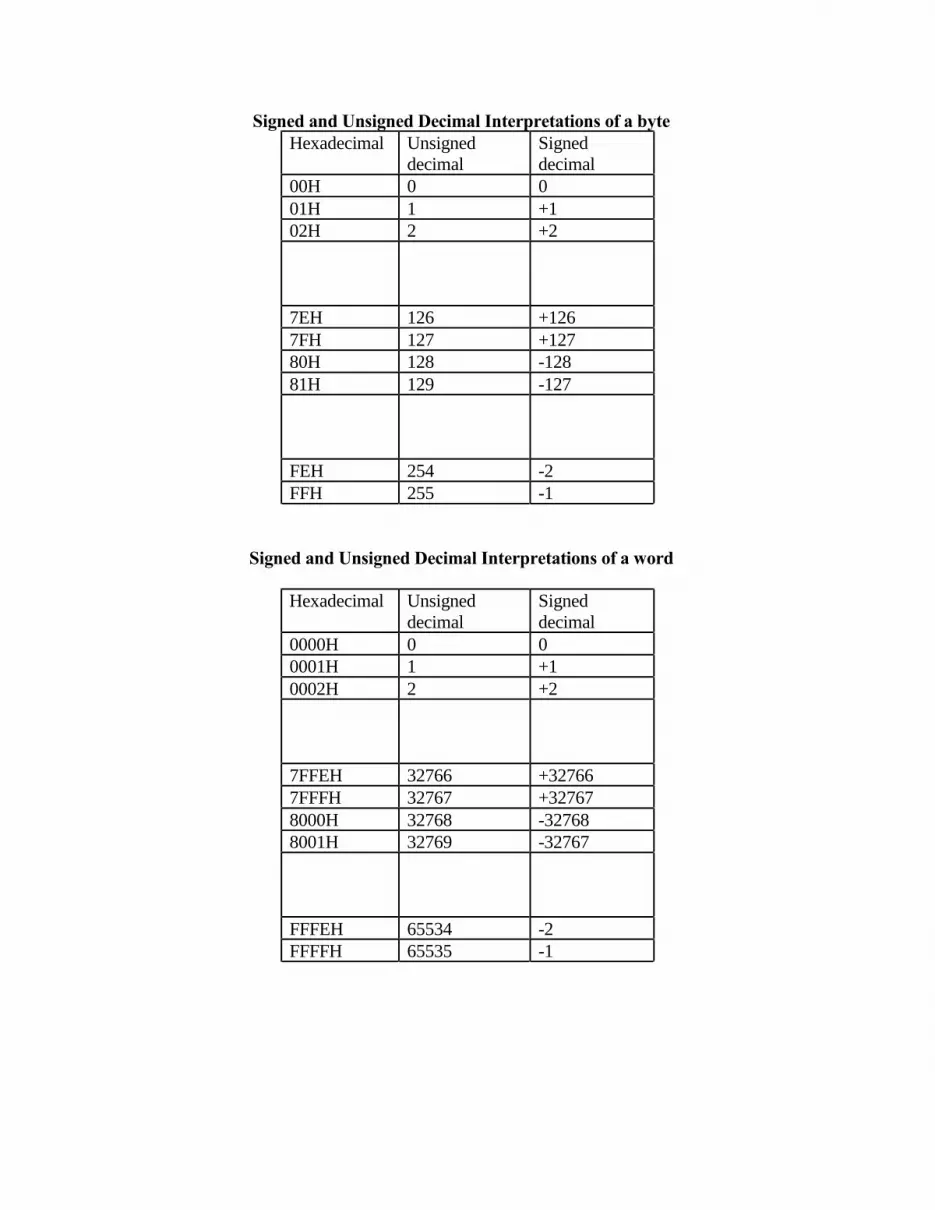
Signed and Unsigned Decimal Interpretations of a byte
Hexadecimal Unsigned Signed
decimal decimal
00H 0 0
01H 1 +1
02H 2 +2
7EH 126 +126
7FH 127 +127
80H 128 -128
81H 129 -127
FEH 254 -2
FFH 255 -1
Signed and Unsigned Decimal Interpretations of a word
Hexadecimal Unsigned Signed
decimal decimal
0000H 0 0
0001H 1 +1
0002H 2 +2
7FFEH 32766 +32766
7FFFH 32767 +32767
8000H 32768 -32768
8001H 32769 -32767
FFFEH 65534 -2
FFFFH 65535 -1

r’s complement addition
Addition is performed in the usual manner, irrespective of the signs of the addends. Any final carry
is discarded. Example: (a) EA9BH (b) 4A68H (c) 1001 1111B
+ FFF6H + 3F45H + 1100 1100B
(1)EA91H 89ADH (1)0110 1011B
discard discard
r’s complement subtraction
Since A - B = A + (- B) for any two signed numbers A and B, subtraction is performed by
taking the r’s complement of the subtrahend, and then performing r’s complement addition.
Example: Solve the signed subtractions: (a) 0000 0111B - 0000 0010B (b) 7EDBH - A3C6H
Solution: (a) 0000 0111B 0000 0111B
- 0000 0010B 2’s complement 1111 1110B +
(1)0000 0101B
discard
(b) 7EDBH 7EDBH
- A3C6H 16’s complement (FFFFH - A3C6H + 1H) 5C3AH + DB15H
Signed addition overflow
The addition of two signed binary or hexadecimal numbers will cause an overflow if the sign of
the addends are similar; but they are different from the sign of the result.
For decimal signed addition, overflow is simply determined if the result is outside the range -128 to +127
for 8-bit additions, and outside the range -32768 to +32767 for 16-bit additions.
Example: Perform each of the following signed additions and determine whether overflow will
occur or not: (a) 483FH + 645AH (b) FFE7H + FFF6H (c) E9FFH + 8CF0H (d)
0206H + FFB0H (e) -5633 + -29456 (f) 11111111B + 100000000B
Solution: (a) 483FH (+ve) (b) FFE7H (-ve) (c) E9FFH (-ve) (d) 0206H (+ve)
+ 645AH (+ve) + FFF6H (-ve) + 8CF0H (-ve) + FFB0H (-ve)
AC99H (-ve) (1)FFDDH (-ve) (1)76EFH (+ve) (1)01B6H (+ve)
OVERFLOW
discard discard discard
NO OVERFLOW OVERFLOW NO OVERFLOW;
addends have opposite
signs (e) - 5633 (f) 11111111B (-ve)
+ -29456 + 10000000B (-ve)
-35089 (1)01111111B (+ve)
OVERFLOW;
-35089 < -32768 discard OVERFLOW

Note: Another way of determining signed overflow for binary addition is: overflow occurs
when the number of carries into the sign position (msb) is different from the number of
carries out of the sign position.
Example: Perform each of the following signed additions and determine whether overflow will
occur or not by checking the number of carries into and out of the msb: (a) 0A07H + 01D3H (b)
FFE7H + FFF6H (c) 483FH + 645AH (d) E9FFH + 8CF0H
Solution:
111 carry
(a) 0000 1010 0000 0111B
+ 0000 0001 1101 0011B
0000 1011 1101 1010B
There is no carry into the sign position and no carry out, so there is no overflow (b)
1 1111 1111 11 11 carry 1111 1111 1110 0111B
+ 1111 1111 1111 0110B
(1)1111 1111 1101 1101B
There is both a carry into the sign position and a carry out, so there is no overflow
(c) 1 1111 11 carry
0100 1000 0011 1111B
+ 0110 0100 0101 1010B
1010 1100 1001 1001B
There is a carry into the sign position, but no carry out, so there is overflow
(d) 1 1 11 111 carry
1110 1001 1111 1111B
+ 1000 1100 1111 0000B (1)0111 0110 1110 1111B
There is a carry out of the sign bit, but no carry in, so there is overflow.
Signed subtraction overflow
Since A - B = A + (- B) for any two signed numbers A and B, subtraction is performed by
taking the r’s complement of the subtrahend, and then performing r’s complement addition.
Hence the signed subtraction A - B results in an overflow if the addition A + (-B) results in an
overflow. For decimal signed subtraction, overflow is simply determined if the result is outside the range -
128 to +127 for 8-bit subtractions, and outside the range -32768 to +32767 for 16-bit
subtractions.

Example: Perform each of the following signed subtractions and determine whether overflow
occurs or not :
(a) 9000H - 2000H (b) 7EDBH - A3C6H (c) 0240H - 82A3H
Solution:
(a) 9000H 9000H (-ve)
- 2000H 16’s complement (FFFFH - 2000H + 1H) E000H + (-ve)
(1)7000H (+ve)
There is overflow.
b) 7EDBH 7EDBH (+ve)
- A3C6H 16’s complement (FFFFH - A3C6H + 1H) 5C3AH + (+ve)
DB15H (-ve)
There is overflow.
c) 0240H 0240H (+ve)
- 82A3H 16’s complement (FFFFH - 82A3H + 1H) 7D5DH + (+ve)
7F9DH (+ve)
There is no overflow.
Note: Another way of determining signed subtraction overflow is to perform direct subtraction: The
direct binary or hexadecimal subtraction of two signed numbers causes overflow if the
subtrahend and the difference have the same sign and that sign is different from the sign of the
minuend.
[Note: Minuend - Subtrahend = Difference]
For decimal signed subtraction, overflow is simply determined if the result is outside the range -
128 to +127 for 8-bit subtractions, and outside the range -32768 to +32767 for 16-bit
subtractions.
Example: For each of the following subtractions determine whether overflow will occur or not. Use
direct subtraction.:
(a) 7000H - 8000H (b) 9000H - 2000H (c) 0240H - 82A3H
Solution: (a) 7000H (+ve) (b) 9000H (-ve) (c) 0240H (+ve)
- 8000H (-ve) - 2000H (+ve) - 82A3H (-ve)
(b)F000H (-ve) 7000H (+ve) (b)7F9DH (+ve)
OVERFLOW OVERFLOW NO OVERFLOW
CHARACTER REPRESENTATION
Like all data, characters must be coded in binary in order to be processed by the computer. The
most popular encoding schemes for characters are ASCII (ask-ee), EBCDIC (eb-see-dik) and
Unicode. ASCII is the standard for most mini- and micro-computers, EBCDIC is typically used

in IBM mainframes and some Unisys mainframes. The standard ASCII uses seven bits to
represent a character. The extended ASCII is an 8-bit code. EBCDIC is an 8-bit code, and
Unicode is a 16-bit code.
For the ASCII code, printable characters are grouped together from 20H to 7EH. The characters from 00H to 1FH together with 7FH are control characters. Some control characters are: 07H (bell character), 08H (backspace), 09H (horizontal tab), 0AH (line feed), and 0DH (carriage
return). The ASCII codes for digits and alphabetic characters are:
CHARACTER BINARY HEX
CODE CODE
‘0’ 0011 0000B 30H
‘1’ 0011 0001B 31H
‘9’ 0011 1001B 39H
‘A’ 0100 0001B 41H
‘B’ 0100 0010B 42H
‘Z’ 0101 1010B 5AH
‘a’ 0110 0001B 61H
‘b’ 0110 0010B 62H
‘z’ 0111 1010B 7AH
Some important conversions:
(1) To convert an ASCII digit to a numeric digit subtract 30H :
‘0’ - 30H = 0
‘1’ - 30H = 1
‘9’ - 30H = 9
(2) To convert an uppercase ASCII hexadecimal digits ‘A’ , ‘B’ , ‘C’ , ‘D’ , ‘E’ , or ‘F’ to a
corresponding numeric value subtract 37H :
‘A’ - 37H = 0AH = 10
‘B’ - 37H = 0BH = 11
‘F’ - 37H = 0FH = 15
(3) To convert a lowercase ASCII hexadecimal digit ‘a’ , ‘b’ , ‘c’ , ‘d’ , ‘e’ , or ‘f’ to a
corresponding numeric value subtract 57H:
‘a’ - 57H = 0AH = 10
‘b’ - 57H = 0BH = 11
‘f’ - 57H = 0FH = 15

(4) To convert a lowercase letter to its corresponding uppercase letter subtract 20H :
‘a’ - 20H = ‘A’
‘b’ - 20H = ‘B’
‘z’ - 20H = ‘Z’
An alternative method is to invert bit 5 in the ASCII code of the lowercase letter.
Similarly, to convert an uppercase letter to its corresponding lowercase, invert bit 5 in the ASCII
code of the uppercase letter
Note: Conversions (1), (2), and (3) form the basis of binary, decimal, and hexadecimal
Input/Output routines.
1.2 BINARY CODES
Binary codes are codes which are represented in binary system with modification from the
original ones. • Weighted Binary codes
• Non Weighted Codes
Weighted binary codes are those which obey the positional weighting principles, each position of the
number represents a specific weight. The binary counting sequence is an example.
Reflective Code
A code is said to be reflective when code for 9 is complement for the code for 0, and so is for 8 and 1
codes, 7 and 2, 6 and 3, 5 and 4. Codes 2421, 5211, and excess-3 are reflective, whereas the 8421 code
is not.
Sequential Codes
A code is said to be sequential when two subsequent codes, seen as numbers in binary
representation, differ by one. This greatly aids mathematical manipulation of data. The 8421 and
Excess-3 codes are sequential, whereas the 2421 and 5211 codes are not.
Non weighted codes
Non weighted codes are codes that are not positionally weighted. That is, each position within the
binary number is not assigned a fixed value. Ex: Excess-3 code
Excess-3 Code
Excess-3 is a non weighted code used to express decimal numbers. The code derives its name from
the fact that each binary code is the corresponding 8421 code plus 0011(3).
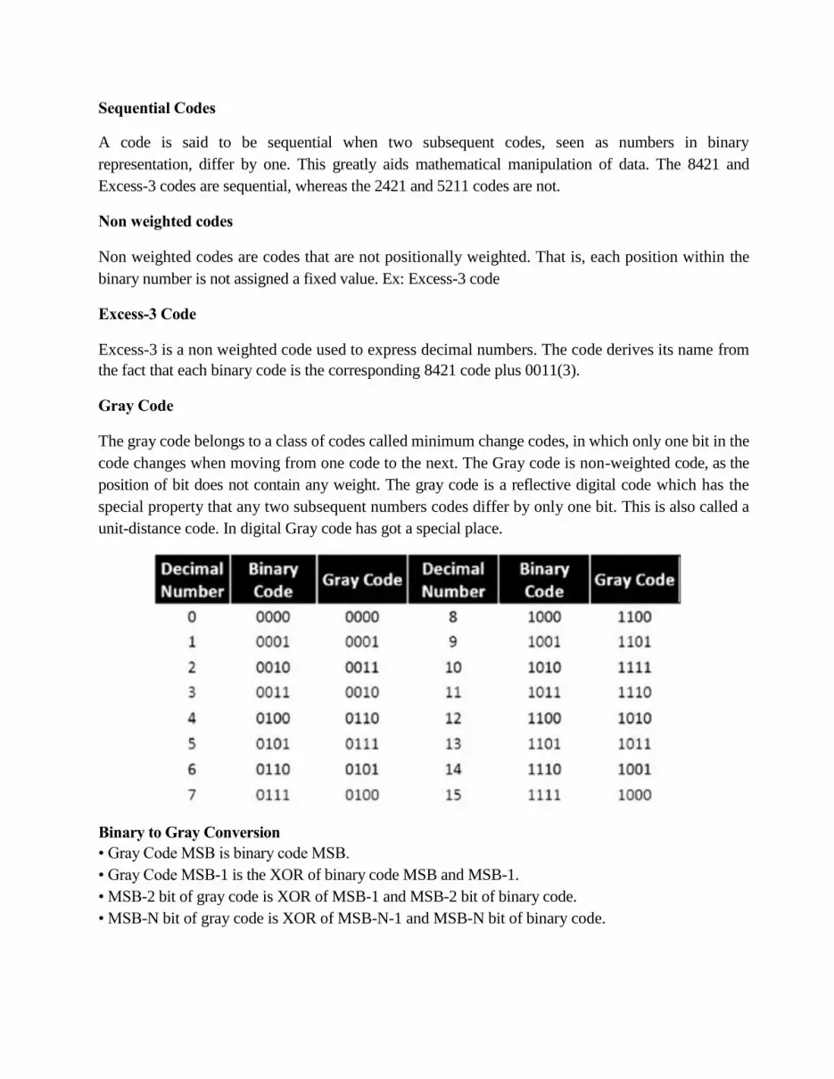
Gray Code
The gray code belongs to a class of codes called minimum change codes, in which only one bit in the
code changes when moving from one code to the next. The Gray code is non-weighted code, as the
position of bit does not contain any weight. The gray code is a reflective digital code which has the
special property that any two subsequent numbers codes differ by only one bit. This is also called a
unit-distance code. In digital Gray code has got a special place.
Binary to Gray Conversion
• Gray Code MSB is binary code MSB.
• Gray Code MSB-1 is the XOR of binary code MSB and MSB-1.
• MSB-2 bit of gray code is XOR of MSB-1 and MSB-2 bit of binary code.
• MSB-N bit of gray code is XOR of MSB-N-1 and MSB-N bit of binary code.

GATE-LEVEL MINIMIZATION
1.3 MAP METHOD/ KARNAUGH MAP
Karnaugh maps provide an alternative way of simplifying logic circuits. Instead of using
Boolean algebra simplification techniques, you can transfer logic values from a Boolean
statement or a truth table into a Karnaugh map. The arrangement of 0's and 1's within the map helps
you to visualize the logic relationships between the variables and leads directly to a simplified
Boolean statement.
Karnaugh maps, or K-maps, are often used to simplify logic problems with 2, 3 or 4 variables.
2-variable Karnaugh maps are trivial but can be used to introduce the methods you need to learn. The
map for a 2-input OR gate looks like this:
The values of one variable appear across the top of the map, defining the column values, while
the values of the other variable appear at the side, defining the values of the variable in each row.
The Karnaugh map for the OR gate is completed by entering a '1' in each of the appropriate cells.
Usually, you don't write in the '0's'. Within the map, adjacent cells containing 1's are grouped together in twos, fours, or eights. In this case, there is one horizontal and on vertical group of two.
You indicate these groupings by drawing a circle round each one.
The horizontal group corresponds to a B value of 1. In the left hand cell, A=0 and in the right hand
cell, A=1. In other words, the value of A does not affect the outcome of the Boolean expression
for these cells. Before grouping, you might have written the Boolean expression for these two cells as:
After grouping, this reduces to:
B
In a similar way, the vertical group could have been written as:
From the map, you can see that the value of B does not affect the value written in the cells for this
group. In other words, the vertical group reduces to:
A
In this way, the Karnaugh map leads to the overall expression A + B.
This is not very exciting but if you apply the same methods to a more complex logic problem, you will begin to understand how Karnaugh maps lead to simpler Boolean statements.

3-variable Karnaugh maps Here is the truth table for a 3-person majority voting system:
input C input B input A output
0 0 0 0
0 0 1 0
0 1 0 0
0 1 1 1
1 0 0 0
1 0 1 1
1 1 0 1
1 1 1 1
This is converted into a Karnaugh map, as follows:

Look carefully at the variables at the top of the Karnaugh map. These are not written in binary order
00, 01, 10, 11 etc. Instead, each column differs from the previous one by just one bit. This is called
Grey code and it is essential for your Karnaugh map to work that you enter the column values in this
order. (You will find out more about Grey code later.)
Within the K-map, you can identify three groups of two, as indicated. The left hand horizontal
group combines the cells and A.B.C. Within this group, the value of B does not affect the
cell values. This means that B can be eliminated from the expression, leaving A.C.
Work through the other groups to confirm that you understand how the remaining terms in the
Boolean expression were derived.
With a little practice, this method is going to be quicker than the alternative, simplfiying the
Boolean expression derived from the truth table:
3-variable examples
1. Simplify the following expression using a Karnaugh map:
You may be able to tell what is going to happen by completing the truth table for this expression. Click
here for answer
2. Simplify the following expression using a Karnaugh map:
From this expression, you can't complete the truth table or Karnaugh map directly. First, you need
to convert the statement into sum of products, or SOP form:
Continue from this point and check your answer by clicking the link
3. Here is another expression to simplify:

Note that has no C variable and fills two cells in the map. This condition is satisfied when C=0 and also when C=1.
4-variable maps A 4-variable map will contain 2
4 = 16 cells. It is important to write the variable values along the
columns and rows in Grey code:
To simplify the equation:
The Karnaugh map becomes:
To give the simplest Boolean statement, you should put a circle round the maximum number of
terms.

In this case, you can make two groups of four, one of which wraps around from top to bottom.
You identify the two variables which remain constant in each group and eliminate the other two:
1.4 DON’T CARE CONDITIONS
Sometimes, not all possible output values are specified in system design, e.g.:
Consider the horizontal line in the middle of the display (segment g):

Fg(w,x,y,z)=Σ(2,3,4,5,6,8,9), but we don’t care what happens to minterms 10, 11,
12, 13, 14, or 15, since the display will not be sent those states
We are free to assign whatever values we want to for minterms 10, 11, 12, 13, 14, and 15. Assign them a
value X to indicate they may be covered, or not, whichever results in the simplest expression
1.5 POS SIMPLIFICATION
A function of N variables, F(v1,v2,…,vN) , can be represented by a Karnaugh map with 2N cells.
(v1,v2,…,vN) = (0,0,…0), (0,1,…0), …, (1,1,…,1)
• F( ), and it’s Karnaugh map have K minterms (1’s) and 2N-K maxterms (0’s)
• If K > 2N-K, it might be easier to cover the maxterms rather than the minterms.
E.g.:

1.6 NAND IMPLEMENTATION OF SUM OF PRODUCTS
1) Consider an arbitrary Sum of Products:
2) Add inversions at each term. This is allowed, since (x’)’=x
3) Convert output gate by DeMorgan’s Law:
Step 1:
Step 2:

Step 3:
Similarly a POS expression can be implemented using NOR gates only.
1.7 QUINE MC-CLUSKY METHOD (TABULAR METHOD)
This is basically a tabular method of minimization and as much it is suitable for computer
applications. The procedure for optimization as follows:
Step 1: Describe individual minterms of the given expression by their equivalent binary
numbers.
Step 2: Form a table by grouping numbers with equivalent number of 1’s in them, i.e. first
numbers with no 1’s, then numbers with one 1, and then numbers with two 1’s, … etc.
Step 3: Compare each number in the top group with each minterm in the next lower group. If the
two numbers are the same in every position but one, place a check sign () to the
right of both numbers to show that they have been paired and covered. Then enter the
newly formed number in the next column (a new table). The new number is the old
numbers but where the literal differ, an “x” is placed in the position of that literal.
Step 4: Using (3) above, form a second table and repeat the process again until no further pairing
is possible. (On second repeat, compare numbers to numbers in the next group that
have the same “x” position.
Step 5: Terms which were not covered are the prime implicants and are ORed and ANDed
together to form final function.
Note: The procedure above gives you the prime implicant but not essential prime implicant.

}
Example E1
Minimize the function given below by Quine-McClusky method.
f(A,B,C,D)= ABCD+ ABCD+ ABCD+ ABCD+ ABCD+ ABCD+ ABCD+ ABCD+ ABCD
Binary 0000 0101 0110 1001 1010 1101 1110 1111 0111
minterm 0 5 6 9 10 13 14 15 7
No of 1's 0 2 2 2 2 3 3 4 3
group 1 2 2 2 2 3 3 4 3
This can be written as a sum of minterms as follows:
f (A , B , C , D ) m ( 0 ,5 ,6 ,7 ,9 ,1 0 ,1 3 ,1 4 ,1 5 )
Step 1: Form a table of functions of minterms according to the number of 1’s in each minterm as
shown in Table E1.a
minterm A B C D
* 0 0 0 0 0
5 0 1 0 1
6 0 1 1 0
} All numbers with no 1’s in each minterm (a)
…
…
All numbers with two 1’s in each minterm
AB 00 01 11 10 CD
9 1 0 0 1
10 1 0 1 0
7 0 1 1 1
13 1 1 0 1
14 1 1 1 0
… …
… } …
All numbers with three 1’s in each minterm
4 00 1
0 12 8
01 1
1 5
1 13
1 9
11 3
1 7
1 15 11
10 2
1 6
1 14
1 10
15 1 1 1 1 } All numbers with four 1’s in each minterm Table E1.a

Step 2: Start pairing off each element of first group with the next, however since m0 has no 1’s,
it and the next group of numbers with one 1’s are missing, therefore they cannot be
paired off. Start by pairing elements of m5 with m7, m13, m14, and m6 with m7, m13,
m14, and so on… If they pair off, write them in a separate table and the minterm
that pair, i.e. m5 and m7 pair off 0101 and 0111 to produce 01x1, so in the next table
E1.b under “minterm paired” we enter “5, 7” and under “ABCD” we enter “01x1” and
place a sign in front of 5 and 7 in Table E1.a
Note: Each minterm in a group must be compared with every minterm in the other group even if
either or both of them have already been checked . minterms
A B C D paired
5, 7 0 1 X 1
5, 13 X 1 0 1
6, 7 0 1 1 X
6, 14 X 1 1 0
9, 13 1 X 0 1
10, 14 1 X 1 0
7, 15 X 1 1 1
13, 15 1 1 X 1
14, 15 1 1 1 X
Table E1.b
Paired minterms
from E1.b
5,7 - 13,15
6,7 - 14,15 ………… (b)
………… (c)
A B C D
x 1 x 1 … (d)
x 1 1 x … (e)
Table E1.c
Step 3: Now repeat the same procedure by pairing each element of a group with the elements of
the next group for elements that have “x” in the same position. For example, “5,7”
matches “13,15” to produce x1x1. These elements are placed in table E1.c as shown,
and the above elements in Table E1.b are checked. (The elements that produce the
same ABCD pattern are eliminated.) Since 9,13 and 10,14 in Table E1.b do not pair
off, they are prime implicants and with m0, from E1.a, and (d) and (e) from E1.c are

unpaired individuals. Therefore, it is possible to write the minimized SOP as
a+b+c+d+r or
f (A,B,C,D) ABCD ACD ACD BD BC
Note: Check this result for Example 1 by Karnaugh map approach.
Two-square implicants:
AB
CD
00
01
11
10
00
1 0
1
3
2
01 11
4 12
1 5 1 13
1 7 1 15
1 6 1 14
10
8
1 9
11
1 10
Table E1.b represents all possible two-square implicants and the literals that they eliminate, i.e. 9
(1001b) combined with 13 (1101b) produces 1x01. As a result, literal “B” is eliminated.
Corresponding product is ACD . Since the only way of making an implicant that contains m9 is to
combine it with m13, the implicant 9-13 is a prime one. The same rule applies to m10.

Four-square implicants:
AB
CD
00
01
11
10
00
1 0
1
3
2
01 11
4 12
1 5 1 13
1 7 1 15
1 6 1 14
10
8
1 9
11
1 10
Table E1.c represents all possible four-square implicants and the literals that they eliminate, i.e. 5
(0101b) combined with 7 (0111b) and 13 (1101b) and 15 (1111b) produces x1x1. As a result,
literals “A” and “C” are eliminated. Corresponding product is BD.
Quine-McClusky Minimization Procedure (the decimal notation)
Step 1: List the minterms grouped according to the number of 1’s in their binary representation
in the decimal format.
Step 2: Compare each minterm with larger minterms in the next group down. If they differ by a
power of 2 then they pair-off. Check both minterms and form a second table by the
minterms paired and substitute the decimal difference of the corresponding minterms
in the bracket, i.e. mx, my (y-x).
Step 3: Compare each element of the group in the new table with elements of the next lower
group and select numbers that have the same numbers in parenthesis. If the lowest
minterm number of the table formed in the lower group is greater than the
corresponding number by a power of 2 then they combine; place a on the right of
both elements.
Step 4: Form a second table by all four minterms followed by both powers of 2 in parentheses,
i.e. the previous value (the difference) and the power of 2 that is greater.

Step 5: Select the common literals from each prime implicant by comparison.
Step 6: Write the minimal SOP from the prime implicant that are not checked .
Note: Read the above procedure in conjunction with the worked example given below.
Example E1.1
Minimize the function f given below by Quine-McClusky method using decimal notation.
f (A,B,C,D) ABCD ABCD ABCD ABCD ABCD ABCD ABCD ABCD ABCD
Solution
Step 1: Organize minterm as follows:
f (A,B,C,D) m(0, 5, 6, 7, 9,10,13,14,15)
Arrange minterms to correspond to their number of 1’s as shown in previous question
1’s Minterms
* 0 0 …(a)
5
6
2 9
10
7
3 13
14
4 15
Table E1.1a
* - squares combined (2 squares);
minterm paired
5*, 7*
(2)
5, 13 (8)
6, 7 (1)
6, 14 (8)
* 9, 13 (4)
* 10, 14 (4)
7, 15 (8)
13, 15 (2)
14, 15 (1)
Table E1.1b
minterms paired
* 5,7-13,15¡
(2,8) …(d)
* 6,14-7,15 (1,8) …(e)
Table E1.1c
…(b)
…(c)
- number in bracket shows the literal being eliminated, i.e. (2) represents C [A=8, B=4, C=2, D=1];

¡- squares combined (4 squares) and numbers in the brackets are the literals eliminated.

Step 2: Compare each element of a group with the element of the next group if the difference is
a power of 2 then they pair off, i.e. the first element in group 2 is paired say with the
first element in group 3, which is 7-5=2, which is power of 2. Therefore, pair (5,7)
makes the first element of the next table and minterms 5 and 7 get checked . The
result is shown in Table E1.1b.
Step 3: Now for the 23-table again compare each element of the group with elements of the
lower group that have the same number in parentheses. If the lowest minterm in the
lower group was greater by a power of 2 then they combine, i.e. 5,7 and 13,15 are
combined because they have (2) in parentheses and 13 is greater then 5 by 8. Then
they are paired off and entered in the next table E1.1c with the original (2) and their
difference (8) in the parentheses.
Step 4: What we are left with is (a) from Table E1.1a, (b) and (c) from Table E1.1b, and (d) and
(e) from Table E1.1c. From Table E1.1c, “d” is 5,7-13,15 (2,8). That means that
positions 21 and 2
3 are X’s. Thus, “d” represents function BD. From the same table, “e” is
6,14-7,15 (1,8), which means positions 20 and 2
3 are X’s. . Thus, “e” represents function
BC. This can also be obtained by writing the elements of minterms and selecting two
remaining literals:
6 14 7 15
0 1 1 0
1 1 1 0
0 1 1 1
1 1 1 1
x 1 1 x
B C
Therefore, the minimized SOP is
f a b c d e ABCD ACD ACD BD BC

Note: Compare this with the method of K-map or standard Quine-McClusky (the first approach).
The above function consists of prime implicants. However, not all of them are necessary
essential prime implicants.
Example 1.1.1. Determination of Essential Prime Implicants
For the SOP obtained in Example 1.1, determine the essential prime implicants and see if further
reduction is possible.
Solution.
Construct a prime implicants table as shown in Table 1.1.1a, with prime implicants on left and
minterms on top:
Minterms
Prime implicants
*(2) 5, 7 - 13, 15
*(3) 6, 14 - 7, 15
*(4) 9, 13
*(5) 10, 14
*(1) 0
0 5 6
(1) (2) (3)
7 9 10 13
(4) (5)
14 15
5
6
9
Table 1.1.1a

In each row, (except the bottom) checks are placed in the columns corresponding to
minterms contained in the prime implicant listing in thay row, i.e. the first prime implicant
testing contains 5, 7, 13, 15. So, is placed in the first row in columns 5, 7, 13, 15. Repeat for each
prime implicant.
Now inspect the table for columns that contain only one . That means that that prime implicant
is the only term that contains that minterm, i.e. for example m0 must be included in the SOP.
This is marked with asterisks (*) in the left column and place in the bottom row. The same
applies to 6, 9, and 10. Therefore, all prime implicants in this example are essential prime
implicants. Other empty cells in the bottom row are covered by essential prime implicants. For
example, once 5 is selected, then 7, 13, and 15 also can be from the bottom row, and so on.

UNIT-2
COMBINATIONAL LOGIC 2.1 COMBINATIONAL CIRCUITS
A combinational circuit consists of an interconnection of logic gates. Combinational logic gates
react to the values of the signals at their inputs and produce the value of the output signal,
transforming binary information from the given input data to a required output data. A block
diagram of a combinational circuit is shown in Figure below. The n input binary variables come
from an external source; the m output variables are produced by the internal combinational logic
circuit and go to an external destination. Each input and output variable exists physically as an
analog signal whose values are interpreted to be a binary signal that represents logic 1 and logic
0. (Note: Logic simulators show only 0’s and 1’s, not the actual analog signals.) In many
applications, the source and destination are storage registers. If the registers are included with the
combinational gates, then the total circuit must be considered to be a sequential circuit. For n
input variables, there are 2n possible combinations of the binary inputs. For each possible input
combination, there is one possible value for each output variable. Thus, a combinational circuit
can be specified with a truth table that lists the output values for each combination of input
variables. A combinational circuit also can be described by m Boolean functions, one for each
output variable. Each output function is expressed in terms of the n input variables.
Block Diagram of a Combinational Circuit
2.2 ANALYSIS PROCEDURE
The analysis of a combinational circuit requires that we determine the function that the circuit
implements. This task starts with a given logic diagram and culminates with a set of Boolean
functions, a truth table, or, possibly, an explanation of the circuit operation.
If the logic diagram to be analyzed is accompanied by a function name or an explanation of what it is
assumed to accomplish, then the analysis problem reduces to a verification of the stated function.
The analysis can be performed manually by finding the Boolean functions or truth table or by using a
computer simulation program.
The first step in the analysis is to make sure that the given circuit is combinational and not
sequential. The diagram of a combinational circuit has logic gates with no feedback paths or
memory elements. A feedback path is a connection from the output of one gate to the input of a
second gate whose output forms part of the input to the first gate. Feedback paths in a digital
circuit define a sequential circuit and must be analyzed by special methods and will not be
considered here. Once the logic diagram is verified to be that of a combinational circuit, one can
proceed to obtain the output Boolean functions or the truth table. If the function of the circuit is
under investigation, then it is necessary to interpret the operation of the circuit from the derived
Boolean functions or truth table. The success of such an investigation is enhanced if one has
previous experience and familiarity with a wide variety of digital circuits.

To obtain the output Boolean functions from a logic diagram, we proceed as follows:
1. Label all gate outputs that are a function of input variables with arbitrary symbols— but with
meaningful names. Determine the Boolean functions for each gate output.
2. Label the gates that are a function of input variables and previously labeled gates with other
arbitrary symbols. Find the Boolean functions for these gates. 3. Repeat the process outlined in step 2 until the outputs of the circuit are obtained.
4. By repeated substitution of previously defined functions, obtain the output Boolean functions in
terms of input variables.
The analysis of the combinational circuit of given Fig. illustrates the proposed procedure.
Logic Diagram for Analysis example
We note that the circuit has three binary inputs— A , B , and C —and two binary outputs— F1 and F2. The outputs of various gates are labeled with intermediate symbols. The outputs of gates that are a
function only of input variables are T1 and T2. Output F2 can easily be derived from the input variables. The Boolean functions for these three outputs are
Next, we consider outputs of gates that are a function of already defined symbols:
To obtain F1 as a function of A , B , and C , we form a series of substitutions as follows:

Truth Table for the Logic diagram obtained from above analysis expression
2.3 DESIGN EXAMPLE
The design of combinational circuits starts from the specification of the design objective and culminates in a logic circuit diagram or a set of Boolean functions from which the logic diagram can be obtained. The procedure involves the following steps:
1. From the specifications of the circuit, determine the required number of inputs and outputs and assign
a symbol to each.
2. Derive the truth table that defines the required relationship between inputs and outputs. 3. Obtain the simplified Boolean functions for each output as a function of the input variables.
4. Draw the logic diagram and verify the correctness of the design (manually or by simulation).
A truth table for a combinational circuit consists of input columns and output columns. The input
columns are obtained from the 2n binary numbers for the n input variables. The binary values for the
outputs are determined from the stated specifications. The output functions specified in the truth table
give the exact definition of the combinational circuit. It is important that the verbal specifications be
interpreted correctly in the truth table, as they are often incomplete, and any wrong interpretation may
result in an incorrect truth table.
The output binary functions listed in the truth table are simplified by any available method, such
as algebraic manipulation, the map method, or a computer-based simplification program.
Frequently, there is a variety of simplified expressions from which to choose. In a particular application, certain criteria will serve as a guide in the process of choosing an implementation. A
practical design must consider such constraints as the number of gates, number of inputs to a
gate, propagation time of the signal through the gates, number of interconnections, limitations of
the driving capability of each gate (i.e., the number of gates to which the output of the circuit

may be connected), and various other criteria that must be taken into consideration when
designing integrated circuits. Since the importance of each constraint is dictated by the particular
application, it is difficult to make a general statement about what constitutes an acceptable
implementation. In most cases, the simplification begins by satisfying an elementary objective, such
as producing the simplified Boolean functions in a standard form. Then the simplification proceeds
with further steps to meet other performance criteria.
This can be explained by taking the example of code conversion, e.g. BCD to Ex-3.
The bit combinations assigned to the BCD and excess-3 codes are listed in Table below. Since each
code uses four bits to represent a decimal digit, there must be four input variables and four output
variables. We designate the four input binary variables by the symbols A, B, C, and D, and the four
output variables by w, x, y , and z . The truth table relating the input and output variables is shown in
Table.
Truth Table for BCD to Ex-3 Code Conversion
The next step is to obtain the minimized K-map expressions:

The k-map expressions can be summarized as
Using these expressions we can design the final circuit
Logic Diagram for BCD to EX-3 Code converter
2.4 BINARY ADDER- SUBTRACTOR
Digital computers perform a variety of information-processing tasks. Among the functions
encountered are the various arithmetic operations. The most basic arithmetic operation is the
addition of two binary digits. This simple addition consists of four possible elementary
operations: 0 + 0 = 0, 0 + 1 = 1, 1 + 0 = 1, and 1 + 1 = 10. The first three operations produce a sum of
one digit, but when both augend and addend bits are equal to 1, the binary sum consists of two digits.
The higher significant bit of this result is called a carry. When the augend and addend numbers
contain more significant digits, the carry obtained from the addition of two bits is added to the next
higher order pair of significant bits. A combinational circuit that performs the addition of two bits is
called a half adder. One that performs the addition of three bits (two significant bits and a previous
carry) is a full adder. The names of the circuits stem from the fact that two half adders can be employed
to implement a full adder.
A binary adder-subtractor is a combinational circuit that performs the arithmetic
operations of addition and subtraction with binary numbers. We will develop this circuit by means
of a hierarchical design. The half adder design is carried out first, from which we develop the full
adder. Connecting n full adders in cascade produces a binary adder for two n -bit numbers. The
subtraction circuit is included in a complementing circuit.
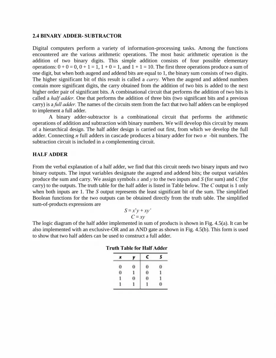
HALF ADDER
From the verbal explanation of a half adder, we find that this circuit needs two binary inputs and two
binary outputs. The input variables designate the augend and addend bits; the output variables
produce the sum and carry. We assign symbols x and y to the two inputs and S (for sum) and C (for
carry) to the outputs. The truth table for the half adder is listed in Table below. The C output is 1 only
when both inputs are 1. The S output represents the least significant bit of the sum. The simplified
Boolean functions for the two outputs can be obtained directly from the truth table. The simplified
sum-of-products expressions are
S = x’y + xy’
C = xy
The logic diagram of the half adder implemented in sum of products is shown in Fig. 4.5(a). It can be
also implemented with an exclusive-OR and an AND gate as shown in Fig. 4.5(b). This form is used
to show that two half adders can be used to construct a full adder.
Truth Table for Half Adder

Logic Diagram for Half Adder
FULL ADDER
Addition of n-bit binary numbers requires the use of a full adder, and the process of addition
proceeds on a bit-by-bit basis, right to left, beginning with the least significant bit. After the least
significant bit, addition at each position adds not only the respective bits of the words, but must
also consider a possible carry bit from addition at the previous position. A full adder is a
combinational circuit that forms the arithmetic sum of three bits. It consists of three inputs and
two outputs. Two of the input variables, denoted by x and y, represent the two significant bits to
be added. The third input, z, represents the carry from the previous lower significant position.
Two outputs are necessary because the arithmetic sum of three binary digits ranges in value from
0 to 3, and binary representation of 2 or 3 needs two bits. The two outputs are designated by the
symbols S for sum and C for carry. The binary variable S gives the value of the least significant
bit of the sum. The binary variable C gives the output carry formed by adding the input carry and
the bits of the words. The truth table of the full adder is listed in Table below. The eight rows
under the input variables designate all possible combinations of the three variables. The output
variables are determined from the arithmetic sum of the input bits. When all input bits are 0, the
Output is 0. The S output is equal to 1 when only one input is equal to 1 or when all three inputs
are equal to 1. The C output has a carry of 1 if two or three inputs are equal to 1. The input and
output bits of the combinational circuit have different interpretations at various stages of the
problem. On the one hand, physically, the binary signals of the inputs are considered binary
digits to be added arithmetically to form a two-digit sum at the output. On the other hand, the
same binary values are considered as variables of Boolean functions when expressed in the truth
table or when the circuit is implemented with logic gates. The maps for the outputs of the full
adder are shown in Figure below. The simplified expressions are
Truth Table for Full Adder

And the expressions obtained from the truth table can be given as:
Full Adder Implementation in SOP form
Full Adder Implementation using two Half Adders and an OR gate

BINARY SUBTRACTOR
The subtraction of unsigned binary numbers can be done most conveniently by means of
complements. The subtraction A - B can be done by taking the 2’s complement of B and adding it to A .
The 2’s complement can be obtained by taking the 1’s complement and adding 1 to the least
significant pair of bits. The 1’s complement can be implemented with inverters, and a 1 can be added to
the sum through the input carry.
4-bit Adder Subtractor with overflow detection
The circuit for subtracting A - B consists of an adder with inverters placed between each data input B
and the corresponding input of the full adder. The input carry C0 must be equal to 1 when subtraction is
performed. The operation thus performed becomes A , plus the 1’s complement of B , plus 1. This is
equal to A plus the 2’s complement of B. For unsigned numbers, that gives A -
B if A<B or the 2’s complement of (B - A) if A>=B. For signed numbers, the result is A - B,
provided that there is no overflow.
The addition and subtraction operations can be combined into one circuit with one common binary
adder by including an exclusive-OR gate with each full adder. A four-bit adder-subtractor circuit is
shown in Fig. above. The mode input M controls the operation. When M = 0, the circuit is an adder, and
when M = 1, the circuit becomes a subtractor. Each exclusive-OR gate receives input M and one of the
inputs of B. When M = 0, we have B XOR 0 = B. The full adders receive the value of B , the input carry
is 0, and the circuit performs A plus B . When M = 1, we have B XOR 1 = B’ and C0 = 1. The B inputs
are all complemented and a 1 is added through the input carry. The circuit performs the operation A
plus the 2’s complement of B. (The exclusive-OR with output V is for detecting an overflow.)
It is worth noting that binary numbers in the signed-complement system are added and subtracted by
the same basic addition and subtraction rules as are unsigned numbers. Therefore, computers need
only one common hardware circuit to handle both types of arithmetic. The user or programmer
must interpret the results of such addition or subtraction differently, depending on whether it is
assumed that the numbers are signed or unsigned.

2.5 DECIMAL ADDER
Computers or calculators that perform arithmetic operations directly in the decimal number
system represent decimal numbers in binary coded form. An adder for such a computer must
employ arithmetic circuits that accept coded decimal numbers and present results in the same
code. For binary addition, it is sufficient to consider a pair of significant bits together with a
previous carry. A decimal adder requires a minimum of nine inputs and five outputs, since four
bits are required to code each decimal digit and the circuit must have an input and output carry.
There is a wide variety of possible decimal adder circuits, depending upon the code used to
represent the decimal digits. Here we examine a decimal adder for the BCD code.
BCD Adder
Consider the arithmetic addition of two decimal digits in BCD, together with an input carry from
a previous stage. Since each input digit does not exceed 9, the output sum cannot be greater than
9 + 9 + 1 = 19, the 1 in the sum being an input carry. Suppose we apply two BCD digits to a
four-bit binary adder. The adder will form the sum in binary and produce a result that ranges
from 0 through 19. These binary numbers are listed in Table 4.5 and are labeled by symbols K,
Z8, Z4, Z2, and Z1. K is the carry, and the subscripts under the letter Z represent the weights 8, 4,
2, and 1 that can be assigned to the four bits in the BCD code. The columns under the binary sum
list the binary value that appears in the outputs of the four-bit binary adder. The output sum of
two decimal digits must be represented in BCD and should appear in the form listed in the
columns under “BCD Sum.” The problem is to find a rule by which the binary sum is converted
to the correct BCD digit representation of the number in the BCD sum.
In examining the contents of the table, it becomes apparent that when the binary sum is equal to or less
than 1001, the corresponding BCD number is identical, and therefore no conversion is needed. When
the binary sum is greater than 1001, we obtain an invalid BCD representation. The addition of binary 6
(0110) to the binary sum converts it to the correct BCD representation and also produces an output
carry as required.
Derivation of BCD Adder

The logic circuit that detects the necessary correction can be derived from the entries in the table. It is
obvious that a correction is needed when the binary sum has an output carry K = 1. The other six
combinations from 1010 through 1111 that need a correction have a 1 in position Z8. To distinguish
them from binary 1000 and 1001, which also have a 1 in position Z8, we specify further that either
Z4 or Z2 must have a 1. The condition for a correction and an output carry can be expressed by the
Boolean function
C = K + Z8Z4 + Z8Z2
When C = 1, it is necessary to add 0110 to the binary sum and provide an output carry for the next
stage.
Block Diagram of BCD Adder
2.6 BINARY MULTIPLIER
Multiplication of binary numbers is performed in the same way as multiplication of decimal
numbers. The multiplicand is multiplied by each bit of the multiplier, starting from the least
significant bit. Each such multiplication forms a partial product. Successive partial products are
shifted one position to the left. The final product is obtained from the sum of the partial products.
To see how a binary multiplier can be implemented with a combinational circuit, consider the
multiplication of two 2-bit numbers as shown in Fig. The multiplicand bits are B1 and B0, the
multiplier bits are A1 and A0, and the product is C3C2C1C0. The first partial product is formed by

multiplying B1B0 by A0. The multiplication of two bits such as A0 and B0 produces a 1 if both bits
are 1; otherwise, it produces a 0. This is identical to an AND operation. Therefore, the partial
product can be implemented with AND gates as shown in the diagram. The second partial
product is formed by multiplying B1B0 by A1 and shifting one position to the left. The two partial
products are added with two half-adder (HA) circuits. Usually, there are more bits in the partial
products and it is necessary to use full adders to produce the sum of the partial products. Note
that the least significant bit of the product does not have to go through an adder, since
it is formed by the output of the first AND gate.
A combinational circuit binary multiplier with more bits can be constructed in a similar fashion. A bit
of the multiplier is ANDed with each bit of the multiplicand in as many levels as there are bits in the
multiplier. The binary output in each level of AND gates is added with the partial product of the
previous level to form a new partial product. The last level produces the product. For J multiplier bits
and K multiplicand bits, we need J * K AND gates and (J - 1) K -bit adders to produce a product of (J +
K) bits.
As a second example, consider a multiplier circuit that multiplies a binary number represented by four
bits by a number represented by three bits. Let the multiplicand be represented by B3B2B1B0 and the multiplier by A2A1A0. Since K = 4 and J = 3, we need 12 AND gates and two 4-bit adders to produce a
product of seven bits. The logic diagram of the multiplier is shown in Fig.
4-bit by 3-bit Binary Multiplier

2.7 MAGNITUDE COMPARATOR
The comparison of two numbers is an operation that determines whether one number is greater
than, less than, or equal to the other number. A magnitude comparator is a combinational circuit
that compares two numbers A and B and determines their relative magnitudes. The outcome of
the comparison is specified by three binary variables that indicate whether A > B, A = B, or A < B.
On the one hand, the circuit for comparing two n -bit numbers has 22n
entries in the truth table
and becomes too cumbersome, even with n = 3. On the other hand, as one may suspect, a
comparator circuit possesses a certain amount of regularity. Digital functions that possess an
inherent well-defined regularity can usually be designed by means of an algorithm—a procedure
which specifies a finite set of steps that, if followed, give the solution to a problem. We illustrate
this method here by deriving an algorithm for the design of a four-bit magnitude comparator.
Logic Diagram for a 4-bit Magnitude Comparator

2.8 DECODERS
Discrete quantities of information are represented in digital systems by binary codes. A binary code
of n bits is capable of representing up to 2n distinct elements of coded information. A decoder is
a combinational circuit that converts binary information from n input lines to a maximum of 2n
unique output lines. If the n -bit coded information has unused combinations, the decoder may have
fewer than 2n outputs.
The decoders presented here are called n -to- m -line decoders, where m <= 2n. Their purpose is to
generate the 2n (or fewer) minterms of n input variables. Each combination of inputs will assert a
unique output. The name decoder is also used in conjunction with other code converters, such as a
BCD-to-seven-segment decoder.
As an example, consider the three-to-eight-line decoder circuit of Fig. below . The three inputs
are decoded into eight outputs, each representing one of the minterms of the three input
variables. The three inverters provide the complement of the inputs, and each one of the eight
AND gates generate one of the minterms. A particular application of this decoder is binary-to-
octal conversion. The input variables represent a binary number, and the outputs represent the
eight digits of a number in the octal number system. However, a three-to-eight-line decoder can
be used for decoding any three-bit code to provide eight outputs, one for each element of the
code.
3 to 8 Line Decoder

2 to 4 line decoder with Enable Input
4 x 16 Decoder using two 3 x 8 Decoder

Combinational Logic Implementation using Decoders
From the truth table of Full Adder we have the expressions for Sum and carry :
S(x, y, z) = ∑(1, 2, 4, 7)
C(x, y, z) = ∑(3, 5, 6, 7)
Implementation of a Full Adder using 3 x 8 decoder
2.10 ENCODERS
An encoder is a digital circuit that performs the inverse operation of a decoder. An encoder has 2n (or
fewer) input lines and n output lines. The output lines, as an aggregate, generate the binary code
corresponding to the input value. An example of an encoder is the octal-to-binary encoder whose truth
table is given in Table below. It has eight inputs (one for each of the octal digits) and three outputs that
generate the corresponding binary number. It is assumed that only one input has a value of 1 at any
given time. The encoder can be implemented with OR gates whose inputs are determined directly from
the truth table. Output z is equal to 1 when the input octal digit is 1, 3, 5, or 7. Output y is 1 for octal
digits 2, 3, 6, or 7, and output x is 1 for digits 4, 5, 6, or 7. These conditions can be expressed by the
following Boolean output functions:
z = D1 + D3 + D5 + D7
y = D2 + D3 + D6 + D7
x = D4 + D5 + D6 + D7
The encoder can be implemented with three OR gates.

The encoder defined in Table above has the limitation that only one input can be active at any
given time. If two inputs are active simultaneously, the output produces an undefined
combination. For example, if D3 and D6 are 1 simultaneously, the output of the encoder will be
111 because all three outputs are equal to 1. The output 111 does not represent either binary 3 or
binary 6. To resolve this ambiguity, encoder circuits must establish an input priority to ensure
that only one input is encoded. If we establish a higher priority for inputs with higher subscript
numbers, and if both D3 and D6 are 1 at the same time, the output will be 110 because D6 has
higher priority than D3. Another ambiguity in the octal-to-binary encoder is that an output with
all 0’s is generated when all the inputs are 0; but this output is the same as when D0 is equal to 1.
The discrepancy can be resolved by providing one more output to indicate whether at least one
input is equal to 1.
Priority Encoder
A priority encoder is an encoder circuit that includes the priority function. The operation of the
priority encoder is such that if two or more inputs are equal to 1 at the same time, the input
having the highest priority will take precedence. The truth table of a four-input priority encoder
is given in Table below. In addition to the two outputs x and y, the circuit has a third output
designated by V ; this is a valid bit indicator that is set to 1 when one or more inputs are equal to
1. If all inputs are 0, there is no valid input and V is equal to 0. The other two outputs are not
inspected when V equals 0 and are specified as don’t-care conditions. Note that whereas X ’s in output
columns represent don’t-care conditions, the X ’s in the input columns are useful for representing
a truth table in condensed form. Instead of listing all 16 minterms of four variables, the truth table uses
an X to represent either 1 or 0. For example, X 100 represents the two minterms 0100 and 1100.
According to Table below, the higher the subscript number, the higher the priority of the input.
Input D3 has the highest priority, so, regardless of the values of the other inputs, when this input
is 1, the output for xy is 11 (binary 3). D2 has the next priority level. The output is 10 if D2 = 1,
provided that D3 = 0, regardless of the values of the other two lower priority inputs. The output
for D1 is generated only if higher priority inputs are 0, and so on down the priority levels.

x = D2 + D3
y = D3 + D1 D2’
V = D0 + D1 + D2 + D3
4-Input Priority Encoder
2.10 MULTIPLEXERS
A multiplexer is a combinational circuit that selects binary information from one of many input lines
and directs it to a single output line. The selection of a particular input line is controlled by a set of selection lines. Normally, there are 2n input lines and n selection lines whose bit combinations
determine which input is selected.
A two-to-one-line multiplexer connects one of two 1-bit sources to a common destination, as shown
in Fig. below. The circuit has two data input lines, one output line, and one selection line S . When S =
0, the upper AND gate is enabled and I0 has a path to the output. When S = 1, the lower AND gate is
enabled and I1 has a path to the output. The multiplexer acts like an electronic switch that selects one of
two sources. The block diagram of a multiplexer is sometimes depicted by a wedge-shaped symbol, as
shown in Fig. below. It suggests visually how a selected one of multiple data sources is directed
into a single destination. The multiplexer is often labeled “MUX” in block diagrams.

2 to 1 Line Multiplexer
A four-to-one-line multiplexer is shown in Fig. below. Each of the four inputs, I0 through I3, is
applied to one input of an AND gate. Selection lines S1 and S0 are decoded to select a particular
AND gate. The outputs of the AND gates are applied to a single OR gate that provides the one-
line output. The function table lists the input that is passed to the output for each combination of
the binary selection values. To demonstrate the operation of the circuit, consider the case when
S1S0 = 10. The AND gate associated with input I2 has two of its inputs equal to 1 and the third
input connected to I2. The other three AND gates have at least one input equal to 0, which makes
their outputs equal to 0. The output of the OR gate is now equal to the value of I2, providing a
path from the selected input to the output. A multiplexer is also called a data selector , since it
selects one of many inputs and steers the binary information to the output line.
4 to 1 Line Multiplexer
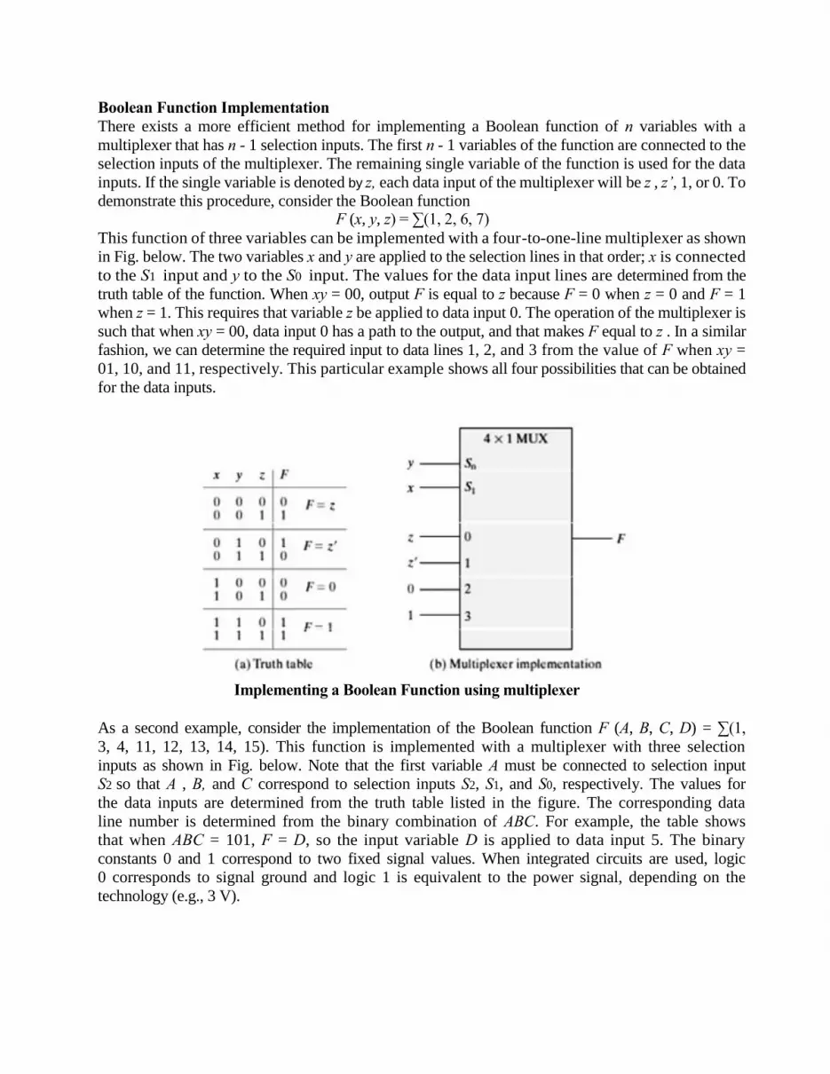
Boolean Function Implementation
There exists a more efficient method for implementing a Boolean function of n variables with a
multiplexer that has n - 1 selection inputs. The first n - 1 variables of the function are connected to the
selection inputs of the multiplexer. The remaining single variable of the function is used for the data
inputs. If the single variable is denoted by z, each data input of the multiplexer will be z , z’, 1, or 0. To
demonstrate this procedure, consider the Boolean function F (x, y, z) = ∑(1, 2, 6, 7)
This function of three variables can be implemented with a four-to-one-line multiplexer as shown
in Fig. below. The two variables x and y are applied to the selection lines in that order; x is connected
to the S1 input and y to the S0 input. The values for the data input lines are determined from the
truth table of the function. When xy = 00, output F is equal to z because F = 0 when z = 0 and F = 1
when z = 1. This requires that variable z be applied to data input 0. The operation of the multiplexer is
such that when xy = 00, data input 0 has a path to the output, and that makes F equal to z . In a similar
fashion, we can determine the required input to data lines 1, 2, and 3 from the value of F when xy =
01, 10, and 11, respectively. This particular example shows all four possibilities that can be obtained
for the data inputs.
Implementing a Boolean Function using multiplexer
As a second example, consider the implementation of the Boolean function F (A, B, C, D) = ∑(1,
3, 4, 11, 12, 13, 14, 15). This function is implemented with a multiplexer with three selection
inputs as shown in Fig. below. Note that the first variable A must be connected to selection input
S2 so that A , B, and C correspond to selection inputs S2, S1, and S0, respectively. The values for
the data inputs are determined from the truth table listed in the figure. The corresponding data
line number is determined from the binary combination of ABC. For example, the table shows
that when ABC = 101, F = D, so the input variable D is applied to data input 5. The binary
constants 0 and 1 correspond to two fixed signal values. When integrated circuits are used, logic
0 corresponds to signal ground and logic 1 is equivalent to the power signal, depending on the
technology (e.g., 3 V).

Implementing a 4 Input function using a Multiplexer

UNIT 3
SYNCHRONOUS AND ASYNCHRONOUS SEQUENTIAL
LOGIC
3.1 SEQUENTIAL CIRCUITS
A block diagram of a sequential circuit is shown in Fig. below. It consists of a combinational
circuit to which storage elements are connected to form a feedback path. The storage elements are
devices capable of storing binary information. The binary information stored in these elements
at any given time defines the state of the sequential circuit at that time. The sequential circuit
receives binary information from external inputs that, together with the present state of the storage
elements, determine the binary value of the outputs. These external inputs also determine the
condition for changing the state in the storage elements. The block diagram demonstrates that
the outputs in a sequential circuit are a function not only of the inputs, but also of the present state of
the storage elements. The next state of the storage elements is also a function of external inputs
and the present state. Thus, a sequential circuit is specified by a time sequence of inputs,
outputs, and internal states. In contrast, the outputs of combinational logic depend only on the
present values of the inputs.
Block Diagram of Sequential circuit
There are two main types of sequential circuits, and their classification is a function of the timing of
their signals. A synchronous sequential circuit is a system whose behavior can be defined from
the knowledge of its signals at discrete instants of time. The behavior of an asynchronous sequential
circuit depends upon the input signals at any instant of time and the order in which the inputs change.
The storage elements commonly used in asynchronous sequential circuits are time-delay devices.
The storage capability of a time-delay device varies with the time it takes for the signal to propagate
through the device. In practice, the internal propagation delay of logic gates is of sufficient duration
to produce the needed delay, so that actual delay units may not be necessary. In gate-type
asynchronous systems, the storage elements consist of logic gates whose propagation delay provides
the required storage. Thus, an asynchronous sequential circuit may be regarded as a combinational
circuit with feedback. Because of the feedback among logic gates, an asynchronous sequential
circuit may become unstable at times. The instability problem imposes many difficulties on the
designer.
A synchronous sequential circuit employs signals that affect the storage elements at only discrete
instants of time. Synchronization is achieved by a timing device called a clock generator, which
provides a clock signal having the form of a periodic train of clock pulses. The clock signal is
commonly denoted by the identifiers clock and clk. The clock pulses are distributed throughout
the system in such a way that storage elements are affected only with the arrival of each pulse. In

practice, the clock pulses determine when computational activity will occur within the circuit,
and other signals (external inputs and otherwise) determine what changes will take place
affecting the storage elements and the outputs. For example, a circuit that is to add and store two binary
numbers would compute their sum from the values of the numbers and store the sum at the
occurrence of a clock pulse. Synchronous sequential circuits that use clock pulses to control storage
elements are called clocked sequential circuits and are the type most frequently encountered in
practice. They are called synchronous circuits because the activity within the circuit and the
resulting updating of stored values is synchronized to the occurrence of clock pulses. The design of
synchronous circuits is feasible because they seldom manifest instability problems and their timing is
easily broken down into independent discrete steps, each of which can be considered separately.
Synchronous Clocked Sequential Circuit
The storage elements (memory) used in clocked sequential circuits are called flipflops. A flip-
flop is a binary storage device capable of storing one bit of information. In a stable state, the
output of a flip-flop is either 0 or 1. A sequential circuit may use many flip-flops to store as
many bits as necessary. The block diagram of a synchronous clocked sequential circuit is shown
in Fig. above. The outputs are formed by a combinational logic function of the inputs to the
circuit or the values stored in the flip-flops (or both). The value that is stored in a flip-flop when
the clock pulse occurs is also determined by the inputs to the circuit or the values presently
stored in the flip-flop (or both). The new value is stored (i.e., the flip-flop is updated) when a
pulse of the clock signal occurs. Prior to the occurrence of the clock pulse, the combinational
logic forming the next value of the flip-flop must have reached a stable value. Consequently, the
speed at which the combinational logic circuits operate is critical. If the clock (synchronizing)
pulses arrive at a regular interval, as shown in the timing diagram in Fig. above, the
combinational logic must respond to a change in the state of the flip-flop in time to be updated
before the next pulse arrives. Propagation delays play an important role in determining the
minimum interval between clock pulses that will allow the circuit to operate correctly. A change
in state of the flip-flops is initiated only by a clock pulse transition—for example, when the value
of the clock signals changes from 0 to 1. When a clock pulse is not active, the feedback loop
between the value stored in the flip-flop and the value formed at the input to the flip-flop is
effectively broken because the flipflop outputs cannot change even if the outputs of the

combinational circuit driving their inputs change in value. Thus, the transition from one state to the
next occurs only at predetermine intervals dictated by the clock pulses.
3.2 STORAGE ELEMENTS: LATCHES
A storage element in a digital circuit can maintain a binary state indefinitely (as long as power is
delivered to the circuit), until directed by an input signal to switch states. The major differences among
various types of storage elements are in the number of inputs they possess and in the manner in
which the inputs affect the binary state. Storage elements that operate with signal levels (rather
than signal transitions) are referred to as latches; those controlled by a clock transition are
flip-flops. Latches are said to be level sensitive devices; flip-flops are edgesensitive devices. The
two types of storage elements are related because latches are the basic circuits from which all
flip-flops are constructed. Although latches are useful for storing binary information and for the design
of asynchronous sequential circuits, they are not practical for use as storage elements in synchronous
sequential circuits.
SR Latch
The SR latch is a circuit with two cross-coupled NOR gates or two cross-coupled NAND gates, and
two inputs labeled S for set and R for reset. Both the versions are shown in Fig. below. The latch has
two useful states. When output Q = 1 and Q’ = 0, the latch is said to be in the set state . When Q = 0 and
Q’ = 1, it is in the reset state.
SR Latch with NOR gates
SR Latch with NAND Gates

SR Latch with Control Input
The operation of the basic SR latch can be modified by providing an additional input signal that
determines (controls) when the state of the latch can be changed by determining whether S and R
(or S’ and R’) can affect the circuit. An SR latch with a control input is shown in Fig. below. It
consists of the basic SR latch and two additional NAND gates. The control input En acts as an
enable signal for the other two inputs. The outputs of the NAND gates stay at the logic-1 level
as long as the enable signal remains at 0. This is the quiescent condition for the SR latch.
When the enable input goes to 1, information from the S or R input is allowed to affect the latch.
SR Latch with Control Input
The set state is reached with S = 1, R = 0, and En = 1 (active-high enabled). To change to the reset
state, the inputs must be S = 0, R = 1, and En = 1. In either case, when En returns to 0, the circuit
remains in its current state. The control input disables the circuit by applying 0 to En, so that the state
of the output does not change regardless of the values of S and R. Moreover, when En = 1 and both the
S and R inputs are equal to 0, the state of the circuit does not change. These conditions are listed in the
function table accompanying the diagram.
An indeterminate condition occurs when all three inputs are equal to 1. This condition places 0’s on
both inputs of the basic SR latch, which puts it in the undefined state.
D Latch (Transparent latch)
One way to eliminate the undesirable condition of the indeterminate state in the SR latch is to
ensure that inputs S and R are never equal to 1 at the same time. This is done in the D latch,
shown in Fig. below. This latch has only two inputs: D (data) and En (enable). The D input goes
directly to the S input, and its complement is applied to the R input. As long as the enable input is
at 0, the cross-coupled SR latch has both inputs at the 1 level and the circuit cannot change state
regardless of the value of D. The D input is sampled when En = 1. If D = 1, the Q output goes to
1, placing the circuit in the set state. If D = 0, output Q goes to 0, placing the circuit in the reset
state.
Graphic Symbols for Latches

3.3 STORAGE ELEMENTS: FLIP FLOPS
The state of a latch or flip-flop is switched by a change in the control input. This momentary
change is called a trigger, and the transition it causes is said to trigger the flip-flop. The D latch with
pulses in its control input is essentially a flip-flop that is triggered every time the pulse goes to the
logic-1 level. As long as the pulse input remains at this level, any changes in the data input will
change the output and the state of the latch.
A flip-flop circuit can be constructed from two NAND gates or two NOR gates. These flip-flops are
shown in figures below. Each flip-flop has two outputs, Q and Q', and two inputs, set
and reset. This type of flip-flop is referred to as an SR flip-flop or SR latch. The flipflop has two useful
states. When Q=1 and Q'=0, it is in the set state (or 1-state). When Q=0 and Q'=1, it is in the clear state
(or 0-state). The outputs Q and Q' are complements of each other and are referred to as the normal and
complement outputs, respectively. The binary state of the flipflop is taken to be the value of the normal
output.
When a 1 is applied to both the set and reset inputs of the flip-flop, both Q and Q' outputs go to
0. This condition violates the fact that both outputs are complements of each other. In normal
operation this condition must be avoided by making sure that 1's are not applied to both inputs
simultaneously.
(a) Logic diagram (b) Truth table
Basic flip-flop circuit with NOR gates
(a) Logic diagram (b) Truth table
Basic flip-flop circuit with NAND gates
The NAND basic flip-flop circuit operates with inputs normally at 1 unless the state of the flipflop has
to be changed. A 0 applied momentarily to the set input causes Q to go to 1 and Q' to go to 0, putting the flip-flop in the set state. When both inputs go to 0, both outputs go to 1. This condition should be
avoided in normal operation.

Clocked SR Flip-Flop
The clocked SR flip-flop consists of a basic NOR flip-flop and two AND gates. The outputs of the
two AND gates remain at 0 as long as the clock pulse (or CP) is 0, regardless of the S and R input
values. When the clock pulse goes to 1, information from the S and R inputs passes through to
the basic flip-flop. With both S=1 and R=1, the occurrence of a clock pulse causes both outputs to
momentarily go to 0. When the pulse is removed, the state of the flip-flop is indeterminate, ie.,
either state may result, depending on whether the set or reset input of the flipflop remains a 1 longer
than the transition to 0 at the end of the pulse.
(a) Logic diagram (b) Truth table
Clocked SR flip-flop
D Flip-Flop
The D flip-flop is a modification of the clocked SR flip-flop. The D input goes directly into the S input
and the complement of the D input goes to the R input. The D input is sampled during the
occurrence of a clock pulse. If it is 1, the flip-flop is switched to the set state (unless it was
already set). If it is 0, the flip-flop switches to the clear state. (a)Logic Diagram (b) Graphic Symbol (c) Transition
table
Clocked D flip-flop

Introduction - JK Flip-Flop
A JK flip-flop is a refinement of the SR flip-flop in that the indeterminate state of the SR type is defined
in the JK type. Inputs J and K behave like inputs S and R to set and clear the flip-flop (note that in a
JK flip-flop, the letter J is for set and the letter K is for clear). When logic 1 inputs are applied to both J
and K simultaneously, the flip-flop switches to its complement state, ie., if Q=1, it switches to Q=0 and
vice versa.
A clocked JK flip-flop is shown. Output Q is ANDed with K and CP inputs so that the flip-flop is
cleared during a clock pulse only if Q was previously 1. Similarly, ouput Q' is ANDed with J and CP
inputs so that the flip-flop is set with a clock pulse only if Q' was previously 1.
Note that because of the feedback connection in the JK flip-flop, a CP signal which remains a 1 (while
J=K=1) after the outputs have been complemented once will cause repeated and continuous
transitions of the outputs. To avoid this, the clock pulses must have a time duration less than the
propagation delay through the flip-flop. The restriction on the pulse width can be eliminated with a
master-slave or edge-triggered construction. The same reasoning also applies to the T flip-flop
presented next.
(a) Logic diagram (b) Graphical symbol (c) Transition table
Clocked JK flip-flop
T Flip-Flop
The T flip-flop is a single input version of the JK flip-flop. As shown, the T flip-flop is obtained from
the JK type if both inputs are tied together. The output of the T flip-flop "toggles" with each clock
pulse.

(a) Logic diagram (b) Graphical symbol (c) Transition
table
Clocked T flip-flop
Triggering of Flip-flops
The state of a flip-flop is changed by a momentary change in the input signal. This change is
called a trigger and the transition it causes is said to trigger the flip-flop. The basic circuits
require an input trigger defined by a change in signal level. This level must be returned to its
initial level before a second trigger is applied. Clocked flip-flops are triggered by pulses.
The feedback path between the combinational circuit and memory elements can produce
instability if the outputs of the memory elements (flip-flops) are changing while the outputs of the
combinational circuit that go to the flip-flop inputs are being sampled by the clock pulse. A way to
solve the feedback timing problem is to make the flip-flop sensitive to the pulse transition rather than
the pulse duration.
The clock pulse goes through two signal transitions: from 0 to 1 and the return from 1 to 0. As shown the positive transition is defined as the positive edge and the negative transition as the negative edge.
Definition of clock pulse transition
The clocked flip-flops already introduced are triggered during the positive edge of the pulse, and the
state transition starts as soon as the pulse reaches the logic-1 level. If the other inputs change while the
clock is still 1, a new output state may occur. If the flip-flop is made to respond to the positive (or
negative) edge transition only, instead of the entire pulse duration, then the multipletransition problem
can be eliminated.

Master-Slave Flip-Flop
A master-slave flip-flop is constructed from two separate flip-flops. One circuit serves as a
master and the other as a slave. The master flip-flop is enabled on the positive edge of the clock
pulse CP and the slave flip-flop is disabled by the inverter. The information at the external R and
S inputs is transmitted to the master flip-flop. When the pulse returns to 0, the master flip-flop is
disabled and the slave flip-flop is enabled. The slave flip-flop then goes to the same state as the
master flip-flop.
Logic diagram of a master-slave flip-flop
The timing relationship is shown and is assumed that the flip-flop is in the clear state prior to the
occurrence of the clock pulse. The output state of the master-slave flip-flop occurs on the
negative transition of the clock pulse. Some master-slave flip-flops change output state on the
positive transition of the clock pulse by having an additional inverter between the CP terminal and
the input of the master.
Timing relationship in a master slave flip-flop
Introduction - Edge Triggered Flip-Flop
Another type of flip-flop that synchronizes the state changes during a clock pulse transition is the
edge-triggered flip-flop. When the clock pulse input exceeds a specific threshold level, the inputs
are locked out and the flip-flop is not affected by further changes in the inputs until the clock
pulse returns to 0 and another pulse occurs. Some edge-triggered flip-flops cause a transition on
the positive edge of the clock pulse (positive-edge-triggered), and others on the negative edge of
the pulse (negative-edge-triggered). The logic diagram of a D-type positive-edge-triggered flip-
flop is shown.

D-type positive-edge triggered flip-flop
When using different types of flip-flops in the same circuit, one must ensure that all flip-flop
outputs make their transitions at the same time, ie., during either the negative edge or the positive edge
of the clock pulse.
Introduction - Direct Inputs
Flip-flops in IC packages sometimes provide special inputs for setting or clearing the flip-flop
asynchronously. They are usually called preset and clear. They affect the flip-flop without the
need for a clock pulse. These inputs are useful for bringing flip-flops to an intial state before
their clocked operation. For example, after power is turned on in a digital system, the states of
the flip-flops are indeterminate. Activating the clear input clears all the flip-flops to an initial
state of 0. The graphic symbol of a JK flip-flop with an active-low clear is shown.
(a) Graphic Symbol (b) Transition table
JK flip-flop with direct clear

3.4 ANALYSIS OF CLOCKED SEQUENTIAL CIRCUITS
Analysis describes what a given circuit will do under certain operating conditions. The behavior of a
clocked sequential circuit is determined from the inputs, the outputs, and the state of its flipflops. The
outputs and the next state are both a function of the inputs and the present state. The analysis of a
sequential circuit consists of obtaining a table or a diagram for the time sequence of inputs, outputs,
and internal states. It is also possible to write Boolean expressions that describe the behavior of the
sequential circuit. These expressions must include the necessary time sequence, either directly or
indirectly.
A logic diagram is recognized as a clocked sequential circuit if it includes flip-flops with clock
inputs. The flip-flops may be of any type, and the logic diagram may or may not include
combinational logic gates. In this section, we introduce an algebraic representation for specifying the
next-state condition in terms of the present state and inputs. A state table and state diagram are then
presented to describe the behavior of the sequential circuit. Another algebraic representation
is introduced for specifying the logic diagram of sequential circuits. Examples are used to illustrate
the various procedures.
State Equations
The behavior of a clocked sequential circuit can be described algebraically by means of state
equations. A state equation (also called a transition equation) specifies the next state as a
function of the present state and inputs. Consider the sequential circuit shown in Fig. below.
Example of Sequential Circuit

We will later show that it acts as a 0-detector by asserting its output when a 0 is detected in a
stream of 1s. It consists of two D flip-flops A and B, an input x and an output y. Since the D input of a
flip-flop determines the value of the next state (i.e., the state reached after the clock
transition), it is possible to write a set of state equations for the circuit:
A(t + 1) = A(t)x(t) + B(t)x(t) B(t
+ 1) = A’(t)x(t)
Output Equation can be written as:
y(t) = [A(t) + B(t)]x’(t)
and removing the symbol (t) we have
A(t + 1) = Ax + Bx
B(t + 1) = A’x
y= (A+B)x’
State Table
The time sequence of inputs, outputs, and flip-flop states can be enumerated in a state table
(sometimes called a transition table).
State Diagram
The information available in a state table can be represented graphically in the form of a state
diagram. In this type of diagram, a state is represented by a circle, and the (clock-triggered)
transitions between states are indicated by directed lines connecting the circles.

State Diagram for the above State Table
The steps presented in this example are summarized below: Circuit diagram - Equations - State table - State diagram
Flip-Flop Input Equations
The logic diagram of a sequential circuit consists of flip-flops and gates. The interconnections
among the gates form a combinational circuit and may be specified algebraically with Boolean
expressions. The knowledge of the type of flip-flops and a list of the Boolean expressions of the
combinational circuit provide the information needed to draw the logic diagram of the sequential
circuit. The part of the combinational circuit that generates external outputs is described
algebraically by a set of Boolean functions called output equation. The part of the circuit that
generates the inputs to flip-flops is described algebraically by a set of Boolean functions called
flip-flop input equations (or, sometimes, excitation equations). We will adopt the convention of
using the flip-flop input symbol to denote the input equation variable and a subscript to designate
the name of the flip-flop output. For example, the following input equation specifies an OR gate
with inputs x and y connected to the D input of a flip-flop whose output is labeled with the
symbol Q: DQ = x + y
The sequential circuit of Fig. 5.15 consists of two D flip-flops A and B, an input x, and an output
y. The logic diagram of the circuit can be expressed algebraically with two flip-flop input
equations and an output equation:
DA = Ax + Bx DB = A’x
y = (A + B)x’
The three equations provide the necessary information for drawing the logic diagram of the
sequential circuit. The symbol DA specifies a D flip-flop labeled A. DB specifies a second D flip-
flop labeled B. The Boolean expressions associated with these two variables and the expression
for output y specifies the combinational circuit part of the sequential circuit. The flip-flop input
equations constitute a convenient algebraic form for specifying the logic diagram of a sequential
circuit. They imply the type of flip-flop from the letter symbol, and they fully specify the
combinational circuit that drives the flip-flops. Note that the expression for the input equation for
a D flip-flop is identical to the expression for the corresponding state equation. This is because of
the characteristic equation that equates the next state to the value of the D input: Q(t + 1) = DQ.

3.5 STATE REDUCTION AND ASSIGNMENT
State Reduction
The reduction in the number of flip-flops in a sequential circuit is referred to as the
statereduction problem. State-reduction algorithms are concerned with procedures for reducing
the number of states in a state table, while keeping the external input-output requirements
unchanged. Since m flip-flops produce 2m states, a reduction in the number of states may (or may not)
result in a reduction in the number of flip-flops. An unpredictable effect in reducing the number
of flip-flops is that sometimes the equivalent circuit (with fewer flip-flops) may require more
combinational gates to realize its next state and output logic. We will illustrate the state-reduction procedure with an example.
State Diagram to be reduced
Step 1: Write State Table

Step 2: Reducing the state table
Step 3: Obtain reduced state table
Step 4: Draw reduced state diagram from reduced state table
The sequential circuit of this example was reduced from seven to five states. In general, reducing the
number of states in a state table may result in a circuit with less equipment. However, the fact that a
state table has been reduced to fewer states does not guarantee a saving in the number of flip-flops or
the number of gates. In actual practice designers may skip this step because target devices are rich in
resources.

State Assignment
In order to design a sequential circuit with physical components, it is necessary to assign unique coded
binary values to the states. For a circuit with m states, the codes must contain n bits, where 2n >= m. For
example, with three bits, it is possible to assign codes to eight states, denoted by binary numbers 000
through 111. If the state table of previous state diagram is used, we must assign binary values to
seven states; the remaining state is unused. If the reduced state table is used, only five states need
binary assignment, and we are left with three unused states. Unused states are treated as don’t-care
conditions during the design. Since don’t-care conditions usually help in obtaining a simpler circuit, it
is more likely but not certain that the circuit with five states will require fewer combinational gates than
the one with seven states.
The simplest way to code five states is to use the first five integers in binary counting order, as
shown in the first assignment of Table below. Another similar assignment is the Gray code
shown in assignment 2. Here, only one bit in the code group changes when going from one
number to the next. This code makes it easier for the Boolean functions to be placed in the map
for simplification. Another possible assignment often used in the design of state machines to
control data-path units is the one-hot assignment. This configuration uses as many bits as there
are states in the circuit. At any given time, only one bit is equal to 1 while all others are kept at 0.
This type of assignment uses one flipflop per state, which is not an issue for register-rich field-
programmable gate arrays. One-hot encoding usually leads to simpler decoding logic for the next
state and output.
Table above is the reduced state table with binary assignment 1 substituted for the letter symbols of the
states. A different assignment will result in a state table with different binary values for the states. The
binary form of the state table is used to derive the next state and output-forming combinational
logic part of the sequential circuit. The complexity of the combinational circuit depends on the binary
state assignment chosen.

3.6 DESIGN PROCEDURE
The procedure for designing synchronous sequential circuits can be summarized by a list of
recommended steps:
1. From the word description and specifications of the desired operation, derive a state diagram for
the circuit. 2. Reduce the number of states if necessary.
3. Assign binary values to the states.
4. Obtain the binary-coded state table.
5. Choose the type of flip-flops to be used.
6. Derive the simplified flip-flop input equations and output equations.
7. Draw the logic diagram.
Suppose we wish to design a circuit that detects a sequence of three or more consecutive 1’s in a string
of bits coming through an input line (i.e., the input is a serial bit stream). The state diagram for
this type of circuit is shown in Fig. below. It is derived by starting with state S0, the reset state. If the
input is 0, the circuit stays in S0, but if the input is 1, it goes to state S1 to indicate that a 1 was
detected. If the next input is 1, the change is to state S2 to indicate the arrival of two consecutive 1’s,
but if the input is 0, the state goes back to S0. The third consecutive 1 sends the circuit to state S3. If
more 1’s are detected, the circuit stays in S3. Any 0 input sends the circuit back to S0. In this way, the
circuit stays in S3 as long as there are three or more consecutive 1’s received. This is a Moore
model sequential circuit, since the output is 1 when the circuit is in state S3 and is 0 otherwise.
State diagram of a sequence detector (from above description)
Synthesis using D Flip Flop
To design the circuit by hand, we need to assign binary codes to the states and list the state table. This is
done in Table 5.11. The table is derived from the state diagram of Fig. 5.27 with a sequential
binary assignment. We choose two D flip-flops to represent the four states, and we label their outputs
A and B. There is one input x and one output y. The characteristic equation of the D flip-flop is Q (t + 1)
= DQ, which means that the next-state values in the state table specify the D input condition for the
flip-flop.

The flip-flop input equations can be obtained directly from the next-state columns of A and B and
expressed in sum-of-minterms form as
A(t + 1) = DA(A,B, x) = ∑ (3, 5, 7) B(t
+ 1) = DB(A,B, x) = ∑(1, 5, 7) y(A,B,
x) = ∑(6, 7)
where A and B are the present-state values of flip-flops A and B, x is the input, and DA and DB are the input equations. The minterms for output y are obtained from the output column in the state table. The
Boolean equations are simplified by means of the maps plotted aboe. The simplified equations are
DA = Ax + Bx DB = Ax + B’x y = AB
The advantage of designing with D flip-flops is that the Boolean equations describing the inputs to the
flip-flops can be obtained directly from the state table. Software tools automatically infer and select
the D -type flip-flop from a properly written HDL model. The schematic of the sequential circuit
is drawn as:

Logic diagram of a Moore-type sequence detector

ASYNCHRONOUS SEQUENTIAL LOGIC
Recalling the synchronous sequential logic :
State changes synchronized by the common clock pulse Input changes occur between clock pulses
Outputs are read during (or immediately proceeding) the clock pulse
Wait long enough after the external input changes for all flip-flop inputs to reach a steady
value before applying the clock pulse
Unsuitable Situations:
Inputs change at any time and cannot be synchronized with a clock
Circuit is large, Clock skew can not be avoided
High performance design
Coming back to asynchronous sequential logic:
Not Synchronized by a Common Clock
States Change Immediately after Input Changes
Timing is a Major Problem
o Unequal delays through various paths in the circuit
Fundamental Mode
o The input signals change only when the circuit is in a stable condition o
The input signals change one at a time
Block Diagram of an Asynchronous Sequential Circuit

yi = Yi for all i
A transition from one stable state to another occurs only in response to a change in an
input variable
3.7 ANALYSIS PROCEDURE
Steps to be followed
1. Lump all of the delay associated with each feedback path into a “delay” box
2. Associate a state variable with each delay output 3. Construct the flow table
Network Equations
Q1+ = X1X 2 ’ + X1’X2Q2 + X2Q1Q 2’
Q2+ = X1’X2Q1’ + X1Q2 + X2Q2
Z = X1 ⊕ Q1 ⊕ Q2

Inferences from above example:
1. Starting in total state X1X2Q1Q2 = 0000.
2. Input changes to 01.
Internal state changes to 01 and then to 11. 3. Input changes to 11.
Go to unstable total state 1111 and then to 1011.
4. Input changes to 10.
Go to unstable total state 1001 and then to 1011. The output sequence : 0 (0) (1) 0 (1) 0 (0) 1 Condensed to the form 0 (1) 0 (1) 0 1.
Two transient 1 outputs can be eliminated by proper design.

Taking another Example
Making maps for above circuit:
Total State:
Combine the internal state with input variables
Stable Total States: 000, 011, 110, 101
Analysis Procedure:
Determine all feedback loops
Designate Yi and yi
Derive the Boolean functions of all Yi as a function of the external inputs and y= Plot
the transition table and label the stable total states

FLOW TABLE
Example of Flow Table
Derivation of circuit specified by above flow table

3.8 CIRCUIT WITH LATCHES
SR Latch with NOR gates
SR Latch with NAND gates

Primitive Flow Table
Primitive Flow Table - Has Exactly One Stable Total State Per Row
Can be further reduced
To Avoid the Timing Problems:
Only one input variable changes at a time
Networks reach a stable total state between input changes (Fundamental Mode)
Every Change in input Changes the State
3.9 DESIGN PROCEDURE
Taking an example of Asynchronous Network with:
Two inputs, One output.
Input sequence X1X2 = 00,01,11 causes output to become 1. The
next input change causes the output to return to 0.
Flow Table

State Diagram:
3.10 REDUCTION OF STATES AND FLOW TABLE
Reduction of the Flow Table to a Minimum Number of Rows
Reduce the number of state variables
Reduce the amount of logic required
Reduction Method :
1.Equivalent states can be combined by using implication table method for completely
specified state tables
2.Compatible rows can be merged for incompletely specified tables
Equivalent States:
For all possible input combinations
Same outputs
Next states are equivalent

Taking an Example for reduction of State Table:
Preparing the Implication Table
Reduced State Table

Incompletely specified State Table
Certain combinations of inputs or input sequences may never occur
The corresponding next states and outputs are regarded as don’t care conditions
Primitive flow table is always incompletely specified
Two incompletely specified states are compatible if for each possible input they have the same
output whenever specified and their next states are compatible whenever they are specified
Don’t care represents unspecified condition
Merging of Flow Table:
Determine all compatible pairs by using the implication table
Find the maximal compatibles using a merger diagram
Find a minimal collection of compatibles that covers all states and is closed
Flow and Implication Tables
Going for Maximal Compatibilities
A group of compatibles that contains all possible combinations of compatible states Can
be obtained from a merger diagram
Is reduced to find cliques in a graph

Use either Merger Diagram or Merger Table:
Merger Diagrams
Merger Diagram
Merger Table
Row Merging
The chosen set of maximal compatibles must cover all states and must be closed
Include all states of the original state table
No implied states or the implied states are included within the set
Example
(a,c,d) (b,e,f)
No implied states for (a,c) (a,d) (c,d) (b,e) (b,f) (e,f)

Choosing Compatible State
3.11 RACE FREE STATE ASSIGNMENT
State Assignment
Primary Objective of Synchronous Networks
Simplification of Logic
Improvement of Performance
Improvement of Testability
Minimization of Power Consumption.
Primary Objective of Asynchronous Networks
Prevention of Critical Races
Simplification of Logic
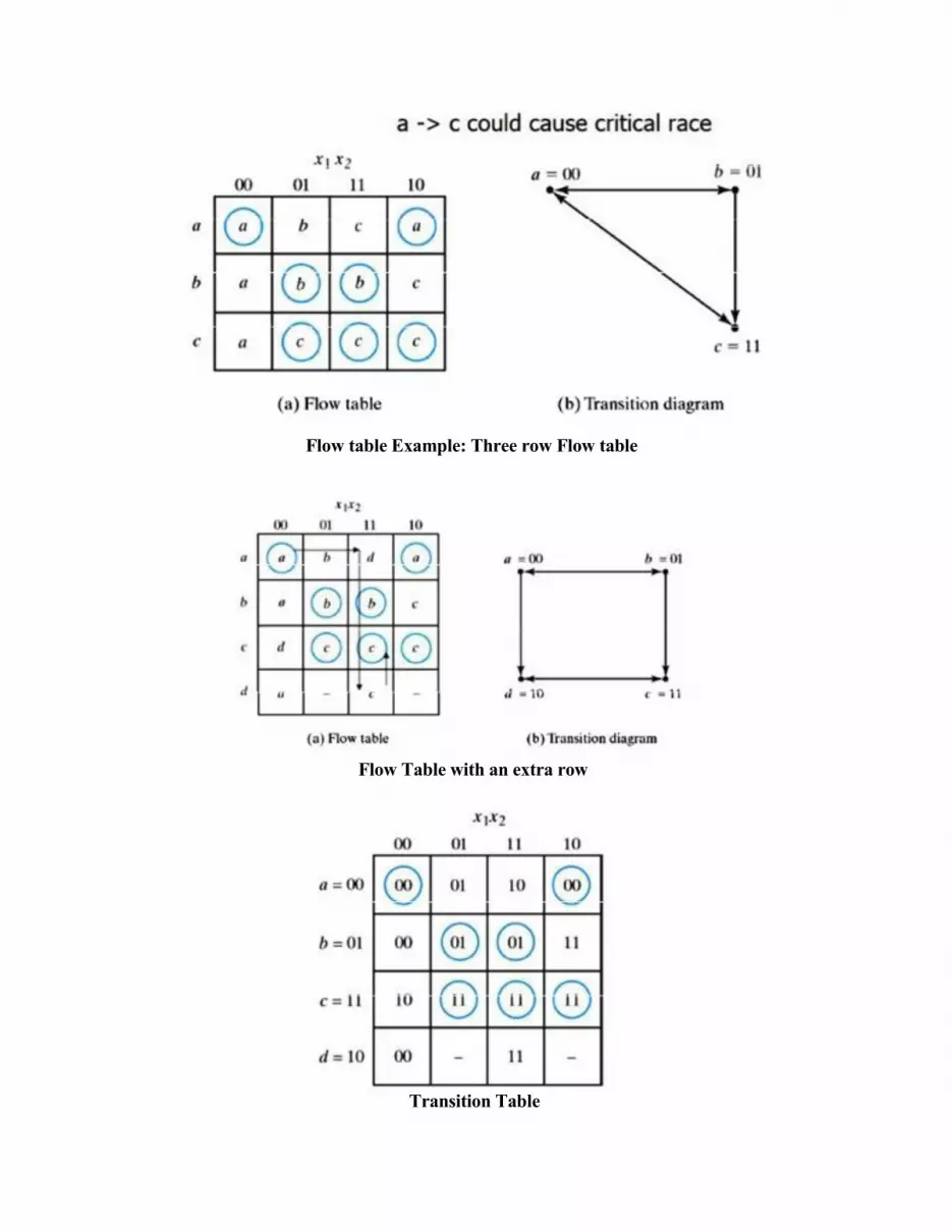
Flow table Example: Three row Flow table
Flow Table with an extra row
Transition Table

3.12 HAZARDS
A hazard is a momentary unwanted switching transient at a logic function’s output (i.e., a
glitch).
Hazards/glitches occur due to unequal propagation delays along different paths in a
combinational circuit.
Can take steps to try and eliminate hazards.
There are two types of hazards; static and dynamic.
For asynchronous circuits in particular, hazards can cause problems in addition to other issues like
races and non-fundamental mode operation!
Momentary false logic function values in an asynchronous circuit can cause a
transition to an incorrect stable state!
Static-0 Hazard:
Occurs when output is 0 and should remain at 0, but temporarily switches to a 1 due to a
change in an input.
Static-1 Hazard:
Occurs when output is 1 and should remain at 1, but temporarily switches to a 0 due to a
change in an input.
Dynamic Hazard:
Occurs when an input changes, and a circuit output should change 0 -> 1 or 1 -> 0, but
temporarily flips between values.

Illustration:
Consider the following circuit with delays where only one input (input b) changes…
Draw a timing diagram to see what happens at output with delays.
From the logic expression, we see that b changing should result in the output remaining at logic
level 1…
Due to delay, the output goes 1->0->1 and this is an output glitch; we see a static-1 hazard.
Fixing Hazards
When circuits are implemented as 2-level SOP (2-level POS), we can detect and remove
hazards by inspecting the K-Map and adding redundant product (sum) terms.
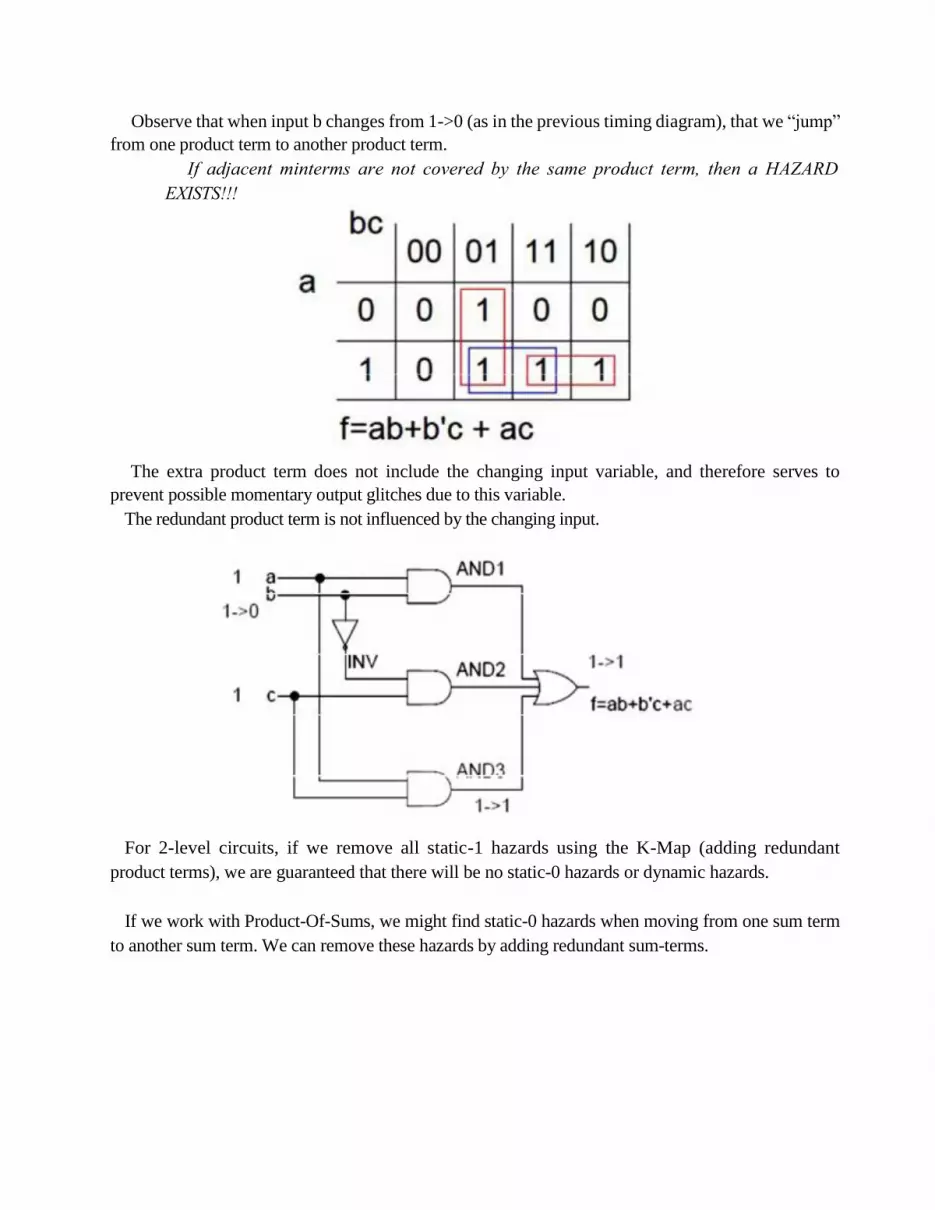
Observe that when input b changes from 1->0 (as in the previous timing diagram), that we “jump”
from one product term to another product term.
If adjacent minterms are not covered by the same product term, then a HAZARD
EXISTS!!!
The extra product term does not include the changing input variable, and therefore serves to
prevent possible momentary output glitches due to this variable.
The redundant product term is not influenced by the changing input.
For 2-level circuits, if we remove all static-1 hazards using the K-Map (adding redundant
product terms), we are guaranteed that there will be no static-0 hazards or dynamic hazards.
If we work with Product-Of-Sums, we might find static-0 hazards when moving from one sum term
to another sum term. We can remove these hazards by adding redundant sum-terms.

UNIT 4
REGISTERS, COUNTERS, MEMORY AND PROGRAMMABLE
LOGIC
REGISTER:
A clocked sequential circuit consists of a group of flip‐flops and combinational gates. The
flip‐flops are essential because, in their absence, the circuit reduces to a purely combinational
circuit (provided that there is no feedback among the gates). A circuit with flip‐flops is
considered a sequential circuit even in the absence of combinational gates. Circuits that include
flip‐flops are usually classified by the function they perform rather than by the name of the
sequential circuit. Two such circuits are registers and counters.
A register is a group of flip‐flops, each one of which shares a common clock and is capable of
storing one bit of information. An n ‐bit register consists of a group of n flip‐flops capable of
storing n bits of binary information. In addition to the flip‐flops, a register may have
combinational gates that perform certain data‐processing tasks. In its broadest definition, a
register consists of a group of flip‐flops together with gates that affect their operation. The
flip‐flops hold the binary information, and the gates determine how the information is transferred
into the register.
A counter is essentially a register that goes through a predetermined sequence of binary states. The gates in the counter are connected in such a way as to produce the prescribed sequence of states.
Although counters are a special type of register, it is common to differentiate them by giving them
a different name.
Various types of registers are available commercially. The simplest register is one that consists of
only flip‐flops, without any gates. A register constructed with four D ‐type flip‐flops to form a four‐bit
data storage register is shown in figure below. The common clock input triggers all flip‐flops on
the positive edge of each pulse, and the binary data available at the four inputs are transferred into the
register. The value of ( I 3 , I 2 , I 1 , I 0 ) immediately before the clock edge determines the value of
( A 3 , A 2 , A 1 , A 0 ) after the clock edge. The four outputs can be sampled at any time to obtain
the binary information stored in the register.
The input Clear_b goes to the active‐low R (reset) input of all four flip‐flops. When this input
goes to 0, all flip‐flops are reset asynchronously. The Clear_b input is useful for clearing the
register to all 0’s prior to its clocked operation. The R inputs must be maintained at logic 1 (i.e.,
de-asserted) during normal clocked operation. Note that, depending on the flip‐flop, either Clear,
Clear_b, reset, or reset_b can be used to indicate the transfer of the register to an all 0’s state.

Four-bit Register
4.1 SHIFT REGISTERS:
A register capable of shifting the binary information held in each cell to its neighboring cell, in a
selected direction, is called a shift register. The logical configuration of a shift register consists
of a chain of flip‐flops in cascade, with the output of one flip‐flop connected to the input of the
next flip‐flop. All flip‐flops receive common clock pulses, which activate the shift of data from
one stage to the next. The simplest possible shift register is one that uses only flip‐flops, as
shown in Fig.

Four bit Shift register
The output of a given flip‐flop is connected to the D input of the flip‐flop at its right. This shift
register is unidirectional (left‐to‐right). Each clock pulse shifts the contents of the register one bit
position to the right. The configuration does not support a left shift. The serial input determines
what goes into the leftmost flip‐flop during the shift. The serial output is taken from the output
of the rightmost flip‐flop. Sometimes it is necessary to control the shift so that it occurs only with
certain pulses, but not with others. As with the data register discussed in the previous section, the
clock’s signal can be suppressed by gating the clock signal to prevent the register from shifting.
A preferred alternative in high speed circuits is to suppress the clock action, rather than gate the
clock signal, by leaving the clock path unchanged, but recirculating the output of each register
cell back through a two‐channel mux whose output is connected to the input of the cell. When
the clock action is not suppressed, the other channel of the mux provides a data path to the cell.
4.2 RIPPLE COUNTER
A register that goes through a prescribed sequence of states upon the application of input pulses
is called a counter. The input pulses may be clock pulses, or they may originate from some
external source and may occur at a fixed interval of time or at random. The sequence of states
may follow the binary number sequence or any other sequence of states. A counter that follows
the binary number sequence is called a binary counter. An n ‐bit binary counter consists of n
flip‐flops and can count in binary from 0 through 2n - 1. Counters are available in two
categories: ripple counters and synchronous counters. In a ripple counter, a flip‐flop output
transition serves as a source for triggering other flip‐flops. In other words, the C input of some or all
flip‐flops are triggered, not by the common clock pulses, but rather by the transition that occurs
in other flip‐flop outputs. In a synchronous counter, the C inputs of all flip‐flops receive the common
clock.
Binary Ripple Counter
A ripple counter is an asynchronous counter where only the first flip-flop is clocked by an
external clock. All subsequent flip-flops are clocked by the output of the preceding flip-flop.
Asynchronous counters are also called ripple-counters because of the way the clock pulse ripples it
way through the flip-flops.
The MOD of the ripple counter or asynchronous counter is 2n if n flip-flops are used. For a 4-bit
counter, the range of the count is 0000 to 1111 (24-1). A counter may count up or count down or count
up and down depending on the input control. The count sequence usually repeats itself. When
counting up, the count sequence goes from 0000, 0001, 0010, ... 1110 , 1111 , 0000, 0001, ... etc.
When counting down the count sequence goes in the opposite manner: 1111, 1110, ... 0010, 0001,
0000, 1111, 1110, ... etc.
The complement of the count sequence counts in reverse direction. If the uncomplemented
output counts up, the complemented output counts down. If the uncomplemented output counts
down, the complemented output counts up.
There are many ways to implement the ripple counter depending on the characteristics of the flip flops
used and the requirements of the count sequence.

Clock Trigger: Positive edged or Negative edged
JK or D flip-flops
Count Direction: Up, Down, or Up/Down
Asynchronous counters are slower than synchronous counters because of the delay in the
transmission of the pulses from flip-flop to flip-flop. With a synchronous circuit, all the bits in the
count change synchronously with the assertion of the clock. Examples of synchronous counters
are the Ring and Johnson counter.
It can be implemented using D-type flip-flops or JK-type flip-flops.
The circuit below uses 2 D flip-flops to implement a divide-by-4 ripple counter (2n = 2
2 = 4). It
counts down.
Notes:
Click on CLK (Red) switch and observe the changes in the outputs of the flip flops. The
CLK switch is a momentary switch (similar to a door bell switch - normally off).
PR and CLR are both connected to VCC (set to 1)
The D flip flop clock has a rising edge CLK input. For example Q0 behaves as follows:

o The D input value just before the CLK rising edge is noted (Q00).
o When CLK rising edge occurs, Q0 is assigned the previously noted D value
(Q00).
o Thus, whenever a rising edge appears at the CLK of the D flip flop, the output Q
changes state (or toggles).
The MOD or number of unique states of this 2 flip flop ripple counter is 4 (22).
Simulate and Breadboard the Ripple Counter circuit.
A Truncated Ripple Counter is used if a MOD of less than 2n is required. For example, if
you want to change the sequence from 3,2,1,0,3,2,1,0 ... to 3,2,0,3,2,0 ...
BCD Ripple Counter
A decimal counter follows a sequence of 10 states and returns to 0 after the count of 9. Such a
counter must have at least four flip‐flops to represent each decimal digit, since a decimal digit is
represented by a binary code with at least four bits. The sequence of states in a decimal counter
is dictated by the binary code used to represent a decimal digit. If BCD is used, the sequence of
states is as shown in the state diagram of Fig1. A decimal counter is similar to a binary counter,
except that the state after 1001 (the code for decimal digit 9) is 0000 (the code for decimal digit 0).
The logic diagram of a BCD ripple counter using JK flip‐flops is shown in Fig. below. The four
outputs are designated by the letter symbol Q, with a numeric subscript equal to the binary
weight of the corresponding bit in the BCD code. Note that the output of Q1 is applied to the C inputs
of both Q2 and Q8 and the output of Q2 is applied to the C input of Q4. The J and K inputs are
connected either to a permanent 1 signal or to outputs of other flip‐flops.
A ripple counter is an asynchronous sequential circuit. Signals that affect the flip‐flop transition
depend on the way they change from 1 to 0. The operation of the counter can be explained by a list of
conditions for flip‐flop transitions. These conditions are derived from the logic diagram and from
knowledge of how a JK flip‐flop operates. Remember that when the C input goes from 1 to 0, the
flip‐flop is set if J = 1, is cleared if K = 1, is complemented if J = K = 1, and is left unchanged if J
= K = 0.

Block Diagram of BCD Adder
To verify that these conditions result in the sequence required by a BCD ripple counter, it is
necessary to verify that the flip‐flop transitions indeed follow a sequence of states as specified by
the state diagram of Fig.1. Q1 changes state after each clock pulse. Q2 complements every time
Q1 goes from 1 to 0, as long as Q8 = 0. When Q8 becomes 1, Q2 remains at 0. Q4 complements
every time Q2 goes from 1 to 0. Q8 remains at 0 as long as Q2 or Q4 is 0. When both Q2 and Q4
become 1, Q8 complements when Q1 goes from 1 to 0. Q8 is cleared on the next transition of Q1.

Block Diagram of three decade Decimal BCD counter
The BCD counter of Fig. is a decade counter, since it counts from 0 to 9. To count in decimal
from 0 to 99, we need a two‐decade counter. To count from 0 to 999, we need a three‐decade
counter. Multiple decade counters can be constructed by connecting BCD counters in cascade,
one for each decade. A three‐decade counter is shown in Fig. above. The inputs to the second
and third decades come from Q8 of the previous decade. When Q8 in one decade goes from 1 to
0, it triggers the count for the next higher order decade while its own decade goes from 9 to 0.
4.3 SYNCHRONOUS COUNTERS
Synchronous counters are different from ripple counters in that clock pulses are applied to the
inputs of all flip‐flops. A common clock triggers all flip‐flops simultaneously, rather than one at a
time in succession as in a ripple counter. The decision whether a flip‐flop is to be
complemented is determined from the values of the data inputs, such as T or J and K at the time of the
clock edge. If T = 0 or J = K = 0, the flip‐flop does not change state. If T = 1 or J = K = 1, the flip‐flop
complements.
Binary Counter
The design of a synchronous binary counter is so simple that there is no need to go through a
sequential logic design process. In a synchronous binary counter, the flip‐flop in the least
significant position is complemented with every pulse. A flip-flop in any other position is
complemented when all the bits in the lower significant positions are equal to 1. For example, if the
present state of a four‐bit counter is A3A2A1A0 = 0011, the next count is 0100. A0 is always
complemented. A1 is complemented because the present state of A0 = 1. A2 is complemented
because the present state of A1A0 = 11. However, A3 is not complemented, because the present state
of A2A1A0 = 011, which does not give an all‐1’s condition.
Synchronous binary counters have a regular pattern and can be constructed with complementing
flip‐flops and gates. The regular pattern can be seen from the four‐bit counter depicted in Fig.
below. The C inputs of all flip‐flops are connected to a common clock. The counter is enabled by
Count_enable. If the enable input is 0, all J and K inputs are equal to 0 and the clock does not
change the state of the counter. The first stage, A0, has its J and K equal to 1 if the counter is
enabled. The other J and K inputs are equal to 1 if all previous least significant stages are equal to 1
and the count is enabled.
The chain of AND gates generates the required logic for the J and K inputs in each stage. The
counter can be extended to any number of stages, with each stage having an additional flip‐flop and
an AND gate that gives an output of 1 if all previous flip‐flop outputs are 1.

Four-bit Synchronous binary Counter
Up-Down Binary Counter
A synchronous countdown binary counter goes through the binary states in reverse order, from 1111 down to 0000 and back to 1111 to repeat the count. It is possible to design a countdown counter in the usual manner, but the result is predictable by inspection of the downward binary

count. The bit in the least significant position is complemented with each pulse. A bit in any other
position is complemented if all lower significant bits are equal to 0. For example, the next state after
the present state of 0100 is 0011. The least significant bit is always complemented. The second
significant bit is complemented because the first bit is 0. The third significant bit is complemented
because the first two bits are equal to 0. But the fourth bit does not change, because not all lower
significant bits are equal to 0.
A countdown binary counter can be constructed as shown in Fig. below, except that the inputs to
the AND gates must come from the complemented outputs, instead of the normal outputs, of the
previous flip‐flops. The two operations can be combined in one circuit to form a counter capable
of counting either up or down. The circuit of an up-down binary counter using T flip‐flops is
shown in Fig. It has an up control input and a down control input. When the up input is 1, the
circuit counts up, since the T inputs receive their signals from the values of the previous normal
outputs of the flip‐flops. When the down input is 1 and the up input is 0, the circuit counts down,
since the complemented outputs of the previous flip‐flops are applied to the T inputs. When the
up and down inputs are both 0, the circuit does not change state and remains in the same count.
When the up and down inputs are both 1, the circuit counts up. This set of conditions ensures that
only one operation is performed at any given time. Note that the up input has priority over the
down input.

Four-bit up-down binary counter
BCD Counter
A BCD counter counts in binary‐coded decimal from 0000 to 1001 and back to 0000. Because of
the return to 0 after a count of 9, a BCD counter does not have a regular pattern, unlike a straight

binary count. To derive the circuit of a BCD synchronous counter, it is necessary to go through a
sequential circuit design procedure.
The state table of a BCD counter is listed in Table. The input conditions for the T flip‐flops are
obtained from the present‐ and next‐state conditions. Also shown in the table is an output y,
which is equal to 1 when the present state is 1001. In this way, y can enable the count of the
next‐higher significant decade while the same pulse switches the present decade from 1001 to
0000.
The flip‐flop input equations can be simplified by means of maps. The unused states for
minterms 10 to 15 are taken as don’t‐care terms. The simplified functions are
TQ1 = 1
TQ2 = Q8Q1
TQ4 = Q2Q1
TQ8 = Q8Q1 + Q4Q2Q1 y
= Q8Q1
The circuit can easily be drawn with four T flip‐flops, five AND gates, and one OR gate.
Synchronous BCD counters can be cascaded to form a counter for decimal numbers of any
length. The cascading is done as in Fig. 3, except that output y must be connected to the count input
of the next‐higher significant decade.
State Table for BCD Counter
Binary Counter with Parallel Load
Counters employed in digital systems quite often require a parallel‐load capability for
transferring an initial binary number into the counter prior to the count operation. Figure below
shows the top‐level block diagram symbol and the logic diagram of a four‐bit register that has a
parallel load capability and can operate as a counter. When equal to 1, the input load control
disables the count operation and causes a transfer of data from the four data inputs into the four
flip‐flops. If both control inputs are 0, clock pulses do not change the state of the register.

4-bit binary counter with parallel load
The carry output becomes a 1 if all the flip‐flops are equal to 1 while the count input is enabled.
This is the condition for complementing the flip‐flop that holds the next significant bit. The carry

output is useful for expanding the counter to more than four bits. The speed of the counter is
increased when the carry is generated directly from the outputs of all four flip‐flops, because the delay
to generate the carry bit is reduced. In going from state 1111 to 0000, only one gate delay occurs,
whereas four gate delays occur in the AND gate chain shown in Fig. Similarly, each flip‐flop is
associated with an AND gate that receives all previous flip‐flop outputs directly instead of
connecting the AND gates in a chain.
The operation of the counter is summarized in Table below. The four control inputs— Clear,
CLK, Load, and Count —determine the next state. The Clear input is asynchronous and, when equal
to 0, causes the counter to be cleared regardless of the presence of clock pulses or other inputs.
This relationship is indicated in the table by the X entries, which symbolize don’t‐care conditions
for the other inputs. The Clear input must be in the 1 state for all other operations. With the Load
and Count inputs both at 0, the outputs do not change, even when clock pulses are applied. A Load
input of 1 causes a transfer from inputs I0 - I3 into the register during a positive edge of CLK . The
input data are loaded into the register regardless of the value of the Count input, because the Count
input is inhibited when the Load input is enabled. The Load input must be 0 for the Count input to
control the operation of the counter.
A counter with a parallel load can be used to generate any desired count sequence. Figure shows
two ways in which a counter with a parallel load is used to generate the BCD count. In each case,
the Count control is set to 1 to enable the count through the CLK input. Also, recall that the Load control inhibits the count and that the clear operation is independent of other control inputs.
4.4 OTHER COUNTERS
Counters can be designed to generate any desired sequence of states. A divide‐by‐ N counter (also
known as a modulo‐ N counter) is a counter that goes through a repeated sequence of N states.
The sequence may follow the binary count or may be any other arbitrary sequence. Counters
are used to generate timing signals to control the sequence of operations in a digital system.
Counters can also be constructed by means of shift registers. In this section, we present a few examples
of non binary counters.
Counter with Unused States
A circuit with n flip‐flops has 2n binary states. There are occasions when a sequential circuit
uses fewer than this maximum possible number of states. States that are not used in specifying
the sequential circuit are not listed in the state table. In simplifying the input equations, the
unused states may be treated as don’t‐care conditions or may be assigned specific next states. It
is important to realize that once the circuit is designed and constructed, outside interference
during its operation may cause the circuit to enter one of the unused states. In that case, it is
necessary to ensure that the circuit eventually goes into one of the valid states so that it can
resume normal operation. Otherwise, if the sequential circuit circulates among unused states,

there will be no way to bring it back to its intended sequence of state transitions. If the unused
states are treated as don’t‐care conditions, then once the circuit is designed, it must be
investigated to determine the effect of the unused states. The next state from an unused state can be
determined from the analysis of the circuit after it is designed.
As an illustration, consider the counter specified in Table below. The count has a repeated
sequence of six states, with flip‐flops B and C repeating the binary count 00, 01, 10, and flip‐flop
A alternating between 0 and 1 every three counts. The count sequence of the counter is not
straight binary, and two states, 011 and 111, are not included in the count. The choice of JK
flip‐flops results in the flip‐flop input conditions listed in the table. Inputs KB and KC have only
1’s and X’s in their columns, so these inputs are always equal to 1. The other flip‐flop input
equations can be simplified by using minterms 3 and 7 as don’t‐care conditions.
State Table for Counter
The simplified equations are
JA = B KA = B
JB = C KB = 1
JC = B’ KC = 1
The logic diagram of the counter is shown in Fig. (a). Since there are two unused states, we
analyze the circuit to determine their effect. If the circuit happens to be in state 011 because of an error
signal, the circuit goes to state 100 after the application of a clock pulse. This action may be determined
from an inspection of the logic diagram by noting that when B = 1, the next clock edge complements
A and clears C to 0, and when C = 1, the next clock edge complements B. In a similar manner, we can
evaluate the next state from present state 111 to be 000.

Counter with unused States
The state diagram including the effect of the unused states is shown in Fig. (b). If the circuit ever
goes to one of the unused states because of outside interference, the next count pulse transfers it
to one of the valid states and the circuit continues to count correctly. Thus, the counter is
self‐correcting. In a self‐correcting counter, if the counter happens to be in one of the unused
states, it eventually reaches the normal count sequence after one or more clock pulses. An
alternative design could use additional logic to direct every unused state to a specific next state.
Ring Counter
A ring counter is a Shift Register (a cascade connection of flip-flops) with the output of the last flip
flop connected to the input of the first. It is initialized such that only one of the flip flop output is
1 while the remainder is 0. The 1 bit is circulated so the state repeats every n clock cycles if n
flip-flops are used. The "MOD" or "MODULUS" of a counter is the number of unique states. The
MOD of the n flip flop ring counter is n.
It can be implemented using D-type flip-flops (or JK-type flip-flops).

Notes:
Enable the flips flops by clicking on the RESET (Green) switch. The RESET switch is a
on/off switch (similar to a room light switch)
Click on CLK (Red) switch and observe the changes in the outputs of the flip flops. The
CLK switch is a momentary switch (similar to a door bell switch - normally off).
The D flip flop clock has a rising edge CLK input. For example Q1 behaves as follows:
o The D input value just before the CLK rising edge is noted (Q0).
o When CLK rising edge occurs, Q1 is assigned the previously noted D value (Q0).
The MOD or number of unique states of this 3 flip flop ring counter is 3.

Johnson Counter
A Johnson counter is a modified ring counter, where the inverted output from the last flip flop is
connected to the input to the first. The register cycles through a sequence of bit-patterns. The
MOD of the Johnson counter is 2n if n flip-flops are used. The main advantage of the Johnson
counter counter is that it only needs half the number of flip-flops compared to the standard ring
counter for the same MOD.
It can be implemented using D-type flip-flops (or JK-type flip-flops).
Notes:
Enable the flips flops by clicking on the RESET (Green) switch. The RESET switch is a
on/off switch (similar to a room light switch)
Click on CLK (Red) switch and observe the changes in the outputs of the flip flops. The
CLK switch is a momentary switch (similar to a door bell switch - normally off).
The D flip flop clock has a rising edge CLK input. For example Q1 behaves as follows:
o The D input value just before the CLK rising edge is noted (Q0).
o When CLK rising edge occurs, Q1 is assigned the previously noted D value (Q0).
The MOD or number of unique states of this 3 flip flop Johnson counter is 6.

MEMORY AND PROGRAMMABLE LOGIC
Introduction:
A memory unit is a device to which binary information is transferred for storage and from which
information is retrieved when needed for processing. When data processing takes place,
information from memory is transferred to selected registers in the processing unit.
Intermediate and final results obtained in the processing unit are transferred back to be stored in
memory. Binary information received from an input device is stored in memory, and information
transferred to an output device is taken from memory. A memory unit is a collection of cells
capable of storing a large quantity of binary information.
There are two types of memories that are used in digital systems: random access memory (RAM) and
read only memory (ROM). RAM stores new information for later use. The process of storing new
information into memory is referred to as a memory write operation. The process of
transferring the stored information out of memory is referred to as a memory read operation.
RAM can perform both write and read operations.
ROM can perform only the read operation. This means that suitable binary information is already
stored inside memory and can be retrieved or read at any time. However, that information cannot be
altered by writing.
ROM is a programmable logic device (PLD). The binary information that is stored within such a
device is specified in some fashion and then embedded within the hardware in a process is
referred to as programming the device. The word “programming” here refers to a hardware
procedure which specifies the bits that are inserted into the hardware configuration of the device.
ROM is one example of a PLD. Other such units are the programmable logic array (PLA),
programmable array logic (PAL), and the field‐programmable gate array (FPGA).

A PLD is an integrated circuit with internal logic gates connected through electronic intact.
Programming the device involves blowing those fuses along the paths that must be removed in order
to obtain the particular configuration of the desired logic function.
We introduce the configuration of PLDs and indicate procedures for their use in the design of
digital systems. We also present CMOS FPGAs, which are configured by downloading a stream of bits into the device to configure transmission gates to establish the internal connectivity
required by a specified logic function (combinational or sequential).
A typical PLD may have hundreds to millions of gates interconnected through hundreds to
thousands of internal paths. In order to show the internal logic diagram of such a device in a
concise form, it is necessary to employ a special gate symbology applicable to array logic. Figure
shows the conventional and array logic symbols for a multiple input OR gate. Instead of having
multiple input lines into the gate, we draw a single line entering the gate. The input lines are
drawn perpendicular to this single line and are connected to the gate through internal fuses. In a
similar fashion, we can draw the array logic for an AND gate. This type of graphical
representation for the inputs of gates will be used throughout the chapter in array logic diagrams.
Conventional and array logic diagrams for OR gate
4.5 RANDOM-ACCESS MEMORY
A memory unit is a collection of storage cells, together with associated circuits needed to transfer
information into and out of a device. The architecture of memory is such that information can be
selectively retrieved from any of its internal locations. The time it takes to transfer information to or
from any desired random location is always the same—hence the name random access memory,
abbreviated RAM. In contrast, the time required to retrieve information that is stored on magnetic tape
depends on the location of the data.
A memory unit stores binary information in groups of bits called words. A word in memory is an entity
of bits that move in and out of storage as a unit. A memory word is a group of 1’s and 0’s and may
represent a number, an instruction, one or more alphanumeric characters, or any other binary‐coded
information. A group of 8 bits is called a byte. Most computer memories use words that are multiples
of 8 bits in length. Thus, a 16‐bit word contains two bytes, and a 32‐bit word is made up of four bytes.
The capacity of a memory unit is usually stated as the total number of bytes that the unit can store.
Communication between memory and its environment is achieved through data input and output
lines, address selection lines, and control lines that specify the direction of transfer. A block
diagram of a memory unit is shown in Fig. below. The n data input lines provide the information
to be stored in memory, and the n data output lines supply the information coming out of
memory. The k address lines specify the particular word chosen among the many available. The
two control inputs specify the direction of transfer desired: The Write input causes binary data to

be transferred into the memory, and the Read input causes binary data to be transferred out of
memory.
Block Diagram of a memory unit
The memory unit is specified by the number of words it contains and the number of bits in each
word. The address lines select one particular word. Each word in memory is assigned an
identification number, called an address, starting from 0 up to 2k - 1, where k is the number of
address lines. The selection of a specific word inside memory is done by applying the k ‐bit
address to the address lines. An internal decoder accepts this address and opens the paths needed
to select the word specified. Memories vary greatly in size and may range from 1,024 words,
requiring an address of 10 bits, to 232 words, requiring 32 address bits. It is customary to refer to
the number of words (or bytes) in memory with one of the letters K (kilo), M (mega), and G
(giga). K is equal to 210, M is equal to 220, and G is equal to 230. Thus, 64K = 216, 2M = 221,
and 4G = 232.
Consider, for example, a memory unit with a capacity of 1K words of 16 bits each. Since 1K =
1,024 = 210 and 16 bits constitute two bytes, we can say that the memory can accommodate
2,048 = 2K bytes. Below figure shows possible contents of the first three and the last three
words of this memory. Each word contains 16 bits that can be divided into two bytes. The words
are recognized by their decimal address from 0 to 1,023. The equivalent binary address consists
of 10 bits. The first address is specified with ten 0’s; the last address is specified with ten 1’s,
because 1,023 in binary is equal to 1111111111. A word in memory is selected by its binary
address. When a word is read or written, the memory operates on all 16 bits as a single unit.

Contents of a 1024 * 16 memory
Write and Read Operations
The two operations that RAM can perform are the write and read operations. As alluded to
earlier, the write signal specifies a transfer‐in operation and the read signal specifies a
transfer‐out operation. On accepting one of these control signals, the internal circuits inside the
memory provide the desired operation.
The steps that must be taken for the purpose of transferring a new word to be stored into memory are as
follows: 1. Apply the binary address of the desired word to the address lines.
2. Apply the data bits that must be stored in memory to the data input lines.
3. Activate the write input.
The memory unit will then take the bits from the input data lines and store them in the word specified by the address lines.
The steps that must be taken for the purpose of transferring a stored word out of memory are as
follows:
1. Apply the binary address of the desired word to the address lines.
2. Activate the read input
The memory unit will then take the bits from the word that has been selected by the address and
apply them to the output data lines. The contents of the selected word do not change after the read
operation, i.e., the word operation is nondestructive.
Commercial memory components available in integrated‐circuit chips sometimes provide the
two control inputs for reading and writing in a somewhat different configuration. Instead of
having separate read and write inputs to control the two operations, most integrated circuits
provide two other control inputs: One input selects the unit and the other determines the
operation. The memory operations that result from these control inputs are specified in Table
below.

Control Inputs to Memory Chip
The memory enable (sometimes called the chip select) is used to enable the particular memory chip
in a multichip implementation of a large memory. When the memory enable is inactive, the memory
chip is not selected and no operation is performed. When the memory enable input is active, the
read/write input determines the operation to be performed.
Memory Decoding
In addition to requiring storage components in a memory unit, there is a need for decoding
circuits to select the memory word specified by the input address. In this section, we present the
internal construction of a RAM and demonstrate the operation of the decoder. To be able to
include the entire memory in one diagram, the memory unit presented here has a small capacity
of 16 bits, arranged in four words of 4 bits each. An example of a two‐dimensional coincident
decoding arrangement is presented to show a more efficient decoding scheme that is used in
large memories. We then give an example of address multiplexing commonly used in DRAM
integrated circuits.
Internal Construction
The internal construction of a RAM of m words and n bits per word consists of m * n binary
storage cells and associated decoding circuits for selecting individual words. The binary storage
cell is the basic building block of a memory unit. The equivalent logic of a binary cell that stores
one bit of information is shown in Fig. below. The storage part of the cell is modeled by an SR
latch with associated gates to form a D latch. Actually, the convenient to model it in terms of
logic symbols. A binary storage cell must be very small in order to be able to pack as many cells
as possible in the small area available in the integrated circuit chip. The binary cell stores one bit
in its internal latch. The select input enables the cell for reading or writing, and the read/write
input determines the operation of the cell when it is selected. A 1 in the read/write input provides
the read operation by forming a path from the latch to the output terminal. A 0 in the read/write
input provides the write operation by forming a path from the input terminal to the latch.

Memory cell
The logical construction of a small RAM is shown in Fig. below. This RAM consists of four
words of four bits each and has a total of 16 binary cells. The small blocks labeled BC represent the
binary cell with its three inputs and one output, as specified in Fig. above. A memory with four
words needs two address lines. The two address inputs go through a 2 * 4 decoder to select one of the
four words. The decoder is enabled with the memory‐enable input. When the memory enable is 0, all
outputs of the decoder are 0 and none of the memory words are selected. With the memory select at 1,
one of the four words is selected, dictated by the value in the two address lines. Once a word has
been selected, the read/write input determines the operation. During the read operation, the four bits
of the selected word go through OR gates to the output terminals. During the write operation, the
data available in the input lines are transferred into the four binary cells of the selected word. The
binary cells that are not selected are disabled, and their previous binary values remain
unchanged. When the memory select input that goes into the decoder is equal to 0, none of the
words are selected and the contents of all cells remain unchanged regardless of the value of the
read/write input.
Commercial RAMs may have a capacity of thousands of words, and each word may range from 1 to
64 bits. The logical construction of a large‐capacity memory would be a direct extension of the
configuration shown here. A memory with 2k words of n bits per word requires k address lines that
go into a k * 2k decoder. Each one of the decoder outputs selects one word of n bits for reading or
writing.

Diagram of a 4 * 4 RAM
4.6 READ ONLY MEMORY:
A read‐only memory (ROM) is essentially a memory device in which permanent binary
information is stored. The binary information must be specified by the designer and is then embedded in the unit to form the required interconnection pattern. Once the pattern is
established, it stays within the unit even when power is turned off and on again.
A block diagram of a ROM consisting of k inputs and n outputs is shown in Fig. below. The
inputs provide the address for memory, and the outputs give the data bits of the stored word that
is selected by the address. The number of words in a ROM is determined from the fact that k
address input lines are needed to specify 2k words. Note that ROM does not have data inputs,
because it does not have a write operation. Integrated circuit ROM chips have one or more
enable inputs and sometimes come with three‐state outputs to facilitate the construction of large
arrays of ROM.

ROM block diagram
Consider, for example, a 32 * 8 ROM. The unit consists of 32 words of 8 bits each. There are
five input lines that form the binary numbers from 0 through 31 for the address. Below figure
shows the internal logic construction of this ROM. The five inputs are decoded into 32 distinct
outputs by means of a 5 * 32 decoder. Each output of the decoder represents a memory address.
The 32 outputs of the decoder are connected to each of the eight OR gates. The diagram shows
the array logic convention used in complex circuits. Each OR gate must be considered as having
32 inputs. Each output of the decoder is connected to one of the inputs of each OR gate. Since
each OR gate has 32 input connections and there are 8 OR gates, the ROM contains 32 * 8 = 256
internal connections. In general, a 2k * n ROM will have an internal k * 2k decoder and n OR
gates. Each OR gate has 2k inputs, which are connected to each of the outputs
of the decoder.
Internal logic of a 32: 8 ROM
Combinational Circuit Implementation
It was shown that a decoder generates the 2k minterms of the k input variables. By inserting OR
gates to sum the minterms of Boolean functions, we were able to generate any desired

combinational circuit. The ROM is essentially a device that includes both the decoder and the OR
gates within a single device to form a minterm generator. By choosing connections for those
minterms which are included in the function, the ROM outputs can be programmed to represent the
Boolean functions of the output variables in a combinational circuit.
The internal operation of a ROM can be interpreted in two ways. The first interpretation is that of
a memory unit that contains a fixed pattern of stored words. The second interpretation is that of a
unit which implements a combinational circuit. From this point of view, each output terminal is
considered separately as the output of a Boolean function expressed as a sum of minterms. For
example, the ROM may be considered to be a combinational circuit with eight outputs, each a
function of the five input variables. Output A7 can be expressed in sum of minterms as
A7(I4, I3, I2, I1, I0) = ∑m(0, 2, 3, …., 29)
(The three dots represent minterms 4 through 27, which are not specified in the figure.) A
connection marked with * in the figure produces a minterm for the sum. All other crosspoints are
not connected and are not included in the sum. In practice, when a combinational circuit is
designed by means of a ROM, it is not necessary to design the logic or to show the internal gate
connections inside the unit. All that the designer has to do is specify the particular ROM by its
IC number and provide the applicable truth table. The truth table gives all the information for
programming the ROM. No internal logic diagram is needed to accompany the truth table.

Programming the ROM according to Table given above
Types of ROMs
The required paths in a ROM may be programmed in four different ways. The first is called mask
programming and is done by the semiconductor company during the last fabrication process of
the unit. The procedure for fabricating a ROM requires that the customer fill out the truth table
he or she wishes the ROM to satisfy. The truth table may be submitted in a special form provided
by the manufacturer or in a specified format on a computer output medium. The manufacturer
makes the corresponding mask for the paths to produce the 1’s and 0’s according to the
customer’s truth table. This procedure is costly because the vendor charges the customer a
special fee for custom masking the particular ROM. For this reason, mask programming is
economical only if a large quantity of the same ROM configuration is to be ordered.
For small quantities, it is more economical to use a second type of ROM called programmable
read only memory, or PROM. When ordered, PROM units contain all the fuses intact, giving all
1’s in the bits of the stored words. The fuses in the PROM are blown by the application of a
high‐voltage pulse to the device through a special pin. A blown fuse defines a binary 0 state and
an intact fuse gives a binary 1 state. This procedure allows the user to program the PROM in the
laboratory to achieve the desired relationship between input addresses and stored words. Special
instruments called PROM programmers are available commercially to facilitate the procedure. In
any case, all procedures for programming ROMs are hardware procedures, even though the word
programming is used.
The hardware procedure for programming ROMs or PROMs is irreversible, and once
programmed, the fixed pattern is permanent and cannot be altered. Once a bit pattern has been
established, the unit must be discarded if the bit pattern is to be changed. A third type of ROM is

the erasable PROM, or EPROM, which can be restructured to the initial state even though it has been
programmed previously. When the EPROM is placed under a special ultraviolet light for a given
length of time, the shortwave radiation discharges the internal floating gates that serve as the
programmed connections. After erasure, the EPROM returns to its initial state and can be
reprogrammed to a new set of values.
The fourth type of ROM is the electrically erasable PROM (EEPROM or E2PROM). This device is
like the EPROM, except that the previously programmed connections can be erased with an
electrical signal instead of ultraviolet light. The advantage is that the device can be erased
without removing it from its socket.
Combinational PLDs
The PROM is a combinational programmable logic device (PLD)—an integrated circuit with
programmable gates divided into an AND array and an OR array to provide an AND-OR
sum‐of‐product implementation. There are three major types of combinational PLDs, differing in
the placement of the programmable connections in the AND- OR array. Below figure shows the
configuration of the three PLDs. The PROM has a fixed AND array constructed as a decoder and
a programmable OR array. The programmable OR gates implement the Boolean functions in
sum‐of‐minterms form. The PAL has a programmable AND array and a fixed OR array. The
AND gates are programmed to provide the product terms for the Boolean functions, which are
logically summed in each OR gate. The most flexible PLD is the PLA, in which both the AND
and OR arrays can be programmed. The product terms in the AND array may be shared by any
OR gate to provide the required sum‐of‐products implementation. The names PAL and PLA
emerged from different vendors during the development of PLDs. The implementation of
combinational circuits with PROM was demonstrated in this section. The design of
combinational circuits with PLA and PAL is presented in the next two sections.
Basic configuration of three PLDs

4.7 PROGRAMMABLE LOGIC ARRAY
The PLA is similar in concept to the PROM, except that the PLA does not provide full decoding of
the variables and does not generate all the minterms. The decoder is replaced by an array of AND
gates that can be programmed to generate any product term of the input variables. The product
terms are then connected to OR gates to provide the sum of products for the required Boolean
functions.
The internal logic of a PLA with three inputs and two outputs is shown in Fig. below. Such a circuit
is too small to be useful commercially, but is presented here to demonstrate the typical logic
configuration of a PLA. The diagram uses the array logic graphic symbols for complex circuits. Each
input goes through a buffer-inverter combination, shown in the diagram with a composite graphic
symbol, that has both the true and complement outputs. Each input and its complement is connected
to the inputs of each AND gate, as indicated by the intersections between the vertical and
horizontal lines. The outputs of the AND gates are connected to the inputs of each OR gate. The
output of the OR gate goes to an XOR gate, where the other input can be programmed to receive a
signal equal to either logic 1 or logic 0. The output is inverted when the XOR input is connected to 1
(since x XOR 1 = x’). The output does not change when the XOR input is connected to 0 (since x XOR
0 = x).
The particular Boolean functions implemented in the PLA of below Fig. are
F1 = AB’+ AC + A’BC’
F2 = (AC + BC)’
The product terms generated in each AND gate are listed along the output of the gate in the
diagram. The product term is determined from the inputs whose crosspoints are connected and
marked with a *. The output of an OR gate gives the logical sum of the selected product terms.
The output may be complemented or left in its true form, depending on the logic being realized.

PLA with three inputs, four product terms, and two outputs
The fuse map of a PLA can be specified in a tabular form. For example, the programming table
that specifies the PLA of above Fig. is listed in above Table. The PLA programming table
consists of three sections. The first section lists the product terms numerically. The second
section specifies the required paths between inputs and AND gates. The third section specifies
the paths between the AND and OR gates. For each output variable, we may have a T (for true)
or C (for complement) for programming the XOR gate. The product terms listed on the left are
not part of the table; they are included for reference only. For each product term, the inputs are
marked with 1, 0, or — (dash). If a variable in the product term appears in the form in which it is
true, the corresponding input variable is marked with a 1. If it appears complemented, the
corresponding input variable is marked with a 0. If the variable is absent from the product term,
it is marked with a dash.
The paths between the inputs and the AND gates are specified under the column head “Inputs” in
the programming table. A 1 in the input column specifies a connection from the input variable to
the AND gate. A 0 in the input column specifies a connection from the complement of the
variable to the input of the AND gate. A dash specifies a blown fuse in both the input variable
and its complement. It is assumed that an open terminal in the input of an AND gate behaves like
a 1.

The paths between the AND and OR gates are specified under the column head “Outputs.” The output
variables are marked with 1’s for those product terms which are included in the function. Each product
term that has a 1 in the output column requires a path from the output of the AND gate to the input of
the OR gate. Those marked with a dash specify a blown fuse. It is assumed that an open terminal in
the input of an OR gate behaves like a 0. Finally, a T (true) output dictates that the other input of
the corresponding XOR gate be connected to 0, and a C (complement) specifies a connection to
1.
The size of a PLA is specified by the number of inputs, the number of product terms, and the number
of outputs. A typical integrated circuit PLA may have 16 inputs, 48 product terms, and eight outputs.
For n inputs, k product terms, and m outputs, the internal logic of the PLA consists of n buffer-inverter
gates, k AND gates, m OR gates, and m XOR gates. There are 2n * k connections between the
inputs and the AND array, k * m connections between the AND and OR arrays, and m connections
associated with the XOR gates.
In designing a digital system with a PLA, there is no need to show the internal connections of the unit
as was done in Fig. above. All that is needed is a PLA programming table from which the PLA can
be programmed to supply the required logic. As with a ROM, the PLA may be mask
programmable or field programmable. With mask programming, the customer submits a PLA
program table to the manufacturer. This table is used by the vendor to produce a custom‐made PLA
that has the required internal logic specified by the customer. A second type of PLA that is available
is the field programmable logic array, or FPLA, which can be programmed by the user by means of a
commercial hardware programmer unit.
In implementing a combinational circuit with a PLA, careful investigation must be undertaken in
order to reduce the number of distinct product terms, since a PLA has a finite number of AND gates.
This can be done by simplifying each Boolean function to a minimum number of terms. The number
of literals in a term is not important, since all the input variables are available anyway. Both the
true value and the complement of each function should be simplified to see which one can be
expressed with fewer product terms and which one provides product terms that are common to other
functions.
4.8 PAL
The PAL is a programmable logic device with a fixed OR array and a programmable AND array.
Because only the AND gates are programmable, the PAL is easier to program than, but is not as
flexible as, the PLA. Figure 7.16 shows the logic configuration of a typical PAL with four inputs and
four outputs. Each input has a buffer-inverter gate, and each output is generated by a fixed OR gate.
There are four sections in the unit, each composed of an AND-OR array that is three wide, the term
used to indicate that there are three programmable AND gates in each section and one fixed OR gate.
Each AND gate has 10 programmable input connections, shown in the diagram by 10 vertical
lines intersecting each horizontal line. The horizontal line symbolizes the multiple‐input
configuration of the AND gate. One of the outputs is connected to a bufferinverter gate and then
fed back into two inputs of the AND gates.
In designing with a PAL, the Boolean functions must be simplified to fit into each section.
Unlike the situation with a PLA, a product term cannot be shared among two or more OR gates.
Therefore, each function can be simplified by itself, without regard to common product terms.

The number of product terms in each section is fixed, and if the number of terms in the function is too
large, it may be necessary to use two sections to implement one Boolean function.
As an example of using a PAL in the design of a combinational circuit, consider the following
Boolean functions, given in sum‐of‐minterms form:
w(A, B, C, D) = g(2, 12, 13)
x(A, B, C, D) = g(7, 8, 9, 10, 11, 12, 13, 14, 15) y(A, B, C, D) = g(0, 2, 3, 4, 5, 6, 7, 8, 10, 11, 15) z(A, B, C, D) = g(1, 2, 8, 12, 13)
Simplifying the four functions to a minimum number of terms results in the following Boolean
functions:
w = ABC’ + A’B’CD’ x = A + BCD
y = A’B + CD + B’D’
z = ABC’ + A’B’CD’ + AC’D’ + A’B’C’D =
w + AC’D’ + A’BC’D
Note that the function for z has four product terms. The logical sum of two of these terms is equal to w. By using w, it is possible to reduce the number of terms for z from four to three.
PAL Programming Table

PAL with four inputs, four outputs, and a three-wide AND-OR structure
Copyright © 2022 FDOKUMEN