
State of the art radiometer standards for NASA's Earth Observing System
11
. . . STATE OF THE ART RADIOMETER STANDARDS FOR NASA’S EARTH OBSERVING SYSTEM Carlos R Jorquera, Virginia G. I}ord, Valerie G, lhval, Carol J. Druegge Jet Propulsion laboratory, California Institute of ‘1’eclmology 4800 oak Grove Drive MS 303-210 Pasadena,CA91109 T: (818] 354-3546 F: (818) 393-6047 HMail: Carlos,R.Jorqucra C?jp].nasa.gov Raj Kordc ]ntcrnational Radiation Detectors 2545 W. 237tI~ Stred, Suite I Torrance, CA 90505 The Multi-Angle imaging SpcctroRadiomctcr (MISR), to bc launched in 1998, is onc of five instruments on NASA’s first Earth Observing Systcm (EOS) platform. The 3% (1 G) absolute radiometric calibration rcquircmcnt is considered challenging, particularly since it must be maintained through the five-year mission life. The instrument rcquircmertts have lcd to the dcvclopmcnt of an On-Board Calibrator (OK) consisting of diffuse panels and photodiodc-based radiomctric standards. Although used cxtcnsivcly in national standard laboratories, MISR will bc the first in-orbit instrument to utilize Spcctralon calibration ‘targets, and the first instrument to establish a radiomctric scale in orbit using detector-based standards. The team has adopted the nomenclature High Quantum Efficiency (HQE) technology to refer to the implementation of 100% internal quantum cfficicnt photodiodcs in a trapped configuration. Filtered HQE radiometers arc being utilized in the preflight calibration phase to calibrate the flat-field source (integrating sphere). In order to provide an element of continuity bctwccn the preflight and post-launch calibrations (and to provide the most accurate characterization of camera illumination ICVCIS during flight), HQE radiometers will also bc used to characterize solar-rcflcctcd light from the diffuse calibration targets during the mission. In addition, radiation-resistant photodiodcs will bc utilized as part of the OBC. These have an cxtcndcd space-lifctirnc over the HQEs, and allow for an uncertainty estimation of the calibration when the HQE and radiation-resistant photodiodc data sets arc compared. ]N1’ItODUCTION The Multi-angle Imaging SpcctroRadiomctcr (MISR) features nine pushbroom cameras, recording in four spectral bands to provide global images of the Earlh’s surface every nine days, at the Equator (see Fig. 1). Data from these 36 channels arc spatial] y rcgistcrcd during ground proccssjng to provide mcasurcmcnts through path lengths of 1.0, 1.1, 1.4, 2.0, and 3.0 (0°, *26.1”, *45.6”, *60,0°, and *70,5° in view angle). The availability of an angular mcasurcmcnt for each sccnc pixel makes these data unique. Spatial sampling ranges from 275 m (250 m cross-track in the nadir) to 1,1 km (1.0 km cross-track in the nadir), depending on the “camera-configuration”, or on-board pixel averaging mode used prjor to transmission of the data. The spectral band shape will nominally bc Gaussian and ccntcrcd at 443,555,670, and 865 nm, Bandwidth is spccificd to bc 25, 15, 15,
-
Upload
independent -
Category
Documents
-
view
4 -
download
0
Transcript of State of the art radiometer standards for NASA's Earth Observing System

.. .
STATE OF THE ART RADIOMETERSTANDARDS FOR NASA’S EARTH
OBSERVING SYSTEM
Carlos R Jorquera, Virginia G. I}ord, Valerie G, lhval, Carol J. DrueggeJet Propulsion laboratory, California Institute of ‘1’eclmology
4800 oak Grove Drive MS 303-210 Pasadena,CA91109T: (818] 354-3546 F: (818) 393-6047 HMail: Carlos,R.Jorqucra C?jp].nasa.gov
Raj Kordc]ntcrnational Radiation Detectors
2545 W. 237tI~ Stred, Suite I Torrance, CA 90505
The Multi-Angle imaging SpcctroRadiomctcr (MISR), to bc launched in 1998, is onc of fiveinstruments on NASA’s first Earth Observing Systcm (EOS) platform. The 3% (1 G) absoluteradiometric calibration rcquircmcnt is considered challenging, particularly since it must bemaintained through the five-year mission life. The instrument rcquircmertts have lcd to thedcvclopmcnt of an On-Board Calibrator (OK) consisting of diffuse panels and photodiodc-basedradiomctric standards. Although used cxtcnsivcly in national standard laboratories, MISR will bcthe first in-orbit instrument to utilize Spcctralon calibration ‘targets, and the first instrument toestablish a radiomctric scale in orbit using detector-based standards. The team has adopted thenomenclature High Quantum Efficiency (HQE) technology to refer to the implementation of 100%internal quantum cfficicnt photodiodcs in a trapped configuration. Filtered HQE radiometers arcbeing utilized in the preflight calibration phase to calibrate the flat-field source (integrating sphere).In order to provide an element of continuity bctwccn the preflight and post-launch calibrations (andto provide the most accurate characterization of camera illumination ICVCIS during flight), HQEradiometers will also bc used to characterize solar-rcflcctcd light from the diffuse calibration targetsduring the mission. In addition, radiation-resistant photodiodcs will bc utilized as part of the OBC.These have an cxtcndcd space-lifctirnc over the HQEs, and allow for an uncertainty estimation ofthe calibration when the HQE and radiation-resistant photodiodc data sets arc compared.
]N1’ItODUCTION
The Multi-angle Imaging SpcctroRadiomctcr (MISR) features nine pushbroom cameras, recordingin four spectral bands to provide global images of the Earlh’s surface every nine days, at theEquator (see Fig. 1). Data from these 36 channels arc spatial] y rcgistcrcd during ground proccssjngto provide mcasurcmcnts through path lengths of 1.0, 1.1, 1.4, 2.0, and 3.0 (0°, *26.1”, *45.6”,*60,0°, and *70,5° in view angle). The availability of an angular mcasurcmcnt for each sccnc pixelmakes these data unique. Spatial sampling ranges from 275 m (250 m cross-track in the nadir) to1,1 km (1.0 km cross-track in the nadir), depending on the “camera-configuration”, or on-boardpixel averaging mode used prjor to transmission of the data. The spectral band shape will nominallybc Gaussian and ccntcrcd at 443,555,670, and 865 nm, Bandwidth is spccificd to bc 25, 15, 15,
.
and 25 nm, respectively, for the four bands (Gaussian full-width half-maximum). The Gaussianprofile, used in conjunction with a Lyot bircfringcnt cube, will provide dcpolariz,ation of theincoming light, and allow the instrument to bc polari~,ation insensitive. MISR data will enableinvestigations into cloud, aerosol, and surface properties.
Throughout the five year mission, MISR must maintain absolute radiometric accuracy to withint3% (1a) over high reflcctancc, spatial] y uniform scenes, The instrument must bc polarizationinsensitive to AI % and radiometrica]ly accurate to better than 2% at 24 pixels distance from a high-contrast edge (e.g. not be limited by image blur and scatter beyond this amount). Geometricspecifications include *250 m along-tracld *500 m (2cJ) cross-track co-registration for the ninecamera images. The temporal stability rcquircmcnt is 2% drift pcr year, or lCSS.
To achieve the radiometric requirements, MISR utilizes an On-Board Calibrator (OBC). lncludcd isa pair of diffuse panels. These arc required to have a high, near-lambcrtian reflectance, While not inusc the panels are stowed and protcctcd. The panels will bc deployed at monthly time intervals andused to direct sunlight into the cameras, filling their fields-of-view and providing a through-the-optics calibration. Over the North Pole, a plate will swing aftward to diffusely reflect sunlight intothe fields-of-view of the aftward-looking and nadir cameras. Over the South Pole, the other platewill swing forward for calibration of the forward-looking and nadir cameras. The nadir camera willprovide a link bctwccn the two sets of observations. Clunulativc space exposure time (deploy time)for each panel is expected to bc ICSS than 100 hours over the mission life.
SpcctralonTM has been selcctcd as the matcria] to bc used as the MISR in-orbit calibration targets,Spcctralon is a product of Labsphcrc (North Sutton, Ncw Hampshire), and is composed of purepolytctrafluoroethylenc (PFTE, ‘or Teflon) polymer resin that is compressed into a hard porouswhite material. Spcctralon targets arc widely used in laboratory and ground/field operations a.s arcflcctancc standard. MISR has provided for the flight qualification of this matcria].
As diffusers in general are subject to UV degradation and contamination, they in themselves are nottypically used as a radiometric standard, In the case of MISR, the calibration targets will bcmonitored by three types of radiometers, each possessing a different photodiode design: radiation-rcsistant diodes and two types of High Quantum Efficiency (I]QE) diodes. The radiation-resistantdetectors are designed to be insensitive to otherwise damaging space radiation. They are expectedto degrade no more than 2% for the 5-year mission. The IIQE sensors arc tailored for optimumperformance within two spectral regions. The “131uc” IIQE photodiodes achieve a nearly 100%internal quantum efficiency in the first two MJSR spectral bands (443 and 555 rim), while the “Red”HQE diodes are intended for the other two bands (670 and 865 rim).
L--”———.- .—— .— . ..— — ..— —
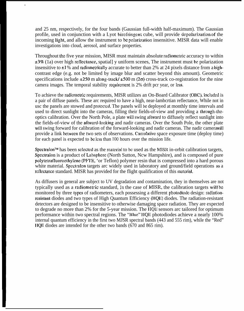
Figure 1. MISR optical bench. Four forward looking (Af, Bf, Cf, Df), four aftward looking(Aa, Ba, Ca, Da), and one nadir camera. PIN refers to the radiation-resistant radiometers.
The utilization of photodiode standards during flight to charactcriz.e diffuse panel radiance allowsthe MISR instrument to bc calibrated without reliance on source irradiance knowledge. For thisreason stray-light and Earlh-shine do not contribute to the calibration uncertainty, provided they arcuniform sources across the panel. Also, MISR will calibrate at several radiornctric levels, byacquiring data as the sun passes through a varying Earth-atmospheric path during the first minute ofcalibration. This activity would not bc possible if reliance on panel radiance from a solar-irradianccand earth atmosphere-transmittance model were required.
During the mission, MISR also plans to conduct semi-annual ground calibration campaigns, utilizingfield measurements and higher resolution sensors (aboard aircraft or in-orbit platforms) to provide acheck of the on-board hardware. These ground calibration campaigns arc limited in number, butbelieved key to validation of the flight calibration as provided by the OX.
HQE AND RADIATION-R IXKTANI’ RADIOMIWRR DINIGNS
Both the FIQE and radiation-resistant radiometers are composed of three main sections: ahermetically scaled assembly containing the photodiodes; an electronic assembly housing a trans-impcdance amplifier; and a precision baffle assembly which defines the light cone incident on thesensors, The hermetically scaled assembly consists of a multi-layer ceramic package whichconducts the diode signals through electrical traces, from the hermetically scaled volume to theunscaled electronics assembly. On the outside of the ceramic, the traces arc terminated in pinswhich are oven-braised onto the ceramic. The amplifier interfaces directly to these pins.
On the sealed side of the ceramic, a frame is oven-braised in a circle enclosing the volume.Pholodiodc sub-assemblies are bonded to the ceramic. Covers arc placed on the frame and lascr-weldcd in place to form a hermetic seal. The hermetic volume is purged through a tube (which isoven-braised onto the ceramic), then backfilled with Argon. The purge tube is crushed then sealedwith epoxy, The hermetic package provides a stable environment, and eliminates the potential fordamage due to humidity or contaminants. As both the diodes and camera CCDS will be hermeticallyscaled in their packages, it is expcctcd that filter shifts, although predicted 10 be small, will be of thesame magnitude and direction for the calibration and camera systems alike,
The baffle assemblies consist of tubes having precision apertures at both ends that define a field-of-vicw of approximately 8°, The apertures arc precision made using photolithography and chemicaletching techniques, and manufactured to a diameter uncertainty of 2 pm. The distance betweenthese apertures is tightly defined by Ihc tubes and retaining structures to an accuracy of ~0.05%.This yields an uncertainty in the Afil product (function of collective area and solid angle) of lessthan 0,5%. The inside of the tubes is baffled to reduce stray-light reflections from reaching thediodes. Structure is provided at both ends of the tube. On the outside end, the structure holds theprecision aperture and provides threaded holes for the aperture retainer, On the inside end, thestructure holds the inner precision aperture, interfaces with the cover of the hermetically sealedpackage, and ensures that the light baffles inside the tube arc held tightly,
HQE Radionleter Configuration
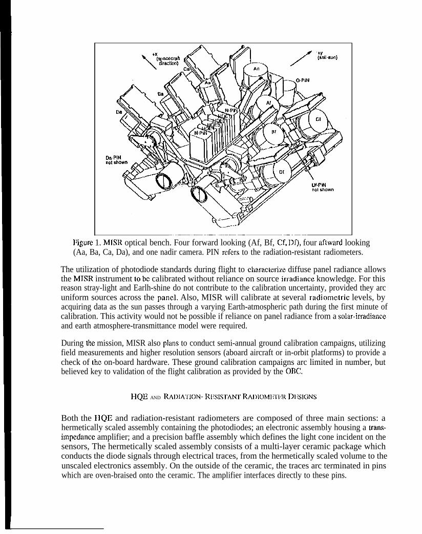
Within the hermetic package, each of the HQ13 photodiodes is in a light-trap configuration wherethree photodiodes are arranged optically in series, as shown in figure 2. The light reflcctcd from onediode is collected by the next, such that all the incoming signal is detected, resulting in near 100%quantum efficiency. In addition, the configuration is arranged so that the path of the incoming lightis made to switch planes once entering, This is done to minimize the polarization sensitivity of thetrap.
1 —. —
Figure 2. HQ13 photodiodc light-trap.
The individual diodes arc bonded onto ceramic carrier disks that protect thcm during testing andfurlhcr assembly, and provide isolated mctallizcd pads for electrical contacts. Wires arc ball-bondedfrom the diodes to the pads, These diode assemblies arc then bonded onto ceramic sub-carriers,The sub-carriers arc triangular in shape and hold the diode assemblies at the angles rcqUirCd to
produce the light-trap configuration. Additionally, the sub-carriers have internal electrical tracesthat carry the diode signals from the diode carriers to the bottom of the subcarricr. The diodecarriers are bonded with conductive epoxy to the sub-carrier, making the electrical connections forthe signals, The sub-carriers arc bonded to a metallic ground plane with conductive epoxy, Thepositive signal connection is formed by ball bonding a wire from a pad on the sub-carrier to a padon the surface of the HQE ceramic package.
I
_—
—.. —
—
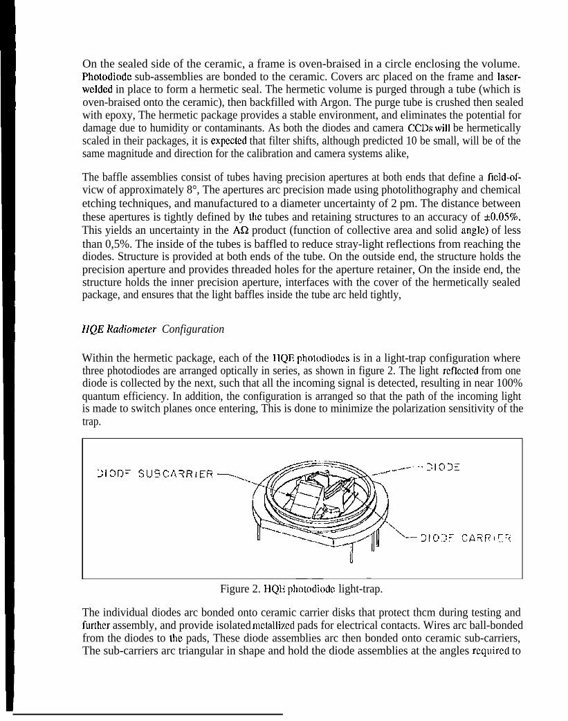
Figure 3. 11Q13 radiometer configuration.
The cover of the HQE hermetic package has a window that is soldered in place. A single spectralfilter pcr package is bonded to this window, and four such packages provide coverage at the fourMISR wavelengths, The HQE baffle assembly consists of onc tube holding inner and outer precisionapcrlurcs. The flange of the base of the light tube provides structure for attaching the electronicsand for interfacing with the optical bench of the instrument (SCC Fig, 3).
Radiation-Resistant Radiometer Coljfiguration
The radiation-resistant photodiodc package has four diodes inside the hermetic volume, with eachdiode filtered to a different MISR spectral band. As with the HQE assembly, radiation-resistantdiodes arc first bonded onto ceramic carrier disks. These diode carriers arc then bonded intocavities in the ceramic base. Electrical connections arc made by bonding the diode carriers withconductive epoxy to the package. The filters arc bonded to the ceramic package directly on top ofthe diodes. Finally, the cover, which in this case has four soldered windows, is laser-welded to thepackage frame.

Figure 4. Radiation-resistant radiometer configuration,
.
.,
The radiation-resistant baffle assembly has four tubes, each holding inner and outer precisionapertures. The flange of the tube assct~~bly is attached to the package cover with screws. Thepackage and baffle combination is then bonded into a ring that attaches to a mounting plate. Thismounting plate interfaces to the electronics asscrnbly and the optical bench of the instrument (SCC
Fig. 4).
On the instrument, five radiation-resistant radiometers will bc used. Two will view in the nadirdirection, two in the forward and aft 70.5° camera directions, and onc detector assembly will bcmechanized on a goniometric arm to monitor the angular rcflcctancc properties of the calibrationpanels (SCC Fig. 1).
PIIOI’OIJIODI[ D1iSICiNS
Specifications common to the HQE and radiation-hard photodiodcs include a surface rcflcctanccloss of less than 25% and a signal-to-noise ratio greater than 500 at full scale. (For the MISRcameras, full scale has been defined as a sccnc with an equivalent rcflcctancc of 1, Equivalentrcflcctancc, pw, provides a measure of radiance, L,, as normalized by the cxo-atmospheric solarirradiance, EOL, at wavelength i, and is defined by pq = xL., / EOL). The HQE photodiodes have beenfurther spccificd to have an internal quantum efficiency (IQE) cxcccding 0,995, to have a linearityof response better than 99.8% over an equivalent rcflcctancc range of 0.05 to 1.0, and stability towithin ~2% through the first six months of flight. For the radiation-hard photodiodcs, thespecifications arc an external QE of greater than 0.30, linearity to better than 99.5%, and stability towithin *2% through the five-year mission. With these photodiodc specifications it is estimated thatthe diffuse panel radiance can bc dctcrmincd to within *170 uncertainty. Panel illumination non-uniformities, relative bi-directional reflectance factor (BRF) knowledge of the panel, and difference

.,
between the photodiode and CCD response functions bring the total estimated error in calibrationto *3%.
Blue HQE Photodiode Design- A41SR Bands 1-2
The detector design implemented for MISR spectral bands 1 and 2 (443 and 555 nm) consists of ashallow-junction n-on-p photodiode fabricated on 4“ diameter P-P+ epitaxial (epi) silicon wafers.The epi silicon layer for these wafers has a thickness of approximately 25 pm and possesses aresistivity of greater than 1 LYcrn, Phosphorus diffusion is carried out to obtain a shallow junction0,1 to 0.25 pm deep (see Fig. 5). Through careful processing this design is capable of achievingdynamic resistances of upwards of 1 Gfi?, resulting in detectors with very low noise performance.Additionally, in order to minimize signal 10SSCS due to front-surface reflections, the silicon dioxideanti-reflection coating is optimized for MJSR bands 1 and 2. This is accomplished by thinning thecoating down to about 80 nm following completion of the diffusion.
Phosphorus IJiffuseclN-lypc Region
\
—.— —..
I P+ Substrate 1,5oi550url,
❑fi’w Active Kcgion + +:.:::::::::u::~ Oxide 80 nm + + P+ fkgion Aluminum
❑ Field Oxide n. .
N+ Region. . IT?l~. Chromium-Ciold
. . . ..
Figure 5. Blue HQE photodiodc design.
This design offers several advantages over other earlier proposals, in particular, a more stable andlower noise performance that does not require biasing for high QE operation. This is a verysignificant improvement over the inversion-layer photodiodc [1], which is the more traditionalchoice for this particular spectral range, and which until not long ago [2] was the only detector typethat could achieve IQEs large enough which allowed it to be used in the fabrication of absoluteradiomctric standards [3].
Red HQE Photodiode Design- A41SR Bands 3 and 4
The Red HQE detectors intended for MISR bands 3 and 4 (670 and 865 nrn) are p-on-nphotodiodcs fabricated on 4“ float zone silicon wafers, again with a rcsistivity greater than 1 flcrn(Fig. 6). The p-n junction was crcatcd by a specific boron ion implantation process which minimizesthe front surface dead region of the photodiodc, thereby achieving very high IQE, even at theshorlcr wavelengths [4], As was the case for the blue 1 IQE diodes, dynamic resistances greater than

1 GQ were also obtained for the red HQE diodes, The optimal Si02 anti-reflection coatingthickness used for these wavelengths was 128 mm
Boron ImplantedP-Type Region
\,,...m,=,.,
—— —
N-Type FL Silicon >1 Ohm cm3s0 .
,,, ,, .,,
❑~ Active Region. Oxide 128 nm ❑] ~ P+ Region Aluminum
❑ c1,,, ,,, ,., ,,,,,Field Oxide ~~ N+ Region Chromium-Gold
Figure 6. Red HQE photodiodc design.
Radiation-Hard Photodiode Design
In order to achieve the radiation-hardness required, and at the same time obtain highest possibleexternal QE, six different types of radiation-hard photodiodcs were fabricated to attain the optimaltrade-off. Three types of these detectors were built on p-p+ cpitaxial wafers, each type having oneof three possible epi layer thicknesses of 5, 15, or 25 pm (same structure as Fig. 5 except for the cpithickness). The remaining three diode types were fabricated on Silicon (lxidc Insulator (S01) wafers(with a buried oxide thickness in the range of 250 to 1000 rim), and similarly, each type had one ofthree possible active Silicon thicknesses: 5, 10, or 18 pm. Because the active Silicon thickness forthe radiation-hard detectors was limited to a maximum of 25 pm, lQE was expected to bc 10WCSIfor MISR band 4. Hence, the anti-reflection coating was optimized for this spectral region in thesame way as for the Red EIQEs. In addition, as with the HQE diodes, a dynamic resistance ofgreater than 1 GCI was also another goal of this design.
DrrrucroR PIiMI’01/MANCt;
IQE and Rej7ectance Measurements
These measurements were performed by following the technique used in a previous study [5],Essentially, two types of light-trapping 100% QE detectors were used as absolute standards: aninversion-layer QED-200 trap made by United Detector Technologies; and a Grascby OptronicsQED-1 50 trap composed of Hamamatsu photodiodcs. The QED-200 was the reference for MISRbands 1 and 2, while the QED-I 50 was best suited for bands 3 and 4. A light-tight fixture wasfabricated to place the photodiodc under test at 45° from the opening to the QED-200, and readingswere acquired for the reflected signal, the photodiodc signal, and the total incoming signal measuredby an additional QED-200 and the QED-150. From these measurements it was then possible todirectly calculate both the front surface rcflcctancc (at 45°) and the IQE for the photodiodcs.

The results presented some surprises. First of all, the Red HQE diode response showed to beextremely high (> 99%) for wavelengths below 600 nm, which is generally not cxpcctcd from p-nphotodiode architectures, This indicates that the Red HQE photodiodes lack the front dead regionnormally found in p-n diodes. LJnfortunatcly this performance was short lived, In a span of littleover a month following fabrication, the JQE for these devices dropped down to 90% at 420 nm, anddown to 97.7% at 552 nm (Fig, 7), indicating that there arc still serious issues of stability to resolve.It is of importance to note that this IQE degradation was not due to humidity effects since allphotodiodcs were kept within a dry nitrogen purge.
k–~“m A—----$----- ,
i0.99
0,98 +g :: \“$’ \j: El+- - Blue HQE \
{
0.93 A Red HQE- Initial0.92 \
● \.g
0,91 ‘ -“— Red HQE- Final
0.90 ~.-l 4.. —.... +&_L.A-+~— \—+—. – ~
I 453 m em 7CQ 803 900
Wavelength (rim)
Figure 7. Typical Blue and Rcd HQ13 photodiodc IQE,
Another unexpected result pertaining to the Rcd HQE sensors was that the IQE at the longerwavelengths showed not to be as high as required, only about 92% at 875 nm, This may beattributed in part to the fact that the foundry used for building these photodiodes is primarilydedicated to IC fabrication, and thcrcforc their processing is not particularly tailored for obtaininglong minority carrier life times, as is critical for these detectors. Currently, additional foundrieswhich specialize on detectors arc being involved in further photodiodc fabrication runs in the hopesof solving this problcm.
The Blue HQE detectors generally showed acceptable performance, although their IQEs at 420 nmwere approximately 99.4%, which was not quite as high as desired (Fig. 7).
[: ~.0.80
%
~[,+
- — —— 15 urn eplL
‘Y. ‘ \
j 0.70‘$ ‘\
\+— 25 urn epl
~ 060 —X- -S”msol
I050 — a- - 10 u~ sol
g0.40 — - - ‘ 8 ‘m ‘0 ’
0.30‘V
-. +.. .+. . . ..I . . J . . . . ..~. J. .+u\.— i
4C13450MKI WC16CK 1650 7007508C085J3KY3
Wavelength (rim)
Figure 8. Typical IQE for all Radiation-hard photodiodc types.

,..,
The radiation-hard photodiode IQE results met more closely with expectations. First of all, thedetectors fabricated on epi wafers showed very comparable performance to the Blue HQE diodes inMISRbands land 2, This wasasexpccted sinccthc only difference bctwecnthcrad-hard designsoncpi wafers and the BlueHQE design was thcepi thickness involved. Towards the longerwavelengths, their IQEs were strong functions of the active silicon thickness of each rad-harddiode, also as expected (Fig. 8). The one exception to this were the S01 diodes with an activesilicon thickness of 18 pm, which had the lowest IQE in all bands, This was due to the fact that thisparticular wafer was of a different type than the other S01 wafers, and additionally, was of lowerquality.
Front surface reflectance for all photodiodc types was found to bc at worst 20%, for spectralregions not targeted by anti-reflection coating optimiy, ation, and at best 10%, for those regionswhich were optimized.
IV Characterization, Shunt Resistance, and Shunt Capacitance Measurements
Current vs. bias voltage (IV) curves were obtained for all photodiodcs. From these, the dynamicresistance at zero bias (shunt resistance) was calculated for each diode using data points near zerovolts. In a separate step, shunt capacitance was also obtained. All three measurements wereperformed at ambient temperature, which was generally about 26° Celsius. The shunt resistance forall photodiodes was determined to bc very nearly 1 Gfl, with the exception of the Red HQE diodes,for which it was approximately 10 Gf2, It is of importance to point out that the operatingtemperature for all these detectors, once in flight, is cxpcctcd to bc approximately 10° C. Takinginto account the shunt resistance temperature coefficient for these diodes, which was measuredapproximately to be a 10% dccrcasc per dcgrcc C incrcasc, it is expected that the shunt resistancefor all photodiodes will be about three times as large in-flight as has been measured at roomtemperature. Thcrcforc, these sensors arc cxpcctcd to have cxccllcnt signal-to-noise mtios.
Fully characterized photodiodc samples of each type were sclcctcd for proton radiation damagetesting, The fluenccs for all other charged particles during the mission arc cxpcctcd to bc negligible.The photodiodcs were irradiated at four protcm cncrgics: 0.1, 0.5, 1.0, and 5.0 McV. Differentphotodiodes of each type were exposed to each of the four energies, and an additional set wereexposed to all four energies. The flucncc for each proton energy level was chosen according towhat is cxpcctcd for the five year flight mission times a factor of three as an error margin: 4.8 x 10⁷,
3,2x 1 07, 1.2 x 10s, and 6.OX 108 PROTONS. Following irradiation, characterization
CI)12measurements were rcpcatcd to determine the amount of induced performance dcg,mdation.
The results were a great deal more favorable than originally expected. All radiation-hard and BlueHQE photodiodcs showed no noticeable IQE changes at any of the exposed proton energies, evenat 875 nm, The radiation-hard photodiodcs built on cpi wafers (and the Blue HQE devices for thatmatter) were expcctcd to be extremely radiation insensitive at the shorter wavelengths [6]. Similarresults were also expected for the detectors fabricated on S01 wafers, although no data was

,.,
available on these. At the longer wavelengths IQE variations were expcctcd to bc a function of thedetector’s active Silicon thickness. It was very encouraging to scc that the predicted flucnces weretoo low to produce noticeable changes even at the longer wavelengths for the rad-hard and BlueHQE sensors.
Data obtained from the Red HQE dcviccs matched more closely what was expected. No IQEchanges were dctectcd in the first two MISR bands (420 nm and 552 rim), while for bands 3 and 4(670 nm and 875 nm) IQE drops of 2% and 11%, respcctivcly, were observed. Additionally, thisdegradation was only measured at the proton energy of 5.0 McV, indicating that only the damagetowards the rear volume of the photodiodcs was significant.
ACKNOW1 J llXiMl lN1’S
The authors would like to thank Charles Cruzan, Don Dunn, and Nick Mardesich for their key rolesin all aspects of the packaging effort.
The research described in this paper was carried out by the Jet Propulsion Laboratory, CaliforniaInstitute of Technology, under a contract with the National Aeronautics and Space Administration.
Reference herein to any specific commercial product, process, or service by trade name, trademark,manufacturer, or otherwise, dots not constitute or imply its endorsement by the United StatesGovernment or the Jet Propulsion Laboratory, California lnstitutc of Technology.
[1] Hansen, T. “Silicon UV Photodiodc Using Natural Inversion Layers,” Phy. Scripts, vol, 18(1978): p. 471.
[2] Kordc, R., Gcist, J, “Stable, High Quantum Efficiency UV-Enhanced Silicon Photodiodes byArsenic Diffusion,” Solid State Electronics vol. 30 (1987): pp. 89-92.
[3] Zalewski, E. F., Duda, C.R. “Silicon photodiodc dcvicc with 100% external quantum efficiency,”Applied Optics vol. 22(1 983): pp. 2867 -2873.-
[4] Korde, R., Geist, J. “Quantun~ Efficiency Stability of Silicon Photodiodcs,” App/ied Optics vol.26 (1989): PP. 5284-5290.
[5] Jorquera, C. R., Brueggc, C., Duval, V. “Evaluation of high quantum efficiency siliconphotodiodes for calibration in the 400 nm to 900 nm spectral region, “ in SPIE Vol. 1762 InfraredTechnology XVIII, 1992, pp. 135-144.
[6] Kordc, R,, Cable, J. S., Canficld, L.R. “100% lntcrnal Quantum Efficiency Silicon Photodiodeswith Onc Gigarad Passivating Silicon Dioxide, ” IEEE Trans. in Nuclear Science vol. 40 no. 6(1993): Pp. 1655-1659.