Spintronics with NSN junction of one-dimensional quantum wires: A study of pure spin current and...
12
arXiv:0710.5240v2 [cond-mat.mes-hall] 19 Feb 2008 Spintronics with NSN Junction of one-dimensional quantum wires : A study of Pure Spin Current and Magnetoresistance Sourin Das 1 , Sumathi Rao 2 and Arijit Saha 2 1 Department of Condensed Matter Physics, Weizmann Institute of Science, Rehovot 76 100, Israel 2 Harish−Chandra Research Institute, Chhatnag Road, Jhusi, Allahabad 211 019, India PACS 73.23.-b – Electronic transport in mesoscopic systems PACS 74.45.+c – Proximity effects; Andreev effect; SN and SNS junctions PACS 72.25.Ba – Spin polarized transport in metals Abstract. - We demonstrate possible scenarios for production of pure spin current and large tun- nelling magnetoresistance ratios from elastic co-tunnelling and crossed Andreev reflection across a superconducting junction comprising of normal metal-superconductor-normal metal, where, the normal metal is a one-dimensional interacting quantum wire. We show that there are fixed points in the theory which correspond to the case of pure spin current. We analyze the influence of electron-electron interaction and see how it stabilizes or de-stabilizes the production of pure spin current. These fixed points can be of direct experimental relevance for spintronics application of normal metal-superconductor-normal metal junctions of one-dimensional quantum wires. We also calculate the power law temperature dependence of the crossed Andreev reflection enhanced tunnelling magnetoresistance ratio for the normal metal-superconductor-normal metal junction. Introduction. – Two fundamental degrees of free- dom associated with an electron that are of direct interest to condensed matter physics are its charge and spin. Until very recently, all conventional electron-based devices have been solely based upon the utilization and manipulation of the charge degree of freedom of an electron. However, the realization of the fact that devices based on the spin degree of freedom can be almost dissipation-less and with very fast switching times, has led to an upsurge in research activity in this direction in recent years [1–3]. The first step towards realization of spin-based electronics (spin- tronics) would be to produce pure spin current (SC). From a purely theoretical point of view, it is straight forward to define a charge current as a product of local charge den- sity with the charge velocity, but such a definition cannot be straight forwardly extended to the case of SC. This is because both spin S and velocity v are vector quantities and hence the product of two such vectors will be a tensor. In this letter, we adopt the simple minded definition of SC, which is commonly used [4]. It is just the prod- uct of the local spin polarization density associated with the electron or hole, (a scalar s which is either positive for up-spin or negative for down-spin) and its velocity [4]. The most obvious scenario in which one can generate a pure SC in the sense defined above would be to have (a) an equal and opposite flow of identically spin-polarized electrons through a channel, such that the net charge current through the channel is nullified leaving behind a pure SC, or (b) alternatively, an equal flow of identically spin polarized electrons and holes in the same direction through a channel giving rise to pure SC with perfect can- cellation of charge current. In this letter, we explore the second possibility for generating pure SC using a normal metal−superconductor−normal metal (NSN) junction. Proposed device and its theoretical modelling. – The configuration we have in mind for the production of pure SC is shown in Fig. 1. The idea is to induce a pair potential in a small region of a quantum wire (QW) by de- positing a superconducting strip on top of the wire (which may be, for instance, a carbon nanotube) due to proximity effects. If the strip width on the wire is of the order of the phase coherence length of the superconductor, then both direct electron to electron co-tunnelling as well as crossed Andreev electron to hole tunnelling can occur across the superconducting region [5]. It is worth pointing out that in the case of a singlet superconductor, which is the case we consider, both the tunnelling processes will conserve spin. In order to describe the mode of operation of the device (see Fig. 1), we first assume that the S-matrix rep- p-1
-
Upload
independent -
Category
Documents
-
view
2 -
download
0
Transcript of Spintronics with NSN junction of one-dimensional quantum wires: A study of pure spin current and...

arX
iv:0
710.
5240
v2 [
cond
-mat
.mes
-hal
l] 1
9 Fe
b 20
08
Spintronics with NSN Junction of one-dimensional quantum
wires : A study of Pure Spin Current and Magnetoresistance
Sourin Das1, Sumathi Rao2 and Arijit Saha2
1 Department of Condensed Matter Physics, Weizmann Institute of Science, Rehovot 76 100, Israel2 Harish−Chandra Research Institute, Chhatnag Road, Jhusi, Allahabad 211 019, India
PACS 73.23.-b – Electronic transport in mesoscopic systemsPACS 74.45.+c – Proximity effects; Andreev effect; SN and SNS junctionsPACS 72.25.Ba – Spin polarized transport in metals
Abstract. - We demonstrate possible scenarios for production of pure spin current and large tun-nelling magnetoresistance ratios from elastic co-tunnelling and crossed Andreev reflection acrossa superconducting junction comprising of normal metal-superconductor-normal metal, where, thenormal metal is a one-dimensional interacting quantum wire. We show that there are fixed pointsin the theory which correspond to the case of pure spin current. We analyze the influence ofelectron-electron interaction and see how it stabilizes or de-stabilizes the production of pure spincurrent. These fixed points can be of direct experimental relevance for spintronics applicationof normal metal-superconductor-normal metal junctions of one-dimensional quantum wires. Wealso calculate the power law temperature dependence of the crossed Andreev reflection enhancedtunnelling magnetoresistance ratio for the normal metal-superconductor-normal metal junction.
Introduction. – Two fundamental degrees of free-dom associated with an electron that are of direct interestto condensed matter physics are its charge and spin. Untilvery recently, all conventional electron-based devices havebeen solely based upon the utilization and manipulationof the charge degree of freedom of an electron. However,the realization of the fact that devices based on the spindegree of freedom can be almost dissipation-less and withvery fast switching times, has led to an upsurge in researchactivity in this direction in recent years [1–3]. The firststep towards realization of spin-based electronics (spin-tronics) would be to produce pure spin current (SC). Froma purely theoretical point of view, it is straight forward todefine a charge current as a product of local charge den-sity with the charge velocity, but such a definition cannotbe straight forwardly extended to the case of SC. This isbecause both spin ~S and velocity ~v are vector quantitiesand hence the product of two such vectors will be a tensor.
In this letter, we adopt the simple minded definitionof SC, which is commonly used [4]. It is just the prod-uct of the local spin polarization density associated withthe electron or hole, (a scalar s which is either positivefor up-spin or negative for down-spin) and its velocity [4].The most obvious scenario in which one can generate apure SC in the sense defined above would be to have (a)
an equal and opposite flow of identically spin-polarizedelectrons through a channel, such that the net chargecurrent through the channel is nullified leaving behind apure SC, or (b) alternatively, an equal flow of identicallyspin polarized electrons and holes in the same directionthrough a channel giving rise to pure SC with perfect can-cellation of charge current. In this letter, we explore thesecond possibility for generating pure SC using a normalmetal−superconductor−normal metal (NSN) junction.
Proposed device and its theoretical modelling. –
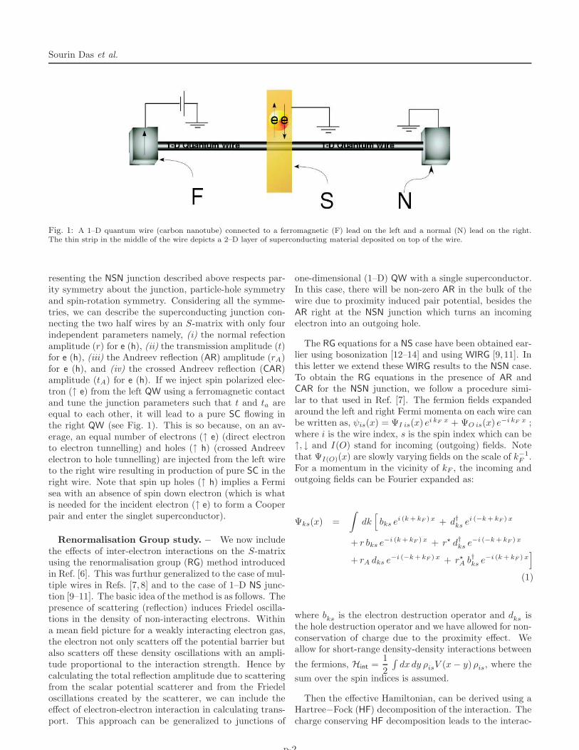
The configuration we have in mind for the production ofpure SC is shown in Fig. 1. The idea is to induce a pairpotential in a small region of a quantum wire (QW) by de-positing a superconducting strip on top of the wire (whichmay be, for instance, a carbon nanotube) due to proximityeffects. If the strip width on the wire is of the order of thephase coherence length of the superconductor, then bothdirect electron to electron co-tunnelling as well as crossedAndreev electron to hole tunnelling can occur across thesuperconducting region [5]. It is worth pointing out thatin the case of a singlet superconductor, which is the casewe consider, both the tunnelling processes will conservespin. In order to describe the mode of operation of thedevice (see Fig. 1), we first assume that the S-matrix rep-
p-1
Sourin Das et al.
Fig. 1: A 1–D quantum wire (carbon nanotube) connected to a ferromagnetic (F) lead on the left and a normal (N) lead on the right.The thin strip in the middle of the wire depicts a 2–D layer of superconducting material deposited on top of the wire.
resenting the NSN junction described above respects par-ity symmetry about the junction, particle-hole symmetryand spin-rotation symmetry. Considering all the symme-tries, we can describe the superconducting junction con-necting the two half wires by an S-matrix with only fourindependent parameters namely, (i) the normal refectionamplitude (r) for e (h), (ii) the transmission amplitude (t)for e (h), (iii) the Andreev reflection (AR) amplitude (rA)for e (h), and (iv) the crossed Andreev reflection (CAR)amplitude (tA) for e (h). If we inject spin polarized elec-tron (↑ e) from the left QW using a ferromagnetic contactand tune the junction parameters such that t and ta areequal to each other, it will lead to a pure SC flowing inthe right QW (see Fig. 1). This is so because, on an av-erage, an equal number of electrons (↑ e) (direct electronto electron tunnelling) and holes (↑ h) (crossed Andreevelectron to hole tunnelling) are injected from the left wireto the right wire resulting in production of pure SC in theright wire. Note that spin up holes (↑ h) implies a Fermisea with an absence of spin down electron (which is whatis needed for the incident electron (↑ e) to form a Cooperpair and enter the singlet superconductor).
Renormalisation Group study. – We now includethe effects of inter-electron interactions on the S-matrixusing the renormalisation group (RG) method introducedin Ref. [6]. This was furthur generalized to the case of mul-tiple wires in Refs. [7, 8] and to the case of 1–D NS junc-tion [9–11]. The basic idea of the method is as follows. Thepresence of scattering (reflection) induces Friedel oscilla-tions in the density of non-interacting electrons. Withina mean field picture for a weakly interacting electron gas,the electron not only scatters off the potential barrier butalso scatters off these density oscillations with an ampli-tude proportional to the interaction strength. Hence bycalculating the total reflection amplitude due to scatteringfrom the scalar potential scatterer and from the Friedeloscillations created by the scatterer, we can include theeffect of electron-electron interaction in calculating trans-port. This approach can be generalized to junctions of
one-dimensional (1–D) QW with a single superconductor.In this case, there will be non-zero AR in the bulk of thewire due to proximity induced pair potential, besides theAR right at the NSN junction which turns an incomingelectron into an outgoing hole.
The RG equations for a NS case have been obtained ear-lier using bosonization [12–14] and using WIRG [9, 11]. Inthis letter we extend these WIRG results to the NSN case.To obtain the RG equations in the presence of AR andCAR for the NSN junction, we follow a procedure simi-lar to that used in Ref. [7]. The fermion fields expandedaround the left and right Fermi momenta on each wire canbe written as, ψis(x) = ΨI is(x) e
i kF x + ΨO is(x) e−i kF x ;
where i is the wire index, s is the spin index which can be↑, ↓ and I(O) stand for incoming (outgoing) fields. Notethat ΨI(O)(x) are slowly varying fields on the scale of k−1
F.
For a momentum in the vicinity of kF , the incoming andoutgoing fields can be Fourier expanded as:
Ψks(x) =
∫
dk[
bks ei (k + kF ) x + d†
ksei (−k + kF ) x
+ r bks e−i (k + kF ) x + r⋆ d†
kse−i (−k + kF ) x
+ rA dks e−i (−k + kF ) x + r⋆
A b†kse−i (k + kF ) x
]
(1)
where bks
is the electron destruction operator and dks
isthe hole destruction operator and we have allowed for non-conservation of charge due to the proximity effect. Weallow for short-range density-density interactions between
the fermions, Hint =1
2
∫
dx dy ρisV (x − y) ρ
is, where the
sum over the spin indices is assumed.
Then the effective Hamiltonian, can be derived using aHartree−Fock (HF) decomposition of the interaction. Thecharge conserving HF decomposition leads to the interac-
p-2
NSN Junction of one-dimensional quantum wires
0 5 10 15 20 25 300.0
0.1
0.2
0.3
0.4
0.5
|t|2 =
|t A
|2
l
V(0) = 0.1, V(2kF) = 0.1 V(0) = 0.2, V(2kF) = 0.2 V(0) = 0.3, V(2kF) = 0.3
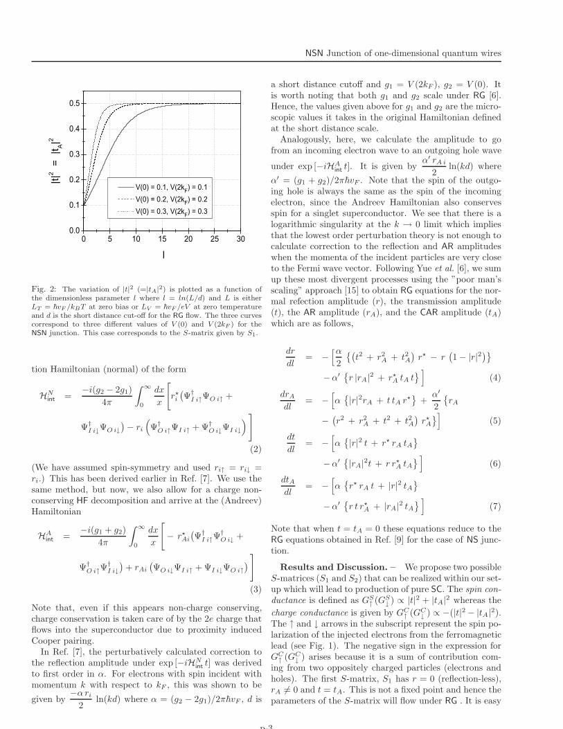
Fig. 2: The variation of |t|2 (=|tA|2) is plotted as a function ofthe dimensionless parameter l where l = ln(L/d) and L is eitherLT = ~vF /kBT at zero bias or LV = ~vF /eV at zero temperatureand d is the short distance cut-off for the RG flow. The three curvescorrespond to three different values of V (0) and V (2kF ) for theNSN junction. This case corresponds to the S-matrix given by S1.
tion Hamiltonian (normal) of the form
HN
int =−i(g2 − 2g1)
4π
∫ ∞
0
dx
x
[
r⋆
i
(
Ψ†I i↑ΨO i↑ +
Ψ†I i↓ΨO i↓
)
− ri
(
Ψ†O i↑ΨI i↑ + Ψ†
O i↓ΨI i↓
)
]
(2)
(We have assumed spin-symmetry and used ri↑ = ri↓ =ri.) This has been derived earlier in Ref. [7]. We use thesame method, but now, we also allow for a charge non-conserving HF decomposition and arrive at the (Andreev)Hamiltonian
HA
int =−i(g1 + g2)
4π
∫ ∞
0
dx
x
[
− r⋆
Ai
(
Ψ†I i↑Ψ
†O i↓ +
Ψ†O i↑Ψ
†I i↓
)
+ rAi
(
ΨO i↓ΨI i↑ + ΨI i↓ΨO i↑
)
]
(3)
Note that, even if this appears non-charge conserving,charge conservation is taken care of by the 2e charge thatflows into the superconductor due to proximity inducedCooper pairing.
In Ref. [7], the perturbatively calculated correction tothe reflection amplitude under exp [−iHN
intt] was derived
to first order in α. For electrons with spin incident withmomentum k with respect to kF , this was shown to be
given by−α ri
2ln(kd) where α = (g2 − 2g1)/2π~vF , d is
a short distance cutoff and g1 = V (2kF ), g2 = V (0). Itis worth noting that both g1 and g2 scale under RG [6].Hence, the values given above for g1 and g2 are the micro-scopic values it takes in the original Hamiltonian definedat the short distance scale.
Analogously, here, we calculate the amplitude to gofrom an incoming electron wave to an outgoing hole wave
under exp [−iHAintt]. It is given by
α′ rA i
2ln(kd) where
α′ = (g1 + g2)/2π~vF . Note that the spin of the outgo-ing hole is always the same as the spin of the incomingelectron, since the Andreev Hamiltonian also conservesspin for a singlet superconductor. We see that there is alogarithmic singularity at the k → 0 limit which impliesthat the lowest order perturbation theory is not enough tocalculate correction to the reflection and AR amplitudeswhen the momenta of the incident particles are very closeto the Fermi wave vector. Following Yue et al. [6], we sumup these most divergent processes using the ”poor man’sscaling” approach [15] to obtain RG equations for the nor-mal refection amplitude (r), the transmission amplitude(t), the AR amplitude (rA), and the CAR amplitude (tA)which are as follows,
dr
dl= −
[α
2
{(
t2 + r2A + t2A)
r⋆ − r(
1 − |r|2)}
−α′{
r |rA|2 + r⋆
A tA t}
]
(4)
drAdl
= −[
α{
|r|2rA + t tA r⋆}
+α′
2
{
rA
−(
r2 + r2A + t2 + t2A)
r⋆
A
}
]
(5)
dt
dl= −
[
α{
|r|2 t + r⋆ rA tA}
−α′{
|rA|2t + r r⋆
A tA}
]
(6)
dtAdl
= −[
α{
r⋆ rA t + |r|2 tA}
−α′{
r t r⋆
A + |rA|2 tA}
]
(7)
Note that when t = tA = 0 these equations reduce to theRG equations obtained in Ref. [9] for the case of NS junc-tion.
Results and Discussion. – We propose two possibleS-matrices (S1 and S2) that can be realized within our set-up which will lead to production of pure SC. The spin con-ductance is defined as GS
↑ (GS
↓ ) ∝ |t|2 + |tA|2 whereas the
charge conductance is given by GC
↑ (GC
↓ ) ∝ −(|t|2 − |tA|2).The ↑ and ↓ arrows in the subscript represent the spin po-larization of the injected electrons from the ferromagneticlead (see Fig. 1). The negative sign in the expression forGC
↑ (GC
↓ ) arises because it is a sum of contribution com-ing from two oppositely charged particles (electrons andholes). The first S-matrix, S1 has r = 0 (reflection-less),rA 6= 0 and t = tA. This is not a fixed point and hence theparameters of the S-matrix will flow under RG . It is easy
p-3
Sourin Das et al.
0 5 10 15 20 25 30 350.00
0.05
0.10
0.15
0.20
0.25
0.30
- (
|t|2 -
|t A
|2 )
l
V(0) = 0.1, V(2kF) = 0.1 V(0) = 0.2, V(2kF) = 0.2 V(0) = 0.3, V(2kF) = 0.3
0 5 10 15 20 25 30 350.0
0.1
0.2
0.3
0.4
0.5
0.6
( |t|
2 + |
t A|2 )
l
V(0) = 0.1, V(2kF) = 0.1 V(0) = 0.2, V(2kF) = 0.2 V(0) = 0.3, V(2kF) = 0.3
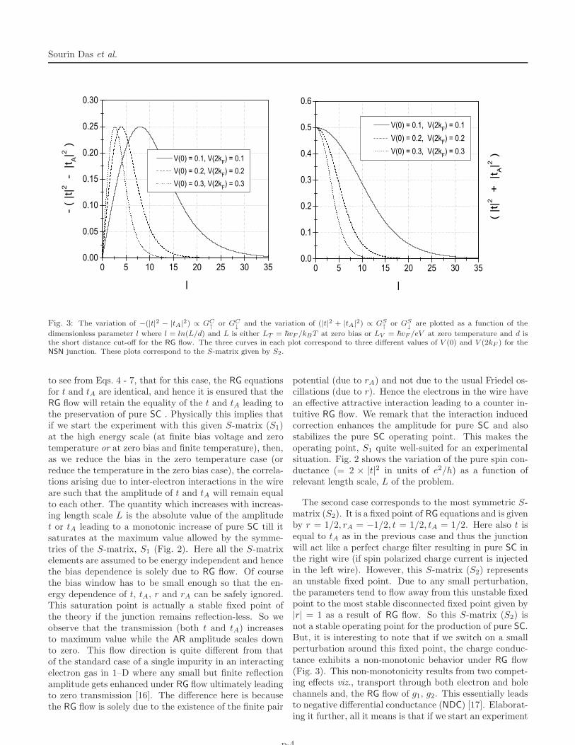
Fig. 3: The variation of −(|t|2 − |tA|2) ∝ GC
↑or GC
↓and the variation of (|t|2 + |tA|2) ∝ GS
↑or GS
↓are plotted as a function of the
dimensionless parameter l where l = ln(L/d) and L is either LT = ~vF /kBT at zero bias or LV = ~vF /eV at zero temperature and d isthe short distance cut-off for the RG flow. The three curves in each plot correspond to three different values of V (0) and V (2kF ) for theNSN junction. These plots correspond to the S-matrix given by S2.
to see from Eqs. 4 - 7, that for this case, the RG equationsfor t and tA are identical, and hence it is ensured that theRG flow will retain the equality of the t and tA leading tothe preservation of pure SC . Physically this implies thatif we start the experiment with this given S-matrix (S1)at the high energy scale (at finite bias voltage and zerotemperature or at zero bias and finite temperature), then,as we reduce the bias in the zero temperature case (orreduce the temperature in the zero bias case), the correla-tions arising due to inter-electron interactions in the wireare such that the amplitude of t and tA will remain equalto each other. The quantity which increases with increas-ing length scale L is the absolute value of the amplitudet or tA leading to a monotonic increase of pure SC till itsaturates at the maximum value allowed by the symme-tries of the S-matrix, S1 (Fig. 2). Here all the S-matrixelements are assumed to be energy independent and hencethe bias dependence is solely due to RG flow. Of coursethe bias window has to be small enough so that the en-ergy dependence of t, tA, r and rA can be safely ignored.This saturation point is actually a stable fixed point ofthe theory if the junction remains reflection-less. So weobserve that the transmission (both t and tA) increasesto maximum value while the AR amplitude scales downto zero. This flow direction is quite different from thatof the standard case of a single impurity in an interactingelectron gas in 1–D where any small but finite reflectionamplitude gets enhanced under RG flow ultimately leadingto zero transmission [16]. The difference here is becausethe RG flow is solely due to the existence of the finite pair
potential (due to rA) and not due to the usual Friedel os-cillations (due to r). Hence the electrons in the wire havean effective attractive interaction leading to a counter in-tuitive RG flow. We remark that the interaction inducedcorrection enhances the amplitude for pure SC and alsostabilizes the pure SC operating point. This makes theoperating point, S1 quite well-suited for an experimentalsituation. Fig. 2 shows the variation of the pure spin con-ductance (= 2 × |t|2 in units of e2/h) as a function ofrelevant length scale, L of the problem.
The second case corresponds to the most symmetric S-matrix (S2). It is a fixed point of RG equations and is givenby r = 1/2, rA = −1/2, t = 1/2, tA = 1/2. Here also t isequal to tA as in the previous case and thus the junctionwill act like a perfect charge filter resulting in pure SC inthe right wire (if spin polarized charge current is injectedin the left wire). However, this S-matrix (S2) representsan unstable fixed point. Due to any small perturbation,the parameters tend to flow away from this unstable fixedpoint to the most stable disconnected fixed point given by|r| = 1 as a result of RG flow. So this S-matrix (S2) isnot a stable operating point for the production of pure SC.But, it is interesting to note that if we switch on a smallperturbation around this fixed point, the charge conduc-tance exhibits a non-monotonic behavior under RG flow(Fig. 3). This non-monotonicity results from two compet-ing effects viz., transport through both electron and holechannels and, the RG flow of g1, g2. This essentially leadsto negative differential conductance (NDC) [17]. Elaborat-ing it further, all it means is that if we start an experiment
p-4
NSN Junction of one-dimensional quantum wires
0 5 10 15 20 25 30-0.15
-0.10
-0.05
0.00
0.05
-(|t|
2 - |
t A|2 )
l
V(0) = 0.1, V(2kF) = 0.1 V(0) = 0.2, V(2kF) = 0.2 V(0) = 0.3, V(2kF) = 0.3
0 5 10 15 20 25 300.00
0.15
0.30
0.45
0.60
0.75
( |t|
2 +
|t A
|2 )
l
V(0) = 0.1, V(2kF) = 0.1 V(0) = 0.2, V(2kF) = 0.2 V(0) = 0.3, V(2kF) = 0.3
Fig. 4: The variation of −(|t|2 − |tA|2) ∝ GC
↑or GC
↓and the variation of (|t|2 + |tA|2) ∝ GS
↑or GS
↓are plotted in left and right panel
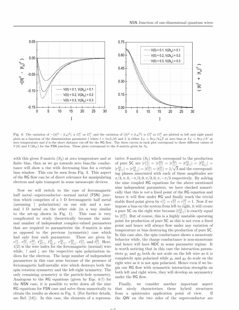
plots as a function of the dimensionless parameter l where l = ln(L/d) and L is either LT = ~vF /kBT at zero bias or LV = ~vF /eV atzero temperature and d is the short distance cut-off for the RG flow. The three curves in each plot correspond to three different values ofV (0) and V (2kF ) for the FSN junction. These plots correspond to the S-matrix given by S3.
with this given S-matrix (S2) at zero temperature and atfinite bias, then as we go towards zero bias,the conduc-tance will show a rise with decreasing bias for a certainbias window. This can be seen from Fig. 3. This aspectof the RG flow can be of direct relevance for manipulatingelectron and spin transport in some mesoscopic devices.
Now we will switch to the case of ferromagnetichalf metal−superconductor−normal metal (FSN) junc-tion which comprises of a 1–D ferromagnetic half metal(assuming ↑ polarization) on one side and a nor-mal 1–D metal on the other side (in a way similarto the set-up shown in Fig. 1). This case is verycomplicated to study theoretically because the mini-mal number of independent complex-valued parametersthat are required to parameterize the S-matrix is nineas opposed to the previous (symmetric) case whichhad only four such parameters. These are given byr11↑↑, r
22↑↑, r
22↓↓, t
12A↑↑, t
21A↓↓, r
22A↑↑, r
22A↓↓, t
12↑↑, and t21↑↑. Here,
1(2) is the wire index for the ferromagnetic (normal) wirewhile, ↑ and ↓ are the respective spin polarization in-dices for the electron. The large number of independentparameters in this case arise because of the presence offerromagnetic half-metallic wire which destroys both thespin rotation symmetry and the left-right symmetry. Theonly remaining symmetry is the particle-hole symmetry.Analogous to the RG equations (given by Eqs. 4-7) forthe NSN case, it is possible to write down all the nineRG equations for FSN case and solve them numerically toobtain the results as shown in Fig. 4. (For further details,see Ref. [18]). In this case, the elements of a represen-
tative S-matrix (S3) which correspond to the productionof pure SC are |r11↑↑| = |r22↑↑| = |r22↓↓| = |t12
A↑↑| = |t21A↓↓| =
|r22A↑↑| = |r22
A↓↓| = |t12↑↑| = |t21↑↑| = 1/√
3 and the correspond-ing phases associated with each of these amplitudes areπ/3, π, 0,−π/3, 0, π/3, 0, π,−π/3 respectively. By solvingthe nine coupled RG equations for the above mentionednine independent parameters, we have checked numeri-cally that this is not a fixed point of the RG equation andhence it will flow under RG and finally reach the trivialstable fixed point given by r11↑↑ = r22↑↑ = r22↓↓ = 1. Now if weimpose a bias on the system from left to right, it will createa pure SC on the right wire because |t12
A↑↑| is exactly equal
to |t12↑↑|. But of course, this is a highly unstable operatingpoint for production of pure SC as this is not even a fixedpoint and hence will always flow under any variation oftemperature or bias destroying the production of pure SC.In this case also, the spin conductance shows a monotonicbehavior while, the charge conductance is non-monotonicand hence will have NDC in some parameter regime. Itis worth noticing that in this case the interaction param-eters g1 and g2 both do not scale on the left wire as it iscompletely spin polarized while g1 and g2 do scale on theright wire as it is not spin polarized. Hence even if we be-gin our RG flow with symmetric interaction strengths onboth left and right wires, they will develop an asymmetryunder the RG flow.
Finally, we consider another important aspectthat nicely characterizes these hybrid structuresfrom a spintronics application point of view. Ifthe QW on the two sides of the superconductor are
p-5

Sourin Das et al.
ferromagnetic half metals then we have a junctionof ferromagnet−superconductor−ferromagnet (FSF).We calculate the tunnelling magnetoresistance ratio(TMR ) [2] which is defined as follows
TMR =
[
G↑↑ − G↑↓
G↑↓
]
(8)
Here, G↑↑ corresponds to the conductance across the junc-tion when both left and right wires are in parallel spin-polarized configurations. G↑↓ corresponds to the casewhen the left and right wires are in anti-parallel spin-polarized configurations. Thus, TMR is the maximum rel-ative change in resistance in going from the parallel tothe anti-parallel configuration. For the parallel case, theCAR amplitude (tA) is zero and the only process whichcontributes to the conductance is the direct tunnellingprocess. This is because the CAR process involves non-local pairing of ↑ e in the left wire with ↓ e in the rightwire to form a Cooper pair. However for ↓ e , the den-sity of states is zero in the right wire which makes thisprocess completely forbidden. Hence, G↑↑ ∝ |t|2. Onthe other hand, for the anti-parallel case, G↑↓ ∝ −|tA|2as there is no density of states for the ↑ e in the rightlead and so no direct tunnelling of ↑ e across the junc-tion is allowed; hence CAR is the only allowed process.Note that the negative sign in G↑↓ leads to a very largeenhancement of TMR (as opposed to the case of standardferromagnet−normal metal−ferromagnet (FNF) junction)since the two contributions will add up. A related set-uphas been studied in [19] where also a large TMR has beenobtained.
One can then do the RG analysis for both parallel andanti-parallel cases. It turns out that the equations for|t| and |tA| are identical leading to identical temperature(bias) dependance. The RG equation for |tA| is
dtAdl
= −β tA[
1 − |tA|2]
(9)
Here, β = (g2 − g1)/2π~vF . |t| satisfies the same equa-tion. So, in a situation where the reflection amplitudes atthe junction for the two cases are taken to be equal thenit follows from Eq. 8 that the TMR will be pinned to itsmaximum value i.e. magnitude of TMR = 2 and the tem-perature dependence will be flat even in the presence ofinter-electron interactions.
Conclusions. – In this letter, we have studied bothspin and charge transport in NSN, FSN, and FSF struc-tures in the context of 1–D QW. We calculated the cor-rections to spin and charge transport arising from inter-electron interactions in the QW. We demonstrated the pos-sibility for production of pure SC in such hybrid junctionsand analysed its stability against temperature and volt-age variations. Finally, we also showed that the presenceof the CAR process heavily enhances the TMR in such ge-ometries.
We acknowledge use of the Beowulf cluster at H.R.I.S.D. was supported by the Feinberg Fellowship Pro-gramme at WIS, Israel.
REFERENCES
[1] Datta S. and Das B., Appl. Phys. Lett. , 56 (1990) 665.[2] Zutik I., Fabian J. and Sharma S. D., Reviews of Mod-
ern Physics , 76 (2004) 323.[3] Rashba E. I., Physica E , 34 (2006) 31.[4] Watson S. K., Potok R. M., Marcus C. M. and
Umansky V., Phys. Rev. Lett. , 91 (2003) 258301.[5] Bignon G., Houzet M., Pistolesi F. and Hekking
F. W. J., Europhys. Lett. , 67 (2004) 110.[6] Yue D., Glazman L. I. and Matveev K. A., Phys. Rev.
B , 49 (1994) 1966.[7] Lal S., Rao S. and Sen D., Phys. Rev. B , 66 (2002)
165327.[8] Das S., Rao S. and Sen D., Phys. Rev. B , 70 (2004)
085318.[9] Takane T. and Koyama Y., J. Phys. Soc. Jpn. , 66
(1997) 419.[10] Man H. T., Klapwijk T. M. and Morpurgo
A. F., Transport through a superconductor-interacting
normal metal junction: a phenomenological description,cond-mat/0504566 (2005).
[11] Titov M., Muller M. and Belzig W., Physical Review
Letters , 97 (2006) 237006.[12] Takane T. and Koyama Y., J. Phys. Soc. Jpn. , 65
(1996) 3630.[13] Fazio R., Hekking F. W. J., Odintsov A. A. and Rai-
mondi R., Superlattices Microstruct. , 25 (1999) 1163.[14] C. Winkelholz, Rosario Fazio F. W. H. and Schn
G., Phys. Rev. Lett. , 77 (1996) 3200.[15] Anderson P. W., Journal of Physics C: Solid State
Physics , 3 (1970) 2436.[16] Kane C. L. and Fisher M. P. A., Phys. Rev. B , 46
(1992) 15233.[17] Esaki L., Phys. Rev. , 109 (1958) 603.[18] Das S., Rao S. and Saha A., manuscript under prepa-
ration.[19] Francesco Giazotto, Fabio Taddei F. B. and Fazio
R., Phys. Rev. Lett. , 97 (2006) 087001.
p-6
arX
iv:0
710.
5240
v2 [
cond
-mat
.mes
-hal
l] 1
9 Fe
b 20
08
Spintronics with NSN Junction of one-dimensional quantum
wires : A study of Pure Spin Current and Magnetoresistance
Sourin Das1, Sumathi Rao2 and Arijit Saha2
1 Department of Condensed Matter Physics, Weizmann Institute of Science, Rehovot 76 100, Israel2 Harish−Chandra Research Institute, Chhatnag Road, Jhusi, Allahabad 211 019, India
PACS 73.23.-b – Electronic transport in mesoscopic systemsPACS 74.45.+c – Proximity effects; Andreev effect; SN and SNS junctionsPACS 72.25.Ba – Spin polarized transport in metals
Abstract. - We demonstrate possible scenarios for production of pure spin current and large tun-nelling magnetoresistance ratios from elastic co-tunnelling and crossed Andreev reflection acrossa superconducting junction comprising of normal metal-superconductor-normal metal, where, thenormal metal is a one-dimensional interacting quantum wire. We show that there are fixed pointsin the theory which correspond to the case of pure spin current. We analyze the influence ofelectron-electron interaction and see how it stabilizes or de-stabilizes the production of pure spincurrent. These fixed points can be of direct experimental relevance for spintronics applicationof normal metal-superconductor-normal metal junctions of one-dimensional quantum wires. Wealso calculate the power law temperature dependence of the crossed Andreev reflection enhancedtunnelling magnetoresistance ratio for the normal metal-superconductor-normal metal junction.
Introduction. – Two fundamental degrees of free-dom associated with an electron that are of direct interestto condensed matter physics are its charge and spin. Untilvery recently, all conventional electron-based devices havebeen solely based upon the utilization and manipulationof the charge degree of freedom of an electron. However,the realization of the fact that devices based on the spindegree of freedom can be almost dissipation-less and withvery fast switching times, has led to an upsurge in re-search activity in this direction in recent years [?, ?, ?].The first step towards realization of spin-based electronics(spintronics) would be to produce pure spin current (SC).From a purely theoretical point of view, it is straight for-ward to define a charge current as a product of local chargedensity with the charge velocity, but such a definition can-not be straight forwardly extended to the case of SC. Thisis because both spin ~S and velocity ~v are vector quantitiesand hence the product of two such vectors will be a tensor.
In this letter, we adopt the simple minded definitionof SC, which is commonly used [?]. It is just the prod-uct of the local spin polarization density associated withthe electron or hole, (a scalar s which is either positivefor up-spin or negative for down-spin) and its velocity [?].The most obvious scenario in which one can generate apure SC in the sense defined above would be to have (a)
an equal and opposite flow of identically spin-polarizedelectrons through a channel, such that the net chargecurrent through the channel is nullified leaving behind apure SC, or (b) alternatively, an equal flow of identicallyspin polarized electrons and holes in the same directionthrough a channel giving rise to pure SC with perfect can-cellation of charge current. In this letter, we explore thesecond possibility for generating pure SC using a normalmetal−superconductor−normal metal (NSN) junction.
Proposed device and its theoretical modelling. –
The configuration we have in mind for the production ofpure SC is shown in Fig. 1. The idea is to induce a pairpotential in a small region of a quantum wire (QW) by de-positing a superconducting strip on top of the wire (whichmay be, for instance, a carbon nanotube) due to proximityeffects. If the strip width on the wire is of the order of thephase coherence length of the superconductor, then bothdirect electron to electron co-tunnelling as well as crossedAndreev electron to hole tunnelling can occur across thesuperconducting region [?]. It is worth pointing out thatin the case of a singlet superconductor, which is the casewe consider, both the tunnelling processes will conservespin. In order to describe the mode of operation of thedevice (see Fig. 1), we first assume that the S-matrix rep-
p-1

Sourin Das et al.
Fig. 1: A 1–D quantum wire (carbon nanotube) connected to a ferromagnetic (F) lead on the left and a normal (N) lead on the right.The thin strip in the middle of the wire depicts a 2–D layer of superconducting material deposited on top of the wire.
resenting the NSN junction described above respects par-ity symmetry about the junction, particle-hole symmetryand spin-rotation symmetry. Considering all the symme-tries, we can describe the superconducting junction con-necting the two half wires by an S-matrix with only fourindependent parameters namely, (i) the normal refectionamplitude (r) for e (h), (ii) the transmission amplitude (t)for e (h), (iii) the Andreev reflection (AR) amplitude (rA)for e (h), and (iv) the crossed Andreev reflection (CAR)amplitude (tA) for e (h). If we inject spin polarized elec-tron (↑ e) from the left QW using a ferromagnetic contactand tune the junction parameters such that t and ta areequal to each other, it will lead to a pure SC flowing inthe right QW (see Fig. 1). This is so because, on an av-erage, an equal number of electrons (↑ e) (direct electronto electron tunnelling) and holes (↑ h) (crossed Andreevelectron to hole tunnelling) are injected from the left wireto the right wire resulting in production of pure SC in theright wire. Note that spin up holes (↑ h) implies a Fermisea with an absence of spin down electron (which is whatis needed for the incident electron (↑ e) to form a Cooperpair and enter the singlet superconductor).
Renormalisation Group study. – We now includethe effects of inter-electron interactions on the S-matrixusing the renormalisation group (RG) method introducedin Ref. [?]. This was furthur generalized to the case of mul-tiple wires in Refs. [?,?] and to the case of 1–D NS junc-tion [?, ?, ?]. The basic idea of the method is as fol-lows. The presence of scattering (reflection) inducesFriedel oscillations in the density of non-interacting elec-trons. Within a mean field picture for a weakly inter-acting electron gas, the electron not only scatters off thepotential barrier but also scatters off these density oscil-lations with an amplitude proportional to the interactionstrength. Hence by calculating the total reflection ampli-tude due to scattering from the scalar potential scattererand from the Friedel oscillations created by the scatterer,we can include the effect of electron-electron interaction incalculating transport. This approach can be generalized
to junctions of one-dimensional (1–D) QW with a singlesuperconductor. In this case, there will be non-zero AR inthe bulk of the wire due to proximity induced pair poten-tial, besides the AR right at the NSN junction which turnsan incoming electron into an outgoing hole.
The RG equations for a NS case have been obtainedearlier using bosonization [?,?,?] and using WIRG [?,?]. Inthis letter we extend these WIRG results to the NSN case.To obtain the RG equations in the presence of AR andCAR for the NSN junction, we follow a procedure similar tothat used in Ref. [?]. The fermion fields expanded aroundthe left and right Fermi momenta on each wire can bewritten as, ψis(x) = ΨI is(x) e
i kF x + ΨO is(x) e−i kF x ;
where i is the wire index, s is the spin index which can be↑, ↓ and I(O) stand for incoming (outgoing) fields. Notethat ΨI(O)(x) are slowly varying fields on the scale of k−1
F.
For a momentum in the vicinity of kF , the incoming andoutgoing fields can be Fourier expanded as:
Ψks(x) =
∫
dk[
bks ei (k + kF ) x + d†
ksei (−k + kF ) x
+ r bks e−i (k + kF ) x + r⋆ d†
kse−i (−k + kF ) x
+ rA dks e−i (−k + kF ) x + r⋆
A b†kse−i (k + kF ) x
]
(1)
where bks
is the electron destruction operator and dks
isthe hole destruction operator and we have allowed for non-conservation of charge due to the proximity effect. Weallow for short-range density-density interactions between
the fermions, Hint =1
2
∫
dx dy ρisV (x − y) ρ
is, where the
sum over the spin indices is assumed.
Then the effective Hamiltonian, can be derived using aHartree−Fock (HF) decomposition of the interaction. Thecharge conserving HF decomposition leads to the interac-
p-2

NSN Junction of one-dimensional quantum wires
0 5 10 15 20 25 300.0
0.1
0.2
0.3
0.4
0.5
|t|2 =
|t A
|2
l
V(0) = 0.1, V(2kF) = 0.1 V(0) = 0.2, V(2kF) = 0.2 V(0) = 0.3, V(2kF) = 0.3
Fig. 2: The variation of |t|2 (=|tA|2) is plotted as a function ofthe dimensionless parameter l where l = ln(L/d) and L is eitherLT = ~vF /kBT at zero bias or LV = ~vF /eV at zero temperatureand d is the short distance cut-off for the RG flow. The three curvescorrespond to three different values of V (0) and V (2kF ) for theNSN junction. This case corresponds to the S-matrix given by S1.
tion Hamiltonian (normal) of the form
HN
int =−i(g2 − 2g1)
4π
∫ ∞
0
dx
x
[
r⋆
i
(
Ψ†I i↑ΨO i↑ +
Ψ†I i↓ΨO i↓
)
− ri
(
Ψ†O i↑ΨI i↑ + Ψ†
O i↓ΨI i↓
)
]
(2)
(We have assumed spin-symmetry and used ri↑ = ri↓ =ri.) This has been derived earlier in Ref. [?]. We use thesame method, but now, we also allow for a charge non-conserving HF decomposition and arrive at the (Andreev)Hamiltonian
HA
int =−i(g1 + g2)
4π
∫ ∞
0
dx
x
[
− r⋆
Ai
(
Ψ†I i↑Ψ
†O i↓ +
Ψ†O i↑Ψ
†I i↓
)
+ rAi
(
ΨO i↓ΨI i↑ + ΨI i↓ΨO i↑
)
]
(3)
Note that, even if this appears non-charge conserving,charge conservation is taken care of by the 2e charge thatflows into the superconductor due to proximity inducedCooper pairing.
In Ref. [?], the perturbatively calculated correction tothe reflection amplitude under exp [−iHN
intt] was derived
to first order in α. For electrons with spin incident withmomentum k with respect to kF , this was shown to be
given by−α ri
2ln(kd) where α = (g2 − 2g1)/2π~vF , d is
a short distance cutoff and g1 = V (2kF ), g2 = V (0). Itis worth noting that both g1 and g2 scale under RG [?].Hence, the values given above for g1 and g2 are the micro-scopic values it takes in the original Hamiltonian definedat the short distance scale.
Analogously, here, we calculate the amplitude to gofrom an incoming electron wave to an outgoing hole wave
under exp [−iHAintt]. It is given by
α′ rA i
2ln(kd) where
α′ = (g1 + g2)/2π~vF . Note that the spin of the outgo-ing hole is always the same as the spin of the incomingelectron, since the Andreev Hamiltonian also conservesspin for a singlet superconductor. We see that there is alogarithmic singularity at the k → 0 limit which impliesthat the lowest order perturbation theory is not enough tocalculate correction to the reflection and AR amplitudeswhen the momenta of the incident particles are very closeto the Fermi wave vector. Following Yue et al. [?], we sumup these most divergent processes using the ”poor man’sscaling” approach [?] to obtain RG equations for the nor-mal refection amplitude (r), the transmission amplitude(t), the AR amplitude (rA), and the CAR amplitude (tA)which are as follows,
dr
dl= −
[α
2
{(
t2 + r2A + t2A)
r⋆ − r(
1 − |r|2)}
−α′{
r |rA|2 + r⋆
A tA t}
]
(4)
drAdl
= −[
α{
|r|2rA + t tA r⋆}
+α′
2
{
rA
−(
r2 + r2A + t2 + t2A)
r⋆
A
}
]
(5)
dt
dl= −
[
α{
|r|2 t + r⋆ rA tA}
−α′{
|rA|2t + r r⋆
A tA}
]
(6)
dtAdl
= −[
α{
r⋆ rA t + |r|2 tA}
−α′{
r t r⋆
A + |rA|2 tA}
]
(7)
Note that when t = tA = 0 these equations reduce to theRG equations obtained in Ref. [?] for the case of NS junc-tion.
Results and Discussion. – We propose two possibleS-matrices (S1 and S2) that can be realized within our set-up which will lead to production of pure SC. The spin con-ductance is defined as GS
↑ (GS
↓ ) ∝ |t|2 + |tA|2 whereas the
charge conductance is given by GC
↑ (GC
↓ ) ∝ −(|t|2 − |tA|2).The ↑ and ↓ arrows in the subscript represent the spin po-larization of the injected electrons from the ferromagneticlead (see Fig. 1). The negative sign in the expression forGC
↑ (GC
↓ ) arises because it is a sum of contribution com-ing from two oppositely charged particles (electrons andholes). The first S-matrix, S1 has r = 0 (reflection-less),rA 6= 0 and t = tA. This is not a fixed point and hence theparameters of the S-matrix will flow under RG . It is easy
p-3

Sourin Das et al.
0 5 10 15 20 25 30 350.00
0.05
0.10
0.15
0.20
0.25
0.30
- (
|t|2 -
|t A
|2 )
l
V(0) = 0.1, V(2kF) = 0.1 V(0) = 0.2, V(2kF) = 0.2 V(0) = 0.3, V(2kF) = 0.3
0 5 10 15 20 25 30 350.0
0.1
0.2
0.3
0.4
0.5
0.6
( |t|
2 + |
t A|2 )
l
V(0) = 0.1, V(2kF) = 0.1 V(0) = 0.2, V(2kF) = 0.2 V(0) = 0.3, V(2kF) = 0.3
Fig. 3: The variation of −(|t|2 − |tA|2) ∝ GC
↑or GC
↓and the variation of (|t|2 + |tA|2) ∝ GS
↑or GS
↓are plotted as a function of the
dimensionless parameter l where l = ln(L/d) and L is either LT = ~vF /kBT at zero bias or LV = ~vF /eV at zero temperature and d isthe short distance cut-off for the RG flow. The three curves in each plot correspond to three different values of V (0) and V (2kF ) for theNSN junction. These plots correspond to the S-matrix given by S2.
to see from Eqs. 4 - 7, that for this case, the RG equationsfor t and tA are identical, and hence it is ensured that theRG flow will retain the equality of the t and tA leading tothe preservation of pure SC . Physically this implies thatif we start the experiment with this given S-matrix (S1)at the high energy scale (at finite bias voltage and zerotemperature or at zero bias and finite temperature), then,as we reduce the bias in the zero temperature case (orreduce the temperature in the zero bias case), the correla-tions arising due to inter-electron interactions in the wireare such that the amplitude of t and tA will remain equalto each other. The quantity which increases with increas-ing length scale L is the absolute value of the amplitudet or tA leading to a monotonic increase of pure SC till itsaturates at the maximum value allowed by the symme-tries of the S-matrix, S1 (Fig. 2). Here all the S-matrixelements are assumed to be energy independent and hencethe bias dependence is solely due to RG flow. Of coursethe bias window has to be small enough so that the en-ergy dependence of t, tA, r and rA can be safely ignored.This saturation point is actually a stable fixed point ofthe theory if the junction remains reflection-less. So weobserve that the transmission (both t and tA) increasesto maximum value while the AR amplitude scales downto zero. This flow direction is quite different from thatof the standard case of a single impurity in an interactingelectron gas in 1–D where any small but finite reflectionamplitude gets enhanced under RG flow ultimately lead-ing to zero transmission [?]. The difference here is becausethe RG flow is solely due to the existence of the finite pair
potential (due to rA) and not due to the usual Friedel os-cillations (due to r). Hence the electrons in the wire havean effective attractive interaction leading to a counter in-tuitive RG flow. We remark that the interaction inducedcorrection enhances the amplitude for pure SC and alsostabilizes the pure SC operating point. This makes theoperating point, S1 quite well-suited for an experimentalsituation. Fig. 2 shows the variation of the pure spin con-ductance (= 2 × |t|2 in units of e2/h) as a function ofrelevant length scale, L of the problem.
The second case corresponds to the most symmetric S-matrix (S2). It is a fixed point of RG equations and is givenby r = 1/2, rA = −1/2, t = 1/2, tA = 1/2. Here also t isequal to tA as in the previous case and thus the junctionwill act like a perfect charge filter resulting in pure SC inthe right wire (if spin polarized charge current is injectedin the left wire). However, this S-matrix (S2) representsan unstable fixed point. Due to any small perturbation,the parameters tend to flow away from this unstable fixedpoint to the most stable disconnected fixed point given by|r| = 1 as a result of RG flow. So this S-matrix (S2) isnot a stable operating point for the production of pure SC.But, it is interesting to note that if we switch on a smallperturbation around this fixed point, the charge conduc-tance exhibits a non-monotonic behavior under RG flow(Fig. 3). This non-monotonicity results from two compet-ing effects viz., transport through both electron and holechannels and, the RG flow of g1, g2. This essentially leadsto negative differential conductance (NDC) [?]. Elaborat-ing it further, all it means is that if we start an experiment
p-4

NSN Junction of one-dimensional quantum wires
0 5 10 15 20 25 30-0.15
-0.10
-0.05
0.00
0.05
-(|t|
2 - |
t A|2 )
l
V(0) = 0.1, V(2kF) = 0.1 V(0) = 0.2, V(2kF) = 0.2 V(0) = 0.3, V(2kF) = 0.3
0 5 10 15 20 25 300.00
0.15
0.30
0.45
0.60
0.75
( |t|
2 +
|t A
|2 )
l
V(0) = 0.1, V(2kF) = 0.1 V(0) = 0.2, V(2kF) = 0.2 V(0) = 0.3, V(2kF) = 0.3
Fig. 4: The variation of −(|t|2 − |tA|2) ∝ GC
↑or GC
↓and the variation of (|t|2 + |tA|2) ∝ GS
↑or GS
↓are plotted in left and right panel
plots as a function of the dimensionless parameter l where l = ln(L/d) and L is either LT = ~vF /kBT at zero bias or LV = ~vF /eV atzero temperature and d is the short distance cut-off for the RG flow. The three curves in each plot correspond to three different values ofV (0) and V (2kF ) for the FSN junction. These plots correspond to the S-matrix given by S3.
with this given S-matrix (S2) at zero temperature and atfinite bias, then as we go towards zero bias,the conduc-tance will show a rise with decreasing bias for a certainbias window. This can be seen from Fig. 3. This aspectof the RG flow can be of direct relevance for manipulatingelectron and spin transport in some mesoscopic devices.
Now we will switch to the case of ferromagnetichalf metal−superconductor−normal metal (FSN) junc-tion which comprises of a 1–D ferromagnetic half metal(assuming ↑ polarization) on one side and a nor-mal 1–D metal on the other side (in a way similarto the set-up shown in Fig. 1). This case is verycomplicated to study theoretically because the mini-mal number of independent complex-valued parametersthat are required to parameterize the S-matrix is nineas opposed to the previous (symmetric) case whichhad only four such parameters. These are given byr11↑↑, r
22↑↑, r
22↓↓, t
12A↑↑, t
21A↓↓, r
22A↑↑, r
22A↓↓, t
12↑↑, and t21↑↑. Here,
1(2) is the wire index for the ferromagnetic (normal) wirewhile, ↑ and ↓ are the respective spin polarization in-dices for the electron. The large number of independentparameters in this case arise because of the presence offerromagnetic half-metallic wire which destroys both thespin rotation symmetry and the left-right symmetry. Theonly remaining symmetry is the particle-hole symmetry.Analogous to the RG equations (given by Eqs. 4-7) forthe NSN case, it is possible to write down all the nineRG equations for FSN case and solve them numerically toobtain the results as shown in Fig. 4. (For further details,see Ref. [?]). In this case, the elements of a represen-
tative S-matrix (S3) which correspond to the productionof pure SC are |r11↑↑| = |r22↑↑| = |r22↓↓| = |t12
A↑↑| = |t21A↓↓| =
|r22A↑↑| = |r22
A↓↓| = |t12↑↑| = |t21↑↑| = 1/√
3 and the correspond-ing phases associated with each of these amplitudes areπ/3, π, 0,−π/3, 0, π/3, 0, π,−π/3 respectively. By solvingthe nine coupled RG equations for the above mentionednine independent parameters, we have checked numeri-cally that this is not a fixed point of the RG equation andhence it will flow under RG and finally reach the trivialstable fixed point given by r11↑↑ = r22↑↑ = r22↓↓ = 1. Now if weimpose a bias on the system from left to right, it will createa pure SC on the right wire because |t12
A↑↑| is exactly equal
to |t12↑↑|. But of course, this is a highly unstable operatingpoint for production of pure SC as this is not even a fixedpoint and hence will always flow under any variation oftemperature or bias destroying the production of pure SC.In this case also, the spin conductance shows a monotonicbehavior while, the charge conductance is non-monotonicand hence will have NDC in some parameter regime. Itis worth noticing that in this case the interaction param-eters g1 and g2 both do not scale on the left wire as it iscompletely spin polarized while g1 and g2 do scale on theright wire as it is not spin polarized. Hence even if we be-gin our RG flow with symmetric interaction strengths onboth left and right wires, they will develop an asymmetryunder the RG flow.
Finally, we consider another important aspectthat nicely characterizes these hybrid structuresfrom a spintronics application point of view. Ifthe QW on the two sides of the superconductor are
p-5

Sourin Das et al.
ferromagnetic half metals then we have a junctionof ferromagnet−superconductor−ferromagnet (FSF).We calculate the tunnelling magnetoresistance ratio(TMR ) [?] which is defined as follows
TMR =
[
G↑↑ − G↑↓
G↑↓
]
(8)
Here, G↑↑ corresponds to the conductance across the junc-tion when both left and right wires are in parallel spin-polarized configurations. G↑↓ corresponds to the casewhen the left and right wires are in anti-parallel spin-polarized configurations. Thus, TMR is the maximum rel-ative change in resistance in going from the parallel tothe anti-parallel configuration. For the parallel case, theCAR amplitude (tA) is zero and the only process whichcontributes to the conductance is the direct tunnellingprocess. This is because the CAR process involves non-local pairing of ↑ e in the left wire with ↓ e in the rightwire to form a Cooper pair. However for ↓ e , the den-sity of states is zero in the right wire which makes thisprocess completely forbidden. Hence, G↑↑ ∝ |t|2. Onthe other hand, for the anti-parallel case, G↑↓ ∝ −|tA|2as there is no density of states for the ↑ e in the rightlead and so no direct tunnelling of ↑ e across the junc-tion is allowed; hence CAR is the only allowed process.Note that the negative sign in G↑↓ leads to a very largeenhancement of TMR (as opposed to the case of standardferromagnet−normal metal−ferromagnet (FNF) junction)since the two contributions will add up. A related set-uphas been studied in [?] where also a large TMR has beenobtained.
One can then do the RG analysis for both parallel andanti-parallel cases. It turns out that the equations for|t| and |tA| are identical leading to identical temperature(bias) dependance. The RG equation for |tA| is
dtAdl
= −β tA[
1 − |tA|2]
(9)
Here, β = (g2 − g1)/2π~vF . |t| satisfies the same equa-tion. So, in a situation where the reflection amplitudes atthe junction for the two cases are taken to be equal thenit follows from Eq. 8 that the TMR will be pinned to itsmaximum value i.e. magnitude of TMR = 2 and the tem-perature dependence will be flat even in the presence ofinter-electron interactions.
Conclusions. – In this letter, we have studied bothspin and charge transport in NSN, FSN, and FSF struc-tures in the context of 1–D QW. We calculated the cor-rections to spin and charge transport arising from inter-electron interactions in the QW. We demonstrated the pos-sibility for production of pure SC in such hybrid junctionsand analysed its stability against temperature and volt-age variations. Finally, we also showed that the presenceof the CAR process heavily enhances the TMR in such ge-ometries.
We acknowledge use of the Beowulf cluster at H.R.I.S.D. was supported by the Feinberg Fellowship Pro-gramme at WIS, Israel.
p-6