Sonication-assisted layer-by-layer deposition of gold nanoparticles for highly conductive gold...
6
Sonication-assisted layer-by-layer deposition of gold nanoparticles for highly conductive gold patterns Fevzihan Basarir 1 , Tae-Ho Yoon ⇑ Program for Integrated Molecular Systems (PIMS), School of Materials Science and Engineering, Gwangju Institute of Science and Technology (GIST), 1 Oryong-dong, Buk-gu, Gwangju 500-712, Republic of Korea article info Article history: Received 18 May 2011 Received in revised form 10 August 2011 Accepted 19 August 2011 Available online 22 September 2011 Keywords: Sonication Gold nanoparticles Layer-by-layer deposition Polyimide Ethanedithiol (EDT) abstract Sonication-assisted layer-by-layer (LBL) deposition of gold nanoparticles (GNPs) was carried out in an attempt to prepare highly conductive gold patterns on polyimide substrates. First, sonication time was optimized with GNPs (12.8 nm) whose size was large enough to be analyzed by FE-SEM in order to eval- uate the surface coverage. Next, multilayer formation (4, 8 and 12 layer) was confirmed using ethanedi- thiol (EDT) as linker molecules under optimized conditions by measuring their UV absorption, near-IR (NIR) transmittance, thickness, and electrical conductivity. Finally, 20-layer films using small GNPs (2.5 nm) were prepared with or without patterning, followed by sintering at 150 °C for 1 h, which pro- vided clean gold patterns with high electrical conductivity (2.5 10 5 O 1 cm 1 ). Ó 2011 Elsevier B.V. All rights reserved. 1. Introduction During the past decades, flexible electronics have emerged as a critical component in sensors, thin film transistors, and solar cells [1], which has led to considerable research on the fabrication of highly conductive metal patterns (for example, gold) without dam- aging the polymeric substrates. Among the approaches introduced, the LBL deposition of gold nanoparticles (GNPs) has received great attention since it is a relatively easy and simple process [2–6]. Unfortunately, this method possesses serious drawbacks such as low electrical conductivity (2 10 3 O 1 cm 1 ) [2], long processing time (60 min), and poor patterning [6]. Therefore, a great deal of research to resolve such drawbacks followed [7–11], including studies on modified LBL deposition such as seeded-growth GNPs [12] and spin-assisted LBL deposition [13], but the problems re- mained unresolved despite such efforts. The low electrical conductivity of GNP multilayer via LBL depo- sition can be attributed to the low surface coverage (or low packing density) of GNPs (21–30%) [3,6,13], likely arising from ionic repul- sion forces that interfere with their side-by-side deposition [14]. However, considering the theoretical jamming limit of 55% [15], it can certainly be improved if proper techniques are employed. In addition, the low conductivity can also, in part, be the result of residual linker molecules remaining after sintering, since large molecules [16,17] cannot be completely removed at low sintering temperatures around 150 °C [18]. Meanwhile, the long deposition time can be reduced if one can increase the diffusion of GNPs by means of some type of agitation. Thus, we have introduced ‘‘shaking-assisted LBL deposition’’ of GNPs in an attempt to increase the surface coverage (packing den- sity) by overcoming the ionic repulsion forces, as well as reduce the deposition time by enhancing the diffusion of GNPs [19]. In addition, small linker molecules such as ethylenediamine (EDA, Mn: 60.1 g/mol, bp: 118 °C) were utilized to ensure that they are removed during the sintering process. These approaches resulted in high electrical conductivity (2.0 10 5 O 1 cm 1 ) and short deposition time of 10 min per each GNP layer, compared to 60 min reported previously [6]. Furthermore, very clean patterns of GNPs were also obtained by the mono-layer printing of 3-aminopropyltriethoxysilane (c-APS) on water–plasma etched polyimide substrates, as reported previously [20]. It is noted, however, the conductivity still remained slightly lower than that of bulk gold (4 10 5 O 1 cm 1 ) [21], which led to our use of ultra- sound as a new technique for further improvement. Ultrasound, which has been widely utilized for decades for cleaning, welding, and sonochemistry [22–24], is known to gener- ate acoustic cavities that undergo implosive collapse, discharging enormous energy in the form of high temperature (5000 K) and high pressure (20,000 psi) [25], which in turn generates shock waves, microjets, turbulence, and shear forces [26,27]. Thus, it is believed that sonication not only enhances the diffusion of GNPs but also imparts kinetic energy to GNPs to overcome their ionic repulsion forces, thereby reducing the deposition time and 1350-4177/$ - see front matter Ó 2011 Elsevier B.V. All rights reserved. doi:10.1016/j.ultsonch.2011.08.012 ⇑ Corresponding author. Tel.: +82 62 715 2307; fax: +82 62 715 2304. E-mail address: [email protected] (T.-H. Yoon). 1 Present address: Materials Institute, TUBITAK Marmara Research Center, Gebze-Kocaeli, Turkey. Ultrasonics Sonochemistry 19 (2012) 621–626 Contents lists available at SciVerse ScienceDirect Ultrasonics Sonochemistry journal homepage: www.elsevier.com/locate/ultsonch
Transcript of Sonication-assisted layer-by-layer deposition of gold nanoparticles for highly conductive gold...

Ultrasonics Sonochemistry 19 (2012) 621–626
Contents lists available at SciVerse ScienceDirect
Ultrasonics Sonochemistry
journal homepage: www.elsevier .com/ locate /ul tsonch
Sonication-assisted layer-by-layer deposition of gold nanoparticlesfor highly conductive gold patterns
Fevzihan Basarir 1, Tae-Ho Yoon ⇑Program for Integrated Molecular Systems (PIMS), School of Materials Science and Engineering, Gwangju Institute of Science and Technology (GIST), 1 Oryong-dong,Buk-gu, Gwangju 500-712, Republic of Korea
a r t i c l e i n f o a b s t r a c t
Article history:Received 18 May 2011Received in revised form 10 August 2011Accepted 19 August 2011Available online 22 September 2011
Keywords:SonicationGold nanoparticlesLayer-by-layer depositionPolyimideEthanedithiol (EDT)
1350-4177/$ - see front matter � 2011 Elsevier B.V. Adoi:10.1016/j.ultsonch.2011.08.012
⇑ Corresponding author. Tel.: +82 62 715 2307; faxE-mail address: [email protected] (T.-H. Yoon).
1 Present address: Materials Institute, TUBITAKGebze-Kocaeli, Turkey.
Sonication-assisted layer-by-layer (LBL) deposition of gold nanoparticles (GNPs) was carried out in anattempt to prepare highly conductive gold patterns on polyimide substrates. First, sonication time wasoptimized with GNPs (12.8 nm) whose size was large enough to be analyzed by FE-SEM in order to eval-uate the surface coverage. Next, multilayer formation (4, 8 and 12 layer) was confirmed using ethanedi-thiol (EDT) as linker molecules under optimized conditions by measuring their UV absorption, near-IR(NIR) transmittance, thickness, and electrical conductivity. Finally, 20-layer films using small GNPs(2.5 nm) were prepared with or without patterning, followed by sintering at 150 �C for 1 h, which pro-vided clean gold patterns with high electrical conductivity (2.5 � 105 O�1 cm�1).
� 2011 Elsevier B.V. All rights reserved.
1. Introduction molecules [16,17] cannot be completely removed at low sintering
During the past decades, flexible electronics have emerged as acritical component in sensors, thin film transistors, and solar cells[1], which has led to considerable research on the fabrication ofhighly conductive metal patterns (for example, gold) without dam-aging the polymeric substrates. Among the approaches introduced,the LBL deposition of gold nanoparticles (GNPs) has received greatattention since it is a relatively easy and simple process [2–6].Unfortunately, this method possesses serious drawbacks such aslow electrical conductivity (2 � 103 O�1 cm�1) [2], long processingtime (�60 min), and poor patterning [6]. Therefore, a great deal ofresearch to resolve such drawbacks followed [7–11], includingstudies on modified LBL deposition such as seeded-growth GNPs[12] and spin-assisted LBL deposition [13], but the problems re-mained unresolved despite such efforts.
The low electrical conductivity of GNP multilayer via LBL depo-sition can be attributed to the low surface coverage (or low packingdensity) of GNPs (21–30%) [3,6,13], likely arising from ionic repul-sion forces that interfere with their side-by-side deposition [14].However, considering the theoretical jamming limit of 55% [15],it can certainly be improved if proper techniques are employed.In addition, the low conductivity can also, in part, be the resultof residual linker molecules remaining after sintering, since large
ll rights reserved.
: +82 62 715 2304.
Marmara Research Center,
temperatures around 150 �C [18]. Meanwhile, the long depositiontime can be reduced if one can increase the diffusion of GNPs bymeans of some type of agitation.
Thus, we have introduced ‘‘shaking-assisted LBL deposition’’ ofGNPs in an attempt to increase the surface coverage (packing den-sity) by overcoming the ionic repulsion forces, as well as reducethe deposition time by enhancing the diffusion of GNPs [19]. Inaddition, small linker molecules such as ethylenediamine (EDA,Mn: 60.1 g/mol, bp: 118 �C) were utilized to ensure that they areremoved during the sintering process. These approaches resultedin high electrical conductivity (2.0 � 105 O�1 cm�1) and shortdeposition time of 10 min per each GNP layer, compared to�60 min reported previously [6]. Furthermore, very clean patternsof GNPs were also obtained by the mono-layer printing of3-aminopropyltriethoxysilane (c-APS) on water–plasma etchedpolyimide substrates, as reported previously [20]. It is noted,however, the conductivity still remained slightly lower than thatof bulk gold (4 � 105 O�1 cm�1) [21], which led to our use of ultra-sound as a new technique for further improvement.
Ultrasound, which has been widely utilized for decades forcleaning, welding, and sonochemistry [22–24], is known to gener-ate acoustic cavities that undergo implosive collapse, dischargingenormous energy in the form of high temperature (�5000 K) andhigh pressure (�20,000 psi) [25], which in turn generates shockwaves, microjets, turbulence, and shear forces [26,27]. Thus, it isbelieved that sonication not only enhances the diffusion of GNPsbut also imparts kinetic energy to GNPs to overcome their ionicrepulsion forces, thereby reducing the deposition time and
622 F. Basarir, T.-H. Yoon / Ultrasonics Sonochemistry 19 (2012) 621–626
increasing the surface coverage of GNPs. In fact, sonication hasalready been utilized in the deposition of gold on carbon nanotubes[28], enzyme immobilization [29], nickel electroplating [30], andiridium electroplating [31]. In this study, therefore, LBL depositionof GNPs under sonication, so-called ‘‘sonication-assisted LBLdeposition’’, was carried out in combination with the use of smalllinker molecules such as EDT in an attempt to obtain highly con-ductive gold patterns by increasing the packing density of GNPs.
2. Experimental section
2.1. Materials
Gold(III) chloride trihydrate (HAuCl4�3H2O, 99.9%), sodiumcitrate tribasic dihydrate (HOC(COONa)(CH2COONa)2�2H2O, 99%),sodium borohydride (NaBH4, 98%), ethylenediamine (EDA, 99.5%,Mn: 60.1 g/mol, bp: 118 �C), ethanedithiol (EDT, 98%, <Mn>:94.2 g/mol, bp: 146 �C) and 3-aminopropyltriethoxysilane (c-APS,98%) were obtained from Sigma–Aldrich (St. Louis, USA) and usedas-received. Large (�12.8 ± 1.4 nm) and small GNPs (�2.5 ±0.5 nm) were prepared via the standard citrate reduction method[14,32]. Briefly, 2.5 nm GNPs were prepared by mixing 50 mL of2 mM HAuCl4 aqueous solution and 50 mL of 12 mM sodiumcitrate solution in a 2-neck round bottom flask and vigorously stir-ring for 5 min. Next, 0.6 mL of 1 mM sodium borohydride solution(NaBH4) was added to reduce the gold salt since sodium citratecannot act as a reducing agent at room temperature. This resultedin a color change from light yellow to pink, indicating GNP forma-tion. The mixture was then stirred for 5 additional minutes beforeending the reaction, which resulted in a GNP concentration of8.9 � 1014 mL�1 based on the particle size (�2.5 nm) and initialgold concentration. In the meantime, 12.8 nm GNPs were preparedby refluxing 100 mL of 1 mM HAuCl4 aqueous solution and thenquickly adding 10 mL of 38.8 mM sodium citrate solution whilestirring vigorously. The color of the solution subsequently changedfrom light yellow to transparent, to dark blue/gray, and then toburgundy red, indicating GNP formation [14]. The mixture wasstirred for 15 min at 100 �C, followed by slow cooling to room tem-perature under stirring. The GNP concentration was estimated tobe 6.6 � 1012 mL�1, which is similar to that reported by Kooijet al. [14]. Finally, the GNPs were characterized by TEM (JEM-2100, JEOL, Japan), which showed well-controlled size and narrowsize distribution.
2.2. Optimization of sonication time
Sonication time was optimized by measuring the surface cover-age of the 1st layer with 12.8 nm GNPs, since they are large enoughto be analyzed by FE-SEM. First, a polyimide (PI) coated N-typesilicon wafer (1 � 1 cm2), which was prepared as published earlier[33], was placed in a 20 mL vial with 2 mL of GNP solution (concen-tration of 8.9 � 1014 mL�1). Next, the vial was half-immersed in thewater of the sonicator (40 kHz, Branson 2210, 115 W), and sonica-tion was carried out by varying the time from 1 to 15 min, whilemaintaining the water temperature at 25 �C by adding ice (or dryice). Finally, the samples were washed with DI water, followedby FE-SEM analyses (S-4700, Hitachi High-Tech, Japan) and surfacecoverage calculation via MetaMorph Imaging System (Ver. 7.6.0.0,Molecular Devices, Sunnyvale, CA).
2.3. Multilayer with large GNPs (12.8 nm) via sonication-assisted LBLdeposition
Under the given sonication times, GNP multilayer samples wereprepared by immersing the polyimide (PI) substrate in 2 mL of GNP
solution under sonication, followed by washing with DI water andthen dipping in 2 mL of EDT solution (20 mM) for 10 min undersonication. This process was repeated to obtain 4, 8, or 12 layers,and then the samples were analyzed by alpha-step surface profiler(a-step 500, Tencor Instruments, USA) and Hall Effect Measure-ment System (7707A, Lake Shore Cryotronics Inc., USA) using afour-point probe method. However, a glass slide instead of PIcoated Si wafer was utilized to prepare the samples for UV–Visspectroscopy (Lambda 750, Perkin Elmer, USA). For comparison,the conventional LBL deposition of 1- and 12-layer GNPs was at-tempted at the deposition time of 60 min [20].
2.4. Gold electrodes via sonication-assisted LBL deposition of smallGNPs
Small GNPs (2.5 nm) were also utilized to prepare 20-layer sam-ples via sonication-assisted LBL disposition followed by sintering at150 �C [20]. The sonication time, which was optimized with12.8 nm GNPs, was utilized since the limitation of FE-SEM makesit difficult to measure the surface coverage with 2.5 nm GNPs.The samples were characterized by measuring their UV–vis absor-bance, NIR transmittance, thickness, and electrical conductivity. Inaddition, the patterning of 20-layer small GNP samples was carriedout using a patterned polydimethylsiloxane (PDMS) stamp (linewidth of 1 lm) [20]. The samples were analyzed by optical micro-scope (BX51, Olympus, Japan) and FE-SEM.
3. Results and discussion
3.1. Optimization of sonication time with 12.8 nm GNPs
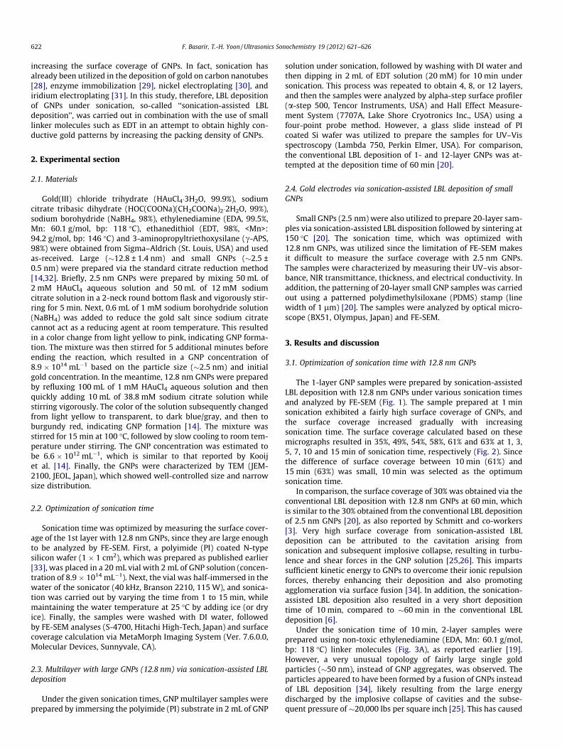
The 1-layer GNP samples were prepared by sonication-assistedLBL deposition with 12.8 nm GNPs under various sonication timesand analyzed by FE-SEM (Fig. 1). The sample prepared at 1 minsonication exhibited a fairly high surface coverage of GNPs, andthe surface coverage increased gradually with increasingsonication time. The surface coverage calculated based on thesemicrographs resulted in 35%, 49%, 54%, 58%, 61% and 63% at 1, 3,5, 7, 10 and 15 min of sonication time, respectively (Fig. 2). Sincethe difference of surface coverage between 10 min (61%) and15 min (63%) was small, 10 min was selected as the optimumsonication time.
In comparison, the surface coverage of 30% was obtained via theconventional LBL deposition with 12.8 nm GNPs at 60 min, whichis similar to the 30% obtained from the conventional LBL depositionof 2.5 nm GNPs [20], as also reported by Schmitt and co-workers[3]. Very high surface coverage from sonication-assisted LBLdeposition can be attributed to the cavitation arising fromsonication and subsequent implosive collapse, resulting in turbu-lence and shear forces in the GNP solution [25,26]. This impartssufficient kinetic energy to GNPs to overcome their ionic repulsionforces, thereby enhancing their deposition and also promotingagglomeration via surface fusion [34]. In addition, the sonication-assisted LBL deposition also resulted in a very short depositiontime of 10 min, compared to �60 min in the conventional LBLdeposition [6].
Under the sonication time of 10 min, 2-layer samples wereprepared using non-toxic ethylenediamine (EDA, Mn: 60.1 g/mol,bp: 118 �C) linker molecules (Fig. 3A), as reported earlier [19].However, a very unusual topology of fairly large single goldparticles (�50 nm), instead of GNP aggregates, was observed. Theparticles appeared to have been formed by a fusion of GNPs insteadof LBL deposition [34], likely resulting from the large energydischarged by the implosive collapse of cavities and the subse-quent pressure of �20,000 lbs per square inch [25]. This has caused
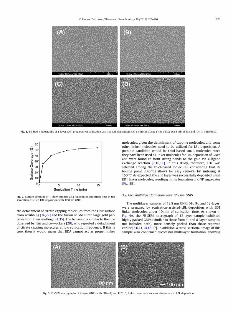
Fig. 1. FE-SEM micrographs of 1-layer GNP prepared via sonication-assisted LBL deposition; (A) 1 min (35%), (B) 3 min (49%), (C) 5 min (54%) and (D) 10 min (61%).
%) 70
e (% 60
ag 50
vera
40
Cov
30
40
ce C 30
urfa 20
S 10
0 5 10 150 0 5 10 15Sonication Time (min)Sonication Time (min)
Fig. 2. Surface coverage of 1-layer samples as a function of sonication time in thesonication-assisted LBL deposition with 12.8 nm GNPs.
F. Basarir, T.-H. Yoon / Ultrasonics Sonochemistry 19 (2012) 621–626 623
the detachment of citrate capping molecules from the GNP surfacefrom scrubbing [26,27] and the fusion of GNPs into large gold par-ticles from their melting [34,35]. The behavior is similar to the oneobserved by Fasi and co-workers [28], who reported a detachmentof citrate capping molecules at low sonication frequency. If this istrue, then it would mean that EDA cannot act as proper linker
Fig. 3. FE-SEM micrographs of 2-layer GNPs with EDA (A) and ED
molecules, given the detachment of capping molecules, and someother linker molecules need to be utilized for LBL deposition. Apossible candidate would be thiol-based small molecules sincethey have been used as linker molecules for LBL deposition of GNPsand were found to form strong bonds to the gold via a ligandexchange reaction [7,10,11]. In this study, therefore, EDT wasselected among the thiol-based molecules, considering that itsboiling point (146 �C) allows for easy removal by sintering at150 �C. As expected, the 2nd layer was successfully deposited usingEDT linker molecules, resulting in the formation of GNP aggregates(Fig. 3B).
3.2. GNP multilayer formation with 12.8 nm GNPs
The multilayer samples of 12.8 nm GNPs (4-, 8-, and 12-layer)were prepared by sonication-assisted-LBL deposition with EDTlinker molecules under 10 min of sonication time. As shown inFig. 4A, the FE-SEM micrograph of 12-layer sample exhibitedhighly packed GNPs (similar to those from 4- and 8-layer samples,not included here), more densely packed than those reportedearlier [5,6,11,14,16,17]. In addition, a cross-sectional image of thissample also confirmed successful multilayer formation, showing
T (B) linker molecuels via sonication-assisted LBL deposition.

Fig. 4. FE-SEM micrographs of 12-layer (A) and its cross-section (B) with 12.8 nm GNPs.
2 4 100.
) 12 layer1 8a.
u.) 12 layer
80ce
1 layer1.
e (a 8 layer
60tan
1 2nce
mitt 4 layer
.
rba 4 layer 40ans
0.6bso
20 Tra 8 layer
Ab
1 layer
% 12 layer0.0
1 layer0
y
400 500 600 700 800
Wavelength (nm)1000 1500 2000 2500
Wavelength (nm)
Fig. 5. UV–vis spectrum and NIR transmittance of GNP multilayer with 12.8 nm GNPs.
Table 1Characteristics of GNP multilayer via sonication-assisted LBL deposition.
# of layer Large GNP (12.8 nm) Small GNP (2.5 nm)
4a 8a 12a 20a 20b
Thickness (nm) 51 ± 3 104 ± 6 161 ± 7 (152 ± 4) 62 ± 3 52 ± 3Conductivity (X�1 cm�1) 60 1.1 � 104 1.5 � 104 (0.2 � 104) 5.0 � 103 (30.7) 2.5 � 105 (3.5 � 103)
(), Via the conventional LBL deposition (data of small GNP from Ref. [2]).a As-deposited.b After sintering.
624 F. Basarir, T.-H. Yoon / Ultrasonics Sonochemistry 19 (2012) 621–626
an approximately 150 nm thickness (Fig. 4B). In the UV–vis analy-ses, the absorption increased as the number of layers increased,indicating increased thickness [4,7] and thus successful multilayerformation (Fig. 5A). In addition to this, the 1-layer sample showeda broad peak at �520 nm due to the surface Plasmon absorption ofGNPs [4], while no absorption peaks were observed from themultilayer samples, owing to the aggregation or agglomeration ofGNPs [36]. On the other hand, the NIR transmittance of thesesamples decreased with increased number of layers (Fig. 5B), asreported previously [6], and became wavelength independent[19]. The 12-layer sample (not sintered) showed 5% transmittance,which was comparable to the 5% from electroplated gold filmsreported by Natan [2], indicating highly packed GNP multilayer.
The thickness of the multilayer evaluated by a-step increasedfrom 51 ± 3 nm to 104 ± 6 and 161 ± 7 nm with 4-, 8-, and 12-layer,respectively (Table 1), which appeared to be reasonable consider-ing the size of the GNPs (�12.8 ± 1.4 nm) and EDT (0.32 nm viaMolecular Studio Program). The electrical conductivity alsoincreased from 60 to 1.1 � 104 and 1.5 � 104 O�1 cm�1 with 4-,8-, and 12-layer, respectively, again demonstrating the increasedthickness [9], while the similar conductivity values from 8 and12-layer can be attributed to the GNP network formation at 8-layer[2,3]. The conductivity of 1.5 � 104 O�1 cm�1 can be compared
with 2 � 103 X�1 cm�1 obtained from the conventional LBL deposi-tion (12-layer with 12.8 nm GNPs), demonstrating an order ofmagnitude higher value despite the similar thickness, as shownin Table 1. This can be attributed to the much higher surface cov-erage of the 1st layer (61%) via sonication-assisted LBL comparedto the 30% by conventional LBL deposition, demonstrating theexcellence of sonication-assisted LBL deposition.
3.3. Gold thin films with 2.5 nm GNPs and patterning
The 20-layer samples using 2.5 nm GNPs were also preparedunder the optimized conditions obtained with 12.8 nm GNPs. Asshown in Table 1, the 20-layer GNPs exhibited a thickness of62 ± 3 nm, which is reasonable considering the diameter of smallGNPs (�2.5 nm) and EDT (0.32 nm via Molecular Studio Program).In addition, the samples exhibited no UV–vis absorption peaks at�520 and 690 nm [13], while showing wavelength independentNIR transmittance (Fig. 6), indicating highly packed small GNPsfrom sonication-assisted LBL deposition (Fig. 4). Upon sinteringat 150 �C for 1 h, the thickness decreased to 52 ± 3 nm with thecomplete removal of EDT molecules, as confirmed by EDX analysis(not included here), which is possible given the boiling point of
401.5
Aft i t i
40(B)(A)
u.) After sintering
30nce
1 0(a.u 30
ttan
As-deposited1.0
nce
20smit p
ban 20
ans
As-deposited0.5so
rb10%
Tra
After sinteringAs deposited
Abs 10%
After sintering
0 0
A
0400 500 600 700 800
0.01000 1500 2000 2500
0400 500 600 700 800
Wavelength (nm)1000 1500 2000 2500
Wavelength (nm)g ( ) g ( )
Fig. 6. UV–vis spectrum (A) and NIR transmittance (B) of 20-layer with 2.5 nm GNPs.
Fig. 7. Optical microscope (A) and FE-SEM (B) images of patterned 20-layer with 2.5 nm GNPs.
F. Basarir, T.-H. Yoon / Ultrasonics Sonochemistry 19 (2012) 621–626 625
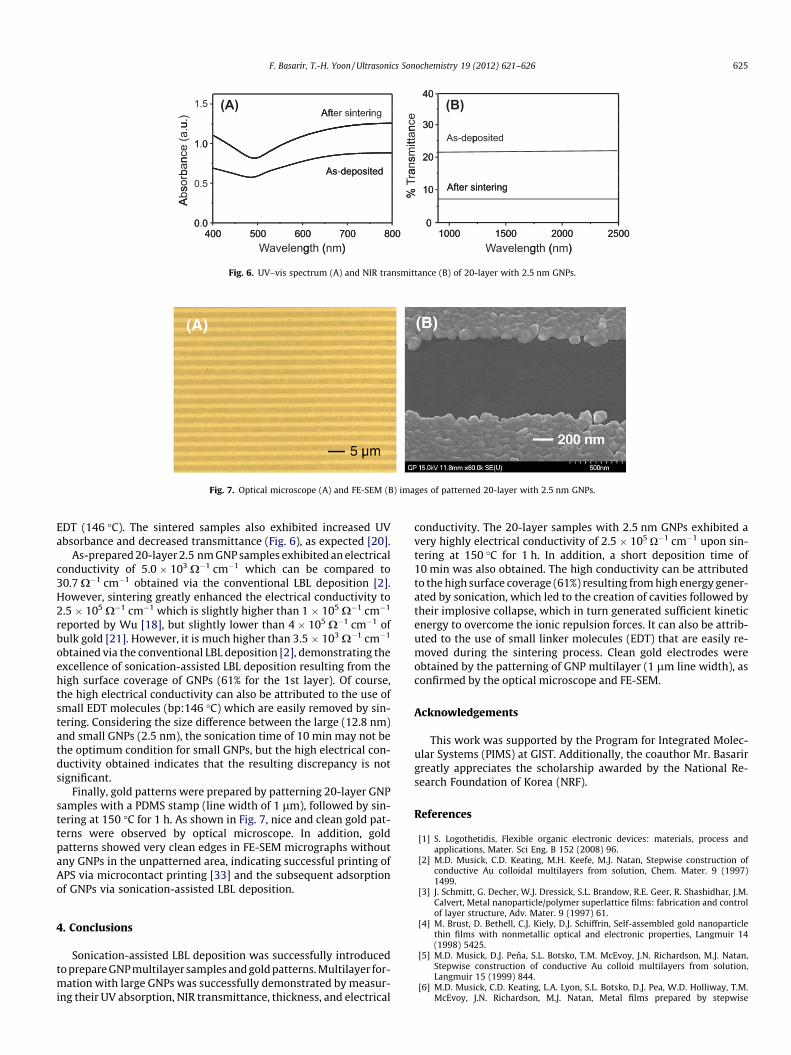
EDT (146 �C). The sintered samples also exhibited increased UVabsorbance and decreased transmittance (Fig. 6), as expected [20].
As-prepared 20-layer 2.5 nm GNP samples exhibited an electricalconductivity of 5.0 � 103 X�1 cm�1 which can be compared to30.7 X�1 cm�1 obtained via the conventional LBL deposition [2].However, sintering greatly enhanced the electrical conductivity to2.5 � 105 X�1 cm�1 which is slightly higher than 1 � 105 X�1 cm�1
reported by Wu [18], but slightly lower than 4 � 105 X�1 cm�1 ofbulk gold [21]. However, it is much higher than 3.5 � 103 X�1 cm�1
obtained via the conventional LBL deposition [2], demonstrating theexcellence of sonication-assisted LBL deposition resulting from thehigh surface coverage of GNPs (61% for the 1st layer). Of course,the high electrical conductivity can also be attributed to the use ofsmall EDT molecules (bp:146 �C) which are easily removed by sin-tering. Considering the size difference between the large (12.8 nm)and small GNPs (2.5 nm), the sonication time of 10 min may not bethe optimum condition for small GNPs, but the high electrical con-ductivity obtained indicates that the resulting discrepancy is notsignificant.
Finally, gold patterns were prepared by patterning 20-layer GNPsamples with a PDMS stamp (line width of 1 lm), followed by sin-tering at 150 �C for 1 h. As shown in Fig. 7, nice and clean gold pat-terns were observed by optical microscope. In addition, goldpatterns showed very clean edges in FE-SEM micrographs withoutany GNPs in the unpatterned area, indicating successful printing ofAPS via microcontact printing [33] and the subsequent adsorptionof GNPs via sonication-assisted LBL deposition.
4. Conclusions
Sonication-assisted LBL deposition was successfully introducedto prepare GNP multilayer samples and gold patterns. Multilayer for-mation with large GNPs was successfully demonstrated by measur-ing their UV absorption, NIR transmittance, thickness, and electrical
conductivity. The 20-layer samples with 2.5 nm GNPs exhibited avery highly electrical conductivity of 2.5 � 105 O�1 cm�1 upon sin-tering at 150 �C for 1 h. In addition, a short deposition time of10 min was also obtained. The high conductivity can be attributedto the high surface coverage (61%) resulting from high energy gener-ated by sonication, which led to the creation of cavities followed bytheir implosive collapse, which in turn generated sufficient kineticenergy to overcome the ionic repulsion forces. It can also be attrib-uted to the use of small linker molecules (EDT) that are easily re-moved during the sintering process. Clean gold electrodes wereobtained by the patterning of GNP multilayer (1 lm line width), asconfirmed by the optical microscope and FE-SEM.
Acknowledgements
This work was supported by the Program for Integrated Molec-ular Systems (PIMS) at GIST. Additionally, the coauthor Mr. Basarirgreatly appreciates the scholarship awarded by the National Re-search Foundation of Korea (NRF).
References
[1] S. Logothetidis, Flexible organic electronic devices: materials, process andapplications, Mater. Sci Eng. B 152 (2008) 96.
[2] M.D. Musick, C.D. Keating, M.H. Keefe, M.J. Natan, Stepwise construction ofconductive Au colloidal multilayers from solution, Chem. Mater. 9 (1997)1499.
[3] J. Schmitt, G. Decher, W.J. Dressick, S.L. Brandow, R.E. Geer, R. Shashidhar, J.M.Calvert, Metal nanoparticle/polymer superlattice films: fabrication and controlof layer structure, Adv. Mater. 9 (1997) 61.
[4] M. Brust, D. Bethell, C.J. Kiely, D.J. Schiffrin, Self-assembled gold nanoparticlethin films with nonmetallic optical and electronic properties, Langmuir 14(1998) 5425.
[5] M.D. Musick, D.J. Pena, S.L. Botsko, T.M. McEvoy, J.N. Richardson, M.J. Natan,Stepwise construction of conductive Au colloid multilayers from solution,Langmuir 15 (1999) 844.
[6] M.D. Musick, C.D. Keating, L.A. Lyon, S.L. Botsko, D.J. Pea, W.D. Holliway, T.M.McEvoy, J.N. Richardson, M.J. Natan, Metal films prepared by stepwise

626 F. Basarir, T.-H. Yoon / Ultrasonics Sonochemistry 19 (2012) 621–626
assembly. 2. Construction and characterization of colloidal Au and Agmultilayers, Chem Mater. 12 (2000) 2869.
[7] N. Krasteva, I. Besnard, B. Guse, R.E. Bauer, K. Mullen, A. Yasuda, T. Vossmeyer,Self-assembled gold nanoparticle/dendrimer composite films for vapor sensingapplications, Nano Lett. 2 (2002) 551.
[8] H. Zhang, H. Lu, N. Hu, Fabrication of electroactive layer-by-layer films ofmyoglobin with gold nanoparticles of different sizes, J. Phys. Chem. B 110(2006) 2171.
[9] Y. Joseph, B. Guse, T. Vossmeyer, A. Yasuda, Gold nanoparticle/organicnetworks as chemiresistor coatings: the effect of film morphology on vaporsensitivity, J. Phys. Chem. C 112 (2008) 12507 (LBL).
[10] T. Vossmeyer, C. Stolte, M. Ijeh, A. Kornowski, H. Weller, Networked gold-nanoparticle coatings on polyethylene: charge transport and strain sensitivity,Adv. Funct. Mater. 18 (2008) 1611.
[11] R.W. Gerber, D.N. Leonard, S. Franzen, Conductive thin film multilayers of goldon glass formed by self-assembly of multiple size gold nanoparticles, ThinSolid Films 517 (2009) 6803.
[12] A.A. Mewe, E.S. Kooij, B. Poelsema, Seeded-growth approach to selectivemetallization of microcontact printed patterns, Langmuir 22 (2006) 5584.
[13] C. Jiang, S. Markutsya, V.V. Tsukruk, Collective and individual plasmonresonances in nanoparticle films obtained by spin-assisted layer-by-layerassembly, Langmuir 20 (2004) 882.
[14] E.S. Kooij, E.A. Martjin Brouwer, H. Wormeester, B. Poelsama, Ionic strengthmediated self-organization of gold nanocrystals: AFM study, Langmuir 18(7677) (2002).
[15] G.Y. Onoda, E.G. Liniger, Experimental determination of the random-parkinglimit in two dimensions, Phys. Rev. A 33 (1986) 715.
[16] M. Chirea, C.M. Pereira, F. Silva, Catalytic effect of gold nanoparticles self-assembled in multilayered polyelectrolyte films, J. Phys. Chem. C 111 (2007)9255.
[17] F. Zhang, M.P. Srinivasan, Layer-by-layer assembled gold nanoparticle films onamine-terminated substrates, J. Colloid Interface Sci. 319 (2008) 450.
[18] Y. Wu, Y. Li, B.S. Ong, P. Liu, S. Gardner, B. Chiang, High-performance organicthin-film transistors with solution-printed gold contacts, Adv. Mater. 17(2005) 184.
[19] F. Basarir, Ph.D. Dissertation, Gwangju Institute of Science and Technology,2011.
[20] F. Basarir, T.H. Yoon, Preparation of gold patterns on polyimide coating vialayer-by-layer deposition of gold nanoparticles, J. Colloid Interface Sci. 352(2010) 11.
[21] R.C. Weast, CRC Handbook of Chem and Phys, 69th ed., CRC Press Inc., NY,1988.
[22] E.V. Rokhina, P. Lens, J. Virkutyte, Low-frequency ultrasound in biotechnology:state of the art, Trends Biotechnol. 27 (2009) 298.
[23] M. Ashokkumar, The characterization of acoustic cavitation bubbles – anoverview, Ultrason. Sonochem. 18 (2011) 864.
[24] P.R. Gogate, Cavitational reactors for process intensification of chemicalprocessing applications: a critical review, Chem. Eng. Process.: ProcessIntensific. 47 (2008) 515.
[25] K.S. Suslick, Sonochemistry, Science 247 (1990) 1439.[26] E. Maisonhaute, C. Prado, P.C. White, R.G. Compton, Surface acoustic cavitation
understood via nanosecond electrochemistry Part III: shear stress in ultrasoniccleaning, Ultrason. Sonochem. 9 (2002) 297.
[27] T.J. Mason, A.J. Cobley, J.E. Graves, D. Morgan, New evidence for the inversedependence of mechanical and chemical effects on the frequency ofultrasound, Ultrason. Sonochem. 18 (2011) 226.
[28] A. Fási, I. Pálinkó, J.W. Seo, Z. Kónya, K. Hernadi, I. Kiricsi, Sonication assistedgold deposition on multiwall carbon nanotubes, Chem. Phys. Lett. 372 (2003)848.
[29] H. Zejli, J.L. Hidalgo-Hidalgo de Cisneros, I. Naranjo-Rodriguez, B. Liu, K.R.Temsamani, J.-L. Marty, Alumina sol–gel/sonogel-carbon electrode based onacetylcholinesterase for detection of organophosphorus pesticides, Talanta 77(2008) 217.
[30] A. Chiba, T. Gotou, K. Kobayashi, W.C. Wu, Influence of sonication of nickelplating in a nickel sulfamate bath, Metal Finishing 98 (9) (2000) 66.
[31] T. Ohsaka, M. Isaka, K. Hirano, T. Ohishi, Effect of ultrasound sonication onelectroplating of iridium, Ultrason. Sonochem. 15 (2008) 283.
[32] N.R. Jana, L. Gearhearth, C.J. Murphy, Seeding growth for size control of 5–40 nm diameter gold nanoparticles, Langmuir 17 (2001) 6782.
[33] F. Basarir, T.H. Yoon, Preparation of -APS monolayer with complete coveragevia contact printing, J. Colloid Interface Sci. 336 (2009) 393.
[34] D. Radziuk, D. Grigoriev, W. Zhang, D. Su, H. Möhwald, D. Shchukin,Ultrasound-assisted fusion of preformed gold nanoparticles, J. Phys. Chem. C114 (2010) 1835.
[35] N.A. Madigan, C.R.S. Hagan, H. Zhang, L.A. Coury Jr., Effects of sonication onelectrode surfaces and metal particles, Ultrason. Sonochem. 3 (1996) S239.
[36] N. Fishelson, I. Shkrob, O. Lev, J. Gun, A.D. Modestov, Studies on chargetransport in self-assembled gold–dithiol films: conductivity:photoconductivity, and photoelectrochemical measurements, Langmuir 17(2001) 403.