Solutions for Industrial Drives and Factory Automation
49
Solutions for Industrial Drives and Factory Automation July 2019
-
Upload
khangminh22 -
Category
Documents
-
view
2 -
download
0
Transcript of Solutions for Industrial Drives and Factory Automation

Solutions for Industrial Drives and Factory Automation
July 2019
Industrial Drive
11/12/20192
High power industrial
Robot / Cobot
Servo driver
High Power VFD
High power pumps
Small industrial -Circulation Pump
-Industrial Fan
High power A/C &
HVAC-2~3HP stand A/C
-Commercial A/C
-HVAC
Home Appliance-Refrigerator
-Room A/C
-Dish washer
-Washing Machine
-Fan motor
Industrial market
focus
Leading quality, supply
chain and manufacturing
network
Comprehensive
product portfolioApplications expertise for
innovative solutions

11/12/20193
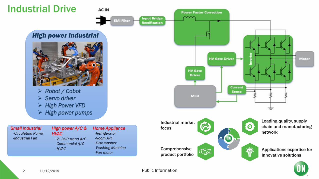
Insulated Gate Bipolar Transistors (IGBTs)
The IGBT Triangle
11/12/20194
Mesa-engineered for low
conduction losses and good
energy handling robustness
Drift area tuned for target BV
(Breakdown Voltage) and fast
switching
Balanced buffer and anode
providing excellent robustness
and low energy losses
Gate designed for low
capacitance and high reliability
transformer-based solutions
Top and bottom metal tailored
for discrete packages or
modulesOn-State
Voltage
Drop
Turn off Loss
Ruggedness
Power Efficiency
Reliable Operation

Leading IGBT Technology
11/12/20195
Best in class performance enabling outstanding
system efficiency & reliability
Various lineup can cover all applications
Can be reliable alternative source of IFX
Field Stop III 650V IGBT 1200V FS Trench IGBTs
Best in class performance in existing
1200V HS IGBTs
SCR IGBT lineup with outstanding power
loss performance
Most advanced RC IGBT technology for IH
application
650V Trade-off of high speed IGBTs
11/12/20196
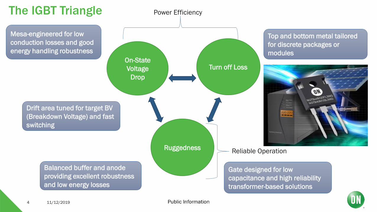
Metal Oxide Semiconductor Field Effect Transistor (MOSFETs)

Rapid Development of Super Junction MOSFETs
11/12/20197
•High efficiency
•Hard Switching Topologies
•Reduced Qg and Eoss
•High efficiency
•Hard Switching Topologies
•Reduced Qg and Eoss
FAST Version
Easy Drive Version
•Hard/Soft Switching
Topologies
•Easy to drive
•Low EMI and Voltage spikes
•Internal Rg and optimized Cap
•Soft switching topologies
•Better system reliability
•Small Qrr and Trr
•Robust diode ruggedness
FRFET Version
• Voltage Range:
•600-800V
•RdsOn Range:
•23mOhm – 1400mOhm
•New innovative packaging
Complete Portfolio
•Optimized versions for fast recovery,
easy switch or fast switching
•Most rugged reverse recovery diode
•Optimized Gate Oscillation for
reduced EMI
•Lower Voltage Spikes
Silicon Carbide MOSFETs
11/12/20198
Bringing Value
Providing full WGB Eco System:
• Internal Manufacturing/Substrates
• Diodes, FETs, Drivers, Isolation
• Physical Device Models for Simultion
Patented termination structure provides superior
robustness for harsh environmental conditions
ON Semi Committed to Complete Vertical Integration for all SiC & GaN
I lea
k(A
)
Vreverse (V)
Type Voltage Generation Status Comments
SiC
MOSFETs
1200 V Gen 1 80mΩ ReleasedDec ’19 Release:
20, 40, 160mΩ
900 V Gen 1 Sample Sep’19 20 & 60 mΩ

NCP51705 – 6A SiC MOSFET Fully integrated Gate Driver
11/12/20199
Product Description
The NCP51705 driver is designed to primarily drive SiC MOSFET transistors. For the lowest possible conduction losses, the driver is capable to deliver the
maximum allowable gate voltage to the SiC MOSFET device.
Unique Features
Adjustable, on-board regulated negative charge pump
Negative voltage drive for fast turn-off (same as above)
5V Reference/Bias Rail
Adjustable UVLO levels
Benefits
Simplified BOM and no need for extra DC/DC
AEC-Q100 with Grade 1 Temperature Range(NCV51705)
Easy digital isolator Vcc supply
Can work with diff SiC FET’s
Other Features
High peak output current - 6A
Extended positive voltage rating for efficient SiC MOSFET operation during the conduction period
Thermal shutdown function
DESAT detection for short circuit protection
Inverting/Non-inverting Input
Market & Applications
Driving SiC MOSFET (NCV51705 for Automotive Applications)
Inverters, Converter, and Motor Drivers
High Performance PFC, AC/DC and DC/DC Converters
Typical Application Schematic
Packaging Information
QFN24 4mm x 4mm
OPN : NCP51705MNTXG NCV51705MNTXG

11/12/201910
Transfer Molded Power Integrated Module
(TMPIMs)

Block Diagram
Target Application
TMPIMs for Industrial Drives (25A-50A)
•High performance Transfer mold PKG
•10X Temp cycles
• 3x Power cycles
• 1200V/600V high performance FS-II IGBT
• Integrated CIB ( Converter, Inverter , Brake)
• Lower parasitic for better efficiency
• Integrated current sense resistor ( optional)
•High performance DBC substrate ( 50A)
• Industrial Inverters
• Servo Drives
• Industrial Pumps
• Industrial Fans
Product Voltage Current Substrate Configuration
NXH35C120L2C2SG 1200V 35A DBC(Al2O3) CIB Sampling
NXH50C120L2C2SG 1200V 50A DBC(HPS) CIB Sampling
1200V Line-up
Features
Package : 73mm X 47mm X 6mm
Benefits
DIP -C2
•Improved REL for longer product life time
• Higher efficiency
•Compact & high density package
• complete portfolio of 1200V/650V CIB’s
Pins Name Pins NameSpacing
RequirementActual **
+ Pin before Inrush+ Pin after
Inrush1.5mm >10.0 mm
+ (or Positive Pin) U, V, W /B 2.6mm 5.4 mm
U, V, W U, V, W 2.5mm 5.4 mm
R, S, T R, S, T 5mm 5.4 mm
R, S, TPin or
Negative Pin5mm 5.4 mm
Any Pins Heatsink 5.5mm 6.0 mm
Any Pins NTC 5.5mm 7.9 mm
** Distance has considered the solder pad of diameter (mm):
sqrt of [pin width*pin width + pin thickness*pin thickness] + 0.3 for
drill tolerance +0.5 for pad width
Pin Name P1 .1 P1.2 N1.1 N1.2 GB NB Eun Gun Evn Gvn Ewn Gwn TH1 TH2Pin width (mm) 1.2 1.2 1.2 1.2 1.2 1.2 1.2 1.2 1.2 1.2 1.2 1.2 1.2 1.2
Coodination 0 2.54 10.16 12.7 17.78 20.32 27.94 30.48 38.1 40.64 48.26 50.8 60.96 63.5
Pin 2 pin clearance (mm) 0.3 5.4 0.3 2.8 0.3 5.4 0.3 5.4 0.3 5.4 0.3 7.9 0.3
Pin Name R S T B P.1 P.2 U Gup V Gvp W GwpPin width (mm) 1.2 1.2 1.2 1.2 1.2 1.2 1.2 1.2 1.2 1.2 1.2 1.2
Coodination 0 7.62 15.24 22.86 30.48 33.02 40.64 43.18 50.8 53.34 60.96 63.5
Pin 2 pin clearance (mm) 5.4 5.4 5.4 5.4 0.3 5.4 0.3 5.4 0.3 5.4 0.3
Side A
Side B
Creepage and Clearance for TMPIM Package
Gwp W Gvp V Gup U (BrOut) B T S R
TH1/2 Gwn Ewn Gvn Evn Gun Eun Nb Gb N VBUS
11/12/201913
High Voltage Gate Driver

High Voltage Gate Drivers Portfolio
11/12/201914
Non - Isolated High & Low side Internally Isolated
HVAC
PFC
UPS
Motor Control
1-Switch PTC Heater
IPMs
Motor Control
White Goods
2-Switch PTC Heater
UPS
Solar Inverter
Motor Control
EV Chargers
PTC Heaters
BSG Inverters
OBC
Traction-InverterA
PP
LIC
ATIO
NS
High Drive Current
Low Propagation Delay
Full Features: DESAT, Clamp, UVLO, TSD, Vee
High Drive Current
Low Propagation Delay
Full Features: DESAT, Clamp, UVLO, TSD, Vee
High Drive Current
Low Propagation Delay
Full Features: DESAT, Clamp, UVLO,
Vee, STO
Isolation Certification: UL/VDE/IECHIG
HLIG
HTS
NCD570x Non – Isolated Gate Drivers
11/12/201915
• High current output(+4A/-6A) at
Miller Plateau
• Short propagation delays with
accurate matching
• Direct Interface to Digital
Isolator/Opto−coupler/Pulse
Transformer for isolation
• 5V reference for external logic
• Tight UVLO thresholds
• Active Miller Clamp
• DESAT with programmable delay
• Soft Turn Off during short circuit
• Negative VEE
• Higher system level
efficiency
• Improved system reliability
• Lower cost
• PCB space savings
• UPS
• Motor Controls
• Solar Inverters
• xEV Charger, PTC Heater
Single channel, high current and high voltage gate drivers. Designed to improve system efficiency with high drive current, reliability with better signal
integrity and to reduce cost with higher level of integration.
Available in SOIC-16 & SOIC-8
NCD5701/03(C)
NCD5701/03(B)
NCD5701/03(A)
NCD5700/02
Value Proposition
Unique FeaturesBenefits
Other Features
Market and Application
Pin Connections
Ordering and Packaging Information
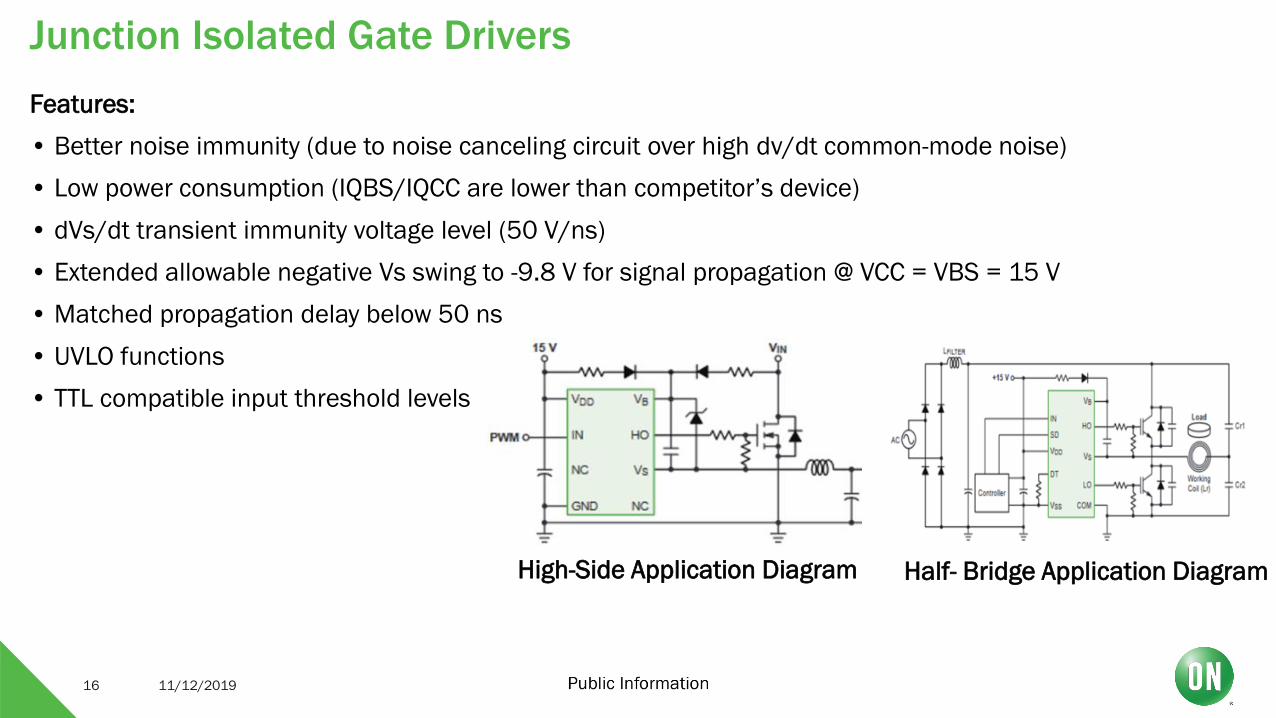
Features:
• Better noise immunity (due to noise canceling circuit over high dv/dt common-mode noise)
• Low power consumption (IQBS/IQCC are lower than competitor’s device)
• dVs/dt transient immunity voltage level (50 V/ns)
• Extended allowable negative Vs swing to -9.8 V for signal propagation @ VCC = VBS = 15 V
• Matched propagation delay below 50 ns
• UVLO functions
• TTL compatible input threshold levels
11/12/201916
High-Side Application Diagram Half- Bridge Application Diagram
Junction Isolated Gate Drivers
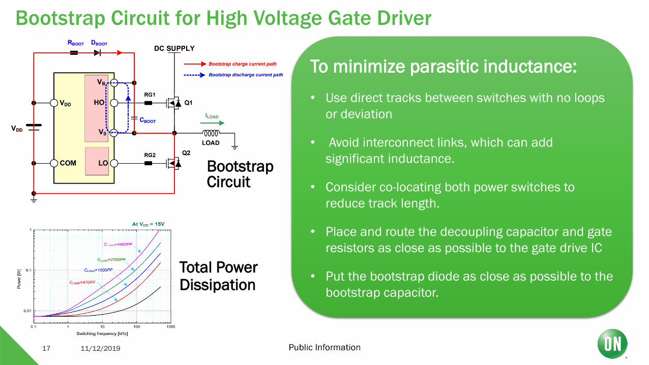
Bootstrap Circuit for High Voltage Gate Driver
11/12/201917
To minimize parasitic inductance:
• Use direct tracks between switches with no loops
or deviation
• Avoid interconnect links, which can add
significant inductance.
• Consider co-locating both power switches to
reduce track length.
• Place and route the decoupling capacitor and gate
resistors as close as possible to the gate drive IC
• Put the bootstrap diode as close as possible to the
bootstrap capacitor.
Bootstrap Circuit
Total Power Dissipation

NCP51530 – High and Low Side, High Performance 700V
11/12/201918
Value Proposition
The NCP51530 are 700 V high frequency high-side and low-side drivers with very low and matched propagation delays for direct drive of 2 N-channel
power MOSFETs in High Performance SMPS & Digital High power converters
Unique Features
Input range: up to 700 V
Excellent dynamic
60/25 ns Typ Prop delay (A/B)
7 ns Max Delay matching
8/15 ns Typ/Max Rise & Fall Times
Negative bridge pin voltage up to -10 Volts
Benefits
Off-line applications
Well suited for high
frequency operations
Robust design
Other Features
Dual input logic
3/3.5 A Source/Sync currents
Max Vcc : 20 V
100 ns Min pulse width
Under voltage lockout for both inputs
Market Application
Server & Telecom Off-line Power Supplies
Industrial High Power Converters
Typical Application Schematic
Packaging Information
NCP51530A/BDR2G : SOIC8
NCP51530A/BMNTWG : DFN10 4mm x 4mm
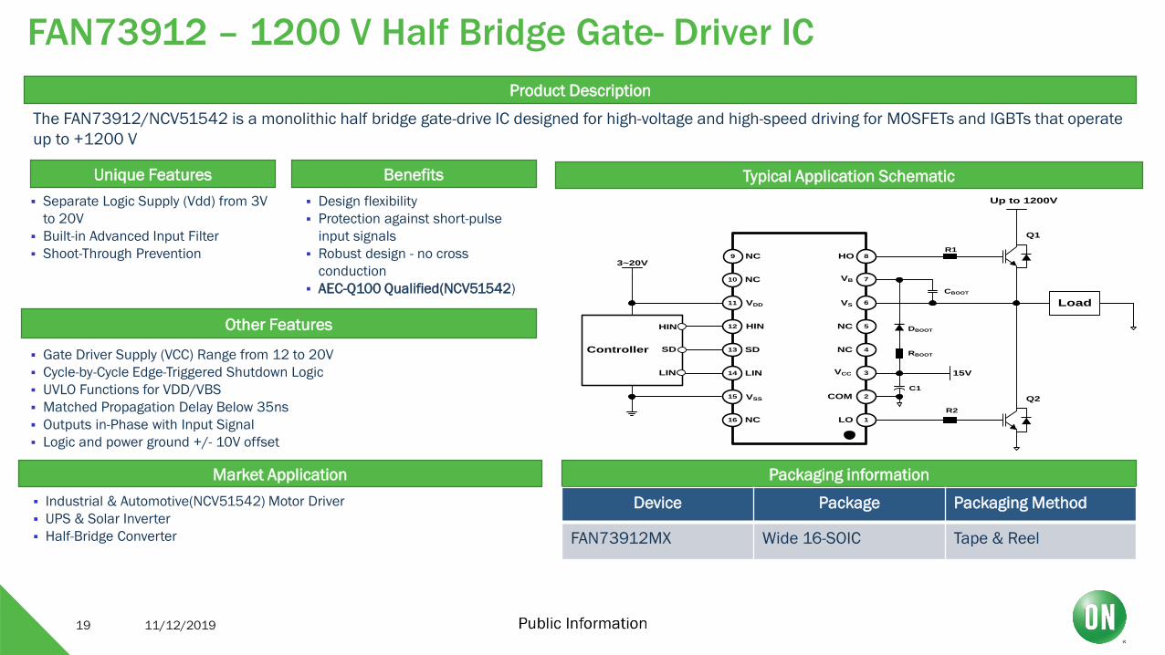
FAN73912 – 1200 V Half Bridge Gate- Driver IC
11/12/201919
Product Description
The FAN73912/NCV51542 is a monolithic half bridge gate-drive IC designed for high-voltage and high-speed driving for MOSFETs and IGBTs that operate
up to +1200 V
Separate Logic Supply (Vdd) from 3V
to 20V
Built-in Advanced Input Filter
Shoot-Through Prevention
Unique Features Benefits
Design flexibility
Protection against short-pulse
input signals
Robust design - no cross
conduction
AEC-Q100 Qualified(NCV51542)
Other Features
Gate Driver Supply (VCC) Range from 12 to 20V
Cycle-by-Cycle Edge-Triggered Shutdown Logic
UVLO Functions for VDD/VBS
Matched Propagation Delay Below 35ns
Outputs in-Phase with Input Signal
Logic and power ground +/- 10V offset
Market Application
Industrial & Automotive(NCV51542) Motor Driver
UPS & Solar Inverter
Half-Bridge Converter
Typical Application Schematic
DBOOT
Q1
RBOOT
CBOOT
3~20V
Q2
C1
R2
R1
Up to 1200V
Controller
HIN
LIN
LO
COM
VB
VSVDD
SD
HIN
NC
15
NC
HO
VSS
NC
14
16
13
12
11
10
2
3
1
4
8
6
7
LIN VCC
SD
15V
Load
NC 5
NC9
Packaging information
Device Package Packaging Method
FAN73912MX Wide 16-SOIC Tape & Reel

FAN73893/4/5/6 – High Voltage 3-Phase Half-Bridge Driver
11/12/201920
Product Description
The NCP73893/4/5/6 are monolithic 3-phase half-bridge gate driver with up to 0.35-A/0.65-A source and sink peak current. It is designed for high-voltage, high-speed, driving
MOSFETs and IGBTs operating up to +600V. The FAN73893/4/5/6 offers stable operation of high-side drivers under high dVS/dt noise circumstances. An advanced level-shift circuit
allows high-side gate driver operation up to Vs= -9.8V(typical) for VBS=15V
Unique Features Benefits
Floating Channel for Bootstrap Operation
to +700V (VB MAX = 720V)
Inverting/Non-inverting Input
FAN73893/4 : Inverting Input
FAN73895/6 : Non-inverting Input
UVLO Output Threshold Voltage (Typ.)
FAN73893/5 : +8.5/ -8.0 V
FAN73894/5 : +11.0/ -10.5V
Negative VS Swing to -9.8V (need to check)
Product Selection upon Diff Switch
Type & Input Signal
High Robustness
Other Features
Over-Current Shutdown Turns Off All 6 Channels
Matched Propagation Delay for All Channels
3.3V & 5.0V Input Logic Compatible
Adjustable Fault-Clear Timing
Shoot-Through Prevention
Built-in Advanced Input Filter & Soft Turn-off Function
Build-in UVLO Functions for All Channels
Market Application
3-Phase Motor Inverter Driver
Air Conditioner, Washing Machine, Refrigerator, Dish Washer
Industrial Inverter – Sewing Machine, Power Tool
General-Purpose 3-Phase Inverter
Typical Application Schematic
Packaging Information
SOIC-28W

Galvanic Isolated Gate Drivers
11/12/201921
A. 5kV UL Recognized Isolation (Robustness) B. Highest Drive Current (improved Efficiency)
C. Best-in-Class EMI (Higher Noise Robustness) D. Best-in-Class CMTI (Higher Noise Robustness)
ON ADI IFX TI
I-source
Peak8A 4.6A 4A 2.5A
I-Sink
Peak8A 4.6A 3A 5A
I-Source
Miller
Plateau
4A 3A 1.1A 2A
I-Sink
Miller
Plateau
6A 4A 2.9A 4A
ON
TI
ADIIFX
Features Inductive
UL 5kV Isolation √
Reliability/Aging √
Temp Range √
EMI √
OUTH/OUTL = High
dv/dt = 118 kV/us
@1500V
Features:
• Safe, Reliable and Certified
Technology
• Increased system efficiency
with high drive current
• Does not generate EMI, nor
is susceptible to system
generated EMI
• Robust Common Mode
Transient Immunity (CMTI)
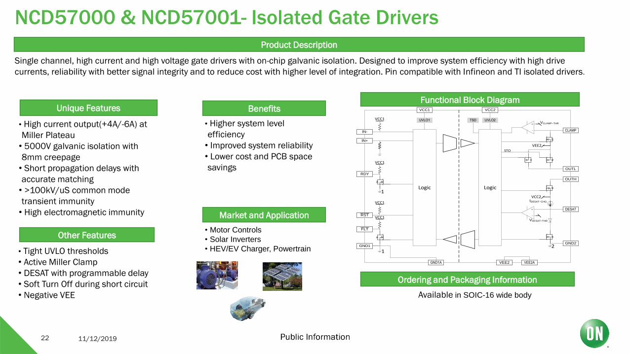
NCD57000 & NCD57001- Isolated Gate Drivers
11/12/201922
• High current output(+4A/-6A) at
Miller Plateau
• 5000V galvanic isolation with
8mm creepage
• Short propagation delays with
accurate matching
• >100kV/uS common mode
transient immunity
• High electromagnetic immunity
• Tight UVLO thresholds
• Active Miller Clamp
• DESAT with programmable delay
• Soft Turn Off during short circuit
• Negative VEE
• Higher system level
efficiency
• Improved system reliability
• Lower cost and PCB space
savings
• Motor Controls
• Solar Inverters
• HEV/EV Charger, Powertrain
Single channel, high current and high voltage gate drivers with on-chip galvanic isolation. Designed to improve system efficiency with high drive
currents, reliability with better signal integrity and to reduce cost with higher level of integration. Pin compatible with Infineon and TI isolated drivers.
Available in SOIC-16 wide body
IN-
FLT
GND1
CLAMP
VCC1
RST
RDY
GND1A
IN+
VEE2AVEE2
GND2
OUTL
OUTH
VCC2
DESAT+
-
IDESAT−CHG
UVLO2
VDESAT−THR
VCC2
TSD
VEE2
+
-
VCLAMP−THR
UVLO1
21
1
VCC1
VCC1
LogicLogic
VCC1
VCC1
STO
Product Description
Unique Features Benefits
Other Features
Market and Application
Functional Block Diagram
Ordering and Packaging Information

NCD57200 - High Side Isolated Half Bridge Gate Driver
11/12/201923
• +1A/-1.5A current output at Miller
Plateau
• DC bus operation up to +900V
• 3.3V/5V/15V logic input
• <50nS propagation delays with
accurate matching
• >50kV/µS common mode transient
immunity
• Asymmetric UVLO protection for both channels
• Output in phase with input signals
• Vcc/VB up to 25V
• Rail-to-rail output
• Higher system level
efficiency
• Improved system reliability
• Lower cost and PCB space
savings
• Fans, Pumps
• Home Appliances
• General purpose drives
High voltage half bridge gate driver designed for system reliability. On-chip magnetic isolation for high side gate to make the driver immune to negative
transients of up to -900V at Vs and common mode transients up to 50kV/µS. Two independent inputs with noise filtering, dead time control & interlock
protection.
Available in SOIC-8
VB
UVLO2
Output Logic
UVLO1Matching
Delay
HO
VS
LO
VCC
Input Logic
VCC
VCC
HIN
GND
LIN
Deadtime and
Interlock
Minimum Pulse Width
Minimum Pulse Width
Product Description
Unique Features Benefits
Other Features
Market and Application
Functional Block Diagram
Ordering and Packaging Information
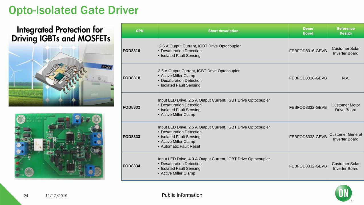
Opto-Isolated Gate Driver
11/12/201924
OPN Short descriptionDemo
Board
Reference
Design
FOD83162.5 A Output Current, IGBT Drive Optocoupler
• Desaturation Detection
• Isolated Fault Sensing
FEBFOD8316-GEVBCustomer Solar
Inverter Board
FOD8318
2.5 A Output Current, IGBT Drive Optocoupler
• Active Miller Clamp
• Desaturation Detection
• Isolated Fault Sensing
FEBFOD8316-GEVB N.A.
FOD8332
Input LED Drive, 2.5 A Output Current, IGBT Drive Optocoupler
• Desaturation Detection
• Isolated Fault Sensing
• Active Miller Clamp
FEBFOD8332-GEVBCustomer Motor
Drive Board
FOD8333
Input LED Drive, 2.5 A Output Current, IGBT Drive Optocoupler
• Desaturation Detection
• Isolated Fault Sensing
• Active Miller Clamp
• Automatic Fault Reset
FEBFOD8333-GEVBCustomer General
Inverter Board
FOD8334
Input LED Drive, 4.0 A Output Current, IGBT Drive Optocoupler
• Desaturation Detection
• Isolated Fault Sensing
• Active Miller Clamp
FEBFOD8332-GEVBCustomer Solar
Inverter Board

11/12/201925
Intelligent Power Module (IPMs)
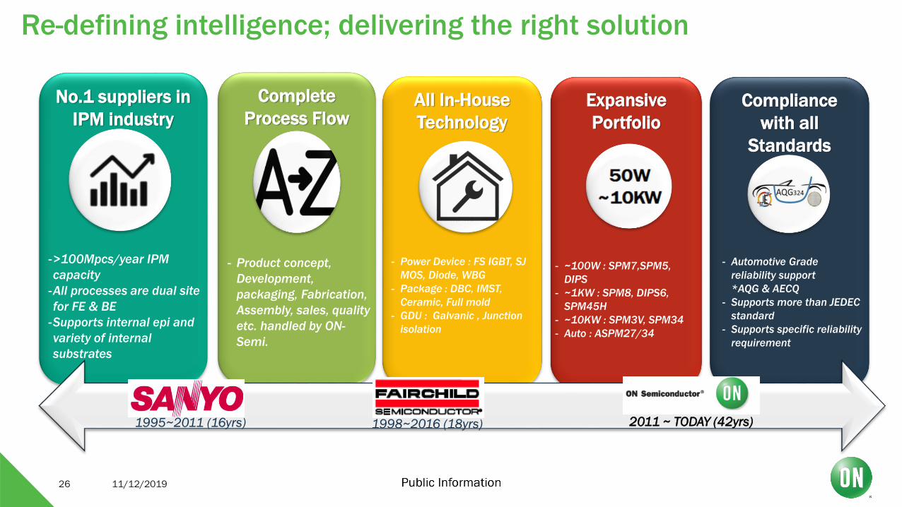
Re-defining intelligence; delivering the right solution
11/12/201926
No.1 suppliers in
IPM industry
Complete
Process Flow All In-House
Technology
Expansive
Portfolio
Compliance
with all
Standards
->100Mpcs/year IPM
capacity
-All processes are dual site
for FE & BE
-Supports internal epi and
variety of internal
substrates
- Product concept,
Development,
packaging, Fabrication,
Assembly, sales, quality
etc. handled by ON-
Semi.
- Power Device : FS IGBT, SJ
MOS, Diode, WBG
- Package : DBC, IMST,
Ceramic, Full mold
- GDU : Galvanic , Junction
isolation
- ~100W : SPM7,SPM5,
DIPS
- ~1KW : SPM8, DIPS6,
SPM45H
- ~10KW : SPM3V, SPM34
- Auto : ASPM27/34
- Automotive Grade
reliability support
*AQG & AECQ
- Supports more than JEDEC
standard
- Supports specific reliability
requirement
191995~2011 (16yrs) 1998~2016 (18yrs) 2011 ~ TODAY (42yrs)

IPM: All In- house technology
11/12/201927
650V FS3/4 Trench SCR IGBT
1200V FSII Trench SCR IGBT
Super Junction SF2/3 MOSFET
Planar UniFET MOSFET
Power Switch
800V/1600V Hyper Fast Diode
650V /1200V Extreme Fast Diode
Power diode
Junction isolation GDU
Gate Driver Unit
Shunt resistor
NTC thermistor
Ceramic capacitors / Resistors
Passive
Component
3-phase topology
PFC ;Interleaved / Bridge-less /
Boost
Variety Topology
DBC substrate (AlN/Al2O3)
IMST substrate
Ceramic substrate
Full Mold PKG
Substrate
SPM3V example
Exterior outline Internal Structure
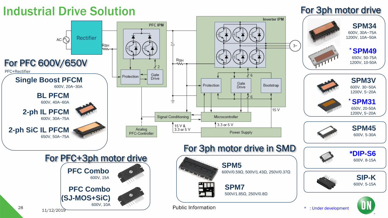
Industrial Drive Solution
11/12/201928
SPM34600V, 30A~75A
1200V, 10A~50A
* SPM31650V, 20-50A
1200V, 5~20A2-ph IL PFCM600V, 30A~75A
BL PFCM600V, 40A~60A
2-ph SiC IL PFCM650V, 50A~75A
SPM3V600V. 30~50A
1200V, 5~20A
* : Under development
* SPM49650V, 50-75A
1200V, 10-50A
SPM45600V. 5-30A
*DIP-S6600V. 8-15A
Rectifier
PFC Combo600V, 15A
PFC Combo
(SJ-MOS+SiC)600V, 10A
SIP-K600V. 5-15A
For 3ph motor drive in SMD
For PFC 600V/650V
For PFC+3ph motor drive
PFC+Rectifier
Single Boost PFCM600V, 20A~30A
SPM5600V/0.59Ω, 500V/1.43Ω, 250V/0.37Ω
SPM7500V/1.85Ω, 250V/0.8Ω
For 3ph motor drive
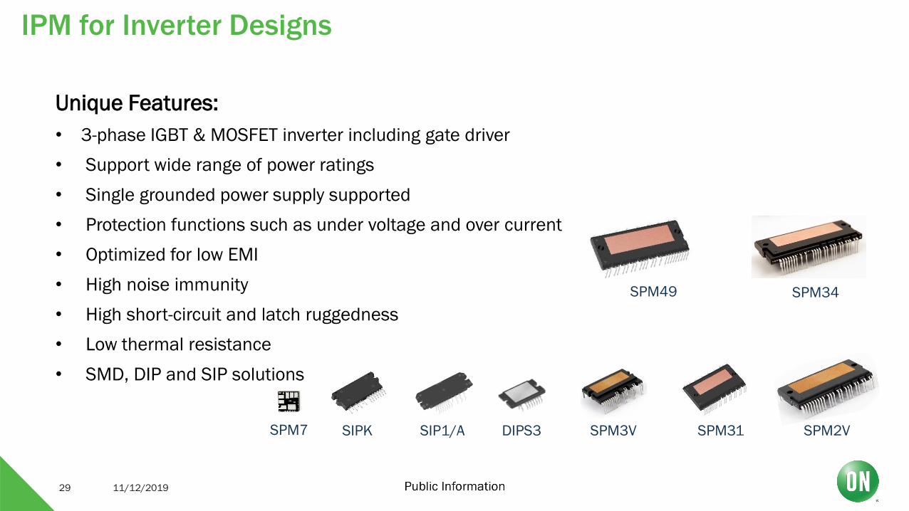
IPM for Inverter Designs
11/12/201929
Unique Features:
• 3-phase IGBT & MOSFET inverter including gate driver
• Support wide range of power ratings
• Single grounded power supply supported
• Protection functions such as under voltage and over current
• Optimized for low EMI
• High noise immunity
• High short-circuit and latch ruggedness
• Low thermal resistance
• SMD, DIP and SIP solutions
DIPS3 SPM3V SPM2V
SPM34
SIP1/ASIPK SPM31
SPM49
SPM7

• All these part is pin-compatible
• Wide product coverage ; 30A~100A/600V ,
10~75A/1200V
• Superior thermal performance and low loss
Features Benefits Block Diagram
Specifications
Package ; 80 mm × 33 mm × 8 mm
Target Applications
Product Voltage Current VCE(SAT) typ. Substrate Status
FNA23060 600V 30A 1.50V DBC(Al2O3) MP
FNA25060 600V 50A 1.50V DBC(Al2O3) MP
FNA27560 600V 75A 1.30V DBC(Al2O3) MP
FNA2A060 600V 100A TBD DBC(AlN) TBD
• 1200V & 600V Advanced Trench SC rated IGBT
• Very low thermal resistance with DBC substrate (Al2O3 , AlN)
• Built-in real NTC on DBC ,bootstrap diodes
• No side dummy for more creepage
SPM®34
Product Voltage Current VCE(SAT) typ. Substrate Status
FNA21012A 1200V 10A 2.2V DBC(Al2O3) MP
FNA22512A 1200V 25A 1.9V DBC(Al2O3) MP
FNA23512A 1200V 35A 1.9V DBC(Al2O3) MP
FNA25012A 1200V 50A 2.2V DBC(AlN) MP
1200V Line up
600V Line up
High power Air conditioner
Industrial Inverters
Industrial Pumps
Industrial Fans
DBC substrateAlN or Al2O3
11/12/201930
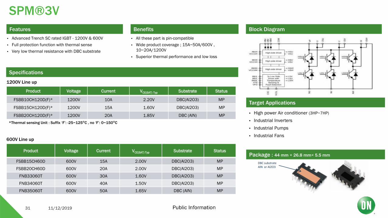
• All these part is pin-compatible
• Wide product coverage ; 15A~50A/600V ,
10~20A/1200V
• Superior thermal performance and low loss
Features Benefits Block Diagram
Specifications
Package : 44 mm × 26.8 mm× 5.5 mm
• Advanced Trench SC rated IGBT - 1200V & 600V
• Full protection function with thermal sense
• Very low thermal resistance with DBC substrate
Product Voltage Current VCE(SAT) Typ Substrate Status
FSBB10CH120D(F)* 1200V 10A 2.20V DBC(Al2O3) MP
FSBB15CH120D(F)* 1200V 15A 1.60V DBC(Al2O3) MP
FSBB20CH120D(F)* 1200V 20A 1.85V DBC (AlN) MP
SPM®3V
Product Voltage Current VCE(SAT) Typ Substrate Status
FSBB15CH60D 600V 15A 2.00V DBC(Al2O3) MP
FSBB20CH60D 600V 20A 2.00V DBC(Al2O3) MP
FNB33060T 600V 30A 1.60V DBC(Al2O3) MP
FNB34060T 600V 40A 1.50V DBC(Al2O3) MP
FNB35060T 600V 50A 1.65V DBC (AlN) MP
1200V Line up
600V Line up
Target Applications
• High power Air conditioner (3HP~7HP)
• Industrial Inverters
• Industrial Pumps
• Industrial Fans
*Thermal sensing Unit : Suffix ‘F’: -25~125°C , no ‘F’: 0~150°C
DBC substrateAlN or Al2O3
11/12/201931
• Single footprint can cover wide product
coverage, specially 1HP~3HP air
conditioner
• Lower EMI, temperature and losses
• Robust protection under fault conditions
Features Benefits Block Diagram
Package & No side dummy ; 39mm × 23mm × 4.5 mm
• Ceramic substrate optimized for cost and thermal
performance
• Wide coverage from 5A to 30A
• Built-in bootstrap diode / NTC on under ceramic
• Stable EMI performance via optimized di/dt, dv/dt
• Support Creepage improved version (FND-) for higher
power air conditioner
Product Voltage Current VCE(SAT) Substrate Status
FNA40560 600V 5A 1.90V Ceramic MP
FNA40860 600V 8A 1.70V Ceramic MP
FNA41060 600V 10A 1.70V Ceramic MP
FNA41560T2 600V 15A 1.60V Ceramic MP
FNC42060F2 600V 20A 1.85V Ceramic MP
FNB43060T2 600V 30A 1.65V Ceramic MP
SPM®45
Specifications
Target Applications
Air conditioner
Compact industrial Inverters
Pumps ,Refrigerator, Washing Machine
No side dummy pin version
Product Voltage Current VCE(SAT) Substrate Status
FND42060F2 600V 20A 1.85V Ceramic MP
FND43060T2 600V 30A 1.65V Ceramic MP
Side dummy for stable assembly
Remove side dummy for wider creepage after mold
FND- version
11/12/201932

11/12/201933
Power Factor Correction (PFCs)
Super Junction MOSFETs
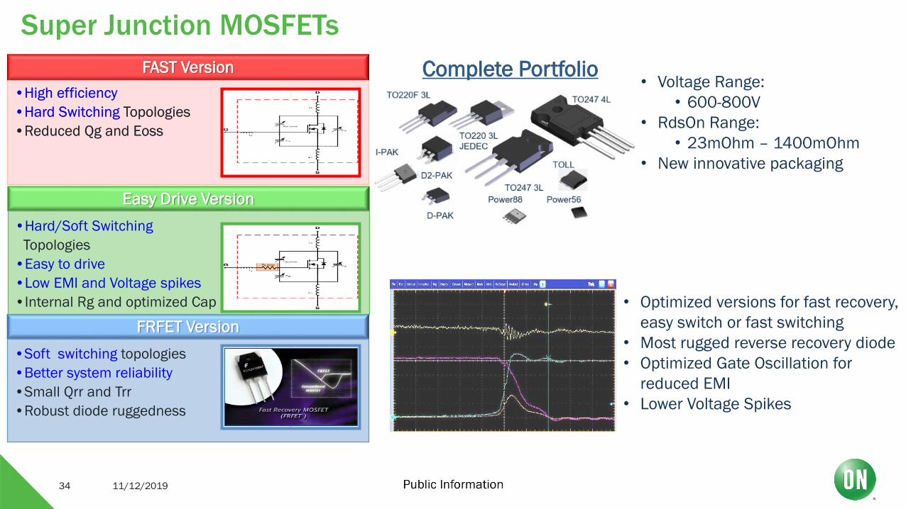
11/12/201934
•High efficiency
•Hard Switching Topologies
•Reduced Qg and Eoss
•High efficiency
•Hard Switching Topologies
•Reduced Qg and Eoss
FAST Version
Easy Drive Version
•Hard/Soft Switching
Topologies
•Easy to drive
•Low EMI and Voltage spikes
•Internal Rg and optimized Cap
•Soft switching topologies
•Better system reliability
•Small Qrr and Trr
•Robust diode ruggedness
FRFET Version
• Voltage Range:
• 600-800V
• RdsOn Range:
• 23mOhm – 1400mOhm
• New innovative packaging
Complete Portfolio
• Optimized versions for fast recovery,
easy switch or fast switching
• Most rugged reverse recovery diode
• Optimized Gate Oscillation for
reduced EMI
• Lower Voltage Spikes
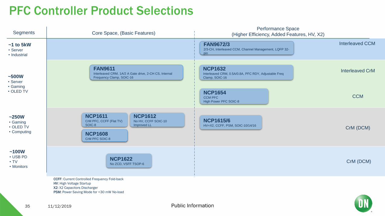
PFC Controller Product Selections
NCP1622 No ZCD, VSFF TSOP-6
NCP1615/6 HV+X2, CCFF, PSM, SOIC-10/14/16
NCP1632Interleaved CRM, 0.5A/0.8A, PFC RDY, Adjustable Freq
Clamp, SOIC-16
FAN9611Interleaved CRM, 1A/2 A Gate drive, 2-CH CS, Internal
Frequency Clamp, SOIC-16
FAN9672/32/3-CH, Interleaved CCM, Channel Management, LQFP 32-
pin
~100W• USB PD
• TV
• Monitors
Segments
~250W• Gaming
• OLED TV
• Computing
~500W• Server
• Gaming
• OLED TV
~1 to 5kW• Server
• Industrial
CrM (DCM)
CCM
Core Space, (Basic Features)Performance Space
(Higher Efficiency, Added Features, HV, X2)
NCP1608 CrM PFC SOIC-8
NCP1612 No HV, CCFF SOIC-10
Improved LL
NCP1611 CrM PFC, CCFF (Flat TV)
SOIC-8
Interleaved CrM
Interleaved CCM
NCP1654 CCM PFC
High Power PFC SOIC-8
CCFF: Current Controlled Frequency Fold-back
HV: High Voltage Startup
X2: X2 Capacitors Discharger
PSM: Power Saving Mode for <30 mW No-load
CrM (DCM)
11/12/201935
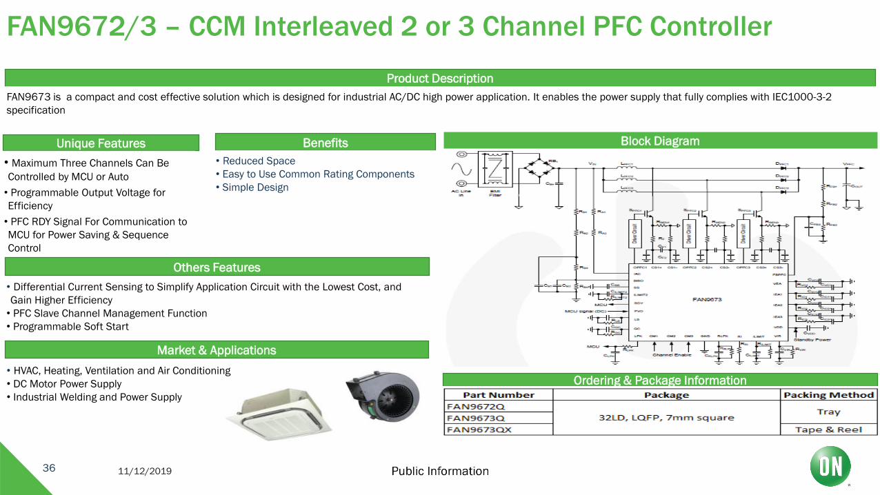
FAN9672/3 – CCM Interleaved 2 or 3 Channel PFC Controller
Market & Applications
Others Features
Ordering & Package Information
Product Description
Unique Features Benefits Block Diagram
FAN9673 is a compact and cost effective solution which is designed for industrial AC/DC high power application. It enables the power supply that fully complies with IEC1000-3-2
specification
• Maximum Three Channels Can Be
Controlled by MCU or Auto
• Programmable Output Voltage for
Efficiency
• PFC RDY Signal For Communication to
MCU for Power Saving & Sequence
Control
• Differential Current Sensing to Simplify Application Circuit with the Lowest Cost, and
Gain Higher Efficiency
• PFC Slave Channel Management Function
• Programmable Soft Start
• Reduced Space
• Easy to Use Common Rating Components
• Simple Design
• HVAC, Heating, Ventilation and Air Conditioning
• DC Motor Power Supply
• Industrial Welding and Power Supply
11/12/201936
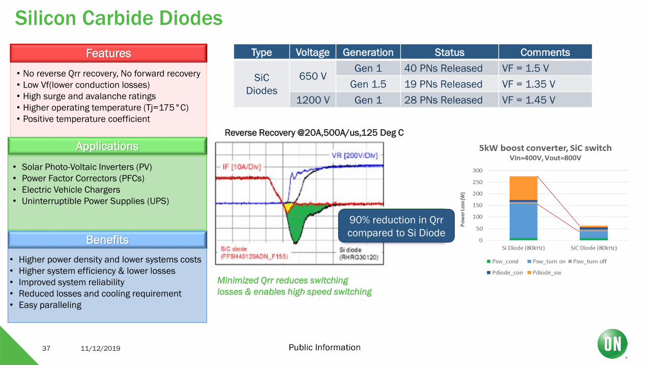
Silicon Carbide Diodes
11/12/201937
Features
• No reverse Qrr recovery, No forward recovery
• Low Vf(lower conduction losses)
• High surge and avalanche ratings
• Higher operating temperature (Tj=175°C)
• Positive temperature coefficient
• Solar Photo-Voltaic Inverters (PV)
• Power Factor Correctors (PFCs)
• Electric Vehicle Chargers
• Uninterruptible Power Supplies (UPS)
Applications
Benefits
• Higher power density and lower systems costs
• Higher system efficiency & lower losses
• Improved system reliability
• Reduced losses and cooling requirement
• Easy paralleling
Type Voltage Generation Status Comments
SiC
Diodes
650 VGen 1 40 PNs Released VF = 1.5 V
Gen 1.5 19 PNs Released VF = 1.35 V
1200 V Gen 1 28 PNs Released VF = 1.45 V
Reverse Recovery @20A,500A/us,125 Deg C
Minimized Qrr reduces switching
losses & enables high speed switching
90% reduction in Qrr
compared to Si Diode
Features Benefits Block Diagram
Specifications
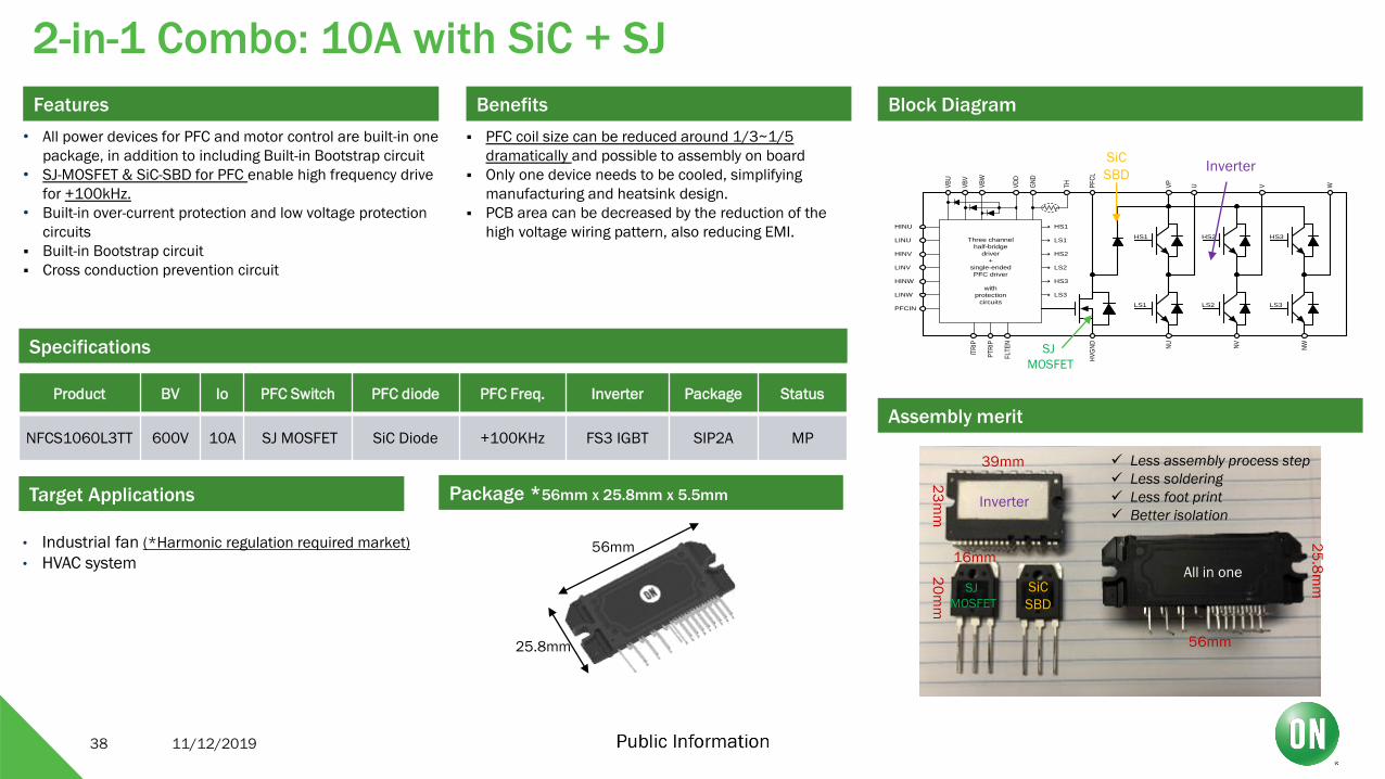
Package *56mm x 25.8mm x 5.5mm
• Industrial fan (*Harmonic regulation required market)
• HVAC system
Target Applications
• All power devices for PFC and motor control are built-in one
package, in addition to including Built-in Bootstrap circuit
• SJ-MOSFET & SiC-SBD for PFC enable high frequency drive
for +100kHz.
• Built-in over-current protection and low voltage protection
circuits
Built-in Bootstrap circuit
Cross conduction prevention circuit
2-in-1 Combo: 10A with SiC + SJ
Assembly merit
56mm
25
.8m
m
23
mm
39mm2
0m
m
16mm
Less assembly process step
Less soldering
Less foot print
Better isolation
56mm
25.8mm
LINW
HINW
LINV
HINV
LINU
HINU
VD
D
GN
D
VB
U
VB
V
VB
W
VP
FLT
EN
PT
RIP
ITR
IP
NWNV
NU
U V W
LS3
HS3
LS2
HS2
LS1
HS1
HS1 HS2 HS3
LS1 LS2 LS3
PF
CL
HV
GN
D
TH
PFCIN
Three channel
half-bridge
driver
+
single-ended
PFC driver
with
protection
circuits
Product BV Io PFC Switch PFC diode PFC Freq. Inverter Package Status
NFCS1060L3TT 600V 10A SJ MOSFET SiC Diode +100KHz FS3 IGBT SIP2A MP
PFC coil size can be reduced around 1/3~1/5
dramatically and possible to assembly on board
Only one device needs to be cooled, simplifying
manufacturing and heatsink design.
PCB area can be decreased by the reduction of the
high voltage wiring pattern, also reducing EMI.
SiC
SBD
Inverter
SJ
MOSFET
All in one
SiC
SBD
SJ
MOSFET
Inverter
11/12/201938

PFC Module Solutions
11/12/201939
Features
• Fully integrated Bridge diode, Power device in single package
• Embedded real NTC on lead frame
• Extreme low thermal resistance
• Variety PFC topology
- Bridgeless PFC
- Single Boost PFC
-2 ch Interleaved PFC
Benefits
• Super easy assembly process
• Easy pcb layout and much lower
inductance
*Megatrend is fast switching for
reduced reactor size
• Higher thermal performance & low Tj
*Discretes have very high Rth
SPM45H SPM3V SPM2V 32
Package
Specifications
Topology Products BVCES IC(Apeak) Shunt
Resistor Package Note
Bridgeless FPDB40PH60B 600 40 Yes SPM3V (Al2O3)
FPDB60PH60B 600 60 Yes SPM3V (AlN)
Single Boost
FBA42060 600 20 No SPM45H
FBA43060 600 30 No SPM45H
FPAB20BH60B 600 20 No SPM3V (Al2O3)
FPAB30BH60B 600 30 No SPM3V (Al2O3)
Interleaved
FPAM30LH60 600 30 No SPM2V 32 (Al2O3)
FPAM50LH60 600 50 No SPM2V 32 (Al2O3)
FPAM50LH60G 600 50 (75) No SPM2V 32 (AlN)
NFL25065L4BT 600 50 No SPM2V 32 (Al2O3)SiC solution
(improving EMI &Thermal )
11/12/201940
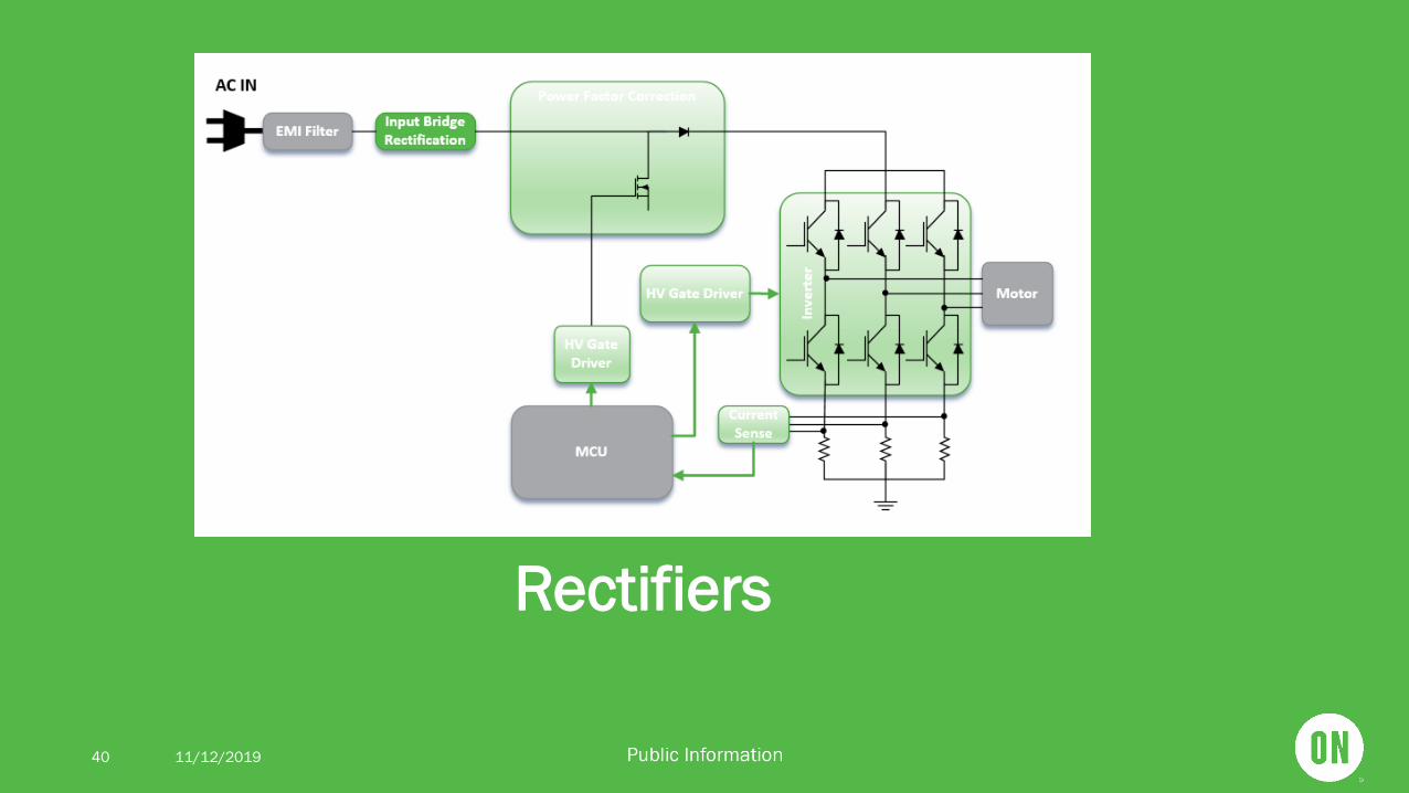
Rectifiers
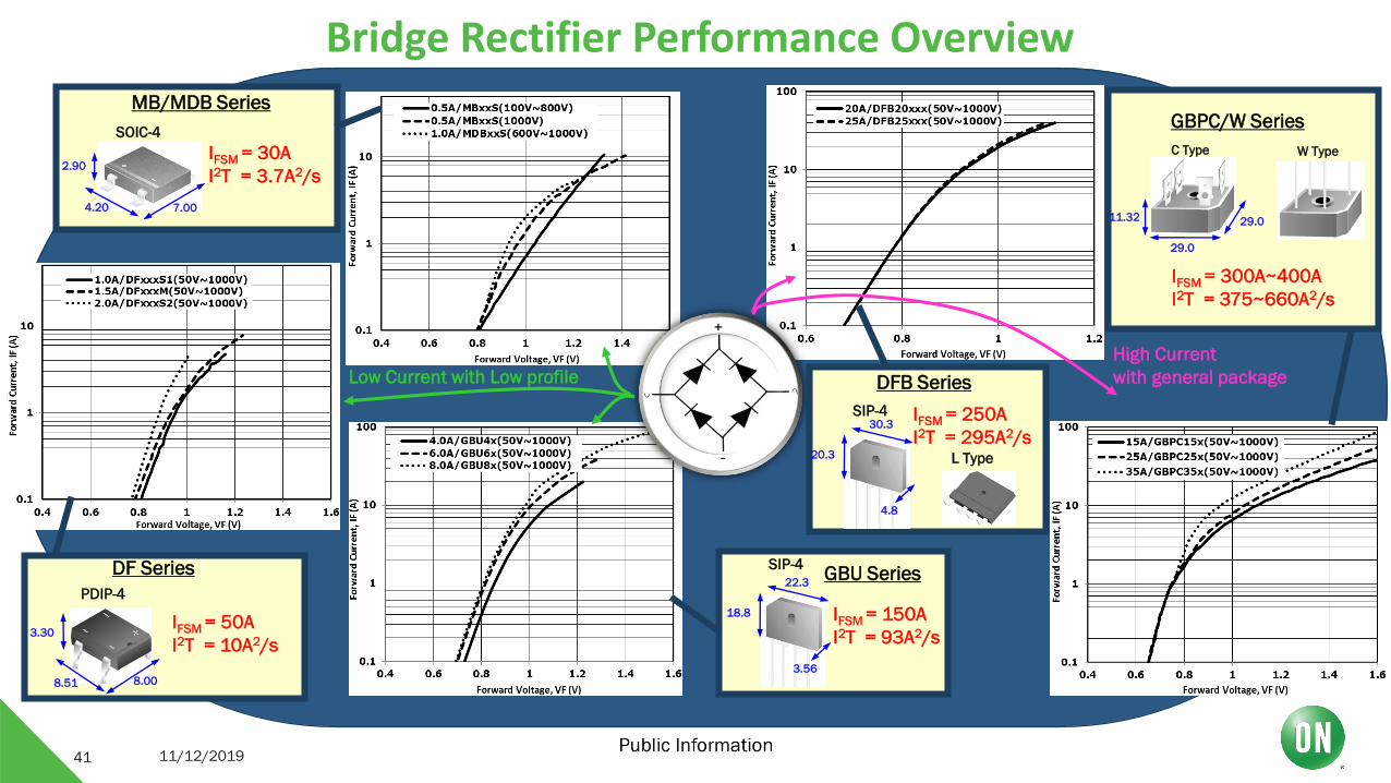
Bridge Rectifier Performance Overview
41
IFSM = 30A
I2T = 3.7A2/s2.90
7.004.20
SOIC-4
MB/MDB Series
8.008.51
3.30
PDIP-4
DF Series
IFSM = 50A
I2T = 10A2/s
18.8
22.3
3.56
SIP-4
IFSM = 150A
I2T = 93A2/s
GBU Series
GBPC/W Series
29.0
29.011.32
C Type W Type
IFSM = 300A~400A
I2T = 375~660A2/s
20.3
30.3
4.8
SIP-4
L Type
DFB Series
IFSM = 250A
I2T = 295A2/s
Low Current with Low profile
High Current
with general package
11/12/2019

Bridge Rectifier - Through Hole & SMD Package
42
Package Topology 50V 100V 200V 400V 600V 800V 1000V
GBPC-4Bridge
Rectifier12A~35A 12A~35A 12A~35A 12A~35A 12A~35A 12A~35A 12A~35A
SIP-4Bridge
Rectifier4A~25A 4A~25A 4A~25A 4A~25A 4A~25A 4A~25A 4A~25A
SOIC-4Bridge
Rectifier0.5A 0.5A 0.5A 0.5A/1A 0.5A/1A 0.5A/1A
PSIP-4Bridge
Rectifier1A~2A 1A~2A 1A~2A 1A~2A 1A~2A 1A~2A 1A~2A
11/12/2019

11/12/201943
Current Sensing

Current Sensing: Reduce Cost, Improve efficiency
11/12/201944
+
-
Supply
Output RSHUNT
LOAD
-
+
NCS21xREF
OUT
IN+
IN-
GN
D
VS
Supply
Supply
Output
RSHUNT
LOAD
+
-
Supply
Output RSHUNT
LOAD
LM358
VOS = 7 mV
(25°C)
To achieve 2% offset error:
350 mV shunt dropTo achieve 2% offset error:
175 mV shunt drop
NCS20081
VOS = 3.5 mV
(25°C)
NCS213
VOS =60 µV
(25°C)
To achieve 2% offset error:
3 mV shunt drop
Reduce voltage drop
across sense resistorSystem efficiency improves
Reduce power
dissipation
Reduce offset voltage Improve accuracy System performance improves
With a 50 mV shunt drop:
14% offset error
With a 50 mV shunt drop:
8% offset error
With a 50 mV shunt drop:
0.07% offset error

11/12/201945
Auxiliary Power
Aux Power

FSL518A/518H/538A/538H – 800 V High Efficient Switchers
11/12/201946
FSL518/538, a highly efficient and rugged 800V solution, provides essential protections from AC line voltage fluctuations and audible noise avoiding feature. 800V
voltage margin eases primary side design with lower voltage 2ndary diode selection helping cost and performance improvement.
Rugged 800V FET with Built-in HV
current source for start up
Fine-tunable Skip Mode Operation
Iso & Non-isolated topology
A with 100 kHz and high IPeak
Easy and Rugged design with enough
voltage margin & Audible noise
avoidance
High Efficiency
Design flexibility
More versatility
Air-conditioning
White Goods
Aux PSU & E-Meters
Line & Slope compensation
Soft-start for low electrical stress
Peak current mode control with Pulse-by-pulse current limit
Frequency hopping for low EMI
Brown In/Out, LOVP, VCC OVP/UVP, OLP, AOCP, TSD
All protections are Auto Restart
PWM
AC
IN
LINE
Drain
GND
VCC
VO
FB
COMP
(a) Isolated opto-coupler feedback (Line detection enable)
PWM
AC
IN
LINE
Drain
GND
VCC
VO
COMP
(b) Non isolated direct feedback (Line detection disable)
FB
PDIP-7
CASE 626APDIP7 MINUS PIN6 GW
CASE 707AA
ZXYTT
L5x8HR
TM
ON
Product Description
Unique Features
Other Features
Market Application
Block Diagram
Packaging Information
Benefits
Part Number RDS-ON Max. (Ohm) Frequency (kHz) Current Limit (mA) Package
FSL518H 8 130 460 DIP/LSOP
FSL518A 8 100 600 DIP/LSOP
FSL538H 4.3 130 660 DIP/LSOP
FSL538A 4.3 100 860 DIP/LSOP

The NCP1342 is a highly integrated quasi-resonant flyback controller capable of controlling rugged and high-performance off-line power supplies. Adjustable maximum frequency clamp
and Rapid Frequency Fold back enable high frequency designs for increased power density. An integrated active X2 capacitor discharge feature also permits low no-load power
consumption below 30 mW
QR Frequency Jittering
Quiet-Skip Technology
Rapid Frequency Foldback
Reduces EMI Signature
Ensures Operation Outside
Audible Range
Enhanced Light Load Efficiency
High voltage startup circuit with Integrated Brownout
Valley Switching Operation with Valley Lockout
Frequency Foldback with 25 kHz Minimum Frequency
VCC Overvoltage Detection
NTC Compatible Fault Pin
Soft-Start for Smooth Start-up Operation
High Drive Capability: -500 mA / +800 mA
Low/Medium USB PD Adapters
Notebook Computer Adapters
Industrial & Server Auxiliary Power
Product Description
Unique Features Benefits Typical Application Schematic
Package information
Other Features
Market & Applications
SOIC-8 and SOIC-9
Pin compatible with NCP1340
NCP1342 - High Frequency QR Controller
11/12/201947

NCP1362 Primary Side PWM Controller
11/12/201948
The NCP1362 is a new quasi−resonant peak current mode control mode controller targeting output power levels from a few watts up to 50 W in a flyback application. It is primary side
regulated for Constant Voltage and Constant Current regulation, achieving excellent line and load regulation of 5% without requiring the typical opto-coupler and voltage reference for
lower cost and improved system reliability. The controller features protections such as Brown-Out, UVP/OVP, OTP, SCP, as well as improved light load efficiency and stand-by
performance.
Product Description
Features
• Quasi- Resonant with Valley Lockout
• Max frequency (80,110,140 KHz and no clamp)
• Frequency Jittering
• LFF and BO on dedicated pin
• Dual Frozen Peak Current
• Constant Voltage & Current PSR < ±5%
• AEC-Q100 Qualified
Benefits
• High Efficiency Operation
• Flexible Design Options
• Improved EMI Signature
• Enables Robust Designs
• Optimize Light Load Efficiency and Stand-by
• Regulated Output without Opto - Coupler
GND
Vcc
CS
0
1
2
3
4
5
0
0
Ac Vout
AcPrim
Sec
Aux
VCC
DRVVsense
0
Block Diagram
Applications
• AC/DC Adapters
• AC/DC Power
• Industrial Auxiliary Power
End Products• Battery Chargers
• Smart Home/ Voice Assistant Devices
• Traction Inverters
PRIMARY SIDE REGULATION (PSR)
Constant Voltage Regulation:
• Eliminates Optocoupler & 3- Terminal programmable shunt
regulator diodes
Design complexity is simplified: highly robust and low cost
• Loss of direct and continuous sensing of output voltage
Vout is built via auxiliary winding Transformer charact.
dependent
Estimated Vout & Iout are refreshed only 1 time per cycle
Stand-by mode:
Deep frequency foldback with min frequency clamp
Constant Current Regulation
• Eliminates Sec. controller and power resistor sensor
Done by measuring Tdemag, Tsw & IPRIM_pk directly on
primary side (Patented)
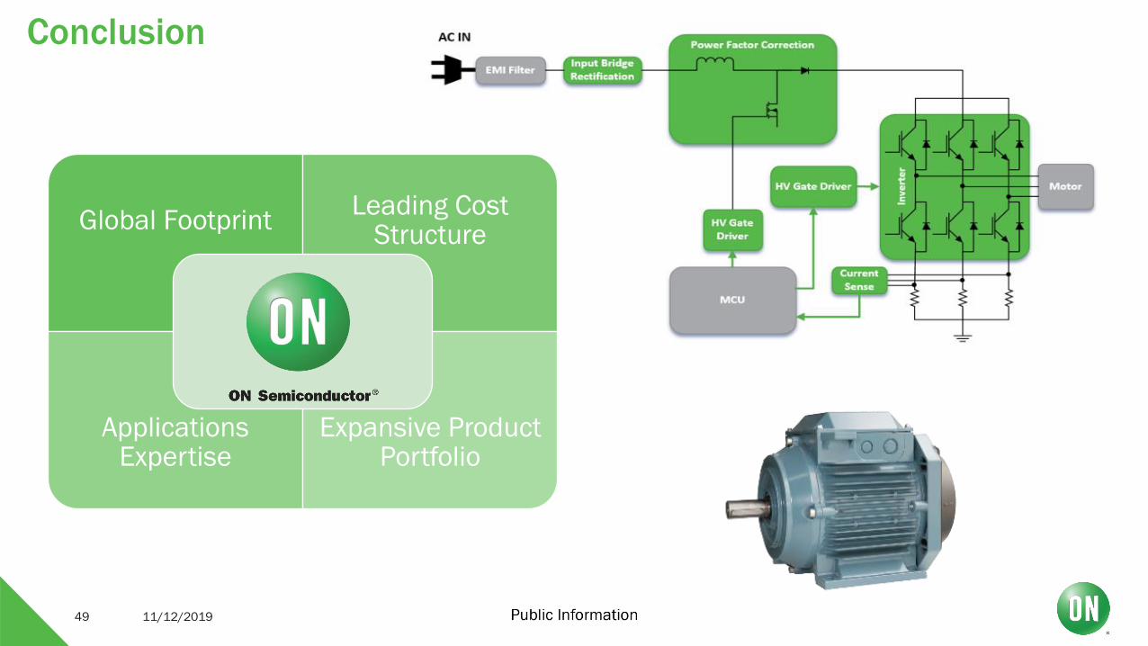
Conclusion
11/12/201949
Global FootprintLeading Cost
Structure
Applications Expertise
Expansive Product Portfolio