Solid State Quantum Optics with a Quantum Dot in a Nano ...
215
Solid State Quantum Optics with a Quantum Dot in a Nano-Photonic Cavity Catherine Louise Phillips A thesis presented for the degree of Doctor of Philosophy Department of Physics and Astronomy University of Sheffield August 2020
-
Upload
khangminh22 -
Category
Documents
-
view
0 -
download
0
Transcript of Solid State Quantum Optics with a Quantum Dot in a Nano ...
Solid State Quantum Optics with a
Quantum Dot in a Nano-Photonic
Cavity
Catherine Louise Phillips
A thesis presented for the degree of
Doctor of Philosophy
Department of Physics and Astronomy
University of Sheffield
August 2020


Abstract
This thesis describes the first and second-order correlation measurements that were
performed on a III-V self-assembled quantum dot weakly coupled to a H1 nano-
photonic crystal cavity. The system has an exceptionally large Purcell factor, which
enables new regimes of light-matter coupling to be explored. In particular, the Purcell
effect enhances the radiative recombination rate by an unprecedented factor, allow-
ing measurements to take advantage of the fast lifetime and broad, transform-limited
linewidth of the excitons excited in the quantum dot. The main results of this thesis
are presented in three chapters, which explore, respectively, the application of the
system as a single-photon source, the interactions between the quantum dot excitons
and their solid-state environment, and the effect of spectral filtering on resonance
fluorescence photon statistics. None of these experiments would have been possible
without the very large Purcell enhancement of the radiative emission from the quan-
tum dot.
In the first set of experiments, the emission properties of the cavity-coupled quantum
dot under π-pulsed resonant excitation were investigated. Hanbury Brown and Twiss
second-order correlation measurements were used to measure the single-photon pu-
rity of the quantum dot emission. Hong-Ou-Mandel measurements were performed
to investigate the indistinguishability of the single-photons produced.
The emission from the cavity-coupled dot was then investigated under continuous
wave excitation. In the second set of experiments, first-order correlation measure-
iii
Abstract
ments were made in conjunction with spectroscopic measurements to investigate the
phonon sideband properties of the quantum dot, both under resonant and slightly
detuned excitation.
In the final set of measurements, spectral filtering was used to alter the photon statis-
tics observed when measuring the resonance fluorescence from the cavity-coupled
quantum dot. Here, the effect of filtering in both the weak and strong driving regimes
was investigated by filtering both above and below the linewidth of the quantum dot.
iv
Acknowledgements
I would like to thank the many people of the LDSD group at Sheffield who have
helped me during the course of my PhD. In particular, my supervisor Mark Fox for
his guidance and encouragement and Alistair Brash for being my lab hero and go-
to question answerer with his encyclopedic paper knowledge. Also within LDSD I
would like to thank Ian Griffiths, Sam Sheldon and Andrew Foster for keeping me
both happy and sane with their fun and interesting company. Thanks also go to Ed
Clarke, Ben Royall and Rikki Coles for their sample growth, fabrication and optimi-
sation, without which this thesis would not have been possible.
Outside of LDSD I would like to thank our theory collaborators: Jake Iles-Smith,
Dara McCutcheon and Ahsan Nazir, for adding mathematical understanding to our
experiment results. Thanks also to Matt Mears, for putting up with me appearing at
his office door since undergrad.
I would also like to thank my friends, especially Dave Brown and Lisa Alhadeff, for
plentiful coffee, conversation and cake. Thanks must also go to my family, for their
endless encouragement and optimism over many years.
v


Publications
Some of the results and figures presented here have appeared in the following publi-
cations:
A. Brash, F. Liu, J. O’Hara, L. M. P. P. Martins, R. J. Coles, C. L. Phillips, B. Royall,
C. Bentham, I. Itskevich, L. R. Wilson, M. S. Skolnick, and A. M. Fox, "Bright and
Coherent On-Chip Single Photons from a Very High Purcell Factor Photonic Crystal
Cavity," in Conference on Lasers and Electro-Optics, OSA Technical Digest (Optical
Society of America, 2017), paper FTu4E.5.
F. Liu, A. J. Brash, J. O’Hara, L. M. P. P. Martins, C. L. Phillips, R. J. Coles, B.
Royall, E. Clarke, C. Bentham, N. Prtljaga, I. E. Itskevich, L. R. Wilson, M. S. Skolnick
and A. M. Fox. “High Purcell factor generation of indistinguishable on-chip single
photons.” Nature Nanotechnology 13, 835-840 (2018).
A. J. Brash, J. Iles-Smith, C. L. Phillips, D. P. S. McCutcheon, J. O’Hara, E.
Clarke, B. Royall, L. R. Wilson, J. Mørk, M. S. Skolnick, A. M. Fox, and A. Nazir.
“Light Scattering from Solid-State Quantum Emitters: Beyond the Atomic Picture.”
Physical Review Letters 123, 167403 (2019).
A. J. Brash, J. Iles-Smith, C. L. Phillips, J. O’Hara, B. Royall, L. R. Wilson, M.
S. Skolnick, A. M. Fox, D. P. S. McCutcheon, E. Clarke, J. Mørk, and A. Nazir,
"Coherent scattering from quantum dots: beyond the atomic picture," in Conference
vii

Publications
on Lasers and Electro-Optics, OSA Technical Digest (Optical Society of America,
2020), paper FW3C.5.
C. L. Phillips, A. J. Brash, D. P. S. McCutcheon, J. Iles-Smith, E. Clarke, B. Roy-
all, M. S. Skolnick, A. M. Fox, and A. Nazir. “Photon Statistics of Filtered Resonance
Fluorescence.” Physical Review Letters 125, 043603 (2020).
viii
Contents
Abstract iii
Acknowledgements v
Publications vii
1 Introduction 1
1.1 Motivation . . . . . . . . . . . . . . . . . . . . . . . . . . . . . . . . . . . 1
1.2 Outline of this work . . . . . . . . . . . . . . . . . . . . . . . . . . . . . . 2
2 Background 5
2.1 Single Photon Sources . . . . . . . . . . . . . . . . . . . . . . . . . . . . 5
2.2 Quantum Dots . . . . . . . . . . . . . . . . . . . . . . . . . . . . . . . . . 6
2.2.1 Quantum Wells, Wires and Dots . . . . . . . . . . . . . . . . . . 6
2.2.2 Self Assembled Quantum Dots . . . . . . . . . . . . . . . . . . . 8
2.2.3 Electronic Structure of QD . . . . . . . . . . . . . . . . . . . . . . 11
2.3 QDs in Applied External Fields . . . . . . . . . . . . . . . . . . . . . . . 16
2.3.1 Quantum-Confined Stark Effect . . . . . . . . . . . . . . . . . . 16
2.3.2 Optical Stark Effect . . . . . . . . . . . . . . . . . . . . . . . . . . 18
2.4 Interactions . . . . . . . . . . . . . . . . . . . . . . . . . . . . . . . . . . 20
2.4.1 Dephasing . . . . . . . . . . . . . . . . . . . . . . . . . . . . . . . 20
2.4.2 Phonons . . . . . . . . . . . . . . . . . . . . . . . . . . . . . . . . 21
2.5 Cavities . . . . . . . . . . . . . . . . . . . . . . . . . . . . . . . . . . . . . 23
2.5.1 Theory . . . . . . . . . . . . . . . . . . . . . . . . . . . . . . . . . 23
ix

Contents
2.5.2 Weak Coupling . . . . . . . . . . . . . . . . . . . . . . . . . . . . 25
2.5.3 Strong Coupling . . . . . . . . . . . . . . . . . . . . . . . . . . . 26
2.5.4 Photonic Crystal Cavities and Waveguides . . . . . . . . . . . . 26
2.5.5 Other Types of Cavities . . . . . . . . . . . . . . . . . . . . . . . 33
3 Experimental Methods 37
3.1 Introduction . . . . . . . . . . . . . . . . . . . . . . . . . . . . . . . . . . 37
3.2 Optical Table . . . . . . . . . . . . . . . . . . . . . . . . . . . . . . . . . . 38
3.3 Cryostat . . . . . . . . . . . . . . . . . . . . . . . . . . . . . . . . . . . . 39
3.4 Resonance Fluorescence . . . . . . . . . . . . . . . . . . . . . . . . . . . 41
3.5 Excitation Lasers . . . . . . . . . . . . . . . . . . . . . . . . . . . . . . . 43
3.5.1 Power Control . . . . . . . . . . . . . . . . . . . . . . . . . . . . . 43
3.5.2 Pulsed: Coherent Mira 900F . . . . . . . . . . . . . . . . . . . . . 44
3.5.3 CW: Toptica DL Pro . . . . . . . . . . . . . . . . . . . . . . . . . 45
3.5.4 CW: M-Squared SOLSTIS . . . . . . . . . . . . . . . . . . . . . . 45
3.5.5 CW: Thorlabs LP808-SA60 . . . . . . . . . . . . . . . . . . . . . . 45
3.5.6 Pulse Shaping . . . . . . . . . . . . . . . . . . . . . . . . . . . . . 46
3.6 Detection Systems . . . . . . . . . . . . . . . . . . . . . . . . . . . . . . . 48
3.7 Calibrating Excitation Power . . . . . . . . . . . . . . . . . . . . . . . . 50
3.7.1 Pulsed Pi power . . . . . . . . . . . . . . . . . . . . . . . . . . . 51
3.7.2 CW Pi Power . . . . . . . . . . . . . . . . . . . . . . . . . . . . . 54
4 Sample 57
4.1 Wafer . . . . . . . . . . . . . . . . . . . . . . . . . . . . . . . . . . . . . . 57
4.2 Design . . . . . . . . . . . . . . . . . . . . . . . . . . . . . . . . . . . . . 59
4.3 Characterisation . . . . . . . . . . . . . . . . . . . . . . . . . . . . . . . . 61
5 Cavity-Coupled QD as a Single-Photon Source 67
5.1 Introduction . . . . . . . . . . . . . . . . . . . . . . . . . . . . . . . . . . 67
5.2 Second-Order Correlation Measurements . . . . . . . . . . . . . . . . . 68
5.2.1 Hanbury Brown and Twiss . . . . . . . . . . . . . . . . . . . . . 69
x

Contents
5.2.2 Hong-Ou-Mandel . . . . . . . . . . . . . . . . . . . . . . . . . . . 72
5.3 Experiments . . . . . . . . . . . . . . . . . . . . . . . . . . . . . . . . . . 79
5.3.1 Method: Hanbury Brown and Twiss . . . . . . . . . . . . . . . . 79
5.3.2 Results: Hanbury Brown and Twiss . . . . . . . . . . . . . . . . 81
5.3.3 Method: Hong-Ou-Mandel . . . . . . . . . . . . . . . . . . . . . 82
5.3.4 Results: Hong-Ou-Mandel . . . . . . . . . . . . . . . . . . . . . 84
5.4 Conclusion . . . . . . . . . . . . . . . . . . . . . . . . . . . . . . . . . . . 93
6 Phonon Effects on QD Emission 95
6.1 Introduction . . . . . . . . . . . . . . . . . . . . . . . . . . . . . . . . . . 95
6.2 Coherent Scattering . . . . . . . . . . . . . . . . . . . . . . . . . . . . . . 96
6.3 First-Order Correlation Measurements . . . . . . . . . . . . . . . . . . . 101
6.3.1 Experimental Method . . . . . . . . . . . . . . . . . . . . . . . . 101
6.3.2 Results and Theory . . . . . . . . . . . . . . . . . . . . . . . . . . 105
6.4 Effect of Excitation Power on the Phonon Sideband . . . . . . . . . . . 111
6.4.1 Experimental Method . . . . . . . . . . . . . . . . . . . . . . . . 111
6.4.2 Results and Theory . . . . . . . . . . . . . . . . . . . . . . . . . . 113
6.5 Phonon Effects in Detuned Coherent Scattering . . . . . . . . . . . . . . 115
6.5.1 Experimental Method . . . . . . . . . . . . . . . . . . . . . . . . 116
6.5.2 Results and Theory . . . . . . . . . . . . . . . . . . . . . . . . . . 117
6.6 Conclusion . . . . . . . . . . . . . . . . . . . . . . . . . . . . . . . . . . . 124
7 Spectral Filtering Effects on QD Resonance Fluorescence 127
7.1 Introduction . . . . . . . . . . . . . . . . . . . . . . . . . . . . . . . . . . 127
7.2 Filtering QD emission . . . . . . . . . . . . . . . . . . . . . . . . . . . . 128
7.3 Weak Driving Regime . . . . . . . . . . . . . . . . . . . . . . . . . . . . 136
7.3.1 Experimental Method . . . . . . . . . . . . . . . . . . . . . . . . 138
7.3.2 Results and Theory . . . . . . . . . . . . . . . . . . . . . . . . . . 138
7.4 Strong Driving - Mollow Triplet Regime . . . . . . . . . . . . . . . . . . 145
7.4.1 Power Dependence at Γ = 0.29γ . . . . . . . . . . . . . . . . . . 147
xi

Contents
7.4.2 Filter Bandwidth Dependence at ΩR = 2γ . . . . . . . . . . . . . 150
7.5 Conclusion . . . . . . . . . . . . . . . . . . . . . . . . . . . . . . . . . . . 153
8 Summary and Future Work 157
8.1 Summary . . . . . . . . . . . . . . . . . . . . . . . . . . . . . . . . . . . . 157
8.1.1 Cavity Coupled QD as a Single-Photon Source . . . . . . . . . . 157
8.1.2 Phonon Effects on QD Emission . . . . . . . . . . . . . . . . . . 158
8.1.3 Spectral Filtering Effects on QD Resonance Fluorescence . . . . 158
8.2 Future Work for the QD in a H1 Cavity . . . . . . . . . . . . . . . . . . 159
8.2.1 Improving the Excitation Pulse Shaping . . . . . . . . . . . . . . 159
8.2.2 Improving the H1 PhCC Sample . . . . . . . . . . . . . . . . . . 162
8.2.3 Homodyne Scheme for Measuring Antibunching and a Sub-
natural Linewidth . . . . . . . . . . . . . . . . . . . . . . . . . . 163
8.3 Future Work - Related Areas . . . . . . . . . . . . . . . . . . . . . . . . . 164
8.3.1 Telecom C-Band QDs . . . . . . . . . . . . . . . . . . . . . . . . . 164
8.3.2 QD Spin in a Cavity for Photonic Cluster State Generation . . . 165
8.3.3 QD Registration . . . . . . . . . . . . . . . . . . . . . . . . . . . . 166
Acronyms 169
xii

1 Introduction
1.1 Motivation
Optical quantum technologies use the quantum states of light to process and transmit
information through the manipulation of quantum bits (qubits). Research into opti-
cal quantum technologies mainly falls into three categories: quantum communication
[1, 2], quantum computation [3–5] and quantum metrology [6, 7]. The production of
single-photon states of light are used as a building block in all three areas.
Quantum communication is the transfer of information between two parties using
the quantum properties of light. This can be extended to quantum cryptography
which uses the principles of quantum measurement, for example the no-cloning the-
orem that prevents the cloning of arbitrary unknown quantum states [8], to enable
secure communication and detect the presence of eavesdroppers [1]. Control over
the number of photons within the communication pulses is required for quantum
cryptography, with single-photon Fock states being the basis on which many proto-
cols are designed [1].
Quantum computers use qubits to perform operations. Quantum computing systems
are designed to out-perform classical computing systems for solving certain mathe-
matical problems [9–11] and for simulating quantum systems [3, 12]. For a system
to have a quantum computing architecture it must meet the DiVincenzo criteria [13].
Single-photons are a possible source of qubits as they are easy to manipulate and al-
low encoding through different degrees of freedom including path, polarisation and
1

1 Introduction
time bin [14]. One scheme for quantum computing is referred to as linear optical
quantum computing. Here, single photons are used along with beam splitters, phase
shifters and single photon detectors [4].
Quantum metrology uses quantum processes such as entanglement to measure with
a higher statistical precision than is possible using classical techniques [7]. Single-
photon states can be used as measurement probes in these schemes [15, 16].
All of these optical quantum technologies require a source of controllable quantum
photon states, in-particularly the ability to create single photons. Semiconductor
quantum dots (QDs) are a solid-state system that can be used as a source of single-
photons [17–19]. QDs can be incorporated into cavity structures to enhance their
emission properties. One of the solid-state systems that can be used to achieve QD
single-photon sources with enhanced emission properties are nano-photonic crystal
cavities and waveguides [20, 21]. These structures can also be used for the routing
and manipulation of the photons produced [22–24], making them a potential build-
ing block for “on-chip” quantum computing [25, 26] .
In this thesis, the properties of a QD that is weakly coupled to a H1 photonic crystal
cavity but with an extremely large Purcell factor of 43±2 are investigated. This cou-
pling enables a Purcell-shortened radiative lifetime of 22.7± 0.9 ps under resonant
excitation of the QD’s neutral exciton, a property that is exploited throughout this
thesis, allowing the exploration of regimes that otherwise would not be possible.
1.2 Outline of this work
This thesis looks at the properties of a cavity-coupled self-assembled quantum dot
(SAQD), its single-photon properties, interaction with its solid state environment and
how the photon statistics of the source can be manipulated.
2

1.2 Outline of this work
In Chapter 2 an introduction to the concepts used throughout this thesis are pre-
sented. This background includes an introduction to the growth and properties of
SAQDs, the effects of the environment on QD emission as well as the effects of opti-
cal cavities. Chapter 3 describes the basic experimental methods used throughout the
experimental chapters. This includes a description of the resonance fluorescence (RF)
set-up, the bath cryostat system, the excitation lasers and detection systems used.
Along with details of the calibration methods used for defining the excitation power
related to the state of the QD system. Chapter 4 contains the details of the QD sample
used for the measurements in this thesis, including the composition of the semicon-
ductor wafer and the fabrication method of the photonic crystal cavity structure. This
chapter also includes a summary of the characterisation work that has previously
been performed on the sample by other researchers.
In Chapter 5 the single-photon properties of the cavity-coupled QD are investigated
under resonant pulsed excitation. Hanbury Brown and Twiss second-order corre-
lation measurements are used to measure the antibunching, and Hong-Ou-Mandel
second-order correlation measurements are performed to find the indistinguishabil-
ity of the single-photons produced. The effect of the excitation pulse length compared
to the QD lifetime is investigated under both measurement schemes along with an
additional investigation into the effect of pulse separation on the photon indistin-
guishability.
In Chapter 6 the effect of the QD’s environment on its coherently scattered emission
is investigated to provide insight into the phonon interactions present in the system.
First-order correlation measurements are used to investigate the phonon relaxation
timescale. Spectroscopic measurements are used to investigate the effect of excitation
power on the phonon properties. The effect of laser detuning on the coherent scatter-
ing is also investigated through first-order correlation measurements.
3

1 Introduction
In Chapter 7 the effect of spectrally filtering the collected RF emission on the mea-
sured photon statistics is investigated. By using filters of various bandwidths both
above and below the natural linewidth of the QD a comprehensive picture of the ef-
fect on the photon statistics can be produced, including investigation in both the low
power Rayleigh scattering regime and high power Mollow triplet regime.
Chapter 8 contains a summary of the experimental chapters and some possible di-
rections for future work involving QDs in high Purcell factor cavities.
4

2 Background
2.1 Single Photon Sources
As was described in Chapter 1, single photon sources are a building block for many
optical quantum technologies including optical quantum computing [3–5] and quan-
tum cryptography [1, 2]. However, single-photons are also desirable for many other
quantum-optics applications including boson sampling [27, 28], single-photon fast
optical switching [29], photonic cluster state generation [30] and a quantum internet
[2, 31, 32] to mention just a few.
All of the above uses for single-photons require certain properties from their single-
photon source (SPS). They need to be bright, pure, on-demand and indistinguishable
[33, 34]. For a SPS to be bright it is optimal for it to be excited preferentially to an
optically-bright state with a short emitter lifetime. This allows the emitter to be re-
excited at a fast rate and so produce photons with a high repetition rate. To be bright,
measurements of SPS also require a high collection efficiency [35–37]. The purity of a
SPS involves measuring the photon statistics of the emission. Purity is defined as the
probability that the output of the SPS comprises single photons, rather than multi-
photon emission. On-demand is the probability that an input will create the desired
output, i.e. that every excitation event results in a single photon being emitted rather
than no emission or multi-photon emission. Indistinguishability, also known as visi-
bility, is the probability that the single photons emitted are identical to each other.
In this thesis a self-assembled quantum dot in a nano-photonic crystal cavity is in-
vestigated as a single-photon source.
5

2 Background
2.2 Quantum Dots
In this section an introduction to quantum dots is given, including the formation
mechanism of self-assembled quantum dots and their electronic structure.
2.2.1 Quantum Wells, Wires and Dots
Electron waves in semiconductors can be characterised by their de Broglie wave-
length:
λD ∼h√
m∗ekBT, (2.1)
where h is Plank’s constant, m∗e is the effective mass of the electron, kB is the Boltz-
mann constant and T is the temperature. In a bulk semiconductor crystal, where all
of the dimensions (x,y and z) are longer than the λD of the electron it is free to travel in
any dimension. However, it is possible to create structures where some or all of the
dimensions are comparable to λD. This quantises the electron’s motion within those
dimensions, confining its travel.
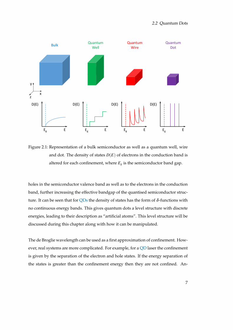
Figure 2.1 shows different confinement shapes where one or more dimensions have
been reduced to be comparable to λD. A system with confinement in one dimension
(e.g. x-direction) allows the electron to travel freely in the other two dimensions. This
system is known as a quantum well. Confinement in two dimensions (e.g. x and
y-directions) allows free movement in one dimension and is known as a quantum
wire. A quantum dot (QD) confines the electron in all three dimensions. It therefore
acts as a three-dimensional potential well with quantised electron motion in all three
directions.
Figure 2.1 also shows how the confinement shape of the structure affects the den-
sity of states D(E) function of electrons in the conduction band of a semiconductor.
Here, Eg is the semiconductor bandgap. With each successive degree of confinement,
the band edge is shifted by the quantum confinement energy. This applies to the
6
2.2 Quantum Dots
D(E) D(E) D(E) D(E)
E E E EEg Eg Eg Eg
BulkQuantum
WellQuantum
WireQuantum
Dot
x
y
z
Figure 2.1: Representation of a bulk semiconductor as well as a quantum well, wire
and dot. The density of states D(E) of electrons in the conduction band is
altered for each confinement, where Eg is the semiconductor band gap.
holes in the semiconductor valence band as well as to the electrons in the conduction
band, further increasing the effective bandgap of the quantised semiconductor struc-
ture. It can be seen that for QDs the density of states has the form of δ -functions with
no continuous energy bands. This gives quantum dots a level structure with discrete
energies, leading to their description as “artificial atoms”. This level structure will be
discussed during this chapter along with how it can be manipulated.
The de Broglie wavelength can be used as a first approximation of confinement. How-
ever, real systems are more complicated. For example, for a QD laser the confinement
is given by the separation of the electron and hole states. If the energy separation of
the states is greater than the confinement energy then they are not confined. An-
7

2 Background
other way to model whether a particle or quasi-particle is confined by a QD is to
use the Bohr radius. Significant confinement requires the Bohr radius of the quasi-
particle to be comparable to the dimensions of the QD. For example, an exciton is a
quasi-particle formed by an electron and hole that are a bound pair through Coulomb
interaction. The Bohr radius (r) is given by:
r = ε
(mµ
)a0, (2.2)
where ε is the dielectric constant, given by the square of the refractive index (n), a0 is
the Bohr radius, m is the mass of the electron and µ is the reduced mass of the exciton.
The reduced mass is given by:
µ =memhh
me +mhh, (2.3)
where me and mhh are the effective masses of the electron and hole, respectively. For
GaAs, n= 3.45, me = 0.067m and mhh = 0.51m. When combined with a0 = 5.29x10⁻¹¹ m
and m = 9.11x10⁻³¹ kg the Bohr radius of the exciton is found to be ∼ 11 nm. There-
fore, a QD requires a radius on the order of 11 nm to show exciton confinement. Ex-
citons in QDs can be used as a basis for a single-photon source and will be discussed
in more detail in Section 2.2.3.
2.2.2 Self Assembled Quantum Dots
Quantum dots come in many forms. The first QDs where the quantum confinement
of carriers was observed were microscopic crystals of CuCl grown within a glass ma-
trix [38]. Since then, other methods of creating QDs including colloidal [39], droplet
epitaxy [40] and self-assembled Stranski-Krastanow growth [41, 42] have emerged.
This thesis will focus on self-assembled quantum dots (SAQDs) grown using the
“bottom-up” Stranski-Krastanow regime method [42].
Stranski-Krastanow QDs
Stranski-Krastanow (SK) QDs are self-organising and are commonly known as self-
assembled quantum dots (SAQDs). The growth method of SK QDs is shown in Fig-
ure 2.2. QD growth in the SK regime involves deposition of a thin, two-dimensional
8

2.2 Quantum Dots
Figure 2.2: Growth of self-assembled QDs in the Stranski-Krastanow regime: (a) InAs
deposited on a GaAs substrate by MBE. (b) A thin layer of InAs builds up
on the GaAs. The strain in the InAs layer is high due to the difference in
unit cell size between the GaAs and InAs. (c) When the InAs reaches a crit-
ical thickness it begins to form 3D “islands” on the 2D substrate to reduce
the total energy of the InAs. These islands are QDs. A thin “wetting”
layer remains between the QDs and the GaAs substrate. (d) To prevent
oxidation the QDs are capped with GaAs.
(2D), layer of semiconductor crystal by molecular beam epitaxy (MBE) or metal-
organic vapour-phase epitaxy (MOVPE) (also known as metal-organic chemical vapour
deposition (MOCVD)) [43–46]. This layer is deposited on top of a semiconductor
crystal substrate which has a different lattice constant. For example, when growing
InAs on GaAs (Fig. 2.2(a-b)) there is a 7% difference in lattice constant [47]. When the
InAs layer is thin, its lattice constant compresses to match that of the GaAs. As the
deposition continues, layer by layer, there is a build-up in the strain InAs due to the
lattice compression [48]. When the top layer reaches the critical thickness, the crystal
surface splits into microscopic “islands” (QDs), transitioning from a 2D to a 3D struc-
ture, in order to reduce the strain in the growth layer (Fig. 2.2(c)). The increase in the
surface energy caused by the dislocations is smaller than the reduction to the internal
strain that this process generates. A thin “wetting” layer remains between the QDs
and the growth substrate.
9

2 Background
QDs grown in the SK regime are commonly used in quantum optics measurements as
they can be incorporated into structures by overgrowing (capping) the strained layer
with a different semiconductor (Fig. 2.2(d)). As well as preventing oxidation, capping
enables the production of integrated photonic nanostructures through the production
of diodes and optical cavities above and below the QD layer. When the cap is grown,
mixing can occur between the cap and the QDs. For example, growing GaAs on InAs
QDs can lead to InGaAs QDs. QDs grown using this method have also been shown
to have good optical properties, e.g. narrow linewidths of the zero phonon line (ZPL)
[49], which, when combined with photonic structures, makes them ideal candidates
for qubits and single-photon sources.
QD Positioning
SAQDs grown in the SK regime are scattered randomly on the semiconductor sub-
strate. However, photonic nanostructures, some of which are discussed in Section 2.5,
require precise placement of the structure around the QD. Therefore, many photonic
devices are fabricated per QD wafer, to increase the probability that a randomly po-
sitioned SAQD will be optimally aligned. This can lead to a large number of “waste”
structures that do not contain optimally positioned QDs being produced and so time
needs to be spent on characterising the structures before measurements can be per-
formed.
One possible solution to this is through the site-controlled growth of QDs. There
are many ways of trying to control the lateral position of QD nucleation [50]. For
example, one method involves the patterning of the semiconductor substrate surface
with differently shaped pits including pyramidal [51, 52] and round pits [53–55] to
encourage the nucleation of QDs in predefined positions.
Another possible solution is the registration of QDs before the photonic structures
are fabricated. One way to register the position and emission wavelength of QDs in-
10

2.2 Quantum Dots
volves using scanning microscopic photoluminescence (µ-PL) spectroscopy [56] and
mapping the emission against markers patterned on the sample’s surface. Another
method involves an imaging set-up where the QDs in the sample are excited with
above-band excitation using LED illumination and the QD emission is imaged on a
CCD camera. Filters used between the sample and the camera can be used to define
the emission bandwidth of the QDs that are mapped. Again, markers patterned on
the sample surface are used to map the positions of the QD emission [57–59].
2.2.3 Electronic Structure of QD
Band Structure
At 4.2 K the bandgap (Eg) of GaAs is 1.52 eV [60]. When introducing an InGaAs QD
to the bulk semiconductor the reduced Eg of the InGaAs leads to a 3D confinement of
carriers. The Eg of the QD depends on the ratio of Gallium to Indium present, with
higher proportions of Indium leading to a smaller Eg [61]. Figure 2.3 shows the mod-
ification to the semiconductor bandgap caused by the presence of InGaAs QD within
bulk GaAs. The energy difference between the s-shell and p-shell of the electrons
in the conduction band is greater than that of the hole bands, as is the offset of the
conduction and valence bands [48]. The confinement energy of the carriers is tem-
perature dependent. At 4.2 K, the thermal energy of the carriers (kBT ) is ∼ 0.36 meV,
much smaller than the spacing of the electron and hole energy levels. At room tem-
perature, kBT is ∼ 25 meV, and the energy levels are therefore effectively no longer
discrete.
The bandstructure of a III-V semiconductor is shown in Figure 2.4. It shows that
the conduction band (purple) is inhabited by electrons and the valence band (blue)
by holes but whereas the conduction band contains only one band, the valence band
contains three. To explain this difference the total angular momentum of the electrons
and holes has to be considered.
11

2 Background
Figure 2.3: Bandgap diagram of an InGaAs QD within bulk GaAs. At 4.2 K the Eg
of GaAs is 1.52 eV [60]. The Eg of the InGaAs QD is smaller and its exact
value depends on the ratio of Ga:In within the QD, the higher the propor-
tion of In the smaller the value of Eg [61]. The energy difference between
the s-shell and p-shell for the electrons in the conduction band is larger
than the energy difference of the hole shells in the valence band, as is the
offset of the bands [48].
The total angular momentum (J) is given by:
J = L+S, (2.4)
where L is the orbital angular momentum and S is the spin angular momentum. The
eigen values of the angular momentum (J) are given by |l− s| ≤ j ≤ l + s [62]. The
conduction band of a bulk III-V semiconductor has similar properties to the s-shell
of atomic physics. This means that it has an orbital angular momentum of l = 0. As
electrons are elementary particles and fermions, they have a spin angular momentum
s of 1/2. Looking at the total angular momentum in the z-axis leads to Jz = ±1/2 to
allow for the two possible spin configurations of the electron, spin up and spin down.
12

2.2 Quantum Dots
hh
lh
so
e
Eg Direct bandgap
Δ
k = 0
k
E
Conduction band
Valence band
Se,z = ± 1/2
Jh,z = ± 3/2
Jh,z = ± 1/2
Jh,z = ± 1/2
J = 3/2
J = 1/2
J = 1/2
Figure 2.4: Band structure of a typical, direct bandgap, bulk III-V semiconductor
showing both the conduction and valence bands. Electrons are found in
the conduction band (purple) which contains one band and is separated
from the valence band by the bandgap (Eg). The holes in the valence band
(blue) are split into three bands, the heavy hole band (hh), light hole band
(lh) and split-off band (so). The so band is split from the hh and lh bands
by the spin-orbit splitting ∆. At k = 0 the hh and lh bands are degenerate
but split with increasing k.
The valence band of III-V semiconductors has predominantly p-shell properties with
some d-shell properties. The p-shell properties lead to an orbital angular momentum
of l = 1. Combining this with the spin of the holes (s = 1/2) means the valence band
is split into two states with j = 3/2 and j = 1/2. Again, these states can be projected
into the z-axis creating one state with Jz =−3/2,−1/2,1/2,3/2 and a second state with
Jz =−1/2,1/2. The two states are separated by an energy difference of ∆ which is the
13

2 Background
spin-orbit splitting. For GaAs ∆ ≈ 0.3 eV [62]. The J = 3/2 state is further split into
two bands, one being the heavy hole (hh) band with Jz =±3/2 and the light hole (lh)
band with Jz = ±1/2. As is shown in Figure 2.4 for a bulk semiconductor the light
hole and heavy hole bands are degenerate at k=0. However, for QDs that lack sym-
metry, for example SAQDs, strain removes the degeneracy, leading to a splitting of
the bands of ∼ 30-300 meV [63, 64] with the light hole band being found at higher
energies. This splitting of the hole bands means that the light holes can be neglected
when modelling the lowest energy states of the QD, giving QDs a lowest energy state
with the properties of the s-shell electron and heavy holes.
Excitons
Excitons are created when an electron is excited out of the valence band into the
conduction band, leaving a positively charged hole quasi-particle behind. If the ex-
citation energy is small, then the electron remains confined within the QD and the
two oppositely charged particles can become a bound electron-hole pair through the
Coulomb interaction. This quasi-particle is known as an exciton (X). As the exciton
consists of a negatively charged electron and positive hole then its overall charge is
neutral. Recombination of the electron and hole results in the emission of a photon.
One property of excitons is a doublet formed in the emission spectrum where each
peak of the doublet has the opposite linear polarisation. This is termed fine-structure
splitting (FSS) and is undesirable for photon entanglement experiments [65, 66]. The
origin of the FSS can be found in the angular momentum of the electron and hole that
the exciton comprises. The angular momentum of the exciton states is described in
the z-direction by:
m = Se,z + Jh,z =±1,±2. (2.5)
Here the electron spin is Se,z =±1/2 and the heavy hole spin is Jh,z =±3/2. The m=±1
states are optically active, unlike the m = ±2 states which are referred to as dark ex-
citons. Fine-structure splitting (FSS) occurs in asymmetric QDs. The asymmetry of
the QD means that the confinement potential of the electron and hole within the QD
14

2.2 Quantum Dots
0 5 0 1 0 0 1 5 0 2 0 0 2 5 0 3 0 0 3 5 09 1 5 . 4 3 0
9 1 5 . 4 3 5
9 1 5 . 4 4 0
9 1 5 . 4 4 5
9 1 5 . 4 5 0
9 1 5 . 4 5 5 D a t a F i t t i n g
Peak
Wav
eleng
th (nm
)
P o l a r i s e r A n g l e ( d e g r e e s )
Figure 2.5: An example of the fine-structure splitting measurement for a neutral ex-
citon. The FSS is measured by rotating a linear polariser in the collection
path and recording the intensity of the neutral exciton peak. Here, the
QD used is the sample that is described in Chapter 4, showing a FSS of
0.013 nm (19 µeV).
plane is not symmetric and results in an exchange energy splitting of the |m| = 1 ex-
citon states creating a doublet. The split states are linear combinations of the m =±1
exciton states and this mixing results in linear polarisation of the QD emission from
each state [67]. The two components of the FSS doublet are polarised along the prin-
ciple axes of the QD potential [68].
FSS can be resolved by using linearly polarised detection as the excitons emit pho-
tons with orthogonal polarisation. An example of this measurement is shown in Fig-
ure 2.5. Here, a QD is excited above band and spectra of the exciton emission are
taken as a function of the collection polarisation angle. When the wavelength of the
exciton emission is plotted against the polarisation angle, the splitting of the doublet
15

2 Background
is seen as an oscillation of the emission wavelength. The amplitude of the oscillation
gives the FSS, in Figure 2.5 the splitting is 0.013 nm (19 µeV). The example used here
is the FSS measurement for the QD sample used in this thesis, the sample will be dis-
cussed in more detail in Chapter 4. FSS can be used to show the charge characteristics
of the QD transitions. The neutral exciton shows FSS whereas the positive and nega-
tive trions, quasi-particles comprising two holes and an electron or two electrons and
a hole respectively, do not show FSS.
Different methods have been used to try to reduce the FSS seen in QDs, including
through the use of applied electric fields [69], strain [70], magnetic fields [65] and lo-
calised annealing [71]. QDs grown in nanowires have also been used to reduce FSS
due to their high symmetry [72].
2.3 QDs in Applied External Fields
Experimentally, different external fields can be applied to QDs and are used to change
their emission properties and behaviour. This section will discuss the effects of ap-
plying electrical and optical fields.
2.3.1 Quantum-Confined Stark Effect
The wavelength of photons emitted by the exciton depends on the energy difference
between the electron and hole when they recombine. The energy difference can be
modified by applying a direct current (DC) electric field across the QD, modifying the
band structure. An illustration of this modification is shown in Figure 2.6. The exci-
ton is still confined to the QD due to the reduced band gap of the InGaAs compared
to that of the GaAs. The applied DC field modifies the shape of the bands, altering
the band structure which brings the electron and hole closer together in energy and
in doing so reduces the energy of the photon that is emitted when the exciton re-
combines. This modification is known as the quantum-confined Stark effect (QCSE).
16

2.3 QDs in Applied External Fields
Figure 2.6: An illustration of the band structure of a QD: (a) No electric field is ap-
plied to the QD, giving an exciton emission energy of Eg0. (b) Application
of a DC electric field to the QD modifies the band structure, causing a
reduction in the energy of the exciton from Eg0 to Eg1 and so shifting its
emission wavelength.
The shift of the emission energy (∆EQCSE) is defined as a function of the applied DC
electric field and is described by:
∆EQCSE = pF +βF2, (2.6)
where F is the strength of the applied DC field, p is the electric dipole moment of the
QD and β is the polarisability [73, 74].
When a high DC electric field is applied the carriers can be swept out of the QD, pre-
venting the exciton from forming. Embedding the QDs within a quantum well creates
potential barriers that prevent carriers from tunnelling out when a high electric field
is applied. This can increase the potential tuning range of the QD emission through
the QCSE. For example, embedding InGaAs QDs within an AlGaAs/GaAs/AlGaAs
quantum well has shown a tuning range for the exciton emission energy of 25 meV
[75]. In the absence of barriers, the tuning range of the emission is limited to a few
hundred picometers [76].
17

2 Background
QCSE tuning of QDs has numerous practical uses. These include tuning QDs into
resonance with cavity structures, moving QDs into and out of resonance with exci-
tation lasers, which is used to evaluate the emission signal to the background laser,
and to perform differential measurements. The QCSE can also be used to tune QDs
into resonance with each other. Tuning multiple QDs into resonance within the
same nanophotonic structure requires split contact diodes where different DC field
strengths can be applied to different parts of the device. These methods make use of
the large energy shift possible when using vertical DC electric fields as the orienta-
tion of the QD dipole is in the z growth direction. Vertical DC fields can be applied
through the use of diode structures where doped semiconductor layers are grown
above and below the QD layer. The QCSE can also be utilised when applying lateral
DC electric fields to the QD. One use for lateral DC fields is for tuning QD FSS. The
effect of lateral fields on the FSS has been shown for QDs that are not built into pho-
tonic structures [69, 77, 78]. Work on applying lateral fields to photonic structures
such as waveguides has also been progressing [79].
2.3.2 Optical Stark Effect
An alternating current (AC) electric field can also be applied to QDs, for example
through the oscillating electric field of a laser. When an atom is excited with a high
intensity laser, at resonance or close to resonance with its transition, then the “bare”
states of the atom are “dressed” by the oscillating optical field. The dressed states
are split by the Rabi frequency (ΩR). A QD can be described as a “artificial-atom”
due to the quantisation of its states and so QDs also experience splitting in the strong
driving regime. This behaviour is known as the AC Stark effect [47, 80].
QDs are often modelled as a two-level emitter (TLE). For a TLE, the strong driving
regime occurs when the strong resonant excitation has a Rabi frequency larger than
the natural linewidth of the exciton (Ω2R 1
T1T2), where T1 is the emitter lifetime and
18

2.3 QDs in Applied External Fields
Figure 2.7: An illustration of the dressing of the “bare” states of the exciton transition
through the application of a high power laser field. The “dressed” states
lead to four possible transitions of which two are degenerate, leading to
the three peaks observed in a Mollow triplet spectra. Here, ΩR is the Rabi
frequency, T1 is the emitter lifetime, T2 is the coherence time and hωL is the
transition energy.
T2 is the coherence time, both of which are discussed in more detail in Section 2.4.1.
Here, the two-level picture breaks down and is replaced by a dressed states approach
[81], as shown in Figure 2.7. Two of the transitions (green) are degenerate, leading to
the production of the Mollow triplet. The central peak (green) is termed the Rayleigh
peak and the two sidebands (orange/blue) are separated from the central peak by
±ΩR. If the driving laser is not resonant with the TLE then ΩR is modified to become
the generalised Rabi frequency: Ω =√
Ω20 +∆2, where Ω0 is the bare Rabi frequency
and ∆ is the detuning of the laser from the QD transition [82].
19

2 Background
2.4 Interactions
This section describes some of the effects that QDs experience through interactions
with their solid-state environment.
2.4.1 Dephasing
SAQD comprise many atoms and are embedded within bulk semiconductor material.
This environment leads to dephasing of the excited state of the QD. Throughout this
thesis the excited state being described is the exciton state. Dephasing of the exciton
state originates from processes such as interactions with the bulk lattice, as well as
effects due to the movement of carriers in and around the QD, amongst others. De-
phasing can be split into three types: T1, T2, and T ∗2 .
T2 is termed the transverse relaxation time and describes how long the state remains
coherent. The T2 dephasing rate depends on both T1 and T ∗2 through the relationship:
1T2
=1
2T1+
1T ∗2
. (2.7)
T1 is termed longitudinal relaxation and accounts for the loss of coherence determined
by population decay from the excited state to the ground state. Population decay can
occur due to spontaneous radiative decays such as the recombination of an exciton.
Non-radiative processes such as the tunnelling of carriers out of the QD also con-
tribute to T1 [83]. T ∗2 is the “pure dephasing” time and changes the coherence of the
state without changing the population. In QDs “pure dephasing” mainly occurs from
interactions with the lattice through phonons; dephasing caused by phonons is tem-
perature dependent and can be reduced by cooling the QD system [47, 84]. In the
absence of phonon or carrier interactions and in the absence of non-radiative recom-
bination channels, then the dephasing time of the QD exciton is limited by radiative
decay of the upper level (T ∗2 T1) and so is termed as being lifetime-limited, T2 = 2T1
[47, 83, 85].
20

2.4 Interactions
2.4.2 Phonons
As SAQDs are grown within bulk semiconductor crystals, there is coupling between
the QD and the vibrational phonon modes of the host lattice. Phonons can be split
into two categories; Longitudinal Optical (LO) phonons and Longitudinal Acoustic
(LA) phonons.
LO phonons have discrete energies. This property leads to the observation of “phonon
replicas” [86–88]. For InGaAs QDs the “phonon replica” peaks have been observed
in spectra to be negatively detuned by ∼ 36 meV away from the exciton emission
of the QD [89]. This is comparable to the LO phonon energy of bulk GaAs which
is 36.59 meV [89, 90]. The discrete LO phonons also allow quasi-excitation of the
QD, exciting at integer multiples of the LO energy to positive detunings [91–93]. LO
phonons will not be investigated in this thesis.
LA phonons have a continuous energy distribution of a few meV rather than dis-
crete energies [94]. The presence of LA phonons in the emission spectra of QDs is ob-
served as a broad phonon sideband (PSB) around a narrow zero-phonon line (ZPL). A
model of the resonance fluorescence (RF) emission for the QD described in Chapter 4
is shown in Figure 2.8, a semi-log plot is used as the PSB has a small RF contribution
compared to the ZPL. The PSB forms when a QD relaxes from its excited (|X〉) to its
ground (|0〉) state. The ground state can be modelled as a manifold of phonon states
and so the system can relax into any of these states via spontaneous emission of a
photon and then reaches the ground state through the absorption or emission of a
phonon. The combined energy of the phonon and photon sum to a level in the man-
ifold. The manifold is generated by displacement of the ions in the lattice when the
charge configuration of the QD changes, for example during the creation of a exciton
[94, 95]. The asymmetry of the PSB occurs as at ∼4 K there is a higher probability
of emitting a phonon than absorbing one. These LA phonon properties will be dis-
cussed in more detail in Chapter 6.
21

2 Background
- 3 - 2 - 1 0 1 2
1 0 - 3
1 0 - 2
1 0 - 1
1 0 0
Inten
sity (a
rb. un
its)
D e t u n i n g ( m e V )
P S B Z P L T o t a l
Figure 2.8: A theoretical model of the resonant fluorescence emission from the neu-
tral exciton of an InGaAs QD described in Chapter 4 at ∼4 K. The spec-
tra shows the narrow ZPL (orange) and the broad asymmetric PSB (blue)
components of the total spectra (black line).
For QDs, LA phonons have been shown to be a major source of dephasing [96–98].
LA phonons lead to “pure dephasing” by providing incoherent alternative relaxation
paths. For example, when optically driving a QD with a pulsed laser, the laser cou-
ples the ground states of the QD and the exciton states to form optically dressed states
that are split by the the Rabi frequency (Figure 2.7). Emission and absorption of LA
phonons with energy equal to the Rabi splitting can result in relaxation between the
dressed states, leading to pure dephasing [98]. They also have a strong temperature
dependence [94, 98, 99], increasingly broadening linewidths and enhancing dephas-
ing effects with higher temperatures. Due to this, QD measurements are usually
performed at ∼4 K to minimise LA phonon effects. The PSB can be undesirable as it
reduces the indistinguishability of the photons produced by a QD. Hence, methods
22

2.5 Cavities
to remove the PSB emission from QD spectra have been developed including the use
of spectral filters applied to the emission or using cavities to enhance the ZPL emis-
sion [95, 100]. Both filters and cavities improve the indistinguishability but can limit
the efficiency of the QD device.
As well as LA phonons there are also Transverse Acoustic (TA) phonons. The carrier-
phonon interaction that TA phonons originate from is Coulomb interaction with the
piezoelectric field, generated by shear crystal deformation. In InGaAs QD systems
this effect is weak [101–103]. Therefore, TA phonons are not considered in this thesis.
2.5 Cavities
Optical cavities can be used to modify the emission properties of QDs. This section
will describe cavity theory, the weak and strong coupling regimes, as well as a dis-
cussion of some of the cavity structures that are used in QD quantum optics.
2.5.1 Theory
A simple cavity can be visualised as two highly reflective mirrors separated by a dis-
tance (Lcav), as shown in Figure 2.9(a). Light is confined to the plane of the cavity,
forming standing waves between the two mirrors. Dependent of the length of the
cavity some frequencies of light constructively interfere while others destructively
interfere. Constructive interference forms resonant cavity modes for light with fre-
quency ωcav. Destructive interference causes the suppression of other frequencies.
An ideal cavity has no losses. A real optical cavity, however, has losses due to the
mirrors not being perfect reflectors. This allows leakage of light from the cavity, de-
fined as the photon loss rate, κ . Photon loss from the cavity leads to a broadening of
the cavity mode linewidth (∆ω). This broadening is often described through use of
23

2 Background
Figure 2.9: Schematic of a simple cavity: (a) The photons are confined between two
mirrors with the field focussed in the centre of the cavity. As the mirrors
are not perfect reflectors some photons are lost from the cavity given by
the rate κ . (b) Cavities can be constructed around QDs. The coupling
strength between the cavity photons and the QD is given by the emitter-
photon coupling rate g0. The decay and dephasing rate of the QD is given
by γ .
the cavity quality factor, Q, where:
Q =ωcav
∆ω. (2.8)
A large Q-factor cavity indicates a longer photon containment time and lower photon
leakage.
Q describes the spectral quality of the cavity; spatial quality is described by the mode
volume Vm. The mode volume is defined as the integral of the normalised electric
field energy density over the volume of the cavity. Vm is often given in units of cubic
wavelength, (λ/n)3.
Cavities can be built around QD emitters, shown schematically in Figure 2.9(b), alter-
ing their emission properties. The interaction between the QD and the cavity requires
the QD emitter to have both spectral and spatial overlap with the cavity. The strength
24

2.5 Cavities
of the QD-cavity interaction is defined using the emitter-photon coupling rate, g0:
g0 =
(µ2ω
2ε0hVm
)1/2
, (2.9)
where µ is the dipole moment of the QD and ε0 is the permittivity of free space. The
emitter-photon coupling rate can be used to define different operating regimes for a
QD in an optical cavity.
2.5.2 Weak Coupling
Weak coupling occurs when:
g0 κ,γ, (2.10)
where the interaction between the QD and the cavity is dominated by incoherent
decay process such as cavity losses (κ) and the decay and dephasing of the QD (γ). In
the weak coupling regime, the emission from the QD is irreversible as the photon that
is emitted escapes from the cavity but the emission rate of the QD is affected by the
cavity. The modification to the QD emission rate is defined by the Purcell effect [104]
which can either enhance the rate of spontaneous emission or suppress it depending
on the detuning between the QD and the cavity. The Purcell factor (FP) is determined
by the properties of the cavity along with the spectral and spatial overlap of the cavity
mode and the QD emission. FP is defined as [47, 105]:
FP =T′
1T1
=3Q
4π2Vm
ω2cav
4Q2(ω−ωcav)2 +ω2cav
ε2, (2.11)
were T1 is the radiative lifetime, T′
1 is the radiative lifetime in the absence of a cav-
ity, Q is the quality factor of the cavity and Vm is the mode volume in units of (λ/n).
The Lorentzian part of Equation 2.11 gives the spectral lineshape of the cavity where
ω is the angular frequency of the emitter and ωcav is the cavity resonance. The spa-
tial overlap between the emitter and the cavity mode is described by the normalised
dipole orientation factor ε = |−→µ ·−→E (−→r0 )||−→µ ||−→E max|
where −→µ represents the transition dipole mo-
ment,−→E (−→r0 ) the electric field at the QD position and
−→E max is the maximum electric
field. To maximise the transition dipole moment, and so the coupling between the
25

2 Background
QD and the cavity, the electric field and the QD dipole moment need to be orientated
parallel to each other. When the QD emission is resonant with the centre of the cavity
mode, FP can be simplified to:
FP =3Q
4π2Vm
(λc
n
)3
, (2.12)
where λc is the cavity wavelength and n is the refractive index of the cavity medium.
Purcell factors greater than one indicate an enhancement of the spontaneous emis-
sion rate. A high Purcell factor, giving a shortened T1, can lead to lifetime-limited
coherence of T2 = 2T1 [106]. A Purcell factor of less than one leads to suppression of
the spontaneous emission by the cavity [47].
2.5.3 Strong Coupling
Strong coupling occurs when [106, 107]:
16g20 > (2κ− γ1)
2, (2.13)
where hg0 is the QD-cavity coupling strength, 2hκ describes the cavity linewidth and
hγ1 is the QD natural linewidth. In the strong coupling regime, photons emitted by
the QD can be reabsorbed by the QD before leaving the cavity. These oscillations of
the photons between the exciton state of the QD and the cavity are known as vacuum
Rabi oscillations [108, 109] and are described by the Jaynes-Cummings model [110]
for a TLE when using quantised excitation with small photon numbers.
The QD-cavity system described in this thesis operates in the weak coupling regime.
2.5.4 Photonic Crystal Cavities and Waveguides
Cavity structures used to enhance the QD light-matter interaction strength are com-
monly referred to as micro- or nano-cavities, dependent on the scale of the structure,
particularly on its mode volume. An example of a family of nano-cavity structures
26

2.5 Cavities
used with integrated SAQDs are photonic crystal cavities (PhCC). The photonic struc-
ture used throughout this thesis is a PhCC.
The photonic crystal (PhC) as used in this work is created within a thin GaAs mem-
brane (which in later experiments contains InGaAs QDs). The suspended membrane
is created by chemically etching a sacrificial layer below the thin GaAs layer (dis-
cussed later in Section 4.2). The difference in refractive index between the GaAs and
the surrounding air on the upper and lower faces of the structure provides confine-
ment of light within the membrane due to total internal reflection.
Etching periodic cylindrical holes in the semiconductor membrane results in a pe-
riodic modulation of the refractive index, with nair = 1 and nGaAs = 3.4, which can be
used to control the propagation of light in the plane of the membrane. Figure 2.10(a)
shows a photonic crystal with a triangular lattice of air holes where the lattice con-
stant is a. The lattice can be characterised using its photonic band structure, in a man-
ner analogous to the electronic band structure of a semiconductor crystal lattice. For
a triangular lattice the reciprocal lattice has a hexagonal Brillouin zone, as shown in
Figure 2.10(b), where the high symmetry points are labelled Γ, M and K. Figure 2.10(c)
shows the photonic band structure of the triangular PhC modelled using MPB (MIT
Photonic Bands [111]) by Andrew Foster. MPB uses Maxwell’s equations to calculate
band structures and dispersion relations in periodic dielectric structures. In addition
to depending on the lattice constant a, the resulting band structure also depends on
the thickness of the simulated lattice (t) and the radius of the etched cylinders (r),
both of which are defined in terms of a. For Figure 2.10(c), t = 0.71a and r = 0.31a.
The simulation also requires the refractive index (n) of the semiconductor, in this case
n = 3.4 was used.
In Figure 2.10(c) the black line marks the light line. This denotes the boundary below
which the modes are confined within the PhC membrane by total internal reflection.
27

2 Background
0 . 0
0 . 1
0 . 2
0 . 3
0 . 4
0 . 5
0 . 6
0 . 7
Γ
Μ Κ B a n d g a p
Γ Μ Κ Γ
D i e l e c t r i c b a n d
A i r b a n d sL i g h t l i n e
( a )
( b )
( c )
a
Frequ
ency
(a/λ)
Figure 2.10: Triangular lattice photonic crystal: (a) A triangular lattice of cylinders
(with period a and cylinder radius r) is etched through a thin dielectric
membrane (with thickness t), creating a suspended 2D PhC. (b) The Bril-
louin zone of a triangular lattice in reciprocal space, with points of high
symmetry labelled Γ, M and K. (c) Bandstructure of the triangular PhC
for TE modes, simulated using MPB. A photonic bandgap (green) can
be seen between bands that represent optical states which are confined
within the PhC membrane (red/blue). Here, the parameters used are
r = 0.31a, t = 0.71a and a refractive index of 3.4. The band structure was
simulated by Andrew Foster.
Above this line (grey region) any modes leak out of the PhC. The red and blue bands
shown lie within the light line and so can propagate through the PhC membrane
[112]. The red line is termed a dielectric band. For this band the electric field is con-
centrated within the dielectric of the lattice. The blue bands are termed air bands.
Here, the electric field is concentrated within the etched holes of the lattice. The lat-
tice of periodic refractive indexes generates a photonic band gap (green) where the
28

2.5 Cavities
0 . 0 0 . 1 0 . 2 0 . 3 0 . 4 0 . 50 . 0
0 . 1
0 . 2
0 . 3
0 . 4
0 . 5
yx
Frequ
ency
(a/λ)
W a v e n u m b e r , k x ( 2 π/ a )
B a n d g a p
L i g h t l i n e
( a ) ( b )
( c )
- m a x
+ m a xE y
a
Figure 2.11: W1 waveguide: (a) Schematic of a W1 PhC waveguide, in which a single
row of cylinders is left unetched in a 2D triangular lattice. (b) MPB sim-
ulation of the TE mode bandstructure of the W1 waveguide. Note that kx
lies along the waveguide. The photonic bandgap (green) now contains
modes (red/purple) that are confined to the waveguide. The simulation
uses the same parameters as Figure 2.10. (c) Simulated electric filed pro-
file (Ey component) in the plane of the PhC membrane, for the lowest
confined mode (red line in (b)). Simulations of the bandstructure and
electric field confinement were performed by Andrew Foster.
propagation of light is forbidden [113–115]. Tuning the wavelengths of this bandgap
is possible by manipulating one or more properties of the lattice, such as the period.
The photonic bandgap acts as a mirror for light with a wavelength which falls within
it.
Waveguide and cavity structures can be created by introducing defects into the PhC
lattice, for instance by leaving one or more of the cylindrical holes unetched. Omit-
29

2 Background
ting a complete row of cylinders, known as a line defect, allows a waveguide to be
formed. Figure 2.11(a) shows a schematic of a W1 waveguide where a single row
of cylinders is left unetched. The dispersion of the waveguide is modelled in MPB
using the same parameters as in Figure 2.10. The resulting dispersion diagram for a
waveguide along the kx direction is shown in Figure 2.11(b).
The diagonal line in Figure 2.11(b) is the light line, above which (grey region) light
leaks from the upper and lower surfaces of the semiconductor membrane. Below
this line the band structure shows the bands that are confined within the PhC. When
simulating a defect structure it is necessary to use a projected band structure. The
bands of the PhC are projected along the direction of the W1 waveguide (kx direc-
tion), forming the boundaries of the membrane band continuum [116]. As in Fig-
ure 2.10(c), Figure 2.11(b) shows a bandgap (green) between the upper and lower
continuum bands. However, the difference here is that there are three additional
modes within the bandgap. These are guided modes which are confined within the
W1 waveguide, as can be shown by visualising the electric field profile of each mode.
For instance, in Figure 2.11(c), the simulated Ey component of the electric field for the
lowest frequency confined mode (red line in Figure 2.11(b)) is plotted. The field is
clearly localised within the defect which forms the waveguide.
The gradient of the confined modes in Figure 2.11(b) is related to the group veloc-
ity of the mode, and is highly frequency dependent. For the lowest frequency guided
mode it can be seen that closer to the light line the gradient is steep, signifying that
this is a fast light region. Closer to the edge of the Brillouin zone the gradient re-
duces, indicating that the mode has a lower group velocity. This is termed the slow
light effect and can be used to enhance the emission rate from QDs via the Purcell
effect [117–119].
Introducing a line defect in the PhC, as discussed above, created a waveguide, with
30
2.5 Cavities
a( b ) ( c )
( d ) ( e )
| E χx | | E χy |
| E ψx |
m a x0
( a )
| E ψy |
Figure 2.12: H1 PhCC: (a) Schematic of a triangular lattice of cylinders etched
through a semiconductor membrane, with one cylinder omitted, forming
a H1 PhCC. (b)-(e) Results of FDTD simulations showing the position-
dependent electric field components for the two orthogonal fundamen-
tal modes of the H1 PhCC, labelled χ and ψ . (b) |Eχx | and (c) |Eχ
y | show
the cavity |Ex| and |Ey| electric field components, respectively, for the χ
mode. (d) |Eψx | and (e) |Eψ
y | show the cavity |Ex| and |Ey| electric field
components, respectively, for the ψ mode. The H1 cavity uses the same
parameters as the triangular lattice PhC from Figure 2.10 and was simu-
lated by Andrew Foster.
31

2 Background
light only able to propagate in a single direction. If instead a point defect is intro-
duced within the PhC, full confinement of the light can be achieved, creating a pho-
tonic crystal cavity (PhCC). A common example of such a cavity in quantum optics
research is the H1 PhCC. This is formed when single cylinder in a triangular lattice
remains unetched, as shown in Figure 2.12(a). The H1 cavity supports two orthog-
onal and degenerate fundamental cavity modes which are labelled here χ and ψ .
Figures 2.12(b-e) show the simulated Ex and Ey electric field spatial profiles for these
modes. The profiles were obtained using finite-difference time-domain (FDTD) sim-
ulations, with the same parameters for lattice period, membrane thickness, and re-
fractive index as used for the triangular lattice PhC in Figure 2.10. The |Eχx | and |Eψ
y |
fields have anti-nodes at the cavity centre, whilst nodes are seen for the orthogonal
components |Eψx | and |Eχ
y |. This means that the cavity modes have orthogonal linear
polarisations at the cavity centre. This linear polarisation allows independent exci-
tation of a single mode using an appropriately orientated dipole at the cavity centre,
which is how the field profiles were obtained using FDTD. The χ-mode is the cavity
mode that is excited with an x-dipole in the centre of the H1 cavity. The ψ-mode is
excited with a y-dipole in the centre of the cavity [120]. However, away from the cen-
tre of the cavity the field has contributions from both Ex and Ey, and is therefore no
longer linearly polarised.
To maximise the cavity Q-factor, the radius and position of the etched cylinders clos-
est to the defect can be modified, as shown by the overlaid lattice in Figure 2.12(b-e).
By altering only the etched cylinders nearest to the defect, a Q-factor of 30,000 can
be obtained by simulation [121, 122]. Achieving the maximum Purcell factor for a
QD embedded in such a cavity requires both spectral and spatial overlap between
the QD and the cavity mode. Spatial overlap is achieved when the QD is located in a
region of high electric field strength. Typically, the cavity centre allows the strongest
coupling [122]. As the electric field extends beyond the cavity in Figures 2.12(b) and
(e), W1 waveguides can be coupled to the χ and ψ cavity modes, allowing routing
32

2.5 Cavities
of photons away from the cavity [121]. A H1 PhCC structure is used throughout this
thesis and is discussed in more detail in Chapter 4.
Another common type of PhCC are L3 cavities. These are formed where a row of
three cylinders in a triangular-lattice PhC remains unetched. Like H1 cavities, L3 cav-
ities can also be coupled to W1 waveguides and various methods exist for optimising
these nano-cavities to improve their Q-factors and waveguide coupling. These meth-
ods include modifying the radius and separation of the etched cylinders closest to the
cavity and the distances between the cavities and waveguides [120, 123, 124]. Cou-
pling QDs to PhCCs allows manipulation of their emission properties and waveg-
uides can be used for “on-chip” routing of both excitation lasers and the QD emission
for quantum-optics measurements.
2.5.5 Other Types of Cavities
Another example of where PhCs can be used to create cavity structures are nanobeam
cavities, Figure 2.13(a). A nanobeam cavity is created by etching cylinders into a
nanobeam waveguide to create two distributed Bragg reflector (DBR) mirrors with a
cavity between them [125–127]. The properties of the cavity can be tuned by changing
the number, separation and radius of the etched cylinders as well as the width of the
central unetched region that constitutes the cavity. The waveguide cavity structure
is also useful for routing both excitation lasers and emitted photons around nano-
photonic structures.
DBR mirrors can also be produced by layering semiconductor materials with differ-
ent refractive indexes. This is the principle used in the creation of micropillar cavities,
Figure 2.13(b). Micropillars can be created by growing alternating layers of GaAs and
AlAs to create DBR mirrors either side of a SAQD layer. The semiconductor wafer is
then etched to create micropillars. The DBR mirrors create confinement in the vertical
direction. In the horizontal direction confinement is achieved by total internal reflec-
33

2 Background
Figure 2.13: Schematics of cavities that can be created around SAQDs. (a) A
nanobeam PhCC is created by leaving a cylinder unetched from the peri-
odic lattice. This cavity is a 2D structure. (b) A micropillar cavity is a 3D
structure where confinement is created using multilayered DBR mirrors
either side of the QD layer. Fewer DBR repetitions are used above the
cavity to enhance vertical emission. (c) A microdisk cavity comprises a
disk of semiconductor containing QDs which is supported by a pedestal.
Total internal reflection supports whispering gallery modes, creating a
high Q cavity.
tion, caused by the difference in refractive index between the semiconductor cavity
and the surrounding air. Micropillars can achieve very high coupling efficiencies ver-
tically for both the excitation laser and the QD emission by having a higher number
of DBR layers below the cavity than above, funnelling the emitted light out of the top
of the micropillar. This efficient coupling has also been shown with cavities that have
high Q-factors [128–130]. A disadvantage of this system, however, is that they are
difficult to incorporate into photonic circuits and the “on-chip” photon routing that
the PhC geometry is well suited for.
Another type of high Q cavity used with SAQDs are microdisk cavities. These cav-
ities are created by etching a disk of semiconductor material that is held above a
substrate on a pedestal, as shown in Figure 2.13(c). Light is trapped within the cav-
ity in all three dimensions by total internal reflection, creating whispering gallery
34

2.5 Cavities
modes. However, microdisks have a large mode volume which reduces the possible
Purcell factor despite their high Q-factors [131–133]. Also, like micropillars, their QD
emission cannot be routed “on-chip” to perform in-situ quantum-optics experiments.
The QD investigated in this thesis is coupled to a H1 PhCC. The QD experiences
a high Purcell factor of 43, leading to a fast emitter lifetime and a broad, transform-
limited linewidth. W1 waveguides are used for “on-chip” routing of the photons
emitted by the QD. The sample used is discussed in more detail in Chapter 4.
35


3 Experimental Methods
In this chapter the experimental methods used to set-up the quantum-optics measure-
ments described in this thesis are discussed. Details of the individual quantum-optics
measurements are discussed within their relevant chapters. All of the following mea-
surements were performed on InGaAs QDs held at cryogenic temperatures.
3.1 Introduction
In this chapter there is a discussion of the laboratory equipment that was aligned,
optimised and used in all of the following measurements by Catherine Phillips and
Alistair Brash, unless otherwise specified. This discussion includes details of the op-
tical table (Section 3.2) where all of the excitation lasers, interferometers and most of
the detectors that are used in the following measurements are mounted and aligned.
Along with the liquid He bath cryostat (Section 3.3) that holds the QD sample at 4.2 K
and the resonance fluorescence (RF) set-up (Section 3.4) that is used to excite the QD
sample. Resonance fluorescence was used in all of the experiments described in this
thesis.
This chapter also describes the different pulsed and continuous wave (CW) lasers
(Section 3.5) used to excite the QD sample and calibrate measurement set-ups. This
description includes the power control utilised for the pulsed and CW lasers and
the 4f pulse shapers used to modify the output of the pulsed laser. Section 3.6 dis-
cusses the photon detection systems used in the following experiments. These in-
clude single-photon detectors that allow for timing information about the photons
37

3 Experimental Methods
emitted by the QD to be measured and a spectrometer which measures the spectral
properties of the QD emission. Section 3.7 discusses the calibration methods for the
excitation power experienced by the QD under both types of laser excitation.
3.2 Optical Table
All the excitation lasers, interferometers, optical filters and most of the detectors used
during the following measurements are built on an optical table. The optical table is
actively stabilised using pneumatic legs that are supplied with compressed air. In ad-
ditional to the vibrational stability provided by the pneumatic legs, the components
mounted on the optical table are also kept thermally stable through the use of high-
density foam walls and covers. The covers also reduce the amount of stray light that
reaches the experiments and detectors, reducing background dark counts. Within the
covers, additional black hardboard dividers (Thorlabs) are used to create enclosures
around the high-power pulsed laser and its pump laser, as well as around the spec-
trometer and interferometers to further reduce stray light detection.
The optical table has a modular design where the individual experimental compo-
nents, for example the interferometers and lasers, all have separate single-mode fibre
inputs and outputs. Having separate fibre paths for each piece of equipment allows
the routing of the excitation lasers and the collected sample emission through dif-
ferent measurement and calibration schemes. For example, either the sample emis-
sion or an excitation laser can be directed through an interferometer to a detector by
changing one fibre connection. This increases the scope of possible measurements
and allows for easier characterisation of measurement equipment than if the optical
paths are fixed. Where possible, the single-mode optical fibres are attached to the ta-
ble to increase stability and reduce possible polarisation drifts from fibre movement
during measurements. The high-density foam covers also aid this by reducing air
movement over the optical table. Using optical fibres to connect equipment rather
38

3.3 Cryostat
than free-space optics can lead to losses from coupling light to and from the fibres.
Loss also occurs where different fibres are connected. To avoid this loss, the ends
of the fibres are cleaned when any connection is changed. Building the smaller set-
ups such as fibre-based Mach-Zehnder interferometers and etalon filters on separate
breadboards on the main optical table also allows them to be moved between labs.
3.3 Cryostat
All of the following measurements were performed with the sample held in a liq-
uid helium bath cryostat. The bath cryostat allows long-term positional stability as
opposed to flow cryostat systems. A schematic of the cryostat system is shown in
Figure 3.1. The cryostat is filled with ∼ 90 litres of liquid He which is kept under
back pressure. The He gas that boils off is collected and recycled centrally using a He
recovery system and liquefier. The cryostat level is topped up every two weeks to
keep the sample at ∼ 4.2 K. The cryostat is mounted on passive isolators to provide
vibrational isolation for the cryostat and sample.
Within the cryostat is an insert tube 1.4 m in length and 10 cm in diameter. A cage
system (Thorlabs) is used to hold the sample inside the insert tube. The sample is
mounted on an x,y,z piezo stack to allow manipulation of the sample position relative
to the excitation laser beam. Between the sample and the piezo stack is a heater and
temperature probe so that temperature dependent measurements can be performed.
This capability was not used for any of the measurements in this thesis which were
all performed at ∼ 4.2 K. Above the sample the cage system holds an aspheric lens
(Edmund Optics) with a focal length of 4.51 mm that focuses the laser excitation on
to the sample. The lens has a diameter of 6.33 mm and a numerical aperture (NA) of
0.55. The resulting focused laser spot has a FWHM of ∼ 1.8 µm at a wavelength of
950 nm. A high NA lens with a short focal length is used to increase the collection
efficiency and resolution of the set-up. A window at the top of the insert tube al-
39

3 Experimental Methods
ExcitationFibre Coupler
x,y,z Piezo Stack
50:50 Beam Splitter
PassiveIsolators
Heater
Sample
Cryostat Window
Camera
Power Meter
Quarter-Wave Plate
Linear Polariser 8:92 Pellicle
Linear PolariserHalf-Wave Plate Soleil-BabinetCompensator
CollectionFibre Coupler
Liquid He Cryostat
237nW
Aspheric Lens
Figure 3.1: Schematic of the liquid He bath cryostat, including excitation and collec-
tion optics used for resonance fluorescence. The sample is mounted on
an x,y,z piezo stack to allow for sample positioning. Passive isolators are
used to provide vibrational isolation for the cryostat.40

3.4 Resonance Fluorescence
lows optical access to the sample. The cage system that holds the sample also allows
alignment with the optical breadboard that is mounted above the cryostat and holds
the excitation and collection optics, shown above the cryostat in Figure 3.1. Before
the insert tube is loaded into the cryostat it is pumped down to high vacuum. A
small amount of He gas (∼ 10 cm3) is then admitted in to the insert tube to act as an
exchange gas and allow thermal contact between the sample and the bath cryostat.
3.4 Resonance Fluorescence
Figure 3.1 shows a schematic of the optics used to perform resonance fluorescence
(RF) measurements on the sample. The excitation laser is routed from the optical ta-
ble to the cryostat-mounted breadboard using a single-mode optical fibre. A single-
mode fibre is also used for the collection path. Using optical fibre for the excitation
and collection paths allows the use of different lasers from the optical table to excite
the sample without realignment. The fibre collection path, from above the cryostat,
also allows the routing of the collected photons to different detection schemes on the
optical table. Single-mode optical fibres are used as their small core allows focusing
to a diffraction limited laser spot, creating spatially well-defined excitation and col-
lection spots when focussed onto the sample. The small, well-defined excitation and
collection spots allow the measurement of micro-photoluminescence (µ-PL) rather
than macro-PL, enabling the collection of µ-PL or RF from a single QD rather than
from the QD ensemble. Free space or multi-mode fibre collection has a higher col-
lection efficiency. However, without the use of a pin hole in the collection path to
remove light that is unfocused or reflected from the sample at a wide angle the col-
lection would be macro-PL. The small core of the single-mode fibre acts as a pin hole.
The excitation and collection paths can be independently adjusted allowing separate
excitation and collection positions on the sample. Ideally, the single-mode fibres and
the aspheric lens above the sample in the cryostat would be numerical aperture (NA)
41

3 Experimental Methods
matched to increase the collection efficiency, as a mismatch in the NA can result in
under or overfilling the lenses and the single-mode fibre core. However, for histori-
cal reasons, here the lens in the cryostat is not NA matched to the single-mode fibres.
For the sample lens in the cryostat an aspheric lens is used to reduce the spherical
aberration that occurs when the beam is not centred on the optical axis of the lens.
Non-centred beams can occur as the independent excitation and collection paths al-
lows the beams to be offset from each other at the sample. Spherical aberration would
reduce the efficiency of the coupling back into the single-mode fibre and would also
affect the imaging of the sample.
The 8:92 pellicle beam splitter is mounted on a flip mount so that it can be moved
in or out of the beam path. The pellicle diverts 8% of the beam to a camera, allowing
viewing of the sample using the laser reflected from the sample surface. The camera
is used for aligning the sample’s excitation or collection by routing the laser through
the excitation or collection paths respectively. The pellicle is removed from the beam
path during measurements. A white-light source cannot be used to view the sample
as the optics are optimised for infra-red wavelengths and so the white-light is not
focused onto the sample. This results in the collected reflection being very weak.
A cross-polarisation measurement scheme is used to suppress the laser that is scat-
tered from the surface of the sample. The linear polariser mounted in the excitation
path remains stationary while the linear polariser in the collection path is rotated un-
til the orientation of the linear polarisation is matched to the desired sample emission.
The half-wave plate and quarter-wave plate, mounted on Newport “Agilis piezo mo-
tor rotation stages”, are then rotated to minimise the laser back reflection by rotating
the excitation polarisation to be orthogonal to the collection polariser. The Soleil-
Babinet Compensator is used to correct for birefringence through the optics and from
the surface of the sample to further improve the laser suppression. The suppres-
sion of the reflected laser also has a dependence on the laser bandwidth. Continuous
42

3.5 Excitation Lasers
wave (CW) lasers have a narrow bandwidth and this allows greater suppression to be
achieved than the broadband pulsed laser emission. This is due to the birefringence
of the optics on the breadboard and sample stick as well as from the surface of the
sample, leading to wavelength-dependant laser suppression. Spectral filters can be
used to reduce the amount of background laser collected.
3.5 Excitation Lasers
This section contains details of the excitation lasers used for the quantum-optics ex-
periments in this thesis.
3.5.1 Power Control
A half-wave plate and variable neutral-density (ND) filter are mounted before the ex-
citation lasers are coupled into the single-mode fibre that routes them up to the sam-
ple breadboard. The half-wave plate is used to maximise the transmission through
the fibre, correcting for any changes of polarisation that occur from bending the fi-
bre. The variable ND filter is used to control the laser power that enters the fibre.
On the breadboard, the power is monitored using a power meter mounted behind a
50:50 beam splitter. Half of the laser power is directed to the sample the other half is
monitored by the power meter. For pulsed and CW lasers, two different types of ND
filters are used. The excitation power of the pulsed laser remains stable for long peri-
ods of time, allowing multi-day measurements to be performed with few corrections
to excitation power drift. This stability allows the use of gradient ND filters mounted
on rotation stages. The ND filter can be moved remotely during an experiment to
correct for slight drifts of the power. These ND filters can also be used to measure
power dependences, either by rotating the filter by set amounts and recording the
power or by manually rotating the filter until the required power is achieved.
For CW driving a different power stabilisation technique is used. During measure-
ments the CW power is much more sensitive to laboratory conditions and can drift
43

3 Experimental Methods
as the laser warms up or if the laser wavelength shifts slightly, particularly when us-
ing tunable CW lasers. Also, the CW power can jump when performing wavelength
dependent measurements and so a stabilisation method with a rapid response time
is required. For this a p-i-d method was developed by Dr Alistair Brash, Dr Tillmann
Godde and Lisa Scaife. The power at the breadboard is measured using a Newport
“2936-R optical power meter”. As well as being able to connect to the computer for
remote power monitoring, the power meter has a 250 kHz analogue output, where
the voltage is proportional to the power detected. This voltage is monitored by a Ar-
duino Uno microcontroller board which has the p-i-d program loaded. The Arduino
supplies a voltage to a Thorlabs “Electronic variable optical attenuator” (VOA) which
the CW laser passes through while on the optical table, before being coupled to the
excitation fibre. The VOA adjusts the power transmitted as a function of the voltage
applied to it. The p-i-d routine mounted on the Arduino adjusts the output voltage
until the voltage measured from the power meter agrees with the voltage expected for
the desired power. This voltage is determined using a relationship calculated from a
calibration measurement performed during the initial set-up of the p-i-d program.
3.5.2 Pulsed: Coherent Mira 900F
The pulsed laser used for the following experiments is the Coherent Mira 900F. This
is a Ti:Sapphire (Ti:S) mode-locked pulsed laser where the pulses have a full-width
half maximum (FWHM) of ∆t ∼ 100 fs. The Ti:S is pumped by a Verdi G10 high-
power optically-pumped semiconductor laser which has a 10 W, λ = 532±2 nm CW
output. The Verdi G10 and the Ti:S crystal of the Mira are cooled with a closed-
loop de-ionised water chiller to 17°C. The Mira also has a dry nitrogen purge line
to prevent adsorption from water in the atmosphere between 920 and 980 nm. The
Mira can tune from 700 - 1000 nm and is mode-locked using Kerr Lens Mode-Locking
[134]. The laser pulses have a separation of 13.2 ns and a repetition rate of 76 MHz.
After the Mira on the optical table there is a glass slide that diverts part of the beam
to a laser spectrometer, along with the internal photodiode of the laser this is used to
44

3.5 Excitation Lasers
ensure that the laser is pulsing at the required wavelength.
3.5.3 CW: Toptica DL Pro
The Toptica DL Pro is a continuous wave (CW) tunable single-mode diode laser. A
semiconductor diode laser is routed through an external high-finesse grating cavity in
the Littrow configuration. The first-order beam from the grating is reflected back into
the laser diode to create the external cavity. The wavelength of the laser is coarsely
tuned by adjusting the angle of the diffraction grating. Fine tuning is then achieved
by changing the length of the external cavity through the use of a piezo actuator
that holds the grating, changing the current through the laser diode or changing the
temperature of the diode. A combination of all three methods can be used to tune
the laser to a precision of 0.001 nm. The Toptica DL Pro has a tuning range of 910 -
985 nm and a bandwidth of ∼ 10 neV. An external wave meter is used to monitor the
emitted wavelength.
3.5.4 CW: M-Squared SOLSTIS
The M-Squared SOLSTIS is a CW tunable single-mode Ti:S laser. The M-Squared is
cooled with a closed-loop de-ionised water chiller to 20 °C. The Ti:S crystal is pumped
by a 7 W Lighthouse Photonics Sprout-G which is a diode-pumped solid-state laser
that emits at 532 nm. The tuning range of the M-Squared is 700-1000 nm. The wave-
length is controlled using a computer interface which uses an external wavemeter
and p-i-d to tune and stabilise the wavelength. Remote computer control makes the
M-Squared an ideal laser for wavelength dependence measurements that involve re-
peated tuning of the excitation laser wavelength and also for single wavelength ex-
periments that require long measurements without wavelength drifts.
3.5.5 CW: Thorlabs LP808-SA60
The Thorlabs LP808-SA60 is a λ = 808 nm diode laser that is used for non-resonant
excitation of the sample. The diode is mounted in a Thorlabs LDM21 thermoelectri-
45

3 Experimental Methods
cally (TE)-cooled mount which keeps the diode at 25°C, stabilising the wavelength of
the diode. The laser diode emits into free-space and passes through a variable wave
plate and a variable ND filter before being coupled into a single-mode fibre. The
wave plate and ND filter allow control over the laser power that reaches the sample.
3.5.6 Pulse Shaping
Pulse shaping allows fine control over the centre wavelength and pulse length of the
pulses produced by the Mira Ti:S laser. After the pulses leave the laser they pass
through a pair of 4f pulse shapers, the schematics of which are shown in Figure 3.2.
The pulse shapers are used to convert the ∼ 100 fs pulses into longer pulses with a
length of ∼ 1−15 ps. Increasing the length of the pulses narrows them spectrally so
that they can be used to address individual QD transitions. The 1200 l mm−1 diffrac-
tion grating splits the pulsed laser emission into its spectral components. A plano-
convex lens, situated at one focal length (f) beyond the grating, then focuses the spec-
trally diverging pulse. An adjustable mechanical slit is mounted in the Fourier plane,
one focal length after the lens. In the Fourier plane each horizontal position corre-
sponds to a different optical frequency. Therefore, the slit can be used to transmit a
narrow range of the possible frequencies and so reduce the bandwidth of the pulse,
increasing the temporal length. A second plano-convex lens and diffraction grating,
located at f and 2f beyond the Fourier plane respectively, are used to recombine the
spectrally separated components of the pulse. The pulsed laser is then coupled into
single-mode fibres. The adjustable slit is mounted on a motorised translation stage
which also allows the centre wavelength of the shaped pulses to be modified.
As can be seen in Figure 3.2 there are two separate pulse shapers. The laser is split
between the two pulse shapers using a half-wave plate and a polarising beam splitter.
This allows for the creation of pump and probe pulses with different pulse durations,
centre wavelengths and powers. One pulse shaper includes a delay stage so that
the relative time between two pulses can be modified. The length of the pulses can
46

3.5 Excitation Lasers
1200 l mm-1
grating
Verdi Laser
Mira Pulsed Laser
Laser Spectrometer
Telescope
Fibre Coupler
1200 l mm-1
grating
Retroreflector
Linear Delay stage 500 mm
Adjustable slit mounted on linear stage
Polarising Beamsplitter
Half-wave Plate
500 mm plano-convex lens
500 mmplano-convex lens
Figure 3.2: Schematic of the 4f pulse shapers used to covert ∼ 100 fs laser pulses into
∼ 1-15 ps pulses with a tunable central wavelength.
47
3 Experimental Methods
be found using two methods. Longer pulses can be attenuated and imaged on the
spectrometer. The spectrum can then be fitted and the FWHM can be converted into
a temporal pulse length. An autocorrelator (APE Mini) can be used to measure the
length of the unshaped pulse when the adjustable slit has been removed from the
pulse shaper. The autocorrelator is used as the unshaped pulses are spectrally too
broad for measurement using the spectrometer.
3.6 Detection Systems
The photon emission from the lasers and from the sample needs to be detected and
analysed. The main detection systems used in the experiments throughout this the-
sis are single-photon avalanche diodes (SPADs), superconducting nanowire single-
photon detectors (SNSPDs) and spectrometers. Both SPADs and SNSPDs detect sin-
gle photons and can be used in time and correlation measurements when linked with
a time-correlated single-photon counting (TCSPC) module. However, unless spectral
filtering is used before the detectors, they are unable to provide any frequency infor-
mation about the detected photons. The spectral properties of the emitted photons
are measured through use of a CCD camera mounted to a spectrometer.
SPADs use silicon avalanche photodiodes to detect single photons. However, SPADs
differ from standard avalanche photodiodes (APDs). Both APDs and SPADs are p-n
diodes that operate in reverse bias. APDs operate below the breakdown voltage of the
diode. Therefore, a photon input creates a voltage output that scales linearly with the
intensity of the input. SPADs operate above the breakdown voltage. This means that
they are unstable so a single photon input can trigger a breakdown event, producing
a large voltage signal. This property means that SPADs operate in “Geiger” mode
and are used as counters, whereas APDs can be used to measure intensity. The volt-
age pulse output of the SPAD is passed to a Stanford Research Systems SR400 gated
photon counter or a Becker & Hickl SPC-130EM TCSPC module to be recorded. The
48

3.6 Detection Systems
SR400 is used for photon counting and time-binning detection signals. The Becker &
Hickl is used for time-binning and correlation measurements.
SNSPDs are also used as single-photon counters. The operation principle of a SNSPD
is the change in resistivity that occurs when a photon reaches the nanowire detector.
The optical fibre input is seated above a superconducting nanowire that meanders
back and forth, creating the equivalent of a large detection surface area. The nanowire
is held at 2.5 K by a liquid helium continuous flow cryostat system. The low tempera-
ture is achieved through use of a lambda point refrigerator by pumping on the liquid
helium reservoir within the detector. The He reservoir is replenished from a liquid
He dewar that the detector is mounted above. A constant current is then applied to
the nanowire. When a single photon is absorbed in the nanowire, the conditions re-
quired for superconductivity are broken, creating a voltage pulse. In experiments the
voltage pulse is passed to a TCSPC to be recorded.
The spectrometer used is a 0.75 m single grating Princeton Acton SP2750, the schematic
of which is shown in Figure 3.3. The separated spectrum is measured on a liquid
nitrogen cooled CCD (Princeton PyLoN 400BR) which operates at -120°C. The spec-
trometer has three different diffraction gratings: a 600 l mm−1, 1200 l mm−1 and a
1800 l mm−1. In the following measurements only the 1200 l mm−1 grating is used,
due to its higher efficiency at ∼900 nm compared to the 1800 l mm−1 grating. The
1200 l mm−1 grating gives a spectrometer resolution of∼ 30 µeV. The wavelengths of
the spectra measured by the spectrometer are calibrated through use of a Neon-Argon
lamp. The spectrometer can also be used as a spectral filter. A movable diverting mir-
ror before the CCD allows the spectrally separated emission to be directed out of a
slit in the side of the spectrometer where it can then by recoupled into a single-mode
fibre. As a spectral filter, the spectrometer has a bandwidth of ∼ 97 µeV, dependent
on the width of the exit slit and the coupling back into the fibre.
49
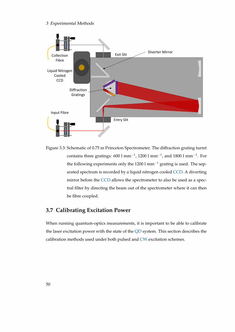
3 Experimental Methods
Liquid Nitrogen Cooled
CCD
Diverter Mirror
Input Fibre
Collection Fibre
Diffraction Gratings
Entry Slit
Exit Slit
Figure 3.3: Schematic of 0.75 m Princeton Spectrometer. The diffraction grating turret
contains three gratings: 600 l mm−1, 1200 l mm−1, and 1800 l mm−1. For
the following experiments only the 1200 l mm−1 grating is used. The sep-
arated spectrum is recorded by a liquid nitrogen cooled CCD. A diverting
mirror before the CCD allows the spectrometer to also be used as a spec-
tral filter by directing the beam out of the spectrometer where it can then
be fibre coupled.
3.7 Calibrating Excitation Power
When running quantum-optics measurements, it is important to be able to calibrate
the laser excitation power with the state of the QD system. This section describes the
calibration methods used under both pulsed and CW excitation schemes.
50

3.7 Calibrating Excitation Power
3.7.1 Pulsed Pi power
Pulsed excitation power is calibrated by measuring Rabi rotations to find π-power.
Rabi rotations are used to calibrate the excitation power that is required for the pop-
ulation of the QD to be found in the excited exciton state after the application of a
laser pulse. Exciting a transition with strong CW excitation causes the population to
oscillate between the ground (|0〉) and excited (|X〉) state at the Rabi frequency (ΩR).
This is called Rabi flopping and leads to the probability of finding the QD in the |0〉
or |X〉 state being given by [47]:
|c0(t)|2 = cos2(ΩRt/2),
|cX(t)|2 = sin2(ΩRt/2). (3.1)
As the population is time dependent, if the excitation laser ends at a time multiple of
nπ/ΩR where n is an odd integer then the population will be in the |X〉 state. If n is
an even integer, then the population is in the |0〉 state. This process can therefore be
applied to pulsed driving of the transition where the length of the excitation pulse de-
termines the final state of the population after the application of the pulse. However,
the Rabi frequency depends on the strength of the applied pulse. Therefore, the final
population after the pulse depends on both the Rabi energy and the pulse length. It
is useful to define the excitation by the pulse area (Θ):
Θ =∫ +∞
−∞
ΩR(t) dt, (3.2)
to relate both the length of the pulse and the rabi frequency. Here the pulse area is a
dimensionless parameter defined in terms of π .
Experimentally, it is easier to adjust the power of the laser pulses than the pulse
length. π-power is therefore found by measuring a power dependence of the RF.
When a pulse with an area of π is applied, the QD is promoted to the |X〉 state if it
started in the |0〉 state. The QD then decays back to the ground state via radiative
51

3 Experimental Methods
decay. If the QD starts in the |0〉 state and interacts with a 2π pulse, then the popula-
tion will be rotated to the |X〉 state and back to the |0〉 state by the pulse. As the QD
ends in the |0〉 state, there is no radiative decay of the population, and so no RF is
detected. This creates an oscillating emission signal which continues with increasing
pulse area. This is known as a Rabi rotation and has been observed for QDs in differ-
ent systems [135–138]. An example of a Rabi rotation measured using the QD sample
described in Chapter 4, with the associated π-pulses labelled, is shown in Figure 3.4.
To determine the π-power of the system, the QD is excited resonant to the neutral
exciton using the shaped pulses from the Mira Ti:S laser. The QD emission is then
detected on either the spectrometer or on a SPAD. The excitation laser power is in-
creased in increments and at each new power a spectrum or the emission intensity is
recorded. To analyse the spectra from the spectrometer, the intensity recorded at the
wavelength corresponding to the exciton peak is extracted and plotted against the
excitation power. The data includes a background from the reflected excitation laser
which increases linearly with excitation power. To remove this, the data is fitted with
a linear fit. The gradient of the fit is used to remove the background and the data
is replotted against the square root of the excitation power. An example of a Rabi
rotation measured using this method can be seen in Figure 3.4, the peaks and troughs
have been labelled with their corresponding π values.
A similar method is used when measuring Rabi rotations using a SPAD. However,
as SPADs do not record any spectral information, the QD emission is filtered around
the zero-phonon line (ZPL) to remove the excitation laser when using short pulses,
as well as to remove emission from other transitions. The same method of applying
a linear background is used to analyse the Rabi rotation. To improve the accuracy
of the measured π-power, these measurements can also be performed using a differ-
ential measurement scheme. After each spectra or intensity is recorded, a different
bias is applied to the sample to move the neutral exciton transition out of resonance
52

3.7 Calibrating Excitation Power
0 5 1 0 1 5 2 0 2 5 3 005 0 0
1 0 0 01 5 0 02 0 0 02 5 0 03 0 0 0
0 2 0 0 4 0 0 6 0 0 8 0 00
1 0 0 0
2 0 0 0
3 0 0 0
4 0 0 0
5 0 0 0 D a t a L i n e a r F i t
Inten
sity (a
rb. un
its)
P o w e r ( n W )
D a t a
Inten
sity (a
rb. un
its)
P o w e r 1 / 2 ( n W 1 / 2 )
π = 3 2 . 9 9 n W
2 π
3 π
4 π
( b )
( a )
Figure 3.4: An example of a Rabi rotation measured to calibrate the pulsed excita-
tion power. (a) Here, the spectrometer is used to measure the intensity
of the unfiltered neutral exciton peak against excitation power. A linear
background that increases with increasing excitation power is fitted to the
data. (b) The gradient of the linear background is used to remove the
laser background and the data is replotted against the square root of the
excitation power. The peaks and troughs have been labelled with their
corresponding π values.
53
3 Experimental Methods
with the excitation laser. A background spectra or emission measurement is then
recorded. By subtracting the background away from the resonant data, the increas-
ing background from the emission laser can be removed from the Rabi rotation data.
As well as being used as a method to calibrate excitation power, Rabi rotations can
also be used when optimising the alignment of the system. A high π-power indicates
that the laser is not well coupled to the QD system, whereas a low collected emis-
sion intensity at π-power is an indication that the emission collection path is not well
aligned.
Recently, Monte Carlo simulations of two-level emitters (TLE) investigating the effect
of multi-photon emission when using long pulses (relative to T1) have shown that the
maximum RF intensity occurs at a pulse area slightly higher than π [139, 140]. The
multi-photon emission can also cause an increase in the RF emission of the 3π peak
above that of the π peak [139].
3.7.2 CW Pi Power
Calibrating the CW excitation laser power utilises the Mollow triplet splitting caused
by the dressing of the levels by the laser. As described in Section 2.3.2, when driving
a TLE resonant to the neutral exciton transition, the “bare” ground and excited states
become “dressed” and split by hΩR. This leads to four possible energy transitions.
However, as two of the transitions are degenerate a Mollow triplet forms with the
side peaks separated from the central peak by hΩR. An example of a Mollow triplet
measured (black line) at an excitation power of 10 µW is shown in the inset of Fig-
ure 3.5.
To calibrate the CW excitation power a power dependence of the Mollow triplet is
measured. As ΩR is increased, the side peaks move further away from the central
peak. The three peaks of the Mollow spectra at each power are fitted with Voigt func-
54

3.7 Calibrating Excitation Power
- 0 . 5 0 . 0 0 . 5 1 . 0 1 . 5 2 . 0 2 . 5 3 . 0 3 . 5 4 . 0 4 . 5 5 . 0 5 . 5- 2 00
2 04 06 08 0
1 0 01 2 01 4 01 6 01 8 02 0 02 2 0
D a t a L i n e a r F i t
Rabi
Energ
y (µe
V)
P o w e r 1 / 2 ( µW 1 / 2 )
- 2 0 0 - 1 0 0 0 1 0 0 2 0 00
2 0
4 0
6 0
Inten
sity (a
rb. un
its)
D e t u n i n g ∆ ( µe V )
ΩR
Figure 3.5: An example of a CW excitation power calibration measurement. The Rabi
energy is measured as a function of the square root of the excitation power
by fitting Mollow triplet spectra. By applying a linear fit, the CW excita-
tion power required for a desired Rabi energy can be calculated and vice
versa. Inset: Mollow triplet spectrum (black) measured at an excitation
power of 10 µW, fitted (red) using a multiple peak Voigt function.
tions using a multiple peak fit, as shown by the red line in the inset of Figure 3.5. The
difference between the side peaks and the central peak is found and converted from
nanometres to electron volts. The excitation laser intensity has a square dependence
to the triplet separation as the electric field increases in proportion to the intensity
squared. By plotting the splitting against the square root of the power, as shown in
Figure 3.5, a linear dependence can be fitted. The linear fit is constrained to pass
through the origin, as the Rabi energy is zero when no field is applied, and can then
be used to find the Rabi power of any applied CW laser power and vice versa.
55

4 Sample
This chapter contains the details of the sample used for the measurements in this the-
sis, including the composition of the semiconductor wafer and the fabrication method
of the photonic crystal structure. In addition, there is a summary of the previous char-
acterisation work performed on the sample.
4.1 Wafer
The sample used has InGaAs QDs grown within a p-i-n diode wafer. The construc-
tion of the wafer is shown in Figure 4.1. The wafer used was part of the VN2668
wafer grown by Dr Edmund Clarke at the EPSRC National Epitaxy Facility at the
University of Sheffield. Self-assembled InGaAs QDs are grown on a GaAs substrate
via MBE using the Stranski-Krastanow method described in Section 2.2.2. The QDs
were grown using the In-flush technique that allows the control of the QD height
[141]. For VN2668 the QDs were capped with 2.5 nm of GaAs before the In-flush,
setting their height to this value. Tunnelling electron microscope (TEM) work carried
out by Dr Maxime Hugues on similar In-flush QD wafers indicates a QD diameter of
15-20 nm.
The QD layer is surrounded, above and below, by undoped 50 nm thick AlGaAs
tunnelling barriers. The barriers reduce the ease with which charges can tunnel into
or out of the QD layer, increasing the stability of the charge environment and so al-
lowing a large QCSE tuning range of the QD emission [75, 142]. Either side of the
barriered QDs are the doped semiconductor layers that form the p-i-n diode. The top
57

4 Sample
1000 nm
p-GaAsAl0.3Ga0.7AsIn(Ga)As QDsAl0.3Ga0.7Asn-GaAs
Sacrificial Layern-Al0.6Ga0.4As
Contacting Layern-GaAs
GaAs Substrate
45 nm50 nm10 nm50 nm45 nm
1000 nm
V
Ti/Au
Ni/Ge/Au
Photonic Crystal Membrane
Figure 4.1: Schematic cross-section of the QD semiconductor wafer. The sample uses
a p-i-n diode design, incorporating AlGaAs barriers for charge stability
and an increased QCSE tuning range.
layer is GaAs p-doped with Beryllium whereas the bottom layer is GaAs n-doped
with Silicon. Both of these doped layers are 45 nm thick.
Beneath the diode is a 1 µm thick sacrificial layer of n-doped AlGaAs. This layer
is selectively removed during sample fabrication to leave a free-standing structure
that is supported from the edges. Below the sacrificial layer there is a 1 µm thick
contacting layer made of n-doped GaAs. The contacting layer and the p-doped GaAs
layer at the top of the diode are connected via Gold bond wires to connections on the
sample holder, allowing a voltage to be applied to the diode. The wafer was grown
from the bottom up via MBE on a GaAs substrate.
58

4.2 Design
1 . 3 4 1 . 3 5 1 . 3 6 1 . 3 70 . 0
0 . 2
0 . 4
0 . 6
0 . 8
1 . 0
Norm
alised
Inten
sity (a
rb. un
its)
E n e r g y ( e V )
M 1 M 2 Q D B a c k g r o u n d
( b )( a )
Figure 4.2: (a) SEM images of the sample used in this thesis, showing a H1 PhCC with
coupled W1 waveguides. The SEM images were taken by Dr Ben Royall.
(b) The H1 cavity displays two orthogonally polarised linear modes, la-
belled M1 and M2, measured using above-band excitation. RF is used to
acquire a spectrum of the QD (green) that is used throughout this thesis,
along with the background suppression possible (blue) using the cross-
polarisation method described in Section 3.4.
4.2 Design
The photonic crystal structure fabricated on this wafer was a H1 PhCC with two cou-
pled W1 waveguides. Scanning electron microscope (SEM) images of the complete
cavity structure are shown in Figure 4.2(a). Before fabrication the structure design
was optimised by Dr Rikki Coles [113, 121].
The SEM images of the cavity show that the ring of etched cylinders closest to the
cavity have a reduced radius and are displaced when compared to the remainder of
the PhC lattice. These modifications are used to improve the Q-factor of the cavity
[122].
59
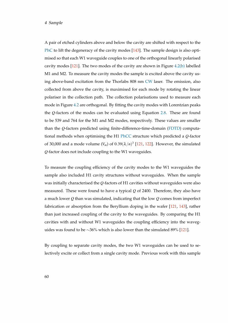
4 Sample
A pair of etched cylinders above and below the cavity are shifted with respect to the
PhC to lift the degeneracy of the cavity modes [143]. The sample design is also opti-
mised so that each W1 waveguide couples to one of the orthogonal linearly polarised
cavity modes [121]. The two modes of the cavity are shown in Figure 4.2(b) labelled
M1 and M2. To measure the cavity modes the sample is excited above the cavity us-
ing above-band excitation from the Thorlabs 808 nm CW laser. The emission, also
collected from above the cavity, is maximised for each mode by rotating the linear
polariser in the collection path. The collection polarisations used to measure each
mode in Figure 4.2 are orthogonal. By fitting the cavity modes with Lorentzian peaks
the Q-factors of the modes can be evaluated using Equation 2.8. These are found
to be 539 and 764 for the M1 and M2 modes, respectively. These values are smaller
than the Q-factors predicted using finite-difference-time-domain (FDTD) computa-
tional methods when optimising the H1 PhCC structure which predicted a Q-factor
of 30,000 and a mode volume (Vm) of 0.39(λ/n)3 [121, 122]. However, the simulated
Q-factor does not include coupling to the W1 waveguides.
To measure the coupling efficiency of the cavity modes to the W1 waveguides the
sample also included H1 cavity structures without waveguides. When the sample
was initially characterised the Q-factors of H1 cavities without waveguides were also
measured. These were found to have a typical Q of 2400. Therefore, they also have
a much lower Q than was simulated, indicating that the low Q comes from imperfect
fabrication or absorption from the Beryllium doping in the wafer [121, 143], rather
than just increased coupling of the cavity to the waveguides. By comparing the H1
cavities with and without W1 waveguides the coupling efficiency into the waveg-
uides was found to be ∼36% which is also lower than the simulated 89% [121].
By coupling to separate cavity modes, the two W1 waveguides can be used to se-
lectively excite or collect from a single cavity mode. Previous work with this sample
60

4.3 Characterisation
has demonstrated their use for exciton spin readout [121] and for the routing of sin-
gle photons [142]. At the end of the waveguides Bragg (λ/2n) grating out-couplers
[144, 145] are used to direct the emission from the waveguides vertically so it can be
collected using the optical set-up described in Section 3.4. Light can also be collected
from above the cavity where FDTD simulations show that the majority of the light is
emitted into an angle of less than 20°, allowing collection by the 0.55 NA cryostat lens.
To fabricate the sample the PhC structure was defined on the wafer using Electron
Beam Lithography (EBL) and then etched using Inductively Coupled Plasma (ICP).
After etching, the sacrificial AlGaAs layer beneath the device is removed using 40%
Hydrofluoric Acid (HF). As is shown schematically in Figure 4.1, removing the sac-
rificial layer leaves the PhCC structure as a suspended membrane supported from
the edges. The sample was fabricated by Dr Ben Royall at the EPSRC National Epi-
taxy Facility at the University of Sheffield. The PhCC structures are fabricated within
diodes with 20 structures per diode. The sample is mounted on a TO-5 header to
provide the electrical connections necessary within the cryostat.
4.3 Characterisation
All of the experimental work in this thesis was performed using a single cavity-
coupled QD. Figure 4.2(b) shows an RF spectrum of the neutral exciton transition
of the QD (green) along with an example of the laser background suppression (blue)
possible using the RF set-up described in Section 3.4. The background suppression is
measured by changing the bias applied to the p-i-n diode and so moving the QD out
resonance with the excitation laser by the QCSE.
The tuning range of the QD neutral exciton emission achieved by the QCSE is shown
in Figure 4.3. Here, the sample is excited using an above-band CW laser and spectra
are recorded and plotted as a function of applied bias. Whereas in Figure 4.2(b) the
61

4 Sample
1 . 3 4 8 1 . 3 5 0 1 . 3 5 2 1 . 3 5 4 1 . 3 5 6 1 . 3 5 80 . 5 00 . 5 50 . 6 00 . 6 50 . 7 00 . 7 50 . 8 00 . 8 50 . 9 00 . 9 5
E n e r g y ( e V )
Bias (
V)
4 . 0 0 08 5 . 5 01 6 7 . 02 4 8 . 53 3 0 . 04 1 1 . 54 9 3 . 05 7 4 . 56 5 6 . 0
Inten
sity (a
rb. un
its)
M 1Q D
Figure 4.3: Bias dependent measurement using above band CW excitation. Spectra of
the µ-PL at each applied bias are recorded. The dashed lines are a guide
to the eye for the neutral exciton emission (black) and the M1 cavity mode
(red). The measurement was performed by Dr Alistair Brash.
sample was saturated by the above-band excitation laser, here the sample is excited
at lower powers, so that the QD emission can be resolved. The dashed black line fol-
lows the QD neutral exciton emission as it is tuned across the M1 cavity mode (red
dashed). As the exciton crosses the cavity mode an enhancement of the emission is
observed, due to the Purcell effect, showing that the exciton transition is weakly cou-
pled to the M1 mode of the cavity. The observed enhancement of the emission occurs
as the Purcell effect shortens the lifetime (T1) of the exciton emission, allowing a faster
re-excitation rate. A strong Purcell effect is observed despite the low Q-factor of 539
measured for the M1 cavity mode as it retains a small mode volume of 0.63(λ/n)3.
The mode volume was calculated from FDTD simulations using parameters from the
fabricated sample, rather than the ideal mode volume calculated for the optimised
H1 PhCC [106, 121]. The measurement shown in Figure 4.3 was performed by Dr
Alistair Brash.
62

4.3 Characterisation
Figure 4.4: Illustration of the double π-pulse resonance fluorescence technique used
for high resolution lifetime measurements.
The Purcell factor (FP) for the cavity coupled QD was calculated by measuring the
exciton T1 along with the radiative lifetime of the QD ensemble (T′
1) on the wafer
away from the cavity and using Equation 2.11. However, the enhancement of the ex-
citon T1 meant that it was unresolvable on the fastest single-photon avalanche diode
(SPAD) available. To achieve higher timing resolutions, a double π-pulse resonance
fluorescence (DPRF) method was developed by Dr Alistair Brash, Dr Luis Martins
and Dr Feng Liu. This method relies on the properties of π-pulses which are dis-
cussed in Section 3.7.1.
Figure 4.4 illustrates the principle of the DPRF technique. The exciton transition is
treated as a two-level emitter (TLE) with its starting population in the ground state
(|0〉). At t = 0, the application of a π-pulse drives the population to the excited state
(|X〉), leaving |X〉 with a population of ∼ 1. After the first π-pulse the population of
|X〉 can decay by spontaneous emission, emitting an RF signal. Therefore, at t > 0, the
populations of |X〉 and |0〉 can be defined as CX and (1−CX ) respectively. A second
π-pulse is then applied to the system at t = ∆t, exchanging the |0〉 and |X〉 popula-
63
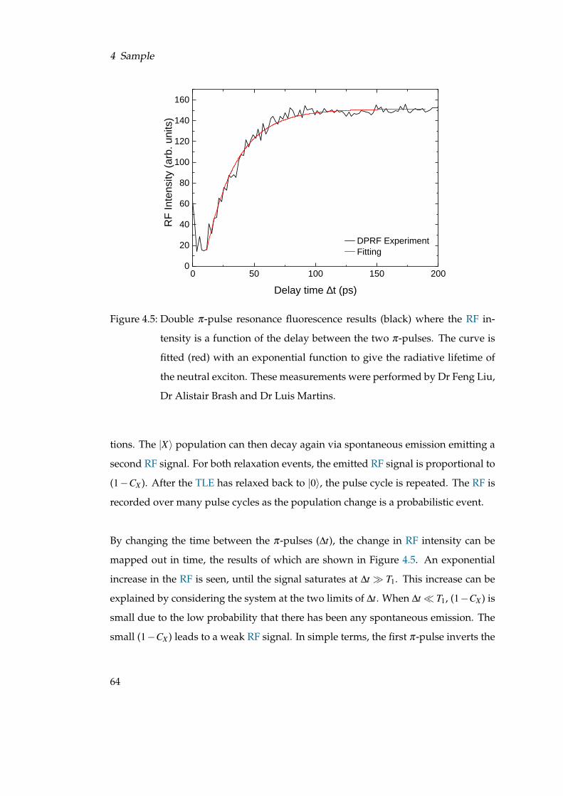
4 Sample
0 5 0 1 0 0 1 5 0 2 0 002 04 06 08 0
1 0 01 2 01 4 01 6 0
RF In
tensity
(arb.
units)
D e l a y t i m e ∆ t ( p s )
D P R F E x p e r i m e n t F i t t i n g
Figure 4.5: Double π-pulse resonance fluorescence results (black) where the RF in-
tensity is a function of the delay between the two π-pulses. The curve is
fitted (red) with an exponential function to give the radiative lifetime of
the neutral exciton. These measurements were performed by Dr Feng Liu,
Dr Alistair Brash and Dr Luis Martins.
tions. The |X〉 population can then decay again via spontaneous emission emitting a
second RF signal. For both relaxation events, the emitted RF signal is proportional to
(1−CX ). After the TLE has relaxed back to |0〉, the pulse cycle is repeated. The RF is
recorded over many pulse cycles as the population change is a probabilistic event.
By changing the time between the π-pulses (∆t), the change in RF intensity can be
mapped out in time, the results of which are shown in Figure 4.5. An exponential
increase in the RF is seen, until the signal saturates at ∆t T1. This increase can be
explained by considering the system at the two limits of ∆t. When ∆t T1, (1−CX ) is
small due to the low probability that there has been any spontaneous emission. The
small (1−CX ) leads to a weak RF signal. In simple terms, the first π-pulse inverts the
64

4.3 Characterisation
system, and the second returns it to the ground state before spontaneous emission
has occurred. Hence, no photons are emitted. At ∆t T1, (1−CX ) tends to 1 as the
majority of the population will have decayed from the |X〉 state. The second π-pulse
returns this population to |X〉, allowing a second decay of the large (1−CX ) popula-
tion and so leading to a strong RF signal being measured. By fitting an exponential
to the DPRF curve, T1 is found to be 22.7±0.9 ps, implying a Purcell factor of 43±2
when Equation 2.11 is used with the T′
1 = 971±15 ps measured for the QD ensemble.
A more detailed description of this method and results can be found in Liu et al. [106]
and the PhD thesis of Dr John O’Hara [139].
To show that the transition being studied is the neutral exciton, fine-structure split-
ting (FSS) of the state is measured. The FSS is measured by exciting the QD with
above-band CW excitation and the QD emission is tuned, by the QCSE, to lie be-
tween the two cavity modes. The linear polariser in the collection path is rotated in
10° steps, with spectra being taken at each step. The resulting spectra are fitted with
Gaussians to find the central wavelength of the emission and plotted against the an-
gle of the collection polariser. The resulting FSS is plotted in Figure 2.5, showing a
splitting of 0.013 nm (19 µeV).
65


5 Cavity-Coupled QD as a Single-Photon
Source
This work was included in the following publication:
Feng Liu, Alistair J. Brash, John O’Hara, Luis M. P. P. Martins, Catherine L. Phillips,
Rikki J. Coles, Benjamin Royall, Edmund Clarke, Christopher Bentham, Nikola
Prtljaga, Igor E. Itskevich, Luke R. Wilson, Maurice S. Skolnick and A. Mark Fox.
“High Purcell factor generation of indistinguishable on-chip single photons.” Nature
Nanotechnology 13, 835-840 (2018).
Hanbury Brown and Twiss and Hong-Ou-Mandel second-order correlation measure-
ments were set up and carried out by Catherine Phillips and Alistair Brash. Master-
equation modelling of multi-photon emission was performed by John O’Hara.
5.1 Introduction
Single photons are desirable for many quantum-optics applications including boson
sampling [27, 28], single-photon fast optical switching [29], photonic cluster state
generation [30, 146], a quantum internet [2, 31, 32], optical quantum computing [4]
and quantum cryptography [2] to mention just a few. All of these uses for single-
photons require certain properties from their single-photon source (SPS). They need
to be bright, pure, on-demand and indistinguishable [33, 34]. A SPS that is bright has
a short emitter lifetime and so can be re-excited at a fast rate. To be bright they also
require a high collection efficiency. The purity of a SPS involves measuring the pho-
67

5 Cavity-Coupled QD as a Single-Photon Source
ton statistics of the emission. Purity is defined as the probability that the output com-
prises single photons rather than multi-photon emission. On-demand is the probabil-
ity that an input will create the desired output, i.e. that every excitation event results
in a single photon being emitted rather than no emission or multi-photon emission.
Indistinguishability, also known as visibility, is the probability that the single photons
emitted are identical to each other.
In this chapter the purity and indistinguishability of the single-photon emission from
a QD in an H1 PhCC is investigated using second-order correlation measurements.
Hanbury Brown and Twiss measurements are used to investigate the single-photon
purity of the emission from the neutral exciton of the QD and Hong-Ou-Mandel ex-
periments are used to investigate the indistinguishability of the single-photons pro-
duced. These measurements are performed under pulsed excitation where the QD
is excited resonantly using a π-pulse, as required for optimal on-demand operation.
The effect of pulse length is also investigated, using a pulse width that is relatively
long compared to the T1 of the QD and a pulse width that is much shorter.
5.2 Second-Order Correlation Measurements
Correlation function measurements can be used to classify the temporal coherence
properties of an emitter and its photon statistics [47]. The first-order correlation
function (g(1)(t)) is so named as it quantifies the properties of the first power of the
electric field through field-field correlations. The second-order correlation function
(g(2)(t)) quantifies intensity-intensity correlations, intensity being the square of the
electric field. This Chapter will discuss second-order correlations. First-order cor-
relations will be discussed in more detail in Chapter 6. Second-order correlation
(g(2)(t)) measurements are used to measure the photon statistics of light emission.
They are also used to measure the indistinguishability of the photons produced. Both
of these properties are important for SPSs and are quantified using Hanbury Brown
68

5.2 Second-Order Correlation Measurements
Figure 5.1: Schematic of the fibre-based set-up used for Hanbury Brown and Twiss
measurements: yellow lines - optical fibres, red lines - coaxial electrical
cables. A 50:50 fibre beam splitter is used to split the QD emission equally
to two single-photon avalanche diodes (SPADs) which are connected to
a time-correlated single-photon counting module (TCSPC). The electrical
delay (∆tTCSPC) centres the time-zero of the TCSPC correlation scan in the
centre of the measurement window.
and Twiss (HBT) and Hong-Ou-Mandel (HOM) measurements, respectively. The de-
tails of these measurements are discussed in this section.
5.2.1 Hanbury Brown and Twiss
The Hanbury Brown and Twiss (HBT) experiment is a g(2)(t) correlation measure-
ment that is used to measure photon statistics [147]. The experimental set-up for a
fibre-based HBT measurement is shown in Figure 5.1. Collected emission from the
sample passes through a 50:50 fibre beam splitter onto two single-photon avalanche
diodes (SPADs). The SPADS are connected by coaxial cables to a time-correlated
single-photon counting module (TCSPC). The TCSPC time tags detection events from
the SPADs using a reversed start-stop configuration. The TCSPC has two channels:
“CFD” and “Sync”. When a detection start-event occurs on the “CFD” channel the
TCSPC starts measuring time. The timer stops either when a detection stop-event
occurs on the “Sync” channel or if the time period becomes longer than the range of
the TCSPC’s internal Time-to-Amplitude Converter (TAC). In the first case the arrival
time of the second photon is plotted on a histogram, in its associated time bin, and the
69

5 Cavity-Coupled QD as a Single-Photon Source
g(2)HBT (0) Photon statistics Photon distribution (−→ time)
> 1 Bunched
1 Coherent (random)
< 1 Antibunched
Table 5.1: Definition of the photon statistics of light with respect to g(2)HBT (0). The pho-
ton distribution shows examples of photon streams in time that would cre-
ate the associated photon statistics.
TCSPC’s internal clock is reset to begin measuring again with the next “CFD” trigger.
In the second scenario, the internal clock is reset and waits for the next trigger. Extra
electrical delay (∆tTCSPC) is added before the “Sync” channel to centre time-zero in
the TAC window. Time-zero is used to define the time where the added delay means
that for the TCSPC it is the equivalent of looking at both SPADs simultaneously. For
example, if a 5 ns delay is added to “Sync” then a photon detection stop-event oc-
curring at 5 ns on that channel would have originated from the same photon pulse
start-event that triggered the “CFD” counter 5 ns previously, this is known as a coin-
cidence event. One metre of coaxial cable is equivalent to about a 5 ns time delay.
Figure 5.2 shows an illustration of the results for HBTs where the sample is excited by
a pulsed laser. The time-zero peak is centred in the measurement window and each of
the correlation peaks are separated by the pulse separation of the laser (tL), arbitrarily
chosen here to be 10 ns. Considering the photons emitted from a source, in this case
a QD, their emission statistics can be split into three categories: bunched, coherent
and antibunched. These statistics are shown in Table 5.1. The g(2)HBT (0) for pulsed ex-
citation is calculated from the area of the g(2)HBT (t) correlation peak (At0) at time-zero
(Fig. 5.2 - green/purple/grey) normalised to the averaged area of the surrounding
peaks (Amean) in the HBT (Fig. 5.2 - blue) using:
g(2)(0) =At0
Amean. (5.1)
70

5.2 Second-Order Correlation Measurements
- 3 0 - 2 0 - 1 0 0 1 0 2 0 3 00 . 00 . 20 . 40 . 60 . 81 . 01 . 21 . 41 . 6
Norm
alised
Coinc
idenc
es
D e l a y ( n s )
B u n c h i n g C o h e r e n t A n t i b u n c h i n g
t L
Figure 5.2: Illustration of pulsed excitation HBTs where tL is the separation of the ex-
citation laser pulses, here chosen arbitrarily to be 10 ns. The centre peak is
time-zero. The area of this peak, normalised to the averaged areas of the
surrounding (blue) peaks, gives g(2)HBT (0). The illustration shows examples
of HBT results for bunched photon statistics (green) where the g(2)HBT (0)> 1,
coherent statistics (purple) where g(2)HBT (0) = 1 and antibunched statistics
(grey) where g(2)HBT (0)< 1.
Bunched photon statistics, defined as g(2)HBT (0) > 1, is where the photons are emit-
ted in groups (bunches). This means that, when one SPAD has been triggered, it is
more likely that a second photon will be detected in a short time window than at
a long time [47]. This leads to a peak above the coherent background level in HBT
measurements, shown in green on Figure 5.2.
Coherent (random) photon statistics occur when the photons from the source are
emitted randomly in time. Lasers are an example of coherent light sources. For a
coherent light source g(2)HBT (t) = 1 at all values of time (t), as when measuring a HBT
71

5 Cavity-Coupled QD as a Single-Photon Source
there is an equal chance of detecting a coincidence at any time delay between the two
detectors [47]. This is shown in purple on Figure 5.2, where the area of the time-zero
coincidence peak has the same area as the surrounding coincidence peaks.
Antibunched photon statistics are seen when the source emits photons one at a time
with a time separation of ∼ tL between them, i.e. up to one photon is produced per
excitation event. This is seen as g(2)HBT (0) < 1. If a single photon passes through a
50:50 beam splitter it can only take one path or the other. Therefore, when comparing
detection events for both SPADs at the same time, a single photon cannot create a co-
incidence event. A source that produced only single photons would have a g(2)HBT (0)
of zero with the single-photon purity of the source being given by 1− g(2)HBT (0). Fig-
ure 5.2 shows an antibunching peak in grey where the g(2)HBT (0) = 0.25. Therefore, the
single-photon purity is 75%.
5.2.2 Hong-Ou-Mandel
The Hong-Ou-Mandel (HOM) second-order correlation measurement (g(2)HOM(t)) [148]
is used to measure the indistinguishability of single photons produced. This is also
known as the “Visibility” of the SPS. The HOM measurement has been used to show
strong photon indistinguishability for QDs embedded in micro and nano-cavities
[149–152]. Here, HOM measurements are made using a fibre-based Mach-Zehnder
interferometer, the schematic of which is shown in Figure 5.3.
Each cycle of the experiment involves excitation by two π-pulses separated by ∆τ .
This produces two photons separated by ∆τ which then pass through a 50:50 fibre
beam splitter. After the beam splitter the interferometer comprises a path where the
polarisation of the photon can be modified and a path with an increased path length
of ∆t. The polarisation is controlled through use of a Phoenix Photonics “Electronic
in-line fibre polarisation controller” which can move the polarisation to any point
on the Poincare sphere by heating the optical fibre. The difference in path length is
72

5.2 Second-Order Correlation Measurements
Figure 5.3: Schematic of the fibre-based Mach-Zehnder interferometer used for Hong-
Ou-Mandel measurements. A 50:50 fibre beam splitter is used to separate
the emission equally down both arms of the interferometer. One arm has
an electrical polarisation controller, the other a fixed fibre delay (∆t) that
matches the separation of the excitation pulses. The fibre paddles allow
the polarisation of both arms to be identical at the second 50:50 fibre beam
splitter where the emission is then split onto two SPADs. As in Figure 5.1
both SPADs are connected to a TCSPC and an electrical delay of ∆tTCSPC is
added to one path.
achieved by increasing the length of fibre used on the opposite side of the interfer-
ometer to the polarisation controller.
The two paths of the interferometer then converge at a second 50:50 fibre beam split-
ter. Here, if two photons arrive with temporally overlapping wavepackets and are
indistinguishable from each other, then they must take the same path out of the beam
splitter [153]. This can be understood by considering Figure 5.4. Here, photons re-
flect off a 50:50 beam splitter which has a higher refractive index (n = n2) than the
surrounding medium (n = n1). When light reflects from the surface of a medium with
a higher refractive index it gains a π phase shift.
Before the beam splitter the state of the system can be written as |1A1B〉 where one
photon is incident on each port of the beam splitter, A and B. The state of the system
73

5 Cavity-Coupled QD as a Single-Photon Source
Figure 5.4: Diagram of the four different outcomes after two photons, incident on
ports A and B, traverse a 50:50 beam splitter with n2 > n1. The output of
each scenario is recorded on two detectors Dt and Db.
after the beam splitter is a superposition of the four different possible paths:
1+2+3+4. (5.2)
The four possible cases can be written in terms of each outcome by picturing two
detectors to the right of the beam splitters in Figure 5.4, one above the beam splitter
(Dt) and one below the beam splitter (Db). Recording the possible amplitude (number
of photons) and phase of the photons at each detector allows the superposition to be
written as [154]:1 2 3 4
|1A1B〉= 1√2(−|2t0b〉 −|1t1b〉 +|1t1b〉 +|0t2b〉).
The change in phase of the photon which follows the solid line in case 1 and case 2,
due to n1 < n2, leads to the negative sign in each case. Significantly, cases 2 and 3 can-
cel in the case of indistinguishable photons, a manifestation of quantum interference.
The final output state is therefore given by the superposition of cases 1 and 4, where
both photons leave through one side of the beam splitter or the other. The bunching
of the photons in either output path is the key characteristic of the HOM effect.
After the beam splitter are two SPADs. As for the HBT measurements, the SPADs
are connected to a TCSPC to record coincidence counts from the two detectors. If
two indistinguishable photons exit through the same port of the second beam splitter
then no coincidence is counted at time-zero.
74

5.2 Second-Order Correlation Measurements
Indistinguishable photons only occur at the second beam splitter of the interferome-
ter when both of the arms are co-polarised (‖) with respect to each other. Maximum
distinguishability occurs when the two arms are cross-polarised (⊥). Indistinguisha-
bility (Equation 5.3) is given by the fraction of the area of the indistinguishable coin-
cidence counts (A⊥) at time-zero compared to the area of the distinguishable coinci-
dence counts (A‖) at time-zero:
V =A⊥−A‖
A⊥. (5.3)
Maximum indistinguishability would occur when no coincidence counts are recorded
at time-zero for a co-polarised interferometer. This would give a visibility of 1 (100%).
As the Mach-Zehnder interferometer used for the HOM measurements is fibre-based,
fibre paddles are used to co-polarise the two arms when initialising the interferom-
eter. This then allows the electronic polarisation controller to change the polarisa-
tion between co and cross-polarised with an extinction ratio of 99.99 ± 0.01%. The
co-polarisation is achieved by connecting one of the exit fibres from the second fi-
bre beam splitter to a fibre-to-fibre u-bench, which adds a short free-space path be-
tween two optical fibres, before the fibre-coupled SPAD. A rotatable linear polariser
is mounted within the u-bench. An attenuated single mode CW laser with the same
wavelength as the exciton emission from the QD is connected to the input of the in-
terferometer. The time-delay arm of the interferometer is disconnected.
The linear polariser is then used to minimise the counts on the SPAD in the con-
nected arm. Fibre paddles comprise three sections which are set with quarter-wave
plate, half-wave plate and quarter-wave plate configurations, respectively. Used in
conjunction with the polarisation controller, they further minimise the counts in the
connected arm. This arm is then disconnected and the opposite arm of the interfer-
ometer is connected. The corresponding fibre paddles are used to minimise the SPAD
signal without changing the angle of the linear polariser in the u-bench. When the
75
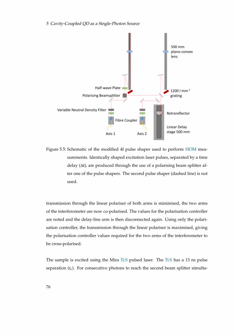
5 Cavity-Coupled QD as a Single-Photon Source
Linear Delay stage 500 mm
Fibre Coupler
1200 l mm-1
grating
Retroreflector
500 mmplano-convex lens
Half-wave Plate
Polarising Beamsplitter
Variable Neutral Density Filter
Axis 1 Axis 2
Figure 5.5: Schematic of the modified 4f pulse shaper used to perform HOM mea-
surements. Identically shaped excitation laser pulses, separated by a time
delay (∆t), are produced through the use of a polarising beam splitter af-
ter one of the pulse shapers. The second pulse shaper (dashed line) is not
used.
transmission through the linear polariser of both arms is minimised, the two arms
of the interferometer are now co-polarised. The values for the polarisation controller
are noted and the delay-line arm is then disconnected again. Using only the polari-
sation controller, the transmission through the linear polariser is maximised, giving
the polarisation controller values required for the two arms of the interferometer to
be cross-polarised.
The sample is excited using the Mira Ti:S pulsed laser. The Ti:S has a 13 ns pulse
separation (tL). For consecutive photons to reach the second beam splitter simulta-
76

5.2 Second-Order Correlation Measurements
neously, the time delay (∆t) used in the Mach-Zehnder interferometer should be the
same as the time delay between photons emitted from the sample. To change the
time delay between the excitation laser pulses, the pulse shaping set-up shown in
Figure 3.2 was modified to that of Figure 5.5. Here, all of the laser power travels
through one pulse shaper by the rotation of the half-wave plate mounted in front of
a polarising beam splitter before the pulse shapers, shown in Figure 3.2. Then, by
using a second half-wave plate and polarising beam splitter after the pulse shaper,
half of the beam is split and aligned through a free-space delay stage before being fi-
bre coupled. Splitting the beam after the pulse shaper rather than before ensures that
the shape of the two excitation pulses should be identical. The two excitation fibres
(labelled Axis 1 and Axis 2 in Fig. 5.5) are then combined using a fibre beam splitter
before travelling to the sample. Each laser pulse emitted now travels to the sample
as two pulses separated by a time ∆t, defined by the position of the linear delay stage.
The ∆t of the Mach-Zehnder interferometer is created by adding an extra length of
optical fibre to one arm. Two methods are used to find the position for the free-space
delay stage so that the laser pulses also have a splitting of ∆t. The first method in-
volves measuring the arrival time of laser pulses at a SPAD after the Mach-Zehnder
interferometer, bypassing the sample, using one axis of the pulse shaper at a time.
The TCSPC is triggered each time the laser emits a pulse, through the use of the laser
photodiode, and is set to “stop” when it receives a signal from the SPAD. This is a
similar set-up to that of a lifetime measurement. Two peaks build up on the TCSPC
histogram, one for each path through the interferometer with the two peaks sepa-
rated by ∆t. This is measured separately for both laser axes. For the free-space delay
path of Axis 2 to match ∆t, the Axis 1 laser pulse that travels down the delayed path
in the interferometer and the Axis 2 laser pulse that travels down the short path of
the interferometer should both reach the SPAD at the same time after the TCSPC has
been triggered. The distance that the free-space delay stage needs to be moved can
be calculated from the time difference between these two peaks. An example of this
77
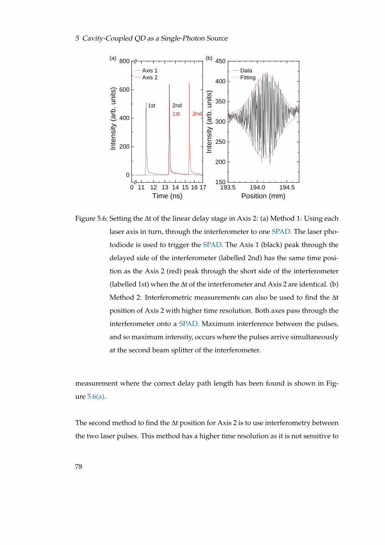
5 Cavity-Coupled QD as a Single-Photon Source
0 1 1 1 2 1 3 1 4 1 5 1 6 1 70
2 0 0
4 0 0
6 0 0
8 0 0
Inten
sity (a
rb. un
its)
T i m e ( n s )
A x i s 1 A x i s 2
1 s t1 s t2 n d
2 n d
1 9 3 . 5 1 9 4 . 0 1 9 4 . 51 5 0
2 0 0
2 5 0
3 0 0
3 5 0
4 0 0
4 5 0 D a t a F i t t i n g
Inten
sity (a
rb. un
its)P o s i t i o n ( m m )
( a ) ( b )
Figure 5.6: Setting the ∆t of the linear delay stage in Axis 2: (a) Method 1: Using each
laser axis in turn, through the interferometer to one SPAD. The laser pho-
todiode is used to trigger the SPAD. The Axis 1 (black) peak through the
delayed side of the interferometer (labelled 2nd) has the same time posi-
tion as the Axis 2 (red) peak through the short side of the interferometer
(labelled 1st) when the ∆t of the interferometer and Axis 2 are identical. (b)
Method 2: Interferometric measurements can also be used to find the ∆t
position of Axis 2 with higher time resolution. Both axes pass through the
interferometer onto a SPAD. Maximum interference between the pulses,
and so maximum intensity, occurs where the pulses arrive simultaneously
at the second beam splitter of the interferometer.
measurement where the correct delay path length has been found is shown in Fig-
ure 5.6(a).
The second method to find the ∆t position for Axis 2 is to use interferometry between
the two laser pulses. This method has a higher time resolution as it is not sensitive to
78
5.3 Experiments
the timing jitter of the detectors used. For this measurement, a single SPAD is again
used after the Mach-Zehnder interferometer. Each laser axis is set to the same power
and both are connected to the interferometer using a fibre beam splitter, bypassing
the sample. The free-space delay stage in Axis 2 is then stepped and at each step the
SPAD records the laser intensity. When the laser pulses from Axis 1 and 2 overlap,
interference fringes are seen in the recorded intensity. By fitting the fringe envelope,
the central position of the envelope with maximum interference can be found, giving
a precise stage position for ∆t. An example of the interference fringes seen is shown
in Figure 5.6(b).
Method 2 is best used in conjunction with method 1 as there are multiple stage po-
sitions that can cause the laser pulses to overlap, but only one where the ∆t of the
stage is the same as the ∆t of the interferometer. As very small steps of the delay
stage (∼ 0.003 mm) are needed to resolve the fringes, the first method can be used
to find the rough position for the delay stage so that a high-resolution measurement
can be made. Depending on the ∆t required, it can be that the delay required for ∆t
cannot be reached over the length of the free-space delay stage. This can be rectified
by adding additional optical delay fibre to Axis 1 or 2 before the sample if ∆t is too
short or long for the delay stage respectively.
5.3 Experiments
This section discusses the specifics of the methods used for the HBT and HOM g(2)(t)
measurements along with their respective results.
5.3.1 Method: Hanbury Brown and Twiss
The sample is excited, resonant to the QD neutral exciton transition, above the cavity
by a π-pulse. The method for calibrating π-power for pulsed excitation is described in
Section 3.7.1. The emission is collected from an out-coupler using the cross-polarised
79

5 Cavity-Coupled QD as a Single-Photon Source
RF method described in Section 3.4. The collected emission passes through a fibre
beam splitter to two SPADs that are connected by coaxial cables to a time correlated
single-photon counting module (TCSPC), as shown in Figure 5.1.
The Mira Ti:S pulsed laser is used to excite the QD with a pulse separation (tL) of
13 ns. Two different laser pulse lengths (τL) were used for the HBT measurements:
13 ps and 2.4 ps. The collected emission signal from using the 13 ps excitation pulse is
unfiltered and has a signal-to-background ratio of ∼20:1. As the 2.4 ps pulse is spec-
trally broader, the collected emission is filtered, centred on the QDs zero-phonon line
(ZPL), using the spectrometer as a grating filter with a bandwidth FWHM of 96 µeV.
Filtering eliminates the residual broadband scatter of the laser from the surface of the
sample and a signal-to-background ratio of ∼50:1 can be achieved. The filtering is
necessary due to the out-of-plane excitation and collection geometry and the short
waveguides of 5 µm in length, meaning that the excitation and collection spots are
only 5 µm apart. This filtering would not be necessary for on-chip experiments as
the background arises from scattering from the surface of the sample and is not cou-
pled into the waveguide. HBT measurements were performed using SPADs with a
quantum efficiency of ∼43% at the cavity wavelength of ∼915 nm. The τL = 13 ps
measurements were made using SPADs and photon counting card (TCSPC) with a
combined IRF that is Gaussian in shape with a FWHM of ∼ 860 ps. The τL = 2.4 ps
measurements were made with newer SPADs that have an IRF of ∼ 340 ps when
combined with the TCSPC.
The TCSPC is configured with a 50 ns delay window which corresponds to a his-
togram bin width of 48.9 ps. A 25 ns delay (5 m of coaxial cable) is added to one
SPAD to centre the time-zero peak in the measurement window. The electrical delay
can be checked by splitting the electrical signal from one SPAD so that both the short
coaxial cable and delayed coaxial cable are connected to the same SPAD. Running a
HBT in this set-up will result in strong coincidence peak at time-zero as the TCSPC
80

5.3 Experiments
is triggering and stopping from the same SPAD signal separated at the TCSPC by the
difference in length of the two coaxial cables. The length of the electrical delay can
then be adjusted to centre time-zero in the centre of the measurement window.
The HBT measurements were repeated in cycles of 15 minutes. Due to the low count
rate of ∼ 0.8-7 kHz per channel on the TCSPC, the measurements were often run
overnight. Using 15 minute cycles allowed the signal to background to be monitored
and allowed for the removal of cycles where there had been time-dependent drifts
such as changes in the laser suppression.
5.3.2 Results: Hanbury Brown and Twiss
Figure 5.7 shows the results for the HBT measurements. The correlation peaks are
separated by the tL = 13 ns of the excitation laser’s pulsed emission. The peaks are
fitted using a multi-peak Gaussian where the width gives the combined IRF of the
SPADs and TCSPC. Using Equation 5.1, the pulse width (τL) of 13 ps (red) gives a
g(2)HBT (0) = 0.134 ± 0.003. This gives a single-photon purity (1-g(2)
HBT (0)) of 86.6 ± 0.3%.
The τL of 2.4 ps (blue) clearly shows the narrower peak width from the improved
IRF. The g(2)HBT (0) measured for τL = 2.4 ps is 0.026± 0.007 which gives a single-photon
purity of 97.4 ± 0.7%. The inset to Figure 5.7 shows the two HBT correlation peaks
at time-zero. This shows that there were very few correlation counts for the τL =
2.4 ps. The pulse length of 13 ps is relatively long compared to the exciton T1 of 22.7
± 0.9 ps [106]. Figure 5.8 shows the Monte Carlo results (green) of master equation
simulations performed by John O’Hara in Ref.[106]. They show that multiple photon
emission events, caused by re-excitation of the QD within the same excitation pulse,
reduce the single-photon purity observed. The coloured points on Figure 5.8 are the
measured values for g(2)HBT (0) at a τL of 13 ps (red) and 2.4 ps (blue). When an excita-
tion pulse with τL < T1 is used, the single-photon purity is improved as the likelihood
of re-exciting the QD within the time that the excitation pulse is present in the system
is decreased.
81

5 Cavity-Coupled QD as a Single-Photon Source
- 3 0 - 2 0 - 1 0 0 1 0 2 0 3 00 . 0
0 . 2
0 . 4
0 . 6
0 . 8
1 . 0
1 . 2
Norm
alised
Coinc
idenc
es
D e l a y ( n s )
τ L = 1 3 p s , U n f i l t e r e d τ L = 2 . 4 p s , F i l t e r e d
- 5 0 50 . 0 00 . 0 50 . 1 00 . 1 5
Figure 5.7: HBT measurements for the QD excited by a resonant π-pulse for laser
pulse widths (τL) of 13 ps (red) and 2.4 ps (blue). The τL = 13 ps emis-
sion is unfiltered, while the τL = 2.4 ps is spectrally filtered using a 96 µeV
grating filter to eliminate residual scatter from the sample surface from
the spectrally broader laser excitation pulse. Inset: Increased scale for the
time-zero peaks of the HBT measurements.
5.3.3 Method: Hong-Ou-Mandel
The sample is excited resonant to the neutral exciton emission with a π-pulse of
length 13 ps (τL) and the emission is collected from an out-coupler. The laser back-
ground is suppressed using the cross-polarisation technique described in Section 3.4,
the signal-to-background ratio is ∼20:1. The entire emission collected from the out-
coupler passes to the interferometer for the HOM (g(2)HOM(t)) measurements without
any filtering. The first time delay (∆t) used was 2 ns. Before measuring a HOM, the
∆t of the laser pulses is set to match that of the interferometer and the two arms of
the interferometer are re-polarised, as described in Section 5.2.2.
82

5.3 Experiments
0 . 0 0 . 5 1 . 0 1 . 50 . 0 0
0 . 0 5
0 . 1 0
0 . 1 5
0 . 2 0
0 . 2 5
0 . 3 0 S i m u l a t i o n τ L = 1 3 p s τ L = 2 . 4 p s
g(2)HB
T (0)
π- P u l s e W i d t h ( τL / T 1 )
Figure 5.8: Monte Carlo simulations (green) of g(2)HBT (0) as a function of the τL relative
to the exciton T1 of 22.7 ± 0.9 ps. The coloured points show the experi-
mental results for the g(2)HBT (0) with a π-pulse length (τL) of 13 ps (red) and
2.4 ps (blue). The Monte Carlo simulation was performed by John O’Hara.
The TCSPC is configured using the same parameters that were used for the HBT
measurements. Again an extra electrical delay is added to one of the SPAD channels
to centre the time-zero peak in the measurement window.
The HOM correlation measurement visibility is given by measuring with the inter-
ferometer in both co-polarised and cross-polarised configurations, where the photon
indistinguishability is maximised and minimised respectively. The polarisation is ro-
tated every 15 minutes during the measurement to minimise any time-dependent
drifts. Due to a count-rate of 2-3 kHz on each channel at the TCSPC, the HOM
measurements were run overnight with the signal to background monitored between
each cycle.
83

5 Cavity-Coupled QD as a Single-Photon Source
After analysing the results for τL = 13 ps and ∆t = 2 ns, further measurements us-
ing a τL = 2.4 ps and a ∆t of 2 ns and 24 ns were performed to investigate the effect
of the excitation pulse length and the time delay between the pulses. As for the HBT
measurements, the τL = 2.4 ps pulses required a 96 µeV grating filter to eliminate the
reflected spectrally broad laser background to achieve a signal-to-background ratio
of ∼50:1.
5.3.4 Results: Hong-Ou-Mandel
Figure 5.9 shows the HOM two-photon interference visibility measurement for pho-
tons produced with a time separation of ∆t of 2 ns and a τL = 13 ps excitation pulse.
Here, no filtering has been used between the sample and the interferometer. The ex-
pected five peak pattern centred around zero time delay is observed [149]. The five
peaks arise from the different paths that consecutive photons can take through the
interferometer. Like the HBT measurements, the HOM records coincidence events.
The peaks labelled 1 and 5 in Figure 5.9 are coincidence counts when the first photon
in the pair takes the short path through the interferometer and the second photon
takes the path delayed by ∆t. There is a time difference of 2∆t = 4 ns between the
two detection events. This peak is repeated 4 ns away from time zero on both sides.
This occurs as the time separated photons can exit from either port of the second
beam splitter and so can be detected on either SPAD. If the first photon triggers the
“CFD” SPAD to start the clock and the second photon triggers the “Sync” SPAD then
the photon peak will be recorded at a time equal to the added electrical delay on the
“Sync” channel plus the 4 ns delay that the second photon gained from the optical
delay in the interferometer. However, if the photon that leaves the interferometer
second triggers the clock on the “CFD” SPAD and the first photon exits through the
“Sync” port of the second beam splitter then the “Sync” SPAD will detect the photon
at a time of the electrical delay minus 4 ns. When both of the photons exit the same
port of the second beam splitter then the event is not recorded as only one detector is
triggered and thus no coincidence counts occur.
84
5.3 Experiments
- 2 0 - 1 0 0 1 0 2 00 . 0
0 . 5
1 . 0
1 . 5
2 . 0
2 . 5
3 . 0
3 . 5
Norm
alised
Coinc
idenc
es
D e l a y ( n s )
2 n s , τ L = 1 3 p s , U n f i l t e r e d 2 n s , τ L = 1 3 p s , U n f i l t e r e d
g ( 2 ) H O M ( 0 ) = 7 8 . 5 ± 4 . 0 %
1
2 3 4
5
Figure 5.9: HOM measurements using ∆t of 2 ns and π-pulse excitation with τL =
13 ps. The coincidence count data for cross-polarised (⊥) arms of the in-
terferometer is shown in grey and the coincidences for co-polarised (‖) in-
terferometer arms are shown in blue. The g(2)HOM(0) value shown is the cor-
rected value taking into account multi-photon emission from the source
and deviations of the interferometer beam splitter.
The peaks labelled 2 and 4 have twice the area of peaks 1 and 5 as they are popu-
lated by two different events. One is where both photons in the pair take the short
path through the interferometer whilst the second event is where both photons take
the delayed path. Both of these events have a time difference of ∆t = 2 ns. Again, this
peak is repeated either side of zero time delay.
The central peak (3) is where the first photon takes the delayed path and the sec-
ond photon takes the short path through the interferometer. The difference in time
between the first and second photon entering the interferometer is the same as the
85
5 Cavity-Coupled QD as a Single-Photon Source
time delay of the delayed path in the interferometer. Therefore, both photons reach
the second beam splitter (Fig. 5.3) at the same time. If the two arms of the interferom-
eter are co-polarised (‖), shown in blue on Figure 5.9, then the photons are maximally
indistinguishable and indistinguishable photons take the same path out of the beam
splitter. This means that no central peak would be seen for perfect indistinguisha-
bility as there would be no coincidence detection events. The grey data in Figure 5.9
shows where the two arms of the interferometer are set to be cross-polarised (⊥). This
means that when the photons reach the second beam splitter, they are maximally dis-
tinguishable from each other due to their difference in polarisation. Therefore, they
are not limited to taking the same path out of the interferometer and so a peak in coin-
cidence counts is seen. By fitting the areas of Peak 3 under both conditions, Equation
5.3 can then be used to find the raw HOM visibility. In this case the raw visibility is
51.2 ± 3.9 %.
Equation 5.3 gives the raw visibility of the two-photon interference. To calculate the
true visibility, it is necessary to correct for deviations in the beam splitters used in
the interferometer away from their ideal behaviour, as well as multi-photon emission
from the sample. There are two different analysis methods for extracting the true
HOM visibility.
The first method uses the following equation [149], where A3 is the area of peak 3:
A3 ∝ (R3T +RT 3)(1+2g(2)HBT (0))−2(1− ε)2R2T 2V. (5.4)
Here the parameters are the g(2)HBT (0) value, the fringe contrast of the interferometer (1-
ε), and both the reflection (R) and transmission (T ) coefficients of the beam splitters.
Equation 5.4 assumes that both of the beam splitters used in the HOM interferometer
have the same values of R and T . These values are shown in Table 5.2.
The left part of Equation 5.4 considers the probability that two photons entering
the interferometer simultaneously, therefore when g(2)HBT (0) is non-zero, take the same
86
5.3 Experiments
Parameter Value Correction Measurement Method
(1 - ε) 0.968 ± 0.004 6.38 %Measurement of fringe contrast
with a single mode laser
g(2)HBT (0),
τP = 13 ps0.134 ± 0.003 19.5 % HBT
g(2)HBT (0),
τP = 2.4 ps0.026 ± 0.007 4.0 % HBT
R 0.544 ± 0.0021.53 %
Resonant transmission
with a single mode laserT 0.456 ± 0.002
Polarisation 99.99 ± 0.01 % <0.01 %Resonant extinction
with a single mode laser
Table 5.2: Parameters used to correct the raw HOM two-photon interference visibil-
ity. The correction column shows the estimated contribution of each com-
ponent. However, these values are approximate due to the co-dependence
of the parameters from equations 5.4 and 5.6
path at the first beam splitter (i.e. R2 or T 2 for the first beam splitter) and then leave
from opposite ports of the second beam splitter, therefore each of the terms for the
first beam splitter are multiplied by RT for the second beam splitter. The right hand
side of Equation 5.4 is the probability that two photons, which are separated by the
interferometer path-length difference (∆t), take the correct paths through the interfer-
ometer to arrive simultaneously at the second beam splitter. This would give a factor
of RT for the first beam splitter. If these photons then exit from opposite ports of the
second beam splitter then a second factor of RT needs to be included for the second
beam splitter. As this can only occur if the two photons do not interact at the second
beam splitter this term is normalised by the (1-ε) term and so would vanish for a
“perfect” second beam splitter. The factor of g(2)HBT (0) is included as the single-photon
purity is an area that can be improved on (for example, through different excitation
schemes, as shown in Section 5.3.2). The single-photon purity can therefore be seen
87

5 Cavity-Coupled QD as a Single-Photon Source
as a limiting factor for the HOM and so can be corrected for.
The values of g(2)HBT (0) are the ones measured in Section 5.3.2. The fringe contrast
of the interferometer was measured by adding a piezo-tunable free-space delay to
one arm of the interferometer. Then, after equalising both the length and intensity
through each of the interferometer arms, and setting the arms to be co-polarised, a
single mode CW laser was used to measure transmission through the interferometer
as a function of the delay. The CW laser has the same wavelength as the neutral exci-
ton emission from the QD that was used in RF for the HOM. The fringe contrast data
is shown in Figure 5.10. The total fringe contrast was obtained by finding the contrast
for each fringe using Equation 5.5 and taking the mean over many fringes:
(1− ε) =Imax− Imin
Imax + Imin. (5.5)
By using equation 5.4 and taking V = 1 for A3‖ and V = 0 for A3⊥, the raw visibil-
ity that would be measured for perfectly indistinguishable photons can be extracted.
Using this to normalise the raw visibility of 51.2± 3.9 %, it is possible to correct for
just the interferometer properties by setting the g(2)HBT (0) contribution to zero. This
gives a corrected visibility of 59.0± 4.0 %. When including the g(2)HBT (0) component,
the corrected value becomes V = 78.5±4.0 %.
The second, equivalent, correction method uses a single equation that compares A3‖
to A2‖ and A4‖ rather than also using the cross-polarised HOM measurement [155]:
V =1
(1− ε)2
[2g(2)(0)+
R2 +T 2
2RT−
A3‖
A2‖+A4‖
(2+g(2)
HBT (0)(R2 +T 2)
RT
)]. (5.6)
Applying this equation to the raw visibility gives a corrected visibility of V = 74.0±
3.1%.
As with the HBT measurements, the HOM measurement was repeated using the nar-
rower pulse width (τL) of 2.4 ps. Again, filtering of 96 µeV is used to eliminate laser
scatter from the spectrally broad pulse. For this measurement newer SPADs were
88

5.3 Experiments
0 2 0 4 0 6 0 8 0 1 0 0 1 2 00 . 0
0 . 2
0 . 4
0 . 6
0 . 8
1 . 0No
rmalis
ed In
tensity
(arb.
units)
∆ t ( f s )
D a t a
I m i n
I m a x
Figure 5.10: Interference fringes using single-mode CW laser through the Mach-
Zehnder interferometer. Fringes are measured while varying the delay
length in one arm of the interferometer.
used, this gives narrower coincidence peaks due to their improved IRF of ∼340 ps as
opposed to ∼860 ps. Figure 5.11 shows the HOM measurement for τL = 2.4 ps and
∆t = 2 ns. The coincidence count data for when the two arms of the interferometer
are cross-polarised (⊥) is shown in grey and the red data is where the arms of the
interferometer had been set to be co-polarised(‖). The raw data gives a visibility of
81.0± 3.7 %. After correcting for the beam splitter, using Equation 5.4, without the
multi-photon emission correction the visibility is 88.8±3.8 %. The corrected visibility
increases to 93.3± 3.6 % when the effects of multi-photon emission are included. In
carrying out this correction, the g(2)HBT (0) value for the τL = 2.4 ps pulses is used.
The raw visibility is higher than for the longer τL partially due to the reduction in
multi-photon emission. As can be seen from Table 5.2, the τL = 2.4 ps HBT contribu-
tion to the HOM correction is much smaller than that of the τL = 13 ps HBT contri-
89

5 Cavity-Coupled QD as a Single-Photon Source
- 2 0 - 1 0 0 1 0 2 00 . 0
0 . 5
1 . 0
1 . 5
2 . 0
2 . 5
3 . 0
3 . 5
Norm
alised
Coinc
idenc
es
D e l a y ( n s )
2 n s ⊥ τ L = 2 . 4 p s , F i l t e r e d 2 n s // τ L = 2 . 4 p s , F i l t e r e d
g ( 2 ) H O M ( 0 ) = 9 3 . 3 ± 3 . 6 %
Figure 5.11: HOM measurements using ∆t of 2 ns and resonant π-pulse of τL = 2.4 ps.
The coincidence count data for cross-polarised (⊥) arms of the interfer-
ometer is shown in grey and the coincidences for co-polarised (‖) interfer-
ometer arms are shown in red. The g(2)HOM(0) value is the corrected value
taking into account multi-photon emission from the source and devia-
tions of the interferometer beam splitter from an ideal beam splitter.
bution. The visibility is also improved due to the spectral filter, used to remove the
spectrally broad laser background, as this filter also removes a significant amount of
the phonon sideband. Theoretical studies have suggested that for unfiltered emission
from InGaAs QDs at 4.2 K that are not Purcell-enhanced, the single-photon visibility
is limited to around 80 % due to incoherent phonon sideband emission, comprising
around 10 % of the total spectrum [95, 100]. As visibility compares two photons, both
of the compared photons should be emitted from the ZPL to have the highest prob-
ability of indistinguishability. However, emission is a probabilistic event, with each
photon having a ∼90 % chance of being emitted from the ZPL and ∼10 % from the
PSB. This leads to an indistinguishability limit of 0.9 x 0.9 ≈ 80 %. The visibility can
90

5.3 Experiments
be improved, without the losses from filtering, by using a QD in a resonant high-Q
cavity. However, for the QD used here the Q-factor is relatively low. Therefore, the
cavity filtering effect is weaker, introducing a theoretical upperbound to the unfil-
tered visibility of ∼ 90 % [95].
A value of ∆t of 2 ns is the equivalent of comparing the indistinguishability of pho-
tons produced over 20 emission cycles of the QD if it were driven with a 10 GHz
pulsed laser. This would produce a pulse separation of 100 ps which at 4.4T1 is suffi-
cient to allow for essentially complete radiative recombination between pulses [106].
To look at how the indistinguishability decays over longer repetition times, a ∆t of
24 ns was used. This is the equivalent of comparing the indistinguishability of pho-
tons produced over 240 emission cycles if 10 GHz excitation is used.
Figure 5.12 shows the HOM for resonant π-pulse excitation using τL = 2.4 ps and
∆t = 24 ns. As can be seen, the peaks A2‖ and A4‖ are not easily identifiable due to
the many overlapping peaks. The change in the g(2)HOM(t) histograms occurs as ∆t is
longer than the pulse separation generated by the laser, tL = 13 ns, under these condi-
tions. Care has to be taken when choosing the ∆t that none of the sidepeaks overlap
with the time-zero correlation peak. Equation 5.4 is used to correct for the interfer-
ometer and multi-photon component as it only compares the A3⊥ and A3‖ peaks. The
raw visibility for this measurement is 69.0± 3.4 % which gives a corrected visibility
of 76.7± 3.4 % when only considering the interferometer deviations and a corrected
visibility of 81.3± 3.6 % when including the multi-photon components of the QD
emission. This shows a 12 % difference between the single-photon indistinguishabil-
ity at ∆t = 2 ns and ∆t = 24 ns.
The reduction in photon indistinguishability at 24 ns compared to 2 ns is attributed to
spectral wandering caused by fluctuations in the charge environment on the scale of
tens of nanoseconds, as the ∆t of 24 ns is much greater than the QDs T1 of 22.7± 0.9 ps.
91

5 Cavity-Coupled QD as a Single-Photon Source
- 2 0 - 1 0 0 1 0 2 00 . 0
0 . 5
1 . 0
1 . 5
2 . 0
2 . 5
3 . 0
3 . 5
Norm
alised
Coinc
idenc
es
D e l a y ( n s )
2 4 n s ⊥ τ L = 2 . 4 p s , F i l t e r e d 2 4 n s // τ L = 2 . 4 p s , F i l t e r e d
g ( 2 ) H O M ( 0 ) = 8 1 . 3 ± 3 . 6 %
Figure 5.12: HOM measurements using ∆t of 24 ns and resonant π-pulse excitation
with τL = 2.4 ps. The coincidence count data for cross-polarised (⊥)
arms of the interferometer is shown in grey and the coincidences for
co-polarised (‖) interferometer arms are shown in purple. The g(2)HOM(0)
value is the corrected value taking into account multi-photon emission
from the source and imperfections of the interferometer beam splitter.
The fluctuations in the charge environment could be a result of etched surfaces close
to the QD [156, 157]. A previous study using QD microlens structures, which also
include etched surfaces close to the QD, showed a visibility decrease of∼40% caused
by spectral wandering on a time scale of 12.5 ns, which is comparable to the 24 ns time
scale used here [158]. The advantage of the QD device studied here is its very short T1
enhanced by the Purcell factor (FP), meaning that a given amount of spectral wander-
ing degrades the visibility far less than the non-Purcell enhanced case. Furthermore,
photons can be extracted much faster than the spectral wandering timescale and thus
longer strings of indistinguishable photons may be generated before their indistin-
guishability begins to degrade.
92

5.4 Conclusion
5.4 Conclusion
The results presented in this chapter show that a QD in a H1 PhCC can act as an ex-
cellent single photon source, enabled particularly by the Purcell factor of 43, giving
a shortened T1 of 22.7 ± 0.9 ps for the neutral exciton. The first important property
shown in Section 5.3.2 is a high single-photon purity. Exciting above the cavity, res-
onant to the neutral exciton with a π-pulse of 13 ps in length and collecting from the
end of a waveguide, a single-photon purity of 86.6 ± 0.3% is observed. This value is
measured without the use of spectral filtering. The lack of a need for spectral filtering
shows promise for on-chip experiments [34] where the produced photons are manip-
ulated and detected without leaving the chip to be filtered.
The effect of the excitation pulse length on the single-photon purity has also been
investigated with a shorter pulse length (τL) of 2.4 ps, giving an improved single-
photon purity of 97.4 ± 0.7%. The shorter pulse length is much smaller than T1 of the
QD and therefore reduces the probability that the neutral exciton will be re-excited
during the excitation pulse. The τL = 2.4 ps pulse requires the collected emission to be
spectrally filtered to remove the residual laser scatter from the spectrally broad pulse,
however on-chip experiments would not require this filtering.
As well as investigating the single-photon purity, the indistinguishability of the pho-
tons produced has also been measured. Using a 13 ps excitation pulse, the single-
photon corrected indistinguishability for this device is shown to be 78.5±4.0 % with-
out spectral filtering. The largest contribution to the visibility correction has been
shown to be the single-photon purity (g(2)HBT (0)). Therefore, using the shorter τL of
2.4 ps, which increases the single-photon purity, gives a visibility, after correction, of
93.3±3.6 %. The shorter τL also shows a higher visibility due to the spectral filtering
used, due to the removal of the majority of the phonon sideband. The incoherent
emission from the phonon sideband would introduce a theoretical upper bound of
∼90% without the use of spectral filtering [95]. Both of these measurements were
93
5 Cavity-Coupled QD as a Single-Photon Source
carried out with a HOM delay line (∆t) of 2 ns, the equivalent of comparing the indis-
tinguishability over 20 photons if a 10 GHz excitation laser had been used.
The τL of 2.4 ps excitation was also used with a ∆t of 24 ns to compare photons over a
longer timescale, the equivalent of 240 photons if a 10 GHz excitation laser had been
used. This gave a visibility of 79.9± 3.4% after correction. This decrease in the visibil-
ity is attributed to spectral wandering caused by charge fluctuations within the QD,
possibly due to the close proximity between the QD and etched surfaces [156–158].
The single-purity and indistinguishability measured using this sample shows promise
for the development of on-chip optical circuits. For example, off-chip experiments
using QDs as single-photon sources have demonstrated boson-sampling while using
indistinguisabilities of ∼65% [28, 159] and the current state-of-the-art for boson sam-
pling off-chip uses an indistinguishability of 94% [27]. The results presented in this
Chapter show greater or comparable visibilities using an on-chip design of QD em-
bedded in a H1 PhCC with coupled waveguides, suggesting that this design could
be used as a foundation for building fully integrated on-chip boson sampling exper-
iments or other optical quantum technologies requiring high quality single photons.
94

6 Phonon Effects on QD Emission
The work presented in this chapter has been published in:
Alistair J. Brash, Jake Iles-Smith, Catherine L. Phillips, Dara P. S. McCutcheon, John
O’Hara, Edmund Clarke, Benjamin Royall, Luke R. Wilson, Jesper Mørk, Maurice S.
Skolnick, A. Mark Fox, and Ahsan Nazir.
“Light Scattering from Solid-State Quantum Emitters: Beyond the Atomic Picture.”
Physical Review Letters 123, 167403 (2019).
First-order correlation measurements were set up and carried out by Catherine Phillips
and Alistair Brash. High resolution spectroscopy of the coherent scatter using a
Fabry-Pérot interferometer was measured by John O’Hara and Alistair Brash. The
lower resolution spectroscopy of the phonon sideband was set up and measured by
Catherine Phillips and Alistair Brash.
All of the Polaron theory modelling and fitting in this chapter was performed by
our collaborators: Jake Iles-Smith, Dara McCutcheon and Ahsan Nazir.
6.1 Introduction
The coherent scattering of light from quantum emitters is a fundamental process that
is used as a foundation for many quantum-optics applications. These applications
typically exploit two important properties of coherent scattering: it retains the co-
herence of the excitation laser and shows antibunching on the timescale of the emit-
ter lifetime. (Whether these properties can be measured simultaneously will be dis-
95
6 Phonon Effects on QD Emission
cussed in Chapter 7.) Solid-state emitters are promising candidates for many pro-
posed quantum technologies owing to their strong light-matter interactions and ease
of integration with photonic structures. However, solid-state emitters demonstrate
strong environmental couplings through phonon interactions leading to phenomena
such as the appearance of a phonon sideband (PSB). Phonon effects were introduced
in Section 2.4.2.
This chapter presents an experimental investigation into the influence of phonon cou-
pling in different RF regimes, accompanied by the theoretical modelling performed
by our collaborators. First-order correlation (g(1)(t)) measurements are used in con-
junction with spectroscopy measurements to resolve the phonon and emission prop-
erties of the QD in both the time and frequency domain, showing deviation from
the two-level “atomic picture”. High and low resolution spectroscopy measurements
are used to show that the proportion of RF emission into the PSB is insensitive to
the excitation power. Furthermore, g(1)(t) measurements are used to show a non-
monotonic relationship between the detuning of the excitation laser and the coherent
fraction that originates from phonon-mediated relaxation. All of these results show
deviations from the idealised “atomic picture” of scattering from a two-level emitter.
They do however show excellent agreement with theory modelling produced using
polaron master equations.
6.2 Coherent Scattering
Continuous wave (CW) driving of a two-level emitter (TLE) comprises two funda-
mental interactions. The first is coherent scattering which is also known as elastic
scattering or resonant Rayleigh scattering. This is where the excitation photon from
the CW laser scatters elastically from the TLE transition, meaning that absorption
and emission from the system become a single coherent event. There is no change
in the population of the levels for coherent scattering. This is shown in Figure 6.1(a).
96

6.2 Coherent Scattering
Figure 6.1: (a) Coherent scattering from a two-level emitter. (b) Incoherent emission
from a two-level emitter where the laser photon is absorbed, exciting the
system. Relaxation due to spontaneous or stimulated emission then oc-
curs, with a coherence time of T1, emitting a photon with the energy of the
transition.
These elastically scattered photons retain the coherence of the excitation laser. This
long coherence time leads to the observation of a “sub-natural linewidth”, whereby
the width of the scattered spectrum implies a coherence time longer than the con-
ventional radiative limit T2 = 2T1. Coherent scattering from a quantum emitter was
first observed for atomic systems [160–162]. More recently, coherent scattering from
QD systems has also been investigated [49, 106, 163–166]. The second fundamental
interaction is incoherent scattering, also known as inelastic scattering. This process
is shown in Figure 6.1(b). Here, the excitation laser photon is absorbed, exciting the
system and populating the excited state. The TLE later relaxes due to spontaneous
or stimulated emission, releasing a photon with the same energy as the optical tran-
sition. In the absence of any dephasing, the coherence of this process is governed by
the transition lifetime (T1).
The presence of the two components discussed above in the scattered light from a
TLE was first demonstrated in a seminal paper by Mollow [81]. He showed that
97

6 Phonon Effects on QD Emission
when a TLE with the natural resonance frequency ω0 is exposed to a monochromatic
field of frequency ω (e.g. a CW excitation laser) the power spectrum of the scattered
light has the form [81, 164]1:
g(ν ,ω,ω0) = 2π|α∞|2δ (ν−ω)+ n∞κΩ2 (ν−ω)2 +Ω2/2+κ2
| f (i(ν−ω))|2, (6.1)
The first term in Equation 6.1 describes coherent scattering, the delta function in-
dicating this component is monochromatic with the frequency of the excitation laser
(ω). The second term in the equation describes incoherent emission with a Lorentzian
lineshape. (Another form of the expressions for the respective contributions of the co-
herent scattering and incoherent emission can be found in [167] p.p. 382-386, where
the scattering is modelled in terms of photodetection signals.)
Using a two-level “atomic picture”, there is no coupling of the TLE to its environ-
ment. Therefore, the main dephasing mechanisms are radiative decay and pure de-
phasing, which are related to the coherence time of the emitter through Equation 2.7.
In the “atomic picture” the coherent fraction of the total emission (FCS) is given by:
FCS =T2
2T1
11+S
. (6.2)
Here, S is the generalised saturation parameter defined as:
S =(Ω2T1T2)
(1+∆2LXT 2
2 ), (6.3)
where Ω is the Rabi frequency, T1 and T2 are the emitter lifetime and coherence time
respectively and ∆LX = ωL−ωX is the laser (ωL) and emitter (ωX ) detuning. Equa-
tion 6.2 generalises expressions from [167] pp. 369, 383 to include pure dephasing.1Here, ν is the emission frequency, κ = 1/T1 is the spontaneous emission rate of the excited state de-
caying to the ground state and Ω is the Rabi frequency. The function f is a third-degree polynomial,
defined in [81, 164], along with α∞, the steady-state quantum mechanical expectation value of the
two-level coherence, and n∞, the steady-state population inversion which is also known as the equi-
librium probability of finding the TLE in the excited state. In Equation 6.1, f , α∞ and n∞ are defined
in terms of κ , Ω, the laser detuning (∆ω = ω −ω0), the pure dephasing rate ( 1T ∗2
= 12T1− 1
T2) and s,
the complex frequency parameter from performing a Laplace transformation to convert the time
dependency to a frequency dependent power spectrum.
98
6.2 Coherent Scattering
Equation 6.2 shows that the coherent fraction approaches unity when the system is
driven well below saturation (S 1) and the emitter coherence is radiatively limited
(T2 = 2T1). The coherent fraction also approaches unity for large detunings between
the transition and the excitation laser (∆LX > T2).
As well as having a sub-natural linewidth due to inheriting the laser coherence time,
the emission in the limit S < 1 has also been shown to exhibit antibunching on the
timescale of the emitter lifetime [49, 163, 165, 166]. This combination of properties
makes coherent scattering from TLEs well suited to many quantum-optics applica-
tions including: creating tuneable single photons [168–170], generating entangled
photon states [171, 172], single photon non-linearities [173–175], and for entangling
remote spins [176, 177]. Solid-state emitters, such as QDs, are useful for these appli-
cations as they are stationary and can be incorporated into photonic structures. These
integrated photonic structures can route photons and create cavities around the emit-
ter, potentially enhancing both the collection efficiency and emission rate.
However, solid state emitters are coupled to their environments. This can lead to
dephasing effects caused by fluctuating charge environments [178, 179] and phonon
broadening at elevated temperatures through strong coupling with the vibrational
modes of the bulk material [180, 181]. Both of these are pure dephasing effects that
broaden the ZPL and can thus be captured by the pure dephasing time T ∗2 . The
phonon broadening of the ZPL in InGaAs QDs can be suppressed through the use
of photonic structures, resonant π-pulse excitation and cryogenic temperatures [106,
155, 182], leading to the emission transform-limited photons from the ZPL. Working
with resonant π-pulse excitation produces the maximum signal intensity for the low-
est excitation power [96, 98, 183], meaning that phonon-mediated excitation induced
dephasing (EID) is minimised compared to driving with larger pulse areas. However,
the coupling to the vibrational modes of the bulk material also leads to a broad PSB in
the QD emission spectrum [95, 99, 181, 184–187]. Similar PSBs have also been seen in
99

6 Phonon Effects on QD Emission
many other solid-state systems including defects in Hexagonal Boron Nitrate (HBN)
[188], colour centres in diamond [189], carbon nanotubes [190], monolayer transition
metal dichalcogenides (TMDCs) [191] and single organic molecules [192].
The phonon sideband is attributed to a rapid change in the configuration of the bulk
material’s lattice during transitions between states of the emitter. This configura-
tion change originates from the difference in Coulomb interaction between the lattice
and the charge configurations associated with the ground and excited states. This
leads to simultaneous emission or absorption of longitudinal acoustic (LA) phonons
alongside the emission of a detuned “sideband” photon. Consequently, to measure
perfectly indistinguishable photons, the PSB needs to be removed from the emission
signal. This can be achieved through the use of spectral filters. However, this does
reduce the efficiency of the single-photon source. If the emitter is embedded in a cav-
ity with a moderate-to-high Q factor then the cavity acts as a spectral filter. Although
increasing Purcell enhancement increases the emission into the ZPL in this regime
the efficiency of the indistinguishable single-photon source is still reduced, mediated
by the fraction emitted into the PSB [95, 100, 193].
The QD studies of the PSB previously referenced were performed with strong res-
onant π-pulse excitation where incoherent scattering dominates. In this regime, there
is a large excited state population and thus a definite change in the charge configu-
ration of the QD. By contrast, in the coherent scattering regime there is a vanishingly
small exciton population. Therefore, it could be assumed that there would be no PSB
effects, as there is no change in the charge configuration. However, recent theory pre-
dictions show phonon effects even at vanishingly weak resonant excitation [99]. The
following measurements explore these effects and their deviations from the “atomic
picture” described by Equation 6.2.
100
6.3 First-Order Correlation Measurements
6.3 First-Order Correlation Measurements
As well as the second-order correlation function, as described in Section 5.2, the first-
order correlation function can also be measured. The first-order correlation function
(g(1)(t)) quantifies the properties of the first power of the electric field through field-
field correlations [47] and is used here to study the coherence of light scattered by the
QD in the time domain.
6.3.1 Experimental Method
The first-order correlation function is measured through use of a Mach-Zehnder in-
terferometer. The set-up for the fibre-based interferometer used in these experiments
is shown in Figure 6.2. The collected emission from the sample passes through a 50:50
fibre beam splitter and down the two arms of the interferometer. One arm of the inter-
ferometer contains a free-space time delay comprising a retroreflector mounted on a
225 mm motorised linear delay stage. The second arm comprises a Phoenix Photonics
“Electronic all-fibre variable phase shifter”. The phase shifter is controlled through
use of a voltage source and the phase shift is induced by heating the fibre, without
affecting the fibre polarisation. The second arm also has a Thorlabs “Electronic vari-
able optical attenuator” (VOA) which is controlled by a second voltage supply and is
used to balance the power through the two arms of the interferometer. It is installed
in this arm of the interferometer as the delay stage arm has greater emission losses.
The main source of loss is due to the recoupling of the emission back into the single-
mode fibre after the free-space delay stage. However, there are also additional losses
due to the reflections on the two mirrors and the retroreflector.
Both arms of the interferometer use fibre paddles so that the emission can be set
to be co-polarised as it recombines at the second beam splitter, using the method
previously described in Section 5.2.2. Having balanced power and co-polarised in-
terferometer arms is important to maximise the fringe contrast in the measurement
101
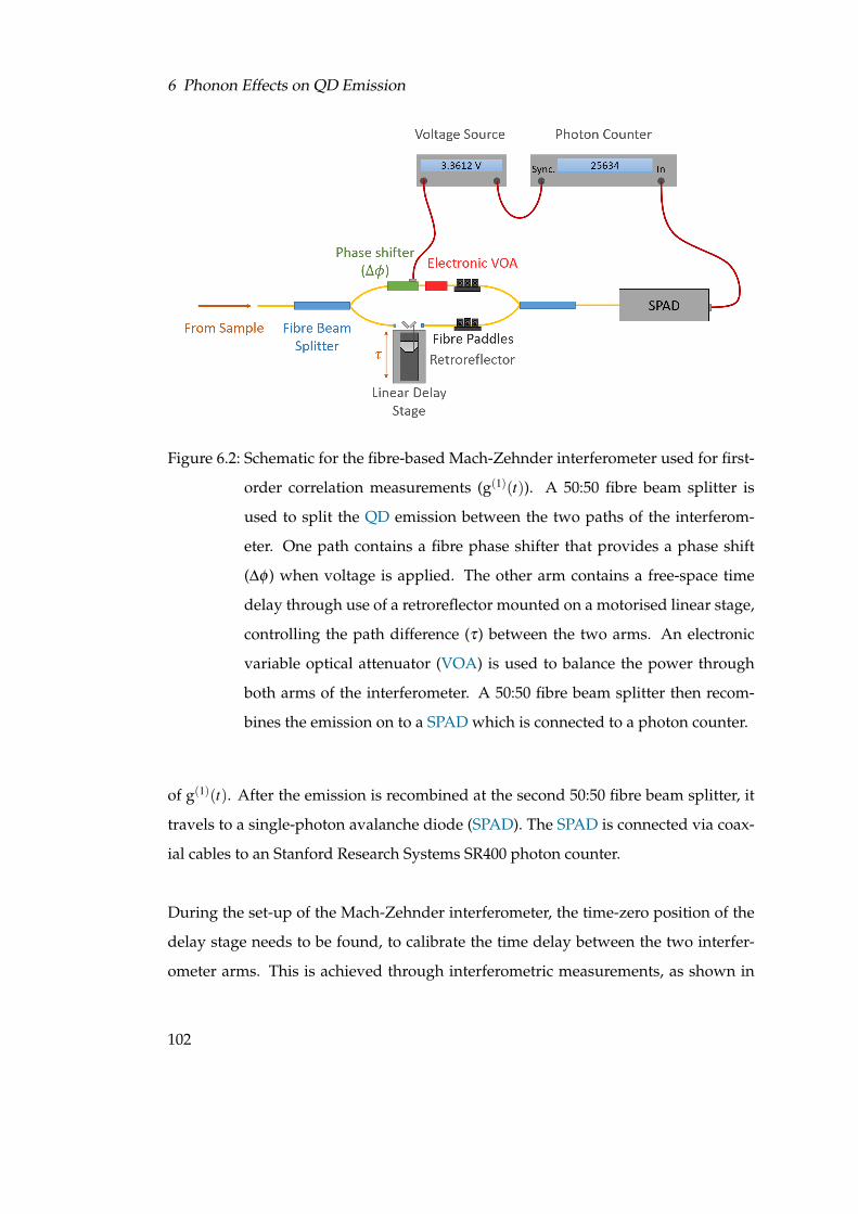
6 Phonon Effects on QD Emission
Figure 6.2: Schematic for the fibre-based Mach-Zehnder interferometer used for first-
order correlation measurements (g(1)(t)). A 50:50 fibre beam splitter is
used to split the QD emission between the two paths of the interferom-
eter. One path contains a fibre phase shifter that provides a phase shift
(∆φ ) when voltage is applied. The other arm contains a free-space time
delay through use of a retroreflector mounted on a motorised linear stage,
controlling the path difference (τ) between the two arms. An electronic
variable optical attenuator (VOA) is used to balance the power through
both arms of the interferometer. A 50:50 fibre beam splitter then recom-
bines the emission on to a SPAD which is connected to a photon counter.
of g(1)(t). After the emission is recombined at the second 50:50 fibre beam splitter, it
travels to a single-photon avalanche diode (SPAD). The SPAD is connected via coax-
ial cables to an Stanford Research Systems SR400 photon counter.
During the set-up of the Mach-Zehnder interferometer, the time-zero position of the
delay stage needs to be found, to calibrate the time delay between the two interfer-
ometer arms. This is achieved through interferometric measurements, as shown in
102

6.3 First-Order Correlation Measurements
- 0 . 1 0 - 0 . 0 5 0 . 0 0 0 . 0 5 0 . 1 00 . 20 . 40 . 60 . 81 . 01 . 21 . 41 . 61 . 82 . 02 . 22 . 4
Coun
ts (x1
04 )
R e l a t i v e s t a g e p o s i t i o n ( m m )
D a t a F i t t i n g
2 . 5 3 . 0 3 . 5 4 . 00 . 0
0 . 5
1 . 0
1 . 5
2 . 0 D a t a
Coun
ts (x1
04 )P h a s e s h i f t e r v o l t a g e ( V )
I m i n
I m a x( a ) ( b )
Figure 6.3: (a) Interferometric measurements are used to find the time-zero position of
the motorised linear stage in the Mach-Zehnder interferometer. The Mira
pulsed Ti:S laser is sent through the interferometer while the delay stage
is stepped. Time-zero occurs when both pulses meet at the second beam
splitter at the same time. This is seen as a maximum in the interference
fringes. (b) Interference fringes recorded as a function of ∆φ by the photon
counter for a fringe contrast measurement, using emission from the QD
under CW excitation. ∆φ is swept by changing the voltage applied to the
fibre phase shifter.
Figure 6.3(a). The Mira Ti:S pulsed laser, tuned to the resonant wavelength of the QD
neutral exciton, is attenuated and sent through the interferometer. The delay stage
is stepped and at each step the signal at the SPAD is recorded by the SR400 pho-
ton counter. Maximum fringe intensity occurs when the laser pulses that have been
split between the two arms of the interferometer arrive simultaneously at the second
beam splitter. This occurs when both arms of the interferometer have the same length
in time or when the τ between the arms differs by the pulse separation of the laser.
103
6 Phonon Effects on QD Emission
However, as the difference between laser pulses corresponds to 3.9 m in free-space or
∼2.69 m in fibre, a comparison of the interferometer arms can be made before mea-
suring time-zero, allowing extra fibre delay to be added if required. It is also useful
to adjust the relative length of fibre in both arms to ensure that time-zero is close to
the near end of the delay stage, as this allows for a larger range of τ delay values to
be reached.
During a g(1)(t) measurement, the time delay (τ) between the two arms of the in-
terferometer is stepped. At each step, a set of interference fringes like those shown in
Figure 6.3(b) are measured. To measure this, the voltage supply steps the voltage to
the electronic phase shifter to change ∆φ . Each time the voltage is stepped, the volt-
age supply also sends a trigger to the “Sync” channel on the SR400 photon counter.
The SR400 is gated to count photons for ∼ 95% of the time that the voltage supply is
set to wait at each voltage. This is done to allow the phase to stabilise after each volt-
age step. After a set of interference fringes has been measured their fringe contrast is
calculated using:
v =Imax− Imin
Imax + Imin. (6.4)
The fringe contrast is calculated for each fringe individually and then averaged to
give the total fringe contrast. The fringe contrast v is related to g(1)(t) through:
v(τ) = (1− ε)|g(1)(τ)|g(1)(0)
, (6.5)
where (1− ε) is the maximum resolvable fringe contrast of the interferometer mea-
sured using a CW laser and is used to account for imperfections in the fibre beam
splitters that would prevent perfect mode overlap. Measuring |g(1)(τ)| gives the time-
averaged coarse-grained value of g(1)(t) as the first-order correlation function also os-
cillates at the transition frequency, resulting in fringes within the g(1)(t). Measuring
|g(1)(τ)| fringes measures the envelope of the first-order-correlation fringes. The mag-
nitude (|...|) is used in Equation 6.5 as the theoretical expression for g(1)(τ) is complex
and only the real components are measured. Fringe contrast v has a magnitude be-
104

6.3 First-Order Correlation Measurements
tween 0 and 1. Therefore, the first-order correlation function has to be normalised
to this range, this is achieved by the factor of 1/g(1)(0). This total fringe contrast can
then be plotted against the time delay (τ) to visualise the temporal coherence of the
QD.
6.3.2 Results and Theory
Figure 6.4(a) shows the results of the g(1)(t) measurement made when the QD is ex-
cited resonant to the neutral exciton, with CW excitation and an excitation power
corresponding to S = 0.25. The CW laser used for this work is the M-Squared Ti:S
and the excitation power was calibrated using the Mollow triplet method described
in Section 3.7.2. This method gives Ω that can then be converted to S using Equa-
tion 6.3, here ∆LX = 0. Both excitation and collection occurred directly above the H1
cavity of the PhC. The emission was collected using the cross-polarisation RF tech-
nique described in Section 3.4.
By using an S of 0.25, the QD is excited well below saturation and coherent scat-
tering is expected to dominate the emission, whilst still ensuring sufficient emission
intensity to perform accurate measurements. The dashed line in Figure 6.4(a) shows
the mono-exponential result expected in this regime using the pure dephasing model
predicted by atomic theory. Instead, the experimental data (triangles) shows a rapid
decay of the coherence in the first few picoseconds. This timescale is comparable to
that seen for phonon interactions in four-wave mixing measurements of InGaAs QDs
[84, 194, 195], suggesting that the rapid loss of coherence is due to the same mecha-
nism, electron-phonon interactions.
Hence, to describe the behaviour seen in Figure 6.4(a) a description of the micro-
scopic nature of the electron-phonon interaction in the QD is needed [196]. Here this
is achieved by applying the polaron transformation to the Hamiltonian of the full
open quantum system. A polaron is a quasi-particle which describes the interaction
105

6 Phonon Effects on QD Emission
0 . 1 1 1 0 1 0 0 1 0 0 00 . 0
0 . 8
0 . 9
1 . 0
E x p e r i m e n t P o l a r o n M E P u r e D e p h a s i n g
Fring
e con
trast
T i m e ( p s )
( a )
( b )
- 2 . 0 - 1 . 5 - 1 . 0 - 0 . 5 0 . 0 0 . 5 1 . 0
1 0 - 3
1 0 - 2
1 0 - 1
1 0 0 E x p e r i m e n t P o l a r o n M E
Inten
sity (a
rb. un
its)
D e t u n i n g ( m e V )
Figure 6.4: (a) First-order correlation measurement at S = 0.25 when ∆LX = 0. The ex-
perimental fringe contrast data (purple triangles) shows good agreement
with a calculation made using the polaron master equation (solid purple
line) where the only free parameters are the phonon coupling strength
(α) and the cutoff frequency (νc) used in the phonon propagator (Equa-
tion 6.8). The dashed purple line shows the monoexponential predicted
by a pure dephasing model, which does not capture the phonon dynam-
ics present. (b) An experimental spectrum (blue triangles), taken at the
same time as the g(1)(t) in (a), is also well produced using the polaron
master equation with the same parameters. The spectrum calculated from
the polaron master equation is convolved with the spectrometer IRF to
reproduced the observed width of the ZPL.
106

6.3 First-Order Correlation Measurements
between a charge and the surrounding lattice. Here, the charged particle is the exci-
ton confined to the QD. When the exciton forms it displaces the surrounding semi-
conductor lattice, which returns to its original state when the exciton recombines.
The QD can be modelled as a two-level system with a ground |0〉 and single-exciton
state |X〉. The two level system is coupled to a phonon bath which can be repre-
sented by a infinite collection of harmonic oscillators. The polaron transformation
displaces the bath of oscillators when the QD is in its excited state [197]. In other
words, the polaron transformation dresses the excitonic states of the system with vi-
brational states, originating from the phonon environment. Dressing the states using
the polaron transformation allows the derivation of a QD master equation (ME) that
is nonperturbative in the electron-phonon coupling strength [99, 197–200]. For the
following theory a more detailed explanation can be found in Brash et al. [200] and
its associated supplement.
In the polaron frame, the first-order correlation function is given by [99]:
g(1)pol(τ) = G(τ)g(1)opt(τ). (6.6)
Here g(1)opt(τ) is the purely optical contribution (equivalent to an ideal TLE) which is
found using the polaron frame ME. G(τ) is the polaron correction function for the
phonon environment, accounting for the non-Markovian phonon relaxation, given
by:
G(τ) = B2eϕ(τ), (6.7)
where B is the Franck-Condon factor, defined as B = e−ϕ(0)/2, and ϕ(τ) is the phonon
propagator defined as:
ϕ(τ) = α
∫∞
0νe−ν2/ν2
c (cos(ντ)coth(ν/2kBT )− isin(ντ))dν . (6.8)
This means that the coupling of the QD to the phonon environment can be described
by the thermal energy of the phonon environment (kBT ) and the coupling strength
(α) and cut-off frequency (νc) for the deformation potential coupling [184, 196, 201].
107

6 Phonon Effects on QD Emission
The coupling strength (α) gives the strength of the exciton-phonon interaction and is
dependent on the bulk properties of the QD [96, 197]. The exponential cut-off with
frequency defines the highest possible energy of the LA phonons associated with a
transition. For excitons in SAQDs the cut-off frequency is proportional to the inverse
of the carrier localisation length, in other words it is inversely proportional to the size
of the QD [184, 197, 202].
The polaron ME is further modified to include the effects of the cavity on the emis-
sion. The Purcell enhancement of the exciton transition is already included within
the ME, but the cavity also leads to spectral filtering of the emission [95]. To include
this effect, the polaron ME is modified to add a cavity filter function, giving the g(1)(t)
correlation function for what is detected in a cavity-based system [200].
Both the cut-off frequency (νc) and the deformation-potential coupling strength (α)
can be extracted by fitting the first 15 ps of the g(1)(t) measurement shown in Fig-
ure 6.4(a). The resulting values of νc = 1.3 ps−1 and α = 0.045 ps2 are comparable to
values previously found for InGaAs QDs [96]. The other parameters in the polaron
ME are set to directly measured values. The solid line in Figure 6.4(a) shows that
the result of the polaron ME accurately reproduces the experimental g(1)(t). After
the first rapid decay in coherence, attributed to phonon relaxation, a second decay in
coherence occurs between τ = 20− 200 ps. This decay is associated with incoherent
resonance fluorescence and is consistent with the radiative lifetime of the QD. After
τ = 200 ps, the g(1)(t) plateaus again. This plateau is caused by the coherent fraction
of the emission where the long coherence time is inherited from the excitation laser.
From the amplitude of the fringe contrast in each region of the g(1)(t) function, the
fraction that each component contributes to the total emission (F) can be determined
(see arrows in Fig. 6.4(a)). This gives a phonon sideband fraction (FPSB) of 0.06, an
incoherent fraction (FINC) of 0.14, and a coherently scattered fraction (FCS) of 0.80.
108

6.3 First-Order Correlation Measurements
To check the accuracy of the components extracted from the polaron ME, the emission
was investigated in the frequency domain as well as the time domain. To measure
this under the same conditions as the g(1)(t) function, part of the emission is sent to
the spectrometer through use of a fibre beam splitter, before the emission reaches the
Mach-Zehnder interferometer. The spectrum measured is shown in Figure 6.4(b) (tri-
angles).
The emission spectrum is calculated theoretically by taking the Fourier transform of
the first-order correlation function derived from the polaron ME. This can be written
in the form:
S(ω) = H(ω)(Sopt(ω)+SSB(ω)), (6.9)
where H(ω) is the frequency-domain cavity filter function [95, 203, 204]. Thus, from
Equation 6.9, the emission spectrum has two main components. One is a purely op-
tical component and is given by:
Sopt(ω) = B2∫ +∞
−∞
g(1)opt(τ)e−iωτdτ. (6.10)
This part includes coherent and incoherent contributions to the spectrum. The second
component, SSB, is a completely incoherent component given by:
SSB(ω) =∫ +∞
−∞
(G(τ)−B2)g(1)opt(τ)e−iωτdτ. (6.11)
This component is attributed to non-Markovian phonon relaxation and leads to the
phonon sidebands in the emission spectrum [95, 99].
Both the optical and sideband components show a dependence on the square of the
Franck-Condon factor (B < 1). The origins of the Franck-Condon factor are shown in
Figure 6.5. The bulk lattice around the QD has a different configuration dependent on
whether the QD is in the ground |0〉 or excited |X〉 state. Both of these lattice config-
urations have their own wavefunctions. The Franck-Condon factor is defined by the
overlap between the two wavefunctions. The probability that the system will emit
109

6 Phonon Effects on QD Emission
Figure 6.5: Origin of the Franck-Condon factor: The ground |0〉 and excited |X〉 states
of the QD have different lattice configurations. The Franck-Condon fac-
tor B corresponds to the overlap of the two lattice configurations. Figure
adapted from Iles-Smith et al. [95].
through the ZPL is B2 and the probability that the system will instead emit through
the PSB is given by the missing fraction of the ZPL, (1−B2) [95].
The theory curve (solid line) plotted on Figure 6.4(b) shows good agreement with
the experimental data (triangles). A broad PSB is seen, which is expected due to the
short timescale of the phonon dynamics. Both the time domain and frequency do-
main measurements show that even in the low power regime well below saturation,
where the excited state population is small, there is still a PSB visible that makes up
∼ 6% of the emission.
110

6.4 Effect of Excitation Power on the Phonon Sideband
6.4 Effect of Excitation Power on the Phonon Sideband
As was shown in Section 6.3, the phonon sideband persists in the low excitation
power coherent scattering regime. To further investigate the effect of S on the PSB,
the RF spectrum is measured for a range of excitation powers using both high and
low resolution spectroscopy.
6.4.1 Experimental Method
The low resolution spectra are measured using the 1200 l mm−1 grating of the spec-
trometer where the PSB can clearly be seen when the spectra are plotted on a semi-log
scale. High resolution spectroscopy on the zero-phonon line (ZPL) is performed us-
ing a Fabry-Pérot interferometer (FPI) by John O’Hara and Alistair Brash. The Fabry-
Pérot has a resolution of 67 MHz (∼ 0.3 µeV) and free-spectral range (FSR) of 10 GHz
(∼ 40 µeV). By scanning the narrow transmission window of the FPI across the entire
FSR, the lineshape of the collected emission can be mapped out. Before the emission
reaches the FPI, the spectrometer is used to filter the emission centred on the ZPL.
The filter bandwidth FWHM of spectrometer is 96 µeV. The filter is centred by mon-
itoring the emission power after the spectrometer and adjusting the grating angle.
The throughput power is maximised when the ZPL is centred through the filter.
The neutral exciton transition of the QD is again excited resonantly (∆LX = 0) above
the H1 cavity with the M-Squared Ti:S. The emission is also collected from the same
position. The cross-polarised RF technique described in Section 3.4 is used to sup-
press the scattered laser. The excitation power is calibrated using Equation 6.3. A
power dependence is measured with the laser being re-suppressed between each
measurement to maximise the signal-to-background ratio.
111

6 Phonon Effects on QD Emission
0 . 0 5 0 . 2 0 . 5 2 5 2 00 . 1 1 1 00 . 0
0 . 2
0 . 4
0 . 6
0 . 8
1 . 0- 3 . 0 0 . 0 3 . 0 6 . 0
1 0 - 3
1 0 - 2
1 0 - 1
1 0 0
Inten
sity (a
rb. un
its)
D e t u n i n g ( m e V )
E x p . P S B Z P L T o t a l
( a )
( b )
- 2 0 - 1 0 0 1 0 2 00 . 0
0 . 5
1 . 0
Inten
sity (a
.u.)
D e t u n i n g ( e V )
E x p . C S I N C Z P L
Fractio
n of to
tal em
ission
G e n e r a l i s e d s a t u r a t i o n p a r a m e t e r
Figure 6.6: Resonance fluorescence spectral components: (a) Low resolution spec-
trum, measured at S = 10, plotted on a semi-log scale where grey triangles
are the experimental data, blue is the fit to the PSB, orange is the fit to the
ZPL and the grey line is the total fit. Inset: High-resolution spectrum of
the ZPL using a Fabry-Pérot interferometer. The grey triangles are the ex-
perimental data; the fit for the coherent scattering is shown in red and for
the incoherent RF in green. The total fit for the ZPL is shown by the yellow
line, this is higher than the incoherent fit as the measured spectra contains
contributions from the incoherent part of two neighbouring FSRs. (b) The
evolution of the RF emission with increasing Ω. Triangles show the ex-
perimental data where blue gives the fraction of the total emission given
by the phonon sideband, red gives the coherent scattering fraction and
green the incoherent emission fraction. The solid lines show the theory
predictions made using the polaron ME model.112

6.4 Effect of Excitation Power on the Phonon Sideband
6.4.2 Results and Theory
Figure 6.6(a) shows a typical spectrum of the resonance fluorescence emission from
the QD measured using both low and high resolution spectroscopy when S = 10. The
PSB can clearly be seen in the low resolution spectrum (grey triangles) as it is plotted
on a semi-log scale. The Gaussian fit to the PSB is shown in blue. The ZPL (orange)
is fitted using a Voigt function. The Voigt function is used as it can incorporate the
Gaussian IRF from the spectrometer, which here was measured to have a FWHM of
68 µeV. The solid grey line shows the combined PSB and ZPL fits. The areas (A) of
these components are used to evaluated the PSB fraction (FPSB):
FPSB =APSB
APSB +AZPL. (6.12)
The inset to Figure 6.6(a) shows the high resolution FPI spectrum (grey triangles)
of the QD ZPL. The broad component (green) is the contribution from the incoherent
resonance fluorescence, the linewidth of which is governed by the transition coher-
ence time T2. The narrow component (red) is the contribution from the coherent scat-
tering. The natural linewidth of the incoherent component is defined as 1/T1. Here
the linewidth is ∼ 25 µeV which is comparable to the ∼ 40 µeV FSR of the FPI. The
broad incoherent scattering component is fitted using a Lorentzian to find AINC. The
narrow coherent scattering component (ACS) is fitted using a Gaussian as the observ-
able linewidth is limited by the IRF of the Fabry-Pérot of ∼ 0.5 µeV. The fraction of
the total emission that is contributed by each component can then be calculated using
the following equations:
FCS =ACS
ACS +AINC
AZPL
APSB +AZPL, (6.13)
and:
FINC =AINC
ACS +AINC
AZPL
APSB +AZPL. (6.14)
113

6 Phonon Effects on QD Emission
Figure 6.6(b) shows the calculated fractions (F) plotted against S . The RF (∆LX = 0)
emission evolves from coherent scattering to incoherent emission as the excitation
power is increased, as would be expected from Equation 6.2. Figure 6.6(b) also shows
that the polaron model (lines) agrees well with the experiment. However, it can be
seen that the coherently scattered fraction does not reach unity at vanishingly small
S. This result has been previously predicted [99] and is accounted for by the fraction
of the emission that is emitted through the phonon sideband (FPSB). Figure 6.6(b)
shows a constant FPSB of ∼ 6% that is independent of Ω.
The origin of the constant FPSB is illustrated in Figure 6.7. The ground (|0〉) and
excited (|X〉) states of the optical transition are dressed by vibronic bands which cor-
respond to the emission or absorption of an LA phonon. In the limit of Ω→ 0, co-
herent scattering dominates, with a probability defined by the square of the Franck-
Condon factor, B2. Coherent scattering, also known as resonant Rayleigh scattering,
is illustrated in Figure 6.7(a). However, due to phonon coupling there is also a finite
probability that the scattering event will end in a different vibrational state of the
ground-state manifold. This is illustrated in Figure 6.7(b) where the probability to
finish in a different vibrational state is given by (1−B2). Inelastic Stokes scattering
occurs when a lower energy photon is emitted, and a phonon is emitted to correct the
energy difference and reach the ground state. Anti-Stokes scattering occurs when a
high energy photon is accompanied by absorption of a LA phonon. At 4.2 K, emission
of a phonon is more likely than absorption, leading to the asymmetry of the phonon
sideband seen in Figure 6.6. As the probability of whether the scattering is Rayleigh
or Stokes/Anti-Stokes depends only on a constant B, then there is always a constant
PSB contribution even at vanishingly small Ω.
114

6.5 Phonon Effects in Detuned Coherent Scattering
| 𝑋
| 0
| 𝑋
| 0
| 𝑋
| 0
StokesRayleigh Anti-Stokes
𝐵2 1 − 𝐵2(a) (b)
Figure 6.7: (a) Coherent scattering (orange-dashed) between the bare ground (|0〉) and
excited (|X〉) states (solid lines) occurs with a probability given by the
Franck-Condon factor squared (B2). (b) The ground and excited states are
dressed by phonon coupling, giving rise to a manifold of vibrational states
(grey shading). The probability of inelastic scattering ending at a different
vibrational state of the ground-state manifold is given by (1−B2). The en-
ergy difference is carried by the emission or absorption of an LA phonon
(red-solid) in Stokes (purple-dashed) or Anti-Stokes (blue-dashed) scatter-
ing processes respectively.
6.5 Phonon Effects in Detuned Coherent Scattering
As well as investigating the influence of phonons on the coherent scattering using
resonant excitation, investigations were also carried out into the effect of detuning
the excitation laser away from the emitter.
115
6 Phonon Effects on QD Emission
6.5.1 Experimental Method
To investigate the effect of detuning, two types of measurements were made. The
first involved measuring spectra using the spectrometer 1200 l mm−1 grating. The
M-Squared CW Ti:S laser is used to excite the QD with hΩ = 5.7 µeV. The power is
calibrated using the method described in Section 3.7.2 when the excitation laser is
resonant with the neutral exciton transition. The M-Squared is then detuned from
∆LX = 0, the background laser scatter is suppressed, and spectra are recorded.
The second method used in this section investigates how the coherent fraction of
the emission changes with detuning. The coherent fraction (FCS) is found using the
g(1)(t) method previously described in Section 6.3. However, rather than measuring
the fringe contrast at a large range of delay times, finding the coherent fraction only
requires the fringe contrast value at time-zero (t0) and at a time when the g(1)(t) is
dominated by coherent emission, in the case of this measurement at 1 ns. The coher-
ent fraction is given by:
FCS =v1ns
vt0. (6.15)
Here, vt0 is the fringe contrast at time-zero and v1ns is the fringe contrast at 1 ns. Un-
derstanding how this can give the coherent fraction requires revisiting Figure 6.4(a),
in which the parts of the g(1)(t) function given by FPSB, FINC and FCS are labelled,
and:
FPSB +FINC +FCS = 1. (6.16)
Looking at these components, it can be seen that Equation 6.15 is the equivalent of
normalising the coherent component to the sum of all contributions:
FCS =FCS
FCS +FINC +FPSB. (6.17)
To allow for any time dependent drifts, five measurements of the fringe contrast are
made at each time point, alternately measuring at each delay stage position. The QD
is excited with hΩ = 25.6 µeV using the M-squared CW Ti:S. The laser is detuned by
∆LX , the laser scatter is suppressed and the FCF is measured.
116

6.5 Phonon Effects in Detuned Coherent Scattering
- 2 - 1 0 1 2 31 0 - 4
1 0 - 3
1 0 - 2
1 0 - 1
1 0 0
Norm
alised
inten
sity
D e t u n i n g ( m e V )
: + 0 . 2 7 m e V - 0 . 2 7 m e V
0 . 2 7 m e V
C S C S
Z P L
- 2 - 1 0 1 21 0 - 3
1 0 - 1
1 0 1
Inten
sity (a
.u.)
D e t u n i n g ( m e V )
Figure 6.8: The influence of phonons on detuned coherent scattering. Semi-log spec-
tra measured with the laser detuned from the ZPL by h∆LX = ±0.27 meV
(blue/red) at a constant hΩ = 5.7 µeV. The coherent scattering (CS) peaks
are separated from the incoherent ZPL. The spectra have been normalised
by the integrated intensity. Inset: Theoretical spectra showing the shift of
the PSB under the same excitation conditions.
6.5.2 Results and Theory
Spectroscopy Measurements
Figure 6.8 shows, on a semi-log plot, spectra of the QD when excited with a CW laser
with a constant hΩ of 5.7 µeV. Two spectra are shown in Figure 6.8 with a laser detun-
ing of h∆LX =±0.27 meV. The coherent scattering peaks, labelled “CS”, dominate the
spectrum and are separated from the ZPL, which remains centred at zero detuning.
For the positive detuning (blue), it can be seen that the PSB is also shifted in the
positive direction by ∼ 0.27 meV. The origins of this shift comes from Equation 6.11,
where the product between (G(τ)−B2) and g(1)opt in the time domain, implies a con-
volution in frequency between the purely optical spectrum and the frequency-space
117
6 Phonon Effects on QD Emission
phonon correlation function. This implies that all optical features have an associated
phonon sideband. The positive detuned spectra shows a +0.27 meV shift in the PSB
for the coherent scattering with respect to the PSB for the ZPL which was measured
when ∆LX = −0.27 meV. The PSB for the ZPL has the same position in both spectra.
It would be expected for the negative detuned spectra to show a −0.27 meV differ-
ence from the negative side of the ZPL. Experimentally this shift is obscured by weak
incoherent backgrounds that occur due to the low counts rates experienced when
exciting with a large ∆LX, here the QD signal is ∼ 50x weaker than when using reso-
nant excitation. The inset to Figure 6.8 shows theoretical spectra calculated under the
same conditions, here the shift in the phonon sideband associated with the coherent
scattering component can clearly be seen for both positive and negative detunings.
The agreement between experiment and theory for positive detunings in Figure 6.8
confirms the interpretation of the product in Equation 6.11, suggesting that all optical
features have a associated phonon sideband.
Detuned Coherent Fraction
Figure 6.9 shows the FCS (grey triangles) found by applying Equation 6.15 to detuned
g(1)(t) measurements. Due to the low count rates when measuring far-detuned from
the ZPL, the main source of error in FCS is shot noise from the detectors. This leads
to the error bars on Figure 6.9 increasing at larger detunings from the ZPL (∆LX = 0).
Both the predictions from the atomic model (green) and the polaron ME (red) are
plotted on Figure 6.9. The coloured areas of the theoretical models are the confidence
bounds given by the experimental uncertainty in Ω. Again, a clear deviation away
from the monotonic increasing of FCS with detuning predicted by the atomic model
is seen in the experimental data. The initial increase of FCS shown in the data is pre-
dicted by both theoretical models. This increase is caused by the phonon interaction
being weaker close to zero detuning [205] and so the atomic interaction dominates.
As the detuning increases in either direction, the coherent fraction starts to decrease.
This decreases occurs due to excitation-induced dephasing (EID) which arises from
118

6.5 Phonon Effects in Detuned Coherent Scattering
- 0 . 8 - 0 . 4 0 . 0 0 . 4 0 . 80 . 0
0 . 2
0 . 4
0 . 6
Cohe
rent fr
actio
n
L a s e r d e t u n i n g ( m e V )
E x p e r i m e n t A t o m i c M o d e l P o l a r o n M E
Figure 6.9: The influence of phonons on detuned coherent scattering. The coherent
fraction (FCS) is measured at different laser detunings (∆LX), using a con-
stant hΩ of 25.6 µeV. The grey triangles show the experimental data. The
green and red areas show respectively the atomic and polaron ME model
predictions. The areas represent the uncertainty in the experimental Ω,
and both models include additional pure dephasing and spectral wander-
ing corrections.
LA phonon mediated transitions between the dressed states of an optically excited
emitter [96, 206]. As the rate of the EID is proportional to (Ω2 +∆2LX ), the coherent
scattering fraction FCS decreases as ∆2LX increases.
Figure 6.9 can be understood by comparison with Figure 6.10. Again the “bare”
ground (|0〉) and excited (|X〉) states are shown dressed by the phonon manifolds
(grey). When ∆LX > 0 (green dashed arrow), an LA phonon (red arrow) can be emit-
ted into the lattice. This allows the |X〉 state to become populated [205], increasing
the probability of incoherent emission (purple arrow). This leads to a decrease in the
coherent fraction (FCS) for ∆LX > 0 as seen in Figure 6.9.
119

6 Phonon Effects on QD Emission
| 𝑋
| 0
| 𝑋
| 0
| 𝑋
| 0
RayleighRayleigh Inc. Rayleigh
Δ𝐿𝑋 > 0 Δ𝐿𝑋 < 0Δ𝐿𝑋 = 0
Figure 6.10: For ∆LX > 0, emission of an LA phonon can populate |X〉. This leads to
an increased probability of incoherent emission, reducing the coherent
fraction. For ∆LX < 0, population of |X〉 requires the absorption of an
LA phonon which is a weak effect at 4.2 K. This limits the possibility of
incoherent emission, and so the coherent fraction begins to increase again
back towards the limiting atomic case.
For ∆LX < 0 (blue dashed arrow) to populate the |X〉 state requires the absorption
of an LA phonon (red) from the lattice. However, at 4.2 K the probability of this
occurring is low [184, 207, 208], inhibiting incoherent scattering. Also, due to the
asymmetry of the phonon manifold [184, 205], the laser detuning exceeds the cut-off
energy for phonon coupling for significantly smaller detunings than when ∆LX > 0.
This leads to a recovery of FCS back towards the limiting atomic case at larger neg-
ative detunings. Resulting in the clear asymmetry seen in the experimental data of
Figure 6.9, the behaviour of which is well modelled by the polaron ME.
120

6.5 Phonon Effects in Detuned Coherent Scattering
Corrections to the Polaron and Atomic Models
Both the atomic and polaron models shown in Figure 6.9 have been corrected for
the QD system used here. When driving off resonance, both the atomic and polaron
models significantly overestimate the coherent fraction that is seen in the experiment.
Here, this has been attributed to pure dephasing originating from charge noise gen-
erated by the reduced scattering cross-section of the QD when exciting off resonance.
The reduced scattering cross-section allows the detuned laser to be absorbed by the
doped bulk material instead [209]. Figure 6.4 shows strong agreement between the
polaron model (with zero pure dephasing) and the experimental data when driving
resonantly. It is therefore suggested that the effect of the pure dephasing only be-
comes significant at large detunings, where the absorption cross-section of the QD
reduces.
To capture the detuning-dependent dephasing in both the atomic and polaron mod-
els, a Lorentzian detuning-dependent dephasing term:
γ(∆LX) = γmax(1−ξ2/(∆2
LX +ξ2)), (6.18)
is used to represent the reducing QD absorption cross-section, where ξ is the natural
linewidth of the QD. When the polaron ME model, with this extra term, is fitted to
the experimental data shown in Figure 6.9, an amplitude of γmax = 21± 0.1 µeV is
found. Figure 6.11(a) shows the modelled detuning-dependent pure dephasing rate,
with Figures 6.12(a) and 6.12(b) showing the dephasing term applied to the polaron
(red dashed) and atomic (green dashed) models respectively; the original models are
plotted with dotted lines.
As well as overestimating the coherent fraction at large detunings, both models also
produce a dip at ∆LX = 0 which is significantly narrower than what is observed in
the experimental data. The suggested reason for this is spectral wandering of the
121

6 Phonon Effects on QD Emission
- 0 . 8 - 0 . 4 0 . 0 0 . 4 0 . 80
5
1 0
1 5
2 0
2 5 D e p h a s i n g
γ (µe
V)
L a s e r d e t u n i n g ( m e V )
( a ) ( b )
- 0 . 8 - 0 . 4 0 . 0 0 . 4 0 . 81 0 - 4
1 0 - 3
1 0 - 2
1 0 - 1
1 0 0 T o t a l C o h e r e n t
Powe
r (arb.
units)
L a s e r d e t u n i n g ( m e V )
Figure 6.11: (a) Theory plot of the detuning-dependent dephasing rate γ(∆LX). (b)
Theory plot of the total (blue) and coherent (red) powers of the QD emis-
sion from the polaron model.
QD, on a timescale T2, due to the charge environment around the QD. In Section
5.3.4, a reduction in Hong-Ou-Mandel visibility for this sample was observed on the
timescale of tens of nanoseconds [106], inferring the presence of such spectral wan-
dering. The effect of spectral wandering is to give a time-varying detuning between
the QD and the laser, meaning that the resulting spectrum contains contributions
from multiple detunings that are weighted according to the noise function associated
with the wandering. To account for the spectral wandering, the polaron and atomic
models are convolved with a Gaussian noise function. The FWHM of the Gaussian
noise function is found to be 66 µeV by fitting the incoherent peak of detuned spec-
tra, for example, the spectra shown in Figure 6.8. The incoherent peak is fitted with a
Voigt function whose Lozentzian width is set to be the natural linewidth of the QD. To
include these effects in the theoretical model, the detuning-dependence of the coher-
ent and incoherent power scattered by the QD (Figure 6.11(b)) is convolved with this
noise function. From these plots, FCS is then calculated according to Equation 6.15 as
before, producing the solid curves in Figure 6.12.
122
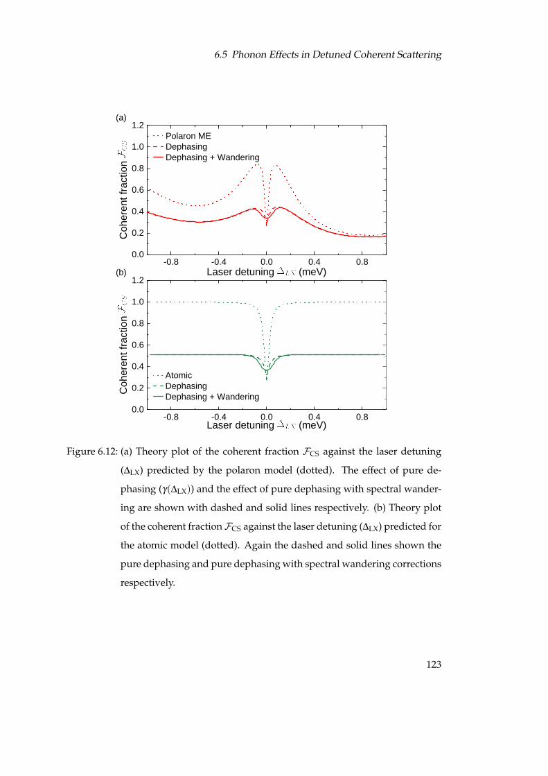
6.5 Phonon Effects in Detuned Coherent Scattering
- 0 . 8 - 0 . 4 0 . 0 0 . 4 0 . 80 . 00 . 20 . 40 . 60 . 81 . 01 . 2
Cohe
rent fr
actio
n
L a s e r d e t u n i n g ( m e V )
P o l a r o n M E D e p h a s i n g D e p h a s i n g + W a n d e r i n g
- 0 . 8 - 0 . 4 0 . 0 0 . 4 0 . 80 . 00 . 20 . 40 . 60 . 81 . 01 . 2
A t o m i c D e p h a s i n g D e p h a s i n g + W a n d e r i n gCo
heren
t frac
tion
L a s e r d e t u n i n g ( m e V )
( b )
( a )
Figure 6.12: (a) Theory plot of the coherent fraction FCS against the laser detuning
(∆LX) predicted by the polaron model (dotted). The effect of pure de-
phasing (γ(∆LX)) and the effect of pure dephasing with spectral wander-
ing are shown with dashed and solid lines respectively. (b) Theory plot
of the coherent fractionFCS against the laser detuning (∆LX) predicted for
the atomic model (dotted). Again the dashed and solid lines shown the
pure dephasing and pure dephasing with spectral wandering corrections
respectively.
123

6 Phonon Effects on QD Emission
Figure 6.11(b) shows the emitted power of the QD against the laser detuning (∆LX)
calculated using the polaron model, illustrating why a detuned spectra is used to
quantify the spectral wandering. Figure 6.11(b) is plotted on a semi-log scale. When
the QD is excited resonantly (∆LX = 0), any wandering results in a sharp drop in the
emitted intensity from the QD due to the steep gradient. Consequently, any spectral
wandering has very little effect on the QD spectra measured as the resonant emission
dominates and any wandering is effectively converted to blinking. However, away
from resonance the gradient of the emitted power is shallower, so the full wandering
distribution contributes to the spectrum. It can also be seen from Figure 6.11(b) that
the coherent emission from the QD is symmetrical with detuning but that the total
emission is asymmetric, demonstrating the reduction in phonon-mediated emission
at negative detunings, which leads to the recovery of the coherent scattering fraction.
Figure 6.12 shows how convolving spectral wandering with the polaron model and
atomic model, both of which have already been corrected for the detuning-dependent
pure dephasing, broadens the central dip. It is important to note from Figure 6.12 that
these corrections only serve to capture additional effects observed in experiments,
they do not change the qualitative features of the two models. The solid curves in
Figure 6.12 incorporating both pure dephasing and spectral wandering are shown
with the experimental data in Figure 6.9.
6.6 Conclusion
The results in this chapter show that, for a solid-state emitter, a fixed fraction of
the emitted light is always lost through the phonon sideband. The PSB is present
regardless of excitation power or detuning. The presence of the phonon sideband
is demonstrated through both first-order correlation (g(1)(t)) measurements and the
use of spectroscopy. These results are modelled using a polaron ME approach which
shows excellent agreement with the measured QD properties. The presence of the
124
6.6 Conclusion
PSB is fundamentally incompatible with atomic model physics where there is no cou-
pling of the emitter to its surroundings, demonstrating the importance of using accu-
rate modelling of solid-state emitters to include their environment.
The polaron ME model is then used to explain the fixed fraction shown experimen-
tally to be emitted through the PSB regardless of the Rabi frequency (Ω). The PSB
area depends solely on the Franck-Condon factor (B); the probability that a photon
will be emitted into the ZPL is B2, leaving a (1−B2) probability that the emission will
involve either the absorption or emission of a phonon. The presence of a PSB whose
area is independent of Ω supports theoretical work that predicts the presence of a
PSB even at vanishingly weak resonant driving [99].
CW detuning measurements of the emitted spectra from the QD show that all fea-
tures of the emission have an associated PSB with the total area of the PSBs still
governed by (1− B2). Here, a PSB was observed both for the ZPL when exciting
detuned but also for the coherently scattered photons which have a frequency equal
to the laser frequency. This phenomenon is described within the polaron ME model,
where a frequency-domain convolution between the optical and PSB components of
the spectrum is found. Measurements of the coherently scattered fraction of the emis-
sion (FCS) with detuning also show the strong influence of phonons. FCS cannot be
described by the monotonic increase with increasing detuning that is predicted by
the atomic model. These effects can, however, be understood by applying phonon
dressing to the “bare” optical transition and modelling the system using the polaron
ME. These measurements also illustrate the asymmetry of the phonon coupling at
4.2 K, where emission of a phonon is more likely than absorption. This asymmetry
allows the cut-off for phonon coupling to be exceeded for negative detuning, causing
the coherent fraction to tend back towards the limiting atomic case for large negative
detunings.
125

6 Phonon Effects on QD Emission
These results were measured using a QD, but are applicable to all solid-state emit-
ters where interactions can occur with the environment. Understanding that these
phonon effects are present in solid-state systems even under the conditions of vanish-
ingly small excitation power or large detunings is important for the development of
indistinguishable single-photon sources, as these processes can lead to a fundamen-
tal limit to the indistinguishability of the photons produced [95]. Furthermore, these
phenomena are also important for a number of other quantum optics applications.
For example in a spin-photon entanglement experiment based on coherent scatter-
ing from Zeeman split states [172], the atomic model suggests that the laser should
be tuned to equal and opposite detunings from the two transitions. For solid-state
emitters, the asymmetry in FCS observed in this chapter will lead to unequal scat-
tering probabilities, compromising the entanglement fidelity. By reoptimising such
schemes with an appropriate model of phonon interactions, optimal performance
could be restored even in the presence of phonon interactions.
126

7 Spectral Filtering Effects on QD
Resonance Fluorescence
The work presented in this chapter has been published in:
Catherine L. Phillips, Alistair J. Brash, Dara P. S. McCutcheon, Jake Iles-Smith,
Edmund Clarke, Benjamin Royall, Maurice S. Skolnick, A. Mark Fox, and Ahsan
Nazir.
“Photon Statistics of Filtered Resonance Fluorescence.” Physical Review Letters 125,
043603 (2020).
Hanbury Brown and Twiss second-order correlation measurements were set up and
carried out by Catherine Phillips and Alistair Brash, including the setting up, opti-
misation and use of all the spectral filters. The 4f tunable filter was built with the
additional assistance of Kévin Seurre. Sensor theory modelling for the g(2)(t) and
g(2)(0) measurements was performed by Ahsan Nazir, Dara McCutcheon and Jake
Iles-Smith. The MATLAB simulations of the emission spectra, transmission coeffi-
cients and filtered fractions (F) were performed by Catherine Phillips.
7.1 Introduction
Spectral filtering of the resonance fluorescence (RF) from a two level emitter (TLE) is
commonly employed in quantum-optics experiments to improve the single-photon
purity and indistinguishability. A single-photon source (SPS), where the emitted pho-
tons are indistinguishable, is necessary for measurements schemes where quantum
127

7 Spectral Filtering Effects on QD Resonance Fluorescence
interference is required. For example, it is required for quantum simulators [210],
boson sampling [27, 28], linear optical quantum computing [211] and quantum re-
peaters [212]. These schemes also require a high efficiency of single-photon produc-
tion, where the SPSs are bright with a high collection efficiency.
The filters used in quantum-optics experiments are typically centred on the zero-
phonon line (ZPL) of the emission and are used to remove residual backgrounds from
the excitation laser [106, 155], other transitions [213] or phonon sidebands [213–215].
Whilst filtering out these components will improve the single-photon indistinguisha-
bility measured in HOM experiments, this always occurs at the cost of the efficiency
[95]. Furthermore, as the bandwidth (Γ) of the filter approaches the natural linewidth
(γ) of the ZPL, theory has predicted that the measured photon statistics of the RF
emission are strongly modified in both the weak (coherent scattering) [216, 217] and
strong (Mollow) driving regimes [218].
This chapter presents a joint experimental and theoretical investigation into the influ-
ence of filtering RF with bandwidth comparable to the natural linewidth. Hanbury
Brown and Twiss (HBT) g(2)(0) experiments are used to measure the photon statis-
tics of spectrally filtered QD RF. Both the low and high power driving regimes are
investigated using a range of spectral filters with different Γ. Simulations of the com-
ponents of the emission after filtering provide insight into the observed modifications
of the photon statistics. The experimental results show excellent agreement with an
extended theoretical model based on the sensor formalism.
7.2 Filtering QD emission
For the following measurements the QD, described in Chapter 4, was slightly de-
tuned from the cavity, leading to a Purcell Factor of 30, which gives a broad natural
line width (γ) of 20 µeV. This enables spectral filtering of the QD RF emission with a
128

7.2 Filtering QD emission
bandwidth (Γ) smaller than γ . Five different filters are used to filter the RF emission.
Four of the filters have a fixed spectral bandwidth (Γ) whereas the fifth filter has a
tunable Γ. The values of Γ used are shown in Table 7.1. The following section de-
scribes the filters and how Γ was measured.
4f Tunable Filter
Figure 7.1 is a schematic diagram of the 4f tunable filter. This filter has both a tunable
Γ and centre wavelength. The 4f tunable filter uses the same principles as the 4f pulse
shaper (Fig. 3.2) used with the Mira Ti:S pulsed laser but in a more compact folded ge-
ometry. The transmission grating splits the emission into its spectral components. A
cylindrical lens is mounted one focal length (f) after the grating, focusing the diverg-
ing, spectrally separated emission at the Fourier plane located one focal length after
the lens. In this plane, each position corresponds to an optical frequency of the input
beam. Therefore, by placing an adjustable slit in the Fourier plane, certain wave-
lengths of light can be transmitted while others are removed from the emission. The
filtered emission is then reflected back through the cylindrical lens and is focussed
on the grating. The spectral components are recombined at the transmission grating
and the filtered emission is recoupled into a single-mode fibre. Unlike the 4f pulse
shaper, which uses two gratings spaced 4f apart, the 4f filter has a folded geometry
and only uses one grating. This means that the filter has a smaller spatial footprint as
the filter only needs to be 2f long.
The folded geometry is also advantageous for alignment. In a 4f geometry the second
grating recombines the spectral components that were spatially separated by the first
grating. The quality of the recombination is quantified by the spectro-spatial over-
lap of the filtered beam after the second grating. Perfect spectro-spatial overlap oc-
curs when the grating perfectly reverses the splitting caused by the first grating. The
spectral splitting depends on the first grating’s angle and tilt with respect to the input
beam. For the second grating to reverse the splitting requires having the same grating
129

7 Spectral Filtering Effects on QD Resonance Fluorescence
Filter Bandwidth Γ (µeV)
Free-space Fabry-Pérot - Thorlabs SA210-8B 0.25
Etalon - Light Machinery 1.6mm fused silica 5.8
Fibre Fabry-Pérot - Micron Optics FFP-TF2 17
1200 l mm−1 grating spectrometer - Princeton 97
4f tunable filter 454
4f tunable filter 3051
Table 7.1: Bandwidth (Γ) of spectral filters.
angle and tilt with respect to the beam as the first grating. The spectro-spatial overlap
after the second grating can be checked by moving a beamblock laterally through the
Fourier plane of the filter and viewing the emission after the grating on an IR card.
For perfect spectro-spatial overlap, blocking part of the beam only affects the inten-
sity of the observed beam. If the spectro-spatial overlap is not optimised, moving
the beamblock will cause the observed spot to move. This occurs as the separated
spectral components in the Fourier plane are being focussed at different points on
the grating. Herein lies the advantage of the folded geometry; by travelling through
the same grating, the input and output beams have the same angles, provided that
both beams have vertical alignment on the grating and that the grating is level in the
horizontal direction.
The resolution of diffraction gratings is given by:
∆λ =λ
mN, (7.1)
where ∆λ is the smallest resolvable difference in the wavelength, m is the diffrac-
tion order and N is the number of illuminated grooves. Therefore, to maximise the
resolution by optimising N, a 1500 l mm−1 transmission grating is used, with the
optics before the grating designed to fill the width of the grating with collimated
emission. The tilted mirror provides a vertical displacement between the input and
130

7.2 Filtering QD emission
150 mm cylindrical lens
75.6 mm cylindrical lens
10 mm cylindrical lens
Pickoff mirror
1500 l mm-1
transmission grating
Tip, tilt and rotation stage
Fiber paddles –polarisation control
Adjustable slit mounted on linear stage
Tilted mirror
Single mode fibre - Output
Single mode fibre - Input
Figure 7.1: Schematic of the filter with tunable centre wavelength and filter band-
width achieved by using a 4f pulse shaper design with a 1500 l mm−1
transmission grating.
output beams, allowing a semicircular pickoff mirror to be used to divert the filtered
emission so that it can be recoupled into the fibre. It is due to the vertical displace-
ment and the large beam waist that pairs of cylindrical lenses are used for the fibre
coupling. If spherical lenses are used, then filling the lens and having a vertical offset
from the centre of the lens causes spherical aberration in the beam. This spherical
aberration leads to the beam having a crescent shape when viewed in the far field,
reducing the efficiency with which it can be coupled in to single-mode fibre. Using
a pair of cylindrical lenses to collimate the beam onto the transmission grating also
allows the beam shape to be modified so that it is wide in the x-axis but narrow in the
y-axis. This allows greater resolution, as the width of the rectangular grating, 5 cm
wide by 1 cm tall, can be filled without a loss in throughput efficiency.
131
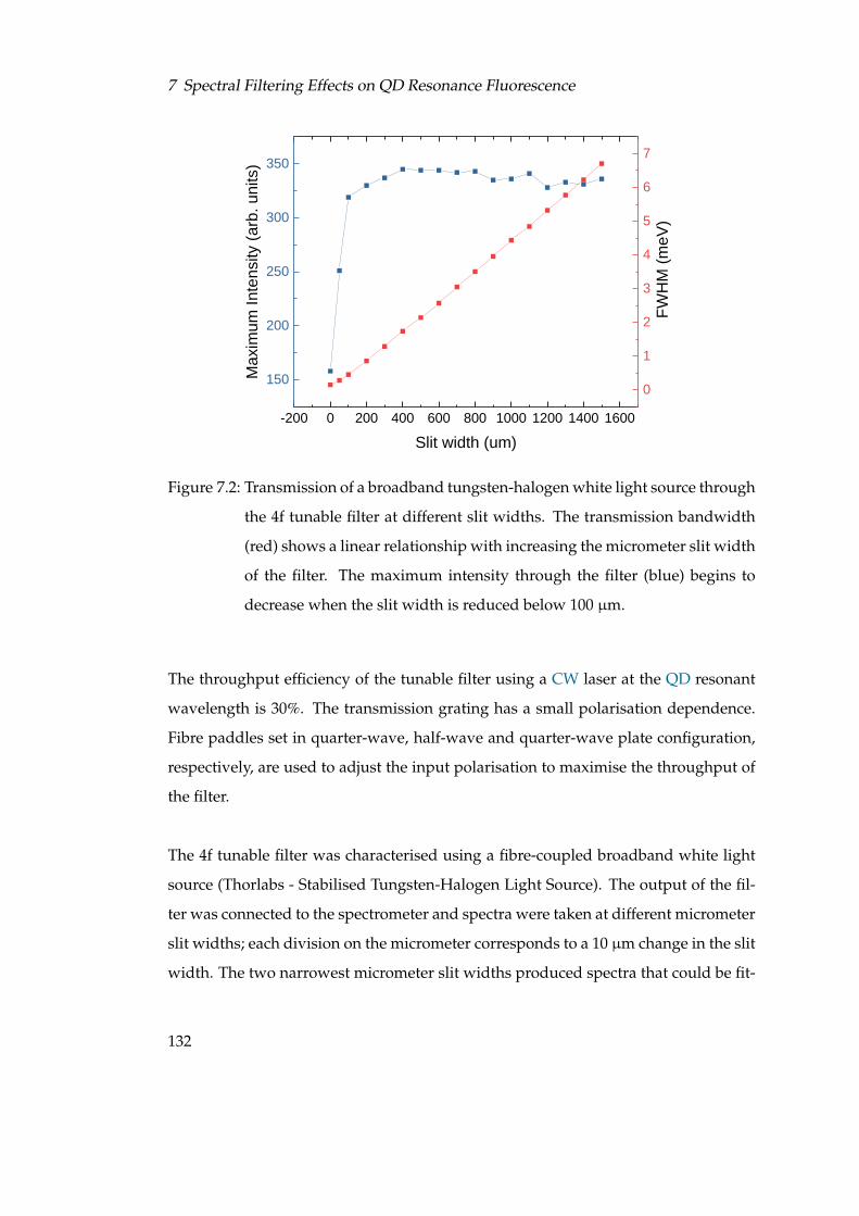
7 Spectral Filtering Effects on QD Resonance Fluorescence
- 2 0 0 0 2 0 0 4 0 0 6 0 0 8 0 0 1 0 0 0 1 2 0 0 1 4 0 0 1 6 0 0
1 5 0
2 0 0
2 5 0
3 0 0
3 5 0
S l i t w i d t h ( u m )
Maxim
um In
tensity
(arb.
units)
01234567
FWHM
(meV
)
Figure 7.2: Transmission of a broadband tungsten-halogen white light source through
the 4f tunable filter at different slit widths. The transmission bandwidth
(red) shows a linear relationship with increasing the micrometer slit width
of the filter. The maximum intensity through the filter (blue) begins to
decrease when the slit width is reduced below 100 µm.
The throughput efficiency of the tunable filter using a CW laser at the QD resonant
wavelength is 30%. The transmission grating has a small polarisation dependence.
Fibre paddles set in quarter-wave, half-wave and quarter-wave plate configuration,
respectively, are used to adjust the input polarisation to maximise the throughput of
the filter.
The 4f tunable filter was characterised using a fibre-coupled broadband white light
source (Thorlabs - Stabilised Tungsten-Halogen Light Source). The output of the fil-
ter was connected to the spectrometer and spectra were taken at different micrometer
slit widths; each division on the micrometer corresponds to a 10 µm change in the slit
width. The two narrowest micrometer slit widths produced spectra that could be fit-
132

7.2 Filtering QD emission
ted using a Gaussian function as the slit width becomes comparable to the diameter
of the focal spot of a single frequency component in the Fourier plane. However, for
slit widths wider than 50 µm, the spectra become top-hat in shape and so could not
be fitted in the same way. Here the FWHM was measured by finding the wavelength
halfway up the rising and falling edges of the top-hat spectra and taking the differ-
ence between these points.
Figure 7.2 (red) shows the results of the micrometer slit width dependence. The mea-
surements show a linear dependence between the width of the slit and the transmit-
ted bandwidth. As well as measuring the FWHM of the spectra, the maximum inten-
sity of the spectra for each micrometer slit width was also analysed and is shown in
blue on Figure 7.2. The intensity measurements show that the filter does not cause the
transmitted signal to lose throughput intensity with slit width change, apart from at
slit widths below 100 µm (454 µeV). This means that the slit does not clip the beam,
implying that the filter is well aligned and the distance between the focussing lens
and the slit is f, the focal length of the lens. In the following experiment, 454 µeV is
the smallest Γ used for the 4f tunable filter.
Spectrometer filtering
As well as being used to take spectra, the Princeton spectrometer can also be used
as a spectral filter. The 1200 l mm−1 grating is used to separate out emission into
its different wavelength components and these are usually directed onto the CCD of
the spectrometer. However, a diverting mirror can be flipped in front of the CCD to
direct the separated emission out of an adjustable exit slit, where it can then be cou-
pled back into a single-mode fibre. The Γ of the spectrometer filtering is governed
by the width of the exit slit, as well as by the coupling of the filtered emission back
into a single-mode fibre. The angle of the grating can be adjusted to change the cen-
tral wavelength transmitted through the filter. The spectrometer’s Γ was found by
sending the attenuated Mira Ti:S pulsed laser through the spectrometer. The filtered
133

7 Spectral Filtering Effects on QD Resonance Fluorescence
- 4 0 0 - 3 0 0 - 2 0 0 - 1 0 0 0 1 0 0 2 0 0 3 0 0 4 0 002 0 04 0 06 0 08 0 0
1 0 0 01 2 0 01 4 0 01 6 0 0
Inten
sity (a
rb. un
its)
D e t u n i n g ∆ ( µe V )
D a t a F i t t i n g
Figure 7.3: Transmission of the attenuated broad Mira Ti:S laser pulse through the
Princeton spectrometer using the 1200 l mm−1 grating. The resulting spec-
tra (black) is measured on a second spectrometer and fitted with a Gaus-
sian (red). The Γ is the FWHM of the Gaussian, 97 µeV.
emission was then measured on a second spectrometer and fitted with a Gaussian to
give the Γ of 97 µeV. The measurement is shown in Figure 7.3. The width of the exit
slit was kept constant for all of the following measurements.
Etalon Filters
The bandwidth for the two Fabry-Pérot filters were found using the following equa-
tion:
Γ =FSRF
, (7.2)
where Γ is the spectral bandwidth of the filter, FSR is the free spectral range and F
is the Finesse of the cavity. The FSR and F are supplied on the datasheets for both
filters.
134

7.2 Filtering QD emission
- 3 0 - 2 0 - 1 0 0 1 0 2 0 3 005 0
1 0 01 5 02 0 02 5 03 0 03 5 04 0 04 5 0
Inten
sity (a
rb. un
its)
D e t u n i n g ∆ ( µe V )
D a t a F i t t i n g
Figure 7.4: Transmission through the Light Machinery etalon measured by scanning
the tunable M-Squared Ti:S CW laser. The M-Squared was stepped by
18 pm and the transmission recorded on a power meter. The resulting
spectra (black) is fitted with a Lorentzian (red) to give a Γ of 5.8 µeV.
Fabry-Pérot interferometers have two high reflectivity mirrors that create a cavity.
Constructive interference occurs when the distance between the mirrors is integer
multiples of λ/2 and that wavelength (λ ) is transmitted out of the far side of the
cavity. Both of the Fabry-Pérot filters are scanning tunable interferometers. For the
Thorlabs tunable Fabry-Pérot etalon, one of the mirrors is mounted on a piezo actu-
ator so the cavity length can be tuned by applying a voltage to the piezo. The fibre
Fabry-Pérot utilises a cavity created through the use of fibre Bragg mirrors rather than
a free-space cavity.
Tunable Fabry-Pérots can be used to transmit a single narrow bandwidth or, by scan-
ning through a free spectral range (FSR) of the etalon, to build up a broader high-
resolution transmission spectra. Broad high resolution scanning using a Fabry-Pérot
135

7 Spectral Filtering Effects on QD Resonance Fluorescence
was shown in Section 6.4. To transmit the single narrow bandwidth, the required
central transmission wavelength needs to be selected and locked. Locking the trans-
mitted wavelength is achieved by continually adjusting the applied bias, keeping the
transmitted signal maximised on a single-photon detector if the peak of the emission
spectrum is the required centre wavelength. The filter output can also be monitored
on a spectrometer if the centre wavelength required is not at the peak of the emission
spectrum. For the following measurements, a narrow bandwidth was required, and
the signal was locked by keeping the transmitted signal maximised.
The Light Machinery etalon is a 1.6 mm thick fused silica solid etalon. This type
of etalon does not use mirrors separated by an air gap to create a cavity. Instead,
it comprises a solid piece of silica with coated faces. Rather than tuning the centre
wavelength of the filter by moving one of the mirrors, the etalon centre wavelength
can be tuned by slightly changing the angle of the incident beam. The Γ of this fil-
ter was found by measuring the transmission as a function of wavelength of the M-
Squared Ti:S CW laser through the etalon. The wavelength of the Ti:S was stepped
by 18 pm and the resulting transmission peak, shown in Figure 7.4 was fitted with a
Lorentzian to give a Γ of 5.8 µeV.
7.3 Weak Driving Regime
When using resonant continuous wave (CW) excitation and an emitter with a lifetime
limited coherence time (T2 = 2T1), the weak excitation regime is defined as Ω2R < (γ2/2)
where ΩR is the Rabi frequency and is defined as γ = 1/T1. This regime is often termed
the Resonant Rayleigh Scattering (RRS) or Heitler Regime [49, 163, 219]. In this ex-
citation regime the resonance fluorescence (RF) spectrum from a two-level system,
such as a QD, has two components: a coherent part and an incoherent part. This was
described in Section 6.2 but is reiterated here as an understanding of both compo-
nents is essential for the following experiments. The origin of these two components
136

7.3 Weak Driving Regime
Figure 7.5: (a) Coherent scattering from a two-level emitter. (b) Incoherent emission
from a two-level emitter; the laser photon is absorbed and populates the
transition’s excited state. The transition then relaxes due to spontaneous
or stimulated emission on a timescale given by T1, emitting a photon with
the energy of the transition.
is again shown in Figure 7.5. The coherent component, shown in Figure 7.5(a), comes
from photons that are coherently scattered by the transition. Here, excitation and
emission become a single coherent event and the elastically scattered photons retain
the coherence of the excitation laser. This leads to a sub-natural linewidth which is
characteristic of a long coherence time [49, 106, 160, 163, 164, 166]. The incoherent
component, shown in Figure 7.5(b), occurs where a photon is absorbed, exciting the
(TLE) from the ground (|0〉) to excited (|X〉) state. Then, by spontaneous or stimulated
emission, the system relaxes back to the ground state, emitting a photon of the same
energy. The linewidth of the incoherent emission is governed by the transition coher-
ence time T2. In the absence of pure dephasing, this is given by the natural linewidth
γ = 1/T1. In Chapter 6, the effect of the solid-state environment on the coherent scat-
tering was investigated. In Chapter 7, investigations are carried out into how the
photon statistics of the scattered and emitted photons are effected, after emission, by
spectral filtering.
137

7 Spectral Filtering Effects on QD Resonance Fluorescence
7.3.1 Experimental Method
The CW laser used for all measurements in this chapter is the Toptica DL Pro. The
neutral exciton of the QD is resonantly excited with a CW laser of energy hωL, induc-
ing a Rabi frequency of ΩR = 0.5γ . ΩR is calibrated using the method described in
3.7.2. The broad γ = 20 µeV of the QD allows the regime of Γ < γ to be explored in the
following HBT g(2)(t) measurements using the filters described in Table 7.1 and the
method described in Section 5.2.1. Here, a CW laser is used instead of a pulsed laser
and the detectors used are the superconducting nanowire single-photon detectors
(SNSPDs).
7.3.2 Results and Theory
Figure 7.6(a) shows the simulated total spectrum (blue) of the QD RF emission at
ΩR = 0.5γ , with the coherent and incoherent components modelled using Lorentzian
line shapes. Under these excitation conditions the natural linewidth (green) of the
QD is 20 µeV with the coherent peak (red) having a linewidth of ∼10 neV inherited
from the resonant CW excitation laser. The area of the coherent peak relative to the
total emission spectrum for the TLE is given by the coherent scattering fraction FCS
[167] calculated using Equation 7.3:
FCS =1
1+2Ω2R/γ2 , (7.3)
which is derived from Equations 6.2 and 6.3 using T2 = 2T1, ∆LLX = 0 and γ = 1/T1.
When ΩR = 0.5γ , Equation 7.3 gives a coherent scattering fraction (FCS) of 2/3. Fig-
ure 7.6(b) shows a high resolution spectrum (triangles) of the QD measured using
a scanning Fabry-Pérot interferometer, measured by Alistair Brash and John O’Hara
under the same conditions as Figure 7.6(a). The grey line shows the total simulated
spectrum from Figure 7.6(a), convolved with the Gaussian IRF of the Fabry-Pérot in-
terferometer which has a FWHM of 1.5 µeV.
A simulation of the normalised transmission of each of the components from the
138

7.3 Weak Driving Regime
- 1 0 - 8 - 6 - 4 - 2 0 2 4 6 8 1 01 0 - 5
1 0 - 4
1 0 - 3
1 0 - 2
1 0 - 1
1 0 0
Inten
sity (a
rb. un
its)
D e t u n i n g ∆ ( µe V )
T o t a l I N C C O H
1 0 - 3 1 0 - 2 1 0 - 1 1 0 0 1 0 1 1 0 20 . 00 . 20 . 40 . 60 . 81 . 0
C o h e r e n t I n c o h e r e n t
Norm
alised
trans
missi
on
F i l t e r w i d t h Γ / γ
( a ) ( b )
- 1 5 - 1 0 - 5 0 5 1 0 1 51 0 - 3
1 0 - 2
1 0 - 1
1 0 0 E x p . C o n .
Inten
sity (a
rb. un
its)D e t u n i n g ∆ ( µe V )( c )
Figure 7.6: (a) Simulated emission spectrum for the QD (blue) under weak (Ω = 0.5γ)
CW excitation, showing the coherent (red) component with a ∼ 10 neV
linewidth inherited from the laser and the incoherent (green) component
with a natural linewidth (γ) of 20 µeV. (b) High resolution spectrum (tri-
angles) of the QD, measured under the same conditions as (a) by John
O’Hara and Alistair Brash, using a scanning Fabry-Pérot interferometer.
The grey line shows the total theoretical spectrum from (a) after convolu-
tion with the IRF of the Fabry-Pérot interferometer. (c) Simulated trans-
mission of the coherent (red) and incoherent (green) components through
an ideal Lorentzian filter of width Γ. Reducing Γ changes the ratio of the
two components.
139

7 Spectral Filtering Effects on QD Resonance Fluorescence
0 . 0
0 . 2
0 . 4
0 . 6
0 . 8
1 . 0 E x p e r i m e n t T h e o r y T h e o r y - c o n v o l v e d I R F
g(2)(0)
0 . 0 1 0 . 1 1 1 0 1 0 00 . 00 . 20 . 40 . 60 . 81 . 0 C o h e r e n t
I n c o h e r e n t
Filter
ed fra
ction
F i l t e r w i d t h Γ / γ
( a )
( b )
Figure 7.7: Filtered resonance fluorescence photon statistics under weak driving
(ΩR = 0.5γ): (a) HBT g(2)(0) measurements of the emission through differ-
ent filter bandwidths (Γ). The lines show the theory derived from sensor
formalism with (solid) and without (dashed) convolution with the IRF of
the nanowire detectors, 37.5 ± 0.1 ps. (b) The simulated filtered fraction
(F) of the emission spectrum that originates from the coherent (red) and
incoherent (green) components of the QD RF emission at ΩR = 0.5γ .
140
7.3 Weak Driving Regime
emission through spectral filters with different Γ is shown in Figure 7.6(c). Here an
ideal Lorentzian filter was applied to both the coherent and incoherent components.
The proportion of each component that the emission contains after the filter is plot-
ted against Γ/γ . As the incoherent linewidth is considerably broader (x2000) than the
coherent scattering, the incoherent component starts to be removed from the RF be-
fore the coherent component when moving to narrower filter bandwidths, changing
their ratio. Theory suggests that it is the change in ratio of the RF components that
leads to a degradation in the antibunching, as antibunching is created by interference
between the RF components [216].
Figure 7.7(a) shows the g(2)(0) values for filtering the RF emission with filters of var-
ious Γ. The measurements (blue triangles) show that where Γ γ , strong antibunch-
ing (g(2)(0)< 1) with a g(2)(0) value of∼0.087± 0.010 is observed. As Γ approaches γ ,
the antibunching begins to degrade till Poissonian statistics (g(2)(0) = 1) are reached
at Γ γ . The black line (dashed) shows the theoretical prediction using sensor theory
formalised in del Valle et al. [220]. For the following theory a more detailed explana-
tion can be found in Phillips et al. [221] and its associated supplement.
The sensor formalism for N-photon correlation functions enlarges the Hilbert space
of the system to include N auxiliary two-level systems. These auxiliary two-level
systems act as sensors for the emitted photons [220–222]. Using the Born-Markov-
secular approach allows the the optical master equation of the QD dynamics to be
derived. Enlarging the system Hilbert space and including two additional two-level
systems to act as sensors for second-order correlation measurements (g(2)(t)) gives
[220–222]:
ρS =−i[HS,ρS]+ γLσ (ρS)+Γ1Lθ1(ρS)+Γ2Lθ2(ρS). (7.4)
Here, −i[HS,ρS] + γLσ (ρS) represents the QD system where HS is the QD Hamilto-
nian and ρS is the QD reduced density operator, both in expanded Hilbert space. The
spontaneous emission rate of the QD is given by γ = 1/T1 and Lσ is the QD emission
141

7 Spectral Filtering Effects on QD Resonance Fluorescence
dissipator. ΓiLθi(ρS) represents each of the sensors. As the broadening of the filter
bandwidth can be described as the broadening of the sensors, each sensor term also
has a dissipator term. The filter width of each sensor is described by Γi.
As the experiments are performed under resonant continuous driving conditions the
second-order photon correlation function can be written as [221, 222]:
g(2)Γ(τ) = lim
η→0
tr[n2(τ)θ1(0)ρS(∞)θ †1 (0)]
〈n1(0)〉SS〈n2(0)〉SS
. (7.5)
Here, ρS(∞) is the steady-state density operator of the combined system of QD and
sensors. For Figure 7.7, as ΩR and γ are known in the experiments, Γ can be swept
and g(2)(0) extracted, producing the dashed sensor formalism line.
Using the same formalism and including convolution with the detector IRF (solid
line) agrees well with the experimental data. The SNSPDs have a Gaussian IRF with
a FWHM of 37.5 ± 0.1 ps. The theory shows that without the detector IRF almost
perfect antibunching (g(2)(0) = 0) would be seen at Γ γ .
Figure 7.7 (b) shows a simulation of what the RF comprises after a filter of width
Γ is applied to the emission. The simulation models the incoherent and coherent
emission as Lorentzian peaks, where the area of the coherent peak relative to the in-
coherent is given by Equation 7.3. The applied filter is also modelled as a Lorentzian.
Unlike Figure 7.6(c), where both the incoherent and coherent components were sepa-
rately normalised, here the filtered fraction (F) gives the ratio of the components that
remain after filtering.
Where Γ γ , Figure 7.7(b) shows that the RF contains 2/3 coherent scattering and
1/3 incoherent emission, matching the FCS given by Equation 7.3. As Γ approaches γ
the incoherent fraction of the RF starts to decrease as the edges of the Lorentzian start
to be removed by the filter. Therefore, the relative coherent fraction of the filtered
emission increases. Filtering with Γ γ removes most of the incoherent component,
142

7.3 Weak Driving Regime
- 1 . 0 - 0 . 5 0 . 0 0 . 5 1 . 00 . 0
0 . 2
0 . 4
0 . 6
0 . 8
1 . 0
F i l t e r w i d t h : 1 5 0 γ 0 . 8 5 γ 0 . 2 9 γ 0 . 0 1 3 γ
g(2)(t)
T i m e ( n s )
Figure 7.8: HBT g(2)(t) measurements of filtered RF through filters of different band-
widths (Γ). The g(2)(t) measurements exhibit time broadening as well as a
reduction in the antibunching as Γ decreases. The solid lines show sensor
theory calculations which include the detector IRF.
leaving the coherent scattering as the dominant fraction. It is important to note that
the smallest filter bandwidth used (Γ = 250 neV) is much greater than the 10 neV
linewidth of the coherent scattering.
Our results demonstrate that the photon statistics measured must depend on interfer-
ence between the different components. A crude example for this reasoning is to con-
sider the behaviour at Γ γ and assume that the incoherent component is purely an-
tibunched and that the coherent component shows Poissonian statistics. This would
give a maximum possible antibunching of 0.67 when ΩR = 0.5γ . In reality, theory
predicts that the incoherent component is bunched [223]. In an interference-free pic-
ture, this would result in an even higher g(2)(0) and perfect antibunching would be
impossible.
143

7 Spectral Filtering Effects on QD Resonance Fluorescence
- 1 . 0 - 0 . 5 0 . 0 0 . 5 1 . 00 . 0
0 . 2
0 . 4
0 . 6
0 . 8
1 . 0
g(2)(t)
T i m e ( n s )
F i l t e r w i d t h ( Γ ) c o n v o l u t i o n : 1 5 0 γ 0 . 8 5 γ 0 . 2 9 γ 0 . 0 1 3 γ
Figure 7.9: HBT simulations where the sensor theory simulation from the Γ = 150γ
g(2)(t) (Figure 7.8) is convolved with the a Gaussian with a FWHM equiv-
alent to the Fourier transform of the different filter bandwidths.
A selection of the g(2)(t) measurements analysed to derive the g(2)(0) values shown
in Figure 7.7(a) are shown in Figure 7.8. As the filter bandwidth decreases, the an-
tibunching dip of the g(2)(t) exhibits time broadening. This broadening can be in-
terpreted using the uncertainty relation [224] ∆E∆t > h/2. By using narrower filter
bandwidths, the uncertainty in the energy of the photons (∆E) is decreased. There-
fore, the associated uncertainty in the photon arrival time has to increase.
However, this explanation can not be used to explain the degree of the reduction
in the antibunching that is observed after filtering, for that the full sensor model is
required [216]. Figure 7.9 shows theoretical g(2)(t) curves, calculated assuming that
the filter acts only to increase the detector timing uncertainty according to the uncer-
tainty relation ∆t = h/(2∆E), where ∆E is the spectral filter bandwidth Γ. To simulate
144

7.4 Strong Driving - Mollow Triplet Regime
this, for each filter width a Gaussian with a FWHM of ∆t is convolved with the g(2)(t)
calculated using sensor theory for the broadest filter (150 γ) where the filtering has
negligible effect. The resulting curves show that the timing uncertainty introduced
by reducing ∆E does decrease the antibunching, however the magnitude of the ef-
fect is much smaller than measured in Figure 7.8. This discrepancy, combined with
the excellent agreement between the experimental data and sensor theory modelling
(solid lines in Figure 7.8), demonstrates that interference between the components
gives rise to the observed photon statistics and that the full sensor theory description
is required to accurately model the filtered HBT [216, 221].
Passing the photons through a filter with a bandwidth Γ is equivalent to a projective
measurement of a linewidth Γ. Therefore, by considering the results of Figures 7.7
and 7.8 in the regime Γ < γ , it can be seen that it is not possible to simultaneously
measure a sub-natural linewidth and strong antibunching from a TLE, agreeing with
previous theoretical predictions [216, 217].
7.4 Strong Driving - Mollow Triplet Regime
To further investigate the effect of filtering on the RF single photon statistics, mea-
surements were also carried out in the strong driving regime. The strong driving
regime is defined as Ω2R 1
T1T2. In this regime, the excitation laser “dresses” the “bare”
ground (|0〉) and excited (|X〉) states of the TLE, here the QD, resulting in the AC Stark
effect transformation, as shown in Figure 7.10. The states are split by the Rabi energy,
hΩR. Figure 7.10 shows that this splitting creates four possible transitions between the
ground and excited states. However, as two of the transitions are degenerate (green),
there are three possible transition energies, giving rise to the Mollow triplet (purple).
The spectrum shown in Figure 7.10 is a simulation for excitation of a TLE with ΩR =
2γ . The central peak of the Mollow triplet (green) is often termed the Rayleigh peak
145

7 Spectral Filtering Effects on QD Resonance Fluorescence
- 2 0 0 - 1 0 0 0 1 0 0 2 0 01 0 - 91 0 - 81 0 - 71 0 - 61 0 - 51 0 - 41 0 - 31 0 - 21 0 - 11 0 0
Inten
sity (a
rb. un
its)D e t u n i n g ∆ ( µe V )
Figure 7.10: Under strong driving conditions the ground (|0〉) and excited (|X〉) states
(dashed) are split (solid) by the Rabi energy (hΩR). This creates four pos-
sible transitions (orange/green/blue). However, two of the transitions
are degenerate (green), leading to three possible transition energies, thus
creating the Mollow Triplet (purple). The emission also contains a coher-
ent scattering component (red). The spectrum shown here is the simula-
tion for excitation of ΩR = 2γ .
and has a linewidth of γ . The two Mollow side peaks (orange/blue) have a width
of 3γ/2 [206, 225]. The three peaks of the Mollow triplet are all formed by incoher-
ent emission. As well as the incoherent peaks, there is also a coherent component
(red). However, as the coherent fraction is governed by Equation 7.3, the fraction of
the spectrum that is coherent in the high power regime is smaller than the coherent
fraction (FCS) in the weak driving regime.
Many frequency-resolved correlation measurements have been performed on the
Mollow triplet. Performing a HBT measurement on the entire Mollow triplet emis-
146

7.4 Strong Driving - Mollow Triplet Regime
sion spectrum shows antibunched photon statistics. Isolating the central peak gives
Poissonian statistics (g(2)(0) = 1) [226–228], whilst isolating the side peaks shows an-
tibunched photon statistics [227, 228]. HBT cross-correlation measurements between
the central Rayleigh peak and either of the side peaks show antibunching [229] and
cross-correlation between the side peaks shows bunching (g(2)(0)> 1) [226, 228, 230].
As well as filtering the individual peaks of the Mollow triplet, measurements have
also been made using filters centred half-way between the Rayleigh peak and the
side peaks. These measurements have shown strong bunching originating from two-
photon transitions known as “leapfrog” transitions [231, 232].
The limit of narrow spectral filtering, however, is relatively unexplored as most stud-
ies use Γ > γ . Peiris et al. [231] have shown that weak bunching (g(2)(0) ∼ 1.2) oc-
curs when measuring centred on the Rayleigh peak through a filter of bandwidth
Γ ∼ 0.25γ . This section describes measurements that were performed to further in-
vestigate the regime of narrow filtering under strong driving conditions.
7.4.1 Power Dependence at Γ = 0.29γ
The first measurement performed to investigate the strong driving regime is a Γ < γ
RF power dependence (ΩR) of the HBT g(2)(0). The QD exciton transition is excited
resonantly with power stabilised CW driving. The excitation power is calibrated us-
ing the method in Section 3.7.2. The RF emission is filtered using the Γ = 0.29γ fused
silica etalon filter (Table 7.1), centred on the Rayleigh peak. This filter is used as it has
Γ < γ . It is also the narrowest filter used in the ΩR = 0.5γ HBT g(2)(0) Γ-dependent
measurements before the return to Poissonian statistics was observed. The etalon
filter also has a stable central transmission wavelength and is tuned by slight adjust-
ments of its angle in the beam path without needing to be locked by the application of
a changing stabilising voltage. The fused silica etalon filter also has a higher through-
put efficiency than the scanning Fabry-Pérot interferometers.
147
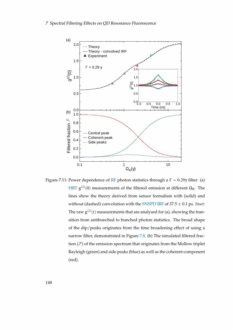
7 Spectral Filtering Effects on QD Resonance Fluorescence
0 . 0
0 . 5
1 . 0
1 . 5
2 . 0 T h e o r y T h e o r y - c o n v o l v e d I R F E x p e r i m e n t
g(2)(0)
Γ = 0 . 2 9 γ
- 1 . 0 - 0 . 5 0 . 0 0 . 5 1 . 00 . 0
0 . 5
1 . 0
1 . 5
2 . 0
g(2)(t)
T i m e ( n s )
( a )
( b )
0 . 1 1 1 00 . 00 . 20 . 40 . 60 . 81 . 0
C e n t r a l p e a k C o h e r e n t p e a k S i d e p e a k s
Filter
ed fra
ction
Ω R ( γ )
Figure 7.11: Power dependence of RF photon statistics through a Γ = 0.29γ filter: (a)
HBT g(2)(0) measurements of the filtered emission at different ΩR. The
lines show the theory derived from sensor formalism with (solid) and
without (dashed) convolution with the SNSPD IRF of 37.5± 0.1 ps. Inset:
The raw g(2)(t) measurements that are analysed for (a), showing the tran-
sition from antibunched to bunched photon statistics. The broad shape
of the dip/peaks originates from the time broadening effect of using a
narrow filter, demonstrated in Figure 7.8. (b) The simulated filtered frac-
tion (F) of the emission spectrum that originates from the Mollow triplet
Rayleigh (green) and side peaks (blue) as well as the coherent component
(red).
148

7.4 Strong Driving - Mollow Triplet Regime
Figure 7.11 shows the HBT g(2)(0) power dependence. The measurements show a
transition from antibunching to bunching (g(2)(0) > 1) as ΩR is increased. Under-
standing the reasons for this transition requires understanding the filtered fractions
(F) that make up the RF emission after the Γ = 0.29γ filter.
A simulation of F is shown in Figure 7.11(b). Similar to the F simulations calculated
for ΩR = 0.5γ , an ideal Lorentzian filter was applied to the modelled RF spectrum.
However, for the strong driving regime, there are also the side peaks of the Mollow
triplet to consider, as well as the central Rayleigh peak and the coherent scattering.
The Rayleigh peak is modelled with a linewidth of γ = 20 µeV, the side peaks with a
linewidth of 3γ/2 [206, 225] and the coherent scattering with a linewidth of 10 neV.
As can be seen in Figure 7.11(b), at low ΩR the filtered spectrum is mostly coher-
ent (red) due to the large coherent fraction (FCS) that passes through the filter owing
to a linewidth Γ. Meanwhile, the majority of the incoherent emission has been re-
moved by the filter as γ > Γ. As ΩR is increased the side peaks (blue) separate from
the Rayleigh peak (green) by hΩR, moving out of the bandwidth of the filter. FCS also
decreases in accordance with Equation 7.3. This leaves the incoherent Rayleigh peak
as the dominant component of the filtered emission. It could therefore be expected
that the g(2)(0) would return to the Poissonian photon statistics that are expected for
the central peak [226–228]. However, this is not what is seen in Figure 7.11(a).
The transition from antibunching to bunching occurs due to an effect in the regime of
Γ < γ that is termed “indistinguishability bunching” [218]. This bunching originates
from quantum fluctuations in the light field [233, 234] and is observed when filtering
at less than the natural linewidth of a light source. This effect has also been observed
for classical light sources, for example when filtering a laser [235]. Here, the filter has
a Γ of 0.29 γ and so this causes “indistinguishability bunching” of the incoherent part
of the emission spectrum. The bunching component competes with the Poissonian
149

7 Spectral Filtering Effects on QD Resonance Fluorescence
statistics of the coherent component. As can be seen in Figure 7.11(b), at larger values
of ΩR the incoherent component dominates as the coherent fraction decreases, lead-
ing to the domination of the indistinguishability bunching effect over the Poissonian
component in the g(2)(0) measurements.
The dashed black line in Figure 7.11(a) shows the prediction of the theoretical model
generated by our theory collaborators. As for Figure 7.7, the sensor formalism Equa-
tion 7.5 is used. However, here γ and Γ are kept constant and ΩR is swept, be-
fore extracting g(2)(0). The theoretical model predicts a maximum bunching value
of g(2)(0) ∼ 2.21 for these parameters. Experimentally we cannot accurately mea-
sure ΩR > 4γ as the laser background is not removed as effectively by the cross-
polarisation technique at high powers, reducing the signal to noise of the collected
emission. Theoretically it has been shown [218] that a bunching upper limit of g(2)(0)=
3 can be reached when using the parameters ΩR = 150γ and Γ = 0.005γ . However, for
a solid state emitter such as a QD, these parameters may not be reached due to the co-
herent fraction increasing again at large ΩR. This increase is due to phonon-mediated
interactions [225].
The corresponding HBT g(2)(t) experimental measurements (black) are shown in the
inset of Figure 7.11(a). They also exhibit the time broadening that was seen in the
ΩR = 0.5γ measurements (Fig. 7.8) that originates from the energy-time uncertainty
relation. The coloured lines show the theoretically modelled g(2)(t) function that cor-
responds to each value of ΩR. The model uses the same parameters that give the
convolved theory model in Figure 7.11(a).
7.4.2 Filter Bandwidth Dependence at ΩR = 2γ
To further investigate the effect of filtering in the strong driving regime, a filter band-
width dependence of g(2)(0) is measured at ΩR = 2γ using the filters listed in Table 7.1.
A simulation of the QD RF emission spectra at ΩR = 2γ is shown in Figure 7.10.
150
7.4 Strong Driving - Mollow Triplet Regime
The results of the filter bandwidth dependence are shown in Figure 7.12(a). Where
Γ γ antibunching is measured. However, the measured antibunching is degraded
compared to the values measured in Figure 7.7(a) with a maximum antibunching of
0.53± 0.01 recorded. The reason for this can be understood by looking at the inset
to Figure 7.12(a); at ΩR = 2γ Rabi oscillations are observed in the g(2)(t) measure-
ment. The short period of the Rabi oscillations narrows the central dip. The depth
of the dip recorded is sensitive to the detector IRF, and very sharp features shorter
than the IRF can be washed out, leading to a reduction in the measured antibunching.
Figure 7.12(b) shows the simulation for the filtered fractions (F) of the emission
against Γ/γ . At Γ γ the collected emission is dominated by the incoherent emis-
sion from the Rayleigh peak and side peaks. At ΩR = 2γ the side peaks mostly lie
within the filter bandwidth when Γ γ . Furthermore, by using Equation 7.3, it can
be calculated that the coherent fraction is 1/9 of the total emission before filtering.
As Γ approaches γ in Figure 7.12(a), the antibunching starts to be further degraded.
This contrasts with the measurements for ΩR = 0.5γ , where the photon statistics tended
to Poissonian statistics (g(2)(0) = 1). Here, as Γ becomes smaller than γ , the photon
statistics show bunching (g(2)(0) > 1). From Figure 7.12(b) it can be seen that, in
the bunching regime, the filtered emission is dominated by the incoherent emission
from the Rayleigh peak, the side peak antibunching contribution having been mostly
removed by the reduction of Γ. Therefore, this bunching is explained by “indistin-
guishability bunching” as the bunching occurs in the region where Γ < γ . Here the
coherent fraction is small so its Poissonian contribution to the g(2)(0) value is out-
weighed by the “indistinguishability bunching” contribution. However, at Γ γ the
coherent scattering component starts to dominate the filtered emission again, bring-
ing the photon statistics back to Poissonian statistics in agreement with Figure 7.7.
151

7 Spectral Filtering Effects on QD Resonance Fluorescence
0 . 0
0 . 5
1 . 0
1 . 5 I d e a l T h e o r y T h e o r y E x p e r i m e n t
g(2)(0)
( a )
( b )
- 0 . 5 0 . 0 0 . 50 . 00 . 51 . 01 . 5
g(2)(t)
T i m e ( n s )
- 0 . 5 0 . 0 0 . 50 . 00 . 51 . 01 . 5
g(2)(t)
T i m e ( n s )
0 . 0 0 1 0 . 0 1 0 . 1 1 1 0 1 0 00 . 00 . 20 . 40 . 60 . 81 . 0
C e n t r a l p e a k C o h e r e n t p e a k S i d e p e a k s
Filter
ed fra
ction
F i l t e r w i d t h Γ / γFigure 7.12: Filtered RF photon statistics under strong driving (ΩR = 2γ): (a) HBT
g(2)(0) measurements of the emission through different filter bandwidths
(Γ). The dashed line shows the theory derived from sensor formalism
without convolution with the SNSPD IRF of 37.5 ± 0.1 ps. The green
region depicts the confidence bounds defined by the theory when in-
cluding the SNSPD IRF as well as a 0% (lower bound) and 20% (upper
bound) contribution to the signal from the laser background. Insets: The
g(2)(t) measurements (black) for the same dataset as (a), Rabi oscillations
are observed for Γ > γ . The theoretically modelled g(2)(t) is shown in
red. (b) The simulated filtered fraction (F) of the emission spectrum that
originates from the coherent (red) and incoherent central Rayleigh peak
(green) as well as the Mollow side peaks (blue) components.
152
7.5 Conclusion
If a filter with a bandwidth smaller than the laser linewidth had been used then ul-
timately a recurrence of the “indistinguishability bunching” would be expected. The
need for very narrow filtering comparable to the coherent peak linewidth (∼ 0.005γ) is
why indistinguishability bunching was not observed in the Heitler regime (ΩR = 0.5γ)
measurements. There the coherent scattering was the dominant part of the filtered
emission and the filters used were much broader than its linewidth.
The theoretical model (green area) in Figure 7.12(a) reproduces the behaviour mea-
sured. Here, the model (Equation 7.5, γ and ΩR are kept constant as Γ is swept) incor-
porates both the SNSPD IRF along with a lower and upper bound that corresponds
to an uncertainty bound between 0% and 20% laser background contribution to the
collected signal. The ideal theory line (dashed) is modelled with neither of these
parameters and shows how perfect antibunching at Γ γ is expected if the Rabi os-
cillations of the g(2)(t) measurements could be fully resolved and not removed by the
detector IRF. Figure 7.12(a) also shows that including a 20% Poissonian background
contribution to the model increases the maximum bunching theoretically achievable,
indicating that this extra contribution to the filtered RF has non-trivial effects.
7.5 Conclusion
In this chapter we have looked at the effect that spectral filtering has on the photon
statistics measured from the RF emission of a TLE. To investigate this, filter band-
width dependant HBT g(2)(0) measurements were made in both the low excitation
power (RRS/Heitler) and high excitation power (Mollow) regimes. The antibunch-
ing that occurs in these regimes originates from interference between the different
components of the unfiltered RF spectrum which have their own photon statistics in
isolation.
In the Heitler regime, using an excitation power of ΩR = 0.5γ , the coherent fraction
153

7 Spectral Filtering Effects on QD Resonance Fluorescence
(FCS) of the neutral exciton emission is 2/3. At this power a transition is seen from an-
tibunching, where g(2)(0) is∼ 0.087±0.010 at Γ= 150γ , to Poissonian photon statistics
(g(2)(0) = 1) when the filter bandwidth becomes narrower than the incoherent natural
linewidth (γ) of the QD. This occurs as filtering below γ alters the ratio of the co-
herent and incoherent components of the RF emission, removing the majority of the
incoherent component and leaving the coherent component to dominate the filtered
emission. As well as measuring a degradation in the antibunching, a time broaden-
ing in the measured g(2)(t) is also observed when measuring at narrower filter widths.
As passing the photons through a filter with a narrow bandwidth is the equivalent
of measuring a narrow linewidth it can, therefore, be seen that it is not possible to si-
multaneously measure a sub-natural linewidth and strong antibunching from a TLE.
Both of these effects have been modelled using sensor formalism [216] by our theory
collaborators, where they have expanded the theory to include the IRF of the detec-
tors [221], showing excellent agreement with the measured results.
A power dependence of the RF photon statistics through a Γ = 0.29γ filter was also
measured. As Γ < γ the majority of the incoherent emission has been removed by
the filter, therefore the low power measurement (ΩR = 0.5γ) shows a small amount of
antibunching where g(2)(0) = 0.087±0.010. However, as ΩR is increased the coherent
fraction decreases, leaving the filtered incoherent fraction as the dominant compo-
nent of the RF. This leads to bunching being observed, with a g(2)(0) of 1.682 ± 0.009
when ΩR = 4.01γ . The bunching occurs due to “indistinguishability bunching” caused
by filtering below the linewidth of the dominant component of the emission, in this
case the incoherent component. Again, the expanded sensor theory model fits the
data well.
A filter bandwidth dependence of the RF photon statistics was also measured in the
Mollow triplet regime where ΩR = 2γ . In the Mollow regime, bunching was also ob-
served where Γ < γ as the incoherent component dominates the filtered spectra at
154

7.5 Conclusion
high power, leading to “indistinguishability bunching”. Here, the maximum bunch-
ing observed is 1.40±0.03 at Γ = 0.85γ . As Γ is reduced further, Poissonian statistics
are restored when Γ γ as the coherent component again dominates the filtered spec-
tra, due to the majority of the incoherent component being removed by the narrow
filter bandwidth. The theoretical model reproduced the behaviour seen in the mea-
surements. Here, the model included the detector IRF along with an upper and lower
bound that corresponded to a 0% and 20% contribution from the laser background to
the collected signal.
The dependence of the photon statistics on the filter bandwidth emphasises the need
for care when using filters to improve the properties of TLEs. However, it also shows
that filtering could be used as a method to modify photon statistics.
155


8 Summary and Future Work
8.1 Summary
In this thesis the properties of a III-V semiconductor QD in a high Purcell factor H1
PhCC have been investigated. In this chapter the experiments performed, and con-
clusions drawn, will be summarised.
Chapter 2 provides an introduction to the concepts used throughout this thesis in-
cluding the growth and properties of self-assembled quantum dots (SAQDs) and the
effect of cavities of QD emission.
Chapter 3 describes the basic experimental methods used throughout the experimen-
tal chapters. This includes a description of the Resonance Fluorescence (RF) set-up,
the lasers and detection methods used
Chapter 4 describes the fabrication process for the sample along with a summary
of the characterisation measurements that were performed. These include the mea-
surement of the T1 time of the neutral exciton emission, through use of a DPRF mea-
surement scheme, and so by extension the Purcell factor of the cavity-QD system.
8.1.1 Cavity Coupled QD as a Single-Photon Source
In Chapter 5 the single-photon properties of the cavity-QD system were investigated
using pulsed RF. Using Hanbury Brown and Twiss (HBT) second-order correlation
157

8 Summary and Future Work
measurements the single-photon properties are shown to be improved when the
length of the excitation pulse is decreased to T1. As well as measuring the anti-
bunching proprieties of the QD, Hong-Ou-Mandel (HOM) measurements were per-
formed, under the same conditions, to measure the single-photon indistinguishabil-
ity. Further investigations into the effect of the excitation pulse separation on the
single-photon indistinguishability were also carried out, showing that the QD-cavity
structure’s high Purcell factor would potentially allow for the production of over 20
or so near-identical photons if the repetition rate of the pump laser was increased.
The indistinguishability begins to decrease at a time on the order of the expected
spectral wandering, an effect that is again reduced by the high Purcell factor of the
H1 cavity.
8.1.2 Phonon Effects on QD Emission
In Chapter 6 the effect of the QD’s environment on its coherently scattered emission
was investigated to provide insight into the phonon interactions present and how
this behaviour deviates from the two-level “atomic picture”. First-order correlation
measurements were used measure the phonon relaxation timescale and were well
fitted using the polaron master equation. Through spectroscopic measurements, the
proportion of emission into the phonon sideband (PSB) was found to be insensitive
to CW excitation power, as is predicted by the polaron model. Investigation into
the effect of laser detuning on the coherent scattering through the use of first-order
correlation measurements also showed a non-monotonic relationship which deviates
from two-level “atomic picture” behaviour.
8.1.3 Spectral Filtering Effects on QD Resonance Fluorescence
In Chapter 7 the effect of filtering RF emission from the QD on the measured photon
statistics was investigated. In the weak (RRS/Heitler) CW excitation regime, filter-
ing the RF emission below the natural linewidth (γ) of the QD showed a reduction
in the measured antibunching, tending to coherent Poissonian statistics where the
158

8.2 Future Work for the QD in a H1 Cavity
filter bandwidth was γ . This verifies that strong antibunching and a sub-natural
linewidth cannot be simultaneously observed. The strong (Mollow) CW excitation
regime was also investigated. Here, a transition from antibunched to bunched statis-
tics was observed as the filter bandwidth was reduced below γ . This “indistinguisha-
bility bunching” occurs when filtering below the linewidth of the dominant compo-
nent of the RF, in this case filtering below the linewidth of the incoherent central peak
of the Mollow triplet. When filtering at γ a transition from bunched to Poissonian
statistics is seen as under these conditions coherent scattering becomes the dominant
component of the emission but the filter bandwidth remains much broader than the
coherent scattering linewidth.
8.2 Future Work for the QD in a H1 Cavity
8.2.1 Improving the Excitation Pulse Shaping
As was demonstrated in Section 5.3.2, the antibunching properties of the QD as a sin-
gle photon source can be improved by decreasing the excitation laser pulse length.
This is due to a lower re-excitation probability when the pulse length is T1 [139].
Experimentally, the reduction in the length of the excitation pulses at the sample is
limited by dispersion. One of the main sources of dispersion originates from the
single-mode fibres that are used between the 4f pulse shapers and the cryostat.
Dispersion is where the individual optical pulses spread out temporally in a medium
(e.g. silicon for single-mode fibres). This occurs as the refractive index (n) of a
medium is wavelength dependent and therefore the speed of light in the medium
is also wavelength dependent [236]. The dispersion can be characterised as normal
or anomalous dispersion. Normal dispersion leads to a lower group velocity for the
high frequency components of a pulse and is termed positive chirp. Anomalous dis-
persion leads to negative chirp where the low frequency components have a lower
group velocity. To enable short pulses at the sample the fibre dispersion needs to be
159

8 Summary and Future Work
Pulsed laser
10 mm cylindrical lens
Pickoff mirror
1200 l mm-1 grating Roof mirror
Rail
Linear stage
Mirror on flip mount
Mirror on flip mountPulse
shapers
Tip, tilt and rotation stage
Figure 8.1: Schematic of the Martinez pulse compressor used to correct for dispersion
in single-mode optical fibres. By adjusting the position of the linear stage
either positive or negative chirp can be corrected for.
compensated for, this is achieved by pre-chirping the pulses in the opposite direction
before the fibre.
To correct for the fibre dispersion a Martinez pulse compressor [237] is built between
the Mira pulsed laser and the 4f pulse shapers. A schematic of the Martinez pulse
compressor is shown in Figure 8.1. Mirrors mounted on flip mounts are used to di-
vert the pulsed laser through the pulse compressor, the flip mounts allow the beam
to bypass the pulse compressor if it is not required. The Martinez pulse compressor
has a similar geometry to a folded 4f pulse shaper. However, rather than using a slit
and titled mirror in the Fourier plane of the shaper, a roof mirror is used at the focal
point (f) of the cylindrical lens to achieve vertical displacement between the input
160

8.2 Future Work for the QD in a H1 Cavity
and output beams. The distance between the lens and the roof mirror is fixed at f.
By mounting them on a linear stage, the distance between the fixed optics and the
1200 mm−1 diffraction grating can be adjusted. Changing this distance can give the
pulses positive or negative chirp by adjusting the path length of the different spectral
components.
To monitor the effect of the Martinez pulse compressor on the pulse dispersion, an
APE Mini autocorrelator is used after the pulsed laser has been coupled into single-
mode fibre. The fibre used between the fibre coupler and the autocorrelator has the
same length as the fibre between the fibre coupler and the cryostat-mounted bread-
board. The Martinez pulse compressor allows correction of both positive or negative
chirp and can reduce the length by an order of magnitude to ∼ 200 fs.
To further increase the control over the excitation pulse length, improvements have
also been made to the 4f pulse shapers. The plano-convex lenses have been replaced
by cylindrical lenses to reduce spherical aberration. Also, to improve the resolution
of the pulse shapers, an additional 3:1 telescope has been incorporated before the
first 1200 l mm−1 diffraction grating to increase the fill of the laser spot on the grat-
ing. This magnification is reversed after the second grating by a second 3:1 telescope,
before the pulsed laser is coupled into the single-mode fibre. The increased resolu-
tion allows for the generation of longer pulses as filling the grating allows for a larger
spectral splitting and so spectrally narrower pulses can be achieved. The telescopes
produce a factor of 3 improvement to the pulse shaper resolution.
Finer excitation pulse control can be used for further investigation of how the an-
tibunching properties of the single-photon source are modified with pulse length.
161
8 Summary and Future Work
8.2.2 Improving the H1 PhCC Sample
The QD in the H1 PhCC used throughout this thesis experiences a Purcell factor (FP)
of ∼43. This leads to a short radiative lifetime of ∼21.7 ps. A short radiative lifetime
is advantageous for single-photon sources in photonic crystal structures as it reduces
the effect of charge fluctuations from nearby etched surfaces and, in doing so, can
reduce the spectral wandering of QD emission, increasing the indistinguishability of
the single photons [34, 106, 238]. Here, the high FP is generated as the H1 PhCC has
a high cavity Q-factor and a low mode volume (Section 4.2). The short radiative life-
time also leads to the exciton’s broad 20 µeV natural linewidth, which made filtering
below the natural linewidth for the HBT measurements of Chapter 7 possible [221].
As well as generating a high FP, a high Q cavity can also be used as a filter to reduce
the QD phonon sideband emission (PSB) [95, 100, 200]. However, a very high Q-factor
can move the cavity to the strong-coupling regime [95].
In Section 2.5.4 methods to increase the Q-factors of H1 PhCCs were discussed. These
included changing the radius and position of the etched holes closest to the cavity.
Improvements to the Q-factor of H1 PhCCs have also been shown in systems where
the lattice of the photonic crystal is stretched [239]. Theoretical Q-factors of ∼ 1x10⁶
have been shown for Silicon H1 PhCCs, where the inner three rings of etched holes
closest to the cavity have a modified position [240]. These all suggest that much
higher Purcell factors than that achieved with the sample in this thesis are possible.
This improvement could be achieved through further simulation of the H1 PhCC and
also through improved fabrication methods, reducing the decrease in the Q-factor
that occurs due to the high scattering loss rates observed in the fabricated samples
[121].
As the FP also depends on the spatial overlap between the emitter and the cavity
mode (Section 2.5.2), the position of the QDs within the cavity is also important to
achieve a high FP. This can be achieved through QD registration which will be dis-
cussed in Section 8.3.3.
162

8.2 Future Work for the QD in a H1 Cavity
Figure 8.2: Theoretical homodyne scheme allows simultaneous measurement of a
sub-natural linewidth and strong antibunching. A π-phase shift is intro-
duced to the driving laser which is then recombined with the RF from a
two-level system at a beam splitter. The modified laser destructively inter-
feres with the coherent part of the RF, returning its relative coherent and
incoherent fractions to their pre-filtering values. This allows strong anti-
bunching to be measured using a HBT set-up. Figure adapted from López
Carreño et al. [216] to include the measurement scheme used in Chapter 7.
8.2.3 Homodyne Scheme for Measuring Antibunching and a Sub-natural
Linewidth
As was shown in Chapter 7, a sub-natural linewidth and strong antibunching cannot
be measured simultaneously. However, a homodyne scheme where the RF output
of a two-level system is combined with a coherent beam, has been shown theoreti-
cally by López Carreño et al. [216] to lead to a recovery of the strong antibunching,
while measuring a sub-natural linewidth. Antibunching occurs from interference be-
tween the coherent and incoherent parts of the RF emission. The coherent part of the
emission inherits a long coherence time from the excitation laser and so has a narrow
linewidth when compared to the incoherent emission’s natural linewidth. Filtering
163

8 Summary and Future Work
below the natural linewidth of the RF removes part of the broad incoherent emission,
leading to a reduction in the observed antibunching [216, 218, 221, 241].
The homodyne scheme proposed by López Carreño et al. [216] introduces an exter-
nal π-phase shifted coherent laser beam to destructively interfere with the coherent
part of the RF and, in doing so, reduce the coherent fraction. This returns the coher-
ent and incoherent fractions of the RF to their relative values before the filter mod-
ification. Therefore, a return of strong antibunching can theoretically be observed.
Figure 8.2 shows the measurement scheme from López Carreño et al., modified to
include the filtering system used in Chapter 7. By diverting part of the laser that is
initially used to excite the two-level system ensures that the homodyning laser has
the same wavelength and coherence time as the driving laser and makes it immune
to slow fluctuations.
8.3 Future Work - Related Areas
The following section describes some possible future directions for QD-cavity cou-
pled systems with high Purcell factors and ways to optimise the fabrication of such
systems.
8.3.1 Telecom C-Band QDs
As was described in Section 1.1, quantum states of light can be used for secure quan-
tum communication [1, 31]. However, many QD sources of quantum light states
emit in the visible and near infra-red range and the current optical-telecom fibre in-
frastructure has a loss of >1 dB/km at 900 nm [242]. Therefore, for low-error long-
distance fibre-based quantum communication, single-photon sources that emit in the
low-loss fibre telecom C-band (∼1550 nm) are required, where the loss is∼0.2 dB/km
[243, 244]. Sources that emit at 1550 nm can also generate photons for use in free-
space satellite communication during daylight, by exploiting the reduction in the
164
8.3 Future Work - Related Areas
solar radiation spectrum and an increase in atmospheric transmission at this wave-
length [245].
Progress has been made on growing QDs that emit in the telecom C-band. Two of the
material systems used to emit in the C-band are InAs/InP and InAs/InGaAs/GaAs.
Both systems have shown the emission of single-photons [246–248] and long coher-
ence times [242, 249]. Combining resonance fluorescence excitation [249], along with
photonic crystal cavity structures [250], has the potential to create Purcell enhanced
single-photon sources, like the cavity-QD system described in this thesis, at telecom
wavelengths.
8.3.2 QD Spin in a Cavity for Photonic Cluster State Generation
As sources of single-photons, QDs have the potential to be used in the generation
of photonic cluster states for linear optical quantum computing. As is described in
Ref. [30], one dimensional photonic cluster states can be generated through repeated
pulsed resonant excitation of a QD whose spin is precessing in an external magnetic
field. This scheme encodes the photons in terms of polarisation. Further work has
been carried out into encoding the photons into time-bins instead of polarisation.
Here, a QD with a trapped charge carrier is placed in a Voigt magnetic field [251, 252].
Both of these schemes benefit from the use of cavities.
When mapping the spin of the electron onto the polarisation of a photon, to pro-
duce a cluster state with a high fidelity T1 needs to be much shorter than the spin
precession time, otherwise there is a large resulting uncertainty in the polarisation
of the emitted photon. However, for any realistic emitter, T2 is finite and therefore it
is advantageous to increase the speed of the spin precession, so that many photons
can be emitted within the spin coherence time, enabling the creation of large cluster
states. To increase the speed of the precession, while maintaining the fidelity, requires
a reduction of T1. This can be achieved through the use of a cavity with a high Purcell
165

8 Summary and Future Work
factor. Reducing the T1, through a strong Purcell enhancement, allows the production
of cluster states with more photons from a spin with the same coherence time.
The spin to time-bin scheme operates in a Voigt magnetic field, where the excitation
scheme produces a double lambda system. Therefore, a cavity with a strong Purcell
effect can be used to enhance the desired transition and suppress the undesired spin-
flip of the diagonal transitions. A large Purcell factor also decreases T1, enabling a
much faster readout.
8.3.3 QD Registration
To achieve all of the above quantum-optics goals it would be beneficial to have finer
control over the QD-cavity properties measured. One way in which this could be im-
proved would be to fabricate nano-photonic structures around optimally positioned
QDs. The positioning of QDs can be achieved through site-controlled QD growth,
as briefly discussed in Section 2.2.2. Another possible solution is the registration of
QDs before the photonic structures are fabricated. Two methods for this are briefly
discussed here.
One method to register the position and emission wavelength of QDs involves us-
ing scanning microscopic photoluminescence (µ-PL) spectroscopy [56]. Gold open-
box markers are patterned onto the sample surface with the boxes having an area
of ∼ 20 µm2. A µ-PL set-up is used to excite the sample using an above-band laser
and to collect the sample emission. By mounting either the sample or the objective
lens of the µ-PL set-up on closed-loop piezo stages, the excitation and collection can
be scanned in a grid pattern across the sample. The collected emission is split onto
two avalanche photodiodes (APDs), each with a different narrow-band filter. One
filter allows emission of the ideal QD wavelength to be detected. The second allows
monitoring of the emission from the semiconductor bandgap. The emission from the
bandgap is reduced above the markers due to the high reflectivity of the gold. By
166

8.3 Future Work - Related Areas
mapping the peaks in the QD emission relative to the marker positions a map of the
sample can be created. For more detailed spectral information about the QDs, a spec-
trometer can be used instead of APDs. This method can map the position of the QDs
with a < 10 nm accuracy [56].
A second method for QD registration is to use an imaging set-up [57–59]. Similarly
to the scanning µ-PL spectroscopy method, markers are patterned onto the surface
of the sample. However, for imaging QD registration the markers can define a larger
registration area, e.g. the 10 mm2 area used in Ref. [58]. The imaging set-up uses
two-colour LED illumination of the sample. A CCD camera detects the emission and
reflected light from the sample. One LED wavelength is above the bandgap of the
semiconductor and so excites the QDs.The second LED has a wavelength close to the
expected QD emission wavelength and is used to dimly illuminate the surface of the
sample. Using low levels of illumination allows the reflective markers to be seen on
the camera without saturating the dimmer QD signal. Image analysis is then used
to map the centre of each QD with respect to the markers. The precision of the QD
mapping relates the pixel size of the camera CCD and the size of the projected image
of the sample on the camera. Optimising the magnification so that the emission from
each QD is detected on multiple pixels has been shown to give position uncertainties
for the QDs of ∼ 5 nm [59]. Incorporating an excitation laser in to the imaging set-up
along with a beam splitter to divert part of the collected emission to a spectrometer al-
lows µ-PL spectra of individual QDs to be taken after their position has been mapped.
Improving the QD-cavity coupling through optimally positioning the nano-photonic
structures around the QDs can increase the Purcell factor of the QD. As well as in-
creasing the possible emission rate, a high Purcell factor would also broaden the nat-
ural linewidth of the emission and so would allow a greater range of spectral filter
bandwidths to be investigated when measuring the effects of spectral filtering on the
QD photon statistics.
167


Acronyms
AC Alternating Current
AlAs Aluminium Arsenide
AlGaAs Aluminium Gallium Arsenide
APD Avalanche Photodiode
CCD Charge-Coupled Device
CuCl Copper Chloride
CW Continuous Wave
DC Direct Current
DBR Distributed Bragg Reflector
DPRF Double π-Pulse Resonance Fluorescence
EBL Electron Beam Lithography
EID Excitation-Induced Dephasing
FPI Fabry-Pérot Interferometer
FSS Fine-Structure Splitting
FDTD Finite-Difference-Time-Domain
FSR Free Spectral Range
FWHM Full-Width Half Maximum
Ga Gallium
GaAs Gallium Arsenide
HBT Hanbury Brown and Twiss
He Helium
HOM Hong-Ou-Mandel
169

Acronyms
HF Hydrofluoric Acid
In Indium
InAs Indium Arsenide
InGaAs Indium Gallium Arsenide
InP Indium Phosphide
ICP Inductively Coupled Plasma
IRF Instrument Response Function
LA Longitudinal Acoustic Phonons
LO Longitudinal Optical Phonons
MOCVD Metal-organic Chemical Vapour Deposition
MOVPE Metal-organic Vapour-phase Epitaxy
µ-PL Microscopic Photoluminescence
MBE Molecular Beam Epitaxy
ME Master Equation
ND Neutral Density
PhC Photonic Crystal
PhCC Photonic Crystal Cavity
PSB Phonon Sideband
QCSE Quantum-Confined Stark Effect
QD Quantum Dot
RF Resonance Fluorescence
SAQD Self-assembled Quantum Dot
SEM Scanning Electron Microscope
SK Stranski-Krastanow
SNSPD Superconducting Nanowire Single-Photon Detectors
SPAD Single-Photon Avalanche Diode
SPS Single Photon Source
TA Transverse Acoustic Phonons
TCSPC Time-correlated Single Photon Counting Module
170
Ti:S Ti:Sapphire
TLE Two-level Emitter
VOA Variable Optical Attenuator
ZPL Zero Phonon Line
171

Bibliography
[1] N. Gisin, G. Ribordy, W. Tittel, and H. Zbinden, “Quantum cryptography,” Re-
views of Modern Physics 74, 145–195 (2002).
[2] Z.-S. Yuan, X.-H. Bao, C.-Y. Lu, J. Zhang, C.-Z. Peng, and J.-W. Pan, “Entangled
photons and quantum communication,” Physics Reports 497, 1 – 40 (2010).
[3] R. P. Feynman, “Simulating physics with computers,” International Journal of
Theoretical Physics 21, 467–488 (1982).
[4] E. Knill, R. Laflamme, and G. J. Milburn, “A scheme for efficient quantum com-
putation with linear optics,” Nature 409, 46–52 (2001).
[5] P. Kok, W. J. Munro, K. Nemoto, T. C. Ralph, J. P. Dowling, and G. J. Milburn,
“Linear optical quantum computing with photonic qubits,” Reviews of Modern
Physics 79, 135–174 (2007).
[6] J. P. Dowling, “Quantum optical metrology – the lowdown on high-N00N
states,” Contemporary Physics 49, 125–143 (2008).
[7] V. Giovannetti, S. Lloyd, and L. Maccone, “Advances in quantum metrology,”
Nature Photonics 5, 222–229 (2011).
[8] J. L. Park, “The concept of transition in quantum mechanics,” Foundations of
Physics 1, 23–33 (1970).
[9] P. W. Shor, “Polynomial-Time Algorithms for Prime Factorization and Discrete
Logarithms on a Quantum Computer,” SIAM Review 41, 303–332 (1999).
173

Bibliography
[10] L. K. Grover, “A fast quantum mechanical algorithm for database search,” in
“28th Annual ACM Symposium on the Theory of Computing (STOC),” (1996),
pp. 212–219.
[11] D. W. Berry, G. Ahokas, R. Cleve, and B. C. Sanders, “Efficient quantum algo-
rithms for simulating sparse hamiltonians,” Communications in Mathematical
Physics 270, 359–371 (2006).
[12] B. P. Lanyon, C. Hempel, D. Nigg, M. Müller, R. Gerritsma, F. Zähringer,
P. Schindler, J. T. Barreiro, M. Rambach, G. Kirchmair, M. Hennrich, P. Zoller,
R. Blatt, and C. F. Roos, “Universal digital quantum simulation with trapped
ions,” Science 334, 57–61 (2011).
[13] D. P. DiVincenzo, “The Physical Implementation of Quantum Computation,”
Fortschritte der Physik 48, 771–783 (2000).
[14] J. L. O'Brien, “Optical Quantum Computing,” Science 318, 1567–1570 (2007).
[15] C. Vitelli, N. Spagnolo, L. Toffoli, F. Sciarrino, and F. De Martini, “Enhanced
resolution of lossy interferometry by coherent amplification of single photons,”
Physical Review Letters 105, 113602 (2010).
[16] M. Müller, H. Vural, C. Schneider, A. Rastelli, O. G. Schmidt, S. Höfling, and
P. Michler, “Quantum-dot single-photon sources for entanglement enhanced
interferometry,” Physical Review Letters 118, 257402 (2017).
[17] Y. Arakawa and M. J. Holmes, “Progress in quantum-dot single photon sources
for quantum information technologies: A broad spectrum overview,” Applied
Physics Reviews 7, 021309 (2020).
[18] H. Wang, Y.-M. He, T.-H. Chung, H. Hu, Y. Yu, S. Chen, X. Ding, M.-C. Chen,
J. Qin, X. Yang, R.-Z. Liu, Z.-C. Duan, J.-P. Li, S. Gerhardt, K. Winkler, J. Jurkat,
L.-J. Wang, N. Gregersen, Y.-H. Huo, Q. Dai, S. Yu, S. Höfling, C.-Y. Lu, and
174

Bibliography
J.-W. Pan, “Towards optimal single-photon sources from polarized microcavi-
ties,” Nature Photonics 13, 770–775 (2019).
[19] M. E. Reimer and C. Cher, “The quest for a perfect single-photon source,” Na-
ture Photonics 13, 734–736 (2019).
[20] M. Arcari, I. Söllner, A. Javadi, S. Lindskov Hansen, S. Mahmoodian, J. Liu,
H. Thyrrestrup, E. H. Lee, J. D. Song, S. Stobbe, and P. Lodahl, “Near-Unity
Coupling Efficiency of a Quantum Emitter to a Photonic Crystal Waveguide,”
Physical Review Letters 113, 093603 (2014).
[21] U. Rengstl, M. Schwartz, T. Herzog, F. Hargart, M. Paul, S. L. Portalupi, M. Jet-
ter, and P. Michler, “On-chip beamsplitter operation on single photons from
quasi-resonantly excited quantum dots embedded in gaas rib waveguides,”
Applied Physics Letters 107, 021101 (2015).
[22] A. Laucht, S. Pütz, T. Günthner, N. Hauke, R. Saive, S. Frédérick, M. Bichler,
M.-C. Amann, A. W. Holleitner, M. Kaniber, and J. J. Finley, “A Waveguide-
Coupled On-Chip Single-Photon Source,” Physical Review X 2, 011014 (2012).
[23] T. Lund-Hansen, S. Stobbe, B. Julsgaard, H. Thyrrestrup, T. Sünner, M. Kamp,
A. Forchel, and P. Lodahl, “Experimental Realization of Highly Efficient Broad-
band Coupling of Single Quantum Dots to a Photonic Crystal Waveguide,”
Physical Review Letters 101, 113903 (2008).
[24] M. N. Makhonin, J. E. Dixon, R. J. Coles, B. Royall, I. J. Luxmoore, E. Clarke,
M. Hugues, M. S. Skolnick, and A. M. Fox, “Waveguide Coupled Resonance
Fluorescence from On-Chip Quantum Emitter,” Nano Letters 14, 6997–7002
(2014).
[25] S. Tanzilli, A. Martin, F. Kaiser, M. De Micheli, O. Alibart, and D. Ostrowsky,
“On the genesis and evolution of Integrated Quantum Optics,” Laser & Pho-
tonics Reviews 6, 115–143 (2012).
175

Bibliography
[26] J. L. O'Brien, A. Furusawa, and J. Vuckovic, “Photonic quantum technologies,”
Nature Photonics 3, 687–695 (2009).
[27] H. Wang, Y. He, Y.-H. Li, Z.-E. Su, B. Li, H.-L. Huang, X. Ding, M.-C. Chen,
C. Liu, J. Qin, J.-P. Li, Y.-M. He, C. Schneider, M. Kamp, C.-Z. Peng, S. Höfling,
C.-Y. Lu, and J.-W. Pan, “High-efficiency multiphoton boson sampling,” Nature
Photonics 11, 361–365 (2017).
[28] J. C. Loredo, M. A. Broome, P. Hilaire, O. Gazzano, I. Sagnes, A. Lemaitre,
M. P. Almeida, P. Senellart, and A. G. White, “Boson Sampling with Single-
Photon Fock States from a Bright Solid-State Source,” Physical Review Letters
118, 130503 (2017).
[29] S. Fan, S. E. Kocabas, and J.-T. Shen, “Input-output formalism for few-photon
transport in one-dimensional nanophotonic waveguides coupled to a qubit,”
Physical Review A 82, 063821 (2010).
[30] N. H. Lindner and T. Rudolph, “Proposal for Pulsed On-Demand Sources of
Photonic Cluster State Strings,” Physical Review Letters 103, 113602 (2009).
[31] H. J. Kimble, “The quantum internet,” Nature 453, 1023–1030 (2008).
[32] Y. Yu, F. Ma, X.-Y. Luo, B. Jing, P.-F. Sun, R.-Z. Fang, C.-W. Yang, H. Liu, M.-Y.
Zheng, X.-P. Xie, W.-J. Zhang, L.-X. You, Z. Wang, T.-Y. Chen, Q. Zhang, X.-H.
Bao, and J.-W. Pan, “Entanglement of two quantum memories via fibres over
dozens of kilometres,” Nature 578, 240–245 (2020).
[33] A. J. Shields, “Semiconductor quantum light sources,” Nature Photonics 1, 215–
223 (2007).
[34] C. P. Dietrich, A. Fiore, M. G. Thompson, M. Kamp and S. Höfling, “GaAs in-
tegrated quantum photonics: Towards compact and multi-functional quantum
photonic integrated circuits,” Laser & Photonics Reviews 10, 870–894 (2016).
176

Bibliography
[35] O. Gazzano, S. M. de Vasconcellos, C. Arnold, A. Nowak, E. Galopin, I. Sagnes,
L. Lanco, A. Lemaître, and P. Senellart, “Bright solid-state sources of indistin-
guishable single photons,” Nature Communications 4 (2013).
[36] A. Dousse, J. Suffczynski, A. Beveratos, O. Krebs, A. Lemaître, I. Sagnes,
J. Bloch, P. Voisin, and P. Senellart, “Ultrabright source of entangled photon
pairs,” Nature 466, 217–220 (2010).
[37] S. Strauf, N. G. Stoltz, M. T. Rakher, L. A. Coldren, P. M. Petroff, and
D. Bouwmeester, “High-frequency single-photon source with polarization con-
trol,” Nature Photonics 1, 704–708 (2007).
[38] A. I. Ekimov and A. A. Onushchenko, “Quantum size effect in three-
dimensional microscopic semiconductor crystals,” Journal of Experimental and
Theoretical Physics Letters 34, 345 (1981).
[39] R. Rossetti, S. Nakahara, and L. E. Brus, “Quantum size effects in the redox
potentials, resonance Raman spectra, and electronic spectra of CdS crystallites
in aqueous solution,” The Journal of Chemical Physics 79, 1086–1088 (1983).
[40] N. Koguchi, S. Takahashi, and T. Chikyow, “New MBE growth method for InSb
quantum well boxes,” Journal of Crystal Growth 111, 688 – 692 (1991).
[41] D. J. Eaglesham and M. Cerullo, “Dislocation-free Stranski-Krastanow growth
of Ge on Si(100),” Physical Review Letters 64, 1943–1946 (1990).
[42] I. N. Stranski and L. Krastanov, Mathematische Naturwissenschaftliche Klasse
2B 146, 79 (1938).
[43] C. W. Snyder, B. G. Orr, D. Kessler, and L. M. Sander, “Effect of strain on sur-
face morphology in highly strained InGaAs films,” Physical Review Letters 66,
3032–3035 (1991).
[44] D. Leonard, M. Krishnamurthy, C. M. Reaves, S. P. Denbaars, and P. M. Petroff,
177
Bibliography
“Direct formation of quantum-sized dots from uniform coherent islands of In-
GaAs on GaAs surfaces,” Applied Physics Letters 63, 3203–3205 (1993).
[45] J. M. Moison, F. Houzay, F. Barthe, L. Leprince, E. André, and O. Vatel, “Self-
organized growth of regular nanometer-scale InAs dots on GaAs,” Applied
Physics Letters 64, 196–198 (1994).
[46] P. Petroff and S. DenBaars, “MBE and MOCVD growth and properties of self-
assembling quantum dot arrays in III-V semiconductor structures,” Superlat-
tices and Microstructures 15, 15 (1994).
[47] M. Fox, Quantum Optics : an introduction (Oxford University Press, Oxford,
2007).
[48] P. Petroff, “Epitaxial Growth and Electronic Structure of Self-Assembled Quan-
tum Dots,” in “Single Quantum Dots: Fundamentals, Applications and New
Concepts,” , vol. 90 of Topics in Applied Physics, P. Michler, ed. (Springer, Berlin,
2003), pp. 1–24.
[49] C. Matthiesen, A. N. Vamivakas, and M. Atatüre, “Subnatural Linewidth Single
Photons from a Quantum Dot,” Physical Review Letters 108, 093602 (2012).
[50] O. G. Schmidt, ed., Lateral Alignment of Epitaxial Quantum Dots, NanoScience
and Technology (Springer-Verlag, 2007).
[51] A. Hartmann, L. Loubies, F. Reinhardt, and E. Kapon, “Self-limiting growth
of quantum dot heterostructures on nonplanar 111B substrates,” Applied
Physics Letters 71, 1314–1316 (1997).
[52] A. Hartmann, Y. Ducommun, E. Kapon, U. Hohenester, and E. Molinari, “Few-
Particle Effects in Semiconductor Quantum Dots: Observation of Multicharged
Excitons,” Physical Review Letters 84, 5648–5651 (2000).
178
Bibliography
[53] S. Kohmoto, H. Nakamura, T. Ishikawa, and K. Asakawa, “Site-controlled self-
organization of individual InAs quantum dots by scanning tunneling probe-
assisted nanolithography,” Applied Physics Letters 75, 3488–3490 (1999).
[54] H. Heidemeyer, C. Müller, and O. Schmidt, “Highly ordered arrays of In(Ga)As
quantum dots on patterned GaAs(001) substrates,” Journal of Crystal Growth
261, 444 – 449 (2004).
[55] K. D. Jöns, P. Atkinson, M. Müller, M. Heldmaier, S. M. Ulrich, O. G. Schmidt,
and P. Michler, “Triggered Indistinguishable Single Photons with Narrow Line
Widths from Site-Controlled Quantum Dots,” Nano Letters 13, 126–130 (2013).
[56] S. M. Thon, M. T. Rakher, H. Kim, J. Gudat, W. T. M. Irvine, P. M. Petroff, and
D. Bouwmeester, “Strong coupling through optical positioning of a quantum
dot in a photonic crystal cavity,” Applied Physics Letters 94, 111115 (2009).
[57] T. Kojima, K. Kojima, T. Asano, and S. Noda, “Accurate alignment of a pho-
tonic crystal nanocavity with an embedded quantum dot based on optical mi-
croscopic photoluminescence imaging,” Applied Physics Letters 102, 011110
(2013).
[58] L. Sapienza, M. Davanço, A. Badolato, and K. Srinivasan, “Nanoscale optical
positioning of single quantum dots for bright and pure single-photon emis-
sion,” Nature Communications 6 (2015).
[59] J. Liu, M. I. Davanço, L. Sapienza, K. Konthasinghe, J. V. De Miranda Car-
doso, J. D. Song, A. Badolato, and K. Srinivasan, “Cryogenic photolumines-
cence imaging system for nanoscale positioning of single quantum emitters,”
Review of Scientific Instruments 88, 023116 (2017).
[60] M. B. Panish and H. C. Casey, “Temperature Dependence of the Energy Gap in
GaAs and GaP,” Journal of Applied Physics 40, 163–167 (1969).
179

Bibliography
[61] W. Porod and D. K. Ferry, “Modification of the virtual-crystal approximation
for ternary III-V compounds,” Physical Review B 27, 2587–2589 (1983).
[62] M. I. Dyakonov, “Basics of Semiconductor and Spin Physics,” in “Springer Se-
ries in Solid-State Sciences,” (Springer Berlin Heidelberg, 2008), pp. 1–28.
[63] P. Hawrylak and M. Korkusinski, “Electronic Properties of Self-Assembled
Quantum Dots,” in “Single Quantum Dots: Fundamentals, Applications and
New Concepts,” , vol. 90 of Topics in Applied Physics, P. Michler, ed. (Springer,
Berlin, 2003), pp. 25–91.
[64] F. Rossi, “Fundamentals of Zero-Dimensional Nanostructures,” in “Semicon-
ductor Macroatoms:Basic Physics and Quantum-Device Applications,” (Impe-
rial College Press, 2005), pp. 1–41.
[65] R. M. Stevenson, R. J. Young, P. Atkinson, K. Cooper, D. A. Ritchie, and A. J.
Shields, “A semiconductor source of triggered entangled photon pairs,” Nature
439, 179–182 (2006).
[66] A. J. Brash, L. M. P. P. Martins, F. Liu, J. H. Quilter, A. J. Ramsay, M. S. Skolnick,
and A. M. Fox, “High-fidelity initialization of long-lived quantum dot hole spin
qubits by reduced fine-structure splitting,” Physical Review B 92, 121301 (2015).
[67] M. Bayer, A. Kuther, A. Forchel, A. Gorbunov, V. B. Timofeev, F. Schäfer, J. P.
Reithmaier, T. L. Reinecke, and S. N. Walck, “Electron and Hole g Factors and
Exchange Interaction from Studies of the Exciton Fine Structure in in0.60ga0.40As
Quantum Dots,” Physical Review Letters 82, 1748–1751 (1999).
[68] D. Gammon, E. S. Snow, B. V. Shanabrook, D. S. Katzer, and D. Park, “Fine
Structure Splitting in the Optical Spectra of Single GaAs Quantum Dots,” Phys-
ical Review Letters 76, 3005–3008 (1996).
[69] K. Kowalik, O. Krebs, A. Lemaître, S. Laurent, P. Senellart, P. Voisin, and J. A.
180

Bibliography
Gaj, “Influence of an in-plane electric field on exciton fine structure in InAs-
GaAs self-assembled quantum dots,” Applied Physics Letters 86, 041907 (2005).
[70] S. Seidl, M. Kroner, A. Högele, K. Karrai, R. J. Warburton, A. Badolato, and
P. M. Petroff, “Effect of uniaxial stress on excitons in a self-assembled quantum
dot,” Applied Physics Letters 88, 203113 (2006).
[71] W. Langbein, P. Borri, U. Woggon, V. Stavarache, D. Reuter, and A. D. Wieck,
“Control of fine-structure splitting and biexciton binding in inxga1−xAs quan-
tum dots by annealing,” Physical Review B 69, 161301 (2004).
[72] R. Singh and G. Bester, “Nanowire Quantum Dots as an Ideal Source of Entan-
gled Photon Pairs,” Physical Review Letters 103, 063601 (2009).
[73] P. W. Fry, I. E. Itskevich, D. J. Mowbray, M. S. Skolnick, and J. J. Finley et al.,
“Inverted Electron-Hole Alignment in InAs-GaAs Self-Assembled Quantum
Dots,” Physical Review Letters 84, 733–736 (2000).
[74] J. J. Finley, M. Sabathil, P. Vogl, G. Abstreiter, and R. Oulton et al., “Quantum-
confined Stark shifts of charged exciton complexes in quantum dots,” Physical
Review B 70, 201308 (2004).
[75] A. J. Bennett, R. B. Patel, J. Skiba-Szymanska, C. A. Nicoll, I. Farrer, D. A.
Ritchie, and A. J. Shields, “Giant Stark effect in the emission of single semi-
conductor quantum dots,” Applied Physics Letters 97, 031104 (2010).
[76] B. Alén, F. Bickel, K. Karrai, R. J. Warburton, and P. M. Petroff, “Stark-shift
modulation absorption spectroscopy of single quantum dots,” Applied Physics
Letters 83, 2235–2237 (2003).
[77] B. D. Gerardot, S. Seidl, P. A. Dalgarno, R. J. Warburton, D. Granados, J. M.
Garcia, K. Kowalik, O. Krebs, K. Karrai, A. Badolato, and P. M. Petroff, “Ma-
nipulating exciton fine structure in quantum dots with a lateral electric field,”
Applied Physics Letters 90, 041101 (2007).
181
Bibliography
[78] M. M. Vogel, S. M. Ulrich, R. Hafenbrak, P. Michler, L. Wang, A. Rastelli, and
O. G. Schmidt, “Influence of lateral electric fields on multiexcitonic transitions
and fine structure of single quantum dots,” Applied Physics Letters 91, 051904
(2007).
[79] T. Pregnalato, “Deterministic quantum photonic devices based on self-
assembled quantum dots,” Ph.D. thesis, University of Copenhagen (2019).
[80] S. H. Autler and C. H. Townes, “Stark Effect in Rapidly Varying Fields,” Phys-
ical Review 100, 703–722 (1955).
[81] B. R. Mollow, “Power Spectrum of Light Scattered by Two-Level Systems,”
Physical Review 188, 1969–1975 (1969).
[82] S. L. Portalupi and P. Michler, “Resonantly Excited Quantum Dots: Superior
Non-classical Light Sources for Quantum Information,” in “Quantum Dots for
Quantum Information Technologies,” , P. Michler, ed. (Springer International
Publishing, Cham, 2017), chap. 3, pp. 77–121.
[83] A. J. Brash, F. Liu, and A. M. Fox, “Ultrafast Manipulation of Excitons and
Spins in Quantum Dots,” in “Quantum Dots for Quantum Information Tech-
nologies,” , P. Michler, ed. (Springer International Publishing, Cham, 2017),
chap. 10, pp. 325–357.
[84] A. Vagov, V. M. Axt, T. Kuhn, W. Langbein, P. Borri, and U. Woggon, “Non-
monotonous temperature dependence of the initial decoherence in quantum
dots,” Physical Review B 70, 201305 (2004).
[85] P. Borri and W. Langbein., “Dephasing Processes and Carrier Dynamics in (In,
Ga)AS Quantum Dots,” in “Single Quantum Dots: Fundamentals, Applica-
tions and New Concepts,” , vol. 90 of Topics in Applied Physics, P. Michler, ed.
(Springer, Berlin, 2003), pp. 1–24.
182

Bibliography
[86] M. J. Steer, D. J. Mowbray, W. R. Tribe, M. S. Skolnick, M. D. Sturge, M. Hop-
kinson, A. G. Cullis, C. R. Whitehouse, and R. Murray, “Electronic energy lev-
els and energy relaxation mechanisms in self-organized InAs/GaAs quantum
dots,” Physical Review B 54, 17738–17744 (1996).
[87] R. Heitz, M. Grundmann, N. N. Ledentsov, L. Eckey, M. Veit, D. Bimberg,
V. M. Ustinov, A. Y. Egorov, A. E. Zhukov, P. S. Kop’ev, and Z. I. Alferov,
“Multiphonon-relaxation processes in self-organized InAs/GaAs quantum
dots,” Applied Physics Letters 68, 361–363 (1996).
[88] R. Heitz, M. Veit, N. N. Ledentsov, A. Hoffmann, D. Bimberg, V. M. Ustinov,
P. S. Kop’ev, and Z. I. Alferov, “Energy relaxation by multiphonon processes in
InAs/GaAs quantum dots,” Physical Review B 56, 10435–10445 (1997).
[89] E. Stock, M.-R. Dachner, T. Warming, A. Schliwa, A. Lochmann, A. Hoffmann,
A. I. Toropov, A. K. Bakarov, I. A. Derebezov, M. Richter, V. A. Haisler, A. Knorr,
and D. Bimberg, “Acoustic and optical phonon scattering in a single In(Ga)As
quantum dot,” Physical Review B 83, 041304 (2011).
[90] U. R. O. Madelung, W. von der Osten, Landolt-Börnstein-Semiconductors: Intrin-
sic Properties of GroupIV Elements and II-V, II-VI and I-VII Compounds, vol. III/22a
(Springer, Berlin, 1987).
[91] T. Flissikowski, A. Hundt, M. Lowisch, M. Rabe, and F. Henneberger, “Photon
Beats from a Single Semiconductor Quantum Dot,” Physical Review Letters 86,
3172–3175 (2001).
[92] H. Kumano, H. Kobayashi, S. Ekuni, Y. Hayashi, M. Jo, H. Sasakura, S. Adachi,
S. Muto, and I. Suemune, “Excitonic spin-state preservation mediated by
optical-phonon resonant excitation in a single quantum dot,” Physical Review
B 78, 081306 (2008).
[93] K. H. Madsen, S. Ates, J. Liu, A. Javadi, S. M. Albrecht, I. Yeo, S. Stobbe, and
183

Bibliography
P. Lodahl, “Efficient out-coupling of high-purity single photons from a coherent
quantum dot in a photonic-crystal cavity,” Physical Review B 90, 155303 (2014).
[94] E. V. Denning, J. Iles-Smith, N. Gregersen, and J. Mork, “Phonon effects in
quantum dot single-photon sources,” Opt. Mater. Express 10, 222–239 (2020).
[95] J. Iles-Smith, D. P. S. McCutcheon, A. Nazir, and J. Mørk, “Phonon scattering in-
hibits simultaneous near-unity efficiency and indistinguishability in semicon-
ductor single-photon sources,” Nature Photonics 11, 521 (2017).
[96] A. J. Ramsay, A. V. Gopal, E. M. Gauger, A. Nazir, B. W. Lovett, A. M. Fox, and
M. S. Skolnick, “Damping of Exciton Rabi Rotations by Acoustic Phonons in
Optically Excited InGaAs/GaAs Quantum Dots,” Physical Review Letters 104,
017402 (2010).
[97] J. Förstner, C. Weber, J. Danckwerts, and A. Knorr, “Phonon-Assisted Damping
of Rabi Oscillations in Semiconductor Quantum Dots,” Physical Review Letters
91, 127401 (2003).
[98] A. J. Ramsay, T. M. Godden, S. J. Boyle, E. M. Gauger, A. Nazir, B. W. Lovett,
A. M. Fox, and M. S. Skolnick, “Phonon-Induced Rabi-Frequency Renormal-
ization of Optically Driven Single InGaAs / GaAs Quantum Dots,” Physical
Review Letters 105, 177402 (2010).
[99] J. Iles-Smith, D. P. S. McCutcheon, J. Mørk, and A. Nazir, “Limits to coherent
scattering and photon coalescence from solid-state quantum emitters,” Physi-
cal Review B 95, 201305 (2017).
[100] T. Grange, N. Somaschi, C. Antón, L. De Santis, G. Coppola, V. Giesz,
A. Lemaître, I. Sagnes, A. Auffèves, and P. Senellart, “Reducing Phonon-
Induced Decoherence in Solid-State Single-Photon Sources with Cavity Quan-
tum Electrodynamics,” Physical Review Letters 118, 253602 (2017).
184

Bibliography
[101] L. Jacak, P. Machnikowski, J. Krasnyj, and P. Zoller, “Coherent and incoher-
ent phonon processes in artificial atoms,” The European Physical Journal D 22,
319–331 (2003).
[102] J. I. Climente, A. Bertoni, G. Goldoni, and E. Molinari, “Phonon-induced elec-
tron relaxation in weakly confined single and coupled quantum dots,” Physical
Review B 74, 035313 (2006).
[103] G. Bester, A. Zunger, X. Wu, and D. Vanderbilt, “Effects of linear and nonlin-
ear piezoelectricity on the electronic properties of InAs/GaAs quantum dots,”
Physical Review B 74, 081305 (2006).
[104] E. M. Purcell, H. C. Torrey, and R. V. Pound, “Resonance Absorption by Nuclear
Magnetic Moments in a Solid,” Physical Review 69, 37–38 (1946).
[105] D. Englund, D. Fattal, E. Waks, G. Solomon, and B. Zhang et al., “Controlling
the Spontaneous Emission Rate of Single Quantum Dots in a Two-Dimensional
Photonic Crystal,” Physical Review Letters 95, 013904 (2005).
[106] F. Liu, A. J. Brash, J. O’Hara, L. M. P. P. Martins, C. L. Phillips, R. J. Coles,
B. Royall, E. Clarke, C. Bentham, N. Prtljaga, I. E. Itskevich, L. R. Wilson, M. S.
Skolnick, and A. M. Fox, “High Purcell factor generation of indistinguishable
on-chip single photons,” Nature Nanotechnology 13, 835–840 (2018).
[107] J. P. Reithmaier, G. Sek, A. Löffler, C. Hofmann, S. Kuhn, S. Reitzenstein, L. V.
Keldysh, V. D. Kulakovskii, T. L. Reinecke, and A. Forchel, “Strong coupling
in a single quantum dot–semiconductor microcavity system,” Nature 432, 197–
200 (2004).
[108] T. B. Norris, J.-K. Rhee, C.-Y. Sung, Y. Arakawa, M. Nishioka, and C. Weisbuch,
“Time-resolved vacuum Rabi oscillations in a semiconductor quantum micro-
cavity,” Physical Review B 50, 14663–14666 (1994).
185

Bibliography
[109] I. I. Rabi, “Space Quantization in a Gyrating Magnetic Field,” Physical Review
51, 652–654 (1937).
[110] E. T. Jaynes and F. W. Cummings, “Comparison of quantum and semiclassical
radiation theories with application to the beam maser,” Proceedings of the IEEE
51, 89–109 (1963).
[111] S. G. Johnson and J. D. Joannopoulos, “Block-iterative frequency-domain meth-
ods for Maxwell’s equations in a planewave basis,” Optics Express 8, 173–190
(2001).
[112] M. Loncar, J. Vuckovic, and A. Scherer, “Methods for controlling positions of
guided modes of photonic-crystal waveguides,” Journal of the Optical Society
of America B: Optical Physics 18, 1362–1368 (2001).
[113] R. J. Coles, “Quantum Optical Circuits using III-V Nanophotonic Structures,”
Ph.D. thesis, University of Sheffield (2015).
[114] E. Yablonovitch, “Inhibited Spontaneous Emission in Solid-State Physics and
Electronics,” Physical Review Letters 58, 2059–2062 (1987).
[115] J. D. Joannopoulos, Photonic crystals : molding the flow of light (Princeton Univer-
sity Press, Princeton, N.J. ; Chichester, 1995).
[116] S. G. Johnson, P. R. Villeneuve, S. Fan, and J. D. Joannopoulos, “Linear waveg-
uides in photonic-crystal slabs,” Physical Review B 62, 8212–8222 (2000).
[117] T. F. Krauss, “Slow light in photonic crystal waveguides,” Journal of Physics D:
Applied Physics 40, 2666–2670 (2007).
[118] S. Hughes, “Enhanced single-photon emission from quantum dots in photonic
crystal waveguides and nanocavities,” Optics Letters 29, 2659–2661 (2004).
[119] V. S. C. Manga Rao and S. Hughes, “Single quantum-dot Purcell factor and β
factor in a photonic crystal waveguide,” Physical Review B 75, 205437 (2007).
186
Bibliography
[120] A. C. T. Thijssen, M. J. Cryan, J. G. Rarity, and R. Oulton, “Transfer of arbitrary
quantum emitter states to near-field photon superpositions in nanocavities,”
Optics Express 20, 22412–22428 (2012).
[121] R. J. Coles, N. Prtljaga, B. Royall, I. J. Luxmoore, A. M. Fox, and M. S. Skolnick,
“Waveguide-coupled photonic crystal cavity for quantum dot spin readout,”
Optics Express 22, 2376–2385 (2014).
[122] M. Shirane, S. Kono, J. Ushida, S. Ohkouchi, N. Ikeda, Y. Sugimoto, and
A. Tomita, “Mode identification of high-quality-factor single-defect nanocav-
ities in quantum dot-embedded photonic crystals,” Journal of Applied Physics
101, 073107 (2007).
[123] Y. Akahane, T. Asano, B.-S. Song, and S. Noda, “High-Q photonic nanocavity
in a two-dimensional photonic crystal,” Nature 425, 944–947 (2003).
[124] A. Faraon, E. Waks, D. Englund, I. Fushman, and J. Vuckovic, “Efficient pho-
tonic crystal cavity-waveguide couplers,” Applied Physics Letters 90, 073102
(2007).
[125] P. Velha, E. Picard, T. Charvolin, E. Hadji, J. C. Rodier, P. Lalanne, and
D. Peyrade, “Ultra-High Q/V Fabry-Perot microcavity on SOI substrate,” Op-
tics Express 15, 16090–16096 (2007).
[126] Q. Quan, P. B. Deotare, and M. Loncar, “Photonic crystal nanobeam cav-
ity strongly coupled to the feeding waveguide,” Applied Physics Letters 96,
203102 (2010).
[127] Q. Quan and M. Loncar, “Deterministic design of wavelength scale, ultra-high
Q photonic crystal nanobeam cavities,” Optics Express 19, 18529–18542 (2011).
[128] A. Dousse, L. Lanco, J. Suffczynski, E. Semenova, A. Miard, A. Lemaître,
I. Sagnes, C. Roblin, J. Bloch, and P. Senellart, “Controlled Light-Matter Cou-
187

Bibliography
pling for a Single Quantum Dot Embedded in a Pillar Microcavity Using Far-
Field Optical Lithography,” Physical Review Letters 101, 267404 (2008).
[129] C. Schneider, P. Gold, S. Reitzenstein, S. Höfling, and M. Kamp, “Quantum dot
micropillar cavities with quality factors exceeding 250, 000,” Applied Physics
B 122 (2016).
[130] H. Ollivier, I. Maillette de Buy Wenniger, S. Thomas, S. C. Wein, A. Harouri,
G. Coppola, P. Hilaire, C. Millet, A. Lemaître, I. Sagnes, O. Krebs, L. Lanco,
J. C. Loredo, C. Antón, N. Somaschi, and P. Senellart, “Reproducibility of High-
Performance Quantum Dot Single-Photon Sources,” ACS Photonics 7, 1050–
1059 (2020).
[131] P. Michler, A. Kiraz, C. Becher, W. V. Schoenfeld, P. M. Petroff, L. Zhang, E. Hu,
and A. Imamoglu, “A Quantum Dot Single-Photon Turnstile Device,” Science
290, 2282–2285 (2000).
[132] A. Kiraz, P. Michler, C. Becher, B. Gayral, A. Imamoglu, L. Zhang, E. Hu, W. V.
Schoenfeld, and P. M. Petroff, “Cavity-quantum electrodynamics using a single
InAs quantum dot in a microdisk structure,” Applied Physics Letters 78, 3932–
3934 (2001).
[133] E. Peter, P. Senellart, D. Martrou, A. Lemaître, J. Hours, J. M. Gérard, and
J. Bloch, “Exciton-Photon Strong-Coupling Regime for a Single Quantum Dot
Embedded in a Microcavity,” Physical Review Letters 95, 067401 (2005).
[134] F. Salin, J. Squier, and M. Piché, “Mode locking of Ti:Al2O3 lasers and self-
focusing: a Gaussian approximation,” Optics Letters 16, 1674–1676 (1991).
[135] T. H. Stievater, X. Li, D. G. Steel, D. Gammon, D. S. Katzer, D. Park, C. Pier-
marocchi, and L. J. Sham, “Rabi Oscillations of Excitons in Single Quantum
Dots,” Physical Review Letters 87, 133603 (2001).
188

Bibliography
[136] H. Kamada, H. Gotoh, J. Temmyo, T. Takagahara, and H. Ando, “Exciton
Rabi Oscillation in a Single Quantum Dot,” Physical Review Letters 87, 246401
(2001).
[137] H. Htoon, T. Takagahara, D. Kulik, O. Baklenov, A. L. Holmes, and C. K. Shih,
“Interplay of Rabi Oscillations and Quantum Interference in Semiconductor
Quantum Dots,” Physical Review Letters 88, 087401 (2002).
[138] A. Zrenner, E. Beham, S. Stufler, F. Findeis, M. Bichler, and G. Abstreiter, “Co-
herent properties of a two-level system based on a quantum-dot photodiode,”
Nature 418, 612–614 (2002).
[139] J. O’Hara, “Quantum Light with Quantum Dots in III-V Photonic Integrated
Circuits: Towards Scalable Quantum Computing Architectures,” Ph.D. thesis,
University of Sheffield (2017).
[140] K. A. Fischer, L. Hanschke, M. Kremser, J. J. Finley, K. Müller, and J. Vuckovic,
“Pulsed Rabi oscillations in quantum two-level systems: beyond the area theo-
rem,” Quantum Science and Technology 3, 014006 (2017).
[141] J. P. McCaffrey, M. D. Robertson, S. Fafard, Z. R. Wasilewski, E. M. Gris-
wold, and L. D. Madsen, “Determination of the size, shape, and composition
of indium-flushed self-assembled quantum dots by transmission electron mi-
croscopy,” Journal of Applied Physics 88, 2272–2277 (2000).
[142] C. Bentham, I. E. Itskevich, R. J. Coles, B. Royall, E. Clarke, J. O’Hara, N. Prtl-
jaga, A. M. Fox, M. S. Skolnick, and L. R. Wilson, “On-chip electrically con-
trolled routing of photons from a single quantum dot,” Applied Physics Letters
106, 221101 (2015).
[143] A. J. Brash, “Ultrafast Dynamics of Single Quantum Dots,” Ph.D. thesis, Uni-
versity of Sheffield (2016).
189

Bibliography
[144] A. Faraon, I. Fushman, D. Englund, N. Stoltz, P. Petroff, and J. Vuckovic,
“Dipole induced transparency in waveguide coupled photonic crystal cavi-
ties,” Optics Express 16, 12154–12162 (2008).
[145] X. Zhou, I. Kulkova, T. Lund-Hansen, S. L. Hansen, P. Lodahl, and L. Mi-
dolo, “High-efficiency shallow-etched grating on GaAs membranes for quan-
tum photonic applications,” Applied Physics Letters 113, 251103 (2018).
[146] D. Istrati, Y. Pilnyak, J. C. Loredo, C. Antón, N. Somaschi, P. Hilaire, H. Ollivier,
M. Esmann, L. Cohen, L. Vidro, C. Millet, A. Lemaître, I. Sagnes, A. Harouri,
L. Lanco, P. Senellart, and H. S. Eisenberg, “Sequential generation of linear clus-
ter states from a single photon emitter,” (2019).
[147] R. H. Brown and R. Q. Twiss, “Correlation between Photons in two Coherent
Beams of Light,” Nature 177, 27–29 (1956).
[148] C. K. Hong, Z. Y. Ou, and L. Mandel, “Measurement of subpicosecond time
intervals between two photons by interference,” Physical Review Letters 59,
2044–2046 (1987).
[149] C. Santori, D. Fattal, J. Vuckovic, G. S. Solomon, and Y. Yamamoto, “Indistin-
guishable photons from a single-photon device,” Nature 419, 594–597 (2002).
[150] A. J. Bennett, D. C. Unitt, A. J. Shields, P. Atkinson, and D. A. Ritchie, “Influ-
ence of exciton dynamics on the interference of two photons from a microcavity
single-photon source,” Optics Express 13, 7772–7778 (2005).
[151] S. Ates, S. M. Ulrich, S. Reitzenstein, A. Löffler, A. Forchel, and P. Michler,
“Post-Selected Indistinguishable Photons from the Resonance Fluorescence of
a Single Quantum Dot in a Microcavity,” Physical Review Letters 103, 167402
(2009).
[152] S. Laurent, S. Varoutsis, L. Le Gratiet, A. Lemaître, I. Sagnes, F. Raineri, A. Lev-
enson, I. Robert-Philip, and I. Abram, “Indistinguishable single photons from
190
Bibliography
a single-quantum dot in a two-dimensional photonic crystal cavity,” Applied
Physics Letters 87, 163107 (2005).
[153] H. Fearn and R. Loudon, “Theory of two-photon interference,” Journal of the
Optical Society of America B: Optical Physics 6, 917–927 (1989).
[154] A. M. Branczyk, “Hong-Ou-Mandel Interference,” arXiv e-prints p.
arXiv:1711.00080 (2017).
[155] N. Somaschi, V. Giesz, L. De Santis, J. C. Loredo, and M. P. Almeida et al.,
“Near-optimal single-photon sources in the solid state,” Nat Photon 10, 340–
345 (2016).
[156] C. F. Wang, A. Badolato, I. Wilson-Rae, P. M. Petroff, E. Hu, J. Urayama, and
A. Imamoglu, “Optical properties of single InAs quantum dots in close prox-
imity to surfaces,” Applied Physics Letters 85, 3423–3425 (2004).
[157] A. Majumdar, E. D. Kim, and J. Vuckovic, “Effect of photogenerated carriers on
the spectral diffusion of a quantum dot coupled to a photonic crystal cavity,”
Physical Review B 84, 195304 (2011).
[158] A. Thoma, P. Schnauber, M. Gschrey, M. Seifried, J. Wolters, J.-H. Schulze,
A. Strittmatter, S. Rodt, A. Carmele, A. Knorr, T. Heindel, and S. Reitzen-
stein, “Exploring Dephasing of a Solid-State Quantum Emitter via Time-
and Temperature-Dependent Hong-Ou-Mandel Experiments,” Physical Re-
view Letters 116, 033601 (2016).
[159] J. C. Loredo, N. A. Zakaria, N. Somaschi, C. Anton, L. de Santis, V. Giesz,
T. Grange, M. A. Broome, O. Gazzano, G. Coppola, I. Sagnes, A. Lemaitre,
A. Auffeves, P. Senellart, M. P. Almeida, and A. G. White, “Scalable perfor-
mance in solid-state single-photon sources,” Optica 3, 433–440 (2016).
[160] F. Y. Wu, R. E. Grove, and S. Ezekiel, “Investigation of the Spectrum of Reso-
191

Bibliography
nance Fluorescence Induced by a Monochromatic Field,” Physical Review Let-
ters 35, 1426–1429 (1975).
[161] H. Gibbs and T. Venkatesan, “Direct observation of fluorescence narrower than
the natural linewidth,” Optics Communications 17, 87 – 90 (1976).
[162] J. Volz, M. Weber, D. Schlenk, W. Rosenfeld, C. Kurtsiefer, and H. Weinfurter,
“An atom and a photon,” Laser Physics 17, 1007–1016 (2007).
[163] H. S. Nguyen, G. Sallen, C. Voisin, P. Roussignol, C. Diederichs, and G. Cass-
abois, “Ultra-coherent single photon source,” Applied Physics Letters 99,
261904 (2011).
[164] K. Konthasinghe, J. Walker, M. Peiris, C. K. Shih, Y. Yu, M. F. Li, J. F. He, L. J.
Wang, H. Q. Ni, Z. C. Niu, and A. Muller, “Coherent versus incoherent light
scattering from a quantum dot,” Physical Review B 85, 235315 (2012).
[165] R. Proux, M. Maragkou, E. Baudin, C. Voisin, P. Roussignol, and C. Diederichs,
“Measuring the Photon Coalescence Time Window in the Continuous-Wave
Regime for Resonantly Driven Semiconductor Quantum Dots,” Physical Re-
view Letters 114, 067401 (2015).
[166] A. J. Bennett, J. P. Lee, D. J. P. Ellis, T. Meany, E. Murray, F. F. Floether, J. P.
Griffths, I. Farrer, D. A. Ritchie, and A. J. Shields, “Cavity-enhanced coherent
light scattering from a quantum dot,” Science Advances 2, e1501256–e1501256
(2016).
[167] C. Cohen-Tannoudji, J. Dupont-Roc, and G. Grynberg, Atom—Photon Interac-
tions: Basic Processes and Applications (Wiley, 1998).
[168] C. Matthiesen, M. Geller, C. H. H. Schulte, C. Le Gall, J. Hansom, Z. Li,
M. Hugues, E. Clarke, and M. Atatüre, “Phase-locked indistinguishable pho-
tons with synthesized waveforms from a solid-state source,” Nature Commu-
nications 4, 1600 (2013).
192
Bibliography
[169] Y. He, Y.-M. He, Y.-J. Wei, X. Jiang, M.-C. Chen, F.-L. Xiong, Y. Zhao, C. Schnei-
der, M. Kamp, S. Höfling, C.-Y. Lu, and J.-W. Pan, “Indistinguishable Tunable
Single Photons Emitted by Spin-Flip Raman Transitions in InGaAs Quantum
Dots,” Physical Review Letters 111, 237403 (2013).
[170] T. M. Sweeney, S. G. Carter, A. S. Bracker, M. Kim, C. S. Kim, L. Yang, P. M. Vora,
P. G. Brereton, E. R. Cleveland, and D. Gammon, “Cavity-stimulated Raman
emission from a single quantum dot spin,” Nature Photonics 8, 442–447 (2014).
[171] E. V. Denning, J. Iles-Smith, D. P. S. McCutcheon, and J. Mork, “Protocol for
generating multiphoton entangled states from quantum dots in the presence of
nuclear spin fluctuations,” Physical Review A 96, 062329 (2017).
[172] D. Scerri, R. N. E. Malein, B. D. Gerardot, and E. M. Gauger, “Frequency-
encoded linear cluster states with coherent Raman photons,” Physical Review
A 98, 022318 (2018).
[173] A. Javadi, I. Söllner, M. Arcari, S. L. Hansen, L. Midolo, S. Mahmoodian,
G. Kiršanske, T. Pregnolato, E. H. Lee, J. D. Song, S. Stobbe, and P. Lodahl,
“Single-photon non-linear optics with a quantum dot in a waveguide,” Nature
Communications 6 (2015).
[174] A. Sipahigil, R. E. Evans, D. D. Sukachev, M. J. Burek, J. Borregaard, M. K.
Bhaskar, C. T. Nguyen, J. L. Pacheco, H. A. Atikian, C. Meuwly, R. M. Camacho,
F. Jelezko, E. Bielejec, H. Park, M. Loncar, and M. D. Lukin, “An integrated
diamond nanophotonics platform for quantum-optical networks,” Science 354,
847–850 (2016).
[175] D. Hallett, A. P. Foster, D. L. Hurst, B. Royall, P. Kok, E. Clarke, I. E. Itskevich,
A. M. Fox, M. S. Skolnick, and L. R. Wilson, “Electrical control of nonlinear
quantum optics in a nano-photonic waveguide,” Optica 5, 644–650 (2018).
[176] A. Delteil, Z. Sun, W. bo Gao, E. Togan, S. Faelt, and A. Imamoglu, “Generation
193
Bibliography
of heralded entanglement between distant hole spins,” Nature Physics 12, 218–
223 (2015).
[177] R. Stockill, M. J. Stanley, L. Huthmacher, E. Clarke, M. Hugues, A. J. Miller,
C. Matthiesen, C. Le Gall, and M. Atatüre, “Phase-Tuned Entangled State Gen-
eration between Distant Spin Qubits,” Physical Review Letters 119, 010503
(2017).
[178] J. Houel, A. V. Kuhlmann, L. Greuter, F. Xue, M. Poggio, B. D. Gerardot, P. A.
Dalgarno, A. Badolato, P. M. Petroff, A. Ludwig, D. Reuter, A. D. Wieck, and
R. J. Warburton, “Probing Single-Charge Fluctuations at a GaAs/AlAs Interface
Using Laser Spectroscopy on a Nearby InGaAs Quantum Dot,” Physical Re-
view Letters 108, 107401 (2012).
[179] A. V. Kuhlmann, J. Houel, A. Ludwig, L. Greuter, D. Reuter, A. D. Wieck,
M. Poggio, and R. J. Warburton, “Charge noise and spin noise in a semicon-
ductor quantum device,” Nature Physics 9, 570–575 (2013).
[180] E. A. Muljarov and R. Zimmermann, “Dephasing in Quantum Dots: Quadratic
Coupling to Acoustic Phonons,” Physical Review Letters 93, 237401 (2004).
[181] A. Reigue, J. Iles-Smith, F. Lux, L. Monniello, M. Bernard, F. Margaillan,
A. Lemaitre, A. Martinez, D. P. S. McCutcheon, J. Mørk, R. Hostein, and V. Vo-
liotis, “Probing Electron-Phonon Interaction through Two-Photon Interference
in Resonantly Driven Semiconductor Quantum Dots,” Physical Review Letters
118, 233602 (2017).
[182] H. Wang, Z.-C. Duan, Y.-H. Li, S. Chen, J.-P. Li, Y.-M. He, M.-C. Chen, Y. He,
X. Ding, C.-Z. Peng, C. Schneider, M. Kamp, S. Höfling, C.-Y. Lu, and J.-W. Pan,
“Near-Transform-Limited Single Photons from an Efficient Solid-State Quan-
tum Emitter,” Physical Review Letters 116, 213601 (2016).
[183] L. Monniello, C. Tonin, R. Hostein, A. Lemaitre, A. Martinez, V. Voliotis, and
194

Bibliography
R. Grousson, “Excitation-induced dephasing in a resonantly driven InAs/GaAs
quantum dot,” Physical Review Letters 111, 026403 (2013).
[184] B. Krummheuer, V. M. Axt, and T. Kuhn, “Theory of pure dephasing and the
resulting absorption line shape in semiconductor quantum dots,” Physical Re-
view B 65, 195313 (2002).
[185] P. Kaer and J. Mørk, “Decoherence in semiconductor cavity QED systems due
to phonon couplings,” Physical Review B 90, 035312 (2014).
[186] D. P. S. McCutcheon, “Optical signatures of non-Markovian behavior in open
quantum systems,” Physical Review A 93, 022119 (2016).
[187] L. Besombes, K. Kheng, L. Marsal, and H. Mariette, “Acoustic phonon broaden-
ing mechanism in single quantum dot emission,” Physical Review B 63, 155307
(2001).
[188] N. R. Jungwirth and G. D. Fuchs, “Optical Absorption and Emission Mecha-
nisms of Single Defects in Hexagonal Boron Nitride,” Physical Review Letters
119, 057401 (2017).
[189] E. Neu, D. Steinmetz, J. Riedrich-Möller, S. Gsell, M. Fischer, M. Schreck,
and C. Becher, “Single photon emission from silicon-vacancy colour centres
in chemical vapour deposition nano-diamonds on iridium,” New Journal of
Physics 13, 025012 (2011).
[190] A. Jeantet, Y. Chassagneux, C. Raynaud, P. Roussignol, J. S. Lauret, B. Besga,
J. Estève, J. Reichel, and C. Voisin, “Widely Tunable Single-Photon Source from
a Carbon Nanotube in the Purcell Regime,” Physical Review Letters 116, 247402
(2016).
[191] D. Christiansen, M. Selig, G. Berghäuser, R. Schmidt, I. Niehues, R. Schnei-
der, A. Arora, S. M. de Vasconcellos, R. Bratschitsch, E. Malic, and A. Knorr,
195
Bibliography
“Phonon Sidebands in Monolayer Transition Metal Dichalcogenides,” Physical
Review Letters 119, 187402 (2017).
[192] C. Clear, R. C. Schofield, K. D. Major, J. Iles-Smith, A. S. Clark, and D. P. S. Mc-
Cutcheon, “Phonon-induced optical dephasing in single organic molecules,”
Physical Review Letters 124, 153602 (2020).
[193] P. Kaer, N. Gregersen, and J. Mork, “The role of phonon scattering in the indis-
tinguishability of photons emitted from semiconductor cavity QED systems,”
New Journal of Physics 15, 035027 (2013).
[194] P. Borri, W. Langbein, U. Woggon, V. Stavarache, D. Reuter, and A. D. Wieck,
“Exciton dephasing via phonon interactions in InAs quantum dots: Depen-
dence on quantum confinement,” Physical Review B 71, 115328 (2005).
[195] T. Jakubczyk, V. Delmonte, S. Fischbach, D. Wigger, D. E. Reiter, Q. Mermillod,
P. Schnauber, A. Kaganskiy, J.-H. Schulze, A. Strittmatter, S. Rodt, W. Langbein,
T. Kuhn, S. Reitzenstein, and J. Kasprzak, “Impact of Phonons on Dephasing of
Individual Excitons in Deterministic Quantum Dot Microlenses,” ACS Photon-
ics 3, 2461–2466 (2016).
[196] A. Nazir and D. P. S. McCutcheon, “Modelling exciton–phonon interactions
in optically driven quantum dots,” Journal of Physics: Condensed Matter 28,
103002 (2016).
[197] D. P. S. McCutcheon and A. Nazir, “Quantum dot Rabi rotations beyond the
weak exciton–phonon coupling regime,” New Journal of Physics 12, 113042
(2010).
[198] H.-P. Breuer and F. Petruccione, The Theory of Open Quantum Systems (Oxford
University Press on Demand, New York, 2002).
[199] C. Roy and S. Hughes, “Phonon-Dressed Mollow Triplet in the Regime of Cav-
196
Bibliography
ity Quantum Electrodynamics: Excitation-Induced Dephasing and Nonpertur-
bative Cavity Feeding Effects,” Physical Review Letters 106, 247403 (2011).
[200] A. J. Brash, J. Iles-Smith, C. L. Phillips, D. P. S. McCutcheon, J. O’Hara,
E. Clarke, B. Royall, L. R. Wilson, J. Mørk, M. S. Skolnick, A. M. Fox, and
A. Nazir, “Light Scattering from Solid-State Quantum Emitters: Beyond the
Atomic Picture,” Physical Review Letters 123, 167403 (2019).
[201] M. Glässl, M. D. Croitoru, A. Vagov, V. M. Axt, and T. Kuhn, “Influence of the
pulse shape and the dot size on the decay and reappearance of Rabi rotations
in laser driven quantum dots,” Physical Review B 84, 125304 (2011).
[202] T. Calarco, A. Datta, P. Fedichev, E. Pazy, and P. Zoller, “Spin-based all-optical
quantum computation with quantum dots: Understanding and suppressing
decoherence,” Physical Review A 68, 012310 (2003).
[203] K. Roy-Choudhury and S. Hughes, “Quantum theory of the emission spec-
trum from quantum dots coupled to structured photonic reservoirs and acous-
tic phonons,” Physical Review B 92, 205406 (2015).
[204] E. V. Denning, J. Iles-Smith, A. D. Osterkryger, N. Gregersen, and J. Mork,
“Cavity-waveguide interplay in optical resonators and its role in optimal
single-photon sources,” Physical Review B 98, 121306 (2018).
[205] J. H. Quilter, A. J. Brash, F. Liu, M. Glässl, A. M. Barth, V. M. Axt, A. J. Ramsay,
M. S. Skolnick, and A. M. Fox, “Phonon-Assisted Population Inversion of a Sin-
gle InGaAs/GaAs Quantum Dot by Pulsed Laser Excitation,” Physical Review
Letters 114, 137401 (2015).
[206] A. Ulhaq, S. Weiler, C. Roy, S. M. Ulrich, M. Jetter, S. Hughes, and P. Michler,
“Detuning-dependent Mollow triplet of a coherently-driven single quantum
dot,” Optics Express 21, 4382 (2013).
197

Bibliography
[207] F. Liu, L. M. P. Martins, A. J. Brash, A. M. Barth, J. H. Quilter, V. M. Axt, M. S.
Skolnick, and A. M. Fox, “Ultrafast depopulation of a quantum dot by LA-
phonon-assisted stimulated emission,” Physical Review B 93, 161407 (2016).
[208] A. J. Brash, L. M. P. P. Martins, A. M. Barth, F. Liu, J. H. Quilter, M. Glässl, V. M.
Axt, A. J. Ramsay, M. S. Skolnick, and A. M. Fox, “Dynamic vibronic coupling
in InGaAs quantum dots [Invited],” Journal of the Optical Society of America
B: Optical Physics 33, C115–C122 (2016).
[209] H. C. Casey, D. D. Sell, and K. W. Wecht, “Concentration dependence of the
absorption coefficient for n- and p-type GaAs between 1.3 and 1.6 eV,” Journal
of Applied Physics 46, 250–257 (1975).
[210] A. Aspuru-Guzik and P. Walther, “Photonic quantum simulators,” Nature
Physics 8, 285–291 (2012).
[211] M. Varnava, D. E. Browne, and T. Rudolph, “How Good Must Single Photon
Sources and Detectors Be for Efficient Linear Optical Quantum Computation?”
Physical Review Letters 100, 060502 (2008).
[212] H.-J. Briegel, W. Dür, J. I. Cirac, and P. Zoller, “Quantum repeaters: The role
of imperfect local operations in quantum communication,” Physical Review
Letters 81, 5932–5935 (1998).
[213] E. Schöll, L. Hanschke, L. Schweickert, K. D. Zeuner, M. Reindl, S. F. Covre da
Silva, T. Lettner, R. Trotta, J. J. Finley, K. Müller, A. Rastelli, V. Zwiller, and
K. D. Jöns, “Resonance Fluorescence of GaAs Quantum Dots with Near-Unity
Photon Indistinguishability,” Nano Letters 19, 2404–2410 (2019).
[214] G. Kiršanske, H. Thyrrestrup, R. S. Daveau, C. L. Dreeßen, T. Pregnolato, L. Mi-
dolo, P. Tighineanu, A. Javadi, S. Stobbe, R. Schott, A. Ludwig, A. D. Wieck, S. I.
Park, J. D. Song, A. V. Kuhlmann, I. Söllner, M. C. Löbl, R. J. Warburton, and
P. Lodahl, “Indistinguishable and efficient single photons from a quantum dot
in a planar nanobeam waveguide,” Physical Review B 96, 165306 (2017).
198

Bibliography
[215] L. Dusanowski, S.-H. Kwon, C. Schneider, and S. Höfling, “Near-Unity Indis-
tinguishability Single Photon Source for Large-Scale Integrated Quantum Op-
tics,” Physical Review Letters 122, 173602 (2019).
[216] J. C. L. Carreño, E. Z. Casalengua, F. P. Laussy, and E. del Valle, “Joint
subnatural-linewidth and single-photon emission from resonance fluores-
cence,” Quantum Science and Technology 3, 045001 (2018).
[217] E. Zubizarreta Casalengua, J. López Carreño, F. Laussy, and E. del Valle,
“Conventional and unconventional photon statistics,” arXiv e-prints p.
arXiv:1901.09030 (2019).
[218] A. Gonzalez-Tudela, F. P. Laussy, C. Tejedor, M. J. Hartmann, and E. del Valle,
“Two-photon spectra of quantum emitters,” New Journal of Physics 15, 033036
(2013).
[219] W. Heitler, The Quantum Theory of Radiation (Oxford University Press, Oxford,
1954).
[220] E. del Valle, A. Gonzalez-Tudela, F. P. Laussy, C. Tejedor, and M. J. Hart-
mann, “Theory of Frequency-Filtered and Time-Resolved N-Photon Correla-
tions,” Physical Review Letters 109, 183601 (2012).
[221] C. L. Phillips, A. J. Brash, D. P. S. McCutcheon, J. Iles-Smith, E. Clarke, B. Royall,
M. S. Skolnick, A. M. Fox, and A. Nazir, “Photon Statistics of Filtered Resonance
Fluorescence,” Physical Review Letters 125, 043603 (2020).
[222] E. del Valle, A. Gonzalez-Tudela, F. P. Laussy, C. Tejedor, and M. J. Hartmann,
“Erratum: Theory of frequency-filtered and time-resolved n-photon correla-
tions [phys. rev. lett. 109, 183601 (2012)],” Physical Review Letters 116, 249902
(2016).
[223] Dalibard, J. and Reynaud, S., “Correlation signals in resonance fluorescence :
199

Bibliography
interpretation via photon scattering amplitudes,” Journal de Physique. France
44, 1337–1343 (1983).
[224] W. Heisenberg, “Über den anschaulichen Inhalt der quantentheoretischen
Kinematik und Mechanik,” Zeitschrift für Physik 43, 172–198 (1927).
[225] D. P. S. McCutcheon and A. Nazir, “Model of the Optical Emission of a Driven
Semiconductor Quantum Dot: Phonon-Enhanced Coherent Scattering and Off-
Resonant Sideband Narrowing,” Physical Review Letters 110, 217401 (2013).
[226] C. A. Schrama, G. Nienhuis, H. A. Dijkerman, C. Steijsiger, and H. G. M. Hei-
deman, “Intensity correlations between the components of the resonance fluo-
rescence triplet,” Physical Review A 45, 8045–8055 (1992).
[227] A. Ulhaq, S. Weiler, S. M. Ulrich, R. Roßbach, M. Jetter, and P. Michler, “Cas-
caded single-photon emission from the Mollow triplet sidebands of a quantum
dot,” Nature Photonics 6, 238–242 (2012).
[228] S. Weiler, D. Stojanovic, S. M. Ulrich, M. Jetter, and P. Michler, “Postselected
indistinguishable single-photon emission from the Mollow triplet sidebands of
a resonantly excited quantum dot,” Physical Review B 87, 241302 (2013).
[229] C. A. Schrama, G. Nienhuis, H. A. Dijkerman, C. Steijsiger, and H. G. M. Heide-
man, “Destructive interference between opposite time orders of photon emis-
sion,” Physical Review Letters 67, 2443–2445 (1991).
[230] A. Aspect, G. Roger, S. Reynaud, J. Dalibard, and C. Cohen-Tannoudji,
“Time Correlations between the Two Sidebands of the Resonance Fluorescence
Triplet,” Physical Review Letters 45, 617–620 (1980).
[231] M. Peiris, B. Petrak, K. Konthasinghe, Y. Yu, Z. C. Niu, and A. Muller, “Two-
color photon correlations of the light scattered by a quantum dot,” Physical
Review B 91 (2015).
200
Bibliography
[232] Y. Nieves and A. Muller, “Third-order frequency-resolved photon correlations
in resonance fluorescence,” Physical Review B 98, 165432 (2018).
[233] J. A. Armstrong, “Theory of Interferometric Analysis of Laser Phase Noise∗,”
Journal of the Optical Society of America 56, 1024–1031 (1966).
[234] L. Knöll, W. Vogel, and D.-G. Welsch, “Quantum noise in spectral filtering of
light,” Journal of the Optical Society of America B: Optical Physics 3, 1315–1318
(1986).
[235] R. C. Neelen, D. M. Boersma, M. P. van Exter, G. Nienhuis, and J. P. Woerdman,
“Spectral filtering within the Schawlow-Townes linewidth as a diagnostic tool
for studying laser phase noise,” Optics Communications 100, 289–302 (1993).
[236] M. Fox, Optical Properties of Solids (Oxford University Press, Oxford, 2013), 2nd
ed.
[237] O. Martinez, “Design of high-power ultrashort pulse amplifiers by expan-
sion and recompression,” IEEE Journal of Quantum Electronics 23, 1385–1387
(1987).
[238] A. Kiraz, M. Atatüre, and A. Imamoglu, “Quantum-dot single-photon sources:
Prospects for applications in linear optics quantum-information processing,”
Physical Review A 69, 032305 (2004).
[239] I. J. Luxmoore, E. D. Ahmadi, A. M. Fox, M. Hugues, and M. S. Skolnick, “Un-
polarized H1 photonic crystal nanocavities fabricated by stretched lattice de-
sign,” Applied Physics Letters 98, 041101 (2011).
[240] M. Minkov and V. Savona, “Automated optimization of photonic crystal slab
cavities,” Scientific Reports 4 (2014).
[241] L. Hanschke, L. Schweickert, J. C. L. Carreño, E. Schöll, K. D. Zeuner, T. Lettner,
E. Z. Casalengua, M. Reindl, S. F. C. da Silva, R. Trotta, J. J. Finley, A. Rastelli,
201

Bibliography
E. del Valle, F. P. Laussy, V. Zwiller, K. Müller, and K. D. Jöns, “Origin of An-
tibunching in Resonance Fluorescence,” Physical Review Letters 125, 170402
(2020).
[242] M. Anderson, T. Müller, J. Huwer, J. Skiba-Szymanska, A. B. Krysa, R. M.
Stevenson, J. Heffernan, D. A. Ritchie, and A. J. Shields, “Quantum telepor-
tation using highly coherent emission from telecom c-band quantum dots,” npj
Quantum Information 6 (2020).
[243] T. Miya, Y. Terunuma, T. Hosaka, and T. Miyashita, “Ultimate low-loss single-
mode fibre at 1.55 µm,” Electronics Letters 15, 106–108(2) (1979).
[244] W. A. Gambling, “The rise and rise of optical fibers,” IEEE Journal of Selected
Topics in Quantum Electronics 6, 1084–1093 (2000).
[245] S.-K. Liao, H.-L. Yong, C. Liu, G.-L. Shentu, D.-D. Li, J. Lin, H. Dai, S.-Q. Zhao,
B. Li, J.-Y. Guan, W. Chen, Y.-H. Gong, Y. Li, Z.-H. Lin, G.-S. Pan, J. S. Pelc,
M. M. Fejer, W.-Z. Zhang, W.-Y. Liu, J. Yin, J.-G. Ren, X.-B. Wang, Q. Zhang, C.-
Z. Peng, and J.-W. Pan, “Long-distance free-space quantum key distribution in
daylight towards inter-satellite communication,” Nature Photonics 11, 509–513
(2017).
[246] T. Müller, J. Skiba-Szymanska, A. B. Krysa, J. Huwer, M. Felle, M. Anderson,
R. M. Stevenson, J. Heffernan, D. A. Ritchie, and A. J. Shields, “A quantum
light-emitting diode for the standard telecom window around 1, 550 nm,” Na-
ture Communications 9 (2018).
[247] M. Benyoucef, M. Yacob, J. P. Reithmaier, J. Kettler, and P. Michler, “Telecom-
wavelength (1.5 µm) single-photon emission from InP-based quantum dots,”
Applied Physics Letters 103, 162101 (2013).
[248] M. Paul, F. Olbrich, J. Höschele, S. Schreier, J. Kettler, S. L. Portalupi, M. Jet-
ter, and P. Michler, “Single-photon emission at 1.55 µm from MOVPE-grown
202
Bibliography
InAs quantum dots on InGaAs/GaAs metamorphic buffers,” Applied Physics
Letters 111, 033102 (2017).
[249] C. Nawrath, F. Olbrich, M. Paul, S. L. Portalupi, M. Jetter, and P. Michler,
“Coherence and indistinguishability of highly pure single photons from non-
resonantly and resonantly excited telecom c-band quantum dots,” Applied
Physics Letters 115, 023103 (2019).
[250] A. Kors, K. Fuchs, M. Yacob, J. P. Reithmaier, and M. Benyoucef, “Telecom
wavelength emitting single quantum dots coupled to inp-based photonic crys-
tal microcavities,” Applied Physics Letters 110, 031101 (2017).
[251] K. Tiurev, M. H. Appel, P. L. Mirambell, M. B. Lauritzen, A. Tiranov, P. Lo-
dahl, and A. S. Sørensen, “High-fidelity multi-photon-entangled cluster state
with solid-state quantum emitters in photonic nanostructures,” arXiv e-prints
p. arXiv:2007.09295 (2020).
[252] J. P. Lee, B. Villa, A. J. Bennett, R. M. Stevenson, D. J. P. Ellis, I. Farrer, D. A.
Ritchie, and A. J. Shields, “A quantum dot as a source of time-bin entangled
multi-photon states,” Quantum Science and Technology 4, 025011 (2019).
203