
Smart Home Automation System - Semantic Scholar
169
Smart Home Automation System By Ali Mohammad Tamimi Anas Radwan Barakat Supervisor: Dr.Fouad Zaro Submitted to the College of Engineering In fulfillment of the requirement for the Degree of Bachelor degree in Electrical Engineering Palestine Polytechnic University May 2019
-
Upload
khangminh22 -
Category
Documents
-
view
0 -
download
0
Transcript of Smart Home Automation System - Semantic Scholar
Smart Home Automation System
By
Ali Mohammad Tamimi Anas Radwan Barakat
Supervisor: Dr.Fouad Zaro
Submitted to the College of Engineering
In fulfillment of the requirement for the Degree of
Bachelor degree in Electrical Engineering
Palestine Polytechnic University
May 2019
II
Smart Home Automation System
By
Ali Mohammad Tamimi Anas Radwan Barakat
Supervisor: Dr.Fouad Zaro
Submitted to the College of Engineering
In partial fulfillment of the requirement for the Degree of
Bachelor degree in Electrical Engineering
Signature of the Head of the Department Signature of the project supervisor
Name: Name:
Signature of the examining committee
................................. .................................
Palestine Polytechnic University
May 2019

III
الملخص
نظام تحكم منزلي ذكي
ةلتوسعل وقابلحيث المزايا ومرن منتحكم منزلي ذكي رخيص الثمن وتطبيق نظاميهدف هذا المشروع إلى تصميم
من ةاضافة الى ذلك سيتم تطبيق مجموع ،(Wi-Fi)الالسلكي االتصالعلى تكنولوجيا األردوينو و اعتمادا الحجم،من حيث
المنزلية،هربائية توفير أفضل تحكم باألحمال الكالكهربائي في المنزل و االستهالكالبرمجية بحيث يتم تخفيف ية و االساليب التقن
باي وقت كان. نظام ممكنا من أي مكان بالعالم و سيكون الوصول للكما و
ائية ية الكهربيد األجهزة المنزلدبشكل أساسي النظام سوف يعتمد على تكنولوجيا ولوحات األردوينو، في البداية قمنا بتح
التي سيتم التحكم بها و عدد الغرف المنزلية ، ونوع المعلومات و البيانات التي سوف يقوم النظام بجمعها من البيئة الداخلية و
مع المعلومات جائف التحكم و ظالخارجية للمنزل، بناء على ما سبق، قمنا بتصميم دائرة كهربائية عامة قادرة على القيام بكامل و
من الحساسات الكهربائية المختلفة ، جميع هذه الدوائر الكهربائية سوف تكون متصلة بموقع على شبكة اإلنترنت و ذلك باستخدام
، من ثم يتصل هذا الموقع بالمستخدم عن طريق تطبيق ذكي يعمل على نظام األندرويد.(Wi-Fi)الالسلكي ال االتصال
إنتاج نموذج نهائي لنظام تحكم منزلي ذكي كامل بحيث يكون مطبق على وحدة سكنية تمكنا من في نهاية هذا المشروع
قادر لنهائيا النظام أن ثحي العام.عليها كعينة دراسية، بحيث يتم تعميم النظام الحقا لالستخدام المنزلي التجاري عملنامحددة
التبريد،ت التكييف و وحدا)المقابس( و والمخارج الكهربائية اإلضاءةختلفة مثل: المنزلية الم واألجهزة الكهربائيةعلى التحكم باألدوات
درجة و توليد الطاقة الكهربائية من نظام الخاليا الشمسة المنزليو اللحظي المنزلي الكهربائي االستهالكقادر على عرض كما و
نظام اإلنذار من السرقة، الغازات السامة و نذار من الحريق و إيحتوي على نظام و كما الرطوبة في كل غرفة على حدة، و الحرارة
الكهربائي المنزلي. االستهالكالتي تعمل على ترشيد لياتالنظام مجموعة من اآليمتلك كما و

IV
Abstract
Smart Home Automation System
The aim of this paper is to design and implement a cheap, flexible, scalable Smart Home
Automation System based on Arduino Technology and Wi-Fi connection, in addition to apply
specific techniques for power consumption reduction and load management. The system will be
accessible anywhere, anytime.
The project will rely on Arduino Technology and NodeMCU boards, at the beginning we
determined the electrical appliances to be controlled in the house, number of rooms to be controlled
and type of information and data to be collected from indoor/outdoor environment, then we
designed 3 general circuits that perform the whole process (master, indoor slave and outdoor
slave), all will be connected to a cloud database that communicates with the user by an android
application connected to the internet.
At the end of this project, we produced a fully working system (prototype) for small
presentation room as a case study that could be generalized for residual use. The system is able to
control all home electrical units and appliances like: lights, sockets, HVAC (Heating, Ventilating
and air conditioning) units, fire, gas and intruder siren systems, in addition to monitor the real time
power consumption, a PV system generation and the current room's temperature and humidity.
Furthermore, the system is able to reduce power consumption using predefined algorithms.

V
إهداء
العزيز.نا عليه إلى والدي أكما والنفيس ألكونإلى من بذل الغالي والحنان،إلى أمي الحبيبة منبع المحبة
وأسرتي.أخوتي واألخوة إلىطعم المحبة هممع تإلى من ذق
.معلمينا العلماءإلى كل من علمني حرفا أساتذتنا و
.أصدقائنا األعزاءوبنا إلى أحبائنا وقلقوت اإلى من ضاقت السطور ذكرهم إلى من كانو
علمه إلى مشرفنا القدير الدكتور فؤاد الزرو.وونصحه إلى من كان سندا لنا بجهده ووقته

VI
Acknowledgment
A part of our effort and the successes of any project depends largely on the encouragements
of others.
We would like to start with a special gratitude to our university for the help and support
provided in its facilities for the past five years, and for our electrical engineering department for
the large effort had been spent during our study to reinforce us with all knowledge needed.
And no thanks could be enough for our supervisor Dr.Fouad Zaro, for his support, effort and
guidelines he gave us during the course, special thanks to Eng. Elias Maharmeh for his support,
we would like also to thank Dr.Saleh Takroury, Eng.Obadah Qawasme, Eng.Alaa Tamimi and
Eng.Mohammad Qaisi for their help.

VII
Table of Contents
III ....................................................................................................................................... الملخص
Abstract .................................................................................................................................... IV
V ............................................................................................................................................ إهداء
Acknowledgment...................................................................................................................... VI
List of Figures ........................................................................................................................... X
List of Tables .......................................................................................................................... XII
List of Abbreviations ................................................................................................................ XI
1 Chapter One ........................................................................................................................ 2
1.1 Introduction .................................................................................................................. 2
1.2 Literature Review ......................................................................................................... 2
1.3 Problem Statement ....................................................................................................... 5
1.4 Objectives .................................................................................................................... 6
1.5 Importance ................................................................................................................... 6
1.6 Project scope ................................................................................................................ 6
1.7 Timeframe .................................................................................................................... 8
2 Main Design Concept ....................................................................................................... 10
2.1 Introduction ................................................................................................................ 10
2.2 System Layout ............................................................................................................ 10
2.3 System main parts ...................................................................................................... 11
2.3.1 Android application ............................................................................................. 11
2.3.2 Google firebase real-time database. ..................................................................... 13
2.3.3 Master Circuit ..................................................................................................... 14
2.3.4 Slave circuits ....................................................................................................... 18
2.3.5 Custom Wi-Fi shield. .......................................................................................... 26
VIII
2.4 I2C Communication ................................................................................................... 27
2.4.1 Why I2C communication? ................................................................................... 27
2.4.2 How it works? ..................................................................................................... 27
2.4.3 Protocol ............................................................................................................... 28
2.5 Power and energy calculations. ................................................................................... 29
2.6 Hardware .................................................................................................................... 31
2.7 Software ..................................................................................................................... 37
2.8 Case Study ................................................................................................................. 38
3 Electrical Design............................................................................................................... 41
3.1 Introduction ................................................................................................................ 41
3.2 Electrical Components ................................................................................................ 42
3.2.1 Master Circuit ..................................................................................................... 42
3.2.2 IS (Room Control Slave) Circuits ........................................................................ 43
3.2.3 OS (Outdoor slave) Circuit .................................................................................. 44
3.3 PCB Schemes ............................................................................................................. 45
3.3.1 Traces widths ...................................................................................................... 45
3.3.2 Calculations ........................................................................................................ 45
3.3.3 PCB 3D view ...................................................................................................... 47
3.4 Wall mounted Covers ................................................................................................. 51
3.4.1 Master Board Cover ............................................................................................ 51
3.4.2 Salve's circuits cover ........................................................................................... 54
3.4.3 HVAC Remote controller cover .......................................................................... 57
4 Results & Recommendations ............................................................................................ 60
4.1 Introduction ................................................................................................................ 60
4.2 Results ....................................................................................................................... 61
IX
4.2.1 Master circuit features ......................................................................................... 61
4.2.2 Indoor circuit features.......................................................................................... 62
4.2.3 Outdoor circuit features ....................................................................................... 64
4.2.4 Wi-Fi shield board ............................................................................................... 66
4.3 Android app. .............................................................................................................. 67
4.4 Small presentation room. ............................................................................................ 70
4.5 Response time ............................................................................................................ 73
4.6 Components temperature ............................................................................................ 74
4.7 Recommendations ...................................................................................................... 75
References ................................................................................................................................ 76
Appendices ............................................................................................................................... 33
X
List of Figures
Figure 2.1 Project layout ........................................................................................................... 11
Figure 2.2 Android app flowchart ............................................................................................. 12
Figure 2.3 Wi-Fi shield for Arduino board [6]. ......................................................................... 13
Figure 2.4 house feedback in the Android app .......................................................................... 14
Figure 2.5 Google sheet online user_15_minute_watt demand .................................................. 15
Figure 2.6 Master circuit block diagram. ................................................................................... 16
Figure 2.7 PV status Android app. ............................................................................................ 16
Figure 2.8 Master circuit flowchart. .......................................................................................... 17
Figure 2.9 Indoor Slave block diagram. .................................................................................... 19
Figure 2.10 Indoor slave flow chart A. ...................................................................................... 20
Figure 2.11 Indoor flow chart B. ............................................................................................... 21
Figure 2.12 In app on/off buttons and timers. ............................................................................ 22
Figure 2.13 In app HVAC control. ............................................................................................ 22
Figure 2.14 In app indoor slave feedback. ................................................................................. 23
Figure 2.15 OS block diagram. ................................................................................................. 24
Figure 2.16 OS flowchart.......................................................................................................... 25
Figure 2.17 logic shifter circuit [7] ........................................................................................... 26
Figure 2.18 I2C Protocol [8]. .................................................................................................... 28
Figure 2.19 C.T/P.T meter [9]. .................................................................................................. 35
Figure 2.20 Node MCU[9] ........................................................................................................ 36
Figure 2.21 RTC board[9] ........................................................................................................ 36
Figure 2.22 Node MCU[9] ........................................................................................................ 37
Figure 2.23 Master circuit cover ............................................................................................... 39
Figure 2.24 Bedroom ................................................................................................................ 40
Figure 2.25 Living room ........................................................................................................... 40
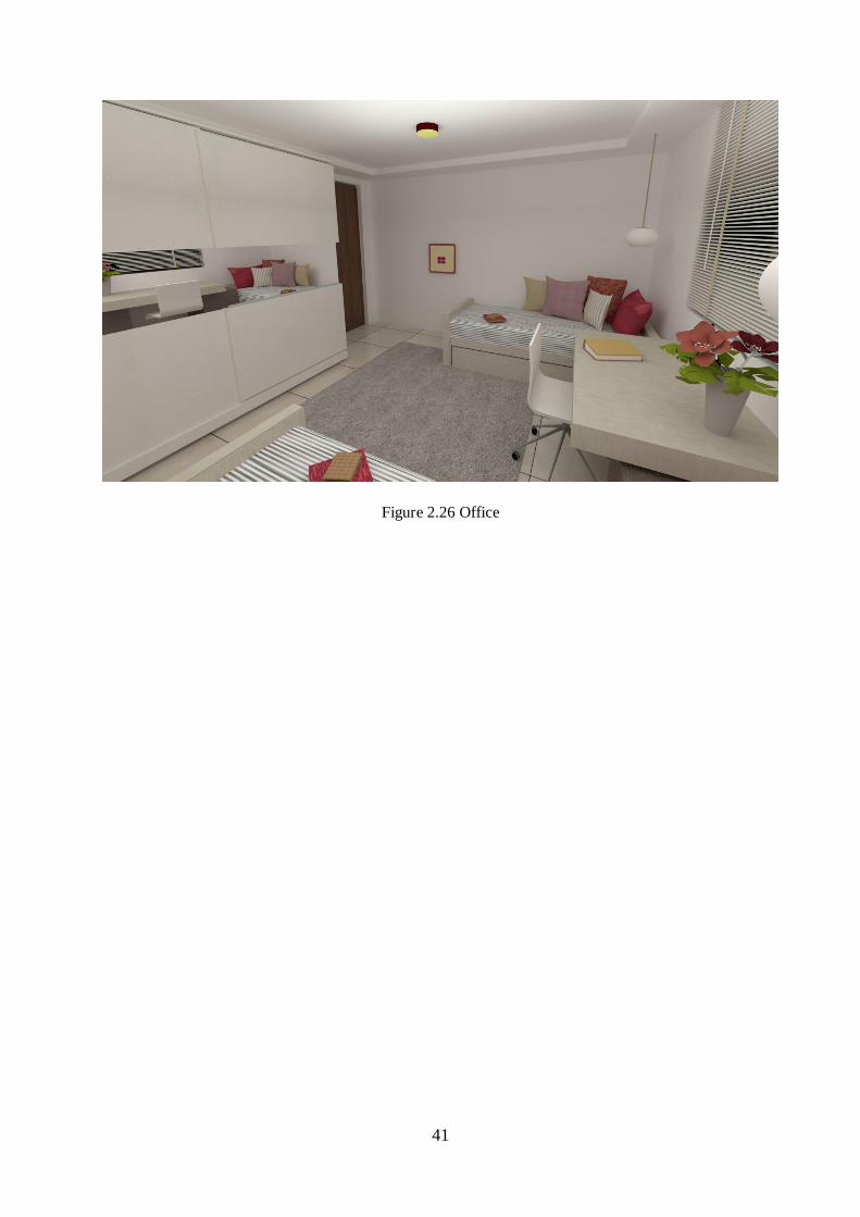
Figure 2.26 Office .................................................................................................................... 41
Figure 3.1 Master PCB top view b. Master PCB bottom view. .................................................. 47
Figure 3.2 top and bottom view. ............................................................................................... 48
Figure 3.3 OS top and bottom view........................................................................................... 49
Figure 3.4 Master board cover layout ........................................................................................ 52
XI
Figure 3.5 Master's top cover dimensions ................................................................................. 52
Figure 3.6 Master's on wall frame dimensions .......................................................................... 53
Figure 3.7 Master's in wall frame side dimensions .................................................................... 53
Figure 3.8 Master's in wall frame dimensions ........................................................................... 54
Figure 3.9 Slave's in wall frame side dimensions ...................................................................... 54
Figure 3.10 Slave's cover main layout ....................................................................................... 55
Figure 3.11 Slave's top cover dimensions.................................................................................. 55
Figure 3.12 Slave's on wall frame dimensions ........................................................................... 56
Figure 3.13 Slave's in wall frame dimension ............................................................................. 56
Figure 3.14 Remote's main cover layout ................................................................................... 57
Figure 3.15 Remote's top cover dimensions .............................................................................. 58
Figure 3.16 Remote's side cover dimensions ............................................................................. 58
Figure 4.1 Master circuit. .......................................................................................................... 62
Figure 4.2 Indoor circuit. .......................................................................................................... 63
Figure 4.3 Outdoor circuit......................................................................................................... 65
Figure 4.4 shield board. ............................................................................................................ 66
Figure 4.5 main screen. ............................................................................................................. 67
Figure 4.6 Indoor screen ........................................................................................................... 68
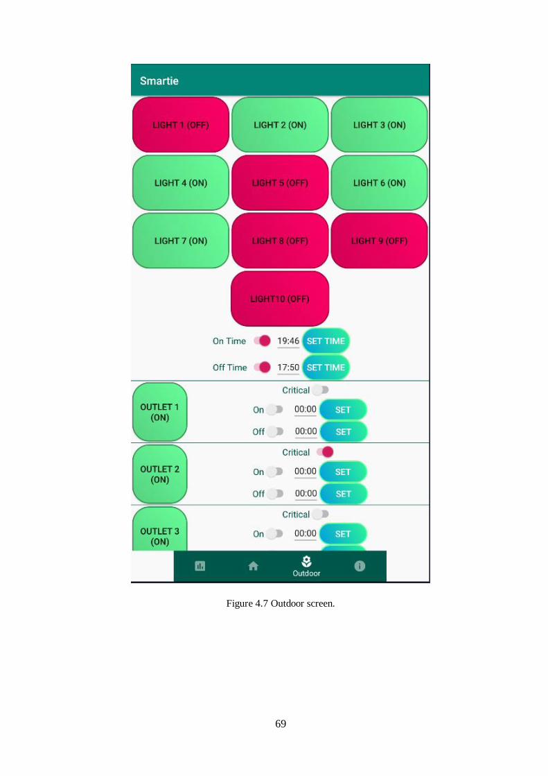
Figure 4.7 Outdoor screen......................................................................................................... 69
Figure 4.8 Presentation room. ................................................................................................... 71
Figure 4.9 Presentation room. ................................................................................................... 72

XII
List of Tables
Table 1.1 Timeframe Table......................................................................................................... 8
Table 2.1 Arduino Mega Data sheet .......................................................................................... 31
Table 2.2 Main programs used in designing process. ................................................................ 37
Table 2.3 Programming languages used in this project. ............................................................. 38
Table 3.1 Master board electrical components. ......................................................................... 42
Table 3.2 IS electrical components. .......................................................................................... 43
Table 3.3 OS electrical components. ......................................................................................... 44
Table 4.1 Response time. .......................................................................................................... 73
XI
List of Abbreviations
SHAS
Smart Home Automation System.
IoT
Internet of Things
PC
Personal Computer
HVAC
Heating Ventilating Air Conditioning units
UPS
Uninterruptable Power Supply
I/O
Inputs/Outputs
USB
Universal Serial Bus
LAN
Local Access Network
PCB
Printed Circuit Board
I2C
Inter-Integrated Circuit
IP
Internet Protocol
C.T
Current Transformer
P.T
Potential Transformer
IS
Indoor Slave
OS
Outdoor slave
LDR
Light Dependent Resistor
PIR
Passive Infrared Sensor
Kbps
kilobytes per second
SCL
Serial Clock Line
SDA
Serial Data Addressing
ID
Identification
SRAM
Static Random Access Memory

XII
EEPROM
Electrically Erasable Programmable Read-Only Memory
LED
Light Emitting Diode
DC
Direct Current
IR
Infra-Red
RH
Relative Humidity
CAD
Computer-aided drafting
IDE
Integrated Development Environment
Http
Hypertext Transfer Protocol
SDK
Software Development Kit
3D/2D
3 Dimensions/ 2 Dimensions.

1
Chapter One
Introduction
1.1 Introduction
1.2 Literature Review
1.3 Problem Statement
1.4 Objectives
1.5 Importance
1.6 Project scope
1.7 Time frame

2
1 Chapter One
1.1 Introduction
Smart home automation system (SHAS) is new trend has been started beside all new
technological innovation we have today, this trend started when smart appliances became more
popular, nowadays we have smartphone, smart tablets, smart cars, smart washing machines and
the list goes on. Most of smart appliances became "smart" when you connect them to the internet,
to give access and control power over their settings and configurations and give more technical
and useful information about the process they do, from this point of view Smart home automation
became a thing.
Internet of things (IoT) can be described as connecting everyday objects like smart phones,
internet televisions, sensors and actuators to the internet where the devices are intelligently linked
together to enable new forms of communication amongst people and themselves [1].
Smart home automation system opens the door for safer life, increasing comfort and more
control over house energy and consumption which all leads to energy saving and load control [2].
This project is an application of Smart home automation system (SHAS) concept in which we
apply Arduino technology to give the control over the whole system, in order to obtain a law cost,
flexible, scalable, user friendly and power economical system.
1.2 Literature Review
In [2] a flexible standalone smart home system illustrated, this system had been built using
Arduino-android application combination, the main purpose of this paper is to prove that a
complete smart home system could be built using Arduino microcontroller without using any
personal computers (PCs) or even high end microprocessors.
The author used an Ethernet connection for communication between the Arduino and the
smartphone, so the commands is transferring from the smartphone (android application) to micro

3
web-server inside the Arduino itself, and the data is transferred back from Arduino micro web-
server to the android application.
The main final results of the paper is a fully working small prototype containing small
circuit do basic control operations such as light, socket, HVAC (heating ventilating air
conditioning units) and Security control with fully working android application.
In [3] a full smart home system design presented, the main purpose of this design is to find
a solid way to communicate three main elements in the proposed system:
A website server (User interface to communicate with the system).
A personal computer as a Server.
Arduino hardware.
The methodology used in this system depends on a website user interface so the user could
interact with system by sending commands to the server (personal computer), then the server do
the processing needed for that command and then send the actuator status to the Arduino hardware.
On the other hand, Arduino hardware collects sensors data and sends it back to the server, then the
server do the processing needed for these data and decide the best implementation of system's
actuators, and send information about the process to the user by website page.
The main advantage of this smart system is the hardware/software capability gained using
personal computer power. However, this leads to some drawbacks that could affect the system
feasibility and stability, one large drawback is the cost, when we take in consideration the cost of
using a personal computer which is higher than 500$ for a moderate unit that is 10 times higher
than the cost of an Arduino circuit which could work as a master circuit for the system, and the
cost of using uninterruptable power supply (UPS) for the computer that also cost at least 200$ , all
of this additional cost make the system less affordable and highly complicated, another important
drawback of the system is the instable connection between the server computer and the Arduino
hardware using Wi-Fi communication.
In [4] a smart home automation system proposed based on Bluetooth technology, the main
purpose of this paper is to design and implement fully working, effective, flexible and cost efficient
home automation system relying just on Bluetooth technology.
4
The methodology used in this particular system depends on two main parts
Arduino hardware/software with Bluetooth module.
Android application.
The process start form Arduino board collecting all sensors and digital I/O data and sends
it to the user using Bluetooth communication, these data presented to the user using an android
application with friendly user interface, then the user responds to the system by sending back
commands to Arduino board.
To be mentioned that Arduino board also programmed in such algorithm allowing it to take
some small actions by itself just depending on sensors data, these actions could be preprogramed
or defined by user.
The main advantage of this system is simplicity, this system is simple in such way to reduce
the cost of using special hardware/software tools. On the other hand, this simplicity came on
reliability and practicality account, relying on Bluetooth communication is weak, because
Bluetooth technology usually has limited connectivity range and it's not secure.
In [5], the author presented a concept design of Home Automation system based on internet
website, the project aims to control electrical home units using a website accessible from anywhere
worldwide, this website connected to a personal computer mounted in the house as a system server,
this pc will be connected to a hardware controller from one side using USB or LAN connection,
and from the other side the controller will be connected with all electrical equipment's and units,
the author provided a full detailed control design and algorithms, but It lakes from any electrical
designs like PCB (printed circuit board) or even simulation diagrams or schemes.
One large advantage for the system is scalability, the system design allow to connect any
new house units using simple configuration and registration procedures, and because the system
uses a PC (personal computer) server you could add large amount of devices and units, and worth
to be mentioned that system designed in such way to be friendly with users who don’t have big
experience with websites and computers like elderly and disability persons.

5
However, the system suffers from the following
High Costs, although the design helped to make the system highly scalable but the layout
made the system costly because of using separate personal computer as a server which
costs over 500$ as mentioned before.
Complexity, despite the system is user-friendly but it's complicated in design in such way
that could affect efficiency and speed, because it offers multiple options to connect
hardware units with system software, and this variety of choices came on system efficiency
account.
1.3 Problem Statement
Smart Home Automation is a new trend that became more important day by day because of
the increase in importance of load management and power consumption reduction, and the families
with disability members and busy parents need of such systems, so in near future Smart Home will
be a must. However, current available industrial SHAS is expensive and inflexible because each
manufacturer focusing on certain electrical appliances over others to control, and most of these
system depend on replacing the traditional electrical units with smart ones which increase the total
system cost and make these systems hardly implemented in our market.
Our project is meant to provide a complete and finished solution prototype, this prototype
intend to be cheap, flexible, scalable, and practical so it won't replace any traditional or old
electrical units in the house, furthermore this project will provide different predefined and
programmed scenarios to reduce power consumption which of course serve the need of healthier
and less polluted environment.

6
1.4 Objectives
Design and build fully working smart home automation system (SHAS) prototype.
Implement cost and feature competitive system.
Subject the system for power consumption reduction.
Implement efficient power management techniques.
Design the whole system so it could meet the Palestinian tendencies.
Finishing our prototype in a professional way so it would be ready for marketing.
Marketing our system in the local markets in first phase, to be marketed in Global markets
later.
1.5 Importance
Smart home systems become much more popular and important day by day for many families,
also integrating these systems with home solar systems and implementing smart and manual
techniques for power consumption reduction and loads management, furthermore the need of these
systems for families with elderly and disability members increased the importance of these smart
systems, so building and implementing such systems locally is an important path to be taken, so
we could produce a competitive system that open new market doors for our economy, rise new
employment opportunities and develop the quality of technology in Palestine.
1.6 Project scope
In this project we implemented and designed a smart home system prototype based on Arduino
technology and NodeMCU boards based on Wi-Fi connection, this project will be divided into
separate circuits, each circuit will control all electrical appliances in a specific region defined for
it and all are connected to central cloud database.
For easy implementation purposes we took a specific house as a case study to implement our
system, then we could generalize our system for residual use.

7
In electrical design section, we designed all circuit using PCB (printed circuit boards)
technology, so we ended with three finished electrical boards printed by professional specialized
PCB manufacture and all electrical components and equipment are added and welded on these
boards.
In mechanical design section, we designed a special in wall cases and covers for each circuit
board and for some special electrical circuits and components need to be separated from the main
board.
In Software section, we defined the main software and programming languages used for
programming our system, and we designed a full flowchart for each software part in our system.

8
1.7 Timeframe
For tasks had been done in this course of our project see Table 1.1.
Table 1.1 Timeframe Table
Weeks Tasks
1 2 3 4 5 6 7 8 9 10 11 12 13 14 15
Programming firebase
Real-time database
I2C communication programming
Slaves programming
Android application programming
User interface For android
Circuits testing and Soldering
3D covers
System testing
Documentation

9
2
Chapter Two
Main Design Concepts
2.1 Introduction
2.2 System Layout
2.3 System main parts
2.4 I2C Communication
2.5 Hardware
2.6 Software
2.7 Case Study

10
2 Main Design Concept
2.1 Introduction
In order to build price competitive system we designed our system to fully work using Arduino
and NodeMCU boards over using personal computers as servers, and to make the system scalable
we divided it into sections each section controlled by separate circuit called slave and a master
circuit for electrical consumption and production monitoring and intruder siren system. All of these
circuits connected to a central cloud database.
2.2 System Layout
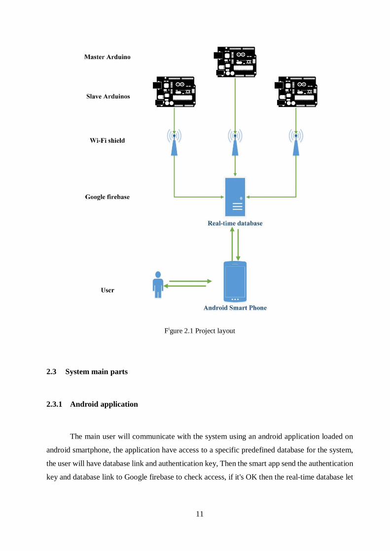
Our system is divided into four main parts see Figure 2.1.
A. Android application to be controlled by user connected to internet.
B. Google firebase real-time database.
C. Master circuit.
D. Slave circuits.
E. Custom designed Wi-Fi shield.
11
Figure 2.1 Project layout
2.3 System main parts
2.3.1 Android application
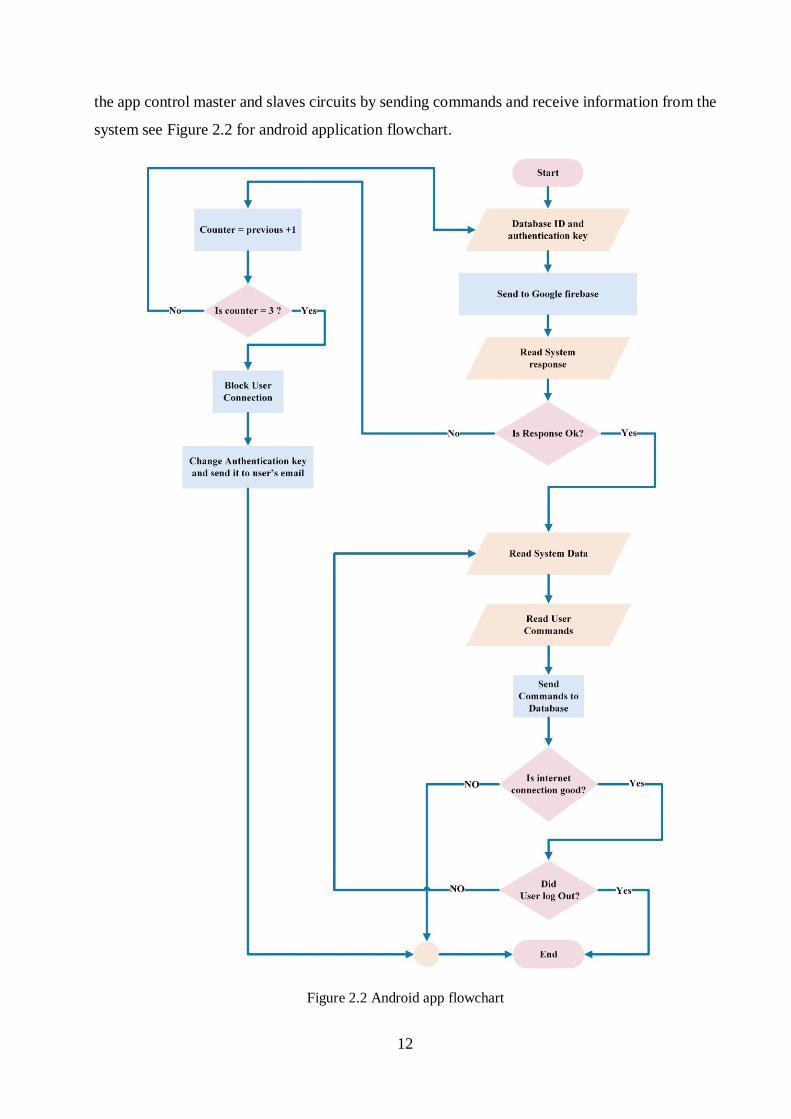
The main user will communicate with the system using an android application loaded on
android smartphone, the application have access to a specific predefined database for the system,
the user will have database link and authentication key, Then the smart app send the authentication
key and database link to Google firebase to check access, if it's OK then the real-time database let
12
the app control master and slaves circuits by sending commands and receive information from the
system see Figure 2.2 for android application flowchart.
Figure 2.2 Android app flowchart
13
2.3.2 Google firebase real-time database.
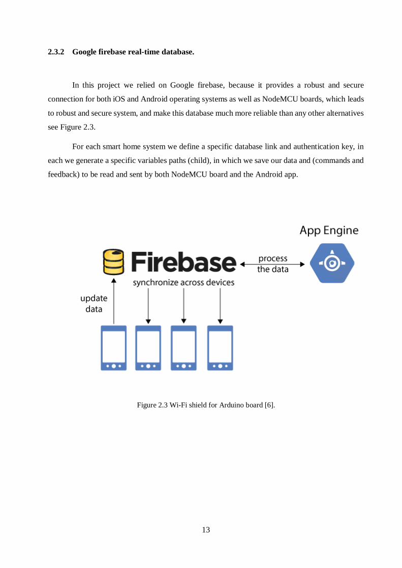
In this project we relied on Google firebase, because it provides a robust and secure
connection for both iOS and Android operating systems as well as NodeMCU boards, which leads
to robust and secure system, and make this database much more reliable than any other alternatives
see Figure 2.3.
For each smart home system we define a specific database link and authentication key, in
each we generate a specific variables paths (child), in which we save our data and (commands and
feedback) to be read and sent by both NodeMCU board and the Android app.
Figure 2.3 Wi-Fi shield for Arduino board [6].
14
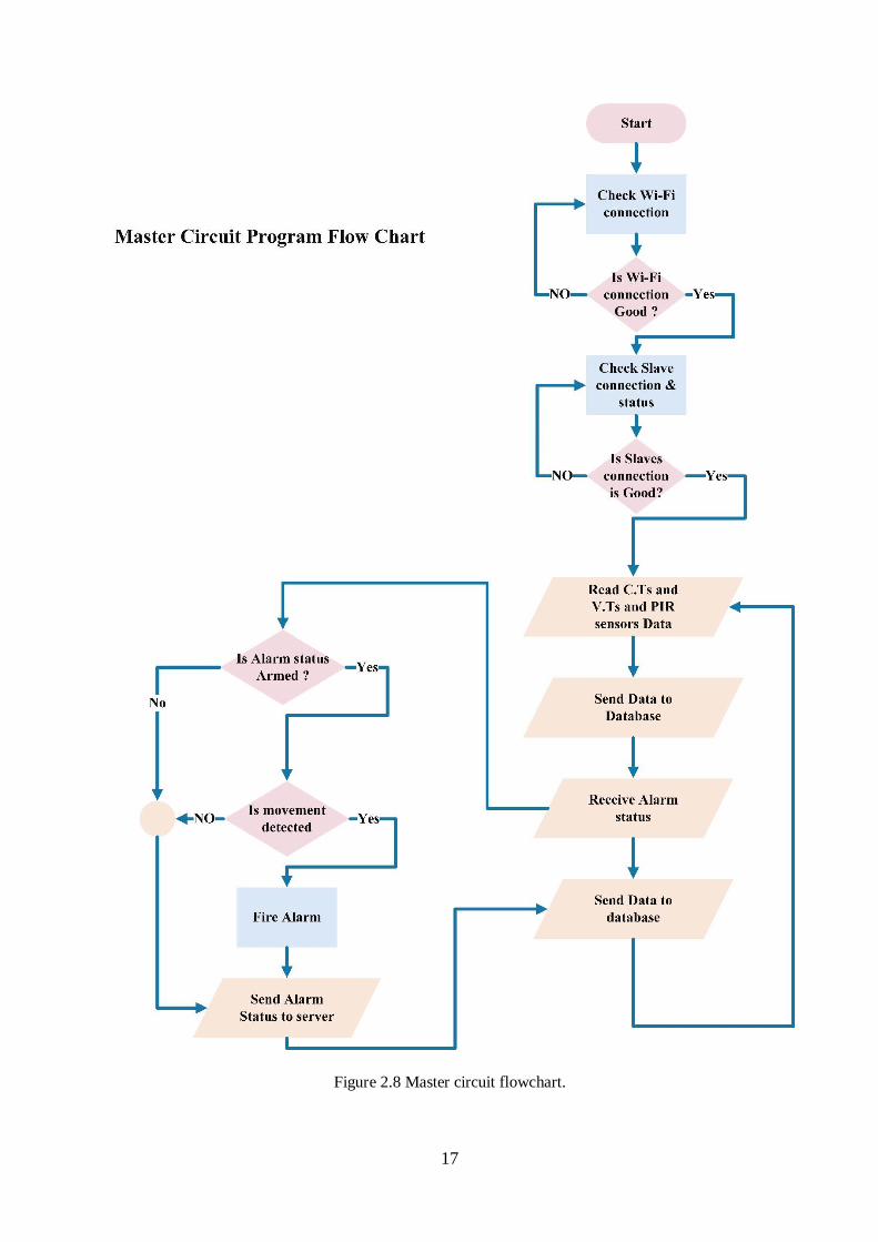
2.3.3 Master Circuit
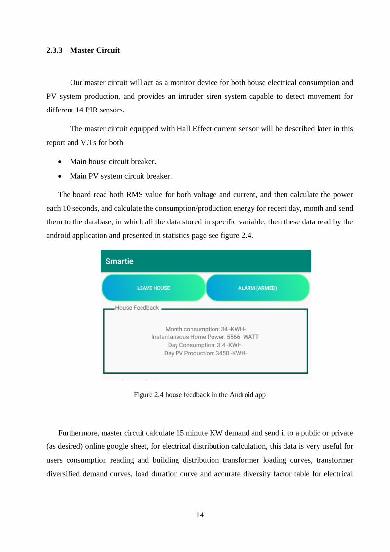
Our master circuit will act as a monitor device for both house electrical consumption and
PV system production, and provides an intruder siren system capable to detect movement for
different 14 PIR sensors.
The master circuit equipped with Hall Effect current sensor will be described later in this
report and V.Ts for both
Main house circuit breaker.
Main PV system circuit breaker.
The board read both RMS value for both voltage and current, and then calculate the power
each 10 seconds, and calculate the consumption/production energy for recent day, month and send
them to the database, in which all the data stored in specific variable, then these data read by the
android application and presented in statistics page see figure 2.4.
Figure 2.4 house feedback in the Android app
Furthermore, master circuit calculate 15 minute KW demand and send it to a public or private
(as desired) online google sheet, for electrical distribution calculation, this data is very useful for
users consumption reading and building distribution transformer loading curves, transformer
diversified demand curves, load duration curve and accurate diversity factor table for electrical

15
utility database, so distribution transformer capacity and expansion calculations will be much more
accurate see figure 2.5 for online google sheet.
Figure 2.5 Google sheet online user_15_minute_watt demand
For intruder siren system, Master board read alarm system status form the database, if the
system is armed and any of the 14 indoor attached PIR sensors detects any movement it will send
a notification to the user smartphone and will fire an in-house alarm, and in the future we're
planning to connect the alarm system with police station system for automatic dispatch in case of
intruder detection see figure 2.6 for Master circuit block diagram.
In addition to all previous master circuit's features, the master circuit also provided with
expected solar hours for each month these data provided by NASA, and the circuit compare at the
end of each day the generated energy and peak instantaneous power measured during last day and
compare them to both expected energy generation and peak power, after that it gives the user an
indication of the PV system status, if the PV system is normal, or need a clean or maintenance see
figure 2.7.
All software operation that the circuit should perform illustrated in Figure 2.8.

16
Figure 2.6 Master circuit block diagram.
Figure 2.7 PV status Android app.
17
Figure 2.8 Master circuit flowchart.

18
2.3.4 Slave circuits
These circuits meant to perform all electrical operations and collecting data from Rooms
and outside environment like: temperature, Humidity, Gas/Fire detection, intruder detection and
light intensity.
We have two main types of standard slave circuits
a) Indoor slave (IS).
b) Outdoor slave (OS).
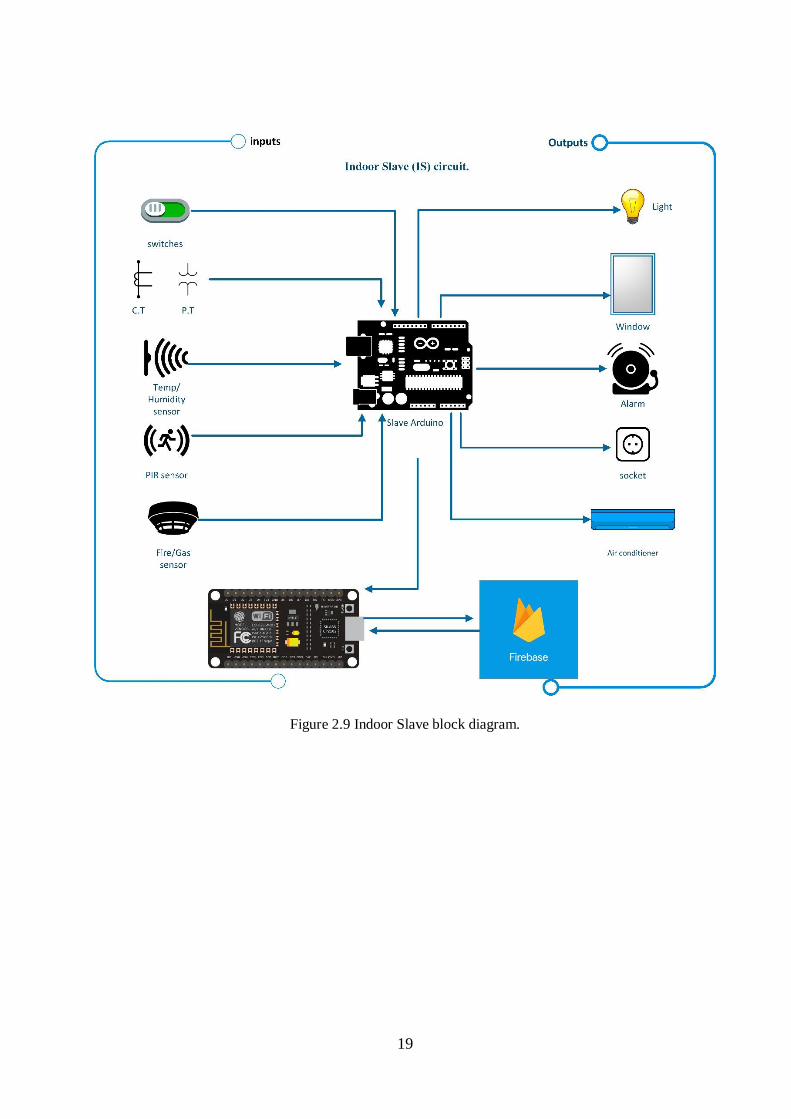
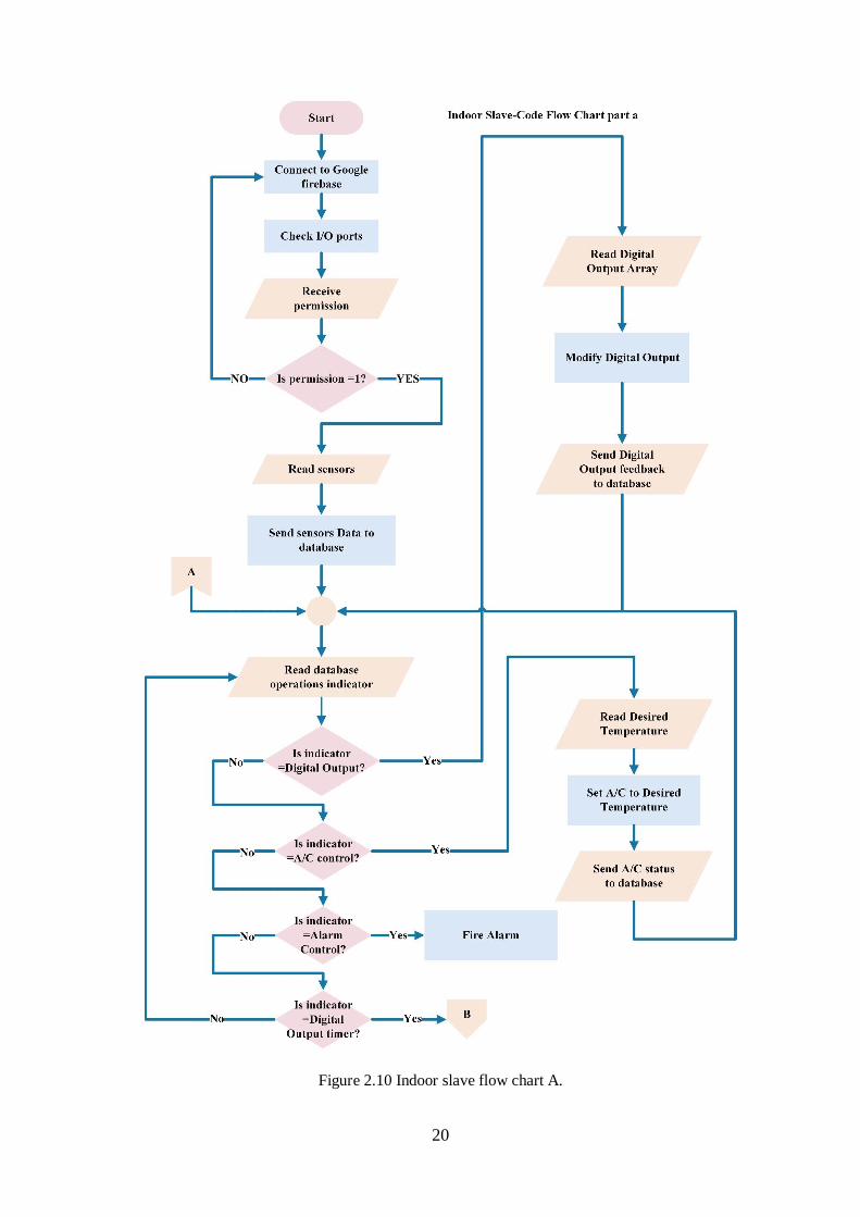
2.3.4.1 Indoor slave (IS)
This circuit will control all electrical appliances in its working region which is indoor room
see Figure 2.9 and Figure 2.10 & 2.11 for circuit flowchart.
A. IS inputs:
1. Lights On/Off switches.
2. Windows up/down switches.
3. Temp/humidity sensor.
4. Light sensor LDR.
5. Gas/fire sensor.
6. PIR sensor.
7. Hall Effect current sensor.
8. V.T.
B. IS outputs:
1. 5 X Light unit (on/off).
2. 3 X Window (up/down).
3. 8 X Sockets (on/off).
4. An HVAC (heating ventilating air conditioning unit) unit remote controller.
5. Alarm unit.
19
Figure 2.9 Indoor Slave block diagram.
20
Figure 2.10 Indoor slave flow chart A.

21
Figure 2.11 Indoor flow chart B.

22
For each electrical unit we provides 4 ways to control it see figure 2.12:
In app switching on and off.
Classical manual switches.
Timing, in which each component will have on timer and off timer switch.
Some predefined button like leave house.
Figure 2.12 In app on/off buttons and timers.
For HVAC units, we provides central infra-red unit, which could control the unit as desired,
cooling or heating and the temperature value see figure 2.13.
Figure 2.13 In app HVAC control.
23
Each indoor circuit able to monitor its region electrical consumption, and gives the user a feedback
of the instantaneous power and recent month energy consumption see Figure 2.14.
Figure 2.14 In app indoor slave feedback.
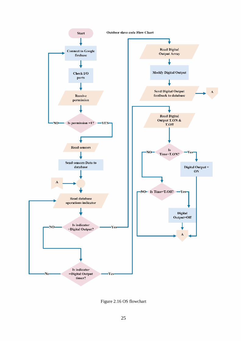
2.3.4.2 Outdoor slave (OS)
This circuit will control all electrical appliances in its working area, which include front
and back yard areas see Figure 2.15 and Figure 2.16 for circuit flowchart.
OS Inputs:
1. Lights On/Off switches.
2. Temp/humidity sensor.
3. Light sensor LDR.
4. PIR sensor.
5. Hall Effect current sensor.
6. V.T.
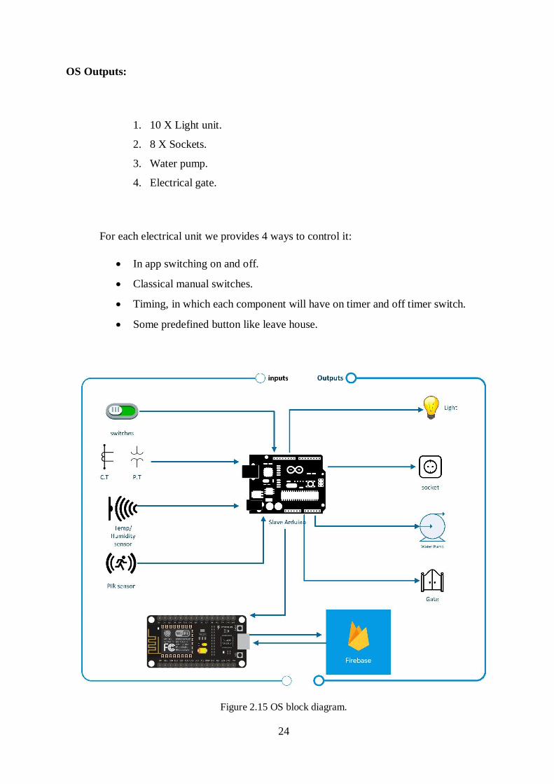
24
OS Outputs:
1. 10 X Light unit.
2. 8 X Sockets.
3. Water pump.
4. Electrical gate.
For each electrical unit we provides 4 ways to control it:
In app switching on and off.
Classical manual switches.
Timing, in which each component will have on timer and off timer switch.
Some predefined button like leave house.
Figure 2.15 OS block diagram.
25
Figure 2.16 OS flowchart
26
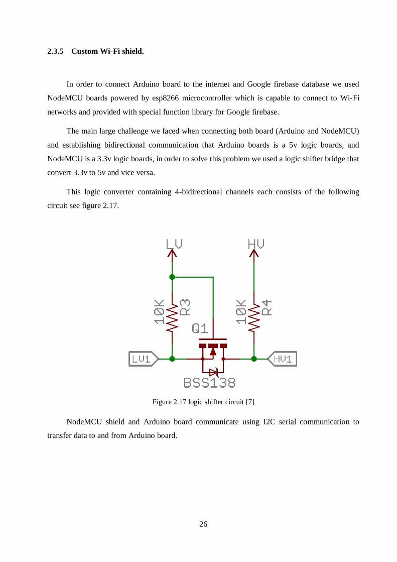
2.3.5 Custom Wi-Fi shield.
In order to connect Arduino board to the internet and Google firebase database we used
NodeMCU boards powered by esp8266 microcontroller which is capable to connect to Wi-Fi
networks and provided with special function library for Google firebase.
The main large challenge we faced when connecting both board (Arduino and NodeMCU)
and establishing bidirectional communication that Arduino boards is a 5v logic boards, and
NodeMCU is a 3.3v logic boards, in order to solve this problem we used a logic shifter bridge that
convert 3.3v to 5v and vice versa.
This logic converter containing 4-bidirectional channels each consists of the following
circuit see figure 2.17.
Figure 2.17 logic shifter circuit [7]
NodeMCU shield and Arduino board communicate using I2C serial communication to
transfer data to and from Arduino board.

27
2.4 I2C Communication
Slave and master Arduino boards communicate with Wi-Fi shield NodeMCU board by (I2C)
communication, this communication provide reliable and robust communication between different
manufacturer boards, although it's much more simple than alternative communication types for
microcontroller but yet it's the most used serial communication in microcontroller industry.
2.4.1 Why I2C communication?
Simple, needs just two wires.
Support multi masters, multi slaves devices.
Supported for Arduino microcontroller.
Supported for ESP8266 microcontroller.
Support bidirectional data transmission.
Best economical communication technology because it needs just two wires for the whole
system could be connected as ring configuration.
2.4.2 How it works?
Well each device has a preset ID or a unique device address so the master can choose with
which devices will be communicating.
The two wires, or lines are called serial clock (or SCL) and serial data (or SDA). The SCL
line is the clock signal which synchronize the data transfer between the devices on the I2C bus and
it’s generated by the master device. The other line is the SDA line which carries the data.
The two lines are “open-drain” which means that pull up resistors needs to be attached to
them so that the lines are high because the devices on the I2C bus are active low. Commonly used
values for the resistors are from 2k ohm for higher speeds at about 400 kbps, to 10k ohm for lower
speed at about 100 kbps [8].

28
2.4.3 Protocol
The data signal is transferred in sequences of 8 bits. So after a special start condition occurs
comes the first 8 bits sequence which indicates the address of the slave to which the data is being
sent. After each 8 bits sequence follows a bit called Acknowledge. After the first acknowledge bit
in most cases comes another addressing sequence but this time for the internal registers of the slave
device. After the addressing sequences follows the data sequences as many until the data is
completely sent and it ends with a special stop condition see Figure 2.12.
Figure 2.18 I2C Protocol [8].

29
2.5 Power and energy calculations.
In this section we're illustrating our technique in calculating voltage and current RMS values.
For voltage measuring we're using ZMPT101B voltage transformer, that converts voltage
from AC range to DC sinusoidal wave form with 2.5v reference value, in order to calculate the
RMS value we take 40 samples each cycle (i.e. one sample each 500 micro seconds), then we
calculate the RMS value for the measured cycle using the following equation.
𝑉𝑟𝑚𝑠/𝑐𝑦𝑐𝑙𝑒 = √∑ 𝑉𝑠𝑎𝑚𝑝𝑙𝑒240
1
40
And for higher accuracy we take the average RMS value for 12 cycle, this process refreshed
each 10 seconds, this calculation process used for both current and voltage and for current
measuring we're using ACS712 Hall Effect IC.
Each 10 seconds we calculate the apparent power and add it to energy variables to calculate
energy.
𝑆 (𝑉𝐴) = 𝑉𝑟𝑚𝑠 ∗ 𝐼𝑟𝑚𝑠
To calculate the average power we need to calculate PF (power factor), and to do so we
measure the time difference b/t voltage zero crossing sample and current zero crossing sample, as
we have 20 sample per cycle
1 𝑥 𝐶𝑦𝑐𝑙𝑒 = 20𝑚𝑠 𝑓𝑜𝑟 50 ℎ𝑧 𝑓𝑟𝑒𝑞𝑢𝑒𝑛𝑐𝑦
And

30
1 𝑥 𝐶𝑦𝑐𝑙𝑒 = 360 𝑑𝑒𝑔𝑟𝑒𝑒
For 20 samples per cycle we have
1 𝑥 𝑠𝑎𝑚𝑝𝑙𝑒 = 1𝑚𝑠 = 18 𝑑𝑒𝑔𝑟𝑒𝑒.
Now we calculate the number of samples b/t voltage zero crossing sample and current zero
crossing sample
𝑉0 𝑠𝑎𝑚𝑝𝑙𝑒 # − 𝐼0 𝑠𝑎𝑚𝑝𝑙𝑒 # = 𝑁.
Now for power factor angle
𝜃 = 18 ∗ 𝑁
𝑃𝐹 = 𝐶𝑜𝑠(𝜃)
Average power
𝑃𝑎𝑣𝑔 = 𝑆 ∗ 𝑃𝐹
𝐸𝑛𝑒𝑟𝑔𝑦 𝑣𝑎𝑟𝑖𝑎𝑏𝑙𝑒 (𝑊𝑎𝑡𝑡 𝐻𝑜𝑢𝑟) = 𝑝𝑟𝑒𝑣𝑜𝑖𝑢𝑠 𝑣𝑎𝑙𝑢𝑒 (𝑤𝑎𝑡𝑡 𝐻𝑜𝑢𝑟) + 𝑃𝑎𝑣𝑔(𝑤𝑎𝑡𝑡) ∗ (10
3600)
.
31
2.6 Hardware
In this section we're listing our project hardware components with full description and
working principle of each component.
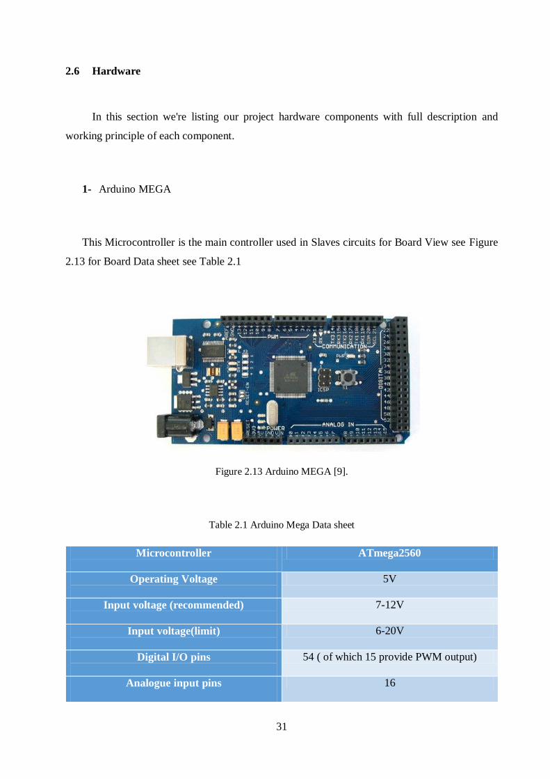
1- Arduino MEGA
This Microcontroller is the main controller used in Slaves circuits for Board View see Figure
2.13 for Board Data sheet see Table 2.1
Figure 2.13 Arduino MEGA [9].
Table 2.1 Arduino Mega Data sheet
Microcontroller
ATmega2560
Operating Voltage
5V
Input voltage (recommended)
7-12V
Input voltage(limit)
6-20V
Digital I/O pins
54 ( of which 15 provide PWM output)
Analogue input pins
16
32
DC Current per I/O pin
20 mA
DC Current for 3.3v pin
50mA
Flash memory
256 KB of which 8 KB used by boot loader
SRAM
8 KB
EEPROM
4 KB
Clock Speed
16 MHZ
LED_BUILTIN
13
Length
101.52mm
Width
53.3mm
Weight
37 g
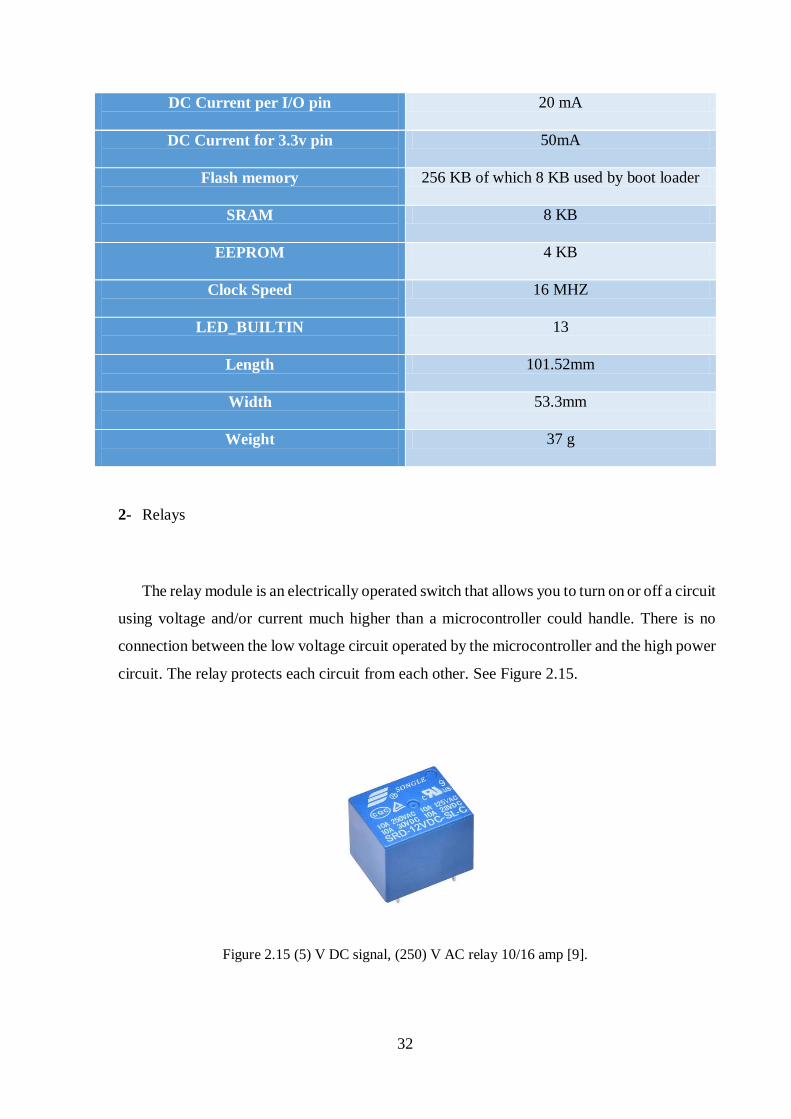
2- Relays
The relay module is an electrically operated switch that allows you to turn on or off a circuit
using voltage and/or current much higher than a microcontroller could handle. There is no
connection between the low voltage circuit operated by the microcontroller and the high power
circuit. The relay protects each circuit from each other. See Figure 2.15.
Figure 2.15 (5) V DC signal, (250) V AC relay 10/16 amp [9].

33
3- Gas/Fire sensor
The MQ series of gas sensors use a small heater inside with an electro-chemical sensor. They
are sensitive for a range of gasses and are used indoors at room temperature. They can be calibrated
more or less but a known concentration of the measured gas or gasses is needed for that. The output
is an analogue signal and can be read with an analogue input of the Arduino. See Figure 2.16.
Figure 2.16 Gas/fire sensor [9].
4- PIR sensor
PIRs are basically made of a pyro electric sensor , which can detect levels of infrared
radiation. Everything emits some low level radiation, and the hotter something is, the more
radiation is emitted. The sensor in a motion detector is actually split in two halves. The reason
for that is that we are looking to detect motion (change) not average IR levels. The two halves
are wired up so that they cancel each other out. If one half sees more or less IR radiation t han
the other, the output will swing high or low. See Figure 2.17.

34
Figure 2.17 PIR sensor [9].
5- Humidity and temperature sensor
This is a multifunctional sensor that gives you temperature and relative humidity information
at the same time. It can meet measurement needs of general purposes. It provides reliable readings
when environment humidity condition in between 20% RH and 90% RH, and temperature
condition in between 0°C and 50°C. See Figure 2.18.
Figure 2.18 Temp/humidity sensor [9].
6- Light sensor
A photo resistor is a light-controlled variable resistor. The resistance of a photo resistor
decreases with increasing incident light intensity; in other words, it exhibits photoconductivity. A
photo resistor can be applied in light-sensitive detector circuits, and light-activated and dark-
activated switching circuits. See Figure 2.19.
35
Figure 2.19 LDR sensor [9].
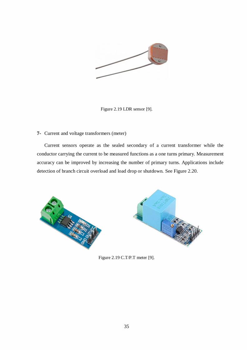
7- Current and voltage transformers (meter)
Current sensors operate as the sealed secondary of a current transformer while the
conductor carrying the current to be measured functions as a one turns primary. Measurement
accuracy can be improved by increasing the number of primary turns. Applications include
detection of branch circuit overload and load drop or shutdown. See Figure 2.20.
Figure 2.19 C.T/P.T meter [9].
36
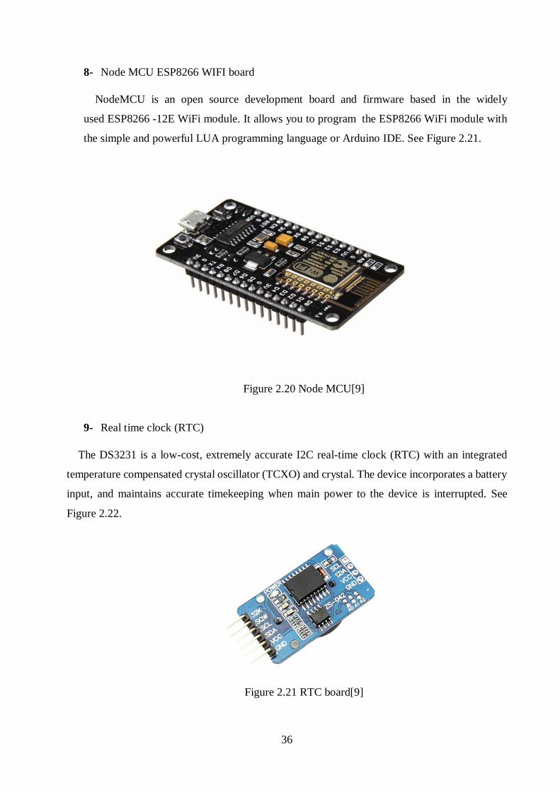
8- Node MCU ESP8266 WIFI board
NodeMCU is an open source development board and firmware based in the widely
used ESP8266 -12E WiFi module. It allows you to program the ESP8266 WiFi module with
the simple and powerful LUA programming language or Arduino IDE. See Figure 2.21.
Figure 2.20 Node MCU[9]
9- Real time clock (RTC)
The DS3231 is a low-cost, extremely accurate I2C real-time clock (RTC) with an integrated
temperature compensated crystal oscillator (TCXO) and crystal. The device incorporates a battery
input, and maintains accurate timekeeping when main power to the device is interrupted. See
Figure 2.22.
Figure 2.21 RTC board[9]

37
10- 4 channel logic level converter
A level shifter in digital electronics, also called a logic-level shifter, is a circuit used to
translate signals from one logic level or voltage domain to another, allowing compatibility
between ICs with different voltage requirements, such as TTL and CMOS. Many modern full
featured systems use level shifters to bridge domains between low-power application
processors running at 1.8 V and other system functions like sensors or other analog intensive
applications running at 3.3 or 5V. See Figure 2.23.
Figure 2.22 Node MCU[9]
2.7 Software
In this projects we used different software programs and programming languages to implement
our designs, as shown in Table 2.1
Table 2.2 Main programs used in designing process.
Program
Use
Proteus version 8.1 Design Main Electrical Circuits PCB schemes
AutoCAD 2016 Design Case Study House
Shapr3D (based on CAD Software) Design Wall mounted covers for PCB boards
Microsoft Visio 2016 Design project Diagrams and Flowcharts

38
For Programming language and programming software tools used see Table 2.2
Table 2.3 Programming languages used in this project.
Programming Language
Use
Arduino IDE software based on C/C++
Arduino programming
Http Commands + AT commands
Google firebase real-time database
android SDK based on Java android Application programming
2.8 Case Study
For simplification purposes this project will rely on specific case study to be generalized
later, this case study is a house consisting of:
1. 3 X Bedroom.
2. 1 X kitchen.
3. 1 X living room.
4. 1 X guestroom.
5. 3 X bathroom.
6. Front-back yard area.
Each bedroom will be served byIS slave circuit.
The guestroom, living room and kitchen will be served by oneIS slave circuit.
Bathrooms and stairs region will be served by oneIS slave circuit.
Front-back yard area will be served by OS slave circuit.
39
Master circuit will be connected to all previous slave circuits.
A full 3D design had been sketched for our case study house, the positioning ofIS (room control
slave), OS (Outdoor slave), master circuit and HVAC remote control covers shown in Figures
Figure 2.23 Master circuit cover

40
Figure 2.24 Bedroom
Figure 2.25 Living room
41
Figure 2.26 Office

40
3
Chapter Three
Electrical Design
3.1 Introduction
3.2 Electrical Components
3.3 PCB Schemes
3.4 Wall mounted Covers

41
3 Electrical Design
3.1 Introduction
In this chapter we introduce our PCB (printed circuit board) designs for all electrical circuits
in our system, all circuits designs had been implemented on Proteus Software version 8.1, in
second section of the chapter we're listing the electrical components in each circuits and
description of the main role of it in the circuit, then in PCB section we're attaching the final
schemes of PCB boards in 2D and 3D, finally we presented our 3D designs of Circuits covering.
42
3.2 Electrical Components
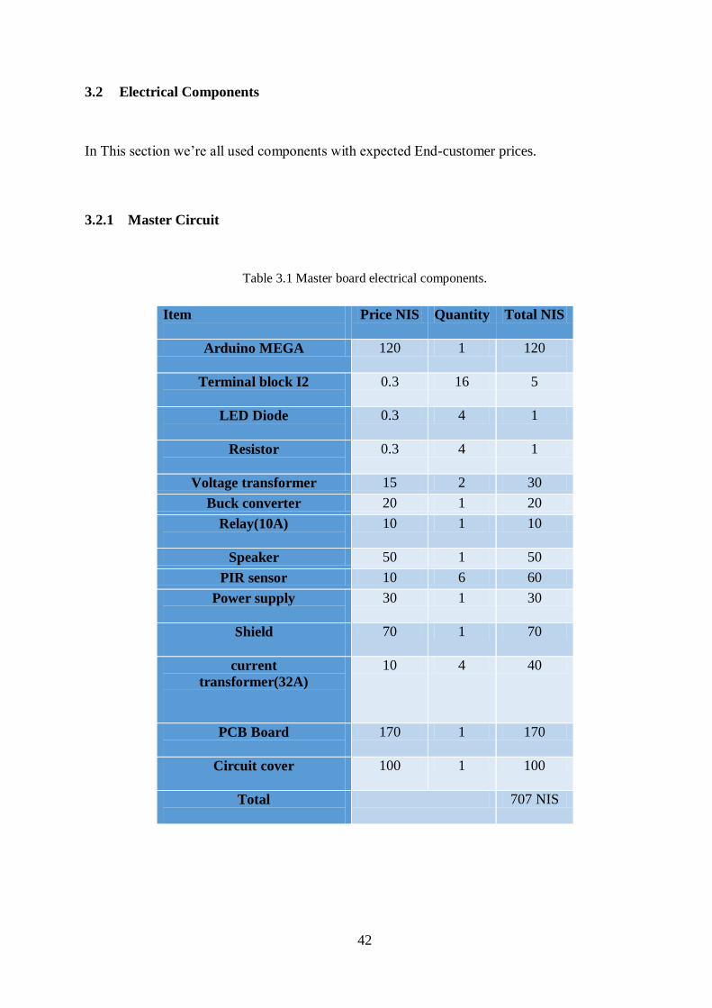
In This section we’re all used components with expected End-customer prices.
3.2.1 Master Circuit
Table 3.1 Master board electrical components.
Item
Price NIS Quantity Total NIS
Arduino MEGA 120 1 120
Terminal block I2
0.3 16 5
LED Diode
0.3 4 1
Resistor
0.3 4 1
Voltage transformer 15 2 30
Buck converter 20 1 20
Relay(10A)
10 1 10
Speaker 50 1 50
PIR sensor 10 6 60
Power supply
30 1 30
Shield
70 1 70
current
transformer(32A)
10 4 40
PCB Board
170 1 170
Circuit cover
100 1 100
Total
707 NIS
43
3.2.2 IS (Room Control Slave) Circuits
Table 3.2IS electrical components.
Item
Price NIS Quantity Total NIS
IR diode 2 1 2
Arduino MEGA
120 1 120
Terminal block I2
0.3 50 15
LED
0.3 20 6
Resistor
0.2 35 7
Buck converter 20 3 60
Relay(10A)
10 6 60
Power supply
30 1 30
current transformer(16A)
10 1 10
current transformer(10A)
10 1 10
Relay(16A)
12 14 168
Speaker
50 1 50
Voltage transformer 15 1 15
Temperature sensor
16 1 16
PIR sensor
10 1 10
Light sensor 2 1 2
Buffer IC 8 3 24
Gas sensor 15 1 15
Headers 150 0.067 10
Circuit cover 100 1 100
PCB 200 1 200
Shield 70 1 70
Total
1000
44
3.2.3 OS (Outdoor slave) Circuit
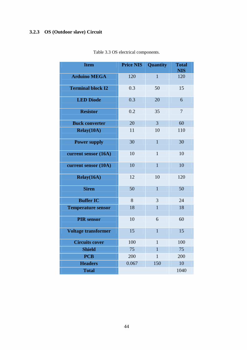
Table 3.3 OS electrical components.
Item Price NIS Quantity Total
NIS
Arduino MEGA
120 1 120
Terminal block I2
0.3 50 15
LED Diode
0.3 20 6
Resistor
0.2 35 7
Buck converter 20 3 60
Relay(10A)
11 10 110
Power supply
30 1 30
current sensor (16A)
10 1 10
current sensor (10A)
10 1 10
Relay(16A)
12 10 120
Siren
50 1 50
Buffer IC 8 3 24
Temperature sensor
18 1 18
PIR sensor
10 6 60
Voltage transformer 15 1 15
Circuits cover 100 1 100
Shield 75 1 75
PCB 200 1 200
Headers 0.067 150 10
Total 1040

45
3.3 PCB Schemes
In this project we designed 3 main PCB (printed circuit board) boards, one is a master PCB
board, OS (Outdoor-slave) PCB board and IS (Indoor-slave) PCB boards. All PCB boards
designed using Proteus software ver. 8.1.
For trace's width calculations we have 2 types of traces:
Signal trace that represent all signals from-into Arduino boards.
Power traces that represent phase traces, 16 Amp phase for power circuits and 10 Amp
phase for lighting circuits.
3.3.1 Traces widths
For signal trace width we chose 1.2 mm width which is s standard in PCB design.
For 10 Amp trace we chose 3.75 mm width.
For 16 Amp trace we chose 4.5 mm width.
3.3.2 Calculations
First, the Area is calculated:
Area [mils^2] = (Current [Amps]/ (k*(Temp_Rise [deg. C])^b))^(1/c) (3.1)
Then, the Width is calculated:
Width [mils] = Area [mils^2]/ (Thickness [oz]*1.378[mils/oz]) (3.2)
For IPC-2221 external layers: k = 0.048, b = 0.44, c = 0.725
46
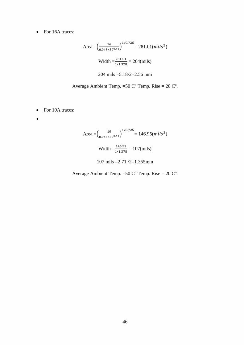
For 16A traces:
Area =(16
0.048∗500.44)1/0.725
= 281.01(𝑚𝑖𝑙𝑠2)
Width =281.01
1∗1.378 = 204(mils)
204 mils =5.18/2=2.56 mm
Average Ambient Temp. =50 Co Temp. Rise = 20 Co.
For 10A traces:
Area =(10
0.048∗500.44)1/0.725
= 146.95(𝑚𝑖𝑙𝑠2)
Width =146.95
1∗1.378 = 107(mils)
107 mils =2.71 /2=1.355mm
Average Ambient Temp. =50 Co Temp. Rise = 20 Co.

47
3.3.3 PCB 3D view
Master PCB top and bottom view shown in Figure 3.1.
Figure 3.1 Master PCB top view b. Master PCB bottom view.
48
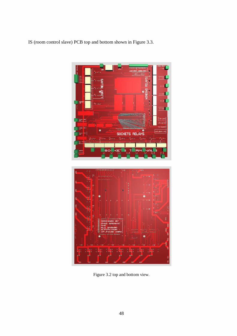
IS (room control slave) PCB top and bottom shown in Figure 3.3.
Figure 3.2 top and bottom view.

49
For OS (Outdoor slave) PCB top and bottom view shown in Figure 3.5.
Figure 3.3 OS top and bottom view.

50
For Wi-Fi shield PCB top and bottom view shown in Figure 3.6
Figure 3.6 WIFI shield top and bottom view.

51
3.4 Wall mounted Covers
In this section we present our special designed wall mounted covers and frames, all of the
following 3D designs designed using Shapr3D, it's a CAD software works with AutoCAD and
Solid works, the main idea of these designs is to be printed using 3D printer by polymer materials.
We designed 3 covers for three main components, one is for the master PCB board, the
second for slave's circuits and finally a cover for HVAC (heating ventilating air conditioning)
unit's remote controller and Gas/fire sensor circuit.
3.4.1 Master Board Cover
This cover consists of three parts, an In wall frame which will be hidden inside the wall
with 8mm depth and will be mounted using 4 screws, then an On wall frame will cover the circuit
from the outside and also mounted using 4 screws, the third part is a top Cover will be attached
with the On Wall Mounted part by 4 Magnet pairs, this particular part is meant to be transparent
for easy presenting purposes but for actual production it will be color and material customizable
to meet the main house decoration. For the design layout and dimensions see Figures 3.7-3.11

52
Figure 3.4 Master board cover layout
Figure 3.5 Master's top cover dimensions

53
Figure 3.6 Master's on wall frame dimensions
Figure 3.7 Master's in wall frame side dimensions
54
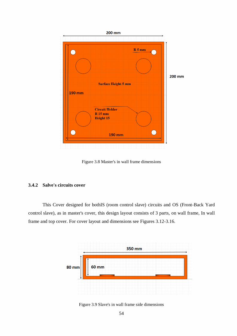
Figure 3.8 Master's in wall frame dimensions
3.4.2 Salve's circuits cover
This Cover designed for bothIS (room control slave) circuits and OS (Front-Back Yard
control slave), as in master's cover, this design layout consists of 3 parts, on wall frame, In wall
frame and top cover. For cover layout and dimensions see Figures 3.12-3.16.
Figure 3.9 Slave's in wall frame side dimensions
55
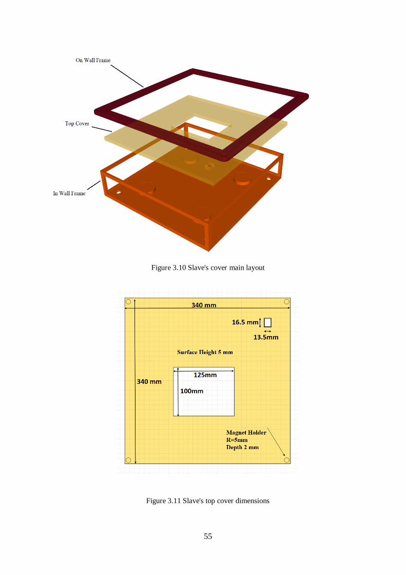
Figure 3.10 Slave's cover main layout
Figure 3.11 Slave's top cover dimensions

56
Figure 3.12 Slave's on wall frame dimensions
Figure 3.13 Slave's in wall frame dimension
57
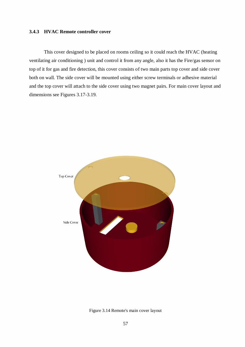
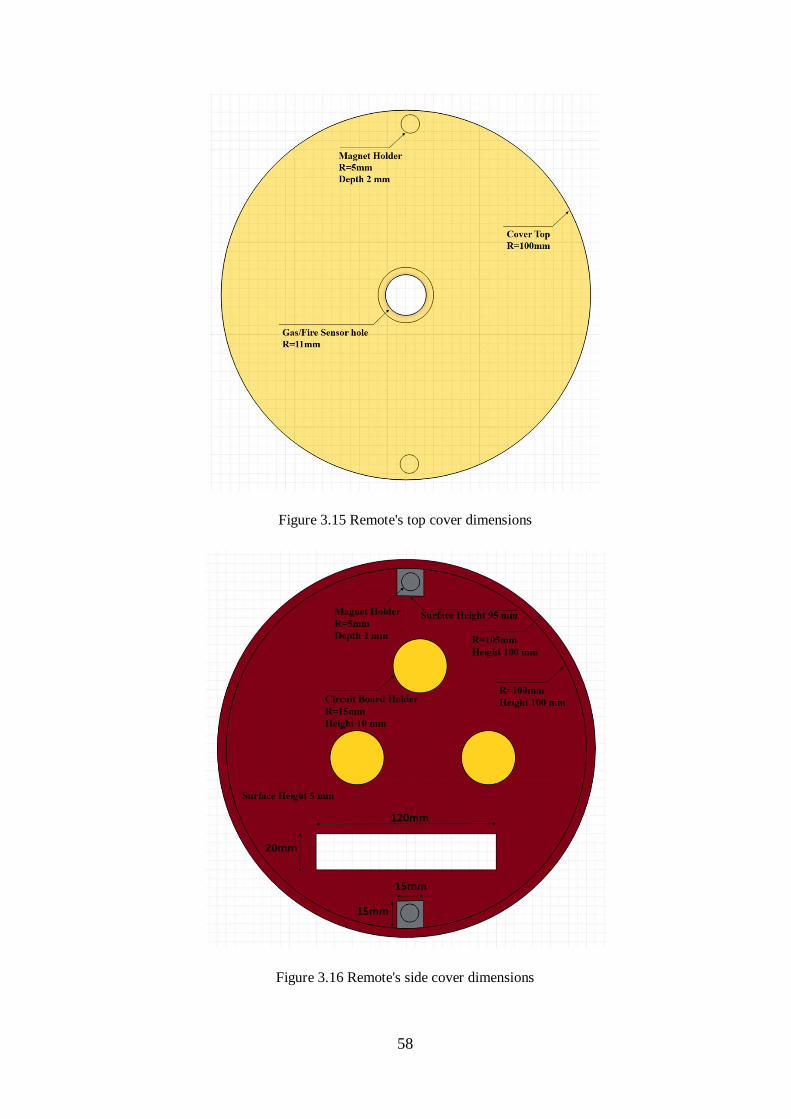
3.4.3 HVAC Remote controller cover
This cover designed to be placed on rooms ceiling so it could reach the HVAC (heating
ventilating air conditioning ) unit and control it from any angle, also it has the Fire/gas sensor on
top of it for gas and fire detection, this cover consists of two main parts top cover and side cover
both on wall. The side cover will be mounted using either screw terminals or adhesive material
and the top cover will attach to the side cover using two magnet pairs. For main cover layout and
dimensions see Figures 3.17-3.19.
Figure 3.14 Remote's main cover layout
58
Figure 3.15 Remote's top cover dimensions
Figure 3.16 Remote's side cover dimensions

59
4
Chapter Four
Results and Recommendations
4.1 Introduction
4.2 Results
4.3 Android App
4.4 Small presentation room
4.5 Response time
4.6 Components temperature
4.7 Recommendations

60
4 Results & Recommendations
4.1 Introduction
In this chapter we're presenting our last result, features and future improvements for this
project, on the other hand after almost 9 months of development we have some recommendations
we would to share for any future development on similar projects,.

61
4.2 Results
At the end of this course we had designed and produced 4 main PCB circuits, and a small
presentation room for project illustration and presentation.
Worth to be mentioned that all circuit boards (Indoor, Outdoor and Master) are separated
hardware, and could be used separately and independently, they all connected to central database,
but all have access to the internet and this method of controlling highly improve system stability,
speed and flexibility.
4.2.1 Master circuit features
The master circuit board able to do the following:
Measure main house instantaneous power up to 10.5 kW (Max. 42Arms and 250Vrms).
Measure recent day and month house energy consumption.
Measure main PV system instantaneous power up to 10 kW (Max. 42Arms and 250Vrms).
Measure recent day and month PV system energy Production.
An intruder siren system with 6 PIR inputs.
All previous mentioned featured uploaded to special firebase database URL and
presented/controlled using Android smart app.
Measure 15-watt demand and upload it to online public google sheet for utility 15-kW
demand, transformers and feeders load calculations.
For finished circuit see figure 4.1.

62
Figure 4.1 Master circuit.
4.2.2 Indoor circuit features
The indoor circuit board able to do the following:
Control 5 separated light unites by on/off button, by on-time/off-time, by custom made
button and scenarios (like leave home button).
Control 8 separated outlet unites by on/off button, by on-time/off-time, by custom made
button and scenarios (like leave home button).

63
Control 3 separated electric window unites by up/down button, by up-time/down-time, by
custom made button and scenarios (like leave home button).
Control HVAC units using IR central sender able to control AC mode (heat/cool) and AC
temperature.
Measure main room instantaneous power up to 5000 kW (Max. 21Arms and 250Vrms).
Measure month house energy consumption.
Read room temperature and humidity.
Fire/gas detection sensor which automatically open all connected windows.
All previous mentioned featured uploaded to special firebase database URL and
presented/controlled using Android smart app.
For finished circuit see figure 4.2.
Figure 4.2 Indoor circuit.

64
4.2.3 Outdoor circuit features
The outdoor circuit board able to do the following:
Control 10 separated light unites by on/off button, by on-time/off-time, by custom made
button and scenarios (like leave home button).
Control 8 separated outlet unites by on/off button, by on-time/off-time, by custom made
button and scenarios (like leave home button).
Control water pump by on/off button, by on-time/off-time, by custom made button and
scenarios (like leave home button).
Control one gate by on/off button.
Measure main room instantaneous power up to 5000 kW (Max. 21Arms and 250Vrms).
Measure month house energy consumption.
Measure outdoor temperature and humidity.
Detect outdoor movement for automatically activates some loads and lights.
All previous mentioned featured uploaded to special firebase database URL and
presented/controlled using Android smart app.
For finished circuit see figure 4.3.

65
Figure 4.3 Outdoor circuit.
66
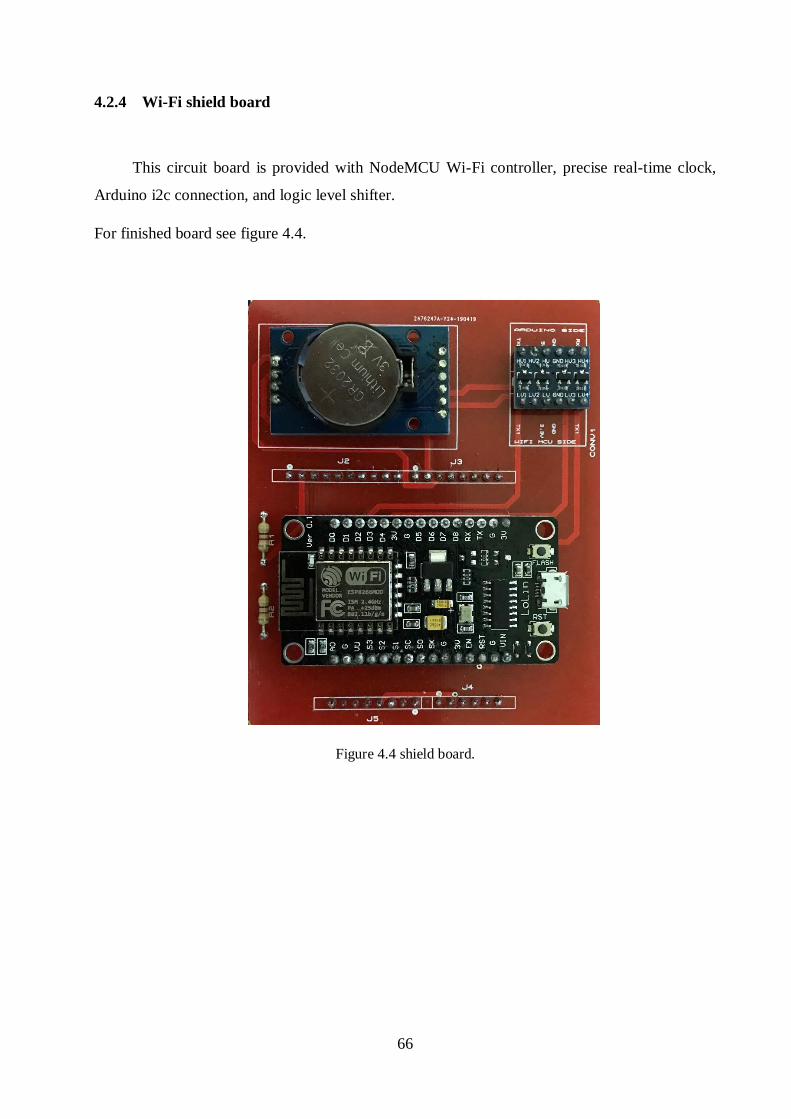
4.2.4 Wi-Fi shield board
This circuit board is provided with NodeMCU Wi-Fi controller, precise real-time clock,
Arduino i2c connection, and logic level shifter.
For finished board see figure 4.4.
Figure 4.4 shield board.
67
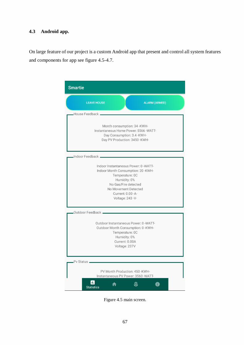
4.3 Android app.
On large feature of our project is a custom Android app that present and control all system features
and components for app see figure 4.5-4.7.
Figure 4.5 main screen.

68
Figure 4.6 Indoor screen
69
Figure 4.7 Outdoor screen.

70
4.4 Small presentation room.
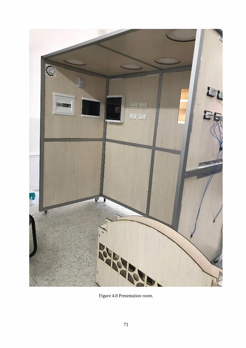
In polytechnic university labs we did build a small room as a presentation for our system (see
figure 4.8-4.9) contains the following:
Main C.B panels with 5 C.B.
Master circuit.
Intruder siren system.
2 PIR sensors.
Gas/fire sensor.
IR central sender.
Heater/cooler as HVAC presentation.
Electric window.
Electric wood gate
Indoor circuit with 4 light, 3 window and 1 reset switches.
6 light units 2 outdoor, 4 indoor.
8 outlets, for both indoor and outdoor.
Electric water pump.
71
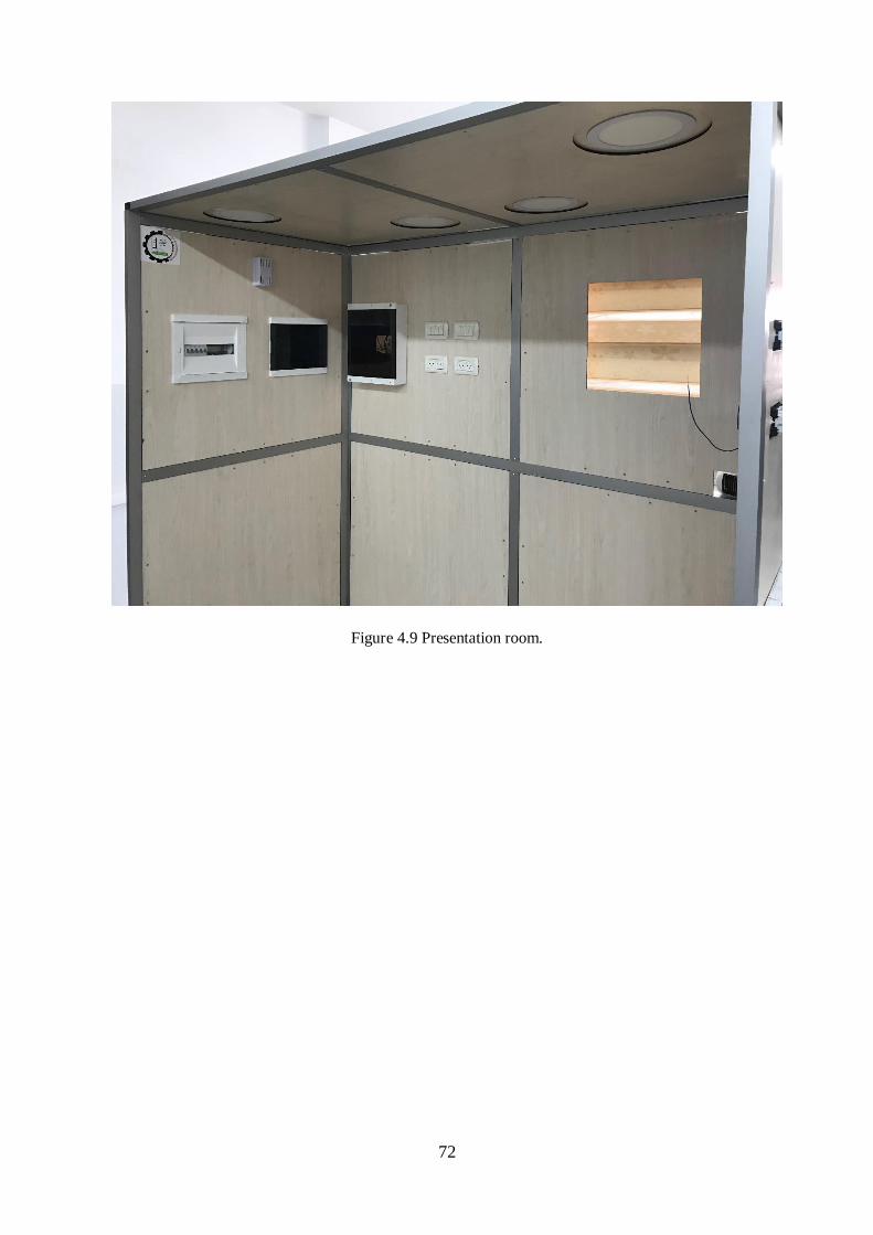
Figure 4.8 Presentation room.
72
Figure 4.9 Presentation room.

73
4.5 Response time
In following table 4.1 we recorded actual response time from Android app commands to system
circuits under different internet connection speeds.
Note: The list of commands below had been taken in different times for different circuits (Indoor
and outdoor) and different commands (on/off and on-time/off-time).
Table 4.1 Response time.
Command
#
command
status
act
time
(sec)
feedback
time
(sec)
1 Succeed 1.28 2.18
2 Succeed 1.08 1.88
3 Succeed 1.07 2.57
4 Succeed 1.73 3.54
5 Succeed 0.98 1.5
6 Succeed 1.5 2.41
7 Succeed 1.6 2.58
8 Succeed 1.51 2.41
9 Succeed 1.46 2.19
10 Succeed 2.53 3.32
11 Succeed 1.34 2.13
12 Succeed 1.86 2.83
13 Succeed 3.67 4.89
14 Succeed 2.11 3.21
15 Succeed 2.98 3.86
16 Succeed 1.94 3.04
17 Succeed 2.04 2.73
18 Succeed 1.2 2.11
19 Succeed 4 6
20 Succeed 1.85 2.59
21 Succeed 1.11 1.79
22 Succeed 0.86 1.5
23 Succeed 1.43 2.53
24 Succeed 1.19 1.9
25 Succeed 1.08 2.19
26 Succeed 2.8 3.49
27 Succeed 1.31 2.22
28 Succeed 0.99 1.69
29 Succeed 1.29 2.47
30 Succeed 1.45 2.26
31 Succeed 0.9 1.41
32 Succeed 0.8 1.43
74
33 Succeed 1.16 2.19
34 Succeed 1.54 2.7
35 Succeed 1.89 2.89
36 Succeed 1.78 2.54
37 Succeed 0.95 2.45
38 Succeed 1.4 2.23
39 Succeed 1.84 2.47
40 Succeed 1.13 1.92
41 Succeed 1.2 1.9
42 Succeed 1.31 2.37
43 Succeed 6.78 8.21
44 Succeed 1.74 3.14
45 Succeed 1.56 2.27
46 Succeed 1.4 2.04
47 Succeed 4.5 4.98
48 Succeed 1.61 2.24
49 Succeed 1.44 1.95
50 Succeed 1.13 1.67
Average 100% 1.746 2.6602
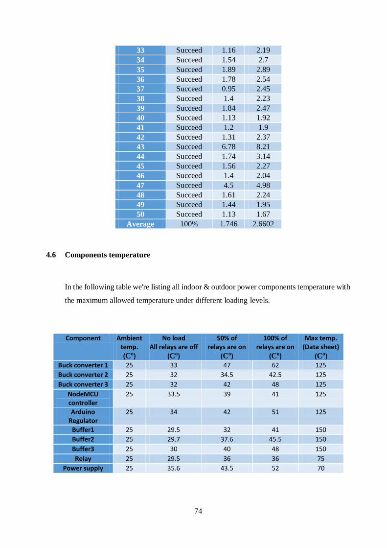
4.6 Components temperature
In the following table we're listing all indoor & outdoor power components temperature with
the maximum allowed temperature under different loading levels.
Component Ambient temp.
(Co)
No load All relays are off
(Co)
50% of relays are on
(Co)
100% of relays are on
(Co)
Max temp. (Data sheet)
(Co)
Buck converter 1 25 33 47 62 125
Buck converter 2 25 32 34.5 42.5 125
Buck converter 3 25 32 42 48 125
NodeMCU controller
25 33.5 39 41 125
Arduino Regulator
25 34 42 51 125
Buffer1 25 29.5 32 41 150
Buffer2 25 29.7 37.6 45.5 150
Buffer3 25 30 40 48 150
Relay 25 29.5 36 36 75
Power supply 25 35.6 43.5 52 70

75
4.7 Recommendations
In this section we have some recommendation to be taken in consideration for future
development and improvement for this project and/or other similar project.
Supplying Arduino board with 6.5v power supply is the most suitable and stable case,
although Arduino company says "input Voltage recommended = 5-12", 12v power supply
cause high power dissipation in Arduino regulator and may cause thermal tripping for the
board.
Energize each 7 AC relays with separate power supply or regulator like lm2596.
Supply Hall Effect sensor ACS712T by separate precise 5v power supply or by Arduino
5v terminals, because this specific sensor is highly sensitive to harmonics and noises and
need a precise voltage to work probably and precisely.
For Such large PCBs and large amount of component to be powered, use 25 watt or higher
power supply because it reaches high temperature that could affect the system stability in
long term use.
Arduino code sketch should be less than 75% of Arduino memory size, because large size
sketch files could cause instability in Arduino performance.
For i2c connection,
o I2c wire should be less than 1 meter long for stable connection and data transfer.
o Don’t make two requests in a row without delay less than 50ms.
o Don’t make transmit data two times in a row without delay less than 50ms.
o Use 4.7 K ohm pull-up resistor on both SDA and SCL.
o Don’t use delay function in Arduino interrupt function.
For PCB designing, Proteus software is powerful enough but so hard to use and rely on,
instead we recommend Multisim software.
For 3.3v to 5v level shifting, we recommend bi-directional logic level shifter with
MOSFET devices instead of other elements.
For more precise Current measurement, use current transformer instead of ACS712T.
Make sure that all components are working under normal conditions mentioned in their
datasheets.

76
References
[1] G. Kortuem, F. Kawsar, V. Sundramoorthy, and D. Fitton, "Smart objects as building
blocks for the internet of things," IEEE Internet Computing, vol. 14, no. 1, pp. 44-51, 2010.
[2] S. Kumar, "Ubiquitous smart home system using android application," arXiv preprint
arXiv:1402.2114, 2014.
[3] A. ElShafee and K. A. Hamed, "Design and implementation of a WIFI based home
automation system," World academy of science, engineering and technology, vol. 68, pp.
2177-2180, 2012.
[4] S. Anwaarullah and S. Altaf, "RTOS based home automation system using Android,"
international journal of advanced Trends in computer science and engineering, vol. 2, no.
1, pp. 480-484, 2013.
[5] R. J. Nunes and J. C. Delgado, "An Internet application for home automation," in
Electrotechnical Conference, 2000. MELECON 2000. 10th Mediterranean, 2000, vol. 1,
pp. 298-301: IEEE.
[6] https://arduino.stackexchange.com/questions/24919/how-to-connect-wi-fi-shield-esp-
12e-esp8266-uart-wifi-wireless-shield-with-ardui. (2018, 19/11/2018). Arduino.
[7] learn.sparkfun.com. (2019, 30/04/2019). Bi-Directional Logic Level Converter. Available:
https://learn.sparkfun.com/tutorials/bi-directional-logic-level-converter-hookup-guide/all
[8] H. T. Mechatronics. (2018, 20/11/2018). I2C Communication Available:
https://howtomechatronics.com/tutorials/arduino/how-i2c-communication-works-and-
how-to-use-it-with-arduino/
[9] A. Express. (2018, 01/12/2018). Arduino accesorios. Available:
https://www.aliexpress.com/wholesale?catId=0&initiative_id=AS_20181201121635&Se
archText=arduino+accesorios

Appendices
In this section we're attaching all design components, equipment and devices datasheets.

The Arduino Mega 2560 is a microcontroller board based on the ATmega2560 (datasheet). It has 54 digital input/output pins (of which 14 can be used as PWM outputs), 16 analog inputs, 4 UARTs (hardware serial ports), a 16 MHz crystal oscillator, a USB connection, a power jack, an ICSP header, and a reset button. It contains everything needed to support the microcontroller; simply connect it to a computer with a USB cable or power it with a AC-to-DC adapter or battery to get started. The Mega is compatible with most shields designed for the Arduino Duemilanove or Diecimila.
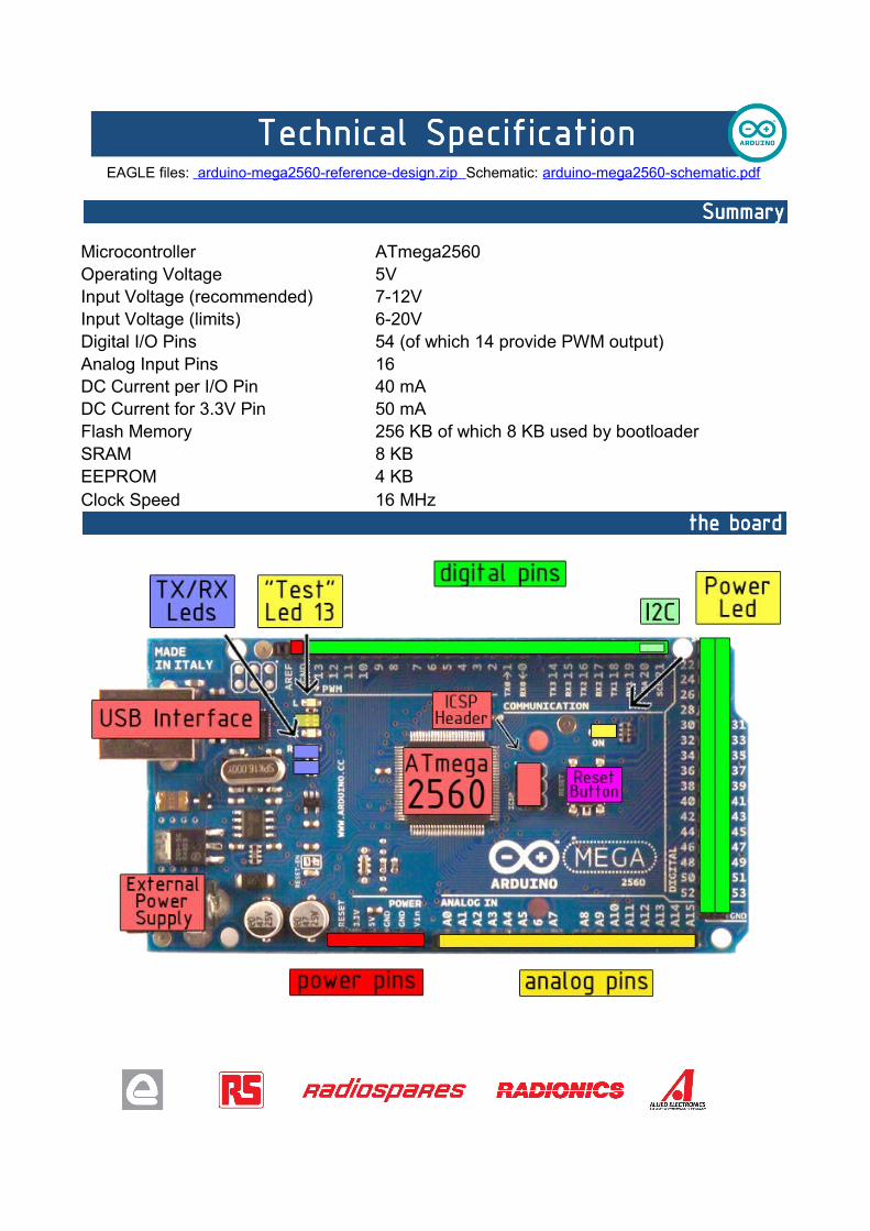
EAGLE files: arduino-mega2560-reference-design.zip Schematic: arduino-mega2560-schematic.pdf
Microcontroller ATmega2560Operating Voltage 5VInput Voltage (recommended) 7-12VInput Voltage (limits) 6-20VDigital I/O Pins 54 (of which 14 provide PWM output)Analog Input Pins 16DC Current per I/O Pin 40 mADC Current for 3.3V Pin 50 mAFlash Memory 256 KB of which 8 KB used by bootloaderSRAM 8 KBEEPROM 4 KBClock Speed 16 MHz

The Arduino Mega2560 can be powered via the USB connection or with an external power supply. The power source is selected automatically. External (non-USB) power can come either from an AC-to-DC adapter (wall-wart) or battery. The adapter can be connected by plugging a 2.1mm center-positive plug into the board's power jack. Leads from a battery can be inserted in the Gnd and Vin pin headers of the POWER connector.
The board can operate on an external supply of 6 to 20 volts. If supplied with less than 7V, however, the 5V pin may supply less than five volts and the board may be unstable. If using more than 12V, the voltage regulator may overheat and damage the board. The recommended range is 7 to 12 volts.
The Mega2560 differs from all preceding boards in that it does not use the FTDI USB-to-serial driver chip. Instead, it features the Atmega8U2 programmed as a USB-to-serial converter.
The power pins are as follows:
• VIN. The input voltage to the Arduino board when it's using an external power source (as opposed to 5 volts from the USB connection or other regulated power source). You can supply voltage through this pin, or, if supplying voltage via the power jack, access it through this pin.
• 5V. The regulated power supply used to power the microcontroller and other components on the board. This can come either from VIN via an on-board regulator, or be supplied by USB or another regulated 5V supply.
• 3V3. A 3.3 volt supply generated by the on-board regulator. Maximum current draw is 50 mA. • GND. Ground pins.
The ATmega2560 has 256 KB of flash memory for storing code (of which 8 KB is used for the bootloader), 8 KB of SRAM and 4 KB of EEPROM (which can be read and written with the EEPROM library).
Each of the 54 digital pins on the Mega can be used as an input or output, using pinMode(), digitalWrite(), and digitalRead() functions. They operate at 5 volts. Each pin can provide or receive a maximum of 40 mA and has an internal pull-up resistor (disconnected by default) of 20-50 kOhms. In addition, some pins have specialized functions:
• Serial: 0 (RX) and 1 (TX); Serial 1: 19 (RX) and 18 (TX); Serial 2: 17 (RX) and 16 (TX); Serial 3: 15 (RX) and 14 (TX). Used to receive (RX) and transmit (TX) TTL serial data. Pins 0 and 1 are also connected to the corresponding pins of the ATmega8U2 USB-to-TTL Serial chip .
• External Interrupts: 2 (interrupt 0), 3 (interrupt 1), 18 (interrupt 5), 19 (interrupt 4), 20 (interrupt 3), and 21 (interrupt 2). These pins can be configured to trigger an interrupt on a low value, a rising or falling edge, or a change in value. See the attachInterrupt() function for details.
• PWM: 0 to 13. Provide 8-bit PWM output with the analogWrite() function. • SPI: 50 (MISO), 51 (MOSI), 52 (SCK), 53 (SS). These pins support SPI communication, which, although
provided by the underlying hardware, is not currently included in the Arduino language. The SPI pins are also broken out on the ICSP header, which is physically compatible with the Duemilanove and Diecimila.
• LED: 13. There is a built-in LED connected to digital pin 13. When the pin is HIGH value, the LED is on, when the pin is LOW, it's off.
• I2C: 20 (SDA) and 21 (SCL). Support I2C (TWI) communication using the Wire library (documentation on the Wiring website). Note that these pins are not in the same location as the I2C pins on the Duemilanove.
The Mega2560 has 16 analog inputs, each of which provide 10 bits of resolution (i.e. 1024 different values). By default they measure from ground to 5 volts, though is it possible to change the upper end of their range using the AREF pin and analogReference() function.
There are a couple of other pins on the board:
• AREF. Reference voltage for the analog inputs. Used with analogReference(). • Reset. Bring this line LOW to reset the microcontroller. Typically used to add a reset button to shields which
block the one on the board.

The Arduino Mega2560 has a number of facilities for communicating with a computer, another Arduino, or other microcontrollers. The ATmega2560 provides four hardware UARTs for TTL (5V) serial communication. An ATmega8U2 on the board channels one of these over USB and provides a virtual com port to software on the computer (Windows machines will need a .inf file, but OSX and Linux machines will recognize the board as a COM port automatically. The Arduino software includes a serial monitor which allows simple textual data to be sent to and from the board. The RX and TX LEDs on the board will flash when data is being transmitted via the ATmega8U2 chip and USB connection to the computer (but not for serial communication on pins 0 and 1).
A SoftwareSerial library allows for serial communication on any of the Mega's digital pins.
The ATmega2560 also supports I2C (TWI) and SPI communication. The Arduino software includes a Wire library to simplify use of the I2C bus; see the documentation on the Wiring website for details. To use the SPI communication, please see the ATmega2560 datasheet.
The Arduino Mega2560 can be programmed with the Arduino software (download). For details, see the reference and tutorials.
The Atmega2560 on the Arduino Mega comes preburned with a bootloader that allows you to upload new code to it without the use of an external hardware programmer. It communicates using the original STK500 protocol (reference, C header files).
You can also bypass the bootloader and program the microcontroller through the ICSP (In-Circuit Serial Programming) header; see these instructions for details.

Rather then requiring a physical press of the reset button before an upload, the Arduino Mega2560 is designed in a way that allows it to be reset by software running on a connected computer. One of the hardware flow control lines (DTR) of the ATmega8U2 is connected to the reset line of the ATmega2560 via a 100 nanofarad capacitor. When this line is asserted (taken low), the reset line drops long enough to reset the chip. The Arduino software uses this capability to allow you to upload code by simply pressing the upload button in the Arduino environment. This means that the bootloader can have a shorter timeout, as the lowering of DTR can be well-coordinated with the start of the upload.
This setup has other implications. When the Mega2560 is connected to either a computer running Mac OS X or Linux, it resets each time a connection is made to it from software (via USB). For the following half-second or so, the bootloader is running on the Mega2560. While it is programmed to ignore malformed data (i.e. anything besides an upload of new code), it will intercept the first few bytes of data sent to the board after a connection is opened. If a sketch running on the board receives one-time configuration or other data when it first starts, make sure that the software with which it communicates waits a second after opening the connection and before sending this data.
The Mega contains a trace that can be cut to disable the auto-reset. The pads on either side of the trace can be soldered together to re-enable it. It's labeled "RESET-EN". You may also be able to disable the auto-reset by connecting a 110 ohm resistor from 5V to the reset line; see this forum thread for details.
The Arduino Mega has a resettable polyfuse that protects your computer's USB ports from shorts and overcurrent. Although most computers provide their own internal protection, the fuse provides an extra layer of protection. If more than 500 mA is applied to the USB port, the fuse will automatically break the connection until the short or overload is removed.
The maximum length and width of the Mega PCB are 4 and 2.1 inches respectively, with the USB connector and power jack extending beyond the former dimension. Three screw holes allow the board to be attached to a surface or case. Note that the distance between digital pins 7 and 8 is 160 mil (0.16"), not an even multiple of the 100 mil spacing of the other pins.
The Mega is designed to be compatible with most shields designed for the Diecimila or Duemilanove. Digital pins 0 to 13 (and the adjacent AREF and GND pins), analog inputs 0 to 5, the power header, and ICSP header are all in equivalent locations. Further the main UART (serial port) is located on the same pins (0 and 1), as are external interrupts 0 and 1 (pins 2 and 3 respectively). SPI is available through the ICSP header on both the Mega and Duemilanove / Diecimila. Please note that I2C is not located on the same pins on the Mega (20 and 21) as the Duemilanove / Diecimila (analog inputs 4 and 5).

Arduino can sense the environment by receiving input from a variety of sensors and can affect its surroundings by controlling lights, motors, and other actuators. The microcontroller on the board is programmed using the Arduino programming language (based on Wiring) and the Arduino development environment (based on Processing). Arduino projects can be stand-alone or they can communicate with software on running on a computer (e.g. Flash, Processing, MaxMSP).
Arduino is a cross-platoform program. You’ll have to follow different instructions for your personal OS. Check on the Arduino site for the latest instructions. http://arduino.cc/en/Guide/HomePage
Once you have downloaded/unzipped the arduino IDE, you can Plug the Arduino to your PC via USB cable.
Now you’re actually ready to “burn” your first program on the arduino board. To select “blink led”, the physical translation of the well known programming “hello world”, select
File>Sketchbook>Arduino-0017>Examples>Digital>Blink
Once you have your skecth you’ll see something very close to the screenshot on the right.
In Tools>Board select MEGA
Now you have to go toTools>SerialPort and select the right serial port, the one arduino is attached to.


1. Warranties
1.1 The producer warrants that its products will conform to the Specifications. This warranty lasts for one (1) years from the date of the sale. The producer shall not be liable for any defects that are caused by neglect, misuse or mistreatment by the Customer, including improper installation or testing, or for any products that have been altered or modified in any way by a Customer. Moreover, The producer shall not be liable for any defects that result from Customer's design, specifications or instructions for such products. Testing and other quality control techniques are used to the extent the producer deems necessary.
1.2 If any products fail to conform to the warranty set forth above, the producer's sole liability shall be to replace such products. The producer's liability shall be limited to products that are determined by the producer not to conform to such warranty. If the producer elects to replace such products, the producer shall have a reasonable time to replacements. Replaced products shall be warranted for a new full warranty period.
1.3 EXCEPT AS SET FORTH ABOVE, PRODUCTS ARE PROVIDED "AS IS" AND "WITH ALL FAULTS." THE PRODUCER DISCLAIMS ALL OTHER WARRANTIES, EXPRESS OR IMPLIED, REGARDING PRODUCTS, INCLUDING BUT NOT LIMITED TO, ANY IMPLIED WARRANTIES OF MERCHANTABILITY OR FITNESS FOR A PARTICULAR PURPOSE
1.4 Customer agrees that prior to using any systems that include the producer products, Customer will test such systems and the functionality of the products as used in such systems. The producer may provide technical, applications or design advice, quality characterization, reliability data or other services. Customer acknowledges and agrees that providing these services shall not expand or otherwise alter the producer's warranties, as set forth above, and no additional obligations or liabilities shall arise from the producer providing such services.
1.5 The Arduino products are not authorized for use in safety-critical applications where a failure of the product would reasonably be expected to cause severe personal injury or death. Safety-Critical Applications include, without limitation, life support devices and systems, equipment or systems for the operation of nuclear facilities and weapons systems. Arduino products are neither designed nor intended for use in military or aerospace applications or environments and for automotive applications or environment. Customer acknowledges and agrees that any such use of Arduino products which is solely at the Customer's risk, and that Customer is solely responsible for compliance with all legal and regulatory requirements in connection with such use.
1.6 Customer acknowledges and agrees that it is solely responsible for compliance with all legal, regulatory and safety-related requirements concerning its products and any use of Arduino products in Customer's applications, notwithstanding any applications-related information or support that may be provided by the producer.
2. Indemnification
The Customer acknowledges and agrees to defend, indemnify and hold harmless the producer from and against any and all third-party losses, damages, liabilities and expenses it incurs to the extent directly caused by: (i) an actual breach by a Customer of the representation and warranties made under this terms and conditions or (ii) the gross negligence or willful misconduct by the Customer.
3. Consequential Damages Waiver
In no event the producer shall be liable to the Customer or any third parties for any special, collateral, indirect, punitive, incidental, consequential or exemplary damages in connection with or arising out of the products provided hereunder, regardless of whether the producer has been advised of the possibility of such damages. This section will survive the termination of the warranty period.
4. Changes to specifications
The producer may make changes to specifications and product descriptions at any time, without notice. The Customer must not rely on the absence or characteristics of any features or instructions marked "reserved" or "undefined." The producer reserves these for future definition and shall have no responsibility whatsoever for conflicts or incompatibilities arising from future changes to them. The product information on the Web Site or Materials is subject to change without notice. Do not finalize a design with this information.
The producer of Arduino has joined the Impatto Zero® policy of LifeGate.it. For each Arduino board produced is created / looked after half squared Km of Costa Rica’s forest’s.

Features• High Performance, Low Power AVR® 8-Bit Microcontroller• Advanced RISC Architecture
– 131 Powerful Instructions – Most Single Clock Cycle Execution– 32 x 8 General Purpose Working Registers– Fully Static Operation– Up to 20 MIPS Throughput at 20 MHz– On-chip 2-cycle Multiplier
• High Endurance Non-volatile Memory Segments– 4/8/16/32K Bytes of In-System Self-Programmable Flash progam memory
(ATmega48PA/88PA/168PA/328P)– 256/512/512/1K Bytes EEPROM (ATmega48PA/88PA/168PA/328P)– 512/1K/1K/2K Bytes Internal SRAM (ATmega48PA/88PA/168PA/328P)– Write/Erase Cycles: 10,000 Flash/100,000 EEPROM– Data retention: 20 years at 85°C/100 years at 25°C(1)
– Optional Boot Code Section with Independent Lock BitsIn-System Programming by On-chip Boot ProgramTrue Read-While-Write Operation
– Programming Lock for Software Security• Peripheral Features
– Two 8-bit Timer/Counters with Separate Prescaler and Compare Mode– One 16-bit Timer/Counter with Separate Prescaler, Compare Mode, and Capture
Mode– Real Time Counter with Separate Oscillator– Six PWM Channels– 8-channel 10-bit ADC in TQFP and QFN/MLF package
Temperature Measurement– 6-channel 10-bit ADC in PDIP Package
Temperature Measurement– Programmable Serial USART– Master/Slave SPI Serial Interface– Byte-oriented 2-wire Serial Interface (Philips I2C compatible)– Programmable Watchdog Timer with Separate On-chip Oscillator– On-chip Analog Comparator– Interrupt and Wake-up on Pin Change
• Special Microcontroller Features– Power-on Reset and Programmable Brown-out Detection– Internal Calibrated Oscillator– External and Internal Interrupt Sources– Six Sleep Modes: Idle, ADC Noise Reduction, Power-save, Power-down, Standby,
and Extended Standby• I/O and Packages
– 23 Programmable I/O Lines– 28-pin PDIP, 32-lead TQFP, 28-pad QFN/MLF and 32-pad QFN/MLF
• Operating Voltage:– 1.8 - 5.5V for ATmega48PA/88PA/168PA/328P
• Temperature Range:– -40°C to 85°C
• Speed Grade:– 0 - 20 MHz @ 1.8 - 5.5V
• Low Power Consumption at 1 MHz, 1.8V, 25°C for ATmega48PA/88PA/168PA/328P:– Active Mode: 0.2 mA– Power-down Mode: 0.1 µA– Power-save Mode: 0.75 µA (Including 32 kHz RTC)
8-bit Microcontroller with 4/8/16/32K Bytes In-SystemProgrammable Flash
ATmega48PAATmega88PAATmega168PAATmega328P
Summary
Rev. 8161CS–AVR–05/09
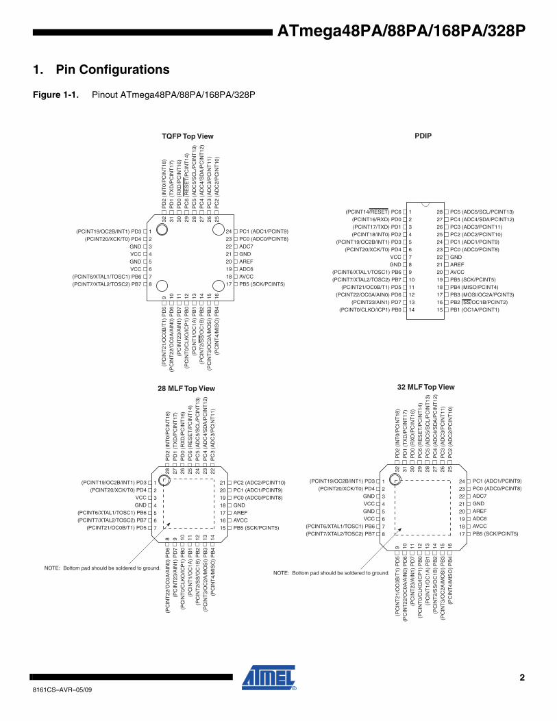
28161CS–AVR–05/09
ATmega48PA/88PA/168PA/328P
1. Pin Configurations
Figure 1-1. Pinout ATmega48PA/88PA/168PA/328P
12345678
2423222120191817
(PCINT19/OC2B/INT1) PD3(PCINT20/XCK/T0) PD4
GNDVCCGNDVCC
(PCINT6/XTAL1/TOSC1) PB6(PCINT7/XTAL2/TOSC2) PB7
PC1 (ADC1/PCINT9)PC0 (ADC0/PCINT8)ADC7GNDAREFADC6AVCCPB5 (SCK/PCINT5)
32 31 30 29 28 27 26 25
9 10 11 12 13 14 15 16
(PC
INT
21/O
C0B
/T1)
PD
5(P
CIN
T22
/OC
0A/A
IN0)
PD
6(P
CIN
T23
/AIN
1) P
D7
(PC
INT
0/C
LKO
/ICP
1) P
B0
(PC
INT
1/O
C1A
) P
B1
(PC
INT
2/S
S/O
C1B
) P
B2
(PC
INT
3/O
C2A
/MO
SI)
PB
3(P
CIN
T4/
MIS
O)
PB
4
PD
2 (I
NT
0/P
CIN
T18
)P
D1
(TX
D/P
CIN
T17
)P
D0
(RX
D/P
CIN
T16
)P
C6
(RE
SE
T/P
CIN
T14
)P
C5
(AD
C5/
SC
L/P
CIN
T13
)P
C4
(AD
C4/
SD
A/P
CIN
T12
)P
C3
(AD
C3/
PC
INT
11)
PC
2 (A
DC
2/P
CIN
T10
)
TQFP Top View
1234567891011121314
2827262524232221201918171615
(PCINT14/RESET) PC6(PCINT16/RXD) PD0(PCINT17/TXD) PD1(PCINT18/INT0) PD2
(PCINT19/OC2B/INT1) PD3(PCINT20/XCK/T0) PD4
VCCGND
(PCINT6/XTAL1/TOSC1) PB6(PCINT7/XTAL2/TOSC2) PB7
(PCINT21/OC0B/T1) PD5(PCINT22/OC0A/AIN0) PD6
(PCINT23/AIN1) PD7(PCINT0/CLKO/ICP1) PB0
PC5 (ADC5/SCL/PCINT13)PC4 (ADC4/SDA/PCINT12)PC3 (ADC3/PCINT11)PC2 (ADC2/PCINT10)PC1 (ADC1/PCINT9)PC0 (ADC0/PCINT8)GNDAREFAVCCPB5 (SCK/PCINT5)PB4 (MISO/PCINT4)PB3 (MOSI/OC2A/PCINT3)PB2 (SS/OC1B/PCINT2)PB1 (OC1A/PCINT1)
PDIP
12345678
2423222120191817
32 31 30 29 28 27 26 25
9 10 11 12 13 14 15 16
32 MLF Top View
(PCINT19/OC2B/INT1) PD3(PCINT20/XCK/T0) PD4
GNDVCCGNDVCC
(PCINT6/XTAL1/TOSC1) PB6(PCINT7/XTAL2/TOSC2) PB7
PC1 (ADC1/PCINT9)PC0 (ADC0/PCINT8)ADC7GNDAREFADC6AVCCPB5 (SCK/PCINT5)
(PC
INT
21/O
C0B
/T1)
PD
5(P
CIN
T22
/OC
0A/A
IN0)
PD
6(P
CIN
T23
/AIN
1) P
D7
(PC
INT
0/C
LKO
/ICP
1) P
B0
(PC
INT
1/O
C1A
) P
B1
(PC
INT
2/S
S/O
C1B
) P
B2
(PC
INT
3/O
C2A
/MO
SI)
PB
3(P
CIN
T4/
MIS
O)
PB
4
PD
2 (I
NT
0/P
CIN
T18
)P
D1
(TX
D/P
CIN
T17
)P
D0
(RX
D/P
CIN
T16
)P
C6
(RE
SE
T/P
CIN
T14
)P
C5
(AD
C5/
SC
L/P
CIN
T13
)P
C4
(AD
C4/
SD
A/P
CIN
T12
)P
C3
(AD
C3/
PC
INT
11)
PC
2 (A
DC
2/P
CIN
T10
)
NOTE: Bottom pad should be soldered to ground.
1234567
21201918171615
28 27 26 25 24 23 22
8 9 10 11 12 13 14
28 MLF Top View
(PCINT19/OC2B/INT1) PD3(PCINT20/XCK/T0) PD4
VCCGND
(PCINT6/XTAL1/TOSC1) PB6(PCINT7/XTAL2/TOSC2) PB7
(PCINT21/OC0B/T1) PD5
(PC
INT
22/O
C0A
/AIN
0) P
D6
(PC
INT
23/A
IN1)
PD
7(P
CIN
T0/
CLK
O/IC
P1)
PB
0(P
CIN
T1/
OC
1A)
PB
1(P
CIN
T2/
SS
/OC
1B)
PB
2(P
CIN
T3/
OC
2A/M
OS
I) P
B3
(PC
INT
4/M
ISO
) P
B4
PD
2 (I
NT
0/P
CIN
T18
)P
D1
(TX
D/P
CIN
T17
)P
D0
(RX
D/P
CIN
T16
)P
C6
(RE
SE
T/P
CIN
T14
)P
C5
(AD
C5/
SC
L/P
CIN
T13
)P
C4
(AD
C4/
SD
A/P
CIN
T12
)P
C3
(AD
C3/
PC
INT
11)
PC2 (ADC2/PCINT10)PC1 (ADC1/PCINT9)PC0 (ADC0/PCINT8)GNDAREFAVCCPB5 (SCK/PCINT5)
NOTE: Bottom pad should be soldered to ground.

38161CS–AVR–05/09
ATmega48PA/88PA/168PA/328P
1.1 Pin Descriptions
1.1.1 VCCDigital supply voltage.
1.1.2 GNDGround.
1.1.3 Port B (PB7:0) XTAL1/XTAL2/TOSC1/TOSC2Port B is an 8-bit bi-directional I/O port with internal pull-up resistors (selected for each bit). ThePort B output buffers have symmetrical drive characteristics with both high sink and sourcecapability. As inputs, Port B pins that are externally pulled low will source current if the pull-upresistors are activated. The Port B pins are tri-stated when a reset condition becomes active,even if the clock is not running.
Depending on the clock selection fuse settings, PB6 can be used as input to the inverting Oscil-lator amplifier and input to the internal clock operating circuit.
Depending on the clock selection fuse settings, PB7 can be used as output from the invertingOscillator amplifier.
If the Internal Calibrated RC Oscillator is used as chip clock source, PB7..6 is used as TOSC2..1input for the Asynchronous Timer/Counter2 if the AS2 bit in ASSR is set.
The various special features of Port B are elaborated in ”Alternate Functions of Port B” on page76 and ”System Clock and Clock Options” on page 26.
1.1.4 Port C (PC5:0)Port C is a 7-bit bi-directional I/O port with internal pull-up resistors (selected for each bit). ThePC5..0 output buffers have symmetrical drive characteristics with both high sink and sourcecapability. As inputs, Port C pins that are externally pulled low will source current if the pull-upresistors are activated. The Port C pins are tri-stated when a reset condition becomes active,even if the clock is not running.
1.1.5 PC6/RESETIf the RSTDISBL Fuse is programmed, PC6 is used as an I/O pin. Note that the electrical char-acteristics of PC6 differ from those of the other pins of Port C.
If the RSTDISBL Fuse is unprogrammed, PC6 is used as a Reset input. A low level on this pinfor longer than the minimum pulse length will generate a Reset, even if the clock is not running.The minimum pulse length is given in Table 28-3 on page 308. Shorter pulses are not guaran-teed to generate a Reset.
The various special features of Port C are elaborated in ”Alternate Functions of Port C” on page79.
1.1.6 Port D (PD7:0)Port D is an 8-bit bi-directional I/O port with internal pull-up resistors (selected for each bit). ThePort D output buffers have symmetrical drive characteristics with both high sink and sourcecapability. As inputs, Port D pins that are externally pulled low will source current if the pull-upresistors are activated. The Port D pins are tri-stated when a reset condition becomes active,even if the clock is not running.

48161CS–AVR–05/09
ATmega48PA/88PA/168PA/328P
The various special features of Port D are elaborated in ”Alternate Functions of Port D” on page82.
1.1.7 AVCC
AVCC is the supply voltage pin for the A/D Converter, PC3:0, and ADC7:6. It should be externallyconnected to VCC, even if the ADC is not used. If the ADC is used, it should be connected to VCC
through a low-pass filter. Note that PC6..4 use digital supply voltage, VCC.
1.1.8 AREFAREF is the analog reference pin for the A/D Converter.
1.1.9 ADC7:6 (TQFP and QFN/MLF Package Only)In the TQFP and QFN/MLF package, ADC7:6 serve as analog inputs to the A/D converter.These pins are powered from the analog supply and serve as 10-bit ADC channels.

58161CS–AVR–05/09
ATmega48PA/88PA/168PA/328P
2. OverviewThe ATmega48PA/88PA/168PA/328P is a low-power CMOS 8-bit microcontroller based on theAVR enhanced RISC architecture. By executing powerful instructions in a single clock cycle, theATmega48PA/88PA/168PA/328P achieves throughputs approaching 1 MIPS per MHz allowingthe system designer to optimize power consumption versus processing speed.
2.1 Block Diagram
Figure 2-1. Block Diagram
The AVR core combines a rich instruction set with 32 general purpose working registers. All the32 registers are directly connected to the Arithmetic Logic Unit (ALU), allowing two independentregisters to be accessed in one single instruction executed in one clock cycle. The resulting
PORT C (7)PORT B (8)PORT D (8)
USART 0
8bit T/C 2
16bit T/C 18bit T/C 0 A/D Conv.
InternalBandgap
AnalogComp.
SPI TWI
SRAMFlash
EEPROM
WatchdogOscillator
WatchdogTimer
OscillatorCircuits /
ClockGeneration
PowerSupervisionPOR / BOD &
RESET
VC
C
GN
D
PROGRAMLOGIC
debugWIRE
2
GND
AREF
AVCC
DAT
AB
US
ADC[6..7]PC[0..6]PB[0..7]PD[0..7]
6
RESET
XTAL[1..2]
CPU
68161CS–AVR–05/09
ATmega48PA/88PA/168PA/328P
architecture is more code efficient while achieving throughputs up to ten times faster than con-ventional CISC microcontrollers.
The ATmega48PA/88PA/168PA/328P provides the following features: 4/8/16/32K bytes of In-System Programmable Flash with Read-While-Write capabilities, 256/512/512/1K bytesEEPROM, 512/1K/1K/2K bytes SRAM, 23 general purpose I/O lines, 32 general purpose work-ing registers, three flexible Timer/Counters with compare modes, internal and externalinterrupts, a serial programmable USART, a byte-oriented 2-wire Serial Interface, an SPI serialport, a 6-channel 10-bit ADC (8 channels in TQFP and QFN/MLF packages), a programmableWatchdog Timer with internal Oscillator, and five software selectable power saving modes. TheIdle mode stops the CPU while allowing the SRAM, Timer/Counters, USART, 2-wire Serial Inter-face, SPI port, and interrupt system to continue functioning. The Power-down mode saves theregister contents but freezes the Oscillator, disabling all other chip functions until the next inter-rupt or hardware reset. In Power-save mode, the asynchronous timer continues to run, allowingthe user to maintain a timer base while the rest of the device is sleeping. The ADC Noise Reduc-tion mode stops the CPU and all I/O modules except asynchronous timer and ADC, to minimizeswitching noise during ADC conversions. In Standby mode, the crystal/resonator Oscillator isrunning while the rest of the device is sleeping. This allows very fast start-up combined with lowpower consumption.
The device is manufactured using Atmel’s high density non-volatile memory technology. TheOn-chip ISP Flash allows the program memory to be reprogrammed In-System through an SPIserial interface, by a conventional non-volatile memory programmer, or by an On-chip Boot pro-gram running on the AVR core. The Boot program can use any interface to download theapplication program in the Application Flash memory. Software in the Boot Flash section willcontinue to run while the Application Flash section is updated, providing true Read-While-Writeoperation. By combining an 8-bit RISC CPU with In-System Self-Programmable Flash on amonolithic chip, the Atmel ATmega48PA/88PA/168PA/328P is a powerful microcontroller thatprovides a highly flexible and cost effective solution to many embedded control applications.
The ATmega48PA/88PA/168PA/328P AVR is supported with a full suite of program and systemdevelopment tools including: C Compilers, Macro Assemblers, Program Debugger/Simulators,In-Circuit Emulators, and Evaluation kits.
2.2 Comparison Between ATmega48PA, ATmega88PA, ATmega168PA and ATmega328PThe ATmega48PA, ATmega88PA, ATmega168PA and ATmega328P differ only in memorysizes, boot loader support, and interrupt vector sizes. Table 2-1 summarizes the different mem-ory and interrupt vector sizes for the three devices.
ATmega88PA, ATmega168PA and ATmega328P support a real Read-While-Write Self-Pro-gramming mechanism. There is a separate Boot Loader Section, and the SPM instruction canonly execute from there. In ATmega48PA, there is no Read-While-Write support and no sepa-rate Boot Loader Section. The SPM instruction can execute from the entire Flash.
Table 2-1. Memory Size Summary
Device Flash EEPROM RAM Interrupt Vector Size
ATmega48PA 4K Bytes 256 Bytes 512 Bytes 1 instruction word/vector
ATmega88PA 8K Bytes 512 Bytes 1K Bytes 1 instruction word/vector
ATmega168PA 16K Bytes 512 Bytes 1K Bytes 2 instruction words/vector
ATmega328P 32K Bytes 1K Bytes 2K Bytes 2 instruction words/vector
78161CS–AVR–05/09
ATmega48PA/88PA/168PA/328P
3. Resources A comprehensive set of development tools, application notes and datasheets are available fordownload on http://www.atmel.com/avr.
Note: 1.
4. Data RetentionReliability Qualification results show that the projected data retention failure rate is much lessthan 1 PPM over 20 years at 85°C or 100 years at 25°C.

88161CS–AVR–05/09
ATmega48PA/88PA/168PA/328P
5. Register SummaryAddress Name Bit 7 Bit 6 Bit 5 Bit 4 Bit 3 Bit 2 Bit 1 Bit 0 Page
(0xFF) Reserved – – – – – – – –
(0xFE) Reserved – – – – – – – –
(0xFD) Reserved – – – – – – – –
(0xFC) Reserved – – – – – – – –
(0xFB) Reserved – – – – – – – –
(0xFA) Reserved – – – – – – – –
(0xF9) Reserved – – – – – – – –
(0xF8) Reserved – – – – – – – –
(0xF7) Reserved – – – – – – – –
(0xF6) Reserved – – – – – – – –
(0xF5) Reserved – – – – – – – –
(0xF4) Reserved – – – – – – – –
(0xF3) Reserved – – – – – – – –
(0xF2) Reserved – – – – – – – –
(0xF1) Reserved – – – – – – – –
(0xF0) Reserved – – – – – – – –
(0xEF) Reserved – – – – – – – –
(0xEE) Reserved – – – – – – – –
(0xED) Reserved – – – – – – – –
(0xEC) Reserved – – – – – – – –
(0xEB) Reserved – – – – – – – –
(0xEA) Reserved – – – – – – – –
(0xE9) Reserved – – – – – – – –
(0xE8) Reserved – – – – – – – –
(0xE7) Reserved – – – – – – – –
(0xE6) Reserved – – – – – – – –
(0xE5) Reserved – – – – – – – –
(0xE4) Reserved – – – – – – – –
(0xE3) Reserved – – – – – – – –
(0xE2) Reserved – – – – – – – –
(0xE1) Reserved – – – – – – – –
(0xE0) Reserved – – – – – – – –
(0xDF) Reserved – – – – – – – –
(0xDE) Reserved – – – – – – – –
(0xDD) Reserved – – – – – – – –
(0xDC) Reserved – – – – – – – –
(0xDB) Reserved – – – – – – – –
(0xDA) Reserved – – – – – – – –
(0xD9) Reserved – – – – – – – –
(0xD8) Reserved – – – – – – – –
(0xD7) Reserved – – – – – – – –
(0xD6) Reserved – – – – – – – –
(0xD5) Reserved – – – – – – – –
(0xD4) Reserved – – – – – – – –
(0xD3) Reserved – – – – – – – –
(0xD2) Reserved – – – – – – – –
(0xD1) Reserved – – – – – – – –
(0xD0) Reserved – – – – – – – –
(0xCF) Reserved – – – – – – – –
(0xCE) Reserved – – – – – – – –
(0xCD) Reserved – – – – – – – –
(0xCC) Reserved – – – – – – – –
(0xCB) Reserved – – – – – – – –
(0xCA) Reserved – – – – – – – –
(0xC9) Reserved – – – – – – – –
(0xC8) Reserved – – – – – – – –
(0xC7) Reserved – – – – – – – –
(0xC6) UDR0 USART I/O Data Register 189
(0xC5) UBRR0H USART Baud Rate Register High 193
(0xC4) UBRR0L USART Baud Rate Register Low 193
(0xC3) Reserved – – – – – – – –
(0xC2) UCSR0C UMSEL01 UMSEL00 UPM01 UPM00 USBS0 UCSZ01 /UDORD0 UCSZ00 / UCPHA0 UCPOL0 191/206
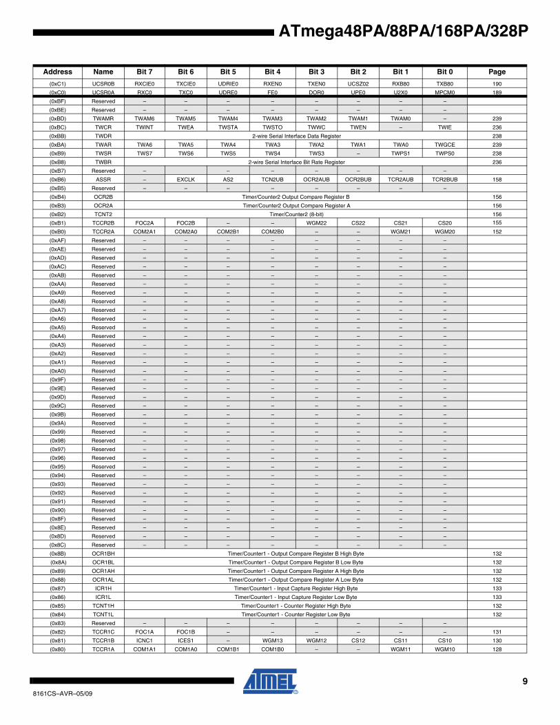
98161CS–AVR–05/09
ATmega48PA/88PA/168PA/328P
(0xC1) UCSR0B RXCIE0 TXCIE0 UDRIE0 RXEN0 TXEN0 UCSZ02 RXB80 TXB80 190
(0xC0) UCSR0A RXC0 TXC0 UDRE0 FE0 DOR0 UPE0 U2X0 MPCM0 189
(0xBF) Reserved – – – – – – – –
(0xBE) Reserved – – – – – – – –
(0xBD) TWAMR TWAM6 TWAM5 TWAM4 TWAM3 TWAM2 TWAM1 TWAM0 – 239
(0xBC) TWCR TWINT TWEA TWSTA TWSTO TWWC TWEN – TWIE 236
(0xBB) TWDR 2-wire Serial Interface Data Register 238
(0xBA) TWAR TWA6 TWA5 TWA4 TWA3 TWA2 TWA1 TWA0 TWGCE 239
(0xB9) TWSR TWS7 TWS6 TWS5 TWS4 TWS3 – TWPS1 TWPS0 238
(0xB8) TWBR 2-wire Serial Interface Bit Rate Register 236
(0xB7) Reserved – – – – – – –
(0xB6) ASSR – EXCLK AS2 TCN2UB OCR2AUB OCR2BUB TCR2AUB TCR2BUB 158
(0xB5) Reserved – – – – – – – –
(0xB4) OCR2B Timer/Counter2 Output Compare Register B 156
(0xB3) OCR2A Timer/Counter2 Output Compare Register A 156
(0xB2) TCNT2 Timer/Counter2 (8-bit) 156
(0xB1) TCCR2B FOC2A FOC2B – – WGM22 CS22 CS21 CS20 155
(0xB0) TCCR2A COM2A1 COM2A0 COM2B1 COM2B0 – – WGM21 WGM20 152
(0xAF) Reserved – – – – – – – –
(0xAE) Reserved – – – – – – – –
(0xAD) Reserved – – – – – – – –
(0xAC) Reserved – – – – – – – –
(0xAB) Reserved – – – – – – – –
(0xAA) Reserved – – – – – – – –
(0xA9) Reserved – – – – – – – –
(0xA8) Reserved – – – – – – – –
(0xA7) Reserved – – – – – – – –
(0xA6) Reserved – – – – – – – –
(0xA5) Reserved – – – – – – – –
(0xA4) Reserved – – – – – – – –
(0xA3) Reserved – – – – – – – –
(0xA2) Reserved – – – – – – – –
(0xA1) Reserved – – – – – – – –
(0xA0) Reserved – – – – – – – –
(0x9F) Reserved – – – – – – – –
(0x9E) Reserved – – – – – – – –
(0x9D) Reserved – – – – – – – –
(0x9C) Reserved – – – – – – – –
(0x9B) Reserved – – – – – – – –
(0x9A) Reserved – – – – – – – –
(0x99) Reserved – – – – – – – –
(0x98) Reserved – – – – – – – –
(0x97) Reserved – – – – – – – –
(0x96) Reserved – – – – – – – –
(0x95) Reserved – – – – – – – –
(0x94) Reserved – – – – – – – –
(0x93) Reserved – – – – – – – –
(0x92) Reserved – – – – – – – –
(0x91) Reserved – – – – – – – –
(0x90) Reserved – – – – – – – –
(0x8F) Reserved – – – – – – – –
(0x8E) Reserved – – – – – – – –
(0x8D) Reserved – – – – – – – –
(0x8C) Reserved – – – – – – – –
(0x8B) OCR1BH Timer/Counter1 - Output Compare Register B High Byte 132
(0x8A) OCR1BL Timer/Counter1 - Output Compare Register B Low Byte 132
(0x89) OCR1AH Timer/Counter1 - Output Compare Register A High Byte 132
(0x88) OCR1AL Timer/Counter1 - Output Compare Register A Low Byte 132
(0x87) ICR1H Timer/Counter1 - Input Capture Register High Byte 133
(0x86) ICR1L Timer/Counter1 - Input Capture Register Low Byte 133
(0x85) TCNT1H Timer/Counter1 - Counter Register High Byte 132
(0x84) TCNT1L Timer/Counter1 - Counter Register Low Byte 132
(0x83) Reserved – – – – – – – –
(0x82) TCCR1C FOC1A FOC1B – – – – – – 131
(0x81) TCCR1B ICNC1 ICES1 – WGM13 WGM12 CS12 CS11 CS10 130
(0x80) TCCR1A COM1A1 COM1A0 COM1B1 COM1B0 – – WGM11 WGM10 128
Address Name Bit 7 Bit 6 Bit 5 Bit 4 Bit 3 Bit 2 Bit 1 Bit 0 Page

108161CS–AVR–05/09
ATmega48PA/88PA/168PA/328P
(0x7F) DIDR1 – – – – – – AIN1D AIN0D 244
(0x7E) DIDR0 – – ADC5D ADC4D ADC3D ADC2D ADC1D ADC0D 261
(0x7D) Reserved – – – – – – – –
(0x7C) ADMUX REFS1 REFS0 ADLAR – MUX3 MUX2 MUX1 MUX0 257
(0x7B) ADCSRB – ACME – – – ADTS2 ADTS1 ADTS0 260
(0x7A) ADCSRA ADEN ADSC ADATE ADIF ADIE ADPS2 ADPS1 ADPS0 258
(0x79) ADCH ADC Data Register High byte 260
(0x78) ADCL ADC Data Register Low byte 260
(0x77) Reserved – – – – – – – –
(0x76) Reserved – – – – – – – –
(0x75) Reserved – – – – – – – –
(0x74) Reserved – – – – – – – –
(0x73) Reserved – – – – – – – –
(0x72) Reserved – – – – – – – –
(0x71) Reserved – – – – – – – –
(0x70) TIMSK2 – – – – – OCIE2B OCIE2A TOIE2 157
(0x6F) TIMSK1 – – ICIE1 – – OCIE1B OCIE1A TOIE1 133
(0x6E) TIMSK0 – – – – – OCIE0B OCIE0A TOIE0 105
(0x6D) PCMSK2 PCINT23 PCINT22 PCINT21 PCINT20 PCINT19 PCINT18 PCINT17 PCINT16 68
(0x6C) PCMSK1 – PCINT14 PCINT13 PCINT12 PCINT11 PCINT10 PCINT9 PCINT8 68
(0x6B) PCMSK0 PCINT7 PCINT6 PCINT5 PCINT4 PCINT3 PCINT2 PCINT1 PCINT0 68
(0x6A) Reserved – – – – – – – –
(0x69) EICRA – – – – ISC11 ISC10 ISC01 ISC00 65
(0x68) PCICR – – – – – PCIE2 PCIE1 PCIE0
(0x67) Reserved – – – – – – – –
(0x66) OSCCAL Oscillator Calibration Register 37
(0x65) Reserved – – – – – – – –
(0x64) PRR PRTWI PRTIM2 PRTIM0 – PRTIM1 PRSPI PRUSART0 PRADC 42
(0x63) Reserved – – – – – – – –
(0x62) Reserved – – – – – – – –
(0x61) CLKPR CLKPCE – – – CLKPS3 CLKPS2 CLKPS1 CLKPS0 37
(0x60) WDTCSR WDIF WDIE WDP3 WDCE WDE WDP2 WDP1 WDP0 54
0x3F (0x5F) SREG I T H S V N Z C 9
0x3E (0x5E) SPH – – – – – (SP10) 5. SP9 SP8 12
0x3D (0x5D) SPL SP7 SP6 SP5 SP4 SP3 SP2 SP1 SP0 12
0x3C (0x5C) Reserved – – – – – – – –
0x3B (0x5B) Reserved – – – – – – – –
0x3A (0x5A) Reserved – – – – – – – –
0x39 (0x59) Reserved – – – – – – – –
0x38 (0x58) Reserved – – – – – – – –
0x37 (0x57) SPMCSR SPMIE (RWWSB)5. – (RWWSRE)5. BLBSET PGWRT PGERS SELFPRGEN 284
0x36 (0x56) Reserved – – – – – – – –
0x35 (0x55) MCUCR – BODS BODSE PUD – – IVSEL IVCE 44/62/86
0x34 (0x54) MCUSR – – – – WDRF BORF EXTRF PORF 54
0x33 (0x53) SMCR – – – – SM2 SM1 SM0 SE 40
0x32 (0x52) Reserved – – – – – – – –
0x31 (0x51) Reserved – – – – – – – –
0x30 (0x50) ACSR ACD ACBG ACO ACI ACIE ACIC ACIS1 ACIS0 242
0x2F (0x4F) Reserved – – – – – – – –
0x2E (0x4E) SPDR SPI Data Register 169
0x2D (0x4D) SPSR SPIF WCOL – – – – – SPI2X 168
0x2C (0x4C) SPCR SPIE SPE DORD MSTR CPOL CPHA SPR1 SPR0 167
0x2B (0x4B) GPIOR2 General Purpose I/O Register 2 25
0x2A (0x4A) GPIOR1 General Purpose I/O Register 1 25
0x29 (0x49) Reserved – – – – – – – –
0x28 (0x48) OCR0B Timer/Counter0 Output Compare Register B
0x27 (0x47) OCR0A Timer/Counter0 Output Compare Register A
0x26 (0x46) TCNT0 Timer/Counter0 (8-bit)
0x25 (0x45) TCCR0B FOC0A FOC0B – – WGM02 CS02 CS01 CS00
0x24 (0x44) TCCR0A COM0A1 COM0A0 COM0B1 COM0B0 – – WGM01 WGM00
0x23 (0x43) GTCCR TSM – – – – – PSRASY PSRSYNC 137/159
0x22 (0x42) EEARH (EEPROM Address Register High Byte) 5. 21
0x21 (0x41) EEARL EEPROM Address Register Low Byte 21
0x20 (0x40) EEDR EEPROM Data Register 21
0x1F (0x3F) EECR – – EEPM1 EEPM0 EERIE EEMPE EEPE EERE 21
0x1E (0x3E) GPIOR0 General Purpose I/O Register 0 25
Address Name Bit 7 Bit 6 Bit 5 Bit 4 Bit 3 Bit 2 Bit 1 Bit 0 Page

118161CS–AVR–05/09
ATmega48PA/88PA/168PA/328P
Note: 1. For compatibility with future devices, reserved bits should be written to zero if accessed. Reserved I/O memory addresses should never be written.
2. I/O Registers within the address range 0x00 - 0x1F are directly bit-accessible using the SBI and CBI instructions. In these registers, the value of single bits can be checked by using the SBIS and SBIC instructions.
3. Some of the Status Flags are cleared by writing a logical one to them. Note that, unlike most other AVRs, the CBI and SBI instructions will only operate on the specified bit, and can therefore be used on registers containing such Status Flags. The CBI and SBI instructions work with registers 0x00 to 0x1F only.
4. When using the I/O specific commands IN and OUT, the I/O addresses 0x00 - 0x3F must be used. When addressing I/O Registers as data space using LD and ST instructions, 0x20 must be added to these addresses. The ATmega48PA/88PA/168PA/328P is a complex microcontroller with more peripheral units than can be supported within the 64 location reserved in Opcode for the IN and OUT instructions. For the Extended I/O space from 0x60 - 0xFF in SRAM, only the ST/STS/STD and LD/LDS/LDD instructions can be used.
5. Only valid for ATmega88PA.
0x1D (0x3D) EIMSK – – – – – – INT1 INT0 66
0x1C (0x3C) EIFR – – – – – – INTF1 INTF0 66
0x1B (0x3B) PCIFR – – – – – PCIF2 PCIF1 PCIF0
0x1A (0x3A) Reserved – – – – – – – –
0x19 (0x39) Reserved – – – – – – – –
0x18 (0x38) Reserved – – – – – – – –
0x17 (0x37) TIFR2 – – – – – OCF2B OCF2A TOV2 157
0x16 (0x36) TIFR1 – – ICF1 – – OCF1B OCF1A TOV1 134
0x15 (0x35) TIFR0 – – – – – OCF0B OCF0A TOV0
0x14 (0x34) Reserved – – – – – – – –
0x13 (0x33) Reserved – – – – – – – –
0x12 (0x32) Reserved – – – – – – – –
0x11 (0x31) Reserved – – – – – – – –
0x10 (0x30) Reserved – – – – – – – –
0x0F (0x2F) Reserved – – – – – – – –
0x0E (0x2E) Reserved – – – – – – – –
0x0D (0x2D) Reserved – – – – – – – –
0x0C (0x2C) Reserved – – – – – – – –
0x0B (0x2B) PORTD PORTD7 PORTD6 PORTD5 PORTD4 PORTD3 PORTD2 PORTD1 PORTD0 87
0x0A (0x2A) DDRD DDD7 DDD6 DDD5 DDD4 DDD3 DDD2 DDD1 DDD0 87
0x09 (0x29) PIND PIND7 PIND6 PIND5 PIND4 PIND3 PIND2 PIND1 PIND0 87
0x08 (0x28) PORTC – PORTC6 PORTC5 PORTC4 PORTC3 PORTC2 PORTC1 PORTC0 86
0x07 (0x27) DDRC – DDC6 DDC5 DDC4 DDC3 DDC2 DDC1 DDC0 86
0x06 (0x26) PINC – PINC6 PINC5 PINC4 PINC3 PINC2 PINC1 PINC0 86
0x05 (0x25) PORTB PORTB7 PORTB6 PORTB5 PORTB4 PORTB3 PORTB2 PORTB1 PORTB0 86
0x04 (0x24) DDRB DDB7 DDB6 DDB5 DDB4 DDB3 DDB2 DDB1 DDB0 86
0x03 (0x23) PINB PINB7 PINB6 PINB5 PINB4 PINB3 PINB2 PINB1 PINB0 86
0x02 (0x22) Reserved – – – – – – – –
0x01 (0x21) Reserved – – – – – – – –
0x0 (0x20) Reserved – – – – – – – –
Address Name Bit 7 Bit 6 Bit 5 Bit 4 Bit 3 Bit 2 Bit 1 Bit 0 Page
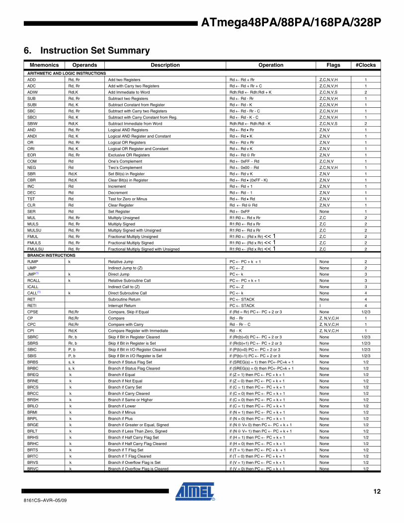
128161CS–AVR–05/09
ATmega48PA/88PA/168PA/328P
6. Instruction Set SummaryMnemonics Operands Description Operation Flags #Clocks
ARITHMETIC AND LOGIC INSTRUCTIONS
ADD Rd, Rr Add two Registers Rd ← Rd + Rr Z,C,N,V,H 1
ADC Rd, Rr Add with Carry two Registers Rd ← Rd + Rr + C Z,C,N,V,H 1
ADIW Rdl,K Add Immediate to Word Rdh:Rdl ← Rdh:Rdl + K Z,C,N,V,S 2
SUB Rd, Rr Subtract two Registers Rd ← Rd - Rr Z,C,N,V,H 1
SUBI Rd, K Subtract Constant from Register Rd ← Rd - K Z,C,N,V,H 1
SBC Rd, Rr Subtract with Carry two Registers Rd ← Rd - Rr - C Z,C,N,V,H 1
SBCI Rd, K Subtract with Carry Constant from Reg. Rd ← Rd - K - C Z,C,N,V,H 1
SBIW Rdl,K Subtract Immediate from Word Rdh:Rdl ← Rdh:Rdl - K Z,C,N,V,S 2
AND Rd, Rr Logical AND Registers Rd ← Rd • Rr Z,N,V 1
ANDI Rd, K Logical AND Register and Constant Rd ← Rd • K Z,N,V 1
OR Rd, Rr Logical OR Registers Rd ← Rd v Rr Z,N,V 1
ORI Rd, K Logical OR Register and Constant Rd ← Rd v K Z,N,V 1
EOR Rd, Rr Exclusive OR Registers Rd ← Rd ⊕ Rr Z,N,V 1
COM Rd One’s Complement Rd ← 0xFF − Rd Z,C,N,V 1
NEG Rd Two’s Complement Rd ← 0x00 − Rd Z,C,N,V,H 1
SBR Rd,K Set Bit(s) in Register Rd ← Rd v K Z,N,V 1
CBR Rd,K Clear Bit(s) in Register Rd ← Rd • (0xFF - K) Z,N,V 1
INC Rd Increment Rd ← Rd + 1 Z,N,V 1
DEC Rd Decrement Rd ← Rd − 1 Z,N,V 1
TST Rd Test for Zero or Minus Rd ← Rd • Rd Z,N,V 1
CLR Rd Clear Register Rd ← Rd ⊕ Rd Z,N,V 1
SER Rd Set Register Rd ← 0xFF None 1
MUL Rd, Rr Multiply Unsigned R1:R0 ← Rd x Rr Z,C 2
MULS Rd, Rr Multiply Signed R1:R0 ← Rd x Rr Z,C 2
MULSU Rd, Rr Multiply Signed with Unsigned R1:R0 ← Rd x Rr Z,C 2
FMUL Rd, Rr Fractional Multiply Unsigned R1:R0 ← (Rd x Rr) << 1 Z,C 2
FMULS Rd, Rr Fractional Multiply Signed R1:R0 ← (Rd x Rr) << 1 Z,C 2
FMULSU Rd, Rr Fractional Multiply Signed with Unsigned R1:R0 ← (Rd x Rr) << 1 Z,C 2
BRANCH INSTRUCTIONS
RJMP k Relative Jump PC ← PC + k + 1 None 2
IJMP Indirect Jump to (Z) PC ← Z None 2
JMP(1) k Direct Jump PC ← k None 3
RCALL k Relative Subroutine Call PC ← PC + k + 1 None 3
ICALL Indirect Call to (Z) PC ← Z None 3
CALL(1) k Direct Subroutine Call PC ← k None 4
RET Subroutine Return PC ← STACK None 4
RETI Interrupt Return PC ← STACK I 4
CPSE Rd,Rr Compare, Skip if Equal if (Rd = Rr) PC ← PC + 2 or 3 None 1/2/3
CP Rd,Rr Compare Rd − Rr Z, N,V,C,H 1
CPC Rd,Rr Compare with Carry Rd − Rr − C Z, N,V,C,H 1
CPI Rd,K Compare Register with Immediate Rd − K Z, N,V,C,H 1
SBRC Rr, b Skip if Bit in Register Cleared if (Rr(b)=0) PC ← PC + 2 or 3 None 1/2/3
SBRS Rr, b Skip if Bit in Register is Set if (Rr(b)=1) PC ← PC + 2 or 3 None 1/2/3
SBIC P, b Skip if Bit in I/O Register Cleared if (P(b)=0) PC ← PC + 2 or 3 None 1/2/3
SBIS P, b Skip if Bit in I/O Register is Set if (P(b)=1) PC ← PC + 2 or 3 None 1/2/3
BRBS s, k Branch if Status Flag Set if (SREG(s) = 1) then PC←PC+k + 1 None 1/2
BRBC s, k Branch if Status Flag Cleared if (SREG(s) = 0) then PC←PC+k + 1 None 1/2
BREQ k Branch if Equal if (Z = 1) then PC ← PC + k + 1 None 1/2
BRNE k Branch if Not Equal if (Z = 0) then PC ← PC + k + 1 None 1/2
BRCS k Branch if Carry Set if (C = 1) then PC ← PC + k + 1 None 1/2
BRCC k Branch if Carry Cleared if (C = 0) then PC ← PC + k + 1 None 1/2
BRSH k Branch if Same or Higher if (C = 0) then PC ← PC + k + 1 None 1/2
BRLO k Branch if Lower if (C = 1) then PC ← PC + k + 1 None 1/2
BRMI k Branch if Minus if (N = 1) then PC ← PC + k + 1 None 1/2
BRPL k Branch if Plus if (N = 0) then PC ← PC + k + 1 None 1/2
BRGE k Branch if Greater or Equal, Signed if (N ⊕ V= 0) then PC ← PC + k + 1 None 1/2
BRLT k Branch if Less Than Zero, Signed if (N ⊕ V= 1) then PC ← PC + k + 1 None 1/2
BRHS k Branch if Half Carry Flag Set if (H = 1) then PC ← PC + k + 1 None 1/2
BRHC k Branch if Half Carry Flag Cleared if (H = 0) then PC ← PC + k + 1 None 1/2
BRTS k Branch if T Flag Set if (T = 1) then PC ← PC + k + 1 None 1/2
BRTC k Branch if T Flag Cleared if (T = 0) then PC ← PC + k + 1 None 1/2
BRVS k Branch if Overflow Flag is Set if (V = 1) then PC ← PC + k + 1 None 1/2
BRVC k Branch if Overflow Flag is Cleared if (V = 0) then PC ← PC + k + 1 None 1/2

138161CS–AVR–05/09
ATmega48PA/88PA/168PA/328P
BRIE k Branch if Interrupt Enabled if ( I = 1) then PC ← PC + k + 1 None 1/2
BRID k Branch if Interrupt Disabled if ( I = 0) then PC ← PC + k + 1 None 1/2
BIT AND BIT-TEST INSTRUCTIONS
SBI P,b Set Bit in I/O Register I/O(P,b) ← 1 None 2
CBI P,b Clear Bit in I/O Register I/O(P,b) ← 0 None 2
LSL Rd Logical Shift Left Rd(n+1) ← Rd(n), Rd(0) ← 0 Z,C,N,V 1
LSR Rd Logical Shift Right Rd(n) ← Rd(n+1), Rd(7) ← 0 Z,C,N,V 1
ROL Rd Rotate Left Through Carry Rd(0)←C,Rd(n+1)← Rd(n),C←Rd(7) Z,C,N,V 1
ROR Rd Rotate Right Through Carry Rd(7)←C,Rd(n)← Rd(n+1),C←Rd(0) Z,C,N,V 1
ASR Rd Arithmetic Shift Right Rd(n) ← Rd(n+1), n=0..6 Z,C,N,V 1
SWAP Rd Swap Nibbles Rd(3..0)←Rd(7..4),Rd(7..4)←Rd(3..0) None 1
BSET s Flag Set SREG(s) ← 1 SREG(s) 1
BCLR s Flag Clear SREG(s) ← 0 SREG(s) 1
BST Rr, b Bit Store from Register to T T ← Rr(b) T 1
BLD Rd, b Bit load from T to Register Rd(b) ← T None 1
SEC Set Carry C ← 1 C 1
CLC Clear Carry C ← 0 C 1
SEN Set Negative Flag N ← 1 N 1
CLN Clear Negative Flag N ← 0 N 1
SEZ Set Zero Flag Z ← 1 Z 1
CLZ Clear Zero Flag Z ← 0 Z 1
SEI Global Interrupt Enable I ← 1 I 1
CLI Global Interrupt Disable I ← 0 I 1
SES Set Signed Test Flag S ← 1 S 1
CLS Clear Signed Test Flag S ← 0 S 1
SEV Set Twos Complement Overflow. V ← 1 V 1
CLV Clear Twos Complement Overflow V ← 0 V 1
SET Set T in SREG T ← 1 T 1
CLT Clear T in SREG T ← 0 T 1
SEH Set Half Carry Flag in SREG H ← 1 H 1
CLH Clear Half Carry Flag in SREG H ← 0 H 1
DATA TRANSFER INSTRUCTIONS
MOV Rd, Rr Move Between Registers Rd ← Rr None 1
MOVW Rd, Rr Copy Register Word Rd+1:Rd ← Rr+1:Rr None 1
LDI Rd, K Load Immediate Rd ← K None 1
LD Rd, X Load Indirect Rd ← (X) None 2
LD Rd, X+ Load Indirect and Post-Inc. Rd ← (X), X ← X + 1 None 2
LD Rd, - X Load Indirect and Pre-Dec. X ← X - 1, Rd ← (X) None 2
LD Rd, Y Load Indirect Rd ← (Y) None 2
LD Rd, Y+ Load Indirect and Post-Inc. Rd ← (Y), Y ← Y + 1 None 2
LD Rd, - Y Load Indirect and Pre-Dec. Y ← Y - 1, Rd ← (Y) None 2
LDD Rd,Y+q Load Indirect with Displacement Rd ← (Y + q) None 2
LD Rd, Z Load Indirect Rd ← (Z) None 2
LD Rd, Z+ Load Indirect and Post-Inc. Rd ← (Z), Z ← Z+1 None 2
LD Rd, -Z Load Indirect and Pre-Dec. Z ← Z - 1, Rd ← (Z) None 2
LDD Rd, Z+q Load Indirect with Displacement Rd ← (Z + q) None 2
LDS Rd, k Load Direct from SRAM Rd ← (k) None 2
ST X, Rr Store Indirect (X) ← Rr None 2
ST X+, Rr Store Indirect and Post-Inc. (X) ← Rr, X ← X + 1 None 2
ST - X, Rr Store Indirect and Pre-Dec. X ← X - 1, (X) ← Rr None 2
ST Y, Rr Store Indirect (Y) ← Rr None 2
ST Y+, Rr Store Indirect and Post-Inc. (Y) ← Rr, Y ← Y + 1 None 2
ST - Y, Rr Store Indirect and Pre-Dec. Y ← Y - 1, (Y) ← Rr None 2
STD Y+q,Rr Store Indirect with Displacement (Y + q) ← Rr None 2
ST Z, Rr Store Indirect (Z) ← Rr None 2
ST Z+, Rr Store Indirect and Post-Inc. (Z) ← Rr, Z ← Z + 1 None 2
ST -Z, Rr Store Indirect and Pre-Dec. Z ← Z - 1, (Z) ← Rr None 2
STD Z+q,Rr Store Indirect with Displacement (Z + q) ← Rr None 2
STS k, Rr Store Direct to SRAM (k) ← Rr None 2
LPM Load Program Memory R0 ← (Z) None 3
LPM Rd, Z Load Program Memory Rd ← (Z) None 3
LPM Rd, Z+ Load Program Memory and Post-Inc Rd ← (Z), Z ← Z+1 None 3
SPM Store Program Memory (Z) ← R1:R0 None -
IN Rd, P In Port Rd ← P None 1
OUT P, Rr Out Port P ← Rr None 1
PUSH Rr Push Register on Stack STACK ← Rr None 2
Mnemonics Operands Description Operation Flags #Clocks

148161CS–AVR–05/09
ATmega48PA/88PA/168PA/328P
POP Rd Pop Register from Stack Rd ← STACK None 2
MCU CONTROL INSTRUCTIONS
NOP No Operation None 1
SLEEP Sleep (see specific descr. for Sleep function) None 1
WDR Watchdog Reset (see specific descr. for WDR/timer) None 1
BREAK Break For On-chip Debug Only None N/A
Mnemonics Operands Description Operation Flags #Clocks
158161CS–AVR–05/09
ATmega48PA/88PA/168PA/328P
7. Ordering Information
7.1 ATmega48PA
Note: 1. This device can also be supplied in wafer form. Please contact your local Atmel sales office for detailed ordering information and minimum quantities.
2. Pb-free packaging complies to the European Directive for Restriction of Hazardous Substances (RoHS directive).Also Halide free and fully Green.
3. See ”Speed Grades” on page 306.4. NiPdAu Lead Finish.
Speed (MHz) Power Supply Ordering Code(2) Package(1) Operational Range
20(3) 1.8 - 5.5
ATmega48PA-AU
ATmega48PA-MMH(4)
ATmega48PA-MUATmega48PA-PU
32A
28M1
32M1-A28P3
Industrial
(-40°C to 85°C)
Package Type
32A 32-lead, Thin (1.0 mm) Plastic Quad Flat Package (TQFP)
28M1 28-pad, 4 x 4 x 1.0 body, Lead Pitch 0.45 mm Quad Flat No-Lead/Micro Lead Frame Package (QFN/MLF)
32M1-A 32-pad, 5 x 5 x 1.0 body, Lead Pitch 0.50 mm Quad Flat No-Lead/Micro Lead Frame Package (QFN/MLF)
28P3 28-lead, 0.300” Wide, Plastic Dual Inline Package (PDIP)
168161CS–AVR–05/09
ATmega48PA/88PA/168PA/328P
7.2 ATmega88PA
Note: 1. This device can also be supplied in wafer form. Please contact your local Atmel sales office for detailed ordering information and minimum quantities.
2. Pb-free packaging complies to the European Directive for Restriction of Hazardous Substances (RoHS directive).Also Halide free and fully Green.
3. See ”Speed Grades” on page 306.4. NiPdAu Lead Finish.
Speed (MHz) Power Supply Ordering Code(2) Package(1) Operational Range
20(3) 1.8 - 5.5
ATmega88PA-AUATmega88PA-MMH(4)
ATmega88PA-MU
ATmega88PA-PU
32A28M1
32M1-A
28P3
Industrial
(-40°C to 85°C)
Package Type
32A 32-lead, Thin (1.0 mm) Plastic Quad Flat Package (TQFP)
28M1 28-pad, 4 x 4 x 1.0 body, Lead Pitch 0.45 mm Quad Flat No-Lead/Micro Lead Frame Package (QFN/MLF)
32M1-A 32-pad, 5 x 5 x 1.0 body, Lead Pitch 0.50 mm Quad Flat No-Lead/Micro Lead Frame Package (QFN/MLF)
28P3 28-lead, 0.300” Wide, Plastic Dual Inline Package (PDIP)

178161CS–AVR–05/09
ATmega48PA/88PA/168PA/328P
7.3 ATmega168PA
Note: 1. This device can also be supplied in wafer form. Please contact your local Atmel sales office for detailed ordering information and minimum quantities.
2. Pb-free packaging complies to the European Directive for Restriction of Hazardous Substances (RoHS directive).Also Halide free and fully Green.
3. See ”Speed Grades” on page 312.4. NiPdAu Lead Finish.
Speed (MHz)(3) Power Supply Ordering Code(2) Package(1) Operational Range
20 1.8 - 5.5
ATmega168PA-AUATmega168PA-MMH(4)
ATmega168PA-MU
ATmega168PA-PU
32A28M1
32M1-A
28P3
Industrial
(-40°C to 85°C)
Package Type
32A 32-lead, Thin (1.0 mm) Plastic Quad Flat Package (TQFP)
28M1 28-pad, 4 x 4 x 1.0 body, Lead Pitch 0.45 mm Quad Flat No-Lead/Micro Lead Frame Package (QFN/MLF)
32M1-A 32-pad, 5 x 5 x 1.0 body, Lead Pitch 0.50 mm Quad Flat No-Lead/Micro Lead Frame Package (QFN/MLF)
28P3 28-lead, 0.300” Wide, Plastic Dual Inline Package (PDIP)

188161CS–AVR–05/09
ATmega48PA/88PA/168PA/328P
7.4 ATmega328P
Note: 1. This device can also be supplied in wafer form. Please contact your local Atmel sales office for detailed ordering information and minimum quantities.
2. Pb-free packaging complies to the European Directive for Restriction of Hazardous Substances (RoHS directive).Also Halide free and fully Green.
3. See Figure 28-1 on page 316.
Speed (MHz) Power Supply Ordering Code(2) Package(1) Operational Range
20(3) 1.8 - 5.5ATmega328P- AUATmega328P- MU
ATmega328P- PU
32A32M1-A
28P3
Industrial
(-40°C to 85°C)
Package Type
32A 32-lead, Thin (1.0 mm) Plastic Quad Flat Package (TQFP)
28P3 28-lead, 0.300” Wide, Plastic Dual Inline Package (PDIP)
32M1-A 32-pad, 5 x 5 x 1.0 body, Lead Pitch 0.50 mm Quad Flat No-Lead/Micro Lead Frame Package (QFN/MLF)
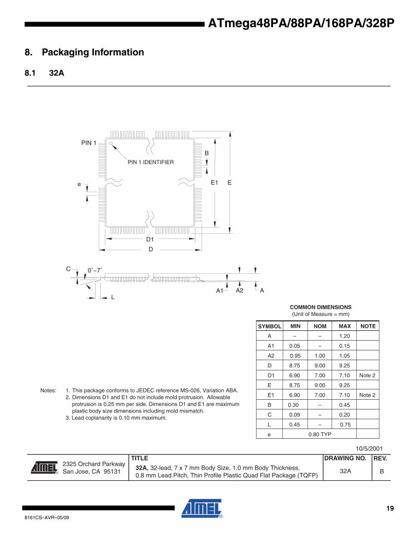
198161CS–AVR–05/09
ATmega48PA/88PA/168PA/328P
8. Packaging Information
8.1 32A
2325 Orchard Parkway San Jose, CA 95131
TITLE DRAWING NO.
R
REV.
32A, 32-lead, 7 x 7 mm Body Size, 1.0 mm Body Thickness,0.8 mm Lead Pitch, Thin Profile Plastic Quad Flat Package (TQFP)
B32A
10/5/2001
PIN 1 IDENTIFIER
0˚~7˚
PIN 1
L
C
A1 A2 A
D1
D
e E1 E
B
Notes: 1. This package conforms to JEDEC reference MS-026, Variation ABA. 2. Dimensions D1 and E1 do not include mold protrusion. Allowable
protrusion is 0.25 mm per side. Dimensions D1 and E1 are maximum plastic body size dimensions including mold mismatch.
3. Lead coplanarity is 0.10 mm maximum.
A – – 1.20
A1 0.05 – 0.15
A2 0.95 1.00 1.05
D 8.75 9.00 9.25
D1 6.90 7.00 7.10 Note 2
E 8.75 9.00 9.25
E1 6.90 7.00 7.10 Note 2
B 0.30 – 0.45
C 0.09 – 0.20
L 0.45 – 0.75
e 0.80 TYP
COMMON DIMENSIONS(Unit of Measure = mm)
SYMBOL MIN NOM MAX NOTE
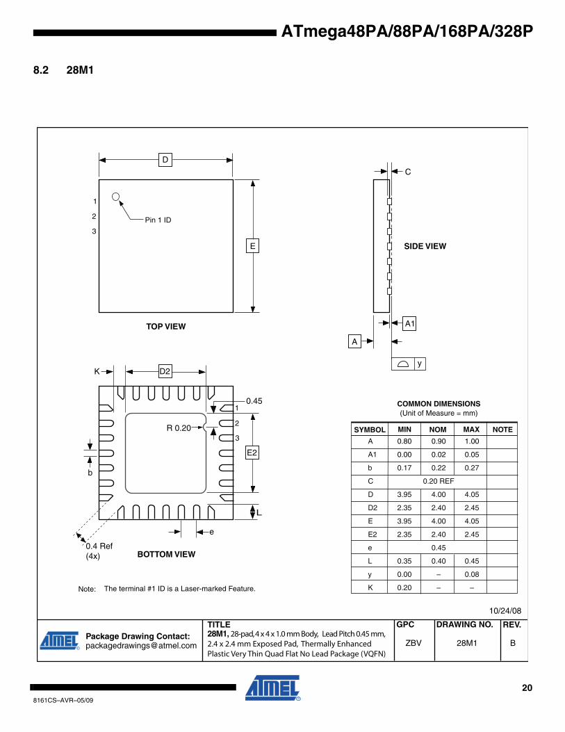
208161CS–AVR–05/09
ATmega48PA/88PA/168PA/328P
8.2 28M1
TITLE DRAWING NO. GPC REV. Package Drawing Contact: [email protected] 28M1ZBV B
28M1, 28-pad, 4 x 4 x 1.0 mm Body, Lead Pitch 0.45 mm, 2.4 x 2.4 mm Exposed Pad, Thermally Enhanced Plastic Very Thin Quad Flat No Lead Package (VQFN)
10/24/08
SIDE VIEW
Pin 1 ID
BOTTOM VIEW
TOP VIEW
Note: The terminal #1 ID is a Laser-marked Feature.
D
E
e
K
A1
C
A
D2
E2
y
L
1
2
3
b
1
2
3
0.45 COMMON DIMENSIONS(Unit of Measure = mm)
SYMBOL MIN NOM MAX NOTE
A 0.80 0.90 1.00
A1 0.00 0.02 0.05
b 0.17 0.22 0.27
C 0.20 REF
D 3.95 4.00 4.05
D2 2.35 2.40 2.45
E 3.95 4.00 4.05
E2 2.35 2.40 2.45
e 0.45
L 0.35 0.40 0.45
y 0.00 – 0.08
K 0.20 – –
R 0.20
0.4 Ref(4x)
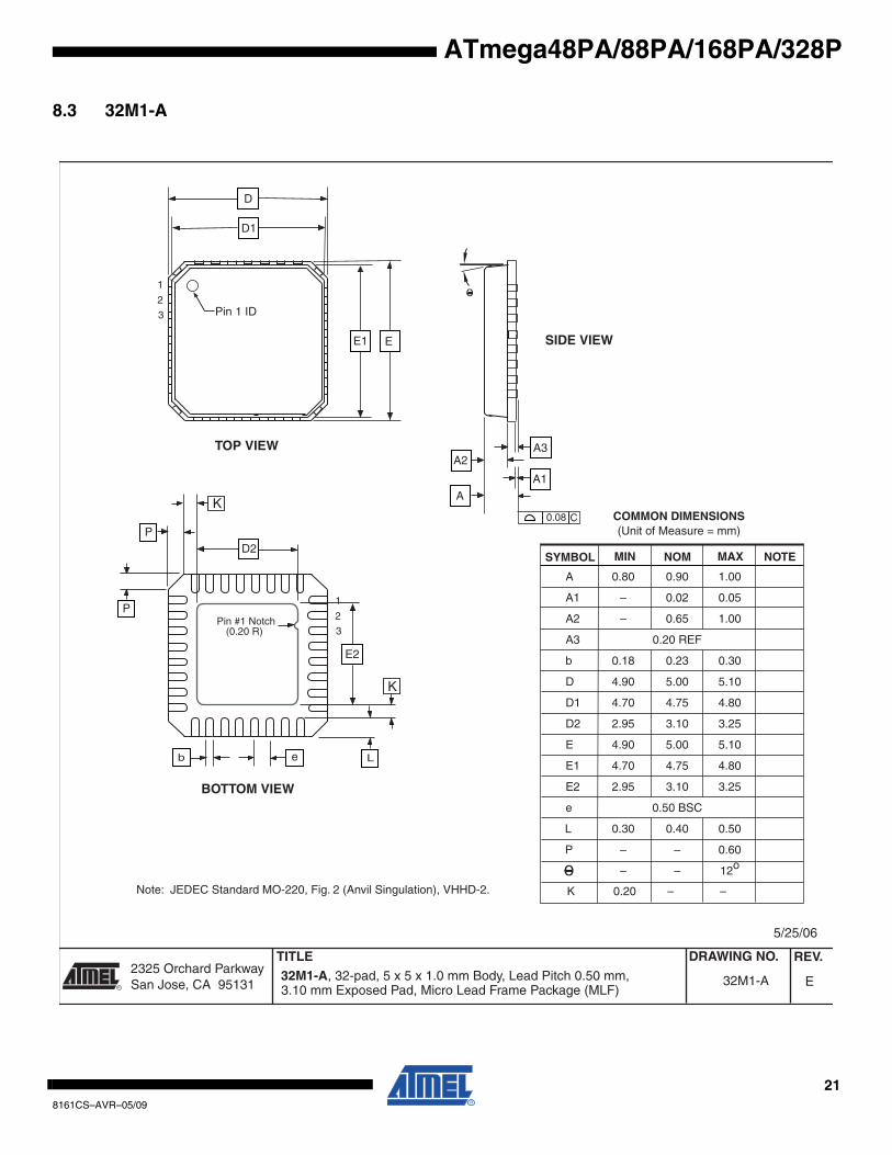
218161CS–AVR–05/09
ATmega48PA/88PA/168PA/328P
8.3 32M1-A
2325 Orchard Parkway San Jose, CA 95131
TITLE DRAWING NO.
R
REV. 32M1-A, 32-pad, 5 x 5 x 1.0 mm Body, Lead Pitch 0.50 mm, E32M1-A
5/25/06
3.10 mm Exposed Pad, Micro Lead Frame Package (MLF)
COMMON DIMENSIONS(Unit of Measure = mm)
SYMBOL MIN NOM MAX NOTE
D1
D
E1 E
eb
A3A2
A1 A
D2
E2
0.08 C
L
1
2
3
P
P
01
2
3
A 0.80 0.90 1.00
A1 – 0.02 0.05
A2 – 0.65 1.00
A3 0.20 REF
b 0.18 0.23 0.30
D
D1
D2 2.95 3.10 3.25
4.90 5.00 5.10
4.70 4.75 4.80
4.70 4.75 4.80
4.90 5.00 5.10
E
E1
E2 2.95 3.10 3.25
e 0.50 BSC
L 0.30 0.40 0.50
P – – 0.60
– – 12o
Note: JEDEC Standard MO-220, Fig. 2 (Anvil Singulation), VHHD-2.
TOP VIEW
SIDE VIEW
BOTTOM VIEW
0
Pin 1 ID
Pin #1 Notch(0.20 R)
K 0.20 – –
K
K

228161CS–AVR–05/09
ATmega48PA/88PA/168PA/328P
8.4 28P3
2325 Orchard Parkway San Jose, CA 95131
TITLE DRAWING NO.
R
REV. 28P3, 28-lead (0.300"/7.62 mm Wide) Plastic Dual Inline Package (PDIP) B28P3
09/28/01
PIN1
E1
A1
B
REF
E
B1
C
L
SEATING PLANE
A
0º ~ 15º
D
e
eB
B2(4 PLACES)
COMMON DIMENSIONS(Unit of Measure = mm)
SYMBOL MIN NOM MAX NOTE
A – – 4.5724
A1 0.508 – –
D 34.544 – 34.798 Note 1
E 7.620 – 8.255
E1 7.112 – 7.493 Note 1
B 0.381 – 0.533
B1 1.143 – 1.397
B2 0.762 – 1.143
L 3.175 – 3.429
C 0.203 – 0.356
eB – – 10.160
e 2.540 TYP
Note: 1. Dimensions D and E1 do not include mold Flash or Protrusion.Mold Flash or Protrusion shall not exceed 0.25 mm (0.010").

238161CS–AVR–05/09
ATmega48PA/88PA/168PA/328P
9. Errata
9.1 Errata ATmega48PAThe revision letter in this section refers to the revision of the ATmega48PA device.
9.1.1 Rev. DNo known errata.
9.2 Errata ATmega88PAThe revision letter in this section refers to the revision of the ATmega88PA device.
9.2.1 Rev. FNo known errata.
9.3 Errata ATmega168PAThe revision letter in this section refers to the revision of the ATmega168PA device.
9.3.1 Rev ENo known errata.
9.4 Errata ATmega328PThe revision letter in this section refers to the revision of the ATmega328P device.
9.4.1 Rev DNo known errata.
9.4.2 Rev CNot sampled.
9.4.3 Rev B• Unstable 32 kHz Oscillator
1. Unstable 32 kHz OscillatorThe 32 kHz oscillator does not work as system clock.
The 32 kHz oscillator used as asynchronous timer is inaccurate.
Problem Fix/ WorkaroundNone
9.4.4 Rev A• Unstable 32 kHz Oscillator
1. Unstable 32 kHz OscillatorThe 32 kHz oscillator does not work as system clock.
The 32 kHz oscillator used as asynchronous timer is inaccurate.
Problem Fix/ WorkaroundNone

248161CS–AVR–05/09
ATmega48PA/88PA/168PA/328P
10. Datasheet Revision HistoryPlease note that the referring page numbers in this section are referred to this document. Thereferring revision in this section are referring to the document revision.
10.1 Rev. 8161C – 05/09
10.2 Rev. 8161B – 01/09
1. Updated ”Features” on page 1 for ATmega48PA/88PA/168PA/328P.
2. Updated ”Overview” on page 5 included the Table 2-1 on page 6.
3. Updated ”AVR Memories” on page 16 included ”Register Description” on page 21 and inserted Figure 7-1 on page 17.
4. Updated ”Register Description” on page 44.
5. Updated ”System Control and Reset” on page 46.
6. Updated ”Interrupts” on page 57.
7. Updated ”External Interrupts” on page 70.
8. Updated ”Boot Loader Support – Read-While-Write Self-Programming, ATmega88PA, ATmega168PA and ATmega328P” on page 277.
9. Inserted ”ATmega168PA DC Characteristics” on page 315.
10. Inserted ”ATmega328P DC Characteristics” on page 316.
11. Inserted ”ATmega168PA Typical Characteristics” on page 375.
12. Inserted ”ATmega328P Typical Characteristics” on page 399.
13. Inserted Ordering Information for ”ATmega168PA” on page 432.
14. Inserted Ordering Information for ”ATmega328P” on page 433.
15. Inserted ”Errata ATmega328P” on page 438.
16. Editing updates.
1. Updated ”Features” on page 1 for ATmega48PA and updated the book accordingly.
2. Updated ”Overview” on page 5 included the Table 2-1 on page 6.
3. Updated ”AVR Memories” on page 16 included ”Register Description” on page 21 and inserted Figure 7-1 on page 17.
4. Updated ”Register Description” on page 44.
5. Updated ”System Control and Reset” on page 46.
6. Updated ”Interrupts” on page 57.
7. Updated ”External Interrupts” on page 70.
8. Inserted Typical characteristics for ”ATmega48PA Typical Characteristics” on page 327.
9. Updated figure names in Typical characteristics for ”ATmega88PA Typical Character-istics” on page 351.
10. Inserted ”ATmega48PA DC Characteristics” on page 314.

258161CS–AVR–05/09
ATmega48PA/88PA/168PA/328P
10.3 Rev. 8161A – 11/08
11. Updated Table 28-1 on page 317 by removing the footnote from Vcc/User calibration
12. Updated Table 28-7 on page 323 by removing Max value (2.5 LSB) from Absoluteaccuracy, VREF = 4V, VCC = 4V, ADC clock = 200 kHz.
13. Inserted Ordering Information for ”ATmega48PA” on page 430.
1. Initial revision (Based on the ATmega48P/88P/168P/328P datasheet 8025F-AVR-08/08).
2. Changes done compared to ATmega48P/88P/168P/328P datasheet 8025F-AVR-08/08:
– Updated ”DC Characteristics” on page 313 with new typical values for ICC.
– Updated ”Speed Grades” on page 316.
– New graphics in ”Typical Characteristics” on page 326.
– New ”Ordering Information” on page 430.

8161CS–AVR–05/09
Headquarters International
Atmel Corporation2325 Orchard ParkwaySan Jose, CA 95131USATel: 1(408) 441-0311Fax: 1(408) 487-2600
Atmel AsiaUnit 1-5 & 16, 19/FBEA Tower, Millennium City 5418 Kwun Tong RoadKwun Tong, KowloonHong KongTel: (852) 2245-6100Fax: (852) 2722-1369
Atmel EuropeLe Krebs8, Rue Jean-Pierre TimbaudBP 30978054 Saint-Quentin-en-Yvelines CedexFranceTel: (33) 1-30-60-70-00 Fax: (33) 1-30-60-71-11
Atmel Japan9F, Tonetsu Shinkawa Bldg.1-24-8 ShinkawaChuo-ku, Tokyo 104-0033JapanTel: (81) 3-3523-3551Fax: (81) 3-3523-7581
Product Contact
Web Sitewww.atmel.com
Technical [email protected]
Sales Contactwww.atmel.com/contacts
Literature Requestswww.atmel.com/literature
Disclaimer: The information in this document is provided in connection with Atmel products. No license, express or implied, by estoppel or otherwise, to anyintellectual property right is granted by this document or in connection with the sale of Atmel products. EXCEPT AS SET FORTH IN ATMEL’S TERMS AND CONDI-TIONS OF SALE LOCATED ON ATMEL’S WEB SITE, ATMEL ASSUMES NO LIABILITY WHATSOEVER AND DISCLAIMS ANY EXPRESS, IMPLIED OR STATUTORYWARRANTY RELATING TO ITS PRODUCTS INCLUDING, BUT NOT LIMITED TO, THE IMPLIED WARRANTY OF MERCHANTABILITY, FITNESS FOR A PARTICULARPURPOSE, OR NON-INFRINGEMENT. IN NO EVENT SHALL ATMEL BE LIABLE FOR ANY DIRECT, INDIRECT, CONSEQUENTIAL, PUNITIVE, SPECIAL OR INCIDEN-TAL DAMAGES (INCLUDING, WITHOUT LIMITATION, DAMAGES FOR LOSS OF PROFITS, BUSINESS INTERRUPTION, OR LOSS OF INFORMATION) ARISING OUT OFTHE USE OR INABILITY TO USE THIS DOCUMENT, EVEN IF ATMEL HAS BEEN ADVISED OF THE POSSIBILITY OF SUCH DAMAGES. Atmel makes norepresentations or warranties with respect to the accuracy or completeness of the contents of this document and reserves the right to make changes to specificationsand product descriptions at any time without notice. Atmel does not make any commitment to update the information contained herein. Unless specifically providedotherwise, Atmel products are not suitable for, and shall not be used in, automotive applications. Atmel’s products are not intended, authorized, or warranted for useas components in applications intended to support or sustain life.
© 2009 Atmel Corporation. All rights reserved. Atmel®, Atmel logo and combinations thereof, AVR® and others are registered trademarks ortrademarks of Atmel Corporation or its subsidiaries. Other terms and product names may be trademarks of others.

Disclaimer and Copyright Notice. Information in this document, including URL references, is subject to change without noticeTHIS DOCUMENT IS PROVIDED AS IS WITH NO WARRANTIES WHATSOEVER, INCLUDING ANYWARRANTY OF MERCHANTABILITY, NONINFRINGEMENT, FITNESS FOR ANY PARTICULAR PURPOSE, OR ANY WARRANTY OTHERWISE ARISING OUT OF ANY PROPOSAL, SPECIFICATIONOR SAMPLE. All liability, including liability for infringement of any proprietary rights, relating to usedocument is disclaimed. No licenses express or implied, by estoppel orThe WiFi Alliance Member Logo is a trademark of the WiFi Alliance.All trade names, trademarks and registered trademarks mentioned in this document are property ofhereby acknowledged. Copyright © 2015 AI-Thinker team. All rights reserved Notice Product version upgrades or other reasons, possible changes inotice or indication of the circumstances the right to modify the content of this manual. This manual is used make every effort to provide accurate information in this manual, but this manual all statements, information and advice nor does it constitute any express or imp
ESP-01 WiFi Module
Information in this document, including URL references, is subject to change without notice. DOCUMENT IS PROVIDED AS IS WITH NO WARRANTIES WHATSOEVER, INCLUDING ANYWARRANTY OF MERCHANTABILITY, NON
PURPOSE, OR ANY WARRANTY OTHERWISE ARISING OUT OF ANY PROPOSAL, g liability for infringement of any proprietary rights, relating to use
document is disclaimed. No licenses express or implied, by estoppel or otherwise, to any intellectual property rights are granted herein.r Logo is a trademark of the WiFi Alliance.
All trade names, trademarks and registered trademarks mentioned in this document are property of their respective owners, and are
All rights reserved.
Product version upgrades or other reasons, possible changes in the contents of this manual. AI-Thinker reserves inotice or indication of the circumstances the right to modify the content of this manual. This manual is used only as a guide, make every effort to provide accurate information in this manual, but Ai-thinker does not ensure that manual content without error, in this manual all statements, information and advice nor does it constitute any express or implied warranty.
01 WiFi Module Version1.0
DOCUMENT IS PROVIDED AS IS WITH NO WARRANTIES WHATSOEVER, INCLUDING ANYWARRANTY OF MERCHANTABILITY, NON-PURPOSE, OR ANY WARRANTY OTHERWISE ARISING OUT OF ANY PROPOSAL, g liability for infringement of any proprietary rights, relating to use of information in this
otherwise, to any intellectual property rights are granted herein.
their respective owners, and are
Thinker reserves in the absence of any only as a guide, Ai-thinker
does not ensure that manual content without error, in
Table of Contents1. Preambles ................................
1.1. Features ................................
1.2. Parameters ................................
2. Pin Descriptions ................................
3. Packaging and Dimension
4. Functional Descriptions
4.1. MCU ................................
4.2. Memory Organization
4.2.1. Internal SRAM and ROM
4.2.2. External SPI Flash
4.3. Crystal ................................
4.4. Interfaces ................................
4.5. Absolute Maximum Ratings
4.6. Recommended Operating Conditions
4.7. Digital Terminal Characteristics
5. RF Performance ................................
6. Power Consumption ................................
7. Reflow Profile ................................
8. Schematics ................................
Table of Contents
................................................................................................
...........................................................................................
......................................................................................
.........................................................................................
Packaging and Dimension ................................................................
Functional Descriptions ................................................................
...............................................................................................
Memory Organization ................................................................
Internal SRAM and ROM ...........................................................
External SPI Flash ................................................................
............................................................................................
.......................................................................................
Absolute Maximum Ratings ..........................................................
Recommended Operating Conditions ................................
Digital Terminal Characteristics .....................................................
.......................................................................................
................................................................
..........................................................................................
...............................................................................................
.................................. 3
........................... 4
...................... 6
......................... 7
........................................ 10
........................................... 12
............................... 12
................................... 12
........................... 12
...................................... 12
............................ 13
....................... 13
.......................... 15
........................................... 15
..................... 15
....................... 16
................................................ 17
.......................... 18
............................... 19

Shenzhen Anxinke Technology CO;LTD
1. Preambles ESP-01 WiFi module is developed by
encapsulates Tensilica L106 integrates industry
Clock speed support 80 MHz, 160 MHz, supports the RTOS, integrated Wi
The module supports standard IEEE802.11
add modules to an existing device networking, or building a separate network controller.
ESP8266 is high integration wireless SOCs, designed for space and power constrained mobile platform
It provides unsurpassed ability to embed Wi
application, with the lowest cost, and minimal space requirement.
Figure 1 ESP8266EX Block Diagram
ESP8266EX offers a complete and self
or to offload Wi-Fi networking functions from another application processor
When ESP8266EX hosts the application, it boots up directly from an external flash. In has
improve the performance of the system in such applications.
Alternately, serving as a Wi-Fi adapter, wireless internet access can be added to any micro controllerbased design
with simple connectivity (SPI/SDIO or I2C/UART interface).
http://www.ai-thinker.com
module is developed by Ai-thinker Team. core processor ESP8266 in smaller sizes of the module
Tensilica L106 integrates industry-leading ultra low power 32-bit MCU micro, with the 16
Clock speed support 80 MHz, 160 MHz, supports the RTOS, integrated Wi-Fi MAC/BB/RF/PA/LNA, on
The module supports standard IEEE802.11 b/g/n agreement, complete TCP/IP protocol stack. Users can use the
add modules to an existing device networking, or building a separate network controller.
wireless SOCs, designed for space and power constrained mobile platform
unsurpassed ability to embed Wi-Fi capabilities within other systems, or to function as a standalone
application, with the lowest cost, and minimal space requirement.
Figure 1 ESP8266EX Block Diagram
self-contained Wi-Fi networking solution; it can be used to host
Fi networking functions from another application processor.
When ESP8266EX hosts the application, it boots up directly from an external flash. In has integrated
improve the performance of the system in such applications.
Fi adapter, wireless internet access can be added to any micro controllerbased design
with simple connectivity (SPI/SDIO or I2C/UART interface).
3
core processor ESP8266 in smaller sizes of the module
bit MCU micro, with the 16-bit short mode,
/BB/RF/PA/LNA, on-board antenna.
b/g/n agreement, complete TCP/IP protocol stack. Users can use the
wireless SOCs, designed for space and power constrained mobile platform designers.
Fi capabilities within other systems, or to function as a standalone
Fi networking solution; it can be used to host the application
integrated cache to
Fi adapter, wireless internet access can be added to any micro controllerbased design
Shenzhen Anxinke Technology CO;LTD
ESP8266EX is among the most integrated WiFi chip in the industry; it integrates the antenna
power amplifier, low noise receive amplifier, filters, power management modules,
and the entire solution, including front-end module, is designed
ESP8266EX also integrates an enhanced version of Tensilica’s L106 Diamond series 32
SRAM, besides the Wi-Fi functionalities. ESP8266EX is often integrated wit
specific devices through its GPIOs; codes for such applications are
Espressif Systems’ Smart Connectivity Platform (ESCP) demonstrates sophisticated system
fast sleep/wake context switching for energy
signal processing, and spur cancellation and radio co
LCD interference mitigation.
1.1. Features
• 802.11 b/g/n
• Integrated low power 32-bit MCU
• Integrated 10-bit ADC
• Integrated TCP/IP protocol stack
• Integrated TR switch, balun, LNA, power amplifier and matching network
• Integrated PLL, regulators, and power management units
• Supports antenna diversity
• Wi-Fi 2.4 GHz, support WPA/WPA2
• Support STA/AP/STA+AP operation modes
• Support Smart Link Function for both Android and iOS devices
• Support Smart Link Function for both Android and iOS devices
• SDIO 2.0, (H) SPI, UART, I2C, I2S, IRDA, PWM,
http://www.ai-thinker.com
ESP8266EX is among the most integrated WiFi chip in the industry; it integrates the antenna
power amplifier, low noise receive amplifier, filters, power management modules, it requires minimal external circuitry,
end module, is designed to occupy minimal PCB area.
ESP8266EX also integrates an enhanced version of Tensilica’s L106 Diamond series 32-bit processor,
Fi functionalities. ESP8266EX is often integrated with external sensors and other application
specific devices through its GPIOs; codes for such applications are provided in examples in the SDK.
Espressif Systems’ Smart Connectivity Platform (ESCP) demonstrates sophisticated system-
t sleep/wake context switching for energy-efficient VoIP, adaptive radio biasing. for low-power operation, advance
signal processing, and spur cancellation and radio co-existence features for common cellular, Bluetooth, DDR, LVDS,
Integrated TR switch, balun, LNA, power amplifier and matching network
Integrated PLL, regulators, and power management units
Support STA/AP/STA+AP operation modes
Support Smart Link Function for both Android and iOS devices
Support Smart Link Function for both Android and iOS devices
SDIO 2.0, (H) SPI, UART, I2C, I2S, IRDA, PWM, GPIO
4
ESP8266EX is among the most integrated WiFi chip in the industry; it integrates the antenna switches, RF balun,
it requires minimal external circuitry,
bit processor, with on-chip
sensors and other application
provided in examples in the SDK.
-level features include
power operation, advance
features for common cellular, Bluetooth, DDR, LVDS,

Shenzhen Anxinke Technology CO;LTD
• STBC, 1x1 MIMO, 2x1 MIMO
• A-MPDU & A-MSDU aggregation and 0.4s guard interval
• Deep sleep power <10uA, Power down leakage current < 5uA
• Wake up and transmit packets in < 2ms
• Standby power consumption of < 1.0mW (DTIM3)
• +20dBm output power in 802.11b mode
• Operating temperature range -40C ~ 125C
http://www.ai-thinker.com
MSDU aggregation and 0.4s guard interval
Deep sleep power <10uA, Power down leakage current < 5uA
Wake up and transmit packets in < 2ms
Standby power consumption of < 1.0mW (DTIM3)
mode
40C ~ 125C
5
Shenzhen Anxinke Technology CO;LTD
1.2. Parameters
Table 1 below describes the major parameters.
http://www.ai-thinker.com
Table 1 below describes the major parameters.
Table 1 Parameters
6

Shenzhen Anxinke Technology CO;LTD
2. Pin Descriptions
There are altogether 8 pin counts, the definitions of which are described in Table 2 below
http://www.ai-thinker.com
pin counts, the definitions of which are described in Table 2 below。
Table 2 ESP-01 Pin design
7

Shenzhen Anxinke Technology CO;LTD
NO.
1
2
3
4
5
6
7
8
http://www.ai-thinker.com
Table 2 Pin Descriptions
Pin Name Function
GND
GPIO2 GPIO,Internal Pull
GPIO0 GPIO,Internal Pull
RXD UART0,data received pin RXD
VCC 3.3V power supply (VDD)
RST
1) External reset pin
2) Can loft or external MCU
CH_PD Chip enable pin. Active high
TXD UART0,data
8
Function
GND
,Internal Pull-up
GPIO,Internal Pull-up
UART0,data received pin RXD
3.3V power supply (VDD)
External reset pin, active low
Can loft or external MCU
,
Chip enable pin. Active high
UART0,data send pin RXD

Shenzhen Anxinke Technology CO;LTD
Mode GPIO15
UART Low
Flash Boot Low
Table
http://www.ai-thinker.com
Table 3 Pin Mode
GPIO15 GPIO0
Low Low
Low High
Table 4 Receiver Sensitivity
9
GPIO2
High
High
Shenzhen Anxinke Technology CO;LTD
3. Packaging and Dimension
The external size of the module is 14.3mm*2
integrated in this module is an SPI flash, the capacity of which is
The antenna applied on this module is a 3DBi PCB
Figure 3 [Module Pin Counts,
http://www.ai-thinker.com
Packaging and Dimension
mm*24.8mm*3mm, as is illustrated in Figure 3 below. The type of
lash, the capacity of which is 1 MB, and the package size of which is SOP
The antenna applied on this module is a 3DBi PCB-on-board antenna.
[Module Pin Counts, 8 pin, 14.3 mm *24.8 mm *3.0 mm]
10
below. The type of flash
which is SOP-210mil.
3.0 mm]

Shenzhen Anxinke Technology CO;LTD
Table 5
Length Width
14.3 mm 24.8 mm
http://www.ai-thinker.com
Figure 4 Top View of ESP-01 WiFi Module
Dimension of ESP-01 WiFi Module
Height PAD Size(Bottom)
3 mm 0.9 mm x 1.7 mm
11
WiFi Module
Pin Pitch
2.54 mm
Shenzhen Anxinke Technology CO;LTD
4. Functional Descriptions
4.1. MCU
ESP8266EX is embedded with Tensilica L106 32
consumption and 16-bit RSIC. The CPU clock speed is 80MHz. It can
ESP8266EX is often integrated with external sensors and other specific devices through its GPIOs;
applications are provided in examples in the SDK.
4.2. Memory Organization
4.2.1. Internal SRAM and ROM
ESP8266EX WiFi SoC is embedded with memory controller, including SRAM and ROM. MCU can visit
units through iBus, dBus, and AHB interfaces. All memory units can be visited upon
will decide the running sequence according to t
According to our current version of SDK provided, SRAM space that is available to users is assigned
RAM size < 36kB, that is to say, when ESP8266EX is working under the station mode and
router, programmable space accessible to user in heap and data section is
There is no programmable ROM in the SoC, therefore, user program must be stored in an
http://www.ai-thinker.com
Functional Descriptions
ESP8266EX is embedded with Tensilica L106 32-bit micro controller (MCU), which features extra low
bit RSIC. The CPU clock speed is 80MHz. It can also reach a maximum value of 160MHz.
ESP8266EX is often integrated with external sensors and other specific devices through its GPIOs;
applications are provided in examples in the SDK.
Memory Organization
Internal SRAM and ROM
WiFi SoC is embedded with memory controller, including SRAM and ROM. MCU can visit
units through iBus, dBus, and AHB interfaces. All memory units can be visited upon request, while a memory arbiter
will decide the running sequence according to the time when these requests are received by the processor.
According to our current version of SDK provided, SRAM space that is available to users is assigned
RAM size < 36kB, that is to say, when ESP8266EX is working under the station mode and is
router, programmable space accessible to user in heap and data section is around 36kB.)
There is no programmable ROM in the SoC, therefore, user program must be stored in an
12
bit micro controller (MCU), which features extra low power
value of 160MHz.
ESP8266EX is often integrated with external sensors and other specific devices through its GPIOs; codes for such
WiFi SoC is embedded with memory controller, including SRAM and ROM. MCU can visit the memory
request, while a memory arbiter
requests are received by the processor.
According to our current version of SDK provided, SRAM space that is available to users is assigned as below:
is connected to the
There is no programmable ROM in the SoC, therefore, user program must be stored in an external SPI flash.
4.2.2. External SPI Flash
efinableMB external SPI flash to store user programs. If larger deThis module is mounted with an 1 M storage space
is required, a SPI flash with larger memorry size is preferred. Theoretically speaking, up to 16 MBB memory capacity can
be supported.
Suggested tySPI Flash memory capacit :
h memory that can be supported is 512 kB;OTA is disabled: the minimum flash
h memory that can be supported is 1 MB.OTA is enabled: the minimum flash
Several SPI modes can be supportedd, including Standard SPI, Dual SPI, and Quad SPI.
, otherwisect SPI mode when you are downloading into the flash,Therefore, please choose the correc
firmwares/programs that you downnloaded may not work in the right way.
Shenzhen Anxinke Technology CO;LTD
4.3. Crystal
Currently, the frequency of crystal oscillators supported include
crystal oscillators applied should be ±10PPM, and the operating temperature range
When using the downloading tools, please remember to select the right crystal oscillator type. In
capacitors C1 and C2, which are connected to the earth, are added to the input and
oscillator respectively. The values of the two capacitors can be
capacitive values of C1 and C2 depend on
circuit. Normally, the capacitive values of C1 and C2 are within 10pF if the crystal oscillator frequency is 26MHz, while
the values of C1 and C2 are 10pF<C1, C2<22pF if the crystal oscillator frequency is 40MHz
4.4. Interfaces
http://www.ai-thinker.com
Currently, the frequency of crystal oscillators supported include 40MHz, 26MHz and 24MHz. The
crystal oscillators applied should be ±10PPM, and the operating temperature range should be between
When using the downloading tools, please remember to select the right crystal oscillator type. In
capacitors C1 and C2, which are connected to the earth, are added to the input and output terminals of the crystal
oscillator respectively. The values of the two capacitors can be flexible, ranging from 6pF to 22pF, however, the specific
acitive values of C1 and C2 depend on further testing and adjustment on the overall performance of the whole
capacitive values of C1 and C2 are within 10pF if the crystal oscillator frequency is 26MHz, while
re 10pF<C1, C2<22pF if the crystal oscillator frequency is 40MHz.
Table 6 Descriptions of Interfaces
13
40MHz, 26MHz and 24MHz. The accuracy of
should be between -20°C and 85°C.
When using the downloading tools, please remember to select the right crystal oscillator type. In circuit design,
output terminals of the crystal
flexible, ranging from 6pF to 22pF, however, the specific
further testing and adjustment on the overall performance of the whole
capacitive values of C1 and C2 are within 10pF if the crystal oscillator frequency is 26MHz, while
Shenzhen Anxinke Technology CO;LTD
http://www.ai-thinker.com
14
Shenzhen Anxinke Technology CO;LTD
4.5. Absolute Maximum Ratings
4.6. Recommended Operating Conditions
4.7. Digital Terminal Characteristics
Table
Note: Test conditions: VDD = 3.3V, Temperature = 20
http://www.ai-thinker.com
Absolute Maximum Ratings
Table 7 Absolute Maximum Ratings
Recommended Operating Conditions
Table 8 Recommended Operating Conditions
Digital Terminal Characteristics
Table 9 Digital Terminal Characteristics
Note: Test conditions: VDD = 3.3V, Temperature = 20 , if nothing special is stated.
15
Shenzhen Anxinke Technology CO;LTD
5. RF Performance
http://www.ai-thinker.com
Table 10 RF Performance
16

Shenzhen Anxinke Technology CO;LTD
6. Power Consumption
❶Modem-Sleep requires the CPU to be working, as in PWM or I2S applications. According to
U-APSD), it saves power to shut down the Wi
transmission. E.g. in DTIM3, to maintain a sleep 300mswake 3ms cycle to receive AP’s Beacon packages, the current is
about 15mA.
❷ During Light-Sleep, the CPU may be suspended in applications like Wi
Wi-Fi Modem circuit can be turned off and CPU suspended to save power
E.g. in DTIM3, to maintain a sleep 300ms-
❸ Deep-Sleep does not require Wi-Fi connection to be maintained. For application with long time
transmission, e.g. a temperature sensor that checks the temperature every 100s
to the AP (taking about 0.3~1s), the overall average current is
http://www.ai-thinker.com
Table 11 Power Consumption
Sleep requires the CPU to be working, as in PWM or I2S applications. According to
APSD), it saves power to shut down the Wi-Fi Modem circuit while maintaining a Wi-Fi connection with no data
transmission. E.g. in DTIM3, to maintain a sleep 300mswake 3ms cycle to receive AP’s Beacon packages, the current is
Sleep, the CPU may be suspended in applications like Wi-Fi switch. Without data
Fi Modem circuit can be turned off and CPU suspended to save power according to the 802.11 standard (U
-wake 3ms cycle to receive AP’s Beacon packages, the current is about 0.9mA.
Fi connection to be maintained. For application with long time
transmission, e.g. a temperature sensor that checks the temperature every 100s ,sleep 300s and waking up to connect
he overall average current is less than 1mA.
17
Sleep requires the CPU to be working, as in PWM or I2S applications. According to 802.11 standards (like
Fi connection with no data
transmission. E.g. in DTIM3, to maintain a sleep 300mswake 3ms cycle to receive AP’s Beacon packages, the current is
Fi switch. Without data transmission, the
according to the 802.11 standard (U-APSD).
cycle to receive AP’s Beacon packages, the current is about 0.9mA.
Fi connection to be maintained. For application with long time lags between data
sleep 300s and waking up to connect
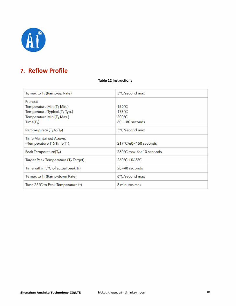
Shenzhen Anxinke Technology CO;LTD
7. Reflow Profile
http://www.ai-thinker.com
Table 12 Instructions
18
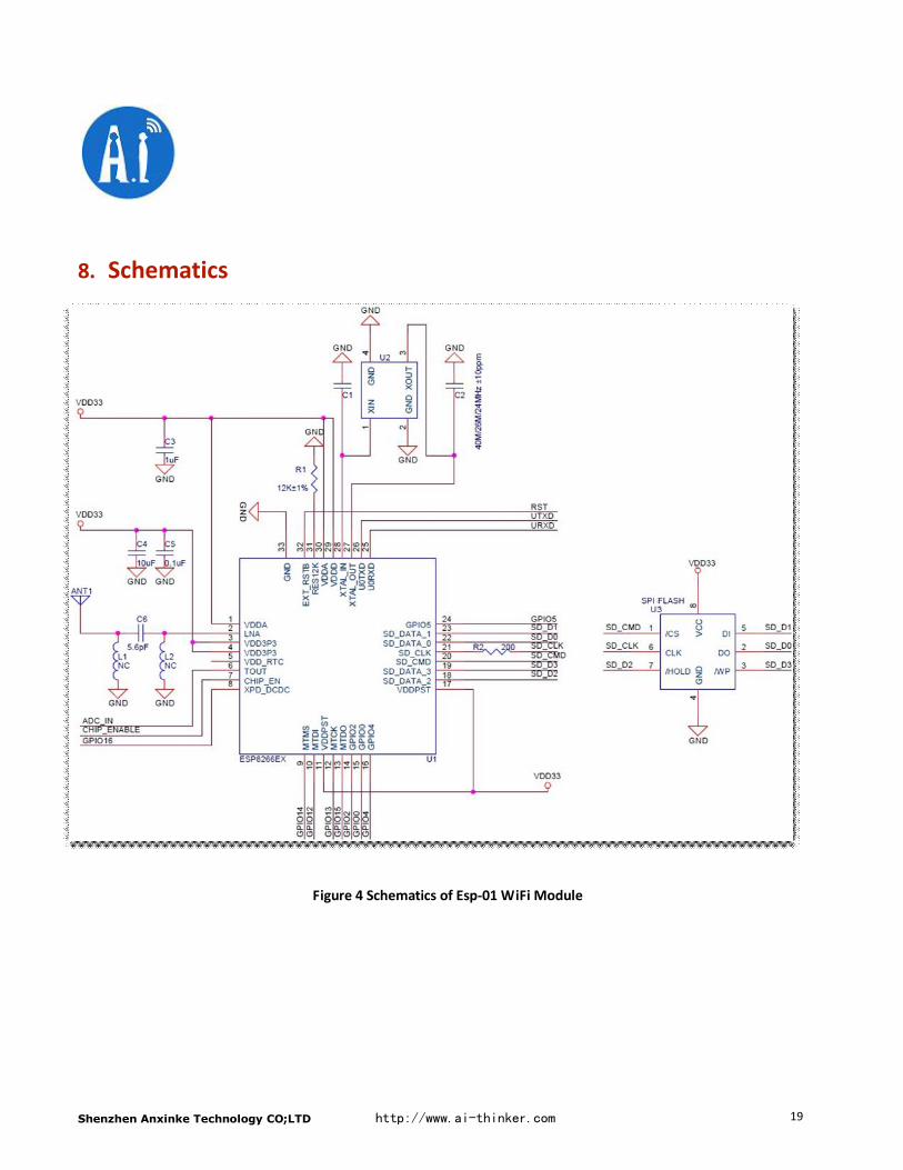
Shenzhen Anxinke Technology CO;LTD
8. Schematics
Figure 4 Schematics of E
http://www.ai-thinker.com
Figure 4 Schematics of Esp-01 WiFi Module
19
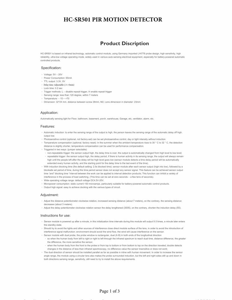
sor free
seller.
i i g
feedback
ress
c La guage
Product Discription
HC-SR501 is based on infrared technology, automatic control module, using Germany imported LHI778 probe design, high sensitivity, high
reliability, ultra-low-voltage operating mode, widely used in various auto-sensing electrical equipment, especially for battery-powered automatic
controlled products.
Specification:
Voltage: 5V – 20V
Power Consumption: 65mA
TTL output: 3.3V, 0V
Lock time: 0.2 sec
Trigger methods: L – disable repeat trigger, H enable repeat trigger
Sensing range: less than 120 degree, within 7 meters
Temperature: – 15 ~ +70
Dimension: 32*24 mm, distance between screw 28mm, M2, Lens dimension in diameter: 23mm
Application:
Automatically sensing light for Floor, bathroom, basement, porch, warehouse, Garage, etc, ventilator, alarm, etc.
Features:
Automatic induction: to enter the sensing range of the output is high, the person leaves the sensing range of the automatic delay off high,
output low.
Photosensitive control (optional, not factory-set) can be set photosensitive control, day or light intensity without induction.
Temperature compensation (optional, factory reset): In the summer when the ambient temperature rises to 30 ° C to 32 ° C, the detection
distance is slightly shorter, temperature compensation can be used for performance compensation.
Triggered in two ways: (jumper selectable)
non-repeatable trigger: the sensor output high, the delay time is over, the output is automatically changed from high level to low level;
repeatable trigger: the sensor output high, the delay period, if there is human activity in its sensing range, the output will always remain
high until the people left after the delay will be high level goes low (sensor module detects a time delay period will be automatically
extended every human activity, and the starting point for the delay time to the last event of the time).
With induction blocking time (the default setting: 2.5s blocked time): sensor module after each sensor output (high into low), followed by a
blockade set period of time, during this time period sensor does not accept any sensor signal. This feature can be achieved sensor output
time “and” blocking time “interval between the work can be applied to interval detection products; This function can inhibit a variety of
interference in the process of load switching. (This time can be set at zero seconds – a few tens of seconds).
Wide operating voltage range: default voltage DC4.5V-20V.
Micropower consumption: static current <50 microamps, particularly suitable for battery-powered automatic control products.
Output high signal: easy to achieve docking with the various types of circuit.
Adjustment:
Adjust the distance potentiometer clockwise rotation, increased sensing distance (about 7 meters), on the contrary, the sensing distance
decreases (about 3 meters).
Adjust the delay potentiometer clockwise rotation sensor the delay lengthened (300S), on the contrary, shorten the induction delay (5S).
Instructions for use:
Sensor module is powered up after a minute, in this initialization time intervals during this module will output 0-3 times, a minute later enters
the standby state.
Should try to avoid the lights and other sources of interference close direct module surface of the lens, in order to avoid the introduction of
interference signal malfunction; environment should avoid the wind flow, the wind will cause interference on the sensor.
Sensor module with dual probe, the probe window is rectangular, dual (A B) in both ends of the longitudinal direction
so when the human body from left to right or right to left through the infrared spectrum to reach dual time, distance difference, the greater
the difference, the more sensitive the sensor,
when the human body from the front to the probe or from top to bottom or from bottom to top on the direction traveled, double detects
changes in the distance of less than infrared spectroscopy, no difference value the sensor insensitive or does not work;
The dual direction of sensor should be installed parallel as far as possible in inline with human movement. In order to increase the sensor
angle range, the module using a circular lens also makes the probe surrounded induction, but the left and right sides still up and down in
both directions sensing range, sensitivity, still need to try to install the above requirements.
Page 1 of 3
10/29/2013http://www.electrodragon.com/?product=pir
HC-SR501 PIR MOTION DETECTOR
Delay time: Adjustable (.3->5min)
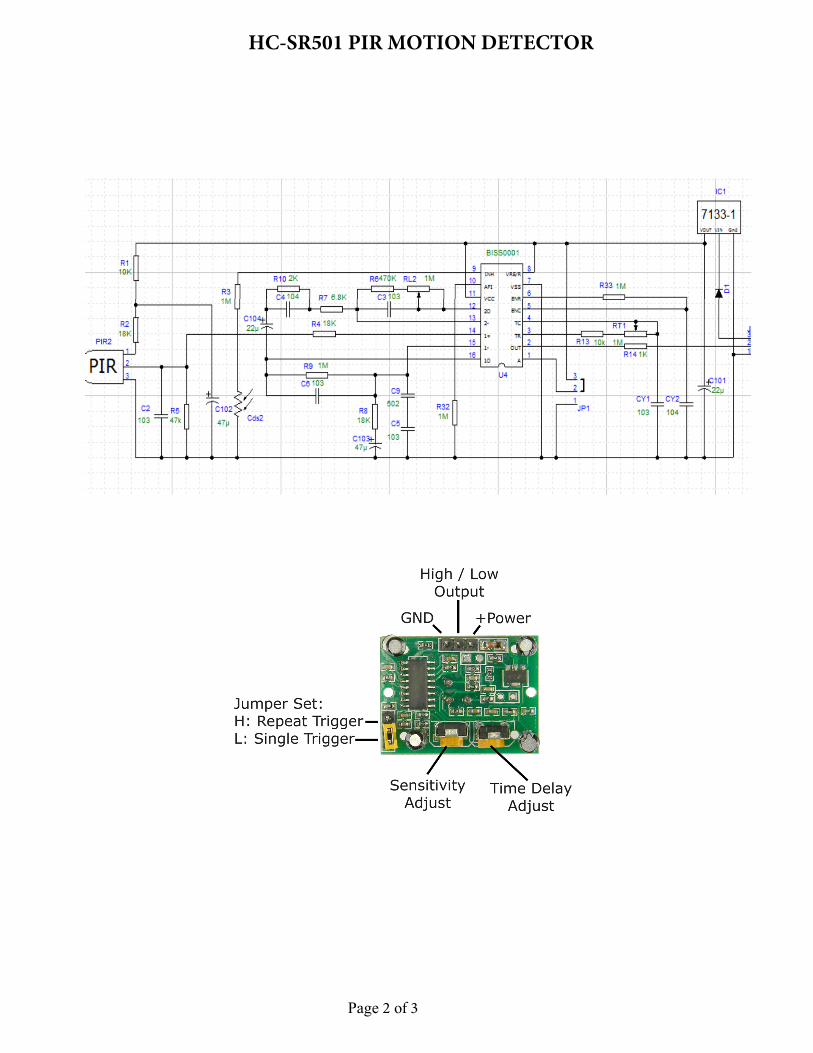
HC-SR501 PIR MOTION DETECTOR
Page 2 of 3
1 working voltage range :DC 4.5-20V
2 Quiescent Current :50uA
3 high output level 3.3 V / Low 0V
4. Trigger L trigger can not be repeated / H repeated trigger
5. circuit board dimensions :32 * 24 mm
6. maximum 110 ° angle sensor
7. 7 m maximum sensing distance
Product Type HC--SR501 Body Sensor Module
Operating Voltage RangeQuiescent Current <50uA
Level output High 3.3 V /Low 0V
Trigger L can not be repeated trigger/H can be repeated trigger(Default repeated trigger)
Delay time
Block time 2.5S(default)Can be made a range(0.xx to tens of seconds
Board Dimensions 32mm*24mm
Angle Sensor <110 ° cone angle
Operation Temp. -15-+70 degrees
Lens size sensor Diameter:23mm(Default)
Application scope
•Security products
•Body induction toys
•Body induction lamps
•Industrial automation control etc
Pyroelectric infrared switch is a passive infrared switch which consists of BISS0001 ,pyroelectric infrared sensors and a few external components. It can autom tically
open all kinds of equipments, inculding incandescent lamp, fluorescent lamp, intercom, automatic, electric fan, dryer and automatic washing machine, etc.
It is widely used in enterprises, hotels, stores, and corridor and other sensitive area for automatical lamplight, lighting and alarm system.
Instructions
Induction module needs a minute or so to initialize. During initializing time, it will output 0-3 times. One minute later it comes into standby.
Keep the surface of the lens from close lighting source and wind, which will introduce interference.
Induction module has double -probe whose window is rectangle. The two sub-probe (A and B) is located at the two ends of rectangle. When human body move from l ft
to right, or from right to left, Time for IR to reach to reach the two sub-probes differs.The lager the time diffference is, the more sensitive this module is. When hum n
body moves face-to probe, or up to down, or down to up, there is no time difference. So it does not work. So instal the module in the direction in which most hum n
activities behaves, to guarantee the induction of human by dual sub-probes. In order to increase the induction range, this module uses round lens which can induct IR
from all direction. However, induction from right or left is more sensitivity than from up or down.
.
5-20VDC
Page 3 of 3
5-300S( adjustable) Range (approximately .3Sec -5Min)
Light dependent resistors
Issued March 1997
NORP12 RS stock number 651-507NSL19-M51 RS stock number 596-141
Two cadmium sulphide (cdS) photoconductive cellswith spectral responses similar to that of the humaneye. The cell resistance falls with increasing light inten-sity. Applications include smoke detection, automaticlighting control, batch counting and burglar alarm sys-tems.
Guide to source illuminationsLight source Illumination (Lux)Moonlight __________________________________ 0.160W bulb at 1m ______________________________ 501W MES bulb at 0.1m ________________________ 100Fluorescent lighting __________________________ 500Bright sunlight ____________________________ 30,000
Light memory characteristicsLight dependent resistors have a particular property inthat they remember the lighting conditions in whichthey have been stored. This memory effect can beminimised by storing the LDRs in light prior to use.Light storage reduces equilibrium time to reachsteady resistance values.
NORP12 (RS stock no. 651-507)
Absolute maximum ratingsVoltage, ac or dc peak ______________________ 320VCurrent __________________________________ 75mAPower dissipation at 30°C _________________ 250mWOperating temperature range _______ -60°C to +75°C
Electrical characteristicsTA = 25°C. 2854°K tungsten light source
1. Dark to 110% RL2. To 10 3 RLRL = photocell resistance under given illumination.
Features Wide spectral response Low cost Wide ambient temperature range.
Circuit symbol
Parameter Conditions Min. Typ. Max. Units
Cell resistance 1000 lux - 400 - Ω10 lux - 9 - kΩ
Dark resistance - 1.0 - - MΩDark capacitance - - 3.5 - pF
Rise time 1 1000 lux - 2.8 - ms10 lux - 18 - ms
Fall time 2 1000 lux - 48 - ms10 lux - 120 - ms
Dimensions
232-3816Data pack F
Data Sheet
232-3816
2
Figure 1 Power dissipation derating Figure 3 Resistance as a function of illumination
Figure 2 Spectral response
*1Ftc=10.764 lumens

232-3816
3
Absolute maximum ratingsVoltage, ac or dc peak ______________________ 100VCurrent ___________________________________ 5mAPower dissipation at 25°C _________________ 50mW*Operating temperature range _________ -25°C +75°C
*Derate linearly from 50mW at 25°C to 0W at 75°C.
Electrical characteristics
Dimensions
Parameter Conditions Min. Typ. Max. Units
Cell resistance 10 lux 20 - 100 kΩ100 lux - 5 - kΩ
Dark resistance 10 lux after10 sec 20 - - MΩ
Spectral response - - 550 - nm
Rise time 10ftc - 45 - ms
Fall time 10ftc - 55 - ms
Figure 4 Resistance as a function illumination
Figure 5 Spectral response

232-3816
Typical application circuits
Figure 8 Automatic light circuit
Figure 7 Light interruption detector
Figure 6 Sensitive light operated relay Figure 9 Logarithmic law photographic light meter
Figure 10 Extremely sensitive light operated relay
Relay energised when light level increases above thelevel set by VR1
Typical value R1 = 100kΩR2 = 200kΩ preset to give two overlapping ranges.(Calibration should be made against an accurate meter.)
As Figure 6 relay energised when light level dropsbelow the level set by VR1 (Relay energised when light exceeds preset level.)
Incorporates a balancing bridge and op-amp. R1 andNORP12 may be interchanged for the reverse function.
Adjust turn-on point with VR1
The information provided in RS technical literature is believed to be accurate and reliable; however, RS Components assumes no responsibility for inaccuraciesor omissions, or for the use of this information, and all use of such information shall be entirely at the user’s own risk.No responsibility is assumed by RS Components for any infringements of patents or other rights of third parties which may result from its use.Specifications shown in RS Components technical literature are subject to change without notice.
RS Components, PO Box 99, Corby, Northants, NN17 9RS Telephone: 01536 201234An Electrocomponents Company © RS Components 1997
MQ-2 Semiconductor Sensor for Combustible Gas
Sensitive material of MQ-2 gas sensor is SnO2, which with lower conductivity in clean air. When the target combustible gas exist, The sensor’s conductivity is more higher along with the gas concentration rising. Please use simple electrocircuit, Convert change of conductivity to correspond output signal of gas concentration.
MQ-2 gas sensor has high sensitity to LPG, Propane and Hydrogen, also could be used to Methane and other combustible steam, it is with low cost and suitable for different application.
Character Configuration
*Good sensitivity to Combustible gas in wide range * High sensitivity to LPG, Propane and Hydrogen * Long life and low cost * Simple drive circuit
Application
* Domestic gas leakage detector * Industrial Combustible gas detector * Portable gas detector Technical Data Basic test loop
T
The above is basic test circuit of the sensor.
The sensor need to be put 2 voltage,
heater voltage(VH) and test voltage(VC).
VH used to supply certified working
temperature to the sensor, while VC used
to detect voltage (VRL) on load resistance
(RL)whom is in series with sensor. The
sensor has light polarity, Vc need DC
power. VC and VH could use same power
circuit with precondition to assure
performance of sensor. In order to make
the sensor with better performance,
suitable RL value is needed:
Power of Sensitivity body(Ps):
Ps=Vc2×Rs/(Rs+RL)2
Model No. MQ-2
Sensor Type Semiconductor
Standard Encapsulation Bakelite (Black Bakelite)
Detection Gas Combustible gas and smoke
Concentration 300-10000ppm
( Combustible gas)
Loop Voltage Vc ≤24V DC
Heater Voltage VH 5.0V±0.2V ACorDC Circuit
Load
Resistance RL Adjustable
Heater
Resistance RH 31Ω±3Ω(Room Tem.)
Heater
consumption PH ≤900mW
Sensing
Resistance Rs 2KΩ-20KΩ(in 2000ppm C3H8 )
Sensitivity S Rs(in air)/Rs(1000ppm
isobutane)≥5
Character
Slope α ≤0.6(R5000ppm/R3000ppm CH4)
Tem. Humidity 20±2;65%±5%RH
Standard test circuit Vc:5.0V±0.1V;
VH: 5.0V±0.1V Condition
Preheat time Over 48 hours
Vc
VH
GND
RL
VRL
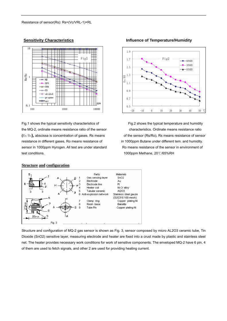
Resistance of sensor(Rs): Rs=(Vc/VRL-1)×RL
Sensitivity Characteristics Influence of Temperature/Humidity
Fig.1 shows the typical sensitivity characteristics of Fig.2 shows the typical temperature and humidity
the MQ-2, ordinate means resistance ratio of the sensor characteristics. Ordinate means resistance ratio
(Rs/Ro), abscissa is concentration of gases. Rs means of the sensor (Rs/Ro), Rs means resistance of sensor
resistance in different gases, Ro means resistance of in 1000ppm Butane under different tem. and humidity.
sensor in 1000ppm Hyrogen. All test are under standard Ro means resistance of the sensor in environment of
test conditions. 1000ppm Methane, 20/65%RH
Structure and configuration
Structure and configuration of MQ-2 gas sensor is shown as Fig. 3, sensor composed by micro AL2O3 ceramic tube, Tin
Dioxide (SnO2) sensitive layer, measuring electrode and heater are fixed into a crust made by plastic and stainless steel
net. The heater provides necessary work conditions for work of sensitive components. The enveloped MQ-2 have 6 pin, 4
of them are used to fetch signals, and other 2 are used for providing heating current.
Fig1
0.5
0.7
0.9
1.1
1.3
1.5
1.7
1.9
-20 -10 0 10 20 30 40 50
Rs/
R0
60%RH
30%RH
85%RH
Fig2
Notification 1 Following conditions must be prohibited 1.1 Exposed to organic silicon steam
Organic silicon steam cause sensors invalid, sensors must be avoid exposing to silicon bond, fixature, silicon latex, putty or plastic contain silicon environment 1.2 High Corrosive gas
If the sensors exposed to high concentration corrosive gas (such as H2Sz, SOX,Cl2,HCl etc), it will not only result in corrosion of sensors structure, also it cause sincere sensitivity attenuation. 1.3 Alkali, Alkali metals salt, halogen pollution
The sensors performance will be changed badly if sensors be sprayed polluted by alkali metals salt especially brine, or be exposed to halogen such as fluorin. 1.4 Touch water
Sensitivity of the sensors will be reduced when spattered or dipped in water. 1.5 Freezing
Do avoid icing on sensor’surface, otherwise sensor would lose sensitivity. 1.6 Applied voltage higher
Applied voltage on sensor should not be higher than stipulated value, otherwise it cause down-line or heater damaged, and bring on sensors’ sensitivity characteristic changed badly. 1.7 Voltage on wrong pins
For 6 pins sensor, if apply voltage on 1、3 pins or 4、6 pins, it will make lead broken, and without signal when apply on 2、4 pins 2 Following conditions must be avoided 2.1 Water Condensation
Indoor conditions, slight water condensation will effect sensors performance lightly. However, if water condensation on sensors surface and keep a certain period, sensor’ sensitivity will be decreased.
2.2 Used in high gas concentration
No matter the sensor is electrified or not, if long time placed in high gas concentration, if will affect sensors characteristic.
2.3 Long time storage
The sensors resistance produce reversible drift if it’s stored for long time without electrify, this drift is related with storage conditions. Sensors should be stored in airproof without silicon gel bag with clean air. For the sensors with long time storage but no electrify, they need long aging time for stbility before using.
2.4 Long time exposed to adverse environment
No matter the sensors electrified or not, if exposed to adverse environment for long time, such as high humidity, high temperature, or high pollution etc, it will effect the sensors performance badly.
2.5 Vibration
Continual vibration will result in sensors down-lead response then repture. In transportation or assembling line, pneumatic screwdriver/ultrasonic welding machine can lead this vibration.
2.6 Concussion
If sensors meet strong concussion, it may lead its lead wire disconnected.
2.7 Usage For sensor, handmade welding is optimal way. If use wave crest welding should meet the following
conditions: 2.7.1 Soldering flux: Rosin soldering flux contains least chlorine 2.7.2 Speed: 1-2 Meter/ Minute 2.7.3 Warm-up temperature:100±20 2.7.4 Welding temperature:250±10 2.7.5 1 time pass wave crest welding machine
If disobey the above using terms, sensors sensitivity will be reduced.

YYYYour specialist in innovating humidity & temperature sensors
Thomas Liu (Sales Manager)
Email: [email protected]
- 1 -
StandardStandardStandardStandardAM2302AM2302AM2302AM2302/DHT22/DHT22/DHT22/DHT22 AM2302AM2302AM2302AM2302/DHT22/DHT22/DHT22/DHT22 withwithwithwith bigbigbigbig casecasecasecase andandandand wireswireswireswires
DigitalDigitalDigitalDigital relativerelativerelativerelative humidityhumidityhumidityhumidity &&&& ttttemperatureemperatureemperatureemperature sensorsensorsensorsensorAM2302AM2302AM2302AM2302/DHT22/DHT22/DHT22/DHT22
1.1.1.1. FeatureFeatureFeatureFeature &&&&ApplicationApplicationApplicationApplication::::*High precision*Capacitive type*Full range temperature compensated*Relative humidity and temperature measurement*Calibrated digital signal
*Outstanding long-term stability*Extra components not needed*Long transmission distance, up to 100 meters*Low power consumption*4 pins packaged and fully interchangeable
2.2.2.2. Description:Description:Description:Description:AM2302 output calibrated digital signal. It applys exclusive digital-signal-collecting-technique and humiditysensing technology, assuring its reliability and stability. Its sensing elements is connected with 8-bit single-chipcomputer.Every sensor of this model is temperature compensated and calibrated in accurate calibration chamber and thecalibration-coefficient is saved in type of programme in OTP memory, when the sensor is detecting, it will citecoefficient from memory.Small size & low consumption & long transmission distance(100m) enable AM2302 to be suited in all kinds ofharsh application occasions. Single-row packaged with four pins, making the connection very convenient.
3.3.3.3. TechnicalTechnicalTechnicalTechnical Specification:Specification:Specification:Specification:Model AM2302Power supply 3.3-5.5V DCOutput signal digital signal via 1-wire busSensing element Polymer humidity capacitorOperating range humidity 0-100%RH; temperature -40~80CelsiusAccuracy humidityhumidityhumidityhumidity +-2%RH+-2%RH+-2%RH+-2%RH(Max +-5%RH); temperature +-0.5CelsiusResolution or sensitivity humidity 0.1%RH; temperature 0.1CelsiusRepeatability humidity +-1%RH; temperature +-0.2CelsiusHumidity hysteresis +-0.3%RHLong-term Stability +-0.5%RH/yearInterchangeability fully interchangeable

YYYYour specialist in innovating humidity & temperature sensors
Thomas Liu (Sales Manager)
Email: [email protected]
- 2 -
4.4.4.4. Dimensions:Dimensions:Dimensions:Dimensions: (unit----mm)(unit----mm)(unit----mm)(unit----mm)
StandardStandardStandardStandardAM2302AM2302AM2302AM2302’’’’ssss dimensionsdimensionsdimensionsdimensions asasasas aboveaboveaboveaboveBigBigBigBig casecasecasecase’’’’ssss dimensionsdimensionsdimensionsdimensions asasasas aboveaboveaboveaboveRedRedRedRed wire--powerwire--powerwire--powerwire--power supply,supply,supply,supply, BlackBlackBlackBlack wire--GNDwire--GNDwire--GNDwire--GNDYellowYellowYellowYellow wire--Datawire--Datawire--Datawire--Data outputoutputoutputoutput
5.5.5.5. ElectricalElectricalElectricalElectrical connectionconnectionconnectionconnection diagram:diagram:diagram:diagram:
6.6.6.6. OperatingOperatingOperatingOperating specifications:specifications:specifications:specifications:(1)(1)(1)(1) PowerPowerPowerPower andandandand PinsPinsPinsPinsPower's voltage should be 3.3-5.5V DC. When power is supplied to sensor, don't send any instruction to the sensorwithin one second to pass unstable status. One capacitor valued 100nF can be added between VDD and GND forwave filtering.(2)(2)(2)(2) CommunicationCommunicationCommunicationCommunication andandandand signalsignalsignalsignal1-wire bus is used for communication between MCU and AM2302. ( Our 1-wire bus is specially designed, it'sdifferent from Maxim/Dallas 1-wire bus, so it's incompatible with Dallas 1-wire bus.)IllustrationIllustrationIllustrationIllustration ofofofof ourourourour 1-wire1-wire1-wire1-wire bus:bus:bus:bus:

YYYYour specialist in innovating humidity & temperature sensors
Thomas Liu (Sales Manager)
Email: [email protected]
- 3 -
DATA=DATA=DATA=DATA=16161616 bitsbitsbitsbits RHRHRHRH data+data+data+data+16161616 bitsbitsbitsbits TemperatureTemperatureTemperatureTemperature data+8data+8data+8data+8 bitbitbitbitssss check-sumcheck-sumcheck-sumcheck-sumExample: MCU has received 40 bits data from AM2302 as
0000000000000000 0010001000100010 1000100010001000 1100110011001100 0000000000000000 0001000100010001 0101010101010101 1111111111111111 1110111011101110 111011101110111016 bits RH data 16 bits T data check sum
Here we convert 16 bits RH data from binary system to decimal system,0000 0010 1000 1100 → 652Binary system Decimal system
RH=652/10=65.2%RHRH=652/10=65.2%RHRH=652/10=65.2%RHRH=652/10=65.2%RHHere we convert 16 bits T data from binary system to decimal system,0000 0001 0101 1111 → 351Binary system Decimal system
T=351/10=35.1T=351/10=35.1T=351/10=35.1T=351/10=35.1When highest bit of temperature is 1, it means the temperature is below 0 degree Celsius.Example: 1111000 0000 0110 0101, T= minus 10.1
16 bits T dataSum=0000 0010+1000 1100+0000 0001+0101 1111=1110 1110Check-sumCheck-sumCheck-sumCheck-sum=the last 8 bits of Sum=1110 1110
When MCU send start signal, AM2302 change from standby-status to running-status. When MCU finishs sendingthe start signal, AM2302 will send response signal of 40-bit data that reflect the relative humidity and temperatureto MCU. Without start signal from MCU, AM2302 will not give response signal to MCU. One start signal for oneresponse data from AM2302 that reflect the relative humidity and temperature. AM2302 will change to standbystatus when data collecting finished if it don't receive start signal from MCU again.
See below figure for overall communication process, thethethethe intervalintervalintervalinterval ofofofof wholewholewholewhole processprocessprocessprocess mustmustmustmust beyondbeyondbeyondbeyond 2222 seconds.seconds.seconds.seconds.
------------------------------------------------------------------------------------------------------------------------------------1) Step 1: MCU send out start signal to AM2302 and AM2302 send response signal to MCU
YYYYour specialist in innovating humidity & temperature sensors
Thomas Liu (Sales Manager)
Email: [email protected]
- 4 -
Data-bus's free status is high voltage level. When communication between MCU and AM2302 begins, MCU willpull low data-bus and this process must beyond at least 1~10ms to ensure AM2302 could detect MCU's signal, thenMCU will pulls up and wait 20-40us for AM2302's response.When AM2302 detect the start signal, AM2302 will pull low the bus 80us as response signal, then AM2302 pulls
up 80us for preparation to send data. See below figure:
------------------------------------------------------------------------------------------------------------------------------------2). Step 2: AM2302 send data to MCUWhen AM2302 is sending data to MCU, every bit's transmission begin with low-voltage-level that last 50us, the
following high-voltage-level signal's length decide the bit is "1" or "0". See below figures:
Attention:Attention:Attention:Attention:If signal from AM2302 is always high-voltage-level, it means AM2302 is not working properly, please check
the electrical connection status.

YYYYour specialist in innovating humidity & temperature sensors
Thomas Liu (Sales Manager)
Email: [email protected]
- 5 -
7.7.7.7. ElectricalElectricalElectricalElectrical Characteristics:Characteristics:Characteristics:Characteristics:Items Condition Min Typical Max UnitPower supply DC 3.3 5 6 VCurrent supply Measuring 1 1.5 mA
Stand-by 40 Null 50 uACollectingperiod
Second 2 Second
8.8.8.8. AttentionsAttentionsAttentionsAttentions ofofofof application:application:application:application:(1) Operating and storage conditions
We don't recommend the applying RH-range beyond the range stated in this specification. The AM2302 sensorcan recover after working in abnormal operating condition to calibrated status, but will accelerate sensors' aging.(2) Attentions to chemical materials
Vapor from chemical materials may interfere AM2302's sensitive-elements and debase AM2302's sensitivity.(3) Disposal when (1) & (2) happens
Step one: Keep the AM2302 sensor at condition of Temperature 50~60Celsius, humidity <10%RH for 2 hours;Step two: After step one, keep the AM2302 sensor at condition of Temperature 20~30Celsius, humidity
>70%RH for 5 hours.(4) Attention to temperature's affection
Relative humidity strongly depend on temperature, that is why we use temperature compensation technology toensure accurate measurement of RH. But it's still be much better to keep the sensor at same temperature whensensing.
AM2302 should be mounted at the place as far as possible from parts that may cause change to temperature.(5) Attentions to light
Long time exposure to strong light and ultraviolet may debase AM2302's performance.(6) Attentions to connection wires
The connection wires' quality will effect communication's quality and distance, high quality shielding-wire isrecommended.(7) Other attentions
* Welding temperature should be bellow 260Celsius.* Avoid using the sensor under dew condition.* Don't use this product in safety or emergency stop devices or any other occasion that failure of AM2302 may
cause personal injury.

AC1010 • 10 Amp Current Transformer
snoitacificepSlacirtcelE
tnerruCyramirP .xamA06,.monA01
oitaRsnruT lanimon1:0001
daolmho001rofA01taoitaRpmAreptloV A/V001.0
daolmho001rofA1taoitaRpmAreptloV A/V790.0
C°02taecnatsiseRCD smho8.14
)top-iH(egatloVgnidnatshtiWcirtceleiD smrVK4
snoitacificepSlacinahceM snoitacificepSlatnemnorivnE
esaC etanobracyloP erutarepmeTegarotS C°031+ot°55-
tnaluspacnE yxopE ecnatsiseRnoitalusnI .nimsmhogem001
ytilibimmalF OV-49LUotsmrofnoC
slanimreT mm08.0ØsniP
gnikraM
)Y/W(edoCetaDniptratstatoD,0101
thgieWetamixorppA smarg3.61
ecnareloT mm2.0±
0.01
0.1
1
10
100
Ou
tpu
t V
olt
age
in V
olt
s
1 10 100 Input Current in Amps
Output Volts vs Input Current For various ohmic loads
50100200
500
1K
2K5K10K
Infinity
0.1
1
10
100
Sec
RM
S E
xcit
ing
Vo
ltag
e in
Vo
lts
0.01 0.1 1 10 100 1000 Sec RMS Exciting current in mA
Typical Excitation Curve (AC1005~AC1020)
10
100
1000
10000 L
oad
Res
ista
nce
RL
in o
hm
s
0 100 200 300 400 500 600 Percent ratio error in %
%RE vs RL at Rated primary current (AC1010)
Notes:1) Unless requested, the terminating resistor and the one-turn primary are not supplied2) Pin 3: Normally for mechanical support only but will be
used on center tapped designs
Low Cost 50/60Hz Current TransformersApplications• Sensing Overload Current• Ground fault detection• Metering• Analog to Digital Circuits
Electrical Specifications @ 20°C ambient
I - Turn Primary 1/8W
100 ohms
2
1
1.0V10A 10mA RL
Amveco Magnetics, Inc., 11222 Richmond Avenue, Suite 120, Houston, TX 77082 - (800) 527-7042 http://www.amveco.com CT’s\AC1010 05-00
Dimensions
7.62
15.24
11.12
5±1mm
INDIAW/Y
AC1010
Ø9.50
2 3 1
23.8
0
23.80
1.75
Ø 0.813

1
2. APPLICATIONS • Domestic appliance, office machine, audio, equipment, automobile, etc.
( Remote control TV receiver, monitor display, audio equipment high rushing current use application.) 3. ORDERING INFORMATION
SRD XX VDC S L C Model of relay Nominal coil voltage Structure Coil sensitivity Contact form
A:1 form A S:Sealed type L:0.36W B:1 form B SRD 03 05 06 09 12 24 48VDC
F:Flux free type D:0.45W C:1 form C 4. RATING
CCC FILE NUMBER:CH0052885-2000 7A/240VDC CCC FILE NUMBER:CH0036746-99 10A/250VDC UL /CUL FILE NUMBER: E167996 10A/125VAC 28VDC TUV FILE NUMBER: R9933789 10A/240VAC 28VDC
5. DIMENSION(unit:mm) DRILLING(unit:mm) WIRING DIAGRAM
RELAY ISO9002
1. MAIN FEATURES • Switching capacity available by 10A in spite of small size design for highdensity P.C. board mounting technique.
• UL,CUL,TUV recognized.
• Selection of plastic material for high temperature and
better chemical solution performance.
• Sealed types available.
• Simple relay magnetic circuit to meet low cost of
mass production.

2
6. COIL DATA CHART (AT20C)
Coil Sensitivity
Coil Voltage Code
Nominal Voltage (VDC)
Nominal Current
(mA)
Coil Resistance (Ω) ±10%
Power Consumption
(W)
Pull-In Voltage (VDC)
Drop-Out Voltage (VDC)
Max-Allowable Voltage (VDC)
03 03 120 25 05 05 71.4 70 06 06 60 100 09 09 40 225 12 12 30 400 24 24 15 1600
SRD (High Sensitivity)
48 48 7.5 6400
abt. 0.36W 75%Max. 10% Min. 120%
03 03 150 20 05 05 89.3 55 06 06 75 80 09 09 50 180 12 12 37.5 320 24 24 18.7 1280
abt. 0.45W SRD (Standard)
48 48 10 4500 abt. 0.51W
75% Max. 10% Min. 110%
7. CONTACT RATING SRD Type
Item FORM C FORM A
Contact Capacity Resistive Load (cosΦ=1)
7A 28VDC 10A 125VAC 7A 240VAC
10A 28VDC 10A 240VAC
Inductive Load (cosΦ=0.4 L/R=7msec)
3A 120VAC 3A 28VDC
5A 120VAC 5A 28VDC
Max. Allowable Voltage 250VAC/110VDC 250VAC/110VDC Max. Allowable Power Force 800VAC/240W 1200VA/300W Contact Material AgCdO AgCdO 8. PERFORMANCE (at initial value) Type Item SRD
Contact Resistance 100mΩ Max. Operation Time 10msec Max. Release Time 5msec Max. Dielectric Strength Between coil & contact Between contacts
1500VAC 50/60HZ (1 minute) 1000VAC 50/60HZ (1 minute)
Insulation Resistance 100 MΩ Min. (500VDC) Max. ON/OFF Switching Mechanically Electrically
300 operation/min 30 operation/min
Ambient Temperature -25°C to +70°C Operating Humidity 45 to 85% RH Vibration Endurance Error Operation
10 to 55Hz Double Amplitude 1.5mm 10 to 55Hz Double Amplitude 1.5mm
Shock Endurance Error Operation
100G Min. 10G Min.
Life Expectancy Mechanically Electrically
107 operations. Min. (no load) 105 operations. Min. (at rated coil voltage)
Weight abt. 10grs.
9.REFERENCE DATA Coil Temperature Rise
0.1 0.3 0.5 0.70.0 0.2 0.4 0.6 0.8
5
15
25
35
45
0
10
20
30
40
50
Coil Power (W)
Operation Time
0.1 0.3 0.5 0.70.0 0.2 0.4 0.6 0.8
2
6
10
0
4
8
12
Operation time
Release time
Coil Power (W)
Life Expectancy AC120V/DC24V cosΦ=1
2 6 100 4 8 12
2
3
5
2
3
5
1
10
100
Current of Load (A) Life Expectancy
1 3 5 70 2 4 6 8
2
3
5
2
3
5
1
10
100
AC : 120V TV-5
Current of Load (A)

SONGLE RELAY
NingBo Songle Relay Co.,LTD. SMIH
1、SPST through DPDT contact arrangements. 2、5KV dielectric,coil to contact. 3、Standard type and plastic sealed type available. 4、High sensitivity type for low coil consumption is available.
5、For electrical device in control system,e.g heating controllers. servo motors,solenoid valves,lifting magnets etc.
!COLL SPECIFICATION [at25degrees ]
Coil
Sensitivity
Nominal
Voltage
(VDC)
Nominal
Current
(mA)
Coil
Resistance
(ohm+10%)
Power
Consumption
(w)
Pull-in
Voltage
(VDC)
Drop-out
Voltage
(VDC)
Max-Allow
Able
Voltage(VDC)
3 120 17
5 71 47
6 60 68
9 40 155
12 30 270
18 20 600
High
Senstivity
24 15 1100
abt 0.54w
75%Max 5%MIn 130%
3 150 12.5
5 89 36
6 75 50
9 50 115
12 37.5 200
18 25 450
Standard
Sensitivity
24 18.7 820
Abt 0.72w 75%Max 5%MIn 130%
!CONTACT RATING
Contact Form SPDT
Contact Capacity
Resistave Load(cos"=1)
Inductiv Load(cos"=0.4)
L/R=7msec
16A 240VAC
16A 125VAC
5A 120VAC
5A 24VDC
Contact Material AgCdo
!NOTE: Contact rating 1:16A/240VAC
-
TUV File No.R9933789

SONGLE RELAY
!PERFORMANCE[at initial value]
Contact Rsistance 100 mhom Max
Operate time 15 msec. Max
Release time 10 msec. Max
Dielectric Strength
Between coil & contact
Between contacts
5000VAC 50/60Hz(1min)
1000VAC 50/60Hz(1min)
Insulaton Resistance 100M ohm Min(500VDC)
Max. ON/OFF Switching
Mechanically
Electrically
300 ops/min
30 ops/min
Operating Ambient temp -30 to 70degrees
Operating Humidity 45 to 85% RH
Vibration
Damage Limits
Operating Extremes
10 to 55Hz Double Amp.1.5mm
10 to 55Hz Double Amp.1.5.mm
Shock
Damage Limits
Operating Extremes
100G
10G
Life Expectancy
Mechanically
Electrically
1,000,000 ops. Min(no load)
100,000 ops. Min(at rated coil volt.) Weight abt.13grs
!ORDER INFORMATION
SMIH 12VDC S L C
Model of relay Nminal coil voltage Structure Coil sensitivity Contact form
S:Sealed type L:0.54w A: 1 form A
B: 1 form B SMIH 03,05,06,09,12,24VDC F:Flux free type D:0.72w
C: 1 form C

SONGLE RELAY
!OUT LINE DIMENSIONS [UNIT:mm] PCB LAYOUT[UNIT:mm] WIRING DIAGRAM
15 5 5
7.6
29
20.6
12.6
AC1020 • 20 Amp Current Transformer
snoitacificepSlacirtcelE
tnerruCyramirP .xamA06,.monA02
oitaRsnruT lanimon1:0001
daolmho001rofA02taoitaRpmAreptloV A/V001.0
daolmho001rofA2taoitaRpmAreptloV A/V790.0
C°02taecnatsiseRCD smho8.14
)top-iH(egatloVgnidnatshtiWcirtceleiD smrVK4
snoitacificepSlacinahceM snoitacificepSlatnemnorivnE
esaC etanobracyloP erutarepmeTegarotS C°031+ot°55-
tnaluspacnE yxopE ecnatsiseRnoitalusnI .nimsmhogem001
ytilibimmalF OV-49LUotsmrofnoC
slanimreT mm08.0ØsniP
gnikraMAMELAT
)Y/W(edoCetaDniptratstatoD,0201CA
thgieWetamixorppA smarg3.61
ecnareloT mm2.0±
0.01
0.1
1
10
100
Ou
tpu
t V
olt
age
in V
olt
s
1 10 100 Input Current in Amps
Output Volts vs Input CurrentFor various ohmic loads
50100200
500
1K
2K5K10K
Infinity
0.1
1
10
100
Sec
RM
S E
xcit
ing
Vo
ltag
e in
Vo
lts
0.01 0.1 1 10 100 1000 Sec RMS Exciting current in mA
Typical Excitation Curve(AC1005~AC1020)
10
100
1000
10000 L
oad
Res
ista
nce
RL
in o
hm
s
0 200 400 600 800 1000 Percent ratio error in %
%RE vs RL at Rated primary current(AC1020)
Notes:1) Unless requested, the terminating resistor and the one-turn
primary are not supplied2) Pin 3: Normally for mechanical support only but will be
used on center tapped designs
I - TurnPrimary 1/8W
100 ohms
2
1
2.0V20A 20mA RL
Low Cost 50/60Hz Current TransformersApplications• Sensing Overload Current• Ground fault detection• Metering• Analog to Digital Circuits
Electrical Specifications @ 20°C ambient
Dimensions
11.12
5±1mm
TALEMA INDIAW/Y
AC1020
Ø9.50
2 3 1
23.8
0
23.80
Ø 0.813
7.62
15.24 1.75
• Competitive pricing due to high volumeproduction
• Manufactured in an ISO-9001:2000,TS-16949:2002 and ISO-14001:2004certified Talema facility
• Fully RoHS compliant
Germany: Int.+49 89 - 841 00-0 • Ireland: Int.+35 374 - 954 8666 • Czech Rep: Int.+420 377 - 338 351 • India: Int.+91 427 - 244 1325 http://www.talema-nuvotem.com (06-06)CT’s\AC1020

22±0.5
11.5±0.5
31±
0.5
Model
Input current
Output type
Model
Input current
Output type
SCT-013-000
0-100A
0-50mA
SCT-013-025
0-25A
0-1V
SCT-013-005
0-5A
0-1V
SCT-013-030
0-30A
0-1V
2.5mm Audio Plug
3.5mm Audio Plug
X
11.9
15.0
Y
2.5
3.5 standard
SCT-013-010
0-10A
0-1V
SCT-013-050
0-50A
0-1V
SCT-013-015
0-15A
0-1V
SCT-013-060
0-60A
0-1V
SCT-013-020
0-20A
0-1V
SCT-013-000V
0-100A
0-1V
※ Output type: voltage output type built-in sampling resistor, current output type built-in protective diode.
Front View Side View Schematic diagramThree-core plug size
Optional
Characteristics:Openning size: 13mm*13mm, Non-linerity±3%(10%—120% of rated input current) 1m leading wire, standard Φ3.5 three core plug output. Current output type and voltage output type (voltage output type built-in sampling resistor)Purpose:Used for current measurement, monitor and protection for AC motor, lighting equipment, air compressor etcCore material: ferriteMechanical strength: the number of switching is not less than 1000 times(test at 25)Safty index:Dielectric strength(between shell and output)1000V AC/1min Fire resistance property: In accordance with UL94-Vo Work temperature: -25~+70Outline size diagram: (in mm)
Model: SCT-013 Rated input current:5A/100A
34±0.5
23.5±0.5
13±0.510
±0.5
32±0.5
Table of technical parameter:
Split core current transformer
Swiching angle180°
1m
35.3
K Output
X
ΦY
VacancyL Output
Diagram for standard three-core plug
R
RoHS
TVS
Ip
Iout
Current output type
Voltage output type
Ip
TVS
K
L
K
L
Tel: 86-13933609279 Fax: 86-7929499-804 skype:macymeng1Web (China):www.yhdc.com Web (Latvia):www.yhdc.lv