SKDAV GOVT.POLYTECHNIC ROURKELA LECTURE NOTES
71
SKDAV GOVT.POLYTECHNIC ROURKELA DEPARTMENT OF ELECTRICAL ENGINEERING LECTURE NOTES Year & Semester:3rd Year, 5th Semester (ELECTRICAL) Subject Code/Name: TH-5, POWER ELECTRONICS AND PLC NIRUPAMA BARIK GUEST LECTURER(ELECTRICAL)
-
Upload
khangminh22 -
Category
Documents
-
view
1 -
download
0
Transcript of SKDAV GOVT.POLYTECHNIC ROURKELA LECTURE NOTES

SKDAV
GOVT.POLYTECHNIC
ROURKELA
DEPARTMENT OF ELECTRICAL
ENGINEERING
LECTURE NOTES
Year & Semester:3rd Year, 5th Semester (ELECTRICAL)
Subject Code/Name: TH-5, POWER ELECTRONICS AND
PLC
NIRUPAMA BARIK
GUEST LECTURER(ELECTRICAL)

DETAILED CONTENT:
1. UNDERSTAND THE CONSTRUCTION AND WORKING OF POWER ELECTRONIC
DEVICES
1.1 Construction, Operation, V-I characteristics & application of power diode, SCR,
DIAC,TRIAC, Power MOSFET,GTO &IGBT
1.2 Two transistor analogy of SCR.
1.3 Gate characteristics of SCR.
1.4 Switching characteristic of SCR during turn on and turn off.
1.5 Turn on methods of SCR.
1.6 Turn off methods of SCR (Line commutation and Forced commutation)
1.6.1 Load Commutation
1.6.2 Resonant pulse commutation
1.7 Voltage and Current ratings of SCR.
1.8 Protection of SCR
1.8.1 Over voltage protection
1.8.2 Over current protection
1.8.3 Gate protection
1.9 Firing Circuits
1.9.1 General layout diagram of firing circuit
1.9.2 R firing circuits
1.9.3 R-C firing circuit
1.9.4 UJT pulse trigger circuit
1.9.5 Synchronous triggering (Ramp Triggering )
1.10 Design of Snubber Circuits
2. UNDERSTAND THE WORKING OF CONVERTERS, AC REGULATORS AND
CHOPPERS.
2.1 Controlled rectifiers Techniques(Phase Angle, Extinction Angle control), Single
quadrant semi converter, two quadrant full converter and dual Converter
2.2 Working of single-phase half wave controlled converter with Resistive and R-L
loads.
2.3 Understand need of freewheeling diode.
2.4 Working of single phase fully controlled converter with resistive and R- L loads.
2.5 Working of three-phase half wave controlled converter with Resistive load
2.6 Working of three phase fully controlled converter with resistive load.
2.7 Working of single phase AC regulator.
2.8 Working principle of step up & step down chopper.
2.9 Control modes of chopper
2.10 Operation of chopper in all four quadrants.
3. UNDERSTAND THE INVERTERS AND CYCLO-CONVERTERS
3.1 Classify inverters.
3.2 Explain the working of series inverter.
3.3 Explain the working of parallel inverter
3.4 Explain the working of single-phase bridge inverter.

3.5 Explain the basic principle of Cyclo-converter.
3.6 Explain the working of single-phase step up & step down Cyclo-converter.
3.7 Applications of Cyclo-converter.
4. UNDERSTAND APPLICATIONS OF POWER ELECTRONIC CIRCUITS
4.1 List applications of power electronic circuits.
4.2 List the factors affecting the speed of DC Motors.
4.3 Speed control for DC Shunt motor using converter.
4.4 Speed control for DC Shunt motor using chopper.
4.5 List the factors affecting speed of the AC Motors.
4.6 Speed control of Induction Motor by using AC voltage regulator.
4.7 Speed control of induction motor by using converters and inverters (V/F control).
4.8 Working of UPS with block diagram.
4.9 Battery charger circuit using SCR with the help of a diagram.
4.10 Basic Switched mode power supply (SMPS) - explain its working & applications
5. PLC AND ITS APPLICATIONS
5.1 Introduction of Programmable Logic Controller(PLC)
5.2 Advantages of PLC
5.3 Different parts of PLC by drawing the Block diagram and purpose of each part of
PLC.
5.4 Applications of PLC
5.5 Ladder diagram
5.6 Description of contacts and coils in the following states
i)Normally open ii) Normally closed iii) Energized output iv)latched Output v)
branching
5.7 Ladder diagrams for i) AND gate ii) OR gate and iii) NOT gate.
5.8 Ladder diagrams for combination circuits using NAND,NOR, AND, OR and NOT
5.9 Timers-i)T ON ii) T OFF and iii)Retentive timer5.10 Counters-CTU, CTD
5.11 Ladder diagrams using Timers and counters
5.12 PLC Instruction set
5.13 Ladder diagrams for following
(i) DOL starter and STAR-DELTA starter (ii) Stair case lighting (iii) Traffic light
Control (iv) Temperature Controller
5.14 Special control systems- Basics DCS & SCADA systems
5.15 Computer Control–Data Acquisition, Direct Digital Control System (Basics only)
Learning Resources:
Sl.No Title of the Book Name of Authors Name of the Publisher
1. Power Electronics Dr. P. S. Bhimbhra Khanna Publisher
2.
Modern Power Electronics and AC Drives
B.K.Bose PHI Publisher
3. Power Electronics M. D. Singh and K.B Khanchandani
TMH
4. Power Electronics M H Rashid PHI Publisher 5. Power Electronics P C Sen TMH 6. Power Electronics N Mohan Willey (India)

COURSE OUTCOME:
After the completion of the course the students will be able to
CO1- Select an appropriate power semiconductor device and design control circuit and the
power circuit for a given power converter for the required application.
CO2- Determine the power circuit configuration needed to fulfill the required power conversion
with applicable constraints.
CO3- Determine the drive circuit requirements in terms of electrical isolation and the
requirement of drives and ease of control.
CO4- Specify the appropriate power circuit configuration amongst the phase-controlled rectifiers
& choppers for the speed control of DC motor drives. Implement speed control schemes for AC
motors by using different control.
CO5- Design the ladder diagrams for various combination circuits, use the PLC instructions for
controlling various applications and also control the industrial applications and also control the
industrial application systems by DCS, computer control techniques

MODULE-1
1. UNDERSTAND THE CONSTRUCTION AND WORKING OF POWER
ELECTRONIC DEVICES
1.1 CONSTRUCTION, OPERATION, V-I CHARACTERISTICS & APPLICATION OF
POWER DIODE, SCR, DIAC, TRIAC, POWER MOSFET, GTO & IGBT
POWER DIODE
Basic structure: Power diode consists of three layers. Top layer is a heavily doped P+ layer. Middle layer is lightly doped n– layer and the last layer is a heavily doped n+ layer. The heavily doped p+ layer act as an anode. The thickness of this layer is around 10 μm and doping level is 1019 cm-3. Last layer of the heavily doped n+ act as a cathode. The thickness of this layer is around 250 to 300 μm and doping level is 1019 cm-3. Middle layer of lightly doped n– is known as a drift layer. The thickness of the drift layer depends on the required breakdown voltage. The breakdown voltage increases with an increase in the width of the drift layer. Resistivity of this layer is high because of the low level of doping. If the width of the drift layer increased, then the on-state voltage drop increase therefore power loss is more. The doping level of the drift layer is 1014 cm-3. The junction is form between the anode layer (p+) and drift layer (n–). The cross-section area of the diode depends on the magnitude of current to be handled. Higher the current to handle, more the area required.
Operating Principle of Power diode: The operating principle of power diode is same as the conventional PN junction diode. A diode conducts when the anode voltage is higher than the cathode voltage. The forward voltage drop across the diode is very low around 0.5V to 1.2V. In this region, the diode works as a forward characteristic.

If the cathode voltage is higher than the anode voltage, then the diode works as blocking mode. In this mode, diode works according to the reverse characteristic. V-I characteristic of Power Diode:

Application of Power Diode in Power Electronics: 1. High voltage rectifier 2. As freewheeling diode 3. As feedback diode

POWER BJT
Construction of Power BJT: The power BJT has three terminals Collector (C), Emitter (E) and Base (B). It has a vertically oriented four-layers structure. The vertical structure uses to increase the cross-sectional area. There are two types of BJT; n-p-n transistor and p-n-p transistor. Out of these two types, the n-p-n transistors widely use compare to the p-n-p transistor. It has four layers. The first layer is a heavily doped emitter layer (n+). The second layer is moderately doped the base layer (p). The third region is lightly doped collector drift region (n-). The last layer is a highly doped collector region (n+). The drift layer (n-) increase the voltage blocking capacity of the transistor due to the low doping level. The width of this layer decides the breakdown voltage. The disadvantage of this layer is that the increase on state voltage drops and increase on state device resistance, which increases power loss. The power handling capacity of the power transistor is very large. So, they have to dissipate power in the form of heat. Sometimes, heatsink uses to increase effective area and therefore increase power dissipation capacity. the heatsink made from metal.


POWER MOSFET A power MOSFET has three terminal devices. Arrow indicates the direction of current flow. MOSFET is a voltage controlled device. The operation of MOSFET depends on flow of majority carriers only.
The Power MOSFET is a type of MOSFET. The operating principle of power MOSFET is similar to the general MOSFET. The power MOSFETS are very special to handle the high level of powers. It shows the high switching speed and by comparing with the normal MOSFET, the power MOSFET will work better. The power MOSFETs is widely used in the n-channel enhancement mode, p-channel enhancement mode, and in the nature of n-channel depletion mode. Here we have explained about the N-channel power MOSFET. The design of power MOSFET was made by using the CMOS technology and also used for development of manufacturing the integrated circuits in the 1970s. A power MOSFET is a special type of metal oxide semiconductor field effect transistor. It is specially designed to handle high-level powers. Working of Power MOSFET and Characteristics: The construction of the power MOSFET is in V-configurations, as we can see in the following figure. Thus, the device is also called as the V-MOSFET or V-FET. The V-shape of power MOSFET is cut to penetrate from the device surface is almost to the N+ substrate to the N+, P, and N – layers. The N+ layer is the heavily doped layer with a low resistive material and the N- layer is a lightly doped layer with the high resistance region.

(N – Channel Power MOSFET) Both the horizontal and the V cut surface are covered by the silicon dioxide dielectric layer and the insulated gate metal film is deposited on the SiO2 in the V-shape. The source terminal contacts with the both N+ and P- layers through the SiO2layer.Thedrain terminal of this device is N+. The V-MOSFET is an E-mode FET and there is no exists of the channel in between the drain & source till the gate is positive with respect to the source. If we consider the gate is positive with respect to the source, then there is a formation of the N-type channel which is close to the gate and it is in the case of the E-MOSFET. In the case of E-MOSFET, the N-type channel provides the vertical path for the charge carriers. To flow between the drain and source terminals. If the VGS is zero or negative, then there is no channel of presence and the drain current is zero. The following figures show the drain & transfer characteristics for the enhancement mode of N-channel power MOSFET is similar to the E-MOSFET. If there is an increase in the gate voltage then the channel resistance is reduced, therefore the drain current ID is increased. Hence the drain current ID is controlled by the gate voltage control. So that for a given level of VGS, ID is remaining constant through a wide range of VDS levels.


Applications of Power MOSFET The power MOSFET’s are used in the power supplies • DC to DC converters • Low voltage motor controllers • These are widely used in the low voltage switches which are less than the 200V INSULATED GATE BIPOLAR TRANSISTOR(IGBT) BASIC CONSTRUCTION The n+ layer substrate at the drain in the power MOSFET is substituted by p+ layer substrate and called as collector. When gate to emitter voltage is positive, n- channel is formed in the p region. This n- channel short circuit the n- and n+ layer and an electron movement in n channel cause hole injection from p+ substrate layer to n- layer.

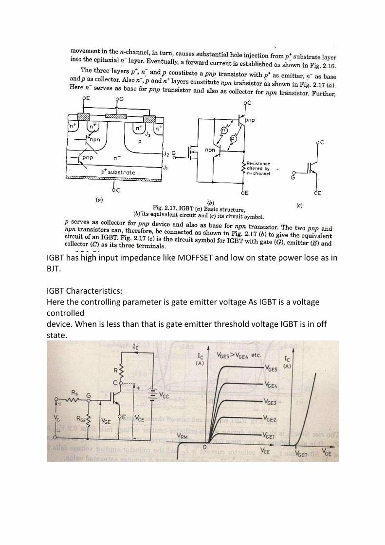
IGBT has high input impedance like MOFFSET and low on state power lose as in BJT. IGBT Characteristics: Here the controlling parameter is gate emitter voltage As IGBT is a voltage controlled device. When is less than that is gate emitter threshold voltage IGBT is in off state.

Switching characteristics:
Turn on time Time between the instants forward blocking state to forward on -state. Turn on time = Delay time + Rise time Delay time = Time for collector emitter voltage fall from Vce to 0.9 Vce =collector current to rise from initial leakage current to 0.1Ic Ic= Final value of collector current. Rise time Collector emitter voltage to fall from 0.9 to 0.1 Ic rises from 0.1Ic to Ic. After the device is on state the device carries a steady current of Ic and the collector emitter voltage falls to a small value called conduction drop . Turn off time 1) Delay time

2) Initial fall time 1 3) Final fall time 2 Collector current falls from Ic to 0.9Ic at the end of the collector emitter voltage begins to rise. Turn off time = Collector current falls from 90% to 20% of its initial value Ic OR The time during which collector emitter voltage rise from to 0.1. SCR (THYRISTOR) Thyristor is a four layer three junction p-n-p-n semiconductor switching device. It has 3terminals these are anode, cathode and gate. SCRs are solid state device, so they are compact, possess high reliability and have low loss.
SCR is made up of silicon, it acts as a rectifier; it has very low resistance in the forward direction and high resistance in the reverse direction. It is a unidirectional device. Static V-I characteristics of a Thyristor: The circuit diagram for obtaining static V-I characteristics is as shown
Anode and cathode are connected to main source voltage through the load. The gate

and cathode are fed from source. A typical SCR V-I characteristic is as shown below:
VBO=Forward breakover voltage VBR=Reverse breakover voltage Ig=Gate current Va=Anode voltage across the thyristor terminal A,K. Ia=Anode current A thyristor is normally four layer three-terminal device. Four layers are formed
by alternating n-type semiconductor and p-type semiconductor materials.
Consequently there are three pn junctions formed in the device. It is a bistable
device. The three terminals of this device are called anode (A), cathode (K) and
gate (G) respectively. The gate (G) terminal is control terminal of the device. That
means, the current flowing through the device is controlled by electrical signal
applied to the gate (G) terminal. The anode (A) and cathode (K) are the power
terminals of the device handle the large applied voltage and conduct the major
current through the thyristor. The main difference of thyristors with other
digital and electronics switches is that, a thyristor can handle large current and
can withstand large voltage, whereas other digital and electronic switches
handle only tiny current and tiny voltage.

TYPES OF THYRISTORS
There are four major types of thyristors:
1. Silicon Controlled Rectifier (SCR) 2. Gate Turn-off Thyristor (GTO) and Integrated Gate Commutated Thyristor
(IGCT) 3. MOS-Controlled Thyristor (MCT) 4. Static Induction Thyristor (SITh).
What is Thyristor or SCR?
It is a silicon based semiconductor device, which is used in electrical
circuits for switching operation. SCR, whose full form is silicon controlled
rectifier, is also a well-known member of thyristor family. Although there are
many different members are available in thyristor family, but silicon controlled
rectifiers are so widely used that as if thyristor and SCR become synonymous.
The characteristic of thyristor consists of the characteristic of thyratron tube
and characteristic of transistor. The name of thyristor consists of first four letters
of thyratron tube and last five letters of transistor. [THYRItron + transISTOR].
The device has ideal states, i.e. On and OFF. Generally an SCR consists of two PN
junctions, but sometimes it may also consist of more than two PN junctions. it is
four-layer (PNPN) three terminals (Anode, Cathode, Gate) semi-controlled
device. This device has two states i.e. on and OFF. We can turn it ON by sending
a gate current signal between second P layer and cathode.
STRUCTURE:
Thyristor is a four layer, three-junction, p-n-p-n semiconductor switching
device. It has three terminals; anode, cathode and gate. Fig. (a) gives
constructional details of a typical thyristor. Basically, a thyristor consists of four
layers of alternate p-type and n-type silicon semiconductors forming three
junctions J1, J2 and J3 as shown in Fig. (a). The threaded portion is for the
purpose of tightening the thyristor to the frame or heat sink with the help of a
nut. Gate terminal is usually kept near the cathode terminal Fig.(a). Schematic
diagram and circuit symbol for a thyristor are shown respectively in Figs. (b) and
(c). The terminal connected to outer p region is called anode (A), the terminal
connected to outer n region is called cathode and that connected to inner p
region is called the gate (G). For large current applications, thyristors need

better cooling ; this is achieved to a great extent by mounting them onto heat
sinks.
An SCR is so called because silicon is used for its construction and its
operation as a rectifier (very low resistance in the forward conduction and very
high resistance in the reverse direction) can be controlled. Like the diode, an SCR
is an unidirectional device that blocks the current fl.ow from cathode to anode.
Unlike the diode, a thyristor also blocks the current flow from anode to cathode
witil it is triggered into conduction by a proper gate signal between gate and
cathode terminals.

STATIC V-I CHARACTERISTICS OF A THYRISTOR
The symbolic diagram and the basic circuit diagram for determining
the characteristics of thyristor is shown in the figure below,
From the circuit diagram, the anode and cathode are connected to the
supply voltage through the load. Another secondary supply Es is applied
between the gate and the cathode terminal which supplies for the positive gate
current when the switch S is closed. On giving the supply we get the required V-
I characteristics of a thyristor show in the figure
Anode to cathode voltage Va and anode current Ia . The thyristor has three
basic modes of operation, namely the reverse blocking mode, forward blocking
(off-state) mode and forward conduction (on-state) mode.
Reverse Blocking Mode of Thyristor
Initially for the reverse blocking mode of the thyristor, the cathode is
made positive with respect to anode by supplying voltage E and the gate to
cathode supply voltage Es is detached initially by keeping switch S open.

Here Junctions J1 and J3 are reverse biased whereas the junction J2 is forward
biased. The behavior of the thyristor here is similar to that of two diodes are
connected in series with reverse voltage applied across them. As a result only a
small leakage current of the order of a few μAmps flows.
This is the reverse blocking mode or the off-state, of the thyristor. If the reverse voltage is now increased, then at a particular voltage, known as the critical breakdown voltage VBR, an avalanche occurs at J1 and J3 and the reverse current increases rapidly. A large current associated with VBR gives rise to more losses in the SCR, which results in heating. This may lead to thyristor damage as the junction temperature may exceed its permissible temperature rise.
The maximum working reverse voltage across a thyristor does not exceed VBR. When reverse voltage applied across a thyristor is less than VBR, the device offers very high impedance in the reverse direction. The SCR in the reverse blocking mode may therefore be treated as open circuit.

Forward Blocking Mode
When the anode is positive with respect to the cathode, with gate kept in
open condition. The thyristor is said to be forward biased as shown the figure .
Junctions J1 and J3 are forward biased but junction J2 goes into reverse
biased condition. In this particular mode, a small current, called forward leakage

current is allowed to flow initially as shown in the diagram for characteristics of
thyristor. if we keep on increasing the forward biased anode to cathode voltage.
In this particular mode, the thyristor conducts currents from anode to cathode with a very small voltage drop across it. A thyristor is brought from forward blocking mode to forward conduction mode by turning it on by exceeding the forward break over voltage or by applying a gate pulse between gate and cathode. In this mode, thyristor is in on-state and behaves like a closed switch. Voltage drop across thyristor in the on state is of the order of 1 to 2 V depending beyond a certain point, then the reverse biased junction J2 will have an avalanche breakdown at a voltage called forward break over voltage VB0 of the thyristor. But, if we keep the forward voltage less than VBO, we can see from the characteristics of thyristor, that the device offers a high impedance. Thus even here the thyristor operates as an open switch during the forward blocking mode.
Forward Conduction Mode
When the anode to cathode forward voltage is increased, with gate circuit open, the reverse junction J2 will have an avalanche breakdown at forward break over voltage VBO leading to thyristor turn on. Once the thyristor is turned on we can see from the diagram for characteristics of thyristor, that the point M at once shifts toward N and then anywhere between N and K. Here NK represents the forward conduction mode of the thyristor. In this mode of operation, the thyristor conducts maximum current with minimum voltage drop, this is known as the forward conduction forward conduction or the turn on mode of the thyristor. DIAC
A DIAC is a diode that conducts electrical current only after its breakover voltage
(VBO) has been reached. DIAC stands for “Diode for Alternating Current”. A DIAC is
a device which has two electrodes, and it is a member of the thyristor family. DIACs
are used in the triggering of thyristors. The figure below shows a symbol of a DIAC,
which resembles the connection of two diodes in series. DIACs have no gate
electrode, unlike some other thyristors that they are commonly used to trigger,
such as a TRIAC.
The advantage of a DIAC is that it can be turned on or off simply by reducing the
voltage level below its avalanche breakdown voltage. DIACs are also known as a
transistor without a base. It should also be noted that a DIAC can be either turned

on or off for both polarities of voltage (i.e. positive or negative voltage). They also
still works when avalanche breakdown occurs.
Application of DIAC
The main application of a DIAC is its use in a TRIAC triggering circuit. The DIAC is connected to the gate terminal of the TRIAC. When the voltage across the gate decreases below a predetermined value, the gate voltage will be zero and hence the TRIAC will be turned off. Some other applications of a DIAC include:
1. It can be used in the lamp dimmer circuit 2. It is used in a heat control circuit 3. It is used in the speed control of a universal motor
Construction of DIAC
It is a device which consists of four layers and two terminals. The construction is almost the same as that of the transistor. But there are certain points which deviate from the construction from the transistor. The differentiating points are-
1. There is no base terminal in the DIAC 2. The three regions have almost the same level of doping 3. It gives symmetrical switching characteristics for either polarity of
voltages
The DIAC can be turned on for both the polarity of voltages. When A2 is more positive with respect to A1 then the current does not flow through the corresponding N-layer but flows from P2-N2-P1-N1. When A1 is more positive A2 then the current flows through P1-N2-P2-N3. The construction resembles the diode connected in series. When the applied voltage is small in either polarity, a very small current flows which is known as leakage current because of the drift of electrons and holes in the depletion

region. Although a small current flows, it is not sufficient to produce avalanche breakdown, hence the device remains in the non-conducting state.
When the applied voltage in either polarity exceeds the breakdown voltage, DIAC current rises and the device conducts in accordance with its V-I characteristics.
TRIAC
Triac is a three terminal AC switch which is different from the other silicon
controlled rectifiers in the sense that it can conduct in both the directions that
is whether the applied gate signal is positive or negative, it will conduct. Thus,
this device can be used for AC systems as a switch.
This is a three terminal, four layer, bi-directional semiconductor device that
controls AC power. The triac of maximum rating of 16 kw is available in the
market.

Figure shows the symbol of triac, which has two main terminals MT1 and MT2
connected in inverse parallel and a gate terminal.
Construction of Triac
Two SCRs are connected in inverse parallel with gate terminal as common.
Gate terminals is connected to both the N and P regions due to which gate signal
may be applied which is irrespective of the polarity of the signal. Here, we do
not have anode and cathode since it works for both the polarities which means
that device is bilateral. It consists of three terminals namely, main terminal
1(MT1), main terminal 2(MT2), and gate terminal G.

Figure shows the construction of a triac. There are two main terminals namely MT1 and MT2 and the remaining terminal is gate terminal.
Operation of Triac
The triac can be turned on by applying the gate voltage higher than break over voltage. However, without making the voltage high, it can be turned on by applying the gate pulse of 35 micro seconds to turn it on. When the voltage applied is less than the break over voltage, we use gate triggering method to turn it on.
There are four different modes of operations, they are-
1. When MT2 and Gate being Positive with Respect to MT1 When this happens, current flows through the path P1-N1-P2-N2. Here, P1-N1 and P2-N2 are forward biased but N1-P2 is reverse biased. The triac is said to be operated in positively biased region. Positive gate with respect to MT1 forward biases P2-N2 and breakdown occurs.
2. When MT2 is Positive but Gate is Negative with Respect to MT1 The current flows through the path P1-N1-P2-N2. But P2-N3 is forward biased and current carriers injected into P2 on the triac.
3. When MT2 and Gate are Negative with Respect to MT1 Current flows through the path P2-N1-P1-N4. Two junctions P2-N1 and P1-N4 are forward biased but the junction N1-P1 is reverse biased. The triac is said to be in the negatively biased region.
4. When MT2 is Negative but Gate is Positive with Respect to MT1 P2-N2 is forward biased at that condition. Current carriers are injected so the triac turns on. This mode of operation has a disadvantage that it should not be used for high (di/dt) circuits. Sensitivity of triggering in mode 2 and 3 is high and if marginal triggering capability is required, negative gate pulses should be used. Triggering in mode 1 is more sensitive than mode 2 and mode 3.
Characteristics of a Triac
The triac characteristics is similar to SCR but it is applicable to both positive and negative triac voltages. The operation can be summarized as follows-
First Quadrant Operation of Triac
Voltage at terminal MT2 is positive with respect to terminal MT1 and gate voltage is also positive with respect to first terminal.

Second Quadrant Operation of Triac
Voltage at terminal 2 is positive with respect to terminal 1 and gate voltage is negative with respect to terminal 1.
Third Quadrant Operation of Triac
Voltage of terminal 1 is positive with respect to terminal 2 and the gate voltage is negative.
Fourth Quadrant Operation of Triac
Voltage of terminal 2 is negative with respect to terminal 1 and gate voltage is positive.
When the device gets turned on, a heavy current flows through it which
may damage the device, hence in order to limit the current a current limiting
resistor should be connected externally to it. By applying proper gate signal,
firing angle of the device may be controlled. The gate triggering circuits should
be used for proper gate triggering. We can use diac for triggering the gate pulse.
For firing of the device with proper firing angle, a gate pulse may be applied up
to a duration of 35 micro seconds.
Advantages of Triac
• It can be triggered with positive or negative polarity of gate pulses.
• It requires only a single heat sink of slightly larger size, whereas for SCR,
two heat sinks should be required of smaller size.
• It requires single fuse for protection.
• A safe breakdown in either direction is possible but for SCR protection
should be given with parallel diode.
Disadvantages of Triac
• They are not much reliable compared to SCR.
• It has (dv/dt) rating lower than SCR.
• Lower ratings are available compared to SCR.
• We need to be careful about the triggering circuit as it can be triggered in
either direction.
Uses of Triac
• They are used in control circuits.
• It is used in High power lamp switching.
• It is used in AC power control.
GTO
• A gate turn-off thyristor (GTO) is a special type of thyristor, which is a high-
power semiconductor device. It was invented at General Electric. GTOs,
as opposed to normal thyristors, are fully controllable switches which can
be turned on and off by their third lead, the gate lead.
• Normal thyristors (silicon-controlled rectifiers) are not fully controllable
switches (a "fully controllable switch" can be turned on and off at will).
Thyristors can only be turned ON using the gate lead, but cannot be
turned OFF using the gate lead. Thyristors are switched ON by a gate
signal, but even after the gate signal is de-asserted (removed), the
thyristor remains in the ON-state until a turn-off condition occurs (which
can be the application of a reverse voltage to the terminals, or a decrease
of the forward current below a certain threshold value known as the
"holding current"). Thus, a thyristor behaves like a normal semiconductor
diode after it is turned on or "fired".
• The GTO can be turned on by a gate signal, and can also be turned off by
a gate signal of negative polarity.
• Turn on is accomplished by a "positive current" pulse between the gate
and cathode terminals. As the gate-cathode behaves like PN junction,
there will be some relatively small voltage between the terminals. The
turn on phenomenon in GTO is however, not as reliable as an SCR

(thyristor) and small positive gate current must be maintained even after
turn on to improve reliability.
• Turn off is accomplished by a "negative voltage" pulse between the gate
and cathode terminals. Some of the forward current (about one-third to
one-fifth) is "stolen" and used to induce a cathode-gate voltage which in
turn causes the forward current to fall and the GTO will switch off
(transitioning to the 'blocking' state.)
• GTO thyristors suffer from long switch off times, whereby after the
forward current falls, there is a long tail time where residual current
continues to flow until all remaining charge from the device is taken away.
This restricts the maximum switching frequency to approx 1 kHz. It may
be noted however, that the turn off time of a GTO is approximately ten
times faster than that of a comparable SCR.
• To assist with the turn-off process, GTO thyristors are usually constructed
from a large number (hundreds or thousands) of small thyristor cells
connected in parallel.
Simplified cross section of a GTO thyristor
Electronic symbol

Equivalent circuit of a GTO thyristor
Characteristic Description Thyristor (1600 V,
350 A) GTO (1600 V,
350 A)
VT ON On state voltage drop 1.5 V 3.4 V
ton,Igon Turn on time, gate current
8 µs,200 mA 2 µs,2 A
toff Turn off time 150 µs 15 µs
Comparison of an SCR and GTO of same rating.
• A distributed buffer gate turn-off thyristor (DB-GTO) is a thyristor with
additional PN layers in the drift region to reshape the field profile and
increase the voltage blocked in the off state. Compared to a typical PNPN
structure of a conventional thyristor, this thyristor would be a PN-PN-PN
type structure in here.
Reverse bias
• GTO thyristors are available with or without reverse blocking capability.
Reverse blocking capability adds to the forward voltage drop because of
the need to have a long, low doped P1 region.

• GTO thyristors capable of blocking reverse voltage are known as
Symmetrical GTO thyristors, abbreviated S-GTO. Usually, the reverse
blocking voltage rating and forward blocking voltage rating are the same.
The typical application for symmetrical GTO thyristors is in current source
inverters.
• GTO thyristors incapable of blocking reverse voltage are known as
asymmetrical GTO thyristors, abbreviated A-GTO, and are generally more
common than Symmetrical GTO thyristors. They typically have a reverse
breakdown rating in the tens of volts. A-GTO thyristors are used where
either a reverse conducting diode is applied in parallel (for example, in
voltage source inverters) or where reverse voltage would never occur (for
example, in switching power supplies or DC traction choppers).
• GTO thyristors can be fabricated with a reverse conducting diode in the
same package. These are known as RCGTO, for Reverse Conducting GTO
thyristor.
Safe operating area
• Unlike the insulated gate bipolar transistor (IGBT), the GTO thyristor
requires external devices ("snubber circuits") to shape the turn on and
turn off currents to prevent device destruction.
• During turn on, the device has a maximum dI/dt rating limiting the rise of
current. This is to allow the entire bulk of the device to reach turn on
before full current is reached. If this rating is exceeded, the area of the
device nearest the gate contacts will overheat and melt from over current.
The rate of dI/dt is usually controlled by adding a saturable reactor (turn-
on snubber), although turn-on dI/dt is a less serious constraint with GTO
thyristors than it is with normal thyristors, because of the way the GTO is
constructed from many small thyristor cells in parallel. Reset of the
saturable reactor usually places a minimum off time requirement on GTO
based circuits.
• During turn off, the forward voltage of the device must be limited until
the current tails off. The limit is usually around 20% of the forward
blocking voltage rating. If the voltage rises too fast at turn off, not all of
the device will turn off and the GTO will fail, often explosively, due to the
high voltage and current focused on a small portion of the device.
Substantial snubber circuits are added around the device to limit the rise

of voltage at turn off. Reseting the snubber circuit usually places a
minimum on time requirement on GTO based circuits.
• The minimum on and off time is handled in DC motor chopper circuits by
using a variable switching frequency at the lowest and highest duty cycle.
This is observable in traction applications where the frequency will ramp
up as the motor starts, then the frequency stays constant over most of
the speed ranges, then the frequency drops back down to zero at full
speed.
Applications
• The main applications are in variable speed motor drives, high power
inverters and traction. GTOs are increasingly being replaced by integrated
gate-commutated thyristors, which are an evolutionary development of
the GTO, and insulated gate bipolar transistors, which are members of the
transistor family.
1.2Two Transistor Model of SCR
Basic operating principle of SCR, can be easily understood by the two transistor model of SCR or analogy of silicon controlled rectifier, as it is also a combination of P and N layers, shown in figure below.
This is a pnpn thyristor. If we bisect it through the dotted line then we will get two transistors i.e. one pnp transistor with J1 and J2 junctions and another is with J2 and J3junctions as shown in figure below.

When the transistors are in off state, the relation between the collector current and emitter current is shown below
Here, IC is collector current, IE is emitter current, ICBO is forward leakage current, α is common base forward current gain and relationship between IC and IB is
Where, IB is base current and β is common emitter forward current gain. Let’s for transistor T1 this relation holds

And that for transistor T2
Now, by the analysis of two transistors model we can get anode current,
From equation (i) and (ii), we get,
If applied gate current is Ig then cathode current will be the summation of anode current and gate current i.e.
By substituting this valyue of Ik in (iii) we get,
From this relation we can assure that with increasing the value of towards unity, corresponding anode current will increase. Now the question is how increasing? Here is the explanation using two transistor model of SCR. At the first stage when we apply a gate current Ig, it acts as base current of T2 transistor i.e. IB2 = Ig and emitter current i.e. Ik= Ig of the T,2 transistor. Hence establishment of the emitter current gives rise α2 as
Presence of base current will generate collector current as
This IC2 is nothing but base current IB1 of transistor T,1, which will cause the flow of collector current,

IC1 and IB1 lead to increase IC1 as and hence, α1 increases. Now,
new base current of T2 is , which will lead to increase
emitter current and as a result α2 also increases and this further
increases . As , α1 again increases. This continuous positive feedback effect increases towards unity and anode current tends to flow at a very large value. The value current then can only be controlled by external resistance of the circuit.

1.4 Switching or ON OFF Characteristics of SCR | Turn ON Turn OFF Time
Turn ON Time of SCR
A forward biased thyristor can be turned on by applying a
positive voltage between gate and cathode terminal. But it takes some
transition time to go from forward blocking mode to forward conduction mode.
This transition time is called turn on time of SCR and it can be subdivided into
three small intervals as delay time (td) rise time(tr), spread time(ts).
Delay Time of SCR (td)
After application of gate current, the thyristor will start conducting over a very tiny region. Delay time of SCR can be defined as the time taken by the gate current to increase from 90% to 100% of its final value Ig. From another point of view, delay time is the interval in which anode current rises from forward leakage current to 10% of its final value and at the same time anode voltage will fall from 100% to 90% of its initial value Va.
Rise Time of SCR(tr)
Rise time of SCR in the time taken by the anode current to rise from 10% to 90%
of its final value. At the same time anode voltage will fall from 90% to 10% of its
initial value Va. The phenomenon of decreasing anode voltage and increasing

anode current is entirely dependent upon the type of the load. For example if
we connect a inductive load, voltage will fall in a faster rate than the current
increasing. This is happened because induction does not allow initially high
voltage change through it. On the other hand if we connect a capacitive load it
does not allow initial high voltage change through it, hence current increasing
rate will be faster than the voltage falling rate.
High increasing rate of dia/dt can create local hot spot in the device which is not suitable for proper operation. So, it is advisable to use a inductor in series with the device to tackle high dia/dt. Usually value of maximum allowable di/dt is in the range of 20 to 200 A per microsecond.
Spread Time of SCR(ts)
It is the time taken by the anode current to rise from 90% to 100% of its final value. At the same time the anode voltage decreases from 10% of its initial value to smallest possible value. In this interval of time conduction spreads all over the area of cathode and the SCRwill go to fully ON State. Spread time of SCR depends upon the cross-sectional area of cathode.
Turn OFF Time of SCR
Dynamic process of the SCR from conduction state to forward blocking state
is called commutation process or turn-off process. Once the thyristor is switched
on or in other point of view, the anode current is above latching current, the
gate losses control over it. That means gate circuit cannot turn off the device.
For turning off the SCR anode current must fall below the holding current. After
anode current fall to zero we cannot apply forward voltage across the device
due to presence of carrier charges into the four layers. So we must sweep out
or recombine these charges to proper turn off of SCR. So turn off time of
SCR can be defined as the interval between anode current falls to zero and
device regains its forward blocking mode. On the basis of removing carrier
charges from the four layers, turn off time of SCR can be divided into two time
regions,
1. Reverse Recovery Time. (trr) 2. Gate Recovery Time(tgr)
The tum-off time tq of a thyristor is defined as the time between the instant anode current becomes zero and the instant SCR regains forward blocking capability. During time tq, all the excess carriers from the four layers of SCR must be removed. This removal of excess carriers consists of sweeping out of holes from outer p-layer and electrons from outer n-layer. The carriers

around junction J2 can be removed only by recombination. The turn-off time is divided into two intervals ; reverse recovery time t.; and the gate recovery time tgr; i.e. tq = trr + tgr
Reverse Recovery Time(trr)
It is the interval in which change carriers remove from J1, and J3 junction. At time
t1, anode current falls to zero and it will continue to increase in reverse direction
with same slope (di/dt) of the forward decreasing current. This negative current
will help to sweep out the carrier charges from junction J1 and J3. At the time
t2 carrier charge density is not sufficient to maintain the reverse current hence
after t2 this negative current will start to decrease. The value of current at t2 is
called reverse recovery current. Due to rapid decreasing of anode current, a
reverse spike of voltage may appear across the SCR. Total recovery time t3- t1 is
called reverse recovery time. After that, device will start to follow the applied
reverse voltage and it gains the property to block the forward voltage.
Gate Recovery Time(tgr)
After sweeping out the carrier charges from junction J1 and J3 during reverse recovery time, there still remain trapped charges in J2 junction which prevent the SCR from blocking the forward voltage. These trapped charge can be removed by recombination only and the interval in which this recombination is done, called gate recovery time.
The thyristor turn-off time tq is applicable to an individual SCR. In actual practice, thyristor (or thyristors) form a part of the power circuit. The tum-off time provided to the thyristor by the practical circuit is called circuit turn-off time tc. It is defined as the time between the instant anode current becomes zero and the instant reverse voltage due to practical circuit reaches zero, see Fig.Time tc must be greater than tq for reliable turn-off, otherwise the device may turu-on at an undesired instant, a process called commutation failure.

1.5THYRISTOR TURN-ON METHODS
With anode positive with respect to cathode, a thyristor can be turned on by any one of the following techniques.
a) Forward Voltage Triggering b) Gate Triggering c) dv/dt Triggering: d) Temperature Triggering e) Light Triggering
Triggering means turning ON of a device from its off state. Turning ON of a thyristor refers to thyristor triggering. Thyristor is turned on by increasing the anode current flowing through it. The increase in anode current can be achieved by many ways.
a). Forward Voltage Triggering :
The applied forward voltage is gradually increased beyond a pt.known as forward break over voltage VBO and gate is kept open. This method is not preferred because during turn on of thyristor, it is associated with large voltage and large current which results in huge power loss and device may be damaged.
When anode to cathode for'ward voltage is increased with gate circuit open, the reverse biased junction J 2 will break. This is known as avalanche breakdown and the voltage at which avalanche occurs is called forward breakover voltage VBo· At this voltage, thyristor changes from off-state (high voltage with low leakage current) to on-state characterised by low voltage across thyristor with large forward current. As other junctions J1, J3 are already forward biased, breakdown of junction J2 allows free movement of carriers across three junctions and as a result, large forward anode-current flows. As stated before, this forward current is limited by the load impedance. In practice, the transition from off-state to on-state obtained by exceeding VBo is never employed as it may destroy the device.

if the anode voltage is reduced below VBo. SCR will continue conduction of the current. The SCR can now be turned off only by reducing the anode current below a certain value called holding current
(b) Gate Triggering :
Turning on of thyristors by gate triggering is simple, reliable and efficient, it is therefore the most usual method of firing the forward biased SCRs. A thyristor with forward breakover voltage (say 800 V) higher than the normal working voltage (say 400 V) is chosen. This means that thyristor will remain in forward blocking state with normal working voltage across anode and cathode and with gate open. However, when tum-on of a thyristor is required, a positive gate voltage between gate and cathode is applied. With gate current thus established, charges are injected into the inner p layer and voltage at which forward break.over occurs is reduced. The forward voltage at which the. device switches to on-state depends upon the magnitude of gate current. Higher the gate current, lower is the forward breakover voltage.
Once the SCR is conducting a forward current, reverse biased junction J2 no longer exists. As such, no gate current is required for the device to remain in on-state. Therefore, if the gate current is removed, the conduction of current from anode to cathode remains unaffected., if gate current is reduced to zero before the rising anode current attains a value, called the latching current, the thyristor will turn-off again. The gate pulse width should therefore be judiciously chosen to ensure that anode current rises above the latching current. Thus latching current may be defined as the minimum value of anode current which it must attain during turn-on process to maintain conduction when gate signal is removed. Once the thyristor is conducting, gate loses control. The thyristor can be turned-off (or the thyristor can be returned to forward blocking state) only if the forward current falls below a low-level current called the holding current. Thus holding current may be defined as the minimum value of anode current below which it must fall for turning-off the thyristor. The latching current is higher than the holding current.
Latching current is associated with turn-on process and holding current with turn-off process. It is usual to take latching current as two to three times the holding current. In industrial applications, holding current (typically 10 mA) is almost taken as zero
(c) dv/dt Triggering:
In this method of triggering if the applied rate of change of voltage is large, then the device will turn on even though the voltage appearing across the device is small. We know that when SCR is applied with forward voltage across the

anode and cathode, junctions j1 and j3 will be in forward bias and junction j2 will be in reverse bias. This reverse biased junction j2 will have the characteristics of the capacitor due to the charges exist across the junction. If the forward voltage is suddenly applied a charging current will flow tending to turn on the SCR. This magnitude of the charging current depends on the rate of change of appliedvoltage.
i. When the device is forward biased, J1 and J3 are forward biased, J2 is reverse biased.
ii. Junction J2 behaves as a capacitor, due to the charges existing across the junction.
iii. If voltage across the device is V, the charge by Q and capacitance by C then, ic =dQ/dt Q=CV ic =d(CV)/dt =C.dV/d+V.dC/dt as dC/dt = 0
ic = C.dV/dt iv. Therefore when the rate of change of voltage across the device
becomes large, the device may turn ON, even if the voltage across the device is small.
(d) Temperature Triggering :
During forward blocking, most of the applied voltage appears across reverse biased junction J2• This voltage across junction J2 associated with leakage current through junction J2 further increases. This cumulative process may turn on the SCR at some high temperature.
(e) Light Triggering:
The pulse of light of appropriate wavelength is guided by optical fibres for irradiation. If the intensity of this light thrown on the recess exceeds a certain value, forward-biased SCR is turned on. Such a thyristor is known as light-activated SCR (LASCR).
LASCR may be triggered with a light source or with a gate signal. Sometimes a combination of both light source and gate signal is used to trigger an SCR. For this, the gate is biased with voltage or current slightly less than that required to turn it on, now a beam of light directed at the inner p-layer junction turns on the SCR. The light intensity required to turn-on the SCR depends upon

the voltage bias given to the gate. Higher the voltage (or current) bias, lower the light intensity required. , Light-triggered thyristors used in high-voltage direct current (HVDC) transmission systems. In these several SCRs are connected in series-parallel combination and their light-triggering has the advantage of electrical isolation between power and control circuits.
1.6SCR Turn OFF Methods An SCR is said to be ‘turned OFF’ if there is no flow of forward current and even if the SCR is once again forward biased (positive voltage at anode), the SCR will not conduct without any Gate Signal (using one of the SCR Turn ON Methods).
The reverse voltage, which causes to commutate the SCR, is called the Commutation Voltage. Depending on the type of switching of SCR (Cyclic or Sequential), the commutation methods are classified into two major types. They are:
• Natural Commutation • Forced Commutation
Before discussing about different types of ACR Turn OFF Methods, there is an important quantity known as the Turn OFF Time of SCR which we have to understand.
Turn OFF Time tOFF of an SCR is the time between the moment anode current becomes zero and the moment SCR starts to block the forward voltage.
Natural Commutation In natural commutation, the source of commutation voltage is the supply source itself. If the SCR is connected to an AC supply, at every end of the positive half cycle, the anode current naturally becomes zero (due to the alternating nature of the AC Supply). As the current in the circuit goes through the natural zero, a reverse voltage is applied immediately across the SCR (due to the negative half cycle). These conditions turn OFF the SCR.
This method of commutation is also called as Source Commutation or AC Line Commutation or Class F Commutation. This commutation is possible with line commutated inverters, controlled rectifiers, cyclo converters and AC voltage regulators because the supply is the AC source in all these converters.

During the positive half cycle of the AC Supply, the load current flows normally. But, during the negative cycle, the SCR will turn OFF (due to momentary zero current and immediate negative polarity). For successful natural commutation, the turn OFF time tOFF must be less than the duration of half cycle of the supply.
Forced Commutation In case of DC circuits, there is no natural current zero to turn OFF the SCR. In such circuits, forward current must be forced to zero with an external circuit (known as Commutating Circuit) to commutate the SCR. Hence the name, Forced Commutation.
This commutating circuit consist of components like inductors and capacitors and they are called Commutating Components. These commutating components cause to apply a reverse voltage across the SCR that immediately bring the current in the SCR to zero.
Depending on the process for achieving zero current in the SCR and the arrangement of the commutating components, Forced Commutation is classified into different types. They are:
• Class A – Self Commutation by Resonating the Load • Class B – Self Commutation by Resonating the Load • Class C – Complementary Commutation

• Class D – Auxiliary Commutation • Class E – Pulse Commutation
such as class A, B, C, D, and E. This commutation is mainly used in chopper and inverter circuits.
Class A Commutation This is also known as Self Commutation by Resonating the Load or simply the Resonant Commutation. In this commutation, the source of commutation voltage is in the load. The commutating components are L and C and the Capacitor can be connected either in parallel or in series with the load resistance RL as shown below.
There are also waveforms of SCR current, voltage and capacitor voltage.
The value of load resistance and the commutating components are selected in such a way that they form an under-damped RLC resonant circuit. When the circuit is applied with a DC Source, the forward currents starts flowing through the SCR and during this period, the capacitor is charged up to the value of Vdc. The current in the circuit will be either of the two waveforms shown below, depending on how the load is connected to the capacitor (parallel or series).

When conducting, the current in the SCR is the charging current of the capacitor. From the waveforms, it is clear that the current becomes zero at the point ‘K’. At this point, the SCR turns OFF.
The resonant frequency of the circuit, which depends on the Commutation Components L and C and also on the load resistance, determines the time for switching OFF the SCR.
Class A Commutation method is simple and reliable and is usually used in high frequency operations i.e., frequencies in the range of 1000 Hz and above due to the high values of L and C components (as they carry the full load current). This type of commutation is generally used in Series Inverters.
Class-B or Resonant Pulse Commutation of SCR Class-B or Resonant Pulse Commutation is a forced commutation technique to turn off an SCR. In this technique, thyristor or SCR is turned off by gradual build-up of resonant current in the reverse direction i.e. from cathode to anode of SCR. This technique is also known as current commutation and occurs

in DC circuit not in AC circuit. Let us consider the circuit diagram for Class-B or Resonant Pulse Commutation for better understanding of the commutation process involved.
The commutation circuit comprises of Capacitor C, Inductor L and an auxiliary thyristor TA. Initially thyristor T1 and TA are in off state and capacitor C is charged to voltage Vs with left hand plate positive as shown in figure. Positive direction of capacitor voltage and capacitor current ic are shown in figure and taken as reference. Now, at t=0, the main thyristor / SCR is gated and turned on. Load current equal to I0 starts flowing through the main thyristor T1 and Load. Now, we want to turn this thyristor off. To do this, we fire the auxiliary thyristor TA at t=t1. Till time t=t1, the capacitor is charged with source voltage Vs i.e. vc = Vs, capacitor current ic = 0 and current through main thyristor T1 i.e. i0 = I0. This is shown in figure below.

When auxiliary thyristor TA is fired, it starts conducting and provides a path for the discharge of capacitor C. L, C and TA forms a resonating circuit. The resonating current ic for this circuit is given as
Negative sign in the above expression of resonating current is given as the actual current flows in a direction opposite to the direction of current ic shown in the first figure.

Carefully observe the waveform of ic. It can be seen that, after half cycle, the value of ic reduces to zero at t=t2. This means, the current through the auxiliary thuristor TA reduces to zero. Let’s check if the auxiliary thyristor gets reversed biased after t=t2. Why are we checking this? This is because, the current through TA is zero at t=t2 and if it gets reversed biased after t=t2 then TA will get turned off. The voltage across TA equals the voltage across capacitor. The expression for capacitor voltage can be calculated as
From the above expression of voltage across capacitor, if we put ωt = π then value of Cosωt will -1. This means, the capacitor voltage will get reversed after half a cycle of capacitor current i.e. at t=t2. Thus, the auxiliary thyristor TA is reversed biased after t=t2. Hence it will get turned off at t=t2. Now, TA is OFF and capacitor C is charged up to source voltage Vs with its right hand plate positive. This means, the diode D is now forward biased and hence resonating current ic will now flow through least resistive path i.e. through C, L, D and main thyristor T1. But this resonating current ic will flow through the main SCR T1 from cathode to anode i.e. in reverse direction. This simply means, the current I through the main thyristor T1 will be given as I = I0 – ic When the magnitude of ic reaches I0, the current through the SCR T1 will become zero. This can be seen at t=t3. Now, you might ask, when the resonating current will attain a value of I0? This can easily be calculated from the equation of the resonating current. Let’s find it.
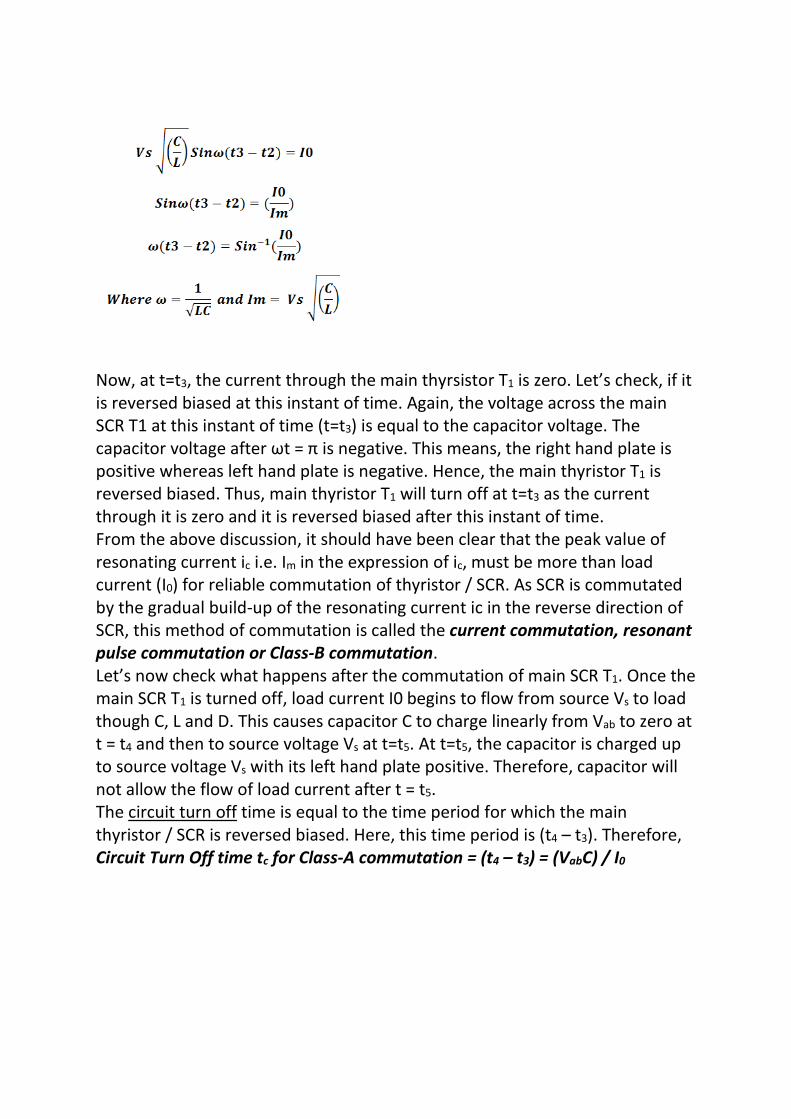
Now, at t=t3, the current through the main thyrsistor T1 is zero. Let’s check, if it is reversed biased at this instant of time. Again, the voltage across the main SCR T1 at this instant of time (t=t3) is equal to the capacitor voltage. The capacitor voltage after ωt = π is negative. This means, the right hand plate is positive whereas left hand plate is negative. Hence, the main thyristor T1 is reversed biased. Thus, main thyristor T1 will turn off at t=t3 as the current through it is zero and it is reversed biased after this instant of time. From the above discussion, it should have been clear that the peak value of resonating current ic i.e. Im in the expression of ic, must be more than load current (I0) for reliable commutation of thyristor / SCR. As SCR is commutated by the gradual build-up of the resonating current ic in the reverse direction of SCR, this method of commutation is called the current commutation, resonant pulse commutation or Class-B commutation. Let’s now check what happens after the commutation of main SCR T1. Once the main SCR T1 is turned off, load current I0 begins to flow from source Vs to load though C, L and D. This causes capacitor C to charge linearly from Vab to zero at t = t4 and then to source voltage Vs at t=t5. At t=t5, the capacitor is charged up to source voltage Vs with its left hand plate positive. Therefore, capacitor will not allow the flow of load current after t = t5. The circuit turn off time is equal to the time period for which the main thyristor / SCR is reversed biased. Here, this time period is (t4 – t3). Therefore, Circuit Turn Off time tc for Class-A commutation = (t4 – t3) = (VabC) / I0

1.8SCR- PROTECTION:
Protection of a device is an important aspect for its reliable and efficient
operation. SCR is a very delicate semiconductor device. So we have to use it in
its specified ratings to get desired output. SCR may face different types of
threats during its operation due to over voltages, over currents etc. There are
different types of thyristor protection schemes available for satisfactory
operation of the device like
1. Over voltage protection. 2. Over current protection. 3. High dv/dt protection. 4. High di/dt protection. 5. Thermal protection.
Over Voltage Protection
It is the most important protection scheme w. r. t. others as thyristors are
very sensitive to over voltages. Maximum time thyristor failures happen due to
over-voltage transients. A thyristor may be subjected to internal or external
over-voltages.
Internal Over-Voltages : After commutation of a thyristor reverse recovery
current decays abruptly with high di/dt which causes a high reverse voltage [as,
V = L(di/dt) so if di/dt is high then V will be large] that can exceed the rated
break-over voltage and the device may be damaged.
External Over-Voltages : These are caused due to various reasons in the supply line like lightning, surge conditions (abnormal voltage spike) etc. External over voltage may cause different types of problem in thyristor operation like increase in leakage current, permanent breakdown of junctions, unwanted turn-on of devices etc. So, we have to suppress the over-voltages. Protective Measure : The effect of over-voltages can be minimized by using non-linear resistors called voltage clamping devices like metal oxide like metal oxide varistor. At the time of normal operation it offers high impedance and acts as it is not present in the circuit. But when the voltage exceeds the rated voltage then it serves as a low impedance path to protect SCR.
Over Current Protection
Over current mainly occurs due to different types of faults in the circuit.
Due to over current i2R loss will increase and high generation of heat may take
place that can exceed the permissible limit and burn the device.

Protective Measure : SCR can be protected from over current by using CB and
fast acting current limiting fuses (FACLF). CB are used for protection of thyristor
against continuous overloads or against surge currents of long duration as a CB
has long tripping time. But fast-acting fuses is used for protecting SCR against
high surge current of very short duration.
High dv/dt Protection
When a thyristor is in forward blocking state then only J2 junction is
reverse biased which acts as a capacitor having constant capacitance value
Cj (junction capacitance). As we know that current through capacitor follows the
relation Hence leakage current through the
J2 junction which is nothing but the leakage current through the device will
increase with the increase in dva/dt i.e. rate of change of applied voltage across
the thyristor. This current can turn-on the device even when the gate signal is
absent. This is called dv/dt triggering and must be avoided which can be
achieved by using Snubber circuit in parallel with the device.
Protective Measure :Snubber Circuit : It consists of a capacitor connected in
series with a resistor which is applied parallel with the thyristor, when S is closed
then voltage Vs is applied across the device as well as Cs suddenly. At first
Snubber circuit behaves like a short circuit. Therefore voltage across the device
is zero. Gradually voltage across Cs builds up at a slow rate. So dv/dt across the
thyristor will stay in allowable range.
Before turning on of thyristor Cs is fully charged and after turning on of thyristor
it discharges through the SCR. This discharging current can be limited with the
help of a resistance (Rs) connected in series with the capacitor (Cs) to keep the
value of current and rate of change of current in a safe limit.
High di/dt Protection
When a thyristor is turned on by gate pulse then charge carriers spread
through its junction rapidly. But if rate of rise of anode current, i.e. di/dt is
greater than the spreading of charge carriers then localized heat generation will
take place which is known as local hot spots. This may damage the thyristor.
Protective Measure : To avoid local hot spots we use an inductor in series with
the device as it prevents high rate of change of current through it.

High Temperature Protection:
With the increase in the temperature of the junction, insulation may get failed.
So we have to take proper measures to limit the temperature rise.
Protective Measure : We can achieve this by mounting the thyristor on heat sink
which is mainly made by high thermal conductivity metals like aluminium (Al),
Copper (Cu) etc. Mainly aluminium (Al) is used due to its low cost. There are
several types of mounting techniques for SCR such as – Lead-mounting, stud-
mounting, Bolt-down mounting, press-fit mounting, press-pack mounting etc.
Gate Protection of Thyristor
Like thyristor, Gate circuit should also be protected from over voltages and over
currents. Over voltages in the gate circuit can cause false triggering and over
current can cause high junction temperature.
Protective Measure : Over voltages thyristor protection is achieved by using
a zener diode and a resistor can be used to protect the gate circuit from over
current. Noise in gate circuit can also cause false triggering which can be avoided
by using a resistor and a capacitor in parallel. A diode (D) may be connected in
series or in parallel with the gate to protect it from high reverse voltage.
Overall Protection of a Thyristor
Lead mounting : In such mounting technique housing of SCR itself is used as heat radiator. Hence no need of additional heat zink arrangement. Hence, this technique of thyristor Protection is generally used for low current application, normally less than one ampere. Stud mounting : The anode of the thyristor is in the form of threaded stud which is screwed to a metalling heat sink block. Bolt-down mounting : Here the device is connected to the heat sink with the help of nut-bolt mechanism. It is mainly used in small and medium rating circuit. Press fit mounting : This kind of mounting is obtained by inserting the whole SCR into the metallic block. It is used in high rating circuit. Press-Pack mounting : This kind of mounting for thyristor protection is obtained by sandwiching the thyristor between to heat sink with the help of clamps. It is used for very high rating circuit.

1.9 Firing circuits
Main features of firing circuits
A firing circuit should fulfill the following two functions If power circuit has more than one SCR, the firing circuit should produce gating pulses for each SCR at the desired instant for
proper operation of the power circuit The control signal generated by a firing circuit may not be able to turn on an SCR. It is therefore common to feed the voltage pulse to a driver circuit and then to a gate cathode circuit
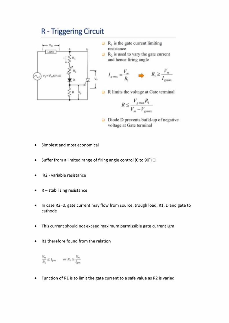
• Simplest and most economical
• Suffer from a limited range of firing angle control (0 to 90 )ͦ
• R2 - variable resistance
• R – stabilizing resistance
• In case R2=0, gate current may flow from source, trough load, R1, D and gate to cathode
• This current should not exceed maximum permissible gate current Igm
• R1 therefore found from the relation
• Function of R1 is to limit the gate current to a safe value as R2 is varied

• Resistance R should have a value such that maximum voltage drop across it does not exceed maximum possible gate voltageVgm
• This can happen only when R2 is zero, Under this condition, Vm .R/ (R1 + R)≤Vgm As resistance R1, R2 are large, gate trigger circuit draws a small current, Diode D allows the flow of current during positive half cycle only, The amplitude of this dc pulse can be controlled by varying R2
• The potentiometer setting R2 determines the gate voltage amplitude , When R2 is large current i is small and the voltage across R,vg=i.R is also small , AsVgp is less thanVgt, SCR will not turn on , Therefore load voltage vo=0, io=0 and supply voltage appear across SCR ,Trigger circuit consist of resistance only, therefore vg is in phase with source voltage vs , R2 is adjusted such that Vgp=Vgt, this gives the value of firing angle as 90
• The same circuit also is applicable forTRIAC. However, diode D1 has to be removed such that a trigger signal will be available at the gate terminal during both halfcycles. Because the gate of a TRIAC is not equally sensitive in all four of its modes of switching, α and hence vo are usually different in the positive and negative half-cycles of the supply voltage.

RC triggering circuit
The limited range of firing angle control by resistance firing circuit can be overcome by RC firing circuit , Several variations of RC trigger circuits are available , In these cases the range of α is extendable beyond 90. RC half wave triggering circuit , By varying the value R, firing angle can be controlled from 0 to 180 , In the –ve half cycle capacitor C charges through D2 with lower plate +ve to the peak supply voltageVm at ωt=-90 , After ωt=-90, source voltage Vs decreasing from –Vm at ωt=-90 to zero at ωt=0

During this period capacitor voltage may fall from -Vm to some small value -oa , Now the charging of the capacitor (with upper plate positive) takes place through R and the charging rate depends on the time-period RC. When capacitor charges to +ve voltage equal to VGT , conduction of the SCR takes place. After this capacitor holds a small +ve voltage ,Diode D1 used to prevent the breakdown of cathode to gate junction through D2 during the –ve cycle
RC≥0.65T=4/ω


Diode D1-D4 form a full – wave diode bridge When capacitor charges to a voltage equal to
Vgt, SCR triggers and rectified voltageVd appears across load asVo The value of RC can be calculated by
RC≥50T/2=157/ω
R is given by R<< (Vs-Vgt)/Igt


1.10 DESIGN OF SNUBBER CIRCUITS

However, during π to π + α, some of the motor energy is fed back to the supply (v and i have opposite polarity and so are va and ia which means reversal of power flow). Observe that the fundamental of the current drawn from the mains lags the voltage by angle Φ1 = α.
The voltage and current waveforms for α > 90° are shown in Fig. 11.20. The average motor terminal voltage is now negative. If the motor terminals are reversed, it will act as a generator feeding power back to the ac supply. This is

the inversion operation of the converter and is used in regenerative braking of the motor. One point needs to be noted here. During the conduction period of either Th1Th3 or Th2Th4 as the supply voltage becomes negative, the armature current begins to reduce, causing the inductance polarity to reverse so that the conducting thyristors continue to be forward-biased.
The voltage and current waveforms for the case of discontinuous armature current can be found as in the case of the semi-converter. (see Fig. 11.20).

Torque-Speed Characteristics:
It will be assumed here that the armature current is continuous. For a semi converter with free-wheeling diode action, the armature circuit equations are
For a full-converter, the armature circuit equation is
Let ν = √2 V sin ωt . The average motor terminal voltages are: With a semi-converter,
With a full-converter,
Figure 11.21 gives the variation of the motor terminal voltage as a function of the firing angle for both the semi-converter and full-converter. In the case of the full-converter inversion operation occurs for 90° < α < 180°.