Characteristics of Jumps in Case of Symmetric and Un-Symmetric Operations of Regulators
Upload
independentCategory
view
1download
0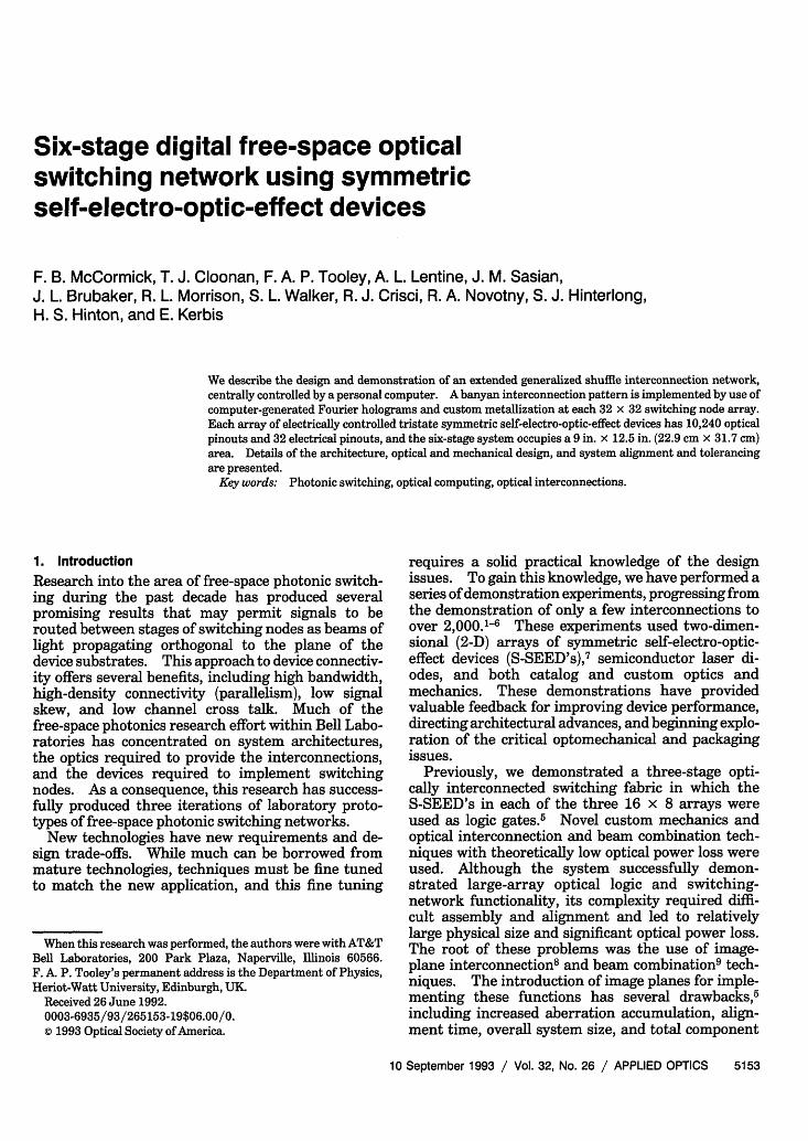
Six-stage digital free-space opticalswitching network using symmetricself-electro-optic-effect devices
F. B. McCormick, T. J. Cloonan, F. A. P. Tooley, A. L. Lentine, J. M. Sasian,J. L. Brubaker, R. L. Morrison, S. L. Walker, R. J. Crisci, R. A. Novotny, S. J. Hinterlong,
H. S. Hinton, and E. Kerbis
We describe the design and demonstration of an extended generalized shuffle interconnection network,centrally controlled by a personal computer. A banyan interconnection pattern is implemented by use ofcomputer-generated Fourier holograms and custom metallization at each 32 x 32 switching node array.Each array of electrically controlled tristate symmetric self-electro-optic-effect devices has 10,240 opticalpinouts and 32 electrical pinouts, and the six-stage system occupies a 9 in. X 12.5 in. (22.9 cm x 31.7 cm)area. Details of the architecture, optical and mechanical design, and system alignment and tolerancingare presented.
Key words: Photonic switching, optical computing, optical interconnections.
1. Introduction
Research into the area of free-space photonic switch-ing during the past decade has produced severalpromising results that may permit signals to berouted between stages of switching nodes as beams oflight propagating orthogonal to the plane of thedevice substrates. This approach to device connectiv-ity offers several benefits, including high bandwidth,high-density connectivity (parallelism), low signalskew, and low channel cross talk. Much of thefree-space photonics research effort within Bell Labo-ratories has concentrated on system architectures,the optics required to provide the interconnections,and the devices required to implement switchingnodes. As a consequence, this research has success-fully produced three iterations of laboratory proto-types of free-space photonic switching networks.
New technologies have new requirements and de-sign trade-offs. While much can be borrowed frommature technologies, techniques must be fine tunedto match the new application, and this fine tuning
When this research was performed, the authors were with AT&TBell Laboratories, 200 Park Plaza, Naperville, Illinois 60566.F. A. P. Tooley's permanent address is the Department of Physics,Heriot-Watt University, Edinburgh, UK.
Received 26 June 1992.0003-6935/93/265153-19$06.00/0.a 1993 Optical Society of America.
requires a solid practical knowledge of the designissues. To gain this knowledge, we have performed aseries of demonstration experiments, progressing fromthe demonstration of only a few interconnections toover 2,000.16 These experiments used two-dimen-sional (2-D) arrays of symmetric self-electro-optic-effect devices (S-SEED's), 7 semiconductor laser di-odes, and both catalog and custom optics andmechanics. These demonstrations have providedvaluable feedback for improving device performance,directing architectural advances, and beginning explo-ration of the critical optomechanical and packagingissues.
Previously, we demonstrated a three-stage opti-cally interconnected switching fabric in which theS-SEED's in each of the three 16 x 8 arrays wereused as logic gates.5 Novel custom mechanics andoptical interconnection and beam combination tech-niques with theoretically low optical power loss wereused. Although the system successfully demon-strated large-array optical logic and switching-network functionality, its complexity required diffi-cult assembly and alignment and led to relativelylarge physical size and significant optical power loss.The root of these problems was the use of image-plane interconnections and beam combinations tech-niques. The introduction of image planes for imple-menting these functions has several drawbacks,5including increased aberration accumulation, align-ment time, overall system size, and total component
10 September 1993 / Vol. 32, No. 26 / APPLIED OPTICS 5153
count, as well as decreased system stability, opticalpower throughput, and signal-level uniformity. Fur-thermore, to avoid unwanted image magnificationbetween image planes, one must precisely match thefocal lengths of all lenses. Since the trade-offs be-tween increased aberration, alignment time, systemstability, and so forth are highly coupled, the optimalsystem design is not obvious.
The evaluation of our previous system resulted inthe following goals for the current system demonstra-tion.
* Decrease the system physical size.* Increase the number of switching nodes ac-
cessed and the optical connectivity provided.* Increase the maximum system data rate.* Decrease the system assembly and alignment
time required.* Increase the system mechanical stability, ther-
mal stability, and alignment tolerances.' 0
* Adopt a more modular and repairable design.* Investigate alternative network control injec-
tion schemes."* Progress toward higher functionality nodes, or
smart pixels.* Minimize the total system component counts.
is composed of two beams, as shown in Fig. 1(a). Theratio of the powers in these beams determines thelogic state that they represent. Since an S-SEEDdoes not emit light, a set of two bias or clock beams isrequired in addition to the input data beams (signalbeams). These beams are formed by the laser andthe spot array generator. In operation, the signalbeams first set the state of the device, and subse-
Input Signals Output Signals
Clock 7 Q
(a)
In this paper we describe a free-space optical switch-ing fabric demonstration that addresses these goals.It implements a fully interconnected extended gener-alized shuffle (EGS) fabricl2 that uses banyan intercon-nections. This EGS fabric connects 16 input chan-nels to 32 output channels; each channel transmits32 bits in parallel. The fabric uses six arrays ofapplication-specific S-SEED's with 1024 S-SEED'sper array. Each stage provides 10,240 optical pin-outs and 32 electrical pinouts of input-output (I/O),and the total system size is approximately 9 in. x 12.5in. (22.9 cm x 31.7 cm). This paper is organized asfollows. After a brief review of S-SEED operationalcharacteristics in Section 2, Section 3 describes thesystem architectural design, including the intercon-nection implementation, node functionality, and con-trol scheme. The optical and mechanical systemdesigns are detailed in Sections 4 and 5. Severalimportant system performance issues are describedin Section 6, and the experimental system results arepresented in Section 7. Lastly, the limitations andsuccesses of the various techniques used in thisexperiment are discussed in Section 8.
2. Symmetric Self-Electro-Optic-Effect DeviceOperation Characteristics
The S-SEED operates as an optical set-reset latch,which can be made to simulate a logic gate.7 Used asa latch, the S-SEED has a single signal input, and itretains the input value until changed by the presenceof an input signal of the opposite state. An S-SEEDlogic gate has at least two signal inputs; their levelsdetermine whether the gate will switch states. TheS-SEED is a differential device; each input and output
ti t2Signals
Clock - _Output - -
S,
S3
R0
time t,
0.6
0.5
*5 0.4
l, 0.30
P 0.2
0.1
0
Clock Q
Clock Q
time th
(b)
0 0.5 1.0 1.5 2.0
Pinl/Pin2
Fig. 1. S-SEED operation: (a) inputs and inverted outputs, (b)signal timing for time-sequential gain showing reflection-modedevice operation, (c) bistability power transfer characteristic. In(c) the reflected output power of one window versus the ratio ofpowers incident upon both windows is shown. The curve wascalculated with measured reflectivity and responsivity data on asingle quantum-well modulator from the first device array.
5154 APPLIED OPTICS / Vol. 32, No. 26 / 10 September 1993
R2
Ri , l/T, T.

quently the clock beams read the state [Fig. 1(b)].Absorption of the signal beams changes the voltageacross each diode of the S-SEED. This voltagechange causes the spectral position of the excitonicabsorption peak to shift and thus changes the absorp-tion or modulation of the clock beams. The reflectedclock beams form the output signals. The device hasgain if the signal beams are not present simulta-neously with the clock beams and if the clock beamshave higher power. This is referred to as time-sequential gain. The output from a S-SEED is thustwo beams that are reflected from both the R window(Q) and S window (Q), as in Fig. 1(a). These outputbeams propagate to the next S-SEED array, whichhas no clock beams incident simultaneously.
The state of the output is expressed as the ratio ofthe power in the Q beam to the power in the Q beam.Therefore it is important that the two read beams areequal in power before reflection. The operation of aS-SEED is determined by the form of the bistablepower transfer characteristic shown in Fig. 1(c).The power reflected from the S window (Q), is plottedagainst the ratio of the total signal powers to the Rand S windows (signal beams). Since the clock powerincident upon the S window is fixed, the reflectedpower is proportional to the reflectivity. The ratio ofthe signal powers is defined as the input contrastratio. If the input contrast is increased from zero,the reflectivity of the S window switches from a lowvalue, RI, to a high value, R2, at an input contrastvalue equal approximately to the ratio of the absor-bances of the two windows, T = (1 - R1 )/(1 - R 2 ).Simultaneously, the reflectivity of the other window(R) switches from R2 to R,. The transition point(ideally) occurs at an input contrast of 1/T = (1 -R2)A(1 - R,) when the input contrast is reduced froma high value. The ratio of the two reflectivities,R 2 /R,, is the output contrast ratio.
The introduction of new clock beams at each S-SEED array (time-sequential gain) performs a digitalregeneration function. This digital regeneration ateach stage restores the amplitude, synchronization,and beam quality of the signals transmitted to thenext stage. If we assume that the outputs of oneS-SEED array can successfully set the states of thedevices in the next S-SEED array, then these arrayscan, in principle, be cascaded indefinitely. The sig-nal regeneration at each stage significantly lessensthe problems of cross talk, signal skew, and overallsystem size limitations for high-speed operation inmultistage systems.
The switching speed of S-SEED's is approximatelydetermined by the absorbed differential power.Since the switching energy of a S-SEED of a givensize and bias voltage is constant, increasing thedifferential power of the incident signal decreases theswitching time. The switching energy scales withthe device size, driving us toward smaller devices.The devices used in this experiment have the follow-
ing characteristics:
* Switching energies of E. = 4 pJ at 10-V bias.* Required bias voltage (across all devices in
parallel) of 10 V.* Operational wavelength range of approximately1 nm about 848.5 nm.* Temperature range of approximately ±3.7 0C
about room temperature.* Fabrication in square arrays with the windows
of each device separated by 20 m. The device spacingis 40 [um in both directions.
* Window sizes of 6 vim x 21 a.m. As is dis-cussed in Section 3, three spots were incident uponeach window. The three spots were spatially sepa-rated to avoid coherent interference, so a 6 m 7Vim area was dedicated to each spot.
* Reflection-mode operation; this facilitates fabri-cation, improves performance, and permits access tothe substrate for optimal heat sinking.
The required bias voltage, operating wavelengthrange, and temperature range are related to thepermissible variations in the optical input powers.For example, a 9-V bias, the device operates withvariations of ±32% in the set and reset input powersat X = 848.5 nm (at room temperature). However,for X = 849.5 nm, the permissible variation decreasesto +22%, and for = 850 nm the permissiblevariation is only 10%. We did not measure theactual variations in optical power, but we think it isbetween 10% and 22%, thus giving us a wavelengthtolerance of greater than ± 1 nm. The primary effectof temperature is to shift the wavelength, and mea-surements on other S-SEED's confirm that a 3.7 'Cchange should shift the excitonic peak by 1 nm. Inthis system the devices were operated at 30 C, whichmoved the best operating wavelength from 848.5 nmto 850 nm for better matching with other systemcomponents (lasers, lenses, and diffractive elements).At this temperature the tolerances may vary slightlyfrom those given above for room temperature. Thetolerance to set and reset variations was not criticallydependent on bias because both the contrast ratio andthe bistable loop width increased with increasingbias. However, the device was more tolerant to clockbeam variations at larger biases because of the in-creased bistable loop width.
3. Architecture
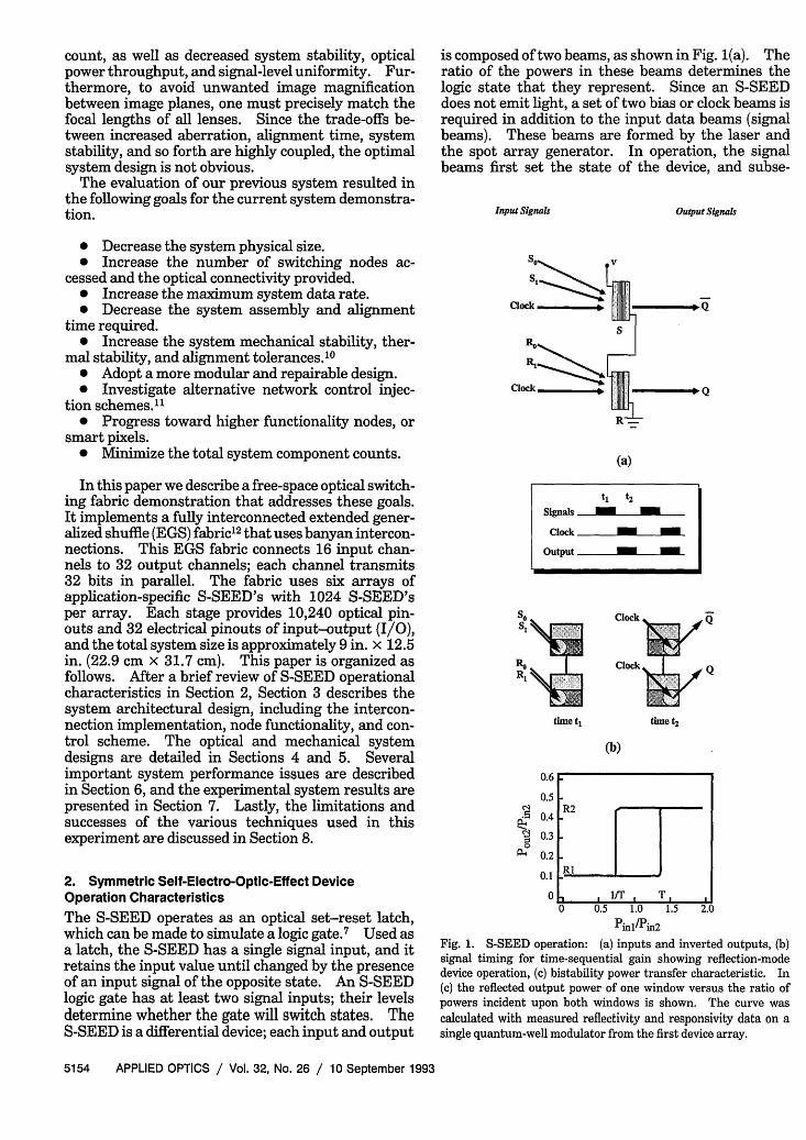
Figure 2 shows a free-space photonic switching fabricthat comprises both optical components and elec-tronic components. In the current system design,the centralized controller and switch-transmissioninterfaces are implemented with electronics, whilethe multistage interconnection network is imple-mented by use of free-space photonics. This divisionof technologies was chosen because the multistageinterconnection network inherently requires a highdensity of high-bandwidth connections.
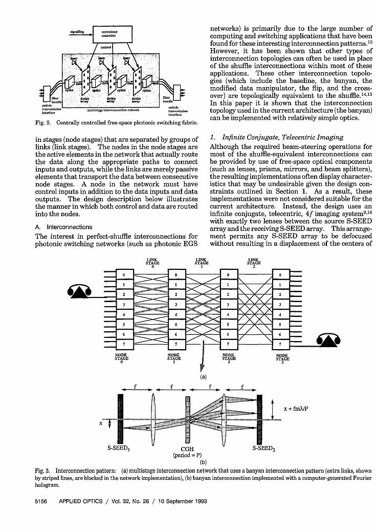
A typical multistage interconnection network isshown in Fig. 3(a), and it consists of nodes arranged
10 September 1993 / Vol. 32, No. 26 / APPLIED OPTICS 5155
Dfiberwtch dlswitch-
fiber,bundle
switch-interface multistage intercoinection network -t-rfia..Interf e " - 'rac
Fig. 2. Centrally controlled free-space photonic switching fabric.
in stages (node stages) that are separated by groups oflinks (link stages). The nodes in the node stages arethe active elements in the network that actually routethe data along the appropriate paths to connectinputs and outputs, while the links are merely passiveelements that transport the data between consecutivenode stages. A node in the network must havecontrol inputs in addition to the data inputs and dataoutputs. The design description below illustratesthe manner in which both control and data are routedinto the nodes.
A. Interconnections
The interest in perfect-shuffle interconnections forphotonic switching networks (such as photonic EGS
LINK LISTAGE ST
0INKAGEI
networks) is primarily due to the large number ofcomputing and switching applications that have beenfound for these interesting interconnection patterns. 13However, it has been shown that other types ofinterconnection topologies can often be used in placeof the shuffle interconnections within most of theseapplications. These other interconnection topolo-gies (which include the baseline, the banyan, themodified data manipulator, the flip, and the cross-over) are topologically equivalent to the shuffle.'4'15
In this paper it is shown that the interconnectiontopology used in the current architecture (the banyan)can be implemented with relatively simple optics.
1. Infinite Conjugate, Telecentric ImagingAlthough the required beam-steering operations formost of the shuffle-equivalent interconnections canbe provided by use of free-space optical components(such as lenses, prisms, mirrors, and beam splitters),the resulting implementations often display character-istics that may be undesirable given the design con-straints outlined in Section 1. As a result, theseimplementations were not considered suitable for thecurrent architecture. Instead, the design uses aninfinite conjugate, telecentric, 4f imaging system9' 16
with exactly two lenses between the source S-SEEDarray and the receiving S-SEED array. This arrange-ment permits any S-SEED array to be defocusedwithout resulting in a displacement of the centers of
LSE2
(a)
^ f , < f W < f M f I
x
CGH(period = P)
x + fmA/P
(b)
Fig. 3. Interconnection pattern: (a) multistage interconnection network that uses a banyan interconnection pattern (extra links, shownby striped lines, are blocked in the network implementation), (b) banyan interconnection implemented with a computer-generated Fourierhologram.
5156 APPLIED OPTICS / Vol. 32, No. 26 / 10 September 1993
kim
o 0X , t'"to'y i 0- -. oo ,0 S 2 ^ V,
delce i devye ; devie ' X>
the signal spots on the array. In addition, thecollimated beams between the lenses accumulate noaberration when they propagate through plane-parallel optical components such as beam splitters.
2. Beam Steering Based on Binary Phase GratingsThe beam-steering operations that provide the link-stage interconnections between adjacent S-SEED ar-rays can be provided by the hardware arrangementshown in Fig. 3(b). This arrangement is based on asimple two-lens infinite-conjugate telecentric imagingsystem set up to provide 4f imaging. However, acomputer-generated hologram (CGH) is added at thepupil plane between the two imaging lenses forproviding the necessary beam-steering operations.1 7
This CHG was fabricated as a binary phase grating(BPG), in a manner similar to that for the BPG's usedto generate the optical power supply, or clock beamarrays.18 19 The effect of a grating on an opticalbeam is well described by the laws of diffraction.The optical power within a beam that is directed at abinary phase grating is typically redirected from thegrating into several orders (diffracted beams) that aresymmetric about the zero-order (nondiffracted beam[Fig. 3(b)]. The grating equation describes the rela-tionship between the angle of the incident beam Qi,the period of the gratingp, the wavelength of the lightX, the grating order m, and the angle of the mthorder's diffracted beam (0d):
p(sin d - sin Oi) =ik. (1)
Changes in the periodic structure of the grating canforce different amounts of optical power from theoriginal beam to be routed into various differentorders, and changes in the period of the grating canforce the different orders to have different angularspacings. When the output beams from the gratingare routed through a lens, each order that containsoptical power creates an output image spot in thefocal plane of that lens. The terms output spot andoutput order are used interchangeably within thispaper. Although this is not strictly correct, there isa one-to-one relationship between the two, becausethe output lens (which must be designed with sin 0distortion) performs an angular-to-spatial transforma-tion, routing light into an order with an angle 0 fromthe optical axis to a spot in the image plane a distanceh = f sin 0 from the optical axis, where f is the focallength of the lens. Thus the action of the grating onany input beam forces consecutive orders to generatea set of spots that are spaced by 4f/p in the imageplane.
The effect of the interconnection CGH on thepropagation of light and the resulting connectionsthat it provides can be easily described as shown inFig. 3(b), in which the effective spot displacementproduced by the hologram and the lens is schemati-cally illustrated by a three-way branch on each beamdirectly following each hologram. After passingthrough a lens of focal length f, the orders from thefirst grating would create three spots that are dis-
placed from one another by a distance of 4f/p in theimage plane. The grating thus diffracts the lightinto the m = 1, m = 0, and m = -1 orders.
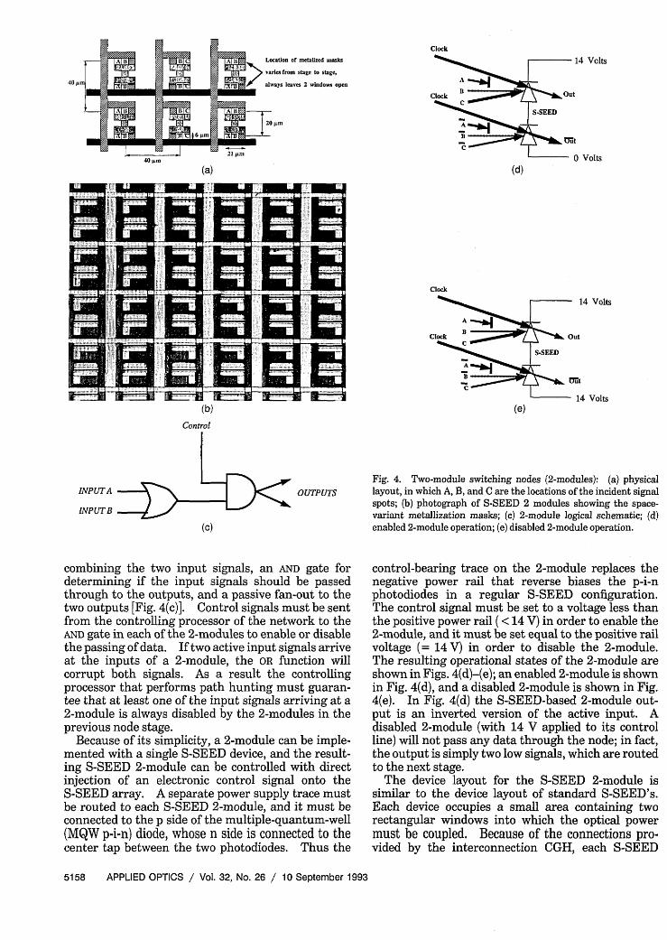
3. Optical Implementation of BanyanInterconnectionsThe banyan network shown in Fig. 3(a) is typicallyused to provide connections between two-input, two-output switching nodes. Since there are two out-puts from each of these nodes, the banyan mustprovide a connection from every node in the nodestage i to two nodes in node stage i + 1.17 If theimage inversion that occurs in a 4f imaging system isignored, then the optical hardware within Fig 3(b)can be used to implement the banyan link-stageconnections. However, several stage-dependent mod-ifications to the hardware must be included. First,the beam displacements provided by the grating (andthe associated grating period) must be varied fromlink stage to link stage because the period of thebanyan interconnection is varied from link stage tolink stage. The grating required for the banyanconnections must produce three output beams (andthree output spots) from each of the input beams, soit is similar to the grating shown in Fig. 3(b). Onlytwo of these three output beams are actually used bythe network; the third beam is an unused beam.Unfortunately, some of the unused beams in theoutput plane are imaged inside of the receivingS-SEED array's working area, so these beams mustbe blocked by a mask before arriving at the receivingS-SEED array. The blocked beams within the net-work are illustrated by striped lines in Fig. 3(a). Theblocking function can be provided by a mask thatpartially covers the S-SEED windows within theoutput image plane. Ideally, this mask would beconstructed of an absorbing material. However, inthe current architecture, the mask is provided by thesame metallization layer that is used for electricalconnectivity within the S-SEED array. This metallayer can be easily modified to force the metal to coverdifferent parts of the S-SEED windows, depending onthe link-stage interconnections being implemented.The resulting application-specific S-SEED's havemetal masks, each covering 33% of each S-SEEDwindow, as shown in Fig. 4(a). These metal maskscovering portions of the S-SEED windows are shownin the photograph of Fig. 4(b). The use of a metallicmask (instead of an absorbing mask) can lead toproblems because of reflected light within the system,but it is shown in Subsection 6.A that, because of thesynchronization of the clock and signal beams, thisreflected power problem is not significant.
B. Nodes
EGS networks can be implemented with many differ-ent types of switching nodes. A two-module switch-ing node (2-module) is a simple switching node thathas two inputs and two outputs, so it is well suited foruse with the banyan interconnection. In its simplestdigital form a 2-module contains an OR gate for
10 September 1993 / Vol. 32, No. 26 / APPLIED OPTICS 5157
Clock
.At B ~qSB I uc AlI Location O tmelalzed asks
_aries from stage to stage,
40 p.- a s leaves 2 windows open
_ 5 _ ~~~~~~~~~~20 Am.
(d)
Clock
(e)
- 14 Volts
Out
trth
- 0 Volts
- 14 Volts
out
- 14 Volts
Fig. 4. Two-module switching nodes (2-modules): (a) physicallayout, in which A, B, and C are the locations of the incident signalspots; (b) photograph of S-SEED 2 modules showing the space-variant metallization masks; (c) 2-module logical schematic; (d)enabled 2-module operation; (e) disabled 2-module operation.
combining the two input signals, an AND gate fordetermining if the input signals should be passedthrough to the outputs, and a passive fan-out to thetwo outputs [Fig. 4(c)]. Control signals must be sentfrom the controlling processor of the network to theAND gate in each of the 2-modules to enable or disablethe passing of data. If two active input signals arriveat the inputs of a 2-module, the OR function willcorrupt both signals. As a result the controllingprocessor that performs path hunting must guaran-tee that at least one of the input signals arriving at a2-module is always disabled by the 2-modules in theprevious node stage.
Because of its simplicity, a 2-module can be imple-mented with a single S-SEED device, and the result-ing S-SEED 2-module can be controlled with directinjection of an electronic control signal onto theS-SEED array. A separate power supply trace mustbe routed to each S-SEED 2-module, and it must beconnected to the p side of the multiple-quantum-well(MQW p-i-n) diode, whose n side is connected to thecenter tap between the two photodiodes. Thus the
control-bearing trace on the 2-module replaces thenegative power rail that reverse biases the p-i-nphotodiodes in a regular S-SEED configuration.The control signal must be set to a voltage less thanthe positive power rail (< 14 V) in order to enable the2-module, and it must be set equal to the positive railvoltage (= 14 V) in order to disable the 2-module.The resulting operational states of the 2-module areshown in Figs. 4(d)-(e); an enabled 2-module is shownin Fig. 4(d), and a disabled 2-module is shown in Fig.4(e). In Fig. 4(d) the S-SEED-based 2-module out-put is an inverted version of the active input. Adisabled 2-module (with 14 V applied to its controlline) will not pass any data through the node; in fact,the output is simply two low signals, which are routedto the next stage.
The device layout for the S-SEED 2-module issimilar to the device layout of standard S-SEED's.Each device occupies a small area containing tworectangular windows into which the optical powermust be coupled. Because of the connections pro-vided by the interconnection CGH, each S-SEED
5158 APPLIED OPTICS / Vol. 32, No. 26 / 10 September 1993
40 Rum21 (m
(a)
(b)
Control
INPUTA
INPUT B
OUTPUTS
(C)
window receives three input signals. The three datasignals incident upon the top window of a 2-moduleare labeled A, B, and C [Fig. 4(g)], and the logical com-plements of these signals (A, B, and C) are thereforeimaged on the bottom window. For a 2-module tooperate correctly, one of these three signals must beblocked, one of the signals can be enabled, and theother signal must be disabled. The signals that areblocked change from stage to stage, and so that thissignal masking is enabled, the three signals areimaged to different spatial locations within the devicewindow, as shown in Fig. 4(a). This also avoids thedestructive interference that can occur between theenabled and disabled signals, were they coincident.In order to provide sufficient space for the three spotswithin a single device window, the dimensions on thedevice windows for the current architecture werechosen to be 6 jLm x 21 jim, and the two windowsassociated with a particular S-SEED were givencenter-to-center spacings of 20 jim. Thus a 32 x 32array of S-SEED's contains a 64 x 32 array ofwindows. The rectangular S-SEED windows areoriented with the long edge of the rectangle in thehorizontal direction. The center-to-center spacingbetween windows in the vertical dimension is 20 m,and the center-to-center spacing between windows inthe horizontal dimension is 40 jum. Thus the entiredevice array occupies an area of 1.28 mm x 1.28 mm.
C. Control
Every switching network must provide a means ofinjecting control signals into the switching nodes toset up the paths within the fabric. Many differentcontrol injection techniques have been proposed forphotonic switching applications.20 In previous exper-iments, various forms of these control injection tech-niques have been implemented. For example, oneexperimental prototype used a spatial light modula-tor (a movable mask) for selectively blocking clocksignals for creating the control signals for the nodes.4Although this control injection technique yielded anoperational fabric, the fabric reconfiguration rate waslimited by the speed of the spatial light modulator,and the system data rate was limited by the opticallosses within the spatial light modulator. Also, theaddition of the spatial light modulator to the systemrequired that additional components be added, andthis resulted in a relatively complicated hardwaredesign.
Another experimental prototypes injected the con-trol signals in through the front end of the network,passing the control signals from node stage to nodestage through the same optics used by the datasignals. This approach was promising, but it re-quired more complicated nodes to store the controlbits. In addition, the approach also required a morecomplicated front end within the system design, andthe prototype implemented only the input interfaceand one switching stage of the network.
In the current prototype, direct injection of elec-tronic control signals into the S-SEED array was
used. A personal computer performed the routingcalculations, and custom-designed driver electronicsinterfaced to the computer created the control signalsthat were distributed to each column of the S-SEEDswitching-node arrays. This experiment imple-ments the input interface and five switching stagesfor providing full connectivity between 16 input portsand 32 output ports. The drawbacks of this ap-proach are the requirement of additional pinouts onthe S-SEED package and the increased size of theS-SEED array for accommodating the control traces.The bandwidth of the package pinouts may also limitthe reconfiguration rate of the fabric. However, thedirect injection technique does not require any compli-cation of the system optics nor increase in the nodeoptical hardware.
Ideally, each S-SEED 2-module in the device arraywould have a unique trace routed to it for directcontrol injection, but this would require 1024 connec-tions to the 32 x 32 S-SEED array. The number ofleads could be reduced by placement of a memory cellnext to each 2-module so that multiple control bitscan be multiplexed on a smaller number of controltraces. However, this technique requires smart-pixel technologies, which are still under develop-ment.21 Thus control injection design for the cur-rent architecture uses only 32 control traces, andeach control trace is routed vertically between adja-cent columns to the 32 S-SEED 2-modules in aparticular column of the device array. This controlinjection technique places certain limitations on therouting permutations that can be provided in theresulting network because it forces all of the S-SEED2-modules within a column to have the same controlsignals, and it permits switching of data only betweencolumns. Thus if one bit in column i is switched tocolumn j, then all of the bits in column i must beswitched to columnj. Although is has some short-comings, this approach permits testing of a realcontrol injection technique within the system. Inaddition, a large device array with a relatively largefield of view can be fully operated and tested.
D. Input/Output
In a switching network based on free-space digitaloptics, the input and output signals would probablybe interfaced to the optical fabric via fibers. Eachfiber would be associated with a distinct input (out-put) channel, and the fibers would be bundled into arectangular matrix for permitting spots to be imagedbetween the bundle an the S-SEED arrays.
However, for the current prototype system, thefunction of the input fiber bundle is performed with aSEED spatial light modulator array.7 An S-SEED inthe spatial light modulator array is set by electroni-cally injected data signals to be a logical 1 (with ahigh-power Q beam) or a logical 0 (with a low-power Qbeam). The data lines are connected to the centertap between the pair of MQW diodes, so the voltageacross the diodes can be determined by externalelectronics that inject data into the fabric. Ideally,
10 September 1993 / Vol. 32, No. 26 / APPLIED OPTICS 5159
each S-SEED in the spatial light modulator arraywould be set by a distinct data line. However,because of the pinout limitations described above,only 32 data lines are injected into the 32 x 32 array,so the 32 S-SEED modulators down any column inthe array are driven with the same data line. Sincethe devices in the S-SEED spatial light modulatorarray do not have a control trace connected to theirbias rails, they cannot be selectively disabled as the2-modules can be. As a result, if all the spatial lightmodulator devices produce active data, data corrup-tion will always occur in the succeeding node stage.To circumvent this problem, one can illuminate onlythe even-numbered columns of the spatial light mod-ulator by using the clock laser.
The output fiber bundle is replaced in the currentprototype by a CCD camera. As a result, the qualityof the optical waveforms in the system and the overalltemporal operation of the system can be qualitativelyanalyzed by observation of the system output signalson display monitors.
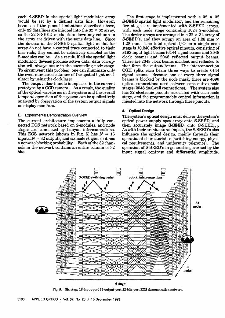
E. Experimental Demonstration Overview
The current architecture implements a fully con-nected EGS network based on 2-modules, and nodestages are connected by banyan interconnections.This EGS network (shown in Fig. 5) has N = 16inputs, N = 32 outputs, and six node stages, so it hasa nonzero blocking probability. Each of the 32 chan-nels in the network contains an entire column of 32bits.
The first stage is implemented with a 32 x 32S-SEED spatial light modulator, and the remainingfive stages are implemented with S-SEED arrays,with each node stage containing 1024 2-modules.The device arrays are arranged in a 32 x 32 array ofS-SEED's, and they occupy an area of 1.28 mm x1.28 mm. The total optical I/O on a single nodestage is 10,240 effective optical pinouts, consisting of8192 input light beams (6144 signal beams and 2048clock beams) and 2048 reflected output beams.There are 2048 clock beams incident and reflected tothat form the output beams. The interconnectionCGH splits each beam three ways to create 6144signal beams. Because one of every three signalbeams is blocked by the node mask, there are 4096optical connections used between consecutive nodestages (2048 dual-rail connections). The system alsohas 32 electronic pinouts associated with each nodestage, and the programmable control information isinjected into the network through these pinouts.
4. Optical Design
The system's optical design must deliver the system'soptical power supply spot array onto S-SEEDi andthen accurately image S-SEED, onto S-SEED,+l.As with their architectural impact, the S-SEED's alsoinfluence the optical design, mainly through theiroperational characteristics (switching energy, physi-cal requirements, and uniformity tolerance). Theoperation of S-SEED's in general is governed by theinput signal contrast and differential amplitude.
optical interconnections
32nodes
6 stages
Fig. 5. Six-stage 16-input-port 32-output-port 32-bits-port EGS demonstration network.
5160 APPLIED OPTICS / Vol. 32, No. 26 / 10 September 1993
The input signal contrast is Cin PS/PR, or the ratioof total powers incident upon the S and R diodes ofthe S-SEED. So that a binary 1 is correctly trans-ferred from one device to the next, C1,, must be greaterthan -1.4 (or < 1/1.4 for a binary 0) for a 10-Vapplied bias. The speed at which the S-SEEDswitches states to store this bit of information isapproximately determined by the absolute powerdifference between Ps and PR, AP = Ps - PR, andthus by the signal power transmission efficiency fromthe previous stage. Signal contrast is affected by theS-SEED contrast, the uniformity of the power supplyspot array generation, the transmission uniformity ofthe optical path, the degree to which all spots aresimilarly coupled into the device windows, and thepresence of scattered light in the system. Signaltransmission efficiency is determined primarily bythe optical component transmissions but also by theoverall spot/device window coupling efficiency as wellas by any vignetting of the signal beams by the opticalsystem. These constraints, in addition to other prac-tical system attributes, mandate an optical systemdesign that should do the following:
* Provide a high space-bandwidth product. Thepower/speed trade-offs associated with S-SEED's ne-cessitate small device sizes for minimizing devicecapacitance and switching energy and thus achievinghigh-speed operation with low incident optical power.The small optical input/output windows of the de-vices mandate a high-resolution optical imaging sys-tem. Coupling 99% of a beam's power into a 5-jimwindow requires objective lens speeds of <f/1.7 (Ref.5) and a high degree of wave-front correction (Strehlratio > 0.8, or diffraction limited). Since the -SEED's are fabricated on a flat substrate, the opticalsystem must operate uniformly over a flat image fieldof at least 1.28 mm 1.28 mm. Infinite conjugateimaging was used in this experiment; the power andsignal beams are thus focused to spot arrays at theimage planes and are arrays of collimated beamsbetween image planes. Since the laser beams arecollimated when they pass through elements such aspolarizing beam splitters and retarders, aberrationaccumulation is minimized. A highly symmetric op-tical design forces aberrations that are odd functionsof the pupil radius to be canceled, thus minimizingthe accumulation of coma, distortion, and image tilt.The optical system used in this experiment makesthree passes through a very well corrected f/ 1. 5 lensand can produce 5-ji.m pots (e- 2 diameter) over a4.2-mm 2 area, thus providing a space-bandwidthproduct of over 2 x 10⁵.
* Ease alignment tolerances. This is difficult todo since it conflicts with device size/resolution require-ments discussed above; however, certain techniquesare effective, such as the use of telecentric imaging forminimizing the lateral misalignment effects of imagedefocus. Nearly telecentric imaging was used in thisexperiment for increasing the alignment tolerances.
* Enable high optical throughput efficiency and
uniformity. Efficiency can be increased by minimiza-tion of the number of surfaces (and thus Fresnelreflection losses) encountered along the optical path.Since clipping energy from any of the beams from theBPG may introduce signal-level nonuniformities aswell as loss, no vignetting may be tolerated. Scat-tered or stray light causes nonuniformity and lowersignal-to-noise ratios, affecting system speed in amanner similar to a loss of efficiency. These issuesare discussed in detail in Section 6.
* Permit accurate image registration. Align-ment concerns require -f sin 0 distortion to matchthe sin 0 diffraction of the binary phase gratings(BPG's) used for spot array generation and intercon-nection. Since the BPG defines the aperture stop ofthese systems, telecentric imaging requires the objec-tive lens to have an external aperture stop and a frontfocal length large enough to permit space between thestages for polarizing beam splitters and other opticalelements. The objective lens used in this experi-ment has a front focal length of-approximately 15 mmand f sin 0 distortion.
* Minimize system physical size and cost. Smallsize can be achieved by minimizing the number ofcomponents, the number of image planes, and thefocal lengths of the lenses. The focal length of theobjective lenses is highly coupled to other systemparameters. An increase in focal length decreasesthe field angle over which the lens must operate, for agiven image size, and thus eases aberration control(especially field curvature and distortion). Addition-ally, it helps the fabrication tolerances of the BPG's,since it permits the use of a larger grating period.Maintaining the low f-number, however, requires alarger laser beam diameter, and thus an increase inthe clear aperture of the rest of the components of thesystem [polarizing beam splitters (PBS's), wedges,prisms, and so forth]. For minimization of aberra-tion contributions and vignetting from these compo-nents, their diameters must generally be 1.5-2 timesthe beam diameter, which also increases the compo-nent costs. The longer focal length further de-creases the angular tolerance for beam pointing andrequires higher precision beam pointing mechanisms.The focal length of the lens used in this experimentwas 15.61 mm, a reasonable compromise betweenthese trade-offs. The objective lens working dis-tance must be at least 1 mm owing to S-SEEDpackaging characteristics (such as wire bonds andcover glass).
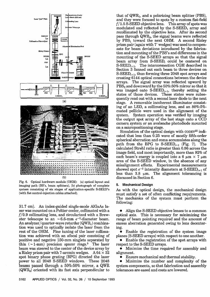
The optical hardware necessary for implementa-tion of a multistage interconnection network may besubdivided into optical hardware modules (OHM's)for facilitating assembly, test, and repair. Each OHMconsists of the hardware associated with one S-SEEDarray. The OHM's are identical except for a changein the period of the interconnection CGH.
The OHM in Fig. 6(a) is 1.5 in. x 12.5 in. (3.8 cm x31.7 cm) in size, and the complete system of six stagesshown in Fig. 6(b) occupies 9 in. x 12.5 in. (22.9 cm x
10 September 1993 / Vol. 32, No. 26 / APPLIED OPTICS 5161
Laer "pen" Plae
Analyzer
;A4CWflimatl.n Fine-Adjut
Risley Pdism
509BS
BPG PBS ~~~PBS PBS PBS
S-SEEDI S-SEED 1 1
(a)
(b)
Fig. 6. Optical hardware module (OHM): (a) optical layout andimaging path (BS's, beam splitters), (b) photograph of completesystem consisting of six stages of application-specific S-SEED's(with flat control-injection cables attached).
31.7 cm). An index-guided single-mode AlGaAs la-ser was mounted on a Peltier cooler, collimated with af/0.9 collimating lens, and circularized with a Brew-ster telescope to an 6.6-mm e-2-diameter beam.An analyzer/quarter-wave retarder (QWR1) combina-tion was used to optically isolate the laser from therest of the OHM. Fine tuning of the laser collima-tion was achieved with an afocal pair consisting ofpositive and negative 150-mm singlets separated bythin (- 1-mm) precision spacer rings.5 The laserbeam was steered to the center of the device array bya Risley prism pair with 7-arcmin wedges. A 64 x 32spot binary phase grating (BPG) directed the laserpower to all 2048 S-SEED windows. These 2048beams passed through a 50%:50% mirror, a QWR(QWR2) oriented with its fast axis perpendicular to
that of QWR1, and a polarizing beam splitter (PBS),and they were focused to spots by a custom flat-fieldf/1.5 S-SEED objective lens. This array of spots wasmodulated and reflected by the S-SEED1 array andrecollimated by the objective lens. After its secondpass through QWR3, the signal beams were reflectedby PBS1 toward the next OHM. A second Risleyprism pair (again with 7' wedges) was used to compen-sate for beam deviations introduced by the fabrica-tion and mounting of the PBS's and differences in themounting of the S-SEED arrays so that the signalbeam array from S-SEED could be centered onS-SEEDi+1 . The interconnection CGH described inSection 3 fanned out each beam to three devices onS-SEEDi+1, thus forming three 2048 spot arrays andcreating 6144 optical connections between the devicearrays. The signal array was reflected upward byPBS2 and downward by the 50%:50% mirror so that itwas imaged onto S-SEEDi+1, thereby setting thestates of those devices. These states were subse-quently read out with a second laser diode to the nextstage. A removable incoherent illuminator consist-ing of an LED, a collimating lens, and an 80%:5%-coated pellicle were used in the alignment of thesystem. System operation was verified by imagingthe output spot array of the last stage onto a CCDcamera system or an avalanche photodiode mountedon a micropositioning stage.
Simulation of the optical design with CODEV22 indi-cated that less than 0.25 wave of mostly fifth-orderspherical aberration and coma accumulates along thepath from the BPG to S-SEEDi÷1 (Fig. 7). Thecalculated Strehl ratio is greater than 0.86 across theimage field, and most importantly, more than 92% ofeach beam's energy is coupled into a 6 m x 7 imarea of the S-SEED window, in the absence of anymisalignment effects. Experimental measurementsshowed spot e-2 intensity diameters at S-SEEDi+1 ofless than 3.8 Wim. The alignment tolerancing isdiscussed in Section 6.
5. Mechanical Design
As with the optical design, the mechanical designmust satisfy a set of often conflicting requirements.The mechanics of the system must perform thefollowing:
* Align the S-SEED objective lenses to a commonoptical axis. This is necessary for minimizing therange of beam pointing required and the amount ofexcess aberration generated owing to lens decenter-ing.
* Enable the registration of the system imageplanes (S-SEED arrays) with respect to one another.
* Enable the registration of the spot arrays withrespect to the S-SEED arrays.
* Minimize the time required for assembly andalignment.
* Ensure mechanical and thermal stability.* Minimize the number and complexity of the
system components, so that fabrication and assemblytolerances are eased and costs are lowered.
5162 APPLIED OPTICS / Vol. 32, No. 26 / 10 September 1993
Y-FAN
0.25
- 0.25
0. 25
25
-. 25
0.25
( XI, Y )
1.00, 1.00RELATIVE FIELD( 2.35', 2.35')
-z ` 4 /
0.85, 0.85RELATIVE FIELD
( 2.00', 2.00')
1_ ' 3 - .
0.43, 0.43RELATIVE FIELD
12 -.00', 1.00') I
0. 00, 0. 00RELATIVE FIELD
( 0.00', 0.00')
-1-I-
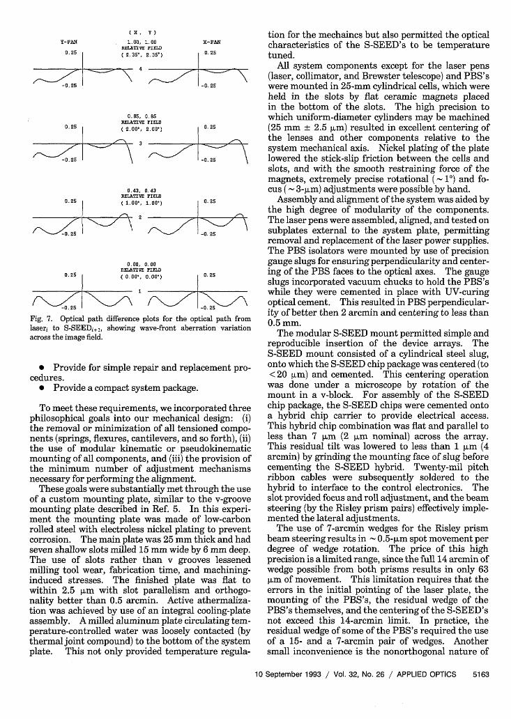
Fig. 7. Optical path difference plots for the optlaseri to S-SEEDi+1, showing wave-front aberr,across the image field.
* Provide for simple repair and replacedures.
* Provide a compact system package.
To meet these requirements, we incorpphilosophical goals into our mechanicalthe removal or minimization of all tensinents (springs, flexures, cantilevers, and:the use of modular kinematic or pseumounting of all components, and (iii) thethe minimum number of adjustmentnecessary for performing the alignment.
These goals were substantially met thrcof a custom mounting plate, similar to Imounting plate described in Ref. 5. Inment the mounting plate was made ofrolled steel with electroless nickel platincorrosion. The main plate was 25 mm tiseven shallow slots milled 15 mm wide byThe use of slots rather than v groovmilling tool wear, fabrication time, andinduced stresses. The finished platewithin 2.5 jim with slot parallelism anality better than 0.5 arcmin. Active tion was achieved by use of an integral cassembly. A milled aluminum plate circperature-controlled water was loosely ccthermal joint compound) to the bottom oplate. This not only provided tempera
tion for the mechaincs but also permitted the opticalX-FM characteristics of the S-SEED's to be temperature0.25 tuned.
All system components except for the laser pens\~'N (laser, collimator, and Brewster telescope) and PBS's
-0. 25 were mounted in 25-mm cylindrical cells, which wereheld in the slots by flat ceramic magnets placedin the bottom of the slots. The high precision towhich uniform-diameter cylinders may be machined
0.25 (25 mm ± 2.5 aim) resulted in excellent centering ofthe lenses and other components relative to thesystem mechanical axis. Nickel plating of the plate
-0.25 lowered the stick-slip friction between the cells andslots, and with the smooth restraining force of themagnets, extremely precise rotational (-1) and fo-cus (- 3-jim) adjustments were possible by hand.
0. 25 Assembly and alignment of the system was aided bythe high degree of modularity of the components.
rs&\ The laser pens were assembled, aligned, and tested on-0.25 subplates external to the system plate, permitting
removal and replacement of the laser power supplies.The PBS isolators were mounted by use of precisiongauge slugs for ensuring perpendicularity and center-
0.25 ing of the PBS faces to the optical axes. The gaugeslugs incorporated vacuum chucks to hold the PBS's
y-7 while they were cemented in place with UV-curing
optical cement. This resulted in PBS perpendicular-ical path from ity of better then 2 arcmin and centering to less thanition variation 0.5 mm.
The modular S-SEED mount permitted simple andreproducible insertion of the device arrays. TheS-SEED mount consisted of a cylindrical steel slug,
cement pro- onto which the S-SEED chip package was centered (to< 20 m) and cemented. This centering operationwas done under a microscope by rotation of themount in a v-block. For assembly of the S-SEED
orated three chip package, the S-SEED chips were cemented ontodesign: (i) a hybrid chip carrier to provide electrical access.
)ned compo- This hybrid chip combination was flat and parallel toso forth), (ii) less than 7 lm (2 A.m nominal) across the array.cdokinematic This residual tilt was lowered to less than 1 um (4provision of arcmin) by grinding the mounting face of slug beforemechanisms cementing the S-SEED hybrid. Twenty-mil pitch
ribbon cables were subsequently soldered to theugh the use hybrid to interface to the control electronics. The
,he v-groove slot provided focus and roll adjustment, and the beamthis experi- steering (by the Risley prism pairs) effectively imple-low-carbon mented the lateral adjustments.
g to prevent The use of 7-arcmin wedges for the Risley prismiick and had beam steering results in 0.5-Lm spot movement pery6 mm deep. degree of wedge rotation. The price of this high,es lessened precision is a limited range, since the full 14 arcmin ofmachining- wedge possible from both prisms results in only 63
was flat to im of movement. This limitation requires that thernd orthogo- errors in the initial pointing of the laser plate, theithermaliza- mounting of the PBS's, the residual wedge of the:ooling-plate PBS's themselves, and the centering of the S-SEED'sulating tem- not exceed this 14-arcmin limit. In practice, the)ntacted (by residual wedge of some of the PBS's required the usef the system of a 15- and a 7-arcmin pair of wedges. Anotherture regula- small inconvenience is the nonorthogonal nature of
10 September 1993 / Vol. 32, No. 26 / APPLIED OPTICS 5163
l
4 2

the beam pointing when Risley prisms are used.Since each wedge sweeps the spot through a circleindependently, together, the wedge pair does notprovide the perpendicular X-Y movements of a foldmirror, but rather provides a spiraling movement,This was a negligible inconvenience in practice.Another potential difficulty exists if the wedges ofeach prism pairs are not perfectly matched. Theresulting wedge difference results in a small regionabout the nominal beam direction that is unreachable.This was not evident in this experiment, since itrequires that the spot array be nearly perfectlyaligned to the S-SEED's without the Risley prismpair in place. It could thus be easily corrected by aslight rough repointing of the laser plate. Since fewmechanical vibrations or thermal expansions/contrac-tions will act to rotate the Risley prism or BPG cellswithin the slots, this lateral alignment mechanism isinherently stable. In addition, it is simple, compact,and inexpensive.
The alignment of each stage of the system followsan identical procedure. Before system assembly, thelaser pens and S-SEED mounts were assembled andaligned off-line in separate alignment fixtures, andthe PBS's were aligned and cemented to their remov-able pedestals on the system plate.
The laser pen assembly proceeds first by alignmentof the collimating objective to the fixed laser while theoutput wave-front error and collimation is monitoredwith a radially shearing interferometer.2 3 After thelens is cemented in place, the Brewster telescope isadjusted to circularize the 3:1 ellipticity of thecollimated beam. Adjustment of the Brewster tele-scope is necessary because of the significant (10%-20%) variation of divergence angles between the laserdiodes used in the system. Interferometric monitor-ing of the wave front after the Brewster telescope alsoenabled very sensitive collimation testing. Lack ofcollimation of only 0.1 wave resulted in 0.25 wave ofastigmatism, easily visible in the interferogram.
The optical isolator is adjusted for maximum trans-mission of the beam through the PBS. The collima-tion of the beam is checked with a scanning laterallyshearing interferometer, and it is fine tuned (if neces-sary) by variation of the separation of the singlets ofthe afocal pair with precision spacers.24 The 64 x 32array of spots formed by the BPG is visually alignedonto the S-SEED array by insertion of a X/2 retarderin place of the interconnection CGH and observationof the reflected image with a 600-mm focal lengthCCD camera system mounted at the output of Stage6.Sliding the lens within the slot focuses the spots,while rotation of the first Risley prism pair and theBPG provides x, y, and rotational alignment. Sincethe entire array is not viewable at this magnification,the S-SEED array was fabricated with the letter F atits center for ensuring proper overall orientation ofthe spot array.
For alignment of the output of this stage, which isthe reflected clock spot array from S-SEEDi, onto thenext stage, the X/2 retarder is moved after PBSi+l
and S-SEEDi+l is rotated to match S-SEEDi, (includ-ing the image inversion). After the second Risleyprism pair is rotated to align the spots laterally, CGHis inserted and rotated to align the three 64 x 32signal spot arrays onto S-SEEDi+1.
The simplicity, ready access, and smoothness of theindividual alignment mechanisms enables the assem-bly and alignment of each OHM to be performed inless than 30 min.
6. System Issues
A. Scattered Light
Any light that does not follow the ideal path of lightflow in the system creates a type of optical spatialnoise that can cause signal level nonuniformities,lower system speed, or operational errors. Evenperfectly uniform scattered light degrades the systemoperation, since it lowers the differential input signalcontrasts. In this system the high quality of theoptical surfaces and coatings limits the accumulationof randomly scattered light, but optical spatial noiseeffects are still present owing to the presence atS-SEEDi of the disabled signals from Stagei-1, reflec-tions of the signal beams from the window masks ofprevious stages, interconnection CGH noise orders,and polarization power-leakage effects.
The most fundamental optical noise problem is thelowered effective contrast caused by the simultaneousdelivery of the disabled signal with the enabled signal.For example, if a logic 1 signal has a contrast of CRin= 3:1, the additional presence of 1 jiW at both opticalinput windows lowers the contrast to (3 + 1) jiW:(1 +1) RW, or CRin = 2:1. In principle, both of the beamsin each disabled signal are of equal amplitude, but inpractice they may be unequal because of BPG errors,nonuniform transmission through lenses and PBS's,or misalignments at S-SEEDi_1 or S-SEED. Thesenonuniformities can further lower the effective inputsignal contrast, thereby lowering the maximum speedof operation or preventing operation at any speed.Although it is difficult to separate the nonuniformityof the disabled signals from that of the enabled signal,the successful operation of the system indicates thatthe uniformity is better than the worst case, in whichthe disabled signals would effectively cancel the en-abled signals and lower the effective contrast enoughto cause switching errors.
Reflections from the interconnection masks on theS-SEED windows are another source of optical spatialnoise. Ideally, the S-SEED window masks would behighly absorbing; however, this would require addi-tional device processing steps. If we trace one of thereflected signals from the output of the first devicearray (Fig. 8), we find that the undesirable reflectionsignal is created at the second device array and canpropagate to the third device array. All odd-num-bered stages are clocked synchronously out of phasewith the even-numbered stages. Thus at the thirddevice array the reflected noise signals are presentsimultaneously with the much higher powered clockbeams. The power of the clock signals thus over-
5164 APPLIED OPTICS / Vol. 32, No. 26 / 10 September 1993
2-module array (source)40 .o
order order oder ou~ter order orger ordr order order order order
ffi S ark <H~2 34
3-module army (redever)
noise orders 3 signal spots noise orders
Noise power 1.4% etagoolpower P,
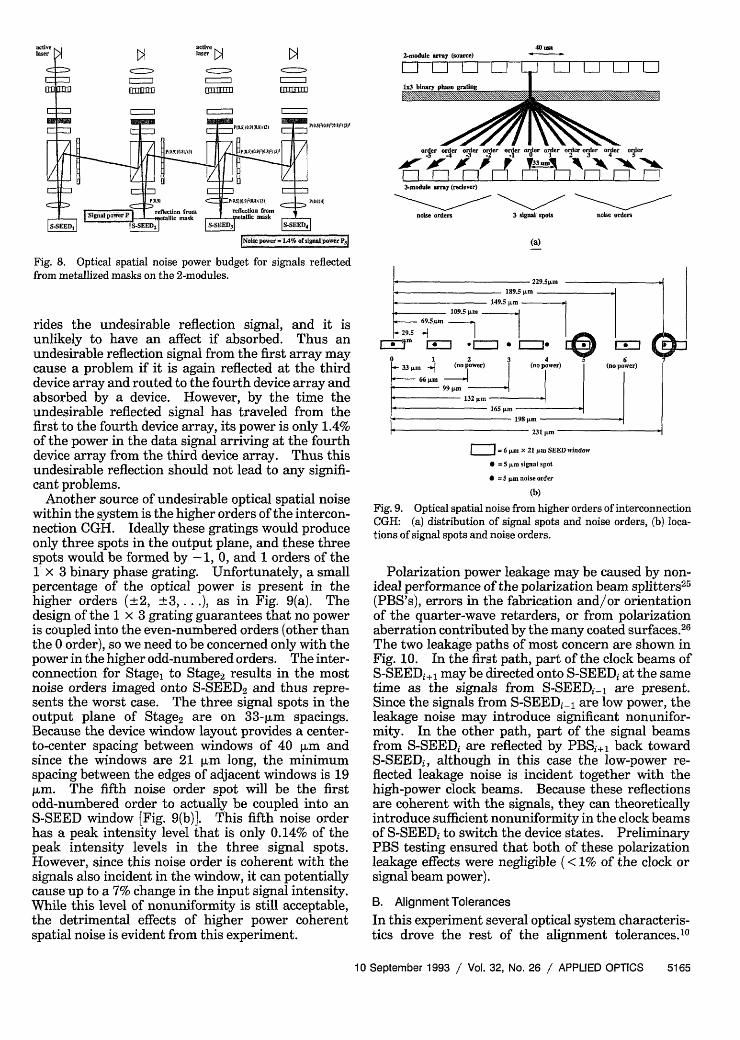
Fig. 8. Optical spatial noise power budget for signals reflectedfrom metallized masks on the 2-modules.
rides the undesirable reflection signal, and it isunlikely to have an affect if absorbed. Thus anundesirable reflection signal from the first array maycause a problem if it is again reflected at the thirddevice array and routed to the fourth device array andabsorbed by a device. However, by the time theundesirable reflected signal has traveled from thefirst to the fourth device array, its power is only 1.4%of the power in the data signal arriving at the fourthdevice array from the third device array. Thus thisundesirable reflection should not lead to any signifi-cant problems.
Another source of undesirable optical spatial noisewithin the system is the higher orders of the intercon-nection CGH. Ideally these gratings would produceonly three spots in the output plane, and these threespots would be formed by -1, 0, and 1 orders of the1 x 3 binary phase grating. Unfortunately, a smallpercentage of the optical power is present in thehigher orders (-+2, 3 ... ), as in Fig. 9(a). Thedesign of the 1 x 3 grating guarantees that no poweris coupled into the even-numbered orders (other thanthe 0 order), so we need to be concerned only with thepower in the higher odd-numbered orders. The inter-connection for Stage, to Stage2 results in the mostnoise orders imaged onto S-SEED2 and thus repre-sents the worst case. The three signal spots in theoutput plane of Stage2 are on 33-jm spacings.Because the device window layout provides a center-to-center spacing between windows of 40 jim andsince the windows are 21 jim long, the minimumspacing between the edges of adjacent windows is 19jm. The fifth noise order spot will be the firstodd-numbered order to actually be coupled into anS-SEED window [Fig. 9(b)]. This fifth noise orderhas a peak intensity level that is only 0.14% of thepeak intensity levels in the three signal spots.However, since this noise order is coherent with thesignals also incident in the window, it can potentiallycause up to a 7% change in the input signal intensity.While this level of nonuniformity is still acceptable,the detrimental effects of higher power coherentspatial noise is evident from this experiment.
(a)
189.5 Pm
149.5 p.m109.5 Rm
69.5,um
-29.5 |
0~ y * [ J lo }[ a
33m A n (no power)66 m -n
* . 99 p.m
132 p.m
165 p.m b
198 P.m
m = 6 m eX 21 p.m SEED window
* = 5 P.m signal spot
* =5 .mnoise order
(b)
Fig. 9. Optical spatial noise from higher orders of interconnectionCGH: (a) distribution of signal spots and noise orders, (b) loca-tions of signal spots and noise orders.
Polarization power leakage may be caused by non-ideal performance of the polarization beam splitters25
(PBS's), errors in the fabrication and/or orientationof the quarter-wave retarders, or from polarizationaberration contributed by the many coated surfaces.26
The two leakage paths of most concern are shown inFig. 10. In the first path, part of the clock beams ofS-SEEDi+, may be directed onto S-SEEDi at the sametime as the signals from S-SEEDi-1 are present.Since the signals from S-SEEDL , are low power, theleakage noise may introduce significant nonunifor-mity. In the other path, part of the signal beamsfrom S-SEEDi are reflected by PBSi+,1 back towardS-SEEDi, although in this case the low-power re-flected leakage noise is incident together with thehigh-power clock beams. Because these reflectionsare coherent with the signals, they can theoreticallyintroduce sufficient nonuniformity in the clock beamsof S-SEED, to switch the device states. PreliminaryPBS testing ensured that both of these polarizationleakage effects were negligible (< 1% of the clock orsignal beam power).
B. Alignment Tolerances
In this experiment several optical system characteris-tics drove the rest of the alignment tolerances.'0
10 September 1993 / Vol. 32, No. 26 / APPLIED OPTICS 5165
activelaser
II -
Clock/Power
S-SEED Arrays
Fig. 10. Critical power leakage paths caused by polarizationerrors: path 1 (upper), path 2 (lower). Gray arrows denoteleakage power.
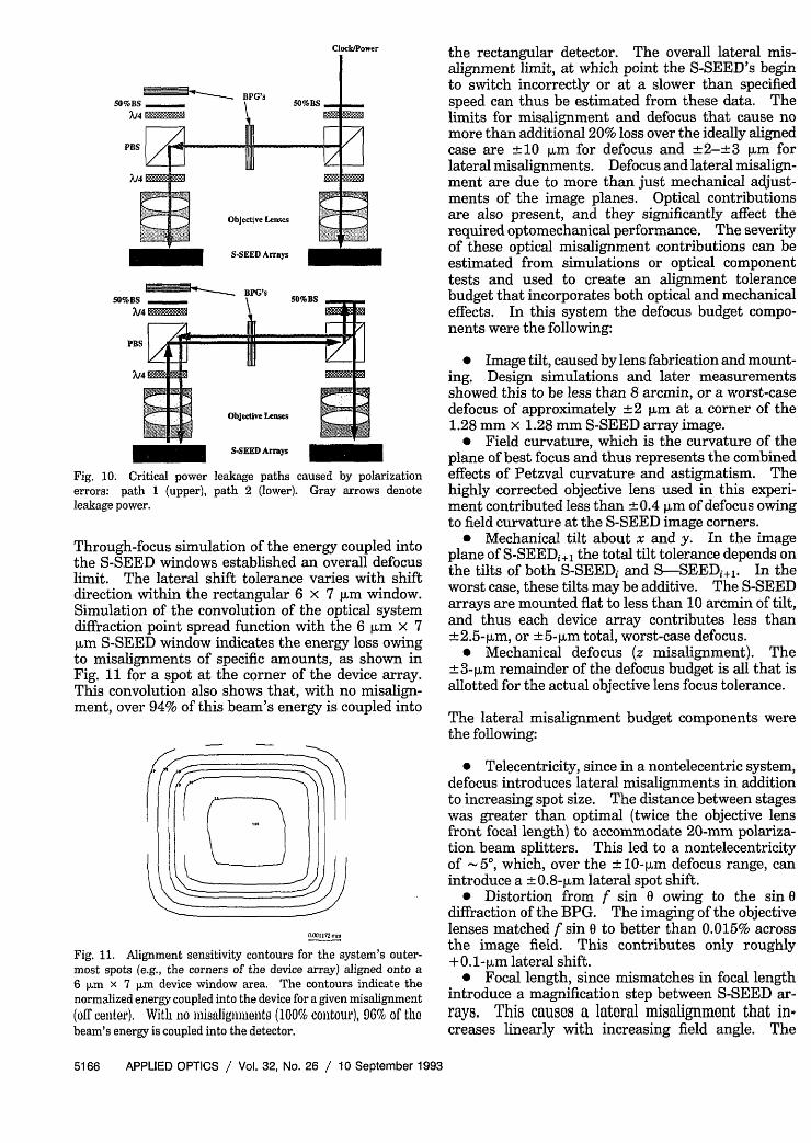
Through-focus simulation of the energy coupled intothe S-SEED windows established an overall defocuslimit. The lateral shift tolerance varies with shiftdirection within the rectangular 6 x 7 jim window.Simulation of the convolution of the optical systemdiffraction point spread function with the 6 jim x 7jm S-SEED window indicates the energy loss owingto misalignments of specific amounts, as shown inFig. 11 for a spot at the corner of the device array.This convolution also shows that, with no misalign-ment, over 94% of this beam's energy is coupled into
0.001172 m
Fig. 11. Alignment sensitivity contours for the system's outer-most spots (e.g., the corners of the device array) aligned onto a6 pLm x 7 um device window area. The contours indicate thenormalized energy coupled into the device for a given misalignment(off cetei'). Witli tio iiialiglllillmts (100% contouw), 96% of tliebeam's energy is coupled into the detector.
the rectangular detector. The overall lateral mis-alignment limit, at which point the S-SEED's beginto switch incorrectly or at a slower than specifiedspeed can thus be estimated from these data. Thelimits for misalignment and defocus that cause nomore than additional 20% loss over the ideally alignedcase are 10 m for defocus and 2-±3 jim forlateral misalignments. Defocus and lateral misalign-ment are due to more than just mechanical adjust-ments of the image planes. Optical contributionsare also present, and they significantly affect therequired optomechanical performance. The severityof these optical misalignment contributions can beestimated from simulations or optical componenttests and used to create an alignment tolerancebudget that incorporates both optical and mechanicaleffects. In this system the defocus budget compo-nents were the following:
* Image tilt, caused by lens fabrication and mount-ing. Design simulations and later measurementsshowed this to be less than 8 arcmin, or a worst-casedefocus of approximately 2 jim at a corner of the1.28 mm x 1.28 mm S-SEED array image.
* Field curvature, which is the curvature of theplane of best focus and thus represents the combinedeffects of Petzval curvature and astigmatism. Thehighly corrected objective lens used in this experi-ment contributed less than ±0.4 jim of defocus owingto field curvature at the S-SEED image corners.
* Mechanical tilt about x and y. In the imageplane of S-SEEDi+l the total tilt tolerance depends onthe tilts of both S-SEED, and S-SEEDi+1 . In theworst case, these tilts may be additive. The S-SEEDarrays are mounted flat to less than 10 aremin of tilt,and thus each device array contributes less than+2.5-jim, or +5-jm total, worst-case defocus.
* Mechanical defocus (z misalignment). The3-jim remainder of the defocus budget is all that is
allotted for the actual objective lens focus tolerance.
The lateral misalignment budget components werethe following:
* Telecentricity, since in a nontelecentric system,defocus introduces lateral misalignments in additionto increasing spot size. The distance between stageswas greater than optimal (twice the objective lensfront focal length) to accommodate 20-mm polariza-tion beam splitters. This led to a nontelecentricityof 50, which, over the ± 10-jLm defocus range, canintroduce a ± 0.8-jm lateral spot shift.
* Distortion from f sin 0 owing to the sin 0diffraction of the BPG. The imaging of the objectivelenses matched f sin 0 to better than 0.015% acrossthe image field. This contributes only roughly+0.1-jim lateral shift.
* Focal length, since mismatches in focal lengthintroduce a magnification step between S-SEED ar-rays. This causes a lateral misalignment that in.creases linearly with increasing field angle. The
5166 APPLIED OPTICS / Vol. 32, No. 26 / 10 September 1993

focal lengths of the objective lenses were carefullymeasured and matched to within 0.1%, or 15 jim.The resulting spot misalignment at the image cornersis less than ± 1 jim.
* Wavelength range, since laser mode hops andwavelength shift change the spot spacing. Since thisincreases with the number of spots generated, largersystems are more sensitive to wavelength variations.Reflections from the collimating lens, Brewster tele-scope, and other components can cause significantlaser wavelength destabilization (3 nm). Laserwavelength and stability were characterized and heldto 850 0.5 nm, causing roughly +0.5-jim lateralspot shift in the worst case.
* Mechanical misalignment inx andy. The high-resolution pointing of the Risley prisms enabled spotpositioning to better than 0.5 jim.
* Mechanical roll about the z axis, since to beproperly registered, the spots must also be rotation-ally aligned to each S-SEED array, and the S-SEEDarrays must be aligned to each other. To achieve a0.5-jm rotational alignment, the BPG must be ro-tated to an accuracy of 0.03°. This alignment was byfar the most demanding. The use of a 15-30-cmlever arm for rotating the BPG's and S-SEED'sintroduced sufficient mechanical advantage for achiev-ing the high accuracy. In practice, rotational mis-alignment of 1 Ilm were tolerated without seriousperformance degradation.
Although it is unlikely that all of these worst-casemisalignment contributions would be present simul-taneously, these tolerance assignments provide areasonable working picture of the system tolerancing.However, the actual situation is undoubtedly morecomplex, since the overall lateral misalignment anddefocus limits may actually be highly coupled in somesystems. For example, this coupling can cause thelateral tolerance limit to decrease with defocus, so adifferent lateral misalignment budget might be re-quired at each focal position. The amount of thiscoupling appears to be very system specific, anddetermination of the degree of this coupling is yetanother reason for building practical demonstrationsystems.
C. Component and System Testing
An often overlooked issue in the implementation ofthese demonstration experiments is the need forextensive testing, both before and after system assem-bly. Because demonstration systems are complexcombinations of many piece parts, one critical aspectis the need to fully characterize the individual partsbefore design and assembly, so that the causes ofsystem operation anomalies can be prevented or atleast accurately identified later.27 Quality assuranceand characteriztaion of lenses, beam splitters, BPG's,S-SEED arrays, and so forth are the first level oftesting required, but in a modular system, testingmust also be done at the subassembly level (e.g., laserpens and mounted and connectorized S-SEED's) and
at the system level (stage-by-stage operation andcomplete system operation). The three main system-level characteristics under test are the optical powerthroughput efficiency, the device coupling efficiency(a function of the wave-front aberration and align-ment), and the beam array uniformity. The mixtureof optical, mechanical, and electrical issues affectingthese characteristics necessitates the development ofnovel test equipment and techniques.28
For this experiment a laser-diode-based 850-nmTwyman-Green interferometer was constructed fortesting pIano components, objective lenses, and lasercollimating lenses. The laser pens were assembledwith a radially shearing interferometer for ensuringlow ( -/8 peak to valley) wave-front error. Collima-tion of the lasers and system was verified by ascanninglateralshearinginterferometer. Theangu-lar transmission performance of the PBS assemblieswas verified with an automated system that simulta-neously measured the PBS transmission and reflec-tion as a function of input polarization and angle ofincidence. For meeting the tight laser-wavelengthstability requirements described above, the assem-bled laser pens were characterized by another comput-er-controlled system that measured the laser outputwavelength as a function of laser-case temperatureand injection current over a 20° and 30-mA range,respectively. Beam array uniformity was examinedwith a custom high-resolution video imaging process-ing system.29 Testing of the complete system at itsmaximum speed is not possible owing to the lack of2-D optical logic analyzers or 2-D bit-error-rate testsets capable of simultaneously monitoring all of thedata streams. Serial testing of each interconnectionindependently is time consuming and does not detectall transient system faults.
D. Power Throughput Efficiency and System Speed
In the absence of signal non-uniformities limitations,the system loss ultimately determines the maximumsystem speed. Assuming ideal uniformity, the sys-tem switching speed is given by l/Trs, where switch-ing time T is
=rw = (EswN)/(Piaseriisys), (2)
where Ew is the S-SEED switching energy ( 4 pJ), Nis the number of beams into which the laser is divided(2048), Piaser is the output power of the laser, and qysis the system optical power efficiency, or the fractionof the power from laseri that is transmitted as usefuldifferential signal power at S-SEEDi+1. The maindrawback to the pupil-plane beam combination andinterconnection techniques used in this experiment isthe resulting low optical power efficiency of 1%.As shown in Fig. 12, the main contributors to thepower loss are the BPG and CGH efficiencies (- 60%and 80%), the 50%:50% beam splitter losses, andthe absorptive losses of the S-SEED's (- 50%). Asdiscussed earlier, this power is further lessened byany misalignment effects. From Eq. (2), the maxi-
10 September 1993 / Vol. 32, No. 26 / APPLIED OPTICS 5167
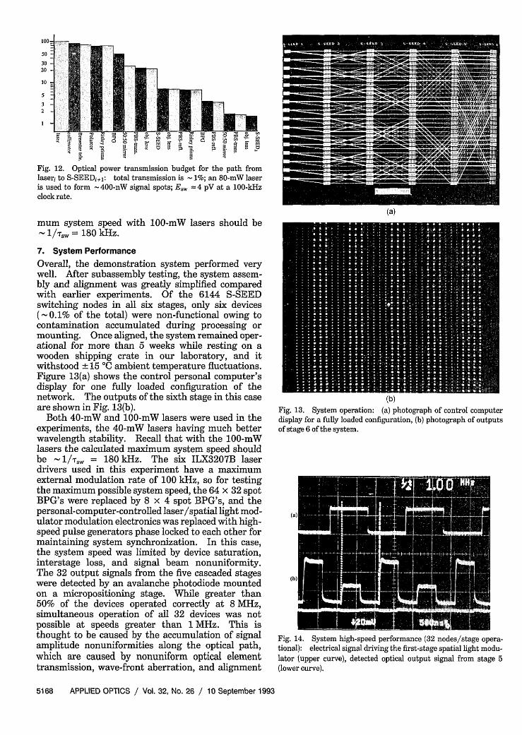
Fig. 12. Optical power transmission budget for the path fromlaseri to S-SEEDj+1: total transmission is -1%; an 80-mW laseris used to form 400-nW signal spots; E,,S 4 pV at a 100-kHzclock rate.
mum system speed with 100-mW lasers should be-/T = 180 kHz.
7. System Performance
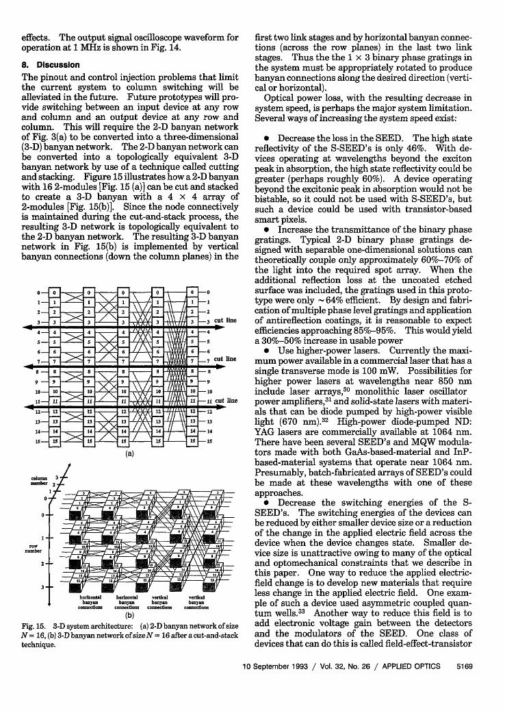
Overall, the demonstration system performed verywell. After subassembly testing, the system assem-bly and alignment was greatly simplified comparedwith earlier experiments. Of the 6144 S-SEEDswitching nodes in all six stages, only six devices(- 0.1% of the total) were non-functional owing tocontamination accumulated during processing ormounting. Once aligned, the system remained oper-ational for more than 5 weeks while resting on awooden shipping crate in our laboratory, and itwithstood ± 15 OC ambient temperature fluctuations.Figure 13(a) shows the control personal computer'sdisplay for one fully loaded configuration of thenetwork. The outputs of the sixth stage in this caseare shown in Fig. 13(b).
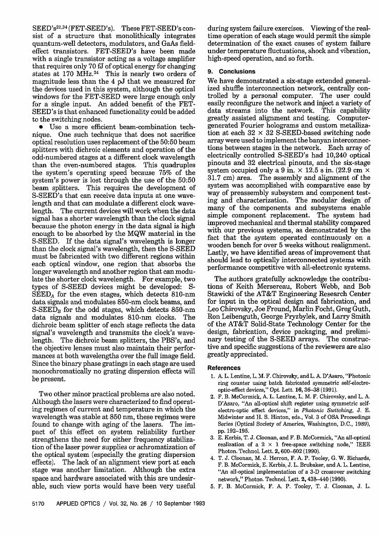
Both 40-mW and 100-mW lasers were used in theexperiments, the 40-mW lasers having much betterwavelength stability. Recall that with the 100-mWlasers the calculated maximum system speed shouldbe lr8 = 180 kHz. The six ILX3207B laserdrivers used in this experiment have a maximumexternal modulation rate of 100 kHz, so for testingthe maximum possible system speed, the 64 x 32 spotBPG's were replaced by 8 x 4 spot BPG's, and thepersonal-computer-controlled laser/spatial light mod-ulator modulation electronics was replaced with high-speed pulse generators phase locked to each other formaintaining system synchronization. In this case,the system speed was limited by device saturation,interstage loss, and signal beam nonuniformity.The 32 output signals from the five cascaded stageswere detected by an avalanche photodiode mountedon a micropositioning stage. While greater than50% of the devices operated correctly at 8 MHz,simultaneous operation of all 32 devices was notpossible at speeds greater than 1 MHz. This isthought to be caused by the accumulation of signalamplitude nonuniformities along the optical path,which are caused by nonuniform optical elementtransmission, wave-front aberration, and alignment
(a)_ . ID _i - || | |
I I |II I il Ii IS I, l |
.
.
.-.|||| l| , !. ; .
| s 4| i z* t s. E .
S E 31| |s .{ s lX | l
(b)Fig. 13. System operation: (a) photograph of control computerdisplay for a fully loaded configuration, (b) photograph of outputsof stage 6 of the system.
Fig. 14. System high-speed performance (32 nodes/stage opera-tional): electrical signal driving the first-stage spatial light modu-lator (upper curve), detected optical output signal from stage 5(lower curve).
5168 APPLIED OPTICS / Vol. 32, No. 26 / 10 September 1993
effects. The output signal oscilloscope waveform foroperation at 1 MHz is shown in Fig. 14.
8. Discussion
The pinout and control injection problems that limitthe current system to column switching will bealleviated in the future. Future prototypes will pro-vide switching between an input device at any rowand column and an output device at any row andcolumn. This will require the 2-D banyan networkof Fig. 3(a) to be converted into a three-dimensional(3-D) banyan network. The 2-D banyan network canbe converted into a topologically equivalent 3-Dbanyan network by use of a technique called cuttingand stacking. Figure 15 illustrates how a 2-D banyanwith 16 2-modules [Fig. 15 (a)] can be cut and stackedto create a 3-D banyan with a 4 x 4 array of2-modules [Fig. 15(b)]. Since the node connectivelyis maintained during the cut-and-stack process, theresulting 3-D network is topologically equivalent tothe 2-D banyan network. The resulting 3-D banyannetwork in Fig. 15(b) is implemented by verticalbanyan connections (down the column planes) in the
071-2 -
3-
0
2
3
0
2
3
0
2
3
0
1
2
3
0
2
3
-0-1
-2.- 3 cut line
.� I - * - I - I - S - I � S - S - I - * �4-S-6-7-
4
5
6
7
4
5
76
7
4
5
6
7
4
5
6
7
4
-6
7
-4-5-6
- cut line
8- 8 - 8 _8 -9 - 9 9 9 -+9
10- -10 . _ < 10 < 10 AVlM 10 -10
-H1--1- _ 1-1 7 ai -1I cut12-13-14-15-
12
13
14
15
12
13
14
15
;12 'XX.
L_(a)
12
13
14
15 12
-12-13-14-15
horizontal horizontal vertical verticalbanyan banyan banyan banyan
connections connetions connections connections
(b)
Fig. 15. 3-D system architecture: (a) 2-D banyan network of sizeN = 16, (b) 3-D banyan network of sizeN = 16 after a cut-and-stacktechnique.
first two link stages and by horizontal banyan connec-tions (across the row planes) in the last two linkstages. Thus the the 1 x 3 binary phase gratings inthe system must be appropriately rotated to producebanyan connections along the desired direction (verti-cal or horizontal).
Optical power loss, with the resulting decrease insystem speed, is perhaps the major system limitation.Several ways of increasing the system speed exist:
* Decrease the loss in the SEED. The high statereflectivity of the S-SEED's is only 46%. With de-vices operating at wavelengths beyond the excitonpeak in absorption, the high state reflectivity could begreater (perhaps roughly 60%). A device operatingbeyond the excitonic peak in absorption would not bebistable, so it could not be used with S-SEED's, butsuch a device could be used with transistor-basedsmart pixels.
* Increase the transmittance of the binary phasegratings. Typical 2-D binary phase gratings de-signed with separable one-dimensional solutions cantheoretically couple only approximately 60%-70% ofthe light into the required spot array. When theadditional reflection loss at the uncoated etchedsurface was included, the gratings used in this proto-type were only - 64% efficient. By design and fabri-cation of multiple phase level gratings and applicationof antireflection coatings, it is reasonable to expectefficiencies approaching 85%-95%. This would yielda 30-50% increase in usable power
* Use higher-power lasers. Currently the maxi-mum power available in a commercial laser that has asingle transverse mode is 100 mW. Possibilities forhigher power lasers at wavelengths near 850 nminclude laser arrays,30 monolithic laser oscillatorpower amplifiers,31 and solid-state lasers with materi-als that can be diode pumped by high-power visiblelight (670 nm).3 2 High-power diode-pumped ND:YAG lasers are commercially available at 1064 nm.There have been several SEED's and MQW modula-tors made with both GaAs-based-material and InP-based-material systems that operate near 1064 nm.Presumably, batch-fabricated arrays of SEED's couldbe made at these wavelengths with one of theseapproaches.
* Decrease the switching energies of the S-SEED's. The switching energies of the devices canbe reduced by either smaller device size or a reductionof the change in the applied electric field across thedevice when the device changes state. Smaller de-vice size is unattractive owing to many of the opticaland optomechanical constraints that we describe inthis paper. One way to reduce the applied electric-field change is to develop new materials that requireless change in the applied electric field. One exam-ple of such a device used asymmetric coupled quan-tum wells.33 Another way to reduce this field is toadd electronic voltage gain between the detectorsand the modulators of the SEED. One class ofdevices that can do this is called field-effect-transistor
10 September 1993 / Vol. 32, No. 26 / APPLIED OPTICS 5169
SEED's21' 34 (FET-SEED's). These FET-SEED's con-sist of a structure that monolithically integratesquantum-well detectors, modulators, and GaAs field-effect transistors. FET-SEED's have been madewith a single transistor acting as a voltage amplifierthat requires only 70 fJ of optical energy for changingstates at 170 MHz.34 This is nearly two orders ofmagnitude less than the 4 pJ that we measured forthe devices used in this system, although the opticalwindows for the FET-SEED were large enough onlyfor a single input. An added benefit of the FET-SEED's is that enhanced functionality could be addedto the switching nodes.
* Use a more efficient beam-combination tech-nique. One such technique that does not sacrificeoptical resolution uses replacement of the 50:50 beamsplitters with dichroic elements and operation of theodd-numbered stages at a different clock wavelengththan the even-numbered stages. This quadruplesthe system's operating speed because 75% of thesystem's power is lost through the use of the 50:50beam splitters. This requires the development ofS-SEED's that can receive data inputs at one wave-length and that can modulate a different clock wave-length. The current devices will work when the datasignal has a shorter wavelength than the clock signalbecause the photon energy in the data signal is highenough to be absorbed by the MQW material in theS-SEED. If the data signal's wavelength is longerthan the clock signal's wavelength, then the S-SEEDmust be fabricated with two different regions withineach optical window, one region that absorbs thelonger wavelength and another region that can modu-late the shorter clock wavelength. For example, twotypes of S-SEED devices might be developed: S-SEEDA for the even stages, which detects 810-nmdata signals and modulates 850-nm clock beams, andS-SEEDB for the odd stages, which detects 850-nmdata signals and modulates 810-nm clocks. Thedichroic beam splitter of each stage reflects the datasignal's wavelength and transmits the clock's wave-length. The dichroic beam splitters, the PBS's, andthe objective lenses must also maintain their perfor-mances at both wavelengths over the full image field.Since the binary phase gratings in each stage are usedmonochromatically no grating dispersion effects willbe present.
Two other minor practical problems are also noted.Although the lasers were characterized to find operat-ing regimes of current and temperature in which thewavelength was stable at 850 nm, these regimes werefound to change with aging of the lasers. The im-pact of this effect on system reliability furtherstrengthens the need for either frequency stabiliza-tion of the laser power supplies or achromatization ofthe optical system (especially the grating dispersioneffects). The lack of an alignment view port at eachstage was another limitation. Although the extraspace and hardware associated with this are undesir-able, such view ports would have been very useful
during system failure exercises. Viewing of the real-time operation of each stage would permit the simpledetermination of the exact causes of system failureunder temperature fluctuations, shock and vibration,high-speed operation, and so forth.
9. Conclusions
We have demonstrated a six-stage extended general-ized shuffle interconnection network, centrally con-trolled by a personal computer. The user couldeasily reconfigure the network and inject a variety ofdata streams into the network. This capabilitygreatly assisted alignment and testing. Computer-generated Fourier holograms and custom metalliza-tion at each 32 x 32 S-SEED-based switching nodearray were used to implement the banyan interconnec-tions between stages in the network. Each array ofelectrically controlled S-SEED's had 10,240 opticalpinouts and 32 electrical pinouts, and the six-stagesystem occupied only a 9 in. x 12.5 s in. (22.9 cm x31.7 cm) area. The assembly and alignment of thesystem was accomplished with comparative ease byway of preassembly subsystem and component test-ing and characterization. The modular design ofmany of the components and subsystems enablesimple component replacement. The system hadimproved mechanical and thermal stability comparedwith our previous systems, as demonstrated by thefact that the system operated continuously on awooden bench for over 5 weeks without realignment.Lastly, we have identified areas of improvement thatshould lead to optically interconnected systems withperformance competitive with all-electronic systems.
The authors gratefully acknowledge the contribu-tions of Keith Mersereau, Robert Webb, and BobStawicki of the AT&T Engineering Research Centerfor input in the optical design and fabrication, andLeo Chirovsky, Joe Freund, Marlin Focht, Greg Guth,Ron Leibenguth, George Pryzbylek, and Larry Smithof the AT&T Solid-State Technology Center for thedesign, fabrication, device packaging, and prelimi-nary testing of the S-SEED arrays. The construc-tive and specific suggestions of the reviewers are alsogreatly appreciated.
References1. A. L. Lentine, L. M. F. Chirovsky, and L. A. D'Asaro, "Photonic
ring counter using batch fabricated symmetric self-electro-optic-effect devices," Opt. Lett. 16, 36-38 (1991).
2. F. B. McCormick, A. L. Lentine, L. M. F. Chirovsky, and L. A.D'Asaro, "An all-optical shift register using symmetric self-electro-optic effect devices," in Photonic Switching, J. E.Midwinter and H. S. Hinton, eds., Vol. 3 of OSA ProceedingsSeries (Optical Society of America, Washington, D.C., 1989),pp. 192-195.
3. E. Kerbis, T. J. Cloonan, and F. B. McCormick, "An all-opticalrealization of a 2 x 1 free-space switching node," IEEEPhoton. Technol. Lett. 2, 600-602 (1990).
4. T. J. Cloonan, M. J. Herron, F. A. P. Tooley, G. W. Richards,F. B. McCormick, E. Kerbis, J. L. Brubaker, and A. L. Lentine,"An all-optical implementation of a 3-D crossover switchingnetwork," Photon. Technol. Lett. 2, 438-440 (1990).
5. F. B. McCormick, F. A. P. Tooley, T. J. Cloonan, J. L.
5170 APPLIED OPTICS / Vol. 32, No. 26 / 10 September 1993

Brubaker, A. L. Lentine, R. L. Morrison, S. J. Hinterlong, M. J.Herron, S. L. Walker, and J. M. Sasian, "Experimentalinvestigation of a free-space optical switching network usingsymmetric self-electro-optic-effect devices," Appl. Opt. 31,5431-5446(1992).
6. F. B. McCormick, F. A. P. Tooley, J. M. Sasian, J. L. Brubaker,A. L. Lentine, T. J. Cloonan, R. L. Morrison, S. L. Walker, andR. J. Crisci, "Parallel interconnection of two 64 x 32 symmet-ric self electro-optic effect device arrays," Electron. Lett. 27,1869-1871 (1991).
7. A. L. Lentine, H. S. Hinton, D. A. B. Miller, J. E. Henry, J. E.Cunningham, and L. M. F. Chirovsky, "Symmetric self electro-optic effect device: optical set-reset latch, differential logicgate and differential modulator/detector," IEEE J. QuantumElectron. 25, 1928 (1989).
8. J. Jahns and M. J. Murdocca, "Crossover networks and theiroptical implementation," Appl. Opt. 27, 3155-3160 (1988).
9. F. B. McCormick and M. E. Prise, "Optical circuitry for freespace interconnections," Appl. Opt. 29, 2013-2018 (1990).
10. F. B. McCormick, F. A. P. Tooley, J. L. Brubaker, J. M. Sasian,T. J. Cloonan, A. L. Lentine, S. J. Hinterlong, and M. J.Herron, "Optomechanics of a free-space switch: the sys-tem," in Optomechanics and Dimensional Stability, R. A.Paquin and D. Vukobratovich, eds., Proc. Soc. Photo-Opt.Instrum. Eng. 1533,97-114 (1991).
11. T. J. Cloonan, G. W. Richards, F. B. McCormick, and A. L.Lentine, "Control injection in free-space photonic switchingarchitectures," in Photonic Switching, H. S. Hinton and J. W.Goodman, eds., Vol. 8 of OSA Proceedings Series (OpticalSociety of America, Washington, D.C., 1991), pp. 180-185.
12. T. J. Cloonan, G. W. Richards, F. B. McCormick, and A. L.Lentine, "Extended generalized shuffle network architecturesfor free-space photonic switching," in Photonic Switching,H. S. Hinton and J. W. Goodman, eds., Vol. 8 of OSAProceedings Series (Optical Society of America, Washington,D.C., 1991), pp. 43-47.
13. H. S. Stone, "Parallel processing with the perfect shuffle,"IEEE Trans. Comput. C-20, 153-161 (1977).
14. C.-L. Wu and T.-Y. Feng, "On a class of multistage interconnec-tion networks," IEEE Trans. Comput. C-29, 694-701 (1971).
15. T. J. Cloonan, "Topological equivalence of optical crossovernetworks and modified data manipulator networks," Appl.Opt. 28, 2494-2498 (1989).
16. M. E. Prise, N. Streibl, and M. M. Downs, "Optical consider-ations in the design of a digital computer," Opt. QuantumElectron. 20, 49-77 (1988).
17. T. J. Cloonan and M. J. Herron, "Optical implementation andperformance of one-dimensional and two-dimensional trimmedinverse augmented data manipulator networks for multiproces-sor computer systems," Opt. Eng. 28, 305-314 (1989).
18. H. Dammann and K. Gortler, "High efficiency in-line multipleimaging by means of multiple phase holograms," Opt. Com-mun. 3, 312-315 (1971).
19. R. L. Morrison and S. L. Walker, "Progress in diffractive phasegratings used for spot array generation," in Optical Comput-ing, Vol. 6 of 1991 OSA Technical Digest Series (OpticalSociety of America, Washington, D.C., 1991) pp. 144-147.
20. T. J. Cloonan, F. B. McCormick, and A. L. Lentine, "Analysisof control subsystems for free-space photonic switching archi-tectures," Appl. Opt. 31, 2587-2606.
21. D. A. B. Miller, M. D. Feuer, T. Y. Chang, S. C. Shunk, J. E.Henry, D. J. Burrows, and D. S. Chemla, "Field-effect transis-tor self-electro-optic effect device: integrated photodiode,quantum well modulator, and transistor," IEEE Photon.Technol. Lett. 1, 62-63 (1989).
22. Computer code CODEV (Optical Research Associates, Pasadena,Calif.).
23. D. Malacara, "Radial, rotational, and reversal shear interferom-eters," in Optical Shop Testing, D. Malacara, ed. (Wiley, NewYork, 1978), pp. 149-178.
24. F. B. McCormick, A. L. Lentine, R. L. Morrison, S. L. Walker,L. M. F. Chirovsky, and L. A. D'Asaro, "Parallel operation of a32 x 16 symmetric self electro-optic effect device array," IEEEPhoton. Technol. Lett. 3, 232-234 (1991).
25. J. L. Pezzaniti and R. A. Chipman, "A polarization metrologyfor optical interconnects which use polarization beam combin-ing," in Optical Computing, Vol. 6 of 1991 OSA TechnicalDigest Series (Optical Society of America, Washington, D.C.,1991), pp. 156-159; J. L. Pezzaniti and R. A. Chipman,"Angular dependence of polarizing beam splitter cubes," Appl.Opt. (to be published).
26. R. A. Chipman, "Polarization analysis of optical systems,"Opt. Eng. 28, 90-99 (1989).
27. F. A. P. Tooley, F. B. McCormick, J. M. Sasian, R. J. Crisci,R. L. Morrison, E. Kerbis, and J. L. Brubaker, "Opticalevaluation of components for free-space digital optics," inAnnual Meeting, Vol. 17 of OSA Technical Digest Series(Optical Society of America, Washington, D.C., 1991), p. 105.
28. F. B. McCormick, J. M. Sasian, R. J. Crisci, R. L. Morrison,F. A. P. Tooley, and E. Kerbis, "Fabrication and testing issuesin free-space digital optical switching and computing," inInternational Symposium on Optical Fabrication, Testing,and Surface Evaluation, J. Tsujiuchi, ed., Proc. Soc. Photo-Opt. Instrum. Eng. 1720, 553-572 (1992).
29. R. L. Morrison, "Image analysis for diagnostics in photonicswitching," in Applications of Optical Engineering: Proceed-ings of OE/Midwest '90, M. K. Dubiel, H. E. Eppinger, R. E.Gillespie, R. P. Guzik, and J. E. Pearson, eds., Proc. Soc.Photo-Opt. Instrum. Eng. 1396,568-574 (1990).
30. J. P. Donnelly, R. J. Baily, W. D. Goodhue, C. A. Wang, G. A.Lincoln, and G. D. Johnson, "Monolithic two dimensionalsurface arrays of AlGaAs horizontal-cavity diode lasers withetched facets and external parabolic reflecting mirrors," inConference on Lasers and Electro-Optics, Vol. 12 of OSATechnical Digest Series (Optical Society of America, Washing-ton, D.C., 1992), p. 344.
31. D. F. Welch, R. Parke, D. Mehuys, D. Scifres, "High powerdiffraction limited operation of monolithically integrated ac-tive grating master oscillator power amplifiers," in Conferenceon Lasers and Electro-Optics, Vol. 12 of OSA Technical DigestSeries (Optical Society of America, Washington, D.C., 1992),p. 342.
32. R. Scheps, "Cr:LiCaAIF laser pumped by visible laser diodes,"IEEE J. Quantum Electron. 27, 1968-1970 (1991).
33. K. W. Goossen, D. A. B. Miller, J. E. Cunningham, W. Y. Jan,A. L. Lentine, A. M. Fox, and N. K. Ailawadi, "Low fieldelectro-absorption and self-biased self electro-optic effect de-vice using slightly asymmetric coupled quantum wells," inQuantum Optoelectronics, Vol. 7 of OSA Technical DigestSeries (Optical Society of America, Washington, D.C., 1991),pp. 26-29.
34. L. A. D'Asaro, L. M. F. Chirovsky, E. J. Laskowski, S. S. Pei,T. K. Woodward, A. L. Lentine, R. E. Leibenguth, M. W. Focht,J. M. Freund, G. Guth, and L. E. Smith, "Batch fabricationand testing of GaAs-AlGaAs field effect transistor self electro-optic effect device (FET-SEED) smart pixel arrays," IEEE J.Quantum Electron. 29, 670-677 (1993).
10 September 1993 / Vol. 32, No. 26 / APPLIED OPTICS 5171
Copyright © 2022 FDOKUMEN