Simulation of the time evolution of clocked and nonclocked Quantum Cellular Automaton (QCA) circuits
11
Università di Pisa !" $%&'() *" +,--%.(/(%) +" 0,&&,''%&1) *" *,'2''() !"#$%&'"() (+ ',- '"#- -.(%$'"() (+ /%(/0-1 &)1 )()/%(/0-1 2$&)'$# 3-%%$%&4 5$'(#&'() 62357 /"4/$"'8) 3%24&,5 %6 7885(19 :;<=('=) !") 88">?@AB>?CD EFGGFH" !"#$%&'"() (+ '"#, ,-(%$'"() (+ .%(./,0 &)0 )().%(./,0 1$&)'$# .,%%$%&2 &$'(#&'() ."2.$"'3 #$ &'()* I(8,4-(J1&-% 9( 0&/1/&14(, 9155K0&6%4J,L(%&1M N51--4%&(',) 0&6%4J,-(',) O151'%J2&(',L(%&() P&(Q14=(-R 9( :(=, +$ ,-..'/*0*' I(8,4-(J1&-% 9( 0&/1/&14(, 9155K0&6%4J,L(%&1M N51--4%&(',) 0&6%4J,-(',) O151'%J2&(',L(%&() P&(Q14=(-R 9( :(=, ,*123443 5-((-))'(3 I(8,4-(J1&-% 9( 0&/1/&14(, 9155K0&6%4J,L(%&1M N51--4%&(',) 0&6%4J,-(',) O151'%J2&(',L(%&() P&(Q14=(-R 9( :(=, +-22*6' +-)1))* I(8,4-(J1&-% 9( 0&/1/&14(, 9155K0&6%4J,L(%&1M N51--4%&(',) 0&6%4J,-(',) O151'%J2&(',L(%&() P&(Q14=(-R 9( :(=,
Transcript of Simulation of the time evolution of clocked and nonclocked Quantum Cellular Automaton (QCA) circuits

Università di Pisa
!"# $%&'()# *"# +,--%.(/(%)# +"# 0,&&,''%&1)# *"# *,'2''()# !"#$%&'"()* (+* ',-* '"#-* -.(%$'"()* (+* /%(/0-1* &)1*)()/%(/0-1*2$&)'$#*3-%%$%&4*5$'(#&'()*62357*/"4/$"'8)#3%24&,5#%6#7885(19#:;<=('=)#!")#88">?@AB>?CD#EFGGFH"#
#
!"#$%&'"()*(+*'"#,*,-(%$'"()*(+*.%(./,0*&)0*)().%(./,0*1$&)'$#*.,%%$%&2*&$'(#&'()*."2.$"'3#
#$%&'()*%I(8,4-(J1&-%#9(#0&/1/&14(,#9155K0&6%4J,L(%&1M#N51--4%&(',)#0&6%4J,-(',)#O151'%J2&(',L(%&()#
P&(Q14=(-R#9(#:(=,#+$%,-..'/*0*'%
I(8,4-(J1&-%#9(#0&/1/&14(,#9155K0&6%4J,L(%&1M#N51--4%&(',)#0&6%4J,-(',)#O151'%J2&(',L(%&()#P&(Q14=(-R#9(#:(=,##
,*123443%5-((-))'(3%I(8,4-(J1&-%#9(#0&/1/&14(,#9155K0&6%4J,L(%&1M#N51--4%&(',)#0&6%4J,-(',)#O151'%J2&(',L(%&()#
P&(Q14=(-R#9(#:(=,#+-22*6'%+-)1))*%
I(8,4-(J1&-%#9(#0&/1/&14(,#9155K0&6%4J,L(%&1M#N51--4%&(',)#0&6%4J,-(',)#O151'%J2&(',L(%&()#P&(Q14=(-R#9(#:(=,#
##
###
Simulation of time evolution of clocked and nonclocked quantum cellularautomaton circuits
L. Bonci, M. Gattobigio, G. Iannaccone, and M. MacucciDipartimento di Ingegneria dell’Informazione, Universita degli studi di Pisa, Via Diotisalvi 2,I-56122 Pisa, Italy
!Received 25 March 2002; accepted for publication 27 June 2002"
We have studied, by means of a Monte Carlo simulation, data propagation in quantum cellularautomaton circuits, comparing the performance of nonclocked and clocked implementations. Basedon two choices of fabrication parameters, we have evaluated the maximum achievable clock speedfor different operating temperatures, concluding that better performance can be obtained with theclocked architecture, which, however, involves significant technological difficulties. The largediscrepancy existing between a simple estimate of the cell switching time, based on the RC timeconstant, and our results is discussed and explained by means of an intuitive argument. Twodifferent circuits have been investigated, a binary wire and a majority voting gate, obtaininganalogous results, with a slightly smaller maximum clock rate for the majority voting gate, due tothe larger number of cells involved. © 2002 American Institute of Physics.#DOI: 10.1063/1.1501747$
I. INTRODUCTION
The quantum cellular automaton !QCA" architecture ini-tially proposed in Ref. 1 has very innovative features withrespect to conventional electronic circuits. For example, it ischaracterized by extreme modularity and by a very lowpower consumption.
The basic element of a QCA circuit is a cell made up offour quantum dots arranged at the vertices of a square, asshown in Fig. 1!a". The cell contains two excess electrons,which can tunnel between dots and encode the binary infor-mation: electrons tend to align along one of the square di-agonals, giving rise to two possible polarization states, whichcan be associated to the two binary logic values. Adjacentcells interact via Coulomb coupling, which allows propagat-ing logic values along a chain of cells, and, more in general,obtaining combinatorial circuits through the assembly oftwo-dimensional !2D" arrays of cells.1
In principle, QCA operation can be achieved without netcurrent flow along the circuit, because the two electrons be-longing to each cell may be prevented from tunneling tonearby cells, which leads to extremely low-power consump-tion. A QCA circuit performs logical operations on the basisof the so-called ‘‘ground state computation’’ principle: theinput cells are set into the state corresponding to the logicalinput vector, the system is allowed to relax to the groundstate, then the logical output vector is obtained by readingthe final states reached by the output cells. Let us consider,for example, two adjacent cells such as those shown in Fig.1!b". If the logical state of a cell !the input cell" is enforcedfrom the outside, then the other cell !the output cell" willevolve towards the same logical state, since the configurationof minimum energy is the one corresponding to the two pairsof electrons aligned along parallel diagonals.
It has been demonstrated by Lent et al.1 that any combi-natorial logical function can be implemented by properly as-
sembling 2D arrays of QCA cells. Recently, experimentaldemonstration of the operation of coupled QCA cells and ofa majority voting gate has been achieved with cells consist-ing of metal islands connected by means of capacitive tunneljunctions.2,3 Very promising nanoscale cells have also beenfabricated on SOI substrates.4
A few serious drawbacks of the QCA architecture havehowever been pointed out in the last few years. First, ex-tremely tight fabrication tolerances !prohibitive, at least inthe medium term" or a careful adjustment of each cell arerequired for proper operation of QCA circuits.5 Second, theoperating temperature for semiconductor or metal QCA sys-tems remains far below room temperature.6,7 The only pos-sibility to obtain large-scale QCA circuits operating at roomtemperature seems to be that of molecular implementations,although detailed studies on the subject are still missing, andsome difficulties have already been recognized, such as thatof obtaining a substrate completely free from stray charges.Further problems may appear when large QCA systems areconsidered in the framework of ground-state computation: alarge system is very likely to get temporarily stuck in a meta-stable state and thus reach the ground state after a time toolong for computational purposes.8 For this reason, an adia-batic logic scheme has been proposed, in which the evolutionof the system is driven by a multiphase clock.9
In a previous paper,10 we addressed the adiabatic opera-tion of QCA circuits, focusing on a recent proposal by Tothand Lent.11 We performed an analytical calculation of theswitching time as a function of several device parametersand, considering a realistic cell geometry, we determined theregion in the parameter space that allows operation at anacceptable clock speed. These results were supported also bymeans of a simple numerical simulation of a QCA wire.10 Inthe present article, we report the results of numerical MonteCarlo simulations of more complex circuits, in order to betterassess the differences between the operation of QCA circuits
JOURNAL OF APPLIED PHYSICS VOLUME 92, NUMBER 6 15 SEPTEMBER 2002
31690021-8979/2002/92(6)/3169/10/$19.00 © 2002 American Institute of Physics
Downloaded 19 Oct 2002 to 131.114.9.134. Redistribution subject to AIP license or copyright, see http://ojps.aip.org/japo/japcr.jsp

based on the relaxation to the ground state and those basedon an adiabatic clocked scheme.
In particular, we shall determine the maximum data pro-cessing rate that can be achieved with the two schemes anddiscuss the reasons for a discrepancy of several orders ofmagnitude between the minimum switching time for aclocked array and the estimate that can be obtained fromsimple considerations on the involved time constants. In Sec.II we briefly discuss the clocked model, while in Sec. III theMonte Carlo simulator is outlined, along with the approachused to include cotunneling. The overall simulation strategyis introduced in Sec. IV, while Sec. V deals with the analysisof a clocked and of a nonclocked binary wire, including anintuitive justification of the results achieved. Finally, the per-formance of a more complex logic gate, a majority votinggate, is discussed in Sec. VI, and conclusions are presentedin Sec. VII.
II. SIX-DOT CLOCKED QCA CELL
The problem of the existence of metastable states couldbe avoided if we were able to modulate the potential barrierswhich separate cell dots. By lowering and raising these bar-riers, we could drive the system towards the correct logicaloutput without getting stuck in any metastable state. For thispurpose, an adiabatic logic scheme has been proposed, inwhich the evolution of the system is driven by a multiphaseclock.9
Adiabatic switching of a QCA cell consists in letting thecell evolve into the instantaneous ground state, and then‘‘freezing’’ the electron configuration when the cell must beused to drive nearby cells. This can be achieved by modulat-ing the interdot barriers:9 barriers should be raised to lock theelectrons in the dots they are currently occupying, and thenlowered slowly enough not to drive the system into an ex-cited state.
An interesting way of modulating the interdot barriers ina metal-dot QCA implementation has been proposed in Ref.11: it consists of replacing the barrier with another dot whosepotential can be varied by means of an external voltage. Aclocked cell is shown in Fig. 2 and is made up of six dots:the ordinary four dots !1, 3, 4, and 6" plus the two dotsrequired for implementation of the modulated barriers !2 and5". The potential of each dot is adjusted by means of capaci-tively coupled voltage sources.
The operation of circuits based on the cell of Fig. 2 hasbeen previously described, for example, in Refs. 10 and 11.
By applying an appropriate clock sequence to the cells, it ispossible to control the data flow and to avoid the problemsconnected with the existence of metastable states.9 However,while metastable states are no longer a problem for adiabaticQCA logic, signal propagation is still limited by the switch-ing time of single cells. Proper operation can be obtained iftransition rates for tunneling are sufficiently large to allow anelectron to actually tunnel into the proper dot while the cellis in the active state. Moreover, the typical energy differ-ences between the various electronic configurations in thecells need to be much larger than kT , in order to preventthermally excited random fluctuations of the logical values.In Ref. 10, we evaluated the switching time by computingthe transition rates for electrons as a function of materialparameters and cell geometry. Here we shall use those resultsto test operation of QCA circuits with and without clock, viaa Monte Carlo simulation.
III. QCA CIRCUIT SIMULATOR
The numerical simulation of the circuits discussed in thefollowing has been performed with a semiclassical approach,in the framework of the orthodox Coulomb blockadetheory,13 since quantum effects associated with the confine-ment energy can be neglected at the dimensional scale beingconsidered, because such an energy is much smaller than theelectrostatic interaction energy.
We used a Monte Carlo code that we have developed,12specifically adapted to cope with circuits containing clockedsingle-electron devices. Our software allows simulating cir-cuits made up of capacitors, tunneling capacitors, and volt-age sources, with very few topological constraints. The volt-age sources can provide piecewise linear waveforms.Cotunneling has also been taken into consideration, althoughapproximately.14
Our code is based on a semistatic Monte Carlo tech-nique: the simulation is divided into a given number of steps,and, for each step, we first evaluate the adjustment gate volt-
FIG. 1. !a" A QCA cell consists of four dots separated by tunneling barrierswith two excess electrons; electrons tend to align along one diagonal !logi-cal ‘‘1’’" or along the other !logical ‘‘0’’"; !b" if the driver cell is set into aspecific logic state, the driven cell will evolve towards the same logicalstate, in order to minimize the total electrostatic energy.
FIG. 2. Complete cell, made up of six dots. Each semicell consists of threedots connected by tunneling junctions and coupled to external voltagesources via capacitors.
3170 J. Appl. Phys., Vol. 92, No. 6, 15 September 2002 Bonci et al.
Downloaded 19 Oct 2002 to 131.114.9.134. Redistribution subject to AIP license or copyright, see http://ojps.aip.org/japo/japcr.jsp

ages, according to the linear evolution rule defined in theinput file, then we compute the variation of the free energy%E associated with each possible single-electron transitionthrough the tunneling junctions. Once the free-energy varia-tions have been determined, we can compute the correspond-ing probability rates using the ‘‘orthodox’’ Coulomb block-ade theory13
&!1
e2RT
%E1"e" %E/kB T , !1"
where RT is the tunneling resistance, e the electron charge,kB the Boltzmann constant, and T the temperature.
In this way, we can compute all the transition rates, andthe actual transition taking place is chosen randomly with arelative probability proportional to its rate. The transition isthen implemented by changing the dot occupancy, the newgate voltage configuration is computed, and the same proce-dure repeated until the total predefined simulation time haselapsed.
This standard procedure does not take into considerationthe cotunneling effect, namely, the possibility of simulta-neous tunneling of two or more electrons. This effect is usu-ally far less probable than single-electron tunneling, but canbecome prevalent when no direct tunneling transition is en-ergetically viable !negative %E", while simultaneous many-electron tunneling transitions can lead to a lower-energystate.
A rigorous simulation of the cotunneling effect is quite adifficult task, but, as we shall discuss later, we have realizedthat in some range of parameters cotunneling cannot be dis-regarded, if the nonclocked scheme of Sec. II is adopted.Thus, we have included its effects, considering only the first-order contribution, which corresponds to the simultaneoustunneling of two electrons. Following Fonseca et al.,14 wecan write the two-electron cotunneling probability as
&!'
12(e41RT(1)
1RT(2)
#! 1%E (1)"%E/2$
1%E (2)"%E/2"2
#%E
e%E/kB T"1 #%E2$!2(kBT "2"]. !2"
This expression is not suitable for numerical simulation, be-cause of the divergences occurring when one of the interme-
diate transitions matches one half of the total energy differ-ence. This problem can be avoided by resorting to thefollowing approximate expression:
&!163
'
(
C2
e8RT2
%Ee%E/kB T"1 #%E2$!2(kBT "2"], !3"
where RT and C represent, respectively, the average value ofthe tunneling resistance and of the capacitance of the junc-tions involved in the cotunneling event. This expression is asomehow crude approximation, but it has been shown14 togive the correct order of magnitude of the effect, which iswhat we need.
IV. CIRCUITS AND SIMULATION STRATEGIES
In order to test the operation of clocked and nonclockedarchitectures, we studied two different circuits: a linear chainmade up of six QCA cells and a majority voting gate madeup of eight QCA cells. They are shown in Figs. 3–5. For thelinear chain, we present both the nonclocked and the clockedimplementation, while for the majority voting gate we reportonly the circuit diagram for the nonclocked version, since theother can be easily derived looking at that for the clockedlinear chain. The greater complexity of the clocked case isapparent. In Figs. 3–5, we sketch also the time evolution ofthe applied potentials that produces switching of the firstcell, while in Fig. 4, the clocked external gate potentials areshown".
The simulation strategy differs in the two cases. In thecase without clock, we are strictly following the ground-statecalculation paradigm. Namely, the circuit output becomesvalid after the system has relaxed to the ground state. In thecase of the chain, this implies that we can perform the simu-lation starting from the ground state, with all the cells in thesame logical state, then switching the first cell via the above-mentioned voltage variation, and observing the time evolu-tion, until the new ground state is reached. By repeatingseveral times the simulation, we shall be able to check circuitreliability and to compute the average time needed to reachthe correct logical output.
In the clocked case, the situation is different, because theswitching time is enforced from the outside. Thus, in order tocheck circuit operation, we follow the time evolution of eachsingle cell and verify that its logical state is correct in theappropriate time intervals. In this case, we do not need to
FIG. 3. Chain made up of six nonclocked cells. The first cell to the left is coupled to external leads via the capacitors C*. The voltage variations which enforcethe state of the first cell are sketched next to such capacitors.
3171J. Appl. Phys., Vol. 92, No. 6, 15 September 2002 Bonci et al.
Downloaded 19 Oct 2002 to 131.114.9.134. Redistribution subject to AIP license or copyright, see http://ojps.aip.org/japo/japcr.jsp

average over several different histories, because statistics canbe obtained observing a large enough number of clockcycles.
Before presenting simulation results, we need to discussour choice of system parameters. Our goal is both to checkthe validity of experimental results by extending them tomore complex circuits and to forecast the operation of futuredevices. We have thus chosen two different sets of param-
eters: the first has been obtained from the recent experimentsthat have successfully shown operation of simple QCAdevices,2,3 while the second has instead been derived fromour previous work, in which we theoretically discussed thelimits of clocked QCA devices.10 In that paper, we performeda parametric study to assess the feasibility of clocked QCAdevices studying different material combinations. The choicereported in the second line of Tables I and II has been ob-
FIG. 4. Chain made up of six clocked cells like the one represented in Fig. 2. The external voltages which drive the cells are labeled as V1 ,V2¯V6 and theirtime behavior is sketched below and above the circuits diagram. The value of the capacitors which connect the cells is indicated as Cc in Table II.
FIG. 5. A majority voting gate madeup of nonclocked cells. The first cell tothe left is coupled to external leads viathe capacitors C*. The voltage varia-tions which cause switching of the firstcell are sketched to the left. The othertwo input cells, at the top and bottomof the vertical arm, are kept in a con-stant logical state via appropriate ex-ternal gates !not shown", during thewhole time evolution.
3172 J. Appl. Phys., Vol. 92, No. 6, 15 September 2002 Bonci et al.
Downloaded 19 Oct 2002 to 131.114.9.134. Redistribution subject to AIP license or copyright, see http://ojps.aip.org/japo/japcr.jsp
tained as a tradeoff between miniaturization, efficiency, andtechnical feasibility. Such a small and precise structure is notyet realizable but it could be so in not too far a future.
V. BINARY WIRE SIMULATIONS
This section is devoted to the study of the operation ofthe binary wires shown in Figs. 3 and 4. As already dis-cussed, we start with the simulation of devices based on theparameters of experimentally realized cells. The followingresults have been obtained with cell parameters similar tothose of Ref. 2.
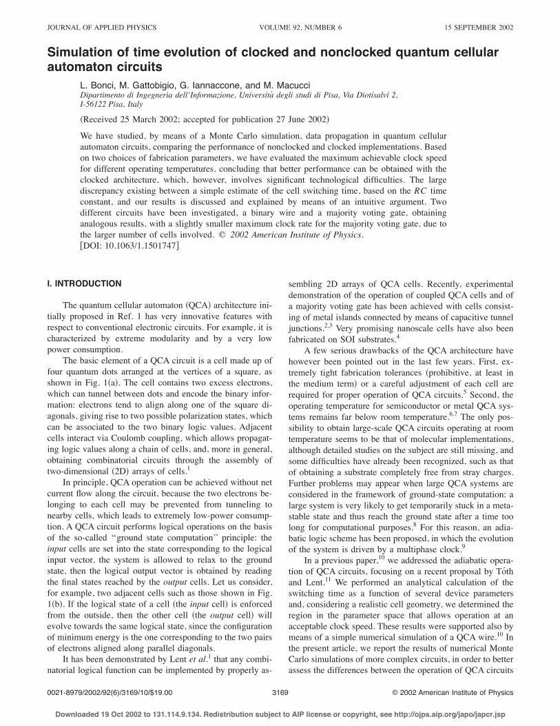
The time evolution of the six cells of the chain of Fig. 3is shown in Fig. 6. We have chosen to indicate the logicalstates with the symbols 1, x , and 0, where 1 and 0 corre-spond to the two valid polarization states, while x indicatesall the other cell states with the two electrons not alignedalong one of the diagonals. The initial condition for thesimulation is the chain ground state, with all the cells in thelogical state 0. After a short time, we switch the first cellstate to 1, by means of a change in the external voltagesapplied to the left end of the chain. After the switching event,the system is not in the ground state any more, and it evolvesto relax into the new ground state, which is reached when allthe cells are in the logical state 1 !the first cell cannot switchback to 0, due to the external bias". It is apparent from thefigure that the relaxation process does not proceed in a regu-lar and smooth way, but, rather, the system moves randomlyamong the various chain states. Many of these states areactually very close in energy and, due to thermal activation,states of significantly higher energy can be reached, too.
The average relaxation time to the ground state is a sta-tistical quantity which we studied by averaging over severalrealizations of the time evolution. The average value of therelaxation time, )t rel* , as a function of temperature is shownin Fig. 7. We notice that )t rel* decreases as temperature in-creases. This is due to the increased tunneling rate, but sucha phenomenon is limited by the fact that beyond a certaintemperature, the system no longer approaches a stableground state, because of thermal fluctuations. In Fig. 7, wemarked with a dashed pattern the approximate regionwhithin which the circuit is not working any more. Anyway,before entering this region we already have hints of degraded
operation in the sudden increase of the relaxation time and inthe broadening of the distribution !see T!0.85 K and noticethat the vertical scale is logarithmic".
Knowledge of the average relaxation time is not suffi-cient to assess how fast the circuit can perform, because weneed to take into consideration that the distribution of relax-ation times can exhibit long tails, and thus )t rel* is actuallytoo conservative an estimate. This is clear from Fig. 8, wherewe show the relaxation time distribution for T!0.05 K. Weobtained quite broad distributions in all of the simulations,with long tails that are the consequence of the existence ofmetastable states, although they do not play a major role in asimple circuit such as the considered chain.
We notice also that, as temperature decreases, the impor-tance of cotunneling events increases. If we define Rct as theratio of the number of cotunneling events to that of tunnelingevents, we obtain, for the case at hand, that Rct!35 at T!0.025 K, which means that cotunneling is the predominantphenomenon, while Rct!1.4#10"2 at T!0.075 K.
With the other parameter set, namely, the one obtained inRef. 10, we have found a similar behavior, but on differenttemperature and time scales. The results of the simulation areshown in Figs. 9–10: the average relaxation time is nowsmaller and the operating temperature is higher, but the over-all behavior is qualitatively similar to that obtained with theprevious parameter choice, i.e., we still have a broad relax-ation time distribution, with long tails. Performance im-provements are an obvious consequence of the larger voltageimbalance achievable with smaller devices !characterized bysmaller capacitance values". A larger voltage imbalance im-
FIG. 6. Time evolution of the logical states of the six cells of a QCA chainin the nonclocked case. The values of the parameters are Co!400 aF, Cv!288 aF, Cc!88 aF, C*!1 aF, and RT!200 k+ .
TABLE I. Circuit parameters for the nonclocked case.
Co!aF"
Cv!aF"
Cc!aF"
C*!aF"
RT!k+"
Experimental values2,3 400 288 88 1 200Theoretical prediction10 5.3 5.3 2 0.1 200
TABLE II. Circuit parameters for the clocked case.
C!aF"
C1!aF"
C2!aF"
C3!aF"
C4!aF"
Cc!aF"
RT!k+"
Experimental values2,3 420 300 25 80 200 50 200Theoretical prediction10 5.3 1.2 1.2 3.57 1.48 1 200
3173J. Appl. Phys., Vol. 92, No. 6, 15 September 2002 Bonci et al.
Downloaded 19 Oct 2002 to 131.114.9.134. Redistribution subject to AIP license or copyright, see http://ojps.aip.org/japo/japcr.jsp

plies both a higher-tunneling rate and less sensitivity to ther-mal fluctuations.
Let us now move on to the clocked architecture of Fig.4. As we discussed before, by means of an external clockdriving the cells we set the rate of switching, which is notdictated by the global relaxation to the ground state anymore. In this case, we need to assess whether the systemrelaxation to the local instantaneous ground state is fastenough to follow the changes due to the clock evolution andto result in the correct final output. A typical evolution isshown in Fig. 11, for the choice of parameters represented bythe first row in Table II: in the considered time interval wecan see only one propagation error. Reliability of circuit op-eration, as already discussed in Ref. 10, depends on clockrate and on temperature. If the clock is too fast, the cell is notable to switch and the logical state is lost. The same happensfor a temperature that is too high compared to the energyimbalance. We can safely disregard cotunneling, because itscontribution is far less important in the clocked case, due tothe fact that the barrier modulation makes the direct transi-tion always available. Cotunneling effects, if present, arethus not needed for reaching the ground state, as they wereinstead in the nonclocked case.
In order to assess the reliability of circuit operation, weperformed runs over several !250" clock cycles. During theseruns, we checked the logical state of the second and the sixth!last" cell of the chain, and calculated the number of timessuch cells are in the state expected as correct; in this way wewere able to compute the relative frequency of correct outputPCO over the total number of clock cycles. By ‘‘checking thelogical state,’’ we mean observing the cell state during thetime interval which corresponds to the locked condition forthat cell. In such an interval, the cell should be in the ex-pected logical state. Actually, this is strictly true only at verylow temperature, because when the temperature is compa-rable to the energy difference between logical states, we cansee the cell switching back and forth between them.
We then need to properly define the meaning of correctlogical state for the observed cell, and this can be done byaddressing the measurement process. The measurement ofthe electron occupancy can be performed by averaging thecell state over the locked time interval, and thus we candecide to consider a cell to be in the correct state if it remainsin that state for more than a certain percentage of the timeinterval. We choose such a percentage as 90%.
FIG. 7. Average relaxation time )t rel* as a function of temperature. In thedashed region, the operation is completely disrupted due to thermal fluctua-tions. The values of the parameters are Co!400 aF, Cv!288 aF, Cc!88 aF, C*!1 aF, and RT!200 k+ .
FIG. 8. Distribution of the switching time )t rel* for the nonclocked chain ofFig. 3, for T!0.05 K. The values of the parameters are Co!400 aF, Cv!288 aF, Cc!88 aF, C*!1 aF, and RT!200 k+ .
FIG. 9. Average relaxation time )t rel* as a function of temperature. In thedashed region, the operation is completely disrupted, due to thermal fluc-tuations. The values of the parameters are Co!5.3 aF, Cv!5.3 aF, Cc!2 aF, C*!0.1 aF, and RT!200 k+ .
FIG. 10. Distribution of the relaxation time )t rel* for the nonclocked chainof Fig. 3, for T!4.2 K. The values of the parameters are Co!5.3 aF, Cv!5.3 aF, Cc!2 aF, C*!0.1 aF, and RT!200 k+ .
3174 J. Appl. Phys., Vol. 92, No. 6, 15 September 2002 Bonci et al.
Downloaded 19 Oct 2002 to 131.114.9.134. Redistribution subject to AIP license or copyright, see http://ojps.aip.org/japo/japcr.jsp

With this prescription, we have obtained the resultsshown in Figs. 12 and 13. In each figure, we show the per-centage of correct output PCO as a function of the clockperiod ,. The solid curves refer to the last cell, while thedashed ones refer to the second cell. We have considered twodifferent temperatures: T!0.01 K !a" and T!0.025 K !b".Figure 12 clearly shows how circuit operation deteriorateswith increasing clock frequency and temperature. Moreover,it is clear that PCO decreases as we proceed along the chain,due to the fact that the overall error probability increaseswith the number of intermediate cells. This process has beenstudied in Refs. 6, 7, 15, where it has been shown that theerror probability increases as the logarithm of the number ofcells in a linear chain.
The temperature range we studied has been chosen onthe basis of the following considerations. For the presentselection of parameters, we have observed that temperatureeffects become negligible below T!0.01 K; therefore, wehave selected this value as the lower bound of the interval ofanalysis. As far as the upper bound of the interval is con-cerned, we have chosen a value T!0.025 K, because forlarger temperature values thermal fluctuations completelydisrupt the operation of the circuit.
We repeated the simulation with the other parameter set,obtaining the results shown in Fig. 13 for three temperatures:1 K !a", 2.5 K !b", and 4.2 K !c". Similar comments apply tothis result, although the temperature range is different and wewere able to find a region of correct operation that extendsdown to a clock period of 10"7 s and to a temperature of 2.5K, which could be a reasonable operating condition. This lastchoice of parameters is the same as that used in Ref. 10 tocompute the probability of correct operation of a similar butsimpler linear chain. In that case, the basic block of the chainwas a semicell, namely, only half of the cell shown in Fig. 2.The total chain was thus made up of only 18 dots. Ourpresent results are consistent with those of the previous paperand the slightly better performance of the cell of Ref. 10 canbe attributed to the simpler structure of that circuit.
We wish to point out that the minimum clock periodallowing correct operation according to our simulations isorders of magnitude larger than the intuitive estimate thatcould be obtained on the basis of the RTC time constantassociated with the tunneling resistances and the capacitancevalues. Such a naive estimate would yield a typical minimumclock period around 10"12 s, which is approximately fourorders of magnitude smaller than the result we get from ourMonte Carlo runs.
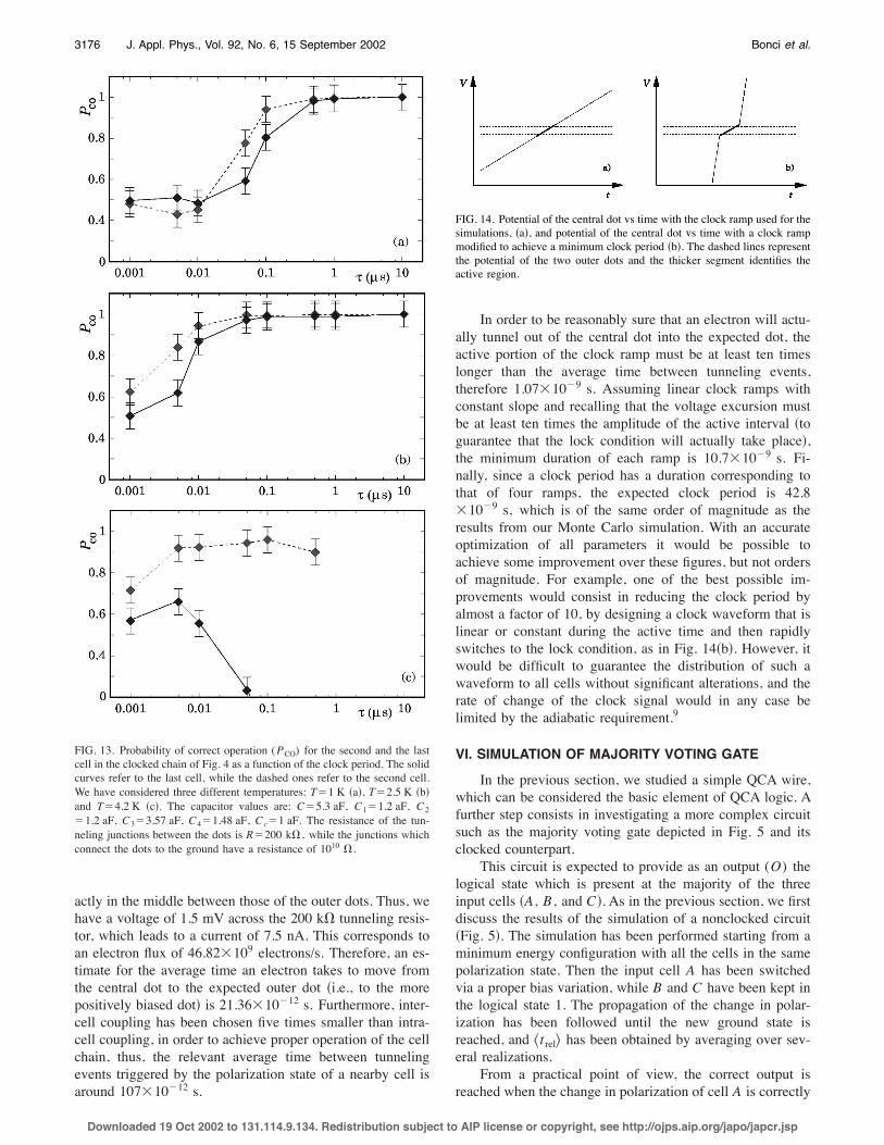
It is instructive to discuss the origin of this discrepancyand to derive an intuitive argument justifying our numericalresults. To this aim, let us consider the mechanism wherebyan electron on the central dot of a semicell tunnels into theouter dot at the lower potential: tunneling into the expecteddot is possible within a time interval slightly longer !due tothe contribution of thermal energy" than that during whichthe potential of the central dot lies between those of the topand bottom dots, indicated with a bold segment in Fig. 14!a".
The voltage imbalance created between the two outerdots because of the presence of an excess electron on one ofthe dots in the other half of the same cell is, from our calcu-lations, about 3 mV: considering the linearity of the ramp, wecan compute, as a first approximation, the electron tunnelingrate between the central dot and the outer dot at the lowerpotential in the condition with the central dot potential ex-
FIG. 11. Time evolution of the logical states of the six cells of a QCA chainin the clocked case. The capacitor values are: C!420 aF, C1!300 aF, C2!25 aF, C3!80 aF, C4!200 aF, Cc!50 aF. The resistance of the tunnel-ing junctions between dots is R!200 k+ , while the junctions which con-nect the dots to the ground have a resistance of 1010 + .
FIG. 12. Probability of correct operation (PCO) for the second and the lastcell in the clocked chain of Fig. 4 as a function of the clock period. The solidcurves refer to the last cell, while the dashed ones refer to the second cell.We have considered two different temperatures: T!0.01 K !a" and T!0.025 K !b". The capacitor values are: C!420 aF, C1!300 aF, C2!25 aF, C3!80 aF, C4!200 aF, Cc!50 aF. The resistance of the tunnel-ing junctions between the dots is R!200 k+ , while the junctions whichconnect the dots to the ground have a resistance of 1010 + .
3175J. Appl. Phys., Vol. 92, No. 6, 15 September 2002 Bonci et al.
Downloaded 19 Oct 2002 to 131.114.9.134. Redistribution subject to AIP license or copyright, see http://ojps.aip.org/japo/japcr.jsp
actly in the middle between those of the outer dots. Thus, wehave a voltage of 1.5 mV across the 200 k+ tunneling resis-tor, which leads to a current of 7.5 nA. This corresponds toan electron flux of 46.82#109 electrons/s. Therefore, an es-timate for the average time an electron takes to move fromthe central dot to the expected outer dot !i.e., to the morepositively biased dot" is 21.36#10"12 s. Furthermore, inter-cell coupling has been chosen five times smaller than intra-cell coupling, in order to achieve proper operation of the cellchain, thus, the relevant average time between tunnelingevents triggered by the polarization state of a nearby cell isaround 107#10"12 s.
In order to be reasonably sure that an electron will actu-ally tunnel out of the central dot into the expected dot, theactive portion of the clock ramp must be at least ten timeslonger than the average time between tunneling events,therefore 1.07#10"9 s. Assuming linear clock ramps withconstant slope and recalling that the voltage excursion mustbe at least ten times the amplitude of the active interval !toguarantee that the lock condition will actually take place",the minimum duration of each ramp is 10.7#10"9 s. Fi-nally, since a clock period has a duration corresponding tothat of four ramps, the expected clock period is 42.8#10"9 s, which is of the same order of magnitude as theresults from our Monte Carlo simulation. With an accurateoptimization of all parameters it would be possible toachieve some improvement over these figures, but not ordersof magnitude. For example, one of the best possible im-provements would consist in reducing the clock period byalmost a factor of 10, by designing a clock waveform that islinear or constant during the active time and then rapidlyswitches to the lock condition, as in Fig. 14!b". However, itwould be difficult to guarantee the distribution of such awaveform to all cells without significant alterations, and therate of change of the clock signal would in any case belimited by the adiabatic requirement.9
VI. SIMULATION OF MAJORITY VOTING GATE
In the previous section, we studied a simple QCA wire,which can be considered the basic element of QCA logic. Afurther step consists in investigating a more complex circuitsuch as the majority voting gate depicted in Fig. 5 and itsclocked counterpart.
This circuit is expected to provide as an output (O) thelogical state which is present at the majority of the threeinput cells !A , B , and C". As in the previous section, we firstdiscuss the results of the simulation of a nonclocked circuit!Fig. 5". The simulation has been performed starting from aminimum energy configuration with all the cells in the samepolarization state. Then the input cell A has been switchedvia a proper bias variation, while B and C have been kept inthe logical state 1. The propagation of the change in polar-ization has been followed until the new ground state isreached, and )t rel* has been obtained by averaging over sev-eral realizations.
From a practical point of view, the correct output isreached when the change in polarization of cell A is correctly
FIG. 13. Probability of correct operation (PCO) for the second and the lastcell in the clocked chain of Fig. 4 as a function of the clock period. The solidcurves refer to the last cell, while the dashed ones refer to the second cell.We have considered three different temperatures: T!1 K !a", T!2.5 K !b"and T!4.2 K !c". The capacitor values are: C!5.3 aF, C1!1.2 aF, C2!1.2 aF, C3!3.57 aF, C4!1.48 aF, Cc!1 aF. The resistance of the tun-neling junctions between the dots is R!200 k+ , while the junctions whichconnect the dots to the ground have a resistance of 1010 + .
FIG. 14. Potential of the central dot vs time with the clock ramp used for thesimulations, !a", and potential of the central dot vs time with a clock rampmodified to achieve a minimum clock period !b". The dashed lines representthe potential of the two outer dots and the thicker segment identifies theactive region.
3176 J. Appl. Phys., Vol. 92, No. 6, 15 September 2002 Bonci et al.
Downloaded 19 Oct 2002 to 131.114.9.134. Redistribution subject to AIP license or copyright, see http://ojps.aip.org/japo/japcr.jsp

propagated along the horizontal arm of the circuit. Cells inthe vertical arms are not supposed to change polarization.However, we observed that, increasing the temperature, cor-rect propagation along the horizontal arm was sometimesassociated with incorrect polarization states appearing in thevertical arms. This means that the system was not in thecorrect final ground state, which would be reached in alonger time, but still in a state with the correct value at theoutput. We decided to compute )t rel* based on just the outputvalue, because this is probably closer to what could be donein a real experiment, but we also evaluated the occurrence ofthe configuration corresponding to the actual ground state,and indicated its relative frequency in the figure, with thenumbers next to each data point !see Fig. 15".
By comparison, with the single chain dynamics !Fig. 7",we notice that the relaxation times, at least for low-temperature values, are shorter, as expected. Indeed, the dis-tance between the input cell A and the output cell O is in thiscase shorter than in the previously studied chain. However,due to the greater circuit complexity, we have a larger num-ber of states which are very close in energy and thus a largererror probability. This is reflected both in the increase ofrelaxation time at higher temperature and in the fast relativeincrease of the results with correct output but nonrelaxedvertical arms, as shown by the percentages indicated in thefigure.
The simulation of the nonclocked majority voting gatehas been also performed for the other parameter set !seesecond line of Table II", obtaining coherent results, which wedo not show here because they are not of particular signifi-cance.
Let us now consider the simulation of a clocked majorityvoting gate. We adopt the same simulation strategy as in thecase of the clocked chain: we monitor the output cell O byaveraging its value over the proper portion of the clock pe-riod. If we repeat this simulation for various temperaturevalues and clock periods, we obtain the probability of correctoperation as for the case of the linear chain: results areshown in Fig. 16. If we compare Fig. 16 with Fig. 13, we
notice a less pronounced dependence of PCO on temperature,but also an overall increased error probability, which repre-sents a further limitation to the maximum operating speed,when a nontrivial circuit with a parameter choice reflecting arealistic QCA implementation is considered.
VII. CONCLUSIONS
The comparison between nonclocked and clocked QCAarchitectures shows that the latter is better suited for compu-tational purposes. In the nonclocked case, the relaxation tothe ground state is a statistical process with a broad timedistribution: we have found long tails in the relaxation timedistribution, which reveal the existence of metastable inter-mediate states. The importance of metastable states is ex-pected to increase once circuit complexity is increased, thuspreventing operation of complex circuits at a reasonablespeed.
The clocked architecture allows one to overcome theseproblems and to achieve much faster and more reliable op-eration, in addition to an improved control over the data flow.In the clocked case, the main constraint to be taken intoconsideration is the limitation on clock rate and thus on cir-cuit speed, due to the finite tunneling rate between the dotswhich make up the device. We have shown that for a reason-able !although not yet approachable with present tecnolo-gies" device geometry, it is possibile to operate a QCA chainand a majority voting gate at a clock period of a few micro-seconds and at a temperature of a few kelvins. We have alsopointed out the reasons why a simple estimation of theswitching speed based on RC time constants would yieldresults for the minimum achievable clock period that aremuch shorter than the actual values obtained from our MonteCarlo simulation.
Overall, the clocked QCA architecture appears morepromising than that based on ground-state relaxation, but wewish to point out that the positive characteristics of theclocked architecture must be weighed against the much
FIG. 15. Average relaxation time )t rel* as a function of temperature for theoperation of a nonclocked majority voting gate. In the dashed region, theoperation is completely disrupted due to thermal fluctuations. The values ofthe parameters are: Co!400 aF, Cv!288 aF, Cc!88 aF, C*!1 aF, andRT!200 k+ .
FIG. 16. Probability of correct operation (PCO) for the output cell in aclocked majority voting gate as a function of clock period. We studied twodifferent temperatures: T!1 K !dashed line" and T!2.5 K !solid line". Thecapacitor values are: C!5.3 aF, C1!1.2 aF, C2!1.2 aF, C3!3.57 aF,C4!1.48 aF, Cc!1 aF. The resistance of the tunneling junctions betweenthe dots is R!200 k+ , while the junctions which connect the dots to theground have a resistance of 1010 + .
3177J. Appl. Phys., Vol. 92, No. 6, 15 September 2002 Bonci et al.
Downloaded 19 Oct 2002 to 131.114.9.134. Redistribution subject to AIP license or copyright, see http://ojps.aip.org/japo/japcr.jsp

greater complexity of the associated circuits, whose imple-mentation is currently beyond available fabrication capabili-ties.
ACKNOWLEDGMENTS
Support from the European Commission through the ES-PRIT Project ANSWERS !Contract No. 28667" and from theProject ‘‘5% Nanotecnologie’’ of the Italian National Re-search Council !CNR" is gratefully acknowledged.
1C. S. Lent, P. D. Tougaw, and W. Porod, J. Appl. Phys. 74, 3558 !1993".2A. O. Orlov, I. Amlani, G. Toth, C. S. Lent, G. H. Bernstein, and G. L.Snider, Appl. Phys. Lett. 74, 2875 !1999"; I. Amlani, A. O. Orlov, G. Toth,G. H. Bernstein, C. S. Lent, and G. L. Snider, Science 284, 289 !1999"; I.Amlani, A. O. Orlov, R. K. Kummaruku, G. H. Bernstein, C. S. Lent, andG. L. Snider, Appl. Phys. Lett. 77, 738 !2000".3A. O. Orlov, I. Amlani, R. K. Kummamuru, R. Ramasubramanian, G.Toth, C. S. Lent, G. H. Bernstein, and G. L. Snider, Appl. Phys. Lett. 77,295 !2000".
4C. Single, R. Augke, F. E. Prins, D. A. Wharam, and D. P. Kern, Semi-cond. Sci. Technol. 14, 1165 !1999".5M. Governale, M. Macucci, G. Iannaccone, C. Ungarelli, and J. Martorell,J. Appl. Phys. 85, 2962 !1999".6C. Ungarelli, S. Francaviglia, M. Macucci, and G. Iannaccone, J. Appl.Phys. 87, 7320 !2000".7M. Macucci, G. Iannaccone, S. Francaviglia, B. Pellegrini, Int. J. CircuitTheory Appl. 29, 37 !2001".8R. Landauer, in Ultimate Limits of Fabrication and Measurement, editedby M. E. Welland, Kluwer, Dordrecht, 1994.9C. S. Lent and P. D. Tougaw, Proc. IEEE 85, 541 !1997".10L. Bonci, G. Iannaccone, and M. Macucci, J. Appl. Phys. 89, 6435 !2001".11G. Toth and C. S. Lent, J. Appl. Phys. 85, 2977 !1999".12M. Macucci, M. Gattobigio, and G. Iannaccone, J. Appl. Phys. 90, 6428
!2001".13D. V. Averin and K. K. Likharev, in Mesoscopic Phenomena in Solids,edited by B. L. Altshuler, P. A. Lee, and R. A. Webb !Elsevier, Amster-dam, 1991".
14L. R. C. Fonseca, A. N. Korotov, K. K. Likharev, and A. A. Odinstov, J.Appl. Phys. 78, 3238 !1995".
15C. S. Lent, P. D. Tougaw, and W. Porod, Proceedings of the Workshop onPhysics and Computing, 17–20 November 1994, Dallas, TX, p. 1.
3178 J. Appl. Phys., Vol. 92, No. 6, 15 September 2002 Bonci et al.
Downloaded 19 Oct 2002 to 131.114.9.134. Redistribution subject to AIP license or copyright, see http://ojps.aip.org/japo/japcr.jsp


![[2004] QCA 420 - SUPREME COURT OF QUEENSLAND](https://static.fdokumen.com/doc/165x107/631dbd5a85e2495e150f986f/2004-qca-420-supreme-court-of-queensland.jpg)