Simulation of a Low-Voltage Organic Transistor Compatible With Printing Methods
16
Abstract—The use of printing methods to deposit organic semiconductors promises to enable low cost electronics. However, printing processes deposit thick and amorphous semiconductor layers that result in poorly performing Organic Field Effect Transistors (OFETs) that generally are not appropriate for incorporation into commercially viable circuits. Another undesirable property of OFETs is their high operating voltage (~40 V). Organic Metal-Semiconductor Field-Effect Transistors (OMESFETs) are proposed as alternatives to OFETs for use with printing methods. OMESFETs operate at low voltages (~5 V), and are expected to show better on/off current ratios than OFETs in a thick film semiconductor. Simulations of OFETs and OMESFETs are performed assuming regioregular poly (3-hexylthiophene) (rr-P3HT) as the amorphous semiconductor layer with localized states close to the band edge. The results of the simulations show a current ratio of 10 4 in the OMESFET, and of 700 in the OFET for a 400 nm thick semiconductor layer. Because the OMESFET operates in the depletion mode, versus the accumulation mode in the OFET, the calculated mobility in the OMESFET is two orders of magnitude smaller than that in the OFET. Simulations suggest that the OMESFET design offers performance advantages over printable OFETs, where low voltage operation is demanded. Index Terms—Organic Field-Effect Transistor (OFET), Organic Metal-Semiconductor Field-Effect Transistor (OMESFET), regioregular poly (3-hexylthiophene) (rr- P3HT), Organic Schottky junction. I. INTRODUCTION OTENTIALLY simple and easy methods of fabricating organic electronic devices including inkjet printing [1], micro-contact printing [2] and roll-to-roll printing [3], have promised very low cost electronic products compared to the lithography methods in silicon Manuscript received June…., 2007. This work was supported by the Natural Sciences and Engineering Research Council of Canada (I2I grant). A. Takshi is with the Electrical & Computer Engineering Department, University of British Columbia, Vancouver, Canada, V6T 1Z4 (phone: 604-822-6267; email: arasht@ ece.ubc.ca). A. Dimopoulos is with the Electrical & Computer Engineering Department, University of British Columbia, Vancouver, Canada, V6T 1Z4 (email: alexd@ ece.ubc.ca). J. Madden is with the Electrical & Computer Engineering Department and the Advanced Materials & Process Engineering Lab, University of British Columbia, Vancouver, Canada, V6T 1Z4 (email: jmadden@ ece.ubc.ca). technology. In spite of relatively rapid progress in the last decade in the development of new organic electronic materials and fabrication processes [4], making a printed OFET with reasonable electronic characteristics remains a serious challenge [5]. This challenge arises from a contradiction between the fabrication methods and the electrical characteristics of the organic semiconductors. On the one hand, to enhance the performance of the device very thin layers of semiconductor [6] and insulator [7] are necessary. Also, the molecular order of the semiconductor at the interface between the insulator and the semiconductor is very critical [8]. On the other hand, printing methods produce relatively thick and non-uniform layers of the materials and result in amorphous molecular structure [2, 9]. In this paper we first review the operation modes in an OFET and the challenges to achieve reasonable performance with printing methods. Then the structure of an OMESFET and its compatibility with low-cost fabrication techniques are discussed. The charge transport in organics is also reviewed. The electrical characteristics of a simulated OFET and an OMESFET are then presented. The simulation work presented is intended to provide guidance and motivation for the experimental implementation of the OMESFET. The results point to both the possibilities and the limitations of this design, as well as to methods of optimizing device performance. II. BACKGROUND A. OFET Because of the similarities between amorphous and organic semiconductors, the Thin-Film Transistor (TFT) structure, used in amorphous silicon, has also been used in building OFETs. Fig. 1 shows a schematic of an OFET. In an OFET the gate electrode is separated from the channel by an insulator. The drain and source electrodes make ohmic contacts with the semiconductor layer. Most OFETs work in either the depletion or accumulation modes [10]. In the accumulation mode, which turns the transistor on, excess carriers are accumulated at the interface between semiconductor and insulator by applying a sufficiently high voltage to the gate electrode (voltage larger than the threshold). The accumulated layer, with a thickness of less than a few nanometers [11], Simulation of a low voltage organic transistor compatible with printing methods Arash Takshi, Alexandros Dimopoulos and John D. Madden, Member, IEEE P
Transcript of Simulation of a Low-Voltage Organic Transistor Compatible With Printing Methods
Abstract—The use of printing methods to deposit organic
semiconductors promises to enable low cost electronics.
However, printing processes deposit thick and amorphous
semiconductor layers that result in poorly performing Organic
Field Effect Transistors (OFETs) that generally are not
appropriate for incorporation into commercially viable
circuits. Another undesirable property of OFETs is their high
operating voltage (~40 V). Organic Metal-Semiconductor
Field-Effect Transistors (OMESFETs) are proposed as
alternatives to OFETs for use with printing methods.
OMESFETs operate at low voltages (~5 V), and are expected
to show better on/off current ratios than OFETs in a thick film
semiconductor.
Simulations of OFETs and OMESFETs are performed
assuming regioregular poly (3-hexylthiophene) (rr-P3HT)
as the amorphous semiconductor layer with localized states
close to the band edge. The results of the simulations show a
current ratio of 104 in the OMESFET, and of 700 in the OFET
for a 400 nm thick semiconductor layer. Because the
OMESFET operates in the depletion mode, versus the
accumulation mode in the OFET, the calculated mobility in the
OMESFET is two orders of magnitude smaller than that in the
OFET. Simulations suggest that the OMESFET design offers
performance advantages over printable OFETs, where low
voltage operation is demanded.
Index Terms—Organic Field-Effect Transistor (OFET),
Organic Metal-Semiconductor Field-Effect Transistor
(OMESFET), regioregular poly (3-hexylthiophene) (rr-
P3HT), Organic Schottky junction.
I. INTRODUCTION
OTENTIALLY simple and easy methods of
fabricating organic electronic devices including inkjet
printing [1], micro-contact printing [2] and roll-to-roll
printing [3], have promised very low cost electronic
products compared to the lithography methods in silicon
Manuscript received June…., 2007. This work was supported by the
Natural Sciences and Engineering Research Council of Canada (I2I grant).
A. Takshi is with the Electrical & Computer Engineering Department,
University of British Columbia, Vancouver, Canada, V6T 1Z4 (phone:
604-822-6267; email: arasht@ ece.ubc.ca).
A. Dimopoulos is with the Electrical & Computer Engineering
Department, University of British Columbia, Vancouver, Canada,
V6T 1Z4 (email: alexd@ ece.ubc.ca).
J. Madden is with the Electrical & Computer Engineering Department
and the Advanced Materials & Process Engineering Lab, University of
British Columbia, Vancouver, Canada, V6T 1Z4 (email: jmadden@
ece.ubc.ca).
technology. In spite of relatively rapid progress in the last
decade in the development of new organic electronic
materials and fabrication processes [4], making a printed
OFET with reasonable electronic characteristics remains a
serious challenge [5]. This challenge arises from a
contradiction between the fabrication methods and the
electrical characteristics of the organic semiconductors. On
the one hand, to enhance the performance of the device very
thin layers of semiconductor [6] and insulator [7] are
necessary. Also, the molecular order of the semiconductor
at the interface between the insulator and the semiconductor
is very critical [8]. On the other hand, printing methods
produce relatively thick and non-uniform layers of the
materials and result in amorphous molecular structure [2, 9].
In this paper we first review the operation modes in an
OFET and the challenges to achieve reasonable
performance with printing methods. Then the structure of an
OMESFET and its compatibility with low-cost fabrication
techniques are discussed. The charge transport in organics is
also reviewed. The electrical characteristics of a simulated
OFET and an OMESFET are then presented.
The simulation work presented is intended to provide
guidance and motivation for the experimental
implementation of the OMESFET. The results point to both
the possibilities and the limitations of this design, as well as
to methods of optimizing device performance.
II. BACKGROUND
A. OFET
Because of the similarities between amorphous and
organic semiconductors, the Thin-Film Transistor (TFT)
structure, used in amorphous silicon, has also been used in
building OFETs. Fig. 1 shows a schematic of an OFET. In
an OFET the gate electrode is separated from the channel
by an insulator. The drain and source electrodes make
ohmic contacts with the semiconductor layer.
Most OFETs work in either the depletion or
accumulation modes [10]. In the accumulation mode, which
turns the transistor on, excess carriers are accumulated at
the interface between semiconductor and insulator by
applying a sufficiently high voltage to the gate electrode
(voltage larger than the threshold). The accumulated layer,
with a thickness of less than a few nanometers [11],
Simulation of a low voltage organic transistor
compatible with printing methods
Arash Takshi, Alexandros Dimopoulos and John D. Madden, Member, IEEE
P

provides a highly conductive path between the drain and
source [12]. As a result, the output conductance of the
OFET increases. When the voltage between the drain and
the source terminals, VDS, is low, the drain current, ID,
changes linearly with the gate voltage as [10]:
]))[(( DSTGS
if
D VVVL
CZI −=
µ (1)
where Ci is the capacitance of the insulating layer per unit of
area, µf is the field-effect mobility of carriers in the channel,
VGS is the gate source voltage, and VT is the threshold
voltage. Z and L are channel width and length, respectively.
When VDS is larger than VGS-VT the drain current
saturates. Then [10]:
2))(2
( TGS
if
D VVL
CZI −=
µ (2)
Equation 1 is often used to calculate the threshold voltage
and the field-effect mobility from the slope and the voltage
intercept of the ID-VGS plot in an OFET.
In order to turn off the transistor the depletion mode is
usually applied. In this mode, the gate has to repel carriers
not only from the channel but also from the entire thickness
of the semiconductor [12]. Therefore, the on/off current
ratio drops with increasing in the bulk conductivity and/or
the thickness of the semiconductor [13].
Building OFETs from very lightly doped semiconductors
[14] and reducing the semiconductor layer thickness to a
few nanometers [13] maximizes bulk resistance.
Unfortunately, deposition of a nanometers-thick layer with
current printing methods, such as micro-contact printing or
inkjet printing, results in very thick and poor quality films
[2, 9]. Also, printing methods need soluble organic
materials, and in these the background doping of the
semiconductor is usually at a medium level (~1016
cm-3
)
[12]. Often the application of very low doped small organic
molecules with a more accurate deposition method like
vapor deposition is preferred to obtain high performance in
OFETs [10], but the fabrication method is as expensive as
those applied in amorphous silicon TFTs.
Also, most OFETs operate over voltage ranges in excess
of 20V [15]. Such a wide voltage range limits the
application of OFETs in low-cost products, particularly if
they are battery operated. To reduce the voltage range the
gate capacitance must be increased [16]. The simplest way
of doing this is to decrease the thickness of the insulating
layer (to a few tens of nanometers); however, this again is
challenging using current printing technology [17].
B. OMESFET
In this paper, the OMESFET structure is proposed as a
low-voltage transistor for use with printing methods. The
organic MESFET has been demonstrated as a low-voltage,
thick-film (a few micrometers) organic transistor once
before [18]. OMESFETs work only in the depletion mode,
and similar to Junction Field-Effect Transistors (JFETs), the
cross section of the channel in the bulk part of the
semiconductor layer is controlled by the depletion region
extending from the gate electrode [19]. Fig. 2 depicts the
proposed geometry for the OMESFET. Although an
instance of the OMESFET has been reported, and low
voltage operation demonstrated, the performance described
was otherwise poor or undetermined. The question posed in
this research is what performance can be expected of the
OMESFET?
In an OMESFET, the depletion region results from a
Schottky contact between the gate electrode and the
semiconductor. Schottky contacts between organic
semiconductors and metals have been studied extensively
[20] and have been applied in Organic Light Emitting
Diodes (OLEDs) [21] and organic solar cells [22]. In a
transistor, conventional device models suggest that if the
thickness of the semiconductor layer, a, is larger than the
depth of the depletion region, W, a conductive path is open
between the drain and the source and the transistor is on. At
very low VDS the drain current is expressed as [23]:
( )DSD V
a
WaGI
−= 0
(3)
where G0 is the maximum conductance (in the absence of
the depletion region) [23]:
aL
ZqG bµ=0
(4)
where q is the unit charge, µb is the bulk mobility and is
the doping density. For larger VDS the depletion depth is not
uniform along the channel and it is deeper close to the drain
contact. Again following conventional device theory, it is
expected that at large enough drain to source voltages the
depletion region pinches off and the current saturates. Also
the depth of the depletion region can be controlled by VGS
which results in a control on the drain current. Reverse
biasing the Schottky junction extends the depletion region
and causes a lowering of drain current. Eventually at the
pinch-off voltage the transistor turns off. The semiconductor
thickness determines the pinch-off voltage and the
saturation current in OMESFETs. In crystalline
semiconductors W is proportional to the square root of the
applied voltage across the Schottky contact [19]. Therefore
the drain current can be well characterized versus VGS. In
contrast, the depletion width in organic semiconductors is
not simply expressed and depends on the density of states
and the doping density. In such a case, simulation of the
device is required to obtain the device parameters.
Nevertheless, the current is proportional to G0. Hence, the
conductance of the transistor in the on mode increases with
the semiconductor thickness and the doping density. Such a
fact is, indeed, an advantage for printing methods, which
use soluble organics and have poor control on the film
thickness. The printing of various materials including
organic semiconductors [2], metals [24, 25], and conducting
polymers [1] has been demonstrated.
A further advantage is the lack of an insulating layer in
the OMESFET which leads to a simpler fabrication process
than that in the OFET. There are only three basic steps in
the OMESFET fabrication: patterning the drain and source
contacts, deposition of the semiconductor layer, and
deposition of the gate electrode.
As the primary drawback of OMESFETs is a reliance on
bulk rather than field-effect mobility. In the accumulation
mode the field-effect mobility is much higher than the bulk
mobility. Therefore higher on current, conductance and
transcondactance are expected in the OFET than those in
the OMESFET.
To compare the performance of an OMESFET with an
OFET we have simulated both devices using the same
dimensions and materials. The organic semiconductor has to
be specified for the simulation software. Since, in some
aspects organics are different from crystalline
semiconductors, we first review the energy structure and the
model applied for conduction in organic semiconductors.
The simulation results from the OFET and an OMESFET
models are then presented.
C. Organic Semiconductors
The energy structure in organic semiconductors is
different from that in crystalline semiconductors. In
organics the highest occupied molecular orbital (HOMO)
and the lowest unoccupied molecular orbital (LUMO) are
analogous to the edges of the valence and the conduction
bands, respectively [26]. The amorphous structure and the
low energy of interaction between molecules in organic
semiconductors leads to very narrow (or non-existent)
energy bands, and localized states in the band gap [27].
Instead of bands with delocalized carriers, there can be a
mobility edge, where the density of localized states is high
and thus the effective carrier mobility is also high.
Localized states also appear between the bands (or mobility
edges) and affect conduction. Often there is a relatively high
concentration of localized states. As a practical means of
describing transport in these materials, Horowitz [10] has
suggested the multiple trapping and release (MTR) model
for conduction in organics. Carriers are assumed to be
trapped in localized states, but they can be thermally
released to the band (or mobility edge) for a short time until
they are trapped again. Therefore the mobility is affected by
the density of trap states and their energy difference from
the band edge. For a single trap level the effective bulk
mobility, µb, is obtained from [10]:
∆−=
kT
Etb exp0αµµ (5)
where α is the ratio between the density of states at the edge
of the energy band and the density of traps, µ0 is the
mobility in the delocalized states, ∆Et is the activation
energy of the trap (the energy difference between the trap
level and the mobility edge), k is the Boltzmann constant
and T is the absolute temperature. The MTR model is
usually applied to study a device characteristic at a constant
temperature e.g., room temperature. For the temperature
dependency of parameters in a device more complicated
models such as variable range hopping (VRH) are preferred
[27]. The advantage of the MTR model is that an organic
material can be modeled as a semiconductor provided that
the density of states (DOS) is defined. Also, by knowing the
DOS, some effects such as the Meyer-Neldel relation
(MNR) are implicitly considered [28]. The experimental
results well supports the application of the trapping model
for DC analysis of organic devices at a constant temperature
[11, 29].
Amorphous semiconductors usually behave like single-
carrier semiconductors since the mobility of one type of
carriers is often much lower than the other. Organic
semiconductors with dominant hole mobility are called P-
type and are usually more stable than N-type organic
semiconductors when exposed to air [30]. The polymer
modeled in this work (rr-P3HT) is P-type.
III. SIMULATIONS
Medici 4.0 (produced by Synopsys [31]) is used as the
CAD tool for the device simulation. Medici models the two-
dimensional distributions of potential and carrier
concentrations in a device. The program solves Poisson’s
equation and the continuity equation in every node of a two-
dimensional mesh determined by the user. The third
dimension is always normalized to 1µm. Medici 4.0
implements the MTR model by considering localized states
as traps.
A. Materials and Parameters
Regioregular- Poly 3 hexylthiophene (rr-P3HT), which is
a very stable P-type polymer semiconductor [4], is chosen
as the semiconductor for the simulated devices. Rr-P3HT
has shown the highest field-effect mobility among the
soluble organic semiconductors [32], making it a good
candidate for printing. The band gap of this semiconductor
is 1.7 eV [33]. The electron affinity is calculated to be 3.15
eV from the ionization energy and the band gap of rr-P3HT
[34]. Since rr-P3HT is a P-type material, the simulation is
done on holes as carriers and the effect of electrons is
ignored. Therefore, only the density of localized states close
to the valence band is considered. Table I lists the applied
density of traps at 19 discrete levels which is intended to
mimic the density of states measured by Tanase et al [35].
In the MTR model, mobility of holes in the valence band is
required (µ0) [12]. Although µ0 is not strictly known in rr-
P3HT, the highest reported field effect mobility (0.12
cm2/Vs [32]), is used in the simulation in order to estimate
performance under relatively optimum conditions. The
dielectric constant is set to be εs=3 [36], and the doping
density is set at 1x10¹⁶
cm-3
[12].
In current printing technology, a good value for the
thickness of a printed organic semiconductor layer is
considered to be 400 nm [2]. For simplicity, gold with a
work function of 5.1 eV, and aluminum with work function
of 4.3 eV [37], are chosen for ohmic and Schottky contacts
to the semiconductor, respectively [9]. In the OFET model,
SiO2 is chosen as the insulating layer, with a thickness of
100 nm [2]. All parameters and their references are listed in
Table II.
B. OFET
The structure shown in Fig. 1 is used in the simulated
OFET. The gate electrode, located at the bottom, is
assumed to be made of aluminum, and the insulating layer is
SiO2 with a thickness of 100 nm. The drain and source
electrodes are gold and are 4 µm wide and 20 nm thick. The
gap between the drain and the source is assumed to be 4 µm
which is actually the channel length of the transistor. In the
simulations the channel width is normalized to 1 µm, so the
channel width to length ratio (Z/L) is 0.25.
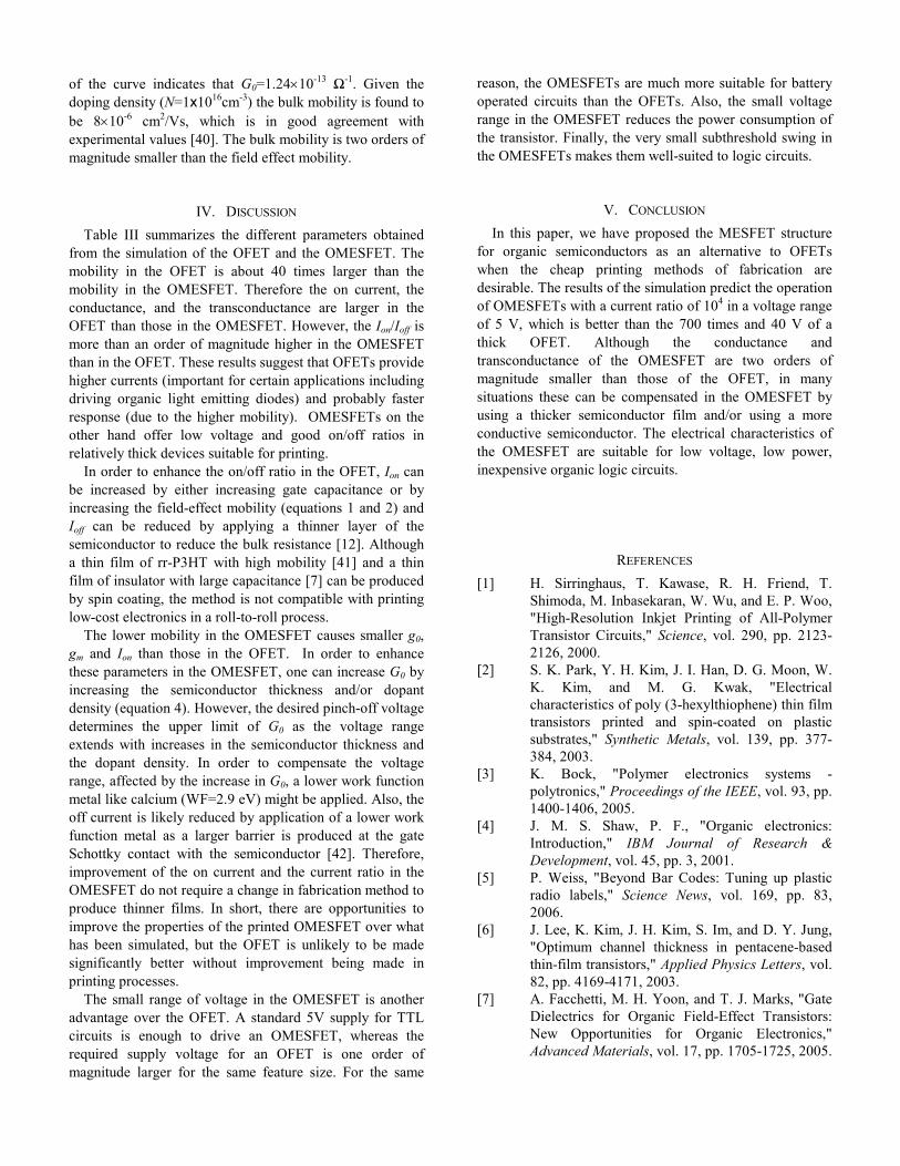
The output characteristic of the OFET is shown in Fig.
3(a) for five different values of the gate voltage. Since the
mobility of carriers in organics is found to be field
dependent at electric fields higher than 105 V/cm [10] the
drain-source voltage is limited to 40 V to ignore the
dependency of the mobility to the electric field. The output
conductance (g0) of the OFET in the linear regime is 5x10-11
Ω-1
, calculated from the slope of the plot when VGS=-40 V at
VDS=0 V.
To study the transfer characteristics of the transistor the
drain current is plotted versus the gate voltage in the linear
regime (VDS=-0.5 V), as shown in Fig. 3(b). A threshold
voltage of -14 V is found for the transistor from the
intercept of the asymptote to the voltage axis. Also, from
the slope a mobility of 3.1×10⁻⁴
cm2/Vs is obtained, again
using equation 1. Redrawing the curve in a semilog scale
(Fig. 3(c)) shows a poor current on/off ratio (Ion/Ioff) of 700,
which is due to the thickness of the semiconductor. To be
more like a switch, a transistor is required to have a high
current ratio, which also reduces the static power dissipation
in a logic circuit. The inverse slope of the plot at VGS=0 V,
known as subthreshold swing, is 4 V/decade, which is
relatively large for a FET transistor [19] but typical of an
OFET. The transconductance (gm) in the linear regime is
found from the slope of the plot at VGS=-40 V to be gm
=1.5x10⁻¹²
Ω-1
.
The transistor characteristics are reasonably close to
those measured in printed OFETs [38]. A mobility of order
of 10-4
cm2/Vs and a threshold voltage of -14 V are typical
in a printed rr-P3HT OFET [38]. A current ratio of 100 in a
printed OFET is achieved by Knobloch et al [38]. Also,
normalizing the current in their transistor to Z/L=0.25 one
obtains an output characteristic similar to Fig. 3(a). This
similarity supports the choice of parameters to describe rr-
P3HT.
C. OMESFET
The cross section of the device is shown in Fig. 2. Gold is
chosen for drain and source electrodes and aluminum is
used for the gate electrode. The same dimensions and
materials that are applied in the OFET are used for the
OMESFET in order to compare the performance of the two
transistors. The thickness of each electrode is 20 nm and the
channel length is 4 µm. The gate electrode is assumed to be
long enough not only to cover the channel area but also to
extend over the drain and source electrodes. The
semiconductor is rr-P3HT, with the same density of states
as defined in Table I.
The Schottky contact is reverse biased in the OMESFET
and a small current is passing through the gate. In this
operating mode there is no need to consider special effects
such as the space charge limited current (SCLC) [39] and/or
the Meyer-Neldel relation (MNR) [28] for the Schottky
contact.
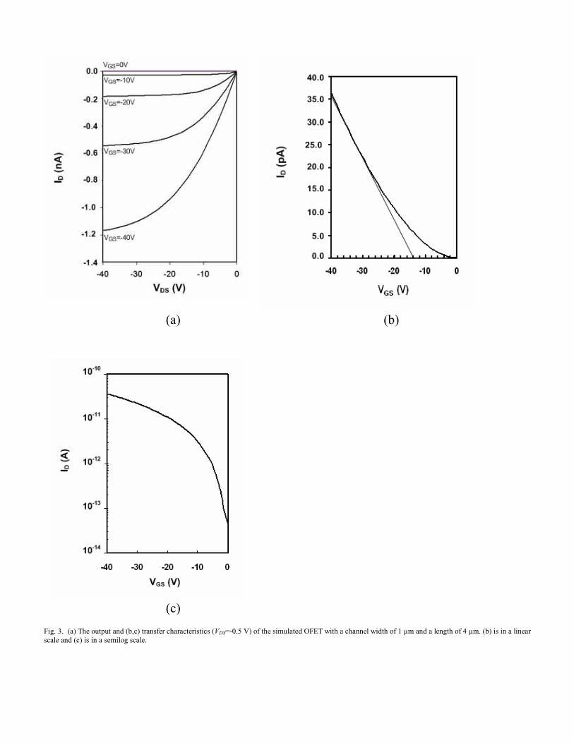
The output and transfer characteristics of the OMESFET
are plotted in Fig. 4. The output characteristics show both
the resistive and saturation modes of the transistor, which
confirms the occurrence of the pinch off in the transistor.
Since the transistor works in depletion mode, it is on at
VGS=0 and application of a positive voltage to the gate
switches the transistor to the off mode. g0=1x10-13
Ω-1
is
found from the plot at VGS=0. In Fig. 4(b) the variation of
the drain current versus the gate voltage at VDS=-0.5 V is
shown. The plot shows a subthreshold swing of 180
mV/decade, and the transconductance is gm=2x10-14
Ω-1
.
Ion/Ioff of the order of 104 is achieved using a gate voltage
range of 5 V. In spite of the fact that in OFETs the gate
current is not a crucial parameter in DC characteristics,
because of the insulating layer, the gate current in
OMESFETs limits the performance of the devices. In Fig.
5, the gate current is plotted versus the gate voltage at VDS=-
10 V. The leakage current of the reverse biased Schottky
junction between the gate and the semiconductor shows a
current value in the order of 10-18
A. This current is small
enough compared to the drain current to be ignored when
the transistor is on. However, the off current for the
transistor is in the same range as the gate current. Therefore
it is expected that the off current would be reduced if the
gate current is reduced.
In order to obtain G0 the device is simulated in the
absence of the aluminum layer. The I-V curve between the
drain and the source terminals is plotted (Fig. 6). The slope
of the curve indicates that G0=1.24×10⁻¹³
Ω-1
. Given the
doping density (=1x10¹⁶
cm-3
) the bulk mobility is found to
be 8×10⁻⁶
cm2/Vs, which is in good agreement with
experimental values [40]. The bulk mobility is two orders of
magnitude smaller than the field effect mobility.
IV. DISCUSSION
Table III summarizes the different parameters obtained
from the simulation of the OFET and the OMESFET. The
mobility in the OFET is about 40 times larger than the
mobility in the OMESFET. Therefore the on current, the
conductance, and the transconductance are larger in the
OFET than those in the OMESFET. However, the Ion/Ioff is
more than an order of magnitude higher in the OMESFET
than in the OFET. These results suggest that OFETs provide
higher currents (important for certain applications including
driving organic light emitting diodes) and probably faster
response (due to the higher mobility). OMESFETs on the
other hand offer low voltage and good on/off ratios in
relatively thick devices suitable for printing.
In order to enhance the on/off ratio in the OFET, Ion can
be increased by either increasing gate capacitance or by
increasing the field-effect mobility (equations 1 and 2) and
Ioff can be reduced by applying a thinner layer of the
semiconductor to reduce the bulk resistance [12]. Although
a thin film of rr-P3HT with high mobility [41] and a thin
film of insulator with large capacitance [7] can be produced
by spin coating, the method is not compatible with printing
low-cost electronics in a roll-to-roll process.
The lower mobility in the OMESFET causes smaller g0,
gm and Ion than those in the OFET. In order to enhance
these parameters in the OMESFET, one can increase G0 by
increasing the semiconductor thickness and/or dopant
density (equation 4). However, the desired pinch-off voltage
determines the upper limit of G0 as the voltage range
extends with increases in the semiconductor thickness and
the dopant density. In order to compensate the voltage
range, affected by the increase in G0, a lower work function
metal like calcium (WF=2.9 eV) might be applied. Also, the
off current is likely reduced by application of a lower work
function metal as a larger barrier is produced at the gate
Schottky contact with the semiconductor [42]. Therefore,
improvement of the on current and the current ratio in the
OMESFET do not require a change in fabrication method to
produce thinner films. In short, there are opportunities to
improve the properties of the printed OMESFET over what
has been simulated, but the OFET is unlikely to be made
significantly better without improvement being made in
printing processes.
The small range of voltage in the OMESFET is another
advantage over the OFET. A standard 5V supply for TTL
circuits is enough to drive an OMESFET, whereas the
required supply voltage for an OFET is one order of
magnitude larger for the same feature size. For the same
reason, the OMESFETs are much more suitable for battery
operated circuits than the OFETs. Also, the small voltage
range in the OMESFET reduces the power consumption of
the transistor. Finally, the very small subthreshold swing in
the OMESFETs makes them well-suited to logic circuits.
V. CONCLUSION
In this paper, we have proposed the MESFET structure
for organic semiconductors as an alternative to OFETs
when the cheap printing methods of fabrication are
desirable. The results of the simulation predict the operation
of OMESFETs with a current ratio of 104 in a voltage range
of 5 V, which is better than the 700 times and 40 V of a
thick OFET. Although the conductance and
transconductance of the OMESFET are two orders of
magnitude smaller than those of the OFET, in many
situations these can be compensated in the OMESFET by
using a thicker semiconductor film and/or using a more
conductive semiconductor. The electrical characteristics of
the OMESFET are suitable for low voltage, low power,
inexpensive organic logic circuits.
REFERENCES
[1] H. Sirringhaus, T. Kawase, R. H. Friend, T.
Shimoda, M. Inbasekaran, W. Wu, and E. P. Woo,
"High-Resolution Inkjet Printing of All-Polymer
Transistor Circuits," Science, vol. 290, pp. 2123-
2126, 2000.
[2] S. K. Park, Y. H. Kim, J. I. Han, D. G. Moon, W.
K. Kim, and M. G. Kwak, "Electrical
characteristics of poly (3-hexylthiophene) thin film
transistors printed and spin-coated on plastic
substrates," Synthetic Metals, vol. 139, pp. 377-
384, 2003.
[3] K. Bock, "Polymer electronics systems -
polytronics," Proceedings of the IEEE, vol. 93, pp.
1400-1406, 2005.
[4] J. M. S. Shaw, P. F., "Organic electronics:
Introduction," IBM Journal of Research &
Development, vol. 45, pp. 3, 2001.
[5] P. Weiss, "Beyond Bar Codes: Tuning up plastic
radio labels," Science ews, vol. 169, pp. 83,
2006.
[6] J. Lee, K. Kim, J. H. Kim, S. Im, and D. Y. Jung,
"Optimum channel thickness in pentacene-based
thin-film transistors," Applied Physics Letters, vol.
82, pp. 4169-4171, 2003.
[7] A. Facchetti, M. H. Yoon, and T. J. Marks, "Gate
Dielectrics for Organic Field-Effect Transistors:
New Opportunities for Organic Electronics,"
Advanced Materials, vol. 17, pp. 1705-1725, 2005.

[8] V. Podzorov, S. E. Sysoev, E. Loginova, V. M.
Pudalov, and M. E. Gershenson, "Single-crystal
organic field effect transistors with the hole
mobility ~ 8 cm2/V s," Applied Physics Letters,
vol. 83, pp. 3504-3506, 2003.
[9] S. P. Speakman, G. G. Rozenberg, K. J. Clay, W.
I. Milne, A. Ille, I. A. Gardner, E. Bresler, and J.
H. G. Steinke, "High performance organic
semiconducting thin films: Ink jet printed
polythiophene [rr-P3HT]," Organic Electronics,
vol. 2, pp. 65-73, 2001.
[10] G. Horowitz, "Organic Field-Effect Transistors,"
Advanced Materials, vol. 10, pp. 365-377, 1998.
[11] T. Lindner, G. Paasch, and S. Scheinert, "Influence
of distributed trap states on the characteristics of
top and bottom contact organic field-effect
transistors," Journal of Materials Research, vol.
19, pp. 2014-2027, 2004.
[12] E. J. Meijer, C. Detcheverry, P. J. Baesjou, E. van
Veenendaal, D. M. de Leeuw, and T. M. Klapwijk,
"Dopant density determination in disordered
organic field-effect transistors," Journal of Applied
Physics, vol. 93, pp. 4831-4835, 2003.
[13] A. N. Aleshin, H. Sandberg, and H. Stubb, "Two-
dimensional charge carrier mobility studies of
regioregular P3HT," Synthetic Metals, vol. 121,
pp. 1449-1450, 2001.
[14] S. R. Forrest, "The path to ubiquitous and low-cost
organic electronic appliances on plastic," ature,
vol. 428, pp. 911-918, 2004.
[15] M. J. Panzer, C. R. Newman, and C. D. Frisbie,
"Low-voltage operation of a pentacene field-effect
transistor with a polymer electrolyte gate
dielectric," Applied Physics Letters, vol. 86, pp.
103503-3, 2005.
[16] J. H. Schon, C. Kloc, and B. Batlogg, "On the
intrinsic limits of pentacene field-effect
transistors," Organic Electronics, vol. 1, pp. 57-
64, 2000.
[17] M. Halik, H. Klauk, U. Zschieschang, G. Schmid,
C. Dehm, M. Schutz, S. Maisch, F. Effenberger,
M. Brunnbauer, and F. Stellacci, "Low-voltage
organic transistors with an amorphous molecular
gate dielectric," ature, vol. 431, pp. 963-966,
2004.
[18] H. T. Yutaka Ohmori, Keiro Muro, Masao Uchida,
Tsuyoshi Kawai and Katsumi Yoshino
"Fabrication and Characteristics of Schottky Gated
Poly(3-alkylthiophene) Field Effect Transistors "
Japanese Journal of Applied Physics vol. 30, pp.
L610-L611, 1991.
[19] S. M. Sze and K. N. Kwok, Physics of
semiconductor Devices, 3rd ed. Hoboken, NJ:
John Wiley & Sons, Inc., 2006.
[20] R. Gupta, S. C. K. Misra, B. D. Malhotra, N. N.
Beladakere, and S. Chandra,
"Metal/semiconductive polymer Schottky device,"
Applied Physics Letters, vol. 58, pp. 51-52, 1991.
[21] W. Brutting, S. Berleb, and A. G. Muckl, "Device
physics of organic light-emitting diodes based on
molecular materials," Organic Electronics, vol. 2,
pp. 1-36, 2001.
[22] C. J. Brabec, N. S. Sariciftci, and J. C. Hummelen,
"Plastic Solar Cells," Advanced Functional
Materials, vol. 11, pp. 15-26, 2001.
[23] David L. Pulfrey and N. G. Tarr, Introduction to
microelectronic devices. Englewood Cliffs, NJ:
Prentice Hall, 1989, ch. 9.
[24] K. F. Teng and R. W. Vest, "Application of ink jet
technology on photovoltaic metallization,"
Electron Device Letters, IEEE, vol. 9, pp. 591-
593, 1988.
[25] H. Cheong Min and S. Wagner, "Inkjet printed
copper source/drain metallization for amorphous
silicon thin-film transistors," Electron Device
Letters, IEEE, vol. 21, pp. 384-386, 2000.
[26]
http://nobelprize.org/nobel_prizes/chemistry/laurea
tes/2000/chemadv.pdf.
[27] K. Morigaki, Physics of Amorphous
Semiconductors: Imperical College Press and
World Scientific Publishing Co. Pte. Ltd., 1999.
[28] W. B. Jackson, "Connection between the Meyer-
Neldel relation and multiple-trapping transport,"
Physical Review B, vol. 38, pp. 3595, 1988.
[29] S. Scheinert, G. Paasch, M. Schrodner, H. K. Roth,
S. Sensfuss, and T. Doll, "Subthreshold
characteristics of field effect transistors based on
poly(3-dodecylthiophene) and an organic
insulator," Journal of Applied Physics, vol. 92, pp.
330-337, 2002.
[30] M. Zhu, G. Liang, T. Cui, and K. Varahramyan,
"Depletion-mode n-channel organic field-effect
transistors based on NTCDA," Solid-State
Electronics, vol. 47, pp. 1855-1858, 2003.
[31]
http://www.synopsys.com/products/mixedsignal/ta
urus/device_sim_ds.html.
[32] J. F. Chang, B. Sun, D. W. Breiby, M. M. Nielsen,
T. I. Solling, M. Giles, I. McCulloch, and H.
Sirringhaus, "Enhanced Mobility of Poly(3-
hexylthiophene) Transistors by Spin-Coating from
High-Boiling-Point Solvents," Chem. Mater., vol.
16, pp. 4772-4776, 2004.
[33] T. A. Chen, X. Wu, and R. D. Rieke,
"Regiocontrolled synthesis of poly(3-
alkylthiophenes) mediated by Rieke zinc: Their
characterization and solid-state properties,"
Journal of the American Chemical Society, vol.
117, pp. 233-244, 1995.
[34] A. J. Cascio, J. E. Lyon, M. M. Beerbom, R.
Schlaf, Y. Zhu, and S. A. Jenekhe, "Investigation
of a polythiophene interface using photoemission
spectroscopy in combination with electrospray
thin-film deposition," Applied Physics Letters, vol.
88, pp. 062104-3, 2006.
[35] C. Tanase, E. J. Meijer, P. W. M. Blom, and D. M.
de Leeuw, "Unification of the Hole Transport in
Polymeric Field-Effect Transistors and Light-
Emitting Diodes," Physical Review Letters, vol.
91, pp. 216601, 2003.
[36] G. Liang, T. Cui, and K. Varahramyan,
"Fabrication and electrical characteristics of
polymer-based Schottky diode," Solid-State
Electronics, vol. 47, pp. 691-694, 2003.
[37] D. B. A. Rep, A. F. Morpurgo, and T. M.
Klapwijk, "Doping-dependent charge injection into
regioregular poly(3-hexylthiophene)," Organic
Electronics, vol. 4, pp. 201-207, 2003.
[38] A. Knobloch, A. Manuelli, A. Bernds, and W.
Clemens, "Fully printed integrated circuits from
solution processable polymers," Journal of Applied
Physics, vol. 96, pp. 2286-2291, 2004.
[39] V. R. Nikitenko, H. Heil, and H. von Seggern,
"Space-charge limited current in regioregular poly-
3-hexyl-thiophene," Journal of Applied Physics,
vol. 94, pp. 2480-2485, 2003.
[40] M. Raja, G. C. R. Lloyd, N. Sedghi, W. Eccleston,
R. Di Lucrezia, and S. J. Higgins, "Conduction
processes in conjugated, highly regio-regular, high
molecular mass, poly(3-hexylthiophene) thin-film
transistors," Journal of Applied Physics, vol. 92,
pp. 1441-1445, 2002.
[41] H. Sirringhaus, N. Tessler, and R. H. Friend,
"Integrated Optoelectronic Devices Based on
Conjugated Polymers," Science, vol. 280, pp.
1741-1744, 1998.
[42] P. Stallinga, H. L. Gomes, M. Murgia, and K.
Mullen, "Interface state mapping in a Schottky
barrier of the organic semiconductor terrylene,"
Organic Electronics, vol. 3, pp. 43-51, 2002.
Arash Takshi was born in Tehran, Iran in
1971. He received a B.Sc. in electronics
from Amir Kabir University of Technology
(Tehran Polytechnic) in 1993, and an M.Sc.
in analog electronics from Sharif University
of Technology, Tehran, in 1996 and a Ph.D.
from the University of British Columbia,
Vancouver, in 2007. He is currently a
Postdoc at UBC where he is doing research
on bioelectronc devices.
Alexandros Dimopoulos (M’01) was born in Montréal, Canada in 1982.
He received a B.Eng. degree in electrical engineering from the University
of Victoria in 2005. He is currently a M.A.Sc. student at the University of
British Columbia where he is exploring polymer electronic devices.
John D. Madden (M’95) was born in
Ottawa, Canada in 1968. He received a
B.Sc. in Physics from the University of
British Columbia (UBC) in 1991, an M.Eng.
in Biomedical Engineering from McGill
University, Montreal, in 1995 and a Ph.D.
from the BioInstrumentation Lab at MIT in
2000. Dr. Madden left MIT for UBC in
2002 and is currently an Assistant Professor
of Electrical & Computer Engineering. His
research involves fundamental studies and applications of polymer and
nanotube actuators and electronic devices.

Fig. 1. Schematic of an OFET.

Fig. 2. The proposed geometry for Organic Metal-Semiconductor Field Effect Transistor (OMESFET).
(a) (b)
(c) Fig. 3. (a) The output and (b,c) transfer characteristics (VDS=-0.5 V) of the simulated OFET with a channel width of 1 µm and a length of 4 µm. (b) is in a linear
scale and (c) is in a semilog scale.
(a)
(b)
Fig. 4. (a) The output and (b) transfer characteristics (VDS=-0.5 V) of the simulated OMESFET with a channel width of 1 µm and a length of 4 µm.

Fig. 5. The input characteristic of the simulated OMESFET.
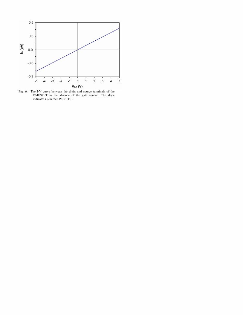
Fig. 6. The I-V curve between the drain and source terminals of the
OMESFET in the absence of the gate contact. The slope
indicates G0 in the OMESFET.

TABLE I
DISCRETE LEVELS OF TRAP DENSITY RELATIVE TO THE EDGE OF VALENCE
BAND IN RR-P3HT
Ei Ei-EV (eV) Density of localized states (cm3.eV)-1
E1 0 1.00x10²¹
E2 0.03 4.15 x10²⁰
E3 0.06 1.72 x10²⁰
E4 0.09 7.15 x10¹⁹
E5 0.12 2.97 x10¹⁹
E6 0.15 1.23 x10¹⁹
E7 0.18 5.12 x10¹⁸
E8 0.21 2.12 x10¹⁸
E9 0.24 8.82 x10¹⁷
E10 0.27 3.66 x10¹⁷
E11 0.30 1.52 x10¹⁷
E12 0.33 6.31 x10¹⁶
E13 0.36 2.62 x10¹⁶
E14 0.39 1.09 x10¹⁶
E15 0.42 4.51 x10¹⁵
E16 0.45 1.87 x10¹⁵
E17 0.48 7.78 x10¹⁴
E18 0.51 3.23 x10¹⁴
E19 0.54 1.34 x10¹⁴

TABLE II
THE LIST OF SET UP PARAMETERS FOR USED MATERIALS IN THE SIMULATION
OF THE ORGANIC TRANSISTORS
Material Parameter Symbol Value Unit Ref.
Band gap Eg 1.7 eV [33]
Electron affinity χe 3.15 eV [34]
Permittivity εs 3 [36]
Dopant Density NS 1x1016 cm-3 [12]
Mobility µ 0.12 cm2/Vs [32]
rr-P3HT
Thickness ts 400 nm [2]
Au work function φAu 5.1 eV [37] Metals
Al work function φAl 4.3 eV [37]
SiO2 thickness tins 100 nm [2] Insulator
SiO2 permittivity εins 3.9 [20]

TABLE III
ELECTRICAL CHARACTERISTICS OF THE SIMULATED OFET AND OMESFET
Parameter OFET OMESFET
Ion/Ioff 700 104
Gate voltage range (V) 40 5
Threshold/Pinch-off voltage (V) 14 5
Subthreshold swing (mV/decade) 4000 180
Mobility (cm2/Vs) 3.1×10⁻⁴ 8×10⁻⁶
go (Ω-1) 5×10-11 1×10-13
gm (Ω-1) 1.5×10⁻¹² 2×10-14
Ion (A) @ VDS=-0.5V 3.5×10⁻¹¹ 4×10-14