Simulation and Experimental Demonstration of the Importance ...
15
HAL Id: hal-02299068 https://hal.archives-ouvertes.fr/hal-02299068 Submitted on 25 Nov 2019 HAL is a multi-disciplinary open access archive for the deposit and dissemination of sci- entific research documents, whether they are pub- lished or not. The documents may come from teaching and research institutions in France or abroad, or from public or private research centers. L’archive ouverte pluridisciplinaire HAL, est destinée au dépôt et à la diffusion de documents scientifiques de niveau recherche, publiés ou non, émanant des établissements d’enseignement et de recherche français ou étrangers, des laboratoires publics ou privés. Distributed under a Creative Commons Attribution - NonCommercial| 4.0 International License Simulation and Experimental Demonstration of the Importance of IR-Drops During Laser Fault-Injection Raphael Andreoni Camponogara-Viera, Philippe Maurine, Jean-Max Dutertre, Rodrigo Possamai Bastos To cite this version: Raphael Andreoni Camponogara-Viera, Philippe Maurine, Jean-Max Dutertre, Rodrigo Possamai Bastos. Simulation and Experimental Demonstration of the Importance of IR-Drops During Laser Fault-Injection. IEEE Transactions on Computer-Aided Design of Integrated Circuits and Systems, IEEE, 2020, 39 (6), pp.1231-1244. 10.1109/TCAD.2019.2928972. hal-02299068
-
Upload
khangminh22 -
Category
Documents
-
view
0 -
download
0
Transcript of Simulation and Experimental Demonstration of the Importance ...
HAL Id: hal-02299068https://hal.archives-ouvertes.fr/hal-02299068
Submitted on 25 Nov 2019
HAL is a multi-disciplinary open accessarchive for the deposit and dissemination of sci-entific research documents, whether they are pub-lished or not. The documents may come fromteaching and research institutions in France orabroad, or from public or private research centers.
L’archive ouverte pluridisciplinaire HAL, estdestinée au dépôt et à la diffusion de documentsscientifiques de niveau recherche, publiés ou non,émanant des établissements d’enseignement et derecherche français ou étrangers, des laboratoirespublics ou privés.
Distributed under a Creative Commons Attribution - NonCommercial| 4.0 InternationalLicense
Simulation and Experimental Demonstration of theImportance of IR-Drops During Laser Fault-Injection
Raphael Andreoni Camponogara-Viera, Philippe Maurine, Jean-MaxDutertre, Rodrigo Possamai Bastos
To cite this version:Raphael Andreoni Camponogara-Viera, Philippe Maurine, Jean-Max Dutertre, Rodrigo PossamaiBastos. Simulation and Experimental Demonstration of the Importance of IR-Drops During LaserFault-Injection. IEEE Transactions on Computer-Aided Design of Integrated Circuits and Systems,IEEE, 2020, 39 (6), pp.1231-1244. �10.1109/TCAD.2019.2928972�. �hal-02299068�
AUTHORS’ VERSION 1
Simulation and Experimental Demonstration of theImportance of IR-Drops During Laser
Fault-InjectionRaphael A. C. Viera∗†‡, Philippe Maurine∗, Jean-Max Dutertre†, and Rodrigo Possamai Bastos‡ ∗ LIRMM,
CNRS, UMR N5506 (Montpellier, France)† Mines Saint-Etienne, CEA-Tech, Centre CMP, F - 13541 (Gardanne, France)‡ Univ. Grenoble Alpes, Grenoble INP, CNRS, TIMA (Grenoble, France)
{raphael.viera, dutertre}@emse.fr, [email protected], [email protected]
Abstract—Laser fault injections induce transient faults intoICs by locally generating transient currents that temporarily flipthe outputs of the illuminated gates. Laser fault injection canbe anticipated or studied by using simulation tools at differentabstraction levels: physical, electrical or logical. At the electricallevel, the classical laser-fault injection model is based on theaddition of current sources to the various sensitive nodes of CMOStransistors. However, this model does not take into account thelarge transient current components also induced between theVDD and GND of ICs designed with advanced CMOS technologies.These short-circuit currents provoke a significant IR-drop thatcontribute to the fault injection process. This paper describesour research on the assessment of this contribution. It showsthrough simulation and experiments that during laser fault in-jection campaigns, laser-induced IR-drop is always present whenconsidering circuits designed with deep submicron technologies.It introduces an enhanced electrical fault model taking the laser-induced IR-drop into account. It also proposes a methodologythat allows the use of the model to simulate laser-induced faultsat the electrical level in large-scale circuits. On the basis offurther simulations and experimental results, we found that,depending on the laser pulse characteristics, the number ofinjected faults may be underestimated by a factor of up to 2.4 ifthe laser-induced IR-drop is ignored. This could lead to incorrectestimations of the fault injection threshold, which is especiallyrelevant to the design of countermeasure techniques for secureintegrated systems.
Index Terms—Laser fault injection, Hardware security imple-mentation, Methodologies for EDA, Electrical simulation.
I. INTRODUCTION
Fault injection attacks have become a common way to defeatthe security mechanisms of embedded devices. There is alarge and constantly growing number of known techniques forinjecting faults into ICs [1], [2]. Among them one can findtechniques that:
• disrupt the clock signal [3],• induce sudden variations of the supply voltage [4] or of
the substrate bias [5],• inject parasitic currents into using powerful electromag-
netic disturbances or intense light flashes [1], [6].The efficiency of optical attacks was first demonstrated usinga camera flash [7]. However, to be able to influence each
Auhors’ version
logic cell independently, and thus to better control the injectedfaults, focusable sources of ionizing radiations are preferable.Laser sources are such sources. Indeed they allow to controlthe injected faults with precision thanks to their high spatialand temporal resolutions as highlighted in [7], which reportedin the early 2000s the use of laser to induce a bit-flip in a SRAMcell. Following this pioneering work, the necessity for design-ing robust circuits, resistant to laser fault injection attacks soonbecame apparent in the hardware security community. Hencethe need for models and methodologies allowing researchersto forecast the effects of laser based attacks on ICs.
Although fault simulations can be performed at differentabstraction levels of design flows (transistor level, gate level,RTL level, and even software level), low abstraction levelsprovide the highest accuracy.
When a laser illuminates an IC, it generates a parasitic(photoelectric) current [8]. This current generates an undesiredtransient voltage that propagates through the logic toward theinput of a register (D-type Flip Flops) and, if it is still presentwhen the next rising clock edge occurs, a bit may be inverted,producing a soft error (SE). At the electrical level, it hasbeen demonstrated [9], [10] that this transient current can beefficiently modeled with a current source delivering a currentwith a double exponential shape. This current source is addedto the netlist of the cell illuminated by the laser beam. Thenan electrical level simulation, which is expected to take intoaccount the effects of the laser illumination, is performed.
If such an explanation was found relevant for old CMOStechnologies, it has been put into question for advanced sub-micron technologies. Indeed, with increasing transistor density,laser illumination does not affect a single transistor (or CMOSgate) but rather illuminates multiple gates simultaneously. Inthis case, a laser shot also induces a current that flows fromVDD to GND causing a temporary power supply voltage drop(IR-drop) known by designers to be a source of timing failures.As the induced IR-drop may be of significant amplitude andduration [11], it has to be taken into account while simulatinglaser fault injection.
The above remark implies that the models [12]–[15] usedso far for simulating the effects of laser shots on ICs designedwith advanced technologies can lack accuracy. Furthermore,the joint effects of the photoelectric currents and of the related
https://doi.org/10.1109/TCAD.2019.2928972
IEEE TCAD: Transactions on Computer-Aided Design of Integrated Circuits and Ssytems
AUTHORS’ VERSION 2
IR-drop can only be accurately simulated at low abstractionlevels (taking into account the layout topology to betterrepresent the physical phenomenon) in the scope of a wholesystem. The simulation must thus be performed on complexcircuits and not just in one (or few) CMOS cell.
To the best of our knowledge, among the formerly proposedfault simulators [12], [16]–[20], the most recent one is [21]which is based on open-source code [22]. The major issue withthese fault simulators is that they rely on electrical models[13], [15], [23] that are technology dependent. For instance,in [24], the authors proposed a model that includes verticalparasitic bipolar junctions inherent to MOSFETs in the faultinjection process that may lead to IR-drop effects. However,they did not extend their work beyond the scope of a singleinverter. In fact, modeling the RC network of power/groundrails is a difficult task, since the RC values depend on thetechnology, the size of cells, the position of voltage taps onthe rails, the RC parasitics, etc. None of the aforementionedarticles consider the effect of laser induced IR-drop.
Within this context, the contribution of this paper is three-fold. Firstly, it shows through simulation and experiment thatduring a laser shot, an additional current component causingan IR-drop with a significant effect on the target operation isalways present when considering circuits designed in relativelynew technologies. Secondly, the paper introduces an improvedtransient fault model that takes the laser-induced IR-drop intoaccount for simulation purposes. Thirdly, it is derived, fromthe enhanced fault model, which uses an adequate simulationmethodology based on standard CAD tools (taking the inducedIR-drop into account) to forecast the effect of laser faultinjections in large scale circuits.
The rest of this paper is organized as follows. Section IIrecalls the background on the effects of laser illumination onICs. Section III discusses the limitations of the classical faultmodel before introducing an enhanced fault model. Gate levelsimulations and experimental results of laser injections aregiven in Section IV in order to demonstrate the existence oflaser-induced IR-drops and to validate the proposed enhancedfault model. Section V details the method used to simulatelaser-induced faults in large-scale circuits, and Section VIanalyzes simulation results provided by the proposed method.Additional evidence of the importance of laser-induced IR-drop at system level is provided in Section VII. Section VIIIconcludes the paper.
II. STATE OF THE ART OF LASER SHOT EFFECTS ON ICS
A. Effect of a Laser Shot at Transistor Level
ICs are known to be sensitive to induced transient currents.Such currents may be caused by a laser beam passing throughthe device, creating electron-hole pairs along the path ofthe laser beam [8]. These induced charge carriers generallyrecombine without any significant effect, unless they reachthe strong electric field found in the vicinity of reverse biasedPN junctions (the reverse biased junction is the most laser-sensitive part of circuits) [25]. In this case, the electrical fieldputs these charges into motion and a transient current flows.Each induced transient current has its proper characteristics
such as polarity, amplitude and duration that depend on laserenergy, laser shot location, device technology, device supplyvoltage and output load. The nature of these currents was firststudied in the case of radioactive particles [26]–[30]. Laserillumination was first used as a way to emulate the effect ofionizing particles since the properties of the transient currentsthey both induce are similar.
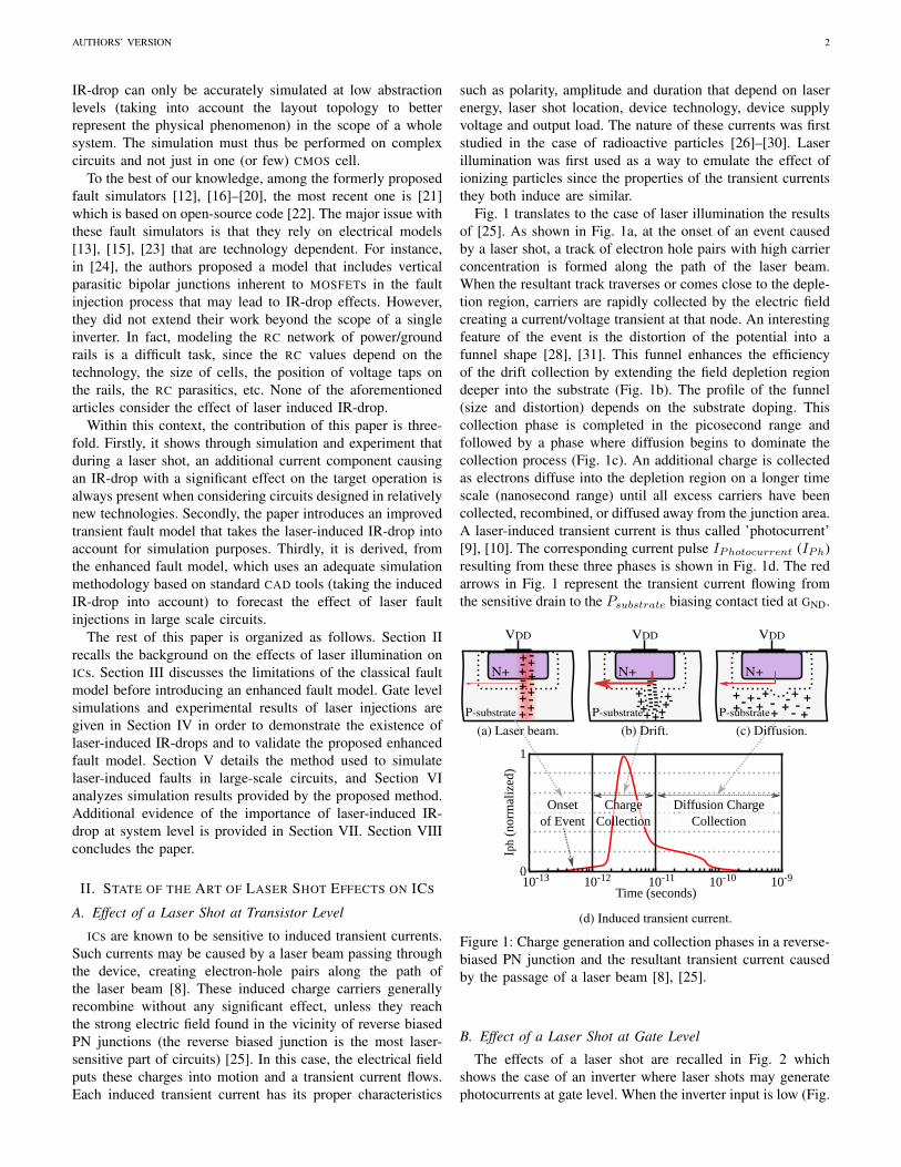
Fig. 1 translates to the case of laser illumination the resultsof [25]. As shown in Fig. 1a, at the onset of an event causedby a laser shot, a track of electron hole pairs with high carrierconcentration is formed along the path of the laser beam.When the resultant track traverses or comes close to the deple-tion region, carriers are rapidly collected by the electric fieldcreating a current/voltage transient at that node. An interestingfeature of the event is the distortion of the potential into afunnel shape [28], [31]. This funnel enhances the efficiencyof the drift collection by extending the field depletion regiondeeper into the substrate (Fig. 1b). The profile of the funnel(size and distortion) depends on the substrate doping. Thiscollection phase is completed in the picosecond range andfollowed by a phase where diffusion begins to dominate thecollection process (Fig. 1c). An additional charge is collectedas electrons diffuse into the depletion region on a longer timescale (nanosecond range) until all excess carriers have beencollected, recombined, or diffused away from the junction area.A laser-induced transient current is thus called ’photocurrent’[9], [10]. The corresponding current pulse IPhotocurrent (IPh)resulting from these three phases is shown in Fig. 1d. The redarrows in Fig. 1 represent the transient current flowing fromthe sensitive drain to the Psubstrate biasing contact tied at GND.
VDD VDD VDD
N+
P-substrate P-substrate P-substrate
N+ N+
(a) Laser beam. (b) Drift. (c) Diffusion.
++++++
++---
----------------
++++
++
+
++-
-
- ---
--
-
++
+++++
+
++- - - -
-- --
Iph
(nor
mal
ized
)
Time (seconds)
0
1
Charge Collection
Onsetof Event
Diffusion ChargeCollection
10-910-1010-1210-13 10-11
(d) Induced transient current.
Figure 1: Charge generation and collection phases in a reverse-biased PN junction and the resultant transient current causedby the passage of a laser beam [8], [25].
B. Effect of a Laser Shot at Gate Level
The effects of a laser shot are recalled in Fig. 2 whichshows the case of an inverter where laser shots may generatephotocurrents at gate level. When the inverter input is low (Fig.
AUTHORS’ VERSION 3
2a), the most laser-sensitive part of the inverter is the NMOStransistor drain due to a reverse biased PN junction betweenthe drain and the Psubstrate. Thus, an induced transient current(IPh) flows from the drain of the NMOS to the Psubstrate
biasing contact (at GND). Similar reasoning can be made whenthe inverter input is high (Fig. 2b). In that case, the susceptiblepart of the inverter is the drain of the PMOS transistor. In Fig.2a (resp. Fig. 2b), a part of the induced photocurrent (IPh)discharges (resp. charges) the inverter output capacitance. Asa result the inverter output switches to low voltage (resp. highvoltage), thus a so called voltage transient occurs.
CLoad
'0' '1' >> '0'
IPh
IPh
(a) NMOS sensitive drain.
CLoad
'1' '0' >> '1'
IPh
IPh
(b) PMOS sensitive drain.
Figure 2: Electrical model of laser-induced transient currentsapplied to a CMOS inverter.
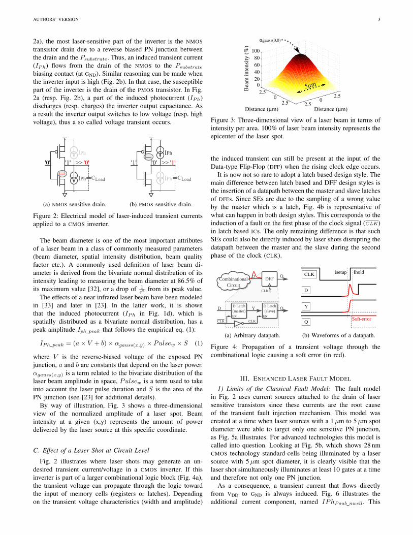
The beam diameter is one of the most important attributesof a laser beam in a class of commonly measured parameters(beam diameter, spatial intensity distribution, beam qualityfactor etc.). A commonly used definition of laser beam di-ameter is derived from the bivariate normal distribution of itsintensity leading to measuring the beam diameter at 86.5% ofits maximum value [32], or a drop of 1
e2 from its peak value.The effects of a near infrared laser beam have been modeled
in [33] and later in [23]. In the latter work, it is shownthat the induced photocurrent (IPh in Fig. 1d), which isspatially distributed as a bivariate normal distribution, has apeak amplitude Iph peak that follows the empirical eq. (1):
IPh peak = (a× V + b)× αgauss(x,y) × Pulsew × S (1)
where V is the reverse-biased voltage of the exposed PNjunction, a and b are constants that depend on the laser power.αgauss(x,y) is a term related to the bivariate distribution of thelaser beam amplitude in space, Pulsew is a term used to takeinto account the laser pulse duration and S is the area of thePN junction (see [23] for additional details).
By way of illustration, Fig. 3 shows a three-dimensionalview of the normalized amplitude of a laser spot. Beamintensity at a given (x,y) represents the amount of powerdelivered by the laser source at this specific coordinate.
C. Effect of a Laser Shot at Circuit Level
Fig. 2 illustrates where laser shots may generate an un-desired transient current/voltage in a CMOS inverter. If thisinverter is part of a larger combinational logic block (Fig. 4a),the transient voltage can propagate through the logic towardthe input of memory cells (registers or latches). Dependingon the transient voltage characteristics (width and amplitude)
020406080
100
Distance (µm)Distance (µm)
Bea
m in
tens
ity (%
)
002.5
2.5 2.5
2.5
5µm
αgauss(0,0)
Figure 3: Three-dimensional view of a laser beam in terms ofintensity per area. 100% of laser beam intensity represents theepicenter of the laser spot.
the induced transient can still be present at the input of theData-type Flip-Flop (DFF) when the rising clock edge occurs.
It is now not so rare to adopt a latch based design style. Themain difference between latch based and DFF design styles isthe insertion of a datapath between the master and slave latchesof DFFs. Since SEs are due to the sampling of a wrong valueby the master which is a latch, Fig. 4b is representative ofwhat can happen in both design styles. This corresponds to theinduction of a fault on the first phase of the clock signal (CLK)in latch based ICs. The only remaining difference is that suchSEs could also be directly induced by laser shots disrupting thedatapath between the master and the slave during the secondphase of the clock (CLK).
D Latch(master)
CLK
D D Latch(slave)
Y Q
CLKEN EN
CombinationalCircuit
DFF
CLK
D Q
(a) Arbitrary datapath.
tholdtsetupCLK
D
Y
Soft-errorQ
(b) Waveforms of a datapath.
Figure 4: Propagation of a transient voltage through thecombinational logic causing a soft error (in red).
III. ENHANCED LASER FAULT MODEL
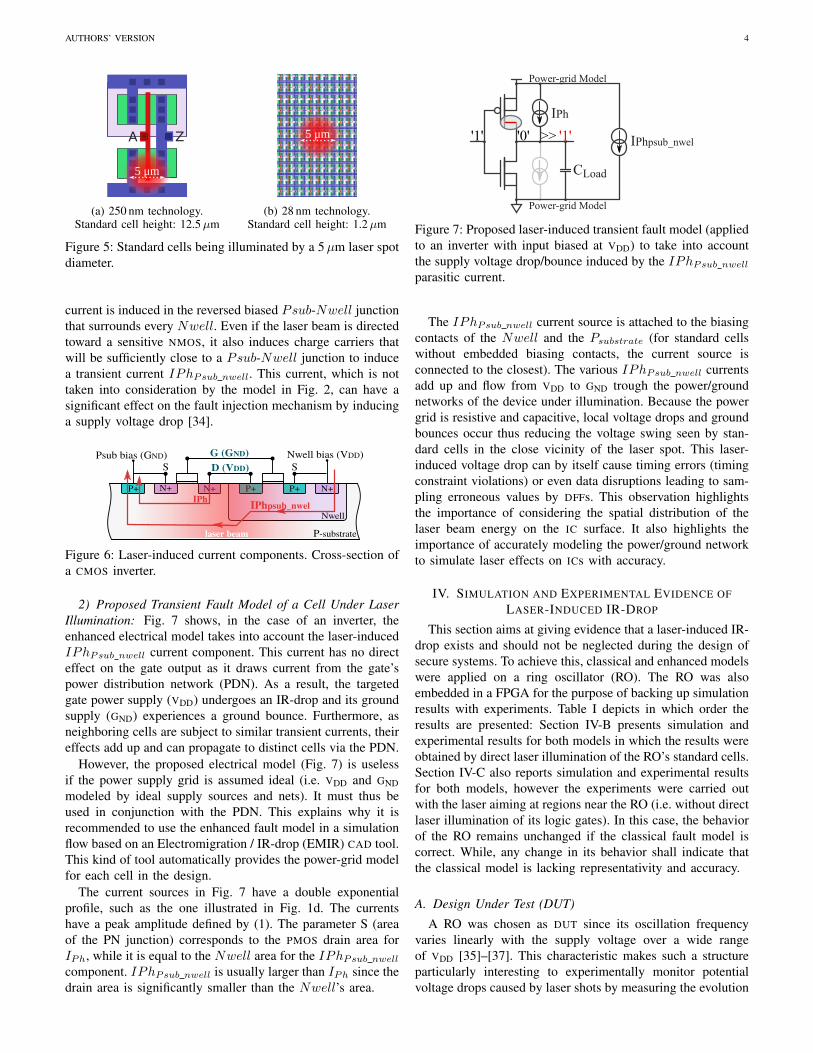
1) Limits of the Classical Fault Model: The fault modelin Fig. 2 uses current sources attached to the drain of lasersensitive transistors since these currents are the root causeof the transient fault injection mechanism. This model wascreated at a time when laser sources with a 1µm to 5µm spotdiameter were able to target only one sensitive PN junction,as Fig. 5a illustrates. For advanced technologies this model iscalled into question. Looking at Fig. 5b, which shows 28 nmCMOS technology standard-cells being illuminated by a lasersource with 5µm spot diameter, it is clearly visible that thelaser shot simultaneously illuminates at least 10 gates at a timeand therefore not only one PN junction.
As a consequence, a transient current that flows directlyfrom VDD to GND is always induced. Fig. 6 illustrates theadditional current component, named IPhPsub nwell. This
AUTHORS’ VERSION 4
ZA
5 μm
(a) 250 nm technology.Standard cell height: 12.5µm
A ZA ZA ZA ZA ZA Z
A Z
A ZA Z
A ZA ZA Z A Z
A Z
A Z
A ZA ZA ZA Z
A ZA ZA ZA ZA Z
A ZA Z
A ZA ZA Z
A Z
A ZA Z
A ZA ZA ZA ZA ZA ZA ZA ZA ZA ZA Z
A Z
A Z
A ZA ZA ZA ZA ZA ZA ZA ZA Z
A ZA ZA ZA ZA Z
A Z
A ZA ZA ZA ZA Z
A ZA ZA ZA ZA ZA ZA ZA ZA Z
A Z
A Z
A ZA ZA ZA ZA ZA ZA ZA ZA ZA ZA Z
A ZA Z
A Z
A ZA ZA ZA ZA ZA ZA ZA Z
A ZA ZA ZA ZA ZA Z
A Z
A ZA ZA ZA Z
A ZA ZA ZA ZA ZA ZA ZA ZA ZA Z
A Z
A Z
5 μm
(b) 28 nm technology.Standard cell height: 1.2µm
Figure 5: Standard cells being illuminated by a 5µm laser spotdiameter.
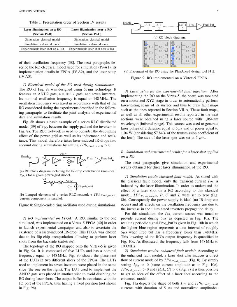
current is induced in the reversed biased Psub-Nwell junctionthat surrounds every Nwell. Even if the laser beam is directedtoward a sensitive NMOS, it also induces charge carriers thatwill be sufficiently close to a Psub-Nwell junction to inducea transient current IPhPsub nwell. This current, which is nottaken into consideration by the model in Fig. 2, can have asignificant effect on the fault injection mechanism by inducinga supply voltage drop [34].
Psub bias (GND)
P+ N+N+
P-substrate
SNwell bias (VDD)
Nwell
P+ N+P+
SG (GND)D (VDD)
IPhpsub_nwel
laser beam
IPh
Figure 6: Laser-induced current components. Cross-section ofa CMOS inverter.
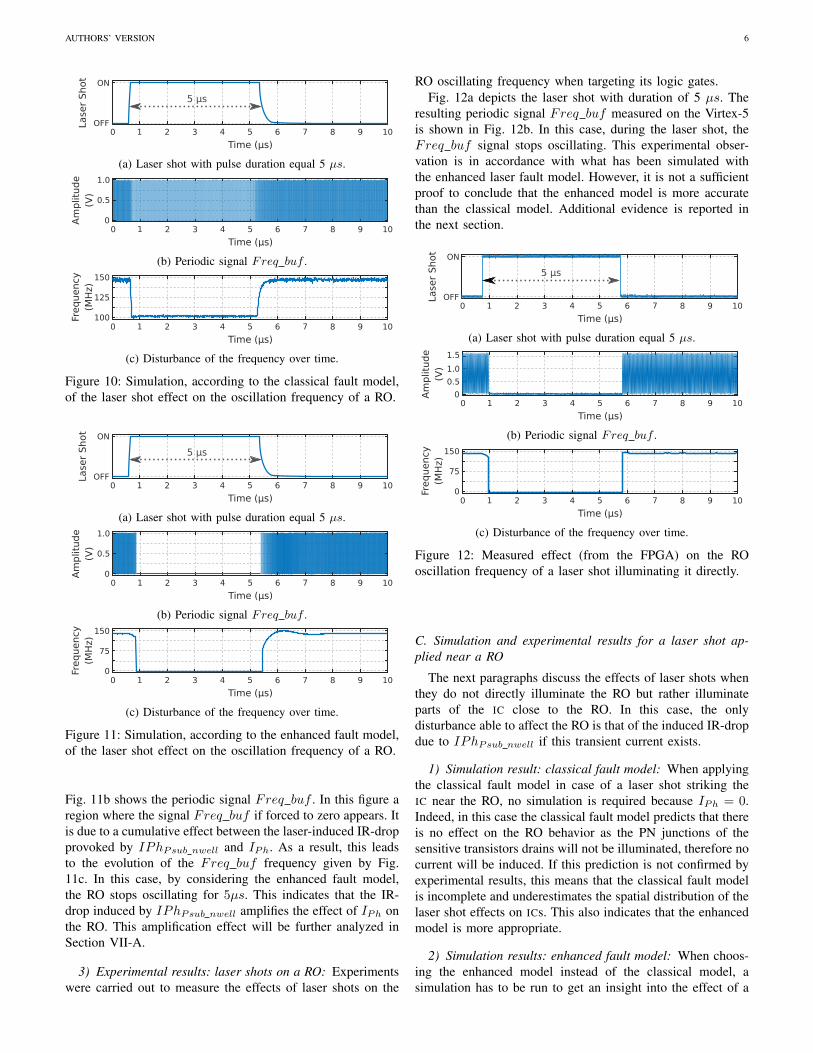
2) Proposed Transient Fault Model of a Cell Under LaserIllumination: Fig. 7 shows, in the case of an inverter, theenhanced electrical model takes into account the laser-inducedIPhPsub nwell current component. This current has no directeffect on the gate output as it draws current from the gate’spower distribution network (PDN). As a result, the targetedgate power supply (VDD) undergoes an IR-drop and its groundsupply (GND) experiences a ground bounce. Furthermore, asneighboring cells are subject to similar transient currents, theireffects add up and can propagate to distinct cells via the PDN.
However, the proposed electrical model (Fig. 7) is uselessif the power supply grid is assumed ideal (i.e. VDD and GNDmodeled by ideal supply sources and nets). It must thus beused in conjunction with the PDN. This explains why it isrecommended to use the enhanced fault model in a simulationflow based on an Electromigration / IR-drop (EMIR) CAD tool.This kind of tool automatically provides the power-grid modelfor each cell in the design.
The current sources in Fig. 7 have a double exponentialprofile, such as the one illustrated in Fig. 1d. The currentshave a peak amplitude defined by (1). The parameter S (areaof the PN junction) corresponds to the PMOS drain area forIPh, while it is equal to the Nwell area for the IPhPsub nwell
component. IPhPsub nwell is usually larger than IPh since thedrain area is significantly smaller than the Nwell’s area.
CLoad
'1' '0' >> '1' IPhpsub_nwel
IPh
Power-grid Model
Power-grid Model
Figure 7: Proposed laser-induced transient fault model (appliedto an inverter with input biased at VDD) to take into accountthe supply voltage drop/bounce induced by the IPhPsub nwell
parasitic current.
The IPhPsub nwell current source is attached to the biasingcontacts of the Nwell and the Psubstrate (for standard cellswithout embedded biasing contacts, the current source isconnected to the closest). The various IPhPsub nwell currentsadd up and flow from VDD to GND trough the power/groundnetworks of the device under illumination. Because the powergrid is resistive and capacitive, local voltage drops and groundbounces occur thus reducing the voltage swing seen by stan-dard cells in the close vicinity of the laser spot. This laser-induced voltage drop can by itself cause timing errors (timingconstraint violations) or even data disruptions leading to sam-pling erroneous values by DFFs. This observation highlightsthe importance of considering the spatial distribution of thelaser beam energy on the IC surface. It also highlights theimportance of accurately modeling the power/ground networkto simulate laser effects on ICs with accuracy.
IV. SIMULATION AND EXPERIMENTAL EVIDENCE OFLASER-INDUCED IR-DROP
This section aims at giving evidence that a laser-induced IR-drop exists and should not be neglected during the design ofsecure systems. To achieve this, classical and enhanced modelswere applied on a ring oscillator (RO). The RO was alsoembedded in a FPGA for the purpose of backing up simulationresults with experiments. Table I depicts in which order theresults are presented: Section IV-B presents simulation andexperimental results for both models in which the results wereobtained by direct laser illumination of the RO’s standard cells.Section IV-C also reports simulation and experimental resultsfor both models, however the experiments were carried outwith the laser aiming at regions near the RO (i.e. without directlaser illumination of its logic gates). In this case, the behaviorof the RO remains unchanged if the classical fault model iscorrect. While, any change in its behavior shall indicate thatthe classical model is lacking representativity and accuracy.
A. Design Under Test (DUT)
A RO was chosen as DUT since its oscillation frequencyvaries linearly with the supply voltage over a wide rangeof VDD [35]–[37]. This characteristic makes such a structureparticularly interesting to experimentally monitor potentialvoltage drops caused by laser shots by measuring the evolution
AUTHORS’ VERSION 5
Table I: Presentation order of Section IV results
Laser illumination on a RO Laser illumination near a RO(Section IV-B) (Section IV-C)
Simulation: classical model Simulation: classical model
Simulation: enhanced model Simulation: enhanced model
Experimental: laser shot on a RO Experimental: laser shot near a RO
of their oscillation frequency [38]. The next paragraphs de-scribe the RO electrical model used for simulation (IV-A1), itsimplementation details in FPGA (IV-A2), and the laser setup(IV-A3).
1) Electrical model of the RO used during simulations:The RO of Fig. 8a was designed using 65 nm technology. Itfeatures an AND2 gate, a BUFFER gate, and seven inverters.Its nominal oscillation frequency is equal to 148 MHz. Theoscillation frequency was fixed in accordance with that of theRO considered during the experiments described in the follow-ing paragraphs to facilitate the joint analysis of experimentaldata and simulation results.
Fig. 8b shows a basic example of a series RLC distributedmodel [39] of VDD between the supply pad and the inverters inFig. 8a. The RLC network is used to consider the decouplingeffect of the power grid as well as its inductance and resis-tance. This model therefore takes laser-induced IR-drops intoaccount during simulations by setting IPhPsub nwell > 0.
Enable1 2
Freq Freq_buf7
VRLC
IPh
(a) RO block diagram including the IR-drop contribution (non-idealVDD) for a given power-grid model.
VddVRLC
R L C IPhpsub_nwell
(b) Lumped elements of a series RLC network + IPhPsub nwell
current component in parallel.
Figure 8: Single-ended ring oscillator used during simulations.
2) RO implemented on FPGA: A RO, similar to the onesimulated, was implemented on a Virtex-5 FPGA [40] in orderto launch experimental campaigns and also to ascertain theexistence of a laser-induced IR-drop. This FPGA was chosendue to its flip-chip encapsulation allowing to perform lasershots from the backside (substrate).
The topology of the RO mapped onto the Virtex-5 is givenin Fig. 9a. It is composed of five LUTs and has a nominalfrequency equal to 148 MHz. Fig. 9b shows the placementof the LUTs in two different slices of the FPGA. The LUTsused to implement its seven inverters were placed in the sameslice (the one on the right). The LUT used to implement theAND2 gate was placed in another slice to avoid disabling theRO during laser shots. The output buffer is associated with theIO port of the FPGA, thus having a fixed position (not shownin Fig. 9b).
EnableLUT11
LUT12
LUT17
Freq Freq_buf
(a) RO block diagram.
SLICEL SLICEL
(b) Placement of the RO using the PlanAhead design tool [41].
Figure 9: RO implemented on a Virtex-5 FPGA.
3) Laser setup for the experimental fault injection: Afterimplementing the RO on the Virtex-5, the board was mountedon a motorized XYZ stage in order to automatically performlaser-testing scans of its surface and thus to draw fault mapssuch as the ones reported in Section VII-A. These fault maps,as well as all other experimental results reported in the nextsections were obtained using a laser source with 1,064 nmwavelength (infrared range). This source was used to generatelaser pulses of a duration equal to 5µs and of power equal to1.04 W (considering 57.84% of the transmission coefficient ofthe lens). The size of the laser spot was set at 5 µm.
B. Simulation and experimental results for a laser shot appliedon a RO
The next paragraphs give simulation and experimentalresults obtained for direct laser illumination of the RO.
1) Simulation result: classical fault model: As stated withthe classical fault model, only the transient current IPh isinduced by the laser illumination. In order to understand theeffect of a laser shot on a RO according to this classicalmodel, IPhPsub nwell, R, C and L were set to zero (Fig.8b). Consequently the power supply is ideal (no IR-drop canoccur) and all effects on the oscillation frequency are due tothe increase in the illuminated inverters propagation delay.
For this simulation, the IPh current source was tuned toprovide current during 5µs as depicted in Fig. 10a. Theresulting periodic signal Freq buf is given in Fig. 10b in whichthe lighter blue region represents a time interval of roughly5µs when Freq buf has a frequency lower than 148 MHz.This lowering of the RO’s output frequency is quantified inFig. 10c. As illustrated, the frequency falls from 148 MHz to100 MHz.
2) Simulation results: enhanced fault model: According tothe enhanced fault model, a laser shot also induces a directflow of current modeled by IPhPsub nwell (Fig. 8). By simplysetting IPh > 0 (same current amplitude as in Fig. 10c),IPPsub nwell > 0 and (R,L,C) > 0 (Fig. 8) it is thus possibleto get an idea of the effect of a laser shot according to theenhanced model.
Fig. 11a depicts the shape of both IPh and IPhPsub nwell
currents with duration of 5 µs and normalized amplitudes.
AUTHORS’ VERSION 6
Lase
r S
hot ON
OFF0 1 2 3 4 5 6 7 8 9 10
Time (μs)
5 μs
(a) Laser shot with pulse duration equal 5 µs.
Am
plit
ude
(V)
0 1 2 3 4 5 6 7 8 9 10
Time (μs)
0
1.0
0.5
(b) Periodic signal Freq buf .
0 1 2 3 4 5 6 7 8 9 10
Time (μs)
Frequency
(MH
z)
150
125
100
(c) Disturbance of the frequency over time.
Figure 10: Simulation, according to the classical fault model,of the laser shot effect on the oscillation frequency of a RO.
Lase
r S
hot ON
OFF0 1 2 3 4 5 6 7 8 9 10
Time (μs)
5 μs
(a) Laser shot with pulse duration equal 5 µs.
Am
plit
ude
(V)
0 1 2 3 4 5 6 7 8 9 10
Time (μs)
0
1.0
0.5
(b) Periodic signal Freq buf .
0 1 2 3 4 5 6 7 8 9 10
Time (μs)
Frequency
(MH
z)
150
75
0
(c) Disturbance of the frequency over time.
Figure 11: Simulation, according to the enhanced fault model,of the laser shot effect on the oscillation frequency of a RO.
Fig. 11b shows the periodic signal Freq buf . In this figure aregion where the signal Freq buf if forced to zero appears. Itis due to a cumulative effect between the laser-induced IR-dropprovoked by IPhPsub nwell and IPh. As a result, this leadsto the evolution of the Freq buf frequency given by Fig.11c. In this case, by considering the enhanced fault model,the RO stops oscillating for 5µs. This indicates that the IR-drop induced by IPhPsub nwell amplifies the effect of IPh onthe RO. This amplification effect will be further analyzed inSection VII-A.
3) Experimental results: laser shots on a RO: Experimentswere carried out to measure the effects of laser shots on the
RO oscillating frequency when targeting its logic gates.Fig. 12a depicts the laser shot with duration of 5 µs. The
resulting periodic signal Freq buf measured on the Virtex-5is shown in Fig. 12b. In this case, during the laser shot, theFreq buf signal stops oscillating. This experimental obser-vation is in accordance with what has been simulated withthe enhanced laser fault model. However, it is not a sufficientproof to conclude that the enhanced model is more accuratethan the classical model. Additional evidence is reported inthe next section.
Lase
r S
hot ON
OFF0 1 2 3 4 5 6 7 8 9 10
Time (μs)
5 μs
(a) Laser shot with pulse duration equal 5 µs.
Am
plit
ude
(V)
1.5
00 1 2 3 4 5 6 7 8 9 10
Time (μs)
1.0
0.5
(b) Periodic signal Freq buf .150
0 1 2 3 4 5 6 7 8 9 10
Time (μs)
Frequency
(MH
z)
75
0
(c) Disturbance of the frequency over time.
Figure 12: Measured effect (from the FPGA) on the ROoscillation frequency of a laser shot illuminating it directly.
C. Simulation and experimental results for a laser shot ap-plied near a RO
The next paragraphs discuss the effects of laser shots whenthey do not directly illuminate the RO but rather illuminateparts of the IC close to the RO. In this case, the onlydisturbance able to affect the RO is that of the induced IR-dropdue to IPhPsub nwell if this transient current exists.
1) Simulation result: classical fault model: When applyingthe classical fault model in case of a laser shot striking theIC near the RO, no simulation is required because IPh = 0.Indeed, in this case the classical fault model predicts that thereis no effect on the RO behavior as the PN junctions of thesensitive transistors drains will not be illuminated, therefore nocurrent will be induced. If this prediction is not confirmed byexperimental results, this means that the classical fault modelis incomplete and underestimates the spatial distribution of thelaser shot effects on ICs. This also indicates that the enhancedmodel is more appropriate.
2) Simulation results: enhanced fault model: When choos-ing the enhanced model instead of the classical model, asimulation has to be run to get an insight into the effect of a
AUTHORS’ VERSION 7
Lase
r S
hot ON
OFF0 1 2 3 4 5 6 7 8 9 10
Time (μs)
5 μs
(a) Laser shot with pulse duration equal 5 µs.
Am
plit
ude
(V)
0 1 2 3 4 5 6 7 8 9 10
Time (μs)
0
1.0
0.5
(b) Periodic signal Freq buf .
0 1 2 3 4 5 6 7 8 9 10
Time (μs)
Frequency
(MH
z)
150
135
120
(c) Disturbance of the frequency over time.
Figure 13: Simulation, according to the enhanced fault model,of a laser shot near the RO.
laser shot near the RO. Indeed, even if there is no photocurrentinjected directly into the RO (IPh = 0 in the simulation), theIPhPsub nwell current flowing close to the RO alters its supplyand thus its operations.
Fig. 13 shows the simulation results obtained in the caseof a laser shot of duration equal to 5 µs as considered informer cases. The amplitude of IPhPsub nwell is such thatit generated a maximum frequency drop of around 38 MHz.This drop can be observed in Fig. 13c that reports the completeevolution of the oscillation frequency. As shown, the evolutionhas a smoother profile than that observed in previous cases.This is due to the RC filtering effect of the supply voltagenetwork. Frequency bounces are observed around the steadyvalues, which are due to the inductance of the power network.Finally, the profile of Fig. 13c shows that the RLC networkwas designed to have an under-damped response [42].
3) Experimental results: laser shots near a RO: To ex-perimentally observe the effect of a laser shot near a RO,several regions around it (but not over it) were illuminated.The Psub-Nwell junctions, physically interconnected with theLUTs used to implement the RO, were located by monitoringthe output of the RO directly. Laser shot positions, associatedwith an illumination of the PN junctions related to its design,were found in the same way.
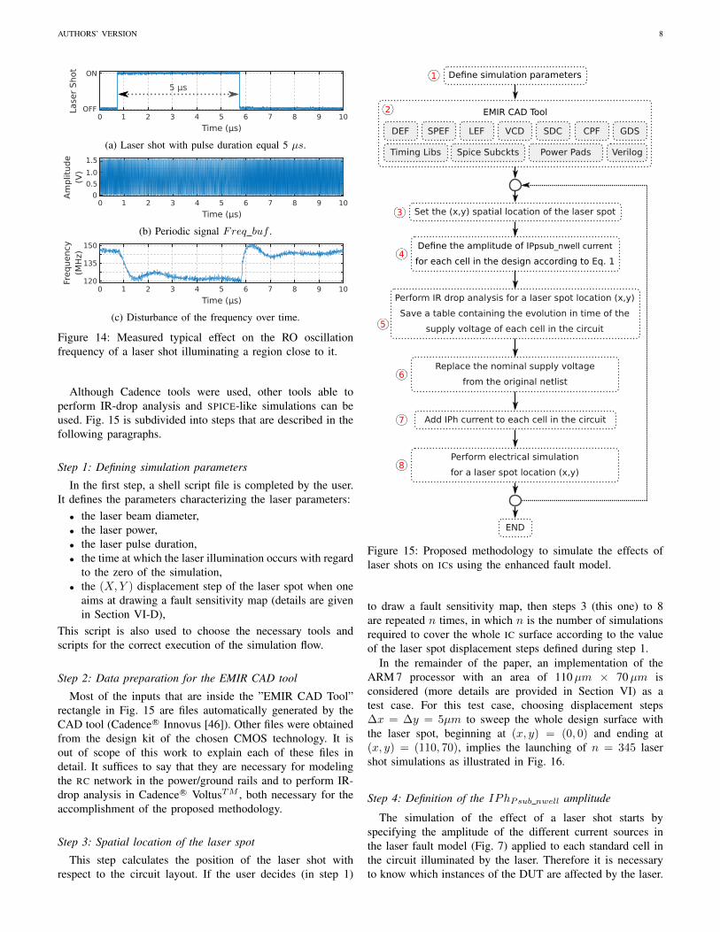
Fig. 14a depicts the laser shot with a duration of 5 µs. Fig.14b shows the periodic signal Freq buf typically observedwith the oscilloscope, when illuminating a region close tothe RO. In this figure, a region in lighter blue is visible.It corresponds to an increase of the Freq buf period. Thisbehavior is similar to the one obtained by simulation in Fig.10b.
Fig. 14c shows the evolution of Freq buf frequency whenthe laser is active. As in the simulation, this evolution hasa smooth profile due to the filtering effect (RC effect) of the
supply voltage network. It is also possible to observe, as in thesimulation in Fig. 13c, the bounces caused by the inductance.
D. Summary
Because we could identify (following the work described in[43]) the RO position with preliminary experiments we can besure that Fig. 14c and Fig. 12c give the responses of the ROin two radically different situations (laser spot locations).
In the case associated to Fig. 14c the laser did not illuminatedirectly the RO, thus only activating IPhPsub nwell. On thecontrary, in case of Fig. 12c, the laser beam directly illumi-nated the RO thus activating both IPh and IPhPsub nwell.
The comparison of the experimental results with the simu-lation results, especially the comparison of Fig. 14c and Fig.13c showing a high level of correlation, demonstrates that laserinduced IR-drops must not be neglected. This also highlightsthe superiority of the enhanced fault model proposed in thispaper over the classical fault model. Despite this evidence ofthe existence and importance of the laser induced IR-drop,results suggest that these laser induced IR-drops amplify theeffect of IPh. Indeed, instead of having a drop in frequencyof 48 MHz (Fig. 10c) when considering only IPh (classicalmodel), the frequency falls to zero (Fig. 11c and Fig. 12c)when the IR-drop is taken into account.
However, considering the laser-induced IR-drops could notbe done by running simple electrical simulations in which thepower/ground networks are assumed ideal. This explains whythe next section presents a standard CAD tool-based methodused to simulate laser-induced faults in large-scale circuits.Together with the simulation results provided by the proposedmethod, other experimental results will be used to empha-size the existence of the IPhPsub nwell current component.More importantly, the relevance of simulating this currentwill be shown by observing experimentally the phenomenahighlighted by simulations and carried out with the proposedsimulation flow, which is based on the enhanced fault model.
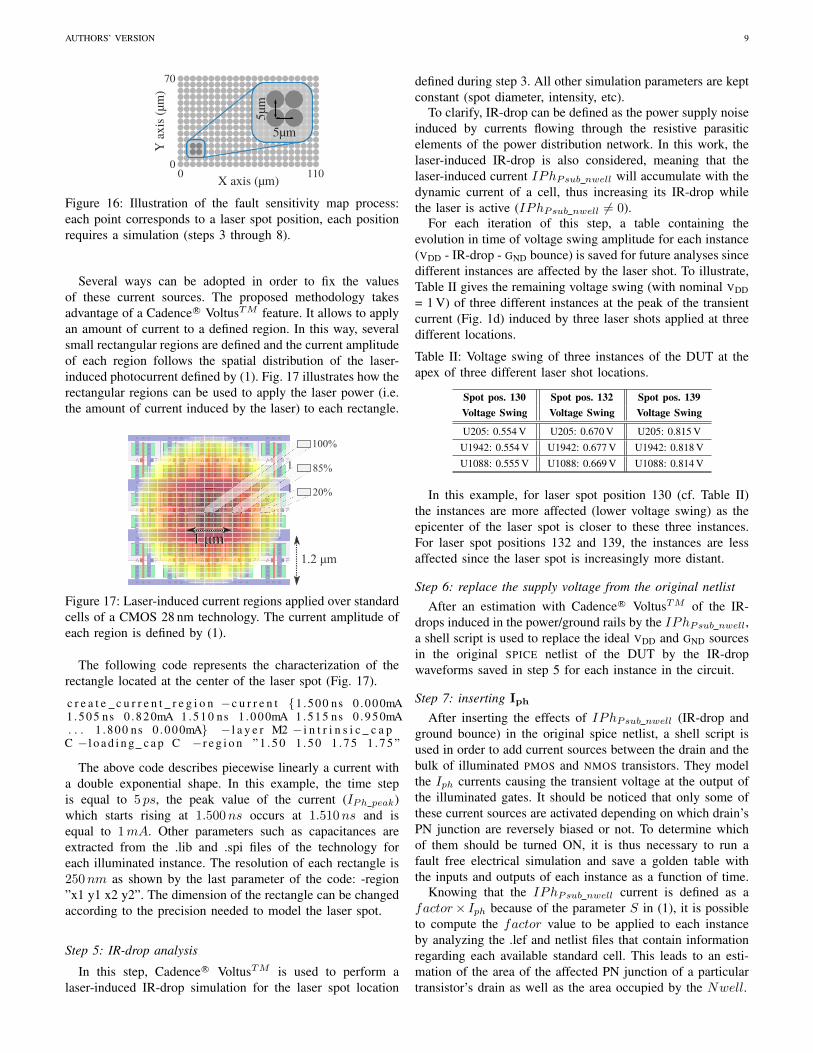
V. PROPOSED METHODOLOGY FOR LASER FAULTSIMULATION USING STANDARD CAD TOOLS
A simulation flow taking laser-induced IR-drops into ac-count during the simulation of large scale circuits is given inFig. 15. This methodology is based on standard CAD tools:Cadence R© VoltusTM [44] for EMIR simulation and Cadence R©
Spectre R© XPS [45] for the electrical/hybrid simulation. Theproposed methodology provides: the ability to draw laser-induced IR-drop sensitivity maps and fault maps that can helpthe designer to decide how to harden designs against laser faultinjection; and the ability to validate the efficiency of embeddedcountermeasures.
This methodology can be easily adapted to provide supple-mentary results to the ones reported in this work. To the bestof our knowledge, this is the first methodology for simulatingthe effects of laser shots on ICs that simultaneously takes intoaccount the design, the complete layout and the laser-inducedIR-drops that have been proven to play a significant role infault occurrence.
AUTHORS’ VERSION 8
Lase
r S
hot ON
OFF0 1 2 3 4 5 6 7 8 9 10
Time (μs)
5 μs
(a) Laser shot with pulse duration equal 5 µs.
Am
plit
ude
(V)
1.5
00 1 2 3 4 5 6 7 8 9 10
Time (μs)
1.0
0.5
(b) Periodic signal Freq buf .150
0 1 2 3 4 5 6 7 8 9 10
Time (μs)
Frequency
(MH
z)
135
120
(c) Disturbance of the frequency over time.
Figure 14: Measured typical effect on the RO oscillationfrequency of a laser shot illuminating a region close to it.
Although Cadence tools were used, other tools able toperform IR-drop analysis and SPICE-like simulations can beused. Fig. 15 is subdivided into steps that are described in thefollowing paragraphs.
Step 1: Defining simulation parameters
In the first step, a shell script file is completed by the user.It defines the parameters characterizing the laser parameters:
• the laser beam diameter,• the laser power,• the laser pulse duration,• the time at which the laser illumination occurs with regard
to the zero of the simulation,• the (X,Y ) displacement step of the laser spot when one
aims at drawing a fault sensitivity map (details are givenin Section VI-D),
This script is also used to choose the necessary tools andscripts for the correct execution of the simulation flow.
Step 2: Data preparation for the EMIR CAD tool
Most of the inputs that are inside the ”EMIR CAD Tool”rectangle in Fig. 15 are files automatically generated by theCAD tool (Cadence R© Innovus [46]). Other files were obtainedfrom the design kit of the chosen CMOS technology. It isout of scope of this work to explain each of these files indetail. It suffices to say that they are necessary for modelingthe RC network in the power/ground rails and to perform IR-drop analysis in Cadence R© VoltusTM , both necessary for theaccomplishment of the proposed methodology.
Step 3: Spatial location of the laser spot
This step calculates the position of the laser shot withrespect to the circuit layout. If the user decides (in step 1)
Define simulation parameters
SPEF LEFDEF CPFSDCVCD GDS
VerilogTiming Libs Spice Subckts Power Pads
EMIR CAD Tool
1
2
Set the (x,y) spatial location of the laser spot3
Define the amplitude of IPpsub_nwell current
for each cell in the design according to Eq. 1 4
Perform IR drop analysis for a laser spot location (x,y)
Save a table containing the evolution in time of the
supply voltage of each cell in the circuit5
Replace the nominal supply voltage
from the original netlist
Add IPh current to each cell in the circuit
6
7
Perform electrical simulation
for a laser spot location (x,y)8
END
Figure 15: Proposed methodology to simulate the effects oflaser shots on ICs using the enhanced fault model.
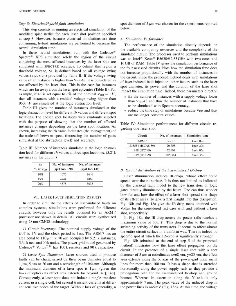
to draw a fault sensitivity map, then steps 3 (this one) to 8are repeated n times, in which n is the number of simulationsrequired to cover the whole IC surface according to the valueof the laser spot displacement steps defined during step 1.
In the remainder of the paper, an implementation of theARM 7 processor with an area of 110µm × 70µm isconsidered (more details are provided in Section VI) as atest case. For this test case, choosing displacement steps∆x = ∆y = 5µm to sweep the whole design surface withthe laser spot, beginning at (x, y) = (0, 0) and ending at(x, y) = (110, 70), implies the launching of n = 345 lasershot simulations as illustrated in Fig. 16.
Step 4: Definition of the IPhPsub nwell amplitude
The simulation of the effect of a laser shot starts byspecifying the amplitude of the different current sources inthe laser fault model (Fig. 7) applied to each standard cell inthe circuit illuminated by the laser. Therefore it is necessaryto know which instances of the DUT are affected by the laser.
AUTHORS’ VERSION 9
5µm
5µm
X axis (µm)
Y a
xis (
µm)
0 110
70
0
Figure 16: Illustration of the fault sensitivity map process:each point corresponds to a laser spot position, each positionrequires a simulation (steps 3 through 8).
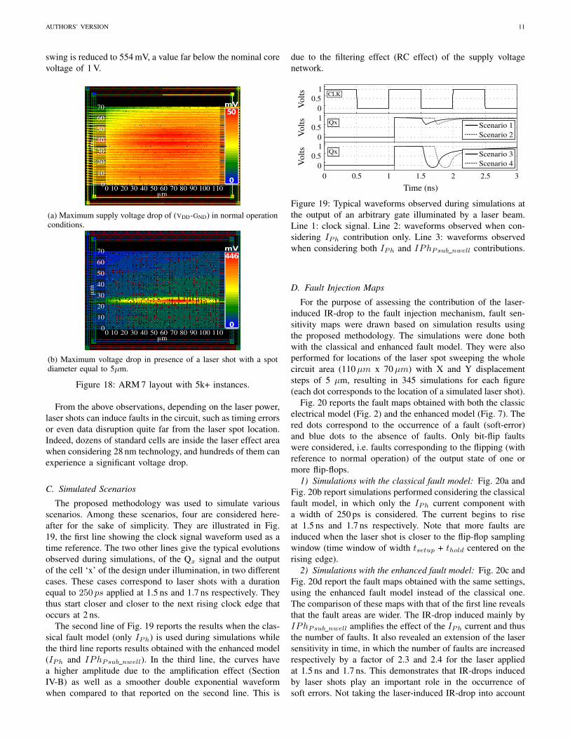
Several ways can be adopted in order to fix the valuesof these current sources. The proposed methodology takesadvantage of a Cadence R© VoltusTM feature. It allows to applyan amount of current to a defined region. In this way, severalsmall rectangular regions are defined and the current amplitudeof each region follows the spatial distribution of the laser-induced photocurrent defined by (1). Fig. 17 illustrates how therectangular regions can be used to apply the laser power (i.e.the amount of current induced by the laser) to each rectangle.
1.2 μm
100%
1 μm1 μm
85%
20%
Figure 17: Laser-induced current regions applied over standardcells of a CMOS 28 nm technology. The current amplitude ofeach region is defined by (1).
The following code represents the characterization of therectangle located at the center of the laser spot (Fig. 17).
c r e a t e c u r r e n t r e g i o n −c u r r e n t {1 .500 ns 0 .000mA1.505 ns 0 .820mA 1.510 ns 1 .000mA 1.515 ns 0 .950mA. . . 1 . 800 ns 0 .000mA} − l a y e r M2 − i n t r i n s i c c a p
C −l o a d i n g c a p C −r e g i o n ” 1 . 5 0 1 . 5 0 1 . 7 5 1 . 7 5 ”
The above code describes piecewise linearly a current witha double exponential shape. In this example, the time stepis equal to 5 ps, the peak value of the current (IPh peak)which starts rising at 1.500ns occurs at 1.510ns and isequal to 1mA. Other parameters such as capacitances areextracted from the .lib and .spi files of the technology foreach illuminated instance. The resolution of each rectangle is250nm as shown by the last parameter of the code: -region”x1 y1 x2 y2”. The dimension of the rectangle can be changedaccording to the precision needed to model the laser spot.
Step 5: IR-drop analysis
In this step, Cadence R© VoltusTM is used to perform alaser-induced IR-drop simulation for the laser spot location
defined during step 3. All other simulation parameters are keptconstant (spot diameter, intensity, etc).
To clarify, IR-drop can be defined as the power supply noiseinduced by currents flowing through the resistive parasiticelements of the power distribution network. In this work, thelaser-induced IR-drop is also considered, meaning that thelaser-induced current IPhPsub nwell will accumulate with thedynamic current of a cell, thus increasing its IR-drop whilethe laser is active (IPhPsub nwell 6= 0).
For each iteration of this step, a table containing theevolution in time of voltage swing amplitude for each instance(VDD - IR-drop - GND bounce) is saved for future analyses sincedifferent instances are affected by the laser shot. To illustrate,Table II gives the remaining voltage swing (with nominal VDD= 1 V) of three different instances at the peak of the transientcurrent (Fig. 1d) induced by three laser shots applied at threedifferent locations.
Table II: Voltage swing of three instances of the DUT at theapex of three different laser shot locations.
Spot pos. 130 Spot pos. 132 Spot pos. 139Voltage Swing Voltage Swing Voltage Swing
U205: 0.554 V U205: 0.670 V U205: 0.815 V
U1942: 0.554 V U1942: 0.677 V U1942: 0.818 V
U1088: 0.555 V U1088: 0.669 V U1088: 0.814 V
In this example, for laser spot position 130 (cf. Table II)the instances are more affected (lower voltage swing) as theepicenter of the laser spot is closer to these three instances.For laser spot positions 132 and 139, the instances are lessaffected since the laser spot is increasingly more distant.
Step 6: replace the supply voltage from the original netlistAfter an estimation with Cadence R© VoltusTM of the IR-
drops induced in the power/ground rails by the IPhPsub nwell,a shell script is used to replace the ideal VDD and GND sourcesin the original SPICE netlist of the DUT by the IR-dropwaveforms saved in step 5 for each instance in the circuit.
Step 7: inserting Iph
After inserting the effects of IPhPsub nwell (IR-drop andground bounce) in the original spice netlist, a shell script isused in order to add current sources between the drain and thebulk of illuminated PMOS and NMOS transistors. They modelthe Iph currents causing the transient voltage at the output ofthe illuminated gates. It should be noticed that only some ofthese current sources are activated depending on which drain’sPN junction are reversely biased or not. To determine whichof them should be turned ON, it is thus necessary to run afault free electrical simulation and save a golden table withthe inputs and outputs of each instance as a function of time.
Knowing that the IPhPsub nwell current is defined as afactor× Iph because of the parameter S in (1), it is possibleto compute the factor value to be applied to each instanceby analyzing the .lef and netlist files that contain informationregarding each available standard cell. This leads to an esti-mation of the area of the affected PN junction of a particulartransistor’s drain as well as the area occupied by the Nwell.
AUTHORS’ VERSION 10
Step 8: Electrical/hybrid fault simulation
This step consists in running an electrical simulation of themodified spice netlist for each laser shot position specifiedat step 3. However, because electrical simulations are timeconsuming, hybrid simulations are performed to decrease theoverall simulation time.
In these hybrid simulations, run with the Cadence R©
Spectre R© XPS simulator, solely the region of the circuitcontaining the most affected instances by the laser shot aresimulated with SPECTRE accuracy. To delimit this region athreshold voltage, th, is defined based on all voltage swingvalues (VDD-GND) provided by Table II. If the voltage swingvalue of an instance is higher than VDD-th, it is considered asnot affected by the laser shot. This is the case for instanceswhich are far away from the laser spot epicenter (Table II). Forexample, if th is set equal to 5% of the nominal VDD = 1V ,then all instances with a residual voltage swing higher than950mV are simulated at the logic abstraction level.
Table III gives the number of instances simulated at thelogic abstraction level for different th values and different spotlocations. The chosen spot locations were randomly selectedwith the purpose of showing that the number of affectedinstances changes depending on the laser spot location. Asshown, increasing the th value facilitates (the management) ofthe trade off between speed (increasing the number of gatessimulated at the abstraction level) and accuracy.
Table III: Number of instances simulated at the logic abstrac-tion level for different th values at three spot locations. (5.21kinstances in the circuit.)
th No. of instances No. of instances% of VDD (spot loc. 130) (spot loc. 139)
10% 1676 1646
15% 4744 4866
20% 4878 5033
VI. LASER FAULT SIMULATION RESULTS
In order to simulate the effects of laser-induced faults oncomplex systems, simulations were performed for differentcircuits, however only the results obtained for an ARM 7processor are shown in details. All circuits were synthesizedusing 28 nm CMOS technology.
1) Circuit Inventory: The nominal supply voltage of theDUT is 1 V and the clock period is 1ns. The ARM 7 has anarea equal to 110µm × 70µm occupied by 5.21 k instances,5.34 k nets and 90 k nodes. The power-grid model generated byCadence R© VoltusTM has 100 k resistors and 90 k capacitors.
2) Laser Spot Diameter: Laser sources used to producefaults can be characterized by their beam diameter equal to1µm, 5µm or 20µm and a wavelength of 1064 nm. Althoughthe minimum diameter of a laser spot is 1µm (given thelaws of optics) its effect area extends far beyond [47], [48].Consequently, a laser spot does not induce a single transientcurrent in a single cell, but several transient currents at differ-ent sensitive nodes of the target. Without loss of generality, a
spot diameter of 5µm was chosen for the experiments reportedbelow.
A. Simulation Performance
The performance of the simulation directly depends onthe available computing resources and the complexity of thesimulated circuit. The processor used to perform simulationswas an Intel R© Xeon R© [email protected] GHz with two cores and16 GB of RAM. Table IV gives the simulation performance ofthe four assessed circuits. Note how the simulation time doesnot increase proportionally with the number of instances inthe circuit. Since the proposed method deals with simulationsof laser-induced fault injection, other factors such as the laserspot diameter, its power and the duration of the laser shotimpact the simulation time. Indeed, these parameters directly:
• fix the number of instances with a supply voltage lowerthan VDD-th and thus the number of instances that haveto be simulated with Spectre accuracy,
• reduce the time step of simulations because VDD and GNDare no longer constant values.
Table IV: Simulation performances for different circuits re-garding one laser shot.
Circuit No. of instances Simulation time
ARM 7 5,210 1min 02s
S38584 (ISCAS’89) 20,705 1min 20s
B18 (ITC’99) 52,601 3min 05s
B19 (ITC’99) 105,344 6min 35s
B. Spatial distribution of the laser-induced IR-drop
Laser illumination induces IR-drops, whose effect couldspread over the IC surface. It is thus not limited as indicatedby the classical fault model to the few transistors or logicgates directly illuminated by the beam. One can thus wonderhow far and how the effect of a laser shot spread (the shapeof its effect area). To give a first insight into this dissipation,Fig. 18b and Fig. 18a give the IR-drop maps obtained withVoltus for the considered test case with and without a lasershot, respectively.
In Fig. 18a, the IR-drop across the power rails reaches amaximum value of 50mV . This drop is due to the normalswitching activity of the transistors. It seems to affect almostthe entire circuit surface in a uniform way. There is indeed nospecific spot at which the IR-drop is significantly stronger.
Fig. 18b (obtained at the end of step 5 of the proposedmethod) illustrates how the laser effect propagates on thecircuit. In the presence of a single laser shot with a spotdiameter of 5µm at coordinates x=68µm, y=25µm, the effectarea extends along the X axis of the power-grid main metallines for more than 100µm. It has a shape that is stretchedhorizontally along the power supply rails as they provide apropagation path for the laser-induced IR-drop and groundbounce. Whereas its extension along the Y axis is onlyapproximately 7µm. The peak value of the induced drop inthe power lines is 446 mV (Fig. 18b). At this time, the voltage
AUTHORS’ VERSION 11
swing is reduced to 554 mV, a value far below the nominal corevoltage of 1 V.
(a) Maximum supply voltage drop of (VDD-GND) in normal operationconditions.
mV446
00 10 20
μm
μm
30 40 50 60 70 80 90 110100010203040506070
(b) Maximum voltage drop in presence of a laser shot with a spotdiameter equal to 5µm.
Figure 18: ARM 7 layout with 5k+ instances.
From the above observations, depending on the laser power,laser shots can induce faults in the circuit, such as timing errorsor even data disruption quite far from the laser spot location.Indeed, dozens of standard cells are inside the laser effect areawhen considering 28 nm technology, and hundreds of them canexperience a significant voltage drop.
C. Simulated Scenarios
The proposed methodology was used to simulate variousscenarios. Among these scenarios, four are considered here-after for the sake of simplicity. They are illustrated in Fig.19, the first line showing the clock signal waveform used as atime reference. The two other lines give the typical evolutionsobserved during simulations, of the Qx signal and the outputof the cell ‘x’ of the design under illumination, in two differentcases. These cases correspond to laser shots with a durationequal to 250 ps applied at 1.5 ns and 1.7 ns respectively. Theythus start closer and closer to the next rising clock edge thatoccurs at 2 ns.
The second line of Fig. 19 reports the results when the clas-sical fault model (only IPh) is used during simulations whilethe third line reports results obtained with the enhanced model(IPh and IPhPsub nwell). In the third line, the curves havea higher amplitude due to the amplification effect (SectionIV-B) as well as a smoother double exponential waveformwhen compared to that reported on the second line. This is
due to the filtering effect (RC effect) of the supply voltagenetwork.
Time (ns)
Volts
0 0.5 1 1.5 2 2.5 3
Scenario 3Scenario 4
Qx
00.5
1
Volts CLK
00.5
1
Qx
Volts
00.5
1Scenario 1Scenario 2
Figure 19: Typical waveforms observed during simulations atthe output of an arbitrary gate illuminated by a laser beam.Line 1: clock signal. Line 2: waveforms observed when con-sidering IPh contribution only. Line 3: waveforms observedwhen considering both IPh and IPhPsub nwell contributions.
D. Fault Injection Maps
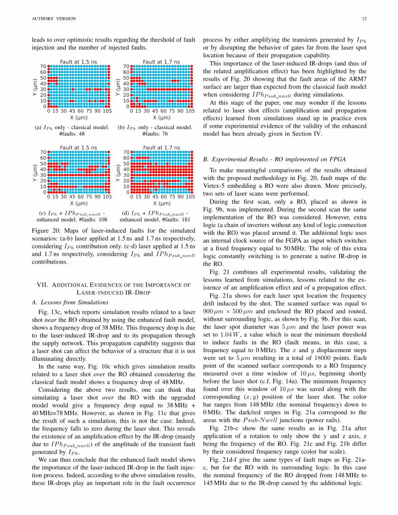
For the purpose of assessing the contribution of the laser-induced IR-drop to the fault injection mechanism, fault sen-sitivity maps were drawn based on simulation results usingthe proposed methodology. The simulations were done bothwith the classical and enhanced fault model. They were alsoperformed for locations of the laser spot sweeping the wholecircuit area (110µm x 70µm) with X and Y displacementsteps of 5 µm, resulting in 345 simulations for each figure(each dot corresponds to the location of a simulated laser shot).
Fig. 20 reports the fault maps obtained with both the classicelectrical model (Fig. 2) and the enhanced model (Fig. 7). Thered dots correspond to the occurrence of a fault (soft-error)and blue dots to the absence of faults. Only bit-flip faultswere considered, i.e. faults corresponding to the flipping (withreference to normal operation) of the output state of one ormore flip-flops.
1) Simulations with the classical fault model: Fig. 20a andFig. 20b report simulations performed considering the classicalfault model, in which only the IPh current component witha width of 250 ps is considered. The current begins to riseat 1.5 ns and 1.7 ns respectively. Note that more faults areinduced when the laser shot is closer to the flip-flop samplingwindow (time window of width tsetup + thold centered on therising edge).
2) Simulations with the enhanced fault model: Fig. 20c andFig. 20d report the fault maps obtained with the same settings,using the enhanced fault model instead of the classical one.The comparison of these maps with that of the first line revealsthat the fault areas are wider. The IR-drop induced mainly byIPhPsub nwell amplifies the effect of the IPh current and thusthe number of faults. It also revealed an extension of the lasersensitivity in time, in which the number of faults are increasedrespectively by a factor of 2.3 and 2.4 for the laser appliedat 1.5 ns and 1.7 ns. This demonstrates that IR-drops inducedby laser shots play an important role in the occurrence ofsoft errors. Not taking the laser-induced IR-drop into account
AUTHORS’ VERSION 12
leads to over optimistic results regarding the threshold of faultinjection and the number of injected faults.
Fault at 1.5 ns
600 30 4515 10575 900
10203040506070
X (μm)
Y (μ
m)
(a) IPh only - classical model.#faults: 48
Fault at 1.7 ns
600 30 4515 10575 900
10203040506070
X (μm)Y (μ
m)
(b) IPh only - classical model.#faults: 76
600 30 4515 10575 900
10203040506070
X (μm)
Y (μ
m)
Fault at 1.5 ns
(c) IPh + IPhPsub nwell -enhanced model. #faults: 108
600 30 4515 10575 900
10203040506070
X (μm)
Y (μ
m)
Fault at 1.7 ns
(d) IPh + IPhPsub nwell -enhanced model. #faults: 181
Figure 20: Maps of laser-induced faults for the simulatedscenarios: (a-b) laser applied at 1.5 ns and 1.7 ns respectively,considering IPh contribution only. (c-d) laser applied at 1.5 nsand 1.7 ns respectively, considering IPh and IPhPsub nwell
contributions.
VII. ADDITIONAL EVIDENCES OF THE IMPORTANCE OFLASER-INDUCED IR-DROP
A. Lessons from Simulations
Fig. 13c, which reports simulation results related to a lasershot near the RO obtained by using the enhanced fault model,shows a frequency drop of 38 MHz. This frequency drop is dueto the laser-induced IR-drop and to its propagation throughthe supply network. This propagation capability suggests thata laser shot can affect the behavior of a structure that it is notilluminating directly.
In the same way, Fig. 10c which gives simulation resultsrelated to a laser shot over the RO obtained considering theclassical fault model shows a frequency drop of 48 MHz.
Considering the above two results, one can think thatsimulating a laser shot over the RO with the upgradedmodel would give a frequency drop equal to 38 MHz +40 MHz=78 MHz. However, as shown in Fig. 11c that givesthe result of such a simulation, this is not the case. Indeed,the frequency falls to zero during the laser shot. This revealsthe existence of an amplification effect by the IR-drop (mainlydue to IPhPsub nwell) of the amplitude of the transient faultgenerated by IPh.
We can thus conclude that the enhanced fault model showsthe importance of the laser-induced IR-drop in the fault injec-tion process. Indeed, according to the above simulation results,these IR-drops play an important role in the fault occurrence
process by either amplifying the transients generated by IPh
or by disrupting the behavior of gates far from the laser spotlocation because of their propagation capability.
This importance of the laser-induced IR-drops (and thus ofthe related amplification effect) has been highlighted by theresults of Fig. 20 showing that the fault areas of the ARM7surface are larger than expected from the classical fault modelwhen considering IPhPsub nwell during simulations.
At this stage of the paper, one may wonder if the lessonsrelated to laser shot effects (amplification and propagationeffects) learned from simulations stand up in practice evenif some experimental evidence of the validity of the enhancedmodel has been already given in Section IV.
B. Experimental Results - RO implemented on FPGA
To make meaningful comparisons of the results obtainedwith the proposed methodology in Fig. 20, fault maps of theVirtex-5 embedding a RO were also drawn. More precisely,two sets of laser scans were performed.
During the first scan, only a RO, placed as shown inFig. 9b, was implemented. During the second scan the sameimplementation of the RO was considered. However, extralogic (a chain of inverters without any kind of logic connectionwith the RO) was placed around it. The additional logic usesan internal clock source of the FGPA as input which switchesat a fixed frequency equal to 50 MHz. The role of this extralogic constantly switching is to generate a native IR-drop inthe RO.
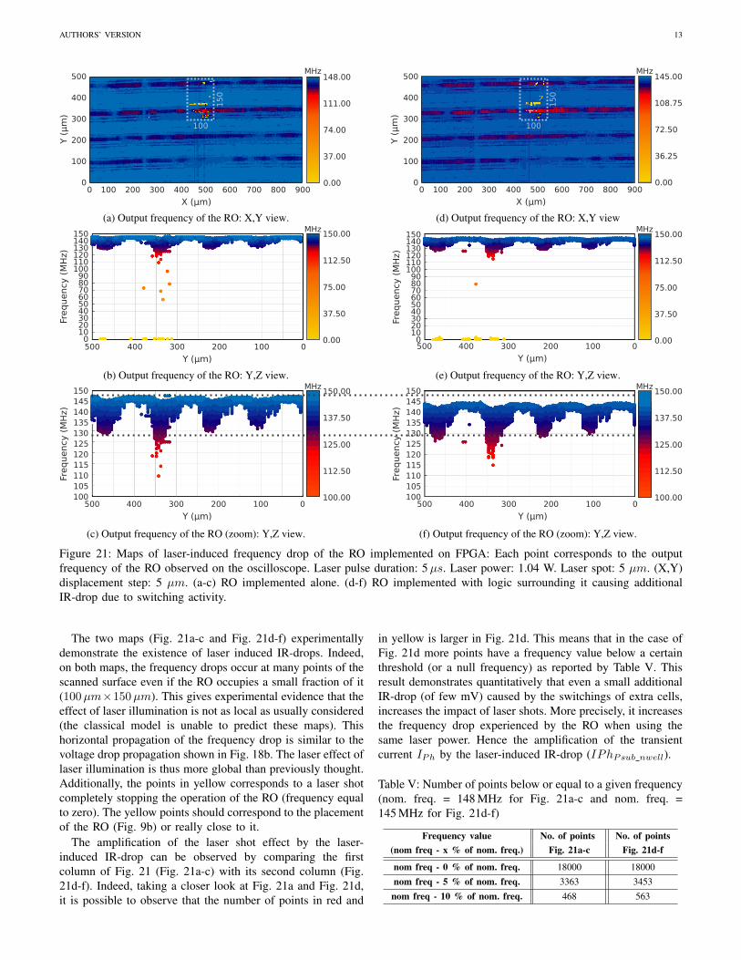
Fig. 21 combines all experimental results, validating thelessons learned from simulations, lessons related to the ex-istence of an amplification effect and of a propagation effect.
Fig. 21a shows for each laser spot location the frequencydrift induced by the shot. The scanned surface was equal to900µm × 500µm and enclosed the RO placed and routed,without surrounding logic, as shown by Fig. 9b. For this scan,the laser spot diameter was 5µm and the laser power wasset to 1.04W , a value which is near the minimum thresholdto induce faults in the RO (fault means, in this case, afrequency equal to 0 MHz). The x and y displacement stepswere set to 5µm resulting in a total of 18000 points. Eachpoint of the scanned surface corresponds to a RO frequencymeasured over a time window of 10µs, beginning shortlybefore the laser shot (c.f. Fig. 14a). The minimum frequencyfound over this window of 10µs was saved along with thecorresponding (x, y) position of the laser shot. The colorbar ranges from 148 MHz (the nominal frequency) down to0 MHz. The dark/red stripes in Fig. 21a correspond to theareas with the Psub-Nwell junctions (power rails).
Fig. 21b-c show the same results as in Fig. 21a afterapplication of a rotation to only show the y and z axis, zbeing the frequency of the RO. Fig. 21c and Fig. 21b differby their considered frequency range (color bar scale).
Fig. 21d-f give the same types of fault maps as Fig. 21a-c, but for the RO with its surrounding logic. In this casethe nominal frequency of the RO dropped from 148 MHz to145 MHz due to the IR-drop caused by the additional logic.
AUTHORS’ VERSION 13
0 100 200 300 400 500 600 700 800 900
X (μm)
100
300
500
400
200
0
Y (μ
m)
0.00
72.50
36.25
145.00
108.75
400 300 200 100 05000
30
50
110
130
150
90
70
140
120
100
80
60
40
2010
Y (μm)
Frequency
(M
Hz)
0.00
75.00
37.50
150.00
112.50
130
140
150145
135
125
110
120115
105100
400 300 200 100 0500
Y (μm)
Frequency
(M
Hz)
100.00
125.00
112.50
150.00
137.50
100
300
500
400
200
00 100 200 300 400 500 600 700 800 900
X (μm)
Y (μ
m)
0.00
74.00
37.00
148.00
111.00
0
30
50
110
130
150
90
70
140
120
100
80
60
40
2010
400 300 200 100 0500
Y (μm)
Frequency
(M
Hz)
0.00
75.00
37.50
150.00
112.50
400 300 200 100 0500
130
140
150145
135
125
110
120115
105100
Y (μm)
Frequency
(M
Hz)
100.00
125.00
112.50
150.00
137.50
MHzMHz
MHzMHz
MHzMHz
(a) Output frequency of the RO: X,Y view. (d) Output frequency of the RO: X,Y view
(b) Output frequency of the RO: Y,Z view. (e) Output frequency of the RO: Y,Z view.
(c) Output frequency of the RO (zoom): Y,Z view. (f) Output frequency of the RO (zoom): Y,Z view.
100
15
0
100
15
0Figure 21: Maps of laser-induced frequency drop of the RO implemented on FPGA: Each point corresponds to the outputfrequency of the RO observed on the oscilloscope. Laser pulse duration: 5µs. Laser power: 1.04 W. Laser spot: 5 µm. (X,Y)displacement step: 5 µm. (a-c) RO implemented alone. (d-f) RO implemented with logic surrounding it causing additionalIR-drop due to switching activity.
The two maps (Fig. 21a-c and Fig. 21d-f) experimentallydemonstrate the existence of laser induced IR-drops. Indeed,on both maps, the frequency drops occur at many points of thescanned surface even if the RO occupies a small fraction of it(100µm×150µm). This gives experimental evidence that theeffect of laser illumination is not as local as usually considered(the classical model is unable to predict these maps). Thishorizontal propagation of the frequency drop is similar to thevoltage drop propagation shown in Fig. 18b. The laser effect oflaser illumination is thus more global than previously thought.Additionally, the points in yellow corresponds to a laser shotcompletely stopping the operation of the RO (frequency equalto zero). The yellow points should correspond to the placementof the RO (Fig. 9b) or really close to it.
The amplification of the laser shot effect by the laser-induced IR-drop can be observed by comparing the firstcolumn of Fig. 21 (Fig. 21a-c) with its second column (Fig.21d-f). Indeed, taking a closer look at Fig. 21a and Fig. 21d,it is possible to observe that the number of points in red and
in yellow is larger in Fig. 21d. This means that in the case ofFig. 21d more points have a frequency value below a certainthreshold (or a null frequency) as reported by Table V. Thisresult demonstrates quantitatively that even a small additionalIR-drop (of few mV) caused by the switchings of extra cells,increases the impact of laser shots. More precisely, it increasesthe frequency drop experienced by the RO when using thesame laser power. Hence the amplification of the transientcurrent IPh by the laser-induced IR-drop (IPhPsub nwell).
Table V: Number of points below or equal to a given frequency(nom. freq. = 148 MHz for Fig. 21a-c and nom. freq. =145 MHz for Fig. 21d-f)
Frequency value No. of points No. of points(nom freq - x % of nom. freq.) Fig. 21a-c Fig. 21d-f
nom freq - 0 % of nom. freq. 18000 18000
nom freq - 5 % of nom. freq. 3363 3453
nom freq - 10 % of nom. freq. 468 563
AUTHORS’ VERSION 14
VIII. CONCLUSIONS
This paper reported a methodology which allows the simu-lation of laser fault injection at the electrical level in large-scale circuits by using standard CAD tools. An enhancedelectrical fault model that takes laser-induced IR-drop intoaccount was proposed. The enhanced fault model was appliedto each instance of a test-chip used in the methodology inorder to demonstrate how the induced IR-drop facilitates theoccurrence of SEs by amplifying laser-induced perturbationson logic signals.
This paper also revealed, based on simulation and experi-mental results that, when an IC —fabricated in a relatively oldtechnology node (Virtex-5 FPGA - 65 nm)— is illuminatedby a laser beam, it induces IR-drops. The induced IR-dropshave a global effect spreading through the supply network.The paper gives experimental evidence that the effect of laserillumination is not as localised as previously thought.
Results reveal that ignoring the laser-induced IR-drop mayresult in underestimating the risk of fault injection, not to men-tion the incorrect estimation of the fault injection threshold.Indeed, for the test-chip assessed, an increase in the numberof faults by a factor of 2.4 has been observed when IR-dropsare taken into account. This result is especially relevant forthe design of countermeasure techniques for secure integratedsystems.
REFERENCES
[1] A. Barenghi, L. Breveglieri, I. Koren et al., “Fault injection attacks oncryptographic devices: Theory, practice, and countermeasures,” Proceed-ings of the IEEE, vol. 100, no. 11, Nov 2012.
[2] H. Bar-El, H. Choukri, D. Naccache et al., “The sorcerer’s apprenticeguide to fault attacks,” Proceedings of the IEEE, vol. 94, no. 2, Feb 2006.
[3] M. Agoyan, J.-M. Dutertre, D. Naccache et al., “When clocks fail: Oncritical paths and clock faults,” in CARDIS, 2010.
[4] R. Ahmadi and F. N. Najm, “Timing analysis in presence of powersupply and ground voltage variations,” in ICCAD-2003. InternationalConference on Computer Aided Design, Nov 2003, pp. 176–183.
[5] P. Maurine, K. Tobich, T. Ordas et al., “Yet Another Fault InjectionTechnique: by Forward Body Biasing Injection,” in YACC’2012.
[6] A. Dehbaoui, J.-M. Dutertre, B. Robisson et al., “Electromagnetic Tran-sient Faults Injection on a hardware and software implementations ofAES,” in FDTC 2012, Leuven, Belgium, Sep. 2012, p. 7.
[7] S. P. Skorobogatov and R. J. Anderson, “Optical fault induction attacks,”in 4th CHES. London, UK: Springer-Verlag, 2002, pp. 2–12.
[8] A. H. Johnston, “Charge generation and collection in p-n junctionsexcited with pulsed infrared lasers,” IEEE Trans. Nucl. Sci., 1993.
[9] A. G. Jordan and A. G. Milnes, “Photoeffect on diffused p-n junctionswith integral field gradients,” IRE Trans. on Electron Devices, 1960.
[10] J. L. Wirth and S. C. Rogers, “The transient response of transistors anddiodes to ionizing radiation,” IEEE Trans. on Nuclear Science, 1964.
[11] R. A. C. Viera, J. M. Dutertre, R. P. Bastos et al., “Role of laser-inducedir drops in the occurrence of faults: Assessment and simulation,” in 2017Euromicro Conference on Digital System Design (DSD), Aug 2017.
[12] F. Lu, G. D. Natale, M. L. Flottes et al., “Laser-induced fault simulation,”in Euromicro Conference on Digital System Design, 2013.
[13] A. Douin, V. Pouget, D. Lewis et al., “Electrical modeling for lasertesting with different pulse durations,” in 11th IEEE IOLTS, July 2005.
[14] H. M. Huang, Y. Lin, and C. H. P. Wen, “Fast-yet-accurate variation-aware current and voltage modelling of radiation-induced transientfault,” in DATE, 2016.
[15] C. Godlewski, V. Pouget, D. Lewis et al., “Electrical modeling of theeffect of beam profile for pulsed laser fault injection,” MicroelectronicsReliability, Aug. 2009.
[16] G. S. Greenstein and J. H. Patel, “E-proofs: A cmos bridging faultsimulator,” in 1992 IEEE/ACM ICCAD, Nov 1992, pp. 268–271.
[17] H. Cha, E. M. Rudnick, J. H. Patel et al., “A gate-level simulation envi-ronment for alpha-particle-induced transient faults,” IEEE Transactionson Computers, vol. 45, no. 11, Nov 1996.
[18] W. Meyer and R. Camposano, “Active timing multilevel fault-simulationwith switch-level accuracy,” IEEE TCAD, vol. 14, no. 10, Oct 1995.
[19] M. B. Santos and J. P. Teixeira, “Defect-oriented mixed-level faultsimulation of digital systems-on-a-chip using hdl,” in DATE, 1999.
[20] G. Hubert, R. Velazco, and P. Peronnard, “A generic platform for remoteaccelerated tests and high altitude seu experiments on advanced ics:Correlation with musca sep3 calculations,” in 2009 15th IOLTS, 2009.
[21] F. Lu, G. D. Natale, M. L. Flottes et al., “Layout-aware laser faultinjection simulation and modeling: From physical level to gate level,”in 2014 9th IEEE International Conference on Design Technology ofIntegrated Systems in Nanoscale Era (DTIS), May 2014.
[22] A. Bosio and G. D. Natale, “Lifting: A flexible open-source faultsimulator,” in 2008 17th Asian Test Symposium, Nov 2008, pp. 35–40.
[23] A. Sarafianos, O. Gagliano, V. Serradeil et al., “Building the electricalmodel of the pulsed photoelectric laser stimulation of an nmos transistorin 90nm technology,” in IRPS, 2013 IEEE International, April 2013.
[24] L. Heriveaux, J. Clediere, and S. Anceau, “Electrical modeling of theeffect of photoelectric laser fault injection on bulk cmos design,” in 39thISTFA ASM, 2013.
[25] R. C. Baumann, “Radiation-induced soft errors in advanced semiconduc-tor technologies,” IEEE Transactions on Device and Materials Reliabil-ity, vol. 5, no. 3, pp. 305–316, Sept 2005.
[26] D. H. Habing, “The use of lasers to simulate radiation-induced transientsin semiconductor devices and circuits,” IEEE Transactions on NuclearScience, vol. 12, no. 5, pp. 91–100, Oct 1965.
[27] T. C. May and M. H. Woods, “Alpha-particle-induced soft errors indynamic memories,” IEEE Transactions on Electron Devices, Jan 1979.
[28] C. M. Hsieh, P. C. Murley, and R. R. O’Brien, “A field-funneling effecton the collection of alpha-particle-generated carriers in silicon devices,”IEEE Electron Device Letters, vol. 2, no. 4, pp. 103–105, April 1981.
[29] G. C. Messenger, “Collection of charge on junction nodes from iontracks,” IEEE Transactions on Nuclear Science, 1982.
[30] F. Wang and V. D. Agrawal, “Single event upset: An embedded tutorial,”in 21st International Conference on VLSI Design, Jan 2008.
[31] C.-M. Hsieh, P. C. Murley, and R. R. O’Brien, “Collection of charge fromalpha-particle tracks in silicon devices,” IEEE Transactions on ElectronDevices, vol. 30, no. 6, pp. 686–693, Jun 1983.
[32] S. Buchner, F. Miller, V. Pouget et al., “Pulsed-laser testing for single-event effects investigations,” IEEE Trans. on Nuclear Science, 2013.
[33] E. W. Enlow and D. R. Alexander, “Photocurrent modeling of mod-ern microcircuit pn junctions,” IEEE Transactions on Nuclear Science,vol. 35, no. 6, pp. 1467–1474, Dec 1988.
[34] J.-M. Dutertre, R. Possamai Bastos, O. Potin et al., “Improving theability of Bulk Built-In Current Sensors to detect Single Event Effectsby using triple-well CMOS,” Microelectronics Reliability, Sep. 2014.
[35] J. A. McNeill, “Jitter in ring oscillators,” IEEE JSSC, Jun 1997.[36] A. Hajimiri, S. Limotyrakis, and T. H. Lee, “Jitter and phase noise in ring
oscillators,” IEEE Journal of Solid-State Circuits, vol. 34, no. 6, 1999.[37] F. Herzel and B. Razavi, “A study of oscillator jitter due to supply and
substrate noise,” IEEE Transactions on Circuits and Systems II: Analogand Digital Signal Processing, vol. 46, no. 1, pp. 56–62, Jan 1999.
[38] M. Lecomte, J. J. A. Fournier, and P. Maurine, “Thoroughly analyzingthe use of ring oscillators for on-chip hardware trojan detection,” in 2015ReConFig, Dec 2015, pp. 1–6.
[39] J. Rubinstein, P. Penfield, and M. A. Horowitz, “Signal delay in rc treenetworks,” IEEE TCAD, vol. 2, no. 3, pp. 202–211, July 1983.
[40] Xilinx. Virtex-5 overview. (December 3, 2017). [Online]. Available:https://www.xilinx.com/support/documentation/data sheets/ds100.pdf
[41] Xilinx. Planahead design and analysis tool. (January 8,2018). [Online]. Available: https://www.xilinx.com/products/design-tools/planahead.html
[42] C. Alexander and M. Sadiku, Fundamentals of Electric Circuits, 4th ed.McGraw Hill Higher Education, 2008.
[43] J. Breier, W. He, S. Bhasin et al., “Extensive laser fault injectionprofiling of 65 nm fpga,” Journal of Hardware and SystemsSecurity, vol. 1, no. 3, pp. 237–251, Sep 2017. [Online]. Available:https://doi.org/10.1007/s41635-017-0016-z
[44] Cadence. Voltus IC power integrity solution. (December 3,2017). [Online]. Available: https://www.cadence.com/content/cadence-www/global/en US/home/tools/digital-design-and-signoff/silicon-signoff/voltus-ic-power-integrity-solution.html
[45] Cadence. Spectre extensive partitioning simulator. (December 3,2017). [Online]. Available: https://www.cadence.com/content/cadence-www/global/en US/home/tools/custom-ic-analog-rf-design/circuit-simulation/spectre-extensive-partitioning-simulator-xps.html
[46] Cadence. Innovus implementation system. (December 3, 2017).[Online]. Available: https://www.cadence.com/content/cadence-www/global/en US/home/tools/digital-design-and-signoff/hierarchical-design-and-floorplanning/innovus-implementation-system.html
[47] F. Darracq, H. Lapuyade, N. Buard et al., “Backside seu laser testing forcommercial off-the-shelf srams,” IEEE Trans. on Nuclear Science, 2002.
[48] C. Roscian, A. Sarafianos, J. M. Dutertre et al., “Fault model analysis oflaser-induced faults in sram memory cells,” in FDTC, 2013.