Silicate formation and thermal stability of ternary rare earth oxides as high-k dielectrics
7
Silicate formation and thermal stability of ternary rare earth oxides as high-k dielectrics S. Van Elshocht, a C. Adelmann, T. Conard, A. Delabie, A. Franquet, L. Nyns, and O. Richard IMEC vzw, Kapeldreef 75, B-3001 Heverlee, Belgium P. Lehnen AIXTRON AG, Kackertstrasse 15-17, Aachen, Germany J. Swerts ASM Belgium, Kapeldreef 75, B-3001 Heverlee, Belgium S. De Gendt IMEC vzw, Kapeldreef 75, B-3001 Heverlee, Belgium and Department of Chemistry, University of Leuven, Celestijnenlaan 200F, B-3001 Heverlee, Belgium Received 5 November 2007; accepted 11 February 2008; published 30 June 2008 Hf-based dielectrics are currently being introduced into complementary metal oxide semiconductor transistors as replacement for SiON to limit gate leakage current densities. Alternative materials such as rare earth based dielectrics are of interest to obtain proper threshold voltages as well as to engineer a material with a high thermal stability. The authors have studied rare earth based dielectrics such as Dy 2 O 3 , DyHfO x , DyScO x , La 2 O 3 , HfLaO x , and LaAlO x by means of ellipsometry, time of flight secondary ion mass spectroscopy x-ray diffraction, and x-ray photoelectron spectroscopy. The authors show that ellipsometry is an easy and powerful tool to study silicate formation. For ternary rare earth oxides, this behavior is heavily dependent on the composition of the deposited layer and demonstrates a nonlinear dependence. The system evolves to a stable composition that is controlled by the thermal budget and the rare earth content of the layer. It is shown that silicate formation can lead to a severe overestimation of the thermal stability of ternary rare earth oxides. © 2008 American Vacuum Society. DOI: 10.1116/1.2891257 I. INTRODUCTION Chip performance has drastically increased during the past decades, pushed forward by the ITRS roadmap that projects a doubling of the amount of transistors on a chip every two years. This task has been mainly accomplished by downscaling the dimensions of the transistor, including the gate dielectric thickness down to a few atomic layers. Con- sequently, gate leakage current densities have reached unac- ceptable levels. As a solution alternative gate dielectrics, re- placing the standard SiON, were researched, leading to the identification of Hf-based dielectrics, which were recently announced to be integrated in the 45 nm technology node. 1 A specific class of alternative dielectrics that receives a lot of attention is the rare earth oxides, both as binary and ter- nary compounds. Rare earth oxides are being explored for their property to shift the work function of a metal gate to- wards n type, which is of interest to engineer a proper tran- sistor threshold voltage. 2,3 In addition, they are studied be- cause of their thermal stability in order to obtain a material that remains amorphous during the entire complementary metaloxide semiconductor CMOS process. 4 Finally, they have been shown to reduce the thickness of the low-k inter- facial layer between high-k and silicon substrate, which is currently one of the crucial challenges to overcome in order to reach ultimate EOT scaling. 5 A typical and frequently described phenomenon observed for rare earth oxides is silicate formation that can occur when a rare earth oxide is in contact with a Si-containing dielec- tric or a silicon substrate in the presence of oxygen. 6–10 This silicate formation goes far beyond local interface reactions and reports can be found on nanometer-thick rare earth ox- ides that are fully transformed into a silicate layer. 11 As such, it has been used to consume the typical SiO 2 -like interfacial between high-k and silicon substrate or to boost its k value, as shown, for example, for Y or La 2 O 3 deposited on SiO 2 . 5,12 The extent of this silicate formation depends on parameters such as temperature and the ion radius of the rare earth element. 13–15 As these rare earth silicates form and hence are stable at high temperatures, they are an interesting alternative for hafnium silicates that have been reported to phase sepa- rate when annealed at high temperatures. 16–18 Interestingly, annealing a Si-capped Y 2 O 3 layer at 900 ° C was not seen to result in silicate formation as compared to an identical uncapped layer that demonstrated silicate formation already at 700 °C. 19,20 A similar observation has been re- ported for Pr 2 O 3 . 21 In addition, no metallic Si could be found in a PrSiO x layer formed starting from Pr 2 O 3 deposited di- rectly on a Si substrate. 21 This suggests that silicate forma- tion for rare earth based materials does not occur by diffu- sion of Si and subsequent oxidation, but rather through the diffusion of SiO x -like species. This could explain why cap- a Electronic mail: [email protected]. 724 724 J. Vac. Sci. Technol. A 26„4…, Jul/Aug 2008 0734-2101/2008/26„4…/724/7/$23.00 ©2008 American Vacuum Society
-
Upload
independent -
Category
Documents
-
view
0 -
download
0
Transcript of Silicate formation and thermal stability of ternary rare earth oxides as high-k dielectrics

Silicate formation and thermal stability of ternary rare earth oxides ashigh-k dielectrics
S. Van Elshocht,a� C. Adelmann, T. Conard, A. Delabie, A. Franquet,L. Nyns, and O. RichardIMEC vzw, Kapeldreef 75, B-3001 Heverlee, Belgium
P. LehnenAIXTRON AG, Kackertstrasse 15-17, Aachen, Germany
J. SwertsASM Belgium, Kapeldreef 75, B-3001 Heverlee, Belgium
S. De GendtIMEC vzw, Kapeldreef 75, B-3001 Heverlee, Belgium and Department of Chemistry, University of Leuven,Celestijnenlaan 200F, B-3001 Heverlee, Belgium
�Received 5 November 2007; accepted 11 February 2008; published 30 June 2008�
Hf-based dielectrics are currently being introduced into complementary metal oxide semiconductortransistors as replacement for SiON to limit gate leakage current densities. Alternative materialssuch as rare earth based dielectrics are of interest to obtain proper threshold voltages as well as toengineer a material with a high thermal stability. The authors have studied rare earth baseddielectrics such as Dy2O3, DyHfOx, DyScOx, La2O3, HfLaOx, and LaAlOx by means ofellipsometry, time of flight secondary ion mass spectroscopy x-ray diffraction, and x-rayphotoelectron spectroscopy. The authors show that ellipsometry is an easy and powerful tool tostudy silicate formation. For ternary rare earth oxides, this behavior is heavily dependent on thecomposition of the deposited layer and demonstrates a nonlinear dependence. The system evolvesto a stable composition that is controlled by the thermal budget and the rare earth content of thelayer. It is shown that silicate formation can lead to a severe overestimation of the thermal stability
of ternary rare earth oxides. © 2008 American Vacuum Society. �DOI: 10.1116/1.2891257�I. INTRODUCTION
Chip performance has drastically increased during thepast decades, pushed forward by the ITRS roadmap thatprojects a doubling of the amount of transistors on a chipevery two years. This task has been mainly accomplished bydownscaling the dimensions of the transistor, including thegate dielectric thickness down to a few atomic layers. Con-sequently, gate leakage current densities have reached unac-ceptable levels. As a solution alternative gate dielectrics, re-placing the standard SiON, were researched, leading to theidentification of Hf-based dielectrics, which were recentlyannounced to be integrated in the 45 nm technology node.1
A specific class of alternative dielectrics that receives a lotof attention is the rare earth oxides, both as binary and ter-nary compounds. Rare earth oxides are being explored fortheir property to shift the work function of a metal gate to-wards n type, which is of interest to engineer a proper tran-sistor threshold voltage.2,3 In addition, they are studied be-cause of their thermal stability in order to obtain a materialthat remains amorphous during the entire complementarymetaloxide semiconductor �CMOS� process.4 Finally, theyhave been shown to reduce the thickness of the low-k inter-facial layer between high-k and silicon substrate, which iscurrently one of the crucial challenges to overcome in orderto reach ultimate EOT scaling.5
a�
Electronic mail: [email protected].724 J. Vac. Sci. Technol. A 26„4…, Jul/Aug 2008 0734-2101/2008
A typical and frequently described phenomenon observedfor rare earth oxides is silicate formation that can occur whena rare earth �oxide� is in contact with a Si-containing dielec-tric or a silicon substrate in the presence of oxygen.6–10 Thissilicate formation goes far beyond local interface reactionsand reports can be found on nanometer-thick rare earth ox-ides that are fully transformed into a silicate layer.11 As such,it has been used to consume the typical SiO2-like interfacialbetween high-k and silicon substrate or to boost its k value,as shown, for example, for Y or La2O3 deposited on SiO2.5,12
The extent of this silicate formation depends on parameterssuch as temperature and the ion radius of the rare earthelement.13–15 As these rare earth silicates form and hence arestable at high temperatures, they are an interesting alternativefor hafnium silicates that have been reported to phase sepa-rate when annealed at high temperatures.16–18
Interestingly, annealing a Si-capped Y2O3 layer at 900 °Cwas not seen to result in silicate formation as compared to anidentical uncapped layer that demonstrated silicate formationalready at 700 °C.19,20 A similar observation has been re-ported for Pr2O3.21 In addition, no metallic Si could be foundin a PrSiOx layer formed starting from Pr2O3 deposited di-rectly on a Si substrate.21 This suggests that silicate forma-tion for rare earth based materials does not occur by diffu-sion of Si and subsequent oxidation, but rather through the
diffusion of SiOx-like species. This could explain why cap-724/26„4…/724/7/$23.00 ©2008 American Vacuum Society

725 Van Elshocht et al.: Silicate formation and thermal stability 725
ping layers excluding oxygen and preventing the oxidationof the silicon substrate can prevent silicate formation forthese materials.
Based on the different reports in literature, it is clear thatthe material interactions that lead to silicate formation areaffected by a wide range of process parameters. We havestudied the thermal behavior and stability of rare earth basedoxides, such as Dy2O3, DyHfOx, DyScO3, La2O3, LaAlO3,and HfLaOx as a function of anneal temperature, time, andambient, as well as a function of their composition. Obser-vations were made by complementary analysis techniques,where we will demonstrate that ellipsometry can be a pow-erful tool to characterize silicate formation for rare earth ma-terials.
We will show that all oxides listed above strongly inter-mix with the SiO2 layer underneath, in agreement with thetendency of rare earth elements to form silicates. More inter-estingly, for ternary rare earth oxides, this behavior wasfound to be clearly dependent on the composition of theas-deposited layer and varies as a nonlinear function of therare earth content. These systems seem to evolve to a stablecomposition that is controlled by the thermal budget and therare earth content of the layer. Trying to gain insight in thisbehavior is important, since it provides a better insight in thebehavior of these dielectrics during the thermal treatmentsinherent to a CMOS process flow.
Finally, we will discuss the effect of silicate formationand the resulting Si content of rare earth dielectrics on theirthermal stability and the consequences for XRD measure-ments used to determine crystallization temperatures.
II. EXPERIMENTAL DETAILS
All layers were deposited on 200 mm p-type Si�100� wa-fers. The native oxide was removed by a short 2% HF dipafter which a thin 1 nm oxide was grown in a H2O /O3 so-lution �“IMEC-clean”�.22 HfO2, Dy2O3, Sc2O3, HfDyOx, andDyScOx layers were deposited in an AIXTRON Tricentreactor by atomic vapor deposition �AVD®� usingHf�o-But�2�mmp�2, Dy�EDMDD�3 or Dy�mmp�3, andSc�EDMDD�3 or Sc�mmp�3 as precursors with O2 asoxidant.23–26 La2O3, Al2O3, LaAlOx, and HfLaOx were de-posited by atomic layer deposition in an ASM Pulsar® 3000reactor27 with La�thd�3, TMA, and a compatible Hf precur-sor. H2O and O3 were used as oxidants. Thermal annealswere done in an Applied Materials RTPXE+ chamber. Thick-ness of the layers was measured by a KLA-TENCOR ASETF5 ellipsometer measuring the total dielectric stack as asingle layer with variable refractive index. The error regard-ing repeatability is, based on duplicate wafers and tool per-formance, estimated to be on the order of 10%, i.e., wellbelow the magnitude of the variations observed. The abso-lute error is difficult to predict, but we have tried to limit theerror by using somewhat thicker �7–10 nm� layers and keep-ing the starting thickness as similar as possible. Samplepreparation for transmission electron microscopy �TEM� wasdone by conventional ion milling. TEM measurements were
done using a Tecnai F30 operating at 300 kV. Time of flightJVST A - Vacuum, Surfaces, and Films
secondary ion mass spectroscopy �TOFSIMS� measurementswere done using an ION-TOF-IV instrument with a Gasource operating at a beam energy of 15 keV �area of 80�80 �m2� for analysis and a Xe beam with an energy of350 eV �sputter area of 500�500 �m2� for depth profiling.X-ray reflectance �XRR� and glancing incidence x-ray dif-fraction �GI-XRD� ��=1° � were performed in a Bede Me-trixL diffractometer using Cu K� radiation.
III. RESULTS AND DISCUSSION
A rather straightforward way to study interfacial regrowthfor high-k dielectrics is to perform ellipsometric thicknessmeasurements before and after high temperature annealing inoxygen containing ambients. We will demonstrate that thistechnique can also be used as a very fast and simple methodto study silicate formation for rare earth elements. We an-nealed various dielectrics between 800 and 1000 °C for 15 sin an oxygen partial pressure of 10 Torr and measured thethickness before and after anneal. In Fig. 1�a�, we have plot-ted the thickness increase as a function of anneal temperaturefor various dielectrics. As a reference, we added a 1 nm wetchemical SiO2 layer �grown in a H2O /O3 solution�, whichwas also used as starting surface for the deposition of theother dielectrics.
For HfO2, a thickness increase of �1 nm is observed after1000 °C anneal, which can be ascribed to oxidation of theinterface. Interestingly, the SiO2 layer, under similar annealconditions, only increased by �0.6 nm. HfO2 and otherhigh-k dielectrics have been reported to demonstrate a cata-lyticlike growth behavior of the interfacial layer, potentiallyexplaining this difference, i.e., more SiO2 growth is observedin the presence of Hf and Zr as compared to the growth ofpure SiO2.28–30 A significantly larger increase is observed forLa2O3 ��2 nm�, while Dy2O3 and DyScOx even show athickness increase of almost 4 nm.
In Fig. 1�b�, we show the thickness increase after a 120 sanneal at 1000 °C as a function of the starting thickness ofthe layer for the various dielectrics plotted in Fig. 1�a�. ForHfO2 and Sc2O3, the thickness increase after anneal is foundto be independent of the starting thickness. On the contrary,for La2O3, Dy2O3, and DyScOx, a thickness increase is ob-served that is clearly function of the layer thickness before
FIG. 1. Thickness increase after 15 s anneal in an oxygen containing ambi-ent as function of �a� anneal temperature; �b� starting thickness for a 120 sanneal at 1000 °C.
anneal: the thicker the starting layer, the larger the thickness

726 Van Elshocht et al.: Silicate formation and thermal stability 726
increase. This could be considered counterintuitive as onewould expect that, in effect, oxidation of the silicon substratewould be rather inhibited when a thicker layer is depositedon top. Indeed, because of the longer distance for diffusion, athicker dielectric could screen the silicon substrate from theoxidizing ambient, i.e., serving as an oxygen diffusionbarrier.31
However, the much larger thickness increase for the Dy-and La-based dielectrics as compared to HfO2 �Fig. 1�a�� andthe thickness dependence �Fig. 1�b�� can be explained by thetendency of rare earth materials to form silicates. As a resultof the silicate formation, a consumption of the SiO2 interfa-cial layer will occur. Obviously, at the same time the con-sumed layer will continuously regrow during the high tem-perature oxidizing anneals. Consequently, this additionallygrown SiO2 will result in a thickness increase surplus to thethickening of the interfacial oxide.32 In addition, under theassumption that the composition of the silicate that is formedis independent of the layer starting thickness, a thickerhigh-k layer can incorporate a larger amount of SiO2 and,hence, a larger thickness increase will be observed with in-creasing starting thickness.
As a first approximation, it can be assumed that, the largerthe tendency to form a silicate, the larger the thickness in-crease will be. Hence, based on the similarities betweenDy2O3 and DyScOx observed in Fig. 1, it could already beconcluded that the tendency to form a silicate is comparablefor both DyScOx with �50 /50 composition and Dy2O3, i.e.,the addition of Sc2O3 to Dy2O3 does not result in a signifi-cant reduction of the silicate formation.
TOFSIMS depth profiles confirm the interpretation of thethickness measurements where we compare a Sc2O3 layer�demonstrating a marginal thickness increase� and a DyScOx
layer �showing a very significant thickness increase�, bothbefore and after anneal �see Fig. 2�. First, a distinct differ-ence in SiO2 bulk content is observed for the DyScOx layeras compared to the Sc2O3 layer. While for Sc2O3 layer noSiO2 is observed in the bulk of the layer, a clear SiO2 signalis present for the DyScOx layer confirming the silicate for-mation that was suggested by the thickness measurements inFig. 1. In addition, the different thickness increase measuredfor both layers is confirmed as indicated by the double ar-
FIG. 2. TOFSIMS depth profiles before �thick gray� and after �thin black� a60 s 1000 °C O2 anneal for �a� Sc2O3 and �b� DyScOx layers. As opposed toSc2O3, DyScOx displays a large Si�O2� indiffusion after anneal indicatingsilicate formation.
rows.
J. Vac. Sci. Technol. A, Vol. 26, No. 4, Jul/Aug 2008
This excellent agreement between ellipsometry and TOF-SIMS clearly demonstrates that straightforward and easilyaccessible thickness measurements can be used as a tool toassess the silicate formation of high-k layers. In the follow-ing, we will systematically use such thickness measurementsto explore the different parameters that can affect silicateformation, as there are ambient, time, temperature, and com-position. To eliminate a possible influence of the startingthickness as observed in Fig. 1�b�, we have normalized allmeasured thickness increases to the starting thickness as suchallowing comparison between layers that potentially have adifferent starting thickness. Normalized thickness increase isdefined as �thickness after anneal−thickness before anneal�/thickness before anneal�.
First of all, it is important to note that the ambient �wherewe distinguish between oxidizing and nonoxidizing ambi-ents� is an important parameter to consider as it controls theoxidation of the silicon substrate and as such also the silicateformation �see Fig. 3�. Typically, high-k layers are depositedon �thin� oxidelike starting surfaces. During postdepositionanneals in nonoxidizing ambients, the silicate formation willbe limited to the amount of SiO2 present before anneal. Po-tentially, excess oxygen present in the layer �e.g., moisture�can act as an additional source of SiO2 because of oxidationof the Si substrate. Hence, in the case of anneal in nonoxi-dizing ambients, thickness differences will be marginal ornonexisting, as the total amount of material is not changing�see Fig. 3�. This makes oxygen deficient ambients of littleinterest in studying silicate formation by ellipsometry. Be-cause of these considerations, in the following, only O2 an-neals will be used in the study of silicate formation by ellip-sometry.
Differently, when annealing under oxidizing conditions,the silicate formation is not limited by the depletion of SiO2,as the amount of reacted SiO2 can be replenished by oxida-tion of the silicon substrate. In other words, an unlimitedsupply of SiO2 is available and the silicate formation is onlydiffusion limited. As a result, as long as silicate formation
FIG. 3. Normalized thickness increase comparing O2 �closed symbols� andN2 �open symbols� ambients for a 60 s 1000 °C anneal for La2O3 �triangles�and DyScOx �squares�.
proceeds, a continuous thickness increase will be observed.

727 Van Elshocht et al.: Silicate formation and thermal stability 727
This dependence on the ambient is similar to the differencebetween uncapped and capped �e.g., with a metal gate� lay-ers, where in the latter case the silicate formation will belimited to the amount of SiO2 and excess oxygen present inthe sealed stack.
In Fig. 3, we compare La2O3 and DyScOx. For DyScOx,as described above, no thickness change is observed whenannealing the layer in N2 while a significant increase is ob-served for the O2 anneal. For La2O3 layer, we also note asignificant thickness increase for the O2 anneal, but observe a�30% decrease when annealing in N2. This decrease is par-tially ascribed to densification of the layer, where the layer isestimated to have a density of �80% of bulk density asdetermined by XRR. Indeed, exposure of hygroscopic mate-rials such as La2O3 results in significant OH absorption.33
Anneal of the layer can result in the removal of OH anddensification of the layer, as also observed for Y2O3.20 Thisobservation also implies that the observed thickness in-creases in our experiments for a La-containing material willbe underestimated as part of the thickness increase will becompensated by the densification of the layer. We have partlycompensated for this by using the thickness after a 600 °Canneal as reference value for the unannealed stack instead ofthe as-deposited thickness. This 600 °C anneal was also usedto remove organic surface contamination, resulting for mostlayers in a 2–3 Å thickness decrease.
In Fig. 4�a�, we explore the time scale in which the sili-cate formation occurs. We have plotted the normalized thick-ness increase as a function of anneal time at 1000 °C in10 Torr O2. The x-axis values are the summed anneal timesas the samples were subsequently annealed for 5, 10, 15, 30,and 60 s with a thickness measurement between anneals. Forall layers, it is observed that the silicate formation occursvery fast with a maximum effect during the first 10 s. Asexpected, different plateau levels are observed for the vari-ous materials, which can be related to their different ten-dency to form a silicate similar to what observed in Fig. 1.
For different temperatures, a similar time dependence isobserved �the largest change occurs during the initial 10 s�,but the observed plateau decreases for lower temperatures, asshown for example in Fig. 4�b� for La2O3 annealed at 800 or
FIG. 4. Normalized thickness increase as a function of time for �a� variouslayers annealed at 1000 °C and �b� La2O3 annealed at 800 and 1000 °C.
1000 °C. As the silicate formation will depend on both the
JVST A - Vacuum, Surfaces, and Films
diffusion of Si�O2� and oxygen, it can be understood that thisprocess will be temperature dependent similar to the well-known oxidation process of silicon.
The observation of a plateau also suggests that the systemtends to evolve to a stable silicate composition after whichthe silicate formation stops. A similar conclusion can bedrawn based on the different thickness increase depending onthe layer thickness. In Fig. 5, we have plotted the thicknessincrease for DyScOx layers after a 15 s anneal at 1000 °C.As also shown in Fig. 1�b�, we observe a linear relationbetween thickness increase and as-deposited thickness. Inter-estingly, when the thickness increase is normalized to theas-deposited thickness, a quasiconstant value is obtained.This is an additional indication that all these layers tend toreact until a stable composition is reached. Note that the datapoints in this figure are for a collection of DyScOx layersdeposited using two different precursors, which demonstratesthat the observations made are not related to the precursorchemistry used, but are a real material property.
Finally, when we consider ternary rare earth dielectrics,the composition of the layer has a significant impact on itstendency towards silicate formation. A different behavior canbe observed not only depending on the ratio of the rare earthelement present, but also depending on the actual elementthat is combined with the rare earth element, e.g., HfLaOx
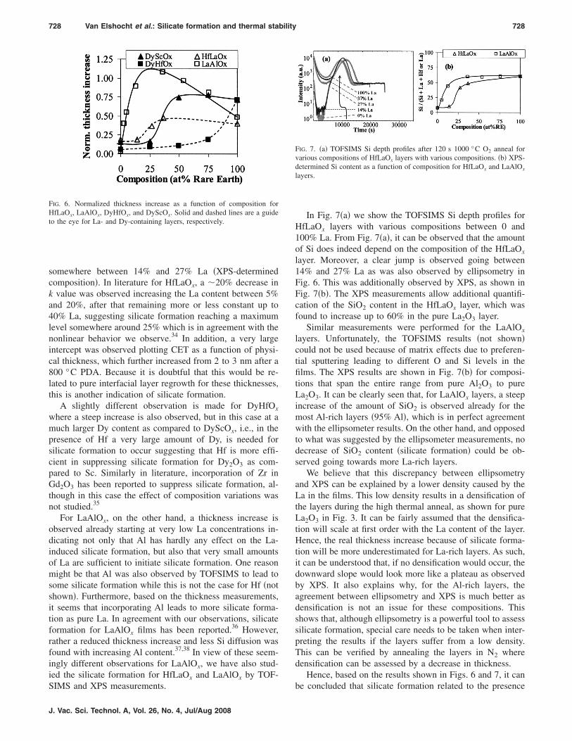
versus LaAlOx. In Fig. 6, we have plotted the normalizedthickness increase measured after a total anneal of 120 s inO2 as a function of composition for ternary oxides of Dy�mixed with Hf or Sc� and La �mixed with Hf or Al�.
From Fig. 6, it can be clearly seen that the thickness in-crease for ternary rare earth based oxides is not a linear re-lation as function of composition. When we consider, forexample, DyScOx layers with different compositions, thenwe observe that increasing the content of the rare earth ele-ment does not result in a gradual increase of the silicateformation. To the contrary, a rather steep increase in silicateformation is observed between �25% and �50% of Dy�nominal composition�.
A very similar behavior is observed for HfLaOx that also
FIG. 5. Thickness increase �open symbols� and normalized thickness in-crease �closed symbols� for DyScOx layers as a function of as-depositedthickness after a 10 Torr O2 1000 °C anneal.
demonstrates a rather steep increase in silicate formation
728 Van Elshocht et al.: Silicate formation and thermal stability 728
somewhere between 14% and 27% La �XPS-determinedcomposition�. In literature for HfLaOx, a �20% decrease ink value was observed increasing the La content between 5%and 20%, after that remaining more or less constant up to40% La, suggesting silicate formation reaching a maximumlevel somewhere around 25% which is in agreement with thenonlinear behavior we observe.34 In addition, a very largeintercept was observed plotting CET as a function of physi-cal thickness, which further increased from 2 to 3 nm after a800 °C PDA. Because it is doubtful that this would be re-lated to pure interfacial layer regrowth for these thicknesses,this is another indication of silicate formation.
A slightly different observation is made for DyHfOx
where a steep increase is also observed, but in this case at amuch larger Dy content as compared to DyScOx, i.e., in thepresence of Hf a very large amount of Dy, is needed forsilicate formation to occur suggesting that Hf is more effi-cient in suppressing silicate formation for Dy2O3 as com-pared to Sc. Similarly in literature, incorporation of Zr inGd2O3 has been reported to suppress silicate formation, al-though in this case the effect of composition variations wasnot studied.35
For LaAlOx, on the other hand, a thickness increase isobserved already starting at very low La concentrations in-dicating not only that Al has hardly any effect on the La-induced silicate formation, but also that very small amountsof La are sufficient to initiate silicate formation. One reasonmight be that Al was also observed by TOFSIMS to lead tosome silicate formation while this is not the case for Hf �notshown�. Furthermore, based on the thickness measurements,it seems that incorporating Al leads to more silicate forma-tion as pure La. In agreement with our observations, silicateformation for LaAlOx films has been reported.36 However,rather a reduced thickness increase and less Si diffusion wasfound with increasing Al content.37,38 In view of these seem-ingly different observations for LaAlOx, we have also stud-ied the silicate formation for HfLaOx and LaAlOx by TOF-
FIG. 6. Normalized thickness increase as a function of composition forHfLaOx, LaAlOx, DyHfOx, and DyScOx. Solid and dashed lines are a guideto the eye for La- and Dy-containing layers, respectively.
SIMS and XPS measurements.
J. Vac. Sci. Technol. A, Vol. 26, No. 4, Jul/Aug 2008
In Fig. 7�a� we show the TOFSIMS Si depth profiles forHfLaOx layers with various compositions between 0 and100% La. From Fig. 7�a�, it can be observed that the amountof Si does indeed depend on the composition of the HfLaOx
layer. Moreover, a clear jump is observed going between14% and 27% La as was also observed by ellipsometry inFig. 6. This was additionally observed by XPS, as shown inFig. 7�b�. The XPS measurements allow additional quantifi-cation of the SiO2 content in the HfLaOx layer, which wasfound to increase up to 60% in the pure La2O3 layer.
Similar measurements were performed for the LaAlOx
layers. Unfortunately, the TOFSIMS results �not shown�could not be used because of matrix effects due to preferen-tial sputtering leading to different O and Si levels in thefilms. The XPS results are shown in Fig. 7�b� for composi-tions that span the entire range from pure Al2O3 to pureLa2O3. It can be clearly seen that, for LaAlOx layers, a steepincrease of the amount of SiO2 is observed already for themost Al-rich layers �95% Al�, which is in perfect agreementwith the ellipsometer results. On the other hand, and opposedto what was suggested by the ellipsometer measurements, nodecrease of SiO2 content �silicate formation� could be ob-served going towards more La-rich layers.
We believe that this discrepancy between ellipsometryand XPS can be explained by a lower density caused by theLa in the films. This low density results in a densification ofthe layers during the high thermal anneal, as shown for pureLa2O3 in Fig. 3. It can be fairly assumed that the densifica-tion will scale at first order with the La content of the layer.Hence, the real thickness increase because of silicate forma-tion will be more underestimated for La-rich layers. As such,it can be understood that, if no densification would occur, thedownward slope would look more like a plateau as observedby XPS. It also explains why, for the Al-rich layers, theagreement between ellipsometry and XPS is much better asdensification is not an issue for these compositions. Thisshows that, although ellipsometry is a powerful tool to assesssilicate formation, special care needs to be taken when inter-preting the results if the layers suffer from a low density.This can be verified by annealing the layers in N2 wheredensification can be assessed by a decrease in thickness.
Hence, based on the results shown in Figs. 6 and 7, it can
FIG. 7. �a� TOFSIMS Si depth profiles after 120 s 1000 °C O2 anneal forvarious compositions of HfLaOx layers with various compositions. �b� XPS-determined Si content as a function of composition for HfLaOx and LaAlOx
layers.
be concluded that silicate formation related to the presence

729 Van Elshocht et al.: Silicate formation and thermal stability 729
of rare earth elements is not solely governed by the annealprocess parameters, but can also be influenced by other ele-ments in the layer and the ratio in which they are present.
The silicate formation described above is an additionalparameter to take into account when studying crystallizationbehavior of rare earth containing layers. Indeed, when the Sicontent increases as a result of the silicate formation, it raisesthe crystallization onset temperature keeping the layer amor-phous up to higher temperatures. As a small variation of thecomposition can lead to a sudden and significant change insilicate formation, this could lead to issues assessing crystal-lization behavior. XRD is the most frequently used techniqueto determine crystallization temperatures, but it cannot dis-tinguish if an increase in crystallization temperature is theresult of the material itself or because of silicate formationfor that specific composition. Therefore, the crystallizationtemperature of a material can be overestimated when notcarefully taking into account silicate formation that can po-tentially occur depending on the process conditions and thelayer underneath, e.g., a �thick� SiO2 layer is often used asstarting surface for the deposition of high-k layers.
As a simple example to illustrate this, we show in Fig.8�a� a cross section TEM of a 12 nm Dy2O3 layer depositedon 20 nm SiO2 after annealing at 1000 °C for 60 s in a N2
ambient. While Dy2O3 is already crystalline asdeposited,39,40 a large part of the Dy2O3 is seen to be amor-phous after anneal. This is obviously the result of amorphiza-tion that occurred during anneal because of silicate formationwith the thick SiO2 layer underneath and consuming it in theprocess �the SiO2 layer is 5 nm thinner after anneal�. For thepresent stack and anneal conditions, 6 nm Dy2O3 is trans-formed into a DySiOx and �5 nm crystalline Dy2O3 is lefton top. More aggressive anneal conditions or a thinnerDy2O3 would have resulted in a fully amorphous layer. InFig. 8�b�, we show the XRD spectra for this sample as de-posited and after anneal. It can be seen that the signal inten-sity after anneal is actually lower as compared to withoutanneal, suggesting a more amorphous layer after anneal. Athinner Dy2O3 would have yielded a fully amorphous layerthat could, if results were purely based on XRD, lead to the
FIG. 8. Cross-section TEM of a 12 nm Dy2O3 layer deposited on 20 nmSiO2 after a 60 s 1000 °C N2 anneal and XRD spectra of the same stackbefore �gray� and after �black� anneal. Consumption of the SiO2 layer un-derneath during anneal results in amorphization of the Dy2O3 layer by for-mation of a DySiOx layer.
conclusion that Dy2O3 remains amorphous up to 1000 °C.
JVST A - Vacuum, Surfaces, and Films
In conclusion, we have shown that thickness variationsobserved by ellipsometry during O2 anneals at high tempera-ture can be used as a simple and powerful method to assesssilicate formation for rare earth based materials. Special careneeds to be taken when analyzing layers with a low densityas the latter can obscure the thickness increases caused bysilicate formation. Silicate formation for ternary rare earthbased materials depends on the ratio of the rare earth to theother element and on the nature of the other element. Someelements such as Hf can suppress silicate formation moreefficiently than others such as Al. The effect of silicate for-mation is an important parameter to take into account whenanalyzing the effect of the composition of ternary rare earthoxides on their thermal stability.
1See, e.g., Alex. Tullo, Chem. Eng. News 85, 9 �2007�.2L. Pantisano, T. Schram, B. O’Sullivan, T. Conard, S. De Gendt, G.Groeseneken, P. Zimmerman, A. Akheyar, M. M. Heyns, S. Shamuilla, V.V. Afanas’ev, and A. Stesmans, Appl. Phys. Lett. 89, 113505 �2006�.
3L.-A. Ragnarsson, V. S. Chang, H. Y. Yu, H.-J. Cho, T. Conard, K. M.Yin, A. Delabie, J. Swerts, T. Schram, S. De Gendt, and S. Biesemans,IEEE Electron Device Lett. 28, 486 �2007�.
4P. Sivasubramani, J. Kim, M. J. Kim, B. E. Gnade, and R. M. Wallace, J.Appl. Phys. 101, 114108 �2007�.
5D. J. Lichtenwalner, J. S. Jur, A. I. Kingon, M. P. Augustin, Y. Yang, S.Stemmer, L. V. Goncharova, T. Gustafsson, and E. Garfunkel, J. Appl.Phys. 98, 024314 �2005�.
6M. Copel, E. Cartier, and F. M. Ross, Appl. Phys. Lett. 78, 1607 �2001�.7M. Copel, E. Cartier, V. Narayanan, M. C. Reuter, S. Guha, and N. Bo-jarczuk, Appl. Phys. Lett. 81, 4227 �2002�.
8C.-J. Choi, M.-G. Jang, Y.-Y. Kim, M.-S. Jun, T.-Y. Kim, and M.-H.Song, Appl. Phys. Lett. 91, 012903 �2007�.
9G. Lupina, T. Schroeder, J. Dabrowski, Ch. Wenger, A. U. Mane, H.-J.Mussig, P. Hoffmann, and D. Schmeisser, J. Appl. Phys. 99, 114109�2006�.
10A. Fissel, Z. Elassar, O. Kirfel, E. Bugiel, M. Czernohorsky, and H. J.Osten, J. Appl. Phys. 99, 074105 �2006�.
11A. Sakai, S. Sakashita, M. Sakashita, Y. Yasuda, S. Zaima, and S.Miyazaki, Appl. Phys. Lett. 85, 5322 �2004�.
12M. Copel, Appl. Phys. Lett. 82, 1580 �2003�.13T.-M. Pan, F.-J. Tsai, C.-I. Hsieh, and T.-W. Wu, Electrochem. Solid-State
Lett. 10, G21 �2007�.14D. Eom, S. Y. No, C. S. Hwang, and H. J. Kim, J. Electrochem. Soc. 154,
G49 �2007�.15H. Ono and T. Katsumaata, Appl. Phys. Lett. 78, 1832 �2001�.16J. A. Gupta, D. Landheer, J. P. McCaffrey, and G. I. Sproule, Appl. Phys.
Lett. 78, 1718 �2001�.17G. Lupina, T. Schroeder, Ch. Wenger, J. Dabrowski, and H.-J. Mussig,
Appl. Phys. Lett. 89, 222909 �2006�.18S. Stemmer, Y. Li, B. Foran, P. S. Lysaght, S. K. Streiffer, P. Fuoss, and
S. Seiffert, Appl. Phys. Lett. 83, 3141 �2003�.19B. W. Busch, J. Kwo, M. Hong, J. P. Mannaerts, B. J. Sapjeta, W. H.
Schulte, E. Garfunkel, and T. Gustafsson, Appl. Phys. Lett. 79, 2447�2001�.
20D. Niu, R. W. Ashcraft, and G. N. Parsons, Appl. Phys. Lett. 80, 3575�2002�.
21A. Goryachko, J. P. Liu, D. Krüger, H. J. Osten, E. Bugiel, R. Kurps, andV. Melnik, J. Vac. Sci. Technol. A 20, 1860 �2002�.
22M. Meuris, P. W. Mertens, A. Opdebeeck, H. F. Schmidt, M. Depas, G.Vereecke, M. M. Heyns, and A. Philipossian, Solid State Technol. 38,109 �1995�.
23M. Schumacher and J. Linder, European Semicond. 23 �November 2002�.24S. Van Elshocht, P. Lehnen, B. Seitzinger, A. Abrutis, C. Adelmann, B.
Brijs, M. Caymax, T. Conard, S. De Gendt, A. Franquet, C. Lohe, M.Lukosius, A. Moussa, O. Richard, P. Williams, T. Witters, and P. Zim-merman, J. Electrochem. Soc. 153, F219 �2006�.
25C. Adelmann, P. Lehnen, S. Van Elshocht, C. Zhao, B. Brijs, A. Franquet,T. Conard, M. Roeckerath, J. Schubert, O. Boissière, C. Lohe, and S. De
Gendt, Chem. Vap. Deposition 13, 568 �2007�.
730 Van Elshocht et al.: Silicate formation and thermal stability 730
26R. Thomas, P. Ehrhart, M. Luysberg, M. Boese, R. Waser, M. Roeckerath,E. Rije, J. Schubert, S. Van Elshocht, and M. Caymax, Appl. Phys. Lett.89, 232902 �2006�.
27Pulsar® is a trademark of ASM International nv, The Netherlands.28S. Van Elshoch, M. Caymax, S. De Gendt, T. Conard, J. Pétry, L. Daté, D.
Pique, and M. M. Heyns, J. Electrochem. Soc. 151, F77 �2004�.29J.-P. Maria, D. Wicaksana, A. I. Kingon, B. Busch, H. Schulte, E. Gar-
funkel, and T. Gustafsson, J. Appl. Phys. 90, 3476 �2002�.30S. Guha, E. Cartier, M. A. Gribelyuk, N. A. Bojarczuk, and M. C. Copel,
Appl. Phys. Lett. 77, 2710 �2000�.31B. E. Deal and A. S. Grove, J. Appl. Phys. 36, 3770 �1965�.32X. Wu, D. Landheer, G. I. Sproule, T. Quance, M. J. Graham, and G. A.
Botton, J. Vac. Sci. Technol. A 20, 1141 �2002�.33S. Jeon and H. Hwang, J. Appl. Phys. 93, 6393 �2003�.34
Y. Yamamoto, K. Kita, K. Kyuno, and A. Toriumi, Appl. Phys. Lett. 89,J. Vac. Sci. Technol. A, Vol. 26, No. 4, Jul/Aug 2008
032903 �2006�.35S. A. Park, Y. S. Roh, Y. K. Kim, J. H. Baeck, M. Noh, K. Jeong, C. H.
Chang, M. K. Joo, T. G. Kim, J. H. Song, and S.-H. Ko, J. Appl. Phys.98, 024906 �2005�.
36L. Miotti, C. Driemeier, F. Tatsch, C. Radtke, V. Edon, M. C. Hugon, O.Voldoire, B. Agius, and I. J. R. Baumvol, Electrochem. Solid-State Lett.9, F49 �2006�.
37J. Jun, J. H. Jun, and D. J. Choi, Electrochem. Solid-State Lett. 6, F37�2003�.
38R. Fujitsuka, M. Sakashita, A. Sakai, M. Ogawa, S. Zaima, and Y. Ya-suda, Jpn. J. Appl. Phys., Part 1 46, 2428 �2005�.
39R. Thomas, P. Ehrhart, M. Roeckerath, S. Van Elshocht, E. Rije, M.Luysberg, M. Boese, J. Schubert, M. Caymax, and R. Waser, J. Electro-chem. Soc. 154, G147 �2007�.
40
F.-C. Chiu, J. Appl. Phys. 102, 044116 �2007�.