signal processing for an autonomous underwater vehicle
119
UNIVERSITÀ DI PISA Facoltà di Ingegneria Laurea Specialistica in Ingegneria dell’Automazione Tesi di laurea Candidato: Matteo Tanzini Relatori: Prof. Andrea Caiti Prof. Alexander Leonessa SIGNAL PROCESSING FOR AN AUTONOMOUS UNDERWATER VEHICLE: AN FPGA APPROACH Sessione di Laurea del 09/07/2009 Archivio tesi Laurea Specialistica in Ingegneria dell’Automazione Anno accademico 2008/2009 Consultazione consentita
-
Upload
khangminh22 -
Category
Documents
-
view
0 -
download
0
Transcript of signal processing for an autonomous underwater vehicle
UNIVERSITÀ DI PISA
Facoltà di Ingegneria
Laurea Specialistica in Ingegneria dell’Automazione
Tesi di laurea
Candidato:
Matteo Tanzini
Relatori:
Prof. Andrea Caiti
Prof. Alexander Leonessa
SIGNAL PROCESSING FOR AN AUTONOMOUS UNDERWATER VEHICLE:
AN FPGA APPROACH
Sessione di Laurea del 09/07/2009 Archivio tesi Laurea Specialistica in Ingegneria dell’Automazione
Anno accademico 2008/2009 Consultazione consentita

2
3
Dedico questo lavoro ai miei due nonni che non hanno potuto avere la soddisfazione di vedere il proprio nipote laurearsi.

4
5
Ringraziamenti Desidero ringraziare il Prof. Alexander Leonessa per il supporto scientifico e morale che mi ha dato durante il mio soggiorno negli Stati Uniti; il Prof. Andrea Caiti per la gentilezza, la disponibilità e l’aiuto dato lungo tutto lo sviluppo di questa tesi; Gary Stein per il concreto contributo sperimentale e il tempo dedicatomi; Marco Vincenzi per il supporto tecnico e la sua disponibilità. Desidero ringraziare la mia famiglia che ha sempre creduto in me e mi ha aiutato in tutti i momenti difficili del mio percorso formativo; ringrazio mio padre che durante tutti questi anni ha partecipato attivamente alla costruzione della mia cultura scientifica. Infine ringrazio la mia Giulia per avermi fatto sempre sentire speciale, in grado di superare tutti gli ostacoli.

6
7
ABSTRACT
The idea of this thesis comes out from the participation of the University of Central Florida to the Annual International Autonomous Underwater Vehicle Competition of 2007. The goal of this competition is to build an AUV capable to accomplish to some various objectives. One of these, wants the AUV to detect an underwater acoustic ping and follow it to his source. The objective of this thesis is to improve the performance of this trajectory tracking. A Field Programmable Logic Gate Array will be used to perform an effective Digital Signal Processing.
8
INDEX
INTRODUCTION .................................................................................... 11
DESCRIPTION OF THE OPERATIVE CONTEST ............................. 12
2. STATE OF ART ................................................................................... 13
2.1 Autonomous Underwater Vehicles: a general view .................... 13 2.1.1 Introducion ................................................................................................. 13 2.1.2 History ......................................................................................................... 14 2.1.3 AUV Technology ......................................................................................... 16 2.1.4 The Future of AUV Technology ................................................................. 19
2.2 Simplified method for obtaining navigational information from hydrophone arrays ............................................................................. 20 2.2.1 Introduction ................................................................................................ 20 2.2.2 Amplifier Circuit ........................................................................................ 22 2.2.3 Signal processing board .............................................................................. 22 2.2.4 Signal Processing ........................................................................................ 23 2.2.5 Results and Conclusions ............................................................................. 24
2.3 Development and Testing of an Acoustic Positioning System – Description and Signal Processing ..................................................... 24 2.3.1 General Description .................................................................................... 24 2.3.2 Hardware description ................................................................................. 25 2.3.3 Conclusions ................................................................................................. 26
2.4 Underwater Acoustic Source Localization Based on Passive Sonar and Intelligent Processing ....................................................... 26 2.4.1 General Description .................................................................................... 26 2.4.2 Acquisition, control and processing unit .................................................... 26 2.4.3 System Software .......................................................................................... 27 2.4.4 Acquisition and conditioning circuit control ............................................. 27
2.5 Field Programmable Gate Array (FPGA) ................................... 28 2.5.1 What is an FPGA? ...................................................................................... 28 2.5.2 Why do we need FPGAs? ........................................................................... 30 2.5.3 Logic Block.................................................................................................. 31 2.5.4 FPGA Routing Techniques ......................................................................... 34 2.5.5 FPGA Structural Classification ................................................................. 36 2.5.6 Programming .............................................................................................. 38 2.5.7 FPGA Design Flow ..................................................................................... 40 2.5.8 Five reason to choose an FPGA .................................................................. 41
3.THE HARDWARE ................................................................................ 43
3.1 How to choose an FPGA board .................................................... 43
3.2 The Market Analysis ..................................................................... 48 3.2.1 Pentek - Model 6256 ................................................................................... 49 3.2.2 Innovative integration X3-A4D4 ................................................................ 50
9
3.2.3 Echotek ECAD-DA-41-PMC .................................................................... 51 3.2.4 Bittware TETRA-PMC+ ............................................................................ 52
3.3 A real choice ................................................................................... 53 3.3.1 New solutions ............................................................................................... 53 3.3.2 The FPGA board choice: ALTERA/TERASIC DE2 Development and Education Board .................................................................................................. 55 3.3.4 The A/D board choice: MAX1127 Evaluation Kit from MAXIM ............. 57 3.3.5 The A/D board: a self-made board ............................................................. 58 3.3.6 The Costs ..................................................................................................... 59
3.4 Simulation’s hardware .................................................................. 59 3.4.1 Signal generation: a Digital Acquisition Board ......................................... 60 Specifications Summary ...................................................................................... 60
3.5 The experimental setup ................................................................. 62
4. BORN AND DEVELOPMENT OF THE ALGORITHM .................. 63
4.1 The 2007 AUVSI competition ...................................................... 63
4.2 The vehicle ..................................................................................... 64
4.3 The idea .......................................................................................... 66 4.3.1 The hydrophones ......................................................................................... 66 4.3.2 Issues............................................................................................................ 67
4.4 The Mathematic Theory................................................................ 68 4.4.1 The idea ....................................................................................................... 68 4.4.2 Extracting the Delay ................................................................................... 69 4.4.3 The practice result ...................................................................................... 74 4.4.4 The Delay extraction ................................................................................... 74
4.5 The simulation scheme .................................................................. 75 4.5.1 First blocks .................................................................................................. 77 4.5.2 The simulated input .................................................................................... 77 4.5.3 Windowing ................................................................................................. 78 4.5.4 The Fast Fourier Transform ...................................................................... 81 4.5.5 The product between the FFT outputs ....................................................... 87 4.5.6 The inverse Fast Fourier Transform .......................................................... 87 4.5.7 The cross correlation................................................................................... 87 4.5.8 Delay Calculation ........................................................................................ 89 4.5.9 Results ......................................................................................................... 90 4.5.10 Simulation Conclusions ............................................................................. 94
5. IMPLEMENTATION, EXPERIMENT, RESULTS .......................... 95
5.1 The input signal generation .......................................................... 95 5.1.1 An acquisition tool ...................................................................................... 96
5.2 Sampling ....................................................................................... 96
5.3 The Real Scheme ......................................................................... 100 5.3.1 Timing ....................................................................................................... 103 5.3.2 Resource managing ................................................................................... 104

10
5.4 Final Discussion and Future work .............................................. 108
6. CONCLUSIONS ................................................................................. 110
BIBLIOGRAFY ...................................................................................... 111
APPENDIX A – HOW TO PROGRAM AN FPGA ............................. 112
FIGURE INDEX ..................................................................................... 117
11
INTRODUCTION
The idea of this thesis starts from an Universal Central Florida’s Project aimed to participate to the AUVSI & ONR’s 10th Annual International Autonomous Underwater Vehicle Competition of 2007. The goal of the 2007 mission is to make a vehicle to autonomously navigate an obstacle course. The UCF team developed an AUV: the SCOUT.
The final obstacle the vehicle has to manage, is to identify an underwater ping and tracking it until his source.
To accomplish this, the vehicle mounts four hydrophones on his structure, in a diamond pattern. The incoming signals are treated and then sent to the Hydrophones processor to perform computations to calculate the pinger’s relative heading and distance. This trajectory tracking is the weak point of the project.
The trajectory tracking is affected by a route error equal to ± 30°. The working team found that the problem was on the low acquisition time of the digital acquisition board used for it.
The purpose of this thesis is to use a faster new technology, an FPGA board, to handle better results for the trajectory tracking.
A general research on FPGA is made to show the state of art and to understand his peculiarity. This would be an introduction to who has no knowledge on the FPGA world: this research will comprehend hardware, software and market knowledges.
To understand what kind of FPGA would have fit our needs, a choice method is created and then a real market comparison has made. Various options are evaluated and then a trade-off choice between our needs has made: we focused on performance and price.
To understand how to manage an FPGA, have been analyzed two software: a low level program language that use the Quartus II software, and a visual one, that utilize a Matlab Simulink tool, the DSP builder.
At this point, the theory is discussed: how to physically calculate the ping direction source? This comprehends the idea that comes from the hydrophones diamond pattern, how to extract the incoming signal’s data and how to apply some Digital Signal Processing to them.
A simulation study is done to understand the effective goodness of the FPGA project. The argumentation will go deep in to the FPGA programming, creating a simulation
scheme only on Simulink DSP Builder Software and then fitting that scheme, to a real simulation with real simulated inputs and dealing with the FPGA board directly.
At last the results and the limitation of the algorithm are analyzed and some purpose are made for future workers on the real project.
12
DESCRIPTION OF THE OPERATIVE CONTEST This thesis was developed in two different contests: the first one was the department of
Mechanical, Materials, and Aerospace Engineering at University of Central Florida, America, the other one was the department of Electric systems and Automation of Engineering at University of Pisa.
On the first contest, it was possible to stay in touch with the Scout’s developing team and to benefit of all the knowledge of Prof. Alexander Leonessa, our supervisor, furthermore it was possible to use the laboratories resources and the University’s funding. At UCF was developed the research and the theoretical simulation part of the thesis while the Italy experience was focused on the real implementation in laboratory.
To stay at UCF was really useful dealing with the real beneficiaries of this thesis directly. Choices and requests were made in real time. Furthermore it was easier to contact directly lot of hardware manufacturers to get information about our needs.
At University of Pisa the supervision passed to Prof. Andrea Caiti. Here we were able to use laboratories to build up our hardware and we had the support of the department technicians and a lot of useful lab facilities and tools.
13
2. STATE OF ART The bibliographic research comprehends three sections. The first section will introduce you in the world of the Autonomous Underwater
Vehicles. In the second section three experiences similar to our’s will be described. The first
experience is born form the same competition that the UCF team was involved. The system results similar to our one because the AUV, developed by the team, extracts the necessary informations from an hydrophone’s array performing some DSP analysis with an FPGA and a microcontroller. The second experience discuss about an USBL Acoustic positioning System for an underwater vehicle: they use an FPGA doing some DSP. In the third experience an FPGA is used to process source localization based on a passive sonar.
The third section will give a wide view about FPGA.
2.1 Autonomous Underwater Vehicles: a general view [1][2] 2.1.1 Introducion
An Autonomous Underwater Vehicle (AUV) is a robotic device that is driven through the water by a propulsion system, controlled and piloted by an onboard computer, and maneuverable in three dimensions. This level of control, under most environmental conditions, permits the vehicle to follow precise preprogrammed trajectories wherever and whenever required. Sensors on board the AUV sample the ocean as the AUV moves through it, providing the ability to make both spatial and time series measurements. Sensor data collected by an AUV is automatically geospatially and temporally referenced and normally of superior quality. Multiple vehicle surveys increase productivity, can insure adequate temporal and spatial sampling, and provide a means of investigating the coherence of the ocean in time and space.
The fact that an AUV is normally moving does not prevent it from also serving as a Lagrangian, or quasi Eulerian, platform. This mode of operation may be achieved by programming the vehicle to stop thrusting and float passively at a specific depth or density layer in the sea, or to actively loiter near a desired location. AUV’s may also be programmed to swim at a constant pressure or altitude or to vary their depth and/or heading as they move through the water, so that undulating sea saw survey patterns covering both vertical and/or horizontal swaths may be formed. AUV’s are also well suited to perform long linear transects, sea sawing through the water as they go, or traveling at a constant pressure. They also provide a highly productive means of performing seafloor surveys using acoustic or optical imaging systems.
When compared to other Lagrangian platforms, AUV’s become the tools of choice as the need for control and sensor power increases. The AUV’s advantage in this area is achieved at the expense of endurance, which for an AUV is typically on the order of 8- 50 hours. Most vehicles can vary their velocity between 0.5 and 2.5 m/s. The optimum speed and the corresponding greatest range of the vehicle occur when its hotel load (all required power except propulsion) is twice the propulsive load. For most vehicles, this occurs at a velocity near 1.5 m/s.
The degree of autonomy of the robot presents an interesting dichotomy. Total autonomy does not provide the user with any feedback on the vehicle’s progress or health, nor does it provide a means of controlling or redirecting the vehicle during a
14
mission. It does, however, free the user to perform other tasks, thereby greatly reducing operational costs, as long as the vehicle and the operator meet at their duly appointed times at the end of the mission. For some missions, total autonomy may be the only choice; in other cases when the vehicle is performing a routine mission, it may be the preferable mode of operation.
Bidirectional acoustic, radio frequency, and satellite based communications systems offer the capability to monitor and redirect AUV missions worldwide from a ship or from
land. For this reason, semi-autonomous operations offer distinct advantages over fully autonomous operations.
2.1.2 History The following presents highlights of
some notable achievements in the history of AUV’s. In the short space and time available, it is unfortunately not possible to provide information on all systems.
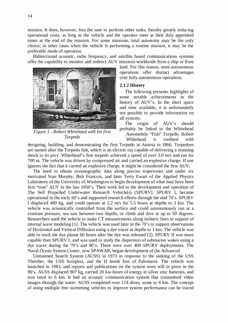
The origin of AUV’s should probably be linked to the Whitehead
Automobile “Fish” Torpedo. Robert Whitehead is credited with
designing, building, and demonstrating the first Torpedo in Austria in 1866. Torpedoes are named after the Torpedo fish, which is an electric ray capable of delivering a stunning shock to its prey. Whitehead’s first torpedo achieved a speed of over 3.0 m/s and ran for 700 m. The vehicle was driven by compressed air and carried an explosive charge. If one ignores the fact that it carried an explosive charge, it might be considered the first AUV.
The need to obtain oceanographic data along precise trajectories and under ice motivated Stan Murphy, Bob Francois, and later Terry Ewart of the Applied Physics Laboratory of the University of Washington to begin development of what may have been first “true” AUV in the late 1950’s. Their work led to the development and operation of The Self Propelled Underwater Research Vehicle(s) (SPURV). SPURV I, became operational in the early 60’s and supported research efforts through the mid 70’s. SPURV I displaced 480 kg, and could operate at 2.2 m/s for 5.5 hours at depths to 3 km. The vehicle was acoustically controlled from the surface and could autonomously run at a constant pressure, sea saw between two depths, or climb and dive at up to 50 degrees. Researchers used the vehicle to make CT measurements along isobaric lines in support of internal wave modeling [1]. The vehicle was used later in the 70’s to support observations of Horizontal and Vertical Diffusion using a dye tracer at depths to 1 km. The vehicle was able to track the dye plume 66 hours after the dye was released [2]. SPURV II was more capable than SPURV I, and was used to study the dispersion of submarine wakes using a dye tracer during the 70’s and 80’s. There were over 400 SPURV deployments. The Naval Ocean System Center, now SPAWAR, began development of the Advanced
Unmanned Search System (AUSS) in 1973 in response to the sinking of the USS Thresher, the USS Scorpion, and the H bomb loss of Palomares. The vehicle was launched in 1983, and reports and publications on the system were still in press in the 90’s. AUSS displaced 907 kg, carried 20 kw-hours of energy in silver zinc batteries, and was rated to 6 km. It had an acoustic communication system that transmitted video images through the water. AUSS completed over 114 dives, some to 6 km. The concept of using multiple free swimming vehicles to improve system performance can be traced
Figure 1 - Robert Whitehaed with his first
Torpedo
15
to the development of this system. This work was completed some time in the early 80’s. [5] IFREMER’s Epulard was designed in 1976, assembled by 1978, and was fully operational by 1980. Epulard was the first 6 km rated acoustically controlled AUV that supported deep ocean photography and bathymetric surveys. The vehicle maintained a constant altitude above the bottom by dragging a cable. Epulard completed 300 dives, some to 6 km, between 1970 and 1990 [3].
According to Busby’s 1987 Undersea Vehicle Directory, there were six operational AUV’s and an additional 15 other vehicles that were considered to be prototypes or under construction by 1987. During this period, AUV’s were called un-tethered (autonomous) ROV’s, and the acronym AUV stood for Advanced Underwater Vehicle, a vehicle under development by the U.S. Defense Advanced Research Projects, which was completed in 1984. The origin of the 3 Hugin vehicle, which is currently manufactured by Konsberg Simard, can also be traced back to the late 80’s [4].
During the 90’s, there was a rekindling of interest in AUV’s in academic research. The Massachusetts Institute of Technology’s Sea Grant AUV lab developed six Odyssey vehicles during the early 90’s. These vehicles displaced 160 kg, could operate at 1.5 m/s for up to six hours, and were rated to 6 km. Odyssey vehicles were operated under ice in 1994, and to a depth of 1.4 km for 3 hours in the open ocean in 1995 [6]. Odyssey vehicles were also used in support of experiments demonstrating the Autonomous Ocean Sampling Network during this period [7].
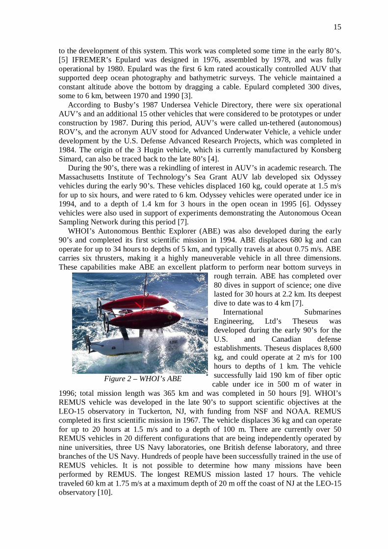
WHOI’s Autonomous Benthic Explorer (ABE) was also developed during the early 90’s and completed its first scientific mission in 1994. ABE displaces 680 kg and can operate for up to 34 hours to depths of 5 km, and typically travels at about 0.75 m/s. ABE carries six thrusters, making it a highly maneuverable vehicle in all three dimensions. These capabilities make ABE an excellent platform to perform near bottom surveys in
rough terrain. ABE has completed over 80 dives in support of science; one dive lasted for 30 hours at 2.2 km. Its deepest dive to date was to 4 km [7].
International Submarines Engineering, Ltd’s Theseus was developed during the early 90’s for the U.S. and Canadian defense establishments. Theseus displaces 8,600 kg, and could operate at 2 m/s for 100 hours to depths of 1 km. The vehicle successfully laid 190 km of fiber optic cable under ice in 500 m of water in
1996; total mission length was 365 km and was completed in 50 hours [9]. WHOI’s REMUS vehicle was developed in the late 90’s to support scientific objectives at the LEO-15 observatory in Tuckerton, NJ, with funding from NSF and NOAA. REMUS completed its first scientific mission in 1967. The vehicle displaces 36 kg and can operate for up to 20 hours at 1.5 m/s and to a depth of 100 m. There are currently over 50 REMUS vehicles in 20 different configurations that are being independently operated by nine universities, three US Navy laboratories, one British defense laboratory, and three branches of the US Navy. Hundreds of people have been successfully trained in the use of REMUS vehicles. It is not possible to determine how many missions have been performed by REMUS. The longest REMUS mission lasted 17 hours. The vehicle traveled 60 km at 1.75 m/s at a maximum depth of 20 m off the coast of NJ at the LEO-15 observatory [10].
Figure 2 – WHOI’s ABE
16
South Hampton Oceanography Center’s Autosub was developed during the early 90’s to provide scientists with the capability to monitor the oceans in new ways. Autosub completed its first scientific mission in 1998. The vehicle displaces 1700 kg, and can travel for up 6 days at 3 knots at depths up to 1.6 km. Autosub has completed 271 missions, totaling 750 hours and covering 3,596 km. Its deepest dive was to 1 km.; its longest mission lasted 50 hours [11]. In 1998, the UK National Environmental Research Council provided 2.6m pounds in grants and training awards for use with the Autosub. These grants stimulated a great deal of interest in the scientific community. The turn of the century ushered in the first commercial enterprise to offer deep water (3 km) AUV survey services. C&C Technologies of Lafayette, Louisiana offers a Hugin 3000 AUV for charter. The vehicle was manufactured by Kongsberg Simrad of Norway. The vehicle displaces 1400 kg, and can operate at 4 knots for 40 hours utilizing an aluminum/oxygen fuel cell. C&C Technologies has completed over 17,702 km of (paid for) geophysical mapping, some to 3 km, since the vehicle was first offered in 2000. C&C Technologies also offers its clients interactive software on their web site that permits them to monitor and direct the progress of the generation of charts that are being made aboard the survey ship that is supporting the AUV survey. [12].
2.1.3 AUV Technology Over the years, the focus of technology development has changed as new ideas
surfaced to address technology problems. Some of the problems have been solved, others remain that must be addressed, and other, previously unrecognized problems, have surfaced. It is hard to list those technologies that are needed for AUV systems. Any list that is developed will be incomplete. It could be suggested, however, that the following list represents many of the technologies that have been addressed over the past three decades.
• Autonomy • Energy • Navigation • Sensors • Communications
The interesting aspect of this list is that although there have been advances in these technical areas, a number of these technologies still remain the “technology long poles” associated with AUV systems. Limits in these technologies limit the capability of AUV systems. Technology “Long Poles”
• Autonomy / Cooperation / Intelligent Systems and Technologies • Energy Systems / Energy management • Navigation • Sensor Systems and Processing • 3D Imaging • Communications.
2.1.3.1 Autonomy / Cooperation / Intelligent Systems and Technologies In the 1980s there was a considerable effort placed into understanding how to give an
AUV a level of intelligence necessary to accomplish assigned tasks. Issues such as intelligent systems architectures design, mission planning, perception and situation assessment were investigated. These are all hard problems and there were few successes that led to in-water evaluation. As the capabilities required by the first generation AUVs became clear, the tasks the AUVs were to perform seemed not to demand a high level of intelligent behavior. In fact many of the tasks being assigned to today’s AUVs required
17
only a list of preprogrammed instructions to accomplish a task. For this reason, there has not been a significant level of development, recently, that is focused on AUV autonomy.
The problem of autonomy still remains unsolved. There have been some successes with other autonomous systems, but those advances have not been brought into the AUV community. There are very few programs funded to address these issues and the problem remains. As AUV operations increase, it will become apparent that more investigation is needed. This will again emphasize the need for more development along the lines of making AUV systems more intelligent and better able to adapt to the environment within which they exist.
The use of multiple cooperating AUVs was first considered in the 1980s. Some work was undertaken, but not completed. Since that time, there has been little funded work on this technological issue. In the past few years, there has been increased recognition of the potential of multiple cooperating AUVs. Currently some work is underway to investigate cooperating AUVs tasked to meet some of the needs of mine clearance. Many more investigations are required as the problem is a significant problem and far from being solved. 2.1.3.2 Energy Systems / Energy management
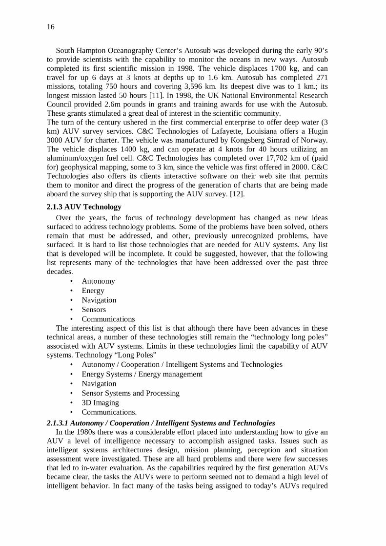
Endurance of AUVs has increased from a few hours to 10s of hours. Some systems now contemplate missions of days and, a very few, of years. This extended endurance, however, is at the expense of sensing capability, as well as very limited transit speeds. In the majority of early AUV systems, Lead Acid batteries were the workhorse for energy systems. Some AUV designs included Silver Zinc batteries, but, for the most part, the cost was prohibitive. Some applications, such as the ABE vehicle, utilized Lithium primary batteries. A number of other chemistries were tried for different applications. Recent advances in NiMH batteries have provided new opportunities for AUV and this technology is being used in many of the current AUV systems. In 1987 the use of an Aluminum / Oxygen “semi-cell” was proposed to DARPA for use in an AUV. A number of years later a similar system development was funded and dramatically increased the endurance of the DARPA UUV.
Currently the ALTEX [altex] program is underway to utilize similar technology to allow an AUV to transit under the Arctic ice. Solar Energy is now being used to power an AUV [AUSI]. This system demands a detailed design of onboard energy management; both during the acquisition phase, as well as, the utilization phase of operations. It is an inexhaustible energy source but requires an AUV to surface while recharging. The Glider AUVs [Simonetti] utilize heat energy to vary the buoyancy of an AUV that can glide up and down in the water column. The potential endurance of such a system is measured in years. 2.1.3.3 Navigation
Early AUV systems relied on dead reckoning for their navigation. Acoustic transponder navigation systems provided greater accuracy but at a significant logistics cost. Inertial navigation systems were available for more expensive AUVs, but costs were prohibitive for the non-military user. With advances in inertial platform technology, the cost has dropped significantly to a point where it is possible to utilize these systems for lower cost AUVs.
Figure 3 - A typical Energy system focused AUV

18
Navigation systems continue to improve in accuracy as well as precision. In the past few years, many AUVs have taken advantage of Global Positioning Systems (GPS). When the vehicle surfaces, it is possible to obtain an accurate position and update onboard inertial systems. Still, there is strong interest in being able to navigate relative to the environment within which the system exists. This environment referenced navigation utilizing bottom features, gravimetric variations or other similar characteristics is an objective to be attained. A successful system will provide a significant increase in AUV capability. 2.1.3.4 Sensor Systems and Processing / 3D Imaging
An AUV is simply a platform on which to mount sensors and sensing systems. Initial efforts to develop AUV technology was more concerned about the basic technologies required to allow reliable vehicle operation. As that reliability was achieved, sensors were added to the vehicle system to acquire data from the ocean environment. Most of these efforts to date have been to integrate existing sensors and sensor processing to the sometimes unique constraints of the AUV. This paradigm has proven to work reasonably well. Recently it has been recognized that we must develop entirely new sensors based on the constraints imposed by an AUV. This would change the paradigm of sensor integration. It would encourage the development of sensors specifically for AUVs; smarter, lower power, highly reliable, smaller in size, etc. It is also becoming clear that AUVs can be used in groups to act cooperatively to acquired needed data. By maintaining a common spatial and temporal reference, data acquired by multiple AUVs can be aggregated and processed to obtain synoptic, high resolution data describing a process of interest. Much work continues on the development of higher and higher resolution imaging systems, both optical and acoustic. With the new processors it has been possible to obtain very high resolution images over longer and longer ranges [LENS]. The roadblock to much of this work is the ability to analyze the acquired data autonomously such that the AUV can utilize this data for guidance and control decisions. This perception ability is still beyond the currentcapabilities of AUVs. 2.1.3.5 Communications
In the underwater environment acoustic communications is probablythe most viable communication system available to the system designer. Some development programs have investigated and evaluated other technologies such as laser communication at short range and relatively noise free communications over larger ranges using RF current field density techniques. In the past 10 years there has been significant advances in acoustic communications such that relatively low error rate communications is possible over ranges of kMs at bit rate of a few kbps [Comms]. This remains an active area of investigation. Another aspect of communication is the issue of connecting multiple vehicles and/or bottom mounted instrument platforms via a networked-based communication infrastructure. This subsea network can then be connected to a surface vehicle that will act as a gateway to the terrestrial based communication infrastructure such as the internet [Welsh]. Efforts are underway to investigate how to implement such a network and be able to have effective communications among and between multiple underwater systems.
Other technologies have been investigated over the years such as those below. There have been a number of significant advances in these areas and, although there is still much to be learned, they do not represent major stumbling blocks to the further advancement of AUV technology at this time. These technologies continue to be investigated and refined in the development of operational systems. There remain some important advances to be made such as in the area of autonomous manipulation but the emphasis of current activities are not along these lines.
19
• Guidance /Low Level Control • Hydrodynamics and Control Systems • Autonomous Manipulation / Work Systems • User Interface / Development Tools / Emulation / Modeling
There are also issues associated with the basic system design. It is clear that the system design must result from an understanding of the mission to be undertaken by the system. Over the past few decades, there has been an increased effort to standardize such that advances in system design can be shared by the community. This move toward standardization has increased dramatically over the past few years as AUV systems move closer and closer to operational systems.
Another aspect of the system design that has become commonplace is the tendency to think in terms of modularity. This is seen in current efforts to design distributed control systems architecture both in terms of software and hardware. The concept of “plug & play” is becoming a buzz word for AUV developers as well as PC users. In an environment where new sensors are added to AUV systems on a regular basis, it is obvious that a simple method for managing the impact on the vehicle software system is important.
As AUV systems mature to a point where they are being commercialized, the importance of cost reliability and robustness are gaining increased importance. These are the characteristics that are best optimized by industry. The next few years will undoubtedly see AUVs undergo a strong systems design process to optimize these features. This will benefit the community as a whole and should be well received by the potential user community of the future.
• Software System Architecture / Distributed Control • Hardware System Architecture / Standardization • Platform Design • Cost / Reliability / Robustness
2.1.4 The Future of AUV Technology AUV technology has followed a path not unlike other technologies. It has gone
through stages where academic curiosity was followed by research investigation and prototype development. Applications have recently surfaced that seem to have sufficient financial backing to develop operational systems. Certainly the timing of AUV technology was good. It has been able to leverage its development by utilizing many technologies developed for other markets.
The next years will see the expansion of AUV technology into the commercial marketplace. The size of that market is unclear but the move into the marketplace has begun. There are still many important research investigations to be undertaken. Autonomy is probably the most important issue to be addressed but others, such as those described above, certainly must be addressed. It is clear that the limit to the capability of any AUV is the amount of energy it has onboard. There have been many discussions that suggest that fuel cell technology has reached a point where it may well be possible to use this technology in AUV systems. The increase in endurance will be substantial.
Basic research into some of the enabling technologies must be supported. The development of operationally reliable systems must be undertaken. Unique markets where AUV technology can make a significant impact must be identified. Most important, the AUV community must educate the user community of the future about AUV systems capabilities and operational reliability.
20
2.2 Simplified method for obtaining navigational information from hydrophone arrays [3] 2.2.1 Introduction
This thesis describes a simplified method of acquiring acoustic information from a hydrophone array. The hardware consists of an amplifier circuit and a custom designed signal processing board. The hydrophone signal is directly converted to digital form by saturating the signal in the amplifier circuit. The result is a digital pulse waveform that can be analyzed by digital non-DSP devices. The signal processing board consists of a Flex 10k FPGA and an Atmel Mega 128 8-bit microcontroller. Using state machines in the FPGA, the digital waveform outputs of the amplifier circuit are filtered and cross-correlated. The time of arrival values between the hydrophones is used in the triangulation calculations in the microcontroller.
The goal of this system involves gathering accurate data from the hydrophone sensor array and processing the data to obtain navigational information. This particular system is part of Subjugator, an autonomous submarine designed by students of the Machine Intelligence Lab at the University of Florida. 2.2.1.1 Underwater Acoustic Pinger
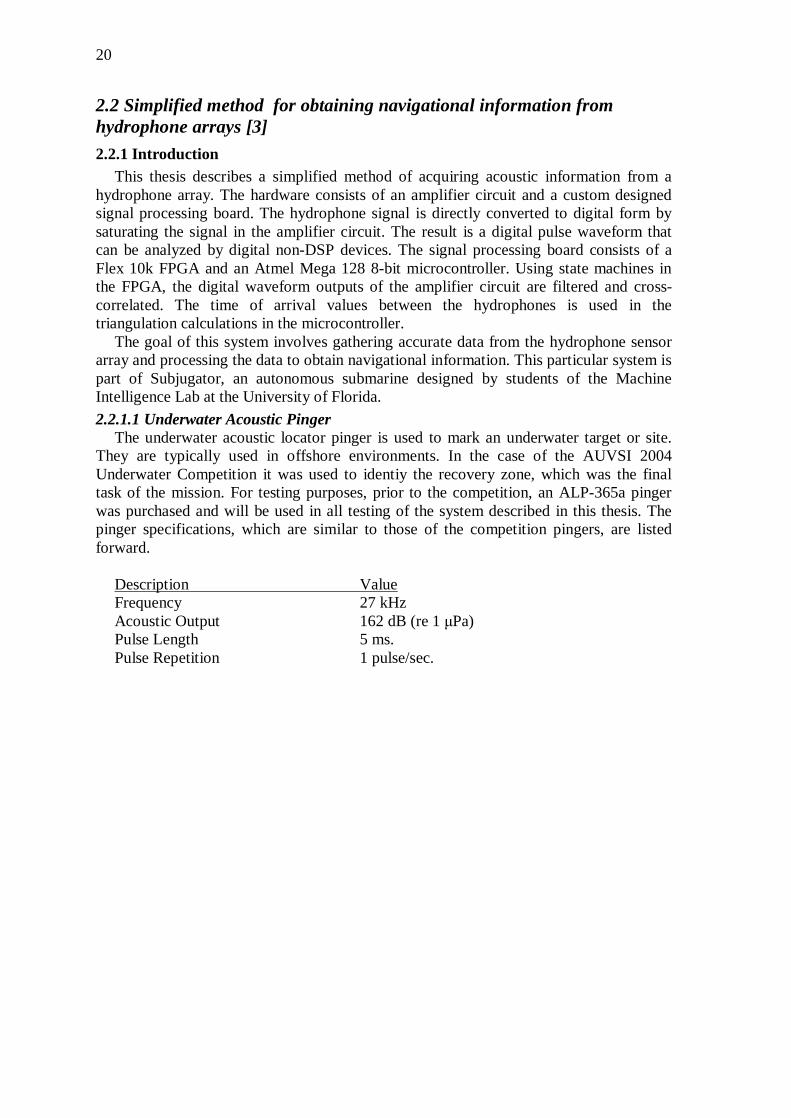
The underwater acoustic locator pinger is used to mark an underwater target or site. They are typically used in offshore environments. In the case of the AUVSI 2004 Underwater Competition it was used to identiy the recovery zone, which was the final task of the mission. For testing purposes, prior to the competition, an ALP-365a pinger was purchased and will be used in all testing of the system described in this thesis. The pinger specifications, which are similar to those of the competition pingers, are listed forward.
Description Value Frequency 27 kHz Acoustic Output 162 dB (re 1 μPa) Pulse Length 5 ms. Pulse Repetition 1 pulse/sec.
21
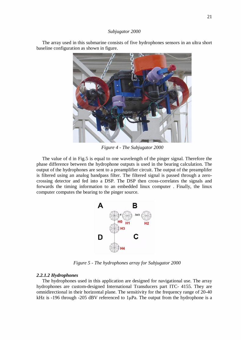
Subjugator 2000
The array used in this submarine consists of five hydrophones sensors in an ultra short baseline configuration as shown in figure.
The value of d in Fig.5 is equal to one wavelength of the pinger signal. Therefore the
phase difference between the hydrophone outputs is used in the bearing calculation. The output of the hydrophones are sent to a preamplifier circuit. The output of the preamplifer is filtered using an analog bandpass filter. The filtered signal is passed through a zero-crossing detector and fed into a DSP. The DSP then cross-correlates the signals and forwards the timing information to an embedded linux computer . Finally, the linux computer computes the bearing to the pinger source.
Figure 5 - The hydrophones array for Subjugator 2000 2.2.1.2 Hydrophones
The hydrophones used in this application are designed for navigational use. The array hydrophones are custom-designed International Transducers part ITC- 4155. They are omnidirectional in their horizontal plane. The sensitivity for the frequency range of 20-40 kHz is -196 through -205 dBV referenced to 1μPa. The output from the hydrophone is a
Figure 4 - The Subjugator 2000
22
differential sinusoidal signal corresponding to the acoustic signal in the water. The hydrophones will be used in a short baseline configuration.
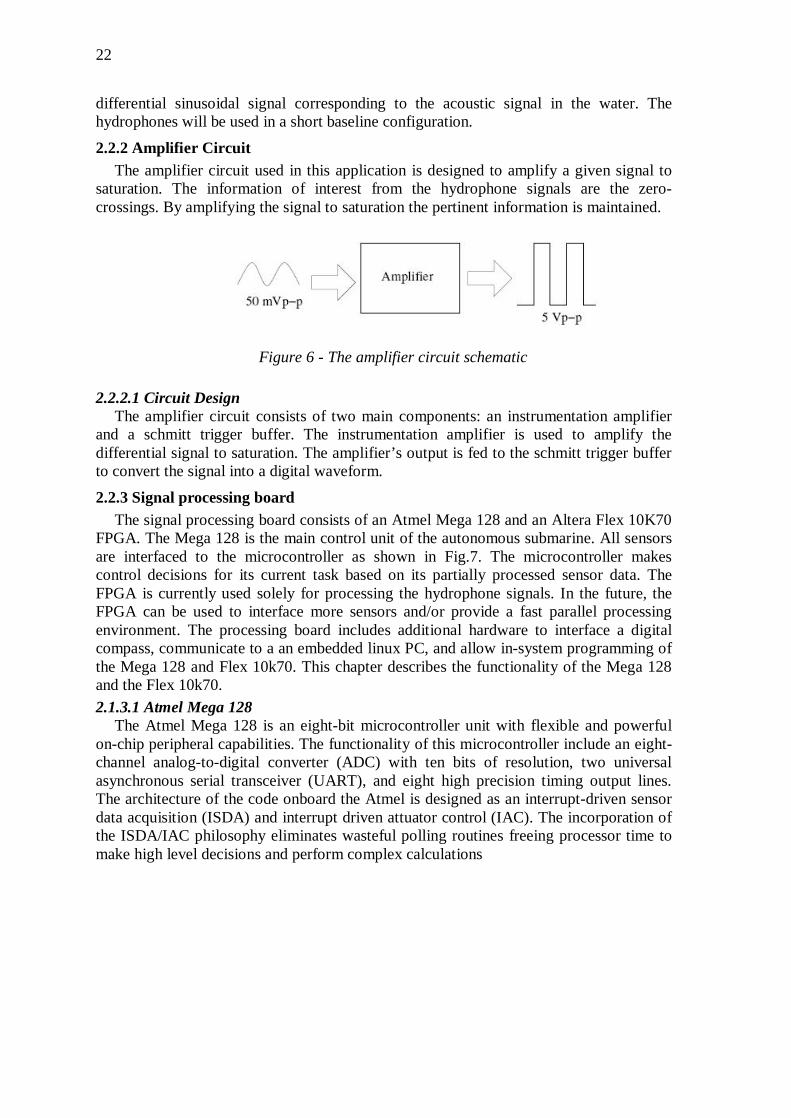
2.2.2 Amplifier Circuit The amplifier circuit used in this application is designed to amplify a given signal to
saturation. The information of interest from the hydrophone signals are the zero-crossings. By amplifying the signal to saturation the pertinent information is maintained.
Figure 6 - The amplifier circuit schematic
2.2.2.1 Circuit Design
The amplifier circuit consists of two main components: an instrumentation amplifier and a schmitt trigger buffer. The instrumentation amplifier is used to amplify the differential signal to saturation. The amplifier’s output is fed to the schmitt trigger buffer to convert the signal into a digital waveform.
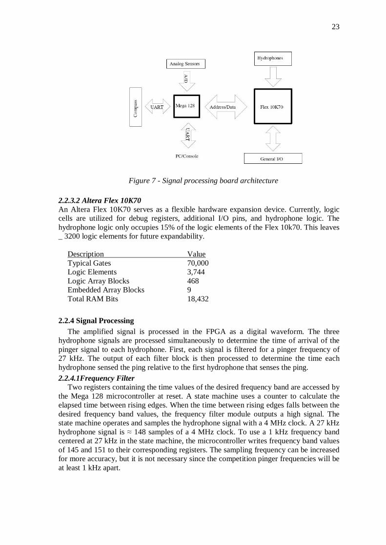
2.2.3 Signal processing board The signal processing board consists of an Atmel Mega 128 and an Altera Flex 10K70
FPGA. The Mega 128 is the main control unit of the autonomous submarine. All sensors are interfaced to the microcontroller as shown in Fig.7. The microcontroller makes control decisions for its current task based on its partially processed sensor data. The FPGA is currently used solely for processing the hydrophone signals. In the future, the FPGA can be used to interface more sensors and/or provide a fast parallel processing environment. The processing board includes additional hardware to interface a digital compass, communicate to a an embedded linux PC, and allow in-system programming of the Mega 128 and Flex 10k70. This chapter describes the functionality of the Mega 128 and the Flex 10k70. 2.1.3.1 Atmel Mega 128
The Atmel Mega 128 is an eight-bit microcontroller unit with flexible and powerful on-chip peripheral capabilities. The functionality of this microcontroller include an eight-channel analog-to-digital converter (ADC) with ten bits of resolution, two universal asynchronous serial transceiver (UART), and eight high precision timing output lines. The architecture of the code onboard the Atmel is designed as an interrupt-driven sensor data acquisition (ISDA) and interrupt driven attuator control (IAC). The incorporation of the ISDA/IAC philosophy eliminates wasteful polling routines freeing processor time to make high level decisions and perform complex calculations
23
Figure 7 - Signal processing board architecture
2.2.3.2 Altera Flex 10K70 An Altera Flex 10K70 serves as a flexible hardware expansion device. Currently, logic cells are utilized for debug registers, additional I/O pins, and hydrophone logic. The hydrophone logic only occupies 15% of the logic elements of the Flex 10k70. This leaves _ 3200 logic elements for future expandability.
Description Value Typical Gates 70,000 Logic Elements 3,744 Logic Array Blocks 468 Embedded Array Blocks 9 Total RAM Bits 18,432
2.2.4 Signal Processing The amplified signal is processed in the FPGA as a digital waveform. The three
hydrophone signals are processed simultaneously to determine the time of arrival of the pinger signal to each hydrophone. First, each signal is filtered for a pinger frequency of 27 kHz. The output of each filter block is then processed to determine the time each hydrophone sensed the ping relative to the first hydrophone that senses the ping. 2.2.4.1Frequency Filter
Two registers containing the time values of the desired frequency band are accessed by the Mega 128 microcontroller at reset. A state machine uses a counter to calculate the elapsed time between rising edges. When the time between rising edges falls between the desired frequency band values, the frequency filter module outputs a high signal. The state machine operates and samples the hydrophone signal with a 4 MHz clock. A 27 kHz hydrophone signal is ≈ 148 samples of a 4 MHz clock. To use a 1 kHz frequency band centered at 27 kHz in the state machine, the microcontroller writes frequency band values of 145 and 151 to their corresponding registers. The sampling frequency can be increased for more accuracy, but it is not necessary since the competition pinger frequencies will be at least 1 kHz apart.
24
2.2.5 Results and Conclusions The system described in the previous chapters was integrated and tested in a 2’ x 5’ x
1.5’ container of water where the results were quite good. Based on these results, the system described in this thesis is affected by noise. Creating
a reliable acoustic based positioning system, requires accurate signal filtering. The passive hydrophone sensors used in this system are sensitive to most frequencies of noise. With proper analog or digital filtering, the sensors can be used with better results. The system described in this thesis can be made more reliable may building more complex filtering entities in the FPGA. The FPGA can parallel process all the filtering of the signals and cross-correlate at high speeds. However, the development time for using the FPGA will take longer than using a Digital Signal Processor. The best approach would likely involve developing a tunable analog filter that feeds into an FPGA or DSP to cross-correlate the signals.
2.3 Development and Testing of an Acoustic Positioning System – Description and Signal Processing [4] 2.3.1 General Description
This work presents an USBL Acoustic Positioning System developed for an underwater vehicle. The position estimation is based on time-of-arrival (TOA) estimation of acoustic signals traded between a transponder and a transducer array placed on the vehicle. Modulated Barker-coded signals are used to achieve low ambiguity. Real-time DSP is implemented in a Programmable Logic Device. The TOA estimator uses a time-domain matched filter with quantized coefficients. The signal design is based on the characteristics of the employed acoustic transducers and system requirements. Numerical simulations and FPGA realization tests have shown the viability of implementing the proposed TOA estimator.
An Acoustic Positioning System (APS) estimates relative positions using acoustic waves. For underwater vehicle navigation, an APS can consist of an embedded module and a transponder placed at a reference location. The vehicle estimates its position sending an interrogation pulse to the transponder and measuring the TOAs of the reply signal. The reply is received by an array of transducers. The direction- of-arrival (DOA) is estimated computing the delays of the TOA measured for the acoustic receivers of the array.
In the case of an Ultrashort Baseline (USBL) APS (with an array baseline shorter than 1 meter), very small phase differences of the received signals must be measured. In order to obtain TOA estimations of high precision, coded waveforms and signal processing techniques are used.
This work describes an USBL-APS that is being developed for guiding an autonomous underwater vehicle (AUV) in missions of retrieval of off-shore equipments from the seafloor. The transponder is placed at the target to be retrieved. The APS is designed for short range operation (about 100 m), but it must estimate the position with increasing precision as it approaches the target, reaching 50 mm at a distance of 1 m. In this way, the AUV can autonomously connect a rescue tool to the target.
25
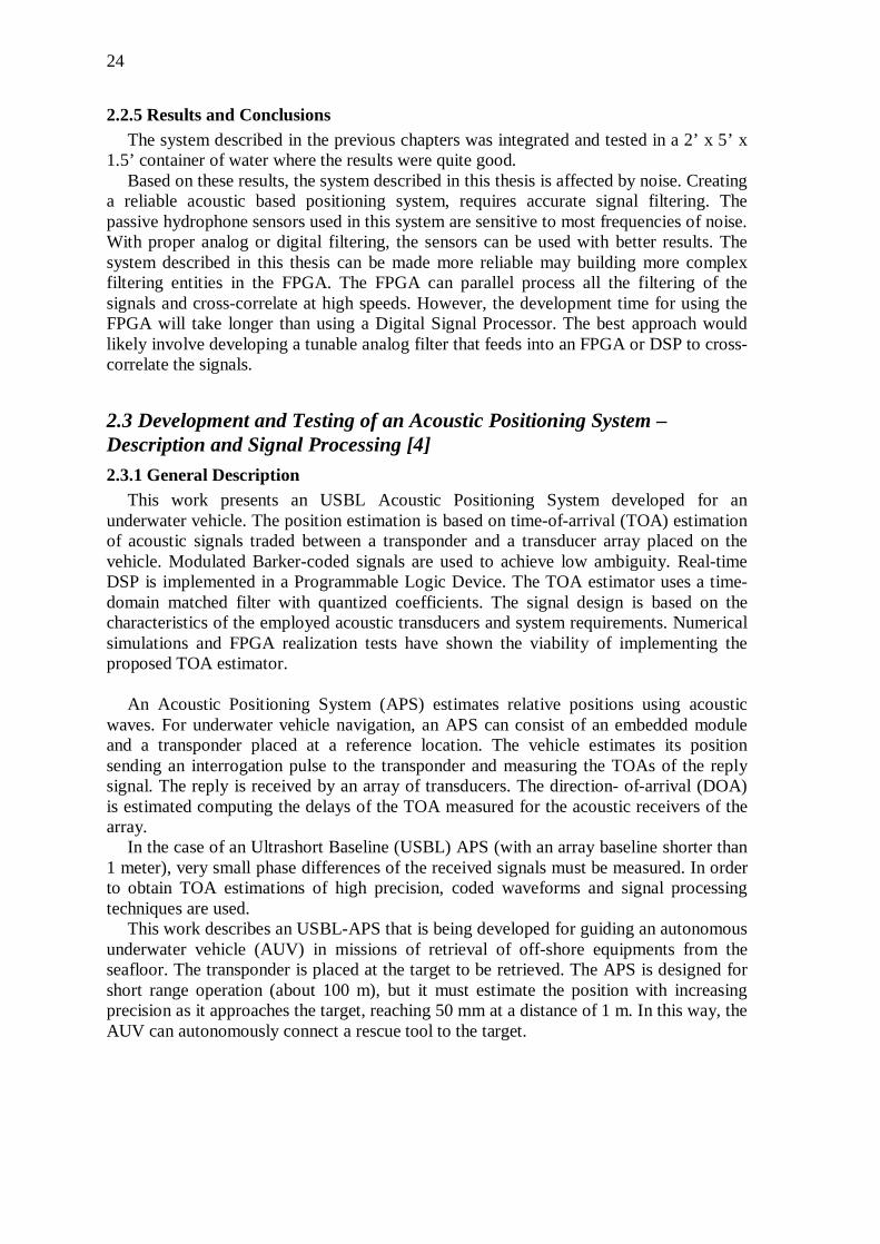
Figure 8 - The USBL positioning system Recently, with the use of fast Digital Signal Processors, the application of complex
waveforms and signal processing allows the development of real-time high accuracy APSs . Further, with the development of commercial high density Field Programmable Gate Arrays (FPGA), reconfigurable and fully parallel signal processing is possible. FPGAs has been used for acoustic signal processing and digital communications systems.
This work proposes a configurable APS digital processing unit that performs real-time signal processing using a FPGA. Considerations about signal design for our specific application are presented. Finally, the TOA estimation performance and the system viability are evaluated.
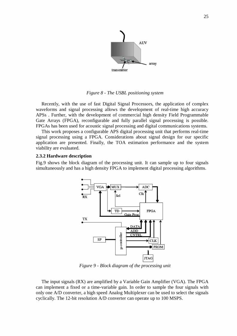
2.3.2 Hardware description Fig.9 shows the block diagram of the processing unit. It can sample up to four signals simultaneously and has a high density FPGA to implement digital processing algorithms.
Figure 9 - Block diagram of the processing unit
The input signals (RX) are amplified by a Variable Gain Amplifier (VGA). The FPGA can implement a fixed or a time-variable gain. In order to sample the four signals with only one A/D converter, a high speed Analog Multiplexer can be used to select the signals cyclically. The 12-bit resolution A/D converter can operate up to 100 MSPS.
26
Signal processing, storage and other functions are performed by the FPGA. It can operate at high speed, and it has a density of about 600K logic gates. Such characteristics allow the implementation of several signal processing algorithms and logic functions. The FPGA configuration is stored in a serial PROM.
A microcontroller controls the whole processing unit. It trades data and instructions with a host computer via a serial port (SP). The microcontroller can also generate digital signals used to drive the acoustic transmitter (TX). The microcontroller uses 3 buses to interface with the FPGA: Data, Address and Control buses. The programmable clock generator (CLK) drives the ADC and the FPGA logic, and is configured by the microcontroller.
The board has also a Threshold Detector (TD) implemented by a voltage comparator. The system can use it to have a coarse TOAestimation.The TDcan be connected to one of the VGA outputs, and its output is read by the FPGA. 2.3.3 Conclusions
The proposed APS processing unit provides high programmability, flexibility and can be used in many other applications, like non-destructive testing and acoustic communications. The use of high density FPGA allows the implementation of real-time DSP algorithms.
2.4 Underwater Acoustic Source Localization Based on Passive Sonar and Intelligent Processing [5] 2.4.1 General Description The work presents a distributed measuring system designed and implemented for underwater acoustic source detection and localization. The main part of the system is a sonar unit with three hydrophones connected to a conditioning block controlled by an acquisition, control and processing unit expressed by a real-time controller, a FPGA core and a set of IO modules. The conditioned signals are acquired and processed at the real time controller level using wavelets filtering algorithms in order to extract the relative time delay information. An intelligent algorithm based on a neural network uses the time delays and the sonar structure azimuth as input values to calculate the range and bearing angle associated with the detected underwater acoustic source. 2.4.2 Acquisition, control and processing unit
The sonar unit, including the hydrophones, is connected to the three-channel hydrophone conditioning circuit, H-CC. This circuit is controlled by the ACQ-PP unit using an analog output of the AO analog output module (NI cRIO-9263) and two digital outputs of DO digital output module (NI cRIO- 9472). The hydrophones gains and offsets are controlled through signals synthesized in the real-time system and use an E2POT non-volatile digital potentiometer (Xicor X9C102).
27
Figure 10 - Hardware schematics
For signal acquisition, a four channel synchronous AI acquisition module (NI cRIO-
9215) is used: three of the analog input channels are connected to the H-CC outputs and the forth channel to an electronic compass that is a part of the sonar unit. A high speed continuous buffered algorithm is implemented on the FPGA core (NI cRIO-9103) that communicates with the real-time controller through a PCI internal bus. The graphical user interface for the system and the advanced processing and design tasks (e.g. neural network design) are assured by a laptop PC connected to the ACQ-PP through an Ethernet link. The positioning elements are provided by a GPS system (Garmin GPSMAP76) that communicates with NI cRIO-9002 real-time controller of the ACQ-PP through a RS232 link.
2.4.3 System Software The system software performs the following tasks:
a) multiple-channel analogue-to-digital conversion control through FPGA core programming,
b) hydrophone conditioning channel control, c) noise filtering based on wavelet threshold denoising technique, d) underwater sound source localization and motion tracking using an intelligent
range - bearing angle estimator based on source-hydrophones time-of-flight differences and on the orientation of the hydrophone array.
2.4.4 Acquisition and conditioning circuit control For underwater sound source localization and motion tracking the information from the three hydrophone channels is acquired using the analog input module of ACQ-PP. The acquisition rate and the data format are imposed by the programmed FPGA core. Thus, in the present case, a multichannel simultaneously acquisition for an imposed sampling rate (e.g. 44.l kS/s) is performed in order to obtain the digital samples associated with hydrophones' channels. The digital values are transferred from the FPGA to the real-time controller (NI cRIO-9002) using the PCI bus. At the real-time controller, the samples are processed according to the above processing tasks using the specific software developed in LabVIEW real-time. Referring to the conditioning circuit control, the FPGA is programmed to assure the H-CC gain control using the DO module.
28
2.5 Field Programmable Gate Array (FPGA) [6] Field-programmable gate array (FPGA) technology continues to gain momentum, and the worldwide FPGA market is expected to grow from $1.9 billion in 2005 to $2.75 billion by 2010. Since its invention by Xilinx in 1984, FPGAs have gone from being simple glue logic chips to actually replacing custom application-specific integrated circuits (ASICs) and processors for signal processing and control applications. 2.5.1 What is an FPGA?
FPGA are a special form of Programmable logic devices(PLDs) with higher densities as compared to custom ICs and capable of implementing functionality in a short period of time using computer aided design (CAD) software.
At the highest level, FPGAs are reprogrammable silicon chips. Using prebuilt logic blocks and programmable routing resources, you can configure these chips to implement custom hardware functionality without ever having to pick up a breadboard or soldering iron. You develop digital computing tasks in software and compile them down to a configuration file or bitstream that contains information on how the components should be wired together. In addition, FPGAs are completely reconfigurable and instantly take on a brand new “personality” when you recompile a different configuration of circuitry. In the past, FPGA technology was only available to engineers with a deep understanding of digital hardware design. The rise of high-level design tools, however, is changing the rules of FPGA programming, with new technologies that convert graphical block diagrams or even C code into digital hardware circuitry.
FPGA chip adoption across all industries is driven by the fact that FPGAs combine the best parts of ASICs and processor-based systems. FPGAs provide hardware-timed speed and reliability, but they do not require high volumes to justify the large upfront expense of custom ASIC design. Reprogrammable silicon also has the same flexibility of software running on a processor-based system, but it is not limited by the number of processing cores available. Unlike processors, FPGAs are truly parallel in nature so different processing operations do not have to compete for the same resources. Each independent processing task is assigned to a dedicated section of the chip, and can function autonomously without any influence from other logic blocks. As a result, the performance of one part of the application is not affected when additional processing is added.
Field Programmable Gate Arrays are two dimensional array of logic blocks and flip-flops with a electrically programmable interconnections between logic blocks.
The interconnections consist of electrically programmable switches which is why FPGA differs from Custom ICs, as Custom IC is programmed using integrated circuit fabrication technology to form metal interconnections between logic blocks.
In an FPGA logic blocks are implemented using multiple level low fanin gates, which gives it a more compact design compared to an implementation with two-level AND-OR logic. FPGA provides its user a way to configure:
1. The intersection between the logic blocks and 2. The function of each logic block.
Logic block of an FPGA can be configured in such a way that it can provide functionality as simple as that of transistor or as complex as that of a microprocessor. It can used to implement different combinations of combinational and sequential logic functions. Logic blocks of an FPGA can be implemented by any of the following:
29
1. Transistor pairs 2. combinational gates like basic NAND gates or XOR gates 3. n-input Lookup tables 4. Multiplaexers 5. Wide fanin And-OR structure
Figure 11 - Simplified version of FPGA internal architecture
Routing in FPGAs consists of wire segments of varying lengths which can be interconnected via electrically programmable switches. Density of logic block used in an FPGA depends on length and number of wire segments used for routing. Number of segments used for interconnection typically is a tradeoff between density of logic blocks used and amount of area used up for routing.
The ability to reconfigure functionality to be implemented on a chip gives a unique advantage to designer who designs his system on an FPGA It reduces the time to market and significantly reduces the cost of production.
Every FPGA chip is made up of a finite number of predefined resources with programmable interconnects to implement a reconfigurable digital circuit.
Figure 12 - the different parts of an FPGA
FPGA chip specifications include the amount of configurable logic blocks, the number
of fixed function logic blocks, such as multipliers, and size of memory resources like
30
embedded block RAM. There are many other parts to an FPGA chip, but these are typically the most important when selecting and comparing FPGAs for a particular application.
At the lowest level, configurable blocks of logic, such as slices or logic cells, are made up of two basic things: flip-flops and look-up tables (LUTs). This is important to note because the various FPGA families differ in the way flip-flops and LUTs are packaged together 2.5.2 Why do we need FPGAs?
By the early 1980’s Large scale integrated circuits (LSI) formed the back bone of most of the logic circuits in major systems. Microprocessors, bus/IO controllers, system timers etc were implemented using integrated circuit fabrication technology. Random “glue logic” or interconnects were still required to help connect the large integrated circuits in order to :
• generate global control signals (for resets etc.) • data signals from one subsystem to another sub system. • Systems typically consisted of few large scale integrated components and
large number of SSI (small scale integrated circuit) and MSI (medium scale integrated circuit) components.
Initial attempt to solve this problem led to development of Custom ICs which were to replace the large amount of interconnect. This reduced system complexity and manufacturing cost, and improved performance. However, custom ICs have their own disadvantages. They are relatively very expensive to develop, and delay introduced for product to market (time to market) because of increased design time. There are two kinds of costs involved in development of Custom ICs:
1. Cost of development and design 2. cost of manufacture ( A tradeoff usually exists between the two costs)
Therefore the custom IC approach was only viable for products with very high volume, and which were not time to market sensitive.
FPGAs were introduced as an alternative to custom ICs for implementing entire system on one chip and to provide flexibility of reprogramability to the user. Introduction of FPGAs resulted in improvement of density relative to discrete SSI/MSI components (within around 10x of custom ICs). Another advantage of FPGAs over Custom ICs is that with the help of computer aided design (CAD) tools circuits could be implemented in a short amount of time (no physical layout process, no mask making, no IC manufacturing)
Figure 13 - FPGA comparative analysis

31
2.5.3 Logic Block Logic block in an FPGA can be implemented in ways that differ in number of inputs
and outputs, amount of area consumed, complexity of logic functions that it can implement, total number of transistors that it consumes. This section will describe some important implementations of logic blocks. 2.5.3.1 Crosspoint FPGA
Consist of two types of logic blocks. One is transistor pair tiles in which transistor pairs run in parallel lines as shown in figure below:
Figure 14 - Transistor pair tiles in cross-point FPGA
second type of logic blocks are RAM logic which can be used to implement random access memory. 2.5.3.2 Plessey FPGA
Basic building block here is 2-input NAND gate which is connected to each other to implement desired function.
Figure 15 - The Plessey logic block
Both Crosspoint and Plessey are fine grain logic blocks. Fine grain logic blocks have an advantage in high percentage usage of logic blocks but they require large number of wire segments and programmable switches which occupy lot of area.
32
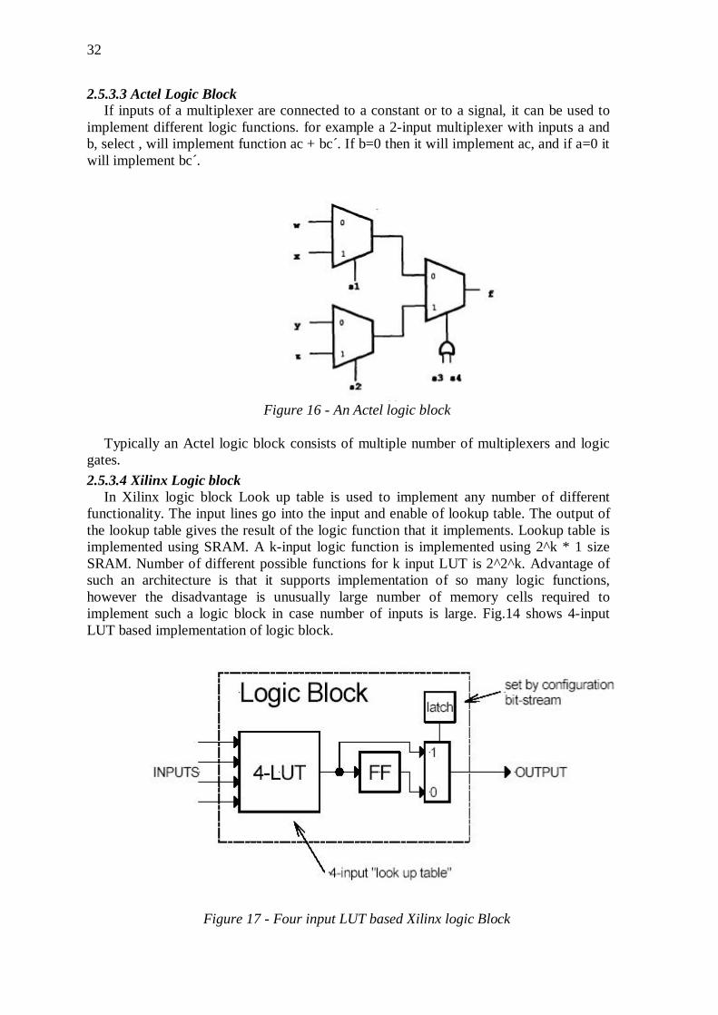
2.5.3.3 Actel Logic Block If inputs of a multiplexer are connected to a constant or to a signal, it can be used to
implement different logic functions. for example a 2-input multiplexer with inputs a and b, select , will implement function ac + bc´. If b=0 then it will implement ac, and if a=0 it will implement bc´.
Figure 16 - An Actel logic block
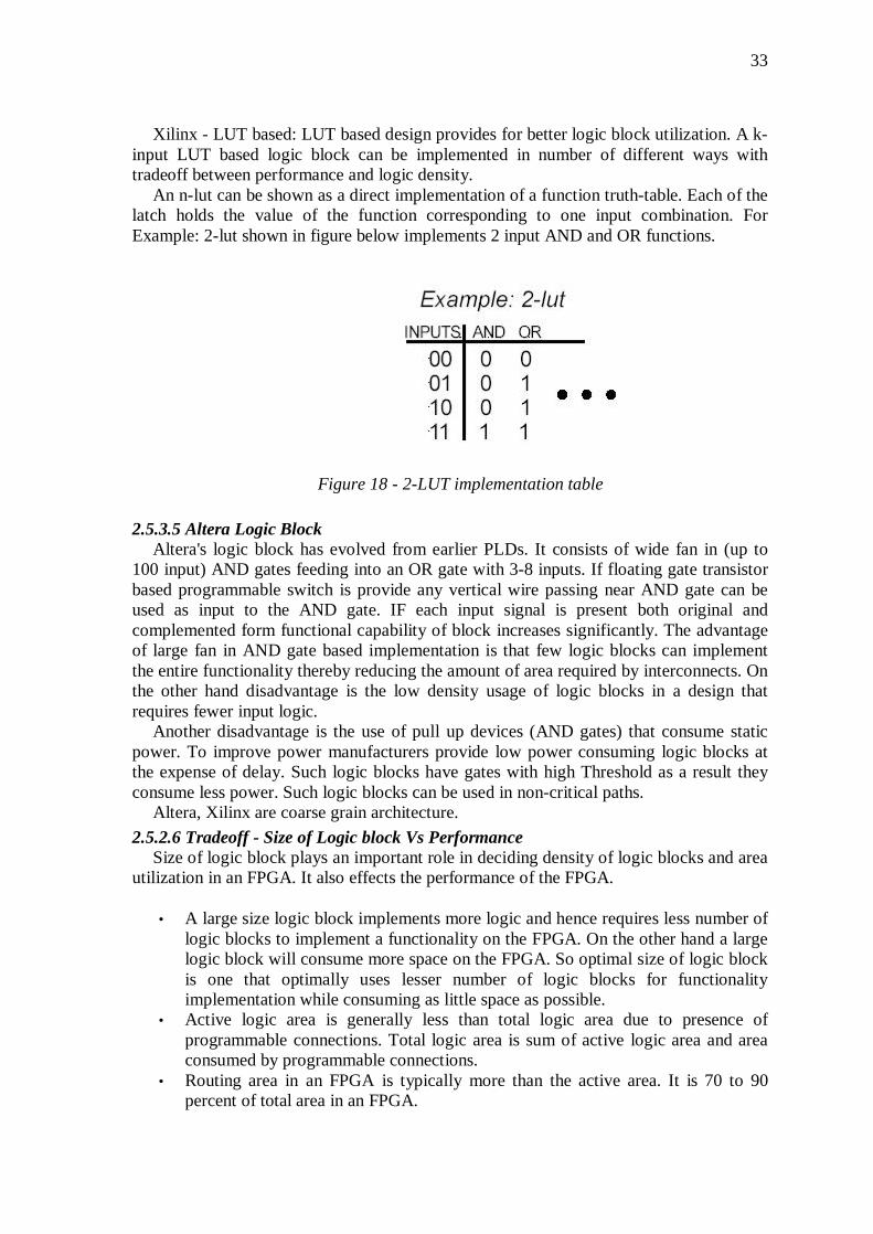
Typically an Actel logic block consists of multiple number of multiplexers and logic gates. 2.5.3.4 Xilinx Logic block
In Xilinx logic block Look up table is used to implement any number of different functionality. The input lines go into the input and enable of lookup table. The output of the lookup table gives the result of the logic function that it implements. Lookup table is implemented using SRAM. A k-input logic function is implemented using 2^k * 1 size SRAM. Number of different possible functions for k input LUT is 2^2^k. Advantage of such an architecture is that it supports implementation of so many logic functions, however the disadvantage is unusually large number of memory cells required to implement such a logic block in case number of inputs is large. Fig.14 shows 4-input LUT based implementation of logic block.
Figure 17 - Four input LUT based Xilinx logic Block
33
Xilinx - LUT based: LUT based design provides for better logic block utilization. A k-
input LUT based logic block can be implemented in number of different ways with tradeoff between performance and logic density.
An n-lut can be shown as a direct implementation of a function truth-table. Each of the latch holds the value of the function corresponding to one input combination. For Example: 2-lut shown in figure below implements 2 input AND and OR functions.
Figure 18 - 2-LUT implementation table
2.5.3.5 Altera Logic Block
Altera's logic block has evolved from earlier PLDs. It consists of wide fan in (up to 100 input) AND gates feeding into an OR gate with 3-8 inputs. If floating gate transistor based programmable switch is provide any vertical wire passing near AND gate can be used as input to the AND gate. IF each input signal is present both original and complemented form functional capability of block increases significantly. The advantage of large fan in AND gate based implementation is that few logic blocks can implement the entire functionality thereby reducing the amount of area required by interconnects. On the other hand disadvantage is the low density usage of logic blocks in a design that requires fewer input logic.
Another disadvantage is the use of pull up devices (AND gates) that consume static power. To improve power manufacturers provide low power consuming logic blocks at the expense of delay. Such logic blocks have gates with high Threshold as a result they consume less power. Such logic blocks can be used in non-critical paths.
Altera, Xilinx are coarse grain architecture. 2.5.2.6 Tradeoff - Size of Logic block Vs Performance
Size of logic block plays an important role in deciding density of logic blocks and area utilization in an FPGA. It also effects the performance of the FPGA.
• A large size logic block implements more logic and hence requires less number of logic blocks to implement a functionality on the FPGA. On the other hand a large logic block will consume more space on the FPGA. So optimal size of logic block is one that optimally uses lesser number of logic blocks for functionality implementation while consuming as little space as possible.
• Active logic area is generally less than total logic area due to presence of programmable connections. Total logic area is sum of active logic area and area consumed by programmable connections.
• Routing area in an FPGA is typically more than the active area. It is 70 to 90 percent of total area in an FPGA.
34
• In case of Lookup table based FPGA, a 4-input lookup table gives best results in terms of logic synthesized and area consumed.
• Granularity of logic block has influence on performance of an FPGA. Typically higher granularity level results in lesser delay between input and output. As the granularity of logic block increases, number of levels of logic in critical path decreases, and hence delay in critical path decreases. On the flip side with increase in granularity level average fan out increases and number of switches also increases as each block has more pins. Also the length of wires increases with increase in size of logic block.
2.5.4 FPGA Routing Techniques Routing architecture comprises of programmable switches and wires. Routing provides
connection between I/O blocks and logic blocks, and between one logic block and another logic block.
The type of routing architecture decides area consumed by routing and density of logic blocks.
Routing technique used in an FPGA largely decides the amount of area used by wire segments and programmable switches as compared to area consumed by logic blocks.
A wire segment can be described as two end points of an interconnect with no programmable switch between them. A sequence of one or more wire segments in an FPGA can be termed as a track.
Typically an FPGA has logic blocks, interconnects and Input/Output blocks. Input Output blocks lie in the periphery of logic blocks and interconnect. Wire segments connect I/O blocks to wire segments through connection blocks. Connection blocks are connected to logic blocks, depending on the design requirement one logic block is connected to another and so on. 2.5.4.1 Xilinx Routing architecture
In Xilinx routing, connections are made from logic block into the channel through a
Figure 19 - Xilinx routing architecture
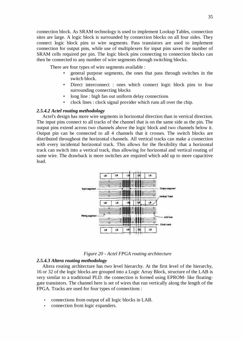
35
connection block. As SRAM technology is used to implement Lookup Tables, connection sites are large. A logic block is surrounded by connection blocks on all four sides. They connect logic block pins to wire segments. Pass transistors are used to implement connection for output pins, while use of multiplexers for input pins saves the number of SRAM cells required per pin. The logic block pins connecting to connection blocks can then be connected to any number of wire segments through switching blocks.
There are four types of wire segments available : • general purpose segments, the ones that pass through switches in the
switch block. • Direct interconnect : ones which connect logic block pins to four
surrounding connecting blocks • long line : high fan out uniform delay connections • clock lines : clock signal provider which runs all over the chip.
2.5.4.2 Actel routing methodology Actel's design has more wire segments in horizontal direction than in vertical direction.
The input pins connect to all tracks of the channel that is on the same side as the pin. The output pins extend across two channels above the logic block and two channels below it. Output pin can be connected to all 4 channels that it crosses. The switch blocks are distributed throughout the horizontal channels. All vertical tracks can make a connection with every incidental horizontal track. This allows for the flexibility that a horizontal track can switch into a vertical track, thus allowing for horizontal and vertical routing of same wire. The drawback is more switches are required which add up to more capacitive load.
Figure 20 - Actel FPGA routing architecture 2.5.4.3 Altera routing methodology
Altera routing architecture has two level hierarchy. At the first level of the hierarchy, 16 or 32 of the logic blocks are grouped into a Logic Array Block, structure of the LAB is very similar to a traditional PLD. the connection is formed using EPROM- like floating-gate transistors. The channel here is set of wires that run vertically along the length of the FPGA. Tracks are used for four types of connections :
• connections from output of all logic blocks in LAB. • connection from logic expanders.
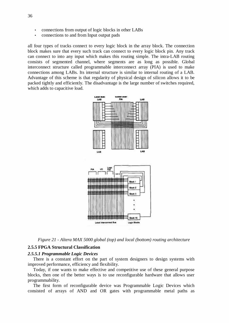
36
• connections from output of logic blocks in other LABs • connections to and from Input output pads
all four types of tracks connect to every logic block in the array block. The connection block makes sure that every such track can connect to every logic block pin. Any track can connect to into any input which makes this routing simple. The intra-LAB routing consists of segmented channel, where segments are as long as possible. Global interconnect structure called programmable interconnect array (PIA) is used to make connections among LABs. Its internal structure is similar to internal routing of a LAB. Advantage of this scheme is that regularity of physical design of silicon allows it to be packed tightly and efficiently. The disadvantage is the large number of switches required, which adds to capacitive load.
Figure 21 - Altera MAX 5000 global (top) and local (bottom) routing architecture
2.5.5 FPGA Structural Classification 2.5.5.1 Programmable Logic Devices
There is a constant effort on the part of system designers to design systems with improved performance, efficiency and flexibility.
Today, if one wants to make effective and competitive use of these general purpose blocks, then one of the better ways is to use reconfigurable hardware that allows user programmability.
The first form of reconfigurable device was Programmable Logic Devices which consisted of arrays of AND and OR gates with programmable metal paths as
37
interconnection between them. They could be programmed to into a single chip to meet specific requirements. PLDs later evolved into what was later known as FPGAs.
Basic structure of an FPGA includes logic elements, programmable interconnects and memory. Arrangement of these blocks is specific to particular manufacturer. On the basis of internal arrangement of blocks FPGAs can be divided into three classes: 2.5.5.2 Symmetrical arrays
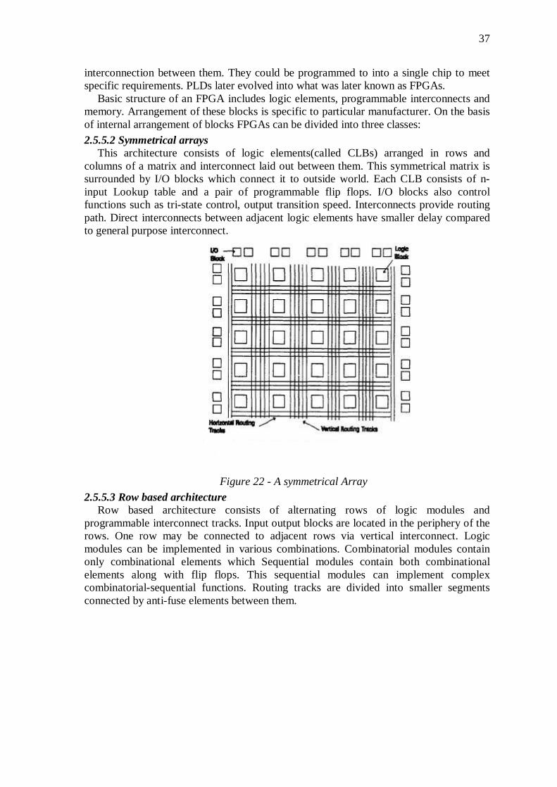
This architecture consists of logic elements(called CLBs) arranged in rows and columns of a matrix and interconnect laid out between them. This symmetrical matrix is surrounded by I/O blocks which connect it to outside world. Each CLB consists of n-input Lookup table and a pair of programmable flip flops. I/O blocks also control functions such as tri-state control, output transition speed. Interconnects provide routing path. Direct interconnects between adjacent logic elements have smaller delay compared to general purpose interconnect.
Figure 22 - A symmetrical Array
2.5.5.3 Row based architecture Row based architecture consists of alternating rows of logic modules and
programmable interconnect tracks. Input output blocks are located in the periphery of the rows. One row may be connected to adjacent rows via vertical interconnect. Logic modules can be implemented in various combinations. Combinatorial modules contain only combinational elements which Sequential modules contain both combinational elements along with flip flops. This sequential modules can implement complex combinatorial-sequential functions. Routing tracks are divided into smaller segments connected by anti-fuse elements between them.
38
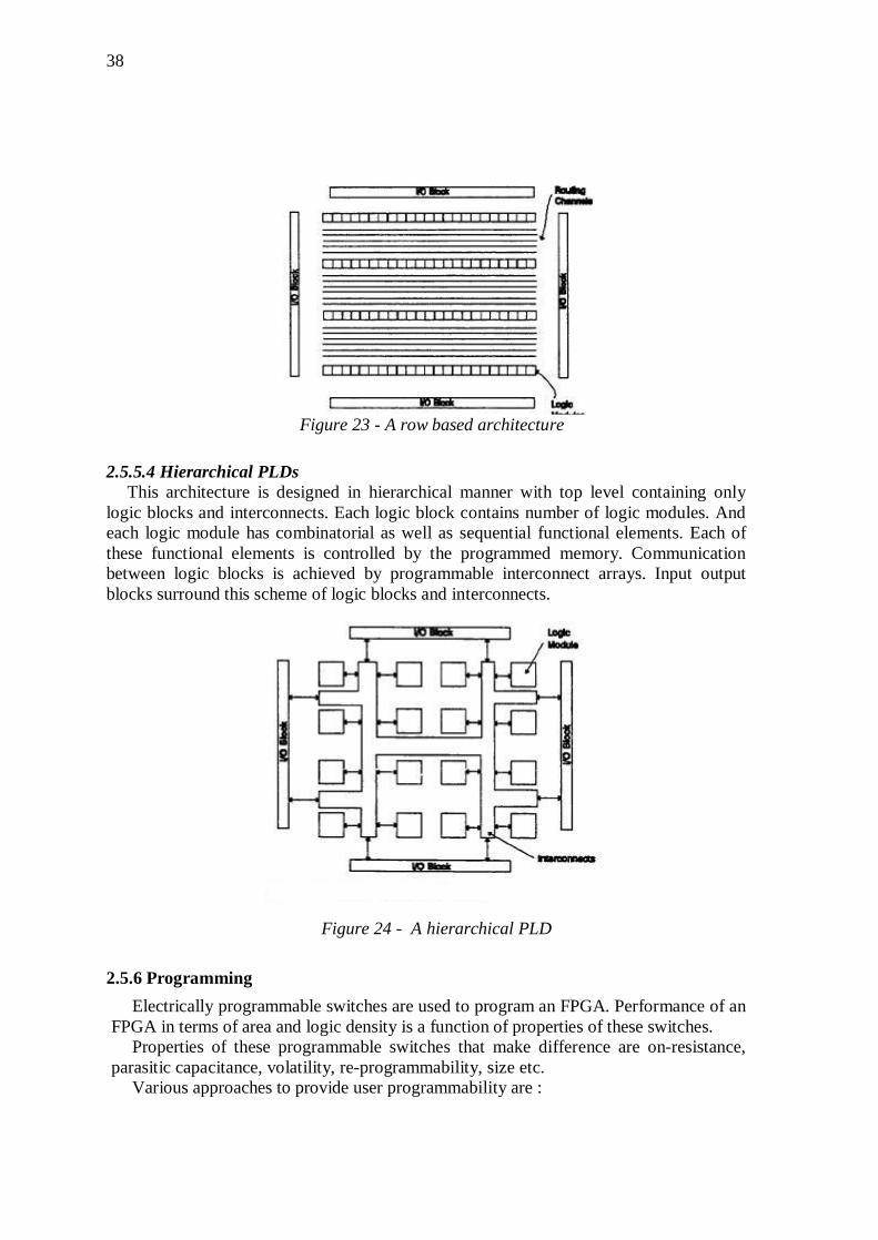
2.5.5.4 Hierarchical PLDs This architecture is designed in hierarchical manner with top level containing only
logic blocks and interconnects. Each logic block contains number of logic modules. And each logic module has combinatorial as well as sequential functional elements. Each of these functional elements is controlled by the programmed memory. Communication between logic blocks is achieved by programmable interconnect arrays. Input output blocks surround this scheme of logic blocks and interconnects.
Figure 24 - A hierarchical PLD
2.5.6 Programming Electrically programmable switches are used to program an FPGA. Performance of an
FPGA in terms of area and logic density is a function of properties of these switches. Properties of these programmable switches that make difference are on-resistance,
parasitic capacitance, volatility, re-programmability, size etc. Various approaches to provide user programmability are :
Figure 23 - A row based architecture

39
2.5.6.1 SRAM programming technology Static RAM cells are used to control pass gates or multiplexers. To use pass gate as
closed switch, boolean one is stored in SRAM cell. When zero is stored pass transistor provides high resistance between two wire segments.
Figure 25 - RAM cells used to control pass gates (a) or multiplexers (b)
To use SRAM as multiplexer, state of control values stored in SRAM decides which of
the multiplexer inputs are connected to the output as shown in figure b. Advantage of SRAM is that it provides fast re-programmability and integrated circuit
fabrication technology is required to build it. While disadvantage is the space it consumes as minimum five transistors are required to implement a memory cell. 2.5.6.2 Floating Gate Programming
Technology found in ultraviolet erasable EPROM and electrically erasable EEPROM devices is used in FPGA from Altera. The programmable switch is a transistor that permanently be disabled.
Here again the advantage is reprogrammability but there is another advantage no
Figure 26 – Floating gate programming technology

40
external permanent memory source is need to program it at power-up. However it requires three additional processing steps over CMOS technology. Other disadvantages are high static power consumption due to pull up resistor and high ON-resistance of EPROM transistor.
Electrically programmable EPROM is used by AMD and Lattice. Use of EEPROM gives advantage of easy reprogrammability. However EEPROM cell is twice as large as EPROM cell. 2.5.6.3 Antifuse programming methodology
An Antifuse is a two terminal device with an unprogrammed state providing very high resistance between its terminals. To create a low resistance link between the two terminals high voltage is applied across the terminals to blow the antifuse. Extra bit of circuitry is required to program an antifuse. Antifuse technology is used by FPGA’s from Actel, QuickLogic and Crosspoint.
Advantage of Antifuse is relatively small size and hence area reduction which is 40nnulled by area consumed by extra circuitry to program it. Another big advantage is low series resistance and low parasitic capacitance. 2.5.7 FPGA Design Flow
One of the most important advantages of FPGA based design is that users can design it using CAD tools provided by design automation companies.
Generic design flow of an FPGA includes following steps: • System Design: At this stage designer has to decide what portion of his
functionality has to be implemented on FPGA and how to integrate that functionality with rest of the system.
• I/O integration with rest of the system: Input Output streams of the FPGA are integrated with rest of the Printed Circuit Board, which allows the design of the PCB early in design process. FPGA vendors provide extra automation software solutions for I/O design process.
• Design Description: Designer describes design functionality either by using schema editors or by using one of the various Hardware Description Languages(HDLs) like Verilog or VHDL.
• Synthesis: Once design has been defined CAD tools are used to implement the design on a given FPGA. Synthesis includes generic optimization, slack optimizations, power optimizations followed by placement and routing. Implementation includes Partition, Place and route. The output of design implementation phase is bit-stream file.
• Design Verification: Bit stream file is fed to a simulator which simulates the design functionality and reports errors in desired behavior of the design. Timing tools are used to determine maximum clock frequency of the design. Now the design is loading onto the target FPGA device and testing is done in real environment.
Example
Below given circuit consists of gates and flip flops. Combinational elements of the circuit are covered by a 4-input Look up table(4-LUT). Sequential elements in the input circuit map to flip flops on the FPGA. Placement of these elements is done in such a way as to minimize wiring during routing.
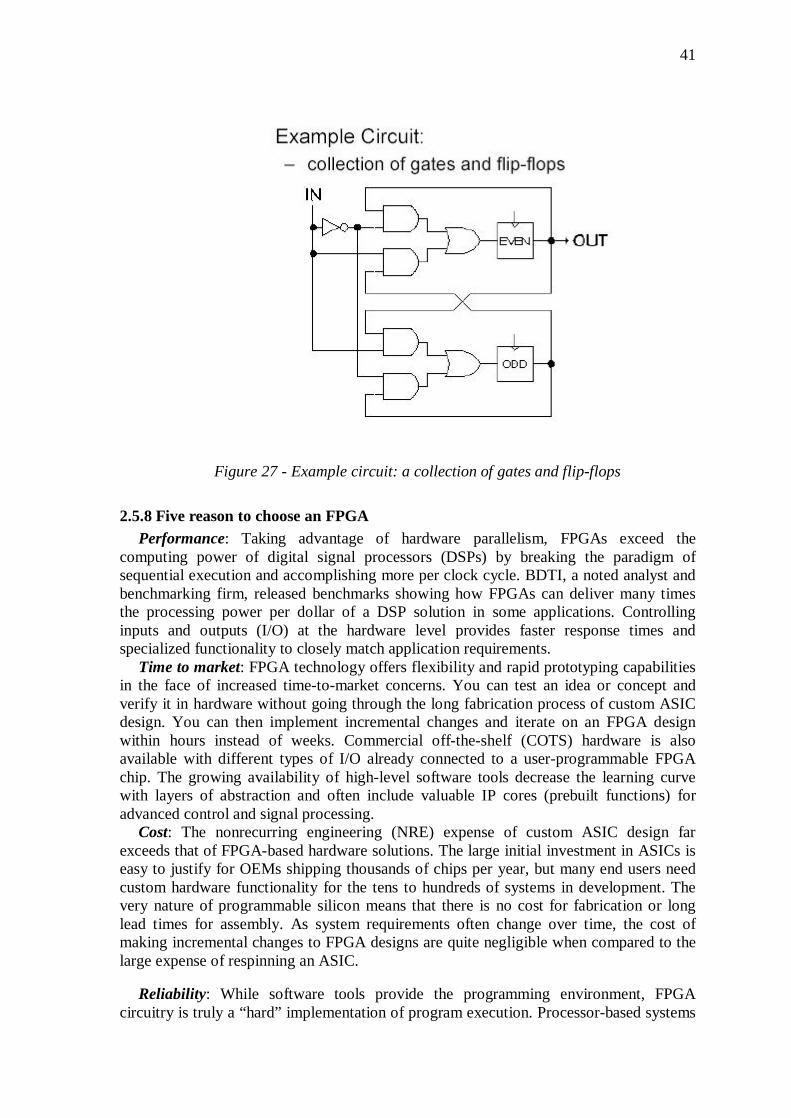
41
Figure 27 - Example circuit: a collection of gates and flip-flops
2.5.8 Five reason to choose an FPGA
Performance: Taking advantage of hardware parallelism, FPGAs exceed the computing power of digital signal processors (DSPs) by breaking the paradigm of sequential execution and accomplishing more per clock cycle. BDTI, a noted analyst and benchmarking firm, released benchmarks showing how FPGAs can deliver many times the processing power per dollar of a DSP solution in some applications. Controlling inputs and outputs (I/O) at the hardware level provides faster response times and specialized functionality to closely match application requirements.
Time to market: FPGA technology offers flexibility and rapid prototyping capabilities in the face of increased time-to-market concerns. You can test an idea or concept and verify it in hardware without going through the long fabrication process of custom ASIC design. You can then implement incremental changes and iterate on an FPGA design within hours instead of weeks. Commercial off-the-shelf (COTS) hardware is also available with different types of I/O already connected to a user-programmable FPGA chip. The growing availability of high-level software tools decrease the learning curve with layers of abstraction and often include valuable IP cores (prebuilt functions) for advanced control and signal processing.
Cost: The nonrecurring engineering (NRE) expense of custom ASIC design far exceeds that of FPGA-based hardware solutions. The large initial investment in ASICs is easy to justify for OEMs shipping thousands of chips per year, but many end users need custom hardware functionality for the tens to hundreds of systems in development. The very nature of programmable silicon means that there is no cost for fabrication or long lead times for assembly. As system requirements often change over time, the cost of making incremental changes to FPGA designs are quite negligible when compared to the large expense of respinning an ASIC.
Reliability: While software tools provide the programming environment, FPGA circuitry is truly a “hard” implementation of program execution. Processor-based systems
42
often involve several layers of abstraction to help schedule tasks and share resources among multiple processes. The driver layer controls hardware resources and the operating system manages memory and processor bandwidth. For any given processor core, only one instruction can execute at a time, and processor-based systems are continually at risk of time-critical tasks pre-empting one another. FPGAs, which do not use operating systems, minimize reliability concerns with true parallel execution and deterministic hardware dedicated to every task.
Long-term maintenance: As mentioned earlier, FPGA chips are field-upgradable and do not require the time and expense involved with ASIC redesign. Digital communication protocols, for example, have specifications that can change over time, and ASIC-based interfaces may cause maintenance and forward compatibility challenges. Being reconfigurable, FPGA chips are able to keep up with future modifications that might be necessary. As a product or system matures, you can make functional enhancements without spending time redesigning hardware or modifying the board layout.
43
3.THE HARDWARE This chapter intends to describe all the hardware used in this thesis, the core is formed
by: • An FPGA Board • An Analog to Digital Board • A Digital Acquisition Board
The hardest step in hardware was to choose an FPGA that can fit our needs. The
present market has an infinite choice of FPGA boards and the companies can practically fit the needs of everyone. An important step is to learn how to move in this entangled variety and make the best choice that can fit our application.
3.1 How to choose an FPGA board [7] Usually we could project an FPGA that fit our needs but this would imply a big
investment of money and time. This is no longer a need because there are many companies that offer board level FPGA solutions for any type of use.
Now we are going to analyze the criteria for an FPGA board selection. This criteria comes down in to 3 particular areas:
1. How complicated is my project?
• Simple (ex: machine control application with digital I/O) è Small FPGA (Altera ACEX or Cyclone)
• Complex (ex: processing image data or high speed analog data) è Large FPGA (Xilinx Virtex II or 4)
2. How fast do I need to process data?
• Slow (under 60 MHz)
è Altera Cyclone/Xilinx Spartan • Fast (from 60 to 100 MHz)
è Xilinx Virtex II or Altera Stratix • Very Fast (to 500 MHz)
è Xilinx Virtex 4
3. Special needs Need in special work condition
• Large amount of Memory • Fast memory • Conduction Cooling/ Extended Temperature • Resistant hardware
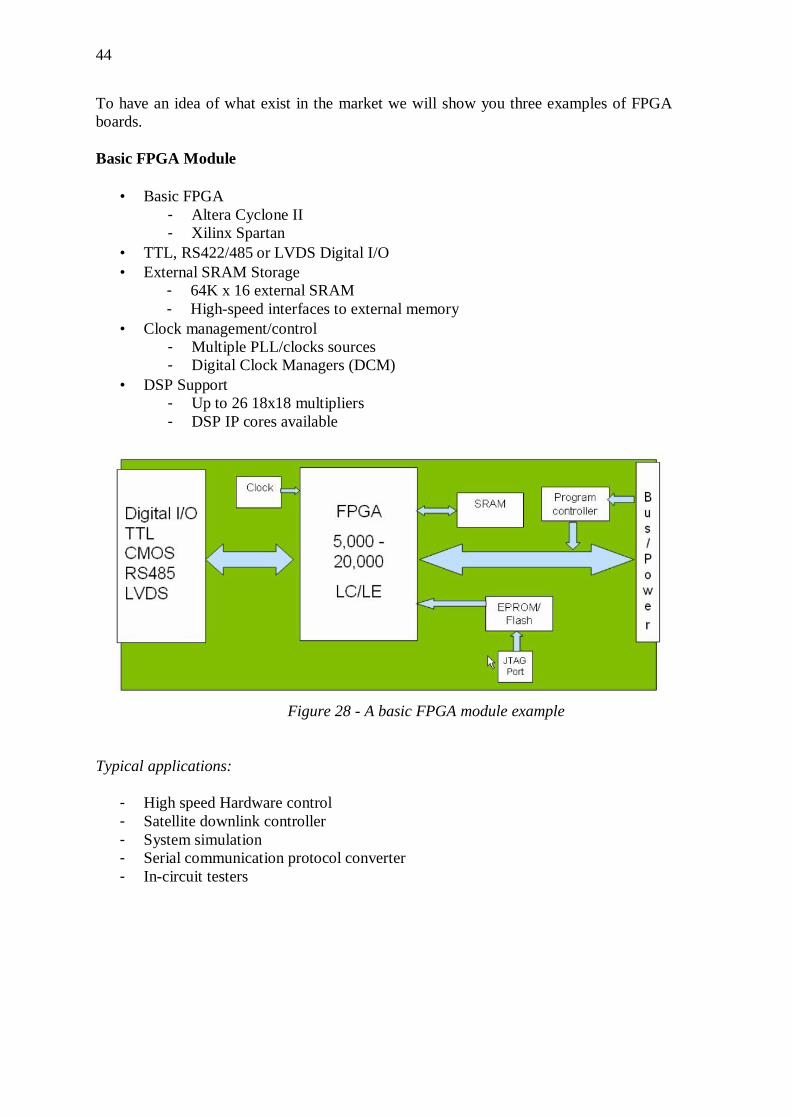
44
To have an idea of what exist in the market we will show you three examples of FPGA boards. Basic FPGA Module
• Basic FPGA - Altera Cyclone II - Xilinx Spartan
• TTL, RS422/485 or LVDS Digital I/O • External SRAM Storage
- 64K x 16 external SRAM - High-speed interfaces to external memory
• Clock management/control - Multiple PLL/clocks sources - Digital Clock Managers (DCM)
• DSP Support - Up to 26 18x18 multipliers - DSP IP cores available
Typical applications:
- High speed Hardware control - Satellite downlink controller - System simulation - Serial communication protocol converter - In-circuit testers
Figure 28 - A basic FPGA module example
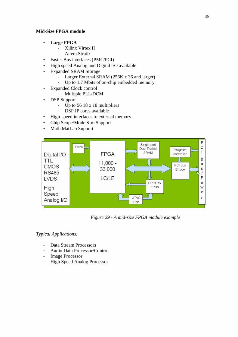
45
Mid-Size FPGA module
• Large FPGA - Xilinx Virtex II - Altera Stratix
• Faster Bus interfaces (PMC/PCI) • High speed Analog and Digital I/O available • Expanded SRAM Storage
- Larger External SRAM (256K x 36 and larger) - Up to 1.7 Mbits of on-chip embedded memory
• Expanded Clock control - Multiple PLL/DCM
• DSP Support - Up to 56 18 x 18 multipliers - DSP IP cores available
• High-speed interfaces to external memory • Chip Scope/ModelSIm Support • Math MatLab Support
Typical Applications:
- Data Stream Processors - Audio Data Processor/Control - Image Processor - High Speed Analog Processor
Figure 29 - A mid-size FPGA module example
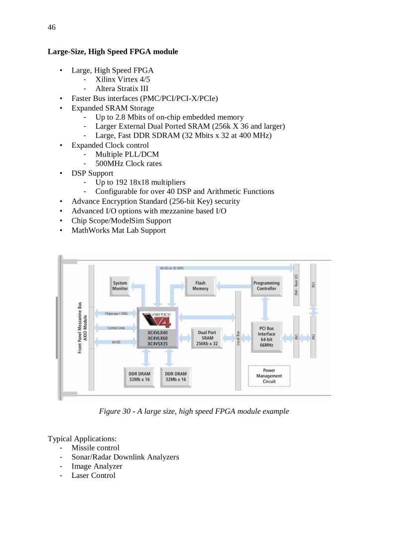
46
Large-Size, High Speed FPGA module
• Large, High Speed FPGA - Xilinx Virtex 4/5 - Altera Stratix III
• Faster Bus interfaces (PMC/PCI/PCI-X/PCIe) • Expanded SRAM Storage
- Up to 2.8 Mbits of on-chip embedded memory - Larger External Dual Ported SRAM (256k X 36 and larger) - Large, Fast DDR SDRAM (32 Mbits x 32 at 400 MHz)
• Expanded Clock control - Multiple PLL/DCM - 500MHz Clock rates
• DSP Support - Up to 192 18x18 multipliers - Configurable for over 40 DSP and Arithmetic Functions
• Advance Encryption Standard (256-bit Key) security • Advanced I/O options with mezzanine based I/O • Chip Scope/ModelSim Support • MathWorks Mat Lab Support
Typical Applications:
- Missile control - Sonar/Radar Downlink Analyzers - Image Analyzer - Laser Control
Figure 30 - A large size, high speed FPGA module example
47
Fig.31 gives a bird’s eye on various type of FPGA boards and their performance, it shows the resource specifications used to compare FPGA chips within various Xilinx families. The number of gates has traditionally been a way to compare the size of FPGA chips to ASIC technology, but it does not truly describe the number of individual components inside an FPGA. This is one of the reasons that Xilinx did not specify the number of equivalent system gates for the new Virtex-5 family. The figure below gives an idea of the tradeoff between price and performance.
Figure 32 – The trade off between cost and performance for FPGA boards
Figure 31 – General view on various FPGA boards

48
It’s really important to consider the support that the supplier offers with the board and what the final user really need. What a Module Supplier Should Offer
• Engineering Design Kit - Schematic and parts list - Example VHDL code (compiled and source)
§ Bus interface § Memory interface § I/O interface § Interrupts § DMA transfers
- Pin Definitions - Manuals
What the customer Requires • Development Tools
- Xilinx § ISE Foundation software suite § Or ISE WebPACK
- Altera § Quartus II design software
• Development Platform (Matlab etc.)
3.2 The Market Analysis After this introduction on how to choose a general FPGA board let’s focus on the real choice of our project. Here we will anticipate the constraints explained better in the next chapters. The needs of our project are:
- Make an analog to digital conversion of 4 independent signals - Have a sample time of acquisition over 1 MHz and handle this elaboration - Have the capabilities to realize an algorithm to calculate the delays
between the 4 signals - Find an FPGA small enough that can enter inside the cylindrical
enclosures - Stay under a budget of 1000$ - Have a software support to develop the project - 12 bit A/D
A 12 bit A/D has enough accuracy to analyze our kind of signals. In front of the previous research we need a medium-low level FPGA board because
generally the FPGAs have a faster clock then we need, our elaboration seems not to be so complicated to need a lot amount of RAM or logic cells.
A long research is made, analyzing a lot of solutions proposed by the major companies. Xilinx and Altera are the major companies building FPGA cores and boards and they purpose multifunction boards to fit the majority of cases. There are also a lot of

49
other companies that try to fit more particular needs using Xilinx and Altera’s FPGA cores
There, will be shown some companies’ examples chosen from a selection of the best
interesting FPGA boards
3.2.1 Pentek - Model 6256 Cost: more than 2000$ Features Summary:
A/D: 2/4 channels ; Sample Freq. Max: 105 MHz ; 14 bit Fpga: 2 Virtex II pro 2-XC2VP50 53136 logic cells SDRAM: extern 2x64 MB 32 bit Flash 2x16MB 16 bit Clock: external input, LVDS clock/sync bus for multi- module synchronization Software: Gate-flow design kit (visual programming kit) ; IP Cores
General Information The Model 6256 is a complete two or four channel data acquisition and signal
processing subsystem implemented as a VIM-2 module. Up to two 6256 modules can be attached to any of the Pentek VIM baseboards for a total of eight channels. The 6256 is ideal for digitizing signal bandwidths up to 45 MHz with subsequent real-time digital signal processing and data buffering of those signals using two on-board Xilinx Virtex-II Pro FPGAs. A/D Converters
The front end accepts two full scale analog HF or IF inputs at +4 dBm full scale into 50 ohms on front panel SMA connectors.
Each input is transformer coupled, and digitized by a 14-bit 105 MHz A/D converter (Analog Devices AD6645).
The A/D converters deliver parallel digital output into a Virtex-II Pro FPGA for further processing. An optional second-slot mezzanine provides two additional A/D converters. These deliver output to a second Virtex-II Pro for a 4-channel system.
The A/D clock can be driven from an internal crystal oscillator or from an external sample clock supplied through a front panel
SMA connector. A front panel LVDS clock and sync bus supports synchronization across multiple modules. For large, multichannel systems, up to 80 modules can be synchronized using the Model 9190 Clock and Sync Generator. Virtex-II Pro FPGAs
The Model 6256 is equipped with a pair of FPGA devices from the Xilinx Virtex-II Pro family. Models XC2VP20 or XC2VP50
Figure 33 – Pentek 6256
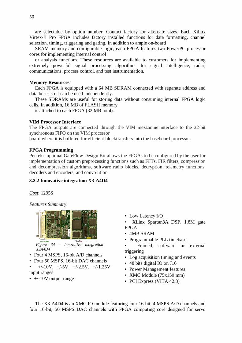
50
are selectable by option number. Contact factory for alternate sizes. Each Xilinx Virtex-II Pro FPGA includes factory installed functions for data formatting, channel selection, timing, triggering and gating. In addition to ample on-board
SRAM memory and configurable logic, each FPGA features two PowerPC processor cores for implementing internal control
or analysis functions. These resources are available to customers for implementing extremely powerful signal processing algorithms for signal intelligence, radar, communications, process control, and test instrumentation. Memory Resources
Each FPGA is equipped with a 64 MB SDRAM connected with separate address and data buses so it can be used independently.
These SDRAMs are useful for storing data without consuming internal FPGA logic cells. In addition, 16 MB of FLASH memory
is attached to each FPGA (32 MB total). VIM Processor Interface The FPGA outputs are connected through the VIM mezzanine interface to the 32-bit synchronous FIFO on the VIM processor board where it is buffered for efficient blocktransfers into the baseboard processor. FPGA Programming Pentek's optional GateFlow Design Kit allows the FPGAs to be configured by the user for implementation of custom preprocessing functions such as FFTs, FIR filters, compression and decompression algorithms, software radio blocks, decryption, telemetry functions, decoders and encoders, and convolution.
3.2.2 Innovative integration X3-A4D4 Cost: 1295$ Features Summary:
• Four 4 MSPS, 16-bit A/D channels • Four 50 MSPS, 16-bit DAC channels • +/-10V, +/-5V, +/-2.5V, +/-1.25V input ranges • +/-10V output range
• Low Latency I/O • Xilinx Spartan3A DSP, 1.8M gate FPGA • 4MB SRAM • Programmable PLL timebase • Framed, software or external triggering • Log acquisition timing and events • 48 bits digital IO on J16 • Power Management features • XMC Module (75x150 mm) • PCI Express (VITA 42.3)
The X3-A4D4 is an XMC IO module featuring four 16-bit, 4 MSPS A/D channels and four 16-bit, 50 MSPS DAC channels with FPGA computing core designed for servo
Figure 34 – Innovative integration X3A4D4
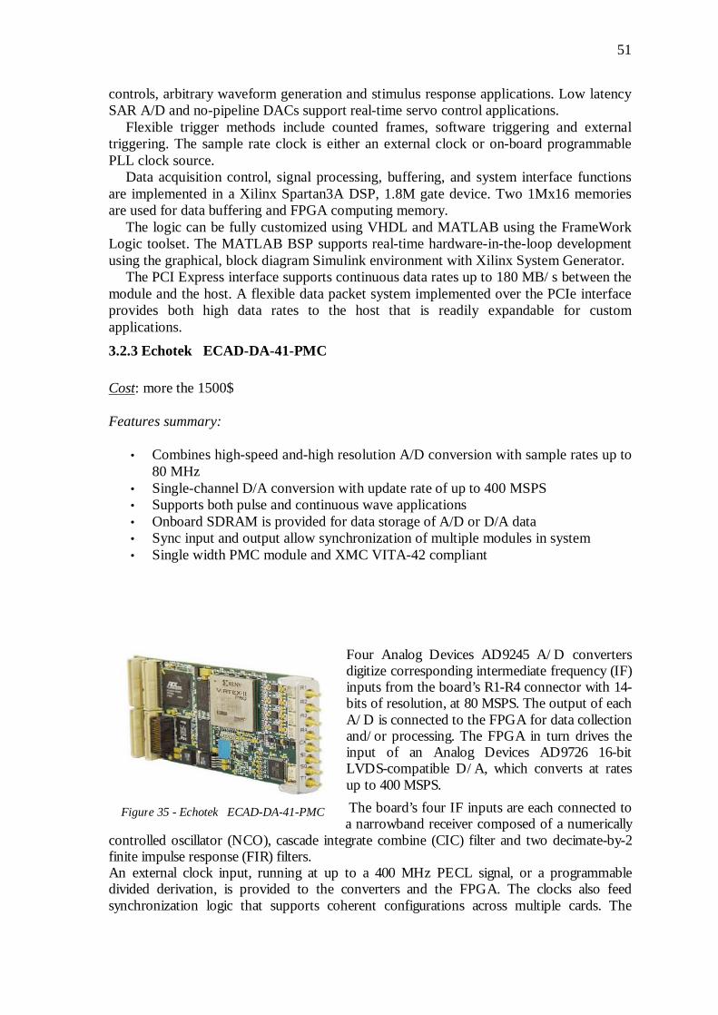
51
controls, arbitrary waveform generation and stimulus response applications. Low latency SAR A/D and no-pipeline DACs support real-time servo control applications.
Flexible trigger methods include counted frames, software triggering and external triggering. The sample rate clock is either an external clock or on-board programmable PLL clock source.
Data acquisition control, signal processing, buffering, and system interface functions are implemented in a Xilinx Spartan3A DSP, 1.8M gate device. Two 1Mx16 memories are used for data buffering and FPGA computing memory.
The logic can be fully customized using VHDL and MATLAB using the FrameWork Logic toolset. The MATLAB BSP supports real-time hardware-in-the-loop development using the graphical, block diagram Simulink environment with Xilinx System Generator.
The PCI Express interface supports continuous data rates up to 180 MB/ s between the module and the host. A flexible data packet system implemented over the PCIe interface provides both high data rates to the host that is readily expandable for custom applications. 3.2.3 Echotek ECAD-DA-41-PMC Cost: more the 1500$ Features summary:
• Combines high-speed and-high resolution A/D conversion with sample rates up to 80 MHz
• Single-channel D/A conversion with update rate of up to 400 MSPS • Supports both pulse and continuous wave applications • Onboard SDRAM is provided for data storage of A/D or D/A data • Sync input and output allow synchronization of multiple modules in system • Single width PMC module and XMC VITA-42 compliant
Four Analog Devices AD9245 A/D converters digitize corresponding intermediate frequency (IF) inputs from the board’s R1-R4 connector with 14-bits of resolution, at 80 MSPS. The output of each A/D is connected to the FPGA for data collection and/or processing. The FPGA in turn drives the input of an Analog Devices AD9726 16-bit LVDS-compatible D/A, which converts at rates up to 400 MSPS. The board’s four IF inputs are each connected to a narrowband receiver composed of a numerically
controlled oscillator (NCO), cascade integrate combine (CIC) filter and two decimate-by-2 finite impulse response (FIR) filters. An external clock input, running at up to a 400 MHz PECL signal, or a programmable divided derivation, is provided to the converters and the FPGA. The clocks also feed synchronization logic that supports coherent configurations across multiple cards. The
Figure 35 - Echotek ECAD-DA-41-PMC

52
board’s PCI r2.2 compliant interface transfers data at 64-bit/66 MHz, 64-bit/33 MHz, 32-bit/66 MHz, or 32-bit/33 MHz rates in both PCI master and slave modes, plus chained DMA bursting for reduced CPU overhead. Forty-two user-definable I/O pins connect the card’s P4 connector with the FPGA, and a high-speed serial interface connects a VITA-42 compliant XMC connector to the FPGA for industry-standard ECMA-342 RapidIO®.
3.2.4 Bittware TETRA-PMC+ Cost: 3995$ Features Summary:
• High-performance wideband A/Ds
- Four channels, 14-bit A/D (AD6645) - Up to 105 MHz per channel
• Altera Cyclone II reconfigurable FPGA
- A/D control and data distribution - Configurable pre-processing of highspeed A/D data
• 32-bit, 66 MHz PCI interface via Cyclone II FPGA
• Four external link ports
- Configurable for TS201-based boards - Available via PMC+ interface - Up to 210 MBytes/s per channel
• Internal/external clock and triggering • Complete software support • Cyclone II development and customization support
Product Overview
BittWare’s Tetra-PMC+ (TRPM) board is a high-speed analog input board that provides data capture for four 14-bit A/D channels running at up to 105 MHz. The board streams the data directly to an Altera Cyclone II FPGA,
which provides A/D control, data distribution, and front-end processing capabilities. A 32-bit, 66 MHz PCI interface and
four TigerSHARC link ports make the captured data available to the host board.
High-Speed A/D Interface
The high-speed A/D interface features four 14-bit A/D conversion channels, each sampled at up to 105 MHz. Using high-quality 14-bit A/D converters from Analog Devices, the analog interface provides input bandwidth up to 150 MHz with DC coupled
Figura 36 - Bittware TETRA-PMC+
53
inputs. For clocking options, the board features an internal clock and an external clock and trigger; the clock is user-configurable to the onboard clock or external clock.
Altera Cyclone II Reconfigurable FPGA
The Cyclone II reconfigurable FPGA (Altera) provides A/D control and data distribution for the Tetra- PMC+ and is available for configurable preprocessing of high speed A/D data, such as digital filtering, decimation, and digital down conversion. To interface the A/D data to the host, the Cyclone II contains a link port interface providing direct access to the ADSP-TS201 DSPs located on the base board.
PMC+ I/O Interface
When attached to one of BittWare’s PMC+ base boards, it supports BittWare’s PMC+ extensions, which include four link ports directly connected to the Cyclone II FPGA. The PMC+ link ports are configurable for BittWare’s T2 (ADSP-TS201S) based boards and are an ideal way to move high-speed data directly to the DSPs.
Available Development Tools
BittWare offers complete software development tools that allow designers to easily develop application code and integrate the Tetra-PMC+ into their systems. For user-configured pre-processing, Altera also provides a complete suite of development tools for the Cyclone II.
3.3 A real choice The boards analyzed, give an idea of what solutions are on the market. Corresponding
to our project they have really good performance and they can fit our needs. The main problem of these boards is the high price that overcome our budget. It was not possible to find an FPGA board with also the A/D conversion of 4 channel.
We decide to direct to other solutions probably removing some specific. 3.3.1 New solutions 3.3.1.1 Multiplexer and FPGA
The first solution was to choose one FPGA board with only 2 analog input and to build a simple multiplexing board to send 4 analog signals in 2 channels.
In telecommunication and Signal processing, an analog time division multiplexer may take several samples of separate analogue signals and combine them into one pulse amplitude modulated (PAM) wide band analogue signal.
There are two techniques to use this transmission’s system. Time division multiplexing (TDM): is a type of digital or (rarely) analog multiplexing
in which two or more signals or bit streams are transferred apparently simultaneously as sub-channels in one communication channel, but are physically taking turns on the channel. The time domain is divided into several recurrent timeslots of fixed length, one for each sub-channel. A sample byte or data block of sub-channel 1 is transmitted during timeslot 1, sub-channel 2 during timeslot 2, etc. One TDM frame consists of one timeslot per sub-channel. After the last sub-channel the cycle starts all over again with a new frame, starting with the second sample, byte or data block from sub-channel 1, etc.
Frequency division multiplexing (FDM): more channels are combined in one single transmission’s channel. The signals are divided by frequency. There are always unused frequency bands between the channels known as “guard bands”. Those bands reduce the “bleedover” effect between the adjacent channels. This condition is known as “crosstalk”.

54
To set up this system we decided to choice a 2 A/D FPGA and to build a simple 4 to 2 multiplexing board. A good low cost FPGA chosen for this target was: Cyclone II EP2C70 DSP development board Cost: 995$ Features summary:
• Cyclone II EP2C70 DSP development board o Cyclone II EP2C70F672C6 device
• Analog I/O o Two 14-bit analog-to-digital (A/D) converter
channels with 125-million samples per second (MSPS)
o Two 14-bit, 165-MSPS, 70 dB digital-to-analog (D/A) converters
o One 24-bit RGB VGA adapter with a DB-15 connector
o One Audio CODEC with input, output, and amplified output • External I/O
o Mictor connector for hardware and software debugging o 3.3-V/5-V tolerant Altera expansion/prototype headers o One Texas Instruments Evaluation Module (TI-EVM) expansion
connector to connect to the Spectrum Digital 'DSP Starter Kit (DSK) for the TMS320C6416', Revision E
• Memory subsystem o 256-Mbyte DDR2 SDRAM DIMM o 1-Mbyte synchronous SRAM (SSRAM) o Two EPCS64 devices
• MATLAB/Simulink evaluation software • DSP Builder development tool • Quartus II Education Kit • Evaluation IP cores • System reference designs and labs
o DSP Builder filtering design o DSP Builder/SOPC Builder image processing reference design o Fast Fourier transform (FFT) coprocessor reference design for Texas
Instruments' TMS320C6416 DSK o Nios® II reference designs o DDR2 DIMM reference design
• Cables and accessories • USB-BlasterTM download cable • Power supply • International power cords
Video input daughtercard features:
• Two composite video input channels using the TI TVP5146 ADC
Figure 37 - Cyclone II EP2C70 DSP development board
55
• Support for NTSC/PAL • 10-bit BT.656 output • Compatibility with expansion connector, standard on most Altera development
kits and included with the Video Development Kit, Cyclone II Edition
This board must be linked to another board built around 2 multiplexer like this:
AD8170: 2 Channel Buffered, 250MHz, 10 ns Multiplexer w/Amplifier • Fully Buffered Inputs and
Outputs • Fast Channel Switching: 10 ns • Internal Current Feedback Output
Amplifier High Output Drive: 50 mA Flexible Gain Setting via External Resistor(s)
• High Speed 250 MHz Bandwidth, G = +2 1000 V/µs Slew Rate Fast Settling Time of 15 ns to 0.1%
• Low Power: < 10 mA
• Excellent Video Specifications (RL = 150 O, G = +2) Gain Flatness of 0.1 dB Beyond 80 MHz 0.02% Differential Gain Error 0.05° Differential Phase Error
• Low Crosstalk of -78 dB @ 5 MHz
• High Disable Isolation of -88 dB @ 5 MHz
• High Shutdown Isolation of -92 dB @ 5 MHz
• Low Cost
This solution could be a nice one but doesn’t respect some constraints like the size of the board and the price is quite high. Furthermore, with this kind of choice we foresee that the complexity of the project should raise, expending lot of memory and logic resources lowering the overall performances
3.3.1.2 A/D conversion and FPGA Then second solution was to choose a low cost FPGA, without any A/D conversion and analog input, assisted by a dedicated A/D board. This is a really simple solution that imply only a special attention to the linking methods of the two boards. This solution appear to be the best one:
- No need to build a board - Lot of solutions on the market - Low costs
We moved in this direction and we chose the two boards.
3.3.2 The FPGA board choice: ALTERA/TERASIC DE2 Development and Education Board
We avoid the size constraint. To respect it, it’s a must refer to high band boards as the one presented before.
We choose a development and education board to have all the support necessary to move the first steps in the FPGA world.
The purpose of the Altera DE2 Development and Education board is to provide the ideal vehicle for learning about digital logic, computer organization, and FPGAs.
The DE2 board features a state-of-the-art Cyclone® II 2C35 FPGA in a 672-pin package. All important components on the board are connected to pins of this chip,
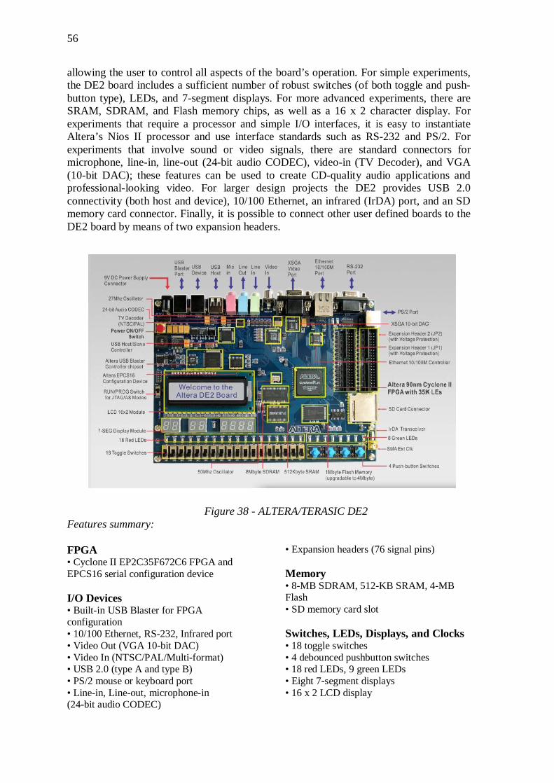
56
allowing the user to control all aspects of the board’s operation. For simple experiments, the DE2 board includes a sufficient number of robust switches (of both toggle and push-button type), LEDs, and 7-segment displays. For more advanced experiments, there are SRAM, SDRAM, and Flash memory chips, as well as a 16 x 2 character display. For experiments that require a processor and simple I/O interfaces, it is easy to instantiate Altera’s Nios II processor and use interface standards such as RS-232 and PS/2. For experiments that involve sound or video signals, there are standard connectors for microphone, line-in, line-out (24-bit audio CODEC), video-in (TV Decoder), and VGA (10-bit DAC); these features can be used to create CD-quality audio applications and professional-looking video. For larger design projects the DE2 provides USB 2.0 connectivity (both host and device), 10/100 Ethernet, an infrared (IrDA) port, and an SD memory card connector. Finally, it is possible to connect other user defined boards to the DE2 board by means of two expansion headers.
Features summary: FPGA • Cyclone II EP2C35F672C6 FPGA and EPCS16 serial configuration device I/O Devices • Built-in USB Blaster for FPGA configuration • 10/100 Ethernet, RS-232, Infrared port • Video Out (VGA 10-bit DAC) • Video In (NTSC/PAL/Multi-format) • USB 2.0 (type A and type B) • PS/2 mouse or keyboard port • Line-in, Line-out, microphone-in (24-bit audio CODEC)
• Expansion headers (76 signal pins) Memory • 8-MB SDRAM, 512-KB SRAM, 4-MB Flash • SD memory card slot Switches, LEDs, Displays, and Clocks • 18 toggle switches • 4 debounced pushbutton switches • 18 red LEDs, 9 green LEDs • Eight 7-segment displays • 16 x 2 LCD display
Figure 38 - ALTERA/TERASIC DE2

57
• 27-MHz and 50-MHz oscillators, external SMA clock input
3.3.4 The A/D board choice: MAX1127 Evaluation Kit from MAXIM We choose an analog to digital converter, the MAX1126/MAX1127 quad 12-bit
analog-to-digital converter, mounted on an evaluation board. This board fit our needs and is linkable to the FPGA board by the parallel ports.
Features summary:
• Sample Rate Up to 65Msps (MAX1127) • Low-Voltage and Power Operation • Optional On-Board Clock-Shaping Circuitry • Four analog input • Serial SLVS/LVDS Outputs • On-Board LVPECL Differential Output Drivers • On-Board Deserializer • LVDS Test Mode
The MAX1127 evaluation kit (EV kit) is a fully assembled and tested circuit board
that contains all the components necessary to evaluate the performance of the MAX1126/MAX1127 quad 12-bit analog-to-digital converter (ADC). The MAX1126/MAX1127 accept 4 differential analog input signals. The EV kit generates these signals from user-provided single-ended input sources. The digital outputs produced by the ADC can be easily sampled with a user-provided, high-speed logic analyzer or data-acquisition system. The EV kit also features an on-board deserializer to ease integration with standard logic analysis systems. The EV kit operates from 1.8V and 3.3V power supplies (1.5V for the optional FPGA) and includes circuitry that generates a clock signal from an AC signal provided by the user.
Input Signal
Although the MAX1127 accepts differential analog input signals, the EV kit only requires a single-ended analog input signal, with an amplitude of less than 1.4VP-P
Figure 39 - MAX1127
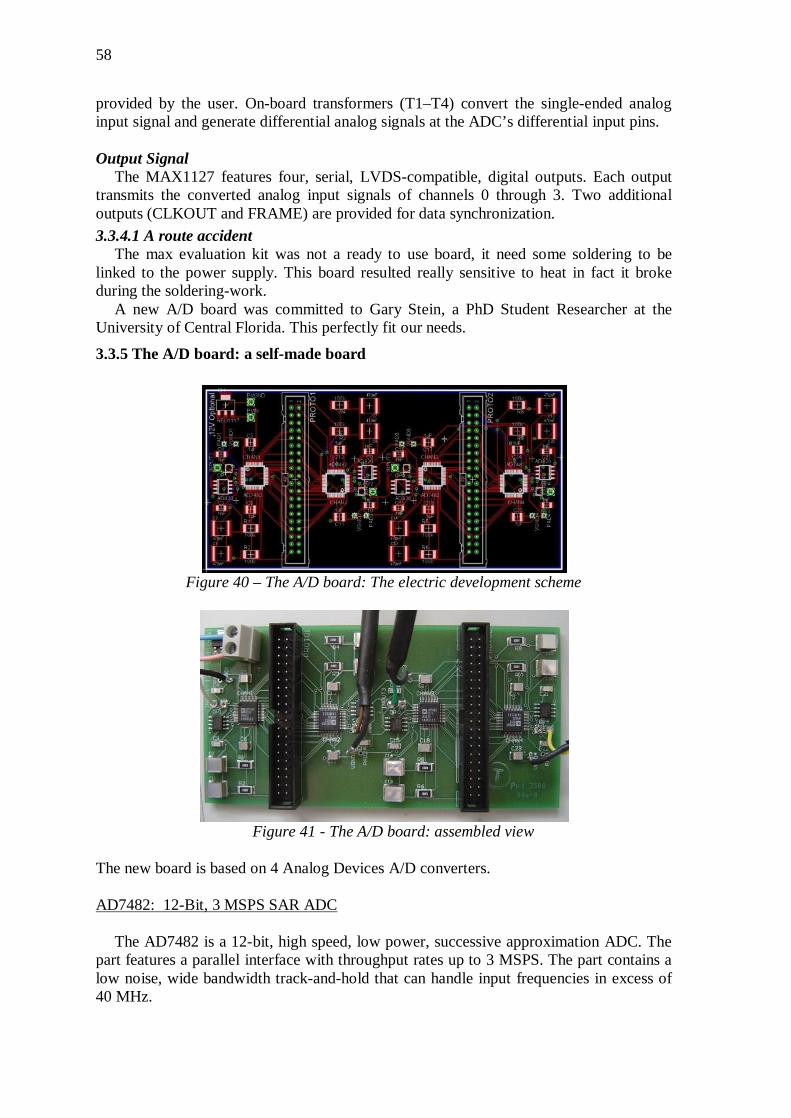
58
provided by the user. On-board transformers (T1–T4) convert the single-ended analog input signal and generate differential analog signals at the ADC’s differential input pins.
Output Signal
The MAX1127 features four, serial, LVDS-compatible, digital outputs. Each output transmits the converted analog input signals of channels 0 through 3. Two additional outputs (CLKOUT and FRAME) are provided for data synchronization. 3.3.4.1 A route accident
The max evaluation kit was not a ready to use board, it need some soldering to be linked to the power supply. This board resulted really sensitive to heat in fact it broke during the soldering-work.
A new A/D board was committed to Gary Stein, a PhD Student Researcher at the University of Central Florida. This perfectly fit our needs.
3.3.5 The A/D board: a self-made board
Figure 40 – The A/D board: The electric development scheme
Figure 41 - The A/D board: assembled view
The new board is based on 4 Analog Devices A/D converters. AD7482: 12-Bit, 3 MSPS SAR ADC
The AD7482 is a 12-bit, high speed, low power, successive approximation ADC. The part features a parallel interface with throughput rates up to 3 MSPS. The part contains a low noise, wide bandwidth track-and-hold that can handle input frequencies in excess of 40 MHz.
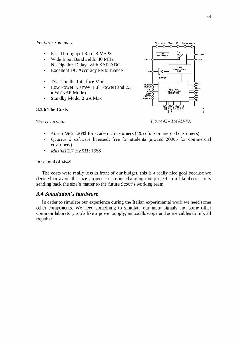
59
Features summary:
• Fast Throughput Rate: 3 MSPS • Wide Input Bandwidth: 40 MHz • No Pipeline Delays with SAR ADC • Excellent DC Accuracy Performance
• Two Parallel Interface Modes • Low Power: 90 mW (Full Power) and 2.5
mW (NAP Mode) • Standby Mode: 2 µA Max
3.3.6 The Costs The costs were:
• Altera DE2 : 269$ for academic customers (495$ for commercial customers) • Quartus 2 software licensed: free for students (around 2000$ for commercial
customers) • Maxim1127 EVKIT: 195$
for a total of 464$.
The costs were really less in front of our budget, this is a really nice goal because we decided to avoid the size project constraint changing our project in a likelihood study sending back the size’s matter to the future Scout’s working team.
3.4 Simulation’s hardware In order to simulate our experience during the Italian experimental work we need some
other components. We need something to simulate our input signals and some other common laboratory tools like a power supply, an oscilloscope and some cables to link all together.
Figure 42 – The AD7482
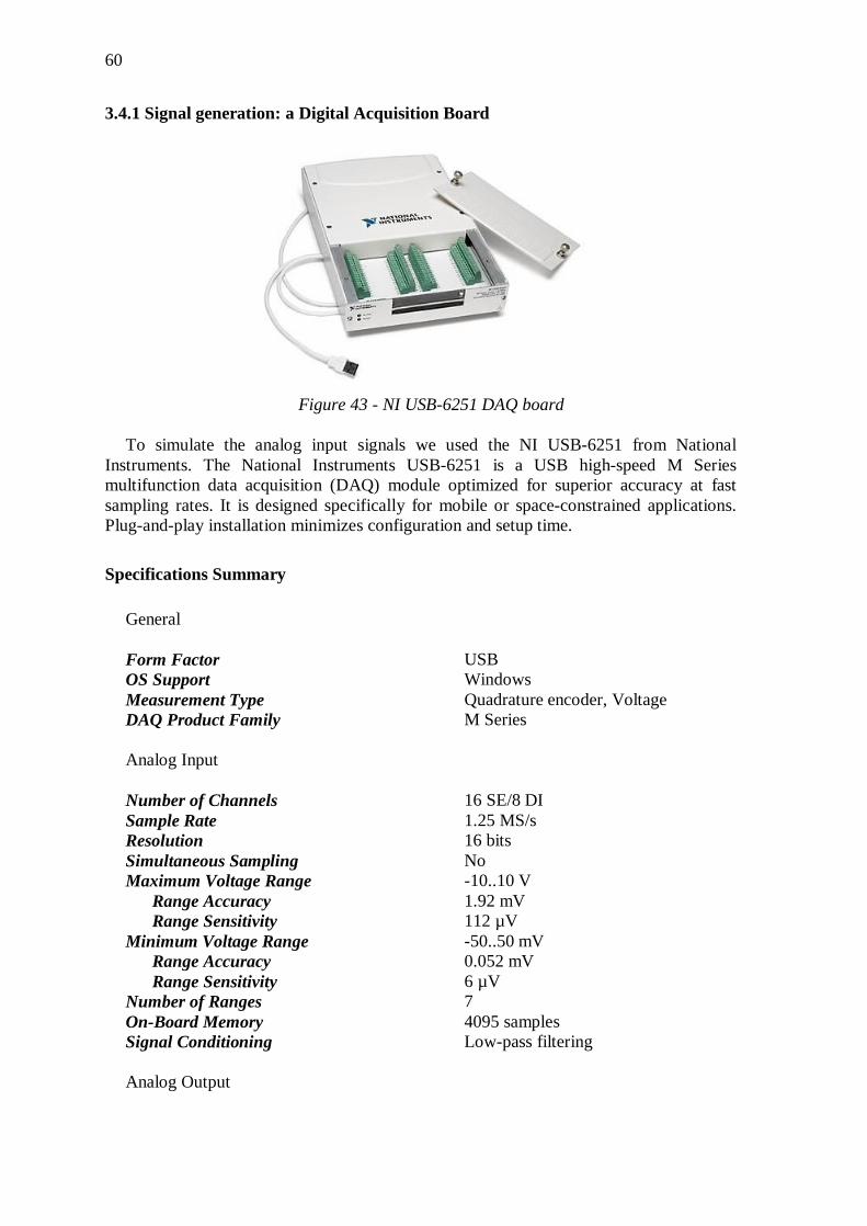
60
3.4.1 Signal generation: a Digital Acquisition Board
Figure 43 - NI USB-6251 DAQ board
To simulate the analog input signals we used the NI USB-6251 from National
Instruments. The National Instruments USB-6251 is a USB high-speed M Series multifunction data acquisition (DAQ) module optimized for superior accuracy at fast sampling rates. It is designed specifically for mobile or space-constrained applications. Plug-and-play installation minimizes configuration and setup time.
Specifications Summary
General
Form Factor USB OS Support Windows Measurement Type Quadrature encoder, Voltage DAQ Product Family M Series
Analog Input
Number of Channels 16 SE/8 DI Sample Rate 1.25 MS/s Resolution 16 bits Simultaneous Sampling No Maximum Voltage Range -10..10 V Range Accuracy 1.92 mV Range Sensitivity 112 µV Minimum Voltage Range -50..50 mV Range Accuracy 0.052 mV Range Sensitivity 6 µV Number of Ranges 7 On-Board Memory 4095 samples Signal Conditioning Low-pass filtering
Analog Output
61
General
Number of Channels 2 Update Rate 2.86 MS/s Resolution 16 bits Maximum Voltage Range -10..10 V Range Accuracy 2.08 mV Minimum Voltage Range -5..5 V Range Accuracy 1.045 mV Current Drive (Channel/Total) 5 mA/10 mA
Digital I/O
Number of Channels 24 DIO Timing Hardware, Software Maximum Clock Rate 1 MHz Logic Levels TTL Maximum Input Range 0..5 V Maximum Output Range 0..5 V Input Current Flow Sinking, Sourcing Programmable Input Filters Yes Output Current Flow Sinking, Sourcing Current Drive (Channel/Total) 24 mA/448 mA Watchdog Timer No Supports Programmable Power-Up States? Yes Supports Handshaking I/O? No Supports Pattern I/O? Yes Counter/Timers
Number of Counter/Timers 2 Resolution 32 bits Maximum Source Frequency 80 MHz Logic Levels TTL Maximum Range 0..5 V Timebase Stability 50 ppm GPS Synchronization No Pulse Generation Yes Buffered Operations Yes Debouncing/Glitch Removal Yes
Timing/Triggering/Synchronization
Synchronization Bus (RTSI) No Triggering Analog, Digital Physical Specifications Length 18.8 cm, 26.67 cm Width 17.09 cm Height 4.45 cm I/O Connector 68-pin male SCSI-II type, screw term.
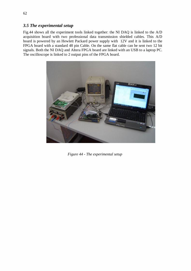
62
3.5 The experimental setup Fig.44 shows all the experiment tools linked together: the NI DAQ is linked to the A/D acquisition board with two professional data transmission shielded cables. This A/D board is powered by an Hewlett Packard power supply with 12V and it is linked to the FPGA board with a standard 48 pin Cable. On the same flat cable can be sent two 12 bit signals. Both the NI DAQ and Altera FPGA board are linked with an USB to a laptop PC. The oscilloscope is linked to 2 output pins of the FPGA board.
Figure 44 - The experimental setup

63
4. BORN AND DEVELOPMENT OF THE ALGORITHM In this chapter we develop the core of our work. We will start talking about the
competition and the AUV the UCF team worked on, focusing on their underwater acoustic acquisition. We will describe the idea that is the basis of the implemented system. This idea justifies our future DSP algorithm.
Then our simulation’s algorithm for the FPGA is presented.
4.1 The 2007 AUVSI competition [8] The idea of this thesis starts from an Universal Central Florida’s Project aimed to
participate to the AUVSI & ONR’s 10th Annual International Autonomous Underwater Vehicle Competition of 2007. The UCF team developed an AUV, the SCOUT.
The goal of the 2007 mission is for the vehicle to autonomously navigate an obstacle course, as shown in Fig.45.
The tasks of the mission include:
• Passing through a validation gate. • Docking with buoys and releasing them from their mooring • Locating a pipeline • and follow it. (Along the pipeline will be two bins, one that will be covered by
a Buoy. The Vehicle can drop markers in either bin).
Figure 45 – The competition obstacle course
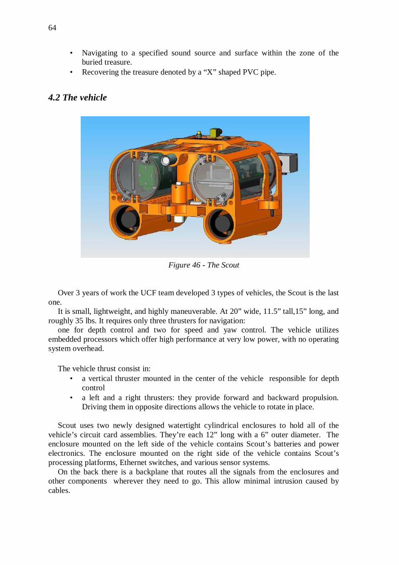
64
• Navigating to a specified sound source and surface within the zone of the buried treasure.
• Recovering the treasure denoted by a “X” shaped PVC pipe.
4.2 The vehicle
Over 3 years of work the UCF team developed 3 types of vehicles, the Scout is the last one.
It is small, lightweight, and highly maneuverable. At 20” wide, 11.5” tall,15” long, and roughly 35 lbs. It requires only three thrusters for navigation:
one for depth control and two for speed and yaw control. The vehicle utilizes embedded processors which offer high performance at very low power, with no operating system overhead.
The vehicle thrust consist in: • a vertical thruster mounted in the center of the vehicle responsible for depth
control • a left and a right thrusters: they provide forward and backward propulsion.
Driving them in opposite directions allows the vehicle to rotate in place. Scout uses two newly designed watertight cylindrical enclosures to hold all of the
vehicle’s circuit card assemblies. They’re each 12” long with a 6” outer diameter. The enclosure mounted on the left side of the vehicle contains Scout’s batteries and power electronics. The enclosure mounted on the right side of the vehicle contains Scout’s processing platforms, Ethernet switches, and various sensor systems.
On the back there is a backplane that routes all the signals from the enclosures and other components wherever they need to go. This allow minimal intrusion caused by cables.
Figure 46 - The Scout
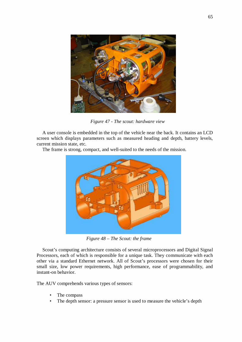
65
Figure 47 - The scout: hardware view
A user console is embedded in the top of the vehicle near the back. It contains an LCD
screen which displays parameters such as measured heading and depth, battery levels, current mission state, etc.
The frame is strong, compact, and well-suited to the needs of the mission.
Scout’s computing architecture consists of several microprocessors and Digital Signal
Processors, each of which is responsible for a unique task. They communicate with each other via a standard Ethernet network. All of Scout’s processors were chosen for their small size, low power requirements, high performance, ease of programmability, and instant-on behavior. The AUV comprehends various types of sensors:
• The compass • The depth sensor: a pressure sensor is used to measure the vehicle’s depth
Figure 48 – The Scout: the frame
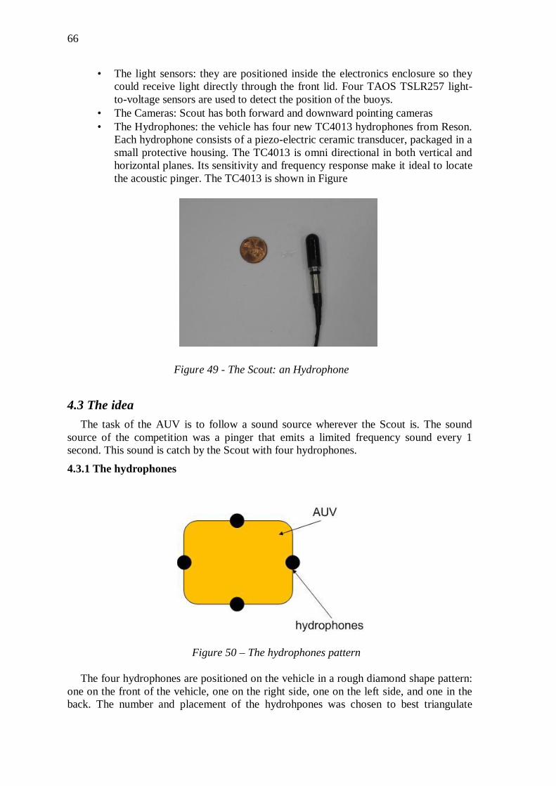
66
• The light sensors: they are positioned inside the electronics enclosure so they could receive light directly through the front lid. Four TAOS TSLR257 light-to-voltage sensors are used to detect the position of the buoys.
• The Cameras: Scout has both forward and downward pointing cameras • The Hydrophones: the vehicle has four new TC4013 hydrophones from Reson.
Each hydrophone consists of a piezo-electric ceramic transducer, packaged in a small protective housing. The TC4013 is omni directional in both vertical and horizontal planes. Its sensitivity and frequency response make it ideal to locate the acoustic pinger. The TC4013 is shown in Figure
4.3 The idea The task of the AUV is to follow a sound source wherever the Scout is. The sound
source of the competition was a pinger that emits a limited frequency sound every 1 second. This sound is catch by the Scout with four hydrophones.
4.3.1 The hydrophones
Figure 50 – The hydrophones pattern
The four hydrophones are positioned on the vehicle in a rough diamond shape pattern: one on the front of the vehicle, one on the right side, one on the left side, and one in the back. The number and placement of the hydrohpones was chosen to best triangulate
Figure 49 - The Scout: an Hydrophone
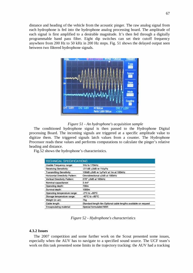
67
distance and heading of the vehicle from the acoustic pinger. The raw analog signal from each hydrophone is fed into the hydrophone analog processing board. The amplitude of each signal is first amplified to a desirable magnitude. It’s then fed through a digitally programmable band pass filter. Eight dip switches can set their cutoff frequency anywhere from 200 Hz to 50 kHz in 200 Hz steps. Fig. 51 shows the delayed output seen between two filtered hydrophone signals.
The conditioned hydrophone signal is then passed to the Hydrophone Digital processing Board. The incoming signals are triggered at a specific amplitude value to digitize them. The triggered signals latch values from a counter. The Hydrophone Processor reads these values and performs computations to calculate the pinger’s relative heading and distance.
Fig.52 shows the hydrophone’s characteristics.
4.3.2 Issues
The 2007 competition and some further work on the Scout presented some issues, especially when the AUV has to navigate to a specified sound source. The UCF team’s work on this task presented some limits in the trajectory tracking: the AUV had a tracking
Figure 51 - An hydrophone's acquisition sample
Figure 52 - Hydrophone's characteristics

68
error of +/- 30°. They imputed this error to the low sampling frequency and the low speed of the data’s treatment typical of the hardware adopted.
The purpose of this thesis is to use a faster technology, an FPGA board to reach better results on the trajectory tracking.
4.4 The Mathematic Theory The UCF team for the 2007 AUVSI competition found some precision issues in
following the ping route. This problem was imputed to the low frequency sampling during the acquisition of the hydrophones signals.
Our objective is to handle 4 signals with a sampling rate of more than 1 MHz and then processing them with the FPGA to obtain the delays between each one so that the future algorithm can have some more rigorous data to calculate the route on. 4.4.1 The idea
Our work is focused on the acquisition of the ping signal from an underwater source. This source is positioned on the objective that the AUV has to reach, so, the ping indicates our route source. To listen to this ping the AUV has docked 4 hydrophones on his frame. Once the signals are acquired by the hydrophones they are sent to a board for signal conditioning to have a good shape to work with and then, they are sent to the A/D board and the FPGA board.
To follow the route, the AUV compute an algorithm that use the signal delays as inputs. Our objective is to extract this delay from the signal sources and make it available to the AUV. Figure 54 shows the flow diagram.
Figure 53 – The idea for the trajectory tracking

69
Figure 54 – The flow diagram for the delay extraction
4.4.2 Extracting the Delay A way to succeed in extract the delay between two signal can be to analyze the cross correlation between them. 4.4.2.1 Cross correlation [9]
In signal processing, cross-correlation is a measure of similarity of two waveforms as a function of a time-lag applied to one of them. This is also known as a sliding dot product or inner-product
The complex cross correlation of f(x) with g(x) is defined as ( ) = ( ) ∗ ∗( ) = ( )
∗( − )
(1) The definition can also be written as ( ) = ( ) ∗ ∗( ) = ( + )
∗( )
(2)
after changing the dummy variable of integration. The corresponding definition of cross correlation for sequences would be [ ] = F[N + M]G∗[N]
(3) Some authors define cross correlation as ( ) = ( )
∗( + )
(4)
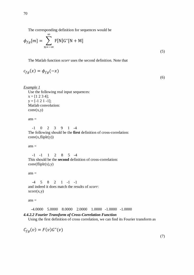
70
The corresponding definition for sequences would be [ ] = F[N]G∗[N + M]
(5)
The Matlab function xcorr uses the second definition. Note that ( ) = (− )
(6)
Example 1 Use the following real input sequences: x = [1 2 3 4]; y = [-1 2 1 -1]; Matlab convolution: conv(x,y) ans = -1 0 2 3 9 1 -4 The following should be the first definition of cross-correlation: conv(x,fliplr(y)) ans = -1 -1 1 2 8 5 -4 This should be the second definition of cross-correlation: conv(fliplr(x),y) ans = -4 5 8 2 1 -1 -1 and indeed it does match the results of xcorr: xcorr(x,y) ans = -4.0000 5.0000 8.0000 2.0000 1.0000 -1.0000 -1.0000
4.4.2.2 Fourier Transform of Cross-Correlation Function Using the first definition of cross correlation, we can find its Fourier transform as ( ) = ( ) ∗( )
(7)
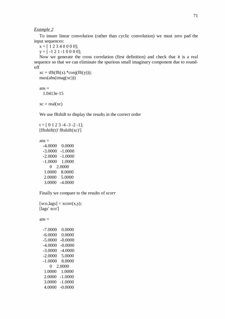
71
Example 2 To insure linear convolution (rather than cyclic convolution) we must zero pad the
input sequences: x = [ 1 2 3 4 0 0 0 0]; y = [ -1 2 1 -1 0 0 0 0]; Now we generate the cross correlation (first definition) and check that it is a real
sequence so that we can eliminate the spurious small imaginary component due to round-off
xc = ifft(fft(x).*conj(fft(y))); max(abs(imag(xc))) ans = 1.0413e-15 xc = real(xc) We use fftshift to display the results in the correct order t = [ 0 1 2 3 -4 -3 -2 -1]; [fftshift(t)' fftshift(xc)'] ans = -4.0000 0.0000 -3.0000 -1.0000 -2.0000 -1.0000 -1.0000 1.0000 0 2.0000 1.0000 8.0000 2.0000 5.0000 3.0000 -4.0000 Finally we compare to the results of xcorr [xco,lags] = xcorr(x,y); [lags' xco'] ans = -7.0000 0.0000 -6.0000 0.0000 -5.0000 -0.0000 -4.0000 -0.0000 -3.0000 -4.0000 -2.0000 5.0000 -1.0000 8.0000 0 2.0000 1.0000 1.0000 2.0000 -1.0000 3.0000 -1.0000 4.0000 -0.0000
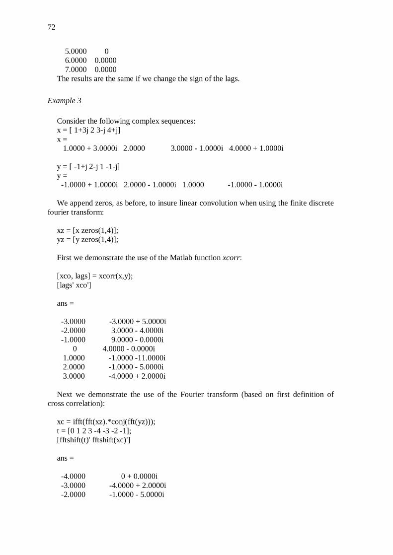
72
5.0000 0 6.0000 0.0000 7.0000 0.0000 The results are the same if we change the sign of the lags.
Example 3 Consider the following complex sequences: x = [ 1+3j 2 3-j 4+j] x = 1.0000 + 3.0000i 2.0000 3.0000 - 1.0000i 4.0000 + 1.0000i y = [ -1+j 2-j 1 -1-j] y = -1.0000 + 1.0000i 2.0000 - 1.0000i 1.0000 -1.0000 - 1.0000i We append zeros, as before, to insure linear convolution when using the finite discrete
fourier transform: xz = [x zeros(1,4)]; yz = [y zeros(1,4)]; First we demonstrate the use of the Matlab function xcorr: [xco, lags] = xcorr(x,y); [lags' xco'] ans = -3.0000 -3.0000 + 5.0000i -2.0000 3.0000 - 4.0000i -1.0000 9.0000 - 0.0000i 0 4.0000 - 0.0000i 1.0000 -1.0000 -11.0000i 2.0000 -1.0000 - 5.0000i 3.0000 -4.0000 + 2.0000i Next we demonstrate the use of the Fourier transform (based on first definition of
cross correlation): xc = ifft(fft(xz).*conj(fft(yz))); t = [0 1 2 3 -4 -3 -2 -1]; [fftshift(t)' fftshift(xc)'] ans = -4.0000 0 + 0.0000i -3.0000 -4.0000 + 2.0000i -2.0000 -1.0000 - 5.0000i
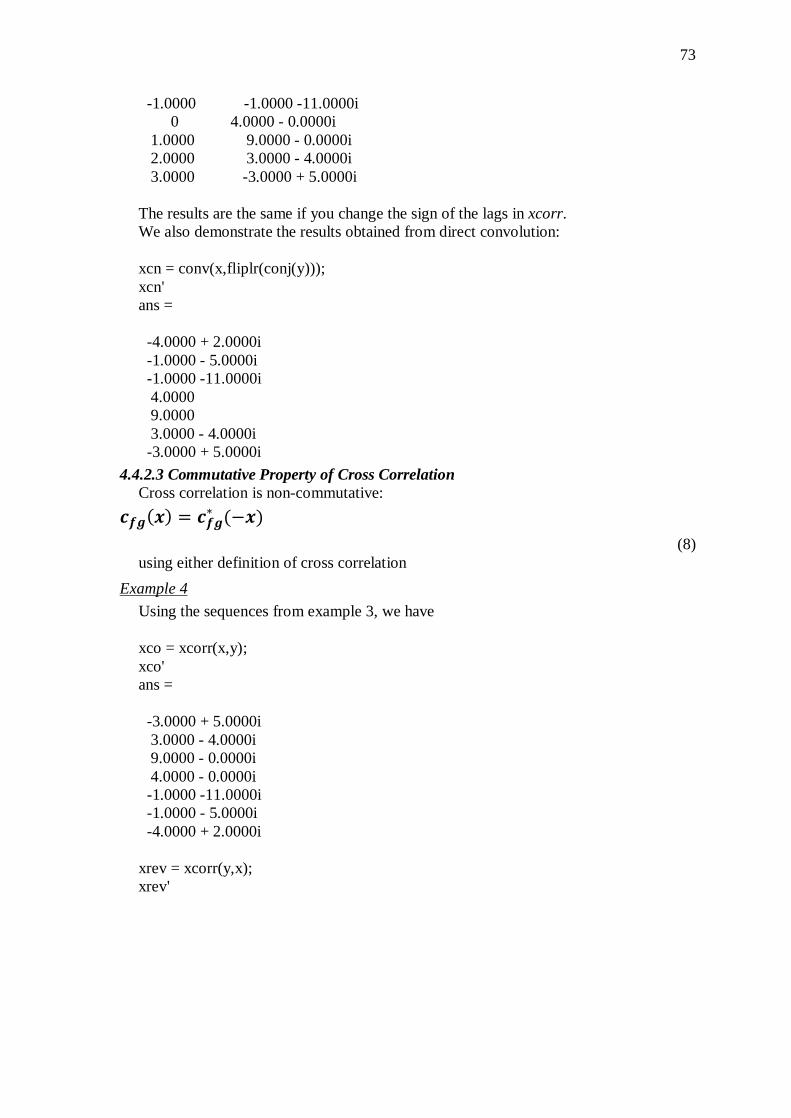
73
-1.0000 -1.0000 -11.0000i 0 4.0000 - 0.0000i 1.0000 9.0000 - 0.0000i 2.0000 3.0000 - 4.0000i 3.0000 -3.0000 + 5.0000i The results are the same if you change the sign of the lags in xcorr. We also demonstrate the results obtained from direct convolution: xcn = conv(x,fliplr(conj(y))); xcn' ans = -4.0000 + 2.0000i -1.0000 - 5.0000i -1.0000 -11.0000i 4.0000 9.0000 3.0000 - 4.0000i -3.0000 + 5.0000i
4.4.2.3 Commutative Property of Cross Correlation Cross correlation is non-commutative: ( ) = ∗ (− )
(8) using either definition of cross correlation
Example 4 Using the sequences from example 3, we have xco = xcorr(x,y); xco' ans = -3.0000 + 5.0000i 3.0000 - 4.0000i 9.0000 - 0.0000i 4.0000 - 0.0000i -1.0000 -11.0000i -1.0000 - 5.0000i -4.0000 + 2.0000i xrev = xcorr(y,x); xrev'
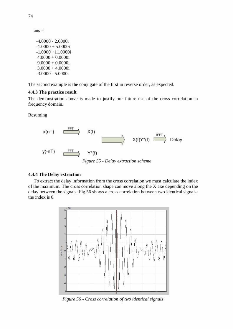
74
ans = -4.0000 - 2.0000i -1.0000 + 5.0000i -1.0000 +11.0000i 4.0000 + 0.0000i 9.0000 + 0.0000i 3.0000 + 4.0000i -3.0000 - 5.0000i
The second example is the conjugate of the first in reverse order, as expected. 4.4.3 The practice result The demonstration above is made to justify our future use of the cross correlation in frequency domain. Resuming
4.4.4 The Delay extraction To extract the delay information from the cross correlation we must calculate the index
of the maximum. The cross correlation shape can move along the X axe depending on the delay between the signals. Fig.56 shows a cross correlation between two identical signals: the index is 0.
Figure 55 - Delay extraction scheme
Figure 56 - Cross correlation of two identical signals

75
Fig. 57 shows the cross correlation between 2 identical signal but one delayed ten
samples from the other. The maximum index move along the X axe showing the accurate delay.
Figure 57 – Cross correlation of two delayed signals
4.5 The simulation scheme To learn how to program an FPGA some training time must be spent. To do some DSP
with an Altera FPGA involves the use of the DSP Builder tool: a visual programming language built on Simulink Matlab. Basically, the DPS Builder add a number of blocks that can be translated to the FPGA language.
This simulation scheme works only on Simulink Matlab’s environment and simulate the FPGA flow and the signal input. The objective of this scheme is to calculate the input signals’ delay without considering the real FPGA’s programming issues as the language coherency and the management of the hardware resources.
In this scheme (Fig. 58) the DSP Builder blocks (the ones with a blue edge), and the Simulink ones are used together: in the real scheme, downloadable directly on the board for his execution will be available only the DSP Builder blocks. These blocks have corresponding translation in HDL language so that the board could be programmed.
One of the first problem encountered was that the Dsp Builder blocks are more logic oriented and they don’t allow the same freedom of design (especially in DSP) that Simulink gives. Often, to have not a higher DSP programming language, make us to use some tricky scheme to substitute, for example, an obvious Simulink one block: a clear example of this will be found on the last part of the scheme where a maximum must be calculated (Cap. 4.5.8).
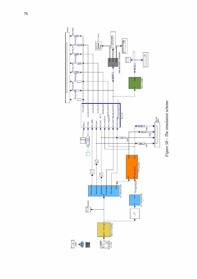
76
Figu
re 5
8 –
The
simul
atio
n sc
hem
e
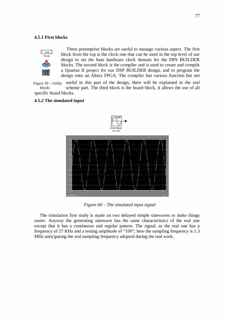
77
4.5.1 First blocks
These preemptive blocks are useful to manage various aspect. The first
block from the top is the clock one that can be used in the top level of our design to set the base hardware clock domain for the DPS BUILDER blocks. The second block is the compiler and is used to create and compile a Quartus II project for our DSP BUILDER design, and to program the design onto an Altera FPGA. The compiler has various function but not
useful in this part of the design, there will be explained in the real scheme part. The third block is the board block, it allows the use of all
specific board blocks. 4.5.2 The simulated input
Figure 60 – The simulated input signal
The simulation first study is made on two delayed simple sinewaves to make things easier. Anyway the generating sinewave has the same characteristics of the real one except that it has a continuous and regular pattern. The signal, as the real one has a frequency of 27 KHz and a testing amplitude of “100”; here the sampling frequency is 1.3 MHz anticipating the real sampling frequency adopted during the real work.
Figure 59 – Utility blocks
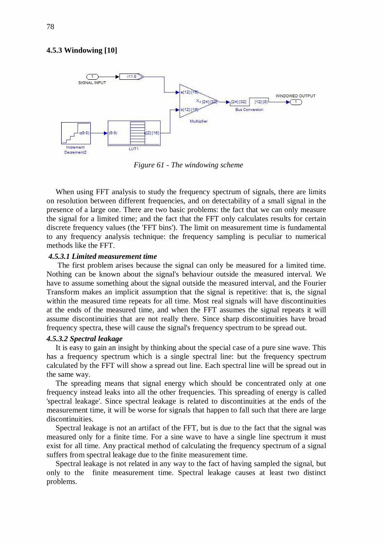
78
4.5.3 Windowing [10]
When using FFT analysis to study the frequency spectrum of signals, there are limits on resolution between different frequencies, and on detectability of a small signal in the presence of a large one. There are two basic problems: the fact that we can only measure the signal for a limited time; and the fact that the FFT only calculates results for certain discrete frequency values (the 'FFT bins'). The limit on measurement time is fundamental to any frequency analysis technique: the frequency sampling is peculiar to numerical methods like the FFT. 4.5.3.1 Limited measurement time
The first problem arises because the signal can only be measured for a limited time. Nothing can be known about the signal's behaviour outside the measured interval. We have to assume something about the signal outside the measured interval, and the Fourier Transform makes an implicit assumption that the signal is repetitive: that is, the signal within the measured time repeats for all time. Most real signals will have discontinuities at the ends of the measured time, and when the FFT assumes the signal repeats it will assume discontinuities that are not really there. Since sharp discontinuities have broad frequency spectra, these will cause the signal's frequency spectrum to be spread out. 4.5.3.2 Spectral leakage
It is easy to gain an insight by thinking about the special case of a pure sine wave. This has a frequency spectrum which is a single spectral line: but the frequency spectrum calculated by the FFT will show a spread out line. Each spectral line will be spread out in the same way.
The spreading means that signal energy which should be concentrated only at one frequency instead leaks into all the other frequencies. This spreading of energy is called 'spectral leakage'. Since spectral leakage is related to discontinuities at the ends of the measurement time, it will be worse for signals that happen to fall such that there are large discontinuities.
Spectral leakage is not an artifact of the FFT, but is due to the fact that the signal was measured only for a finite time. For a sine wave to have a single line spectrum it must exist for all time. Any practical method of calculating the frequency spectrum of a signal suffers from spectral leakage due to the finite measurement time.
Spectral leakage is not related in any way to the fact of having sampled the signal, but only to the finite measurement time. Spectral leakage causes at least two distinct problems.
Figure 61 - The windowing scheme

79
First, any given spectral component will contain not just the signal energy, but also noise from the whole of the rest of the spectrum. This will degrade the signal to noise ratio.
Second, the spectral leakage from a large signal component may be severe enough to mask other smaller signals at different frequencies. 4.5.3.3 The Window’s application The effects of spectral leakage can be reduced by reducing the discontinuities at the ends of the signal measurement time. This leads to the idea of multiplying the signal within the measurement time by some function that smoothly reduces the signal to zero at the end points: hence avoiding discontinuities altogether. The process of multiplying the signal data by a function that smoothly approaches zero at both ends, is called 'windowing': and the multiplying function is called a 'window' function. 4.5.3.4 Some window examples [11] The table lists, for various window functions, the following parameters: Sidelobe level: The attenuation to the top of the highest side lobe Fall off: The asymptotic rate of fall off to the side lobe Coherent gain: The normalized DC gain
Equivalent noise bandwidth: The bandwidth of a rectangular filter which would let pass the same amount of broadband noise
6 dB bandwidth: The bandwidth in which the window function falls by 6 dB
Worst case processing loss: The ratio of input signal to noise to output signal to noise, including scalloping loss for the worst case frequency
Figure 62 - Characteristics for various window
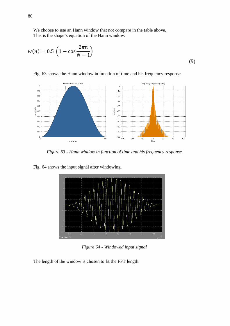
80
We choose to use an Hann window that not compare in the table above. This is the shape’s equation of the Hann window: ( ) = 0.5 1 − cos 2 − 1
(9)
Fig. 63 shows the Hann window in function of time and his frequency response.
Figure 63 - Hann window in function of time and his frequency response
Fig. 64 shows the input signal after windowing.
Figure 64 - Windowed input signal
The length of the window is chosen to fit the FFT length.
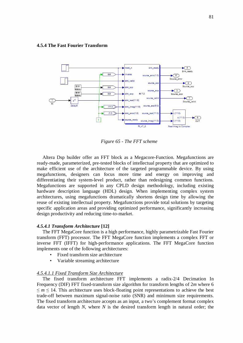
81
4.5.4 The Fast Fourier Transform
Altera Dsp builder offer an FFT block as a Megacore-Function. Megafunctions are ready-made, parameterized, pre-tested blocks of intellectual property that are optimized to make efficient use of the architecture of the targeted programmable device. By using megafunctions, designers can focus more time and energy on improving and differentiating their system-level product, rather than redesigning common functions. Megafunctions are supported in any CPLD design methodology, including existing hardware description language (HDL) design. When implementing complex system architectures, using megafunctions dramatically shortens design time by allowing the reuse of existing intellectual property. Megafunctions provide total solutions by targeting specific application areas and providing optimized performance, significantly increasing design productivity and reducing time-to-market.
4.5.4.1 Transform Architecture [12]
The FFT MegaCore function is a high performance, highly parametrizable Fast Fourier transform (FFT) processor. The FFT MegaCore function implements a complex FFT or inverse FFT (IFFT) for high-performance applications. The FFT MegaCore function implements one of the following architectures:
• Fixed transform size architecture • Variable streaming architecture
4.5.4.1.1 Fixed Transform Size Architecture
The fixed transform architecture FFT implements a radix-2/4 Decimation In Frequency (DIF) FFT fixed-transform size algorithm for transform lengths of 2m where 6 ≤ m ≤ 14. This architecture uses block-floating point representations to achieve the best trade-off between maximum signal-noise ratio (SNR) and minimum size requirements. The fixed transform architecture accepts as an input, a two’s complement format complex data vector of length N, where N is the desired transform length in natural order; the
Figure 65 - The FFT scheme
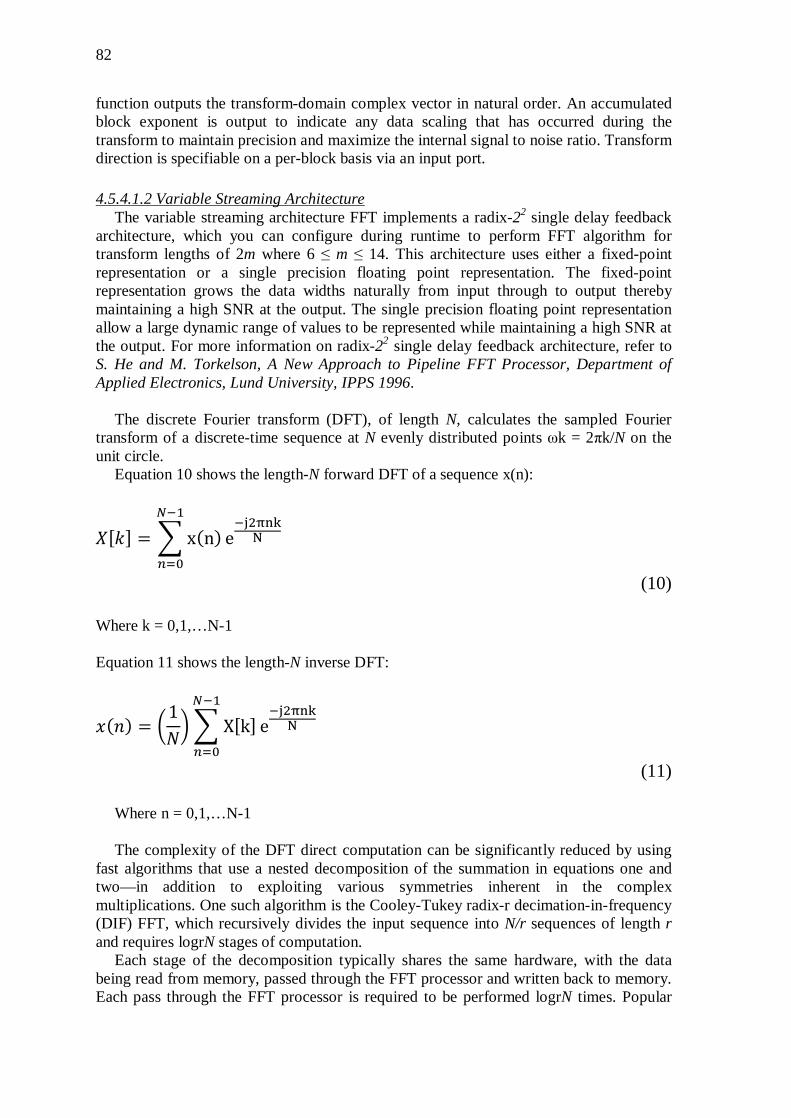
82
function outputs the transform-domain complex vector in natural order. An accumulated block exponent is output to indicate any data scaling that has occurred during the transform to maintain precision and maximize the internal signal to noise ratio. Transform direction is specifiable on a per-block basis via an input port.
4.5.4.1.2 Variable Streaming Architecture
The variable streaming architecture FFT implements a radix-22 single delay feedback architecture, which you can configure during runtime to perform FFT algorithm for transform lengths of 2m where 6 ≤ m ≤ 14. This architecture uses either a fixed-point representation or a single precision floating point representation. The fixed-point representation grows the data widths naturally from input through to output thereby maintaining a high SNR at the output. The single precision floating point representation allow a large dynamic range of values to be represented while maintaining a high SNR at the output. For more information on radix-22 single delay feedback architecture, refer to S. He and M. Torkelson, A New Approach to Pipeline FFT Processor, Department of Applied Electronics, Lund University, IPPS 1996.
The discrete Fourier transform (DFT), of length N, calculates the sampled Fourier
transform of a discrete-time sequence at N evenly distributed points ωk = 2πk/N on the unit circle.
Equation 10 shows the length-N forward DFT of a sequence x(n): [ ] = x(n)
e (10)
Where k = 0,1,…N-1 Equation 11 shows the length-N inverse DFT: ( ) = 1 X[k]
e (11)
Where n = 0,1,…N-1
The complexity of the DFT direct computation can be significantly reduced by using
fast algorithms that use a nested decomposition of the summation in equations one and two—in addition to exploiting various symmetries inherent in the complex multiplications. One such algorithm is the Cooley-Tukey radix-r decimation-in-frequency (DIF) FFT, which recursively divides the input sequence into N/r sequences of length r and requires logrN stages of computation.
Each stage of the decomposition typically shares the same hardware, with the data being read from memory, passed through the FFT processor and written back to memory. Each pass through the FFT processor is required to be performed logrN times. Popular
83
choices of the radix are r = 2, 4, and 16. Increasing the radix of the decomposition leads to a reduction in the number of passes required through the FFT processor at the expense of device resources.
A radix-4 decomposition, which divides the input sequence recursively to form four-point sequences, has the advantage that it requires only trivial multiplications in the four-point DFT and is the chosen radix in the Altera FFT MegaCore function. This results in the highest throughput decomposition, while requiring non-trivial complex multiplications in the post-butterfly twiddle-factor rotations only. In cases where N is an odd power of two, the FFT MegaCore automatically implements a radix- 2 pass on the last pass to complete the transform.
To maintain a high signal-to-noise ratio throughout the transform computation, the FFT MegaCore function uses a block-floating-point architecture, which is a trade-off point between fixed-point and full floating point architectures.
In a fixed-point architecture, the data precision needs to be large enough to adequately represent all intermediate values throughout the transform computation. For large FFT transform sizes, an FFT fixed-point implementation that allows for word growth can make either the data width excessive or can lead to a loss of precision.
In a floating-point architecture each number is represented as a mantissa with an individual exponent—while this leads to greatly improved precision, floating-point operations tend to demand increased device resources.
In a block-floating point architecture, all of the values have an independent mantissa but share a common exponent in each data block. Data is input to the FFT function as fixed point complex numbers (even though the exponent is effectively 0, you do not enter an exponent).
The block-floating point architecture ensures full use of the data width within the FFT function and throughout the transform. After every pass through a radix-4 FFT, the data width may grow up to log2 (4√2) = 2.5 bits. The data is scaled according to a measure of the block dynamic range on the output of the previous pass. The number of shifts is accumulated and then output as an exponent for the entire block. This shifting ensures that the minimum of least significant bits (LSBs) are discarded prior to the rounding of the post-multiplication output. In effect, the block-floating point representation acts as a digital automatic gain control. To yield uniform scaling across successive output blocks, you must scale the FFT function output by the final exponent.
The variable streaming architecture uses a radix 22 single delay feedback architecture, which is a fully pipelined architecture. For a length N transform there are log4(N) stages concatenated together. The radix 22 algorithm has the same multiplicative complexity of a fully pipelined radix-4 architecture, however the butterfly unit retains a radix-2 architecture. The butterfly units use the DIF decomposition. The variable streaming architecture uses either fixed point of single precision floating point data representation. Fixed point representation allows for natural word growth through the pipeline. The maximum growth of each stage is log2(4 √2) = 2.5 bits, which is accommodated in the design by growing the pipeline stages by either 2 bits or 3 bits. After the complex multiplication the data is rounded down to the expanded data size using convergent rounding.
The floating point internal data representation is single precision floating point (32 bit, IEEE 754 representation). Floating point operations are costly in terms of hardware resources. To reduce the amount of logic required for floating point operations, the variable streaming FFT uses "fused" floating point kernels. The reduction in logic occurs by fusing together several floating point operations and reducing the number of normalizations that need to occur.

84
Some applications for the FFT require an FFT > user operation > IFFT chain. In this case, choosing the input order and output order carefully can lead to significant memory and latency savings. For example, consider where the input to the first FFT is in natural order and the output is in bit-reversed order (FFT is operating in engine-only mode). In this example, if the IFFT operation is configured to accept bit-reversed inputs and produces natural order outputs (IFFT is operating in engine-only mode), only the minimum amount of memory is required, which provides a saving of N complex memory words, and a latency saving of N clock cycles, where N is the size of the current transform. 4.5.4.2 FFT Processor Engine Architectures
The FFT MegaCore function can be parameterized to use either quad output or single-output engine architecture. To increase the overall throughput of the FFT MegaCore function, you may also use multiple parallel engines of a variation. This section discusses the following topics:
• Radix 22 single-delay feedback architecture • Quad-output FFT engine architecture • Single-output FFT engine architecture
4.5.4.2.1 Radix-22 Single Delay Feedback Architecture
Radix-22 single delay feedback architecture is a fully pipelined architecture for calculating the FFT of incoming data. It is similar to radix- 2 single delay feedback architectures. However, the twiddle factors are rearranged such that the multiplicative complexity is equivalent to a radix-4 single delay feedback architecture. There are log2(N) stages with each stage containing a single butterfly unit and a feedback delay unit that delays the incoming data by a specified number of cycles, halved at every stage. These delays effectively align the correct samples at the input of the butterfly unit for the butterfly calculations. Every second stage contains a modified radix-2 butterfly whereby a trivial multiplication by –j is performed before the radix-2 butterfly operations. The output of the pipeline is in bit-reversed order. The following scheduled operations in the pipeline for an FFT of length N = 16 occur.
1. For the first 8 clock cycles, the samples are fed unmodified through the butterfly unit to the delay feedback unit.
2. The next 8 clock cycles perform the butterfly calculation using the data from the delay feedback unit and the incoming data. The higher order calculations are sent through to the delay feedback unit while the lower order calculations are sent to the next stage.
3. The next 8 clock cycles feeds the higher order calculations stored in the delay feedback unit unmodified through the butterfly unit to the next stage. Subsequent data stages use the same principles. However, the delays in the feedback path are adjusted accordingly.
Subsequent data stages use the same principles. However, the delays in the feedback path are adjusted accordingly.
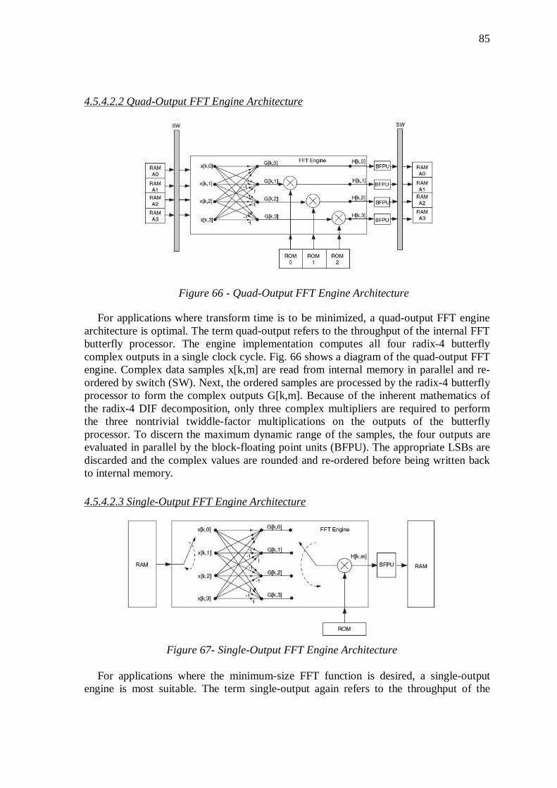
85
4.5.4.2.2 Quad-Output FFT Engine Architecture
Figure 66 - Quad-Output FFT Engine Architecture
For applications where transform time is to be minimized, a quad-output FFT engine architecture is optimal. The term quad-output refers to the throughput of the internal FFT butterfly processor. The engine implementation computes all four radix-4 butterfly complex outputs in a single clock cycle. Fig. 66 shows a diagram of the quad-output FFT engine. Complex data samples x[k,m] are read from internal memory in parallel and re-ordered by switch (SW). Next, the ordered samples are processed by the radix-4 butterfly processor to form the complex outputs G[k,m]. Because of the inherent mathematics of the radix-4 DIF decomposition, only three complex multipliers are required to perform the three nontrivial twiddle-factor multiplications on the outputs of the butterfly processor. To discern the maximum dynamic range of the samples, the four outputs are evaluated in parallel by the block-floating point units (BFPU). The appropriate LSBs are discarded and the complex values are rounded and re-ordered before being written back to internal memory. 4.5.4.2.3 Single-Output FFT Engine Architecture
For applications where the minimum-size FFT function is desired, a single-output
engine is most suitable. The term single-output again refers to the throughput of the
Figure 67- Single-Output FFT Engine Architecture

86
internal FFT butterfly processor. In the engine architecture, a single butterfly output is computed per clock cycle, requiring a single complex multiplier. 4.5.4.3 I/O Data Flow architecuteres The Altera Megacore FFT supports 4 types of architectures:
• Streaming: allows continuous processing of input data, and outputs a continuous complex data stream without the requirement to halt the data flow in or out of the FFT function.
• Variable Streaming: allows continuous streaming of input data and produces a continuous stream of output data similar to the streaming architecture.
• Buffered Burst: it requires fewer memory resources than the streaming I/O data flow architecture, but the tradeoff is an average block throughput reduction.
• Burst: it operates similarly to the buffered burst architecture, except that the burst architecture requires even lower memory resources for a given parameterization at the expense of reduced average throughput.
For our type of analysis, that implies a real time acquisition we choice a Streaming architecture and therefore a Quad output Architecture. The only other parameter we set is the FFT length that was 1024 point long, the other parameters involve a resource analysis that we have done during the study of the real scheme. To work in the right way the FFT Megacore requires a specific timing that we can see in the Fig. 68
We decided to work initially with a 1024 point FFT as a trade off between
computation time and accuracy. Fig. 69 shows the result of one cycle of the FFT Megacore. You can see the imaginary
part on the first graphic, the real part on the second graphic and the timing of an FFT window on the third graphic. The output of the FFT is observed in a time domain as a data flow to manage the timing of the FFT.
Figure 68 - FFT mecagore Timing
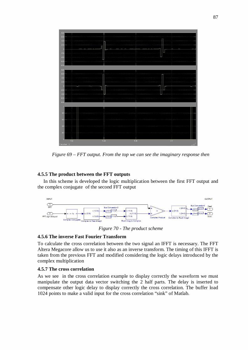
87
Figure 69 – FFT output. From the top we can see the imaginary response then
4.5.5 The product between the FFT outputs In this scheme is developed the logic multiplication between the first FFT output and
the complex conjugate of the second FFT output
Figure 70 - The product scheme
4.5.6 The inverse Fast Fourier Transform To calculate the cross correlation between the two signal an IFFT is necessary. The FFT Altera Megacore allow us to use it also as an inverse transform. The timing of this IFFT is taken from the previous FFT and modified considering the logic delays introduced by the complex multiplication 4.5.7 The cross correlation As we see in the cross correlation example to display correctly the waveform we must manipulate the output data vector switching the 2 half parts. The delay is inserted to compensate other logic delay to display correctly the cross correlation. The buffer load 1024 points to make a valid input for the cross correlation “sink” of Matlab.
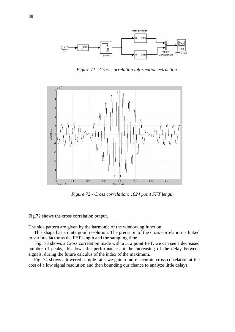
88
Fig.72 shows the cross correlation output. The side pattern are given by the harmonic of the windowing function
This shape has a quite good resolution. The precision of the cross correlation is linked to various factor as the FFT length and the sampling time.
Fig. 73 shows a Cross correlation made with a 512 point FFT, we can see a decreased number of peaks, this lows the performances at the increasing of the delay between signals, during the future calculus of the index of the maximum.
Fig. 74 shows a lowered sample rate: we gain a more accurate cross correlation at the cost of a low signal resolution and then bounding our chance to analyze little delays.
Figure 71 - Cross correlation information extraction
Figure 72 - Cross correlation: 1024 point FFT length
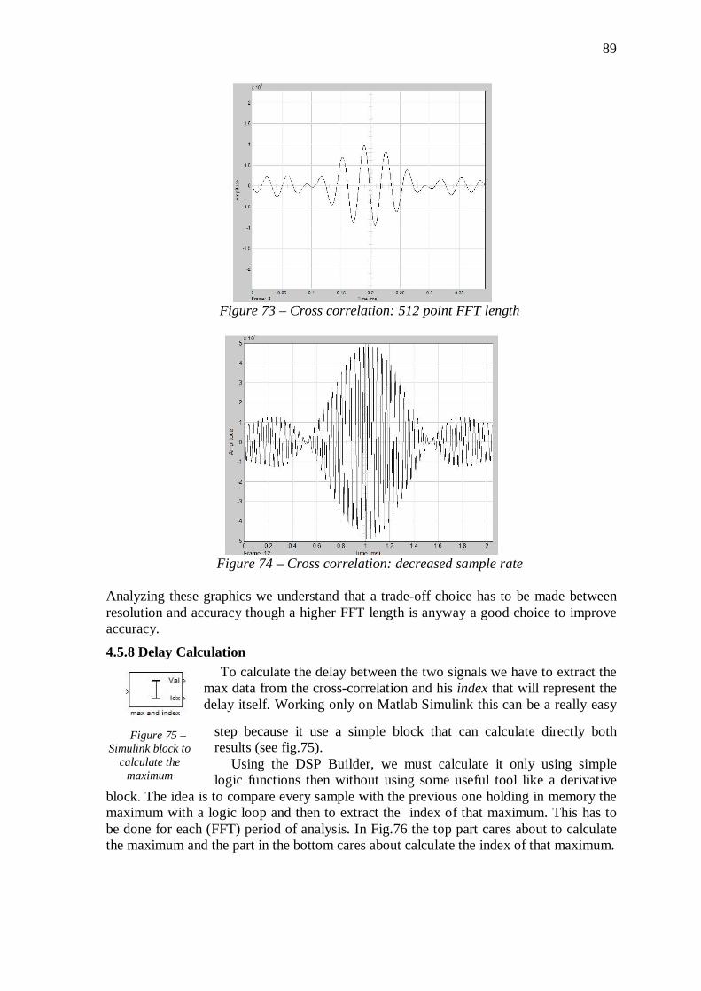
89
Figure 73 – Cross correlation: 512 point FFT length
Figure 74 – Cross correlation: decreased sample rate
Analyzing these graphics we understand that a trade-off choice has to be made between resolution and accuracy though a higher FFT length is anyway a good choice to improve accuracy.
4.5.8 Delay Calculation To calculate the delay between the two signals we have to extract the
max data from the cross-correlation and his index that will represent the delay itself. Working only on Matlab Simulink this can be a really easy
step because it use a simple block that can calculate directly both results (see fig.75).
Using the DSP Builder, we must calculate it only using simple logic functions then without using some useful tool like a derivative
block. The idea is to compare every sample with the previous one holding in memory the maximum with a logic loop and then to extract the index of that maximum. This has to be done for each (FFT) period of analysis. In Fig.76 the top part cares about to calculate the maximum and the part in the bottom cares about calculate the index of that maximum.
Figure 75 – Simulink block to
calculate the maximum

90
4.5.9 Results We made some tests to understand if the algorithm is robust and until what
performance. Delay samples
To check the algorithm accuracy we tested various couple of signals with different delays. Having a sampling rate of 1.3 MHz one sinewave period is made of 48 sample so the maximum delay between the 2 signals is 48 samples. Indeed we expect a maximum observable delay of 24 sample because after half signal the algorithm see the second signal delayed regard of the first one instead of the opposite. Anyway, the algorithm is able to observe a direct delay untill 32 samples, after, it find a negative delay as explained before. Noise
To evaluate the robustness of the algorithm we inserted a simple noise input in both channels: the regular sinewave and the delayed one.
In Fig.77 we can see the windowed input signals with a noise variance of 500. The algorithm is considered to be really robust in simulation. With a danger noise like the one inserted the delay is estimated with a discard of only one sample. With a noise variance of 100 the algorithm is perfectly stable.
Figure 76 – Delay calculation scheme
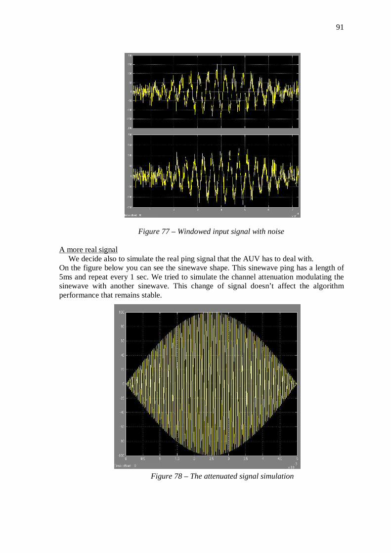
91
A more real signal
We decide also to simulate the real ping signal that the AUV has to deal with. On the figure below you can see the sinewave shape. This sinewave ping has a length of 5ms and repeat every 1 sec. We tried to simulate the channel attenuation modulating the sinewave with another sinewave. This change of signal doesn’t affect the algorithm performance that remains stable.
Figure 77 – Windowed input signal with noise
Figure 78 – The attenuated signal simulation
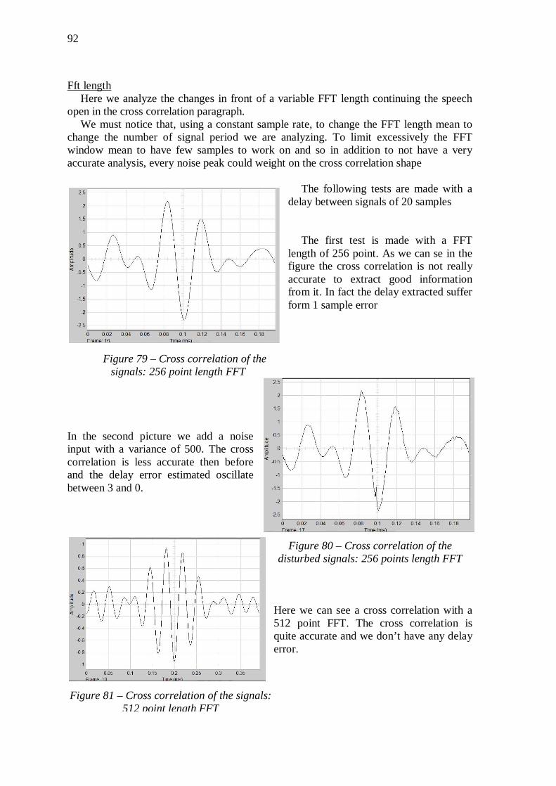
92
Fft length
Here we analyze the changes in front of a variable FFT length continuing the speech open in the cross correlation paragraph.
We must notice that, using a constant sample rate, to change the FFT length mean to change the number of signal period we are analyzing. To limit excessively the FFT window mean to have few samples to work on and so in addition to not have a very accurate analysis, every noise peak could weight on the cross correlation shape
The following tests are made with a
delay between signals of 20 samples The first test is made with a FFT
length of 256 point. As we can se in the figure the cross correlation is not really accurate to extract good information from it. In fact the delay extracted suffer form 1 sample error
In the second picture we add a noise input with a variance of 500. The cross correlation is less accurate then before and the delay error estimated oscillate between 3 and 0.
Here we can see a cross correlation with a 512 point FFT. The cross correlation is quite accurate and we don’t have any delay error.
Figure 79 – Cross correlation of the signals: 256 point length FFT
Figure 80 – Cross correlation of the disturbed signals: 256 points length FFT
Figure 81 – Cross correlation of the signals: 512 point length FFT
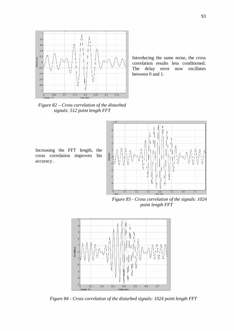
93
Introducing the same noise, the cross correlation results less conditioned. The delay error now oscillates between 0 and 1.
Increasing the FFT length, the cross correlation improves his accuracy .
Figure 84 - Cross correlation of the disturbed signals: 1024 point length FFT
Figure 82 – Cross correlation of the disturbed signals: 512 point length FFT
Figure 83 - Cross correlation of the signals: 1024 point length FFT
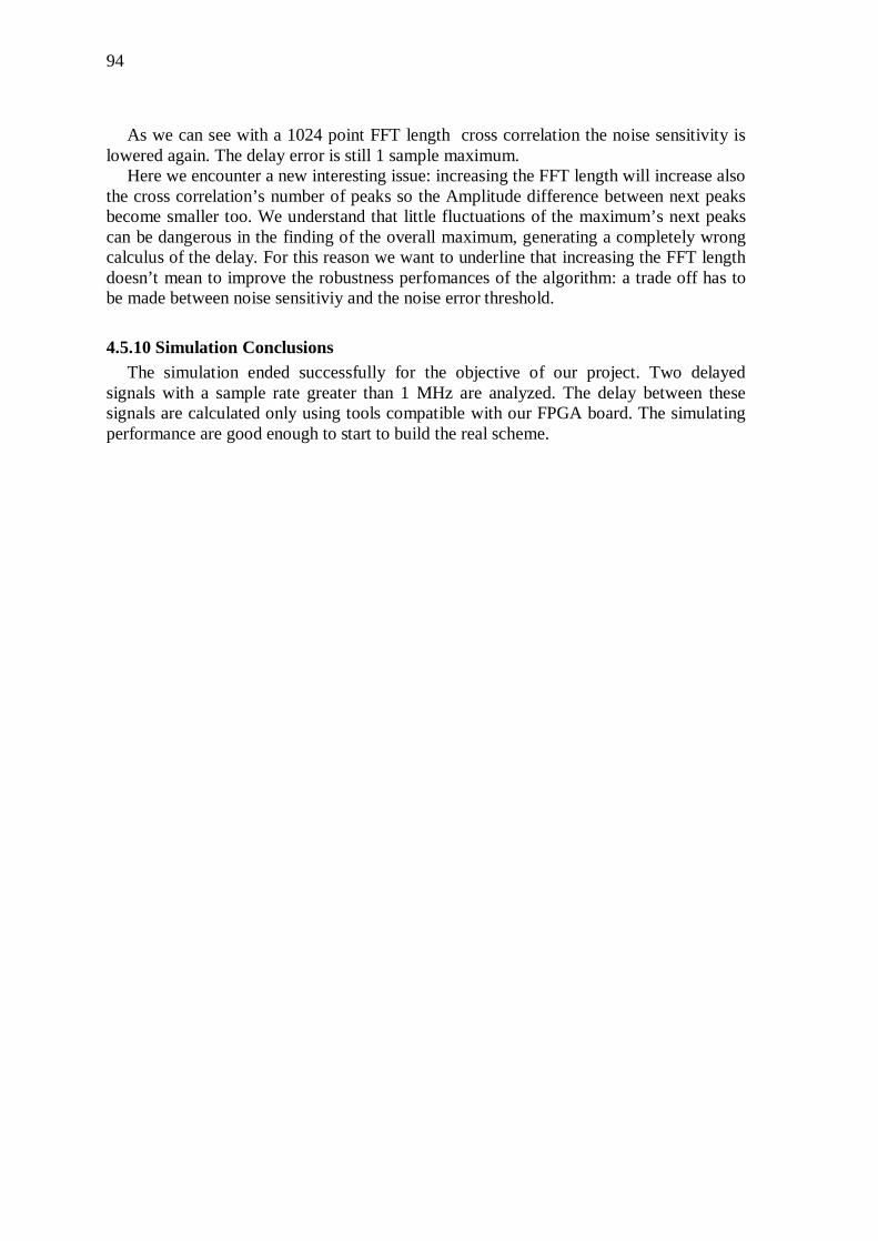
94
As we can see with a 1024 point FFT length cross correlation the noise sensitivity is
lowered again. The delay error is still 1 sample maximum. Here we encounter a new interesting issue: increasing the FFT length will increase also
the cross correlation’s number of peaks so the Amplitude difference between next peaks become smaller too. We understand that little fluctuations of the maximum’s next peaks can be dangerous in the finding of the overall maximum, generating a completely wrong calculus of the delay. For this reason we want to underline that increasing the FFT length doesn’t mean to improve the robustness perfomances of the algorithm: a trade off has to be made between noise sensitiviy and the noise error threshold. 4.5.10 Simulation Conclusions
The simulation ended successfully for the objective of our project. Two delayed signals with a sample rate greater than 1 MHz are analyzed. The delay between these signals are calculated only using tools compatible with our FPGA board. The simulating performance are good enough to start to build the real scheme.

95
5. IMPLEMENTATION, EXPERIMENT, RESULTS This chapter shows the experimental part of this thesis: this involves the use of the
whole hardware. The DAQ board generates the signals that have to be analyzed. The A/D board , timed by the FPGA, will digitalize and send them to the FPGA board. The simulation scheme will be optimized to be fitted to the FPGA board.
5.1 The input signal generation The NI DAQ board is programmable in LABVIEW. We use this powerful tool to
generate our simple signals Fig. 85 shows how the two signals are created and tested. The NI USB 6251 allow to
use the DAQ assistant: this is a wizard manager that allow us to configure the I/O in some simple guided steps. Furthermore, to generate the 2 signals, a pre-built block called Simulate signal is used. The signal has a Frequency of 27 KHz, an offset of 2V and an amplitude of 0,7V.
Figure 85 – Labview scheme for the simulated input signals
Fig.86 shows the two signals generated, the second one has a phase delay of 90
degrees.
Figure 86 - The signals generated

96
5.1.1 An acquisition tool It’s important to spend some words on a vital tool of the DSP Builder: the Signal Tap
II. It is our DSP builder’s tool to catch the board’s signals while the board is working. This logic analyzer helps debug an FPGA design by probing the state of the internal
signals in the design without the use of external equipment. Defining custom trigger-condition logic provides greater accuracy and improves the ability to isolate problems. The SignalTap II Embedded Logic Analyzer does not require external probes, or changes to the design files to capture the state of the internal nodes or I/O pins in the design. All captured signal data is conveniently stored in device memory until the designer is ready to read and analyze the data.
This can be a really useful tool, the only issues is that, using FPGA hardware, it will steal some memory and logic resources from our availability, this can be a problem if in the future we will have some hardware restriction.
Figura 87 - Memory usage of Signal Tap II
5.2 Sampling [13] The A/D board developed for our simulation need to be driven by an external source.
There are some parameters to respect to make work the A/D converter in the right way especially the timing characteristics of the driving signal.
The A/D converter has various type of driving modes: we used the parallel mode 2 read cycle.
Fig.88 shows a timing diagram for the AD7482 operating in Parallel Mode 2
Figure 88 – Parallel mode 2 timing for the AD7482
In Parallel Mode 2, the data in the output register is not updated until the next falling
edge of /CONVST . The BUSY output pin shows the working time of the A/D converter.

97
Figure 89 - Timing characteristics for the AD7482
We used the FPGA board to generate the driving signal. We have created a scheme to
drive the board and to watch the sampled signals .

98
Fig. 90 shows the DSP Builder timing and Observation scheme. On the left part we can see the observation scheme. Twelve input ports route the
twelve input bits’ signal in the Signal Tap II analyzer (the output ports are need by the Signal Tap II too). The 12 bit output is practically useless, we put it there only for a Signal Tap requirement, it needs a sort of output to work correctly.
On the right part a simple square signal drive /CONVST pin of the A/D board. To create that signal we have used the internal cloak of the FPGA. The FPGA’s
frequency clock range go from 10 MHz to 500 MHz.
Figure 90 - Acquisition test scheme
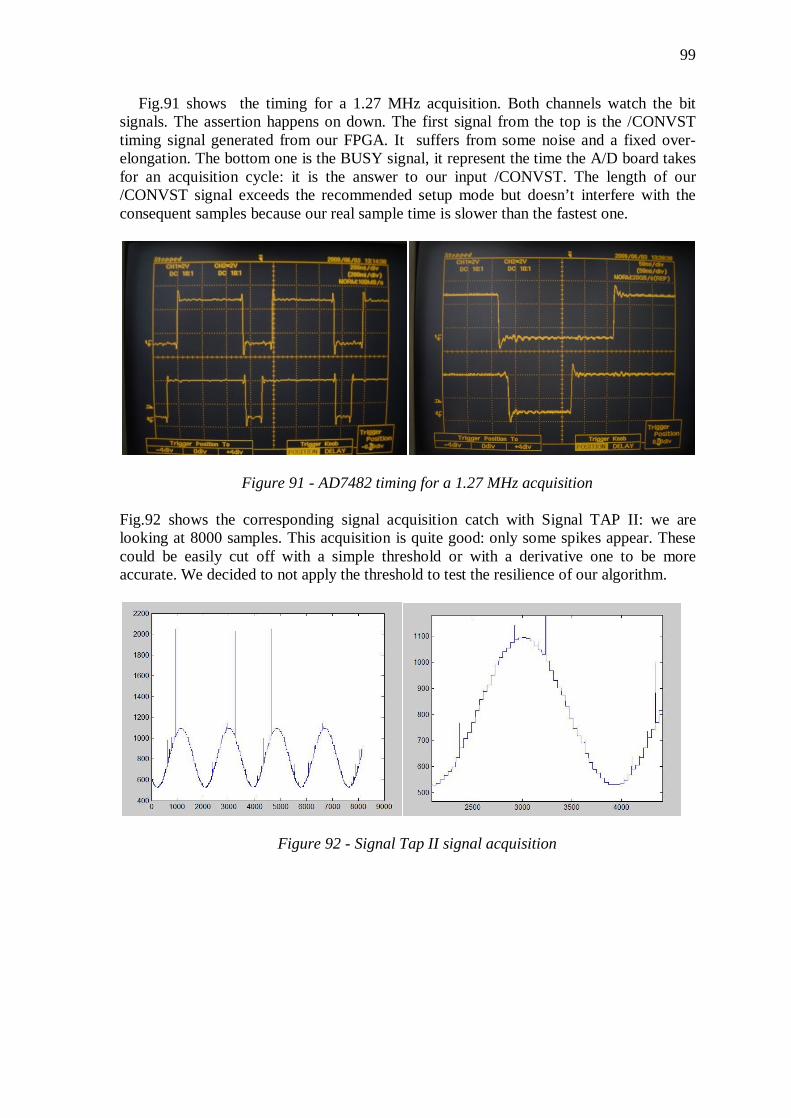
99
Fig.91 shows the timing for a 1.27 MHz acquisition. Both channels watch the bit signals. The assertion happens on down. The first signal from the top is the /CONVST timing signal generated from our FPGA. It suffers from some noise and a fixed over-elongation. The bottom one is the BUSY signal, it represent the time the A/D board takes for an acquisition cycle: it is the answer to our input /CONVST. The length of our /CONVST signal exceeds the recommended setup mode but doesn’t interfere with the consequent samples because our real sample time is slower than the fastest one.
Figure 91 - AD7482 timing for a 1.27 MHz acquisition Fig.92 shows the corresponding signal acquisition catch with Signal TAP II: we are looking at 8000 samples. This acquisition is quite good: only some spikes appear. These could be easily cut off with a simple threshold or with a derivative one to be more accurate. We decided to not apply the threshold to test the resilience of our algorithm.
Figure 92 - Signal Tap II signal acquisition
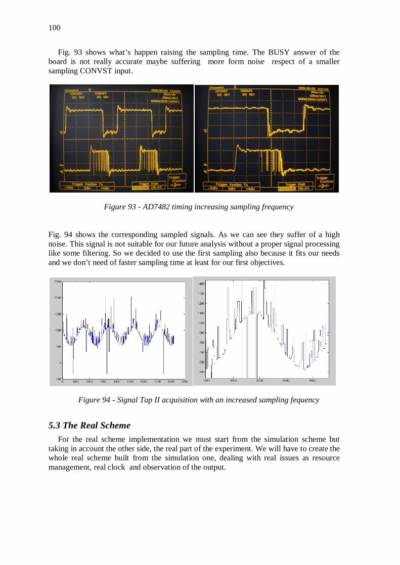
100
Fig. 93 shows what’s happen raising the sampling time. The BUSY answer of the board is not really accurate maybe suffering more form noise respect of a smaller sampling CONVST input.
Figure 93 - AD7482 timing increasing sampling frequency Fig. 94 shows the corresponding sampled signals. As we can see they suffer of a high noise. This signal is not suitable for our future analysis without a proper signal processing like some filtering. So we decided to use the first sampling also because it fits our needs and we don’t need of faster sampling time at least for our first objectives.
Figure 94 - Signal Tap II acquisition with an increased sampling fequency
5.3 The Real Scheme For the real scheme implementation we must start from the simulation scheme but
taking in account the other side, the real part of the experiment. We will have to create the whole real scheme built from the simulation one, dealing with real issues as resource management, real clock and observation of the output.
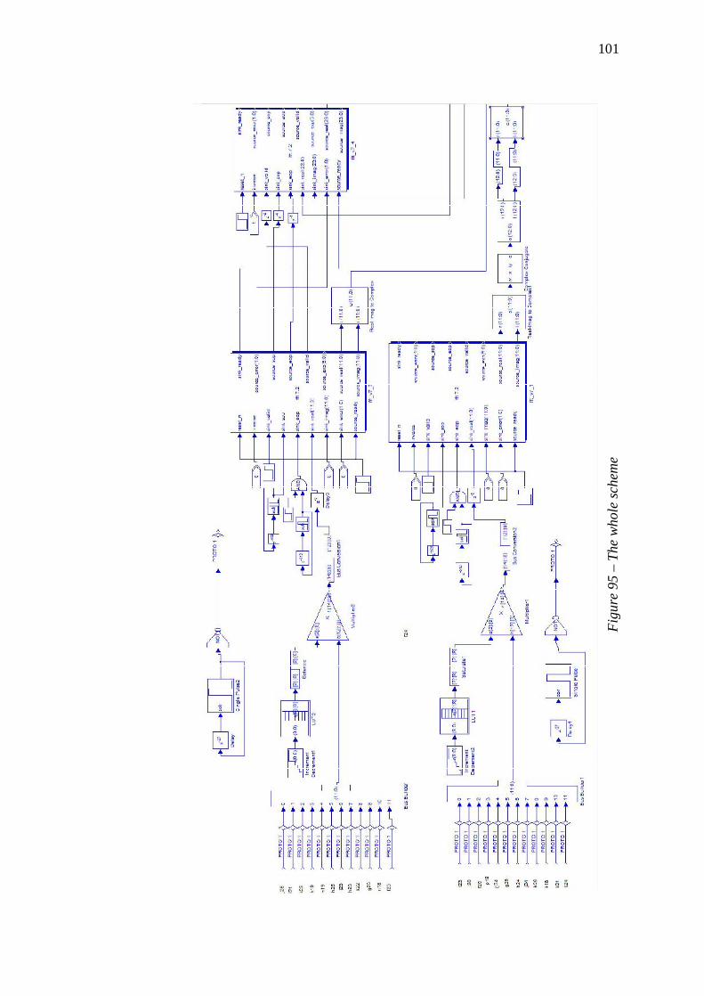
101
Figu
re 9
5 –
The
whol
e sc
hem
e
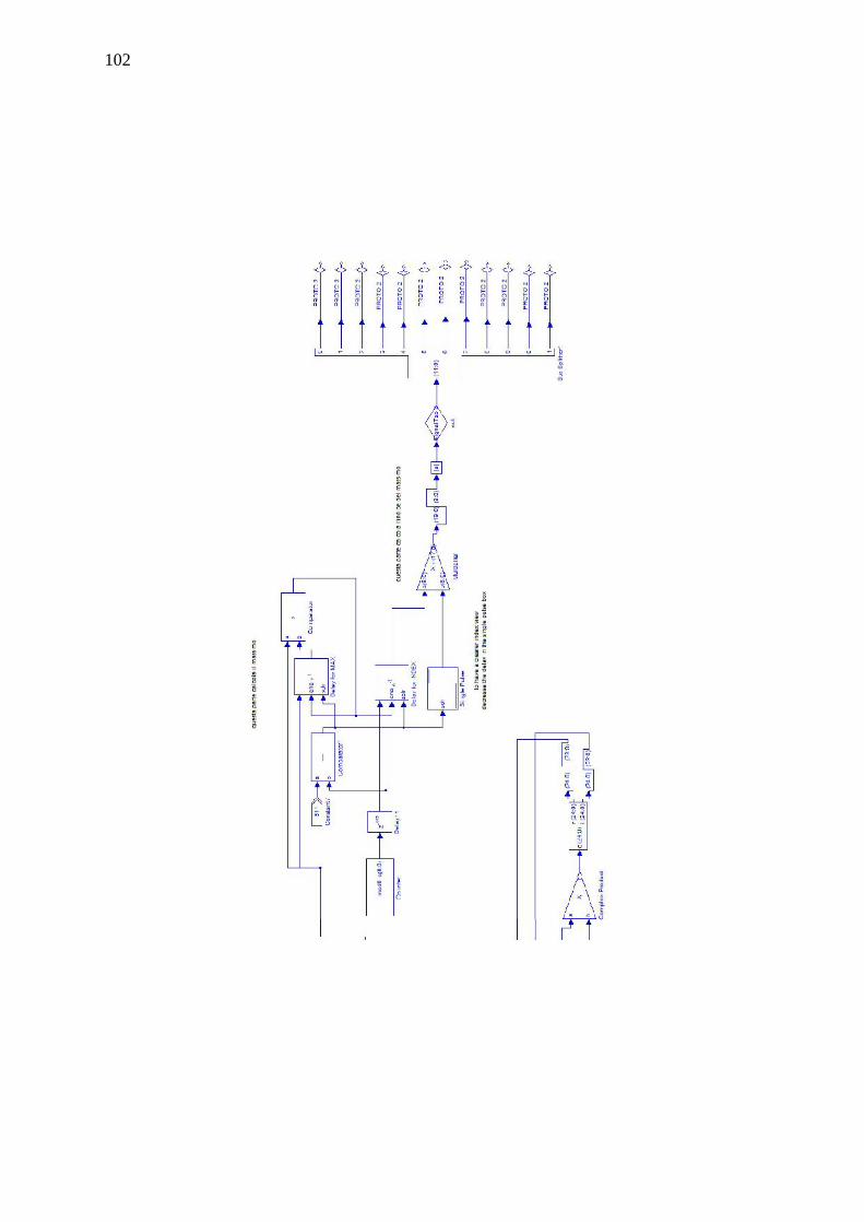
102
103
To build the real scheme a lot of consideration has to be made. First of all the scheme has to be compiled to be translated in HDL language to program
the FPGA board. The compiler works on 3 phases:
1. Create a Quartus II project 2. Run the Synthesis 3. Run the Fitter 4. Program the FPGA
On phase two the compiler translate the Simulink scheme in HDL language. On phase
three the compiler compare and analyze the resources need for the scheme created with the ones of our board.
To make the visual algorithm readable for the compiler only DSP builder blocks must be used. So all the subsystem has to be decomposed and all the simulink block has to be translated with the DSP builder ones. For example:
è
This shows that sometimes also a simple block must be translated in an understandable language for the compiler, as in this case, where a Simlink square signal generator must be translated in a DSP Builder step signal with a delayed reset input. Also from this example we can understand how much work has to be made to improve the DSP Builder software to make it more friendly for a Matlab Simulink user.
In the final scheme we substitute the simulated input signal with a 12-bit input for each signal: each port catches an input bit from the parallel port and then, together, they create the signal bus.
Two are the main issues working with the real scheme:
1. Timing 2. Resource management
5.3.1 Timing When we work only on DSP builder some consideration has to be made. First we are
not using any more the sampling time of Simulink and all the blocks are timed by the internal clock of the board. Basically we need a specific clock for two parts: the timing of the A/D board and the timing of the FFTs. The clock block establish the base clock of the board, in our case is 20 ns. We must obtain two different clocks from it. We use a PLL (Phase-Locked Loop) block: it synthesizes a clock signal that is based on a reference clock, it generates internal clocks that operate at frequencies that are multiples of the frequency of the system clock.
This block has some limitation that link together the various clocks generated, the width between maximum clock division time and multiplication time is limited. We have chosen a trade off that was also considered in the sampling time chosen for the A/D sampling.
Figure 96 – Dsp builder translation of a Simulink block
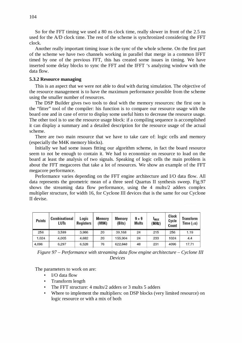
104
So for the FFT timing we used a 80 ns clock time, really slower in front of the 2.5 ns used for the A/D clock time. The rest of the scheme is synchronized considering the FFT clock.
Another really important timing issue is the sync of the whole scheme. On the first part of the scheme we have two channels working in parallel that merge in a common IFFT timed by one of the previous FFT, this has created some issues in timing. We have inserted some delay blocks to sync the FFT and the IFFT ‘s analyzing window with the data flow.
5.3.2 Resource managing This is an aspect that we were not able to deal with during simulation. The objective of
the resource management is to have the maximum performance possible from the scheme using the smaller number of resources.
The DSP Builder gives two tools to deal with the memory resources: the first one is the “fitter” tool of the compiler: his function is to compare our resource usage with the board one and in case of error to display some useful hints to decrease the resource usage. The other tool is to use the resource usage block: if a compiling sequence is accomplished it can display a summary and a detailed description for the resource usage of the actual scheme.
There are two main resource that we have to take care of: logic cells and memory (especially the M4K memory blocks).
Initially we had some issues fitting our algorithm scheme, in fact the board resource seem to not be enough to contain it. We had to economize on resource to load on the board at least the analysis of two signals. Speaking of logic cells the main problem is about the FFT megacores that take a lot of resources. We show an example of the FFT megacore performance.
Performance varies depending on the FFT engine architecture and I/O data flow. All data represents the geometric mean of a three seed Quartus II synthesis sweep. Fig.97 shows the streaming data flow performance, using the 4 mults/2 adders complex multiplier structure, for width 16, for Cyclone III devices that is the same for our Cyclone II devise.
Figure 97 – Performance with streaming data flow engine architecture – Cyclone III
Devices
The parameters to work on are: • I/O data flow • Transform length • The FFT structure: 4 mults/2 adders or 3 mults 5 adders • Where to implement the multipliers: on DSP blocks (very limited resource) on
logic resource or with a mix of both
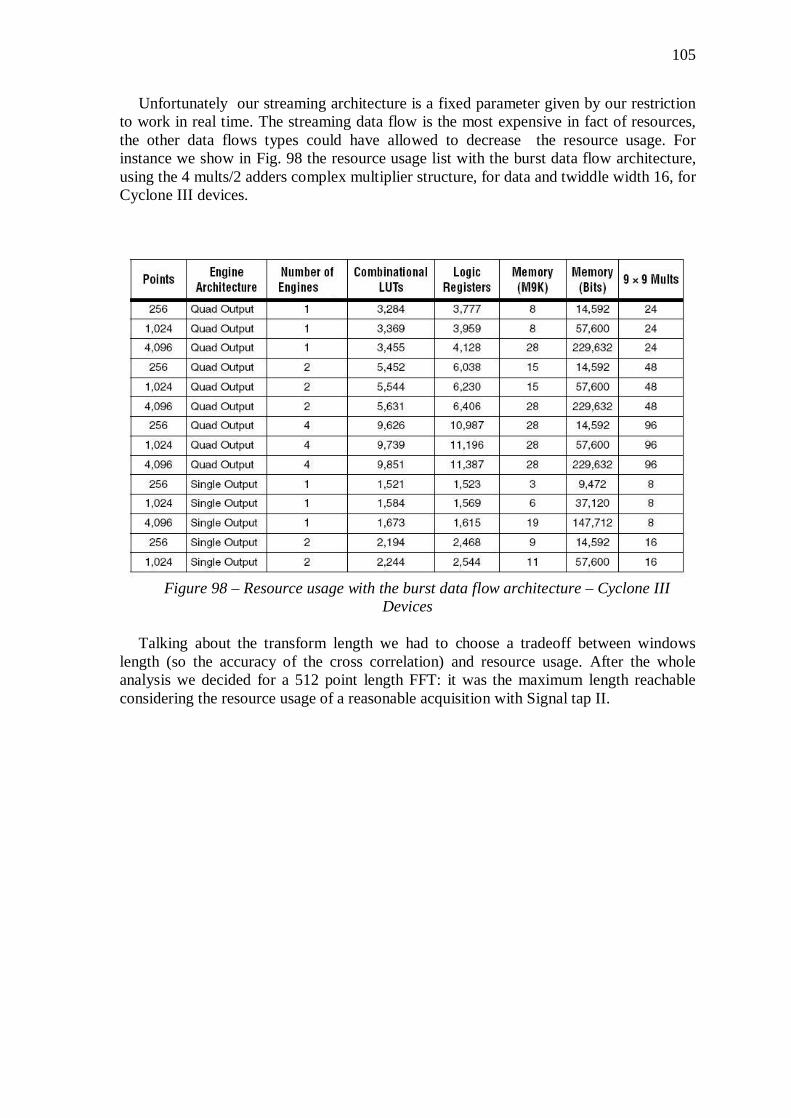
105
Unfortunately our streaming architecture is a fixed parameter given by our restriction to work in real time. The streaming data flow is the most expensive in fact of resources, the other data flows types could have allowed to decrease the resource usage. For instance we show in Fig. 98 the resource usage list with the burst data flow architecture, using the 4 mults/2 adders complex multiplier structure, for data and twiddle width 16, for Cyclone III devices.
Figure 98 – Resource usage with the burst data flow architecture – Cyclone III
Devices
Talking about the transform length we had to choose a tradeoff between windows length (so the accuracy of the cross correlation) and resource usage. After the whole analysis we decided for a 512 point length FFT: it was the maximum length reachable considering the resource usage of a reasonable acquisition with Signal tap II.
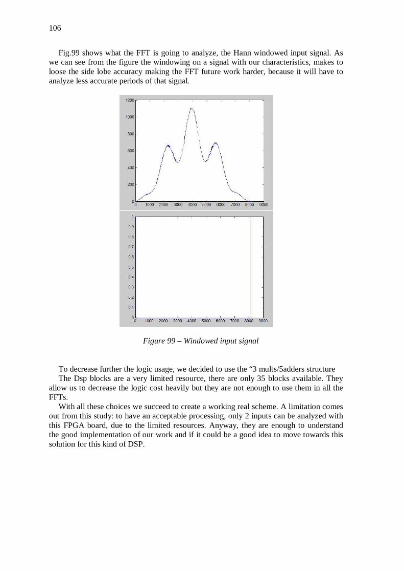
106
Fig.99 shows what the FFT is going to analyze, the Hann windowed input signal. As we can see from the figure the windowing on a signal with our characteristics, makes to loose the side lobe accuracy making the FFT future work harder, because it will have to analyze less accurate periods of that signal.
Figure 99 – Windowed input signal
To decrease further the logic usage, we decided to use the “3 mults/5adders structure The Dsp blocks are a very limited resource, there are only 35 blocks available. They
allow us to decrease the logic cost heavily but they are not enough to use them in all the FFTs.
With all these choices we succeed to create a working real scheme. A limitation comes out from this study: to have an acceptable processing, only 2 inputs can be analyzed with this FPGA board, due to the limited resources. Anyway, they are enough to understand the good implementation of our work and if it could be a good idea to move towards this solution for this kind of DSP.

107
Fig.100 shows the resource usage block of the FPGA board
Figure 100 - resource usage of the FPGA
The resource that result critics are logic cells(31345 on 35000) and M4Ks memory
block (99 on 105). Fig. 101 shows as instance the delay calculation for two signals with a phase delay of
90°. The output is constantly a delay of 12 sample that is what we was expecting for a 90° phase delay.
We notice that the channel and A/D noise doesn’t interfere in a good delay calculation: the windowing has a good role eliminating our input noise that was made of peaks for the most part.
Figure 101 - The delay calculated
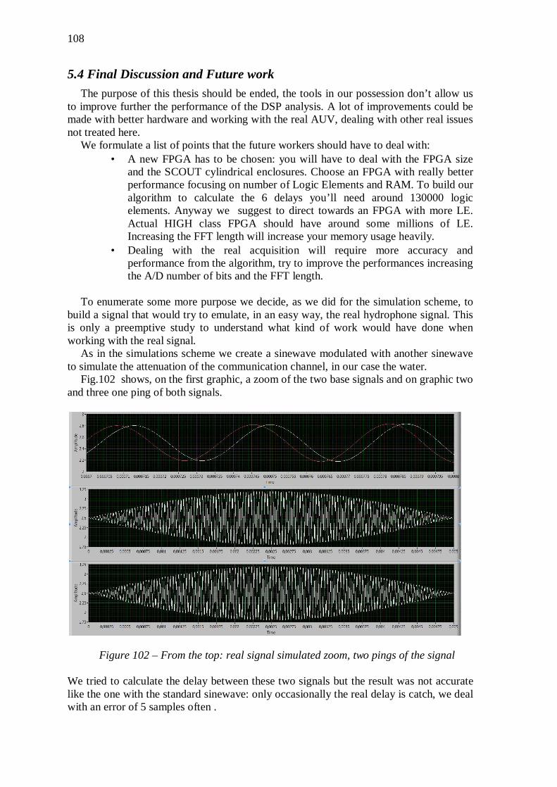
108
5.4 Final Discussion and Future work The purpose of this thesis should be ended, the tools in our possession don’t allow us
to improve further the performance of the DSP analysis. A lot of improvements could be made with better hardware and working with the real AUV, dealing with other real issues not treated here.
We formulate a list of points that the future workers should have to deal with: • A new FPGA has to be chosen: you will have to deal with the FPGA size
and the SCOUT cylindrical enclosures. Choose an FPGA with really better performance focusing on number of Logic Elements and RAM. To build our algorithm to calculate the 6 delays you’ll need around 130000 logic elements. Anyway we suggest to direct towards an FPGA with more LE. Actual HIGH class FPGA should have around some millions of LE. Increasing the FFT length will increase your memory usage heavily.
• Dealing with the real acquisition will require more accuracy and performance from the algorithm, try to improve the performances increasing the A/D number of bits and the FFT length.
To enumerate some more purpose we decide, as we did for the simulation scheme, to
build a signal that would try to emulate, in an easy way, the real hydrophone signal. This is only a preemptive study to understand what kind of work would have done when working with the real signal.
As in the simulations scheme we create a sinewave modulated with another sinewave to simulate the attenuation of the communication channel, in our case the water.
Fig.102 shows, on the first graphic, a zoom of the two base signals and on graphic two and three one ping of both signals.
Figure 102 – From the top: real signal simulated zoom, two pings of the signal We tried to calculate the delay between these two signals but the result was not accurate like the one with the standard sinewave: only occasionally the real delay is catch, we deal with an error of 5 samples often .
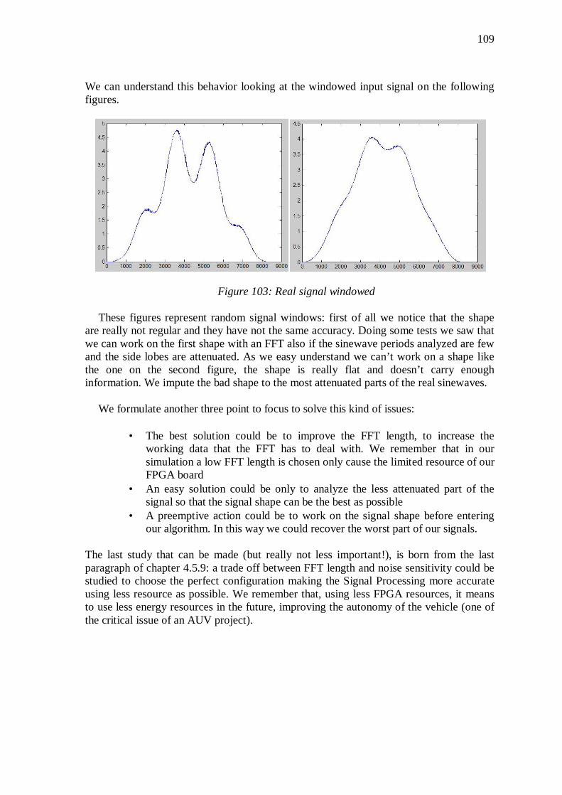
109
We can understand this behavior looking at the windowed input signal on the following figures.
Figure 103: Real signal windowed
These figures represent random signal windows: first of all we notice that the shape are really not regular and they have not the same accuracy. Doing some tests we saw that we can work on the first shape with an FFT also if the sinewave periods analyzed are few and the side lobes are attenuated. As we easy understand we can’t work on a shape like the one on the second figure, the shape is really flat and doesn’t carry enough information. We impute the bad shape to the most attenuated parts of the real sinewaves.
We formulate another three point to focus to solve this kind of issues:
• The best solution could be to improve the FFT length, to increase the working data that the FFT has to deal with. We remember that in our simulation a low FFT length is chosen only cause the limited resource of our FPGA board
• An easy solution could be only to analyze the less attenuated part of the signal so that the signal shape can be the best as possible
• A preemptive action could be to work on the signal shape before entering our algorithm. In this way we could recover the worst part of our signals.
The last study that can be made (but really not less important!), is born from the last paragraph of chapter 4.5.9: a trade off between FFT length and noise sensitivity could be studied to choose the perfect configuration making the Signal Processing more accurate using less resource as possible. We remember that, using less FPGA resources, it means to use less energy resources in the future, improving the autonomy of the vehicle (one of the critical issue of an AUV project).
110
6. CONCLUSIONS A preemptive and experimental study is made to improve the UCF Robotic team’s
work on the AUVSI competition of 2007. The thesis focused on the trajectory tracking objective of the competition. The state of art is analyzed and a new solution is chosen to give the AUV new tracking performances. An FPGA is chosen for the Signal Processing to go beyond the previous limits. We analyzed the FPGA market to understand where the trend is going to, and to choose a board according to our experimental needs.
An algorithm based on a cross correlation analysis is created, and tested on computer simulation and with experimental tools. The algorithm creation was limited by the hardware chosen but the experimental results are exhaustive to make the FPGA solution a good choice for an underwater signal processing. The algorithm is accurate and has a good noise rejection.
A real experiment with real hydrophones signals is not done yet. This is left to who will deal with the real AUV and with more real issues
Lot of improvements can be made with a new hardware and new founds. The FPGA world is actually in full evolution and can give a new range of solutions and ideas for future analysis.

111
BIBLIOGRAFY
[1] Alt, C. Autonomous Underwater vehicles. Retrieved from http://www.geo-prose.com/ALPS/white_papers/alt.pdf
[2] Blidberg, D. The Development of Autonomous Underwater Vehicles (AUV). Retrieved from http://ausi.org/publications/ICRA_01paper.pdf abgerufen
[3] Panez, R. (2004). Simplified method to obtain navigational information. Retrieved from http://www.mil.ufl.edu/publications/thes_diss/Rolando_Panez_thesis.pdf abgerufen
[4] Vines Faria de Lima, F., & Massatoshi Furukawa, C. Development and Testing of an Acoustic Positioning System – Description and Signal Processing.
[5] Postolache, O., Girao, P., & Pereira, M. Underwater Acoustic Source Localization Based on Passive Sonar and Intelligent Processing.7
[6] FPGA Tutorial. Retrieved from http://www.tutorial-reports.com/book/print/260 [7] Acromag. Custom board level solutions. [8] Sean Bean, J. H. (2007). SCOUT, The University of Central Florida’s 2007
Autonomous Underwater Vehicle. [9] Loomis, J. S.. Cross Correlation. Retrieved from
http://www.johnloomis.org/ece561/notes/xcorr/xcorr.html abgerufen [10] BORES Signal Processing. FFT windows Function [11] Window function. Retrieved from Wikipedia:
http://en.wikipedia.org/wiki/Window_function abgerufen [12] Altera. FFT MegaCore Function - User Guide. [13] Devices, A.. AD7482. Retrieved from http://www.analog.com/static/imported-
files/data_sheets/AD7482.pdf abgerufen [14] Altera. Introduction to the Quartus II Software.

112
APPENDIX A – HOW TO PROGRAM AN FPGA [14]
The first step to use the board that must accomplish to our project is to find a way to manage it. The Altera Corporation furnish a global software for their FPGAs that can fit the most of needs. This software is the Quartus 2.
QUARTUS 2
Due to the significant increase in FPGA device densities over the last few years, designs are increasingly complex and may involve multiple designers. The inherent flexibility of advanced FPGAs means that the pin layout, power consumption, and timing performance for each design block are all dependent on the final design implementation. The system architect must resolve these design issues when integrating design blocks, often leading to problems that affect the overall time to market and thereby increase cost. Many potential problems can be solved earlier in the design cycle by selecting the optimal device and programming method, properly planning I/O pin locations, estimating power consumption, selecting appropriate third-party tools, planning for in-system debugging options, performing good design partitioning for incremental compilation, and obtaining early timing estimates. The first step in using Quartus2 Software is to consider our design priorities. What are the important factors for our design? More device features, density, or performance can increase system cost. Signal integrity and board issues may impact I/O pin locations. Power, timing performance, and area utilization affect each other, and compilation time is affected by optimizations for these factors. The Quartus® II software optimizes designs for the best average results, but we can change settings to focus on one aspect of the design results and trade off other aspects. Design flow The Altera Quartus II design software provides a complete, multiplatform design environment that easily adapts to our specific design needs. It is a comprehensive environment for system-on-a-programmable-chip (SOPC) design. The Quartus II software includes solutions for all phases of FPGA and CPLD design (Figure 104).
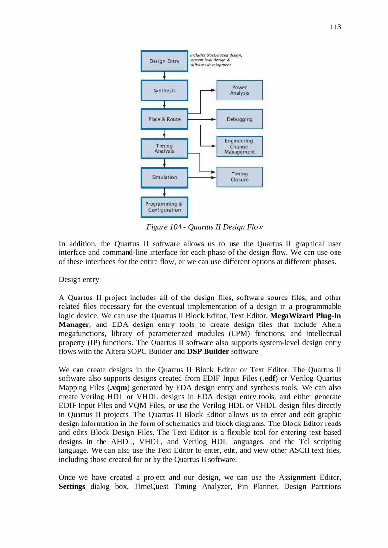
113
Figure 104 - Quartus II Design Flow
In addition, the Quartus II software allows us to use the Quartus II graphical user interface and command-line interface for each phase of the design flow. We can use one of these interfaces for the entire flow, or we can use different options at different phases. Design entry A Quartus II project includes all of the design files, software source files, and other related files necessary for the eventual implementation of a design in a programmable logic device. We can use the Quartus II Block Editor, Text Editor, MegaWizard Plug-In Manager, and EDA design entry tools to create design files that include Altera megafunctions, library of parameterized modules (LPM) functions, and intellectual property (IP) functions. The Quartus II software also supports system-level design entry flows with the Altera SOPC Builder and DSP Builder software. We can create designs in the Quartus II Block Editor or Text Editor. The Quartus II software also supports designs created from EDIF Input Files (.edf) or Verilog Quartus Mapping Files (.vqm) generated by EDA design entry and synthesis tools. We can also create Verilog HDL or VHDL designs in EDA design entry tools, and either generate EDIF Input Files and VQM Files, or use the Verilog HDL or VHDL design files directly in Quartus II projects. The Quartus II Block Editor allows us to enter and edit graphic design information in the form of schematics and block diagrams. The Block Editor reads and edits Block Design Files. The Text Editor is a flexible tool for entering text-based designs in the AHDL, VHDL, and Verilog HDL languages, and the Tcl scripting language. We can also use the Text Editor to enter, edit, and view other ASCII text files, including those created for or by the Quartus II software. Once we have created a project and our design, we can use the Assignment Editor, Settings dialog box, TimeQuest Timing Analyzer, Pin Planner, Design Partitions
114
window, and the Chip Planner to specify initial design constraints, such as pin assignments, device options, logic options, and timing constraints. Synthesis We can use the Analysis & Synthesis module of the Compiler to analyze our design files and create the project database. Analysis & Synthesis uses Quartus II Integrated Synthesis to synthesize our Verilog Design Files (.v) or VHDL Design Files (.vhd) We can start a full compilation in the Quartus II software, which includes the Analysis & Synthesis module, or we can start Analysis & Synthesis separately. We can perform an Analysis & Elaboration to check a design for syntax and semantic errors without performing a complete Analysis & Synthesis or check a single design file for syntax errors. Place & Route The Quartus II Fitter places and routes your design, which is also referred to as “fitting” in the Quartus II software. Using the database that has been created by Analysis & Synthesis, the Fitter matches the logic and timing requirements of the project with the available resources of the target device. It assigns each logic function to the best logic cell location for routing and timing, and selects appropriate interconnection paths and pin assignments. If we have made resource assignments in our design, the Fitter attempts to match those resource assignments with the resources on the device, tries to meet any other constraints we have set, and then attempts to optimize the remaining logic in the design. If we have not set any constraints on the design, the Fitter automatically optimizes it. If it cannot find a fit, the Fitter terminates compilation and issues an error message. Power Analysis The Quartus II PowerPlay Power Analysis Tools provide an interface that allows us to estimate static and dynamic power consumption throughout the design cycle. The PowerPlay Power Analyzer performs postfitting power analysis and produces a power report that highlights, by block type and entity, the power consumed. The Altera PowerPlay Early Power Estimator estimates power consumption at other stages of the design process and produces a Microsoft Excel-based spreadsheet with estimate information. Debugging The Quartus II SignalTap II Logic Analyzer, the External Logic Analyzer Interface, the SignalProbe feature, the In-System Memory Content Editor, and the In-System Sources and Probes Editor enable us to analyze internal device nodes and I/O pins while operating in-system and at system speeds. The SignalTap II Logic Analyzer is an embedded logic analyzer that routes the signal data through the JTAG port to the Quartus II software based on user-defined trigger conditions. We can use the External Logic Analyzer Interface to connect an off-chip logic analyzer to nodes in the design. The SignalProbe feature uses otherwise unused device routing resources to route selected signals to an external logic analyzer or oscilloscope. The In-System Memory Content and In-System Sources and Probes Editors allow us to view and modify, at run-time, data in a design.
115
Engeneering change menagement The Quartus II software allows us to make small modifications, often referred to as engineering change orders (ECO), to a design after a full compilation. These ECO changes can be made directly to the design database, rather than to the source code or the Quartus II Settings File (.qsf). Making the ECO change to the design database allows us to avoid running a full compilation in order to implement the change Timing Analysis The Quartus II Time Quest Timing Analyzer allows us to analyze the performance of all logic in our design and help to guide the Fitter to meet timing requirements. The TimeQuest analyzer uses industry-standard Synopsys Design Constraint (SDC) methodology for constraining designs and reporting results. We can use the information generated by the timing analyzer to analyze, debug, and validate the timing performance of your design. Simulation We can perform functional and timing simulation of our design by using EDA simulation tools or the Quartus II Simulator. The Quartus II software provides the following features for performing simulation of designs in EDA simulation tools:
• NativeLink integration with EDA simulation tools • Generation of output netlist files • Functional and timing simulation libraries • Generation of test bench template and Memory Initialization Files • (.mif) • Generation of Signal Activity Files (.saf) for power analysis
Timing Closures The Quartus II software offers a fully integrated timing closure flow that allows us to meet our timing goals by controlling the synthesis and place and route of a design. Using the timing closure flow results in faster timing closure for complex designs, reduced optimization iterations, and automatic balancing of multiple design constraints. The timing closure flow allows us to perform an initial compilation, view design results, and perform further design optimization efficiently. Programming and configuration Once we have successfully compiled a project with the Quartus II software, we can program or configure an Altera device. The Assembler module of the Quartus II Compiler generates programming files that the Quartus II Programmer can use to program or configure a device with Altera programming hardware. We can also use a stand-alone version of the Quartus II Programmer to program and configure devices. The Assembler automatically converts the Fitter’s device, logic cell, and pin assignments into a programming image for the device, in the form of one or more Programmer Object Files (.pof) or SRAM Object Files (.sof) for the target device.
116
DSP BUILDER The QUARTUS 2 is a really powerful tool that allow to program the FPGAs in their full complexity. Like all the low level program tools it is less useful in case of some more general application or high level programming. In our case we will have to deal with some DSP application so we will need some MACRO functions and some more visual language to program our FPGA in an easy way. This is the reason why we choose the DPS BUILDER. Digital signal processing (DSP) system design in Altera programmable logic devices (PLDs) requires both high-level algorithm and hardware description language (HDL) development tools. The Altera DSP Builder integrates these tools by combining the algorithm development, simulation, and verification capabilities of The MathWorks MATLAB and Simulink system-level design tools with VHDL and Verilog HDL design flows, including the Altera Quartus II software. DSP Builder shortens DSP design cycles by helping us create the hardware representation of a DSP design in an algorithm-friendly development environment. We can combine existing MATLAB functions and Simulink blocks with Altera DSP Builder blocks and Altera intellectual property (IP) MegaCore® functions to link system-level design and implementation with DSP algorithm development. In this way, DSP Builder allows system, algorithm, and hardware designers to share a common development platform. We can use the blocks in DSP Builder to create a hardware implementation of a system modeled in Simulink in sampled time. DSP Builder contains bit- and cycle-accurate Simulink blocks—which cover basic operations such as arithmetic or storage functions—and takes advantage of key device features such as built-in PLLs, DSP blocks, or embedded memory. We can integrate complex functions by using MegaCore functions in your DSP Builder model. We can also experience the faster performance and richer instrumentation of hardware co-simulation by implementing parts of our design in an FPGA. The DSP Builder Signal Compiler block reads Simulink Model Files (.mdl) that are built using DSP Builder and MegaCore functions and generates VHDL files and Tcl scripts for synthesis, hardware implementation, and simulation. High-Speed DSP with Programmable Logic, an FPGA advantage Programmable logic offers compelling performance advantages over dedicated digital signal processors. Programmable logic can be thought of as an array of elements, each of which can be configured as a complex processor routine. These processor routines can then be linked together in serial (the same way digital signal processor would execute them), or they can be connected in parallel. In parallel, they offer many times the performance of standard digital signal processors by executing hundreds of instructions at the same time. Algorithms that benefit from this improved performance include forward-error correction (FEC), modulation/demodulation, and encryption.
117
FIGURE INDEX
Figure 1 - Robert Whitehaed with his first Torpedo................................................... 14 Figure 2 – WHOI’s ABE ........................................................................................... 15 Figure 3 - A typical Energy system focused AUV ...................................................... 17 Figure 5 - The hydrophones array for Subjugator 2000 ............................................ 21 Figure 4 - The Subjugator 2000 ................................................................................ 21 Figure 6 - The amplifier circuit schematic ................................................................ 22 Figure 7 - Signal processing board architecture ....................................................... 23 Figure 8 - The USBL positioning system ................................................................... 25 Figure 9 - Block diagram of the processing unit ........................................................ 25 Figure 10 - Hardware schematics ............................................................................. 27 Figure 11 - Simplified version of FPGA internal architecture ................................... 29 Figure 12 - the different parts of an FPGA................................................................ 29 Figure 13 - FPGA comparative analysis ................................................................... 30 Figure 14 - Transistor pair tiles in cross-point FPGA ............................................... 31 Figure 15 - The Plessey logic block .......................................................................... 31 Figure 16 - An Actel logic block ................................................................................ 32 Figure 17 - Four input LUT based Xilinx logic Block ................................................ 32 Figure 18 - 2-LUT implementation table ................................................................... 33 Figure 19 - Xilinx routing architecture ..................................................................... 34 Figure 20 - Actel FPGA routing architecture ............................................................ 35 Figure 21 - Altera MAX 5000 global (top) and local (bottom) routing architecture ... 36 Figure 22 - A symmetrical Array ............................................................................... 37 Figure 24 - A hierarchical PLD ............................................................................... 38 Figure 23 - A row based architecture ........................................................................ 38 Figure 25 - RAM cells used to control pass gates (a) or multiplexers (b) ................... 39 Figure 26 – Floating gate programming technology ................................................. 39 Figure 27 - Example circuit: a collection of gates and flip-flops ............................... 41 Figure 28 - A basic FPGA module example .............................................................. 44 Figure 29 - A mid-size FPGA module example .......................................................... 45 Figure 30 - A large size, high speed FPGA module example ..................................... 46 Figure 32 – The trade off between cost and performance for FPGA boards .............. 47 Figure 31 – General view on various FPGA boards .................................................. 47 Figure 33 – Pentek 6256 ........................................................................................... 49 Figure 34 – Innovative integration X3A4D4.............................................................. 50 Figure 35 - Echotek ECAD-DA-41-PMC ................................................................ 51 Figura 36 - Bittware TETRA-PMC+ ........................................................................ 52 Figure 37 - Cyclone II EP2C70 DSP development board .......................................... 54 Figure 38 - ALTERA/TERASIC DE2 ......................................................................... 56 Figure 39 - MAX1127 ............................................................................................... 57 Figure 40 – The A/D board: The electric development scheme .................................. 58 Figure 41 - The A/D board: assembled view ............................................................. 58 Figure 42 – The AD7482 .......................................................................................... 59 Figure 43 - NI USB-6251 DAQ board ....................................................................... 60 Figure 44 - The experimental setup ........................................................................... 62 Figure 45 – The competition obstacle course ............................................................ 63 Figure 46 - The Scout ............................................................................................... 64
118
Figure 47 - The scout: hardware view ...................................................................... 65 Figure 48 – The Scout: the frame .............................................................................. 65 Figure 50 – The hydrophones pattern ....................................................................... 66 Figure 49 - The Scout: an Hydrophone ..................................................................... 66 Figure 51 - An hydrophone's acquisition sample ....................................................... 67 Figure 52 - Hydrophone's characteristics ................................................................. 67 Figure 53 – The idea for the trajectory tracking ....................................................... 68 Figure 54 – The flow diagram for the delay extraction ............................................. 69 Figure 55 - Delay extraction scheme ........................................................................ 74 Figure 56 - Cross correlation of two identical signals .............................................. 74 Figure 57 – Cross correlation of two delayed signals ............................................... 75 Figure 58 – The simulation scheme........................................................................... 76 Figure 60 – The simulated input signal ..................................................................... 77 Figure 59 – Utility blocks ......................................................................................... 77 Figure 61 - The windowing scheme........................................................................... 78 Figure 62 - Characteristics for various window ........................................................ 79 Figure 63 - Hann window in function of time and his frequency response ................. 80 Figure 64 - Windowed input signal ........................................................................... 80 Figure 65 - The FFT scheme ..................................................................................... 81 Figure 66 - Quad-Output FFT Engine Architecture .................................................. 85 Figure 67- Single-Output FFT Engine Architecture .................................................. 85 Figure 68 - FFT mecagore Timing ............................................................................ 86 Figure 69 – FFT output. From the top we can see the imaginary response then ........ 87 Figure 70 - The product scheme ............................................................................... 87 Figure 71 - Cross correlation information extraction................................................ 88 Figure 72 - Cross correlation: 1024 point FFT length .............................................. 88 Figure 73 – Cross correlation: 512 point FFT length ............................................... 89 Figure 74 – Cross correlation: decreased sample rate .............................................. 89 Figure 75 – Simulink block to calculate the maximum .............................................. 89 Figure 76 – Delay calculation scheme ...................................................................... 90 Figure 77 – Windowed input signal with noise .......................................................... 91 Figure 78 – The attenuated signal simulation ........................................................... 91 Figure 79 – Cross correlation of the signals: 256 point length FFT .......................... 92 Figure 80 – Cross correlation of the disturbed signals: 256 points length FFT ......... 92 Figure 81 – Cross correlation of the signals: 512 point length FFT .......................... 92 Figure 84 - Cross correlation of the disturbed signals: 1024 point length FFT ......... 93 Figure 82 – Cross correlation of the disturbed signals: 512 point length FFT .......... 93 Figure 83 - Cross correlation of the signals: 1024 point length FFT......................... 93 Figure 85 – Labview scheme for the simulated input signals ..................................... 95 Figure 86 - The signals generated ............................................................................ 95 Figura 87 - Memory usage of Signal Tap II .............................................................. 96 Figure 88 – Parallel mode 2 timing for the AD7482 ................................................. 96 Figure 89 - Timing characteristics for the AD7482 ................................................... 97 Figure 90 - Acquisition test scheme .......................................................................... 98 Figure 91 - AD7482 timing for a 1.27 MHz acquisition ............................................ 99 Figure 92 - Signal Tap II signal acquisition .............................................................. 99 Figure 93 - AD7482 timing increasing sampling frequency .....................................100 Figure 94 - Signal Tap II acquisition with an increased sampling fequency .............100 Figura 96 – The whole scheme ................................................................................101 Figure 97 – Dsp builder translation of a Simulink block ..........................................103

119
Figure 97 – Performance with streaming data flow engine architecture – Cyclone III Devices........................................................................................................................ 104
Figure 98 – Resource usage with the burst data flow architecture – Cyclone III Devices........................................................................................................................ 105
Figure 99 – Windowed input signal......................................................................... 106 Figure 100 - resource usage of the FPGA ............................................................... 107 Figure 101 - The delay calculated ........................................................................... 107 Figure 102 – From the top: real signal simulated zoom, two pings of the signal ..... 108 Figure 103: Real signal windowed .......................................................................... 109 Figure 104 - Quartus II Design Flow ...................................................................... 113