Service Manual - Recherche de manuels
63
ViewSonic VG2230wm-3 Model No. VS11422 22” Color TFT LCD Display (VG2230wm-3_SM Rev. 1a May. 2009) ViewSonic 381 Brea Canyon Road, Walnut, California 91789 USA - (800) 888-8583 Service Manual
-
Upload
khangminh22 -
Category
Documents
-
view
0 -
download
0
Transcript of Service Manual - Recherche de manuels

ViewSonic VG2230wm-3 Model No. VS11422
22” Color TFT LCD Display
(VG2230wm-3_SM Rev. 1a May. 2009)
ViewSonic 381 Brea Canyon Road, Walnut, California 91789 USA - (800) 888-8583
Service Manual

2
Copyright Copyright © 2008 by ViewSonic Corporation. All rights reserved. No part of this publication may be reproduced, transmitted, transcribed, stored in a retrieval system, or translated into any language or computer language, in any form or by any means, electronic, mechanical, magnetic, optical, chemical, manual or otherwise, without the prior written permission of ViewSonic Corporation. Disclaimer ViewSonic makes no representations or warranties, either expressed or implied, with respect to the contents hereof and specifically disclaims any warranty of merchantability or fitness for any particular purpose. Further, ViewSonic reserves the right to revise this publication and to make changes from time to time in the contents hereof without obligation of ViewSonic to notify any person of such revision or changes. Trademarks Optiquest is a registered trademark of ViewSonic Corporation. ViewSonic is a registered trademark of ViewSonic Corporation. All other trademarks used within this document are the property of their respective owners. Product disposal at end of product life The lamp in this product contains mercury. Please dispose of in accordance with local, state or federal laws.
Revision History Revision SM Editing Date Description of Changes TPV Model Editor
1a 05/20/2009 Initial Release TC9MRLDBDWVSDN
TC9MRLDKDWVSDN Eric

3
TABLE OF CONTENTS
1. Precautions and Safety Notices ......................................................................................... 4
2. Specification ....................................................................................................................... 6
3. Front Panel Function Control Description ....................................................................... 7
4. Circuit Description............................................................................................................. 12
5. Adjusting Procedure.......................................................................................................... 24
6. Trouble Shooting Flow Chart ............................................................................................ 33
7. Block Diagrams ................................................................................................................ 34
8. Schematic Diagrams ........................................................................................................ 36
9. PCB Layout Diagrams ...................................................................................................... 45
10. Exploded Diagram and Spare Parts List ........................................................................ 50
11. Recommended Spare Parts List...................................................................................... 61
12. Different Parts List ......................................................................................................... 62

4
1. Precautions and Safety Notices 1.1 Safety Precautions This monitor is manufactured and tested on a ground principle that a user’s safety comes first. However, improper
use or installation may cause damage to the monitor as well as the user. Carefully go over the following WARNINGS
before installing and keep this guide handy.
WARNINGS .This monitor should be operated only at the correct power sources indicated on the label on the rear end of the
monitor. If you’re unsure of the power supply in your residence, consult you local dealer or power company.
.Use only the special power adapter that comes with this monitor for power input.
.Do not try to repair the monitor your self as it contains no user-serviceable parts. This monitor should only be
repaired by a qualified technician.
.Do not remove the monitor cabinet. There is high-voltage parts inside that may cause electric shock to human
bodies, even when the power cord is unplugged.
.Stop using the monitor if the cabinet is damaged. Have it checked by a service technician.
.Put your monitor only in a clean, dry environment. If it gets wet, unplug the power cable immediately and consult
your service technician.
.Always unplug the monitor before cleaning it .Clean the cabinet with a clean, dry cloth. Apply non-ammonia based
cleaner onto the cloth, not directly onto the glass screen.
.Keep the monitor away from magnetic objects, motors, TV sets, and transformer.
.Do not place heavy objects on the monitor or power cord.
1.2 Product Safety Notice Many electrical and mechanical parts in this chassis have special safety visual inspections and the protection
afforded by them cannot necessarily be obtained by using replacement components rated for higher voltages,
wattage, etc. Before replacing any of these components read the parts list in this manual carefully. The use of
substitute replacement parts which do not have the same safety characteristics as specified in the parts list may
create shock, fire, or other hazards.
1.3 Service Notes 1. When replacing parts or circuit boards, clamp the lead wires around terminals before soldering.
2. When replacing a high wattage resistor (more than 1W of metal oxide film resistor) in circuit board, keep the
resistor about 5mm away from circuit board.
3. Keep wires away from high voltage, high temperature components and sharp edges.
4. Keep wires in their original position so as to reduce interference.
5. Usage of this product please refer to also user’s manual.

5
1.4 Handing and Placing Methods
Correct methods : Incorrect Methods :
Only touch the metal-frame of the panel or the front
cover of the monitor.
Do not touch the surface of the polarizer .
Surface of the panel is pressed by fingers & this may
cause “ MURA “
Take out the monitor with cushion Take out the monitor by grasping the LCD panel.
That may cause “ MURA“.
Place the monitor on a clean & soft foam pad . Place the monitor on foreign objects .
That could scratch the surface of panel

6
2. Specification

7
3. Front Panel Function Control Description Use the buttons on the front control panel to display and adjust the OSD controls which display on the screen. The
OSD controls are explained at the top of the next page and are defined in “Main Menu Controls”.

8
Do the following to adjust the display setting: 1. To display the Main Menu, press button [1].
NOTE: All OSD menus and adjustment screens disappear automatically after about 15 seconds. This is adjustable
through the OSD timeout setting in the setup menu.
2. To select a control to adjust, press or to scroll up or down in the Main Menu.
3. After the desired control is selected, press button [2]. A control screen like the one shown below appears.
4. To adjust the control, press the up or down buttons.
5. To save the adjustments and exit the menu, press button [1] twice.
The following tips may help you optimize your display:
• Adjust the computer's graphics card so that it outputs a 1680 x 1050 @ 60Hz video signal to the LCD display.
(Look for instructions on “changing the refresh rate” in the graphics card's user guide.)
• If necessary, make small adjustments using H. POSITION and V. POSITION until the screen image is completely
visible. (The black border around the edge of the screen should barely touch the illuminated “active area” of the LCD
display.)
The command line at the bottom of the
control screen tells what to do next from
this screen. You can toggle between
control

9
Main Menu Controls Adjust the menu items shown below by using the up and down buttons.
Control Explanation
Auto Image Adjust automatically sizes, centers, and fine tunes the video signal to eliminate
waviness and distortion. Press the [2] button to obtain a sharper image.
NOTE: Auto Image Adjust works with most common video cards. If this function does not work on
your LCD display, then lower the video refresh rate to 60 Hz and set the resolution to its pre-set
value.
Contrast adjusts the difference between the image background (black level) and the foreground
(white level).
Brightness adjusts background black level of the screen image.
Input Select toggles between inputs if you have more than one computer connected to the LCD
Display.
Audio Adjust
Volume increases the volume, decreases the volume, and mutes the audio.
Mute temporarily silences audio output.
Color Adjust provides several color adjustment modes, including preset color temperatures and
a User Color mode which allows independent adjustment of red (R), green (G), and blue (B). The
factory setting for this product is 6500K (6500 Kelvin).
sRGB-This is quickly becoming the industry standard for color management, with support being
included in many of the latest applications. Enabling this setting allows the LCD display to more
accurately display colors the way they were originally intended. Enabling the sRGB setting will
cause the Contrast and Brightness adjustments to be disabled.
9300K-Adds blue to the screen image for cooler white (used in most office settings with
fluorescent lighting).
7500K-Adds blue to the screen image for cooler white (used in most office settings with
fluorescent lighting).
6500K-Adds red to the screen image for warmer white and richer red.
5400K-Adds green to the screen image for a darker color.
User Color Individual adjustments for red (R), green (G), and blue (B).
1. To select color (R, G or B) press button [2].
2. To adjust selected color, press and .
Important: If you select RECALL from the Main Menu when the product is set to a Preset Timing

10
Mode, colors return to the 6500K factory preset.
Information displays the timing mode (video signal input) coming from the graphics card in the
computer, the LCD model number, the serial number, and the ViewSonic® website URL. See your
graphics card’s user guide for instructions on changing the resolution and refresh rate (vertical
frequency).
NOTE: VESA 1920 x 1080 @ 60Hz (recommended) means that the resolution is 1920 x 1080 and
the refresh rate is 60 Hertz.
Manual Image Adjust displays the Manual Image Adjust menu.
H./V. Position (Horizontal/Vertical Position) moves the screen image left or right and up or
down.
H. Size (Horizontal Size) adjusts the width of the screen image.
Fine Tune sharpens the focus by aligning text and/or graphics with pixel boundaries.
NOTE: Try Auto Image Adjust first.
Sharpness adjusts the clarity and focus of the screen image.
Aspect ratio Selects the image size for 4:3 and full screen.
ECO Mode provides the lower power consumption by reducing the brightness.
Standard: The default brightness setting.
Optimize: Decreases the brightness by 25 %.
Conserve: Decreases the brightness by 50 %.
NOTE: When the ECO Mode is set to "Optimize" or "Conserve", the Brightness, Contrast, and
Dynamic Contrast cannot be adjusted.

11
Setup Menu displays the menu shown below:
Language Select allows the user to choose the language used in the menus and control
screens.
Resolution Notice advises the optimal resolution to use.
If you enable the Resolution Notice shown above and your computer is set at a resolution other
than 1680 x 1050, the following screen appears.
OSD Position allows the user to move the OSD menus and control screens.
OSD Timeout sets the length of time the OSD screen is displayed. For example, with a “15
second” setting, if a control is not pushed within 15 seconds, the display screen disappears.
OSD Background allows the user to turn the OSD background On or Off.
Memory Recall returns the adjustments back to factory settings if the display is operating
in a factory Preset Timing Mode listed in the Specifications of this manual.

12
4. Circuit Description 4.1 Main Board
General Embedded dual DDC with DDC1/2B/CI Zoom scaling up and down No external memory required. Require only one crystal to generate all timing. Programmable 3.3V/5V detection reset output. Embedded crystal output to micro-controller. 3 channels 8 bits PWM output, and wide range selectable PWM frequency. Analog RGB Input Interface Integrated 8-bit triple-channel 210/165 (optional) MHz ADC/PLL Embedded programmable Schmitt trigger of HSYNC Support Sync On Green (SOG) and various kindsof composite sync modes On-chip high-performance hybrid PLLs High resolution true 64 phase ADC PLL Y/Pb/Pr support up to HDTV 1080i resolution Support 1 Analog input Digital Video Input Interface Built-in YUV to RGB color space converter & de-interlace DVI Compliant Digital Input Interface (optional) Single link on-chip TMDS receiver Support to 165Mhz with long cable Adaptive algorithm for TMDS capability Data enable only mode support High-Bandwidth Digital Content Protection (HDCP 1.1) (optional only in H version) Enhanced protection of HDCP secret key (optional only in H version) Auto Detection /Auto Calibration Input format detection Compatibility with standard VESA mode and support user-defined mode Smart engine for Phase/Image position/Color calibration Scaling Fully programmable zoom ratios Independent horizontal/vertical scaling Advanced zoom algorithm provides high image quality Sharpness/Smooth filter enhancement Support non-linear scaling from 4:3 to 16:9 or 16:9 to 4:3
Vivid Color™ Dynamic Contrast Control (DCC) Independent Color Management (ICM) Scalar--- RTD2554VH-GR (U6) True 10 bits color processing engine sRGB compliance Advanced Dithering logic for 18-bit panel color depth enhancement Dynamic overshoot-smear canceling engine Brightness and contrast control Programmable 10-bit gamma support Output Interface Fully programmable display timing generator Flexible data pair swapping for easier system design. Programmable TCON function support RSDS-output interface on single PCB Spread-Spectrum DPLL to reduce EMI Fixed Last Line output for perfect panel capability Host Interface Support MCU serial/parallel bus interface. Support MCU dual edge data latch. Embedded OSD Embedded 12K SRAM dynamically stores OSD command and fonts Support multi-color RAM font, 1, 2 and 4-bit per pixel 16 color palette with 24bit true color selection Maximum 8 window with alpha-blending/ gradient/dynamic fade-in/fade-out, bordering/ shadow/3D window type Rotary 90,180,270 degree Independent row shadowing/bordering Programmable blinking effects for each character OSD-made internal pattern generator for factory mode Support 12x18~4x18 proportional font Decompress OSD font Power & Technology 3.3V power supplier 0.18um CMOS process, 128-pin QFP package

13
Block Diagram

14
Pin Description Input Port
Name I/O No Description Note
AVS0 I 19 1st ADC vertical sync input
Power from PIN 13
no power 5V
tolerance
AHS0 I 20 1st ADC horizontal sync input
Adjustable Schmidt trigger
Power from PIN 13
no power 5V
tolerance
ADC_VDD AP 21 ADC Power (1.8V)
ADC_GND AG 22 ADC Ground
B0- AI/I 30 Negative BLUE Analog input (Pb-) 3.3 tolerance
B0+ AI/I 31 Positive BLUE Analog input (Pb+) 3.3 tolerance
G0- AI/I 32 Negative GREEN analog input (Y-) 3.3 tolerance
G0+ AI/I 33 Positive GREEN analog input (Y+) 3.3 tolerance
SOG0 AI/I 34 Sync on Green 3.3 tolerance
R0- AI/I 35 Negative RED analog input (Pr-) 3.3 tolerance
R0+ AI/I 36 Positive RED analog input (Pr+) 3.3 tolerance
ADC_GND AG 37 ADC Ground
ADC_VDD AP 38 ADC Power (1.8V)
PLL Name I/O Pin No Description Note
APLL_GND AG 1 Ground for multi-phase PLL
APLL_VDD AP 2 Power for multi-phase PLL 3.3V
PLL_TEST1_HIGH I/O 3 Test Pin 1
Power-on-latch for MCU crystal location
PLL_TEST2 I/O 4 Test Pin 2 M2PLL
XO AO 127 Crystal OSC output
XI AI 128 Reference clock input from external crystal
or from single-ended CMOS/TTL OSC
3.3V
tolerance
Host interface Name I/O Pin No Description Note
SDIO[0] I/O 112 Parallel port data [0] (Open drain)LSB 5V tolerance
SDIO[1] I/O 113 Parallel port data [1] (Open drain) 5V tolerance
SDIO[2] I/O 114 Parallel port data [2] (Open drain) 5V tolerance
SDIO[3] I/O 115 Serial control I/F data in or Parallel port
data [3] (Open drain) MSB
5V tolerance
SCSB I 118 Serial control I/F chip select 5V tolerance
SCLK I 119 Serial control I/F clock 5V tolerance

15
TMDS (optional) Name I/O Pin No Description Note
TMDS_TST AIO 5 TMDS_TEST Pin
Power-on-latch for host interface type
REXT AI 6 Impedance Match Reference.
TMDS_VDD AP 7 TMDS power (3.3V)
RX2P AI 8 Differential Data Input
RX2N AI 9 Differential Data Input
TMDS_GND AG 10 TMDS ground
RX1P AI 11 Differential Data Input
RX1N AI 12 Differential Data Input
TMDS_VDD AP 13 TMDS power (3.3V)
RX0P AI 14 Differential Data Input
RX0N AI 15 Differential Data Input
TMDS_GND AG 16 TMDS ground
RXCP AI 17 Differential Data Input
RXCN AI 18 Differential Data Input
Pad/Digital Power & Ground
Name I/O Pin No Description
PVCC P 59/83/108 Pad 3.3V Power
PGND G 60/84/107 Pad 3.3V Ground
VCCK P 47/116 Digital 1.8V Power
GNDK G 46/117 Digital 1.8V Ground
6-bit RSDS Display Interface Name I/O No Description
BB3P O 61
BB3N O 62
BB2P O 63
BB2N O 64
BB1P O 65
BB1N O 66
BCLKP O 67
BCLKN O 68
BG3P O 69
BG3N O 70
BG2P O 73
BG2N O 74
BG1P O 75
BG1N O 76

16
BR3P O 77
BR3N O 78
BR2P O 79
BR2N O 80
BR1P O 81
BR1N O 82
AB3P O 85
AB3N O 86
AB2P O 87
AB2N O 88
AB1P O 89
AB1N O 90
ACLKP O 91
ACLKN O 92
AG3P O 93
AG3N O 94
AG2P O 97
AG2N O 98
AG1P O 99
AG1N O 100
AR3P O 101
AR3N O 102
AR2P O 103
AR2N O 104
AR1P O 105
AR1N O 106
Timing Controller Name I/O No Description
TCON0 O 48 Refer to Pin share part.
TCON1 O 49
TCON2 O 111
TCON4 O 44/50/121
TCON5 O 42/114
TCON6 O 120
TCON7 O 41/111
TCON8 O 44/113
TCON9 O 51/122
TCON10 O 42/112
TCON11 O 43/120
TCON13 O 52/110

17
DDC Channel Name I/O No Description
DDCSCL1(ADC) I 50 Open drain, no power 5V tolerance
DDCSDA1(ADC) I/O 51 Open drain, no power 5V tolerance
DDCSCL2(DVI) I 121 Open drain, no power 5V tolerance
(optional)
DDCSDA2(DVI) I/O 120 Open drain, no power 5V tolerance
(optional)
PWM Name I/O No Description
PWM0 O 122
PWM1 O 48/111
PWM2 O 49
MISC Name I/O No Description
RESET O 123 Reset out
Open drain (Internal 75KOhm high), 5V tolerance
3.3V_REF I 124 Reference 3.3V for Reset Out

18
MCU--- RTD2120L-LF (U3) Overview
This chip is the micro-processor of LCD monitor. It uses the design ware DW8051 of Synopsys as the 8051 core of
this chip and is compatible with other industry 8051 series. Also, 96Kbyte FLASH with 8 bit bus is embedded in this
chip which is licensed from TSMC 0.18um e-FLASH process. Here we use the package of PLCC44/LQFP48 if we
would like to have a discrete MCU controller or we make a multi-chip package with our LCD monitor controller to
form one chip package to save the cost of package and PCB material.
Features • Operating voltage range : 3.0V to 3.6V
• 8051 core, CPU operating frequency up to 50MHz
• 4 clocks per machine cycle
• 256-byte internal RAM
• 512-byte external data RAM, including 256-byte DDC RAM(128-byte x 2) and 256-byte general purpose RAM
• 96K-byte flash memory, 64k for program and 32k for saving parameter
• Two DDC ports Compliant with VESA DDC1/2B/2Bi/CI
• Three channels of PWM DAC with programable frequency from 100K to 100Hz
• Watchdog timer with programmable interval
• Three 16-bit counters/timers (T0, T1, and T2)
• One PLL to provide programmable operating frequency and clock output, 2 clock output ports
• One full-duplex serial port
• Six interrupt sources with 2 external interrupts
• Four channels of 6-bit ADC
• Hardware In System Programming(ISP) capability, no boot code required
• Built-in Low voltage reset circuit
• Embedded 1.8V regulator
• Code protection
• Available in 44-pin PLCC or 48-pin LQFP package

19
Application Block Diagram

20
Pin Description
Pin No. Name I/O
Internal
Pull
Up/Down
Default
output
value
Pin Type Description
PLCC LQFP
2 44 P5.0/PWM0 I/O -- 1(P5.0) Open Drain
General purpose
I/O / PWM0
output
3 45 P5.1/PWM1 I/O -- 1(P5.1) Open Drain
General purpose
I/O / PWM1
output
4 46 P5.2/PWM2 I/O -- 1(P5.2) Open Drain
General purpose
I/O / PWM2
output
5 47 P5.3/PWM3 I/O -- 1(P5.3) Open Drain
General purpose
I/O / PWM3
output
6 48 P5.4/PWM4 I/O -- 1(P5.4) Open Drain
General purpose
I/O / PWM4
output
7 1 P5.5/PWM5 I/O -- 1(P5.5) Open Drain
General purpose
I/O / PWM5
output
8 2 P5.6/DSCL I/O -- 1(P5.6) Open Drain
General purpose
I/O / DVI DDC
SCL
9 3 P5.7/DSDA I/O -- 1(P5.7) Open Drain
General purpose
I/O / DVI DDC
SDA
10 4 RST I Down 0 Input High active
RESET
11 5 ASCL/P3.0/RXD I/O -- 1(ASCL) Open Drain
ADC DDC SCL /
General purpose
I/O / RXD
13 8 ASDA/P3.1/TXD I/O -- 1(ASDA) Open Drain
ADC DDC SDA /
General purpose
I/O / TXD
14 9 P3.2/INT0 I/O -- 1(P3.2) Standard 8051
General purpose
I/O / External
interrupt 0

21
15 10 P3.3/INT1 I/O -- 1(P3.3) Standard 8051
General purpose
I/O / External
interrupt 1
16 11 P3.4/T0 I/O -- 1(P3.4) Standard 8051 General purpose
I/O / Timer 0
17 12 P3.5/T1 I/O -- 1(P3.5) Standard 8051 General purpose
I/O / Timer 1
18 13 P7.6/CLKO2 I/O Up 1 Push-Pull General purpose
I/O / Clock out 2
19 14 P7.7 I/O Up 1 Push-Pull General purpose
I/O
20 15 XO O -- -- -- Crystal out
21 16 XI I -- -- -- Crystal in
22 17 VSS -- -- -- -- Ground
Pin No. Name I/O
Internal
Pull
Up/Down
Default
output
value
Pin Type Description
PLCC LQFP
24 20 P6.0/ADC0 I/O Up 1(P6.0) Push-Pull General purpose
I/O / ADC 0 input
25 21 P6.1/ADC1 I/O Up 1(P6.1) Push-Pull General purpose
I/O / ADC 1 input
26 22 P6.2/ADC2 I/O Up 1(P6.2) Push-Pull General purpose
I/O / ADC 2 input
27 23 P6.3/ADC3 I/O Up 1(P6.3) Push-Pull General purpose
I/O / ADC 3 input
28 24 P6.4 I/O Up 1 Push-Pull General purpose
I/O
29 25 P6.5 I/O Up 1 Push-Pull General purpose
I/O
30 26 P6.6/CLKO1 I/O Up 1(P6.6) Push-Pull General purpose
I/O / Clock out 1
31 27 P6.7 I/O Up 1 Push-Pull General purpose
I/O
32 28 VSYNC I Down 0 Input VSYNC input

22
36 33 P1.7 I/O -- 1 Standard 8051/
Push-Pull
General purpose
I/O
37 34 P1.6 I/O -- 1 Standard 8051/
Push-Pull
General purpose
I/O
38 35 P1.5 I/O -- 1 Standard 8051/
Push-Pull
General purpose
I/O
39 36 P1.4 I/O -- 1 Standard 8051/
Push-Pull
General purpose
I/O
40 37 P1.3 I/O -- 1 Standard 8051/
Push-Pull
General purpose
I/O
41 38 P1.2 I/O -- 1 Standard 8051/
Push-Pull
General purpose
I/O
42 39 P1.1 I/O -- 1 Standard 8051/
Push-Pull
General purpose
I/O
43 40 P1.0/ET2 I/O -- 1(P1.0) Standard 8051/
Push-Pull
General purpose
I/O / External
Timer 2
44 41 VCC -- -- -- -- Power
DC to DC--- AP1117D33L (U8/U10)
AP1117 is a low dropout positive adjustable or fixed-mode regulator with 1A output current capability. The product is
specifically designed to provide well-regulated supply for low voltage IC applications such as high-speed bus
termination and low current 3.3V logic supply. AP1117 is also well suited for other applications such as VGA cards.
AP1117 is guaranteed to have lower than 1.4V dropout at full load current making it ideal to provide well-regulated
outputs of 1.25 to 5.0 with 6.4V to 18V input supply.

23
Pin Descriptions
Name I/O Pin # Function
Adj (GND) I 1 A resistor divider from this pin to the Vout pin and ground sets the output voltage.
(Ground only for Fixed-Mode)
Vout O 2 The output of the regulator. A minimum of 10uF capacitor (0.15Ω ≤ESR ≤20Ω)
must be connected from this pin to ground to insure stability.
Vin I 3
The input pin of regulator. Typically a large storage capacitor (0.15Ω ≤ESR
≤20Ω) is connected from this pin to ground to insure that the input voltage does
not sag below the minimum dropout voltage during the load transient response.
This pin must always be 1.3V higher than Vout in order for the device to regulate
properly.

24
5. Adjustment Procedure Setting the Timing Mode
Setting the timing mode is important for maximizing the quality of the screen image and minimizing eye strain. The
timing mode consists of the resolution (example 1680 x 1050) and refresh rate (or vertical frequency; example 60
Hz). After setting the timing mode, use the OSD (On-screen Display) controls to adjust the screen image.
For the best picture quality set your LCD display timing mode to:
VESA 1680 x 1050 @ 60Hz.
To set the Timing Mode:
1. Set the resolution: Right-click on the Windows desktop > Properties > Settings > set the resolution.
2. Set the refresh rate: See your graphic card's user guide for instructions.
WARNING: Do not set the graphics card in your computer to exceed the maximum refresh rate of 75Hz; doing so
may result in permanent damage to your LCD display.
OSD and Power Lock Settings
• OSD Lock: Press and hold [1] and the up arrow for 10 seconds. If any buttons are pressed the message OSD
Locked will display for 3 seconds.
• OSD Unlock: Press and hold [1] and the up arrow again for 10 seconds.
• Power Button Lock: Press and hold [1] and the down arrow for 10 seconds. If the power button is pressed the
message Power Button Locked will display for 3 seconds. With or without this setting, after a power failure, your
LCD display’s power will automatically turn ON when power is restored.
• Power Button Unlock: Press and hold [1] and the down arrow again for 10 seconds.
Dynamic Contrast
• DCR On/Off: Press for 3 seconds to turn DCR On or Off.
5.1 White balance, Luminance adjustment
Approximately 2 Hours should be allowed for warm up before proceeding White-Balance adjustment.
Before started adjust white balance, please setting the Chroma-C7120 MEM. Channel 0 to9300K colors, MEM.
Channel 1 to 7500K colors, MEM. Channel 2 to 6500K MEM. Channel 3 to 5400K MEM. Channel 4 to sRGB
(our 9300K parameter is x=283±12, y=297±12; 7500K parameter is x=299±12, y=315±12; 6500 parameter is x
=313±12, y=329±12; and 5400K parameter is x = 335 ±12, y =350±12; sRGB parameter is x=313±12, y=329±12)
How to setting MEM.channel you can reference to Minolta-CA210 user guide or simple use “ SC” key and “ NEXT”
key to modify x, y, Y value and use “ID” key to modify the TEXT description Following is the procedure to do
white-balance adjust
Enter into Burn/in mode:
AC ON the monitor with no signal ,and press “power” button to DC OFF the monitor, then press”1” and “power”
button at the same time to enter Burn/in mode;
Enter into the factory mode:
AC ON the monitor with signal connected, and press “power” button to DC OFF the monitor, then press”1” and
“power” button at the same time to enter factory mode;

25
Gain adjustment:
Move cursor to “Factory” and press “2” key.
Move cursor to “ Auto Level” and press “2” key to adjust Gain and Offset automatically;
(notice:this monitor do auto level must in T144(1280X1024@60Hz) P48(32 Grays))
a. Adjust 9300K color-temperature
1. Switch the Chroma-C7120 to RGB-mode (with press “MODE” button)
2. Switch the MEM.channel to Channel 0 (with up or down arrow on Chroma-C7120)
3.The LCD-indicator on Minolta-CA210 will show x = 283 ±12, y = 297±12
b. Adjust 7500K color-temperature
4. Switch the Chroma-C7120 to RGB-mode (with press “MODE” button)
5. Switch the MEM.channel to Channel 1 (with up or down arrow on Chroma-C7120)
6. The LCD-indicator on Minolta-CA210 will show x = 299 ±12, y = 315 ±12
c. Adjust 6500K color-temperature
7. Switch the Chroma-C7120 to RGB-mode (with press “MODE” button)
8. Switch the MEM.channel to Channel 2 (with up or down arrow on Chroma-C7120)
9. The LCD-indicator on Minolta-CA210 will show x = 313 ±12, y = 329 ±12
d. Adjust 5400K color-temperature
1. Switch the Chroma-C71200 to RGB-mode (with press “MODE” button)
2. Switch the MEM.channel to Channel 3 (with up or down arrow on Chroma-C7120)
3.The LCD-indicator on Minolta-CA210 will show x = 335 ±12, y =350±12
e. Adjust sRGB color-temperature
1. Switch the Chroma-C7120 to RGB-mode (with press “MODE” button)
2. Switch the MEM.channel to Channel 4 (with up or down arrow on Chroma-C7120)
3.The LCD-indicator on Minolta-CA210 will show x = 313 ±12, y = 329 ±12
10. press “1” key to save adjust value and exit .
Turn the POWER-button off to on to quit from factory mode, and reset the monitor.
Max Brightness measurement: >250 cd/m2 Test conditions:
a. Switch to the full white pattern, in user mode main menu: 1. Set <Color Settings> Red, Green, and Blue to the max. 2. Set <Brightness> Brightness, Contrast to the max.

26
5.2 Firmware Upgrade Procedure 5.2.1 Equipment needed:
- VG2230wm-3
- PC (Personal computer)
- LPT cable
- Firmware upgrade program
ISP Board
Part No.: 715GT039-A
LPT Cable VGA Cable

27
Hardware Connect status
a Connect ISP_Tool with PC by LPT Cable.
b Connect Power Cord to Monitor.
c Connect monitor to the ISP_Tool by VGA cable.
The process of ISP write is as follows.
a. Double-click ,running the program as follows:

28
b. Choose , click , running the program as follows:
c. Click icon, search the program” VG2230WM_RTD2554V_CMO_RSDS_DUAL_V011_081111_b.hex”,
and click open:
d. Click icon, search the program”
VG2230WM_RTD2554V_CMO_RSDS_DUAL_EXTEND_V011_081111.hex”, and click open:

29
f. Click icon, until appear the follow Fig, writer completed
5.3 DDC Key in Procedure Note:
1. Every time after replacing the main board, you have to do the DDC key in.
2. If you find the DDC does not conform to the LCD TV, you have to do the DDC key in.
5.3.1 Equipment Needed
- VG2230wm-3
- PC (Personal computer)
- LPT cable
- 12V DC
- Firmware upgrade program
- DDC Card
5.3.2 Install software
You must install the at the first.
Note: After installation, you must restart the PC to take the setup to effect.

30
5.3.3 Connect the DDC board as follow:
Part No.:715GT034-B
Note: If you can’t update the EDID firmware, please cut off the 5th Pin of the VGA cable that connects the monitor
side. Picture as below:
Connect to the PC LPT Connect this port to the
VSC VG2230wm-3’s VGA
12V Input
Cut off this Pin
Please connect this port of the
VGA cable with the VSC monitor

31
For analog
a. Double-click ,appear as follow Figs:
b. Click .

32
c. Key in the Serial Number printed on the barcode label, then click “OK”
d. Unit appears the following Fig, writer completed.
12 codes, for example.
QC9060100001

33
6. Troubleshooting Flow Chart

34
7. Block Diagrams 7.1 Main Board
Scalar IC RTD2554VH-GR
(U6)
D-Sub
Connector
(CN1)
MCU
RTD2120L-LF
(U3)
LCD Interface
(CN4, CN6)
Key Control
interface
(CN404)
Crystal 24MHz
(Y1)
DVI
Connector
(CN2)
H sync
V sync
RGB
D-DATA
D-CLK

35
7.2 Power Board
CN5
BL_ADJ
EMI filter
Bridge Rectifier and Filter
PWM Control IC
Transformer Diode rectifier
& Filter AC input
5V
Syntony circuit and Output
Circuit
Lamp
ON/OFF
Feedback Circuit
Over Voltage Protect
DC/AC Nu-Pulse PWM
Control IC
Feedback Circuit
Diode rectifier & Filter
13.8V

36
8. Schematic Diagrams 8.1 Main Board
VGA_SDA
BI+
GI+
RI+
VSIN
HSIN
GI+
RI+
BI+
HSIN
VGA_SCL
12
Z5
OPEN/UDZSF-5.6B/RoHS
R4
0402/2.2K/5%
12
Z1OPEN/UDZSF-5.6B/RoHS
1
32
D3OPEN/BAV99/RoHS
12
Z6
OPEN/UDZSF-1.9V
C3
OPEN/0402/100n/16V/Y
C4
OPEN/0402/100n/16V/Y
162738495
11
12
13
14
1510
CN1MLX89263-6762/RoHS
1
32
D4OPEN/BAV99/RoHS
C1
OPEN/0402/100n/16V/Y1
2
Z2
OPEN/UDZSF-5.6B/RoHS
R6 OPEN/0402/0R/5%
R5
0402/2.2K/5%
C5OPEN/0603/10u/6.3V/5/B
12
Z3
OPEN/UDZSF-5.6B/RoHS
12
Z4
OPEN/UDZSF-5.6B/RoHS
1
32
D1OPEN/BAV99/RoHS
VGA_SCL
VGA_SDA
VGA_5V
V18S
VGA_5V
GND_POWER
GND_POWER
GND_POWER
GND_POWERGND_POWER
GND_POWERGND_POWER
GND_POWER
GND_POWER
GND_POWER
GND_POWER
GND_POWER
GND_POWER
GND_POWER
VSIN
OEM MODEL Size
Rev
Date Sheet of
TPV MODEL
PCB NAME称爹
T P V ( Top Victory Electronics Co . , Ltd. )
Key Component
絬 隔 瓜 絪 腹 A
Custom
2 7Wednesday , June 18, 2008<称爹>
01.VGA
RI+
GI+
BI+
VSINHSIN

37
RX1+RX1-
RXC- RXC+
DVI_HPD
RX2- RX2+
DVI_HPD
RX0-
RX2-
RX0+
RX1-
RX0-
RXC-
RX1+
RX2+
RXC-RXC+
DVI_SCLDVI_SCLDVI_SCLDVI_SCLDVI_SCLDVI_SCLDVI_SCLDVI_SCL
DVI_SDA
RXC+
RX0+
12 Z11
OPEN/UDZSF-5.6B/RoHS
DAT2-1DAT2+2
2/4shield3
DAT4-4DAT4+5
DDC SCL 6
DDC SDA7
VSYNC8
R25
HSYNC28
DAT1-9DAT1+10
1/3shield11
DAT3- 12DAT3+13
+5V14
SYNC GND15
HPD16
G26
RGB GND29
DAT0-17DAT0+18
0/5shield19
DAT5-20DAT5+21
clk shield22
clk+23
clk-24
B27
CN2
2DS-0342-S01/RoHS
R10
0402/1K/5%
12
Z7OPEN/UDZSF-5.6B/RoHS
12 Z9
OPEN/UDZSF-5.6B/RoHS 1A1
GND2
2A3
2B4
VCC5
1B6
D31
OPEN/PJSRV05-4
12
Z8OPEN/UDZSF-5.6B/RoHS
1A1
GND2
2A3
2B4
VCC5
1B6
D30
OPEN/PJSRV05-4
DVI_SCL
DVI_SDA
DVI_5V
GND_POWER
GND_POWER
DVI_5VGND_POWER
GND_POWER
GND_POWER
GND_POWER
GND_POWER
GND_POWER
Modify 1k
OEM MODEL Size
Rev
Date Sheet of
TPV MODEL
PCB NAME称爹
T P V ( Top Victory Electronics Co . , Ltd. )
Key Component
絬 隔 瓜 絪 腹 A
Custom
3 7Wednesday , June 18, 2008<称爹>
02.DVI
RX0+
RX2-RX2+
RX1+RX1-
RX0-

38
AMP_SHDN
MUTE
SOURCE_SELECT
R41
0402/10K/5%
R43
0402/10K/5%
YOUT
MCU_VDD
MCU_VDD
GND_POWER
MUTE 1
32
Q12N7002/RoHS
R1060402/4.7K/5%
R120402/10K/5%
MUTE
R32
0402/10K/5%
MCU_VDD
1
32
Q3
2N7002/RoHS
GND_POWER
GND_POWER
1
32
Q5
2N7002/RoHS
DVI_HPD
+ 0.8V -
+ 0.24V -
MCU_VDD
GND_POWER
C160805/1u/25V/7
R210402/1K/5%
R23
0402/10K/5%
+ 0.79V -+ 0.79V -
INV_ON/OFFINV_ON/OFFINV_ON/OFFINV_ON/OFFINV_ON/OFFINV_ON/OFF
R1370402/1.5K/5%
R136
0402/100R/1%
R138OPEN/0402/10M/5%
INV_ON/OFF
1
32
Q10BSS84
GND_POWER
MCU_VDD
DCDC_ON/OFF
RESET_MCU
R47OPEN/0402/1M/5%
R42
0402/10K/5%
R38 0402/22R/5%
R46
BK1608HM121-T
PANEL_ON/OFF
R1150402/3K/1%
R34 0402/22R/5%
R1120402/2.2K/5%
1
23
D14
BAV70W/RoHS
C21
0402/22p/50V/N
1 2
D28
1N4148WS
NC6
NC7
HSDA1/TXD/P3.18
P3.3/INT110
P6.3
/AD
323
P6.4
24
P3.4/T011
P6.0
/AD
020
VSS
17
VCC
41
P1.3
37
P6.5 25
VSYNC 28
NC
18
NC 29NC 30NC 31
P5.5/PWM51
P5.6/HSCL22
P5.7/HSDA23
RST4
HSCL1/RXD/P3.05
P3.2/INT09
P3.5/T112
X116
P7.6
/CLK
O2
13
P7.7
14
X215
NC
19
P6.1
/AD
121
P6.2
/AD
222
P6.6/CLKO126P6.727
NC32P1.733P1.6 34P1.5 35P1.4 36
P1.2
38P1
.139
P1.
0/ET
240
NC
42N
C43
P5.
0/PW
M0
44P
5.1/
PWM
145
P5.
2/PW
M2
46P
5.3/
PWM
347
P5.
4/PW
M4
48
RTD 2120L
48-pin
LQFP
U3
RTD2120L-LF/RoHS
C19
0603/33P/50v /N/RoHS
1
32
Q8BSS84-F
R39 0402/22R/5%
R1140402/2.2K/5%
R26
0402
/4.7
K/5%
2Y1
24MHz/RoHS
R27
0402
/4.7
K/5%
R140402/10K/5%
1
23
D19 BAV70W/RoHS
R33 0402/22R/5% R360402/22R/5%
R18
0402/10K/5%
1 2
D29
SX34
R16
0402/10K/5%
R370402/22R/5%
R13
0402/10K/5%
R31
0402
/4.7
K/5%
1 2
D27
1N4148WS
C20
0402/22p/50V/N
R17
0402/10K/5%
R1110402/2.2K/5%
R440402/10K/5%
C171206/10u/16V/Y/RoHS
R350402/22R/5%
R1160402/4.7K/5%
C151206/10u/6.3V/5/RoHS
R1130402/2.2K/5%
R15
0402/10K/5%
DVI_5V
VGA_5V
DVI_SDA
VGA_SCL
+5V
LED_ORG
DVI_SCLRTD_SDIO3
VGA_SDA
LED_GRN
INV_ADJ
+5V
GND_POWER
GND_POWER
GND_POWER
GND_POWER
MCU_VDD
MCU_VDD
GND_POWER
MCU_VDD
MCU_VDD
MCU_VDD
MCU_VDD
MCU_VDD
GND_POWER
MCU_VDD
GND_POWER
GND_POWER
+5V
Reference Voltage 3.3V
RTD_SCSB
DC5V_Detect
Detect Power DC 5V
IICSDA
GND_POWER
R50 NC/0402/100R/5%
R51 NC/0402/100R/5%
A01
A12
A23
GND4 SDA 5SCL 6WP 7
VCC 8
SEEPROM
U5
NC/24LC16BT-I/SNG/RoHS
R48NC/0402/4.7K/5%
IICSCL
R49
NC/0402/4.7K/5%
MCU_VDD
WP
DC5V_Detect
C22
NC/0402/100n/16V/Y
SOURCE_SELECTSOURCE_SELECT
WP
SerialHost Interface
RTD_SCLKRTD_SCSB
RTD_SCLK
PWR_SWMENU
IICS
CL
IICS
DA
GNDKEY_UP
GND
RC筿隔箇痙, LPFぇノ,Layout璶綼 MCU
KEY_DOWN
INV_SW
PWR_SW
AUTO_ADJAUTO_ADJ
MENUMENUMENUMENU
SOURCE_SELECT
VOL_PWM
KEY_DOWNKEY_DOWNKEY_DOWNKEY_DOWNKEY_DOWNKEY_DOWNKEY_DOWN
PWR_SW
KEY_UP
AUTO_ADJKEY_DOWNKEY_DOWNKEY_DOWNKEY_DOWNKEY_DOWNKEY_DOWNKEY_DOWNKEY_DOWNKEY_DOWNKEY_DOWNKEY_DOWNKEY_DOWNKEY_DOWNKEY_DOWNKEY_DOWNKEY_DOWNKEY_DOWNKEY_DOWNKEY_DOWNKEY_DOWNKEY_DOWNKEY_DOWNKEY_DOWNKEY_DOWNKEY_DOWNKEY_DOWNKEY_DOWNKEY_DOWNKEY_DOWNKEY_DOWNKEY_DOWNKEY_DOWNKEY_DOWNKEY_DOWNKEY_DOWNKEY_DOWNKEY_DOWNKEY_DOWNKEY_DOWNKEY_DOWNKEY_DOWNKEY_DOWNKEY_DOWNKEY_DOWNKEY_DOWNKEY_DOWNKEY_DOWNKEY_DOWNKEY_DOWNKEY_DOWNKEY_DOWNKEY_DOWNKEY_DOWNKEY_DOWNKEY_DOWNKEY_DOWNKEY_DOWNKEY_DOWNKEY_DOWNKEY_DOWN
MENU
COUT
KEY_UP
R40
0402/10K/5%
KEY_DOWN
OEM MODEL Size
Rev
Date Sheet of
TPV MODEL
PCB NAME称爹
T P V ( Top Victory Electronics Co . , Ltd. )
Key Component
絬 隔 瓜 絪 腹 A
Custom
4 7Thursday , June 19, 2008<称爹>03.MCU
AUTO_ADJ

39
TCON5R19 22 ohm 1/16W
RI1
-R
I1
RTD_SDIO3
BI1
-B
I1
GI1
GI1
-
TCON11
GND
GND
RTD_SCLKRTD_SCSB
TCON0
TCON4
TCON1
TCON13TCON2
TCON7
OPTION Remark
PIN5(TMDS TEST):Host Interface Select"H"--Parallel"L"--Serial
PIN4(PLL TEST2):Crystal in Frequecy"H"--1X(24MHz Crystal)"L"--2X(12MHz Crystal)
PIN3(PLL TEST1):MCU Host interfaceType"H"--112~115+118/119, "L"--51~56
RX2+
RX0+RX1-RX1+RX2-
RXC-RXC+RX0-
OEM MODEL Size
Rev
Date Sheet of
TPV MODEL
PCB NAME称爹
T P V ( Top Victory Electronics Co . , Ltd. )
Key Component
絬 隔 瓜 絪 腹 A
Custom
5 7Thursday , June 19, 2008<称爹>
04.SCALER
RTD_SDIO3
A_R1P
A_R0PA_R0N
A_R1N
A_G
1PA
_G1N
A_B
0NA
_B0P
A_B
2NA
_B2P
A_G
0NA
_G0P
A_C
KP
A_G
2PA
_CK
N
A_B
1PA
_B1N
A_R
2PA
_R2N
A_G
2N
YOUT
VSYNC
HSYNC
B_B1N
B_B
0PB
_B0NB_G
1P
B_G
0PB
_G1N
B_B2PB_B2NB_B1P
B_R
1PB
_R1N
B_R
2N
B_G
0NB
_R2P
B_G
2N
B_C
KP
B_C
KN
B_R
0NB
_R0P
B_G
2P
100M/10ohm
SOGI
RI1
RI1-
GI1
GI1-
BI1-
BI1
B_B2NB_B2P
A_B1N
A_B0N
A_CKP
A_B2NA_B2P
A_B1P
A_G1NA_G1P
A_G2PA_G2N
A_CKN
A_B0P
A_R0P
A_G0PA_G0N
A_R2NA_R2P
B_B1N
A_R0N
A_R1NA_R1P
B_B1P
B_CKN
B_B0NB_B0P
B_G1P
B_G2PB_G2N
B_CKP
B_G1N
B_R2N
B_G0NB_G0P
B_R2P
B_R0NB_R0P
B_R1NB_R1P
TCON0TCON1 STV
STB
RESET_MCU
TCON2TCON13
RI+
RTD_SCLKRTD_SCSB
TCON7
TCON11TCON5
CKV
POLGVOFF
OETCON4
PWM0
GND
GND
GI+
BI+
RTD_SCSBRTD_SCLK
C440402/22p/50V/N
C34 0402/47n/16V/Y
R75
0402
/4.7
K/5
%
R61 0402/100R/5%
C48
0402
/100
n/16
V/Y
C240402/100n/16V/Y
C230402/100n/16V/Y
RESET_OUTC30 0402/47n/16V/Y
C26
1206/47u/6.3V/5/RoHS
1 2B4MCB1608S601EA
R56 0402/100R/5% 1
32
Q2
OPEN/2N7002
R80
0402
/4.7
K/5
%
C29
1206/47u/6.3V/5/RoHS
C39 0402/47n/16V/Y
C27OPEN/0402/12p/50V/N
R79
0402
/4.7
K/5
%
1 2B5MCB1608S601EA
1 2FB2
MCB1005S100FA
R74
0402
/4.7
K/5
%
C740402/100n/16V/Y
C49
0402
/100
n/16
V/Y
1 2FB3
MCB1005S100FA
R700402/1K/5%
C43 0402/47n/16V/Y
R78 0402/100R/5%
R20 22 ohm 1/16W
C33OPEN/0402/12p/50V/N
C47
0402
/100
n/16
V/Y
C31 0402/47n/16V/Y
R69 0402/100R/5%
C28 0402/47n/16V/Y
C500402/12p/50V/N
C46
0402
/100
n/16
V/Y
C36 0402/100n/16V/Y
R52 0402/100R/5%
C410402/100n/16V/Y
R29 0402/0R/5%
R30 OPEN/0402/2K/5%
C25 0402/47n/16V/Y
R730402/30K/5%
AD
C_G
ND
22A
DC
_VD
D21
NC
23
NC
24
AD
C_G
ND
37
SO
G0_
TE
ST25
NC
26
NC
27
AD
C_V
DD
38
NC
28
NC
29
B0+
31
AHS1_TEST 39AVS1_TEST40
TM
DS
_TST
5
TM
DS
_GN
D10
TM
DS
_VD
D7
RE
XT
6
TM
DS
_VD
D13
RX
0P/R
X2P
8
RX
0N/R
X2N
9
TM
DS
_GN
D16
RX
1P11
RX
1N12
RX
0P14
RX
0N15
RX
CP
17
RX
CN
18
XO127
XI128NC
126 PVCC125
AP
LL_V
DD
2
PLL
_TES
T1
3
PLL
_TES
T2
4
AP
LL_G
ND
1
VCCK47
GNDK46
PVCC59
PV
CC
72
PV
CC
83
NC
95
PVCC108 PGND
60
GN
DK
71
PG
ND
84
NC
96
PGND107
DDCSCL1/TCON450DDCSDA1/TCON951
NC57
VCCK55
PGND54
PVCC53
TCON1352
PWM1/TCON048
NC58
BB3P 61BB3N62BB2P63BB2N 64
BB
1P65
BB
1N66
BC
LKP
67BC
LKN
68B
G3P
69
DDCSCL2/TCON4121 DDCSDA2/TCON6/TCON11120
BG
2P73
BG
2N74
BG
1P75
BG
1N76
BR
3P77
BR
3N78
BR
2P79
BR
2N80
BR
1P81
BR
1N82
AB
3P85
AB
3N86
AB
2P87
AB
2N88
AB
1P89
AB
1N90
AC
LKP
91AC
LKN
92A
G3P
93A
G3N
94
AG
2P97
AG
2N98
AG
1P99
AG
1N10
0A
R3P
101
AR
3N10
2
AR2P103
AR2N104
AR1P105
SDIO2/TCON5114
SDIO3115
SCSB118
SCLK119
PWM0/TCON9122
RESET123
33V_REF124
SDIO1/TCON8113 SDIO0/TCON10112
AV
S019
AH
S0
20
B0-
30
G0+
33G
0-32
R0+
36R
0-35
SO
G0
34
GNDK56
PWM2/TCON149
AR1N106
VCCK109
TCON13110
TCON7/TCON2/PWM1111
VCCK116 GNDK117
BG
3N70
TCON1143
TCON5/TCON10 42
TCON741
TCON4/TCON844NC 45
RTD2554V
U6
R640402/22R/5%
R77
0402
/4.7
K/5
%
C40 0402/100n/16V/Y
R66 0402/22R/5%
R530402/75R/5%
R65 0402/22R/5%
R71
0402/10K/5%
R55 0402/100R/5%
R57 0402/100R/5%
R63 0402/100R/5%
C38
0402/100n/16V/Y
R590402/75R/5%
C42OPEN/0402/12p/50V/N
R76
0402
/1K
/5%
R620402/22R/5%
C32 0402/100n/16V/Y
RX2-
RXC+RX0-
C37
0402/100n/16V/Y
1 2FB1
MCB1005S100FA
RX2+
RX1-
R670402/75R/5%
C45
0402
/100
n/16
V/Y
RXC-
RX1+
RX0+
R72 0402/100R/5%
C35
0402/100n/16V/Y
R58OPEN/0402/1M/1%
R28OPEN/0402/10K/5%
VGA_SDA
V18S
V33S
VGA_SCL
DVI_SDADVI_SCL
HSY
NC
VS
YN
C
RTD_SDIO3
GND_POWER
VCM_PWM
BB2NBB2P
FB2NFB2P
BB0NBB0P
BB1NBB1P
BG1NBG1P
BG2PBG2N
BCKNBCKP
BG0NBG0P
BR1NBR1P
BR2NBR2P
FB1NFB1P
BR0NBR0P
FG2PFG2N
FB0PFB0N
FG0PFG0N
FG1NFG1P
FR2NFR2P
FCKPFCKN
FR0PFR0N
FR1PFR1N
R7 22 ohm 1/16W
V33S_PAD
V33S
GND_POWER
GND_POWER
GND_POWER
V33S_PAD
GND_POWER
V33S_PAD
GND_POWER
GND_POWER
V18S_C
GND_POWER
GND_POWER
GND_POWER
GND_POWER
GND_POWER
V18S_C
V33S_PADV33S
GND_POWERV18S_C
GND_POWERGND_POWER
GND_POWER
V33S_PADGND_POWER
GND_POWER
GND_POWER
GND_POWER
GND_POWER
GND_POWER
V33S_PAD
V18S_C
V33S_PAD
GND_POWER
GND_POWER
GND_POWERV33S_PAD
GND_POWER
GND_POWER
GND_POWER
GND_POWER
GND_POWER
GND_POWERGND_POWERV18S_C
GND_POWER
V18S_C
GND_POWER
GND_POWER
GND_POWER
V33S_PAD
V33S_PAD
BSTHI
GND_POWER
GND_POWER
V33S
GND_POWER
FSTHI
SerialHost Interface
R8 22 ohm 1/16WR9 22 ohm 1/16W
RESET_OUT
R11 22 ohm 1/16W
VSIN
HSIN
R68 22 ohm 1/16W
RX
0-
RX
C+
RX
2-R
X2+
RX
1-
RX
0+
RX
C-
RX
1+
R91 22 ohm 1/16W
SO
GI

40
LED_GRN
12345678910
CN701
HEADER 10
1 2B10 MCB1608S601EA
1 2B12 MCB1608S601EA
[INV_GND]
GND_POWER
GND_POWER
LED_O
LED_G
+5V
SOURCE_SELECT
LED_GLED_O
OSD Interface
C711206/47u/6.3V/5/RoHS
GN
D1
VOUT 2VIN3
VOUT 4
U10EC50117KAG/3.3V/1A
TO252
GND_POWER
AUTO_ADJKEY_DOWN
OEM MODEL Size
Rev
Date Sheet of
TPV MODEL
PCB NAME称爹
T P V ( Top Victory Electronics Co . , Ltd. )
Key Component
絬 隔 瓜 絪 腹 A
Custom
6 7Wednesday , June 18, 2008<称爹>05.INTERFACE
V33D
KEY_UPMENU
L30 ohm
L10 ohmL40 ohm
L20 ohm
C6
OPEN/0402/100n/16V/Y
C7
OPEN/0402/100n/16V/Y
C8
OPEN/0402/100n/16V/Y
C9
OPEN/0402/100n/16V/Y
PWR_SW
+5V
BB0PBB0N
BCKPBCKN
BB2PBB2NBB1PBB1N
BG1PBG1NBG0PBG0N
BSTHI
GVOFF
BG2PBG2N
12V
BB2NBB2P
BR0NBR0P
+5V
BB1NBB1P
VCM_PWM
BB0P
BSTHI
PANEL_ON/OFFDCDC_ON/OFF
11
22
33
44
55
66
77
88
99
1010
1111
1212
1313
1414
1515
1616
1717
1818
1919
2020
2121
2222
2323
2424
2525
2626
2727
2828
2929
3030
3131
3232
3333
3434
3535
3636
CN4
FH12-36S-0.5SH(55)/RoHS
BG2NBG2P
BB0N
BCKNBCKP
BG0NBG0PBG1NBG1P
BR2NBR2P
BR1NBR1P
GND_POWER
C55
0603/100n/25V/Y/RoHS
+ C59
1206/4.7u/16V/Y/RoHS
PANEL_ON/OFF
VCM_PWM
GND_POWER
GVOFF
(SCALER VCC)
BR1NBR0PBR0N
DCDC_ON/OFF
BR2PBR2NBR1P
Scaler Core
SPK_R+SPK_R-
SPK_L+SPK_L-
INV_ON/OFF
+5V+5V
12V
12B11
0805/0R/5%
R1050402/1K/5%
C70OPEN/0402/100n/16V/Y
GND_POWER
INV_ADJ
FG1NFG0PFG0N
FB0N
FG2PFG2NFG1P
FB2NFB1PFB1NFB0P
FR1NFR0PFR0N
FB2P
FCKN
FR2PFR2NFR1P
STV
FSTHI
FCKP
V33D
CKV
FB1PFB2NFB2P
OE
FG2P
FB0NFB0P
FG0PFG0N
FG1PFG1N
FG2N
POL
FSTHI
FCKPFCKN
STB
FR2NFR2P
FR0PFR1NFR1P
CKVSTV
FB1N
FR0N
GND_POWER
STBPOL
OE
11
22
33
44
55
66
77
88
99
1010
1111
1212
1313
1414
1515
1616
1717
1818
1919
2020
2121
2222
2323
2424
2525
2626
2727
2828
2929
3030
3131
3232
3333
3434
3535
3636
CN6
FH12-36S-0.5SH(55)/RoHSV33D
delete C72,C73
1 2D18
SX34
123456789
101112131415
CN5
7101N-E015-NNN/RoHS
R1010402/33R/5%G
ND
1
VOUT 2VIN3
VOUT4
U8EC50117KAG/3.3V/1A
1
23
Q6
SST3906F
GN
D1
VOUT 2VIN3
VOUT4
U9 G1117-18T63UF
R1020402/33R/5%
C69
OPEN/0402/100n/16V/Y
R980402/33R/5%R990402/33R/5%
R89
0402/10K/5%
TP1
V33C1
C65
OPEN/0402/100n/16V/Y
R940402/240R/1%C66
OPEN/0402/100n/16V/Y
C631206/47u/6.3V/5/RoHS
1 2D26
SX34
R880402/240R/1%
R1030402/33R/5%
R1000402/33R/5%
C67
OPEN/0402/100n/16V/Y
R1040402/33R/5%
C64
OPEN/0402/100n/16V/Y
R95
0402/10K/5%
C68OPEN/0402/100n/16V/Y
12D23
1206/0R/5%
R960402/4.7K/5%
R900402/4.7K/5%
TP1
V18C1
1
23
Q4
SST3906F
R970402/33R/5%
V18S
V33S
V33S
V33S
V33S
GND_POWER
GND_POWER
GND_POWER
+5V
GND_POWER
TO252
SOT-223
LED_ORG

41
LIN
RIN
LIN-
RIN-
LIN-RIN
RIN-LIN
MUTE
AMP_SHDN
VOL_PWM
SE/BTL 13ROUT+
14VDD
15ROUT-
16MUTE
1
/SHDN2
RIN-3
BYPASS4
GND5
LIN-6
VOL7
VOLMAX8 LOUT- 9VDD
10LOUT+
11GND
12
U7
APA2068
R820402/0R/5%
C541206/10u/10V/Y
C57 0805/2.2u/16V/Y
R85 OPEN/0402/0R/5%
12
D17
OPEN/VPORT0603470KV05T
C56 0402/1u/10V/Y
R81 0603/0R/5%
R84 OPEN/0402/0R/5%
C58 0402/1u/10V/Y
R83 0402/0R/5%
12
D16 OPEN/VPORT0603470KV05T
R86
OPEN/0402/0R/5%
2101131
J1
2SJ-05101NC3
+C53
LV101M016E055R
R87
0402/0R/5%
1 2B8 MCB1608S601EA 1 2B9 MCB1608S601EA
GND
GND_POWER
+5V
GNDGND
GND
GND
GND
5V_AMP
GND
GND
GND
5V_AMP
5V_AMP
5V_AMP
GND
GND_POWER GND
GND
GND GND_POWER
GND
OEM MODEL Size
Rev
Date Sheet of
TPV MODEL
PCB NAME称爹
T P V ( Top Victory Electronics Co . , Ltd. )
Key Component
絬 隔 瓜 絪 腹 A
A
7 7Wednesday , June 18, 2008<称爹>
06.audio
SPK_R-
SPK_L-
SPK_L+
SPK_R+
+5V

42
8.2 Power Board
1'ST 2'ndFLYBACK
EMI FILTER PWM IC CIRCUIT
VOLTAGE FB
5V & 13.8V OUTPUT
INVERTER PWM IC CIRCUIT
VOLTAGE CLAMP CIRCUIT
POWER STAGE & DRIVER
PROTECTION CIRCUIT
T1
CY3
Y1102
D101
DO41PR1007
D102
DO411N4007
R110.39R2W
1
2
PC1-A
1010BDIP04
3
4PC1-B1010BDIP04
C2
1KV/DIP102
R201100R1206
R202100R
1206
R20410K0805
+ C10222uF/25V5x11
+C202
470uF/25V10x16
+C203
470uF/25V10x16
R102
01206
C101
1KV/DIP102K
R101100K2W
R203240
0805
R205
1K
08051%
R20610.2K08051%
L201JUMPER
C207
0805
104/16V
R20710K
08051%
C201
0805102/50V
C104
0805102
C103
0805104
1 D/ST2 NC3 C/OCP4 VCC5 GND6 FB7 PM/SS/LATCH
U1
TO220-7PSTRW6200
1
2
3
U201
TO92TL431
+ C1100uF/450V18x36
C105
0805103
J5
0.6x12mmjumper
CY1
Y2102 CY2
Y2102
RX2330K0805
RX1330K0805
CX1
180X085_1500.33uF
1 2F1
T3.15A / 250VMST
VAR1V14K275-5
14D
TH1
5R/4A10D
RX3330K0805N
L
FG
AC1
R211100R1206
R212
100R1206
D211
TO-220ABSTPR1620CT +
C212470uF/25V
10x16
+C213
470uF/25V10x16
C211
0805102/100V
L203Jumper
R2132.4K
1206
1 OV2 LI3 COMP4 FT5 FSET6 BOSC7 DBRT8 EN 9VIN
10BT
11TG
12SW
13VCC
14BG
15GND
16AGND
U301
SO16MP1008
R313
300K0805
C3010805272
R30147K0805
R3023.3K0805
R303100K
0805
R306200K0805
12
3
Q301
SOT233904
C308
0805104
R305560K0805
R31230K
1206
C303
0805104
C304
0805473
C305
0805104
R31110K
0805
R310
1K1/8W
C307
0805102R308
100K0805
12
3
Q302
SOT233904
R30910K
1/8W
R307100K0805
D305
SOT23BAV70
D304
SOT23BAV70
D301
SOD1231N4148
R316100K0805
R314560K0805
12
3
Q303
SOT233904
R320100K0805
12
3
Q304
SOT232N7002
C309
0805105
R31530K0603
R317
10K1206
D302
SOT23BAV70
R321100K0805
R323
20K1/8W
R324
20K0805
R322
20K0805
R325
20K0805
C314
3KV/DIP8PF
C318
0805682
R33220K
0805
R3361K
0805
1
2
CN201
2P
12
3Q3072N7002SOT23
R327
1K08051%
12
34
56
78
910
1112
1314
1516
CN5
2.54m
RGA
008051%
RG1
00.6x10mm
D303
SOT23BAV70
1
3
6
5
9
7
12
5
T301-E
EEL2210P
6
7
8
4
1
2
C315
3KV/DIP8PF
C319
0805682
R33320K0805
R3371K
0805
1
2
CN202
2P
C316
3KV/DIP8PF
C320
0805682
R33420K
0805
R3381K
1206
1
2
CN203
2P
C317
3KV/DIP8PF
C321
0805682
R33520K0805
R3391K
0805
1
2
CN204
2P
R10482K
0805
3
R302A43K0805
1 2
F2013.15AMST
J3jumper
0.6x7mm
D201
DO-201SB560
+C302A
10uF/25V5x11
AOL+AOL-
AOR+AOR-
SHUTDOWNMUTE
VOL_ADJ
ADU_DET
+C215470uF/25V
10x16
C318A
0805NI
C319A
0805NI
C320A
0805NI
C321A
0805NI
12
3
Q305
SOT233904
R3282K
0805
1
2
3 Q306
SOT233906
R33010
1/8W
R32910
0805
C311
0805105
+ C310A470uF/25V10x16
C312
0805105
Q308N
AP9575
TO-252
Q308P
TO-252
AP9977
8
10
11
12
34
LF1
ET20-4PEMI
D1
DO411N4007
D2
DO411N4007
D3
DO411N4007
D4
DO411N4007
FGD1.8
R2142.4K
1206
C306
0603105
C323
0805NIC322
0805NI
+5V/1.5A
GND2-1GND1
GND1
GND1
GND1
GND2-1
GND-FG
+13.8V
ON/OFF
BL_ADJ
LV1
LV2
LV3
LV4
LI
LI1
LI3
LI2
LI4
LV1 LI1
IC_VERF
IC_VERF
+13.8V
LI2
LI4
LI
GND2-S
GND2-1
GND2-1
GND2-S
GND2-S
GND2-S
GND2-S
GND2-S
GND2-1 GND2-1
GND2-1
GND1
+5V/1.5A
ON/OFF
LV2 LI2
GND2-S
LV3 LI3
GND2-S
LV4 LI4
GND2-S
GND2-1
BL_ADJ
GND2-1
GND2-1 GND-FG
GND2-1
+13.8V/0.7A
+5V/1.5A
+13.8V/0.7A
AOL+
AOR+
SHUTDOWN
VOL_ADJ
+5V/1.5A
ADU_DET
GND2-1
AOL-
AOR-
MUTE
GND2-1

43
8.3 Key Board
AUDIOR+AUDIOL-
缠 秈 タ紈 タ紈
AUDIOL+
1 2
3 4
SW1
TSSB-3L
1 2
3 4
SW2
TSSB-3L
1 2
3 4
SW3
TSSB-3L
1 2
3 4
SW4
TSSB-3L
artey
Title
SHEET
"CHI MEI" COPYRIGHT 2000 , ALL RIGHTS RESEREVD, COPYING FORBIDDEN
REV
DWG NO
APPROVED CHECKED DESIGNER DRAWER
DATE
筿 Τ そ
02
OSD KEY PAD2006/3/27
1/1
<Variant Name>
LED_OR1
AUTO
CN2
3802Y-E002-NNN
CN3
3802Y-E002-NNN123456789
101112131415
CN1
88202-15011
D119-21UYOC/S530-A2/TR8
Orange LED
D219-21VGC/TR8
LED_GR1
Blue LED
PWR_SW
1 2
3 4
SW5
TSSB-3L
MENUKEY_UPKEY_DOWN
[MENU][KEY_UP][SELECT] [KEY_DOWN][AUTO] [PWR_SW]
AUDIOR-

44
AUDIOR+AUDIOL-AUDIOL+
11
33
22
44
SW1
DTS-62NV
tonyEricartey tony
Title
SHEET
"CHI MEI" COPYRIGHT 2000 , ALL RIGHTS RESEREVD, COPYING FORBIDDEN
REV
DWG NO
APPROVED CHECKED DESIGNER DRAWER
DATE
筿 Τ そ
OSD KEY PAD
1/1
<Variant Name>
123456
CN4HEADER 10_22
LED_OR1
123456789
101112131415
CN1
7100-E15N-00C
DOWNUP
1
2
D2
ORANGE LED
1 2
D3
UDZSF-3.6B
1 2
D4
UDZSF-3.6B
1 2
D5
UDZSF-3.6B
12
D6
UDZSF-3.6B
12
D7
UDZSF-3.6B
1
2
D1
Blue LED
12
D8
UDZSF-3.6B
LED_BR1PWR_SW
CN2
3802Y-E002-NNN/RoHS
CN3
3802Y-E002-NNN/RoHS
AUDIO12
[PWR_SW]
AUDIOR-

45
9. PCB Layout Diagrams 9.1 Main Board

46

47
9.2 Power Board

48

49
9.3 Key Board

50
10. Exploded Diagram and Spare Parts List 10.1 EPL

51
Exploded Parts List
Item Description Part Number Q'ty
1 BEZEL NA 1
2 PANEL NA 1
3 MAIN BOARD- CBPC9RLVSQN NA 1
4 POWER BOARD NA 1
5 SCREW 0M1G 330 4120 13
6 COVER AD NA 1
7 REAR COVER NA 1
8 SCREW 0M1G1740 15 47 CR3 4
9 HINGE ASS'Y NA 1
10 SCREW 0M1G 330 6 47 CR3 4
11 VESA-SUPPORT-PLATE NA 1
12 PLATE LOCK NA 1
13 SCREW 0M1G1740 8120 1
14 POWER KEY BOARD NA 1
15 KEY PAD POWER NA 1
16 LENS NA 1
17 SCREW 0Q1G1030 10120 4
18 SCREW 0Q1G 330 5120 2
19 KEY BOARD NA 1
20 KEY PAD NA 1

52
PPL
QSG
MANUAL(CD)
Item Description Part Number Q'ty
1 LCD MONITOR NA 1
2 PE BAG NA 1
3 22 LCD CARTON NA 1
4 EPS(BOTTOM) NA 1
5 EPS(TOP) NA 1
6 POWER CORD NA 1
7 D-SUB CABLE NA 1
8 AUDIO CABLE NA 1
9 SIGNAL CABLE DVI GREATLAND NA 1
10 MANUAL NA 1
11 QSG NA 1
10.MANUAL (CD)11.QSG

53
10.2 Spare Parts List
TC9MRLDBDWVSDN
Location Part Number Description Remark
019G6014 1 TIE FOR STRAP
023G3178709 4A VSC17-LCD FRONT LOGO
023G3178709 6A BIRD LOGO
040G 581 26704 SHIPPING LABEL
041G 68508 A CONTROL CARD
044G9003 5 CORNER PAPER
044G9003 90 CORNER PAPER
050G 600 1 W WHITE STRAP
050G 600 2 HANDLE1
050G 600 3 HANDLE2
052G 1185 24 VSC TAPE
052G 1186 SMALL TAPE
052G 1205 A ALUMINIUM TAPE
052G 1211 B CONDUCTIVE TAPE 85MM *40MM *0.09MM
052G 2191 A PAPER TAPE
070GHDCP500HDC HDCP CODE
080G L19 6HIB OWER BOARD
E08902 089G 728GAA DB D-SUB CABLE
E08902 089G 728HAA DB D-SUB CABLE 2nd Source
089G 76W 15N00 FFC CABLE 15P 235MM(REFRESH)
E08903 089G1748GAA AC SIGNAL CABLE DVI GREATLAND
E08903 089G1748HAA AC DVI CABLE 2nd Source
E08907 089G176C 36 1 FFC CABLE 36P 125MM/D008479 2nd Source
E08907 089G176J 36 1 FFC CABLE
089G404A18N IS POWER CORD
0M1G 330 4120 SCREW 42A9930008
0M1G 330 6 47 CR3 SCREW 42-D005390
0M1G1740 8120 SCREW FOR STD/MF 42-D020715/42-D000649
0M1G1740 15 47 CR3 SCREW 42-D001756
705GQ934098 22" BEZEL ASS'Y
078G 517N00 D SPK 4OHM 2.5W 80*29*20
E08908 089G176C 6 1 FFC CABLE 6P 240MM 32-D013272 2nd Source
0Q1G 330 5120 SCREW 42-D003574
0Q1G1030 10120 SCREW 42-D001524
N34G0056 KSA1B0130 BEZEL 40-D013276
E08908 089G176J 6 1 FFC CABLE

54
KEPC9QE7 KEY BOARD
CN1 033G8019 6T H FPC CONN. 1.0MM 6P
SW4 077G 602 2 DT CMO TACT SWITCH DTSA-62NV
SW5 077G 602 2 DT CMO TACT SWITCH DTSA-62NV
SW1 077G 602 2 DT CMO TACT SWITCH DTSA-62NV
SW2 077G 602 2 DT CMO TACT SWITCH DTSA-62NV
SW3 077G 602 2 DT CMO TACT SWITCH DTSA-62NV
715G3064 1 KEY BOARD PCB
E750 750GLMC0KZ142C000Q PANEL A220Z1-H04 VSC CMO SM0Z121D01 2nd Source
E750 750GLMC0KZ152C000Q PANEL A220Z1 VSC CMO SM0Z101D01
756GQ9CB VV002 MAIN BOARD-CBPC9RLVSQN
SMTC9-U3 100GVRMC001N11 MCU ASS'Y-056G1125701 X
CN5 033G801915T H CONNECTOR
CN701 033G8022 10 H CMO HEADER FEMALE 10P 2.5PITCH
040G 45762412B CBPC LABEL
C26 067G305V100 3 105 10UF +-20% 16V
C29 067G305V100 3 105 10UF +-20% 16V
C15 067G305V101 4P CAP 105C 100UF M 25V 6.3*11
C63 067G305V101 4P CAP 105C 100UF M 25V 6.3*11
C59 067G305V101 4P CAP 105C 100UF M 25V 6.3*11
C53 067G305V101 4P CAP 105C 100UF M 25V 6.3*11
C71 067G305V101 4P CAP 105C 100UF M 25V 6.3*11
J1 088G 30214KD1C PHONE JACK 5PIN
CN1 088G 35315F XH D-SUB 15PIN VERTICAL CONN WITH SCREW
CN2 088G 35424F DL DVI 24PIN CONN F WITH SCREW
U7 N12G6900001 BT HEAT SINK
Q85G 583603 GASKET_ALUMINIUM FOIL
Q85G 583605 GASKET_ALUMINIUM FOIL
CN4 033G801936Y H HC 0.5 PITCH 36P SMT FPC CONN
CN6 033G801936Y H HC 0.5 PITCH 36P SMT FPC CONN
U6 056G 562578CMO IC,SCALER,RTD2554VH-GR,QFP-128
U10 056G 563 52 IC AP1117D33L-13 TO252-3L DIODES
U8 056G 563 52 IC AP1117D33L-13 TO252-3L DIODES
U9 056G 563113 IC G1117-18T63UF 1A/1.8V SOT-223
U7 056G 616 45 IC APA2068KAI-TRL 2.6W*2 SOP-16-P
U3 056G1125701 X IC MCU RTD2120L-LF REALTEK
Q6 057G 417517 TRA LMBT3906LT1G -200MA/-40V SOT-23 LRC
Q4 057G 417517 TRA LMBT3906LT1G -200MA/-40V SOT-23 LRC
Q1 057G 759 2A TANSISTOR 2N7002 SOT-23
Q3 057G 759 2A TANSISTOR 2N7002 SOT-23

55
Q5 057G 759 2A TANSISTOR 2N7002 SOT-23
Q10 057G 763 59 FET BSS84 −0.13A/−50V SOT-23
Q8 057G 763 59 FET BSS84 −0.13A/−50V SOT-23
R29 061G0402000 RST CHIP MAX 0R05 1/16W
R82 061G0402000 RST CHIP MAX 0R05 1/16W
R83 061G0402000 RST CHIP MAX 0R05 1/16W
R87 061G0402000 RST CHIP MAX 0R05 1/16W
R136 061G0402100 0F RST CHIPR 100 OHM +-1% 1/16W
R78 061G0402101 RST CHIPR 100 OHM +-5% 1/16W
R72 061G0402101 RST CHIPR 100 OHM +-5% 1/16W
R69 061G0402101 RST CHIPR 100 OHM +-5% 1/16W
R63 061G0402101 RST CHIPR 100 OHM +-5% 1/16W
R61 061G0402101 RST CHIPR 100 OHM +-5% 1/16W
R57 061G0402101 RST CHIPR 100 OHM +-5% 1/16W
R56 061G0402101 RST CHIPR 100 OHM +-5% 1/16W
R55 061G0402101 RST CHIPR 100 OHM +-5% 1/16W
R52 061G0402101 RST CHIPR 100 OHM +-5% 1/16W
R39 061G0402101 RST CHIPR 100 OHM +-5% 1/16W
R38 061G0402101 RST CHIPR 100 OHM +-5% 1/16W
R34 061G0402101 RST CHIPR 100 OHM +-5% 1/16W
R33 061G0402101 RST CHIPR 100 OHM +-5% 1/16W
R10 061G0402102 RST CHIPR 1 KOHM +-5% 1/16W
R105 061G0402102 RST CHIPR 1 KOHM +-5% 1/16W
R21 061G0402102 RST CHIPR 1 KOHM +-5% 1/16W
R70 061G0402102 RST CHIPR 1 KOHM +-5% 1/16W
R76 061G0402102 RST CHIPR 1 KOHM +-5% 1/16W
R88 061G0402102 RST CHIPR 1 KOHM +-5% 1/16W
R94 061G0402102 RST CHIPR 1 KOHM +-5% 1/16W
R95 061G0402103 RST CHIPR 10 KOHM +-5% 1/16W
R89 061G0402103 RST CHIPR 10 KOHM +-5% 1/16W
R71 061G0402103 RST CHIPR 10 KOHM +-5% 1/16W
R44 061G0402103 RST CHIPR 10 KOHM +-5% 1/16W
R43 061G0402103 RST CHIPR 10 KOHM +-5% 1/16W
R42 061G0402103 RST CHIPR 10 KOHM +-5% 1/16W
R41 061G0402103 RST CHIPR 10 KOHM +-5% 1/16W
R40 061G0402103 RST CHIPR 10 KOHM +-5% 1/16W
R32 061G0402103 RST CHIPR 10 KOHM +-5% 1/16W
R12 061G0402103 RST CHIPR 10 KOHM +-5% 1/16W
R13 061G0402103 RST CHIPR 10 KOHM +-5% 1/16W
R14 061G0402103 RST CHIPR 10 KOHM +-5% 1/16W

56
R15 061G0402103 RST CHIPR 10 KOHM +-5% 1/16W
R16 061G0402103 RST CHIPR 10 KOHM +-5% 1/16W
R17 061G0402103 RST CHIPR 10 KOHM +-5% 1/16W
R18 061G0402103 RST CHIPR 10 KOHM +-5% 1/16W
R23 061G0402103 RST CHIPR 10 KOHM +-5% 1/16W
R137 061G0402152 RST CHIP 1K5 1/16W 5%
R65 061G0402220 RST CHIPR 22 OHM +-5% 1/16W
R66 061G0402220 RST CHIPR 22 OHM +-5% 1/16W
R68 061G0402220 RST CHIPR 22 OHM +-5% 1/16W
R7 061G0402220 RST CHIPR 22 OHM +-5% 1/16W
R8 061G0402220 RST CHIPR 22 OHM +-5% 1/16W
R9 061G0402220 RST CHIPR 22 OHM +-5% 1/16W
R91 061G0402220 RST CHIPR 22 OHM +-5% 1/16W
R64 061G0402220 RST CHIPR 22 OHM +-5% 1/16W
R62 061G0402220 RST CHIPR 22 OHM +-5% 1/16W
R37 061G0402220 RST CHIPR 22 OHM +-5% 1/16W
R36 061G0402220 RST CHIPR 22 OHM +-5% 1/16W
R35 061G0402220 RST CHIPR 22 OHM +-5% 1/16W
R20 061G0402220 RST CHIPR 22 OHM +-5% 1/16W
R19 061G0402220 RST CHIPR 22 OHM +-5% 1/16W
R11 061G0402220 RST CHIPR 22 OHM +-5% 1/16W
R111 061G0402222 RST CHIPR 2.2 KOHM +-5% 1/16W
R112 061G0402222 RST CHIPR 2.2 KOHM +-5% 1/16W
R113 061G0402222 RST CHIPR 2.2 KOHM +-5% 1/16W
R114 061G0402222 RST CHIPR 2.2 KOHM +-5% 1/16W
R4 061G0402222 RST CHIPR 2.2 KOHM +-5% 1/16W
R5 061G0402222 RST CHIPR 2.2 KOHM +-5% 1/16W
R115 061G0402240 1F RST CHIPR 0402 2.4K OHM +-1% 1/16W
R73 061G0402303 RST CHIPR 30 KOHM +-5% 1/16W
R100 061G0402330 RST CHIPR 33 OHM +-5% 1/16W
R101 061G0402330 RST CHIPR 33 OHM +-5% 1/16W
R102 061G0402330 RST CHIPR 33 OHM +-5% 1/16W
R103 061G0402330 RST CHIPR 33 OHM +-5% 1/16W
R104 061G0402330 RST CHIPR 33 OHM +-5% 1/16W
R97 061G0402330 RST CHIPR 33 OHM +-5% 1/16W
R98 061G0402330 RST CHIPR 33 OHM +-5% 1/16W
R99 061G0402330 RST CHIPR 33 OHM +-5% 1/16W
R116 061G0402472 RST CHIPR 4.7 KOHM +-5% 1/16W
R96 061G0402472 RST CHIPR 4.7 KOHM +-5% 1/16W
R90 061G0402472 RST CHIPR 4.7 KOHM +-5% 1/16W
57
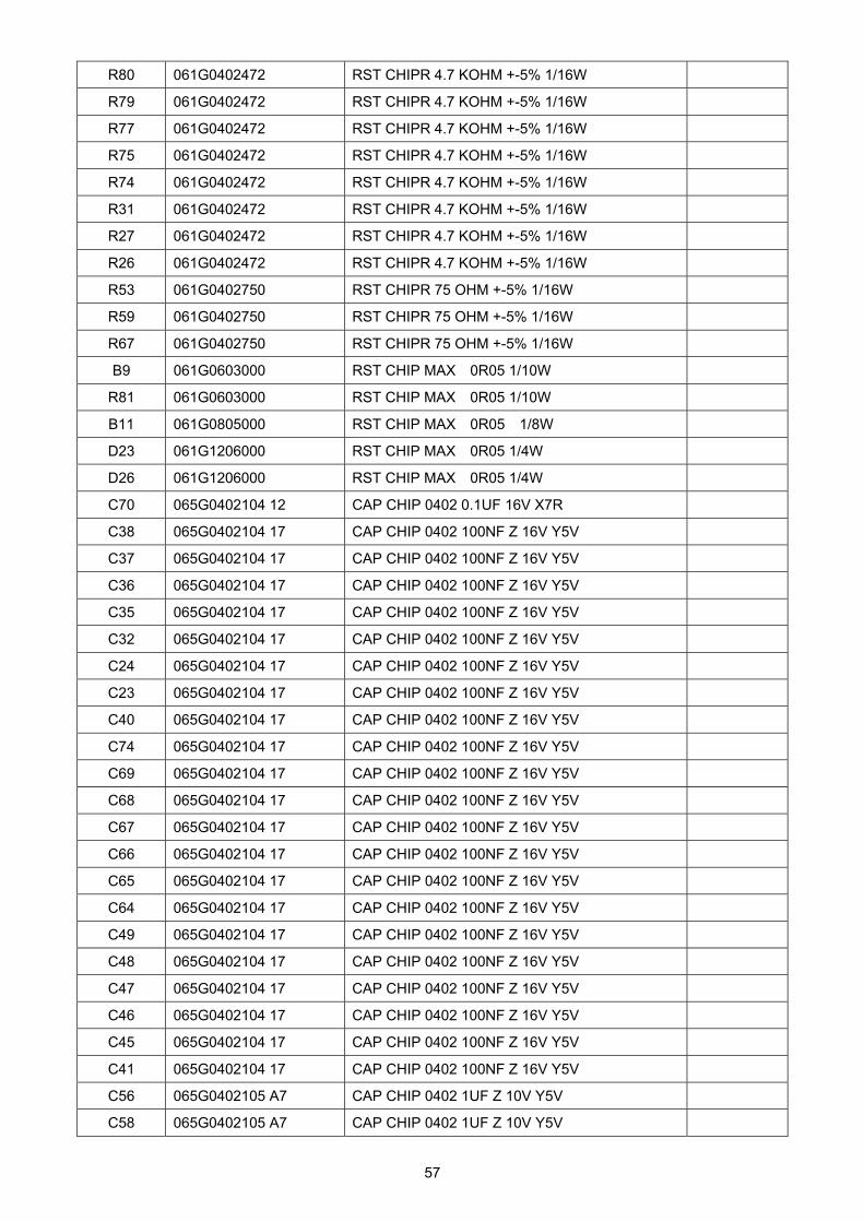
R80 061G0402472 RST CHIPR 4.7 KOHM +-5% 1/16W
R79 061G0402472 RST CHIPR 4.7 KOHM +-5% 1/16W
R77 061G0402472 RST CHIPR 4.7 KOHM +-5% 1/16W
R75 061G0402472 RST CHIPR 4.7 KOHM +-5% 1/16W
R74 061G0402472 RST CHIPR 4.7 KOHM +-5% 1/16W
R31 061G0402472 RST CHIPR 4.7 KOHM +-5% 1/16W
R27 061G0402472 RST CHIPR 4.7 KOHM +-5% 1/16W
R26 061G0402472 RST CHIPR 4.7 KOHM +-5% 1/16W
R53 061G0402750 RST CHIPR 75 OHM +-5% 1/16W
R59 061G0402750 RST CHIPR 75 OHM +-5% 1/16W
R67 061G0402750 RST CHIPR 75 OHM +-5% 1/16W
B9 061G0603000 RST CHIP MAX 0R05 1/10W
R81 061G0603000 RST CHIP MAX 0R05 1/10W
B11 061G0805000 RST CHIP MAX 0R05 1/8W
D23 061G1206000 RST CHIP MAX 0R05 1/4W
D26 061G1206000 RST CHIP MAX 0R05 1/4W
C70 065G0402104 12 CAP CHIP 0402 0.1UF 16V X7R
C38 065G0402104 17 CAP CHIP 0402 100NF Z 16V Y5V
C37 065G0402104 17 CAP CHIP 0402 100NF Z 16V Y5V
C36 065G0402104 17 CAP CHIP 0402 100NF Z 16V Y5V
C35 065G0402104 17 CAP CHIP 0402 100NF Z 16V Y5V
C32 065G0402104 17 CAP CHIP 0402 100NF Z 16V Y5V
C24 065G0402104 17 CAP CHIP 0402 100NF Z 16V Y5V
C23 065G0402104 17 CAP CHIP 0402 100NF Z 16V Y5V
C40 065G0402104 17 CAP CHIP 0402 100NF Z 16V Y5V
C74 065G0402104 17 CAP CHIP 0402 100NF Z 16V Y5V
C69 065G0402104 17 CAP CHIP 0402 100NF Z 16V Y5V
C68 065G0402104 17 CAP CHIP 0402 100NF Z 16V Y5V
C67 065G0402104 17 CAP CHIP 0402 100NF Z 16V Y5V
C66 065G0402104 17 CAP CHIP 0402 100NF Z 16V Y5V
C65 065G0402104 17 CAP CHIP 0402 100NF Z 16V Y5V
C64 065G0402104 17 CAP CHIP 0402 100NF Z 16V Y5V
C49 065G0402104 17 CAP CHIP 0402 100NF Z 16V Y5V
C48 065G0402104 17 CAP CHIP 0402 100NF Z 16V Y5V
C47 065G0402104 17 CAP CHIP 0402 100NF Z 16V Y5V
C46 065G0402104 17 CAP CHIP 0402 100NF Z 16V Y5V
C45 065G0402104 17 CAP CHIP 0402 100NF Z 16V Y5V
C41 065G0402104 17 CAP CHIP 0402 100NF Z 16V Y5V
C56 065G0402105 A7 CAP CHIP 0402 1UF Z 10V Y5V
C58 065G0402105 A7 CAP CHIP 0402 1UF Z 10V Y5V

58
C50 065G0402120 31 CAP CHIP 0402 12P 50V NPO
C44 065G0402220 31 CHIP 22PF 50V NPO
C21 065G0402220 31 CHIP 22PF 50V NPO
C20 065G0402220 31 CHIP 22PF 50V NPO
C43 065G0402473 17 CAP CHIP 0402 47NF K 16V Y5V
C39 065G0402473 17 CAP CHIP 0402 47NF K 16V Y5V
C34 065G0402473 17 CAP CHIP 0402 47NF K 16V Y5V
C31 065G0402473 17 CAP CHIP 0402 47NF K 16V Y5V
C30 065G0402473 17 CAP CHIP 0402 47NF K 16V Y5V
C28 065G0402473 17 CAP CHIP 0402 47NF K 16V Y5V
C25 065G0402473 17 CAP CHIP 0402 47NF K 16V Y5V
C19 065G0603330 31 CER1 0603 NP0 50V 33P PM
C16 065G0805105 22 CAP CHIP 0805 1UF K 25V X7R
C57 065G0805225 17 CHIP 2.2UF 16V Y5V
C17 065G1206106 17 MLCC 10 UF Z 16V Y5V
C54 065G1206106 17 MLCC 10 UF Z 16V Y5V
FB3 071G 42U100 TS CHIP BEAD 0402 10OHM+-25% 0.5A
FB2 071G 42U100 TS CHIP BEAD 0402 10OHM+-25% 0.5A
FB1 071G 42U100 TS CHIP BEAD 0402 10OHM+-25% 0.5A
R46 071G 59M121 Y CHIP BEAD 0603 120OHM+-25% 0.35A
B8 071G 59M252 M CHIP BEAD 0603 2500OHM+-25% 0.2A
L1 071G 59S221 M CHIP BEAD 0603 220OHM+-25% 2A
L2 071G 59S221 M CHIP BEAD 0603 220OHM+-25% 2A
L3 071G 59S221 M CHIP BEAD 0603 220OHM+-25% 2A
L4 071G 59S221 M CHIP BEAD 0603 220OHM+-25% 2A
B5 071G 59U601 TS CHIP BEAD 0603 600OHM+-25% 0.2A
B4 071G 59U601 TS CHIP BEAD 0603 600OHM+-25% 0.2A
B12 071G 59U601 TS CHIP BEAD 0603 600OHM+-25% 0.2A
B10 071G 59U601 TS CHIP BEAD 0603 600OHM+-25% 0.2A
Y1 093G 22S509CMO CRYSTAL SMD-49,24MHZ,30PF H=4.1 MM CMO
D19 093G 64S503CMO BAV70W,SOT-323(SC-70),PAN JIT CMO
D14 093G 64S503CMO BAV70W,SOT-323(SC-70),PAN JIT CMO
D28 093G 64S523SEM DIODE 1N4148WS SEMTECH
D27 093G 64S523SEM DIODE 1N4148WS SEMTECH
D29 093G3004 3 SM340A
D18 093G3004 3 SM340A
715G3279 2C MAIN BOARD PCB
KEPC9QE6 POWER KEY BOARD
CN1 033G8019 2CMO CONN.25-D000187
CN4 033G8019 7CMO CONN.25-D006242

59
CN1 033G8019 2JCMO CONNECTOR 1.0PITCH SMT 15P
CN3 033G8032 2C CONNECTOR
CN2 033G8032 2C CONNECTOR
SW1 077G 606 7 DT CMO TACT SWITCH DTSA-62NV
D2 081G 63O 1 GP LED GPTS0603OC3-PB
D1 081G0603 B GP LED GPTS06033BC1 GP
D8 093G 39S 94 T DIODE UDZSNP3.6B 200MW/3.6V SC-76
D7 093G 39S 94 T DIODE UDZSNP3.6B 200MW/3.6V SC-76
D3 093G 39S 94 T DIODE UDZSNP3.6B 200MW/3.6V SC-76
D5 093G 39S 94 T DIODE UDZSNP3.6B 200MW/3.6V SC-76
D4 093G 39S 94 T DIODE UDZSNP3.6B 200MW/3.6V SC-76
D6 093G 39S 94 T DIODE UDZSNP3.6B 200MW/3.6V SC-76
715G3065 1 POWER KEY PCB
N15G0004 1 PLATE LOCK 40A1599954
N15G0006 1 VESA-SUPPORT-PLATE 41-D010954
N33G0025 X2 1L0100 KEY PAD 40-D013277
N33G0026 X2 1L0100 KEY PAD POWER 40-D013278
N33G0027 1 1P0100 LENS 40-D013270
N34G0057BEB 1B0130 REAR 40-D013269
N40G000296810A LABEL HI-POT-PASS 77-D005237
N45G 52001 PE SHEET
N45G 88607001 PE BEG FOR 22 MONITOR 78-D016339
N52G 2191 01 TAPE /7345911004
N52G6020001 HB PANEL PROTECTOR FILM
M085 N85G0001 9 COVER AD
Q07G 1 5V 28 X WOODEN PALLET
Q37G0145011 HINGE ASS'Y
Q40G 22N709 5A RATING LABEL
Q40G0001624 4A PALLET LABEL
Q40G000270927A EPA LABEL
Q44G6002114 92 PAPER BOARD
Q44G9003160 CORNER PAPER
Q44GC111101 EPS
Q44GC111201 EPS
Q44GC111709 1A 22 LCD CARTON
Q45G 77 5 PE PACKING
Q50G 4 10 TIE
Q52G 1210500 AL TAPE
M085 SN85G00019 MAIN FRAME
E08904 089G 17356C553 AUDIO CABLE 1800MM

60
E08904 089G 17356G553 AUDIO CABLE 1800MM 2nd Source
E08904 089G 17356H553 AUDIO CABLE 1800MM 2nd Source
Q41G780070973A VG2230WM QSG
Q41G780070974A VISTA INSERT
Q45G2007M0101A PE BAG
Q70G2201709 3A VG2230WM CD
040G 58162435A P/N LABEL FOR MANUAL PE BAG
N40G0001968 2A S/N LABEL 7741513161
N40G000196855A CARTON LABEL
N40G000196867A S/N LABEL FOR VIEWSONIC
E750 750GLM220KZ1J2M0VS PANEL A220Z1-002 SM0Z12AD01 NB CMO 2nd Source

61
11. Recommended Spare Parts List
NA

62
12. Different Parts List
Diversity of TC9MRLDKDWVSDN compared with TC9MRLDBDWVSDN
Location Part Number Description Remark
E08901 089G402A18N CX POWER CORD 2nd source
E08901 089G402A18N IS POWER CORD/32-D022438 2nd source
E08901 089G402A18N YH POWER CORD(32-D022438)
Q41G780070961A CAUTION CARD
Q41G780070975A WALL MOUNT INSERT PAGE
Q41G780070976A MEXICO LIMITED WARRANTY FOR USA

63
* Reader’s Response* Dear Readers: Thank you in advance for your feedback on our Service Manual, which allows continuous improvement of our products. We would appreciate your completion of the Assessment Matrix below, for return to ViewSonic Corporation.
Assessment A. What do you think about the content of this Service Manual?
Unit Excellent Good Fair Bad
1. Precautions and Safety Notices
2. Specification
3. Front Panel Function Control Description
4. Circuit Description
5. Adjustment Procedure
6. Troubleshooting Flow Chart
7. Block Diagrams
8. Schematic Diagrams
9.PCB Layout Diagrams
10. Exploded Diagram and Spare Parts List
11. Recommended Spare Parts List
12.Different Parts List
B. Are you satisfied with this Service Manual?
Item Excellent Good Fair Bad
1. Service Manual Content 2. Service Manual Layout 3. The form and listing
C. Do you have any other opinions or suggestions regarding this service manual?
Reader’s basic dada:
Name: Title: Company: Add: Tel: Fax: E-mail: After completing this form, please return it to ViewSonic Quality Assurance in the USA at facsimile 1-909-839-7943. You may also e-mail any suggestions to the Director, Quality Systems & Processes ([email protected])