
SERVICE MANUAL - NPB-4000/4000C Patient Monitor
219
To contact Mallinckrodt, Inc. representative: in the United States, call 1-800-635-5267: outside of the United States, call your local Mallinckrodt representative. Caution: Federal law (U.S.A.) restricts this device to sale by or on the order of a physician. ©2000 Mallinckrodt Inc. All rights reserved 062643A-0700 SERVICE MANUAL NPB-4000/4000C Patient Monitor
-
Upload
khangminh22 -
Category
Documents
-
view
3 -
download
0
Transcript of SERVICE MANUAL - NPB-4000/4000C Patient Monitor

To contact Mallinckrodt, Inc. representative: in the United States, call 1-800-635-5267: outside of the United States, call your local Mallinckrodt representative.
Caution: Federal law (U.S.A.) restricts this device to sale by or on the order of a physician.
©2000 Mallinckrodt Inc. All rights reserved 062643A-0700
SERVICE MANUAL
NPB-4000/4000C Patient Monitor

Covered by one or more of the following U.S. Patents and foreign equivalents: 4,621,643; 4,653,498; 4,700,708; 4,770,179; 4,869,254;5,078,136; 5,351,685; and 5,368,026.
To obtain information about a warranty, if any, for this product, contact Mallinckrodt Technical Services or your localMallinckrodt representative.
Nellcor Puritan Bennett Inc. is a wholly owned subsidiary of Mallinckrodt Inc. Nellcor, Nellcor Puritan Bennett,Durasensor,and Oxisensor II are trademarks of Mallinckrodt Inc.
Purchase of this instrument confers no expressed or implied license under any Mallinckrodt patent to use the instrumentwith any sensor that is not manufactured or licensed by Mallinckrodt.
www.mallinckrodt.com
Mallinckrodt Inc.675 McDonnell BoulevardP.O. Box 5980St. Louis, MO 63134Telephone 314.654.2000Toll Free 1.800.635.5267
MallinckrodtEurope BVHambakenwettering 15231 DD’s-HertogenboschThe NetherlandsTelephone +31.73.6485200
Nellcor Puritan Bennett Inc.4280 Hacienda DrivePleasanton, CA 94588

iii
TABLE OF CONTENTS
List of FiguresList of Tables
List of Figures.............................................................................................. viList of Tables ............................................................................................... viiiSection 1: Introduction ............................................................................... 1-1
1.1 Manual Overview........................................................................ 1-11.2 Warnings, Cautions, and Notes ................................................. 1-11.3 NPB-4000/C Patient Monitor Description ................................... 1-11.4 Related Documents.................................................................... 1-2
Section 2: Routine Maintenance................................................................ 2-12.1 Cleaning ..................................................................................... 2-12.2 Periodic Safety and Functional Checks...................................... 2-12.3 Batteries ..................................................................................... 2-22.4 Environmental Protection ........................................................... 2-2
Section 3: Performance Verification.......................................................... 3-13.1 Introduction................................................................................. 3-13.2 Equipment Needed..................................................................... 3-13.3 Performance Tests..................................................................... 3-23.4 Safety Tests ............................................................................... 3-17
Section 4: Power-Up Defaults Menu and Diagnostic Mode .................... 4-14.1 Introduction................................................................................. 4-14.2 Power-Up Defaults Menu ........................................................... 4-14.3 Diagnostic Mode......................................................................... 4-3
Section 5: Troubleshooting........................................................................ 5-15.1 Introduction................................................................................. 5-15.2 How to Use This Section ............................................................ 5-15.3 Who Should Perform Repairs .................................................... 5-15.4 Replacement Level Supported ................................................... 5-15.5 Obtaining Replacement Parts .................................................... 5-15.6 Troubleshooting Guide ............................................................... 5-2
Section 6: Disassembly Guide................................................................... 6-16.1 Introduction................................................................................. 6-16.2 How to Use This Section ............................................................ 6-16.3 Disassembly Sequence Flow Charts.......................................... 6-36.4 Closed Case Disassembly Procedures...................................... 6-46.5 Front Case Disassembly Procedures......................................... 6-66.6 Rear Case Disassembly Procedures ......................................... 6-10
Section 7: Spare Parts ................................................................................ 7-17.1 Introduction................................................................................. 7-1
Section 8: Packing For Shipment .............................................................. 8-18.1 General Instructions ................................................................... 8-18.2 Repacking In Original Carton ..................................................... 8-18.3 Repacking In a Different Carton................................................. 8-1
Section 9: Specifications............................................................................ 9-19.1 Scope ......................................................................................... 9-19.2 General....................................................................................... 9-19.3 Electrical..................................................................................... 9-29.4 Environmental ............................................................................ 9-29.5 Measuring Parameters............................................................... 9-39.6 Trends ........................................................................................ 9-6

Contents
iv
Section 10: Introduction and System Description .................................. 10-110.1 System Overview ..................................................................... 10-110.2 System Block Diagram............................................................. 10-110.3 ECG Processing....................................................................... 10-510.4 Respiration Processing ............................................................ 10-610.5 NIBP Processing ...................................................................... 10-610.6 SpO2 Processing...................................................................... 10-610.7 Temperature Processing.......................................................... 10-6
Section 11: Isolated Front End Functions - Theory of Operation ......... 11-111.1 Block Diagram.......................................................................... 11-111.2 Overview .................................................................................. 11-211.3 Interface Circuit ........................................................................ 11-411.4 ECG.......................................................................................... 11-511.5 Respiratory Circuit .................................................................... 11-711.6 Temperature Circuit ................................................................. 11-711.7 Optocouplers ............................................................................ 11-811.8 Controls .................................................................................... 11-911.9 A/D Converter........................................................................... 11-1011.10 Isolated Power Supply............................................................ 11-1211.11 SpO2 Board ............................................................................ 11-1211.12 Isolation .................................................................................. 11-12
Section 12: NIBP - Theory of Operation................................................... 12-112.1 NIBP System Overview ............................................................ 12-112.2 The Pneumatic Assembly ........................................................ 12-312.3 NIBP Hardware ........................................................................ 12-3
Section 13: Microprocessor Computer and Control –Theory of Operation................................................ 13- 1
13.1 General..................................................................................... 13-113.2 Power Supply Connections ...................................................... 13-213.3 NIBP Processing ...................................................................... 13-413.4 Recorder Operation.................................................................. 13-513.5 Isolated Front End Interface..................................................... 13-713.6 RS-232 Serial Port Interface .................................................... 13-813.7 CPU Connections..................................................................... 13-913.8 DRAM Control .......................................................................... 13-1213.9 FLASH Control ......................................................................... 13-1413.10 LCD Display............................................................................ 13-1613.11 Real-Time Clock (RTC).......................................................... 13-1813.12 DUART Control ...................................................................... 13-1913.13 Knob Interface Control ........................................................... 13-1913.14 Switch Control ........................................................................ 13-2013.15 Miscellaneous Control - CS5#................................................ 13-2013.16 Digital Schematic Figure 17-5 Through Figure 17-7 .............. 13-2313.17 Current Drain Of Digital Electronics ....................................... 13-25
Section 14: Main Color Board Digital Theory of Operation ................... 14-114.1 General..................................................................................... 14-114.2 Power Supply Connections ...................................................... 14-314.3 CPU Connections..................................................................... 14-514.4 LNA 386EX Connections.......................................................... 14-714.5 CPU Timing Signals ................................................................. 14-714.6 DRAM Control .......................................................................... 14-814.7 FLASH Control ......................................................................... 14-1014.8 LCD Display.............................................................................. 14-1214.9 Real Time Clock (RTC)............................................................ 14-1514.10 DUART Control ...................................................................... 14-16

Contents
v
14.11 Knob Interface Control ........................................................... 14-1714.12 Push Button Control ............................................................... 14-1714.13 Miscellaneous Control - CS5#................................................ 14-1714.14 Speaker .................................................................................. 14-2014.15 NIBP (Non Invasive Blood Pressure) Control......................... 14-2014.16 Front End Interface................................................................. 14-2414.17 Digital Schematic.................................................................... 14-2614.18 Block Diagram........................................................................ 14-3714.19 Current Drain of Digital Electronics ........................................ 14-39
Section 15: Power Supply - Theory of Operation..................................... 15-115.1 Overview .................................................................................. 15-115.2 AC Mains Flyback Power Supply ............................................. 15-315.3 Battery Charger ........................................................................ 15-515.4 Buck Converter Operation........................................................ 15-515.5 Power Devices ......................................................................... 15-615.6 Miscellaneous Control .............................................................. 15-715.7 System Power Supply .............................................................. 15-715.8 Mains (AC) Led Operation........................................................ 15-815.9 Power Supply Control Logic ..................................................... 15-915.10 Alarm Section ......................................................................... 15-1015.11 NIBP Pump Control ................................................................ 15-1015.12 Safety Devices ....................................................................... 15-10
Section 16: MP-205 Service Manual (Npb P/N: 044540A-0296).............. 16-116.1 Overview .................................................................................. 16-116.2 Module Descripton ................................................................... 16-116.3 Circuit Description .................................................................... 16-216.4 Interconnections ....................................................................... 16-216.5 Sensor Interconnect ................................................................. 16-216.6 Oxichip Circuit .......................................................................... 16-216.7 Preamp..................................................................................... 16-316.8 Programmable Gain Amplifier (PGA), Demodulator and
Demultiplexer ........................................................................... 16-316.9 Filters and Level Shifter............................................................ 16-316.10 LED Driver.............................................................................. 16-416.11 Reset Schmitt Trigger ............................................................ 16-416.12 High Resolution A/D Converter .............................................. 16-416.13 Input Filter .............................................................................. 16-416.14 Power Decoupling .................................................................. 16-516.15 Status and Timing .................................................................. 16-516.16 Analog Power Regulation....................................................... 16-516.17 Microcontroller........................................................................ 16-516.18 Troubleshooting The MP-205................................................. 16-716.19 Packing for Shipment ............................................................. 16-1316.20 MP205 Specifications............................................................. 16-14
Section 17: Drawings................................................................................. 17-117.1 Overview .................................................................................. 17-117.2 List of Figures........................................................................... 17-1

Contents
vi
LIST OF FIGURESFigure 6-1: NPB-4000/C Disassembly Sequence Flow Chart, Sheet 1 .............6-3Figure 6-2: NPB-4000/C Disassembly Sequence Flow Chart, Sheet 2 .............6-4Figure 7-1: NPB-4000/C Top Assembly Drawing...............................................7-2Figure 7-2: NPB-4000/C Front Case Assembly Diagram (Sheet 1 of 2)............7-4Figure 7-3: NPB-4000/C Front Case Assembly Diagram (Sheet 2 of 2)............7-6Figure 7-4: NPB-4000/C Rear Case Assembly Diagram (Sheet 1 of 2) ............7-8Figure 7-5: NPB-4000/C Rear Case Assembly Diagram (Sheet 2 of 2) .........7-10Figure 7-6: NPB-4000/C Power Supply/Heat Sink Assembly Diagram............7-12Figure 10-1: NPB-4000/C System Block Diagram ...........................................10-2Figure 11-1: NPB-4000/C Simplified Block Diagram........................................11-1Figure 11-2: Isolated Front End Block Diagram ...............................................11-2Figure 11-3: Front End Block Diagram, Expanded ..........................................11-3Figure 11-4: Interface Circuit Block Diagram ...................................................11-4Figure 11-5: ECG Circuit Block Diagram .........................................................11-5Figure 11-6: Respiratory Circuit Block Diagram...............................................11-7Figure 11-7: Optocouplers Block Diagram.......................................................11-8Figure 11-8: Controls Block Diagram ...............................................................11-9Figure 12-1: NPB-4000/C System Block Diagram ...........................................12-1Figure 12-2: NIBP System Block Diagram .......................................................12-2Figure 12-3: Oxcillatory Characteristics Diagram.............................................12-2Figure 12-4: Pneumatic Assembly Block Diagram...........................................12-3Figure 12-5: NIBP Hardware Block Diagram ...................................................12-3Figure 13-1: Power Supply Interface................................................................13-2Figure 13-2: NIBP Processing Circuitry Block Diagram ...................................13-4Figure 13-3: Recorder System Block Diagram.................................................13-6Figure 13-4: Isolated Front End Block Diagram ...............................................13-7Figure: 13-5: 16 Bit Word ................................................................................13-8Figure 13-6: Watch Dog Timer Block Diagram ..............................................13-11Figure 13-7: CPU Signals...............................................................................13-12Figure 13-8: DRAM Timing.............................................................................13-13Figure 13-9: RAS# and CAS# Requirements.................................................13-14Figure 13-10: Flash Cycle ..............................................................................13-15Figure 13-11: Write Pulse ..............................................................................13-15Figure 13-12: DS1693 Timing ........................................................................13-18Figure 13-13: Interface Timing .......................................................................13-19Figure 13-14: DUART Control ........................................................................13-19Figure 13-15: Digital Section Block Diagram..................................................13-24Figure 14-1: Power Supply Connections ..........................................................14-3Figure 14-2: LNA 386EX CONNECTIONS ......................................................14-7Figure 14-3: CPU Timing Diagram...................................................................14-8Figure 14-4: DRAM Timing...............................................................................14-9Figure 14-5: RAS# and CAS# Timing ..............................................................14-9Figure 14-6: Flash Read Timing.....................................................................14-11Figure 14-7: Flash Write Timing.....................................................................14-11Figure 14-8: DS1693 Timing ..........................................................................14-15Figure 14-9: Interface Timing .........................................................................14-16Figure 14-10: DUART Read/Write Timing .....................................................14-16Figure 14-11: Oscillatory Characteristics Diagram.........................................14-21Figure 14-12: Pneumatic Assembly Block Diagram.......................................14-22Figure 14-13: NIBP Hardware Block Diagram ...............................................14-23Figure 14-14: NPB-4000C Color Motherboard Block Diagram ......................14-38Figure 15-1: Power Supply Block Diagram ......................................................15-2Figure 15-2: Power Supply Detail Diagram ......................................................15-2Figure 15-3: General Flyback Circuit Concept .................................................15-3Figure 15-4: AC Power Supply Block Diagram ................................................15-3Figure 15-5: Buck Converter Circuit .................................................................15-5Figure 15-6: Float Voltage vs. Temperature ...................................................15-6

Contents
vii
Figure 16-1: Preamplifier and PGA Outputs ....................................................16-9Figure 16-2: Filter Outputs and ADC Input.....................................................16-10Figure 16-3: MP-205 with an SRC-2 Filter Output .........................................16-11Figure 16-4: MP-205 with an SRC-2 LED Drive Current Test at TP7 ............16-12Figure 16-5: MP-205 with SRC-2 Serial Port TXD Signal, U4 Pin 25 ...........16-13Figure 17-1: MP-205 PCB Schematic (Sheet 1 of 2) .......................................17-3Figure 17-2: MP-205 PCB Schematic (Sheet 2 of 2) .......................................17-5Figure 17-3: NPB-4000/C Power Supply PCB Schematic (Sheet 1 of 2).........17-7Figure 17-4: NPB-4000/C Power Supply PCB Schematic (Sheet 2 of 2).........17-9Figure 17-5: NPB-4000/C Main PCB Schematic (Sheet 1 of 3).....................17-11Figure 17-6: NPB-4000/C Main PCB Schematic (Sheet 2 of 3).....................17-13Figure 17-7: NPB-4000/C Main PCB Schematic (Sheet 3 of 3).....................17-15Figure 17-8: NPB-4000/C Interconnect Diagram ...........................................17-17Figure 17-9: NPB-4000C Color Motherboard Schematic...............................17-19

Contents
viii
LIST OF TABLES
Table 3-1: Required Test Equipment…………………………………. 3-1Table 3-2: Dynamic Operating Range………………………………… 3-7Table 3-3: Serial Port Voltage…………………………………………. 3-16Table 3-4: Earth Leakage Current Values……………………………. 3-18Table 3-5: Enclosure Leakage Current……………………………….. 3-19Table 3-6: Patient Leakage Current Values………………………….. 3-20Table 3-7: Patient Leakage Current Values – Mains Voltage
on Applied Part…………………………………………….. 3-21Table 3-8: Test Lead Combinations…………………………………… 3-21Table 3-9: Allowable Leakage Current………………………………... 3-22Table 4-1: Power-up Defaults Menu…………………………………… 4-2Table 4-2: A/D Channel Designators………………………………….. 4-5Table 5-1: Problem Categories………………………………………… 5-2Table 5-2: Power Problems…………………………………………….. 5-3Table 5-3: Serviceable Hardware Error Codes………………………. 5-4Table 5-4: Error Code Categories……………………………………… 5-6Table 5-5: Switches/Knob Problems…………………………………… 5-7Table 5-6: Display/Audible Tones Problems………………………….. 5-8Table 5-7: Operational Performance Problems………………………. 5-9Table 7-1: Top Assembly (Figure 7-1)………………………………… 7-3Table 7-2: Front Case Assembly (Figure 7-2)………………………… 7-5Table 7-3: Front Case Assembly (Figure 7-3)………………………… 7-7Table 7-4: Rear Case Assembly (Figure 7-4)………………………… 7-9Table 7-5: Rear Case Assembly (figure 7-5)…………………………. 7-11Table 7-6: Power Supply Assembly (Figure 7-6)…………………….. 7-13Table 7-7: NPB-4000/C Accessories………………………………….. 7-13Table 16-1: Oxichip Circuit Pin Descriptions…………………………. 16-5Table 16-2: Fault Evaluation…………………………………………… 16-7Table 16-3: Reported Errors…………………………………………… 16-8

1-1
SECTION 1: INTRODUCTION1.1 Manual Overview1.2 Warnings, Cautions, and Notes1.3 NPB-4000/C Patient Monitor Description1.4 Related Documents
1. INTRODUCTION
1.1 MANUAL OVERVIEW
This manual contains information for servicing the model NPB-4000 andNPB-4000C patient monitor, subsequently referred to as NPB-4000/Cthroughout this manual. Only qualified service personnel should service thisproduct. Before servicing the NPB-4000/C, read the operator’s manual carefullyfor a thorough understanding of operation.
1.2 WARNINGS, CAUTIONS, AND NOTES
This manual uses three terms that are important for proper operation of themonitor: Warning, Caution, and Note.
1.2.1 Warning
A warning precedes an action that may result in injury or death to the patient oruser. Warnings are boxed and highlighted in boldface type.
1.2.2 Caution
A caution precedes an action that may result in damage to, or malfunction of, themonitor. Cautions are highlighted in boldface type.
1.2.3 Note
A note gives information that requires special attention.
1.3 NPB-4000/C PATIENT MONITOR DESCRIPTION
The purpose and function of the NPB-4000/C patient monitor is to monitor:ECG; heart rate; noninvasive blood pressure (systolic, diastolic, and meanarterial pressures); functional arterial oxygen saturation; respiration rate; andtemperature for adult and pediatric patients in all hospital areas and hospital-typefacilities. It may be used during hospital transport and in mobile, land-basedenvironments, such as ambulances.
The physical and operational characteristics of the monitor are described in theoperator’s manual and in the Specifications section of this manual.

Section 1: Introduction
1-2
1.4 RELATED DOCUMENTS
To perform test and troubleshooting procedures and to understand the principlesof operation and circuit analysis sections of this manual, you must know how tooperate the monitor. Refer to the NPB-4000/C operator’s manual. Tounderstand the various Nellcor sensors, ECG leads, blood pressure cuffs, and temperature probes that work with the monitor, refer to the individual directions for use that accompany these accessories.
2-1
SECTION 2: ROUTINE MAINTENANCE2.1 Cleaning2.2 Periodic Safety and Functional Checks2.3 Batteries2.4 Environmental Protection
2. ROUTINE MAINTENANCE
2.1 CLEANING
WARNING: Do not immerse the NPB-4000/C or its accessories in liquid orclean with caustic or abrasive cleaners. Do not spray or pour any liquid onthe monitor or its accessories.
To clean the NPB-4000/C, dampen a cloth with a commercial, nonabrasivecleaner and wipe the exterior surfaces lightly. Do not allow any liquids to comein contact with the power connector or switches. Do not allow any liquids topenetrate connectors or openings in the instrument. For cables, sensors andcuffs, follow the cleaning instructions in the directions for use that accompanythese accessories.
2.2 PERIODIC SAFETY AND FUNCTIONAL CHECKS
The NPB-4000/C requires no routine service or calibration other than cleaningand battery maintenance. The following performance verification tests may beused following repair or during routine maintenance (if required by your localinstitution).
1. Inspect the exterior of the NPB-4000/C for damage.
2. Inspect labels for legibility. If the labels are not legible, contact Mallinckrodt Technical Services Department or your local Mallinckrodtrepresentative.
3. Verify that the unit performs properly as described in paragraph 3.3.
4. Perform the electrical safety tests detailed in paragraph 3.4. If the unit failsthese electrical safety tests, do not attempt to repair. Contact Mallinckrodt Technical Services Department or your local Mallinckrodt representative.

Section 2: Routine Maintenance
2-2
2.3 BATTERIES
If the NPB-4000/C has not been used for a long period of time, the battery willneed charging. To charge the battery, connect the NPB-4000/C to an AC outletor external DC supply as described in Paragraph 3.3.1 in this service manual orthe Setup and Use section of the operator’s manual.
Note: Storing the NBP-4000/C for a long period without charging the batterymay degrade the battery capacity. A complete battery recharge requires8 hours. The battery may require a full charge/discharge cycle to restorenormal capacity.
Mallinckrodt recommends that the NPB-4000/C’s sealed, lead-acid batteries be replaced at 2-year intervals. Refer to Section 6, Disassembly Guide.
2.4 ENVIRONMENTAL PROTECTION
Follow local governing ordinances and recycling plans regarding disposal orrecycling batteries and other device components.

3-1
SECTION 3: PERFORMANCE VERIFICATION3.1 Introduction3.2 Equipment Needed3.3 Performance Tests3.4 Safety Tests
3. PERFORMANCE VERIFICATION
3.1 INTRODUCTION
This section discusses the tests used to verify performance following repairs orduring routine maintenance. All tests can be performed without removing theNPB-4000/C covers.
If the NPB-4000/C fails to perform as specified in any test, repairs must correctthe problem before the monitor is returned to the user.
3.2 EQUIPMENT NEEDED
Table 3-1 lists the equipment required for performance verification.
Table 3-1: Required Test Equipment
Equipment Description
Digital multimeter (DMM) Fluke Model 87 or equivalent
Sensor extension cable EC-8
Durasensor® oxygen transducer DS-100A
Oxisensor® II oxygen transducer D-25
ECG cable CE-10
ECG electrodes standard
ECG leads LE series
NIBP hose SHBP-10
NIBP cuff SCBP series
Pulse oximeter tester Nellcor SRC-2
ECG simulator medSim 300 or equivalent
NIBP simulator Bio-Tek “BP Pump” or equivalent
Respiration simulator medSim 300 or equivalent
Temperature simulator medSim 300 or equivalent
Safety analyzer Bio-Tek 601 Pro or equivalent
Stopwatch Manual or electronic

Section 3: Performance Verification
3-2
3.3 PERFORMANCE TESTS
The battery charge and battery performance test should be performed beforemonitor repairs whenever the battery is suspected as being a source of theproblems. All other tests may be used following repairs or during routinemaintenance (if required by your local institution. Before performing the batteryperformance test, ensure that the battery is fully charged (Paragraph 3.3.1).
This section is written using Nellcor factory-set power-up defaults. If your institution has preconfigured custom defaults, those values will be displayed.
3.3.1 Battery Charge
Perform the following procedure to fully charge the battery.
1. Connect monitor to AC power source using proper power cord.
2. Verify BATTERY CHARGING/AC SOURCE indicator is lit.
3. Charge battery for at least 8 hours.
Note: The battery may require a complete charge/discharge cycle to restore itsnormal capacity, depending on its previous usage.
4. The only way to check for a full charge is to perform the procedure inparagraph 3.3.2 “Battery Performance Test.”
3.3.2 Battery Performance Test
1. The NPB-4000 monitor is specified to typically operate on battery power aminimum of 4 hours, at 25° C, with no printing, and one NIBP measurementevery 15 minutes. The NPB-4000/C monitor is specified to typically operateon battery power a minimum of 3 hours, at 25° C, with no printing, and oneNIBP measurement every 15 minutes. Before performing this test, ensurethat the battery is fully charged (paragraph 3.3.1).
2. Connect Nellcor SRC-2 pulse oximeter tester to monitor viaEC-8 sensor cable.
3. Connect NIBP simulator to monitor via SHBP-10 hose.
4. Set SRC-2 switches as follows:
SWITCH POSITION RATE 38 LIGHT LOW MODULATION LOW RCAL/MODE RCAL 63/LOC

Section 3: Performance Verification
3-3
5. Set NIBP simulator to simulate pressure setting of 120/80 mmHg and heartrate of 80 bpm.
6. Ensure monitor is not connected to AC power.
7. With NPB-4000/C turned off, press On/Standby switch and verify batteryicon appears at bottom of display after power-on self-test is completed.Boxes in battery icon should all be filled, indicating battery is charged.
8. Verify monitor is responding to SpO2 simulator signal and audible alarm issounding. Use knob to select SpO2 Menu and permanently silence SpO2
audible alarm.
9. Use knob to select NIBP Menu and set Automatic Measurement Interval to15 minutes. Exit menu and press front panel NIBP Start/Stop switch tomanually initiate first NIBP measurement. Subsequent NIBP measurementswill be taken automatically every 15 minutes.
10. NPB-4000 monitor must operate for at least 4 hours before monitorautomatically powers down due to low battery condition. NPB-4000/Cmonitor must operate for at least 3 hours before monitor automaticallypowers down due to low battery condition.
11. Verify low battery alarm occurs 15-30 minutes before battery fullydischarges.
12. Allow monitor to operate until it automatically powers down due to lowbattery condition. Verify audible alarm sounds when monitor automaticallyshuts down. Press Alarm Silence switch to terminate this audible alarm.
13. If monitor passes this test, immediately recharge battery (paragraph 3.3.1,steps 1–3).
3.3.3 Power-On Self-Test
1. Connect monitor to AC power source and verify BATTERYCHARGING/AC SOURCE indicator is lit.
2. Do not connect any input cables to monitor.
3. Observe monitor front panel. With monitor off, press On/Standby switch.Monitor must perform the following sequence.
a. Monitor emits three consecutively higher pitched beeps.
b. A few seconds later, display backlight illuminates, but display is blank.
c. Nellcor logo then appears for a few seconds, with version numbers of boot and operational software displayed in lower left corner of display.

Section 3: Performance Verification
3-4
Note: The upper version number corresponds to the boot software, thelower version number corresponds to the operational software.
Note: Power-on self-test takes approximately 10 seconds to complete.
d. A beep signals end of power-on self-test
e. Upon successful completion of power-on self-test, display will be innormal monitoring screen configuration.
Note: No vital signs numeric values or waveforms will be displayed.
3.3.4 Hardware and Software Tests
Hardware and software testing include the following tests.
• 3.3.4.1 SpO2 Testing
• 3.3.4.2 Operation with an ECG Simulator
• 3.3.4.3 Operation with a Respiration Simulator
• 3.3.4.4 Verification of Pneumatic System
• 3.3.4.5 Operation with a Temperature Simulator
• 3.3.4.6 General Operation
3.3.4.1 SpO2 Testing
SpO2 testing includes the following tests.
• 3.3.4.1.1 Alarms and Alarm Silence
• 3.3.4.1.2 Heart Rate Tone Volume Control
• 3.3.4.1.3 Dynamic Operating Range
• 3.3.4.1.4 LED Excitation Test
3.3.4.1.1 Alarms and Alarm Silence
1. Connect SRC-2 pulse oximeter tester to sensor input cable and connectcable to monitor.

Section 3: Performance Verification
3-5
2. Set SRC-2 as follows:
SWITCH POSITIONRATE 38LIGHT LOWMODULATION OFFRCAL/MODE RCAL 63/LOCAL
3. Press monitor On/Standby switch to turn monitor on.
4. After normal power-up sequence, verify SpO2% display initially indicateszero.
Note: The pulse bar may occasionally indicate a step change as the monitor is inthe pulse search mode.
5. Move modulation switch on SRC-2 to LOW.
6. Verify following monitor reaction:
a. Pulse bar begins to track artificial pulse signal from SRC-2.
b. Initially, zero is displayed in SpO2 frame.
c. After about 10 to 20 seconds, monitor displays saturation and heart rateas specified by tester. Verify values are within following tolerances:
Oxygen Saturation Range 79% to 83%
Heart Rate Range 35 to 41 bpm
d. Audible alarm sounds and both SpO2% and HEART RATE displayswill flash, indicating both parameters have violated default alarmlimits.
Note: Heart rate tone source, found in the Heart Rate Menu, should be setto “SpO2”.
e. Heart rate tone is heard.
5. Press Alarm Silence switch on monitor front panel. Audible alarm istemporarily silenced.

Section 3: Performance Verification
3-6
6. Verify the following:
a. An audible alarm remains silenced.
b. “Slashed bell” icon appears in each numeric frame on display.
c. SpO2% and HEART RATE displays continue flashing.
d. Heart rate tone is audible.
e. Audible alarm returns in approximately 60 seconds.
3.3.4.1.2 Heart Rate Tone Volume Control
1. Set up NPB-4000/C monitor and SRC-2 pulse oximeter tester as indicated inparagraph 3.3.4.1.1.
2. Apply power to monitor and verify SpO2 and heart rate values are correctlydisplayed.
3. Press Alarm Silence switch on front panel of the monitor to temporarilysilence audible alarm.
4. Verify heart rate tone source, found in Heart Rate Menu, is set to “SpO2”.
5. Press Heart Rate Tone Volume switch on front panel of monitor.
6. Within 3 seconds of having pressed Heart Rate Tone Volume switch, rotateknob CW and verify beeping heart rate tone sound level increases.
7. Rotate knob CCW and verify beeping heart rate tone decreases until it is nolonger audible.
8. Rotate knob CW to return beep volume to a comfortable level.
Note: Three seconds after the last switch-press or rotation of the knob, functionof the knob reverts to moving the highlight on the display screen.
3.3.4.1.3 Dynamic Operating Range
The following test sequence verifies proper monitor operation over a range ofinput signals.
1. Connect SRC-2 to NPB-4000/C and turn NPB-4000/C on.
2. Place SRC-2 in RCAL 63/LOCAL mode.
3. Set SRC-2 as indicated in Table 3-2. Verify NPB-4000/C readings arewithin indicated tolerances. Allow monitor several seconds to stabilizereadings.

Section 3: Performance Verification
3-7
Note: A “*” indicates values that produce an alarm. Press the Alarm Silenceswitch to temporarily silence the audible alarm.
Table 3-2: Dynamic Operating Range
SRC-2 Settings NPB-4000/C Indications
RATE LIGHT MODULATION SpO2 Pulse Rate
38 HIGH2 LOW 79 - 83* 35 - 41*112 HIGH1 HIGH 79 - 83* 109 - 115201 LOW LOW 79 - 83* 195 - 207*201 LOW HIGH 79 - 83* 195 - 207*
Note: For the pulse rate setting of 201 BPM, the pulse rate tolerance of 195 to207 BPM is greater than the ±3 BPM accuracy specification of themonitor, due to the performance characteristics of the SRC-2 tester.
4. Turn monitor off.
3.3.4.1.4 LED Excitation Test
This procedure uses normal system components to test circuit operation. ANellcor Oxisensor II oxygen transducer, model D-25, is used to examine LED intensity control. The red LED is used to verify intensity modulation caused by the LED intensity control circuit.
1. Connect EC-8 sensor extension cable to monitor.
2. Connect D-25 sensor to sensor extension cable.
3. Press On/Standby switch to turn monitor on.
4. Leave sensor open with LEDs and photodetector visible.
5. After monitor completes normal power-up sequence, verify sensor LED isbrightly lit.
6. Slowly move sensor LED in proximity of photodetector element of sensor.Verify; as LED approaches optical sensor, LED intensity decreases.
7. Open sensor and notice LED intensity increases.
8. Repeat step 6 and intensity will again decrease. This variation is anindication that microprocessor is in proper control of LED intensity.
9. Turn NPB-4000/C off.

Section 3: Performance Verification
3-8
3.3.4.2 Operation with an ECG Simulator
1. With monitor off, connect ECG leads to appropriate jacks on ECG tester.
2. Connect leads to CE-10 ECG cable.
3. Connect CE-10 to ECG input port on NPB-4000/C.
4. Set ECG tester as follows:
Heart rate: 30 bpm
Amplitude: 1 millivolt
Lead select: II
Normal sinus rhythm
Adult mode
Note: The accuracy of NPB-4000/C ECG measurements is ±5 bpm. In theprocedure below, add the tolerance of the simulator to the acceptablerange of readings.
5. Press On/Standby switch to turn monitor on.
6. After normal power-up sequence, verify the following monitor reactions:
a. After at least five heartbeats, monitor displays a heart rate of 30 ±5bpm.
b. Audible alarm will sound and HEART RATE display will flash,indicating heart rate is below default lower alarm limit.
7. Press Alarm Silence switch. Verify audible alarm is silenced.
8. Increase heart rate setting on ECG simulator to 240 bpm.
9. After at least five heartbeats, verify monitor displays heart rate of 240 ±5bpm.
10. Verify audible alarm sounds and HEART RATE display flashes, indicatingheart rate is above default upper alarm limit.
11. Press Alarm Silence switch to silence alarm.
12. Decrease heart rate setting on ECG simulator to 120 bpm.
13. After at least five heartbeats, verify monitor displays heart rate of 120 ±5bpm.

Section 3: Performance Verification
3-9
14. Disconnect LL lead from ECG simulator.
15. Verify “Leads Off” alarm message appears, three dashes are displayed inHEART RATE display, and low priority audible alarm sounds.
16. Reconnect LL lead to ECG simulator. Verify “Leads Off” alarm messageno longer appears and audible alarm is silenced.
17. Repeat steps 14 through 16 for LA and RA leads.
18. Turn monitor off.
3.3.4.3 Operation with a Respiration Simulator
1. With monitor off, connect ECG leads to appropriate jacks on respirationsimulator.
2. Connect ECG leads to CE-10 ECG cable.
3. Connect CE-10 to ECG input port on NPB-4000/C.
Note: The accuracy of NPB-4000/C ECG measurements is ±3 breaths perminute. In the procedure below, add the tolerance of the simulator to theacceptable range of readings.
4. Set simulator for respiration rate of 120 breaths per minute.
5. Press On/Standby switch to turn monitor on.
6. After normal power-up sequence, verify the following monitor reactions:
a. Monitor displays respiration rate of 120 ±3 breaths per minute.
b. Audible alarm will sound and RESPIRATION RATE display willflash, indicating respiration rate is above default upper alarm limit.
7. Press Alarm Silence switch. Verify alarm is silenced.
8. Decrease respiration rate setting on respiration simulator to 20 breaths perminute.
9. Verify monitor displays respiration rate of 20 ±3 breaths per minute.

Section 3: Performance Verification
3-10
3.3.4.4 Verification of Pneumatic System
Tests in paragraphs 3.3.4.4.1 through 3.3.4.4.5 verify the functionality of theNPB-4000/C pneumatic system. These tests are designed to use the Bio-Tek“BP Pump” noninvasive blood pressure simulator. The internal test volume ofthe Bio-Tek simulator is 250 cm3 , which is used to calculated theinflation/deflation rate periods. The Bio-Tek simulator or any equivalent NIBPsimulator is required to perform these tests.
The NPB-4000/C must be placed in Diagnostic Mode, with the NIBP Test screenactive for each of the NIBP tests. For a detailed explanation of the DiagnosticMode, refer to Section 4, Power-up Defaults Menu and Diagnostic Mode.
Each of the tests described in paragraphs 3.3.4.4.1 through 3.3.4.4.5 must beperformed to verify pneumatic system functionality. These tests can beperformed individually (in any order) or sequentially. Prior to performing any ofthese tests, perform the following setup procedure. If these tests are performedin sequence, this procedure needs to be performed once prior to the first test.
1. Turn on Bio-Tek simulator and press MODE button to place simulator intest mode. Simulator screen will indicate “Internal Cuff” and “PressureGauge”.
2. Connect simulator hose to NIBP connector on NPB-4000/C.
3. Follow procedure described in Section 4 to place NPB-4000/C in DiagnosticMode with NIBP Test screen active.
3.3.4.4.1 Pressure Transducer Accuracy
The pressure transducer accuracy test verifies the pressure accuracy of theNBP-4000/C pressure transducer.
1. Ensure Bio-Tek simulator is in test mode. Simulator should display“Pressure Gauge”.
2. Ensure simulator is set up for internal cuff.
3. Ensure NIBP Test screen is active on NPB-4000/C.
4. Press Alarm Silence switch on NPB-4000/C to ensure both valves areclosed.
5. Perform offset adjustment so that simulator and NBP-4000/C both display apressure of 0 mmHg.
a. Press Contrast Adjust switch on NPB-4000/C,
b. Press Zero button on the simulator.
Section 3: Performance Verification
3-11
6. Press Select button on simulator until simulator displays “Pressure SourceSet Test Pressure”.
7. Use Up/Down buttons on simulator to adjust for 250 mmHg.
8. Press Start Pump button on simulator. The simulator will begin topressurize.
Note: The current pressure in mmHg will be displayed on both the simulator andNPB-4000/C displays.
9. Allow 15-20 seconds for pressure to stabilize.
Note: The pressure displayed on the NPB-4000/C and the simulator should bewithin 5 mmHg of one another to successfully complete the test.
10. Press Stop Pump button on simulator to stop test.
11. Press and hold Heart Rate Tone Volume switch until NPB-4000/C displayspressure of 0 mmHg.
Note: Additional NIBP tests may be performed at this time. If no further NIBPtests are to be conducted, turn the NPB-4000/C off. Normal monitoringoperation will return the next time the monitor is turned on.
3.3.4.4.2 Pneumatic Leakage
The pneumatic leakage test verifies the integrity of the pneumatic system. Atimer/stop watch is required for this test.
1. Ensure Bio-Tek simulator is in test mode. The simulator should display“Pressure Gauge”.
2. Ensure simulator is set up for internal cuff.
3. Ensure NIBP Test screen is active on NPB-4000/C.
4. Press Heart Rate Tone Volume switch on NPB-4000/C to ensure bothvalves are closed.
5. Perform offset adjustment so simulator and NBP-4000/C both display apressure of 0 mmHg.
a. Press Contrast Adjust switch on NPB-4000/C,
b. Press Zero button on simulator,
6. Press NIBP Start/Stop switch on NPB-4000/C to activate pump. Hold NIBPStart/Stop switch until NPB-4000/C displays pressure of approximately 250mmHg.

Section 3: Performance Verification
3-12
7. Allow 15-20 seconds for pressure to stabilize.
8. Record pressure displayed on NPB-4000/C.
9. Initiate a 1-minute timer.
10. After 1 minute, record pressure displayed on NPB-4000/C.
Note: The test will have been successfully completed if the pressure hasdropped by 6 mmHg, or less, during the 1-minute period.
11. Press and hold Heart Rate Tone Volume switch until NPB-4000/C displaysa pressure of 0 mmHg.
Note: Additional NIBP tests may be performed at this time. If no further NIBPtests are to be conducted, turn the NPB-4000/C off. Normal monitoringoperation will return the next time the monitor is turned on.
3.3.4.4.3 Inflation Rate
The inflation rate test verifies the inflation rate of the NPB-4000/C. A timer/stopwatch is required for this test.
1. Ensure Bio-Tek simulator is in test mode. The simulator should display“Pressure Gauge”.
2. Ensure simulator is set up for internal cuff.
3. Ensure NIBP Test screen is active on NPB-4000/C.
4. Press Heart Rate Tone Volume switch on NPB-4000/C to ensure bothvalves are closed.
5. Perform offset adjustment so simulator and NBP-4000/C both display apressure of 0 mmHg.
a. Press Contrast Adjust switch on NPB-4000/C,
b. Press Zero button on simulator
6. Simultaneously press and hold NIBP Start/Stop switch on NPB-4000/C toactivate pump, and start the timer.
7. Hold NIBP Start/Stop switch until NPB-4000/C displays a pressure of 280mmHg., and stop timer.
Note: The test will have been successfully completed if the inflation time isbetween 1 and 6 seconds.
8. Press and hold Heart Rate Tone Volume switch until NPB-4000/C displaysa pressure of 0 mmHg.

Section 3: Performance Verification
3-13
Note: Additional NIBP tests may be performed at this time. If no further NIBPtests are to be conducted, turn the NPB-4000/C off. Normal monitoringoperation will return the next time the monitor is turned on.
3.3.4.4.4 Deflation Rate
The deflation rate test verifies the deflation rate of the NPB-4000/C. Atimer/stop watch is required for this test.
1. Ensure Bio-Tek simulator is in test mode. The simulator should display“Pressure Gauge”.
2. Ensure simulator is set up for internal cuff.
3. Ensure NIBP Test screen is active on NPB-4000/C.
4. Press Heart Rate Tone Volume switch on NPB-4000/C to ensure that bothvalves are closed.
5. Perform offset adjustment so that simulator and NBP-4000/C both display apressure of 0 mmHg.
a. Press Contrast Adjust switch on NPB-4000/C,
b. Press Zero button on simulator, to
6. Press and hold NIBP Start/Stop switch on NPB-4000/C to activate pump.
7. Hold NIBP Start/Stop switch until NPB-4000/C displays a pressure of 280mmHg.
8. Start 1 minute timer, and simultaneously press and hold Alarm Silenceswitch on NPB-4000/C.
Note: This will cause the pneumatic system to deflate at a rate of 3 mmHg/sec±1.5 mmHg/sec.
9. After 1 minute, record pressure displayed on the NPB-4000/C.
Note: The test will have been successfully completed if the NPB-4000/Cdisplays a pressure reading of 10 mmHg to 190 mmHg.
10. Press and hold Heart Rate Tone Volume switch until NPB-4000/C displaysa pressure of 0 mmHg.
Note: Additional NIBP tests may be performed at this time. If no further NIBPtests are to be conducted, turn the NPB-4000/C off. Normal monitoringoperation will return the next time the monitor is turned on.

Section 3: Performance Verification
3-14
3.3.4.4.5 Over-pressure
The over-pressure test verifies the functionality of the over-pressure reliefsystem of the NPB-4000/C.
1. Ensure Bio-Tek simulator is in test mode. The simulator should display“Pressure Gauge”.
2. Ensure simulator is set up for internal cuff.
3. Ensure NIBP Test screen is active on NPB-4000/C.
4. Press Heart Rate Tone Volume switch on NPB-4000/C to ensure bothvalves are closed.
5. Perform offset adjustment so simulator and NBP-4000/C both display apressure of 0 mmHg.
a. Press Contrast Adjust switch on NPB-4000/C,
b. Press Zero button on simulator, to
6. Press Select button on simulator until simulator displays “OverpressureTest”.
7. Press Start Test button on simulator.
Note: The simulator will pressurize the system until the monitor’s over-pressurerelief system activates. The simulator will display the pressure value thatcaused the NPB-4000/C over-pressure relief system to activate. The testwill have been successfully completed if the simulator displays a pressurereading of 280 mmHg to 330 mmHg.
8. Press and hold Heart Rate Tone Volume switch to ensure NPB-4000/Cdisplays a pressure of 0 mmHg.
Note: Additional NIBP tests may be performed at this time. If no further NIBPtests are to be conducted, turn the NPB-4000/C off. Normal monitoringoperation will return the next time the monitor is turned on.
3.3.4.5 Operation with a Temperature Simulator
1. With monitor off, connect temperature cable (supplied with the temperaturesimulator) to appropriate connector on temperature simulator.
2. Connect temperature cable to temperature input port on NPB-4000/C.
3. Set temperature simulator as follows:Temperature: 37°C (98.6°F)Probe type: YSI 400 series

Section 3: Performance Verification
3-15
Note: The accuracy of NPB-4000/C temperature measurements is ±0.1˚ C(±0.2˚F). In the procedure below, add the tolerance of the simulator tothe acceptable range of readings.
4. Press On/Standby switch to turn monitor on.
5. After normal power-up sequence, verify temperature reads 37˚ ±0.1˚ C(98.6˚F ±0.2˚F if Fahrenheit is selected as temperature units.)
6. Turn monitor off.
3.3.4.6 General Operation
The following tests are an overall performance check of the system:
• 3.3.4.6.1 Operation with a Human Subject• 3.3.4.6.2 Serial Interface Test
3.3.4.6.1 Operation with a Human Subject
Patient monitoring involves connecting the monitor to a human subject for aqualitative test.
1. Connect EC-8 sensor extension cable to monitor.
2. Connect Nellcor Durasensor oxygen transducer, modelDS-100A, to sensor extension cable.
3. Clip DS-100A to subject as recommended in sensor directions for use.
4. Connect a CE-10 ECG cable to NPB-4000/C.
5. Connect ECG leads to cable.
6. Connect ECG electrodes to leads.
7. Apply ECG electrodes to subject according to leads and electrodesdirections for use.
8. Connect SHBP-10 blood pressure hose to monitor.
9. Apply appropriate SCBP series blood pressure cuff to subject according tothe cuff directions for use.
10. Press On/Standby switch to turn monitor on and verify monitor is operating.
11. Monitor should stabilize on subject’s physiological signal in about 15 to 30seconds.
12. Verify saturation and heart and respiration rates are reasonable for subject.
13. Press NIBP Start/Stop switch on front panel of monitor.

Section 3: Performance Verification
3-16
14. Verify that blood pressure values are reasonable for subject.
3.3.4.6.2 Serial Interface Test
Perform the following procedure to test the serial port voltages. The test isqualitative and will only verify that the serial interface port is powered correctly,and that the “nurse call” signal is operational. The serial connector is a maleDB-9, located on the monitor’s rear panel, identified with the RS-232 symbol.
1. Set up DMM with function set to “VDC” at a range of 10 volts.
2. Connect DMM negative lead to RS-232 connector pin 5 (GND), or shell ofconnector.
3. Connect DMM positive lead to the following pins, in turn, and verifyvoltage values listed in Table 3-3.
Note: Voltage for pin 9 will be that listed for the “no alarm” condition.
Table 3-3: Serial Port Voltages
Measurement (V)Pin Signal Min Type Max
1 not used -0.4 0.0 0.42 RXD <<< -0.4 0.0 0.43 TXD >>> -5.0 -9.0 -15.04 DTR >>> -5.0 -9.0 -15.05 GND -0.4 0.0 0.46 DSR <<< -0.4 0.0 0.47 RTS >>> -5.0 -9.0 -15.08 CTS <<< -0.4 0.0 0.49 Alarm Out >>>
(no alarm) -5.0 -9.0 -15.09 Alarm Out >>>
(alarm underway) 5.0 9.0 15.0
4. Connect Nellcor SRC-2 pulse oximeter tester to monitor via EC-8 sensor extension cable.
5. Set SRC-2 switches as follows:
SWITCH POSITIONRATE 38LIGHT LOWMODULATION LOWRCAL/MODE RCAL 63/LOC

Section 3: Performance Verification
3-17
6. Verify monitor is responding to SpO2 simulator signal and audible alarm issounding.
Note: If desired, press the Alarm Silence switch to temporarily silence theaudible alarm.
7. Connect DMM positive lead to pin 9 and verify voltage value listed inTable 3-3. (Voltage for pin 9 will be that listed for the “alarm underway”condition.)
3.4 SAFETY TESTS
NPB-4000/C safety tests meet the standards of, and are performed in accordancewith, IEC 601-1, Clause 19 (EN60601-1, Second Edition, 1988; Amendment 1,1991-11, Amendment 2, 1995-03) and UL 2601-1 (August 18, 1994), forinstruments classified as Class 1 and TYPE CF and AAMI Standard ES1(ANSI/AAMI ES1 1993).
• 3.4.1 Ground Integrity• 3.4.2 Electrical Leakage
3.4.1 Protective Earth Continuity
This test checks the integrity of the power cord ground wire from the AC plug tothe instrument chassis ground. The current used for this test is less than or equalto 6 Volts RMS, 50 to 60 Hz, and 25 Amperes.
1. Connect the monitor AC mains plug to the analyzer as recommended by theanalyzer operating instructions.
2. Connect the analyzer resistance input lead to the equipotential terminal(ground lug) on the rear of the instrument. Verify that the analyzerindicates 100 milliohms or less.
3.4.2 Electrical Leakage
The following tests verify the electrical leakage of the monitor:
• 3.4.2.1 Earth Leakage Current
• 3.4.2.2 Enclosure Leakage Current
• 3.4.2.3 Patient Leakage Current
• 3.4.2.4 Patient Source Current (Mains on Applied Part)
• 3.4.2.5 Patient Auxiliary Current

Section 3: Performance Verification
3-18
3.4.2.1 Earth Leakage Current
This test is in compliance with IEC 601-1 (earth Leakage current) and AAMIStandard ES1 (earth risk current). The applied voltage for AAMI ES1 is 120Volts AC, 60 Hz, for IEC 601-1 the voltage is 264 Volts AC, 50 to 60 Hz. Allmeasurements shall be made with the power switch in both “On” and “Off”positions.
1. Connect the monitor AC plug to the electrical safety analyzer asrecommended by the analyzer operating instructions.
2. Perform test as recommended by analyzer operating instructions.
Note: Earth leakage current is measured under various conditions of the ACmains and protective earth conductor. For each condition, the measuredleakage current must not exceed that indicated in Table 3-4.
Table 3-4: Earth Leakage Current Values
Test Condition Allowable LeakageCurrent (microamps)
Normal polarity 300
Normal polarity; Neutral (L2) open 1,000
Reverse polarity 300
Reverse polarity; Neutral (L2) open 1,000
3.4.2.2 Enclosure Leakage Current
This test is in compliance with IEC 601-1 (enclosure leakage current) and AAMIStandard ES1 (enclosure risk current). This test is for ungrounded enclosurecurrent, measured between enclosure parts and earth. The applied voltage forAAMI/ANSI is 120 Volts AC at 60 HZ, and for IEC 601-1 the applied voltage is264 Volts AC at 50 to 60 Hz.
1. Connect the monitor AC plug to the electrical safety analyzer asrecommended by the analyzer operating instructions.
2. Place a 200 cm2 foil in contact with the instrument case making sure the foilis not in contact with any metal parts of the enclosure that may be grounded.
3. Measure the leakage current between the foil and earth.
Note: The analyzer leakage current indication must note exceed the values listedin Table 3-5.

Section 3: Performance Verification
3-19
Table 3-5: Enclosure Leakage Current
AC LineCord
Neutral Line Wire
Power LineGroundWire
IEC 601-1AAMI/ANSI
ES1Standard
Closed Closed Closed 100 µA 100 µAClosed Closed Open 500 µA 300 µAClosed Open Closed 500 µA 300 µAOpen Closed Closed 500 µA 100 µAOpen Open Closed 500 µA 300 µAOpen Closed Open 500 µA 300 µA
3.4.2.3 Patient Leakage Current
This test measures patient leakage current in accordance with IEC 601-1, clause19, for Class I, type CF equipment. Patient leakage current in this test ismeasured from any individual patient connection to earth (power ground).
1. Configure the electrical safety analyzer as recommended by the analyzer operating instructions.
2. Connect the monitor’s AC mains power cord to the analyzer as recommended by the analyzer operating instructions.
3. Connect the ECG test cable between the ECG connector on the NPB- 4000/C and the appropriate input connector on the analyzer.
4. Turn on the NPB- 4000/C.
5. Perform the patient leakage current test as recommended by the analyzer operating instructions.
Note: Patient leakage current is measured under various conditions of the ACmains and protective earth conductor. For each condition, the measuredleakage current must not exceed that indicated in Table 3-6.
6. Repeat the patient leakage current test for the SpO2 and temperature patient connections, using the appropriate test cables.
Note: This test requires a test cable for each patient connector. Forexample, the ECG test cable consists of the ECG cableconnector, with all conductors shorted together, connected to atest lead from the electrical safety analyzer. Test cables for SpO2
and temperature can be configured in a similar manner, bywrapping each sensor end individually with aluminum foil filledwith conductive gel (only enough gel to ensure conductivity).Attach a wire to the foil that is connected to a test lead from theelectrical safety analyzer.

Section 3: Performance Verification
3-20
Table 3-6: Patient Leakage Current Values
Test Condition Allowable LeakageCurrent (microamps)
Normal polarity 10
Normal polarity; Neutral (L2) open 50
Normal polarity; Earth open 50
Reverse polarity 10
Reverse polarity; Neutral (L2) open 50
Reverse polarity; Earth open 50
3.4.2.4 Patient Leakage Current - (Mains Voltage on the Applied Part)
This test measures patient leakage current in accordance with IEC 601-1, clause19, for Class I, type CF equipment. In this test, 110% of mains voltage is appliedbetween each patient connection and earth (power ground). Patient leakagecurrent is then measured from any individual patient connection to earth.
Note: This test requires the same test cables for each patient connector asdescribed in paragraph 3.4.2.3.
Warning: AC mains voltage will be present on the applied part terminalsduring this test. Exercise caution to avoid electrical shock hazard.
1. Configure electrical safety analyzer as recommended by analyzer operatinginstructions.
2. Connect monitor’s AC mains power cord to analyzer as recommended byanalyzer operating instructions.
3. Connect ECG test cable between ECG connector on NPB-4000/C andappropriate input connector on analyzer.
4. Turn on NPB-4000/C.
5. Perform test as recommended by analyzer operating instructions.
Note: Patient leakage current is measured with normal and reverse mainspolarity. For each condition, the measured leakage current must notexceed that indicated in Table 3-7
6. Repeat test for SpO2 and temperature patient connections, using appropriatetest cables.

Section 3: Performance Verification
3-21
Table 3-7: Patient Leakage Current Values— Mains Voltage on Applied Part
Test Condition Allowable LeakageCurrent (microamps)
Normal polarity 50
Reverse polarity 50
3.4.2.5 Patient Auxiliary Current
This test measures patient auxiliary current in accordance with IEC 601-1, clause 19,for Class 1, type CF equipment.
The applied voltage for AAMI ESI is 120 volts, 60 Hz, and for IEC 601-1 the voltageis 264 volts, 50 to 60 Hz.
Patient auxiliary current is measured between each ECG test lead and between eachsensor connection for all possible connections.
Note: This test requires the same test cables for each patient connector asdescribed in paragraph 3.4.2.3.
1. Configure the electrical safety analyzer as recommended by the electrical analyzer’s operating instructions.
2. Connect the monitor’s AC mains power cord to the electrical analyzer as recommended by the electrical analyzer’s operating instructions.
3. Connect the patient test lead combination in table 3-8 to the appropriate input connector on the electrical analyzer.
4. Turn on the NBP-4000/4000C.
5. Perform patient auxiliary current test per table 3-9 as recommended by electricalanalyzer’s operating instructions.
6. Repeat the patient auxiliary current test for each test lead combination as listed in Table 3-8 and measure each patient auxiliary current.
Temperature SpO2
ECG #3 (RA) SpO2
ECG #2 (LL) SpO2
ECG #1 (LA) SpO2
ECG #3 (RA) Temperature
Table 3-8: Test Lead Combinations
First Test Lead Second Test Lead
ECG #2 (LL) Temperature
ECG #1 (LA) Temperature
ECG #2 (LL) ECG #3 (RA)
ECG # 1 (LA) ECG # 2 (LL)
ECG #1 (LA) ECG #3 (RA)

Section 3: Performance Verification
3-22
Reversed Closed Open 50
Reversed Open Normal 50
Reversed Closed Normal 10
Normal Closed Open 50
Table 3-9: Allowable Leakage Current
Polarity Neutral LineWire (L2)
Power LineGround Wire
Allowable LeakageCurrent (microamps)
Normal Open Normal 50
Normal Closed Normal 10

4-1
SECTION 4: POWER-UP DEFAULTS MENU AND DIAGNOSTIC MODE4.1 Introduction4.2 Power-up Defaults Menu4.3 Diagnostic Mode
4. POWER-UP DEFAULTS MENU AND DIAGNOSTIC MODE
4.1 INTRODUCTION
This section discusses use of the Power-up Defaults Menu to configure power-ondefault settings, and the Diagnostic Mode to obtain service-related informationabout the monitor.
4.2 POWER-UP DEFAULTS MENU
The purpose of the Power-up Defaults Menu (Table 4-1) is to allow theauthorized user to create a “power-up default” for each setting in theNPB-4000/C. Power-up defaults are the settings in effect each time theNPB-4000/C is powered on. Once the Power-up Defaults Menu is entered,physiological monitoring is terminated. The screen layouts do not display anyinformation associated with normal monitoring operation.
Use the following procedure to configure the power-up default settings for theNPB-4000/C monitor:
1. Set NPB-4000/C to normal monitoring mode.
2. Adjust each accessible setting on monitor as desired.
Note: Use the techniques described in the operator’s manual. Such settingsinclude alarm limits, choice of display type for the graphic frames, andECG lead select.
3. Use knob to invoke Set-up Menu (choose the screwdriver icon found alongthe bottom of the display).
4. Select menu item “Enter Power-Up Defaults Menu”.
Note: Once selected, a pop-up box will appear with the text “Enter 3-DigitPasscode”. Use the knob to enter the passcode, 2 1 5. This passcode isset at the factory and may not be changed.
5. Enter Passcode. The Power-up Defaults Menu will now be present. Theavailable menu items are explained in Table 4-1. Make changes to thesemenu items as desired.

Section 4: Power-up Defaults Menu and Diagnostic Mode
4-2
Table 4-1: Power-up Defaults Menu
MENU ITEM CHOICES EXPLANATION
Accept Current Settingsas Power-Up Defaults?
“Yes”
“No”
If “Yes” is chosen, thecurrent NPB-4000/Csettings become thepower-up defaults.
Adult/Neonatal Mode Neonatal mode is notavailable at this time; thus,when this item is selected,the following pop-upmessage will appear:“Selection not available”.
Permanent Audible AlarmSilence
“Make Available”
“Deny Access”
If “Make Available” ischosen, the caregiver maypermanently silence theaudible alarm for aparticular parameter via theAlarm/Limits Menu. Someinstitutions may wish toprevent audible alarms frombeing permanently silenced.If so, “Deny Access” shouldbe selected.
Alarm Suspend “Make Available”
“Deny Access”
If “Make Available” ischosen, the caregiver mayinvoke the Alarm SuspendMode by pressing andholding the Alarm Silenceswitch for 2 seconds. Someinstitutions may wish toprevent Alarm Suspendfrom being invoked. If so,“Deny Access” should beselected.
Auto-Set Limits “Make Available”
“Deny Access”
If “Make Available” ischosen, the caregiver mayinvoke the Auto-Set Limitsfunction via the Alarm/LimitsMenu. Some institutionsmay wish to preventAuto-Set Limits from beinginvoked. If so, “DenyAccess” should be selected.

Section 4: Power-up Defaults Menu and Diagnostic Mode
4-3
Table 4-1: Power-up Defaults Menu
MENU ITEM CHOICES EXPLANATION
Language “English”“French”“German”“Spanish”“Italian”“Portuguese”“Japanese”“Russian”“Chinese”
The language selected willbe used for all the textshown on the display; theselected language will beeffective the next time themonitor is powered up.
(Note that if an unfamiliarlanguage is chosen, theuser may find it difficult tooperate the monitor.)
Enter Diagnostic Mode “Yes”
“No”
If “Yes” is chosen, thePower-up Defaults Menu isexited and the DiagnosticMenu appears.
Done When selected, the Power-up Defaults Menu isimmediately exited and theuser is instructed to powerdown the monitor.
6. After making changes to menu items, pick menu item “Accept currentsettings as power-up defaults?”
7. Select “YES”.
8. Select “Done”.
Upon selecting “Done”, a Notice screen will appear, with the directions that themonitor must be powered off, and that any changes made to the power-updefaults will be in effect next time the unit is powered up.
4.3 DIAGNOSTIC MODE
The purpose of Diagnostic Mode is to allow factory, field-service and hospitalbiomedical technicians access to a series of test and system-related informationscreens for the purpose of verifying NPB-4000/C performance ortroubleshooting problems.
To access the Diagnostic Mode, first invoke the Power-up Defaults Menu asdescribed in paragraph 4.2. Then, select the menu item, “Enter DiagnosticMode”. Choose “Yes”; the Power-up Defaults Menu will be exited and theDiagnostic Menu will appear.

Section 4: Power-up Defaults Menu and Diagnostic Mode
4-4
The Diagnostic Menu lists the test and system-related information screens.Selection of an item in the menu will invoke that test or information screen. Thetest and information screens that appear in the Diagnostic Menu are as follows:
• Error Codes
• System Information
• System A/D Values
• NIBP Test
4.3.1 Error Codes
This screen displays the 10 most recent error codes logged by the NPB-4000/C.After 10 error codes have been logged, the oldest error codes will be deleted asnew error codes are added. The error code is displayed in hexadecimal.Adjacent to each error code will be the date/time when the error code wasrecorded. Error codes may not be changed or reset in this screen. When in theError Code screen, the “Return” item is always highlighted; pressing the knobwill return the user to the Diagnostic Menu. Rotating the knob, while in theError Code screen, will have no effect.
Refer to paragraph 5.6.2 for more detail on error codes.
4.3.2 System Information
This screen displays several system-related items:
• Monitor On-time: Displays the number of hours, rounded to the nearesthour, that the Main PCB has been operational. This value may not be reset.
Note: The Monitor On-time value is stored in nonvolatile memory located inthe real-time clock chip, when a new Main PCB is installed, this valuewill be reset to zero.)
• Backlight On-time: Displays the number of hours, rounded to the nearesthour, that the LCD Backlight has been operational. This value may be resetto zero, for instance at the time when a technician changes the backlight orinstalls a new LCD.
• Recorder On-time: Displays the number of hours, rounded to the nearesthour, that the Recorder has been operational. This value may be reset tozero, for instance at the time when a technician installs a new recorder.
• Battery Deep Discharges: Displays the number of deep-discharge cyclesseen by the battery. The monitor records a deep discharge cycle when thebattery voltage reaches 5.6 volts, the voltage at which a “Low Battery” alarmis issued. This value may be reset to zero, for instance at the time when atechnician installs a new battery.

Section 4: Power-up Defaults Menu and Diagnostic Mode
4-5
• System Software Version: Displays the revision level of the systemsoftware. The revision level is also momentarily shown on the LCD as partof the Copyright screen. This value may not be changed by the user.
• SpO2 Software Version: Displays the revision level of the software of theMP-205 SpO2 module. This value may not be changed by the user.
When in the System Information screen, the knob may be rotated to select any ofthe “changeable” items. If one of those items is selected, a press of the knob willcause a pop-up menu to appear. The first item in the pop-up will read “Make nochange”; the second item in the pop-up will read “Reset to zero”. Exiting thescreen is accomplished in the normal manner, by selecting “Return”.
4.3.3 System A/D Values
This screen displays the current value of each analog-to-digital (A/D) channel, involts. Some of the channels are for AC-coupled signals (such as ECG input), sothe numbers on the screen will be constantly changing when an input signal ispresent. These AC-coupled values are shown to give an indication as to whetherbasic functionality of the channel is present, but no significance can be derivedfrom the values of the numbers displayed. However, others of the A/D channelsread DC voltages, (for example, power supply voltages and battery voltage)those voltage values directly provide useful diagnostic information.
The Primary and Secondary Status messages from the SpO2 module will bedisplayed and updated at the rate of about once per second. Presence of thecorrect SpO2 message indicates that, at a basic level, communication betweenthe SpO2 module and the main monitor processor is working correctly. None ofthe displayed values may be changed or reset in this screen.
When in the System A/D screen, the “Return” item is always highlighted; a pressof the knob will return the user to the Diagnostic Menu. Rotating the knob whilein the System A/D screen will have no effect . The A/D channel designators areshown in Table 4-2.
Table 4-2: A/D Channel Designators
A/D CHANNEL DESIGNATOR A/D CHANNEL DESIGNATOR
1. ECG 12. (BATTERY VOLTAGE) X 0.52. RWAVE 13. not used3. PACEMAKER 14. +3.3VDC POWER SUPPLY4. RESPIRATION 15. (+12VDC POWER SUPPLY) X
0.335. PRESSURE XDUCER 1 16. (NIBP VOLTAGE REF) X 0.86. PRESSURE XDUCER 2 17. GROUND REFERENCE7. NIBP OSCILLATORY 18. (+5 VDC POWER SUPPLY) X 0.88. ECG LEADS OFF 19. ADC MID-SCALE VALUE9. TEMERATURE 20. ADC FULL-SCALE VALUE
10. ISOLATED VOLTAGE REF 21. ADC ZERO-SCALL VALUE11. ISOLATED VOLTAGE ZERO
SpO2 S1 S018 SpO2 S2 S010

Section 4: Power-up Defaults Menu and Diagnostic Mode
4-6
4.3.4 NIPB Test
An NIBP Test screen is provided to facilitate troubleshooting problems andperforming verification testing for the NIBP subsystem. Typically, when thesetests are performed, the pneumatic system is connected to an external pressure-reading device and a closed reference volume. The NIBP Test screen provides areal-time numeric display of the pressure in the pneumatic system, means forcontrolling the pump and valves, and a display indicating whether theproportional and safety valves are open or closed.
Warning: A blood pressure cuff, connected to the monitor, should never beapplied to a human subject while the monitor is in Diagnostic Mode, asinjury could result.
The NIBP Test screen elements are described below:
• Pressure Display: The real-time value of the system pneumatic pressure isdisplayed in mmHg. The value is updated at the rate of approximately twotimes per second.
• Proportional Valve Display: The display indicates whether the proportionalvalve is open or closed.
• Safety Valve Display: The display indicates whether the safety valve isopen or closed.
• Activate pump: For as long as the NIBP Start/Stop switch is pressed, thepump will run. If system pressure reaches the hardware over-pressureprotection point (280 to 330 mmHg), the safety valve will open and thepump will be disabled, until the pressure falls below the safety threshold.
• Deflate: For as long as the Alarm Silence switch is pressed, the proportionalvalve will open and bleed off pressure at the rate of 3 ±1.5 mmHg/sec.
• Open Both Valves: For as long as the Heart Rate Tone Volume switch ispressed, the safety valve and proportional valve open to maximum andremain so for as long as the switch is pressed.
• Offset Adjust: A momentary press of the Contrast Adjust switch willinvoke the “zero calibration” routine that is performed immediately prior toeach blood pressure measurement. This routine looks at the pressure in thesystem, and if the pressure is non-zero, an offset is applied which causes thesystem pressure to be displayed as “zero”.
• When in the NIBP Test screen, the “Return” item is always highlighted; apress of the knob will return the user to the Diagnostic Menu. Rotating theknob while in the NIBP Test screen will have no effect.

5-1
SECTION 5: TROUBLESHOOTING5.1 Introduction5.2 How to Use this Section5.3 Who Should Perform Repairs5.4 Replacement Level Supported5.5 Obtaining Replacement Parts5.6 Troubleshooting Guide
5. TROUBLESHOOTING
5.1 INTRODUCTION
This section explains how to troubleshoot the NPB-4000/C if problems arise.Tables are supplied that list possible monitor difficulties, along with probablecauses, and recommended actions to correct the difficulty.
5.2 HOW TO USE THIS SECTION
Use this section in conjunction with Section 3, Performance Verification, andSection 7, Spare Parts. To remove and replace a part you suspect is defective,follow the instructions in Section 6, Disassembly Guide. The circuit analysissection in the Technical Supplement appendix offers information on how themonitor functions.
5.3 WHO SHOULD PERFORM REPAIRS
Only qualified service personnel should open the monitor housing, remove andreplace components, or make adjustments. If your medical facility does not havequalified service personnel, contact Mallinckrodt Technical Services or your local Mallinckrodt representative.
5.4 REPLACEMENT LEVEL SUPPORTED
The replacement level supported for this product is to the printed circuit board(PCB) and major subassembly level. Once you isolate a suspected PCB, followthe procedures in Section 6, Disassembly Guide, to replace the PCB with aknown good PCB. Check to see if the trouble symptom disappears and that themonitor passes all performance tests. If the trouble symptom persists, swap backthe replacement PCB with the suspected malfunctioning PCB (the original PCBthat was installed when you started troubleshooting) and continuetroubleshooting as directed in this section.
5.5 OBTAINING REPLACEMENT PARTS
Mallinckrodt Technical Services provides technical assistance information and replacement parts. To obtain replacement parts, contact Mallinckrodt or your local Mallinckrodt representative. Refer to parts by the part names and part numbers listed in Section 7, Spare Parts.

Section 5: Troubleshooting
5-2
5.6 TROUBLESHOOTING GUIDE
Problems with the NPB-4000/C are separated into the categories indicated inTable 5-1. Refer to the paragraph indicated for further troubleshootinginstructions.
Note: Taking the recommended actions discussed in this section will correct themajority of problems you will encounter. However, problems not covered here can be resolved by calling Mallinckrodt Technical Services or your local Mallinckrodt representative.
Table 5-1: Problem Categories
Problem Area Refer to Paragraph
1. Power
• No power-up
• Fails power-on self-test
• Powers down without apparentcause
5.6.1
2. Error Messages 5.6.2
3. Switches/Knob
• Monitor does not respond properly toswitches
5.6.3
4. Display/Audible Tones
• Display does not respond properly
• Tones do not sound properly
5.6.4
5. Operational Performance
• Displays appear to be operational,but monitor shows no readings
• Suspect readings
• Printer not responding
5.6.5
All of the categories in Table 5-1are discussed in the following paragraphs.

Section 5: Troubleshooting
5-3
5.6.1 Power
Table 5-2 lists recommended actions to address power problems.
Table 5-2: Power Problems
Condition Recommended Action
1. The NPB-4000/Cfails to power-upwhen theOn/Standbyswitch is pressed.
1. Ensure power cord is plugged into operational ACoutlet of appropriate voltage and frequency. Ensuregreen BATTERY CHARGING/AC SOURCE indicatoris lit. If indicator is not lit, replace power supplyassembly.
2. Check fuses located on power supply assemblyabove AC inlet receptacle. Replace fuses ifnecessary.
3. Inside monitor, check main ribbon cable and ensurethat it is connected to main PCB and power supplyassembly.
4. Ensure keypad is plugged into Main PCB. Ifconnection is good, replace keypad.
5. If the problem persists, replace main PCB.
2. The NPB-4000/Cturns on, thenshuts off andsounds an alarmand no error codeis displayed.
1. Press Alarm Silence switch to terminate audiblealarm. Ensure AC power cord is connected andgreen BATTERY CHARGING/AC SOURCE indicatoris lit, or ensure DC source is connected and greenBATTERY CHARGING/DC SOURCE indicator is lit.If monitors operates successfully, battery may bedischarged.
2. Recharge battery as directed in paragraph 3.3.1. Ifbattery fails to hold charge, replace battery.
3. If problem persists, replace main PCB.
4. If problem persists, replace power supply assembly.
5.6.2 Error Codes
When the NPB-4000/C detects an error condition, the monitor will attempt toshow an error code on the display screen. If such an error occurs duringmonitoring operation, an audible alarm tone will sound. Press the Alarm Silenceswitch to terminate the audible alarm tone.
Error codes are displayed in hexadecimal numbers. Additionally, DiagnosticMode may be used to gain access to an error code record, stored in non-volatilememory, of the last 10 error codes encountered by the monitor. Refer toSection 4 for further details on Diagnostic Mode.
Each error code corresponds to a particular problem in the monitor. Listed in thesections that follow are recommended actions to take when an error code isencountered.

Section 5: Troubleshooting
5-4
5.6.2.1 Serviceable Hardware Error Codes
Listed in Error! Reference source not found. are error codes that correspond tohardware problems, and the recommended actions to take should such an errorbe encountered.
Table 5-3: Serviceable Hardware Error Codes
HexCode Explanation Recommended Action
1 Improper shutdown. 1. Cycle power.
2. If error persists, returnmonitor for service.
2 NIBP Sensor Error.• The two pressure
transducers do notagree.
1. Check for blocked hoses inpneumatic system.
2. Replace main PCB3 NIBP Pressure Violation
Error.• Pressure on cuff
could not beremoved by normalmeans.
• A fault has beendetected in NIBPsystem that couldnot be handled byreleasing pressureby normal means.
• NIBP system hasreleased pressureusing safety valve.
1. Cycle power.
2. Check for blocked hoses inpneumatic system.
3. Replace main PCB.
Note: This error may occurduring a blood pressuremeasurement in STATmode, if the leg cuff isused.
4 Measured value of3.3-volt power supplywas low.
1. Check power supply.
2. Replace power supplyassembly.
5 Measured value of3.3-volt power supplywas high.
1. Check power supply.
2. Replace power supplyassembly.
6 Measured value of12-volt power supplywas low.
1. Check power supply.
2. Replace power supplyassembly.
7 Measured value of12-volt power supplywas high.
1. Check power supply.
2. Replace power supplyassembly.
8 Measured value of5-volt power supply waslow.
1. Check power supply.
2. Replace power supplyassembly.
9 Measured value of5-volt power supply washigh.
1. Check power supply.
2. Replace power supplyassembly.
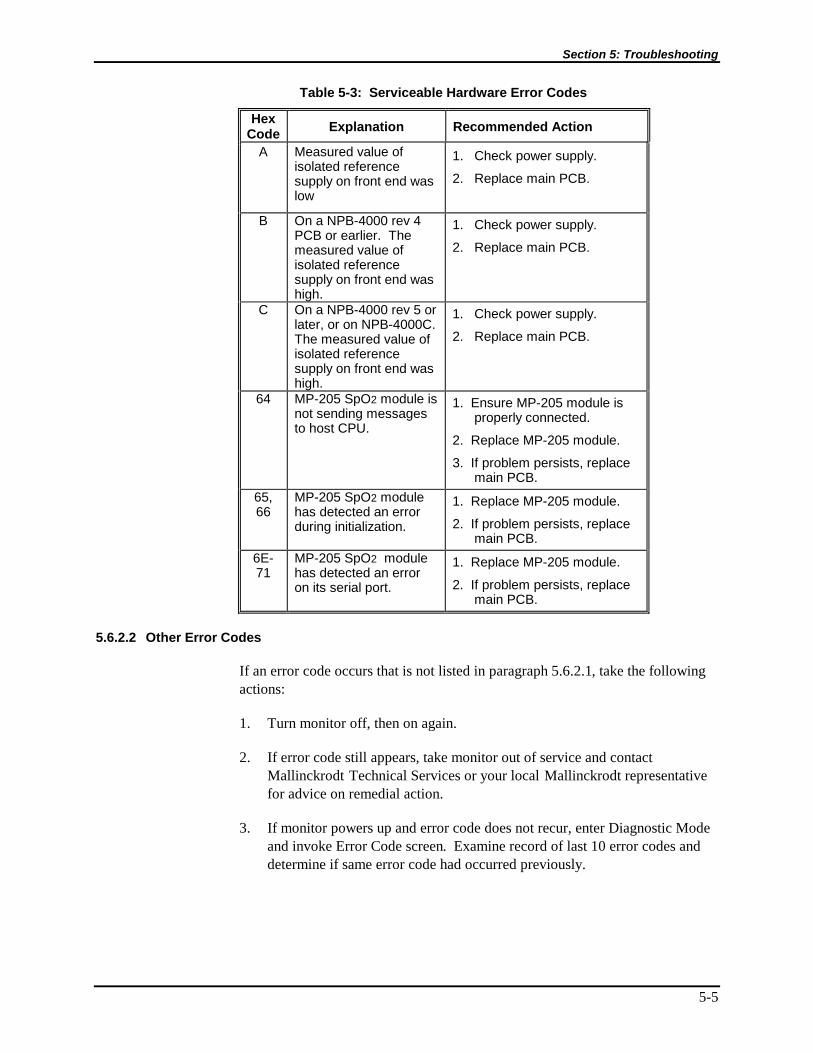
Section 5: Troubleshooting
5-5
Table 5-3: Serviceable Hardware Error Codes
HexCode Explanation Recommended Action
A Measured value ofisolated referencesupply on front end waslow
1. Check power supply.
2. Replace main PCB.
B On a NPB-4000 rev 4PCB or earlier. Themeasured value ofisolated referencesupply on front end washigh.
1. Check power supply.
2. Replace main PCB.
C On a NPB-4000 rev 5 orlater, or on NPB-4000C.The measured value ofisolated referencesupply on front end washigh.
1. Check power supply.
2. Replace main PCB.
64 MP-205 SpO2 module isnot sending messagesto host CPU.
1. Ensure MP-205 module isproperly connected.
2. Replace MP-205 module.
3. If problem persists, replacemain PCB.
65,66
MP-205 SpO2 modulehas detected an errorduring initialization.
1. Replace MP-205 module.
2. If problem persists, replacemain PCB.
6E-71
MP-205 SpO2 modulehas detected an erroron its serial port.
1. Replace MP-205 module.
2. If problem persists, replacemain PCB.
5.6.2.2 Other Error Codes
If an error code occurs that is not listed in paragraph 5.6.2.1, take the followingactions:
1. Turn monitor off, then on again.
2. If error code still appears, take monitor out of service and contact Mallinckrodt Technical Services or your local Mallinckrodt representative for advice on remedial action.
3. If monitor powers up and error code does not recur, enter Diagnostic Modeand invoke Error Code screen. Examine record of last 10 error codes anddetermine if same error code had occurred previously.

Section 5: Troubleshooting
5-6
4. If Error Code screen indicates same error has occurred previously, takemonitor out of service and contact Mallinckrodt Technical Services or your local Mallinckrodt representative for advice on remedial action.
5. If Error Code screen indicates no previous occurrences of this error, monitormay be returned to service.
As a reference, Table 5-4 lists the general categories for other error codes. Theerror code categories are shown only in hexadecimal format:
Table 5-4: Error Code Categories
Code (hex) Explanation
500xxxx internal user interface error
501xxxx remote serial port error
502xxxx date and time error
503xxxx NIBP error
504xxxx front end error
505xxxx alarm error
506xxxx audio error
507xxxx recorder error
508xxxx trend error
509xxxx flash memory data error
50axxxx SpO2 error
50bxxxx ECG error
50cxxxx power down task error
50dxxxx on board diagnostic error
50exxxx power monitor error
50fxxxx temperature measurement error
510xxxx internal user interface error
511xxxx error handling error
512xxxx pSOS (operating system) initialization error
513xxxx serial driver error
5.6.3 Switches/Knobs
Table 5-5 lists recommended actions to address problems with the knob andfront panel switches.

Section 5: Troubleshooting
5-7
Table 5-5: Switches/Knob Problems
Condition Recommended Action
1. NPB-4000/C fails topower-up whenOn/Standby switch ispressed.
1. Take steps as noted in paragraph 5.6.1.
2. NPB-4000/C powers-up, but some or one ofthe other switchesrespond.
1. Ensure keypad is plugged into Main PCB. Ifconnection is good, change keypad.
2. If problem persists, change Main PCB.
3. When knob is rotated,no highlight appears ondisplay screen, and/ormonitor does notrespond to knobpresses.
1. Ensure encoder cable is plugged into MainPCB. If connection is good, changeencoder.
2. If problem persists, replace Main PCB.

Section 5: Troubleshooting
5-8
5.6.4 Display/Audible Tones
Table 5-6 lists recommended actions to address problems with the display andaudible tones.
Table 5-6: Display/Audible Tones Problems
Condition Recommended Action
1. System powers-upand…
• LCD screen is totallyblack or white.
Or,
• LCD screen isilluminated, but nodata is visible.
Or,
• LCD screen hasdata, but is notilluminated.
Note: Pressing the NPB-4000 contrast adjustswitch causes the LCD contrast setting toimmediately change to normal, factory-default value. Pressing the NPB-4000/Ccontrast adjust switch toggles the displaybetween the two different color schemes(black background and white background).
1. NPB-4000. Adjust LCD screen contrast bypressing contrast adjust switch momentarily,then turning knob four revolutions in eachdirection. Turning knob counter-clockwiseshould brighten screen; turning knobclockwise should darken screen.
Or
2. NPB-4000C. Adjust LCD screen contrast bypressing contrast adjust switch momentarily.Screen will toggle background color.
3. Ensure red LED, located on top left corner ofmain PCB is illuminated. If LED is notilluminated, monitor is not in “on” state; followtroubleshooting steps in paragraph 5.6.1.
4. Ensure backlight cable is connected to mainPCB and backlight inverter PCB.
5. Ensure LCD cable is connected to main PCBand LCD PCB.
6. If problem persists, replace main PCB.
7. If problem persists, replace backlight PCB.
8. If problem persists, replace LCD assembly.
2. NPB-4000/Cresponds to switchpress, but key presstone fails to sound.
1. Ensure speaker cable is connected to powersupply assembly.
2. If problem persists, replace speakerassembly.
3. If problem persists, replace main PCB.

Section 5: Troubleshooting
5-9
Table 5-6: Display/Audible Tones Problems
Condition Recommended Action
3. Audible alarm doesnot sound.
1. Verify alarm volume setting in Alarm/Limitsmenu, and test operation of alarm tone bypressing Heart Rate Tone Volume switchwhile alarm volume setting is displayed.
2. Ensure speaker cable is connected to powersupply assembly.
3. If problem persists, replace speakerassembly.
4. If problem persists, replace main PCB.
5.6.5 Operational Performance
Table 5-7 lists recommended actions to address problems related to operationalperformance.
Table 5-7: Operational Performance Problems
Condition Recommended Action
1. Monitor appears to beoperational, butphysiological values aresuspect or nonexistent.
1. Replace each patient cable (or hose) with aknown serviceable cable.
2. Ensure internal ECG, temperature, andSpO2 cables are connected to main PCB.Ensure hoses in pneumatic system areproperly connected, and NIBP pump motoris connected to power supply PCB.
3. If problem persists, replace main PCB.
2. Printer paper will notadvance.
1. Open printer door and check paper ispresent. Press printer module firmly intomonitor to ensure printer module is fullyengaged with connector on printer PCB.
2. Cycle power on monitor. Printer shouldexecute a line feed at conclusion of power-up sequence.
3. If problem persists, ensure main ribboncable is connected to printer PCB, powersupply, and main PCB.
4. If problem persists, replace printer.
5. If problem persists, replace printer PCB.
6. If problem persists, replace main PCB.

Section 5: Troubleshooting
5-10
Table 5-7: Operational Performance Problems
Condition Recommended Action
3. Printer paper willadvance, but paperremains blank whenprinting should bepresent.
1. Open printer door and check paper isoriented correctly; paper should exit frombottom of roll. See operator’s manual foran illustration of correct paper orientation.
2. If problem persists, replace printer.

6-1
SECTION 6: DISASSEMBLY GUIDE6.1 Introduction6.2 How to Use this Section6.3 Disassembly Sequence Flow Charts6.4 Closed Case Disassembly Procedures6.5 Front Case Disassembly Procedures6.6 Rear Case Disassembly Procedures
6. DISASSEMBLY GUIDE
WARNING: Performance Verification. Do not place the NPB-4000/C intooperation after repair or maintenance has been performed, until allPerformance Tests and Safety Tests listed in Section 3 of this servicemanual have been performed. Failure to perform all tests could result inerroneous monitor readings.
6.1 INTRODUCTION
The NPB-4000/C can be disassembled down to all major component parts,including:
• PCBs• battery• cables• function switches• chassis enclosures
The following tools are required:
• small, Phillips-head screwdriver• medium, Phillips-head screwdriver• needle-nose pliers• 9/16-inch socket (for knob encoder)
WARNING: Before attempting to open or disassemble the NPB-4000/C,disconnect the power cord from the NPB-4000/C.
Caution: Observe ESD (electrostatic discharge) precautions when workingwithin the unit.
Note: Some spare parts have a business reply card attached. When you receivethese spare parts, please fill out and return the card.
6.2 HOW TO USE THIS SECTION
The step-by-step procedures that are used to access replaceable parts of theNPB-4000/C are illustrated in the Disassembly Sequence Flow Charts inparagraph 6.3, Figure 6-1 and Figure 6-2. As indicated in the flow charts, themonitor consists of two main assemblies, the Front Case Assembly and RearCase Assembly.

Section 6: Disassembly Guide
6-2
The ovals on the flow charts contain reference designators that point to specificsteps in the Disassembly Procedures. The Disassembly Procedures, paragraphs6.4, 6.5, and 6.6 contain detailed disassembly instructions, accompanied byillustrations.
The rectangular boxes on the flow charts represent the various components orsub-assemblies. The digits appearing in these boxes are the part numbers of thecomponent or subassembly. Section 7, Spare Parts, contains a complete listingof the available spare parts and exploded views.

Section 6: Disassembly Guide
6-3
6.3 DISASSEMBLY SEQUENCE FLOW CHARTS
Figure 6-1: NPB-4000/C Disassembly Sequence Flow Chart, Sheet 1

Section 6: Disassembly Guide
6-4
Figure 6-2: NPB-4000/C Disassembly Sequence Flow Chart, Sheet 2
6.4 CLOSED CASE DISASSEMBLY PROCEDURES
This section describes the items that may be removed/replaced withoutdisassembling the main case of the monitor.
Step A1
Procedure
To remove front panel knob:
a) Knob is friction-fit on encoder shaft. Grasp sides of knob firmly and pullstraight back from monitor; knob should slip off encoder shaft.
b) If knob does not move, separate front and rear cases as described in stepB1. There is a hole in front cover behind knob; insert small screwdriverblade in hole and push firmly against back of knob.

Section 6: Disassembly Guide
6-5
Step A2
Procedure
To remove carrying handle:
a) Use screwdriver to remove two fastening screws and washers. Retain forreassembly.
b) Remove handle by sliding it straight back toward rear of monitor.
Illustration
Step A3
Procedure
To remove printer:
a) Press Paper Eject button on printer (right side). Door will drop forward.
b) Remove paper roll, if installed. Two fastening screws are visible at backpanel of printer.
c) Use screwdriver to back out captive fastening screws.
d) Pull printer straight out side of monitor, disengaging connector at rear ofmodule from Printer PCB in assembly.
Removal of Printer PCB can be accomplished only after front and rear casesare separated.

Section 6: Disassembly Guide
6-6
6.5 FRONT CASE DISASSEMBLY PROCEDURES
This section describes the steps to separate the front and rear case assemblies,and the items that may be removed/replaced on the front case assembly.
Step B1
Procedure
To separate front and rear case assemblies:
a) Remove handle as indicated in step A1.
b) Use screwdriver to remove four screws fastening Rear Case Assembly toFront Case Assembly. Retain for reassembly.
Illustration
Procedure
c) Separate two major case assemblies. There is enough cable and tubingslack to permit the two assemblies to remain at approximately a 90-degreeangle to each other.
Illustration
Main ribboncable assembly NIBP tubing
Connector toprinter PCB(when installed)
Rick Chesser
Rick Chesser
Rick Chesser

Section 6: Disassembly Guide
6-7
Procedured) Disconnect large ribbon-cable connector from main PCB.
e) Unscrew NIBP tubing connector from pump to main PCB. Front and rearcase assemblies are now completely separable from one another.
Illustration
Step B2Procedure
To remove SpO2 module, ECG/Temp connector assembly, and encoderassembly:
• SpO2 module: remove three screws located at corners of SpO2 module,lift off ground wire and foil shield, pull SpO2 module straight up todisengage it from main PCB.
• ECG/Temp cable/connector assembly: unplug connector from MainPCB, remove screws fastening ECG connector to front case, rotatetemperature connector counter-clockwise to unscrew it from fastening nuton outside of front case.
• The encoder assembly: unplug connector from main PCB. Removeknob, as described in step A1. Use 9/16” hex socket to unscrew fasteningnut on outside of front case. Encoder may be pulled away from front case.
SpO2 module
Rick Chesser

Section 6: Disassembly Guide
6-8
Step B3
Procedure
To remove main PCB:
a) Disconnect connectors, from main PCB, for:
• Switch panel• SpO2• ECG/Temp• Encoder• LCD (display)• Backlight
Illustration
EncoderSwitchpanelconnector
NIBP Tubingconnector
SpO2 cable
Rick Chesser
Rick Chesser
Rick Chesser
Rick Chesser
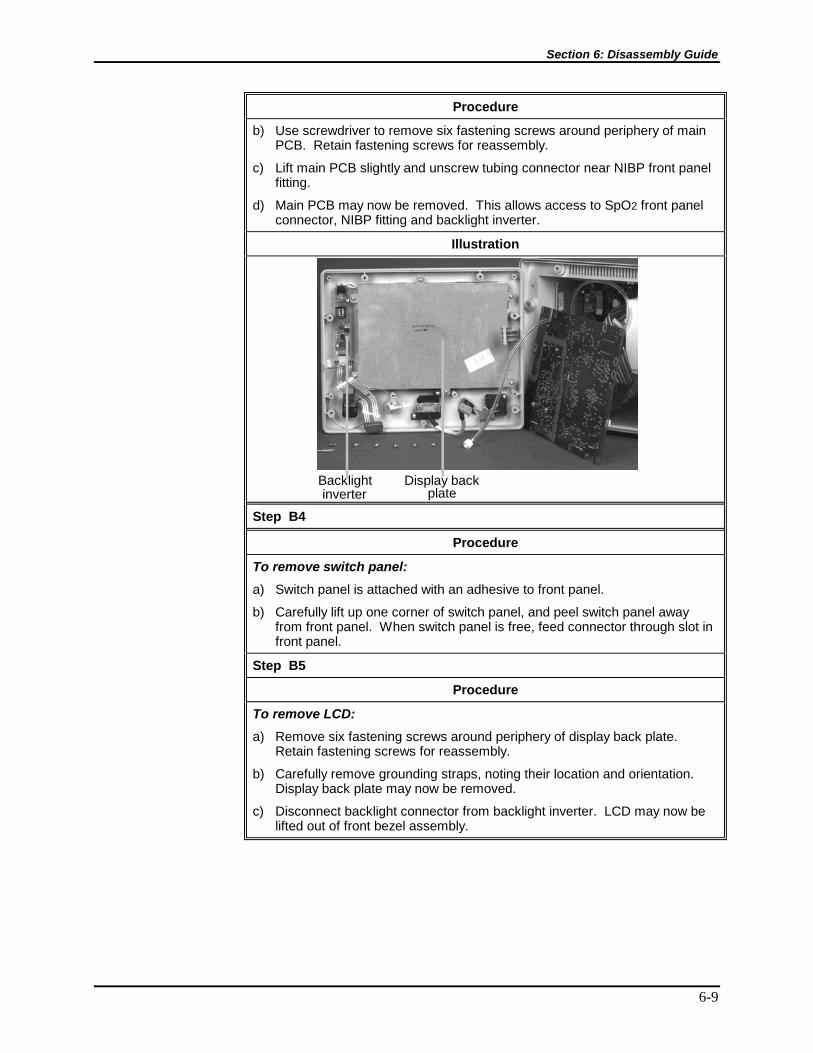
Section 6: Disassembly Guide
6-9
Procedure
b) Use screwdriver to remove six fastening screws around periphery of mainPCB. Retain fastening screws for reassembly.
c) Lift main PCB slightly and unscrew tubing connector near NIBP front panelfitting.
d) Main PCB may now be removed. This allows access to SpO2 front panelconnector, NIBP fitting and backlight inverter.
Illustration
Step B4
Procedure
To remove switch panel:
a) Switch panel is attached with an adhesive to front panel.
b) Carefully lift up one corner of switch panel, and peel switch panel awayfrom front panel. When switch panel is free, feed connector through slot infront panel.
Step B5
Procedure
To remove LCD:
a) Remove six fastening screws around periphery of display back plate.Retain fastening screws for reassembly.
b) Carefully remove grounding straps, noting their location and orientation.Display back plate may now be removed.
c) Disconnect backlight connector from backlight inverter. LCD may now belifted out of front bezel assembly.
Backlightinverter
Display backplate
Rick Chesser
Rick Chesser
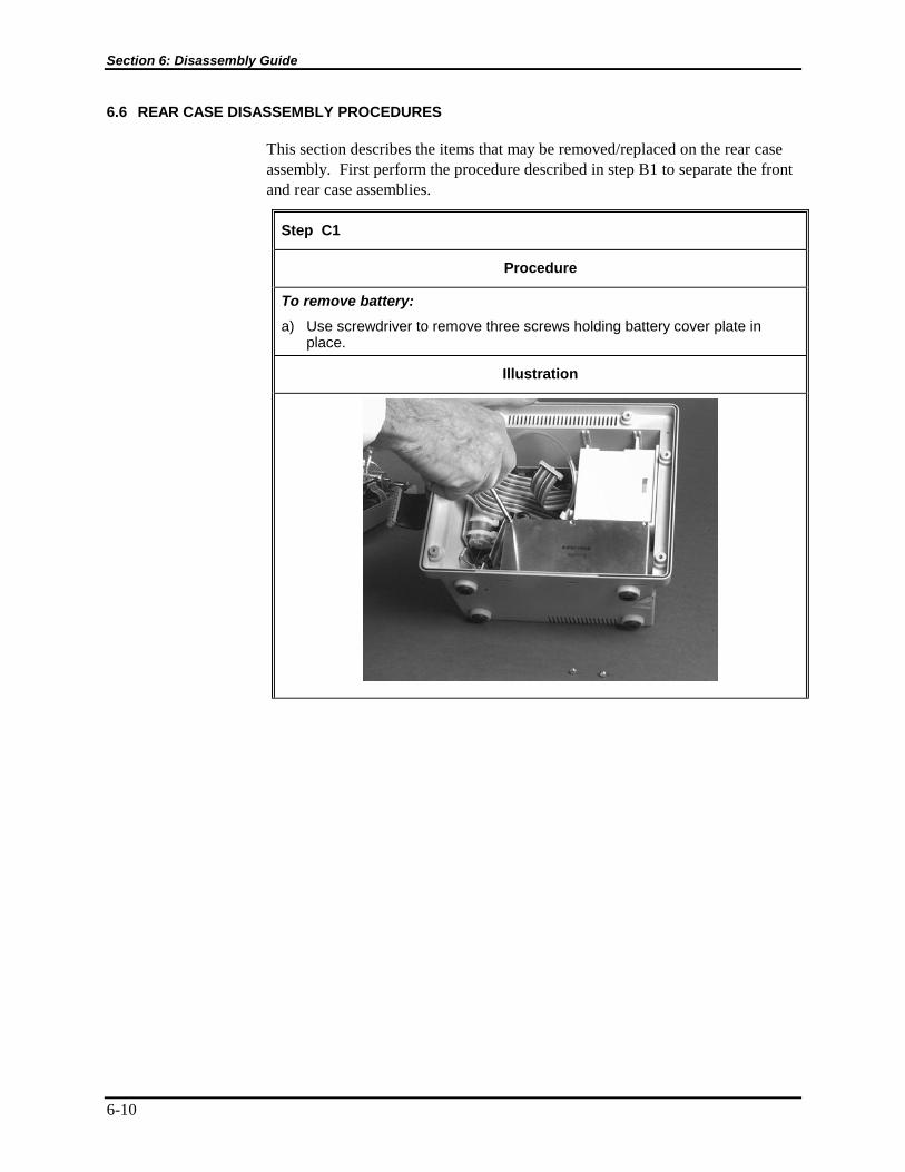
Section 6: Disassembly Guide
6-10
6.6 REAR CASE DISASSEMBLY PROCEDURES
This section describes the items that may be removed/replaced on the rear caseassembly. First perform the procedure described in step B1 to separate the frontand rear case assemblies.
Step C1
Procedure
To remove battery:
a) Use screwdriver to remove three screws holding battery cover plate inplace.
Illustration

Section 6: Disassembly Guide
6-11
Procedureb) Grasp strap, accessible through opening in top foam cover, and gently pull
battery from its housing.Illustration
Procedurec) Remove wire connectors from battery clips. Remember red wire is
connected to plus (+) side of battery pack.Illustration

Section 6: Disassembly Guide
6-12
Step C2
ProcedureTo remove battery housing:
a) Remove battery as described in step C1. Carefully remove two foambattery pads from battery housing.
b) If a printer is installed, remove it as described in step A3.
c) If a printer is not installed, remove printer blanking cover by slipping smallflat-blade screwdriver into one of the slots on the blanking cover. Usescrewdriver to gently depress snap-tab on inside of cover, while pullingcover away from monitor. After first tab is released, repeat process onother side of cover and remove cover.
Illustration
Battery housing
Rick Chesser

Section 6: Disassembly Guide
6-13
Procedured) On rear panel of monitor, remove three screws fastening battery housing.
e) Carefully slide battery housing from rear case assembly.Illustration
Proceduref) Disconnect speaker twisted-pair-connector from power supply PCB.
Speaker is mounted on one side of battery housing.
g) If printer had been installed, disconnect ribbon cable from printer PCB.Printer PCB may be removed by removing four screws fastening PCB tobattery housing.
Illustration
Screws fasteningbattery housing
Rick Chesser
Rick Chesser
Rick Chesser
Rick Chesser
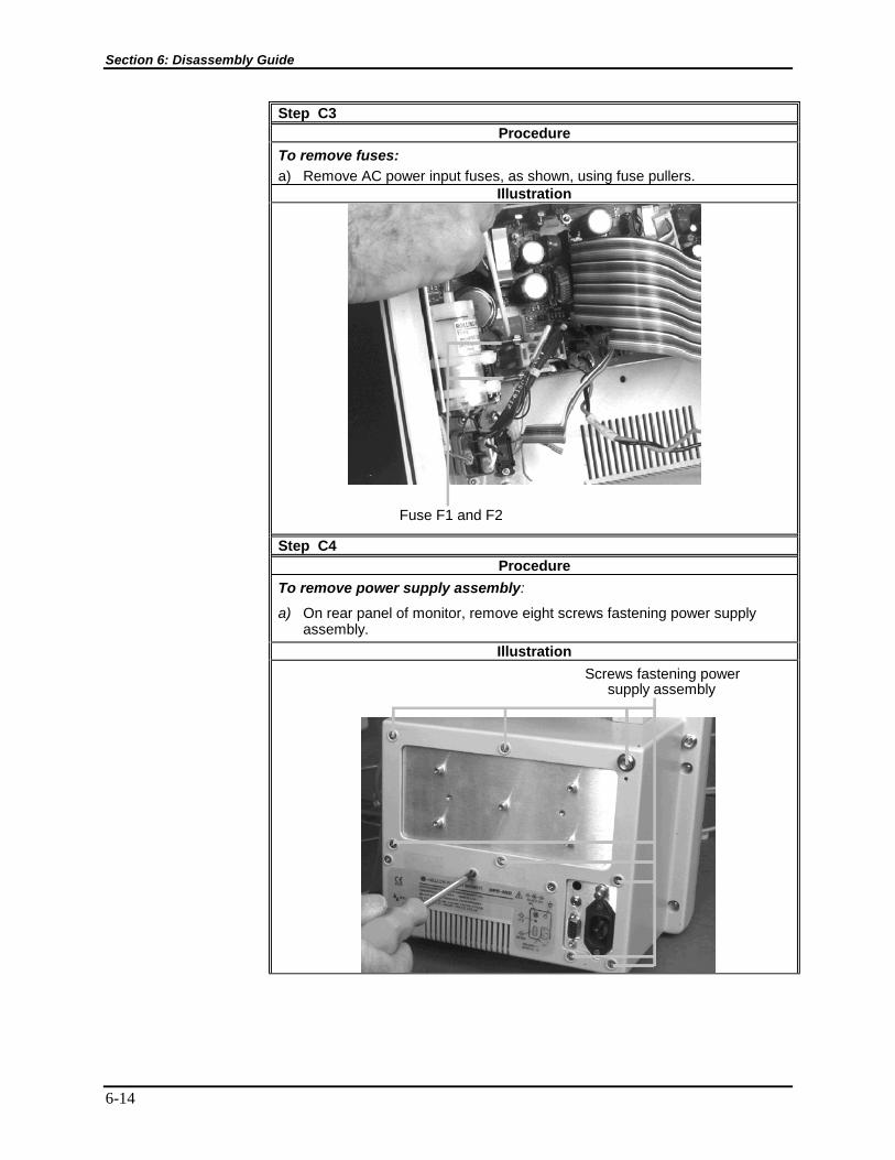
Section 6: Disassembly Guide
6-14
Step C3Procedure
To remove fuses:a) Remove AC power input fuses, as shown, using fuse pullers.
Illustration
Step C4Procedure
To remove power supply assembly:
a) On rear panel of monitor, remove eight screws fastening power supplyassembly.
Illustration
Fuse F1 and F2
Screws fastening powersupply assembly
Rick Chesser
Rick Chesser
Rick Chesser
Rick Chesser
Rick Chesser
Rick Chesser
Rick Chesser
Rick Chesser
Rick Chesser
Rick Chesser
Rick Chesser
Rick Chesser
Rick Chesser

Section 6: Disassembly Guide
6-15
Procedureb) Carefully lift power supply assembly from rear case.
c) Power supply assembly may be disassembled into the following elements:
• Power supply PCB• NIBP pump• Heat sink/chassis• Main ribbon cable
Illustration

[THIS PAGE INTENTIONALLY LEFT BLANK]

7-1
SECTION 7: SPARE PARTS7.1 Introduction
7. SPARE PARTS
7.1 INTRODUCTION
Spare parts, along with part numbers, are shown in Table 7-1 through Table 7-7.“Item No.” corresponds to the circled callout numbers in Figure 7-1 throughFigure 7-6. The “Step Ref.” corresponds to the disassembly steps described inSection 6.

Section 7: Spare Parts
7-2
Figure 7-1: NPB-4000/C Top Assembly Drawing

Section 7: Spare Parts
7-3
Table 7-1: Top Assembly (Figure 7-1)
ItemNo. Description
NPBPart No.
StepRef.
NPB-4000
2 Handle 047394 A2
NPB-4000C
2 Handle 047394 A2

Section 7: Spare Parts
7-4
Figure 7-2: NPB-4000/C Front Case Assembly Diagram (Sheet 1 of 2)

Section 7: Spare Parts
7-5
Table 7-2: Front Case Assembly (Figure 7-2)
ItemNo. Description
NPBPart No.
StepRef.
NPB-4000
1 Knob 044727 A1
5 SpO2 module 046085 B2
6 Connector/cable, ECG/temp 047376 B2
7 Encoder 291186 B2
8 PCB, main, Version 3.0 049624 B3
9 NIBP fitting and tubing 047375 B3
10 Inverter, backlight 047378 B3
11 Cable, SpO2 060230 B3
12 Switch panel 046787 B4
13 Plate, display back 047379 B5
14 Display (LCD) 047377 B5
15 Bezel ,front 049623 B5
NPB-4000C
1 Knob 044727 A1
5 SpO2 module 046085 B2
6 Connector/cable, ECG/temp 047376 B2
7 Encoder 291186 B2
8 PCB, main 049591 B3
9 NIBP fitting and tubing 047375 B3
10 Inverter, backlight 049621 B3
11 Cable, SpO2 060230 B3
12 Switch panel 046787 B4
13 Plate, display back 049592 B5
14 Display (LCD) 049593 B5
15 Bezel ,front 049589 B5

Section 7: Spare Parts
7-6
Figure 7-3: NPB-4000/C Front Case Assembly Diagram (Sheet 2 of 2)
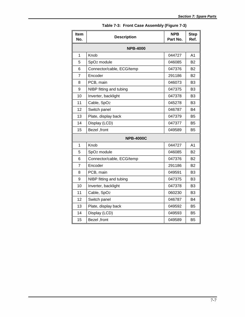
Section 7: Spare Parts
7-7
Table 7-3: Front Case Assembly (Figure 7-3)
ItemNo. Description
NPBPart No.
StepRef.
NPB-4000
1 Knob 044727 A1
5 SpO2 module 046085 B2
6 Connector/cable, ECG/temp 047376 B2
7 Encoder 291186 B2
8 PCB, main 046073 B3
9 NIBP fitting and tubing 047375 B3
10 Inverter, backlight 047378 B3
11 Cable, SpO2 045278 B3
12 Switch panel 046787 B4
13 Plate, display back 047379 B5
14 Display (LCD) 047377 B5
15 Bezel ,front 049589 B5
NPB-4000C
1 Knob 044727 A1
5 SpO2 module 046085 B2
6 Connector/cable, ECG/temp 047376 B2
7 Encoder 291186 B2
8 PCB, main 049591 B3
9 NIBP fitting and tubing 047375 B3
10 Inverter, backlight 047378 B3
11 Cable, SpO2 060230 B3
12 Switch panel 046787 B4
13 Plate, display back 049592 B5
14 Display (LCD) 049593 B5
15 Bezel ,front 049589 B5
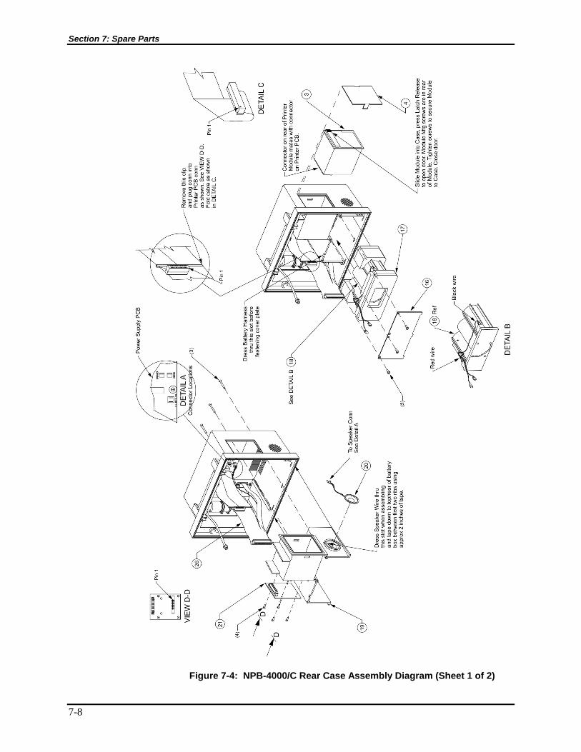
Section 7: Spare Parts
7-8
Figure 7-4: NPB-4000/C Rear Case Assembly Diagram (Sheet 1 of 2)

Section 7: Spare Parts
7-9
Table 7-4: Rear Case Assembly (Figure 7-4)
ItemNo. Description
NPBPart No.
StepRef.
NPB-4000
3 Printer module 060480 A3
4 Plate, printer blanking 047386 A3
16 Cover, battery 047382 C1
17 Pads, battery 047383 C1
18 Battery 047384 C1
19 Housing, battery 047381 C2
20 Speaker 047387 C2
21 PCB, printer 047388 C2
26 Cable, main ribbon 047391 C4
27 Case, Rear 047393 C4
NPB-4000C
3 Printer module 060480 A3
4 Plate, printer blanking 047386 A3
16 Cover, battery 047382 C1
17 Pads, battery 047383 C1
18 Battery 047384 C1
19 Housing, battery 047381 C2
20 Speaker 047387 C2
21 PCB, printer 047388 C2
26 Cable, main ribbon 047391 C4
27 Case, Rear 047393 C4

Section 7: Spare Parts
7-10
Figure 7-5: NPB-4000/C Rear Case Assembly Diagram (Sheet 2 of 2)

Section 7: Spare Parts
7-11
Table 7-5: Rear Case Assembly (Figure 7-5)
ItemNo. Description
NPBPart No.
StepRef.
NPB-4000
3 Printer module 060480 A3
4 Plate, printer blanking 047386 A3
16 Cover, battery 047382 C1
17 Pads, battery 047383 C1
18 Battery 047384 C1
19 Housing, battery 047381 C2
20 Speaker 047387 C2
21 PCB, printer 047388 C2
26 Cable, main ribbon 047391 C4
27 Case, Rear 047393 C4
è Power Supply Assembly 049622 C6
NPB-4000C
3 Printer module 060480 A3
4 Plate, printer blanking 047386 A3
16 Cover, battery 047382 C1
17 Pads, battery 047383 C1
18 Battery 047384 C1
19 Housing, battery 047381 C2
20 Speaker 047387 C2
21 PCB, printer 047388 C2
26 Cable, main ribbon 047391 C4
27 Case, Rear 047393 C4
è Power Supply Assembly 049622 C6

Section 7: Spare Parts
7-12
Figure 7-6: NPB-4000/C Power Supply/Heat Sink Assembly Diagram

Section 7: Spare Parts
7-13
Table 7-6: Power Supply Assembly (Figure 7-6)
ItemNo. Description
NPBPart No.
StepRef.
NPB-4000
22 Fuse, 0.75A, slo-blow, 250V, 5x20 mm 691501 C3
23 PCB, power supply 046074 C4
24 Pump, NIBP 047389 C4
26 Cable, main ribbon 047391 C4
NPB-4000C
22 Fuse, 0.75A, slo-blow, 250V, 5x20 mm 691501 C3
23 PCB, power supply 046074 C4
24 Pump, NIBP 047389 C4
26 Cable, main ribbon 047391 C4
Some of the accessories available for the NPB-4000/C are listed below.
Table 7-7: NPB-4000/C Accessories
NPBPart No. Description
CE-10 ECG cable
LE-3SI ECG leads (IEC color code)
LE-3SN ECG leads (AHA color code)
ASP3 Oxisensor‚ II sensor assortment pack
DS100A Durasensor‚ oxygen transducer
EC-8 SpO2 sensor extension cable
SHBP-10 NIBP hose
902096 Printer paper (10 rolls)
045279 GCX mounting plate
046270 GCX roll stand
046283 GCX wall mount
045992 Accessory bag
044997 DC input cable
044998 Defib sync cable

[THIS PAGE INTENTIONALLY LEFT BLANK]

8-1
SECTION 8: PACKING FOR SHIPMENT8.1 General Instructions8.2 Repackaging in Original Carton8.3 Repackaging in a Different Carton
8. PACKING FOR SHIPMENT
To ship the monitor for any reason, follow the instructions in this section.
8.1 GENERAL INSTRUCTIONS
Pack the monitor carefully. Failure to follow the instructions in this section mayresult in loss or damage not covered by the Mallinckrodt warranty. If the original shipping carton is not available, use another suitable carton; NorthAmerican customers may call Mallinckrodt Technical Services to obtain a shipping carton.
Prior to shipping the monitor, contact your supplier or the local Mallinckrodt office (Technical Services Department) for a returned goods authorization (RGA) number. Mark the shipping carton and any shipping documents with the returned goods authorization number.
8.2 REPACKING IN ORIGINAL CARTON
If available, use the original carton and packing materials. Pack the monitor asfollows:
1. Place the monitor and, if necessary, accessory items in original packaging.
2. Place in shipping carton and seal carton with packaging tape.
3. Label carton with shipping address, return address and RGA number, ifapplicable.
8.3 REPACKING IN A DIFFERENT CARTON
If the original carton is not available, use the following procedure to pack theNPB-4000/C:
1. Place the monitor in a plastic bag.
2. Locate a corrugated cardboard shipping carton with at least 200 pounds persquare inch (psi) bursting strength.
3. Fill the bottom of the carton with at least 2 inches of packing material.
4. Place the bagged unit on the layer of packing material and fill the boxcompletely with packing material.

Section 8: Packing for Shipment
8-2
5. Seal the carton with packing tape.
6. Label the carton with the shipping address, return address, and RGAnumber, if applicable.

9-1
SECTION 9: SPECIFICATIONS9.1 Scope9.2 General9.3 Electrical9.4 Environmental9.5 Measuring Parameters9.6 Trends
9. SPECIFICATIONS
9.1 SCOPE
This section includes specifications for the NPB-4000/C. The instrument isdesigned to monitor patient vital signs, including: electrocardiogram and heartrate, respiration rate, noninvasive blood pressure, blood oxygen saturation, andtemperature. In addition to displaying the instantaneous values of the measuredparameters, the NPB-4000/C includes provisions for displaying waveform data,as well as trends in graphical and tabular format. An optional printer providesfor hard copy recording.
9.2 GENERALSize: 10.6 in. x 8.6 in. x 6.5 in. (26.9 cm x 21.8 cm x
16.5 cm) excluding handle
Weight: 10.8 lb. (4.9 kg) excluding accessories, options,cables
Display:
NPB-4000
Screen Type: Liquid Crystal Display (LCD), Monochrome, ColdCathode Fluorescent Backlit
Screen Size: 151 mm x 113 mm
Resolution: 640 x 480 pixel
NPB-4000C
Screen Type: Liquid Crystal Display (LCD) Color, Cold CathodeFluorescent Backlit
Screen Size: 130 mm x 97 mm
Resolution: 640 x 480 pixel
Printer (optional):
Type: Thermal
Weight: 0.9 lb. (0.4 kg)
Paper Width: 50 mm
Speeds: 25 mm/s and 50 mm/s
Safety Standards: IEC 601-1, UL 2601-1, Can/CSA C22.2 601.1-M90

Section 9: Specifications
9-2
Protection Class: Class I, internally powered equipment:per IEC 601-1, clause 2.2.4
Degree of Protection: Type CF: per IEC 601-1, clause 2.2.26
Mode of operation: Continuous
9.3 ELECTRICAL
Internal Battery: 6V, 8 Ampere-Hours; Type - sealed lead-acid
Battery Operating Time:
NPB-4000 4 hours typical @ 25˚C, no printing, one NIBPmeasurement per 15 min. (fully charged battery)
NPB-4000C 3 hours typical @ 25˚C, no printing, one NIBPmeasurement per 15 min. (fully charged battery)
AC Mains: 100 VAC to 240 VAC, 50 Hz to 60 Hz, 1A max
DC (External): 10 VDC to 16 VDC, 5A max
9.4 ENVIRONMENTAL
Mechanical Shock: IEC 68-2-27100g; 6 msec; three axes18 total shocks, nonoperating
Mechanical Vibration:
Sinusoidal: IEC 68-2-610 Hz to 58 Hz; 0.15 in. displacement58 Hz to 150 Hz; 2g acceleration4 min/sweep; 20 sweeps/axis, nonoperating
Temperature:
Operating: 0 º C to 50˚C
Storage: -20 º C to 60˚C
Humidity:
Operating: 5 % RH to 95% RH, noncondensing
Storage: 5 % RH to 95% RH, noncondensing
Water Resistance: IEC 529 Classification IPX1 (Protected againstvertically dripping water)
Altitude: 0 ft to10,000 ft (operating)
(1037 hPa to 697 hPa)
ElectromagneticCompatibility:
Radiated and conducted electromagnetic energy perCISPR 11, Class B
Section 9: Specifications
9-3
9.5 MEASURING PARAMETERS
9.5.1 ECG Measurement/Display
Heart Rate Range: 20 BPM - 250 BPM
Heart Rate Accuracy: ±5 BPM
Bandwidth:
NormalMonitoring:
0.5 Hz to 40 Hz
Extended LowFrequencyResponse:
0.05 Hz to 40 Hz
Leads: 3 Lead (user selectable)
Display SweepSpeeds:
12.5 mm/sec, 25 mm/sec, and 50 mm/sec
Pacemaker Detection: Indicator on waveform display, user selectable
ECG Size(sensitivity):
0.5 mV/cm, 1 mV/cm, 2 mV/cm, 4 mV/cm
Lead Off Detection: Detected and displayed
Input Impedance: > 5 MΩCMMR (commonmode rejection ratio):
> 90 dB at 50 Hz or 60 Hz
Input Dynamic Range: ±5 mV AC, ±300 mV DC
DefibrillatorDischarge:
<5 sec per IEC 601-2-27
Recovery: <8 sec per AAMI EC13-1992
Standards:
Meets the performance standards of ANSI/AAMI EC13-1992. Instead of a1 mV standardizing voltage (section 3.2.2.9), a fixed, 1 cm reference bar isalways present in the ECG display, along with the ECG size setting expressedin mV/cm. The following information references particular sections ofANSI/AAMI EC13-1992.
Respiration, leads-offsensing waveform.3.1.2.1(b)
A 100 kHz square wave is used to inject42 mA, p-p differentially between RA and LA.
Tall T-wave rejection.3.1.2.1(c)
T-wave of 0.8 mV amplitude will not affect heartrate determination.
Heart rate averaging.3.1.2.1(d)
Averages six of the most recent eight detected R-Rintervals excluding the longest and shortest of theeight intervals.

Section 9: Specifications
9-4
Response to irregularrhythm. 3.1.2.1(e)
a) Ventricular bigeminy - 80 BPMb) Slow alternating ventricular bigeminy - 60 BPMc) Rapid alternating ventricular bigeminy -
120 BPMd) Bi-directional systoles - 89 to 96 BPM
Heart rate meterresponse time.3.1.2.1(f)
a) Change from 80 to 120 BPM: 4 to 6 secb) Change from 80 to 40 BPM: 6 to 7 sec
Time to alarm fortachycardia.3.1.2.1(g)
Waveform 4(a) Amplitude0.5 mV1 mV2 mV
Waveform 4(b) Amplitude1 mV2 mV4 mV
Avg. Time to Alarm4 sec4 sec4 sec
Avg. Time to Alarm3 sec3 sec3 sec
Pacemaker pulserejection. 3.1.4.1,3.1.4.2
With the exceptions noted below, the monitor willreject all pacemaker pulses having amplitudes of±2 to ±700 mV and pulse widths from 0.1 to 2 ms,with and without under/overshoot. Following arepacer pulse conditions that the monitor will reject,but are less than the maximum range listed in thestandard:
Pacer pulse width = 2ms, double pulse,without over/undershoot,no QRS
Pacer amplitude =±300 mV
Pacer pulse width = 2ms, single and doublepulse, with 2 mVover/undershoot, no QRS
Pacer amplitude =±300 mV
Pacer pulse width = 0.1ms, double pulse, with 2mV over/undershoot,ineffective pacing
Pacer amplitude =+300 mV, -450 mV
9.5.2 Respiration Measurement/Display
Technique: Trans-thoracic impedance
Range: 3 breaths/min to 150 breaths/min
Accuracy: ±3 breaths/min
Leads: RA to LA
Display SweepSpeeds:
6.25 mm/s, 12.5 mm/s, 25 mm/s
Lead Off Condition: Detected and displayed
Section 9: Specifications
9-5
9.5.3 NIBP (Noninvasive Blood Pressure) Measurement/Display
Note: Systolic and diastolic blood pressure measurements determined withthis device are equivalent to those obtained by a trained observer usingthe cuff/stethoscope auscultation method, within the limits prescribedby the American National Standard, Electronic or automatedsphygmomanometers.
Technique: Oscillometric
Measurement Modes:
Auto: Automatic BP measurements at intervals of 1, 3, 5,10, 15, 30, 60, and 90 minutes
Manual: Single measurement initiated by NIBP Start/Stopswitch
STAT: Series of consecutive measurements for 5 minutes
Cuff Pressure Display: 10mmHg to 300 mmHg
Blood PressureMeasurement Range:
Systolic: 60 mmHg to 250 mmHg
Mean ArterialPressure:
30 mmHg to 235 mmHg
Diastolic: 20 mmHg to 220 mmHg
Pulse Rate Range: 20 BPM to 200 BPM
Blood PressureAccuracy:
Mean error and standard deviation perANSI/AAMI SP10, 1992
Pulse Rate Accuracy: Greater of ±2 BPM or ±2% of pulse rate value
Initial Cuff Inflation: 180 mmHg (factory default), selectable 100 mmHgto 280 mmHg, in 20 mmHg intervals
Subsequent CuffInflation:
Previous SYS + 50 mmHg
Standards: Meets performance standards ofANSI/AAMI SP10-1992
9.5.4 Temperature Measurement/Display
Technique: Thermistor probe (YSI 400 series compatible)
Range: 15° C to 45° C
Accuracy: ±0.1° C
Section 9: Specifications
9-6
9.5.5 SpO2 Measurement/Display
Range:
Pulse Rate: 20 BPM to 250 BPM
% Saturation: 0 % to 100%
Accuracy:
Pulse Rate: ±3 BPM
SpO2: 70 % to 100%: ±2 digits0 % to 69%: Unspecified
SpO2 accuracies are expressed as plus or minus “X” digits (saturationpercentage points) between saturations of 70–100%. This variation equalsplus or minus one standard deviation (1SD), which encompasses 68% ofthe population. All accuracy specifications are based on testing thesubject monitor on healthy adult volunteers in induced hypoxia studiesacross the specified range. Adult accuracy is determined withOxisensor® II D-25 sensors.
9.6 TRENDS
Types: Graphical and Tabular
Memory Storage: 12 hours, nonvolatile
Data interval: 20 seconds: (Stored data point is the average over20-second interval)
Graphical Format: One graph per vital sign
Display range: 2 hours, scrollable
Vertical Scaling:
Heart rate: 50 BPM to 100 BPM, 0 BPM to 250 BPM,25 BPM to 125 BPM
NIBP: 50 mmHg to 100 mmHg, 0 mmHg to 150 mmHg,0 mmHg to 300 mmHg
SpO2: 0% to 100%, 60% to 100%, 80% to 100 %
RespirationRate:
0 BPM to 20 BPM, 0 BPM to 50 BPM,0 BPM to 150 BPM
Temperature°C:
15º C to 45º C, 33º C to 41º C, 35º C to 39 ° C
Temperature°F:
55º F to 155º F, 91º to 107º F, 96º F to 102° F
Tabular Format: One table for all variablesSix fields per row (time and 5 vital signs)
Display interval: Per NIBP measurement, or 15 minutes for no NIBP,or 20 seconds during alarm condition.

10-1
SECTION 10: INTRODUCTION AND SYSTEM DESCRIPTION10.1 System Overview10.2 System Block Diagram10.3 ECG Processing10.4 Respiration Processing10.5 NIBP Processing10.6 SpO2 Processing10.7 Temperature Processing
10. INTRODUCTION AND SYSTEM DESCRIPTION
10.1 SYSTEM OVERVIEW
10.1.1 The Complete NPB-4000/C Patient Monitor System
The NPB-4000/C patient monitor is a full-function monitor for use on adult andpediatric patients. The functions performed by the system include monitoringpatient ECG, heart rate, respiration rate, blood pressures, blood oxygensaturation, and temperature.
In addition to monitoring and displaying the status of these physiologicalparameters, the instrument performs various microprocessor-programmedanalytical functions, such as:
• Creating both visual and audible alarm signals when settable limits areviolated;
• Creating and displaying warning messages when conditions are detectedthat would degrade or prevent valid measurements;
• Creating and displaying trend waveforms or tabular data;
• Providing a synchronizing pulse for defibrillator operation;
• Providing input to an optional recorder for printout of current or trendwaveforms or tabular data.
The monitor is essentially a battery-powered instrument. An internal chargingunit is designed to accept either an AC line voltage or DC source input voltage.The charger uses these external power sources to maintain a “float” voltagesource available from the batteries.
10.2 SYSTEM BLOCK DIAGRAM
The NPB-4000/C patient monitor functions are represented graphically in theSystem Block Diagram, Figure 10-1.
Each section of the System Block Diagram is described briefly in the text thatfollows the illustration. This is followed by more detailed descriptions of thetheory of operation of each block.

Section 10: Introduction and System Description
10-2
Figure 10-1: NPB-4000/C System Block Diagram
10.2.1 Isolated Front End
The Isolated Front End section includes all the circuitry to convert ECG, SpO2,and temperature measurements to digital format and to connect this informationto the processor. The respiration detection is obtained from two of the threeelectrodes of the ECG connections.
Galvanic isolation of these circuits from the remainder of the monitor isaccomplished by utilizing an isolated power supply and by incorporatingopto-isolators between the Front End outputs and inputs to the microprocessorcomputation and control circuitry.
10.2.2 NIBP Front End
The NIBP section contains the pumps, valves, pressure measurement circuitry,and control circuitry for the noninvasive blood pressure measurement. Pressuredata is converted to digital format and conveyed to the processor section.
10.2.3 Power System
The power system section contains a power supply capable of operating themonitor and charging the battery from either an AC source of 100 to 240 voltsAC at 50 to 60 Hz or a 10 to 16 volt DC input. This section also contains thebattery, battery monitoring circuitry, and battery charging circuitry. The batteryprovides the operating power for the monitor.
Power system outputs of ±12 volts DC, +5 volts DC, and -24 volts DC aredeveloped for use throughout the non-isolated portions of the monitor.

Section 10: Introduction and System Description
10-3
10.2.4 µP, Memory, and Control
The microprocessor (µP), Memory, and Control section contains the system CPUand all digital support circuitry. The latter includes the RAM, nonvolatilememory, and real-time clock. This section also contains the display logic,keypad (switch) interface logic, RS-232 I/O control, defibrillator synchronizationcontrol, and printer logic.
10.2.5 Display
The display is a cold-cathode, backlighted, fluorescent LCD unit. The pixelresolution of 0.23 mm provides a 640x480 line display. The NPB-4000 displayis presented in black and white mode only (no gray scale). The NPB-4000Cdisplay is presented in color.
10.2.6 Keypad (Switches) and Knob
The keypad circuit contains five push-switch membrane switches and two greenLEDs. The LEDs are driven by the power supply system and indicate the sourceof externally applied power mains (AC or DC), the charging of the batteries, andthe condition of the source cable in-line fuses. Signals from the LEDs arereturned to the microcomputer for processing and control as required.
The power switch, connected directly to the supply, toggles the power betweenStandby and On modes. When in Standby, the display is blank, and nomonitoring is performed. However, the batteries are charging if either an AC orDC power source is connected to the rear panel.
The alarm silencing switch is connected directly to the processor and to thesystem power supply. Pressing this switch turns off the battery fuse alarm in thesystem power supply. Response of the processor depends upon the action inpressing this switch. If momentarily pressed (less than 2 seconds), alarms aresilenced temporarily for a preset interval determined by the menu selection. Ifheld pressed for 2 seconds or more, the Alarm Suspend condition is initiated.
The NIBP switch output is connected to the processor. Response of theprocessor depends upon the state of NIBP operation at the time and the action inpressing this switch. If momentarily pressed (less than 2 seconds), a single NIBPmeasurement is obtained. If pressed for 2 seconds or more, the processorinitiates a STAT monitoring sequence. Pressing the NIBP switch at any time apressure measurement is in effect will cause the processor to terminate themeasurement and to deflate the cuff.
NPB-4000. The display Contrast switch, operates in conjunction with theNellcor knob to determine the apparent black/white contrast setting in the display. Changing contrast is actually a change in the viewing angle. Outputs of the switch and knob are connected to the processor. Momentary pressing the switch sets the contrast to mid-range, factory-default value. Momentary pressing the switch, followed within 3 seconds by a rotation of the knob, are processed to vary the contrast of the display. When there has been no knob rotation for three seconds, the contrast control function is terminated by the processor. The contrast control function also is terminated if the knob is pressed any time within this 3-second interval.

Section 10: Introduction and System Description
10-4
NPB-4000C. Pressing the Contrast switch changes the background color fromwhite to black or black to white.
Operation of the Volume switch accomplishes similar functions for the volumeof the heart rate audible tone as the display contrast control switch does for thedisplay. Pressing this switch enables the knob to vary the tone volume. Thesame timing consideration of 3 seconds is provided, in which to adjust the tonevolume or to terminate the action.
10.2.7 Nellcor Knob
This is a rotating, push-switch knob. The associated knob circuitry generates apulse when pressed and generates a digitally encoded pair of quadrature signalswhose relative magnitudes and polarities represent the angular position of theknob. These outputs are connected to the processor where they are interpreted asrequired for the functions involved. Successive angular positions determine thedirection of knob rotation.
In addition to the functions performed when in conjunction with the keypadswitches as described above, the Knob operates in conjunction with the displayto select menus and lists of parameter variables.
10.2.8 RS-232 I/O
This is a rear panel 9-pin connector providing interfaces with other computersystems or equipment. The driver for this “port” is a Universal AsynchronousReceive-Transmit (UART) integrated circuit that interfaces this port with themicroprocessor. The baud rate for this serial transmission function isprogrammable from 1200 baud to 38.4 kilobaud.
One pin (9) of RS-232 connector is reserved for a Nurse Call signal. The Nursecall signal reacts when a low, medium, or high level alarm is activated.
10.2.9 Defib Synch Pulse
The rear-panel connector for the Defib Sync Pulse is keyed so that theconnection of a cable can be detected by the processor. When a connection isdetected, the processor software initiates the generation by hardware of aTTL-compatible pulse capable of driving 1 TTL load over a three-meter cablewith less than 200 pF capacitance.
The defib pulse is triggered by the detection of the R-wave in the QRS sequenceof the ECG waveform complex. The pulse signal is active for 100±10milliseconds.
10.2.10 Speaker
The speaker is capable of providing 73 dBA of volume at a distance of one meterduring alarm conditions. The processor drives the speaker in different patternsas specified for the different alarm priorities and conditions. Refer to theoperator’s manual for descriptions of alarm responses.

Section 10: Introduction and System Description
10-5
10.2.11 Recorder
The optional recorder (printer) module is installed in the right panel of themonitor. Refer to the NPB-4000/C monitor operator’s manual for printingprocedures. It provides users with the capability to obtain hard-copy records ofselected vital signs information. Basic control of the recorder is implemented bytwo push-switch controls on the recorder front panel. One of these is used toobtain continuous recordings of the real-time waveforms displayed in the top twographic frames. Along with the waveforms, the recorder prints the values of thevital signs being displayed. The printing continues until the user presses eitherrecorder switch a second time.
The other control switch initiates a printout for 20 seconds of the sameinformation recorded by the continuous control.
If scrolling is enabled in a display frame containing trend data when thecontinuous recording switch is operated, then the trend record for that vital signis printed. If the snapshot recording switch is operated, then only the trend dataon the display is printed.
The recorder may be programmed via the monitor menu display to print asnapshot recording when an alarm condition occurs.
Printing is accomplished on 50-mm wide thermal paper at printer speedsprogrammable up to 50 mm/sec.
10.3 ECG PROCESSING
The technique used in ECG senses the varying potential difference between twopoints at the skin surface which respond to the chemical actions of the muscularactivity of the heart.
Three electrodes are attached to the patient’s right arm (RA), left arm (LA) andleft leg (LL). The varying potentials at these locations are cable-connected tothe ECG circuit inputs where they are conditioned, and the difference ofpotential between two selected leads is digitized before transmitting throughopto-isolators to the processor. The processor-installed algorithms operate onthe signals to develop drivers for the graphic display and to compute the heartrate in beats per minute (bpm).
In addition to the acquisition of the QRS waveform complex, the ECG input andsubsequent signal processing computing circuitry perform a number of otherfunctions:
• They detect a “lead-off” condition if one of the electrode connections isdisrupted.
• They detect the presence of pacemaker signals within the QRS waveformcomplex of the ECG.
• They generate a synchronization pulse for external use with defibrillators .The Defib Synch Pulse output is available at a connector in the rear panel.
10.4 RESPIRATION PROCESSING

Section 10: Introduction and System Description
10-6
The patient’s respiration is detected by using two of the three leads of the ECGelectrodes and cable. A low-level excitation signal is applied to these leads, andthe variation of the thoracic impedance caused by the breathing is sensed andprocessed for display and measurement.
10.5 NIBP PROCESSING
The NIBP processing uses an oscillometric technique to provide neededmeasurements at selected intervals. This technique uses an inflatablesphygmomanometer cuff similar to those used by clinicians in routinemeasurements.
A motorized pump inflates the cuff to approximately 180 mmHg initially, atwhich point the pressure effectively stops the flow of blood. Then, undermonitor control, the pressure in the cuff is gradually reduced, while a pressuretransducer detects the air pressure and transmits the parameter signal to theNIBP input circuitry.
As the pressure is reduced, blood flows in the previously occluded artery, andchanges the measurements made by the transducer. The point at whichoscillation increases sharply is defined as systolic pressure . As the cuffcontinues to deflate, oscillation amplitude increases to a maximum, and thendecreases. The peak oscillation amplitude is defined as the mean arterialpressure. The point at which the system detects a rapid decrease in oscillation isdefined as the diastolic pressure.
10.6 SPO2 PROCESSING
Measurement of oxygen saturation in the blood uses a specrophotometrytechnique. It is based on the facts that oxyhemoglobin and deoxyhemoglobindiffer in the their absorption of red and infrared light, and that the volume ofarterial blood in tissue changes during the pulse.
Using these facts, a pulse oximeter passes red and infrared light into an arteriolarbed and measures changes in light absorption during the pulsatile cycle. Thelight sources are red and infrared light emitting diodes (LEDs), while thedetection is accomplished by a photodiode.
To identify the oxygen saturation of arterial hemoglobin, the monitor uses thepulsatile nature of arterial flow. During systole, a new pulse of arterial bloodenters the vascular bed, and both blood volume and light absorption increase.During diastole, blood volume and light absorption reach their lowest point. Themeasurement is based upon the difference between maximum and minimumabsorption, focusing on the pulsatile arterial blood.
In addition to the oximetry function, the input signals may be used to calculateheart rate.
10.7 TEMPERATURE PROCESSING
Measurement of patient temperature is accomplished by processing the signalfrom a probe containing a resistor whose impedance is temperature dependent.The class of such components is called thermistor.

Section 10: Introduction and System Description
10-7
The NPB-4000/C patient monitor is designed to accept the signals fromelectrically isolated Series 400 probes manufactured by Yellow SpringsIncorporated. Interchangeable probes in this series may be used for esophageal,rectal, skin or surface, or airway temperature measurement. Probes are furnishedwith a standard 10-feet lead; extension leads are available.
The signal from the probe is conditioned by the monitor input circuitry,processed, and used to drive the numeric display.

[THIS PAGE INTENTIONALLY LEFT BLANK]

11-1
SECTION 11: ISOLATED FRONT END FUNCTIONS - THEORY OFOPERATION
11.1 Block Diagram11.2 Overview11.3 Interface Circuit11.4 ECG11.5 Respiratory Circuit11.6 Temperature Circuit11.7 Optocouplers11.8 Controls11.9 A/D Converter11.10 Isolated Power Supply11.11 SpO2 Board11.12 Isolation
11. ISOLATED FRONT END FUNCTIONS - THEORY OF OPERATION
11.1 BLOCK DIAGRAM
See Figure 11-1. The simplified block diagram of the previous section has beenreproduced and highlighted to indicate the circuit block that will be described insome detail in the paragraphs that follow. As shown, the selected block is theisolated Front End circuitry. This block contains the interfaces with the patientconnections at the input, and delivers an isolated output to the microprocessorand controller. An expanded block diagram for this circuitry is shown inFigure 11-2.
Figure 11-1: NPB-4000/C Simplified Block Diagram

Section 11: Isolated Front End Functions -- Theory of Operation
11-2
Figure 11-2: Isolated Front End Block Diagram
The NPB-4000/C Front End module is a part of the Main Board. It provides anisolation barrier between a patient’s body and electrical potentials on the rest ofthe board as well as some high voltage protection of the isolation barrier itself.
11.2 OVERVIEW
The NPB-4000/C Front End Module consists of eight major blocks: interfacecircuit, ECG, respiration, temperature, controls, power supply, isolation, andA/D converter on the non-isolated side. It also carries an SpO2 module whichuses Front End for isolation and power supply.
• The ECG channel has 3-lead capability and a gain of 285. It provides twolevels of low frequency noise filtering, T-wave filtering, R-wave detection,pacer detection capability and baseline reset.
• The temperature channel provides measurements over the range of15 to 45˚C using YS400 series probes.
• The respiration channel incorporates the standard impedance pneumographymethod of injecting 100 kHz current of 42 micro Amps into a patientthrough the RA and LA leads and measuring voltage modulated byrespiration on the same leads. Respiration can be measured in the range of200 to 2000 ohms of a body impedance with the maximum modulation of 10ohms.

Section 11: Isolated Front End Functions -- Theory of Operation
11-3
• Isolation is provided by optocouplers. A total of four optocouplers are usedfor digital signals and a linear optocoupler with a multiplexer is used for allanalog signals. The isolated side has its own power supply which generates+5 volts and -5 volts for analog circuitry and +5 volts for digital circuitry.A switching driver and an isolated transformer provide 100 kHz AC-powerto the isolated side.
• An A/D converter on the non-isolated side digitizes signals coming from thelinear optocoupler line as well as three signals from the NIBP circuit andother analog signals, such as samples of power supply voltages on the non-isolated part.
An expanded block diagram of the Front End is presented in the Figure 11-3.
Figure 11-3: Front End Block Diagram, Expanded
Circuit descriptions that follow include reference designations of componentsidentified in the Main PCB Schematic Drawing, Figure 17-7.
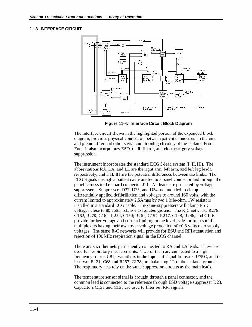
Section 11: Isolated Front End Functions -- Theory of Operation
11-4
11.3 INTERFACE CIRCUIT
Figure 11-4: Interface Circuit Block Diagram
The interface circuit shown in the highlighted portion of the expanded blockdiagram, provides physical connection between patient connectors on the unitand preamplifier and other signal conditioning circuitry of the isolated FrontEnd. It also incorporates ESD, defibrillator, and electrosurgery voltagesuppression.
The instrument incorporates the standard ECG 3-lead system (I, II, III). Theabbreviations RA, LA, and LL are the right arm, left arm, and left leg leads,respectively, and I, II, III are the potential differences between the limbs. TheECG signals through a patient cable are fed to a panel connector and through thepanel harness to the board connector J11. All leads are protected by voltagesuppressers. Suppressers D27, D25, and D24 are intended to clampdifferentially applied defibrillation and voltages to around 160 volts, with thecurrent limited to approximately 2.5Amps by two 1 kilo-ohm, 1W resistorsinstalled in a standard ECG cable. The same suppressers will clamp ESDvoltages close to 80 volts, relative to isolated ground. The R-C networks R278,C162, R279, C164, R254, C150; R261, C157, R247, C148, R246, and C146provide further voltage and current limiting to the levels safe for inputs of themultiplexers having their own over-voltage protection of ±0.5 volts over supplyvoltages. The same R-C networks will provide for ESU and RFI attenuation andrejection of 100 kHz respiration signal in the ECG channel.
There are six other nets permanently connected to RA and LA leads. These areused for respiratory measurements. Two of them are connected to a highfrequency source U81, two others to the inputs of signal followers U75C, and thelast two, R121, C68 and R257, C178, are balancing LL to the isolated ground.The respiratory nets rely on the same suppression circuits as the main leads.
The temperature sensor signal is brought through a panel connector, and thecommon lead is connected to the reference through ESD voltage suppresser D23.Capacitors C131 and C136 are used to filter out RFI signals.

Section 11: Isolated Front End Functions -- Theory of Operation
11-5
The SpO2 sensor signal is brought through a panel connector and a separatepanel cable to the board connectors J101 and J100. The Front End also has anSpO2 output connector J10, into which the SpO2 module (MP-205) is plugged.
11.4 ECG
Figure 11-5: ECG Circuit Block Diagram
See Figure 11-5. As shown in the highlighted portion of the expanded blockdiagram, the ECG circuitry consists of the lead selection, preamplifier, amplifierand filter, R-wave detector, and pacemaker detector circuitry.
11.4.1 Preamplifier, Amplifier and Filter.
The ECG preamplifier connects to a patient via three leads. At any time, two ofthe leads are selected by the multiplexer U79 and connected to the inputs of theinstrumentation amplifier U80 configured to have a gain of four. A commonmode signal at the amplifier input is measured by the amplifier U75B, and usedto drive the patient body via the amplifier U75A, resistor R291, and multiplexerU78 so that the common mode signal on the body and the output of thepreamplifier would be eliminated. The amplifier U75B is also used for drivingthe shield with the common mode signal to eliminate capacitance loading.
The output of the drive amplifier U75A is used for leads-off detection. Toimplement this function, input leads of the differential amplifier are connected tothe VDD supply through 20 megohm resistors R252 and R266. If any of thepatient leads become disconnected from the body, the output of the driveamplifier U75A will go to a rail. A window comparator U77D is used to detectthis event by producing a positive going signal sent to the A/D converter.

Section 11: Isolated Front End Functions -- Theory of Operation
11-6
The preamplifier is followed by a 0.05 Hz high-pass filter made of capacitorC147 and resistors R248 and R249. The corner frequency can be changed bysoftware to 0.5 Hz, set by resistors R238 and R250 and switch U63B. If acommon mode charge on the capacitor C147 will offset the baseline to the pointwhere ESG signal clipping is detected, it can be quickly removed under softwarecontrol through the analog switch U63C and limiting resistor R239. The ECGcircuit is completed by an amplifier U73B set for gain of 41 and a two-poleChebychev low-pass active filter, U74C, with the cutoff frequency of 50 Hz andthe gain of 1.75. The U74C has a +2.5 volts offset determined by resistors R225and R236 to convert bipolar signals to unipolar format, as required by linearoptocoupler. Thus, the total output swing of the ECG channel is about 1.5 volts.
11.4.2 R-wave Detector.
The ECG signal is further used to detect R-wave peaks. Active bandpass filterwith U71A amplifier has the center frequency of 14 Hz and the passband of±5 Hz. This filtering should eliminate false triggering in case of tall T-wavefollowing R-wave. The signal is rectified by the full-wave rectifier made ofamplifiers U71B and U71C, and dual-diode D13. This signal is used as oneinput to the comparator U74D. Sample-and-hold circuit consists of amplifierU71D, diode D17, capacitor C137, and discharge resistors R219 and R229. Theresistors ratio sets the level of the comparator which goes to the positive railwhen the next R-wave signal reaches the preset level of the previous R-wavesignal held in the capacitor. The comparator signal turns on the monostablemultivibrator U64A, which generates a 130-millisecond pulse. The pulse is sentto SpO2 circuit and to analog multiplexer via divider R180, R186.
11.4.3 Pacemaker Detector.
Pacers are detected by the dV/dt circuit made of amplifier U74A, resistor R251,and capacitor C152. The circuit output will go to approximately ±1.4 volts whenpacer is detected. This will set off the window comparator built aroundamplifier U74B and turn on monostable U64B to create an 8-millisecond pulsesent to the analog multiplexer via divider R179, R185.

Section 11: Isolated Front End Functions -- Theory of Operation
11-7
11.5 RESPIRATORY CIRCUIT
Figure 11-6: Respiratory Circuit Block Diagram
As shown in the highlighted portion of the expanded block diagram, Figure 11-6,the Respiratory circuitry includes the ECG leads, and some control circuitry.
Respiration is detected by measuring modulation of a high frequency AC signalsent to a body. The AC signal is 100 kHz, 4 volts peak square-wavecomplementary signals are produced by oscillator U81. These signals, viaresistors R288 and R271, generate 42 microamps p-p current which is injected ina body through patient leads RA and LA. The AC voltage drop on these leads isrespiration modulated and fed through high-pass filters C94, R244, C95, R228,and resistors R129 and R141 to a multiplexer U76 via buffers U75C and U75D.The multiplexer is controlled by the same AC signal that generates current and,in conjunction with amplifier U77C having gain of 9, comprise a synchronousdetector.
The DC component of the filtered signal is removed by 0.1 Hz high-pass filterC134, C172, R205, and R204, and the remaining low frequency respirationsignal is fed for further amplification. The capacitors C134 and C172 can bequickly discharged through U63D switch under software control in case ofsignificant baseline drift. Amplifier U72B has a gain of 667 and creates +2.5volts offset via resistors R215 and R216 to convert bipolar signals to unipolarformat. Complete swing of the output is about 1.5 volts p-p, and the signal is fedto the linear optocoupler multiplexer.
11.6 TEMPERATURE CIRCUIT
The temperature is measured in the body range of 15 to 45˚C using YellowSpring series 400 thermistor thermometers. Thermistor with the resistance rangeof 3539 to 984.2 ohms is connected as a feedback of amplifier U72A. Thereference signal of 1.235 volts is supplied by voltage reference U70 throughprecision resistor R217. The temperature, therefore, is measured using outputratios. Other ratios have to be arrived at by using Yellow Spring thermistorvalue chart. Resistors R203, R218 and capacitor C130 comprise a low passfilter.

Section 11: Isolated Front End Functions -- Theory of Operation
11-8
11.7 OPTOCOUPLERS
Figure 11-7: Optocouplers Block Diagram
See Figure 11-7. The optical couplers that isolate the Front End signals from thenon-isolated digital hardware are of two types: Linear and Digital.
11.7.1 Linear optocoupler
All analog signals, ECG, Respiration, Temperature, VREF and AGND, as wellas voltage levels of binary signals PM( pacemaker), QRS (R-wave), andLOFF(leads off) are fed to the inputs of analog multiplexer U67 and to the linearoptocoupler U57. The optocoupler has an LED and two matched sensingphotodiodes and works in a servo mode with two operational amplifiers, U60and U51. Input current set by multiplexer output and resistor R166 is comparedby U60 with the current of input photodiode. The LED is controlled by U60until two currents are equal. The current of the output diode mirrors the inputdiode’s current, thus producing an image of the multiplexer voltage at the outputof U57. Operational amplifiers maintain very close to zero impedance at diodeoutputs, which provides for very linear diode currents and a very linear andstable current ratio. A small positive DC offset is provided from divider R168,R169 to compensate for possible amplifier negative voltage offset.
11.7.2 Digital Optocouplers.
Digital optocouplers are inverting, high-gain, low-power types. The baud rate isset for 50 kHz operation. Inverter U61 provides inversion of optocouplersignals.

Section 11: Isolated Front End Functions -- Theory of Operation
11-9
11.8 CONTROLS
Figure 11-8: Controls Block Diagram
See Figure 11-8. The isolated control signals are developed and applied in thehighlighted blocks as shown in the block diagram.
Front end operations are controlled by serial signals on ADCTX line clocked bysignals on ADCCLK line. These serial signals from the Main Board CPU arefed to the Front End through opto-isolators U55 and U56 with pull-ups R182 andR173. Signals inverted by U61 go to eight-bit Serial-in/Parallel-out ShiftRegister U66. The beginning of a stream sets up one-shot retriggerablemultivibrator U62A for the duration of 130 microseconds. The stream is 16 bitslong, and each pulse retriggers the one shot. At the end of the stream, and after a130 microseconds time-out, the parallel set of bits representing the last eight bitsin the serial stream will be latched in an eight-bit buffer.
The bits represent different control functions. A group of three bits, MuxA,MuxB, and MuxC, control eight-bit data multiplexer U67; and a group of twobits, LSEL1 and LSEL2, control four-bit lead select multiplexers U79 and U78.Two others are individual bits, 0.5 Hz controls corner frequency of the high-passfilter, and ECGRES controls baseline reset.
The bit assignment is as follows(MSB first):
Bit 9 ParityBit 10 ECGRESBit 11 0.5HzBit 12 LSEL2Bit 13 LSEL1Bit 14 MuxCBit 15 MuxBBit 16 MuxA

Section 11: Isolated Front End Functions -- Theory of Operation
11-10
The parity bit is set for odd and is checked in the odd/even parity checker U65.Even parity, if detected, represents an error and the U65 output signal will turnon switch U63A. The switch will drive the output of U60 amplifier beyond thenormal range of data signals and will set A/D output at all ones, which will beinterpreted as an error.
Lead Select bits 12 and 13 select lead and test configurations as follows:
Bit 12 Bit 13 Selection
0 0 Test
0 1 Lead I
1 0 Lead II
1 1 Lead III
The mux address bits determine the following selections:
Bit 14 Bit 15 Bit 16 Selection
0 0 0 ECG
0 0 1 QRS
0 1 0 PM
0 1 1 RESP
1 0 0 LOFF
1 0 1 SCAL
1 1 1 AGN
11.9 A/D CONVERTER
A/D converter U53 on the non-isolated side is a 12-bit, 100 kHz sampling ratedevice with serial control and 14 analog inputs (3 are internal and 11 areexternal). It is configured for unipolar operation, 5 volts input and 16-bit cycle.The converter has four control lines: ADCS*(CS*), ADCRX(DATA/OUT),ADCTX(DATA/IN) and ADCCLK(I/CLK). Clock rate is set at 25 kHz. Eachcontrol burst is 16 bits long. The first eight-bit encode control information forthe converter (MSB first) is: four-bit analog channel address (D7-D4), two-bitdata length select (D3-D2), output format MSB or LSB first encode (D1) andunipolar or bipolar output select (D0). The last eight bits are ignored (they areused, though, to control operations of the isolated part).
When selected, the converter enables DATA INPUT and the I/O CLOCK andremoves DATA OUT from the high impedance state. The I/O CLOCK shifts outdata from the previous conversion and clocks in control bits for the currentconversion. On the fourth falling edge of the I/O CLOCK the next channelselection is complete and the converter goes into the sampling mode. The fallingedge of the 16th I/O CLOCK puts data in hold, takes EOC low and begins thecurrent conversion which lasts for 10 millisecond. If the selected channel isISOAD the data comes from a channel of multiplexer U67, selected duringprevious serial burst. At least 80 microseconds delay is required between serial

Section 11: Isolated Front End Functions -- Theory of Operation
11-11
bursts. This will provide enough time out for multiplexer control data to belatched. The multiplexer has at least four clock cycles of I/O CLOCK to settlebefore A/D sampling begins.
Data bits are assigned as follows:
Input Data Bits Address Bits
D7 D6 D5 D4 LS1 LS2 LSBF BIP
Inputs:
AIN0 — Isolated data 0 0 0 0
AIN1 — NIBPPSR1 0 0 0 1
AIN2 — NIBPPSR2 0 0 1 0
AIN3 — OSC 0 0 1 1
AIN4 — VBATTAD 0 1 0 0
AIN5 — TEMAD 0 1 0 1
AIN6 — +3.3VAD 0 1 1 0
AIN7 — +12AD 0 1 1 1
AIN8 — –24AD 1 0 0 0
AIN9 — NC 1 0 0 1
AIN10 — NC 1 0 1 0
Internally connectedinputs:
(Vref+ — Vref–)/2 1 0 1 1
Vref– 1 1 0 0
Vref+ 1 1 0 1
Software power down 1 1 1 1
Output data length:
8 bits 0 1
12 bits X 0
16 bits 1 1
Output data format
MSB first 0
LSB first 1
Unipolar (binary) 0
Bipolar (2s complement) 1

Section 11: Isolated Front End Functions -- Theory of Operation
11-12
11.10 ISOLATED POWER SUPPLY
The isolated power supply consists of high-current switched driver, U54,isolation transformer T1, two full-wave rectifiers with dual diodes D11 and D10,filter capacitors C122 and C127 and three voltage regulators. Regulators U83and U68 provide +5 volts and -5 volts for analog circuitry and regulator U69provides +5 volts for digital circuitry on both Front End and SpO2 boards.Switched driver U54 is controlled by square wave 100 kHz signals from the CPUand powered by the main power supply 12 volts regulator.
11.11 SPO2 BOARD
The SpO2 board (MP-205) plugs into the main board and uses it for powersupply and isolation. The SpO2 input signal through D-type panel connector andFront End connector J101 is fed to the receptacle J100; power, control, andoutput signals go to the receptacle J10. Two output signals are asynchronous:serial link RX and TX. Serial TX controls optocoupler U59, and RX iscontrolled by optocoupler U58. Control signal is ECG_SYNC which comesfrom the R-wave detector.
11.12 ISOLATION
The isolation barrier is provided by isolation transformer T1, linear optocouplerU57, and digital optocouplers U59, U58, U55, and U56. Spark gap SG1 is usedto protect isolation components against over-voltage exceeding their limits.

12-1
SECTION 12: NIBP - THEORY OF OPERATION12.1 NIBP System Overview12.2 The Pneumatic Assembly12.3 NIBP Hardware
12. NIBP - THEORY OF OPERATION
12.1 NIBP SYSTEM OVERVIEW
See Figure 12-1. The NPB-4000/C noninvasive blood pressure (NIBP)measurement and display operations described in this section include thepneumatics of the inflatable cuff and control valves, the specialized Front EndNIBP circuitry, some of the microprocessor memory and control circuitry, someof the power system, and specific switches on the keypad. These are highlightedin the main system block diagram, as shown, with a distinction among thedifferent shades of background tint to identify those that are only partly involvedfrom the major circuitry dedicated to the NIBP functions.
3-Lead ECG Temp 1
Isolated FrontEnd
EKG, Resp,Temp, & SpO2
CircuitrySpO2
uP, Memory,and Control
CircuitryKeypad
(Switches)
Display
Front EndNIBP Circuit
NIBP
Defib. Sync
RS-232 I/O
Speaker
Printer I/O
Power System
Battery
DC In
AC Line In LNA
Power
Figure 12-1: NPB-4000/C System Block Diagram
The major blocks involved from the cuff to the microprocessor are shown in thesimplified block of the NIBP see Figure 12-2. The pump and motor, mounted onthe power system assembly, are driven by a pulse-width-modulated (PWM)signal from the digital hardware section of the main board assembly. That signalis gated by an enabling signal originating in the microprocessor of the section ofthe main board. The pumped air is ducted through tubing and valves mounted onthe main board and made available at the Front End connection to the cuff.

Section 12: NIBP - Theory of Operation
12-2
Figure 12-2: NIBP System Block Diagram
Prior to making blood pressure measurements, the cuff is placed around a limb,typically an upper arm (left or right). The NIBP measurement system is initiatedby commands responding to pressing the NIBP Start/Stop switch on the frontpanel. The cuff is inflated at a rate controlled by the pump excitation current toa pressure above systolic, at which level the artery is effectively occluded. Then,as the cuff pressure is reduced at constant rate, the pressure transducers provideanalog signals to the digital hardware where they are digitized and processed toobtain systolic, diastolic, and mean blood pressure values, as well as the beatrate.
The technique for translating the pressure signals into the required measurementsmakes use of the action of the oscillatory characteristic of the returning arterialpressure. The phenomenon is illustrated in the diagram below.
See Figure 12-3. Systolic pressure is defined as the point at which oscillationincreases sharply. As the cuff deflates, oscillation amplitude increases to amaximum, and then decreases. The point of peak oscillation amplitude is themean arterial pressure. The point at which oscillations cease is defined as thediastolic pressure
Figure 12-3: Oscillatory Characteristics Diagram

Section 12: NIBP - Theory of Operation
12-3
12.2 THE PNEUMATIC ASSEMBLY
The pneumatic assembly, consisting of the pump, two controlling valves, andtubing to connect the various pneumatic components together are illustrated inthe schematic diagram that follows.
See Figure 12-4. The pump output is connected to the cuff and to two valves: atwo-way proportional control valve (V2) and a three-way valve (V1), as well asto two pressure transducers. Operation of the valves and of the pump control aredefined as described in the following text.
Figure 12-4: Pneumatic Assembly Block Diagram
Valve V1 is a three-way valve. In the V1 deenergized position, the portion ofthe pneumatic system encompassing the cuff and pump are open to theatmosphere, thus preventing the cuff from being pressurized. In the V1energized position, the cuff and pump are connected to V2 and the pressuretransducers. When V2 is closed, action of the pump will pressurize the cuff.Control valve V2 is used to bleed pressure from the cuff during an NIBPmeasurement, at a controlled deflation rate.
12.3 NIBP HARDWARE
See Figure 12-5. The NIBP analog control hardware is highlighted in the blockdiagram. It includes the Front End NIBP circuitry, as well as the pressuretransducers and pump. Refer to the main PCB schematic drawing, Sheet 2,Figure 17-6, in connection with the circuit operation descriptions.
Figure 12-5: NIBP Hardware Block Diagram

Section 12: NIBP - Theory of Operation
12-4
12.3.1 Pressure Transducers
Pressure transducers PS1 and PS2 convert pneumatic pressure levels to voltagesin the range from 0.33 volts at 0 mmHg to 4 volts at 300 mmHg. TransducerPS1 is used to sense the main cuff pressure. Transducer PS2 is used as a backupcuff pressure sensor, from which over-pressure warning signals are obtained.Both transducers outputs are smoothed to remove the effects of pumpingpulsation. The output of PS1 is identified as signal NIBPPRSR1, while that ofPS2 is NIBPPRSR2.
12.3.2 Filtering the Oscillatory Signal
Amplifiers U16-1 and U16-14, in combination with the lumped resistance andcapacitance values of the passive components, form a band pass filter thatseparates and amplifies the oscillatory signals OSC from the deflating cufftransducer signal NIBPRSR1. Amplifier U16-8 provides hysteresis.
12.3.3 Power Supplies
Battery power, VBATTP, connected to the board at J3, pins 13 and 14, isregulated in U15 when that component is enabled by the NPANPWR analogpower On/Off signal input to U10-4. The regulator accepts a battery voltage of 6to 8 volts and delivers regulated +5 volts to power the pressure transducers andbiasing circuitry for the operational amplifiers.
12.3.4 Over-Pressure Detector
Pump and valve drivers are controlled by the NPPVEN pump and valve enablesignal that is generated in U16-7 level-detector amplifier circuit. One input tothat amplifier is the NIBPRSR2 signal from transducer P2. The other is a valuedetermined by voltage divider R68 and R64, and feedback resistor R61.
The pump and valve drivers are enabled only when cuff pressure is belownominal 330 mmHg for adult mode, and below 165 mmHg for neonatalmeasurements.
12.3.5 Pump and Valve Drivers
Three-way valve V1 coil is powered by VPS that is switched in series with thecoil through n-channel MOSFET Q10-6. Switching action of Q10-6 iscontrolled by the input signal NP3WYV, that is gated by the enabling signalNPPVEN at switch U23. The VPS signal is developed from VBATTP throughQ11-6 that is also controlled by NPVEN gating transistor Q6. Diode D5 acts tosuppress voltage spikes. Resistor R101 ensures that Q10-6 will be OFF in caseof an open to the input line. The valve is either fully closed, or fully open.
Control valve V2 coil is powered by VBATTP and controlled by switching n-channel MOSFET Q10-7 in series with the coil. Q10-7 is controlled by inputsignal NIBPCNTLVLV. Pulse width modulation (PWM) of a five-volt level isused to operate the control valve. No-voltage results in a fully closed valve. Asthe duty cycle of the PWM is varied from 0 to 100 percent, the valve changessmoothly from fully closed to fully open. Repetition rate for the PWM is at least9 kHz. Diode D4 suppresses voltage spikes, and resistor R100 assures thatQ10-7 will be OFF if the input line should open.

Section 12: NIBP - Theory of Operation
12-5
12.3.6 NIBP Pump Control
Note: The following description is duplicated in the Power Supply section.Reference designations for the two paragraphs that follow are found inpower supply schematic drawing, Figure 17-3and Figure 17-4.
The power supply mechanical assembly holds the blood pressure pump andshield. The power supply contains circuitry that allows logic level control of thepump power from the processor board. For single-point fault protection, thepump requires two signals (PUMPON and PVENB to activate the pump.PUMPON (when high) turns on FET Q18 that pulls the bottom lead of the motorto ground. The PVENB signal through level translator Q19, turns on FET Q17that pulls the top motor lead to VBATT.
When no voltage is present at Q18, the pump is fully off. As the duty cycleincreases from 0 to 100 percent, the pump power changes smoothly from fullOFF to fully ON. This control technique minimizes overshoot of the targetedpressure. Diode D32 suppresses voltage spikes, while R78 ensures that Q18 willbe OFF if the line opens. Resistor R77 and capacitor C46 suppress motor brushnoise.
12.3.7 Digital Signal Processing and Information Display
NPB-4000/C software, resident in the microprocessor controller and memoryperipherals, include the algorithms needed to process the digitized outputs of thedigital hardware just described. It also includes the system software thatresponds to the commands for desired modes of NIBP measurements, display ofNIBP values of systolic, diastolic and mean arterial pressure, storing trend data,and for recording/printing of such data, and for initiation and silencing alarms.Details of these functions are contained in the theory of operation of themicroprocessor and control circuitry.

[THIS PAGE INTENTIONALLY LEFT BLANK]

13-1
SECTION 13: MICROPROCESSOR COMPUTER AND CONTROL –THEORY OF OPERATION
13.1 General13.2 Power Supply Connections13.3 NIBP Processing13.4 Recorder Operation13.5 Isolated Front End Power Interface13.6 SpO2 Interface13.7 Isolated Front End Power Signals13.8 RS-232 Serial Port Interface13.9 CPU Connections13.10 Knob Interface Control13.11 Push Switch Control13.12 Digital Schematic Pages 1/213.13 Current Drain of Digital Electronics
13. MICROPROCESSOR COMPUTER AND CONTROL –THEORY OF OPERATION
13.1 GENERAL
The NPB-4000/C digital design is based on an Intel 386EX microcontroller,which has a 386SX microprocessor core and peripheral blocks around it. Theinternal peripherals are all controlled by on-board programmable registers. Inorder to save power, this design has a Vcc = 3.3 volts.
The data from the Front End (ECG, temp, resp) is multiplexed through a linearopto isolator to a 12-bit A/D converter, which is connected to the on-boardsynchronous serial port. The synchronous serial port is controlled by theon-board DMA unit.
The LCD display is a 640x480 black and white display that is connected to anS-MOS 1351FLB controller chip. This chip interfaces via the data bus to the386EX. It has two 32kx8 SRAMs for data storage. The backlight is controlledby enabling +12 volts to the inverter board. The contrast for the LCD iscontrolled from the onboard -24 volts.
The main executable memory is a 256Kx16 flash memory which takes the upper512k bytes of address space. This flash contains the boot program and theexecutable program for controlling the whole unit.
A 512-kbyte DRAM is located in lower memory starting at location 0 and is usedfor data storage and manipulation. The DRAM also has the ability to executecode when programming the flash with a new program from the external RS-232port.
An RTC (real-time clock) chip is connected which keeps date and time of day.This unit has 64 bytes of battery-backed-up RAM; 14 bytes are used for thereal-time clock (RTC), and 50 bytes are available for the software to use.
The recorder (thermal printer) and the external RS-232 port are controlled fromsoftware via a duart (dual serial port chip). These ports are the same as the comports used on a PC and the duart is programmable via software.

Section 13: Microprocessor Computer and Control –Theory of Operation
13-2
The SpO2 unit (MP-205) is connected to an asynchronous serial port via opto-isolators.
The push switches and rotating knob interface to the 386EX via the FPGAcircuit. They are polled by the software at a 200-Hz rate.
The speaker is connected to an amplifier circuit, that is connected to a digitalpotentiometer. The programmable frequency is generated in the FPGA andconnects to this programmable digital pot. The software controls the volume byprogramming this digital pot.
The defib sync pulse is bit-programmed via software and goes to the outsideworld via a digital driver.
The NIBP circuit is controlled by various port bits and control circuits in theASIC.
13.2 POWER SUPPLY CONNECTIONS
Figure 13-1: Power Supply Interface
See Figure 13-1. The power supply system provides the power for the mainboard and all of the circuitry in the system. It also contains control circuits forturning on and off the power, as well as supplying the battery backup for thesystem.
13.2.1 Voltages
The microprocessor and its associated circuits are powered from the regulated3.3 volts generated on the power supply board. The 3.3 volts powers themicrocontroller, DRAM, flash, LCD controller and a portion of the LCDcontrast circuit, memory, the DUART, and real-time clock. The 5 volts powersthe Nellcor knob, A/D converter, a portion of the LCD contrast circuit, and a portion of the speaker circuit. The 12 volts powers portions of the LCD contrast circuit and speaker circuit, the backlight inverter input voltage, and the op amp for the battery voltage and temperature-monitoring signals going to the A/D converter. The -24 volts is used to drive the LCD contrast regulator.

Section 13: Microprocessor Computer and Control –Theory of Operation
13-3
13.2.2 Microcontroller Signals
The battery and microcontroller have two signals that connect directly with eachother, EARLY WARNING and PS OFF. The battery circuits generate anEARLY WARNING signal to the microcontroller that the power is going downwithin 100 millisecond. This EARLY WARNING signal could be due to thepower On/Standby switch being depressed or from the battery voltage getting toolow. The signal is connected directly to INTERRUPT 5 and INTERRUPT 7.The software will save any information it must save and finish its housekeepingbefore sending the PS OFF signal back to the battery circuits.
13.2.3 Membrane Switch and LED Signals
13.2.3.1 Membrane Switches Connected to the Power Supply
The power supply circuit connects directly with the ON/Standby switch and thetwo LEDs on the membrane switch. The On/Standby switch goes directly fromthe membrane switch to the power supply board. This is to allow powering upwhen off. Another switch, the Alarm Silence switch also goes to the batterycircuit. Unlike the On/Standby switch, this switch also goes to themicrocontroller.
13.2.3.2 Power Supply Generated LED Signals
The power supply circuits generate two LED driving signals, one that indicatesthat the AC mains is connected, and one that indicates that the DC power isconnected. When the AC Mains LED is being driven on, a high voltage levelgoes to the 386EX port 1 bit 6 as the AC mains input status bit. When the LEDis off, the signal is a logic low. The software will interpret the signal levels so asto tell whether the AC mains is connected or not. The same is true with the DCconnector. The signal driving the DC LED goes to port 1, bit 7. This indicatesthe DC power status.
13.2.4 Battery Signals to the A/D Converter
The battery voltage and temperature signal is sent to the main board where it isbuffered by an amplifier circuit that converts it to a signal within the 0-5 voltsrange of the A/D converter. The BATTSNS+ signal is sent directly to the MainBoard and is divided by two by a resistor divider circuit on the positive input tothe amplifier. The amplifier has a gain of two, which brings the signal back toits original signal level and then it is resistor-divided to the 0-5 volts range forthe A/D converter.
13.2.5 Sync/Alarm 50kHz Signal
The power supply needs a 50 kHz signal to synchronize its own internaloperation and to keep the alarm from sounding if the watch dog timer (WDT)times out. The 50 kHz signal is “anded” with the watchdog timer (WDT), and ifthe WDT should time out, the power supply circuit will sound the alarm and shutdown the Main Board.

Section 13: Microprocessor Computer and Control –Theory of Operation
13-4
13.3 NIBP PROCESSING
See Figure 13-2. The NIBP circuits consist of microprocessor control forturning on and off certain signals, control logic generating the pump PWM andvalve PWM, and status signals.
Figure 13-2: NIBP Processing Circuitry Block Diagram
13.3.1 NIBP Signals Going to the A/D Converter
The NIBP circuits generate three analog signals which must be converted to adigital code, the pressure from transducer 1, the pressure from transducer 2, andthe oscillatory signal from pressure transducer 1. The signals are connected tothe A/D converter for conversion and subsequent processing by themicroprocessor.
13.3.2 Pressures 1 and 2
The pressure transducers output 0.33 volts at 0 mm-Hg to 4 volts at 300 mmHg.Transducer 1 is used for the main cuff pressure signal from which blood pressureresults are calculated. Transducer 2 is used as the backup cuff pressure signalsfrom which over-pressure warnings are obtained. These pressure voltages go tothe A/D converter and are monitored by the software.
13.3.3 Oscillatory Signal
Transducer 1’s signal is also filtered and amplified to separated cuff pressureoscillation signals that are present on the cuff pressure signal during the deflateportion of the measurement cycle. This signal also goes to the A/D converterand software algorithms detect the blood pressure systolic and diastolic values.
13.3.4 Microcontroller Control and Status Signals
There are five signals that interface directly with the microcontroller and NIBPcircuits. Four of the signals are for control of the NIBP circuits from themicrocontroller software and one signal is a status signal fed back to thesoftware. All of the signals require 0-5 volts levels by the NIBP circuits, so each

Section 13: Microprocessor Computer and Control –Theory of Operation
13-5
of them is buffered by a logic gate that is connected to 5 volts. The inputs tothese buffers are TTL-compatible and will switch when the input goes below0.8 volts or above 2.4 volts.
13.3.5 Analog Power On/Off - Port 1 Bit 1
This signal turns on the power to the NIBP circuits via a regulator run from thebattery. To turn on the NIBP circuits, port 1 bit 1 must be set by software to ahigh state.
13.3.6 3-Way Valve On/Off - Port 1 Bit 2
This bit controls the three-way pressure valve which is a back safety valve forthe cuff pressure. A high signal allows a blood pressure measurement to occur,while a low signal dumps the air and the cuff is prevented from pressurizing.
13.3.7 Pvenable - Port 3 Bit 7
This bit is generated by the NIBP circuits for software monitoring of theover-pressure condition. Normal operation occurs when this signal is at a highlevel, indicating the cuff pressure is normal, while a low signal indicates anover-pressure condition.
13.3.8 Valve PWM Signal - FPGA
The FPGA control circuit produces a pulse-width modulated signal that is routedto the control valve for relieving the cuff pressure in an orderly manner for bloodpressure measurement. The software programs an eight-bit register in the FPGA,which outputs a high pulse level for a programmable time, then a low level for aperiod of time. The high level is programmed by the software and the FPGAcircuit automatically generates the low portion of the signal.
When this signal is low, the valve is fully closed. As the duty cycle of the PWMis varied from 0 to 100 percent, the valve changes smoothly from fully closed tofully open. The PWM repetition rate must be a minimum of 9 kHz. The circuituses an eight-bit counter clocked at 5 MHz. This gives a 19.5 kHzprogrammable signal period, well above the 9 kHz minimum.
13.3.9 Pump Motor PWM Control Signal - FPGA
The software programs an eight-bit register in the FPGA circuit to generate aPWM control signal to the pump motor. When the signal is at a low level, thepump is off. A PWM signal is generated to turn on the pump in a smoothfashion by varying the duty cycle from 0 to 100 percent. There is an eight-bitcounter that is clocked at 78 kHz. This gives a 304 Hz signal frequency forpump operation. Minimum pump PWM frequency for proper operation is300 Hz.
13.4 RECORDER OPERATION
See Figure 13-3. The recorder is a thermal recorder option that is supplied byGeneral Scanning Corp. This recorder has a self-contained microprocessor andcontrol circuits for properly operating the recorder from commands sent to it viaUART serial connection. The detailed operation of the recorder is specified inthe operational manual supplied by the vendor.

Section 13: Microprocessor Computer and Control –Theory of Operation
13-6
Figure 13-3: Recorder System Block Diagram
13.4.1 Recorder/Microcontroller Interface
The recorder is interfaced to the microcontroller via a DUART that has twoUARTs programmed by the software. The DUART has a UART0 and aUART1, each with a full UART signal complement. The circuit uses UART1 ofthe DUART for the recorder interface. This UART has 16-byte fifos on each ofthe receive and transmit channels. The software programs the UART by settingthe chip select unit, CS4 to I/O addresses for the recorder and then programmingthe internal registers for baud rate, parity, and bit count. Up to 16 bytes can betransferred to the UART, which will transmit serially to the recorder . TheUART generates RS-232 signals in TTL/CMOS compatible signal levels. Therecorder takes 0-5 volt signals, so each of the signals to/from the recorder mustbe translated from/to 3.3 volts/5 volts. This is done with the HCT244 buffers.
The UART signals and recorder signals are listed below.
Host transmit -> printer receiveprinter reset bit -> printer resetHost receive <- printer transmitHost CTS <- printer clear to send
The host signals are generated by the programmable UART.
13.4.2 Recorder Power
The recorder requires 5 volts for logic operation and 10-18 volts for print headoperation. The power for the recorder is generated on the power supply boardand goes directly to the recorder from the power supply board. It is merged withthe control signals to make one 50-pin cable going to the recorder interfaceboard.

Section 13: Microprocessor Computer and Control –Theory of Operation
13-7
13.5 ISOLATED FRONT END INTERFACE
Figure 13-4: Isolated Front End Block Diagram
See Figure 13-4. The interface to the Front End electronics is shown above andconsists of using the microprocessor’s synchronous serial unit to interface to theA/D converter. The synchronous serial unit interfaces with the DMA unit,which passes the data to be transmitted to the A/D. The data received from theA/D goes to the other DMA channel and is transferred to a data buffer.
13.5.1 A/D Converter Transmit Control
The A/D converter initiates a conversion when it receives a serial stream fromthe microprocessor. The processor software sets up the DMA, synchronousserial unit, and timer channel 0 to work together to transfer control words to theA/D and Front End. The timer is set for a rate of 800 Hz and its output isprogrammed to go directly to the DMA unit. The DMA unit passes data fromthe DRAM to the SSIO unit, which in turn transmits the 16-bit word to the A/Dand the Front End. The first eight bits transmitted are stored by the A/D andinterpreted. A conversion starts. At the same time, the previous conversion istransmitted back to the SSIO unit (this is discussed in the next section). The lasteight bits are read by the Front End and are used to select the Front End muxchannel (three bits), initiate baseline reset (one bit), lead select (two bits), andselect a 0.5 Hz filter (one bit). The eighth bit is a parity bit, which is checked bythe Front End circuit. The software puts together a buffer with this data andprograms the DMA channel to transmit the data words each time the timergenerates a DMA request.

Section 13: Microprocessor Computer and Control –Theory of Operation
13-8
13.5.2 16-Bit Word Transmitted to the A/D Converter and Front End
Figure: 13-5: 16 Bit Word
13.5.3 A/D Converter Receiver Control
The A/D converter is a pipelined converter and transmits the result of theprevious conversion when receiving the next transmission for a conversion. Theprevious conversion is transmitted to the SSIO unit’s receiver and the SSIO thenrequests a DMA transfer to memory.
13.5.4 SpO2 INTERFACE
The microprocessor’s asynchronous channel 2 (SIO2) is used to interface to theSpO2 unit via opto-isolators. There are two signals, transmit and receive. Thisis a UART-type unit and when the SpO2 transmits, the SIO receives the data andgenerates an interrupt to the software. When the software wants to transmit abyte to the SpO2, it transfers data to the SIO transmitter and the SIO unitautomatically transmits it to the SpO2.
13.5.5 ISOLATED FRONT END POWER SIGNALS
The isolated Front End requires its own power supply and voltages, separatefrom the other voltages in the system. The FPGA generates a 100 kHz signalthat connects to an isolation transformer. These signals are enabled/disabled bya bit in the CS5 control register. These signals are also connected to, and insynchronization with, the 50 kHz power supply clock. Resetting the Front Endcan be accomplished by turning the 100 kHz clock off, then back on again. Thisturns the Front End power supply off, then back on.
13.6 RS-232 SERIAL PORT INTERFACE
The RS-232 output serial port uses one of the asynchronous units of theDUART. It is programmed by the software using CS4 and the A3 address bit setto 0. This is done in the FPGA and output as DUARTCS0. The eightprogrammable registers are internal to the UART channel and are set up for baudrate, parity, number of bits to transmit, and start and stop bits. This channel alsohas an internal register with an extra bit . The circuit uses this bit as theNURSECALL signal on pin 9 of the RS-232 connector.

Section 13: Microprocessor Computer and Control –Theory of Operation
13-9
13.7 CPU CONNECTIONS
The processor in this system is a 386EX. The 386EX contains a 386SX core andintegrated peripherals. It operates from a 40-MHz oscillator, and includes thefollowing on-board peripherals:
DMA Controller UnitBus Interface UnitChip-select UnitClock and Power Management UnitDRAM Refresh Control UnitWatch Dog Timer Unit2 Asynchronous Serial I/O UnitsSynchronous Serial I/O UnitTimer Unit with three 16-bit Counter/TimersInterrupt Control UnitThree 8-Bit Digital I/O Ports
The connections are as follows:
Address bus connects to the LCD controller, RTC address/data mux,DRAM address mux, and the boot and trend flashes. Six address linesgo to the FPGA.
The data bus connects to the data bus buffers, which in turn connect tothe DRAM, RTC, DUART, boot flash, trend flash, LCD controller, andthe FPGA.
The address and data control signals are distributed to the FPGA,DRAM, RTC, LCD controller, boot and trend flashes, and DUART.
RESET comes from the FPGA.
CLK2 is a 40 MHz signal from the onboard oscillator.
13.7.1 Port 1 Signals
Port 1 is connected to the following signals:
1.1 NIBP analog power on/off - out1.2 NIBP 3-way valve on/off - out1.3 NIBP neonatal measurement - out - not used1.4 LCD contrast up - out1.5 LCD contrast down - out1.6 AC mains input status bit - in1.7 DC input status bit - in
13.7.2 Port 2 Bits
Port 2 bits used are as follows:
2.7 Speaker volume up/down select - out

Section 13: Microprocessor Computer and Control –Theory of Operation
13-10
13.7.3 Port 3 Bits
Port 3 bits used are as follows:
3.2 Defib key input - in3.5 PSOFF - out3.6 Defib sync pulse - out3.7 NIBP PV enable - in
13.7.4 Chip Select Unit
The chip select unit has 8 chip selects and are defined as follows:
CS0: LCD control register select - eight-bit I/OCS1: LCD memory select - 16-bit memoryCS2: Trend flash select - eight-bit memoryCS3: RTC select - eight-bit I/OCS4: Duart select - eight-bit I/OCS5: Misc. control/status registers - NIBP control, switch status, and
speaker tone control - eight-bit I/OCS6: DRAM select - 8/16-bit memoryUCS: Executable flash select - 16-bit memory
There are wait states associated with each of the CSU’s selects, and they aredefined as follows:
CS0: read/write - six wait statesCS1: read/write - six wait statesCS2: read/write - four wait statesCS3: read/wrote - 18 wait statesCS4: read/write - two wait statesCS5: read/write - no wait statesCS6: read/write - one wait stateUCS: read - two wait states/write - four wait states
13.7.5 Timer Unit
The timer unit has three timers: two are used for output control, and one is usedto initiate DMA transfers to the A/D converter.
TIMEROUT0: Speaker volume adjust pulseTIMEROUT1: A request for initiating an A/D conversionTIMEROUT2: 100 kHz output to the FPGA for generating the 100 kHz
and 50 kHz signals for the power supply
13.7.6 Interrupts
There are five interrupts used:
INT1: DUART channel 1 interruptINT2: DUART channel 2 interruptINT5: Early warning from the power supply
(Also connected to INT 7)

Section 13: Microprocessor Computer and Control –Theory of Operation
13-11
13.7.7 Synchronous Serial Port
The synchronous serial port is connected to the A/D converter. The signals usedare as follows:
STXCLK: synchronous transmit clockSRXCLK: synchronous receive clockSSIOTX: synchronous transmit dataSSIORX: synchronous receive data
The STXCLK signal is generated in the FPGA circuit each time Timer 1 initiatesa pulse (1.25 millisecond intervals). There are 16 clock pulses generated byenabling a 25 kHz signal to the STXCLK line. The A/D is programmed for16-bit transfers, and when the A/D receives the 16th clock, it will activate theEOC signal that turns off the STXCLK signal. The A/D makes a conversion andpasses the data back the next time it receives the STXCLK signal. TheSRXCLK signal is connected to the STXCLK, and each time a new conversionis initiated, the previous conversion’s data is transferred to the 386EX via theSSIORX data line.
13.7.8 Asynchronous Serial Port
There are two asynchronous UART ports on the 386EX, but only one is used. Itis connected to the opto-isolators that connect to the SpO2 unit.
TXD0: asynchronous transmit signalRXD0: asynchronous receive signal
The remaining port is reserved for future use.
13.7.9 Watch Dog Timer Unit (WDT)
See Figure 13-6. The watchdog timer unit within the 386EX has one outputwhich goes to the FPGA.
Figure 13-6: Watch Dog Timer Block Diagram

Section 13: Microprocessor Computer and Control –Theory of Operation
13-12
13.7.10 CPU Timing Signals
The 386EX runs from a 40 MHz crystal oscillator and the main timing is derivedfrom this clock. It is called CLK2. Inside the CPU, CLK2 is divided by two,generating two new clocks, PH1 and PH2. Each T state is made up of one PH1and one PH2 clock. There are a minimum of two T states per cycle. Each waitstate is one T state long (50 nanosecond) Therefore, adding wait states is adding50 nanoseconds for each additional T2 states.
13.7.11 CPU Signals
Various signals change at various times within a cycle, and the generic timing isshown below. Some of the key signals are ADS#, M/IO#, D/C#, W/R#, WR#,RD#, CS0-CS6#, BLE#, and BHE#. Typical control circuits will look at ADS#at the end of PH2 and make decisions at this time. See Figure 13-7.
40MHZ
T1 T2 T1 T2
PH1
PH2
ADS#W/R,BLE#,BHE#,CSO:6#,UCS#,D/C#,M/IO,A1:25
RD#,WR#
LBA#,READY#
D0:15
Figure 13-7: CPU Signals
13.8 DRAM Control
The DRAM control consists of one 256kx16 DRAM chip, three 74ACT157address mux chips, address resistors, and the FPGA control circuit.
The CS6* (* = # = a low true signal) signal has been assigned to the DRAMmemory address space: 0-3FFFF words, or 0-7FFFF bytes. The CS6* controlregister in the chip select unit (CSU) must be programmed for one wait state.Since the data bus is 16 bits wide and the DRAM is a x16 part, most transferswill be of the 16-bit variety. However, eight-bit transfers are allowed andprovisions have been made for byte addressing. This is done by using the upperand lower cas signals, UCAS and LCAS.
13.8.1 DRAM Signals
For the DRAM design we must generate six signals, RAS#, UCAS#, LCAS#,DRAMOE#, DRAMWR#, and CASADREN. All of these signals are generatedin the FPGA from the 386EX signals, ADS#, CS6#, M/IO#, D/C#, WR#, andRD#. Since the CSU is programmed for one wait state, the CSU generates theREADY# signal, which terminates the transfer.

Section 13: Microprocessor Computer and Control –Theory of Operation
13-13
13.8.2 DRAM Timing
T1 T2W T2 T1
25ns 25ns
75ns
50ns
50ns
75ns
75ns
RAS#
RAS#
CLK2
CASADREN
U/LCAS
DRAMWR#
DRAMOE#
Figure 13-8: DRAM Timing
See Figure 13-8. The DRAM requires 130 nanoseconds total time, read/writeand precharge for each cycle. There is one wait state for each DRAM access anda total of three T states, which is 150 nanoseconds. Since the DRAM minimumaccess time is 130 nanoseconds, we have 20 nanoseconds of margin. TheHitachi HM51W4260AL has a RAS* time of 70 nanoseconds, a precharge timeof 50 nanoseconds, a CAS* time of 20 nanoseconds, and a WE* time of 15nanoseconds. The BLE* and BLH* signals are used to select byte-orientedreads and writes. There are two CAS* lines that are used to implement the bytewrites.
The RAS# and CAS# requirements are shown in Figure 13-9.

Section 13: Microprocessor Computer and Control –Theory of Operation
13-14
10NS
VALID ROW VALID COL
10NS
50NS70NS
20NS
10NS15NS
RAS#
ROW/COL ADDR
UCAL/LCAS#
20NS
Figure 13-9: RAS# and CAS# Requirements
13.8.3 DRAM FPGA Circuits
The DRAM control circuits in the FPGA must decode the various 386EX controlsignals and generate the DRAM signals. This is done by using CS6# to set a flipflop when ADS# and PH are true. The flip flop is RAS#. This signal is passedto two more flip flops and the RAS# output is 75 nanoseconds long. This signalis generated for all DRAM accesses and refresh. The DRAM output is enabledwhen either BLE# or BHE# is true, which means a read is occurring. Since theDRAM outputs are bi-directional, we need to disable the DRAMOE# signal if awrite is taking place. The WR# signal being false allows DRAMOE# to occur.If it is true, then the DRAMWR# signal occurs. The BLE# and BHE# signalsare also used to generate the UCAS# and LCAS# signals during a read or writeoperation. Since we are using RAS only for refresh, the CAS signals must beinhibited for refresh.
13.9 Flash Control
The flash memory and control consists of two flash chips, a bootable flash (alsocalled the executable flash) and a trend flash. The control consists of the randomlogic in the FPGA. The bootable flash is a 256Kx16 Intel (part no.E28F400BVT60) or Micron (part no. MT28F400 SG-8) flash with the boot inthe top section (T), and is preprogrammed on the data I/O or some other unitwith the boot program. The executable program can also be programmed thisway or by downloading it to the 386EX via the RS-232 connection. The trendflash consists of Atmel AT29LV256 32kx8 devices that store the trend data andthat write 64 bytes at a time. It takes two wait states for reading the flash, eitherthe executable or the trend, and four wait states to write either of these flashes.
13.9.1 Executable flash
The executable flash is a word-oriented flash, that is, reading and writing is doneon a word basis, and byte reads and writes are not allowed. The trend flash isbyte oriented and all reads and writes are done on a byte basis.
The chip select unit has UCS* assigned to the executable flash and CS2* isassigned to the trend flash. Typically, the executable flash is assigned the upper256k words, or 512k bytes in the system. The word address space is 40000 to

Section 13: Microprocessor Computer and Control –Theory of Operation
13-15
7FFFF, which is 80000 to FFFFF in bytes. This is the upper portion of thespace. The trend flash is assigned to the 32k byte space above the video ram,that is, 84000 to 8FFFF words, or 11000 to 14000 bytes. The software, however,has the ability to overlap the trend flash address with the executable flashaddress. The design gives priority to the trend flash address over the executableflash.
The executable flash has a long delay time for writing to it, and this is why thereare four wait states. It also has a long delay from output data on to output datafloat. This requires that data buffers be installed between the 386EX and theflash. Since doing this only for the flash is awkward, the buffers were put in forall external devices.
See Figure 13-10. The read cycle time for the executable flash is 110nanoseconds. The write pulse width must be at least 150 nanoseconds. Refer tothe timing diagrams for the flash for minimum timing parameters.
T1
25NS 25NS
T2W T2W T2
CLK2
PH2
FLSHCE#
FLSHRD#
50NS50NS 50NS 50NS
Figure 13-10: Flash Cycle
In the FPGA control logic, the executable flash chip select, is anded with thetrend flash chip select such that CS2* must be high, inactive, when addressingthe executable flash. This allows the address overlap for the trend flash. Theexecutable flash chip enable, FLSH1CE#, is generated in the FPGA and thengoes to the executable flash. The trend flash is connected directly to CS2#,because it has priority over the executable if an overlapping addressing schemeis used.
See Figure 13-11. The write pulse width is generated via a state machine to givethe proper pulse width.
T1
25NS 25NS
T2W T2W T2W
CLK2
PH2
FLSHCE#
FLSHRD#
50NS50NS 50NS 50NS
T2
50NS
Figure 13-11: Write Pulse

Section 13: Microprocessor Computer and Control –Theory of Operation
13-16
13.9.2 Flash FPGA Control Circuit
The FPGA decodes the boot flash and trend flash select signals and generates theboot flash (FLSH1CE#) signal whenever the trend flash is not being accessed.Since the trend flash address space may overlap the boot flash space, the trendflash has priority.
The flash outputs are enabled for a read cycle. During a write cycle, the data businputs data to the flash.
Since the boot flash is for booting up and executing the software program, mostaccesses to the boot flash are reads. Only when a new program is downloadedwill a write to the boot flash occur.
13.9.3 Trend Flash
The purpose of the trend flash is to store the patient’s data. It has both read andwrite accesses occurring at regular intervals. The flash chosen for this purposeinterfaces with the 386EX easily, and writing data consists of transferring64 bytes at a time. The flash takes care of any erasing and writing operationsinternally. Typical worst-case write/erase times for 64 bytes is less than1 second.
13.10 LCD Display
The LCD display is a black and white (B&W) 640x480 pixel display, used as a1-bit/pixel B&W display. Gray shading is not used in this display. It is a dualpanel, dual drive unit and the 1351 drives the display directly. It operates from3.3 volts.
The LCD display is divided into two sections: each section is 640x240 pixels,which equals a total of 153,600 pixels per section. A 32Kx8 SRAM has256,000 bits, thus one SRAM is used for each of the display sections. Only onebit is available to drive each pixel. For shading or color, more memory isneeded.
The SRAM access time is defined by the 1351FLB as one over the frequencyminus 20 nanoseconds.
tacc = 1/fosc - 20 nanoseconds
Our system uses an oscillator frequency (FOSC) = 10 MHz, therefore,80 nanoseconds access time on the SRAM is needed. Using this SRAM and10 MHz, the worst-case access time is 4 TOSC + TCLK = 500 nanoseconds.
The LCD display interfaces to the S-MOS LCD controller chip, SF1351FLB.This controller chip is connected to the 386EX and two 32kx8 SRAMs. TheLCD controller has control registers that must be set up by software beforewriting to the memory and display.

Section 13: Microprocessor Computer and Control –Theory of Operation
13-17
13.10.1 LCD Control
There are two chip selects assigned to the LCD display chip: one for the controlregisters inside the chip, and one for the display memory space. The chip itselfhas a state machine controller inside, and generates the necessary signals to storeand retrieve data from the memory when requested. It also takes care of drivingthe LCD display directly, with the data from the display SRAM.
The circuit uses the 1351 in mode 5 and the 16-bit microprocessor interfaceconfiguration. All transfers are word oriented, and byte reads and writes are notallowed.
The processor interface consists of the following signals .
IOCS# is the control register chip select and connects directly with CS0#from the 386EX. To program the 1351 registers, the software selectsthis address and transfers the data.
MEMCS# is the display memory select signal. It is connected to CS1#directly and display data is transferred to the display ram using thisaddress space.
IORD#, IOWR#, MEMRD#, and MEMWR# are used to read and writeto/from the control registers and the display memory. The two readsignals are connected directly with the RD# signal from the 386EX. Thetwo write signals are connected directly with the WR# signal from the386EX.
The MPUCLK is connected to a 10 MHz clock generated in phase withthe PH1 clock in the FPGA. Since PH1 occurs at the beginning of each386EX T state, the 1351 will be in synch with the 386EX.
RESET is connected directly with the RESET signal from the FPGA,which goes to the 386EX.
The MPUSEL signal is tied to 3.3 volts via a resistor. This indicates thatthe 1351 is to operate in word mode.
The BHE# signal is connected directly to the BHE# signal from the386EX.
AB0-AB15 is connected to the address bus of the 386EX.
DB0-DB15 is connected to the bi-directional data bus BD0-BD15.
The above signals are all of the signals used to interface to the 386EX fortransferring of data to and from the control registers and the display RAM.

Section 13: Microprocessor Computer and Control –Theory of Operation
13-18
Both read and write transfers between the 386EX and the 1351FLB are definedin the 1351FLB manual, pages 1-33 and 1-34. The timing specifications of the1351FLB for reading and writing data to and from the control registers ordisplay RAM, allow a direct interface to the 386EX. External control circuits inthe FPGA are not necessary, except for one signal, the READY# signal. This isexplained in a following section.
13.10.2 LCD Display RAM
The interface signals for the display RAM are prefaced with the letter V, whichindicates video RAM. The interface to the display RAM (VRAM) is defined inthe 1351FLB manual and is connected directly to the RAM.
The LCD display interfaces directly with the 1351FLB. Timing diagrams are inthe associated manuals. The signals used are LCDENB, XSCL, LP, WF, YD,UD0-UD3, and LD0-LD3. The UD and LD signals are data lines to the upperand lower display panels. The XSCL is the data shift clock and the LCD displaystores the data on the falling edge of this clock. The LP signal is the latch pulseand is used to latch the data into the X-drivers. The YD signal is the framepulse, which indicates a start-of-frame.
13.10.3 LCD FPGA Control Circuits
The LCD display chip interfaces directly with the 386EX. The only circuit thatis necessary to generate in the FPGA is the READY# circuit. The 1351generates a wait signal when transfers are initiated . This wait signal is gatedwith the LCD select signals and implements an external READY signal when the1351 has completed the transfer.
13.11 Real-time Clock (RTC)
The RTC is a Dallas DS1693, which has the crystal and battery imbedded in theunit. It is a 28-pin DIP package and runs from a 3.3 volts supply.
CS3# is assigned to the RTC in the I/O space and the software must assign14 wait states to this unit.
The timing for the DS1693 is shown in Figure 13-12.
Figure 13-12: DS1693 Timing
See Figure 13-13. The timing for this interface is done in the FPGA. There is astate machine that is clocked at 20 MHz and generates 18 states.

Section 13: Microprocessor Computer and Control –Theory of Operation
13-19
Figure 13-13: Interface Timing
13.12 DUART Control
See Figure 13-14. The DUART is a Startech ST16C2550CJ44 which consists of2 UARTs and fifos for the read and write portions of each UART. Channel 0 isassigned to the RS-232 port, which exits the unit near the AC and DC inputs.Channel 1 is assigned to the recorder. The fifos are 16 bytes deep, and transferto/from the DUART would save time if done on 8- or 16-byte boundaries.
Interfacing to the DUART is done by assigning CS4# to the DUART I/O space,with four addresses assigned to each UART. The DUART channel 0 is the baseaddress assigned to CS4# and the channel 1 address is the base address + 8 (A3).There are four addresses assigned to each UART, 0,1,2,and 3.
Software must program two wait states for CS4# and define them as a bytedevice.
A state machine in the FPGA is used to generate the proper signals forprogramming the unit.
Figure 13-14: DUART Control
13.13 KNOB INTERFACE CONTROL
The knob consists of a rotary knob with a push switch. The knob is rotated andthe cursor on the LCD display moves forward or backward, depending on whichway the knob is rotated. When the knob is pushed, it must be detected andindicated to the 386EX.

Section 13: Microprocessor Computer and Control –Theory of Operation
13-20
The knob has two channels: channel A and channel B. When clockwise rotationoccurs, channel A leads channel B and when counterclockwise rotation occurs,channel B leads channel A. The software monitors the knob flip flop, and whenit is set true, the knob has turned. The direction is read by the other bits in thestatus register, and the software determines the knob direction. The KNOBINTflip flop is reset by the software when a write to CS5# + A occurs. The knobdirection is determined by the software by reading CS5# + A, bits 4 and 5.
The circuit that drives the knob is a 3.3 volts circuit, with appropriate resistorvalues to allow the same current at 3.3 volts through the optocouplers as wouldhave occurred at 5 volts.
13.14 SWITCH CONTROL
There are five switches and one knob push-button switch. All of these switchesgo to the FPGA control circuit except for the On/Standby switch, which goesdirectly to the power supply control circuit. Each of the switch circuits has adebounce resistor and capacitor associated with it and then goes to the FPGA.The signals ALRMSIL, NIBPPB, AUDTONVOL, LCDCONTRST, andKNOBPB go to the FPGA where they are OR’d together and exit as PBINT.This is read by the software in the status register . The software debounces anddetects the length of time the switch is depressed. The software determineswhich switch was depressed by reading CS5# + A, bits 4 through 7.
13.15 MISCELLANEOUS CONTROL - CS5#
The NIBP PUMP PWM, NIBP VALVE PWM, SPEAKER FREQUENCYDUTY CYCLE, and a miscellaneous control register are all assigned to the I/Ospace programmed to CS5#. The addressing scheme is as follows:
CS5# NIBP PUMP PWM 8 bitsCS5# + 2 Not usedCS5# + 4 SPEAKER HIGH VALUE 8 bitsCS5# + 6 SPEAKER LOW VALUE 8 bitsCS5# + 8 CONTROL REG 8 bitsCS5# + A WRITE RESETS KNOB INT/READ PUSH SWITCHS and
the KNOB ROTATION DIRECTION bitsCS5# + C WRITE WDTEN (WATCHDOG TIMER ENABLE)/READ
PUSH SWITCH SWITCHES AND THE KNOB PUSHBUTTON
CS5# + E WRITE NSCALL (BIT 7) and/or PTRRST (BIT 6)/RADNSCALL and PTRRST
13.15.1 CS5# NIBP Pump PWM 8 Bits
The NIBP pump pulse width modulated (PUMP_PWM) signal is generated inthe FPGA via an eight-bit register which is clocked at 313 kHz. An eight-bitvalue is loaded into this register, and then the PUMP_PWM_GO bit (bit 0) in theCONTROL REG. is set true, and the pump PWM signal begins. The eight-bitregister starts counting down, and the signal output is low until the counterunderflows, at which time it is reloaded with the programmed value. It nowcounts up, and the signal output goes high until the counter overflows. It is thenreloaded and counts down. The PUMP_PWM signal is generated this way untilit is shut off by resetting the PUMP_PWM_GO bit in the control reg.

Section 13: Microprocessor Computer and Control –Theory of Operation
13-21
The NIBP valve pulse width modulated (NIBPCNTLVLV) signal is generated inthe FPGA via this same eight-bit register, which is clocked at 313 kHz. Aneight-bit value is loaded into this register, and then the VALVE_PWM_GO bit(bit 1) in the control reg. is set true, and the valve PWM signal begins. Theeight-bit register starts counting down, and the signal output is low until thecounter underflows, at which time it is reloaded with the programmed value. Itnow counts up, and the signal output goes high until the counter overflows . It isthen reloaded and counts down. The NIBPCNTLVLV signal is generated thisway until it is shut off by resetting the VALVE_PWM_GO bit in the control reg.
13.15.2 CS5# + 4 Speaker High, CS5# + 6 Speaker Low Value
The speaker tone frequency is generated using two eight-bit registers, one whichis the value for the high portion of the frequency and one value for the lowportion for the frequency. The frequency range is 200 Hz to 1000 Hz. The16-bit counter has a selectable count frequency of 78 kHz or 313 kHz. Thisselection is programmed in the control reg. using the CLK_FREQ_SEL (bit 2).Signal A 0 selects 313 kHz and a 1 selects 78 kHz. Once the values are loaded,and the frequency clock is selected, the FREQ_GO bit (bit three) is set to beginthe tone frequency. Software has complete control over the duty cycle of thistone by programming the high and low values and being able to select the clockfrequency for the counter. The TONE_OUT signal is low until the low counteroverflows and sets the TONE_OUT flip flop high. Now the high counter isenabled, and the TONE_OUT signal stays high until the high counter overflows,at which time it goes low and the low counter begins counting. This cyclecontinues until the FREQ_GO bit is reset to zero.
13.15.3 CS5# + 8 Control Register
This register has eight programmable bits as follows:
BIT 0 PUMP_PWM_GOBIT 1 VALVE_PWM_GOBIT 2 CLK_FREQ_SELBIT 3 FREQ_GOBIT 4 BCK_LITE_ONBIT 5 FRONT END CLOCK ENABLEBIT 6 PORGQM FLASH ENABLEBIT 7 ADCS RESET
Bits 0 through 3 were defined in the above paragraphs and need no furtherexplanation here. Bit 4, BCK_LITE_ON is a bit that turns on the LCD backlightwhen set to a 1. When powered on, this bit is 0 and the backlight is off. To turnon the backlight this bit must be set to a 1.
Bit 5 enables the clock going to the Front End transformer, that generates theisolated Front End voltages. If the Front End should ever go into a baselinecondition, it is reset by stopping the clock to the transformer, and the Front Endvoltage will go to zero. Turning this bit back on powers the Front End up and,essentially, acts as a reset.
Bit 6 enables programming of the boot flash. This would be used if a newexecutable program were downloaded via the RS-232 channel and stored in theexecutable flash.

Section 13: Microprocessor Computer and Control –Theory of Operation
13-22
Bit 7 resets the A/D converter and is generated when software starts a conversionsequence.
13.15.4 CS5# + A RESET KNOB INT/READ PUSH SWITCHS
The I/O address of CS5# + 6 has two functions associated with it. Writing tothis register generates a KNOB_INT_RST signal which resets the knob interruptflip flops. This would be done by software after a knob interrupt occurs.
The software polls this register every 50 millisecond and looks to see if thePB INT bit (bit 6) or the KNOB INT bit (bit 7) is set true, indicating that aswitch has been pressed or that the knob is being rotated. If either of these bits isset true, then the software just looks at bits 3, 4, and 5 to determine which of theknob functions has occurred. If the PB INTB is set true, then register C must beread to determine which switch has been pushed.
Register CS5# + A has the following bit assignments:
Bit 0 Not usedBit 1 Not usedBit 2 Not usedBit 3 Knob push button switchBit 4 Knob channel B rotationBit 5 Knob channel A rotationBit 6 Push Button occurredBit 7 Knob rotation occurred
13.15.5 CS5# + C Write Enables WDT/READ Push Buttons
After powering up, the software must enable the watch dog timer function bywriting to this register. The act of writing to CS5# + C automatically sets theWDT flip flop to a 1 and enables the WDT time out function.
Reading this register gives the push-button status, as well as the state of theWDT flip flop.
Register CS5# + C has the following bit assignments:
Bit 0 Not used
Bit 1 Not used
Bit 2 Not used
Bit 3 WDTEN (Watch Dog Timer Enable)
Bit 4 LCD Contrast switch
Bit 5 Audio Volume switch
13.15.6 CS5# + E WRITE NSCALL/PTRRST/READ PUSH SWITCHS
Writing to this register sets or resets the nurse call and printer reset bits . To setNSCALL, write a 1 to bit 7, and to reset NSCALL write a 0 to bit 7. To reset theprinter, write a 1 to bit 6. To reset this bit write, a 0 to bit 6.
The bit assignments for reading this register are shown below. The bitassignments for writing the NSCALL and PTRRST are different from the readassignments.

Section 13: Microprocessor Computer and Control –Theory of Operation
13-23
Register CS5# + E has the following bit assignments
Bit 0 Not used
BIT 1 Not used
BIT 2 Not used
BIT 3 Not used
BIT 4 Not used
BIT 5 NURSE CALL
BIT 6 PRINTER RESET
BIT 7 PRINTER CTS (CLEAR TO SEND)
The NURSECALL and PRINTER RESET bits are the flip flop outputsprogrammed by writing to register CS5# + E as explained above.
A 1 (high) indicates that the bit is true, a 0 that the bit is false.
13.16 DIGITAL SCHEMATIC FIGURE 17-5 THROUGH FIGURE 17-7
These schematics include all of the above circuits and some additional circuitsthat need explanation. For clarity purposes we will discuss the page 1 andintegrate page 2 wherever necessary.
Page 1 of the schematics is mostly the digital portion of the design. It containsthe following chips:
386EXMP microcontrollerACT1000F programmable device with the control circuitsLCDCONTROLLER
1351FLB LCD display control chip
74HCT244 buffer chips for the signals from the LCDcontroller to the display itself
74LVC16245 data bus buffer to interface the 386EX to the otherchips
RTC DS1693 real-time clock with 64 bytes of battery-backedram and on-board crystal
74LVC541 mux for the address/data to the RTCDUART dual UART for the RS-232 and recorderMAX211E RS-232 interface chip with 15,000 volts ESDDISPLAY RAM 32K x 8 SRAM for the LCD displayDRAM 256K x 16 dynamic ram memory74ACT157 address mux for the DRAMBOOT FLASH bootable/executable flash memoryTREND FLASH flash memory for storing trend dataOSCILLATOR 40 MHz oscillator to generate CLK2

Section 13: Microprocessor Computer and Control –Theory of Operation
13-24
Page 2 of the schematics contains the NIBP circuits, the speaker circuits, theLCD contrast circuit, the battery voltage and temperature input circuits, thepush-switch interface circuit, and the backlight interface connector circuit . The50-pin connector connects to the recorder, RS-232 connector, the power supplyconnector, the defib connector, and the speaker.
The speaker circuit consists of a software-programmable digital potentiometerchip, U28, which is a Dallas DS1666S-10. The software sets the tone frequencyby setting the high register with a value, setting the low register with a value,then programming the digital potentiometer up/down according to the timingspecified in the requirement specification.
13.16.1 Block Diagram
See Figure 13-15. The following diagram is a block diagram of the digitalsection of the NPB-4000/C design.
Figure 13-15: Digital Section Block Diagram

Section 13: Microprocessor Computer and Control –Theory of Operation
13-25
13.17 CURRENT DRAIN OF DIGITAL ELECTRONICS
The current drain has been determined by using the maximum numbers in thedata sheets of the devices. Typically, the devices operate significantly lower.
386EX 130 mA
4M DRAM 95 mA
4M FLASH 30 mA
LCD CNTLR 20 mA
256k SRAM 50 mA x2 = 100 mA
DUART 3 mA
RS232 XCVR 5 mA
256k FLASH 15 mA
RTC 15 mA
40MHz osc 9 mA
Subtotal = 422 mA
misc. logic 78 mA
Grand Total = 500 mA
Available Power = 3.3 volts x 500 mA = 1.65 W

[THIS PAGE INTENTIONALLY LEFT BLANK]

14-1
SECTION 14: MAIN COLOR BOARD DIGITAL THEORY OFOPERATION
14.1 General14.2 Power Supply Connections14.3 CPU Connections14.4 LNA 386EX Connections14.5 CPU Timing14.6 Dram Control14.7 Flash Control14.8 LCD Display14.9 Real Time Clock (RTC)14.10 DUART Control14.11 Knob Interface Control14.12 Push Button Control14.13 Miscellaneous Control - CS5#14.14 Speaker14.15 NIBP (Non Invasive Blood Pressure) Control14.16 Front End Interface14.17 Digital Schematic14.18 Block Diagram14.19 Current Drain of Digital Electronics
14. MAIN COLOR BOARD DIGITAL THEORY OF OPERATION
14.1 GENERAL
The LNA color digital design is based around an Intel 386EX microcontroller,which has a 386SX microprocessor core and peripheral blocks around it. Theinternal peripherals are all controlled by on board programmable registers. Inorder to save power this design has a Vcc = 3.3 volts.
The data from the front end (ECG, temperature, respiration, etc.) is multiplexedthrough a linear opto isolator to a 12 bit A/D converter, which is connected tothe on board synchronous serial port. The synchronous serial port is controlledby the on board DMA unit.
The LCD display is a 640x480 TFT color display which is connected to anS-MOS 1354F0A controller chip. This chip interfaces via the data bus to the386EX and has one 1MX16 DRAM for data storage. The backlight is controlledby enabling the +12 volts DC to the inverter board. There is no contrastadjustment for this display.
The main executable memory is a 512Kx16 flash memory which takes the upper1Megabyte of address space. This flash contains the boot program and theexecutable program for controlling the whole unit.
A 2 Megabyte DRAM is located in lower memory starting at location 0 and isused for data storage and manipulation. The DRAM also has the ability toexecute code when programming the flash with a new program from the externalRS-232 port.

Section 14: Main Color Board Digital Theory of Operation
14-2
A RTC (real time clock) chip keeps the date and time of day. This unit has 64bytes of battery backed up ram, 14 bytes are used for the RTC, and 50 bytes areavailable for the software to use.
The recorder (thermal printer) and the external RS-232 port are controlled fromsoftware via a DUART (dual serial port chip). These ports are the same as theCOM ports used on a PC and the DUART is programmable via software.
The SpO2 unit (MP205) is connected to one of the 386EX’s asynchronous serialports via opto-isolators.
The push buttons and rotating knob interface to the 386EX via the FPGA circuit.They are polled by the software at a 200 Hz rate.
The speaker is connected to an amplifier circuit which is connected to a digitalpotentiometer. The programmable frequency is generated in the FPGA andconnects to this programmable digital potentiometer. The software controls thevolume by programming this digital pot.
The DEFIB SYNC pulse is bit programmed via software and goes to the outsideworld via a digital driver. The DEFIB SYNC pulse’s purpose is to indicate onthe leading edge that now is the time to fire the defibrillator.
The NIBP circuit is controlled by various port bits and control circuits in theASIC. It automatically inflates a pressure cuff attached to the patient and thendeflates the cuff and takes the measurement.
The main board uses the following voltages and nominal currents; 3.3 volts DCat 300 mA, 5 volts DC at 260 mA, 12 volts DC at 315 mA with 165 mA for thebacklight, and -24 volts DC at 1.2 mA.
The IC’s and their reference designations are as follows:
386EX, U740MHZ OSC, X3A/D CONV, U53AUDIO POT, U26BOOT FLASH, U504CONTRAST POT, U18DATA BUS BUFFER, U9DRAM, U501DRAM ADR MUX, U2,U6,U8DUART, U24FPGA, U505LCD CONTROLLER, U500LCD VRAM, U502MISC BFRS, U1,U12,U17OP AMPS, U27,U16,U25PRSR XDCRS, PS1,PS2RS232 BFR, U19RTC, U4RTC ADR MUX, U3TREND FLASH, U14VOLTAGE REG, VR1

Section 14: Main Color Board Digital Theory of Operation
14-3
14.2 POWER SUPPLY CONNECTIONS
Figure 14-1: Power Supply Connections
The power supply provides the power for the main board and all of the circuitryin the system. It also contains control circuits for turning on and off the power,as well as supplying the battery backup for the system.
14.2.1 Voltages
The microprocessor and its associated circuits are powered from the regulated3.3 volts DC generated on the power supply board. The 3.3 volts DC powers themicrocontroller, DRAM, flash, LCD controller and a portion of the LCDcontrast circuit, memory, the DUART, and real time clock. The 5 volts DCpowers the Nellcor knob, the TFT color display, and a portion of the speakercircuit. The A/D converter is powered by its own 5 volt regulator. The 12 voltsDC powers the speaker circuit, the backlite inverter input voltage, and the opamp for the battery voltage going to the A/D converter. The -24 volts is notused. Typical current draws are as follows:
3.3 volts DC @ 300 mA5.0 volts DC @ 260 mA12.0 volts DC @ 315 mA-24 volts DC @ 1.2 mA

Section 14: Main Color Board Digital Theory of Operation
14-4
14.2.2 Microcontroller Signals
The power supply circuit and microcontroller have 2 signals which connectdirectly with each other, EARLY WARNING and PSOFF. The battery circuitsgenerate an EARLY WARNING signal to the microcontroller to warn it that thepower is going down within 100 ms. This EARLY WARNING signal isgenerated if the power On/Standby switch is pressed or the battery voltage getstoo low. The signal is connected directly to INTERRUPTS 5 and 7. Thesoftware will save any information it must save and finish its housekeepingbefore sending the PSOFF signal back to the battery circuits.
14.2.3 MEMBRANE SWITCHES/POWER SUPPLY
The power supply circuit connects directly with the On/Standby switch and the 2LED’s on the membrane switch. The On/Standby switch goes directly from themembrane switch to the power supply board via the 50 pin cable. This is toallow powering up when off. Another switch also goes to the battery circuit, theAlarm Silence switch. Unlike the On/Standby switch, this switch also goes tothe microcontroller.
14.2.4 POWER SUPPLY GENERATED LED SIGNALS
The power supply circuits generate two LED driving signals, one that indicatesthat the AC mains is connected, and one which indicates that the DC power isconnected. When the AC MAINS LED is being driven on, a high voltage levelgoes to the 386EX port 1 bit 6 as the AC mains input status bit. When the LEDis off the signal is a logic low. The software will interpret the signal levels so asto tell whether the AC mains is connected or not. The same is true with the DCpower input connector. The signal driving the DC led goes to port 1, bit 7. Thisindicates the DC power status.
14.2.5 BATTERY SIGNALS TO THE A/D CONVERTER
The battery voltage signal is sent to the main board where it is buffered by anamplifier circuit which converts it to a signal in the 0-5 volt range of the A/Dconverter. The BATTSNS+ signal is sent directly to the main board and isdivided by 2 by a resistor divider circuit on the positive input to the amplifier.The amplifier has a gain of 2, which brings the signal back to its original signallevel and then we resistor divide it to the 0-5 volt range for the A/D converter.
14.2.6 SYNC/ALARM 50KHZ SIGNAL
The power supply needs a 100 kHz signal to synchronize its own internaloperation and to keep the alarm from sounding. The 100 kHz signal is “anded”with the watch dog timer (WDT) and if the WDT should time out the powersupply circuit will sound the alarm and shut down the main board.

Section 14: Main Color Board Digital Theory of Operation
14-5
14.3 CPU CONNECTIONS
The CPU (U7) is a 386EX microcontroller, which contains a 386SX core andvarious integrated peripherals. The 386EX operates from a 40 MHz oscillator(X3) and has the following on board peripherals:
• DMA Controller Unit• Bus Interface Unit• Chip-select Unit• Clock and Power Management Unit• Dram Refresh Control Unit• Watch Dog Timer Unit• Asynchronous Serial I/O Units• Synchronous Serial I/O Unit• Timer Unit with 3 16 Bit Counter/Timers• Interrupt Control Unit• Bit Digital I/O Ports
The 386EX’s address bus connects to the LCD controller (U500), RTCaddress/data mux (U3), DRAM address mux (U2, U6, U8), and the boot (U504)and trend flash (U14). Six address lines go to the FPGA (U505). The 386EX’sdata bus connects to the data bus buffers, which in turn connect to the DRAM(U501), RTC (U4), DUART (U24), boot flash, trend flash, LCD controller, andthe FPGA. The 386EX’s control signals are distributed to the FPGA, DRAM,RTC, LCD controller, boot and trend flash, and DUART. Reset to the 386EX isgenerated in the FPGA.
CLK_40MHZ is a 40 MHz signal from the on board oscillator.
14.3.1 PORT 1 SIGNALS
Port 1 is connected to the following signals:
1.0 NU1.1 NIBP analog power on/off - out1.2 NIBP 3-way valve on/off - out1.3 NIBP neonatal measurement - out1.4 NU1.5 NU1.6 AC mains input status bit - in1.7 DC input status bit - in
14.3.2 PORT 2 BITS
Port 2 uses one bit.
Speaker volume up/down select - out
14.3.3 PORT 3 BITS
Port 3 bits used are as follows:
3.2 Defib key input - in3.5 PSOFF - out3.6 Defib sync pulse - out3.7 NIBP PV enable - in

Section 14: Main Color Board Digital Theory of Operation
14-6
14.3.4 CHIP SELECT UNIT
The chip select unit has 8 chip selects and are defined as follows:
CS0: LCD control register select - 8 bit I/OCS1: LCD memory select - 16 bit memoryCS2: Trend flash select - 8 bit memoryCS3: RTC select - 8 bit I/OCS4: DUART select - 8 bit I/OCS5: Misc. control/status regs - NIBP control, push button status, and
speaker tone control 8 bit I/OCS6: DRAM select - 8/16 bit memoryUCS Executable flash select - 16 bit memory
There are programmable wait states associated with each of the CSU’s selectsand they are defined as follows:
CS0: read/write - 2 wait statesCS1: read/write - 2 wait statesCS2: read/write - 4 wait statesCS3: read/write - 18 wait statesCS4: read/write - 2 wait statesCS5: read/write - no wait statesCS6: read/write - 1 wait stateUCS: read - 1 wait state/write - 4 wait states
14.3.5 TIMER UNIT
The timer unit has 3 timers, 2 are used for output control and 1 is used to initiateDMA transfers to the A/D converter.
TIMEROUT0: Speaker volume adjust pulseTIMEROUT1: DMA request for initiating an A/D conversionTIMEROUT2: 100 kHz output to the FPGA for generating the 100khz
and 50 kHz signals for the power supply
14.3.6 INTERRUPTS
There are 2 interrupts used:
INT2: DUART channel 0 interruptINT5: Early warning from the power supply
14.3.7 SYNCHRONOUS SERIAL UNIT
The synchronous serial port is connected to the A/D converter. The signals usedare as follows:
STXCLK: synchronous transmit clockSRXCLK: synchronous receive clockSSIOTX: synchronous transmit dataSSIORX: synchronous receive data
The STXCLK signal is generated in the FPGA circuit each time timer1 initiatesa pulse (every 1.25 ms). Sixteen clock pulses are generated by enabling a 25kHz signal onto the STXCLK line. The A/D is programmed for 16 bit transfersand when the A/D receives the 16th clock, it will activate the EOC signal whichturns off the STXCLK signal. The STXCLK signal can also be turned off bysetting the ADCS_RESET bit in the Control Register of the FPGA The A/Dmakes a conversion and passes the data back the next time it receives theSTXCLK signal. The SRXCLK signal is connected to the STXCLK and each

Section 14: Main Color Board Digital Theory of Operation
14-7
time a new conversion is initiated the previous conversion’s data is transferred tothe 386EX via the SSIORX data line.
14.3.8 ASYNCHRONOUS SERIAL PORT
There are 2 asynchronous UART ports on the 386EX, but only one is used. It isconnected to the opto-isolators that connect to the SPO2 unit.
TXD0: asynchronous transmit signalRXD0: asynchronous receive signal
14.3.9 WATCH DOG TIMER UNIT (WDT)
The watchdog timer unit within the 386EX has one output which goes to theFPGA.
14.4 LNA 386EX CONNECTIONS
Figure 14-2: LNA 386EX CONNECTIONS
14.5 CPU TIMING SIGNALS
The 386EX runs from a 40mhz crystal oscillator and the main timing is derivedfrom this clock. It is called CLK_40MHZ. Inside the CPU CLK_40MHZ isdivided by 2, generating two new clocks, PH1 and PH2. Each T state is made upof one PH1 and one PH2 clock. There are a minimum of 2 T states per cycle.Each wait state is one T state long (50 ns). Therefore, adding wait states is likeadds 50 ns on for each wait state.

Section 14: Main Color Board Digital Theory of Operation
14-8
14.5.1 CPU SIGNALS
Various signals change at various times within a cycle, and the generic timing isshown below. Some of the key signals are ADS#, M/IO#, D/C#, W/R#, WR#,RD#, CS0-CS6#, BLE#, and BHE#. Typical control circuits will look at ADS#at the end of PH2 and make decisions at this time. Refer to the 386EX timingdiagrams for a more detailed explanation.
Figure 14-3: CPU Timing Diagram
14.6 DRAM CONTROL
The DRAM control consists of one 1Mx16 EDO DRAM chip, three 74ACT157address mux chips, address resistors, and the FPGA control circuit.
CS6* (* = # = / a low true signal) has been assigned to the DRAM memoryaddress space, 0-100000 words, or 0-200000 bytes. The CS6* control register inthe chip select unit (CSU) must be programmed for 1 WAIT STATE. Since thedata bus is 16 bits wide and the DRAM is a x16 part, most transfers will be ofthe 16 bit variety. However, 8 bit transfers are allowed and we have madeprovisions for byte addressing. This is done by using the upper and lower CASsignals, UCAS and LCAS.
14.6.1 DRAM SIGNALS
For the DRAM design we must generate 6 signals, RAS#, UCAS#, LCAS#,DRAMOE#, DRAMWR#, and CASADREN. All of these signals are generatedin the FPGA from the 386EX signals, ADS#, CS6#, M/IO#, D/C#, WR#, andRD#. Since the CSU is programmed for 1 wait state, the CSU generates theREADY# signal which terminates the transfer.

Section 14: Main Color Board Digital Theory of Operation
14-9
14.6.1.1 DRAM TIMING
Figure 14-4: DRAM Timing
The DRAM requires 104 ns total time, read/write and precharge for each cycle.There is 1 wait state for each DRAM access and a total of 3 T states which is150 ns. Since the DRAM minimum access time is 104 ns, we have 46 ns ofmargin. We are using the Hitachi HM51W18165LTT or equivalent which has aRAS* time of 60 ns, a precharge time of 40 ns, a CAS* time of 10 ns, and aWE* time of 10 ns. The BLE* and BLH* signals are used to select byte orientedreads and writes. There are 2 CAS* lines, which are used to implement the bytewrites.
The RAS# and CAS# requirements are shown below.
Figure 14-5: RAS# and CAS# Timing
Section 14: Main Color Board Digital Theory of Operation
14-10
14.6.2 DRAM FPGA CIRCUITS
The DRAM control circuits in the FPGA must decode the various 386EX controlsignals and generate the DRAM signals. This is done by using CS6# to set a flipflop when ADS# and PH2 are true. When this is true, a flip flop is set, which isoutput as RAS#. The output of this flip flop is RAS# which is 75 ns long. Thissignal is generated for all DRAM accesses and refresh. The DRAM output isenabled when either BLE# or BHE# is true, which means a read is occurring.Since the DRAM outputs are bi-directional, we need to disable the DRAMOE#signal if a write is taking place. The WR# signal being false allows DRAMOE#to occur, and if it is true, then the DRAMWR# signal occurs. The BLE# andBHE# signals are also used to generate the UCAS# and LCAS# signals during aread or write operation. Since we are using RAS only for refresh, the CASsignals must be inhibited for refresh.
14.7 FLASH CONTROL
The flash memory and control consists of 2 flash chips, a bootable flash, alsocalled the executable flash, and a trend flash. The control consists of the randomlogic in the FPGA. The bootable flash is a 512Kx16 Intel) flash with the boot inthe top section (T), and is preprogrammed on the data I/O or some other unitwith the boot program. The executable program can also be programmed thisway or by downloading it to the 386EX via the RS-232 connection. The trendflash consists of Atmel AT29LV256 32kx8 devices which stores the trend dataand which writes 64 bytes at a time. It takes 1 wait state for reading theexecutable, 2 wait states for reading the trend, and 4 wait states to write either ofthese flashes.
14.7.1 EXECUTABLE FLASH
The executable flash is a word oriented flash, i.e., reading and writing is done ona word basis, and byte reads and writes are not allowed. The trend flash is byteoriented and all reads and writes are done on a byte basis.
The chip select unit has UCS* assigned to the executable flash and CS2* isassigned to the trend flash. Typically, the executable flash is assigned the upper512 k words, or 1 Megabyte in the system. The word address space is 00000-7FFFF, which is 00000-FFFFF in bytes. This is the upper portion of the space.The trend flash is assigned to the 32 k byte space above the video ram, that is,84000-8FFFF words, or 11000-14000 bytes. The software, however, has theability to overlap the trend flash address with the executable flash address. Thedesign gives priority to the trend flash address over the executable flash.
The read cycle time for the executable flash is 90 ns. The write cycle time mustbe at least 100 ns. Refer to the timing diagrams for the flash for minimumtiming parameters.
The executable flash has a delay time of 4 wait states for writing to it.

Section 14: Main Color Board Digital Theory of Operation
14-11
Figure 14-6: Flash Read Timing
In the FPGA control logic, the executable flash chip select is anded with thetrend flash chip select such that CS2* must be high, inactive, when addressingthe executable flash. This allows the address overlap for the trend flash. Theexecutable flash chip enable FLSH1CE# is generated in the FPGA and then goesto the executable flash. The trend flash is connected directly to CS2# because ithas priority over the executable if an overlapping addressing scheme is used. Thewrite pulse width is generated via a state machine to give the proper pulse width
Figure 14-7: Flash Write Timing
14.7.2 FLASH FPGA CONTROL CIRCUIT
The FPGA decodes the boot flash and trend flash select signals and generates theboot flash (FLSH1CE#) signal whenever the trend flash is not being accessed.Since the trend flash address space may overlap the boot flash space, the trendflash has priority.
The flash outputs are enabled for a read cycle. During a write cycle, the data businputs data to the flash.

Section 14: Main Color Board Digital Theory of Operation
14-12
Since the boot flash is for booting up and executing the software program, mostaccesses to the boot flash are reads. Only when a new program is downloadedwill a write to the boot flash occur.
14.7.3 TREND FLASH
The trend flash is different. Its purpose is to store the patients data. It has bothread and write accesses occurring at regular intervals. The flash chosen for thispurpose interfaces with the 386EX easily, and writing data consists oftransferring 64 bytes at a time. The flash takes care of any erasing and writingoperations internally. Typical worst case write/erase times for 64 bytes is lessthan 1 second.
14.8 LCD DISPLAY
The LCD panel is a color 640x3(RGB)x480 pixel TFT (Thin Film Transistor)display. The 1354 drives the display through some translation buffers(74HCT244: U506, U507, U508) because the 1354 operates from the 3.3 voltsDC and the LCD display operates from 5 volts DC.
The LCD display is a single panel display constructed of 640x3x480 dots, whichequals a total of 921,600 pixels. We wanted 4 bits per pixel, therefor we needed3,686,400 bits of memory to support the display. A 1MX16 EDO DRAM waschosen because it allowed us to expand to 8 or 16 bits per pixel and it was veryinexpensive. The SED1354 supports either a 50 ns or 60 ns access time DRAM.The 60 ns access time is used.
The LCD display interfaces to the S-MOS LCD controller chip, SED1354F0Athrough some 74HCT244 buffers. This controller chip is connected to the386EX and one 1MX16 EDO DRAM. The LCD controller has control registerswhich must be setup by software before writing to the memory and display. Italso has configuration inputs that will determine the mode of operation atpowerup or reset. The SED1354 is configured in the following. These valuescould be changed by adding or removing 10k ohm pull-up resistors on the mainboard. (The 1354 has 100k ohm pull-down resistors built inside the chip.)
Pin Name Value of this pin at rising edge of RESET#MD[0] 0 16 bit CPU data bus interfaceMD[3:1] 011 Generic CPU interfaceMD[4] 1 Little EndianMD[5] 0 Active Low WaitMD[7:6] 01 Symmetric DRAMMD[8] 1 General Purpose I/O pinsMD[9] 1 General Purpose OutputMD[10] 0 Active high LCDPWR polarityMD[15:11] Not Used
14.8.1 LCD CONTROL
There are 2 chip selects assigned to the LCD display chip, one for the controlregisters inside the chip, and one for the display memory space. The chip itselfhas a state machine controller inside, and generates the necessary signals to storeand retrieve data from the memory when requested. It also takes care of drivingthe LCD display directly, with the data from the display DRAM.

Section 14: Main Color Board Digital Theory of Operation
14-13
The processor interface consists of the following signals.
CS# is the chip select for the SED1354. It connects directly from the FPGA pin53 to the SED1345. This signal will go low whenever there is an access by the386EX to CS0# or CS1#. CS0# relates to the internal registers and CS1# relatesthe display DRAM.
M/R# is the signal that distinguishes between a memory or register access.When M/R# is low, the 386EX is accessing a register. When M/R# is high, the386EX is accessing the display memory. This pin is connected directly to theM/IO signal of the 386EX.
RD#, RD/WR#, WE0#, and WE1# are used to read and write to/from the controlregisters and the display memory. The 2 read signals (RD# and RD/WR#) areconnected directly from the FPGA. The 2 write signals (WE0#, and WE1# ) areconnected directly from the FPGA. When RD# is low, it indicates that Data Bits[7:0] are being read from the 1354. When RD/WR# is low, it indicates that DataBits [15:8] are being read from the 1354. When both RD# and RD/WR# arelow, it indicates that Data Bits [15:0] are being read from the 1354. WhenWE0# is low, it indicates that Data Bits [7:0] are being written to the 1354.When WE1# is low, it indicates that Data Bits [15:8] are being written to the1354. When both WE0# and WE1# are low, it indicates that Data Bits [15:0] arebeing written to the 1354. RD# is generated by “anding” BLE# and RD# of the386EX, and it comes out of the FPGA pin 59. RD/WR# is generated by“anding” BHE# and RD# of the 386EX, and it comes of the FPGA pin 60.WE0# is generated by “anding” BLE# and WR# of the 386EX, it then getssynchronized with a flip flop. WE0# is on pin 56 of the FPGA. WE1# isgenerated by “anding” BHE# and WR# of the 386EX, it then gets synchronizedwith a flip flop. WE1# is on pin 58 of the FPGA.
The CLKI signal is connected to the 40 MHz clock generated by the crystaloscillator X3. This signal provides the pixel clock and the memory clock The40 MHz frequency allows the software to vary the LCD refresh rate from 80 Hzto 120 Hz
The BUSCLK signal is connected to the 40 MHz clock generated by the crystaloscillator X3. It is the CPU bus clock.
RESET# is connected directly with the RESET# signal from U12 pin 3.
The BS# signal is tied to 3.3 volts DC via a resistor. This pin is suppose to bepulled up in order to operate in Generic CPU mode.
AB0 of the 1354 is connected to BLE# of the 386EX. AB1-AB20 is connectedto the address bus of the 386EX.
DB0-DB15 is connected to the bi-directional data bus BD0-BD15.
WAIT# is connected to the FPGA pin 141. When this signal is low, it indicatesto the CPU to wait. When this signal goes high data is valid. This signal will beused by the 386EX. The 386EX will insert 2 wait states automatically and endthe cycle only when WAIT# returns high.

Section 14: Main Color Board Digital Theory of Operation
14-14
The above signals are all of the signals used to interface to the 386EX fortransferring of data to and from the control registers and the display ram.
There are some general purpose I/O ports that are under software control. Theycan be programmed as inputs or outputs. Two of these ports are being used(GPIO4 and GPIO5) as outputs and the rest are not being used. If GPIO4 is set,information is displayed left to right. If GPIO4 is cleared, information isdisplayed right to left. If GPIO5 is set, information is displayed top to bottom.If GPIO5 is cleared, information is displayed bottom to top. The software willprogram GPIO4 & 5 to be set. The unused ports are pulled-down with 1k ohmresistors on the main board. There is one general purpose output port (pin 106).It is not being used.
14.8.2 LCD DISPLAY RAM
The interface signals for the display RAM are prefaced with the letters VID,which implies video ram. The interface to the display ram (VIDRAM) is definedin the SED1354 Hardware Functional Specification manual and is connecteddirectly to the DRAM.
The LCD display interfaces directly with the SED1354 through the 74HCT244buffers. The signals used are DRDY, FPFRAME, FPLINE, FPSHIFT, andFPDATA[15:0].
The FPLINE signal is the line pulse, which indicates the start of a line. It is anactive low signal. The FPFRAME signal is the frame pulse, which indicates astart-of-frame. It is an active low signal. FPSHIFT is the data shift clock and theLCD display stores the data on the falling edge of this clock. DRDY is thedisplay enable output signal. It indicates when data is ready for each line ofvideo. It is an active high signal. It goes high when data for the line is valid andstays high until the line is finished. FPDATA[15:0] generate the RED, BLUE,GREEN video information and are defined as follows;
FPDATA[15] is Blue bit 1FPDATA[14] is Blue bit 2FPDATA[13] is Green bit 0FPDATA[12] is Green bit 1FPDATA[11] is Green bit 2FPDATA[10] is Red bit 1FPDATA[9] is Red bit 2FPDATA[8] is Blue bit 3FPDATA[7] is Blue bit 4FPDATA[6] is Blue bit 5FPDATA[5] is Green bit 3FPDATA[4] is Green bit 4FPDATA[3] is Green bit 5FPDATA[2] is Red bit 3FPDATA[1] is Red bit 4FPDATA[0] is Red bit 5
The 1354 can only support 64,000 colors, therefore Red bit 0 and Blue bit 0 arenot supported and are tied to ground through 1k ohm pull-down resistors (R515and R516).

Section 14: Main Color Board Digital Theory of Operation
14-15
14.8.3 LCD AND 386EX INTERFACE
The LCD display chip interfaces directly with the 386EX. When the 386EXinitiates a transfer to the 1354F0A, the 386EX generates two wait states andterminates the cycle when the WAIT# signal of the 1354 returns high. This istrue for transfers to the 1354F0A’s Video Memory or control registers.
14.8.4 LCD CONTRAST CIRCUIT
There is no contrast adjustment for this TFT display. The contrast circuitry isnot being used.
Pressing the Contrast switch on the front of the NPB-4000C causes thebackground color to change from a black background to a white background.
14.8.5 BACKLIGHT CIRCUIT
The backlight of the LCD display is a CCFL (cold cathode fluorescent light) andis turned on and off by a digital control bit in the FPGA Control Register. Whenpower is applied it is reset to 0. The backlight requires an AC high voltagewhich is generated by an inverter, which takes 12 volts DC and generates the ACvoltage. When software wants the backlight on it sets this bit and it turns onFET Q1, which completes the circuit to ground and allows the inverter togenerate the AC voltage. Resetting this bit breaks the ground connection andinhibits the AC signal to the backlight.
14.9 REAL TIME CLOCK (RTC)
The RTC is a Dallas DS1693 which has the crystal and battery imbedded in theunit. It is a 28 pin DIP package and runs from a 3.3 volt DC supply.
CS3# is assigned to the RTC in the I/O space and the software must assign 14wait states to this unit.
The timing for the DS1693 is shown below.
Figure 14-8: DS1693 Timing
The timing for this interface is done in the FPGA. There is a state machinewhich is clocked at 20 MHz and generates 18 states.

Section 14: Main Color Board Digital Theory of Operation
14-16
Figure 14-9: Interface Timing
The timing diagram above shows the signals and their relationship to each other.
14.10 DUART CONTROL
The DUART is a Startech ST16C2550CJ44 which consists of 2 UARTs andFIFOS for the read and write portions of each UART. Channel 0 is assigned tothe RS-232 port which exits the unit near the AC and DC inputs. Channel 1 isassigned to the recorder. The FIFOS are 16 bytes deep and transfers to/from theDUART would save time if done on 8 or 16 byte boundaries.
Interfacing to the DUART is done by assigning CS4# to the DUART I/O space,with 4 addresses assigned to each UART. The DUART channel 0 is the baseaddress assigned to CS4# and the channel 1 address is the base address + 8 (A3).There are 4 addresses assigned to each UART, 0,1,2,and 3.
Software must program 2 wait states for CS4# and define it as a byte device.
A state machine in the FPGA is used to generate the proper signals forprogramming the unit.
Figure 14-10: DUART Read/Write Timing
Section 14: Main Color Board Digital Theory of Operation
14-17
14.11 KNOB INTERFACE CONTROL
The knob consists of a rotary knob with a push button switch. The knob isrotated and the cursor on the LCD display moves forward or backward,depending on which way the knob is rotated. When the knob is pushed it mustbe detected and indicated to the 386EX.
The knob has 2 channels, channel A and channel B. When clockwise rotationoccurs, channel A leads channel B and when counter clockwise rotation occurs,channel B leads channel A. The software monitors the knob flip flop and when itis set true the knob has turned. The direction is read by 2 other bits in the statusregister and the software determines the knob direction. The KNOBINT flipflop in the FPGA is reset by the software when a write to CS5# + A occurs. Theknob direction is determined by reading CS5# + A, bits 4 and 5.
The circuit which drives the knob is a 3.3 volt DC circuit, with appropriateresistor values to allow the same current at 3.3 volts through the opto couplers aswould have occurred at 5 volts.
14.12 PUSH BUTTON CONTROL
There are 5 push button switches and one knob push button switch. All of thesepush buttons go to the FPGA control circuit except for the ON/OFF push button,which goes directly to the power supply control circuit. Each of the push buttoncircuits have a debounce resistor and capacitor associated with them and then goto the FPGA. The signals ALRMSIL, NIBPPB, AUDTONVOL,LCDCONTRST, and KNOBPB go to the FPGA where they are “or’ed” togetherand exit as PBINT. This is read by the software in the status register. Thesoftware debounces and detects the length of time the push button is pressed.The software determines which push button was pushed by reading CS5# + c,bits 4-7.
14.13 MISCELLANEOUS CONTROL - CS5#
The NIBP PUMP PWM, NIBP VALVE PWM, SPEAKER FREQUENCYDUTY CYCLE, and a miscellaneous control register are all assigned to the I/Ospace programmed to CS5#. The addressing scheme is as follows:
CS5# NIBP PUMP/VALVE PWM 8 bits (R/W)CS5# + 2 NUCS5# + 4 SPEAKER HIGH VALUE 8 bits (R/W)CS5# + 6 SPEAKER LOW VALUE 8 bits (R/W)CS5# + 8 CONTROL REG. 8 bits (R/W)CS5# + A WRITE RESETS KNOB INT/READ PB AND KNOB
INT BITS, AND THE KNOB ROTATION DIRECTIONBITS
CS5# + C WRITE WDTEN (WATCH DOG TIMERENABLE)/READ PUSH BUTTON SWITCHES ANDTHE KNOB PUSH BUTTON
CS5# + E WRITE NSCALL (BIT 7) and/or PTRRST (BIT 6)

Section 14: Main Color Board Digital Theory of Operation
14-18
14.13.1 CS5# NIBP PUMP PWM 8 BITS
The NIBP pump pulse width modulated (PUMP_PWM) signal is generated inthe FPGA via an 8 bit register which is clocked at 313 kHz. An 8 bit value isloaded into this register and then the PUMP_PWM_GO bit (bit 0) in theCONTROL REG. is set true and the pump PWM signal begins. The 8 bitregister starts counting down and the signal output is low until the counterunderflows, at which time it is reloaded with the programmed value. It nowcounts up, and the signal output goes high until the counter overflows. It is thenreloaded and counts down, etc. The PUMP_PWM signal is generated this wayuntil it is shut off by resetting the PUMP_PWM_GO bit in the CONTROL REG.
The NIBP valve pulse width modulated (NIBPCNTLVLV) signal is generated inthe FPGA via this same 8 bit register which is clocked at 313 kHz. An 8 bitvalue is loaded into this register and then the VALVE_PWM_GO bit (bit 1) inthe CONTROL REG. is set true and the valve PWM signal begins. The 8 bitregister starts counting down and the signal output is low until the counterunderflows, at which time it is reloaded with the programmed value. It nowcounts up, and the signal output goes high until the counter overflows. It is thenreloaded and counts down, etc. The NIBPCNTLVLV signal is generated thisway until it is shut off by resetting the VALVE_PWM_GO bit in the CONTROLREG.
The same register is used for both PWMs because they are mutually exclusiveand software uses only one at a time.
14.13.2 CS5# + 4 SPEAKER HIGH, CS5# + 6 SPEAKER LOW VALUE
The speaker tone frequency is generated using two 8 bit registers, one which isthe value for the high portion of the frequency and one value for the low valuefor the frequency. The frequency range is 200 Hz to 1000 Hz. The 16 bitcounter has a count frequency selectable of 78 kHz or 313 kHz. This selection isprogrammed in the CONTROL REG. using the CLK_FREQ_SEL (bit 2). A 0selects 156 kHz and a 1 selects 78 kHz. Once the values are loaded and thefrequency clock is selected the FREQ_GO bit (bit 3) is set to begin the tonefrequency. Software has complete control over the duty cycle of this tone byprogramming the high and low values and being able to select the clockfrequency for the counter. The TONE_OUT signal is low until the low counteroverflows and sets the TONE_OUT flip flop high. Now the high counter isenabled and the TONE_OUT signal stays high until the high counter overflows,at which time it goes low and the low counter begins counting. This cyclecontinues until the FREQ_GO bit is reset to 0.
14.13.3 CS5# + 8 CONTROL REGISTER
This register has 8 programmable bits as follows:
BIT 0: PUMP_PWM_GOBIT 1: VALVE_PWM_GOBIT 2: CLK_FREQ_SELBIT 3: FREQ_GOBIT 4: BCK_LITE_ONBIT 5: FRONT END CLOCK ENABLEBIT 6: PROGRAM FLASH ENABLEBIT 7: ADCS RESET

Section 14: Main Color Board Digital Theory of Operation
14-19
Bits 0-3 were defined in the above paragraphs. Bit 4, BCK_LITE_ON is a bitthat turns on the LCD backlight when set to a 1. When powered on this bit is 0and the backlight is off. To turn on the backlight this bit must be set to a 1.
Bit 5 enables the clock going to the front end transformer, which generates theisolated front end voltages. If the front end should ever go into a base linecondition, it is reset by stopping the clock to the transformer and the front endvoltages will go to 0. Turning this bit back on powers the front end up andessentially acts as a reset.
Bit 6 enables programming of the boot flash. This would be used if a newexecutable program were downloaded via the RS-232 channel and stored in theexecutable flash.
Bit 7 set causes the A/D converter chip select to be set and clears STYXCLKsignal. Bit 7 cleared causes the A/D converter chip select to be cleared and startsa conversion sequence.
14.13.4 CS5# + A RESET KNOB INT/READ PUSH BUTTONS
The I/O address of CS5# + 6 has 2 functions associated with it. Writing to thisregister generates a KNOB_INT_RST signal which resets the knob interrupt flipflops. This would be done by software after a knob interrupt occurs.
The software polls this register every 50 ms and looks to see if the PB_INT bit(bit 6) or the KNOB_INT bit (bit 7) is set true, indicating that a button has beenpressed or the knob is being rotated. If either of these bits is true the softwaremust look at bits 3, 4, and 5 to determine which of the knob functions occurred.If the PB_INT is set true, then register C must be read to determine which buttonwas pushed.
Register CS5# + A has the following bit assignments.
BIT 0: Not usedBIT 1: Not usedBIT 2: Not usedBIT 3: Knob push buttonBIT 4: Knob channel b rotationBIT 5: Knob channel a rotationBIT 6: Push button occurredBIT 7: Knob rotation occurred
14.13.5 CS5# + C WRITE ENABLES WDT/READ PUSH BUTTONS
After powering up the software must enable the watch dog timer function bywriting to this register. The act of writing to CS5#+C automatically sets theWDT flip flop to a one and enables the WDT time out function.
Reading this register gives the push button status, as well as the state of theWDT flip flop.
Section 14: Main Color Board Digital Theory of Operation
14-20
Register CS5# + C has the following bit assignments.
BIT 0: Not usedBIT 1: Not usedBIT 2: Not usedBIT 3: WDT (watch dog timer enable)BIT 4: LCD contrast switchBIT 5: Audio volume switchBIT 6: NIBP switchBIT 7: Alarm silence button
14.13.6 CS5# + E WRITE NSCALL/PTRRST/READ PUSH BUTTONS
Writing to this register sets or resets the NURSECALL and PRINTER RESETbits. To set NURSECALL write a 1 to bit 7 and to reset NSCALL write a 0 tobit 7. To reset the printer write a 1 then a 0 to bit 6.
The bit assignments for reading this register are shown below. The bitassignments for writing the NURSECALL and PRINTER RESET are differentfrom the read assignments.
Register CS5# + E has the following bit assignments.
BIT 0: Not usedBIT 1: N Not usedBIT 2: Not usedBIT 3: Not usedBIT 4: Not usedBIT 5: NURSECALLBIT 6: PRINTER RESETBIT 7: PRINTER CTS (clear to send)
The NURSECALLL and PRINTER RESET bits are the flip flop outputsprogrammed by writing to register CS5# + E as explained above.
14.14 SPEAKER
The speaker circuit consists of an 8 ohm speaker driven by a circuit whichconsists of U26, U27, Q12, Q13, and some discrete resistors and capacitors.U26 is a logarithmic potentiometer which is set by software. Pulses are sent tothis potentiometer from a timer in the processor and these pulses turn the volumeup and down. A tone is generated by programming the registers in the FPGA andconnecting this tone to the potentiometer. The tone’s amplitude is modified bythe potentiometer and sent to the amplifier U27 which adds a DC offset to thetone and drives transistors Q12 and Q13, which generates a 12 volt signal. Thissignal goes to a 3.3 ohm resistor and is then capacitively coupled by a 220 uFcapacitor to the speaker.
14.15 NIBP (NON INVASIVE BLOOD PRESSURE) CONTROL
NIBP is a measurement taken by wrapping a blood pressure cuff on the patientsarm and automatically inflating the cuff, then deflating the cuff under controlledconditions and monitoring the signals from the pressure transducers connected tothe cuff air tubes. Pressure signals are amplified, passed to an A/D converter forconversion to digital format, and then analyzed by the processor software.

Section 14: Main Color Board Digital Theory of Operation
14-21
14.15.1 NIBP System Overview
The NPB-4000C Non-Invasive Blood Pressure (NIBP) measurement and displayoperations described in this section include the pneumatics of the inflatable cuffand control valves, the specialized front end NIBP circuitry, some of the µPMemory and Control circuitry, some of the Power System, and specific switcheson the Keypad. The major blocks involved from the cuff to the microprocessorare the pump, pressure transducers, control valves, digital control circuits, andthe analog detection circuits. The pump is mounted on the Power Systemassembly and is driven by a pulse-width-modulated (PWM) signal from theDigital Hardware section of the Main Board assembly. That signal is gated byan enabling signal originating in the microprocessor of the section of the MainBoard. The pumped air is ducted through tubing and valves mounted on theMain Board and made available at the front end connection to the cuff.
Principle of MeasurementPrior to making blood pressure measurements, the cuff is placed around thearterial location of an upper arm (left or right). The NIBP measurement systemis initiated by commands responding to pressing the NIBP switch on the frontpanel. The cuff is inflated at a rate controlled by the pump excitation current toa pressure above diastolic, at which level the artery is effectively occluded.Then, as the cuff pressure is reduced at constant rate, the pressure transducersprovide analog signals to the digital hardware where the are digitized andprocessed to obtain systolic, diastolic, and mean blood pressure values, as wellas the beat rate. The technique for translating the pressure signals into therequired measurements makes use of the action of the oscillatory characteristicof the returning arterial pressure. The phenomenon is illustrated in the diagrambelow.
See Figure 14-11. Systolic pressure is defined as the point at which oscillationincreases sharply. As the cuff deflates, oscillation amplitude increases to amaximum, and then decreases. The point of peak oscillation amplitude is themean arterial pressure. The point at which oscillations cease is defined as thediastolic pressure.
Figure 14-11: Oscillatory Characteristics Diagram

Section 14: Main Color Board Digital Theory of Operation
14-22
14.15.1.1 The pneumatic assembly
The pneumatic assembly, consisting of the pump, two controlling valves, andtubing to connect the various pneumatic components together are illustrated inthe schematic diagram that follows.
See Figure 14-12. The pump output is connected to the cuff and to two valves: atwo-way and a three-way valve, as well as to two pressure transducers.Operation of the valves and of the pump control are defined as described in thefollowing text.
Figure 14-12: Pneumatic Assembly Block Diagram
Control valve V2 is used to control the rate of deflation. The smoothly variableopening of the valve is controlled by the valve excitation current.
3-Way valve V1 is either fully ON or fully OFF. It performs two functions:
1. It dumps the remaining pressure from the cuff at the end of thedeflation cycle;
2. It connects the pressure transducers directly to the atmosphere forcalibration purposes.
14.15.1.2 NIBP Hardware
The NIBP Analog Control Hardware is highlighted in the block diagram. Itincludes the front end NIBP circuitry, as well as the pressure transducers andpump.

Section 14: Main Color Board Digital Theory of Operation
14-23
Figure 14-13: NIBP Hardware Block Diagram
14.15.1.2.1 Pressure Transducers
Pressure transducers PS1 and PS2 convert pneumatic pressure levels to voltagesin the range from 0.33 volts at 0 mmHg to 4 volts at 300 mmHg. TransducerPS1 is used to sense the main cuff pressure. Transducer PS2 is used as a backupcuff pressure sensor, from which over-pressure warning signals are obtained.Both transducers outputs are smoothed to remove the effects of pumpingpulsation. The output of PS1 is identified as signal NIBPPRSR1, while that ofPS2 is NIBPPRSR2.
14.15.1.2.2 Filtering the Oscillatory Signal
Amplifiers U16-1 and U16-14, in combination with the lumped resistance andcapacitance values of the passive components, form a band pass filter thatseparates and amplifies the oscillatory signals OSC from the deflating cufftransducer signal NIBPRSR1. Amplifier U16-8 provides hysteresis.
14.15.1.2.3 Power Supplies
Battery power, VBATTP, connected to the board at J3, pins 13 and 14, isregulated in U15 when that component is enabled by the NPANPWR analogpower On/Off signal input to U10-4. The regulator accepts a battery voltage of 6to 8 volts and delivers regulated +5 volts to power the pressure transducers andbiasing circuitry for the operational amplifiers.
14.15.1.2.4 Over-Pressure Detector
Pump and Valve drivers are controlled by the NPPVEN pump and valve enablesignal that is generated in U16-7 level-detector amplifier circuit. One input tothat amplifier is the NIBPRSR2 signal from transducer P2. The other is a valuedetermined by voltage divider R68 and R64, and feedback resistor R61.
The pump and valve drivers are enabled only when cuff pressure is belownominal 330 mmHg for adult mode, and below 165 mmHg for neonatalmeasurements.

Section 14: Main Color Board Digital Theory of Operation
14-24
14.15.1.2.5 Pump and Valve Drivers
Three-way valve V1 coil is powered by VPS that is switched in series with thecoil through n-channel MOSFET Q10-6. Switching action of Q10-6 iscontrolled by the input signal NP3WYV, that is gated by the enabling signalNPPVEN at switch U23. VPS is developed from VBATTP through Q11-6 thatis also controlled by NPVEN gating transistor Q6. Diode D5 acts to suppressvoltage spikes. Resistor R101 insures that Q10-6 will be OFF in case of an opento the input line. The valve is either fully closed, or fully open.
Control valve V2 coil is powered by VBATTP and controlled by switching n-channel MOSFET Q10-7, in series with the coil. Q10-7 is controlled by inputsignal NIBPCNTLVLV. Pulse width modulation (PWM) of a 5-volt level isused to operate the control valve. No-voltage results in a fully closed valve. Asthe duty cycle of the PWM is varied from 0 to 100%, the valve changes smoothlyfrom fully closed to fully open. Repetition rate for the PWM is at least 9 kHz.Diode D4 suppresses voltage spikes, and resistor R100 assures that Q10-7 willbe OFF if the input line should open.
14.15.1.2.6 NIBP Pump Control
The power supply mechanical assembly holds the blood pressure pump andshield. The power supply contains circuitry that allows logic level control of thepump power from the processor board. For singly-point fault protection, thepump requires two signals (PUMPON and PVENB to activate the pump.PUMPON (when high) turns on FET Q18 that pulls the bottom lead of the motorto ground. PVENB, through level translator Q19, turns on FET Q17 that pullsthe top motor lead to VBATT.
When no voltage is present at Q18, the pump is fully OFF. As the duty cycleincreases from 0 to 100%, the pump power changes smoothly from full OFF tofully ON. This control technique minimizes overshoot of the targeted pressure.Diode D32 suppresses voltage spikes, while R78 insures that Q18 will be OFF ifthe line opens. Resistor R77 and capacitor C46 suppress motor brush noise.
14.15.1.3 Digital Signal Processing and Information Display
NPB-4000C software, resident in the microprocessor controller and memoryperipherals, include the algorithms needed to process the digitized outputs of theDigital Hardware just described. It also includes the system software thatresponds to the commands for desired modes of NIBP measurements, display ofNIBP values of systolic, diastolic and mean arterial pressure, storing trend data,and for recording/printing of such data, and for initiation and silencing alarms.Details of these functions are contained in the theory of operation of themicroprocessor and control circuitry.
14.16 FRONT END INTERFACE
The LNA front end multiplexes analog channels to a linear opto-coupler which isconnected to the A/D converter. The A/D converter connects to the transmit andreceive ports of the SSIO (Synchronous Serial I/O) unit in the 386EX. Controldata is passed to the A/D and the front end via the SSIO signals at the same time

Section 14: Main Color Board Digital Theory of Operation
14-25
the previous conversion is transferred to the 386EX. The SSIO unit works withthe both of the DMA units in the 386EX as well as the timer unit.
The functional operation of the DMA, SSIO, A/D Converter, and the front end isas follows. Software sets up DMA CHANNEL 0 to transfer from DRAM abuffer which contains 16 bit control words. The timer is set up to generate apulse every 1.25 ms (800 Hz rate). DMA CHANNEL 1 is set up to transfer datafrom the SSIO receive buffer to a DRAM buffer. The SSIO unit is set up totransmit and receive data when it receives a serial clock. Once set up all of theabove circuits work together with the FPGA serial clock circuit to initiate aconversion and transfer the conversions into memory.
The timer output is routed to DMA CHANNEL 0 and the FPGA. The DMA unittransfers a 16 bit control word from DRAM to the SSIO transmit buffer. At thesame time the FPGA starts synchronizing to the 25 kHz clock generatedinternally in the FPGA. The FPGA circuit generates a serial clock which goes tothe SSIO clock input and the A/D converter clock input. The SSIO transmit unitstarts transmitting the 16 bit control word to the A/D and the front end. The A/Dconverter receives and interprets the first 8 bits, and ignores the last 8 bits. Thefront end ignores the first 8 bits and stores the last 8 bits. At the same time thatit is receiving the control word, the A/D transmits to the SSIO receive unit thedata from the previous conversion. Three things are happening at once. TheA/D starts a new conversion after receiving the control word, the A/D transmitsto the SSIO the previous conversion’s data, and the front end changes it’smultiplexer to the new input channel. Since the A/D converter has its ownsample and hold, once the conversion begins, the input to the A/D can changewithout affecting the conversion. Thus, the front end sets up for the nextconversion, the A/D starts a conversion, and the A/D also transmits the previousconversion’s data. Once the DMA unit receives the new data word from the A/Dit transfers it to the DRAM memory.
There is a specific sampling scheme for converting the analog signals. The A/Dconverter’s sampling sequence is programmed by software. The channelselections for the A/D and the front end are contained in the control wordstransmitted by the SSIO. Since the A/D is a pipelined converter, the A/Dchannel address sent is for the next conversion, and the front end channeladdress is for the second conversion. Thus, when a control word is sent, itcontains the A/D channel to convert, and the front end channel for the nextconversion. The data that gets transferred is for the previous channel. Samplingoccurs every 1.25 ms (800 Hz rate), and there is room for 20 samples in a cycle.The samples are repeated every 500 ms.
14.16.1 TIMER/DMA/SSIO INTERFACE
The software sets up TIMER1 to generate an output at an 800 Hz rate (1.25 ms).The timer is routed to DMA CHANNEL 0 which is programmed to transfer a 16bit control word to the SSIO transmit holding buffer. The SSIO transmits thisword to the A/D and the front end. The A/D stores the first 8 bits and the frontend stores the last 8 bits. At the same time the A/D transfers to the SSIO receivebuffer the previous conversions data. When the SSIO receive buffer becomesfull, it starts DMA CHANNEL 1, which transfers the data word to memory fromthe SSIO receive buffer. This process continues indefinitely.

Section 14: Main Color Board Digital Theory of Operation
14-26
The control words sent to the A/D converter contain the A/D multiplexerchannel to convert, the data length, data format, and whether the conversion is aunipolar or bipolar conversion.
The first bit transferred out the SSIO transmit line is the most significant bit, bit15. The A/D takes bits 15-8 and the front end takes bits 7-0. Bit definitions areas follows.
BIT 16-12: A/D MUX CHANNEL SELECTBIT 11-10: A/D DATA LENGTHBIT 9: A/D DATA FORMATBIT 8: UNIPOLAR/BIPOLAR
Once the A/D reads these 8 bits, a conversion starts.
BIT 7-5: FRONT END MUX CHANNEL SELECTBIT 4-3: LEAD SELECTBIT 2: 0.5 HZ FILTER SELECTBIT 1: BASELINE RESETBIT 0: PARITY
Once these 8 bits are strobed into the front end serial shift register, a load pulseis generated which transfers these bits to the output register in the shift registerand these bits now become effective.
14.17 DIGITAL SCHEMATIC
These schematics include all of the above circuits and some additional circuitswhich need explanations. The schematic contains the following chips:
386EXMP microcontroller42MX09 programmable device with the control
circuitsLCD CONTROLLER 1354F0A LCD display control chip74HCT244 buffer chips for the signals from the
LCD controller to the display itself74LVC16245 data bus buffer to interface the 386EX
to the other chipsRTC DS1693 real time clock with 64 bytes of battery
backed ram and on board crystal74LVC541 mux for the address/data to the RTCDUART dual uart for the RS232 and recorderMAX211E RS232 interface chip with 15kv ESDDISPLAY RAM 1MX16 EDO DRAM for the LCD
displayDRAM 1Mx16 EDO dynamic ram memory74ACT157 address mux for the DRAMBOOT FLASH bootable/executable flash memoryTREND FLASH flash memory for storing trend dataOSCILLATOR 40mhz oscillator to generate CLK2
The schematics contains the NIBP circuits, the speaker circuits, the batteryvoltage and temperature input circuits, the push button interface circuit, and thebacklight interface connector circuit. The 50 pin connector connects to therecorder, RS-232 connector, the power supply connector, the DEFIB connector,and the speaker.

Section 14: Main Color Board Digital Theory of Operation
14-27
The speaker circuit consists of a software programmable digital potentiometerchip, U28, which is a Dallas DS1666s-10. The software sets the tone frequencyby setting the high register with a value, the low register with a value, thenprogramming the digital potentiometer up/down according to the timingspecified in the requirement specification.
14.17.1 FPGA THEORY OF OPERATION
The Actel FPGA is a 3.3 volt, 9000 gate device which contains miscellaneouscontrol and glue logic for the NPB-4000C. It is packaged in a 176 pin TQFP.
The FPGA contains the following control circuits.
1. DRAM control2. FLASH control3. PUSH BUTTON detect4. RESET/CLOCK PHASE control5. BIDIRECTIONAL DATA BUFFER control6. CONTROL REGISTER control7. READY/ control8. RTC/DUART state machine/control9. READ-BACK multiplexer10. PUMP/VALVE PWM11. CONTRAST PWM (not used)12. SPEAKER FREQUENCY generator13. KNOB detect14. POWER SUPPLY SYNC ALARM control15. A/D CONVERTER SERIAL CLOCK control16. LCD control
14.17.2 DRAM CONTROL CIRCUIT
The DRAM control circuits consist of a small state machine to generate RAS/,LCAS/, UCAS/,DRAMOE/, WRITE/, CASADREN/, FDRRD, andENDTABFR. The process of reading, writing, and refreshing the DRAM iscontrolled by these circuits. Each portion of the circuit is described below.
RAS/ (Row Address Strobe) is a 75 ns signal which strobes the row address intothe DRAM. Next, a 50 ns signal called LCAS/ (Lower Column Address Strobe)and/or UCAS/ (Upper Column Address Strobe) is/are generated which strobesthe column address into the DRAM. Once RAS/ and LCAS/ and/or UCAS/ haveoccurred, either a read of the DRAM takes place if DRAMOE/ is true, or a writeto the DRAM takes place if WRITE/ is true. Only one of these last 2 signals canbe true at one time. 25 ns before CAS/ occurs, CASADREN is generated. Whenthis signal is high the row address is enabled to the DRAM and when it is lowthe column address is enabled to the DRAM. The signal ENDTABFR is a lowtrue signal and enables the data bus buffer on the Mother Board (D5-18055) totransfer data to or from the 386EX.

Section 14: Main Color Board Digital Theory of Operation
14-28
14.17.3 RAS/ CONTROL CIRCUIT
The RAS/ control circuit consists of 5 flip flops called STARTFF, DRAMINFF,RAS1FF, RAS2FF, and RAS3FF. The ADS/ signal from the 386EX is andedwith the CLK_PH2 signal and then goes to the IDE/ input of the DRAMINFF.CS6/ (DRAM chip select) goes to the D input. It is clocked into the flip flop onthe rising edge of the IOCLOCK signal at the end of the T1 state (which is thesame as the beginning of the T2 state). At the same time the STARTFF isconditioned to get set every time CLK_PH2 and ADS/ occur. This signifies thebeginning of a cycle because ADS/ is only true at the beginning of a new cycle.Once these 2 flip flops are set RAS/ is generated and goes out of the FPGA onpin 138. CASADREN is low and enables the row address to the DRAM. On thenext 3 consecutive CLK_40MHZ rising edges, RAS1FF is set low, then RAS2FFis set low, and finally RAS3FF is set low. This takes 75 ns, and when RAS3FFis set low it disables the RASAND gate and turns off RAS/ (RAS/ goes high).
The STARTFF had to be added because if an idle state occurs after a DRAMread the RAS state machine does not turn off properly and it will not pick up thenext DRAM read if it follows the idle state. What was happening was asfollows. The DRAMINFF is set at the beginning of the T2 state of a validDRAM read cycle. The RAS1FF is set 25 ns later, the RAS2FF is set 25 ns afterthat, and the RAS3FF is set 25 ns after that. It takes another 75 ns for each ofthese flip flops to turn off and this extends into the first T state of the next cycle.If it is a valid cycle everything is OK. If, however, it is an idle state, then thestate machine just continues to turn back on because CS6/ remains low duringthe idle state even though it’s not doing a DRAM read. Since the state machinethinks it is back on, it does a DRAM read cycle, but it is out of sync with theactual next DRAM read. The idle state is only one T state long (50 ns) and theeasiest solution at the time was to put in the STARTFF which turns on onlywhen ADS/ is true which can only occur at the beginning of a valid cycle and notwhen an idle state occurs. The STARTFF turns off when the READY/ signaloccurs which happens at the end of each cycle. This gives a definitive start andstop for each valid cycle.
14.17.3.1 UCAS/ and LCAS/ CONTROL CIRCUITS
25 ns after RAS/ goes low, RAS1FF/ goes low and CASADREN goes low,enabling the column address to the DRAM. 25ns later RAS2FF/ is set low, andis conditioned with BLEB/, RAS1/, and LCD_MEM_SEL/ to generate LCAS/.Substituting BHEB/ for BLEB/ and conditioning with the same signals, UCAS/is generated. The DRAM is separated into upper and lower portions and requireseparate CAS signals, hence the UCAS/ and LCAS/ signals. BLEB and BHEBare low byte and high byte enable signals from the 386EX. LCD_MEM_SEL/ ispart of the conditioning because software requested that the display memorymight be overlaid with the DRAM memory and, therefore, it has priority.

Section 14: Main Color Board Digital Theory of Operation
14-29
14.17.3.2 DRAMOE/ CONTROL CIRCUIT
The DRAMOE/ signal enables the output drivers in the DRAM which isactivated on a read of the DRAM memory. DRAMOE/ is generated from RAS1/,BLEORBHE, WRB/, and LCD_MEM_SEL/. The RAS1/ must be low,indicating that a DRAM access is beginning. The BLEORBHE is high (true)and indicates that a valid read is occurring. The WRB/ must be high indicatingthat a write is not taking place, and LCD_MEM_SEL/ is high indicating that thememory location is mapped to DRAM and not LCD memory.
14.17.3.3 CASADREN SIGNAL
The CASADREN signal is a signal which enables the row address and columnaddress to the DRAM when RAS/ and CAS/ are generated. This signal is highand enables the row address when RAS/ goes low and remains high until RAS1/goes low at which time CASADREN goes low, enabling the column address.This occurs 25 ns before LCAS/ or UCAS/ goes low. It is connected to theRAS1/ signal and stays low for 75 ns.
14.17.3.4 WRITE SIGNAL
The WRITE/ signal is generated for writing to DRAM, FLASH, RTC, and theDUART. Writing to the DRAM occurs when RAS1/ is true, WRB/ is true,LCD_MEM_SEL/ is false, and D_CB is high, indicating a data operation. As anote, a WRITE/ must be generated in glue logic because various memory andperipheral chips require a hold time when writing data to it. The 386EX turnsthe WR/ signal off at the end of the last T2 state of a cycle. When this happens,the data bus buffer is also turned off and the data lines go into a tri-statecondition. This can happen rather quickly, (less then 5 ns) and cannot guaranteea decent hold time for the data being written.
14.17.3.5 ENDTABFR SIGNAL
The signal ENDTABFR is a low true signal and enables the data bus buffer onthe Mother Board (D5-18055) to transfer data to or from the 386EX. It powersup in the high state and is set low when ADSB/ goes low, which signifies that anew cycle is beginning. This is true for all transfers except if the RTC isselected. If the RTC is selected then the signal doesn’t go low until state 9 of theRTC state machine. This is ensured by jamming the D input with a high signalgenerated by the anding of RTC_SEL low and the state machine having notreached state 8. When ENDTABFR is low, it is set high again when theREADY/ signal goes low, signifying the end of a cycle. The RTC has amultiplexed address/data bus and requires that the data bus buffer be tri-statedwhen the address is enabled to the RTC chip.

Section 14: Main Color Board Digital Theory of Operation
14-30
14.17.4 CONTROL REGISTER DECODE
The CONTROL REGISTER decoder is a 1 of 8 decoder which decodes theregister addresses for the 8 control registers in the FPGA. The decoder generatesa high going pulse coincident with WRB/ on 1 of the 8 output signal lines. Theregister addresses are as follows:
1. LOAD NIBP PUMP PWM ADDRESS 300 HEX2. LOAD CONTRAST PWM ADDRESS 302 HEX, NOT USED3. LOAD SPEAKER HIGH ADDRESS 304 HEX4. LOAD SPEAKER LOW ADDRESS 306 HEX5. LOAD CONTROL REG ADDRESS 308 HEX6. RESET KNOB INTERRUPT ADDRESS 30A HEX7. ENABLE WATCH DOG
TIMERADDRESS 30C HEX
8. LOAD CONTROL REG 2
The function of each of these registers is explained later.
14.17.5 PUSH BUTTON INTERRUPT
When a membrane switch is pressed, a low true signal occurs. All of themembrane switches are or’ed together to generate the PBINTPD signal which isread via the status register. This signal also comes out on pin 81 of the FPGAfor testing purposes only. It does not go the 386EX interrupt inputs. Thesoftware polls the status register at a known rate and checks to see if this bit isset.
14.17.6 WATCH DOG TIMER ENABLE
The WDT output from the 386EX is anded with a 50 kHz signal which is derivedfrom the 100 kHz output of timer 2 of the 386EX. When powering up the WDTis not in the correct mode of operation until the software programs it. Therefore,to prevent the power supply from shutting down prematurely, the WDTENFFmust be set high after the WDT has been programmed. Writing to address 30Cautomatically sets this bit high and enables the WDT function.
14.17.7 REGISTER 30E
This register has 2 bits, NSCALL (nurse call) and PTRRST (printer reset). Eachof these bits can be set high or low by programming the bit 6 for the PTRRSTsignal and bit 7 for the NSCALL signal. The NSCALL signal goes out on pin123 and PTRRST goes out on pin 151.
14.17.8 FLASH CHIP ENABLE
The EXECUTABLE FLASH chip is assigned to UCS (upper chip select) and theTREND FLASH is assigned to CS2. Software requested that they be able tomap the TREND FLASH in the EXECUTABLE FLASH address space. Toaccomplish this the TREND FLASH selection has priority over theEXECUTABLE FLASH. Thus, the EXECUTABLE FLASH chip select must beconditioned with the TREND FLASH chip select. This is done by andingBOOTFLSHSEL/ low with TRND_FLSH_SEL/ high and M_IOB/ high. TheFLSH1CE/ low gets generated whenever the BOOT FLASH is being addressedand the TREND FLASH is not being addressed.

Section 14: Main Color Board Digital Theory of Operation
14-31
14.17.9 FLASH WRITE STATE MACHINE
The FLASH write state machine consists of 5 flip flops and is set into actionwhen CS2/ or UCS/ is low, CLK_PH1 is high ( which indicates the first phase ofthe T2 state), WRB/ is low, and BLEORBHE is high indicating a byte or wordtransfer. The FLSHWRFF1 signal is set true at the midpoint of T2, whichgenerates FLASHWRT and WRITE/ on pin 2. The state machine flip flops areclocked on CLK_PH1 which occurs at the beginning of each T2 state. There are4 flip flops which gives a 200 ns time, and the FLSHWRT signal gets turned offat the mid point of the last T2 state, generating a total WRITE/ low pulse of 250ns. Minimum for either FLASH is 200 ns.
14.17.10 RESET/CLOCK PHASE CLOCK CIRCUITS
When power is turned on, a reset signal is enters on pin 104. The RESETFF isset true on the next CLK_40MHZ rising clock edge and RESET exits on pin 63.This is the master reset signal for the whole board and the 386EX. At the sametime it is required to make sure that the control circuits are in sync with the386EX, and this is done by generating our own phase 1 (CLK_PH1) and phase 2(CLK_PH2) signals. The CLK_PH1 signal starts as soon as RESET goes low,and CLK_PH2 always follows CLK_PH1 and is the inverse of CLK_PH1.These clocks are 50 percent duty cycle clocks running at 20 MHz (50 ns period).Each T state of the processor is composed of 2 phases or clock states, firstCLK_PH1, then CLK_PH2, and is 50 ns long.
14.17.11 READY/ CIRCUIT
The READY/ circuit is complicated by the fact that either the processor or anexternal peripheral can generate the READY/ signal. There are 2 conditionsunder which an external READY/ signal can be generated. First was any accessto the LCD controller or memory, and second, when a HALT instruction isexecuted. The software programs 2 wait states for any access to the LCDcontroller and each access is terminated after the WAIT# signal from the 1354returns high. The WAIT# signal is connected to pin 141 of the FPGA. Theother remaining circuit requiring and external READY/ is when a HALTinstruction is executed. The HALT AND gate ands D_CB/ low, M_IOB/high,and W_RB/ high to generate a READY/. The HALT READY/ and LCD WAIT#are connected through a multiplexer which connects to the 386 READY/. ThisREADY/ signal comes out on pin 47 of the FPGA.
14.17.12 MICELLANEOUS CLOCK CIRCUITS
The master clock from the 40 MHz oscillator enters the FPGA on pin 154 and75. The CLK2_40MHZ is the 40 MHz internal clock for the FPGA. A 20 MHzclock enters the FPGA on pin 158, this signal is generated by the 386EX. Thissignal called PHI1-FPGA will be used in the LCD control circuit.

Section 14: Main Color Board Digital Theory of Operation
14-32
14.17.13 RTC/DUART STATE MACHINE
Interfacing to the DUART and RTC requires slowing down the signals. A 20state machine is implemented to interface to these circuits. The state machinealways starts up when ADSB/ is low and CLK_PH1 is high. The RTC1AFF isset high on the rising edge of the master clock, CLK2_40MHZ. If the RTC orDUART is not selected, the state machine is reset on the next CLK2_40MHZ.The first 2 flip flops of the state machine are clocked on the CLK2_40MHZrising edge, while the remaining flops are clocked on the rising edge ofCLK_PH1, which occurs at the beginning of each state. The time between therising edges of this clock is 50 ns. The total time for the state machine is 1000ns (1 us). This is required for the RTC, but the DUART only requires 4 states,200 ns. The software programs the CS4 (DUART) for 2 wait state and the RTCfor 18 wait states.
14.17.14 RTC CONTROL
The RTC control signals consist of READ_RTC, WRITE_RTC, RTC_ADREN/,and RTC_ALE. These are all generated from the state machine cycles. TheRTC has a multiplexed address/data bus, and, therefore, requires that the bi-directional data bus be tri-stated while the address is enabled to the RTC. TheENDTABFR signal is disabled high if the RTC is selected. It is jammed high bythe ENDTARTCAND gate which ands RTC_SEL/ low and RTCS8 low.ENDTABFR goes low at the start of state 9 by anding RTCS9 low and RTCS8high. During the time ENDTABFR is high, the address is enabled byRTC_ADREN/, which is generated when RTCS2 is high and while RTCS8 islow. At this same time RTC_ALE is generated between states 1 and 5, latchingthe address into the RTC. When state 9 is reached, either a read or writehappens, depending on the state of the WR/ and RD/ signals. The READ_RTCis generated between the states 9 and 20, while WRITE_RTC is generatedbetween the states of 9 and 19. The READ_RTC generates FDRRD/ on pin 46.The WRITE_RTC generates WRITE/ on pin 2.
In review, the RTC control has to enable the address to the RTC and generate theRTC_ALE signal to latch the address. Next, the data buffer must be enabled inthe proper direction and the read or write signals generated.
14.17.15 DUART CONTROL
The DUART has 2 UART channels within one chip, and the chip select (CS4) isused for both. The base address is used to program UART channel 0, and thebase address + 80 hex is used to program UART channel 1. This decoding isdone under the DUART control section and the 2 chip selects (DURT0_CS andDURT1_CS). The software programs 2 wait states for the DUART. TheREAD_DUART signal is generated from the state machine states 1 to 3, shuttingoff in state 4. This gives a 150 ns read pulse. The write pulse is generated fromstates 1 to2, shutting off in state 3, generating a 100 ns write pulse. This gives a50 ns hold time on the data to the DUART.

Section 14: Main Color Board Digital Theory of Operation
14-33
14.17.16 FREQUENCY GENERATOR
The master clock in, generates 2 internal signals, CLK_PH1 and CLK_PH2, bothof which are 20 MHz clocks 180 degrees out of phase with each other. TheCLK_PH1 is divided down into 10 MHz, 5 MHz, 2.5 MHz, 1.25 MHz, 525 kHz,313 kHz, 156 kHz, and 78 kHz. The 10 MHz is output on pin 139 and goes tothe DUART controller as its master clock. 313 kHz is used by the NIBP PWMcircuits. The 156 kHz and 78 kHz are used by the speaker frequency generatingcircuit.
14.17.17 LCD CONTROL
The LCD CONTROL circuit generates the control signals for the SED1354, theyare RD_WR/, RD/, WR0/, WR1/, and CS/.
The RD/ is generated by anding BLEB/ with RDB/. The output signal is calledLCD_LRD/. This signal comes from pin 59 of the FPGA and goes to pin 7 ofthe 1354.
The RD_WR/ is generated by anding BHEB/ with RD/. The output signal iscalled LCD_URD/. This signal comes from pin 60 of the FPGA and goes to pin10 of the 1354.
The WR0/ is generated by an AND gate and a flip flop. The AND gate is“anding” BLEB/ with WRB/. The flip flop is used to delay the WR0/. Thereason for the delay is to ensure that data out of the 386 is valid and to meet themaximum delay from WR0/ low to data valid of the 1354. The flip flop willbecome cleared when ADS/ goes low for the start of the next cycle. The outputsignal is called LCD_LWR/. This signal comes from pin 56 of the FPGA andgoes to pin 8 of the 1354.
The WR1/ is generated by an AND gate and a flip flop. The AND gate is“anding” BHEB/ with WRB/. The flip flop is used to delay the WR1/. Thereason for the delay is to ensure that data out of the 386 is valid and to meet themaximum delay from WR0/ low to data valid of the 1354. The flip flop willbecome cleared when ADS/ goes low for the start of the next cycle. The outputsignal is called LCD_UWR/. This signal comes from pin 58 of the FPGA andgoes to pin 9 of the 1354.
CS/ is essentially generated by “or’ing” LCD_CNTL_SEL/ withLCD_MEM_SEL/. The First flip flop will become set when ADS/ andPHI1_FPGA are both low to indicate the start of a cycle The Second flip flopwill get set when LCD_CNTL_SEL/ or LCD_MEM_SEL/ is low and the Firstflip flop is set. The Third flip flop will get set 25 ns after the Second. Thereason for the third flip flop is to meet the minimum timing from WE0/ or WE1/low to CS/ low of the 1354. The flip flops will stay latched untilLCD_CNTL_SEL and LCD_MEM_SEL/ are both high or if ADS/ goes low.The output signal is called LCD_CS/. It comes from the FPGA pin 53 and goesto pin 4 of the 1354.

Section 14: Main Color Board Digital Theory of Operation
14-34
14.17.18 READ BACK MULTIPLEXER
A read back multiplexer allows the software to read back programmed and statussignals from the FPGA. Register assignments are as follows:
1. PUMP/VALVE PWM 300 HEX2. CONTRAST PWM 302 HEX, not used3. SPEAKER HIGH VALUE 304 HEX4. SPEAKER LOW VALUE 306 HEX5. CONTROL REG 308 HEX6. PUSH BUTTON STATUS 30A HEX7. KNOB/MISC STATUS 30C HEX8. MISC STATUS 30E HEX
14.17.19 NIBP PUMP/VALVE PWM CONTROL
This circuit consists of an 8 bit holding register and an 8 bit up/down counter.This circuit is first used to control the NIBP pump by generating a pulse widthmodulated signal which drives the pump on the POWER SUPPLY board. Afterthe pump has inflated the cuff, this same circuit is used to control opening thevalve to let the air out of the cuff. The pump PWM signal exits on pin 4 and thevalve PWM exits on pin 132. The enable for these 2 output buffers areprogrammed in the control register and are mutually exclusive.
The software loads a value into the 8 bit holding register. The counter is clockedby a 313 kHz clock and on all the time. When the counter overflows, the valuein the holding register is loaded into the counter synchronously with the 313 kHzclock. The counter operates as a count up then count down circuit, alwaysgenerating the same frequency, but with different duty cycles. Once a value isloaded into the counter, the counter counts up until it overflows. IfPUMP_PWM_GO is true, then the PUMP_PWM_FF is output on pin 3. Whenthe counter overflows, the PUMP_PWM_FF changes state, and the counter isreloaded with the holding register’s value. Now the counter counts down until itunderflows, at which time, the flip flop changes state, the holding register’svalue is reloaded and counting continues in the up direction. Since the samevalue is loaded each time, the total time for a count up and a count down is 313kHz divided by 255, and, therefore, the signal frequency remains the same. Theduty cycle changes as the software programs the holding register, thus allowingfor a fully OFF to a fully ON signal with intermediate steps at a 3.2 usresolution.

Section 14: Main Color Board Digital Theory of Operation
14-35
14.17.20 SPEAKER HIGH AND LOW CONTROL
The speaker requires tones from about 300 Hz to 1 kHz with a 55 percent dutycycle. In order to give software full control over both the frequency and dutycycle, there are 2 software programmable 8 bit up counters, one for generatingthe low portion of the TONE_OUT and one for generating the high portion. TheTONE_OUT flip flop is jammed reset when the FREQ_GO bit in the controlregister is low. This enables the SPEAKER LOW counter. The softwareprograms the high and low values into the respective holding registers, then setsthe FREQ_GO bit. The TONE_OUT on pin 93 is low, and remains low untilthe SPEAKER LOW counter overflows, which sets the TONE_OUT high andloads the SPEAKER HIGH counter. This counter now increments until itoverflows, which now sets the TONE_OUT signal low and reloads theSPEAKER LOW counter. This process continues until the software turns off theTONE_OUT signal by resetting the FREQ_GO bit in the control register.
14.17.21 CONTROL REGISTER
The control register is an 8 bit register with miscellaneous programmable controlbits. These 8 bits are programmable and can be read back via the read backmultiplexer.
14.17.21.1 PUMP_PWM_GO and VALVE_PWM_GO BITS
The PUMP_PWM_GO is bit 0 and VALVE_PWM_GO is bit 1. These bits havebeen mentioned above and are used to control the pump control signal forinflating the cuff and the valve control signal for deflating the cuff.
14.17.21.2 CLK_FREQ_SEL CONTROL BIT
Bit 2 is the CLK_FREQ_SEL bit which selects the clock frequency for thespeaker counting registers. When low 156 kHz is selected and when high 313kHz is selected. The 156 kHz is required so we can generate the low tones withthe two 8 bit counters.
14.17.21.3 FREQ_GO BIT
The FREQ_GO is bit 3 and is used to control the TONE_OUT signal to thespeaker. Setting this bit to a high enables the TONE_OUT and setting it low,disables the TONE_OUT.
14.17.21.4 BCK_LITE_ON
This is bit 4 and is used to turn the LCD display CCF (Cold CathodeFluorescent) backlight ON and OFF. Setting this bit high turns the backlight onand setting this bit low turns the backlight off.

Section 14: Main Color Board Digital Theory of Operation
14-36
14.17.21.5 FE_CLK_EN BIT
Bit 5 is the FE_CLK_EN which stands for the front end clock enable bit. Thisbit enables the 200 kHz signal to the front end power supply transformer. Thesoftware has control over the front end power supply via this bit. The majorreason for having this bit is to reset the front end by turning the power OFF, thenON again via this bit.
14.17.21.6 PROG_EN BIT
Bit 6 is the program enable bit for reprogramming or storing data in theexecutable FLASH. This bit when high enables the +3.3 volts DC onto theprogramming bit of the FLASH. This allows data to be written into the FLASHby writing to the FLASH.
14.17.21.7 ADCS_RESET BIT
This bit when high resets the A/D converter and clears the STYXCLK signal. Itholds the A/D converter in reset state until this bit is set low. This bit exits theFPGA via pin 162.
14.17.22 STXCLK and ADCS/ CIRCUITS
The A/D converter has a synchronous serial interface (SSIO) to the 386EX. The3 signals are transmit data, receive data, and clock. When the SSIO port in the386EX is programmed and activated, it operates in an unusual manner. If newdata is not ready after a transmission, the serial unit will transmit the same dataover again. The solution is to generate the synchronous serial clock in the FPGArather than the 386EX SSIO unit. The TIMER0’S output is routed to the FPGAon pin 95 and enables a 25 kHz clock which goes out on pin 134. This is themaster synchronous serial clock and is routed to the A/D converter and the386EX SSIO unit. The 386EX SSIO unit is programmed as a slave for the serialclock and thus when it receives the serial clock from the FPGA it starts enablingdata onto the transmit line, and receives data on the receive line. The A/Dconverter receives 16 clocks and then asserts its EOC signal which comes in onpin 43. This turns off the serial clock and it doesn’t turn on again until the nexttick from the timer. (The serial clock can also be turned off by setting theADCS_RESET bit in the CONTROL Register of the FPGA.) This same timertick is routed to the 386EX DMA unit and a new piece of data is transferred tothe SSIO unit in a waiting buffer. After the present data is transmitted, the newdata is loaded into the transmit register and is ready for transmission on the nexttimer tick. This solves the problem of the SSIO unit retransmitting data.

Section 14: Main Color Board Digital Theory of Operation
14-37
14.17.23 SYNC_ALARM CIRCUIT
The power supply board requires a 50 kHz signal to generate the variousvoltages in the system. A 100 kHz, 50 percent duty cycle signal is programmedin the 386EX TIMER 1 unit. It enters the FPGA on pin 119 and is divided by 2to get 50 kHz. This is anded with the WDT (pin 62) signal from the 386EX.The WDTDETFF is held reset until enabled by WDTEN. If the WDT shouldtime out the WDTDETFF flip flop is set and disables the 50 kHzSYNC_ALARM signal from going to the power supply, which will generate anEARLEY WARNING signal to the 386EX and then shut off power to the mainboard.
14.17.24 FE_CLK_100KHZ
This circuit feeds the 100 kHz clock from TIMER1 to pin 129 to the front endfor its power supply. It is enabled by FE_CLK_EN from the CONTROLREGISTER as described earlier. The 100 kHz is not divided, the TIMER1counter must be set into a mode which produces a 50 percent duty cycle squarewave.
14.17.25 KNOB ROTATION DETECT
The rotating knob on the front of the unit has an optical interface. Five volts aresupplied to it and it generates 2 signal channels (A and B) which are input to theFPGA on pins 163 and 164. When the knob rotates clockwise the square waveon CHANNEL A leads the square wave on CHANNEL B by 90 degrees. Whenrotating counter clockwise, CHANNEL B leads CHANNEL A by 90 degrees.This circuit exclusively ors the channels and generates an edge each time achannel input changes state. One flip flop is set on the rising edge and another isset on the trailing edge. These 2 flip flops are or’ed together and exit on pin 100,which is for debugging purposes only. The software polls the status register andif the KNOB INTERRUPT is high in bit 7 of hex address 30A, software readsthe status of the 2 input channels in bits 4 and 5 of the same register. Softwarekeeps track of these bits and can determine which one changes first to determinethe direction. The software to keep up with the knob rotation and in whichdirection it is turning.
14.18 BLOCK DIAGRAM
The following diagram is a block diagram of the digital section of the LNA colordesign.

Section 14: Main Color Board Digital Theory of Operation
14-38
Figure 14-14: NPB-4000C Color Motherboard Block Diagram

Section 14: Main Color Board Digital Theory of Operation
14-39
14.19 CURRENT DRAIN OF DIGITAL ELECTRONICS
The worst case current drain has been determined by using the maximumnumbers in the data sheets of the devices. Typically the devices operatesignificantly lower.
386EX 130 mA16M DRAM 170max2=340 mA8M FLASH 20 mALCD CNTLR 30 mADUART 3 mARS232 XCVR 5 mA256K FLASH 15 mARTC 15 mA40mhz osc 9 mA
subtotal 567 mAmisc. logic 78 mAgrand total 645 mA
power = 3.3 volts x 645 mA = 2.12 Watts worst case
Typical numbers are 3.3 volts at 300 mA = 0.99 Watts.

[THIS PAGE INTENTIONALLY LEFT BLANK]

15-1
SECTION 15: POWER SUPPLY - THEORY OF OPERATION15.1 Overview15.2 AC Mains Flyback Power Supply15.3 Battery Charger15.4 Buck Converter Operation15.5 Power Devices15.6 Miscellaneous Control15.7 System Power Supply15.8 Mains (AC) LED Operation15.9 Power Supply Control Logic15.10 Alarm Section15.11 NIBP Pump Control15.12 Safety Devices
15. POWER SUPPLY - THEORY OF OPERATION
15.1 OVERVIEW
15.1.1 Three Power Supplies
See Figure 15-1 and
Figure 15-2. The NPB-4000/C power supply, as shown in the block diagram,consists of three power supplies and some control logic. The three supplies are:
AC Mains Supply - Accepts universal AC input power (90 - 264 voltsRMS, 47-63 Hz). Provides safety line isolation, and produces 18 voltsDC at 2 amps (36 Watts) for the Battery Charger.
Battery Charger - Accepts input from either an external DC source(vehicle battery) of 10-16 volts DC, or from the output of the AC MainsSupply (18 volts DC). Provides a tailored charging profile for theNPB-4000/C lead-acid, 3-cell battery. Includes current limiting andtemperature compensated float voltage. Maximum output, 7 volts DC at3.5 amps (24.5 watts).
System Power Supply - Accepts input from the internal NPB-4000/Cbattery (5.4 to 7 volts DC) and produces regulated outputs of +12, +5,+3.3 and -24 volts DC for NPB-4000/C system usage. Maximum totaloutput power is 25 watts distributed among the four outputs. This peakpower occurs only briefly during NIBP pump and printer operation.Typical output power is about 8 watts.

Section 15: Drawings
15-2
Figure 15-1: Power Supply Block Diagram
Control logic on the power supply assembly is responsible for severalsystem functions:
• AC and DC charging LED drivers• System ON/OFF control from the front panel membrane
switch• Early Warning OFF notification to the processor board• OFF on command from the processor board• Alarm driver based on processor fault (watch dog time-out)• Alarm Silence from front panel• NIBP Pump control from logic levels• Battery Voltage transmittal to the processor board
Figure 15-2: Power Supply Detail Diagram
15.2 AC MAINS FLYBACK POWER SUPPLY

Section 15: Drawings
15-3
15.2.1 Overview
The AC (mains) power supply accepts 90 to 264 volts RMS at 47 to 63 Hz andprovides 18 volts DC at a maximum of 2 amps into the battery charger circuit.The 18 volts DC overrides any supplied external DC (10-16 volts DC) andbecomes the dominant source to the charger when both external AC and DC arepresent.
Figure 15-3: General Flyback Circuit Concept
15.2.2 Flyback Principles
See Figure 15-3. In a general flyback circuit, energy is stored in an inductor andtransferred to a load during switching cycles. In the first part of the cycle, theswitch is closed, the input voltage is applied to the inductor, and current buildslinearly. When the switch opens, the voltage at point A (which was grounded)"flies back" up until it hits the output diode. The energy stored in the inductornow depletes into the load.
In the NPB-4000/C power supply, the inductor is a transformer which providesboth isolation and a step-down function to reduce the output voltage as required.
Figure 15-4: AC Power Supply Block Diagram
See Figure 15-4. The NPB-4000/C AC supply runs from a universal AC inputand has EMI filtering, rectification, and capacitive storage to provide 100 to 350

Section 15: Drawings
15-4
volts DC to the flyback circuit. A control IC runs the FET switch, while thetransformer (used as an inductor) stores energy and transfers it to the load.
15.2.3 Input filter and Rectifier
The input EMI filter consists of an external "canned" EMI filter assembly(common-mode choke plus X capacitors) that is external to the NPB-4000/Cpower supply PC board, plus an on- board filter consisting of an L1common-mode choke with C1 and C2 as X capacitors and C7 and C8 as Ycapacitors. Resistor R1 bleeds off any residual voltage on C1 and C2 after theconnection to input AC is broken. Surge Limiter R16 limits the initial currentthrough the AC Front End on a cold start when C3 is completely discharged.Fuses F1 and F2 offer safety breaks for both sides of the input line. Diodebridge D1 rectifies the incoming AC to produce a DC voltage from 100 to 350volts DC at C3.
15.2.4 Controller
The input controller (U1) is a two-loop (current and voltage) controller thatforms a fixed frequency variable duty cycle PWM flyback power supply byoperating the main switching FET Q1 to regulate the voltage across C12.Controller U1 draws minimal current before operation starts. Initial controllerpower builds up on C4 from the current supplied by R14 and R15. When U1begins to operate (at about 10 volts DC), the primary tap (T1, pin 3) suppliespower through D4 for the controller. The primary tap also creates the voltage onC12 which is regulated by the controller to 11 volts DC. The transformersecondary is indirectly regulated by turns ratio and magnetic coupling to provideabout 18 volts DC.
Resistor R11 and capacitor C14 set the fixed operating frequency (about 100kHz) of the converter. Current loop feedback enters the controller from currentshunt R6, which produces a peak signal of 1 volt with a 1.5 amp primary current.Current limiting (short protection) occurs when the ISNS pin of the controllerreaches 1.1 volts. The current waveform is filtered by R8 and C15 to drive theISENSE input of the controller. Feed-forward resistor R13 provides a bias thatlowers the current limit setpoint as the primary input voltage rises . Thecontroller voltage error amplifier works with an internal 2.5 volt reference toregulate the voltage at pin 2 at 2.5 volts. Attenuator R10 and R12 scale the11 volts DC down to 2.5 volts DC for the error amplifier. Error amplifiercompensation is provided by C11, C17, and R9.
15.2.5 Power Devices
The switching FET is driven through R4 (to eliminate the possibility of bipolarlatch-up of the output stage). Leakage inductance energy from the transformerprimary is caught by D2 and C9, and dissipated in R2. Capacitor C16 andresistor R7 help to damp spurious ringing and lower EMI radiation.
The transformer output is rectified and filtered by D5 and C18. Capacitor C10and resistor R17 serve to damp output leakage inductance ringing.

Section 15: Drawings
15-5
15.3 BATTERY CHARGER
15.3.1 Overview
The NPB-4000/C power supply contains a battery charger circuit that acceptsDC input from either the isolated AC mains flyback circuit or an externallysupplied DC input (10 to 16 volts DC). The output of the battery chargerprovides a current limited, voltage regulated, temperature compensated output tocharge a 6 volt, 8 AH lead-acid battery.
15.4 BUCK CONVERTER OPERATION
Figure 15-5: Buck Converter Circuit
See Figure 15-5. The battery charger is a buck-switching converter design. In abuck converter (which provides a reduced, or bucked, output voltage) a seriesswitch applies the input voltage to the output through an inductor. When theinductor current has built to a level sufficient to satisfy the load, the switch isopened. The current flowing in the inductor causes the input lead to fly downuntil it is caught by the catch diode at a voltage slightly below ground. Theinductor current then diminishes until the switching cycle is repeated.
The battery charger receives input DC either from the external DC supply (10 to14 volts) or the AC main supply which provides 18 volts DC. Dual diode D5essentially acts as an OR gate, allowing the highest voltage to charge C18. Thusthe complete input DC range on C18 is from about 10 to 18 volts DC.
15.4.1 Controller
Controller U2 receives its power directly from the input source. Controller U2will begin operation when the available input voltage is above 9 volts DC. Thefrequency of PWM operation (about 100 kHz) is set by R26 and C22. CapacitorC69 charges slowly and provides soft start operation by slowly raising thecurrent limit of the controller by clamping the COMP pin through D35.

Section 15: Drawings
15-6
Switch current information comes from current transformer T2 that provides acurrent through R29, which is 1/100 of the main switch current . Thus 1 voltacross R29 represents 3.4 amps of switch current. The current waveform is fedthrough an RC filter (R20, C23) to the controller. The controller limits theoutput current when the ISNS pin reaches about 1.1 volts, or about 3.5 ampsaverage output current.
15.4.2 Float Voltage Regulation
When not in current limit, the controller regulates the VFBK pin to +2.5 voltsbased on an internal reference. Resistors R25 and R28 attenuate the outputvoltage to 2.5 volts DC. The thermistor R52 in series with R51 provides voltagesetpoint modulation based on the thermistor resistance. The nominal regulatedvoltage setpoint at 25˚C is 7.05 volts DC. With a 3-cell battery, the nominalcharged cell voltage is thus 2.35 volts at 25˚C. The temperature compensationof the battery charger adjusts the output voltage to match (three times) therecommended charged cell voltage as shown in Figure 15-6.
Figure 15-6: Float Voltage vs. Temperature
Capacitor C42, resistor R27, and capacitor C24 provide frequency compensationfor the voltage error amplifier.
15.4.3 Drive Translator
The switch control output of the controller does not drive the buck switchdirectly, but through the inverting driver U3. The series buck switch isP-channel FET Q2. The switch is on when the gate is pulled down towardground from the DC input rail. Because the gate voltage rating is limited to15 volts, and the charger input voltage (DCSRC) may exceed 18 volts, we haveadded a driver voltage regulator consisting of emitter follower Q5 with ZenerD9, which keeps the voltage from driver U3 limited to 12 volts under all inputvoltage conditions. Diode D7 couples the switch control signal from thecontroller to the driver.
15.5 POWER DEVICES
The switch connects the input source to inductor L3 through current transformerT2 and a section of diode D10. A second section of D10 acts as the "catch"diode in the buck converter. The output voltage is built up across C20 andapplied directly to the battery. The series section of diode D10 has been added

Section 15: Drawings
15-7
to the basic buck-converter diagram to prevent back driving of the circuit fromthe battery when not charging. Diode D20 acts as a lightweight "catch" diode forthe small inductance of the current transformer.
15.6 MISCELLANEOUS CONTROL
The voltage regulation attenuator R28/R25 loads the battery when the circuit isnot powered, so voltage sensing of the output voltage occurs using Q6 as aswitch to connect attenuator resistor R28 to the output voltage. When thecontroller is running, it produces a reference voltage (+5 volts) from VREF.This turns on Q3, which pulls 4 ma. from R24, saturating Q6.
A characteristic of buck regulators is an "oscillation" that occurs when the dutycycle exceeds 50 percent because of the flattening of the effective outputinductor current slope. The classic method of solving this problem is called"slope compensation" whereby an enhancing slope is summed with the inductorcurrent slope. Slope compensation is applied here by emitter follower Q4 whichinjects a portion of the oscillator timing ramp into the current loop.
15.7 SYSTEM POWER SUPPLY
The system power supply is a flyback design like the AC mains supply, but it isnon-isolated, runs from a DC input of 5.2 to 7.5 volts, and produces multipleoutput voltages.
The main switching FET (Q8) in the system supply requires +12 volts gate drivefor low on resistance (efficient operation), so the controller IC (U4) is poweredfrom the +12 volts DC output generated by the operating supply.
15.7.1 Voltage Doubler
In order to get started, we have a voltage doubler to pump up the battery voltageuntil supply operation has commenced. When the /PWRUP signal goes low, thestartup sequence begins. Transistor Q12 goes on, providing the battery voltageto doubler U5. Doubler U5 is a dual-inverting power driver, and one section actsas an oscillator with negative feedback provided through R44 and C41. Theoutput of the oscillator (/OUTA) is applied to the second inverting driver sectionresulting in the /OUTB signal. Capacitor C68 provides positive feedbackhysteresis to ensure consistent high duty cycle oscillation . When /OUTB is low,C39 is charged to the battery voltage through R42 and D19. When /OUTB ishigh, the top of C39 is at twice the battery voltage and dumps its charge into C30through D16. In a brief period, C30 will have built up enough voltage forcontroller U4 to start, and thereafter U4 receives its power from the +12 voltsystem output through D16.
15.7.2 Controller
The oscillator in U4 runs at about 40 kHz, set by C37 and R39. When the entiresystem is running, an external 50 kHz sync pulse is applied to C45, whichcreates a pulse on R47 to synchronize supply operation to the external signal.Capacitor C34 charges slowly and provides soft start operation by slowly raisingthe current limit of the controller by clamping the COMP pin through D18.

Section 15: Drawings
15-8
Controller U4 is a two-loop controller, current and voltage. Input currentinformation is supplied by transformer T4 which with its 100:1 turns ratioproduces 1 volt across R31 at 15.4 amps of peak switch current. Current limit isestablished by U4 at 1.1 volts or 17 amps peak. This peak current equates toabout 5 amps maximum average input current.
The voltage loop of U4 regulates the +3.3 volt output through attenuator R41 andR40 which provides 2.5 volts at U4, pin 2. The internal U4 reference and erroramplifier regulates this voltage, while C35 and gain limiter R38 provide loopcompensation.
15.7.3 Power Devices
Controller U4 drives the switching FET Q8 through R37 (to prevent bipolar latchup of U4). The switching FET builds current in the system transformer,monitored by current transformer T4. When the main FET shuts off, C32 andR36 provide rise-time limitation and leakage inductance snubbing. Leakagecurrent energy is caught by D17 and transferred to C25/C33. Transistor Q7 actsas a switch that turns on when the supply is running to shunt the leakage energy(through R34) to the +12 volts DC supply output. This output (+12 volts)always has a load (from the NPB-4000/C isolated Front End).
The transformer secondary has four rectified outputs to produce +12, +5, +3.3and -24 volts DC. The -24-volt winding has snubbing (R35, C31) to dampsecondary leakage inductance ringing.
15.7.4 Control Circuits
The system supply is turned ON and OFF by the PWRUP/ signal that controlsQ11 and Q12. The supply is started when Q12 turns on, powering the voltagedoubler to start the controller. When the supply turns OFF, the voltage doubleris stopped, but by that time, the supply is powered from the +12 output.Transistor Q11 now comes into play, dropping the output of the error amplifier(through the COMP pin of U4) to stop system supply operation.
15.8 MAINS (AC) LED OPERATION
The NPB-4000/C monitor has a front panel LED indicator that shows when ACis connected to the unit and charging is underway. The DC input to the chargerpowers comparator U14. When there is no external DC input (DCIN is low), thecomparator output is low. The low output turns on Q29, which powers theMAINS LED indicator from the +5 reference (CVREF) of the charger IC.
15.8.1 External (DC) LED Operation
The NPB-4000/C monitor has a separate front panel LED indicator that showswhen external DC is connected to the unit and charging is underway from thissource. When external DC is the source for the charger input voltage, thesection of D5 that is connected to the external DC is forward biased.Comparator U14 senses that condition and opens its open collector output.Resistor R98 pulls the output up to the +5 volt reference at CVREF and drivesthe MAINS LED through emitter follower Q23.

Section 15: Drawings
15-9
Neither LED is driven until CVREF is up, indicating that sufficient power isreaching the charger.
15.9 POWER SUPPLY CONTROL LOGIC
When the battery is initially attached to the power supply, an R/C circuitproduces a single positive pulse (PWRRST) which ensures that the power andalarm circuits are initially OFF.
15.9.1 ON/OFF Control
The NPB-4000/C system power supply is turned ON and OFF by alternatepushes of a membrane switch on the front panel. This membrane switch ispulled up to the battery voltage through R61, buffered, and filtered by R62/C52.The conditioned signal toggles flip flop U8 (pin 1) with alternate switch pushes.
The second section of flip flop U8 (pin 12) produces the actual system powersupply ON/OFF control signal. The ON signal from U8 (pin 1) produces a briefpositive pulse at U8 (pin 8) that turns the system supply ON.
If the push-switch switch is pushed to turn the supply OFF, U12 (pin 1) will golow. While the system supply is running, U12 (pin 2) will also be low. Thesetwo low levels cause U12 (pin 3) to be low, which removes the RESET conditionfrom oscillator/divider U10. Oscillator U10 will begin to oscillate and willproduce a positive edge on its Q14 output after about 1 second. This edge willclock a low into U8 (pin 11), shutting off the system supply.
15.9.2 Early Warning
The one-second delay between the request for OFF from the push-button and theactual OFF action is called the early warning delay. This delay period allows theprocessor on the Main Board to store data and make a graceful shutdown beforesystem power is lost. The power supply provides an early warning signal to theMain Board via U11 (pin 6) and Q14 to alert of the pending shutdown.
The processor board can shut down the system power supply on command,without any action from the front panel ON/OFF button. This occurs through thePSOFF line (active low), which produces a high level on U12 (pin 5). Theresulting high on U8 (pin 10) directly shuts off system power. In general, theprocessor has two reasons for shutting power down: either to truncate an earlywarning cycle, or to halt operation under extreme low battery conditions.
15.9.3 SYNC Pulses
The system power supply runs at about 40 kHz without external synching, butwill move up to 50 kHz operation with an external clock signal. The externalsync signal from the processor drives Q16, which produces a 5-volt signal on itscollector that synchronizes the main supply through C45.

Section 15: Drawings
15-10
15.10 ALARM SECTION
15.10.1 Alarm Control
When the supply is first turned on, R82 tries to charge C54. During the 300-500milliseconds charge-up time, it is expected that the supply will come intooperation, and the processor board will return sync pulses. The sync pulse willdrive Q20 to discharge C54. If the sync pulses stop for any reason, C54 will rise,which will activate the alarm sounder and shut off the supply .
Flip flop U9 latches an alarm condition and is also used to stop a soundingalarm. The flip flop is reset by PWRRST, or by a push of the front panelSILENCE push button.
15.10.2 Alarm Sounder
A SET condition of U9 will turn on FETs Q21 and Q22. With power applied,timing U13 will oscillate and drive the speaker lead with the alarm waveform.
15.11 NIBP PUMP CONTROL
The power supply mechanical assembly holds the blood pressure pump andshield. The power supply contains circuitry that allows logic level control of thepump power from the processor board. For single point fault protection, thepump requires two signals (PUMPON and PVENB) to activate the pump. ThePUMPON signal (when high) turns on the N-channel FET section of U15, whichpulls the bottom lead of the motor to ground. The PVENB signal, through leveltranslator Q19, turns on the P channel section of U15, which pulls the top motorlead to VBATT.
Diode D32, capacitor C46, and resistor R77 provide noise control during motoroperation.
15.12 SAFETY DEVICES
A number of safety devices serve to limit the severity of fault-induced problems.
• Fuse-Limited AC high input lead• Fuse-Limited AC Low input lead• Fuse-Limited external DC input lead• Fuse-Limited VBATT lead for system supply operation• Polyswitch® (self-resetting fuse) protected VBATSNS lead for control
logic and Main Board usage• Two signals and two paths required to activate the NIBP pump• Short-circuit protected AC Mains Supply• Short-circuit protected charger• Short-circuit protected system supply (current-limiting and three
polyswitches)• Alarm sound if processor fails

Section 15: Drawings
15-11
15.12.1 Watchdog Shutoff
Another shutdown path exists for the system supply . When the system supplybegins operation, PWRUP goes high, which begins to charge C49 through R65.Eventually (0.5 second), C49 will charge up (through U12) and the systemsupply will shut off.
The way that the supply is kept running is through the receipt of aSYNC/ALARM pulse from the processor board. This 50 kHz square wave fromthe processor has two purposes: it synchronizes the switching frequency of thesystem power supply, and its absence indicates a time-out of the watch dog timerin the processor section. Transistor Q16 produces a 5-volt pulse for synching thesupply, and the periodic pulsing allows Q15 to keep C49 discharged. If the syncpulse disappears, the system supply will keep running for a while (based on itsown R/C oscillator), but the rising voltage on C49 will shut the unit down in afew hundred milliseconds.

[THIS PAGE INTENTIONALLY LEFT BLANK]

16-1
SECTION 16: MP-205 SERVICE MANUAL (NPB P/N: 044540A-0296)16.1 Overview16.2 Module Description16.3 Circuit Description16.4 Interconnections16.5 Sensor Interconnect16.6 Oxichip Circuit16.7 Preamp16.8 Programmable Gain Amplifier (PGA), Demodulator and Demultiplexer16.9 Filters and Level Shifter16.10 LED Driver16.11 Reset Schmitt Trigger16.12 High Resolution A/D Converter16.13 Input Filter16.14 Power Decoupling16.15 Status and Timing16.16 Analog Power Regulation16.17 Microcontroller16.18 Troubleshooting The MP-20516.19 Packing for Shipment16.20 JMP-205 Specifications
16. MP-205 SERVICE MANUAL
16.1 OVERVIEW
This section contains technical and service information for the Nellcor pulse oximetry module, model MP-205. This product is to be serviced only by qualified service personnel.
16.2 MODULE DESCRIPTON
The MP-205 is a printed circuit module containing signal processing circuits to measure oxygen saturation and pulse rate based on signals supplied by Nellcor oxygen transducers (sensors) connected to the host system and applied to a patient.
The MP-205 is built around an 80C552 microcontroller, and has beenimplemented using low-power design techniques. The module consumesapproximately 0.5 Watts.
The MP-205 incorporates C-Lock® ECG synchronization to allow measurementson patients with low perfusion, or in the presence of patient motion. An ECGsynchronization signal can be brought into the module via a hardwiredconnection or a real-time software input. ECG synchronization processing canbe enabled or disabled by software.
The host system supplies analog outputs, parallel input/output, LCD displaydrive, patient-isolated power, and alarms.

Section 16: MP-205 Service Manual; 044540A-0296
16-2
16.3 CIRCUIT DESCRIPTION
This section provides service personnel with an explanation of the circuitoperation for the oximetry module. The text is supported with a schematicdiagram, see Figure 17-1.
16.4 Interconnections
16.4.1 Host (Monitor) Interconnect
The monitor interface is a 14-pin dual-row header connector, JP5. Thisconnector includes the power supplied by the host monitor, a serial interfaceport, and two hardware control lines. The power required by the oximetrymodule is +5 volts (digital) and ±5 volts (analog).
Other than supply voltages provided to the module from the power supply, thereare five data signals present at the module connection to the monitor, seeFigure 17-1.
CTS* clear to send is a logic signal (active low)transmitted to the module by the monitor tosuspend data transmission from the module.
EXT_RESET* an asynchronous input (active low) from themonitor to effect a reset in the oximetry module;CR3 provides a voltage protection from the power-on reset.
RXD the receive data line to the oximetry module.
TXD the transmitted data line from the oximetry module;U6 provides a buffer for this signal.
C_LOCK a hardwired timing pulse (active high) transmittedto the oximetry module, via the host instrument,from an external ECG monitor. The rising edge ofthis pulse is used by the module to satisfy thesoftware requirements necessary to perform pulserecognition using ECG as a timing reference.
NOTE: “ * ” indicates a LOW active signal.
16.5 Sensor Interconnect
The sensor interface is a 10-pin dual-row connector, JP1, located on the oximetrymodule PCB.
16.6 Oxichip Circuit
At the heart of the oximetry module is the U1 Oxichip™ integrated circuit, whichprovides variable LED drive, photodetector amplification, variable gain,demodulation, filtering, and signal conditioning for the analog-to-digitalconverter (ADC) input. The Oxichip circuit generates its own LED modulationand photodetector demodulation timing. It requires only a single clock at8-times the desired LED switching frequency. A block diagram of the Oxichipcircuit is shown on Figure 17-2.
In the following discussion, parts that are internal to the Oxichip circuit are notedwith a "U1." prefix.

Section 16: MP-205 Service Manual; 044540A-0296
16-3
16.7 Preamp
The current-to-voltage (I-to-V) converter has a gain of -249 K V/A and alow-pass corner frequency of 30 kHz. The voltage amplifier has a gain of-2 V/V and a low-pass corner frequency of 20 kHz. The voltage amplifier isdisconnected from the I-to-V converter during LED switching transients toprevent transmission of the switching spikes into the programmable gainamplifier (PGA).
The ambient light canceller (ALC), which consists of U1A3, R6, and C6,generates a current opposing the DC current coming from the photodetector,which is caused by ambient light. The ALC switches on during the Red cycleand has a closed-loop frequency response of 240 Hz. It can cancel up to 36microamps of DC photocurrent. The response time to a change in LED drive isless than 2 milliseconds.
The RC filter that removes sensor cable noise is comprised of R1 and C49.Component CR4 serves as an ESD-protection diode.
16.8 Programmable Gain Amplifier (PGA), Demodulator and Demultiplexer
The PGA U1A4 provides a variable gain to accommodate a wide range of signalstrengths. As the PGA amplifies the signal from the preamp by a programmablegain, the demodulator shifts the frequency down to baseband, while thedemultiplexer separates the IR and Red components of the signal. The PGA hasa programmable gain from 1 to 128 in powers of 2.
The PGA output goes to the peak detectors for status monitoring and to thedemodulator/demultiplexer (U1A5, which is internal to the Oxichip circuit) forsignal processing.
There are two peak detectors: one detects positive peaks (above the 2.2-voltsreference) and one detects negative peaks, or valleys (below the 2.2-voltsreference). This measurement point is referred to as COMPARE2, or C2. Thepeak and valley detector circuitry consists of CR3, R26, R41, R42, R43, C42,and C41.
The response of the peak detectors is nonlinear since the diode CR2 impedancechanges as the voltage on the diode changes. The charging time constant islimited to no faster than 20.8 microseconds. The decay time constant is 19.8milliseconds.
16.9 Filters and Level Shifter
The filters and level shifter circuitry are shown in Figure 17-2.
The 10 Hz filters eliminate the high frequency components of the optical signaland get it ready for conversion to a digital signal, thereby smoothing out the Redand IR signal from the demultiplexer. The gain of the Red filter circuit is eight,while the gain of the IR filter circuit is five.

Section 16: MP-205 Service Manual; 044540A-0296
16-4
The Red filter circuit components consist of U1A6-8, R19–21, R31, R34–37,C22, C29–30, and C37–38. The IR filter circuit components consist ofU1A10-12, R22–24, R32–33, R38–40, C23–24, C31–32, and C39. The IR filteris identical to the Red filter except for the component values in the last stage.
The level shifter moves the reference for the signal back to ground. The levelshifter (U1A9) selects the desired signal and shifts the signal reference from 2.2volts reference to ground, or 0 volts. This circuit has a gain of two and anintentional offset of 80–120 millivolts at the output.
16.10 LED Driver
The LED driver circuit generates regulated and programmable currents fordriving the sensor LED’s. The circuit switches the currents in the proper phasesof the LED strobe cycle. The IR and Red currents can be programmedindependently. The LED currents are generated by forcing aprogrammable-voltage across R9, then switching the resulting current throughthe LED’s.
The LED driver is almost entirely contained within the Oxichip U1 circuit. Thisdriver also has an over-current detection feature that shuts down all LED drive ifthe average current exceeds 44 milliamps. The over-current trip level is set bypassing the LED current through R10 and C9 and comparing the voltage drop toVDD-0.3 volts. Components CR5 and CR6 serve as ESD-protection diodes. SeeFigure 17-2.
16.10.1 References
There are three voltage references on the Oxichip U1 circuit. The 3.125 voltreference is used for Rcal stimulus and the high resolution A/D converterreference. It is a low-impedance output. The 2.2 volt buffered reference is usedas the signal ground for the photodetector cathode and is a low-impedanceoutput. The 2.2 volt reference is used for signal ground in the rest of the circuit.It is a high-impedance output and is filtered by C3.
16.11 Reset Schmitt Trigger
The power-on reset function is accomplished with a Schmitt Trigger inside theOxichip U1 circuit and external components R45 and C44. The Schmitt Triggersupplies an active high reset to the processor on RST. Diode CR2 protects theOxichip circuit from the discharge of C44.
16.12 High Resolution A/D Converter
The oximetry module uses a crystal semiconductor CS5102A 16-bit A/Dconverter for the conversion of the filtered optical signals and for RCALmeasurement. This A/D converter is shown in Figure 17-2 as U2.
16.13 Input Filter
The input filter to U2 is through the level shifter circuit, which consists of R18and C13. The Rcal filter circuit consists of R17, C20 and C21.

Section 16: MP-205 Service Manual; 044540A-0296
16-5
16.14 Power Decoupling
The power supply decoupling circuit consists of R29, R30, C16 through C18,C28, and C26 and C27.
16.15 Status and Timing
The LED drive, ALC, demodulator, and demultiplexer require timing signals tooperate properly. All of the proper timing sequences are provided by the statemachine, the OXICLK signal, within the Oxichip U1 circuit. The state machinerequires a clock from the CPU at 8 times the desired LED strobe frequency.
16.16 Analog Power Regulation
The oximetry module analog functions are powered by ±5 volts DC. Analogfiltering is provided by R15 and R16, and C11 and C12.
16.17 Microcontroller
The oximetry module microcontroller is an 80C552 IC, U4, with 64K ROM, U3,32K RAM, U7, and an address latch U6. The connection to the Oxichip circuitgain settings is through the data bus and the control lines CS* and LE.
Table 16-1: Oxichip Circuit Pin Descriptions
Pin NamePin #,type Signal Description
CS* 1, DI Chip Select, latches the data bus into the storageregisters.Connected to WR* U4P3-6
LE 2, DI Latch Enable, enables writing to the storage register.Connected to U4.P1-1
CYCLE 3, DO Indicates whether the Oxichip circuit is in a Red or IRcycle.High is Red, low is IRConnected to U4P3-3
CLH 4, LP High side current limit protectionConnects to LED supply voltage through resistor R10in parallel with capacitor C9.
LEDPOS 5, LO +LED connection to sensor
LEDNEG 6, LO -LED connection to sensor
CLL 7, LP Low side current control. Connects to LED supplyreturn through 10 Watt resistor R9.
GATE 8, DO Combined gate signal, rising edge initiates aCOMPARE A/D conversion.Connects to U4-STADC
SATIN* 9, DO LED on or off status indicator: high is off, low is on.Connects to U3P4-3.
RESET* 10, DI Input of Schmitt Trigger for generating a reset.
RST 11, DO Output of Schmitt Trigger, active high reset pulse.
VSS 12, DP Digital power return.
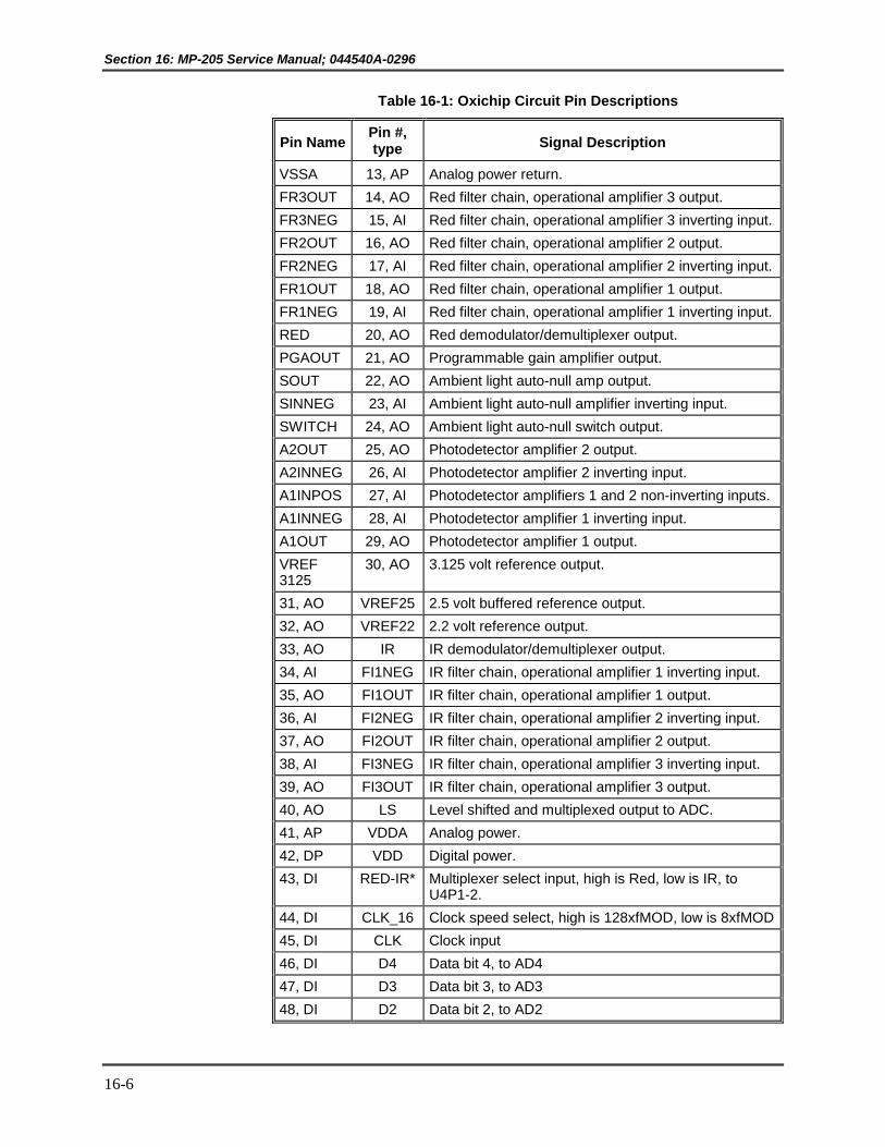
Section 16: MP-205 Service Manual; 044540A-0296
16-6
Table 16-1: Oxichip Circuit Pin Descriptions
Pin NamePin #,type Signal Description
VSSA 13, AP Analog power return.
FR3OUT 14, AO Red filter chain, operational amplifier 3 output.
FR3NEG 15, AI Red filter chain, operational amplifier 3 inverting input.
FR2OUT 16, AO Red filter chain, operational amplifier 2 output.
FR2NEG 17, AI Red filter chain, operational amplifier 2 inverting input.
FR1OUT 18, AO Red filter chain, operational amplifier 1 output.
FR1NEG 19, AI Red filter chain, operational amplifier 1 inverting input.
RED 20, AO Red demodulator/demultiplexer output.
PGAOUT 21, AO Programmable gain amplifier output.
SOUT 22, AO Ambient light auto-null amp output.
SINNEG 23, AI Ambient light auto-null amplifier inverting input.
SWITCH 24, AO Ambient light auto-null switch output.
A2OUT 25, AO Photodetector amplifier 2 output.
A2INNEG 26, AI Photodetector amplifier 2 inverting input.
A1INPOS 27, AI Photodetector amplifiers 1 and 2 non-inverting inputs.
A1INNEG 28, AI Photodetector amplifier 1 inverting input.
A1OUT 29, AO Photodetector amplifier 1 output.
VREF3125
30, AO 3.125 volt reference output.
31, AO VREF25 2.5 volt buffered reference output.
32, AO VREF22 2.2 volt reference output.
33, AO IR IR demodulator/demultiplexer output.
34, AI FI1NEG IR filter chain, operational amplifier 1 inverting input.
35, AO FI1OUT IR filter chain, operational amplifier 1 output.
36, AI FI2NEG IR filter chain, operational amplifier 2 inverting input.
37, AO FI2OUT IR filter chain, operational amplifier 2 output.
38, AI FI3NEG IR filter chain, operational amplifier 3 inverting input.
39, AO FI3OUT IR filter chain, operational amplifier 3 output.
40, AO LS Level shifted and multiplexed output to ADC.
41, AP VDDA Analog power.
42, DP VDD Digital power.
43, DI RED-IR* Multiplexer select input, high is Red, low is IR, toU4P1-2.
44, DI CLK_16 Clock speed select, high is 128xfMOD, low is 8xfMOD
45, DI CLK Clock input
46, DI D4 Data bit 4, to AD4
47, DI D3 Data bit 3, to AD3
48, DI D2 Data bit 2, to AD2

Section 16: MP-205 Service Manual; 044540A-0296
16-7
Table 16-1: Oxichip Circuit Pin Descriptions
Pin NamePin #,type Signal Description
49, DI D1 Data bit 1, to AD1
50, DI D0 Data bit 0, to AD0
51, DO LIM Overcurrent limit indicator, high indicates current limithas tripped, to U4P4-6.
52, DI EN* LED enable, high disables LED drive, low enablesLED drive, to U4P1-0.
16.18 TROUBLESHOOTING THE MP-205
16.18.1 Introduction
The MP-205 is a subsystem intended for use with a host system. This sectionassumes that the host provides a means of communicating with the modulethrough the serial host data interface described in the “OEM Pulse OximetryModule, Model MP-205, Engineering Product Specification.”
16.18.2 Fault Evaluation
Proceed as follows to evaluate and determine possible fault or error sources:
Table 16-2: Fault Evaluation
Indication ActionNo communication Check cables and interconnections.
Check 5-volt digital power supply.Check processor clock Y1.Check TXD buffer U5.Check BAUD rate jumpers.
Error X00no sensor
Sensor may be disconnected or damaged.Cable between sensor and MP-205 may bedisconnected or not functioning properly.
Error P00pulse search
The sensor may be improperly applied to the patientor may be damaged. Try another sensor. Try anSRC-2 pulse oximeter tester to checkMP-205 functionality.Cover the sensor to eliminate the possibility ofambient light interference.The patient’s perfusion may be too poor for theinstrument to detect an acceptable pulse. Try usingC-lock ECG synchronization, if available.Check + and –5 volt analog power supplies.Check for proper LED drive function.Check the signal path from the photodetector inputto the A:D converter.
Waveform outputincorrect
Sensor or interconnecting cables may be damaged.Interrogate module with W00 and determine if theupdate rate is appropriate.Noise may be present.
The following table lists reported error numbers, the error description, andrecommended user action.

Section 16: MP-205 Service Manual; 044540A-0296
16-8
Table 16-3: Reported Errors
Error # Error Description Recommended ActionE011 RAM error occurred
(MP-205 stops normaloperation)
Host should not continue operationwith the MP-205.
E012 ROM error occurred(MP-205 stops normaloperation)
Host should not continue operationwith the MP-205.
E013 Last message sent by hosthad a checksum error(last message or commandwas discarded)
Serial line may be defective. Checkfor possible noise on the serial lineinterface. Verify correctness ofchecksum calculation. Resend lastmessage to the MP-205. If errorpersists, MP-205 may be defective.
E014 Write not permitted orcommand not allowed(command discarded, normaloperation continues)
Check command description for validvalues. Resend command withcorrect value.
E015 Module received a commandwith a value out of range(command discarded, normaloperation continues)
Check command description for validvalues. Resend command withcorrect value.
E016 Calibration failed(MP-205 continues withnormal operation)
Nonfatal error; host design decideswhat action to take.
E017 Calibration already inprogress(MP-205 continues withnormal operation)
Continue processing.
E018 Calibration request denied(MP-205 continues withnormal operation)
Continue processing.
E019 Communication syntax erroron command sent by host(command discarded; normaloperation continues)
Check command description forcorrect syntax. Resend commandwith correct value.
E0210 Excessive sensor current wasdetected (MP-205 stopsnormal operation andcontinuously sends this errormessage)
Notify user to check and/or replacethe sensor or cable. Reset or cyclepower to the MP-205. Retrysaturation measurement with patient.Check for excessive noise on +5 voltdigital supply. If error persists,MP-205 may not be functioningproperly.
16.18.3 Waveforms
Figure 16-1 through Figure 16-5 are typical waveforms as measured at varioustest points (labeled TP) on the oximetry module. These waveforms are valuable in tracing signals and locating faults. The user must use a Nellcor SRC-2 pulse oximeter tester. Contact Mallinckrodt Technical Services Department if you have difficulty replicating these waveform examples.

Section 16: MP-205 Service Manual; 044540A-0296
16-9
16.18.4 SRC-2 SettingsRate: 112
Light: High2Modulation: LOW
Remote/Local: RCAL 63
Figure 16-1: Preamplifier and PGA Outputs
16.18.5 Trace DescriptionsCHNL 2 : TP3 Primary Input PreamplifierCHNL 1 : TP4 Secondary Input PreamplifierCHNL 3 : TP9 PGA output

Section 16: MP-205 Service Manual; 044540A-0296
16-10
16.18.6 SRC-2 SettingsRate: 112
Light: High2Modulation: HIGH
Remote/Local: RCAL 63
Figure 16-2: Filter Outputs and ADC Input
16.18.7 Trace DescriptionsCHNL 3 : TP5 ADC InputCHNL 1 : TP6 Red Filter OutputCHNL 2 : TP2 IR Filter Output

Section 16: MP-205 Service Manual; 044540A-0296
16-11
16.18.8 SRC-2 SettingsRate: 112
Light: High2Modulation: HIGH
Remote/Local: DC RCAL 63
Figure 16-3: MP-205 with an SRC-2 Filter Output
16.18.9 Trace DescriptionsCHNL 2 : TP6 Red Filter OutputCHNL 1 : TP2 IR Filter Output

Section 16: MP-205 Service Manual; 044540A-0296
16-12
16.18.10 SRC-2 SettingsRate: 112
Light: High2Modulation: HIGH
Remote/Local: DC RCAL 63
Figure 16-4: MP-205 with an SRC-2 LED Drive Current Test at TP7

Section 16: MP-205 Service Manual; 044540A-0296
16-13
16.18.11 SRC-2 SettingsRate: 112
Light: High2Modulation: HIGH
Remote/Local: DC RCAL 63
Figure 16-5: MP-205 with SRC-2 Serial Port TXD Signal, U4 Pin 25
16.19 PACKING FOR SHIPMENT
Should you need to ship the oximetry module for any reason, follow theinstructions in this section.
16.19.1 General Instructions
Pack the module carefully. If the original shipping carton is not available, useanother suitable carton or call Mallinckrodt Technical Services Department to obtain a shipping carton.
Prior to shipping the device, contact your supplier or your local office Mallinckrodt Technical Services Department for a returned goods authorization (RGA) number. Mark the shipping carton and any shipping forms with the RGA number.
16.19.2 Repackaging in Original Carton
If available, use the original carton and packing materials. Pack the module asfollows:
1. Place module in original packaging.
2. Place packaging in shipping carton and seal carton with packaging tape.
3. Label carton with shipping address, return address, and RGA number.

Section 16: MP-205 Service Manual; 044540A-0296
16-14
16.19.3 Repackaging in a Different Carton
If the original carton is not available:
1. Place module in antistatic bag.
2. Locate suitable corrugated cardboard shipping carton.
3. Fill bottom of carton with packing material.
4. Place bagged unit on layer of packing material and fill box completely withpacking material.
5. Seal carton with packing tape.
6. Label carton with shipping address, return address, and RGA number.
16.20 MP205 SPECIFICATIONS
16.20.1 Measurement Range/AccuracyRangeSaturation: 1 - 100%Pulse Rate: 20 - 250 beats per minute (bpm)AccuracySpO2 1
Adults: 70 - 100% ±2 digits0 - 69% unspecified
Neonates: 70 - 100% ±3 digitsPulse Rate 20 - 250 bpm ±3 bpm
1 Accuracies are expressed as ± “X” digits (saturation % points) betweensaturations of 70 and 100 percent. This variation equals ± one standarddeviation (1SD), which encompasses 68 percent of the population. All accuracyspecifications are based on testing the subject monitor on healthy adultvolunteers in induced hypoxia studies across the specified range. Adult accuracyis determined with Oxisensor® II D-25 sensors. Neonatal accuracy isdetermined with Oxisensor II N-25 sensors. In addition, the neonatal accuracyspecification is adjusted to take into account the theoretical effect of fetalhemoglobin in neonatal blood on oximetry measurements.

Section 16: MP-205 Service Manual; 044540A-0296
16-15
16.20.2 Measurement Conditions
SpO2 and pulse rate accuracy specifications apply under the followingconditions:
• Electrosurgical apparatus not used• Patient free of injected intravascular dyes• Insignificant concentration of carboxyhemoglobin and
methemoglobin• Sensor at a temperature between 28º C and 42ºC• External illumination less than 5,000 lumens/square meter (typical
office lighting)• Response mode set at Mode 1
16.20.3 Sensors
16.20.3.1 Measurement Wavelengths
Red: 660 nm, nominalInfrared: 920 nm, nominal

[THIS PAGE INTENTIONALLY LEFT BLANK]

17-1
SECTION 17: DRAWINGS17.1 Overview17.2 List of Figures
17. DRAWINGS
17.1 OVERVIEW
This section contains circuit schematics for the NPB-4000/C patient monitor.
17.2 LIST OF FIGURES
Figure No. Title Page
Figure 17-1 MP-205 PCB Schematic (Sheet 1 of 2) 17-3
Figure 17-2 MP-205 Schematic PCB (Sheet 2 of 2) 17-5
Figure 17-3 NPB-4000/C Power Supply PCB (Sheet 1 of 2) 17-7
Figure 17-4 NPB-4000/C Power Supply PCB (Sheet 2 of 2) 17-9
Figure 17-5 NPB-4000/C Main PCB Schematic (Sheet 1 of 3) 17-11
Figure 17-6 NPB-4000/C Main PCB Schematic (Sheet 2 of 3) 17-13
Figure 17-7 NPB-4000/C Main PCB Schematic (Sheet 3 of 3) 17-15
Figure 17-8 NPB-4000/C Interconnect Diagram 17-17
Figure 17-9 NPB-4000C Color Motherboard Schematic 17-19

[THIS PAGE INTENTIONALLY LEFT BLANK]
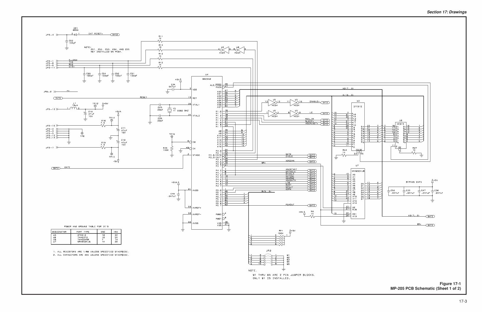
Section 17: Drawings
17-3
Figure 17-1MP-205 PCB Schematic (Sheet 1 of 2)

Section 17: Drawings
17-5
Figure 17-2MP-205 PCB Schematic (Sheet 2 of 2)

Section 17: Drawings
17-7
(PICO)
MOTOR MURS120T3D32
2.0K 5%
R80
100K1%
R76
515%
R77
TP64
TP66
TP65
0.01UF10%
C46
1AF9
1
2
P4 2P4 1
2N4401
Q19
21
3
U15
3
4
56
SI9928DY
PVENB
VBATT
100K1%
R79
100K1%
R78
U15
1
2
78
SI9928DYPUMPON
PWRGND
(External)
CLK Q
D Q
CLR
SET
4013
U9
9
11
10
12
13
8
VBATSNS
PWRGND
VSS
VDD
4071
U12
14
7VSS
VDD
4049
U11
1
8GND
VCC
4013
U9
14
7GND
VCC
4013
U8
14
7
VBATSNS
PWRGND
4071
U128
910
100K1%
R84
TP86
TP70
TP71
TP69
4049
U1114 15
4049
U119 10
4049
U1112 CLK Q
D Q
CLR
SET
4013
U95
3
4
2
1
6
TP67
VBATSNS
ALARM
PWRRST
ALARM
SILENCE
PWRGND
RESETVCC
OUT
GND
DISCH
CONTTHRESH
TRIG
NE555
U13
562
748
3
1
10UF25V10%
C56
100UF
10%25V
C57
D
S
G
ZVP2106GCT
Q21
1
2
3
1 5%
R87
D
SG
ZVN4206GCT
Q22
1
2
3
23.7K1%
R86
1K1%
R85
TP84
TP85
TP83
TP87
TP72
0.01UF10%
C55
VBATSNS
SPKR
ALARM
ALARM
PWRGND
-
+
2N3906
Q292
13
1K 1%
R98
10K1%
R95
10K 1%
R90
10K 1%
R69
10K1%
R94
51
R93
5%
10K1%
R92
51
R88
5%
TP75 TP79
0.1UF10%
C590.1UF
10%
C62
0.1UF10%
C58
TP74
TP78
2N4401
Q23
21
3B/S
-VGND
B+V
LM311D
U147
3
2
568
41
TP29
TP76
TP77
MAINSLED
DCSRC
CVREF
DCLEDDCIN
PWRGND
P3
12345678910
111213141516171819202122232425262728293031323334353637383940
P21
P22
MAINSLED
PSOFFERLYWRN
SYNC/ALARMVBATSNSSPKR
ON/OFF
DCLED
PUMPONPVENBSILENCEVBATMEAS
+5V
-24V+3.3V
+12V
PWRGND
SIGRTN
10K1%
R60
TP40
BAW56D26
1 2
3
VBATSNS
+12V
10UF
25V10%
C51
100K 1%
R62
100K1%
R61
100K1%
R63
TP414049
U113 2
4049
U115 4
BA
V70
D24
12
3
0.01UF10%
C44
VBATSNS
ON/OFF
battery connection.during originalPositive Pulse
4071
U1213
1211
100K
R83
TP45
TP44TP42
TP46
1000PF
C52
CLK Q
D Q
CLR
SET
4013
U8
5
3
4
2
1
6
BA
V70
D28
12
3
PWRGND
PWRGND
1%
PWRRST
VCCQ10
Q8Q9
RPIP0P0GND
Q4Q7Q5Q6Q14Q13Q12
4060
U1012345678 9
10111213141516
1000PF 10% C53
51K 5%
R71 510K 5%
TP48
TP52
TP51
TP50
TP57
TP56
TP49VBATSNS
PWRGND
about 1 second delay5kHz oscillator =
0 = Off Request
1 = ON
R72
PWRGND
4071
U12
1
23
100K 1%
R100
TP59
TP58
TP60
TP61
0.1UF
10%
C64
CLK Q
D Q
CLR
SET
4013
U8
9
11
10
12
13
8
BAV70
D34
1
2
3
PWRUP
ON
To sheet 1
To System PS
1000PF 10%
C47
1K 1%
R74
51K5%
R75
4705%
R73
TP63
TP62
2N4401
Q16
21
3SYNC/ALARM
+5V
SYNC
10UF
25V10%
C541K 1%
R81
100K1%
R82
TP6811
BA
V70D27
12
3
2N4401
Q20
21
3
ON
PWRGND
100UF
25V10%
C50
2N3906
Q13
21
310K 1%
R66
100K1%
R67
51K5%
R64
TP47
TP43
0.1UF10%
C48
BA
V70
D6
1 2
3
0.01UF10%
C61
VBATSNS
VBATSNS
ALARM
PWRGND
BA
V70
D25
12
3
100K1%
R68
TP54
4071
U12
6
54
51K 5%
R70 TP55TP53
2N4401
Q14
21
3ERLYWRN
PWRGND 4049
U1176
Figure 17-3NPB-4000/C Power Supply PCB Schematic (Sheet 1 of 2)

Section 17: Drawings
17-9
SLO-BLO
SLO-BLO
SURGE LIMITER
750MA
F11 2 3 4
750MA
F21 2 3 4
EXTERNAL DC
P1 6
LINE 1
LINE 2
EARTH GROUNDY CAP
P1 2
P1 1
100PF10%
C7
CHASSIS
X CAP
Y CAP
1W
1MEG10%
R1
100PF10%
C8
0.1UF10%C1
X CAP
22 mHy
L1
1
23
4
0.1UF10%
C2 220UF
400VDC10%
C35010%
R162KBP08M D11
2 3
4500V2W
MUR1100ED2
30K5%
R2
0.02UF10%
C9
5T
40T
LNAXFMR1
T13
1
5
6 10A
11A
1W 1W
51 5%
R3
75K 5%
R14
75K 5%
R15
TP7
MURS120T3
D3
680K 5%
R13
COMP VCC
OUT
GND
VFBK
VREFRT/CTISNS
UC3845
U112
34
5
6
7
8
100PF 5%
C170.1UF 5%
C11
18.2K1%
R11
1K 5%
R9
8.45K1%
R10
2.49K1%
R12
TP2
TP6
TP4TP3
TP5
TP1
470pf10%
C140.1UF10%
C13
0.01UF10%
C12
1000PF5%
C15
P1 5P1 4
P1 3
100UF
25VDC
10%
C4
1K 1%
R8
TP89
1KV
2W
7
4
3305%
R7
100PF10%
C16
Shield
MURS120T3
D4
4.7 5%
R4
D
S
G
IRFBE30
Q1
1
2
3
0.685%1W
R6
2
100UF
25VDC
10%
C6
100UF
25VDC
10%
C5
BEADS
L2
7AMP
F3
1 2
D
S
G
ZVP2106GCT
Q12
1
2
3
D
S
G
ZVN4206GCT
Q11
1
2
3
TP26
PWRUP
TP27
BAT54C
D191
2
3
100UF
25VDC
10%
C39
105%
R42
TP30
NC2OUTA
V+OUTBINB
GNDINANC1
MIC4426
U51234 5
678
0.01UF
C68
100K 1%
R44TP25 TP28
0.1UF10%
C41
22UF
25VDC10%
C34BAV99D18
1 2
3
1000PF 5%
C35
33K 5%R38
9531%
R41 100K1%
R43
TP35
+3V
1000PF 5%
C45
51 5%
R47
4.64K 1%
R39
2.49K1%
R40
TP36
TP33
0.1UF10%
C380.01UF5%
C37
BAV70
D211
23
SYNC
COMP VCC
OUT
GND
VFBK
VREFRT/CTISNS
UC3843
U412
34
5
6
7
8
470PF5%
C36
470UF
25VDC
10%
C30
1 5%
R37
1k 1%
R97
IRFZ40
TP38
P72
P71
0.1UF5%
C43
DCSRC
10K 1%
R46TP32
TP34
TP31
2N4401
Q10
21
3
DCIN
8T
1W
TO-220
3300UF
25V10%
C18
1000PF 5%
C10
240 5%
R17
TP19
MBR20100CT
D5
1
2
3
8
TEMPCO
1K1%
R18
TP9
TP8
2N4401
Q3
21
3
DCSRC
CVREF
10UF
25V10%
C19
2K5%
R21
1K1%
R2010K1%
R19
TP13 TP17
TP10
TP112N4401
Q4
21
3
NC2OUTA
V+OUTBINB
GNDINANC1
MIC4426
U31234 5
678
BA
V70D7
1 2
3
D
S
G
IRF9Z30Q21
2
3
MURS120T3D20
1K1%
R2229.4
1%
R29T21
243
XFMRCUR4700PF10%
C60
BAW56
D8
1
23
24.91%
R65
12V
105%
R48
BZX84C12ZXCTD9
TP73
D35
100KR45 1%
COMP VCC
OUT
GND
VFBK
VREFRT/CTISNS
UC3843
U212
34
5
6
7
8
TP16
TP12
0.1UF10%
C65
TP81
100UF
25V10%
C69
BAV99
1
2
30.01UF 5%
C42
4.02K 1%
R26
2.49K1%
R25
1000PF5%
C23
0.1UF10%
C214700PF
5%
C22
THERMISTOR
0.022UF 10%
C24
5.36k 1%
R28
100 5%
R27 TP14TP15
18.2k 1%
R51
10kR52
3900UF
10V
10%
C20
MBR203DCTL
D10
23
127uHy
10%
L3
2N3906
Q5
21
3 2N3906
Q6
21
32K5%
R23
1K1%
R24TP18TP80
SIGRTN
BATT-
BATT+
7AMPF4
1 2
1.5AMPF5
1 2
250PCB-TAB
P5
1
2
250PCB-TABP6
1
2
BEAD
L4
0.1UF10%
C49VBATSNS
VBATT
POLYSWITCH
10UF10%25V
C25
MBRS140T3
D15
2
1
1K 1%
R30
4.991%
R311K1%
R32
TP37
TP39
0.1UF10%
C33
BAT54CD16
12
3D17
2N3906Q7
3 20 5%2W
R34
3
5
1K1%
R33 T4
1
2
4
3
XFMRCUR
MBRS140T3
3900UF
10V10%
C40
MURS320T3D13
MBRS340T3
D12
D14
5600UF
6.3V10%
C273300UF
16V10%
C283900UF
10V10%
C26
8
12
11
7MBRD340
D11
1 23
1.5A
F6
1 2
1.5A
F7
1 2
F8
+5V
+3.3V
+3V
+12V
PWRGND
POLYSWITCH
POLYSWITCH
MURS320T3330UF
35V10%
C29
1000PF 10%
C31
100 5%
R35
14
0.2A1 2
-24V
POLYSWITCH
LNAXFMR2
T36
D
S
G
Q8
1
2
3
105%
R36
1000PF10%
C32
Figure 17-4NPB-4000/C Power Supply PCB Schematic (Sheet 2 of 2)

Section 17: Drawings
17-11
Figure 17-5NPB-4000/C Main PCB Schematic (Sheet 1 of 3)
FERRITE BEAD
BOARD MOUNTABLE
U9
U2
U2
U2
U2
U6
U6
U6
U6
U8
U8
U8
U8
X3
U13
RN1
RN1
RN1
RN1
RN1
RN1
RN1
RN1
JP4
J6
J6
J6
J6
J6J6
J6J6
J6J6
J6J6
J6J6
J6
J6J6
J6J6
J6J6
J6J6
J6J6
J6J6
J6
U12
R12
TP
277
Q4
Q3
C5
U3
J1J1
J1J1
J1
J1J1
J1J1
J1J1
J5J5
J5
J5J5
J5J5
J5J5
J5J5
J5J5
J5J5
J5
J1J1
J1J1
U17
U3
U3U3
R113
U3
R104
U3
U17
R6
R30
R45
R1
R25
R48
R51
R49
R26
R13
R11
J8
R107
R116
J7
R75
R8
R29
C18
R7
R114
R34
U22
J8
U21
U4
DS1
DS2
DS1
DS2DS2DS2
DS1DS1
DS5DS5DS5DS5
DS3DS3DS3DS3
DS4DS4DS4DS4
U14
C16
U1
X2
U12
U12U1
C11
U17
U1
R22
TP261
C32
U17
C53
C56C52
C21
C14
C55
R17
R23
C82
R106
U17
U17
J7
U1
U5
C22 C26
R43
R42
C47
R71
U24
U17
VR2
U1
U1
U17
U3
J8
U6
U8
U2U7
U1
R58
U1
SW1
J7J7
J7
J7
J7
J7
J7
J7
J7J7
J7
J7
J7
J7
J7
J7
J7
J7
J7
J7
C84
C83
U1
C59
C44
C51
C62
C38
C6
C4
C13
C15
C43
C50
C2
C41
C76
C30
R5
U20
J8
J8
R18
J7
R20
C10 C24
C25
C61
C57
C8
C9
C12
C17
R47
J8
J7
J7
J7
TP252
TP405
TP348TP328
TP358
TP408
U12
TP355
TP340
TP410
TP276
TP320
TP215
TP238
TP285TP271
TP281
TP316
TP207
TP191
TP200
TP225
R46
TP208
TP184
TP178
TP222
TP152
TP148
TP145
TP153
TP146
TP154
TP147
TP155
TP160
TP156
TP149
TP157
R10
TP171
TP173
TP193
TP291
TP235
TP253TP226
TP239
TP194
TP203TP210
TP218
TP223
TP204
TP211
TP219
TP217TP216
TP197
TP206TP198
TP213
TP214TP209
TP
236
TP
250
TP
254
TP
240
TP
230
TP
244
TP
246
TP
251
TP
247
TP
241
J7
TP
237
TP
231
TP
227
TP
224
TP334
TP347
TP349
TP361
TP395
TP385
TP388
TP398
TP324
TP275
TP274
TP269
TP265
TP303
TP310
TP305TP325
TP362
TP262
TP
306
TP167
TP354
TP367
TP
270
TP228
TP196
R128
TP389
TP406
TP284
C91
TP283
TP290
TP278
TP366
TP
233
TP
201
TP322
TP266
TP365
TP381
TP319
TP69
TP335
TP341TP386
TP183
TP399
TP409
TP394
TP311
TP229
TP220
C90
TP179
TP
264
U12
TP337
TP318
TP346
TP331
TP317
TP345
TP330
TP286TP344
TP329
TP343TP315
TP326TP342
TP314TP336
TP360
TP
313
TP
312
TP
338
TP
321
TP
332
TP
212
TP
323
TP
245
TP357
TP350
TP168TP249
TP279
TP282
TP288TP298
TP301TP294
TP300TP295
TP307
TP397
TP356
TP339
TP407
TP280
TP403
TP378
TP377
TP353TP374
TP359
TP370TP372
TP400
TP391TP396
TP401
TP351TP364
TP375
TP376TP379
TP382
TP384TP387
TP390
C89
TP186
TP373
J7
TP392
JP1
TP369
R152
U3
C7
C37
U3
U11
U12
TP248
TP255
TP260
U12
U19
U12
R40
TP293C
77
C78
TP299
R105
TP308
TP304
R115
TP
463
R28
TP
449
R38
TP437
TP
433
TP465
TP
482
TP439
TP458
TP474
TP466
R127
C1
R103R112
R102
C79
C80
C75
C74
C81
D3
C31
R3
R15
R9
R14
R16
TP289
TP327
TP190
TP205
TP333
TP404
TP383TP402
TP368
TP352
R125
J12
TP363
C98
D8
D8
D9
D9
D10
D10
D11
D11
D13
D13
D12
D12
DR
AM
OE
DRAMOE
DRAMOE
BD
14
BD14
BD14
BD14
BD
12
BD12
BD12
BD12
BD
11
BD11
BD11
BD11
BD
7
BD7 BD7
BD7
BD7
BD7
BD7
BD
7
BD7
BD8
BD8
BD
8
BD8
NURSECALL
A16A16
A16
A15
A15
A15
A15
A14
A14
A14
A14
A14
A13
A13
A13
A13
A13
A12
A12
A12
A12
A12
A11
A11
A11
A11
A11
D14
D14
A10
A10
A10
A10
A10
A9
A9
A9
A9
A9
A17
A17
A17
A8
A8
A8
A8
A8
A7
A7
A7
A7
A7
A7
A6
A6
A6
A6
A6
A6
LCDCNTRSTUP
LCDCNTRSTUP
D15
D15
ADCCLK
RESET
RESET
RESET
RESET
RESET
RESET
KNOBCHB
LCDCNTRSTDWN
LCDCNTRSTDWN
SP
KR
FR
EQ
SPKRFREQ
SPKR_ADJ_PLS
SPKR_ADJ_PLS
ACMAINST
ACMAINST
A4
A4
A4
A4
A4
A4
A4
PUMPON
W/R
W/R
DISPOFF
DISPOFF
JTOUT
JTAGCLK
LCDCONTRAST
LCDCONTRAST LCDCONTRAST
JTMD
JTDTA
SP02TX
LCDCONTRST
DEFIBKEY
A2
A2
A2
A2
A2
A2
A2
A2
RXDATA
DCST
DCST
KNOBCHA
SP02RX
AUDTONVOL
GND
GND
GND
GND
READY
READY
READY
D0
D0
LCA
S
LCAS
LCAS
D1
D1
NPANPWR
NPANPWR
DL0
CS
3
CS3
CS3
CS3
BD
13
BD13
BD13
BD13
HSTTX
HSTTX
DL3
A5
A5
A5
A5
A5
A5
BD
0
BD0 BD0
BD0
BD0
BD0
BD0
BD
0
BD0
CTS
RESET
RESET
RESET
RESET
NIBPCNTLVLV
FLM
WR
WR
WR
WR
WR
ADS
ADS
ADS
ADCRX NPNEON
NPNEON
DL2
ADCS
ADCS
FETX
FETX
PTR_RESET
SYNC/ALARMSOUND
BD
15
BD15
BD15
BD15
SPEAKER
BD
1
BD1 BD1
BD1
BD1
BD1
BD1
BD
1
BD1
BD
2
BD2 BD2
BD2
BD2
BD2
BD2
BD
2
BD2
BD
3
BD3 BD3
BD3
BD3
BD3
BD3
BD
3
BD3
BD
4
BD4 BD4
BD4
BD4
BD4
BD4
BD
4
BD4
BD
5
BD5 BD5
BD5
BD5
BD5
BD5
BD
5
BD5
SYNC_ALRM
KNOBPB
D2
D2
SPKRU/D
SPKRU/D
STXCLK
ST
XC
LK
STXCLK
DUART1INT
DUART1INT
DUART1INT
KNOBINT
DL1
DU3
DU2
DU1
PRG_EN
PRG_EN
FE_100KHZ
FE
_100
KH
Z
D3
D3
CP
D4
D4
DU0
ENDTABFR
ENDTABFR
ENDTABFR
PS
_100
KH
Z
PS_100KHZ
PS_100KHZ
TM
R1O
UT
TMR1OUT
TMR1OUT
CS
1
CS1
CS1
CS1
DSR
RTS
TXDATA
DTR
CS
0
CS0
CS0
CS0
BHE
BHE
BHE
BHE
BD9
BD9
BD
9
BD9
BD10
BD10
BD
10
BD10
CS
2
CS2
CS2
CS2
LP
PTRRST
PTRRST
NIBPPB
HSTRX
HSTRX
D5
D5
D6
D6
D7
D7
A3
A3
A3
A3
A3
A3
A3
PTRCTS
PTRCTS
BS8
BS8
RESETIN
EARLYWRNG
+5V
+5V
+5V
+5V
+5V
+5V
+5V
+5V
+12V
CLK10MHZ
CLK10MHZ
CLK10MHZ
CLK10MHZ
ADCTX
DUARTCS0
DUARTCS0
DEFIBSYNCPLS
DEFIBSYNCPLS
DEFIBSYNCPLS
BLE
BLE
BLE
BLE
BLE
BLE
BLE
PTR_CTS
PTR_TXD
PH
1
PH1
A20
BACKLITE_ON
NSCALL
NS
CA
LL
BD
6
BD6 BD6
BD6
BD6
BD6
BD6
BD
6
BD6
CNTRSTPWM
DUARTCS1
DUARTCS1
FLS
H1C
E
FLSH1CE
FLSH1CE
EOC
WR
ITE
WRITE
WRITE
WRITE
WR
ITE
WRITE
ALE
ALE
ALE
FD
RR
D
FDRRD
FD
RR
D
FDRRD
FDRRD
A18 A18
A18
A18
UCAS
UCAS
UCAS
CLK2
CLK
2
CLK2
CLK2
CLK2
EOCIN
EOCIN
M/IO
M/IO
M/IO
PSOFF
D/C
D/C
D/C
RD
RD
RD
RD
LBA
LBA
LBA
FERX
FERX
UCS
UCS
UCS
CS
6
CS6
CS6
CS
5
CS5
CS5
CS
4
CS4
CS4
A1
A1
A1
A1
A1
A1
A1
A1
NP3WYV
NP3WYV
STARTOUT
DUART0INT
DUART0INT
DUART0INT
PBINT
WDTOUT
WDTOUT
WDTOUT
+3.3V
+3.3V
+3.3V
+3.3V
+3.3V
+3.3V+3.3V
+3.3V
+3.3V
+3.3V
+3.3V
+3.3V
+3.3V
+3.3V
+3.3V
+3.3V
+3.3V
+3.3V
+3.3V
+3.3V+3.3V
+3.3V
+3.3V
+3.3V
+3.3V
+3.3V+3.3V
+3.3V
+3.3V
+3.3V
+3.3V
+3.3V
+3.3V
+3.3V
+3.3V
+3.3V
+3.3V
CA
SA
DR
EN
CASADREN
CASADREN
PH
2
PH2
NPPVEN3
LCDREADY
LCDREADY
LCD
RE
AD
Y
ADREN
ADREN
A19
A19
RA
S
RAS
RAS
ALRMSIL
PTR_RXD
J7
NOT ON PARTS LIST
NOT ON PARTS LIST
J5,J6
BSD15:0
ADDRESS BUS
TO VIA
TO VIA
TO VIA
TO VIA
TO VIA
TO VIA
TO VIA
TO V
IA
TO VIA
TO VIA
TO VIA
TO VIA
TO VIA
TO VIA
TO VIA
1OE
1A11A2
GND8
1A31A4
VCC4
1A51A6
GND7
1A71A8
2A1
2A2GND6
2A3
2A4VCC3
2A5
2A6GND5
A27
2A82OE2DIR
2B8
2B7
GND42B6
2B5
VCC22B4
2B3
GND32B2
2B1
1B81B7
GND2
1B61B5
VCC1
1B41B3
GND1
1B21B1
1DIR
74LVC16245
1
23
4
5
67
8
910
11
1213
14
1516
17
1819
20
212223
24 25
26
2728
29
3031
32
3334
35
3637
38
3940
41
4243
4445
4647
48
B Y
A23 4
B Y
A56 7
B Y
A1110 9
B Y
A1413 12
B Y
A14
13 12
B Y
A11
10 9
B Y
A5
6 7
B Y
A2
3 4
B Y
A1413 12
B Y
A1110 9
B Y
A56 7
B Y
A23 4
EN
OUT GND
VDD
SG-636PCE
14
78
1
VSS1
I/O15
I/O14
I/O13I/O12
VSS2
I/O11I/O10
I/O9
I/O8
NC4
LCASUCAS
OE
A8A7
A6
A5A4
VSS3VCC3
A3A2
A1
A0NC3
RAS
WENC2
NC1
I/O7
I/O6
I/O5I/O4
VCC2
I/O3I/O2
I/O1
I/O0
VCC1
HM51S4260ATT
1
23
4
56
7
89
10
13
14
15
1617
18
1920
2122 23
24
2526
27
2829
30
31
32
35
3637
38
3940
41
424344
89
116
215
314
413
710
611
512
JUMPER
1
2
3
1
2
15
3
45
67
89
1011
12
1314
1617
1819
2021
2223
2425
26
2728
74AC240
218
1
2N4403
2
13
2N4401
21
3
YA6 14
1110
98
7
65
43
21
32
1
45
67
89
1011
12
1314
1516
1514
1312
VCC
GND
G1
G2
74LVC541
1
19
20
10
YA7 13
YA4 16
YA5 15
YA3 17
YA2 18
74LVC541
614
1
28
WEA12
A7
A6
A5A4
A3
A2A1
A0
I/O0
I/O1I/O2
GND
I/O3
I/O4I/O5
I/O6
I/O7
CE
A10
OE
A11
A9
A8
A13A14
VCC
TC55V328J
272
34
5
67
8
910
1112
13
14
1516
17
1819
20
21
22
23
24
25
26
1
28
4
WEA12
A7
A6
A5A4
A3
A2A1
A0
I/O0
I/O1I/O2
GND
I/O3
I/O4
I/O5I/O6
I/O7
CE
A10
OE
A11
A9A8
A13A14
VCC
TC55V328J
272
34
5
67
8
910
1112
13
14
1516
17
1819
20
21
22
23
24
25
26
1
28
DS1693
CEI
CEO
VCC1
VCC0
SQW
NC4
IRQ
PSEL
RD
NC3
WR
ALE
CS
KS
AD2
AD3
GND
PWR
AD7
AD6
AD5
AD4
AD1
AD0
RCLR
NC2
NC1
VBAUX12
34
5
67
89
11
1213
14 15
1617
1819
2021
2223
24
2526
2728
10
LED04BH
6 3
LED04BH
8 1
LED04BH
5 4
LED04BH
7 2
LED04BH
6 3
LED04BH
5 4
LED04BH
7 2LED04BH
8 1
LED04BH
5 4LED04BH
6 3LED04BH
7 2LED04BH
8 1
LED04BH
5 4LED04BH
6 3LED04BH
7 2LED04BH
8 1
LED04BH
5 4LED04BH
6 3LED04BH
7 2LED04BH
8 1
WEA12
A7
A6A5
A4
A3A2
A1
A0
I/O0
I/O1
I/O2
GND
I/O3
I/O4
I/O5I/O6
I/O7
CE
A10
OE
A11
A9A8
A13
A14
VCC
AT29LV
23
45
6
78
9
1011
1314
15
16
1819
20
2122
23
24
25
27
28
29
30
31
32
HCT244137
1 2
74AC240
4 16
74AC240
812BE
AE
GND
VCC
74HCT244
1
19
20
10
74LVC541
7 13
HCT244
155
1
74LVC541
5 15
74LVC541
9 11
74LVC541
3 17
27
HCT244
119
6543
SD
I
GN
D1
MO
DE 30292827262524232221
VC
C219181716151413121110
GN
D2
VC
C1
GND3
VCC3PRB
33
3231
IOPCL49
48
4746
45
4443
42
4140
HCLK
38VCC4
98
9796
95
9493
GND6VCC7
VCC6
CLKBCLKA
86
8584
83
8281
80 79 78 77 76 IOC
LK
74 73 72 71 70 GN
D5
VK
S
VP
P
66 65 64 63 62 61 60 59 VC
C5
VS
V
56 55 54 53 52 GN
D4
DCLK99
PRA
ACT100QF
1 2 3 4 5 6 8 9 10 11 12 13 14 15 16 17 18 19 20 21 22 23 24 25 26 27 28 29 307
3132
33
3435
36
3738
39
4041
42
4344
45
4647
48
49
50
515253545556575859606162636465666768697071727374757677787980
81
82
83
8485
86
8788
89
9091
9394
95
9697
98
92
99100
D2D3
D4
D5
D6
D7
RXB
RXA
TXRDYB
TXA
TXB
OPB
CSA
CSB
XTA
L1
XTA
L2
IOW
CD
B
GN
D
RX
RD
YB
IOR
DS
RB
RIB
RT
SB
CT
SB A2
A1
A0
INTB
INTA
RXRDYA
OPA
RTSA
DTRA
DTRB
RESET
CT
SAD
SR
A
CD
A
RIA
VC
C
TX
RD
YA
D0
D1
16C2550
123456
7
89
10
1112
13
1415
16
17
18 19 20 21 22 35 24 25 26 27 28
29
30
3132
33
2334
36
37
39
4041
42
4344
38
74LVC541
416
IN
COM
OUT
MN13821-J12
3
HCT244
812
HCT244
416
74LVC541
218
YA8 12
5
G
A/B
GND
VCC
ACT157
1
15 8
16
G
A/B
GND
VCC
ACT157
115 8
16
G
A/B
GND
VCC
ACT157
115 8
16
VCC6
VSS3
RD
VCC4
BHE
NA
A2
A3A4
VSS5VCC5
A5
A7
A9A10
A11
A12A13
D14
D12
A19
D10
A22
A23
A25
SMI
A24
TCK
SRXCLK/DTR1#
SSIORX/RI1#
D1
VCC9
RXD0/P2.5
VSS12
UCS
REFRESH#/CS6
D0
D2
D3
VCC1
D4
D5
D6D7
D8D9
VSS6
CAS2/A18
D13
A15
D15
TD1
TMS
M/IO
VCC3
D/C
RXD1/DRQ1
VSS11
WDTOUT
TXD1/DACK1#
P1.7/HLDAP1.6/HOLD
CS0/P2.0
SMIACT
CS1/P2.1
CS4/P2.4CS3/P2.3
CS2/P2.2
INT1/P3.3
VCC8
P3.7/COMCLK
P3.2/INT0
STXCLK/DSR1
INT7/TMRGATE1
FLT
P1.5/LOCK#
P1.4/RIO#
NC
VSS10
INT6/TMRCLK1
TMRCLK2/PEREQ
NMI
BUSY#/TMRGATE2
INT4/TMRCLK0INT5/TMRGATE0
VSS2
LBA
VSS1
D11
P1.0/DCD0#
P3.6/PWRDOWN
P3.5/INT3
INT2/P3.4
VCC7
TMROUT1/P3.1
VSS7
CAS1/A17
A14
A8
A1
BLE
VSS4
WR
W/R
VCC10
P1.1/RTS0#
P2.7/CTS0#TXD0/P2.6
CLK2
P1.3/DSR0#
P1.2/DTR0#
VSS9
TMROUT2/ERROR#
VSS8
TMROUT0/P3.0
A21
A20
CAS0/A16
A6
ADS
BS8READY
TD0
VCC2
SSIOTX/RTS1#
CS5/DACK0#
TRST
DCD1/DRQ0
CTS1#/EOP#
VCC11
VCC12
RESET
1
2
3
4
5
67
8
9
10
1112
13
14
15
16
17
18
1920
60
2223
24
25
26
27
28
2930
31
32
33
3435
36
37
38
39
40
41
42
4344
45
4647
4849
50
5152
53
5455
56
5758
59
21
6162
63
64
6566
67
68
69
70
71
72
73
74
75
76
77
7879
80
81
82
83
84
85
87
88
89
90
91
92
93
9495
96
97
98
99
100
101
102
103
104105
106
107108
109
110
111
112
113
114
115
116
117
118
119
120
121
122
123
124125
126
127
128
129
130
131
132
86
HCT244
6 14
HCT244
2 18
12
12
3
4
5
6
7
8
910
11
12
13
14
15
16
17
18
19
20
HCT244
173
LD3
OS
C1
OS
C2
VA4VA5
VA6VA7
VA8
VA9VA10
VA11
VA12VA13
VA14
VA15VCSO
VCS1
VCS2
VCS3VCS4
VD0
VD1VD2
VD3
VD4VD5
VD6
VD7VD8
VD9
VD10VDD2
VSS2
VD
11
VD
12
VD
13
VD
14
VD
15
LCD
EN
B
XS
CL LPWF
YD
UD
0
UD
1
UD
2
UD
3
LD0
LD1
LD2
DB
7
DB
8
DB
9
DB
10
DB
11
DB
12
DB
13
DB
14
DB
15
VW
E
VA
O
VA
1
VA
2
VA
3
DB
1
DB
2
DB
3
DB
4
DB
5
DB
6
MEMRDREADY
MPUCLK
RESETMPUSEL
BHE
ABOAB1
AB2
AB3
AB4AB5
AB6
AB7AB8
AB9
AB10AB11
AB12
AB13AB14
AB15
DBO
MEMWR
VSS
VDDIOSC
IOWR
IORDMEMCS
SED1351FLB
50
51
12
3
4
6
78
9
1011
12
1314
15
1617
18
1920
21
2223
24
2526
27
28
5
29 30 31 32 33 34 35 36 37 38 39 40 41 42 43 44 45 46 47 48
49
52
5354
55
5657
58
5960
61
6267
66
6564
63
6869
70
7172
73
7475
76
7778
100
99
798081828384 85 8687 8889909192939495969798
6
3
26
2
25
24
23
1
1
1
1
1
1
74AC240
119
1
1
1
1
1
1
1
11
1
1
1
1
1
1
1
1
1
1
1
1
1
1
1
1
1
1
1
1
1
1
1
1
1
1
1
1
1
1
1
1
1
1
1
1
1
1
1
1
1
1
1
1
1
1
1 1 1 1 1 1 1 1 1 1
22
1 1 1 1
1
1
1
1
1
1
1
1
1
1
1
1
1
1
1
1
1
1
1
1
1
1
1
1
1
1
1
1
1
1
1
1
1
1
1
1
1
1
1
1
1
1
1
1
1
1
1
1
1
1
1
1
1
BE
AE
GND
VCC
74AC240
1
19
20
10
1
1
1
1
1
1
1
1
1
1
1
1
1
1
1
1
1
1 1 1 1 1 1 1
1
1
1
1
11
1
1
1
1
1
1
1
1
1
1
1
1
1
1
1
1
1
1
1
1
1
1
1
1
1
1
1
1
1
1
1
1
1
1
1
1
21
1
12
3
1
YA9 11
VCC
GND
G1
G2
74LVC541
1
19
20
10
VCC1
GND2
VPP
BYTE
WP
RP
DQ15
DQ14
DQ13DQ12
DQ11
DQ10DQ9
A17
A16A15
VCC2
A14
A13
A8
A9
A11
OE
A10
CE
DQ7DQ6
DQ5
DQ4DQ3
GND1
DQ2
DQ1DQ0
A0A1
A2
A3A4
A5
A6A7
A12
WE
DQ8
28F400
17
18
20
21
22
2324
25
2627
31
32
53
34
35
36
37
38
39
40
41
42
44
45
46
47
48
49
50
51
52
33
54
55
3
45
6
78
9
10
13
14
43
74AC240
173
1
1
1
74AC240
137
T3OUT
T1OUT
T2OUT
R2IN
R2OUT
T2IN
R1IN
GND
VCC
C1+
V+
C1-
R1OUT
T1IN
C2+
C2-
V-
R5IN
R5OUT
T3IN
T4IN
R4OUT
R4IN
EN
SHDN
R3OUT
R3IN
T4OUT
MAX211E
1
23
45
67
89
11
12
1314 15
16
17
1819
2021
2223
2425
2627
28
10
74A
C24
0 15
5
1
1
1
1
1
1
11
1
1
1
1
1
1
PMBD914
1
1
1
1
1
1
1
1
1
1
1
2
1
J8-KNOBJ7-LEDSJ6-TEST PTS.J5-TEST PTS.J4-BACKLITEJ3-50 PIN CONN.J2-KEYPADJ1-LCD CONN.
32KX16
256KX16
256KX16
BFRRS232
BFRDATA BUS
RTC
MUXADDRDRAM
DRAM
DUART
FLASHTREND
FLASHBOOT
CONNLCD
RAM
DISPLAY
CONTROLLER
LCD
32KX8
32KX8
VALUE
33
33
33
33
33
33
33
33
0_OHMS
0.1
100
100
1K
10K
33.2
1.0M
10K
100K
40.2K
2.4K
33.2
10K
10K
100
100
10K
10K
10K
0.1
0_OHMS
100
100K
0.1
40.68MHZ
0.1
1K
0.1
0.10.1
0.1
0.1
0.1
0.1
2.4K
1K
120P
F
100
10PF 10PF
511
1.0M
47nF
1.0M
10K
120P
F
120P
F
0.1
0.1
0.1
0.1
0.1
0.1
0.1
0.1
0.1
0.1
0.1
0.1
0.1
120P
F
0.1
1K
2.4K2.4K
0.1
0.1
0.1
0.1
0.1
0.1 0.1
0.1
0.1
10K
40.2K
1K
10K
.01U
F
.01U
F
.01U
F
10K
0.1
0.1
1K
120P
F
120P
F
100
100
100K
2.4K
10K
0.1
100100
100
120P
F
120P
F
120P
F
120P
F 120PF
1UF
1K
1K
1K
1K
1K
10K
0.1

Section 17: Drawings
17-13
Figure 17-6NPB-4000/C Main PCB Schematic (Sheet 2 of 3)
3
2
1
4
21
3
4 16
1
1
6 1411 9
1 2
7
6
5
3
1
2
4
11
11
2
3
6
5
4
1
2
3
6
5
4
11 10
12
1 2
13
89
6
14
7
3
1
8
9
10
1
2
3
76
5
1413
12
1 23 45 67 89 10
11 1213 1415 16
17 1819 2021 2223 2425 2627 2829 3031 3233 3435 3637 3839 4041 4243 4445 4647 4849 50
21
3
2
1
3
8
2
8 12
6 14
1
7
3
4
5
6
3
4
5 6
1
2
3
7
6
5
1
2
3
8
4
8
4
1
3 1
123 4
56
21
3
2 18
2
7
34
6
1
8
5
1
19
20
10
1
2
3
4
5
6
7
8 9
10
11
12
13
14
15
16
1
13 7
1
23
1
1
1
1
1
1
1
1
1
1
1
1
1
1
1
1
1
1
1
1
11
1
1
1
1 1
1
1
1
1
1
1
1
3
45
6
2
1
3
1
1
1
1
2
3
3
1
2
1
1
15 5
17 3
2
13
1
1
2
7 8
812
15
14
1
23
13
4
16
8
1
1
1
1
1
1
1
2
1
1
1
GND PROBE POINTS (THRU-HOLE)
LOCATE CLOSE TO POWER SUPPLY CONNECTOR (J3)
J4
J4
J4
J4
Q6
C66
C67
C34
C35
C40
C48
C33
C20
C36
C45
C29
C27
C23
C19
C58
U10
C39
TP195
TP221
C60
V2
V1
R118
U12
U10
J9
R73
R101
R50
R53
R55
R80
R86
R64
R68
R61
R72
R56
R59
R57
R52
R88
R95
R66
R62
R100
R77
R69
R76
R65
R54
R81 R78
R117
R70
R74
R79
R96
R93
R92
R44
R37
R33
R24
R41
R36
R27
R21
R87
R84
R89
R94
R98
C101
R91
R110
R108
R120R109
R111
R119
-
+
U27
Q12
C102
R35
R83
C65
U16
R99
TP258
PS1
PS2
U23
U23
U23
U23
D2
+
-
U16
+
-
U16
+
-
U16
+
-
U16
C46
C3
C70
C73
J3
TP424
TP460
TP435
TP174
Q9
Q7
J2
J2
U10
U10
J2
J2
J2
J2
J2
J2
Q10
-
+
U25
-
+
U25
-
+
U27
C42
U25
U27
TP242
C103
D1
C104
U15
D4
D5
C100
R82
Q2
R67
U10
U18
U10
U26
R32
R39
TP267
U10
R31
VR1
R97
TP187
TP268
TP272
TP202
TP188
TP256
TP192 TP164
TP263
TP166
TP296
TP189
TP243
TP234
TP134
TP182
TP150TP100
TP158
TP172
C49
TP273
TP287
TP177
TP297
TP175
TP412
RT1
TP181
TP180
TP309
R63
TP302
TP199
TP232
TP176
TP292
Q11
Q8
R60
TP144
TP123
TP129
Q1
R4
R2
R85
R90
C72
Q13
TP159
C28
C69
TP257
U10
C64
TP455
C71 C54
TP445
U10
Q5
R19
C63
TP259
R136
R122
R123
R124
R135
Q10
R126
U17
R133
C88C87
U28
U28
C86
C85
R130
R131
R132
TP420
TP421
TP423
TP425
TP422
TP426
DS6
R134
TP169
TP170
R140
C93
TP427
C97
1%
1%
1%
1%
1%
1%
1%
1%
1%
1%
1%
1%
1%
1%
1%
1%
1%
1%
1%
1%
1%
1%
NPNEON
VPVS
OSC
TEMPAD
+5V
+5V
+5V
+5V
+5V
+5V
+5V+5V
+5V
+5V
+5V
NIBPCNTLVLV
VBATTAD
R87
TXDATA
RTS
GND
GND
GND
GND
GND
GND
GND
GND
GND
GND
ALARM_SILENCE
ALARM_SILENCE
ALARM_SILENCE
PSOFF
NPANPWR
ACMAINST
NIBPRSR2
LCDCNTRSTUP
+5REF
LCDCONTRAST
AUDTONVOL
LCDCONTRST
PTR_CTS
PTR_RXD
PTR_RESET
RXDATA
DTR
DSR
CTS
V
DCST
DC/LED
PB2IN
PB3IN
SPKR_ADJ_PLS
PB4IN
PUMPON
SYNC/ALARMSOUND
LCDCNTRSTDWN
ON/OFF
ON/OFF
+5VREG
+5VREG
+5VREG
+5VREG
+5VREG
+5VREG
+5VREG
+5VREG
+5VREG
BACKLITE_ON
SPKRFREQ
+3.3V
+3.3V
+3.3V
+3.3V
+3.3V
+3.3V
+3.3V
+3.3V
+3.3V
+3.3V
+3.3V
SPKRU/D
SPEAKER
SPEAKER
SIGRTN
SIGRTN
BATTSNS+
BATTSNS+
MAINS/LED
NIBPPB
VBATTP
VBATTP
VBATTP
VBATTP
VBATTP
VBATTP
NURSECALL
DEFIBSYNCPLS
NIBPRSR1
PTR_TXD
DISPOFF
DEFIBKEY
CNTRSTPWM
ALRMSIL
PSOFF
NP3WYV
NPPVEN
NPPVEN
+12V
+12V
+12V+12V
+12V
+12V
+12V
+12V
+12V
+12V
EARLYWRNG
-24V
-24V
NPPVEN3
DEFIBOUT
TO VIA
TO VIA
TO VIA
TO VIA
TO VIATO VIA
CONTROL VALVE
6V COIL
3 WAY VALVE
2N4401
HCT244
74AC240
HCT244
LM358
FZT690BCT
LMC
660
DMS873
DMS873
4066
4066
4066
4066
LMC660
LMC660
LMC660
LMC660
16V
16V
2N4401
2N4403
HCT244
HCT244
SI9936DY
LM358
LM358
LM358
LM35
8
LM35
8
TK11450
1N4001
1N4001
2N4401
HCT244
DS1669S
74HCT244
DS1666S
HCT244
LM337L
SI9928D4
2N4401
VN2210N3
FZT549CT
HCT244
20V 20V 20V
HCT244
2N4401
SI9936DY
74LVC541
20V
74HC123
74H
C12
3
PWM FROM ACTEL
(P3.7)
(P1.1)
POWER ON LED
BACKLITE
WAVEFORM
0 TO 3.3
CS
V-
V+
NC
NC
C1 GND
VD
VCC
NC
NC
C1 GND
VD
VCC
NO
Y Z
E
NO
Y Z
E
NO
Y ZE
VDD
VSS
16V
25V
V-
V+
V-
V+
CTRL
GND VOUT
VIN
UC V+
RH
RW
DC
V-
RL
D
BE
AE
GND
VCC
U/D
NC1
NC2
INC
NC3
CS
NC4
GND VL
NC5
NC6
VH
VW
VB
NC7
VCC IN
COM
OUT
16V
D
S
G
Q
Q
R
B
A
CEXT
CREXT
VCC
GND
0.1
680PF
0.1
1.0UF
1.0UF
0.1
0.1
680PF
0.1
0.1
.01UF
.01UF
.01UF
.01UF
0.1
0.1
0.1
VSO-E95574
11-18-3-BV-5-P-77
20K
3.92K
100K
3.92K
100K
332K
75K
243K
68.1K
68.1K
182K
20K
562K
665K
665K
562K
20K
20K
665K
665K
100K
100K
33.2K
20K
100K
100K
8.25K 430
10K
20K
10K
100K
10K
10K
430
33.2
33.2
33.2
33.2
100K
100K
100K
100K
10K
10K
10K
10K
33.2K
0.1
430
100K
10K
1K
20K
10K3
.01UF
33.2
100K
.01UF
100K
BAT54C
10UF
10UF
220UF
10UF
0.1
.01UF
BAT54C
.01UF
0.1
10K
100K
10K
10K
10K
100K
10UF
VALUE
100K
100K
100K
10K
10K
10K
0.1
0.1
0.1
22UF 22UF 22UF
10K
.01UF
10K
100K
100K
33.2K
10K
1.5K
0_OHM
22UF0.1
0.1
.01UF
100
10K
10K
100
33.2K
0.1
.01UF

Section 17: Drawings
17-15
Figure 17-7NPB-4000/C Main PCB Schematic (Sheet 3 of 3)
BIN#
Fc=4.5Hz
Fc=1.6KHZ
Fc=4.5Hz
Fc=4.5Hz
+5AD
31
31
31
C
A
W=18
W=36
W=36
Fc=33KHZ
C
C
D
9.6V
+4V
D
CTS
D
C
A
B
A
D
D
B
A
BA
C
BA
B
B
A
N/C
N/C
R15=3539 OHMSR45=984.2 OHMS
NOT ON PCB
F
E
D
NO
C
A
B
LL
LA
RA
-
+
-
+
-
+-
+
-
+
-
+
-
+
-
+
-
+
-
+
-
+
1%
-
+
1%
-
+
1%
-
+
-
+
-
+
-
+
-
+
-
+
-
+
-
+
-
+
-
+
FRONT VIEW
F
E
DC
B
A
RED
BLACK
WHITE
SPO2
CONNSDSUB9 PIN
SPO2
U80
D14
0.1C124
U71
0.47UF
C147
U71
U75U74
U50
U72
U71
20MEG
R144
0
R143
TP413
D10
100K
R142
U63
TP380
40.2K
R141
40.2K
R129
TP393
120PF
C94
120PF
C95
TP371
332K
R228
120PF
C68
10UF
16V
C137
332K
R121
J10
J10
J10
J10
J10
J10
J10
J10
J10
J10
J10
J10
J10
J10
TP185
U64
1000PF
C178
40.2k
R288
40.2K
R257
J11
U84
U84
10K
R163
U84
U63
U84
TP103
U84
U84
U61
U61
U67
U84
TP94
U59
U55
U56
U75
D11
TP434
U62
0.1
C177
22UF
20V
C122
22UF
20V
C127
33.2R193
100
R221
D17
10K
R208
U79
0.1C92
D26
U73
J13
D22
100KR201
U58
100
R286
40.2KR181
0.47UFC173
.47UF
C172
TP431
T1
U61
TP432
U82
U74
U51
TP429
75K
R291
TP428
J15
U74
0.1C138
100
R270
U75
100
R262
U71
TP25
U73
0.1
C171
0.1C170
10K
R161
TP162
0.1C169
U61
40.2K
R139
U73
0.1
C126
TP417
TP436
J14
U70
0.1
C108
TP21
10K
R138
1000PF
C125
100K
R169
100K
R263
40.2K
R219
332K
R244
U62
100
R203
10KR150
U62
TP80
150K
R229
332K
R226
2.4K
R230
332KR197
10K
R200
1K
R260
0.1
C105
TP42
10K
R280
40.2K
R281
75KR212
100
R220
22UF20V
C106
10K
R282
TP106
8.25K
R285 TP99
8.25K
R284
120PF
C154
100R277
100R276
8.25K
R196
100R287
40.2K
R180
40.2KR283
40.2K
R223
33.2K
R207
TP72
0.1
C130
10UF
16V
C176
1K
R237
TP40
TP16
10UF16V
C175
10KR186
100R265
1KR234
75KR241
665K
R216
TP137
40.2k
R271
3.3M
R191
8.25K
R206
100K
R178
10KR179
40.2KR185
10K
R211
100K
R251
TP37
40.2K
R245
40.2K
R255
243KR174
1.5KR168
.01UFC174
D13
1UF
C109
TP109
TP119
1K
R227
TP127
TP104
1.5K
R158
1.5K
R155
2.4KR173
2.4K
R182
1.5K
R156
430
R167100K
R170
100K
R166100K
R153
2.4K
R256
3.92KR175
1.5K
R184
40.2K
R209
40.2K
R210
3.3MR204
1K
R198
665K
R222
2.21kR217
TP121
100K
R267
0.1C161
0.1
C149
47nF
C129
47nFC133
40.2K
R213
TP35
TP38
U51
47nF
C128
100
R253
TP23
.1UF
C142
40.2K
R243
47nF
C140
665K
R238
100
R218
TP27
0.1
C158
0.1C163
TP78
.01UFC136
0.1C165
0.1
C155
U76
3.3MR205
47nF
C121
.01UF
C152
U68
TP43
0.1C153
100K
R160
1K
R233
TP105
20M
R202
10UF
16V
C123
TP30
0.1
C143
1KR239
120PF
100V
C107
0.1C120
20K
R137
0.1C119
0.1
C117
U61
0.1C111
0.1
C116
47nF
C115
TP52
3.92K
R240
.47UF
C134
47nF
C135
U51
.01UFC131
0.1
C114
47nFC113
1K
R157
TP66
TP138
1000PF
C159
1000PF
C160
120PF
C145
120PF
C144
10K
R231
U83
U72
3.92KR199
U81
40.2K
R246
1K
R177
TP74
1KR195
U77
20k
R162
120PF
C162
1K
R192
1KR176
1K
R189
TP165
1KR183
1K
R235
1K
R264
U77
U63
2.4K
R171
U57
U53
TP122
120PF
C139
1K
R268
120PFC150
D15
120PF
C148
U65
2.4KR172
665K
R215
.47UF
C141
0.1
C132
20M
R266
2.4K
R159
20M
R252
U71 U74
2.4K
R224
U77
120PF
C146
40W
D23
TP73
U61
TP59
U78
TP7
2.4KR164
20KR214
20K
R242
U60
SPARKGAP
SG1
100
R290
120PFC157
U630.1
C118
J101
D24
J11
J11
J11
J11
J11
J11
J11
D25
U72
U66
120PF
C164D27
TP14
TP49
TP76
75K
R259
TP44
U61
TP61
8.25K
R258
TP81
U69
40.2K
R154
TP101
8.25K
R274
TP98
U74
TP163
U6433.2K
R247
TP70
U64
TP89
TP8
TP133
TP17
120PFC112
U63
TP55
TP10
75K
R273
D20
TP48
10K
R151
TP24
TP54
U77
U54
U77
TP64
TP136
TP22
TP15
TP416
8.25K
R236
8.25K
R225
TP112
TP120
40.2K
R279
TP118
TP93
D21TP65
TP84
TP125
TP82
Q21
TP124
TP87
TP141
TP108
TP115
TP113
TP126
TP116
120PFC168
40.2K
R261
TP26
TP111
TP91
TP13
75KR232
120PFC156
TP114
100KR187
100KR194
TP75
TP63
TP102
33.2K
R254
U52
TP135
J100
TP139
33.2K
R278
.47UFC167
1KR190
VALUEL1
TP132
TP143
.1UFC166
100K
R296
40.2KR294
TP151
.01UF
C110
TP36
3.3M
R248
Q22
TP3
100K
R293
TP131
TP53
TP12
TP2
TP19
TP68
3.3MR249TP5
TP32
TP97
TP11
U75
TP29
TP161
TP79
TP20
TP39
TP18
TP67
TP95
TP34TP1
TP128
TP88
TP71
TP77
TP58
TP41
TP45
TP57
TP86
TP9
D12
40.2KR188
TP96
TP83
TP90
TP4
TP28
TP107
TP142
TP85
2.4KR165
TP110
U75TP117
TP46
Q20
TP60
TP62
TP47
TP130
TP50
120PF
C151
D16
TP56
TP33
100K
R250
TP92
TP140
TP31
TP51
TP411
TP6
1K
1K
1K
Fc=33kHz
-VS
+VS
OUT
REF
+IN
-IN
AD620A
2
1
8
3
4
5
6
7
BAV99
1
2
3
TL034C
1413
12
TL034C
8
9
10
MC34184D
7
6
5
TLO34C
14
13
12
OUT
COM
IN
NJM78L05UA
1
2
3
AD706J
12
3
TL034C
7
6
5
BAW56
1
2
3
NO
YZE
CD4016
12
13
4
3
1
2
5
6
7
8
9
10
11
12
13
14
CREXT
CEXT
A
B
R
Q
Q
74HC221A
15
14
1
2
3
13
4
2
74HC041312
74HC041110
1%
74HC0498
NO
Y ZE
CD4016
1110
12
74HC0456
74HC04
12
74HC04
34
74HC04
12
74HC041110
I/O0
I/O1I/O2
I/O4
I/O5I/O6
I/O7
VEE
VSSVDD
INH
CB
A
O/II/O3
4051
11
10
9
6
1314
15
121
52
4
3
16
8
7
VCC
GND
74H
C04
14
7
VCC
GND
NC
NC
VE
OUT
CNW139
2
3
1
4
87
6
5
VCC
GND
NC
NC
VE
OUT
CNW139
2
3
1
4
8
7
6
5
VCC
GND
NC
NC
VE
OUT
CNW139
2
3
1
4
8
7
6
5
V-
V+
MC
3418
4D
4
11
BAV70
1
23
GND
VCC
74H
C12
3
16
8
PMBD914
I/0X
I/1XI/2X
I/0YI/1Y
I/2YI/3Y
VEE
VSS
VDD
OIY
INH
B
A
OIX
I/3X
CD4052
1
2
3
4
5
6
7
89
10
11
12 13
14
15
16
BAV99
1
2
3
AD712J
1
2
3
12
BAV99
1
23
1%
VCC
GND
NC
NC
VE
OUT
CNW139
2
3
1
4
8
7
6
5
1%
XFMR00A
1
36
8
10
VCC
GND
74H
C04
14
7
1
2
LM4040-4.1
TLO34C
7
6
5
V-
V+
TLC
2262
C
8
4
1 2
TL034C
8
9
10
MC34184D
1
2
3
TL034C
1
2
3
V-
V+
AD
712J
8
4
74HC04 34
1%
AD712J
76
5
12
3
8
4
LM385BYM-1.2
1%
1%
CREXTCEXT
A
BR
Q
Q
74HC123
1514
12
3
13
4
CREXT
CEXT
A
BR
Q
Q
74HC123
76
9
10
11
5
12
1%
1%
1%
1%
1%
1%
1%
1%
1%
1%
1%
1%
1%
1%
1%
BAV70
1
23
1%
1%1%
1%
1%
.05%
TLC2262C
7
6
5
INH
C
VDD
B
A
CY
CX
VSS
VEE
CX/CY
AXAY
BX
AX/AY
BX/BY
BY
4053
11
10
96
1213
2
1
53
4
15
14
7
8
16OUT
COM
IN
MC78M05CDT1
2
3
74HC04
1312
TLC2262C
1
2
3
1%
OUT
COM
IN1
2
378L05
V-
V+
AD
706J
8
4
R
C
RC/C
VDD
OSCOUT
RETRIG
Q
Q
EXRST
+TRIG VSS
ASTBLE
-TRIG
ASTBLE
CD4047B
1
2
3
45
6
78
9
1011
12
13
14
TL034C
8
9
10
1%
TL034C
14
13
12
NO
YZ
E
CD4016
4
3
5
LOC111EV-X1
1
2
3
4 5
6
7
8
VCC
EOC
I/OCLK
DATA/IN
DATA/OUT
CS
REF+
REF-
AIN10
AIN9 GND
AIN8
AIN7
AIN6
AIN5
AIN4
AIN3
AIN2
AIN1
AIN0
TLC2543
1
23
4
5
67
8
9
1011
12
13
1415
16
17
19
20
18
BAV70
1
2
3
A
BC
DE
FG
H
I
EVEN
ODD
VCC
GND
74HC280
89
10
11
1213
1
24
5
6
14
7
1%
V-
V+
TL0
34C
4
11
V-
V+
TLO
34C
4
11
V-
V+
TL0
34C
4
11
SDC15
74HC04
5 6
I/0XI/1X
I/2X
I/0Y
I/1YI/2Y
I/3Y
VEE
VSS
VDD
OIY
INH
B
A
OIX
I/3X
CD4052
1
2
3
4
5
6
7
89
10
11
12 13
14
15
16
V-
V+
TLE2061C
62
3
18
7
4
VSS
VDD
4016
14
7
1
23
45
6
78
910
1SMB75C
1
3
4
5
6
7
8
1SMB75C
AD706J
76
5
G
RCK
SCK
SCLR
SER
QH
VCCGND
QA
QBQC
QD
QEQF
QGQH
74HC595
1
2
34
56
7
8
9
10
11
12
13
14 15
16
1SMB75C
1%
74HC04
98
1%
OUT
COM
IN
NJM79L05UA
1
23
1%
1%
TLO34C
1
2
3
CREXTCEXT
A
BR
Q
Q
74HC221A
7
6
9
10
11
5
12
GND
VCC
74H
C22
1A
16
8
NOY Z
E
CD4016
8 9
6
1%
BAV99
12
3
1%
TL034C
7
6
5
GND2
VS2
GND1
OUT2
OUT1
IN
VS1
MIC4420C
2
1
4
7
6
8
5
TL034C
1
2
3
1% 1%
BAV99
12
3
2N4403
2
13
1%
1% 1%8
4
LM385BYM-1.2
1
23
45
6
78
910
1%
2N4403
2
13
1%
MC34184D
8
9
10
PMBD914
1%
MC34184D
14
13
12
2N4403
2
13
PMBD914
SP02TX
ADCCLK
MAXA
MAXA MAXA
AGND
AGND
AGND
AGND
AGND
AGND
RX
0.5HZ
0.5HZ
+5VREG
+5REG
+5REG
+5REG
+5REG
+5REG +5REG
+5REG
+5REG
+5REG
+5REG
+5REG
+5REG
+5REG
+5REG
+5REG
+5REG
GND
GND
SP02RX
TEMP
TEMP
VDD
VDD
VDD
VDD
VDD VDD
VDD
VDD
VDD
VDD
VDD
VDD
VDD
VDD
VDD
VDD
VDD
VDD
VDD
+5REF
NIBPRSR2
LSEL1
LSEL1
+3.3V
+3.3V
+7_9V
EOC
PAR
FE_100KHZ
TX
ECG
+5V
PM
PM
PM
C-LOCK
C-LOCK
PARITY
PARITY
NIBPRSR1
ADCS
RESP
ADCRX
QRS
QRS
MAXB
MAXB MAXB
VREF
VREF
MAXC
MAXC MAXC
A
+12V
+12V
+12V
ADCTX
VEE
VEE
VEE
VEE
VEE
VEEVEE
VEE
VEE
VEE
VEE
VEE
VEE
VEE
VEE
VEEVEE
VEE
-7_9V
OSC
LSEL2
LSEL2
ECGRES
ECGRES
B
LOFF
LOFF
VBATTAD
TEMPAD
LOC-111EV-X1
OPTOCOUPLERS
.945-1.061
.851-.955
.975-1.072
.886-.994
.806-.886
.733-.805
SIEMENSCLARE
IL300-EF-X1X6
F
E
D
G
OUT
MAXC
MAXB
MAXA
AGNDVRLoFFTEMPPMQRSECG
1 1
1
0
0 0
10
00
00 0 0
01
1 11 1 1
RA-LA RA-LL LA-LL TEST
.31.0.7
0110
0101
RATIO
LINB3
LS2(B)
LS1(A)
0321LEAD
F=170KHz
Fc=13KHZ
G=9
V37=2.268V
(1NA118)
+2.5V
Fc=3Hz
130us
+/-5HZ
(IL-300)
+1.235V
CF=14Hz
130mS
8mS
+75mV
V45=1.985V
V15=3.933V
1.235V
3
21
+4V
+LED
-LED
RCAL
RCAL RTN
CATHODE
N.C.
N.C.
N.C.
ANODE
G=666
Fc=5Hz
+2.5V
G=1.75
Fc=50HZ
5Vp
5Vp
G=41G=4
Fc=.1Hz
Fc=.5HZFc=.05HZ

Section 17: Drawings
17-17
Figure 17-8NPB-4000/C Interconnect Diagram
J21
2
3
45
6
7
8
J81
2
3
4
56
1 2 3 4 5 6
P1
J101
1
2
3
4
5
6
7
8
9
10
J41
2
3
4
JX1
1 2 3 4 5 6 7 8 9 10 11 12 13 13 15 16 17 18 19 20
P4P2
J31
2
3
45
6
7
89
10
11
12
1314
15
16
1718
19
20
2122
23
24
25
2627
28
29
3031
32
33
3435
36
37
3839
40
41
42
4344
45
46
4748
49
50
100PF
JX41
2
3
45
6
7
89
10
11
12
1314
15
16
1718
19
20
2122
23
24
25
2627
28
29
3031
32
33
3435
36
37
3839
40
41
42
4344
45
46
4748
49
50
12
3
4
56
7
8
9
1011
12
13
1415
16
17
1819
20
21
2223
24
25
26
2728
29
30
3132
33
34
3536
37
38
39
40
P3
J111
2
3
4
56
7
8
.1UF
100PF
J101
2
34
5
6
78
9
10
11
12
13
14
J100
J11
23
4
5
6
78
9
10
1112
13
14
1516
-24V+3.3V
+3.3V
+3.3V
CTS
RXD
TXD
+12V
+12V
+12V
+12V
+12V
+5V
+5V
+5V
GROUND
GROUNDGROUND
GROUND
GROUND
GROUND
GROUND
GROUND
GROUND
PTR
F3
7AM
P (
DC
)
F2
750M
A (
AC
2)
F1
750M
A (
AC
1)
F4 (7 AMP)
(HEADER,MALE)
(HEADER,FEMALE)
AGND
+5REG
AGND
CTS
VDDRX
TX
VEE
N.C.AGND
N.C.
AGND
AGNDCLOCK
DL3
DL2
DL1
DL0
DU3
DU2DU1
DU0
LCD CONTRASTGND
3.3V
DISPOFF
CPLP
FLM
GND+12V
GND
DC LEDAC MAINS LED
LCD CONTRAST
AUDIOTONE VOLUME
NIBPALARM/SILENCE
ON/OFF
+5V
CHANNEL A
CHANNEL BPB
GND
GND
TEMP
TEMPSHIELD
LL
NIC
LC
LARA
AMP 1-102153-0 (MALE)
ESQ-107-23-G-D
ESQ-105-23-G-D
SAMTEC
SAMTEC
AMP 640457-6 (MALE)
AMP 640457-8 (MALE)
AMP 640457-8 (MALE)
AMP 102153-3 (MALE)
AMP 640457-4 (MALE)
P6
P5
(+)
(-)
BATTERY
6V,8AH
BEADS
RECEPTACLE
BEAD
6 PIN
SPEAKER
2 PIN2 PIN PUMP
2 PIN PUMP
PWB
INTERFACEPRINTER
50 PIN HEADER TO PRINTER
20 PIN HEADER (FEMALE)
TO PRINTER INTERFACE PWB
20 PIN HEADER (MALE)
(2.5MM PHONE JACK)
DEFIB SYNC OUTPUTRS-232 I/O PORT
9 PIN D-SUB (MALE)
(HEADER,FEMALE)
10 W
IRE
RIB
BO
N
10 P
IN C
ON
N (
?)
10 P
IN C
ON
N (
?)SP02
6 WIRES
BOARD
DAUGHTER
MP 205
FROM SPEAKER
2 PIN SPEAKER
(INPUT)
SUPPLY
D.C.
PUMP
057068
LUG
GND
AC
FILTER
LINE
P/N 5021780
TRONOMED
AMP 102153-1
20 P
IN C
ON
N (
?)
20 W
IRE
RIB
BO
N
AM
P 4
9997
-4
AMP 49997-4
SYSTEM
MAIN
SUPPLY
PCB
PCB
POWER
SWITCH PANEL
CABLE ON
VIA RIBBON
SWITCH PANEL
TO MEMBRANE
RIBBON CABLE
VIA KNOB
TO KNOB
NELLCOR HARNESS
CABLE
VIA RIBBON
TO LCD
HARNESS
BACKLIGHT
TO LED
N.C.
594837261
NURSECALL
GND
DTR
CTS
TX
RTS
RX
DSR
DEFIBSYNC
NOT USED
V BATTERY
V BATTERY
SPEAKER OUT
DC LED (DIRECT DRIVE)MAINS LED (DIRECT DRIVE)
SIG RTN (ANALOG GROUND)
VBATT (SENSE ONLY)EARLY WARNING (ACTIVE LOW)
ALARM SILENCE (DIRECT KEY)
PS OFF(ACTIVE HIGH)
PV ENABLE(ACTIVE HIGH)
PUMP ON (ACTIVE HIGH)
SYNC/ALARM SOUND (50KHz)
ON/OFF (DIRECT KEY)
NOT USED (ON PWR SUP)
NOT USED (ON PWR SUP)
NOT USED (ON PWR SUP)
NOT USED (ON PWR SUP)

Section 17: Drawings
17-19
Figure 17-9NPB-4000/C Color Motherboard Schematic
1OE1A11A2
GND81A31A4
VCC41A51A6
GND71A71A82A12A2
GND62A32A4
VCC32A52A6
GND5A272A82OE2DIR
2B82B7GND42B62B5VCC22B42B3GND32B22B11B81B7GND21B61B5VCC11B41B3GND11B21B11DIR
74LVC16245
U9123456789101112131415161718192021222324 25
2627282930313233343536373839404142434445464748
B Y
AU2
23 4
B Y
AU2
56 7
B Y
AU2
1110 9
B Y
AU2
1413 12
B Y
AU6
1413 12
B Y
AU6
1110 9
B Y
AU6
56 7
B Y
AU6
23 4
B Y
AU8
1413 12
B Y
AU8
1110 9
B Y
AU8
56 7
B Y
AU8
23 4
33RN19
33RN116
33RN115
33RN114
33RN113
33RN110
33RN111
33RN112
J6 1
J6 2 J6 15
J6 3
J6 4
J6 5
J6 6
J6 7
J6 8
J6 9
J6 10
J6 11
J6 12
J6 13
J6 14
J6 16
J6 17
J6 18
J6 19
J6 20
J6 21
J6 22
J6 23
J6 24
J6 25
J6 26
J6 27
J6 2874AC240
U12218
0_OHMS
R12
TP2771
0.1C5
YA U36 14
PH1
RESET
VCC12VCC11
CTS1#/EOP#
DCD1/DRQ0
TRST
CS5/DACK0#
SSIOTX/RTS1#
VCC2
TD0
READYBS8
ADS
A6
CAS0/A16
A20A21
TMROUT0/P3.0
VSS8
TMROUT2/ERROR#
VSS9
P1.2/DTR0#P1.3/DSR0#
CLK2
TXD0/P2.6P2.7/CTS0#
P1.1/RTS0#
VCC10
W/R
WR
VSS4
BLE
A1
A8
A14
CAS1/A17
VSS7
TMROUT1/P3.1
VCC7
INT2/P3.4P3.5/INT3P3.6/PWRDOWN
P1.0/DCD0#
D11
VSS1
LBA
VSS2
INT5/TMRGATE0INT4/TMRCLK0
BUSY#/TMRGATE2
NMI
TMRCLK2/PEREQ
INT6/TMRCLK1
VSS10
P1.4/RIO#P1.5/LOCK#
FLT
INT7/TMRGATE1
STXCLK/DSR1
P3.2/INT0
P3.7/COMCLK
VCC8
INT1/P3.3
CS2/P2.2CS3/P2.3CS4/P2.4
CS1/P2.1
SMIACT
CS0/P2.0
P1.6/HOLDP1.7/HLDA
TXD1/DACK1#
WDTOUT
VSS11
RXD1/DRQ1
D/C
VCC3
M/IO
TMSTD1
D15
A15
D13
CAS2/A18
VSS6
D9D8D7D6D5D4
VCC1
D3D2
D0
REFRESH#/CS6UCS
VSS12
RXD0/P2.5
VCC9
D1
SSIORX/RI1#
SRXCLK/DTR1#
TCK
A24
SMI
A25
A23A22
D10
A19
D12
D14
A13A12A11A10A9
A7
A5
VCC5 VSS5
A4A3A2
NA
BHE
VCC4
RD
VSS3
VCC6
U7
12
3
4
5678
9
1011121314
15
16
17
181920
60
2223
24
2526
27
28
2930
31
3233
3435
36
37
38
39
40
41
42434445
4647
484950515253545556575859
21
616263
64
65666768
69
70
71
72
73
7475
76
77
7879
80
81
82
83
8485
87
88
89
90
91
92
93949596
97
98
99
100
101102
103
104105106107108
109
110
111
112
113
114
115
116
117
118
119
120
121
122123124125126
127
128
129
130
131132
86
J5 3J5 2J5 1
J5 4
J5 5
J5 6
J5 7
J5 8
J5 9
J5 10
J5 11
J5 12
J5 13
J5 14
J5 15
J5 16
VCC
GND
G1
G2
74LVC541
U17119
2010
YA U37 13
YA U34 16
YA U35 15
YA U33 17YA U32 18
74LVC541
U17 614
1K
R6
10KR30
1.0MR1
10K R25
33.2
R26
3KR13
10KR11
J8 1
10KR8
10KR29
0.1C18
0_OHMS
R7
100KR34
J8 4
DS1693
CEICEO
VCC1VCC0SQWNC4IRQ
PSELRD
NC3WR
ALECSKS
AD2AD3
GNDPWRAD7AD6AD5AD4
AD1AD0RCLRNC2NC1VBAUX U41
23456789
11121314 15
16171819202122232425262728
10
0.1C16
HCT244
U1 137
74AC240
U12416
74AC240U12
812
BE
AE
GND
VCC
74HCT244
U1119
2010
0.1C11
74LVC541
U177 13
HCT244 U1
155
1KR22
TP2611
74LVC541
U175 15
0.1C53
0.1
C56 0.1C52
0.1C21
0.1C14
0.1
C55
2.4KR17
1KR23
74LVC541
U179 11
74LVC541
U173 17
TP5351
TP5361
HCT244
U1119
TP5331
OE
OUT GND
+V
40MHZSG-636PCE
X38
45
1
TP5001
33.2R500
47nF
C47
1.0M
R71
D2D3D4
D5D6D7RXBRXATXRDYBTXATXBOPBCSACSB
XTAL
1XT
AL2
IOW
CDB
GND
RXRD
YBIO
RDS
RBRI
BRT
SBCT
SB
A2A1A0
INTBINTA
RXRDYAOPA
RTSADTRADTRB
RESETCTSA
DSRACDARIAVCCTXRDYAD0D1
16C2550
U24
123456
7891011121314151617
18 19 20 21 22 35 24 25 26 27 28
293031323323343637
39
4041424344
38
74LVC541
U17 416
IN
COM
OUT
MN13821-J
VR212
3
HCT244
U1812
560PFC190
74LVC541
U17 218
YA U38 12
J8 5
G
A/B
GND
VCC
ACT157
U6115 8
16
G
A/B
GND
VCC
ACT157
U8115 8
16
G
A/B
GND
VCC
ACT157
U2115 8
16
10KR544
HCT244U1
6 14
10KR58
HCT244
U12 18
SW1
12
HCT244
U1 173
TP5371
TP5341
0.1
C51
0.1C62
0.1
C38
0.1C6
0.1C4
0.1C13
0.1
C500
0.1C2
0.1C30
1K
R5
J8 6
J8 3
2.4KR18
2.4KR20
0.1C10
0.1C24
0.1C25
0.1
C8
0.1
C9 0.1
C12
0.1
C17
J8 2
TP2521
TP4051
TP3481
TP3281
TP3581
TP4081
74AC240U12
119
TP3551
TP3401
TP4101
TP320
1
TP2151
TP2381
TP3161
TP2071
TP1911
TP2001
TP2251
TP1841
TP1781
TP2221
1K
R10
TP1711
TP1731
TP1931
TP2911
TP5291
TP3341
TP3471
TP3491
TP3611
TP3951
TP3851
TP3881
TP3981
TP3621
TP2621
TP1671
TP3541
TP367 1
TP2701
TP2281
560PFC186
TP1961
10K
R128
TP3891
TP4061
TP284 1
.01U
F
C91
TP4141
TP2831
TP2901
TP2781
TP3661
TP23
3
1
TP2011
TP322 1
TP3651
TP3811
TP3191
TP691
TP3351
TP3411
TP3861
TP3991
TP4091
TP3941
TP311 1
TP229 1
TP220 1
.01U
F
C90
TP1791
TP2641
BE
AE
GND
VCC
74AC240
U12119
2010
TP3371
TP3181
TP3461
TP3311
TP3171
TP3451
TP3301
TP2861
TP3441
TP3291
TP3431
TP3151
TP3261
TP3421
TP3141
TP3361
TP360 1
TP313
1
TP312
1
TP338
1
TP321
1
TP332
1
TP212
1
TP323
1 TP3571
TP3501
TP1681
TP2491
TP2791
TP2821
TP2881
TP2981
TP3011
TP2941
TP3001
TP2951
TP307 1
TP3971
TP356 1
TP339 1
TP4071
TP2801
TP4031
TP3781TP3771TP3531TP3741TP3591TP3701TP3721TP4001TP3911TP3961TP4011TP3511TP3641TP3751TP3761TP3791TP3821TP3841TP3871TP3901
.01U
F
C89
TP3731
TP3921
JP1 1 2 3
TP3691
10KR152
YA U39 11
0.1C7
0.1C37
VCC
GND
G1
G2
74LVC541
U3119
2010
120pfC522
74AC240
U12173
TP2481
TP2551
TP2601
74AC240U12
137
T3OUTT1OUTT2OUTR2INR2OUTT2IN
R1INGNDVCCC1+V+C1-
R1OUTT1IN
C2+C2-V-
R5INR5OUTT3INT4IN
R4OUTR4IN
ENSHDN
R3OUTR3IN
T4OUT
MAX211E
U19
123456789
11121314 15
16171819202122232425262728
10
74AC
240
U12
15
5
1KR40
TP2931
TP299 1
TP3081
TP3041
TP46
3
1
100KR28
TP449
1
TP43
7
1
TP43
3
1
TP4651
TP48
2
1
TP439 1
TP458 1
TP4741
TP466 1
10KR127
0.1C1
1K
R3
1KR15
1K
R9
1K
R14
1K
R16
TP2891
TP3271
TP1901
TP2051
TP3331
TP4041
TP3831
TP4021
TP3681
TP3521
10K
R125
TP3631
0.1C98
560PFC185560PF
C184
560PFC183560PF
C182
560PFC181560PF
C180
BEAD
L5
BEAD
L4
BEAD
L3560PFC179
BEAD
L2
560PFC202
560PFC201
BEAD
L13
560PFC204
560PFC203
BEAD
L14
56PFC528
560PFC189
BEAD
L7
560PFC195
560PFC196
BEAD
L10
560PFC193
560PFC194
BEAD
L9
BEAD
L8
560PFC192
560PFC191
100
R146
1KR147
1KR148
TP4151 TP4181 TP4191
TP4301
TP4441
TP4431
TP4421
TP4411
4.99KR42
TP4461
TP4471
133R149120PF
C96TP4501
J50012
1nf
C517
10nf
C516
0.1
C521
33.2
R537
OSCINOSCOUT
AVDDD_C
STOPS0LF
AVSSS1
SSONS3DVDDDVSSS2FOUTR1R0OVSSOVDDREFOUT
SM530
U5031234567891011
121314151617
1920
18
0.1
C520
0.1
C519
0.0ohm
R532
1K
R531
0.0ohm
R533
0.0ohm
R5350.0ohm
R536
0.0ohm
R534
56PFC518
TP515
1
0.0ohm
R538
0.0ohm
R539
0.0ohm
R540
TP5161
TP5171
TP5181
TP306
1
J502123456789
33.2R543
A42MX09FPGA
NC
I/O
I/O
I/O
I/OI/ONC
NC I/O
I/O
GNDVCCA
VCCA
NC
NC
NCNCI/O
I/ONC
I/ONC
NCI/OI/ONCI/ODCLK,I/O
PRB,I/OI/OCLKB,I/OI/O
CLKA,I/OI/OPRA,I/ONCI/O
I/O
I/ONCNCNC
I/O
I/OI/ONCSDI,I/O
I/O
GND I/O
I/O
I/O
I/O
I/O
I/O
NC NC I/O
I/O
NC I/O
I/O
I/O
I/O
NC NC NC VCCI
GND
VCC
GND
NC NC GND
I/O
I/O
NC I/O
NC I/O
I/O
I/O
NCNC
I/O
I/O
I/O
I/O
I/O
I/O
GND
I/OI/ONC
I/OI/OI/ONC
I/ONC
I/ONCNC
I/O
I/O
NCI/OI/O
I/OI/O
VCCAGNDNC
I/O
NCI/OI/ONC
I/OI/OI/O
I/ONCNC
I/ONC
I/OI/OI/OI/OI/OI/OGNDI/
OI/
OI/
OI/
OI/
OI/
ONCNCI/
OI/
OI/
ONCI/
OI/
OI/
ONCVC
CANCNCVC
CANCGN
DNCI/
ONCNCGN
DI/
OI/
OI/
OI/
O
I/ONCNC
I/ONC
I/O
I/O
GND
MODE I/O
I/O
I/O
U505
1 2 3 4 5 6 7 8 9 10 11 12 13 14 15 16 17 18 19 20 21 22 23 24 25 26 27 28 29 30 31 32 33 34 35 36 37 38 39 40 41 42 43 44
4546474849505152535455565758596061626364
65
6667686970
71
727374
75
76777879808182838485868788
89909192 9394
95
9697989910
010
110
210
310
410
510
610
710
810
911
011
111
211
311
411
511
611
7
118
119
120
121
122
123
124
125
126
127
128
129
130
131
132
133
134
135136137138
139
140141142143144145146147148149150151152153154155156157158159160161162163164165166167168169170171172173174175176
TP5301
56PFC527
BD10
D8
D8
D9
D9
BD6
BD6 BD6
BD6
BD6
D10
D10BD11
D11
D11
D13
D13
D12
D12
BACKLITE_ON
NURSECALL
BD12BD13
BD15
D14
D14
U7-38U7-38
LCDCNTRSTUP
100
D15
D15
ADCCLK
U7-71
U7-71
RESET
RESET
RESET
RESET
PTRRST
PTRRST
LCDCNTRSTDWN
U5-8
U5-8
A20
A20
A20
SPKR_ADJ_PLS
ACMAINST
PUMP
ONBD
7
BD7 BD7
BD7
BD7
U7-15
U7-15
A6
A6
A6
W/R
W/R
DRAM
OE
DRAMOE
LCD_CS
LCD_CS
A3
A3A3
A3 VID_RAS
JTOUT
JTAGCLK
JTMDJTDTA
SP02TX
ADCS
ADCS
DEFIBKEY
U5-5
8
U5-58
RXDATA
DCST
KNOBCHA
PS_1
00KH
Z
PS_100KHZ
PS_100KHZ
SP02RX
LCDCONTRST
U7-109
U7-109
READY
READY
READY
D0
D0
D1
D1
NPANPWR
CS3
CS3
CS3
CS3
HSTTX
HSTTX
BD8
CTS
LCD_UWR
FE_1
00KH
Z
LCD_URD
ADCRX
NPNEON
RAS
RAS
SDI
SDI
FETX
PTR_RESET
SYNC/ALARMSOUND
SYNC/ALARMSOUND
KNOBPB
D2
D2
SPKRU/D
STXCLK
STXCLK
DUART1INT
DUART1INT
A5
A5
A5
ALRMSIL
D3
D3
D4
D4
ENDTABFR
ENDTABFR
ENDTABFR
PRA
PRA
SPKR
FREQ
U5-37
U5-37
CS1
CS1
CS1
DSR
RTSTXDATA
DTR
CS0
CS0
CS0
ADRE
N
ADREN
CS2
CS2
CS2
VID_WE
AUDTONVOL
PRB
PRB
HSTRX
HSTRX
D5
D5
D6
D6
D7
D7
PTRCTS
PTRCTS
BS8
BS8
+5V
+5V
+5V
+5V
+5V
BD14
CLK10MHZ
CLK10MHZ
ADCTX
DCLKDCLKPRG_EN
DEFIBSYNCPLS
DEFIBSYNCPLS
PTR_CTS
STARTOUT
PTR_TXD
+3.3V
+3.3V+3.3V
+3.3V
+3.3V
+3.3V
+3.3V
+3.3V
+3.3V
+3.3V
+3.3V
+3.3V
+3.3V
+3.3V
+3.3V
+3.3V
+3.3V
+3.3V
+3.3V
+3.3V
+3.3V
+3.3V
+3.3V
WRIT
E
WRITE
WRITE
WRITE
RESET
RESET
RESET
CNTR
STPW
M
DUARTCS1
DUARTCS1
FLSH
1CE
FLSH1CE
EOC
A1
A1
A1
A1
A1
BLE
BLE
BLE
BLE
BLE
CLK_40MHZ
CLK_40MHZ
CLK_40MHZ
CLK_40MHZ
EOCI
N
EOCIN
EOCIN
LCD_LRD
PSOFF
CS6
CS6
CS6
EARLYWRNG
LBA
LBA
LBA
FERX
M/IO
M/IO
M/IO
CS4
CS4
CS4
CS5
CS5
CS5
GND
GND
CASA
DREN
CASADREN
CASADREN
NP3WYV
KNOBCHB
DUART0INT
DUART0INT
UCAS
UCAS
LCAS
LCAS
PH2
NPPVEN3
A2
A2
A2
A2
A2
NIBPPB
PTR_RXD
BD0
BD0 BD0
BD0
BD0
PH1
LCDREADY
LCDREADY
DUARTCS0
DUARTCS0
BD1
BD1 BD1
BD1
BD1
BD2
BD2 BD2
BD2
BD2
BD4
BD4 BD4
BD4
BD4
A14
A14
A13
A13
A11
A11
A12
A12
U5-89
U5-89
BD9
A19
A19
A19
A19
WR
WR
WR
WR
RD
RD
RD
BHE
BHE
BHE
TMR1OUT
TMR1OUT
TMR1OUT
A7
A7
A7A8
A8
A17
A17
A18
A18
A18
A10
A10
A9
A9
A16
A16
A15
A15
BD3
BD3 BD3
BD3
BD3
BD5
BD5 BD5
BD5
BD5
VID_LCAS
UCS
UCS
UCS
SYNC_ALRM
D/C
D/C
D/C
A4
A4
A4
A4
PH1-FPGA
PH1-FPGA
LCD_LWR
VID_UCAS
ALE
ALE
ALE
MODE
MODE
RESETIN
FDRRD
FDRRD
FDRRD
FDRRD
NSCA
LL
NSCALL
WDTOUT
WDTOUT
WDTOUT
NIBP
CNTL
VLV
NIBPCNTLVLV
ADS
ADS
ADS
NOT ON PARTS LISTJ5,J6
BSD15:0
TO VIA
TO VIA
TO VIA
TO VIA
TO VIA
TO VIA
TO VIA
TO VIA
TO VIA
TO VIA
TO VIA
TO VIA
TO V
IA
NDC
ACTEL HDR
S0
R0
S2
S3
SSON
MUXADDRDRAM
BFRRS232
BFRDATA BUS
RTC
DUART