Granične teme : izabrani članci (Border topics : selected papers)
Upload
khangminh22Category
view
0download
0
International Journal of Reconfigurable Computing
Guest Editors: Claudia Feregrino, Miguel Arias, Kris Gaj,Viktor K. Prasanna, Marco D. Santambrogio, and Ron Sass
Selected Papers fromthe International Conferenceon Reconfigurable Computing and FPGAs (ReConFig’10)
Selected Papers from the InternationalConference on Reconfigurable Computingand FPGAs (ReConFig’10)

International Journal of Reconfigurable Computing
Selected Papers from the InternationalConference on Reconfigurable Computingand FPGAs (ReConFig’10)
Guest Editors: Claudia Feregrino, Miguel Arias, Kris Gaj,Viktor K. Prasanna, Marco D. Santambrogio, and Ron Sass

Copyright © 2012 Hindawi Publishing Corporation. All rights reserved.
This is a special issue published in “International Journal of Reconfigurable Computing.” All articles are open access articles distributedunder the Creative Commons Attribution License, which permits unrestricted use, distribution, and reproduction in any medium, pro-vided the original work is properly cited.

Editorial Board
Cristinel Ababei, USANeil Bergmann, AustraliaKoen Bertels, TheNetherlandsChristophe Bobda, GermanyMiodrag Bolic, CanadaJoao Cardoso, PortugalPaul Chow, CanadaRene Cumplido, MexicoAravind Dasu, USAClaudia Feregrino, MexicoAndres Garcıa-Garcıa, MexicoSoheil Ghiasi, USADiana Gohringer, GermanyReiner Hartenstein, GermanyMichael Hubner, GermanyJohn Kalomiros, GreeceVolodymyr Kindratenko, USA
Paris Kitsos, GreeceChidamber Kulkarni, USAMiriam Leeser, USAGuy Lemieux, CanadaHeitor Silverio Lopes, BrazilMartin Margala, USALiam Marnane, IrelandEduardo Marques, BrazilMaire McLoone, UKSeda Ogrenci Memik, USAGokhan Memik, USADaniel Mozos, SpainNadia Nedjah, BrazilNik Rumzi Nik Idris, MalaysiaJose Nunez-Yanez, UKFernando Pardo, SpainMarco Platzner, Germany
Salvatore Pontarelli, ItalyMario Porrmann, GermanyViktor K. Prasanna, USALeonardo Reyneri, ItalyTeresa Riesgo, SpainMarco D. Santambrogio, USARon Sass, USAPatrick R. Schaumont, USAAndrzej Sluzek, SingaporeWalter Stechele, GermanyTodor Stefanov, TheNetherlandsGregory Steffan, CanadaGustavo Sutter, SpainLionel Torres, FranceJim Torresen, NorwayW. Vanderbauwhede, UKMustak E. Yalcın, Turkey
Contents
Selected Papers from the International Conference on Reconfigurable Computing and FPGAs(ReConFig’10), Claudia Feregrino, Miguel Arias, Kris Gaj, Viktor K. Prasanna, Marco D. Santambrogio,and Ron SassVolume 2012, Article ID 319827, 2 pages
Evaluation of Runtime Task Mapping Using the rSesame Framework, Kamana Sigdel, Carlo Galuzzi,Koen Bertels, Mark Thompson, and Andy D. PimentelVolume 2012, Article ID 234230, 17 pages
Implementation of Ring-Oscillators-Based Physical Unclonable Functions with Independent Bits inthe Response, Florent Bernard, Viktor Fischer, Crina Costea, and Robert FouquetVolume 2012, Article ID 168961, 13 pages
Blind Cartography for Side Channel Attacks: Cross-Correlation Cartography, Laurent Sauvage,Sylvain Guilley, Florent Flament, Jean-Luc Danger, and Yves MathieuVolume 2012, Article ID 360242, 9 pages
A Hardware Efficient Random Number Generator for Nonuniform Distributions with ArbitraryPrecision, Christian de Schryver, Daniel Schmidt, Norbert Wehn, Elke Korn, Henning Marxen,Anton Kostiuk, and Ralf KornVolume 2012, Article ID 675130, 11 pages
Hardware Middleware for Person Tracking on Embedded Distributed Smart Cameras,Ali Akbar Zarezadeh and Christophe BobdaVolume 2012, Article ID 615824, 10 pages
Exploration of Uninitialized Configuration Memory Space for Intrinsic Identification of Xilinx Virtex-5FPGA Devices, Oliver Sander, Benjamin Glas, Lars Braun, Klaus D. Muller-Glaser, and Jurgen BeckerVolume 2012, Article ID 219717, 10 pages
Placing Multimode Streaming Applications on Dynamically Partially Reconfigurable Architectures,S. Wildermann, J. Angermeier, E. Sibirko, and J. TeichVolume 2012, Article ID 608312, 12 pages
Redsharc: A Programming Model and On-Chip Network for Multi-Core Systems on a ProgrammableChip, William V. Kritikos, Andrew G. Schmidt, Ron Sass, Erik K. Anderson, and Matthew FrenchVolume 2012, Article ID 872610, 11 pages
On the Feasibility and Limitations of Just-in-Time Instruction Set Extension for FPGA-BasedReconfigurable Processors, Mariusz Grad and Christian PlesslVolume 2012, Article ID 418315, 21 pages
Combining SDM-Based Circuit Switching with Packet Switching in a Router for On-Chip Networks,Angelo Kuti Lusala and Jean-Didier LegatVolume 2012, Article ID 474765, 16 pages
A Fault Injection Analysis of Linux Operating on an FPGA-Embedded Platform, Joshua S. Monson,Mike Wirthlin, and Brad HutchingsVolume 2012, Article ID 850487, 11 pages

NCOR: An FPGA-Friendly Nonblocking Data Cache for Soft Processors with Runahead Execution,Kaveh Aasaraai and Andreas MoshovosVolume 2012, Article ID 915178, 12 pages
Dynamic Circuit Specialisation for Key-Based Encryption Algorithms and DNA Alignment,Tom Davidson, Fatma Abouelella, Karel Bruneel, and Dirk StroobandtVolume 2012, Article ID 716984, 13 pages
A Dynamically Reconfigured Multi-FPGA Network Platform for High-Speed Malware Collection,Sascha Muhlbach and Andreas KochVolume 2012, Article ID 342625, 14 pages
Using Partial Reconfiguration and Message Passing to Enable FPGA-Based Generic ComputingPlatforms, Manuel Saldana, Arun Patel, Hao Jun Liu, and Paul ChowVolume 2012, Article ID 127302, 10 pages
Exploring Many-Core Design Templates for FPGAs and ASICs, Ilia Lebedev, Christopher Fletcher,Shaoyi Cheng, James Martin, Austin Doupnik, Daniel Burke, Mingjie Lin, and John WawrzynekVolume 2012, Article ID 439141, 15 pages

Hindawi Publishing CorporationInternational Journal of Reconfigurable ComputingVolume 2012, Article ID 319827, 2 pagesdoi:10.1155/2012/319827
Editorial
Selected Papers from the International Conference onReconfigurable Computing and FPGAs (ReConFig’10)
Claudia Feregrino,1 Miguel Arias,1 Kris Gaj,2 Viktor K. Prasanna,3
Marco D. Santambrogio,4 and Ron Sass5
1 Instituto Nacional de Astrofısica, Optica y Electronica, 72840 Puebla, PUE, Mexico2 George Mason University, Fairfax, VA 22030, USA3 University of Southern California, Los Angeles, CA 90033, USA4 Politecnico di Milano, 20133 Milano, Italy5 The University of North Carolina at Charlotte, Charlotte, NC 28223, USA
Correspondence should be addressed to Claudia Feregrino, [email protected]
Received 23 August 2012; Accepted 23 August 2012
Copyright © 2012 Claudia Feregrino et al. This is an open access article distributed under the Creative Commons AttributionLicense, which permits unrestricted use, distribution, and reproduction in any medium, provided the original work is properlycited.
The sixth edition of the International Conference on Recon-figurable Computing and FPGAs (ReConFig’10) was held inCancun, Mexico, from November 30 to December 2, 2010.This special issue covers actual and future trends on reconfig-urable computing and FPGA technology given by academicand industrial specialists from all over the world. All articlesin this special issue are extended versions of selected paperspresented at ReConFig’10, for final publication they werepeer reviewed to ensure that they are presented with thebreadth and depth expected from this high quality journal.
There are a total of 16 articles in this issue. The following8 papers correspond to the track titled general sessions.In “Evaluation of Runtime Task Mapping Using the rSesameFramework”, K. Sigdel et al. present the rSesame frameworkto perform a thorough evaluation (at design time andat runtime) of various task mapping heuristics from thestate of the art. The experimental results suggest that suchan extensive evaluation can provide a useful insight bothinto the characteristics of the reconfigurable architectureand on the efficiency of the task mapping. In “Explorationof Uninitialized Configuration Memory Space for IntrinsicIdentification of Xilinx Virtex-5 FPGA Devices”, O. Sanderet al. demonstrate an approach to utilize unused parts ofconfiguration memory space for FPGA device identification.Based on a total of over 200,000 measurements on nineXilinx Virtex-5 FPGAs, it is shown that the retrieved valueshave promising properties with respect to consistency onone device, variety between different devices, and stability
considering temperature variation and aging. In “PlacingMultimode Streaming Applications on Dynamically PartiallyReconfigurable Architectures”, S. Wildermann et al. discuss thearchitectural issues to design reconfigurable systems whereparts of the hardware can be dynamically exchanged atruntime in order to allow streaming applications runningin different modes of the systems to share resources. Theauthors propose a novel algorithm to aggregate severalstreaming applications into a single representation, calledmerge graph, in addition, they propose an algorithm toplace streaming application at runtime which not onlyconsiders the placement and communication constraints,but also allows to place merge tasks. In “On the Feasibilityand Limitations of Just-in-Time Instruction Set Extensionfor FPGA-Based Reconfigurable Processors”, M. Grad and C.Plessl study the feasibility of moving the customizationprocess to runtime and evaluate the relation of the expectedspeedups and the associated overheads. The authors presenta tool flow that is tailored to the requirements of thisjust-in-time ASIP specialization scenario. The methods areevaluated by targeting a previously introduced Woolcanoreconfigurable ASIP architecture for a set of applicationsfrom the SPEC2006, SPEC2000, MiBench, and SciMark2benchmark suites. In “A Fault Injection Analysis of LinuxOperating on an FPGA-Embedded Platform” J. S. Monson etal. present an FPGA-based Linux test bed for the purposeof measuring its sensitivity to single-event upsets. The testbed consists of two ML410 Xilinx development boards

2 International Journal of Reconfigurable Computing
connected using a 124-pin custom connector board. TheDesign Under Test (DUT) consists of the “hard core”PowerPC, running the Linux OS, and several peripheralsimplemented in “soft” (programmable) logic. In “NCOR: AnFPGA-Friendly Nonblocking Data Cache for Soft Processorswith Runahead Execution” K. Aasaraai and A. Moshovospropose an FPGA-friendly nonblocking cache that exploitsthe key properties of runahead execution. In “A DynamicallyReconfigured Multi-FPGA Network Platform for High-SpeedMalware Collection”, S. Muhlbach and A. Kock refine the baseNetStage architecture for better management and scalability.By using dynamic partial reconfiguration it is possible toupdate the functionality of the honeypot during operation.The authors describe the technical aspects of these modifi-cations and show results evaluating an implementation ona current quad-FPGA reconfigurable computing platform.In “Exploring Many-Core Design Templates for FPGAs andASICs”, I. Lebedev et al. present a highly productive approachto hardware design based on a many-core microarchitecturaltemplate used to implement compute-bound applicationsexpressed in a high-level data-parallel language such asOpenCL. The template is customized on a per-applicationbasis via a range of high-level parameters such as theinterconnect topology or processing element architecture.
Two papers are within the area of security and cryptog-raphy. In “Implementation of Ring-Oscillators-Based PhysicalUnclonable Functions with Independent Bits in the Response”,F. Bernard et al. analyze and propose some enhancementsof Ring-Oscillators-based Physical Unclonable Functions(PUFs). PUFs are used to extract a unique signature of anintegrated circuit in order to authenticate a device and/or togenerate a key. The authors show that designers of RO PUFsimplemented in FPGAs need a precise control of placementand routing and an appropriate selection of ROs pairs to getindependent bits in the PUF response. In “Blind Cartographyfor Side Channel Attacks: Cross-Correlation Cartography”,L. Sauvage et al. present a localisation method based oncross-correlation, which issues a list of areas of interestwithin the attacked device. It realizes an exhaustive analysis,since it may localise any module of the device and notonly those which perform cryptographic operations. Themethod is experimentally validated using observations of theelectromagnetic near field distribution over a Xilinx Virtex 5FPGA.
Two papers are within the area of high performancereconfigurable computing. Nonuniform random numbersare key for many technical applications, and designingefficient hardware implementations of nonuniform randomnumber generators is a very active research field. However,most state-of-the-art architectures are either tailored tospecific distributions or use up a lot of hardware resources.At ReConFig’10, we have presented a new design that savesup to 48% of area compared to state-of-the-art inversion-based implementation, usable for arbitrary distributions andprecision. In “A Hardware Efficient Random Number Gener-ator for Nonuniform Distributions with Arbitrary Precision”,C. de Schryver et al. introduce a more flexible version ofa non-uniform random number generators presented atReConFig’10.the authors introduce a refined segmentation
scheme that allows to reduce the approximation errorsignificantly.
Two papers are within the area of multiprocessor sys-tems and networks on chip. In “Redsharc: A ProgrammingModel and On-Chip Network for Multi-Core Systems on aProgrammable Chip”, W. V. Kritikos et al. document theAPI, describe the common infrastructure, and quantifythe performance of a complete implementation of thereconfigurable data-stream hardware-software architecture(Redsharc). The authors also report the overhead, in termsof resource utilization, along with the ability to integrate hardand soft processor cores with purely hardware kernels beingdemonstrated. In “Combining SDM-Based Circuit Switchingwith Packet Switching in a Router for On-Chip Networks”,A. Kuti Lusala and J. D. Legat present a hybrid routerarchitecture for Networks-on-Chip “NoC”. The architecturecombines Spatial Division Multiplexing- “SDM-” basedcircuit switching and packet switching in order to efficientlyand separately handle both streaming and best-effort trafficgenerated in real-time applications. Combining these twotechniques allows mitigating the poor resource usage inher-ent to circuit switching.
Finally, two more papers are within the area of reconfigu-ration techniques. In “Dynamic Circuit Specialisation for Key-Based Encryption Algorithms and DNA Alignment”, T. David-son et al. explain the core principles behind the dynamiccircuit specialization technique. Parameterised reconfigu-ration is a method for dynamic circuit specialization onFPGAs. The main advantage of this new concept is the highresource efficiency. Additionally, there is an automated toolflow, TMAP, that converts a hardware design into a moreresource-efficient runtime reconfigurable design without alarge design effort. In “Using Partial Reconfiguration andMessage Passing to Enable FPGA-Based Generic ComputingPlatforms”, M. Saldana et al. introduce a new partition-based Xilinx PR flow to incorporate PR within the previouslyproposed MPI-based message-passing framework to allowhardware designers to create template bitstreams, which arepredesigned, prerouted, and generic bitstreams that can bereused for multiple applications.
Acknowledgments
It is our pleasure to express our sincere gratitude to allwho contributed in any way to produce this special issue.We would like to thank all the reviewers for their valuabletime and effort in the review process and to provideconstructive feedbacks to the authors. We thank all theauthors who contributed to this Special Issue for submittingtheir manuscript and sharing their latest research results. Wehope that you will find in this Special Issue a valuable sourceof information to your future research.
Claudia FeregrinoMiguel Arias
Kris GajViktor K. Prasanna
Marco D. SantambrogioRon Sass
Hindawi Publishing CorporationInternational Journal of Reconfigurable ComputingVolume 2012, Article ID 234230, 17 pagesdoi:10.1155/2012/234230
Research Article
Evaluation of Runtime Task Mapping Usingthe rSesame Framework
Kamana Sigdel,1 Carlo Galuzzi,1 Koen Bertels,1 Mark Thompson,2 and Andy D. Pimentel2
1 Computer Engineering Group, Technical University of Delft, Mekelweg 4, 2628 CD, Delft, The Netherlands2 Computer Systems Architecture Group, University of Amsterdam, Science Park 904, 1098 XH, Amsterdam, The Netherlands
Correspondence should be addressed to Kamana Sigdel, [email protected]
Received 8 May 2011; Revised 20 December 2011; Accepted 30 December 2011
Academic Editor: Viktor K. Prasanna
Copyright © 2012 Kamana Sigdel et al. This is an open access article distributed under the Creative Commons Attribution License,which permits unrestricted use, distribution, and reproduction in any medium, provided the original work is properly cited.
Performing runtime evaluation together with design time exploration enables a system to be more efficient in terms of variousdesign constraints, such as performance, chip area, and power consumption. rSesame is a generic modeling and simulationframework, which can explore and evaluate reconfigurable systems at both design time and runtime. In this paper, we use therSesame framework to perform a thorough evaluation (at design time and at runtime) of various task mapping heuristics fromthe state of the art. An extended Motion-JPEG (MJPEG) application is mapped, using the different heuristics, on a reconfigurablearchitecture, where different Field Programmable Gate Array (FPGA) resources and various nonfunctional design parameters,such as the execution time, the number of reconfigurations, the area usage, reusability efficiency, and other parameters, are takeninto consideration. The experimental results suggest that such an extensive evaluation can provide a useful insight both into thecharacteristics of the reconfigurable architecture and on the efficiency of the task mapping.
1. Introduction
In recent years, reconfigurable architectures [1, 2] havereceived an increasing attention due to their adaptabilityand short time to market. Reconfigurable architectures usereconfigurable hardware, such as Field Programmable GateArray (FPGA) [3, 4] or other programmable hardware(e.g., Complex Programmable Logic Device (CPLD) [5],reconfigurable Datapath Array (rDPA) [6]). These hardwareresources are frequently coupled with a core processor,typically a General Purpose Processor (GPP), which isresponsible for controlling the reconfigurable hardware. Partof the application’s tasks is executed on the GPP, while therest of the tasks are executed on the hardware. In general,the hardware implementation of an application is moreefficient in terms of performance than a software implemen-tation. As a result, reconfigurable architectures enhance thewhole application through an implementation of selectedapplication kernels onto the reconfigurable hardware, whilepreserving the flexibility of the software execution with theGPP at the same time [7, 8]. The design of such architecturesis subject to numerous design constraints and requirements,
such as performance, chip area, power consumption, andmemory. As a consequence, the design of heterogeneousreconfigurable systems imposes several challenges to systemdesigners such as hardware-software partitioning, DesignSpace Exploration (DSE), task mapping, and task scheduling.
Reconfigurable systems can evolve under diverse condi-tions due to the changes imposed either by the architecture,by the applications, or by the environment. A reconfig-urable architecture can evolve under different conditions,for instance, processing elements shutdown in order tosave power, or additional processing elements are addedin order to meet the execution deadline. The applicationbehavior can change, for example, due to the dynamicnature of the application-application load changes due to thearrival of sporadic tasks. In such systems, the design processbecomes more sophisticated as all design decisions have tobe optimized in terms of runtime behaviors and values. Dueto changing runtime conditions with respect to, for exam-ple, user requirements or having multiple simultaneouslyexecuting applications competing for platform resources,design time evaluation alone is not enough for any kind ofarchitectural exploration. Especially in the case of partially
2 International Journal of Reconfigurable Computing
dynamic reconfigurable architectures that are subject tochanges at the runtime, design time exploration and taskmapping are inadequate and cannot address the changingruntime conditions. Performing runtime evaluation enablesa system to be more efficient in terms of various designconstraints, such as performance, chip area, and powerconsumption. The evaluation carried at runtime can be moreprecise and can evaluate the system more accurately than atdesign time. Nevertheless, such evaluations are typically hardto obtain due to the enormous size and complexity of thesearch space generated by runtime parameters and values.
In order to benefit from both design time and runtimeevaluations, we developed a modeling and simulation frame-work, called rSesame [9], which allows the exploration andthe evaluation of reconfigurable systems at both design timeand runtime. With the rSesame framework, designers caninstantiate a model that can explore and evaluate any kindof reconfigurable architecture running any set of streamingapplications from the multimedia domain. The instantiatedmodel can be used to evaluate and compare various char-acteristics of reconfigurable architectures, hardware-softwarepartitioning algorithms, and task mapping heuristics. In[10], we used the rSesame framework to perform runtimeexploration of a reconfigurable architecture. In [11], weproposed a new task mapping heuristic for runtime taskmapping onto reconfigurable architectures based on hard-ware configurations reuse. In this paper, we present anextension of the work presented in [10, 11]. In particular, wepresent an extensive evaluation and comparison of varioustask mapping heuristics from the state of the art (includingthe heuristics we presented in [11]) both at design time andat runtime using the rSesame framework. More specifically,the main contributions of this paper are the following:
(i) a detailed case study using the rSesame framework formapping different runtime task mapping heuristicsfrom the state of the art (including the runtimetask mapping heuristics in [11]). For this casestudy, we use an extended MJPEG application and areconfigurable architecture;
(ii) an extensive evaluation of the different heuristics fora given reconfigurable architecture. This evaluation isperformed by considering different number of FPGAresources for the same reconfigurable architecturemodel;
(iii) a thorough comparison of the aforementionedheuristics under different resource conditions usingvarious nonfunctional design parameters, such asexecution time, number of reconfiguration, areausage, and reusability efficiency. The comparison isdone both at design time as well as at runtime.
The rest of the paper is organized as follows. Section 2provides the related research. Section 3 discusses the rSesameframework, which is used as a simulation platform for eval-uating task mapping at runtime, while Section 4 presents adetailed case study using the different heuristics. In Section 5,a detailed analysis and evaluation of the task mapping at
runtime using the rSesame framework is presented. Finally,Section 6 concludes the paper.
2. Related Work
Task mapping can be performed in two mutual nonexclusiveways: at design time and at runtime. The task mappingperformed at the design time can generally be faster, but itmay be less accurate as the runtime behavior of a systemis mostly captured by using offline (static) estimations andpredictions. Examples of techniques for task mapping atdesign time are dynamic programming [12], Integer LinearProgramming (ILP) [13], simulated annealing [14, 15], tabusearch [16], genetic algorithm [17, 18], and ant colonyoptimization [19].
In another way of performing task mapping, the recon-figurable system is evaluated for any changes in the runtimeconditions and the task mapping is performed at runtimebased on those conditions. Under such scenario, the changesin the system are considered and the task mapping isperformed accordingly. In [20], the authors present a simpleapproach for runtime task mapping in which a mappingmodule evaluates the most frequently executed tasks atruntime and maps them onto a reconfigurable hardwarecomponent. However, this work [20] focuses on the lowerlevel and it targets only loop kernels. A similar approachfor high-level runtime task mapping is presented in [21] formultiprocessor System on Chip (SoC) containing fine-grainreconfigurable hardware tiles. This approach details a genericruntime resource assignment heuristic that performs fast andefficient task assignment. In [22], the authors define thedynamic coprocessor management problem for processorswith an FPGA and provide a mapping to an online opti-mization based on the cumulative benefit heuristic, whichis inspired by a commonly used accumulation approach inonline algorithm work.
In the same way, the study in [23] presents runtimeresource allocation and scheduling heuristic for the multi-threaded environment, which is based on the status ofthe reconfigurable system. Correspondingly, [24] presents adynamic method for runtime task mapping, task schedulingand task allocation for reconfigurable architectures. Theproposed method consists of dynamically adapting an archi-tecture to the processing requirement. Likewise, the authorsin [25, 26] present an online resource management forheterogeneous multiprocessor SoC systems, and the authorsin [27] present a runtime mapping of applications ontoa heterogeneous reconfigurable tiled SoC architecture. Theapproach presented in [27] proposes an iterative hierarchicalapproach for runtime mapping of applications to a hetero-geneous SoC. The approach presented in [28] consists of amapper, which determines a mapping of application(s) toan architecture, using a library at runtime. The approachproposed by authors in [29] performs mapping of streamingapplications, with real-time requirements, onto a reconfig-urable MPSoC architecture. In the same way, Faruque et al.[30] present a scheme for runtime-agent-based distributedapplication mapping for on-chip communication for adap-tive NoC-based heterogeneous multiprocessor systems.
International Journal of Reconfigurable Computing 3
There are few attempts which combine design timeexploration together with runtime management and try toevaluate the system at both stages [21, 31]. However, thesemethodologies are mostly restricted to the MPSoC domainand do not address the reconfigurable system domain. Unlikeexisting approaches that are either focused on design time oron runtime task mapping, we are focused on exploring andevaluating reconfigurable architectures at design time as wellas at runtime during early design stages.
3. rSesame Framework
The rSesame [9] framework is a generic modeling andsimulation infrastructure, which can explore and evalu-ate reconfigurable systems at early design stages both atdesign time and at runtime. It is built upon the Sesameframework [32]. The rSesame framework can be efficientlyemployed to perform DSE of the reconfigurable systems withrespect to hardware-software partitioning, task mapping,and scheduling [10]. With the rSesame framework, anapplication task can be modeled either as a hardware (HW),or as a software (SW), or as a pageable task. A HW (SW)task is always mapped onto the reconfigurable hardwarecomponent (microprocessor), while a pageable task can bemapped on either of these resources. Task assignment tothe SW, HW, and pageable categories is performed at designtime based on the design time exploration of the system. Atruntime, these tasks are mapped onto their correspondingresources based on time, resources, and conditions of thesystem.
The rSesame framework uses the Kahn Process Network(KPN) [33] at the granularity of coarse-grain tasks forapplication modeling. Each KPN process contains functionalapplication code instrumented with annotations that gen-erate read, write, and execute events describing the actionsof the process. The generated traces are forwarded ontothe architecture layer using an intermediate mapping layer,which consists of Virtual Processors (VPs) to schedule thesetraces. Along with the VPs, the mapping layer contains aRuntime Mapping Manager (RMM) that deals with theruntime mapping of the applications on the architecture.Depending on current system conditions, the RMM decideswhere and when to forward these events. To supportits decision making, the RMM employs an arbitrary setof user-defined policies for runtime mapping, which cansimply be plugged in and out of the RMM. The RMMalso collaborates with other architectural components togather architectural information. The architecture layerin the framework models the architectural resources andconstraints. These architectural components are constructedfrom generic building blocks provided as a library, whichcontains components for processors, memories, on-chipnetwork components, and so forth. As a result, any kind ofreconfigurable architecture can be constructed from thesegeneric components. Beside the regular parameters, such ascomputation and communication delays, other architecturalparameters like reconfiguration delay and area for thereconfigurable architecture can also be provided as extrainformation to these components.
The rSesame framework provides various useful designparameters to the designer. These include the total executiontime (in terms of simulated cycles), area usage, number ofreconfigurations, percentage of reconfiguration, percentageof HW/SW execution, and reusability efficiency. Thesedesign parameters are described in more detail in thefollowing.
3.1. Execution Time. The execution time is recorded in termsof simulated clock cycles. The SW execution time is the totalnumber of cycles when all the tasks are mapped only on theGPP. The HW execution time is recorded when the tasks aremapped onto the FPGA. The speedup is calculated as a ratioof these two values.
3.2. Percentage of HW and SW Execution Time. The per-centage of HW (SW) execution is computed as the totalpercentage of the execution time contributed by the FPGA(GPP) for HW (SW) execution of an application. Similarly,the percentage of reconfiguration time represents the per-centage of the total execution time spent in reconfigurations.This provides an indication on the total time spent in thecomputation and in the reconfiguration. These values arecalculated as follows.The percentage of SW execution time is given by
SW Exec(%) =∑N
i=1 #SWEx(Ti) · TSW(i)
TotalExecTime· 100, (1)
where #SWEx(Ti) is the total number of SW executionscounted by the model for task Ti,TSW(i) is the softwareexecution latency for task Ti, and TotalExecTime is the totalsimulated execution time.The percentage of HW execution time is given by
HW Exec.(%) ≤∑N
i=1 #HWEx(Ti) · THW(i)
TotalExecTime· 100, (2)
where #HWEx(Ti) is the total number of HW executionscounted for task Ti by the model, THW(i) is the hardwareexecution latency for task Ti, and TotalExecTime is the totalexecution cycles incurred while running an application ontothe given reconfigurable architecture.
Note that, the HW execution percentage can only begiven here as an upper bound, since the execution of tasks onthe FPGA can be performed in parallel. The metric calculatedhere is an accumulated value. The simulator, however, cangive the actual value. A similar equation holds for the timespent reconfiguring, which is given as a percentage of thetotal execution time as follows:
Recon(%) ≤∑N
i=1 #Recon(Ti) · TRecon(i)
TotalExecTime· 100, (3)
where #Recon(Ti) is the number of times Ti is configured,TRecon(i) is the reconfiguration delay of Ti, and TotalExecTimerepresents the total execution cycles incurred while runningan application onto the given reconfigurable architecture.

4 International Journal of Reconfigurable Computing
3.3. Number of Reconfigurations. The number of reconfigu-rations is recorded as the total number of reconfigurationsincurred during the execution of an application onto thegiven architecture. This provides an indication on how effi-ciently the reconfiguration delay is avoided, while mappingtasks onto the FPGA. For example, the mapping of taskA, task B, and then task A again on the FPGA requires 3reconfigurations, while by changing this mapping sequenceto task A, task A and then task B, only 2 reconfigurations arerequired.
3.4. Time-Weighted Area Usage. The weighted area usagefactor is a metric that computes how much area is usedthroughout the entire execution of an application on aparticular architecture. This provides an indication on howefficiently the FPGA area is utilized. This metric is calculatedas follows:
Area Usage(%) =∑N
i=1 Area(Ti)·THW(i)· #HWEx(Ti)TotalExecTime · Area(FPGA)
· 100,
(4)
where Area(Ti) is the area occupied by task Ti on the FPGA,THW(i) is the hardware execution latency of Ti, #HWEx(Ti) isthe total number of HW executions counted by the modelfor task Ti, Area(FPGA) is the total area available on theFPGA, and TotalExecTime is the total execution time of theapplication.
3.5. Reusability Efficiency. A task execution onto the FPGAhas two phases: the configuration phase, where its configu-ration data that represents a task is loaded onto the FPGA,and the running phase, where the task is actually processingdata. In an ideal case, a task can be configured onto the FPGAonly once and it is executed in all other cases. Nonetheless,this is not always possible as the FPGA has limited area. TheReusability Efficiency (RE) is the ratio of the reconfigurationtime that is saved due to the hardware configuration reuse tothe total execution time of any task. The RE of a task can bedefined as follows:
REtask = (#HWEx− #Recon) · TRecon
#HWEx · THW + #SWEx · TSW + #Recon · TRecon,
(5)
where #HWEx, #SWEx, and #Recon are the number ofHW executions, SW executions, and reconfigurations ofa task, respectively. Similarly, THW, TSW, and TRecon arethe corresponding hardware, software, and reconfigurablelatencies.
The RE of a task indicates the percentage of the totaltime saved by a task when multiple reconfigurations areavoided or, in other words, a task configuration is reused.The numerator in (5) represents the time that is saved when amapping of a task is reused, and the denominator representsthe total execution time. The total RE for an application canbe calculated as the summation of the numerator in (5) for
all N tasks divided by the total execution time for the wholeapplication as follows:
REApp ≤∑N
i=1(#HWEx(i)− #Recon(i)) · TRecon(i)
TotalExecTime. (6)
Note that the RE calculated in this way for the wholeapplication can only be given here as an upper bound,since the execution of tasks on the reconfigurable hardwarecan be performed in parallel. A higher RE can obtain ahigher speedup. To study this relation, we use the RE as anevaluation parameter to study the behavior of each task.
4. Case Study
We use the rSesame framework as a simulation platformfor performing extensive evaluation of the various taskmapping heuristics from the state of the art. In order toperform this case study, we constructed a Molen model usingthe rSesame framework for mapping an extended MJPEGapplication (see Section 4.2) onto the Molen reconfigurablearchitecture [34] (see Section 4.1). The Molen model isused to evaluate the different task mapping heuristics underconsideration. We incorporated these heuristics as strategiesfor the Molen model to perform runtime task mapping of theextended MJPEG application onto the Molen architecture.We conducted an evaluation of these task mapping heuristicsbased on various system attributes recorded from the model.
The rSesame framework allows easy modification andadjustment of individual components in the model, whilekeeping other parts intact. As a result, the framework allowsdesigners to experiment with different kinds of runtimetask mapping heuristics. The considered heuristics havevariable complexity in terms of their implementation andthe nature of their execution. In the original context, theywere used at different system stages, ranging from the lowerarchitecture level to Operating System (OS), and the higherapplication levels. These heuristics are used as a strategy toperform runtime mapping decisions in the model. They aretaken from literature, and have been adapted to fit in theframework. In the following, we discuss these heuristics inmore detail.
4.1. As Much As Possible Heuristic (AMAP). AMAP tries tomaximize the use of FPGA resources (such as area) as muchas possible, and it performs task mapping based on resourceavailability. In this case, tasks are executed on the FPGA if thelatter has enough resource to accommodate them; otherwise,they are executed on the GPP. This straightforward heuristiccan be used as a simple resource management strategy invarious domains.
Algorithm 1 presents the pseudocode that describes thefunctionality of the AMAP heuristic for performing runtimemapping of a task Ti. The heuristic chooses to execute taskTi onto the FPGA if there are sufficient resources (e.g., areain Algorithm 1) for Ti (line 3 to 6 in Algorithm 1). In allother conditions, tasks are executed on the GPP (line 7 to9 in Algorithm 1).

International Journal of Reconfigurable Computing 5
(1) HW← set of tasks mapped onto the FPGA(2) SW← set of tasks mapped onto the GPP(3) if Ti.area ≤ area then(4) {Ti is mapped onto FPGA}(5) HW = HW ∪ Ti
(6) area = area− Ti.area(7) else(8) {Map Ti onto the GPP}(9) SW = SW ∪ Ti
(10) end if
Algorithm 1: Pseudocode for the As Much As Possible heuristic(AMAP) for mapping task Ti.
(1) HW← set of tasks mapped onto the FPGA(2) SW← set of tasks mapped onto the GPP(3) if Ti.area ≤ area then(4) if CB(Ti) > (TSW(i) − THW(i)) then(5) {Ti is mapped onto the FPGA}(6) HW = HW ∪ Ti
(7) area = area − Ti.area(8) end if(9) else(10) {Not enough area, swap the mapped tasks.}(11) while area ≤ Tj .area and j ∈HW do(12) if CB(Ti) - (TSW(i) − THW(i)) > CB(T j) then(13) area = area + Tj .area(14) end if(15) end while(16) if Ti.area ≤ area then(17) {Ti is mapped onto the FPGA}(18) HW = HW ∪ Ti
(19) area = area −Ti.area(20) else(21) {Map Ti onto the GPP}(22) SW = SW ∪ Ti
(23) end if(24) end if
Algorithm 2: Pseudocode for the cumulative benefit heuristic(CBH) for the mapping on task Ti.
4.2. Cumulative Benefit Heuristic (CBH). CBH maintains acumulative benefit (CB) value for each task that representsthe amount of time that would have been saved up tothat point if the task had always been executed onto theFPGA. Mapping decisions are made based on these valuesand on the available resources. For example, if the availableFPGA resources are not sufficient to load the current task,other tasks can be swapped if the CB of the current taskis higher than that of the to-be-swapped-out set. Huangand Vahid [22] used this heuristic for dynamic coprocessormanagement of reconfigurable architectures at architecturelevel.
Algorithm 2 presents the pseudocode that describes thefunctionalities of CBH for performing runtime mappingof a task Ti. If resources, such as area slices, are available
(1) T ← set of all tasks.(2) while T ! = ∅ and area ≤ Total area do(3) Select Ti with maximum frequency count(4) if area + Ti.area ≤ Total area then(5) map Ti onto the FPGA(6) area = area + Ti.area(7) else(8) map Ti onto the GPP(9) end if(10) Remove Ti from T(11) end while(12) Map rest of the tasks from T onto the GPP
Algorithm 3: Pseudocode for the Interval Based Heuristics (IBH)for the mapping on task Ti.
in the FPGA, then Ti is executed onto the FPGA only ifthe CB of Ti is larger than its loading time defined bythe difference between TSW(i) and THW(i), where TSW(i) andTHW(i) are the software and the hardware latencies of task Ti,respectively (line 3 to 8 in Algorithm 2). In other cases, whenthe FPGA lacks current capacity for executing the task, theheuristic searches for a subset of FPGA-resident tasks, suchthat removing the subset yields sufficient resources in theFPGA to execute the current task. The condition, however,is such that all the tasks in the subset must have smaller CBvalue than the current task (line 9 to 18 in Algorithm 2). Ifsuch a subset is not attained, then the current task is executedby the GPP (line 19 to 22 in Algorithm 2).
4.3. Interval-Based Heuristic (IBH). In IBH, the execution isdivided into a sequence of time slices (intervals) for mappingand scheduling. At the beginning of each interval, a task isexamined for its execution. In each interval, the executionfrequency of each task is counted, and the mapping decisionsare made based on the frequency count of the previousintervals, such that tasks with the highest frequency countare mapped onto the FPGA. In [23], this heuristic is used forresource management in a multithreaded environment at OSlevel.
Algorithm 3 presents the pseudocode that describes thefunctionalities of the IBH heuristic for performing runtimemapping in each interval for a set T of tasks. Working fromthe highest to the lowest frequency count, each task Ti ∈ Tthat satisfies the current resource conditions is selected forFPGA execution. The area constraint is updated accordinglybefore considering the next task. This process continues untilthe FPGA is full or until there is no task left in T (line 2to 6 in Algorithm 3). If the FPGA current capacity is notenough for executing any task from T , then these tasks areexecuted with the GPP (line 8 to 12 in Algorithm 3). As itcan be seen in Algorithm 3, tasks are executed onto the FPGAbased on frequency count, but other mapping criteria, suchas speedup, can also be used.
4.4. Reusability-Based Heuristic (RBH). RBH is based on thehardware configuration reuse concept, which tries to avoid

6 International Journal of Reconfigurable Computing
Waiting Mapped Running
(1) (2)
(4)(3)
Figure 1: A finite-state machine (FSM) showing the different statesof a task.
the reconfiguration overhead by reusing the configurations,which are already available on the FPGA. The basic idea ofthe heuristic is to avoid reconfiguration as much as possible,in order to reduce the total execution time. Especially in caseof application domains, such as streaming and networking,where certain tasks are executed in a periodic manner, forexample, on the basis of pixel blocks or entire frames,hardware configuration reuse can easily be exploited. To takeadvantage of such characteristics of streaming applications,we proposed this heuristic in [11].
For certain tasks that are mapped onto the FPGA,RBH preserves them in the FPGA after their execution.These tasks are not removed from the hardware, so thattheir hardware configurations can be reused when the taskis re-executed. Reusing hardware configurations multipletimes can significantly avoid reconfiguration overhead; thus,performance can be considerably improved. Unfortunately,preserving hardware configurations is not possible for alltasks. For this reason, the heuristic tries to preserve hardwareconfigurations for selected tasks. For example, tasks that havehigher reconfiguration delay and occur more frequently inthe system have priority on being preserved in the FPGA.
We define three states for a task as shown in Figure 1: awaiting state, a mapped state, and a running state. A taskis in the waiting state if it waits to be mapped. A task isin the mapped state if it is already configured onto theFPGA, but it is not being executed; however, it may bere-executed later. A task is in the running state when thetask is actually processing data. Figure 1 depicts a finite-statemachine (FSM) showing the different states of a task, wherethe numbers 1 to 4 refer to the following state transitions:
(1) area becomes available or task dependency ends;
(2) task execution starts;
(3) other tasks need to be executed;
(4) task execution finishes, but the task may re-execute.
It should be noted that the mapped state has a reconfig-uration delay associated with it. If a task transits from awaiting state to a running state, this delay is considered.However, if the task is already in the mapped state, itshardware configuration is saved in the FPGA and this delay isignored. Thus, when the task needs to be re-executed, it canimmediately start processing without reconfiguration. Theperformance can be significantly improved by avoiding theformer transition.
Algorithm 4 presents the pseudocode that describes thefunctionality of the RBH heuristic for performing runtimemapping of a task Ti. If Ti is already configured, then itstarts directly processing data (line 1 to 4 in Algorithm 4).However, if Ti is not currently available in the FPGA, then thetask is evaluated for its speedup. If resources are available, Ti
is executed onto the FPGA only if there is a performance gain(line 5 to 10 in Algorithm 4). The performance gain in thiscase is measured in terms of speedup. The speedup for eachtask is measured at runtime by using the following equation:
Speedup =⎧⎪⎪⎨⎪⎪⎩TSW
THWt = 0,
TSW · (#HWEx + #SWEx)#SWEx · TSW + #HWEx · THW + #Recon · TRecon
t > 0,
(7)
where #HWEx, #SWEx, and #Recon are the number ofHW executions, SW executions, and reconfigurations ofa task, respectively. Similarly, THW, TSW, and TRecon arethe corresponding hardware, software, and reconfigurablelatencies, and t is the execution time-line. When theapplication execution starts, t = 0. The heuristic maintainsa profiling count of HW executions, SW executions, andreconfigurations for all tasks. Each time a task is executed,these counters for that task are updated. For instance, if atask is executed with the GPP, its SW count is incremented,and if the task is executed on the FPGA, its HW count isincremented. Similarly, the reconfiguration count of a taskis incremented when a task is (re)configured. These countvalues for each task are accumulated from all the previousexecutions. As a result, they reflect the execution historyof a task. The speedup calculated with these count valuesindicates the precise speedup of a task up to that point ofexecution.
If the available resources are not enough in the FPGA,a set of tasks from the FPGA is swapped to accommodateTi in the FPGA. The task swapping, in this case, is donebased on two factors: (a) speedup and (b) reconfiguration-to-execution ratio (RER). In the first step, a candidate set oftasks from the FPGA is selected, in such a way that these tasksare less beneficial than the current task in terms of speedup(line 12 to 16 in Algorithm 4). The speedup in this case is alsocalculated by using (7). In the second step, the candidate setis examined for its RER ratio, such that tasks with the lowestRER values are swapped first (line 17 to 21 in Algorithm 4).The RER value for each task is computed as follows:
RER = TRecon
THW· Exec Freq, (8)
where Exec Freq is the average execution frequency of thetask in its past history. The execution frequency of a task canbe simply computed from the execution profile of each taskwith respect to the total execution count of that applicationas follows:
ExecFreq = #HWEx∑Ni=1 HWiEx
, (9)
International Journal of Reconfigurable Computing 7
(1) {Task already mapped onto the FPGA, do not con f igure.}(2) ifTi == MAPPED then(3) Ti.state← RUNNING;(4) else(5) if area ≥ Ti.area then(6) if Speedup(Ti) > 1 then(7) {Task not mapped onto the FPGA, con f igure it.}(8) configure(Ti);(9) Ti.state← RUNNING;(10) end if(11) else(12) for All tasks Tj onto the FPGA do(13) if SpeedUp(Tj) < SpeedUp(Ti) then(14) candidateSet = candidateSet ∪Tj
(15) end if(16) end for(17) while area ≤ Ti.area do(18) Select Tk ∈ candidate Set with lowest RER(19) removeSet = removeSet ∪Tk
(20) area = area + Tk .area;(21) end while(22) if Ti.area ≤ area then(23) for All task Tm ∈ removeSet do(24) Tm.state = WAITING;(25) end for(26) {Task not mapped onto the FPGA, con f igure it.}(27) configure(Ti);(28) Ti.state← RUNNING;(29) end if(30) end if(31) end if
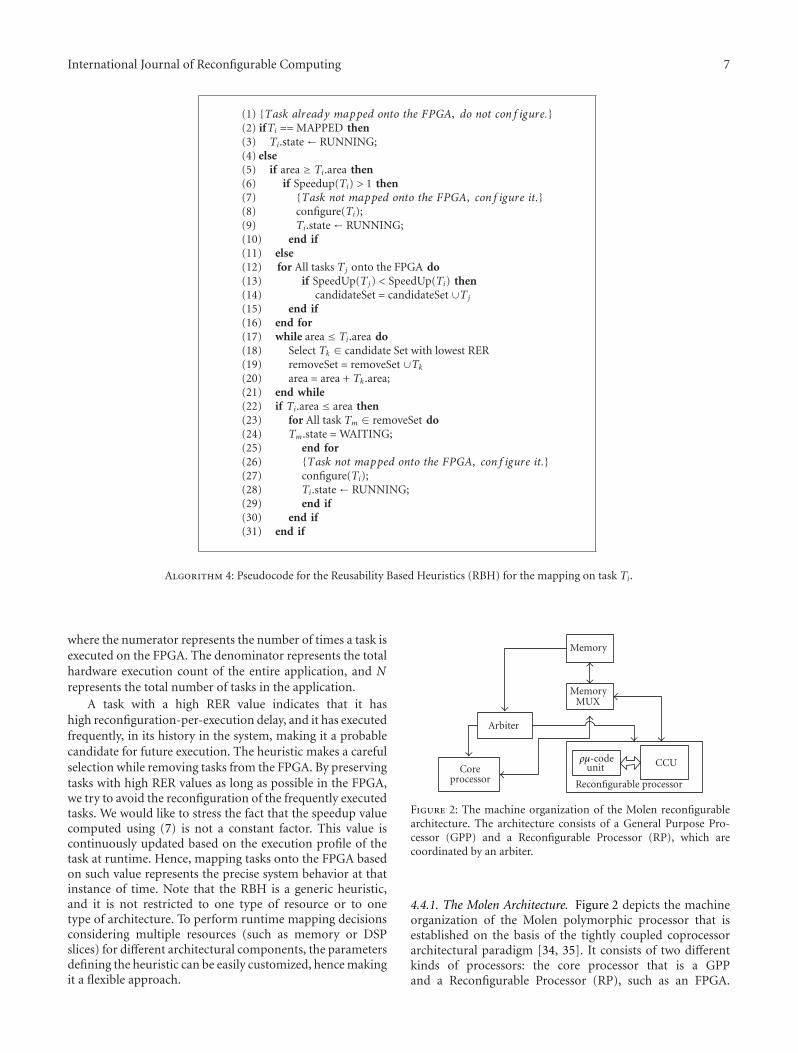
Algorithm 4: Pseudocode for the Reusability Based Heuristics (RBH) for the mapping on task Ti.
where the numerator represents the number of times a task isexecuted on the FPGA. The denominator represents the totalhardware execution count of the entire application, and Nrepresents the total number of tasks in the application.
A task with a high RER value indicates that it hashigh reconfiguration-per-execution delay, and it has executedfrequently, in its history in the system, making it a probablecandidate for future execution. The heuristic makes a carefulselection while removing tasks from the FPGA. By preservingtasks with high RER values as long as possible in the FPGA,we try to avoid the reconfiguration of the frequently executedtasks. We would like to stress the fact that the speedup valuecomputed using (7) is not a constant factor. This value iscontinuously updated based on the execution profile of thetask at runtime. Hence, mapping tasks onto the FPGA basedon such value represents the precise system behavior at thatinstance of time. Note that the RBH is a generic heuristic,and it is not restricted to one type of resource or to onetype of architecture. To perform runtime mapping decisionsconsidering multiple resources (such as memory or DSPslices) for different architectural components, the parametersdefining the heuristic can be easily customized, hence makingit a flexible approach.
Reconfigurable processor
Core processor
CCUρμ-codeunit
Memory
Arbiter
Memory MUX
Figure 2: The machine organization of the Molen reconfigurablearchitecture. The architecture consists of a General Purpose Pro-cessor (GPP) and a Reconfigurable Processor (RP), which arecoordinated by an arbiter.
4.4.1. The Molen Architecture. Figure 2 depicts the machineorganization of the Molen polymorphic processor that isestablished on the basis of the tightly coupled coprocessorarchitectural paradigm [34, 35]. It consists of two differentkinds of processors: the core processor that is a GPPand a Reconfigurable Processor (RP), such as an FPGA.

8 International Journal of Reconfigurable Computing
Video in
DCT2
DCT3
DCT4
Q1
Q2
Q3
Q4
VLE Video out
Init
DCT1
B CA D
F
E
MJPEG
APP1
APP2
APP3
A′ B′ C′ D′ E ′
F ′
A′′ B′′ C ′′ D′′ E ′′
F ′′
Figure 3: The Motion-JPEG (MJPEG) application model consid-ered for the case study. The MJPEG application is extended byinjecting sporadic applications in each frame.
The reconfigurable processor is further subdivided intothe reconfigurable microcode (ρμ-code) unit and a CustomComputing Unit (CCU). The CCU is executed on the FPGA,and it supports additional functionalities, which are notimplemented in the core processor. In order to speed up theprogram execution, parts of the code running on a GPP canbe implemented on one or more CCUs.
The GPP and the RP are connected to an arbiter. Thearbiter controls the coordination of the GPP and the RPby directing instructions to either of these processors. Thecode to be mapped onto the RP is annotated with specialpragma directives. When the arbiter receives the pragmainstruction for the RP, it initiates an “enable reconfigurableoperation” signal to the reconfigurable unit, gives the datamemory control to the RP, and drives the GPP into a waitingstate. When the arbiter receives an “end of reconfigurableoperation” signal, it releases the data memory control back tothe GPP and the GPP can resume its execution. An operationexecuted by the RP is divided into two distinct phases: setand execute. In the set phase, the CCU is configuredto perform the supported operations, and in the executephase the actual execution of the operation is performed. Thedecoupling of set and execute phase allows the set phaseto be scheduled well ahead of the execute phase and therebyhiding the reconfiguration latency.
4.4.2. The Application Model. We extend a Motion-JPEG(MJPEG) encoder application to use it as an applicationmodel for this case study. The corresponding KPN is shownin Figure 3. The frames are divided into blocks, and eachtask performs a different function on each block as itis passed from task to task. MJPEG operates on theseblocks (partially) in parallel. A random number (0 to 3) ofapplications (APP1 to APP3) is injected in each frame of theMJPEG application in order to create a dynamic application
Table 1: Available area (in slices) for different FPGAs from theXilinx Virtex4 FX family [36].
Hardware Area (slices)
XC4VFX12 5472
XC4VFX20 8544
XC4VFX40 18624
XC4VFX60 25280
XC4VFX100 42176
XC4VFX140 63168
behavior. These applications are considered as sporadic ones,which randomly appear in the system and compete withMJPEG for the resources. In this case study, we want toevaluate task mapping under different resource conditions;therefore we use only one application as a benchmark forcomparing different heuristics. Nevertheless, the rSesameframework allows to evaluate any number of applications,architectures, and task mapping heuristics.
4.4.3. Experimental Setup. As discussed before, for this casestudy, we consider a model instantiated from the rSesameframework for the Molen reconfigurable architecture. Themodel instantiated for this case study consists of 30 CCUsallowing each task to be mapped onto one CCU. Note thatthe number of CCUs is a parameter that can be definedbased on the number of pageable and HW tasks. For this casestudy, we consider all tasks as pageable to fully exploit theruntime mapping by deciding where and when to map themat runtime depending on the system condition. The modelallows dynamic partial reconfiguration and, therefore, if theFPGA cannot accommodate all tasks at once, the latter canbe executed after runtime reconfiguration.
We study and evaluate different task mapping heuris-tics from various domains by considering, for the samearchitecture model, different FPGA sizes. We considersix FPGAs from the Xilinx Virtex-4 FX family [36],namely, XC4VFX12, XC4VFX20, XC4VFX40, XC4VFX60,XC4VFX100, and XC4VFX140. These FPGAs have differentavailable area (slices) as shown in Table 1. As a result,they are used to evaluate the runtime task mapping underdifferent resource conditions. Note that, in this case study,we have used area as one dimensional space. Nevertheless,rSesame can evaluate any other types and numbers ofarchitectural parameter. We assume that the Processor LocalBus (PLB) of these FPGAs is 4 bytes wide, and the InternalConfiguration Access Port (ICAP) functions at 100 MHz;thus, its configuration speed is considered at 400 MB/sec[37].
We use estimated values of the computational latency,the area occupancy (on the FPGA), and the reconfigurationdelay for each CCU. The computational latency values for theGPP model are initialized using the estimates obtained fromliterature [38, 39] (non-Molen specific).
We estimated area occupancy for each process mappedonto the CCU using the Quipu model [40]. Quipu estab-lishes a relation between hardware and software, and it

International Journal of Reconfigurable Computing 9
5
6
Spee
dup
RBH CBH IBH AMAP STonly HWonly SWonlyRBH CBH IBH AMAP STonly HWonly SWonly
0
1
2
3
4
5
6
7
8
9
10
0
1
2
3
4
7
XC4VFX40 XC4VFX60 XC4VFX100 XC4VFX140XC4VFX12 XC4VFX20
FPGAs
Sim
ula
ted
exec
uti
on c
ycle
s (b
illio
ns)
Figure 4: Comparison of the different heuristics tested in the proposed case study under different FPGAs conditions in terms of simulatedexecution time with corresponding application speedup. The application performance is proportional to the FPGA size. HWonly mappinghas the best performance followed by RBH, AMAP, CBH, and IBH. STonly has the worst performance.
predicts FPGA resources from a C-level description of anapplication using Partial Least Squares Regression (PLSR)and Software Complexity Metrics (SCMs). Kahn processescontain functional C-code together with annotations thatgenerate events such as read, execute, and write. As a result,Quipu can estimate area occupancy of each Kahn process.Such estimations are accepted while exploring systems at veryearly design stages with rSesame. In later design stages, othermore refined models can be used to perform more accuratearchitectural explorations.
Based on the reconfiguration delay of each FPGA andthe estimated area of each Kahn process, we computedthe reconfiguration delay of each CCU using the followingequation:
TRecon = CCU slicesFPGA slices
· FPGA bitstreamICAP bandwidth
, (10)
where CCU slices is the total number of area slices a CCUrequires, FPGA slices is the total number of slices availableon a particular FPGA, FPGA bitstream is the bitstream sizein MBs of the FPGA, and ICAP bandwidth is the ICAPconfiguration speed. As a final remark, we assume that thereis no delay associated with the runtime mapping, such as taskmigration and context switching.
5. Heuristics Evaluation
In this section, we provide a detailed analysis of the experi-mental results and their implications for the aforementionedcase study. We conducted a wide variety of experimentson the above-mentioned task mapping heuristics withthe Molen architecture by considering various FPGAs ofdifferent sizes. We evaluated and compared these heuristicsbased on the following parameters:
(i) the execution time,
(ii) the number of reconfigurations,
(iii) the percentage of hardware/software executions,
(iv) the reusability efficiency.
The detailed description of these parameters has beenprovided in Section 3. In the rest of this section, we discussthe evaluation results by using these parameters in moredetail.
5.1. Execution Time. Figure 4 depicts the results of runningdifferent task mapping heuristics for mapping an extendedMJPEG application onto the Molen architecture with variousFPGAs of different sizes. The primary y-axis (left) in thegraph represents the application execution time measuredfor each heuristic. The software-only (SWonly) execution ismeasured when all the tasks are mapped onto the GPP. Sim-ilarly, the hardware-only (HWonly) execution is measuredwhen all the tasks are mapped onto the FPGA. In HWonly,tasks are forced to be executed on the FPGA. However, if thetask does not fit on the entire FPGA, the task is executedon the GPP. The static execution (STonly) is measuredwhen only design time exploration is performed. In STonlyexecution, a fixed set of hardware tasks is considered forthe FPGA mapping and this set does not change during theapplication runtime. For this experiment, tasks considered asfixed hardware are DCT1–DCT4 and Q1–Q4. The secondaryy-axis (right) in Figure 4 represents the application speedupfor each heuristic compared to the SWonly execution. The x-axis lists different types of FPGAs, which are ranked (fromleft to right) based on their sizes, such that XC4VFX12has the smallest number of area slices and XC4VFX140has the largest number of area slices (see Table 1). Severalobservations in terms of FPGA resources and speedup fordifferent heuristics can be made from Figure 4.
A first observation that can be noticed from Figure 4is that the application performance is proportional to theFPGA size to a certain degree: the bigger the available areain the FPGA, the higher the application performance. In thecase of XC4VFX12, there is no significant performance gain

10 International Journal of Reconfigurable Computing
Table 2: The performance increase in different heuristics withthe corresponding area increase in the FPGA. There is no linearrelation between the area and the corresponding performanceimprovement.
Heuristics
Performance increase (%)
XC4VFX12⇒XC4VFX20
XC4VFX100⇒XC4VFX140
(54% slice increase) (33% slice increase)
HWonly 67.9 3.14
STonly 0.69 0.007
AMAP 30 7.7
IBH 15 0.87
CBH 67 8.5
RBH 70 2.8
by using any heuristic compared to the software execution.As there is a limited area, only few tasks can be mapped ontothe FPGA; thus, performance is limited. Nevertheless, there isa notable performance improvement with the other FPGAs.
Secondly, while comparing the results of different heuris-tics for different FPGAs in Figure 4, we observe that thereis no linear relation between the FPGA area and the corre-sponding performance. For instance, although XC4VFX20has 54% more slices than XC4VFX12, the correspondingincrease in the application performance is 67.9%, in thecase of HWonly, as shown in Table 2. Similarly, there is 33%increase in area slices while comparing XC4VFX140 withXC4VFX100 in Table 1. Nevertheless, there is considerablylower increase in the performance in this case, as comparedto the former case. The performance increase associatedwith the corresponding area increase in XC4VFX12 andXC4VFX20 as compared to XC4VFX100, and XC4VFX140respectively, in case of different heuristics is reported inTable 2. The table depicts that there is no linear increase inthe performance with area increase. This becomes obviousas the performance increase in an application is bounded bythe degree of parallelism in that application. The use of moreresources does not always guarantee a better applicationperformance.
Another observation that can be made from Figure 4 isin terms of application performance of each heuristic. Asit can be seen from the figure, STonly has the worst appli-cation performance, and HWonly has the best applicationperformance. HWonly executes all tasks on the FPGA. As aresult, it has approximately up to 9 times better performancethan SWonly. STonly executes a fixed set of tasks on theFPGA, and mapping optimizations cannot be performed atruntime and, as a result, it has only upto 3 times betterperformance than SWonly. On the other hand, with runtimeheuristics such as AMAP, IBH, CBH, and RBH, the taskmapping is performed at runtime. When the applicationbehavior changes due to the arrival of a sporadic application,task mapping is optimized, and better performance can beobtained in latter cases. This can be clearly seen in the figure,
1
1.5
2
2.5
3
3.5
Spee
du
p
0
0.5
FPGAs
XC
4VFX
12
XC
4VFX
20
XC
4VFX
40
XC
4VFX
60
XC
4VFX
100
XC
4VFX
140
RBH-STonly
RBH-IBH
RBH-CBH
RBH-AMAP
RBH-HWonly
Figure 5: The performance increase of the RBH compared toHWonly, STonly, IBH, CBH, and AMAP. RBH performs betterthan AMAP under all resource conditions except XC4VFX12. RBHperforms better than STonly, IBH, and CBH under all resourceconditions.
where the performance of the other heuristics, such as RBH,CBH, IBH, and AMAP, are bounded by HWonly and STonly.
While comparing the application performance of RBHagainst the other heuristics, we observe that RBH pro-vides the best performance. RBH outperforms IBH underall resource conditions. RBH performs similar to CBHin the case of XC4VFX12, XC4VFX20, and XC4VFX40,while it performs better than CBH for the rest of theFPGAs. Task mapping is highly influenced by the taskselection criteria and the FPGA size. CBH chooses a taskwith the highest SW/HW latency difference and executesthat task in FPGA. RBH also maps tasks based on thespeedup factor, but the major difference is in the way thisvalue is calculated. RBH calculates the speedup value atruntime taking into account the past execution history,while with CBH, the SW/HW value is calculated statically.This difference significantly influences the performance ofthese heuristics. The performance increase of the RBH ascompared to HWonly, STonly, IBH, CBH, and AMAP isreported in Figure 5. As it can be inferred from the figure,the performance improvement of the RBH compared toAMAP shows an irregular behavior. The RBH performs10% worse than AMAP for XC4VFX12. However, theimprovement significantly increases for XC4VFX20. ForXC4VFX40, the improvement suddenly decreases to 10%.The improvement is regained for XC4VFX60 and staysidentical for XC4VFX100 and XC4VFX140. AMAP performstask mapping based on the area availability in an ad hocmanner, in the sense that it tries to map as many tasks aspossible at once. However, the RBH performs a selectivetask mapping based on the task speedup and the hardwareconfiguration reuse. When area is limited, as in the caseof XC4VFX12, not many hardware configurations can bepreserved in the FPGA. Thus, configuration reuse cannot
International Journal of Reconfigurable Computing 11
XC4VFX40
XC4VFX60
XC4VFX100
XC4VFX140
RBHCBH
IBH
AMAP
STonlyHWonly
XC4VFX12
XC4VFX20
Number of reconfigurations
FPG
As
0 4000 8000 12000 16000
Figure 6: Heuristics comparison under different FPGAs conditionsin terms of number of reconfigurations. There is a direct relationbetween the number of reconfigurations and the FPGA area.
be exploited with the RBH. As a result, AMAP performsbetter than RBH. With the increase in area, many hardwareconfigurations can be preserved in the FPGA. Consequently,the RBH performs better than AMAP.
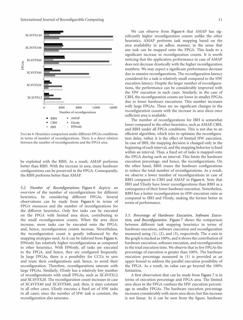
5.2. Number of Reconfigurations. Figure 6 depicts anoverview of the number of reconfigurations for differentheuristics, by considering different FPGAs. Severalobservations can be made from Figure 6 in terms ofFPGA resources and the number of reconfigurations forthe different heuristics. Only few tasks can be executedon the FPGA with limited area slices, contributing tothe small reconfiguration counts. When the area slicesincrease, more tasks can be executed onto the FPGA,and, hence, reconfiguration counts increase. Nevertheless,the reconfiguration count is greatly influenced by themapping strategies used. As it can be inferred from Figure 6,HWonly has relatively higher reconfigurations as comparedto other heuristics. With HWonly, all tasks are executedto the FPGA, and hence, they are configured frequently.In large FPGAs, there is a possibility for CCUs to saveand reuse their configurations and, hence, to avoid theirreconfiguration. Therefore, reconfigurations saturate withlarge FPGAs. Similarly, STonly has a relatively low numberof reconfigurations with small FPGAs, such as XC4VFX12and XC4VFX20. The reconfiguration count increases in caseof XC4VFX40 and XC4VFX60, and, then, it stays constantin all other cases. STonly executes a fixed set of HW tasksin all cases; since the number of HW task is constant, thereconfiguration also saturates.
We can observe from Figure 6 that AMAP has sig-nificantly higher reconfiguration counts unlike the otherheuristics. AMAP performs task mapping based on thearea availability in an adhoc manner, in the sense thatany task can be mapped onto the FPGA. This leads to asignificant increase in reconfiguration counts. It is worthnoticing that the application performance in case of AMAPdoes not decrease drastically with the higher reconfigurationnumbers. We may expect a significant performance decreasedue to massive reconfigurations. The reconfiguration latencyconsidered for a task is relatively small compared to the HWexecution latency. Despite the larger number of reconfigura-tions, the performance can be considerably improved withthe HW execution in such cases. Similarly, in the case ofCBH, the reconfiguration counts are lower in smaller FPGAsdue to lower hardware executions. This number increaseswith large FPGAs. There are no significant changes in thereconfiguration counts with the increase in area slices oncesufficient area is available.
The number of reconfigurations for IBH is somewhatlower compared to the other heuristics, such as AMAP, CBH,and RBH under all FPGA conditions. This is not due to anefficient algorithm, which tries to optimize the reconfigura-tion delay, rather it is the effect of limited HW execution.In case of IBH, the mapping decision is changed only in thebeginning of each interval, and the mapping behavior is fixedwithin an interval. Thus, a fixed set of tasks is mapped ontothe FPGA during such an interval. This limits the hardwareexecution percentage, and hence, the reconfigurations. Onthe other hand, RBH reuses the hardware configurationsto reduce the total number of reconfigurations. As a result,we observe a lower number of reconfigurations in case ofRBH compared to CBH and AMAP in Figure 6. Note thatIBH and STonly have lower reconfigurations than RBH as aconsequence of their lower hardware execution. Nonetheless,RBH has a better reconfiguration-to-HW-execution ratio ascompared to IBH and STonly, making the former better interms of performance.
5.3. Percentage of Hardware Execution, Software Execu-tion, and Reconfiguration. Figure 7 shows the comparisonbetween different task mapping heuristics in terms ofhardware execution, software execution and reconfigurationmeasured using (1), (2), and (3), respectively. The x-axis inthe graph is stacked as 100%, and it shows the contribution ofhardware execution, software execution, and reconfigurationto the total execution time. We observe that in few FPGAs thepercentage of execution is greater than 100%. The hardwareexecution percentage measured in (1) is provided as anupper bound to address the parallel execution possibility ofthe FPGA. As a result, its value can go beyond the 100%limitation.
A first observation that can be made from Figure 7 is interms of execution percentage and FPGA area. The limitedarea slices in the FPGA confines the HW execution percent-age in smaller FPGAs. The hardware execution percentageincreases considerably with more area slices, but this increaseis not linear. As it can be seen from the figure, hardware

12 International Journal of Reconfigurable Computing
XC4VFX20
XC4VFX40
XC4VFX60
XC4VFX100
XC4VFX140
FPG
As
0 20 40 60 80 100 120 140
XC4VFX12
Execution (HW/SW/reconfiguration) (%)
(a) HWonly
0 20 40 60 80 100 120
XC4VFX20
XC4VFX40
XC4VFX60
XC4VFX100
XC4VFX140
FPG
As
XC4VFX12
Execution (HW/SW/reconfiguration) (%)
(b) STonly
0 20 40 60 80 100 120 140
XC4VFX40
XC4VFX60
XC4VFX100
XC4VFX140
FPG
As
XC4VFX12
XC4VFX20
Execution (HW/SW/reconfiguration) (%)
(c) AMAP
XC4VFX20
XC4VFX40
XC4VFX60
XC4VFX100
XC4VFX140
FPG
As
0 50 100 150
XC4VFX12
Execution (HW/SW/reconfiguration) (%)
(d) IBH
0 50 100
XC4VFX20
XC4VFX40
XC4VFX60
XC4VFX100
XC4VFX140
FPG
As
XC4VFX12
Execution (HW/SW/reconfiguration) (%)
(e) CBH
0 20 40 60 80 100 120
XC4VFX20
XC4VFX40
XC4VFX60
XC4VFX100
XC4VFX140
FPG
As
XC4VFX12
Execution (HW/SW/reconfiguration) (%)
SW execution (%)
HW execution (%)
Reconfiguration (%)
(f) RBH
Figure 7: The comparison of different heuristics based on percentage of hardware execution, software execution, and reconfiguration. Thehardware execution percentage is low in smaller FPGAs, and it increases considerably with more area slices.
execution percentage somewhat saturates with large FPGAs,such as XC4FX100 and XC4FX140. This observation is validfor all the runtime mapping heuristics including STonly andHWonly.
With HWonly mapping, all tasks are forced to beexecuted to the FPGA. However, if the task does not fiton the entire FPGA, then the task is executed with theGPP. Therefore, in Figure 7, we observe certain percentageof software execution with small FPGAs, but, with largerFPGA, there is only HW execution and the correspondingreconfiguration. With smaller FPGAs, almost no tasks areexecuted in hardware and, as a result, STonly has veryminimal hardware execution (if any) and, therefore, theless reconfigurations. With the larger FPGAs, STonly hasa relatively good but constant hardware execution and
reconfiguration percentage, since it executes a fixed set oftasks on the FPGA.
While comparing the runtime heuristics, such as AMAP,CBH, IBH, and RBH, we can observe that AMAP hasthe best hardware execution percentage in larger FPGAs,followed by RBH and CBH. CBH and RBH somehow showsimilar behavior in terms of hardware execution percentage.However, in case of reconfiguration percentage, they do notfollow the same trend. The reconfiguration is somewhatlinear to the hardware execution in case of CBH. However,RBH does not show any linear increase in reconfigurationwith hardware execution. RBH performs task mappingbased on configuration reuse and, as a result, tries toavoid reconfiguration with more hardware executions. Thisbehavior of RBH heuristic is apparent in the figure, especially

International Journal of Reconfigurable Computing 13
3
4
5
6
7
8
9
2
3
4
5
6
Spee
dup
HWonly
STonly
AMAP
IBH
CBH
RBH
HWonly
STonly
AMAP
IBH
CBH
RBH
0
1
0
12
Tim
e-w
eigh
ted
area
usa
ge
FPGAs
XC4VFX12 XC4VFX20 XC4VFX40 XC4VFX60 XC4VFX100 XC4VFX140
Figure 8: The comparison of different heuristics in terms of time-weighted area usage against speedup under different FPGAs conditions.The HWonly has the most time-weighted area usage, followed by the other runtime heuristics AMAP, CBH, IBH, and RBH.
in the case of moderate to large FPGAs, such as XC4FX60,XC4FX100, and XC4FX140. IBH follows a behavior similarto STonly in terms of software and hardware execution, as italso executes a fixed set of tasks on the FPGA.
By mapping more tasks onto the FPGA, the applicationcan be accelerated, but it also has reconfiguration overhead.The efficiency of the mapping heuristics lies in finding thebest mapping while minimizing the number of reconfig-urations. Nevertheless, in Figure 7, we see almost a linearcontribution of the reconfiguration overhead to the totalexecution time in all heuristics, except in RBH. This phe-nomenon is highly influenced by the policy implemented fortask mapping. Another observation that can be made fromthe figure is the contribution of the hardware execution, SWexecution, and reconfiguration to the total execution time.The figure shows that the GPP executes most of the applica-tion and the FPGA computes only less than 40% of the totalapplication. This is due to the architectural restrictions of theMolen architecture. The GPP and the RP run in a mutualexclusive way, due to the processor/coprocessor nature of thearchitecture. This influences the mapping decision, which,in turn, contributes to the low hardware execution rates.This significantly increases the total execution time. Anotherreason for the lower percentage of hardware execution is dueto the lower hardware latency for each task. The executionpercentage is calculated as the ratio of execution latencyof all tasks to the total execution time of an application.The hardware latency is comparatively lower than the SWlatency for each task. Therefore, the corresponding hardwareexecution contribution is always lower compared to thepercentage of SW execution.
5.4. Time-Weighted Area Usage. Figure 8 depicts an averagetime-weighted area usage measured using Equation (4) for
different heuristics under different FPGA devices. The pri-mary y-axis (left) in the graph represents the time-weightedarea usage measured for each heuristic. The secondary y-axis(right) in the figure represents the application speedup foreach heuristic compared to the SWonly execution. Severalobservations can be made from Figure 8 in terms of FPGAresources and time-weighted area usage of different heuris-tics. The first observation that can be made from the figureis in terms of time-weighted area usage and the hardwareresource. As it can be seen from the figure, the time-weightedarea usage is directly impacted by the number of area slicesin the FPGA. With the limited area slices in small FPGAs,few tasks are executed in the FPGA, contributing to a smallernumber of hardware executions. This, in turn, contributesto the lower area usage. With sufficient area slices, there isa considerable number of hardware executions and, hence,the area usage is high. Nonetheless, there is no linear relationbetween the time-weighted area usage and the availableFPGA area. In XC4VFX140, the area usage is relatively lowcompared to XC4FX100, despite the fact that area slices aregreater in the former. The area usage measured is the time-weighted factor, and it depends on the hardware execution,the total FPGA area and the total execution time, as shownin Equation (4). The increase in the area slices, with nosignificant increase in hardware executions, contributes tothe lower area usage in the former case.
As it can be inferred from Figure 8, HWonly has thehighest time-weighted area usage under all FPGA conditions.HWonly executes all tasks onto the FPGA and, as a result,the cost of using FPGA in this case is higher than allthe other heuristics. STonly, however, has the lowest areausage due to its lower number of hardware executionsand, therefore, its corresponding performance is also verypoor. Similarly, AMAP has higher area usage compared to

14 International Journal of Reconfigurable Computing
other heuristics, such as CBH, IBH, and RBH, under allFPGA conditions, except XC4VFX60. AMAP performs taskmapping based on area availability. As a matter of fact,it has a relatively higher number of hardware executionscompared to the other heuristics and, therefore, it consumesadditional area. RBH, on the other hand, has less time-weighted area usage. While comparing AMAP and RBH, wecan observe that RBH performs somewhat better than AMAPin terms of performance. This implies that RBH reuses thehardware configuration already present in the FPGA to avoidreconfiguration overhead and, as a result, it can give betterperformance with the same amount of hardware resourcesas required by AMAP. Likewise, CBH has a comparablepercentage of time-weighted area usage, but it lags behind interms of speedup as compared to RBH. However, IBH hasa considerably low percentage of area usage, as it also haslower hardware executions due to the constantly executedHW task set, and hence it also has lower performance. Wecan summarize that HWonly has the best performance butconsumes more hardware resources. STonly has the lowestarea usage but straggles behind in terms of performance.A tradeoff in terms of performance and resources can beobtained with task mapping at runtime, which performsselective task mapping onto the FPGA at runtime.
Another compelling observation that can be made fromFigure 8 is about the lower value of the time-weightedarea usage. The Molen architecture is based on proces-sor/coprocessor paradigm. As a result, the GPP and theRP run in a mutual exclusive. This contributes to thelower number of hardware executions, which consequentlyincreases the total execution time. Thus, these two factorssignificantly contribute to the low value of area usage. Thearea usage can be increased either by mapping more tasksonto the FPGA or by operating the RP and the GPP inparallel.
5.5. Reusability Efficiency. Figure 9 depicts the reusabilityefficiency (RETask) recorded for all CCUs using Equation(5) for different heuristics under different FPGA conditions.Several observations can be made from the figure in terms ofFPGA area and the RETask of each CCU. Firstly, we observethat the CCU reuse is significantly affected by the number ofarea slices in the FPGA. Small FPGAs, such as XC4VFX12 andXC4VFX20, have many CCUs with RETask value zero. A CCUhas an RETask value of zero under the following conditions:
(i) when a CCU is always mapped onto the GPP
(ii) when a CCU is configured every time it is executedon the FPGA.
With few resources in the FPGA, only a limited numberof tasks can be executed to the FPGA. Additionally, insuch cases, hardware configurations cannot be preserved forfuture reuse. As a result, CCUs have an RETask value of zero.Moreover, in this case, CCUs that are reused have a verysmall size in terms of area. With the increase in numberof slices in the FPGA, more CCUs are reused. Medium-sized FPGAs, such as XC4VFX40 and XC4VFX60, reuse moreCCUs compared to smaller FPGAs, but, in such cases, the
reuse percentage is still low. With the larger FPGAs such asXC4VFX100 and XC4VFX140, more CCUs are reused withlarge RETask value.
As it can be inferred from Figure 9, HWonly has the bestRETask for many CCUs in large FPGAs, such as XC4VFX100and XC4VFX140. HWonly executes all the tasks on theFPGA and, as a result, it has high hardware execution count.However, with small FPGAs, all the tasks are configured, dueto area restrictions, and there is no configuration reuse. Onthe other hand, with larger FPGAs, more configurations aresaved and reused and, as a consequence, many CCUs have aconsiderably high RETask value. Similarly, STonly always mapsa set of fixed tasks onto the FPGA. Out of these tasks, only afew number of small tasks can be reused. We notice that theseCCUs have a relatively higher RE value compared to the onesreused with the AMAP heuristic in the figure. AMAP hashigher HW execution percentage as compared to IBH andCBH. As a matter of fact, many tasks are reused in case ofAMAP, but the reuse percentage of these CCUs is low. AMAPhas no fixed pattern for task execution and, as a result, anytask can be executed in FPGA. Therefore, the reusability israther distributed among many CCUs. CBH, on the otherhand, follows a specific policy for task execution in FPGAand hence executes a fixed set of selected task. As a result, aset of selected tasks is reused. Similar behavior is observedin the case of CBH. As it also executes a set of specific taskwithin an interval, same tasks are reused (if any).
Likewise, from Figure 9, we observe that the RETask ofRBH is better than that of other runtime heuristics for manyCCUs. The impact of this hardware configuration reuse, incase of RBH, can be directly seen in terms of performancegain in Figure 4, where RBH has better speedup than theother heuristics. From Figure 10, we also observe that, forfew tasks, RETask decreases when FPGA resources increase.With larger FPGAs, more tasks can fit onto the FPGA. As aresult, these tasks are also mapped onto the FPGA, thus, overwriting the saved configurations of other tasks. RETask for fewtasks decreases in the FPGAs with moderate size. With theabundant resources, the hardware configuration can be savedfor more tasks, and RETask increases again.
Note that STonly, AMAP, CBH, and IBH do not mapthe task based on the hardware configuration reuse. Thereuse obtained in the case of STonly, AMAP, CBH, andIBH is a default value determined based on the arrival ofthe application task. If a CCU is already configured on theFPGA when its corresponding task arrives, the task can beexecuted without reconfiguration. However, the RBH reusesmore hardware configurations than the other heuristics ontop of the default value obtained.
Figure 10 depicts the total REapp recorded using Equation(6) for different heuristics under different resource condi-tions. In the figure, we again observe that the reusabilityincreases when using larger FPGAs. HWonly executes allthe tasks in FPGA and, therefore, there can be a possibilitythat many of these tasks are reused when sufficient area isavailable, resulting into higher REapp. STonly has almost aconstant REapp in larger FPGA, since it executes a constantset of tasks in FPGA. While comparing runtime heuristics,such as AMAP, CBH, IBH, and RBH, we can observe that

International Journal of Reconfigurable Computing 15
0
50
100XC4VFX12
HWonly
STonly
AMAP
IBH
CBH
RBH
0
50
100XC4VFX20
0
50
100XC4VFX40
0
50
100XC4VFX60
0
50
100XC4VFX100
0
50
100
CC
U0
CC
U1
CC
U2
CC
U3
CC
U4
CC
U5
CC
U6
CC
U7
CC
U8
CC
U9
CC
U10
CC
U11
CC
U12
CC
U13
CC
U14
CC
U15
CC
U16
CC
U17
CC
U18
CC
U19
CC
U20
CC
U21
CC
U22
CC
U23
CC
U24
CC
U25
CC
U26
CC
U27
CC
U28
CC
U29
XC4VFX140
Figure 9: Reusability efficiency (RETask) of CCUs for different heuristics under different FPGA conditions. The CCU reuse is significantlyaffected by the number of area slices in the FPGA.
since the RBH has more CCUs reused than other heuristics,as shown in Figure 7(f), RBH has a better REapp value thanother heuristics in all resource conditions but XC4VFX12.Since XC4VFX12 has less area, all the heuristics have approx-imately the same value for REapp. REapp is the accumulationof the time saved due to hardware configuration reuse of eachCCU. If all CCUs obtain the same value of the RE for a taskmapping heuristic, then the application REapp depends onthe corresponding total execution time of that heuristics.
6. Observations and Conclusions
In this paper, we evaluated the task mapping of application(s)onto reconfigurable architectures under different resourceconditions. We thoroughly evaluated various task mappingheuristics from the state of the art with the rSesameframework for a reconfigurable architecture with differentFPGA resources using an extended MJPEG application.Based on the evaluation discussed in the previous sections,we can summarize the following conclusions.
(i) The comparison of different FPGAs shows that withvery limited resources (in case of small FPGAs), the

16 International Journal of Reconfigurable Computing
3210
Reusability efficiency (%)
XC4VFX40
XC4VFX60
XC4VFX100
XC4VFX140
XC4VFX12
XC4VFX20
FPG
As
RBHCBHIBH
AMAP
STonlyHWonly
Figure 10: Heuristics comparison under different FPGAs condi-tions in terms of application reusability efficiency (REapp). RBH hasbetter REapp compared to other heuristics.
number of tasks that can be mapped onto the FPGAis low. Consequently, these tasks are mapped onto theGPP. This leads to a poor application performance.
(ii) More resources (in case of moderate/higher FPGAs)imply more tasks mapped onto the FPGA. Con-sequently, we can obtain better application perfor-mance.
(iii) Runtime mapping provides better performance incase of dynamic application/architecture conditions.If the application behavior is well known in advance,design time mapping can give equal performance.
(iv) Mapping all the tasks onto the FPGA gives better per-formance, but it consumes more hardware resources.Runtime mapping performs task mapping based onthe runtime system conditions. As a matter of fact,with the runtime mapping, a tradeoff can be obtainedin terms of performance and resources.
(v) Comparing different heuristics, in case of limitedresources conditions (small FPGAs), the adhoc taskmapping of AMAP performs better compared toCBH, IBH, and RBH. Due to limited resources, thecareful task selection with RBH, CHB, and IBHcannot be fully exploited in such cases.
(vi) The reuse of hardware configurations is better in caseof sufficient resource conditions (medium-to-largeFPGAs). As a result, the configuration reuse can be
well exploited. Additionally, the RBH provides betterapplication performance than AMAP and CBH.
(vii) In case of abundant resource conditions (very largeFPGAs), the performance saturates due to appli-cation constraints. Under such scenarios, all theheuristics have similar performances.
Acknowledgments
This research is partially supported by Artemisia iFESTProject (Grant 100203), Artemisia SMECY (Grant 100230),FP7 Reflect (Grant 248976).
References
[1] K. Compton and S. Hauck, “Reconfigurable computing: asurvey of systems and software,” ACM Computing Surveys, vol.34, no. 2, pp. 171–210, 2002.
[2] T. J. Todman, G. A. Constantinides, S. J. E. Wilton, O.Mencer, W. Luk, and P. Y. K. Cheung, “Reconfigurable com-puting: architectures and design methods,” IEE Proceedings—Computers and Digital Techniques, vol. 152, no. 2, pp. 193–207.
[3] S. Hauck, “The roles of FPGA’s in reprogrammable systems,”Proceedings of the IEEE, vol. 86, no. 4, pp. 615–638, 1998.
[4] R. J. F. Stephen, D. Brown, and J. Rose, Field-ProgrammableGate Arrays, vol. 180 of The Springer International Series inEngineering and Computer Science, Kluwer Academic Publish-ers, 1992.
[5] Xilinx Corporation, Coolrunner-II CPLDs Family Overview,September 2008.
[6] R. W. Hartenstein and R. Kress, “A datapath synthesis systemfor thereconfigurable datapath architecture,” in Proceedings ofthe Asia andSouth Pacific Design Automation Conference (ASP-DAC ’95), pp. 479–484, September 1995.
[7] S. Vassiliadis and D. Soudris, Fine- and Coarse-Grain Reconfig-urable Computing, vol. 16, Springer, Berlin, Germany, 2007.
[8] N. S. Voros and and K. Masselos, System-Level Design ofReconfigurable Systems-on-Chip, Springer, Berlin, Germany,1st edition, 2005.
[9] K. Sigdel, M. Thompson, C. Galuzzi, A. D. Pimentel, and K.Bertels, “rSesame —a generic system-level runtime simulationframework for reconfigurable architectures,” in Proceedings ofthe International Conference on Field-Programmable Technol-ogy (FPT ’09), pp. 460–464, 2009.
[10] K. Sigdel, M. Thompson, C. Galuzzi, A. D. Pimentel, andK. Bertels, “Evaluation of runtime task mapping heuristicswith rSesame—a case study,” in Proceedings of the Design,Automation and Test in Europe Conference and Exhibition(DATE ’10), pp. 831–836, deu, March 2010.
[11] K. Sigdel, C. Galuzzi, K. Bertels, M. Thompson, and A. D.Pimentel, “Runtime task mapping based on hardware config-uration reuse,” in Proceedingsof the International Conference onReconfigurable Computing and FPGAs (ReConFig ’10), pp. 25–30, 2010.
[12] P. V. Knudsen and J. Madsen, “PACE: a dynamic programmingalgorithm for hardware/software partitioning,” in Proceedingsof the 4th International Workshop on Hardware/Software Co-Design (Codes/CASHE ’96), pp. 85–92, March 1996.
[13] M. Kaul and R. Vemuri, “Design-space exploration for block-processing based temporal partitioning of run-time reconfig-urable systems,” Journal of VLSI Signal Processing Systems for
International Journal of Reconfigurable Computing 17
Signal, Image, and Video Technology, vol. 24, no. 2, pp. 181–209, 2000.
[14] B. Miramond and J. M. Delosme, “Design space explorationfor dynamically reconflgurable architectures,” in Proceedingsof the Design, Automation and Test in Europe (DATE ’05), pp.366–371, March 2005.
[15] B. Miramond and J. M. Delosme, “Decision guide environ-ment for design space exploration,” in Proceedings of the 10thIEEE International Conference on Emerging Technologies andFactory Automation (ETFA ’05), pp. 881–888, September 2005.
[16] L. Y. Li and M. Shi, “Software-hardware partitioning strategyusing hybrid genetic and Tabu search,” in Proceedings of theInternational Conference on Computer Science and SoftwareEngineering (CSSE ’08), vol. 4, pp. 83–86, 2008.
[17] B. Mei, P. Schaumont, and S. Vernalde, “A hardware-softwarepartitioning and scheduling algorithm for dynamically recon-figurable embedded systems,” in Proceedings of the AnnualWorkshop on Circuits, Systemsand Signal Processing (ProRISC’00), pp. 1–8, November 2000.
[18] C. Haubelt, S. Otto, C. Grabbe, and J. Teich, “A system-levelapproachto hardware reconfigurable systems,” in Proceedingsof the Asia and South Pacific Design Automation Conference(ASP-DAC ’05), pp. 298–301, 2005.
[19] G. Wang, W. Gong, and R. Kastner, “Application partitioningon programmable platforms using the ant colony optimiza-tion,” Embedded Computing, vol. 2, no. 1, pp. 119–136, 2006.
[20] G. Still, R. Lysecky, and F. Vahid, “Dynamic hardware/softwarepartitioning: a first approach,” in Proceedings of the DesignAutomationConference (DAC ’03), 2003.
[21] V. Nollet, P. Avasare, H. Eeckhaut, D. Verkest, and H.Corporaal, “Run-time management of a MPSoC containingFPGA fabric tiles,” IEEE Transactions on Very Large ScaleIntegration (VLSI) Systems, vol. 16, no. 1, pp. 24–33, 2008.
[22] C. Huang and F. Vahid, “Dynamic coprocessor managementfor FPGA-enhanced compute platforms,” in Proceedings ofthe International Conference on Compilers, Architecture andSynthesis for Embedded Systems (CASES ’08), pp. 71–78, 2008.
[23] W. Fu and K. Compton, “An execution environment forreconfigurable computing,” in Proceedings of the 13th AnnualIEEE Symposium on Field-Programmable Custom ComputingMachines (FCCM ’05), pp. 149–158, April 2005.
[24] F. Ghaffari, M. Auguin, M. Abid, and M. B. Jemaa, “Dynamicand on-line design space exploration for reconfigurablearchitectures,” Transactions on High-Performance EmbeddedArchitectures and Compilers, vol. 4050, pp. 179–193, 2007.
[25] A. Kumar, B. Mesman, B. Theelen, H. Corporaal, and H.Yajun, “Resource manager for non-preemptive heteroge-neous multiprocessor system-on-chip,” in Proceedings of theIEEE/ACM/IFIP Workshop on Embedded Systems for Real TimeMultimedia (ESTIMEDIA ’06), pp. 33–38, October 2006.
[26] O. Moreira, J. J. D. Mol, and M. Bekooij, “Online resourcemanagement in a multiprocessor with a network-on-chip,”in Proceedings of the ACM Symposium on Applied Computing(SAC ’07), pp. 1557–1564, March 2007.
[27] L. T. Smit, J. L. Hurink, and G. J. M. Smit, “Run-time mappingof applications to a heterogeneous SoC,” in Proceedings of theInternational Symposium on System-on-Chip (SoC ’05), pp. 78–81, November 2005.
[28] L. T. Smit, G. J. M. Smit, J. L. Hurink, H. Broersma,D. Paulusma, and P. T. Wolkotte, “Run-time mapping ofapplications to a heterogeneous reconfigurable tiled systemon chip architecture,” in Proceedings of the IEEE InternationalConference on Field-Programmable Technology (FPT ’04), pp.
421–424, December 2004.[29] P. K. F. Holzenspies, G. J. M. Smit, and J. Kuper, “Mapping
streaming applications on a reconfigurable MPSoC platformat run-time,” in Proceedings of the International Symposium onSystem-on-Chip (SOC ’07), pp. 74–77, November 2007.
[30] M. A. A. Faruque, R. Krist, and J. Henkel, “ADAM: run-time agent-based distributed application mapping for on-chipcommunication,” in Proceedings of the 45th Design AutomationConference (DAC ’08), pp. 760–765, June 2008.
[31] C. Ykman-Couvreur, E. Brockmeyer, V. Nollet, T. Marescaux,F. Catthoor, and H. Corporaal, “Design-time applicationexploration for MPSoC customized runtime management,”in Proceesings of InternationalSymposium on System-on-Chip(SOC ’05), pp. 66–69, 2005.
[32] A. D. Pimentel, C. Erbas, and S. Polstra, “A systematicapproach to exploring embedded system architectures atmultiple abstraction levels,” IEEE Transactions on Computers,vol. 55, no. 2, pp. 99–111, 2006.
[33] G. Kahn, “The semantics of a simple language for parallelprogramming,” in Proceedings of the IFIP Congress, vol. 74,1974.
[34] S. Vassiliadis, S. Wong, G. N. Gaydadjiev, K. L. M. Bertels, G.Kuzmanov, and E. M. Panainte, “The MOLEN polymorphicprocessor,” IEEE Transactions on Computers, vol. 53, no. 11,pp. 1363–1375, 2004.
[35] S. Vassiliadis, G. N. Gaydadjiev, K. Bertels, and E. M. Panainte,“The Molen programming paradigm,” in Proceeding of theInternational workshopon Systems, Architectures, Modeling andSimulation (SAMOS ’03), pp. 1–30, July 2003.
[36] Xilinx Corporation, “Virtex-4 family overview (V3.0)”.[37] Xilinx DS86, “LogiCORE IP XPS HWICAP (v5.00a),” 2010.[38] H. Nikolov, M. Thompson, T. Stefanov et al., “Daedalus:
toward composable multimedia MPSoC design,” in Proceed-ings of the 45th annual Design Automation Conference (DAC’08), pp. 574–579, 2008.
[39] A. D. Pimentel, M. Thompson, S. Polstra, and C. Erbas,“Calibration of abstract performance models for system-leveldesign space exploration,” Journal of Signal Processing Systems,vol. 50, no. 2, pp. 99–114, 2008.
[40] R. Meeuws, Y. Yankova, K. Bertels, G. Gaydadjiev, andS. Vassiliadis, “A quantitative prediction model for hard-ware/software partitioning,” in Proceedings of the InternationalConference on Field Programmable Logic and Applications (FPL’07), pp. 735–739, August 2007.

Hindawi Publishing CorporationInternational Journal of Reconfigurable ComputingVolume 2012, Article ID 168961, 13 pagesdoi:10.1155/2012/168961
Research Article
Implementation of Ring-Oscillators-Based Physical UnclonableFunctions with Independent Bits in the Response
Florent Bernard, Viktor Fischer, Crina Costea, and Robert Fouquet
Laboratoire Hubert Curien, CNRS, UMR5516, Universite de Lyon, 42000 Saint-Etienne, France
Correspondence should be addressed to Florent Bernard, [email protected]
Received 1 May 2011; Revised 21 September 2011; Accepted 14 January 2012
Academic Editor: Kris Gaj
Copyright © 2012 Florent Bernard et al. This is an open access article distributed under the Creative Commons AttributionLicense, which permits unrestricted use, distribution, and reproduction in any medium, provided the original work is properlycited.
The paper analyzes and proposes some enhancements of Ring-Oscillators-based Physical Unclonable Functions (PUFs). PUFs areused to extract a unique signature of an integrated circuit in order to authenticate a device and/or to generate a key. We show thatdesigners of RO PUFs implemented in FPGAs need a precise control of placement and routing and an appropriate selection ofROs pairs to get independent bits in the PUF response. We provide a method to identify which comparisons are suitable whenselecting pairs of ROs. Dealing with power consumption, we propose a simple improvement that reduces the consumption of thePUF published by Suh et al. in 2007 by up to 96.6%. Last but not least, we point out that ring oscillators significantly influence oneanother and can even be locked. This questions the reliability of the PUF and should be taken into account during the design.
1. Introduction
Security in integrated circuits (ICs) became a very importantproblem due to high information security requirements.In order to assure authenticity and confidentiality, crypto-graphic keys are used to encrypt the information. Severalsolutions were proposed for key generation, each with theirupsides and downsides.
Confidential keys can be generated using True Ran-dom Number Generators (TRNGs) and stored in volatileor nonvolatile memories. Saving the confidential key ina nonvolatile memory inside the device ensures that thekey will never be lost and that it will not be disclosedin case of passive attacks. On the other hand, nonvolatilememories are easy targets for invasive attacks [1]. Volatilememories are typical for Field Programmable Gate Arrays(FPGAs). Storing the confidential key in a volatile memorypermits to erase the memory contents in case of invasiveattack detection. This implies the use of a communicationchannel to transmit the key after device configuration [1].Communication channels are usually easy to corrupt andinformation can be easily intercepted. The confidentialityand authenticity of designs are therefore compromised.
A solution is backing up the embedded volatile memoryblock with a battery. However, it was proved that battery-backed RAMs content can be read after a long period ofstorage [2–5] even if the memory is not powered any more.Thus, the need of generating secret keys inside the IC becameobvious.
An alternative to TRNG for key generation is the PhysicalUnclonable Function (PUF). PUFs are functions that extracta unique signature of an IC, based on randomness during themanufacturing process. This signature can be used as device-dependent key or device identification code. The mainadvantage of this principle introduced by Pappu et al. in[6, 7] is the fact that the key does not need to be storedin the device and it is thus harder to disclose. Based onintrinsic physical characteristics of circuits obtained duringthe manufacturing process, the extracted signature is impos-sible to reproduce by a different IC or by an attacker. PUFswork on challenge-response pairs. The challenge is usually astimulus sent from outside the device, and the response is thesignature of the circuit.
The quality of a PUF is determined mainly by its unique-ness and its reliability. To quantify these properties of aPUF, two types of response variations: intra- (for reliability)
2 International Journal of Reconfigurable Computing
and inter- (for uniqueness) chip variations [8] are used.The intrachip variation refers to the responses of the samePUF (the same device) at the same challenge, regardlessof environmental changes (e.g., temperature, voltage). Inthe ideal case, this variation should be 0. This meansthat the response of the PUF for a given challenge shouldalways be the same. The intrachip variation measures thereproducibility of the response. The function must be able toreproduce the same response over and over again, especiallyin the case of reconfigurable devices.
The interchip variation refers to the responses of differentPUFs (different devices) at the same challenge. Ideally, thisvariation should be of 50%, meaning that every bit is equallylikely to be zero or one. If this variation is close to 50% thenthe uniqueness of the responses is guaranteed.
In this paper, we focus on PUF implementation issues inreconfigurable devices and on the independency of bits inthe response. Reconfigurable devices are intensively used forimplementing cryptographic algorithms on hardware due tothe “reconfigurable” property of such circuits. Thus we haveto deal with two objectives: to keep the reconfigurable prop-erty of FPGAs and to guarantee the uniqueness and reliabilityof a PUF. In other words, if the PUF response changes whenthe device is reconfigured, the uniqueness and reliabilityof a PUF are questionable. We analyze and propose someenhancements of the concept introduced in 2007 by Suhand Devadas [8]. This principle is a ring-oscillators-basedPUF (RO-PUF). It was chosen for our experiments becauseit is one of the most suitable for implementation in FPGAs,independently from the technology. The PUF uses a relativelyhigh number of ring oscillators in order to emphasize theintrinsic characteristics of ICs and extract the signature. Theprinciple is based on the fact that the frequency of ROsdepends on gate and routing delays determined partially inan uncontrolled way by the manufacturing process.
In the first part of our work, we had to deal withimplementation issues related to the mapping of the PUF tovarious FPGA technologies. We found out that, contrary towhat original authors stated [8], the placement and routingconstraints play a very important role (even when ROs areidentically laid out) in the design of the function, especiallyif one wants to obtain sufficient inter-chip variability. Theprecise control of the initial phase of ROs and careful designof frequency comparators is another important issue thatdetermines the precision of the function and thus reducesintrachip variations. This was not discussed before. Further-more, in the response there are bits that are dependent oneach others. We propose a method justified by mathematicalmeans in order to identify which pairs of ROs we have toselect to ensure independency of bits in the response. Themain disadvantage of the original design is the high powerconsumption. We propose a simple modification enablingsignificant power economy. Finally, during our experimentswe observed a very important phenomenon that has asignificant impact on the generated results and that wascompletely neglected in the original design: the existence ofa mutual dependence between the ROs can lead sometimesto their mutual locking in FPGAs. It is essential to take intoaccount this unavoidable behavior of ROs in the PUF design.
The paper is organized as follows. In Section 2 we presentrelated work on PUFs implementation and metrics used tomeasure the quality of a PUF. Section 3 deals with PUFdesign issues and with the first problem stated: the needof manual placement and routing of the design. Then weremark that some bits in the response might be dependentdue to an inappropriate selection of ROs. An exampleof such a situation and a model of RO pair selection isproposed in Section 4 and a method to identify pairs that willgive independent bit in the response is provided. Section 5presents results of implementation of the RO PUF in mainFPGA technologies and analyzes the quality of the PUF inrelationship to the selected technology and the quality of theevaluation board. It also evaluates the impact of the mutualdependence of rings on the reliability of the PUF. Section 6proposes some important enhancement of the function andfinally, Section 7 concludes the paper.
2. PUF Background
2.1. Source of Noise in Electronic Devices. From its man-ufacturing to its usage, an electronic device is faced withmany sources of noise coming from different processes andhaving different signification from one to another. We candistinguish at least three classes of sources of randomness.
(i) In manufacturing process: this noise is due tovariation in the silicon layers during the manufac-turing process. Once the device is manufactured, itcontains these informations which are specific to eachintegrated circuit. An ideal PUF should be built toextract the maximum amount of this manufacturingnoise in order to identify a circuit.
(ii) Local noise: this noise appears when the circuit isworking. It is due to the random thermal motion ofcharge carriers. This noise is very suitable for randomnumber generation but inappropriate for PUF. Itshould be reduced compared to manufacturing noiseto decrease the intrachip variation.
(iii) Global environmental noise: this noise comes fromenvironmental condition (e.g., global temperatureand voltage) when the circuit is working. This noisecan disrupt the PUF response and increase theintrachip variation making a circuit identificationmore difficult to perform. Furthermore, this sourceof noise can be easily manipulated from outside.Therefore, PUFs must be developed in order toreduce the influence of this global environmentalnoise.
2.2. Related Works and PUF Evaluation. Several conceptsof PUF and implementation in reconfigurable devices havealready been introduced until now. In [9], the randominitialization of SRAM cells in FPGAs is used to generate aspecific signature. But in recent FPGAs, manufacturers tendto initialize SRAM cells to a known value that make SRAMcells-based PUF difficult to use. A similar idea is used onFPGA flip-flops and is based on their initial unstable states
International Journal of Reconfigurable Computing 3
[10]. Other PUFs are based on differences in the siliconlayers of the device leading to differences between delaypaths [8, 11, 12]. The main difficulty in these last designsis to guarantee a perfect symmetry on delay paths in orderto exploit the slight differences due to the manufacturingprocess. Furthermore the placement and routing must bedone carefully to exploit the noise due to manufacturingprocess.
In most of these PUFs, delay paths are implemented withROs (RO-PUFs). In [13], a new approach is studied in orderto use RO-PUF. The so-called Compensation Method permitsto reduce the influence of unsuitable source of noise on thePUF response. It is realized with Configurable ROs (CROs).One disadvantage pointed by the authors is the reductionof the maximum number of independent bits that can beextracted from such a PUF leading to an increase in thenumber of ROs that should be used.
As mentioned in introduction, PUF quality is evaluatedby its uniqueness and its reliability. In [13], authors proposedtwo metrics. These metrics cannot directly give the charac-terization of interdie variation process which can only beestimated based on PUF responses. Thus it depends greatlyon how the PUF is implemented to extract the maximumamount of manufacturing noise.
Let (i, j) be a pair of chips with i /= j and Ri (resp., Rj) then-bit response of chip i (resp., chip j). The first metric is theaverage interdie Hamming Distance (HD) among a group ofk chips and is defined as
Inter− dHD(k) = 2k(k − 1)
k−1∑i=1
k∑j=i+1
HD(Ri,Rj
)n
× 100%.
(1)
This distance should converge to 50% in the case of anideal PUF.
The second metric introduced by the authors of [13] isused to ensure the reliability of a PUF. An n-bits response isextracted from chip i (Ri) at normal operating conditions.Then at a different operating condition (different temper-ature or different voltage), x samples (R′i,y)y∈{1,...,x} of theresponse of the same PUF at this operating conditions areextracted. The average intradie HD over x samples for thechip i is defined as
Intra− dHD(x, i) = 1x
x∑y=1
HD(Ri,R′i,y
)n
× 100%. (2)
This distance should be close to 0% to ensure reliableresponses from the PUF in a given chip at various operatingconditions.
In [14], a deeper analysis on a special PUF (the ArbiterPUF that was originally proposed in [12]) evaluation leadthe author to consider 4 indicators on the evaluation ofthe intrachip variation (randomness, steadiness, correctness,and diffuseness). For the inter-chip variation the metric usedis also the uniqueness (expressed differently than in [13]).Even if measurements of uniqueness and reliability seemsufficient to qualify a PUF, it can be interesting to go further
(especially in the case of an unexpected high intrachip vari-ation).
3. PUF Design Issues
3.1. Principle of the PUF and Its Implementation in FPGA.In the principle of the PUF published in [8] that wasselected for our experiments, N identically laid-out ROs areplaced on the IC. Slight differences between their frequencieswill appear because of the unavoidable differences in thesilicon layers of the semiconductor device caused by themanufacturing process. Pairs of oscillators are chosen oneafter another and their frequencies compared. The responseof the PUF is equal to 1 if the first RO is faster and 0otherwise.
The RO PUF in Figure 1, as not many details were givenby the authors in [8], is realized using 32 ROs controlledby an enable signal for all selected technologies (ALTERA,XILINX, and ACTEL). Two counters are used to definethe winner of the race by counting N periods of the twogenerated clock signals: if one of the two counters (thewinner of the race) reaches a predefined value N , the arbiterstops the race and saves its result in the shift register. Theprinciple of the race arbiter is depicted in Figure 2. Once oneof counters reached the maximum value N , it sets its outputsignal “finished” to 1. This value causes that the “done” signalof the winning counter is also set to 1 and it blocks the “done”signal of the second counter, which cannot be set any more.This means that the race can have only one winner, pointedout by the OR gate (0 for counter 2, 1 for counter 1). Oncethe race result was obtained and saved, the oscillation andcounter could restart using the same control signal (enable).
When compared with the original principle publishedin [8], the proposed principle is more precise; it canrecognize differences that are smaller than 1-bit, so thecounting period can be shorter and the PUF responsefaster. In our experiments, we used 10-bit counters and themost significant bit was used as the output signal (signal“finished”) of the counter.
The output of the PUF presented in Figure 1 is 1-bitwide. In order to obtain a wider response, we use a shiftregister with a 16-bit output. To get more responses at once,the challenge generator is included in the design. It is asimple 8-bit counter-incremented after each race. For eachvalue of the challenge generator, two different oscillators arechosen for comparison. They are separated in two groupsof 16 (group A and group B). The output of the counter isdivided in two parts: 4 Least Significant Bits (LSB) selectingone of 16 ROs in group A and 4 Most Significant Bits (MSB)selecting one of 16 ROs in group B. Thus, every oscillator ingroup A is compared to all oscillators in group B. This way,we obtain 16 × 16 = 256 different challenges thus 256responses of 1 bit for each device. For simplicity, we considerthat each IC delivers 256-bit responses. The generated bitstreams are sent to the PC using a USB interface. For thisreason, a small USB module featuring a Cypress EZ-USBdevice was connected to the evaluation board containing
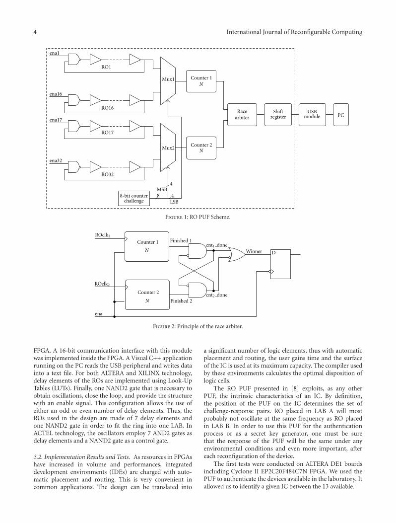
4 International Journal of Reconfigurable Computing
8-bit counterchallenge
8
4
4
Mux1
Mux2
RO16
RO1
RO17
RO32
Racearbiter
ena1
Shiftregister
USBmodule PC
MSB
LSB
ena16
ena17
ena32
Counter 1N
Counter 2N
Figure 1: RO PUF Scheme.
Counter 1
Counter 2
N
ROclk1
ROclk2
ena
Finished 1
Finished 2
Winner D
cnt1 done
cnt2 doneN
Figure 2: Principle of the race arbiter.
FPGA. A 16-bit communication interface with this modulewas implemented inside the FPGA. A Visual C++ applicationrunning on the PC reads the USB peripheral and writes datainto a text file. For both ALTERA and XILINX technology,delay elements of the ROs are implemented using Look-UpTables (LUTs). Finally, one NAND2 gate that is necessary toobtain oscillations, close the loop, and provide the structurewith an enable signal. This configuration allows the use ofeither an odd or even number of delay elements. Thus, theROs used in the design are made of 7 delay elements andone NAND2 gate in order to fit the ring into one LAB. InACTEL technology, the oscillators employ 7 AND2 gates asdelay elements and a NAND2 gate as a control gate.
3.2. Implementation Results and Tests. As resources in FPGAshave increased in volume and performances, integrateddevelopment environments (IDEs) are charged with auto-matic placement and routing. This is very convenient incommon applications. The design can be translated into
a significant number of logic elements, thus with automaticplacement and routing, the user gains time and the surfaceof the IC is used at its maximum capacity. The compiler usedby these environments calculates the optimal disposition oflogic cells.
The RO PUF presented in [8] exploits, as any otherPUF, the intrinsic characteristics of an IC. By definition,the position of the PUF on the IC determines the set ofchallenge-response pairs. RO placed in LAB A will mostprobably not oscillate at the same frequency as RO placedin LAB B. In order to use this PUF for the authenticationprocess or as a secret key generator, one must be surethat the response of the PUF will be the same under anyenvironmental conditions and even more important, aftereach reconfiguration of the device.
The first tests were conducted on ALTERA DE1 boardsincluding Cyclone II EP2C20F484C7N FPGA. We used thePUF to authenticate the devices available in the laboratory. Itallowed us to identify a given IC between the 13 available.
International Journal of Reconfigurable Computing 5
Table 1: RO PUF responses for three projects implemented in thesame device (ROs were constrained but not the race arbiter).
Response no. 1 (only thePUF)
031f031f031f0005573f031f031f471f
573f031f011fd73ff7bf431f0117031f
Response no. 2 (PUF andcounter)
010000004df20000000045a04de245e0
45a0fff70000000045e0fff745e045e0
Response no. 3 (only thePUF and an extra output)
0007600f7eef7eef200fffff724f704f
600f0007600f7eef0005000772ef0007
As expected, we were able to perform this operation onall the devices: both inter- and intrachip variations were innormal ranges. However, authors insisted that the designneeded no further placement and routing constraints in [8],page 3: “[· · · ] there is no need for careful layout and routing.For example, the paths from oscillator outputs to countersdo not need to be symmetric.” While it is clear that ROsmust be identically laidout (which is achieved thanks to amacro in [8]), it is questionable that extra logic around theROs (e.g., the race arbiter) needs no placement and routingconstraints. We can imagine the next scenario: in order tocontrol royalties, the IP vendor wants to use a PUF for linkingthe IP licence to a concrete FPGA device. However, a whilelater, he needs to make an upgrade of his IP function, stillrelated to the same device and the same PUF response. Thismeans that he needs that the response of the PUF block willbe independent of the rest of the design.
We evaluated the impact of the changes in surroundinglogic on the PUF response. First, we added a new counter-block module. Since it was independent of the PUF, it shouldnot change the PUF response. Contrary to all expectations,instead of obtaining almost the same response of thePUF (i.e., obtaining small intrachip variation), the devicegave completely different response so that presumably lowintrachip variation after addition of the additional logic wasalmost as high as an ideal inter-chip variation: 48,8% ofthe response bits changed. We have to stress here, that theplacement and routing of ROs was constrained, but not thestructure of the arbiter.
In the next experiment, we kept initial PUF and sent itsoutput, as before, towards the USB module and additionallytowards a 7-segment display available on ALTERA DE1board. While we were still maintaining the placement androuting for ROs, we got another (the third) response of thePUF for the same device! The responses for three projectsincluding the same PUF in the same device are depicted inTable 1.
3.3. Imposing Placement and Routing Solution for ResponseStabilization. The above-mentioned results show that theoptimization performed by the compiler implies differentplacement and routing for the race arbiter after eachrecompilation.
As we need to have the minimal intrachip variationeven for project upgrades, this is of extreme importance.Different placement of the race arbiter implies different PUFand different intrinsic characteristics that are explored. In
Table 2: RO PUF responses for three projects implemented in thesame device (ROs and race arbiter were constrained).
Response no. 1 (only thePUF)
ea09ebf9ea09ebfbea09eb59ebfbeb79
ea09ebfbfffffbffeb79ea49ebfb0001
Response no. 2 (PUF andcounter)
ea09ebf9ea09ebfbea09ea69ebfbeb79
ea09ebfbfffffbffeb79ea49ebfb0001
Response no. 3 (only thePUF and an extra output)
ea09ebf9ea09ebfbea09ea59ebfbeb79
ea09ebfbfffffbffeb79ea19fbfb0001
both targeted processes (authentication and key generation)this is not acceptable. Therefore, imposing placement androuting constraints on the whole PUF block is mandatoryin order to obtain a response independent from architecturemodifications in a reconfigurable device.
Once placement and routing constraints were applied onboth ROs and arbiter structure, the PUF provided excellentand expected responses. Table 2 presents results of threeprojects including the same PUF in the same device. Onlyfew differences exist (printed in bold).
4. Bit Dependency in the PUF Response
In Section 3.1, we presented the way we selected pairs ofoscillators to obtain a 256-bit response. We have to evaluatehow many bits are independent in the PUF response. Forexample, consider 2 ROs a, b in group 1 and two other ROsc, d in group 2. The comparisons are (a, c), (a,d), (b, c), and(b,d), giving 4 possible bits in the response. But if a > c,c > b, b > d, then we can predict a > d, so there are only 3bits of information instead of 4 in this example.
In the following, we propose to compute how many bitsin the response are independent. This could help RO-PUFdesigners to select pairs of ROs.
4.1. Generalization. Let (a1, . . . , an) be the first group of ROsand (b1, . . . , bn) be the second group of ROs. We use therelation x > y when RO x is faster than RO y. In most ofcases, ROs in group 1 (resp., in group 2) are not sorted thanksto the relation >. However it exists a permutation σ ∈ Sn
(resp., σ ′ ∈ Sn) such as aσ(1) > aσ(2) > · · · > aσ(n) (resp.,bσ ′(1) > bσ ′(2) > · · · > bσ ′(n)).
We define the matrix of all comparison results betweenone RO in group 1 and one RO in group 2. Matrix rows areindexed by (aσ(1), . . . , aσ(n)) and matrix columns are indexedby (bσ ′(1), . . . , bσ ′(n))
Compn =
⎛⎜⎜⎜⎜⎝c1,1 c1,2 · · · c1,n
c2,1 c2,2 · · · c2,n...
.... . .
...cn,1 cn,2 · · · cn,n
⎞⎟⎟⎟⎟⎠,
where ci, j =⎧⎨⎩
0 when aσ(i) ≤ bσ ′( j)
1 when aσ(i) > bσ ′( j).
(3)

6 International Journal of Reconfigurable Computing
Because (aσ(i))i and (bσ ′( j)) j are sorted, if aσ(i) ≤ bσ ′( j),then for all k ≥ i, aσ(k) ≤ bσ ′( j) because aσ(i) > aσ(k). In otherwords if ci, j = 0 then for all k ≥ i, ck, j = 0.
Similarly, if aσ(i) > bσ ′( j), then for all l ≥ j, aσ(i) > bσ ′(l)because bσ( j) > bσ(l). In other words, if ci, j = 1 then for eachl ≥ j, ci,l = 1.
Among the 2n2
possible matrices, only matrices withgeneral term ci, j following the two rules,
(1) if ci, j = 0 then for all k ≥ i, ck, j = 0,
(2) if ci, j = 1 then for each l ≥ j, ci,l = 1,
can be obtained when comparing pairs of ROs. The othersdenote antagonist comparisons that cannot appear (e.g., a >c, c > b, b > d and a < d which is impossible).
4.2. Number of Possible Matrices. Let Mm,n be the numberof possible matrices Mm,n with m rows and n columns. Bysymmetry of the role played by (ai)i and (bj) j it is obviousthat Mm,n =Mn,m.
By convention, we set for all n ∈ N, M0,n = 1 = Mn,0,thus we have the following recursive relation giving Mm,n
(m ≤ n):
Mm,n =m∑i=0
Mi,n−i ×Mm−i,i. (4)
To prove this relation, we write the matrix with fourblocks for i from 0 to m:
Mm,n =⎛⎝ Ai,n−i Bi,i
Cm−i,n−i Dm−i,i
⎞⎠ (5)
with block Bi,i necessarily filled with 1s and block Cm−i,n−inecessarily filled with 0 s. This can be explained by buildingfirst matrices.
For example, for i = 0 we have
Mm,n =(Cm,n
) =⎛⎜⎜⎝
0 . . . 0...
. . ....
0 . . . 0
⎞⎟⎟⎠. (6)
Then the only location to set a one in the matrix is theupper right corner. Indeed, if we set a 0 instead then the lastcolumn will be filled with 0 s according to rule (1). In thiscase, it is impossible to set a 1 elsewhere in a line of the matrixbecause according to rule (2), it would force a 1 in the lastcolumn in the same line which is impossible. For i = 1 wehave
Mm,n =
⎛⎜⎜⎜⎜⎜⎝
A1,n−1 1
0 . . . 0...
. . ....
0 . . . 0
Dm−1,1
⎞⎟⎟⎟⎟⎟⎠ (7)
with M1,n−1 matrices for A1,n−1 and Mm−1,1 for Dm−1,1
for a total of M1,n−1 × Mm−1,1 possible matrices in thisconfiguration. The next configuration is obtained with a 1 inthe upper right corner of block Cm−1,n−1 and following rules(1) and (2) the 2 × 2 block B2,2 is necessarily filled with1 s. So the next configuration will be the study of all possiblematrices of the shape
Mm,n =
⎛⎜⎜⎜⎜⎜⎜⎝
A2,n−21 11 1
0 . . . 0...
. . ....
0 . . . 0
Dm−2,2
⎞⎟⎟⎟⎟⎟⎟⎠
(8)
then for i = 3 possible matrices with a 1 in the upper rightcorner of block Cm−2,n−2, and so on until i = m where the lastpossible matrice has the form:
Mm,n =
⎛⎜⎜⎝
1 . . . 1...
. . ....
1 . . . 1
⎞⎟⎟⎠. (9)
Thus for i from 0 to m we count all the possible matricesAi,n−i and Dm−i,i following the two previously mentionedrules. For each i, there are Mi,n−i possible matrices for Ai,n−iand Mm−i,i matrices for Dm−i,i. Thus, there are Mi,n−i×Mm−i,ipossible matrices for a given i. The sum over i gives theformula in (4).
Using this formula in our context (two groups withthe same number n of ROs), there are Mn,n possiblematrices. Then log2(Mn,n) gives the number of independentcomparisons we can perform to get independent bits in theresponse.
For n = 16 ROs in each group, we got (only) M16,16 =601080390 authorized matrices among the 2256 possible.Then only a mean of log2(M16,16) ≈ 29 comparisons leadsto 29 independent bits in the PUF response (instead of 256).We can deduce that we should have n = 135 ROs in eachgroup to get a PUF response with 256 independent bits.
4.3. Example. In the next example, we use the response inTable 2. Due to intrachip variation, some bits change in theresponse. To have only one representation of the response, weuse a mean over 64 PUF responses with the same challengeand we obtain ea09ebf9ea09ebfbea09eb59ebfbeb79ea09ebf-bfffffb ffeb79ea49ebfb0001. If we analyze the response, wecan see repetitive patterns (e.g., ea09, ebf9, etc.) meaning thatthere are dependent bits in the response.
We can be more precise and give, in this configuration,the number of bits that are independent in the PUF response.

International Journal of Reconfigurable Computing 7
We rewrite the PUF response column by column in a16 × 16 matrix, with rows from top to bottom a1, . . . , a16
and columns from left to right b1, . . . , b16
⎛⎜⎜⎜⎜⎜⎜⎜⎜⎜⎜⎜⎜⎜⎜⎜⎜⎜⎜⎜⎜⎜⎜⎜⎜⎜⎜⎜⎜⎜⎝
1 1 1 1 1 1 1 1 1 1 1 1 1 1 1 01 1 1 1 1 1 1 1 1 1 1 1 1 1 1 01 1 1 1 1 1 1 1 1 1 1 1 1 1 1 00 0 0 0 0 0 0 0 0 0 1 1 0 0 0 01 1 1 1 1 1 1 1 1 1 1 1 1 1 1 00 0 0 0 0 0 0 0 0 0 1 0 0 0 0 01 1 1 1 1 1 1 1 1 1 1 1 1 1 1 00 1 0 1 0 1 1 1 0 1 1 1 1 0 1 00 1 0 1 0 0 1 0 0 1 1 1 0 0 1 00 1 0 1 0 1 1 1 0 1 1 1 1 1 1 00 1 0 1 0 0 1 1 0 1 1 1 1 0 1 00 1 0 1 0 1 1 1 0 1 1 1 1 0 1 01 1 1 1 1 1 1 1 1 1 1 1 1 1 1 00 0 0 0 0 0 0 0 0 0 1 1 0 0 0 00 0 0 1 0 0 1 0 0 1 1 1 0 0 1 01 1 1 1 1 1 1 1 1 1 1 1 1 1 1 1
⎞⎟⎟⎟⎟⎟⎟⎟⎟⎟⎟⎟⎟⎟⎟⎟⎟⎟⎟⎟⎟⎟⎟⎟⎟⎟⎟⎟⎟⎟⎠
. (10)
Then we have to transform this matrix with respect to thetwo previous rules. We count the Hamming weight of eachline. Then we permute lines to obtain the Hamming weightof line aσ(i) greater than or equal to the one of line aσ(i+1) foreach i see Table 5.
We obtain
⎛⎜⎜⎜⎜⎜⎜⎜⎜⎜⎜⎜⎜⎜⎜⎜⎜⎜⎜⎜⎜⎜⎜⎜⎜⎜⎜⎜⎜⎜⎝
1 1 1 1 1 1 1 1 1 1 1 1 1 1 1 11 1 1 1 1 1 1 1 1 1 1 1 1 1 1 01 1 1 1 1 1 1 1 1 1 1 1 1 1 1 01 1 1 1 1 1 1 1 1 1 1 1 1 1 1 01 1 1 1 1 1 1 1 1 1 1 1 1 1 1 01 1 1 1 1 1 1 1 1 1 1 1 1 1 1 01 1 1 1 1 1 1 1 1 1 1 1 1 1 1 00 1 0 1 0 1 1 1 0 1 1 1 1 1 1 00 1 0 1 0 1 1 1 0 1 1 1 1 0 1 00 1 0 1 0 1 1 1 0 1 1 1 1 0 1 00 1 0 1 0 0 1 1 0 1 1 1 1 0 1 00 1 0 1 0 0 1 0 0 1 1 1 0 0 1 00 0 0 1 0 0 1 0 0 1 1 1 0 0 1 00 0 0 0 0 0 0 0 0 0 1 1 0 0 0 00 0 0 0 0 0 0 0 0 0 1 1 0 0 0 00 0 0 0 0 0 0 0 0 0 1 0 0 0 0 0
⎞⎟⎟⎟⎟⎟⎟⎟⎟⎟⎟⎟⎟⎟⎟⎟⎟⎟⎟⎟⎟⎟⎟⎟⎟⎟⎟⎟⎟⎟⎠
. (11)
The same work is done with columns (Hamming weightof column bσ ′( j) is less or equal than the one of columnbσ ′( j+1)) see Table 6:
Finally, we obtain the following matrix:
⎛⎜⎜⎜⎜⎜⎜⎜⎜⎜⎜⎜⎜⎜⎜⎜⎜⎜⎜⎜⎜⎜⎜⎜⎜⎜⎜⎜⎜⎜⎜⎜⎜⎜⎜⎜⎝
1 1 1 1 1 1 1 1 1 1 1 1 1 1 1 10 1 1 1 1 1 1 1 1 1 1 1 1 1 1 10 1 1 1 1 1 1 1 1 1 1 1 1 1 1 10 1 1 1 1 1 1 1 1 1 1 1 1 1 1 10 1 1 1 1 1 1 1 1 1 1 1 1 1 1 10 1 1 1 1 1 1 1 1 1 1 1 1 1 1 10 1 1 1 1 1 1 1 1 1 1 1 1 1 1 10 0 0 0 0 1 1 1 1 1 1 1 1 1 1 10 0 0 0 0 0 1 1 1 1 1 1 1 1 1 10 0 0 0 0 0 1 1 1 1 1 1 1 1 1 10 0 0 0 0 0 0 1 1 1 1 1 1 1 1 10 0 0 0 0 0 0 0 0 1 1 1 1 1 1 10 0 0 0 0 0 0 0 0 0 1 1 1 1 1 10 0 0 0 0 0 0 0 0 0 0 0 0 0 1 10 0 0 0 0 0 0 0 0 0 0 0 0 0 1 10 0 0 0 0 0 0 0 0 0 0 0 0 0 0 1
⎞⎟⎟⎟⎟⎟⎟⎟⎟⎟⎟⎟⎟⎟⎟⎟⎟⎟⎟⎟⎟⎟⎟⎟⎟⎟⎟⎟⎟⎟⎟⎟⎟⎟⎟⎟⎠
(12)
with σ = (1 2 3 4 5 6 7 8 9 10 11 12 13 14 15 16
16 1 2 3 5 7 13 10 8 12 11 9 15 4 14 6
)which is the permutation of rows and σ ′ =(
1 2 3 4 5 6 7 8 9 10 11 12 13 14 15 1616 1 3 5 9 14 6 8 13 2 4 7 10 15 12 11
)which is the per-
mutation of columns. Thus, aσ(1) = a16 > bσ ′(1) = b16
(upper left corner in the matrix) gives a one. Then othercomparisons between aσ(1) and bσ ′( j) for j > 1 give noadditional information because we know that they willgive a 1. The next comparison is between aσ(2) = a1 andbσ ′(1) = b16 which is a zero, meaning that a1 < b16. Then
other comparisons between bσ ′(1) and aσ(i) for i > 1 areuseless because we know that they will give a 0. In this way,we can identify which comparisons are giving information(they are boxed in the matrix). This also gives indexes ofROs that have to be compared. In this special case, they are(aσ(1) = a16 and bσ ′(1) = b16, aσ(2) = a1 and bσ ′(1) = b16,aσ(2) = a1 and bσ ′(2) = b1,. . .). In our case, we have 31suitable comparisons and so 31 bits in the response that areindependent (close to the theoretical mean of 29 computed).
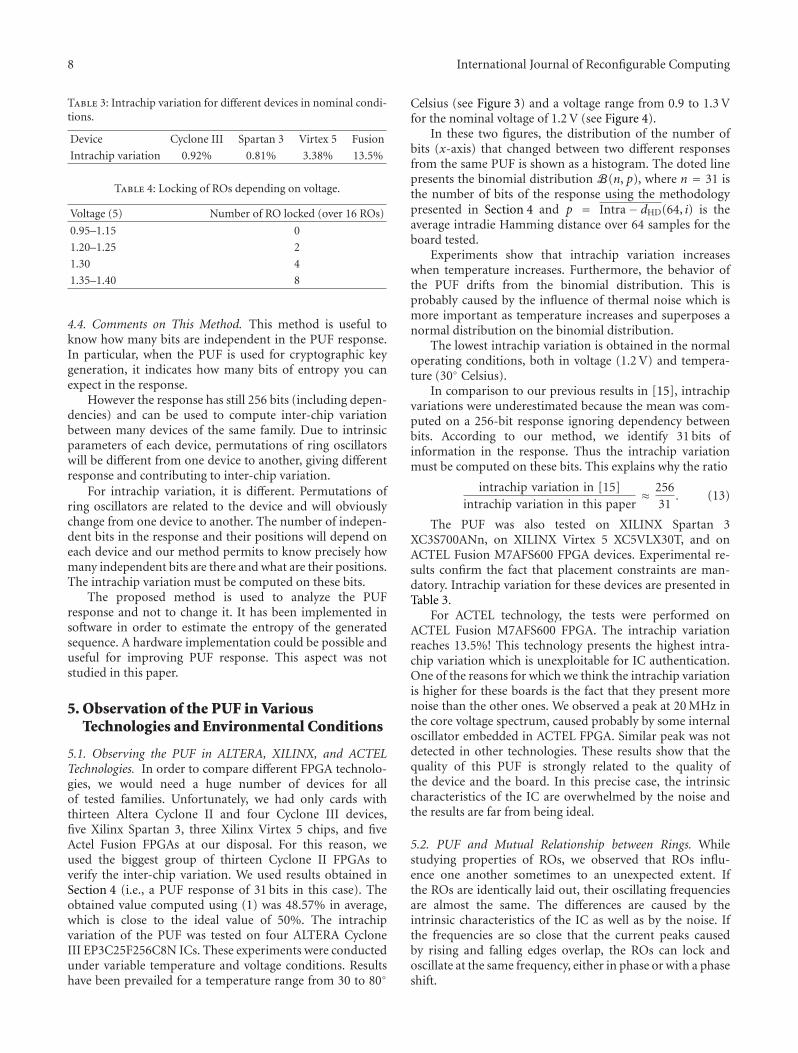
8 International Journal of Reconfigurable Computing
Table 3: Intrachip variation for different devices in nominal condi-tions.
Device Cyclone III Spartan 3 Virtex 5 Fusion
Intrachip variation 0.92% 0.81% 3.38% 13.5%
Table 4: Locking of ROs depending on voltage.
Voltage (5) Number of RO locked (over 16 ROs)
0.95–1.15 0
1.20–1.25 2
1.30 4
1.35–1.40 8
4.4. Comments on This Method. This method is useful toknow how many bits are independent in the PUF response.In particular, when the PUF is used for cryptographic keygeneration, it indicates how many bits of entropy you canexpect in the response.
However the response has still 256 bits (including depen-dencies) and can be used to compute inter-chip variationbetween many devices of the same family. Due to intrinsicparameters of each device, permutations of ring oscillatorswill be different from one device to another, giving differentresponse and contributing to inter-chip variation.
For intrachip variation, it is different. Permutations ofring oscillators are related to the device and will obviouslychange from one device to another. The number of indepen-dent bits in the response and their positions will depend oneach device and our method permits to know precisely howmany independent bits are there and what are their positions.The intrachip variation must be computed on these bits.
The proposed method is used to analyze the PUFresponse and not to change it. It has been implemented insoftware in order to estimate the entropy of the generatedsequence. A hardware implementation could be possible anduseful for improving PUF response. This aspect was notstudied in this paper.
5. Observation of the PUF in VariousTechnologies and Environmental Conditions
5.1. Observing the PUF in ALTERA, XILINX, and ACTELTechnologies. In order to compare different FPGA technolo-gies, we would need a huge number of devices for allof tested families. Unfortunately, we had only cards withthirteen Altera Cyclone II and four Cyclone III devices,five Xilinx Spartan 3, three Xilinx Virtex 5 chips, and fiveActel Fusion FPGAs at our disposal. For this reason, weused the biggest group of thirteen Cyclone II FPGAs toverify the inter-chip variation. We used results obtained inSection 4 (i.e., a PUF response of 31 bits in this case). Theobtained value computed using (1) was 48.57% in average,which is close to the ideal value of 50%. The intrachipvariation of the PUF was tested on four ALTERA CycloneIII EP3C25F256C8N ICs. These experiments were conductedunder variable temperature and voltage conditions. Resultshave been prevailed for a temperature range from 30 to 80◦
Celsius (see Figure 3) and a voltage range from 0.9 to 1.3 Vfor the nominal voltage of 1.2 V (see Figure 4).
In these two figures, the distribution of the number ofbits (x-axis) that changed between two different responsesfrom the same PUF is shown as a histogram. The doted linepresents the binomial distribution B(n, p), where n = 31 isthe number of bits of the response using the methodologypresented in Section 4 and p = Intra− dHD(64, i) is theaverage intradie Hamming distance over 64 samples for theboard tested.
Experiments show that intrachip variation increaseswhen temperature increases. Furthermore, the behavior ofthe PUF drifts from the binomial distribution. This isprobably caused by the influence of thermal noise which ismore important as temperature increases and superposes anormal distribution on the binomial distribution.
The lowest intrachip variation is obtained in the normaloperating conditions, both in voltage (1.2 V) and tempera-ture (30◦ Celsius).
In comparison to our previous results in [15], intrachipvariations were underestimated because the mean was com-puted on a 256-bit response ignoring dependency betweenbits. According to our method, we identify 31 bits ofinformation in the response. Thus the intrachip variationmust be computed on these bits. This explains why the ratio
intrachip variation in [15]intrachip variation in this paper
≈ 25631
. (13)
The PUF was also tested on XILINX Spartan 3XC3S700ANn, on XILINX Virtex 5 XC5VLX30T, and onACTEL Fusion M7AFS600 FPGA devices. Experimental re-sults confirm the fact that placement constraints are man-datory. Intrachip variation for these devices are presented inTable 3.
For ACTEL technology, the tests were performed onACTEL Fusion M7AFS600 FPGA. The intrachip variationreaches 13.5%! This technology presents the highest intra-chip variation which is unexploitable for IC authentication.One of the reasons for which we think the intrachip variationis higher for these boards is the fact that they present morenoise than the other ones. We observed a peak at 20 MHz inthe core voltage spectrum, caused probably by some internaloscillator embedded in ACTEL FPGA. Similar peak was notdetected in other technologies. These results show that thequality of this PUF is strongly related to the quality ofthe device and the board. In this precise case, the intrinsiccharacteristics of the IC are overwhelmed by the noise andthe results are far from being ideal.
5.2. PUF and Mutual Relationship between Rings. Whilestudying properties of ROs, we observed that ROs influ-ence one another sometimes to an unexpected extent. Ifthe ROs are identically laid out, their oscillating frequenciesare almost the same. The differences are caused by theintrinsic characteristics of the IC as well as by the noise. Ifthe frequencies are so close that the current peaks causedby rising and falling edges overlap, the ROs can lock andoscillate at the same frequency, either in phase or with a phaseshift.
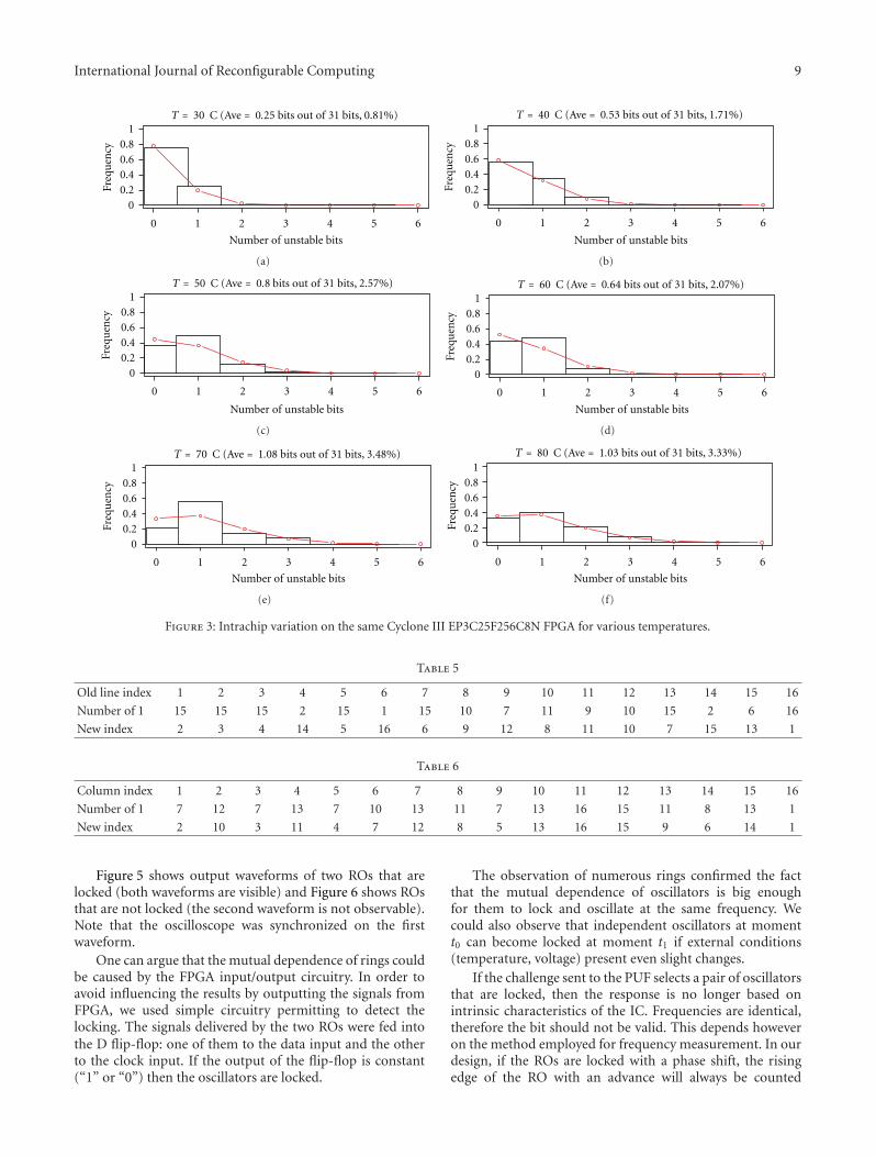
International Journal of Reconfigurable Computing 9
0.20.40.60.8
1
Number of unstable bits
Freq
uen
cy
0
0 1 2 3 4 5 6
T = 30 C (Ave = 0.25 bits out of 31 bits, 0.81%)
(a)
0.20.40.60.8
1
Number of unstable bits
Freq
uen
cy
0
0 1 2 3 4 5 6
T = 40 C (Ave = 0.53 bits out of 31 bits, 1.71%)
(b)
0.20.40.60.8
1
Number of unstable bits
Freq
uen
cy
0
0 1 2 3 4 5 6
T = 50 C (Ave = 0.8 bits out of 31 bits, 2.57%)
(c)
0.20.40.60.8
1
Number of unstable bits
Freq
uen
cy
0
0 1 2 3 4 5 6
T = 60 C (Ave = 0.64 bits out of 31 bits, 2.07%)
(d)
0.20.40.60.8
1
Number of unstable bits
Freq
uen
cy
0
0 1 2 3 4 5 6
T = 70 C (Ave = 1.08 bits out of 31 bits, 3.48%)
(e)
0.20.40.60.8
1
Number of unstable bits
Freq
uen
cy
0
0 1 2 3 4 5 6
T = 80 C (Ave = 1.03 bits out of 31 bits, 3.33%)
(f)
Figure 3: Intrachip variation on the same Cyclone III EP3C25F256C8N FPGA for various temperatures.
Table 5
Old line index 1 2 3 4 5 6 7 8 9 10 11 12 13 14 15 16
Number of 1 15 15 15 2 15 1 15 10 7 11 9 10 15 2 6 16
New index 2 3 4 14 5 16 6 9 12 8 11 10 7 15 13 1
Table 6
Column index 1 2 3 4 5 6 7 8 9 10 11 12 13 14 15 16
Number of 1 7 12 7 13 7 10 13 11 7 13 16 15 11 8 13 1
New index 2 10 3 11 4 7 12 8 5 13 16 15 9 6 14 1
Figure 5 shows output waveforms of two ROs that arelocked (both waveforms are visible) and Figure 6 shows ROsthat are not locked (the second waveform is not observable).Note that the oscilloscope was synchronized on the firstwaveform.
One can argue that the mutual dependence of rings couldbe caused by the FPGA input/output circuitry. In order toavoid influencing the results by outputting the signals fromFPGA, we used simple circuitry permitting to detect thelocking. The signals delivered by the two ROs were fed intothe D flip-flop: one of them to the data input and the otherto the clock input. If the output of the flip-flop is constant(“1” or “0”) then the oscillators are locked.
The observation of numerous rings confirmed the factthat the mutual dependence of oscillators is big enoughfor them to lock and oscillate at the same frequency. Wecould also observe that independent oscillators at momentt0 can become locked at moment t1 if external conditions(temperature, voltage) present even slight changes.
If the challenge sent to the PUF selects a pair of oscillatorsthat are locked, then the response is no longer based onintrinsic characteristics of the IC. Frequencies are identical,therefore the bit should not be valid. This depends howeveron the method employed for frequency measurement. In ourdesign, if the ROs are locked with a phase shift, the risingedge of the RO with an advance will always be counted
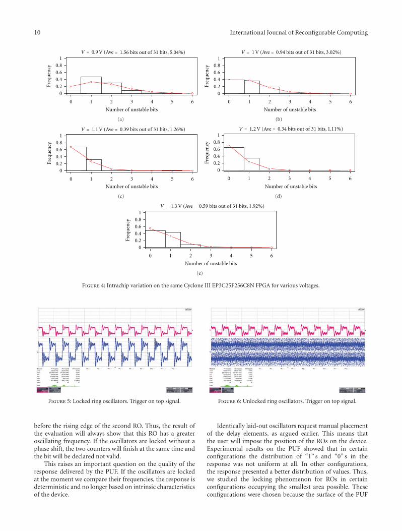
10 International Journal of Reconfigurable Computing
0.20.40.60.8
1
Number of unstable bits
Freq
uen
cy
0
0 1 2 3 4 5 6
= 1.56 bits out of 31 bits, 5.04%)V = 0.9 V (Ave
(a)
0.20.40.60.8
1
Number of unstable bits
Freq
uen
cy
0
0 1 2 3 4 5 6
= 0.94 bits out of 31 bits, 3.02%)V = 1 V (Ave
(b)
0.20.40.60.8
1
Number of unstable bits
Freq
uen
cy
0
0 1 2 3 4 5 6
= 0.39 bits out of 31 bits, 1.26%)V = 1.1 V (Ave
(c)
0.20.40.60.8
1
Number of unstable bits
Freq
uen
cy
0
0 1 2 3 4 5 6
= 0.34 bits out of 31 bits, 1.11%)V = 1.2 V (Ave
(d)
0.20.40.60.8
1
Number of unstable bits
Freq
uen
cy
0
0 1 2 3 4 5 6
= 0.59 bits out of 31 bits, 1.92%)V = 1.3 V (Ave
(e)
Figure 4: Intrachip variation on the same Cyclone III EP3C25F256C8N FPGA for various voltages.
Figure 5: Locked ring oscillators. Trigger on top signal.
before the rising edge of the second RO. Thus, the result ofthe evaluation will always show that this RO has a greateroscillating frequency. If the oscillators are locked without aphase shift, the two counters will finish at the same time andthe bit will be declared not valid.
This raises an important question on the quality of theresponse delivered by the PUF. If the oscillators are lockedat the moment we compare their frequencies, the response isdeterministic and no longer based on intrinsic characteristicsof the device.
Figure 6: Unlocked ring oscillators. Trigger on top signal.
Identically laid-out oscillators request manual placementof the delay elements, as argued earlier. This means thatthe user will impose the position of the ROs on the device.Experimental results on the PUF showed that in certainconfigurations the distribution of “1” s and “0” s in theresponse was not uniform at all. In other configurations,the response presented a better distribution of values. Thus,we studied the locking phenomenon for ROs in certainconfigurations occupying the smallest area possible. Theseconfigurations were chosen because the surface of the PUF

International Journal of Reconfigurable Computing 11
Figure 7: Configuration of ROs in a compact block.
should be relatively small comparing to the rest of the logicimplemented in the device. Moreover, the PUF needs to beimplemented in an isolated zone so that additional logic hasonly minimum influence on the response.
We tested two particular configurations, ROs grouped ina compact block, as presented in Figure 7 and ROs placedon two columns as presented in Figure 8. In this case onecolumn represents one group of ROs.
Experimental results show that in the first configuration,there are more chances to have locked ROs. The most proba-ble explanation for this phenomenon is that ROs placed closeto each others are powered by the same wires. This fact has agreat influence on the behavior of the oscillators. In Table 4we present the influence of the voltage on the locking ofthe ROs on Cyclone III IC. Considering these experimentalresults, we cannot determine with precision the conditionsunder which ROs lock. We only observed that pairs of ROscan lock or unlock if environmental conditions change. Thus,questions rise on the reliability of the PUF and as manualplacement is required, the configuration of the oscillatorsand the placement and routing of both ROs and arbiter mustbe carefully studied. In a recent publication by Maiti andSchaumont [13], the “Compensation method” used to selectpairs of ROs in order to have good PUF properties indicateto choose ROs as close as possible from one to each others.Even if more investigation should be done on the locking ofRO, such a method seems to be exposed to this phenomenon.
6. Further Enhancements of the PUF
Next, we propose some modifications of the PUF in order toenhance its characteristics.
6.1. Reduction of Intrachip Variations. As we observed in Ses-sion 5, changing environmental conditions (namely, voltage
Figure 8: Configuration of ROs in 2 columns.
and temperature) increases the intrachip variation. This isdue to the fact that identically laid-out ROs have very closeoscillation frequencies. Since all ROs do not have exactlythe same dependence on environmental conditions, someROs can be more affected than others, and differences infrequencies can invert. While for laboratory temperatures theintrachip variation did not exceeded 4 bits, for temperatureranges from 30 to 80◦ Celsius, up to 15 bits out of 256 wereunstable. For device authentication this is not a problem ifthe inter-chip variation remains high. For key generation thisfact is not acceptable. We must guarantee the uniqueness ofthe key generated by the device. Therefore, as proposed bySuh and Devadas, an error correcting code can be used tocorrect errors due to the intrachip variation.
As usual, the response should not be used directly as a keyeven after correcting the errors. On one hand, there are weak
12 International Journal of Reconfigurable Computing
and periodic patterns in the response. On the other hand,after this error correcting process, the entropy of the “key”will probably be reduced. A hash function (e.g., Whirlpool[16] based on a modified AES) can be used to remove weakpatterns but unfortunately it cannot solve the problem ofentropy reduction.
6.2. Reduction of the Power Consumption. When dealing withthe power consumption of the PUF, we used small dedicatedmodules made in our laboratory featuring ALTERA CycloneIII EP3C25F256C8N FPGA. We measured the static currentconsumption of the module and obtained 4 mA. Then wemeasured the consumption of the PUF using the 32 ROsand a PLL delivering the clock signal. The module consumed24.7 mA, which is indeed considerable for a backgroundfunction such as PUF. However, the PUF employs each timeonly two out of N ROs in order to obtain one bit of theresponse. Thus, we propose to stop all the N − 2 oscillators(30 in our case) that are currently not used for the responsebit. The ROs are enabled and stopped using the enableinput of the structure (Figure 1). When only two ROs wererunning, we measured a 13.4 mA current consumption. Thisis a reduction of consumption by approximately 51%.
In the next paragraph, we estimate the approximatepower reduction that can be obtained in the design proposedin [8]. The total power consumption represents the sum ofthe static consumption (S), the consumption of the logicwhich is independent of the number of ROs (i.e., PLL,counters, comparators, etc.) (L) and the consumption of thelogic which depends almost linearly on the number of ROs(multiplexers and ROs) denoted by R(N) = λ × N whereN is the number of ROs and λ a constant float. We canmake a simple calculus and show that the improved modelwould probably reduce considerably the consumption of theboard.
In [8], Suh and Devadas used 1024 ROs in their design.Then, if we shut down unused ROs for each comparison, weshould obtain a consumption of approximately S + L + λ ×2 = 13.4 mA instead of S + L + λ × 1024 = 397.6 mA. Withour improved PUF control, we obtain a current consumptionreduction of 1 − 13.4/397.6 = 96.6%. The PUF’s powerconsumption thus becomes much more suitable for practicalimplementations.
Such an idea for reducing self-heating has been proposedin [17] but was not considered by Suh and Devadas in theirdesign. However, in this paper only one ring is selected ata time. This idea cannot be used in our proposal to savemore power consumption. If we want to use only one RO, wehave to count its number of raising edges during one enabletime, record this number, and repeat this measurement byselecting another RO during the same enable time. Themain problem in such a case is the influence of the globaldeterministic part of the jitter on the frequency of one-ringoscillator [18]. This influence will not be the same from onemeasurement to another. Thus the comparison between thenumber of raising edges of two ROs will be suitable only ifthey are influenced by the same global deterministic part ofthe jitter in the same time.
7. Conclusions
The concept introduced in [8] is very simple, with a differen-tial structure that presents an excellent behavior as long as theIC is not reconfigured. As this structure (the PUF) is uselessif implemented alone in an IC, we analyze the influence ofadditional logic upon the response of the PUF. Our workproves that placement and routing constraints are required inorder to maintain the quality of the PUF in FPGAs. Withoutany constraints, additional logic creates a completely dif-ferent PUF and implicitly a completely different response.Instead of a small and acceptable intrachip variation after theIC reconfiguration, we obtained the variation 48.8% that wascomparable in size to an ideal inter-chip variation (50%).
We also showed that bits in the response are dependentand propose a method to select pairs of ROs to haveindependent bits. Unfortunately this shortens the PUFresponse. The huge current consumption obtained by Suhand Devadas was also of our concern. We improved thedesign in order to considerably reduce the consumption. Fora small PUF, (e.g., the one described in our experimentalconditions with 32 ROs) the consumption was reduced by51%. For a greater PUF, our improvement leads to an evenmore important reduction: we reduced the consumption ofthe PUF described in [8] by 96.6%.
Moreover, we showed that there are other phenomenathat influence and jeopardize the integrity of the PUF.We argued why the “locking” phenomenon is affecting theresponse of the PUF and it is very important to notice thatnot all challenges can be used at any moment. Apart from thelocking, our experimental results show that noisy mother-boards can increase the intrachip variation for the PUF.
Acknowledgments
The work presented in this paper was realized in the frameof the SecReSoC Project n. ANR-09-SEGI-013, supportedby the French National Research Agency (ANR). The workwas partially supported also by the Rhones-Alpes Region andSaint-Etienne Metropole, France. The authors would like tothank Malick Boureima and Nathalie Bochard for their helpwith numerous experiments.
References
[1] S. Drimer, “Volatile FPGA design security–a survey,” in IEEEComputer Society Annual Volume, pp. 292–297, 2008.
[2] R. Anderson and M. Kuhn, “Low cost attacks on tamperresistant devices,” in Security Protocols, pp. 125–136, Springer,1998.
[3] R. Anderson and M. Kuhn, “Tamper resistance: a cautionarynote,” in 2nd USENIX Workshop on Electronic Commerce, vol.2, 1996.
[4] S.P. Skorobogatov, “Semi-invasive attacks-a new approach tohardware security analysis,” Tech. Rep., University of Cam-bridge, Computer Laboratory, 2005.
[5] J. A. Halderman, S. D. Schoen, N. Heninger et al., “Lest weremember: cold boot attacks on encryption keys,” in USENIXSecurity Symposium, P.C. van Oorschot, Ed., pp. 45–60, 2008.
International Journal of Reconfigurable Computing 13
[6] R. Pappu, Physical one-way functions, Ph.D. thesis, Massa-chusetts Institute of Technology, 2001.
[7] R. Pappu, B. Recht, J. Taylor, and N. Gershenfeld, “Physicalone-way functions,” Science, vol. 297, no. 5589, pp. 2026–2030,2002.
[8] G. E. Suh and S. Devadas, “Physical unclonable functions fordevice authentication and secret key generation,” in 44thACM/IEEE Design Automation Conference (DAC ’07), pp. 9–14, June 2007.
[9] J. Guajardo, S. Kumar, G.J. Schrijen, and P. Tuyls, “FPGAintrinsic PUFs and their use for IP protection,” in Crypto-graphic Hardware and Embedded Systems (CHES ’07), pp. 63–80, 2007.
[10] S. Kumar, J. Guajardo, R. Maes, G. J. Schrijen, and P. Tuyls,“Extended abstract: the butterfly PUF protecting IP on everyFPGA,” in IEEE International Workshop on Hardware-OrientedSecurity and Trust (HOST ’08), pp. 67–70, 2008.
[11] B. Gassend, D. Clarke, M. Van Dijk, and S. Devadas, “Siliconphysical random functions,” in Proceedings of the 9th ACMConference on Computer and Communications Security, pp.148–160, November 2002.
[12] D. Lim, J. W. Lee, B. Gassend, G. E. Suh, M. Van Dijk, andS. Devadas, “Extracting secret keys from integrated circuits,”IEEE Transactions on Very Large Scale Integration, vol. 13, no.10, pp. 1200–1205, 2005.
[13] A. Maiti and P. Schaumont, “Improved ring oscillator PUF: anFPGA-friendly secure primitive,” Journal of Cryptology, pp. 1–23, 2010.
[14] Y. Hori, T. Yoshida, T. Katashita, and A. Satoh, “Quantitativeand statistical performance evaluation of arbiter physicalunclonable functions on FPGAs,” in International Conferenceon Reconfigurable Computing and FPGAs, pp. 298–303, 2010.
[15] C. Costea, F. Bernard, V. Fischer, and R. Fouquet, “Analysisand enhancement of ring oscillators based physical unclonablefunctions in FPGAs,” in International Conference on Reconfig-urable Computing and FPGAs, pp. 262–267, 2010.
[16] P. Barreto and V. Rijmen, “The Whirlpool hashing function,”in 1st Open NESSIE Workshop, vol. 13, p. 14, Leuven, Belgium,2000.
[17] P. Sedcole and P. Y. K. Cheung, “Within-die delay variability in90nm FPGAs and beyond,” in IEEE International Conferenceon Field Programmable Technology (FPT ’06), pp. 97–104,December 2006.
[18] V. Fischer, F. Bernard, N. Bochard, and M. Varchola, “Enhanc-ing security of ring oscillator-based RNG implemented inFPGA,” in Proceedings of the Field- Programable Logic andApplications (FPL ’08), pp. 245–250, September 2008.
Hindawi Publishing CorporationInternational Journal of Reconfigurable ComputingVolume 2012, Article ID 360242, 9 pagesdoi:10.1155/2012/360242
Research Article
Blind Cartography for Side Channel Attacks:Cross-Correlation Cartography
Laurent Sauvage, Sylvain Guilley, Florent Flament, Jean-Luc Danger, and Yves Mathieu
Telecom ParisTech, Institut Telecom CNRS LTCI, 46 rue Barrault, F-75634 Paris Cedex 13, France
Correspondence should be addressed to Laurent Sauvage, [email protected]
Received 12 July 2011; Revised 20 October 2011; Accepted 27 December 2011
Academic Editor: Kris Gaj
Copyright © 2012 Laurent Sauvage et al. This is an open access article distributed under the Creative Commons AttributionLicense, which permits unrestricted use, distribution, and reproduction in any medium, provided the original work is properlycited.
Side channel and fault injection attacks are major threats to cryptographic applications of embedded systems. Best performancesfor these attacks are achieved by focusing sensors or injectors on the sensible parts of the application, by means of dedicatedmethods to localise them. Few methods have been proposed in the past, and all of them aim at pinpointing the cryptoprocessor.However it could be interesting to exploit the activity of other parts of the application, in order to increase the attack’s efficiencyor to bypass its countermeasures. In this paper, we present a localisation method based on cross-correlation, which issues a listof areas of interest within the attacked device. It realizes an exhaustive analysis, since it may localise any module of the device,and not only those which perform cryptographic operations. Moreover, it also does not require a preliminary knowledge aboutthe implementation, whereas some previous cartography methods require that the attacker could choose the cryptoprocessorinputs, which is not always possible. The method is experimentally validated using observations of the electromagnetic near fielddistribution over a Xilinx Virtex 5 FPGA. The matching between areas of interest and the application layout in the FPGA floorplanis confirmed by correlation analysis.
1. Introduction
Side channel attacks (SCA) and fault injection attacks (FIA)are very efficient techniques to retrieve secret data stored incryptographic devices such as smartcards. First attacks havebeen performed globally, for instance by measuring the pow-er consumption (power analysis: PA) [1] of a device underanalysis (DUA) or by quickly changing the nominal voltageof its power supply [2]. But best results have then beenachieved locally, by using a small EM probe just over thecryptoprocessor (electromagnetic analysis: EMA) [3] or byshooting at it with a laser beam [4, 5]. Indeed, for SCA,such locality permits to solely collect the activity of the cryp-toprocessor, instead of gathering the activity of the wholeDUA. In the case of FIA, depending on the technology pro-cess of the integrated circuit, only one bit of the implementa-tion can be affected. However, the efficiency of these attacksrelies on localisation methods which have to pinpoint as ac-curately as possible the DUA-sensitive areas. Using these
localisation methods is mandatory in the case of a crypto-graphic application embedded in a field Programmable gatearray (FPGA) as its regular structure prevents the localisationof sensible modules by optical or electron microscopy. In-deed, the task is easier for most ASICs, where the functionalmodules stand clearly out from a visual inspection of thelayout as rectangular shapes. Some methods have been pro-posed in the past, illustrated using as observations the nearelectromagnetic (EM) field radiated by the DUA: an EMprobe is moved over the DUA from a position to anotherone, and for each of them, the temporal variation of the EMfield is measured with an oscilloscope. We use once againsuch cartography procedure in this paper. Furthermore, wenote that all previously published localisation methods alongwith the one in this paper can deal with other physicalphenomenons, such as photons emitted by transistors whilethey commute [6, 7].
Up to now, two strategies have been deployed to locatecryptographic modules within a DUA. They consist in iden-
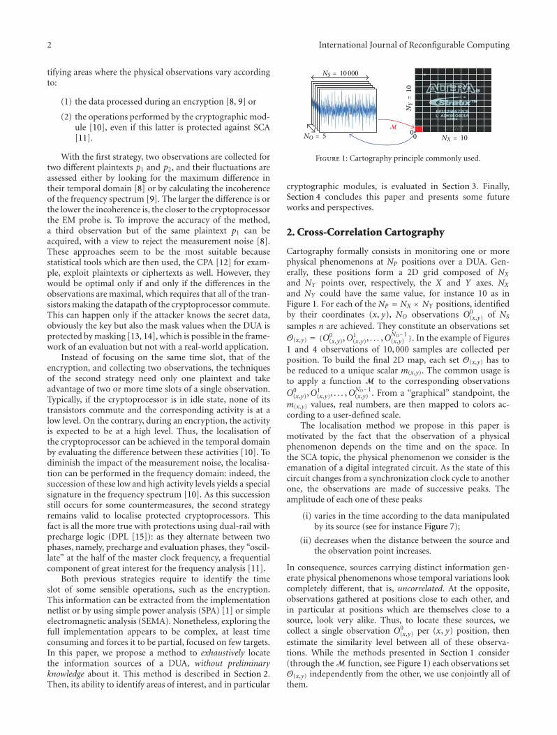
2 International Journal of Reconfigurable Computing
tifying areas where the physical observations vary accordingto:
(1) the data processed during an encryption [8, 9] or
(2) the operations performed by the cryptographic mod-ule [10], even if this latter is protected against SCA[11].
With the first strategy, two observations are collected fortwo different plaintexts p1 and p2, and their fluctuations areassessed either by looking for the maximum difference intheir temporal domain [8] or by calculating the incoherenceof the frequency spectrum [9]. The larger the difference is orthe lower the incoherence is, the closer to the cryptoprocessorthe EM probe is. To improve the accuracy of the method,a third observation but of the same plaintext p1 can beacquired, with a view to reject the measurement noise [8].These approaches seem to be the most suitable becausestatistical tools which are then used, the CPA [12] for exam-ple, exploit plaintexts or ciphertexts as well. However, theywould be optimal only if and only if the differences in theobservations are maximal, which requires that all of the tran-sistors making the datapath of the cryptoprocessor commute.This can happen only if the attacker knows the secret data,obviously the key but also the mask values when the DUA isprotected by masking [13, 14], which is possible in the frame-work of an evaluation but not with a real-world application.
Instead of focusing on the same time slot, that of theencryption, and collecting two observations, the techniquesof the second strategy need only one plaintext and takeadvantage of two or more time slots of a single observation.Typically, if the cryptoprocessor is in idle state, none of itstransistors commute and the corresponding activity is at alow level. On the contrary, during an encryption, the activityis expected to be at a high level. Thus, the localisation ofthe cryptoprocessor can be achieved in the temporal domainby evaluating the difference between these activities [10]. Todiminish the impact of the measurement noise, the localisa-tion can be performed in the frequency domain: indeed, thesuccession of these low and high activity levels yields a specialsignature in the frequency spectrum [10]. As this successionstill occurs for some countermeasures, the second strategyremains valid to localise protected cryptoprocessors. Thisfact is all the more true with protections using dual-rail withprecharge logic (DPL [15]): as they alternate between twophases, namely, precharge and evaluation phases, they “oscil-late” at the half of the master clock frequency, a frequentialcomponent of great interest for the frequency analysis [11].
Both previous strategies require to identify the timeslot of some sensible operations, such as the encryption.This information can be extracted from the implementationnetlist or by using simple power analysis (SPA) [1] or simpleelectromagnetic analysis (SEMA). Nonetheless, exploring thefull implementation appears to be complex, at least timeconsuming and forces it to be partial, focused on few targets.In this paper, we propose a method to exhaustively locatethe information sources of a DUA, without preliminaryknowledge about it. This method is described in Section 2.Then, its ability to identify areas of interest, and in particular
NO = 5M
00
NS = 10 000
NY=
10
NX = 10
Figure 1: Cartography principle commonly used.
cryptographic modules, is evaluated in Section 3. Finally,Section 4 concludes this paper and presents some futureworks and perspectives.
2. Cross-Correlation Cartography
Cartography formally consists in monitoring one or morephysical phenomenons at NP positions over a DUA. Gen-erally, these positions form a 2D grid composed of NX
and NY points over, respectively, the X and Y axes. NX
and NY could have the same value, for instance 10 as inFigure 1. For each of the NP = NX × NY positions, identifiedby their coordinates (x, y), NO observations O0
(x,y) of NS
samples n are achieved. They constitute an observations setO(x,y) = {O0
(x,y),O1(x,y), . . . ,O
NO− 1(x,y) }. In the example of Figures
1 and 4 observations of 10, 000 samples are collected perposition. To build the final 2D map, each set O(x,y) has tobe reduced to a unique scalar m(x,y). The common usage isto apply a function M to the corresponding observationsO0
(x,y),O1(x,y), . . . ,O
NO− 1(x,y) . From a “graphical” standpoint, the
m(x,y) values, real numbers, are then mapped to colors ac-cording to a user-defined scale.
The localisation method we propose in this paper ismotivated by the fact that the observation of a physicalphenomenon depends on the time and on the space. Inthe SCA topic, the physical phenomenon we consider is theemanation of a digital integrated circuit. As the state of thiscircuit changes from a synchronization clock cycle to anotherone, the observations are made of successive peaks. Theamplitude of each one of these peaks
(i) varies in the time according to the data manipulatedby its source (see for instance Figure 7);
(ii) decreases when the distance between the source andthe observation point increases.
In consequence, sources carrying distinct information gen-erate physical phenomenons whose temporal variations lookcompletely different, that is, uncorrelated. At the opposite,observations gathered at positions close to each other, andin particular at positions which are themselves close to asource, look very alike. Thus, to locate these sources, wecollect a single observation O0
(x,y) per (x, y) position, thenestimate the similarity level between all of these observa-tions. While the methods presented in Section 1 consider(through the M function, see Figure 1) each observations setO(x,y) independently from the other, we use conjointly all ofthem.

International Journal of Reconfigurable Computing 3ΓA
,B(d
)(%
)
02468
10
− 4 − 3 − 2 − 1 0 1 2 3 4
00.20.40.60.8
1
− 4 − 3 − 2 − 1 0 1 2 3 4
− 100− 50
050
100
− 4 − 3 − 2 − 1 0 1 2 3 4
A(a
.u.)
B(a
.u.)
n
n
d
(+2,90%)
Figure 2: From top to bottom: one reference signal A, the same Bbut with a lower amplitude and delayed by two samples, and theirnormalized cross-correlation function ΓA,B(d).
The first step of our technique consists in taking eachobservation O0
(x,y) as a reference, then looking for the maxi-mum of normalized cross-correlation (abridged NXC)between this reference and the other observations. The NXCfunction is defined as
ΓA,B(d)
=cov(A,Bd)σA ·σB
=
∑d+inf(NA,NB)− 1n= d
(A(n) − A(n)
)·(B(n − d) − B(n)
)√∑NA− 1
n= 0
(A(n) − A(n)
)2·
√∑NB− 1n= 0
(B(n − d) − B(n)
)2.
(1)
In (1), cov(·,·) stands for the covariance, A and B are twoobservations (at two different points), which, respectively,have NA and NB temporal samples, whose mean values areA(n) and B(n), and whose standard deviations are σA andσB. Bd means that a delay d belonging to the interval from− (NB − 1) to NA − 1 is applied to B. From a “graphical”standpoint, the waveform of B is shifted to the right alongthe temporal X-axis, or in other words the origin n = 0 of Bis moved to n = m. We simply abridge A0 as A and note thatσBd = σB because the standard deviation is considered overthe complete waveform (and is thus independent of the offsetd). Figure 2 shows the variations of the NXC function ΓA,B(d)according to the d values, when A and B are two signals withan identical shape, but distinct amplitudes, are delayed bytwo samples. The maximum value of ΓA,B(d) indicates thatA and B are 90% similar, while the index of this maximum,2, provides the sample delay between A and B. The value ofΓA,B(d) does not reach 100% because of computational side-effects: the X-axis is not infinite but bounds to [− 4; +4].
To briefly illustrate the result of such computation, weprovide two NXC maps on Figure 3. The first one, (a), has
been obtained considering the center of the map as thereference point. Maximum correlation values are at a verylow level, lightly positive in red on the map, or negativein blue, except for the reference point, which by definitionis 100% correlated to itself and takes the yellow point inthe center. It does not identify a source of interest, becauseit is insulated. On the second map, (b) of Figure 3, anarea of high correlation (in yellow) stands out around thereference point located at X = − 7.90 mm and Y = 12.0 mmand is marked with a white cross. This zone has a sizegreater than the actual active logic in the FPGA and notablyextends outside the silicon chip’s boundary, depicted in awhite dashed line. The diffusion of the EM field accountsfor this extension of a couple of millimeters around theradiating logic. Indeed, in our setup, the distance betweenthe loop sensor and the silicon surface is roughly speakingequal to 2 mm. Above, a second area emerges in blue, witha negative correlation value, as the observations correspondto EM field measurements, these ones, and in turn thecorrelation values, may be of opposite sign. But in reality, thissecond blue area contains the same information as the firstyellow area does. Therefore, to prevent such artifact, we nowconsider the absolute maximum values of the normalizedcross-correlation function.
Each observation gathered at a position of the 2D gridbecome in turn a reference observation, we finally collectNP NXC maps. Most of them are alike, as computed atneighbouring points, close to physical sources. The secondstep of our technique aims at grouping them. For thispurpose, we need once again a correlation estimator, butthis time, as we manipulate maps, this one should take intoaccount the two dimensions x and y. This bidimensionalestimator, namely, Γ2D
M,N (p, q), is defined as:
Γ2DM,N
(p, q
)=
cov(M,N(p,q)
)σM ·σN
, (2)
where
cov(M,N(p,q)
)=
xmax∑x= p
ymax∑y= q
(M(x, y
)− M(x, y)
)
·(N(x − p, y − q
)− N(x, y)
),
with xmax = p + inf(NXM ,NXN
)− 1
and ymax = q + inf(NYM ,NYN
)− 1,
σM =
√√√√√NXM∑x= 0
NYM∑y= 0
(M(x, y) − M(x, y)
)2,
σN =
√√√√√NXN∑x= 0
NYN∑y= 0
(N(x − p, y − q) − N(x, y)
)2.
(3)
In this equation, M and N are two maps, of NXM and NXN
points on x, NYM and NYN points on y, whose mean values

4 International Journal of Reconfigurable Computing
Γ(%
)
− 10 − 5 0 5 100
5
10
15
20
− 100
− 50
0
50
100Y
(mm
)
X (mm)
(a)
Γ(%
)
− 10 − 5 0 5 100
5
10
51
20
− 100
− 05
0
50
100
Area of interest
Y(m
m)
X (mm)
(b)
Figure 3: Normalized cross-correlation maps obtained when the reference point, marked with a white cross, is useless (a) or of interest (b).
are M(x, y) and N(x, y) and standard deviations σM andσN . N(p,q) means that a spacial offset is applied to the mapN , so that its origin point (0, 0) is moved to (p, q). Thisoffset is useful when the objective is to find the locationof a small pattern within a reference map. In this paper, aswe compare maps with identical size, p and q are set tozero. As previously, we fix a reference map, then we lookfor the maximum of the absolute value of Γ2D
M,N (p, q). If thismaximum is greater than a user-defined threshold, maps areconsidered as identical and grouped in the same list. Everylist is called an area of interest.
To finish the analysis, one map per list has to be extracted.It could be randomly chosen, but we suggest to select themap for which the number of points with a value aboveunder, respectively, a user-defined threshold is the greatest.The corresponding map is the one with the widest, nearestarea. The full method is summarized by the Algorithm 1. Inthis algorithm, the selection of areas of interest is representedby a function called “extract.”
3. Experimental Results
To evaluate the efficiency of our method, we have usedit against an FPGA-based cryptoprocessor performing thesimple and triple Data Encryption Standard (3DES) [16],and protected by first-order Boolean masking [13, 14]. Inpractice, we have implemented the same masking schemeas in [17]. We concur this design is obsolete for at leasttwo reasons. First of all, DES has been replaced by theAdvanced Encryption Standard (AES) [18] since the year2001. Second, the employed masking scheme is not robustagainst High-Order Side Channel Attack (HO-SCA) [17, 19].Nonetheless, the objective of this section is not to comeup with a new attack to break a still considered invulner-able countermeasure, but to experimentally prove that ourmethod identifies areas of interest, and in particular two
sensible 64-bit registers, LR and MASK, carrying respectivelythe masked value and the mask itself.
To make the experiment easier, we have constrainedtheir placement so that they may fit in rectangular areas,themselves placed at the opposite sides of the FPGA. Asdepicted by Figure 4, MASK is at the top left hand corner,while LR is at the bottom right hand corner. Splitting theseregisters in such a way has spread the routing of the 3DEScryptoprocessor datapath all over the FPGA. Therefore, in aview to keep the other components of our implementationvisible, for the 3DES datapath, only its logic cells aredisplayed. They appear as black dots in the upper half partof the floorplan. The KEY scheduling block is at the bottomright of Figure 4, in salmon, while the 3DES CONTROLler,in green, is in the middle, on the left. Close to this latter, wefind a 6502 CISC CPU in olive and an UART in turquoise.All previous components share a VCI bus along with itsmemories, in gold in Figure 4. This real-life application hasbeen programmed into a Xilinx [20] Virtex 5 FPGA, whosemetallic lid has been removed with a cutter, as shown inFigure 5. This way, not only we can reduce the analysis areastrictly to the FPGA silicon die, but the signal to noise ratiois also greatly improved.
Observations have been acquired using a 2 mm diameterEM probe, a 3 GHz bandwidth 30 dB gain preamplifier, andan Agilent [21] Infiniium 54854 oscilloscope, whose band-width and sampling rate have been set up to, respectively,3 GHz and 10 GSa/s. The EM probe has been moved follow-ing a 25× 25 points grid, per step of 480 μm along the X-axis,and 400 μm along the Y-axis. The grid is rather rectangular,since we covered the whole silicon die of the Virtex 5 (referto Figure 5): 12 mm wide and 10 mm high. Then, maps havebeen grouped together according to a threshold of 90%, thatis, two maps whose 2D cross-correlation coefficient is greaterthan 90% are considered as identical and gathered in thesame list. Finally, we have counted for each map the numberof points with a correlation level above 90%. From each list,

International Journal of Reconfigurable Computing 5
Require: One observation per pointEnsure: List of identical maps
For each 2D grid point (x, y) do {Fixed reference point A}{/ Looping over all fixed reference points A /}x re f xy re f yfor each 2D grid point (x, y) do
{/ Looping over all mobile points B /}m(x, y) maxd(|ΓO(x re f ,y re f ),O(x,y)(d)|)
end formap(x re f , y re f ) m
end fori 0 {/ Index of areas of interest /}for each 2D grid point (x, y) do
{/ Looping over all fixed reference points A /}x re f xy re f ylist[i] map(x re f , y re f )for each 2D grid point (x, y) do
{/ Looping over all mobile points B /}Mr map(x re f , y re f )Mc map(x, y)if Mc / list and max(|Γ2D
Mr ,Mc(0, 0)|) > threshold
thenlist[i] map(x, y)
end ifend fori i + 1
end forfor j = 0 to i do
area( j) extract (list[ j])end for
Algorithm 1: Algorithm for grouping maps per area of interest.
3DES datapath
LR
MASK
Figure 4: Floorplan of the cryptographic application under ISEfloorplanner.
we have extracted only the map with the greatest number ofsuch points.
Proceeding this way, we have obtained eleven areas ofinterest. The nine most significant ones are reported onFigure 6, with a disposition in the page that reflects theirlocation within the FPGA. As in Figure 3, reference points
Silicon die(backside)
PCB
Metalliclid
Thermalpaste
Figure 5: Photograph of the FPGA chip whose cryptographic mod-ules are to be located by cross-correlation cartography.
are marked with a white cross. The maps (a) and (i) pinpointtwo areas in the top left hand and bottom right hand corners.At first sight, they correspond to the two sensible registersLR and MASK. To confirm this, we have conducted largeacquisition campaigns of 1,000 observations per point, thencomputed for each of them the CEMA factor, that is, CPA(Correlation Power Analysis) with electromagnetic waves.We denote by ρ this CEMA factor, to distinguish it from Γ,the NXC coefficient defined in (1). Note that we use data
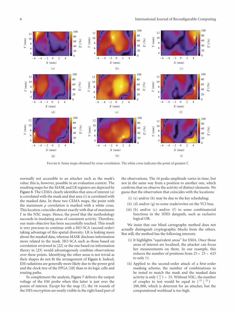
6 International Journal of Reconfigurable Computing
|Γ|
(%)
− 6 − 4 − 2 0 2 4
4
6
8
10
12
0
20
40
60
80
100
Y(m
m)
X (mm)
(a)
|Γ|
(%)
− 6 − 4 − 2 0 2 4
4
6
8
10
12
0
20
40
60
80
100
Y(m
m)
X (mm)
(b)
|Γ|
(%)
− 6 − 4 − 2 0 2 4
4
6
8
10
12
0
20
40
60
80
100
Y(m
m)
X (mm)
(c)
|Γ|
(%)
− 6 − 4 − 2 0 2 4
4
6
8
10
12
0
20
40
60
80
100
Y(m
m)
X (mm)
(d)
|Γ|
(%)
− 6 − 4 − 2 0 2 4
4
6
8
10
12
0
20
40
60
80
100
Y(m
m)
X (mm)
(e)
|Γ|
(%)
− 6 − 4 − 2 0 2 4
4
6
8
10
12
0
20
40
60
80
100
Y(m
m)
X (mm)
(f)
|Γ|
(%)
− 6 − 4 − 2 0 2 4
4
6
8
10
12
0
20
40
60
80
100
Y(m
m)
X (mm)
(g)
|Γ|
(%)
− 6 − 4 − 2 0 2 4
4
6
8
10
12
0
20
40
60
80
100
Y(m
m)
X (mm)
(h)
|Γ|
(%)
− 6 − 4 − 2 0 2 4
4
6
8
10
12
0
20
40
60
80
100
Y(m
m)
X (mm)
(i)
Figure 6: Some maps obtained by cross-correlation. The white cross indicates the point of greatest Γ.
normally not accessible to an attacker such as the mask’svalue: this is, however, possible in an evaluation context. Theresulting maps for the MASK and LR registers are depicted byFigure 8. The CEMA clearly identifies that area of interest (a)is correlated with the mask and that area (i) is correlated withthe masked data. In these two CEMA maps, the point withthe maximum ρ correlation is marked with a white cross.This location coincides almost exactly with that of maximumΓ in the NXC maps. Hence, the proof that the methodologysucceeds in insulating areas of consistent activity. Therefore,our main objective has been successfully reached. This resultis very precious to continue with a HO-SCA (second order)taking advantage of this spatial diversity: LR is leaking moreabout the masked data, whereas MASK discloses informationmore related to the mask. HO-SCA such as those based oncorrelation reviewed in [22] or the one based on informationtheory in [23] would advantageously combine observationsover these points. Identifying the other areas is not trivial astheir shapes do not fit the arrangement of Figure 4. Indeed,EM radiations are generally more likely due to the power gridand the clock tree of the FPGA [10] than to its logic cells androuting paths.
To complement the analysis, Figure 7 delivers the outputvoltage of the EM probe when this latter is just over thepoints of interest. Except for the map (f), the 16 rounds ofthe DES encryption are neatly visible in the right hand part of
the observations. The 16 peaks amplitude varies in time, butnot in the same way from a position to another one, whichconfirms that we observe the activity of distinct elements. Weguess that the observation that coincides with the locations:
(i) (e) and/or (h) may be due to the key scheduling;
(ii) (d) and/or (g) to some reads/writes on the VCI bus;
(iii) (b) and/or (c) and/or (f) to some combinatorialfunctions in the 3DES datapath, such as exclusivelogical OR.
We insist that our blind cartography method does notactually distinguish cryptographic blocks from the others.But still, the method has the following interests.
(i) It highlights “equivalent areas” for EMA. Once thoseareas of interest are localized, the attacker can focusher measurements on them. In our example, thisreduces the number of positions from 25 × 25 = 625to only 11.
(ii) Applied to the second-order attack of a first-ordermasking scheme, the number of combinations tobe tested to match the mask and the masked dataactivity is only
(112
)= 55. Without NXC, the number
of couples to test would be equal to(
25 × 252
)200, 000, which is deterrent for an attacker, but thecomputational workload is too high.

International Journal of Reconfigurable Computing 7
− 80− 60− 40− 20
02040
0 0.2 0.4 0.6 0.8 1
t (s)
EM
pro
be o
utp
ut
volt
age
(V)
(a)
− 30− 10
10
30
50
− 500 0.2 0.4 0.6 0.8 1
t (s)
(b)
− 30− 20− 10
0102030
0 0.2 0.4 0.6 0.8 1
t (s)
(c)
− 40− 30− 20− 10
010203040
0 0.2 0.4 0.6 0.8 1
t (s)
EM
pro
be o
utp
ut
volt
age
(V)
(d)
− 40− 20
020406080
0 0.2 0.4 0.6 0.8 1
t (s)
(e)
0 0.2 0.4 0.6 0.8 1− 20
− 10
0
10
20
t (s)
(f)
0 0.2 0.4 0.6 0.8 1− 15
− 55
15
25
35
t (s)
EM
pro
be o
utp
ut
volt
age
(V)
(g)
− 30− 20− 10
010203040
0 0.2 0.4 0.6 0.8 1
t (s)
(h)
− 100
− 60
− 20
20
60
0 0.2 0.4 0.6 0.8 1
t (s)
(i)
Figure 7: Output voltage of the EM probe when positioned over the points of interest.
|ρ|
(%)
− 6 − 4 − 2 0 2 4
4
6
8
10
12
0
20
40
60
80
100
X (mm)
Y(m
m)
(a)
|ρ|
(%)
− 6 − 4 − 2 0 2 4
4
6
8
10
12
0
20
40
60
80
100
X (mm)
Y(m
m)
(b)
Figure 8: CEMA maps obtained knowing the activity of the MASK (a) and LR (b) registers. The white cross indicates the point of greatest ρ.
4. Conclusion and Future Works
Many implementation-level attacks can be enhanced if thefloorplan of the application is known by the attacker. Forinstance, side-channel measurements can be made less noisyif focused on the most leaking zone, and fault injectionattacks (by electromagnetic waves or laser shots) have indeedmore chance to succeed in perturbing the adequate resourceif positioned well in a vicinity of the zone of influence. Asfar as ASICs are concerned, the location of each modulecan be guessed by an optical analysis of chip photographs.
Modern ASICs (such as modern smartcards) have theirlogic dissolved so as to make its analysis intractable. Now,regarding FPGAs, the problem is the same, since the fabric isextremely regular and does not show the location of the userdesign. In addition, FPGA chips are wider than ASICs, thusthe research for sensitive regions is a priori more complex.
In this paper, we introduce a novel location methodbased on cross-correlation of electromagnetic cartographies.It is indeed able to reveal the position of blocks. This showsthat the structure of the floorplan shall not be consideredconfidential in FPGAs, even if the bitstream is confidential

8 International Journal of Reconfigurable Computing
(e.g., encrypted). Then, we experimentally demonstrate thatthe cross-correlation location method is efficient to pinpointareas of interest in the context of a protected cryptographicapplication. This methodology illustrates a new aspect of thewealth of the information carried out by the electromagneticfield leaked by electronic devices. The floorplan reverse-engineering method presented in this paper is an algorithm-agnostic preliminary step that enables the further realizationof well-focused electromagnetic analysis attacks aiming thistime at extracting secrets. We have exemplified this methodwith the successful localization of the registers that holdthe mask and the masked data that are manipulated con-comitantly. Being able to record traces from both locationsallows for second-order attacks by combination of the twainmeasurements [24]. Also, the same method could be used torecord traces selectively from one half of separable dual-raillogic styles (such as SDDL [25, Section 3.1], DWDDL [26],divided backend duplication [27], partial DDL [28], or PA-DDL [29]) thereby defeating the complementation propertyof those “hiding” countermeasures.
References
[1] P. C. Kocher, J. Jaffe, and B. Jun, “Differential power analysis,”in Proceedings of the 19th Annual International CryptologyConference Advances in Cryptology (CRYPTO ’99), vol. 1666of Lecture Notes in Computer Science, pp. 388–397, Springer,Santa Barbara, Cali, USA, 1999.
[2] R. Anderson and M. Kuhn, “Tamper resistance—a cautionarynote,” in Proceedings of the 2nd USENIX Workshop on Elec-tronic Commerce (WOEC’96), pp. 1–11, USENIX Association,Berkeley, Calif, USA, 1996.
[3] K. Gandolfi, C. Mourtel, and F. Olivier, “Electromagneticanalysis: concrete results,” in Proceedings of the 3rd Inter-national Workshop Cryptographic Hardware and EmbeddedSystems (CHES’01), C. K. Koc, D. Naccache, and C. Paar, Eds.,vol. 2162 of Lecture Notes in Computer Science, pp. 251–261,Springer, Paris, France, 2001.
[4] M. Agoyan, J.-M. Dutertre, A.-P. Mirbaha, D. Naccache, A.-L. Ribotta, and A. Tria, “Single-bit DFA using multiple-bytelaser fault injection,” in Proceedings of the IEEE InternationalConference on Technologies for Homeland Security (HST’10),pp. 113–119, 2010.
[5] G. Canivet, J. Clediere, J. B. Ferron, F. Valette, M. Renaudin,and R. Leveugle, “Detailed analyses of single laser shot effectsin the configuration of a Virtex-II FPGA,” in 14th IEEEInternational On-Line Testing Symposium, (IOLTS ’08), pp.289–294, Rhodes, Greece, 2008.
[6] S. P. Skorobogatov, “Using optical emission analysis forestimating contribution to power analysis,” in Proceedingsof the 6th International Workshop on Fault Diagnosis andTolerance in Cryptography (FDTC ’09), pp. 111–119, IEEEComputer Society, Lausanne, Switzerland, 2009.
[7] J. Di-Battista, J.-C. Courrege, B. Rouzeyre, L. Torres, and P.Perdu, “When failure analysis meets side-channel attacks,” inProceedings of the 12th International Workshop CryptographicHardware and Embedded Systems (CHES ’10), Santa Barbara,Calif, USA, 2010.
[8] D. Real, F. Valette, and M. Drissi, “Enhancing correlationelectromagnetic attack using planar near-field cartography,”in Proceedings of the Design, Automation and Test in Europe,(DATE ’09), pp. 628–633, IEEE, Nice, France, April 2009.
[9] A. Dehbaoui, V. Lomne, P. Maurine, and L. Torres, “Magni-tude squared incoherence em analysis for integrated crypto-graphic module localisation,” Electronics Letters, vol. 45, no.15, pp. 778–780, 2009.
[10] L. Sauvage, S. Guilley, and Y. Mathieu, “ElectroMagneticradiations of FPGAs: high spatial resolution cartography andattack of a cryptographic module,” ACM Transactions onReconfigurable Technology and Systems, vol. 2, no. 1, pp. 1–24,2009.
[11] L. Sauvage, S. Guilley, J.-L. Danger, Y. Mathieu, and M.Nassar, “Successful attack on an FPGA-based WDDL DEScryptoprocessor without place and route constraints,” inProceedings of the Design, Automation and Test in Europe(DATE’09), pp. 640–645, IEEE, Nice, France, April, 2009.
[12] E. Brier, C. Clavier, and F. Olivier, “Correlation power analysiswith a leakage model,” in Proceedings of the 6th InternationalWorkshop Cryptographic Hardware and Embedded Systems(CHES’04), vol. 3156 of Lecture Notes in Computer Science, pp.16–29, Springer, Cambridge, Mass, USA, August, 2004.
[13] L. Goubin and J. Patarin, “DES and differential power analysis(The “Duplication” Method),” in Proceedings of the 1st Inter-national Workshop Cryptographic Hardware and EmbeddedSystems (CHES’99), vol. 1717 of Lecture Notes in ComputerScience, pp. 158–172, Worcester, Mass, USA, August, 1999.
[14] S. Chari, C. S. Jutla, J. R. Rao, and P. Rohatgi, “Towardssound approaches to counteract power-analysis attacks,” inProceedings of the 19th Annual International Cryptology Con-ference Advances in Cryptology (CRYPTO ’99), vol. 1666 ofLecture Notes in Computer Science, pp. 398–412, Springer,Santa Barbara, Calif, USA, August, 1999.
[15] J.-L. Danger, S. Guilley, S. Bhasin, and M. Nassar, “Overview ofdual rail with precharge logic styles to thwart implementation-level attacks on hardware cryptoprocessors,” in Proceedingsof the 3rd International Conference on Signals, Circuits andSystems (SCS’09), pp. 1–8, IEEE, Jerba, Tunisia, November2009.
[16] National Institute of Standards and Technology, “DataEncryption Standard (DES): FIPS PUB 46-3,” 1999,http://csrc.nist.gov/publications/fips/fips46-3/fips46-3.pdf. .
[17] E. Peeters, F.-X. Standaert, N. Donckers, and J.-J. Quisquater,“Improved higher-order side-channel attacks with FPGAexperiments,” in Proceedings of the 7th International WorkshopCryptographic Hardware and Embedded Systems (CHES ’05),vol. 3659 of Lecture Notes in Computer Science, pp. 309–323,Springer, Edinburgh, UK, 2005.
[18] National Institute of Standards and Technology, “AdvancedEncryption Standard (AES): FIPS PUB 197,” 2001,http://csrc.nist.gov/publications/fips/fips197/fips-197.pdf.
[19] T. S. Messerges, “Using second-order power analysis to attackDPA resistant software,” in Proceedings of the 2nd InternationalWorkshop Cryptographic Hardware and Embedded Systems(CHES’00), vol. 1965 of Lecture Notes in Computer Science, pp.238–251, Springer, Worcester, Mass, USA, August, 2000.
[20] “Xilinx FPGA designer,” http://www.xilinx.com/.[21] “Agilent Technologies,” http://www.home.agilent.com/.[22] E. Prouff, M. Rivain, and R. Bevan, “Statistical analysis of
second order differential power analysis,” IEEE Transactions onComputers, vol. 58, no. 6, pp. 799–811, 2009.
[23] B. Gierlichs, L. Batina, B. Preneel, and I. Verbauwhede,“Revisiting higher-order DPA attacks: multivariate mutualinformation analysis,” in Proceedings of the The Cryptographer’sTrack at RSA Conference (CT-RSA’10), vol. 5985 of LectureNotes in Computer Science, pp. 221–234, Springer, San Fran-cisco, Calif, USA, March 2010.
International Journal of Reconfigurable Computing 9
[24] E. Prouff, M. Rivain, and R. Bevan, “Statistical analysis ofsecond order differential power analysis,” IEEE Transactions onComputers, vol. 58, no. 6, pp. 799–811, 2009.
[25] K. Tiri and I. Verbauwhede, “A logic level design methodologyfor a secure DPA resistant ASIC or FPGA implementation,”in Proceedings of the Design, Automation and Test in EuropeConference and Exhibition (DATE’04), pp. 246–251, IEEEComputer Society, Paris, France, February 2004.
[26] P. Yu and P. Schaumont, “Secure FPGA circuits usingcontrolled placement and routing,” in Proceedings of the5th IEEE/ACM international conference on Hardware/softwarecodesign and system synthesis (CODES+ISSS’07), pp. 45–50,ACM, New York, NY, USA, 2007.
[27] K. Baddam and M. Zwolinski, “Divided Backend duplicationmethodology for balanced dual rail routing,” in Proceedingsof the Cryptographic Hardware and Embedded Systems (CHES’08), vol. 5154 of Lecture Notes in Computer Science, pp. 396–410, Springer, Washington, DC, USA, 2008.
[28] J.-P. Kaps and R. Velegalati, “DPA Resistant AES on FPGAUsing Partial DDL,” in Proceedings of the 18th IEEE AnnualInternational Symposium on Field-Programmable CustomComputing Machine (FCCM’10), pp. 273–280, IEEE Com-puter Society, Charlotte, NC, USA, May, 2010.
[29] W. He, E. D. L. Torre, and T. Riesgo, “A precharge-absorbedDPL logic for reducing early propagation effects on FPGAimplementations,” in Proceedings of the ReConFig, IEEE Com-puter Society, Quintana Roo, Mexico, 2011.
Hindawi Publishing CorporationInternational Journal of Reconfigurable ComputingVolume 2012, Article ID 675130, 11 pagesdoi:10.1155/2012/675130
Research Article
A Hardware Efficient Random Number Generator forNonuniform Distributions with Arbitrary Precision
Christian de Schryver,1 Daniel Schmidt,1 Norbert Wehn,1 Elke Korn,2
Henning Marxen,2 Anton Kostiuk,2 and Ralf Korn2
1 Microelectronic Systems Design Research Group, University of Kaiserslautern, Erwin-Schroedinger-Straße,67663 Kaiserslautern, Germany
2 Stochastic Control and Financial Mathematics Group, University of Kaiserslautern, Erwin-Schroedinger-Straße,67663 Kaiserslautern, Germany
Correspondence should be addressed to Christian de Schryver, [email protected]
Received 30 April 2011; Accepted 23 November 2011
Academic Editor: Ron Sass
Copyright © 2012 Christian de Schryver et al. This is an open access article distributed under the Creative Commons AttributionLicense, which permits unrestricted use, distribution, and reproduction in any medium, provided the original work is properlycited.
Nonuniform random numbers are key for many technical applications, and designing efficient hardware implementations of non-uniform random number generators is a very active research field. However, most state-of-the-art architectures are either tailoredto specific distributions or use up a lot of hardware resources. At ReConFig 2010, we have presented a new design that saves upto 48% of area compared to state-of-the-art inversion-based implementation, usable for arbitrary distributions and precision. Inthis paper, we introduce a more flexible version together with a refined segmentation scheme that allows to further reduce theapproximation error significantly. We provide a free software tool allowing users to implement their own distributions easily, andwe have tested our random number generator thoroughly by statistic analysis and two application tests.
1. Introduction
The fast generation of random numbers is essential for manytasks. One of the major fields of application are Monte Carlosimulation, for example widely used in the areas of financialmathematics and communication technology.
Although many simulations are still performed on high-performance CPU or general-purpose graphics processingunit (GPGPU) clusters, using reconfigurable hardware accel-erators based on field programmable gate arrays (FPGAs) cansave up to at least one order of magnitude of power con-sumption if the random number generator (RNG) is locatedon the accelerator. As an example, we have implementedthe generation of normally distributed random numberson the three mentioned architectures. The results for theachieved throughput and the consumed energy are given inTable 1. Since one single instance of our proposed hardwaredesign (together with a uniform random number generator)consumes less than 1% of the area on the used Xilinx Virtex-5 FPGA, we have introduced a line with the extrapolated
values for 100 instances to highlight the enormous potentialof hardware accelerators with respect to the achievablethroughput per energy.
In this paper, we present a refined version of the floatingpoint-based nonuniform random number generator alreadyshown at ReConFig 2010 [1]. The modifications allow ahigher precision while having an even lower area consump-tion compared to the previous results. This is due to a refinedsynthesis. The main benefits of the proposed hardwarearchitecture are the following:
(i) The area saving is even higher than the formerlypresented 48% compared to the state-of-the-artFPGA implementation of Cheung et al. from 2007[2].
(ii) The precision of the random number generator canbe adjusted and is mainly independent of the outputresolution of the auxiliary uniform RNG.

2 International Journal of Reconfigurable Computing
Table 1: Normal random number generator architecture comparison.
Implementation ArchitecturePower
consumptionThroughput
[M samples/s]Energy per
sample
Fast Mersenne Twister,optimized for SIMD
Intel Core 2 Duo PC 2.0 GHz,3 GB RAM, one core only
∼100 W 600 166.67 pJ
Nvidia Mersenne Twister+ Box-Muller CUDA Nvidia GeForce 9800 GT ∼105 W
1510 69.54 pJ
Nvidia Mersenne Twister+ Box-Muller OpenCL
1463 71.77 pJ
Proposed architecture, only oneinstance [1] Xilinx FPGA Virtex-5FX70T-3 380 MHz
∼1.3 W 397 3.43 pJ
Proposed architecture, 100 instances ∼1.9 W 39700 0.05 pJ
(iii) Our design is exhaustively tested by statistical andapplication tests to ensure the high quality of ourimplementation.
(iv) For the convenience of the user, we provide a free toolthat creates the lookup table (LUT) entries for anydesired nonuniform distribution with a user-definedprecision.
The rest of the paper is organized as follows. In Section2, we give an overview about current techniques to obtainuniform (pseudo-)random numbers and to transform themto nonuniform random numbers. Section 3 shows state-of-the-art inversion-based FPGA nonuniform random numbergenerators, as well as a detailed description of the newlyintroduced implementation. It also presents the LUT creatortool needed for creating the lookup table entries. Howfloating point representation can help to reduce hard-ware complexity is explained in Section 4. Section 5 showsdetailed synthesis results of the original and the improvedimplementation and elaborates on the excessive quality teststhat we have applied. Finally, Section 6 concludes the paper.
2. Related Work
The efficient implementation of random number generatorsin hardware has been a very active research field for manyyears now. Basically, the available implementations can bedivided into two main groups, that are
(i) random number generators for uniform distribu-tions,
(ii) circuits that transform uniformly distributed randomnumbers into different target distributions.
Both areas of research can, however, be treated as nearlydistinct. We will give an overview of available solutions outof both groups.
2.1. Uniform Random Number Generators. Many highlyelaborate implementations for uniform RNGs have beenpublished over the last decades. The main common charac-teristic of all is that they produce a bit vector with n bits thatrepresent (if interpreted as an unsigned binary-coded integerand divided by 2n − 1) values between 0 and 1. The set of all
results that the generator produces should be as uniformly aspossible distributed over the range (0, 1).
A lot of fundamental research on uniform randomnumber generation has already been made before 1994. Acomprehensive overview of the work done until that pointin time has been given by L’Ecuyer [3] who summarizedthe main concepts of uniform RNG construction and theirmathematical backgrounds. He also highlights the difficultiesof evaluating the quality of a uniform RNG, since in thevast majority of the cases, we are dealing not with trulyrandom sequences (as, e.g., Bochard et al. [4]), but withpseudorandom or quasirandom sequences. The latter onesare based on deterministic algorithms. Pseudorandomnessmeans that the output of the RNG looks to an observer likea truly random number sequence if only a limited periodof time is considered. Quasirandom sequences, however, donot aim to look very random at all, but rather try to cover acertain bounded range in a best even way. One major fieldof application for quasirandom numbers is to generate asuitable test point set for Monte Carlo simulations, in orderto increase the performance compared to pseudorandomnumber input [5, 6].
One of the best investigated high-quality uniform RNGsis the Mersenne Twister as presented by Matsumoto andNishimura in 1998 [7]. It is used in many technical appli-cations and commercial products, as well as in the RNGresearch domain. Well-evaluated and optimized softwareprograms are available on their website [8]. Nvidia hasadapted the Mersenne Twister to their GPUs in 2007 [9].
A high-performance hardware architecture for the Mer-senne Twister has been presented in 2008 by Chandrasekaranand Amira [10]. It produces 22 millions of samples persecond, running at 24 MHz. Banks et al. have comparedtheir Mersenne Twister FPGA design to two multiplierpseudo-RNGs in 2008 [11], especially for the use in finan-cial mathematics computations. They also clearly show thatthe random number quality can be directly traded off againstthe consumed hardware resources.
Tian and Benkrid have presented an optimized hardwareimplementation of the Mersenne Twister in 2009 [12], wherethey showed that an FPGA implementation can outperforma state-of-the-art multicore CPU by a factor of about 25, anda GPU by a factor of about 9 with respect to the throughput.The benefit for energy saving is even higher.
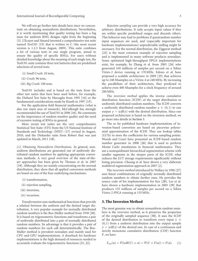
International Journal of Reconfigurable Computing 3
We will not go further into details here since we concen-trate on obtaining nonuniform distributions. Nevertheless,it is worth mentioning that quality testing has been a bigissue for uniform RNG designs right from the beginning[3]. L’Ecuyer and Simard invented a comprehensive test suitenamed TestU01 [13] that is written in C (the most recentversion is 1.2.3 from August, 2009). This suite combinesa lot of various tests in one single program, aimed toensure the quality of specific RNGs. For users withoutdetailed knowledge about the meaning of each single test, theTestU01 suite contains three test batteries that are predefinedselections of several tests:
(i) Small Crush: 10 tests,
(ii) Crush: 96 tests,
(iii) Big Crush: 106 tests.
TestU01 includes and is based on the tests from theother test suites that have been used before, for example,the Diehard Test Suite by Marsaglia from 1995 [14] or thefundamental considerations made by Knuth in 1997 [15].
For the application field financial mathematics (what isalso our main area of research), McCullough has stronglyrecommended the use of TestU01 in 2006 [16]. He commentson the importance of random number quality and the needof excessive testing of RNGs in general.
More recent test suites are the very comprehensiveStatistical Test Suite (STS) from the US National Institute ofStandards and Technology (NIST) [17] revised in August,2010, and the Dieharder suite from Robert that was justupdated in March, 2011 [18].
2.2. Obtaining Nonuniform Distributions. In general, non-uniform distributions are generated out of uniformly dis-tributed random numbers by applying appropriate conver-sion methods. A very good overview of the state-of-the-art approaches has been given by Thomas et al. in 2007[19]. Although they are mainly concentrating on the normaldistribution, they show that all applied conversion methodsare based on one of the four underlying mechanisms:
(i) transformation,
(ii) rejection sampling,
(iii) inversion,
(iv) recursion.
Transformation uses mathematical functions that providea relation between the uniform and the desired target dis-tribution. A very popular example for normally distributedrandom numbers is the Box-Muller method from 1958 [20].It is based on trigonometric functions and transforms a pairof uniformly distributed into a pair of normally distributedrandom numbers. Its advantage is that it provides a pair ofrandom numbers for each call deterministically. The Box-Muller method is prevalent nowadays and mainly used forCPU and GPU implementations. A drawback for hardwareimplementations is the high demand of resources needed toaccurately evaluate the trigonometric functions [21, 22].
Rejection sampling can provide a very high accuracy forarbitrary distributions. It only accepts input values if theyare within specific predefined ranges and discards others.This behavior may lead to problems if quasirandom numberinput sequences are used, and (especially important forhardware implementations) unpredictable stalling might benecessary. For the normal distribution, the Ziggurat method[23] is the most common example of rejection samplingand is implemented in many software products nowadays.Some optimized high-throughput FPGA implementationsexist, for example, by Zhang et al. from 2005 [24] whogenerated 169 millions of samples per second on a XilinxVirtex-2 device running at 170 MHz. Edrees et al. haveproposed a scalable architecture in 2009 [25] that achievesup to 240 Msamples on a Virtex-4 at 240 MHz. By increasingthe parallelism of their architecture, they predicted toachieve even 400 Msamples for a clock frequency of around200 MHz.
The inversion method applies the inverse cumulativedistribution function (ICDF) of the target distribution touniformly distributed random numbers. The ICDF convertsa uniformly distributed random number x ∈ (0, 1) to oneoutput y = icdf(x) with the desired distribution. Since ourproposed architecture is based on the inversion method, wego more into details in Section 3.
The so far published hardware implementations of in-version-based converters are based on piecewise polyno-mial approximation of the ICDF. They use lookup tables(LUTs) to store the coefficients for various sampling points.Woods and Court have presented an ICDF-based randomnumber generator in 2008 [26] that is used to performMonte Carlo simulations in financial mathematics. Theyuse a nonequidistant hierarchical segmentation scheme withsmaller segments in the steeper parts of the ICDF, whatreduces the LUT storage requirements significantly withoutlosing precision. Cheung et al. have shown a very elaboratemultilevel segmentation approach in 2007 [2].
The recursion method introduced by Wallace in 1996 [27]uses linear combinations of originally normally distributedrandom numbers to obtain further ones. He provides thesource code of his implementation for free [28]. Lee et al.have shown a hardware implementation in 2005 [29] thatproduces 155 millions of samples per second on a XilinxVirtex-2 FPGA running at 155 MHz.
3. The Inversion Method
The most genuine way to obtain nonuniform random num-bers is the inversion method, as it preserves the propertiesof the originally sampled sequence [30]. It uses the ICDFof the desired distribution to transform every input x ∈(0, 1) from a uniform distribution into the output sampley = icdf(x) of the desired one. In case of a continuous andstrictly monotone cumulative distribution (CDF) functionF, we have
Fout(α) = P(icdf(U) ≤ α) = P(U ≤ F(α)) = F(α). (1)
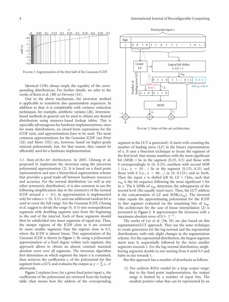
4 International Journal of Reconfigurable Computing
0 0.05 0.1 0.15 0.2 0.25 0.3 0.35 0.4 0.45 0.5x
−4.5−4−3.5−3−2.5−2−1.5−1−0.5
0
icdf
(x)
Figure 1: Segmentation of the first half of the Gaussian ICDF.
Identical CDFs always imply the equality of the corre-sponding distributions. For further details, we refer to theworks of Korn et al. [30] or Devroye [31].
Due to the above mechanism, the inversion methodis applicable to transform also quasirandom sequences. Inaddition to that, it is completable with variance reductiontechniques, for example, antithetic variates [26]. Inversion-based methods in general can be used to obtain any desireddistribution using memory-based lookup tables. This isespecially advantageous for hardware implementations, sincefor many distributions, no closed-form expressions for theICDF exist, and approximations have to be used. The mostcommon approximations for the Gaussian ICDF (see Peter[32] and Moro [33]) are, however, based on higher-graderational polynomials, but, for that reason, they cannot beefficiently used for a hardware implementation.
3.1. State-of-the-Art Architectures. In 2007, Cheung et al.proposed to implement the inversion using the piecewisepolynomial approximation [2]. It is based on a fixed pointrepresentation and uses a hierarchical segmentation schemethat provides a good trade-off between hardware resourcesand accuracy. For the normal distribution (as well as anyother symmetric distribution), it is also common to use thefollowing simplification: due to the symmetry of the normalICDF around x = 0.5, its approximation is implementedonly for values x ∈ (0, 0.5), and one additional random bit isused to cover the full range. For the Gaussian ICDF, Cheunget al. suggest to divide the range (0, 0.5) into nonequidistantsegments with doubling segment sizes from the beginningto the end of the interval. Each of these segments shouldthen be subdivided into inner segments of equal size. Thus,the steeper regions of the ICDF close to 0 are coveredby more smaller segments than the regions close to 0.5,where the ICDF is almost linear. This segmentation of theGaussian ICDF is shown in Figure 1. By using a polynomialapproximation of a fixed degree within each segment, thisapproach allows to obtain an almost constant maximalabsolute error over all segments. The inversion algorithmfirst determines in which segment the input x is contained,then retrieves the coefficients ci of the polynomial for thissegment from a LUT, and evaluates the output as y =∑ ci ·xiafterwards.
Figure 2 explains how, for a given fixed point input x, thecoefficients of the polynomial are retrieved from the lookuptable (that means how the address of the corresponding
−1
k
1
1
1 1 1
1 1 1 11 1
1 1 1 11 10 0 0 0
0
0 0 0
0
0
0 0 0 0
1 1 10
Sign
Fixed point input x
CountLZ
Logical left shifter
Nu
mbe
r of
lead
ing
zero
s (L
Z)
Shift outfirst 1
ROM
c 0 c 1
xsig
Fill up with 0
LZ + 1
· · ·
· · ·
<<
Figure 2: State-of-the-art architecture.
segment in the LUT is generated). It starts with counting thenumber of leading zeros (LZ) in the binary representationof x. It uses a bisection technique to locate the segment ofthe first level: that means numbers with the most significantbit (MSB) 1 lie in the segment [0.25, 0.5) and those with0 correspondingly in (0, 0.25), numbers with second MSB1 (i.e., x = 01 . . .) lie in the segment [0.125, 0.25) andthose with 0 (i.e., x = 00 . . .) in (0, 0.125), and so forth.Then the input x is shifted left by LZ + 1 bits, such thatxsig is the bit sequence following the most significant 1-bitin x. The k MSBs of xsig determine the subsegments of thesecond level (the equally sized ones). Thus, the LUT addressis the concatenation of LZ and MSBk(xsig). The invertedvalue equals the approximating polynomial for the ICDFin that segment evaluated on the remaining bits of xsig.The architecture for the case of linear interpolation [2] ispresented in Figure 2. It approximates the inversion with amaximum absolute error of 0.3 · 2−11.
The works of Lee et al. [34, 35] are also based on thissegmentation/LUT approach. They use the same techniqueto create generators for the log-normal and the exponentialdistributions, with only slight changes in the segmentationscheme. For the exponential distribution, the largest segmentstarts near 0, sequentially followed by the twice smallersegments towards 1. For the log-normal distribution, neigh-boring segments double in size starting from 0 until 0.5 andhalve in size towards 1.
But this approach has a number of drawbacks as follows.
(i) Two uniform RNGs needed for a large output range:due to the fixed point implementation, the outputrange is limited by a number of input bits. Thesmallest positive value that can be represented by an
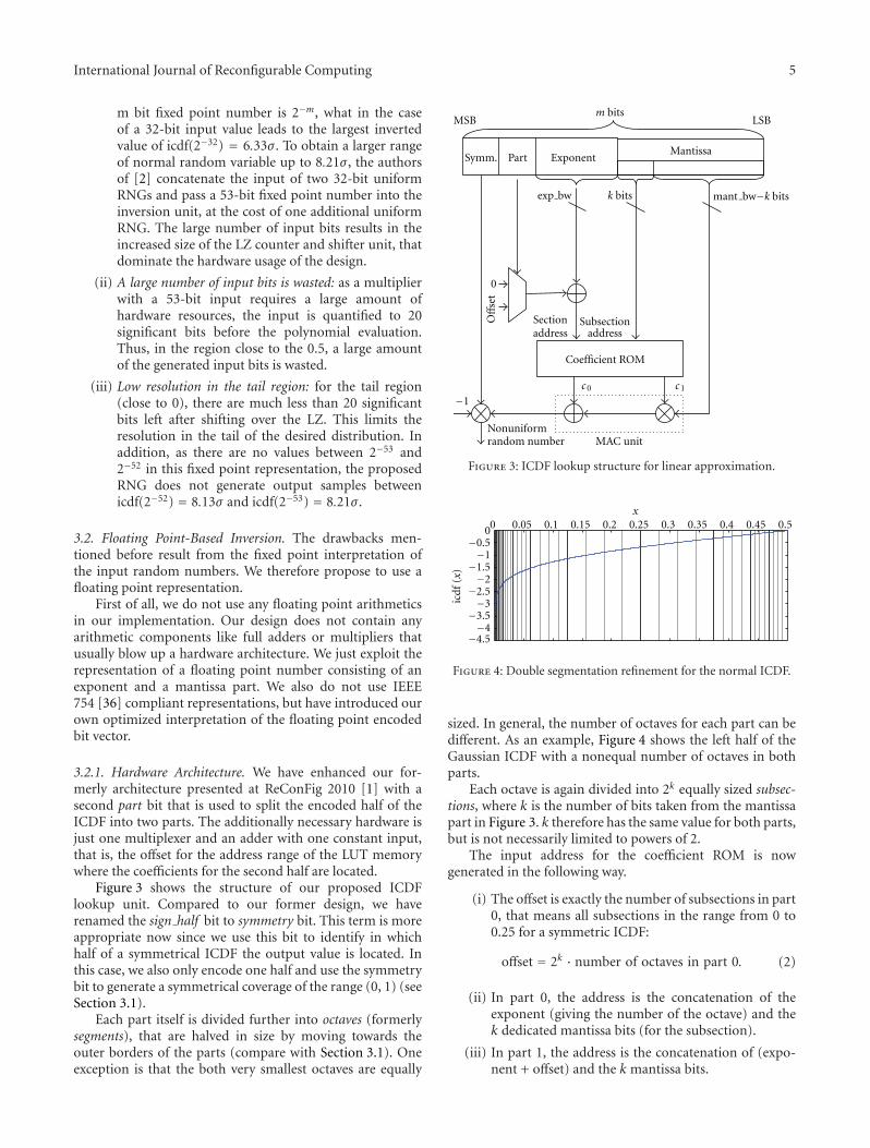
International Journal of Reconfigurable Computing 5
m bit fixed point number is 2−m, what in the caseof a 32-bit input value leads to the largest invertedvalue of icdf(2−32) = 6.33σ . To obtain a larger rangeof normal random variable up to 8.21σ , the authorsof [2] concatenate the input of two 32-bit uniformRNGs and pass a 53-bit fixed point number into theinversion unit, at the cost of one additional uniformRNG. The large number of input bits results in theincreased size of the LZ counter and shifter unit, thatdominate the hardware usage of the design.
(ii) A large number of input bits is wasted: as a multiplierwith a 53-bit input requires a large amount ofhardware resources, the input is quantified to 20significant bits before the polynomial evaluation.Thus, in the region close to the 0.5, a large amountof the generated input bits is wasted.
(iii) Low resolution in the tail region: for the tail region(close to 0), there are much less than 20 significantbits left after shifting over the LZ. This limits theresolution in the tail of the desired distribution. Inaddition, as there are no values between 2−53 and2−52 in this fixed point representation, the proposedRNG does not generate output samples betweenicdf(2−52) = 8.13σ and icdf(2−53) = 8.21σ .
3.2. Floating Point-Based Inversion. The drawbacks men-tioned before result from the fixed point interpretation ofthe input random numbers. We therefore propose to use afloating point representation.
First of all, we do not use any floating point arithmeticsin our implementation. Our design does not contain anyarithmetic components like full adders or multipliers thatusually blow up a hardware architecture. We just exploit therepresentation of a floating point number consisting of anexponent and a mantissa part. We also do not use IEEE754 [36] compliant representations, but have introduced ourown optimized interpretation of the floating point encodedbit vector.
3.2.1. Hardware Architecture. We have enhanced our for-merly architecture presented at ReConFig 2010 [1] with asecond part bit that is used to split the encoded half of theICDF into two parts. The additionally necessary hardware isjust one multiplexer and an adder with one constant input,that is, the offset for the address range of the LUT memorywhere the coefficients for the second half are located.
Figure 3 shows the structure of our proposed ICDFlookup unit. Compared to our former design, we haverenamed the sign half bit to symmetry bit. This term is moreappropriate now since we use this bit to identify in whichhalf of a symmetrical ICDF the output value is located. Inthis case, we also only encode one half and use the symmetrybit to generate a symmetrical coverage of the range (0, 1) (seeSection 3.1).
Each part itself is divided further into octaves (formerlysegments), that are halved in size by moving towards theouter borders of the parts (compare with Section 3.1). Oneexception is that the both very smallest octaves are equally
MSBm bits
LSB
Symm. Part ExponentMantissa
exp bw k bits mant bw−k bits
Off
set
0
Sectionaddress address
Subsection
Coefficient ROM
−1
Nonuniformrandom number MAC unit
c 0 c 1
Figure 3: ICDF lookup structure for linear approximation.
0 0.05 0.1 0.15 0.2 0.25 0.3 0.35 0.4 0.45 0.5x
−4.5−4−3.5−3−2.5−2−1.5−1−0.5
0
icdf
(x)
Figure 4: Double segmentation refinement for the normal ICDF.
sized. In general, the number of octaves for each part can bedifferent. As an example, Figure 4 shows the left half of theGaussian ICDF with a nonequal number of octaves in bothparts.
Each octave is again divided into 2k equally sized subsec-tions, where k is the number of bits taken from the mantissapart in Figure 3. k therefore has the same value for both parts,but is not necessarily limited to powers of 2.
The input address for the coefficient ROM is nowgenerated in the following way.
(i) The offset is exactly the number of subsections in part0, that means all subsections in the range from 0 to0.25 for a symmetric ICDF:
offset = 2k · number of octaves in part 0. (2)
(ii) In part 0, the address is the concatenation of theexponent (giving the number of the octave) and thek dedicated mantissa bits (for the subsection).
(iii) In part 1, the address is the concatenation of (expo-nent + offset) and the k mantissa bits.
6 International Journal of Reconfigurable Computing
Table 2: Selected tool configuration for provided error values.
Parameter Value
Growing octaves 54
Diminishing octaves 4
Subsection bits (k) 3
Mantissa bits (mant bw − k) 18
Output precision bits 42
This floating point-based addressing scheme efficientlyexploits the LUT memory in a hardware friendly way sinceno additional logic for the address generation is neededcompared to other state-of-the-art implementations (seeSections 2.2 and 3.1). The necessary LUT entries can easilybe generated with our freely available tool presented inSection 3.2.2.
3.2.2. The LUT Creator Tool. For the convenience of the userswho like to make use of our proposed architecture, we havedeveloped a flexible C++ class package that creates the LUTentries for any desired distribution function. The tool hasbeen rewritten from scratch, compared to the one presentedat ReConFig 2010 [1]. It is freely available for download onour website (http://ems.eit.uni-kl.de/).
Most of the detailed documentation is included in thetool package itself. It uses Chebyshev approximation, asprovided by the GNU Scientific Library (GSL) [37]. Themain characteristics of the new tool are as follows.
(i) It allows any function defined on the range (0,1) to be approximated. However, the GSL alreadyprovides a large number of ICDFs that may be usedconveniently.
(ii) It provides configurable segmentation schemes withrespect to
(i) symmetry,
(ii) one or two parts,
(iii) independently configurable number of octavesper part,
(iv) number of subsections per octave.
(iii) The output quantization is configurable by the user.
(iv) The degree of the polynomial approximation isarbitrary.
Our LUT creator tool also has a built-in error estimationthat directly calculates the maximum errors between theprovided optimal function and the approximated version.For linear approximation and the configuration shownin Table 2, we present a selection of maximum errors inTable 3. For optimized parameter sets that take the specificcharacteristics of the distributions into account, we expecteven lower errors.
Table 3: Maximum approximation errors for different distribu-tions.
Distribution Symmetry Maximum absolute error
Normal Point 0.000383397
Log-normal (0, 1) None 0.00233966
Gamma (0, 1) None 0.00787368
Laplace (1) Point 0.000901326
Exponential (1) None 0.000787368
Rayleigh (1) None 0.000300666
MSBm bits
LSB
Symm.
Symm.
Part
Part
Exponent
Exponent part
Counting direction
Mantissa
Mantissa part
LZ
Countleading zeros (LZ)
data valid Uniform floating point number
CTRL
mant bw bitsm−mant bw−2 bits
Uniform RNG(e.g. MT19937)
0
Figure 5: Architecture of the proposed floating point RNG.
4. Generating Floating Point Random Numbers
Our proposed LUT-based inversion unit shown inSection 3.2.1 requires dedicated floating point encodednumbers as inputs. In this section, we present an efficienthardware architecture for generating these numbers. Ourdesign consumes an arbitrary-sized bit vector from anyuniform random number generator and transforms it intothe floating point representation with adjustable precisions.In Section 5.2, we show that our floating point convertermaintains the properties of the uniform random numbersprovided by the input RNG.
Figure 5 shows the structure of our unit and how it mapsthe incoming bit vector to the floating point parts. Comparedto our architecture presented on ReConFig 2010 [1], we haveenhanced our converter unit with an additional part bit. Itprovides the information if we use the first or the secondsegmentation refinement of the ICDF approximation (seeSection 3.2).
For each floating point random number that is to begenerated, we extract the symmetry and the part bit in thefirst clock cycle, as well as the mantissa part that is justmapped to the output one to one. The mantissa part inour case is encoded with a hidden bit, for a bit width of

International Journal of Reconfigurable Computing 7
mant bw bits, it can therefore represent the values 1, 1 +(1/2mant bw), 1 + (2/2mant bw), . . . , 2− (1/2mant bw).
The exponent in our floating point encoding representsthe number of leading zeros (LZs) that we count from theexponent part of the incoming random number bit vector.We can use this exponent value directly as the segmentaddress in our ICDF lookup unit described in Section 3.2.1.In the hardware architecture, the leading zeros computationis, for efficiency reasons, implemented as a comparator tree.
However, if we would only consider one random numberavailable at the input of our converter, the maximum valuefor the floating point exponent would be m−mant bw − 2,with all the bits in the input exponent part being zero.To overcome this issue, we have introduced a parameterdetermining the maximum value of the output floating pointexponent, max exp. If now all bits in the input exponent partare detected to be zero, we store the value of already countedleading zeros and consume a second random number wherewe continue counting. For the case that we have again onlyzeros, we consume a third number and continue if eitherone is detected in the input part or the predefined maximumof the floating point exponent, max exp, is reached. In thiscase, we set the data valid signal to 1 and continue withgenerating the next floating point random number.
For the reason that we have to wait for further inputrandom numbers to generate one floating point result, weneed a stalling mechanism for all subsequent units of theconverter. Nevertheless, depending on size of the exponentpart in the input bit vector that is arbitrary, the probabilityfor necessary stalling can be decreased significantly. A secondrandom number is needed with the probability of P2 =1/2m−mant bw−2, a third with P3 = 1/22·(m−mant bw−2), and soon. For an input exponent part with the size of 10 bits, forexample, P2 = 1/210 = 0.976 · 10−3, which means that onaverage one additional input random number has to beconsumed for generating about 1,000 floating point results.
We have already presented pseudocode for our converterunit at the ReConFig 2010 [1] that we have enhanced now forour modified design by storing two sign bits. The modifiedversion is shown in Algorithm 1.
5. Synthesis Results and Quality Test
In addition to our conference paper presented at ReConFig2010 [1], we provide detailed synthesis results in thissection on a Xilinx Virtex-5 device, for both speed and areaoptimization. Furthermore, we show quality tests for thenormal distribution.
5.1. Synthesis Results. Like for the proposed architecturefrom ReConFig 2010, we have optimized the bit widths toexploit the full potential of the Virtex-5 DSP48E slice thatsupports an 18 · 25 bit + 48 bit MAC operation. We thereforeselected the same parameter values that are as follows: inputbitwidth m = 32, mant bw = 20, max exp = 54, and k = 3for subsegment addressing. The coefficient c0 is quantized to46 bits, and c1 has 23 bits.
We have synthesized our proposed design and thearchitecture presented at ReConFig with the newer Xilinx
rn← get random number();symmetr y ← rn.get symmetr y();part ← rn.get part();mant ← rn.get mantissa();exp ← rn.get exponent();LZ ← exp.count leading zeros();while (exp == 0) and (LZ < max exp) do∣∣∣∣∣∣∣rn← get random number();exp ← rn.get exponent();LZ ← LZ + exp.count leading zeros();
end
LZ ← min(LZ,max exp);return symmetr y, part, mant, LZ
Algorithm 1: Floating point generation algorithm.
Table 4: ReConFig 2010 [1]: optimized for speed.
Slices FFs LUTs BRAMs DSP48E
Floating point converter 30 62 40 — —
LUT evaluator 12 47 — 1 1
Complete design 40 108 39 1 1
Table 5: Proposed design: optimized for speed.
Slices FFs LUTs BRAMs DSP48E
Floating point converter 30 62 40 — —
LUT evaluator 18 47 7 1 1
Complete design 42 109 46 1 1
Table 6: ReConFig 2010 [1]: optimized for area.
Slices FFs LUTs BRAMs DSP48E
Floating point converter 13 11 26 — —
LUT evaluator 12 47 — 1 1
Complete design 26 84 26 1 1
ISE 12.4, allowing a fair comparison of the enhancementimpacts. Both implementations have been optimized for areaand speed, respectively. The target device is a Xilinx Virtex-5XC5FX70T-3. All provided results are post place and route.
From Tables 4 and 5, we see that just by using the newerISE version, we already save area of the whole nonuniformrandom number converter compared to the ReConFig resultthat was 44 slices (also optimized for speed) [1]. Themaximum clock frequency is now 393 MHz compared toformerly 381 MHz.
Even with the ICDF lookup unit extension described inSection 3.2.1, the new design is two slices smaller than in theformer version and can run at 398 MHz. We still consumeone 36 Kb BRAM and one DSP48E slice.
The synthesis results for area optimization are given inTables 6 and 7. The whole design now only occupies 31 sliceson a Virtex-5 and still runs at 286 MHz instead of 259 MHzformerly. Compared to the ReConFig 2010 architecture, we

8 International Journal of Reconfigurable Computing
Table 7: Proposed design: optimized for area.
Slices FFs LUTs BRAMs DSP48E
Floating point converter 13 11 26 — —
LUT evaluator 18 47 7 1 1
Complete design 31 85 34 1 1
therefore consume about 20% more area by achieving aspeedup of about 10% at a higher precision.
5.2. Quality Tests. Quality testing is an important part in thecreation of a random number generator. Unfortunately, thereare no standardized tests for nonuniform random numbergenerators. Thus, for checking the quality of our design, weproceed in three steps: in the first step, we test the floatingpoint uniform random number converter, and then we checkthe nonuniform random numbers (with a special focus onthe normal distribution here). Finally, the random numbersare tested in two typical applications: an option pricingcalculation with the Heston model [38] and the simulation ofthe bit error rate and frame error rate of a duo-binary turbocode from the WiMax standard.
5.2.1. Uniform Floating Point Generator. We have alreadyelaborated on the widely used TestU01 suite for uniformrandom number generators in Section 2.1. TestU01 needs anequivalent fixed point precision of at least 30 bits, and for thebig crush tests even 32 bits. The uniformly distributed float-ing point random numbers have been created as describedin Section 4 with a mantissa of 31 bits from the output of aMersenne Twister MT19937 [7].
The three test batteries small crush, crush, and big crushhave been used to test the quality of the floating pointrandom number generator. The Mersenne Twister itself isknown to successfully complete all except two tests. Thesetwo tests are linear complexity tests that all linear feedbackshift-register and generalized feedback shift-register-basedrandom number generators fail (see [13] for more details).Our floating point transform of Mersenne random numbersalso completes all but the specific two tests successfully.Thus, we conclude that our floating point uniform randomnumber generator preserves the properties of the inputgenerator and shows the same excellent structural properties.
For computational complexity reasons, for the followingtests, we have restricted the output bit width of the floatingpoint converter software implementation to 23 bits. Theresolution is lower than the fixed point input in someregions, whereas in other regions a higher resolution isachieved. Due to the floating point representation, theregions with higher resolutions are located close to zero.Figure 6 shows a zoomed two-dimensional plot of randomvectors produced by our design close to zero. It is importantto notice that no patterns, clusters, or big holes are visiblehere.
Besides the TestU01 suite, the equidistribution of ourrandom numbers has also been tested with several variants of
0
0.02
0.04
0.06
0.08
0.1
0 0.02 0.04 0.06 0.08 0.1
3 million × 3 million RNs, detail
Figure 6: Detail of uniform 2D vectors around 0.
the frequency test mentioned by Knuth [15]. While checkingthe uniform distribution of the random numbers up to12 bits, no extreme P value could be observed.
5.2.2. Nonuniform Random Number Generator. For thenonuniform random number generator, we have selected aspecific set of commonly applied tests to examine and ensurethe quality of the produced random numbers. In this paper,we focus on the tests performed for normally distributedrandom numbers, since those are most commonly used inmany different fields of applications. Also the applicationtests presented below use normally distributed randomnumbers.
As a first step, we have run various χ2-tests. In these tests,the empirical number of observations in several groups iscompared with the theoretical number of observations. Testresults that would only occur with a very low probabilityindicate a poor quality of the random numbers. This may bethe case if either the structure of the random numbers doesnot fit to the normal distribution or if the numbers showmore regularity than expected from a random sequence.The batch of random numbers in Figure 7 shows that thedistribution is well approximated. The corresponding χ2-testwith 100 categories had a P value of 0.4.
The Kolmogorov-Smirnov test compares the empiricaland the theoretical cumulative distribution function. Nearlyall tests with different batch sizes were perfectly passed. Thosenot passed did not reveal an extraordinary P value. A refinedversion of the test, as described in Knuth [15] on page 51,sometimes had low P values. This is likely to be attributed tothe lower precision in some regions of our random numbers,as the continuous CDF can not be perfectly approximatedwith random numbers that have fixed gaps. Other normalitytests were perfectly passed, including the Shapiro-Wilk [39]test. Stephens [40] argues that the latter one is more suitable

International Journal of Reconfigurable Computing 9
−3 −2 −1 0 1 2 3
1 million RNs
0
0.1
0.2
0.3
0.4
Den
sity
Figure 7: Histogram of Gaussian random numbers.
for testing the normality than the Kolmogorov-Smirnov test.The test showed no deviation from normality.
We not only compared our random numbers with thetheoretical properties, but also with those taken from thewell-established normal random number generator of the Rlanguage. It is based on a Mersenne Twister as well. Again,we used the Kolmogorov-Smirnov test, but no difference indistribution could be seen. Comparing the mean with thet-test and the variance with the F-test gave no suspiciousresults. The random numbers of our generator seem to havethe same distribution as standard random numbers, with anexception of the reduced precision in the central region andan improved precion in the extreme values. This differencecan be seen in Figures 8 and 9. Both depict the empiricalresults of a draw of 220 random numbers, the first with thepresented algorithm and the second with the RNG of R.
The tail distribution of the random numbers of thepresented algorithm seems to be better in the employed testset. The area of extreme values is fitted without large gapsin contrast to the R random numbers. The smallest valuefrom our floating point-based random number generator is1 · 2−54, compared to 1 · 2−32 in standard RNGs, thus valuesof−8.37σ and 8.37σ can be produced. Our approximation ofthe inverse cumulative distribution function has an absoluteerror of less than 0.4 · 2−11 in the achievable interval.Thus, the good structural properties of the uniform randomnumbers can be preserved. Due to the good properties ofour random number generator, we expect it to perform wellin the case of a long and detailed approximation, whererare extreme events can have a huge impact (consider risksimulations for insurances, e.g.).
5.2.3. Application Tests. Random number generators arealways embedded in a strongly connected application envi-ronment. We have tested the applicability of our normalRNG in two scenarios: first, we have calculated an option
0.0005
0.001
0.0015
0.002
0
dnor
m (
x)
3.5 4 4.5 5
x
normal RNs, extreme values220
Figure 8: Tail of the empirical distribution function.
0.0005
0.001
0.0015
0.002
0
dnor
m (
xR)
3.5 4 4.5 5
xR
normal R-RNs, extreme values220
Figure 9: Tail of the empirical distribution function for the R RNG.
price with the Heston model [38]. This calculation was doneusing the Monte Carlo simulation written in Octave. Theprovided RNG of Octave randn() has been replaced by abit true model of our presented hardware design. For thewhole benchmark set, we could not observe any peculiaritieswith respect to the calculated results and the convergencebehavior of the Monte Carlo simulation. For the secondapplication, we have produced a vast set of simulationsof a wireless communications system. For comparison toour RNG, a Mersenne Twister and inversion using theMoro approximation [33] has been used. Also in this test,

10 International Journal of Reconfigurable Computing
no significant differences between the results from bothgenerators could be observed.
6. Conclusion
In this paper, we present a new refined hardware architectureof a nonuniform random number generator for arbitrarydistributions and precision. As input, a freely selectableuniform random number generator can be used. Our unittransforms the input bit vector into a floating point notationbefore converting it with an inversion-based method to thedesired distribution. This refined method provides moreaccurate random numbers than the previous implemen-tation presented at ReConFig 2010 [1], while occupyingroughly the same amount of hardware resources.
This approach has several benefits. Our new implemen-tation saves now more than 48% of the area on an FPGAcompared to state-of-the-art implementations, while evenachieving a higher output precision. The design can run at upto 398 MHz on a Xilinx Virtex-5 FPGA. The precision itselfcan be adjusted to the users’ needs and is mainly independentof the output resolution of the uniform RNG. We provide afree tool allowing to create the necessary look-up table entriesfor any desired distribution and precision.
For both components, the floating point converter andthe ICDF lookup unit, we have presented our hardwarearchitecture in detail. Furthermore, we have providedexhaustive synthesis results for a Xilinx Virtex-5 FPGA. Thehigh quality of the random numbers generated by our designhas been ensured by applying extensive mathematical andapplication tests.
Acknowledgment
The authors gratefully acknowledge the partial financial sup-port from the Center for Mathematical and ComputationalModeling (CM)2 of the University of Kaiserslautern.
References
[1] C. de Schryver, D. Schmidt, N. Wehn et al., “A new hardwareecient inversion based random number generator for non-uniform distributions,” in Proceedings of the InternationalConference on Recongurable Computing and FPGAs (ReConFig’10), pp. 190–195, December 2010.
[2] R. C. C. Cheung, D.-U. Lee, W. Luk, and J. D. Villasenor,“Hardware generation of arbitrary random number distribu-tions from uniform distributions via the inversion method,”IEEE Transactions on Very Large Scale Integration (VLSI)Systems, vol. 15, no. 8, pp. 952–962, 2007.
[3] P. L’Ecuyer, “Uniform random number generation,” Annals ofOperations Research, vol. 53, no. 1, pp. 77–120, 1994.
[4] N. Bochard, F. Bernard, V. Fischer, and B. Valtchanov, “True-randomness and pseudo-randomness in ring oscillator-basedtrue random number generators,” International Journal ofReconfigurable Computing, vol. 2010, article 879281, 2010.
[5] H. Niederreiter, “Quasi-Monte Carlo methods and pseudo-random numbers,” American Mathematical Society, vol. 84, no.6, p. 957, 1978.
[6] H. Niederreiter, Random Number Generation and Quasi-Monte Carlo Methods, Society for Industrial Mathematics,1992.
[7] M. Matsumoto and T. Nishimura, “Mersenne twister: a 623-dimensionally equidistributed uniform pseudo-random num-ber generator,” ACM Transactions on Modeling and ComputerSimulation, vol. 8, no. 1, pp. 3–30, 1998.
[8] M. Matsumoto, Mersenne Twister, http://www.math.sci.hiro-shima-u.ac.jp/?m-mat/MT/emt.html, 2007.
[9] V. Podlozhnyuk, Parallel Mersenne Twister, http://developer.download.nvidia.com/compute/cuda/2 2/sdk/website/proje-cts/MersenneTwister/doc//MersenneTwister.pdf, 2007.
[10] S. Chandrasekaran and A. Amira, “High performance FPGAimplementation of the Mersenne Twister,” in Proceedings of the4th IEEE International Symposium on Electronic Design, Testand Applications (DELTA ’08), pp. 482–485, January 2008.
[11] S. Banks, P. Beadling, and A. Ferencz, “FPGA implementationof Pseudo Random Number generators for Monte Carlomethods in quantitative finance,” in Proceedings of the Inter-national Conference on Reconfigurable Computing and FPGAs(ReConFig ’08), pp. 271–276, December 2008.
[12] X. Tian and K. Benkrid, “Mersenne Twister random numbergeneration on FPGA, CPU and GPU,” in Proceedings of theNASA/ESA Conference on Adaptive Hardware and Systems(AHS ’09), pp. 460–464, August 2009.
[13] P. L’Ecuyer and R. Simard, “TestU01: a C library for empiricaltesting of random number generators,” ACM Transactions onMathematical Software, vol. 33, no. 4, 22 pages, 2007.
[14] G. Marsaglia, Diehard Battery of Tests of Randomness,http://stat.fsu.edu/pub/diehard/, 1995.
[15] D. E. Knuth, Seminumerical Algorithms, Volume 2 of The Artof Computer Programming, Addison-Wesley, Reading, Mass,USA, 3rd edition, 1997.
[16] B. D. McCullough, “A review of TESTU01,” Journal of AppliedEconometrics, vol. 21, no. 5, pp. 677–682, 2006.
[17] A. Rukhin, J. Soto, J. Nechvatal et al., “A statistical testsuite for random and pseudorandom number generators forcryptographic applications,” http://csrc.nist.gov/publications/nistpubs/800-22-rev1a/ SP800-22rev1a.pdf, Special Publica-tion 800-22, Revision 1a, 2010.
[18] G. B. Robert, Dieharder: A Random Number Test Suite,http://www.phy.duke.edu/?rgb/General/dieharder.php, Ver-sion 3.31.0, 2011.
[19] D. B. Thomas, W. Luk, P. H. W. Leong, and J. D. Villasenor,“Gaussian random number generators,” ACM ComputingSurveys, vol. 39, no. 4, article 11, 2007.
[20] G. E. P. Box and M. E. Muller, “A note on the generationof random normal deviates,” The Annals of MathematicalStatistics, vol. 29, no. 2, pp. 610–611, 1958.
[21] A. Ghazel, E. Boutillon, J. L. Danger et al., “Design andperformance analysis of a high speed AWGN communicationchannel emulator,” in Proceedings of the IEEE Pacific RimConference, pp. 374–377, Citeseer, Victoria, BC, Canada, 2001.
[22] D.-U. Lee, J. D. Villasenor, W. Luk, and P. H. W. Leong,“A hardware Gaussian noise generator using the box-mullermethod and its error analysis,” IEEE Transactions on Comput-ers, vol. 55, no. 6, pp. 659–671, 2006.
[23] G. Marsaglia and W. W. Tsang, “The ziggurat method forgenerating random variables,” Journal of Statistical Software,vol. 5, pp. 1–7, 2000.
[24] G. Zhang, P. H. W. Leong, D.-U. Lee, J. D. Villasenor, R. C.C. Cheung, and W. Luk, “Ziggurat-based hardware gaussianrandom number generator,” in Proceedings of the International

International Journal of Reconfigurable Computing 11
Conference on Field Programmable Logic and Applications (FPL’05), pp. 275–280, August 2005.
[25] H. Edrees, B. Cheung, M. Sandora et al., “Hardware-optimizedziggurat algorithm for high-speed gaussian random numbergenerators,” in Proceedings of the International Conference onEngineering of Recongurable Systems & Algorithms (ERSA ’09),pp. 254–260, July 2009.
[26] N. A. Woods and T. Court, “FPGA acceleration of quasi-montecarlo in finance,” in Proceedings of the International Conferenceon Field Programmable Logic and Applications (FPL ’08), pp.335–340, September 2008.
[27] C. S. Wallace, “Fast pseudorandom generators for normaland exponential variates,” ACM Transactions on MathematicalSoftware, vol. 22, no. 1, pp. 119–127, 1996.
[28] C. S. Wallace, MDMC Software—Random Number Gener-ators, http://www.datamining.monash.edu.au/software/ran-dom/index.shtml, 2003.
[29] D. U. Lee, W. Luk, J. D. Villasenor, G. Zhang, and P. H.W. Leong, “A hardware Gaussian noise generator using theWallace method,” IEEE Transactions on Very Large ScaleIntegration (VLSI) Systems, vol. 13, no. 8, pp. 911–920, 2005.
[30] R. Korn, E. Korn, and G. Kroisandt, Monte Carlo Methodsand Models in Finance and Insurance, Financial MathematicsSeries, Chapman & Hull/CRC, Boca Raton, Fla, USA, 2010.
[31] L. Devroye, Non-Uniform Random Variate Generation,Springer, New York, NY, USA, 1986.
[32] J. A. Peter, An algorithm for computing the inverse normalcumulative distribution function, 2010.
[33] B. Moro, “The full Monte,” Risk Magazine, vol. 8, no. 2, pp.57–58, 1995.
[34] D.-U. Lee, R. C. C. Cheung, W. Luk, and J. D. Villasenor, “Hier-archical segmentation for hardware function evaluation,” IEEETransactions on Very Large Scale Integration (VLSI) Systems,vol. 17, no. 1, pp. 103–116, 2009.
[35] D.-U. Lee, W. Luk, J. Villasenor, and P. Y. K. Cheung, “Hier-archical Segmentation Schemes for Function Evaluation,” inProceedings of the IEEE International Conference on Field-Programmable Technology (FPT ’03), pp. 92–99, 2003.
[36] IEEE-SA Standards Board. IEEE 754-2008 Standard forFloating-Point Arithmetic, August 2008.
[37] Free Software Foundation Inc. GSL—GNU Scientic Library,http://www.gnu.org/software/gsl/, 2011.
[38] S. L. Heston, “A closed-form solution for options withstochastic volatility with applications to bond and currencyoptions,” Review of Financial Studies, vol. 6, no. 2, p. 327, 1993.
[39] S. S. Shapiro and M. B. Wilk, “An analysis-of-variance test fornormality (complete samples),” Biometrika, vol. 52, pp. 591–611, 1965.
[40] M. A. Stephens, “EDF statistics for goodness of fit and somecomparisons,” Journal of the American Statistical Association,vol. 69, no. 347, pp. 730–737, 1974.

Hindawi Publishing CorporationInternational Journal of Reconfigurable ComputingVolume 2012, Article ID 615824, 10 pagesdoi:10.1155/2012/615824
Research Article
Hardware Middleware for Person Tracking on EmbeddedDistributed Smart Cameras
Ali Akbar Zarezadeh1 and Christophe Bobda2
1 Department of Computer Science, University of Potsdam, 14482 Potsdam, Germany2 Department of Computer Science and Computer Engineering, University of Arkansas, Fayetteville, AR 72701, USA
Correspondence should be addressed to Christophe Bobda, [email protected]
Received 29 April 2011; Accepted 6 December 2011
Academic Editor: Ron Sass
Copyright © 2012 A. A. Zarezadeh and C. Bobda. This is an open access article distributed under the Creative CommonsAttribution License, which permits unrestricted use, distribution, and reproduction in any medium, provided the original work isproperly cited.
Tracking individuals is a prominent application in such domains like surveillance or smart environments. This paper providesa development of a multiple camera setup with jointed view that observes moving persons in a site. It focuses on a geometry-based approach to establish correspondence among different views. The expensive computational parts of the tracker are hardwareaccelerated via a novel system-on-chip (SoC) design. In conjunction with this vision application, a hardware object request broker(ORB) middleware is presented as the underlying communication system. The hardware ORB provides a hardware/softwarearchitecture to achieve real-time intercommunication among multiple smart cameras. Via a probing mechanism, a performanceanalysis is performed to measure network latencies, that is, time traversing the TCP/IP stack, in both software and hardware ORBapproaches on the same smart camera platform. The empirical results show that using the proposed hardware ORB as client andserver in separate smart camera nodes will considerably reduce the network latency up to 100 times compared to the softwareORB.
1. Introduction
Smart cameras are embedded systems for performing imageanalysis directly at the sensor, and thus delivering descriptionof scene in an abstract manner [1]. Networks of multiplesmart cameras can be used to efficiently implement featureslike detection accuracy, fault tolerance, and robustness thatwould not have been possible with a single camera in suchapplications like surveillance or smart environments. In suchnetworks, smart camera nodes are usually embedded systemswith very tight design and operation requirements. Besidescomplex computations that must take place in real time,communication among the cameras has to be handled aswell. In embedded environment, the complex computationcan efficiently be handled using a combination of hardwareand software. While the hardware handles the most com-putational demanding tasks, the software takes care of thecontrol parts. By using FPGA as the main computationalcomponent, complex computation can be directly imple-mented in hardware, while the control part can be carried
out by an embedded processor. We used this approachin the design of an FPGA-based embedded smart cameraplatform [2]. Also, in our previous works [3, 4], we proposeda software/hardware codesign middleware approach, calledhardware ORB. The motivation for the hardware ORB wasto provide a low-latency intercommunication with determin-istic behavior among the smart camera nodes. The middle-ware enables developers to program distributed applicationsseamlessly, without having to focus on the details of theimplementation, thus reducing the development time [5].
The middleware provides designers to transparentlydescribe distributed systems. A lightweight agent-orientedmiddleware for distributed smart cameras was introduced byQuaritsch in his PhD thesis [1]. His middleware implementsbasic networking and messaging functionality for collabo-rative image processing. There are some existing hardwareimplementations of ORB which are exploited in the area ofsoftware-defined radio (SDR) systems. The integrated circuitORB (ICO) engine [6, 7] implements a hardware CORBAORB. PrismTech’s ICO is such an ORB in SDR applications.

2 International Journal of Reconfigurable Computing
The ICO engine is responsible for implementing the transfersyntax used in CORBA messages.
According to the network performance analysis, the Lin-ux kernel must be manipulated to collect timing measure-ments on internals. The data streams kernel interface (DSKI)instrumentation software was made for Linux [8]. It sup-ports gathering of system behavioral data from instrumenta-tion points inserted in kernel and application source. Demteret al., in [9], demonstrated the performance analysis of theTCP/IP stack for the Linux kernel, and then the time travers-ing of packets for each layer of the Linux kernel TCP/IP stackwas analyzed. Their idea to achieve network performanceanalysis inspired us to follow the same methodology withsome modification for extraction of the network latencies.
Adequate coverage of the critical areas is not feasiblewith only one camera. Inevitably, multiple cameras mustobserve an overlapping scene from different views. It pro-vides robustness against occlusion and improves accuracy[10]. The observations of an object on different capturedvideo streams must be identified as the same object. Itis of crucial importance to determine the correspondencebetween different views. Khan and Shah [10] introduced apure geometry-based approach without need for camera cal-ibration parameters. Calderara et al. [11] proposed anotherclass of geometry-based approach called homography andepipolar-based consistent labeling for outdoor park surveil-lance (HECOL). As the highlighted benefit, their methodidentifies people in groups by leveraging the probabilisticBayesian theory.
In [3], we proposed Common object Request BrokerArchitecture (CORBA) in the compact profile as a softwaremiddleware. Additionally, the hardware ORB for server sidewas proposed to overcome the limitations of the softwareORB running on an embedded platform in real-time appli-cations. The concept of the hardware ORB was extended intwo steps in [4]: (i) a new client hardware ORB as a pairof the sever hardware ORB and (ii) performance analysisof both hardware and software approaches for systematicmeasurement of the latencies.
This paper adds a distributed multicamera tracker layerwith jointed field of view (FoV) on top of our hardware ORBmiddleware. Tracking being a key part of high-level visualalgorithms, a wide variety of applications, like surveillance,human motion analysis, and traffic monitoring, can benefitfrom the results provided in this paper. The simultaneousassociation process in an overlapped camera setup demandstwofold constraints: (i) a real-time stand-alone tracker ateach camera node and (ii) tight data exchange mechanismamong multiple cameras with deterministic behavioral. Theexisting works mostly concentrate on the only softwareimplementations of vision algorithms and communicationmodules, leaving the optimal hardware/software implemen-tation, in particular in the embedded system open. Bypresenting such typical vision application, first our novelsystem-on-chip (SoC) architecture of a real-time stand-alonetracker based on an FPGA-based smart camera is demon-strated. It functions via segmentation process (object detec-tion) and object association (identification) steps. Seg-mentation algorithm demands an impressive amount of
computational power. By hardware acceleration of thesegmentation, we achieve an efficient implementation whichguaranties a real-time performance. Second, we prove theviability and versatility of our proposed communication in-frastructure based on the hardware ORB. Considering theparallelized internal nature of our hardware ORB, it appro-priately satisfies such constraints dictated by the upperapplication layer.
The rest of the paper is organized as follows: first, anexplanation of the methodology for finding the correspon-dence of an object which appears simultaneously on multipleoverlapping cameras is given in Section 2. In Section 3, anarchitectural view of the proposed system inside the smartcamera is presented. Afterwards, Section 4 is dedicated toexplain the protocol stack performance analysis on the basisof probing strategy implementation. Section 5 is devoted tothe experimental results. It reveals the obtained empiricalresults. Finally, the paper is briefly concluded in Section 6.
2. Tracker System
The focus of this section is the multiperson tracking in anoverlapping multi-camera setup. The tracking system classi-fies all the observations of the same person, grabbed fromdifferent cameras, into trajectories. In the case of failure ina camera node, the tracking process can uninterruptedly becontinued with other cameras, and trajectories of personsfrom various views can be merged [12]. Regarding the occlu-sion of the target person, the trajectories still can be keptupdated in all cameras via exchanging the extracted abstractfeatures in multiple cameras. The usage of multiple camerasrequires keeping consistent association among the differentviews of single persons. Put simply, it assigns the same labelto different instances of the same person acquired by differentcameras. This task is known as consistent labeling [10, 11].We divide the whole procedure into two off-line and on-line phases. At the off-line phase by reidentification of aknown person who moves in the camera FoVs, we extract theFoV lines and homography matrix by means of multiviewgeometry computations. Using the determined hypothesisfrom the off-line phase, we find the correspondence betweendifferent simultaneous observations of the same person inon-line phase.
2.1. Off-Line Phase. The off-line process aims at computingoverlapping constraints among camera views to create thehomography. This process applies for each pair of overlappedcameras. It performs the computation of the entry edges offield of view (EEoFoV). As the upper-left side of Figure 1shows, two adjacent cameras C1 and C2 have partiallyoverlapping view scenes. Our goal is to extract the FoVlines associated to the C2 in C1 and vice versa. The low-er-left side of Figure 1 depicts the defined overlappingzones Z1,2 and Z2,1 between the cameras C1 and C2, re-spectively, assuming a single person walks through the FoVsof the C1 and C2 and crosses the EEoFoVs of each indi-vidual camera. Once the person appears in the FoV ofa camera, an stand-alone tracker is allocated to him/her.
International Journal of Reconfigurable Computing 3
Camera 2
Camera 1Cam 2
P1
P4
P2P3
P2P1
P3
P4
Cam 1
Groungplane
58
10
12
11
976
3
1
2
4
Figure 1: Detecting the overlapping zones based on FoV lines (left), and gathered person trajectories in off-line phase (right).
In each new scan of the scene, the tracker keepsthe other neighbor camera updated about new position(lower support point) of the person. Integration of all thepositions represents the person’s trajectory.
As illustrated in the right side of Figure 1, after gath-ering adequate number of trajectories, we collect all pointswhich lay on the EEoFoVs and establish a set as Γ1,2={p1,2
1 , p1,22 , . . . , p1,2
12 }, where the subscripts indicate corre-sponding points in the two cameras. Afterwards, we elicit apolygon, which encompasses all points p1,2
i ∈ Γ1,2 with thebiggest covered area. In order to compute this polygon, weneed to find out if two points in the set Γ1,2 are adjacent. Ourstrategy consists of sorting out this set of points based onthe p1,2
i of the X and Y coordinates. First, we sort out all thep1,2i points based on the X values and then construct a new
set of points called Ω1,2. Now, to each element of the Ω1,2
a label equal to the element’s position at the set is assigned.Afterwards, we sort out the Ω1,2 considering the elements’ Yvalues and then form a new set of points referred to as Θ1,2.Figure 2 shows a 2D representation of the EEoFoV pointswhere each column is the Θ1,2 (sorting based on Y), andeach element of the column is the label assigned from sortingbased on X(Ω1,2). Let us start from the label 1 (point withthe lowest X value). At the first column from the positionof label 1, we look for its nearest adjacent point based onthe minimum Euclidean distance in the direction toward thebigger Y values. The point with label 3 has the minimumEuclidean distance. We continue this procedure up to the lastelement of the list with the highest Y value. Afterwards, wechange the direction backward from the highest to the lowestY values. After several iterations, all edges are computed.
Figure 3 shows the final computed graph where all ver-texes are the EEoFoV points sorted based on the X values and
5
8
10
4
2
12
1
11
3
9
7
6
1
5
8
10
4
2
12
1
11
3
9
7
6
5
8
10
4
2
12
1
11
3
9
7
6
5
8
10
4
2
12
1
11
3
9
7
6
5
8
10
4
2
12
1
11
3
9
7
6
5
8
10
4
2
12
1
11
3
9
7
6
5
8
10
4
2
12
1
11
3
9
7
6
5
8
10
4
2
12
1
11
3
9
7
6
5
8
10
4
2
12
1
11
3
9
7
6
5
8
10
4
2
12
1
11
3
9
7
6
5
8
10
4
2
12
1
11
3
9
7
6
Figure 2: Arrangement of gathered EEoFoV points based on X andY coordinate sorting.
1 2 3 4 5 6 7 8 9 10 11 12
Figure 3: Final computed graph representing the extracted poly-gon.
all edges are results of previous iterations. Hence, the polygonis extracted.
According to the sign alteration of the slope of lines,connecting the adjacent points (the right side of Figure 1),we classify all the points into four groups. Next, by meansof linear regression, the best line on each group is fitted, andthus, all FoV lines are computed. Intersection points between

4 International Journal of Reconfigurable Computing
the four lines in the cameras C1 and C2 (the four corners ofthe Z1,2 and Z2,1) are the best candidates for computation ofhomography matrix [11]. The homography matrixH1,2 fromcamera C1 to camera C2 is formulated as
⎡⎢⎢⎢⎣x1,2k
y1,2k
1
⎤⎥⎥⎥⎦ =
⎡⎢⎢⎢⎣h1,2
1,1 h1,21,2 h1,2
1,3
h1,22,1 h1,2
2,2 h1,22,3
h1,23,1 h1,2
3,2 h1,23,3
⎤⎥⎥⎥⎦×
⎡⎢⎢⎢⎣x2,1k
y2,1k
1
⎤⎥⎥⎥⎦. (1)
2.2. On-Line Phase. At the on-line process, once a cameranode detects a new object, it sends the person’s position to-gether with an accompanying wall clock time stamp to alloverlapped neighboring nodes. Hence, each node has itsown local knowledge of the detected person and also theexternal information received from its neighbors. The cor-respondence between the local and external informationmust be accomplished. Based on the computed FoV linesat the off-line phase, we determine whether the detectedperson is in the overlapping zone or not. If this condition isasserted, with using the computed ground-plane homogra-phy matrix, we convert the person’s locally extracted lowersupport point from the local coordinate to the externalcoordinate corresponding to the neighbor camera node. Byusing the temporal information (time stamp) and min-imum Euclidean distance between the spatial data (e.g.,distance between position of the person in local and externalobservations), we infer the correspondence. Provided thatthe person is only in the FoV of one camera, the history ofthat individual is applied to determine whether he is a newperson or the one who has been observed previously.
The on-line process must be performed repeatedly forevery acquired new video frame at all cameras. Thus, it im-poses two key constraints on the entire design: (i) a real-time stand-alone tracker at each camera node and (ii) a real-time data exchange mechanism among multiple cameras.Next Section 3 covers the architectural aspect of our imple-mented system inside the smart camera to tackle processingand communication tasks.
3. Smart Camera Internal Architecture
The focus of this section is the structure of hardware/softwareinside the FPGA, which is the computing element insideour smart cameras. To have an efficient partitioning of thehardware/software, we use different processes for implemen-tation of the communication and computer vision tasks.Our architecture consists of two processes: computer visionmodule (CVM) and communication module (CM).
3.1. Computer Vision Module. The CVM is a framework tolaunch the upper intelligence layer, which contains all therequired computer vision algorithms for processing the cap-tured raw video stream. As Figure 4 shows, it consists oftwo threads: serverPeer Thread (SPT) and ClientPeer Thread(CPT).
The CPT listens to the receiving events from the CMprocess inside the node. Based on the initial configuration, it
CVAppProcess
CommClientProcessCommServerProcess
Features
Neighbor no. 1
Object no. 1 features
Synch internal and external
ClientPeer Thread
Neighbor ListObj Tracker List
ServerPeer Thread
.
.
.
Object no. m features
Neighbor no. n
Obj Tracker no. 1
Obj Tracker no. n
Figure 4: Computer vision processor internal architecture.
SDICtrl
SDICtrl
MemCtrl
Bayerto
RGBFG
BGBG
VGA
CPU
PLB
bu
s
Segm
enta
tionImage
sensor
Figure 5: The hardware accelerated segmentation module.
generates a neighbor list, which includes all the node’s neigh-bors inside the cluster. At run time, this list keeps track ofpersons for a particular neighbor node. The SPT is designedto get query from the image sensor and subsequently runningupper layer computer vision algorithms cyclically. In eachcycle, it runs a locally stand-alone multiperson trackerfor detection and tracking purposes. Segmentation playsexplicitly a basic role for labeling the pixels as foreground(FG) or background (BG) pixels. The segmentation isperformed by the method proposed by Horprasert et al.[13]. To gain real-time performance in such a low levelpixel processing unit, the segmentation process is totallyoffloaded into the hardware. Figure 5 shows the SoC for thesegmentation process.
The SoC design presents a pipelined chain of IP coresfrom grabbing the raw image, conversion from the Bayer toRGB patterns, segmenting, and streaming data flow. Theintegrated algorithm inside the segmentation module com-pares an initially trained BG image to the current image.The decision for each pixel, whether an FG or BG, is madebased on the color and brightness distortions properties. Twostreaming data interface (SDI) controllers are employed forhandling the streaming data flow between a given individualIP core and memory [14].
The output FG image of the hardware segmentationmodule is readily accessible from the software tracker in apreassigned block of memory. The tracker exploits the FGimage to detect the moving persons in the scene. A newinstance of the tracker is instantiated for each new personin the scene. Each instance holds the extracted featuresfor an individual person. The SPT participates on finding

International Journal of Reconfigurable Computing 5
WirePHY
ETHHardware ORB
Mem Ctrl
Pro
cess
or
PLB
bu
s
NP
I
Streamingdata
interface
Videocompression
Imagesensor
Figure 6: The usage of the hardware ORB for video streaming.
SCTP/IP bit stream
Wire
ORB switch
PHYETH
Hardware ORB
MAC Ctrl
Protocol stack module
Filter
GIOP protocol
Mem intrfc
ICA
P
Reconfigurablemodule
UDP/IP bit stream
TCP/IP bit stream
Mem
Ctr
l
Pro
cess
or
PLB
bu
s
NPI
Figure 7: The general architecture of the hardware ORB IP core.
the association between its local person’s features and theexternal person’s features kept by the CPT. The mechanismfor the discovery of such a correspondence is based on thetracking algorithm explained in Section 2.
3.2. Communication Module. The CM acts as the output/input gates for pushing/pulling the locally generated eventsby the CVM to the cluster of cameras. It has an intercon-nection with the CVM through some of interprocess facili-ties, for example, shared memory. The hardware ORB is thecore engine of the CM. As a CORBA-based middleware IPcore, the hardware ORB allows clients in a real-time ma-nner to invoke operations on distributed objects withoutconcern about communication protocols. The hardwareORB server is responsible for replying determined requestsof the CORBA client hosted in a GPP or another smartcamera platform. Hence, a predefined block of memory canbe used as a CORBA servant object. Figure 6 shows theusage of the hardware ORB as a video streaming solutionfor the acquired video footage. In this case, it is supposedthat the compressed information of video stream resides in adetermined location of memory. Therefore, upon the requestof a client node in another smart camera node, the hardwareORB fetches such processed data from memory and thendirectly serializes and transmits it through the protocol stacktowards the client node. Figure 7 shows the overall anatomyof the hardware ORB IP core. The most considerable featureof such architecture is to have a redundant offloaded protocolstack in parallel operation with the embedded processor. Itsmain advantage is to have the possibility of using the networkservices on the operating system and also utilizing another
software ORB running on the embedded processor. Besidesthe usage of the software ORB, the hardware ORB plays therole of an auxiliary deterministic and real-time performancecommunication engine. Considering Figure 7, the ORBswitch shares the MAC layer between the processor and thehardware ORB. Basically, the hardware ORB can exchangethe contents of blocks of the memory through general inter-ORB protocol (GIOP), without the usage of the embeddedprocessor. It implements the lower layers of the standardTCP/IP stack and also supports the direct access to DDRmemory with the native port interface (NPI) of multiportmemory controller (MPMC). Figure 8 shows the internalarchitecture of the IP core as client/server node in more de-tails. To initiate a new transaction in the client side, theembedded processor must activate the transmission path bywriting in a specific register of the IP core. Then, based on thedefined responsibilities of GIOP such as common data rep-resentation (CDR) and interoperable object reference (IOR),it constructs the request message format and sends it downthrough the protocol stack. Afterwards, there are two sepa-rate transmission buffers, one for the embedded processorand another for the hardware ORB, called Tx buffer and hardORB Tx buffer, respectively. The ORB switch connects one ofthe two buffers to the MAC Tx controller for transmission.
The hardware ORB’s server mechanism is semanticallysimilar to the client’s one. Once the server receives a requestpacket from the Rx path of the protocol stack, if the packetsatisfies the filter criteria (i.e., the predefined TCP port num-ber and CORBA interoperable object reference), the serverfetches the relevant data from memory by a module, calledreader controller. Then the hardware ORB constructs theTCP/IP packet and finally stores it inside the hard ORB Txbuffer for transmission via the MAC Tx controller.
Once the client receives the reply from the server, thereplied packet comes up through the receiving path of thehardware ORB and finally is stored in the memory by meansof the writer controller. Moreover, the embedded processoris connected to the TX and RX dual port buffers of theMAC layer (Tx buffer and Rx buffer) by means of the PLBslave interface, and it enables the protocol stack on Linux.Referring to Figure 8, once a new packet arrives from theMAC Rx controller, one copy is placed inside the Rx bufferof the embedded processor and routed at the same time tothe Rx path of the protocol stack of the hardware ORB. Thehardware ORB listens to the incoming packets and looksfor the specific ones with a predefined TCP port numberand CORBA IOR. If the incoming packet satisfies the filtercriteria, first, with the masking of the Rx interrupt to theembedded processor, the hardware ORB blocks the interfaceto the embedded processor. It avoids racing between thehardware ORB and the embedded processor. Afterwards, thehardware ORB copies the received data to DDR memory bya module called writer controller.
4. Protocol Stack Performance AnalysisIn this section, the performance analysis methodology onthe basis of probing strategy is explained. We use the ter-minology of [15] to characterize the performance parameters
6 International Journal of Reconfigurable Computing
Writer CtrlP
roce
ssor
Rx filter
ETH-Tx
Wire
ETH-Rx
IP-Rx
TCP-Rx
Host to networklayer
Internet layer
Transportlayer (client)
GIOP-RxInter-ORB
protocol (client)
PLB
bu
s
Mem
Ctr
lNPI
DMAengine
PLBslave
interface
Txbuff
Rxbuff
MAC RxCtrl
MAC TxCtrl
ORBswitch
TxFIFO
RxFIFO
PHY
ETH
Hard ORBTx buff
IP-Tx
TCP-Tx
GIOP-Tx
Writer FIFO
ARP-Tx
ARPlookuptable
Address resolutionprotocol
Hardware ORB
Reader Ctrl
ReaderFIFO
ClientServer
Figure 8: The architecture of the hardware ORB client/server IP core.
(i.e., time of flight, sending/receiving overheads, injection/reception, transmission time, and bandwidth). For a networkwith only two devices, the bandwidth for injection (sending)is yielded by dividing the Packet size upon the maximumof the sending overhead and transmission time. The similarcalculation can be done for the bandwidth of reception bysubstitution of the receiving overhead instead of the sendingoverhead. Total data bandwidth supplied by network isdefined as aggregate bandwidth. The fraction of aggregatebandwidth that gets delivered to the application is effectivebandwidth or throughput [15],
Eff.bandwidth
= min(
2× BWLink Injection, 2× BWLink Reception
).
(2)
The goal of performance analysis is to determine theunderlying metrics such as sending and receiving overheadsand the time of flight. It is of particular interest to investigatethe protocol stack traversal times (GIOP/TCP/IP/ETH). InSections 4.1 and 4.2, we explain our methodology for prob-ing the software and hardware ORB approaches, respectively.
4.1. Software ORB Probing Strategy. Figure 9 illustrates theinternal mechanism for extraction of the protocol stack tra-versal times where two FPGA-based smart cameras are using
FPGA (smart camera)
Client
Request: getshortSeq()
FPGA (smart camera)
Server
Reply: seq of shortvalues
Fast ethernet
TAO CORBAcompact profile
TAO CORBAcompact profile
Ope
rati
ng
syst
em (
Lin
ux)
Ker
nel
Use
r
Ker
nel
Use
r
SocketTCPIP
Procentry
Probingpoints
Ope
rati
ng
syst
em (
Lin
ux)
SocketTCP
IPNet Dev DrvNet Dev Drv
Procentry
SyncDevDrv
SyncDevDrv
SYNC pulse
Figure 9: Software ORB experiment setup.
the software ORB. The big challenge here is how to accuratelytrack packets traversing the Linux kernel. To measure packettraversal, an additional time stamp probing code is addedto the Linux kernel code, similar to the approach in [9]. Asdepicted in Figure 9, a variety of probing points at severalpositions of the kernel’s protocol stack (including networkdevice driver, IP layer, TCP layer, and socket layer) are in-serted. A unique identification (ID) code is assigned to eachprobing point position. Later at the postprocessing phase of

International Journal of Reconfigurable Computing 7
performance analysis, those ID codes are used for packettracking across network protocol stack. The acquired timestamps relevant to each unique ID must be stored and madelater accessible in the user space for further analysis. Forstorage and access at initialization phase, a virtual memorysegment is allocated. Anytime the time stamp code inside theKernel is called, the acquired time stamp together with IDcode is written into this segment. To make the measurementresults transparent in the user space, a proc file entry as abridge between the kernel and user space is created. The procfile is a virtual file residing in the proc directory of Linux. Thisgives the possibility of reading the aforementioned kernelmemory segment into the user space. Therefore, based onour definition, each line of this proc entry file contains anID, which determines unique probing point and also a timestamp. Thus, after completing the test, the contents of thisproc entry are used for further analysis. However, for timesynchronization between two nodes (for measurement oftime of flight), two particular IO pins of FPGAs on bothcameras are connected by an external wire. On a certainpredetermined point of transaction, client node first recordsa time stamp and simultaneously asserts a pulse signal to theserver node to generate an interrupt there. At that point, theserver records a time stamp in its relevant interrupt serviceroutine (ISR). In the postprocessing analysis, on the basisof those time reference events, we reach to the same timereference in the client and server measured records. To havean access to this physical IO, another new Linux device driveron both client and server nodes is developed for handlingISR. Also, to have a seamless measurement results in theuser and kernel spaces for later postprocessing; again thementioned device driver is used. In fact, by calling the ioctl inthe user space, some particular probing points in the kernelspace are activated.
4.2. Hardware ORB Probing Strategy. The second probingstrategy (Figure 10) presents a realistic interconnection oftwo smart camera systems with fully utilization of thehardware ORB’s client and server. We perform measurementson the FPGA by monitoring some hardware probing pointsin the state diagram of each protocol stack layer and thenstarting and stopping a timer which gives us the best results.As Figure 10 shows, inside both client and server nodes, anauxiliary IP core called measurement tool is used. It countsprecisely the number of clock cycles between the start andstop commands coming from probing points placed in sev-eral layers of TCP/IP inside the hardware ORB. Therefore, theconsumed time is exactly determined. Also, for measurementof time of flight in the same manner like the software ORBprobing, particular IO pins of FPGAs on both cameras areconnected by an external wire. Once the server node sendsthe first bit of packet, it commands for starting of a counterinside. When the client receives this first bit, it notifies theserver node to stop counting via a pulse on the wire.
5. Experiments
We mounted three video cameras apart in our lab. Two sets ofour developed embedded FPGA-based smart camera systems
FPGA (smart camera)
Client
Request: getshortSeqand copy it to Mem
FPGA (smart camera)
Server
Reply: Xmit specifiedblock of Mem
Hardware ORB server
Fast ethernet
GIOP/TCP/IP/ETH
Hardware ORB client
GIOP/TCP/IP/ETH
Mea
sure
men
t to
ol
Mea
sure
men
t to
ol
SYNC pulse (time of flight calc)
Figure 10: Hardware ORB client and server experiment setup.
Table 1: The FPGA resource usage by the SoC design.
IP Core Flip-flop LUT BRAM
Segmentation 140 479 8
VGA out 73 248
Bayer 2 RGB 64 75 2
SDI Ctrl 0 1658 1867 2
SDI Ctrl 1 1522 1731 2
Mem Ctrl 8262 7172 19
Hard ORB 3787 4265 2
(PICSy) [2] were interconnected to a desktop PC with log-itech Webcam C500. PICSy features a Virtex4 (Xilinx) FPGAdevice with a PowerPC 405 clocked at 300 MHz. OpenCVwas used for implementation of computer vision algorithms.TAO [16] was applied as the middleware for exchanging theabstract information between cameras. Table 1 shows theFPGA resource usage by each IP core in the SoC design.We first program the cameras to identify multiple personsrandomly walking on the site. The following sequence wasconducted between the adjacent neighboring nodes. When awalking person appeared in the FOV of a camera, the cameragenerated a new event at each captured video frame. Thepayload of event was the person’s extracted lower supportpoint and the wall clock. The camera cyclically supplied itsother neighboring consumer nodes with those features. Itwas of particular interest to measure the performance of thesegmentation module on both smart camera and desktopPC. A PC with Intel Core2Duo running at 3.16 GHz neededan approximately 23 ms to compute the FG for a 640 ×480 sized image. In comparison to the PC, the superiorityof the hardware-implemented module was achieved by afactor of ≈7 (≈3.8 ms). Furthermore, the entire procedurefrom the acquiring one video frame to putting the FG intothe memory took ≈34 ms (the pixel clock of the imagesensor was 48 MHz). Next, we investigated intercameracommunication as follows:
(i) software ORBs running on both cameras (Figure 9);
(ii) hardware ORBs hosted on both cameras (Figure 10).
CORBA TAO client and server ran on both smart camerashaving Linux with kernel 2.6.31 and TAO version 1.7.3 as

8 International Journal of Reconfigurable Computing
CORBA client CORBA server
X.SYN 2905 R.SYN 391
X.SYN ACK 2804R.SYN ACK 333
X.ACK 2030 R.ACK 310
R.GIOP Req 244
X.ACK 2781
X.GIOP reply 2758
R.ACK 170
R.FIN ACK 218
X.FIN ACK 2841
R.ACK 196
X.GIOP Req 2767
R.ACK 185
R.GIOP reply 233
X.ACK 2756
X.FIN ACK 2805
R.FIN ACK 298
X.ACK 2740
USR-Start
Socket
Socket-ACCEPT
Socket 5167
USR-Finish
Socket 2277
1316
15672
3114
133
3877
3052
75
T1
T2
1358
5167
5347
0
112
3087
4056
2283
59
9685
T3
T4
2318
37
3059
Createbind
connect
Figure 11: Measured latency values (in μs) from CORBA IIOPtransaction state diagram for software ORB.
ORB. In both test scenarios, the measurements were achievedwith a CORBA client invoking on a CORBA servant theoperation getshortSeq(), returning a short sequence value asa result of operation. The network nodes were connectedto each other directly without any other interfaces. In bothbenchmarks, the whole progress is repeated for differentvalues of the ShortSequence parameter length, doubling thepayload size starting from 32 bytes up to 1408 bytes. Thetests were performed with the network interface speed of100 Mbps.
Figures 11 and 12 show the transaction state diagramsin both client and server nodes based on the on-the-wireprotocol of CORBA (internet inter-ORB protocol (IIOP)),corresponding to the software ORB and hardware ORBapproaches.
Here, the major focus was on the demonstration of thepacket processing time when traversing the protocol stacklayers. In both Figures 11 and 12, X. stands for transmitand R. for receive, respectively. There is one number insideof each state, which represents measured processing time(μs) for that particular state. There is another number inFigure 11, related to each two adjacent states, which showsthe waiting time for either receiving a special event from theother node or interprocessing time between two consequentstates in the same node. Depending on the payload size,there are some variable timing values in both figures, called
CORBA client CORBA server
X.SYN 10.09 R.SYN
X.SYN ACK 9.97R.SYN ACK
X.ACK 9.035 R.ACK
R.GIOP Req
X.ACK 8.645
X.GIOP reply T5
R.ACK
R.FIN ACK
X.FIN ACK 8.925
R.ACK
X.GIOP Req 19.955
R.ACK
R.GIOP reply T6
X.ACK 9.32
X.FIN ACK 9.14
R.FIN ACK
X.ACK 9.055
USR-Start
Figure 12: Measured latency values (in μs) from CORBA IIOPtransaction state diagram for hardware ORB.
T1
T2
T3
T4
T5
T6
Payload (byte)
32 64 128 256 512 1024 1408
0
50
100
150
200100020003000400050006000700080009000
1000011000
Tim
e (m
s)
Figure 13: Timing parameters for Figures 11 and 12.
T1, T2, T3, T4, T5, and T6 which are shown in Figure 13,as well. Considering Figure 11, the whole transaction startswith invoking the operation getshortSeq() in the client nodein the user space application. It corresponds to USR-startstate. Afterwards, there are some interactions between theclient and server across the TCP state diagram. Finally, USR-finish is the point where the application receives the requestresults. Figure 12 demonstrates the same story for the hard-ware ORB implementation. But there are some remarkabledifferences. First, in the software ORB approach, a very costlyprocedure is placed between USR-start state and X.SYN inthe client side. It consists of the CORBA internal processing

International Journal of Reconfigurable Computing 9
Payload (byte)
32 64 128 256 512 1024 1408
Ban
dwid
th (
Kbp
s)
050
100150200250300
2000
4000
6000
8000
10000
12000
14000
16000
Link injection softLink injection hardLink reception soft
Link reception hardEff. Bandwidth softEff. Bandwidth hard
Figure 14: Comparison of latencies between software and hardwareORBs.
tasks in the user space and then coming through the socketoperation in the kernel space, and thereafter, starting the TCPstate diagram (X.SYN). According to our experiments, thissegment is very expensive and nondeterministic. The secondtime-consuming zone is positioned between X.ACK andX.GIOP reply states in the server side. It constructs the majorpart of link injection time. Finally, the third critical pointappears in the client side when delivering the received data tothe user space application. On the contrary, the entire clientand server transactions in the hardware ORB approach aresummarized in the pure TCP state diagram, and it drasticallyshrinks the overheads. It is interesting to mention that theprocessing time for the whole transaction is 100 times fasterthan the software ORB. Furthermore, it should be notedthat on the receiving side of each state in the hardwareORB, there are no timing values due to its pipeliningnature. Collectively, considering the measurement of the linkinjection and reception in both benchmarks, Figure 14 showsthe calculated bandwidth based on the different payloads.In terms of the software ORB, the measured time for T1
on the client side, as a good representation of the serverprocessing time, is used for the link injection parameterand summation of T2 and T3 for the link reception. Inthe same manner, T5 and T6 parameters are used for linkinjection and link reception in the hardware ORB approach.As it can be seen in Figure 14, the proposed hardware ORBwill greatly increase the network throughput, much betterthan the software ORB. Additionally, a combination of thehardware ORBs client and server provides a realistic solutionfor interconnection between two smart cameras, resulting inhuge improvement of the network latency, thus guaranteeinga real-time behavior. Judging from the data in this graph,the trend for the software ORB is continuing in the higherpayload sizes. It can be easily concluded from Figure 14 thatthe software ORB is realizable when having higher payloadsize.
6. Conclusion and Future Research
Through this paper, we demonstrated the concept of adistributed person tracker system as an upper layer on top ofthe communication layer. The tracker leverages a geometry-based approach to establish correspondence among differentviews in an overlapped installed camera setup. The SoC de-sign of an FPGA-based smart camera was presented. The de-sign has emerged as a novel hardware/software architectureaimed at enforcing the real-time requirement of image proc-essing applications. Experimental results reveal that the lowlevel pixel processing hardware implemented module out-performed the PC one by the factor of 7. To provide therequired communication facilities dictated by upper appli-cation layer, that is, distributed person tracker, we provideda real-time hardware/software intercommunication systemamong smart camera nodes, the hardware ORB which drasti-cally shrinks the network latencies. Moreover, an exhaustiveperformance analysis was accomplished to accurately trackpackets traversing inside the Linux kernel. Very outstandingadvantage of the hardware ORB in terms of speed waspointed out in favor of using gate-level implementationrather than embedded processor. The outlook of this workincludes the model of the person tracker. Because ofoccurrence of segmentation noise and also instant arrivalof group of people to scene, such simple solution is not astable one. Considering the proposed method by Calderaraet al. in [11], such kind of probabilistic models like Bayesianframework is a promising solution to increase the certaintyand stability of the tracker system.
References
[1] M. Quaritsch, A lightweight agent-oriented middleware for dis-tributed smart cameras, Ph.D. dissertation, Graz University ofTechnology, 2008.
[2] C. Bobda, A. A. Zarezadeh, F. Muhlbauer, R. Hartmann, andK. Cheng, “Reconfigurable architecture for distributed smartcameras,” in Proceedings of the Engineering of ReconfigurableSystems and Algorithms (ERSA ’10), pp. 166–178, 2010.
[3] A. A. Zarezadeh and C. Bobda, “Hardware orb middleware fordistributed smart camera systems,” in Proceedings of the En-gineering of Reconfigurable Systems and Algorithms (ERSA ’10),pp. 104–116, 2010.
[4] A. A. Zarezadeh and C. Bobda, “Performance analysis of hard-ware/software middleware in network of smart camera sys-tems,” in Proceedings of the International Conference on Recon-figurable Computing and FPGAs (ReConFig ’10), pp. 196–201,2010.
[5] The evolution from single to pervasive smart cameras, 2008.[6] F. Humcke, “Making fpgas first class sca citizens,” SDR Forum
Technical Conference, 2006.[7] F. Casalino, G. Middioni, and D. Paniscotti, “Experience re-
port on the use of corba as the sole middleware solution in sca-based sdr environments,” SDR Forum Technical Conference,2008.
[8] “Data streams kernel interface,” http://www.ittc.ku.edu/kusp/initial/initial datastreams.html.
[9] J. Demter, C. Dickmann, H. Peters, N. Steinleitner, and X. Fu,“Performance analyzer of the tcp/ip stack of linux kernel2.6.9,” http://user.informatik.uni-goettingen.de/.

10 International Journal of Reconfigurable Computing
[10] S. Khan and M. Shah, “Consistent labeling of tracked objectsin multiple cameras with overlapping fields of view,” IEEETransactions on Pattern Analysis and Machine Intelligence, vol.25, no. 10, pp. 1355–1360, 2003.
[11] S. Calderara, A. Prati, and R. Cucchiara, “HECOL: homogra-phy and epipolar-based consistent labeling for outdoor parksurveillance,” Computer Vision and Image Understanding, vol.111, no. 1, pp. 21–42, 2008.
[12] S. Velipasalar, Peer-to-peer tracking for distributed smart cam-eras, Ph.D. dissertation, Princeton University, 2007.
[13] T. Horprasert, D. Harwood, and L. S. Davis, A StatisticalApproach for Real-Time Robust Background Subtraction andShadow Detection, vol. 99, Citeseer, 1999.
[14] F. Muhlbauer, L. O. M. Rech, and C. Bobda, “Hardware Ac-celerated OpenCV on System on Chip,” Reconfigurable Com-munication-Centric Systems-on-Chip Workshop, 2008.
[15] T. M. Pinkston and J. Duato, Interconnection Networks—Ap-pendix E of Computer Architecture: A Quantitative Appraoch,Morgan Kaufmann, 4th edition, 2006.
[16] “The ace orb,” http://www.cs.wustl.edu/∼schmidt/TAO-status.html.

Hindawi Publishing CorporationInternational Journal of Reconfigurable ComputingVolume 2012, Article ID 219717, 10 pagesdoi:10.1155/2012/219717
Research Article
Exploration of Uninitialized Configuration Memory Space forIntrinsic Identification of Xilinx Virtex-5 FPGA Devices
Oliver Sander, Benjamin Glas, Lars Braun, Klaus D. Muller-Glaser, and Jurgen Becker
Institute for Information Processing Technology (ITIV), Karlsruhe Institute of Technology (KIT),Engesserstr. 5, 76131 Karlsruhe, Germany
Correspondence should be addressed to Oliver Sander, [email protected]
Received 8 June 2011; Revised 25 October 2011; Accepted 25 October 2011
Academic Editor: Claudia Feregrino
Copyright © 2012 Oliver Sander et al. This is an open access article distributed under the Creative Commons Attribution License,which permits unrestricted use, distribution, and reproduction in any medium, provided the original work is properly cited.
SRAM-based fingerprinting uses deviations in power-up behaviour caused by the CMOS fabrication process to identify distinctdevices. This method is a promising technique for unique identification of physical devices. In the case of SRAM-based hardwarereconfigurable devices such as FPGAs, the integrated SRAM cells are often initialized automatically at power-up, sweeping potentialidentification data. We demonstrate an approach to utilize unused parts of configuration memory space for device identification.Based on a total of over 200,000 measurements on nine Xilinx Virtex-5 FPGAs, we show that the retrieved values have promisingproperties with respect to consistency on one device, variety between different devices, and stability considering temperaturevariation and aging.
1. Introduction
Identification of devices is a primitive that plays a crucialrole for a number of applications, including authenticationof devices and protection against cloning of devices (cocalledproduct piracy) or intellectual property. IDs which are storedin nonvolatile memory can often be easily cloned or mod-ified. Hence approaches have been published to overcomethe aforementioned drawbacks. They are usually based onunique physical properties of the single chip. For example,such properties are caused by manufacturing process varia-tions. The two main approaches in this context are physicalfingerprinting and the use of physical uncloneable functions(PUFs). Former strives to identify a given circuit directly byphysical characteristics latter use physical characteristics toperform a challenge-response authentication.
A promising technique used for both approaches is toobserve the state of uninitialized SRAM cells. When voltageabove a certain threshold is applied to an SRAM cell its initialunstable state will change to one of two possible stable states“0” or “1”. The probability for each stable state is heavilydependant on small variations originated during the CMOSfabrication process causing slight deviation in thresholdvoltage inside the cells. The probability varies between
different cells even inside a single chip thus representing acharacteristic initial memory content on power-up for eachdevice. Depending on the probability distribution the majorpart of the memory content is stable for most of the power-ups. Other bits having a probability around 50% show apower-up behaviour similar to random noise. Assuming ahigh rate of stable data the memory content can be used toprovide high quality identification data that is very hard toreproduce deliberately.
Considering SRAM-based field-programmable gatearrays (FPGAs), configuration memory or BRAM cells canpotentially be used to retrieve fingerprints from uninitializedSRAM cells. Nevertheless this technique depends on theavailability of SRAM that is not automatically initialized toa designated fixed value at device power-up. As a randomconfiguration might well lead to short circuits and thereforedamage the device physically, many vendors enforce theclearing of configuration memory by an unavoidableinitialization phase on power-up. This is the case, forexample, for the Xilinx Virtex-5 series FPGAs considered inthis contribution. Certainly not all parts of the configurationare so critical. Initializing SRAM cells on power-up to afixed value might consume additional area on the chip. Dueto area efficiency, there is some chance for certain regions
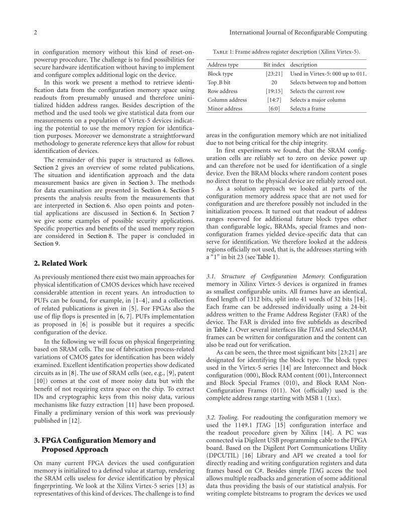
2 International Journal of Reconfigurable Computing
in configuration memory without this kind of reset-on-powerup procedure. The challenge is to find possibilities forsecure hardware identification without having to implementand configure complex additional logic on the device.
In this work we present a method to retrieve identi-fication data from the configuration memory space usingreadouts from presumably unused and therefore unini-tialized hidden address ranges. Besides description of themethod and the used tools we give statistical data from ourmeasurements on a population of Virtex-5 devices indicat-ing the potential to use the memory region for identifica-tion purposes. Moreover we demonstrate a straightforwardmethodology to generate reference keys that allow for robustidentification of devices.
The remainder of this paper is structured as follows.Section 2 gives an overview of some related publications.The situation and identification approach and the datameasurement basics are given in Section 3. The methodsfor data examination are presented in Section 4. Section 5presents the analysis results from the measurements thatare interpreted in Section 6. Also open points and poten-tial applications are discussed in Section 6. In Section 7we give some examples of possible security applications.Specific properties and benefits of the used memory regionare considered in Section 8. The paper is concluded inSection 9.
2. Related Work
As previously mentioned there exist two main approaches forphysical identification of CMOS devices which have receivedconsiderable attention in recent years. An introduction toPUFs can be found, for example, in [1–4], and a collectionof related publications is given in [5]. For FPGAs also theuse of flip flops is presented in [6, 7]. PUFs implementationas proposed in [6] is possible but it requires a specificconfiguration of the device.
In the following we will focus on physical fingerprintingbased on SRAM cells. The use of fabrication process-relatedvariations of CMOS gates for identification has been widelyexamined. Excellent identification properties show dedicatedcircuits as in [8]. The use of SRAM cells (see, e.g., [9], patent[10]) comes at the cost of more noisy data but with thebenefit of not requiring extra space on the chip. To extractIDs and cryptographic keys from this noisy data, variousmechanisms like fuzzy extraction [11] have been proposed.Finally a preliminary version of this work was previouslypublished in [12].
3. FPGA Configuration Memory andProposed Approach
On many current FPGA devices the used configurationmemory is initialized to a defined value at startup, renderingthe SRAM cells useless for device identification by physicalfingerprinting. We look at the Xilinx Virtex-5 series [13] asrepresentatives of this kind of devices. The challenge is to find
Table 1: Frame address register description (Xilinx Virtex-5).
Address type Bit index description
Block type [23:21] Used in Virtex-5: 000 up to 011.
Top B bit 20 Selects between top and bottom
Row address [19:15] Selects the current row
Column address [14:7] Selects a major column
Minor address [6:0] Selects a frame
areas in the configuration memory which are not initializeddue to not being critical for the chip integrity.
In first experiments we found, that the SRAM config-uration cells are reliably set to zero on device power upand can therefore not be used for identification of a singledevice. Even the BRAM blocks where random content posesno direct threat to the physical device are reliably zeroed out.
As a solution approach we looked at parts of theconfiguration memory address space that are not used forconfiguration and are therefore possibly not included in theinitialization process. It turned out that readout of addressranges reserved for additional future block types otherthan configurable logic, BRAMs, special frames and non-configuration frames yielded device-specific data that canserve for identification. We therefore looked at the addressregions officially not used, that is, the addresses starting witha “1” in bit 23 (see Table 1).
3.1. Structure of Configuration Memory. Configurationmemory in Xilinx Virtex-5 devices is organized in framesas smallest configurable units. All frames have an identical,fixed length of 1312 bits, split into 41 words of 32 bits [14].Each frame can be addressed individually using a 24-bitaddress written to the Frame Address Register (FAR) of thedevice. The FAR is divided into five subfields as describedin Table 1. Over several interfaces like JTAG and SelectMAP,frames can be written for configuration and the content canalso be read out for verification.
As can be seen, the three most significant bits [23:21] aredesignated for identifying the block type. The block typesused in the Virtex-5 series [14] are Interconnect and blockconfiguration (000), Block RAM content (001), Interconnectand Block Special Frames (010), and Block RAM Non-Configuration Frames (011). Not (officially) used is thecomplete address range starting with MSB 1 (1xx).
3.2. Tooling. For readouting the configuration memory weused the 1149.1 JTAG [15] configuration interface andthe readout procedure given by Xilinx [14]. A PC wasconnected via Digilent USB programming cable to the FPGAboard. Based on the Digilent Port Communications Utility(DPCUTIL) [16] Library and API we created a tool fordirectly reading and writing configuration registers and dataframes based on C#. Besides simple JTAG access the toolallows multiple readbacks and generation of some additionaldata thus providing the basis of our statistical analysis. Forwriting complete bitstreams to program the devices we used
International Journal of Reconfigurable Computing 3
the standard Xilinx Suite v10.1, the associated programmingcables, and the iMPACT tool.
4. Examination
In this section we give some figures about the collected data.Examination results based on this data are given in Section 5.
We looked at a total of nine Xilinx XC5VLX110T devices[17], integrated in Digilent XUPV5-LX110T EvaluationPlatforms [18]. In the following we denote the devices withletters A, . . . , I. Since the substructure of the address spaceoutside the area used for configuration is not public, weused the autoincrementation of the FAR to determine validaddresses. It turned out that at least 96 kbit of nontrivialdata could be read out from an unconfigured device withina certain memory region. A block of ten consecutive frames(13,120 bit) was chosen for closer investigation. In this paper,we refer to this data stream consisting of 10 frames of data.Each time we perform a readout of the device, we read these10 frames.
For statistical examination for each device X ∈(A, . . . , H) two measurement series of 10,000 readouts ΘX =(ϑ1
X, . . . , ϑ10,000X ) each were collected, one series from the
unconfigured device (ΘiX) and one from the programmed
device (ΘiX). So a total of 160,000 data streams (each consists
of 10 frames) could be used for statistics and creating masteridentification keys. In addition, test data TX = (τ1
X , . . . , τ100X ),
resp., TX = (τ1X, . . . , τ100
X ) of 100 readouts was collectedfrom every board setup, that is, a total of 1,600 test streams.Eventually for the exploration of temperature stability wemade another 40000 measurements for three selected boardsD, H, and I which were exposed to a wide temperature range.
For ideal identification of devices it would be optimal tohave a bijective mapping from an ID to a physical device andvice versa. The examination of the measurement data wastherefore done looking in two directions. First the correlationand consistency of the different measurements on one boardwere investigated, to get a unique mapping from a deviceto an ID. From each measurement series a reference datastream as master identification key was created that servesas a candidate for device representation. In a second stepthe results from different boards were compared aiming foran injective mapping from one ID to one specific device.Validation of the identification process was performed usingthe test data sets and the reference IDs. The results are givenin the following paragraphs.
5. Results
5.1. Similarity and Reference Keys. First we look at theconformity of different readouts from the very same deviceX to map each device to an ID. Therefore we used 10,000readouts to create a frequency distribution of zeros and onesof every bit in the data stream for each FPGA. Figures 1 and 2show the results for two single devices. The other devicesshowed similar figures.
The measurement reveals a distinct accumulation of bitsshowing constantly the same value. As can be seen in Table 2
0
20
40
60
80
100
0 2000 4000 6000 8000 10000 12000
Bit index in data stream
Pro
babi
lity
of "
1" (
%)
Figure 1: Probability of bit value “1” over 10 k measurements ondevice D.
0
20
40
60
80
100
0 2000 4000 6000 8000 10000 12000
Bit index in data stream
Pro
babi
lity
of "
1" (
%)
Figure 2: Probability of bit value “1” over 10 k measurements ondevice F.
the number of ones dominates the number of zeros by afactor of 1.7. The portion of flipping bits is below ten percentranging from 7.2% to 9.7% with a mean value of 8.4%over the devices under consideration (see Figure 3). Thedistribution of zeros and ones is pretty similar for differentdevices (Figure 3). For the very same device—configured orunconfigured—the numbers are not identical but relativelyclose to each other. These differing results for one device aremore probably caused by temperature variances than by thefact of configuration dependencies.
Figure 4 depicts the total amount of constant bitsobserved over a variable number of compared readouts fordifferent devices. The measurements show that more than90% of all bits are constant over all compared readouts.We therefore notice a distinctive coherence of measurementsfrom one device.
To quantify this coherence we compared the single datastreams with a reference stream ρ to get a measurabledeviation value. To achieve this we used the probabilitydistribution to generate a reference data stream ρ of themeasurement, setting each bit to the value with the higherprobablity of occurrence according to the measured data.ρ therefore represents the bitwise rounded mean of allmeasured streams.
We then determined the Hamming Distance (HD) ofevery readout to this reference key. Figure 5 shows therespective distribution for one device. The readouts fromone board show a close cross-correlation. For device Dthe Hamming distances show an expectancy value of 99,equivalent to only 0.75% of the total data, and a standarddeviation of 7.4. Device F gives an expectancy value of 137(1.0%) with a standard deviation of 9.1. All HD values
4 International Journal of Reconfigurable Computing
57.7%33.9%
8.4%
Ones
Zeros
Flipping
Figure 3: Mean occurrences of constant ones and zeros as well asflipping bits of Table 2.
86
88
90
92
94
96
98
100
Measurement cycles
Minimum number of constant bits (device F)Maximum number of constant bits (device D)
Nu
mbe
r of
con
stan
t bi
ts (
%)
Figure 4: Percentage of constant bits over 10,000 measurements fortwo devices, that represent the maximum (device D) and minimum(device F) over all devices. All other values reside in the area betweenthe two curves.
computed from all devices resided in an interval of [53–208]. The analyses of the measurement series from the otherdevices are in between the two extremal values given.
So far, the compared values were originated fromunconfigured devices and directly measured after startup.For identification of the device, the key data should beindependent from the content of the address ranges ofconfiguration memory that are used for programmingthe device. Therefore, also the programmed device wasexamined. Figure 6 depicts the HD values of readoutsof a programmed board in relation to the reference keydetermined on the same board in unconfigured state.
The values read out from the configured board showa slightly higher deviation from the reference but are stillwithin a mean deviation of well below 1% of the totaldata stream. This is also the case for the other examineddevices (see also Table 3). So all data streams from one boardshow a great mutual similarity. To verify the usability of theproposed approach, we compare in a next step data fromdifferent devices.
5.2. Distinction and Identification. For unique identification,the mapping of a given ID value to a device is necessary.
Table 2: Number of constant zeros, ones, and flipping bits.
Device Ones Zeros Flipping
A 7798 59,4% 4238 32,3% 1084 8,3%
A 7744 59,0% 4190 31,9% 1186 9,0%
B 7698 58,7% 4435 33,8% 987 7,5%
B 7661 58,4% 4414 33,6% 1045 8,0%
C 7388 56,3% 4676 35,6% 1056 8,0%
C 7325 55,8% 4642 35,4% 1153 8,8%
D 7702 58,7% 4479 34,1% 939 7,2%
D 7638 58,2% 4432 33,8% 1050 8,0%
E 7626 58,1% 4350 33,2% 1144 8,7%
E 7566 57,7% 4357 33,2% 1197 9,1%
F 7517 57,3% 4418 33,7% 1185 9,0%
F 7491 57,1% 4352 33,2% 1277 9,7%
G 7498 57,1% 4577 34,9% 1045 8,0%
G 7418 56,5% 4543 34,6% 1159 8,8%
H 7537 57,4% 4543 34,6% 1040 7,9%
H 7460 56,9% 4552 34,7% 1108 8,4%
0
50
100
150
200
250
300
350
400
450
5001 13 25 37 49 61 73 85 97 109
121
133
145
157
169
181
193
205
Occ
urr
ence
s
Hamming distance to reference
Device F
Device D
Figure 5: Distribution of Hamming distances to the respectivereference streams for unconfigured devices D and F and 10,000measurements each.
Here the difference between readouts of different boardsis the crucial property. A first indicator is the differencebetween the computed reference keys. Table 3 shows themutual Hamming distances of all reference keys.
The table shows a very close correlation between themeasurements of the same device, meaning that only a slightdependency on the configuration state can be determined.In contrast, HD values between different devices are all near6000, meaning a 45% deviation and therefore near to theexpected value of 50% for pure random streams. A closerlook at the streams revealed some bits that are constantly zeroover all measurements of all devices, which in combinationwith the slight nonuniform distribution of ones and zeroes(see Table 2) may account for the lower absolute deviation.
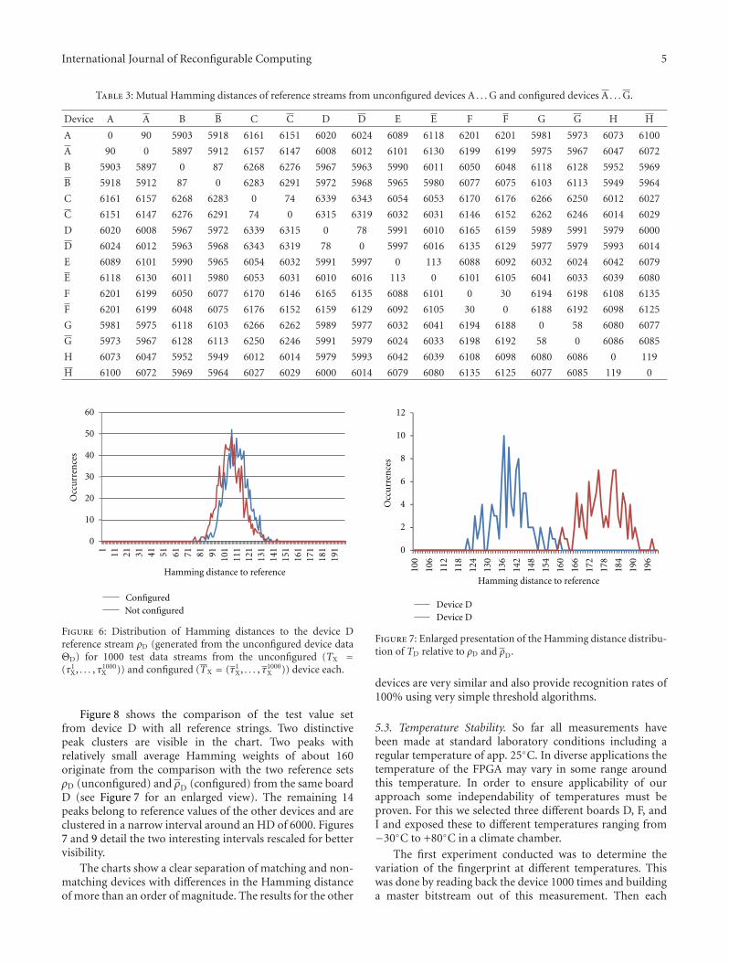
International Journal of Reconfigurable Computing 5
Table 3: Mutual Hamming distances of reference streams from unconfigured devices A . . .G and configured devices A . . .G.
Device A A B B C C D D E E F F G G H H
A 0 90 5903 5918 6161 6151 6020 6024 6089 6118 6201 6201 5981 5973 6073 6100
A 90 0 5897 5912 6157 6147 6008 6012 6101 6130 6199 6199 5975 5967 6047 6072
B 5903 5897 0 87 6268 6276 5967 5963 5990 6011 6050 6048 6118 6128 5952 5969
B 5918 5912 87 0 6283 6291 5972 5968 5965 5980 6077 6075 6103 6113 5949 5964
C 6161 6157 6268 6283 0 74 6339 6343 6054 6053 6170 6176 6266 6250 6012 6027
C 6151 6147 6276 6291 74 0 6315 6319 6032 6031 6146 6152 6262 6246 6014 6029
D 6020 6008 5967 5972 6339 6315 0 78 5991 6010 6165 6159 5989 5991 5979 6000
D 6024 6012 5963 5968 6343 6319 78 0 5997 6016 6135 6129 5977 5979 5993 6014
E 6089 6101 5990 5965 6054 6032 5991 5997 0 113 6088 6092 6032 6024 6042 6079
E 6118 6130 6011 5980 6053 6031 6010 6016 113 0 6101 6105 6041 6033 6039 6080
F 6201 6199 6050 6077 6170 6146 6165 6135 6088 6101 0 30 6194 6198 6108 6135
F 6201 6199 6048 6075 6176 6152 6159 6129 6092 6105 30 0 6188 6192 6098 6125
G 5981 5975 6118 6103 6266 6262 5989 5977 6032 6041 6194 6188 0 58 6080 6077
G 5973 5967 6128 6113 6250 6246 5991 5979 6024 6033 6198 6192 58 0 6086 6085
H 6073 6047 5952 5949 6012 6014 5979 5993 6042 6039 6108 6098 6080 6086 0 119
H 6100 6072 5969 5964 6027 6029 6000 6014 6079 6080 6135 6125 6077 6085 119 0
0
10
20
30
40
50
60
1 11 21 31 41 51 61 71 81 91 101
111
121
131
141
151
161
171
181
191
Configured
Hamming distance to reference
Not configured
Occ
urr
ence
s
Figure 6: Distribution of Hamming distances to the device Dreference stream ρD (generated from the unconfigured device dataΘD) for 1000 test data streams from the unconfigured (TX =(τ1
X, . . . , τ1000X )) and configured (TX = (τ1
X, . . . , τ1000X )) device each.
Figure 8 shows the comparison of the test value setfrom device D with all reference strings. Two distinctivepeak clusters are visible in the chart. Two peaks withrelatively small average Hamming weights of about 160originate from the comparison with the two reference setsρD (unconfigured) and ρD (configured) from the same boardD (see Figure 7 for an enlarged view). The remaining 14peaks belong to reference values of the other devices and areclustered in a narrow interval around an HD of 6000. Figures7 and 9 detail the two interesting intervals rescaled for bettervisibility.
The charts show a clear separation of matching and non-matching devices with differences in the Hamming distanceof more than an order of magnitude. The results for the other
0
2
4
6
8
10
1210
0
106
112
118
124
130
136
142
148
154
160
166
172
178
184
190
196
Device DDevice D
Hamming distance to reference
Occ
urr
ence
s
Figure 7: Enlarged presentation of the Hamming distance distribu-tion of TD relative to ρD and ρD.
devices are very similar and also provide recognition rates of100% using very simple threshold algorithms.
5.3. Temperature Stability. So far all measurements havebeen made at standard laboratory conditions including aregular temperature of app. 25◦C. In diverse applications thetemperature of the FPGA may vary in some range aroundthis temperature. In order to ensure applicability of ourapproach some independability of temperatures must beproven. For this we selected three different boards D, F, andI and exposed these to different temperatures ranging from−30◦C to +80◦C in a climate chamber.
The first experiment conducted was to determine thevariation of the fingerprint at different temperatures. Thiswas done by reading back the device 1000 times and buildinga master bitstream out of this measurement. Then each

6 International Journal of Reconfigurable Computing
0
2
4
6
8
10
12
115
230
345
460
575
690
710
5812
0913
6015
1116
6218
1319
6421
1522
6624
1725
6827
1928
7030
2131
7233
2334
7436
2537
7639
2740
7842
2943
8045
3146
8248
3349
8451
3552
8654
3755
8857
3958
9060
4161
92
Hamming distance
Device E
Device A Device A Device BDevice D
Device BDevice DDevice C Device C
Device E Device F Device FDevice G Device HDevice G Device H
Occ
urr
ence
s
Figure 8: Distribution of Hamming distances of test set TD = (τ1D, . . . , τ100
D ) to all reference values ρX and ρX for X ∈ {A, . . . , G}.
0
5
10
5900
5911
5922
5933
5944
5955
5966
5977
5988
5999
6010
6021
6032
6043
6054
6065
6076
6087
6098
6109
6120
6131
6142
6153
6164
6175
6186
6197
6208
6219
6230
6241
6252
6263
6274
6285
6296
6307
6318
6329
6340
6351
6362
6373
6384
6395
5900
5911
5922
5933
5944
5955
5966
5977
5988
5999
6010
6021
6032
6043
6054
6065
6076
6087
6098
6109
6120
6131
6142
6153
6164
6175
6186
6197
6208
6219
6230
6241
252
263
274
85 96 07 8 9 0 1Device E
Device A Device A Device B Device B Device C Device C Device E
Device F Device F Device G Device HDevice G Device H
Figure 9: Enlarged presentation of the Hamming distance distribution of TD relative to ρX and ρX for X /=D.
bitstream is compared to the master. Representative resultsare depicted in Figures 10, 11, and 12 for the mean valueof 20◦C and both extrema −30◦C and +80◦C. The meanhamming distance varies for about 40 bits depending onthe temperature, what is quite a moderate value, havingin mind a nonmatching HD of about 6000. Moreoverfor different temperatures the curves look quite similar.Interestingly there is no common temperature-dependentbehavior. While in Figure 11 the standard temperature hasthe smallest variation and the lowest temperature the highestone, the situation changes for the second board, wherethe lowest temperature has the lowest variation and thehighest temperature the highest one. Actually this is thebehavior we expected before our experiments. However thesituation reverses for board D in Figure 12. So we can onlyconclude that there is some slight variation with differenttemperatures.
In our second experiment we compared the measure-ments taken at different temperatures to the referencebitstream generated from the readbacks at 20◦C. Theresults for Board H are depicted in Figure 13. Results for
other boards look similar. Obviously the comparison showsoptimum results for 20◦C. For all other measurements weget a rising hamming distance with greater temperaturedifferences for both measurements. Again the form of thecurves remains similar which again means the variance ofthe hamming distances are almost equal. The maximumhamming distance goes up to around 300 for the highestand lowest temperatures which is very moderate comparedto non matching hamming distances.
The third experiment is a temperature sweep, starting at85◦C and cooling down to −30◦C. This process took about40 min, and 4800 measurements were taken with 500 msbetween each measurement. Out of all measurements amaster bitstream was built and the hamming distance foreach readback calculated. The results are shown in Figure 14.At the beginning the hamming distance is around 350, goesdown to 120 at approximately 0◦C, and then goes up againwith even more decreasing temperature. The blue line showsthe chip temperature which is around 5 to 10◦ higher thanthe surrounding temperature for an unconfigured Virtex-5device.

International Journal of Reconfigurable Computing 7
0
10
20
30
40
50
6050 57 64 71 78 85 92 99 10
6
113
120
127
134
141
148
155
162
169
Hamming distance
Minus 30 CPlus 20 CPlus 80 C
Occ
urr
ence
s
Figure 10: Hamming distance of single readback and masterbitstream of board H at different temperatures.
0
10
20
30
40
50
60
50 57 64 71 78 85 92 99 106
113
120
127
134
141
148
155
162
169
Hamming distance
Minus 30 CPlus 20 CPlus 70 C
Occ
urr
ence
s
Figure 11: Hamming distance of single readback and masterbit-stream of board I at different temperatures.
One can conclude that our device identification mecha-nism shows slight temperature dependency, which does notinfluence the identification process. In a final experiment weused the 20◦C master bitstreams for non matching devicesat different temperatures. For such non matching devices thetemperature has almost no influence, resulting in a deviationof about 20 in the hamming distance. Related to an absolutehamming distance of around 6000 this is neglectable. Sofinally device recognition is feasible for a wide temperaturerange.
5.4. Aging. Another important aspect is device aging. Again,we have to point out we do not know what informationexactly is read from the device by our methodology. However
0
10
20
30
40
50
60
70
50 57 64 71 78 85 92 99 106
113
120
127
134
141
148
155
162
169
Hamming distance (bit)
Minus 30 CPlus 20 CPlus 60 C
Occ
urr
ence
s
Figure 12: Hamming distance of single readback and masterbit-stream of board D at different temperatures.
0
10
20
30
40
50
60
70
50 62 74 86 98 110
122
134
146
158
170
182
194
206
218
230
242
254
266
278
290
302
314
326
338
350
Hamming distance
Minus 30 CMinus 20 C
Plus 0 CPlus 20 C
Plus 40 C
Plus 60 C
Plus 80 C
Occ
urr
ence
s
Figure 13: Matching device identification with master bitstreamgenerated at 20◦C and identification readback temperature rangefrom−30◦C to +80◦C (1 k measurements at each temperature step).
we did a readback for different devices with a time differenceof one year. The master bitstream generated one year ago wasapplied to the readback. Figure 15 shows the result for deviceH. One can see a slight deviation between both devices.The difference might be based on some aging of the device,but also slight deviations in the environment cannot becompletely ruled out. However this effect is relatively smalland does not affect the identification mechanism presentedin this paper.
6. Discussion
The examination shows a very high correlation within datastreams from a single device. Test data revealed deviationsfrom the reference master around 1% of the total data

8 International Journal of Reconfigurable Computing
0
20
40
60
80
100
0
50
100
150
200
250
300
350
400
4501
241
481
721
961
1201
1441
1681
1921
2161
2401
2641
2881
3121
3361
3601
3841
4081
4321
4561
TemperatureHamming distance
Hamming distance (mean value)
Ham
min
g di
stan
ce (
bit)
Readback number
Tem
pera
ture
(C
)
− 20
− 40
Figure 14: 4800 hamming distance measurements taken duringtemperature sweep from 85◦C to −30◦C environmental tempera-ture. The blue curve shows the chip temperature.
0
10
20
30
40
50
60
50 57 64 71 78 85 92 99 106
113
120
127
134
141
148
155
162
169
Hamming distance (bit)
First measurementSecond measurement
Occ
urr
ence
s
Figure 15: Two device identification measurements taken with oneyear between 1st and 2nd measurement.
stream. On the other hand comparison to reference keysfrom other devices resulted in HD values corresponding toa deviation in more than 40% of the bits enabling a reliableidentification of the device being read out. In additionthe identification technique needs no configuration on thedevice and therefore no area on the configurable fabricor other hardware resources. We therefore believe that themethod can be used to securely and reliably identify physicaldevices.
An open issue is the question where the data originatesfrom in the first place. Since the address space is not usedofficially on the devices it could as well be omitted. So itis possible that the readback retrieves data from memorylocations that are in fact used for some purpose. On theother side there are the distinct differences between differentinstances of the same device model and the Hamming
0100020003000400050006000
0 2000 4000 6000 8000 10000 12000 14000
Bit index in data stream
Nu
mbe
r of
togg
les
Figure 16: Number of single bit value changes for the different bitindices over 10,000 measurements on device D.
distances near the expectancy values for random strings.This seems to be unlikely for deliberately configured data.Nevertheless we are so far not able to determine the preciseorigin of the readout data. In addition the data shows slightrepetitive patterns as can be seen in Figures 1 and 2 that haveto be analysed to get valid statements about the number ofusable identification bits.
Moreover the question arises whether the data could alsobe used to generate random numbers. Here not the constantbut the variable bits are crucial for the quality. Figures 1and 2 already show that the data have different distributiondepending on the bit index. Figure 16 shows in additionthe number of value changes over the measured set of datastreams for the different bit indices.
The variety of behaviours of the different bits could beseen as an indication that an extraction of random numberscould be possible, but further analysis and postprocessing ofthe data is needed to get reliable results.
7. Security Applications
There are several possible applications for the describedSRAM-based PUFs. Since the PUF consists of memoryvalues, it is easy to evaluate also for an attacker. Hence itshould be possible to create the memory response withoutthe specific device but only a readout of the memory. Asecurity application therefore has to make sure that the PUFis actually evaluated and not replayed values are used. Onepossibility for that is guaranteed direct physical access tothe device. This is utilized in two applications examplarilylooked at in the following: product piracy protection and IPprotection.
For the first use case, the initial memory content isread out at production of the device and an adequateerror correcting coding mechanism is applied to create astable fingerprint. This fingerprint is then used to createa manufacturer certificate for the device, for example, bysigning a hash value of the fingerprint with a manufacturer-specific secret key. This certificate is then delivered togetherwith the device to the customer who is then able to verifywhether he acquired a genuine device since a manufacturer ofbogus devices is neither able to create valid certificates for hisdevice nor to clone the PUF-fingerprints for the cloned units.Since the fingerprinting does not rely on memory regionsused for configuration the verification can be performedeven during operation without interruption and withoutneed to restart the device.

International Journal of Reconfigurable Computing 9
Possible applications for the considered identificationmechanism are not restricted to external evaluation of adevice but could as well be used inside a configurationbitstream itself. This is considered in the second use case forIP protection. Since the configuration memory is accessiblefrom the fabric through the common ICAP interface, a con-figured bitstream could easily use the available informationto identify the device it is configured on and perhaps reactaccordingly. A straightforward application would be to binda configuration to a specific device. To show feasibility weimplemented the basic functionality.
Using an ICAP interface connected to a MicroBlazeSystem we were able to read out the identifying data fromwithin the device, getting similar results as when usingthe external JTAG access. By comparing the data with areference string stored in the configuration bitstream, thedesign can verify whether it is run on a predefined device. Ifa mismatch is detected, an internal enforcement mechanismcan, for example, disable the design or reduce functionality,building a reliable copy protection mechanism for hardwareconfiguration IP.
8. Specific Properties of the Memory Region
When the identification is used for policy enforcement andcopy protection, circumventing the identification could beof interest for possible attackers. In the classical use caseusing memory cells for identification it has to be guaranteedthat the cells are read out before any influence on thecontents is possible, since the memory cells can easily bewritten with arbitrary values. In contrast to that we observedthat writing on the considered addresses was not possibleover the examined interfaces—the readout values were notchangeable by write attempts. This is a major benefit incontrast to general memory cells.
In addition, since the used cells are outside the memoryspace used for configuration, we assume that they are notused for programming a design to the chip. The identifica-tion should therefore work also for configured devices duringruntime and for partial bitstreams having no control andno information about the contents of the surrounding chiparea or even about their own placing on the area as longas they have access to the ICAP interface. So no area hasto be reserved for the identification and no constraints forplacement and routing are imposed by the approach.
9. Conclusion and Further Work
For the challenge of identifying physical devices of XilinxVirtex-5 FPGA family we examined configuration memoryreadouts from address ranges that are assumedly not usedin the series. We chose an address range reserved for futureblock types to read out data and compared the readoutsmutually from one device and between devices. Resultsshowed a strong coherence of different streams from thesame device and strong deviations between devices. Thisholds true also for a wide temperature range. Moreover weshowed device identification is feasible after one year of
aging. We therefore assume the data suitable for identifica-tion of physical devices. The method opens identificationpossibilities for FPGA series where other SRAM-basedapproaches fail because of enforced initialization to definedvalues at startup.
To proof reliable identification some future work isnecessary. So far it is not clear how long the potential keysequences are and in what ratio they include real identifi-cation information and noise. It could also be investigated,whether it is also applicable to devices of other series.
Acknowledgments
The authors acknowledge support by Deutsche Forschungs-gemeinschaft and Open Access Publishing Fund of KarlsruheInstitute of Technology.
References
[1] B. Gassend, D. Clarke, M. van Dijk, and S. Devadas, “Siliconphysical random functions,” in Proceedings of the 9th ACMConference on Computer and Communications Security (CCS’02), pp. 148–160, ACM, New York, NY, USA, November 2002.
[2] B. Gassend, D. Lim, D. Clarke, M. van Dijk, and S. Devadas,“Identification and authentication of integrated circuits,”Concurrency and Computation: Practice and Experience, vol.16, no. 11, pp. 1077–1098, 2004.
[3] J. Guajardo, S. S. Kumar, G.-J. Schrijen, and P. Tuyls, “Fpgaintrinsic pufs and their use for ip protection,” in Proceedings ofthe 9th International Workshop on Cryptographic Hardware andEmbedded Systems (CHES ’07), pp. 63–80, Springer, Berlin,Germany, 2007.
[4] P. Tuyls and B. Skoric, “Strong authentication with physicalunclonable functions,” in Security, Privacy, and Trust in Mod-ern Data Management, M. Petkovic and W. Jonker, Eds., Data-Centric Systems and Applications, pp. 133–148, Springer,Berlin, Germany, 2007.
[5] R. Maes, “PUF Bibliography,” 2010, http://www.rmaes.ulyssis.be/pufbib.php/.
[6] R. Maes, P. Tuyls, and I. Verbauwhede, “Intrinsic pufs fromflip-flops on reconfigurable devices,” in Proceedings of the 3rdBenelux Workshop on Information and System Security (WISSec’08), p. 17, Eindhoven, NL, USA, 2008.
[7] S. S. Kumar, J. Guajardo, R. Maes, G. J. Schrijen, and P.Tuyls, “The butterfly PUF protecting IP on every FPGA,” inProceedings of the IEEE International Workshop on Hardware-Oriented Security and Trust (HOST ’08), pp. 67–70, June 2008.
[8] Y. Su, J. Holleman, and B. Otis, “A1.6pJ/blt 96% stable chip-ID generating circuit using process variations,” in Proceedingsof the 54th IEEE International Solid-State Circuits Conference(ISSCC ’07), pp. 406–611, San Francisco, Calif, USA, February2007.
[9] D. E. Holcomb, W. P. Burleson, and K. Fu, “Power-up SRAMstate as an identifying fingerprint and source of true randomnumbers,” IEEE Transactions on Computers, vol. 58, no. 9, pp.1198–1210, 2009.
[10] S. Chaudhry, P. A. Layman, J. G. Norman, and J. R. Thom-son, “Electronic fingerprinting of semiconductor integratedcircuits,” US patent 6,738,294, Agere Systems Inc., 2002.
[11] Y. Dodis, R. Ostrovsky, L. Reyzin, and A. Smith, “Fuzzyextractors: how to generate strong keys from biometrics and
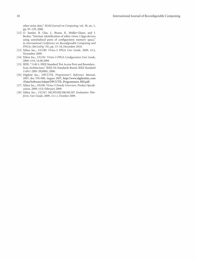
10 International Journal of Reconfigurable Computing
other noisy data,” SIAM Journal on Computing, vol. 38, no. 1,pp. 97–139, 2008.
[12] O. Sander, B. Glas, L. Braun, K. Muller-Glaser, and J.Becker, “Intrinsic identification of xilinx virtex-5 fpga devicesusing uninitialized parts of configuration memory space,”in International Conference on Reconfigurable Computing andFPGAs (ReConFig ’10), pp. 13–18, December 2010.
[13] Xilinx Inc., UG190: Virtex-5 FPGA User Guide, 2009, v5.2,November 2009.
[14] Xilinx Inc., UG191: Virtex-5 FPGA Configuration User Guide,2009, v3.8, 14.08.2009.
[15] IEEE, “1149.1: IEEE Standard Test Access Port and Boundary-Scan Architecture,” IEEE-SA Standards Board, IEEE Standard1149.1-2001 (R2008), 2006.
[16] Digilent Inc., DPCUTIL Programmer’s Reference Manual,2007, doc 576-000, August 2007, http://www.digilentinc.com/Data/Software/Adept/DPCUTIL Programmers RM.pdf.
[17] Xilinx Inc., DS100: Virtex-5 Family Overview. Product Specifi-cation, 2009, v5.0, February 2009.
[18] Xilinx Inc., UG347: ML505/ML506/ML507 Evaluation Plat-form: User Guide, 2009, v3.1.1, October 2009.

Hindawi Publishing CorporationInternational Journal of Reconfigurable ComputingVolume 2012, Article ID 608312, 12 pagesdoi:10.1155/2012/608312
Research Article
Placing Multimode Streaming Applications onDynamically Partially Reconfigurable Architectures
S. Wildermann, J. Angermeier, E. Sibirko, and J. Teich
Hardware/Software Co-Design, University of Erlangen-Nuremberg, 91058 Erlangen, Germany
Correspondence should be addressed to S. Wildermann, [email protected]
Received 29 April 2011; Revised 21 October 2011; Accepted 25 October 2011
Academic Editor: Claudia Feregrino
Copyright © 2012 S. Wildermann et al. This is an open access article distributed under the Creative Commons Attribution License,which permits unrestricted use, distribution, and reproduction in any medium, provided the original work is properly cited.
By means of partial reconfiguration, parts of the hardware can be dynamically exchanged at runtime. This allows that streamingapplication running in different modes of the systems can share resources. In this paper, we discuss the architectural issues to designsuch reconfigurable systems. For being able to reduce reconfiguration time, this paper furthermore proposes a novel algorithm toaggregate several streaming applications into a single representation, called merge graph. The paper also proposes an algorithm toplace streaming application at runtime which not only considers the placement and communication constraints, but also allows toplace merge tasks. In a case study, we implement the proposed algorithm as runtime support on an FPGA-based system on chip.Furthermore, experiments show that reconfiguration time can be considerably reduced by applying our approach.
1. Introduction
Embedded systems used to have fixed functionality dedicatedto a specific task. A trend of recent years is, however, tobuild embedded systems which are regarded as “smart.” Inthis context, the functionality can be adapted, reorganized,and controlled by external requests from human operators oreven internal self-managing, self-adapting mechanisms. Thismeans that an embedded system’s functionality is not fixedto a single configuration anymore, but several applicationare running. Still, not all applications are running all thetime, but depend on the operational mode of the system.Here, we are speaking of multimode systems, which can, forexample, be found in a typical “smart phone” scenario wherethe operational mode depends, for example, on the radiolink quality or the user’s input. Other examples are “smartcameras” which have internal adaptation mechanism thatswitch between appropriate signal processing algorithms. Inthis paper, we consider multimode streaming applicationswhich can also be found in above-mentioned examples, inthe form of signal and image processing flows, but also DataStream Management Systems, and so forth.
In a multimode system, the system resources can beutilized better. This is due to the fact that, during systemdesign, only those applications which run concurrently are
considered. This makes it possible to perform resourcesharing between processes which run mutually exclusive.When speaking of resource sharing of hardware resources,one precondition is the reconfigurability of the computingplatform. In this context, field-programmable gate arrays(FPGAs) offer the capability of partial reconfiguration. Thismeans that hardware modules can be dynamically loadedand partly exchanged during runtime. Applying this tech-nology in the design of multimode streaming applications,however, requires (a) system architectures which supportpartial reconfiguration and (b) proper reconfiguration man-agers which provide algorithms for scheduling and placingapplications at runtime.
This paper deals with modeling and dynamically placingstreaming applications on FPGA-based platforms. The focuslies on systems where it is not predictable at design timewhich applications actually run and in which order theyare executed. This is especially the case when implementingautonomic SoCs. For example, [1] introduces a methodologyfor self-organizing smart cameras which switch betweenconfigurations depending on runtime decisions. In this self-managing context, placement needs to be flexible since it isnot known beforehand when and what kind of reconfigura-tion is requested.

2 International Journal of Reconfigurable Computing
One advantage of running streaming applications inhardware is to exploit parallelism by means of pipelining.Therefore, the complete data flow is placed and modules areconnected via circuit switching techniques. Particularly inthe domain of streaming applications, data flows may havestrong similarities. For example, in image processing, convo-lution filters are commonly applied. Now, while one stream-ing application uses a Canny filter for edge detection, anotherapplication might use a Sobel filter. In this case, it is notnecessary to replace the filters by means of reconfigurationwhen switching between both streaming applications, sincethe logic remains the same. A better strategy would be to usethe same filter module for both applications, and to keepthe filter parameters in registers. So, replacing the Cannyfilter module by the Sobel filter can be achieved by replacingthe filter parameters in the registers. It is possible to reducereconfiguration time when applying this kind of resourcesharing.
In this work, we provide a novel approach to merge thedata flow graphs of multiple applications with strong simi-larities into a single data flow graph. We review techniques tobuild proper reconfigurable systems to run these multimodestreaming application. Furthermore, an algorithm is presentfor placing such streaming applications. The approach con-siders the heterogeneity of common FPGAs, such as Block-RAM columns, as well as the routing restrictions of on-chipstreaming bars.
The paper is organized as follows. Section 2 presentsrelated work. Section 3 provides the preliminaries of partialreconfiguration. Section 4 describes the model for streamingapplications as well as the algorithm to generate the mergegraph. The problem of placing streaming applications isthen formally defined in Section 5. Section 6 provides theplacing algorithm. An implementation of the algorithm onan FPGA platform is described in Section 7 which is used inthe experiments provided in Section 8. Section 9 concludesthis paper.
2. Related Work
Partial run-time reconfiguration of FPGAs has been inves-tigated since several years. But still, reconfiguration harborsmany problems. There are of course architectural issues con-cerning how to support partial reconfiguration and howto establish systemwide communication. Solutions can beclassified into three basic principles: on-chip buses are themost common way of linking together communicating mod-ules. For example, [2] and [3] present on-chip buses forflexible module placement. Hard macros implement thecommunication infrastructure within the FPGA fabric. Cir-cuit switching is a technique where physically wired links areestablished between two or more modules as, for example,presented in [4] and [5]. The latter has a low overhead since itimplements the wires directly within the routing fabric of theFPGA. We consider this kind of technique for streaming datain reconfigurable systems. Packet switching techniques, forexample, networks on chip [6], are also possible but imposea certain overhead when implemented on FPGAs.
Hardware reuse is basically investigated on the logic andthe system level. Reference [7] provides a mechanism forhardware reuse on the logic level. Frames in common withthe previously placed configuration are determined whichwill then be reused. A similar approach is followed in [8]which aims at increasing the number of common frames byproperly ordering the LUT inputs to keep their content thesame over several configurations. Such approaches are highlydependent on the architecture and are computationally in-tensive.
System level approaches are often performed via graphmatching techniques. For example, [9] presents an approachwhere common components between successive configu-rations are determined to minimize reconfiguration time.Reference [10] presents an approach which is based on thereconfiguration state graph (RSG) which models the con-figurations and the reconfiguration between them. Theseapproaches are applied during synthesis and require knowl-edge of the switching order between configurations. Theresult is the synthesized system. Hence, these methods are notapplicable when extending a running system without havingto perform a complete redesign, also affecting flexibility aswell as maintainability and limiting the use of self-managingmechanisms.
Reference [11] introduces an algorithm to place stream-ing applications with similarities. In order to express thesesimilarities, the authors propose to model the applicationsby means of extended data flow graphs. Here, so-called ORnodes are used to describe differing parts of applicationswhile keeping their similarities. A First-Fit heuristic is thenintroduced to place such applications. In the work at hand,we replace the model from [11] by merge graphs. In a mergegraph, several data flow graphs are merged into a singlerepresentation. However, no OR nodes are required. Eachnode of the merge graph is annotated with the identifier ofthe applications it is part of. An algorithm to automaticallygenerate merge graphs is proposed. The placing algorithmfrom [11] is then extended to work with this novel model.
3. Partially Reconfigurable Architectures
Reconfigurable architectures are typically divided into staticand dynamic parts. Logic residing in the static part is neededthroughout system operation, for example, the connectionlogic for the communication interfaces.
On the other side, the dynamic part is designed for load-ing and exchanging functionality at runtime. Functionalitywhich is only required in some operational system modesmay be implemented as partially reconfigurable modules (PRmodules) and, thus, can be dynamically loaded and ex-changed during runtime. In this way, logic and other re-sources can be shared by system components which only runmutually exclusive.
In the following, we concentrate on hardware recon-figuration on FPGAs. We present possibilities to organizethe reconfigurable fabrics to support partial reconfiguration,and give an overview of sophisticated communication tech-niques, before presenting a concrete example.

International Journal of Reconfigurable Computing 3
CLB Block-RAM
(a) PR region
I/O bar
I/O bar
CommunicationinterfaceTile
16 bit
16 bit
(b) tiling
Synthesis region
(c) synthesis region
(d) feasible position
Figure 1: Example of a PR region and a possible tiling.
3.1. Enabling Partial Reconfiguration. PR modules can beloaded into dedicated areas on the reconfigurable systems.These areas are denoted as partially reconfigurable regions(PR regions). The possible shapes and positions for load-ing PR modules into these regions strongly depend onthe PR region layout. Here, the problems are that, first,modern reconfigurable fabrics are an array consisting ofcells of different types, such as logic blocks (CLBs), Block-RAMs, or multiply-accumulate units (DSPs), as illustrated inFigure 1(a). This increases the inhomogeneity of the under-lying structure. Second, low-overhead infrastructures haveto be provided that enable systemwide communication andsupport partial reconfiguration.
One common solution is to build so-called tiled partiallyreconfigurable systems, as proposed, for example, by [2]. Here,the PR regions are divided into reconfigurable tiles whichare the smallest atomic units for partial reconfiguration. Anexample for a possible tiling is shown in Figure 1(b). Theapproach allows to place multiple PR modules with varioussizes in the same PR region. At the same time, placementrestrictions are decreased and usability is enhanced. Still, thetiles consist of several different cell types according to theunderlying cell structure.
Sophisticated communication techniques for reconfig-urable systems are commonly provided by communicationmacros which can be placed in the PR region to interconnectthe reconfigurable tiles. Since each reconfigurable tile offers acommunication interface, the tiling of the PR region dependson the chosen communication technique. Koch et al. give
a rule in [12] how to calculate the size of tiles. It dependson the communication overhead in terms of required cellsas well as the set of modules which are candidates for beingplaced as PR modules.
The synthesis flow for PR modules requires additionalsteps compared to the flow for static system designs (see,e.g., [2, 5]). First, an area on the reconfigurable system isselected which provides sufficient cell types as required forimplementing the module. This area is denoted as synthesisregion. Although this does not necessarily have to be the case,most synthesis flows propose the use of rectangular synthesisregions. Then, the communication macro is placed. Finally,the module can be synthesized in the selected region. Thisflow now allows to place the module at any location withthe same arrangement of cell types as the synthesis region.An example of a synthesis region for a PR module requiring10 CLBs and 4 Block-RAMs is given in Figure 1(c). The twofeasible positions for placing this PR module are depicted inFigure 1(d).
As pointed out in this section, the chosen communi-cation technique strongly influences the layout of the par-tially reconfigurable part of the system. In the following, thecommunication techniques targeted in this work are pre-sented.
3.2. Communication Techniques. Section 2 describes ap-proaches to provide communication interfaces for dynamicplacement of hardware modules. On-chip buses are suitablefor dynamically integrating hardware modules into an FPGA
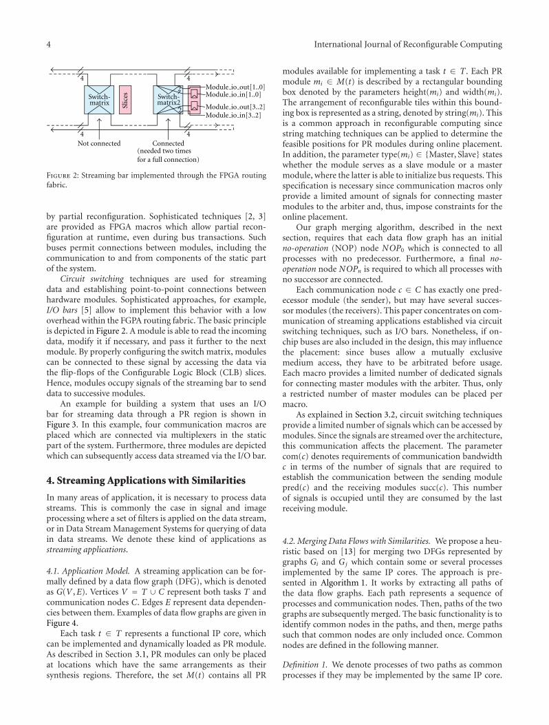
4 International Journal of Reconfigurable Computing
Slic
esSwitch-matrix
Switch-matrix2
Not connected Connected(needed two times for a full connection)
4 4
44
Module io out[1..0]Module io in[1..0]
Module io out[3..2]Module io in[3..2]
2
2
Figure 2: Streaming bar implemented through the FPGA routingfabric.
by partial reconfiguration. Sophisticated techniques [2, 3]are provided as FPGA macros which allow partial recon-figuration at runtime, even during bus transactions. Suchbuses permit connections between modules, including thecommunication to and from components of the static partof the system.
Circuit switching techniques are used for streamingdata and establishing point-to-point connections betweenhardware modules. Sophisticated approaches, for example,I/O bars [5] allow to implement this behavior with a lowoverhead within the FGPA routing fabric. The basic principleis depicted in Figure 2. A module is able to read the incomingdata, modify it if necessary, and pass it further to the nextmodule. By properly configuring the switch matrix, modulescan be connected to these signal by accessing the data viathe flip-flops of the Configurable Logic Block (CLB) slices.Hence, modules occupy signals of the streaming bar to senddata to successive modules.
An example for building a system that uses an I/Obar for streaming data through a PR region is shown inFigure 3. In this example, four communication macros areplaced which are connected via multiplexers in the staticpart of the system. Furthermore, three modules are depictedwhich can subsequently access data streamed via the I/O bar.
4. Streaming Applications with Similarities
In many areas of application, it is necessary to process datastreams. This is commonly the case in signal and imageprocessing where a set of filters is applied on the data stream,or in Data Stream Management Systems for querying of datain data streams. We denote these kind of applications asstreaming applications.
4.1. Application Model. A streaming application can be for-mally defined by a data flow graph (DFG), which is denotedas G(V ,E). Vertices V = T ∪ C represent both tasks T andcommunication nodes C. Edges E represent data dependen-cies between them. Examples of data flow graphs are given inFigure 4.
Each task t ∈ T represents a functional IP core, whichcan be implemented and dynamically loaded as PR module.As described in Section 3.1, PR modules can only be placedat locations which have the same arrangements as theirsynthesis regions. Therefore, the set M(t) contains all PR
modules available for implementing a task t ∈ T . Each PRmodule mi ∈ M(t) is described by a rectangular boundingbox denoted by the parameters height(mi) and width(mi).The arrangement of reconfigurable tiles within this bound-ing box is represented as a string, denoted by string(mi). Thisis a common approach in reconfigurable computing sincestring matching techniques can be applied to determine thefeasible positions for PR modules during online placement.In addition, the parameter type(mi) ∈ {Master, Slave} stateswhether the module serves as a slave module or a mastermodule, where the latter is able to initialize bus requests. Thisspecification is necessary since communication macros onlyprovide a limited amount of signals for connecting mastermodules to the arbiter and, thus, impose constraints for theonline placement.
Our graph merging algorithm, described in the nextsection, requires that each data flow graph has an initialno-operation (NOP) node NOP0 which is connected to allprocesses with no predecessor. Furthermore, a final no-operation node NOPn is required to which all processes withno successor are connected.
Each communication node c ∈ C has exactly one pred-ecessor module (the sender), but may have several succes-sor modules (the receivers). This paper concentrates on com-munication of streaming applications established via circuitswitching techniques, such as I/O bars. Nonetheless, if on-chip buses are also included in the design, this may influencethe placement: since buses allow a mutually exclusivemedium access, they have to be arbitrated before usage.Each macro provides a limited number of dedicated signalsfor connecting master modules with the arbiter. Thus, onlya restricted number of master modules can be placed permacro.
As explained in Section 3.2, circuit switching techniquesprovide a limited number of signals which can be accessed bymodules. Since the signals are streamed over the architecture,this communication affects the placement. The parametercom(c) denotes requirements of communication bandwidthc in terms of the number of signals that are required toestablish the communication between the sending modulepred(c) and the receiving modules succ(c). This numberof signals is occupied until they are consumed by the lastreceiving module.
4.2. Merging Data Flows with Similarities. We propose a heu-ristic based on [13] for merging two DFGs represented bygraphs Gi and Gj which contain some or several processesimplemented by the same IP cores. The approach is pre-sented in Algorithm 1. It works by extracting all paths ofthe data flow graphs. Each path represents a sequence ofprocesses and communication nodes. Then, paths of the twographs are subsequently merged. The basic functionality is toidentify common nodes in the paths, and then, merge pathssuch that common nodes are only included once. Commonnodes are defined in the following manner.
Definition 1. We denote processes of two paths as commonprocesses if they may be implemented by the same IP core.
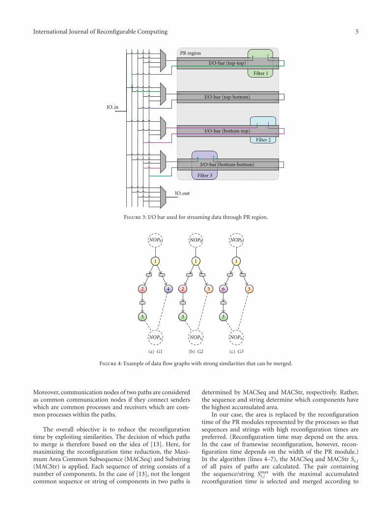
International Journal of Reconfigurable Computing 5
PR region
Filter 1
Filter 2
Filter 3
IO out
IO in
I/O-bar (top-top)
I/O-bar (top-bottom)
I/O-bar (bottom-top)
I/O-bar (bottom-bottom)
Figure 3: I/O bar used for streaming data through PR region.
1
2 4
3
NOP0
NOPn
(a) G1
1
2 5
3
NOP0
NOPn
(b) G2
1
6 5
3
NOP0
NOPn
(c) G3
Figure 4: Example of data flow graphs with strong similarities that can be merged.
Moreover, communication nodes of two paths are consideredas common communication nodes if they connect senderswhich are common processes and receivers which are com-mon processes within the paths.
The overall objective is to reduce the reconfigurationtime by exploiting similarities. The decision of which pathsto merge is therefore based on the idea of [13]. Here, formaximizing the reconfiguration time reduction, the Maxi-mum Area Common Subsequence (MACSeq) and Substring(MACStr) is applied. Each sequence of string consists of anumber of components. In the case of [13], not the longestcommon sequence or string of components in two paths is
determined by MACSeq and MACStr, respectively. Rather,the sequence and string determine which components havethe highest accumulated area.
In our case, the area is replaced by the reconfigurationtime of the PR modules represented by the processes so thatsequences and strings with high reconfiguration times arepreferred. (Reconfiguration time may depend on the area.In the case of framewise reconfiguration, however, recon-figuration time depends on the width of the PR module.)In the algorithm (lines 4–7), the MACSeq and MACStr Si, jof all pairs of paths are calculated. The pair containingthe sequence/string Smax
i, j with the maximal accumulatedreconfiguration time is selected and merged according to

6 International Journal of Reconfigurable Computing
(1): initialize merged graph GM ;(2): extract all paths Pi/ j of Gi/ j ;(3): While at least one pair of paths with non-empty MACSeq or MACStr exists do.(4): calculate MACSeq/MACStr Si, j for each pair (pi, pj) ∈ Pi × Pj ;(5): find pair (pi, pj) with Smax
i, j having maximum reconfiguration time;(6): merge paths pi and pj according to Smax
i, j and add them to GM ;// see Algorithm 2
(7): Pi/ j = Pi/ j \ pi/ j ;(8): end while(9): add all remaining paths p ∈ Pi and p ∈ Pj as or-paths to GM ;
// see Algorithm 3
Algorithm 1: Merging two data flow graphs Gi and Gj .
(1): ensure GM contains the NOP nodes NOP0 and NOPn;(2): v0 = NOP0
(3): for k = 0 to |Si, j| do(4): (v(k)
i , v(k)j ) = Si, j[k]; // the k-th pair in the sequence
(5): determine or-paths ori/ j , that is, all vertices in pi/ j between v(k−1)i/ j and v
(k)i/ j
(6): add ori/ j to GM ; // see Algorithm 3(7): make new node nM ;(8): link vM[i] to v
(k)i and nM[ j] to v
(k)j ;
(9): add vM to GM ;(10): add edge to GM connecting the last vertices added from pi and pj to vM ;(11): v0 = vM ;(12): end for
Algorithm 2: Merging two paths pi and pi according to common sequence Si, j and adding them to the merged graph GM .
Algorithm 2. When no further paths with similarities exist,the remaining paths are added to the merge graph (line 9).
Path merging works as shown in Algorithm 2. Here,
(v(k)i , v(k)
j ) = Si, j[k] denotes the kth pair of common nodesin the sequence (line 4). All common nodes are successivelyadded to the merged graph GM . The nodes of the paths whichare not part of the sequence/string and lie between commonnodes are denoted as or-paths (line 5) and added separatelyaccording to Algorithm 3 (line 6). When merging a pair ofcommon nodes, a new node is added to the merged graphwhich represents the common node. It contains references tothe common nodes and is connected with the last verticesfrom the paths added to the merged graphs (lines 7–10).
Algorithm 3 shows how to add an or-path to the mergedgraph. Here, the elements in the or-paths are iteratively
added. If the current element v(k)i is not already part of
the merged graph GM , a new node is added to GM with a
reference to v(k)i (lines 3–6). Then, the last element of the or-
path added to GM is connected to this new node in GM (line10).
The proposed heuristic can now be used to subsequentlymerge several data flow graphs. In all cases, it is requiredthat all graphs have a initial NOP node NOP0 and a finalNOP node NOPn. As an example, Figure 5 shows the dataflow graph resulting when merging the three graphs fromFigure 4.
5. Problem Formulation
Placing tasks on a reconfigurable device is a complex prob-lem, in which many resource constraints must be respected.In our scenario, one important limited resource consists inthe communication infrastructure, for example, the signalsavailable for circuit switching. Typically, the amount of usedconnection bandwidth at each position and instant in timemust not exceed a certain maximum number. Therefore, itmay be necessary to delay the placement of one module untilsome more communication bandwidth is released. Further-more, the data dependencies must be respected, that is, allthe temporary results on which one tasks depends must havebeen already computed before it can be executed. In addition,each module may require Block-RAM resources at specificrelative positions; thus the Block-RAM resource limitationsmust also be respected for the task placement. In a moreformal manner, the placement problem can be specified asfollows.
Given a task graph GT(VT ,ET) and a tiled recon-figurable architecture where A represents the set ofreconfigurable tiles,
find for each process t ∈ T with outgoing commu-nication nodes Cout
t = succ(t) and incoming com-munication nodes Cin
t = pred(t) a feasible locationF ⊆ A
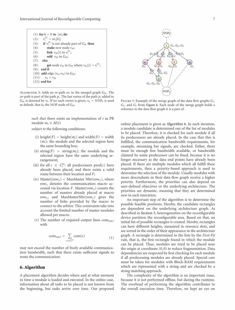
International Journal of Reconfigurable Computing 7
(1): for k = 0 to |ori|do(2): v
(k)i = ori[k];
(3): if v(k)i is not already part of GM then
(4): make new node vM ;(5): link vM[i] to v
(k)i ;
(6): add vM to GM ;(7): else(8): get node vM in GM where vM[i] = v
(k)i ;
(9): end if(10): add edge (v0, vM) to GM ;(11): v0 = vM(12): end for
Algorithm 3: Adds an or-path ori to the merged graph GM . Theor-path is part of the path pi. The last vertex of the path pi added toGM is denoted by v0. If no such vertex is given, v0 = NOP0 is usedas default, that is, the NOP node of GM .
such that there exists an implementation of t as PRmodule mi ∈M(t)
subject to the following conditions:
(i) height(F) = height(mi) and width(F) = width(mi): the module and the selected region havethe same bounding box;
(ii) string(F) = string(mi): the module and theselected region have the same underlying ar-rangement;
(iii) for all c ∈ Cint : all predecessors pred(c) have
already been placed, and there exists a validroute between their location and F;
(iv) Master(rowy) < MaxMaster Nbr(rowy), whererowy denotes the communication macro ac-cessed via location F. Master(rowy) counts thenumber of masters already placed at macrorowy , and MaxMasterNbr(rowy) gives thenumber of links provided by the macro toconnect to the arbiter. This constraints take intoaccount the limited number of master modulesallowed per macro.
(v) The number of required output lines comout,t
with
comout,t =∑
c∈Coutt
com(c) (1)
may not exceed the number of freely available communica-tion bandwidth, such that there exists sufficient signals toroute the communication.
6. Algorithm
A placement algorithm decides where and at what momentin time a module is loaded and executed. In the online case,information about all tasks to be placed is not known fromthe beginning, but tasks arrive over time. Our proposed
1
2
3
456
NOP0
NOPn
G1, G2
G1, G2
G1, G2
G1, G2
, G3
G2, G3
G2, G3
G1
G1
G1
, G2, G3
G3
G3
G3
Figure 5: Example of the merge graph of the data flow graphs G1,G2, and G3 from Figure 4. Each node of the merge graph holds areference to the data flow graph it is a part of.
online placement is given as Algorithm 4. In each iteration,a module candidate is determined out of the list of modulesto be placed. Therefore, it is checked for each module if allits predecessors are already placed. In the case that this isfulfilled, the communication bandwidth requirements, forexample, streaming bar signals, are checked. Either, theremust be enough free bandwidth available, or bandwidthclaimed by some predecessor can be freed, because it is nolonger necessary as the data end points have already beenplaced. If there are multiple modules which all fulfill theserequirements, then a priority-based approach is used todetermine the selection of the module. Usually modules withmore descendants in their data flow graph receive a higherpriority. Furthermore, the priorities can also depend onuser-defined objectives or the underlying architecture. Thepriorities are dynamic, meaning that they are determinednew in each interation.
An important step of the algorithm is to determine thepossible feasible positions. Hereby, the candidate rectanglesare dependent on the underlying architecture graph. Asdescribed in Section 3, heterogeneities on the reconfigurabledevice partition the reconfigurable area. Based on that, aninitial list of possible rectangles is created. Hereby, rectanglescan have different heights, measured in resource slots, andare sorted in the order of their appearance in the architecturegraph. A rectangle is determined in the lists by the First-Fitrule, that is, the first rectangle found in which the modulecan be placed. Thus, modules are tried to be placed nearthe origin at coordinate (0, 0) to reduce fragmentation. Datadependencies are respected by first checking for each moduleif all predecessing modules are already placed. Special caremust be taken for modules with Block-RAM requirementswhich are represented with a string and are checked by astring matching approach.
The complexity of the algorithm is an important issue,because it is not performed offline, but during the runtime.The overhead of performing the algorithm contributes tothe overall execution time. Therefore, we kept an eye on

8 International Journal of Reconfigurable Computing
Initialize list of rectangles, communication bandwidth usage;for i = 1 to |M|do
Determine set of modules for which data-dependencies are met, and still unplaced, named Ki;Remove modules from Ki, for which currently not enough communication bandwidth is available;Remove modules from Ki, for which no suitable feasible position can be found in GA with a first-fit heuristic.If more than one module is still included in Ki, then select one according to criteria such asnumber of descendants, module size, Block-RAM usage, and so forth.Place Ki in the determined feasible position and update resource usage informations;
end for.
Algorithm 4: Placement Algorithm.
the performance of the algorithm and followed a list-basedtechnique. The algorithm consists of a loop with variouschecks for suitability over all still available tasks. More pre-cisely, it has a running time of O(|M|2). Thus, it can be exe-cuted efficiently also at runtime. Other offline approaches,like [14], might achieve better solutions, but are to complextoo be employed in an online setting, where the tasks to beconsidered might also change over runtime, and downtimeof the system must be minimized. Thus, new modules can bedeveloped and be integrated in the running reconfigurablesystem, because the placement algorithm is fast and flexibleenough to adapt at runtime to the new situation.
However, when placing a merge graph, special care mustbe taken. In this case, we start placing the modules fromthe left top-most position towards the right bottom-mostposition. Furthermore, we keep pointers for all streamingapplications that are aggregated into the merge graph. Eachpointer indicates the position from which the First-Fistheuristic starts searching. Each time a module is selectedaccording to Algorimth 4, the heuristic starts searching fromthat pointer that is most advanced and belongs to anapplication the module is part of. After the module is placed,all affected pointers are advanced onto the first free positionafter the bounding box of this module. By successively per-forming this step all modules are placed, and amodule run-ning mutually exclusive may use the same resources.
7. Case Study
Figure 6 illustrates the FPGA-based system on chip from [15]which is implemented on a Xilinx Virtex-II XUP Pro boardand serves as a case study. The two dark-red areas on the righttop and bottom compose the dynamic part of the system.Reconfiguration is only possible in the dynamic part whichcontains a reconfigurable on-chip bus and streaming bars ascommunication primitives. Both primitives are generated bythe framework ReCoBus-Builder [5]. Note that the partialmodules possess different sizes and that modules can beplaced in a two-dimensional manner since four macros areplaced in the partial part.
The proposed placement algorithm was implementedfor the described SoC. The procedure of runtime reconfig-uration is illustrated in Figure 7, highlighting the stepsrequired to dynamically load PR modules. Reconfigurationis basically performed by keeping an image of the current
FPGA configuration in the memory. This is used as a virtualrepresentation of the FPGA. When a PR module is loaded,its bitfile is loaded from the memory and combined withthe virtual representation (see steps 1 to 4 in Figure 7). Themodule is then physically loaded by writing the modifiedframes of this bitfile to the FPGA via the ICAP interface (seesteps 5 to 8 in Figure 7). The use of the virtual representationis necessary since reconfiguration happens in a framewisemanner, and thus, also logic from the static part has to berewritten when placing a new PR module. Details of thisprocedure are described in [15].
In addition to the static bitfile and the bitfiles of the PRmodules, the CF card also contains the application descrip-tions provided in XML format. This XML format allows todescribed the application by specifying the nodes and theedges of the data flow graphs or merge graphs, respectively.Each node is associated with the required parameters, such asthe name of the bitfile of the PR module and the parametersspecified in Section 4. When loading a new application, theXML description is first loaded to initialize the placementalgorithm. Then, candidate modules are selected and posi-tions determined as described in the last section.
8. Experiments
We have performed several experiments in order to evaluatethe proposed approach. The architecture from the case studywas chosen to perform the experiments. Furthermore, 6 dataflow graphs were generated, consisting of 5 to 15 nodes.Processes were chosen from 5 different IP block types, whereeach type is associated with a PR module, specified by itsbounding box and arrangement as well as a reconfigurationtime which is proportional to the PR module width. Thesedata flow graphs are chosen according to image process-ing applications already implemented on the architecturedescribed in Section 7. Details of this kind of filters and dataflows are presented in [15, 16]. As shown there, the inputimage can be sent pixel by pixel via the I/O bar. The pixelscan then be accessed by image filters which are loaded as PRmodules. The width of the I/O bar chosen in our experimentsis 32 bit. The test case applications are assumed to work ongrayscale input images. Therefore, the required output linesper communication node are set to 8 bit.
Now, the presented placement approach allows to placesuch applications by respecting the placement constraints

International Journal of Reconfigurable Computing 9
CF-card
RS232port
DDRmemory
Videoboard
VGA D/Aconv.
SysACE
RS232
Memory controler
PowerPC
NPI module
ICAP
PLB/RCBbridge
I/O barconnection
Videocontroler
Module 1
Mod2
Mod3
Dynamic areas
Processor local bus
Ext. peripheral connection
NPI/IP connection
On-chip bus connection
Streaming bar connection
NPI/memory C. connection
I2C
Figure 6: System overview of one possible partitioning of a heterogeneous FPGA-based SoC platform consisting of CPU subsystem andreconfigurable area from [15]. Reconfigurable modules can vary in size and be freely placed, allowing a very good exploitation of the FPGAspace. The on-chip ReCoBus (red) and the streaming bar (blue) are routed through the dynamic part, allowing a systemwide communicationbetween hardware and software modules.
as well as the data dependencies expressed by the data flowgraph, so that pixels are accessed and processed in the correctorder. Furthermore, when switching between image process-ing applications, our merging approach allows to reducethe required reconfiguration time. This is analyzed in thefollowing experiments.
We have chosen the following metrics to compare ourtest runs. Let G denote the set of data flow graphs which aremerged into graph GM(VM ,EM) according to Algorithm 1.Then, the similarity s0 is measured according to
s1 =∑
G(V ,E)∈G |V | − |VM|∑G(V ,E)∈G |V |
,
s0 = s1(∣∣G∣∣− 1)/∣∣G∣∣ ,
(2)
where 0 ≤ s 1 ≤ (|G| − 1)/(|G|) measures how much wecan reduce the number of nodes by merging the graphsG(V ,E) ∈ G. In the best case, all graphs would be exactlythe same and consist of vertex set V . Here, s1 would havethe value (|V | · |G| − |V |)/(|V | · |G|). In the worst case,no similarities do exist and s1 would be 0. So, the similaritys0 ∈ [0, 1] measures how far we are away from the best case.
The area rate indicates how much the area required forplacing the merged graph differs from the area requiredwhen not merging the graphs. In the second case, resourcesharing is enabled so that graphs are placed separately andmay also occupy the resource used by the other graphs.Each graph G ∈ G is placed separately according to theproposed algorithm, and the area requirements areaG stem-ming from this placement is calculated. Then, the maximalarea areamax
|G| = maxG∈G{areaG} is determined. We have

10 International Journal of Reconfigurable Computing
SysACE
Memory controler
PowerPC
ICAP
Current configurationframe
Current configuration finished
Current configuration outstanding
Previous configuration
DDR-memory
Partial-modulebitfiles
Static-bitfilesCF-card
Staticimage
Partial modules
Reconfig.Frame
Areas
1
2
3
4
5
6
8
7
Figure 7: Reconfiguration procedure.
furthermore calculated the area required for placing themerged graph according to the described algorithm. Thisarea is denoted as areaGM . The area rate is given as
areaGM
areamax|G|
. (3)
The reconfiguration time rate states how much we canreduce the reconfiguration time when merging the graphs.For each pair G1,G2 ∈ G with G1 /=G2, we calculate thereconfiguration time required for switching from G1 to G2
(a) by completely placing G2 without exploiting similaritiesof the data flow graphs and (b) by using the merged graphand only loading the differing PR modules. By dividing themaximal values, we obtain the reconfiguration time rate.
In the first set of experiments, we have generated all(62
) = 15 pairs for the data flow graphs. Each pair wasmerged according to the proposed algorithm and evaluatedaccording to the metrics described above. The results areshown in Table 1 and indicate a correlation between thesimilarity of graphs and the potential to reduce the recon-figuration time. Test-case A2 has the biggest similarity andlowest reconfiguration time rate, thus reducing the recon-figuration time by 76% when applying the merged graph.
However, the similarity metric does not consider the recon-figuration time of the merged processes. So, it is not possibleto directly relate this metric with the reconfiguration timerate. This can, for example, be seen in test-cases A7 and A8.A7 has the minimal similarity but using the merged graphreduces the reconfiguration time by 17%. In contrast, A8has a higher similarity than A7. Nonetheless, using mergegraphs only reduces the reconfiguration time by 8%. Still,the experiments show the benefits of the proposed approach.Reconfiguration times can be reduced in all cases, rangingfrom 6% to 76% for the test cases.
The second observation is that, in most cases, there isno difference between separate placement and using themerged graph regarding the required area. In some cases,the area requirement can even be reduced. Then, in onecase, it is larger than placing the graphs separately. Thisdifference stems from the fact that the candidate list used inAlgorithm 4 differs in the approaches. This affects the orderin which PR modules are placed and may consequently resultin different area requirements.
In the second set of experiments, we have generatedall 20 combinations when choosing 3 out of the 6 dataflow graphs. The graphs were merged and again evaluated
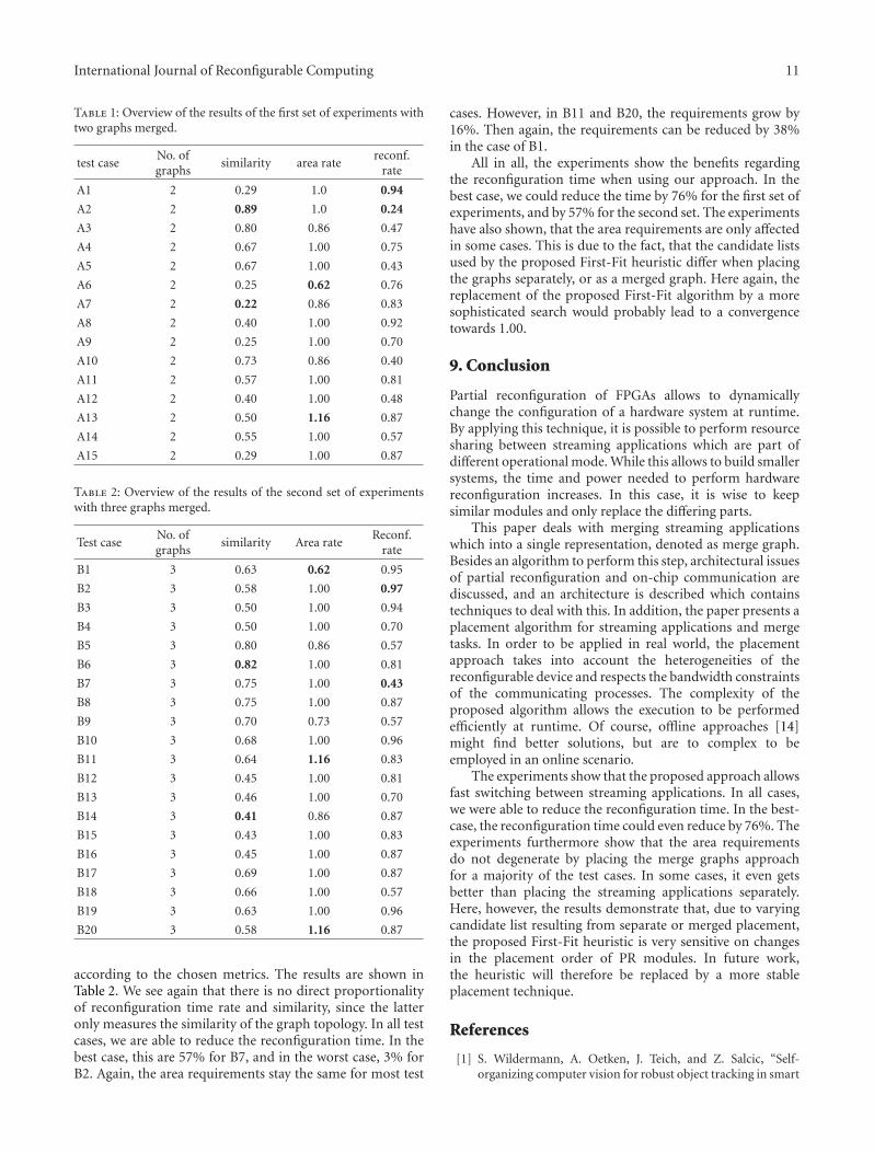
International Journal of Reconfigurable Computing 11
Table 1: Overview of the results of the first set of experiments withtwo graphs merged.
test caseNo. ofgraphs
similarity area ratereconf.
rate
A1 2 0.29 1.0 0.94
A2 2 0.89 1.0 0.24
A3 2 0.80 0.86 0.47
A4 2 0.67 1.00 0.75
A5 2 0.67 1.00 0.43
A6 2 0.25 0.62 0.76
A7 2 0.22 0.86 0.83
A8 2 0.40 1.00 0.92
A9 2 0.25 1.00 0.70
A10 2 0.73 0.86 0.40
A11 2 0.57 1.00 0.81
A12 2 0.40 1.00 0.48
A13 2 0.50 1.16 0.87
A14 2 0.55 1.00 0.57
A15 2 0.29 1.00 0.87
Table 2: Overview of the results of the second set of experimentswith three graphs merged.
Test caseNo. ofgraphs
similarity Area rateReconf.
rate
B1 3 0.63 0.62 0.95
B2 3 0.58 1.00 0.97
B3 3 0.50 1.00 0.94
B4 3 0.50 1.00 0.70
B5 3 0.80 0.86 0.57
B6 3 0.82 1.00 0.81
B7 3 0.75 1.00 0.43
B8 3 0.75 1.00 0.87
B9 3 0.70 0.73 0.57
B10 3 0.68 1.00 0.96
B11 3 0.64 1.16 0.83
B12 3 0.45 1.00 0.81
B13 3 0.46 1.00 0.70
B14 3 0.41 0.86 0.87
B15 3 0.43 1.00 0.83
B16 3 0.45 1.00 0.87
B17 3 0.69 1.00 0.87
B18 3 0.66 1.00 0.57
B19 3 0.63 1.00 0.96
B20 3 0.58 1.16 0.87
according to the chosen metrics. The results are shown inTable 2. We see again that there is no direct proportionalityof reconfiguration time rate and similarity, since the latteronly measures the similarity of the graph topology. In all testcases, we are able to reduce the reconfiguration time. In thebest case, this are 57% for B7, and in the worst case, 3% forB2. Again, the area requirements stay the same for most test
cases. However, in B11 and B20, the requirements grow by16%. Then again, the requirements can be reduced by 38%in the case of B1.
All in all, the experiments show the benefits regardingthe reconfiguration time when using our approach. In thebest case, we could reduce the time by 76% for the first set ofexperiments, and by 57% for the second set. The experimentshave also shown, that the area requirements are only affectedin some cases. This is due to the fact, that the candidate listsused by the proposed First-Fit heuristic differ when placingthe graphs separately, or as a merged graph. Here again, thereplacement of the proposed First-Fit algorithm by a moresophisticated search would probably lead to a convergencetowards 1.00.
9. Conclusion
Partial reconfiguration of FPGAs allows to dynamicallychange the configuration of a hardware system at runtime.By applying this technique, it is possible to perform resourcesharing between streaming applications which are part ofdifferent operational mode. While this allows to build smallersystems, the time and power needed to perform hardwarereconfiguration increases. In this case, it is wise to keepsimilar modules and only replace the differing parts.
This paper deals with merging streaming applicationswhich into a single representation, denoted as merge graph.Besides an algorithm to perform this step, architectural issuesof partial reconfiguration and on-chip communication arediscussed, and an architecture is described which containstechniques to deal with this. In addition, the paper presents aplacement algorithm for streaming applications and mergetasks. In order to be applied in real world, the placementapproach takes into account the heterogeneities of thereconfigurable device and respects the bandwidth constraintsof the communicating processes. The complexity of theproposed algorithm allows the execution to be performedefficiently at runtime. Of course, offline approaches [14]might find better solutions, but are to complex to beemployed in an online scenario.
The experiments show that the proposed approach allowsfast switching between streaming applications. In all cases,we were able to reduce the reconfiguration time. In the best-case, the reconfiguration time could even reduce by 76%. Theexperiments furthermore show that the area requirementsdo not degenerate by placing the merge graphs approachfor a majority of the test cases. In some cases, it even getsbetter than placing the streaming applications separately.Here, however, the results demonstrate that, due to varyingcandidate list resulting from separate or merged placement,the proposed First-Fit heuristic is very sensitive on changesin the placement order of PR modules. In future work,the heuristic will therefore be replaced by a more stableplacement technique.
References
[1] S. Wildermann, A. Oetken, J. Teich, and Z. Salcic, “Self-organizing computer vision for robust object tracking in smart
12 International Journal of Reconfigurable Computing
cameras,” in Proceedings of the 7th International Conferenceon Autonomic and Trusted Computing (ATC ’10), vol. 6407 ofLecture Notes in Computer Science, pp. 1–16, Springer, 2010.
[2] J. Hagemeyer, B. Kettelhoit, M. Koester, and M. Porrmann,“Design of homogeneous communication infrastructures forpartially reconfigurable FPGAs,” in Proceedings of the Interna-tional Conference on Engineering of Reconfigurable Systems andAlgorithms (ERSA ’07), pp. 238–247, Las Vegas, Nev, USA, June2007.
[3] D. Koch, C. Haubelt, and J. Teich, “Efficient reconfigurableon-chip buses for fpgas,” in Proceedings of the 16th IEEE Sym-posium on Field-Programmable Custom Computing Machines(FCCM ’08), pp. 287–290, April 2008.
[4] H. ElGindy, H. Schroder, A. Spray, A. K. Somani, and H.Schmeck, “RMB—a reconfigurable multiple bus network,”in Proceedings of the 2nd International Symposium on High-Performance Computer Architecture (HPCA ’96), pp. 108–117,February 1996.
[5] D. Koch, C. Beckhoff, and J. Teich, “ReCoBus-Builder—anovel tool and technique to build statically and dynamicallyreconfigurable systems for FPGAs,” in Proceedings of theInternational Conference on Field Programmable Logic andApplications (FPL ’08), pp. 119–124, September 2008.
[6] C. Bobda, A. Ahmadinia, M. Majer, J. Teich, S. Fekete, and J.van der Veen, “DyNoC: a dynamic infrastructure for commu-nication in dynamically reconfigurable devices,” in Proceedingsof the International Conference on Field Programmable Logicand Applications (FPL ’05), pp. 153–158, August 2005.
[7] U. Malik and O. Diessel, “On the placement and granularity ofFPGA configurations,” in Proceedings of the IEEE InternationalConference on Field-Programmable Technology (FPT ’04), pp.161–168, December 2004.
[8] K. P. Raghuraman, H. Wang, and S. Tragoudas, “A novelapproach to minimizing reconfiguration cost for LUT-basedFPGAs,” in Proceedings of the 18th International Conference onVLSI Design: Power Aware Design of VLSI Systems, pp. 673–676, January 2005.
[9] N. Shirazi, W. Luk, and P. Y. K. Cheung, “Automating pro-duction of run-time reconfigurable designs,” in Proceedings ofIEEE Symposium on FPGAs for Custom Computing Machines(FCCM ’98), pp. 147–156, IEEE Computer Society, NapaValley, Calif, USA, 1998.
[10] M. Rullmann and R. Merker, “Design methods and tools forimproved partial dynamic reconfiguration,” in DynamicallyReconfigurable Systems—Architectures, Design Methods andApplications, pp. 147–163, Springer, Berlin, Germany, March2010.
[11] J. Angermeier, S. Wildermann, E. Sibirko, and J. Teich, “Plac-ing streaming applications with similarities on dynamicallypartially reconfigurable architectures,” Proceedings of the Inter-national Conference on Reconfigurable Computing and FPGAs(ReConFig ’10), pp. 91–96, 2010.
[12] D. Koch, C. Beckhoff, and J. Teich, “A communication archi-tecture for complex runtime systems and its implementationon spartan-3 FPGAs,” in Proceedings of the 7th ACM SIGDAInternational Symposium on Field-Programmable Gate Arrays(FPGA ’09), pp. 253–256, February 2009.
[13] P. Brisk, A. Kaplan, and M. Sarrafzadeh, “Area-efficient in-struction set synthesis for reconfigurable system-on-chipdesigns,” in Proceedings of the 41st Design Automation Confer-ence (DAC ’04), pp. 395–400, June 2004.
[14] S. Wildermann, F. Reimann, D. Ziener, and J. Teich, “Symbolicdesign space exploration for multi-mode reconfigurable sys-tems,” in Proceedings of the 7th IEEE/ACM/IFIP International
Conference on Hardware/Software Codesign and System Synthe-sis (CODES+ISSS ’11), pp. 129–138, 2011.
[15] A. Oetken, S. Wildermann, J. Teich, and D. Koch, “A bus-based SoC architecture for flexible module placement onreconfigurable FPGAs,” in Proceedings of the InternationalConference on Field Programmable Logic and Applications (FPL’10), pp. 234–239, Milano, Italy, August 2010.
[16] D. Ziener, S. Wildermann, A. Oetken, A. Weichslgartner, andJ. Teich, “A flexible smart camera system based on a partiallyreconfigurable dynamic FPGA-SoC,” in Proceedings of theWorkshop on Computer Vision on Low-Power ReconfigurableArchitectures at the FPL, Chania, Greece, September 2011.

Hindawi Publishing CorporationInternational Journal of Reconfigurable ComputingVolume 2012, Article ID 872610, 11 pagesdoi:10.1155/2012/872610
Research Article
Redsharc: A Programming Model and On-Chip Network forMulti-Core Systems on a Programmable Chip
William V. Kritikos,1 Andrew G. Schmidt,1 Ron Sass,1 Erik K. Anderson,2
and Matthew French2
1 Reconfigurable Computing Systems Laboartory, ECE Deptartment, UNC Charlotte, 9201 University City Boulevad,Charlotte, NC 28223, USA
2 Information Sciences Institute, University of Southern California, 3811 North Fairfax Drive, Suite 200, Arlington, VA 22203, USA
Correspondence should be addressed to William V. Kritikos, [email protected]
Received 6 May 2011; Revised 21 July 2011; Accepted 28 September 2011
Academic Editor: Claudia Feregrino
Copyright © 2012 William V. Kritikos et al. This is an open access article distributed under the Creative Commons AttributionLicense, which permits unrestricted use, distribution, and reproduction in any medium, provided the original work is properlycited.
The reconfigurable data-stream hardware software architecture (Redsharc) is a programming model and network-on-a-chipsolution designed to scale to meet the performance needs of multi-core Systems on a programmable chip (MCSoPC). Redsharc usesan abstract API that allows programmers to develop systems of simultaneously executing kernels, in software and/or hardware, thatcommunicate over a seamless interface. Redsharc incorporates two on-chip networks that directly implement the API to supporthigh-performance systems with numerous hardware kernels. This paper documents the API, describes the common infrastructure,and quantifies the performance of a complete implementation. Furthermore, the overhead, in terms of resource utilization, isreported along with the ability to integrate hard and soft processor cores with purely hardware kernels being demonstrated.
1. Introduction
Since the resources found on FPGA devices continue totrack Moore’s Law, modern, high-end chips provide hun-dreds of millions of equivalent transistors in the form ofreconfigurable logic, memory, multipliers, processors, anda litany of increasingly sophisticated hard IP cores. As aresult, engineers are turning to multi-core systems on aprogrammable chip (MCSoPC) solutions to leverage theseFPGA resources. MCSoPC allow system designers to mixhard processors, soft processors, third party IP, or customhardware cores all within a single FPGA. In this work, we areonly considering multi-core systems with a single processorcore, multiple third party IP cores, and multiple customhardware cores.
A major challenge of MCSoPC is how to achieve intercorecommunication without sacrificing performance. This prob-lem is compounded by the realization that cores may use dif-ferent computational and communication models; threadsrunning on a processor communicate much differentlythan cores running within the FPGA fabric. Furthermore,
standard on-chip interconnects for FPGAs do not scale welland cannot be optimized for specific programming models;contention on a bus can quickly limit performance.
To address these issues, this paper investigatesRedsharc—an API and common infrastructure for realizingMCSoPC designs. Redsharc’s contribution has two parts.
First, introduction of an abstract programming modeland API that specifically targets MCSoPC is presented. Anabstract API, as described by Jerraya and Wolf in [1], allowscores to exchange data without knowing how the oppositecore is implemented. In a Redsharc system, computationalunits, known as kernels, are implemented as either softwarethreads running on a processor, or hardware cores runningin the FPGA fabric. Regardless of location, kernels com-municate and synchronize using Redsharc’s abstract API.Redsharc’s API is based both on a streaming model to passdata using unidirectional queues and a block model thatallows kernels to exchange index-based bidirectional data.Section 3 explains the Redsharc API in detail.
Redsharc’s second contribution is the development of fastand scalable on-chip networks to implement the Redsharc

2 International Journal of Reconfigurable Computing
API, with special consideration to the hardware/softwarenature of MCSoPC. The stream switch network (SSN),discussed in Section 4.1, is a run-time reconfigurable cross-bar on-chip network designed to carry streams of databetween heterogeneous cores. The block switch network(BSN), discussed in Section 4.2, is a routable crossbar on-chip network designed to exchange index data elementsbetween cores and blocks of memory.
To evaluate the proposed approach, the API and infras-tructure have been implemented as a software library anda collection of VHDL components with generics. A seriesof benchmarks were run on a Xilinx ML510 developmentboard to demonstrate Redsharc’s performance. A BLASTbioinformatics kernel was also ported to a Redsharc core todemonstrate the full use of the Redsharc API and to showscalability. Results are listed in Section 6.
2. Related Work
The idea of creating an API to abstract communicationbetween heterogeneous computational units has its roots inboth the DARPA adaptive computing systems (ACSs) project[2] and PipeRench project [3]. These projects focused onprocessor to off-chip FPGA accelerator communication andcontrol, they existed prior to the realization of MCSoPC.
More recently, ReconOS [4] and hthreads [5] imple-mented a programming model based on Pthreads toabstract the hardware/software boundary. They successfullydemonstrate the feasibility of abstract programming mod-els in heterogeneous systems. However, their middlewarelayer requires an impractical amount of FPGA resources.Furthermore, their communication bandwidth is limiteddue to a reliance on proprietary buses. Redsharc addressesthese problems by developing an abstract API better suitedfor MCSoPC and developing custom on-chip networks,respectively, supporting the API.
Using a message passing interface (MPI) for parallelcommunication has also been explored on FPGAs. MPIis commonly used in scientific applications running onlarge clusters with traditional microprocessor-based nodes.Several works, including TMD-MPI [6] and SoC-MPI [7],have implemented some of the standard MPI function callsin an FPGA library. While supporting MPI may be usefulwhen trying to port an existing scientific application to anFPGA cluster, it adds several layers of abstraction that are notnecessary for streaming models. Some logic must be presentto decode received message, strip out the real data from themessage, and deliver that data to the appropriate input of thecomputational unit. The streaming model allows for directconnection of a stream to computational units, as the streamcontains only data. We depend on the streams being properlyset up before data is delivered. The goal of Redsharc is toimplement as light-weight as possible, so a streaming systemwas chosen over an MPI or Pthreads-based system.
The stream model is common within FPGA program-ming. Projects such as [8, 9] use high level stream APIs orstream languages with compilation tools to automaticallygenerate MCSoPC. Unlike Redsharc, these efforts focus ona purely streaming programming model and do not include
support for random access memory. Furthermore, thesemodels do not permit the mixing of heterogeneous hardprocessors, soft processors, or custom FPGA cores as may beneeded to meet stringent application demands.
Researchers have also customized streaming networks tocommunicate between heterogeneous on-chip cores usingabstract interfaces. For example, aSOC [10] is notablefor communication between heterogeneous computationalunits, but it targets ASICs instead of FPGAs. Finally, SIMPPL[11] developed an FPGA-based streaming network but donot consider heterogeneous computational units. Moreover,existing on-chip networks only support pure streamingapplications and do not include support for random accessmemory.
3. Redsharc API
Developing an abstract API for MCSoPC is not a trivialtask. The API must support parallel operations, be realizablein all computational domains, be resource friendly, and beflexible enough to incorporate a large number of applicationdomains. However, these goals can be in conflict at times.
To find the middle ground in these conflicting require-ments, Redsharc is based on the stream virtual machine(SVM) API [12]. SVM was originally designed as anintermediate language between high level stream languagesand low level instruction sets of various architectures beingdeveloped by the DARPA polymorphous computing systems(PCSs) program. The main idea was that multiple high-level languages would map to a common stable architecturalabstraction layer that included SVM. That layer would thenmap to specific polymorphous computing systems such asTRIPS, MONARC, RAW, and others as illustrated in Figure 1[13–15]. SVM has no preference to the computationalmodel for individual kernels and only specifies how kernelscommunicate with each other. SVM is primarily basedon the relatively simple stream model, but it includes theconcept of indexed block data to support random access.These features make it an ideal candidate for porting toMCSoPC. The REDSHARC system implements the sameSVM API that would be used on a TRIPS, MONARCH, orRAW architectures while targeting FGPAs instead of ASICprocessors. Future work could allow the high level languagesshown in Figure 1 to target FPGA-, TRIPS-, MONARCH-,and RAW-based processors.
The Redsharc API recognizes two types of kernels, workerand control. There is only one control kernel in the systemand it is responsible for creating and managing streams,blocks, and worker kernels. There may be multiple workerkernels that perform functions on data elements presentedin streams or blocks. A stream is a unidirectional flow of dataelements between two kernels. A block is an indexed set ofdata elements shared between two or more kernels. In thecurrent Redsharc implementation, a data element can be ofany size 2n bits where n is an integer and greater than 5.
Applications are divided into kernels. Because bothhardware and software kernels utilize the same block andstream API, the initial stages of application developmentdo not need to be concerned with a particular kernel

International Journal of Reconfigurable Computing 3
Table 1: Redsharc control kernel’s API calls.
Control’s API call Description
kernelInitNull (kernel ∗k) Initializes k to a default state
kernelInit (kernel ∗k, streams ∗s, blocks ∗b) Configures streams/blocks in array s/b for communication with k
kernel Add Dependence (kernel ∗k1, kernel ∗k2) Makes k2 dependent on the completion of k1
kernelRun(kernel ∗k) Adds k to the list of schedulable kernels
kernelPause(kernel ∗k) Removes k from the list of schedulable kernels
streamInitFifo(stream ∗s) Initializes s
blockInit(block ∗b) Initializes b
Table 2: Redsharc worker kernel’s API calls.
Worker’s API Call Description
void kernelEnd() Indicates kernel has completed its work
void streamPush(element ∗e, stream ∗s) Pushes e onto a stream s
void streamPushMulticast(element ∗e, stream ∗s) Pushes e to multiple streams
void streamPop(element ∗e, stream ∗s) Pops top element from s and stores value in e
void streamPeek(element ∗e, stream ∗s) Reads top element from s storing value in e
void blockWrite(element ∗e, int index, block ∗b) Writes e to b at index
void blockRead(element ∗e, int index, block ∗b) Reads index b and stores in e
being implemented in software or hardware. The systemcan be viewed as kernels with logical connections as shownin Figure 2. After each kernel is defined, the kernels areimplemented using either hardware or software, dependingon the suitability of the kernel’s task to a software orhardware environment. At that point in time, the system willresemble Figure 3.
3.1. Software Kernel Interface. There are two types of softwarekernels in Redsharc, worker kernels which perform workfor the application, and a single control kernel whichsets up the blocks, streams, and which manages the otherkernels. Control kernels are always implemented in software.The software kernel interface (SWKI) is implemented as atraditional software library. User kernels link against thelibrary when generating executable files. Different processors(hard or soft) may implement the SWKI in different ways,however, a common approach has been to use a threadingmodel to manage multiple software kernels executing on asingle processor.
The control kernel API, in C syntax, is presentedin Table 1. The symbols, kernel, stream, block, andelement, are variable types in Redsharc. The control kernelcreates variables of these types and initializes them for useduring run-time. In Redsharc, the streams and blocks akernel communicates with are set at run-time with thekernelInit command. A dependency is used in conjunc-tion with a block to allow one kernel to write elements toa block and prohibit any reading kernel from starting untilthe write is complete. Only the control kernel is aware ofeach worker kernel’s location, either hardware or software.Due to the added complexity control, kernels may only beimplemented in software.
The worker kernel API is listed in Table 2. WhilekernelEnd is used to communicate with the control kernel
when work is completed, the remainder of the API isdedicated to stream or block communication. In much thesame way that a function in an object-oriented language maybe overloaded for different variable types, the Redsharc APIis independent of data element width, block location, or thetransmitting or receiving kernel’s implementation.
3.2. Hardware Kernel Interface. The hardware API layer,known as the hardware kernel interface (HWKI), is imple-mented as a VHDL entity that is included during synthesis.There is one HWKI for each hardware kernel. The HWKI isa thin wrapper that connects hardware kernels to the SSNand BSN. Described in more detail in Section 4, the HWKIimplements the Redsharc stream API as a series of interfacessimilar to FIFO ports, and the Redsharc block API as a seriesof interfaces similar to BRAM ports. The use of SVM hassimplified the development of hardware kernels. Figure 4illustrates the HWKI as implemented in VHDL. A kerneldeveloper only needs to know how to pop and push datafrom an FIFO to use the Redsharc stream switch network.Similarly, all accesses to memory, on-chip, or off-chip, areonly a simple BRAM access with additional latency.
4. Redsharc’s Networks on a Chip
The stream switch network (SSN) and block switch network(BSN) were necessitated by performance and scalability. Pro-gramming models that are built on top of existing general-purpose on-chip networks such as IBM’s CoreConnect [16]must translate higher level API calls to lower level networkprocedures often with a large overhead. For example, even asimple streamPeek() operation may require two bus readtransactions, the first to check if the stream is not empty, thesecond to retrieve the value of the top element. In previouswork, Liang et al., [10] showed custom on-chip networks
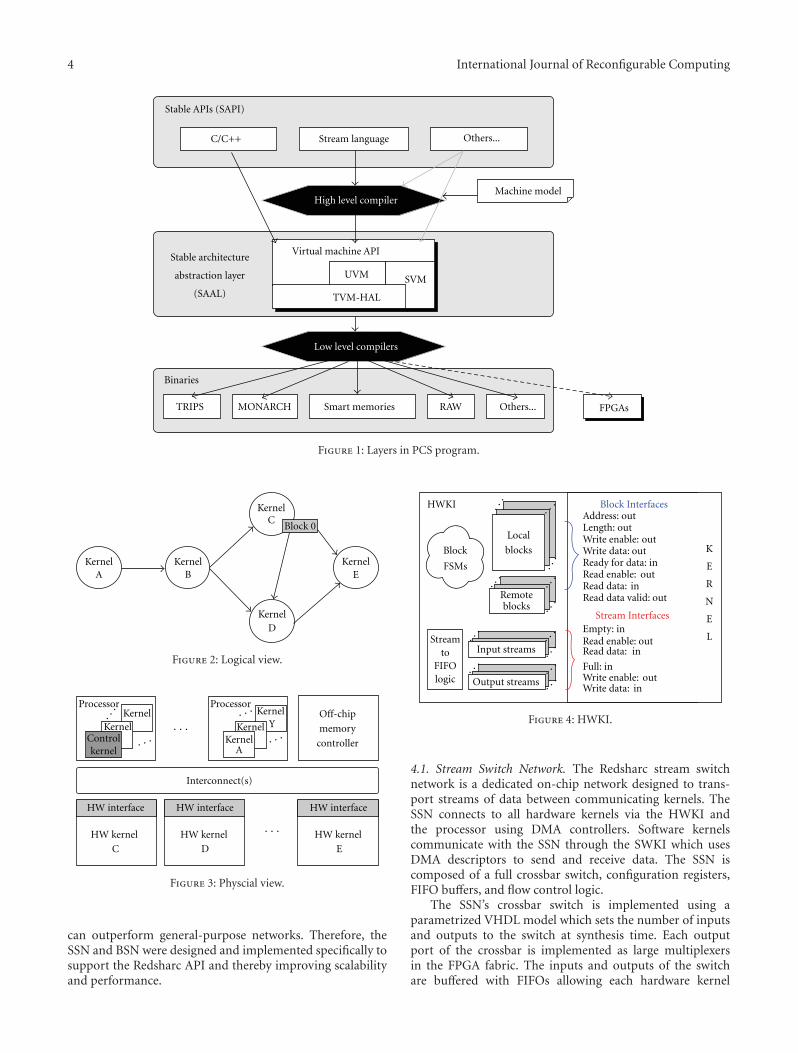
4 International Journal of Reconfigurable Computing
Stable architecture
abstraction layer
(SAAL)
Stable APIs (SAPI)
High level compilerMachine model
TRIPS MONARCH Smart memories RAW
Others...
FPGAs
Binaries
Low level compilers
Virtual machine API
UVM SVM
TVM-HAL
C/C++ Stream language
Others...
Figure 1: Layers in PCS program.
Block 0
KernelA
KernelB
KernelC
KernelD
KernelE
Figure 2: Logical view.
HW interface
HW kernel
C D E
Interconnect(s)
Controlkernel
Kernel
A
Y
ProcessorOff-chip
memory
controller
KernelProcessor
Kernel
KernelKernel
HW interface HW interface
HW kernel HW kernel···
···
···
···
······
Figure 3: Physcial view.
can outperform general-purpose networks. Therefore, theSSN and BSN were designed and implemented specifically tosupport the Redsharc API and thereby improving scalabilityand performance.
Block Interfaces
Stream Interfaces
HWKI
Read enable:Read data:
Local
blocks
Remoteblocks
Input streams
Output streams
Block
FSMs
Streamto
FIFOlogic
Address: outLength: out
outWrite enable:Write data:Ready for data: in
Read data valid:
out
inout
Empty: inRead enable: outRead data: in
Full: inoutWrite enable:
Write data: in
out
K
E
R
N
L
E
···
···
···
···
···
···
···
···
···
···
···
···
Figure 4: HWKI.
4.1. Stream Switch Network. The Redsharc stream switchnetwork is a dedicated on-chip network designed to trans-port streams of data between communicating kernels. TheSSN connects to all hardware kernels via the HWKI andthe processor using DMA controllers. Software kernelscommunicate with the SSN through the SWKI which usesDMA descriptors to send and receive data. The SSN iscomposed of a full crossbar switch, configuration registers,FIFO buffers, and flow control logic.
The SSN’s crossbar switch is implemented using aparametrized VHDL model which sets the number of inputsand outputs to the switch at synthesis time. Each outputport of the crossbar is implemented as large multiplexersin the FPGA fabric. The inputs and outputs of the switchare buffered with FIFOs allowing each hardware kernel

International Journal of Reconfigurable Computing 5
to run within its own clock domain. Data is transferredfrom a kernel’s output FIFO to another kernel’s input FIFOwhenever data is available in the output FIFO and roomexists in the input FIFO. The flow control signals usedin the SSN are based on the LocalLink specification [17].The SSN’s internal data width is set at synthesis time anddefaults to 32 bits. To fulfill the Redsharc API requirementthat each stream has a variable width, the FIFOs on the edgesof the SSN translate the stream’s data from 32 bits to thekernel’s data width requirement. The SSN runs by defaultat 200 MHz, however, this system clock can be reduced toimprove the timing score for very dense designs.
Figure 5 shows the streams and kernels in an SSN system.The input streams are shown on the left side of the figureflowing into hardware kernels, with the output streams onthe right. Hardware kernels may have any number of inputand output streams. Also shown are the streams connectingthe processor’s DMA controllers ports which connect directlyto the switch, along with the switch configuration registerswhich are accessible from the system bus.
Hardware kernels are presented with standard FIFOinterfaces as their Redsharc stream API implementation.While abstracted from hardware developers the FIFOs aredirectly part of the SSN.
Software kernels communicate with the SWKI library.The SWKI in turn communicates with hardware kernels byinteracting with the DMA controllers. The DMA controllerscan read or write data from off-chip memory into aLocalLink port. The SWKI’s stream API is written to senda pointer and length to the DMA engine for the amountof data to send or receive and the location of that data. Aninterrupt occurs when the DMA transaction has finished.Using the DMA controllers, the processor is more efficientwhen there is a large amount of data to push from software tohardware or vice versa, which is often the case with streamingapplications. The SWKI is also responsible for configuringthe SSN’s switch to connect the processor with the receivingor transmitting hardware kernel.
An advantage of the crossbar switch is that multicaststream pushes are possible by simply having several outputports reading data from the same input port. The controlkernel can change the switch configuration at run-timeto modify application functionality or for load balancingoptimizations.
4.2. Block Switch Network. The purpose of the block switchnetwork is to implement the low level communicationneeded by the Redsharc block API. Redsharc blocks arecreated at synthesis time but allocated at run time by thecontrol kernel. Blocks may be specified to be on-chip aspart of an HWKI or a section of off-chip volatile memory.The BSN is implemented as a routable crossbar switch andpermits access from any kernel to any block.
Figure 6 shows the BSN’s router. The router consists of afull crossbar switch, switch controller, and routing modules.When a kernel requests data, the routing module decodesthe address request and notifies the switch controller. Theswitch controller checks the availability of the output portand, if not in use, configures the switch. This configuration
···
Processor block
SSN
crossbar
switch
Switch configregisters
RXDMA
TXDMA
FIFO
Hardware
kernel 0
FIFO
FIFO
FIFO
FIFO
BusI/F
Hardware
FIFO
FIFO FIFO
FIFO
FIFO
kernel N
Figure 5: Stream switch network.
···
···
···
BSNcrossbar
switch
Input ports Output ports
Switch controller
RM0
Port 0
Port 1
Port 2
Port 3
RM1
RM2
RM3
RM
Port 0
Port 1
Port 2
Port 3
Port NPort N
N
Figure 6: Block switch network’s router consisting of a full crossbarswitch, routing modules per each input port, and a single switchcontroller used to configure the inputs to the requested outputs.
can take as few as 2 clock cycles. The configuration will stallif the desired output port is currently in use by another inputuntil the first port finishes the transmission. The input portsare shown on the left side of the figure which are connectedto the output of the hardware kernels. The output ports onthe right connect to the input port of the hardware kernels.Hardware kernels can consist of any number of local, remoteand off-chip memory ports, giving the kernel a higher degreeof parallelism with memory access.
“Local” blocks, commonly implemented as BRAM, areaccessible to a hardware kernels with low latency (≈2

6 International Journal of Reconfigurable Computing
clock cycles). They are instantiated as part of a hardwarekernel’s HWKI. A “remote” block is on-chip memory that islocated in a different hardware kernel’s HWKI, but accessiblethrough the BSN. This is made possible through dual-portedBRAMs. One port is dedicated to the local hardware kernel,the second port is dedicated to the BSN. “Off-chip” blocksare allocated in volatile off-chip RAM (e.g., DDR2 SDRAM).The BSN communicates directly with the memory controller.While hardware kernels still share this connection for blockcommunication, requests are serialized at the last possiblepoint helping to improve overall performance.
The BSN abstracts away the different block types toprovide hardware developers with a common interface viathe HWKI. The HWKI block interface is an extension of thecommon BRAM interface with the addition of “ready fordata,” “valid,” “request size,” and “done.” The added signalsoffer the ability to burst larger amounts of data in and outof memory. The use of the ready for data and valid signals isnecessary since requests to remote and off-chip memory maytake an undetermined amount of time.
The BSN also abstracts away data (element) sizes fromthe kernel developer. In conventional bus-based systems, thedeveloper may need to access 32-bit data from one locationand 128-bit data from a second location. As a result, thedeveloper must be aware of the amount of data needed foreach request type. In the Redsharc system, the BSN, gives thedeveloper the exact data size needed and handles the internaltransfers accordingly. With the BSN a developer can stilltransfer 128-bit data, but instead of actively transmitting thefour 32-bit words, only a single transaction is required. TheBSN still transfers all 128-bits; however, it does so internallyas a burst of four 32-bit words.
Another advantage is the block location can be moved(e.g., from a local block to a off-chip block) at synthesis timebased on available resources without requiring the kerneldeveloper to redesign their code. For example, if the designrequires a significant amount of BRAMs to be used elsewherein the system, the data can be placed in off-chip memory. Tothe kernel developer the interface remains fixed and only theconnection within the HWKI changes.
Software kernels access blocks through the SWKI. Ifthe block is located off-chip, the SWKI routes the requestthrough the PPC’s memory port (avoiding bus arbitration).If the block is located within the BSN, the request istranslated to memory mapped commands to the BSN on thePLB.
While blocks are conceptualized as either being stored inon-chip block RAMs or in off-chip RAM, many designs alsoneed access to a set of small control or “one off” registers tointerface with peripheral or kernels. We group these togetheras special purpose registers. For example, a design may needaccess to one or more of these registers in order to set someinitial parameters, such as sequence length or number oftransfers. Rather than dedicating an entire block, a designermay want to have the more familiar register access within thekernel. The BSN enables access to these registers by both thecontrol kernel and other hard and soft kernels in the system.A designer can specify at synthesis the number of registerswhich are to be allocated for the kernel. To the hardware
kernel interface, the registers are additional elements with aspecific address range. However, to the kernel, the registersare directly accessible without performing block transfers.
5. Implementation
The Redsharc infrastructure spans several IP cores andincorporates multiple interfaces. Nonetheless, by utilizingVHDL generics and by careful organization, Redsharc canbe synthesized for multiple FPGA families. Specifically, thisis possible because of four key principles. First, it simplifieshardware and software kernel development through anabstract programming model that has been implementedin a conventional software and hardware kernel interface(SWKI and HWKI, resp.). Second, Redsharc can use bothhard and soft processing cores to control kernel execution.Third, by design, Redsharc enables low-latency and high-bandwidth access to streams of data between hardware andsoftware kernels through the stream switch network (SSN).Last, having a separate network for data transfers to randomaccess block memory (through the block switch network,BSN) reduces resource contention.
5.1. Kernel Integration. Among its many contributions,Redsharc enables rapid kernel integration into new andexisting systems. Through the use of the hardware kernelinterface (HWKI), a kernel developer can exclusively focuson the design of the kernel rather than how to accessstreams and blocks of data. Complexities associated with bustransactions and memory controllers need not be consideredby the kernel developer. Instead, the Redsharc infrastructuresimplifies these accesses to mere FIFO and BRAM interfaces.The HWKI is then responsible for translating these requestsinto the more complex stream and block transfers. This isespecially important as systems migrate from on FPGA to thenext because modifying low-level kernels to access memoryshould be the last concern for a system designer.
5.2. System Integration. Separate from kernel developmentis system integration. Redsharc emphasizes the difference inorder to enable designers to more efficiently construct largesystems comprising of several kernels that are executing inboth hardware and software. The goal is to allow the rapidassembly of such systems without significant involvementfrom individual kernel developers. In fact, so long as thekernel developer adheres to FIFO- and BRAM-like interfaces,the system designer is free to assemble and modify thesystem.
Ultimately, a Redsharc system is comprised of one ormore processors, memory controllers, and kernels. Theprocessors can be hard or soft IP, such as the PowerPC,MicroBlaze, or Nios processor. While performance and/oravailable resources may dictate which processor to use, theRedsharc system has been designed to be completely pro-cessor and FPGA vendor agnostic. The LocalLink interfacestandard used in the SSN and BSN can be replaced with asimilar point to point streaming protocol with flow control.The internal LocalLink channels in the SSN and BSN wouldnot need to be modified to accept a new streaming protocol,
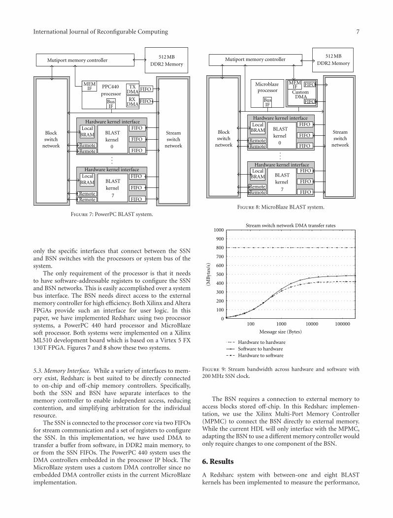
International Journal of Reconfigurable Computing 7
BLASTkernel
0
FIFO
Hardware kernel interface
FIFO
LocalBRAM
RemoteRemote
Block
RXDMA
TXDMA
PPC440
processor
Streamswitch
network
FIFO
Bus
IF
Mutiport memory controllerDDR2 Memory
Hardware kernel interface
FIFO
FIFO
FIFO
FIFO
FIFO
BLASTkernel
7
switchnetwork
IF
MEM
LocalBRAM
512 MB
···
RemoteRemote
Figure 7: PowerPC BLAST system.
only the specific interfaces that connect between the SSNand BSN switches with the processors or system bus of thesystem.
The only requirement of the processor is that it needsto have software-addressable registers to configure the SSNand BSN networks. This is easily accomplished over a systembus interface. The BSN needs direct access to the externalmemory controller for high efficiency. Both Xilinx and AlteraFPGAs provide such an interface for user logic. In thispaper, we have implemented Redsharc using two processorsystems, a PowerPC 440 hard processor and MicroBlazesoft processor. Both systems were implemented on a XilinxML510 development board which is based on a Virtex 5 FX130T FPGA. Figures 7 and 8 show these two systems.
5.3. Memory Interface. While a variety of interfaces to mem-ory exist, Redsharc is best suited to be directly connectedto on-chip and off-chip memory controllers. Specifically,both the SSN and BSN have separate interfaces to thememory controller to enable independent access, reducingcontention, and simplifying arbitration for the individualresource.
The SSN is connected to the processor core via two FIFOsfor stream communication and a set of registers to configurethe SSN. In this implementation, we have used DMA totransfer a buffer from software, in DDR2 main memory, toor from the SSN FIFOs. The PowerPC 440 system uses theDMA controllers embedded in the processor IP block. TheMicroBlaze system uses a custom DMA controller since noembedded DMA controller exists in the current MicroBlazeimplementation.
Microblaze
Custom DMA
BLASTkernel
0
FIFO
Hardware kernel interface
FIFO
LocalBRAM
RemoteRemote
Block
processor
Streamswitch
network
FIFO
Bus
IF
Mutiport memory controllerDDR2 Memory
Hardware kernel interface
FIFO
FIFO
FIFO
FIFO
BLASTkernel
7
switchnetwork
IF
MEM
LocalBRAM
512 MB
RemoteRemote
FIFO
···
Figure 8: MicroBlaze BLAST system.
0
100
100
200
300
400
500
600
700
800
900
1000
1000 10000 100000
Message size (Bytes)
Stream switch network DMA transfer rates
Hardware to hardwareSoftware to hardwareHardware to software
(MB
ytes
/s)
Figure 9: Stream bandwidth across hardware and software with200 MHz SSN clock.
The BSN requires a connection to external memory toaccess blocks stored off-chip. In this Redsharc implemen-tation, we use the Xilinx Multi-Port Memory Controller(MPMC) to connect the BSN directly to external memory.While the current HDL will only interface with the MPMC,adapting the BSN to use a different memory controller wouldonly require changes to one component of the BSN.
6. Results
A Redsharc system with between-one and eight BLASTkernels has been implemented to measure the performance,

8 International Journal of Reconfigurable Computing
scalability, and resource utilization of the Redsharc abstractAPI and infrastructure. The characteristics, measured on aVirtex 5 FX 130T FPGA, are presented in this section. XilinxISE Design Suite version 11.4 was used for all experimentsfor FPGA implementation.
6.1. Network Performance. The SSN’s performance is mea-sured by the bandwidth between two kernels. While theHWKI abstracts these issues from the hardware developer,these metrics are dependent on (1) width of the stream,(2) width of the SSN, (3) clock frequency of the SSNand kernels. Between two hardware kernels, running at200 MHz and a 32 bit data width, the SSN’s bandwidthis 800 MB/s. When the receiving or transmitting kernel issoftware, the bandwidth is limited by the throughput of theDMA controller and the message size. Figure 9 shows themeasured bandwidth for different stream lengths betweenhardware kernels and software kernels. The SSN performsbest with large message sizes.
The BSN’s performance is measured by the latency andbandwidth of a read operation. Similar to the SSN, theRedsharc API abstracts synthesis-time configurations thatmay affect the bandwidth of a specific system. The settingsthat affect BSN’s bandwidth are (1) location and width ofthe data, (2) operating frequency of the hardware kernel andBSN (clock domain crossing adds overhead), and (3) possiblecontention at the remote block. Table 3 provides an overviewof the BSN performance for the three types of data locality,given both the BSN and hardware kernels on the same100 MHz clock. The BSN performs very favorable comparedto the PLB which, in previous work, has a measured peekperformance of 25 MB/s [18] for a 32 bit read transactionand a 200 MB/s for 1024 bit transaction.
6.2. Kernel Performance. In order to demonstrate Redsharc’sscalability, a BLAST bioinformatics kernel was implemented.BLAST is a bioinformatics application that performs DNAcomparisons. BLAST compares one short DNA sequence,called the query, against a long database of DNA sequences,and produces a stream of indexes where the two sequencesmatch. The database of DNA sequences is 35 KBytes. TheBLAST query is encoded into the 8 KByte local block.Researchers have implemented BLAST on FPGAs to demon-strate impressive speedups [19]; however, previous work[20, 21] has shown that bandwidth requirements for BLASTlimit the scalability such that a common bus interconnect isinsufficient for transferring databases to each BLAST core aswell as being used for off-chip memory lookups. Specifically,each BLAST core can sustain database input rates of 3.2 GB/s.Common bus implementation, such as the processor localbus (PLB), offers sufficient bandwidth (12.8 GB/s) althoughthere are limitations on the burst size and the numberof concurrent transfers. For these reasons and due to theaforementioned previous research investigating conventionalbus-based implementations, this work focuses on analyzingthe scalability of BLAST cores within the Redsharc system.
The BLAST hardware kernel used in these experiments isa reimplementation of the BLAST algorithm with two input
Table 3: BSN latency and bandwidth for each block type with100 Mhz BSN clock.
Block type 32 b data width 1024 b data width
Local 2 cc (200 MB/s) 2 cc (6400 MB/s)
Remote 16 cc (25 MB/s) 47 cc (272 MB/s)
Off-chip 25 cc (16 MB/s) 56 cc (228 MB/s)
streams: one for the input database and one for the lengthof each sequence in the database. One output stream is usedfor the matching results. Three blocks (one local and twooff-chip) store query information. Each BLAST kernel addedto the system can run one query in parallel. Furthermore,it is possible to use the multicast capabilities of the SSN tobroadcast the same database to all of the running BLASTkernels.
For comparison, a constant work size of eight queriesand one database is used to test the system. The systemwith a single BLAST kernel must sequentially evaluate thequeries, while the system with eight kernels can evaluatethem in parallel. This test will show if the Redsharc systemcan scale with increasing hardware kernels. Table 4 showsthe execution time results of the system when executingwith a PowerPC processor. The performances of the BLASTapplication when implemented on a microblaze based systemare shown in Table 5.
Both systems show no speedup in the time to load thequeries into the blocks or read the result data back from thekernels. These operations are entirely sequential and offer nopossible speedup. The 100 MHz Microblaze processor takessignificantly longer than the 400 MHz PowerPC processor inthese sequential steps. A nearly linear speedup is observedin both systems in the time spent comparing the database tothe query. Note that with eight queries running in parallel,the BSN must handle the increasing load for the queryinformation stored in off-chip memory blocks while the SSNis also reading the database from off-chip memory. Thiscontention for the single off-chip memory resource preventstotally linear scaling.
6.3. Resource Utilization. This subsection presents the sizesof the BSN, SSN, and HWKI, the three critical hardwarecomponents that comprise a Redsharc system. Table 6 showsthe resource utilization of a single BLAST kernel and itsassociated HWKI. The most used resources are the lookuptables. The remote block interface components of the HWKIappears to use an extraordinary amount of resources. Thisis due to one of the remote blocks having a data width of448 bits, the natural data width of a single lookup of thequery information stored in the off-chip memory block.The HWKI handles expanding the data from the 32 bitmemory interface into the 448 bit data width, a job thatwould normally have to be done by the application internally.
Figure 11 and Table 8 show the number of lookup tablesused in the one, two, four, and eight kernel systems usedin these tests. The figure shows that even at eight kernels,the Redsharc infrastructure, the BSN and SSN, uses fewerresources than the kernels. It also shows that the SSN is
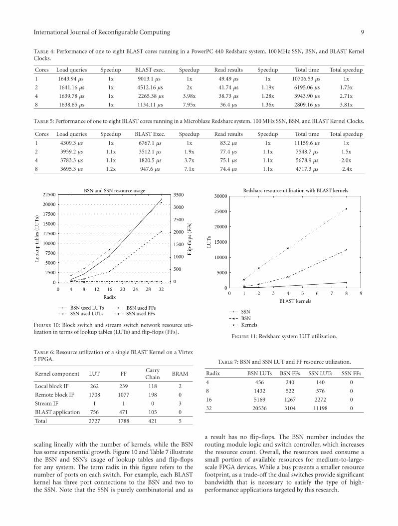
International Journal of Reconfigurable Computing 9
Table 4: Performance of one to eight BLAST cores running in a PowerPC 440 Redsharc system. 100 MHz SSN, BSN, and BLAST KernelClocks.
Cores Load queries Speedup BLAST exec. Speedup Read results Speedup Total time Total speedup
1 1643.94 μs 1x 9013.1 μs 1x 49.49 μs 1x 10706.53 μs 1x
2 1641.16 μs 1x 4512.16 μs 2x 41.74 μs 1.19x 6195.06 μs 1.73x
4 1639.78 μs 1x 2265.38 μs 3.98x 38.73 μs 1.28x 3943.90 μs 2.71x
8 1638.65 μs 1x 1134.11 μs 7.95x 36.4 μs 1.36x 2809.16 μs 3.81x
Table 5: Performance of one to eight BLAST cores running in a Microblaze Redsharc system. 100 MHz SSN, BSN, and BLAST Kernel Clocks.
Cores Load queries Speedup BLAST Exec. Speedup Read results Speedup Total time Total speedup
1 4309.3 μs 1x 6767.1 μs 1x 83.2 μs 1x 11159.6 μs 1x
2 3959.2 μs 1.1x 3512.1 μs 1.9x 77.4 μs 1.1x 7548.7 μs 1.5x
4 3783.3 μs 1.1x 1820.5 μs 3.7x 75.1 μs 1.1x 5678.9 μs 2.0x
8 3695.3 μs 1.2x 947.6 μs 7.1x 74.4 μs 1.1x 4717.3 μs 2.4x
0
2500
5000
7500
10000
12500
15000
17500
20000
4 8 12 16 20 24 28 32
500
1000
1500
2000
2500
3000
3500
Look
up
tabl
es (
LUT
s)
Radix
BSN and SSN resource usage
BSN used LUTsSSN used LUTs
BSN used FFsSSN used FFs
0
0
22500Fl
ip-fl
ops
(FFs
)
Figure 10: Block switch and stream switch network resource uti-lization in terms of lookup tables (LUTs) and flip-flops (FFs).
Table 6: Resource utilization of a single BLAST Kernel on a Virtex5 FPGA.
Kernel component LUT FFCarryChain
BRAM
Local block IF 262 239 118 2
Remote block IF 1708 1077 198 0
Stream IF 1 1 0 3
BLAST application 756 471 105 0
Total 2727 1788 421 5
scaling lineally with the number of kernels, while the BSNhas some exponential growth. Figure 10 and Table 7 illustratethe BSN and SSN’s usage of lookup tables and flip-flopsfor any system. The term radix in this figure refers to thenumber of ports on each switch. For example, each BLASTkernel has three port connections to the BSN and two tothe SSN. Note that the SSN is purely combinatorial and as
0
5000
10000
15000
20000
25000
30000
0 1 2 3 4 5 6 7 8 9
LUT
s
BLAST kernels
SSNBSNKernels
Redsharc resource utilization with BLAST kernels
Figure 11: Redsharc system LUT utilization.
Table 7: BSN and SSN LUT and FF resource utilization.
Radix BSN LUTs BSN FFs SSN LUTs SSN FFs
4 456 240 140 0
8 1432 522 576 0
16 5169 1267 2272 0
32 20536 3104 11198 0
a result has no flip-flops. The BSN number includes therouting module logic and switch controller, which increasesthe resource count. Overall, the resources used consume asmall portion of available resources for medium-to-large-scale FPGA devices. While a bus presents a smaller resourcefootprint, as a trade-off the dual switches provide significantbandwidth that is necessary to satisfy the type of high-performance applications targeted by this research.
10 International Journal of Reconfigurable Computing
Table 8: Redsharc system LUT utilization.
Kernels SSN BSN Kernel logic
1 100 534 2727
2 172 1193 6476
4 615 3672 12942
8 1770 12470 25886
The HWKI supports access to variable number of streamsand blocks with variable data element sizes. As such, wepresent the resources required for each additional stream orblock and assume 32-bit data widths for all ports. For theSSN, only an LUT is required for each input and outputport to drive the Xilinx LocalLink signals and the input andoutput stream FIFOs. The FIFO depth is configurable by thehardware developer so the number of BRAMs is variable. Forthe BSN, more logic is needed to support local and remoteblock requests. Each local block requires 176 flip-flops and300 LUTs whereas each remote block only requires 161 flip-flops and 163 LUTs. These represent a minimal amount ofresources needed to support the high-bandwidth memorytransactions while maintaining a common memory interfaceto the hardware kernel.
7. Conclusion
Programming MCSoPC that span hardware and softwareis not a trivial task. While abstract programming modelshave been shown to ease the programmer burden of crossingthe hardware/software boundary, their abstraction layerincurs a heavy burden on performance. Redsharc solves thisproblem by merging an abstract programming model withon-chip networks that directly implement the programmingmodel.
The Redsharc API is based on a streaming programmingmodel but it incorporates random access blocks of memory.Two on-chip networks were implemented to facilitate thestream and block API calls. Our results showed that theSSN and BSN have comparable bandwidth to state-of-the-art technology and scales nearly linearly with parallelhardware kernels. Redsharc can be implemented acrossmultiple platforms, with no dependence on a particularFPGA family or processor interface. Ergo, programmers,and system architects may develop heterogeneous systemsthat span the hardware/software domain, using a seamlessabstract API, without giving up performance of custominterfaces.
Disclaimer
The views, opinions, and/or findings contained in thisarticle/presentation are those of the author/presenter andshould not be interpreted as representing the official viewsor policies, either expressed or implied, of the DefenseAdvanced Research Projects Agency or the Department ofDefense.
References
[1] A. Jerraya and W. Wolf, “Hardware/software interface code-sign for embedded systems,” Computer, vol. 38, no. 2, pp. 63–69, 2005.
[2] M. Jones, L. Scharf, J. Scott et al., “Implementing an API fordistributed adaptive computing systems,” in Proceedings of the7th Annual IEEE Symposium on Field-Programmable CustomComputing Machines (FCMM ’99), pp. 222–230, April 1999.
[3] R. Laufer, R. R. Taylor, and H. Schmit, “PCI-pipeRenchand the swordAPI: a system for stream-based reconfigurablecomputing,” in Proceedings of the 7th Annual IEEE Sym-posium on Field-Programmable Custom Computing Machines(FCMM ’99), pp. 200–208, April 1999.
[4] E. Lubbers and M. Platzner, “Reconos: an rtos supportinghard-and software threads,” in Proceedings of the InternationalConference on Field Programmable Logic and Applications(FPL ’07), pp. 441–446, August 2007.
[5] D. Andrews, R. Sass, E. Anderson et al., “Achieving program-ming model abstractions for reconfigurable computing,” IEEETransactions on Very Large Scale Integration (VLSI) Systems,vol. 16, no. 1, pp. 34–44, 2008.
[6] A. Patel, C. A. Madill, M. Saldana, C. Comis, R. Pomes, and P.Chow, “A scalable FPGA-based multiprocessor,” in Proceedingsof the 14th Annual IEEE Symposium on Field-ProgrammableCustom Computing Machines (FCCM ’06), pp. 111–120, April2006.
[7] P. Mahr, C. Lorchner, H. Ishebabi, and C. Bobda, “SoC-MPI:a flexible message passing library for multiprocessor systems-on-chips,” in Proceedings of the International Conference onReconfigurable Computing and FPGAs (ReConFig ’08), pp. 187–192, 2008.
[8] M. Gokhale, J. Stone, J. Arnold, and M. Kalinowski, “Stream-oriented fpga computing in the streams-c high level language,”in Proceedings of the IEEE Symposium on Field-ProgrammableCustom Computing Machines (FCCM ’00), pp. 49–56, April2000.
[9] D. Unnikrishnan, J. Zhao, and R. Tessier, “Application-specificcustomization and scalability of soft multiprocessors,” inProceedings of the IEEE Symposium on Field ProgrammableCustom Computing Machines (FCCM ’09), pp. 123–130, April2009.
[10] J. Liang, A. Laffely, S. Srinivasan, and R. Tessier, “An architec-ture and compiler for scalable on-chip communication,” IEEETransactions on Very Large Scale Integration (VLSI) Systems,vol. 12, no. 7, pp. 711–726, 2004.
[11] L. Shannon and P. Chow, “Simplifying the integration of pro-cessing elements in computing systems using a programmablecontroller,” in Proceedings of the 13th Annual IEEE Symposiumon Field-Programmable Custom Computing Machines (FCCM’05), vol. 2005, pp. 63–72, 2005.
[12] P. Mattison and W. Thies, “Streaming virtual machine specifi-cation, version 1.2,” Tech. Rep., January 2007.
[13] M. B. Taylor, J. Kim, J. Miller et al., “The raw microprocessor:a computational fabric for software circuits and general-purpose programs,” IEEE Micro, vol. 22, no. 2, pp. 25–35,2002.
[14] K. Sankaralingam, R. Nagarajan, H. Liu et al., “ExploitingILP, TLP, and DLP with the polymorphous trips architecture,”IEEE Micro, vol. 23, no. 6, pp. 46–10, 2003.
[15] R. Rettberg, W. Crowther, P. Carvey, and R. Tomlinson, “Themonarch parallel processor hardware design,” Computer, vol.23, no. 4, pp. 18–28, 1990.
International Journal of Reconfigurable Computing 11
[16] 128-Bit Processor Local Bus Architecture Specifications, IBM,Version 4.7 edition.
[17] Xilinx, http://www.xilinx.com/products/design resources/conn central/locallink member/sp006.pdf.
[18] A. G. Schmidt and R. Sass, “Characterizing effective memorybandwidth of designs with concurrent high-performancecomputing cores,” in Proceedings of the International Confer-ence on Field Programmable Logic and Applications (FPL ’07),pp. 601–604, August 2007.
[19] S. Datta, P. Beeraka, and R. Sass, “RC-BLASTn: implemen-tation and evaluation of the BLASTn Scan function,” inIEEE Symposium on Field Programmable Custom ComputingMachines (FCCM ’09), pp. 88–95, April 2009.
[20] S. Datta and R. Sass, “Scalability studies of the BLASTnscan and ungapped extension functions,” in Proceedings of theInternational Conference on ReConFigurable Computing andFPGAs (ReConFig ’09), pp. 131–136, December 2009.
[21] A. G. Schmidt, S. Datta, A. A. Mendon, and R. Sass, “Inves-tigation into scaling i/o bound streaming applications pro-ductively with an all-FPGA cluster,” International Journal onParallel Computing. In press.

Hindawi Publishing CorporationInternational Journal of Reconfigurable ComputingVolume 2012, Article ID 418315, 21 pagesdoi:10.1155/2012/418315
Research Article
On the Feasibility and Limitations of Just-in-Time Instruction SetExtension for FPGA-Based Reconfigurable Processors
Mariusz Grad and Christian Plessl
Paderborn Center for Parallel Computing, University of Paderborn, 33098 Paderborn, Germany
Correspondence should be addressed to Mariusz Grad, [email protected]
Received 13 May 2011; Revised 19 August 2011; Accepted 16 September 2011
Academic Editor: Viktor K. Prasanna
Copyright © 2012 M. Grad and C. Plessl. This is an open access article distributed under the Creative Commons AttributionLicense, which permits unrestricted use, distribution, and reproduction in any medium, provided the original work is properlycited.
Reconfigurable instruction set processors provide the possibility of tailor the instruction set of a CPU to a particular application.While this customization process could be performed during runtime in order to adapt the CPU to the currently executedworkload, this use case has been hardly investigated. In this paper, we study the feasibility of moving the customization process toruntime and evaluate the relation of the expected speedups and the associated overheads. To this end, we present a tool flow that istailored to the requirements of this just-in-time ASIP specialization scenario. We evaluate our methods by targeting our previouslyintroduced Woolcano reconfigurable ASIP architecture for a set of applications from the SPEC2006, SPEC2000, MiBench, andSciMark2 benchmark suites. Our results show that just-in-time ASIP specialization is promising for embedded computingapplications, where average speedups of 5x can be achieved by spending 50 minutes for custom instruction identification andhardware generation. These overheads will be compensated if the applications execute for more than 2 hours. For the scientificcomputing benchmarks, the achievable speedup is only 1.2x, which requires significant execution times in the order of days toamortize the overheads.
1. Introduction
Instruction set extension (ISE) is a frequently used approachfor tailoring a CPU architecture to a particular applicationor domain [1]. The result of this customization process isan application-specific instruction set processor (ASIP) thataugments a base CPU with custom instructions to increasethe performance and energy efficiency.
Once designed, the ASIP’s instruction set is typicallyfixed and turned into a hardwired silicon implementation.Alternatively, a reconfigurable ASIP architecture can imple-ment the custom instructions in reconfigurable logic. Suchreconfigurable ASIPs have been proposed in academic re-search [2–6], and there exist a few commercially availableCPU architectures that allow for customizing the instructionset, for example, the Xilinx Virtex 4/5FX FPGAs or theStretch S5 processor [7]. But although the adaptation ofthe instruction set during runtime is technically feasibleand provides a promising technology to build adaptivecomputer systems which optimize themselves according to
the needs of the actually executed workload [8], the idea ofadapting the instruction set during runtime has been hardlyexplored.
A number of obstacles make the exploitation of just-in-time (JIT) ISE challenging: (1) there are only very fewcommercially available silicon implementations of reconfig-urable ASIP architectures, (2) methods for automaticallyidentifying custom instructions are algorithmically expensiveand require profiling data that may not be available untilruntime, and (3) synthesis and place-and-route tool flowsfor reconfigurable logic are known to be notoriously slow.While it is evident that even long runtimes of design tools willbe amortized over time provided that an application-levelspeedup is achieved, it is so far an open question whetherthe total required execution time until a net speedup isachieved stays within practical bounds. The goal of this workis to gain insights into the question whether just-in-timeprocessor customization is feasible and worthwhile under theassumption that we rely on commercially available FPGAdevices and tools.

2 International Journal of Reconfigurable Computing
In our previous work we have presented initial results ineach of these three areas. We have introduced the Woolcanoreconfigurable instruction set architecture in Grad and Plessl[6] (obstacle 1). Woolcano is based on a Xilinx Virtex4FX FPGA and augments the PowerPC core in the devicewith user-defined custom instructions (UDCI) that can bechanged at runtime using partial reconfiguration. In Gradand Plessl [9] we presented a circuit library and data pathgenerator that can generate custom instructions for thisarchitecture. In recent work [10] we have presented newheuristics for reducing the runtime of methods for identify-ing and selecting custom instructions for JIT ISE (obstacle 2).Further, we have presented a first evaluation [11] of how thelong runtimes of FPGA implementation tools, mentioned as(obstacle 3) above, limit the applicability of the approach.
This paper makes the following specific contributionsover our previous work.
(i) In contrast to our previous work which treated theindividual subproblems in JIT ISE in isolation, thispaper presents them in a comprehensive way andcovers the architecture, the design methods, and thecorresponding tool flow along with a more detailedevaluation.
(ii) We provide an extended discussion and formal de-scription of our candidate identification, estimation,selection, and pruning methods for a just-in-timecontext. Further we describe the algorithms whichwere developed for candidate estimation and selec-tion in detail.
(iii) Finally, we present an extended experimental evalu-ation of the candidate identification and estimationmethods. In particular, we focus on the candidateidentification process and evaluate the suitability ofthree state-of-the-art ISE algorithms for our purposesby comparing their runtime, number of identifiedinstruction candidates, and the impact of constrain-ing the search space.
2. Related Work
This work is built on research in three areas: reconfigurableASIP architectures, ISE algorithms, and just-in-time com-pilation, which have mostly been studied in separation inrelated works. Just-in-time ISE inherently needs a close inte-gration of these topics; hence a main contribution of thiswork is the integration of these approaches into a consistentmethodology and tool flow.
From the hardware perspective, this work does not targetthe static but reconfigurable ASIP architectures such asour Woolcano architecture [6] or comparable architectureslike CHIMAERA [4], PRISC [3], or PRISM [12]. Thesearchitectures provide programmable functional units thatcan be dynamically reconfigured during the runtime in orderto implement arbitrary custom instructions.
Research in the areas of ISE algorithms for ASIP architec-tures is extensive; a recent survey can be found in Galuzzi andBertels [13]. However, the leading state-of-the-art algorithms
for this purpose have an exponential algorithmic complexitywhich is prohibitive when targeting large applications andwhen the runtime of the customization process is a concernas it is in the case for JIT ISE. This work leverages ourpreliminary work [10] in which new heuristics were studiedfor effective ISEs search space pruning. It was shown thatthese methods can reduce the runtime of ISE algorithms bytwo orders of magnitude.
The goal of this work is to translate software binaries onthe fly into optimized binaries that use application-specificcustom instructions. Binary translation is used, for example,to translate between different instruction sets in an efficientway and has been used, for example, in Digital’s FX!32product for translating X86 code to the Alpha ISA [14].Binary translation has also been used for cases where thesource and target ISAs are identical with the objective tocreate a binary with a higher degree of optimization [15, 16].
This work is conceptually similar to these approaches as italso does not translate between different instruction sets, butoptimizes binaries to use specific user-defined instructionsin a reconfigurable ASIP. This kind of binary translationhas hardly been studied so far. One comparable researcheffort is the WARP project [17]. The WARP processor is acustom system on chip comprising a simple reconfigurablearray, an ARM7 processor core, and additional cores forapplication profiling and place and route. This work differsfrom WARP in several ways. The main difference is that wetarget a reconfigurable ASIP with programmable processingunits in the CPU’s datapath, while WARP uses a bus-attachedFPGA coprocessor that is more loosely coupled with theCPU. Hence, this work allows to offload operations at theinstruction level where WARP needs to offload whole loopsto the accelerators in order to cope with longer communi-cation delays. Further, WARP operates at the machine-codelevel and reconstructs the program’s higher-level structurewith decompilation, while this work relies on higher-levelinformation that is present in the virtual machine. Finally,WARP assumes a custom system on chip, while this worktargets commercially available standard FPGAs.
Beck and Carro [18] present work on binary translationof Java programs for a custom reconfigurable ASIP architec-ture with coarse-grained reconfigurable datapath units. Theyshow that for a set of small benchmarks an average speedupof 4.6x and power reduction of 10.9x can be achieved. Theidentification and synthesis of new instructions occur atruntime; however, the paper does not specify what methodsare used for instruction identification and what overheadsarise from instruction synthesis.
3. General ASIP Specialization Tool Flow andJust-in-Time Runtime System
Figure 1 illustrates the difference between a conventionalstatic ASIP specialization process (ASIP-SP) and a runtimesystem with a just-in-time ASIP-SP support. The ASIP-SP isresponsible for (a) generating bistreams for configuring theunderlying reconfigurable ASIP hardware architecture withinstruction extensions and (b) for modifying the source code

International Journal of Reconfigurable Computing 3
Reconfigurable ASIP architecture
Static system based on traditional
compiler(static compilation)
Runtime system basedon virtual machine with
JIT capabilities(dynamic compilation)
Bitstream andmachine code
ASIPspecialization
process
Runtimeadaptation
HW custom instructions (CI)
CPU execution CPU execution
Step
1: c
ompi
lati
onSt
ep 2
: exe
cuti
on
Step
1: i
nte
rpre
tati
on (
sou
rce
code
com
pila
tion
wit
h c
oncu
rren
t e
xecu
tion
) an
d ru
nti
me
adap
tati
on (
har
dwar
e an
d so
ftw
are)
Reconfigurable ASIP architecture
ASIPspecialization
process
HW custom instructions (CI)
Figure 1: Overview of ASIP specialization process for conventional static and runtime systems.
to actually utilize the newly created instructions. So far, ASIPspecialization has been applied almost exclusively in staticsystems, where steps (a) and (b) occur off line before theapplication is executed.
This work studies the feasibility of moving the ASIPspecialization to runtime by integrating it into a virtualmachine with just-in-time compilation capabilities. In sucha system the ASIP specialization is performed concurrentlywith the execution of the application. As soon as (a) and(b) are available, the runtime adaptation phase occurswhere ASIP architecture is reconfigured and the applicationbinary is modified such that the newly available custominstructions are utilized. The main advantages of executingASIP specialization as part of the runtime system are thefollowing.
(i) The system can optimize its operation by reconfig-uring the instruction set and by changing the code atruntime, which is fundamentally more powerful thanstatic ASIP specialization.
(ii) The system can collect execution time, profiling, andmachine level information in order to identify thecode sections that are actually performance limitingat runtime; these sections are ideal candidates to beaccelerated with custom instructions.
(iii) The virtual machine has the capability to executevarious dynamic optimizations like hotspot detec-tion, alias analysis, or branch prediction to furtheroptimize the performance.
4. Our Tool Flow Implementation
For the purpose of evaluating the potential of just-in-timeASIP specialization, we have developed a prototypical toolflow that is presented in Figure 2. Our tool flow executes
ASIP specialization as part of a runtime system as introducedin the previous section. However, since Xilinx’s proprietaryFPGA design tools can be executed only on X86 CPUs, ourcurrent version of the tool flow runs the ASIP-SP on a hostcomputer and not on the Woolcano ASIP architecture itself;see Section 10 for details considering the experimental setup.
The details of our implemented tool flow and theWoolcano hardware architecture are presented in Figure 2.The process comprises three main phases: Candidate Search,Netlist Generation, and Instruction Implementation.
During the first phase, Candidate Search, suitable candi-dates for custom instructions are identified in the applica-tion’s bitcode with the help of ISE algorithms which searchthe data flow graphs for suitable instruction patterns.
The ISE algorithms are computationally intensive withruntimes ranging from seconds to days, which is a majorconcern for the just-in-time ASIP specialization. To avoidsuch scenarios, the candidate identification process is pre-ceded by basic block pruning heuristics which prune thesearch space for candidate identification algorithms to thebasic blocks from which the best performance improvementscan be expected. It was shown by Grad and Plessl [10] thatthe runtime of the ISE algorithms can be reduced by twoorders of magnitude by sacrificing 1/4 of the speedup. The ISEalgorithm identifies a set of custom instruction candidates.Afterwards the selection process using the performanceestimation data singles out only the best one.
The estimation data are computed by the PivPav tool[9], and they represent the performance difference for everycandidate when executed either in software or in hardware.This is possible since PivPav has a database with a widecollection of the presynthesized hardware IP cores togetherwith more than 90 different metrics; see Grad and Plessl[9] for details. The next two phases in the process cover thegeneration of hardware from a software candidate and arealso implemented with the help of the PivPav tool.

4 International Journal of Reconfigurable Computing
Candidate search
Candidateidentification (ISE)
Candidateselection
Candidateestimation
Basic block pruner
Bit
code
(IR
)
Bit
code
(IR
)
PivPavNetlist generation
Generate VHDL
Extract netlists
Create project(xtclsh)
PivPavInstruction impl.
Check syntaxSynthesis (xst)
Translate (ngdbuild)
Map and par(map, par, trce)
Partialreconfiguration
bitstream(bitgen)
Stru
ct. V
HD
L
FCM controller
UDCI 1 UDCI 2 UDCI n
Operand bus
Result bus
FSM
Operand regs
Result reg.
Bus macro
ICAPcontroller
Control bus
Woolcano architecture
ASIP specialization process (ASIP-SP) executed on
Xilinx ISE tools: xtclsh, xst, ngdbuild, map, par, trce, bitgen
Dell T3500 workstation
Woolcano reconfigurable ASIP architecture
ASIP specialization process
Dell T3500 workstation
Ru
nti
me
sou
rce
code
adap
tati
on
Ru
nti
me
reco
nfi
gura
tion
PPC 405CPU
APU
Partially reconfigurable"instruction slot"
region (PRR)
Figure 2: Overview of the developed tool flow and the targeted Woolcano hardware architecture. During experimental evaluation, insteadof a PPC405 CPU, the ASIP specialization process was executed on a Dell T3500 workstation; see Section 10 for details.
The second phase, Netlist Generation, generates a VHDLcode from the candidate’s bitcode and prepares an FPGACAD project for synthesizing the candidate. The GenerateVHDL task is performed with PivPav’s datapath generator.This generator iterates over the candidate’s datapath andtranslates every instruction into a matching hardware IPcore, wires these cores, and generates structural VHDL codefor the custom instruction. Next, PivPav extracts the netlistfor the IP cores from its circuit database. This is performedfor every IP core instantiated during the VHDL generationand is used to speed up the synthesis and the translationprocesses during the FPGA CAD tool flow; that is, PivPavis used as a netlist cache. Finally, an FPGA CAD project for
Xilinx ISE is created, the parameters of the FPGA are set up,and the VHDL and the netlist files are added.
In the third phase, Instruction Implementation, the pre-viously prepared project is processed with the Xilinx FPGACAD tool flow. This results in an FPGA configuration bit-stream for the given custom instruction candidate. This bit-stream can be loaded to the Woolcano architecture using par-tial reconfiguration. These steps are also handled by PivPav.
5. Woolcano Hardware Architecture
The bottom part of Figure 2 shows the Woolcano dynamical-ly reconfigurable ASIP architecture. The main components
International Journal of Reconfigurable Computing 5
of the architecture are the PowerPC core, the internal config-uration access port (ICAP) controller, the fabric co-processormodule (FCM) controller, and the partial reconfigurationregions for implementing UDCI which we denote also asinstruction slots. The FCM controller implements the inter-face between the CPU core and the UDCI. It forwards theinputs to the instruction slots via the operand bus and, afterthe custom instruction has finished computing, it transfersthe output back to the CPU via the result bus. The controlbus is used for sending control information, for example,activation or abort signals, to the UDCI.
Bus macros are placed at the interface between the in-struction slot and the (a) operand, (b) control, and (c) re-sult busses for enabling dynamic partial reconfiguration of theinstruction slots. The instruction slots can be reconfiguredvia ICAP or the external configuration port of the FPGA.
The FCM controller was implemented as a finite-statemachine (FSM) and is responsible for connection to theauxiliary processor unit (APU) interface of the PowerPC 405core. Its main function is to implement the APU protocol fortransferring data and for dispatching instructions. Duringthe UDCI execution the CPU is blocked and it is waitingfor the UDCI results. The architectural constraints of theAPU allow only for two input and one output operandsto the UDCI. This restriction limits the amount of data aUDCI instruction can operate on, which in turn limits theachievable speedup. To circumvent this limitation, the FCMcore implements internal operand registers for supplying theUDCI with additional operands.
The number of instruction slots as well as their input andoutput operands are compile-time configurable architectureparameters denoted as Cmax, inmax, outmax, respectively. Sinceall inputs and outputs to the instruction slots must be fedthrough Xilinx bus macros, the size and geometric placementoptions of the bus macros limit the number of input oper-ands and results.
6. Candidate Identification
The candidate identification process identifies subgraphs inthe intermediate representation (IR) code, which are suitablefor fusing into a new UDCI which can be implementedfor the Woolcano architecture. Suitable candidates are richin instruction-level parallelism (ILP) while satisfying thearchitectural constraints of the target architecture.
6.1. Formal Problem Definition. Formally, we can define thecandidate identification process as follows. Given a dataflow graph (DFG) G = (V ,E), the architectural constraintsinmax, outmax and a set of infeasible instructions F, find allcandidates (subgraphs) C = (V ′,E′) ⊆ G which satisfy thefollowing conditions:
Cin ≤ inmax, (1)
Cout ≤ outmax, (2)
V ′ ∩ F = ∅, (3)
∀t ∈ C : convex(t). (4)
Here,
(i) the DFG is a direct acyclic graph (DAG) G(V ,E), witha set of nodes or vertices V that represent IR operations(instructions), constants and values, and an edge set Erepresented as binary relation on V which representsthe data dependencies. The edge set E consists ofordered pairs of vertices where an edge ei j = (vi, vj)exists in E if the result of operation or the valuedefined by vi is read by vj .
(ii) C = (V ′,E′) is a subgraph of G = (V ,E) if V ′ ⊆ Vand E′ ⊆ E.
(iii) Cin is the set of input nodes of C, where a node vi /∈ Cwith (vi, vj) ∈ E for some node vj ∈ C is called aninput node.
(iv) Cout is the set of output nodes of C, where a node v0 ∈C with (v0, vk) ∈ E for some node vk /∈ C is called anoutput node.
(v) inmax, outmax are constants that specify the input/output operand constraints for UDCIs which applyto the instruction slot implementation of the Wool-cano architecture.
(vi) F ⊆ V is a subset of illegal graph nodes (IR instruc-tions) which are not allowed to be included in anUDCI. This set includes for instance all memoryaccess instructions like loads and stores (since a UDCIcannot access memory) and other instructions whichare not suitable for a hardware implementation, forexample, for performance reasons.
(vii) Convex means that there does not exist a pathbetween two vertices in C which contains a node thatdoes not belong to C. In other words candidate C isconvex if vi ∈ C, i = 0, . . . , k for all paths 〈v0, . . . , vk〉with v0 ∈ C and vk ∈ C where path is defined asfollows. A path from a vertex u to a vertex v in a graphC is a sequence 〈v0, v1, . . . , vk〉 of vertices such thatv0 = u, vk = v and (vi−1, vi) ∈ E for i = 1, . . . , k.Convexity ensures that C can be executed atomicallyin the hardware. This property is required to makesure that an instruction can be executed as an atomicoperation without exchanging intermediate resultswith the CPU.
Translating these formal definitions to practice means thatthe identification of UDCI candidates occurs at the level ofbasic blocks (BBs). BBs are suitable units for this purposesince they have a DAG structure as required by the ISEalgorithms. In addition, it is feasible to enforce the convexitycondition (cf. condition (4)) on them. When selecting IRcode for a UDCI implementation, illegal instructions, suchas control flow or memory operations, must be excluded (cf.condition (3)). Finally, the number of inputs and outputs ofthe candidate has to respect the architectural constraints (cf.conditions (1) and (2)). These architectural constraints arevariable and are defined by the FCM controller and by theinterface to the partially reconfigurable slots into which theUDCIs are loaded.

6 International Journal of Reconfigurable Computing
Table 1: Candidate identification ISE algorithms comparison.
Algorithm# of
inputs# of
outputsWorst-casecomplexity
Overlappingcandidates
MaxMisoInvariant
(∞)Invariant
(1)O(n) No
SingleCut Variant Variant O(exp) Yes
Union Variant Variant O(exp) No
6.2. Supported Instruction Set Identification Algorithms. Forthe identification process, we implemented three state-of-the-art ISE algorithms that are considered as the most suit-able for runtime processor specialization: the SingleCut (SC)[19], the Union (UN) [20], and the MaxMiso (MM) [21]algorithm. The most relevant properties of these algorithmsare presented in Table 1.
All identification algorithms do not try to find candidatesin the entire application at once. Instead, they focus on theindividual basic blocks of the application. Hence, in order toprune the search space, the ISE algorithm is executed selec-tively only for the most promising BBs (cf. Section 9). EachISE algorithm analyzes the basic block to identify all feasiblecandidates. Further, some algorithms allow to constrain thenumber of inputs and outputs of candidates to match thearchitectural constraints of the targeted ASIP architecture.Finally, all algorithms fulfill the condition (3).
The advantage of the MM algorithm is its linear complex-ity O(n). However, it finds only candidates which have a sin-gle output and does not allow to constrain number of inputs.Therefore, some of the generated candidates need to be dis-carded at additional costs later in the selection phase becausethey validate conditions and thus they cannot be imple-mented. In contrast, the SC and UN algorithms already allowfor restricting the desired number of inputs and outputsfor candidates during the identification phase. Finally, theSC algorithm may produce overlapping candidates. Hence,when using this algorithm an additional phase is needed inthe selection process to eliminate the overlapping candidates.
7. Candidate Estimation
Since the number of UDCIs that can be implemented con-currently in the Woolcano architecture is limited, only thebest candidates are selected for an implementation. Thecorresponding selection process which is described in thefollowing section is based on the estimated performance ofevery candidate when executing in software on the CPU or inhardware as a UDCI. Based on these performance estimatesthe subsequent selection process can decide whether it isaffordable and beneficial to implement a candidate as a hard-ware UDCI instruction.
7.1. Software Estimation. The Woolcano architecture con-sists of a PowerPC 405 CPU hard core which is used forsoftware execution. In contrast to modern general-purposeCPUs, the PowerPC CPU has a relatively simple design. It hasa scalar, in-order, five-stage pipeline, and most instructions
have a latency of a single cycle. This simple design makes thetask of software estimation relatively easy since the executionof the instructions in the candidate is sequential. Hence, thepresented bellow estimation method is not a novel idea, andit is based on research published in Gong et al. [22].
We estimate the performance of the execution with theexpression shown in (5) which corresponds to the sum oflatencies of all instructions found in the candidate multipliedby the CPU clock period. This estimation technique has analgorithmic complexity of O(n) where n is the number ofPowerPC instructions found in a candidate
Tsw = Tcpu · Lsum [ns],
Lsum =n∑i=0
Li [ns].(5)
Here,
(i) Tcpu is the clock period of used PowerPC CPU.
(ii) Lsum is the sum of latencies of all instructions foundin a candidate, where n is the number of instructionsand Li is the latency of the ith instruction foundin a candidate (the instruction latencies have beendetermined from the PowerPC manual [23]).
The use of the Tcpu in (5) ensures that the differences in clockperiods between the PowerPC CPU and the UDCI hardwareimplementation are taken into account.
The presented method yields correct results only whenthe candidate’s IR code is translated one to one into thematching PowerPC instructions. In the case of a mismatchbetween these two, the estimation results are inaccurate.The mismatch can happen due to a few reasons, that is,folding a few IR instructions into a single target instruction,or because of differences in the register sets. The PowerPCarchitecture has a fixed amount of registers (32 general-purpose registers) whereas the IR code uses an unlimitednumber of virtual registers. For larger code, which requiresmore registers than available, the backend of the compilerproduces additional instructions which will move data fromregisters into temporary variables kept on the stack. Theseadditional instructions are not covered in the softwareestimation process. For such cases it has been shown that theestimation inaccuracy can be as high as 29% [24].
7.2. Hardware Estimation. Since each instruction candidatecan be translated to a wide variety of functionally equivalentdatapaths, the task of hardware estimation is much morecomplicated than the task of software estimation. In thefollowing, we choose to illustrate approach used in this workby means of an actual example. Listing 1 shows an excerptfrom a raytracing algorithm. The corresponding IR code ofone of the identified candidates is presented in Listing 2. Thiscandidate is constructed from adders and multipliers andcorresponds to the scalar product which is shown in Listing 1on the 5th line.
When translated to hardware, the DFG structure of thecandidate is preserved; that is, instead of complex high-levelsynthesis [25], a more restricted and thus simpler datapath

International Journal of Reconfigurable Computing 7
bool const const{· · ·
float ∗ ∗ ∗float ∗ − ∗ ∗if < return false;· · ·}
Listing 1: Part of the raytracing source code.
· · ·% mul float % %% mul float % %% add float % %% mul float % %% add float % %· · ·
Listing 2: IR of candidate found in 5th line of previous listing.
synthesis (DPS) process [1] is required which does notgenerate complex finite state machines in order to scheduleand synchronize computational tasks. The first step in thehardware estimation for DPS involves translating each IRinstruction (node) into a corresponding hardware operator,where operators may exist as purely combinational operatorsor as sequential operators. Sequential operators produce avalid result after one or—in the case of pipelined operators—several clock cycles. Also, functionally equivalent operatorscan have a large variety of different properties such ashardware area, speed, latency, and power consumption.Therefore, the hardware estimation tasks have to deal withthree different types of datapath structures: combinational,sequential, and hybrid datapaths, where a mix of sequentialand combinational operators exists. Examples for such data-paths for the discussed candidate are shown in Figure 3. Thehardware estimation process used in this work for estimatingthe delay of a UDCI supports all of these scenarios and isformally defined as
Chw = Tudci · RD · Pmax [ns], (6)
Tudci = max{L} [ns], (7)
Pmax = max{P} [#]. (8)
Here,
(i) Tudci corresponds to the minimal allowable clock pe-riod, which is visualized as the tallest green box inFigure 3. For combinational datapaths, scenario (a),it is equivalent to the latency of critical path, whereasfor the sequential datapaths, scenario (b), to the
maximal latency of all operators ( in thisexample). For hybrid datapaths, scenario (c), it corre-sponds to the highest latency of all sequential opera-tors and combinational paths; in this case, to the sumof combinational and sequentialoperator latencies.
(ii) RD is an experimentally determined routing delayparameter which is used to decrease the Tudci. Therouting delays are equivalent to the communicationlatencies between connected operators caused by therouting switch boxes and wires. The precise valueof RD is unknown until the physical placement ofthe operators is performed in the FPGA; however,experiments showed that RD often corresponds toabout half of all circuit latencies.
(iii) Pmax is the maximum number of pipeline stages. Itcan be interpreted as the maximum number of allgreen rectangles covering a given DFG. For scenarios(a), (b), (c), and (d), Pmax equals to 1, 3, 2, and 24,respectively.
(iv) L is a set of latencies generated in Algorithm 1, andits maximum for all operators defines the minimalallowable clock period; see (7). The graphical inter-pretation of L, as presented in Figure 3, correspondsto a list of the height of all green boxes. Thus, com-binational datapaths, scenario (a), have the highestlatencies, whereas the smallest latency can be found inhighly pipelined sequential datapaths, scenario (d).The latency of each operator is obtained from thePivPav circuit library with the functionfound in the algorithm in the 4th line.
(v) P is a set of all pipeline stages generated byAlgorithm 1. P is used in (8) to select the maximumnumber of stages in a given datapath. The numberof pipeline stages for operator is retrieved with
function and it is presented in squarebrackets in the operator name; thus, the -reflects the 10 stages multiplier.
Algorithm 1 is used to compute the values of the L and Psets, which are associated with the height and the numberof green boxes, respectively. In the first line of the algo-rithm, initialization statements are found. In the second line,
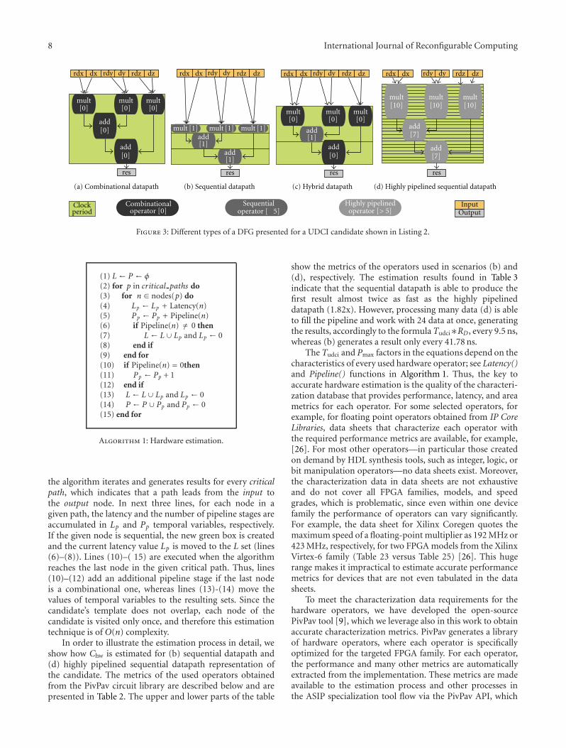
8 International Journal of Reconfigurable Computing
mult [1] mult [1] mult [1]add[1]
add[1]
add[1]
rdx dx rdy dy rdz dz rdx dx rdy dy rdz dz rdx dx rdy dy rdz dz rdx dx rdy dy rdz dz
mult[10]
mult[10]
mult[10]
add[7]
add[7]
res res res res
mult[0] mult
[0]mult[0]
mult[0]
mult[0]
mult[0]
add[0]
add[0]
add[0]
(a) Combinational datapath (b) Sequential datapath (d) Highly pipelined sequential datapath(c) Hybrid datapath
Clockperiod
Combinationaloperator [0]
Sequential Highly pipelined InputOutputoperator [ 5] operator [> 5]
Figure 3: Different types of a DFG presented for a UDCI candidate shown in Listing 2.
(1) L← P ← φ(2) for p in critical paths do(3) for n ∈ nodes(p) do(4) Lp ← Lp + Latency(n)(5) Pp ← Pp + Pipeline(n)(6) if Pipeline(n) /= 0 then(7) L ← L∪ Lp and Lp ← 0(8) end if(9) end for(10) if Pipeline(n) = 0then(11) Pp ← Pp + 1(12) end if(13) L← L∪ Lp and Lp ← 0(14) P ← P ∪ Pp and Pp ← 0(15) end for
Algorithm 1: Hardware estimation.
the algorithm iterates and generates results for every criticalpath, which indicates that a path leads from the input tothe output node. In next three lines, for each node in agiven path, the latency and the number of pipeline stages areaccumulated in Lp and Pp temporal variables, respectively.If the given node is sequential, the new green box is createdand the current latency value Lp is moved to the L set (lines(6)–(8)). Lines (10)–( 15) are executed when the algorithmreaches the last node in the given critical path. Thus, lines(10)–(12) add an additional pipeline stage if the last nodeis a combinational one, whereas lines (13)-(14) move thevalues of temporal variables to the resulting sets. Since thecandidate’s template does not overlap, each node of thecandidate is visited only once, and therefore this estimationtechnique is of O(n) complexity.
In order to illustrate the estimation process in detail, weshow how Chw is estimated for (b) sequential datapath and(d) highly pipelined sequential datapath representation ofthe candidate. The metrics of the used operators obtainedfrom the PivPav circuit library are described below and arepresented in Table 2. The upper and lower parts of the table
show the metrics of the operators used in scenarios (b) and(d), respectively. The estimation results found in Table 3indicate that the sequential datapath is able to produce thefirst result almost twice as fast as the highly pipelineddatapath (1.82x). However, processing many data (d) is ableto fill the pipeline and work with 24 data at once, generatingthe results, accordingly to the formulaTudci∗RD, every 9.5 ns,whereas (b) generates a result only every 41.78 ns.
The Tudci and Pmax factors in the equations depend on thecharacteristics of every used hardware operator; see Latency()and Pipeline() functions in Algorithm 1. Thus, the key toaccurate hardware estimation is the quality of the characteri-zation database that provides performance, latency, and areametrics for each operator. For some selected operators, forexample, for floating point operators obtained from IP CoreLibraries, data sheets that characterize each operator withthe required performance metrics are available, for example,[26]. For most other operators—in particular those createdon demand by HDL synthesis tools, such as integer, logic, orbit manipulation operators—no data sheets exist. Moreover,the characterization data in data sheets are not exhaustiveand do not cover all FPGA families, models, and speedgrades, which is problematic, since even within one devicefamily the performance of operators can vary significantly.For example, the data sheet for Xilinx Coregen quotes themaximum speed of a floating-point multiplier as 192 MHz or423 MHz, respectively, for two FPGA models from the XilinxVirtex-6 family (Table 23 versus Table 25) [26]. This hugerange makes it impractical to estimate accurate performancemetrics for devices that are not even tabulated in the datasheets.
To meet the characterization data requirements for thehardware operators, we have developed the open-sourcePivPav tool [9], which we leverage also in this work to obtainaccurate characterization metrics. PivPav generates a libraryof hardware operators, where each operator is specificallyoptimized for the targeted FPGA family. For each operator,the performance and many other metrics are automaticallyextracted from the implementation. These metrics are madeavailable to the estimation process and other processes inthe ASIP specialization tool flow via the PivPav API, which

International Journal of Reconfigurable Computing 9
Table 2: Excerpt from metrics requested by the candidate estimation process from PivPav circuit library for the XC4VFX100-FF1152-10FPGA device.
HW Oper.Pp Lp Max FRQ after PAR FF LUT Slice BUF DSP
# ns [MHz] # # # # #
mul 1 24.81 40.3 66 76 46 103 0
add 1 32.15 31.1 66 377 250 103 5
mul 10 7.31 136.8 66 134 150 103 4
add 7 7.19 139.0 66 556 326 103 4
Table 3: Results of hardware estimation process for DFGs presentedin Figures 3(b) and 3(d) implemented with two different sets ofoperators found in Table 2.
Sequential datapath(Figure 3(b))
Highly pipelined sequentialdatapath (Figure 3(d))
L [ns] 24.81 and 32.15 7.31 and 7.19
Tudci [ns] 32.15 7.31
P # 3 and 2 24 and 17
Pmax # 3 24
RD # 1.30 1.30
Chw [ns] 125.39 228.07
is illustrated in Figure 2. Since all the data are generatedbeforehand with the benchmarking facilities of the PivPav,there is no need to run the FPGA CAD tool flow in theestimation process.
It is worth noticing that the presented estimation methodis not in itself a novel idea. There are many timing analysisapproaches which perform equivalent steps to the onepresented above [27]. Therefore, this subsection does notcontribute to the hardware timing analysis field. The noveltyin this estimation approach relies on the precise characteri-zation data that were generated with PivPav tool. These datatogether with presented methods allow to precisely estimatethe hardware performances for UDCI instructions.
8. Candidate Selection
Once the set of candidates has been determined and estima-tion data are available, the selection process makes the finaldecision about which candidates should be implemented inthe hardware.
First, all the candidates that violate at least one of theconstraints presented below are rejected:
C|in| ≤ inmax, (9)
C|out| ≤ outmax, (10)
Csw
Chw≤ threshold. (11)
Here,
(i) C|in| and C|out| are equivalent to the constraints de-scribed in conditions (1) and (2), respectively. Theycorrespond to architectural constraints for the num-ber of input and output operands to the UDCI. They
are applied to the ISE algorithms that are not ableto perform this step themselves, such as the MMalgorithm.
(ii) Csw and Chw correspond to the software and hardwareestimations, respectively. If threshold = 1.0, thenthere are no performance gains; when threshold >1.0there is a performance gain since it takes more cyclesto execute the candidate in software than in hardware.Finally, if threshold <1.0, the hardware implementa-tion has a lower performance than the software.
After applying these conditions, the search space of the selec-tion process is significantly reduced, since candidates thatare either infeasible or would provide only low speedups arediscarded. As a result, the runtime of the subsequent steps inthe tool flow is considerably lower.
8.1. Candidate Selection. In general, selecting the optimalset of UDCI instructions under different architectural con-straints is a demanding task. Related work has studied differ-ent selection approaches, such as greedy heuristics, simulatedannealing, ILP, or evolutionary algorithms; see, for example,Meeuws et al. [28] or Pozzi et al. [19]. For the purpose ofthe ASIP specialization, we use the greedy candidate selectionalgorithm that is presented in Algorithm 2 and which hasa computational complexity of O(|Cinput|). When using theSC algorithm which may produce overlapping candidates forISE identification our algorithm rejects any candidates thatoverlap with any candidate that has been selected so far. Theaim of this process is to select up to Cmax candidates fromthe set of Cinput candidates generated by the identificationprocess that offers the greatest advantage in terms of somemetric M; in this case the application performance:
Cres = max(∀Ci ∈ Cinput :
∑M(Ci)
). (12)
Here,
(i) Cres is the resulting set of best candidates, |Cres| is asize of this set, and Cmax is the architectural constraintrepresenting the number of supported UDCI instruc-tions.
(ii) M is a metric function defined as
M(Ci) = Csw(Ci)Chw(Ci)
. (13)

10 International Journal of Reconfigurable Computing
while |Cres| ≤ Cmax doci ← max{M(Ci) | Ci ∈ Cinput}if ci does not overlap with Cres then
Cres ← Cres ∪ ciend ifCinput ← Cinput ∩ ci.
end while
Algorithm 2: Best candidate selection.
8.2. Selection Metrics. The metric function is used as a policyin the greedy selection process and is responsible for selectingonly the best candidates. While in (13), the applicationperformance policy is used, and nothing prevents basing thedecision preference on a different metric. It is worth men-tioning that the PivPav tool could be used to provide a wealthof other metrics since the circuit library stores more than90 different properties about every hardware operator. Theseproperties could be used for instance to develop resourceusage or power consumption policies. Consequently, theycan be used to estimate the size of the final bitstreamand partial reconfiguration time, the runtimes of netlistgeneration and instruction implementation, or many othermetrics. Finally, all these policies could be merged togetherinto a sophisticated ASIP specialization framework whichwould
(i) maximize the performances,
(ii) minimize the power consumption, and
(iii) constrain the resource area to the sizes of UDCI slot.
Such a combined metric can be defined as an integer linearprogramming model. While this method would allow a moreprecise selection of candidates based on more parameters, itsalgorithmic complexity is higher than O(|C|input||), resultingin runtimes that are much longer, often by orders ofmagnitude. Since it is important to keep the runtimes of theASIP-SP as low as possible, the tradeoff between the gainsand the costs of the metric function is an interesting researchtopic in itself.
9. Pruning the Search Space
Pruning is the first process executed in the ASIP-SP outlinedin Figure 2. Pruning uses a set of algorithms which act asfilters to shrink the search space for the subsequent processesby rejecting or by passing certain BBs.
This decision is based on the data obtained from programanalysis which provides information about loops, the sizesof BBs, and the contained instruction types. In addition, theASIP-SP makes it possible to discard dead code by runningthe filters only for the code which was executed at least once.
The objective of the pruning process is described by thefollowing term:
max(
metric functionruntime of candidate identification
). (14)
The pruning aims to maximize the ratio between a metricfunction to the time spent in the candidate identificationprocess. The metric function is defined in (13) and is equiv-alent to the application performance gain. The denominatorof the equation takes into the account only the runtimeof the candidate identification since in comparison to thisruntime the runtime of the candidate estimation and selectionprocesses is insignificant.
For this work, we are using this @50pS3L filter heuristic,which has been shown in our previous work [10] to providethe best results for just-in-time systems. This filter has threesequential pruning stages which can be decoded from itsname. The first filter stage (indicated by @) filters out deadcode; that is, it discards all BBs that have not been executedat least once. This information is available during the ASIP-SP runtime without access to profiling data. The secondfilter stage (indicated by 50p) selects BBs based on their size.Here, only BBs that have a size of at least 50% of the sizeof the largest BB in the application are selected. Preferringlarge over small BBs simplifies the task of identifying largecandidates which are likely to provide more speedups.Finally, the last filter stage (indicated by 3L) selects only BBswhich are part of a loop and selects the 3 largest of theseBBs. The rationale of this filter is that the BBs contained in aloop have a higher chance of being executed, and promotingcandidates which are more frequently executed is one of themethods to increase the overall application speedup.
10. Experimental Setup
While this work targets the reconfigurable ASIPs, like ourWoolcano architecture presented in Figure 2, due to practicallimitations it is currently not feasible to execute the completeASIP-SP on an embedded reconfigurable ASIP architecture.The specialization process heavily uses the LLVM compilerframework and the Xilinx ISE tools which require high-performance CPUs and desktop operating systems. Theseresources are not available in currently existing ASIP archi-tectures. Hence, we used Linux and a Dell T3500 workstation(dual core Intel Xeon W3503 2.40 GHz, 4 M L3, 4.8 GT/s,12 GB DDR3/1333 MHz RAM) as a host computer in placeof the PowerPC 405 CPU of the Woolcano architecture toexecute the ASIP-SP; see Figure 2.
The lack of the possibility to run the complete toolflow on the ASIP has a number of consequences for theexperimental evaluation. Instead of running the ASIP-SP asa single process, we are forced to spilt this process into twosteps. In the first step, the host computer is used to generatethe partial bitstreams by executing the tasks correspondingto the upper half of Figure 2. In the second step, we switchto the Woolcano architecture where we use the generatedbitstreams to reconfigure the UDCI slots and to measure theperformance improvements.
It is also worth noticing that this two-step process has animpact on several reported measurements. First, all perfor-mance measurements reported in Table 5 and 6, in columnsMax ASIP-SP speedups and ASIP ratio, are performed forWoolcano’s PowerPC405 CPU and not for the host CPU.

International Journal of Reconfigurable Computing 11
Table 4: Characteristics of scientific and embedded applications. AVG-S represents the averages for scientific applications and AVG-E forthe embedded applications. Ratio = AVG-S/AVG-E.
AppSources Compilation to IR IR in BBs Code coverage Kernel size
files loc real fun blk ins max avg udci live dead const size ins freq
# # [s] # # # # # [%] [%] [%] [%] [%] # [%]
164.gzip 20 8605 3.89 33 1006 6925 59 6.88 29.68 38.86 44.66 16.48 5.78 400 90.34
179.art 1 1270 1.06 21 376 2164 43 5.76 21.53 42.05 28.47 29.48 9.84 213 92.45
183.equake 1 1513 1.71 15 257 2670 132 10.39 23.0 75.39 8.91 15.69 15.32 409 92.9
188.ammp 31 13483 10.10 98 4244 26647 382 6.28 25.74 19.22 70.89 9.89 3.38 901 95.81
429.mcf 25 2685 0.97 18 284 1917 77 6.75 13.09 75.9 13.09 11.01 25.77 494 98.46
433.milc 89 15042 10.88 87 1538 14260 363 9.27 32.59 61.67 34.72 3.61 10.83 1545 93.99
444.namd 32 5315 22.77 84 5147 47534 291 9.24 37.82 31.71 62.81 5.48 7.33 3486 93.64
458.sjeng 23 13847 8.49 86 3373 20531 69 6.09 21.1 48.49 49.44 2.07 44.6 9157 100.0
470.lbm 6 1155 1.36 16 104 1988 405 19.12 57.55 55.23 24.9 19.87 32.75 651 97.57
473.astar 19 5829 3.68 45 757 6010 70 7.94 27.45 78.79 5.31 15.91 6.39 384 91.3
AVG S 24.70 6874 6.49 50 1709 13065 189.1 8.77 28.95 52.73 34.32 12.95 16.20 1764 94.65
adpcm 6 448 0.29 6 43 233 39 7.21 33.48 60.66 29.18 10.16 41.97 128 91.79
fft 3 187 0.26 10 47 297 41 6.53 42.09 58.88 30.26 10.86 44.08 134 95.98
sor 3 74 0.13 4 19 99 22 7.06 34.34 46.51 50.39 3.1 24.81 32 97.52
whetstone 1 442 0.25 12 44 285 32 6.58 34.04 32.75 36.27 30.99 10.21 29 93.27
AVG E 3.25 288 0.23 8 38.3 228.5 33.5 6.85 35.99 49.70 36.52 13.78 30.27 80.75 94.64
RATIO 7.60 23.89 28.22 6.29 44.67 57.18 5.64 1.28 0.80 1.06 0.94 0.94 0.54 21.85 1.00
Table 5: Specialization process executed for whole applications when targeting the Woolcano architecture without capacity constraints. Theperformance of the custom instructions has been determined with the PivPav tool. ISE algorithms: MM: MaxMiso, SC: SingleCut, UN:Union. SC and UN search is constrained to 4 inputs and 1 input.
App
Executionruntimes ISE algorithm runtime Candidates found Max ASIP-SP Speedup
VM Nat Ratio MM SC UN MM SC UN MM SC UN
[s] [s] x [ms] [ms] [ms] # # # x x x
164.gzip 23.71 18.47 1.28 40.6 549.0 11170.0 1621 44177 43682 1.172 1.213 1.213
179.art 69.92 74.70 0.94 12.3 55.1 3350.0 371 3534 3513 1.526 21.414 21.414
183.equake 7.97 6.79 1.17 13.5 457.9 4351.0 672 9690 9690 2.147 25.972 25.972
188.ammp 23.18 17.24 1.34 145.7 15840 — 7547 122441 — 3.449 20.826 —
429.mcf 23.94 24.06 1.00 11.1 68.7 200.5 571 3571 3562 1.112 1.112 1.112
433.milc 20.95 16.43 1.28 78.1 5065 — 3573 59450 — 1.301 21.546 —
444.namd 39.94 34.31 1.16 227.5 35854 — 11490 125970 — 1.609 24.846 —
458.sjeng 180.41 155.66 1.16 123.7 6244.1 235195.7 5540 83173 83035 1.118 1.137 1.137
470.lbm 5.68 5.36 1.06 8.6 2777.1 — 490 18216 — 2.554 44.622 —
473.astar 66.00 67.68 0.98 33.4 914.8 303796653 1408 37025 32368 1.159 1.19 1.19
AVG S 46.17 42.07 1.14 69.45 6783 30405092 3328 50724 17585 1.71 16.39 5.20
adpcm 29.22 28.35 1.03 1.7 15.0 3869.4 83 819 819 1.243 1.309 1.293
fft 18.47 18.49 1.00 1.6 9.7 33.1 87 553 552 3.1 14.413 14.413
sor 15.83 15.85 1.00 0.7 4.3 14.6 35 384 375 14.418 14.422 14.418
whetstone 28.66 28.50 1.01 1.6 9.5 64.0 69 435 435 18.012 18.012 18.012
AVG E 23.04 22.80 1.01 1.40 9.62 995.27 68.50 547.75 545.25 9.19 12.04 12.03
RATIO 2.00 1.85 1.13 49.61 705.05 30549.59 48.59 92.61 32.25 0.19 1.36 0.43
12 International Journal of Reconfigurable Computing
Table 6: The runtime overheads for the ASIP-SP.
AppCandidate Search: @50pS3L ASIP Runtime overheads Break-even
real pruner blk ins can ratio const map par sum break-even time
[ms] effic # # # x [m : s] [m : s] [m : s] [m : s] [d : h : m : s]
164.gzip 1.44 71.79 2 100 19 1.00 56 : 22 13 : 02 18 : 28 87 : 52 206 : 22 : 15 : 50
179.art 1.05 23.37 3 79 9 1.01 26 : 42 8 : 58 13 : 20 49 : 00 1 : 12 : 18 : 13
183.equake 2.25 8.33 2 244 11 1.00 32 : 38 7 : 56 16 : 12 56 : 46 259 : 02 : 28 : 33
188.ammp 3.27 52.29 1 382 92 1.41 272 : 58 102 : 12 142 : 49 517 : 59 0 : 14 : 56 : 39
429.mcf 1.05 28.2 1 77 5 1.00 14 : 50 4 : 06 7 : 48 26 : 44 213 : 20 : 05 : 55
433.milc 6.6 26.71 2 673 9 1.00 26 : 42 6 : 44 15 : 08 48 : 34 568 : 06 : 08 : 05
444.namd 7.68 57.43 3 776 129 1.03 382 : 45 117 : 24 178 : 04 678 : 13 6 : 16 : 00 : 48
458.sjeng 1.8 184.11 3 121 8 1.00 23 : 44 6 : 56 12 : 58 43 : 38 2403 : 01 : 35 : 57
470.lbm 10.62 2.43 3 961 179 2.53 531 : 07 181 : 51 308 : 24 1021 : 22 1 : 03 : 29 : 48
473.astar 2.25 38.2 3 184 33 1.00 97 : 54 29 : 46 46 : 59 174 : 39 5149 : 02 : 19 : 14
AVG S 3.80 49.29 2.30 358 49 1.20 146 : 34 47 : 53 76 : 01 270 : 28 881 : 00 : 33 : 54
adpcm 0.84 5.59 2 61 8 1.08 23 : 44 6 : 00 10 : 34 40 : 18 0 : 04 : 34 : 10
fft 0.78 3.78 2 75 14 2.40 41 : 32 11 : 44 20 : 56 74 : 12 0 : 01 : 53 : 07
sor 0.24 2.21 1 22 2 1.00 5 : 56 4 : 48 10 : 12 20 : 56 0 : 00 : 24 : 19
whetstone 0.54 7.7 2 49 9 15.43 26 : 42 11 : 34 25 : 52 64 : 08 0 : 01 : 08 : 04
AVG E 0.60 4.82 1.75 52 8 4.98 24 : 28 8 : 31 16 : 53 49 : 53 0 : 01 : 59 : 55
RATIO 6.33 10.23 1.31 6.95 5.99 0.24 5.99 5.62 4.50 5.42 10580
Further, in order to compute the break-even time reported inTable 6 we used the runtime overheads values from the sametable which were measured on the host computer. Therefore,this value is computed as if Woolcano’s PowerPC CPU hadthe processing power of the host machine. Finally, while theASIP specialization tool flow is capable of performing UDCIreconfiguration during runtime, in practice, we had to switchfrom the first to the second step manually.
The hardware limitations of Woolcano, in particular thenumber of UDCI slots, in practice do not allow us to measurethe performance improvements on a real system for allapplications. To this end, for these applications we estimatethe speedups with the help of the techniques presented inSection 7.
11. Applications for Experimental Evaluation
Table 4 shows the characteristics of used applications dividedinto two groups. The upper part of the table shows datafor applications obtained from the SPEC2006 and SPEC2000benchmark suites which represent scientific computing do-main whereas the lower part represents applications from theembedded computing domain obtained from the SciMark2and MiBench.
While the used benchmark suites count 98 different ap-plications altogether, we could not run our evaluation on allof them due to cross-compilation errors. Hence, from theset of available applications, we selected the ones which arethe most representative and allow us to get comprehensiveinsights into the JIT ASIP specialization methodology. Whilewe have used slightly different application sets in our pre-vious publications which evaluated specific parts of the toolflow, we have chosen an adapted common set of applications
for this work in order to get a consistent end-to-end evalua-tion of the whole tool flow.
11.1. Source Code Characterization and Compilation. Thesecond and third columns of Table 4 contain the number ofsource files and lines of code and tell that scientific applicationshave on average 23.89x more code than the embeddedapplications. This difference influences the compilation timeshown in the fourth column which for scientific applicationsis 28.22x longer on average, but still the average compilationtime is only 6.5 s. The next three columns express the charac-teristics of the bitcode reflecting the total number of functions,basic blocks, and intermediate instructions, respectively. Forthe scientific applications the ratio between ins (13065) andthe LOC (6874) is 1.9. This means that an average singlehigh-level code line is expressed with almost two IR instruc-tions and less than one (0.8) for embedded applications.Since scientific applications have 24 times more LOCs thanembedded applications, this results in a 57x difference in theIR instructions.
The ISE algorithms operate on the BBs, and thus the IR inBBs column indicates the characteristics of these BBs in moredetail. The max column indicates the BB with the highestnumber of IR instructions and avg is the average number ofIR instructions in all BBs. These values in combination withthe data presented in Figures 4, 5, and 6 allow to understandthe runtime of the ISE and the number of candidates.
For embedded applications the largest BBs cover on aver-age more than 14.7% of the application whereas the largestbasic block for scientific applications covers only 1.4% of thetotal application. The difference between average-size BBsfor embedded and scientific applications is 1.28x and resultsin a small average number of IR instructions of less than

International Journal of Reconfigurable Computing 13
100 101 102 103
10− 1
100
101
102
103
104
105
Nodes
Alg
orit
hm
run
tim
e(m
s)
SC-41
UN-41SC-41-avgUN-41-avg
MM-fitted
O (exp)O (n2)
(s)
(min)
Small Medium Large
(ms)
Figure 4: Runtimes of the ISE identification algorithm for differentbasic block sizes (nodes). The SC: SingleCut, UN: Union, MM:MaxMiso algorithms. The label “41” means that the SC and UNsearch has been constrained to 4 inputs and 1 output.
10 for both cases. The small size of BBs in our applicationsneeds to be attributed to the actual benchmark code, thecompiler, and the properties of the intermediate representa-tion. Our experiments have shown that the size of the BBsdoes not change significantly for different compiler opti-mizations, transformations, or with the size of application(LOC).
11.2. Feasible UDCI Instructions. The udci column lists thepercentage of all IR instructions which are feasible for ahardware implementation. Feasible instructions include thearithmetic, logic, and cast instructions for all data typesand make up to 1/3 of all instructions of the application.Considering the small average size of BBs this means that thesize of an average-found candidate is only between 2 and 3 IRinstructions. This fact emphasizes the need for a proper BBand candidate selection and stresses even more the impor-tance of the proper pruning algorithms in order to avoidspending time with analyzing candidates that will likely notresult in any speedup.
11.3. Code Coverage. The Code Coverage columns show thepercentages of the size of live, dead, and constant code. Thesevalues were determined by executing each application fordifferent input data sets and by recording the execution
NodesFo
un
dca
ndi
date
s
MMSC-41UN-41
MM-fitted
SC and UN-fitted
n6
n2
Medium LargeSmall100
101
102
103
104
101 102 103
Figure 5: Number of found candidates by ISE algorithms for a largespectrum of BB nodes, where SC and UN are constrained to 4 inputsand 1 output.
frequency of each BB. For the SPEC benchmark suite appli-cations, the standard test, train, and ref data sets were used,whereas for the embedded ones, due to the unavailabilityof standard data sets, each application was tested with atleast three different custom-prepared input data sets. Afterexecution, the change in execution frequency per block be-tween the different runs was compared. If the frequency wasequal to 0, the code was marked as dead. If the frequencywas different from 0 but did not change for different inputs,the code was marked as constant, and if the frequencyhas changed, the block was marked as live. This frequencyinformation was used to compute the break-even points in thefollowing section. In addition, the live frequency informationindicates that roughly only 50% of the application has adynamic behavior in which the ISE algorithms are interestedin searching for candidates.
11.4. Kernel Size. The last three columns contain data on thesize of the kernel of the application. These data are derivedfrom the frequency data. The kernel of an application isdefined as the code that is responsible for more than 90%of the execution time. The size of the kernel is measured asthe total number of IR instructions contained in the basicblocks which represent the kernel. For scientific applications,16.20% of the code affects 94.65% of the total applicationexecution time, and it corresponds to more than 1.7 k IR
14 International Journal of Reconfigurable Computing
100
101
102
103
104
105
10 20 30 40 50 60 70 80 90 100
NodesSmall Medium
MaxMiso-avgn2
n
Fou
nd
can
dida
tes
SC and UN-i2-o1-avgSC and UN-i2-o2-avgSC and UN-i4-o1-avgSC and UN-i4-o2-avg
Figure 6: Number of found candidates by ISE algorithms for a me-dium spectrum of BB nodes, where SC and UN have variable con-straints.
instructions. For embedded applications, the average relativekernel size is 30.27% and is expressed only with 80 IR instruc-tions. These numbers indicate that it is relatively easier toincrease the performances of the embedded applicationsthan the scientific ones, since they require 22x smaller UDCIinstructions.
11.5. Execution Runtimes. The VM column in Table 5 repre-sents the application runtime when executed on the LLVMvirtual machine. The runtime of the application dependsheavily on the input data which, in the case of the scientificapplications, were obtained from the train datasets of theSPEC benchmark suite. Due to the unavailability of standarddata sets for the embedded applications, custom-made datasets were used. For both application classes, the input dataallowed to exercise the most computationally intensive partsof the application for a few or several tens of seconds. The Natcolumn shows the real runtime of the application when stat-ically compiled, that is, without the overhead caused by theruntime translation. The Ratio column shows the proportionof Nat and VM and represents the overhead involved with theinterpretation during the runtime. For the small embeddedapplications, the overhead of the VM is insignificant (1%).For the large scientific applications, the average overheadcaused by the VM equals on average 14%. However, it isimportant to notice that for some applications like 179.art or
473.astar, the VM was significantly faster than the staticallycompiled code by 6% and 2%, respectively. This means thatthe VM optimized the code in a way which allowed toovercome the overhead involved in the optimization as wellas the dynamic just-in-time compilation.
12. Experimental Evaluation ofthe Candidate Identification
In this section, we evaluate and compare the ISE algo-rithms which have been used for candidate identificationas presented in Figure 2. Our evaluation covers the runtimecharacteristics of the algorithms as well as the number ofidentified candidates for different architectural constraints,the maximum gain in application performance, and the run-time of our benchmark algorithms when statically compiledto native code and when executing in a virtual machine. Thediscussion is based on data presented in Table 5 which wasobtained for the benchmark applications introduced in theprevious section.
12.1. ISE Algorithm Runtimes and Comparison. The averageISE algorithm runtimes are presented in the 5th to 7thcolumns of Table 5. As stated previously, the MM algorithmhas a linear complexity and therefore is the fastest, resultingin a 0.22 s runtime for , which is the largestapplication. Due to its larger algorithmic complexity, theruntime of the UN algorithm should generally exceed theruntime of SC but this is not the case for applications whichinclude specific types of BBs. For example, it took 3837 msto process such a specific BB consisting of 55 nodes in the
application, which is 99.15% of the overall runtime ofthe UN algorithm. On contrast, the same BB was analyzed bythe SC algorithm in a mere 4.7 ms.
Since both SC and UN have exponential complexity, theirruntimes are a few orders of magnitude higher than for MM.In average, MM is 96.94x faster than the SC algorithm.
The identification times for BBs of similar sizes alsovary significantly for the same algorithm since the numberof candidates that need to be actually considered in a BBdepends not only on the total size of the BB but also on thestructure of the represented DFG, the number and locationof infeasible instructions in the DFG, the architecturalconstraints, and other factors. For example, it took the SCalgorithm 1707 ms to analyze a BB of with 102instructions, while the analysis of a slightly larger BB in
with 120 instructions took only 76 ms, which isa 22.5x difference in runtime. This example illustrates thatit is impossible to accurately estimate the runtime of theexponential ISE algorithms SC and UN in advance whenbasing the estimation solely on the size of the BB.
It is worth pointing out that for keeping the search spaceand thus the algorithm runtimes manageable, we had toapply rather tight architectural constraints for the custominstructions (4 inputs, 1 output) in our comparison of ISEalgorithm in Table 5. When loosening these constraints, theexecution times for the SC and UN algorithms rapidly growfrom seconds to many hours.

International Journal of Reconfigurable Computing 15
The overall runtime characterization of the instructionidentification algorithms is summarized in Figure 4 whichplots the runtime of the different algorithms for varyingBB sizes. Each data point represents an average which wascomputed by running the ISE algorithm 1000 times on eachBB. The multitude of data points for a fixed BB size illustratesthat the runtime of the same algorithm can vary over severalorders of magnitude for BBs which have an equal size butdiffer in their structure as pointed out above. This effect isparticularly strong for larger BBs where many variants ofDAG structures exist.
For visualizing the overall behavior of the algorithmswe have also added the average runtime for the SC and theUN algorithms for each BB size. It can be observed that thevariability for the UN algorithm is larger than for the SCalgorithm. Another interesting observation is that althoughthe SC and UN algorithms have a worst-case algorithmiccomplexity of O(exp), on average their runtime is onlypolynomial O(n2), which can be seen by comparing the bluedotted lines with the red and green lines, respectively.
We are able to fit the runtime of the MM algorithm witha linear polynomial model which is represented with a blackline which has an almost ideal characteristic (goodness ofthe fit: R2 = 0.9995). This means that the runtime of theMM algorithm always depends linearly on the BB size O(n).Unfortunately, the behavior of the other algorithms is notsufficiently regular to perform a meaningful curve fittingwith similar quality.
In general, we can say that the MM is the fastest algorithmand outperforms the SC and UN algorithms easily in terms ofruntime for small, medium, and large basic blocks. For smallBBs of up to 10 instructions, the runtime difference is in therange of up to an order of magnitude; for medium inputs(102 instructions), up to two orders of magnitude and forthe largest BBs (103 and more instructions), a difference ofmore than three orders of magnitude can be observed. Whilethe runtime of the MM stays on the millisecond time scaleeven for the largest inputs, the SC and UN algorithms workon a scale of seconds or minutes.
It is important to note that runtime of the exponentialalgorithms tend to literally explode when these algorithmsare constrained less tightly than 4 input 1 output (41), inparticular when allowing a larger number of outputs. Forinstance, when applying an 8-input 2-output (82) constraint,common runtimes are in the order of 108 ms, which is threeorders of magnitude higher than for the 41 constraint.
In terms of runtime, SC is approximately one order ofmagnitude faster than UN. However, the runtime for bothalgorithms grows similarly for increasing BB sizes with theexception of significant outliers for the UN algorithm, forpeaks with a runtime difference of three orders of magnitudewhich can be observed for large BBs. A similar behavior wasalso found for architectural constraints other than 41.
The results presented here have been obtained usinga special benchmarking mode of our tool flow where theinstruction candidates are identified but not copied to aseparate data structure for further processing. Additionally,the time needed to reject overlapping candidates for SCalgorithm as well as the time needed for the MM algorithm
to validate condition (1) presented in Section 6 was not in-cluded. As a result, the runtimes of the candidate identifica-tion algorithms will be slightly longer in practice when theyare applied as part of the complete tool flow.
12.2. Candidates Found by the ISE Algorithms. The numberof candidates found by the ISE identification algorithms ispresented in columns 8, 7, and 9 of Table 5. In addition, anoverview of all identified candidates as a function of the BBsize is shown in Figure 5, while Figure 6 presents a close upof the same data for medium-sized BBs. As illustrated by thered line in Figure 5, the SC and the UN algorithms generatean equal number of candidates, given that the same archi-tectural constraints are used and that any overlapping UDCIcandidates generated by the SC algorithm are removed.
In general, the total number of subgraphs that can becreated from an arbitrary graph G is exponential exp(n)in the number of nodes of G. For ASIP specialization sce-narios, that is, when architectural constraints are appliedcf. conditions (1), (2), and (4) [29] has shown that thenumber of subgraphs is bounded by n(Cin+Cout+1). Thus, forthe 4-input/1-output constraints applied in this study, thesearch space is equal to n6, which is represented by the graydotted line found in the upper-left corner of Figure 5. Whenapplying the final constraint condition (3), the search spaceis significantly reduced from n6 by at least a power of 4 ton2, which is presented with the blue dotted line above allresults.
The black line represents a linear fitting for the MM algo-rithm, whereas the red line shows a second-order polynomialcurve fitting for the SC and UN algorithms. The goodness ofthese fits represented with R2 parameter is equal to 0.9663 forMM and to 0.9564 for the SC and UN algorithms. Therefore,it is safe to assume that the number of candidates for the4-input/1-output constraint is limited by a second-orderpolynomial.
Figure 6 shows that the longer runtimes of the SC andthe UN algorithm also result in the identification of morecandidates. The difference for small and medium BBs is upto one order of magnitude and increases for even larger BBs.
The data points (number of candidates) were obtained byrunning the ISE algorithms on the applications presented inSection 11. Thus, each data point is associated with a singleBB, and closely located data points tell that there are manyBBs of similar sizes.
It can be observed in Figure 6 that there are less datapoints with large BBs than medium or small BBs. This is aconsequence of the distribution of basic block sizes; that is,most BBs found in these applications have sizes of up to 100instructions. For such BBs, the number of feasible candidatesreaches more than 10 when using the MM algorithm andmore than 100 when using the SC and UN algorithms.Given that the average application has at least a few dozens(38 for embedded) or hundreds (1709 for scientific) of BBsthis results in thousands of feasible candidates that aresuitable for hardware implementation. In our experiments,we considered 3328 MM (50724 SC) candidates for thescientific and 68.5 MM (547.75 SC) candidates for the em-bedded applications. These high numbers are more than
16 International Journal of Reconfigurable Computing
enough since an average ISA consists of around 80 coreinstructions for X86 platform and around 100 for PowerPC.If one assumes 10% modification to the ISA, it results in atask of selecting less than 10 UDCI instructions from a set ofthousands of feasible candidates.
The number of found candidates depends strongly onthe architectural constraints that are applied. Tighter con-straints, that is, allowing a smaller number of inputs and out-puts, lead to a smaller number of candidates for the SC andUN algorithm. This behavior can be seen in Figure 6 wherethe average number of candidates is plotted as a function ofthe BB size for various constraints. There are two groups ofconstraints: the 21,41 and 22,42, between which a rising gapof one order of magnitude is established. Applying the MMalgorithm to BBs with a size of 100 instructions leads to morethan 10 feasible candidates whereas applying SC or UN leadsto more than 100 candidates for the first set of constraintsand even two orders of magnitude more candidates (104) forthe second set of constraints. This validates the second-orderpolynomial characteristic n2 of the number of candidates forthe SC or UN algorithms.
The similar behavior of the lines representing the averagenumber of identified candidates is caused by the less or equal(≤) relationships found in conditions (1) and (2). That is, theless constrained algorithms (like 41) include all candidates ofmore constrained ones like 21. The area between the red andgray line corresponds exactly to the number of additionalcandidates found in less constrained algorithms. Also, thegraphs illustrate that the number of candidates dependsmuch stronger on the number of allowable outputs than onthe number of allowable inputs.
For BBs with sizes of approximately 75 instructions, wesee an interesting decay from which all ISE algorithms suffer.This decay is found only in a concrete benchmark and is theresult of a high concentration of illegal instructions in basicblocks of those sizes, for which only a few feasible candidateswere found.
Finally, it can be seen that the MM algorithm has a linearcharacteristic a · n where a ≤ 1. The SC and UN algorithmsalso show a linear characteristic with a ≥ 1 for the case of the21 and 41 constraints, whereas for the 22 and 42 constraints,the characteristic changes by a power (n2).
12.3. Achievable Performance Gain. The Max ASIP-SP Speed-up columns presented in Table 5 describe the upper limitof performance improvement that can be achieved with theWoolcano reconfigurable ASIP architecture and the pre-sented ASIP-SP. These values show the hypothetical best-casepotential in which all candidates found by three differentISE algorithms are implemented as custom instructions. Inreality, the overheads caused by implementing all possibleinstructions and the limited hardware resources of the recon-figurable ASIP require pruning of the set of candidates thatare evaluated and implemented to a tractable subset. There-fore, the speedup quoted in these columns should be treatedonly as an upper boundary on the achievable performance.
The ISE algorithms have a lot to offer, reaching a speedupof up to 44.62x for SC algorithm and 18.01x for MM and
UN algorithms. The average speedups achieved with MM,SC, and UN are 1.71, 16.39, and 5.20, respectively for thescientific applications and 9.19, 12.04, and 12.03 for theembedded applications. For all applications, the averagespeedups achieved with MM, SC, and UN are 3.85, 15.15,and 10.02, with the value of median 1.57, 16.22, and 7.85,respectively. These results clearly indicate that the SC algo-rithm is superior for static systems where identification run-times are not a major concern.
For a JIT specialization process, one needs to balance theachievable speedup with the identification time. Comparingthe ratios of average speedup to identification runtime forembedded applications results in the following ratios : 6.56(MM), 1.25 (SC), and 0.01 (UN). These figures suggest thatthe MM algorithm is the most suitable for such systems.In addition, the considerable difference of 0.19 betweenaverage speedups for different application sets suggests thatthe MM algorithm could find better candidates in the smallerapplications with more pronounced kernels and that theseapplications will benefit most from JIT-based systems.
It is important to remember that these results wereobtained for the first time for the FPGA-based Woolcanoarchitecture and not as presented in related work for a fixedCMOS ASIP architecture. This distinction is significant sincethe same hardware custom instructions will achieve signifi-cantly higher speedups when implemented in CMOS tech-nology, often by more than one order of magnitude. But atthe same time, a fixed architecture will sacrifice the flexibilityand runtime customization capabilities of the Woolcanoarchitecture.
13. Runtime Overhead of the ASIPSpecialization Process
As elaborated in the previous section, the reconfigurableASIP architecture is considerably faster than the underlyingCPU alone for both benchmark domains. Thus, the over-heads of just-in-time software compilation, optimization,and custom instruction generation can be amortized pro-vided that the application will be executed long enough. Inthis section, we analyze the achievable performance gains byASIP specialization, presented in Figure 2, and the runtimecosts of the three different phases of that process. These fig-ures are used to compute for how long the application needsto be executed until the hardware generation overheads areamortized, that is, when a net speedup is achieved.
13.1. Candidate Search. As described in Section 4, the Candi-date Search phase is responsible for finding and selecting onlythe best custom instruction candidates from the software.As this task is frequently very time consuming, we are usingour pruning mechanisms introduced in Section 9 to reducethe search space for instruction candidates. The number ofselected candidates, after pruning, is indicated in the cancolumn of Table 6.
The third column of Table 6 represents the pruning effi-ciency ratio which is defined as the quotient of two terms.The first term is the ratio of the average maximum ASIP

International Journal of Reconfigurable Computing 17
speedup to the runtime of the identification algorithm whenno pruning is used. The second term is the same ratiowhen using the @50pS3L pruning mechanism. The pruningefficiency can be used as a metric to describe the relative gainin the speedup-to-identification-time ratio with and withoutpruning.
The blk and ins columns represent the number of basicblocks and instructions which have been passed to theidentification process. These numbers are significantly lowerthan the total number of blocks and instructions presentedin the 6th and 7th columns of Table 4. That is, the pruningmechanism reduced the size of the bitcode that needs to beanalyzed in the identification task by a factor of 36.49x and4.4x for scientific and embedded applications, respectively.
The overall runtime of the data pruning, identification,estimation, and selection is aggregated in the real column.The total candidate search time is in the order of millisecondsand thus insignificant in comparison to the overheads in-volved in the hardware generation.
13.2. Performance Improvements. The column ASIP ratiorepresents the speedup of the augmented hardware archi-tecture when all candidates selected by Candidate Search areoffloaded from the software to custom instructions. In con-trast to the maximum performance shown in the 11th col-umn in Table 5 which assumes that all candidates are movedto hardware, the average speedup drops by 30% from 1.71x–1.20x for scientific applications and by 46% from 9.19x–4.98x for the embedded ones. Comparing the fft with the470.lbm applications illustrates the main difference betweenembedded and scientific applications. Both applications havea similar speedup of 2.40x versus 2.53x, respectively, butdiffer significantly in the number of candidates that needto be translated to hardware to achieve these speedups (14versus 179 candidates). This correlates with the previouslydescribed observation that scientific applications have asignificantly larger kernel size.
13.3. Netlist Generation. The tasks discussed in this sectionare represented by the second phase in Figure 2. The taskGenerate VHDL is performed with the PivPav datapath gen-erator which produces the structural VHDL code. The data-path generator traverses the datapath graph of the candidateand matches every node with a VHDL component. This isa constant time operation requiring 0.2 s per candidate. Theextract netlist task retrieves the netlist files for each hardwarecomponent used in the candidate’s VHDL description fromthe PivPav database. This step allows reduction of the FPGACAD tool flow runtimes, since the synthesis process needs tobuild only a final netlist for the top module. The next step isto create the FPGA CAD project which is performed by PivPavwith the help of the TCL scripting language. After the projectis created, it is configured with the FPGA parameters andthe generated VHDL code as well as the extracted netlist filesare added. On average this process took 2.5 s per candidate,making this the most time-consuming task of the netlistgeneration phase. The average total runtime for these threetasks is presented in the C2V column of Table 7 and amounts
Table 7: Constant overheads involved in the ASIP-SP. C2V corre-sponds to the Netlist Generation phase in Figure 2. Syn, Xst, Tra,and Bitgen are the FPGA CAD tool flow processes and correspondto the syntax check, synthesis, translate, and partial reconfigurationbitstream generation processes, respectively, which can be found inthe third phase in Figure 2.
C2V[s]
Syn[s]
Xst[s]
Tra[s]
Bitgen[s]
Sum[s]
Average 3.22 4.22 10.60 8.99 151.00 178.03
Stdev 0.10 0.10 0.23 1.22 2.43
to 3.22 s. As the standard deviation is only 0.10, this time canbe considered as constant.
13.4. Instruction Implementation. Once the project is createdit can be used to generate the partial reconfiguration bit-stream representing the FPGA implementation of the custominstruction. This step is performed with the FPGA CAD toolflow which includes several steps. First, the VHDL sourcecode is checked for any syntax errors. The runtime of this taskis presented in the second column of Table 7. On average ittakes 4.22 s to perform this task for every candidate. Since thestdev is very low (0.10) we can assume that this is a constanttime too.
Once the source code is checked successfully the synthesisprocess is launched. Since all the netlists for all hardwarecomponents are retrieved from a database there is no need toresynthesize them. The synthesis process thus has to generatea netlist just for the top-level module which on average took10.60 s. The runtime of this task does not vary a lot sincethe VHDL source code for all candidates has a very similarstructure and changes only with the number of hardwarecomponents. After this step all netlists and constraint filesare consolidated into a single database with the translate task,which runs for 8.99 s on average.
In the next step, the most computationally intensive partsof the tool flow are executed. These are the mapping and theplace and route tasks which are not constant time processesas the previous tasks, but their duration depends on thenumber of hardware components and the type of operationthey perform. For instance, the implementation of the shiftoperator is trivial in contrast to a division. The spectrum ofruntimes for the mapping process ranges from 40 s for smallcandidates up to 456 s for large and complex ones, whereasthe place and route task takes 56 s–728 s. There is no strictcorrelation between the duration of these processes; the ratioof place and route and mapping runtimes vary from 1.4xfor small candidates to 2.5x for large candidates. The laststep in the hardware custom instruction generation processis the bitstream generation. Our measurements show thatthis is again a constant time process depending only on thecharacteristics of the chosen FPGA. Surprisingly, the runtimeof this task is substantial. On average, 151 s per candidate arespent to generate the partial reconfiguration bitstream. Thisruntime is constant and does not depend on the character-istics of a candidate. In many cases, the bitstream creationconsumed more time than all other tasks of the instruction
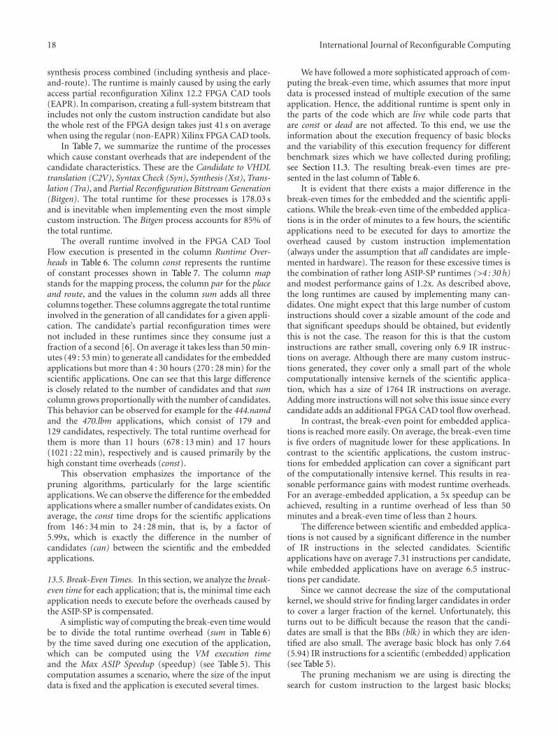
18 International Journal of Reconfigurable Computing
synthesis process combined (including synthesis and place-and-route). The runtime is mainly caused by using the earlyaccess partial reconfiguration Xilinx 12.2 FPGA CAD tools(EAPR). In comparison, creating a full-system bitstream thatincludes not only the custom instruction candidate but alsothe whole rest of the FPGA design takes just 41 s on averagewhen using the regular (non-EAPR) Xilinx FPGA CAD tools.
In Table 7, we summarize the runtime of the processeswhich cause constant overheads that are independent of thecandidate characteristics. These are the Candidate to VHDLtranslation (C2V), Syntax Check (Syn), Synthesis (Xst), Trans-lation (Tra), and Partial Reconfiguration Bitstream Generation(Bitgen). The total runtime for these processes is 178.03 sand is inevitable when implementing even the most simplecustom instruction. The Bitgen process accounts for 85% ofthe total runtime.
The overall runtime involved in the FPGA CAD ToolFlow execution is presented in the column Runtime Over-heads in Table 6. The column const represents the runtimeof constant processes shown in Table 7. The column mapstands for the mapping process, the column par for the placeand route, and the values in the column sum adds all threecolumns together. These columns aggregate the total runtimeinvolved in the generation of all candidates for a given appli-cation. The candidate’s partial reconfiguration times werenot included in these runtimes since they consume just afraction of a second [6]. On average it takes less than 50 min-utes (49 : 53 min) to generate all candidates for the embeddedapplications but more than 4 : 30 hours (270 : 28 min) for thescientific applications. One can see that this large differenceis closely related to the number of candidates and that sumcolumn grows proportionally with the number of candidates.This behavior can be observed for example for the 444.namdand the 470.lbm applications, which consist of 179 and129 candidates, respectively. The total runtime overhead forthem is more than 11 hours (678 : 13 min) and 17 hours(1021 : 22 min), respectively and is caused primarily by thehigh constant time overheads (const).
This observation emphasizes the importance of thepruning algorithms, particularly for the large scientificapplications. We can observe the difference for the embeddedapplications where a smaller number of candidates exists. Onaverage, the const time drops for the scientific applicationsfrom 146 : 34 min to 24 : 28 min, that is, by a factor of5.99x, which is exactly the difference in the number ofcandidates (can) between the scientific and the embeddedapplications.
13.5. Break-Even Times. In this section, we analyze the break-even time for each application; that is, the minimal time eachapplication needs to execute before the overheads caused bythe ASIP-SP is compensated.
A simplistic way of computing the break-even time wouldbe to divide the total runtime overhead (sum in Table 6)by the time saved during one execution of the application,which can be computed using the VM execution timeand the Max ASIP Speedup (speedup) (see Table 5). Thiscomputation assumes a scenario, where the size of the inputdata is fixed and the application is executed several times.
We have followed a more sophisticated approach of com-puting the break-even time, which assumes that more inputdata is processed instead of multiple execution of the sameapplication. Hence, the additional runtime is spent only inthe parts of the code which are live while code parts thatare const or dead are not affected. To this end, we use theinformation about the execution frequency of basic blocksand the variability of this execution frequency for differentbenchmark sizes which we have collected during profiling;see Section 11.3. The resulting break-even times are pre-sented in the last column of Table 6.
It is evident that there exists a major difference in thebreak-even times for the embedded and the scientific appli-cations. While the break-even time of the embedded applica-tions is in the order of minutes to a few hours, the scientificapplications need to be executed for days to amortize theoverhead caused by custom instruction implementation(always under the assumption that all candidates are imple-mented in hardware). The reason for these excessive times isthe combination of rather long ASIP-SP runtimes (>4 : 30 h)and modest performance gains of 1.2x. As described above,the long runtimes are caused by implementing many can-didates. One might expect that this large number of custominstructions should cover a sizable amount of the code andthat significant speedups should be obtained, but evidentlythis is not the case. The reason for this is that the custominstructions are rather small, covering only 6.9 IR instruc-tions on average. Although there are many custom instruc-tions generated, they cover only a small part of the wholecomputationally intensive kernels of the scientific applica-tion, which has a size of 1764 IR instructions on average.Adding more instructions will not solve this issue since everycandidate adds an additional FPGA CAD tool flow overhead.
In contrast, the break-even point for embedded applica-tions is reached more easily. On average, the break-even timeis five orders of magnitude lower for these applications. Incontrast to the scientific applications, the custom instruc-tions for embedded application can cover a significant partof the computationally intensive kernel. This results in rea-sonable performance gains with modest runtime overheads.For an average-embedded application, a 5x speedup can beachieved, resulting in a runtime overhead of less than 50minutes and a break-even time of less than 2 hours.
The difference between scientific and embedded applica-tions is not caused by a significant difference in the numberof IR instructions in the selected candidates. Scientificapplications have on average 7.31 instructions per candidate,while embedded applications have on average 6.5 instruc-tions per candidate.
Since we cannot decrease the size of the computationalkernel, we should strive for finding larger candidates in orderto cover a larger fraction of the kernel. Unfortunately, thisturns out to be difficult because the reason that the candi-dates are small is that the BBs (blk) in which they are iden-tified are also small. The average basic block has only 7.64(5.94) IR instructions for a scientific (embedded) application(see Table 5).
The pruning mechanism we are using is directing thesearch for custom instruction to the largest basic blocks;
International Journal of Reconfigurable Computing 19
hence, the average basic block that passes the pruningstage has 155.65 instructions for a scientific and 29.71 forembedded application (see Table 6). However, even theselarger blocks include a sizable number of the hardware-infeasible instructions, such as accesses to global variables ormemory, which cannot be included in a hardware custominstruction. As a result, there are only 7.31 instructions percandidate in a scientific application which causes high break-even times for them.
This observation illustrates that there are practical limi-tations for the ASIP-SP when using code that has been com-piled from imperative languages.
14. Reduction of Runtime Overheads
In this section, we propose two approaches for reducing thetotal runtime overheads and in turn also the break-eventimes: partial reconfiguration bitstream caching and acceler-ation of the CAD tool flow.
14.1. Partial Reconfiguration Bitstream Caching. As in manyareas of computer science, caching can be applied also in thecontext of our work. Much like virtual machines cache thebinary code that was generated on the fly for further use, wecan cache the generated partial bitstreams for each custominstruction. To this end, each candidate needs to have aunique identifier that is used as a key for reading and writingthe cache. We can, for example, compute a signature of theLLVM bitcode that describes the candidate for this purpose.The cached bitstreams can be stored for example in an on-disk database.
14.2. Acceleration of the CAD Tool Flow. A complementarymethod for reducing the runtime overheads is to acceleratethe FPGA CAD tool flow. There are several options to achievethis goal. One possibility is to use a faster computer thatprovides faster CPUs and faster and larger memory or torun the FPGA tool concurrently. Alternatively, it may bepossible to use a smaller FPGA device, since the constantprocesses of the tool flow depend strongly on the capacityof the FPGA device. We have used a rather large Virtex-4FX100 device, therefore switching to a smaller device woulddefinitely reduce the runtime of the tool flow. Another optionwould be to use a memory file system for storing the filescreated by the tool flow. As the FPGA CAD tool flow isknown to be I/O intensive, this should speed up the tool flow.Finally, we could change our architecture to a more coarse-grained architecture with simplified computing elements andlimited or fixed routing. It has been shown that it is possibleto develop customized tools for such architectures whichwork significantly faster [30].
14.3. Extrapolation. In Table 8 we calculate the averagebreaking-even time for the embedded applications when ap-plying these ideas. When the cache is disabled and we donot assume any performance gain from the tool flow, thefirst value is equal to the AVG E row and the last column inTable 6. One can note also that these values do not scale
Table 8: The average breaking-even time for the embedded appli-cations using a partial reconfiguration bitstream cache and a fasterFPGA CAD tool flow.
Faster FPGA CAD tool flow [%]
Cache 0 30 60 90
hit [%] [h : m : s] [h : m : s] [h : m : s] [h : m : s]
0 01 : 59 : 55 01 : 24 : 48 00 : 48 : 27 00 : 12 : 07
10 01 : 47 : 44 01 : 15 : 25 00 : 43 : 06 00 : 10 : 46
20 01 : 32 : 59 01 : 05 : 05 00 : 37 : 11 00 : 09 : 18
30 01 : 28 : 09 01 : 01 : 42 00 : 35 : 15 00 : 08 : 49
40 01 : 13 : 08 00 : 51 : 11 00 : 29 : 15 00 : 07 : 19
50 01 : 01 : 00 00 : 42 : 42 00 : 24 : 24 00 : 06 : 06
60 00 : 48 : 50 00 : 34 : 10 00 : 19 : 32 00 : 04 : 53
70 00 : 35 : 12 00 : 24 : 38 00 : 14 : 05 00 : 03 : 31
80 00 : 29 : 19 00 : 20 : 31 00 : 11 : 43 00 : 02 : 56
90 00 : 14 : 07 00 : 09 : 53 00 : 05 : 39 00 : 01 : 24
linearly because we consider the frequency information forbasic blocks.
For this evaluation, we varied the assumed cache hit rateto be between 0%–90%. That is, for simulating a cache witha 20% hit rate, we have populated the cache with 20% ofthe required bitstreams for a particular application, whereasthe selection whose bitstreams are stored in the cache israndom. Whenever there is a hit in the cache for a givencandidate, the whole runtime associated with the generationof the candidate is subtracted from the total runtime; seesum column in Table 6. The values in the Faster FPGA CADtool flow columns are decreasing linearly with the assumedspeedup.
If we assume that the FPGA CAD tool flow can beaccelerated by 30% and that we have 30% cache hits, theaverage break-even time drops almost by half (1.94x), from1 : 59 : 55 h to 1 : 01 : 42 h. This means that the whole runtimeof the ASIP-SP could be compensated in a bit more than onehour and for the rest of the time the adapted architecturewould provide a performance gain by an average factor of 5x.These assumptions are modest values since the cache hit ratedepends only on the size of the cache, and our Dell T3500workstation could be easily replaced by a faster one.
15. Conclusion and Future Work
In this work, we have studied the just-in-time ASIP-SP foran FPGA-based reconfigurable architecture. The most signif-icant parts of this process, including the candidate identifi-cation, estimation, selection, and pruning mechanisms werenot only described with precise formalisms but were alsoexperimentally evaluated. In particular, we discussed andcompared characteristics of three state-of-the-art instructionset extension algorithms in order to study the candidate iden-tification mechanism in detail. This study included not onlyalgorithm runtimes, number of found UDCI candidates,their properties, and impact of algorithm constraints on thesearch space, but more importantly the achievable maximum

20 International Journal of Reconfigurable Computing
performance gains for various embedded computing andscientific benchmark applications.
The study of the ASIP process was performed bothseparately for every element but more importantly also forthe entire ASIP process, where the feasibility and limitationswere investigated. The study has shown that for embeddedapplications an average speedup of 5x can be achieved witha runtime overhead of less than 50 minutes. This overheadcan be compensated if the application executes for two hoursor for one hour when assuming a 30% cache hit rate and afaster FPGA CAD tool flow. Our study further showed thatthe larger and more complex software kernels of scientificapplications, represented by the SPEC benchmarks, do notmap well to custom hardware instructions targeting theWoolcano architecture and lead to excessive times until thebreak-even point is reached. The reason for this limitationcan be found in the properties of the intermediate codegenerated by LLVM when compiling C code, in particular,rather small basic block sizes with an insufficient amountof instruction level parallelism. Similar results are expectedfor other imperative languages. Simultaneously, this workhas explored the potential of our Woolcano reconfigurablearchitecture, the ISE algorithms, and pruning mechanism forthem as well as the PivPav estimation and datapath synthesistools.
References
[1] P. Ienne and R. Leupers, Customizable Embedded Processors:Design Technologies and Applications, Morgan Kaufmann, SanFrancisco, Calif, USA, 2006.
[2] M. J. Wirthlin and B. L. Hutchings, “Dynamic instruction setcomputer,” in Proceedings of the 3rd IEEE Symposium on FPGAsfor Custom Computing Machines, (FCCM ’95), pp. 99–107,IEEE Computer Society, April 1995.
[3] R. Razdan and M. D. Smith, “A high-performance microar-chitecture with hardware-programmable functional units,” inProceedings of the 27th International Symposium on Microar-chitecture, (MICRO ’94), pp. 172–180, ACM, New York, NY,USA, November 1994.
[4] Z. A. Ye, A. Moshovos, S. Hauck, and P. Banerjee, “Chimaera:a high-performance architecture with a tightly-coupled recon-figurable functional unit,” in Proceedings of the 27th AnnualInternational Symposium on Computer Architecture, (ISCA’00), pp. 225–235, ACM, June 2000.
[5] P. M. Athanas and H. F. Silverman, “Processor reconfigurationthrough instruction-set metamorphosis,” Computer, vol. 26,no. 3, pp. 11–18, 1993.
[6] M. Grad and C. Plessl, “Woolcano: an architecture and toolflow for dynamic instruction set extension on Xilinx Virtex-4 FX,” in Proceedings of the 9th International Conference onEngineering of Reconfigurable Systems and Algorithms (ERSA’09), pp. 319–322, CSREA Press, Monte Carlo Resort, Nev,USA, July 2009.
[7] J. M. Arnold, “S5: the architecture and development flowof a software configurable processor,” in Proceedings of theInternational Conference on Field Programmable Technology,(ICFPT ’05), pp. 121–128, IEEE Computer Society, Kent RidgeGuild House, Singapore, December 2005.
[8] S. Borkar, “Design challenges of technology scaling,” IEEEMicro, vol. 19, no. 4, pp. 23–29, 1999.
[9] M. Grad and C. Plessl, “An open source circuit library withbenchmarking facilities,” in Proceedings of the 10th Interna-tional Conference on Engineering of Reconfigurable Systems andAlgorithms (ERSA, ’10), T. P. Plaks, D. Andrews, R. F. DeMaraet al., Eds., pp. 144–150, CSREA Press, Las Vegas, Nev, USA,July 2010.
[10] M. Grad and C. Plessl, “Pruning the design space for just-in-time processor customization,” in Proceedings of the Interna-tional Conference on ReConFigurable Computing and FPGAs(ReConFig ’10), pp. 67–72, IEEE Computer Society, Cancun,Mexico, December 2010.
[11] M. Grad and C. Plessl, “Just-in-time instruction set ex-tension—feasibility and limitations for an FPGA-based recon-figurable ASIP architecture,” in Proceedings of the 18th Recon-figurable Architectures Workshop, (RAW ’11), pp. 278–285,IEEE Computer Society, May 2011.
[12] M. Wazlowski, L. Agarwal, T. Lee et al., “PRISM-II compilerand architecture,” in Proceedings of the IEEE Symposium onField-Programmable Custom Computing Machines, (FCCM’93), pp. 9–16, IEEE Computer Society, April 1993.
[13] C. Galuzzi and K. Bertels, “The instruction-set extensionproblem: a survey,” in Proceedings of the International Confer-ence on Architecture of Computing Systems, (ARCS ’08), LectureNotes in Computer Science, no. 4943, pp. 209–220, Springer/Kluwer Academic, Dresden, Germany, February 2008.
[14] R. J. Hookway and M. A. Herdeg, “DIGITAL FX!32: com-bining emulation and binary translation,” Digital TechnicalJournal, vol. 9, no. 1, pp. 3–12, 1997.
[15] V. Bala, E. Duesterwald, and S. Banerjia, “Transparent dy-namic optimization,” Tech. Rep. number HPL-1999-78, HPLaboratories Cambridge, 1999.
[16] K. Ebcioglu and E. R. Altman, “DAISY: dynamic compilationfor 100% architectural compatibility,” in Proceedings of the24th Annual International Symposium on Computer Architec-ture, pp. 26–37, New York, NY, USA, June 1997.
[17] F. Vahid, G. Stitt, and R. Lysecky, “Warp processing: dynamictranslation of binaries to FPGA circuits,” Computer, vol. 41,no. 7, pp. 40–46, 2008.
[18] A. C. S. Beck and L. Carro, “Dynamic reconfiguration withbinary translation: breaking the ILP barrier with softwarecompatibility,” in Proceedings of the 42nd Design AutomationConference, (DAC ’05), pp. 732–737, New York, NY, USA, June2005.
[19] L. Pozzi, K. Atasu, and P. Ienne, “Exact and approximatealgorithms for the extension of embedded processor instruc-tion sets,” IEEE Transactions on Computer-Aided Design ofIntegrated Circuits and Systems, vol. 25, no. 7, pp. 1209–1229,2006.
[20] P. Yu and T. Mitra, “Scalable custom instructions identifica-tion for instruction-set extensible processors,” in Proceedingsof the International Conference on Compilers, Architecture,and Synthesis for Embedded Systems, (CASES ’04), pp. 69–78,Washington, DC, USA, September 2004.
[21] C. A. William, W. Fornaciari, L. Pozzi, and M. Sami, “A DAG-based design approach for reconfigurable VLIW processors,”in Proceedings of the Design, Automation and Test in EuropeConference, (DATE ’99), pp. 778–779, ACM, Munich, Ger-many, January 1999.
[22] J. Gong, D. D. Gajski, and S. Narayan, “Software estimationfrom executable specifications,” Journal of Computer SoftwareEngineering, vol. 2, pp. 239–258, 1994.
[23] The PowerPC 405TM Core, IBM, 1998.

International Journal of Reconfigurable Computing 21
[24] A. Ray, T. Srikanthan, and W. Jigang, “Practical techniques forperformance estimation of processors,” in Proceedings of theInternational Workshop on System-on-Chip for Real-TimeApplications, (IWSOC ’05), pp. 308–311, IEEE ComputerSociety, Washington, DC, USA, 2005.
[25] B. So, P. C. Diniz, and M. W. Hall, “Using estimates frombehavioral synthesis tools in compiler-directed design spaceexploration,” in Proceedings of the 40th Design AutomationConference, pp. 514–519, New York, NY, USA, June 2003.
[26] Floating-Point Operator v5.0, Xilinx.
[27] N. Maheshwari and S. S. Sapatnekar, Timing Analysis andOptimization of Sequential Circuits, Springer/Kluwer Aca-demic Publishers, Norwell, Mass, USA, 1999.
[28] R. Meeuws, Y. Yankova, K. Bertels, G. Gaydadjiev, and S.Vassiliadis, “A quantitative prediction model for hardware/software partitioning,” in Proceedings of the InternationalConference on Field Programmable Logic and Applications, (FPL’07), pp. 735–739, Amsterdam, The Netherlands, August 2007.
[29] P. Bonzini and L. Pozzi, “Polynomial-time subgraph enumer-ation for automated instruction set extension,” in Proceedingsof the Design, Automation and Test in Europe Conference andExhibition, pp. 1331–1336, Nice, France, April 2007.
[30] E. Bergeron, M. Feeley, and J. P. David, “Hardware JIT com-pilation for off-the-shelf dynamically reconfigurable FPGAs,”in Proceedings of the Joint European Conferences on Theory andPractice of Software 17th International Conference on CompilerConstruction (CC/ETAPS’08), pp. 178–192, Springer-Verlag,Berlin, Heidelberg, 2008.
Hindawi Publishing CorporationInternational Journal of Reconfigurable ComputingVolume 2012, Article ID 474765, 16 pagesdoi:10.1155/2012/474765
Research Article
Combining SDM-Based Circuit Switching with Packet Switchingin a Router for On-Chip Networks
Angelo Kuti Lusala and Jean-Didier Legat
Institute of Information and Communication Technologies, Electronics and Applied Mathematics,Universite Catholique de Louvain, 1348 Louvain-la-Neuve, Belgium
Correspondence should be addressed to Angelo Kuti Lusala, [email protected]
Received 1 May 2011; Revised 5 September 2011; Accepted 19 September 2011
Academic Editor: Marco D. Santambrogio
Copyright © 2012 A. K. Lusala and J.-D. Legat. This is an open access article distributed under the Creative Commons AttributionLicense, which permits unrestricted use, distribution, and reproduction in any medium, provided the original work is properlycited.
A Hybrid router architecture for Networks-on-Chip “NoC” is presented, it combines Spatial Division Multiplexing “SDM” basedcircuit switching and packet switching in order to efficiently and separately handle both streaming and best-effort traffic generatedin real-time applications. Furthermore the SDM technique is combined with Time Division Multiplexing “TDM” technique in thecircuit switching part in order to increase path diversity, thus improving throughput while sharing communication resourcesamong multiple connections. Combining these two techniques allows mitigating the poor resource usage inherent to circuitswitching. In this way Quality of Service “QoS” is easily provided for the streaming traffic through the circuit-switched sub-router while the packet-switched sub-router handles best-effort traffic. The proposed hybrid router architectures were synthesized,placed and routed on an FPGA. Results show that a practicable Network-on-Chip “NoC” can be built using the proposed routerarchitectures. 7 × 7 mesh NoCs were simulated in SystemC. Simulation results show that the probability of establishing pathsthrough the NoC increases with the number of sub-channels and has its highest value when combining SDM with TDM, therebysignificantly reducing contention in the NoC.
1. Introduction
Real-time applications have grown in complexity and requiremore and higher-power computing resources. These appli-cations are then suitable to be run on parallel environ-ments such as MultiProcessor Systems-on-Chip “MPSoC”platforms. However, application performance in an MPSoCplatform strongly depends on the on-chip interconnectionnetwork used to carry communications between cores inthe platform. Since Real-time applications generate bothstreaming and best-effort traffics, there is then a need forthe on-chip interconnection network to provide QoS forthe streaming traffic and data completion for the best-efforttraffic.
Streaming traffic is best handled in circuit-switched net-work. Since communication resources are prereserved beforeany data transfer, QoS is thereby intrinsically supported.Circuit switching often leads to a poor usage of communi-cation resources, since reserved resources for a transaction
are exclusively used by that transaction. For that reason,it is not suitable for best-effort traffic. Best-effort traffic iswell handled in packet-switched network, however, becauseof its nondeterministic behavior; packet switching is notsuitable for streaming traffic. To improve resource utilizationin circuit-switched networks, time division multiplexing“TDM” is often used in order to share resources amongmultiple connections. TDM consists in dividing a channelin time intervals called time slots; multiple connections cantherefore use a given channel by assigning a time slot toeach connection. In TDM-based circuit-switched networks,consecutive time slots are reserved in consecutive links alongthe path between a source node and a destination node.Using TDM, a circuit-switched network can then handleboth streaming and best-effort traffic. Reserved time slots areused to carry streaming traffic, while unreserved time slotsare used to carry best-effort traffic [1]. However, providingQoS and sharing resources between streaming and best-effort traffic are hard and often lead to a complex design with
2 International Journal of Reconfigurable Computing
huge hardware and power consumption overhead [2]. Inpacket-switched network, streaming and best-effort trafficsare handled by either assigning priorities to each type oftraffic, with streaming traffic having the highest priority,[3] or by reserving buffers or virtual channels “VCs” forcarrying the streaming traffic, while the unreserved buffersare used to carry the best-effort traffic [4]. The first approach,while providing interesting results for varying traffic, cannotprovide strong guarantees denoted “Hard QoS” for real-time applications. The second approach also leads to acomplex design, with huge area and power consumptionoverhead depending on the number of buffers per inputport.
In order to efficiently handle both streaming and best-effort traffic in an NoC, we propose a hybrid router whichcombines circuit switching with packet switching in orderto separately and independently handle each type of traffic.The hybrid router then consists of two subrouters: a circuitswitched subrouter and a packet switched subrouter. The cir-cuit switched subrouter is responsible for handling streamingtraffic, while the packet-switched subrouter is responsiblefor handling best-effort traffic. In this way, we ensure thateach type of traffic is efficiently and suitably handled. Inorder to improve low resources usage inherent to circuitswitching, the circuit-switched subrouter uses SDM andTDM techniques. The SDM technique that we use consistsin having more than one link between two adjacent routers.In this way, concurrent data streams are physically separated,thereby increasing path diversity in the router and improvingthroughput. The TDM technique allows sharing physicallyseparate links among multiple connections. We then definean SDM Channel as a set of links. Each link or subchannelis identified by a number. When the SDM-Channel is sharedfollowing the TDM technique, the SDM-Channel is therebydenoted SDM-TDM Channel.
Since circuit-switched subrouters are used to carry thestreaming traffic, a path which consists of successive linksbetween a source node and a destination node must firstbe established before transferring streaming traffic. Thistask is performed by the packet-switched subrouters byreserving an available subchannel in an SDM-Channel orby reserving a requested time slot at any subchannel inan SDM-TDM channel along the path between the sourceand the destination nodes. The packet-switched subrouterthen configures the attached circuit-switched subrouter byindicating the subchannel to use in an SDM-Channel or byindicating the subchannel and the time slots to use in theSDM-TDM Channel for the concerned connection. Whenthe transfer of the streaming traffic is completed, the circuit-switched subrouter notifies the attached packet-switchedsubrouter to release reserved resources used to carry theconcerned streaming traffic.
In the proposed router architecture, each subrouter inde-pendently handles traffic. A node or tile, which can be aprocessing element “PE” or a storage element “SE”, is con-nected to each subrouter as shown in Figures 1 and 2. Whena PE needs to transfer best-effort traffic, it directly sends its“normal or data payload” best-effort packet to the attachedpacket-switched subrouter for routing through the network
hop by hop. When the PE needs to transfer streaming traffic,it first sends a “set-up” best-effort packet to the attachedpacket-switched subrouter. The set-up best-effort packetis responsible for reserving resources, thereby establishinga path between a source and destination nodes. When aset-up packet reaches its destination, an acknowledgmentbest-effort packet is generated and routed from destinationto source through the packet-switched subnetwork. Uponreceiving the acknowledgment packet, the source node thenstarts transferring streaming traffic, which is segmented inpackets like cells in asynchronous transfer mode “ATM”networks. When the transfer of the streaming traffic iscompleted, the source node sends a teardown streamingpacket along the established path whose purpose is to releasereserved resources used for the concerned streaming traffic.
Since the circuit-switched subrouters and the packet-switched subrouters do not share links, and avoiding the useof the store-and-forwardstrategy, there is then no need touse FIFO buffers in the circuit-switched subrouter to storestreaming packets unlike in [5]. This significantly reduces thearea and power consumption of the router. Combining SDMand TDM techniques in a router allows taking advantagesof the abundance of wires resulting from the increased levelof CMOS circuits. We then have two degrees of freedomto optimize the router; one can increase either the numberof subchannels in an SDM-TDM Channel or the numberof time slots per subchannel. In both cases, the numberof available channels increases in the network, therebyincreasing the possibilities of establishing paths through thenetwork.
The proposed hybrid router architectures were imple-mented in Verilog and synthesized on FPGA with differentnumber of subchannels in an SDM-Channel and for differentnumbers of subchannels and time slots in an SDM-TDMChannel. Synthesis results show that increasing the numberof subchannels in an SDM-Channel does not significantlyimpact the size of the router, while the clock frequencyis only slightly reduced. When combining SDM and TDMtechniques, increasing the number of subchannels, whilemaintaining fixed the number of time slots significantlyimpacts the size of the router, while the maximum clockfrequency remains almost constant; increasing the numberof time slots while maintaining fixed the number of sub-channels does not significantly impact the size of the routerwhile it significantly reduces the clock frequency. In order toevaluate the performance of the proposed architectures interms of established paths through the network accordingto the number of set-up requests packets, three 7 × 7 2Dmeshes NoCs were simulated in SystemC under randomuniform traffic and compared: an SDM-based hybrid NoC,a TDM-based hybrid NoC, and an SDM-TDM-based hybridNoC. Simulation results show that combining SDM andTDM techniques in a router substantially increases theprobability of establishing paths through the network, whilethis probability is appreciable in the SDM-based NoC andsmall in the TDM-based NoC.
The rest of the paper is organized as follows. Relatedwork is reviewed in Section 2. Section 3 introduces theproposed router architectures. Section 4 discusses simulation
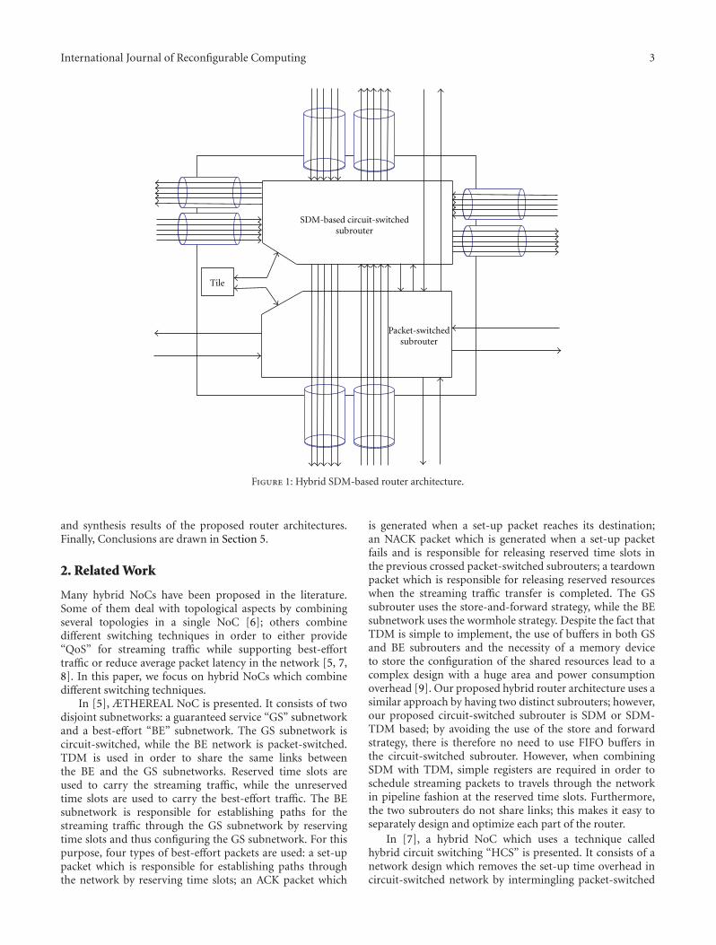
International Journal of Reconfigurable Computing 3
SDM-based circuit-switched
Tile
Packet-switchedsubrouter
subrouter
Figure 1: Hybrid SDM-based router architecture.
and synthesis results of the proposed router architectures.Finally, Conclusions are drawn in Section 5.
2. Related Work
Many hybrid NoCs have been proposed in the literature.Some of them deal with topological aspects by combiningseveral topologies in a single NoC [6]; others combinedifferent switching techniques in order to either provide“QoS” for streaming traffic while supporting best-efforttraffic or reduce average packet latency in the network [5, 7,8]. In this paper, we focus on hybrid NoCs which combinedifferent switching techniques.
In [5], ÆTHEREAL NoC is presented. It consists of twodisjoint subnetworks: a guaranteed service “GS” subnetworkand a best-effort “BE” subnetwork. The GS subnetwork iscircuit-switched, while the BE network is packet-switched.TDM is used in order to share the same links betweenthe BE and the GS subnetworks. Reserved time slots areused to carry the streaming traffic, while the unreservedtime slots are used to carry the best-effort traffic. The BEsubnetwork is responsible for establishing paths for thestreaming traffic through the GS subnetwork by reservingtime slots and thus configuring the GS subnetwork. For thispurpose, four types of best-effort packets are used: a set-uppacket which is responsible for establishing paths throughthe network by reserving time slots; an ACK packet which
is generated when a set-up packet reaches its destination;an NACK packet which is generated when a set-up packetfails and is responsible for releasing reserved time slots inthe previous crossed packet-switched subrouters; a teardownpacket which is responsible for releasing reserved resourceswhen the streaming traffic transfer is completed. The GSsubrouter uses the store-and-forward strategy, while the BEsubnetwork uses the wormhole strategy. Despite the fact thatTDM is simple to implement, the use of buffers in both GSand BE subrouters and the necessity of a memory deviceto store the configuration of the shared resources lead to acomplex design with a huge area and power consumptionoverhead [9]. Our proposed hybrid router architecture uses asimilar approach by having two distinct subrouters; however,our proposed circuit-switched subrouter is SDM or SDM-TDM based; by avoiding the use of the store and forwardstrategy, there is therefore no need to use FIFO buffers inthe circuit-switched subrouter. However, when combiningSDM with TDM, simple registers are required in order toschedule streaming packets to travels through the networkin pipeline fashion at the reserved time slots. Furthermore,the two subrouters do not share links; this makes it easy toseparately design and optimize each part of the router.
In [7], a hybrid NoC which uses a technique calledhybrid circuit switching “HCS” is presented. It consists of anetwork design which removes the set-up time overhead incircuit-switched network by intermingling packet-switched
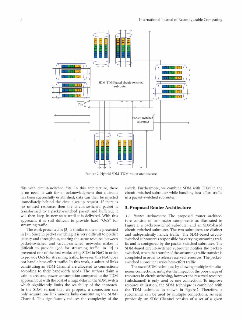
4 International Journal of Reconfigurable Computing
Tile
T3T2T1subrouter
Packet-switched
T3T2T1
T3T2T1
T3T2T1
T3T2T1
T3T2T1
T3T2T1
T3T2T1
T3T2T1
T3T2T1
T3T2T1
T3T2T1
T3
T2
T1
T3
T2
T1
T3
T2
T1
T3
T2
T1
T3
T2
T1
T3
T2
T1
T3
T2
T1
T3
T2
T1
T3
T2
T1
T3
T2
T1
T3
T2
T1
T3
T2
T1
circuit-switchedSDM-TDM based-
subrouter
Figure 2: Hybrid SDM-TDM router architecture.
flits with circuit-switched flits. In this architecture, thereis no need to wait for an acknowledgment that a circuithas been successfully established; data can then be injectedimmediately behind the circuit set-up request. If there isno unused resource, then the circuit-switched packet istransformed to a packet-switched packet and buffered; itwill then keep its new state until it is delivered. With thisapproach, it is still difficult to provide hard “QoS” forstreaming traffic.
The work presented in [8] is similar to the one presentedin [7]. Since in packet switching it is very difficult to predictlatency and throughput, sharing the same resource betweenpacket-switched and circuit-switched networks makes itdifficult to provide QoS for streaming traffic. In [9] ispresented one of the first works using SDM in NoC in orderto provide QoS for streaming traffic; however, this NoC doesnot handle best-effort traffic. In this work, a subset of linksconstituting an SDM-Channel are allocated to connectionsaccording to their bandwidth needs. The authors claim again in area and power consumption compared to the TDMapproach but with the cost of a huge delay in the SDM switchwhich significantly limits the scalability of the approach.In the SDM variant that we propose, a connection canonly acquire one link among links constituting the SDM-Channel. This significantly reduces the complexity of the
switch. Furthermore, we combine SDM with TDM in thecircuit-switched subrouter while handling best-effort trafficin a packet-switched subrouter.
3. Proposed Router Architecture
3.1. Router Architecture. The proposed router architec-ture consists of two major components as illustrated inFigure 1: a packet-switched subrouter and an SDM-basedcircuit-switched subrouter. The two subrouters are distinctand independently handle traffic. The SDM-based circuit-switched subrouter is responsible for carrying streaming traf-fic and is configured by the packet-switched subrouter. TheSDM-based circuit-switched subrouter notifies the packet-switched, when the transfer of the streaming traffic transfer iscompleted in order to release reserved resources. The packet-switched subrouter carries best-effort traffic.
The use of SDM technique, by allowing multiple simulta-neous connections, mitigates the impact of the poor usage ofresources in circuit switching, however the reserved resource(subchannel) is only used by one connection. To improveresource utilization, the SDM technique is combined withthe TDM technique as shown in Figure 2. Therefore, asubchannel can be used by multiple connections. As seenpreviously, an SDM-Channel consists of a set of a given
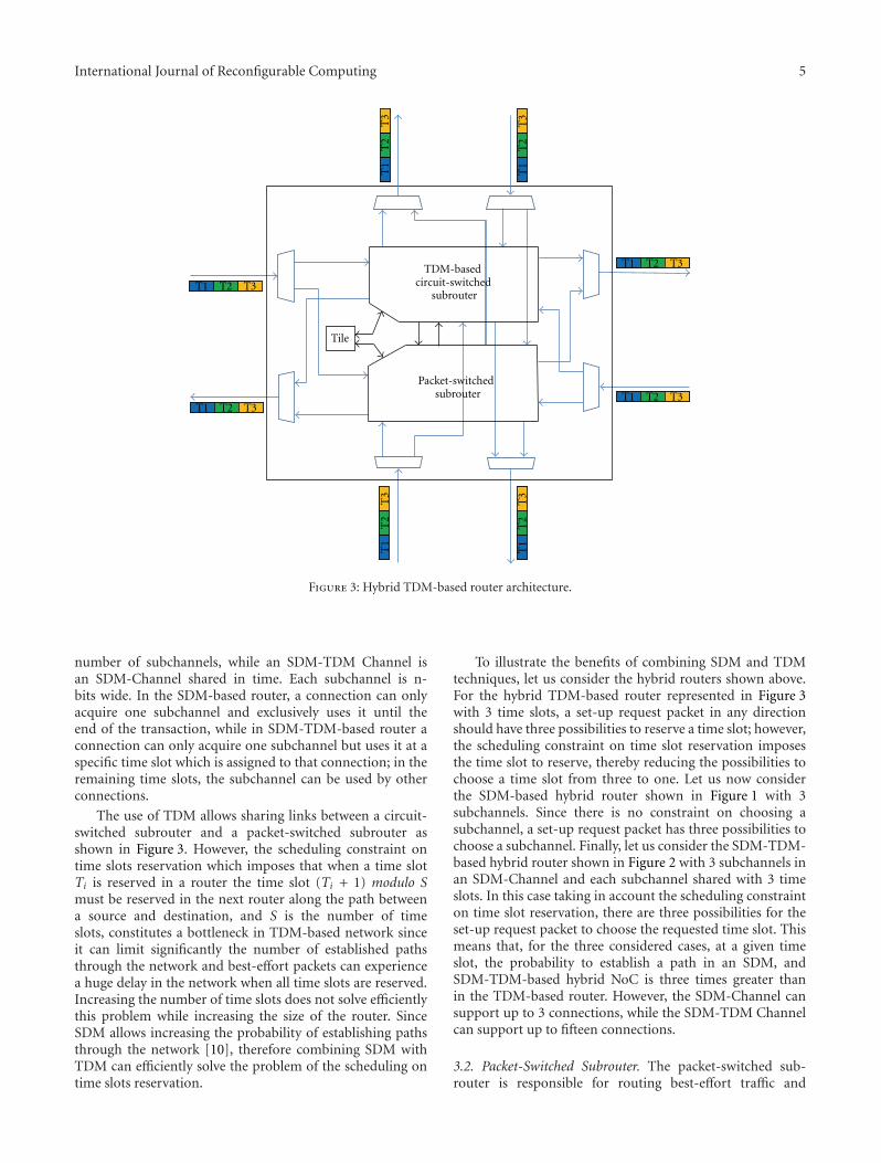
International Journal of Reconfigurable Computing 5
T3T2T1
T3T2T1T3T2T1
T3T2T1
T3
T2
T1
T3
T2
T1
T3
T2
T1
T3
T2
T1
TDM-basedcircuit-switched
Packet-switched
Tile
subrouter
subrouter
Figure 3: Hybrid TDM-based router architecture.
number of subchannels, while an SDM-TDM Channel isan SDM-Channel shared in time. Each subchannel is n-bits wide. In the SDM-based router, a connection can onlyacquire one subchannel and exclusively uses it until theend of the transaction, while in SDM-TDM-based router aconnection can only acquire one subchannel but uses it at aspecific time slot which is assigned to that connection; in theremaining time slots, the subchannel can be used by otherconnections.
The use of TDM allows sharing links between a circuit-switched subrouter and a packet-switched subrouter asshown in Figure 3. However, the scheduling constraint ontime slots reservation which imposes that when a time slotTi is reserved in a router the time slot (Ti + 1) modulo Smust be reserved in the next router along the path betweena source and destination, and S is the number of timeslots, constitutes a bottleneck in TDM-based network sinceit can limit significantly the number of established pathsthrough the network and best-effort packets can experiencea huge delay in the network when all time slots are reserved.Increasing the number of time slots does not solve efficientlythis problem while increasing the size of the router. SinceSDM allows increasing the probability of establishing pathsthrough the network [10], therefore combining SDM withTDM can efficiently solve the problem of the scheduling ontime slots reservation.
To illustrate the benefits of combining SDM and TDMtechniques, let us consider the hybrid routers shown above.For the hybrid TDM-based router represented in Figure 3with 3 time slots, a set-up request packet in any directionshould have three possibilities to reserve a time slot; however,the scheduling constraint on time slot reservation imposesthe time slot to reserve, thereby reducing the possibilities tochoose a time slot from three to one. Let us now considerthe SDM-based hybrid router shown in Figure 1 with 3subchannels. Since there is no constraint on choosing asubchannel, a set-up request packet has three possibilities tochoose a subchannel. Finally, let us consider the SDM-TDM-based hybrid router shown in Figure 2 with 3 subchannels inan SDM-Channel and each subchannel shared with 3 timeslots. In this case taking in account the scheduling constrainton time slot reservation, there are three possibilities for theset-up request packet to choose the requested time slot. Thismeans that, for the three considered cases, at a given timeslot, the probability to establish a path in an SDM, andSDM-TDM-based hybrid NoC is three times greater thanin the TDM-based router. However, the SDM-Channel cansupport up to 3 connections, while the SDM-TDM Channelcan support up to fifteen connections.
3.2. Packet-Switched Subrouter. The packet-switched sub-router is responsible for routing best-effort traffic and
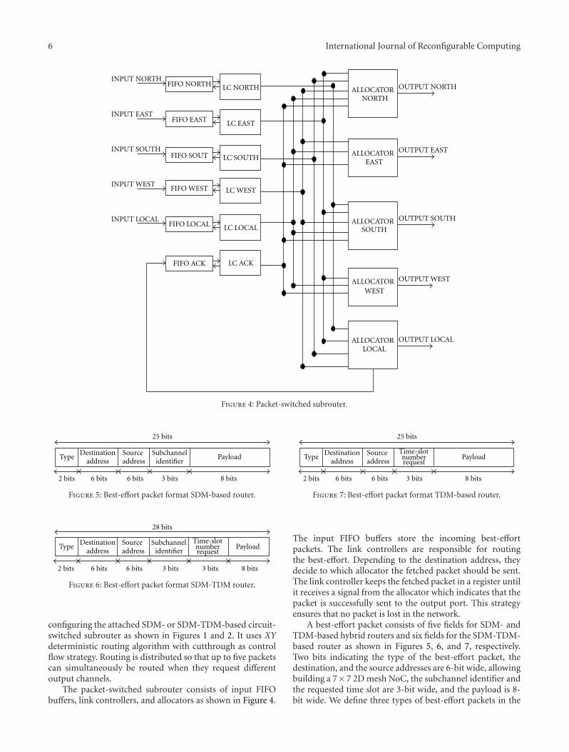
6 International Journal of Reconfigurable Computing
OUTPUT WEST
OUTPUT SOUTH
OUTPUT EAST
OUTPUT NORTH
INPUT LOCAL
INPUT WEST
INPUT SOUTH
INPUT EAST
INPUT NORTHLC NORTH
LC EAST
LC SOUTH
LC WEST
LC LOCAL
LC ACK
FIFO NORTH
FIFO EAST
FIFO SOUT
FIFO WEST
FIFO LOCAL
FIFO ACK
ALLOCATORNORTH
ALLOCATOREAST
ALLOCATORSOUTH
ALLOCATORWEST
ALLOCATORLOCAL
OUTPUT LOCAL
Figure 4: Packet-switched subrouter.
TypeDestination
addressPayload
Subchannelidentifier
Sourceaddress
2 bits 6 bits 8 bits
25 bits
3 bits6 bits
Figure 5: Best-effort packet format SDM-based router.
Time-slot
request
2 bits 6 bits 8 bits
28 bits
3 bits
TypeDestination
addressPayload
identifierSourceaddress
6 bits 3 bits
Subchannelnumber
Figure 6: Best-effort packet format SDM-TDM router.
configuring the attached SDM- or SDM-TDM-based circuit-switched subrouter as shown in Figures 1 and 2. It uses XYdeterministic routing algorithm with cutthrough as controlflow strategy. Routing is distributed so that up to five packetscan simultaneously be routed when they request differentoutput channels.
The packet-switched subrouter consists of input FIFObuffers, link controllers, and allocators as shown in Figure 4.
2 bits 6 bits 8 bits
25 bits
3 bits6 bits
TypeDestination
addressPayload
Sourceaddress
Time-slot
requestnumber
Figure 7: Best-effort packet format TDM-based router.
The input FIFO buffers store the incoming best-effortpackets. The link controllers are responsible for routingthe best-effort. Depending to the destination address, theydecide to which allocator the fetched packet should be sent.The link controller keeps the fetched packet in a register untilit receives a signal from the allocator which indicates that thepacket is successfully sent to the output port. This strategyensures that no packet is lost in the network.
A best-effort packet consists of five fields for SDM- andTDM-based hybrid routers and six fields for the SDM-TDM-based router as shown in Figures 5, 6, and 7, respectively.Two bits indicating the type of the best-effort packet, thedestination, and the source addresses are 6-bit wide, allowingbuilding a 7×7 2D mesh NoC, the subchannel identifier andthe requested time slot are 3-bit wide, and the payload is 8-bit wide. We define three types of best-effort packets in the

International Journal of Reconfigurable Computing 7
2 (2, 3 ) (2, 1 ) 0
TypeDestination
addressPayload
Subchannelidentifier
Sourceaddress
0
Figure 8: Set-up packet node source (2,1).
2 1
TypeDestination
addressPayload
identifierSourceaddress
0(2, 3 ) (2, 1 )
Subchannel
Figure 9: Incoming set-up packet allocator EAST (2,2).
proposed hybrid router.
(i) Set-up request best-effort packet.
(ii) ACK best-effort packet.
(iii) Normal best-effort packet.
The set-up request packet is responsible for reservingresources which are subchannels for the SDM-based router,subchannels and requested time slots for the SDM-TDM-based router, and requested time slots for the TDM-basedrouter. The set-up request packet thereby establishes a pathbetween a source node and a destination node. Its payload iszero and its type is 2. The ACK packet, which is generatedwhen a set-up request packet reaches its destination, isresponsible for notifying the source node that the pathis successfully established. Its type is 1and its subchannelidentifier, time slot request number, and payload fields arezero, respectively. The Normal best-effort packet carries thebest-effort payload. Its type is 3and its subchannel identifierand time lot number request fields are zero respectively.
The allocators are responsible for forwarding best-effort packets to the output ports, reserving resources andconfiguring the attached circuit-switched subrouter. Theyfirst check the type of the best-effort packet. If the packetis an ACK or a normal packet, the allocator directly sendsit to the output link without modifying it. If the best-effort packet is a set-up request packet, then the SDM-TDM-based router, allocator reserves an available requestedtime slot at any available subchannel in the SDM-TDMChannel in the concerned direction and builds a new set-up packet by replacing the fields subchannel number andtime slot number request of the incoming packet by thenumber identifier of the reserved subchannel and the timeslot number to request in the next hop. For the SDM-basedrouter, the allocator only reserves a subchannel in the SDM-Channel and builds a new set-up packet by replacing the fieldsubchannel identifier of the incoming set-up request packetby the number identifier of the reserved subchannel. In bothcases, the value of the subchannel identifier in the incomingset-up request packet and the value of the subchannelin the outgoing set-up request packet are concatenated,and the result is stored in a register which is denoted“reg identifier”. Its MSB is the incoming subchannel and itsLSB is the outgoing subchannel. Each subchannel has its own
2 2
TypeDestination
addressPayload
Sourceaddress
0(2, 3 ) (2, 1 )
identifierSubchannel
Figure 10: Outgoing set-up packet allocator EAST (2,2).
DestinationSource
ACK
123
ACKACK
1
23
1 2 1
Setup
ACK
Setup
SetupSetup(2, 3 )(2, 1 ) (2, 2 )
1
ALLOCEAST LOCAL
ALLOCALLOCEAST
SWITCHEAST LOCAL
SWITCHEAST
SWITCH
Figure 11: SDM path between source (2,1) and destination (2,3).
reg identifier. This register helps to retrieve the subchannelto release when a NACK signal is received.
3.2.1. Set-up Path Phase in SDM-Based Router. To illustratethe process of path establishment in the SDM-based router,let us consider an SDM-channel consisting of 3 subchannels;the subchannel identifiers are 1, 2, and 3, respectively. Let usconsider a set-up path phase between a source node attachedto the router with coordinates (2,1) and a destination nodeattached to the router with coordinates (2,3) as shown inFigure 11. The set-up request packet from the source node isgiven in Figure 8; the fields subchannel identifier and payloadare zero.
At the router (2,1), the allocator EAST, reserves an avail-able subchannel in the SDM-Channel output port. Supposethat the reserved subchannel is the subchannel 1, theallocator then builds the outgoing set-up request packet withthe identifier of the reserved subchannel and concatenatesthe value of the subchannel identifier in the incoming set-uprequest packet with the value of the channel identifier in theoutgoing set-up request packet. It then stores this value inthe register identifier of subchannel 1 which is the outgoingsubchannel. At the router (2,2), let us assume that subchan-nel 1 in this allocator is already reserved by another set-uprequest packet and the remaining subchannels are available.The allocator will then reserve for example subchannel 3.It builds the outgoing set-up request packet (Figure 10)and concatenates the value of subchannel identifier in theincoming set-up packet (Figure 9) with the value of thesubchannel identifier in the outgoing set-up request packetand stores this value in the register identifier of subchannelidentifier 2.
At the router (2,3), the allocator LOCAL reserves thesubchannel if it is free. It then generates an ACK packet,which is routed through the packet-switched subnetworkfrom the destination to the source. Upon reception of

8 International Journal of Reconfigurable Computing
DestinationSource
ACK
123
ACK
1
23
1 2 1
Setup
ACK
Setup
SetupSetup 21 10(2, 3 )(2, 1 ) (2, 2 )
1
fail = 1Setup
ALLOCEAST LOCAL
ALLOCALLOCEAST
SWITCHEAST LOCAL
SWITCHEAST
SWITCH
Figure 12: Failed path establishment in SDM-based router.
1 (2, 3 ) (2, 1 ) 0
Type Dest addr
Time-slot
requestSrc addr Payload
0 0
identifierSubchannel number
Figure 13: SDM-TDM set-up packet node source (2,1).
the ACK packet, the source node then starts transferringstreaming traffic. For simplicity, we represent in Figure 11this process with only the concerned allocators and switches.
When a set-up request packet fails to reserve a subchan-nel in a hop, the NACK signal is generated and propagatesto all previous crossed packet subrouter in order to releasethe reserved subchannels by the failed set-up request packet.The NACK signal at the router where it fails is equal to thesubchannel value contained in the incoming set-up requestpacket; it indicates the subchannel to release in the previouspacket-switched subrouter. At the previous subrouter, thevalue of the NACK to propagate is the MSB of the registeridentifier associated to the subchannel indicated by theNACK value. Figure 12 shows the NACK signals for theconsidered example when the set-up request packet fails atthe allocator LOCAL at router (2,3).
3.2.2. Set-up Path Phase in SDM-TDM-Based Router. Letus now consider an SDM-TDM Channel consisting of 3subchannels and 3 time slots. The subchannel identifiers are1, 2, and 3, respectively, and the time slots numbers are also1, 2, and 3, respectively. We considerm as in the previousexample, a set-up path phase between a source node attachedto the router with coordinates (2,1) and a destination nodeattached to the router with coordinates (2,3). The set-uprequest packet from the source node is given in Figure 13;the fields’ subchannel identifier, time slot number request,and payload are set to zero, respectively.
At the router (2,1), the allocator EAST reserves anavailable time slot in any available subchannel in the SDM-TDM Channel output port and indicates to the sourcethe time slot from which to transfer streaming packetfollowing the relationship (Ti − 1) modulo S, where Ti isthe reserved time slot and S the number of time slots. Letus suppose that time slot 1 is reserved at the subchannel
1 (2, 3 ) (2, 1 ) 1
Type Dest addr Src addr Payload
2 0
Time-slot
requestidentifierSubchannel number
Figure 14: SDM-RDM outgoing set-up packet allocator EAST(2,1).
1 (2, 3 ) (2, 1 ) 3
Type Dest addr Src addr Payload
3 0
Time-slot
requestidentifierSubchannel number
Figure 15: SEM-TDM outgoing set-up packet allocator EAST (2,2).
1, the allocator then builds the outgoing set-up requestpacket with the reserved subchannel identifier and the timeslot to request in the next hop (Figure 14), therefore thetime slot number 3 is the time slot at which the sourcenode injects streaming packets in the network. The allocatorconcatenates the incoming subchannel with the outgoingsubchannel in a register denoted “reg identifier time1”.Since there are three time slots per sub-subchannel, wethereby define reg identifier time1, reg identifier time2, andreg identifier time3 for each subchannel. These registersallow easy retrieval of the subchannel where the specifiedtime slot must be released if a NACK signal is received.
At the router (2,2), let us assume that time slot number2 at subchannel 1 and time slot number 2 at subchannel2 are already reserved by other set-up request packets; theallocator will then reserve the time slot number 2 at thesubchannel 3. The outgoing set-up request packet is shown inFigure 15. It concatenates the incoming subchannel and theoutgoing subchannel in the reg identifier time2 associated tothe subchannel identifier 3.
At the router (2,3), the allocator LOCAL reserves therequested time slot at the unique subchannel; in this case, itis the time slot number 3. The ACK packet is then generatedand routed through the packet-switched subrouter from thedestination to the source. Upon reception of the ACK packet,the source node then starts transferring streaming data atthe time slot specified by the allocator EAST at router (2,1).Figure 16 shows the established path and the scheduling oftime slots.
When a set-up request packet failed to reserve timeslot at any subchannel, the NACK signal is sent backand propagated to all previous packet-switched subrouterscrossed by the failed set-up request packet. The NACKindicates the subchannel in which the specified time slotnumber has to be released. For illustration purposes, let ussuppose for the considered example that the set-up requestpacket fails to reserve the time slot number 3 at the allocatorLOCAL (2,3). The allocator LOCAL will then issue the NACKsignal indicating to the router (2,2) to release time slotnumber 2 at the subchannel value contained in the incomingset-up packet, which is 3 in our case. At the router (2,2),
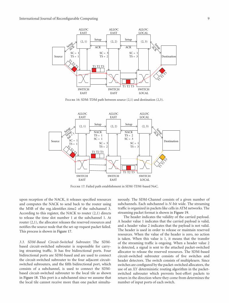
International Journal of Reconfigurable Computing 9
TS = 2 TS = 3TS = 1SC = 3SC = 1
DestinationSource
(2, 3 )(2, 1 ) (2, 2 )
ACK ACKACK
Setup
ACK
Setup
SetupSetup
SC = 1
T1 T2 T3
T1 T2 T3
T1 T2 T3 T1 T2 T3
ALLOCEAST LOCAL
ALLOCALLOCEAST
SWITCHEAST LOCAL
SWITCHEAST
SWITCH
Figure 16: SDM-TDM path between source (2,1) and destination (2,3).
TS = 2 TS = 3TS = 1 SC = 3SC = 1 DestinationSource
(2, 3 )(2, 1 ) (2, 2 )
ACK
Setup Setup
SetupSetup
SC = 1
T1 T2 T3
T1T2
T3
T1 T2 T3 T1 T2 T3
NACKNACKTS = 1SC = 1
TS = 2SC = 3fai
l = 1Setu
p
ALLOCEAST LOCAL
ALLOCALLOCEAST
SWITCHEAST LOCAL
SWITCHEAST
SWITCH
Figure 17: Failed path establishment in SDM-TDM-based NoC.
upon reception of the NACK, it releases specified resourcesand computes the NACK to send back to the router usingthe MSB of the reg identifier time2 of the subchannel 3.According to this register, the NACK to router (2,1) directsto release the time slot number 1 at the subchannel 1. Atrouter (2,1), the allocator releases the reserved resources andnotifies the source node that the set-up request packet failed.This process is shown in Figure 17.
3.3. SDM-Based Circuit-Switched Subrouter. The SDM-based circuit-switched subrouter is responsible for carry-ing streaming traffic. It has five bidirectional ports. Fourbidirectional ports are SDM-based and are used to connectthe circuit-switched subrouter to the four adjacent circuit-switched subrouters, and the fifth bidirectional port, whichconsists of a subchannel, is used to connect the SDM-based circuit-switched subrouter to the local tile as shownin Figure 18. This port is a subchannel since we assume thatthe local tile cannot receive more than one packet simulta-
neously. The SDM-Channel consists of a given number ofsubchannels. Each subchannel is N-bit wide. The streamingtraffic is organized in packets like cells in ATM networks. Thestreaming packet format is shown in Figure 19.
The header indicates the validity of the carried payload.A header value 1 indicates that the carried payload is valid,and a header value 2 indicates that the payload is not valid.The header is used in order to release or maintain reservedresources. When the value of the header is zero, no actionis taken. When this value is 1, it means that the transferof the streaming traffic is ongoing. When a header value 2is detected, a signal is sent to the attached packet-switchedallocator to release the reserved resources. The SDM-basedcircuit-switched subrouter consists of five switches andheader detectors. The switch consists of multiplexers. Sinceswitches are configured by the packet-switched allocators, theuse of an XY deterministic routing algorithm in the packet-switched subrouter which prevents best-effort packets toreturn in the direction where they come from determines thenumber of input ports of each switch.
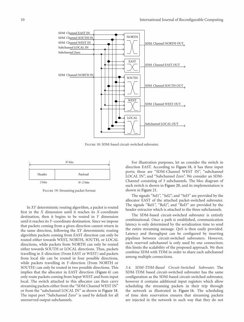
10 International Journal of Reconfigurable Computing
Subchannel LOCAL IN
Subchannel Zero
SDM Channel WEST IN
SDM Channel SOUTH IN
SDM Channel EAST IN
SDM Channel NORTH IN
Subchannel LOCAL OUT
SDM Channel WEST OUT
SDM Channel SOUTH OUT
SDM Channel EAST OUT
SDM Channel NORTH OUT
LOCAL
WEST
SOUTH
EAST
NORTH
Figure 18: SDM-based circuit-switched subrouter.
Header Payload
N bits
N-2 bits2 bits
Figure 19: Streaming packet format.
In XY deterministic routing algorithm, a packet is routedfirst in the X dimension until it reaches its X-coordinatedestination, then it begins to be routed in Y dimensionuntil it reaches its Y-coordinate destination. Since we imposethat packets coming from a given direction cannot return inthe same direction, following the XY deterministic routingalgorithm packets coming from EAST direction can only berouted either towards WEST, NORTH, SOUTH, or LOCALdirections, while packets from NORTH can only be routedeither towards SOUTH or LOCAL directions. Thus, packetstravelling in X-direction (From EAST or WEST) and packetsfrom local tile can be routed in four possible directions,while packets travelling in Y-direction (From NORTH orSOUTH) can only be routed in two possible directions. Thisimplies that the allocator in EAST direction (Figure 4) canonly route packets coming from Input WEST and from inputlocal. The switch attached to this allocator can then carrystreaming packets either from the “SDM Channel WEST IN”or from the “subchannel LOCAL IN” as shown in Figure 18.The input port “Subchannel Zero” is used by default for allunreserved output subchannels.
For illustration purposes, let us consider the switch indirection EAST. According to Figure 18, it has three inputports; these are “SDM-Channel WEST IN”, “subchannelLOCAL IN”, and “Subchannel Zero”. We consider an SDM-Channel consisting of 3 subchannels. The bloc diagram ofsuch switch is shown in Figure 20, and its implementation isshown in Figure 21.
The signals “Sel1”, “Sel2”, and “Sel3” are provided by theallocator EAST of the attached packet-switched subrouter.The signals “Rel1”, “Rel2”, and “Rel3” are provided by theheader extractor which is attached to the three subchannels.
The SDM-based circuit-switched subrouter is entirelycombinational. Once a path is established, communicationlatency is only determined by the serialization time to sendthe entire streaming message. QoS is then easily provided.Latency and throughput can be configured by insertingpipelines between circuit-switched subrouters. However,each reserved subchannel is only used by one connection;this limits the scalability of the proposed approach. We thencombine SDM with TDM in order to share each subchannelamong multiple connections.
3.4. SDM-TDM-Based Circuit-Switched Subrouter. TheSDM-TDM based circuit-switched subrouter has the sameconfiguration as the SDM-based circuit-switched subrouter,however it contains additional input registers which allowscheduling the streaming packets in their trip throughthe network as illustrated in Figure 16. The schedulingof time slots reservation ensures that streaming packetsare injected in the network in such way that they do not

International Journal of Reconfigurable Computing 11
Sel1 Sel2 Sel3
Subchannel LOCAL IN
SDM Channel WEST IN
SDM Channel EAST OUT
Rel1 Rel2 Rel3
SDM Channel Zero
Figure 20: Block diagram SDM switch EAST.
Subchannel LOCAL IN
SDM Channel WEST IN
SDM Channel EAST OUT
SDM Channel Zero
Sel1
Sel2
Sel3
Figure 21: SDM switch EAST implementation.
collide. Figure 22 shows the bloc diagram of the SDM-TDMcircuit-switched subrouter, and Figure 23 shows the blocdiagram of the switch in direction NORTH and the attachedpacket-switched allocator.
4. Results
4.1. Simulation Results. The proposed hybrid routers wereimplemented in SystemC RTL. 7 × 7 2D mesh NoCs werebuilt and simulated in SystemC under synthetic traffic. Weevaluate the performance of the NoCs in terms of numberof simultaneous established connections (paths) through thenetwork when all tiles in the network attempt to establish apath in the network. This worst case scenario leads to a highlevel of contention to occur in the network. The number ofestablished paths in the network reflects the capacity of thenetwork to face congestion. The fraction of set-up request
packets which reach their destination reflects the probabilityof establishing a path in the network. A higher probability ofestablishing paths implies a higher number of applications tobe run simultaneously in the network, thereby significantlyimproving the performances of the applications.
Three NoC platforms are compared; the SDM-basedhybrid NoC, the SDM-TDM-based hybrid NoC, and theTDM-based hybrid NoC. These platforms are evaluated withthe same traffic pattern in order to objectively compare themin terms of established paths according to the number of set-up request packets sent through the network. The destinationnodes are generated using a uniform distribution. Thesesimulations were performed with 4-packet deep FIFO bufferper input port for the packet-switched subrouter, while adifferent number of channels in an SDM-Channel, an SDM-TDM Channel, and TDM Channel are considered.
For the SDM-based NoC, the number of establishedpaths through the network for 3, 4, and 5 subchannels in
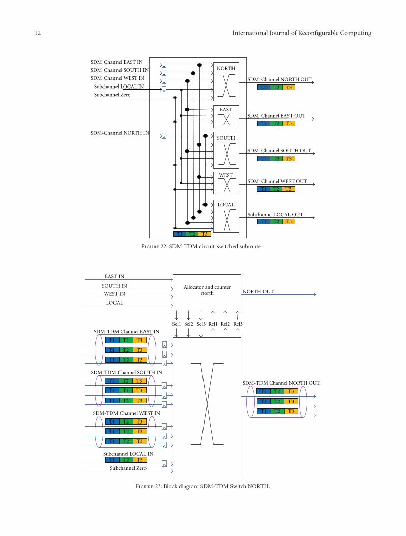
12 International Journal of Reconfigurable Computing
LOCAL IN
Zero
SDM Channel WEST IN
SDM Channel SOUTH IN
SDM Channel EAST IN
SDM-Channel NORTH IN
Subchannel LOCAL OUT
SDM Channel WEST OUT
SDM Channel SOUTH OUT
SDM Channel EAST OUT
SDM Channel NORTH OUT
LOCAL
WEST
SOUTH
EAST
NORTH
T1 T2 T3
T1 T2 T3
T1 T2 T3
T1 T2 T3
T1 T2 T3
T1 T2 T3
Subchannel
Subchannel
Figure 22: SDM-TDM circuit-switched subrouter.
Zero
LOCAL IN
SDM-TDM Channel EAST IN
SDM-TDM Channel NORTH OUT
LOCAL
WEST IN NORTH OUTAllocator and counter
SDM-TDM Channel SOUTH IN
SDM-TDM Channel WEST IN
SOUTH IN
EAST IN
T1 T2 T3
north
T1 T2 T3
T1 T2 T3
T1 T2 T3
T1 T2 T3
T1 T2 T3
T1 T2 T3
T1 T2 T3
T1 T2 T3
T1 T2 T3
T1 T2 T3
T1 T2 T3
T1 T2 T3
Sel1 Sel2 Sel3 Rel1 Rel2 Rel3
Subchannel
Subchannel
Figure 23: Block diagram SDM-TDM Switch NORTH.

International Journal of Reconfigurable Computing 13E
stab
lish
edco
nn
ecti
ons
Set up requests
490 980 1470 1960 2450 2940 3430 3920 4410 4900
3500
3000
2500
2000
1500
1000
500
0
3 subchannels4 subchannels5 subchannels
-
Figure 24: Established connections in 7× 7 SDM-NoC.
Est
ablis
hed
con
nec
tion
s
6000
5000
4000
3000
2000
1000
0
3 subchannels and 3 time slots3 subchannels and 4 time slots3 subchannels and 5 time slots
490 980 1470 1960 2450 2940 3430 3920 4410 4900
Set up requests-
Figure 25: Established connections in 7× 7 SDM-TDM NoC.
an SDM-Channel is given in Figure 24. For the SDM-TDM-based NoC, the number of established connections for 3subchannels and 3, 4, and 5 time slots is given in Figure 25.Figure 26 gives the number of established connections in anTDM-based NoC for 3, 4, and 5 time slots in a channel.
For the SDM-based NoC, simulation results show thatthe number of established connections increases with thenumber of subchannels in an SDM-Channel. For 3 sub-channels in an SDM-Channel, up to 46% of the set-uprequest packets sent in the network successfully reach theirdestination; for 4 and 5 subchannels in a SDM-Channel, upto 61% and 72% of set-up request packets sent in the networkreach their destination, respectively.
For the SDM-TDM-based NoC, considering only 3subchannels and 3, 4, and 5 time slots, Figure 25 shows thatup to 98% of set-up request packets sent in the networksuccessfully reach their destination in the three cases. Forthe TDM-based NoC, simulation results in Figure 26 showthat for 3, 4, and 5 time slots up to 17%, 22%, and27%, respectively, of the set-up request sent in the network
490 980 1470 1960 2450 2940 3430 3920 4410 4900
Est
ablis
hed
con
nec
tion
s
600
500
400
300
200
100
0
3 time slots4 time slots5 time slots
Set up requests-
Figure 26: Established connections in 7× 7 TDM NoC.
reach their destination. The poor performance of the TDM-based NoC related to the number of established paths isessentially due to the scheduling constraint on time slotreservation, which is a bottleneck for TDM-based NoC.Increasing the number of time slots does not efficientlysolve the problem while increasing the size of the router.Since there is no constraint on resource reservation inthe SDM-based NoC and by offering an increased pathdiversity, the SDM-based NoC has an appreciable probabilityof establishing connections through the network, howeversince each reserved resource is exclusively used by oneconnection until the end of the transaction, there is still apoor usage of subchannel, although overall the poor usageof resource is mitigated by the number of subchannels in theSDM-Channel. The SDM-TDM NoC solves this problem byallowing increased path diversity, while sharing subchannelsamong multiple connections, thereby performing the highestprobability of path establishment in the network.
The ability of the proposed hybrid routers to handle best-effort traffic is evaluated by means of the average latencyand average throughput according to the injection best-efforttraffic rate. To evaluate the average latency for the best-effort traffic, we consider that 25 tiles are injecting best-efforttraffic, while 24 tiles are transferring streaming traffic.
Figure 27 shows the average latency of the best-efforttraffic for the three hybrid NoCs. The TDM-based NoChas the smallest average latency compared to the SDM-and SDM-TDM-based NoCs. This is due to the fact thatthe TDM-based NoC has the smallest probability of pathestablishment; it in results a small number of establishedpaths, therefore a small number of ACK best-effort packets,thereby impacting weakly the total number of the best-effort packets in the network. Whereas the SDM-TDM-based NoC allows the highest number of established paths, itresults in a higher number of ACK best-effort packets, whichsignificantly impact the total number of best-effort packets inthe network, thereby increasing the average latency. However,the three hybrid routers begin to saturate beyond an injectiontraffic rate of 0.1.
The average time to establish paths through the SDM-based NoC is reported in Table 1. As noticed previously, we
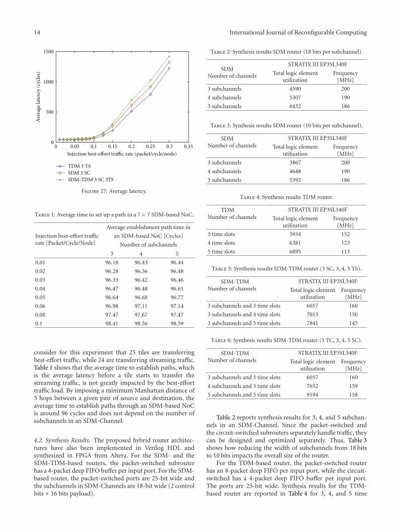
14 International Journal of Reconfigurable Computing
TDM 3 TSSDM 3 SCSDM-TDM 3 SC 3TS
1500
1000
500
00 0.05 0.1 0.15 0.2 0.25 0.3 0.35
Ave
rage
late
ncy
(cyc
les)
Injection best-effort traffic rate (packet/cycle/node)
Figure 27: Average latency.
Table 1: Average time to set up a path in a 7× 7 SDM-based NoC.
Injection best-effort trafficrate [Packet/Cycle/Node]
Average establishment path time in
an SDM-based NoC [Cycles]
Number of subchannels
3 4 5
0.01 96.18 96.43 96.44
0.02 96.28 96.36 96.48
0.03 96.33 96.42 96.46
0.04 96.47 96.48 96.61
0.05 96.64 96.68 96.77
0.06 96.98 97.11 97.14
0.08 97.47 97.67 97.47
0.1 98.41 98.56 98.59
consider for this experiment that 25 tiles are transferringbest-effort traffic, while 24 are transferring streaming traffic.Table 1 shows that the average time to establish paths, whichis the average latency before a tile starts to transfer thestreaming traffic, is not greatly impacted by the best-efforttraffic load. By imposing a minimum Manhattan distance of5 hops between a given pair of source and destination, theaverage time to establish paths through an SDM-based NoCis around 96 cycles and does not depend on the number ofsubchannels in an SDM-Channel.
4.2. Synthesis Results. The proposed hybrid router architec-tures have also been implemented in Verilog HDL andsynthesized in FPGA from Altera. For the SDM- and theSDM-TDM-based routers, the packet-switched subrouterhas a 4-packet deep FIFO buffer per input port. For the SDM-based router, the packet-switched ports are 25-bit wide andthe subchannels in SDM-Channels are 18-bit wide (2 controlbits + 16 bits payload).
Table 2: Synthesis results SDM router (18 bits per subchannel).
SDMNumber of channels
STRATIX III EP3SL340F
Total logic elementutilization
Frequency[MHz]
3 subchannels 4590 200
4 subchannels 5307 190
5 subchannels 6432 186
Table 3: Synthesis results SDM router (10 bits per subchannel).
SDMNumber of channels
STRATIX III EP3SL340F
Total logic elementutilization
Frequency[MHz]
3 subchannels 3867 200
4 subchannels 4648 190
5 subchannels 5392 186
Table 4: Synthesis results TDM router.
TDMNumber of channels
STRATIX III EP3SL340F
Total logic elementutilization
Frequency[MHz]
3 time slots 5934 152
4 time slots 6381 123
5 time slots 6895 113
Table 5: Synthesis results SDM-TDM router (3 SC, 3, 4, 5 TS).
SDM-TDMNumber of channels
STRATIX III EP3SL340F
Total logic elementutilization
Frequency[MHz]
3 subchannels and 3 time slots 6057 160
3 subchannels and 4 time slots 7013 150
3 subchannels and 5 time slots 7841 145
Table 6: Synthesis results SDM-TDM router (3 TC, 3, 4, 5 SC).
SDM-TDMNumber of channels
STRATIX III EP3SL340F
Total logic elementutilization
Frequency[MHz]
3 subchannels and 3 time slots 6057 160
4 subchannels and 3 time slots 7652 159
5 subchannels and 3 time slots 9194 158
Table 2 reports synthesis results for 3, 4, and 5 subchan-nels in an SDM-Channel. Since the packet-switched andthe circuit-switched subrouters separately handle traffic, theycan be designed and optimized separately. Thus, Table 3shows how reducing the width of subchannels from 18 bitsto 10 bits impacts the overall size of the router.
For the TDM-based router, the packet-switched routerhas an 8-packet deep FIFO per input port, while the circuit-switched has a 4-packet deep FIFO buffer per input port.The ports are 25-bit wide. Synthesis results for the TDM-based router are reported in Table 4 for 3, 4, and 5 time

International Journal of Reconfigurable Computing 15
Table 7: Synthesis results 4× 4 SDM-based NoC.
Number of channels 4× 4 SDM NoC
Subchannels Combinational Combinational with register Registers Total logic utilization Frequency
3 19564 29499 18696 67759/270400 (25%) 124 MHz
4 24953 33032 18978 76963/270400 (28%) 100 MHz
5 30001 36473 19036 85531/270400 (32%) 82 MHz
Table 8: Synthesis results 4× 4 SDM-TDM based NoC.
Number of channels 4× 4 SDM-TDM NoC
Subchannels Time Slots Combinational Combinational with register Registers Total logic utilization Frequency
3 3 24383 38134 22771 85288/270400 (32%) 85 MHz
4 3 32996 47811 22862 103669/270400 (38%) 78 MHz
5 3 37362 55222 22942 111526/270400 (43%) 70 MHz
slots, respectively. For the SDM-TDM-based router, synthesisresults are reported for a various number of subchannelsand time. Packet-switched ports are 28-bit wide, and thesubchannels are 18-bit wide. Synthesis results are reportedin Tables 5 and 6.
Results from Tables 2, 4, 5, and 6 show that for a givennumber of channels (subchannels and time slots) the SDM-based router has better performances in terms of maximumclock frequency and the total logic used in the FPGAcompared to the two other hybrid routers. This is due to itssimplicity, since the critical path is confined in the packet-switched subrouter, while the circuit-switched subrouter isentirely combinational. Increasing by one, the number of thesubchannels in an SDM-Channel results in the increase of16% in the router size, while the clock frequency is slightlyreduced.
Furthermore, results from Table 2 show the impact ofreducing the width of the subchannels from 18 bits to 10 bitson the size of the router, while the clock frequency is notimpacted. Thus, optimization for a high clock frequency con-cerns only the packet-switched subrouter, while optimizationof the size of the router concerns essentially the circuit-switched subrouter.
For the TDM-based hybrid router, Table 4 shows that ithas the smallest clock frequency compared to the two otherhybrid routers; this is essentially due to the fact that channelsare shared between the two subrouters and the use of buffersin both subrouters, which increases the complexity of therouter, thereby lengthening the critical path and increasingthe size of the router. Increasing by one, the number of timeslots leads to an increase of 7% in the router size, while theclock frequency is significantly reduced.
However, the size of the TDM-based router grows slowerthan the sizes of the SDM- and SDM-TDM-based routerswhen increasing the number of the channels by one. Itmeans that, compared to the SDM-based router, there isa subchannels number threshold from which the size ofthe SDM-based router becomes greater than the size of theTDM-based router.
For the SDM-TDM based subrouter, it has the highestoverhead in the total logic used in the FPGA; this is the
cost of combining the two techniques in a single router.However, it offers appreciable clock frequencies comparedto the TDM-based router, since the packet-switched and thecircuit-switched subrouters do not share the same channelsand independently handle traffic. Furthermore, the circuit-switched subrouter has just simple registers instead of FIFObuffers. This eases the control of the critical path in thedesign of the router. Optimization can be done separately inorder to either reduce the size or increase the clock frequencyof the router. The SDM-TDM approach gives more flexibilitysince it allows optimization in either space or time. Table 5shows that keeping the number of subchannel fixed whileincreasing the number of the time slots implies an increaseby 16% in the size of the router, whereas results from Table 6show that maintaining constant the number of time slotswhile increasing the number of the subchannels leads to anincrease of 20% in the size of the router, while the clockfrequency remains practically constant.
Thus, there is a tradeoff between an optimal number ofsubchannels and the number of time slots according to theconstraint on the clock frequency and the area of the router.
The proposed hybrid routers were used to build complete4 × 4 2D mesh NoC on the Stratix III EP3SL340F FPGAdevice. Synthesis results for the SDM-based NoC, SDM-TDM-based NoC, and TDM-based NoC are shown in Tables7, 8, and 9, respectively. These results show the impact of theinterconnecting links on the frequency and area.
The impact of the interconnecting links on the frequencyand the area of the TDM-based NoC is small compared to theSDM- and SDM-TDM-based NoCs. This is essentially dueto the fact that links in the TDM-based router are sharedbetween the best-effort and the streaming traffic, therebyreducing the link overhead between routers. However, TheSDM-based NoC and the SDM-TDM based NoC, althoughthe interconnecting link overhead, take advantages of theabundance of wires resulting from the high-level integrationof CMOS circuits. The impact of interconnecting link canbe mitigated by reducing the width of subchannels as shownin Tables 2 and 3, thereby reducing the area of the completeNoC.
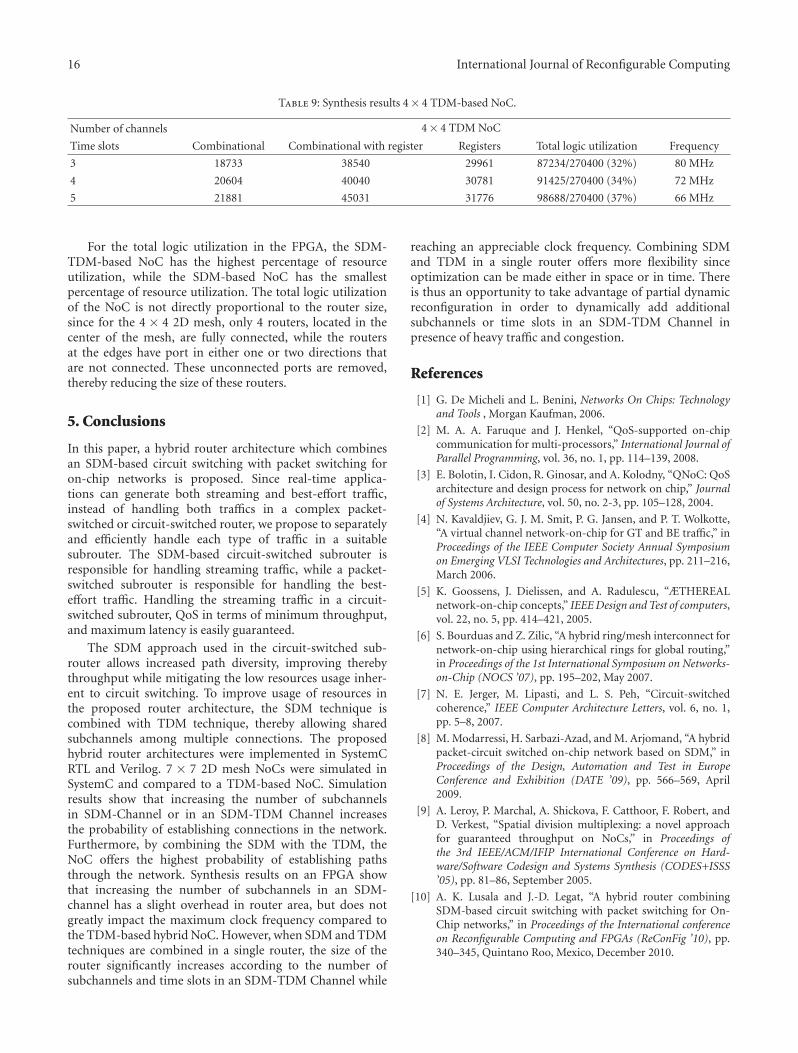
16 International Journal of Reconfigurable Computing
Table 9: Synthesis results 4× 4 TDM-based NoC.
Number of channels 4× 4 TDM NoC
Time slots Combinational Combinational with register Registers Total logic utilization Frequency
3 18733 38540 29961 87234/270400 (32%) 80 MHz
4 20604 40040 30781 91425/270400 (34%) 72 MHz
5 21881 45031 31776 98688/270400 (37%) 66 MHz
For the total logic utilization in the FPGA, the SDM-TDM-based NoC has the highest percentage of resourceutilization, while the SDM-based NoC has the smallestpercentage of resource utilization. The total logic utilizationof the NoC is not directly proportional to the router size,since for the 4 × 4 2D mesh, only 4 routers, located in thecenter of the mesh, are fully connected, while the routersat the edges have port in either one or two directions thatare not connected. These unconnected ports are removed,thereby reducing the size of these routers.
5. Conclusions
In this paper, a hybrid router architecture which combinesan SDM-based circuit switching with packet switching foron-chip networks is proposed. Since real-time applica-tions can generate both streaming and best-effort traffic,instead of handling both traffics in a complex packet-switched or circuit-switched router, we propose to separatelyand efficiently handle each type of traffic in a suitablesubrouter. The SDM-based circuit-switched subrouter isresponsible for handling streaming traffic, while a packet-switched subrouter is responsible for handling the best-effort traffic. Handling the streaming traffic in a circuit-switched subrouter, QoS in terms of minimum throughput,and maximum latency is easily guaranteed.
The SDM approach used in the circuit-switched sub-router allows increased path diversity, improving therebythroughput while mitigating the low resources usage inher-ent to circuit switching. To improve usage of resources inthe proposed router architecture, the SDM technique iscombined with TDM technique, thereby allowing sharedsubchannels among multiple connections. The proposedhybrid router architectures were implemented in SystemCRTL and Verilog. 7 × 7 2D mesh NoCs were simulated inSystemC and compared to a TDM-based NoC. Simulationresults show that increasing the number of subchannelsin SDM-Channel or in an SDM-TDM Channel increasesthe probability of establishing connections in the network.Furthermore, by combining the SDM with the TDM, theNoC offers the highest probability of establishing pathsthrough the network. Synthesis results on an FPGA showthat increasing the number of subchannels in an SDM-channel has a slight overhead in router area, but does notgreatly impact the maximum clock frequency compared tothe TDM-based hybrid NoC. However, when SDM and TDMtechniques are combined in a single router, the size of therouter significantly increases according to the number ofsubchannels and time slots in an SDM-TDM Channel while
reaching an appreciable clock frequency. Combining SDMand TDM in a single router offers more flexibility sinceoptimization can be made either in space or in time. Thereis thus an opportunity to take advantage of partial dynamicreconfiguration in order to dynamically add additionalsubchannels or time slots in an SDM-TDM Channel inpresence of heavy traffic and congestion.
References
[1] G. De Micheli and L. Benini, Networks On Chips: Technologyand Tools , Morgan Kaufman, 2006.
[2] M. A. A. Faruque and J. Henkel, “QoS-supported on-chipcommunication for multi-processors,” International Journal ofParallel Programming, vol. 36, no. 1, pp. 114–139, 2008.
[3] E. Bolotin, I. Cidon, R. Ginosar, and A. Kolodny, “QNoC: QoSarchitecture and design process for network on chip,” Journalof Systems Architecture, vol. 50, no. 2-3, pp. 105–128, 2004.
[4] N. Kavaldjiev, G. J. M. Smit, P. G. Jansen, and P. T. Wolkotte,“A virtual channel network-on-chip for GT and BE traffic,” inProceedings of the IEEE Computer Society Annual Symposiumon Emerging VLSI Technologies and Architectures, pp. 211–216,March 2006.
[5] K. Goossens, J. Dielissen, and A. Radulescu, “ÆTHEREALnetwork-on-chip concepts,” IEEE Design and Test of computers,vol. 22, no. 5, pp. 414–421, 2005.
[6] S. Bourduas and Z. Zilic, “A hybrid ring/mesh interconnect fornetwork-on-chip using hierarchical rings for global routing,”in Proceedings of the 1st International Symposium on Networks-on-Chip (NOCS ’07), pp. 195–202, May 2007.
[7] N. E. Jerger, M. Lipasti, and L. S. Peh, “Circuit-switchedcoherence,” IEEE Computer Architecture Letters, vol. 6, no. 1,pp. 5–8, 2007.
[8] M. Modarressi, H. Sarbazi-Azad, and M. Arjomand, “A hybridpacket-circuit switched on-chip network based on SDM,” inProceedings of the Design, Automation and Test in EuropeConference and Exhibition (DATE ’09), pp. 566–569, April2009.
[9] A. Leroy, P. Marchal, A. Shickova, F. Catthoor, F. Robert, andD. Verkest, “Spatial division multiplexing: a novel approachfor guaranteed throughput on NoCs,” in Proceedings ofthe 3rd IEEE/ACM/IFIP International Conference on Hard-ware/Software Codesign and Systems Synthesis (CODES+ISSS’05), pp. 81–86, September 2005.
[10] A. K. Lusala and J.-D. Legat, “A hybrid router combiningSDM-based circuit switching with packet switching for On-Chip networks,” in Proceedings of the International conferenceon Reconfigurable Computing and FPGAs (ReConFig ’10), pp.340–345, Quintano Roo, Mexico, December 2010.

Hindawi Publishing CorporationInternational Journal of Reconfigurable ComputingVolume 2012, Article ID 850487, 11 pagesdoi:10.1155/2012/850487
Research Article
A Fault Injection Analysis of Linux Operating onan FPGA-Embedded Platform
Joshua S. Monson, Mike Wirthlin, and Brad Hutchings
Department of Electrical and Computer Engineering, Brigham Young University, 459 Clyde Building, Provo, UT 84602, USA
Correspondence should be addressed to Joshua S. Monson, [email protected]
Received 1 May 2011; Revised 28 July 2011; Accepted 1 September 2011
Academic Editor: Claudia Feregrino
Copyright © 2012 Joshua S. Monson et al. This is an open access article distributed under the Creative Commons AttributionLicense, which permits unrestricted use, distribution, and reproduction in any medium, provided the original work is properlycited.
An FPGA-based Linux test-bed was constructed for the purpose of measuring its sensitivity to single-event upsets. The test-bedconsists of two ML410 Xilinx development boards connected using a 124-pin custom connector board. The Design Under Test(DUT) consists of the “hard core” PowerPC, running the Linux OS and several peripherals implemented in “soft” (programmable)logic. Faults were injected via the Internal Configuration Access Port (ICAP). The experiments performed here demonstrate thatthe Linux-based system was sensitive to 199,584 or about 1.4 percent of all tested bits. Each sensitive bit in the bit-stream ismapped to the resource and user-module to which it configures. A density metric for comparing the reliability of modules withinthe system is presented. Using this density metric, we found that the most sensitive user module in the design was the PowerPC’sdirect connections to the DDR2 memory controller.
1. Introduction
Over the last decade, Linux Operating Systems (OSs) havebeen used on several space-based computing platforms.NASA, for example, sponsored the FlightLinux project whichculminated by demonstrating a reliable Linux OS on theUoSat12 satellite [1]. The use of Linux on the UoSat12 pro-vided enough compatibility with ground systems to allow thesatellite to be accessible over the Internet. Compatibility withground systems is only one of the many reasons to use Linuxon space-based computing platforms.
Reliable hardware is essential for Linux to operate; how-ever, integrated circuits (ICs) aboard space-based computingplatforms are susceptible to failures known as Single-EventUpsets (SEUs). SEUs are random bit flips caused by high-energy particles that collide with the ICs. To ensure correctoperation in the presence of radiation, ICs can be speciallydesigned or “hardened.” Unfortunately, radiation-hardenedICs are expensive and usually two or three silicon generationsbehind the state of the art [2]. These factors limit the useof radiation-hardened parts in space-based computing andleave engineers looking for alternatives.
Field Programmable Gate Arrays (FPGAs) are among thestate-of-the-art components that are of interest in space-based computing. FPGAs are microchips that contain anarray of logic and interconnect that can be programmedand reprogrammed to perform almost any digital function.FPGAs often replace application-specific integrated circuits(ASICs) in space-based computing because designing forFPGAs is faster and less expensive than designing for ASICs.Additionally, reprogrammability allows designers to remo-tely fix bugs that appear after the platform has launched.These features make FPGAs ideal for space-based platforms[3–5].
The function performed by reprogrammable FPGAs isdefined by the values of memory cells on the device knownas the bit-stream. Changing the values of the bits in the bitstream may modify the behavior of a logic circuit on anFPGA (until it is reconfigured). For example, a single changein the bit stream has the potential to change the contents of aLook-Up Table (LUT), connect nets together, or completelydisconnect a net. In most ICs, SEUs will only corrupt data.In FPGAs, however, SEUs are able to affect data and the logicfunction performed.
2 International Journal of Reconfigurable Computing
To prevent SEUs from affecting the output of an FPGAdesign, mitigation techniques are used. Common methodsof mitigating and detecting the effects of SEUs are bit-streamscrubbing [6], Triple Modular Redundancy [7] (TMR),Partial TMR (PTMR) [8], and duplicate with compare(DWC) [9]. TMR uses redundant circuits and majorityvoters to improve the reliability of FPGA designs. PTMR is areduced form of TMR that has been shown (on small circuits,at least) to reduce area overhead with only a small reductionin reliability. In bit-stream scrubbing, the bit-stream of theFPGA is occasionally rewritten to prevent the accumulationof SEUs. DWC is a method of detecting SEUs by creatinga copy of the circuit, comparing the results, and flaggingdifferences when they occur.
In FPGA-Embedded Linux systems using “hard core”processors, important peripherals (such as the memorycontroller) are implemented in the reconfigurable fabric ofthe FPGA and are susceptible to SEUs. SEU-induced failuresin these components have the potential of crashing thekernel. Understanding each peripheral’s likelihood of causinga kernel failure due to an SEU aids in understanding thereliability of the system and in creating a more reliable systemat the lowest cost. To gain this understanding, we constructeda test-bed that allows us to simulate SEUs in the FPGA fabricsurrounding a “hard core” embedded processor running aLinux kernel using a process known as fault injection [10].Preliminary results, along with a fault injection analysis,from this test-bed have been previously reported [11]. Inthis paper, we present new results from a fault injectiontest using the same design under test. For this new test, wehave improved both our fault injection process and analysis.These changes have resulted in a 3X improvement in detectedsensitive bits and a decrease (from 8% to less than 1%) insensitive bits that could not be mapped to part of the design.
2. Previous Work
The development of fast, comprehensive fault injectionsystems has been the focus of much of the previous work [12–14]. These fault injection systems are able to emulate upsetsin FPGA fabric and microprocessor cache lines and specialregisters. Rather than performing exhaustive tests, these faultinjection systems use a probabilistic model to statisticallydetermine the reliability of a design.
The work presented by Sterpone and Violante [15]performed fault injection experiments on the memory imageof a Linux microkernel running on a Xilinx Microblaze proc-essor implemented in soft-logic. Their work focused onmemory faults during the bootstrapping process but did notexamine the sensitivity of the circuitry/logic that implementstheir system. Essentially, their fault-injection process mod-ified the content of the memories that contain the Linuxprogram. In contrast, our effort injects faults directly intothe hardware implementation and analyzes the sensitivity ofa full Linux kernel system (rather than a micro kernel) tocircuit and logic failures that may be caused by SEUs.
In another work by Johnson et al. [16], they describe thevalidation of a fault injection simulator using a proton accel-
erator. Their analysis used the bit-stream offsets of sensitivebits to compute the row and column locations of the sensitivebits. Doing this allowed them to create a “map” of the FPGAshowing the locations of sensitive bits. Their fault injectionsimulator was able to predict the locations of an impressive97% of the upsets caused by the proton accelerator.
In this work, we also endeavor to improve the verificationof fault injection experiments. For our fault injection exper-iment, we studied the bit-stream to determine the relation-ships between configuration bits and FPGA resources; thisallowed us to take the next logical step and map sensitive bitsto FPGA resources and, further, map resources to user-designmodules.
Sterpone and Violante also used knowledge of the con-figuration bit-stream, but rather than examining what hap-pened (as we do) they tried to predict where faults wouldoccur. In [17, 18], they present a reliability analysis toolthat would perform a static analysis to predict locations ofsensitive bits then they would perform fault injection basedon their predictions. They found that their static analyzercould predict the locations of all the sensitive configurationbits in a design mitigated using TMR without being overlypessimistic. They also found that their partial fault injectionresults matched that of an exhaustive fault injection test.
The similarity between our work and their work isthe reliance on architectural and configuration bit-streamknowledge to identify where the problems might occur. A keydifference is that their work focused on verifying relativelysmall systems mitigated by TMR, while our work focuses onthe reliability analysis of large, unmitigated FPGA designs. Itis likely that their techniques could be used to analyze thisLinux system but unfortunately, their system is not availableto us and direct comparisons between the two approachescannot be made.
3. System Architecture
The process of fault injection requires a development boardwith the ability to feed test vectors into a design under test,monitor the important outputs, and modify the configura-tion memory of the design. The ideal development board toperform these functions would contain three FPGAs, one toact as the golden, one to act as the device under test, andone to act as the experiment controller. Should the output ofthe golden be known or simple, a two-FPGA solution wouldbe sufficient. These FPGAs should be connected such thatthe experiment controller is able to access the configurationmemory of the device under test and send (receive) input(output) vectors from both the golden and design under test.Unfortunately, there are very few boards that provide therequired connectivity. This is the primary reason we havedeveloped our own fault injection platform.
Our two-FPGA fault injection system consists of a Linux-based host PC, two Xilinx ML410 development boards,and a 124-pin custom connector board. In our system, oneML410 acts as the experiment controller and golden and theother acts as the Device Under Test (DUT). The connectorboard provides enough connectivity for the controller to

International Journal of Reconfigurable Computing 3
Host
Controller Device under test
PPC
ICAPcore
Customconnector
board
ICAP
Design undertest
PLB
GPIOcore
GPIOcoreEthernet
Figure 1: A block diagram of our fault injection system.
Configureand boot
kernel
Injectfault
Wait(10 ms)
Test ICAPand DUT
Test ICAPand DUTfault
Repair Wait(5 ms)
P
P
FF
Figure 2: Flowchart of the fault injection routine.
send (receive) input (output) vectors from the DUT andalso provides enough pins to fully connect the experimentcontroller to the Internal Configuration Access Port (ICAP)of the DUT. The ICAP is a module that resides inside theFPGA fabric and provides connections that allow compo-nents inside the FPGA to read and write the configurationmemory.
As shown in Figure 1, the Linux-based host provides asimplified interface to the fault injection platform over anEthernet connection. This allows the host to maintain anNFS mounted file system that provides a simple means fortransferring software, test vectors, and results to and from theexperiment controller. This connection allows experimentsoftware to be developed on the host and then cross-compiled and transferred to the PowerPC 405. The RS-232serial port acts as the console for the Linux kernel.
All DUT test designs communicate directly with theexperiment controller via routing (contained in the DUT testdesign) that connects the DUT’s ICAP to the custom connec-tor board. The experiment controller injects faults throughthis 400 MB/sec connection. In cases where an injected faultcauses the DUT’s ICAP interface to fail, the controller cancompletely reconfigure the DUT using the external con-figuration interface. The control and communication cir-cuitry for the ICAP is implemented on the experimentcontroller board to maximize available circuitry in the DUT.The ICAP interface on the experimental-controller board iscontrolled and configured by software and supports a widevariety of experiments.
4. Description of Fault Injection Experiment
The goal of this fault injection experiment is to measurethe sensitivity of an FPGA-based Linux system to upsetsin the configuration memory. In this FPGA-embedded sys-tem, all inputs and outputs of the processor must travelthrough the FPGA fabric. For example, the clock, memoryinterface, STDIN and STDOUT, general purpose I/O, and
reset circuitry are implemented in the FPGA fabric. Thus theprocessor is unable to operate independently of the FPGAfabric, and faults injected into these components may causethe processor or Linux kernel to fail.
In general, fault injection tests are performed by modify-ing the configuration memory of the FPGA and then testingor observing the design to determine if the modificationhas caused a failure. The configuration memory is modifiedby reading a frame (the smallest addressable portion ofconfiguration memory), changing a bit within the frame, andwriting the frame back into the device. If the modified con-figuration memory causes the DUT to fail, the bit isconsidered “sensitive”, otherwise the bit is considered “notsensitive.”
In this test, each configuration bit is upset for over 106
FPGA clock cycles. However, it is not possible to test eachbit in all possible states of the processor, I/O, and operatingsystem. It is possible that some configuration bits tested dur-ing fault injection may be tagged as nonsensitive but are infact sensitive under certain system conditions. While we rec-ognize that some sensitive configuration bits may be taggedas nonsensitive, this form of fault injection provides a goodestimate of the “average” sensitivity behavior of the systemunder test. Previous results from similar fault injectionexperiments show that the vast majority of sensitive bits areeasily detected (i.e., they have a high probability of detection)and the average sensitivity of a design is adequately repre-sented in fault injection experiments [16].
This fault injection procedure is carried out by thecontroller as illustrated in Figure 2. Before starting the firsttest, the controller reconfigures the DUT and waits for theLinux kernel to boot and the test program to start. After theDUT has booted, the controller injects a single fault into theconfiguration memory of the DUT. After 10 ms, the DUTis tested five times over an interval of 1 ms before the faultis classified. If the DUT fails to respond to any of the tests,the bit is classified as sensitive and the DUT is reconfiguredand rebooted. On the other hand, if the DUT successfullyresponds to all five tests, the bit is classified as not sensitive.

4 International Journal of Reconfigurable Computing
Table 1: Time breakout of a nonsensitive bit test.
Configure FPGA 4 secBoot Linux Kernel 16 secInject fault .226 ms10 ms wait 12.5 msTest ICAP .105 msTest DUT 17.9 msRepair fault .120 ms5 ms wait 8.9 msTest ICAP .104 msTest DUT 17.9 msAvg. test time (non-sensitive bit) 59.7 ms
To prevent the accumulation of faults, the hardware andsoftware must be returned to a correct state before beginningthe next test. This can be done by performing a full FPGAreconfiguration, recopying the original Linux image intomemory and rebooting the kernel. While this is the idealapproach, the process of reconfiguring, copying the Linuxmemory image, and booting the kernel takes 20 seconds.Since 98% of the more than 13 million configuration bitstested are not sensitive, rebooting the DUT after each bitwould cause the test to be prohibitively long. The alternativeto rebooting the DUT is to repair the fault and move onto thenext test. This approach does not guarantee that the systemstate is error free and in fact it may be possible for the repairof a fault to induce an error. To ensure that the system isat least working correctly, we subject the DUT and ICAP toanother set of tests after a 5 ms wait period. If a fault is found,it is attributed to the bit most recently tested and the entireDUT is rebooted.
Sensitive configuration bits are detected in the DUTusing a simple two-phase hand shaking protocol over thegeneral purpose I/O connections (GPIO) provided by thecustom connector board. The controller initiates a test ofthe DUT by inverting its GPIO bit. The DUT respondssuccessfully to the test by inverting its GPIO bit to matchthe controller’s GPIO bit. The DUT implements this protocolwith a small test program that runs in the background of theLinux kernel. The pseudo-code for this test program is shownin Listing 1. The test program accesses the GPIO moduleto see if the controller inverted its bit; if the controller hasinverted its bit, the test program responds by inverting theDUT’s GPIO bit to match. At the end of each iteration, thetest program is supposed to sleep for 200 μs and wake upand repeat the process; however, time measurements of thetest program reveal that the program really sleeps for close to4 ms. Using the top program, we found that the Linux kernelspends 99% of its time in the idle state and 1% of its time foruser and system processes.
Table 1 shows the average time for each phase of thetest of a single non-sensitive bit. The total testing time ofa non-sensitive bit is almost 60 ms with the majority of thetime occupied receiving 5 test responses from the DUT. Notethat the wait times are slightly longer than initially intendedbecause of the use of the usleep() function.
dut test program ( )
{int dut gpio = 0;
int controller gpio;
init gpio ( );
while ( 1 ){
controller gpio = read gpio ( );
if( gpio value != dut gpio)
{dut gpio = controller gpio;
set gpio (dut gpio);
}usleep (200);
}close gpio ( );
}
Listing 1: Pseudo-code of DUT test program.
To convince ourselves that the 5 and 10 ms wait timesimposed after faults were injected were sufficient to detectthe vast majority faults, we performed additional tests withlonger wait times. A subset of the configuration memory (4different configuration blocks) was tested with an additional15 ms (2X) and 30 ms (3X) of wait time. Table 2 summarizesthe number of sensitive configuration bits found in eachtest. As Table 2 shows, increasing the length of the test didnot significantly increase the number of sensitive bits found.Additionally, we found 97.8% percent of the sensitive bitswere identical for all three tests which suggests that the 10 mswait time is adequate.
Although fault injection is a proven and effective way toemulate SEUs, there are a few FPGA components that faultinjection cannot test. For example, reading and writing theblock rams (BRAMs) via the ICAP may cause side effectsthat artificially increase the bit-sensitivity count. Some LUTsin the Virtex 4 architecture contain additional circuitry thatallows them to be used as 16-bit shift registers (SRL16s)or distributed RAM memories (LUT RAMS). The dynamicmemory elements of SRL16s and LUT RAMs are part of theconfiguration memory and can be corrupted during readsand writes. To prevent this, Xilinx has included the GLUT-MASK as a configuration option in the Virtex 4 architecture.When set, the GLUTMASK prevents both configurationmemory reads and writes from modifying the contents ofSRL16s and LUT RAMs. IOB (input/output buffer) con-figuration blocks should also be avoided; these bits controlFPGA I/0 pins and arbitrarily flipping these bits may causeboard or device damage. All of these situations were takeninto account during the design of our experiment.
5. Sensitive Bit Density Metric
When designing for FPGAs, the goal is often to squeeze asmuch performance out of the device as possible. Reliability
International Journal of Reconfigurable Computing 5
Table 2: Number of sensitive configuration bits detected in originaland 2X and 3X wait time tests.
Block Original test 2X wait times 3X wait times
1 495 494 494
2 478 456 462
3 494 494 494
4 577 579 569
requirements often make this goal difficult to achieve becauseof the area overheads of mitigation techniques such as TMR.
A way to reduce the area cost of reliability is to use lessermitigation techniques such as PTMR or DWC. While the areacosts of these methods are lower they may have other costssuch as lower performance or reliability. In some systems,costs may also be reduced by applying different mitigationtechniques to different modules in the design. How shouldan engineer decide which mitigation techniques should beapplied to each module to make the most efficient use of theFPGA?
One method would be to perform a fault injection testand determine which modules contain the most sensitivebits and apply more aggressive mitigation techniques to themodules that contain the most sensitive bits.
While this method is simple and straightforward it maynot lead to the most efficient use of area. For example,consider a fault injection test of a design containing a largemodule that is moderately resilient to injected faults and asmall module that is unable to tolerate a single fault at anytime. After the test, it may be found that the large module,because of its size, contained more sensitive configurationbits than the small module. However, because the largemodule masks a portion of its sensitive bits while the smallmodule does not, redundancy techniques would be moreefficiently applied to the small module even though it hasfewer sensitive bits. By using more redundancy techniqueson the smaller module, more sensitive bits will be mitigatedper unit area than using the same mitigation technique onthe larger module.
5.1. A New Metric. To deal with this issue, we present ametric that takes into account both the number of sensitivebits and size of the module. This metric is called the sensitivebit density metric. This metric was first introduced by usin [11] and was measured in sensitive bits per unmitigatedresource. The resources considered were nets and instances.Unfortunately, nets can vary in length while instancescan vary in configuration, thus using nets and instancesobscures the size of the sensitive cross-section of configu-ration bits. In this paper, we have improved the accuracyof the sensitive bit density metric by measuring it in sensitivebits per configuration bit. This directly links the metric tothe sensitive cross section of the design. Modules with ahigher sensitive bit density metric will be more efficientlymitigated by redundancy techniques than modules withlower sensitivity bit metrics.
To calculate the sensitive bit density metric, we mustknow the number of sensitive configuration bits and the bit-area of each module in the design. Fault injection is usedto estimate the number of sensitive configuration bits ofeach module in the design. Ideally, the bit-area of the eachmodule is calculated by adding up the configuration bits thatmust have a specific value for the design to work properly.To make our estimate of design bit-area for modules in ourLinux system, we have added up all the bits in used routingresources and the bits required to set components of slicesthat are explicitly used.
One might ask, why do not all of the bits actuallydemonstrate sensitivity during a test? It is because sensitivityis a dynamic phenomenon that depends, to some extent, onsystem behavior. In our Linux system, there are three issuesthat reduce the number of detections of sensitive bits:masking, hiding, and kernel resiliency.
5.2. Masking, Hiding, and Kernel Resiliency. Masking occurswhen the current operating mode of the circuit does notallow the invalid signal to propagate and cause a systemfailure. A well-known form of masking is TMR. In TMR,majority voters mask the effects sensitive bits that residein one of the three redundant copies of the circuit. In oursystem, many modules are addressed over the processor localbus (PLB). If these components are not used by the processor,they cannot cause a failure in the Linux kernel and are thusmasked from causing a failure.
Hiding occurs when the SEU causes the value of theaffected signal to be correct during the fault injection test. Forexample, consider a circuit with a low asserted reset signaland assume that the reset is asserted infrequently. Suppose anSEU strikes a portion of the routing causing an open whichresults in a “stuck at” 1 fault. This circuit will continue tooperate correctly until a reset is required. During the time thecircuit is operating correctly, we would say that this sensitivebit was hidden.
The kernel is said to be resilient to faults that are prop-agated into the processor but that do not cause a kernelfailure. In our opinion this is most likely to occur when a faultappears in a data or instruction word before it is consumedby the processor. A data word may not effect the operation ofthe kernel at all, while a fault could appear in an unused fieldof an instruction word.
6. Analysis of Results
Our results will be presented using three different analyses.The general overview analyzes the overall number of sensitivebits and describes the reliability of our unmitigated LinuxSystem. In the FPGA resource analysis, the sensitive bitsanalyzed in the general overview are mapped to the resourcesthey control. In the user circuit analysis, the sensitiveresources are mapped to the modules that contain them(memory controller, UART, etc.) and a metric for comparingthe sensitivity of modules is explained.
These three analyses are interesting because they providea designer with data that answers questions such as what is

6 International Journal of Reconfigurable Computing
Table 3: Device logic utilization.
Resource Used Available Utilization
Slice registers 6,271 50,560 12%
4-input LUT 5,688 50,560 11%
Block RAMs 53 232 23%
SRL16 shift registers 281 50,560 .5%
LUT RAMs 0 50,560 0%
the general sensitivity of the DUT? What resources containthe most sensitive configuration bits? Which modules in theDUT are most sensitive to SEUs? Answers to these questionscould aid in the directed application of mitigation techniquesand possibly save design area or suggest FPGA architectureimprovements.
In addition, these analyses allow those performing faultinject experiments to verify their results by confirming thatsensitive bits actually have the ability to effect the design.This is done by mapping sensitive bits to actual resources inthe FPGA and verifying that they belong to or can affect acomponent in the DUT.
Our analysis relied heavily upon the open source toolRapidSmith [19] developed at Brigham Young University.RapidSmith is a Java API that is able to both parse Xilinxdesign files and interface with part databases. In this project,RapidSmith was one of the key components that allowed usto do sensitivity analysis in both the logic and interconnectportion of the design.
6.1. General Overview Analysis. This subsection provides thereader with a general idea of the vulnerable cross section ofour design. Specifically, it presents the design utilization, thebits in the bit-stream that were and were not tested, and thenumber of sensitive configuration bits found in the design.
Table 3 shows the device utilization of the DUT. While23% of the BRAMs are instantiated less than half of themare actually used by the Linux kernel, making their effectiveutilization about 10%. The BRAMs not used by the Linuxkernel are inserted by Xilinx’s Embedded Development Kit(EDK) and are used to boot the PowerPC. Overall, the deviceutilization is between 10% and 12%.
Table 4 gives a summary of the bits that were and werenot tested. The majority of these bits were BRAM and SRL16bits. The number of sensitive configuration bits contributedby these resources was estimated as discussed in the nextparagraph. We did not attempt to estimate the number ofsensitive-masked bits or the IOB bits.
Table 5 presents the number of sensitive configurationbits found in the DUT and ICAP circuitry. The SRL16 bitswere estimated by assuming that all content bits in theshift register would be sensitive. The same assumption wasmade for all BRAMs used by the Linux kernel (some wereinstantiated by EDK but not used by the kernel). The IOBbits were not tested, and no attempt was made to estimatethe effect of their sensitivity on the device.
The Mean Time Between Failure (MTBF) is a commonparameter used in reliability analysis. The equation for
Table 4: Summary of bits tested/not tested.
Bits tested 13,757,308 66%
Bits not tested 7,140,228 34%
Mask file bits (nottested)
821,636 4%
IOB bits (not tested) 944,640 4%
BRAM content (nottested)
5,373,952 25%
Total bits 20,960,512 100%
Table 5: Summary of sensitive bits.
Sensitive bits SRL16 bitsBRAMcontent
Total
DUT 119,110 4,496 58,880 182,486
ICAP 1,329 0 0 1,329
estimating the MTBF is presented in (1). The calculationrequires that we know the configuration bit upset rate, λbit,and the number of sensitive configuration bits in the design,Nbits.
The configuration bit upset rate is λbit = 2.78 ×10⁻⁷ upsets per day [20]. This failure rate is the same forcommercial- and radiation-tolerant Virtex 4 devices. Thedifference between the commercial- and radiation-tolerantdevices is the use of a thin epitaxial layer to remove single-event latch-up (SEL) and to significantly increase the totalionizing dose (TID) of the device.
Nbits is the number of sensitive configuration bits foundin the design. To estimate this value, we use the numberof sensitive configuration bits we found during our faultinjection experiment, 119,110. Additionally, upsets in BRAMand SRL16 content will also cause failures in the DUT.Since these components were not tested we estimate themby assuming that all bits in these elements are sensitive.We choose this approach because it provides a slightlypessimistic lower bound on the MTBF. The actual measuredfaults plus the estimated BRAM and SRL16 content bitsbrings Nbits to 182,486.
Kernel failures can also be caused by upsets in theprocessor. Since our focus was on faults in the reconfigurablefabric, we did not perform any fault injection into theprocessor. Additionally, we do not know the number ofstate elements within the processor so we cannot form apessimistic guess. Thus, our MTBF only indicates the averagetime between failures caused by the reconfigurable fabric.Using these numbers for λbit andNbits, we calculate the MTBFof our system due to faults induced by the reconfigurablefabric to be 19.7 days while in the IDLE operating mode:
MTBF = 1λ= 1
λbit ×Nbits
= 12.78× 10⁻⁷upsets/day× 182, 486 bits
= 19.7 days.
(1)

International Journal of Reconfigurable Computing 7
Open48%
Bridgingshorts18%
Buffershorts17%
Clockcolumn
0.3%
Logic16%
Unknown0.6%
Figure 3: The distribution of sensitive configuration bits amongutilized resources.
6.2. FPGA Resource Analysis. An FPGA resource analysisprovides insight into which resources contained the sensitiveconfiguration bits that cause system failure. This is done bymapping the sensitive bits analyzed in the previous sectionto the resources that they program. Understanding theresources involved in causing a design to fail could suggestimproved resource-level mitigation approaches or futureimprovements to FPGA architectures.
Failures were placed into three sensitivity categories:Logic, Routing, and Unknown. The routing failures can besubdivided into three categories: open, bridging, and bufferfailures. Figure 3 shows the distribution of the different typesof failures identified in the design.
6.2.1. Logic Failures. Logic failures are the failures thatoccurred within the logic elements (slices) of the FPGAand accounted for 19% of all design failures. We were ableto directly match most of the sensitive bits that causedthese failures to components of slices that were specified asused in the design file. Some of the sensitive bits mappedto components of slices that were specified as unused inthe design file; however, we often found that the unused(default) setting of the sensitive bit had relevance to theproper configuration of used slice components. For example,there is a mux at the input of the slice flip-flop set/resetline that allows the designer to choose between the invertedand noninverted version of the reset signal. When a flip-flopis instantiated in a design without a reset, an assumptionis made by the bit stream generator about the default bit-stream setting of the mux. If the bit that controls the mux isflipped by an SEU it will invert the default reset signal andhold the flip-flop in its reset state.
To compensate for this problem, we used the part da-tabase in RapidSmith to determine if an unused logicelement’s default setting could affect a used logic element.In about 10% of all logic sensitivities, an upset of the defaultsetting was the cause of the failure.
6.2.2. Routing Failures. Routing failures accounted for 80%of all failure in the design. We now describe how routing fail-
Bit A Bit B Bit C Bit D
Bit E
Bit F
Bit G
1
Buffer
Figure 4: An example of a virtex 4 Routing Switch.
ures occur, what their effects are, and how we identify them.To understand routing failures, one must first understand thestructure of a programmable interconnect point (PIP) in theVirtex 4. While the structure of the Virtex 4 is not completelydocumented in the literature, the structure of a Virtex II pipis documented in [21, 22]. Our bit-stream studies lead us tobelieve a similar structure is used in the Virtex 4.
We conjecture that the Virtex 4 PIP (shown in Figure 4)is a two-level mux followed by a level restoring buffer. Theselect signals on this mux come from configuration bits A–G. Bits A–D are column bits while bits E–G are row bits. Thesmall circles on the pass transistors represent connectionsfrom other wires in the switchbox. To properly pass a signalthrough the switch box, two configuration bits (a row bit anda column bit) must be set to “1” while all of the other bitsmust be set to “0”.
For example, if we wanted to connect the wire cominginto the top-left most pass transistor to the wire at the outputof the PIP, we would set bits A and E to “1” and all the otherbits to “0”. Setting the other bits to “0” prevents contentionwithin the PIP. By default, routing bits are set to “0”. Since bitsA and E are the bits that change from their default conditionswe refer to them as primary bits.
Open failures are caused when an SEU sets one of theprimary bits to a “0”. This results in the disconnection ofthe input wire from the output wire. Since the PIP is nowundriven the output will be driven high by the level restoringbuffer.
To describe bridging and buffer failures, we have simpli-fied the PIP in Figure 4 from a 3 × 4 PIP to the 2 × 2 PIPin Figures 5–8, where A and C are the primary bits ineach PIP and net1 was originally passed through the PIP.Figure 5 shows the simplified PIP under normal (non-SEU)conditions. A lightning bolt on one of the configuration bitsindicates that the bit has been changed to its current value byan SEU. The inside of the circles tells whether a buffer or netis driving the connection. The circle on the output describesa common function performed by the PIPs in the givenconfiguration. Please note that these are common functions,not necessarily the function performed by every PIP in thegiven configuration. In fact, our data suggests that someinvalid configurations of PIPs result in no failures at all.

8 International Journal of Reconfigurable Computing
Bit A = 1 Bit B = 0
Bit C = 1
Bit D = 0
T1 T2
T3 T4
T5
T6
Buf. Buf.
net1
net1
net2
Figure 5: A simplified pip under normal operating conditions. Nobits affected by SEUs.
Bit A = 1 Bit B = 0
Bit C = 1
Bit D = 1
T1 T2
T3 T4
T5
T6
Buf.
Buf.
Net2
ANDnet2
net1
net1
Figure 6: Example of a row bridging short. Bit D was affected by anSEU.
Figure 6 demonstrates a row bridging failure. The pri-mary bit A allows net1 and net2 to drive the inputs oftransistors T5 and T6, respectively. Since bit D was affectedby an SEU, both row bits are active allowing both net1 andnet2 to drive the output of the PIP causing a row bridgingfailure. Figure 7 demonstrates a column-bridging failure. Inthis case, net2 is driving the input of transistor T2, the SEUhas effected bit B which allows both net1 and net2 to drivethe input of T5 causing a column bridging short.
Figures 8 and 9 are examples of buffer failures and areexactly the same as row and column bridging failures withthe exception that a buffer rather than a net is driving theconnection created by the SEU.
In general, row-based buffer and bridging failures exhibitANDing behavior. For a bridging failure this means that net1and net2 are ANDed together. For a buffer failure this meansthat net1 is ANDed with a level restoring buffer, fortunately,this reduces to net1 being ANDed with a constant “1”, whichproduces no effect on net1. While this ANDing behaviorreduces the amount of row buffer failures, it does notalways eliminate them. The majority of all row buffer failures
Bit A = 1 Bit B = 1
Bit C = 1
Bit D = 0
T1 T2
T3 T4
T5
T6
Buf. Buf.
net1
ORnet2
net1
net2
Figure 7: Example of a column bridging short. Bit B was affectedby an SEU.
Bit A = 1 Bit B = 0
Bit C = 1
Bit D = 1
T1 T2
T3 T4
T5
T6
Buf.
Buf. Buf.
net1
ANDbuf.
net1
Figure 8: Example of a row buffer short. Bit D was affected by anSEU.
Bit A = 1
Bit C = 1T1 T2
T3 T4
T5
T6
Buf.
Buf. Buf.
Bit D = 0
Bit B = 1
net1
OR buf.= 1’
’
net1
Figure 9: Example of a column buffer short. Bit B was affected byan SEU.

International Journal of Reconfigurable Computing 9
Table 6: Comparison of components.
Module namePrimary
bitsInterconnect
bitsLogic bits Bit-Area # of sens. Density metric
ICAP 987 3,827 23 3,850 1,329 0.34519482
IPLB 2,439 11,035 2,276 13,311 3,641 0.27353317
DPLB 2,417 11,025 2,163 13,188 2,781 0.21087351
PPC 10,030 43,188 6,219 49,407 8,957 0.1812901
DDR2 122,228 554,433 113,114 667,547 91,398 0.1369162
GPIO 917 4,522 1,688 6,210 850 0.136876
SYSTEMRESET 1,503 6,842 1,370 8,212 728 0.088650756
CLOCKGEN 11,966 48,194 562 48,756 4,145 0.08501518
PLB 18,121 78,556 10,864 89,420 3,449 0.038570788
INTC 2,236 10,642 2,932 13,574 365 0.026889643
IIC 11,558 53,990 13,562 67,552 927 0.0137227615
UART 2,633 12,563 3,425 15,988 203 0.012697022
SystemAce 3,093 14,348 3,808 18,156 113 0.006223838
BRAMCNTRL 11,525 50,616 4,099 54,715 25 4.5691308E-4
JTAGDEBUG 1,728 7,737 0 7,737 0 0.0
MGTPROTECTOR 13,504 64,784 0 64,784 0 0.0
in our fault injection test occurred in PIPs that are driven bythe outputs of the slices. This is expected because the defaultsettings of some logic elements in the slice is “0”. Instead ofthe net being ANDed with a constant “1” which has no effect,the net is ANDed with a “0” which is always “0”.
Column-based buffer and bridging failures typicallyresult in ORing behavior. For a bridging failure, this meansthat net1 and net2 are ORed together. For a buffer failure, thismeans that net1 is ORed with a constant “1” which results ina constant “1” output for the PIP. In our fault injection test,column-based failures occurred twice as often as row-basedfailures for both bridging and buffer failures.
Once we understand the structure of PIPs and the waysthat failures can occur, identifying these failures from faultinjection results is straight forward. If the sensitive bit is aprimary bit, then we know an open failure has occurred. Ifthe sensitive bit is not a primary bit, the driver (buffer ornet) of the connection created by the SEU will classify thefailure as a buffer or bridging failure. We can further classifybuffer and bridging as row or column failures by identifyingwhether the sensitive bit is a row bit or column bit.
Unknown failures accounted for less than 1% of all fail-ures in the design. These were failures for which the sensitivebits that caused the failures could not be mapped to part ofthe design. Even though we do not know why these sensitivebits have caused design failure, we are confident in ourfault injection results due to the fact that we were able todiagnose over 99% of the sensitive configuration bits thatwere found.
6.3. User-Circuit Reliability Analysis. The user-circuit reli-ability was analyzed on a module by module basis. Inthis analysis, the sensitive resources identified in the FPGAresource analysis are mapped to the modules that containthem. This information can be used to make decisions on
the amount of redundancy used to increase the reliability ofa system on a module by module basis. The primary methodwe have chosen in comparing modules is the sensitive bitdensity metric described in Section 5. This metric providesguidance on which modules would be most efficientlymitigated using redundancy techniques.
Table 6 provides the number of sensitive bits, bit area,and sensitive bit density metric for each component. Thebit area is broken down into primary bits, interconnectbits (which also include primary bits), and logic bits.Recall from the previous subsection that primary bits areinterconnect configuration bits that result in open failures.The Interconnect Bit column is the total of all interconnectconfiguration bits for the specified component. The logic bitscolumn is the total number of bits used to configure the logicelements of the component. The bit area is the sum of theinterconnect and logic bits for the component.
It is interesting to note that the majority of the bit areaof each component is composed of nonprimary interconnectbits. The components with the highest densities of sensitivebits have far fewer sensitive configuration bits than thenumber of configuration bits specified in the interconnect bitarea. This data seems to suggest that many shorting connec-tions (caused by the faults in non-primary bit interconnect)do not affect the output of individual PIPs. This may suggestthat our current method overestimates the actual sensitivebit area of a component; however, at the present time we donot know which non-primary configuration bits will causeerrors and which ones will not; therefore, we must includeall of these bits to avoid underestimating the bit area ofthe component. Further work would need to be done toconclusively show which bits will and will not cause shortingfailures.
Since the ICAP component on the DUT is almost purelyinterconnect, it is comforting to see that the number of

10 International Journal of Reconfigurable Computing
sensitive ICAP bits found exceeds the number of primarybits. In fact, our test caught 959 of the 987 faults introducedinto the primary bits of the ICAP. Twenty-six of the twenty-eight remaining primary bits exhibited the hiding behaviordiscussed in Section 5. The other two bits exhibited maskingbehavior. All 28 bits belonged to a state machine thatinitializes the ICAP immediately after configuration. Afterinitialing the ICAP the nets in the state machine hold valuesof “1” that do not ever change. A fault in one of the primarybits of a PIP causes the PIP’s output to be pulled high leavingthe signal at its correct value and exhibiting hiding behavior.The fact that all the possible open failures within theICAP were caught demonstrates that our tests of the ICAPduring fault injection were sufficient to catch errors on allthe interconnect of the ICAP module.
The first group of components we discuss are the mod-ules that are on the main processor data path. Thesecomponents occupy 4 of the first 5 rows of Table 6. Thesecomponents are the IPLB, DPLB, PPC, and DDR2. The IPLBand DPLB are the connections between the PowerPC and theDDR2 memory controller. The PPC is the module that isused to instantiate PowerPC processor. The PPC defines theconnectivity to the IPLB, DPLB, processor local bus (PLB),ground and VCC connections. The DDR2 is a multiportedmemory controller that has direct connections to thePowerPC through the IPLB and DPLB and also is connectedthrough another port to the PLB.
One thing to notice about Table 6 is that the DDR2contained 85% of the sensitive bits found in the faultinjection test but did not have the highest sensitive bit densitymetric. The IPLB and DPLB each contained only 2% ofthe sensitive bits but had the highest density metrics. Thissuggests that using redundancy techniques on the IPLB andDPLB will result in a more efficient use of area than usingredundancy techniques on the DDR2.
The reason the DDR2 has a lower metric than the IPLBand DPLB is because of the second port connected to thePLB. The second port adds more bit-area to the DDR2 com-ponent but does not add any sensitive configuration bitsbecause the port is essentially unused. A solution to thisproblem would be to examine the DDR2 module anddetermine the sensitive-bit density metric of the port that isused by the processor. The metric is then likely to suggestthat using redundancy techniques is likely more efficient forthat one port. We also notice that the GPIO module, whichthe processor uses to respond to test requests also has a highsensitive bit density metric. The reader is referred to Table 6for the remaining results.
We should also mention that the sensitive bit densitymetric may change under different operation modes of thesystem. Our results have only presented the metric fromone operation mode. It is possible that the module with thehighest metric may change throughout the operation of thedesign. This means that there are possible gains from usingdifferent mitigation techniques as the sensitive bit densitychanges during the run-time of the design. A possible wayto accomplish this would be to use the dynamic partialreconfiguration ability of FPGAs.
7. Conclusion
A reliable Linux OS can be a useful tool on an FPGA-embedded system. Fault injection testing is an importantfirst step in testing the reliability of FPGA-Embedded LinuxSystems. Our test-bed provides an effective platform forfault injection and other useful experiments investigating thelow-level details of the FPGA. Using different analyses infault injection may help in identifying the lowest cost SEUmitigation techniques for FPGA-Embedded Linux Systemsand provide additional confidence in fault injection results.
Our experiment showed that our Linux FPGA-embeddedsystem was sensitive to 182,515 bits which gave our unmit-igated system an MTBF of 19.7 days. We were able tomatch more than 99% of all failures to design utilized FPGAresources. We also found that in our system routing failuresaccount for 83% of all design failures, while logic failuresaccounted for the other 16%.
In our FPGA resource analysis, we described the effectsand identification of open, bridging, and buffer failures. Wefound that bridging and buffer failures often impose logic-like behavior on the net that was affected by the failure. Someof these logic-like behaviors affected the operation of thecircuit while others did not.
We also suggested the use of the terms hiding and kernelresiliency to describe phenomena in which faults injectedinto the user circuit did not cause kernel failure. We evenfound an example of hiding in our ICAP circuitry thatdemonstrates the phenomena actually exists. Although wedid not find an example of kernel resiliency, there are waysit could be evaluated. For example, by performing faultinjection testing on the instruction and data memory of theLinux kernel, we may be able to draw correlations betweenthe faults that cause kernel failure and the faults that do not.
In our user-circuit analysis, we showed that modulescould be compared using the sensitive bit density metric.This metric helps determine which modules can be mitigatedmost efficiently using redundancy techniques such as TMRand PTMR. The sensitive bit density metric also indicatedthat using the same mitigation technique for the wholedesign may not lead to the most efficient use of FPGA area.Additionally, since the metric may change for a moduleduring the operation of the circuit, it may be profitable tochange the mitigation method of a module during run-timeusing dynamic partial reconfiguration.
Acknowledgments
The authors would like to express their thanks to the Infor-mation Sciences Institute-East (ISI) for providing the ML410boards and custom connector board. They would especiallylike to thank Neil Steiner for his assistance in the initial stagesof their project.
References
[1] B. Ramesh, T. Bretschneider, and I. Mcloughlin, “Embeddedlinux platform for a fault tolerant space based parallel

International Journal of Reconfigurable Computing 11
computer,” in Proceedings of the Real-Time Linux Workshop,pp. 39–46, 2004.
[2] D. S. Katz, “Application-based fault tolerance for spaceborneapplications,” 2004, http://hdl.handle.net/2014/10574.
[3] M. Caffrey, “A space-based reconfigurable radio,” in Proceed-ings of the International Conference on Engineering of Re-configurable Systems and Algorithms (ERSA ’02), T. P. Plaks andP. M. Athanas, Eds., pp. 49–53, CSREA Press, June 2002.
[4] M. Caffrey, K. Morgan, D. Roussel-Dupre et al., “On-orbitflight results from the reconfigurable cibola flight experimentsatellite (CFESat),” in Proceedings of the 17th IEEE Sympo-sium on Field Programmable Custom Computing Machines(FCCM ’09), pp. 3–10, April 2009.
[5] M. Caffrey, K. Katko, and A. Nelson, “The cibola flight ex-periment,” in Proceedings of the 23rd Annual Small SatelliteConference, August 2009.
[6] C. Carmichael, M. Caffrey, and A. Salazar, “Correcting single-event upsets through virtex partial configuration,” XilinxApplication Notes, vol. 1.0, 2000.
[7] F. L. Kastensmidt, L. Sterpone, L. Carro, and M. S. Reorda, “Onthe optimal design of triple modular redundancy logic forsram-based fpgas,” in Proceedings of the Conference on Design,Automation and Test in Europe (DATE ’05), pp. 1290–1295,IEEE Computer Society, Washington, DC, USA, 2005.
[8] S. Baloch, T. Arslan, and A. Stoica, ““Probability based par-tial triple modular redundancy technique for reconfigurablearchitectures,” in Proceedings of the IEEE Aerospace Conference,p. 7, 2006.
[9] D. L. McMurtrey, Using deplication with compare for on-lineerror detection in FPGA-based designs, Ph.D. dissertation,Brigham Young University, Provo, Utah, USA, 2006.
[10] F. Lima, C. Carmichael, J. Fabula, R. Padovani, and R. Reis, “Afault injection analysis of virtex fpga tmr design methodology,”in Proceedings of the 6th European Conference on Radiation andIts Effects on Components and Systems, pp. 275–282, 2001.
[11] J. Monson, M. Wirthlin, and B. Hutchings, “Fault injectionresults of linux operating on an fpga embedded platform,” inProceedings of the International Conference on ReconfigurableComputing and FPGAs, pp. 37–42, 2010.
[12] U. Legat, A. Biasizzo, and F. Novak, “Automated SEU faultemulation using partial FPGA reconfiguration,” in Proceedingsof the 13th IEEE International Symposium on Design and Di-agnostics of Electronic Circuits and Systems (DDECS ’10), pp.24–27, 2010.
[13] M. S. Reorda, L. Sterpone, M. Violante, M. Portela-Garcia, C.Lopez-Ongil, and L. Entrena, “Fault injection-based reliabilityevaluation of SoPCs,” in Proceedings of the 11th IEEE EuropeanTest Symposium (ETS ’06), pp. 75–82, 2006.
[14] P. Civera, L. Macchiarulo, M. Rebaudengo, M. S. Reorda, andM. Violante, “FPGA-based fault injection for microprocessorsystems,” in Proceedings of the 10th Asian Test Symposium, pp.304–309, November 2001.
[15] L. Sterpone and M. Violante, “An analysis of SEU effects inembedded operating systems for Real-Time applications,” inProceedings of the IEEE International Symposium on IndustrialElectronics (ISIE ’07), pp. 3345–3349, 2007.
[16] E. Johnson, M. Caffrey, P. Graham, N. Rollins, and M. Wirth-lin, “Accelerator validation of an FPGA SEU simulator,” IEEETransactions on Nuclear Science, vol. 50, no. 6 I, pp. 2147–2157,2003.
[17] L. Sterpone and M. Violante, “Static and dynamic analysis ofSEU effects in SRAM-based FPGAs,” in Proceedings of the 12thIEEE European Test Symposium (ETS ’07), pp. 159–164, May2007.
[18] L. Sterpone and M. Violante, “A new analytical approachto estimate the effects of SEUs in TMR architectures imple-mented through SRAM-based FPGAs,” IEEE Transactions onNuclear Science, vol. 52, no. 6, pp. 2217–2223, 2005.
[19] C. Lavin, M. Padilla, J. Lamprecht, P. Lundrigan, B. Nelson,and B. Hutchings, “HMFlow: accelerating FPGA compilationwith hard macros for rapid prototyping,” in Proceedings ofthe 19th IEEE Annual International Symposium on Field-Pro-grammable Custom Computing Machines (FCCM ’11), May2011.
[20] G. Allen, “Virtex-4VQ dynamic and mitigated single eventupset characterization summary,” 2009, http://hdl.handle.net/2014/41104.
[21] C. Beckhoff, D. Koch, and J. Torresen, “Short-circuits on fpgascaused by partial runtime reconfiguration,” in Proceedings ofthe International Conference on Field Programmable Logic andApplications (FPL ’10), pp. 596–601, 2010.
[22] S. Srinivasan, A. Gayasen, and N. Vijaykrishnan, “Leakagecontrol in FPGA routing fabric,” in Proceedings of Conferenceon Asia South Pacific Design Automation (ASP-DAC’05), vol. 1,pp. 661–664z, 2005.
Hindawi Publishing CorporationInternational Journal of Reconfigurable ComputingVolume 2012, Article ID 915178, 12 pagesdoi:10.1155/2012/915178
Research Article
NCOR: An FPGA-Friendly Nonblocking Data Cache forSoft Processors with Runahead Execution
Kaveh Aasaraai and Andreas Moshovos
Department of Electrical and Computer Engineering, University of Toronto, Toronto, ON, Canada
Correspondence should be addressed to Kaveh Aasaraai, [email protected]
Received 30 April 2011; Revised 22 August 2011; Accepted 27 August 2011
Academic Editor: Viktor K. Prasanna
Copyright © 2012 K. Aasaraai and A. Moshovos. This is an open access article distributed under the Creative CommonsAttribution License, which permits unrestricted use, distribution, and reproduction in any medium, provided the original work isproperly cited.
Soft processors often use data caches to reduce the gap between processor and main memory speeds. To achieve high efficiency,simple, blocking caches are used. Such caches are not appropriate for processor designs such as Runahead and out-of-orderexecution that require nonblocking caches to tolerate main memory latencies. Instead, these processors use non-blocking caches toextract memory level parallelism and improve performance. However, conventional non-blocking cache designs are expensive andslow on FPGAs as they use content-addressable memories (CAMs). This work proposes NCOR, an FPGA-friendly non-blockingcache that exploits the key properties of Runahead execution. NCOR does not require CAMs and utilizes smart cache controllers.A 4 KB NCOR operates at 329 MHz on Stratix III FPGAs while it uses only 270 logic elements. A 32 KB NCOR operates at 278 Mhzand uses 269 logic elements.
1. Introduction
Embedded system applications increasingly use soft process-ors implemented over reconfigurable logic. Embedded appli-cations, like other application classes, evolve over time andtheir computation needs and structure change. If the experi-ence with other application classes is any indication, embed-ded applications will evolve and incorporate algorithmswith unstructured instruction-level parallelism. Existing softprocessor implementations use in-order organizations sincethese organizations map well onto reconfigurable logic andoffer adequate performance for most existing embedded ap-plications. Previous work has shown that for programs withunstructured instruction-level parallelism, a 1-way out-of-order (OoO) processor has the potential to outperform a2- or even a 4-way superscalar processor in a reconfigurablelogic environment [1]. Conventional OoO processor designsare tuned for custom logic implementation and rely heav-ily on content addressable memories, multiported registerfiles, and wide, multisource and multidestination datapaths.These structures are inefficient when implemented on anFPGA fabric. It is an open question whether it is possible todesign an FPGA-friendly soft core that offers the benefits of
OoO execution while overcoming the complexity and ineffi-ciency of conventional OoO structures.
A lower complexity alternative to OoO architectures isRunahead Execution, or simply Runahead, which offers mostof the benefits of OoO execution [2]. Runahead relies on theobservation that often most of the performance benefits ofOoO execution result from allowing multiple outstandingmain memory requests. Runahead extends a conventional in-order processor with the ability to continue execution evenon a cache miss, with the hope to find more useful misses andthus overlap memory requests. Section 3 discusses Runaheadexecution in more detail.
Runahead was originally demonstrated on high-end gen-eral-purpose systems where main memory latencies are inthe order of a few hundred cycles. This work demonstratesthat even under the lower main memory latencies (a few tensof cycles) observed in FPGA-based systems today, Runaheadcan improve performance. However, Runahead, as originallyproposed, relies on nonblocking caches which do not mapwell on FPGAs as they rely on highly associative Content-Addressable Memories (CAMs).
This work presents NCOR (Nonblocking Cache Opti-mized for Runahead execution) an FPGA-friendly alternative

2 International Journal of Reconfigurable Computing
to conventional nonblocking caches. NCOR does not useCAMs Instead it judiciously sacrifices some of the flexibilityof a conventional nonblocking cache to achieve higher oper-ating frequency and thus superior performance when imple-mented on an FPGA. Specifically, NCOR sacrifices the abilityto issue secondary misses, that is, requests for memory blocksthat map onto a cache frame with an outstanding request tomemory. Ignoring secondary misses enables NCOR to trackoutstanding misses within the cache frame avoiding the needfor associative lookups. This work demonstrates that thissimplification does not affect performance nor correctnessunder Runahead execution.
This work extends the work that introduced NCOR [3]as follows. It quantitatively demonstrates that conventionalnonblocking caches are not FPGA-friendly because they re-quire CAMs which lead to a low operating frequency andhigh area usage. It provides a more detailed description ofNCOR and of the underlying design tradeoffs. It explainshow NCOR avoids the inefficiencies of conventional designsin more detail. It compares the frequency and area of conven-tional, nonblocking CAM-based caches and NCOR. Finally,it measures how often secondary misses occur in Runaheadexecution showing that they are relatively infrequent.
The rest of this paper is organized as follows. Section 2reviews conventional, CAM-based nonblocking caches.Section 3 reviews Runahead execution and its requirements.Section 4 provides the rationale behind the optimizationsincorporated in NCOR. Section 5 presents NCOR archi-tecture. Section 6 discusses the FPGA implementation ofNCOR. Section 7 evaluates NCOR comparing it to conven-tional CAM-based cache implementations. Section 8 reviewsrelated work, and Section 9 summarizes our findings.
2. Conventional Nonblocking Cache
Nonblocking caches are used to extract Memory Level Paral-lelism (MLP) and reduce latency compared to conventionalblocking caches that service cache miss requests one at a time.In blocking caches if a memory request misses in the cache,all subsequent memory requests are blocked and are forcedto wait for the outstanding miss to receive data from mainmemory. Blocked requests may include request for data thatis already in the cache or that could be serviced concurrentlyby modern main memory devices. A nonblocking cache doesnot block subsequent memory requests when a request miss-es. Instead, these requests are allowed to proceed concur-rently. Some may hit in the cache, while others may be sentto the main memory system. Overall, because multiple re-quests are serviced concurrently, the total amount of time theprogram has to wait for the memory to service its requests isreduced.
To keep track of outstanding requests and to make thecache available while a miss is pending, information regard-ing any outstanding request is stored in Miss Status HoldingRegisters (MSHRs) [4]. MSHRs maintain the informationthat is necessary to direct the data received from the mainmemory to its rightful destination, for example, cache frameor a functional unit. MSHRs can also detect whether amemory request is for a block for which a previous request is
Execute1
1Execute
2
2
3
3
Stall
Improvement
Stall
Runahead
Ru
nah
ead mode
Time
Con
ven
tion
al
(a)
(b)
Mem B
Mem B
Mem A
Mem A
Figure 1: (a) In-order execution of instructions resulting in stallson cache misses. (b) Overlapping memory requests in Runaheadexecution.
still pending. Such requests can be serviced without issuingan additional main memory request. To detect these accessesand to avoid duplicate requests, for every request missing inthe cache, the entire array of MSHRs is searched. A matchingMSHR means the data has already been requested frommemory. Such requests are queued and serviced when thedata arrives. Searching the MSHRs requires an associativelookup, which is implemented using a Content-AddressableMemory (CAM). CAMs map poorly to reconfigurable logicas Section 7 shows. As the number of MSHRs bounds themaximum number of outstanding requests, more MSHRsare desirable to extract more MLP. Unfortunately, the areaand latency of the underlying CAM grow disproportionatelylarge with the number of MSHRs making large number ofMSHRs undesirable.
3. Runahead Execution
Runahead builds on top of a simple in-order processor thatmaps well onto FPGA fabrics. Runahead improves per-formance by avoiding the stalls caused by cache misses asFigure 1(a) depicts. A conventional in-order processor stallswhenever a memory request misses in the cache. Even onreconfigurable platforms, a main memory request may takeseveral tens of soft processor cycles to complete limiting per-formance. Main memory controllers, however, support mul-tiple outstanding requests. Runahead exploits this ability andimproves performance by requesting multiple data blocksfrom memory instead of stalling whenever a request is made.For Runahead to be advantageous the following concernsmust be addressed: (1) how can the processor reasonably de-termine which addresses the program will soon require and(2) how much additional functionality is needed to allow theprocessor to issue multiple requests.
Runahead shows that it is relatively straightforward toaddress both issues without overly complicating existing in-order processor designs. As Figure 1(b) shows, upon encoun-tering a cache miss, or a trigger miss, instead of stalling thepipeline, the processor continues to execute subsequent in-dependent instructions. This is done with the hope of find-ing more cache misses to overlap with the trigger miss.Effectively, Runahead uses the program itself to predict near-future accesses that the program will perform and overlapstheir retrieval.
International Journal of Reconfigurable Computing 3
When a cache miss is detected, the processor createsa checkpoint of its architectural state (e.g., registers) andenters the Runahead execution mode. While the trigger missis pending, the processor continues executing subsequentindependent instructions. Upon the delivery of the triggermiss data, the processor uses the checkpoint and restores allarchitectural state, so that the results produced in Runaheadmode are not visible to the program. The processor then re-sumes normal execution starting immediately after the in-struction that caused the trigger miss.
While all results produced during Runahead mode arediscarded, all valid memory requests are serviced by mainmemory and the data requested is eventually placed in theprocessor cache. If the program subsequently accesses someof this data, performance may improve as this data was pre-fetched (i.e., requested earlier from memory). Provided thata sufficient number of instructions independent of the triggermiss are found during runahead mode, the processor has agood chance of reaching other memory requests that miss.As long as a sufficient number of useful memory requests arereached during Runahead mode, performance improves asthe processor effectively prefetches these into the cache.
Performance trade-offs with Runahead are complex. Onone side, the memory accesses that were initiated during Ru-nahead mode and that fetch useful data effectively prefetchdata for subsequent instructions and reduce overall execu-tion time. On the other side, memory accesses that bring use-less data pollute the cache and consume memory bandwidthand resources, for example, they may evict useful data fromthe cache or they may delay another request. Section 7 showsthat in practice Runahead execution improves performance.
4. Making a Nonblocking Cache FPGA-Friendly
Runahead execution is conceptually an extension to a simplein-order processor. The simplicity of its architecture is one ofthe primary reasons that makes Runahead suitable for recon-figurable fabrics. However, for Runahead to be feasible onthese fabrics, the extensions must come with low overhead.These extensions include checkpointing and nonblockingcaches. Aasaraai and Moshovos proposed a fast, low-costcheckpointing mechanism for out-of-order execution onFPGAs [1]. The same solution could be used in Runaheadexecution. As Section 7 shows, conventional nonblockingcache designs based on MSHRs do not map well on FPGAs.Accordingly there is a need to design a low-cost nonblockingcache suitable for FPGAs. This work observes that Runaheadexecution does not need the full functionality of a conven-tional nonblocking cache and exploits this observation toarrive to an FPGA-friendly nonblocking cache design forRunahead execution.
Conventional nonblocking caches that use MSHRs donot map well on reconfigurable fabrics. The primary reasonis that MSHRs use a CAM to perform associative searches.As Section 7 shows MSHRs lead to low clock frequencies andhigh area usage. In addition to MSHRs, the controller of anonblocking cache is considerably more complex comparedto the one in a blocking cache. The controller is responsible
for a wide range of concurrent operations resulting in large,complex state machines. This work presents the NonblockingCache Optimized for Runahead execution, or NCOR. NCORis an FPGA-friendly design that revisits the conventionalnonblocking cache design considering the specific needs ofRunahead execution. NCOR does away with MSHRs andincorporates optimizations for the cache controller and datastorage.
4.1. Eliminating MSHRs. Using the following observations,NCOR eliminates the MSHRs.
(1) As originally proposed, Runahead executes all trig-ger-miss-independent instructions during Runaheadmode. However, since the results produced in Runa-head mode are later discarded, the processor canchoose not to execute some of these instructions asit finds necessary. This option of selective executioncan be exploited to reduce complexity by avoidingthe execution of instructions that require additionalhardware support. One such instruction class is thosethat cause secondary misses, that is, misses on alreadypending cache frames. Supporting secondary missesis conventionally done via MSHRs, which do not mapwell to FPGAs.
(2) In most cases servicing secondary misses offers noperformance benefit. There are two types of second-ary misses: redundant and distinct. A redundant sec-ondary miss requests the same memory block as thetrigger miss while distinct secondary miss requests adifferent memory block that happens to map to thesame cache frame as the trigger miss. Section 7 showsthat distinct secondary misses are very small fractionof the memory accesses made in Runahead mode.
Servicing a redundant secondary miss cannot directlyimprove performance further as the trigger miss willbring the data in the cache. A redundant secondarymiss may be feeding another load that will miss andthat could be subsequently prefetched. However thisis impossible as the trigger-miss is serviced first whichcauses the processor to switch to normal execution.Distinct secondary misses could prefetch useful data,but as Section 7 shows, this has a negligible impact onperformance.
Based on these observations the processor can simplydiscard instructions that cause secondary misses during ru-nahead mode while getting most, and often all, of the perfor-mance benefits of runahead execution. However, NCOR stillneeds to identify secondary misses to be able to discard them.NCOR identifies secondary misses by tracking outstandingmisses within the cache frames using a single pending bit perframe. Whenever an address misses in the cache, the corre-sponding cache frame is marked as pending. Subsequentaccesses to this frame would observe the pending bit and willbe identified as secondary misses and discarded by the proc-essor. Effectively, NCOR embeds the MHSRs in the cachewhile judiciously simplifying their functionality to reducecomplexity and maintain much of the performance benefits.

4 International Journal of Reconfigurable Computing
4.2. Making the Common Case Fast. Ideally, the cache per-forms all operations in as few cycles as possible. In particular,it is desirable to service cache hits in a single cycle, as hits areexpected to be the common case. In general, it is desirable todesign the controller to favor the frequent operations overthe infrequent ones. Accordingly, NCOR uses a three-partcache controller which favors the most frequent requests,that is, cache hits, by dedicating a simple subcontroller justfor hits. Cache misses and all noncacheable requests (e.g.,I/O requests) are handled by other sub-controllers which aretriggered exclusively for such events and are off the criticalpath for hits. These requests complete in multiple cycles. Thenext section explains the NCOR cache controller architecturein detail.
5. NCOR Architecture
Figure 2 depicts the basic structure of NCOR. The cachecontroller comprises Lookup, Request, and Bus components.NCOR also contains Data, Tag, Request, and Metadata stor-age units.
5.1. Cache Operation. NCOR functions as follows.
(i) Cache Hit. The address is provided to Lookup whichdetermines, as explained in Section 5.2, that thisrequest is a hit. The data is returned in the same cyclefor load operations and is stored in the cache duringthe next cycle for store operations. Other soft proces-sor caches, such as those of Altera Nios II, use twocycles for stores as well [5].
(ii) Tirgger Cache Miss. If Lookup identifies a cache miss,it sends a signal to Request to generate the necessaryrequests to handle the miss. Lookup blocks the cacheinterface until Request signals back that it has gener-ated all the necessary requests.
Request generates all the necessary requests directedat Bus to fulfill the pending memory operation. If adirty line must be evicted, a write-back request is gen-erated first. Then a cache line read request is gener-ated and placed in the Queue between Request andBus.
Bus receives requests through the Queue and sendsthe appropriate signals to the system bus. The pendingbit of the cache frame that will receive the data is set.
(iii) Secondary Cache Miss in Runahead Mode. If Lookupidentifies a secondary cache miss, that is, a miss ona cache frame with pending bit set, it discards theoperation.
(iv) Secondary Cache Miss in Normal Mode. If Lookupidentifies a secondary cache miss in normal executionmode, it blocks the pipeline until the frame’s pendingbit is cleared. It is possible to have a secondary miss innormal execution mode as a memory access initiatedin Runahead mode may be still pending. In normalexecution processor cannot discard operations andmust wait for the memory request to be fulfilled.
Lookup Request BusRequestqueue
Tag
Data
System bus
Meta data
Figure 2: Nonblocking cache structure.
The following subsections describe the function of eachNCOR component.
5.2. Lookup. Lookup is the cache interface that communi-cates with the processor and receives memory requests. Look-up performs the following operations.
(i) For cache accesses, Lookup compares the request ad-dress with the tag stored in the Tag storage to deter-mine whether this is a hit or a miss.
(ii) For cache hits, on a load, Lookup reads the data fromthe Data storage and provides it to the processor inthe same cycle as the Tag access. Reading the Datastorage proceeds in parallel with the Tag access andcomparison. Stores, on the other hand, take two cy-cles to complete as writes to the Data storage happenin the cycle after the hit is determined. In addition,the cache line is marked as dirty.
(iii) For cache misses, Lookup marks the cache line aspending.
(iv) For cache misses and non-cacheable requests, Lookuptriggers Request to generate the appropriate requests.In addition, for loads, it stores the instruction metad-ata in the MetaData storage. Lookup blocks the pro-cessor interface until Request signals it has generatedall the necessary requests.
(v) For cache accesses, whether the request hits or missesin the cache, if the corresponding cache line is pend-ing, Lookup discards the request if the processor isin Runahead mode. However, if the processor is innormal execution mode, Lookup stalls the processor.
5.3. Request. Request is normally idle waiting for a triggerfrom Lookup. When triggered, it issues the appropriate re-quests to Bus through request Queue. Request performs thefollowing operations.
(i) Waits in the idle state until triggered by Lookup.
(ii) For cache misses, Request generates a cache line readrequest. In addition if the evicted line is dirty, Requestgenerates a cache line write-back request.
(iii) For non-cacheable requests, depending on the opera-tion, Request generates a single read or write request.
International Journal of Reconfigurable Computing 5
(iv) When all necessary requests are generated andqueued, Request notifies Lookup of its completion andreturns to its idle state.
5.4. Bus. Bus is responsible for servicing bus requests gen-erated by Request. Bus receives requests through the requestQueue and communicates through the system bus with themain memory and peripherals. Bus consists of two internalmodules.
5.4.1. Sender. Sender sends requests to the system bus. It re-moves requests from the request Queue and, depending onthe request type, sends the appropriate signals to the systembus. A request can be of one of the following types.
(i) Cache Line Read. Read requests are sent to the systembus for each data word of the cache line. The criticalword (word originally requested by the processor) isrequested first. This ensures minimum wait time fordata delivery to the processor.
(ii) Cache Line Write-Back. Write requests are sent to thesystem bus for each data word of the dirty cache line.Data words are retrieved from Data storage and sentto the system bus.
(iii) Single Read/Write. A single read/write request is sentto the memory/peripheral through the system bus.
5.4.2. Receiver. Receiver handles the system bus responses.Depending on the processor’s original request type, one ofthe following actions is taken.
(i) Load from Cache. Upon receipt of the first data word,Receiver signals request completion to the processorand provides the data. This is done by providing thecorresponding metadata from the MetaData storageto the processor. Receiver also stores all the data wordsreceived in the Data storage. Upon receipt of the lastword, it stores the cache line tag in the correspondingentry in the Tag storage, sets the valid bit, and clearsboth dirty and pending bits.
(ii) Store to Cache. The first data word received is thedata required to perform the store. Receiver combinesthe data provided by the processor with the datareceived from the system bus and stores it in the Datastorage. It also stores subsequent data words, as theyare received, in the Data storage. Upon the receiptof the last word, Receiver stores the cache line tag inthe corresponding entry in the Tag storage, sets bothvalid and dirty bits, and clears the pending bit.
(iii) Noncacheable Load. Upon receipt of the data word,Receiver signals request completion to the processorand provides the data. It also provides the corre-sponding metadata from the MetaData storage.
5.5. Data and Tag Storage. The Data and Tag storage unitsare tables holding cache line data words, tags, and status bits.Lookup and Bus both access Data and Tag.
5.6. Request Queue. Request Queue is a FIFO memory hold-ing requests generated by Request directed at Bus. RequestQueue conveys requests in the order they are generated.
5.7. MetaData. For outstanding load requests, that is, loadrequests missing in the cache or non-cacheable operations,the cache stores the metadata accompanying the request.This data includes Program Counter and destination registerfor load instructions. Eventually when the request is fulfilledthis information is provided to the processor along withthe data loaded from the memory or I/O. This informationallows the loaded data to be written to the register file. Met-aData is designed as a queue so that requests are processedin the order they were received. No information is placedin the MetaData for Stores as the processor does not requireacknowledgments for their completion.
6. FPGA Implementation
This section presents the implementation of the nonblockingcache on FPGAs. It discusses the design challenges and theoptimizations applied to improve clock frequency and min-imize the area. It first discusses the storage organization andusage and the corresponding optimizations. It then discussesthe complexity of the cache controller’s state machine andhow its critical path was shortened for the most commonoperations.
6.1. Storage Organization. Modern FPGAs contain dedicatedBlock RAM (BRAM) storage units that are fast and take sig-nificantly less area compared to LUT-based storage. This sub-section explains the design choices that made it possible touse BRAMs for most of the cache storage components.
6.1.1. Data. Figure 3 depicts the Data storage organization.As BRAMs have a limited port width, the entire cache linedoes not fit in one entry. Consequently, cache line words arespread, one word per entry, over multiple BRAM entries.This work targets the Nios-II ISA [5] which supports byte,half-word, and word stores (one, two, and four, bytes resp.).These are implemented using the BRAM byte enable signal[6]. Using this signal avoids two-stage writes (read-modify-write) which would increase area due to the added multiplex-ers.
6.1.2. Tag. Figure 3 depicts the Tag storage organization. Un-like cache line data, a tag fits in one BRAM entry. In order toreduce BRAM usage, we store cache line status bits, that is,valid, dirty, and pending bits, along with the tags.
Despite the savings in BRAM usage by storing cache linestatus bits along with the tags, the following problem arises.Lookup makes changes only to the dirty and pending bits andshould not alter valid or Tag bits. In order to preserve validand Tag bits while performing a write, a two-stage writecould be used, in which bits are first read and then writtenback. This read-modify-write sequence increases area andcomplexity and hurts performance. We overcome this prob-lem by using the byte enable signals. As Figure 3 shows, we

6 International Journal of Reconfigurable Computing
Tag
One data word
24 bits8 bits
One cache line
Data
{Unused, valid, tag}{Unused, dirty,pending}
Figure 3: The organization of the Data and Tag storage units.
store valid and Tag bits in the lower 24 bits and dirty andpending bits in the higher eight bits. Then using the byteenable signal, Lookup is able to change only the dirty andpending bits.
6.2. BRAM Port Limitations. Although BRAMs provide fastand area-efficient storage, they have a limited number ofports. A typical BRAM in today’s FPGAs has one read andone write port [6]. Figure 4 shows that both Lookup andBus write and read to/from the Data and Tag storages. Thisrequires four ports. Our design uses only two ports based onthe following observations: BRAMs can be configured to pro-vide two ports, each providing both write and read opera-tions over one address line. Although Lookup and Bus bothwrite and read to/from the Data and Tag at the same time,each only requires one address line.
6.2.1. Tag. For every access from Lookup to the Tag storage,Lookup reads the Tag, valid, dirty, and pending bits for a givencache line. Lookup also writes to the Tag storage in order tomark a line dirty or pending. However, reads and writes neverhappen at the same time as marking a line dirty (for stores)or pending (for misses) happens one cycle after the tag andother status bits are read. Bus only writes to the Tag storage,when a cache line is retrieved from the main memory. There-fore, dedicating one address line to Lookup and one to Bus issufficient to access the Tag storage.
6.2.2. Data. For every Lookup access to the Data storage,Lookup either reads or writes a single, or part of a, word.However, Bus may need to write to or read from the Datastorage at the same time. This occurs if Bus is sending wordsof a write-back request while a previously requested data isbeing delivered by the system bus. To avoid this conflict, werestrict Bus to send a write-back data word only when thesystem bus is not delivering any data. Forward progress isguaranteed as outstanding write-back requests do not blockresponses from the system bus. This restriction minimallyimpacts cache performance as words are sent as soon as thesystem bus is idle. In Section 7.9 we show that even in the
Lookup
Bus
Data
Tag
Sender
Receiver
Figure 4: Connections between Data and Tag storages and Lookupand Bus components.
worst case scenario, impact on performance is marginal.With this modification, dedicating one address line to Lookupand one to Bus is sufficient for accessing the Data storage.
6.3. State Machine Complexity. The cache controller is re-sponsible for looking up in the cache, performing loads andstores, generating, bus requests and handling bus transac-tions. Given the number of operations that the controllerhandles, in many cases concurrently, it requires a large andcomplex state machine. A centralized cache controller can beslow and has the disadvantage of treating all requests thesame. However, we would like the controller to respond asquickly as possible to those requests that are most frequent,that is, requests that hit in the cache. Accordingly, we par-tition the controller into subcomponents. One could parti-tion the controller into two components of CPU-side andbus-side, as Figure 5(a) shows. The CPU-side componentwould be responsible for looking up addresses in the cache,performing loads and stores, handling misses and non-cacheable operations, and sending necessary requests to thebus-side component. The bus-side component would com-municate with the main memory and system peripheralsthrough the system bus.
Due to the variety of operations that the CPU-side com-ponent is responsible for, we find that it still requires a non-trivial state machine. The state machine has numerous inputsignals, and this reduces performance. Among its inputs isthe cache hit/miss signal, a time-critical signal due to thelarge comparator used for tag comparison. As a result, imple-menting the CPU-side component as one state machine leadsto a long critical path.
Higher operating frequency is possible by further parti-tioning the CPU-side component into two subcomponents,Lookup and Request, which cooperatively perform the sameset of operations. Figure 5(b) depicts the three-componentcache controller. The main advantage of this controller is thatcache lookups that hit in the cache, the most frequent oper-ations, are handled only by Lookup and are serviced as fastas possible. However, this organization has its own disadvan-tages. In order for the Lookup and Request to communicate,for example, in the case of cache misses, extra clock cycles arerequired. Fortunately, these actions are relatively rare. In ad-dition, in such cases servicing the request takes in the order oftens of cycles. Therefore, adding one extra cycle delay to theoperation has little impact on performance. Figure 6 showsan overview of the two state machines corresponding toLookup and Request.

International Journal of Reconfigurable Computing 7
CPU-side
BusLookup Request
Bus(a)
(b)
Requestqueue
Requestqueue
Figure 5: (a) Two-component cache controller. (b) Three-compo-nent cache controller.
6.4. Latching the Address. We use BRAMs to store data andtags in the cache. As BRAMs are synchronous rams, the inputaddress needs to be available just before the appropriate clockedge (rising in our design) of the cycle when cache lookupoccurs. Therefore, in a pipelined processor, the address has tobe forwarded to the cache from the previous pipeline stage,for example, the execute stage in a typical 5-stage pipeline.After the first clock edge, the input address to the cachechanges as it is forwarded from the previous pipeline stage.However, the input address is further required for variousoperations, for example, tag comparison. Therefore, the ad-dress must be latched.
Since some cache operations take multiple cycles to com-plete, the address must be latched only when a new request isreceived. This occurs when Lookup ’s state machine is enteringthe lookup state. Therefore, the address register is clockedbased on the next state signal. This is a time-critical signal,and using it to clock a wide register, as is the case with theaddress register, negatively impacts performance.
To avoid using this time-critical signal we make the fol-lowing observations. The cache uses a latched address in twophases: in the first cycle for tag comparison and in subse-quent cycles for writes to Data storage and request gener-ations. Accordingly, we can use two separate registers, addralways and addr lookup one per phase. At every clock cycle,we latch the input address into addr always. We use thisregister for tag comparison in the first cycle. At the end ofthe first cycle, if Lookup is in the lookup state, we copy thecontent of addr always into addr lookup. We use this registerfor writes to the cache and request generation. As a result, theaddr always register is unconditionally clocked every cycle.Also, we use Lookup’s current state register, rather than itsnext state combinational signal, to clock the addr lookupregister. This improves the design’s operating frequency.
7. Evaluation
This section evaluates NCOR. It first compares the area andfrequency of NCOR with those of a conventional MSHR-based nonblocking cache. It then shows the potential perfor-mance advantage that Runahead execution has over an in-order processor using a nonblocking cache.
RequestLookup
Lookup
Wait
Write
Writeback
Readline
I/OWaitI/O
IDLE
Figure 6: Lookup and Request state machines. Double-lined statesare initial states. Lookup waits for Request completion in the “wait”state. All black states generate requests targeted at the Bus controller.
7.1. Methodology. The processor performance is estimatedusing a cycle-accurate, Nios II full system simulator capableof booting and running the uCLinux operating system [7].The simulated processor models include a 5-stage in-orderpipelined processor, 1- to 4-way superscalar processors, andRunahead processors. Table 1 details the simulated processormicroarchitectures.
This evaluation uses benchmarks from the SPEC CPU2006 suite which is typically used to evaluate desktop systemperformance [8]. These benchmarks are representative ofapplications that have unstructured ILP. The assumption isthat in the future, soft-core-based systems will be called uponto run demanding applications that will exhibit sufficientlysimilar behavior. Those benchmarks that the uCLinux’s tool-chain cannot compile or that require a floating-point unit areexcluded. Each benchmark run uses a reference input. Theseinputs are stored in main memory and are accessed throughthe block device driver (Ram-disk). Measurements are takenfor a sample of one billion instructions after skipping severalbillions of instructions so that execution is past initialization.
Area and frequency are measured over Verilog imple-mentations. Quartus II v10.0 did synthesis and place-and-routing and the target FPGA was the Altera Stratix IIIEP3SL150F1152C2. NCOR is compared against a conven-tional, MSHR-based nonblocking cache.
7.2. Simplified MSHR-Based Nonblocking Cache. NCOR wasmotivated as a higher-speed, lower-cost and complexity al-ternative to conventional, MSHR-based nonblocking caches.A comparison of the two designs is needed to demonstratethe magnitude of these advantages. Our experience has beenthat the complexity of a conventional nonblocking cache de-sign quickly results in an impractically slow and large FPGAimplementation. This makes it necessary to seek FPGA-friendly alternatives such as NCOR. For the purposes of dem-onstrating that NCOR is faster and smaller than a conven-tional nonblocking cache, it is sufficient to compare againsta simplified nonblocking cache. This is sufficient, as long as
8 International Journal of Reconfigurable Computing
Table 1: Architectural properties of simulated processors.
I-cache size (Bytes) 32 K
D-Cache size (Bytes) 4–32 K
Cache line size 32 bytes
Cache associativity Direct mapped
Memory latency 26 cycles
BPredictor type GShare
BPredictor entries 4096
BTB entries 256
Pipeline stages 5
No. of outstanding misses 32
the results demonstrate the superiority of NCOR and pro-vided that the simplified conventional cache is clearly fasterand smaller than a full-blown conventional nonblockingcache implementation. The simplifications made to the con-ventional MSHR nonblocking cache are as follows.
(i) Requests mapping to a cache frame for which a re-quest is already pending are not supported. Allowingmultiple pending requests targeting the same cacheframe substantially increases complexity.
(ii) Each MSHR entry tracks a single processor memoryrequest as opposed to all processor requests for thesame cache block request [4]. This eliminates theneed for a request queue per MSHR entry whichtracks individual processor requests, some of whichmay map onto the same cache block. In this orga-nization the MSHRs serve as queues for both pend-ing cache blocks and processor requests. Secondarymisses are disallowed.
(iii) Partial (byte or half-word) loads/stores are not sup-ported.
We use this simplified MSHR-based cache for FPGAresource and clock frequency comparison with NCOR. Inthe performance simulations we use a regular MSHR-basedcache.
7.3. Resources. FPGA resources include ALUTs, block RAMs(BRAM), and the interconnect. In these designs interconnectusage is mostly tied to ALUT and BRAM usage. Accordingly,this section compares the ALUT and BRAM usage of the twocache designs. Figure 7 reports the number of ALUTs usedby NCOR and the MSHR-based cache for various capacities.The conventional cache uses almost three times as manyALUTs compared to NCOR. There are two main reasons whythis difference occurs. (1) The MSHRs in the MSHR-basedcache use ALUTs exclusively instead of a mix of ALUTs andblockrams. (2) The large number of comparators required inthe CAM structure of the MSHRs require a large number ofALUTs.
While the actual savings in the number of ALUTs aresmall compared to the number of ALUTs found in high ca-pacity FPGAs available today (>100 K ALUTs) such small
0
100
200
300
400
500
600
700
4 8 16 32
ALU
Ts
Area
NCORMSHR
(KB)
Figure 7: Area comparison of NCOR and MSHR-based caches overvarious capacities.
0
10
20
30
40
50
4 8 16 32
BR
AM
s
Block ram
NCORMSHR
(KB)
Figure 8: BRAM usage of NCOR and MSHR-based caches overvarious capacities.
savings add up, for example, in a multiprocessor environ-ment. Additionally, there are designs where low-capacityFPGAs such in, for example, low budget, low power, or mil-itary applications.
In NCOR, the bulk of the cache is implemented usingBRAMs, hence the low area usage of the cache. The vast ma-jority of the BRAMs contain the cache’s data, tag, and statusbits. As expected, both caches experience a negligible changein ALUT usage over different capacities, as most of the cachestorage is implemented using BRAMs.
Figure 8 shows the number of BRAMs used in each cachefor various capacities. Compared to the conventional cache,NCOR uses one more BRAM as it stores pending memoryrequests in BRAMs rather than in MSHRs.
7.4. Frequency. Figure 9 reports the maximum clock fre-quency the NCOR and the MSHR-based cache can operate atand for various capacities. NCOR is consistently faster. Thedifference is at its highest (58%) for the 4 KB caches withNCOR operating at 329 MHz compared to the 207 MHz forthe MHSR-based cache. For both caches, and in most cases,frequency decreases as the cache capacity increases. At 32 KBNCOR’s operating frequency is within 18% of the 4 KBNCOR. While increased capacity results in reduced fre-quency in most cases, the 8 KB MSHR-based cache is faster

International Journal of Reconfigurable Computing 9
150
200
250
300
350
4 8 16 32
Maximum clock frequency
NCORMSHR
(KB)
(MH
z)
Figure 9: Clock frequency comparison of NCOR and of a four-entry MSHR-based cache over various cache capacities.
0
50
100
150
200
250
0
1000
2000
3000
4000
2 4 8 16 32
ALU
Ts
Number of MSHRs
Area/frequency
AreaFrequency
(MH
z)
Figure 10: Area and clock frequency of a 32 KB MSHR-based cachewith various number of MSHRs. The left axis is ALUTs and the rightaxis is clock frequency.
than its 4 KB counterpart. As the cache capacity increases,more sets are used, and hence the tag size decreases. Accord-ingly, this makes tag comparisons faster. At the same time,the rest of the cache becomes slower. These two latenciescombine to determine the operating frequency which is ata local minimum at a capacity of 8 KB for the MSHR-basedcache. However, as cache capacity continues to grow, anyreduction in tag comparison latency is overshadowed by theincrease in latency in other components.
7.5. MSHR-Based Cache Scalability. The NCOR studied inthis work is capable of handling up to 32 outstanding re-quests. Supporting more outstanding requests in NCORbasically comes for free as these are tracked in BRAMs. AnMSHR-based cache however uses CAMs, hence LUTs forstorage. Figure 10 reports how the frequency and area ofthe MSHR-based cache scale with MSHR entry count. Asexpected, as the number of MSHRs increases clock frequencydrops and area increases. With 32 MSHRs, the MHSR-basedcache operates at only 126 MHz and requires 3269 ALUTs.
7.6. Runahead Execution. Figure 11 reports the speedupachieved by Runahead execution on 1- to 4-way superscalarprocessors. For this comparison, performance is measured
00.20.40.60.8
1
IPC
Performance
NormalRunahead
bzip
2
gobm
k
hm
mer
sjen
g
quan
tum
h.2
64
asta
r
xala
nc
Ave
rage
Figure 11: Speedup gained by Runahead execution on 1- to 4-waysuperscalar processors. The lower parts of the bars show the IPC ofthe normal processors. The full bars show the IPC of the Runaheadprocessor.
4
6
8
10
0.29
0.3
0.31
2 4 8 16 32
Spee
dup
(%)
IPC
Outstanding requests
IPC
IPCSpeedup
Figure 12: The impact of number of outstanding requests on IPC.Speedup is measured over the first configuration with two outstand-ing requests.
as the instructions per cycle (IPC) rate. IPC is a frequency-independent metric and thus is useful in determining therange of frequencies for which an implementation can oper-ate on and still outperform an alternative. Runahead is ableto outperform the corresponding in-order processor by ex-tracting memory-level parallelism effectively hiding the highmain memory latency. For a typical single-issue pipeline(1-way), on average, Runahead improves IPC by 26%.
As the number of outstanding memory requests increas-es, higher memory level parallelism is extracted, hence higherperformance. Figure 12 shows how the IPC scales with in-creasing the number of outstanding requests. Moving fromtwo outstanding requests to 32, we gain, on average, 7% inIPC. The impact of the number of outstanding requestsis even greater as the memory latency increases. We studymemory latency impact in Figure 13. When memory latencyis lower, increasing outstanding requests marginally increasesspeedup, that is, by 7%. However with a high memory la-tency, by moving from two outstanding requests to 32, thespeedup doubles, that is, from 26% to 54%.
Next we compare the speedup gained with NCOR to thatof a full-blown MSHR-based cache. Figure 14 compares theIPC of Runahead execution with NCOR and MSHR-basedcaches. NCOR achieves slightly lower IPC, less than 4% onaverage, as it sacrifices memory level parallelism for lowercomplexity. However, in the case of sjeng, MSHR performsworse. MSHR is more aggressive in prefetching cache linesand in this case pollutes the cache rather than prefetchinguseful data.

10 International Journal of Reconfigurable Computing
0102030405060
26 100
Memory latency (cycles)
Memory latency impact
2
32
Spee
dup
(%)
Figure 13: Speedup gained by Runahead execution with two and 32outstanding requests, with memory latency of 26 and 100 cycles.
00.10.20.30.40.50.6
IPC comparison
NCORMSHR
bzip
2
gobm
k
hm
mer
sjen
g
quan
tum
h.2
64
asta
r
xala
nc
Ave
rage
Figure 14: Performance comparison of Runahead with NCOR andMSHR-based cache.
Finally we compare NCOR and MSHR-based cachesbased on both IPC and their operating frequency. Figure 15compares the two caches in terms of runtime in seconds overa range of cache sizes. NCOR performs the same task up to34% faster than MSHR. It should be noted that NCOR with4 KB capacity performs faster than a 32 KB MSHR-basedcache.
7.7. Cache Performance. This section compares cache per-formance with and without Runahead execution. Figure 16reports hit ratio for a cache with 32 KB capacity with andwithout Runahead execution. Runahead improves cache hitratio, by as much as 23% for hmmer and by about 7% onaverage. We also report the number of cache Misses Per KiloInstructions (MPKIs) in Figure 17. Runahead reduces MPKI,on average by 39% as it effectively prefetches useful data intothe cache.
7.8. Secondary Misses. Runahead execution tied with NCORachieves high performance even though the cache is unableto service secondary misses. This section provides additionalinsight on why discarding secondary misses has little effecton performance. Figure 18 reports, on average, how manytimes the cache observes a secondary miss (only misses toa different memory block) while in Runahead mode. Thegraph shows that on every invocation of Runahead modeonly 0.1 secondary misses are seen, on average over all bench-marks. Even if the cache was able to service secondary misses,it would have generated only 10 memory requests every 100
11
13
15
17
19
21
23
4 8 16 32
Seco
nds
Runtime
NCORMSHR
(KB)
Figure 15: Average runtime in seconds for NCOR and MSHR-based cache.
708090
100Hit ratio
Normal
Runaheadbz
ip2
gobm
k
hm
mer
sjen
g
quan
tum
h.2
64
asta
r
xala
nc
Ave
rage
(%)
Figure 16: Cache hit ratio for both normal and Runahead execu-tion.
times that it switches to Runahead mode. Therefore, discard-ing secondary misses does not take away a significant oppor-tunity to overlap memory requests. Even for hmmer whichexperiences a high number of secondary misses, Runaheadachieves a 28% speedup as Figure 11 reports. This shows thatnonsecondary misses are in fact fetching useful data.
7.9. Write-Back Stall Effect. In Section 6.2.2 we showed thatBRAM port limitation requires NCOR to delay write-backsin case the system bus is responding to an earlier cache lineread request. Unfortunately in order to study the impact onIPC we need a very accurate DDR-2 model in software sim-ulations which our infrastructure does not include. Alterna-tively, we study the most pessimistic scenario in which allwrite-backs coincide with data return of pending cache linereads, resulting in write-back stalls. Figure 19 shows that,even in this worst case scenario, still Runahead executionwith NCOR is effective, and on average less than 2% perfor-mance is lost.
8. Related Work
Related work in soft processor cache design includes workon automatic generation of caches and synthesizable highperformance caches, including nonblocking and traversalcaches. To the best of our knowledge, NCOR is the firstFPGA-friendly nonblocking data cache optimized for Runa-head execution.
Runahead execution requires a checkpoint mechanismfor the processor’s architectural state. Aasaraai and Moshovos
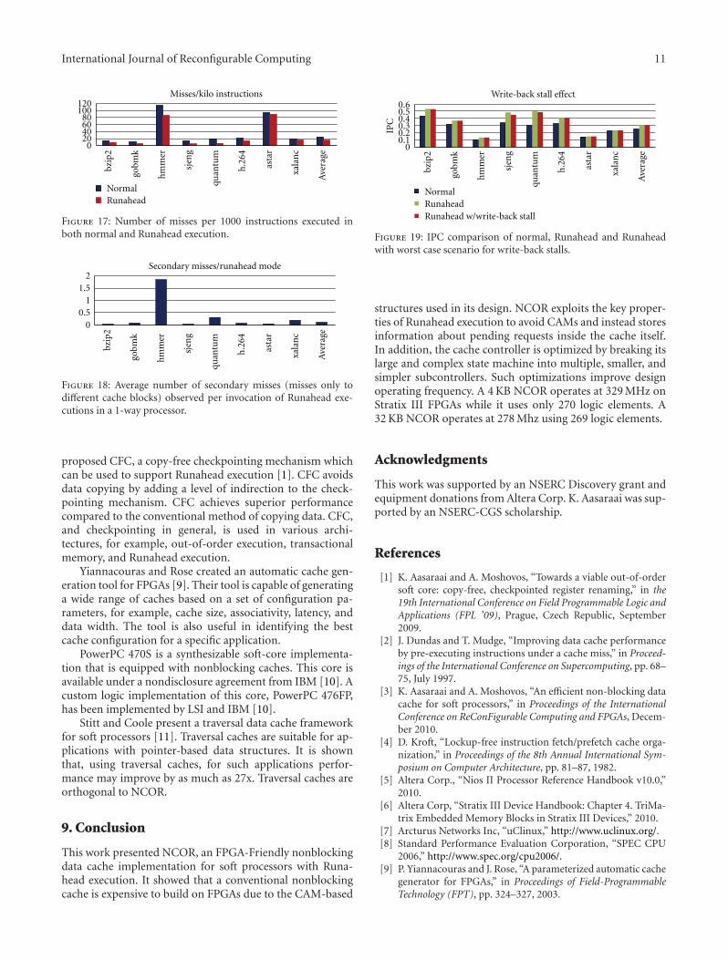
International Journal of Reconfigurable Computing 11
020406080
100120
Misses/kilo instructions
NormalRunahead
bzip
2
gobm
k
hm
mer
sjen
g
quan
tum
h.2
64
asta
r
xala
nc
Ave
rage
Figure 17: Number of misses per 1000 instructions executed inboth normal and Runahead execution.
00.5
11.5
2Secondary misses/runahead mode
bzip
2
gobm
k
hm
mer
sjen
g
quan
tum
h.2
64
asta
r
xala
nc
Ave
rage
Figure 18: Average number of secondary misses (misses only todifferent cache blocks) observed per invocation of Runahead exe-cutions in a 1-way processor.
proposed CFC, a copy-free checkpointing mechanism whichcan be used to support Runahead execution [1]. CFC avoidsdata copying by adding a level of indirection to the check-pointing mechanism. CFC achieves superior performancecompared to the conventional method of copying data. CFC,and checkpointing in general, is used in various archi-tectures, for example, out-of-order execution, transactionalmemory, and Runahead execution.
Yiannacouras and Rose created an automatic cache gen-eration tool for FPGAs [9]. Their tool is capable of generatinga wide range of caches based on a set of configuration pa-rameters, for example, cache size, associativity, latency, anddata width. The tool is also useful in identifying the bestcache configuration for a specific application.
PowerPC 470S is a synthesizable soft-core implementa-tion that is equipped with nonblocking caches. This core isavailable under a nondisclosure agreement from IBM [10]. Acustom logic implementation of this core, PowerPC 476FP,has been implemented by LSI and IBM [10].
Stitt and Coole present a traversal data cache frameworkfor soft processors [11]. Traversal caches are suitable for ap-plications with pointer-based data structures. It is shownthat, using traversal caches, for such applications perfor-mance may improve by as much as 27x. Traversal caches areorthogonal to NCOR.
9. Conclusion
This work presented NCOR, an FPGA-Friendly nonblockingdata cache implementation for soft processors with Runa-head execution. It showed that a conventional nonblockingcache is expensive to build on FPGAs due to the CAM-based
bzip
2
gobm
k
hm
mer
sjen
g
quan
tum
h.2
64
asta
r
xala
nc
Ave
rage
00.10.20.30.40.50.6
IPC
NormalRunahead
Write-back stall effect
Runahead w/write-back stall
Figure 19: IPC comparison of normal, Runahead and Runaheadwith worst case scenario for write-back stalls.
structures used in its design. NCOR exploits the key proper-ties of Runahead execution to avoid CAMs and instead storesinformation about pending requests inside the cache itself.In addition, the cache controller is optimized by breaking itslarge and complex state machine into multiple, smaller, andsimpler subcontrollers. Such optimizations improve designoperating frequency. A 4 KB NCOR operates at 329 MHz onStratix III FPGAs while it uses only 270 logic elements. A32 KB NCOR operates at 278 Mhz using 269 logic elements.
Acknowledgments
This work was supported by an NSERC Discovery grant andequipment donations from Altera Corp. K. Aasaraai was sup-ported by an NSERC-CGS scholarship.
References
[1] K. Aasaraai and A. Moshovos, “Towards a viable out-of-ordersoft core: copy-free, checkpointed register renaming,” in the19th International Conference on Field Programmable Logic andApplications (FPL ’09), Prague, Czech Republic, September2009.
[2] J. Dundas and T. Mudge, “Improving data cache performanceby pre-executing instructions under a cache miss,” in Proceed-ings of the International Conference on Supercomputing, pp. 68–75, July 1997.
[3] K. Aasaraai and A. Moshovos, “An efficient non-blocking datacache for soft processors,” in Proceedings of the InternationalConference on ReConFigurable Computing and FPGAs, Decem-ber 2010.
[4] D. Kroft, “Lockup-free instruction fetch/prefetch cache orga-nization,” in Proceedings of the 8th Annual International Sym-posium on Computer Architecture, pp. 81–87, 1982.
[5] Altera Corp., “Nios II Processor Reference Handbook v10.0,”2010.
[6] Altera Corp, “Stratix III Device Handbook: Chapter 4. TriMa-trix Embedded Memory Blocks in Stratix III Devices,” 2010.
[7] Arcturus Networks Inc, “uClinux,” http://www.uclinux.org/.[8] Standard Performance Evaluation Corporation, “SPEC CPU
2006,” http://www.spec.org/cpu2006/.[9] P. Yiannacouras and J. Rose, “A parameterized automatic cache
generator for FPGAs,” in Proceedings of Field-ProgrammableTechnology (FPT), pp. 324–327, 2003.

12 International Journal of Reconfigurable Computing
[10] IBM and LSI, “PowerPC 476FP Embedded Processor Coreand PowerPC 470S Synthesizable Core User’s Manual,” http://www-03.ibm.com/press/us/en/pressrelease/28399.wss.
[11] G. Stitt and J. Coole, “Traversal caches: a framework for FPGAacceleration of pointer data structures,” International Journalof Reconfigurable Computing, vol. 2010, Article ID 652620, 16pages, 2010.

Hindawi Publishing CorporationInternational Journal of Reconfigurable ComputingVolume 2012, Article ID 716984, 13 pagesdoi:10.1155/2012/716984
Research Article
Dynamic Circuit Specialisation forKey-Based Encryption Algorithms and DNA Alignment
Tom Davidson, Fatma Abouelella, Karel Bruneel, and Dirk Stroobandt
ELIS Department, Ghent University, Sint-Pietersnieuwstraat 41, 9000 Ghent, Belgium
Correspondence should be addressed to Tom Davidson, [email protected]
Received 30 April 2011; Revised 30 August 2011; Accepted 3 September 2011
Academic Editor: Marco D. Santambrogio
Copyright © 2012 Tom Davidson et al. This is an open access article distributed under the Creative Commons Attribution License,which permits unrestricted use, distribution, and reproduction in any medium, provided the original work is properly cited.
Parameterised reconfiguration is a method for dynamic circuit specialization on FPGAs. The main advantage of this new conceptis the high resource efficiency. Additionally, there is an automated tool flow, TMAP, that converts a hardware design into a moreresource-efficient run-time reconfigurable design without a large design effort. We will start by explaining the core principlesbehind the dynamic circuit specialization technique. Next, we show the possible gains in encryption applications using an AESencoder. Our AES design shows a 20.6% area gain compared to an unoptimized hardware implementation and a 5.3% gaincompared to a manually optimized third-party hardware implementation. We also used TMAP on a Triple-DES and an RC6implementation, where we achieve a 27.8% and a 72.7% LUT-area gain. In addition, we discuss a run-time reconfigurable DNAaligner. We focus on the optimizations to the dynamic specialization overhead. Our final design is up to 2.80-times more efficienton cheaper FPGAs than the original DNA aligner when at least one DNA sequence is longer than 758 characters. Most sequencesin DNA alignment are of the order 213.
1. Introduction
Parameterised configurations are a new concept for dynamiccircuit specialization that uses FPGA reconfiguration. It wasdeveloped to use run-time reconfiguration (RTR) to dynam-ically specify the design [1]. This concept is implementedin the TMAP tool flow, an alternative to the normal FPGAtool flow. The TMAP tool flow allows us to automaticallymake a run-time reconfigurable design, based on the originaldesign. Its principles and advantages are discussed in section2. Because this is a new technique, there is still a lot ofexploration needed to fully understand how it should be usedand what the potential gains are for different applications.This paper shows that in at least two fields, key-based en-cryption and DNA alignment, substantial gains can be madeusing parameterised configurations. The TMAP tool flowallows us to check very quickly whether or not a certainimplementation is suitable for dynamic circuit specializationor not. In Section 3 we will discuss the similarities betweenthis tool flow and hardware/software partitioning that doesnot use run-time reconfiguration. There, we will also show
that using parameterised configurations extends the hard-ware/software boundary.
To explain how parameterised configuration can be usedin encryption applications, we start with a straightforwardimplementation of the Advanced Encryption Standard. AESis an encryption algorithm detailed by the NIST in [2] and isexplained in more detail in Section 4. In this section we willalso detail the design decisions for our own AES implemen-tation, k AES. Next, we will explain how exactly the TMAPtool flow is used on this application to make the design run-time reconfigurable. In Section 5 we will discuss the result ofapplying TMAP to k AES. We show a 20.9% area gain for thek AES implementation, compared to the normal FPGA toolflow. In addition, we will compare this result with four other,manually optimized, designs, Crypto-PAn [3], Avalon AES[4], AES128 [5], and AES core [6]. We will show results.We will also use TMAP on the manually optimized designs,and discuss why this does not result in significant gains.Finally, allowing a design to be dynamically specialized willalways introduce a specialization overhead, we will discussthis overhead for the AES implementation in this section.
2 International Journal of Reconfigurable Computing
In Section 6 we will expand our results for the AES algo-rithm to two other key-based encryption algorithms. For theTripleDES [7] encryption algorithm we see a 27.2% LUT-area gain for using parameterisable configuration. The sec-ond algorithm is the RC6 [8] encryption algorithm, here wehave a 72.7% LUT-area gain.
In addition to the encryption algorithms we will also dis-cuss an example of a specialised string matching algorithm,a DNA aligner. DNA alignment is discussed in Section 7.In this case, we followed a different path than with theAES application. We started with an existing DNA aligner,changed the control flow slightly, and applied the TMAP toolflow. The resulting RTR aligner does not show a reductionin the number of LUTs, but does reduce the number of usedBRAMs significantly. It changes the resource tradeoff of thedesign. The RTR aligner can be implemented on a muchcheaper FPGA. We will discuss the details of the RTR alignerand its advantages in comparison with the original designin Section 8. In Section 8.3 we will discuss the test-setupand experimental results for the RTR aligner, with concretenumbers on reconfiguration time as measured on an actualFPGA.
In the case of the DNA aligner, the specialisation over-head has a large impact on the design. We will discuss thisoverhead in detail in Section 9. In this section we will alsodiscuss how to reduce this specialisation overhead usingseveral optimizations.
2. Parameterised Configurations and TMAP
FPGAs can be configured to implement any function, as longas there are enough FPGA resources available. The functionson the FPGA are completely controlled by memory. Thismemory is called the configuration memory. An FPGA con-figuration of a design describes what values the configurationmemory should have to implement the design. Since the con-figuration memory consists of SRAMs, this memory canbe overwritten at run time, and thus the functionality onan FPGA can be changed at run time. This is why FPGAscan be used for run-time reconfigurable implementations ofapplications and why they are a useful platform for dynamiccircuit specialization.
Dynamic circuit specialisation strives to specialise a cir-cuit, at run time, for the specific inputs at that time. Thisis a form of constant propagation in hardware. This special-isation results in a circuit that is both faster and smallerthan the original circuit. Each specialisation takes time, bothto generate the specialised configuration and to configurethe FPGA. This means that in practice, dynamic circuitspecialisation is only useful when some of the inputs of thecircuit change less frequently than others. We will call theseslowly changing inputs parameters from now on.
There has already been a lot of research on run-timereconfiguration on FPGAs. Most vendors even have theirown tool flow for run-time configuration. The Xilinx Modu-lar design flow is one example [9]. This design flow allowsthe user to use the FPGA hardware in a time-multiplexedway. If one wants to implement two or more applicationsthat never need to be available at the same time, then this
design flow can be used to implement both applications onthe same FPGA area. This can be done for completely dif-ferent applications or for different specialisations of the samecircuit. At run time, when a new application is needed, theappropriate configuration is retrieved from memory and theFPGA will be (partially) reconfigured.
This design flow could be used for dynamic circuit spe-cialisation, but only in some very specific cases. The problemwith this approach is that it scales exponentially with respectto the number of parameter bits. A solution for this couldbe to generate the specialised circuit at run time. Howeverrunning the full FPGA tool flow at run time introduces anoverhead of seconds to hours, a much too large overhead formost run-time reconfigurable applications.
Parameterised configuration is not the only methodor concept for dynamic circuit specialisation. The existingtechniques, for both dynamic circuit specialisation and run-time reconfiguration in general, fall in two main categoriesbased on how they approach placement and routing.
The first group avoids placement and routing at runtime and so has trouble realising LUT-area gains. Reference[10] is an example of this. They bypass logic cells that be-come unnecessary after run-time constant propagation. Thisresults in a circuit with better timing behaviour, but this doesnot decrease the number of LUTs the application needs. Ourtechnique, parameterised configurations does show goodarea gains.
The second group implements some form of placementand routing at run time. This group of solutions does showLUT-area gains. The problem with this approach is thatplacement and routing stay NP-complete problems, even ifthey are simplified. Solving NP-complete problems at runtime is very hard because of the limited time available.Our approach takes care of all NP-complete algorithms atcompile time. Reference [11] shows work in developing aJIT hardware compiler, aimed at solving simplified place androute problems at run time. Reference [12] is a paper thatalso falls in this category. They simplify the routing problemby reducing the complexity of the routing architecture. Thepaper presents a global dynamic router for connecting recon-figurable modules. This global dynamic router allows theconnections between modules to be dynamically changed,not the connections within these modules.
The parameterisable configuration concept strives tosolve the problems with the existing techniques. A conven-tional FPGA configuration consists of LUT truth table bitsand routing bits. A parameterised configuration is an FPGAconfiguration where some of the LUT truth table bits areexpressed as Boolean functions instead of Boolean values.The Boolean functions are functions of the parameters wediscussed earlier. If the parameters change, then the newconfiguration is generated by evaluating the Boolean func-tions, based on the current parameter values. By evaluatingthe Boolean functions a fully specified FPGA configurationcan be generated very quickly. This generation only involvesevaluating Boolean expressions, and can be done fast enoughfor use at run time. Actual measurements of this evaluationtime will be discussed in Section 9.
International Journal of Reconfigurable Computing 3
A parameterised configuration consists of two parts. Atemplate, the part of the configuration that has fixed Bool-ean values, and the Boolean functions, the part of the de-sign that is dependent on the parameters. In [1, 13] theTMAP tool flow is presented. This tool flow is able to gen-erate parameterised configurations automatically, based onVHDL. This tool flow is an adaptation of the conventionalFPGA tool flow for the generation of configurations. Bothtool flows are shown in Figure 1.
The conventional tool flow is shown in Figure 1(a). Thesynthesis tool converts a VHDL description of the design to agate level circuit. The technology mapper maps this circuiton an LUT-circuit. This LUT-circuit is then given to theplacer and the router to place the design on an actual FPGA.
There are several changes for the TMAP tool flow, as seenin Figure 1(b). First, the VHDL code is now annotated. Theseannotations show which input signals should be consideredparameters. This annotated VHDL file is then given to anadapted technology mapper, the TMAP technology mapper.This mapper also maps the design to an LUT-circuit, butthe truth tables of these LUTs can now be dependent on theparameter values, instead of being fixed in a conventionalFPGA tool flow. The result is that logic that is only dependenton parameter values will now be expressed as Boolean fun-ctions. These Boolean functions determine the truth tablesof some of the LUTs. This means the total number of LUTswill be smaller because some of the functionality, orig-inally expressed in LUTs, will now be incorporated in theBoolean functions. This will lead to LUT-area gains. Both theplacement and the routing is done with the same tools as theconventional FPGA tool flow.
It is clear that parameterised configurations can be usedto implement dynamic circuit specialisation. As said before,the parameterised configuration consists of two parts, thetemplate and the Boolean functions. The template containsall the LUTs that need to be placed and routed. The areaneeded to implement this template is smaller than usingthe original toolflow without parameters. All the logic thatis only dependent on the parameters is now expressed inBoolean functions and does not require separate LUTs. How-ever, a template in itself does not contain all the informationnecessary for a fully working implementation. Some of thetruth tables are expressed in the Boolean functions. To geta working specialised implementation, these Boolean func-tions need to be evaluated, based on the actual parametervalues.
The above means that all the NP-complete problems, likeplace and route, can be done at compile time, because theydetermine the template which does not change at run time.At run time we only need to evaluate Boolean functions,based on the current parameter values, to specialise the cir-cuit. When a parameter changes, the Boolean functions needto be evaluated and the FPGA needs to be reconfiguredaccording to the new results. This introduces an overhead.
A much more detailed overview of parameterised config-urations is given in both [1, 13]. Important for us is that theinput of the TMAP tool flow is annotated VHDL and its out-put is a working parameterised configuration. This outputalso includes the code that needs to be executed to evaluate
the Boolean functions. The annotations added to the VHDLare very simple and their only role is to tell the tool which ofthe input signals are parameters. Any of the input signals ofa design or parts of a design can be selected as parameters. Itis still the job of the designer to chose the parameters, fromthat point on no user intervention is needed.
The reconfiguration platform, regardless of reconfigura-tion technique, always consists of two elements, the FPGAitself and a configuration manager. This configuration man-ager is responsible for evaluating the Boolean functionsand supervising the reconfiguration of the FPGA. The con-figuration manager is generally a CPU. We will use a Pow-erPC on the FPGA but that is not the only option.
A different perspective on parameterisable configura-tions is given in the next section. There we will discusshow using TMAP can be seen as executing a hardware/software partitioning. This partitioning extends the hard-ware/software boundary, because run-time reconfigurationis used.
3. TMAP as HW/SW Partitioning
The TMAP tool flow is an extended hardware/softwarepartitioning method. It is based on the distinction betweenthe slowly changing inputs, the parameters, and swiftlychanging inputs (regular inputs). Once we have selected theparameters, the tool (TMAP) generates a parameterised con-figuration of the design. This parameterised configurationcan then be split up in a hardware and a software part. Thehardware part corresponds to the bits in the parameterisedconfiguration that have Boolean values (0 or 1). This willgive us an incomplete FPGA configuration, the template.The software part then consists of Boolean expressionsin the parameterised configuration that are dependent onthe parameters. Evaluating these Boolean expressions willgenerate the values to complete the FPGA configuration, andis done in software by the configuration manager.
The similarities between TMAP and hardware/softwarepartitioning are discussed in detail in [14]. However, it isimportant to realize that because run-time reconfigurationis used, the hardware/software boundary can be extendedcompared to traditional hardware/software partitioning.
3.1. The Hardware/Software Boundary. Using FPGAs andrun-time reconfiguration the hardware/software boundarycan be extended so a larger part of the design can be imple-mented in software. This is possible because run-time recon-figuration allows the use of specialized circuits. In a con-ventional hardware/software partitioning, the hardware partwould have to be generic to accommodate all possible pa-rameter values. Using FPGAs and run-time reconfiguration,the hardware part can be optimized for specific parametervalues.
In a conventional approach to hardware/software parti-tioning without run-time reconfiguration, such as [15], wewould select the slowly changing inputs of the design. Nextwe identify the functionalities that are only dependent onthese parameters. This way the hardware/software boundaryis identified. In the next step the boundary is replaced by

4 International Journal of Reconfigurable Computing
Generic
HDL designSynthesis Techn.mapping Place and route
Generic
configuration
(a)
Annotated
HDL designSynthesis TMAP
Parameterizedconfiguration
Place and
outingr
(b)
Figure 1: Conventional and TMAP FPGA tool flow.
registers and the functionalities that are only dependenton the parameters all get a software equivalent. The actualhardware then consists of the registers and the remainderof the design. The signal values on the boundary will becalculated by the software, and then written to those registers.
When using an approach that includes run-time recon-figuration, several things change. Using the parameterisedconfiguration concept, and the TMAP tool flow, we canextend the hardware/software boundary by moving it tothe configuration memory instead of adding registers to thedesign. In addition, because parameterised configurationsare used, the hardware will be a specialized circuit that isoptimized for specific parameter values. This is in contrastto the generic hardware design of the previous approach. Asfor the software, in this case it consists of Boolean functionsthat are generated automatically, based on the hardwarefunctionality that is replaced Figures 2 and 3.
In the next sections of this paper we will discuss in greaterdetail what the effects are of applying TMAP and parameter-isable configurations on actual applications. First, in Sections4 and 5 we will discuss a series of AES implementations,including our own k AES design. We will explain why usingTMAP on our design has better gains, compared to otherAES implementations. In Section 6 we will also discuss twoother encryption algorithms. Finally, we will discuss ourtmapped DNA aligner, the RTR aligner in Section 7. Becausethe specialisation overhead is important in this case, we willgive a detailed overview and offer optimisations in Section 9.
4. Advanced Encryption Standard
The complete Advanced Encryption Standard (AES) is de-scribed in [2] by the NIST. This document describes thedetails and mathematical background involved with thedifferent AESs. We will only discuss the hardware implemen-tation of the algorithm, and therefore will only focus on thepractical implications of AES.
In its most basic form, AES describes how to encode128 bits of data, using an encoding scheme based on a specifickey value. The Advanced Encryption Standard consists ofthree separate standards, whose main difference is the lengthof this key (128, 192, and 256 bits). The three standardsare very similar and do not require significantly differenthardware implementations. This is why we only discuss the128-bit AES algorithm in this paper.
The 128-bit AES application can be split up in twoparts: data encoding and key expansion. The data encodingexplains how the data will be converted into encoded data.For this process we need several values that are key de-pendent, the round keys, which are generated by the keyexpansion.
(1) Data Encoding. In the AES algorithm the input datais encoded per 128-bit blocks. We split this data up in16 bytes, and assign each byte a location in a 4-by-4 statematrix. The encoding part of the AES algorithm consists ofa series of bytetransformations that are applied to the state.These transformations are combined in a specific order andgrouped in a round, and each round has a round key input.This round key value is different for each round, and all thesevalues are the result of the key expansion.
(2) Key Expansion. The round keys, necessary for theaddRoundkey transformation in the different rounds, arederived from the input key. This key is expanded to generatethe different round keys. The first round key is the input key,this key is used in the first addRoundKey() that is appliedto the data input. From the second round key, the roundkey generation uses some similar transformations as the dataencoding process. A more detailed description of the exacttransformations used in both the key expansion and the dataencoding can be found in [2].
4.1. k AES. To explain how the TMAP tool flow works, wechose an application where the parameter is easy to identify.As described in Section 4, the AES application consists of twomain parts: the data encoding and the key generation. Bothparts are clearly separated and work, in general, on a differenttime scale. In most practical applications the key changesmuch slower than the input data. So, the key input signal isa good parameter choice, we expect a large part, if not all, ofthe key expansion will be moved to Boolean functions.
To show how parameterised configuration can signifi-cantly optimize a design very quickly by making it run-time reconfigurable, we wrote our own AES implementation,k AES. In the next Section 5, this design will be comparedwith several other AES designs. k AES is almost a directreflection of the hardware described in the NIST document[2]. The design was deliberately kept fully parallel, and it wastherefore very simple to write and test.
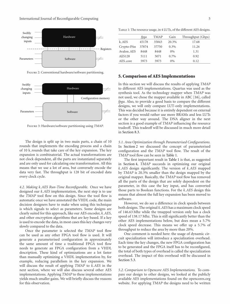
International Journal of Reconfigurable Computing 5
Parameters
s
Hardware
Software
Swiftlychanging
input
Registers
Figure 2: Conventional hardware/software partitioning.
Parameters
s
Hardware
Software
Swiftlychanging
input
Configuration memory
Figure 3: Hardware/software partitioning using TMAP.
The design is split up in two main parts, a chain of 10rounds that implements the encoding process and a chainof 10 k rounds that take care of the key expansion. The keyexpansion is combinatorial. The actual transformations arenot clock dependent, all the parts are instantiated separatelyand are only used for calculating one transformation. All thismeans that we use a lot of area, but conversely encode thedata very fast. The throughput is 128 bit of encoded dataevery clock cycle.
4.2. Making k AES Run-Time Reconfigurable. Once we havedesigned our k AES implementation, the next step is to usethe TMAP tool flow on this design. Since the tool flow isautomatic once we have annotated the VHDL code, the maindecision designers have to make when using this techniqueis which signals to select as parameters. Some designs areclearly suited for this approach, like our AES encoder, k AES,and other encryption algorithms that are key based. If a keyis used to encode the data, in most cases this key changes veryslowly compared to the data.
Once the parameter is selected the TMAP tool flowcan be used as any other FPGA tool flow is used. It willgenerate a parameterised configuration in approximatelythe same amount of time a traditional FPGA tool flowneeds to generate an FPGA configuration from a VHDLdescription. These kind of optimizations are a lot fasterthan manually optimizing a VHDL implementation by, forexample, reducing parallelism in the key expansion. Wewill discuss the result of applying TMAP to k AES in thenext section, where we will also discuss several other AESimplementations. Applying TMAP to these implementationsyields much smaller gains. We will briefly discuss the reasonsfor this observation.
Table 1: The resource usage, in 4 LUTs, of the different AES designs.
fpga TMAP Gain Throughput (Gbps)
k AES 45178 35843 20.3% 17.68
Crypto-PAn 37874 37750 0.3% 11.26
Avalon AES 8448 8448 0% 1.31
AES128 5111 5071 0.7% 0.92
AES core 5973 5973 0% 0.12
5. Comparison of AES Implementations
In this section we will discuss the results of applying TMAPto different AES implementations. Quartus was used as thesynthesis tool. As the technology mapper when TMAP wasnot used, we chose the mapper available in ABC [16], calledfpga. Also, to provide a good basis to compare the differentdesigns, we will only compare LUT-only implementations.This was decided because it is entirely dependent on externalfactors if you would rather use more BRAMs and less LUTsor the other way around. The DNA aligner in the nextsection is a good example of TMAP influencing the resourcetradeoff. This tradeoff will be discussed in much more detailin Section 8.3.
5.1. Area Optimization through Parameterised Configurations.In Section 2 we discussed the concept of parameterisedconfiguration and the TMAP tool flow. The result of theTMAP tool flow can be seen in Table 1.
The first important result in Table 1 is that, as suggestedin Section 4, TMAP succeeds in optimizing our originalk AES design significantly. The version of k AES mappedby TMAP is 20.3% smaller than the design mapped by theoriginal mapper. Basically, the TMAP tool flow has removedall the parts of the design that are solely dependent on theparameter, in this case the key input, and has convertedthose parts to Boolean functions. For the k AES design thismeans that almost the full key expansion has been moved tosoftware.
However, we do see a difference in clock speeds betweenboth designs. The original k AES has a maximum clock speedof 146.63 Mhz while the tmapped version only has a clockspeed of 138.17 Mhz. This is still significantly better than theother AES implementations below, but does mean a 5.7%clock speed decrease. This means we offer up a 5.7% ofthroughput to reduce the area by more than 20%.
One comment is needed here: the usage of dynamic cir-cuit specialization will introduce a specialization overhead.Each time the key changes, the new FPGA configuration hasto be generated and the FPGA itself has to be reconfigured,the total of both types of overhead is called the specializationoverhead. The impact of this overhead will be discussed inSection 5.3.
5.2. Comparison to Opencore AES Implementations. To com-pare our design to other designs, we looked at the publiclyavailable AES implementations found on the opencores.orgwebsite. For applying TMAP the designs need to be written
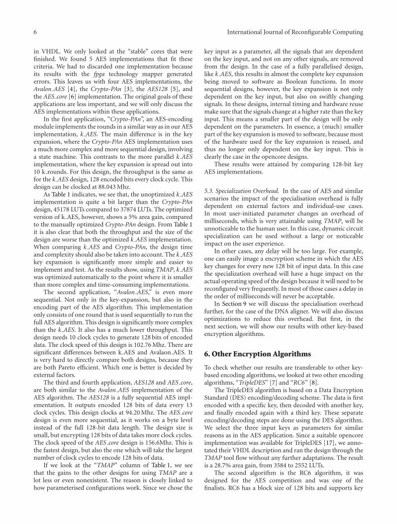
6 International Journal of Reconfigurable Computing
in VHDL. We only looked at the “stable” cores that werefinished. We found 5 AES implementations that fit thesecriteria. We had to discarded one implementation becauseits results with the fpga technology mapper generatederrors. This leaves us with four AES implementations, theAvalon AES [4], the Crypto-PAn [3], the AES128 [5], andthe AES core [6] implementation. The original goals of theseapplications are less important, and we will only discuss theAES implementations within these applications.
In the first application, “Crypto-PAn”, an AES-encodingmodule implements the rounds in a similar way as in our AESimplementation, k AES. The main difference is in the keyexpansion, where the Crypto-PAn AES implementation usesa much more complex and more sequential design, involvinga state machine. This contrasts to the more parallel k AESimplementation, where the key expansion is spread out into10 k rounds. For this design, the throughput is the same asfor the k AES design, 128 encoded bits every clock cycle. Thisdesign can be clocked at 88.043 Mhz.
As Table 1 indicates, we see that, the unoptimized k AESimplementation is quite a bit larger than the Crypto-PAndesign, 45178 LUTs compared to 37874 LUTs. The optimizedversion of k AES, however, shows a 5% area gain, comparedto the manually optimized Crypto-PAn design. From Table 1it is also clear that both the throughput and the size of thedesign are worse than the optimized k AES implementation.When comparing k AES and Crypto-PAn, the design timeand complexity should also be taken into account. The k AESkey expansion is significantly more simple and easier toimplement and test. As the results show, using TMAP, k AESwas optimized automatically to the point where it is smallerthan more complex and time-consuming implementations.
The second application, “Avalon AES,” is even moresequential. Not only in the key-expansion, but also in theencoding part of the AES algorithm. This implementationonly consists of one round that is used sequentially to run thefull AES algorithm. This design is significantly more complexthan the k AES. It also has a much lower throughput. Thisdesign needs 10 clock cycles to generate 128 bits of encodeddata. The clock speed of this design is 102.76 Mhz. There aresignificant differences between k AES and Avalaon AES. Itis very hard to directly compare both designs, because theyare both Pareto efficient. Which one is better is decided byexternal factors.
The third and fourth application, AES128 and AES core,are both similar to the Avalon AES implementation of theAES algorithm. The AES128 is a fully sequential AES impl-ementation. It outputs encoded 128 bits of data every 13clock cycles. This design clocks at 94.20 Mhz. The AES coredesign is even more sequential, as it works on a byte levelinstead of the full 128-bit data length. The design size issmall, but encrypting 128 bits of data takes more clock cycles.The clock speed of the AES core design is 156.6Mhz. This isthe fastest design, but also the one which will take the largestnumber of clock cycles to encode 128 bits of data.
If we look at the “TMAP” column of Table 1, we seethat the gains to the other designs for using TMAP are alot less or even nonexistent. The reason is closely linked tohow parameterised configurations work. Since we chose the
key input as a parameter, all the signals that are dependenton the key input, and not on any other signals, are removedfrom the design. In the case of a fully parallelised design,like k AES, this results in almost the complete key expansionbeing moved to software as Boolean functions. In moresequential designs, however, the key expansion is not onlydependent on the key input, but also on swiftly changingsignals. In these designs, internal timing and hardware reusemake sure that the signals change at a higher rate than the keyinput. This means a smaller part of the design will be onlydependent on the parameters. In essence, a (much) smallerpart of the key expansion is moved to software, because mostof the hardware used for the key expansion is reused, andthus no longer only dependent on the key input. This isclearly the case in the opencore designs.
These results were attained by comparing 128-bit keyAES implementations.
5.3. Specialization Overhead. In the case of AES and similarscenarios the impact of the specialisation overhead is fullydependent on external factors and individual-use cases.In most user-initiated parameter changes an overhead ofmilliseconds, which is very attainable using TMAP, will beunnoticeable to the human user. In this case, dynamic circuitspecialization can be used without a large or noticeableimpact on the user experience.
In other cases, any delay will be too large. For example,one can easily image a encryption scheme in which the AESkey changes for every new 128 bit of input data. In this casethe specialization overhead will have a huge impact on theactual operating speed of the design because it will need to bereconfigured very frequently. In most of those cases a delay inthe order of milliseconds will never be acceptable.
In Section 9 we will discuss the specialisation overheadfurther, for the case of the DNA aligner. We will also discussoptimizations to reduce this overhead. But first, in thenext section, we will show our results with other key-basedencryption algorithms.
6. Other Encryption Algorithms
To check whether our results are transferable to other key-based encoding algorithms, we looked at two other encodingalgorithms, “TripleDES” [7] and “RC6” [8].
The TripleDES algorithm is based on a Data EncryptionStandard (DES) encoding/decoding scheme. The data is firstencoded with a specific key, then decoded with another key,and finally encoded again with a third key. These separateencoding/decoding steps are done using the DES algorithm.We select the three input keys as parameters for similarreasons as in the AES application. Since a suitable opencoreimplementation was available for TripleDES [17], we anno-tated their VHDL description and ran the design through theTMAP tool flow without any further adaptations. The resultis a 28.7% area gain, from 3584 to 2552 LUTs.
The second algorithm is the RC6 algorithm, it wasdesigned for the AES competition and was one of thefinalists. RC6 has a block size of 128 bits and supports key

International Journal of Reconfigurable Computing 7
sizes of 128, 192, and 256 bits. An opencores implementationof this algorithm was also available [18]. Here, we also chosethe key as a parameter. Using TMAP on this implementationresulted in a 72.7% LUT-area gain, from 4635 to 1265 LUTS.
7. DNA Alignment
DNA alignment is used here as an example of a stringmatching algorithm, so not a lot of detail on the biologicalbackground will be given. The actual algorithm is the Smith-Waterman algorithm, proposed in [19]. The aim of thisalgorithm is to find the region within two DNA sequences,sequence A and B, where they share the most similarities.
This is done by filling in a score matrix (F). Each elementin the score matrix corresponds to one character in sequenceA and one character in sequence B. The rows are associatedwith sequence A, which we will call the vertical sequencefrom now on. The columns are associated with sequence B,which we will call the horizontal sequence from now on. Theelement i, j of the score matrix then corresponds to the scorefor comparing Ai and Bj . The score matrix is filled by solving(1) for each element. Once the matrix is completely filled in,the regions with the most similarities are found by startingfrom the maximum value in the score matrix and using atrace-back algorithm to find the start of this region,
Fi, j =Max(FDi, j ,F
Vi, j ,F
Hi, j
), (1)
where
FDi, j = Fi−1, j−1 + S
(A(i),B
(j))
,
FVi, j = Fi−1, j + ω,
FHi, j = Fi, j−1 + ω.
(2)
FD takes the matrix element diagonally above and adds avalue S. This value S is positive if A(i) and B(j) are the sameand negative in case of a mismatch. The values for all possiblepairs A(i) and B(j) are described in a substitution matrix.The values in this substitution matrix are based on biologicalconsiderations, so we will not go into further detail here. Thevalue taken from this matrix is called the substitution cost.
FV takes the matrix element directly above and adds agap penalty, ω. FH does the same but with the element to theleft. The maximum of these three values (FD
i, j ,FVi, j ,F
Hi, j) is then
selected and assigned to Fi, j .
8. RTR Aligner
To get a run-time reconfigurable DNA aligner, we startedwith an already existing DNA aligner, that was developedfor a project (the FlexWare project) funded by the IWT inFlanders and therefore called the Flexware aligner [20]. Wewill first discuss the structure of this Flexware aligner briefly,then we will discuss the changes and decisions made to turnit into an RTR aligner.
8.1. Flexware Aligner. The Flexware aligner, like most DNAaligners, is based on the observation that the data dependen-
(i, j)(i, j − 1)
(i − 1, j − 1) (i − 1, j)
Figure 4: The data dependencies in the Smith-Waterman algorithm[20].
cies in the Smith-Waterman algorithm are west, northwest,and north, as you can see from Figure 4. This means that thealgorithm can be HW accelerated by using a systolic array, asshown in Figure 5. Vertical sequence (A) is streamed throughthe array and each PE calculates an element of the scorematrix each clock tick. Once the full vertical sequence hasbeen streamed through the array, the maximum score and itslocation are known.
If there are not enough PEs to compare the sequencescompletely, memory is used to store temporary data. Then,the horizontal sequence is streamed through the arraymultiple times, each time with different column characters.In Figure 6, you can see the progress of the PEs of thissystolic array through the score matrix. Each clock tick a PEcalculates the score for its row and column characters.
In general the DNA sequences that are compared arelonger (213) than the number of PEs that fit on an FPGA, atmost hundreds on very large FPGAs. This means that morePEs will always speed up the execution.
8.2. RTR Aligner. The parameter selection in the case of theDNA aligner is less straightforward than in the case of AES.However, looking at the inputs of the systolic array we can seethat, for each PE, the column character stays constant whilethe whole vertical sequence is streamed through the systolicarray. On the design level the column sequence was chosenas a parameter, for an individual PE this translates to thecolumn character being chosen as a parameter.
Before applying TMAP to the Flexware aligner, somechanges to the control flow were made so the aligner could bestarted and stopped without any problems. This is necessarybecause between configurations the aligner will have to stopworking and we need to be able to restart it when thereconfiguration is done. The result of these changes andapplying the TMAP tool flow is the RTR aligner. We willcompare this RTR aligner to the original Flexware aligner indetail below.
In most practical cases, the horizontal sequence willalways be longer than the amount of PEs. This means that
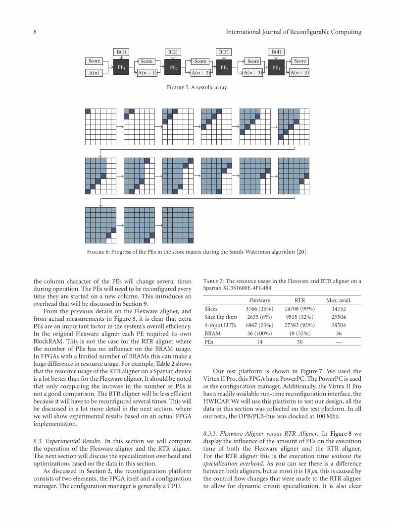
8 International Journal of Reconfigurable Computing
PE1
B(1)
A(n) A(n − 1)
Score ScorePE2
B(2)
A(n − 2)
ScorePE3
B(3)
A(n − 3)
ScorePE4
B(4)
A(n − 4)
Score
Figure 5: A systolic array.
Figure 6: Progress of the PEs in the score matrix during the Smith-Waterman algorithm [20].
the column character of the PEs will change several timesduring operation. The PEs will need to be reconfigured everytime they are started on a new column. This introduces anoverhead that will be discussed in Section 9.
From the previous details on the Flexware aligner, andfrom actual measurements in Figure 8, it is clear that extraPEs are an important factor in the system’s overall efficiency.In the original Flexware aligner each PE required its ownBlockRAM. This is not the case for the RTR aligner wherethe number of PEs has no influence on the BRAM usage.In FPGAs with a limited number of BRAMs this can make ahuge difference in resource usage. For example, Table 2 showsthat the resource usage of the RTR aligner on a Spartan deviceis a lot better than for the Flexware aligner. It should be notedthat only comparing the increase in the number of PEs isnot a good comparison. The RTR aligner will be less efficientbecause it will have to be reconfigured several times. This willbe discussed in a lot more detail in the next section, wherewe will show experimental results based on an actual FPGAimplementation.
8.3. Experimental Results. In this section we will comparethe operation of the Flexware aligner and the RTR aligner.The next section will discuss the specialization overhead andoptimizations based on the data in this section.
As discussed in Section 2, the reconfiguration platformconsists of two elements, the FPGA itself and a configurationmanager. The configuration manager is generally a CPU.
Table 2: The resource usage in the Flexware and RTR aligner on aSpartan XC3S1600E-4FG484.
Flexware RTR Max. avail.
Slices 3766 (25%) 14708 (99%) 14752
Slice flip flops 2635 (8%) 9515 (32%) 29504
4-input LUTs 6967 (23%) 27382 (92%) 29504
BRAM 36 (100%) 19 (52%) 36
PEs 14 50 —
Our test platform is shown in Figure 7. We used theVirtex II Pro, this FPGA has a PowerPC. The PowerPC is usedas the configuration manager. Additionally, the Virtex II Prohas a readily available run-time reconfiguration interface, theHWICAP. We will use this platform to test our design, all thedata in this section was collected on the test platform. In allour tests, the OPB/PLB-bus was clocked at 100 Mhz.
8.3.1. Flexware Aligner versus RTR Aligner. In Figure 8 wedisplay the influence of the amount of PEs on the executiontime of both the Flexware aligner and the RTR aligner.For the RTR aligner this is the execution time without thespecialization overhead. As you can see there is a differencebetween both aligners, but at most it is 18 μs, this is caused bythe control flow changes that were made to the RTR alignerto allow for dynamic circuit specialization. It is also clear

International Journal of Reconfigurable Computing 9
PowerPC BRAM
Bridge
PLB bus
OPB bus
HWICAP Reconfigurable IP
Virtex-II roP
Figure 7: Virtex II Pro run-time reconfigurable platform.
0
0.02
0.04
0.06
0.08
0.1
0.12
0.14
0.16
0.18
0.2
Exe
cuti
onti
me
(ms)
5 10 15 20 25 30 35
Number of PEs
Flexware alignerRTR ali ng er
Figure 8: Execution time (ms) for both aligners, without reconfigu-ration overhead, based on measurements on the test platform whencomparing a 188 to a 258 DNA sequence.
that the relative gain of additional PEs decreases as the totalnumber of PEs in the system increases, for both designs.
For the designs described above the maximum clockspeed was measured too. For 4 PEs the RTR aligner clocksat 62 Mhz and the Flexware aligner at 59 Mhz. However,this difference reduces steadily as the area of both designsincreases with additional PEs. For designs with 20 or morePEs this difference is less than 1 Mhz. For both designs theclock speed gradually settles down to around 50 Mhz whendesigns span the complete Virtex II Pro FPGA. There is noclear difference between the two, certainly not for the largestdesigns.
Now we look at the RTR aligner with the specialisationoverhead included. In this case the total execution time isaround 3.7 seconds, for any number of PEs, when comparinga 188 to a 258 DNA sequence. It is very clear that thisspecialization overhead imposes too large a cost on the
500 1000 1500 2000 2500 3000 3500 400099.2
99.3
99.4
99.5
99.6
99.7
99.8
99.9
Length of the DNA sequence
Rec
onf.
over
hea
d(\
%)
ofto
tale
xecu
tion
5 PEs10 PEs15 PEs20 PEs
25 PEs30 PEs35 PEs
Figure 9: Fraction of the total time spent on reconfiguration, withincreasing DNA sequence length, based on measurements on thetest platform.
design, in this case. Using HWICAP reconfiguration makesthe system very inefficient compared to the Flexware aligner.In the following optimizations we will reduce this overheaddrastically and eventually make the design more efficientthan the Flexware aligner. The reason there is no reductionof the total execution time with additional PEs is becausethe added reconfiguration time of the extra PEs offsets theexecution time increase. This will also change with ouroptimizations.
Figure 9 shows that the fraction of the time spent onactual execution increases with longer DNA sequences,regardless of the number of PEs.
8.3.2. Increasing the DNA Sequence Length. The measure-ments for Figure 8 were taken comparing sequences of 188and 258 characters. Those are small sequences in DNAalignment, where sequences in the order of 213 are a lot morecommon. Increasing the sequence length will impact bothdesigns in a different way.
The Flexware aligner’s overall execution time is pro-portional with the product of the sequence lengths. If onesequence is doubled, the execution time also doubles. If bothsequences double the execution time is quadrupled.
Before we can discuss the impact of increasing the seq-uence length on the RTR aligner, we need to make clearwhich sequence is chosen as a parameter. Because of thespecialization overhead, minimizing the number of reconfig-urations is essential. This means choosing the shortlinebreakest sequence as a parameter is clearly the best choice, thiscan greatly reduce the number of times the PEs need to bereconfigured.
With the shortest sequence as the parameter, increasingthe other sequence length will work to the advantage of

10 International Journal of Reconfigurable Computing
the RTR aligner. The number of reconfigurations will staythe same but the time spent on execution will increase, aswith the Flexware aligner. This means the relative cost ofreconfiguring will decrease.
Another way to see this is that if the nonparameter seq-uence length increases, a configuration will be used longerbefore it is changed. From this we can conclude that forthe RTR aligner to be working efficiently, the nonparametersequence needs to be as long as possible. We will go intofurther detail on this in the next section.
9. Specialisation Overhead
A fundamental property of dynamic circuit specialization isthe overhead incurred by this dynamic specialization. Thereare several possible scenarios, one was discussed with the AESimplementation in Section 5.3. In AES the parameter changeis decided externally, by a user or a governing program,because its parameter, the key, is an input of the global de-sign.
In the RTR aligner there is a subtle difference. There isalso an external parameter decision, a program or user de-cides which two sequences need to be compared. Internally,however, the application itself will govern the actual param-eter change at the input of the PEs. Each time a PE is startedon a new column, it will need to be reconfigured.
In this section we will discuss the RTR aligner specialisa-tion overhead in more detail. In the last parts of this sectionwe will also discuss optimizations we have implemented toreduce the specialization overhead and make the RTR alignermore efficient than the Flexware aligner.
In the case of the RTR aligner the specialization overheadhas a huge influence on the overall efficiency of the design.This is because the timing of the specialization is a part of thesystems normal operating environment. Each comparisonof two DNA sequences will entail a certain number of re-configurations. This number is dependent on the length ofthe sequences and the number of processing elements. To beclear, each time the last PE finishes its column, all the PEs arereconfigured and a start signal is given to restart the calcula-tions. The next time the last PE has finished its column, a newreconfiguration is done. This goes on until every element ofthe score matrix has been calculated. The average specializa-tion overhead of one such reconfiguration, which is reconfig-uring each PE one time, is displayed in Figure 10. It is clearthat if more PEs need to be reconfigured, the specializationtakes longer. This increase is invariable of sequence length.Figure 10 also shows that sometimes a larger design will havea smaller specialization overhead. We will discuss this later inthe subsection about the reconfiguration overhead.
There are a lot of ways to minimize this specializationoverhead, several of the more interesting ones will be appliedto the RTR aligner in order to make it more efficient than theFlexware aligner for the case shown in Table 2.
Before we look at optimizing the specialization overhead,we must first determine in which cases it will be used. TheRTR aligner uses no BRAMs for its PE implementation, theFlexware aligner uses one BRAM for every PE. Most high-end
5 10 15 20 25 30 350
5
10
15
20
25
30
35
40
45
50
Number of PEs
Rec
onfi
gura
tion
over
hea
d(m
s)
Figure 10: Specialization overhead (ms) needed to reconfigure thePEs of the RTR aligner one time, based on measurements in the testplatform.
FPGAs, such as the Xilinx Virtex-line, have enough BRAMs.They generally run out of LUTs before all BRAMs are used bythe Flexware aligner. Cheaper FPGAs, however, such as theXilinx Spartan discussed below quickly run out of BRAMsbefore all the available LUTs are used, making these FPGAsmuch less optimal for the Flexware aligner. An example ofthis is shown in Table 2.
The reason why Spartan implementations are interestingis the price difference between Spartan and Virtex FPGAs.This difference is easily a factor of 10 for equally sized FPGAs.
In [21] we calculated the maximum allowed special-ization overhead for the RTR aligner to be as efficient asthe Flexware aligner. In the case of the Spartan displayedin Table 2, this resulted in the following upper bound forthe specialization overhead of 50 PEs, 455 μ seconds. Thisis an upper bound for the time needed to reconfigure allthe PEs one time. From the measurements of the special-ization overhead displayed in Figure 10 it is clear that wealready surpass this upper bound for 5 PEs, let alone 50. Toimprove the efficiency and meet this upper bound, we willdiscuss several optimizations to the RTR aligner. The SRLoptimization discussed below is interesting for any run-rimereconfigurable application that needs to be reconfigured asfast as possible.
Sadly, we have no Spartan XC3S1600E-4FG484 board totest the final design. We will apply the optimisations to thedesign implemented on the test platform. Based on theseresults we will discuss the effect of the optimisations on theapplication. The biggest disadvantage is that the Virtex IIPro does not have enough area to implement 50 PEs. So, inthe following we will always discuss the results on the testplatform first. Next, we will discuss what the effect of theseoptimisations is on the use case with the Spartan FPGA.
The first thing we have to realize is that the specializationoverhead can be split up in two parts, the evaluation timeand the reconfiguration time. The evaluation time is the time

International Journal of Reconfigurable Computing 11
needed for evaluating Boolean functions of the parameters,as described in Section 2. The reconfiguration time is thetime needed to write these values to the configuration me-mory of the FPGA.
From Table 3, we can see that the evaluation time takesabout 0.24% of the total specialization overhead and theactual reconfiguration time takes up 99.76% of the totalspecialization overhead. Also, these numbers are fairly con-stant when the number of PEs increases.
We can decrease both of these overheads in differentways. Because the reconfiguration time is by far the largestfactor in the overhead we will optimize this reconfigurationtime first.
9.1. Reconfiguration Time. A large part of the reconfigurationtime is introduced by the HWICAP. The way it handles thereconfiguration is not always efficient [22]. It changes thetruth tables in three stage. First, it needs to read a full framefrom the configuration memory. Then it changes the truthtable values. And last, it writes back the full frame. In addi-tion, it writes a padding frame to flush the reconfigurationpipeline [23]. In the Virtex II Pro, each frame contains 320LUTs with a small header. One can see that changing a singleLUT truth table introduces a large overhead. Furthermore,the overhead is dependent on the placement of our design.In a worst case scenario, every LUT of a PE is in a differentcolumn. Each PE has 18 LUTs that need to be reconfigured.So, for each PE 18 frames have to be read and 36 have to bewritten. Figure 10 shows this dependency. If a larger designis placed more efficiently then this can lead to a significantreduction in the total reconfiguration time.
The HWICAP is not the only way to access the con-figuration memory of the FPGA at run time. In [24] thereconfiguration time is reduced using shift register LUTs(SRLs). An SRL is an LUT whose truth table bits are alsoarranged as a shift register. This shift register functions likeany shift register, with a shift in, a shift out, and a clock.Thus, the truth table of an SRL can be changed by shiftingin new values through the shift in input. By connecting theshift out output of one SRL to the shift in input of anotherSRL, a long SRL chain can be formed. This long SRL chaincan then be used to change the truth tables of all the LUTsthat are part of it.
Such a long SRL chain can then be used to reconfigurethe FPGA very quickly, by shifting the new configurationinto the truth tables of the connected LUTs. This way thereconfiguration time is reduced to only hundreds or thou-\linebreak sands of clock cycles, instead of hundreds ofthousands as with the HWICAP.
The SRL chain(s) can be added on top of the alreadyexisting design. The parameterised configurations tool flowdetermines which truth tables need to be changed. TheseLUTs are then marked and arranged in an SRL chainthat is completely independent of the design. The chain isconnected at the input with the configuration manager, ithas no output and is only used to change the truth tables ofthe LUTs. Reference [24] also shows that the impact on theclock frequency of the design of adding these shift register
Table 3: The specialization overhead, split up in reconfigurationtime and evaluation time.
PEs Reconfiguration time (ms) Evaluation time (ms)
5 7.9 (99.76%) 0.019 (0.24%)
10 18.0 (99.76%) 0.044 (0.24%)
15 22.1 (99.74%) 0.057 (0.26%)
20 27.8 (99.76%) 0.069 (0.24%)
25 38.5 (99.76%) 0.095 (0.24%)
30 36.4 (99.74%) 0.095 (0.26%)
35 48.2 (99.76%) 0.120 (0.24%)
Table 4: The reconfiguration time, using shift register LUT re-configuration in the RTR aligner.
PEs Clock cycles Theoretical (μs) Measured (μs)
5 1440 27.91 29.15
10 2880 56.78 59.93
15 4320 84.18 88.93
20 5760 112.31 118.94
25 7200 142.68 151.13
30 8640 172.04 182.23
35 10080 199.83 211.93
LUT chain(s) is minimal. Important to note is that not everyFPGA has this SRL functionality. The Spartan 3 and Virtex IIPro LUTs both have this capability.
The reconfiguration time using SRL reconfigurationcan be seen in Table 4. Compared to the reconfigurationoverhead using the HWICAP, as seen in both Figure 10 andTable 3, this is a huge decrease. The SRL chain is clocked atthe same speed as the design.
The third column shows the theoretical reconfigurationtime, assuming one long SRL. We know that we need toreconfigure 18 LUTs in each PE and that reconfiguring1 bit takes one clock cycle. Based on these numbers wecan calculate for each RTR implementation how long thereconfiguration using SRLs should take. In the next columnwe show our measured results on the test platform. In eachinstance we see that the measured reconfiguration time is5% to 6% larger than the expected value. This is because ofinaccuracies in our measurements. The reconfiguration timeis completely dependent on the SRLs, which are completelydeterministic. However, this extra overhead has no impacton our conclusions. The reconfiguration time using SRLsis two orders of magnitude smaller than the run-timereconfiguration overhead using the HWICAP.
In the use case shown in Table 2 we have 50 PEs at a clockspeed of 46.25 Mhz. The theoretical reconfiguration time isthen 313.04 μs. The upper bound from [21] is 455 μs. We arewell below this upper bound, even if we assume that the 6%overhead is not related to inaccuracy in the way we measured.In that case the reconfiguration time is 331.82 μs. Of course,this does not necessarily mean that the total specialisationoverhead is below the upper bound. For this to be the casewe need to look at the evaluation time too.

12 International Journal of Reconfigurable Computing
9.2. Evaluation Time. The evaluation of the Boolean func-tions in our run-time reconfigurable platform is done by thePowerPC, shown in Figure 7. However, there are two goodreasons to change this in the design on the Spartan. The firstreason is that the Spartan has no PowerPC, so we wouldneed to evaluate the Boolean functions on a Microblaze ora custom processor. A second reason to change this is that, inthe case of the RTR aligner, the evaluation does not involveany Boolean evaluation. The new truth tables are directlydependent on the parameters, no Boolean expressions arenecessary. Because of both these reasons, we propose touse a dedicated hardware block that will function as theconfiguration manager.
This dedicated hardware block takes a character of theparameter DNA sequence as the input and outputs the bitvalues that need to be shifted into the SRLs one clock tickat a time. This means, once we have started the dedicatedhardware, we can start shifting in the results into the SRLthe next clock cycle. The reconfiguration and evaluation canhappen at the same time. This will greatly reduce the totalspecialization overhead. The extra time overhead introducedby the evaluation is then only one clock cycle, compared tothe overhead from reconfiguring using SRLs.
Of course the size of this dedicated hardware blockwill influence how many PEs we can fit on the FPGA.This block uses a very small amount of LUTs (49) butdoes use one BRAM. In return for adding one BRAM, ourtotal specialization overhead is reduced to the values seenin Table 4, with one additional clock cycle for starting thededicated hardware block. This is a huge decrease from thespecialization overhead shown in Figure 10. We can clearlysee the advantages of these optimizations.
An advantage in addition of using the SRLs combinedwith the dedicated hardware is that we can further reduce ourspecialization overhead by using two or more SRL chains andan equal number of dedicated hardware blocks. In this caseone SRL chain will be split up in two or more SRL-chainsthat are half as long, this will then reduce the reconfigurationtime by half.
Finally, we look back at the upper bound, 455 μs pro-posed in [21], for the RTR aligner presented in Table 2. Sincethe Spartan FPGA has SRL capabilities, we can make useof the SRL reconfiguration. Additionally, because we stillhave unused BRAMs in our RTR aligner, we can use thededicated hardware block. We do, however, have to removeone PE to make room for the dedicated hardware block. Ifwe lower the number of PEs of the RTR aligner by one, thenew upper bound becomes 442.43 μs. For 49 PEs and usingboth optimizations, our specialization overhead is reducedto 305.14 μs, well below our new upper bound. If we againtake an extra 6% of reconfiguration time into account thisnumber becomes 323.45 μs, still below the upper bound.
We can calculate, based on [21] that the RTR aligner willfinish its execution earlier than the Flexware aligner on theSpartan XC3S1600E-4FG484, provided the nonparametersequence is long enough. If we assume the nonparametersequence is 213 characters, then the RTR aligner will bebetween 1.15 and 1.29 times more efficient than the Flexwarealigner, depending on the length of the parameter sequence.
The RTR aligner is more efficient than the Flexwarealigner as long as the nonparameter sequence is longer than6046 characters. We can decrease this number and increasethe overall efficiency by using two or more SRL chains anddedicated hardware blocks. For example, using two SRLchains, and two dedicated hardware blocks, increases themaximum efficiency of the RTR over the Flexware aligner to1.90. The nonparameter sequence lower bound for efficiencyis then lowered to 2824. This trend holds for larger numbersof SRL chains.
Since one PE in the RTR aligner has a size of 369 LUTs,we can fit 7 dedicated hardware blocks in the area used forone PE. This means we can use 7 SRL chains. This improvesthe maximum efficiency of the RTR aligner to 2.80-timesthe Flexware aligner for nonparameter sequences longer than758 characters.
10. Conclusions
In this paper we have shown that parameterised configu-rations as a method for dynamic circuit specialization andthe corresponding TMAP tool flow can be used to improvekey-based encryption and DNA alignment. In the case ofencryption we show an area gain of 20.6% in the case of AESencryption, a gain of 29.3% for a TripleDES implementation,and a 72.7% gain for a RC6 implementation. As an exampleof a string matching algorithm we chose an existing DNAaligner, which we adapted to the RTR aligner. This RTRaligner runs more efficiently on cheaper FPGAs than theoriginal design. We also showed methods to greatly reducethe specialization overhead introduced by dynamic circuitspecialization, and discussed their effects in detail for theRTR aligner. They allow the RTR aligner to be up to2.80-times more efficient that the Flexware aligner fornonparameter sequences longer than 758 characters.
Acknowledgment
This paper was funded by a Ph.D. grant of the Institutefor the Promotion of Innovation through Science andTechnology in Flanders.
References
[1] K. Bruneel and D. Stroobandt, “Automatic generation of run-time parameterizable configurations,” in Proceedings of theInternational Conference on Field Programmable Logic andApplications (FPL ’08), pp. 361–366, September 2008.
[2] N. I. of Standards and Technology, “Announcing the AD-VANCED ENCRYPTION STANDARD (AES),” November2001.
[3] “Opencores.org, the Cryptopan project,” http://www.open-cores.org/project,cryptopan core.
[4] “Opencores.org, the Avalon AES project,” http://www.open-cores.org/project,avs aes.
[5] “Opencores.org, the AES128 project,” http://opencores.org/project,aes crypto core.

International Journal of Reconfigurable Computing 13
[6] “Opencores.org, the AES core project,” http://opencores.org/project,aes 128 192 256.
[7] D. Coppersmith, D. B. Johnson, and S. M. Matyas, “A pro-posed mode for triple-DES encryption,” IBM Journal ofResearch and Development, vol. 40, no. 2, pp. 253–261, 1996.
[8] R. L. Rivest, M. J. B. Robshaw, R. Sidney, and Y. L. Yin,“The RC6 block cipher,” in Proceedings of the 1st AdvancedEncryption Standard (AES) Conference, p. 16, 1998.
[9] Xilinx Inc., Two Flows for Partial Reconfiguration: ModuleBased or Small Bit Manipulations, Xilinx Inc., 2002.
[10] N. McKay and S. Singh, “Dynamic specialisation of XC6200FPGAs by parial evaluation,” in Proceedings of the 8th Inter-national Workshop on Field-Programmable Logic and Appli-cations, from FPGAs to Computing Paradigm, pp. 298–307,Springer, London, UK, 1998.
[11] E. Bergeron, M. Feeley, and J. P. David, “Hardware JIT com-pilation for off-the-shelf dynamically reconfigurable FPGAs,”in Proceedings of the Joint European Conferences on Theory andPractice of Software 17th International Conference on CompilerConstruction (CC ’08/ETAPS ’08), pp. 178–192, Springer,Berlin, Germany, 2008.
[12] J. Surıs, C. Patterson, and P. Athanas, “An efficient run-timerouter for connecting modules in FPGAs,” in Proceedings ofthe International Conference on Field Programmable Logic andApplications (FPL ’08), pp. 125–130, September 2008.
[13] K. Bruneel and D. Stroobandt, “Reconfigurability-aware struc-tural mapping for LUT-based FPGAs,” in Proceedings of theInternational Conference on Reconfigurable Computing andFPGAs (ReConFig ’08), pp. 223–228, December 2008.
[14] T. Davidson, K. Bruneel, and D. Stroobandt, “Run-time recon-figuration for automatic hardware/software partitioning,”in Proceedings of International Conference on ReconfigurableComputing and FPGAs (ReConFig ’10), pp. 424–429, IEEEComputer Society, Los Alamitos, Calif, USA, 2010.
[15] A. Kalavade and P. A. Subrahmanyam, “Hardware/softwarepartitioning for multifunction systems,” IEEE Transactions onComputer-Aided Design of Integrated Circuits and Systems, vol.17, no. 9, pp. 819–837, 1998.
[16] “ABC: A System for Sequential Synthesis and Verification,”Berkeley Logic Synthesis and Verification Group, http://www.eecs.berkeley.edu/∼alanmi/abc/.
[17] N. Seewald and K. Sissell, “Braskem triples income, postponesvenezuela projects,” Chemical Week, vol. 171, no. 22, 2009.
[18] “Opencores.org, the RC6 cryptocraphy project,” http://open-cores.org/project,cryptography.
[19] T. F. Smith and M. S. Waterman, “Identification of commonmolecular subsequences,” Journal of Molecular Biology, vol.147, no. 1, pp. 195–197, 1981.
[20] F. Project, “Deliverable 2.6: Report on the process of theimplementation of the Smith-Waterman algorithm on theFPGA architecture,” November 2007.
[21] T. Davidson, K. Bruneel, H. Devos, and D. Stroobandt, “Apply-ing parameterizable dynamic configurations to sequencealignment,” in Proceedings of International Conference onParallel Computing (ParCo ’10), p. 8, Lyon, France, 2010.
[22] K. Bruneel, F. M. M. A. Abouelella, and D. Stroobandt,“Automatically mapping applications to a self-reconfiguringplatform,” in Proceedings of Design, Automation and Test inEurope, K. Preas, Ed., vol. 4, pp. 964–969, Nice, France, 2009.
[23] O. Blodget, P. James-Roxby, E. Keller, S. Mcmillan, and P. Sun-dararajan, “A self-reconfiguring platform,” in Proceedings ofField Programmable Logic and Applications, pp. 565–574, 2003.
[24] B. Al Farisi, K. Bruneel, H. Devos, and D. Stroobandt, “Au-tomatic tool flow for shift-register-LUT reconfiguration: mak-
ing run-time reconfiguration fast and easy (abstract only),”in Proceedings of the 18th Annual ACM/SIGDA InternationalSymposium on Field Programmable Gate Arrays (FPGA ’10),pp. 287–287, ACM, New York, NY, USA, 2010.
Hindawi Publishing CorporationInternational Journal of Reconfigurable ComputingVolume 2012, Article ID 342625, 14 pagesdoi:10.1155/2012/342625
Research Article
A Dynamically Reconfigured Multi-FPGA Network Platform forHigh-Speed Malware Collection
Sascha Muhlbach1 and Andreas Koch2
1 Secure Things Group, Center for Advanced Security Research Darmstadt, Mornewegstr. 32, 64293 Darmstadt, Germany2 Department of Computer Science, Embedded Systems and Applications Group, Technische Universitat Darmstadt,Hochschulstr. 10, 64289 Darmstadt, Germany
Correspondence should be addressed to Sascha Muhlbach, [email protected]
Received 30 April 2011; Accepted 22 August 2011
Academic Editor: Marco D. Santambrogio
Copyright © 2012 S. Muhlbach and A. Koch. This is an open access article distributed under the Creative Commons AttributionLicense, which permits unrestricted use, distribution, and reproduction in any medium, provided the original work is properlycited.
Malicious software has become a major threat to computer users on the Internet today. Security researchers need to gather andanalyze large sample sets to develop effective countermeasures. The setting of honeypots, which emulate vulnerable applications,is one method to collect attack code. We have proposed a dedicated hardware architecture for honeypots which allows both high-speed operation at 10 Gb/s and beyond and offers a high resilience against attacks on the honeypot infrastructure itself. In thiswork, we refine the base NetStage architecture for better management and scalability. Using dynamic partial reconfiguration, wecan now update the functionality of the honeypot during operation. To allow the operation of a larger number of vulnerabilityemulation handlers, the initial single-device architecture is extended to scalable multichip systems. We describe the technicalaspects of these modifications and show results evaluating an implementation on a current quad-FPGA reconfigurable computingplatform.
1. Introduction
The significant increase of malicious software (malware) inrecent years (see [1]) requires security researchers to analyzean ever increasing amount of samples for developing effectiveprevention mechanisms. One method for collecting a largenumber of samples is the use of low-interaction honey-pots (e.g., [2]). Such dedicated computer systems emulatevulnerabilities in applications and are connected directlyto the Internet, spanning large IP address spaces to attractmany different attackers. A number of software applicationsare available helping in building up honeypot systems. Butin addition to having performance limitations in high-speed environments (10+ Gb/s), such software systems alsosuffer from being compromisable themselves (they can besubverted to attack even more hosts). Given the experienceof the Nepenthes research project [3], it is extremely hardto realize an attack surface of millions of IP addresses (suchas multiple class B networks) with actively communicatingservice modules running in software on a single server.
In this context, we have proposed MalCoBox, a low-interaction malware-collection honeypot realized entirely inreconfigurable hardware without any software componentsin [4]. The core of the MalCoBox system is NetStage, a high-speed implementation of the basic Internet communicationprotocols, attached to several independent vulnerabilityemulation handlers (VEH), each emulating a specific secu-rity flaw of an application (see Figure 1). We have demon-strated the feasibility of that approach by implementing aprototype on a FPGA platform, fully employing the power ofdedicated hardware resources to support 10+ Gb/s networktraffic.
With NetStage able to sustain above wire-speed through-put, MalCoBox can easily handle the emulation of multipleclass B networks in a single system (Honeynet-in-a-Box),thus avoiding the overhead of administering a honeynetdistributed across multiple servers. Beyond the performanceaspects, in context of the network security domain, a purelyhardware-based approach such as ours has the additionaladvantage that no general-purpose software programmable

2 International Journal of Reconfigurable Computing
Subnet 1
Subnet 2
Malware collectionhoneypot system
Attacker
Honeypotmanagement
Internalnetwork
VEH
FPGA
MGMT
VEH
VEH
Networkinterface
andcore
protocol
Figure 1: Hardware-based malware collection.
processor is present that could be subverted if the honeypotitself is being attacked.
An important issue for potential MalCoBox users is howthe platform can be updated during operation with new orimproved vulnerability emulation handlers (VEHs) to reactto the changing threat landscape. For an FPGA-based system,the hardware functionality can be altered during operationby using partial reconfiguration (PR). This approach hasalready been used for network routers in [5]. We now employthe technique in a larger scope to flexibly swap-in new VEHswhile the rest of the system stays in operation. The initialdiscussion presented in [6] is expanded in this work.
Another aspect of great practical interest is the number ofdifferent vulnerabilities that can be emulated in parallel. Theoriginal MalCoBox relied on a single-device implementationof NetStage and was limited to ca. 20 VEHs active in thesystem. This is a gap to software honeypots, where even thelow-interaction variants often support 50 · · · 100 differentvulnerabilities implemented as scripts in languages suchas Perl and Python. While it could be argued that thecapacities of individual FPGA chips does increase fromeach generation to the next (which they do), the largerhigh-end devices are significantly more expensive per logiccell than the mid-range versions. Thus, it is worthwhile toexamine how the MalCoBox capacity can be extended usinga multidevice NetStage implementation. This approach hasbeen introduced in [7] and is described in greater detail here.
The paper is organized as follows: Section 2 brieflydescribes the core architecture components. Section 3 coversdetails of the ring implementation and elaborates the differ-ences between single-chip and multichip solution. Section 4continues with a description on the required modificationsof the partial reconfiguration strategy. The implementationof the complete system on the BEEcube BEE3 quad-FPGA reconfigurable computing platform [8] is describedin Section 5, followed by experimental results given inSection 6. We close with a conclusion and an outlook towardsfurther research in the last Section.
1.1. Related Work. To our knowledge, this is the first imple-mentation of such a honeypot system using pure dedicatedhardware blocks. In 2007, Pejovic et al [9]. presented an
initial concept for a hardware honeypot with RAM-basedstate machines for the emulations. Unfortunately, they didnot give any detailed results on the achievable performanceand the possible parallelism. It is likely, however, that theRAM-based state machines could become a bottleneck inhigh-speed environments due to limited bandwidth. Thus,our architecture contains only dedicated hardware blocks.
In terms of FPGA-based networking, a popular genericplatform for research is the Stanford NetFPGA [10], con-taining an FPGA, four 1G interfaces, and various memories.The platform is the vehicle for a wide spectrum of research,for example, on accelerated switches, routers, and networkmonitoring devices. Internally, NetFPGA provides a flexibledata-path structure into which custom processing modulescan be easily inserted. With the widespread use of NetFPGA,a new version supporting 10 G networks is currently beingreleased.
Another related research project is DynaCORE [11]. Itconsists of a network-on-chip- (NoC-) oriented architecturefor a generic reconfigurable network coprocessor, combininggeneral network processing in software with acceleratedfunctions (e.g., encryption) in hardware units. By using cur-rent techniques such as partial reconfiguration, the platformcan be adapted to different communication situations.
In [12], the authors present a reconfigurable networkprocessor based on a MicroBlaze softcore-CPU extendedwith multiple exchangeable hardware accelerators. Partialreconfiguration is used to adapt the system to the currentnetwork traffic workload. Partial reconfiguration is alsoemployed in [13] to support network virtualization, realizingmultiple virtual routers in hardware on a single FPGA.
In contrast to these often packet-oriented approaches,our own research has always been aiming at higher-levelInternet (e.g., TCP and UDP) and application protocols. We,thus, have created NetStage [4] as a novel base architecturefor our honeypot appliance. NetStage is built around an all-hardware Internet protocol stack implementation (includingTCP operation). We have chosen to follow some of theapproaches proven useful with NetFPGA, for example, thecapability to insert “plug-in” hardware modules at variouspoints in the processing flow. In contrast to DynaCORE,however, we generate a light-weight application specificinterconnect between these modules, instead of using ageneral-purpose, but larger NoC scheme.
2. Key Architecture Components
Figure 2 shows the base NetStage architecture (discussedin greater detail in [4]), including extensions to supportdynamic partial reconfiguration (DPR). The architectureprovides module slots (Figure 2(a)) into which the partialVEH bitstreams can be loaded. These VEH slots are looselyinterconnected with the core system by buffers, allowing allVEHs to have the same external interface (important forDPR). Thus, any VEH may be configured into any of the slotsof the same size, with the buffers limiting the impact of briefVEH-level stalls on the system-level throughput.
VEHs share the underlying implementations of the coreprotocols (IP, TCP, and UDP) in NetStage. These have
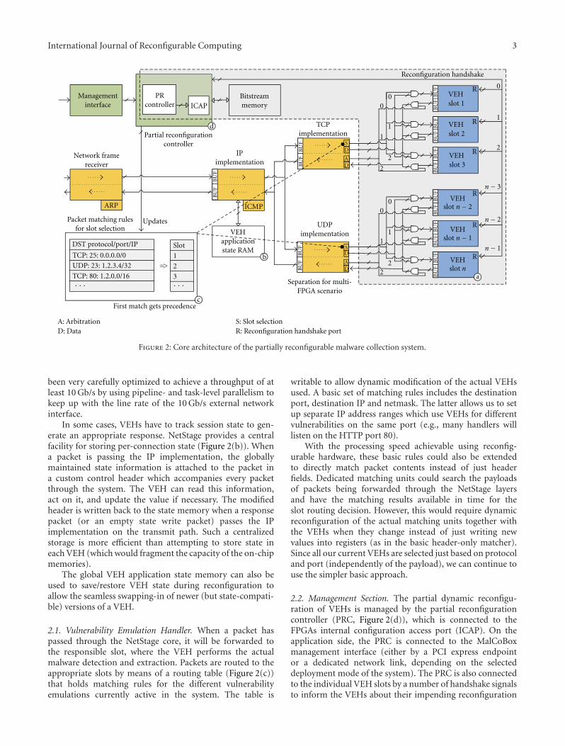
International Journal of Reconfigurable Computing 3
A: Arbitration S: Slot selectionD: Data R: Reconfiguration handshake port
VEHapplicationstate RAM
Managementinterface
VEHslot 1
VEHslot 2
VEHslot 3
ICMPARP
Network framereceiver
IPimplementation
UDPimplementation
TCPimplementation
BU
FB
UF
BU
FB
UF
BU
FB
UF
BU
FB
UF
BU
FB
UF
BU
FB
UF
BU
FB
UF
BU
FB
UF
BU
FB
UF
0
1
2
0
1
2
RBitstreammemory
0
1
2
0
1
2
0
1
2S
A
D
D
S
A
D
D
ICAP
PRcontroller
Partial reconfigurationcontroller
R
R
R
R
R
Reconfiguration handshake
DST protocol/port/IP
TCP: 25: 0.0.0.0/0
UDP: 23: 1.2.3.4/32
TCP: 80: 1.2.0.0/16
Slot
1
2
3
Packet matching rulesfor slot selection
=>
Updates
First match gets precedence
Separation for multi-FPGA scenario
a
c
b
d
slot n− 1
VEH
VEH
VEH
slot n− 2
slot n
n− 1
n− 2
n− 3
· · ·· · ·
Figure 2: Core architecture of the partially reconfigurable malware collection system.
been very carefully optimized to achieve a throughput of atleast 10 Gb/s by using pipeline- and task-level parallelism tokeep up with the line rate of the 10 Gb/s external networkinterface.
In some cases, VEHs have to track session state to gen-erate an appropriate response. NetStage provides a centralfacility for storing per-connection state (Figure 2(b)). Whena packet is passing the IP implementation, the globallymaintained state information is attached to the packet ina custom control header which accompanies every packetthrough the system. The VEH can read this information,act on it, and update the value if necessary. The modifiedheader is written back to the state memory when a responsepacket (or an empty state write packet) passes the IPimplementation on the transmit path. Such a centralizedstorage is more efficient than attempting to store state ineach VEH (which would fragment the capacity of the on-chipmemories).
The global VEH application state memory can also beused to save/restore VEH state during reconfiguration toallow the seamless swapping-in of newer (but state-compati-ble) versions of a VEH.
2.1. Vulnerability Emulation Handler. When a packet haspassed through the NetStage core, it will be forwarded tothe responsible slot, where the VEH performs the actualmalware detection and extraction. Packets are routed to theappropriate slots by means of a routing table (Figure 2(c))that holds matching rules for the different vulnerabilityemulations currently active in the system. The table is
writable to allow dynamic modification of the actual VEHsused. A basic set of matching rules includes the destinationport, destination IP and netmask. The latter allows us to setup separate IP address ranges which use VEHs for differentvulnerabilities on the same port (e.g., many handlers willlisten on the HTTP port 80).
With the processing speed achievable using reconfig-urable hardware, these basic rules could also be extendedto directly match packet contents instead of just headerfields. Dedicated matching units could search the payloadsof packets being forwarded through the NetStage layersand have the matching results available in time for theslot routing decision. However, this would require dynamicreconfiguration of the actual matching units together withthe VEHs when they change instead of just writing newvalues into registers (as in the basic header-only matcher).Since all our current VEHs are selected just based on protocoland port (independently of the payload), we can continue touse the simpler basic approach.
2.2. Management Section. The partial dynamic reconfigu-ration of VEHs is managed by the partial reconfigurationcontroller (PRC, Figure 2(d)), which is connected to theFPGAs internal configuration access port (ICAP). On theapplication side, the PRC is connected to the MalCoBoxmanagement interface (either by a PCI express endpointor a dedicated network link, depending on the selecteddeployment mode of the system). The PRC is also connectedto the individual VEH slots by a number of handshake signalsto inform the VEHs about their impending reconfiguration

4 International Journal of Reconfigurable Computing
(for a clean shutdown, etc.) and to check whether the VEH isidle. An attached bitstream memory can hold several partialbitstreams to allow the system to be reconfigured indepen-dently of the management station in future implementations.
2.3. Reconfigurable VEHs. The VEHs are dedicated to emu-late known application vulnerabilities that may be exploitedby malware. As malware is evolving quickly and newvulnerabilities are detected on a regular basis, the VEHsneed to be updated as well. For example, when the system isused for research purposes, multiple updates per day wouldcommonly be required if a researcher would like to react tocurrent observations in the network traffic.
In a conventional software-based system, such changescould generally be handled quickly by altering a few linesof code in a script language. However, when using dedicatehardware, even minor changes of the functionality requirefull logic synthesis, mapping, and place-and-route steps. Thiseffort can be significantly reduced by employing dynamicpartial reconfiguration (DPR) to recompile just those VEHsactually affected by the change.
As a secondary effect, DPR also allows the arbitrarycombination of VEHs in the system. Otherwise, each specificset of selected VEHs would need to be compiled into its ownstatic configuration.
To support independent partial reconfiguration of any ofthe VEH slots within the architecture, a wrapper encapsulatesthe actual VEH implementation module (see Figure 3). Thiswrapper includes glue logic controlled by the partial recon-figuration controller to disconnect/reconnect all inputs andoutputs of the VEH module. This clean separation is essentialto avoid introducing errors in the rest of the system whenreconfiguring.
The wrapper also contains the send and receive buffersfor each module as well as the corresponding buffer man-agement logic. As all the handlers share the same bufferstructure, it is more efficient to keep it static than configureit with each VEH. The inputs and outputs of the wrapper aredirectly connected to the MalCoBox core (see Figure 2).
3. Multidevice Architecture
To extend our system to multiple FPGAs, we will draw theboundaries between the static NetStage core (basic Ether-net and Internet protocol functions) and the dynamicallyexchangeable VEH slots (see the dotted line in Figure 2). OneFPGA acting as Master node holds the network core and thenetwork interfaces, and the remaining other FPGAs, calledVEH nodes, contain the individual emulation blocks. TheBEE3 platform supports a number of interdevice intercon-nection schemes. For future scalability independently of theBEE3 architecture, we decided to implement a ring structure.Such rings have already proven useful in multichip systemsinternally using NoCs [14].
For extending the NetStage-based MalCoBox to multipledevices, a unidirectional ring suffices (Figure 4). The unidi-rectional ring needs fewer I/O pins on the FPGAs and avoidsthe increased latency of the bus-turnaround cycles thatwould be required when running a bidirectional bus over the
same pins. Also note that in contrast to the implementationsin discussed in prior work, the one described here is usingthe external SDRAM instead of the internal BlockRAM totemporarily store bitstreams, conserving FPGA resources toallow more VEHs.
3.1. Ring Communication. For the communication on thering, we use 66 of the 72 available inter-FPGA data lines onthe BEE3 which are run in DDR mode, resulting in 132 bits ofdata per clock cycle [7]. Four bits are reserved for status bits,the remaining 128 form the data transmission word. As datawords are sent continuously on the ring for synchronizationpurposes (even if not actual data needs to be transmitted),a valid flag is used to indicate words holding actual messagedata. For the separation of individual messages, we use twoflags to signal the first and the last word of a message. As theactual byte size of the message is already stored within theinternal control header (ICH, see Figure 8) used by NetStage(prefixed to the message body), no special-case processingis required for unused bytes in the last data word of amessage. A final flag is used to denote special ring controlmessages used, for example, to control the DPR process(see next section). In a future extension, this could also beused, for example, to enumerate the ring nodes automaticallyduring initialization. Currently, the destination addresses ofthe available FPGAs inside the ring are set during compiletime.
The ICH-prefixed message is prefixed yet again with a128 b ring control header (RCH) when it is transmittedbetween devices. The RCH carries the type information ofthe message and the destination FPGA. The remaining bitsare reserved to implement further control functions in thefuture.
Since we want to maintain a high bandwidth and lowlatency even when distributing the architecture across mul-tiple devices, we want to operate the interdevice links atmaximum speed. To this end, we use the BEE3-providedglobal clock to all FPGAs as the ring clock. However, due todifferent trace lengths and other board-level signal integrityeffects, reliable operation at our target frequency of 250 MHzrequires a training of the individual FPGAs to the linkcharacteristics. This is done using the technique proposedin [15]. A known training sequence is transmitted betweenadjacent FPGAs, and the receiver adjusts its delay until itreceives a stable pattern from the transmitter.
Two additional signals are required to realize trainingprocedure (see Figures 5 and 6). The Master starts the processby asserting a Sync signal, which is routed around the entirering. It is used to both initiate training between neighboringFPGAs and to test whether the nodes did configure correctlyon start-up (an error is indicated if the Sync sent out by theMaster does not match the incoming Sync passed around thering). Once the receiving FPGA of a synchronization pairhas locked on to the training pattern, it asserts its internalReady signal, which is ANDed with the Ready incoming fromits transmitting partner before being output to its receivingpartner (the next device on the ring). Once the Master hasreceived an asserted Ready signal passed around the entire

International Journal of Reconfigurable Computing 5
rd_en
wr_en
din dout
empty
ringbuf_fifo
addra
wr_en
dina doutb
ringbuf_bram
addrb
ringbuf_fifo
addra
wr_en
dina doutb
ringbuf_bram
addrb
01
0
01
0
01
0
01
0
01
0
data_available send_buffer full
data in
write bytes
get next packet
VEH handler
ctrl word in
read finished
amount of bytes read write finished
read address
write enable
data out
write address
ENB
ENB
ENB
veh reset01
1ENB
ENB
ENB
ENB
ENB
ENB++
write byte count
write done
Buffer managementparam: buf_size
read byte count
read done
full
offset
reset
resetrd_en
wr_en
din dout
emptyreset
write byte_count
write done
Buffer managementparam: buf_size
read byte_count
read done
full
offset
reset
0
1 0
ENB
0
1 0
ENB
0
1 0
ENB
01 0
ENB
ENB
reset
reset reset
reset reset
read address
En
able
mod
ule
ENB
get next packet
control word out
packet available
read done
read bytes
data out
active
Mod
ule
act
ive
pr r
equ
est
combinedcontrolword
combinedcontrol word
Receive buffer Send bufferPR handshake port
Receive buffer full
write done
write bytes
write enable
write address
data in
reset
Figure 3: Wrapper encapsulating a vulnerability emulation handler slot.
SDRAMSDRAM
SDRAM
10GCX4
Node 2
Master
Node 3
Node 1
Ringdirection
VEH
VEH
VEHNetStage
core
MGMT PR
VEHVEH
VEH
VEH
VEH
VEH
PR PR
Figure 4: Multi-FPGA network processor in ring topology.
ring, it stops training and releases the ring into normaloperation.
The ring thus achieves a transfer rate of 32 Gb/s betweennodes, more than sufficient for our current 10 Gb/s networkenvironment. For simplicity, and since we did not experi-ence any data integrity issues in our practical experiments
once training completed, we do not perform error detec-tion/correction on the ring communications. However, forlong-term production use, CRC/ECC facilities could beadded here. As there are still data lines available on the BEE3,this could be easily implemented without affecting the basearchitecture.
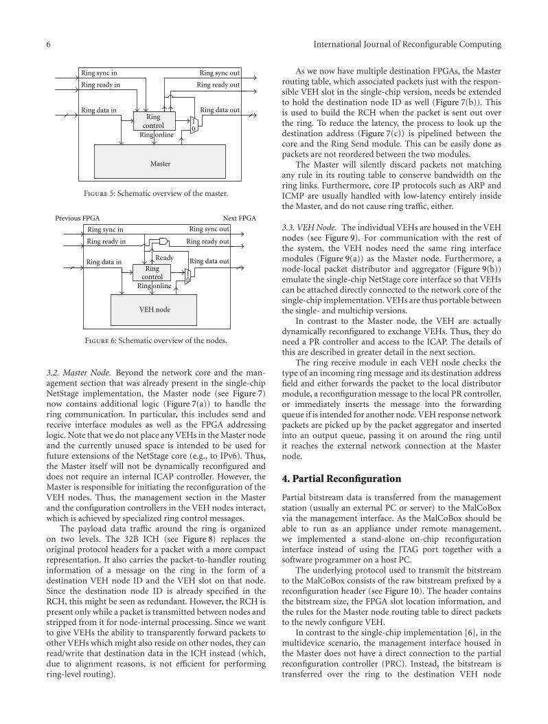
6 International Journal of Reconfigurable Computing
Ring sync in
Ring ready in
Ring sync out
Ring ready out
Ring data in Ring data out
Master
Ringcontrol
10
Ring online
Figure 5: Schematic overview of the master.
Ring sync in
Ring ready in
Ring sync out
Ring ready out
Ring data in Ring data out
VEH node
Ringcontrol 1
0
Ready
Previous FPGA Next FPGA
Ring online
Figure 6: Schematic overview of the nodes.
3.2. Master Node. Beyond the network core and the man-agement section that was already present in the single-chipNetStage implementation, the Master node (see Figure 7)now contains additional logic (Figure 7(a)) to handle thering communication. In particular, this includes send andreceive interface modules as well as the FPGA addressinglogic. Note that we do not place any VEHs in the Master nodeand the currently unused space is intended to be used forfuture extensions of the NetStage core (e.g., to IPv6). Thus,the Master itself will not be dynamically reconfigured anddoes not require an internal ICAP controller. However, theMaster is responsible for initiating the reconfiguration of theVEH nodes. Thus, the management section in the Masterand the configuration controllers in the VEH nodes interact,which is achieved by specialized ring control messages.
The payload data traffic around the ring is organizedon two levels. The 32B ICH (see Figure 8) replaces theoriginal protocol headers for a packet with a more compactrepresentation. It also carries the packet-to-handler routinginformation of a message on the ring in the form of adestination VEH node ID and the VEH slot on that node.Since the destination node ID is already specified in theRCH, this might be seen as redundant. However, the RCH ispresent only while a packet is transmitted between nodes andstripped from it for node-internal processing. Since we wantto give VEHs the ability to transparently forward packets toother VEHs which might also reside on other nodes, they canread/write that destination data in the ICH instead (which,due to alignment reasons, is not efficient for performingring-level routing).
As we now have multiple destination FPGAs, the Masterrouting table, which associated packets just with the respon-sible VEH slot in the single-chip version, needs be extendedto hold the destination node ID as well (Figure 7(b)). Thisis used to build the RCH when the packet is sent out overthe ring. To reduce the latency, the process to look up thedestination address (Figure 7(c)) is pipelined between thecore and the Ring Send module. This can be easily done aspackets are not reordered between the two modules.
The Master will silently discard packets not matchingany rule in its routing table to conserve bandwidth on thering links. Furthermore, core IP protocols such as ARP andICMP are usually handled with low-latency entirely insidethe Master, and do not cause ring traffic, either.
3.3. VEH Node. The individual VEHs are housed in the VEHnodes (see Figure 9). For communication with the rest ofthe system, the VEH nodes need the same ring interfacemodules (Figure 9(a)) as the Master node. Furthermore, anode-local packet distributor and aggregator (Figure 9(b))emulate the single-chip NetStage core interface so that VEHscan be attached directly connected to the network core of thesingle-chip implementation. VEHs are thus portable betweenthe single- and multichip versions.
In contrast to the Master node, the VEH are actuallydynamically reconfigured to exchange VEHs. Thus, they doneed a PR controller and access to the ICAP. The details ofthis are described in greater detail in the next section.
The ring receive module in each VEH node checks thetype of an incoming ring message and its destination addressfield and either forwards the packet to the local distributormodule, a reconfiguration message to the local PR controller,or immediately inserts the message into the forwardingqueue if is intended for another node. VEH response networkpackets are picked up by the packet aggregator and insertedinto an output queue, passing it on around the ring untilit reaches the external network connection at the Masternode.
4. Partial Reconfiguration
Partial bitstream data is transferred from the managementstation (usually an external PC or server) to the MalCoBoxvia the management interface. As the MalCoBox should beable to run as an appliance under remote management,we implemented a stand-alone on-chip reconfigurationinterface instead of using the JTAG port together with asoftware programmer on a host PC.
The underlying protocol used to transmit the bitstreamto the MalCoBox consists of the raw bitstream prefixed by areconfiguration header (see Figure 10). The header containsthe bitstream size, the FPGA slot location information, andthe rules for the Master node routing table to direct packetsto the newly configure VEH.
In contrast to the single-chip implementation [6], in themultidevice scenario, the management interface housed inthe Master does not have a direct connection to the partialreconfiguration controller (PRC). Instead, the bitstream istransferred over the ring to the destination VEH node

International Journal of Reconfigurable Computing 7
NetStage core
Ring sendmodule
Ring receivemodule
Connection tomanagement
network
Matching data
TCP: 0.0.0.0/0:80
TCP: 1.2.3.4/32:25
Target
Destination FPGA and slot routing table
=>
Ruleupdates
DestinationFPGA/slotlookup FIFO
Destinationlookup process
Add destinationto control header
IP, protocol andport information forcurrent packet
To nextFPGA
Fromprevious
FPGA
a
a
b
BU
FB
UF
BU
FB
UF
Bitstreamdata
c
Connectionto internet
Managementinterface
······
1–1
2–5
Figure 7: Master node architecture.
SRC MAC
RAW packet data
SRC IPDST IP
IP protocol
644
1
TCP control information8
Internalflags
SRCport 2
DSTport 22
Datalength 2
FPGA/slot 2
Application state data from global state memory (up to 3 × 16 bytes)
Size of application statedata region (0–3)
Internal control header (32 bytes)
Figure 8: Structure of the internal control header.
FPGA, but the routing rules table still remains inside theMaster node. The management interface, therefore, extractsthe header information from incoming reconfiguration datarequests and updates the routing table, while the rawbitstream data is forwarded to the FPGA specified in thereconfiguration header (see also Figure 7). As the partialreconfiguration process is now distributed across multiple
devices, the time between the Master-local routing ruleupdate and the activation of new VEH in a remote nodeis longer than on the single-chip system. Thus, to avoidmisrouting of packets, the new routing rule is explicitlydisabled until the VEH is actually ready to accept traffic.
In a VEH node, an incoming bitstream is stored innode-local external DDR-SDRAM memory. One an actual
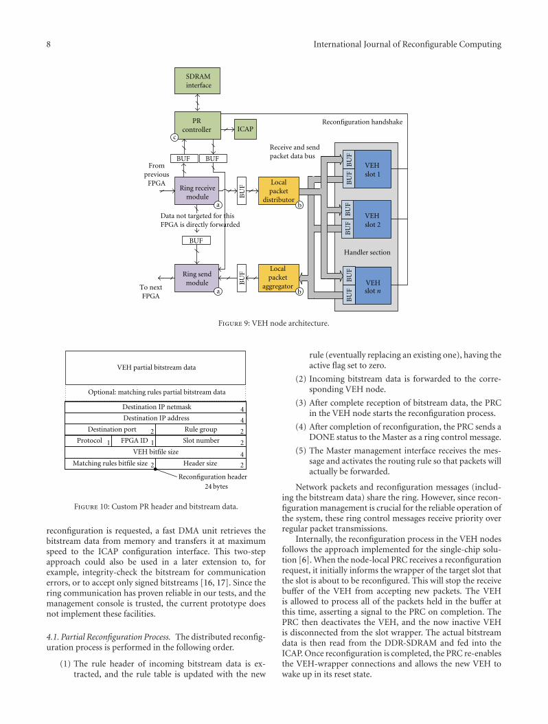
8 International Journal of Reconfigurable Computing
Data not targeted for thisFPGA is directly forwarded
Ring sendmodule
Ring receivemodule
To nextFPGA
Localpacket
aggregator
Receive and sendpacket data bus
Fromprevious
FPGA
Handler section
SDRAMinterface
ICAPPR
controller
BUF
BUF BUF
BU
FB
UF
BU
FB
UF
BU
FB
UF
BU
FB
UF
Reconfiguration handshake
Localpacket
distributor
c
a
a b
b
VEHslot 1
VEHslot 2
slot nVEH
Figure 9: VEH node architecture.
Slot number
Matching rules bitfile size Header size
Optional: matching rules partial bitstream data
VEH bitfile size
Rule groupDestination port
Destination IP address 4
Destination IP netmask
VEH partial bitstream data
4
22
4
2 2
Protocol 21 FPGA ID 1
Reconfiguration header24 bytes
Figure 10: Custom PR header and bitstream data.
reconfiguration is requested, a fast DMA unit retrieves thebitstream data from memory and transfers it at maximumspeed to the ICAP configuration interface. This two-stepapproach could also be used in a later extension to, forexample, integrity-check the bitstream for communicationerrors, or to accept only signed bitstreams [16, 17]. Since thering communication has proven reliable in our tests, and themanagement console is trusted, the current prototype doesnot implement these facilities.
4.1. Partial Reconfiguration Process. The distributed reconfig-uration process is performed in the following order.
(1) The rule header of incoming bitstream data is ex-tracted, and the rule table is updated with the new
rule (eventually replacing an existing one), having theactive flag set to zero.
(2) Incoming bitstream data is forwarded to the corre-sponding VEH node.
(3) After complete reception of bitstream data, the PRCin the VEH node starts the reconfiguration process.
(4) After completion of reconfiguration, the PRC sends aDONE status to the Master as a ring control message.
(5) The Master management interface receives the mes-sage and activates the routing rule so that packets willactually be forwarded.
Network packets and reconfiguration messages (includ-ing the bitstream data) share the ring. However, since recon-figuration management is crucial for the reliable operation ofthe system, these ring control messages receive priority overregular packet transmissions.
Internally, the reconfiguration process in the VEH nodesfollows the approach implemented for the single-chip solu-tion [6]. When the node-local PRC receives a reconfigurationrequest, it initially informs the wrapper of the target slot thatthe slot is about to be reconfigured. This will stop the receivebuffer of the VEH from accepting new packets. The VEHis allowed to process all of the packets held in the buffer atthis time, asserting a signal to the PRC on completion. ThePRC then deactivates the VEH, and the now inactive VEHis disconnected from the slot wrapper. The actual bitstreamdata is then read from the DDR-SDRAM and fed into theICAP. Once reconfiguration is completed, the PRC re-enablesthe VEH-wrapper connections and allows the new VEH towake up in its reset state.

International Journal of Reconfigurable Computing 9
5. Implementation
The MalCoBox running on the multidevice NetStage archi-tecture has been implemented on the BEEcube BEE3 FPGA-based reconfigurable computing platform, which is equippedwith eight 10 Gb/s network interfaces and four Xilinx Virtex5 FPGAs (2x LX155T, 2x LX95T). The Master node is realizedas one of the smaller SX95Ts to have both of the largerLX155T devices available for VEHs.
Network connectivity is provided by the Xilinx XAUIand 10 G MAC IPs. The network core in the Master runsat the speed of the 156.25 MHz clock of the 10 G networkinterface. Together with the internal bus width of 128 bit,this leads to a maximum core throughput of 20 Gb/s. Thisoverprovisioning allows us to react to brief stalls in thedata flow. These could occur if complex VEHs needed extratime to process a packet (e.g., perform a DRAM lookup)and could not guarantee a steady 10 Gb/s throughput.The 20 Gb/s throughput supported by NetStage thus allowshandlers to “catch up” with the normal 10 Gb/s traffic byburst-processing the data accumulated in the buffers atdouble speed.
To allow for greater design flexibility and allow the exe-cution of more complex VEHs having longer combinationalpaths, the clock rates of the Master and VEH Nodes canbe set independently. Currently, we run the VEH Nodesat 125 MHz, thus supporting burst processing at a rate of16 Gb/s. This can be easily altered (sped up or slowed down)to match the complexity (delay) of the required VEHs, aslong as the 10 Gb/s minimum throughput is always achieved.
The ICAP is operated at 32 b data width and driven bya separate clock to support variable reconfiguration speeds(and thus support experiments with overclocking the ICAP).Management access is implemented as dedicated networkinterface with a unique MAC address, directly connected toa standard desktop PC or server. The management interfacereceives bitstream data and control operations over thenetwork using a custom protocol. Perl scripts are usedto assemble the appropriate network packets. The DDR2-SDRAM interface in the VEH nodes is realized by a XilinxMIG core and fully uses the DDR2-SDRAM bandwidth.
The size of all intermodule and slot buffers is set to 4 kB(to hold 2 packets with a maximum size of 1500 B), whichis sufficient to assure stall-free operation as the modulesgenerally consume the data at a minimum rate of 10 Gb/s).If many variable-latency VEHs requiring burst processingare employed, the buffer size will need to be increasedcorrespondingly. This has already been done for the ringreceive buffers, which are set to 16 kB to provide sufficientheadroom to receive bursts of packets on the ring. The sizeof the global application state memory in the Master node iscurrently set to 1 Mb of BRAM, which is sufficient to managethe short running sessions (only a few seconds each) thatwe expect in the honeypot use case. By session, we meanthe time interval the attacker needs to check whether thetarget is vulnerable until the reception of the attack code.For applications requiring more state storage, the data couldalso be stored in the per-node DDR2-SDRAM available onthe BEE3. This would incur longer access latencies, though.
These could be avoided on newer hardware platforms byusing low-latency external memory technologies such asBandwidth Engine [18] or Hybrid Memory Cube [19].
5.1. Destination Lookup. The rules that control the messagerouting to VEHs in different nodes are stored in thedestination routing table (see Figure 11) inside the Masternode. This table is implemented as BRAM (currently witha size of 1024 rules), to achieve high lookup speeds andflexible scaling. In addition to the routing information, eachrule entry contains a rule ID that is used for managementpurposes and an active flag used during the reconfigurationprocess. The table supports multiple rules for the samedestination VEH (e.g., to let it respond to different IPaddresses).
As the destination routing decision is on the criticalpath with regard to latency, we use a hierarchical approachfor lookups. Rules with the same destination port arerepresented as a linked list, and a CAM is used to retrievethe BRAM address of the list head for a given port (seeFigure 12). Then, the individual rules for this port aresearched in list order by following the rules’ next pointers.Beyond quick lookups, this also ensure that rules withthe longest IP address prefix will be matched first. Themanagement process ensures that rules are inserted in thecorrect order.
For efficiency, we have restricted the CAM size to 256entries, reasoning that 256 different active ports should besufficient for most cases. Since the CAM has an 8b wideoutput, the heads of the per-port rule lists always start in thebottom 256 addresses of the routing table BRAM.
5.2. Example VEHs. To test the system, we have createda number of VEHs emulating different vulnerabilities andapplications. In addition to controlling FSMs, the VEHscontain additional logic to perform tasks such as fast parallelpattern matching.
(1) SIP. The SIP VEH looks for packets exploiting avulnerability of the software SIP SDK sipXtapi [20]. Theexploit uses a buffer overflow occurring if a SIP INVITEpacket contains a CSeq field value exceeding 24 bytes inlength. This VEH is based on the UDP protocol.
(2) MSSQL. Another UDP-based VEH has a similar struc-ture and is emulating a vulnerable MSSQL 2000 serverlooking for exploits targeting the resolution service [21]. Thisexploit was used in the past by, for example, the Slammerworm.
(3) Web Server. As a VEH for a further popular application,we implemented a simple web server emulation that containsa ROM with predefined HTML pages to be served to clients.The HTTP headers needed for response generation are alsostored inside the ROM. An FSM checks the URL of incomingrequests and fetches the corresponding output data to be sentfrom the ROM. This VEH can be flexibly used, for example,to emulate a login page for a company intranet and monitor
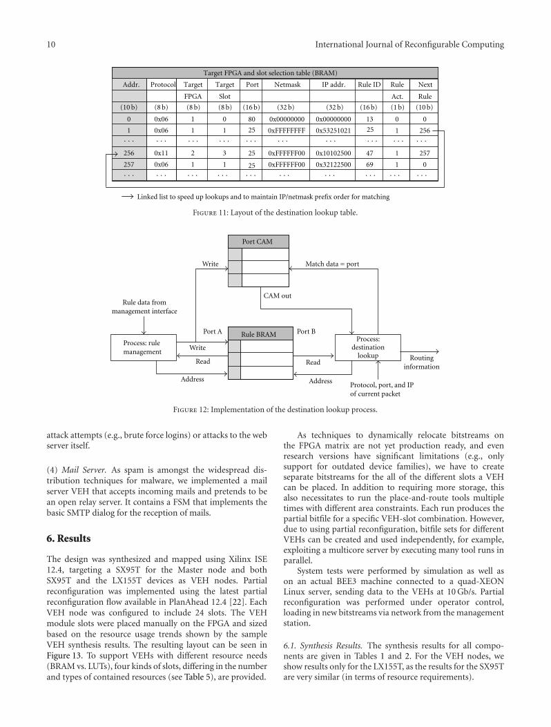
10 International Journal of Reconfigurable Computing
Next
Rule
0
256
257
0
Protocol
0x06
0x06
0x11
0x06
Addr.
0
1
256
257
Target
FPGA
1
1
2
1
Port
80
25
2525
25
Netmask
0x00000000
0xFFFFFFFF
0xFFFFFF00
0xFFFFFF00
IP addr.
0x00000000
0x53251021
0x10102500
0x32122500
Rule ID
13
47
69
Target
Slot
0
1
3
1
Rule
Act.
0
1
1
1
Linked list to speed up lookups and to maintain IP/netmask prefix order for matching
Target FPGA and slot selection table (BRAM)
· · · · · · · · · · · · · · · · · · · · · · · · · · · · · ·
· · ·· · ·· · ·· · ·· · ·· · · · · ·· · ·· · ·· · ·
(10 b) (10 b)(8 b) (8 b) (8 b) (16 b) (16 b)(32 b) (32 b) (1 b)
Figure 11: Layout of the destination lookup table.
Rule BRAMProcess: rulemanagement
Port B
CAM out
Port AProcess:
destinationlookup
Read Read
Write
Write
Rule data frommanagement interface
Port CAM
Match data = port
AddressAddress
Routinginformation
Protocol, port, and IPof current packet
Figure 12: Implementation of the destination lookup process.
attack attempts (e.g., brute force logins) or attacks to the webserver itself.
(4) Mail Server. As spam is amongst the widespread dis-tribution techniques for malware, we implemented a mailserver VEH that accepts incoming mails and pretends to bean open relay server. It contains a FSM that implements thebasic SMTP dialog for the reception of mails.
6. Results
The design was synthesized and mapped using Xilinx ISE12.4, targeting a SX95T for the Master node and bothSX95T and the LX155T devices as VEH nodes. Partialreconfiguration was implemented using the latest partialreconfiguration flow available in PlanAhead 12.4 [22]. EachVEH node was configured to include 24 slots. The VEHmodule slots were placed manually on the FPGA and sizedbased on the resource usage trends shown by the sampleVEH synthesis results. The resulting layout can be seen inFigure 13. To support VEHs with different resource needs(BRAM vs. LUTs), four kinds of slots, differing in the numberand types of contained resources (see Table 5), are provided.
As techniques to dynamically relocate bitstreams onthe FPGA matrix are not yet production ready, and evenresearch versions have significant limitations (e.g., onlysupport for outdated device families), we have to createseparate bitstreams for the all of the different slots a VEHcan be placed. In addition to requiring more storage, thisalso necessitates to run the place-and-route tools multipletimes with different area constraints. Each run produces thepartial bitfile for a specific VEH-slot combination. However,due to using partial reconfiguration, bitfile sets for differentVEHs can be created and used independently, for example,exploiting a multicore server by executing many tool runs inparallel.
System tests were performed by simulation as well ason an actual BEE3 machine connected to a quad-XEONLinux server, sending data to the VEHs at 10 Gb/s. Partialreconfiguration was performed under operator control,loading in new bitstreams via network from the managementstation.
6.1. Synthesis Results. The synthesis results for all compo-nents are given in Tables 1 and 2. For the VEH nodes, weshow results only for the LX155T, as the results for the SX95Tare very similar (in terms of resource requirements).
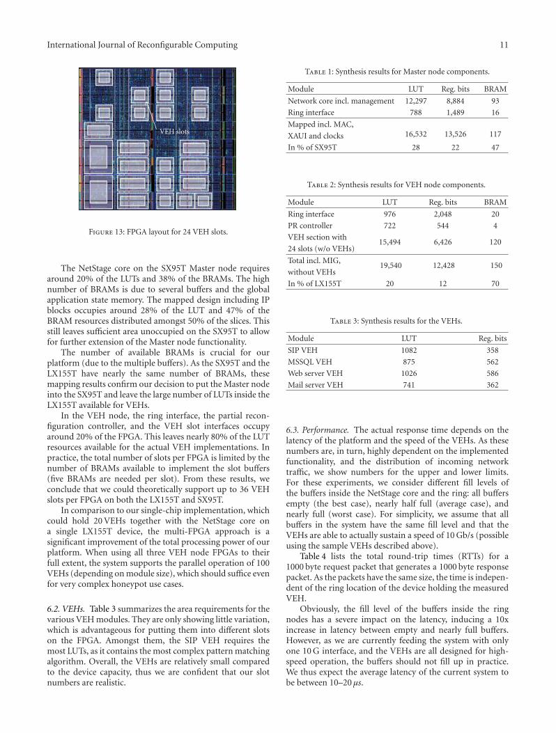
International Journal of Reconfigurable Computing 11
VEH slots
Figure 13: FPGA layout for 24 VEH slots.
The NetStage core on the SX95T Master node requiresaround 20% of the LUTs and 38% of the BRAMs. The highnumber of BRAMs is due to several buffers and the globalapplication state memory. The mapped design including IPblocks occupies around 28% of the LUT and 47% of theBRAM resources distributed amongst 50% of the slices. Thisstill leaves sufficient area unoccupied on the SX95T to allowfor further extension of the Master node functionality.
The number of available BRAMs is crucial for ourplatform (due to the multiple buffers). As the SX95T and theLX155T have nearly the same number of BRAMs, thesemapping results confirm our decision to put the Master nodeinto the SX95T and leave the large number of LUTs inside theLX155T available for VEHs.
In the VEH node, the ring interface, the partial recon-figuration controller, and the VEH slot interfaces occupyaround 20% of the FPGA. This leaves nearly 80% of the LUTresources available for the actual VEH implementations. Inpractice, the total number of slots per FPGA is limited by thenumber of BRAMs available to implement the slot buffers(five BRAMs are needed per slot). From these results, weconclude that we could theoretically support up to 36 VEHslots per FPGA on both the LX155T and SX95T.
In comparison to our single-chip implementation, whichcould hold 20 VEHs together with the NetStage core ona single LX155T device, the multi-FPGA approach is asignificant improvement of the total processing power of ourplatform. When using all three VEH node FPGAs to theirfull extent, the system supports the parallel operation of 100VEHs (depending on module size), which should suffice evenfor very complex honeypot use cases.
6.2. VEHs. Table 3 summarizes the area requirements for thevarious VEH modules. They are only showing little variation,which is advantageous for putting them into different slotson the FPGA. Amongst them, the SIP VEH requires themost LUTs, as it contains the most complex pattern matchingalgorithm. Overall, the VEHs are relatively small comparedto the device capacity, thus we are confident that our slotnumbers are realistic.
Table 1: Synthesis results for Master node components.
Module LUT Reg. bits BRAM
Network core incl. management 12,297 8,884 93
Ring interface 788 1,489 16
Mapped incl. MAC,
XAUI and clocks 16,532 13,526 117
In % of SX95T 28 22 47
Table 2: Synthesis results for VEH node components.
Module LUT Reg. bits BRAM
Ring interface 976 2,048 20
PR controller 722 544 4
VEH section with15,494 6,426 120
24 slots (w/o VEHs)
Total incl. MIG,19,540 12,428 150
without VEHs
In % of LX155T 20 12 70
Table 3: Synthesis results for the VEHs.
Module LUT Reg. bits
SIP VEH 1082 358
MSSQL VEH 875 562
Web server VEH 1026 586
Mail server VEH 741 362
6.3. Performance. The actual response time depends on thelatency of the platform and the speed of the VEHs. As thesenumbers are, in turn, highly dependent on the implementedfunctionality, and the distribution of incoming networktraffic, we show numbers for the upper and lower limits.For these experiments, we consider different fill levels ofthe buffers inside the NetStage core and the ring: all buffersempty (the best case), nearly half full (average case), andnearly full (worst case). For simplicity, we assume that allbuffers in the system have the same fill level and that theVEHs are able to actually sustain a speed of 10 Gb/s (possibleusing the sample VEHs described above).
Table 4 lists the total round-trip times (RTTs) for a1000 byte request packet that generates a 1000 byte responsepacket. As the packets have the same size, the time is indepen-dent of the ring location of the device holding the measuredVEH.
Obviously, the fill level of the buffers inside the ringnodes has a severe impact on the latency, inducing a 10xincrease in latency between empty and nearly full buffers.However, as we are currently feeding the system with onlyone 10 G interface, and the VEHs are all designed for high-speed operation, the buffers should not fill up in practice.We thus expect the average latency of the current system tobe between 10–20 μs.

12 International Journal of Reconfigurable Computing
Table 4: Round-Trip Time for a 1000 B packet: overall and per system component.
Buffer Fill Level Round-Trip Time Core Ring VEH
Empty 5.5 μs 3.6 μs 1.4 μs 0.5 μs
Half 28.7 μs 9.8 μs 17.4 μs 1.5 μs
Full 51.9 μs 16 μs 33.4 μs 2.5 μs
6.4. Partial Reconfiguration Results. Table 5 lists the localreconfiguration time and the total time needed to updatea VEH. The local reconfiguration time is measured fromthe beginning of the DMA transfer between node-localDDR2-SDRAM and ICAP and the end of the reconfigurationprocess. The remote update time is measured from the firstreception of a bitstream packet request at the managementinterface until the DONE message sent by the node PRChas been received at the Master. This time includes all datatransfers of bitstream data from the management stationto the system using the dedicated management networkinterface, sending bitstream messages on the ring fromMaster to the VEH node and the actual device configurationtime. The measurements were made using a 10G Ethernetlink at 80% utilization as the management interface. Thetable lists the theoretical optimum time (assuming rawtransmission speeds) as well as the actual measured time onthe prototype machine (by using tcpdump).
We also distinguish two cases for when looking at thelocal reconfiguration times. On a clean shutdown (labeled“w/ SD”), an outgoing VEH is allowed to fully process thepackets already present in its input queue. Without a cleanshutdown (“w/o SD”), the enqueued packets are discardedwhen the slot is reconfigured. For the clean shutdownmeasurement, we assume that the receive buffer of the VEHto be replaced is half full and that the VEH is able to processdata at 10 Gb/s (being conservative, since all of our currentVEHs can actually handle more).
The time required for cleanly shutting down the outgoingVEH is negligible. Most of the reconfiguration time isactually taken by feeding the bitstream into the ICAP, whichlimits the overall reconfiguration speed. Thus, a small sizeof the VEHs is important for fast reconfiguration (see alsoSection 6.5) and justifies our approach of heterogeneouslysized VEH slots (we can configure the 14 smaller VEH slotsmuch faster than the 4 + 4 + 2 larger ones).
When looking at the total reconfiguration time includingtransfer of the bitstreams from the management station, theuse of a 10 Gb/s management link theoretically adds onlyabout 40% of overhead to the raw device reconfigurationtime. Even in practice, the actually measured time forreconfiguring the bitstream for the largest VEH slot overthe network was just 2.3 ms. Thus, the MalCoBox can bevery quickly adapted to changing attack behavior even ifthe bitstreams are not already present in the node-localDDR2-SDRAM, but have to be fetched from the remotemanagement station.
In [3], Baecher et al. presented results indicating thatin their experiment, the honeypot received an average of3 requests per second, with a peak of 1300 requests persecond. Based on this data, MalCoBox should have sufficient
headroom for very dynamic attack scenarios even if weassume that the system manages a larger attack surface (e.g.,a million IP addresses). This capability will be studied inthe upcoming live test of the MalCoBox system at a centralInternet router.
Note that for the more common use-case of infrequentVEH updates, a 1 Gb/s Ethernet link to the managementstation is quite sufficient.
6.5. Impact of Data Path Width. To evaluate the impact ofthe 128 b data path on the VEH size, we created 64 b versionsof the SIP and the Web Server VEHs and compared themto the original 128 b implementation (Table 6). Data pathconversion between the NetStage core and the VEHs can beeasily performed by the wrappers at the cost of a reducedthroughput for the attached VEH.
The area overhead of the 128 b version is roughly 75%for the SIP VEH and 65% for the Web Server VEH. This wasto be expected, since these VEHs mostly read data from theinput buffer and write data to the output buffer. The arearequired is thus strongly related to the bus width. Togetherwith the data path area, the BlockRAM usage is also reduced.With 64 b operation, we can now narrow the buffers andonly require three BlockRAMs per wrapper instead of five for128 b VEHs.
Given these results, the number of parallel VEHs in thesystem could be increased even further by using the smallerdatapath width, but only at a loss of per-VEH throughput(8 Gb/s with 64 b width and 125 MHz VEH node clocks).Assuming a heterogeneous traffic distribution across allVEHs, this would not actually lead to a slow-down, sincethe NetStage core would keep its 20 Gb/s-capable 128 b datapath width and distribute the traffic across multiple ofthe smaller-but-slower VEHs. The bottleneck would onlybecome apparent if all traffic was to be directed at a singleVEH, which then would not be able to keep up with the10 Gb/s line rate.
7. Conclusion and Next Steps
With this refinement of our MalCoBox system, we havepresented a scalable architecture to build a high-speedhardware-accelerated malware collection solution that offersgreat flexibility through partial reconfiguration and thedistribution of VEHs over multiple FPGAs. In the multide-vice scenario, the total amount of VEH processing poweris significantly improved in contrast to the single-chipimplementation, allowing us to implement even large-scalehoneynets with a single appliance. A dedicated managementinterface allows quick updates or replacements of singlevulnerability emulation handlers by loading new partial

International Journal of Reconfigurable Computing 13
Table 5: Slot size distribution and reconfiguration time.
Qty. LUT/BRAM Bitfile sizeReconfiguration time
Local reconfiguration Remote reconfiguration
w/o SD w/SD Optimum Measured
14 1440/0 59 KB 151 μs 154 μs 218 μs 574 μs
4 2304/0 119 KB 305 μs 308 μs 432 μs 1740 μs
4 2304/2 128 KB 328 μs 332 μs 465 μs 1886 μs
2 4864/0 237 KB 607 μs 610 μs 852 μs 2269 μs
Table 6: Synthesis results for 128 b and 64 b VEHs.
VEH LUT Reg. Bits
SIP 128 Bit 1082 358
SIP 64 Bit 619 278
Web Server 128 Bit 1026 586
Web Server 64 Bit 663 244
bitstreams, without interrupting the operation of the rest ofthe system.
Enabled by the high performance of the dedicated hard-ware, the VEHs actually performing the malware detectionand extraction can contain a wide range of functionality.They can embed complex regular expression logic as wellas simple request-response patterns, while still reaching therequired throughput of 10 Gb/s. Furthermore, our hardwareapproach is resilient against compromising attacks andsignificantly reduces the risk of operating honeypots in aproduction environment.
The presented implementation of the multi-FPGA sys-tem on the BEEcube BEE3 quad-FPGA reconfigurablecomputing platform demonstrated the feasibility of theapproach. Operators have a great flexibility to adapt thesystem to their needs: A tradeoff can easily be made betweenindividual VEH complexity and total vulnerability coverageusing many different VEHs just by altering the distributionof VEH slots sizes; throughput and area can be traded offby selecting between VEH implementations with 64 b and128 b processing widths, and the overall system size can bescaled by selecting either the single-chip or the multi-FPGAapproach.
We will continue our work in this area. MalCoBox isplanned to be stress-tested in a real production environmentconnected to the Internet (e.g., university or ISP). From this,we expect to gain valuable insights on how to improve thearchitecture and its parameters in the future. Furthermore,we will combine the multi-FPGA system with our recentwork on self-adapting by dynamic partial reconfigurationbased on the observed traffic characteristics. We expect toachieve a platform that exploits many of today’s cutting-edgetechnologies in reconfigurable computing to enable a systempresenting maximal flexibility, performance, and security tothe user.
Acknowledgments
This work was supported by CASED and Xilinx, Inc.
References
[1] “Internet Security Threat Report, Volume XV,” Symantec,2010, http://www.symantec.com/.
[2] “HoneyD,” http://www.honeyd.org/.[3] P. Baecher, M. Koetter, T. Holz, M. Dornseif, and F. Freiling,
“The nepenthes platform: an efficient approach to collectmalware,” in Recent Advances in Intrusion Detection,, vol. 4219of Lecture Notes in Computer Science, pp. 165–184, Springer,Berlin, Germany, 2006.
[4] S. Muhlbach, M. Brunner, C. Roblee, and A. Koch, “Mal-CoBox: designing a 10 Gb/s malware collection honeypotusing reconfigurable technology,” in Proceedings of the 20thInternational Conference on Field Programmable Logic andApplications (FPL ’10), pp. 592–595, IEEE Computer Society,2010.
[5] J. W. Lockwood, N. Naufel, J. S. Turner, and D. E. Tay-lor, “Reprogrammable network packet processing on thefield programmable port extender (FPX),” in Proceedingsof the ACM/SIGDA 9th International Symposium on FieldProgrammable Gate Arrays (FPGA ’01), pp. 87–93, ACM, 2001.
[6] S. Muhlbach and A. Koch, “A dynamically reconfigurednetwork platform for high-speed malware collection,” inProceedings of the International Conference on ReConFigurableComputing and FPGAs (ReConFig ’10), pp. 79–84, IEEEComputer Society, 2010.
[7] S. Muhlbach and A. Koch, “A scalable multi-FPGA platformfor complex networking applications,” in Proceedings of theIEEE International Symposium on Field-Programmable CustomComputing Machines (FCCM ’11), pp. 81–84, IEEE ComputerSociety, 2011.
[8] BEEcube, Inc., “BEE3 Hardware User Manual,” 2008.[9] V. Pejovic, I. Kovacevic, S. Bojanic, C. Leita, J. Popovic, and O.
Nieto-Taladriz, “Migrating a honeypot to hardware,” in Pro-ceedings of the International Conference on Emerging SecurityInformation, Systems, and Technologies (SECURWARE ’07), pp.151–156, 2007.
[10] J. W. Lockwood, N. McKeown, G. Watson et al., “NetFPGA—an open platform for gigabit-rate network switching androuting,” in Proceedingsof the IEEE International Conference onMicroelectronic Systems Education: Educating Systems Design-ers for the Global Economy and a Secure World (MSE ’07), pp.160–161, IEEE Computer Society, 2007.
[11] C. Albrecht, R. Koch, and E. Maehle, “DynaCORE: a dynam-ically reconfigurable coprocessor architecture for networkprocessors,” in Proceedings of the 14th Euromicro InternationalConference on Parallel, Distributed, and Network-Based Pro-cessing, pp. 101–108, IEEE Computer Society, 2006.
[12] C. Kachris and S. Vassiliadis, “Analysis of a reconfigurablenetwork processor,” in Proceedings of the 20th InternationalParallel and Distributed Processing Symposium (IPDPS ’06), p.187, IEEE Computer Society, 2006.

14 International Journal of Reconfigurable Computing
[13] D. Yin, D. Unnikrishnan, Y. Liao, L. Gao, and R. Tessier, “Cus-tomizing virtual networks with partial FPGA reconfiguration,”ACM SIGCOMM—Computer Communication Review, vol. 41,pp. 57–64, 2010.
[14] S. Bourduas and Z. Zilic, “A hybrid ring/mesh interconnectfornetwork-on-chip using hierarchical rings for global routing,”in Proceedings of the 1st International Symposium on Networks-on-Chip (NOCS ’07), pp. 195–204, IEEE Computer Society,2007.
[15] C. Thacker, “DDR2 SDRAM Controller for BEE3,” MicrosoftResearch, 2008.
[16] K. v. d. Bok, R. Chaves, G. Kuzmanov, L. Sousa, and A.v. Genderen, “FPGA reconfigurations with run-time regiondelimitation,” in Proceedings of the 18th Annual WorkshoponCircuits, Systems and Signal Processing (ProRISC ’07), pp. 201–207, 2007.
[17] Y. Hori, A. Satoh, H. Sakane, and K. Toda, “Bitstream encryp-tion and authentication using AES-GCM in dynamicallyreconfigurable systems,” in Proceedingsof the 3rd InternationalWorkshop on Security (IWSEC ’08), pp. 261–278, Springer,2008.
[18] M. Miller, “Bandwidth engine serial memory chip breaks 2billion accesses/sec,” in Proceedings of the 23rd Hot Chips Sym-posium, 2011.
[19] J. T. Pawlowski, “Hybrid memory cube: breakthrough DRAMperformance with a fundamentally re-architected DRAM sub-system,” in Proceedings of the 23rd Hot Chips Symposium, 2011.
[20] M. Thumann, “Buffer Overflow in SIP Foundry’s SipXtapi,”2006, http://www.securityfocus.com/archive/1/439617.
[21] D. Litchfield, “Microsoft SQL Server 2000 Unauthenti-cated System Compromise,” http://marc.info/?l=bugtraq&m=102760196931518&w=2.
[22] Xilinx, Partial Reconfiguration User Guide, 2010.
Hindawi Publishing CorporationInternational Journal of Reconfigurable ComputingVolume 2012, Article ID 127302, 10 pagesdoi:10.1155/2012/127302
Research Article
Using Partial Reconfiguration and Message Passing toEnable FPGA-Based Generic Computing Platforms
Manuel Saldana,1 Arun Patel,1 Hao Jun Liu,2 and Paul Chow2
1 ArchES Computing Systems, 708-222 Spadina Avenue, Toronto, ON, Canada M5T 3A22 The Edward S. Rogers Sr. Department of Electrical and Computer Engineering, University of Toronto, 10 King’s College Road,Toronto, ON, Canada M5S 3G4
Correspondence should be addressed to Manuel Saldana, [email protected]
Received 12 May 2011; Accepted 22 August 2011
Academic Editor: Marco D. Santambrogio
Copyright © 2012 Manuel Saldana et al. This is an open access article distributed under the Creative Commons AttributionLicense, which permits unrestricted use, distribution, and reproduction in any medium, provided the original work is properlycited.
Partial reconfiguration (PR) is an FPGA feature that allows the modification of certain parts of an FPGA while the rest of thesystem continues to operate without disruption. This distinctive characteristic of FPGAs has many potential benefits but alsochallenges. The lack of good CAD tools and the deep hardware knowledge requirement result in a hard-to-use feature. In thispaper, the new partition-based Xilinx PR flow is used to incorporate PR within our MPI-based message-passing framework toallow hardware designers to create template bitstreams, which are predesigned, prerouted, generic bitstreams that can be reusedfor multiple applications. As an example of the generality of this approach, four different applications that use the same templatebitstream are run consecutively, with a PR operation performed at the beginning of each application to instantiate the desiredapplication engine. We demonstrate a simplified, reusable, high-level, and portable PR interface for X86-FPGA hybrid machines.PR issues such as local resets of reconfigurable modules and context saving and restoring are addressed in this paper followed bysome examples and preliminary PR overhead measurements.
1. Introduction
Partial reconfiguration (PR) is a feature of an FPGA that al-lows part of it to be reconfigured while the rest of itcontinues to operate normally. PR has been the focus ofconsiderable research because of the many potential benefitsof such a feature. For example, it allows the implementationof more power-efficient designs by using hardware on-demand, that is, only instantiate the logic that is necessaryat a given time and remove unused logic. PR also allowsthe virtualization of FPGA resources by time sharing themamong many concurrent applications. Alternatively, a singlelarge application may be implemented even if it requiresmore logic resources than what a single FPGA can provide aslong as the logic resources are not required simultaneously.Fault-tolerant systems and dynamic load-balancing are alsopotential benefits of PR. All these features make PR attractivefor applications in the fields of automotive and aerospace
design, software radio, video, and image processing, amongother markets.
However, there are many challenges for PR to be morewidely accepted, for example, dynamic changing of logicadds an extra level of difficulty to verification performanceoverheads in terms of designed target frequency and higherresource utilization complex design entry tools and PR CADflows. A PR design requires the partitioning and floor-planning of the entire FPGA into static regions (SRs) andreconfigurable regions (RRs). The SR does not change duringthe execution of an application, and RRs may be dynamicallyreconfigured during the execution of the application. Thispartitioning has added another layer of complexity to FPGAdesign. To cope with this increased complexity, Xilinx hasreleased a new partition-based ISE 12 solution that simplifiesPR design [1].
By looking at Xilinx documentation and comparing theresources in Virtex-E and Virtex 7 devices, we can see that
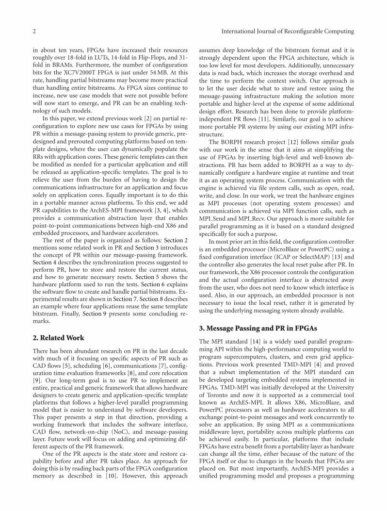
2 International Journal of Reconfigurable Computing
in about ten years, FPGAs have increased their resourcesroughly over 18-fold in LUTs, 14-fold in Flip-Flops, and 31-fold in BRAMs. Furthermore, the number of configurationbits for the XC7V2000T FPGA is just under 54 MB. At thisrate, handling partial bitstreams may become more practicalthan handling entire bitstreams. As FPGA sizes continue toincrease, new use case models that were not possible beforewill now start to emerge, and PR can be an enabling tech-nology of such models.
In this paper, we extend previous work [2] on partial re-configuration to explore new use cases for FPGAs by usingPR within a message-passing system to provide generic, pre-designed and prerouted computing platforms based on tem-plate designs, where the user can dynamically populate theRRs with application cores. These generic templates can thenbe modified as needed for a particular application and stillbe released as application-specific templates. The goal is torelieve the user from the burden of having to design thecommunications infrastructure for an application and focussolely on application cores. Equally important is to do thisin a portable manner across platforms. To this end, we addPR capabilities to the ArchES-MPI framework [3, 4], whichprovides a communication abstraction layer that enablespoint-to-point communications between high-end X86 andembedded processors, and hardware accelerators.
The rest of the paper is organized as follows: Section 2mentions some related work in PR and Section 3 introducesthe concept of PR within our message-passing framework.Section 4 describes the synchronization process suggested toperform PR, how to store and restore the current status,and how to generate necessary resets. Section 5 shows thehardware platform used to run the tests. Section 6 explainsthe software flow to create and handle partial bitstreams. Ex-perimental results are shown in Section 7. Section 8 describesan example where four applications reuse the same templatebitstream. Finally, Section 9 presents some concluding re-marks.
2. Related Work
There has been abundant research on PR in the last decadewith much of it focusing on specific aspects of PR such asCAD flows [5], scheduling [6], communications [7], config-uration time evaluation frameworks [8], and core relocation[9]. Our long-term goal is to use PR to implement anentire, practical and generic framework that allows hardwaredesigners to create generic and application-specific templateplatforms that follows a higher-level parallel programmingmodel that is easier to understand by software developers.This paper presents a step in that direction, providing aworking framework that includes the software interface,CAD flow, network-on-chip (NoC), and message-passinglayer. Future work will focus on adding and optimizing dif-ferent aspects of the PR framework.
One of the PR aspects is the state store and restore ca-pability before and after PR takes place. An approach fordoing this is by reading back parts of the FPGA configurationmemory as described in [10]. However, this approach
assumes deep knowledge of the bitstream format and it isstrongly dependent upon the FPGA architecture, which istoo low level for most developers. Additionally, unnecessarydata is read back, which increases the storage overhead andthe time to perform the context switch. Our approach isto let the user decide what to store and restore using themessage-passing infrastructure making the solution moreportable and higher-level at the expense of some additionaldesign effort. Research has been done to provide platform-independent PR flows [11]. Similarly, our goal is to achievemore portable PR systems by using our existing MPI infra-structure.
The BORPH research project [12] follows similar goalswith our work in the sense that it aims at simplifying theuse of FPGAs by inserting high-level and well-known ab-stractions. PR has been added to BORPH as a way to dy-namically configure a hardware engine at runtime and treatit as an operating system process. Communication with theengine is achieved via file system calls, such as open, read,write, and close. In our work, we treat the hardware enginesas MPI processes (not operating system processes) andcommunication is achieved via MPI function calls, such asMPI Send and MPI Recv. Our approach is more suitable forparallel programming as it is based on a standard designedspecifically for such a purpose.
In most prior art in this field, the configuration controlleris an embedded processor (MicroBlaze or PowerPC) using afixed configuration interface (ICAP or SelectMAP) [13] andthe controller also generates the local reset pulse after PR. Inour framework, the X86 processor controls the configurationand the actual configuration interface is abstracted awayfrom the user, who does not need to know which interface isused. Also, in our approach, an embedded processor is notnecessary to issue the local reset, rather it is generated byusing the underlying messaging system already available.
3. Message Passing and PR in FPGAs
The MPI standard [14] is a widely used parallel program-ming API within the high-performance computing world toprogram supercomputers, clusters, and even grid applica-tions. Previous work presented TMD-MPI [4] and provedthat a subset implementation of the MPI standard canbe developed targeting embedded systems implemented inFPGAs. TMD-MPI was initially developed at the Universityof Toronto and now it is supported as a commercial toolknown as ArchES-MPI. It allows X86, MicroBlaze, andPowerPC processors as well as hardware accelerators to allexchange point-to-point messages and work concurrently tosolve an application. By using MPI as a communicationsmiddleware layer, portability across multiple platforms canbe achieved easily. In particular, platforms that includeFPGAs have extra benefit from a portability layer as hardwarecan change all the time, either because of the nature of theFPGA itself or due to changes in the boards that FPGAs areplaced on. But most importantly, ArchES-MPI provides aunified programming model and proposes a programming

International Journal of Reconfigurable Computing 3
paradigm to the developer that facilitates the implementa-tion of heterogeneous, multicore, multiaccelerator systems.
The use of PR within our message-passing framework isto allow the creation of predesigned and prerouted platformsthat can be distributed as templates to the end users withthe purpose of simplifying the system-level design process.By using PR it is possible to create an array of RRs thatcan be populated with user application cores, known as re-configurable modules (RMs) at run time. Figure 1 showssome examples of these generic designs for one, four, andeight RRs. Application cores can also be placed in the SR andthe ArchES-MPI infrastructure transparently handles thecommunication between the cores regardless of the regionthey are placed in.
A typical MPI program has multiple software processes,each with a unique ID number known as the rank. InArchES-MPI there are software ranks running on processorsand hardware ranks running as hardware engines. One MPIhardware rank can have multiple RMs. This means that therank number assigned to it does not change during the ex-ecution of the entire application, just its functionality de-pending on the RM currently configured. There is anothersituation (not covered in this paper) where a new RMrequires a change in the assigned rank number, which re-quires the NoC routing tables to be updated dynamically.
3.1. Message-Passing Engine and Reconfigurable Regions. Toprocessors, ArchES-MPI appears as a software library thatprovides message-passing capabilities. Hardware enginesmust use a hardware block called the MPE (message-pass-ing engine), which encapsulates in hardware some of the MPIfunctionality. The MPE provides the hardware equivalent toMPI Send and MPI Recv to a hardware engine in the FPGA.It handles unexpected messages, processes the communica-tion protocol, and divides large messages into smaller sizepackets to be sent through the NoC. As shown in Figure 2,the MPE is connected between the hardware engine and theNoC. The MPE receives the message parameters and datafrom the hardware engine, such as the operation (whetherit is sending or receiving a message), the destination nodeid (rank of the process in the MPI environment), the lengthof the message, and an identification number for the message(the Tag parameter in a normal MPI send/receive operation).After this, the MPE will handle the communications throughthe NoC with the destination rank. The hardware engineand the MPE form a single endpoint in the message-pass-ing network. The interfaces between the MPE and thehardware engine are four FIFOs (two for commands andtwo for data), making integration easy. These FIFOs can beasynchronous allowing the hardware engine to operate atdifferent frequencies than its associated MPE.
Based on where the MPE is placed relative to the RR,we can have three possible scenarios. Figure 3(a) shows theMPE placed outside the RR, and it is connected to a userwrapper that controls the MPE and the actual RM throughcontrol signals. The RM is a block instantiated within thewrapper. The RM block can be thought of as the maincomputational pipeline and the wrapper as a higher-level,
RR SR
RR
RR
RR
RR
RR
RRRRRR
RRRR
RR
RR
SRSR
Figure 1: Layout of template-based, generic bitstreams for one,four, and eight reconfigurable regions (RRs) and the static region(SR).
NoC
MPE
Data FIFOs
HW engine
CommandFIFOs
Figure 2: Connection of the application hardware engine and theMPE.
application-specific controller. One of the wrapper’s dutiesis to control the PR synchronization process (described inthe next section). In Figure 3(b), the MPE is also placedoutside the RR but with no wrapper (or a very small andgeneric wrapper) and it is connected directly to the RR. Thismeans that the entire RR is reserved for a single and self-contained RM that must directly control the MPE and handleits own PR synchronization process. This self-containedscenario is more generic than the wrapper-based scenariobecause it does not contain an application-specific wrapperthat may not work with a different application. From theimplementation point of view, the user can still design aspecific wrapper for a particular application but it wouldhave to be placed in the RR and not in the SR. Finally, Figures3(c) and 3(d) show the scenario where there is no MPEin the SR. This scenario gives the user the opportunity toimplement a sub-NoC that may contain many more ranksor user-defined bridges for off-chip communications such asan Ethernet-based bridge. For brevity, in this paper we onlyfocus on the first two scenarios.
4. Partial Reconfiguration Synchronization
Certain applications may need a way to store the current sta-tus of registers, state machines, and memory contents beforePR takes place and restore them once the RM is configuredback again. This is analogous to pushing and poppingvariables to a stack before and after a function call. A localreset pulse may also be required to initialize the newly par-tially reconfigured module to drive registers or state ma-chines to their quiescent state; the global reset cannot be usedfor this.
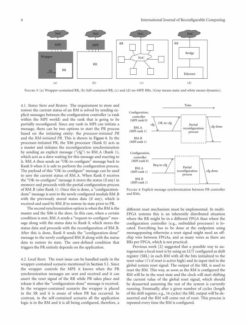
4 International Journal of Reconfigurable Computing
RR
NoC
MPE
Wrapper
rst
(a)
RR
NoC
MPE
(b)
RR
NoC
NoC
(c)
RR
NoC
Bridge
Ethernet
(d)
Figure 3: (a) Wrapper-contained RR, (b) Self-contained RR, (c) and (d) no-MPE RRs. (Gray means static and white means dynamic).
4.1. Status Store and Restore. The requirement to store andrestore the current status of an RM is solved by sending ex-plicit messages between the configuration controller (a rankwithin the MPI world) and the rank that is going to bepartially reconfigured. Since any rank in MPI can initiate amessage, there can be two options to start the PR processbased on the initiating entity: the processor-initiated PRand the RM-initiated PR. This is shown in Figure 4. In theprocessor-initiated PR, the X86 processor (Rank 0) acts asa master and initiates the reconfiguration synchronizationby sending an explicit message (“cfg”) to RM A (Rank 1),which acts as a slave waiting for this message and reacting toit. RM A then sends an “OK-to-configure” message back toRank 0 when it is safe to perform the configuration process.The payload of this “OK-to-configure” message can be usedto save the current status of RM A. When Rank 0 receivesthe “OK-to-configure” message it stores the status (if any) inmemory and proceeds with the partial configuration processof RM B (also Rank 1). Once this is done, a “configuration-done” message is sent to the newly configured module RM Bwith the previously stored status data (if any), which isreceived and used by RM B to restore its state prior to PR.
The second synchronization option is when the RM is themaster and the X86 is the slave. In this case, when a certaincondition is met, RM A sends a “request-to-configure” mes-sage along with the status data to Rank 0, which stores thestatus data and proceeds with the reconfiguration of RM B.After this is done, Rank 0 sends the “configuration-done”message to the newly configured RM B along with the statusdata to restore its state. The user-defined condition thattriggers the PR entirely depends on the application.
4.2. Local Reset. The reset issue can be handled easily in thewrapper-contained scenario mentioned in Section 3.1. Sincethe wrapper controls the MPE it knows when the PRsynchronization messages are sent and received and it canassert the reset signal of the RR while PR takes place andrelease it after the “configuration-done” message is received.In the wrapper-contained scenario the wrapper is placedin the SR and it is aware of when PR has occurred. Incontrast, in the self-contained scenario all the applicationlogic is in the RM and it is all being configured, therefore, a
Time
Partialreconfiguration
process
Req-to-cfg
cfg-done
Partialreconfiguration
processcfg-done
cfg
Configuration,controller
(MPI rank 0)
RM A(MPI rank 1)
RM B(MPI rank 1)
Configuration,controller
(MPI rank 0)
RM A(MPI rank 1)
RM B(MPI rank 1)
OK-to-cfg
Figure 4: Explicit message synchronization between PR controllerand RMs.
different reset mechanism must be implemented. In multi-FPGA systems this is an inherently distributed situationwhere the RR might be in a different FPGA than where theconfiguration controller (e.g., embedded processor) is lo-cated. Everything has to be done at the endpoints usingmessagepassing otherwise a reset signal might need an off-chip wire between FPGAs, and as many wires as there areRRs per FPGA, which is not practical.
Previous work [2] suggested that a possible way to au-togenerate a local reset is by using an LUT configured as shiftregister (SRL) in each RM with all the bits initialized to thereset value (1’s if reset is active high) and its input tied to theglobal system reset signal. The output of the SRL is used toreset the RM. This way, as soon as the RM is configured theRM will be in the reset state and the clock will start shiftingthe current value of the global reset signal, which shouldbe deasserted assuming the rest of the system is currentlyrunning. Eventually, after a given number of cycles (lengthof the shift register, e.g., 16 cycles) the SRL output will be de-asserted and the RM will come out of reset. This process isrepeated every time the RM is configured.

International Journal of Reconfigurable Computing 5
···
...
Local reset SRL
Last reconfigurableframe
FPGA fabric
Figure 5: Placement of the reset SRL within the RR.
However, a problem with the approach is that it will notwork if the SRL placement is not properly constrained. Webelieve that partial reconfiguration of an entire RR does nothappen atomically, which means that not all the logic of anRM is configured at once, but frame by frame. A PR frameis the smallest reconfigurable building block. A PR frame is 1CLB wide by 16, 20, or 40 CLBs high for Virtex 4, 5, and 6,respectively. If the reset SRL is configured before the rest ofthe RM logic is configured then the local reset will be appliedto old logic from the previous RM. The actual time it takesto complete PR depends on how fast the partial bitstreamis transferred from host memory to the ICAP or SelectMAPinterfaces, which in turn depends on what communicationmechanism is being used (PCIe, FSB, Ethernet, etc.). In anycase, a good solution should not rely on configuration timeto be correct.
A possible solution to this problem is to force the CADtools to place the SRL in the last LUT of the last frame withinthe RR to be configured as shown in Figure 5. This way weensure that all the logic from the RM has been configuredbefore the reset SRL and that the local reset will apply to thenew RM logic. However, the caveat of this approach is, that tothe best of our knowledge, there is no official documentationfrom Xilinx regarding how PR is done over the RR. Forexample, Figure 5 assumes that PR follows a top-down andleft-right approach, but it could be otherwise.
To avoid the previous problems, the approach used togenerate a local reset is to take advantage of the existingmessage-passing capability and the MPE to produce anexternal signal to the RM. This approach has the addedbenefit being platform independent. After an RM receives theconfiguration message (“cfg”) and before PR takes place, thecurrent RM can instruct the MPE to be ready to receive the“configuration-done” message, which will come eventually.The RM’s FSM then goes into an idle state waiting for PR tooccur. After PR is done and the new RM has been completelyconfigured, the X86 processor sends the “configuration-done” message, which the MPE is already expecting. Thiscauses the MPE to inform the RM of the newly arrivedmessage by writing a control word to the command FIFObetween the MPE and the RM. The exists signal (Ex inFigure 6) of the command FIFO is then used to generatethe reset pulse for the new RM. After coming out of reset
Global resetcmdwr rd
MPE
Local reset
RR
wrData
ExData
RS Q
RSQ
MPI initializedPR-in-progress
Figure 6: Static registers and decoupling logic between SR and RR.
the RM can dequeue the control word and start running, orresume its operation by restoring its previous status (if any)as mentioned in Section 4.1.
There is an additional requirement for RMs that useArchES-MPI when coming out of reset. The MPI Init func-tion must be called only once by all ranks at the beginningof the application. This function initializes the MPI envi-ronment and in the case of a hardware rank the functioninitializes the MPEs. This means that after coming out ofreset an RM must know whether it is the first time theapplication is running, and therefore the MPE needs tobe initialized, or if the MPE has been initialized alreadyby a previous RM. In the later case the RM must not gothrough the initialization process again. Instead, it mustcontinue its execution and restore its status (if any) using the“configuration-done” message.
A simple solution for this is to add a set-reset flip-flopto the SR that indicates that the MPE has been initialized.This flag, shown as MPI Initialized in Figure 6, must be setby the first RM to run in the FPGA during the initializationprocess after global reset. Successive RMs should check thisflag to know whether or not to do the initialization process.This flag is analogous to a static variable within a softwarefunction that is initialized only once during the first time thefunction is called.
4.3. Decoupling Logic. Another consideration when usingPR is the decoupling between SR and RR logic becausethe outputs of the RR may be undefined during PR. Thismay cause undesired reads or writes to FIFOs with invaliddata. To this end, the synchronization messages can be usedto set and clear a flag to gate the outputs of the RM asshown in Figure 6. When the RM receives the PR message(“cfg” in Figure 4) it sets the PR-in-progress flag, which isa set-reset flip-flop placed in SR that will disable the RRoutputs during PR. After PR is done, the flag is cleared whenthe “configuration-done” message is received. This is thesame message used to generate the local reset as previouslydiscussed. The decoupling logic occupies very little resources:158 flip-flops and 186 LUTs per RR. With one RR this meansless than 1% of the resources available in the XC5VLX330FPGA.
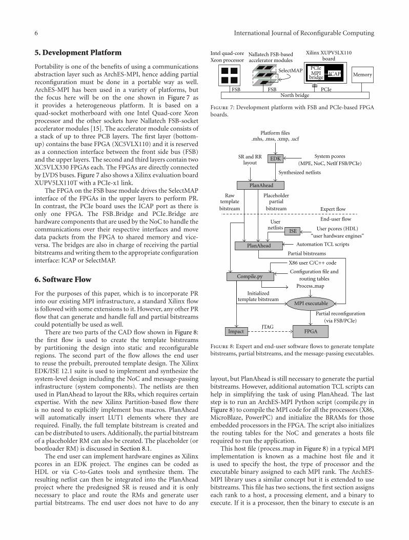
6 International Journal of Reconfigurable Computing
5. Development Platform
Portability is one of the benefits of using a communicationsabstraction layer such as ArchES-MPI, hence adding partialreconfiguration must be done in a portable way as well.ArchES-MPI has been used in a variety of platforms, butthe focus here will be on the one shown in Figure 7 asit provides a heterogeneous platform. It is based on aquad-socket motherboard with one Intel Quad-core Xeonprocessor and the other sockets have Nallatech FSB-socketaccelerator modules [15]. The accelerator module consists ofa stack of up to three PCB layers. The first layer (bottom-up) contains the base FPGA (XC5VLX110) and it is reservedas a connection interface between the front side bus (FSB)and the upper layers. The second and third layers contain twoXC5VLX330 FPGAs each. The FPGAs are directly connectedby LVDS buses. Figure 7 also shows a Xilinx evaluation boardXUPV5LX110T with a PCIe-x1 link.
The FPGA on the FSB base module drives the SelectMAPinterface of the FPGAs in the upper layers to perform PR.In contrast, the PCIe board uses the ICAP port as there isonly one FPGA. The FSB Bridge and PCIe Bridge arehardware components that are used by the NoC to handle thecommunications over their respective interfaces and movedata packets from the FPGA to shared memory and vice-versa. The bridges are also in charge of receiving the partialbitstreams and writing them to the appropriate configurationinterface: ICAP or SelectMAP.
6. Software Flow
For the purposes of this paper, which is to incorporate PRinto our existing MPI infrastructure, a standard Xilinx flowis followed with some extensions to it. However, any other PRflow that can generate and handle full and partial bitstreamscould potentially be used as well.
There are two parts of the CAD flow shown in Figure 8:the first flow is used to create the template bitstreamsby partitioning the design into static and reconfigurableregions. The second part of the flow allows the end userto reuse the prebuilt, prerouted template design. The XilinxEDK/ISE 12.1 suite is used to implement and synthesize thesystem-level design including the NoC and message-passinginfrastructure (system components). The netlists are thenused in PlanAhead to layout the RRs, which requires certainexpertise. With the new Xilinx Partition-based flow thereis no need to explicitly implement bus macros. PlanAheadwill automatically insert LUT1 elements where they arerequired. Finally, the full template bitstream is created andcan be distributed to users. Additionally, the partial bitstreamof a placeholder RM can also be created. The placeholder (orbootloader RM) is discussed in Section 8.1.
The end user can implement hardware engines as Xilinxpcores in an EDK project. The engines can be coded asHDL or via C-to-Gates tools and synthesize them. Theresulting netlist can then be integrated into the PlanAheadproject where the predesigned SR is reused and it is onlynecessary to place and route the RMs and generate userpartial bitstreams. The end user does not have to do any
FSBNorth bridge
MemoryICAPMPIbridge
Nallatech FSB-basedaccelerator modules
Xilinx XUPV5LX110board
FSB
Intel quad-coreXeon processor
PCIe
SelectMAP PCIe
Figure 7: Development platform with FSB and PCIe-based FPGAboards.
SR and RRlayout
EDK
Synthesized netlists
Rawtemplatebitstream
Placeholderpartial
bitstream Expert flow
End-user flow
ISE
Usernetlists User pcores (HDL)
“user hardware engines”
Automation TCL scripts
Partial bitstreams
Configuration file androuting tables
Process map
Initializedtemplate bitstream
MPI executable
FPGAJTAG
Impact
X86 user C/C++ code
Platform files.mhs, .mss, .xmp, .ucf
PlanAhead
PlanAhead
Compile.py
System pcores(MPE, NoC, Netlf FSB/PCIe)
Partial reconfiguration(via FSB/PCIe)
Figure 8: Expert and end-user software flows to generate templatebitstreams, partial bitstreams, and the message-passing executables.
layout, but PlanAhead is still necessary to generate the partialbitstreams. However, additional automation TCL scripts canhelp in simplifying the task of using PlanAhead. The laststep is to run an ArchES-MPI Python script (compile.py inFigure 8) to compile the MPI code for all the processors (X86,MicroBlaze, PowerPC) and initialize the BRAMs for thoseembedded processors in the FPGA. The script also initializesthe routing tables for the NoC and generates a hosts filerequired to run the application.
This host file (process map in Figure 8) in a typical MPIimplementation is known as a machine host file and itis used to specify the host, the type of processor and theexecutable binary assigned to each MPI rank. The ArchES-MPI library uses a similar concept but it is extended to usebitstreams. This file has two sections, the first section assignseach rank to a host, a processing element, and a binary toexecute. If it is a processor, then the binary to execute is an

International Journal of Reconfigurable Computing 7
main()
MPI Init(···);//implicit config. of SRs and initial RMs
···
MPI Send(···, destRank, CFG MSG TAG···);
MPI Recv(statusData RM A,. . ., destRank,OK TO CFG TAG,···);
ARCHES MPI Reconfig(RM B.bit,boardNum,fpgaNum);
MPI Send(statusData RM B,. . ., destRank, CFG DONE TAG,···);···
Figure 9: Partial reconfiguration code snippet.
ELF file generated by the compiler (e.g., gcc) for X86, orcross-compiler for embedded processors (e.g., mb-gcc). Ifit is a hardware engine, the binary to execute is the partialbitstream file generated by PlanAhead. The second sectionassigns the full template bitstreams (as opposed to partialbitstreams) to the FPGAs available in the platform.
The template bitstreams must be downloaded first.For multi-FPGA systems such as the Nallatech FSB-basedaccelerator modules, there can be many template bitstreamsand they all can be downloaded at runtime via FSB. For thePCIe board, JTAG or Flash memory are the only optionsto configure the FPGA at boot time. Once the templatebitstreams are in place, the partial bitstreams can be down-loaded as many times as necessary using the FSB or PCIe linkwithout the need to reboot the host machine.
The ArchES-MPI library parses the configuration fileat runtime and during the execution of the MPI Init()function the template bitstreams (if there are more than one)are downloaded to the FPGAs. This is completely transparentto the user. After this, the user can explicitly download partialbitstreams by calling the ARCHES MPI Reconfig() function(as shown in Figure 9) within the source code. This functionuses three parameters: the partial bitstream filename, theFPGA board number (if there are multiple FPGA boards),and the FPGA number (in case a given board has manyFPGAs). The partial bitstream file includes information thatdetermines which RR to use. In addition, the user cansend and receive the synchronization messages described inSection 4. The code uses MPI message tags (user defined) todistinguish the configuration messages from the applicationmessages. Note that the same code can be used regardless ofthe type of communication interface (PCIe or FSB) or thetype of configuration interface (ICAP or SelectMAP); it is allabstracted away from the user.
7. The Vector Engine Example
The overall performance of a parallel application pro-grammed using message passing depends on many differ-ent factors, such as communication-to-computation ratio,memory access times, and data dependencies, among others.When using PR, additional factors must be included, suchas the partial bitstream size, the number of RRs, and thePR granularity of the application, which is the ratio betweenthe amount of computation per PR event. It is beyond thescope of this paper to provide a complete evaluation of PRoverhead by exploring all the possible parameters. Instead,
0 1 2 3RR
MPE
Wrapper
Vectorelementaccess
...RR 3RR 2RR 1RR 0
RM MUL 0RM SUB 0
RM ADD 0
FSM
RRRRRR
R
RR 3RR 2RR 1RR 0
Figure 10: Vector Engine with 4 functional units (RRs) and threeRMs.
we focus on measuring the PR overhead relative to thePR granularity. A simple vector engine example is used toverify that PR works in real hardware and to provide initialoverhead measurements; it is not intended to be a fast vectoroperation accelerator.
This is an example of a wrapper-contained scenario (seeFigure 3) because application logic is placed in the staticregion. The vector engine core is shown in Figure 10. Thevector elements are distributed across the four functionalpipelines of the engine (i.e., stride access of four). Eachpipeline is an RM that can dynamically change the operationto perform (add, subtract, or multiply). Also, each pipelineincludes an FIFO to store the vector elements.
The wrapper issues Send and Receive commands to theMPE and the data goes directly in and out of the pipelines.The wrapper decodes commands sent as messages from themaster rank (Rank 0), which is the X86 processor; the vectorengine is Rank 1. The vector commands can be LOAD (loada vector into the accumulator), ACC (perform the operationand store the results back into the accumulator), and STORE(flush the accumulator and send it back to the master rank).The wrapper controls the pipeline via control signals (e.g.,enable, done, command, and vector size).
There are four RRs and only one Vector Engine (i.e.,one slave rank). The partial bitstream size is 130872 bytesper RR, and the vector size is set to 4000 floating pointnumbers. The experiment consists of performing 100 LOAD-ACC-STORE (LAS) cycles and performing PR every certainnumber of cycles. This setup allows us to control the amountof communication and computation per PR event. Note thatthe point of the experiment is to measure the overhead for agiven setup and not to compare FSB and PCIe performance.The results are shown in Table 1. The worst-case scenariois when PR is performed every LAS cycle (i.e., fine PRgranularity) with a degradation of 425-fold for PCIe and308-fold for FSB compared to the case where no PR isperformed at all. The best-case scenario is when PR isperformed only once (i.e., coarse PR granularity) for theentire run with an overhead factor of 5 and 4 for PCIe andFSB, respectively. From those numbers, only 0.5% of the timeis spent in the synchronization messages, the rest is spent in
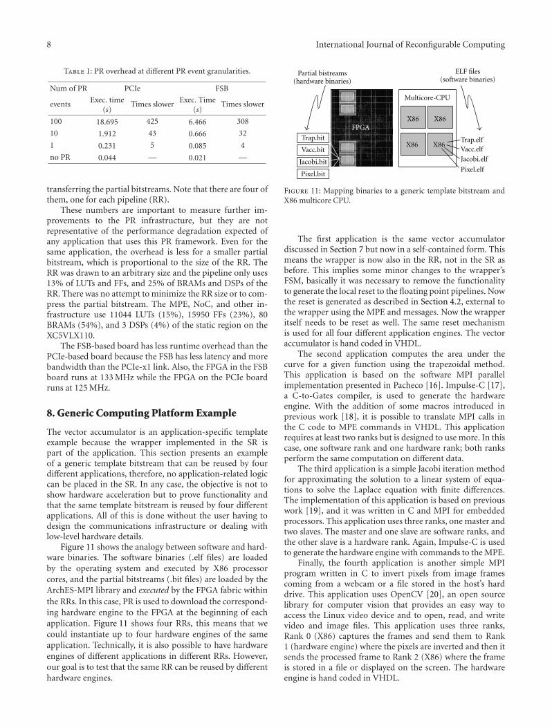
8 International Journal of Reconfigurable Computing
Table 1: PR overhead at different PR event granularities.
Num of PR PCIe FSB
events Exec. time(s)
Times slower Exec. Time(s)
Times slower
100 18.695 425 6.466 308
10 1.912 43 0.666 32
1 0.231 5 0.085 4
no PR 0.044 — 0.021 —
transferring the partial bitstreams. Note that there are four ofthem, one for each pipeline (RR).
These numbers are important to measure further im-provements to the PR infrastructure, but they are notrepresentative of the performance degradation expected ofany application that uses this PR framework. Even for thesame application, the overhead is less for a smaller partialbitstream, which is proportional to the size of the RR. TheRR was drawn to an arbitrary size and the pipeline only uses13% of LUTs and FFs, and 25% of BRAMs and DSPs of theRR. There was no attempt to minimize the RR size or to com-press the partial bitstream. The MPE, NoC, and other in-frastructure use 11044 LUTs (15%), 15950 FFs (23%), 80BRAMs (54%), and 3 DSPs (4%) of the static region on theXC5VLX110.
The FSB-based board has less runtime overhead than thePCIe-based board because the FSB has less latency and morebandwidth than the PCIe-x1 link. Also, the FPGA in the FSBboard runs at 133 MHz while the FPGA on the PCIe boardruns at 125 MHz.
8. Generic Computing Platform Example
The vector accumulator is an application-specific templateexample because the wrapper implemented in the SR ispart of the application. This section presents an exampleof a generic template bitstream that can be reused by fourdifferent applications, therefore, no application-related logiccan be placed in the SR. In any case, the objective is not toshow hardware acceleration but to prove functionality andthat the same template bitstream is reused by four differentapplications. All of this is done without the user having todesign the communications infrastructure or dealing withlow-level hardware details.
Figure 11 shows the analogy between software and hard-ware binaries. The software binaries (.elf files) are loadedby the operating system and executed by X86 processorcores, and the partial bitstreams (.bit files) are loaded by theArchES-MPI library and executed by the FPGA fabric withinthe RRs. In this case, PR is used to download the correspond-ing hardware engine to the FPGA at the beginning of eachapplication. Figure 11 shows four RRs, this means that wecould instantiate up to four hardware engines of the sameapplication. Technically, it is also possible to have hardwareengines of different applications in different RRs. However,our goal is to test that the same RR can be reused by differenthardware engines.
FPGA
Partial bistreams(hardware binaries)
Trap.bit
Vacc.bit
Jacobi.bit
Pixel.bit
X86
Multicore-CPU
ELF files(software binaries)
Trap.elfVacc.elf
Jacobi.elf
Pixel.elf
X86
X86 X86
Figure 11: Mapping binaries to a generic template bitstream andX86 multicore CPU.
The first application is the same vector accumulatordiscussed in Section 7 but now in a self-contained form. Thismeans the wrapper is now also in the RR, not in the SR asbefore. This implies some minor changes to the wrapper’sFSM, basically it was necessary to remove the functionalityto generate the local reset to the floating point pipelines. Nowthe reset is generated as described in Section 4.2, external tothe wrapper using the MPE and messages. Now the wrapperitself needs to be reset as well. The same reset mechanismis used for all four different application engines. The vectoraccumulator is hand coded in VHDL.
The second application computes the area under thecurve for a given function using the trapezoidal method.This application is based on the software MPI parallelimplementation presented in Pacheco [16]. Impulse-C [17],a C-to-Gates compiler, is used to generate the hardwareengine. With the addition of some macros introduced inprevious work [18], it is possible to translate MPI calls inthe C code to MPE commands in VHDL. This applicationrequires at least two ranks but is designed to use more. In thiscase, one software rank and one hardware rank; both ranksperform the same computation on different data.
The third application is a simple Jacobi iteration methodfor approximating the solution to a linear system of equa-tions to solve the Laplace equation with finite differences.The implementation of this application is based on previouswork [19], and it was written in C and MPI for embeddedprocessors. This application uses three ranks, one master andtwo slaves. The master and one slave are software ranks, andthe other slave is a hardware rank. Again, Impulse-C is usedto generate the hardware engine with commands to the MPE.
Finally, the fourth application is another simple MPIprogram written in C to invert pixels from image framescoming from a webcam or a file stored in the host’s harddrive. This application uses OpenCV [20], an open sourcelibrary for computer vision that provides an easy way toaccess the Linux video device and to open, read, and writevideo and image files. This application uses three ranks,Rank 0 (X86) captures the frames and send them to Rank1 (hardware engine) where the pixels are inverted and then itsends the processed frame to Rank 2 (X86) where the frameis stored in a file or displayed on the screen. The hardwareengine is hand coded in VHDL.

International Journal of Reconfigurable Computing 9
Although there has not been any attempt to optimizethe size and placement of the RRs, the FPGA in Figure 11has been partitioned following an educated guess. This guesscomes from the experience of having to design the low-levelLVDS communication interface for the FSB-based platform(See Figure 7), which is the one used in this example. TheFPGA in this platform has abundant LVDS I/O logic tocommunicate with other FPGAs above, sideways, and below.This logic is placed and concentrated towards the middleof the chip closer to specific I/O banks. Therefore, placingthe RR around the middle of the chip would complicatetiming closure because the RR would displace the LVDSlogic creating longer paths and delays. Additionally, theXC5VLX330 FPGA only has two columns of DSP blocks onthe left side of the chip—it is not symmetrical, therefore,there are no RRs on the right side for this particular template.A different template may include DSP-enabled and non-DSP-enabled RRs. In any case, these are exactly the kind ofdecisions that the end user, that is, the application developer,should not need to worry about. The place where the I/Obanks or DSPs are located is completely irrelevant to thetrapezoidal method or the Jacobi algorithm. Instead, thetemplate bitstream has already been created by a hardwareengineer familiar with the platform who can layout the RRsfor the user to work with.
The four applications were compiled, implemented, andrun on the FSB-based platform and all the output resultswere correct for each application. The RR itself occupies6.8% of LUTs and FFs, 4.9% of BRAMs, and 16.6% of DSPsavailable in the XC5VLX330 FPGA. The partial bitstreams forthe four application RMs have the same size (477666 bytes),although they do not require the same resources. Table 2presents the utilization percentage with respect to the RRnot the entire FPGA. In this case, all the engines fit withinthat RR. If this would not have been the case then anothertemplate with a larger RR would have been selected. Thedecision of what template bitstream to use from a collectionof them can be done by a higher-level tool that matches theresources required by an application and resources availablein a template. This is an optimization problem that can beaddressed in future research.
8.1. Boot Loader Reconfigurable Module. When a templatebitstream is downloaded to an FPGA each RR must have aninitial RM configured. The question is what RM should beplaced at the beginning. In our generic platform a simpleplaceholder RM has been created to be the initial RM.This placeholder is in fact a small bootloader for partialbitstreams that merely follows the synchronization stepsdescribed in Section 4. It instructs the MPE to receive aPR message (“cfg” message in Figure 4) indicating that anew RM is going to be configured. The bootloader RM willthen issue another receive command to the MPE for theeventual “configuration-done” message, then it disables allthe outputs from the RR by setting the PR-in-progress flagand finally it will go to an idle state waiting for PR to occur.Once the application RM is configured and out of reset theapplication begins. Just before the application is about to
Table 2: Resource utilization of four application hardware engines(Percentages are relative to the RR).
RR Pixel Trapezoidal Vector acc Jacobi
LUTs 9920 154 (2%) 6397 (65%) 1476 (20%) 5271 (54%)
FFs 9920 112 (2%) 3993 (41%) 1553 (16%) 4460 (45%)
DSPs 32 0 32 (100%) 8 (25%) 13 (41%)
BRAM 16 0 0 4 (25%) 2 (13%)
finish, during the call to the MPI Finalize function (all ranksmust call it) the bootloader RM is restored in all the RRs toset the FPGA ready for the next application. This last step isanalogous to a software process that finishes and returns thecontrol of the processor to the operating system. Similarly,when the application RM finishes it returns the control ofthe MPE to the bootloader RM.
9. Conclusions
The main contribution of this paper is the concept of embed-ding partial reconfiguration into the MPI programmingmodel. We have presented an extension to the ArchES-MPIframework that simplifies the use of PR by abstracting awaythe hardware details from the user while providing a layer ofportability. Such layer allows PR to be performed regardlessof the configuration interface (ICAP or SelectMAP) andindependent of the communication channel used (PCIe orFSB) to communicate with an X86 processor, which isused as a configuration controller. Also, we demonstrateda method to generate local resets without the need of anembedded processor, and provided an alternative to activelystore and restore the status of reconfigurable modules viaexplicit messages. Very little additional logic and code wererequired on top of the existing message-passing infrastruc-ture to enable PR. In addition, the concept of template-basedbitstreams was introduced as a way to use this PR frame-work to create reusable and generic computing platforms.Four different applications were actually implemented andexecuted consecutively reusing the same template bitstream.An approach like this simplifies and speeds up the designprocess of creating multiaccelerator-based computing sys-tems by allowing third-party hardware experts to provideprebuilt accelerators, I/O interfaces, NoC, and memory con-trollers, letting the designer focus on the actual value-added application logic. The initial performance overheadnumbers obtained set a reference point to measure futureimprovements to the PR framework.
Acknowledgments
The authors acknowledge the CMC/SOCRN, NSERC, Im-pulse Accelerated Technologies, and Xilinx for the hardware,tools, and funding provided for this paper.
References
[1] Xilinx, Inc., “Partial Reconfiguration User Guide,” http://www.xilinx.com/support/documentation/sw manuals//xilinx12 2/ug702.pdf.
10 International Journal of Reconfigurable Computing
[2] M. Saldana, A. Patel, H. J. Liu, and P. Chow, “Using partialreconfiguration in an embedded message-passing system,” inProceedings of the International Conference on ReconfigurableComputing and FPGAs (ReConFig ’10), pp. 418–423, Decem-ber 2010.
[3] ArchES Computing, Inc., http://www.archescomputing.com.
[4] M. Saldana, A. Patel, C. Madill et al., “MPI as an abstractionfor software-hardware interaction for HPRCs,” in Proceedingsof the 2nd International Workshop on High-Performance Recon-figurable Computing Technology and Applications (HPRCTA’08), pp. 1–10, November 2008.
[5] P. Lysaght, B. Blodget, J. Mason, J. Young, and B. Bridgford,“Invited paper: enhanced architectures, design methodologiesand CAD tools for dynamic reconfiguration of Xilinx FPGAS,”in Proceedings of the International Conference on Field Pro-grammable Logic and Applications (FPL ’06), pp. 1–6, August2006.
[6] O. Diessel, H. ElGindy, M. Middendorf, H. Schmeck, and B.Schmidt, “Dynamic scheduling of tasks on partially recon-figurable FPGAs,” IEE Proceedings: Computers and DigitalTechniques, vol. 147, no. 3, pp. 181–188, 2000.
[7] C. Bobda, A. Ahmadinia, M. Majer, J. Teich, S. Fekete, and J.van der Veen, “DyNoC: a dynamic infrastructure for commu-nication in dynamically reconfigurable devices,” in Proceedingsof the International Conference on Field Programmable Logicand Applications (FPL ’05), pp. 153–158, August 2005.
[8] K. Papadimitriou, A. Anyfantis, and A. Dollas, “An effectiveframework to evaluate dynamic partial reconfiguration inFPGA systems,” IEEE Transactions on Instrumentation andMeasurement, vol. 59, no. 6, pp. 1642–1651, 2010.
[9] C. Rossmeissl, A. Sreeramareddy, and A. Akoglu, “Partial bit-stream 2-D core relocation for reconfigurable architectures,”in Proceedings of the NASA/ESA Conference on Adaptive Hard-ware and Systems (AHS ’09), pp. 98–105, August 2009.
[10] H. Kalte and M. Porrmann, “Context saving and restoringfor multitasking in reconfigurable systems,” in Proceedings ofthe International Conference on Field Programmable Logic andApplications (FPL ’05), pp. 223–228, August 2005.
[11] D. Koch and J. Teich, “Platform-independent methodology forpartial reconfiguration,” in Proceedings of the 1st Conference onComputing Frontiers (CF ’04), pp. 398–403, ACM, New York,NY, USA, 2004.
[12] H.-H. So, A. Tkachenko, and R. Brodersen, “A unified hard-ware/software runtime environment for FPGA-based recon-figurable computers using BORPH,” in Proceedings of the 4thInternational Conference on Hardware/Software Codesign andSystem Synthesis (CODES+ISSS ’06), pp. 259–264, October2006.
[13] L. Moller, R. Soares, E. Carvalho, I. Grehs, N. Calazans, and F.Moraes, “Infrastructure for dynamic reconfigurable systems:choices and trade-offs,” in Proceedings of the 19th AnnualSymposium on Integrated Circuits and Systems Design (SBCCI’06), pp. 44–49, ACM, New York, NY, USA, 2006.
[14] The MPI Forum, “MPI: a message passing interface,” inProceedings of the ACM/IEEE Conference on Supercomputing,pp. 878–883, ACM, New York, NY, USA, November 1993.
[15] Nallatech, http://www.nallatech.com/.
[16] P. S. Pacheco, Parallel Programming with MPI, Morgan Kauf-mann, 1997.
[17] Impulse Accelerated Technologies, http://www.impulseaccel-erated.com/.
[18] A. W. House, M. Saldana, and P. Chow, “Integrating high-levelsynthesis into MPI,” in Proceedings of the 18th IEEE Interna-tional Symposium on Field-Programmable Custom ComputingMachines (FCCM ’10), pp. 175–178, May 2010.
[19] M. Saldana, D. Nunes, E. Ramalho, and P. Chow, “Config-uration and programming of heterogeneous multiprocessorson a multi-FPGA system using TMD-MPI,” in Proceedings ofthe IEEE International Conference on Reconfigurable Computingand FPGA’s, (ReConFig ’06), pp. 1–10, September 2006.
[20] G. Bradski, “The OpenCV Library,” Dr. Dobb’s Journal of Soft-ware Tools, 2000.
Hindawi Publishing CorporationInternational Journal of Reconfigurable ComputingVolume 2012, Article ID 439141, 15 pagesdoi:10.1155/2012/439141
Research Article
Exploring Many-Core Design Templates for FPGAs and ASICs
Ilia Lebedev,1 Christopher Fletcher,1 Shaoyi Cheng,2 James Martin,2 Austin Doupnik,2
Daniel Burke,2 Mingjie Lin,2 and John Wawrzynek2
1 CSAIL, Massachusetts Institute of Technology, Cambridge, MA 02139, USA2 Department of EECS, University of California at Berkeley, CA 94704, USA
Correspondence should be addressed to Ilia Lebedev, [email protected]
Received 2 May 2011; Accepted 15 July 2011
Academic Editor: Claudia Feregrino
Copyright © 2012 Ilia Lebedev et al. This is an open access article distributed under the Creative Commons Attribution License,which permits unrestricted use, distribution, and reproduction in any medium, provided the original work is properly cited.
We present a highly productive approach to hardware design based on a many-core microarchitectural template used to implementcompute-bound applications expressed in a high-level data-parallel language such as OpenCL. The template is customized on aper-application basis via a range of high-level parameters such as the interconnect topology or processing element architecture.The key benefits of this approach are that it (i) allows programmers to express parallelism through an API defined in a high-levelprogramming language, (ii) supports coarse-grained multithreading and fine-grained threading while permitting bit-level resourcecontrol, and (iii) reduces the effort required to repurpose the system for different algorithms or different applications. We comparetemplate-driven design to both full-custom and programmable approaches by studying implementations of a compute-bounddata-parallel Bayesian graph inference algorithm across several candidate platforms. Specifically, we examine a range of template-based implementations on both FPGA and ASIC platforms and compare each against full custom designs. Throughout this study,we use a general-purpose graphics processing unit (GPGPU) implementation as a performance and area baseline. We show thatour approach, similar in productivity to programmable approaches such as GPGPU applications, yields implementations withperformance approaching that of full-custom designs on both FPGA and ASIC platforms.
1. Introduction
Direct hardware implementations, using platforms such asFPGAs and ASICs, possess a huge potential for exploitingapplication-specific parallelism and performing efficientcomputation. As a result, the overall performance of customhardware-based implementations is often higher than thatof software-based ones [1, 2]. To attain bare metal perfor-mance, however, programmers must employ hardwaredesign principles such as clock management, state machines,pipelining, and device specific memory management—allconcepts well outside the expertise of application-orientedsoftware developers.
These observations raise a natural question: does thereexist a more productive abstraction for high-performance hard-ware design? Based on modern programming disciplines, oneviable approach would (1) allow programmers to expressparallelism through some API defined in a high-level progra-mming language, (2) support coarse-grain multithreading
and fine-grain threading while permitting bit-level resourcecontrol, and (3) reduce the effort required to repurpose theimplemented hardware platform for different algorithms ordifferent applications. This paper proposes an abstractionthat constrains the design to a microarchitectural template,accompanied by an API, that meets these programmer re-quirements.
Intuitively, constraining the design to a template wouldlikely result in performance degradation compared to fully-customized solutions. Consider the high-level chart plottingdesigner effort versus performance, shown in Figure 1. Weargue that the shaded region in the figure is attainable bytemplate-based designs and warrants a systematic explo-ration. To that end, this work attempts to quantify the perfor-mance/area tradeoff, with respect to designer effort, acrosstemplate-based, hand-optimized, and programmable appro-aches on both FPGA and ASIC platforms. From our anal-ysis, we show how a disciplined approach with architecturalconstraints, without resorting to manual hardware design,

2 International Journal of Reconfigurable Computing
GPPGPU
FPGA(HDL) ASIC
MARC
Eas
e-of
-des
ign
PerformanceLow
Low
High
Hig
h
Figure 1: Landscape of modern computing platforms. Ease ofapplication design and implementation versus performance (GPPstands for general purpose processor).
may reduce design time and effort while maintaining accep-table performance.
In this paper; we study microarchitectural templates inthe context of a compute-intensive data-parallel Bayesianinference application. Our thesis, therefore, is that we canefficiently map our application to hardware while being con-strained to a many-core template and parallel programmingAPI. We call this project MARC, for Many-core Approach toReconfigurable Computing, although template-based archi-tectures can be applied outside the many-core paradigm.
We think of a template as an architectural model with aset of parameters to be chosen based on characteristics of thetarget application. Our understanding of which aspects of thearchitecture to parameterize continues to evolve as we in-vestigate different application mappings. However, obviousparameters in the many-core context are the number of pro-cessing cores, core arithmetic-width, core pipeline depth,richness and topology of an interconnection network, andcustomization of cores—from addition of specialized instru-ctions to fixed function datapaths as well as details of thecache and local store hierarchies. In this study we explorea part of this space and compare the performance/area bet-ween MARC and hand-optimized designs in the context of abaseline GPGPU implementation.
The rest of the paper is organized as follows: Section 2introduces the Bayesian network inference application, thecase study examined in this paper. Section 3 describes theexecution model used by OpenCL, the high-level languageused to describe our MARC and GPGPU implementations.The application mapping for the GPGPU platform is detailedin Section 4. We discuss the hand-optimized and MARCimplementations in Section 5. Section 6 covers hardwaremappings for both the hand-optimized and MARC designsas well as a comparison between FPGA and ASIC technology.Finally, in Section 7, we compare the performance/area bet-ween the MARC hand-optimized and GPGPU implementa-tions.
1.1. Related Work. Numerous projects and products haveoffered ways to ease FPGA programming by giving develop-ers a familiar C-style language in place of HDLs [3]. Earlyresearch efforts including [4–6] formed the basis for recentcommercial offerings: Catapult C from Mentor Graphics,ImpulseC, Synfora Pico from Synopsys, and AutoESL from
Xilinx, among others. Each of these solutions requires de-velopers to understand hardware-specific concepts and toprogram using a model that differs greatly from standardC—in a sense, using an HDL with a C syntax. Unlike theseapproaches, the goal of MARC is to expose software pro-gramming models applicable to design of efficient hardware.
There has been a long history of mapping conventionalCPU architectures to FPGAs. Traditionally, soft processorshave been used either as a controller for a dedicated com-puting engine, or as an emulation or prototyping plat-formfor design verification. These efforts have primarily employ-ed a single or small number of processor cores. A few FPGAsystems with a large number of cores have been imple-mented, such as the RAMP project [7]. However, the primarydesign and use of these machines have been as emulationplatforms for custom silicon designs.
There have been many efforts both commercially andacademically on customization of parameterized processorcores on an application-specific basis. The most widely usedis Xtensa from Tensilica, where custom instructions areadded to a conventional processor architecture. We take pro-cessor customization a step further by allowing the in-struction processors to be replaced with an application-specific datapath that can be generated automatically via ourC-to-gates tool for added efficiency and performance. Weleverage standard techniques from C-to-gates compilation toaccomplish the generation of these custom datapaths.
More recently, there have been several other efforts inintegrating the C-to-gates flow with parallel programmingmodels, [8, 9]. These projects share with MARC the goal ofexploiting progress in parallel programming languages andautomatically mapping to hardware.
2. Application: Bayesian Network Inference
This work’s target application is a system that learns Bayesiannetwork structure from observation data. Bayesian networks(BNs) and graphical models have numerous applicationsin bioinformatics, finance, signal processing, and computervision. Recently they have been applied to problems in sys-tems biology and personalized medicine, providing tools forprocessing everincreasing amounts of data provided by high-throughput biological experiments. BNs’ probabilistic natureallows them to model uncertainty in real life systems as wellas the noise that is inherent in many sources of data. UnlikeMarkov Random Fields and undirected graphs, BNs caneasily learn sparse and causal structures that are interpretableby scientists [10–12].
We chose to compare MARC in the context of Bayesianinference for two primary reasons. First, Bayesian inference isa computationally intensive application believed to be partic-ularly well suited for FPGA acceleration as illustrated by [13].Second, our group, in collaboration with Stanford University,has expended significant effort over the previous two yearsdeveloping several generations of a hand-optimized FPGAimplementation tailored for Bayesian inference [13, 14].Therefore, we have not only a concrete reference design butalso well-corroborated performance results for fair compar-isons with hand-optimized FPGA implementations.

International Journal of Reconfigurable Computing 3
2.1. Statistics Perspective. BNs are statistical models that cap-ture conditional independence between variables via thelocal Markov property: that a node is conditionally indepen-dent of its nondescendants, given its parents. Bayesian infer-ence is the process by which a BN’s graph structure is learnedfrom the quantitative observation, or evidence, that the BNseeks to model. Once a BN’s structure (a set of nodes{V1, . . . ,VN }) is determined, and the conditional depen-dence of each node Vi on its parent set Πi is tabulated, thejoint distribution over the nodes can be expressed as
P(V1, . . . ,VN ) =N∏i=1
P(Vi | Πi). (1)
Despite significant recent progress in algorithm develop-ment, computational inference of a BN’s graph structurefrom evidence is still NP-hard [15] and remains infeasibleexcept for cases with only a small number of variables [16].
The algorithm surveyed in this paper is the union of twoBN inference kernels, the order and graph samplers (jointlycalled the “order-graph sampler”). An order is given by atopological sort of a graph’s nodes, where each node is placedafter its parents. Each order can include or be compatiblewith many different graphs. The order sampler takes a BN’sobservation data and produces a set of “high-scoring” BNorders (orders that best explain the evidence). The graphsampler takes this set of high-scoring orders and produces asingle highest-scoring graph for each order. The observationdata is generated in a preprocessing steps and consists of N(for each node) sets of P local-score/parent-set pairs (whichwe will refer to as “data” for short). A local score describesthe likelihood that a given parent set is a node’s true parentset, given an order. A postprocessing step is performed afterthe order-graph sampler to normalize scores and otherwiseclean up the result before it is presented to the user.
In this work, we only study the order and graph sam-pler steps for two reasons. First, the order-graph sampler isresponsible for most of the algorithm’s computational com-plexity. Second, the pre- and postprocessing phases are cur-rently performed on a GPP (general purpose processor) plat-form regardless of the platform chosen to implement theorder-graph sampler.
Following [14, 16, 17], the order-graph sampler usesMarkov chain Monte Carlo (MCMC) sampling to performan iterative random walk in the space of BN orders. First,the algorithm picks a random initial order. The applicationthen iterates as follows (1) the current order is modified byswapping two nodes to form a “proposed order,” which is(2) scored, and (3) either accepted or rejected according tothe Metropolis-Hastings rule. The scoring process, itself, (1)breaks the proposed order into N disjoint “local orders,” and(2) iterates over each node’s parent sets, accumulating eachlocal score whose parent set is compatible with the node’slocal order. For a network of N nodes, the proposed order’sscore can be efficiently calculated by [18]
Score(Op |D
)=
N∏i=1
∑Πi∈ΠP
LocalScore(Vi,Πi; D , Op
),
(2)
where D is the set of raw observations that are used by thepreprocessor to generate local scores, and Op is the proposedorder. This iterative operation continues until the score hasconverged.
To decrease time to convergence, C orders (togethercalled a chain) can be dispatched over a temperature ladderand exchanged per iteration in a technique known as paralleltempering. Additionally, R independent chains (called mul-tiple restarts) can be dispatched to increase confidence thatthe optimum score is a global optimum.
2.2. Compute Perspective. The order-graph sampler is a com-pute intensive set of nested loops, shown in Algorithm 1,while the score() function arithmetic is shown inAlgorithm 2. To put the number of loop iterations intoperspec-tive, typical parameter values for {I, R∗C, N } are{10000, 512, 32 or 37}, where I is the number of MCMCiterations. Furthermore, P = ∑4
i=0
(N−1i
), which equates to
36457 and 66712 (N = 32 and N = 37, resp.) for the designpoints that we study (see Section 7).
We classify the reformulated loop nest as compute inten-sive for two reasons. First, a relatively small amount of input(a local order) is needed for the score() function to computeper-node results over the R ∗ C orders. Second, D[n](shown in Algorithm 1) depends on N and not R∗C. SinceN ≈ 37 and R ∗ C = 512 (i.e., R ∗ C � N ), in practicethere is a large amount of compute time between when n inD[n] changes.
3. The OpenCL Execution Model
To enable highly productive hardware design, we employ ahigh-level language and execution model well suited for theparadigm of applications we are interested in studying: data-parallel, compute-bound algorithms. Due to its popularity,flexibility, and good match with our goals, we employOpenCL (Open Computing Language) as the programmingmodel used to describe applications.
OpenCL [19] is a programming and execution model forheterogeneous systems containing GPPs, GPGPUs, FPGAs[20], and other accelerators designed to explicitly capturedata and task parallelism in an application. The OpenCLmodel distinguishes control thread(s) (to be executed on aGPP host) from kernel threads (data parallel loops to beexecuted on a GPGPU, or similar, device). The user specifieshow the kernels map to an n-dimensional dataset, given aset of arguments (such as constants or pointers to device orhost memory). The runtime then distributes the resultingworkload across available compute resources on the device.Communication between control and kernel threads is pro-vided by shared memory and OpenCL system calls such asbarriers and bulk memory copy operations.
A key property of OpenCL is its memory model. Eachkernel has access to three disjoint memory regions: private,local, and global. Global memory is shared by all kernelthreads, local memory is shared by threads belonging to thesame group, while private memory is owned by one kernelthread. This alleviates the need for a compiler to perform

4 International Journal of Reconfigurable Computing
for {r, c} in R ×C doinitialize(O[r][c])
end forfor i in I do
5: for {r, c} in R ×C doOp[r][c]← swap(O[r][c])
Variable initialization:Op[r][c] · So, Op[r][c] · Sg ← 0Op[r][c] · G← []
10: end forfor n in N do
for {r, c} in R ×C do(so, sg , g) = score(D[n], Op[r][c][n])Op[r][c] · So ← Op[r][c] · So + so
15: Op[r][c] · Sg ← Op[r, c] · Sg + sgOp[r][c] · G · append(g)
end forend forfor r in R do
Metropolis-hastings:20: for c in C do
if1Tc× (Op[r][c] · So −O[r][c] · So) >
log(rand(0, 1)) thenO[r, c] · So ← Op[r][c] · So
save({Op[r][c] · Sg , Op[r, c] · G})end if
25: end forParallel tempering:for c in C do
d ← O[r][c] · So −O[r][c + 1] · So
if log(rand(0, 1)) < d × (1Tc− 1
Tc+1) then
30: exchange(O[r][c], O[r][c + 1])end if
end forend for
end for
Algorithm 1: The reformulated order-graph sampler loop nest. {So, Sg} and G are the current {order, graph} scores and graph associatedwith an order. initialize() generates a random order, swap() exchanges nodes in an order, and save() saves a result for the postprocessingstep.
costly memory access analysis to recognize dependenciesbefore the application can be parallelized. Instead, the userspecifies how the application is partitioned into data-parallelkernels. With underlying SIMD principles, OpenCL is wellsuited for data-parallel problems and maps well to the para-llel thread dispatch architecture found in GPGPUs.
4. Baseline GPGPU Implementation
To implement the order-graph sampler on the GPGPU, theapplication is first divided to different parts according totheir characteristics. The scoring portion of the algorithm,which exhibits abundant data parallelism, is partitioned intoa kernel and executed on the GPGPU, while the less para-llelizable score accumulation is executed on a GPP. Thisensures that the kernel executed on the GPGPU is maximallyparallel and exhibits no interthread communication—an
approach we experimentally determined to be optimal.Under this scheme, the latency of the control thread andscore accumulation phases of the application, running ona GPP, are dominated by the latency of the scoring functionrunning on the GPGPU. Moreover, the score() kernel(detailed in the following section) has a relatively lowbandwidth requirement, allowing us to offload accumulationto the GPP, lowering total latency. The GPP-GPGPU imple-mentation is algorithmically identical to the hardware imple-mentations, aside from minor differences in the precision ofthe log1p(exp(d)) operation, and yields identical results upto the random sequence used for Monte Carlo integration.
4.1. Optimization of Scoring Kernel. We followed four mainstrategies in optimizing the scoring unit kernel: (1) minimiz-ing data transfer overhead between the control thread andthe scoring function, (2) aligning data in device memory, (3)
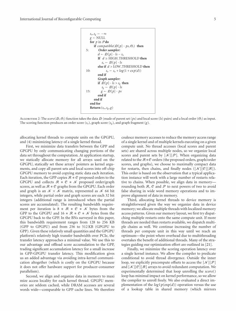
International Journal of Reconfigurable Computing 5
so, sg ← −∞g ← NULLfor p in P do
if compatible(D[p] · ps, Ol) then5: Order sampler:
d ←D[p] · ls− soIf d ≥HIGH THRESHOLD then
so ←D[p] · lselse if d > LOW THRESHOLD then
10: so ← so + log(1 + exp(d))end ifGraph sampler:if D[p] · ls > sg then
sg ←D[p] · ls15: g ←D[p] · ps
end ifend if
end forReturn:(so, sg , g)
Algorithm 2: The score(D , Ol) function takes the data D (made of parent set (ps) and local score (ls) pairs) and a local order (Ol) as input.The scoring function produces an order score (so), graph score (sg), and graph fragment (g).
allocating kernel threads to compute units on the GPGPU,and (4) minimizing latency of a single kernel thread.
First, we minimize data transfers between the GPP andGPGPU by only communicating changing portions of thedata set throughout the computation. At application startup,we statically allocate memory for all arrays used on theGPGPU, statically set these arrays’ pointers as kernel argu-ments, and copy all parent sets and local scores into off-chipGPGPU memory to avoid copying static data each iteration.Each iteration, the GPP copies R∗C proposed orders to theGPGPU and collects R ∗ C ∗ N proposed order/graphscores, as well as R∗C graphs from the GPGPU. Each orderand graph is an N × N matrix, represented as N 64 bitintegers, while partial order and graph scores are each 32 bitintegers (additional range is introduced when the partialscores are accumulated). The resulting bandwidth require-ment per iteration is 8 ∗ R ∗ C ∗ N bytes from theGPP to the GPGPU and 16 ∗ R ∗ C ∗ N bytes from theGPGPU back to the GPP. In the BNs surveyed in this paper,this bandwidth requirement ranges from 128 to 256 KB(GPP to GPGPU) and from 256 to 512 KB (GPGPU toGPP). Given these relatively small quantities and the GPGPUplatform’s relatively high transfer bandwidth over PCIe, thetransfer latency approaches a minimal value. We use this toour advantage and offload score accumulation to the GPP,trading significant accumulation latency for a small increasein GPP-GPGPU transfer latency. This modification givesus an added advantage via avoiding intra-kernel communi-cation altogether (which is costly on the GPGPU becauseit does not offer hardware support for producer-consumerparallelism).
Second, we align and organize data in memory to maximize access locality for each kernel thread. GPGPU mem-ories are seldom cached, while DRAM accesses are severalwords wide—comparable to GPP cache lines. We therefore
coalesce memory accesses to reduce the memory access rangeof a single kernel and of multiple kernels executing on a givencompute unit. No thread accesses (local scores and parentsets) are shared across multiple nodes, so we organize localscores and parent sets by [N ][P ]. When organizing datarelated to the R∗C orders (the proposed orders, graph/orderscores, and graphs), we choose to maximally compact datafor restarts, then chains, and finally nodes ([N ][C][R]).This order is based on the observation that a typical applica-tion instance will work with a large number of restarts rela-tive to chains. When possible, we align data in memory—rounding both R, C and P to next powers of two to avoidfalse sharing in wide word memory operations and to im-prove alignment of data in memory.
Third, allocating kernel threads to device memory isstraightforward given the way we organize data in devicememory; we allocate multiple threads with localized memoryaccess patterns. Given our memory layout, we first try dispat-ching multiple restarts onto the same compute unit. If morethreads are needed than restarts available, we dispatch multi-ple chains as well. We continue increasing the number ofthreads per compute unit in this way until we reach anoptimum—the point where overhead due to multithreadingovertakes the benefit of additional threads. Many of the stra-tegies guiding our optimization effort are outlined in [21].
Finally, we minimize the scoring operation latency overa single kernel instance. We allow the compiler to predicateconditional to avoid thread divergence. Outside the innerloop, we explicitly precompute offsets to access the [N ][P ]and [N ][C][R] arrays to avoid redundant computation. Weexperimentally determined that loop unrolling the score()loop has minimal impact on kernel performance, so we allowthe compiler to unroll freely. We also evaluated a direct im-plementation of the log1p(exp(d)) operation versus the useof a lookup table in shared memory (which mirrors

6 International Journal of Reconfigurable Computing
the hand-optimized design’s approach). Due to the low utili-zation of the floating point units by this algorithm, the directimplementation tends to perform better than a lookup tablegiven the precision required by the algorithm.
4.2. Benchmarking the GPGPU Implementation. To obtainGPGPU measurements, We mapped the data parallel com-ponent to the GPGPU via OpenCL, and optimized the res-ulting kernel as detailed in Section 4.1. We measured the rela-tive latency of each phase of the algorithm by introducing anumber of GPP and GPGPU timers throughout the itera-tion loop. We then computed the latency of each phase ofcomputation (scoring, accumulation, MCMC, etc.) and nor-malized to the measured latency of a single iteration with noprofiling syscalls. To measure the iteration time, we ran theapplication for 1000 iterations with no profiling code in theloop and then measured the total time elapsed using thesystem clock. We then computed the aggregate iterationlatency.
5. Architecture on Hardware Platforms
As with the GPGPU implementation, when the Bayesian in-ference algorithm is mapped to hardware platforms (FPGA/ASIC), it is partitioned into two communicating entities: adata-parallel scoring unit (a collection of Algorithmic-coresor A-cores) and a control unit (the Control-core, or C-core).The A-cores are responsible for all iterations of the score()function from Algorithm 1 while the C-core implements theserial control logic around the score() calls. This scheme isapplied to both the hand-optimized design and the auto-matically generated MARC design, though each of them hasdifferent interconnect networks, memory subsystems, andmethodologies for creating the cores.
5.1. Hand-Optimized Design. The hand-optimized designmapping integrates the jobs of the C-core and A-cores on thesame die and uses a front-end GPP for system initializationand result collection. At the start of a run, network data anda set of R∗C initial orders are copied to a DRAM accessibleby the A-cores, and the C-core is given a “Start” signal. Atthe start of each iteration, the C-core forms R∗C proposedorders, partitions each by node, and dispatches the resultingN ∗R ∗ C local orders as threads to the A-cores. As eachiteration completes, the C-core streams results back to thefront-end GPP while proceeding with the next MCMCiteration.
The hand-optimized design is partitioned into four clockdomains. First, we clock A-cores at the highest frequencypossible (between 250 and 300 MHz) as these have a directimpact on system performance. Second, we clock the logicand interconnect around each A-core at a relatively low freq-uency (25–50 MHz) as the application is compute bound inthe cores. Third, we set the memory subsystem to the freq-uency specified by the memory (∼200 MHz, using a DRAMDIMM in our case). Finally, the C-core logic is clocked at 100MHz, which we found to be ideal for timing closure and tool
Local order thread dispatch
Memory interface
Memory subsystem
Result arbiter
Control unit interface
4A-core clusters
Host I/O interface
Figure 2: The hand-optimized scoring unit (with 4 A-core clusters).
run time given a performance requirement (the latency of theC-core is negligible compared to the A-cores).
5.1.1. Scoring Unit. The scoring unit (shown in Figure 2)consists of a collection of clustered A-cores, a point-to-pointinterface with the control unit, and an interface to off-chipmemory.
A scoring unit cluster caches some or all of a node’s data,taking a stream of local orders as input and outputs order/graph scores as well as partial graphs. A cluster is made up of{A-cores, RAM} pairs, where each RAM streams data to itsA-core. When a cluster receives a local order, it (a) pages indata from DRAM as needed by the local orders, strip-minesthat data evenly across the RAMs and (b) dispatches the localorder to each core. Following Algorithm 1, R∗C local orderscan be assigned to a cluster per DRAM request. Once data ispaged in, each A-core runs P f /Uc iterations of the score()inner loop (from Algorithm 2), where P f is the subset of Pthat was paged into the cluster, and Uc is the number of A-cores in the cluster.
A-core clusters are designed to maximize local orderthroughput. A-cores are replicated to the highest extent pos-sible to maximize read bandwidth achievable by the RAMs.Each A-core is fine-grained multithreaded across multipleiterations of the score() function and uses predicated execu-tion to avoid thread divergence in case of non-compatible(!compatible()) parent sets. To avoid structural hazards inthe scoring pipeline, all scoring arithmetic is built directlyinto the hardware.
Mapping a single node’s scoring operation onto multipleA-cores requires increased complexity in accumulating par-tial node scores at the end of the score() loop. To maximallyhide this delay, we first interleave cross-thread accumulationwith the next local order’s main scoring operation (shownin Figure 3). Next, we chain A-cores together using a dedi-cated interconnect, allowing cross-core partial results to beinterleaved into the next local order in the same way asthreads. Per core, this accumulation scheme adds T cycles
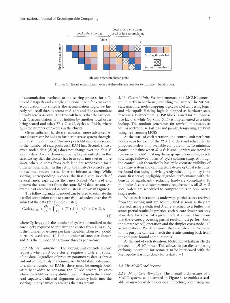
International Journal of Reconfigurable Computing 7
Time
Local order i scoringLocal order i + 1 scoring,
Local order i accumulating
Accumulation thread
Pip
elin
est
age
nu
mbe
r
ith local order completion point
Scoring threads 1–4
Figure 3: Thread accumulation over a 4-thread/stage core for two adjacent local orders.
of accumulation overhead to the scoring process, for a T-thread datapath and a single additional cycle for cross-coreaccumulation. To simplify the accumulation logic, we lin-early reduce all threads across an A-core and then accumulatelinearly across A-cores. The tradeoff here is that the last localorder’s accumulation is not hidden by another local orderbeing scored and takes T2 + T ∗ Uc cycles to finish, whereUc is the number of A-cores in the cluster.
Given sufficient hardware resources, more advanced A-core clusters can be built to further increase system through-put. First, the number of A-cores per RAM can be increasedto the number of read ports each RAM has. Second, since agiven node’s data (D[n]) does not change over the R ∗ Clocal orders, A-core chains can be replicated entirely. In thiscase, we say that the cluster has been split into two or morelanes, where A-cores from each lane are responsible for adifferent local order. In this setup, the cluster’s control strip-mines local orders across lanes to initiate scoring. Whilescoring, corresponding A-cores (the first A-core in each ofseveral lanes, e.g.) across the lanes (called tiles) read andprocess the same data from the same RAM data stream. Anexample of an advanced A-core cluster is shown in Figure 4.
The following analytic model can be used to estimate theparallel completion time to score Ol local orders over the Pf
subset of the data (for a single cluster):
CyclesDRAM +Ol
Ul∗(
P f
Uc+ (T + 1)
)+(T2 + T ∗Uc
),
(3)
where CyclesDRAM is the number of cycles (normalized to thecore clock) required to initialize the cluster from DRAM, Uc
is the number of A-cores per lane (doubles when two SRAMports are used, etc.), Ul is the number of lanes per cluster,and T is the number of hardware threads per A-core.
5.1.2. Memory Subsystem. The scoring unit controls DRAMrequests when an A-core cluster requires a different subsetof the data. Regardless of problem parameters, data is alwayslaid out contiguously in memory. As DRAM data is streamedto a finite number of RAMs, there must be enough RAMwrite bandwidth to consume the DRAM stream. In caseswhere the RAM write capability does not align to the DRAMread capacity, dedicated alignment circuitry built into thescoring unit dynamically realigns the data stream.
5.1.3. Control Unit. We implemented the MCMC controlunit directly in hardware, according to Figure 5. The MCMCstate machine, node swapping logic, parallel tempering logic,and Metropolis-Hasting logic is mapped as hardware statemachines. Furthermore, a DSP block is used for multiplica-tive factors, while log(rand(0, 1)) is implemented as a tablelookup. The random generators for row/column swaps, aswell as Metropolis-Hastings and parallel tempering, are builtusing free-running LFSRs.
At the start of each iteration, the control unit performsnode swaps for each of the R ∗ C orders and schedules theproposed orders onto available compute units. To minimizecontrol unit time when R ∗ C is small, orders are stored inrow order in RAM, making the swap operation a single cyclerow swap, followed by an N cycle column swap. Althoughthe control unit theoretically has cycle accurate visibility ofthe entire system and can therefore derive optimal schedules,we found that using a trivial greedy scheduling policy (firstcome first serve) negligibly degrades performance with thebenefit of significantly reducing hardware complexity. Tominimize A-core cluster memory requirements, all R ∗ Clocal orders are scheduled to compute units in bulk over asingle node.
When each iteration is underway, partial scores receivedfrom the scoring unit are accumulated as soon as they arereceived, using a dedicated A-core attached to a buffer thatstores partial results. In practice, each A-core cluster can onlystore data for a part of a given node at a time. This meansthat the A-core, processing partial results, must perform boththe slower score() operation and the simpler cross-node “+”accumulations. We determined that a single core dedicatedto this purpose can rate match the results coming back fromthe compute-bound compute units.
At the end of each iteration, Metropolis-Hastings checksproceed in [R][C] order. This allows the parallel temperingexchange operation for restart r to be interleaved with theMetropolis-Hastings check for restart r + 1.
5.2. The MARC Architecture
5.2.1. Many-Core Template. The overall architecture of aMARC system, as illustrated in Figure 6, resembles a scal-able, many-core-style processor architecture, comprising one

8 International Journal of Reconfigurable Computing
4ti
les
Loca
lord
er(t
hre
ad)
rou
nd-
robi
ndi
spat
ch
Scoring unit interface
Serialization
Loca
lord
ers
Dat
ast
ream
Gra
phsa
mpl
er
SRAM
P (2) ports
3 lanes
DispatcherData
Start
GS
GS
GS
GS
GS
GS
Clu
ster
inte
rfac
e
2po
rts
(du
al-p
orte
d)
From previous A-core
To next A-core GS
En
Graph
sampler
Ordersampler
LOGtable
Data
A-core
Valid
(s)
TileD
ata
(loc
alsc
ores
,par
ent
sets
)ro
un
d-ro
bin
disp
atch
Initial scores(Int.MIN value)
Ord
ers
Gra
phs
Previous tilelane (0)
Previous tilelane (2)
Localorders
Next tilelane (0)
Next tilelane (1)
Next tilelane (2)
Loca
lord
erla
ne
(0)
Loca
lord
erla
ne
(1)
Loca
lord
erla
ne
(2)
Figure 4: The hand-optimized A-core cluster. This example contains four tiles and three lanes and uses two RAM read ports per tile. “GS”stands for graph sampler.
Control Processor (C-core) and multiple Algorithmic Pro-cessing Cores (A-cores). Both the C-cores and the A-core canbe implemented as conventional pipelined RISC processors.However, unlike embedded processors commonly found inmodern SOCs, the processing cores in MARC are completelyparameterized with variable bit width, reconfigurable multi-threading, and even aggregate/fused instructions. Further-more, A-cores can alternatively be synthesized as fullycustomized datapaths. For example, in order to hide globalmemory access latency, improve processing node utiliza-tion, and increase the overall system throughput, a MARCsystem can perform fine-grained multithreading throughshift register insertion and automatic retiming. Finally, whileeach processing core possesses a dedicated local memoryaccessible only to itself, a MARC system has a global memoryspace implemented as distributed memories accessible byall processing cores through the interconnect network.Communication between a MARC system and its host canbe realized by reading and writing global memory.
5.2.2. Execution Model and Software Infrastructure. OurMARC system builds upon both LLVM, a production-gradeopen-source compiler infrastructure [22] and OpenCL.
Figure 7 presents a high-level schematic of a typicalMARC machine. A user application runs on a host accordingto the models native to the host platform—a high-perfor-mance PC in our study. Execution of a MARC programoccurs in two parts: kernels that run on one or more A-coresof the MARC devices and a control program that runs on
the C-core. The control program defines the context for thekernels and manages their execution. During the execution,the MARC application spawns kernel threads to run on theA-cores, each of which runs a single stream of instructionsas SPMD units (each processing core maintains its own pro-gram counter).
5.2.3. Application-Specific Processing Core. One strength ofMARC is its capability to integrate fully customized appli-cation-specific processing cores/datapaths so that the kernelsin an application can be more efficiently executed. To thisend, a high-level synthesis flow depicted by Figure 8 wasdeveloped to generate customized datapaths for a target ap-plication.
The original kernel source code in C/C++ is first com-piled through llvm-gcc to generate the intermediate repre-sentation (IR) in the form of a single static assignment graph(SSA), which forms a control flow graph where instructionsare grouped into basic blocks. Within each basic block, theinstruction parallelism can be extracted easily as all falsedependencies have been removed in the SSA representation.Between basic blocks, the control dependencies can then betransformed to data dependencies through branch predica-tion. In our implementation, only memory operations arepredicated since they are the only instructions that can gen-erate stalls in the pipeline. By converting the control depen-dencies to data dependencies, the boundaries between basicblocks can be eliminated. This results in a single data flowgraph with each node corresponding to a single instruction

International Journal of Reconfigurable Computing 9
Scheduler
Scoring unit interface
LFSR (row generation)
LFSR (column generation)
MCMC statemachine
Initialization
Results
+
Partial results buffer
Restart x chainorder array
6 nodes
3re
star
ts,2
chai
ns
=6
orde
rs
Hos
tI/
Oin
terf
ace
Log (u) table
Figure 5: The hand-optimized control unit.
P/L P/L P/L P/L
Mem Mem Mem Mem Mem Mem Mem Mem Sch
edu
lerA-core A-core A-coreC-core
Interconnect network
· · ·
· · ·
Figure 6: Diagram of key components in a MARC machine.
in the IR. Creating hardware from this graph involves aone-to-one mapping between each instruction and variouspredetermined hardware primitives. To utilize loop levelparallelism, our high-level synthesis tool also computes theminimal interval at which a new iteration of the loopcan be initiated and subsequently generates a controller topipeline loop iterations. Finally, the customized cores havethe original function arguments converted into inputs. Inaddition, a simple set of control signals is created to initializea C-core and to signal the completion of the execution. Formemory accesses within the original code, each nonaliasingmemory pointer used by the C function is mapped to a mem-ory interface capable of accommodating variable memoryaccess latency. The integration of the customized cores intoa MARC machine involves mapping the input of the cores tomemory addresses accessible by the control core, as well asthe addition of a memory handshake mechanism allowingcores to access global and local memories. For the resultsreported in this paper, the multithreaded customized coresare created by manually inserting shift registers into thesingle-threaded, automatically generated core.
5.2.4. Host-MARC Interface. Gigabit Ethernet is used to im-plement the communication link between the host andthe MARC device. We leveraged the GateLib [23] project
from Berkeley to implement the host interface, allowing thephysical transport to be easily replaced by a faster medium inthe future.
5.2.5. Memory Organization. Following OpenCL, A-corethreads have access to three distinct memory regions: private,local, and global. Global memory permits read and writeaccess to all threads within any executing kernels on anyprocessing core (ideally, reads and writes to global memorymay be cached depending on the capabilities of the device,however in our current MARC machine implementation,caching is not supported). Local memory is a section of theaddress space shared by the threads within a computing core.This memory region can be used to allocate variables thatare shared by all threads spawned from the same computingkernel. Finally, private memory is a memory region that isdedicated to a single thread. Variables defined in one thread’sprivate memory are not visible to another thread, even whenthey belong to the same executing kernel.
Physically, the private and local memory regions in aMARC system are implemented using on-chip memories.Part of the global memory region also resides on-chip, but weallow external memory (i.e., through the DRAM controller)to extend the global memory region, resulting in a largermemory space.
5.2.6. Kernel Scheduler. To achieve high throughput, kernelsmust be scheduled to avoid memory access conflicts. TheMARC system allows for a globally aware kernel sched-uler, which can orchestrate the execution of kernels andcontrol access to shared resources. The global scheduler iscontrolled via a set of memory-mapped registers, which areimplementation specific. This approach allows for a range of
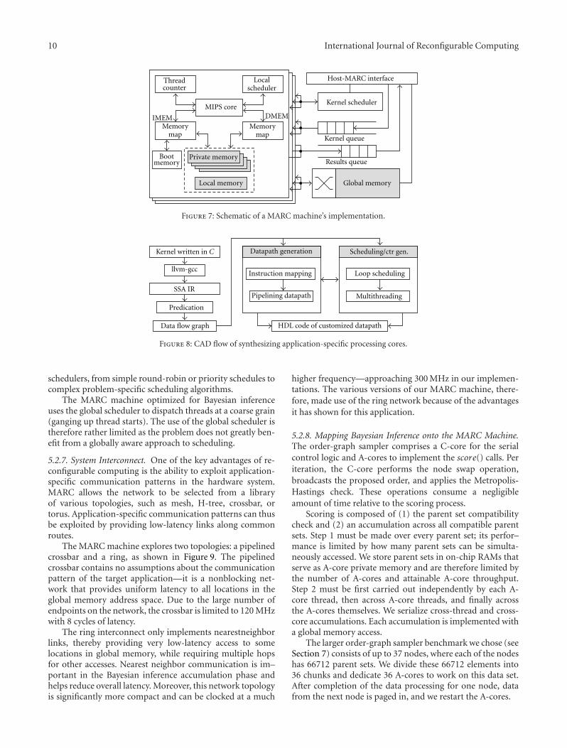
10 International Journal of Reconfigurable Computing
Threadcounter
Localscheduler
MIPS core
IMEM DMEM
Memorymap
Memorymap
Bootmemory
Private memory
Local memory
Host-MARC interface
Kernel scheduler
Kernel queue
Results queue
Global memory
Figure 7: Schematic of a MARC machine’s implementation.
llvm-gcc
SSA IR
Predication
Data flow graph
Datapath generation
Instruction mapping
Pipelining datapath
Scheduling/ctr gen.
Loop scheduling
Multithreading
HDL code of customized datapath
Kernel written in C
Figure 8: CAD flow of synthesizing application-specific processing cores.
schedulers, from simple round-robin or priority schedules tocomplex problem-specific scheduling algorithms.
The MARC machine optimized for Bayesian inferenceuses the global scheduler to dispatch threads at a coarse grain(ganging up thread starts). The use of the global scheduler istherefore rather limited as the problem does not greatly ben-efit from a globally aware approach to scheduling.
5.2.7. System Interconnect. One of the key advantages of re-configurable computing is the ability to exploit application-specific communication patterns in the hardware system.MARC allows the network to be selected from a libraryof various topologies, such as mesh, H-tree, crossbar, ortorus. Application-specific communication patterns can thusbe exploited by providing low-latency links along commonroutes.
The MARC machine explores two topologies: a pipelinedcrossbar and a ring, as shown in Figure 9. The pipelinedcrossbar contains no assumptions about the communicationpattern of the target application—it is a nonblocking net-work that provides uniform latency to all locations in theglobal memory address space. Due to the large number ofendpoints on the network, the crossbar is limited to 120 MHzwith 8 cycles of latency.
The ring interconnect only implements nearestneighborlinks, thereby providing very low-latency access to somelocations in global memory, while requiring multiple hopsfor other accesses. Nearest neighbor communication is im–portant in the Bayesian inference accumulation phase andhelps reduce overall latency. Moreover, this network topologyis significantly more compact and can be clocked at a much
higher frequency—approaching 300 MHz in our implemen-tations. The various versions of our MARC machine, there-fore, made use of the ring network because of the advantagesit has shown for this application.
5.2.8. Mapping Bayesian Inference onto the MARC Machine.The order-graph sampler comprises a C-core for the serialcontrol logic and A-cores to implement the score() calls. Periteration, the C-core performs the node swap operation,broadcasts the proposed order, and applies the Metropolis-Hastings check. These operations consume a negligibleamount of time relative to the scoring process.
Scoring is composed of (1) the parent set compatibilitycheck and (2) an accumulation across all compatible parentsets. Step 1 must be made over every parent set; its perfor–mance is limited by how many parent sets can be simulta-neously accessed. We store parent sets in on-chip RAMs thatserve as A-core private memory and are therefore limited bythe number of A-cores and attainable A-core throughput.Step 2 must be first carried out independently by each A-core thread, then across A-core threads, and finally acrossthe A-cores themselves. We serialize cross-thread and cross-core accumulations. Each accumulation is implemented witha global memory access.
The larger order-graph sampler benchmark we chose (seeSection 7) consists of up to 37 nodes, where each of the nodeshas 66712 parent sets. We divide these 66712 elements into36 chunks and dedicate 36 A-cores to work on this data set.After completion of the data processing for one node, datafrom the next node is paged in, and we restart the A-cores.
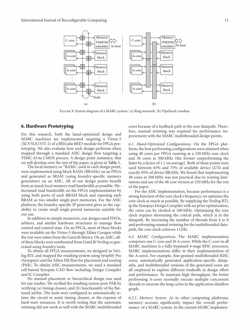
International Journal of Reconfigurable Computing 11
C-core C-core
A-core
A-core
A-core
A-core
A-core
A-core
Memoryblock
Memoryblock
Memoryblock
Memorymappingscheduler
Memoryblock
Memoryblock
Memoryblock
Memorymappingscheduler
Node
···
···
···
···
To host To host
(a) (b)
Figure 9: System diagram of a MARC system. (a) Ring network. (b) Pipelined crossbar.
6. Hardware Prototyping
For this research, both the hand-optimized design andMARC machines are implemented targeting a Virtex-5(XCV5LX155T-2) of a BEEcube BEE3 module for FPGA pro-totyping. We also evaluate how each design performs whenmapped through a standard ASIC design flow targeting aTSMC 65 ns CMOS process. A design point summary, thatwe will develop over the rest of the paper, is given in Table 1.
The local memory or “RAMs”, used in each design point,were implemented using block RAMs (BRAMs) on an FPGAand generated as SRAM (using foundry-specific memorygenerators) on an ASIC. All of our design points benefitfrom as much local memory read bandwidth as possible. We-increased read bandwidth on the FPGA implementation byusing both ports of each BRAM block and exposing eachBRAM as two smaller single-port memories. For the ASICplatform, the foundry-specific IP generator gives us the cap-ability to create small single-ported memories suitable forour use.
In addition to simple memories, our designs used FIFOs,arbiters, and similar hardware structures to manage flowcontrol and control state. On an FPGA, most of these blockswere available on the Virtex-5 through Xilinx Coregen whilethe rest were taken from the GateLib library. On an ASIC, all-of these blocks were synthesized from GateLib Verilog or gen-erated using foundry tools.
To obtain all FPGA measurements, we designed in Veri-log RTL and mapped the resulting system using Synplify Pro(Synopsys) and the Xilinx ISE flow for placement and routing(PAR). To obtain ASIC measurements, we used a standardcell-bawed Synopsis CAD flow including Design Compilerand IC Compiler.
No manual placement or hierarchical design was usedfor our studies. We verified the resulting system post-PAR byverifying (a) timing closure, and (b) functionality of the flat-tened netlist. The tools were configured to automatically re-time the circuit to assist timing closure, at the expense ofhard-ware resources. It is worth noting that the automaticretiming did not work as well with the MARC multithreaded
cores because of a feedback path in the core datapath. There-fore, manual retiming was required for performance im-provement with the MARC multithreaded design points.
6.1. Hand-Optimized Configurations. On the FPGA plat-form, the best performing configurations were attained whenusing 48 cores per FPGA running at a 250 MHz core clockand 36 cores at 300 MHz (the former outperforming thelatter by a factor of 1.1 on average). Both of these points wereused between 65% and 75% of available device LUTs andexactly 95% of device BRAMs. We found that implementing48 cores at 300 MHz was not practical due to routing limi-tations and use of the 48 core version at 250 MHz for the restof the paper.
For the ASIC implementation, because performance is astrong function of the core clock’s frequency, we optimize thecore clock as much as possible. By supplying the Verilog RTLtp the Synopsys Design Compiler with no prior optimization,the cores can be clocked at 500 MHz. Optimizing the coreclock requires shortening the critical path, which is in thedatapath. By increasing the number of threads from 4 to 8and performing manual retiming for the multithreaded data-path, the core clock achieves 1 GHz.
6.2. MARC Configurations. The MARC implementationcomprises one C-core and 36 A-cores. While the C-core in allMARC machines is a fully bypassed 4-stage RISC processor,MARC implementations differ in their implementation ofthe A-cores. For example, fine-grained multithreaded RISCcores, automatically generated application-specific datap-aths, and multithreaded versions of the generated cores areall employed to explore different tradeoffs in design effortand performance. To maintain high throughput, the betterperforming A-cores normally execute multiple concurrentthreads to saturate the long cycles in the application dataflowgraph.
6.2.1. Memory System. As in other computing platforms,memory accesses significantly impact the overall perfor-mance of a MARC system. In the current MARC implemen-

12 International Journal of Reconfigurable Computing
Table 1: A-core counts, for all design points, and a naming convention for all MARC configurations used in the study. If only one core countis listed, it is the same for both 32 and 37 node (32n and 37n) problems (see Section 7). All A-core counts are given for area normalizeddesigns, as discussed in Section 7.
Alias Description Number of cores (32n, 37n)
Hand design FPGA — 48
Hand design ASIC — 2624, 2923
MARC-Ropt-F RISC A-core with optimized network on FPGA 36
MARC-C1-F Customized A-core on FPGA 36
MARC-C2-F Customized A-core (2-way MT) on FPGA 36
MARC-C4-F Customized A-core (4-way MT) on FPGA 36
MARC-Ropt-A RISC A-core with optimized network on ASIC 1269, 1158
MARC-C1-A Customized A-core on ASIC 1782, 1571
MARC-C2-A Customized A-core (2-way MT) on ASIC 1768, 1561
MARC-C4-A Customized A-core (4-way MT) on ASIC 1715, 1519
GPGPU — 512
tation, private or local memory accesses take exactly onecycle, while global memory accesses typically involve longerlatencies that are network dependent. We believe that givendifferent applications, such discrepancies between local andglobal memory access latencies provide ample opportunitiesfor memory optimization and performance improvements.For example, the MARC machine in this work has been opti-mized for local memory accesses, reflecting the needs of theBayesian inference algorithm.
6.2.2. Clock Speed and Area on FPGA and ASIC. For betterthroughput, we have implemented single-threaded, two-way multithreaded, and four-way multithreaded application-specific A-cores for MARC devices. When individuallyinstantiated on the Virtex-5 FPGA, these cores are clockedat 163 MHz, 234 MHz, and 226 MHz, respectively. There is adecrease in clock frequency when the number of threads ischanged from two to four. This is due to the increasedrouting delay to connect LUT-FF pairs further apart in alarger physical area. When the completely assembled MARCmachines traverse the hardware generation flow, the cores’clock frequency decreases further to 144 MHz, 207 MHz,and 206 MHz, respectively due to added FPGA resourceutilization. The same A-cores are used for the ASIC imple-mentation, where they operate at 526 MHz, 724 MHz, and746 MHz, respectively. Due to a higher degree of freedom inASIC place and route, we do not see the performancedip observed when the two-threaded FPGA implementationis changed to four-threaded. However, it is apparent thatdespite the decrease in levels of logic in the critical path, it isdifficult to squeeze out more performance by simple registerinsertion and retiming.
With respect to area, the overhead of multithreading ismore pronounced on an FPGA relative to an ASIC. For the37 node benchmark, the MARC machines with single, two-way, and four-way multithreaded customized A-cores utilize47%, 65%, and 80% of the flip-flops on Virtex-5. Since theyoperate on the same amount of data, 85% of BRAMs are usedfor each of the three design points. Meanwhile, on an ASICwe only observe an area increase from 6.2 mm2 in the single-threaded case to 6.4 mm2 for the four-way multithreaded
design. This is because the ASIC implementation exposes theactual chip area, where the increase in number of registers isdwarfed by the large SRAM area.
7. Performance and Area Comparisons
We compare the performance of the hand-optimized designand the MARC machines on FPGA as well as ASIC platforms.For both the hand-optimized and the MARC implementa-tions on an ASIC, we normalize our area to the FPGA’s diearea. FPGA die area was obtained by X-ray imaging the pack-aged dies and estimating the die area from the resultingphotographs. For the remainder of the paper, all deviceswhose die areas and process nodes are relevant are given inTable 2.
For the FPGA designs, we packed the device to its limitswithout performance degradation. Effectively, the designs areconsuming the entire area of the FPGA. We then performeda similar evaluation for the ASIC platform by attempting tooccupy the same area as an FPGA. This is achieved by run-ning the design for a small number of cores and then scalingup. This technique is valid as the core clock is not distributedacross the network, and the network clock can be slow (50–100 MHz) without adversely affecting performance.
The specific Bayesian network instances we chose consistof 32 and 37 nodes, with dataset of 36457 and 66712elements, respectively. The run times on each hardware plat-form are shown in Tables 4 and 5, for the 32 and 37 node-problem, respectively. The execution time for each platformis also normalized to the fastest implementation—hand-optimized design on ASIC—to show the relative perfor-mance of every design point.
7.1. Benchmark Comparison. The large gap between theamount of data involved in the two problems gives eachdistinct characteristics, especially when mapped to an ASICplatform. Because data for the 32 node problem can fit onan ASIC for both MARC and the hand-optimized design,the problem is purely compute bound. The hand-optimizedsolution benefits from the custom pipelined accumulation
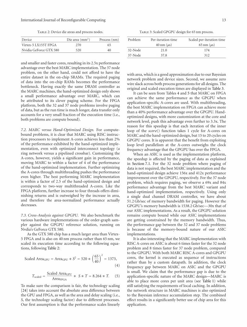
International Journal of Reconfigurable Computing 13
Table 2: Device die areas and process nodes.
Device Die area (mm2) Process (nm)
Virtex-5 LX155T FPGA 270 65
Nvidia GeForce GTX 580 520 40
and smaller and faster cores, resulting in its 2.5x performanceadvantage over the best MARC implementation. The 37 nodeproblem, on the other hand, could not afford to have theentire dataset in the on-chip SRAMs. The required pagingof data into the on-chip RAMs becomes the performancebottleneck. Having exactly the same DRAM controller asthe MARC machines, the hand-optimized design only showsa small performance advantage over MARC, which canbe attributed to its clever paging scheme. For the FPGAplatform, both the 32 and 37 node problems involve pagingof data, but as the run time is much longer, data transfer onlyaccounts for a very small fraction of the execution time (i.e.,both problems are compute bound).
7.2. MARC versus Hand-Optimized Design. For compute-bound problems, it is clear that MARC using RISC instruc-tion processors to implement A-cores achieves less than 2%of the performance exhibited by the hand-optimized imple-mentation, even with optimized interconnect topology (aring network versus a pipelined crossbar). Customizing theA-cores, however, yields a significant gain in performance,moving MARC to within a factor of 4 of the performanceof the hand-optimized implementation. Further optimizingthe A-cores through multithreading pushes the performanceeven higher. The best performing MARC implementationis within a factor of 2.5 of the hand-optimized design andcorresponds to two-way multithreaded A-cores. Like theFPGA platform, further increase to four threads offers dimi-nishing returns and is outweighed by the increase in area,and therefore the area-normalized performance actuallydecreases.
7.3. Cross-Analysis against GPGPU. We also benchmark thevarious hardware implementations of the order-graph sam-pler against the GPGPU reference solution, running onNvdia’s GeForce GTX 580.
As the GTX 580 chip has a much larger area than Virtex-5 FPGA and is also on 40 nm process rather than 65 nm, wescaled its execution time according to the following equa-tions, following Table 2:
Scaled AreaGPU = AreaGPU ∗ S2 = 520∗(
6540
)2
= 1373,
(4)
Tscaled = Scaled AreaGPU
AreaFPGA∗ S∗ T = 8.264∗ T. (5)
To make sure the comparison is fair, the technology scaling[24] takes into account the absolute area difference betweenthe GPU and FPGA, as well as the area and delay scaling (i.e.,S, the technology scaling factor) due to different processes.Our first assumption is that the performance scales linearly
Table 3: Scaled GPGPU design for 65 nm process.
Problem Per-iteration time Scaled per-iteration time
40 nm (μs) 65 nm (μs)
32-Node 21.0 174
37-Node 37.8 312
with area, which is a good approximation due to our Bayesiannetwork problem and device sizes. Second, we assume zerowire slack across both process generations for all designs. Theoriginal and scaled execution times are displayed in Table 3.
It can be seen from Tables 4 and 5 that MARC on FPGAcan achieve the same performance as the GPGPU whenapplication-specific A-cores are used. With multithreading,the best MARC implementation on FPGA can achieve morethan a 40% performance advantage over the GPGPU. Hand-optimized designs, with more customization at the core andnetwork level, push this advantage even further to 3.3x. Thereason for this speedup is that each iteration of the innerloop of the score() function takes 1 cycle for A-cores onMARC and the hand-optimized design, but 15 to 20 cycles onGPGPU cores. It is apparent that the benefit from exploitingloop level parallelism at the A-cores outweighs the clockfrequency advantage that the GPGPU has over the FPGA.
When an ASIC is used as the implementation platform,the speedup is affected by the paging of data as explainedin Section 7.1. For the 32 node problem where paging ofdata is not required, the best MARC implementation and thehand-optimized design achieve 156x and 412x performanceimprovement over the GPGPU, respectively. For the 37 nodeproblem, which requires paging, we observe a 69x and 84xperformance advantage from the best MARC variant andhand-optimized implementation, respectively. Using onlya single dual channel DRAM controller, we have about51.2 Gb/sec of memory bandwidth for paging. However theGPGPU’s memory bandwidth is 1538.2 Gb/sec—30x that ofour ASIC implementations. As a result, the GPGPU solutionremains compute bound while our ASIC implementationsare getting constrained by the memory bandwidth. Thus,the performance gap between the 32 and 37 node problemsis because of the memory-bound nature of our ASICimplementations.
It is also interesting that the MARC implementation withRISC A-cores on ASIC is about 6 times faster for the 32 nodeproblem and 8 times faster for 37 node problem, comparedto the GPGPU. With both MARC RISC A-cores and GPGPUcores, the kernel is executed as sequence of instructionsrather than by a custom datapath. In addition, the clockfrequency gap between MARC on ASIC and the GPGPUis small. We claim that the performance gap is due to theapplication-specific nature of the MARC design—MARC isable to place more cores per unit area (see Table 1) whilestill satisfying the requirements of local caching. In addition,the network structure in MARC machines is also optimizedto the Bayesian inference accumulation step. The combinedeffect results in a significantly better use of chip area for thisapplication.

14 International Journal of Reconfigurable Computing
Table 4: 32-Node. Performance comparison between MARC,hand-optimized, and GPGPU.
Configuration Per iteration Relative
Time (μs) Perf.
GPGPU scaled reference 174 0.0024
MARC-Ropt-F 2550 0.0002
MARC-C1-F 172 0.0025
MARC-C2-F 124 0.0034
MARC-C4-F 136 0.0031
Hand design FPGA 51.4 0.0082
MARC-Ropt-A 27.6 0.0152
MARC-C1-A 1.47 0.2863
MARC-C2-A 1.11 0.3808
MARC-C4-A 1.17 0.3608
Hand design ASIC 0.422 1.0000
Table 5: 37-Node. Performance comparison between MARC,Hand-optimized, and GPGPU.
Configuration Per iteration Relative
Time (μs) Perf.
GPGPU scaled reference 312 0.0119
MARC-Ropt-F 5130 0.0007
MARC-C1-F 310 0.0120
MARC-C2-F 221 0.0169
MARC-C4-F 235 0.0158
Hand design FPGA 110 0.0339
MARC-Ropt-A 38.1 0.0978
MARC-C1-A 5.02 0.7429
MARC-C2-A 4.53 0.8231
MARC-C4-A 4.61 0.8083
Hand design ASIC 3.73 1.0000
8. Conclusion
MARC offers a methodology to design FPGA and ASIC-based high-performance reconfigurable computing systems.It does this by combining a many-core architectural template,high-level imperative programming model [19], and moderncompiler technology [22] to efficiently target both ASICs andFPGAs for general-purpose, computationally intensive data-parallel applications.
The primary objective of this paper is to understandwhether a many-core architecture is a suitable abstractionlayer (or execution model) for designing ASIC and FPGA-based computing machines from an OpenCL specification.We are motivated by recently reemerging interest and effortsin parallel programming for newly engineered and upcomingmany-core platforms, and feel that if we can successfullybuild an efficient many-core abstraction for ASICs andFPGAs, we can apply the advances in parallel programmingto high-level automatic synthesis of computing systems. Of-course, constraining an execution template reduces degrees
of freedom for customizing an implementation using appli-cation-specific detail. However, we work under the hypothe-sis that much of the potential loss in efficiency can be recov-ered through customization of a microarchitectural templatedesigned for a class of applications using application-specificinformation. The study in this paper represents our initialeffort to quantify the loss in efficiency incurred for a signi-ficant gain in design productivity for one particular applica-tion.
We have demonstrated via the use of a many-core micro-architectural template for OpenCL that it is at least some-times possible to achieve competitive performance relative toa highly optimized solution and to do so with considerablereduction in development effort (days versus months). Thisapproach also achieves significant performance advantageover a GPGPU approach—a natural platform for mappingthis class of applications. In this study, the most significantperformance benefit came from customization of the proces-sor cores to better fit the application kernel—an operationwithin reach of modern high-level synthesis flows.
Despite these results, the effectiveness of MARC in thegeneral case remains to be investigated. We are currentlylimited by our ability to generate many high-quality hand-optimized custom solutions in a variety of domains to vali-date and benchmark template-based implementations. Non-etheless, we plan to continue this study, exploring more ap-plication domains, extending the many-core template tailor-ed for OpenCL and exploring template microarchitecturesfor other paradigms. We are optimistic that a MARC-like ap-proach will open new frontiers for rapid prototyping of high-performance computing systems.
Acknowledgments
The authors wish to acknowledge the contributions of thestudents, faculty, and sponsors of the Berkeley WirelessResearch Center and the TSMC University Shuttle Program.This work was funded by the NIH, Grant no.1R01CA130826-01 and the Department of Energy, Awardno. DE-SC0003624.
References
[1] M. Lin, I. Lebedev, and J. Wawrzynek, “HighthroughputBayesian computing machine with reconfigurable hardware,”in Proceedings of the 18th annual ACM/SIGDA InternationalSymposium on Field Programmable Gate Arrays (FPGA ’10),pp. 73–82, ACM, Monterey, California, USA, 2010.
[2] M. Lin, I. Lebedev, and J. Wawrzynek, “OpenRCL: fromsea-of-gates to sea-of-cores,” in Proceedings of the 20th IEEEInternational Conference on Field Programmable Logic andApplications, Milano, Italy, 2010.
[3] Wikipedia, “C-to-hdl,” November 2009, http://en.wikipedia.org/wiki/C to HDL/.
[4] M. Gokhale and J. Stone, “Napa c: compiling for a hybrid risc/fpga architecture,” in Proceedings of the IEEE Symposium onFPGAs for Custom Computing Machines (FCCM ’98), Napa,Calif, USA, 1998.
International Journal of Reconfigurable Computing 15
[5] T. J. Callahan, J. R. Hauser, and J. Wawrzynek, “Garp architec-ture and C compiler,” Computer, vol. 33, no. 4, pp. 62–69,2000.
[6] M. Budiu, G. Venkataramani, T. Chelcea, and S. C. Goldstein,“Spatial computation,” in Proceedings of the 11th InternationalConference on Architectural Support for Programming Lan-guages and Operating Systems (ASPLOS-XI ’04), pp. 14–26,New York, NY, USA, October 2004.
[7] J. Wawrzynek, D. Patterson, M. Oskin et al., “RAMP: researchaccelerator for multiple processors,” IEEE Micro, vol. 27, no. 2,pp. 46–57, 2007.
[8] A. Papakonstantinou, K. Gururaj, J. A. Stratton, D. Chen, J.Cong, and M. W. Hwu, “Fcuda: enabling efficient compilationof cuda kernels onto fpgas,” in Proceedings of the 7th IEEESymposium on Application Specific Processors (SASP ’09), SanFrancisco, Calif, USA, 2009.
[9] M. Owaida, N. Bellas, K. Daloukas, and C. D. Antonopoulos,“Synthesis of platform architectures from opencl programs,”in Proceedings of the 19th IEEE Annual International Sym-posium on Field-Programmable Custom Computing Machines(FCCM ’11), Salt Lake City, Utah, USA, 2011.
[10] J. Friedman, T. Hastie, and R. Tibshirani, “Sparse inverse co-variance estimation with the graphical lasso,” Biostatistics, vol.9, no. 3, pp. 432–441, 2008.
[11] D. Heckerman, D. Geiger, and D. M. Chickering, “LearningBayesian networks: the combination of knowledge and statis-tical data,” Machine Learning, vol. 20, no. 3, pp. 197–243, 1995.
[12] J. Pearl, Probabilistic Reasoning in Intelligent Systems: Networksof Plausible Inference, Morgan Kaufmann, San Francisco, Calif,USA, 1988.
[13] C. Fletcher, I. Lebedev, N. Asadi, D. Burke, and J. Wawrzynek,“Bridging the GPGPU-FPGA efficiency gap,” in Proceedings ofthe 19th ACM/SIGDA International Symposium on Field Pro-grammable Gate Arrays (FPGA ’11), pp. 119–122, New York,NY, USA, 2011.
[14] N. Bani Asadi, C. W. Fletcher, G. Gibeling et al., “Paralearn: amassively parallel, scalable system for learning interaction net-works on fpgas,” in Proceedings of the 24th ACM InternationalConference on Supercomputing, pp. 83–94, ACM, Ibaraki,Japan, 2010.
[15] D. M. Chickering, “Learning Bayesian Networks is NP-Complete,” in Learning from Data: Artificial Intelligence andStatistics V, pp. 121–130, Springer, New York, NY, USA, 1996.
[16] B. Ellis and W. H. Wong, “Learning causal Bayesian networkstructures from experimental data,” Journal of the AmericanStatistical Association, vol. 103, no. 482, pp. 778–789, 2008.
[17] M. Teyssier and D. Koller, “Ordering-based search: a simpleand effective algorithm for learning Bayesian networks,” inProceedings of the 21st Conference on Uncertainty in AI (UAI’5), pp. 584–590, Edinburgh, UK, July 2005.
[18] N. Friedman and D. Koller, “Being Bayesian about networkstructure,” in Proceedings of the 16th Conference on Uncertaintyin Artificial Intelligence, pp. 201–210, Morgan Kaufmann, SanFrancisco, Calif, USA, 2000.
[19] Khronos OpenCL Working Group, The OpenCL Speci-fication, version 1.0.29, December 2008, http://khronos.org/registry/cl/specs/opencl-1.0.29.pdf.
[20] M. Lin, I. Lebedev, and J. Wawrzynek, “OpenRCL: low-powerhigh-performance computing with reconfigurable devices,” inProceedings of the 18th International Symposium on Field Pro-grammable Gate Array, 2010.
[21] NVIDIA OpenCL Best Practices Guide, 2009, http://www.nvidia.com/content/cudazone/CUDABrowser/downloads/
papers/NVIDIA OpenCL BestPracticesGuide.pdf.[22] C. Lattner and V. Adve, “LLVM: a compilation framework for
lifelong program analysis & transformation,” in Proceedingsof the International Symposium on Code Generation and Opti-mization (CGO ’04), pp. 75–86, Palo Alto, Calif, USA, March2004.
[23] G. Gibeling et al., “Gatelib: a library for hardware and softwareresearch,” Tech. Rep., 2010.
[24] J. Rabaey, A. Chandrakasan, and B. Nikolic, Digital IntegratedCircuits, chapter 5, Prentice Hall, New York, NY, USA, 2ndedition, 2003.
Copyright © 2022 FDOKUMEN