SEEING THE LIGHT - CERN Indico
27
SEEING THE LIGHT Roger Rusack The University of Minnesota 1 Lecture 2 – The Physics of Detectors
-
Upload
khangminh22 -
Category
Documents
-
view
0 -
download
0
Transcript of SEEING THE LIGHT - CERN Indico
SEEING THE LIGHT Roger Rusack The University of Minnesota
1
Lecture 2 – The Physics of Detectors
Outline 2
In today’s lecture I want to discuss why some materials scintillate and when they do how you detect that light.
Again I emphasize this is not an exhaustive discussion – more of an introduction to the main components we use in our detectors.
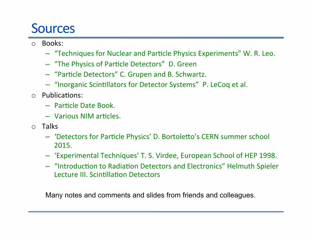
Sources o Books:
– “Techniques for Nuclear and Par@cle Physics Experiments” W. R. Leo. – “The Physics of Par@cle Detectors” D. Green – “Par@cle Detectors” C. Grupen and B. Schwartz. – “Inorganic Scin@llators for Detector Systems” P. LeCoq et al.
o Publica@ons: – Par@cle Date Book. – Various NIM ar@cles.
o Talks – ‘Detectors for Par@cle Physics’ D. BortoleSo’s CERN summer school
2015. – ‘Experimental Techniques’ T. S. Virdee, European School of HEP 1998. – “Introduc@on to Radia@on Detectors and Electronics” Helmuth Spieler
Lecture III. Scin@lla@on Detectors
Many notes and comments and slides from friends and colleagues.

Some Defini@ons 4
Scintillation light is the light that is emitted when ionizing radiation is the source of the energy. Scintillation is luminescence stimulated by ionizing radiation.
Luminescence is light emitted by the excitation of the luminescent centers into response light source or due to electronic stimulation.
Phosphorescence is light emitted from long-lived luminescent sites after several time-constants of the primary emission. Afterglow is the amplitude of the signal.
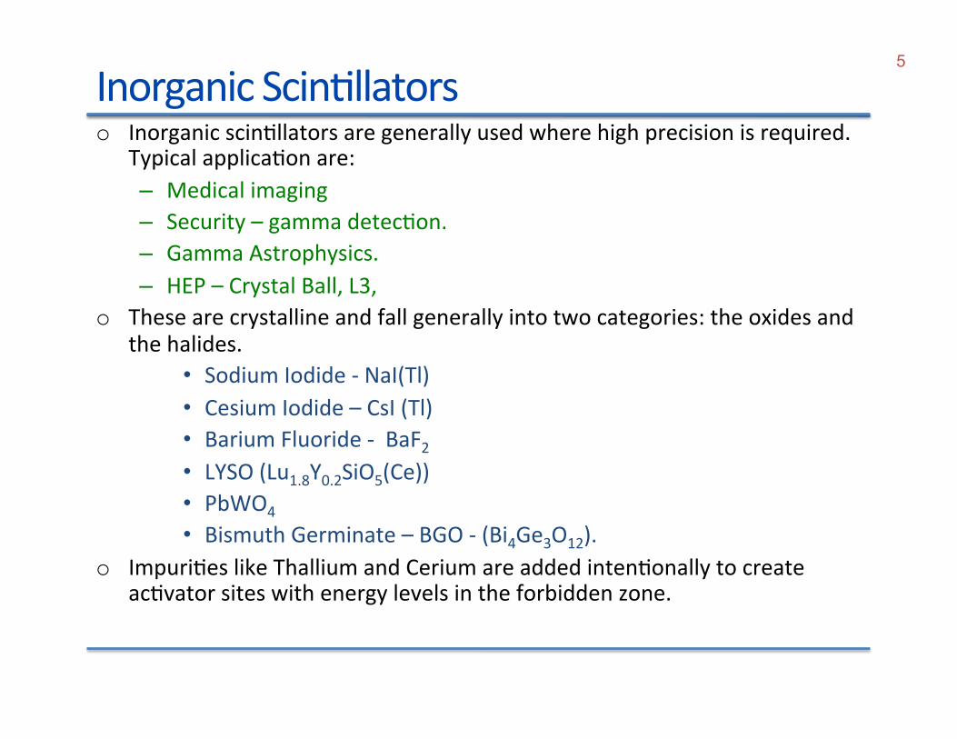
Inorganic Scin@llators o Inorganic scin@llators are generally used where high precision is required.
Typical applica@on are: – Medical imaging – Security – gamma detec@on. – Gamma Astrophysics. – HEP – Crystal Ball, L3,
o These are crystalline and fall generally into two categories: the oxides and the halides.
• Sodium Iodide -‐ NaI(Tl) • Cesium Iodide – CsI (Tl) • Barium Fluoride -‐ BaF2 • LYSO (Lu1.8Y0.2SiO5(Ce)) • PbWO4 • Bismuth Germinate – BGO -‐ (Bi4Ge3O12).
o Impuri@es like Thallium and Cerium are added inten@onally to create ac@vator sites with energy levels in the forbidden zone.
5
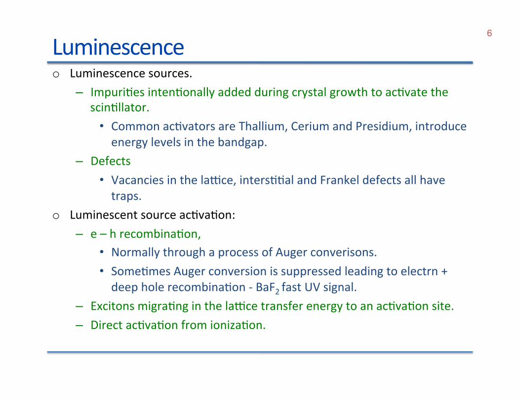
Luminescence o Luminescence sources.
– Impuri@es inten@onally added during crystal growth to ac@vate the scin@llator.
• Common ac@vators are Thallium, Cerium and Presidium, introduce energy levels in the bandgap.
– Defects • Vacancies in the lafce, inters@@al and Frankel defects all have traps.
o Luminescent source ac@va@on: – e – h recombina@on,
• Normally through a process of Auger converisons. • Some@mes Auger conversion is suppressed leading to electrn + deep hole recombina@on -‐ BaF2 fast UV signal.
– Excitons migra@ng in the lafce transfer energy to an ac@va@on site. – Direct ac@va@on from ioniza@on.
6
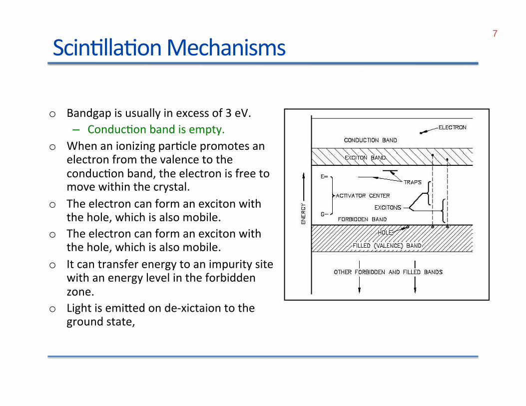
Scin@lla@on Mechanisms
o Bandgap is usually in excess of 3 eV. – Conduc@on band is empty.
o When an ionizing par@cle promotes an electron from the valence to the conduc@on band, the electron is free to move within the crystal.
o The electron can form an exciton with the hole, which is also mobile.
o The electron can form an exciton with the hole, which is also mobile.
o It can transfer energy to an impurity site with an energy level in the forbidden zone.
o Light is emiSed on de-‐xictaion to the ground state,
7
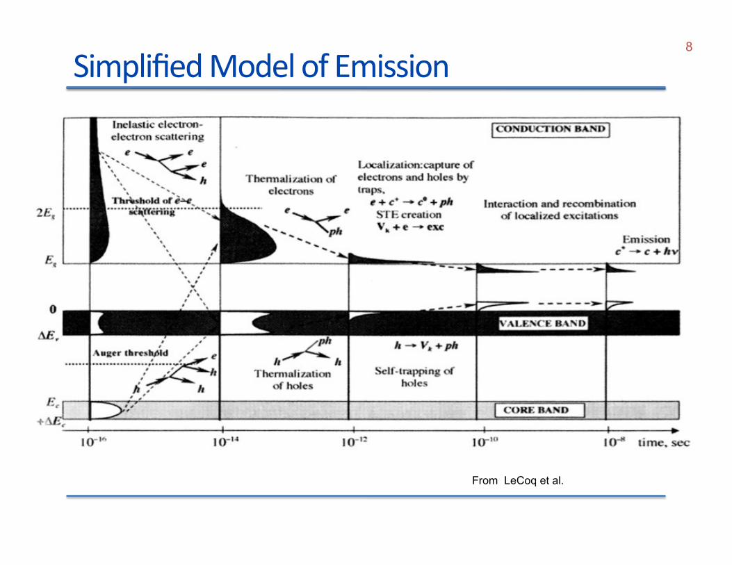
Simplified Model of Emission 8
From LeCoq et al.
Which Crystal? o Cost. o Density
– Crystals are used for total absorp@on calorimetry ⇒ high density. Xo and the shower (Molière) radius should be short be small.
o Light yield – Want good conversion efficiency of the ioniza@on energy to photons.
o Pulse dura@on: – Preferably short < 40 ns.
o Radia@on hard: – Normally not an issue in e+e-‐ machines, where the radia@on levels are
low. – Significant concern in hadron colliders.
o Wavelength of the emiSed light. – PMTs are sensi@ve between 350 nm and 500 nm. – Silicon diodes, APDs and SiPMs can have a sensi@vity in the red. – UV is difficult.
o Level of industrializa@on.
9
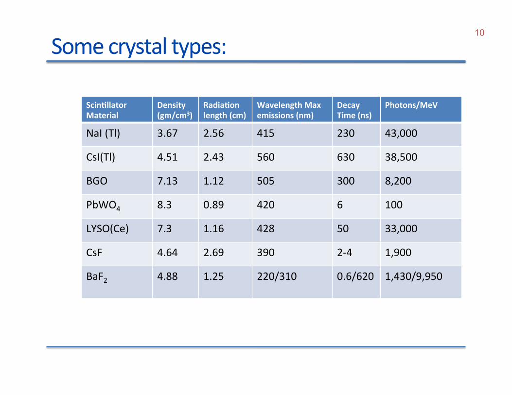
Some crystal types: 10
Scin2llator Material
Density (gm/cm3)
Radia2on length (cm)
Wavelength Max emissions (nm)
Decay Time (ns)
Photons/MeV
NaI (Tl) 3.67 2.56 415 230 43,000
CsI(Tl) 4.51 2.43 560 630 38,500
BGO 7.13 1.12 505 300 8,200
PbWO4 8.3 0.89 420 6 100
LYSO(Ce) 7.3 1.16 428 50 33,000
CsF 4.64 2.69 390 2-‐4 1,900
BaF2 4.88 1.25 220/310 0.6/620 1,430/9,950
Organic Scin@llators 11
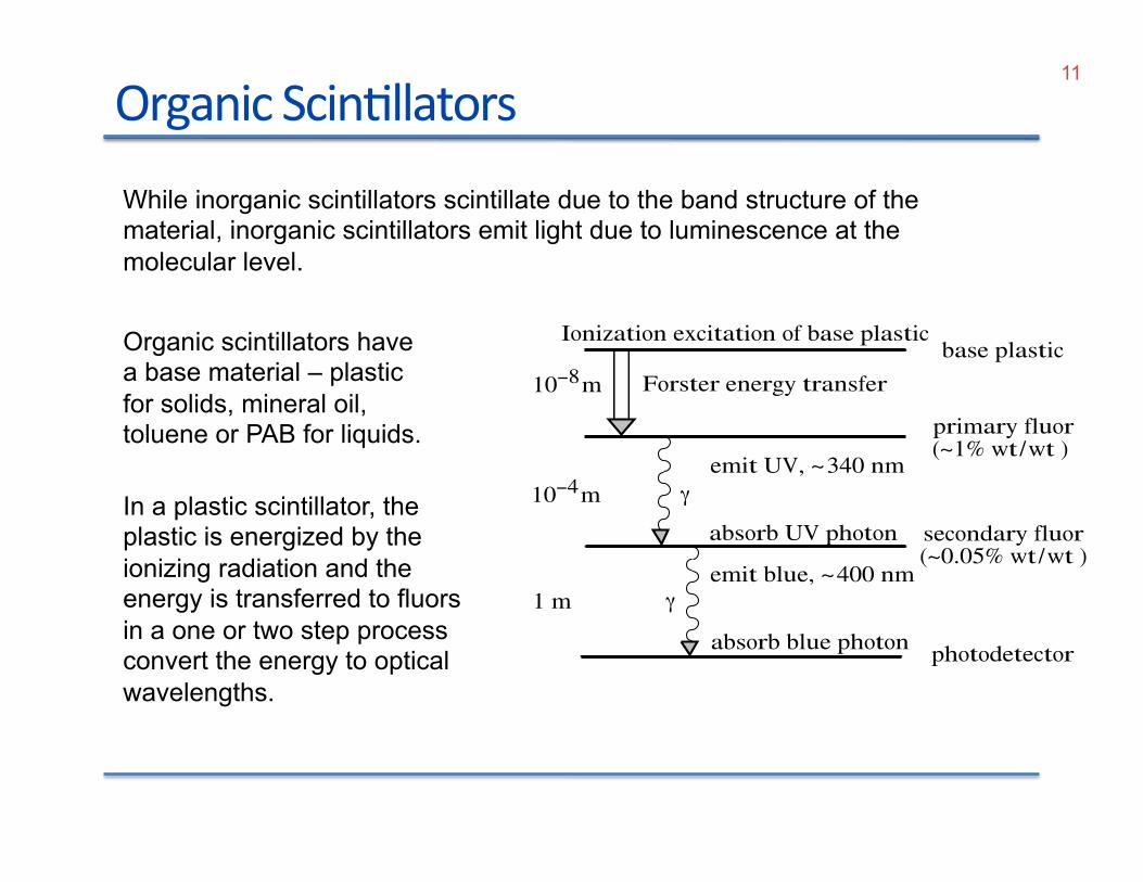
While inorganic scintillators scintillate due to the band structure of the material, inorganic scintillators emit light due to luminescence at the molecular level.
Ionization excitation of base plastic
Forster energy transfer
γ
γ
base plastic
primary fluor(~1% wt /wt )
secondary fluor(~0.05% wt /wt )
photodetector
emit UV, ~340 nm
absorb blue photon
absorb UV photon
emit blue, ~400 nm1 m
10−4m
10−8m
Organic scintillators have a base material – plastic for solids, mineral oil, toluene or PAB for liquids.
In a plastic scintillator, the plastic is energized by the ionizing radiation and the energy is transferred to fluors in a one or two step process convert the energy to optical wavelengths.
Plas@c Scin@llators 12
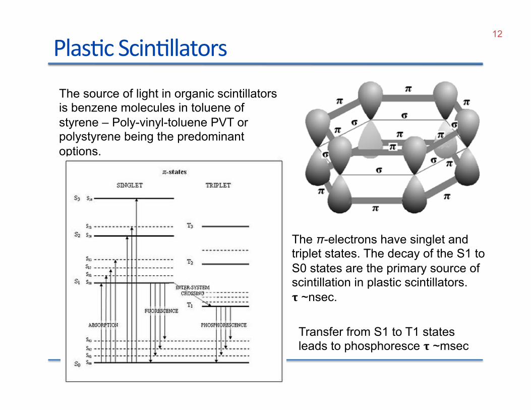
The source of light in organic scintillators is benzene molecules in toluene of styrene – Poly-vinyl-toluene PVT or polystyrene being the predominant options.
The π-electrons have singlet and triplet states. The decay of the S1 to S0 states are the primary source of scintillation in plastic scintillators. 𝛕 ~nsec.
Transfer from S1 to T1 states leads to phosphoresce 𝛕 ~msec
Plas@c Scin@llators 13
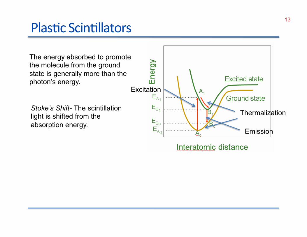
The energy absorbed to promote the molecule from the ground state is generally more than the photon’s energy.
Excitation
Thermalization
Emission
Stoke’s Shift- The scintillation light is shifted from the absorption energy.
Plas@c Scin@llators 14
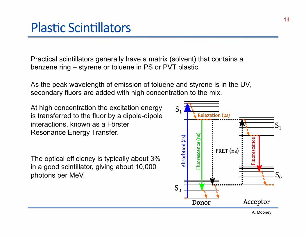
Practical scintillators generally have a matrix (solvent) that contains a benzene ring – styrene or toluene in PS or PVT plastic.
As the peak wavelength of emission of toluene and styrene is in the UV, secondary fluors are added with high concentration to the mix.
At high concentration the excitation energy is transferred to the fluor by a dipole-dipole interactions, known as a Förster Resonance Energy Transfer.
The optical efficiency is typically about 3% in a good scintillator, giving about 10,000 photons per MeV.
A. Mooney
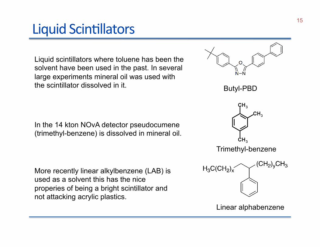
Liquid Scin@llators 15
Butyl-PBD
Trimethyl-benzene
Liquid scintillators where toluene has been the solvent have been used in the past. In several large experiments mineral oil was used with the scintillator dissolved in it.
In the 14 kton NOvA detector pseudocumene (trimethyl-benzene) is dissolved in mineral oil.
More recently linear alkylbenzene (LAB) is used as a solvent this has the nice properies of being a bright scintillator and not attacking acrylic plastics.
Linear alphabenzene

Noble Gas/Liquid Scin@llators 16
J Chem Phys vol 91 (1989) 1469 E Morikawa et al
Argon Xenon and Krypton emit scintillation light in the far UV.
The physical process is the formation of excimers (Ar+Ar) that de-exicite emitting a photon with a time constant of ~ 6 ns.
For liquid argon the peak wavelength is 128 nm. A wavelength shifter is required to shift to the optical region.
Singlet
Triplet
The fluorescent chemical Tetraphenyl Butadiene (TPB) is used in MicroBooNE and under discussion for DUNE
Radia@on Damage o Sources:
– Color center crea@on – ScaSering or absorp@on in light’s pathway. – Intrinsic Damage.
o Inorganic Scin@llators, – In crystals the main source of damage is the crea@on of color centers
that absorb the scin@lla@on light and lead to a reduc@on in light received.
– NaI and CsI crystals are damaged aper ~10 Gy. – BGO and PbWO4 are intrinsic scin@llators more radia@on tolerant ~ 1
MGy of gamma and 10 kGy. – In PbWO4 there are two effects:
• Metastable states created by photons, with a life@me of hours to weeks.
• Long-‐lived states created by hadron interac@ons.
17
Radia@on Damage in Plas@cs 18
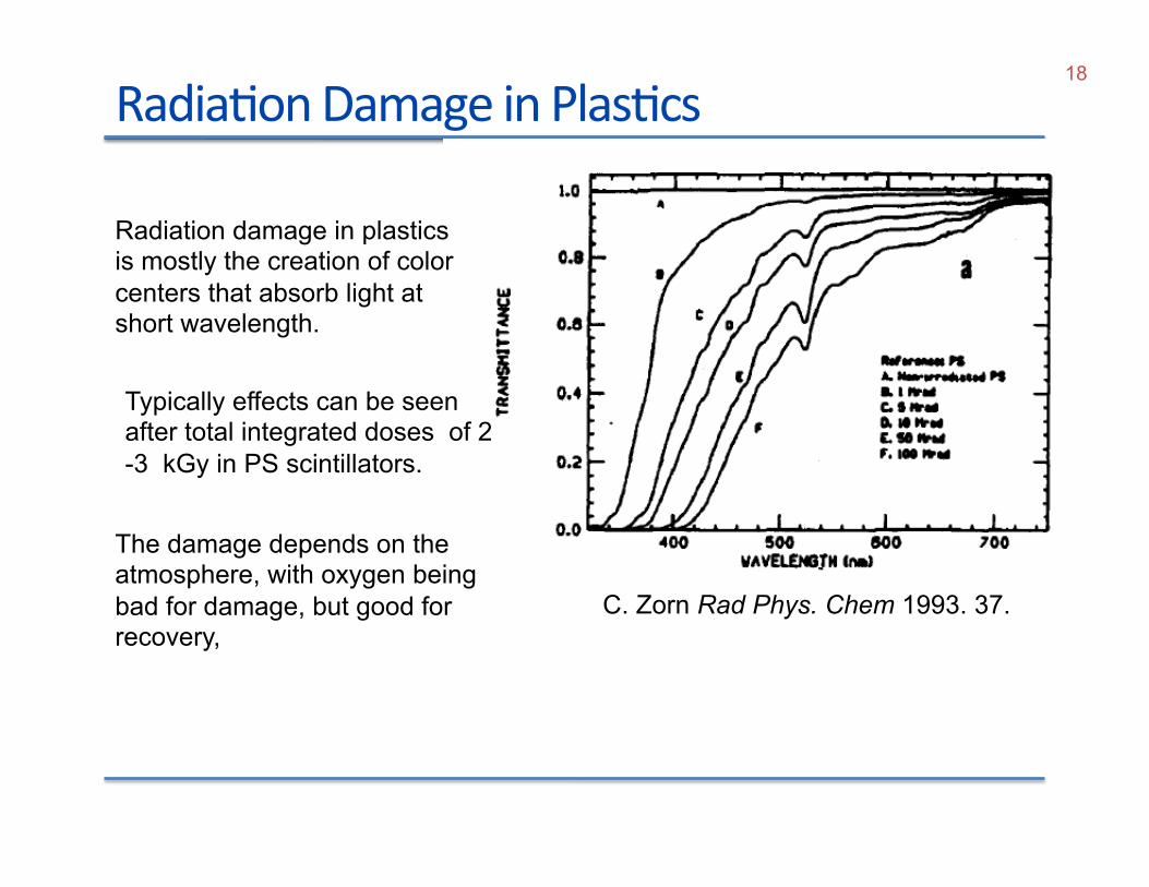
Radiation damage in plastics is mostly the creation of color centers that absorb light at short wavelength.
C. Zorn Rad Phys. Chem 1993. 37.
Typically effects can be seen after total integrated doses of 2 -3 kGy in PS scintillators.
The damage depends on the atmosphere, with oxygen being bad for damage, but good for recovery,
Radia@on Damage in Plas@cs 19
The degree of damage in scintillators depends also on the of the radiation dose. This ‘well-known’ effects was first reported by Wigmans and Sirois in 1988 and continues to be rediscovered about once very ten years.
The explanation for this is generally assumed to be oxygen migration into the scintillator adding to the effect. The chemistry of this is not clear.
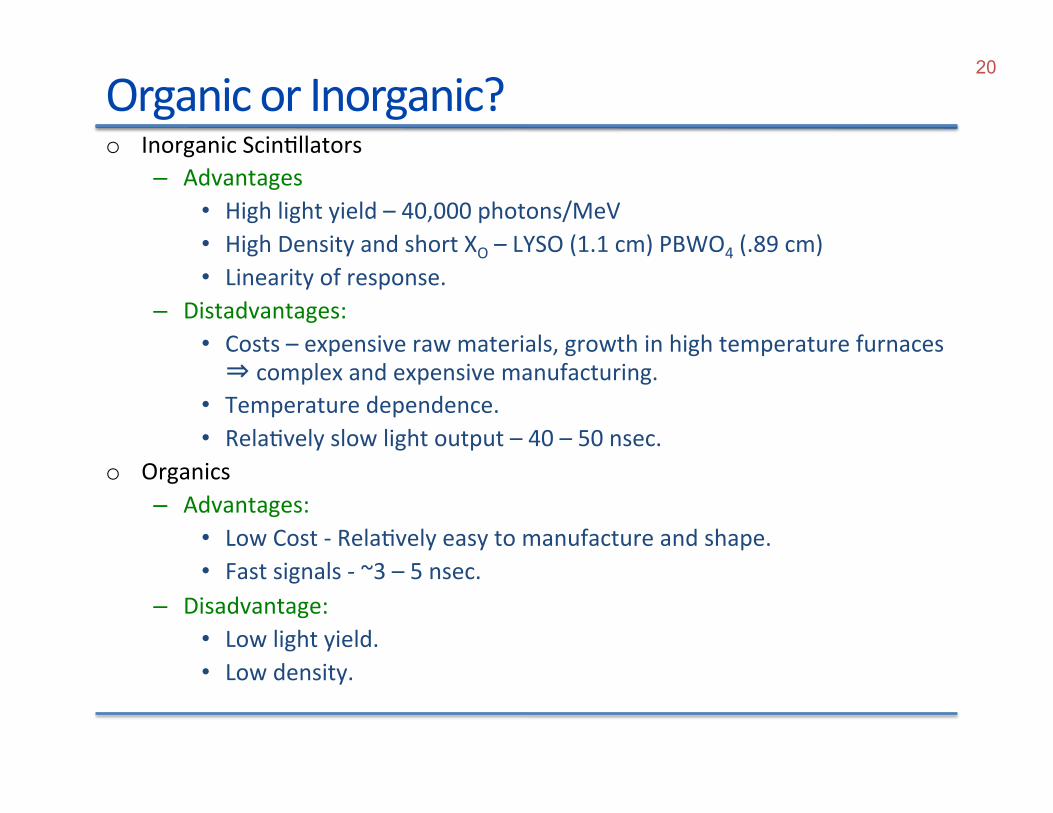
Organic or Inorganic? o Inorganic Scin@llators
– Advantages • High light yield – 40,000 photons/MeV • High Density and short XO – LYSO (1.1 cm) PBWO4 (.89 cm) • Linearity of response.
– Distadvantages: • Costs – expensive raw materials, growth in high temperature furnaces ⇒ complex and expensive manufacturing.
• Temperature dependence. • Rela@vely slow light output – 40 – 50 nsec.
o Organics – Advantages:
• Low Cost -‐ Rela@vely easy to manufacture and shape. • Fast signals -‐ ~3 – 5 nsec.
– Disadvantage: • Low light yield. • Low density.
20
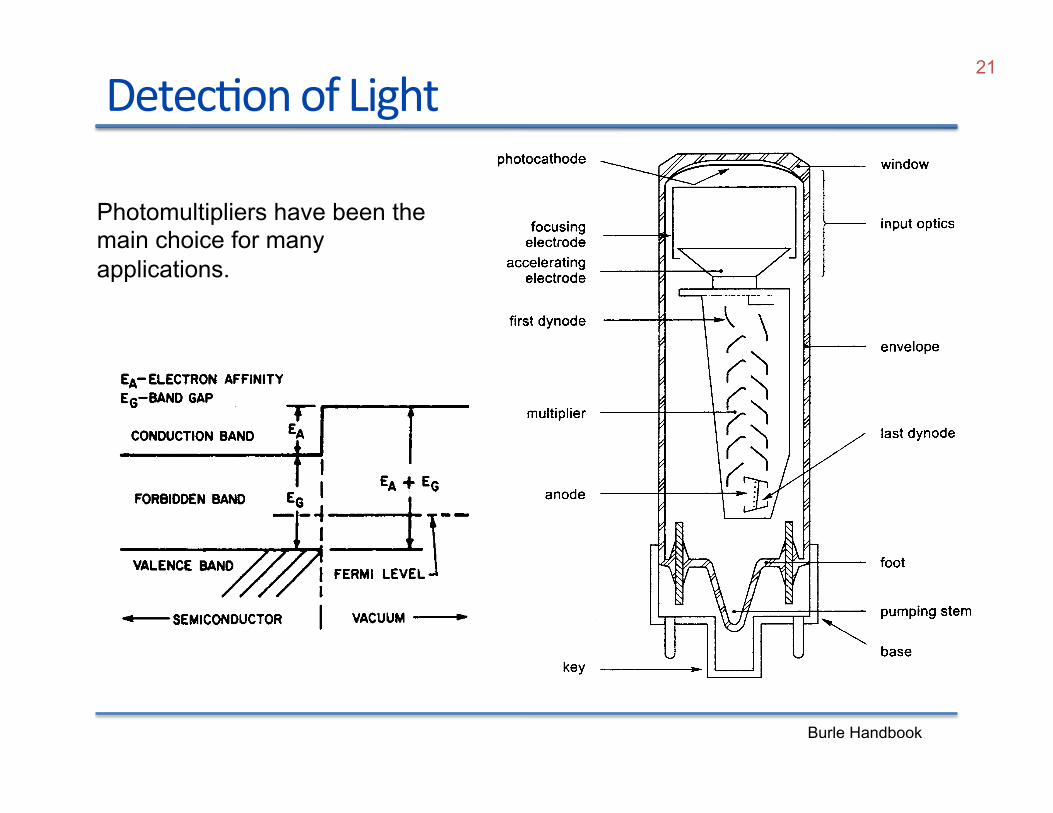
Detec@on of Light 21
Photomultipliers have been the main choice for many applications.
Burle Handbook
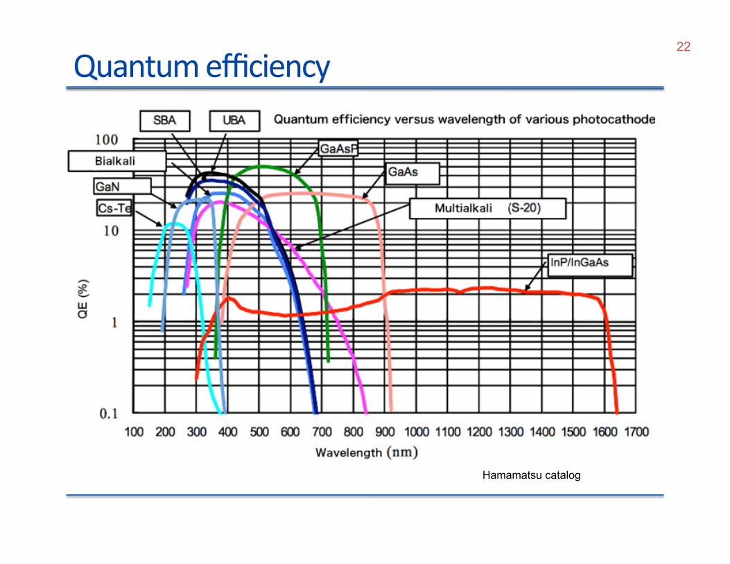
Quantum efficiency 22
Hamamatsu catalog
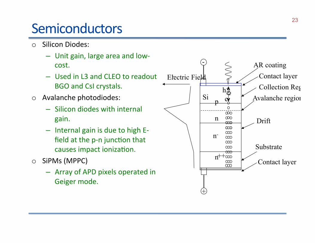
Semiconductors o Silicon Diodes:
– Unit gain, large area and low-‐cost.
– Used in L3 and CLEO to readout BGO and CsI crystals.
o Avalanche photodiodes: – Silicon diodes with internal
gain. – Internal gain is due to high E-‐
field at the p-‐n junc@on that causes impact ioniza@on.
o SiPMs (MPPC) – Array of APD pixels operated in
Geiger mode.
23
+
-
h+ e Si
AR coating Contact layer Collection Region
Avalanche region
Drift
Substrate
Contact layer
Electric Field
p
n
n ++
n-

Quantum Efficiency 24
QE of silicon diodes extends out to 1 µm and can be ~ 80%
The range of the detection efficiency is limited by the the surface treatment (blue light) and the junction depth (red light).
In SiPMs there is an additional geometrical effect that limits the detection efficiency.
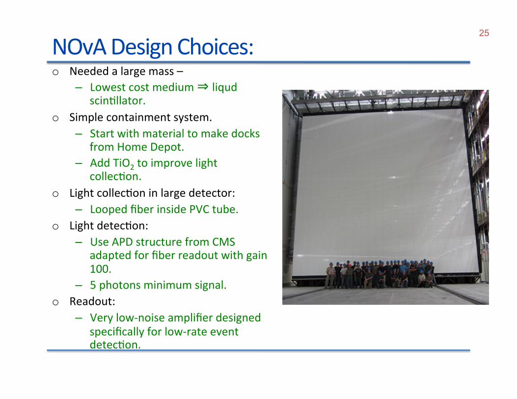
NOvA Design Choices: o Needed a large mass –
– Lowest cost medium ⇒ liqud scin@llator.
o Simple containment system. – Start with material to make docks
from Home Depot. – Add TiO2 to improve light
collec@on. o Light collec@on in large detector:
– Looped fiber inside PVC tube. o Light detec@on:
– Use APD structure from CMS adapted for fiber readout with gain 100.
– 5 photons minimum signal. o Readout:
– Very low-‐noise amplifier designed specifically for low-‐rate event detec@on.
25
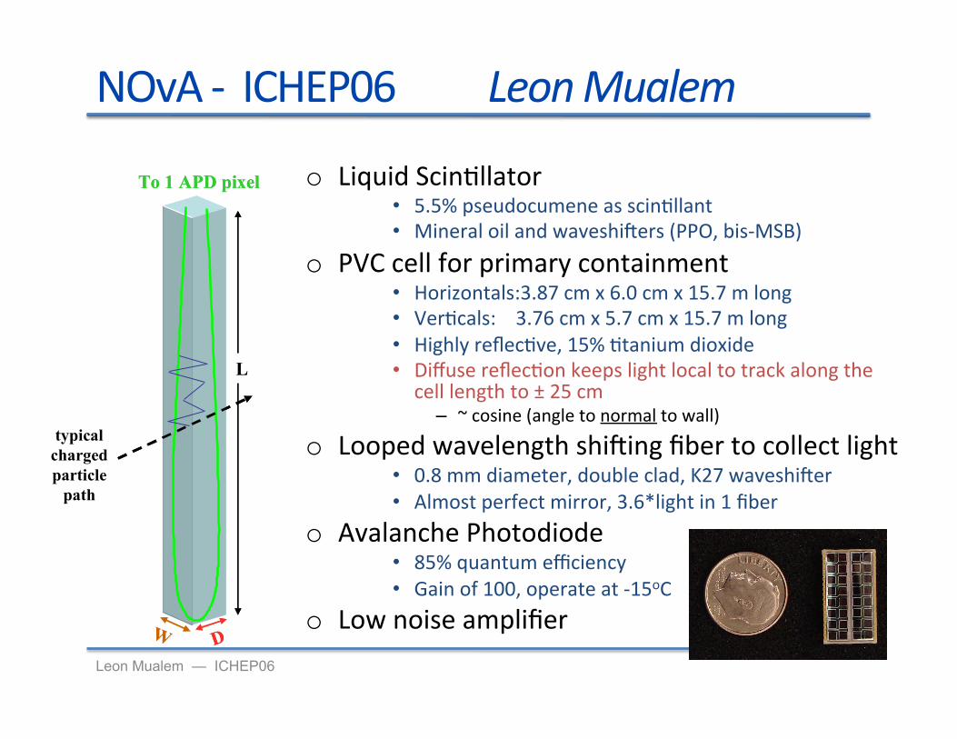
Leon Mualem — ICHEP06
NOvA -‐ ICHEP06 Leon Mualem
o Liquid Scin@llator • 5.5% pseudocumene as scin@llant • Mineral oil and waveshipers (PPO, bis-‐MSB)
o PVC cell for primary containment • Horizontals:3.87 cm x 6.0 cm x 15.7 m long • Ver@cals: 3.76 cm x 5.7 cm x 15.7 m long • Highly reflec@ve, 15% @tanium dioxide • Diffuse reflec@on keeps light local to track along the cell length to ± 25 cm
– ~ cosine (angle to normal to wall)
o Looped wavelength shiping fiber to collect light • 0.8 mm diameter, double clad, K27 waveshiper • Almost perfect mirror, 3.6*light in 1 fiber
o Avalanche Photodiode • 85% quantum efficiency • Gain of 100, operate at -‐15oC
o Low noise amplifier
To 1 APD pixel
W D
typicalchargedparticle
path
L
To 1 APD pixel
W D
typicalchargedparticle
path
L
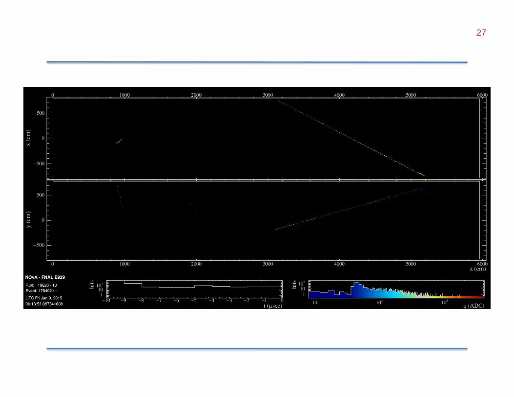
27