Sebuah Kajian Pustaka: - International Journal of Engineering ...
12
International Journal of Engineering, Science and Mathematics Vol. 6 Issue 8, December 2017 (Special Issue) ISSN: 2320-0294 Impact Factor: 6.765 Journal Homepage: http://www.ijesm.co.in, Email: [email protected] Double-Blind Peer Reviewed Refereed Open Access International Journal - Included in the International Serial Directories Indexed & Listed at: Ulrich's Periodicals Directory ©, U.S.A., Open J-Gage as well as in Cabell’s Directories of Publishing Opportunities, U.S.A 857 International Journal of Engineering, Science and Mathematics http://www.ijesm.co.in, Email: [email protected] DESIGN OF HIGH SPEED LOW POWER PARALLEL ADDER USING BEC TECHNIQUE Kala Priya.K* Rajani Chandra CH** Abstract (10pt) Addition is a fundamental operation for any digital system, digital signal processing or control system. A fast and accurate operation of a digital system is greatly influenced by the performance of the resident adders.Adders are also very important component in digital systems because of their extensive use in other basic digital operations such as subtraction, multiplication and division. Hence, improving performance of the digital adder would greatly advance the execution of binary operations inside a circuit compromised of such blocks. The performance of a digital circuit block is gauged by analysingits power dissipation, layout area and its operating speed. As a result, the need for faster and efficient Adders in computers has been a topic of interest over decades. Binary adders are one of the most essential logic elements within a digital system. In addition, binary adders are also helpful in units other than Arithmetic Logic Units (ALU), such as multipliers, dividers and memory addressing. Therefore, binary addition is essential that any improvement in binary addition can result in a performance boost for any computing system and helps to improve the performance of the entire system.The major problem for binary addition is the carry chain. As the width of the input operand increases, the length of the carry chain increases. The binary adder is the critical element in most digital circuit designs including digital signal processors (DSP) and microprocessor data path units. As such, extensive research continues to be focused on improving the power delay performance of the adder. The basic idea of the proposed work is using various types of addersand compared to the adder with Binary to Excess 1 converter (BEC) for high speed of addition by using the simulation through Verilog in Xilinx ISE. Keywords: Adders,Binary adders, Parallel- prefix adders, Verilog, Xilinx Author correspondence: • Kala Priya.K, Assistant Professor, Department of ECE, BITS, Visakhapatnam, India. • Rajani Chandra CH, Assistant Professor, Department of ECE, BITS, Visakhapatnam, India.
-
Upload
khangminh22 -
Category
Documents
-
view
0 -
download
0
Transcript of Sebuah Kajian Pustaka: - International Journal of Engineering ...
International Journal of Engineering, Science and Mathematics Vol. 6 Issue 8, December 2017 (Special Issue) ISSN: 2320-0294 Impact Factor: 6.765 Journal Homepage: http://www.ijesm.co.in, Email: [email protected] Double-Blind
Peer Reviewed Refereed Open Access International Journal - Included in the International Serial Directories Indexed & Listed at: Ulrich's Periodicals Directory ©, U.S.A., Open J-Gage as well as in Cabell’s Directories of Publishing Opportunities, U.S.A
857 International Journal of Engineering, Science and Mathematics
http://www.ijesm.co.in, Email: [email protected]
DESIGN OF HIGH SPEED LOW POWER PARALLEL ADDER USING BEC
TECHNIQUE
Kala Priya.K*
Rajani Chandra CH**
Abstract (10pt)
Addition is a fundamental operation for any digital system, digital signal
processing or control system. A fast and accurate operation of a digital system is greatly influenced by the performance of the resident adders.Adders are also very important component in digital systems because of their extensive use in other basic digital operations such as subtraction, multiplication and division. Hence, improving performance of the digital adder would greatly advance the execution of binary operations inside a circuit compromised of such blocks. The performance of a digital circuit block is gauged by analysingits power dissipation, layout area and its operating speed. As a result, the need for faster and efficient Adders in computers has been a topic of interest over decades.
Binary adders are one of the most essential logic elements within a digital system. In addition, binary adders are also helpful in units other than Arithmetic Logic Units (ALU), such as multipliers, dividers and memory addressing. Therefore, binary addition is essential that any improvement in binary addition can result in a performance boost for any computing system and helps to improve the performance of the entire system.The major problem for binary addition is the carry chain. As the width of the input operand increases, the length of the carry chain increases. The binary adder is the critical element in most digital circuit designs including digital signal processors (DSP) and microprocessor data path units. As such, extensive research continues to be focused on improving the power delay performance of the adder. The basic idea of the proposed work is using various types of addersand compared to the adder with Binary to Excess 1 converter (BEC) for high speed of addition by using the simulation through Verilog in Xilinx ISE.
Keywords:
Adders,Binary adders, Parallel-
prefix adders, Verilog, Xilinx
Author correspondence:
• Kala Priya.K, Assistant Professor, Department of ECE, BITS, Visakhapatnam, India.
• Rajani Chandra CH, Assistant Professor, Department of ECE, BITS, Visakhapatnam, India.
ISSN: 2320-0294Impact Factor: 6.765
858 International Journal of Engineering, Science and Mathematics
http://www.ijesm.co.in, Email: [email protected]
1. Introduction
In VLSI implementations, parallel-prefix adders are known to have the best performance. Reconfigurable logic
such as Field Programmable Gate Arrays (FPGAs) has been gaining in popularity in recent years because it
offers improved performance in terms of speed and power over DSP-based and microprocessor-based
solutions for many practical designs involving mobile DSP and telecommunications applications and a
significant reduction indevelopment time and cost over Application Specific Integrated Circuit (ASIC)
designs[1].
However, because of the structure of the configurable logic and routing resources in FPGAs, parallel-prefix
adders will have a different performance than VLSI implementations. In particular, most modern FPGAs
employ a fast-carry chain which optimizes the carry path for the Binary to Excess-1 Converters (BEC). In this
project, the practical issues involved in designing and implementing tree-based adders on FPGAs are
described.
Several tree-based adder structures are implemented and compared. Finally, some conclusions and
suggestions for improving FPGA designs to enable better tree-based adder performance are given. The main
challenging areas in VLSI are performance, cost, testing, area, reliability and power [2]. The demand for
portable computing devices and communications system are increasing rapidly. These applications require
high speed VLSI circuits. Hence it is important aspect to optimize speed. So these optimizations became main
challenge in the chip designing field.
Parallel-prefix adders, also known as carry-tree adders, pre-compute thepropagate and generate signals.
These signals are variously combined using the fundamental carry operator (fco).
(gL, pL) ο (gR, pR) = (gL+ pL•gR, pL• pR) (1)
Due to associative property of the fco, these operators can be combined in different ways to form various
adder structures. For, example the four-bit carry look-ahead generator is given by
c4= (g4, p4) o [(g3, p3) ο [(g2, p2) ο (g1, p1)]] (2)
A simple rearrangement of the order of operations allows parallel operation, resulting in a more efficient tree
structure for this four bit example is
c4= [(g4, p4) ο (g3, p3)] ο [(g2, p2) ο (g1, p1)] (3)
It is readily apparent that a key advantage of the tree structured adder is that the critical path due to the
carry delay is on the order of log2N for an N-bit wide adder. The arrangement of the prefix network gives rise
to various families of adders. Here BC is designated as the black cell which generates the ordered pair in
equation (1); the gray cell (GC) generates the left signal only. The interconnect area is known to be high, but
for an FPGA with large routing overhead to begin with, this is not as important as in a VLSI implementation.
The regularity of the Kogge-Stone prefix network has built in redundancy which has implications for fault-
tolerant designs. This hybrid design completes the summation process with a 4-bit RCA allowing the carry
prefix network to be simplified [4,5]. Parallel prefix adders allow more efficient implementations of the carry
ISSN: 2320-0294Impact Factor: 6.765
859 International Journal of Engineering, Science and Mathematics
http://www.ijesm.co.in, Email: [email protected]
look-ahead technique and are essentially, variants of carry look-ahead adders. Indeed, in current technology,
parallel prefix adders are among the best adders, with respect to area and time is particularly suited for high
speed addition of large numbers.
In these parallel prefix adders, mainly two types of Generate and Propagate bits are present. Generate and
Propagate concept is extendable to blocks comprising multiple bits. For each bit i ofthe adder, Generate (Gi)
indicates whether a carry is generated from that bit and
Gi= ai&bi (4)
For each bit i of the adder, Propagate (Pi) indicates whether a carry is propagated through that bit
Pi = aibi (5)
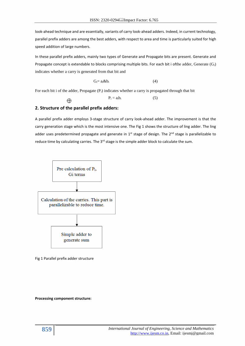
2. Structure of the parallel prefix adders:
A parallel prefix adder employs 3-stage structure of carry look-ahead adder. The improvement is that the
carry generation stage which is the most intensive one. The Fig 1 shows the structure of ling adder. The ling
adder uses predetermined propagate and generate in 1st stage of design. The 2nd stage is parallelizable to
reduce time by calculating carries. The 3rd stage is the simple adder block to calculate the sum.
Fig 1 Parallel prefix adder structure
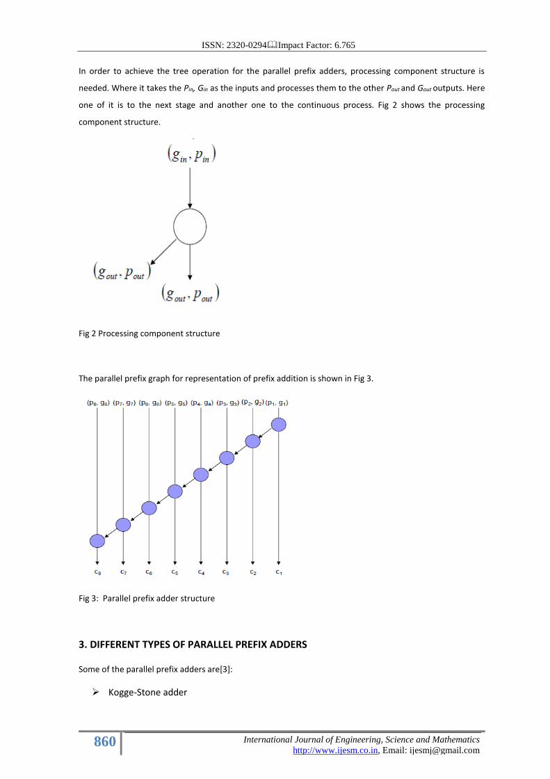
Processing component structure:
ISSN: 2320-0294Impact Factor: 6.765
860 International Journal of Engineering, Science and Mathematics
http://www.ijesm.co.in, Email: [email protected]
In order to achieve the tree operation for the parallel prefix adders, processing component structure is
needed. Where it takes the Pin, Gin as the inputs and processes them to the other Pout and Gout outputs. Here
one of it is to the next stage and another one to the continuous process. Fig 2 shows the processing
component structure.
Fig 2 Processing component structure
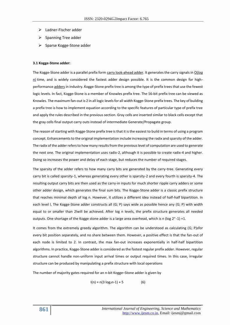
The parallel prefix graph for representation of prefix addition is shown in Fig 3.
Fig 3: Parallel prefix adder structure
3. DIFFERENT TYPES OF PARALLEL PREFIX ADDERS
Some of the parallel prefix adders are[3]:
➢ Kogge-Stone adder
ISSN: 2320-0294Impact Factor: 6.765
861 International Journal of Engineering, Science and Mathematics
http://www.ijesm.co.in, Email: [email protected]
➢ Ladner-Fischer adder
➢ Spanning Tree adder
➢ Sparse Kogge-Stone adder
3.1 Kogge-Stone adder:
The Kogge-Stone adder is a parallel prefix form carry look-ahead adder. It generates the carry signals in O(log
n) time, and is widely considered the fastest adder design possible. It is the common design for high-
performance adders in industry. Kogge-Stone prefix tree is among the type of prefix trees that use the fewest
logic levels. In fact, Kogge-Stone is a member of Knowles prefix tree. The 16-bit prefix tree can be viewed as
Knowles. The maximum fan-out is 2 in all logic levels for all width Kogge-Stone prefix trees. The key of building
a prefix tree is how to implement equation according to the specific features of particular type of prefix tree
and apply the rules described in the previous section. Gray cells are inserted similar to black cells except that
the gray cells final output carry outs instead of intermediate Generate/Propagate group.
The reason of starting with Kogge-Stone prefix tree is that it is the easiest to build in terms of using a program
concept. Enhancements to the original implementation include increasing the radix and sparsity of the adder.
The radix of the adder refers to how many results from the previous level of computation are used to generate
the next one. The original implementation uses radix-2, although it is possible to create radix-4 and higher.
Doing so increases the power and delay of each stage, but reduces the number of required stages.
The sparsity of the adder refers to how many carry bits are generated by the carry-tree. Generating every
carry bit is called sparsity-1, whereas generating every other is sparsity-2 and every fourth is sparsity-4. The
resulting output carry bits are then used as the carry-in inputs for much shorter ripple carry adders or some
other adder design, which generates the final sum bits. The Kogge-Stone adder is a classic prefix structure
that reaches minimal depth of log n. However, it utilizes a different idea instead of half-half bipartition. In
each level l, The Kogge-Stone adder constructs all (G; P) says wide as possible hence any (G; P) with width
equal to or smaller than 2lwill be achieved. After log n levels, the prefix structure generates all needed
outputs. One shortage of the Kogge stone adder is a large area overhead, which is n (log 2n -1) +1.
It comes from the extremely greedy algorithm. The algorithm can be understood as calculating (G; P)sfor
every bit position separately, and no share between them. However, a positive effect is that the fan-out of
each node is limited to 2. In contrast, the max fan-out increases exponentially in half-half bipartition
algorithms. In practice, Kogge-Stone adder is considered as the fastest regular prefix adder. However, regular
structure cannot handle non-uniform input arrival times or output required times. In this case, irregular
structure can be produced by manipulating a prefix structure with local operations
The number of majority gates required for an n-bit Kogge–Stone adder is given by
I(n) = n(3 log2n-1) + 5 (6)
ISSN: 2320-0294Impact Factor: 6.765
862 International Journal of Engineering, Science and Mathematics
http://www.ijesm.co.in, Email: [email protected]
The computation of carries of an n-bit Kogge–Stone adder requires log2 n stages. The number of majority
gates required for an n-bit Kogge–Stone adder is also obtained via a recursive formulation. The general
formula for calculating the number of majority gates for carries from𝑛
2 +1 to nis obtained as follows:
Each stage in the Kogge-Stone adder requires𝑛
2 associative operations (namely carries from
𝑛
2 +1 to n). Except
the last stage, each associative operator in all other stages requires three majority gates. In the last stage,
each associative operation requires only two majority gates (since there is no calculation of the propagate
term):
𝐼𝑐𝑑 (𝑛 ∶
n
2+ 1) = 3 (
𝑛
2 ) (𝑙𝑜𝑔
2𝑛 − 1) + 2 (
𝑛
2)
=𝑛
2[3𝑙𝑜𝑔2𝑛 − 1]
𝐼𝑐𝑑(𝑛) =
𝑛
2[3𝑙𝑜𝑔
2𝑛 − 1] + 𝐼𝑐
𝑑 (𝑛
2)
= 3 [𝑛
2𝑙𝑜𝑔2 𝑛 +
𝑛
4𝑙𝑜𝑔2
𝑛
2+ … + 2.2] − [
𝑛
2+
𝑛
4+. . +2] + 𝐼𝑐
𝑑(2)
= 3[2𝑛𝑙𝑜𝑔2 𝑛 − (𝑙𝑜𝑔2𝑛 + 1)𝑛] − [𝑛 − 2] + 2
= 3𝑛𝑙𝑜𝑔2 𝑛 − 4𝑛 + 4
This will have a reduction of one majority gate each and a total of 𝑛
2 majority gates:
𝐼𝑟(𝑛) = 𝑛
2+ 𝐼𝑟 (
𝑛
2)
= 𝑛 − 1
Hence,𝐼𝑐(𝑛)is given as
𝐼𝑐(𝑛) = 𝐼𝑐𝑑(𝑛) − 𝐼𝑟(𝑛)
= 3𝑛𝑙𝑜𝑔2𝑛 − 5𝑛 − 5(7)
The number of cells required for the Kogge stone adders are more so, in order to achieve same addition
operation with less cells is presented in Ladner-Fischer adder and its working principle is discussed.
3.2 Ladner-Fischer adder:
In 1980, Fischer and Richard Ladner presented a parallel algorithm for computing prefix sums efficiently. They
show how to construct a circuit that computes the prefix sums in the circuit; each node performs an addition
of two numbers. With their construction, one can choose a trade-off between the circuit depth and the
number of nodes.
ISSN: 2320-0294Impact Factor: 6.765
863 International Journal of Engineering, Science and Mathematics
http://www.ijesm.co.in, Email: [email protected]
Ladner and Fischer defined the prefix problem as: Let “o” be an associative operation on n inputs x1,…..,xn, to
compute each of products x1ox2o….oxk,1 ≤ k≤n. In the application of binary addition, the input of prefix
computation is a group of binary vectors with two domains gi(generate) and pi(propagate):
➢ 𝑔𝑖 = {𝑐𝑜, 𝑖𝑓 𝑖 = 0𝑎𝑖𝑏𝑖, 𝑜𝑡ℎ𝑒𝑤𝑖𝑠𝑒
(8)
➢ 𝑝𝑖 = {0, 𝑖𝑓 𝑖 = 0
𝑎𝑖 ⊕ 𝑏𝑖, 𝑜𝑡ℎ𝑒𝑤𝑖𝑠𝑒 (9)
If giequals 1, a carry is generated at bit i; otherwise if pi equals 1, a carry is propagated through bit i. By
prefix computation, the concept of generate and propagate can be extended to multiple bits. We define
G[i: k] and P[i: k] (i≥ k) as:
𝐺[𝑖:𝑘] = {𝑔
𝑖 𝑖𝑓 𝑖 = 𝑘
𝐺[𝑖:𝑘]+ 𝑃[𝑖:𝑘]𝐺[𝑗−1:𝑘], 𝑜𝑡ℎ𝑒𝑟𝑤𝑖𝑠𝑒
(10)
𝑃[𝑖:𝑘] = {𝑝
𝑖 𝑖𝑓 𝑖 = 𝑘
𝑃[𝑖:𝑗]. 𝑃[𝑗−1:𝑘], 𝑜𝑡ℎ𝑒𝑟𝑤𝑖𝑠𝑒(11)
To simplify the representation, we continue to use the same operator to denote the prefix computation on
(G; P):
(G; P)[i:k] = (G; P) [i:j]o(G; P)[j-1:k](12)
The width of the (G; P) term is calculated by i-k + 1. For final outputs, SiandCicanbe generated from GandP:
Ci= G[i:0] (13)
Si= pi ci-1 (14)
Since pre-processing and post-processing have constant delay, prefix computation becomes the core of prefix
adders and dominates the performance. A visual representation of prefix computation structures is to use
directed acyclic graphs. For (G; P) computation in binary addition problem, it has two important properties:
Property 1: (G; P) computation is associative. That is
(G; P)[i:k] = (G; P)[i:j] o (G; P)[j-1:k]
= (G; P)[i:l] o(G; P)[l-1:k]; i ≥ l; j > k (15)
Property 2: (G; P) computation is idempotent. That is
(G; P)[i:k] = (G; P)[i:j] o(G; P)[j-1:k]
= (G; P)[i:j] o(G; P)[l:k]; i ≥ l > j- 1 ≥ k
(16)
These two properties limit the design space of parallel prefix adders. That is the solution space of (G; P)
computation covers every tree-like structures defined under bit width n.

ISSN: 2320-0294Impact Factor: 6.765
864 International Journal of Engineering, Science and Mathematics
http://www.ijesm.co.in, Email: [email protected]
However, the same circuit designs were already studied much earlier in Sovietmathematics. This also has
O(log2n) stages. Its prefix graph is shown in Fig 3.9.The Ladner Fischer Parallel Prefix Adder (LFPPA) is
presented graphically represents the connection of carry operator node in LFPPA for the case of n = 8. The
number of majority gates required for an n-bit Ladner–Fischer adder is given by
𝐼(𝑛) =𝑛
2(3𝑙𝑜𝑔2𝑛 + 4) + 2 (17)
The direct calculation of the carries, 𝐼𝑐𝑑denoted by is given by
𝐼𝑐𝑑 =
𝑛
4[3𝑙𝑜𝑔
2𝑛 + 1] + 𝐼𝑐
𝑑 (𝑛
2)
=3
2[𝑛
2𝑙𝑜𝑔2𝑛 +
𝑛
4𝑙𝑜𝑔2
𝑛
2+ ⋯ + 2.2] − [
𝑛
4+
𝑛
8+ ⋯ + 2 + 1] + 𝐼𝑐
𝑑(2)
=3
2[2𝑛𝑙𝑜𝑔2𝑛 − (𝑙𝑜𝑔2𝑛 + 1)𝑛] − [𝑛 − 2] + 2
=3
2𝑛𝑙𝑜𝑔2𝑛 − 𝑛 + 1 (18)
Here associative operations are applied in stage 1and stage log2n. This leads to a reduction of majority gates,
denoted Ir(n), given by
𝐼𝑟(𝑛) =𝑛
2+ 𝐼𝑟 (
𝑛
2) = 𝑛 − 1
𝐼𝑐(𝑛) = 𝐼𝑐𝑑(𝑛) − 𝐼𝑟(𝑛)
=3
2𝑛𝑙𝑜𝑔2𝑛 − 2𝑛 + 2 (19)
The overall majority gate requirement is given by
𝐼(𝑛) = 𝐼𝑐(𝑛) + 𝐼𝑔𝑝(𝑛) + 𝐼𝑠(𝑛)
=𝑛
2(3𝑙𝑜𝑔2𝑛 + 4) + 2 (20)
Ladner and Fischer’s method not only provides a possible way to achieve minimal depth, but also establishes
a depth-area trade-off for the first time. The upper bound of area is:
𝐴𝑝𝑐(𝑛) < 2 (1 + 1
2𝑛) 𝑛 − 2, 𝑛 ≥ 1 (21)
While Ladner-Fischer adder is better than the Kogge stone adder in terms of number of cells, Spanning Tree
adder’s delay performance is better than this Ladner-Fischer adder.
3.3 Spanning Tree adder:
Spanning tree adders is an existing category of adders. Basically, the performances of adders are evaluated
with propagation delay. This spanning tree uses minimum number of multi-input gates.Path delay is the main
concern for these prefix adders.
ISSN: 2320-0294Impact Factor: 6.765
865 International Journal of Engineering, Science and Mathematics
http://www.ijesm.co.in, Email: [email protected]
3.4 Sparse Kogge-Stoneadder:
Enhancements to the original implementation include increasing the radix and sparsity of the
adder. The radix of the adder refers to how many results from the previous level of computation
are used to generate the next one. The original implementation uses radix-2, although it's possible
to create radix-4 and higher. Doing so increases the power and delay of each stage, but reduces the
number of required stages. The sparsity of the adder refers to how many carry bits are generated
by the carry-tree. Generating every carry bit is called sparsity-1, whereas generating every other is
sparsity-2 and every fourth is sparsity-4. The resulting carries are then used as the carry-in inputs
for much shorter ripple carry adders or some other adder design, which generates the final sum
bits. Increasing sparsity reduces the total needed computationand can reduce the amount of
routing congestion stage this is how the reduction of stages is being done and then the final sum is
being produced by operations performed by the combination.The delay reduction is done by
reducing the number of stages such that the low delay and low power and area is being consumed
such that the high speed is being obtained.
The Sparse Kogge-Stone adder consists of several smaller ripple carry adders (RCAs) on its lower half and a
carry tree on its upper half. Thus, the sparse Kogge-Stone adder terminates with RCAs. The number of carries
generated is less in a Sparse Kogge- Stone adder compared to the regular Kogge-Stone adder. Sparse kogge-
stone adder is nothing but the enhancement of the kogge stone adder. The block in this sparse- kogge stone
adder are similar to the kogge stone adder. In this sparse kogge stone, the reduction of number of stages is
being done by reducing the generation and propagate units. The delay reduction is done by reducing the
number of stages such that the low delay and low power and area is being consumed such that the high speed
is being obtained.
4. RESULTS
Here the adders are implemented by Verilog using the software Xilinx and the timing delay of each adder is
noted from the outputs obtained during the simulation.
The output waveforms of 32-bit adders of all discussed types are as follows.
ISSN: 2320-0294Impact Factor: 6.765
866 International Journal of Engineering, Science and Mathematics
http://www.ijesm.co.in, Email: [email protected]
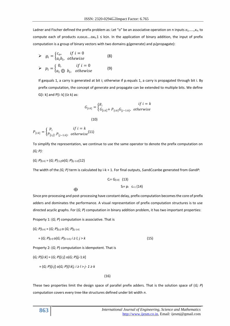
Fig 4 Output for 32-Bit BEC
Fig 5 Output for 32-Bit kogge stone
Fig 6 Output for 32-Bit Sparsekogge stone
ISSN: 2320-0294Impact Factor: 6.765
867 International Journal of Engineering, Science and Mathematics
http://www.ijesm.co.in, Email: [email protected]
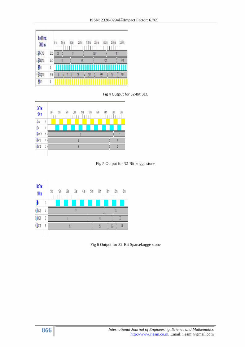
Fig 7 Output for 32-Bit spanning tree
Table 1 Comparison Table Between Adders in terms of timing (delay)
Fig 8 Output for 32-Bit Ladner-Fischer
Type of Adder
TIMING REPORT
32-bit 64 bit
BEC 36.876ns 25.489ns
Kogge stone 24.399ns 19.016ns
Sparsekogge stone 40.177ns 26.111ns
Spanning tree 26.421ns
19.423ns
Ladner-Fischer 30.548ns
41.741ns
ISSN: 2320-0294Impact Factor: 6.765
868 International Journal of Engineering, Science and Mathematics
http://www.ijesm.co.in, Email: [email protected]
5. REFERENCES
[1] B. Ramkumar, H.M. Kittur, and P. M.Kannan, “ASIC implementation ofmodified faster carry save adder,” Eur. J.Sci. Res., vol. 42, no. 1, pp. 53–58, 2010.
[2] D. Radhakrishnan, “Low-voltage low power CMOS full adder,” in Proc. IEEE Circuits Devices Syst., vol. 148, Feb. 2001.
[3] E. Abu-Shama and M. Bayoumi, “A new cell for low power adders,” in Proc. Int. Midwest Symp. Circuits and Systems, 1995, pp. 1014–1017.