SCR Applications
13
SCR Applications The ability of an SCR to control large currents to a load by means of small gate current makes the device very useful in switching and control applications. A few of the possible applications for the SCR are listed in the introduction to SCR blog post. Here we will consider six applications of SCR like power control, switching, zero-voltage switching, over-voltage protection , pulse circuits and battery charging regulator. 1. Power Control. SCR Power Control Circuit Because of the bistable characteristics of semiconductor devices, whereby they can be switched on and off, and the efficiency of gate control to trigger such devices, the SCRs are ideally suited for many industrial applications. SCRs have got specific advantages over saturable core reactors and gas tubes owing to their compactness, reliability, low losses, and speedy turn-on and turn-off. The bistable states (conducting and non-conducting) of the SCR and the property that enables fast transition from one state to the other are made use of in the control of power in both ac and dc circuits. SCR Phase Control In ac circuits the SCR can be turned-on by the gate at any angle α with respect to applied voltage. This angle α is called the firing angle and power control is obtained by varying the firing angle. This is known as phase control . A simple half-wave circuit is shown in figure a. for illustrating the principle of phase control for an inductive load. The load current, load voltage and supply voltage waveforms are shown in figure b. The SCR will turn-
-
Upload
independent -
Category
Documents
-
view
2 -
download
0
Transcript of SCR Applications
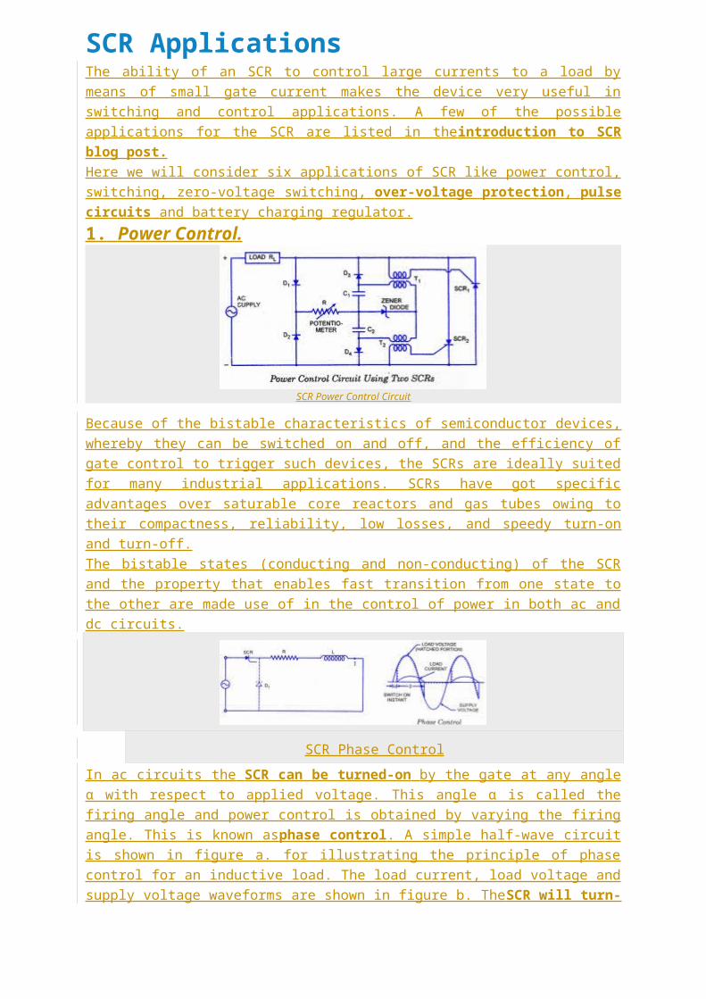
SCR ApplicationsThe ability of an SCR to control large currents to a load bymeans of small gate current makes the device very useful inswitching and control applications. A few of the possibleapplications for the SCR are listed in theintroduction to SCRblog post.Here we will consider six applications of SCR like power control,switching, zero-voltage switching, over-voltage protection, pulsecircuits and battery charging regulator.1. Power Control.
SCR Power Control Circuit
Because of the bistable characteristics of semiconductor devices,whereby they can be switched on and off, and the efficiency ofgate control to trigger such devices, the SCRs are ideally suitedfor many industrial applications. SCRs have got specificadvantages over saturable core reactors and gas tubes owing totheir compactness, reliability, low losses, and speedy turn-onand turn-off.The bistable states (conducting and non-conducting) of the SCRand the property that enables fast transition from one state tothe other are made use of in the control of power in both ac anddc circuits.
SCR Phase ControlIn ac circuits the SCR can be turned-on by the gate at any angleα with respect to applied voltage. This angle α is called thefiring angle and power control is obtained by varying the firingangle. This is known asphase control. A simple half-wave circuitis shown in figure a. for illustrating the principle of phasecontrol for an inductive load. The load current, load voltage andsupply voltage waveforms are shown in figure b. TheSCR will turn-
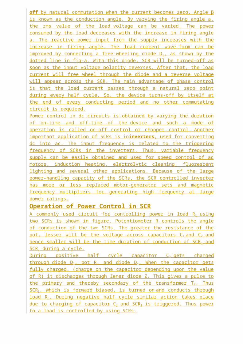
off by natural commutation when the current becomes zero. Angle βis known as the conduction angle. By varying the firing angle a,the rms value of the load voltage can be varied. The powerconsumed by the load decreases with the increase in firing anglea. The reactive power input from the supply increases with theincrease in firing angle. The load current wave-form can beimproved by connecting a free-wheeling diode D1, as shown by thedotted line in fig-a. With this diode, SCR will be turned-off assoon as the input voltage polarity reverses. After that, the loadcurrent will free wheel through the diode and a reverse voltagewill appear across the SCR. The main advantage of phase controlis that the load current passes through a natural zero pointduring every half cycle. So, the device turns-off by itself atthe end of every conducting period and no other commutatingcircuit is required.Power control in dc circuits is obtained by varying the durationof on-time and off-time of the device and such a mode ofoperation is called on-off control or chopper control. Anotherimportant application of SCRs is ininverters, used for convertingdc into ac. The input frequency is related to the triggeringfrequency of SCRs in the inverters. Thus, variable frequencysupply can be easily obtained and used for speed control of acmotors, induction heating, electrolytic cleaning, fluorescentlighting and several other applications. Because of the largepower-handling capacity of the SCRs, the SCR controlled inverterhas more or less replaced motor-generator sets and magneticfrequency multipliers for generating high frequency at largepower ratings.Operation of Power Control in SCRA commonly used circuit for controlling power in load RL usingtwo SCRs is shown in figure. Potentiometer R controls the angleof conduction of the two SCRs. The greater the resistance of thepot, lesser will be the voltage across capacitors C1 and C2 andhence smaller will be the time duration of conduction of SCR1 andSCR2 during a cycle.During positive half cycle capacitor C2 gets chargedthrough diode D1, pot R, and diode D4. When the capacitor getsfully charged, (charge on the capacitor depending upon the valueof R) it discharges through Zener diode Z. This gives a pulse tothe primary and thereby secondary of the transformer T2. ThusSCR2, which is forward biased, is turned on and conducts throughload RL. During negative half cycle similar action takes placedue to charging of capacitor C1 and SCR1 is triggered. Thus powerto a load is controlled by using SCRs.
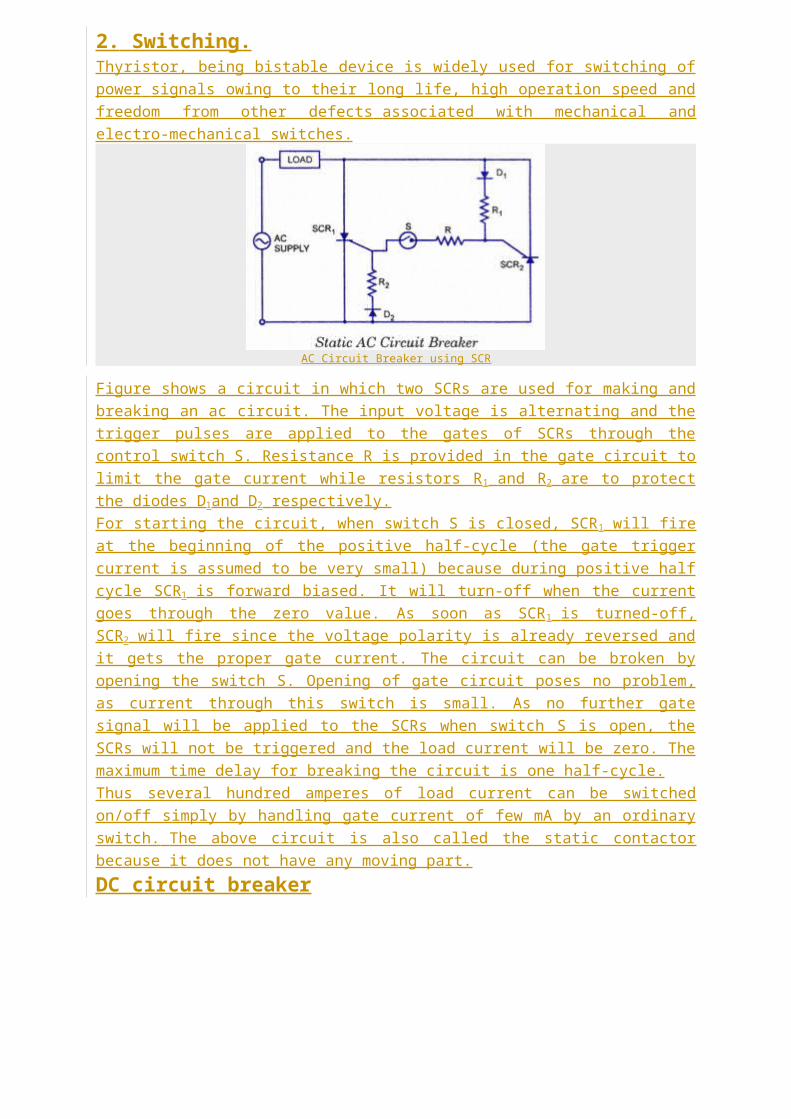
2. Switching.Thyristor, being bistable device is widely used for switching ofpower signals owing to their long life, high operation speed andfreedom from other defects associated with mechanical andelectro-mechanical switches.
AC Circuit Breaker using SCR
Figure shows a circuit in which two SCRs are used for making andbreaking an ac circuit. The input voltage is alternating and thetrigger pulses are applied to the gates of SCRs through thecontrol switch S. Resistance R is provided in the gate circuit tolimit the gate current while resistors R1 and R2 are to protectthe diodes D1and D2 respectively.For starting the circuit, when switch S is closed, SCR1 will fireat the beginning of the positive half-cycle (the gate triggercurrent is assumed to be very small) because during positive halfcycle SCR1 is forward biased. It will turn-off when the currentgoes through the zero value. As soon as SCR1 is turned-off,SCR2 will fire since the voltage polarity is already reversed andit gets the proper gate current. The circuit can be broken byopening the switch S. Opening of gate circuit poses no problem,as current through this switch is small. As no further gatesignal will be applied to the SCRs when switch S is open, theSCRs will not be triggered and the load current will be zero. Themaximum time delay for breaking the circuit is one half-cycle.Thus several hundred amperes of load current can be switchedon/off simply by handling gate current of few mA by an ordinaryswitch. The above circuit is also called the static contactorbecause it does not have any moving part.DC circuit breaker
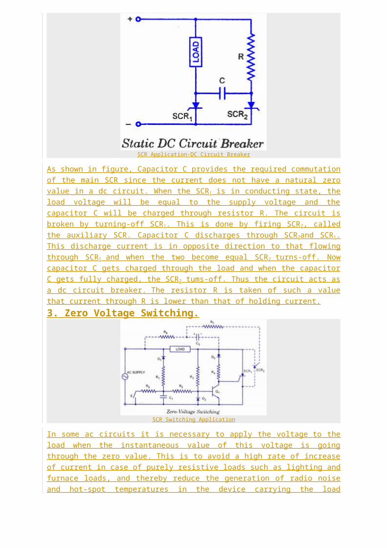
SCR Application-DC Circuit Breaker
As shown in figure, Capacitor C provides the required commutationof the main SCR since the current does not have a natural zerovalue in a dc circuit. When the SCR1 is in conducting state, theload voltage will be equal to the supply voltage and thecapacitor C will be charged through resistor R. The circuit isbroken by turning-off SCR1. This is done by firing SCR2, calledthe auxiliary SCR. Capacitor C discharges through SCR2and SCR1.This discharge current is in opposite direction to that flowingthrough SCR1 and when the two become equal SCR2 turns-off. Nowcapacitor C gets charged through the load and when the capacitorC gets fully charged, the SCR2 tums-off. Thus the circuit acts asa dc circuit breaker. The resistor R is taken of such a valuethat current through R is lower than that of holding current.3. Zero Voltage Switching.
SCR Switching Application
In some ac circuits it is necessary to apply the voltage to theload when the instantaneous value of this voltage is goingthrough the zero value. This is to avoid a high rate of increaseof current in case of purely resistive loads such as lighting andfurnace loads, and thereby reduce the generation of radio noiseand hot-spot temperatures in the device carrying the load
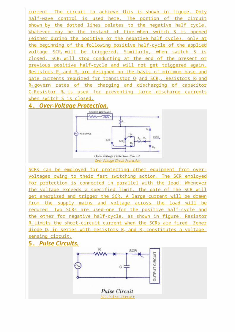
current. The circuit to achieve this is shown in figure. Onlyhalf-wave control is used here. The portion of the circuitshown by the dotted lines relates to the negative half cycle.Whatever may be the instant of time when switch S is opened(either during the positive or the negative half cycle), only atthe beginning of the following positive half-cycle of the appliedvoltage SCR1 will be triggered. Similarly, when switch S isclosed, SCR1 will stop conducting at the end of the present orprevious positive half-cycle and will not get triggered again.Resistors R3 and R4 are designed on the basis of minimum base andgate currents required for transistor Q1 and SCR1. Resistors Rl andR2 govern rates of the charging and discharging of capacitorC1 Resistor R5 is used for preventing large discharge currentswhen switch S is closed.4. Over-Voltage Protection.
Over Voltage Circuit Protection
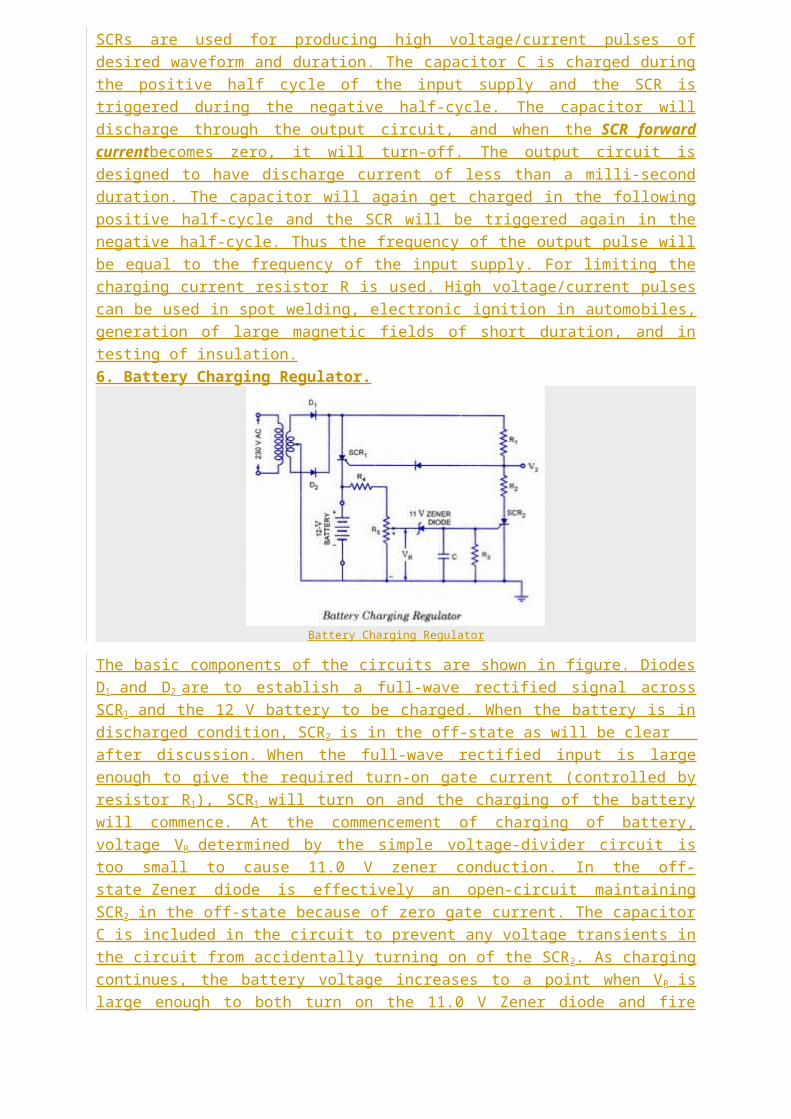
SCRs can be employed for protecting other equipment from over-voltages owing to their fast switching action. The SCR employedfor protection is connected in parallel with the load. Wheneverthe voltage exceeds a specified limit, the gate of the SCR willget energized and trigger the SCR. A large current will be drawnfrom the supply mains and voltage across the load will bereduced. Two SCRs are used—one for the positive half-cycle andthe other for negative half-cycle, as shown in figure. ResistorR1 limits the short-circuit current when the SCRs are fired. Zenerdiode D5 in series with resistors Rx and R2 constitutes a voltage-sensing circuit.5. Pulse Circuits.
SCR-Pulse Circuit
SCRs are used for producing high voltage/current pulses ofdesired waveform and duration. The capacitor C is charged duringthe positive half cycle of the input supply and the SCR istriggered during the negative half-cycle. The capacitor willdischarge through the output circuit, and when the SCR forwardcurrentbecomes zero, it will turn-off. The output circuit isdesigned to have discharge current of less than a milli-secondduration. The capacitor will again get charged in the followingpositive half-cycle and the SCR will be triggered again in thenegative half-cycle. Thus the frequency of the output pulse willbe equal to the frequency of the input supply. For limiting thecharging current resistor R is used. High voltage/current pulsescan be used in spot welding, electronic ignition in automobiles,generation of large magnetic fields of short duration, and intesting of insulation.6. Battery Charging Regulator.
Battery Charging Regulator
The basic components of the circuits are shown in figure. DiodesD1 and D2 are to establish a full-wave rectified signal acrossSCR1 and the 12 V battery to be charged. When the battery is indischarged condition, SCR2 is in the off-state as will be clear after discussion. When the full-wave rectified input is largeenough to give the required turn-on gate current (controlled byresistor R1), SCR1 will turn on and the charging of the batterywill commence. At the commencement of charging of battery,voltage VR determined by the simple voltage-divider circuit istoo small to cause 11.0 V zener conduction. In the off-state Zener diode is effectively an open-circuit maintainingSCR2 in the off-state because of zero gate current. The capacitorC is included in the circuit to prevent any voltage transients inthe circuit from accidentally turning on of the SCR2. As chargingcontinues, the battery voltage increases to a point when VR islarge enough to both turn on the 11.0 V Zener diode and fire

SCR2. Once SCR2 has fired, the short circuit representation forSCR2 will result in a voltage-divider circuit determined by R1 andR2 that will maintain V2 at a level too small to turn SCR1 on.When this occurs, the battery is fully charged and the open-circuit state of SCR1 will cut off the charging current. Thus theregulator charges the battery whenever the voltage drops andprevents overcharging when fully charged. There are many moreapplications of SCRs such as in soft start circuits, logic anddigital circuits, but it is not possible to discuss all thesehere.
FET applicationsJOJO
AUGUST - 30 - 2009
8 COMMENTS
FET has a very high input impedance (100 Mega ohm in case of JFETsand 104 to 109 Mega Ohm in case of MOSFETs), the major shortcomingsof an ordinary transistor i.e. low input impedance with consequent ofloading of signal source is eliminated in FET. Hence FET is an idealdevice for use in almost every application in which transistors canbe used. FETs are widely used as input amplifiers in oscilloscopes,electronic voltmeters and other measuring and testing equipmentbecause of their high input impedance.
As a FET chip occupies very small space as compared to BJTchip, FETs are widely used in ICs.
FETs are used as voltage-variable resistors (WRs) inoperational amplifiers (op-amps) and tone controls etc, formixer operation on FM and TV receivers and in logic circuits.
FETs are generally used in digital switching circuits thoughtheir operating speed is lower.
Applications of FET:1. Low Noise Amplifier. Noise is an undesirable disturbance super-imposed on a useful signal. Noise interferes with the informationcontained in the signal; the greater the noise, the less theinformation. For instance, the noise in radio-receiversdevelops crackling and hissing which sometimes completely masks thevoice or music. Similarly, the noise in TV receivers produces smallwhite or black spots on the picture; a severe
noise may wipe out the picture. Noise is independent of the signalstrength because it exists even when the signal is off.
Every electronic device produces certain amount of noise but FET isa device which causes very little noise. This is especiallyimportant near the front-end of the receivers and other electronicequipment because the subsequent stages amplify front-end noisealong with the signal. If FET is used at the front-end, we get lessamplified noise (disturbance) at the final output.
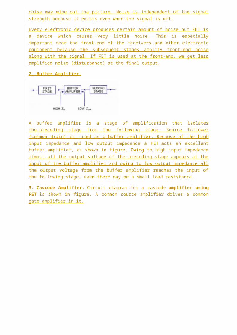
2. Buffer Amplifier.
A buffer amplifier is a stage of amplification that isolatesthe preceding stage from the following stage. Source follower(common drain) is. used as a buffer amplifier. Because of the highinput impedance and low output impedance a FET acts an excellentbuffer amplifier, as shown in figure. Owing to high input impedancealmost all the output voltage of the preceding stage appears at theinput of the buffer amplifier and owing to low output impedance allthe output voltage from the buffer amplifier reaches the input ofthe following stage, even there may be a small load resistance.
3. Cascode Amplifier. Circuit diagram for a cascode amplifier usingFET is shown in figure. A common source amplifier drives a commongate amplifier in it.
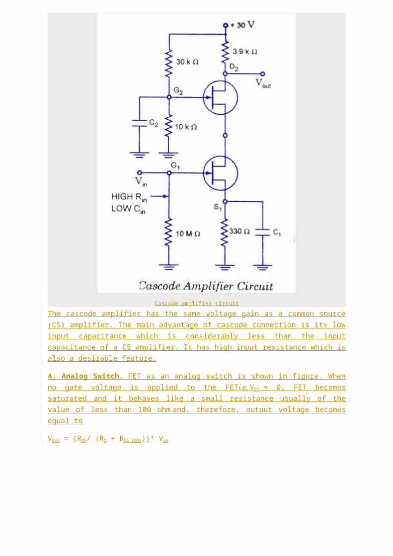
Cascode amplifier circuitThe cascode amplifier has the same voltage gain as a common source(CS) amplifier. The main advantage of cascode connection is its lowinput capacitance which is considerably less than the inputcapacitance of a CS amplifier. It has high input resistance which isalso a desirable feature.
4. Analog Switch. FET as an analog switch is shown in figure. Whenno gate voltage is applied to the FETi.e. VGS = 0, FET becomessaturated and it behaves like a small resistance usually of thevalue of less than 100 ohm and, therefore, output voltage becomesequal to
VOUT = {RDS/ (RD + RDS (ON))}* Vin
JFET-analog-switchSince RD is very large in comparison to RDS 0N), so Vout can be takenequal to zero.
When a negative voltage equal to VGS (OFF) is applied to the gate, theFET operates in the cut-off region and it acts like a very highresistance usually of some mega ohms. Hence output voltage becomesnearly equal to input voltage.
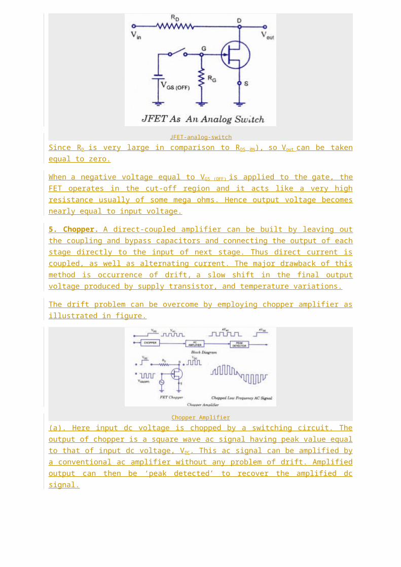
5. Chopper. A direct-coupled amplifier can be built by leaving outthe coupling and bypass capacitors and connecting the output of eachstage directly to the input of next stage. Thus direct current iscoupled, as well as alternating current. The major drawback of thismethod is occurrence of drift, a slow shift in the final outputvoltage produced by supply transistor, and temperature variations.
The drift problem can be overcome by employing chopper amplifier asillustrated in figure.
Chopper Amplifier(a). Here input dc voltage is chopped by a switching circuit. Theoutput of chopper is a square wave ac signal having peak value equalto that of input dc voltage, VDC. This ac signal can be amplified bya conventional ac amplifier without any problem of drift. Amplifiedoutput can then be ‘peak detected’ to recover the amplified dcsignal.
Square wave is applied to the gate of a FET analog switch to make itoperate like a chopper, as illustrated in other figure. The gatesquare wave is negative-going swing from 0 V to at leastVGS (off)- This alternately saturates and cuts-off the JFET. Thusoutput voltage is a square wave varying from +VDC to zero voltalternately.
If the input signal is a low-frequency ac signal, it gets choppedinto the ac waveform as shown in last figure (c). This choppedsignal can now be amplified by an ac amplifier that is drift free.The amplified signal can then be peak-detected to recover theoriginal input low frequency ac signal. Thus both dc and lowfrequency ac signals can be amplified by using a chopper amplifier.
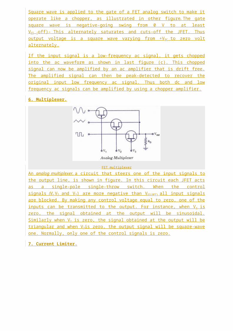
6. Multiplexer.
FET multiplexerAn analog multiplexer, a circuit that steers one of the input signals tothe output line, is shown in figure. In this circuit each JFET actsas a single-pole single-throw switch. When the controlsignals (Vv V2 and V3) are more negative than VGS(0FF) all input signalsare blocked. By making any control voltage equal to zero, one of theinputs can be transmitted to the output. For instance, when Vx iszero, the signal obtained at the output will be sinusoidal.Similarly when V2 is zero, the signal obtained at the output will betriangular and when V3is zero, the output signal will be square-waveone. Normally, only one of the control signals is zero.
7. Current Limiter.
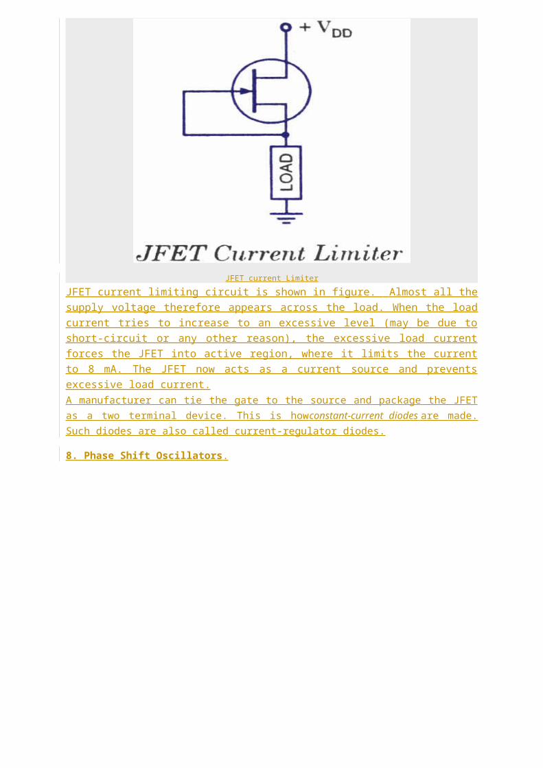
JFET current LimiterJFET current limiting circuit is shown in figure. Almost all thesupply voltage therefore appears across the load. When the loadcurrent tries to increase to an excessive level (may be due toshort-circuit or any other reason), the excessive load currentforces the JFET into active region, where it limits the currentto 8 mA. The JFET now acts as a current source and preventsexcessive load current.A manufacturer can tie the gate to the source and package the JFETas a two terminal device. This is howconstant-current diodes are made.Such diodes are also called current-regulator diodes.
8. Phase Shift Oscillators.
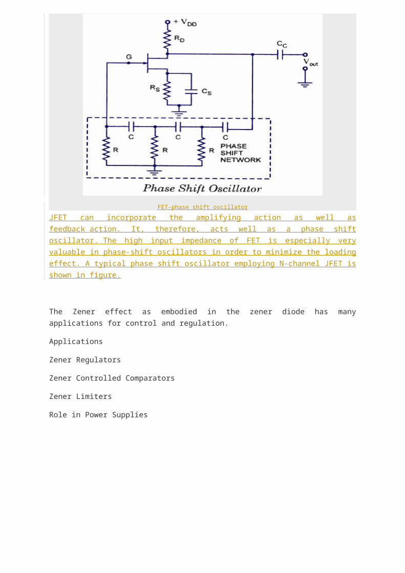
FET-phase shift oscillatorJFET can incorporate the amplifying action as well asfeedback action. It, therefore, acts well as a phase shiftoscillator. The high input impedance of FET is especially veryvaluable in phase-shift oscillators in order to minimize the loadingeffect. A typical phase shift oscillator employing N-channel JFET isshown in figure.
The Zener effect as embodied in the zener diode has manyapplications for control and regulation.
Applications
Zener Regulators
Zener Controlled Comparators
Zener Limiters
Role in Power Supplies


![supreme court reports [2010] 4 scr](https://static.fdokumen.com/doc/165x107/631a6f361a1adcf65a0f1217/supreme-court-reports-2010-4-scr.jpg)
![Douez v. Facebook, Inc., 2017 SCC 33, [2017] 1 SCR 751 ...](https://static.fdokumen.com/doc/165x107/6323c69fb104cba27a08d825/douez-v-facebook-inc-2017-scc-33-2017-1-scr-751-.jpg)


![[2012] 11 SCR 873 - Supreme Court of India](https://static.fdokumen.com/doc/165x107/631cbc0f6c6907d368017086/2012-11-scr-873-supreme-court-of-india.jpg)