Remove/install Sensotronic Brake Control (SBC) hydraulic unit
Upload
khangminh22Category
view
0download
0
)
)
)
SBC-300
SINGLE BOARD COMPUTER
OPERATIONS MANUAL
SD #71401 70 REVISION C AUGUST 25, 1983
A SYNTECH COMPANY

)
SD #7140170 REVISION C AUGUST 25 , 1983
SBC-300
SINGLE BOARD COMPUTER
OPERATIONS MANUAL

I
I
E.MI NOTICE
This equipment has been designed and constructed to professional standards. However, the equipment must be utilized correctly by the user to obtain proper performance and to comply with applicable industry and governmental regulations.
Since the equipment is supplied as an unconf igured component and cannot be tested for electro-magnetic interference (EM!) in al 1 possible conf igu rations, the equipment is not subject to standards imposed by Subpart J of Part 15 of FCC Rules and Regulations .
Final system configuration will require compliance with applicable FCC regulations . SDSystems recommends the installation of shielded data cables for all external cabling. Electro-magnetic interference (EM!) levels are dependent upon final system hardware configuration and application .
Contact SDSystems Customer Service if additional configuration information is required.

TERMINATION NOTE
SDSystems recommends the use of active termination circuitry on the S-100 bus to avoid system problems •
•

)
)
MODIFICATION FOR SBC-300 REVISION A ARTWORK WITH MONITOR RO.M 2.0
The Revision A artwork for the SBC-300 is missing pull up resistors on the EPROM for pins l and 27. To correctly function with a 2764 EPROM, these pins must be tied to +sv. To a cc om p 1 i sh th is , w i r e pins l and 2 7 to pin 2 8. Th i s w i 11 enable the EPROM •
•

) TABLE OP CONTENTS
Subsection Page Number Title No.
SECTION I INTRODUCTION
1.0 GENERAL 1-1 1.1 FEATURES 1-1 1.2 SCOPE l-1
SECTION II FUNCTIONAL DESCRIPTION
2.0 GENERAL 2-1 2.1 CENTRAL PROCESSING UNIT 2-2 2 .1.1 CPU 2-2 2.1.1.1 PROCESSOR OPERATION 2-2 2.1.1.2 Z-80 CPU 2-2 2.1.2 CLOCK RA TE GEN ERA TOR 2-3 2.1.3 CPU CLOCK SPEED SELECTION 2-4 2.2 MEMORY 2-5 2.2.1 RAM 2-5 2.2.1.1 REFRESH 2-6 . 2.2.1.1.1 PIN 1 REFRESH MEMORY DEVICES 2-6 2.2.1.1.2 AVOIDING LONG WAIT STATES 2-6 2.2.1.1.3 REFRESH DURING DMA OPERATIONS 2-7 2.2.1.2 REFRESH WAIT STATE GENERATOR 2-7 2.2.1.2.1 WAIT STATES 2-8 2.2.1.2 . 2 WAIT STATE SELECTION 2-8 2.2.1.2.3 PIN l REFRESH GENERATION 2-9 2.2.l.3 MEMORY TIMING 2-9 2.2.1.3.1 RAM ADDRESS DECODE 2-9 2.2.1.3 . 2 RCM AND COLUMN TIMING 2-10 2.2.2 ROM 2-10 2.2.3 MEMORY ADDRESS AND I/O PORT DECODE 2-10 2.2.3.l MEMORY ADDRESS DECODE 2-11 2.2.3.2 I/O PORT DECODE 2-11 2.2.4 PARITY 2-11 2.2.s MODE DEPENDENT MEMORY cBARACTERISTICS 2-11 2.2.s.1 BUS MASTER MODE MEMORY 2-11 2.2.s.2 SLAVE PROCESSOR MODE MEMORY 2-12 2.3 MEMORY MAPPER 2-12 2.3.1 MAPPER OPERATION 2-12 2.~.1.1 BOARD ADDRESS SELECT 2-13 2.3.l.2 MAPPER RAM 2-13 2.4 INTERRUPT CONTROLLER 2-14 2.4.1 INTERRUPT SELECT 2-14 2.5 BUS INTERFACE 2-15 2.5.l BUS TIMING CONTROLLER 2-15 2.s.2 POWER ON CLEAR AND RESET 2-16 2.5.3 SLAVE CONTROL 2-16 2.6 MASTER/SLAVE CONTROL 2-18 2.6.l MASTER/SLAVE SELECT 2-18

/ .
TABLE OF CONTENTS (Continued) )
Subsection Page I
Number 'l'i tle No.
SECTION II--Continued FUNCTIONAL DESCRIPTION--Continued
2.6.2 LINE TERMINATION 2-18 • 2.7 SASI/PARALLEL PORT 2-19 2.7.1 CIO 2-19 2.8 SERIAL I/O 2-19 2.8.l ASCC 2-20 2.9 POWER REGULATION 2-20 2.9.1 S VOLT BUS OPERATION 2-20
SECTION III THEORY OF OPERATION
3.0 GENERAL 3-1 3.1 MASTER/SLAVE MODES 3-1 3.1 . l MASTERS 3-1 3.1.l . l PERMANENT BUS MASTER 3-1 3.1.1 . 2 TEMPORARY BUS MASTER 3-1 3.1.2 SLAVES 3-2
I 3.1.2.1 SLAVE PROCESSORS 3-2. 3.1.2 . 2 SLAVE PROCESSORS AND MULTI-USER SYSTEMS 3-2 ) 3.1.3 BUS CYCLE OPERATIONS 3-3
l 3.1.3.1 BUS CYCLES 3-4 3.1.3.2 TEMPORARY MASTER ACCESS CYCLES 3-4
j 3.2 SLAVE PRIORITY 3-5 I 3.3 INTERRUPTS 3-5
3.3.1 NON-MASKABLE INTERRUPTS 3-5 3.3.2 MASKABLE INTERRUPTS 3-5 3.3.3 INTERRUPT ENABLE 3-6 3.3.C INTERRUPT CONTROL 3-6 3.3., . 1 OFF-BOARD INTERRUPT PRIORITIZATION 3-7 3.3.4.2 ON-BOARD INTERRUPT PRIORITIZATION 3-7 3.3.4.3 ON-BOARD INTERRUPT ARBITRATION 3-8 3.3.5 INTERRUPT ACKNCMLEDGE 3-9 3.4 MAPPER CONCEPTS 3-10
SECTION IV OPERATIONS
.t.-0 GENERAL 4-1 4.1 INSTALLATION 4-1 .t.1.1 IEEE-696 4-1 .t.1.2 SDSYSTEMS S-100 AND OTHERS 4-1 4.1.3 INITIAL CHECKOUT 4-1 .t.2 SERIAL I/O 4-2
I'
Subsection Number
s.o 5.1 s.1.1 5.2 5.2.l 5.2.2 5.2.3 5.2.4 5.2.5 5.2.6 5.2.7 5.2.8 5.2.9 5.3 5.3.l 5.3.2 5.3.3 5.4 5.4.l 5.4 . 2 5.4.3 5.4.4 5.4.5 5.4.6 5.5 5.5.1 5.s.2 5.5.3 5.5.4 5.6 5.6.1 5.6.2 5.6.2.1 5.6.2.2 5.6.2.3 5.6.2.4 5.7 s..s
6.0 6.1 6.2
TABLE OF CONTENTS (Continued)
GENERAL
Title
·SECTION V MONITOR
SD MONITOR START-OP COMM.AND SYNTAX MEMORY COMMANDS MEMORY MANAGEMENT - •A• COMMAND MEMORY DISPLAY - •D• COMMAND EXAMINE MEMORY - •E• COMMAND FILL MEMORY - °F• COMMAND EXTENDED MEMORY TEST - •J• COMMAND LOCATE STRING - •L• COMMAND MOVE MEMORY - •M• COMMAND MEMORY TEST - •T• COMMAND VERIFY MEMORY - •v• COMMAND INPUT/OUTPUT COMMANDS INPUT FROM PORT - • 1 • COMMAND OUTPUT FROM PORT - •o• COMMAND PORT EXAMINE - •p• COMMAND PROGRAM CONTROL co~~ANDS BREAKPOINT - •s• COMMAND •Go• TO PRcx:;RAM - •G • COMMAND SINGLE STEP - •s• COMMAND REGISTER EXAMINE - •x• COMMAND BEX ARITHMETIC - •a• COMMAND COMMAND PROCESSING - •y• COMMAND DISK UTil..ITY COMM.ANDS BOOT OP - •c• COMMAND READ PROM DISK - •R• COMMAND WRITE TO DISK - •w• COMMAND FORMAT A DISK - •z• COMM.AND CIO INITIALIZATION AND USE ACCESSING THE CIO INTERNAL REX;ISTERS SBC-300 MONITOR AND CIO INITIALIZATION PORT B PORT C PORT A COUNTER/TIMERS ASCC INITIALIZATION PARITY ERRORS
SECTION VI ENVIRONMENTAL CONSIDERATIONS
GENERAL POWER REQUIREMENTS PHYSICAL SPECIFICATIONS
Page No.
5-1 5-1 5-1 5-3 5-3 5-4 5-5 5-5 5-6 5-6 5-7 5-7 5-7 5-8 5-8 5-8 5-9 5-9 . 5-10 5-11 5-11 5-12 5-12 ' 5-13 5-13 5-13 5-14 5-15 5-15 5-15 5-15 5-16 5-16 5-18 5-19 5-19 5-19 5-19
6-1 6-1 6-1

•
Subsection Number
APPENDICES
A B c D E F G B I J K L M N 0 p 0
Figure No • • 2-1 4-1 4-2 4-3
'!'able No.
2-1 2-2 i-3
2-4 5-1 5-2 5-3
TABLE OF CONTENTS (Continued)
'l'i tle
SELECTED IEEE-696 SPECIFICATION SHEETS HEXADECIMAL TO DECIMAL CONVERSION STANDARD ASCII CODES EBCDIC TABLE CIO SPECIFICATION ASCC SPECIFICATION PAL16L8 SPECIFICATION PORT ASSIGNMENTS PARALLEL INTERFACES: SASI/CENTRONICS MONITOR LOCATIONS SAMPLE I/O SUPPORT CODE JUMPER CONNECTION QUICK REFERENCE TABLES DISCLAIMER LIMITED WARRANTY PARTS LIST FOR SBC-300 PARTS PLACEMENT DIAGRAM SCBEMATIC
ILLUSTRATIONS
'l'itle
BLOCK DI AGRAM ADDRESS SWITCH SIGN-ON MESSAGE MEMORY ERROR MESSAGE
'!'ABLES
'l'i tle
CPU CLOCK SPEED SELECTION WAIT STATE SELECTION ON-BOARD MEMORY LOCATION IN BUS SYSTEM SELECTION JUMPER CONNECTIONS FOR BOS MASTER OPERATION SD MONITOR COMMAND SUMMARY SD MONITOR REGISTER MAP DISK FORMATS
Page No .
A-1 B-1 C-1 D-1 E-1 F-1 G-1 B-1 l-1 J-1 K-1 L-1 M-1 N-1 0-1 P-1 0-1
Page No.
2-1 4-1 4-2 4- 2
Page No.
2-4 2-9
2-12 2-19 5-2 5-10 5-14
) , ,
)

)
1.0 GENERAL
SECTION I INTRODUCTION
The SBC-300 is a high performance, self-contained microcomputer system designed around the Z-80 family of micro processors. Cont r o 1 (CPU) , memory , an a extensive input/output facilities are all contained on a single printed wiring board conforming both physically and electrically to every S-100 BUS requirement as specified by IEEE-696. Operation as either the IEEE-696 Permanent Bus Master or as one of any number of slave processors on the bus is supported. The advanced design of the system allows a wide variety of function and performance option s to be selected and easily implemented by the end user in most cases by simple dip switch or jumper arrangement. In addition, the SBC-300 is available with the appropriate CPU, support, memory elements, and jumpers installed for operation at clock speeds of 4 or 6 mHz.
In most cases, options are selected by the connection or disconnection of one or more jumpers; a table will show the specific jumper connections to be made for each option des i r ea. The SB c-3 0 0 w i 11 be con f i g u r e d at th e f act or y in a manner which is likely to sui t the greatest number of users. Those requi ring different pe rformance may change option selections as required.
1.1 FEATURES
S-100 Bus Compatible ( IEEE-6 96)
Z-80 CPU: 4 or 6 mHz
64K Bytes of Internal RAM Plus Parity
2 to 16K Bytes of PROM Using Byte-Wide PROM
System Memory Addressing to 16Mbytes
1.2 SCOPE
Serial, Parallel, and Counter-Timer I/O
SAS! Port
Fully Programmable Communications Options
Dual Programmable Serial Full-Duplex Channels
Dual Programmable Baud Rate Generators
This document describes the function, performance, electrical and physical characteristics of the SBC-300 single board microcomputer system and its interface to the IEEE-696 bus. For detailed description and analysis of individual integrated circuit components, the SASI port, and the IEEE-696 bus beyond what is presented here, consult the various manufacturer data books and s t andard specifications.
1-1

)
TH IS PAGE I NTENTIONALLY LEFT BLANK
)
1- 2

2. 0 GENERAL
SECTION II FUNCTIONAL DESCRIPTION
This section provides a functional description of the basic blocks that make up the SBC-300 single board microcomputer . A block diagram of the SBC-300 appears in Figure 2-1 , and each b lock is discussed in this section. Refer to Section III for an in-depth theory of operation.
The SBC-300 communicates with peripherals through one SASI/parallel and two synchronous or asynchronous serial ports. When operated as the Permanent Bus Master in acc.:>rdance with the IEEE- 696 standard, the SBC-300 controls all aspects of bus operation and provides timing, control, and status signa l s for S-100 bus operation as well as its own operation.
In the slave processor mode, the SBC-300 responds to bus cycles initiated by the current bus master and/or processes data in accordance with instructions stored in the on-board ROM and RAM. It is able to communicate with the outside world via its serial and parallel ports . A slave appears to the bus as a 64K block of RAM. Data is transferred between the slave and the bus via the slave ' s on-board dual ported RAM. A slave device may request service from the bus master by generating an interrupt r equest.
AS-232 RB - 23 I SASI I I POAT S-100 BUS
i I MEMORY I I I SERI AL
SABI I I INTERRUPT II I DRIVERS
M f.STER/ .I CPU SLAVE
110 PARALLEL CONTROLLER CONTROLLER
!ADDRESS I MEUOA~I MAPPER I
I I DATA I
I STATUS I
Figure 2-1 . BLOCK DIAGRAM
2-1

2.1 CENTRAL PROCESSING UNIT
This block of the SBC-300 includes the CPU and the cloc k rate generator . The CPU of the SBC-300 is a member of the Z-80 fami l y and can be run at clock speeds of 4 or 6 mHz as selected by the appropriate conf i gur ation of the clock speed jumpers .
2.1.1 CPU
During normal operati o n, the CPU directs all aspects of data manipulation, movement, s torage, and r etrieval within the SBC-300 microcomputer. The CPU controls c ommunications with the outside world (serial and parallel I/O), othe r bus periph erals , and dyna mic me mory refresh during norm al bus cycles .
2.1.1.1 Processor Operation
The function of the CPU is to get instructions from memory and perform the desired operations.
The CPU accesses a location in memory and retrieves a coded instruction. This instruction is decoded and then performed by the CPU . The address of the next instruction to be executed is applied t o the address lines and the instruction (OP CODE) is fetched and executed. This process is continued indefinitely or unt il the processor is stopped for some reason.
The system memory is used to contain the instructions for the CPU to execute and the data that is to be processed. A typical ins truction sequence may be to read data from a particular peripheral device, store it in a specific location in memory, and then write it out to another periphe ral.
2.1 . 1 . 2 Z-80 CPU
The Z-80 CPU itself contains many of the same functions (on a smalle r scale) as the SBC-300. There is an internal data bus for moving data to and from internal memory (registers) as well as into and out of the Z-80. The re are areas that p rocess data, co ntrol t he opera tion of the rest of th e chip, and generat e contr ol and status si gnals tha t are required to control and in terface with things in the outside world.
Registers are used within the CPU to store instructions and data . Thes e regi sters are small areas of memory which are controlled directly by the CPU Con trol (ther e is no in ternal address bus for acces sing registers) . Th e Z-80 contains 208 bits of R/W memory that are accessib le to the progr a mmer. This memory is arranged as eighteen 8 bit registers and four 16 bit regi sters. All Z-80 registers are construct ed o f static RAM and include 2 sets of 6 general purpose registers. These regist er s may be us ed individually as six 8 bit
2-2
)
)
)

registe rs or in pairs as thr ee 16 bit registers. There are also 2 sets of accumulator and flag registers and 6 special purpose registers .
The act ual pr oce ssing in the Z-80 takes place in the Arithmetic and Logic Unit (ALU) which communicates with the i nternal dat a registers as well as the external data bus by way of the internal data bus. Th e ALU can perform a number of logi ca l and arithmetic operations on data contained in internal registers at the direction of the CPU Control. These operations include :
ADD SUBTRACT AND OR
XOR COMPARE SHIFT L/R TEST BIT
INCREMENT DECREMENT SET BIT RESET BIT
One instruction at a time is r et rieved from the system memory and loaded in the instr uction regi ster. The CPU Control section decode s the instruction and generates all control s ignals necessary to execute the instruction. These signals read and write data from and to the registers, control the ALU, and control all external items as req uired by the rest of the system.
Dynamic RAM mu st be refresh ed by accessing each row in the memory matrix once every 2 or 4 milliseconds, depending on the RAM type. While the CPU is busy decoding an instruction that has been fetched, the internal memory refresh register sends address data out on the lower port ion of the address bus along with a refresh control signal to access a row of memory. The register is incremented one and the new data sent out to access the next row of memory after every instruction fetch. As the register rolls over, the fir st row i s again accessed. As long as th e CPU is running (fetching and pe rforming instructions), the memory is automatically refreshed by the memory refresh counter . This operation is completely transparent to the system.
2.1.2 Clock Rate Generator
The clock rate generator includ~s th e crystal controlled clock oscillator, the division logi c to derive the CPU clock (¢) and the 2 mHz CLOCK signal for the bus from the crystal frequency, and th e line driver for ¢ . The divi der supplies eith er a 6 mHz or a 4 mHz CPU cloc k an d a 2 mHz clock . The 6 mH z clock is derived from a 12 mHz crystal , and th e 4 mHz clock is derived from an 8 mHz crystal . These rates are selected by a combination of the appropriate chip installed in the board and the installation of a jumper. A 74LS93 must be installed for 4 mHz operation or a 74LS92 for 6 mHz operation.
This IC al so applies the proper division ratio to the crystal frequency to arrive at an output of 2 mHz for either of the two possible crystal freq uencies that might be installed. The
2-3

bus line CLOCK must always carry a signal of 2 mHz regardless of the processor clock speed to comply with the I EEE- 696 specif ica t i on.
2 .1 .3 CPU Clock Speed Selection
The SBC-300 is configured at the factory for the processor speed specified, but may be reconfigured by the user for other CPU clock speeds. If the clock speed is to be increased, the speed of the CPU, peripher a ls , and memory chips must be increased as well . This requires the rem oval of the existing parts a nd installation of f aster parts in these locations. If the clock speed is to be reduced for some reason, no change of these units is required.
* * * C A U T I 0 B * * * MULTI-LAYER PRINTED WIRIBG BOARD
When reaoving parts from the SBC-300 board, ensure that the proper desoldering tools and techniques are used to prevent damage to the printed viring board surf ace and inter-layer etches.
The actual CPU clock speed is de te r mined by a combination of jumper connection s and par ts (crystal frequency and div is ion ratio). One or both of these parts must be changed to ef fect a change of the CPU clock speed. Once these parts are in place and the appropriate speed units are installed for !Cs U46 through U48 and the on-board RAM (Table 2-1), the SBC-300 is configured for one of two CPU clock speeds.
Proc. Speed ( mH z)
6 4
Table 2-1. CPU CLOCK SPEED SELECTION
Xtal U42 (Yl) 7 4LS{ mHz) .
12 8
'92 '93
U 46 U47 Peripherals
U48 CPU
Z8536A Z8531A Z-80B Z8536 Z8531 Z-80A
RAM Speed
{ns)
150 200
Delay Line (ns)
150 200
If the fastest (most expensi ve) CPU, peripheral, and memory chips are ins talled, it is recommended that the CPU clock be run as fast as is consistent with the slowest chip on board. If the fast units are installed, there is little to be gained (slightly less power will be dissipated) by r unning the CPU clock at a lower than maximum speed. If the SBC-300 is to be run at a low CPU clock rate, populate the board with the slowest parts.
2-4
)

2.2 MEMORY
The SBC-300 supports full 24 bit memory addressing in accordance with the IEEE-696 specification and may be operated in either the PERMANENT BUS MASTER or the SLAVE mode . Appropriate memory facilities are provided on board to fully exploit the flexibility and utility of the standard bus.
A full 64K of dynamic RAM (64Kxl parts) with parity is installed at the factory . Any byte-wide (up to 128K) PROM may be plugged into the 28 pin socket on the board. Upgrading the on-board memory system requires removal of the existing parts and installation of the replacement memory chips. S e veral modes of refresh are available to cope with any anticipated situation that might arise on the bus.
The on-board memory, as well as any memory that might be visible to the bus, can be mapped to reside in any location within the 16Mbyte range specified by the IEEE-696 S-100 standard. The 16 bit address capability of the Z-80 processor is augmented by a memory mapper which affords the Z-80 access to the entire 16Mbyte potential of the new S-100 bus standard.
The basic memory block of the SBC-300 can be divided into several subsystems: RAM, ROM , MEMORY ADDRESS AND I/0 PORT DECODE , and PARITY. These subs ystems are required to support the 2 internal memo ry syst e ms (RAM and ROM) and to e nsure compatibility with th e bus standard and the v arious other blocks on the SBC-300 .
2 .2 . 1 RAM
The RAM devices that are installed prior to shipment allow pin 1 refresh and are selected so that their speed is consistent with the CPU clock rate.
Upgrading the on-board RAM requires r eplacement of the set of memory IC chips and the possible connection of a few jumpers to select the proper wait states. The only constraints are that the RAM speed be compatible with the CPU clock rate and that the refresh requirements are met (acceptable device numbe rs for replacement appear - in the Parts List Appe ndix) . CPU clock rate considerations are discussed above in the CPU subsection and the refresh restrictions are covered below.
The RAM subsystem includes a latch for data out and line drivers for interface to the bus as well as several small blocks and functions which work together to allow the RAM to perform properly and interface with the rest of the system . These items are: refresh, refresh wait state generator, and memory timing.
2-5
2 . 2 . 1 . 1 Refresh
Any memory device equivalent or similar to the items noted in the Parts List Appendix may be installed in place of the existing RAM devices to increase capacity , replace failed parts (all chips in the array should be of the same type), or satisfy any other particular need of the user. There is, however , one refresh restriction which must be observed:
* * * C A U T I 0 N * * * REFRESH IS NOT SUPPORTED DURING LONG BUS WAIT
STATES IF RON-PIR 1 REFRESH PARTS ARE IBSTALLRD
There are 2 easy solutions to the situation. One is to use pin 1 refresh memory devices in the on-board memory system, and the other is to make sure that items which might cause a long wait state for the processor are never attached to the bus.
2. 2 .1.1.1 Pin 1 Refresh Memory Devices
Industry standard 64K dynamic RA M devi c es are refreshed by addressing each ro w of t h e sto rage ma t ri x within 2 milliseconds. Thi s is call ed Ro w Ad d r e ss Strobe or RAS refresh . Pin l i s not connec t e d to the IC die (it is a nonconnect) and the only method of refr esh is through the refresh address access c ycle gener ated el s ewhe re.
The Z- 80 is rather unique among microprocessors in that it has an internal 7 bit address counter which generates memory refresh cycle addresses after every OP CODE fetch. If the processor is stopped (in a wait state) for an ext ended period of time , there will not be an OP CODE fetch in time to refresh the memory . If this happens, the data in the memory devices becomes uncertain and cannot be used.
Memory devices wi th pin 1 refresh , how ever , allow refresh to be performed by . an additional procedure . There is logic on the SBC-300 that detects long wait ~tates. This logic then generates a refresh cycle which is applied to pin 1 of the appropriately equipped memory devices. The pin 1 refresh cycle is repeated at the proper interval until the processor is running again and pin 1 refresh is no longer needed to maintain the memory. The only time this cycle is implemented is during wait states where the CPU is stopped for excessive amounts of time.
2 .2 . l.l.2 Avoiding Long Wait States
The other method of preventing loss of memory data during long wait states is to never install any device on the bus that might generate a long wait state. Sources of long wait states
2-6
)
)
)

)
include items such as polled I/O disk controllers. These devices use wait sta tes to transfer data into the system memory.
If, for example, the processor directs the disk controlle r to read a sector into memory and the sector requested has just passed the heads, the controller must then wait (which means that the CPU must wait} until that sector comes around again to retrieve the data. This can take as long as 150 ms, which is 148 ms too long if the memory content is to remain valid. The Versaf loppy II disk controller is an example of a polled I/O devi.ce that uses a wait state to transfer data to and from the memory. OMA devices such as the Versaf loppy III disk controller do not cause long wait states for data transfe r and so are safe to use without pin 1 refresh memory devices .
2.2.1.1.3 Refresh During OMA Operations
During a OMA operation, where the SBC-300 is the permanent bus master but has relinquished control of the bus to a OMA device, the SBC-300 generates standard memory refresh cycles from bus activity. As a result, even if there is a DMA controller transferring data into another memory board on the bus, SBC-300 memory is preserved due to its self-generation of refresh cycles.
Depending on the design of other memory boards that might be installed on the bus, this self-generated refresh cycle might take care of memory on the bus as well as on the SBC-300 board. Older designs (such as the EXPANDORAM II and III} can be refreshed in this manner, while newer designs (EXPANDORAM IV} support this procedure as well as several others during DMA transfers.
These boards, which might be used with other processors (no other processors generate memory refresh cycles}, take care of the refresh for on-board memory devices themselves and do not care if the bus master processor is stopped or not. With that type of design, when refresh is not obtained from the bus master processor, the memory board generates cycles for itself. The bus ·is held off by the memory board until it is finished so it will not be busy· with a refresh cycle at the moment its services are required by the bus. Refresh occurs independently of all other activity on the bus, and memory is thus immune to long wait states. There is usually a jumper selected option on these boards, however, which allows refresh to be forced at certain times.
2.2.1.2 Refresh Wait State Generator
The refresh wait state generator perfor ms 2 func tion s. It simultaneously generates the pin 1 refr esh signal and holds the wait line low. The wait line is held low only during the refresh cycle; so if the long wait state which activated the
2-7

pin 1 refresh cycle goes away, the pin 1 refresh cycle will not be interrupted until the refresh is complete.
2.2.1.2.1 Wait States
Wait states are ordered by devices a ttached to the S-100 bus and by the SBC-300 itself. Generally wait states are called to hold up the processor because the CPU runs faster than some peripheral devices are capable of responding. To ensure that valid data read from memory has settled on the data lines before th e processor tries to use it, or to prevent the processor from removing the addres s and data from those lines before a write cycle is complete, the processor is stopped for a period of time until it is safe to proceed.
The wait state is implemented by pulling down the WAIT* line to the processo r. The CPU checks this line on the falling edge of the clock during clock cycle T2 and, if it finds that the WA IT* 1 in e is act i v e , it s us pe n d s a 11 pr o c es s i n g th at might have occurred during the next clock cycle. This creates a wait state. The CPU will continue to create wait states as long as its WAIT* line is held low.
This line (WAIT*) is cont rolled by the wait state generator. It can be triggered by the wait state generator (jumper W3; see Appendix cal led Jumper Connec~ i on Quick Reference Tables) when lines indicating an OP CODE or memory operation become active. This memory operation trigger produces a synchronous wait state of exactly 1 clock period. A device on the bus can trigger a wait state of any duration beginning at the next falling edge of the clock by pulling and holding down either of 2 lines on the bus (RDY and XRDY) . An d fin ally, the refresh wait state generator can cause a wait state to hold off the processor while it applies a refr esh cycle to pin 1 of the on-board RAM. The RAM cannot be written to or read from during refresh, so the processor and bus must be prevented from trying to use the RAM until refresh is complete.
2.2.1.2.2 Wait State Selection
There are 3 modes of memory operation wait sta te generation possible as selected by jumper W3 (Table 2-2) . If the Ml mode is selected, a wait state is generated each time the processor fetches an OP CODE from memory. A wait state will not be generated during a normal memory access because the memory is fast enough to respond to the processor between clock T states. During OP CODE fetches, however, the CPU must refresh the on-board RAM after the read, so a wait state is generated to allow this refresh to be completed before things continue.
If the MREQ* option is selected, a wait s tate is generated during both OP CODE fetches and normal memory accesses. This allows slower memory devices to be used with a faster processor; the processor is held up during a memory read from the slow memory but operates at full speed otherwise.
2-8
)
)

)
If no memory option wait state is selected, then no wait states are generated during memory operations.
Table 2-2. WAIT STATE SELECTION
Wait Selection
Ml* MREQ* None
Wait State Jumper
W3-2 to W3-3 W3-l to W3-2 None
Function
l wait state during OP CODE fetches l wait state during memory accesses No waits inserted
2.2.1.2.3 Pin l Refresh Generation
During long wait states, the CPU is stopped. This means that there will be no RAS refresh cycles from the processor to maintain the memory. If the processor is stopped for more than approximately 2 msec, the content of the memory will no longer be valid. To prevent such loss of data, the refresh wait state generator provides pin 1 refresh cycles to the RAM whenever the CPU is in a wait state. This causes a wait state to be generated in order to prevent the CPU from accessing the RAM during refresh.
2.2.1.3 Memory Timing
Memory timing is basically concerned with restructur ing the address information that appears on the internal address bus into a form that is compatible with the memory devices and then applying that data to the RAM chips. These 2 functions are implemented by the RAM address decode and the row and column timing areas.
2 .2 .l.3 .1 RAM Address Decode
The RAM address decode is very simple . It serves to interface the RAM chip address lines to the SBC-300 internal 16 bit address bus. This is required because in order to fit into a
standard 16 pin package, large capacity memory devices hav e only 8 address lines.
The 16 bit address on the bus is broken into two 8 bit bytes and applied first one and then the other to the 8 address lines of the memory chip array. The two halves of the address are referred to as the row and the column address. Each pair of row and column addresses defines a unique storage location within the storage matrix of each memory device. This is th e same addressing scheme that was developed for magnetic core memories.
2-9
First the row address portion of the information on the address bus is applied to the memory array address lines and then the row enable line (RAS strobe ) to the me mory dev ice arr ay is activated. Nex t the column address por t ion of th e information on t he address bus lines is applied to the same memory arr ay addres s lines and then the column enab le line (CAS strobe ) is activated . This procedure loads the 16 b it address of the desired location into the memory device where it is internally de coded to specify a unique lo ca ti on in the storage array.
There are specific intervals of time which must elapse between each segment of the addressing operation (enables, settling time, change between row and column address, etc.). The row and column timing area is responsible for generation of these intervals .
2.2.1.3.2 Row And Column Timing
The memory devices require a time interval between the different parts of the addressing operation. A delay l ine with multiple taps provides these i n tervals. A pulse applied to the input appears at each successive tap a specific time after it appears at t he prev i ous tap (or the input, if the first tap is being consi dered) . Devices and lines connected to these taps a re therefor e ac ti vated sequential ly with specific time int e rvals inbe tween.
This area also c ontains logi c which, when a ct i vat ed by t h e signals from t he delay lin e , controls all as pect s of RAM reads and writes.
2 . 2.2 ROM
A 28 pin socket on the SB C-300 board allows any of several byte-wide (2Kx 8, 4Kx8, etc.) ROMs to be plugged in. The Parts List Appendix shows compatible device type numbers . The ROM installed before shipment includes the Monitor firmwar e and the system BIOS. Ther e is empty space in the ROM that can be used for any purpose the user desires. However, the user is responsible for programming the ROM with additi onal code.
The ROM portion of the on-board memory occupi es the first 64K segment of th e total 128K block even though a relatively small device might be i nstalled in the socket. Because t he ROM is invisible to the bus, the SBC-300 appears to other items on t he bus as an ordinary 64K block of RAM when in the slave mode.
2.2.3 Memory Address And I/0 Port Decode
The on-board address and port decoding is handled by a combination of the Zilog 8536 Counter Input/Output chip (CIO) ,
2-10
)
)
l

)
)
a PALl (U28) and a decoder chip. The CIO generates a signal {BOOT) which is used by the PAL in conjunction with other timing signals to decide whether the processor is talking to RO M, RAM or off-board memory . When an I/O addres s is being generated, the PAL inhibits the enables to memory devices, and the port decoder (U57) enables the particular I/0 device being addressed.
2.2.3.l Memory Address Decode
The memory decoder generates 4 signals which ar e used to determine what the SBC-300 is addressing. These 4 signals are created within a PAL (U28) from a combina tion of standard Z- 80 timing signals and on-board hardware/software switches.
The 4 signals are PRO M ENB*, RAM ENB*, RDOFF* and GORAM*. PROM ENB* is the on-board ROM enable signal. It is created when the BOOT signal is active. RAM ENB* is the on-board RAM enable signal for the ROM data latch. RDOFF* is the signal which determines that the present memory cycle is off board on another 696 board. The 4th signal is GORAM* and is used to generate the RAS* and CAS* RAM timing s ignals .
2.2.3.2 I/O Port Decode
The I/O port decoder is an address decoder which enables a particular I/O device whenever i ts preselected address is found on the address bus. The I/O decoder generates the enable signals for the ASCC, CIO, memory mapper, SAS! Port and the ATTEN inte r rupt bit .
2 .2.4 Parity
The SBC-300 generates and checks odd parity in it s on-board RAM. The parity checker generates 2 parity error signals for use by the on-board processor and, if in the slave mode, the bus master. Parity error detection is enabled by jumper Wl4-4. The on-board parity error signal is also sent to CIO port c bit 1.
2.2.5 Mode Dependent Memory Characteristics
Some memory characteristics exhibited by the SBC-3 00 change according to the SBC-300 mode selected. Th e SBC-300 may be operated as either the Permanent Bus Master (PBM) or as a slave proces sor in accordance with IEEE- 696 specifications.
2.2.5.1 Bus Master Mode Memory
In the PBM mode, the SBC-300 occupi es 128K of the system memory space. The 1st 64K s egment is PROM (even though there may be only an 8K PROM installed in the socket), and the 2nd
lpAL - Programmable Array Logic MMIR
2- 11

64K segment is the RAM. The entire on-board memory can be mapped into any 128K location in the 16Mbyte bus memory system desired by the appropriate setting of dip switch SW-1 elements as detailed in Table 2-3.
Table 2-3 . ON-BOARD MEMORY LOCATION IN BUS SYSTEM SELECTION
--------------------------------------------------------------SW-1 Always Off When SBC-3 00 On-Board Memory
(X=Off; O=On) Master Begins At (In Hex)--
8 7 6 5 4 3 2 l -------------------------------------------·-------------------0 0 0 0 0 0 0 x 010000 0 0 0 0 0 0 x x 03 0000 0 0 0 0 0 x 0 x 050000 0 0 0 0 0 x x x 070000
I I I I
x x x x x x 0 x FDOOOO x x x x x x x x FFOOOO
2.2.5.2 Slave Processor Mode Memory
In the slave mode, only the 64K of on-board RAM is accessable by the bus. The ROM is completely invisible to the bus, even though the on-board processor might be operating out of it. The RAM portion of the on-board memory is dual ported--it can be accessed by the on-board processor and th e bus as well. In the slave mode, the on-board RAM is the only means through which the PBM and al l other items on the bus can communicate with the slave processor.
2.3 MEMORY MAPPER
Since the Z-80 microprocessor contains 16 address lines, it can address 64K of memory directly~ In order to meet the IEEE-696 specification and allow the addressing of the full 16Mbyte of memory, an additional 8 address lines must be generated. A memory mapper allows the Z-80 to control indirectly, through the mapper, all 24 address lines of the S-100 bus. The memory rnappe r consists of bipolar RAM, a multiplexer, gating logic, and a switch and comparator for selecting which 64K block of system memory the board occupies.
2.3.1 Mapper Operation
The upper 4 bits of the Z-80 physical address lines (Al2-Al5) are applied to the address inputs of the memory mapper RAM to determine which location within the mapper will be accessed
2-12
)
)
)

and output to the extended address bus (Al2-A23). The mapper is accessed as 1/0 port 71H for purposes of updating the stored address. The memory ma pper is bypassed during 1/0 operations and during accesses to the on-board EPROM. During these periods the upper 4 address bits are passed directly to the logical address bus.
2.3.1.1 Board Address Select
The board address select consists of a dip switch and a comparator containing internal 20K pullup resistors. One set of inputs to the comparator is tied to address bus lines Al6 to A23 on the S-100 bus side of the on-board address line drivers . The other set of inputs to the comparator is connected to the board address select dip switch SWl .
Once the starting addr ess of the board is decided, SWl is set to reflect the board starting address. The 8 elements of SWl are capable of defining 256 different 64K boundaries anywhere in the l 6Mbyte range (2 8). The boundaries can be thought of as boundary 0 (beginning at addr ess 0) through boundary 255 (beginning at address 16,711,680). The user selects the binary equivalent for the decimal number of the desired boundary by means of the 8 el ements of SWl.
The comparator constantly checks the state of each of the address lines to which it is connected against the setting of the address sel ect switch SWl . When a match is found, the comparator indicates the match by activating its output line. This output is used elsewhere on the board to indicate that the on-board 64K of RAM is being addressed.
Care must be taken to ensure that no 2 boards attached to the bus have memory that is set to the same starting address.
2 .3 .1 .2 Mapper RAM
The memory mapper RAM is composed of a 16xl2 bit bipolar highspeed static RAM matrix (three 16x4 devices). The upper 4 bit address lines (Al2-Al5) from the Z-80, when applied to the mapper RAM addre ss input lines, select one of sixteen 12 bit data words . This 12 bit word is applied to the upper 12 bits of the S-100 addr ess bus (Al2-A23). These 12 address lines f r om th e mapper , a 1 on g w it h the 1 2 1 ow e r add r es s 1 in es f r om the CPU, create 24 real address lines that are driven out onto the bus, al lowing access to the entire l 6Mbyte address range by the z- 80 .
The 12 bits of da ta to be loaded into the mapper RAM appear on the 8 data lines (D0-07) of the data bus and 4 lines (AS-All) of the address bus of the SBC-300 board. Just after power up the monitor firmware loads the mapper RAM with initial data by applying the appropriate data to the input lines for each address and selecting each of the 16 locations sequentially with Al2-A15 of the on-board address bus. '
2-13

Once t he operating system is in control, it can change the content of the mapper RAM at any time as required. Application programs can, in certain circumstances, change the mappe r RAM content dynamically as the program exec utes, al l ow i ng immediate access to the entir e system memory.
2 .4 INTER RU PT CONTROLLER
The SBC-300 provides service for the Non-Mask a ble Interrupt a nd the 8 vectored interrupt lines from the S- 100 bus as well as th e interrupts from the 2 serial communicati on ports . The interrupt controller prioritize s on-board interrupt requests and the vectored in t errupt lines from the bus, generates the least signifi cant 8 b i ts of t h e interrupt vector, and s tarts the int errup t cycle. An i nte rrupt can also be gene rated in re spon s e to th e sta tus of several other line s on the b us ( j ump e r s e 1 e ct ab 1 e by the use r } to a 11 ow spec i a 1 f e at u r es t o be implemented.
2 . 4. 1 Interrupt Selec t
An area of the SBC-300 board is reserved for the user to install jumpers to connect any of several lines from other places on the board as well as the S-100 bus to the NMI and vectored interrupt lines. If the SBC-300 is configured to be the bus master, th ere are 2 li n es from the bus that are considered inputs (PWRFAIL and ERROR). As a slave processor, there are 7 jum pers that might be instal led in order to put the on-board par ity error and attention lines out onto the bus as vectored interrupts.
As a master, the power failure line might be jumpered to the NMI and the parity error line jumpered to one of the vectored interrupt lines so that if devices on the bus detected these co nd it ions, t h e bu s master processor wou ld be immed i ately noti fi ed and coul d pr oceed a ccordingly.
As a slave, the on-board attention line could be jumpered to any of 6 vectored interrupt lines on the S-100 bus. This would allow the interrupt controller on the bus master to easily determine which slave was requesting the interrupt and then generate the appropriate service routine vector. This procedure limits the number of slaves on the bus to 6.
In situation s where there ar e more th a n 6 s l aves on th e bus, al l sl ave atte ntion l ines co ul d be jumpered to o ne or a few inte r rupt lines on the bus. Then the bus master CPU can poll the slaves to de t ermine which one requested the interrupt as part of the interrupt service routine. All slave parity error line s are usua lly j umpered to a sing le interr upt line (VIl), and t he bus ma ster CPU can pol l the sl aves to deter mi ne the loca tion of the error.
2-1 4
)
)
)
)
2.5 BUS INTERFACE
The IEEE-696 S-100 bus standard specification describes a universal bus that can support a wide range of processors rath e r than just a pa rticular proces sor or family of processors. Signals required to be on the bus were deemed to be the best compromise between ease of implementation and util ity. The bus is configured to allow the widest range of processors the mo st flexibility poss ible without being completely incompatible with existing systems.
Because the bus is a unive rsal design, it is not expected that all status and control signals from a particular processor will be directly applicable to the bus. Nor will all signals on the bus be directly compatible with the requirements of a particular CPU.
All processor manuf act urers have slightly different ways of accomplishing th e sam e task with their mach ine s . Signal names, polarity, phase, and timing might vary radically from one CPU to another even though the bottom line of what gets accomplished is identical . As a result of all thi s , some of the signals from the Z-80 CPU on the SBC-300 must be processed a little before they can be applied to the bus, and some signals on the bus must be proces sed a little before the Z-80 can understand th em. This is t h e task of the bus interface.
The bus interf a ce block consists of several smaller blocks, each one handling a portion o f the job. As bus master, the SBC-300 supplies all timing and control signals on the bus. The bus timing controller uses signals from the CPU and other areas of the board to synthesize the signals required to run the bu s . The Power On Clear (POC) and RESET area si mply handles power clears and resets when the SBC-300 is in either mode .
When the SBC-300 is operated in the slave mode, the slave control area translates the bus signals into a for m that can be understood by the Z-80 so that the SBC-300 can be pr oper ly synchronized to the activity on the bus.
2.5.1 Bus Timing Controller
As bus master, the SBC-300 must supply all timing and control signals for the bus. The IEEE-696 s pec if ica tion calls for a bus that runs a lmost everything off th e rising edge of th e clock. The Z- 80 runs almost everything off the fa lling edge of the clock. The solution is to invert the clock and signals out of the CPU and to del ay some si gnals to get the proper timing relationships for the bus. Other si gnals that the Z-80 does not provide directly are derived from the signals that it doe s generate.
The status and control signals that must be applied to the bus when the SBC-300 is operated as bus master are derived fr om
2-15

the status and control signals from the Z-80 CPU. Through combinational logic (gates), bus standard equivalent signals are constructed from those available from the CPU and appl i ed to the bus. Clocked logic allows the timing relationship of signals to be adjusted t o meet the bus specification.
Signals that need to be delayed or have the timing adjusted are de rived from a chain of flip-flops. As the input propagates through the chain, different signals are picked off at t he appropriate poi nts an d sent out to the bus. Thes e signals have a constant and predictable relationship to each other in time and match the signal function and timing relationships required by the IEEE-696 bus specification.
The address bus is derived from two sources. The low order bits {AO-All) are taken directly from the Z-80 , while the high bits {Al2-A23) are derived from the memory mapper. The low order addr es s bits are driven directly by the Z-80 CPU and will not hold on the bus as long as the high bits. Therefore, care should be take n to insure that no conflict is created by the short hold t ime on the low order addres s bit s .
In the slave mode, the SBC-300 must not apply any of the on- board status and control signals to the bus. The bus timing controller causes the output of the gated line drivers for these signals to become a high impedance when the master mode is selected, thereby preventing problems on the bus.
2.5.2 Power On Clear {POC) And RES ET
This area performs a few simple tasks. In the master mode, it holds down the RESET line on the bus until the power has come up and stabilized. This makes sure that all items on the bus (including the SBC-300) get a RESET signal after the power lines are up f ar enough for the devices to fully reset. Otherwis e, there may be random data in memory ce lls and registers that could cause trouble if they are not clear ed out before normal operation.
The RESET signal is applied to the POC and SLVCLEAR lines on the S-100 bus l ine only when enabled as a master. The RESET line is also usually connected to some sort of mechanical momentary switch which is accessible to the operator for manual resets.
As a slav e processor, the SLVCLEAR and RESET line s ar e monitored a nd acted upo n inst ead of driven. When the bus master sends out a SLVCLEAR signal on the bus, the slave processors o n t he bus decode this signal as an on-board RESET and reset.
2 . 5.3 Slave Control
The same bus signa ls which were derived, inverted , and/or time shifted from the Z- 80 before they wer e applied t o the bus by
2-16
)
)
)

the SBC-300, acting as bus master, must be decoded by the SBC-300, acting as a slave processor on the bus, before they can be understood by the SBC-300. The slave control area takes care of this task.
Combinational logic elements (gates) an d a Programmed Array of Logic (PAL) device are used as a decoder to condense many of the status and control signals on the bus down to a few signals that are meaningful to the SBC-300 and the on-board z-80. Th i s requ i res that some signals be inverted and/or shifted in time .
Al 1 the timing signals that the on-boa rd CPU would normally generate for the on-board memory come from the bus during commur.ication with the slave. Normally the slave is running free with its CPU controlling all aspects of it s operation . But when it has to communicat e with the bus (through the memory), the bus must control the memory so that everything on the bus will be compati ble and synchronized to the bus universal tim i ng. The slave control logic accomplishes this.
Because slave control logic is required to interface the slave to the.bus during memory transfers, the slave's memory does not appear (respond) exactly as just another boa rd of fast memory. There is an appreciable propagation delay through the several layers of decoding in th e slave control area before the appropriate signals are applie d to the on-board memory.
The slave control area contains a wait state generator that sends an adjustable number of waits to the bus master CPU to hold things up until the slave decoding logic and memory systems have had a chance to settle and respond. The wait state generator is simply a counter that holds down the RDY l i ne on the bus until it has counted a specific number of cycles from the bus clock. The number of wa it s sent to the bus master CPU is selected by jumper.
A jumper (Wl3) selects from 0 to 5 waits to be sent to the master during the slave memory cycle. If the re is no jumper installed, ther e will be no wait states sent during a memory cycle to the slave. The number of waits that should be sent is dependent on the processor clock speed of the bus master and how fast the rest of the memoTy in the system runs. The bus master inserts waits into an ordinary memory access, the number depending on the speed of the memory installed. The num ber of waits needed to be inserted by the sl ave is in addit ion to the waits generated by t he master du ring an ordinary memory access.
In t h e master mode, the en tire slave control area is d isabled because as the master the SBC-300 is supplying the status, timing and control signals to the bu s in stead of receiving them.
2-17

2.6 MASTER/SLAVE CONTROL
The IEEE-696 S-100 specification allows for the connection of 3 main types of devices to the bus . There must be exactly 1 Permanent Bus Master (PBM) on the the bus at all times. Up to 16 Temporary Bus Masters (TBM) and any number of bus slaves are allowed on the bus (short of the 22 maximum slots called for in the specif ica ti on).
The SBC-300 may be operated as either the PBM or a slave processor . There is a significant difference between one mode and the other in the way the SBC-300 operates and interfaces to the bus. These differences are effected by logic on the SBC-300 board responding to the mode selection jumpers and switch .
2.6.1 Master/Slave Select
The main diffe rence in the activities of an SBC-300 operating in the master mode and the slave mode is that in the master mode, the SBC-300 puts status , timing , and control signal on the bus, while in the slave mode, it is controlled by those signals on the bus. In order to accomplish the necessary changes, a single hardware jumper (W4) is used to tell the CPU whether the board is a master or slave.
In the master mode , the board ignor e s the status, timing, and control signals on the bus and arr anges to drive these lines on the bus inst ead. In the sl ave mode, the drivers are disabled and the decoders ar e enabled so that the signals on the bus control the slave.
2.6.2 Line Termination
The IEEE-696 bus standard provides that pull up resistors for certai n lines on the bus shall reside either on the bus (mother board) itself or on the PBM. Since the SBC-300 can be operated either as a PBM or as a slave processor, there is a means of providing the pull up resistors for the bus lines that require them when in the master mode (if the bus does not have them). A group of jumpers must be installed if the SBC-300 is to provide the pull up resistors for the bus. If the SBC-300 is not to supply this pull up function or is operating as a slave processor, these jumpers are to be removed. Table 2-4 shows the line termination jumpers.
2.7 SASI/PARALLEL PORT
The SASI/Parallel port is an 8 bit parallel data port along with 8 status lines. The data port is a bi-directional 8 bit port l ocated at I/O address 70H. The 8 SASI cont rol lines are controlled by the CIO port A, which is addressed as I/O port 7AH. The port is available to the user through connector J4
2-18
)
)
)

and can be configured to be any parallel device required. See the Appendix called Paral lel Interfaces: SASI/Centronics for a detailed pin out.
2.7.l CIO
The Zilog 8536 Count er Input/Output chip (CIO) is a parallel I/O device con taining two 8 bit parallel ports and one 4 bit port. Internally, the device 0as three 16 bit counter/timers which are user confi gurabl e. The SBC-300 uses port A of the CIO as the status lines for th e parallel port, port B a s the vectored interrupt controller and port C as general purpose control lines. See t h e Appendix called CIO Specification for a brief description of the CIO.
Table 2-4. JUMPER CONNECTIONS FOR BUS MASTER OPERATION
(See the Appendix called Jumper Connection Quick Reference Tables for detailed list)
Jumper #
W4 Wll Wl5 Wl9
1-2
2-3
W21
Master
OUT I N IN
OUT
OUT
IN
2. 8 SERIAL I/0
Slave
IN OUT OUT
(manual reset for slave) IN
OUT
Notes
Master/Slave select MWRT select Pull ups Slave clear input Manual slave clear when in position 1-2 Standard position for slave RDY and XRDY enable
The SBC-300 contains 2 full duplex serial ports. Port A (J3) is a gener al purpose por t for use with serial printers or any user selectable device. Port B {J2) can be used for a term inal when a video board is not used or as a general purpose port. When a video board is not present, the Monitor checks for a terminal on port B and waits fo r a response from the port. The ports can be used as DTE or DCE, depending u pon the way the configuration jumpers (JS, J 6) are wired.
2.8.l ASCC
The heart of the seri al ports is the Zilog 8531 Asynchro nou s Se r i a l Communications Controller chip (ASCC). This chip contains 2 full dupl ex asynchronous ser ia l ports along with dual programmable b aud rate g ener ators. See the Appendix called ASCC Specification for the programming model.
2-19

2.9 POWER REGULATION
The SBC-300 is equipped with an on-board 5 volt linear regulator for use on 8 volt power busses in accordance with the IEEE-696 S-100 standard. The regulator provides a tightly controlled 5 volts for use by the various devices on the board and is immune to minor fluctuations of the 8 volt power b us .
If 5 volt operation is required {instead of the normal 8 volt operation) and an adequate source of well regulated 5 volts is availab l e, a jumper connection will configure the SBC-300 for 5 volt operation.
A s epara te a r e a of t he p ower supply section prov i des +/- 1 2 v olts DC f r om the +/- 1 6 volts DC power lines on the bus . The +/- 12 vol t s is used on the SBC-300 board only by the Asynchronous Serial Communications Controller (ASCC) for the standard RS-232 communication protocol. Very little power is dissipated in th is area, and so a zene r stabilized supply is more than adequate for the purpose.
2.9.1 5 Volt Bus Operation
If the SBC-300 is t o be installed on a bus using a regulated 5 volt power suppl y to opera te t he 8 volt S-100 lines (this deviates from the IEEE-696 s peci f ication), the on-board regulator may be bypassed b y th e installation of a jumper between the input and the output p i ns of the regulator device. If all items to be attached to the system bus are able to operate with a 5 volt power bus instead of the 8 volts called for i n the specification and if a suitable high performance 5 volt regul a ted power supply is available, it may be advantageous to operate the system on 5 volts.
Operati on of t h e SBC-30 0 on a 5 vol t line eliminates the heat generated by the on-board regulator, allowing a system to be safely operated without a fan . A high performance regulator (such as a switching regulator) for the bus dissipates little or no heat itself and provides generally superior regulation.
* * * C A 0 T I 0 N * * * The on-board regulator must reaain in place when the SBC-300 is operated on an 8 volt power bus, or destruction of the logic devices may result.
2-20
)
)

)
)
3.0 GENERAL
SECTION III THEORY OF OPERATION
This section covers the general theory behind the subdivisions of the SBC-300 and the basic requirements of the IEEE-696 bus specificati on. For detailed information about the IEEE-696 specification , the user needs to obtain a copy of the specification from IEEE as it cannot be reproduced in full in this manual.
3.1 MASTER/SLAVE MODES
3 .1. 1 Masters
There are 2 types of bus masters, permanent and temporary. Each serves a different purpose in the system from the other. The Permanent Bus Master (PBM) is a processor type device that controls the bus and the system, while the Temporary Bus Master (TBM) is usually a DMA device such as a disk or tape controller that obtains control of the bus from the PBM from time to time for the purpose of transferring data to or from the PBM or any slave on the bus.
The acting bus master (permanent or temporary) may initiate bus cycles and, if it is the PBM, may grant control of the bus to a TBM on the bus.
3.1.1.1 Permanent Bus Master (PBM)
As the PBM, the SBC-300 directs all bus activity within the system, driving all data, address, status, and control lines of the bus in accordance with the IEEE-696 bus standard. In this mode, the SBC-300 may utilize any resource that might be attached to the bus including system memory, any I/O device such as a disk controller or a multiple port I/O card, keyboard and video boards, and any slave processor on the bus.
Control of several lines on the bus is retained by the PBM whether it has· cont rol of the bus ·or not. These signals include both clocks, the Power On Clear (POC), and the memory write line and are always controlled by the PBM to avoid timing and synchronization problems with the other items on the bus.
3 .1.1.2 Temporary Bus Master (TBM)
A TBM is a device on the bus that may request control of the bus from th e PBM to condu c t some business that requires the use of the bus. When a TBM gains control of the bus, it becomes the acting bus master until it returns control to the PBM. The TBM does not generate all possible bus cycles nor does it generate all signals required to drive the bus. It
3-1

may not grant control of the bus to anoth e r TBM nor accept an interrupt request.
TBMs acqui re control of the bus, conduct as much busin ess as required , and return control of the bus to th e PBM. Disk and tape cont rol lers are examples of devices that are considered TBMs .
3.1.2 Slaves
Th e SB C-300 may be co nfigured as a interfaced to the bus as a bus slave. slaves are slave processor s.
slave . proc essor and However, not al l bus
A slave on th e bus respond s to bus cycles initiated by the acting bus master. The slave constantly monitors the bus and, if addressed during a particular bus cycle , accepts the data it finds on the bus data lines or applies data to the lines as directed by the control signals present on the bus. At the comple tion of the bus cycle, the slave resumes its regular activity if it is a slave processor or some similar device, or waits for the next bus cycle if i t is a memory board or other unintelligent device.
The slave appears to the bus as simp ly another block of memory. Each sl ave only takes up a slot on the bus a nd a block of memory in the map. The location (address) of the slave in the memory map is selec t ed on the slave board by means of a switch. Slaves can be added to the system until there are no more available slots on the bus or blocks in the memory map.
3.1.2.1 Slave Processors
In the slave processor mode , the SBC-300 operates exc lusively out of on-board memory and may ut ilize any resour ce that i t can access through any means except the S-100 bus (serial ports and the SAS! inte rface). Unless addressed during a bus cycl e , the slave processor operates independently of most li nes on the bus.
The acting bus master may communicate with the slave processor only through the slave processor RAM which is dual ported. As a slave processor, the SBC-300 may not initiate a bus cycl e, and the on ly way it can access the bus ma ster is if it pulls down an interrupt, wait, or error line to get the attention of the bus master in response to some condition on the board.
3.1.2.2 Slave Processors And Multi -User Systems
Slave processors on the bus spread the intelligence and processing power around, allowing high performance multi-user and/or multi-tasking systems to be easily configured on the S-100 bus. Each slave processor runs at fu ll speed regard les s of activity on the bus or in other processors attached to the
3 - 2
)

)
bus. The only time bus activity impacts a particula r slave processor i s when it must in ter rupt the PBM to access some shared resource (hard disk, tape controller, etc.).
This approach offers an excellent compromise between a large, shared processing system with its high cost, inherent response time problems, and all or nobody operation and a locally networked, fully independent array of work stations with its high cost due to duplicat ion of hardwa re and high speed network communication problems.
In this configuration, each user has essentially a fullfeatur ed system operating independently of the bus. Thi s is a vast improvement over previous sm all multi-user systems where a single processor served every user and attended to system housekeeping as well. That type of system spreads a single 8 bit microprocessor too thinly and causes overall system performance to deteriorate dramatically with each added user.
Previously, the solution to this problem was to run multi-user systems on minicomputers using powerful (and expensive) 16 and 32 bit processors, operating systems , and applications programs. A s ingle user on the system seldom requir ed the power of a large processor--which was good--because the power of the single large processor i n a shared system was diluted by the addition of each user . Beyond a certa i n number, the addition of more users would often cause the performance of the ent i re system to deteriorate to the point that it was no longer acceptable and a still larger system was required.
More recently, arrays of small, completely independent systems have been linked via one form or another of a high speed serial communication network. However, there has not yet been a lot of satisfaction with the performance of these systems, and t he cost is quite high ow ing to the duplication of hardware (each user has a power supply, floppies, maybe a hard disk, etc . ).
A multi -user system consisting of 1 PBM to manage the shared resour ces attached to the bus and a slave processor for each user offers performance almost independent of the num ber of users on the system. In additiqn, this ap proach allow s th e use of the enormous amo unt of fa milia r and inexpensive application software available to run on the Z-80 and other microprocessors .
3.1.3 Bus Cycle Operations
There are 2 kinds of bus cycles that might occur on the bus, generalized bus cycles and Temporary Mast er Access (TMA) cycles . All effective communi ca tion betwee n 2 d ev ices attached to the bus takes place during a generalized bus cycle (or s impl y , bus cycle). The process of a TBM gaining control of th e bus from the PBM, c onducti ng its business, and then returning control of the bus to th e PB M is called a TMA.
3-3
3.1.3.1 Bus Cycles
A bus cycle is initiated by a device acting as the bus master and is responded to by a device acting as a bus slave . Communication must occur between the bus master and the addressed bus slave. The device acting as the bus master may be either the PBM or a TBM that has acquired control of the bus from the PBM, and the bus slave may be any addressable slave on the bus .
For example, if the PBM requires some data stored in a memory board somewhere out on the bus, it ini tiates a bus cycle by applying the address of the required data to the address lines of the bus. The slave (memory board) , recognizing its address on the bus address lines, then respond s to the control signals put on the bus by the PBM by retri eving the data from the specified address, putting it on the bus data lines, and informing the PBM that the operation is complete. The PBM deselects the slave, ending the bus cycle, and continues its processing.
3.1.3 . 2 Temporary Master Access (TMA) Cycles
)
The TMA bus cycle is initiated by the TBM requiring the use of the bus. The PBM turns over control of the bus to the highest priority TBM requesting the bus. Once a TBM gains control of the bus, it may initiate generalized bus cycles as often as its task requi res before returning control of the bus to the ) PBM .
While the TBM has control of the bus, however, another TBM may not gain control of the bus. from the TBM acting as bus master. Only the PBM may assign control of the bus to a requesting TBM, and it can only do so it when it has control of the bus. If, for example , the PBM required data from a disk, it would di r e ct the di s k cont r o 11 e r (a TB M ) to r ea d a sect or f r om the disk and load the data into memory beginning at a specific address. The starting address may indicate memory on the PBM board or any memory on the bus.
When the disk controller has read the data and checked for errors, it initiates a TMA cycle by requesting control of the bus. The PBM then releases the bus to the disk controller . The di s k cont r o 11 e r take s cont r o 1 of the bu s a n d i n i ti ates a bus cycle to load the data from the disk into memory, beginning at the starting address requested by the PBM. When the transfer is comple te, control of the bus is returned to the PBM, thus completing the TMA cycle.
While the disk controller TBM is the ac ting bus master, any requests for the bus from other TBMs are ignored. When the current TMA is complete and the bus has been returned to the PBM, control of the bus may be granted to the highest ranking requesting TBM.
3-4

)
)
3 . 2 SLAVE PRINTER
Slave priority is determined by jumpering the ATTEN line (Wl4) to the vectored interrupt bus. Priority is given to slaves as det ermined by the jumper setup. The bus master then arbitrates and gives priority to the correct slave.
3.3 INTERRUPTS
The purpose of an interrupt is to allow peripheral devices to s uspend CPU operation in an orderly manner , and begin a se rvice routine for the periphe r al . This service routin e us ually involves the exchange of data o r status and control i nformation between the CPU and the peripheral requesting the i nterrupt. When the interrupt service rout in e is complete , t he CPU resumes operation exactly where it left off when it r e ceived the interrupt request.
There are 2 types of i nte rrupts recognized by the Z-80 , a s oftware maskable interrupt (INT) and a Non-Maskable Interrupt (NM I ). A control line f o r each goes into the CPU. The NM I can not be ignored by the CPU. Whe n thi~ interrupt line goe s ac tive , the CPU must acce pt it . The maskable interrupt functio n can be enabled or d i sabled by instructions in the program t hat the CPU is executing.
3.3.1 Non-Ma s kable Interrupts (NM!)
An NMI wi l l be accepted by th e CPU wheneve r it is reque sted. Becaus e of this char acteris t ic , the NMI is usually r e served for ind i cating very important conditions such as power f ailur e or error detection. The SBC-300 allows the use r to select (by j umper) any of several lines from the S-100 bus for connection to t he NMI line into the Z-80.
When an NMI is accepted, the CPU ignores the next instruction that i t fetches and does a resta rt to location 0066 HEX ins tead. Th is lo ca ti on is usually in ROM and should con ta in th e sta r ting address out in RAM of the service routine for the NM I . What th e CPU f ind s in 6 6 and th e r es t of th e s e r v ice rou tine (if any ) is completely at the discretion of the user.
3.3.2 Maskable Interrupts
Th e maskable interrupt function can be enabled or disabled by th e program that the CPU i s execu ting. If the re are areas of a program where timing or other const raints would make an un timely interrupt inconvenient or catastrophic, the use r has the option of disabling the maskable interrupts by means of an instruction until the sensitive parts of the program are compl eted . The interrupt line can then be enabled .
3-5

There are 3 possible modes of INT response by the Z-80, each selectable by the user. The most powerful and therefore the most popular is the MODE 2 respon se. When the Z-80 is operated in this mode, the program maintains a table of 8 bit starting addresses for every interrupt service routine i n memory . The CPU I regis ter is loaded with the 8 high order address bits of the table by the program . When an interrupt is accept ed by the CPU, the low order bits are supplied by the interrupt controller. The high and low order bits form a pointer which points to one of the service routine starting addresses in the table according to the low order addres s bits.
The CPU t hen obtains the starting address from the pointed to l ocat i on in t h e table, jumps to that address, and executes the service routine that begins at that location. The table can be changed at any time by the program if it is stored in RAM, allowing different service routines for the same peripheral.
3.3.3 Interrupt Enable
There are 2 enable flip-flops (IFFl and IFF2) in the Z-80 to take care of the status of the maskable interrupt. The state of IFFl is used to enable and disable the INT line of the Z-80 while IFF2 acts as a storage latch for the state of IFFl under certain circum s tances. When I f Fl is set, interrupts a re enabled. When IFFl is reset, interrupts are inhibited. If
)
the CPU is RESET, both flip- f lops are rese t and interrupts are ) ignored. The instruction EI (Enable Interrupts) changes the state of both flip-flops and interrupts are enabled . DI resets both flip-flops and then interrupts are disabled.
When an EI instruction is encountered by the CPU, any pending interrupts will not be accepted until after the instruction f ollowing EI has been executed. This prevents any trouble s hould the next instr uction be a RETURN which must be executed before any interrupts are allowed. Both IFFl and IFF2 a re reset when the CPU accepts an inte rrupt, inhibiting fur ther interrupts until the CPU encounters another EI instruction.
When dealing with maskable interrupts, the state of IFFl and IFF2 is always equal. The functi9n of IFF2 is to save t he status of IFFl when an NMI is accepted by the CPU. This resets IFFl only, preventing further interrupts until the EI instructi on is executed. After the NM I is serviced, executed instructions may cause the content of IFF2 to be examined, tested, o r copied into IFFl in accordance with executed i nstruct ions so that t he complete state of the CPU before the NM I occ ur r ed can be r estored.
3.3.4 Interrupt Control
Interrupt control is handl ed by the Counter/Timer and Paral lel I/O unit (CIO). The CIO is a multi-function dev ice containing 2 gene r a 1 p u r pose 8 bit bid i r ec t i on a 1 pa r a 11e1 po r ts , 1
3-6

special purpose 4 bit port, 3 coun ter/timers, pattern recognition logic and several assor ted regi s ters.
The CIO prioritiz es the interrupt requests from items on the S-100 bus and from its internal parts that might be programmed t o caus e an interrupt in response to some condition (counte r/t i mers, for ex.ample). The Asynchronous Serial Communi cations Controlle r (ASCC) looks after th e 2 seri al p o rts and may ne ed to interrupt the CPU from time to time in r es ponse to some condition on the serial channels . Conflicts between interrupt request s from these 2 devices are resolved th r oug h a daisy chain arbitration procedure.
3 .3.4.1 Off-Board Inte rrupt Prioritization
Serv ice for the 8 vectored interrupt lines from the S-100 bus is i mplemented th rough the general pu r po se 8 bit parallel port B of t h e CIO. The 8 lines from the bus are applied to the pa rall e l port for prioritization. When a request for interr upt service is received from a device on the bus , the pattern r ecognition area of the CIO determ ines which interrupt line was a c tivated and causes the CIO to generate a unique vector fo r e a ch of the 8 interrupt l ines from the S-100 bus and place th e v ector on the lower 8 lines of the address bus when the CPU a c cepts the inter rupt.
At initialization, the CIO i s loa ded with a vector starting location. Each in terrupt l ine on the bus, if activated, causes a data wo rd with a uni q ue offset from this starting point to be gene rated by the i nternal CIO logic and applied to the low or de r lines of the addr ess bus upon acceptance of the interrup t request by the CPU. These 8 bits, together with the high order 8 bits suppl ied from the Z-80 I register, fo r m a 16 bit pointer . This pointer indicates a unique service routine s ta r ting address in a table. The CPU reads the starting add res s from the table and jumps to that location to begin executi on of the interrupt service routine specific to the interrupt line activa ted on the bus.
3.3.4.2 On-Board Interrupt Prioritization
The CIO can genera te interrupts bpsed on the condition of the other 8 bit parallel port (A ) or any of the 3 on-board counter/ timers. Each of these items has a register for holding th e star ting value for vector generation. When activated, inter nal logic generates a unique offset from this starting value fo r each origin of the interrupt request and applies this dat a to the lower 8 lines of the address bu s . Data in othe r registers and additional logic determine th e priority of each of these items.
These it ems and functions are acce ss ible to the user (progra mmer ) and, through impl ementation, allow the overall function of t h e CIO to be radically altered to fit almost any special applicat ion. All the functions, modes of opera ti on,
3-7

and features of the CIO are selected, programmed, and exploit ed via th e programmi ng of the CIO. This is normally done by the moni t or firmware at powe r up initialization, but the CIO can be dynamically reconfigured easily by the Ope rating System (OS) an d applications program as required during the e xecution of programs.
3 . 3 .4.3 On- Board Interrupt Arbit ration
Ther e is an ar b i tration procedure to decide which on-board dev ice will be serviced by the CPU when requests for interrupt service are received fr om more tha n one peripheral at the same mom ent. The CIO controls and prioritizes interrupts requested by it e ms on the bus (8 or maybe more) and may be configured to generate interrupts based on other criteria as well (counter/timer re sults, etc.) . The ASCC controls communication with the outside world through the 2 ser ial ports. These are t he oniy sources of interrupts to the CPU that are generated in response to events occurring off the board .
Each device capable of pulling the CPU interrupt line down in response to a request for an interrupt from a peripheral (on the bus or external to the system) is provided with priority arbitration logic. There are 2 pins on each of these devices that allow prior ities to be set ard disputes settled . One is the Interrupt Enabl e Input (I E! ) and the other is the Interrupt Enable Output (IEO) .
The design of the system determines the priority of each interrupt control device on the board, and the board is etched accordingly. The !EI (input) line of the highest priority device is tied directly to the positive power bus (permanently logic high). The IEO (output) line of the highest priority device is connec ted to the ! EI line of the next highest priority device whose IEO line is connected to the IE! line of the next highes t priority devic e and so on. This forms the dai sy chai n.
The In t errupt Acknowledge (INTACK*) line is connected to all devices on the arbitration daisy chain and signals that the CPU ha s accepted the interrupt and .is ieady for the daisy chain to d e te rmine which device has priority. This signal also causes th e winner of the arbitration to apply the vector to the address lines. When the current interrupt service is complete, the in terrupt acknowledge line goes i nactive and the CPU continues with the task suspended by the interrupt.
There are sever a l inte rnal reg isters in the CIO--Interrupt Pe nding (IP), Interrupt Under Service (IUS), and Interrupt En ab 1 e ( I E) - - that th e CPU ca n s et or r es et to en ab 1 e or disable the i nterrupt initiating ability of the device. Ther e is also a Master Interrupt Enable (MIE) register that enables or disables the entire device with a single bit. The contents of these register s ref lect the condition of the dev ice.
3-8
)
)

When a device needs to pull down the CPU INT line to initiate an interrupt service routine, it must first examine the status of its internal control registers. If it finds that it has an interrupt pending (IP bit high), that the device is enabled (MIE and IE bits high), and that there is not another interrupt under service (IUS bit low), then the !EI line is examined.
If the device contains several possible sources of interrupts (as does the CIO), an internal daisy chain determines interrupt priority. The internal daisy chain is the same sort of arrangement as the external one. The IEI line must be high for a device (or part of a device) to assume it has the highest priority. Once the internal prioritization is determined, the device inspects the !EI line to the device.
If the IEI line is high, it assumes it has highest priority of all devices needing an interrupt at that moment; and, if all other conditions are met, it initiates an interrupt by pulling down the INT line to the CPU. If the INT function of the CPU is enabled, the CPU will accept the interrupt and return an INTACK* signal.
The INTACK* signal is applied to all devices in the daisy chain , causing every device that meets the conditions required to request an interrupt (enabled, IP set, etc.) to send a low out its IEO lin e to disable all devices of lower priority. Each IEO is th e IE! to the device having the next highest priority in the daisy chain. Each device thus passes this low to the next device on the chain and so on down to the end of the chain.
When the chain settles, only 1 device will have its IP bit set high (indicating need to initiate an interrupt) and its IE! line high (indicating it is the highest item in chain requesting interrupt). This device wins the arbitration, applies its vector to the bus, and has its interrupt serviced by the CPU.
The highest priority device will always have a logic high on its !EI (it is wired to logic high); so when it is enabled and its IP bi t is set, i t w i 11 a 1 way. s w in the a r bit r at ion. The highest priority device on the SBC-300 is the CIO and the next (last) item in the chain is the ASCC. This ranking is determined by the board etch layout and is fixed.
3 . 3.5 Interrupt Acknowledge (INTACK*)
The INTACK* signal is derived from the Ml* and MREQ* lines fr o rn the CPU. The z - 8 0 ex a rn in es the INT 1 in e a t the r is in g edge of the last clock cycle at the end of each instruction. If the CPU finds the INT 1 ine active and it has been enabled by the software, it generates a special Ml* cycle consisting of the activation of the Ml* line and then the IOREQ* line (instead of the MREQ*).
3-9

This combina tion, or rathe r the combinati on of the Ml* signal and the absence of the MREQ*, is dec oded by the l ogic of the interrupt acknowledge area to produce the INTACK* signal. During normal processing, this combination will never occur .
INTACK* is applied to the on-board interrupt control lers (CIO and ASCC) to indicate that priority arbitration should begin, the winner applying the low order vector to the address lines, and to lock out any additional interrupt requests from those locations. The CPU releases the INTACK* line after it has completed the interrupt service rou t ine and is ready to continue processing or accept another interrupt.
3.4 MAPPER CONCEPTS
The 16 addres s lines of t he Z-80 allow i t to addres s or "see" only a 64K page of memory. This 64K page can be thought of as a window 64K high that the Z- 80 can look through. The Z-80 cannot see out above or below this window-- only through it-and considers the address of the lowest location visible th ro ug h th e window to be O and the address of the highest location visible through the window to be 64K (65,535). To access loca tions that are visible through the window, the Z-80 will genera te an addres s accordingly (0 through 65,535).
The memory mapper all ows the repos i tioning (moving up or down) of this 64K window in 4K increm ents so that the Z-80 can see into any area of the installed memory. This means that the 64K of me mory that th e Z-80 can see and address through the window can physically be anywhere in the installed memory beginning at a 4K boundary. When the 64K page is moved about, it always comes to rest with the beginning address that the z-80 can see (0) at some multiple of 4K (4K, 8K, 256K, lM , etc.) in the system memory and the highest address that the Z-80 can see , 64K higher.
If , for example , a lMbyte (1,048,576 bytes) memory board is installed on the bus, the SBC-300 on-board 64K of RAM might be assigned to address 0 th rough 65,535 and th e lMbyte board to address 65,536 through 1,114,111 (1Mbyte+64K). In this situation, there ar~ now 1,114,110 bytes of contiguous logical and physical memory extending from 0 .to 1 ,114,111. But as far as the Z-80 is concerned, there is only 64K out there--it can only see a 64K block through its window.
The mapper, under direction of the monitor firmware or the OS, can move the 64K window that the CPU looks through to any area of the in st a 11 e d m em or y. The 1 owes t 1 o ca ti on th at the z - 8 O can see and address thr ough the window wi ll be located at a 4K bo undary and i s considered by the Z-80 to be location O. So, in the example , if the mapper moves the window up in to the memory board area, to begin at 81920 (64K+l6K), a 4K boundary, the Z-80 can directly address all physical memory be twee n 81,920 and 147,455.
3-10
)
)

)
Even th ough this area be g ins far above the addressing capab i lities of an unaided Z-80, it is s till only a 64K range which is exactly defined by the 16 bit physical addressing of the Z-80 (0 to 65,535). It is very unlikely that a greater range of memory will need to be addressed at any one time. Howeve r, the versatility of the mapper is such that if a great e r range i s required, the window can be moved to diff ere nt loca t ions betw e en memory accesses, thereb y simulating a 16Mbyte range. The implementation and e fficiency of thi s operation is dependent on the characteristics of the monitor firmware, OS, and application program.
The end result of using the memory mapper is similar to that obtained by a page select. Both allow different areas of a l ar ge me mory to be acce ssed by t he l i mi ted a ddr ess i n g c apabili ty of a n 8 bit CPU. The main difference is in th e im p lementation and flexibi l ity of the 2 metho d s. The pag e select brings page s of memory into the range of t he CPU by changing the addresses of the selected block to coincide with the addressing range of the CPU . As a new block is paged in, the block that was previously in the addressing range of the CPU is paged out.
Memory mapper operation simulates the addressing abilities of many 16 bit processors. The mapper creates a real 24 bit address on the S-100 address lines corresponding to the location of the des ired area of memory instead of just moving a block of memory into and out of the addressing range of the CPU. Using a mapper is somewhat faster than page selecting, and the physical and logical addresses of all memory elements on the bus are never manipulated by the mapper and remain constant.
When the mapper is being used to generate an addr e ss beyond the 64K capability of the Z-80, its operation is com pletely transpa r e nt to the CPU on the SBC-300 board and al l othe r items on the bus.
3-11

)
THIS PAGE INTENTIONALLY LEFT BLANK
)
3-12

)
4 .O GENERAL
SECTION IV OPERATIONS
The SBC-300 can be configured to operate in several different bus modes . It can be conf igured to operate in accordance with th e IEEE-696 bus specifica tion or, through the use of jumpers, can be used with older syst em s which do not conform to the IEEE-696 specif icat ion.
4. 1 INSTALLATION
4 .1.1 IE EE-696
The SBC-300 can be configured to operate a s either the bus master or a bus slave as specified by the IEEE -696 specification. Refer to the Append ix called Jumpe r Connection Quick Reference Tables for th e standard jumper configurations.
4 . 1.2 SDSystems S-1 00 And Others .
To configure the SBC-300 to run with older SDSystems boards (EXPANDORAM III, VERSAFLOPPY II, VDB-8024) , first jumper the board as a bus master (see the Appendix called Jumper Connection Quick Reference Tables) . Then change jumper W6 to be on p i ns 2 and 3 (lower position). This connect ion jumpers the system clock (¢1) to bu s pin 25 (pSTVAL*) and allows proper operat ion .
4.1.3 Initial Checkout
After setting th e jumpers and configuring the serial port, the addr ess switch must be set. The address switch selects which 128K block the master resides in (64K block fo r a slave). The 8 position dip switch corresponds to th e 8 most significant bits of the 24 bit extended a ddress bus. Up is a logic 0 a nd down is a logic 1 when reading the switches. Th e leftmost sw it ch (S l) is t he LSB (Al6).
Al6 A23
Set to address * * * * * * * ON OlXXXXH * OFF (H==Hex; X=Don't c ar e) LSB MSB
Figure 4-1. ADDRESS SWITCH
Next, insert th e SBC-300 int o the bus a nd either connect a serial terminal to J2 or inse rt an SDSyst em s VDB-8024 board into the bus (the Monitor will tal k to either one). Apply power to the system and observ e the sign-on message.
4-1

SDSYSTEMS SBC-300 MONITOR Vx.x
Figure 4-2. SIGN-ON MESSAGE
After the sign-on message is displayed, the Monitor performs a nondestructive RAM test of all the on-board RAM and ei ther returns the Monitor prompt ( . ) or an error message giving the bad memory location.
MEMORY ERROR aaaa bb cc
aaaa = memory address , bb = data written , cc = data read
Figure 4-3. MEMORY ERROR MESSAGE
4 . 2 SERIAL I/O
The serial ports (JS and J6) can be configured to appear as Data Terminal Equipment (DTE) or Data Communications Equipment (DCE) through the installation of a 16 pin dip header in the proper locati on .
During initialization the SBC-300 monitor checks serial port B (I/0 connector J2, jumper JS) for a terminal or the bus for a VDB-8024 board. The· SBC- 300 responds to whicheve r type of terminal communicates first .
To talk to a standard RS-232 terminal , JS must have a header installed with a minimum of pins 1-16 and 2-lS connected. This connects transmit and receive data together and will allow most terminals to communicate with the SBC-300 . The SBC-300 does not require any of the handshake signals (RTS , CTS , DSR, DTR) to be connected to function . However , some terminals may require certain of these lines t o be act ive so that these signals are available at the header for the user to jumper as desired.
4-2
)
)
I
)
SECTION V MONITOR
5.0 GENERAL
The SDSystems Monitor for the SBC-300 must be ordered to aupport the specific disk controller used. Contact SDSystems for available Monitors.
'l'he SD Monitor program was developed by SDSystems to assist the SBC-300 user in software and hardware debug. Commands are included to provide control and testing of me~ory and input/output ports. Software debug is aided with breakpoint, single step, and register examine commands. Additionally, when using the VERSAFLOPPY II or VFW-III disk controller
··board, commands are provided to support reading and writing to disk from memory and booting up a floppy disk based operating system.
5.1 SD MONITOR START-UP
The SD Monitor start- up i s as follows :
' NOTE:
• s.1.1
l . Power on or depr ess system r eset .
2. Response :
SDSYSTF.MS SBC-300 MONITOR v2 .o (3-4 second pause while RAM memory test executes. The address of any memory location which fails the test is printed followed by the test byte and memory byte.)
3. Reply: 'l'he operator 111ay proceed to use any or all of the SD Monitor commands as described in this document.
On start-up the Monitor program will accept input from either an SDSystems VDB-8024 or a 9600 baud serial device connected to the SBC-300 serial port B (i.e. connector J2 at top left center of board). 'l'he source from which the first input is received will be recognized as the console device until the next system reset occurs •
Canmand Syntax
Bach SO Monitor command is initiated by entering an alpha letter (see Table 5-1) followed by optional hexadecimal operands. The number of operands varies and when there are more than one, each must be separated by a space or a comma. N9te, however, that a space is automatically inserted when the command letter is keyed in and the user must not enter a space before the first operand.
.__,

Table 5-1 . SD MONITOR COMMAND SUMMARY
Command
A nbbb
B aaaa
C n
D aaaa bbbb
E aaaa
F aaaa bbbb dd
G aaaa
B aaaa bbbb
I pp nn
J aaaa bbbb n
Description
.Map the bbbth 4K memory block lH l6Mbyte address space to Z-80's n 4K memory block ·
Set breakpoint at aaaa
Boots up operating system fr om disk unit n
Display memory from aaaa to bbbb
Examine memory at aaaa
Pill memory from aaaa to bbbb with dd
Go to program at aaaa
Bex sum and difference
Input from port pp, nn times
Test RAM pages aaaa through bbbb iri ) the 16Mbyte address space of the l6Mbyte memory using the z-BOs nth 4K memory block
L aaaa bbbb cco eel ccn Locate string in memory from aaaa to bbbb
M aaaa bbbb cccc Move memory block from aaaa to bbbb
0 pp dd nn
p pp
R aaaa f d tt ss nn
s aaaa nn
T aaaa bbbb •
V aaaa bbbb cc cc
W aaaa f d tt as nn
x. b
Y aaaa bbbb
z f d n
to block starting at cccc
Output dd to port pp, nn times
Examine port pp
Read from disk to memory at aaaa
Single step at aaaa, nn times
Test RAM frCIIl aaaa to bbbb
Verify (Compare) memory blocks
Write data to disk from memory
Examine CPO registers (map)
Yank a hex file into aemory
Format a disk (f•format, d•unit, ' n•skew factor)
5-2
)

)
When entering an operand, only hexadecimal characters (0-9, AF) are ac cepted. If a no n-hex ch aract er is entered, a question mark ( ? ) is printed and the command is aborted . If, while entering an operand, a wrong number is entered, the user may start over, as only the last 4 digits of an operand are used. Leading zeroes are assumed if less than 4 digits are entered. Alpha characters may be upper o r lower case.
Examples :
.B 6A defaults to 006A (Hex) • • B 1234 56 defaults to 3456 (Hex).
All command lines are terminated with a carriage return (<er>) which cau ses the comm and to execute. To abort a command befor e the carriage return (<er>), enter a period (. ) .
5.2 MEMORY COMMANDS
The SD Monito r contains nine (9) system memo r y commands providing: memory management, display, modifica tion , block fill, extended memory test, string location, block move, Random Access Memory {RAM) test and block comparison.
5 . 2.1 Memory Management - "A" Command
SYNTAX . A naaa mbbb • •• qeee
Where each of n, m, •• • q is the most si gnificant digit of a Z- 80 4 digit hex address, and each of aaa, bbb, ••• eee is the most signi ficant half of a 16Mbyte 6 digit hex address.
The purpose of the "A" command i s to manage memory in block s of 4K bytes.
Although the Z-80 can address only 64K bytes (i.e . 16 4K blocks) of memory, the SB C-300's memory management c apabil ity allows access to 16 Mbytes. In order to make this 16Mbytes of memory accessible tp the Z-80 microprocessor, s e ctions of the 16Mbyte address space are mapped into the Z-80 64K address s pace in blocks of 4096 bytes .
Th e first 64K of th e 1 6Mbyt e space (000 000 thru OOf fff) is re served fo r t he SBC-300 on board ROM. The second 64K (010 000 through Olf fff) addresses the SBC-300 on board RAM.
A max imum of 10 operands can be e ntered on a sing le command line.
Note t hat the 4K blocks need not be continuous or unique.
5-3

Example:
.A 1040 305f
After executing the above Monitor command, a memory reference by the Z-80 to locat ion lnnn will actually access location 040nnn in the 16Mbyte memory space; and , similarly, the Z-80 will see 05fnnn in the 16Mbyte as its memo ry address 3nnn.
NOTE: Extended memory addressing is effective only to th e extent that it is recognized by a memory device. That is, given a memory device with 16 bit addressi n g capab i li ty, the above Monitor command would make memory loca tion f 001 of the memory device accessible to the Z-80 as addr ess 3001 and, similarly, Offf as lfff .
In addi tion, alterna te memory manage ment techniques used by other memory devices are not directly affected by the SBC-300 's memo ry management capability. The SDSystems Expandoram III memory board, for example , is a memory device which is limited to a 16 bit address, b ut which has 256K bytes of RAM, the 2 56K bytes of RAM being accessible by a ba nk select via a n I/O po r t . Whichever memory se c tion of the Expandor am III is currently selected is the memory that the SBC-300 's memo ry management wil l a c ces s . Since the Expandoram II I is a 16 bit add ressable d e v i ce , any 24 bit address will access i t unless n o bank i s selected (i . e . a b ank which does not exist is s elected) . Note, however , that a 24 bit memory address wi ll access only the Expandoram III if t he a d dress is n o t va l id fo r any o ther me mory devices on the bus.
5 .2 . 2 Memory Display - 11 D" Command
SYNTAX . D aaaa bbbb <er>
Where aaaa is the hexadecimal value of the memory address t o start disp laying from, and bbbb is the optional end address . If bbbb is omitted,_ 256 bytes are displayed s ta rting at aaaa.
When the specified memory is displaye·d , the Monitor waits f o r the user to enter a "space 11 to display the next 256 bytes or a period (. ) to return t o the SD Monitor command mode .
The memory is displayed 16 bytes per line, hexadecimal and ASCII form, with the starting addr ess (hex) at the beginning of each line. The ASCII output displ ays periods (.) for all non-pr in table characters .
The space bar can be used to toggle a pause in exe c ution .
5-4
)
)
)

)
If the user wishes to terminate a display before completion, a period (.) is entered to return to the SD Monitor command mode.
5.2.3 Examine Memory - "E" Command
SYNTAX - . E aaaa <er>
Where aaaa is the hexadecimal memory address at which the user wishes to begin exam ination and/or modification.
The purpose of the "E" command is to print the memory address and data for user examination. The user may then enter new data and a carriage return (<er>) to change the data in that memory location. The Monitor will then advance to the next memory location and display the contents. A period is used at any time to return to the SD Moni tor command mode.
The "up car et" ( ") is u s e d in 1 i e u of the ca r r i age r et urn af ter data entry to re-examine the same address allowing verification of the change. If the "up caret" (") is used without data entry, the previous memory address is examined.
Note that the memory is not altered unless an operand (he x data) is entered before the carr iage return or "up caret" ("). If no hex data is entered before the carriage return, the next location is examined. If no da ta is entered before the "up caret" ("), the previous location is examined.
Note also that if a period (.) is entered after a hex data operand, memory is not altered before returning to the SD Monitor command mode.
5.2.4 Fill Memory - "F" Command
SYNTAX - .F aaaa bbbb cc <er>
Where aaaa is the starting address, bbbb is the ending address and cc is the fi ll ¢iata.
The purpose of the "F" command ·is to cause the hex data (cc) to write to every Random Access Memory (RAM) location from aaaa through bbbbo
5-5

5.2 . 5 Extended Memory Test - "J" Command
SYNTAX - .J aaaa bbbb c <er>
Where aaaa and bbbb are the 4 most significant hex digits of a 24 bit memory address, and c is the most significant he x digit of a 16 bit address .
The purpose of the 11J" command is to perform a modified incrementing memory test on a range of 256 byte pages anywher e in the SBC-300 ' s 16Mbyte address space. a aaa is the address of the start page , and bbbb is the address of the end page. If not entered, bbbb defaults to aaaa .
In order to test a section of the 16Mbyte memory , the Z-80 needs to map the section into its address space. The c parameter specifies the 4K memory region for the Z-80 to use. c defaults to 1 (i.e . the Z- 80 addresses 1000 through lffff will be used to map in sections of the 16Mbyte memory for testing. If specifying a value fo r c , do n o t use any of th e blocks occupied by the Monitor pr ogram (i . e . blocks e and f if using a 4K Monitor , bl o c ks a , e , and f if us i n g an SK Monitor).
All errors are repo rted to th e consol e wit h the 6 di git h e x memory address , da t a writ ten, and data read bac k be ing displayed for all bad l ocations .
At the end of each pass th roug h t he r a ng e spec if ied , a "P 11 is displayed on the co nsole .
At any time during the test , the space bar can be used to toggle a pause in execution.
A period (.) must be entered to termina t e the test .
NOTE : After execution of a 11 J " command , the mapped st a te of the Z-80 4K address space used for the tes t is unknow n .
5 . 2.6 Locate String - "L" Command
SYNTAX - .L aaaa bbbb cco cc1 CC2····CCn <er>
Where aaaa and bbbb are hex memory addresses and cco t h rough ccn are single byte hex data values .
The purpose of the "L" command is to search memor y star t ing at aaaa and ending at bbbb for the string (up to 6 b yte s) specified by the hex values cco through ccn•
5-6
)
)
)

Each time the string is located, the addr ess of the first byte is printed on the cons ole, fo llowed by the first 16 bytes of data found at that address in hexadecimal and ASCII.
The space bar can be used to toggle a pause in execution.
'I'he search is terminated at any time by e nt e ring a period (.) on the console.
5.2.7 Move Memo ry - "M" Command
SYNTAX - .M aaaa bbbb cccc
Where a aaa, bbbb and cccc a re hexadecimal memory addresses .
The purpose of the "M" command is starting at address aaaa and ending the memory block starting at cccc. aaaa.
5.2.8 Memory Test - "T" Command
SYNTAX - .T aaaa bbbb <er>
to cause the memory block at addr ess bbbb to copy to bbbb must be greater than
Where aaaa and bbbb are hexadecimal memory addresses.
The purpose of the "T" command is to perform a modified incrementing memory address test on the Random Access Memory (RAM) starting at aaaa and ending at bbbb.
All errors are reported on the con sole with the memory address, data written and data read back being d isplayed for al l bad locations.
At the e nd of each complete pass on the specified memory bloc k, a "P" is displayed on the console.
At any time during the test, the space bar can be used to toggle a pause in execution.
A period ( .) must be entered to terminate the memory test.
5.2.9 Verify Memory - "V" Command
SYNTAX - .v aaaa bbbb cccc <er>
Where aaaa, bbbb and cccc are valid hexadec imal memory addresses and bbbb is greater than aaaa .
5-7

The purpose o f the "V" command is to compa r e the memory block starting at aaa a and ending a t bbbb with the memo ry b lock starting at cc cc.
Any differences in the memo r y blocks are repo r ted on t he console with the first block address with data f ollowed by th e second block address with data.
The space ba r can be used to togg l e a pause i n execution.
The verification is termina ted by enter i ng a period (.) at any time .
5.3 INPUT/OUTPUT COMMANDS
The SD Monitor contains 3 commands for reading and writing to input and output ports: "I" command for input fr om ports, "O" command for output to ports and "P" comm a nd for por t examination.
5.3.l Input From Port - "I" Command
SYNTAX - . I pp n n <er>
Where pp is th e input port address a n d nn i s the n umbe r of times the port i s read.
The purpose of the "I" command is to r e ad the input port "pp" and dis p lay t he da t a nn t i mes. If "nn " is omitted, the default is o n e (1) r e ad. If "nn"=O, th e port is continuously read and displaye d unti l a period ( .) is e ntered to terminate the operation. The space ba r can be used to toggle a pause in execution.
5.3.2 Output From Port - "O" Command
SYNTAX - .o pp dd n n <er>
Where pp is the p or t addres s, dd is t h e data to output, nn is th e number of times to output the da ~a .
The purpose o f the "O" comman d i s t o write th e data defin ed by dd to port pp. The data i s written the numbe r of tim es defined by nn. If nn is omitted, the default is one (1) . If "nn"=O, the data is continuously written until a pe r i od (. ) i s entered to term i nate the operation. The spa c e ba r c an be used to toggle a pa u se in executi on.
5-8
)
)
)
)
5.3.3 Port Examine - "P" Command
SYNTAX - .P pp <er>
Where pp is the hexadecimal port number (address) to begin examining and/or modification.
After the command is entered, the specified input port address and data are printed. The user may then enter new data and a carriage return (<er>) to change the data in that input/output port. The monitor will then advance to the next input/output port number and display the contents. A period can be entered at any time to return to the SD Monitor command mode.
The "up caret" (") may be used in lieu of the carr iage return after data entry to re- exam ine the same input/output port. If the "up caret" is used without data entry, the previous input/output port is examined.
Note that the port is not altered unless an operand (hex data) is entered before the carriage return or "up caret" ("). If no hex data is entered before the carriage return, the next input/output port is examined. If no hex data is entered before the "up caret" ("), the previous input/output port is examined.
Note also that if a period ( . ) is entered after a hex data operand, the input/output port is not altered before returning to the SD Monitor command mode .
5.4 PROGRAM CONTROL COMMANDS
The SD Monitor provides sever al commands designed to facilitate rapid Z- 80 software development.
The user has total control of all the Z80 Central Processing Unit (CPU) registers via a register map in memory. This map is loaded into the Z-80's registers each time a program is executed from the monitor. Conversely, each time a breakpoint is encountered, the Z-80 CPU regist ers are saved in the register map and displayed on the console.
During single step operation, the registers are loaded and saved in between each instruction step.
The user may also set up the register map using the "E" command. Table 5-2 contains the memory addresses of each of the z-80 registers in the map.
Al l of the register map is pres erved through system resets except for the Stack Pointer {FFE6-FFE7), the Interrupt Enable Flag (FFFA) and the Program Counter (FFFE-FFFF).
5-9

Table 5-2. SD MONITOR REGISTER MAP
Memory Address (Hex)
FFE6 FFE7 FFE8 FFE9 FFEA FFEB FFEC FFED FFEE FFEF FFFO FF Fl FFF2 FFF3 FFF4 FFFS FFF6 FFF7 FFF8 FFF9 FFFA
FFFB FFFC FFFD FFFE FFFF
Register
SP ( LSB) SP (MSB) IY ( LSB) IY (MSB) IX ( LSB) IX (MSB) L' H' E' D' C' B' F' A' L H E D c B IF
I F A PC (LSB) PC (MSB)
5.4.1 Breakpoint - "B" Command
SYNTAX - .B aaaa <er>
Description
Stack Pointer Lower Half Stack Pointer Upper Half Index Reg IY Lower Half Index Reg IY Upper Half Index Reg IX Lower Half Index Reg IX Upper Half Alternate L Alternate H Alternate E Alternate D Alternate C Alternate B Alternate Flags Alternate A L Register H Register E Register D Register C Register B Register Interrupt Enable Flag (0 4=enabled) I Regis t er Flags A Register Program Counter Lower Half Program Counter Upper Half
Where aaaa is the address at which to insert the breakpoint .
The purpose of the "B" command is to insert a software breakpoint in the user's RAM based program. The breakpoint consists of a 3 byte jump instruction replacing the user ' s code at the speci fied address . If "aaaa" is omitted , any existing breakpoint is removed.
When the breakpoint is encountered, the user's code i s restored and the CPU register s are displayed on t he console . The monitor then enters the single step mode and the user may proce ed as discussed under Single Step, Subsection 5.4.3, or may enter a period (.) to return to the monitor command mode .
5-10
)
)
J

The monitor only tracks one breakpoint at a time. If a breakpoint is inserted while another is still in memory, the previous one is automatically removed before inserting the new one. Note that this results in single step execution also removing any existing breakpoint.
If the user inserts a breakpoint and a system reset occurs without the breakpoint having been executed or removed, the breakpoint will still be imbedded in the user 's code . In th is case, the monitor will not remove the breakpoint or restore the user's code unless the breakpoint is flagged by writing a 01 to location ffcO (the "E" command may be used to do this). The breakpoint will then be removed by either executing it or by using the monitor "B" or "S" commands. Alternatively to f laggiag the breakpoint, the user may, of course, restore his code manually either by using the "E" command or by moving it back to the breakpoint address from locations ffc l-ffc3.
5.4.2 "GO" To Program - "G" Command
SYNTAX - .G aaaa <er>
Where aaaa is the hexadecimal address at which the user wishes to begin execution.
The purpose of the "G" command is to begin execution of a program anywhe re in memory (aaaa) .
When the "G" command is entered, the Random Access Memory {RAM) register map is loaded into the z-80's registers before executing the address aaaa.
A program is resumed after a breakpo int (or single step) by omitting the aaaa. This causes execution to begin at the address defined by "PC" in the register map (as displayed by "X" command).
5.4.3 Single Step - "S" Command
SYNTAX - .s aaaa nn <er>
Where aaaa is the address to begin stepping and nn is the number of steps to trace.
The purpose of the "S" command is to single step through Random Acces s Memory {RAM) based programs, displaying all the CPU registers after each step. If the nn is omitted, the default value is 1. If the aaaa is omitted, the default value is the previous "PC" loaded into the Random Access Memory (RAM) register map either by a breakpoint, the memory examine "E" command, or a previous single stepping sequence.
5-11

When the "S" command is entered, the Z-80 registers are displayed with the register s labeled over each column. The user may then step 1 instruction by entering a carriage return. If the user enters a "space, 11 the Monitor steps 11 steps along with a heading and register display . The user must enter a period (.) to return to the SD Monitor command mode.
The space bar can be used to toggle a pause in execution.
Once back in the SD Monitor command mode, all commands may be used. Single stepping is resumed at the address left off by entering "S <er>" with no operands .
5.4.4 Register Examine - "X" Command
SYNTAX - .x a b <er>
Where "a" is the heading print option and "b" is the length option.
The purpose of the "X" command is to examine the Random Access Memory (RAM) register map at any time.
If "a" is omitted , the registers are displayed without a label heading.
If "a" is non-zero, a label heading is printed above the registers.
If "b" is entered, it sets the register display length .
If b=O, it sets the display to short mode; if b=l, it sets the display to the long mode (short mode only displays "PC" and "AP"). Th is effects breakpoint and single step in addition to the "X" corn mand.
The display mode remains set until the "X" command is used to change it.
Note that if "b" is omitted, the disp~ay mode is not altered.
The user must remember also that the Random Acces s Memory (RAM) register map is only altered by a breakpoint, single step or manual changes via the "E" command.
5.4.5 Hex Arithmetic - "H" Command
SYNTAX - .H aaaa bbbb <er>
Where aaaa and bbbb are any 2 hexadecimal numbers.
5-12
)
)
The purpose of the •a• command is to display the hexadecimal sum and difference of aaaa a nd bbbb. The sum aaaa + bbbb is displayed first preceeded by a •+.• The difference (aaaa -bbbb) is displayed second, preceeded by a •-.•·
S.C.6 Command Processing - •y• Command
--------------------------------------------------------------SYNTAX - .Y aaaa bbbb
Where aaaa is the optional override load address and bbbb is the optional byte count . --------------------------------------------------------------The purpose of the •y• command is to provide a means of loading intel hex data from dart port a into memory starting at the address specified by the incoming data stream and (optionally) loading a specified number of bytes.
5.5 DISK UTILITY COMMANDS
The SD Monitor provides several comm ands that are useful in a disk based system. These commands are only operative when a VERSAF'LOPPY II or VFW-III disk controller board is present in the SDSystems microcomputer.
These commands operate on both mini and standard drives. All parameters relating to drive type are contained in the SBC-300 PROM.
5.5.1 Boot Up - •c• Command
SYNTAX - .c a <er>
Where a is the drive number 0 through 3.
The purpose of the •c• comm and is to boot up a floppy disk ' operating system from the specified drive. If the drive
number is not specified in t he SD Monitor .c command, it defaults to O.
NOTE: A compatible disk operating system diskette must be in the defined drive before entering this command •
• Once the boot up is complete, the SD Monitor is exited and the disk operating system is activated causing the associated pro~pt to display on the console.
If nonrecoverable errors are encountered, the message COLD BOOT ERROR is displayed and the user is returned to the Monitor command mode.
5-13

,
5.5.2 Read From Disk - •R• Canmand
--------------------------------------------------------------SYNTAX - .R aaaa f d tt SS nn
Where aaaa is a valid RAM memory address, f is the format type (see Table 5-3), d is a valid drive number, tt is a valid track number (base 0), ss is a valid sector number (base l) and nn is the number of sectors to read into memory (up to PF). All parameters are required. --------------------------------------------------------------The purpose of the •R• command is to provide a means of reading data starting at the specified drive, track and sector into the RAM buffer (starting at aaaa). The number of bytes is determined by nn times the sector size.
Unit No.
00 II: 0 01 II: 1 10 - 2 ll • 3
Table 5-3. DISK FORMATS
-----------------------------------------I Bit t 1-------------------------1 f d 1-------------1-----------
Format Code 7 6 s 4 I 3 2 1 o ---------------1-------------1-----------Unit No. I I x x
I x x x I
x I
Not Used I No. of Sides I Size cs· or s•) I Sector Size I x x I
No. of Sides Size Sector Size
0 -= Single sided o • s• 00 • 128 bytes 1 -= Double sided 1 • s• 01 -= 256 bytes
10 c 512 bytes 11 • 1024 bytes
EXAMPLES:
Code 10 (0001 0000) • e• double sided single density unit 0 Code 23 (0010 0011) • s• single sided single density unit 3 Code 32 (0011 0010) • s• double sided single density unit 2 Cc>de 41 (0100 0001) • e• single sided double density unit 1 Code 53 (0101 0011) • e• double sided double density unit 3
5-14
)
,

•
5.5.3 Write To Disk - •w• Command
--------------------------------------------------------------SYNTAX - .w aaaa fd tt ss nn
Where aaaa is a valid memory . address, f is the format type (see Table 5-3), d is a valid drive number (0 to 3), tt is a valid track number (base 0), ss is a valid sector number (base 1), and nn is the number of sectors to be written from memory (up to FF). All parameters are required. --------------------------------------------------------------The purpose of the •w• command is to provide a means of writing data starting at the specified drive, track and sector
·· from the memory starting at aaaa. The number of bytes written is determined by nn times the sector size.
S.5.4 Format A Disk - •z• Command
SYNTAX - .z fd n
Where f is the format type (see Table 5-3), dis a valid drive number (0 to 3), and n is the skew factor.
The purpose of the •z• command is to provide a means of formatting a disk according to the formats in Table 5-3. The skew factor n, if not specified, defaults to a value of l.
5.6 CIO INITIALIZATION AND OSE
A detailed discussion of programming the CIO chip is beyond the scope of this manual and therefore only a brief discussion of its use is given. A summary of the CIO registers can be found in the Appendix called CIO Specification. The specific initialization code used by version 1.2 of the SBC-300 Monitor can be found in the Appendix called Monitor Locations. ·
For more detailed information on the 8536, see the Zilog publication •zso36 Z-CIO/Z8536 CIO Counter/Timer and Parallel I/O Unit Technical Manual.•
5.6.l Accessing The CIO Internal Registers
Access to the CIO internal registers is via an internal pointer register. Access to the internal pointer register is via the CIO internal state machine logic. The state machine
· can determine whether accesses to the CIO are via the data ports (SBC-300 ports 78B-7AB) or via the control port (SBC-300 port 7BH). Reads and writes to the data ports do not effect the state of the CIO; those to the control port do •
..
5-15

There are three states possible in the CID: the reset state (which should only be active during a SBC-300 reset), state O, and state l. The latter two are the normal operating mode for the CID.
When in state o, reads to SBC-300 port 7BH access the CID register currently addressed by the CID pointer register and leave the CID in state O; writes to port 7BH update the internal CIO pointer register and leave the CIO in state l. When in state l, reads or writes to port 7BB access the CIO register currently indicated by the internal register pointer and return the CIO to state o. Since any read to port 7BH, whether in state 0 or in state l, always leaves the CIO in state O, a read can be used to force the CIO to state O •
.. State l suspends many internal CID operations, especially those related to interrupt generation and control1 therefore, the CIO should not be left in state l.
Note that because the CIO operates as a state machine, it is important that code which accesses the CIO internal registers not be interrupted if the interrupt itself would result in access to the CIO's internal registers. If such an interrupt is possible, the user should disable interrupts at the Z80 during CIO internal register ~ccess . ·
S . 6.2 SBC-300 Monitor And CIO Initialization
Version 2.0 of the SBC-300 Monitor program performs minimal configuration on the Zilog 8536 CIO chip. Port A and the counter/timers are left in a post-reset condition, port B is configured as an interrupt controller for the S-100 vectored interrupt lines, and port C is configured in accordance with necessary hardware requirements.
5.6.2.1 Port B
For use as an interrupt controller, port B is configured as a bit port using Or-Priority Encoded Vector pattern recognition. The correspondence of vectored interrupts to port B's data lines follows the CIO's internal prioritization under Or-PEV •ode. As data bit D7 is highest priority, it is tied to VIC. Data bi t D 0 i s ti e d t . o VI 7 , D 1 to VI 6 , e t c. Al 1 po r t B d a ta lines are set as non-inverting inputs with l's catchers. Enabling of particular vectored interrupts is controlled by ttle pattern definition registers, i.e. the Pattern Polarity, Pattern Transition and Pattern Mask registers. For each 1 n t er r up t l in e, th e s e t ti n gs of it s r es pe ct iv e b 1 t in these registers determine whether the line can generate an interrupt to tbe CPO and, if so, under what conditions. See Figure S in the . Appendix called CID Specification for available configurations.
As is, all the bits in the Pattern Polarity register have been aet to l by the Monitor and those of the Pattern Transition register too. VIl has been enabled by writing al to D6 of
)
} ,

.·
the Pattern Mask register, while all the other vectored interrupts have been disabled by writing O's to their respective bits. VIl is assumed to be the parity line (PBERR) off the SBC-300 or Expandoram IV. This configuration of the pattern definition registers recognizes a high level on .port B data bit D6 as an active interrupt (note that jumper Wl4-4 aust be in place for the SBC-300's on board parity to be seen by the CIO).
Writing a 1 to its respective bit in the Pattern Mask register would enable interrupts for any other particular vectored interrupt line, with a high signal recognized as active. For example, the following Monitor commands would enable VIO :
.I 7B 7B 40
.o 7B l
• I 7B 7B 90
.o 7B l
.o 7B 10
.o 7B 2F
.I 7B 7B 40
.o 7B 2F
.o 7B CO
.o 7B l
.o 7B 90
- force CIO to state 0 with read to 7B - prints contents of currently addressed
register - set pointer register to address register l
- read CIO register 1 . - prints contents of register l
(ports B and C are enabled) - set pointer register to write register l
- write lOH to register 1 : disable port B by resetting 07 in register 1 (MCC)
- set pointer to address register 2F
- read register 2F - prints contents of register 2F
(VIl is already enabled} - set to write register 2f
- write CO to register 1 : enable VIO and VIl
- set pointer register to address register l
- tenable port B by setting D7 in MCC register (and Also leave port C enabled)
or coded:
• doviO:
di llVi C,7bh mvi b,l
outp b inp a ani 7fh outp b outp a 111vi b,2fh
r assume CIO is already in state 0 r disable interrupts r 7b is the CIO control port r l is the master configuration ' control 1 set access up to register l ' read register l r disable port B by resetting bit D7 , set write to register l , send the new info 1 2f is the pattern mask register
5-17
outp b ' set pointer register to r ead 1 t inp a J read it ori 80h J set D7 to enable VIO outp b ' set up the write to 2f outp a ' write out the new info mvi b,l J now 90 back and reenable port B outp b J set the access inp a J read register 1 ori 80h ' reenable port B by setting bit D7 outp b J set the write access outp a ' write register 1 ei 1 reenable interrupts
When an interrupt is received by the CIO on a vectored interrupt line which has been enabled, the CIO will request an interrupt at the Z80. When the interrupt is acknowledged by the Z80, the CIO will imbed into bits D3-Dl of the port B interrupt vector the number of the highest priority port B data bit which exhibits a pattern match at the time of the interrupt acknowledge, and will provide this to the Z80 in response to the mode 2 interrupt acknowledge. In conjunction with the Z80 I register, the port B interrupt vector points to the service routine addresses for vectored interrupts at memory locations fflO-fflf. The vectored interrupts are set up with routines which will print a message noting which vectored interrupt occurred, reset the CIO interr upt logic· and the respective port B data l ine l's catcher, display the state of the zao registers at the time of the interrupt acknowledge , and return the Monitor to command mode. Vll has a special routine to handle parity. See Subsection 5.8 for more information on how VIl is handled.
An interrupt can be handled differently by placing the address of the desired service routine into the appropriate word of the port B vector table at fflO. 'l'he interrupt service routine will have to reset the interrupt logic by code similar to that in the Resetting Vectored Interrupts section of the Appendix called Sample I/O Support Code.
5.6.2.2 Port C
Port C is enabled as a bit port with non-inverting data bits: bits D3, D2, DO output and bit Dl input. Dl must be an input tQ avoid erratic signals on the parity error line. D3 must not go low or the SBC-300 PROM will be forced active with aubsequent loss of control. D2 is held low during Monitor initialization and then set high to enable S-100 bus &laves. Dl is for use when port A is configured as a SASI port. ·
)
Rote that because of 03, port C must always remain enabled. 'l'hus, the CIO must never be reset via DO in CIO register 0 ~ (Master Interrupt Control), and port C must never be disabled via D4 in CIO register 1 (Master Configuration Control) •
.. . ~
) ,.,

5.6.2.3 Port A
Though not done by the Monitor, port A can be configured in conjunction with the SBC-300 parallel I/O data port 708 as either a SASI port or ·a parallel printer port. S_ee the Monitor Initialization Code section of the Appendix called Sample I/O Support Code.
5.6.2.4 Counter/Timers
The Mon i t or does not i n i t i a 1 i z e the CI O count e r It i m er s , bu t space is reserved at ffOB-ffOf for a vector table to service the CIO counter/timer interrupts. See the Monitor Initialization Code section of the Appendix called Sample I/O Support Code.
5.7 ASCC INITIALIZATION
Version 1.2 of the SBC-300 Monitor has configured both ASCC serial ports for 9600 baud with 8 data bits, 1 stop bit, and DTR and RTS on. The xl6 clock is used, with the baud rate generator enabled from the system PCLK and output to TX and RX clocks. See the Appendix called ASCC Specification for a summary of ASCC registers. Refer to the Zilog publication •za030/Z8530 SCC Serial Communications Controller Technical Manual• for more detailed information on programming the ASCC.
5 . 8 PARITY ERRORS
Version 1.2 of the SBC-300 Monitor handles parity errors through bit D6 of the data port of CIO port B. Under most circumstances, when a parity error is acknowledged, the parity error service routine prints the message •PARITY ERROR• on the console, resets the interrupt logic in the CIO and at the data port of CIO port B, displays the contents of the ZBO CPU registers at the time of the interrupt acknowledge, and returns the monitor to the command mode.
'l'here are two conditions under which a parity error is handled differently: during execution of the Monitor •T• test and du r in g exec u ti on of th e • J • test.. If a pa r i t y er r or is acknowledged at the time of the read memory instruction during the verify loop of the test, the message •PARITY ERROR• is displayed at the console followed by the memory address of the location being read at the time of the interrupt. If the eMor occurs during the •T• test, this memory address is_the 180 four digit hex address of the location being tested~ If tbe error occurs during the •J• test, this memory address is the aix digit hex address within the 16Mbyte memory apace of the location being tested. If possible, execution of the test then resumes.
Note that removing jumper Wl4-4 on the SBC-300 will disconnect the SBC-300'& on-board parity error line.
5-19

THIS PAGE INTENTIONl>.LLY LEFT BLANK
)
•
5-20

6. 0 GENERAL
SECTION VI ENVIRONMENTAL CONSIDERATIONS
The maximum recommended ambient operating temperature is sooc (1220F).
6.1 POWER REQUIREMENTS
I 8V +16V -16V ------1---------------------------------------4 rnHz I l . 9A 50mA SOmA 6 mHz I 2.lA SOmA 50rnA
6.2 PHYSICAL SPECIFICATIONS
The SBC-300 is contained on a multi-layer printed circuit board which conforms to the IEEE-696 specification. The board dimensions are 5.125" x 10.0". No components extend more than 0.50" from the component side of the board or more than 0.125" from the solder side of the board.
6-1

THIS PAGE INTENTIONALLY LEFT BLANK
)
)
6-2

APPENDIX A SELECTED IEEE-696 SPECIFICATION SHEETS
NOTE: For additional information, see the complete document "IEEE Standard 696 Interface Devices. "
Pin Signal No. & Type
1
2
3
4
5
6
7
8
9
10
11
12
13
14
15
+8 V (B)
+16 V (B)
XRDY (S)
VIO* ( S)
VII* (S)
VI2* (S)
VI3* (S)
VI4* (S)
VIS* (S)
VI6* (S)
VI7* (S)
NMI* (S)
PWRFAIL* (B)
TMA3 * (M)
Al 8 (M)
IEEE-696 Bus Pin List
Active Level Description
H
L OC
L OC
L OC
L OC
L OC
L OC
L OC
L OC
L OC
L
L OC
H
A-1
Instantaneous minimum greater than 7 V, ins tan tan eous maximum less than 25 v, average maximum less than 11 v.
Instantaneous minimum greater than 14.5 V, instantaneous maximum less than 35 V, aver age maximum less than 21.5 v.
One of two ready inputs to the c urr ent bus master. The bus i s ready when both these ready inputs are true. See pin 72 .
Vectored i nterrupt line 0 .
Vectored interrupt line 1 .
Vectored interrupt line 2 .
Vectored i nterrupt line 3.
Vectored interrupt line 4.
Vectored interrupt line 5 .
Vectored interrupt line 6 .
Vectored interrupt line 7 .
Nonmaskable interrupt .
Power fail bus signal.
Temporary master priority bit 3.
Extended address bit 18.

IEEE-696 Bus Pin List (Continued)
Pin Signal No. & Type
16
17
18
19
20
21
22
23
24
25
26
27
28
29
30
31
32
Al 6 ( M)
Al 7 ( M)
SDSB* (M)
CDSB * (M)
0 V ( B )
NDEF
ADSB* (M)
DODSB* (M)
¢ ( B)
pSTVAL * (M)
pHLDA (M)
RFU
RFU
AS (M)
A4 (M)
A3 (M)
Al 5 ( M)
Active Level Description
H
H
L OC
L OC
L OC
L oc
A
L
H
H
H
H
H
Extended address bit 16 .
Extended address bit 17.
The symbol to disable th e 8 status signals.
Th e signal to disable the 5 control output signals.
Common with pin 100.
Not to be defined . Manufacturer must specify any use in de tail.
The signal to disable the address signals.
Th e control signal to disable the data output signals. (D07-0 for 8 bit transfers, ED7-0 and OD7 -0 for 16 bit tr an sf ers.)
The master timing signal for the bUSo
Status valid strobe.
A control si gna l used in conj unction w i th HOLD* to coordinate bus master tr ansfer operations.
Reserved for future use.
Reserved for future use.
Address bit 5.
Addres s bit 4.
Address bit 3.
Add ress bi t 15 (mo st si gni ficant for nonextended addressing) .
--------------------------------------------------------------
A-2
)
)
)

IEEE-696 Bus Pin Lis t (Continued)
--------------------------------------------------------------Act i v e Pin Signal
No. & Type Level Description --------------------------------------------------------------33
34
35
36
37
38
39
40
41
42
43
44
45
46
47
Al 2 (M) H
A9 (M) H
DOl (M)/EDl (M/S) H
DOO (M)/EDO (M/S) H
Al O (M) H
D0 4 (M)/ED4 (M/S) H
DO S (M)/EDS (M/S) H
D06 (M}/ED6 (M/S) H
DI2 (S)/OD2 (M/S) H
DI3 (S)/OD3 (M/S) H
DI7 (S)/OD7 (M/S) H
sMl (M) H
sOUT H
sINP (M) H
sMEMR (M) H
Address bit 12.
Address bit 9.
Data out bit 1, bidirectional data bit 1.
Data out bit O, bidirectional data bit 0.
Ad dress bit 10 .
Data ou t bi t 4, bidi r e c t ional dat a b i t 4.
Data out bit 5, bidirecti onal data bit 5.
Data out bit 6, bidirectional data bit 6.
Data in bit 2, bidirectional data bit 2.
Data in bit 3, bidirectional data bit 3.
Data in bit 7, bidirectional data bit 7.
T h e status signal which indicates that the cur r e n t cycle is an op-code fe tch.
The status signal ide n ti f y ing t he data transfer bus cycle to an output device.
The status signal identifying the · aata transfer bus cycle from an input device.
The status signal identifying bus cycles which transfer data from memory to a bus master, wh i ch are not interrupt a cknowledge instruction fetch cycle (s).
--------------------------------------------------------------
A-3

Pin No.
48
49
50
51
52
53
54
55
56
57
5 8
59
60
61
62
IEEE-6 96 Bus Pin List (Continued)
Signal & Type
sHLTA (M}
CLOCK (B)
0 V (B)
+8 V (B)
-16 V (B)
0 V (B)
SLAVE CLR* (B)
TMAO* (M)
TMAl * (M)
DMA2 * (M)
sXTRQ * (M)
Al 9 (M)
SIXTN*
A20 (M)
A21 ( M)
Active Level
H
A
L OC
L OC
L OC
L OC
L
H
L OC
H
H
A-4
Desc ription
The status signal which acknowledges that a HLT instruction has be en executed.
2 MHz (+0.5%} 40-60% duty cycle. Not req ui red t o be synchronous with any other bus signal .
Common with pin 10 0 .
Common with pin 1.
Instantaneous max i mum less than -14.5 v, instantaneous minimum greater than -3 5 V, average min imum greater than -21.5 v.
Common with p i n 10 0.
A reset signal to reset bus slaves. Must be active with POC* and may also be generated by externl means.
Temporary master priority bit 0.
Temporary master priority bit 1.
Temporary master priority bit 2.
The status signal which requests 16 -bit slaves to assert SIXTN*.
Extended addr es s b i t 19.
The signal generated by 16-b it s la ves in response to th e 16 b it request signal sXTRQ* .
Extended addr ess bit 20.
Extended address bit 21.
)
)
)

IEEE-696 Bus Pin List (Continued)
Pin Signal No. & Type
63
64
65
66
67
68
69
70
71
72
73
74
75
76
77
A22 (M)
A23 ( M)
NDEF
NDEF
PHANTOM* (M/S)
MWRT (B)
RFU
0 V (B)
RFU
RDY (S)
INT* (S)
HOLD* ( S)
RESET* ( B)
pSYNC (M)
pWR* (M)
Active Level Description
H
H
L OC
H
H OC
L OC
L OC
L OC
H
L
A-5
Extended address bit 22.
Extended address bit 23.
Not to be def ined signal.
Not to be defined signal.
A bus signal which disables norm al slave devices and en ables phantom slaves-primarily used for bootstrapping systems without hardware front panels.
pWR*-sOUT (logic equation). This signal mu st follow pWR* by not more than 30 ns.
Reserved for future use.
Common with pin 100.
Reserved for future use.
See comments for pin 3.
The primary interrupt request bus signal.
The control signal used in conjunction with pHLDA to coordinate bus master transfer operations.
The reset signal to reset bus master devices. This signal must be active with POC* and may also be generated by ext·ernal me ans.
Th e control signal identifying BS1 •
The control signal signifying the presence of val id data on DO bus or data bus .

IEEE-696 Bus Pin List (Continued)
Active Pin Signal No. & Type Level Desc r i p ti o n
78
79
80
81
82
83
84
85
86
87
88
89
90
91
92
93
94
95
pDBIN (M)
AO (M)
Al (M)
A2 (M)
A6 (M)
A7 (M)
A8 (M)
Al 3 ( M)
Al 4 (M)
All (M)
H
H
H
H
H
H
H
H
H
H
D02 (M}/ED2 (M/S) H
D03 (M)/ED3 {M/S) H
D07 (M)/ED7 (M/S) H
DI4 (S)/OD4 (M/S) H
DIS (S)/ODS (M/S) H
DI6 (S)/OD6 (M/S) H
Dil (S)/ODl (M/S) H
DIO (S)/ODO (M/S) H
A-6
The con t rol sign a l that reques ts data on th e DI bus or data bus from the curr e ntly addr e s sed slave.
Ad dres s bit O si gni fica nt ).
Addr ess bit 1 .
Address bit 2.
Addr e ss bit 6.
Address b it 7.
Addr ess bi t 8.
Add ress bi t 1 3 .
Address bi t 14 .
Addr ess bi t 11 .
( lea s t
Dat a out bit 2 , bidirectional da ta bit 2 .
Da ta out b it 3 , bidirectional dat a b it 3 .
Data out bit 7 , bidir ec tional dat a bit 7 .
Dat a in bit 4 a nd bidirectional data bit 12.
D ata in bi t 5 an d bidirectional da ta bit 13.
Da ta i n bi t 6 an d bidir ect i onal data bit 14.
Dat a i n bi t J and bidire ctional data bit 9.
Dat a in bit O ( le ast signi f ica nt for 8 b i t da ta ) and bidirectional d a t a b it 8.
)
)

)
IEEE-696 Bus Pin List (Continued)
Pin Signal No . & Type
96 sINTA (M)
97 sWO* (M)
98 ERROR* (S)
99 POC* ( B)
100 0 V (B)
Active Level Description
H
L
L OC
L
A-7
The sta tus signal identifying the bus input cycle(s) that may follow an accepted interrupt request pre sented on INT*.
The status signal identifying a bus cycle which transfers data from a bus master to a slave.
The bus status signal signifying an error condition during present bus cycle.
The power-on clear signal for all bus devices; when this signal goes low, it must stay l ow for at least 10 inicroseconds.
System ground.
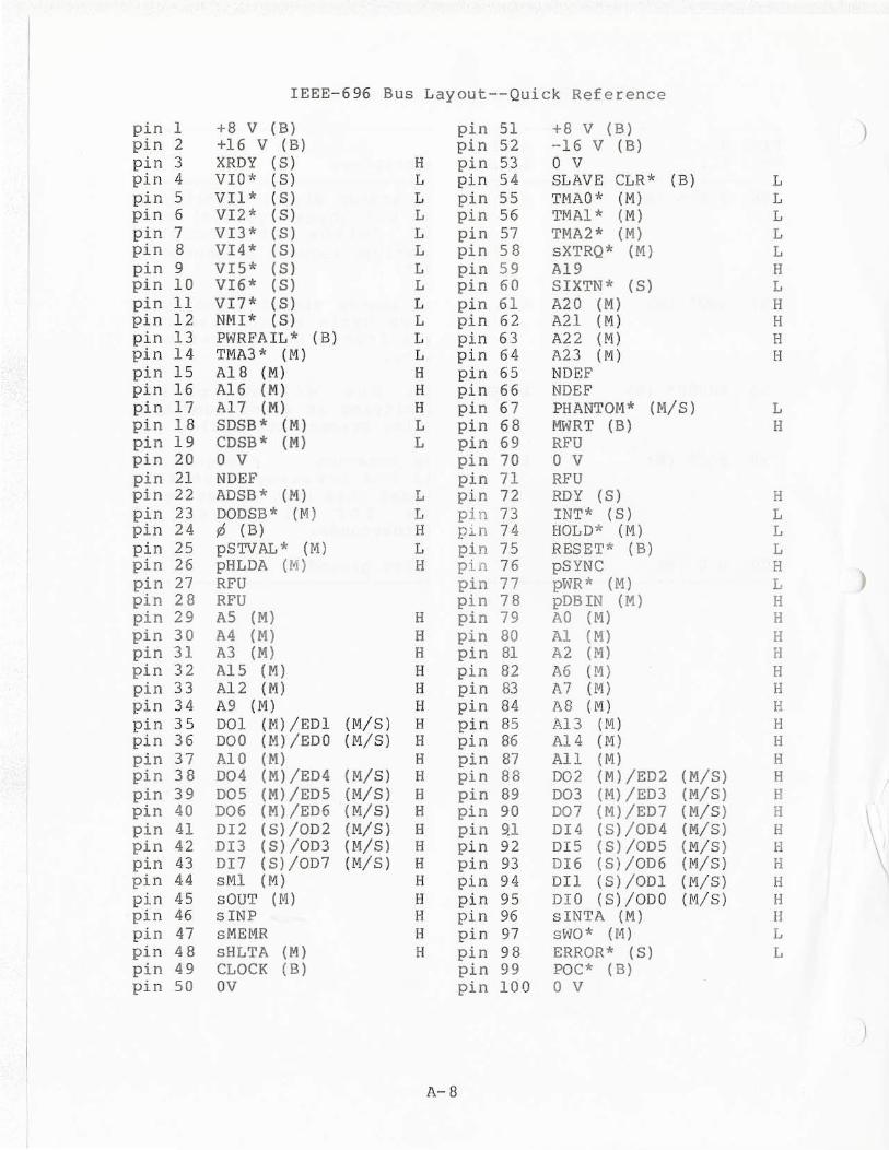
IEEE-696 Bus Lay o ut--Quick Ref e r ence
pin 1 +8 V (B) pin 51 + 8 V (B) ) pin 2 +16 V (B) pin 52 - 16 V (B) pin 3 XRDY ( s) H pin 53 0 v pin 4 VIO* (S) L pin S4 SLAVE CLR* (B) L pin 5 VIl* (S) L pin SS TMAO* (M) L pin 6 VI2* (S) L pin S6 TMAl* ( M) L pin 7 VI3* (S) L pin 57 TMA2* (M) L pin 8 VI4* (S) L pin S8 sXTRQ* (M) L pin 9 VIS* (S) L pin S9 Al9 H pin 10 VI6* (S) L pin 6 0 SIXTN * (S) L pin 11 VI7* (S) L pin 61 A20 (M) H pin 12 NMI* ( s) L pin 62 A21 ( M) H pin 13 PWRFAIL* ( B) L pin 63 A22 (M) H pin 14 TMA3* (M) L pin 64 A23 (M) H pin 15 Al 8 (M) H pin 65 NDEF pin 16 Al6 (M) H pin 66 NDEF pin 17 Al7 (M) H pin 67 PHANTOM* (M/S) L pin 18 SDSB* (M) L pin 68 MWRT (B) H pin 19 CDSB* (M) L pin 69 RFU pin 20 0 v pin 70 0 v pin 21 NDEF pin 71 RFU pin 22 ADSB * (M) L pin 72 RDY (S) H pin 23 DODSB* (M ) L pi n 73 I NT* (S) L pin 24 ¢ ( B) H pin 74 HOLD* ( M.) L pin 25 pSTVAL * (M ) L pi n 75 RES ET* ( B ) L pin 26 pHLDA (M) H p in 76 pSYNC H pin 27 RFU pin 77 pWR* (M) L ) pin 28 RFU pin 78 pDBIN (M) H pin 29 AS (M) H pin 79 AO (M) H pi n 3 0 A4 (M) H pin 80 Al {M) H pin 31 A3 (M ) H pi n 81 A2 (M) H pin 32 AlS ( M) H pin 82 A6 (M) H pin 33 Al2 (M) H pin 83 A7 ( M) H pin 34 A9 (M) H pin 84 A8 (M) H pin 35 DOl (M)/EDl (M/S) H pin 85 Al3 (M) H pin 36 DOO (M)/EDO (M/S) H pin 86 Al4 ( M) H pin 37 AlO (M) H pin 87 All {M) H pin 38 004 (M)/ED4 ( M/S) H pin 88 D02 (M)/ED2 (M/ S) H pin 39 DOS (M ) /EDS (M/S) H pin 89 D03 (M)/ED3 (M/S ) H pin 40 D06 (M)/ED6 (M/S) H pi n 90 007 (M)/ED7 (M/S) H
\ pin 41 DI2 (S ) /OD2 (M/S) H pi n 9.1 DI4 (S) /OD4 (M/S ) H pin 42 DI3 (S)/OD3 (M/S) H pin 92 DIS (S) / ODS (M/S ) H pin 43 DI7 (S)/OD7 (M/S) H pin 93 DI6 (S) /OD6 (M/S) H pin 44 sMl (M) H pin 94 Dil (S)/OD l (M/S) H pin 4S sOUT (M) H pin 9S DI O (S)/ODO (M/S) H pin 46 sINP H pin 96 sINTA (M) H pin 47 sMEMR H pin 97 sWO * (M) L pin 48 sHLTA (M) H pin 98 ERROR* { s) L pin 49 CLOCK ( B ) pin 99 POC* ( B) pin 50 ov pin 100 0 v
A-8

APPENDIX B HEXADECIMAL TO DECIMAL CONVERSION
HEXADECIMAL COLUMNS
6 I 5 I 4 I 3 I 2 I 1 ------------1---------1---------1---------1---------1---------
HEX = DEC IHEX = DECIHEX = DECIHEX = DEC!HEX = DECIHEX = DEC -------- - - --1 - ----- ---1---------1-- -------1---------1---------0 OIO OIO O IO 0 IO O !O O 1 1,048,57611 65,53611 4,096 11 256 11 16 11 1 2 2,097,15212 131,07212 8,192 12 512 12 32 12 2 3 3,145,72813 196,60813 12,288 13 768 13 48 13 3 4 4,194,30414 262,14414 16 , 384 14 1,024 14 64 14 4 5 5,242,8801 5 327 ,68015 20,480 15 1 ,280 15 80 15 5 6 6,291,45616 393,21616 24,576 16 1,536 16 96 16 6 7 7,340,03217 458,7521 7 28 ,672 17 1,792 17 112 17 7 8 8,388,60818 524,28818 32 , 768 18 2,408 18 128 18 8 9 9,437,18419 589,82419 36,86 4 19 2,304 19 144 19 9 A 10,485,760IA 655,360IA 40,960 IA 2,560 IA 160 IA 10 B 11,534,33618 720,896IB 45,056 IB 2,816 IB 176 IB 11 c 1 2,582,91 2IC 786,432IC 49,152 IC 3,072 IC 192 IC 12 D 13,631,488ID 851,968ID 53,248 ID 3,328 ID 208 ID 13 E 14,680,064IE 917,504IE 57,344 IE 3,584 IE 224 IE 14 F 15,728,640 IF 983,040IF 61,440 IF 3,840 IF 240 IF 15 - -----------1------ ---1---------1---------1------ ---1---------
0 1 2 3 I 4 s 6 7 I o 1 2 3 I 4 s 6 7 I o 1 2 3 I 4 s 6 7
BYTE BYTE BYTE
B-1

)
THIS PAGE I NTENTIONALLY LEFT BLANK
)
B- 2

APPENDIX C STANDARD AS CII CODES
BIT POSITION
7 6 517 6 5 7 6 517 6 517 6 s 7 6 s 7 6 517 6 s I 4 3 2 1 ------- 1----- ----- 1----- 1----- -----· ---- - ------1 I I I I
o o 010 o 1 o 1 010 1 111 o o 1 o 1 1 1 o 1 1 1 I t t t t - ------1----- -----1 -- ---1----- ----- ----- ------ 1-----------
NUL I DLE SP I 0 I @ P p I 0 0 0 O ------- 1----- -----1 -----1----- ----- ----- ------1-----------
SOH I DCl I 1 I A @ a q I 0 0 0 1 - - ----- 1----- -----1 -----1----- ----- ----- ------1-----------
s TX I DC 2 " I 2 I B R b r I O O 1 O - ------1 ----- -- ---1-- ---1----- ----- ----- ------ 1-----------
ETX I DC3 # I 3 I C s c s I O O 1 1 -------1 ----- ---- -1 ---- - 1----- -- --- ----- ------1-----------
EOT I DC4 $ I 4 I D T d t I 0 1 0 0 -- ----- 1----- -----1 -----1----- ----- ----- ----- - 1-----------
ENQ I NAK % I 5 I E U e u I 0 1 0 1 - ------ 1---- - - ----1-----1----- ----- ----- ------ 1-----------
ACK I SYN & I 6 I F V f v I 0 1 1 0 ------- 1----- ----- 1----- 1----- ----- ----- ------1 --------- - -
BEL I ETB I 7 I G W g w I 0 1 1 1 -------1----- -----1--- --1----- ----- ----- ------1-----------
BS I CAN ( I 8 I H X h x I 1 0 0 O -------1----- -----1 -----1----- ----- -----1------1-----------
HT I EM ) I 9 I I Y i I y I 1 O 0 1 -------1----- -----1-----1 ----- ----- -----1------1-----------
LF I s UB I ·k I : I J I z j I z I 1 O 1 O -------1 -----1-----1-----1-----1----- -----1------1-----------
VT I ESC I + I ; I K I [ k I { I 1 O 1 1 -------1 -----1-----1 --~-- l----- I---- - -----1------1------~----
FF I FS I , I < I L I \ 1 I I I 1 1 O O -------1-----1-----1-----1-----1----- -----1 ------1 -----------
CR I GS I I = I M I J m I } I 1 1 O 1 -------1-----1-----1-----1-----1-----1-----1------1-----------
so I RS I I > I N I " I n I - I 1 1 1 o - ------ 1-----1--- --1----- 1----- 1-----1----- 1------ 1-----------
SI I us I I I ? I O I - - I o I DEL I 1 1 1 1
NOL Null or all ze ros DCl Dev ice control 1 SOH Start of he ading DC2 Device control 2 STX Start of text DC3 Device contro l 3 ETX End of text DC4 Device control 4 EOT End of transmission NAK Negative acknowledge ENQ Enquiry SYN Synch ro nous idle ACK Ac knowledge ETB End of transmission block BEL Bell , or alarm CAN Cancel BS Backspace EM End of medium HT Horizontal tabulati on SUB Substitut e LF Line fee d ESC Escape VT Vertical tabu l ati on FS File separator FF Form feed GS Group s eparator CR Carriage return RS Record separator so Shift out us Uni t separator SI Shift in SP Space DLE Data link escape DEL Delete
C-1

) THIS PAGE INTENTIONALLY LEFT BLANK
)
)
C-2

lit Position~ 0000 0001 0010
4, 5, 6, 7
Hex 0 1 2
0000 0 NUL DlE OS
'
0001 1 SOH DCl sos
0010 2 STX DC2 FS
0011 3 ETX OC3
0100 4 PF RES SYP
0101 5 HT NL LF
0110 6 LC SS 1% 8
0111 7 DEL IL % 1000 8 CAN
1001 9 RLF EM
1010 A SMM cc SM
1011 B VT
1100 c FF lf'S
1101 0 CR IGS Et-JO
1 110 E so IRS ACK
1111 F SI IUS BEL
Ouplicarc Auignmenr
0011
3
SYN
PN
RS
UC
EOT
OC4
NAK
SUB
APPENDIX D EBCDIC TABLE
0100 0101 0110 Olli
4 5 6 7
SP & -
\
' ! t t :
s I
< . % ~
( ) -
• ; > =
I -, ? ..
EBCDIC Chuacter Assignments (Part 1 of 2)
D-1
s;1 Po,a:on• 0 , 1, 2. 3
1000 1001 1010 1011 1100 1101 1110 11 11
8 9 A 8 c 0 E F
{ ") \ 0
0 j '"\.... A J 1
b k • 8 K s 2
c I t c L T 3
d m u 0 M u 4
e n y £ N v 5
f 0 w F 0 w 6
9 p . G p x 7
h q y H Q y 8
; r z I R z 9

Cho«>cte r
.. • c 0 [
f G H
I J K L M N 0 p
a R 5 T u v w x y z 0
b (
d
• I g ~ ;
j ~
I
"' n
0
p q
' I
I
" . w . y
' 0 I
2 J
• 5 6 7 8 9 &
-I 5
Ht• Choracrer
Cl ' C2 ! CJ C• . C5 C6 C 7 < ca . C9 '!!, 0 1 "' 02 ( Ol )
°' 05 -06 . 07 ; 08 09 >
:
u I El ~
E• ? ES -[ 6
E7 ES E9
{)
' ...... 81
82 : 8J &fl 8-4 BS es g yp 86 CAN 87 cc BS C R 89 DCI 91 DO 92 OCJ 9l DC• 9• DEl 95 Dlf 90 DS 97 EM 98 ENO 99 •f08 A2 EO T Al 'ESC ... ·ne "5 ETX A6 FF A7 FS AB HT 49 IH FO IGS Fl ll fl IRS fl IUS F• LC H Lf F6 NAK F7 Nl F8 N UL F9 P F 50 PN 60 'PRE 61 RE S 58 RLf
H•• .. 5A 7A 78 68 •B •C K 6C 7(
•D SD 6 D 70 • E SE 6E 7E •F SF 6 F 7f co DO EO Al 79 6A 2F
I 16 2• 18 IA
I OD I I 12 lJ J(
07 IC 20 19 1D 26 J7 27 26 OJ oc 22 05 1(
I D 17 H I f 06 25 J D 15 00 ();
J• 27 14 09
CJ.io•octer Ho•
--RS l5 SI "' SM 24 SMM OA 50 OE SOH Ol sos 21 Spo<o '° STX (1'J
SUB lF SYN 32 UC )6
VT oe
•£ T8 ond E08 hov<t th~ to~~~
cuig~"''· P• f a,,d fS( hov~ the t.OMC' haa OH igrcment .
EBCDIC Character Assignments (Part 2 of 2)
D-2
)

) CIO APPENDIX E SPEC I FICATION
Registers Kaster Interrupt Control R~er
Address: 000000 (Redc:l/Wrate)
f flfa\IL( CMl:O L IJQWT .IUSTlll(O AODAUSU O•SHln un <Ao h Of"I A011
Master Configuration Control Register Address: OCXXlOl
(P.ead/Wr1te)
Io, O, °' o, o, 0, o. 0 I
ENUL[ Cf'IE) CON'TAOl ~ llC1
\.Ct LCO
•UTER INTfOOUl'l 1JJ -..Slf LOWU CHAUll IDLC> -
NO WECTOtl tM'it l~L •• ..,. 1 • JUQHT JUSTIFY I.Ao "°"" A Dol COUNTERtmllEfll '
f NA9L( CCTIE1
..,.,.~~ 0 0 CO\IMT{!l.,1Mt•S l ~Oflil(frf0("'1
[
COUHTEOMOMl• LINM
o ' en i , oul'P'Vt c.uu c·• 2
fl'OAT A YfCTOI. IHCLUDU ___J aTATUS (PA Vt.51
COUNTEMllll[lil.$ Yf.CTO" wet.UOES STAJ\1' IC' YISJ
- ~Jn B VICTOR INCl.UOU ITATUi t•I VIS!
Fl;ur•
Port Mode Specification R~ers Addresses: 100000 Port A
101000 Port B {Read/Write)
POOT'IYP<~ U l £CTS (n S)
~tPTSO
f f M IOIU I ' INlllU'l flJOAt 1 0 OUTPUT POfllT 1 1 SIOllUCOONAI. ..,.,
_,...,._Uf'tONTWO IYTIS (ITB)
Mell£ IU,FEA£D MODE (SDI
r LATCM OH f'AntAH MATCM r\.1'11) tall 11100(~ 0£5Kf.W Tl llltfR f H41Ll fDlEI <HillDl.HAK.E MOMSI
,ATTfllUt MOD£ PICtft(ATION •rtS(,.M$)
fltlft 1 HllO - 0 CMiAllf lllATIEt;N MATCH
1 "AHD"MOOE o -oA- ..ooc t ~.PJUOllU'TY fNC:OCtO
VEClOfll' MODE
'---- - tNT£JUllUl'T Ofrf l&ATCM Otfl'Y (UllOI
COUHTfMlllt(fll 2 IMA•LttCTU J
'OflT C AND COUNTC .. I Tl lllllUll l k AGLE ~t•NOCUEJ
' 0 Ctt 1 ' 6ijh1ji lfl1GG.'tll~ CIT 2 1 t C1tt , (S"l)TJiJ11sc.:1),
COVJ'it JHPUT
"°"' A. uu.aLf IPAt1
..a!H UNI( CO..,TROL tl' l t• O• PORTS A A.ND a OlllfJU,l[ 1"'4Dftl!NO(N \'l 't 1 • JllOfll$ A AHO B Afll( llMK( O
Port Handshake Specification Registers Addresses: 100001 Port A
101001 Port B (Reac:l/Wrate)
1 ~ ~ D: ~ 0\ D~ O. ~ 1
KAlllOSHAKf TYPE P'fCIJK;ATK>H J ~ OESKfW YtME PEC,,ICAflON 1111 IHSn lrTS
Hil t HSTD ~:~;~.!:~,~~~ ~~·E'c°c:NsT .. NT
: ~ :~~R1L~~~;:::::AU LY IS 'OllCED I
1 0 P\ILS(O HANO'SHAIU" 1 1 TtO'H WllU. KAMDIHAKf
llt((Wl$Tr#Afr l#fC\FICATIOtrf IJTS rows.
~ ~~ "T i~~~!~~~.m 0tSA1LEo 0 0 OUTPUT WAIT 0 ltffllUT W.ilT t SPfCIA.l AfQU(St t OVtlllUt AEOUEST 1 tNlllUT JIEOU'EST
Port Command and Sta tus Registers Addresses: 001000 Port A
001001 Port B (Reod/Partaal Write)
tNfE.A AUPT UNOEA HAVICE (h.IS.1
1NUH.un fHAlt.l CIEi
IMt(JUllUJIT JlfNOIMC 11">
IU!. l l AND IP AllL W RITt [H USING fH( fOllOW'INt COD[
....,, , coot CltAA '" & IUS
SI l IUS
Cl( Alt 111-S
$tf IP
CLUk •P
ICTIC
CU••rE
l": TE'-"UP1 EAA0fl !EAAI (ftUOONLYI
E-1
~L ••re••u., o• •••o• 00£1
L P'ATifllN WATCH ft.AO [~F'., Cl'UOOH,Yt
ltcPUl AlGISTEft fUU. "ltP:) (RU.D ONl.VI
- - OUTf'Ut llECISTUl Utl'TT fOll(1 (RU.00..LVI

R99ist•n (Continued)
Data Path Polarity Regt.ters Addresses: 100010 Port A
1010 10 Port B CXXl lOI Port C (4 LSBs only)
(Read/Write)
'----- - - OATA H.TM POi...utrY f~ 0 • NO .. IHVVlTI..O 1 • INV1 RT'U•O
Data Dizectlon Regt.ters Add resses: 100011 Port A
101011 Port B 000110 Port C (4 LSBa only)
(Re11d/Wr ite)
'--- - - DATA OU,fCTtC* CO• t•OUTPUT Ill t•tNJ'U'T Ill
Spec:ial V O Control Regt.ten Addresses: 100100 Port A
101100 Port B
Figure
Port Data Regt.ters Addresses: 001101 Port A
0011 10 Port B (Read/Write)
0001 l l Port C (4 LSBs only) (Read/Wr ite)
'--- - - p(CIAl tN'1.ITIOUT"'1JT I~ I• NOANAL tN"6T 0111 OU'T"-'T t • OtlTJl'l.11 WITH OP(H OAIJN Oii
• PVJ WITH 1'• CATCHU t
3. lilt Path O.tlttltlon Regt.ters
Port C Data Register Addre1la: 0011 1 l
(Read/Write)
... ~ t•WIW'1'1'MQ OI C'OUlP\)NQllllQ LAI tit..._%> ' • ......,..., 0# coa••t1"C1t:::ict1110 LU * "...-n:G --·
Figure. -4 . Pat"t Data Reglaterw
Pattern Polarity Regist• rs (PPJ Addresses: 100101 Port A
101101 Port B (Read/Write)
Pattern Tn:maltlon Regt.ten (PT) Addreaea: 100110 Port A
lOlllOPortB. (Reed/Write)
Pattem Mmk Registers (PM) Addreaee: 100111 Port A
101111 Port B (Read/Write)
E- 2
I"' i 0.:0.; •· I°' I°' ! 01'9 PM PT " M TTEftN IW'lCIFK:AnoM - - 0 I. ;m MASKED OH •. .•
t Jt Mil'f TlllA.NllTION I f ZVIO 0 1 ()llff t 0 Ott£ TO·ll.ftO TilAN:stnOlif f\f 1 1 Z'£ft0. TO'<)frit( Tu.tcStnOfrril vt
)
)

JI.gist era (Continued)
Counter/TlEDer Command and Statiia Registers Addresses: 001010 Counter/Timer l
001011 Counter/Timer 2 001 JOO Counter/Timer 3
(Reod/Portlol Write)
....... u ... """"' llt'.IMC( 41Ull _Jj_J, I .-n.ttAU"1' ..,..LI NI
I I 91'TIAkU"1 'CNOltta _, I 1
RI&, IL AHO II' AJtl WlltITTIH UIUrtO ?Ml 'OLLOWtNO COOf
NUUCOOf
CLIAJt .. . "" ....... 0.IAR NI
KT,.
CLl.Allt 1,,
ll!TI(
CU.Utl
.-nu"'1 PAO«"""' ___ _, ~ONLY)
~l oouw•"' •ltOORtu"""'
fl'f.AOC>frflYl
TJUOOIA COM.MAJfO In l'TCIJ {W1tnf 0-lY ·AUD ""VRNI Cit 04T1 COIUU.NO lrT IOCI)
llltAO COUMTftt CO«TlllOL l'ICC> t'l:UDt'll"l Otft'f -CLUJlllD 1 '1' ftU.Off(Q Cat Lal.>
Counter/Timer Mode Sp.etflcation Regitlten Addreaaes: 011100 Counter/Timer I
011101 Counte r/Timer 2 01II10 Counter/Timer 3 CReod/Wrlte)
Cowiter/TlEDer Current Count R911Wten AddreaaM: 010000 Counter/Timer l's MSB
010001 Counter/Timer l's I.SB 010010 Counter/Timer 2'1 MSB 010011 Counter/Timer 2'1 I.SB 010100 Counter/Timer 3'1 MSB 010101 Counter/Timer 3'a I.SB
(Reod Only)
~---LUST IWOtllFICAJrfT D'l'll
Collnter/TlEDer Tt.m. Constant Regittwa Addresses: 010110 Counter/Timer l's MSB
OJOI 11 Counter/Timer l's I.SB 01 loOo Counter/Timer 2's MSB 011001 Counter/Timer 2's I.SB 011010 Counter/Timer 3's MSB 01101 I Counter/Timer 3's I.SB
(Read/Write)
...._ ___ ......., SlOHt,.ICANl OYTl
Figutw I. Cowller/Tlmer R.glaten
E-3
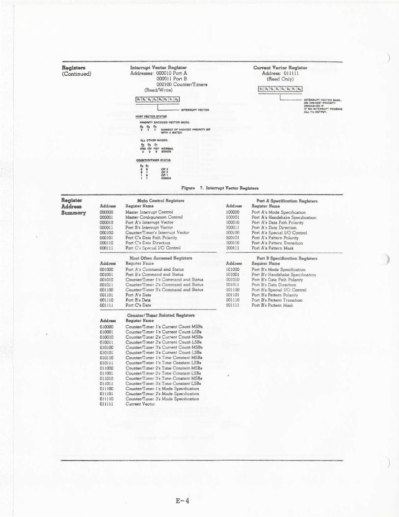
Reglatera (Continued)
Reg later AddrSummary
Addr-000000 000001 000010 CXXJOil 000100 000101 000110 000111
Add,_
001000 001001 001010 001011 001100 001101 001110 0011 11
Add.-
010000 010001 010010 010011 010100 010101 010110 010111 011000 011001 011010 0 11011 011100 01 1101 011110 011111
Interrupt Vector Regist• Addressoo: 000010 Port A
00001 1 Port B (X)()JOO Counterffimel'll
(RE>l!d/Write)
'----- °'""°"" VICTOll
flOllrT ~ STATVa
JltlllC>WtY PtCOmD VW:CTOA ~
!!J !!J lb a a 1. NUMHJl 01' .. ta.HUT ~ sr
""'"A MATCH
AU.OTHPMOOO:
0. DI D1 Oia .;t, ,., litO"M.IA.
t t 0 PACNll
COUNT~~ ...... i i QTJ • , Clt2
' • en, '' ...-
Curr.DI Vector Register Addreu: 011111
(RMd Only)
'----- IMTlllUllU'°" VtC"TOlll Mal. ON KIQMUT U IOJUTY UNMA.$1C l C 1P " NO 1-.TUUUH"T ~...-0
AU. ''• OUTPVT.
Flgwe 7. lziterrupt Vectc: R~rs
Main Control Reglatetw R10QW!er Name M<Uter Interrupt Control Muter Configuration Control Port A's Interrupt Vector Port B's Interrupt Vector Counter/Timers Interrupt Vector Port C's Dai.. Path Polt1rity Port C's Data Direction Port C's Spec!11l 1/0 Control
Mc.t Otten Acc....t Regt.ten R.qW•r Na.me Por1 A's Command and St.stus Port B's Comrr.4nd and Status Counter/T•mer l's Comm.>nd and St.stu1 Counter/Timer Zs Command and Status Counter/Timer 3's Command and St.s!UI Port A's Oat.> Port B'1 Oat.> Port C'a Data
·Col.l.Dlerfnmer Rolated R9iJ!alen R.qWer Nam• Counter/Timer l's Current Count-MSBe Counter/Timer l's Current Count·LSB1 Counter/Timer Zs Current Count·MSB1 Counter/Timer Z s Current Count·LSB1 Counter/Timer 3's Current Count·MSBs Counter/Timer 3's Current Count·LSB1 Counter/Timer l's Time Constant·MSBs Counter/Tlmer l's Time Conslant ·LSB1 Counter/Tuner Zs Time Constant·MSB1 Co~nter/Timer Zs Time Con.ot.snt·LSBs Counter/Timer 3's Time Constant ·MSBs Counter/Timer 3's Time Contlant·LSBs Counter/Timer l's Mode SpecihC41lon Counter/Timer Z s Mode SpecihC41lon Counterrr1mer 3'a Mode SpeciliC4tion Current Voctor
E-4
AddrIOOCXXJ 100001 100010 100'.J 11 100100 100101 1001 10 10011 1
Add,... 101000 101001 101010 101011 101100 101101 101110 101111
Port A SpecUlcatlon Re¢st.,.. R.qist•r Name
Port A's Mode Spec1liC4tion Port A'e Handoh4ite SpecthC4hon Port A's D4ta Pa th Polarity Port A's Dato Direction Port A's Speciol 1/0 Control Port A'• Pattern Polarity Port A's Pottem Transition Port A'• Pattern Mask
Port JI Specltlcatlon Regi.t""' R.qWerNam• Port B's Mode SpeciliC4tion Po" B's Handshoke Specihcahon Port B'a Dai.. Path Polarity Port B's Dai.. Direction Port B'e Special UO Control Port B's Pattern Polanty Port B's Pattern Transition Port s· s Pottern Maalr.
)
)
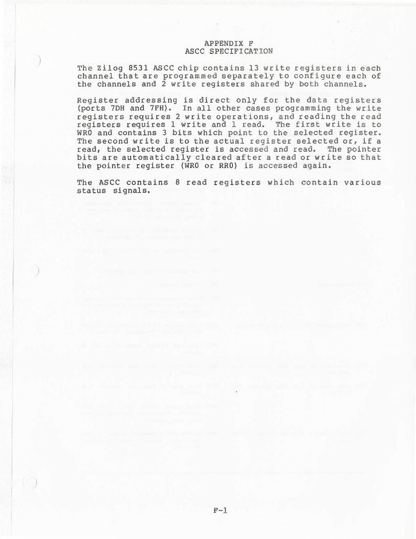
)
)
APPENDIX F ASCC SPECIFI CATION
The Zil og 8531 ASCC chip contains 13 write registers in each channel that are programmed sepa rately to configure each of the channels and 2 write registers shared by both channels.
Regis te r addressing is direct only for the data registers (ports 7DH and 7FH). In all other cases programming the write registers requires 2 write operations, and r eading th e read reg is ter s requires 1 write and 1 read. The first write is t o WRO and contains 3 bits which point to the selected register. The second write is to the actual regist er selected or, if a read, the selected register is accessed and read. The pointer bits are automatically cl eared a fter a read or write so that the pointer register (WRO or RRO) is accessed again .
The ASCC contains 8 read r egisters wh i ch contain various status signals.
F-1

READ IEGISTER FUNCTION
RRO Trans111it/Receive buffer atatua, and External statue
RR1 Special Receive Condition status, residue codes, error conditions
RR2 Modified (Channel B only) interrupt vector and lk11110dified interrupt vector (Channel A
only)
RRJ Interrupt Pending bits (Channel A only)
RRB Receive buffer
RR10 Miscellaneous XMTR, RCVR status parameters
RR12 Lower byte of baud rate generator time constant
RR13 ~per byte of baud r ate generator time
constant
RR1S External/Status interrupt control information
F-2
WRITE IEGISTER fUC'TION
WRO Command Register, (Register Pointers, Z8530 only), CRC imtialuation, resets for various n10de9
WR1 Interrupt condit ions , control
Wa1t/DHA nquest
WR2 Interrupt vector (ace9se through ei th&r chann'9l)
WRJ Receive/Control paramet ers, null'ber of bits per character, Rx CRC enable
WR4 T renemi t /Recei ve misce lleneous peramete rs and l!Ddea, clock rete , nunber of ayl'lC characters, stop bite, parity
WRS Transmit paran>eters end controls, nur:iber of Tx bite per character, Tx CRC enabl e
WR6 Sync character or SOLC address field (1st byte)
WR7 SyllC character or SDLC flag (2nd byte)
WRB Transmit buffer
WR9 Master interrupt control and r eset (accessed through either channel) , reset bits, control inter rupt daisy chain
WR10 Miscellaneous transmitter/receiver control bits, NR2I, NR2, fM encoding, CRC reset
llR11 Clock med! cont1·ol, source of Rx snd Tx c locks
WR12 Lower byte of baud rate generator time constant
\llR13 lipper byte of bsud rate generator time constant
WR 14 Miscellaneous control bite: baud rate generator, Phase-Locked Lo~ crontrol , auto echo, local loopback
WR1S External/Statue inter rupt control info rms-t ion~ontro l external condit ioos CBUSHl<J
i nterrupts
)
)
)

Ul_g ::::.,-:· ............ .
Ta .u,,u. "'"" oco SYNCIHVN1
CTS
h u-.ou,.u•ot o.. lkUKiAIOIU
ReodR~er 1
(o. ~ ~ o, 0 1 O: o. ~ I
~~~:~~::·CODI> L lllUI DU[ Coot '
llUIDUlCOot: 0
ltAIUTY I AJll°"
th O'VUllllUllill IAlllOR
CllllCIJ'MWINQ lfli1110"
IND Of 'Ill.AMI tlDlC;
ttn'UU,Ull'T VfCTOfl •
RoadR~er3
lo, o, o, o. o, o, o~ o.J
~~~C>IANNUllnllTAT ...
CMANNlL I h ,,.
~ANNf.L I lb. " '
Cffl.NHIL I. U111TAT " '
CtCANNlt.. A h "'
CKANICll AAll IP"
0
0
Read R~er 10
ID, o. o, o, o, D, o. Ct I
R.ad R~er 12
( O, o. o, 0 , O, o, 0 . 00 I
U~~~~-"omo• ~ TCu r•r CONSUNT
TCo
TCu
TCu
ReadR~er 15
I•· o. o. •. "' "' • · o.1
F-3

Write Registers. The SCC contains 13 write registers (14 counting WR8, the transmit buffer) in each channel. These write registers are programmed sepa rately to configure the functional "persona lity" of the channels. In addition, there are two registers (WR2 and
Write Register 0
I •t<MSTU I
• .......... I RIGISTUt t
NO&STTR •
' ft.IG &a'flft I
0 AIOllTtR t I l'lEadTEA r 0 "10£STUI I
l I lltlQ&STEft I
• l'tlG&STUl 10
' IU!.G18Tl.lll l1
• lttQ&STUtU
' ft~Qil'Tf~ 11
0 AEGtOlll' 14
I k!EO&ST!A 11
Writ• Reqister l
~Lvo1m•••ll• L TJ. INT UtAILE
U IUTY IS SPECIAL COHOOK>N
lb INT OtSAILf
lh INT OH fl ll;ST CH.AMCfEA ~ $4111Ct.l: CONO!f.otf
' "T OH Al l lb CHAUCTEns OR S,ECIAI. CONDITHlH
lb INT ON SPECIAL CO~OCTION O NI. Y
~----- WAITtOMA AtOUEST O N FIECflYEJTll1Ji11ifl'T
'--------- WiiftDlilA AEQUUf f'UfltCTIOft
L-------- WASTrDMA. AEOUEST l HA.8l.!
Write Reg!mcw.r 2
lHTfOIAUPT YfCTOllt
SYNC? SYMC1 t Y'tCt SYNC1 . .,.., .... ,
F-4
SY~C.0 $ \'NC. $ \'NC. $ VNC1 ..... ....
WR9) shared by the two cha nne ls that may be accessed th rough either of them. WR2 contains the interrupt vector for both c hannels, while WR9 contains the interrupt control bits .
Write Regtst<'M' 3
Io, o. o, o. 01 o, o, . o. J
I l~~L ... ....,.l.
l1 SYNC CHAM.ACJ[A l.OAO IN•usn
A.DOJl:l&S $EA,.CH MOC>E 1aoc.C)
All CRC fNAal f
Emfll~ MUNT MOOE
---- AUTO fNAILU .
O O ft . S t.ll&etu.1111CTE1'
0 I fb 1 B!lSICtlt. ftACtt~
l 0 Jh. t S ITSICtiAMACT£,_
I lh l RllSICHARJ.ClEln
~c\ 04 o, o,. o. ;9
I L • ARITY .~ .. "
L PARITY ( Vf.NJO®
SYl!tC MOD!$ EhABL(
1 sro, PllYfCHAIUCTEA
1 ~, $TO, 81T5/CH~AACTEfll
2 5 TOI' l:llTSICHAAACTEM
0 0 ll DH SYOfC CHARACTE"
I~ flit SYNC. C t'AMCTE1'\
0 sotc $;100((1H11 U 10 FLAG)
EXTUUt.At. SY ltC t100(
Writs R~or 5
I L: :::_•c •'<ML~ Lw"cx::"'c·'i
- la £HAILE
S.U.10 llllEAK
0 a fa. S &ITS (OR L[$S>'CHAAACTfR
h 1' tU5/'Cl>t.\AAC{Ut
h I Bll!ICHAl\ACTEfl
Tat QJt&CH~ACT(R
Wnte R$Sli!Jter 6
SY'*C• $ Y,,,C4 sv~c. t.ncc, I YHC1 SYNC, SYHC4 $Y~ti SYNCi $ 'rlltC1 SYN Ct SYll:IC• SYl+C1 SYMC1 !.Wt<C1 sv-.c, SYNC. ' ' ' AO,_, .... Allft, ..... . .... ..... ..... .
OYHCo U ONOS•NC, ' errs SYHC. ldOlrfOSYNC, 1' ltf&
l TNCo 1.11sv .. c . 16 111s I &ll'rNC , 12 ~IT!
AllAo SOLC I OlC
(AOOfl:lU ftAtfQ()
)
)
)

Write Register 7
(o. o~ o, o, o, o, o. De)
IYNC' l'f .. C, l'rNC, , I YNC\•
•
1 Write Register 9
1 o o. o. o. • • . o • I
11 ~:~ ~PLC ... ,
Sl'NC• IYNC, I YtriC• I TNC, S 'l'N(u IYNC\J SYHC1c S YNC.t
'
:1• •us HM:;Hl$U1US LOW
0 0 MO AESt 1
0 \ CW&NNh AU£1 a 1 0 C-CAlliJif[l fllUU A
IQllC( HA.ROWAfl:C tl!UfT
Write Register 10
~L.: ' OITlt BIT SYNC
lOO• WODE
AIOtU,rLAC OH UNDOlllllUH
MAJl .. frL.l·e 10 1.t
- - GO A.C:TIV( OH POLL
0 0 NIU .... ' 0 fMl fUIAMSt110"'1 • 1)
1 \ f 9'0 (Tfl!AN$1f10N " 0)
Write Register 11
J ~ a a ~ o ~ o o I
SYWC, SYH()
IYNC.11 SYNC,
'
I u.c ou• • xt•• ou••u1 ll'h C OU ' "' TRANSMIT CLOCK
flhC OUT " IR C(HliR.ATO" OU1PU1
Tlh C OUt • Df'Ll CXl1'•U1
fthtOlt
0 0 TIU,'1\1$U t1 Cl.OCK • " h C PIN
Ul.A.NSlll ll CLOCK • Hh C P IN
TfU.N$»11 Cl.O(IC • Ill ClNU.A10A OUTlll>UT
T'-ANSMll CLO(tt • OflLl OU1'UT
IY"fCt &THC , SYNC , , SYNCr
SYHCt .. ,lrifC. ••..CO llOfCOSYMC I llTS IYNC; tllOttOS'fNC, I llTS l'fMC · c. IYNCt snrc, OIST"fC 1111't. 1¥NC1 l'Ot Cs ,.,,,,, 11sv"'c. u llTS
' ' • •01.c
Write Registor 12
~c, o. o~
Writ• Register 13
Write Register 14
l OW(l'I IYT£ or fl till l: CONSU ."11
U'lllElll I YH or T1Ml C.0N$TA ... ':
~I L •• GENEAA10 .. NAO<E
L .,. G£H(IU1011l SOllRCf
f)TAtACOUUf f:UfrilCTIOt<t
AU10 ECHO
t.OC.•l lOOf'IACll
c 0 0 Nuu COMWANO
( NlfR $l.d1Ct4 MODE
RESET Y l §SIWG CLOCK
Dis.lilt DPLL
Sf"' SOURC[ • I A GENU.A10A
HT sou•ct • 1n .c Sf.T j:M MOD(
stT NR.lt MOO(
Write Register 15
J o , '~~ O, D. D ~1
11 1 ~ ~;:=::: ~CJSI[ 11 UNDEOUt.!JlOM If
'---- - - - - - - '"~AkJA9()R' I(
Write Rega l er Bit f unctlom (Continued)
F-5

)
THIS PAGE INTENTIONALLY LEFT BLANK
F-6

)
U28 (DECODE):
APPENDIX G PAL16L8 SPECIFICATION
/MREQ /IORQ /RD /WR BUSAK IEO BOOT /RFSH MASTER GND /INTA /GORAM PA16 /IO / BRFSH /MATCH /RAMENB /PROMENB /RDOFF VCC
IF(VCC )/RAMENB = /BOOT*MASTER*MATCH*PA16+/BOOT*/MASTER*PA16+ /BOOT*/MASTER*BUSAK*MATCH
IF(VCC)/PROMENB = BOOT+MASTER*/BUSAK*MATCH*/PA16+ . /MASTER*/BUSAK*/PA16
IF(VCC)/RDOFF = /BOOT*MASTER*MREQ*/MATCH *RD+ /BOOT*MASTER*IORQ*RD*/IO
+/BOOT*IEO*INTA*IORQ*MASTER
IF(VCC)/GORAM = RAMENB*MREQ*RD+RAMENB *MREQ*WR+ RFSH*MREQ+BRFSH
059 (SLAVE):
/ADSB /HOLD MATCH /DODSB /CE N MEMR SLVRQ DBIN BUSAK GND MEMW /BUSRQ /RDOFF MASTER /BUSENB /DIEN /DOEN /AEN /BRFSH VCC
IF(VCC)/BRFSH = MASTER*/MATCH*MEMR*DBIN*BUSAK
IF(VCC)/BUSENB = /CEN*MASTER+MATCH*/MASTER*AEN
IF(VCC)/BUSRQ = MASTER*HOLD+MASTER*BUSAK*ADSB+/MASTER*SLVRQ
IF(VCC )/AEN = MASTER*/ADSB+BUSAK
IF(VCC)/DOEN = MASTER*/DODSB */BUSAK+BUSAK*MATCH*MEMW
IF(VCC)/DIEN = MASTER*RDOFF*/BU SAK+BUSAK*MATCH*MEMR*DBIN
G-1

)
THIS PAGE INTENTIONALLY LEFT BLANK
)
G-2

)
Port (Hex)
70 71 72
73-77 7 8-78
78 79 7A 7B
7C-7F
7C 7D 7E 7F
)
APPENDIX H PORT ASSIGNMENTS
Signal Name Function
SAS I* MAPPER* ATTEN*
Not Connect ed CIOEN*
Por t c Port B Port A Control
SCCEN Channel
B B A A
SASI/Parallel port- - data Memory mapper Attention bit for slave pro ces sor (used to generate an inte rrupt to master ) Not used CIO (8536) enable
Serial chip enable Function Control Data Control Data
H-1

}
THIS PAGE I NTENT IONALLY LEFT BLANK
H-2

APPENDIX I PARALLEL INTERFACES: SASI/CENTRONICS
SINGLE-ENDED SASI/SCSI COMPATIBLE INTERFACE CONNECTOR J4
NOTES:
All odd pins shall be connected to ground True on SAS! = Signal Assertion = 0.0 VDC to 0.5 VDC False on SAS! = 2.0 VDC to 5 . 25 VDC Parity not used To enable the data port for output (port 70), port 7A
bit 5 must be high
Signal
DBO DBl DB2 DB3 DB4 DBS DB6 DB7 BSY ACK RST MSG SEL C/D* REQ I/O*
J4 Pin Number
2 4 6 8
10 12 14 16 36 38 40 42 44 46 48 50
Port Number
70 70 70 70 70 70 70 70 7A (2) 7A 7A 7A 7A 7A 7A
Bit Number
0 1 2 3 4 5 6 7 1(1)
0(3) 2 7 3 4 5
(1) Port 7A bit 6 is an enable for this line and must be high (2} An I/O instruction to port 70 pulses this line (3} Used in conjunction with port 78 bit 0 (see schematic
sheet 4}
I-1

SASI TO CENTRONICS INTERCONNECT
NOTE: This table shows the pinout s fo r connecting a Centronics parallel po r t t o the SB C-300 SAS I port (J4). The pinout s are from J 4 (50 pin} to a 25 pin ' D' connector. A seco nd cable contains a mating 25 pin 'D' connector a nd the 34 pin Centronics conne ct o r . This c a b le is designed to be a 26 conducto r fla t ri bbon to minimize the construction .
-----------------------------------------------------SASI J4 Pin 25 Pin ID I Centroni c s (34 Pin)
Signal Number Connector S i gnal Pin -----------------------------------·------------------
DBO 2 2 DATA 1 2 DBl 4 3 DATA 2 3 DB2 6 4 DATA 3 4 DB3 8 5 DATA 4 5 DB4 10<-------->6<---------->DATA 5 6 DBS 12 7 DATA 6 7 DB6 14 8 DATA 7 8 DB7 16 9 DATA 8 9 MSG 4 2 11 BUSY 11 SEL 44 1 STROBE* 1 GROUND Any Odd Pin 14 GROUND 19
-----------------------------------------------------
I-2
)
)

APPENDIX J MONITOR LOCArIONS
J-1

\
TEIS PAGE INTENTIONALLY LEFT BLANK

P:OO =
..
CJ>ll'I RMI:~ J.1 IOOl
title 'SC(-~ Version of ltonitor v2.~W 9/'YJ/83'
;tt+t~•tllllllllllllllllllf-f++fllllllllllllllllllllllllllllllllllllll
' t 1/20/63 initiil version dlt1 lli.9ond t
5130163 initiil ttlttst tf.i wl.O t
6115/83 fix '"'' 1isc ol"t1•izition tfJ vl.l t
7/13/SJ fix Piritr. vi'•• sttP. 'cio f>Ott c tf.i vl.2 •
8/0Cs/83 8/19/63 9109183 9111183 9121183 9124183
913J:J/63 9/'YJ/83
first nrsiori for vfti boud lddtd l6dts for fora.t routints fix for doublt dtn~itr disls boot ~rt fixts for du• l-dfnsitr booting added ai rii -boot , • innit b6~t
&ddtd vf2 disk routints
f ixtd boot f<tlustd iS 2.0
tf.i dib rlti dkb wbd
tf.i
~ vO.O
¥0. l ¥0. 3 ¥0.4 ¥0.5 19bd
tf.i
• • f
• • • ¥0.6
• f
v2.0
• -- dor1't fol'9et to Ul"ditt tit It. sitr11>r1 ltld vtrsior, ditt - t
;tfllllllllt-i-f-f+t+tlllllllllllllltlllllllllllllllllllllllllllllllllllllll
;tfffi+++f-f•lllllllllllt+tt+tlllllllllllllllll~+t+++tt-t+t++t
tt1n&: •
ttrtstnt restrictions itt! t
tuni aust Of i l"i9t boundtrr t
Pi9t Offh is rtstrvtd for ttblts. ,.,...s t
;t+++ttttfllllllllllltt-flllllllllt-tllllllllllllllllllllllllllllll
. '
OdfOOh ; address to or-s 90nitor
•
•

0000 = 0000 = 0:0(1 = 0060 =
8000 = 4000 =
0000 =
tKlO() = 0400 =
• 4000 =
CJ>lft RM: ASSEJ1 1.1 I002
; .... 111111r11 1 111111111111t~11111111111111111111111111111111
• ; n sttti t1uitts • ; • ;111111tllllt++tt+t-f++fllllllllllllllllllt+tt+f+attllllflllllllll
;11111111 11t t+t-t-f t+tlfllllllf-f+f-f l llllllllfllllll
I
•i sctllt nt ous t ttUi tts t
• ;t+t+Httffl+fl 11 111 1fl111111IIll1111I11111 11 J llJ
tor tttu OOOOh rbut tttu OOOOt, U l'SI' ttlU runa sctrsz f41U
vdbSc onf f'CtU
urSconf tttu
activtSvctrs tttu
if ahz4 lltlzSconf f41U
initdliY f41 U codliY
t ht if ahz6
9hzSconf f41U
initdl tY tt!U cod In
; ;
t ndif tnd if
conU1nit
;
tol' of ru shrt of ru . ttfiult ustr stick bt lott 1t<initor ,
128 ; htts Hr· 5tctor
1 C«lSOOOOSOC(JOS()OOb OJ OOS000(~'X00$0000t.
OJOO.OOOOt. bit 9isk for wtiich vtctortd inttrrl'uts &re t nd.J td. ( viO -) b7, vil -> t;.6 , t tc. tn lr ,bfrr (f'iritrl tnibl td
~t. : bi ts 1.0 of confSvctr ttnott Cl'u clock Sl't t d
08000tr ; dtliY for snh1 h stibil izt tfttr ciei ini t '"u 40011 : ttliY for init consolt servict
~IOOlb ; (bit 1 rtstrvtd for 8 ahzl
OcOOOtr f41U 600h
Jtrfconf or .tizSconf : initiil vtctor is str con and llblttvtr clock .
)
)
~ J.

•
0000 = 0080 =
FFOO =
FFOO = FFOO = Ff 02 = ff 02 = ff03 = FF04 =
FFOO = FFOO = FFlO = FF20 = Ff 30 =
FFlO = FF12 = FF14 = ff 16 = FF18 = Ff 1~ = FFlC = Ff lE =
FF40 =
FF40 = Ff42 = Ff~= Ff40 = ff 48 = Ff 4A =
FF4C IC
; t+H+fffffffffff+H-ttHHH+ffHHHHU I 1111111
• • • ;llllllllllltf+f+t-tllllllflltlt+tlH~t+l+*+f . • cldfstk cold rtu
riiu rkst+8()h ; cold boot stick rkst+80h ; cold stut addrtss
;ffl l lll lll lllllltllllllllllf+i-f+fl lll llll l lllll l
• ~'t Offh t111uitts •
• ; H-ttttHf fftt-tttt+tH+HfffH+H+tltH 1111111111
SYSPi9 rlU OffOOh ; Ntt Offh rtstrvtd for .ur.iteir and os 's
IYSfinfo rtu IYSPi9 + OOh ; 8 brtts for srstta infor9ition aonhdr riu snSinfo + 0 conffvctr r!U srsfinfo + 2 confSlo rlU confSvctr + 0 confShi r!U confSvctr + 1 .unfvtr rlU srsSinf~ + 4 . t brlts sninfo(5 thru 7) ll't rfu . t
ivt ftlU SYSlli9 ; bi.st Pi9t I'll locttion of inttrruPt vtctors ivtcioc f'IU ivt + 08tr ; offstt tei ciC1 counttr/ti9tr·s isrY 'S - rf u ivtciob ftlU ivt + 10h ; offstt to cio !"Or t b isrv ' s ivtciH r!U ivt + 20h ; offstt tei cio '"rt a isrv's - rfu ivtHC r!U ivt + 30tr ; tffstt to sec isrv's - rf u . t
visr7 r1u ivtciob + OOh Yisrl r1u ivtcioti + 02h YisrS ftlU ivt cio~ + 04h visr4 t'lu ivtciot. + 06h Yisr3 f411U ivtciob + 08t. visr2 r1u ivtciob + Oit1 visr1 r1u ivtciob + Och vinO f411u h1ciob +0th
QrfSPC ftlU 1n11i.s + 40h IPict for \tlt i&blts c c - twlvt brlts - - ... xt ustd br disk routints. le&dtrs taddr r1u nrSsP'C+<l ; trinsftr addrtss 1nit ftlU taddr •2 ; ..,. unit brlt trk ftlU 1nit •2 ; track sctr flU trk +2 ; Hctor trfC ftlU 1ctr +2 ; t of nctors aohds r.u .,.., +2 ; for •inch - rfu ; ; ftaPS ftlU aohds +2 ; rtst of ~riblts art short ttras
CPm ~ ~ 1.1 I004 SBC-))0 ~I~ Cf fl)j!TIJ< 1/2.~ 9/3/J/S3 )
- titht l>Ytts - - atxt four ustd bv Yc.d FF4C = JCr1 t'IU tf9"S .0 ff4E = fCr3 f4'U ftrl +2 FF'SO = hrst f4'U ftr3 +2 FF52 = Jut t'IU fir»t +2
- 1isctll&ntous disk t,.,.or&rits - Hvtntttr1 bYtts - t htr e&r1 S.~tt •i tt. Ytad \IU-5 . 1nll trstit ustd br Yflllll •
FF4C = tr-MSk t'IU tHPS +-0 ; trror IMS~ Ff 4D = trsht t'IU ttloi.SK +1 ; trr-or s.t&tus fF4E = idsv t'IU trsht +l 4 h'tts Ff4f = sidt t'IU idsv +1 id s.idt l>Ytt ITT2= cadsv tttu idsv +4 co.arid nvt FfS3 = Sl'SV t'IU c.dsv +1 s,. ~vt C2 brttsl ~= tNPl t'IU fl'SV +2 ; l bYtf tHPOrUY f't9 FFS6 = tf9P: t'IU tf9Pl +1 ; 2 bYtt ttlPOtlrY f't9 FFS8 = ixnv t'IU t .. P2 +2 ; ix st"rt ~ufftr Ff5A = unit ck t'IU ixnv +2 ; old vnit bYtt fF5£l = rsttk t'IU un1tc:k +1 ; nbr of l"tSttks FfSC = rtrY t'IU rsttk +l ; 11br of rtrrs
- 2 brtts - - fttxt t•o ustd for fliritr ,,.,., inttrrul'ti ) FFSD = ivr1 t'IU rtrv +1 locitio~ for vtctortd inttrtuPt f l&s Ff5£ = NrSloc t'IU ivn +1 ; flu t" nott if flirih trr lotit.ion is. 6.:nC1t1r.
Ff5f = axUloc rtu NtSloc+l ; atxt &Viil1blt loc1 tion ; ~ut 9'itct1 out for· intrrul't s.t1ck • t
FF7E = wviisP t'IU Off7th ; wvt SI' during inttrrul't hlndlift9 FF7E = i11Ustk t'IU wvhsP ; stack for inttrruPts.
FFCO = 5flid rtu tor-40h
FFCO = 80SSl'1 rtu fflid ; ., srs stack rointtr
FFCO = sbl'k t'IU · Sl'id ; soft.art bP fltt FFC1 = •,.cod tttu SPid+1 ; soft.art ~' ustr cedt Ft~ = .,Joe riu iNd+4 ; soft.art bf' loc1tion FFCO = lont t'IU iNd+6 ; rrint fo~t flat ffC7 = ll'Cnt t'IU iNd+7
• FFC8 = axcht t'lu SHd+8 FrC9 s: count tttu 1Nd+9 OOM = f llt rtu 10 ; ~cad flat 5Nd+l0 ·ffOO = ~ts rtu IN6+10b ~= .,.,.1 rlU _..,.,
~ FFD2 = wr2 rlU ~rs+2
FfD4 = trr3 rtu wrs+4 FfD6 = wr4 rtu •f'rs+6 FFOO = wrS rtu tl"ts+8 FFDA = wr6 t'IU ~rs+lO
FFOC s: .,.,.7 t'IU wrs+lZ ff1E = 4"'1'8 rtu wrs+14

CP /,. RWl' ASSE1'I 1. 1 too5 SIC-XlO ~I CJI ~ ~IT CJ\ V2, o-i.f"W 9 I 'JIJI~
FFEO= e!"r9 r!U . ePtJ+lb FfU = .,.rlO tttu ...rs+18
0000 = 90Hft r!U t or ; Oft SYS SI" Ff FE = ... , r!U 9<1H..-2 ; vstr t tsisttr SiVt ltU
FFFC = Mf r!U 90!.St>-'4 FFFA = uir r!U 90SSH
fff 8 = 1bc r!U 90SS..-6 Fffb :: udt r!U 90ss..-10 ffH :: 1hl r!U 90ss..-12 FfF2 :: Ulff' r!U • oss..-14 m o = ubcft r!U eciss..-16 FFEE = Udt P f'4!U 90ss..-18 ffiC= uh!,. .-iu 90ss..-20 FFEA = 1ix ttlU • oss..-22 FFI8 = UiY riu •oss..-24 FfE6= USP ttlU ao>S,...26 FfE4 = tusft t41U 90ss..-2&
ffFD = Vi t41U Ulf+l me = '1f tttu ..af FffF = ui riu uir+l ITTA = '1if r!U 1ir fff9 = \lb tttu 1bc+l FFF8 = llC r!U 11bc fff7 = wd r!U udt+l FfF6 = ¥t r!U 11dt FfF5 = • h r!U uhl+l FFF4 :: ul r!U t hl FFF3 = MP r!U Hf1"+1 FfF2 = tf ft r!U e&fP FFf 1 = •bP r!U 11bcl"+l m o = ICP r!U sbcf' FfU = 1dl' r!U llffl"+l FfEE = WI" r!U 9dtP FFED = • hi' r!U thl l"+l FFEC = ,,,. r!U 11t1l l" .
t
it+ti++tllllll l lt-f+t+++t-ti.fi+f+f~llllllllllllllllll . • t . i/o Htt dtf inititir1s , ce>1a&nds. l MSh • t
• ;111 11 r11 111111111111111111111111 1111 11111111111111111111
• 0001 c •dbd r!U 1 ; vdb dlt& !"Ott
0000 = vdbs r!U 0 : vdb st&tus Hrt t/()70 = MSid t1U 70h ; MSi ilt1 Port G071 c M"l"tt r!U 7lh ; M9C..t'f ._,.~r "rt oon = attfn r1u 72tl ; host attention port 0078 c doc r!U 78h ; cio ilt1 POtt c Ck/79 c ciob r!U 79t1 : cio dit1 ittrt b 007A = cio1 t41U 7&h ; cio 161t1 ..ort a 0071l "' cioctl r!U 7WI c cio control Ptrt
•. 007C a: sccbc riu 7ch c ice ch&nntl • ctntrol Ck17D c iCCbd t1U 74h ; iCC cknrtt l b Mtl

·.
Cf/Pl~ ASSDf 1.1 I006 5a:-~ VER'~ICil CF totlT!Jl V2. <t-~W {//'3fJ/~
007E = 5CCtc f,.U 7th ; sec ch.lnntl 1 control ) 007f = 1cc1d f"u 7th sec ch1nr1t I 1 ilti ,, 0002: vr.osk rlU 2 ; vdb rx 9i.Sk 0004 = vtxasl rlU 4 ; vdb tx MSl 0001 = 1rx11>k rlU 1 ; nc rx Msl 000-4 = stxuk t'IU 4 ; 5CC b: MSk
0009 = csrSt ... u 09h c•dlst1tus cio Port b 0020 = rs tics rib ... u OOlOSOOOOb OOAO = iusl1,.S.sk t41U lOlOSOOOOL
~LCPPY II POrts uStd br disk coritrc.J I tr·
0060 = il'orts ... u 60h 0060 = rnt t'IU iPorts+O ; cor1tro 11 tr rtstt 1ddr· 0063 = 1tltct f"U iPorts+3 ; drivt stltct Port 006< = C9d t'IU iPorts+4 ; c0Moi.r1d .-ort OOM = shtus2 t<IU dl'orts+4 ; stitus Hrt 0005 = trick t,.u if>orts+5 ; tr1d: f'<lrt ()OU= 5tctor2 , .. u df>orts+b ; nctor POrt 0067 = dlh t'IU i~rts+7 ; dih port
;
disl controlltr Cotiaind codts )
()OC(t = rdlc•d t41U OcOh ; rtid 1ddrtss c.d 0088 = rd2cad t41U 88t1 ; rt1d stctor cad OOAS = wr2cad rlU Oi&h ; writt stctor cad ~4= .-tcad t'IU Of4t, ; •ritt track cad
disl trror st1tus bits (trst1t>
bit 7 - irivt not rt1dY •it 6 - writt rrottcttd •it S - trick sttl trror •it 4 - stctor tot found b1t 3 - ere trror •it 2 - tit1 lost bit 1 - dr11 bit •it 0 - •itt ~ltftd StCtor ,..Id fth - controlltr ,.._n, VI'
• Ofh - inv1lid track trror
~y WHOESTER III
0050 = vftrks ~u 50t, ; kst of m rorh )~~ 0050 = •ufftr ~u m.bls+O ; stttor •ufftt 0051 i: flus ttiu vftrbu+l ; trror flus
·: 0051 c .-CYJ t'IU mks+l ; .,-t 19ttC CYl 0052 c JCount ~u vftrks-+2 ; •tctor ctvnt

\ ,I
Cf/Pl~ AS5al 1.1 I007 SBC-300 VERSI~ CJ IOIIT~ ~.<>-VFW 9/ '¥JIS'3
0053 r; ttctor "u mbu+3 ; u ctor nualitr 005-i = oil "u n•bu+4 nlirtdt-r Oo.t-r bYttl Cl055 = nth t'tU vfwLiS+5 CYlin~r (uPPft bYttl 0056 = sdt1 t'tU vf1rbu+6 sizt/drive/hlad select (J(fS'J = shtus t'tU vfwt.is+ 7 ; vf. stitus fX1S7 = COM-a nd fillU vfwtas+7 ; vfw co.aand t>Ott 0058 = .i..1 fi!IU v+.bis+B ~ address Port (Jowl CKl59 = ~ f'IU vf•Lis+9 ; da;, addrt-ss f'Ort Ca idl OOSA = . *9ah f'IU v+.bas+lO ; ._ addreH Pott Chi9til 005B = cont ro l t'tU v+.bu+ll ; ~/fl ol'PY contro l
control f"ort bit .. sks
0001 = bi9f f'tU l ; e· floppy 0001 = tld3 t'tU 2 ; bit3 of wihch head select 0004 = sden f'IU 4 ; sin~lt density 0000 = M Odt fillU 8 ; 1otor •odr : 1= 1 sec dtlar for •otor stut 0010 = Gt'Hd t'tU 101\ ; disl:: rud 0020 = dlier1b fillU 20t1 ; d.a tnablt 0040 = ,.,, t'tU 4()h ; Pto1 chiP select enable - should l>t 0 0080 = knl:: t'tU 80h u lt·ct Ul"ptt k If tf l"f·oa : n.u.
status port bit ...sl::s . • 0001 = trr t"IU 1 ; trror bit 0001 = i rtt f'tU 2 interruPt t'41St bit ~= cor t'IU 4 corrected read bit 0000 = drtt t"IU 8 data rettutst bit 0010 = iCb t"IU 101\ Seti:: COIP lete bit 0020 = wf ~u 20t1 ; write fault/Prot bit 0040 = tdY ~u 4()t, ; drivt rtadY bit ooao = •sY t'IU 80t1 ; vf. busY ht
c
vfw c09ar1ds • . • 0010 = ttstort ~u 10t1 ; htids to trkCIO
if ... ; HCld t'tU 28h ; tHd nctor
• tlst ; 1ot dli ;
C020 c tdcad fillU 20h ; tHd nctor
' tndif c aot 9i
0030 : ..-Clld t'tU ~ ; -~tt sector 0050: f9cld t'tU SOh . • fo~t c..and 0051 r; sdfacad ~u Slh ; for9i t c~nd for sintlt ~nsitY '0070 c 5ttkc:ad ~u 7011 ; Mt( c~r1d
' if ..

t1U 01 ; bi•h bYtt• onbo&rd t&I 1ddrtss 010000
Hdif C ~
'
•
•

IFOO
IF00+1862
lJ02 20
lf03 ~l lf06 C32Cf9 If OY C322E9 If OC C327E9 IFCf C327E9 If 12 C327E9 IFIS C322E9 lfl8 C37EEI lflB C35A£C IFIE C3SFEC lf21 C3MEC lf24 C369EC lf27 C392£E If 2A C3B5E.E
If 2D C30EIC If):) C37tEC If 33 C34rn
•
. Oo2o I:
;t+t+++t-tt+tt-t~t-f-t++t++f-tt++flllllllllllllllllllllllll
' . f k'in txtcut&blt codt t
• ;tffl 1111111 U+Hff·H+H+tHI I I I I I I I ltff-tf++H+fff-tt-1-ff-ff . '
ors runi
111 codt •ust bt ,_9t zero txtcutiblt until init2 •ntrr
;111111111111111111111111111f+fH+~f-+f-+++f-tt
• • ~ic lin~a9t~ into tt0nitor
( CPI• Co.Patablt ) • • ;t+t+ff-flllllllllllllllllllllllllllllllllllllllll
90nhtrt: .itPr in it 0 90nitor cold boot
vtrSbrt : 4b wrl1nfo ; vtrsion nuabtr bYtt
.Sstrt: .ill!' rtntrv . 1 90nitor tt-tntrv • est: .ilP con~t 2 COhSOlt 5titus cit: .ill!' con in 3 rtid consolt cot: JIP conout 4 • ritt consolt .;,,. con out 5 list
.ilP conout 6 f"Un JIP conin 7
.i: .ilP tioef e "'" Hldsk . 9 ' .ilP Httrk 10 .ilP sttstc 11 .ilP Ht ct.a 12
r2: .ill!' rHd 13 .a: .ilP Witt 14
12: .;,,. Jo1dtr 15 12: .;..,. wvtr .
' 16 ,.,. tttlconf 17 ;
;111111111111111111111111111111111111111111111111
• Jitnon and wersion/ditt •
; • ;1+t111111111111111111111111111111111111111111111
I I wrSinfo r.u 20h
; 90nitor ·vtrsion 2.0

CP /Pl IPA: ASSE1I J.1 to J 0 SB(.-»J ~I~ ~ fOlIT £J\ V2. o-vFW 91'31) 183
sitnonhst: )
U36 OAO.D5344~ 'b Otti. Odt1, 'SOSYSIDIS sa:-m POHTtJ\ V2. O' ,()th, Odtio 000 ,.,
'0930S3'
IF fliH
db '-4ft-,
El.SE ; fliZ6
OOlF ; fliZ6
)
•
IFO.C F3 IF65 31C!.tt
IF68 216001
IF6B+DD21 IFOU+7100
IF6F+lSOD
0071 : IF71 Im7B lf73 (;£
IJ74 037B lf7c DB7B
IF78 21C001 U7B Cle17 lf7D OC7B
;t++f-tf+Hff 111 l I l lft Hl-HH-+H+Htl-+ffff I 11111 ~I
f
•nttr htrt &f ttr rtsrt t f
;ttt+t 111 l I I I I lt+ft++l-HI I I I I I I I I I ltl-Hll 11111111
init: di lxi
; if not l>r rtstt ; ini ti•l izt 5tick ,ointt~ ; initielizt 11ta ~PPtr
Jxi ll.1MPSrn1t - rur1i lxix !MPSrttO
J1Pr initS.Pr
9ii.P5rtt0 in xr• •ut in
lxi avi avi tutir
~u S - run• cioctl ; rtsrt cio I
cioctl ; Wtt , tr or cir rst cioctl ; st•tt 0
; no. do bisic cio init 11.ciotib - run• 1>, cionb ; I of brlts c.cioctl ; cio coritr·ol 'Drt
; control brlts to cio
tFSl 110080 lxi d.ini fdJiY ; dtln for srstt• to stibilizt tfttr cio ir11t
!f84 lB IFSS 7A IFSb B3
IF87+20FB
lf8'9 210701 IFOC 0610 IF8E OC7E
IF90+£DB3 .. IF92 21D701
IF~ 0610 IF97 <£7C
ini tdO:
. •
icx d 90V ltd
tri t
.irnz init40
11, sc ctl.b - ruri& ao. init sec
lxi llVi 9Vi eutir
•·sccnb ; t of l>rtts
;
lxi evi evi Mtit
C1 SCCiC
91,JCct&.b - Nini
•.sccnb c.sccl>c
; sec cknrtt 1 & ctr1tro 1 control brtts to sec 1
; sec chinntl I> control : control l>rtts to sec b
) ; rrint sitnon an IF9B 213500 lxi •.sitnonS.st - l - runi
lxix tafrtt
rlU f - Nlfll
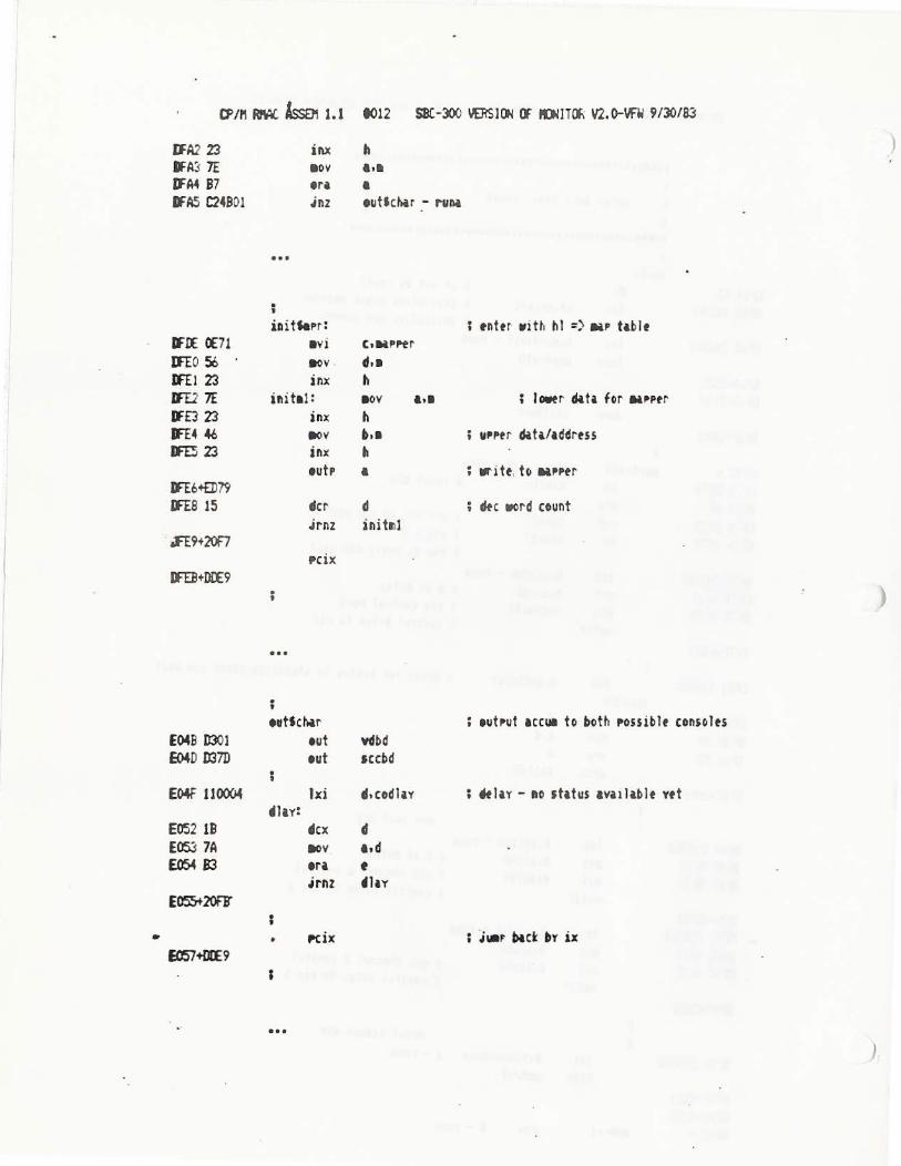
•
CPI,,~ Assa, 1.1 I012 SBC-300 YERSIC»I (I" fOHTCEi V2.~ww 9130183
UA2 23 IFA3 7£ IFA4 87 lfA5 C24B01
IFOC OC71 [FEO 56 lf'El 23 ffE2 7E If £3 23 Jf H 4e lfn 23
IFE6+ED7'9 IFE8 15
.fl9+20F7
IFEB+DOC9
£()48 D30l E-04D 037D
E04F 110004
E052 lB E053 7A E05-4 83
E055+20Fi'
fJ!Sl+mE9
...
inx aov •r• Jnz
illitS.Pr: avi aov inx
init11: inx llOV inx •utP
dcr .irnz
l'CiX
. •
. • tatsc~r
tut tut
lxi 4J 1y:
.Sex eov tri .irnz
rcix
...
h
••• • •utlc~r - Miiii
( tMPl"tr d.1 ti aov &11 ti b.1 ti l
d initril
Wbd sccbd
.s.codln
d •• d
• ~llY
; tntu witt. hi =) 9iP t1blt
; l~r diti for .. PPtr
; VPPtr diti/tddrtss
; ""itt, t~ .. PPtr
; dtc word count
; tutPut accue to both Possiblt consolts
; ttli'r' - ftO Jtitus lVil llblt Ytt
: JU9r blck ~r ix
)
)
)

£060 10
;t-tt++t++tt+flllllllllllllllllt+++ff++tHllllllll
• 9t~rr 9iPPtr - initi1liz1t ion dlt1 •
()O((r-3fff : onbo1rd 'r°" • 400V-7fff : tnbotrd r11i • fKJIXr-ffff : onbo1rd r&1 lo./hi t
• 11111111llllllllllllf++f-iHllllllfll lllll ll lllll f
. • lll'Jinit:
4b 16 EOOE f"FCFFElFfD £076 EB4FEASFE9 E07E EHFIT 9fID £086 El(f £AOFE9
• • • •
11ot Of0()0h.not OtOOlh.not Od002h.not Oc003h aot ObOH ti .r'lot OiOl Sl .. rrot 0901611 .rrot 000l 7h aot 07010t11not 0601Jh,not ()5(Jl2t .. not 0401311 1ot Ol?14t11not 02015h. riot 010l61 .. r1ot 0001711
EOOE 00
• • lll"Jhith:
db 8 E~ E78FI69fIS £097 EXFU.!fEl • •
t1ot 070161 .. not 0601911.not 050l1h.neit 0401bh riot 0301ch. riot 0201 di .. rrot 0101tl .. not OOOlft,
E09F 10
;li+f+tfllllll ll ll l llllllllli+t++ff+f++llllllllll
• 9'1c.rv NPPtr - Iii" a I I ru •
000(;-ffff : tn~otrd ru •
• ; ffffH+H-Hi-fH+f fi-f tff H-H t+f H++H ff 11111111 I I
16 ; nU9btr of .-ords of dlt1 EMO Ef CflI 1 FED EOAB EB4FEA:tt:9 EOBO E78FE69H5 £088 E»£21FE1
aot Of010t.. not OtOl111 .neit Od012t1.not OcOl3t1 aot ObOHt1.not 0.0151'1.not 090161'1.not ()E()l7h aot 070181 .. riot 06019f,,not 05011t .. not 040lt.t1 aot 030lch.not 0201dt .. riot 0101th.not OOOlfh
ex:r> 0001 ECO 00
£OC3 OOC2
;1111111111111111111111111111111111111•1111111111
• cio control bvtt ta.bits • •
;11111111111111111111ltllllllllf+t-+flllllllllllll
;
I ; I
I ; ;
OOt1 • OOOOfOOO 1 b 0000$0000b
: rtstt cio chi, ; 2 ~rtt 5t~utnct
thost c~nttd out art in thit st1tt alrttdr br a.bovt r-t5tt
4b OSh, ~b ; 4,,.r-c: aon invtrtint 4b ()6h, OOOOt-OOlOb ; -dr-c : al l tut txct,t Pbtrr '11 07h. 0000$0000b ; sior-c: aorM I i/o 4b Olh. 00011-0000b ; ~st t.lvt POrt c tn&~ltd

EOCS 2806
EOC7 2Sf'F EOC9 2ITT
Eta 2!J"F
EOCD 2F40
EOCf 0310 EODl 09CO
eoro 0190 £005 ooss 0017 =
~=
'
£007 Ol:l E0!.19 0444 EOte 05£A EOOC1 OllS6 EOif OCOB £0£1 0000 EC£3 OE03 EOE5 CfOO
•
0010 =
. '
db db db db db
db db db
db db
db db
cionb t"u ;
slvtrib
&bovt is tht krt 1ir.i1ua tt~t tht cio tt"uirts the foltowin' inits Port-ti to bindle vtctortd iattrruPts tff tht s-100 bus •
2Sh, OOOOSOllOb 29t.. OOOOSOOO'Jt 2ltt I ()()()()S00(1jto
Zt.h, 1111Sllllb 2ch, 1111S1111b
2dt,, 1111SJ111b 2ttt I 00005()\)()0b 2fb, activtSvctrs
; Pt1St-li
; dPPr--b: nori invtrtint ; ddt-b: all in,.uts ; sior-b: all l's cltchtrs
2d ttiru 2f 4tf i fit Pt rr1 ul: ; ppr·-b : nt fC1r inhrruPt on u.r ; Ptr-b : 1 bit tri&bltd h liSl ir1 2f, ; piar -b : accordint to sntn t"u&tt
03h, ivtciob and OOfft1 ; ivr-li : 1st of vector tlblt 09h, 11 OOSOWOb ; csr-t. : ti Of1 l"Or t b
Olh. 1001S0000b OOtll 1 OOCJS l OOOb f-ciotlt
1011.0lOOb
; •ccr : ltivt b.c tnibltd ; ai er· : ti, vis-t.
;f-fllllllllllf+ti+fft+f-ttif-f+fffllllllllllllllfll
• sec control brtt tlblt t
• ; ... 111111111111111111111111111111111111111111111
Ject1b: if •hz4 dw Oc103ti
• 4404t1
• Ot10St1
• 560bh
• ObOct1
• OOOdt1
• 030tt1
• OOOfh •ht if 8hzb .. Oc103t1
• ()404t,
• 4404h
• 0H05h
• 560bh
• 360ch
• 010dh
• 120ch
• OOOdh
• Ol:lth
• OOOfh "dif
end if Jccnb t4'u S-5Cct&b
'
; •16 clock
; 9600 kud d 4-t,z
; tl clock ; •lb clod
; 9600 kud at 6-hz
; 9600 biud at 6-hz
)
)

•
/
EOD 3tE8 EOC9 37E~ ECO 31ES EOEll 21£8 EOEF ~B EOFl lF!S EOF3 CSE7 EOf"S 19Efc
EOF7 OOif EOF9 0040 EOF'B20 EOFC 000000
; fftf-H-ffHHH+fHH+Ht+ff H+fH-f Hf+++H+ffffffffff+H
I t I s-100 vtctortd inttrru,t~ Cvi& cio f"Ort bl t
I inttrru,t vtctor tablt t
t ;tlll I I I lltffHiHff++tH+Hff+ffHHH-ff-fffff++l I I I I I I I I
' vtatlt:
• • • • dw
• clw
•
vi7 vi6 viS vi4 vi3 vi2 Plitrrfsr viO
;Ht+tl l I l I I I I I I l I I Ill Ill I lfll I I IH-tffHH+ffff+t
t
snttta confitur itior1 infei to bt aovtd UP tei f fOO
t
• t
;HH+H+fHHtfft+ffH+fHfHHH-fHHHtl 11 U II
nsSdah:
• • db
. 9 . 9
4b
11enss trt corifl1nit vtrl1nfei o.o.o
; 90nitor start addrtss ; 16 bit confiturstior1 vtctor· ; •onitor vtrsion I
Sftil't

ECfF 219f"EO [102 CDOCCf
E105 21F7EO ElOO llOOFF ElOB OlOOW
Elel+EDBO
El 10 21E7EO
£113 1110FF
E116 7A
El17+£D47 Ell 9 32fllFF
EllC 011000
E11F+£DBO
El21 ~00 £123 COOCE9
E12b ~C3 El28 3:20600 £12.B 21Cfl8 E12E 226700
El31 D4 £133 0378
E135.nisE •
£137 Pf El3S 3:2~1 E13B Im53 El3lJ 4f ElZ £i5 E140 D3S3 £142 m53
;ffH+t+tHH+l 111111 I I l lHt-ffffH-HHHfHHH+++ffff+ff
& I
; • I
; ff f+f H++f t+i J++H-t-f Htt-f H++f Hff HHHff 1-+ff Hff+fftff
ini t2: lxi fl,.a,.Sru ; MP out ,roe ul 1 ~l'it
lxi fl , snSditi ; •ovt UP srsinfei 1xi 4, srsir1fo lxi ~.s 1 di,..
lxl fl, vtlb It ; cio '"rt b interrupt vectors servict tout1nts ; ( i.t~ s-100 vtctor·td ir1ttr·ruPts >
1xi 4f,ivtc1ob ru leicitiori ,ort ti iv tiblt
9<'V •·d i12 inttrruPts bist ~t Sf ii into i tttister·
sti ui : and into user tta rttisttr m&P
1xi b.16 i ti!lht vtctors ldir ; 90Vt ftttl fCI tP
avi c.O rstSciob t&kts .ask in ,..., c Clll rstSciob clur· lf1Y illttrruPts fro. init
•vi •• 0c3h ; fix .. i vector sti 66h lxi 11.nait ; •i tntrr sh ld 67ti
• ' avi a.slvtn~ ; rtltist slivt reset lint tut cioc
ia2
I I t+f+ff+fllllllllt++++ff+fHf+flllllllllllllllllllll
I I OED: F~ (;();'T R1llEf< Tm AHIJ SE1 A£::C:ffiD I liJL. Y t
I 111111111111111111111111111111111111111111111111111
I llCl"l • sti dlt.t ; initi&lizt controller fl&t to ztro in wet or : chtck fol' YFW-IlI llOV , .. ; s&vt chir in cast it is avi .. ~ ; Jtnd ttst b'l'tt Mt we tor in stet or
) ,
)
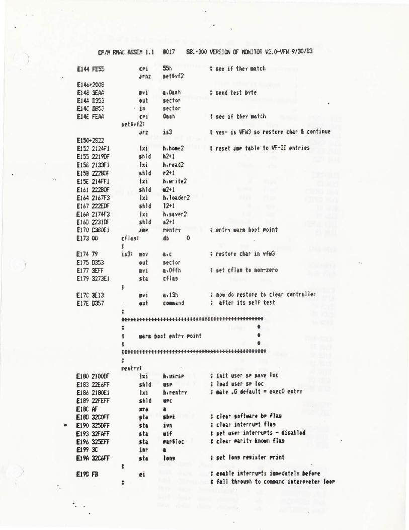
a> /Pl ~ ASS£1I 1. l I017 ~ -X>O '.USICJI CJ" IOUTOO V::.~W 9/'XJ/S3
£14-4 FES5 Cl"i 5St1 ; Ht if ttitr 9itct1 j rnz Htfvf2
£146•2008 £148 :£AA ~i •·Oiih" ; 5tnd ttst ~Ytt [14'< D353 tut He tot El4C IBS3 · in stet or £14€ FEM Cl'i Ouh ; 5tt if tho 91tct1
seUvf2: .itz h3 ; Yts- is ~"3 so rtstort chir l continut
[150+2822 El52 2124f1 lxi h.t1oat2 ; rtstt Jiff' ttblt to YF-lI tntrits ElSS 2219DF shld ll2•1 £158 21n:-1 lxi h.rud2 ElSB 2228Df shld r2•1 £15£ 214f'fl lxi fl,wr itt2 [1 61 222BI:f st1 Id 112•1 E1b4 2l67F3 txi fl, l Oidtr2 £167 222Eif" shld 12+1 EtOA 2174f3 lxi h.nver2 E1 6D 223Hf shld s2+1 El 70 C380El .iaP rtntrv ; tntr~ .ara bo~t Point £173 00 cflu: 4b 0
; E174 79 is3: •ov .. , ; rtstor·t chir in v"-3 £1 75 0353 t ut H e tor Eln FF •vi a.Offh ; set cf Its to AOn-ztro E179 3273£1 sh cf ll9
E17C ~13 •vi • • 13h ; now d~ rtstort to clfir centrolltr £17£ 0357 out co.arid . tfter its self test '
ff++tf+flllllflllllllllf+tf+f-ff++ft-t+f+lllllllll
I . t 9'itl boot tntrr it0int I
• t I
;111111lllllf+lllflllllllllllllllt+t+flllllllllll
,..,.try: E180 2100If lxi ai. usrsl' ; init ustr '" flVt lot £163 22EOFF shld UP ; lo.d user SI' toe £186 21~1 lxi b.rentrY ; 9ll·t .G itftu 1t z: txtcO entry £189 22fEFF shld .,, £19:;; Xl'i • ElSD 32Ctff f ti Al"k ; clttr softlllirt bP fits
• £190 3.2SlWF Sti ivn ; clt&r irittrrul't fllt £19'3 l2Hfl 1t1 •if ; ut ustr inttrrul'ts - •iw.bltd E196~ st1 ~trSloc : cleu· Nrih bo.r1 flu £199 x inr • £19'1 l2r.OfF st1 Ions ; 5tt Ions rttisttr ftt'int
£19D FB ti ; tn&blt iftttrrul'ts i~d1ttlY ~fort . ' C ft! I throutt1 to c.-.nd i11ttrPrtttr lttP

a !ft RMC ASSEJ'I J .1 IOlB SK-Xia ~ 1 Ctl Cf IOtIT Cfi V2. o-i.flJ 9 /'YJ /f:J
;t+t-t+ttlllllllllt+fHt++t+ttfffft-tt+f.t-flllltllll . t t
c01Mnd r~r1ttT l"Oint ~ •
t ; ff+ttffff H H+f Hf Hff+ff HH-f H H+fffHHl+ff+t
El9E 31CO!T txtcO: lxi 5'180Hl'l ElAl WE9 Cill crlf ElM OC2£ llVi ( I I • • E1A6 CDOC~ ull Cot ; wr itt tht chiricttr· ElAS' COC7E9 Cill tcho ; colltct the c..-.nd Elrt; FUE CPi I I .
.irz tXtCO Elfi+2SEE Et£(1 C"5 l'USh b ElBl C008E9 ull SNce £19-4 WUA ull 5CUI ; scu, for the o"trinds to tht c0Mi.r1d E1B7 Cl POP b ElBS 79 •ov l1C
E1B9 219EI1 lxi ••txtcO ElK £5 l'USh h ; l'Ush rtturr. addr-tss
E1BD Db-41 cadact: Sui . 'A' .itc invc1d
El!f+38Sl E1Cl F£1A cri '2'-'A'+l )
.irnc invcad £1C3+»4D ElCS 21IEE1 lxi fl, clldvct ElCS 87 add I
E1C9 SS add 1 [JC.A 6f aov 1 ...
.irnc cadic1 E1CS+3001 ElC!I 24 inr ,, E1CE ~ odic1: ltOV fill
EtCF 23 inx h £100 56 •ov .i.1 E1D1 DS PU Sh d ; l'USh cftsti~tion addrtss E1D2 2A02fF lhld ..-r2 ·; ti 1. de ttt tl"trlllds
ltltd 1Prl E105+£reB £1D7+00Ff
lxiY Sflld ; POint iY to Sllid E1DWD21
• £1DB+W=F £100 C9 nt C .i•P to it
; cadvct:
E1I£ 1IU3b075 • acad. k.cl1 ccad. ti cad E1Eo FFFV6£338 • t<ad1 fcacl • 1cad. hc9d
I ' EtEI 6BE39EI312 • icllCf 1 Jc.d. invc1d. lead E1F6 BIE4l2£20C • 9CMI, i nvc1d, tcad. PC Id
0
; ElFE 12E240CS4D • ilvcad • rc9d. se>d. tcad · £206 12E22££700 • inv~. vcad. ~d • Xtld

E20E 9(l: 79fr7 • YCad, zcad . '
£212 ((:F iavc.d: evi c '?' . . £214 (l)X[F call Cot £217 C39EE1 .;., •xtcO
•
..

)
TH IS PAGE INTENTIONALLY LEFT BLANK
)
• •
\
APPENDIX K SAMPLE I/O SUPPORT CODE
RESETTING VECTORED INTERRUPTS
reset ciob data catcher lsl and Port b interruFt state.
dob cioctl csr·$b r·s tScsr$b
rst$ciob: in aria out
mvi out rnvi out
r·et
equ equ equ equ
ciob c ciob
a.csr$b cioctl
assumes intf!f·ruPts have been disabled by caller Crn entry reg c must have mask for· ciob Port . i .e. to reset Db, c = 1011$llllh
interrupts must be disabled through all code that accesses cio internal registers.
79h 7bh 09h 0010$0000b
SBC-300 CIO Por·t b data Pod SBC-300 CIO contr·o 1 Port cmd/status Port b reset ius,iP in cmd/status Port
first reset l's catcher @ data Port b according to f l a~ l ssed in re9 c
01 s clear·
cmd/status for Po~t J
r·egister select ;t. rst$csr$b clear ius ~ iP cioctl reset ip,ius
ignoring errors fCr r now
K-1

MONITOR INITIALIZATill' CODE
false equ 0 true equ not false
sasi cntrs cntr3
false true false
I/O P(•d addresses S D Svstems SBC-300 cPu
; chiP bases
p$300Par p$300cio
equ ?Oh equ 78h
SBC-300 Parallel Data Port Z8536 Counter/Timer· & Parallel I/O
Z8536 Counter/Timer & Parallel I/O ChiP
p$cioc p$ciob p$cioa p$cioctl
sp$sav equ inUstk equ
SBC-300
cioinit:
mvi stai
lxi lxi lxi ldir
in
mvi mvi lxi outir
p$300cio+O p$300cio+l p$300cio+2 p$300cio+3
Off7eh sp$sav
space for interruPts in page ff
cio ini t
a,iv$Pa9e
h,i$sr d,i$srstab b, i$sr·$nb
p$cioctl
c.P$cioctl b.cionb h, ciotab
set UP z-80 i-r·eg
set uP ilfi2 vectors in Pa9e.Offh just move the table UP there
force cio to state 0
ser1d ini t info
~'-" p .. ._
)
)
im2 ei r·et
iv$pa9e i$sr$tab s r·$ci 1j$d
sr·k io$b sr$cio$a sr-$scc
i$sr:
sr$cioct3 sr·$c ioct2 sr$doct1 sr·$cioi:te
sr$ciob0 sr·$t::iob1 sr$ciob2 sr$ciob3 sr·$ciob4 sr·$ciob5 sr$ciob6 sr$ciob7 actvSints
i Per-r$enb l ;actv$ints
dw d111
dw dw
dw dw dw dw dw dw d111
d111 equ
Offh OffOBh OBh 10h 20h 30h
sr$ct3 sr$ct2 sr$ct1 d$er r
all im2 vectors are in Pase Offh star·t of im2 vect•H· table ir1 Pa9e Offti (lff08 - OffOf rt"served tor cio rntr/timers Off10 - Offlf reserved for cio Port b Off20 - Off2f reserw d for cio Por· t a Off30 - Off3f reser·ved fo r· sec
service routine addresses to move UP cio cntr/timers require 4 addresses service routine address service routine address service routine address service routine address cio Port b requires 3 addresses
sr$vir·7 service r•iutine . · 'r·ess sr·4vir6 service routine ;:..;iJr·ess sr$vir5 ; service routine address sr$vir·4 ; service routine a~t.·ess sr$vir3 ; service routine address sr$vir·2 ; service routine addrt-ss srSvirt ; service routine address sr$vir0 ; service routine address 0000$0000b
anv bit set wi 11 activ;i.t e the VI e.9. the fol lowins would act ivate the Paritv error li ne :
0100$0000b Per·r$enbl
cio Port a requires 8 addresses cio Port a interrupts not currently used
sec requires 8 addresses sec int~rruPts not current lv used
i$sr$nb $- iSsr ; number of bvtes in table
K-3

;*****lHf***************************************** )
* cio control bvte tab I e *
* ;************************************************
cio PC•r·t a data
if sasi
d$Pms$a equ 0000$0000b ; bit Port, no Pattern match d$phs$a equ 0000$0000b ;-ignored if bit Port d$dpp$a equ 1111$1111b sasi is negative logic d$dd$a equ 0011$1 llOb seJ,bsv-out,i/o,req,c/d,ms9,bsv-in,rst d$sio$a equ 0000$0000b normal io bits
2d thru 2f define Ptrn msk d$pp$a equ 0000$0000b ;-ignor·ed when no Pattern match used d$pt$a equ 0000$0000b leave all masked off d$pm$a equ 0000$0000b
dSivia equ sr$cio$a lsb of vector table d$dr$a equ 0000$0000b init Port to all O's
el se ; not sasi
d$p11ts$a equ 0000$0000b ; bit Port, no Patter·n match ) d$Phs$a equ 0000$0000b ;-ignored if bit Port d$dpp$a equ 1010$0100b inver·t strobe, ?, dev$rdv d$ddh ecirJ 0000$1100b Pa7-str·obe. Pa3-on$1 ine, Pa2-dev$rdY d$sio$a equ 0000$0000b normal io bits
2d thru 2f define Ptrn msk d$pp$a equ 0000$0000b ;-ignored when no Pattern match used d$pt$a equ 0000$0000b 1 eave a 11 111asked off d$p111$a equ 0000$0000b
d$iv$a e<rn sr$cio$a lsb of vector table d$dr$a equ 0000$0000b set strobe at data Port
end if ; not sa.s i
cio Por·t b data
d$Pms$b equ 0000$0110b bit Pof't,or-Pev d$phs$b equ 0000$0000b d$dpp$b eq1J 0000$000(lb non inver·tin9 d$dd$b equ 1111$1111b all inPuts d$sio$b equ 1111$1111b all 1,.s catctiers
2d thru 2f define Ptrn msl:: d$pp$b equ l111$1111b set for interrupt on anv d$pt$b eciu 0000$0000b bit enabled bv mask in 2f d$pm$b f:'"IU actvSints whichever· bits are set are enabled
K-4

d$Pms$3 t:'lu d$Pms$1 equ d$Pms$2 equ d$t cm$3 equ d$tcl$3 equ d$tcm$1 equ d$tcl$1 equ d$tc111$2 equ d$tc1$2 equ
dSivtct equ
d$ci sfs equ d$sei equ d$cei equ dStr9r equ
ciotab: db db
db db db db db
db db db
db db
sr$cio$b lsb of vector tabl e
ci(1 cntr/timer data
1000$0(J11b continufJIJS, M external Pins, no des 1000$0000b continuous. r11) externa 1 Pins. Pu 1 se 01Jt Put 1000$0011b continuous. no external Pins, ni:• des 244 b5 = 62500; = 1132 second 244 65 = 62:.00; = 1132 second 0 32 = 32i fo r 1 second
sr$cio$ct note that cio chiP Provides bits d2.dl
cio c/s register commands
0010$0000b 1100$0000b 111 OSOOOOb 0000$0110b
begin ciotab
OOh, 01x1ocoooob Olh, 0001$0000b
Port a fi rst
20t., d$Pms$a 2th, d$Phs$a 22h. d$dpp$a 23h, d$dd$a 24h, d$sio$a
25h, d$pp$a 2bh, dSPUa 27h, d$pm$a
02h, d$iv$a 08h, d$cei
clear interrupt servi ce flags lip, iusl set ie clear ie trigger a cit wi thout 9atin9
micr di sable mie mccr must leave Port c enabl ed
Parallel Port status in Port a
Pattern mc·de specification Pattern ha.ndha.ke sPecification data Path Polarity data direction specia l i(•
Port Ped ar i ty
Pc•rt transl ti Qn Port mask
interrupt vector· command status
K-5

db db db db db
db db db
db db
db db db
db db db db db db
db
db db
nt-:d, POl't b
28h, d$Pms$b 29h, d$Phs$b 2ah, d$dpp$b 2bh, d$dd$b 2ch, d$siCt$b
2dh. d$pp$b 2eh, d$pt$b 2fh, d$pm$b
03h, d$iv$b 09h, d$sei
final lY, c/t's
1ch, d$Pms$1 1dh, d$Pms$2 leh, d$Pms$3
16h, d$tcm$1 17h, d$tc1$1 18h, d$tcm$2 19h. d$tcl $2 lah, d$tcm$3 lbh, d$tcl$3
04h, d$ i v$ct
Qah, d$cei Oah, d$cisfs
if not mfrs
db db db db
else
Obh, d$cei Obh, d$cisfs Och, d$cei Och, d$cisfs
en ti's
if cntr-:3
db db db
el St'
db db
Obh, d$cei Obh, d$cisfs Och, d$sei
; not cntr-3
Obh, d$st-i Och, d$cei
db Och, d$cisfs
init'd to handle vector'd interrupts
Pattern mode sPecif ication Pattern handhake sPecification data Path Polarity data direction special io
Port Polarity Por·t transition Port mask
interrupt vector coml!land status
; use either 1•2 linked. or 3 alone
c/t-1 mode specification re9ister c/t-2 mode specification resister c/t-:3 mode specification re9ister
c/t-1 time constant re9ister msb c/t-1 time constant register lsb c/t-2 timt"! constant register· msb c/t-2 time constant register lsb c/t-:3 time cvr1stant r·egister msb c/t-3 time constant re9ister lsb
cit interr1Jpt vHtor register
c/t-1 coml!land/status r·egister·
disable interrupts on all c/t's
c/t-2 command/stat1Js register·
c/t-:3 command/status r·f!9ister
enable in terrupts on either c/t-2 of c/t-3
enable interrupts on c/t-3
c/t-2 comrri;ind/ status r·eg is ter·
c/t-3 command/status rE<9ister·
enable interruPts on c/ t-2
c/t-2 command/status register c/t-3 corr@and/stat1Js r£<9istt<r·
K-6
)
)
)

cionb
csrSct3 errSmsk
d$er·r:
cU£or-r-0:
t'ndi f not cntr3
endif cntrs
db Olh, 1111$0111b mas tt'r rnr1f i 9ur·a ti •irt contr-o l
db Obh, d$tr9r· c/t-2 command/s tatus re9ister· db Oah, dStr9r c/t-1 command/status r·e9 is t~r·
db Och. d$fr9r· c/t-3 command/status re9istt'r
db OOh, 1000$1100b master interr1JPt cc•nfro 1
equ $-ciotab
routine to service counter/timer err and transfer control to routine of hi9hest Priority counter/timer needin9 service
eq1J Och command/status re9istH., eq•J 0001$0000b ERR bit in csr-'s
. z80 has disabled interruPts , SS Pd sPSsav save stat£-lxi sP,intsstk Push PSW Push h Push b
lxi h, i$sr·$tab - 2 cit isr 1 s are 1st ir1 table mvi c.Picioctl ravi b,csr$ct3 + c/t-3 is hi9hest Priority
inx h 1 word P£or address · i f1)1 h dcr b csr's are sequentia l OIJtP b read tt1e csr inP a ar1i err$msk check ERR bit .i r·z cU£orrO if not set then 90 chHk nt>xt Ut
K-7
c/t-3

mov c,m else set UP address of service routine ) inx h mov b,m lhld sp$sav Put it on user ' s stack (no choice) dcx h mov m.b dcx h mov m.c sh ld sPSsav tJPdate user's stack Ptr
POP b restore state POP h POP PSlll lSPd sPSsav ret and JumP to service routine
111ith interrupts still disabled
end
K-8

APPENDIX M DISCLAIMER
SDSystems, INC. makes no representations or war rant i es with respect to the conten ts her eof and specifically disclaims any implied warranties of merchantabili ty or fitness for any particular purpose. Further, SDSystems, INC. reserves the r ight t o revise th is publi ca ti on and t o make ch anges fr om ti me to time in the content hereof without obligation of SDSystems, INC. to notify any person of such revision or changes.
M-1

)
THIS PAGE INTENTIONALLY LEF'J' BLANK
)
M-2

APPENDIX N LIMITED WARRANTY
All SDSystems printed circuit board assemblies are warranted for a period of one (1) year from date of invoice to be free from defects of material and workmanship.
Should an SDSystems board fail to perform to specifications, obtain a Return Material Authorization (RMA) number from your distributor or from SDSystems. Include this number in all correspondence and with the returned product. Ship the item prepaid to SDSystems and it will, at our option, be repaired or replaced free of charge provided the unit is received during the warranty period.
In order to validate this warranty, the enclosed warranty card must be returned to SDSystems. If no warranty card is on file at the time of product return, dated proof of purchase will be required.
This warranty is invalid if product has been misused or improperly modified. Modifications documented in the SDSystems unit publications may be performed without invalidating the warranty. All other modifications will invalidate the warranty. Warranty is limited to replacement of defective parts and no responsibility i s assumed for damage to other equipment.
SDSYSTEMS MAKES NO WARRANTIES, GUARANTEES, OR REPRESENTATIONS, EXPRESSED OR IMPLIED, WITH RESPECT TO THE PRODUCTS COVERED HEREBY, EXCEPT AS EXPRESSED HEREIN, AND BUYER EXPRESSLY WAIVES ANY OTHER WARRANTIES, GUARANTEES, OR REPRESENTATIONS INCLUDING, BUT NOT LIMITED TO, ANY IMPLIED WARRANTY OF MERCHANTAB ILITY OR FITNESS FOR USE. SDSYSTEMS NEITHER ASSUMES NOR AUTHORIZES ANY OTHER PERSON TO ASSUME FOR SELLER ANY OTHER LIABILITIES IN CONNECTION WITH THE SALE OF THE PRODUCTS. IN NO EVENT WILL SDSYSTEMS BE LIABLE FOR ANY SPECIAL, INCIDENTAL, OR CONSEQUENTIAL DAMAGES.
N-1

)
THIS PAGE I NTENTIONALLY LEF''I' BLANK
)
N-2

APPENDIX 0 PARTS LIST FOR SBC-300
QTY PART/SUB REQD DESCRI PTION NUMBER DESIGNATION
SBC-300 4 MHZ
0 SBC-300 BOARD SCHEMATIC 0300723 l SBC-300 PC BOARD 7000066 l IC, 7406 7010007 U45 l IC, 7438 7010030 us 4 IC, 74LSOO 7010160 U8, Ul6, U24,
U30 5 IC, 74LS02 70101 62 U4, U26, U27,
U51, U68 2 IC, 74LS04 7010164 U32, U37
2 IC, 74LS08 7010166 U34, U75 1 IC, 74LS10 7010168 Ul7 5 IC, 74LS14 7010172 U6, Ul9, U52,
U53, U60 1 IC, 74LS20 7010174 U56 2 IC, 74LS32 7010181 Ul8, U20 7 IC, 74LS7 4 7010195 Ul, U2, U7,
U9, U33, U43, U74
1 IC, 74LS93 7010205 042 1 IC, 74LS112 7010210 Ul5 1 IC, 74LS139 7010220 U57 2 IC, 74LS158 7010229 U64, U72 1 IC, 74LS163 7010233 025 1 IC, 74LS164 7010234 U67 3 IC, 74LS240 7010260 013, U21, 035 2 IC, 74LS244 7010264 055 , U71 5 IC, 74LS24 5 7010265 U61, U70 , U76-
U78 1 IC, 74LS2 80 7010279 U39 1 IC, 74LS368 7010303 036 2 IC, 74LS373 7010304 U29, U40 1 IC, 74LS374 7010305 U38 2 IC, 75188 OR MC1 488 7010332 UlO, Ull 2 I C, 75189 OR MC1489 7010333 U3, Ul2 1 IC, 74LS682 7010518 U69 1 8531 4 MHZ ASCC 70 1 0536 U47 2 74LS125 7010526 Ul4, U44 3 74LS189 7010527 U54, 062, U63 1 IC, MK3880-4 Z80A (4 MHZ) 7010334 U48 1 8536 4 MHZ CIO 7010538 U46 9 IC, PIN 1 REFR 200 NS DRAM 7010532 U23, U31 , u 41 ,
U49, USO , U58, U66, U73, U79
1 DELAY LINE, 5 TAP, 200 NS 7120010 U22 1 PAL 16L8 - DECODE PROG. 72~0006 U28 1 PAL 16L8 SLAVE PROG . 7250007 U59
0-1

QTY REQD
1 1 2 1 1 2 5
3 2 2 3 4 2 1
33
1 1 1 2 1 1 2 1 1 2 2 2 1 1 2 2 1
37 7
5
2 2 1 1 1 1 1 2 0
PART/SUB DESCRIPTION NUMBER DESIGNATION
SBC-300 4 MHZ (Continued)
SIP, 4.7K OHM SIP, lK OHM, 6 PIN 5 RES SIP, 220/330, 10 PIN RES 22 OHM l/4W 5% CC RES 100 OHM l/4W S% CC RES 220 OHM l/4W S% CC RES lK OHM l/4W S% CC
RES 4.7K OHM l/4W S% RES lOK OHM l/4W S% CC RES lSO OHM l/2W S% CC 10 PIN lK RES NTWK CAP lOMF 16V TANT CAP 150PF CAP 300PF 20% SOV .2 CAP .lUF SOV
CAP .OlMF 16V CRAMIC CAP 33PF SOV DIODE, 1N4001 ZENER DIODE 1N4742A TRANS PNP 2N3 906 8 POSITION DIP SWITCH SOCKET 16 PIN 300 ML SOCKET 28 PIN GOLD PL CRYSTAL, 8 MHZ 6-32 X 3/8 PPH SCREW 6-32 NUT LOCKWASHER #6 78H05C +sv s AMP VLT RGLR 2X25 CONN, STRT HDR CONN, 26 PIN STRT HDR HDR ASSY HEATSINK TMH 6103 -B 6S 474 BERG PV JUMPER BERG 1X2 STR .230 PIN TIN
BERG 1X3 STR .23 0 PIN TIN
BERG 2XS HDR ASSY BERG STIK ST 2X9 TIN PL SIP, lK OHM, 8 PIN RES SOCKET, 40 PIN GOLD PL BERG 2X4 BERG 2Xl5 PCB EJECTORS SBC-300 TEST PROCEDURE ASSY
0-2
7010434 7010556 7010530 7020033 7020049 70200 57 7020073
7020089 7020097 7020171 7020223 7030009 7030042 7030044 703004S
70300 46 7030047 7040002 7040004 7040006 7050002 7060003 7060022 70 80007 7130006 7130007 7130009 7160012 7090197 7090196 0100736 7130004 7170004 7170018
7170021
7170105 0100736 7170097 7010413 7060025 7170020 7170106 7130228 0 90 0723
RN4 RN3 RNl , RN2 R8 Rl4 R4, R9 RS-R7, Rl2, Rl6 R3, Rl3 I RlS RlO, Rll Rl, R2 RN5-RN7 Cl , C2 , C6 , C 9 ClS, C39 Cl4 C3-C5, C7, CS, ClO, Cll, C16-C38, C40-C42 Cl3 Cl2 CR3 CRl, CR2 Ql SWl JS, J6 XU6S Yl
VRl J4 J2, J3 JS, J6
W4, W5, W9, Wll, Wl2, WlS-1, W21 Wl, W3, W6, WlO, Wl9 Wl3, Wl7 JS, J6 Wl4 RN8 XU48 Wl6 WlS
)
)

QTY REQD
0 1 1 1 4
5
2 2 1 5
1 2 7
1 1 1 2 1 1 3 2 5
1 1 2 1 2 2 1 1 2 3 1 1 9
1 1 1 1
DESCRIPT ION
SBC-3 00 6 MHZ
SBC-300 BOARD SCHEMATIC SBC-300 PC BOARD IC, 7406 IC, 7438 IC, 74LSOO
IC, 74LS02
IC , 74LS04 IC , 7 4LSO 8 IC, 74LS10 IC, 74LS14
re , 74LS20 IC, 74LS32 IC, 74LS74
IC, 74LS92 re, 74LS112 IC, 74LS139 IC, 74LS158 IC, 74LS163 IC, 74LS164 IC, 74LS240 IC, 74LS244 IC, 74LS245
IC, 74LS2 80 IC, 74LS368 IC , 74LS373 IC, 74LS374 IC, 75188 OR MC1488 IC, 75189 OR MC1489 IC, 74LS682 8S31A 6 MHZ ASCC 74LS125 74LS189 Z8400B- 6 MHZ CPU (Z80B) 8S36A 6 MHZ CIO lSO NS DRAM
lSO NS DELAY LI NE PAL 16L8 - DECODE PROG. PAL 16L8 SLAVE PROG . SIP, 4.7K OHM
0-3
PART/SUB NUMBER DESIGNATION
03007 23 700 0066 7010007 7010030 7010160
7010162
7010164 7010166 701016 8 7010172
7010174 7010181 701019S
7010204 7010210 7010220 70102 29 7010233 7010234 7010260 7010264 701026S
7010279 7010303 7010304 701030S 7010332 7010333 701051 8 7010520 7010526 7010527 7010S28 7010S29 7010S3 4
701053S 72S0006 7250007 701043 4
U45 us U8, Ul6, U24, U30 u 4, u 26 , u 27 , 051, U6 8 U32, U37 U34, U75 Ul7 U6, Ul9, U52 , U53, U60 U56 Ul8, U20 Ul, U2, U7, U9, U33, U43, U74 U42 Ul5 U57 U64, U72 U25 U67 Ul3, U21, U35 USS, U71 U61, U70, U76-U78 U39 U36 U29, U40 U3 8 UlO, Ull U3, Ul2 U69 U47 Ul4, U44 US4, U62 , U63 04 8 U46 U23 , U31 , 041, 049, USO, U58, 066, U73, U79 U22 U28 U59 RN4

QTY REQD
1 2 1 1 2 5
3 2 2 3 4 2 1
33
1 1 1 2 1 1 2 1 1 2 2 2 1 1
37 1 1 2 2 1 7
5
1 2 1 1 2 0
PART/SUB DES CR I PT ION NUMBER DESIGNATION
SBC-3 00 6 MHZ (Continued)
SIP, lK OHM 6 PIN 5 RES SIP, 22 0/330, 10 PIN RES 22 OHM l/4W 5% CC RES 100 OHM 1/4W 5% CC RES 220 OHM l/4W 5% CC RES lK OHM l /4W 5% CC
RES 4.7K OHM 1/4W 5% RES lOK OHM l/4W 5% CC RES 150 OHM 1/2W 5% CC 10 PIN lK RES N'IWK CAP lOMF 16V TANT CAP 150PF CAP 300PF 20% 50V . 2 CAP .lUF 50V
CAP .OlMF 16V CRAMIC CAP 33PF 50V DIODE, 1N4001 ZENER DIODE 1N4742A TRANS PNP 2N3 90 6 8 POSITION DI P SWITCH SOCKET 16 PIN 300 ML SOCKET 28 PIN GOLD PL XTAL, 12 MHZ 6-32 X 3/8 PPH SCREW 6-32 NUT LOCKWASHER #6 78H05C +5V SA VLT RGLR HEATSINK TMH 6103-B 65474 BERG PV JUMPER SIP, lK OHM 8 PIN RES 2X25 CONN, STRT HDR CONN, 26 PIN STRT HDR HOR ASSY SOCKET, 40 PIN GOLD PL BERG 1X2 STR .230 PIN TIN
BERG 1X3 STR .230 PIN TIN
BERG STIK ST 2X9 TI N PL BERG 2X5 BERG 2X4 BERG 2Xl5 PCB EJECTORS SBC-300 TEST PROCEDURE ASSY
0-4
7010556 7 010 53 0 7020033 7020049 7020057 7020073
7020089 70 20097 7020171 7020223 7030009 7030042 7030044 7030045
7030046 7030047 70 40002 7040004 7040006 7050002 7060003 7060022 70 80019 7130006 7130007 7130009 7160012 7130004 7170004 7010413 70 90197 7090196 010 0736 7060025 7170018
7170021
7170097 7170105 7170020 7170106 7130228 0900723
RN3 RNl, RN2 R8 Rl4 R4, R9 R5-R7, Rl2, Rl6 R3, Rl3, Rl5 RlO, Rll Rl, R2 RN5-RN7 Cl, C2, C6, C9 ClS, C39 Cl4 C3-C5, C7, ca, ClO, Cll, Cl6-C38 , C40-C42 Cl3 Cl2 CR3 CRl, CR2 Ql SWl JS, J6 XU65 Yl
VRl
RN8 J4 J2, J3 JS, J6 XU48 W4, WS, W9, Wll, Wl2, WlS-1, W21 Wl, W3, W6, WlO, Wl9 Wl4 Wl3, Wl7 Wl6 Wl5
)
)
)

REPLACEMENT CHIPS (Or Equivalent)
RAMs RO Ms Delay Lines 150 ns 200 ns 150 ns 200 ns
(P) MITSUBISHI M5K4164S-15 -20 2716 DDU-4-5150 DDU-4-5200 FUJITSU MB8265-15 -20 2732 MOST EK MK4164-15 -20 2764 MOTOROLA MCM6664-15 -20
0-5

)
THIS PAGE INTENTIONALLY LEFT BLANK
)
0-6

APPENDIX P PARTS PLACEMENT DIAGRAM
P-1

)
THIS PAGE INTENTIONALLY LEFT BLANK
)
)
P- 2

JUMPER NUMBERING NOTATION j
Throughout the manual, jumper locations are referenced by 'W' number and pin number. The following number convention is adhered to for all jumpers on the board .
For horizontal jumpers that are single row (lx3, lx4, etc.), pins are numbered consecutively from left to right.
For vertical jumpers that are single row (lx3, lx4, etc.), pins are numbered consecutively from top to bottom.
For horizontal jumpers that are dual row (2x3, 2x4, etc.), pins are numbered consecutively from bottom left to right , continuing on the top right to left.
EXAMPLE: W7 ( 1) , W7 { 6) , and W7 ( 8) are to be jumper ed.
16 15 14 13 12 11 10 9
I 0 0 0 0 0 I 0 0 I 0 W7 I I I
I 0 0 0 0 0 I 0 0 I 0
1 2 3 4 5 6 7 8
For vert ical jumpers that are dual row (2 x3, 2x4 , etc. ), pins are numbered consecutively from left top to bottom, continuing on the right bottom to top.
For horizontal jumpers that are triple row (3x3, 3x4, etc.), pins ar e numbered consecutively from left bottom to top, continuing from bottom to top for each column from left to right .
EXAMPLE: W3(4-5) is to be jumpered.
6 9
3 0 0 0 0 12
W3 2 0 I 0 0 0 11 I
1 0 I 0 0 0 10
L-3 (

)
THIS PAGE INTENTIONALLY LEFT BLANK
)
L-4

)
)
APPENDIX L JUMPER CONNECTION QUICK REFEREN,CE TABLES
STANDARD JUMPER CONNECTIONS
(Example: "1-2" means jumper pins 1 and 2 toge ther)
Master Slave
Wl OUT OUT W3 1-2 1-2 W4 OUT IN W5 IN OUT W6 1-2 1-2 W9 IN OUT WlO 1-2 1-2 Wll IN OUT Wl2 IN IN Wl3 POSI'l'ION 1 POSITION 1 Wl4 POSITION 5 POSITION 5 Wl 5-Wl 8 ALL IN CUT ALL Wl9 OUT 2-3 W21 IN OtJT
JUMPER DEFINITIONS
NOTE: "(etch)" means an etch jumper. If a change is desired, the user must cut the etch and insert a jumper.
Jumper
Wl
W2 (etch)
W3
W4
W5
w6
W7 (etch)
W8 (etch)
W9
WlO
Purpose
SCC Por t A Baud CLK select RAM size select
Wait state generator
Master/Slave select
Bus refresh signal pin 66 (for SD EXPANDORl\M II & lII) pSTVAL* source select
Bus clock select
CPU clock select
WAIT* for EXPANDORAM III compa t. PROM select
L-1
Setup
1-2 External (modem) clock 2-3 2 mHz syst em clock 1 - 2 64K DRAM 2-3 Future expansion 1-2 Memory cycle 2-3 OP CODE fetch only (Ml) IN Slave OUT Master IN Outputs RFSH* s ignal OlJ'J' No connect ion to bus
1-2 IEEE-696 tirni~g
2-3 .01 clock 1-2 Futur e expansion 2-3 4/ 6 mHz board 1-2 4/6 mHz board 2- 3 Future expan sion IN EXPANDORAM III OUT All others 1-2 64K and smaller 2-3 128K

JUMPER DEFINITIONS- -Continued
Jumper Purpose
Wll MWRT select
Wl2 BRFSH jumper
Wl3 TMA wait generator Jumper
Wl4 Interrupt select 1
Wl5-Wl8 Bus pull up resistors for master; remove for slave
Wl9 SLVCLR select
W21 RDY/XRDY enable
2 3 4 5 6 7 8 9
L-2
Setup
IN SBC-300 creates MWRT OUT MWRT created elsewhere IN Refresh during TMA
control OUT Ignore refresh 1-5 Wait states inserted
# PWR FAIL to NMI Attention to VI6 Attention to VI7 Parity error to VI l Attention to VI2 ERROR* to VIO Attention to VI4 Attention to VIS Attention to VI3
1-2 Manual reset for srave 2-3 SLVCLR from bus IN RDY/XRDY gated to WAIT* OUT RDY/XRDY not used )

£-d
iD D :~'. D ttD D. aD!~~~ cf++~i :rr rr~ ~ o ~~Til.,.____I ___.
-~ :Grrrr¥w ~o ~wo~oo=~g~ -CJ- I I IWll n 11 c ;;i::::::J ~c:::'.J =:;l U2
~o~o~n 0° ;Na W9CJ ~ ~I ~ 11 ~ -I Irv
o~n~o - n U/6 Uli
L - c I I(/) +~ Wj )> I I I I I I I I ~ ;:;j n ~ n ~ u20v r=::J C/J C/J -< LJ LJ U63
:38 C30 I I r"I c::::JRN3 C25
~ uu~ t=c·~o~'u-2'9 =o~4 ~ ~ USS . D ~ CD
" - -- (X)
r--i~ ~ n c L--J CSl r-1 iSi rvc::::J -
~ CS) w
~2 ~ ~ D ~ ~~ D D G ~ , o o-·G
3
'o1
[ro22
o I o~ -o [F U79 U73 U66 USS U50 U49 U4 l U3 l U23 U 15

)
THIS PAGE INTENTIONALLY LEFT BLANK
)
)
P-4

APPENDIX Q SCHEMATIC
Q-1

)
THIS PAGE INTENTIONALLY LEFT BLANK
)
)
Q-2

)
)
N ..,
0 .... q: ,, .... c:: ...
" t ~ I! !;: ~~ ll'I Ol =-" t-! ~~ )~
~,.
; ~ s ~ t~~ g i ~ ~ ~ ~ ..,, "!?: ~ It ,., ,... t U'I ~) 12:
-·l ~11~ 1-=..+·+-- - -,,.,,,.,;H--t-+-ir-t+-- - -+· -,., !ft,\Ot ... IW~
'"' .. ,
~
8L ~ ~
= E lf\~N
... ~----=t~ I ~-
µ L' .. ..
;L:::, >1l31<>
- T!I~ .. ~ )
"---- - - -=iul 13
N• i> ,,,., '~"~
H3!Slffl
.!l.lllU2
··-- - -
•u co
10
-
0 0--- -----+-+--- _. t-1-1-+-l-+-+-4
Q-3
tlJ.J .f . . -o
,_ ---~-
z
~i...,...,_ >- -=o 0..--+ . ,_.,_. _ ~ ..
t-t-t-+-+-+~ • &-<>-<--+-+-+-> ~=--.> ...
.:f
a i
... ----,,i~:;o: Jeff( ~ ~"" ._._ .......................... -='--!
~ ..... ---.,;;;;
........ -
~: ~'!: ...... .._ __ ~ "---~
..... .. " !
.. " ---- "'
> ~ i ! ~ If I~ .. • '--...---' ... "' ;;\ ~
(/)
UJ I-0 z

IO I ~
JI
I NT*~USI ~-s -: .. oi.. IH'T t.SOZ. ·• •
10 s ~
~R -~~ . .• ~ ,~
d V"""'1a ~ROY!~ -------------------,
ROY :n ~· ---- - ------ - ----l-2: :.--_,
.:t2Y
•SV
"'R'WMT .sv
MREQ
'inRO I IS
R1l i 11
WR ·'" BU.\AI( • IZ.
lED 5 u za
BDOT • PALIC.LS 1•
= 1 20 PIN :i U Sl6 \
MA\"f£ R 8 ~t.Sl.O
= 9 ) " ,
PAIC. II
BRF°S.M 13
NIAl(H IS
+sv IO •<O •O
~ ~
-A 5
A~
A3 A"!.
A l
1'1)
NOTES:
·,.
P..N~-z
"'-A
WAIT
··· "'·----~----- MREO. JNti:-.
iO'
"'
--~~
PRbMiNS -l!1%rr ~
' -~ ~ ,,, CID-£N
U 5T " !>CC£N 3 L<; l~9 ' 1 s;;;<'P"
"- " MAPPER 13 \\ if=
-----r<t 10 .V/ f.. .___,,,
I I
: 6\'liC
I I I I I I I I
I I
MMTfR
I MA.~'TE.R I - --
: ~JI W l 9 ~ I SLVC,a.~• s~ -~ I 3 _l! , I -I -
...__
.. -. OUCftWTI04I QlTI I Al'P,
Mf.m_R
Y1iii . ..,
·j I
l;;-;-----7-------~~:.::~~ :::1 HNP
,- "l'"llT ! ~1J
1
i •I :[: 1~fE n iZ: , .~e ':lnRa lJt
rv~ o I
.~ I r.&1swo.
\. _ _ J. ~ coso .. .l_~Vl,fQ
p $'1'N~
P oa1:-,
Wl).1T
r 1 ·~r. I rt ---;=l__J : ~
,Ll:jii- J' ----- ---·-----.. ~ _----1!.Q. "- --·~"'3W i. -
- - M[M~
J I
l:"'t'' l~!~~ ws ---------~, ;?Cf--~ ••I""" 1·· •
i ..
I,., .. .,,
IS'.l'iJ CL~ s ~..,_..----1 1a M:.-.mi:
. 3 i. gsi voe. •
1~t !1slRt~n·
...... AHLIC.\T101t
t l!I RS.~£.T
.... .U,.llOVIEO
s q,~X~J.~!-1S SBC -3CC>
STAIU:> I U>NTROL
llUICOOl IOl• T I"_., .. 110.
>----------< D 0 3CICI 7 z 3
&CAl.l DO ltOT ICAU MAWIH I tMUT 2 O'
E

)
}
nn 11 a- u "' ~ r ~ lioi ., jlPi 1:1' ,_._
~ ~~ $ ; ~ f) c-Fr' f!Ff'!FF - "I= 'lll!?F~ -
D I I I II ' ;:~ 1'V
tY IY
.... llY ... 5V
..LVOW -
. I
~1 "' .. ~ ...
i ! ---~r-T""'l3 n
i
.----~~~-~~~~!~c-1.......,~·~~i-------~~,; ..., C~~ ~ ~N~-~=~~ 2
• · .T , .. •.i:.A
v I I I•
I .&el -.. ~-
"'ll'W"' ~~~=ttt~===4~~~~==4~:::;~~===--:::_-:: ___ · ==---_-_- . --_ ........ ___. ..... ~ --~ ~.. 2
- - -- -- . -- - j .. ~l.r'JC.;.----~.21Si!f= !W +-- -ZIYd
t ..... la l=
.. .. !;
• 3 ... ,.., .. - J i ~ ----,
Q-5
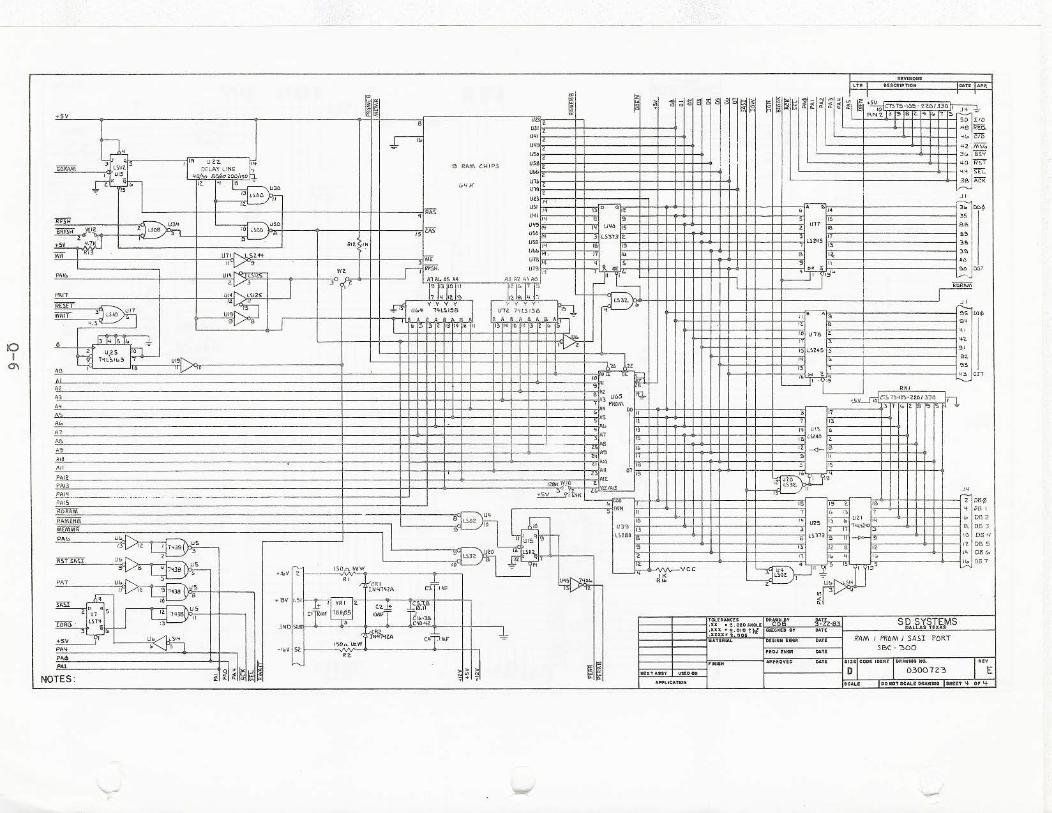
------------------- ------
!O I
°'
OlSatll'TIOlt OAU lot.
I! ~ ®~I ~::i : ~ ~ 0S ~1r1 11 ·~ .v~~li'"l'l i ~: ..... . ' 1 1 I - 1:.._ WI l Ll2. ,M'>(>
USO I 3U I BSY l I I I I_
use z ; '1 ' i+a 1 ""
""" I I -'" S£l. lJ1) ~ : ~ 38, , ACl< U1'3 2. i ,-....,.
+.s_v
~
9 RAM Ci-UP,S
""' Ull ,~ I
~: M \ !I l:) 0 1•c. I T . - .
1 ~ 8 I' I I T ! · · . ""' " " u"" 115 I I I I I I : , USti <oj J U~"l.312. USS Jl./ 1&1 Ul.I. i"I , i
we ura .. '~ 1 rr-"'"" 19 •1,_ - i> I I I I I I I I I I I I I I , ,
Wl I I • u :'t • P • '(i.. II. OI .. • • •
..r' A1 A!. t.S Jilt A3 .l'Z A\ AO __J
Y1 . I" I" 1101 11 I' I" I I' 1-\\11 I u1'4 Ls12s I 1 ~ f1ab l,. 1~ "h RE>fT - I ~~" ~ y y '( y .I I " y y y. 'iYATf'" 3j !.Sil> <.l!7 U19 t ~" I uc... 111-LSl'G U'1t 7 "1 LS l .lt\ 'fVA( __A -:.. g S lo n b .... ., ~ A ft ;; ll A
.,, ~ I I I 1 •p 1 ~1' l"l'"~' I" 1'~1"1'•111 1; 11
I I , lw RFfM - - - J,0
10 ;,)00 e. IS lA5
"
U3't
R•t SHI .,-
'"
J '
tm"\! I I I I I I I I I I I • Ji: -s
1 I I I ' I I I I I I I I I I I I i!Tm• -l--~ 6
M ,, I I I I I I I I l I I I I II I I I I ),~· 1,,
,, 710~¢
va 1
~r52 a oG 3 \O oa ,, ii O& S
'" I 06 ~ \~ 1)8 7 ,-
t CALI I 00 llOT SCALI OfU.WM liffitt -'4 OP 4
._,
Copyright © 2022 FDOKUMEN