Resonance Raman spectroscopy of graphite and graphene
10
Resonance Raman spectroscopy of graphite and graphene V. Zo ´ lyomi 1,2 , J. Koltai 3 , and J. Ku ¨ rti * ,3 1 Physics Department, Lancaster University, LA1 4YB Lancaster, UK 2 Research Institute for Solid State Physics and Optics of the Hungarian Academy of Sciences, P.O. Box 49, 1525 Budapest, Hungary 3 Department of Biological Physics, Eo ¨tvo ¨s University, Pa ´zma ´ny Pe ´ter se ´ta ´ny 1/A, 1117 Budapest, Hungary Received 28 June 2011, revised 4 August 2011, accepted 8 August 2011 Published online 26 September 2011 Keywords double resonance, graphene, graphite, Raman * Corresponding author: e-mail [email protected], Phone: (þ36 1) 372-2795, Fax: (þ36 1) 372-2757 We review the key aspects of Raman spectroscopy of graphite and graphene, focusing on the double resonant Raman modes such as the D, D (also known as G’ or 2D), and D’ bands. We discuss the practical significance of Raman spectroscopy for the study of single- and multi-layer graphene. ß 2011 WILEY-VCH Verlag GmbH & Co. KGaA, Weinheim 1 Introduction Raman spectroscopy is one of the most powerful tools for the study of carbonaceous materials, especially sp 2 or close to sp 2 carbon materials such as graphite, carbon nanotubes, and graphene. It is a quick, non-destructive vibrational spectroscopy method which does not require significant effort for sample preparation. Furthermore, through resonance effects the Raman spectrum also gives information about the electronic structure of the material. One must keep in mind therefore that the Raman spectrum reflects more than simply the phonon density of states of the material. The Raman spectrum of graphite and graphene is dominated by a single mode at around 1580 cm 1 called the G band [1, 2]. This is due to the symmetry of the hexagonal lattice which allows only one first order Raman band for graphene. For only two atoms in the unit cell, there are 3 zone centered normal modes. Two of them are degenerate with E 2g symmetry. These in plane vibrations are Raman active and are responsible for the G band. The remaining mode with B 2g symmetry is not Raman active. In the case of graphite with AB stacking the situation is very similar. For 4 atoms in the unit cell there are 9 zone centered normal modes: A 2u þ 2B 2g þ E 1u þ 2E 2g , as symmetry analysis shows [3]. Only the two E 2g modes are Raman active. One of them is the same in plane mode as for graphene (G band). The other E 2g mode is a very low frequency interplanar mode at 42 cm 1 which we can forget for the purpose of this review. Naively one would not expect the higher order bands to be able to provide significant information about the material due to the reduced intensity of higher order processes. The reality is that, in large part due to resonance effects, the Raman spectrum is quite rich and contains a few higher order Raman bands that have comparable intensity to that of the G band, and can even exceed it in strength in certain cases. In this review, we show what can be learnt from the thorough analysis of the Raman spectrum of sp 2 carbon nanostructures. The paper is organized as follows. First, we summarize the most important features of the Raman spectrum of graphite and graphene. Then, we overview the theoretical background of the higher order processes and look at many of them in detail with emphasis on double resonance. Finally, we review some practical applications for the use of Raman spectroscopy as a tool of sample characterization. 2 Raman spectrum of graphite and graphene Figure 1 shows a typical Raman spectrum of graphite (top) and graphene (bottom). The spectra are dominated by two bands, one at 1580 cm 1 and another at 2700 cm 1 . The former is the aforementioned G band, the only allowed first order Raman band. The second band is the result of a higher order process involving two phonons. This band is called the D band [4], although it was originally named G’ (see, e.g., [2]) and in recent years it has been referred to as 2D [5]. The reason for the confusion in the naming convention lies in the origins of this band which was unclear for many years. This Raman band comes from a double resonance process, as we will discuss in detail in Phys. Status Solidi B 248, No. 11, 2435–2444 (2011) / DOI 10.1002/pssb.201100295 Feature Article pss basic solid state physics b status solidi www.pss-b.com physica ß 2011 WILEY-VCH Verlag GmbH & Co. KGaA, Weinheim
Transcript of Resonance Raman spectroscopy of graphite and graphene

Phys. Status Solidi B 248, No. 11, 2435–2444 (2011) / DOI 10.1002/pssb.201100295 p s sb
statu
s
soli
di
www.pss-b.com
hysi
ca
eature Article
asic solid state physics
Resonance Raman spectroscopyof graphite and graphene
F
b
p
V. Zolyomi1,2, J. Koltai3, and J. Kurti*,3
1 Physics Department, Lancaster University, LA1 4YB Lancaster, UK2 Research Institute for Solid State Physics and Optics of the Hungarian Academy of Sciences, P.O. Box 49, 1525 Budapest, Hungary3 Department of Biological Physics, Eotvos University, Pazmany Peter setany 1/A, 1117 Budapest, Hungary
Received 28 June 2011, revised 4 August 2011, accepted 8 August 2011
Published online 26 September 2011
Keywords double resonance, graphene, graphite, Raman
* Corresponding author: e-mail [email protected], Phone: (þ36 1) 372-2795, Fax: (þ36 1) 372-2757
We review the key aspects of Raman spectroscopy of graphite
and graphene, focusing on the double resonant Raman modes
such as the D, D� (also known as G’ or 2D), and D’ bands. We
discuss the practical significance of Raman spectroscopy for the
study of single- and multi-layer graphene.
� 2011 WILEY-VCH Verlag GmbH & Co. KGaA, Weinheim
1 Introduction Raman spectroscopy is one of the mostpowerful tools for the study of carbonaceous materials,especially sp2 or close to sp2 carbon materials such as graphite,carbon nanotubes, and graphene. It is a quick, non-destructivevibrational spectroscopy method which does not requiresignificant effort for sample preparation. Furthermore, throughresonance effects the Raman spectrum also gives informationabout the electronic structure of the material. One must keep inmind therefore that the Raman spectrum reflects more thansimply the phonon density of states of the material.
The Raman spectrum of graphite and graphene isdominated by a single mode at around 1580 cm�1 calledthe G band [1, 2]. This is due to the symmetry of thehexagonal lattice which allows only one first order Ramanband for graphene. For only two atoms in the unit cell, thereare 3 zone centered normal modes. Two of them aredegenerate with E2g symmetry. These in plane vibrationsare Raman active and are responsible for the G band. Theremaining mode with B2g symmetry is not Raman active. Inthe case of graphite with AB stacking the situation is verysimilar. For 4 atoms in the unit cell there are 9 zone centerednormal modes: A2uþ 2B2g þE1uþ 2E2g, as symmetryanalysis shows [3]. Only the two E2g modes are Ramanactive. One of them is the same in plane mode as for graphene(G band). The other E2g mode is a very low frequencyinterplanar mode at 42 cm�1 which we can forget for thepurpose of this review.
Naively one would not expect the higher order bands tobe able to provide significant information about the material
due to the reduced intensity of higher order processes. Thereality is that, in large part due to resonance effects, theRaman spectrum is quite rich and contains a few higher orderRaman bands that have comparable intensity to that of theG band, and can even exceed it in strength in certain cases.
In this review, we show what can be learnt from thethorough analysis of the Raman spectrum of sp2 carbonnanostructures. The paper is organized as follows. First, wesummarize the most important features of the Ramanspectrum of graphite and graphene. Then, we overview thetheoretical background of the higher order processes andlook at many of them in detail with emphasis on doubleresonance. Finally, we review some practical applicationsfor the use of Raman spectroscopy as a tool of samplecharacterization.
2 Raman spectrum of graphite and grapheneFigure 1 shows a typical Raman spectrum of graphite (top)and graphene (bottom). The spectra are dominated bytwo bands, one at �1580 cm�1 and another at�2700 cm�1. The former is the aforementioned G band,the only allowed first order Raman band. The second band isthe result of a higher order process involving two phonons.This band is called the D� band [4], although it was originallynamed G’ (see, e.g., [2]) and in recent years it has beenreferred to as 2D [5]. The reason for the confusion in thenaming convention lies in the origins of this band which wasunclear for many years. This Raman band comes from adouble resonance process, as we will discuss in detail in
� 2011 WILEY-VCH Verlag GmbH & Co. KGaA, Weinheim

2436 V. Zolyomi et al.: Resonance Raman spectroscopy of graphite and graphenep
hys
ica ssp st
atu
s
solid
i b
Section 3. For the remainder of the paper we will refer to it as2D band to avoid confusion with recent publications. Wemention, however, that denoting a Raman band of a two-dimensional material like graphene with 2D is ratherunfortunate.
Figure 2 shows the (calculated) phonon dispersion ofgraphene in the high frequency range. It is easy to identify theparts of the dispersion which are responsible for the G and 2Dbands. The former originates from the E2g in-plane phonon atthe G point where the longitudinal optical (LO) andtransverse optical (TO) branches touch each other. The 2D
Viktor Zolyomi is a Senior ResearchAssociate at the Physics Department ofLancaster University. He received hisPhD at the Eotvos University in Buda-pest. He specializes in theoreticalphysics in the fields of molecular andcondensed matter physics. His primaryresearch interests are carbon basednanomaterials (such as carbon nano-
tubes, fullerenes, and graphene) and related structures. Hehas been awarded the Academy Youth Award of theHungarian Academy of Sciences (HAS) and the BolyaiResearch Fellowship, both in 2007. In 2008 he won aMarie Curie Intra-European Fellowship to LancasterUniversity which was followed by a Marie Curie Euro-pean Reintegration Grant in 2011.
Janos Koltai is an assistant professorat the Department of BiologicalPhysics, Eotvos University, Budapest.He received his PhD in physics at theEotvos University. The topic of histhesis involved transport calculationsof superconductor–normal metal andsuperconductor–ferromagnetic metalhybrid systems of the mesoscopic size.
His field of interest is now carbon-based nanomaterials (likecarbon nanotubes, graphene and fullerene). He is an expertof transport calculations and density functional theory.
Jeno Kurti is a professor and head ofthe Department of Biological Physicsat the Eotvos Lorand University, Buda-pest. He received his PhD at the EotvosUniversity in the interdisciplinary fieldof molecular physics and solid statephysics of novel materials. His area ofexpertise is vibrational spectroscopyand quantum chemistry of conjugated
polymers, fullerenes, carbon nanotubes and graphene. Hehas been the director of the Institute of Physics of theEotvos University for three years. He is the secretarygeneral of the Eotvos Lorand Physical Society inHungary.
Figure 1 Measured Raman spectrum of graphite (top) andgraphene (bottom) with a laser excitation of 514 nm. Figure repro-duced from Fig. 2a in Ref. [5] with permission from the AmericanPhysical Society.
Figure 2 Calculated phonon dispersion of graphene at the level ofthe local density approximation of density functional theory (opendots). Experimental inelastic X-ray scattering data (measured ongraphite) are shown for comparison (filled dots). The lines are aspline extrapolation to the points. The inset shows the reciprocalspace of graphene, highlighting the high symmetry points of theBrillouin zone. Figure reproduced from Ref. [8] with permissionfrom the American Physical Society.
� 2011 WILEY-VCH Verlag GmbH & Co. KGaA, Weinheim
band is necessarily either a combination band or an overtoneband, because no single phonon has a frequency higher than�1650 cm�1. As we will see later the 2D band is a result of adouble resonance enhanced two-phonon process and onlyzone-boundary phonons have proper frequencies for this. Infact, the 2D band originates from two TO phonons around theK point.
Beyond these two very intense Raman bands, severalweaker ones can also be observed. Two of them can be seenin Fig. 1 already (at �2450 and �3250 cm�1), but a moredetailed measurement reveals that there are many morebands. Figure 3 shows the measurements on the basal planeof highly oriented pyrolitic graphite (HOPG), and the basaland edge planes of pyrolitic graphite (PG). While the spectraseem relatively featureless from afar, a 20� magnificationreveals the many additional features of the spectrum. Withthe exception of the overtone of the G band, all of these bands
www.pss-b.com
Phys. Status Solidi B 248, No. 11 (2011) 2437
Feature
Article
Figure 3 Measured Raman spectrum of graphite taken under vary-ing circumstances with a laser excitation of 488 nm. (a) Spectrumobtained for the basal plane of HOPG, (b) and (c) spectra for thebasal and edge planes of PG, respectively. Figure reproduced fromRef. [9] with permission from the American Physical Society.
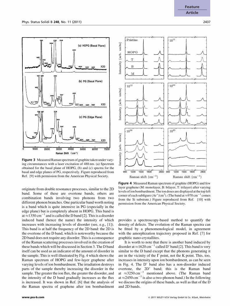
Figure 4 Measured Raman spectrum of graphite (HOPG) and fewlayer graphene (M: monolayer, B: bilayer, T: trilayer) after varyinglevels of ion bombardment. The ion doses are displayed at the top leftcorner of each subfigure (Arþ/cm2). (The band at�970 cm�1 comesfrom the Si substrate.) Figure reproduced from Ref. [10] withpermission from the American Physical Society.
originate from double resonance processes, similar to the 2Dband. Some of these are overtone bands, others arecombination bands involving two phonons from twodifferent phonon branches. One particular band worth notingis a band which is quite intensive in PG (especially in theedge plane) but is completely absent in HOPG. This band isat�1350 cm�1 and is called the D band [2]. This is a disorderinduced band (hence the name) the intensity of whichincreases with increasing levels of disorder (see, e.g., [1]).This band is at half the frequency of the 2D band: the 2D isthe overtone of the D band, which is noteworthy because the2D band does not require any disorder. This is a consequenceof the Raman scattering processes involved in the creation ofthese bands which will be discussed in Section 3. The D banditself can be used as an indicator of the amount of disorder inthe sample. This is well illustrated by Fig. 4 which shows theRaman spectrum of HOPG and few-layer graphene aftervarying levels of ion bombardment. The irradiation destroysparts of the sample thereby increasing the disorder in thesample. The greater the ion flux, the greater the disorder, andthe intensity of the D band gradually increases as the fluxis increased. It was shown in Ref. [6] that the analysis ofthe Raman spectra of graphene after ion bombardment
www.pss-b.com
provides a spectroscopy-based method to quantify thedensity of defects. The evolution of the Raman spectra canbe fitted by a phenomenological model, in agreementwith the amorphization trajectory proposed in Ref. [7] forgraphitic nano-crystallites.
It is worth to note that there is another band induced bydisorder at�1620 cm�1 called D’ band [2]. This band is verysimilar to the D band except that the phonons generating itare in the vicinity of the G point, not the K point. This, too,increases in intensity upon ion bombardment, as can be seenin Fig. 4. The D’ band also has a non-disorder inducedovertone, the 2D’ band; this is the Raman bandat �3250 cm�1 mentioned above. (The Raman bandat �2450 cm�1 is also a two-phonon band.) In the followingwe discuss the origins of these bands, as well as that of the Dand 2D bands.
� 2011 WILEY-VCH Verlag GmbH & Co. KGaA, Weinheim
2438 V. Zolyomi et al.: Resonance Raman spectroscopy of graphite and graphenep
hys
ica ssp st
atu
s
solid
i b
ω (q)
k − q
kk
e
hh
ke
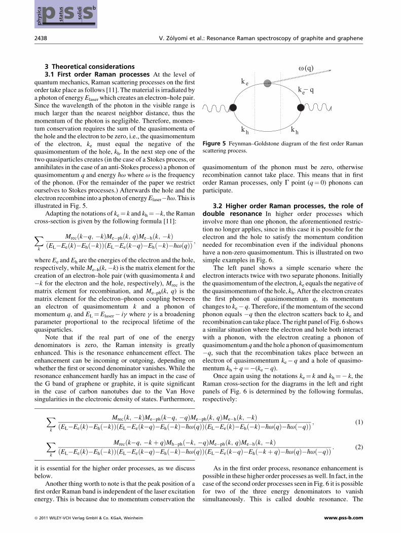
Figure 5 Feynman–Goldstone diagram of the first order Ramanscattering process.
3 Theoretical considerations3.1 First order Raman processes At the level of
quantum mechanics, Raman scattering processes on the firstorder take place as follows [11]. The material is irradiated bya photon of energyElaser which creates an electron–hole pair.Since the wavelength of the photon in the visible range ismuch larger than the nearest neighbor distance, thus themomentum of the photon is negligible. Therefore, momen-tum conservation requires the sum of the quasimomenta ofthe hole and the electron to be zero, i.e., the quasimomentumof the electron, ke must equal the negative of thequasimomentum of the hole, kh. In the next step one of thetwo quasiparticles creates (in the case of a Stokes process, orannihilates in the case of an anti-Stokes process) a phonon ofquasimomentum q and energy �hv where v is the frequencyof the phonon. (For the remainder of the paper we restrictourselves to Stokes processes.) Afterwards the hole and theelectron recombine into a photon of energyElaser��hv. This isillustrated in Fig. 5.
Adapting the notations of ke¼ k and kh¼�k, the Ramancross-section is given by the following formula [11]:
X
k
� 20
Mrecðk�q; �kÞMe�phðk; qÞMe�hðk; �kÞEL�EeðkÞ�Ehð�kÞð Þ EL�Eeðk�qÞ�Ehð�kÞ��hvðqÞð Þ ;
where Ee and Eh are the energies of the electron and the hole,respectively, while Me–h(k, �k) is the matrix element for thecreation of an electron–hole pair (with quasimomenta k and�k for the electron and the hole, respectively), Mrec is thematrix element for recombination, and Me–ph(k, q) is thematrix element for the electron–phonon coupling betweenan electron of quasimomentum k and a phonon ofmomentum q, and EL¼Elaser � ig where g is a broadeningparameter proportional to the reciprocal lifetime of thequasiparticles.
Note that if the real part of one of the energydenominators is zero, the Raman intensity is greatlyenhanced. This is the resonance enhancement effect. Theenhancement can be incoming or outgoing, depending onwhether the first or second denominator vanishes. While theresonance enhancement hardly has an impact in the case ofthe G band of graphene or graphite, it is quite significantin the case of carbon nanotubes due to the Van Hovesingularities in the electronic density of states. Furthermore,
X
k
Mrecðk; �kÞMe�phðk�q; �qÞMe�phðk; qÞMe�hðk; �kÞEL�EeðkÞ�Ehð�kÞð Þ EL�Eeðk�qÞ�Ehð�kÞ��hvðqÞð Þ EL�EeðkÞ�Ehð�kÞ��hvðqÞ��hvð�qÞð Þ ; (1)
X
k
Mrecðk�q; �k þ qÞMh�phð�k; �qÞMe�phðk; qÞMe�hðk; �kÞEL�EeðkÞ�Ehð�kÞð Þ EL�Eeðk�qÞ�Ehð�kÞ��hvðqÞð Þ EL�Eeðk�qÞ�Ehð�k þ qÞ��hvðqÞ��hvð�qÞð Þ : (2)
it is essential for the higher order processes, as we discussbelow.
Another thing worth to note is that the peak position of afirst order Raman band is independent of the laser excitationenergy. This is because due to momentum conservation the
11 WILEY-VCH Verlag GmbH & Co. KGaA, Weinheim
quasimomentum of the phonon must be zero, otherwiserecombination cannot take place. This means that in firstorder Raman processes, only G point (q¼ 0) phonons canparticipate.
3.2 Higher order Raman processes, the role ofdouble resonance In higher order processes whichinvolve more than one phonon, the aforementioned restric-tion no longer applies, since in this case it is possible for theelectron and the hole to satisfy the momentum conditionneeded for recombination even if the individual phononshave a non-zero quasimomentum. This is illustrated on twosimple examples in Fig. 6.
The left panel shows a simple scenario where theelectron interacts twice with two separate phonons. Initiallythe quasimomentum of the electron, ke equals the negative ofthe quasimomentum of the hole, kh. After the electron createsthe first phonon of quasimomentum q, its momentumchanges to ke� q. Therefore, if the momentum of the secondphonon equals �q then the electron scatters back to ke andrecombination can take place. The right panel of Fig. 6 showsa similar situation where the electron and hole both interactwith a phonon, with the electron creating a phonon ofquasimomentum q and the hole a phonon of quasimomentum�q, such that the recombination takes place between anelectron of quasimomentum ke� q and a hole of quasimo-mentum khþ q¼�(ke� q).
Once again using the notations ke¼ k and kh¼� k, theRaman cross-section for the diagrams in the left and rightpanels of Fig. 6 is determined by the following formulas,respectively:
As in the first order process, resonance enhancement ispossible in these higher order processes as well. In fact, in thecase of the second order processes seen in Fig. 6 it is possiblefor two of the three energy denominators to vanishsimultaneously. This is called double resonance. The
www.pss-b.com
Phys. Status Solidi B 248, No. 11 (2011) 2439
Feature
Article
ω (q)
ω (−q)
ω (q)
ω (−q)
ca b ca b
eke
kh hhk
k − qe k − qeke
kh
khhk
k − q ke
k + q
Figure 6 Feynman–Goldstone diagrams of two second orderRaman processes involving two phonons.
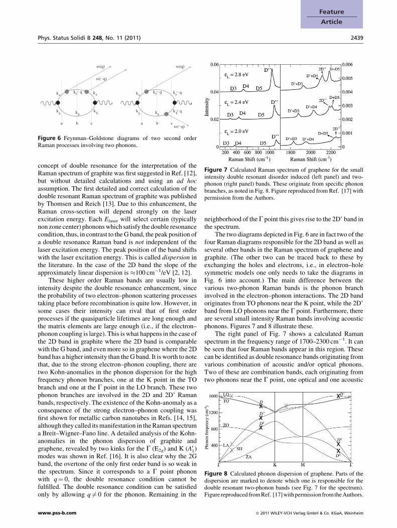
Figure 7 Calculated Raman spectrum of graphene for the smallintensity double resonant disorder induced (left panel) and two-phonon (right panel) bands. These originate from specific phononbranches, as noted in Fig. 8. Figure reproduced from Ref. [17] withpermission from the Authors.
Figure 8 Calculated phonon dispersion of graphene. Parts of thedispersion are marked to denote which one is responsible for thedouble resonant two-phonon bands (see Fig. 7 for the spectrum).Figure reproduced from Ref. [17] with permission from the Authors.
concept of double resonance for the interpretation of theRaman spectrum of graphite was first suggested in Ref. [12],but without detailed calculations and using an ad hocassumption. The first detailed and correct calculation of thedouble resonant Raman spectrum of graphite was publishedby Thomsen and Reich [13]. Due to this enhancement, theRaman cross-section will depend strongly on the laserexcitation energy. Each Elaser will select certain (typicallynon zone center) phonons which satisfy the double resonancecondition, thus, in contrast to the G band, the peak position ofa double resonance Raman band is not independent of thelaser excitation energy. The peak position of the band shiftswith the laser excitation energy. This is called dispersion inthe literature. In the case of the 2D band the slope of theapproximately linear dispersion is �100 cm�1/eV [2, 12].
These higher order Raman bands are usually low inintensity despite the double resonance enhancement, sincethe probability of two electron–phonon scattering processestaking place before recombination is quite low. However, insome cases their intensity can rival that of first orderprocesses if the quasiparticle lifetimes are long enough andthe matrix elements are large enough (i.e., if the electron–phonon coupling is large). This is what happens in the case ofthe 2D band in graphite where the 2D band is comparablewith the G band, and even more so in graphene where the 2Dband has a higher intensity than the G band. It is worth to notethat, due to the strong electron–phonon coupling, there aretwo Kohn-anomalies in the phonon dispersion for the highfrequency phonon branches, one at the K point in the TObranch and one at the G point in the LO branch. These twophonon branches are involved in the 2D and 2D’ Ramanbands, respectively. The existence of the Kohn-anomaly as aconsequence of the strong electron–phonon coupling wasfirst shown for metallic carbon nanotubes in Refs. [14, 15],although they called its manifestation in the Raman spectruma Breit–Wigner–Fano line. A detailed analysis of the Kohn-anomalies in the phonon dispersion of graphite andgraphene, revealed by two kinks for the G (E2g) and K (A0
1)modes was shown in Ref. [16]. It is also clear why the 2Gband, the overtone of the only first order band is so weak inthe spectrum. Since it corresponds to a G point phononwith q¼ 0, the double resonance condition cannot befulfilled. The double resonance condition can be satisfiedonly by allowing q 6¼ 0 for the phonon. Remaining in the
www.pss-b.com
neighborhood of the G point this gives rise to the 2D’ band inthe spectrum.
The two diagrams depicted in Fig. 6 are in fact two of thefour Raman diagrams responsible for the 2D band as well asseveral other bands in the Raman spectrum of graphene andgraphite. (The other two can be traced back to these byexchanging the holes and electrons, i.e., in electron–holesymmetric models one only needs to take the diagrams inFig. 6 into account.) The main difference between thevarious two-phonon Raman bands is the phonon branchinvolved in the electron–phonon interactions. The 2D bandoriginates from TO phonons near the K point, while the 2D’band from LO phonons near the G point. Furthermore, thereare several small intensity Raman bands involving acousticphonons. Figures 7 and 8 illustrate these.
The right panel of Fig. 7 shows a calculated Ramanspectrum in the frequency range of 1700–2300 cm�1. It canbe seen that four Raman bands appear in this region. Thesecan be identified as double resonance bands originating fromvarious combination of acoustic and/or optical phonons.Two of these are combination bands, each originating fromtwo phonons near the G point, one optical and one acoustic
� 2011 WILEY-VCH Verlag GmbH & Co. KGaA, Weinheim

2440 V. Zolyomi et al.: Resonance Raman spectroscopy of graphite and graphenep
hys
ica ssp st
atu
s
solid
i b
phonon: these are the D’þD3 and D’þD4 bands. The 2D’’band comes from two acoustic phonons near the K point,while the DþD5 band is a combination of an optical and anacoustic phonon, both near the K point. Figure 8 depicts thephonon dispersion of graphene and marks the particularbranches involved in these Raman bands. We mention thatthe name D’’ was used for the disorder induced band at2950 cm�1 in the early literature [2].
The left panel of Fig. 7 depicts Raman bands whichinvolve only one phonon with finite q. These are disorderinduced bands similar to the D and D’ bands, they will bediscussed below.
3.3 Disorder induced Raman bands Until now wediscussed overtone and combination bands in the frequencyrange above 1650 cm�1. In this frequency range everyRaman band must trivially involve at least two phonons sincethere are no phonons in the phonon dispersion at such highfrequencies. However, in the lower frequency region it ispossible to observe some bands in the Raman spectrumwhich originate from a single (non G point) phonon. This,however, requires the breaking of the translational symmetryof the lattice by disorder (impurities, lattice defects, edges,etc.) in the sample [13].
The diagrams describing these disorder induced pro-cesses can be traced back to the diagrams in Fig. 6. It is trivialthat a single non G point phonon normally cannot generate aRaman band due to a violation of quasimomentumconservation at recombination, as discussed above.However, it is possible for the momentum conservationcondition to be satisfied at recombination without a secondphonon if one of the electron–phonon scattering events isreplaced by the scattering of an electron (or hole) by a defect.For example, let us replace the second electron–phononscattering event in the left diagram of Fig. 6 with an electron-defect scattering event, the diagram changes as follows.After the electron–hole pair is created, the electron emits aphonon (as in the case of the two-phonon diagram) and itsmomentum changes by q, then it is scattered back into itsoriginal position in k-space by a defect and recombinationcan take place. In other words, the interaction of the electronwith the defect compensates for the missing quasimomentumand allows for this Raman process to complete despite thatonly one, non G point phonon is involved. The Raman cross-section is similar to the formulas for the two-phononprocesses, except that the energy denominators and matrixelements change accordingly.
The most prominent of the disorder induced bands is theD band at �1350 cm�1. This comes from the TO phononsclose to the K point, just like the 2D band. The second mostprominent one is the D’ band at �1620 cm�1 whichoriginates from the LO phonons near the G point; note thatthis one is quite difficult to observe because of its closeproximity to the G band. Some additional, small intensitydisorder induced bands appear in the Raman spectrum below1200 cm�1 as well. These originate from acoustic modes andare depicted in the left panel of Fig. 7.
� 2011 WILEY-VCH Verlag GmbH & Co. KGaA, Weinheim
Like the two-phonon modes, the disorder induced modesare also dispersive. There is a principal difference, however:since only one phonon is involved, the slope of the averagelinear dispersion is roughly half the slope of the correspond-ing two-phonon band. For example, the slope for thedispersion of the D band is �50 cm�1/eV [2, 12, 18].
3.4 Contribution of different double resonantRaman diagrams In the early works in the literature onlya single diagram was taken into account in the description ofdouble resonant Raman processes in graphene and relatedmaterials: the left diagram in Fig. 6 in which the electronparticipates in both scattering events [13]. In fact there are atotal of four diagrams for the two-phonon and eight diagramsfor the disorder induced processes; strictly speaking all ofthem should be taken into account. Interestingly, one half ofthe diagrams in fact dominates the others: if one calculatesthe intensity from the diagrams in which the electron and thehole both participate in a scattering event (such as in the rightdiagram of Fig. 6), the result is much larger than performingthe same calculation for the remaining diagrams in whichonly the electron or only the hole is involved in the scatteringevents.
This is not trivial since complex numbers are summed upwhen the Raman cross-section is calculated, thereforeinterference effects may even lead to some diagramscanceling each other out [19]. The finding is that, due toquantum interference effects, the diagrams where both theelectron and the hole are involved in scattering eventscontribute dominantly to the Raman intensity. This was infact shown recently [17] using a combination of GWcorrected density functional theory and tight binding model.However, it is not even necessary to perform the calculationat a high level of theory, as the appendix of Ref [17] showsthat the same conclusion is reached even in a simplenumerical model in which the phonon energies in the energydenominators are neglected and the matrix elements areconstant.
We note that in fact the conclusion that both types ofdiagrams must be taken into account can be reached evenfrom the analytical solution of a one-dimensional model(used to describe the D band of carbon nanotubes) [20].Figure 9 shows the Raman intensity for a simple one-dimensional model with an electron–hole symmetric quad-ratic gapped electron dispersion and a quadratic phonondispersion. Assuming constant matrix elements all theintegrals can be calculated analytically, as detailed in Ref.[20]. In this model, due to the electron–hole symmetry, fourdiagrams must be taken into account. The solid line showsthe total Raman intensity obtained when the contributions ofall four diagrams are summed up. In order to avoidmisunderstanding, we emphasize that the total intensity isnot simply the sum of the four lines seen in the figure. All theindividual lines in the figure show already the absolute valueof the sum of the corresponding complex amplitudes, as afunction of the Raman shift. The dotted and dashed linesdepict the intensities obtained from the diagrams in which
www.pss-b.com

Phys. Status Solidi B 248, No. 11 (2011) 2441
Feature
Article
0
1
2
3
4
5
6
7
1200 1210 1220 1230 1240 1250
Ram
an in
tens
ity [
arb.
u. ]
Raman shift [ cm-1 ]
Figure 9 Calculated Raman spectrum in a simple one-dimensionalmodel for the D band. The solid line shows the total intensity, whilethe dashed and dotted curves depict the contributions of the twosubtypes of diagrams (see text). Laser excitation energy was 2.2 eVand the broadening parameter was 0.042 eV.
Figure 10 Measured Raman spectra of few-layer graphene andgraphite taken with two different laser excitation energies. It can beseen that the shape and position of the band strongly changes as thenumber of layers increases from one to ten. Figure reproduced fromRef. [5] with permission from the American Physical Society.
the electron and hole are both involved in scattering events,and the ones in which only one of the two quasiparticles isinvolved in scattering events, respectively. The dashed anddotted lines at smaller Raman shifts (left hand side)correspond to processes when the scattering via the phononoccurs first before the scattering via the defect, whereas thedashed and dotted lines at larger Raman shifts (right handside) correspond to processes when the scattering via thedefect occurs first before the scattering via the phonon. It canbe seen that the dotted line and the dashed line both add acomparible contribution to the overall intensity. Thus, evenin such a simple one-dimensional model it can be seen thatthe contribution of the diagrams where both the electron andthe hole are involved in a scattering event must be taken intoaccount. Quantitatively the results of this model do differfrom the two-dimensional case in Ref. [17] in that thecontribution of the aforementioned diagrams is clearlydominant in that case. The difference for this is most likelythe dimensionality: one cannot expect exactly the sameresults in one and two dimensions, especially due to theVan Hove singularities in a one-dimensional system.Nevertheless the main message is the same in the two cases:all diagrams should always be taken into account sinceinterference effects between the contributions of differentdiagrams can yield unexpected results.
4 Characterizing graphene using Ramanspectroscopy As discussed in the preceding sections, theRaman spectrum of graphene and graphite is quite rich andcarries a lot of information. In the following we review a few
www.pss-b.com
examples of how the Raman spectrum of graphene can beused as a powerful tool to characterize graphene.
First, we discuss an interesting behavior of the 2D band.While graphene has a narrow, symmetric 2D band, that ofgraphite is broad and asymmetric (see Fig. 1). However, thisdifference is not only apparent between graphene andgraphite, but also between few-layer graphene samples ofvarying thickness: the 2D band of monolayer, bilayer, andtrilayer graphene looks quite different [5, 21].
Figure 10 shows this effect in more detail as onegradually increases the number of layers in multi-layergraphene. As it can be seen, there is already an abrupt changeas we move from monolayer to bilayer, but the shape of the2D band keeps changing as we increase the number of layers.The 2D band of 10-layer graphene looks almost like that ofgraphite, but below a thickness of ten layers the differencesare quite prominent. Therefore, this phenomenon has a veryimportant practical use: The number of layers can beempirically determined from the Raman spectrum, sincethe difference in the shape and width of the 2D band is quiteprominent and is very characteristic while the number oflayers is not too large.
The reason for the difference is the change in theelectronic band structure due to the inter-layer coupling. Thecoupling causes a splitting of the p and p� bands, whichincreases the number of q phonon wave-vectors that cansatisfy the double resonance condition. Since the splitting inthe valence and conduction band is not the same, the doubleresonance condition can be fulfilled by four different phononwave vectors in bilayer graphene, which means the 2D bandcan in principle be decomposed to four subbands. Indeed, themeasured spectra of bilayer graphene can be well fitted by thesum of four peaks [5, 21]. The intensities of the four subbandsare not the same. We mention that this broadening of the 2D
� 2011 WILEY-VCH Verlag GmbH & Co. KGaA, Weinheim

2442 V. Zolyomi et al.: Resonance Raman spectroscopy of graphite and graphenep
hys
ica ssp st
atu
s
solid
i b
Figure 11 Left panel: Measured Raman G band of graphene underuniaxial strain as a function of incident polarization (at fixed out-going polarization). The splitting of the G band into Gþ and G� isclearly seen. Right panel: intensity of the Gþ (circles) and G�
(squares) bands as a function of polarization angle. Figure repro-duced from Ref. [22] with permission from the American PhysicalSociety.
band is the main reason for the change in the peak height ratioof the G and 2D bands when going from graphene to graphite(see Fig. 1). The measured spectra can be well reproduced bytheory [5]. Note, that the inter-layer coupling also modifiesthe phonon dispersions, but the relative difference is quitesmall compared to the changes in the electronic bandstructure.
Another useful method for characterization is thepolarization study of the G and 2D bands of monolayergraphene as a function of uniaxial strain [22–26].
In pristine graphene, the G band is two-fold degenerate.Applying uniaxial strain reduces the symmetry of the lattice,which in turn lifts the degeneracy of the G band, causing it tosplit into two components. Both components redshift withincreasing strain at different rates, leading to an increasedsplitting as the strain increases. This strain induced splittingis very similar to the splitting of the G band into the Gþ andG� bands in carbon nanotubes due to the curvature of thenanotube [27], hence the same notation is used for the twocomponents in this case as well. G� corresponds to thecomponent in which the movement of the atoms is parallel tothe strain axis, while in the Gþ band the atoms moveperpendicular to the strain axis [22].
The significance of this splitting is revealed if oneperforms the measurement with linearly polarized lightexcitations. If the Raman excitation is polarized, the intensityof both components of the G band strongly depends on thepolarization angle of the incoming and outgoing photon, andthe dependence is different for Gþ and G�: the intensity as afunction of the polarization angle for Gþ is the same as that ofG� but shifted by 908. This can be seen in the left part ofFig. 11. Furthermore, the angle where the intensity peaks canbe directly linked to the angle between the strain axis and acarbon–carbon bond in the lattice. This allows us todetermine the orientation of the sample. For example, inthe case of the measurement depicted in the right side ofFig. 11, one of the maxima of G� is at 568. The differencebetween this angle and 908 (in this case 348) is exactly threetimes as much as the smallest angle between the strain axisand the normal of the carbon–carbon bonds. This means thatthe angle between the strain axis and the directionperpendicular to the carbon–carbon bond is 11.38.
Thus, the polarization study of the G band under uniaxialstrain can tell us the orientation of graphene on the substrate.
The situation is somewhat different in the case of the 2Dband. It also redshifts under uniaxial strain. However, there isno observable splitting, only a broadening for small strains,below 1%, when using visible laser excitation of 514 nm(2.41 eV) [22]. For larger strains the 2D band splits into twodistinct components if the stress is along zigzag or armchairdirections [24]. The intensities of these components stronglydepend on the direction of the incident light polarization withrespect to the strain axis. One of the subbands is dominant forthe parallel polarization, whereas the other one is dominantfor perpendicular polarization. The laser excitation was532 nm (2.33 eV) in this experiment. The splitting wasinterpreted based on the strain-induced shift of the Dirac-
� 2011 WILEY-VCH Verlag GmbH & Co. KGaA, Weinheim
cones. In addition to this effect a different type of broadeningand splitting was observed when using very low (infrared)laser excitation energies of 785 nm (1.58 eV) [26]. The 2Dband could be decomposed into two subbands, even forintermediate (neither zigzag nor armchair) orientation withrespect to the strain axis. The frequencies of the individualcomponents depend on the direction of the polarization of theincident light with respect to the strain axis. In contrast to theobservation in Ref. [24] the 2D band could be decomposedinto two components even in the case of zero tension. Thistype of splitting of the 2D band cannot be explained only bystrain induced asymmetry of the graphene Brillouin zone,instead both the inner and outer scattering mechanisms haveto be taken into account [26, 28].
The reason for this behavior is the trigonal warping of theequi-excitation-energy contours of graphene. In order tounderstand this we must differentiate between so-calledinner and outer Raman processes for the 2D band. The qphonon wave vectors that fulfill the double resonancecondition are those that connect the vicinity of the K andK’ point, as illustrated in Fig. 12. Due to the trigonal warpingeffect, there is a difference between those vectorswhich connect the left side of K with the right side of K’(for which q is larger than the distance of K and K’) and thosewhich connect the right side of K with the left side of K’ (forwhich q is smaller than the distance of K and K’). The formerare called outer, the latter inner processes. Due to the shape ofthe equi-excitation-energy contours, the nesting effect ismuch larger for outer than for inner processes, leading to amuch smaller intensity for the latter [4]. If, however, onereduces the laser excitation to energies in the infrared range,the trigonal warping becomes negligible and thus the inner
www.pss-b.com

Phys. Status Solidi B 248, No. 11 (2011) 2443
Feature
Article
a) b)
K
q
−q2ωD
K K’
q
−q2ωD
c)
K K’
K’
Figure 12 Outer (a)andinner (b)Ramanprocesses for the2Dband.The bottom panel (c) shows the same in the two-dimensionalBrillouin zone for two different equi-excitation-energy contourswith the solid lines depicting the outer and the dashed lines the innerprocesses.
and outer contributions will have the same intensity, and thesplitting becomes apparent in the decomposition of the 2Dband. At even lower energies the splitting should vanish,since, once the trigonal warping in the phonon dispersionbecomes negligible, the phonon frequencies of the inner andouter process will be the same.
Note, that one could also connect the left side of K withthe left side of K’ or the right side of K with the right side ofK’ (for these q is roughly as large as the distance of K and K’),but the contribution of these vanishes due to destructiveinterference [19].
Finally, let us discuss an interesting feature of the Dband. Micro-Raman spectroscopy measurements of stepedges on the surface of graphite reveal that the intensity ofthe D band strongly depends on the shape of the step edge[29]. This is illustrated in Fig. 13, which shows three Raman
Figure 13 Measured Raman spectra of graphite taken from threedifferent regions of a HOPG sample. The inset shows the measuredregions (1: armchair edge, 2: zigzag edge, 3: bulk). Figure repro-duced from Ref. [29] with permission from the American PhysicalSociety.
www.pss-b.com
spectra taken at various locations near the step. The intensityof the D band vanishes in the bulk (as expected in HOPG) andonly becomes visible at the edges, but interestingly theintensity is much bigger at armchair than zigzag edges. Note,that the intensity of the D’ peak does not change with theshape of the edge. The explanation of this phenomenon isquite simple, as illustrated in Fig. 14. When an electron isreflected at the edge during the double resonance process, thetransferred quasimomentum is trivially perpendicular to theedge (since the edge is such a defect which can only transfermomentum perpendicular to itself). The direction perpen-dicular to the armchair edge is parallel in the reciprocal spaceto the vector connecting K and K’, which means the electronis scattered from the vicinity of one K point into the vicinityof an inequivalent K point so the double resonance conditioncan be fulfilled effectively. However, the armchair edgescatters the electron in a direction at an angle of 308 from thisvector, scattering the electron towards an equivalent K pointin the reciprocal space which cannot fulfill the doubleresonance condition. In the case of the D’ band the doubleresonance process is fulfilled by so-called intravalleyprocesses, i.e., where the electron is scattered to anotherstate in the vicinity of the same K point as it started from (thusleading to nearG point phonons). In this case, the direction ofthe scattering at the edge is irrelevant, as the doubleresonance condition can be fulfilled no matter what angle
Figure 14 (a) Depiction of the double resonant Raman processresponsible for the D band. d¼�q is the quasimomentum trans-ferred to the electron by the defect. (b) Transferred quasimomenta da
and dz from an armchair (1) and a zigzag (2) edge, respectively.(c) Illustration of the double resonance process at the two edges,showing that the armchair edge is much more favorable for thedouble resonance condition. The inset shows the relevant phonondensity of states. Figure reproduced from Ref. [29] with permissionfrom the American Physical Society.
� 2011 WILEY-VCH Verlag GmbH & Co. KGaA, Weinheim

2444 V. Zolyomi et al.: Resonance Raman spectroscopy of graphite and graphenep
hys
ica ssp st
atu
s
solid
i b
the electron is scattered in. That is why the D’ band has thesame intensity at all types of edges.
This phenomenon can be exploited in the case ofgraphene as well. Recent studies have shown [30] that themicro-Raman spectra of the D band of a graphene flake alsodepend on the shape of the edge in the exact same way as inthe case of a step edge on the surface of graphite. Thus,analyzing the D band intensity allows one to determine theshape of the edge of a graphene flake.
5 Summary We have reviewed the Raman spec-troscopy of graphene and graphite. We looked at the doubleresonant Raman bands and their origins in detail. The reasonwhy some of the higher order bands – especially the D and 2Dbands – are unusually strong is the strong electron–phononcoupling around the K-point (which is also indicated by aKohn-anomaly in the phonon dispersion) and the doubleresonance effect. We also pointed out that Raman spec-troscopy can be used as a powerful tool of samplecharacterization, reviewing several examples from deter-mining the number of layers in multilayer graphene toidentifying the edges and the orientation of the sample. Wealso mention, that in order to develop graphene-basedelectronic devices one has to find various methods to controlthe electronic band structure, especially the gap of thesystem. One way for doing this may be the deformation ofgraphene by using appropriate strain. Raman spectroscopy isone of the best methods for monitoring this process.
Acknowledgements Support from OTKA Grant No.K81492 and the New Szechenyi Plan No. TAMOP-4.2.1/B-09/1/KMR-2010-0003 is gratefully acknowledged. V. Z. alsoacknowledges the Marie Curie ERG project CARBOTRON(PERG08-GA-2010-276805).
References
[1] F. Tuinstra and J. L. Koenig, J. Chem. Phys. 53(3), 1126–1130 (1970).
[2] R. P. Vidano, D. B. Fischbach, L. J. Willis, and T. M. Loehr,Solid State Commun. 39(2), 341–344 (1981).
[3] R. J. Nemanich and S. A. Solin, Phys. Rev. B 20(2), 392–401(1979).
[4] J. Kurti, V. Zolyomi, A. Gruneis, and H. Kuzmany, Phys.Rev. B 65(16), 165433 (2002).
[5] A. C. Ferrari, J. C. Meyer, V. Scardaci, C. Casiraghi,M. Lazzeri, F. Mauri, S. Piscanec, D. Jiang, K. S. Novoselov,S. Roth, and A. K. Geim, Phys. Rev. Lett. 97(18), 187401(2006).
[6] M. M. Lucchese, F. Stavale, E. H. Martins Ferreira, C. Vilani,M. V. O. Moutinho, R. B. Capaz, C. A. Achete, and A. Jorio,Carbon 38, 1592 (2004).
[7] A. C. Ferrari and J. Robertson, Phys. Rev. B 61, 14095(2000).
[8] J. Maultzsch, S. Reich, C. Thomsen, H. Requardt, andP. Ordejon, Phys. Rev. Lett. 92(7), 075501 (2004).
� 2011 WILEY-VCH Verlag GmbH & Co. KGaA, Weinheim
[9] Y. Kawashima and G. Katagiri, Phys. Rev. B 52(14), 10053–10059 (1995).
[10] E. H. Martins Ferreira, M. V. O. Moutinho, F. Stavale, M. M.Lucchese, R. B. Capaz, C. A. Achete, and A. Jorio, Phys. Rev.B 82(12), 125429 (2010).
[11] R. M. Martin and L. M. Falicov, Light Scattering in Solids I,in: Topics in Applied Physics, edited by M. Cardona, Vol. 8(Springer, Berlin, 1983), p. 79.
[12] A. V. Baranov, A. N. Bekhterev, Y. S. Bobovich, and V. I.Petrov, Opt. Spectrosc. 62, 612 (1987).
[13] C. Thomsen and S. Reich, Phys. Rev. Lett. 85(24), 5214–5217 (2000).
[14] O. Dubay, G. Kresse, and H. Kuzmany, Phys. Rev. Lett. 88,235506 (2002).
[15] O. Dubay and G. Kresse, Phys. Rev. B 67, 035401 (2003).[16] S. Piscanec, M. Lazzeri, F. Mauri, A. C. Ferrari, and
J. Robertson, Phys. Rev. Lett. 93, 185503 (2004).[17] P. Venezuela, M. Lazzeri, and F. Mauri, Theory of double-
resonant Raman spectra in graphene: intensity and line shapeof defect-induced and two-phonon bands, arXiv: 11034582v2.
[18] I. Pocsik, M. Hundhausen, M. Koos, and L. Ley, J. Non-cryst.Solids 227–230B, 1083 (1998).
[19] J. Maultzsch, S. Reich, and C. Thomsen, Phys. Rev. B 70(15),155403 (2004).
[20] J. Kurti, J. Koltai, and V. Zolyomi, The Role of Van HoveSingularities in Disorder Induced Raman Scattering, in:Electronic Properties of Novel Nanostructures, edited byH. Kuzmany, J. Fink, M. Mehring, and S. Roth, AIP Conf.Proc., Vol. 786 (Amer. Inst. Physics, Melville, New York,2005), pp. 416–419.
[21] L. M. Malard, M. H. D. Guimaraes, D. L. Mafra, M. S. C.Mazzoni, and A. Jorio, Phys. Rev. B 79(12), 125426 (2009).
[22] T. M. G. Mohiuddin, A. Lombardo, R. R. Nair, A. Bonetti,G. Savini, R. Jalil, N. Bonini, D. M. Basko, C. Galiotis,N. Marzari, K. S. Novoselov, A. K. Geim, and A. C. Ferrari,Phys. Rev. B 79(20), 205433 (2009).
[23] M. Y. Huang, H. G. Yan, C. Y. Chen, D. H. Song, T. F. Heinz,and J. Hone, J. Proc. Natl. Acad. Sci. USA 106, 7304 (2009).
[24] M. Y. Huang, H. G. Yan, T. F. Heinz, and J. Hone, Nano Lett.10, 4074 (2010).
[25] O. Frank, G. Tsoukleri, J. Parthenios, K. Papagelis, I. Riaz,R. Yalil, K. S. Novoselov, and C. Galiotis, ACS Nano 4, 3131(2010).
[26] O. Frank, M. Mohr, J. Maultzsch, C. Thomsen, I. Riaz,R. Yalil, K. S. Novoselov, G. Tsoukleri, J. Parthenios,K. Papagelis, L. Kavan, and C. Galiotis, ACS Nano 5,2231 (2011).
[27] A. Jorio, A. G. Souza Filho, G. Dresselhaus, M. S. Dressel-haus, A. K. Swan, M. S. Unlu, B. B. Goldberg, M. A. Pimenta,J. H. Hafner, C. M. Lieber, and R. Saito, Phys. Rev. B 65(15),155412 (2002).
[28] M. Mohr, J. Maultzsch, and C. Thomsen, Phys. Rev. B 82,201409 (2010).
[29] L. G. Cancado, M. A. Pimenta, B. R. A. Neves, M. S. S.Dantas, and A. Jorio, Phys. Rev. Lett. 93(24), 247401 (2004).
[30] C. Casiraghi, A. Hartschuh, H. Qian, S. Piscanec, C. Georgi,A. Fasoli, K. S. Novoselov, D. M. Basko, and A. C. Ferrari,Nano Lett. 9(4), 1433–1441 (2009). PMID: 19290608.
www.pss-b.com