Research Article Special Issue - African Journals Online
25
AN EXTERNAL CONTROL UNIT IMPLEMENTED FOR STIMULATOR ASIC TESTING E. Noorsal 1,* , K. Sooksood 2 , H. Xu 3 and Z. I. Rizman 4 1 Faculty of Electrical Engineering, Universiti Teknologi MARA, 13500 Permatang Pauh, Pulau Pinang, Malaysia 2 Department of Electronic, Faculty of Engineering, King Mongkut's Institute of Technology Ladkrabang, 10520 Bangkok, Thailand 3 Department of Advanced Low Power Solution, Texas Instrument Deutschland, Freising, Germany 4 Faculty of Electrical Engineering, Universiti Teknologi MARA, Dungun, Terengganu, Malaysia Published online: 10 November 2017 ABSTRACT This paper presents the design and development of an external control unit (ECU) for a stimulator ASIC testing purposes. The ECU consists of a graphical user interface (GUI) from the PC, a data transceiver and a power transmitter. The GUI was developed using MATLAB for stimulation data setup. The data transceiver was designed using hardware description language (HDL) Verilog code and was implemented in a Virtex-II Pro FPGA board. The overall stimulator ASIC design architecture and its operation for an epiretinal implant application are briefly explained to correlate with the ECU’s design requirements. The flexible multichannel stimulator ASIC was successfully fabricated in a 0.35μm AMS HVCMOS technology. Conducted simulation and measurement results on stimulation waveform generation, supply voltage compliance and external control of supply voltage adaptation validate the functionality of the designed ECU and the stimulator ASIC. Author Correspondence, e-mail: [email protected] doi: http://dx.doi.org/10.4314/jfas.v9i6s.54 Journal of Fundamental and Applied Sciences ISSN 1112-9867 Available online at http://www.jfas.info Research Article Special Issue Journal of Fundamental and Applied Sciences is licensed under a Creative Commons Attribution-NonCommercial 4.0 International License . Libraries Resource Directory . We are listed under Research Associations category.
-
Upload
khangminh22 -
Category
Documents
-
view
0 -
download
0
Transcript of Research Article Special Issue - African Journals Online

AN EXTERNAL CONTROL UNIT IMPLEMENTED FOR STIMULATOR ASIC
TESTING
E. Noorsal1,*, K. Sooksood2, H. Xu3 and Z. I. Rizman4
1Faculty of Electrical Engineering, Universiti Teknologi MARA, 13500 Permatang Pauh, Pulau
Pinang, Malaysia 2Department of Electronic, Faculty of Engineering, King Mongkut's Institute of Technology
Ladkrabang, 10520 Bangkok, Thailand 3Department of Advanced Low Power Solution, Texas Instrument Deutschland, Freising,
Germany 4Faculty of Electrical Engineering, Universiti Teknologi MARA, Dungun, Terengganu, Malaysia
Published online: 10 November 2017
ABSTRACT
This paper presents the design and development of an external control unit (ECU) for a stimulator
ASIC testing purposes. The ECU consists of a graphical user interface (GUI) from the PC, a data
transceiver and a power transmitter. The GUI was developed using MATLAB for stimulation data
setup. The data transceiver was designed using hardware description language (HDL) Verilog
code and was implemented in a Virtex-II Pro FPGA board. The overall stimulator ASIC design
architecture and its operation for an epiretinal implant application are briefly explained to
correlate with the ECU’s design requirements. The flexible multichannel stimulator ASIC was
successfully fabricated in a 0.35μm AMS HVCMOS technology. Conducted simulation and
measurement results on stimulation waveform generation, supply voltage compliance and
external control of supply voltage adaptation validate the functionality of the designed ECU and
the stimulator ASIC.
Author Correspondence, e-mail: [email protected]
doi: http://dx.doi.org/10.4314/jfas.v9i6s.54
Journal of Fundamental and Applied Sciences
ISSN 1112-9867
Available online at http://www.jfas.info
Research Article
Special Issue
Journal of Fundamental and Applied Sciences is licensed under a Creative Commons Attribution-NonCommercial 4.0 International License. Libraries Resource Directory. We are listed under Research Associations category.

E. Noorsal et al. J Fundam Appl Sci. 2017, 9(6S), 710-734 711
Keywords: external control unit; data transceiver; stimulator ASIC; retinal prosthesis; epiretinal
implant; stimulation waveform; Manchester data; voltage compliance.
1. INTRODUCTION
Blindness has a severe impact on an individual's lifestyle and on socioeconomics. A person who
is afflicted with total or partial blindness is often unable to independently perform rudimentary
tasks. A visual prosthesis is a device that is used to provide blind patients with a sense of vision
by electrically stimulating the neural cells in the visual pathway. To date, much research has been
pursued on the retinal prosthesis. In recent years, two main research areas on retinal prostheses
have been pursued, namely the epiretinal implant [1-7] and the subretinal implant [8-10]. The
primary goal of these prostheses is to bypass the damaged photoreceptors and to electrically
stimulate the remaining cells of the retina for visual excitation. Fig. 1 illustrates a system
overview of an epiretinal implant with its components [1]. The external system mainly consists of
a camera and a digital image processor. The captured image from the camera is digitally
processed and converted into encoded stimulation data by the processor before it is transmitted
wirelessly to the implant.
Fig.1. System overview of an epiretinal implant [11]
This implanted system, which is telemetrically powered, consists of the stimulator electronics and
the stimulation electrodes. The stimulator electronics consists of a built-in stimulator ASIC
together with several passive components for the power management. An external control unit
(ECU) is typically employed in an implantable micro-stimulator system to program the intended
stimulus parameters and to monitor the status of the implant chip for complete safety closure
[12-15]. The examples of important safety features that requires ECU’s surveillance are the
internal and compliance of the supply voltage, the electrode impedance, the non-accomplished
charge balancing, the unwanted-fault current into the electrode due to shorted switch, the

E. Noorsal et al. J Fundam Appl Sci. 2017, 9(6S), 710-734 712
decrement in supply voltage due to misalignment of the RF link and the corrupted received data
[1, 12, 14-16]. The desirable features of an ECU with multichannel stimulator is high data rates
for stimulation programming, power delivered through RF inductive link, monitoring and
surveillance for complete safety closure and portability [14, 17]. Therefore, the implementation of
a reliable ECU is indispensable for the implantable micro-stimulator system.
In this work, the design and implementation of the ECU for an epiretinal stimulator ASIC are
discussed and illustrated. The ECU was mainly developed to test the functionality of the
fabricated stimulator ASIC as well as for monitoring purpose. This paper is organized as follows.
Section 2 provides an overview of the overall system architecture for multichannel stimulator
ASIC, the implant chip monitoring, the serial backchannel data transfer operations and the
voltage adaptation protocol. Then, section 3 elucidates the design overview of the ECU, the
internal architecture of a data transceiver in the ECU and the data transceiver’s protocol from the
ECU to the stimulator ASIC. Section 4 discusses the simulation results of the data transceiver
module and the measurement results of the functionality and bidirectional communication link
between the ECU and the fabricated stimulator ASIC. Lastly, section 5 presents the conclusion.
2. METHODOLOGY
2.1. Overview of Stimulator ASIC Design Architecture
The proposed stimulator ASIC design architecture for a 1024 channel epiretinal implant is
depicted in Fig. 2. The stimulator ASIC was designed using hardware description language
(HDL) Verilog code and was implemented in a 0.35 μm AMS HVCMOS technology. The internal
design architecture of the stimulator ASIC mainly consists of Global and Local Function
modules. The global function module consists of a reconfigurable HV power management unit,
an optical receiver, a clock recovery, an ADC, a load modulator and a Global Stimulation Control
Unit (GSU). The local function module consists of an extendable number of distributed Local
Stimulation Units (LSUs). The implant ASIC is powered by a 13.56MHz RF inductive link [1, 11,
18-19]. The HV power management unit, rectifies the RF input by employing several integrated
rectifiers in the circuit [18]. From the power regulator unit, two main supply voltages are
provided namely a 3.3V supply for all low-voltage operations (VDD) and an adjustable
high-voltage supply (VDDP) of up to 20 V, which is used for the stimulator outputs. The ECU
program the intended stimulus parameters by sending the stimulation data (encoded Manchester)

E. Noorsal et al. J Fundam Appl Sci. 2017, 9(6S), 710-734 713
to the stimulator ASIC at a data rate of approximately ∼ 1 Mb/s via an optical link. Details of the
stimulation and data packet protocols can be found in [11].
The clock recovery module, converts the received RF signal into a 13.56MHz clock, which is
used by the GSU as a master clock. The function of the GSU is to receive the serial encoded
Manchesterdata from the Optical Receiver and to control the implant operation. The output
signals from the GSU module, which include stimulation commands (“stim_cmd”), a slow
system clock (“clk_gbl”) at 1 MHz, the address bus and the local stimulation data are connected
globally to all LSUs. Each LSU comprises of a digital pixel control unit (PCU), a 5-bit current
steering DAC and a 1:4 demultiplexed output HV current driver, which includes a
voltage-compliance monitor, charge balancers, a sample and hold (S&H) circuit for electrode
impedance measurements. After the reception of stimulation data, the GSU will program the local
stimulation data to the addressed LSUs. The LSU then provides a stimulation pulse current to the
attached electrodes. The 256 number of LSUs are arranged in an array and addressed using row
and column address decoders.
For electrode charge balancing safety, the global charge balancing circuit (global balance)
updates the status of the electrode balancing from the activated LSUs to the GSU. This is to
ensure that the implant ASIC is safe from any unbalance accumulated charge, which exist in the
electrode after each stimulation [20]. Additionally, global compliance monitoring from all LSUs
is conducted by the Global Compl module, which receives feedback compliance signals from all
LSUs. The voltage compliance signal from each LSU (“compl”) indicates the status of the supply
voltage compliance for each LSU.

E. Noorsal et al. J Fundam Appl Sci. 2017, 9(6S), 710-734 714
Fig.2. The proposed overall epiretinal stimulator system architecture, which consists of global and
locally distributed functions [11]
The status or conditions of epiretinal implant are back communicated to the ECU through the
Load Modulator and RF inductive link for monitoring purposes. The examples of epiretinal
implant conditions that are back communicated to the ECU are the global voltage compliance
problem, the global non-accomplished charge balancing, the electrode impedance, the internal
power condition of the shunt regulator and the data packet error. These epiretinal implant
conditions are first converted into 16-bit backchannel data are then processed by the GSU to
produce pulse position coded signal. The pulse code signal triggers the switch through the Load
Modulator for RF inductive link transmission. Details backchannel data processing and serial
pulse code generation by the GSU can be referred here [12].
In this design work, the supply voltage (VDDP) can be adjusted and adapted externally by the ECU
according to the currently running of stimulation compliance voltage. The ECU will send the
voltage adaptation data via optical link (either voltage increase or voltage decrease) to the
stimulator ASIC depending on the feedback information of the back-communicated data. Once
the GSU receives the voltage adaptation data (“vadj_switch”) from the ECU, it will selectively
short out the reference diode string in the HV Power Management unit for shunt current
adjustment. The 4-bit of “vadj_switch” register, which is directly connected to the diode strings
from the GSU, controls the increment and decrement of the VDDP. To decrease the high supply
voltage, the diode switches are shorted out by shifting binary “1” into the 4-bit “vadj_switch”,

E. Noorsal et al. J Fundam Appl Sci. 2017, 9(6S), 710-734 715
starting from LSB towards the MSB (from minimum “4b’0001” to maximum “4b1111”
decrement). In contrast, to increase the supply voltage, the diode switches are opened by shifting
binary “0” into the 4-bit “vadj_switch”, starting from MSB towards the LSB (from minimum
“4b’0111” to maximum “4b0000” increment).
After power on reset, the ECU starts to monitor the compliance supply voltage of the implant. For
example, if no compliance problem is detected for a stimulation time frame of 100ms, the ECU
will send a voltage decrease data to decrease the supply voltage because it is assumed that the
VDDP is too high for the currently running stimulation. Thereafter, the GSU decreases the shunt
reference by shorting out one diode. Thus, ISh is increased and the VDDP is reduced accordingly.
The process of decreasing the supply voltage at every 100ms is repeated until the implant reports
a voltage compliance problem to the ECU. For this, the compliance monitor in every output stage
detects and reports any output voltage compliance problem (“compl”). It should be noted that the
monitoring time frame of 100ms is not fixed. It is selected based on the stimulation time frame, in
which the external monitoring time frame should not be less than one stimulation time period and
should not be longer than the frequency of the external camera movement (1-10Hz) in the
epiretinal implant system. This is because the camera movement has a direct effect on the
changes of the ambient light intensity that enters the camera.
After reception of the backchannel data and the detection of a voltage compliance problem in the
epiretinal implant by the ECU, a voltage adjust data to increase the supply voltage is sent from
the ECU to the epiretinal implant. The GSU will then increase the supply voltage accordingly by
opening a diode switch in the shunt regulator. Thereafter, the ECU assumes that the implant has
found an optimal compliance voltage and stops sending the voltage decrease data at every 100ms.
The next voltage decrement monitoring is carried out every 1s. If subsequently any of the local
voltage-compliance monitors detect a too small VDDP, the GSU immediately reports to the ECU
and a new voltage increase data is sent to readjust the shunt reference by opening one diode of the
string to increase the VDDP accordingly. Thus, the supply voltage for the output current driver is
always controlled to adjust the supply voltage just high enough for all currently running
stimulations over time. Thus, the power efficiency of the stimulator ASIC is increased.
2.2. Design Methodology and Implementation of an External Control Unit
Fig. 3 depicts the ECU test measurement setup for the stimulator ASIC. The ECU mainly consists
of a graphical user interface (GUI) from the PC, a data transceiver using a Virtex-II Pro FPGA

E. Noorsal et al. J Fundam Appl Sci. 2017, 9(6S), 710-734 716
board and a power transmitter. The main functions of the ECU are to provide stimulation data to
the stimulator ASIC for stimulation operation, to monitor the status of the stimulator ASIC and to
provide external closed-loop power management for complete safety closure. The test
measurement of the fabricated stimulator ASIC is started by setting the intended stimulation data
in GUI. The intended stimulation data are then transferred to the FPGA board for temporary data
storage through the USB connector. Once completed, the stored stimulation data are then
retransmitted to the stimulator ASIC at a data rate of ∼1Mbps using the Manchester encoded data.
It is to note that ∼1Mbps data rate is chosen to emulate the actual data transfer using the optical
link in the epiretinal implant application [1]. The stimulation data can be sent one at a time or at a
stimulation frame rate of 8 different frequencies ranging over 30Hz, 60Hz, 100Hz, 200Hz, 300Hz,
500Hz, 1kHz and 2kHz for repetitive stimulations. Fig. 4 depicts an example of the actual test
measurement setup of the ECU with the stimulator ASIC.
Fig.3. ECU test measurement setup for stimulator ASIC

E. Noorsal et al. J Fundam Appl Sci. 2017, 9(6S), 710-734 717
Fig.4.Actual ECU test measurement setup for stimulator ASIC
2.3. Stimulation Data Setup and Processing
The stimulation data are first prepared according to the intended stimulation pattern that is set by
the users. A graphical user interface (GUI) [22-23] has been developed using MATLAB software
to assist the setup of the intended stimulation data such as local amplitude profiles and global
timing settings as depicted in Fig. 5. The stimulation data are first mapped into binary
representation. Thereafter, the stimulation data are harvested into several data packets with
appended 16-bit CRC signatures. The intended stimulation profile can also be observed in this
GUI by pressing the plot button. After the user is satisfied with the stimulation wave pattern
settings, the stimulation data are sent to the FPGA according to the data protocol rules. For PC to
FPGA board communication, the complete data packet is then divided into an 8-bit of unsigned
integer value and it is appended with the last byte, which is set to the value 255 to indicate the
end of the data packet. The 8-bit data are then sent to the FPGA through the USB connection.

E. Noorsal et al. J Fundam Appl Sci. 2017, 9(6S), 710-734 718
Fig.5. Graphical user interface for stimulation data setup
2.4. Data Transceiver Design Architecture
The data transceiver was designed using the HDL Verilog code and was implemented in Virtex-II
Pro FPGA board. The main functions of the data transceiver are to temporarily stored the
received data from the PC, to provide serial Manchester data at ~1Mbps to the stimulator ASIC,
to decode the backchannel data from the stimulator ASIC and to provide a closed-loop external
control mechanism for stimulator ASIC supply voltage adaptation. For the stimulator ASIC test
measurement setup, the output signals from the Data Transceiver are connected to the stimulator
ASIC.

E. Noorsal et al.
Fig.6. Data t
The internal architecture of the data transceiver
sub-modules, which include a data receiver control unit
a RAM Stim, a RAM Vadj and a
reception of serial data from the PC into the FPGA board.
unit provides the 8-bit received data (“r
writing process of the 8-bit “regData” into the RAM Stim and a 1
increase the program counter address (PCStim). The PC Stim address is reset to its starting
location when the received 8-bit “regData” has the value of 255, which indicates the end of the
data packet. The PC Stim acts as an address pointer during the writing and reading of the 8
data into and from the RAM Stim. The RAM Stim is a register file with an organi
1024 rows. Writing of the 8-bit “regData” into the RAM Stim uses a high clock frequency
(“clk_100MHz”) while reading of the 8
which is the clock frequency for the Manchester data transmiss
as an address pointer during the reading of the 8
consists of two register files with an organization of 8
enable automated voltage adaptat
increase and voltage decrease data. The voltage increase and voltage decrease data are used for
J Fundam Appl Sci. 2017, 9(6S), 710-734
Data transceiver implemented in the FPGA
the data transceiver as depicted in Fig. 6 consists of several
data receiver control unit, a PC Stim, a data transmitter control unit
a RAM Stim, a RAM Vadj and a backchannel decoder. The data receiver control unit
om the PC into the FPGA board. Therefore, the data receiver control
bit received data (“regData”) from the PC, a 1-bit “wr_en” signal to enable the
bit “regData” into the RAM Stim and a 1-bit “inc pcwr” signal to
increase the program counter address (PCStim). The PC Stim address is reset to its starting
bit “regData” has the value of 255, which indicates the end of the
data packet. The PC Stim acts as an address pointer during the writing and reading of the 8
data into and from the RAM Stim. The RAM Stim is a register file with an organi
bit “regData” into the RAM Stim uses a high clock frequency
(“clk_100MHz”) while reading of the 8-bit data uses a low clock frequency (“clk_2MHz”),
which is the clock frequency for the Manchester data transmission. In contrast, the PC_Vadj, acts
as an address pointer during the reading of the 8-bit data from the RAM_Vadj. The RAM_Vadj
consists of two register files with an organization of 8-bit × 7 rows for each register file. To
enable automated voltage adaptation control, the register files are hardcoded with voltage
increase and voltage decrease data. The voltage increase and voltage decrease data are used for
719
consists of several
transmitter control unit,
data receiver control unit controls the
data receiver control
bit “wr_en” signal to enable the
bit “inc pcwr” signal to
increase the program counter address (PCStim). The PC Stim address is reset to its starting
bit “regData” has the value of 255, which indicates the end of the
data packet. The PC Stim acts as an address pointer during the writing and reading of the 8-bit
data into and from the RAM Stim. The RAM Stim is a register file with an organization of 8-bit ×
bit “regData” into the RAM Stim uses a high clock frequency
bit data uses a low clock frequency (“clk_2MHz”),
ion. In contrast, the PC_Vadj, acts
bit data from the RAM_Vadj. The RAM_Vadj
bit × 7 rows for each register file. To
ion control, the register files are hardcoded with voltage
increase and voltage decrease data. The voltage increase and voltage decrease data are used for

E. Noorsal et al. J Fundam Appl Sci. 2017, 9(6S), 710-734 720
the supply voltage adaptation in the stimulator ASIC. Similar to data reading from the
RAM_Stim, the reading process of the 8-bit data from the RAM_Vadj uses the clk_2MHz, which
is the clock frequency for the Manchester data transmission.
The data transmitter control unit controls the frequency of reading the stored stimulation data
from the RAM Stim according to the selected stimulation rate and the transmission of Manchester
encoded data at ~1Mbps to the stimulator ASIC using the “clk_2MHz”. The backchannel decoder
decodes the received pulse code signal (“gsu_lm_out”) from the stimulator ASIC and activates
certain flags for data reception acknowledgment and monitoring purposes.
2.5. Data Transceiver Protocol
Fig. 7 illustrates the data receiving and transmitting protocol of the data transceiver module from
Fig. 6. There are two finite state machines (FSMs) that control the receiving and transmitting of
Manchester data to and from the data transceiver module. The receiver FSM which resides in data
receiver control unitconverts the serial data and controls the storage of 8-bit “regData” from the
PC into the RAM Stim module. The transmitter FSM which resides in the data transmitter control
unit controls the transmission of Manchester data from the data transceiver module to the
stimulator ASIC. To emulate the Manchester data rate of ~1Mbps to the stimulator ASIC, the data
reception process is controlled at a higher clock speed of 100MHz whereas the data transmission
process is controlled at a lower clock speed of 2MHz. Therefore, the receiver FSM operates at
100 MHz while the Transmitter FSM operates at 2 MHz.
Fig.7. Data transceiver protocol
To simplify the explanation, the data transceiver protocol is explained according to its operation.
E. Noorsal et al. J Fundam Appl Sci. 2017, 9(6S), 710-734 721
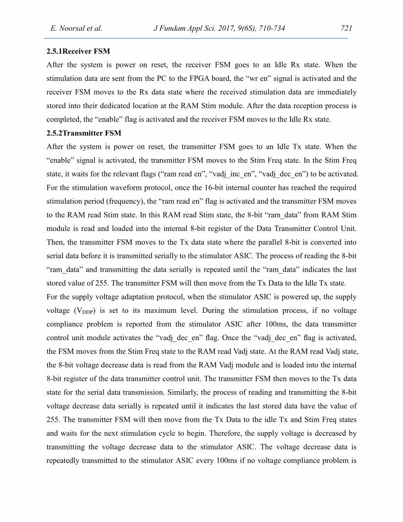
2.5.1Receiver FSM
After the system is power on reset, the receiver FSM goes to an Idle Rx state. When the
stimulation data are sent from the PC to the FPGA board, the “wr en” signal is activated and the
receiver FSM moves to the Rx data state where the received stimulation data are immediately
stored into their dedicated location at the RAM Stim module. After the data reception process is
completed, the “enable” flag is activated and the receiver FSM moves to the Idle Rx state.
2.5.2Transmitter FSM
After the system is power on reset, the transmitter FSM goes to an Idle Tx state. When the
“enable” signal is activated, the transmitter FSM moves to the Stim Freq state. In the Stim Freq
state, it waits for the relevant flags (“ram read en”, “vadj_inc_en”, “vadj_dec_en”) to be activated.
For the stimulation waveform protocol, once the 16-bit internal counter has reached the required
stimulation period (frequency), the “ram read en” flag is activated and the transmitter FSM moves
to the RAM read Stim state. In this RAM read Stim state, the 8-bit “ram_data” from RAM Stim
module is read and loaded into the internal 8-bit register of the Data Transmitter Control Unit.
Then, the transmitter FSM moves to the Tx data state where the parallel 8-bit is converted into
serial data before it is transmitted serially to the stimulator ASIC. The process of reading the 8-bit
“ram_data” and transmitting the data serially is repeated until the “ram_data” indicates the last
stored value of 255. The transmitter FSM will then move from the Tx Data to the Idle Tx state.
For the supply voltage adaptation protocol, when the stimulator ASIC is powered up, the supply
voltage (VDDP) is set to its maximum level. During the stimulation process, if no voltage
compliance problem is reported from the stimulator ASIC after 100ms, the data transmitter
control unit module activates the “vadj_dec_en” flag. Once the “vadj_dec_en” flag is activated,
the FSM moves from the Stim Freq state to the RAM read Vadj state. At the RAM read Vadj state,
the 8-bit voltage decrease data is read from the RAM Vadj module and is loaded into the internal
8-bit register of the data transmitter control unit. The transmitter FSM then moves to the Tx data
state for the serial data transmission. Similarly, the process of reading and transmitting the 8-bit
voltage decrease data serially is repeated until it indicates the last stored data have the value of
255. The transmitter FSM will then move from the Tx Data to the idle Tx and Stim Freq states
and waits for the next stimulation cycle to begin. Therefore, the supply voltage is decreased by
transmitting the voltage decrease data to the stimulator ASIC. The voltage decrease data is
repeatedly transmitted to the stimulator ASIC every 100ms if no voltage compliance problem is

E. Noorsal et al. J Fundam Appl Sci. 2017, 9(6S), 710-734 722
detected. Thus, the transmitter FSM will repeat executing the RAM read Vadj and Tx Data states.
However, if a voltage compliance problem is detected in the stimulator ASIC, the “compl_err_reg”
flag is activated 1.6ms after the reception of the pulse code signal (“gsu_lm_out”) from the
stimulator ASIC. The “vadj_inc_en” flag is then activated by the data transmitter control unit
module. Therefore, the transmitter FSM moves from the Stim Freq state to the RAM read Vadj
state when the “vadj_inc_en” flag is activated. In the RAM read Vadj state, the 8-bit voltage
increase data is read from the RAM Vadj module and loaded into the internal 8-bit register of the
data transmitter control unit. Similarly, the transmitter FSM then moves to the Tx data state for
the serial data transmission. The process of reading and transmitting the 8-bit voltage increase
data serially is repeated until it indicates the last stored data have the value of 255. The
transmitter FSM will then move from the Tx data state to the idle Tx and Stim Freq states and
wait for the next stimulation cycle to begin. The supply voltage of the stimulator ASIC is
increased accordingly after the reception of voltage increase data and is assumed to have reached
an optimum voltage compliance after the first compliance problem is detected. Thereafter, the
supply voltage decrement process is only monitored every 1s. Therefore, the transmitter FSM will
only enter the RAM read Vadj state after 1s. However, if a subsequent voltage compliance
problem is detected, the transmitter FSM will then repeatedly execute the RAM read Vadj and Tx
data states for the voltage increase data reading and transmission. Thus, the voltage increase data
is transmitted again to the stimulator ASIC for the voltage increment process.
3. RESULTS AND DISCUSSION
This section discusses a few of the simulation results from the ECU’s data transceiver unit and
the real-time measurement results of the stimulator ASIC testing using the ECU.
3.1. ECU’s Data Transceiver Simulation Results
Two important simulation results of the ECU’s data transceiver are discussed here. The first
simulation results illustrate and discuss on the data transceiver operation for serial Manchester
data reception and transmitting process. The second simulation results illustrate and discuss on
the backchannel decoder operation for voltage compliance problem detection and voltage
adaptation process.
3.2. Data Transceiver
Fig. 8(a) depicts the receiving and transmitting simulation results of the ECU’s data transceiver

E. Noorsal et al. J Fundam Appl Sci. 2017, 9(6S), 710-734 723
module. Initially, the serial data is received from the PC and temporarily stored in the RAM Stim
module. Thereafter, once the “enable” signal is activated, the Manchester data is serially
transmitted to the stimulator ASIC. Fig. 8(b) depicts the zoom view into marked area A of the
received serial data from the PC and the bit shifting process into the 8-bit “regData” register.
Once the received serial data is shifted and converted into 8-bit parallel data (“regData”), the
8-bit data is temporarily stored into the RAM Stim module (“ram_data”) by activating the “wr_en”
signal.
The zoom view into marked area B as depicted in Fig. 8(c), indicates the serial transmission of
Manchester data from the transmitter control unit. It is observed that the parallel 8-bit “ram_data”
from the RAM Stim register file is converted into serial Manchester data at ~1Mbps using 2MHz
clock frequency. In the real test measurement setup, these serial ~1Mbps Manchester data will be
transmitted to the stimulator ASIC for stimulation programming and waveform generation.
(a) Data receiving and transmitting in the data transceiver module
(b) Zoom view into marked area A of the receiver control unit for serial data reception from PC

E. Noorsal et al. J Fundam Appl Sci. 2017, 9(6S), 710-734 724
(c) Zoom view into marked area B of the transmitter control unit for serial Manchester data
transmission at ~1Mbps
Fig.8. Simulation results of data receiving and transmitting in the data transceiver module
3.3. Backchannel Decoder
Fig. 9(a) depicts the simulation result of the backchannel decoder module in the data transceiver.
In this simulation, the voltage compliance signal is intentionally activated from the GSU
(stimulator ASIC) to observe and check the functionality of the backchannel decoder module in
the data transceiver. Once the voltage compliance signal (“gbl_compl”) is detected by the GSU, a
serial pulse code signal (“gsu_lm_out”) is transmitted to the ECU from the stimulator ASIC. This
serial pulse code signal (“gsu_lm_out”) is decoded by the backchannel decoder. Thereafter, a
“compl_err_reg” flag is activated after 1.6ms to acknowledge the reception and to indicate that
voltage compliance problem occurs in the stimulator ASIC.
Once the “compl_err_reg” flag is activated, the transmitter control unit will activate “vadj_inc_en”
signal to read voltage increase data (“ram_vadj”) from RAM Vadj module and to transmit serially
to the stimulator ASIC as indicated in Fig. 9(b), the zoom view into marked area B. The voltage
increase data will be used by the stimulator ASIC to increase the supply voltage (VDDP)
accordingly. The real-time measurement results on voltage adaptation control mechanism by the
ECU to the stimulator ASIC will be further illustrated and discussed in the next following section.

E. Noorsal et al. J Fundam Appl Sci. 2017, 9(6S), 710-734 725
(a) Backchannel decoder in the data transceiver
(b) Zoom view into marked area B
Fig.9. Simulation waveform of backchannel decoder
3.4. ECU and Stimulator ASIC Measurement Results
In this section, three samples of measurement results are shown here to illustrate the real-time
stimulation operation and control mechanism of the implemented ECU with the fabricated
stimulator ASIC. The first result discusses on the generation of stimulation pulse by sending the
intended stimulation data to the stimulator ASIC from the ECU. The second result discusses on
the decoding of the backchannel data (pulse code signal) by the ECU for voltage compliance
monitoring purpose. The third result discusses the voltage adaptation control mechanism by the
ECU to the stimulator ASIC for power management monitoring purposes.
3.5. Stimulation Waveform Generation
Fig. 10 illustrates an overview of rectangular symmetric pulse stimulation at a stimulation
frequency of 60 Hz. The internal “ram read en” signal from the data transceiver of the ECU is
activated at a frequency of 60 Hz. Therefore, the stimulation data are repeatedly read from the
RAM Stim module and transmitted to the stimulator ASIC at every 16.67 ms. As a result, the
stimulation pulse is generated at the stimulation output driver every 16.67 ms. As can be seen
from Fig. 10(a), two LSUs are activated at a stimulation rate of 60Hz. The zoom view into the
marked area A, as shown in Fig. 10(b), indicates each stimulation cycle with the relevant 5-bit
“stim cmd” as listed in the Register File's timing table of the stimulator ASIC. A further zoom
view into marked area B, as shown in Fig. 10(c), we can observe the “ram read en” flag is
activated high and the transmission of ~1Mbps Manchester data from the ECU before the
stimulation waveform is generated at the output of stimulator ASIC.

E. Noorsal et al. J Fundam Appl Sci. 2017, 9(6S), 710-734 726
(a) Stimulation pulse of 2 LSU at 60 Hz repetition
(b) Zoom view into marked area A for each stimulation pulse

E. Noorsal et al. J Fundam Appl Sci. 2017, 9(6S), 710-734 727
(c) Zoom view into marked area B
Fig.10. Stimulation waveform at 60Hz using ~1Mbps Manchester data from the ECU
3.6. Voltage Compliance
The Global Compl is used to inform the GSU of any voltage compliance problems that occur
from any of the LSUs. Each LSU is equipped with a voltage compliance monitoring circuit to
check the voltage compliance problem if the stimulator output voltage has reached the supply rail
voltage [11]. Fig. 11 illustrates the stimulation operation with or without a voltage compliance
problem. Fig. 11(a) depicts the stimulation output voltage without any voltage compliance
problem and Fig. 11(b) indicates the stimulation output voltage with a voltage compliance
problem. As can be seen in Fig. 11(a), because the stimulation output voltages for both LSUs
have not reached the supply rail of ±10V, the “glb compl” signal is not activated. Therefore, the
backchannel module in the GSU is not activated.
However, in Fig. 11(b), the stimulator output voltage in LSU 1 has reached the supply rail, and
the “glb compl” signal is activated. As a result, the GSU module is activated to send the voltage
compliance problem. Then, the pulse code “gsu lm out” signal from the GSU is sent to the ECU.
At the ECU’s data transceiver, the received pulse code “gsu lm out” signal is decoded and the
“compl err reg” flag is activated to indicate the reception of the voltage compliance problem after
1.6 ms. From the voltage compliance monitoring feedback, the ECU will take necessary action by
increasing the supply voltage of the power transmitter unit.

E. Noorsal et al. J Fundam Appl Sci. 2017, 9(6S), 710-734 728
(a) Stimulation output voltage without compliance error
(b) Stimulation output voltage with compliance error
Fig.11. Stimulation output voltage with global compliance
3.7. Voltage Adaptation Control
Fig. 12 illustrates the effect of the voltage adaptation control mechanism from the ECU. The
“vadj switch” register is connected to the diode switches in the shunt regulator circuit (as depicted
in Fig. 2). At power on reset, the “vadj switch” register is set to binary “0000” (0H). Therefore,
the VDDP is set at its maximum level. Thereafter, the ECU starts to monitor the compliance
voltage based on the status of the decoded “compl err reg” flag in the data transceiver unit. If
there is no compliance problem detected at every 100ms (note that this value was exemplary

E. Noorsal et al. J Fundam Appl Sci. 2017, 9(6S), 710-734 729
chosen and can be selected on the ECU), the ECU sends the voltage decrease data as indicated by
the short pulse flag “vadj dec en” in Fig. 12(a) and the zoom in view into marked area A and B in
Fig. 12(b) and Fig. 12(c) respectively. It should be noted that the “vadj dec en” flag indicates the
duration of the voltage decrease data sent from the ECU to the stimulator ASIC.
The high supply voltage is decreased by shifting binary “1” into the 4-bit “vadj switch”, starting
from the LSB towards the MSB to turn off the diode string in the shunt regulation reference
voltage (see Fig. 2). Therefore, the “vadj switch” data starts from “0000” (0H), “0001” (1H),
“0011” (3H), “0111” (7H) and “1111” (FH) as indicated in Fig. 12(a) and Fig. 12(b). The binary
“1” is shifted left into the “vadj switch” register to turn off the diode string in the power module
for the voltage decrement process. The VDDP is decreased by 1.3V at each decrement step when
there is no compliance problem detected at every 100ms. Therefore, if the VDDP starts from 13V,
it steps down to 11.7V, 10.4V, 9.1V and 7.8V at each decrement step. Fig. 12(c) depicts the zoom
in view into marked area B of the voltage decrement at 100ms and voltage increment once the
“compl err reg” is detected at the ECU. Once the voltage compliance problem is detected, the
VDDP is increased by sending voltage increase data from the ECU to the stimulator ASIC as
indicated by the “vadj inc en” flag. As can be seen from Fig. 12(c), once the compliance error
problem is decoded and detected by the ECU’s Data Transceiver, the “compl err reg” flag is
activated until the next stimulation cycle begins. However, the “vadj inc en” flag is activated for a
short duration after the rising edge of the “compl err reg” flag. This process is to ensure that the
voltage increase data are sent only once after the detection of the “compl err reg" flag from the
ECU. The binary “0” is shifted right into the “vadj switch” register, which results in the change of
binary values from “1111” (FH) to “0111” (7H) to open one diode switch. Consequently, the VDDP
is increased by 1.3 V.

(a) Voltage adaptation control
(b) Zoom view into marked area A
(c) Zoom view into marked area B
Fig.12. Voltage adaptation control after power start-up
E. Noorsal et al. J Fundam Appl Sci. 2017, 9(6S), 710-734 730

E. Noorsal et al. J Fundam Appl Sci. 2017, 9(6S), 710-734 731
4. CONCLUSION
The design and development of the ECU has been illustrated and elucidated. The ECU was
designed to test the functionality of the stimulator ASIC, to monitor the status of the
stimulator ASIC and to provide a closed-loop external control mechanism for the stimulator
ASIC supply voltage adaptation. The ECU mainly consists of the GUI from MATLAB tool
for setting up the intended stimulation pattern and the data transceiver. The data transceiver
was designed in HDL Verilog [21] code and was implemented in Virtex-II Pro FPGA board.
The functions of the Data Transceiver are to receive serial Manchester data from the PC at a
high data rate, to retransmit the Manchester data to the stimulator ASIC at a data rate of
~1Mbps, to decode serial pulse code signal or backchannel data from the stimulator ASIC for
monitoring purposes and to externally control the stimulator ASIC supply voltage adaptation
for power efficiency. The shown simulation and measurement results for the serial data
reception from the PC, the data transmission to the stimulator ASIC, the stimulation
waveform generation, the voltage compliance monitoring and the control mechanism of
voltage adaptation process validate the design functionality of the designed ECU and the
stimulator ASIC.
5. ACKNOWLEDGEMENTS
The authors would like to thank Prof. Maurits Ortmanns from the Institute of
Microelectronics, University of Ulm, Germany for the stimulator ASIC fabrication and for the
test measurement setup conducted at the laboratory.The authors would also like to
acknowledge the UiTM grant: 600-IRMI/DANA/5/3/ARAS (0125/2016).
6. REFERENCES
[1]Ortmanns M, Rocke A, Gehrke M, Tiedtke H J. A 232-channel epiretinal stimulator ASIC.
IEEE Journal of Solid-State Circuits, 2007, 42(12):2946-2959
[2]Wong YT, Dommel N, Preston P, Hallum LE, Lehmann T, Lovell NH, Suaning GJ. Retinal
neurostimulator for a multifocal vision prosthesis. IEEE Transactions on Neural Systems and
Rehabilitation Engineering, 2007, 15(3):425-434.

E. Noorsal et al. J Fundam Appl Sci. 2017, 9(6S), 710-734 732
[3] Chen K, Yang Z, Hoang L, Weiland J, Humayun M, Liu W. An integrated 256-channel
epiretinal prosthesis. IEEE Journal of Solid-State Circuits, 2010, 45(9):1946-1956
[4] Suaning G J, Lovell N H. CMOS neurostimulation ASIC with 100 channels, scaleable
output, and bidirectional radio-frequency telemetry. IEEE Transactions on Biomedical
Engineering, 2001, 48(2):248-260
[5] Sivaprakasam M, Liu W, Wang G, Weiland J D, Humayun M S. Architecture tradeoffs in
high-density microstimulators for retinal prosthesis. IEEE Transactions on Circuits and
Systems I: Regular Papers, 2005, 52(12):2629-2641
[6] Theogarajan L S. A low-power fully implantable 15-channel retinal stimulator chip. IEEE
Journal of Solid-State Circuits, 2008, 43(10):2322-2337
[7] Sivaprakasam M, Liu W, Humayun M S, Weiland J D. A variable range bi-phasic current
stimulus driver circuitry for an implantable retinal prosthetic device. IEEE Journal of
Solid-State Circuits, 2005, 40(3):763-771
[8] Graf H G, Harendt C, Engelhardt T, Scherjon C, Warkentin K, Richter H, Burghartz J N.
High dynamic range CMOS imager technologies for biomedical applications. IEEE Journal of
Solid-State Circuits, 2009, 44(1):281-289
[9] Rothermel A, Liu L, Aryan N P, Fischer M, Wuenschmann J, Kibbel S, Harscher A. A
CMOS chip with active pixel array and specific test features for subretinal implantation. IEEE
Journal of Solid-State Circuits, 2009, 44(1):290-300
[10] Shire D B, Kelly S K, Chen J, Doyle P, Gingerich M D, Cogan S F, Drohan W A, Mendoza
O, Theogarajan L, Wyatt J L, Rizzo J F. Development and implantation of a minimally invasive
wireless subretinal neurostimulator. IEEE Transactions on Biomedical Engineering, 2009,
56(10):2502-2511
[11] Noorsal E, Sooksood K, Xu H, Hornig R, Becker J, Ortmanns M. A neural stimulator
frontend with high-voltage compliance and programmable pulse shape for epiretinal implants.
IEEE Journal of Solid-State Circuits, 2012, 47(1):244-256
[12] Noorsal E, Sooksood K, Xu H, Sukumaran D, Ortmanns M. Multistimulator backchannel
communication link implemented for safety information and closed-loop power management.
In IEEE International Conference on Control System, Computing and Engineering, 2014, pp.
647-651
E. Noorsal et al. J Fundam Appl Sci. 2017, 9(6S), 710-734 733
[13] Xu Q, Hu D, Duan B, He J. A fully implantable stimulator with wireless power and data
transmission for experimental investigation of epidural spinal cord stimulation. IEEE
Transactions on Neural Systems and Rehabilitation Engineering, 2015, 23(4):683-692
[14] Jiang D, Cirmirakis D, Schormans M, Perkins T A, Donaldson N, Demosthenous A. An
integrated passive phase-shift keying modulator for biomedical implants with power telemetry
over a single inductive link. IEEE transactions on biomedical circuits and systems, 2017,
11(1):64-77
[15] Sharmili N, Rao V B, Seetharamaiah P, Swapna N. A prototype 1024 electrode embedded
computer based epiretinal prosthesis system. In IEEE 3rd International Conference on Signal
Processing and Integrated Networks, 2016, pp. 337-341
[16] Liu W, Sivaprakasam M, Wang G, Zhou M, Granacki J, LaCoss J, Wills J. Implantable
biomimetic microelectronic systems design. IEEE Engineering in Medicine and Biology
Magazine, 2005, 24(5):66-74
[17] Coulombe J, Sawan M, Gervais J F. A highly flexible system for microstimulation of the
visual cortex: Design and implementation. IEEE Transactions on Biomedical Circuits and
Systems, 2007, 1(4):258-269
[18] Xu H, Noorsal E, Sooksood K, Becker J, Ortmanns M. A multichannel neurostimulator
with transcutaneous closed-loop power control and self-adaptive supply. In IEEE 38th
European Solid State Circuits Conference, 2012, pp. 309-312
[19] Noorsal E, Xu H, Sooksood K, Ortmanns M. Multichannel microstimulating SoC. In M.
Sawan (Ed.), Handbook of biochips: Integrated circuits and systems for biology and medicine.
New York: Springer, 2015, pp. 1-32
[20] Chun H, Yang Y, Lehmann T. Safety ensuring retinal prosthesis with precise charge
balance and low power consumption. IEEE Transactions on Biomedical Circuits and Systems,
2014, 8(1):108-118
[21] Yeap K H, Nisar H, Chong K H, Rizman Z I, Yang C C, Yong Y T, Lai K C. Design of a
keyless coded home lock system using Verilog hardware description language. International
Journal of Electronics, Computer and Communications Technologies, 2012, 3(1):10-16
E. Noorsal et al. J Fundam Appl Sci. 2017, 9(6S), 710-734 734
[22] Nawi B, Sulaini B, Mohd Z A, Shamsul A Z, Zairi I R. PID voltage control for DC motor
using MATLAB Simulink and Arduino microcontroller. Journal of Applied Environmental and
Biological Sciences, 2015, 5(9):166-173
[23] Miskon M T, Rizman Z I, Chek W A, Fauzi F D. Fitness cycling device with graphical user
interface based on IEEE 802.15. 4 transceiver for real time monitoring.Journal of Applied
Environmental and Biological Sciences, 2014, 4(12):108-114
How to cite this article: Noorsal E, Sooksood K, Xu H, Rizman Z I. An external control unit implemented for stimulator asic testing. J. Fundam. Appl. Sci., 2017, 9(6S), 710-734.