Radiation Hardness of CMOS detector prototypes for ATLAS ...
194
CERN-THESIS-2020-122 //2020
-
Upload
khangminh22 -
Category
Documents
-
view
1 -
download
0
Transcript of Radiation Hardness of CMOS detector prototypes for ATLAS ...

UNIVERSITY OF LJUBLJANA
FACULTY OF MATHEMATICS AND PHYSICS
DEPARTMENT OF PHYSICS
Bojan Hiti
Radiation Hardness of CMOS detector prototypes
for ATLAS Phase-II ITk upgrade
Doctoral thesis
ADVISER: dr. Igor Mandi¢
Ljubljana, 2020
CER
N-T
HES
IS-2
020-
122
//20
20


UNIVERZA V LJUBLJANI
FAKULTETA ZA MATEMATIKO IN FIZIKO
ODDELEK ZA FIZIKO
Bojan Hiti
Sevalna odpornost detektorjev CMOS za
nadgradnjo notranjega sledilnika ATLAS
Doktorska disertacija
MENTOR: dr. Igor Mandi¢
Ljubljana, 2020


Acknowledgements
In this place I would like to thank people who made my PhD study possible. In the
rst place I would like to thank my adviser Igor Mandi¢ for his excellent support,
availability and guidance throughout my PhD studies. His experience smoothed
many bumps for me. My gratitude goes to prof. dr. Marko Mikuº for enabling me
to work in this group. Thanks to dr. Gregor Kramberger for the inspiring and fun
hours in the lab. Similarly, I thank Andrej Gori²ek for technical and moral support
during the ever dreaded test beam campaigns. I further want to thank the rest of my
coworkers at the Department for experimental particle physics (F9) for an enjoyable
working atmosphere. It was a pleasure being a part of this group. A high ve goes
to members of the Club 11:42 for our regular meetings.
I would also like to express my thanks to other people I have worked with during
my time as a PhD student. A special thanks goes to Jens Janssen for helping main-
tain our beam telescope and keeping all seven planes pointing in the same direction,
irrespective of the day and time. I would also like to thank the CERN ATLAS Pixel
group for the possibility of working within the group and for performing numerous
measurements together.
I thank my friends for life outside work and my parents for their tireless support.
Finally, I would like to thank my family: Cora for helping me pedal up the PhD
mountain and our wonderful boys Anton and Emil for the joy they brought us.
This is for you.


Izvle£ek
V doktorskem delu je predstavljena ²tudija zbiranja naboja v odvisnosti od seval-
nih po²kodb v detektorjih CMOS zasnovanih za nadgradnjo (Phase-II) Notranjega
sledilnika ATLAS ITk. Preu£evani vzorci so bili razviti v ²tirih vzporednih razvojnih
smereh in izdelani v razli£nih industrijskih procesih. Glavna dejavnika preu£evana
v tem delu sta za£etna upornost senzorja in velikost zbiralne elektrode. Vzorci so
bili obsevani z reaktorskimi nevtroni v obmo£ju uenc 1013 neq/cm21016 neq/cm
2 in
s protoni od 1014 neq/cm23.6 · 1015 neq/cm
2. Zbiranje naboja v vzorcih je bilo opre-
deljeno z meritvami z metodo e-TCT, radioaktivnim virom β 90Sr in v visokoenergi-
jskem testnem ºarku pionov. Meritve efektivne koncentracije prostorskega naboja za
metodo e-TCT kaºejo na veliko odvisnost od obsevanja, na katero vpliva tudi efek-
tivna odstranitev za£etnih akceptorjev. Ta poteka po£asneje v materialih z niºjo
za£etno upornostjo in se tipi£no kon£a okoli uence ∼ 1013 neq/cm2 v materialu
z visoko za£etno upornostjo 2 kΩ cm ter okoli uence ∼ 1015 neq/cm2 v materialu z
nizko za£etno upornostjo 20Ω cm. Odstranitev akceptorjev lahko povzro£i pove£anje
osiroma²enega podro£ja v senzorju v dolo£enem obmo£ju uenc, kar je bilo opaºeno
v meritvah z metodo e-TCT in z radioaktivnim virom 90Sr. Meritve v detektorju z
majhno zbiralno elektrodo s testnim ºarkom so razkrile obmo£ja z nizko u£inkovi-
tostjo znotraj blazinice po obsevanju. Na podlagi teh rezultatov so bile uvedene
spremembe zasnove blazinic, ki bodo po pri£akovanjih izbolj²ale zbiranje naboja v
tem detektorju.
Klju£ne besede:
ATLAS ITk CERN HL-LHC Silicijevi detektorji
Detektorji odporni na sevanje Sevalne po²kodbe Transport nosilcev naboja
Odstranitev akceptorjev DMAPS HV-CMOS
HR-CMOS
PACS:
29.40.Gx 29.40.Wk 61.80.-x


Abstract
This thesis presents a study of charge collection properties and its dependence on
displacement damage caused by irradiation in CMOS detector prototypes developed
for the phase-II upgrade of the Inner Tracker (ITk) in ATLAS experiment. Investi-
gated samples were developed in four separate development lines and manufactured
in dierent industrial processes. The main design parameters studied in this work
are initial resistivity and the size of collection electrode. Samples were irradiated
with reactor neutrons to uences between 1013 neq/cm2 and 1016 neq/cm
2 and with
protons to uences between 1014 neq/cm2 and 3.6 ·1015 neq/cm
2. Charge collection in
the samples was characterised with Edge-TCT, radioactive 90Sr beta source and in
a highly energetic pion test beam. Measurements of eective space charge concen-
tration with Edge-TCT show signicant radiation dependence inuenced by initial
acceptor removal. Acceptor removal is slower at lower initial substrate resistivity
and is typically nished at a uence of ∼ 1013 neq/cm2 in highly resistive 2 kΩ cm
material and ∼ 1015 neq/cm2 in material with initial resistivity of 20Ω cm. Acceptor
removal may cause the increase of the depth of depletion zone in certain range of
uences which was observed by both Edge-TCT and 90Sr. Measurements of in-pixel
hit detection eciency with test beam revealed signicant eciency gaps on pixel
edges in samples with a small collection electrode after irradiation. These results
prompted modications of pixel design in form of additional implanted structures
which are expected to signicantly improve detector performance.
Keywords:
ATLAS ITk CERN HL-LHC Silicon detectors
Radiation damage Charge transport Acceptor removal
Radiation hard detectors DMAPS HV-CMOS
HR-CMOS
PACS:
29.40.Gx 29.40.Wk 61.80.-x


Contents
List of gures 15
List of tables 19
List of acronyms 21
1 Introduction 23
2 The LHC and the ATLAS Experiment 25
2.1 The Large Hadron Collider . . . . . . . . . . . . . . . . . . . . . . . . 25
2.1.1 Physics at the LHC . . . . . . . . . . . . . . . . . . . . . . . . 27
2.2 The ATLAS Experiment . . . . . . . . . . . . . . . . . . . . . . . . . 29
2.2.1 ATLAS Inner Detector . . . . . . . . . . . . . . . . . . . . . . 31
2.3 High Luminosity LHC and ATLAS Phase-II upgrade . . . . . . . . . 32
2.3.1 ATLAS ITk . . . . . . . . . . . . . . . . . . . . . . . . . . . . 33
2.3.2 CMOS pixel option for ITk . . . . . . . . . . . . . . . . . . . 35
3 Silicon particle detectors 39
3.1 Silicon as particle detector . . . . . . . . . . . . . . . . . . . . . . . . 39
3.1.1 Semiconductors . . . . . . . . . . . . . . . . . . . . . . . . . . 39
3.1.2 Doping of silicon . . . . . . . . . . . . . . . . . . . . . . . . . 41
3.1.3 The p-n junction . . . . . . . . . . . . . . . . . . . . . . . . . 42
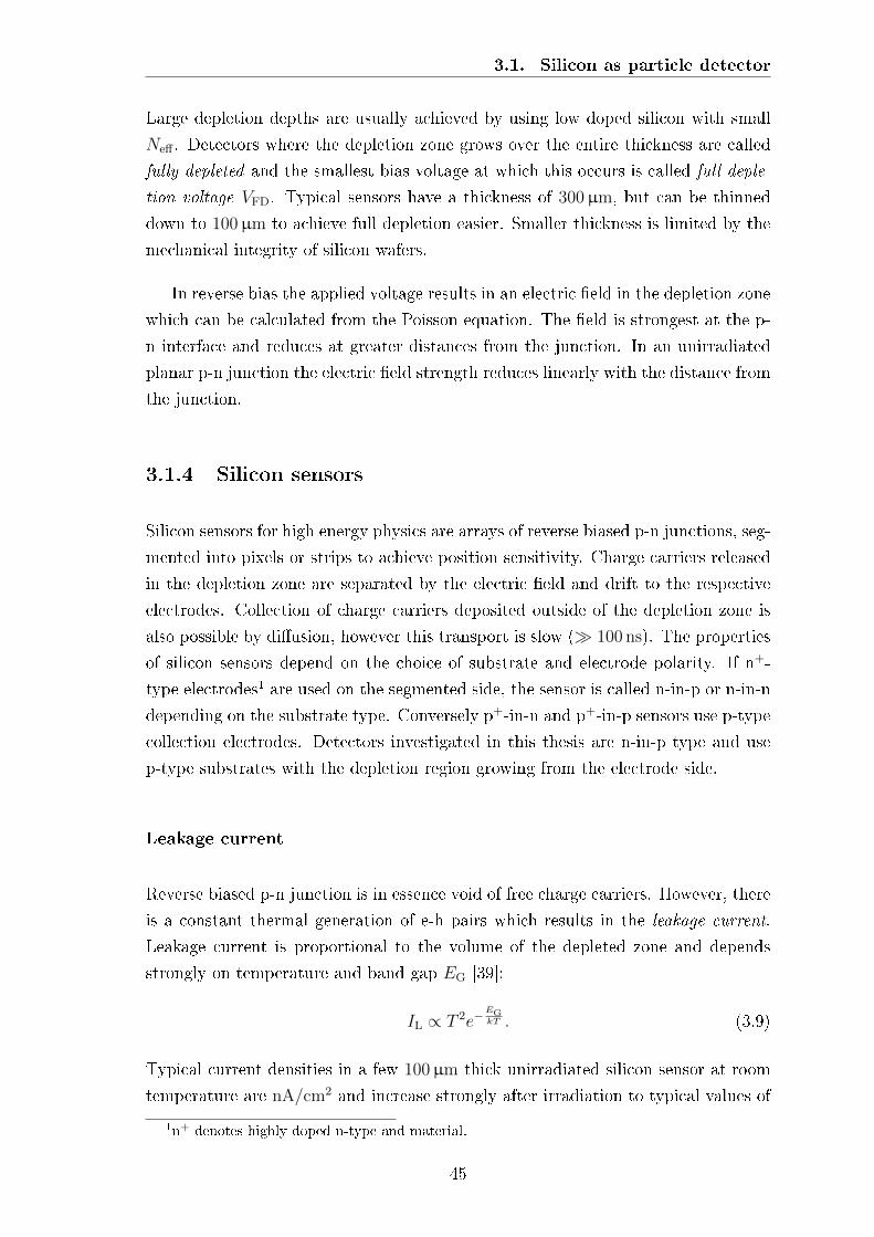
3.1.4 Silicon sensors . . . . . . . . . . . . . . . . . . . . . . . . . . . 45
3.1.5 Noise in silicon detectors . . . . . . . . . . . . . . . . . . . . . 46
3.2 Charged particle interaction with matter . . . . . . . . . . . . . . . . 47
3.3 Shockley-Ramo theorem . . . . . . . . . . . . . . . . . . . . . . . . . 49
3.4 Hybrid pixel detectors . . . . . . . . . . . . . . . . . . . . . . . . . . 51
3.5 MAPS Monolithic Active Pixel Sensors . . . . . . . . . . . . . . . . 52
3.5.1 Large and small readout electrode designs . . . . . . . . . . . 53
3.5.2 SOI sensors . . . . . . . . . . . . . . . . . . . . . . . . . . . . 55
4 Radiation damage in silicon 57
11

4.1 Surface radiation damage . . . . . . . . . . . . . . . . . . . . . . . . . 57
4.2 Displacement damage . . . . . . . . . . . . . . . . . . . . . . . . . . . 58
4.2.1 NIEL hypothesis . . . . . . . . . . . . . . . . . . . . . . . . . 60
4.2.2 Leakage current . . . . . . . . . . . . . . . . . . . . . . . . . . 61
4.2.3 Charge trapping . . . . . . . . . . . . . . . . . . . . . . . . . . 62
4.2.4 Changes of eective doping concentration . . . . . . . . . . . . 63
4.2.5 Acceptor removal . . . . . . . . . . . . . . . . . . . . . . . . . 65
5 DMAPS prototypes for ATLAS Phase-II upgrade 71
5.1 LFoundry 150 nm development line . . . . . . . . . . . . . . . . . . . 72
5.2 TowerJazz 180 nm development line . . . . . . . . . . . . . . . . . . . 73
5.2.1 Asynchronous readout architecture in TJ MALTA . . . . . . . 76
5.3 ams/TSI 180/350 nm development line pixel . . . . . . . . . . . . . 77
5.4 ams 350 nm development line strip . . . . . . . . . . . . . . . . . . 78
5.5 X-FAB 180 nm development line . . . . . . . . . . . . . . . . . . . . . 78
6 Laboratory setups for charge collection measurements 81
6.1 TCT Transient current technique . . . . . . . . . . . . . . . . . . . 82
6.1.1 TCT setup . . . . . . . . . . . . . . . . . . . . . . . . . . . . 84
6.1.2 TCT method and analysis . . . . . . . . . . . . . . . . . . . . 86
6.2 Charge collection measurement with 90Sr . . . . . . . . . . . . . . . . 89
7 Results of charge collection measurements 95
7.1 Irradiation of samples . . . . . . . . . . . . . . . . . . . . . . . . . . . 95
7.2 Results with LFoundry prototypes . . . . . . . . . . . . . . . . . . . . 97
7.2.1 Edge-TCT measurements with CCPD_LF . . . . . . . . . . . 99
7.2.2 Edge-TCT measurements with "Test Structures" chip . . . . . 106
7.2.3 Two dimensional Edge-TCT measurements . . . . . . . . . . . 108
7.2.4 90Sr measurements with "Test Structures" chip . . . . . . . . 110
7.3 Results with CHESS2 . . . . . . . . . . . . . . . . . . . . . . . . . . . 113
7.3.1 Edge-TCT measurements with CHESS2 . . . . . . . . . . . . 115
7.3.2 90Sr measurements with CHESS2 . . . . . . . . . . . . . . . . 121
7.4 Results with X-FAB XTB02 . . . . . . . . . . . . . . . . . . . . . . . 124
7.4.1 Simulation of charge collection in a SOI device . . . . . . . . . 132
7.5 Results with TowerJazz Investigator . . . . . . . . . . . . . . . . . . . 135
7.6 Summary of acceptor removal in CMOS detectors . . . . . . . . . . . 142
8 Test beam eciency measurement with TowerJazz MALTA 145
8.1 Tested samples . . . . . . . . . . . . . . . . . . . . . . . . . . . . . . 145
8.2 Experimental setup . . . . . . . . . . . . . . . . . . . . . . . . . . . . 148

8.2.1 Track reconstruction and selection . . . . . . . . . . . . . . . . 148
8.2.2 Eciency calculation . . . . . . . . . . . . . . . . . . . . . . . 151
8.3 Eciency measurement . . . . . . . . . . . . . . . . . . . . . . . . . . 153
8.3.1 Eciency of unirradiated sample . . . . . . . . . . . . . . . . 153
8.3.2 Eciency of irradiated sample . . . . . . . . . . . . . . . . . . 156
8.3.3 Dependence of eciency on threshold and bias voltage . . . . 159
8.4 Further development . . . . . . . . . . . . . . . . . . . . . . . . . . . 159
9 Summary and outlook 163
Bibliography 167
Raz²irjeni povzetek v slovenskem jeziku 179


List of gures
2.1 CERN accelerator complex . . . . . . . . . . . . . . . . . . . . . . . . 26
2.2 Schedule of the LHC operations 20112026 . . . . . . . . . . . . . . . 26
2.3 Particles of the standard model . . . . . . . . . . . . . . . . . . . . . 28
2.4 Standard model production cross sections measured by ATLAS . . . . 29
2.5 The ATLAS experiment . . . . . . . . . . . . . . . . . . . . . . . . . 30
2.6 ATLAS Inner Detector layout . . . . . . . . . . . . . . . . . . . . . . 32
2.7 HL-LHC event with 200 pile-up . . . . . . . . . . . . . . . . . . . . . 33
2.8 ATLAS ITk layout . . . . . . . . . . . . . . . . . . . . . . . . . . . . 34
2.9 Simulated uence and dose distributions in the ATLAS ITk after
4000 fb−1 at HL-LHC . . . . . . . . . . . . . . . . . . . . . . . . . . . 35
2.10 Simulated tracking performance of ITk CMOS Layer 4 . . . . . . . . 37
3.1 Dopant energy levels in silicon . . . . . . . . . . . . . . . . . . . . . . 41
3.2 p-n junction . . . . . . . . . . . . . . . . . . . . . . . . . . . . . . . . 42
3.3 Charge density, electric eld and potential in p-n junction . . . . . . 44
3.4 Mean energy loss of muons in copper . . . . . . . . . . . . . . . . . . 48
3.5 Energy loss distribution of 2GeV positrons in silicon . . . . . . . . . 49
3.6 Simulated electric and weighting eld in a strip detector . . . . . . . 50
3.7 Hybrid pixel detector . . . . . . . . . . . . . . . . . . . . . . . . . . . 51
3.8 MAPS and DMAPS . . . . . . . . . . . . . . . . . . . . . . . . . . . 53
3.9 Large and small collection electrode MAPS designs . . . . . . . . . . 54
3.10 Contributions to detector capacitance in MAPS . . . . . . . . . . . . 55
3.11 Schematics of a SOI MAPS . . . . . . . . . . . . . . . . . . . . . . . 56
4.1 Types of point defects in silicon . . . . . . . . . . . . . . . . . . . . . 59
4.2 Sources of radiation damage in the bulk . . . . . . . . . . . . . . . . 59
4.3 Simulated distribution of vacancies in irradiated silicon . . . . . . . . 60
4.4 Increase of space charge after irradiation in dierent silicon wafers . . 64
4.5 Parametrisation of acceptor removal t to data . . . . . . . . . . . 69
5.1 CMOS chips in LFoundry development line . . . . . . . . . . . . . . . 73
5.2 TowerJazz process modication . . . . . . . . . . . . . . . . . . . . . 74
15

5.3 TowerJazz MALTA readout architecture . . . . . . . . . . . . . . . . 75
5.4 Pixel design in X-FAB SOI architecture . . . . . . . . . . . . . . . . . 79
6.1 Absorption depth of light in silicon . . . . . . . . . . . . . . . . . . . 83
6.2 Top- and Edge-TCT . . . . . . . . . . . . . . . . . . . . . . . . . . . 83
6.3 TCT setup . . . . . . . . . . . . . . . . . . . . . . . . . . . . . . . . . 84
6.4 Induced pulses and charge proles measured with Edge-TCT . . . . . 87
6.5 Edge-TCT focus nding procedure . . . . . . . . . . . . . . . . . . . 88
6.6 Setup for measurements of CCE with 90Sr . . . . . . . . . . . . . . . 90
6.7 Example of CCE measurements with 90Sr . . . . . . . . . . . . . . . . 92
7.1 Test structures on LFoundry CCPD_LF sample . . . . . . . . . . . . 98
7.2 Test structures on LFoundry "Test Structures" sample . . . . . . . . 98
7.3 Photograph of LFoundry CMOS prototypes . . . . . . . . . . . . . . 99
7.4 CCPD_LF induced pulses in Edge-TCT measurement . . . . . . . . 100
7.5 CCPD_LF charge collection proles . . . . . . . . . . . . . . . . . . 102
7.6 CCPD_LF depletion depth in irradiated samples . . . . . . . . . . . 104
7.7 CCPD_LF Neff evolution with received neutron uence . . . . . . . . 105
7.8 Depletion depth in LFoundry "Test Structures" chip . . . . . . . . . . 107
7.9 Evolution of Neff with uence in LF "Test Structures" . . . . . . . . . 108
7.10 CCPD_LF two dimensional Edge-TCT measurement . . . . . . . . . 109
7.11 LFoundry 90Sr charge spectra . . . . . . . . . . . . . . . . . . . . . . 111
7.12 LFoundry dependence of 90Sr charge on bias voltage . . . . . . . . . . 112
7.13 Charge carrier drift in top/back biased detector . . . . . . . . . . . . 113
7.14 CHESS2 prototype chip . . . . . . . . . . . . . . . . . . . . . . . . . 114
7.15 CHESS2 Edge-TCT charge proles after neutron irradiation . . . . . 116
7.16 CHESS2 Edge-TCT depletion depth after neutron irradiation . . . . 117
7.17 CHESS2 Neff evolution with received neutron uence . . . . . . . . . 118
7.18 CHESS2 Edge-TCT depletion depth after proton irradiation . . . . . 120
7.19 CHESS2 Neff evolution with proton uence . . . . . . . . . . . . . . . 121
7.20 CHESS2 90Sr charge spectra . . . . . . . . . . . . . . . . . . . . . . . 122
7.21 CHESS2 mean MIP charge for dierent irradiation levels . . . . . . . 123
7.22 X-FAB XTB02 sample . . . . . . . . . . . . . . . . . . . . . . . . . . 125
7.23 X-FAB XTB02 depletion depth . . . . . . . . . . . . . . . . . . . . . 126
7.24 X-FAB XTB02 Neff evolution with neutron uence . . . . . . . . . . 127
7.25 X-FAB XTB02 2d Edge-TCT maps at dierent Vbias . . . . . . . . . . 128
7.26 X-FAB XTB02 2d Edge-TCT maps at dierent uences . . . . . . . . 129
7.27 X-FAB XTB02 induced pulses and eciency gaps . . . . . . . . . . . 130
7.28 X-FAB XTB02 2d maps at dierent biasing congurations . . . . . . 131
7.29 SOI device simulated in KDetSim . . . . . . . . . . . . . . . . . . . . 133

7.30 SOI simulation charge collection maps . . . . . . . . . . . . . . . . 134
7.31 TowerJazz Investigator chip . . . . . . . . . . . . . . . . . . . . . . . 136
7.32 TJ Investigator output signal . . . . . . . . . . . . . . . . . . . . . . 137
7.33 TJ Investigator 2d Edge-TCT on 20µm× 20µm pixels . . . . . . . . 138
7.34 TJ Investigator 2d Edge-TCT on 50µm× 50µm pixels (low doping) . 139
7.35 TJ Investigator 2d Edge-TCT on 50µm× 50µm pixels (high doping) 140
7.36 TJ Investigator 2d Edge-TCT measurements at dierent uences . . . 141
7.37 Acceptor removal coecient in HV-CMOS materials . . . . . . . . . . 143
8.1 TowerJazz MALTA sample . . . . . . . . . . . . . . . . . . . . . . . . 146
8.2 ENC spectrum of TowerJazz front end . . . . . . . . . . . . . . . . . 147
8.3 Test beam experimental setup . . . . . . . . . . . . . . . . . . . . . . 149
8.4 Track to cluster residual distributions in test beam on MALTA DUT 150
8.5 Reduced χ2 distribution of track reconstruction t . . . . . . . . . . . 152
8.6 2× 2 pixel cell for test beam eciency measurement . . . . . . . . . . 153
8.7 In-pixel eciency in unirradiated MALTA chip . . . . . . . . . . . . . 154
8.8 Average cluster size in unirradiated MALTA chip . . . . . . . . . . . 155
8.9 In-pixel eciency in a MALTA chip irradiated to 1 · 1015 neq/cm2 . . 156
8.10 Average cluster size in irradiated MALTA chip . . . . . . . . . . . . . 157
8.11 Comparison of in-pixel eciency in sectors S2 and S3 . . . . . . . . . 158
8.12 Dependence of detection eciency on threshold and Vbias . . . . . . . 160
8.13 Proposed modications of TowerJazz pixel design . . . . . . . . . . . 162
8.14 Simulated transient current in dierent pixel designs . . . . . . . . . 162

List of tables
2.1 Specications of ATLAS pixel detectors . . . . . . . . . . . . . . . . . 35
7.1 List of irradiated CHESS2 samples. . . . . . . . . . . . . . . . . . . . 115
19


List of acronyms
ATLAS A Toroidal LHC ApparatuS. 29
BOX Buried oxide. 56
BSM Beyond Standard Model Physics. 27
CCE Charge collection eciency. 89
CERN European Organization for Nuclear Research. 23
DMAPS Depleted Monolithic Active Pixel Sensor. 23, 53
DUT Detector under test. 145
ENC Equivalent noise charge. 46
HL-LHC High Luminosity LHC. 23, 32
HR-CMOS High resistivity CMOS (detector). 53
HV-CMOS High voltage CMOS (detector). 53
ID Inner Detector. 23, 31
ITk Inner Tracker. 23, 33
LHC Large Hadron Collider. 23
MAPS Monolithic Active Pixel Sensor. 39, 52
MIP Minimum ionising particle. 48, 145
MPV Most probable value. 48, 89
NIEL Non Ionising Energy Losses. 60
ROI Region of interest. 148
S/N Signal to noise ratio. 46
SCT Semiconductor Tracker. 31
SM Standard Model. 27
SOI Silicon on insulator. 55
TCT Transient Current Technique. 81, 82
TDAQ Trigger and Data Acquisition. 30
TID Total Ionising Dose. 57
21

22

Chapter 1
Introduction
Particle colliders are the primary experimental tools in the eld of high energy
physics that help us probe the properties of elementary particles and search for
physics beyond the Standard Model. The Large Hadron Collider (LHC) built by
the European Organization for Nuclear Research (CERN) in Geneva is the most
powerful particle collider to date, with proton-proton collisions reaching a centre of
mass energy of 13TeV. An integral part of LHC are experiments such as ATLAS,
which detect the products of collisions and allow us to reconstruct the underlying
physical processes.
To increase the sensitivity to rare processes the LHC will undergo the High Lu-
minosity upgrade (HL-LHC) in the years 20242026, which will increase the instan-
taneous luminosity to 5 · 1034 cm−2 s−1, a factor of ve above LHC. This ambitious
programme will present a major challenge for the experiments that will have to
cope with up to 200 simultaneous collisions and a signicantly increased radiation
damage. ATLAS will therefore undergo a substantial buildup named Phase-II up-
grade to be ready for data taking at HL-LHC. One of the main components of the
Phase-II upgrade will be replacement of the existing Inner Detector (ID) with a new
Inner Tracker (ITk) with a larger silicon surface area, greater radiation tolerance
and capability to operate at higher particle rates.
Current state of the art hybrid pixel detectors, consisting of sensor and readout
electronics implemented in separate silicon chips, are demanding in terms of produc-
tion resources due to technologically complex bump bond interconnections. ATLAS
CMOS collaboration explored the possibility of using depleted monolithic active
pixel sensors (DMAPS) produced in an industrial CMOS process to facilitate the
production of large detector volumes required for the outermost ITk Pixel Layer 4.
23
Chapter 1. Introduction
Monolithic detectors have sensing and readout functionality implemented on the
same silicon chip, thus removing the need for bump bonding, while also reducing
the material budget. Monolithic concept has been already known for a few decades,
but its radiation tolerance and speed of charge collection have been insucient for
use in high radiation environment. Recently rapid development of CMOS sensors
has been driven by commercial applications, such as smart phone imaging sensors,
which has resulted in several vendors oering processes enabling usage of high bias
voltages and/or high resistivity silicon substrates. This allows design of detector
elements with signicant depletion depth which is necessary for fast charge collec-
tion. Charged particle tracking detector production in such high volume industrial
process would allow a signicantly shorter turnaround time at a fraction of cost of
hybrid detectors.
Since ATLAS is pioneering the use of DMAPS in high radiation environment,
one of the main challenges for the ATLAS CMOS collaboration is demonstration
of sucient radiation hardness. Radiation damage can be classied in two main
categories: damage to the electronics which is predominantly a consequence of ion-
ising dose, and degradation of charge collection due to the damage in silicon lattice.
In this thesis extensive studies of charge collection in dierent DMAPS prototypes
developed within the ATLAS CMOS group were carried out after irradiating the
samples with neutrons and protons. Dierent measurement techniques encompass-
ing laser, radioactive sources and highly energetic particle beam were employed for
characterisation of samples.
This thesis has the following structure: Chapter 2 introduces the LHC machine,
its physics programme, and the ATLAS detector together with the details of Phase-II
upgrade. The basics of silicon particle detectors are presented in Chapter 3. Chapter
4 gives an overview of radiation damage in silicon and its eects on particle detec-
tors. DMAPS prototypes developed within the ATLAS CMOS collaboration and
investigated in this thesis are presented in Chapter 5. The laboratory setups used to
evaluate detector properties with Edge-TCT and radioactive sources are described
in Chapter 6, with the results following in Chapter 7. Measurements of detection
eciency with a DMAPS prototype in a test beam are shown in Chapter 8. Finally,
the conclusions and outlook are given in Chapter 9.
24
Chapter 2
The LHC and the ATLAS
Experiment
2.1 The Large Hadron Collider
The LHC is a synchrotron accelerator with a circumference of 27 km which can
collide two beams of protons with a centre of mass energy of 13TeV or nuclei of
heavy elements such as lead with a centre of mass energy of 2.8TeV per nucleon
[1, 2]. LHC uses a system of four preaccelerators which accelerate the beams to
an energy of 450GeV before injection into the main ring (Figure 2.1). The beams
intersect at four points along the LHC ring, called interaction points (IP) where
collisions occur. Four experiments named ALICE [3], ATLAS [4], CMS [5] and
LHCb [6] built around the interaction points detect the products of these collisions.
A core part of the LHC are 1232 NbTi superconducting dipole bending magnets
and additional higher order magnets for focusing of the beams. Particles are acceler-
ated with radiofrequency cavities which also longitudinally structure the beams into
groups called bunches. The LHC can simultaneously contain up to 2808 colliding
proton bunches per beam, spaced at a time interval of 25 ns.
The LHC operation is organised into periods of data taking called Runs, inter-
spersed with maintenance and upgrade periods called Shutdowns (Figure 2.2). In
2019 the LHC is in the state of the Long Shutdown (LS2) after having nished the
Run 2 data taking.
An important quantity specifying a collider's performance is the instantaneous
25

Chapter 2. The LHC and the ATLAS Experiment
Figure 2.1: Schematic view of the CERN accelerator complex showing the LHCwith the four main experiments ALICE, ATLAS, CMS and LHCb, as well as thepreaccelerator chain with independent experiments [7].
Figure 2.2: Schedule of the LHC operation with data taking (Runs) and maintenanceperiods (Shutdowns) [8].
26

2.1. The Large Hadron Collider
luminosity L which relates event rate dNdt
with the event cross section σ:
dN
dt= L · σ. (2.1)
The total number of events produced in a given time frame is proportional to the
integrated luminosity Lint which is a time integral of L. The units of Lint are inverse
barns: 1 b−1 = 0.01 fm−2. The design value of the instantaneous luminosity in
proton-proton collisions at the LHC is 1·1034 cm−2 s−1 [2], but excellent performance
of the LHC and the experiments resulted in peak luminosities above 2 ·1034 cm−2 s−1
in Run 2 data taking [9].
However, a higher instantaneous luminosity results in an increased number of
proton-proton interactions, called pile-up, within an individual bunch crossing. The
average value of pile-up during the LHC Run 2 in the year 2018 was 38.3 [9], but
it is planned to increase up to 200 during the HL-LHC operation (see Section 2.3).
High pile-up causes an increased readout occupancy in the detectors and can even-
tually result in an irreversible data loss due to insucient data processing capacities.
Moreover, a high density of the collisions makes it challenging to correctly assign the
detected collision products to a certain collision vertex. Therefore, a compromise
between high luminosity and a feasible detection capability is necessary.
2.1.1 Physics at the LHC
The current theory describing elementary particles and their interactions is the stan-
dard model of electroweak and strong interactions (SM). It was developed in 1960s
and 1970s [10, 11, 12, 13] and describes particles of matter (quarks and leptons)
which interact via elementary forces by exchange of gauge bosons. The most re-
cently discovered constituent of the SM is the Higgs boson, a particle of the Higgs
eld which interacts with massive particles [14, 15, 16, 17]. The SM constituents
and their properties are shown in Figure 2.3.
Many theoretical predictions of the SM agree with experimentally observed data
to a very high degree of precision. However, the SM does not account for some phe-
nomena such as gravity, the dark matter and dark energy, the neutrino oscillations
or the matter-antimatter asymmetry in the universe. Their sources are commonly
referred to as beyond standard model (BSM) physics or new physics and are one of
the main drivers for the modern particle physics experiments. Since BSM processes
are expected to occur at very high energies and at low rates, both high collision
energy and high luminosity are vital for its discovery. The LHC with its unprece-
27

Chapter 2. The LHC and the ATLAS Experiment
u c t
d s b
e μ τ
νe νμ ντ
g
γ
W Z
Hup charm top
down strange bottom
electron muon tau
e neutrino μ neutrino τ neutrino
gluon
photon
W boson Z boson
higgs
2.2 M 1.27 G 173.21 G
4.7 M 96 M 4.18 G
0.51 M 105.66 M 1.78 G
< 2 < 0.19 M < 18.2 M
0
0
80.38 G 91.18 G
125.09 G
+2/3 +2/3 +2/3
-1/3 -1/3 -1/3
-1 -1 -1
0 0 0
0
0
±1 0
0
1/2 1/2 1/2
1/2 1/2 1/2
1/2 1/2 1/2
1/2 1/2 1/2
1
1
1 1
0
Mass: eV/c2
Charge
Spin
Name
1st 2nd 3rd
strongnuclear
force
electromagnetic
force
weak
nuclearforce
QUARKS
LEPTONS
FERMIONS GAUGE BOSONS
Figure 2.3: Particles of the standard model. Image from [18].
dented collision energy and high luminosity thus provides an excellent environment
for such studies.
The research programme at the LHC can be divided in two categories: precision
measurements of SM processes and searches for new, yet unobserved phenomena
within and beyond the SM. The precision measurements are aimed at studying the
known SM processes and determine their parameters such as particle masses or
process cross sections. These measurements are vital as SM processes represent a
background to potential new physics and it is important to correctly estimate their
contribution. Moreover, discrepancies between the SM and experimental data may
indicate the nature of new physics. The LHC allows us to study the entire spectrum
of the SM, including the heaviest known particles the top quark, the W and Z
bosons and the Higgs boson and to measure their properties with unprecedented
precision. As an example Figure 2.4 shows a summary of p-p production cross
sections of several SM processes measured by the ATLAS detector.
The objective of searches in HEP is to look for yet unobserved processes which
can originate from the SM or beyond. Experiments at the LHC have made numerous
rst observations of SM processes such as on-shell light-light scattering [19] and
existence of pentaquarks [20]. However, the greatest success to date was the rst
observation of the Higgs boson by experiments ATLAS and CMS in 2012 [21, 22].
This discovery came as a large success ve decades after the theoretical introduction
of the electroweak symmetry breaking mechanism [14, 15, 16, 17].
The open questions of the SM suggest existence of other unknown particles,
which motivate searches for BSM physics. At the LHC theses are roughly divided
28

2.2. The ATLAS Experiment
pp
500 µb−1
80 µb−1
W Z tt t
t-chan
WW H
total
ttH
VBF
VH
Wt
2.0 fb−1
WZ ZZ t
s-chan
ttW ttZ tZj
10−1
1
101
102
103
104
105
106
1011σ
[pb]
Status: July 2018
ATLAS Preliminary
Run 1,2√s = 7,8,13 TeV
Theory
LHC pp√
s = 7 TeV
Data 4.5 − 4.6 fb−1
LHC pp√
s = 8 TeV
Data 20.2 − 20.3 fb−1
LHC pp√
s = 13 TeV
Data 3.2 − 79.8 fb−1
Standard Model Total Production Cross Section Measurements
Figure 2.4: Summary of SM production cross sections measured by ATLAS [9].
into two groups: SUSY and exotics. Supersymmetry (SUSY) is a theory which
proposes elegant solutions to some of the problems not solved by the SM and also
predicts existence of supersymmetric partners to SM particles [23]. The lightest
SUSY particle is predicted to be stable and is a candidate for the dark matter
particle. Exotics cover a broad range of particles predicted by BSM theories which
include additional gauge bosons, heavy neutrinos, extra dimensions, multiple Higgs
bosons, miniature black holes or gravitons.
No BSM physics has yet been observed at the LHC, but the experimental data
allows us to exclude low mass regions and set a lower limit on the mass of new
particles. These typically lie in range of few TeV. Further data taking will reduce
the statistical errors and increase potential to discover new physics.
2.2 The ATLAS Experiment
A Toroidal LHC ApparatuS (ATLAS) is one of the four main experiments at the
LHC and together with CMS one of the two general purpose detectors [4, 24]. It
has a cylindrical layout with a length of 44m and a diameter of 25m consisting of a
29

Chapter 2. The LHC and the ATLAS Experiment
Figure 2.5: The ATLAS experiment with detector subsystems [4].
barrel with two end caps (Figure 2.5). This geometry achieves an almost hermetic
coverage around the interaction point.
The layout of ATLAS is driven by the requirement to successfully reconstruct
all particles generated by proton collisions. For example a leptonic decay of a top
quark t → bℓν requires precise tracking to detect the decaying b quark, detection
of the lepton, and complete measurement of hadronic jet energies to detect missing
energy carried by a neutrino.
The main detector subsystems are thus the Inner Detector for charged particle
tracking, electromagnetic and hadronic calorimeters for energy measurements and
muon detectors for muon identication and momentum measurement. A supercon-
ductive magnetic system consisting of an inner solenoid and an outer toroid provides
a complex magnetic eld for bending of charged particle trajectories. A three stage
real time trigger and data acquisition (TDAQ) system is used for identication of the
most interesting events which are retained for further analysis. The trigger system
reduces the readout rate from 40MHz (rate of LHC collisions) to around 200Hz,
which is feasible for storage.
ATLAS uses a Cartesian coordinate system with the origin in the IP, the z-axis
given by the beam direction, and the xy-plane (named also the transverse plane)
oriented by the positive x-axis showing toward the centre of the LHC ring. Positions
in the transverse direction are often given by the radial distance to the IP R and
30

2.2. The ATLAS Experiment
the azimuthal angle ϕ. Another commonly used coordinate is the pseudorapidity η,
which is a transformation of the polar angle to the z-axis θ:
η = − ln tan (θ/2). (2.2)
For the directions along the beam axis pseudorapidity takes values of η = ±∞ and
for θ = 90 it takes value η = 0. A useful feature is that every distribution over
pseudorapidity is Lorentz invariant for relativistic boosts in z-direction.
2.2.1 ATLAS Inner Detector
The ATLAS Inner Detector (ID) is dedicated to reconstruction of charged particle
trajectories [4]. This serves several purposes: calculation of particle momentum from
the track's curvature in the magnetic eld, charge identication, and determination
of the track's vertex (point of origin). The latter plays a role in heavy avour tagging
detection of long lived hadrons containing c or b quarks, which generate primary
and secondary vertices separated by several 100µm.
The ID consists of three subsystems (Figure 2.6): closest to the beam pipe is the
silicon Pixel Detector, followed by the silicon microstrip detector (Semiconductor
Tracker - SCT) and the straw-tube Transition Radiation Tracker (TRT). The ID
is contained within the 2T solenoid magnet and covers a pseudorapidity range of
η < |2.5|. The silicon sensors are operated at low temperatures around −10C
provided by a CO2 based cooling system. A multiple layer design ensures particle
detection in several points along its trajectory to provide reliable tracking.
The Pixel Detector utilises pixels with a size of 400µm in the z-direction and
50µm in ϕ, while the SCT uses one dimensionally segmented microstrips with a
pitch of 80µm in ϕ-direction and a length of approximately 12 cm. Strip sensors
are assembled in so called stereo modules composed of two sensors rotated relative
to each other by a small angle of 40mrad to provide hit sensitivity along the strip
length. Before the beginning of the LHC Run 2 in 2014 an additional innermost
layer of pixels, the Insertable B-Layer (IBL), was installed at a radius of 3.2 cm from
the interaction point to further improve the tracking performance [25]. The IBL has
a pixel size of 250µm× 50µm and partially employs 3D silicon sensors which is the
rst large scale experimental use of this type of detector.
The proximity of the interaction point makes the ID particularly the Pixel
Detector the most exposed part of ATLAS in terms of particle rate and radia-
31

Chapter 2. The LHC and the ATLAS Experiment
(a) (b)
Figure 2.6: a) The ATLAS Inner Detector layout [26]. b) Schematics of the barrelpart with radial distances to the interaction point [27].
tion damage. This dictates use of fast and radiation resistant sensors and readout
electronics. Moreover, the entire detector layout has to be lightweight to minimise
scattering on detector components and provide a good tracking resolution.
2.3 High Luminosity LHC and ATLAS Phase-II up-
grade
By the end of the Run 2 in 2018 the LHC delivered an integrated luminosity of
190 fb−1 [9]. By the end of Run 3 in 2023 the total delivered luminosity will have
reached 300 fb−1. At this point the operation under the same conditions would re-
quire an impractically long time to acquire a further statistically signicant dataset,
as halving of the statistical error for a given measurement would require around ten
years. The LHC is therefore planned to undergo a major upgrade in the years 2024
2026 named High Luminosity LHC (HL-LHC, Figure 2.2). This will consolidate the
machine for another 1015 years of data taking in which it will deliver an integrated
luminosity up to 4000 fb−1 [28].
The nominal peak instantaneous luminosity of the HL-LHC will increase to
5 · 1034 cm−2 s−1 with the ultimate values reaching up to 7.5 · 1034 cm−2 s−1 and
corresponding pileup values 140200. This is an increase by a factor 57.5 com-
pared to the original LHC design values. Collision events will contain an enormous
number of particles (Figure 2.7) which will have to be correctly detected and as-
signed to the right vertices. At present the experiments are not designed for such
challenging conditions. The increased detector occupancy and data rates would re-
32
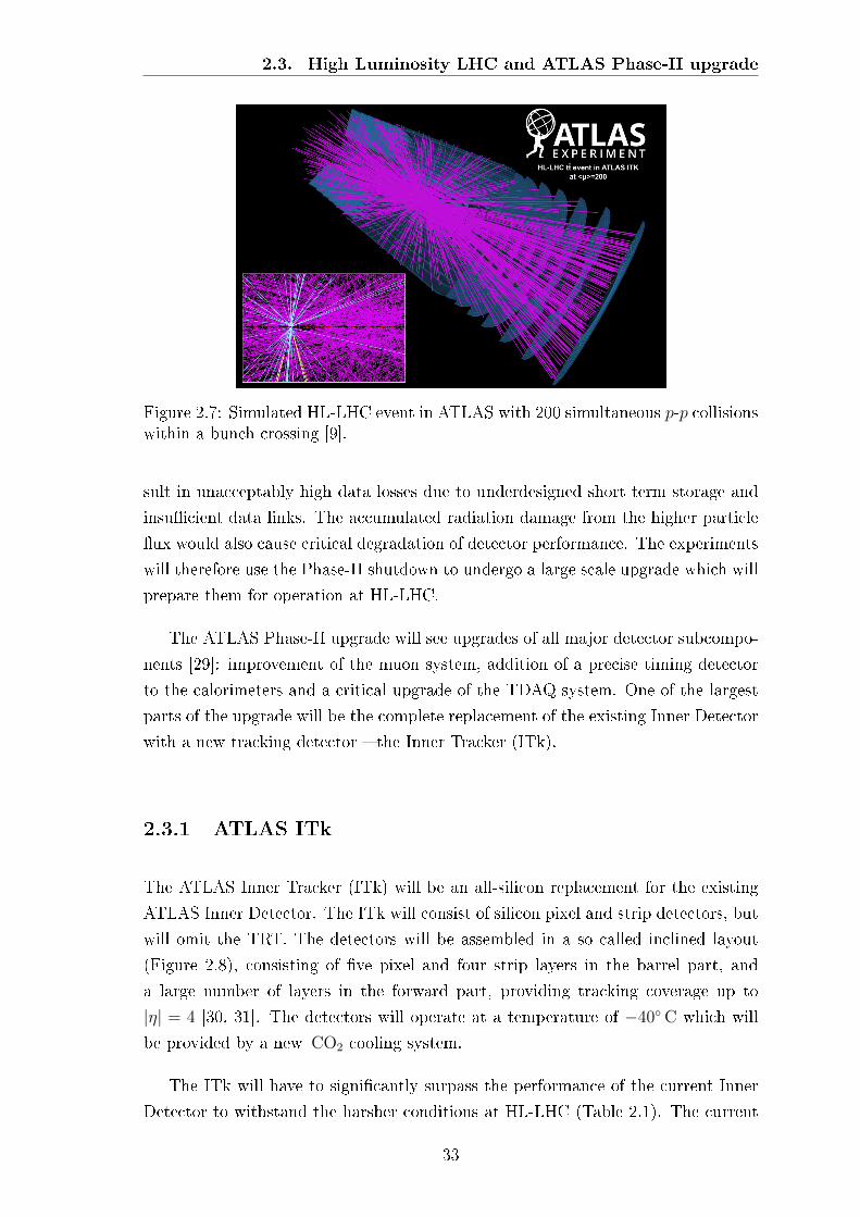
2.3. High Luminosity LHC and ATLAS Phase-II upgrade
Figure 2.7: Simulated HL-LHC event in ATLAS with 200 simultaneous p-p collisionswithin a bunch crossing [9].
sult in unacceptably high data losses due to underdesigned short term storage and
insucient data links. The accumulated radiation damage from the higher particle
ux would also cause critical degradation of detector performance. The experiments
will therefore use the Phase-II shutdown to undergo a large scale upgrade which will
prepare them for operation at HL-LHC.
The ATLAS Phase-II upgrade will see upgrades of all major detector subcompo-
nents [29]: improvement of the muon system, addition of a precise timing detector
to the calorimeters and a critical upgrade of the TDAQ system. One of the largest
parts of the upgrade will be the complete replacement of the existing Inner Detector
with a new tracking detector the Inner Tracker (ITk).
2.3.1 ATLAS ITk
The ATLAS Inner Tracker (ITk) will be an all-silicon replacement for the existing
ATLAS Inner Detector. The ITk will consist of silicon pixel and strip detectors, but
will omit the TRT. The detectors will be assembled in a so called inclined layout
(Figure 2.8), consisting of ve pixel and four strip layers in the barrel part, and
a large number of layers in the forward part, providing tracking coverage up to
|η| = 4 [30, 31]. The detectors will operate at a temperature of −40C which will
be provided by a new CO2 cooling system.
The ITk will have to signicantly surpass the performance of the current Inner
Detector to withstand the harsher conditions at HL-LHC (Table 2.1). The current
33

Chapter 2. The LHC and the ATLAS Experiment
Figure 2.8: Schematic view of the ATLAS ITk layout in one quadrant with pixeldetector (red) and strip detector (blue). Interaction point is at (0,0) [30, 31].
ID is designed to operate at peak luminosities of 1 · 1034 cm−2 s−1 over a lifespan of
10 years in which it will record up to 400 fb−1. In terms of radiation damage (see
Chapter 4) this translates to a hadron uence of 1 ·1015 neq/cm2 in the pixel detector
and 2 · 1014 neq/cm2 in the SCT [32]. The Pixel Detector also has to withstand a
total ionising dose of 50MRad. The high-performance IBL is designed for 850 fb−1,
a uence of 5 · 1015 neq/cm2 and an ionising dose of 250MRad. The front end elec-
tronics, short term data buering and output bandwidth of the ID reach saturation
at a particle rate of ∼ 1MHz/mm2, which occurs at a luminosity of 3 ·1034 cm−2 s−1
(pile-up ∼ 50) at 25 ns bunch crossing time. Higher luminosity results in signicant
data losses. This performance does not meet the requirements for the HL-LHC.
The ITk will have to withstand 4000 fb−1, a peak luminosity of 7.5 ·1034 cm−2 s−1
and a pile-up of 200. The distribution of the accumulated radiation damage at the
end of the ITk lifetime has been evaluated by a simulation shown in Figure 2.9. The
innermost pixel layer (Layer 0) is expected to receive a particle ux of 10MHz/mm2,
a hadron uence of 2 ·1016 neq/cm2 and an ionising dose of 1GRad (last two numbers
include a safety factor of 1.5). To ensure sucient detector performance newly
developed radiation hard sensors will have to be used: 3D sensors in Layer 0 and
thinned planar sensors with a thickness of 100µm to 150µm in the outer layers. The
pixel detector will also use a new readout chip produced in 65 nm CMOS technology
which is under joint development with CMS [33]. Despite the improved components
the two innermost pixel layers will have to be replaced after 2000 fb−1 at the half of
the ITk lifetime due to the extreme radiation damage [30].
The outermost pixel layer of the ITk (Layer 4) will be exposed to a particle ux
34

2.3. High Luminosity LHC and ATLAS Phase-II upgrade
z [cm]
0 50 100 150 200 250 300 350 400
r [c
m]
0
20
40
60
80
100
-1 /
4000
fb-2
cmS
i 1 M
eV n
eutr
on e
q. fl
uenc
e
1410
1510
1610
1710
Simulation PreliminaryATLASFLUKA + PYTHIA8 + A2 tune
ITk Inclined Duals
(a)
z [cm]
0 50 100 150 200 250 300 350 400
r [c
m]
0
20
40
60
80
100
-1G
y / 4
000f
bT
otal
ioni
sing
dos
e
410
510
610
710
Simulation PreliminaryATLASFLUKA + PYTHIA8 + A2 tune
ITk Inclined Duals
(b)
Figure 2.9: Simulated a) uence and b) dose distributions in the ATLAS ITk after4000 fb−1 at HL-LHC [34].
Pixels LHC IBLHL-LHC
Pixel Layer 0HL-LHC
Pixel Layer 4
Particle rate 1MHz/mm2 5MHz/mm2 10MHz/mm2 1MHz/mm2
Hadron uence 1 · 1015 neq/cm2 5 · 1015 neq/cm2 2 · 1016 neq/cm2 1.5 · 1015 neq/cm2
Ionising dose 50MRad 250MRad 1000MRad 80MRad
Area 1.7m2 0.15m2 ≈ 1m2 ≈ 10m2
Table 2.1: Design specications for dierent ATLAS pixel detectors [25, 29, 32].
of 1MHz/mm2, accumulating a total uence of 1.5 · 1015 neq/cm2 and an ionising
dose of 80MRad. The large surface area of Layer 4 (approximately 10m2) has
motivated investigations of new detector concepts which would simplify the detector
production, such as active CMOS sensors, described in the next Section 2.3.2.
The ITk strip detector will cover a total area of ≈ 160m2 and will have to
withstand uences up to 1.2 · 1015 neq/cm2 and ionising doses up to 50MRad (safety
factor 1.5 included). The strip detector will also get a greater role in the trigger
architecture, as it will contribute already to the rst trigger level (Level-0 trigger)
[34].
2.3.2 CMOS pixel option for ITk
For pixel detectors at hadron colliders high speed and radiation hardness are paramount.
The main technology that has been successfully used for many years and is also the
baseline for ITk are so called hybrid detectors. In hybrid pixel modules the electron-
ically passive sensor an the readout electronics are implemented in separate silicon
chips interconnected by bump bonding (discussed in 3.4). Since bump bonding is
35

Chapter 2. The LHC and the ATLAS Experiment
complex and requires highly specialised production processes, simplications are
desired.
As an alternative to the hybrid solution ATLAS was investigating active CMOS
detectors, where the sensor and readout electronics are implemented in the same chip
and therefore do not require the complicated hybridisation (bump bonding) step.
CMOS sensors have a widespread use in digital imaging and are a well developed
technology, which however has to be adapted for application in HEP experiments.
The main problem of existing technology is insucient speed because of slow charge
collection resulting also in low radiation tolerance. In particle tracking applications
uniform eciency over entire chip surface is required, which is also not the case for
imaging sensors. These are some of technological drawbacks that must be solved to
adapt CMOS technology for tracking at ATLAS. Another advantage of CMOS tech-
nology is a large number of vendors oering suitable CMOS processes and relatively
well available detector grade (high resistivity) silicon wafers. This may result in a
signicantly faster and cheaper production. In addition, CMOS technology leads to
a reduced amount of material in the detector volume, which can result in a better
position resolution due to reduced scattering. So far CMOS detectors have been
used in the experiments Star [35] and ALICE [36] where uences and particle rates
are by a factor of 100 lower than in ITk Layer 4. Since CMOS detectors have not yet
been used in a large experiment with a high radiation and high rate environment it
is imperative to demonstrate tat they are suitable for reliable operation in the entire
lifetime expected for ITk.
ATLAS investigated CMOS detector technology as an option for the outermost
pixel layer (Layer 4), which has the largest surface and therefore oers the largest
savings of production resources. At the same time performance requirements in
terms of data rates and radiation hardness are not as high as in the inner layers.
ATLAS studied several dierent CMOS detector versions for Layer 4 which are
presented in detail in Chapter 5.
The CMOS option plans detectors with a small pixel pitch of ≤ 50µm and a
thickness of 25µm100µm. The eect of CMOS Layer 4 on ITk tracking perfor-
mance was compared to the benchmark 150µm thick hybrid solution in a simulation
[30]. Figure 2.10 shows an example of such comparison in a case of cluster eciency
for single muons. Overall no signicant dierences have been observed in terms of
cluster eciency, total number of clusters per track, track parameters d0, z0 and
q/pT and track reconstruction performance between the hybrid and the CMOS op-
tions, indicating that the CMOS option is viable from the physics point of view.
36

2.3. High Luminosity LHC and ATLAS Phase-II upgrade
Figure 2.10: Simulated tracking performance of CMOS Layer 4 in ITk. CMOSdetectors with pixel pitches 36µm×36µm and 50µm×50µm, and varying thicknesswere compared to the baseline 50µm × 50µm hybrid detector with a thickness of150µm. No signicant dierences in the eciency for association of cluster to tracksin Layer 4 were found between dierent options [30].
A successful operation in the challenging ATLAS environment would prove the
maturity of CMOS technology and make it a serious contender for future tracking
detectors. This motivated the international detector community to form a large
collaboration of institutes within and outside ATLAS with a goal to deliver a func-
tional CMOS module in time for the Phase-II upgrade. This required a substantial
amount of R&D, design iterations and testing which have been divided between the
institutions to maximise eciency. A part of the test programme were also studies
of radiation eects on CMOS sensors which is the topic of this thesis.
Due to a tight time line of the ATLAS Phase-II upgrade and with the detectors
still being in development phase the ATLAS pixel CMOS programme was stopped
in March 2019 after having run for more than four years. However, CMOS detectors
will be developed further outside of the scope of ATLAS to capitalise on the invested
eort and produce a fully functional monolithic CMOS detector.
37

Chapter 2. The LHC and the ATLAS Experiment
38

Chapter 3
Silicon particle detectors
Detectors for tracking applications in high energy physics have to be lightweight,
with a high resolution, fast, easily producible and in many cases radiation tolerant.
Silicon detectors have all these properties and are well available thanks to the highly
developed semiconductor industry. Silicon has therefore been the standard solution
for high performance tracking detectors.
This chapter covers the broad topic of silicon detectors from basics to applications
in modern experiments. The rst part introduces the principles of operation of
semiconductor detectors as p-n junctions, the interaction of highly energetic particles
with tracking detectors and the properties of signal formation.
The second part of this chapter presents detector solutions for high energy physics
experiments: the hybrid modules as the standard option for pixel detectors and the
emerging CMOS technology. The most attractive CMOS solution are Monolithic
Active Pixel Sensors (MAPS), where the entire detector functionality is implemented
on a single silicon chip.
3.1 Silicon as particle detector
3.1.1 Semiconductors
In an isolated atom electrons occupy discrete energy levels dened by the atomic
orbitals. When atoms form covalent bonds, atomic orbitals overlap and form new
energy states. In crystals, typically consisting of 1023 atoms per cm3, the overlapping
orbitals generate a multiplet of allowed states which form a quasi continuous energy
39

Chapter 3. Silicon particle detectors
region. These regions, called energy bands, are described by the energy band model
of solids (see e.g. [37]). In a thermal equilibrium at a temperature T the occupation
probability for a state with an energy E is given by the Fermi-Dirac statistics:
f(E) =1
e(E−EF)/kBT + 1, (3.1)
where kB is the Boltzmann constant and EF is the Fermi energy, at which the
occupation probability is exactly 0.5. Energy bands are separated by energy regions
where no states are allowed. The energy gap between the last occupied band the
valence band and the rst unoccupied band the conduction band is called band
gap Eg and determines electrical properties of materials. Based on Eg we classify
materials into:
• Conductors, if Eg = 0. The valence and conduction bands overlap. EF is
within the valence gap. Electrons can be easily raised into states which enable
electrical current to ow.
• Insulators, if Eg > 3 eV. The band gap is too large to allow transitions into
conduction band, therefore no current ows under applied electric eld. EF is
by convention set in the middle of the band gap.
• Semiconductors, if Eg < 3 eV. EF is in the middle of the band gap. The
band gap is suciently small to allow transitions into the conduction band by
thermal excitations.
In a semiconductor the transition of an electron into the conduction band leaves
a vacancy in the valence band, called hole. Electrons and holes can freely move
through the crystal lattice, allowing electric current to ow. The resistivity ρ of
a semiconductor depends on the electron/hole concentrations n and p, and their
mobilities µe and µh:
ρ =1
e(µen+ µhp). (3.2)
Charge carrier concentration in the conduction band of a pure semiconductor is
called intrinsic carrier concentration and is strongly temperature dependent.
Silicon is a semiconductor with an indirect band gap of 1.12 eV, an intrinsic
carrier concentration of ∼ 1010 cm−3 and an intrinsic resistivity of ρ ≈ 230 kΩ cm at
room temperature. The average ionisation energy Eion for generation of an electron-
hole pair in silicon is 3.6 eV, which includes the energy of a phonon produced in the
process.
40

3.1. Silicon as particle detector
E=1.12eV
gap
EC
EV
P
Al
0.045
0.067
As
Ga
0.054
0.072
Pd
0.34
Tl
0.3
Ti
In
0.16
0.21
Cu
0.53
0.24
0.4
Sb
B
0.045
0.039
Li0.033
C
0.25
0.35
D
Pt
0.36
0.3
0.25
A
D
Au
0.54
0.29
D
A
0.16
0.38
0.51
0.41
O
AGap center
0.14
0.55
0.4
Fe
Figure 3.1: Additional energy levels in silicon band gap introduced by impurities.Acceptor states are drawn in red and donor states in dark blue. Useful dopants, mostcommonly boron (B) and phosphorus (P), add additional levels near the conductionand valence bands, while other states in the mid gap such as those introduced bycopper or gold are undesired [38].
3.1.2 Doping of silicon
Electrical conductivity of silicon can be altered by doping addition of elements
from groups III and V of the periodic system which substitute Si atoms in the lat-
tice. Group III dopants such as boron are called acceptors and have three valence
electrons. To form four covalent bonds they accept an additional electron from a
neighbour Si atom and change from a neutral to a negatively charged state. The
complementary positively charged defect (hole) is highly mobile and acts as a posi-
tive charge carrier. Conversely, dopants from group V (such as phosphorus), called
donors, have an additional electron which is released into the lattice, leaving a pos-
itively charged donor ion. Silicon predominantly doped with acceptors is called
p-type and donor doped silicon is called n-type. In addition, silicon wafers also
contain low concentrations of other impurities such as oxygen and carbon which are
introduced during production process.
The dopant states inuence the position of energy bands relative to the Fermi
level. In p-type silicon the energy bands shift so that EF is between the valence
band and the acceptor level, while in n-type silicon EF is between the donor level
and the conduction band.
The energies of the states introduced by doping are called shallow states and are
typically separated by only a few tens of meV from the valence band (acceptors)
or the conductive band (donors) as shown in Figure 3.1. This means that at room
temperature with kBT = 23meV the thermal excitations are sucient to ionise the
majority of dopant atoms and create free charge carriers in the material. Depending
on the application the doping concentration range from ≈ 1012 cm−3 to ≈ 1020 cm−3,
which is much higher than intrinsic carrier concentration. Electrical properties of
such material, called extrinsic semiconductor, are completely determined by doping.
41

Chapter 3. Silicon particle detectors
donorlevel
acceptorlevel
n-type p-type
separate
momentof contact
equilibrium
e-currenth+current
electrons
holesh+ h+ h+ h+ h+
h+ h+
e-e-e-e-e-
e- e-
SCR
EF-iEF-n
EF-p
EC
EC
EC
EC
EF-n
EF-p
EF
EV
EV
EV
Figure 3.2: The p-n junction. Top: separate n-type and p-type material have adierent Fermi level. Middle: theoretical situation at the time of contact betweenthe two types. The Fermi levels equalise by diusion and recombination of chargecarriers. Bottom: emergence of space charge region in thermal equilibrium [38].
3.1.3 The p-n junction
Particle detectors rely on detecting a relatively small amount of e-h pairs deposited
in the material by highly energetic charged particles. In a typical 300µm thick
silicon detector approximately 24 000 e-h are deposited on average. In silicon with
intrinsic carrier concentration of the order of ∼ 1010 cm−3 the additional charge
is insignicant, hence pure silicon cannot be used as a detector. A greatly reduced
concentration of background free charge carriers can be achieved in a depleted region
which forms on the p-n junction in doped silicon.
A p-n junction develops on the interface between p-type and n-type silicon (Fig-
ure 3.2). Separated p- and n-type materials have dierent Fermi levels. On contact,
their Fermi levels equalise, leading to the shifting of energy bands. On a microscopic
level a gradient in the charge carrier concentration results in diusion of majority
charge carriers into the opposite type material where they recombine. In the process
the p-side obtains a net negative charge and the n-side a net positive charge (space
charge) due to the immobile acceptor and donor ions. The polarised region depleted
of free charge carriers is called a space charge region (SCR) or depletion region.
Polarisation of SCR results in a built-in electric eld that eventually balances the
diusion.
Properties of a p-n junction with acceptor and donor concentrations NA,D are
schematically presented in Figure 3.3. They can be calculated by solving the Poisson
42

3.1. Silicon as particle detector
equation for the electrical potential V :
− d2V
dx2=ρ(x)
ϵSiϵ0, (3.3)
where ρ(x) is the space charge density in the junction. In an abrupt junction ap-
proximation at position x = 0 with no free charge carriers in the SCR it holds
ρ(x) =
⎧⎨⎩−e0NA if − xp < x < 0;
e0ND if 0 < x < xn;(3.4)
where xp,n is the width of the SCR in the p-type and n-type material. The potential
dierence over an unbiased p-n junction is called the built-in potential Vbi:
Vbi =e0
2ϵSiϵ0(NDx
2n +NAx
2p) ≈ 0.5− 1V in silicon. (3.5)
Since the whole system is electrically neutral it also holds
NAxp = NDxn, (3.6)
showing that the width of the depleted region on each side is inversely proportional
to the doping concentration. In tracking detectors one side (electrode) is typically
by several orders of magnitude more heavily doped than the other side (substrate),
in which case the depletion of the electrode can be neglected (xelectrode = 0) and
the doping concentration can be substituted by the eective doping concentration
of the substrate Neff . From equations 3.5 and 3.6 it follows that the full width of
the depletion zone w is
w =
√2ϵϵSiVbie0Neff
. (3.7)
p-n junction behaves like a diode under application of external electric potential
V . In forward bias with p-side connected to positive polarity and n-side to negative
polarity the junction becomes conductive when V > Vbi.
In particle detectors the depletion zone acts as a sensitive volume with a low
background charge carrier concentration. The signal is proportional to the number
of charge carriers generated in the depletion zone by the charged particle. Therefore
particle detectors are typically operated in reverse mode with the bias voltage much
higher than Vbi to increase the width of the depletion zone. Equation 3.7 can then
be modied to
w =
√2ϵϵSiV
e0Neff
. (3.8)
43

Chapter 3. Silicon particle detectors
n-dopedp-doped
Efield
x
x
Charge density
x
Electric field
x
Electrical potential
+
-
Vbi
xp xn
xn
xn
xn
xp
xp
xp
ND
-NA
Figure 3.3: Schematics of space charge density, electric eld and electrical potentialin p-n junction.
44
3.1. Silicon as particle detector
Large depletion depths are usually achieved by using low doped silicon with small
Neff . Detectors where the depletion zone grows over the entire thickness are called
fully depleted and the smallest bias voltage at which this occurs is called full deple-
tion voltage VFD. Typical sensors have a thickness of 300µm, but can be thinned
down to 100µm to achieve full depletion easier. Smaller thickness is limited by the
mechanical integrity of silicon wafers.
In reverse bias the applied voltage results in an electric eld in the depletion zone
which can be calculated from the Poisson equation. The eld is strongest at the p-
n interface and reduces at greater distances from the junction. In an unirradiated
planar p-n junction the electric eld strength reduces linearly with the distance from
the junction.
3.1.4 Silicon sensors
Silicon sensors for high energy physics are arrays of reverse biased p-n junctions, seg-
mented into pixels or strips to achieve position sensitivity. Charge carriers released
in the depletion zone are separated by the electric eld and drift to the respective
electrodes. Collection of charge carriers deposited outside of the depletion zone is
also possible by diusion, however this transport is slow (≫ 100 ns). The properties
of silicon sensors depend on the choice of substrate and electrode polarity. If n+-
type electrodes1 are used on the segmented side, the sensor is called n-in-p or n-in-n
depending on the substrate type. Conversely p+-in-n and p+-in-p sensors use p-type
collection electrodes. Detectors investigated in this thesis are n-in-p type and use
p-type substrates with the depletion region growing from the electrode side.
Leakage current
Reverse biased p-n junction is in essence void of free charge carriers. However, there
is a constant thermal generation of e-h pairs which results in the leakage current.
Leakage current is proportional to the volume of the depleted zone and depends
strongly on temperature and band gap EG [39]:
IL ∝ T 2e−EGkT . (3.9)
Typical current densities in a few 100µm thick unirradiated silicon sensor at room
temperature are nA/cm2 and increase strongly after irradiation to typical values of
1n+ denotes highly doped n-type and material.
45

Chapter 3. Silicon particle detectors
µA/cm2. To prevent a positive feedback loop through ohmic heating the thermal
runaway irradiated detectors require cooling.
3.1.5 Noise in silicon detectors
Electronic noise limits the minimal detectable signal size and is the source of fake
signals, therefore an optimised electronic design of the detector is vital. This section
gives a brief overview of noise properties, required for the scope of this thesis, while
a more detailed analysis can be found for example in [39].
The parameter describing the detector's noise performance is the signal to noise
ratio (S/N). Detector noise is usually specied by the equivalent noise charge (ENC),
given in electrons, which is the ratio of eective noise voltage on the output and the
output voltage for a signal of one electron on the input:
ENC =
√< u2noise,out >
Uout,1 e−e−. (3.10)
The sources of noise in silicon detectors are both sensor and readout electronics.
The three main noise contributions are:
• Current noise due to statistical uctuations of the leakage current in the sensor
(shot noise);
• 1/f voltage noise in the input transistor;
• Thermal current noise in the input transistor.
The characteristic dependence of ENC on the main detector parameters is given
by:
ENC2 = αshotIleakτ + α1/fC2D + αtherm
C2D
gmτ, (3.11)
with Ileak the sensor leakage current, τ the shaping time of the preamplier, Cd the
sensor capacitance and gm the transconductance of the input transistor. Coecients
αi describe the size of shot noise, 1/f and thermal contributions. As apparent
from the above formula, detectors with a higher capacitance feature a higher noise,
for example strip detectors have typically higher noise than pixel detectors due
to a larger electrode capacitance. Shot noise contribution depends on integration
time and leakage current. Leakage current considerably increases with irradiation
(Chapter 4.2.2), however in case of LHC the overall eect is not problematic due to
a relatively short integration time (25 ns).
46

3.2. Charged particle interaction with matter
3.2 Charged particle interaction with matter
The basis for the detection of particles is their interaction with the detector material
which deposits energy and produces electrical signals. The mechanism of energy
deposition depends on particle type and its energy. Charged particle with sucient
energy ionises material along its path with minimal disturbance of its trajectory
which is ideal situation for tracking. On the other hand electrically neutral particles
like photons or neutrons ionise detector material via secondary particles and cannot
be tracked in the same way as charged particles.
Ionisation occurs when incoming highly energetic particle knocks out electrons
from outer atomic shells in the target, losing energy equivalent to the electron's
binding energy in the process. Macroscopically the average ionisation losses per
distance travelled are given by the Bethe-Bloch formula (Figure 3.4) [40]:
−⟨dE
dx
⟩= Kρz2
Z
A
1
β2
(1
2ln
2mec2β2γ2Tmax
I2− β2 +
δ(βγ)
2
), (3.12)
ρ density of the material
K 4πNAr2emec
2 = 0.307075MeV g−1 cm2
z charge of traversing particle in units of electron charge
Z atomic number of absorption medium (14 for silicon)
A atomic mass of absorption medium (28 for silicon)
mec2 rest mass of the electron (0.511MeV)
β velocity of the traversing particle in fraction of speed of light
γ Lorentz factor 1/√1− β2
I mean excitation energy (137 eV for silicon)
δ(βγ) density correction at high energies
The maximal kinetic energy Tmax that can be transferred to an electron by a
particle of mass M is approximated by:
Tmax =2mec
2β2γ2
1 + 2γme/M + (me/M)2. (3.13)
The Bethe-Bloch formula is valid over a wide range of energies corresponding to
47

Chapter 3. Silicon particle detectors
Figure 3.4: Mean energy loss of muons in copper as a function of βγ. Ionisationdescribed by the Bethe-Bloch formula 3.12 is the primary mechanism of energy lossesin the range of βγ ≈ 0.1−1000. Minimum stopping power is reached at βγ ≈ 2−3.The corresponding particle is a minimum ionising particle (MIP). Figure from [41].
βγ ≈ 0.1 − 1000. The ionisation losses have a broad minimum around βγ ≈ 2 − 3
which extends up to βγ ≈ few hundred. These particle are called Minimum Ion-
ising Particles (MIP). For βγ > 1000 the dominant mechanism of energy losses is
bremsstrahlung, while at β < 0.1 various other eects not described by the Bethe-
Bloch formula dominate. The Bethe-Bloch formula gives the mean value of energy
losses in a medium, but actual energy depositions vary due to uctuations in the
number of scattering interactions which follow Poissonian statistics, and varying
energy transfer in each scattering event (see for example [39]). The energy loss
spectrum is dened by two main contributions: a Gaussian part from numerous
scattering events with a small energy deposition, and a part at higher energy de-
positions corresponding to infrequent central collisions with a larger energy transfer
(so called δ-electrons), which results in an asymmetric energy loss distribution. The
extent of asymmetry depends on the thickness of the material and particle type and
energy. For highly energetic particles in thin material layers such as silicon detectors
the distribution is highly asymmetric and can be described by the Landau probabil-
ity distribution (Figure 3.5) [42]. Since the mean value of the Landau distribution
is strongly inuenced by uctuations at high values of energy deposition, the more
stable most probable value (MPV) is usually used to characterise the spectrum. In
silicon (Z = 14, A = 28, ρ = 2.3 g/ cm2, Eion,e,h = 3.6 eV) the mean MIP energy
loss is 400 eV/µm, which corresponds to a mean value of 100 eh pairs/µm and the
MPV of 80 eh pairs/µm.
48

3.3. Shockley-Ramo theorem
Figure 3.5: Measured energy loss distribution for 2GeV positrons in 174µm ofsilicon, approximation by the Landau function (dashed line) and a more renedmodel (solid line) [43].
3.3 Shockley-Ramo theorem
The principle of signal formation in silicon detectors is that of an ionisation chamber.
The drifting electric charge induces a current in the readout electrodes, which is
detected and amplied by the readout electronics. An elegant connection between
the velocity of the charge carriers, the device geometry and the induced current
was derived by Shockley and Ramo in 1930s [44, 45]. Their theorem was originally
developed to explain signal formation in gas chambers, but may also be used in
silicon [46]. It gives the following dependence of the induced current I:
I = e0v(r) · Ew(r) (3.14)
where v is the charge carrier velocity and Ew is the weighting eld. The weighting
eld gives the electrostatic coupling between a given electrode and charge at position
r in the given geometry. It is calculated as Ew = −∇Uw, where Uw is the weighting
potential obtained from the Laplace equation in which the sensing electrode is set
to a a unit potential of 1 and all other electrodes connected to low impedance are
set to a potential of 0. For example, in two planar electrodes geometry at a distance
d the weighting eld is constant Ew = −1dz. In strip and pixel geometry the largest
weighting eld is in the proximity of the readout electrode, which is therefore the
most important region for signal creation. The trajectory of the charge carrier
drift is determined by the actual electric eld in the device which has in general a
dierent direction than the weighting eld. The dierence between the electric and
weighting elds is illustrated in Figure 3.6 which represents a 100µm thick depleted
strip detector with the central strip read out.
49

Chapter 3. Silicon particle detectors
m]µx [0 50 100 150 200 250 300
m]
µy
[
0102030405060708090
100
(a)
)-1
|E| (
V c
m
0
2
4
6
8
10
m]µx [0 50 100 150 200 250 300
m]
µy
[
0102030405060708090
100
(b)
)-1
| (cm
w|E
0
0.01
0.02
0.03
0.04
0.05
0.06
0.07
m]µx [0 50 100 150 200 250 300
m]
µy
[
0102030405060708090
100
(c)
wU
00.10.20.30.40.50.60.70.80.91
m]µx [0 50 100 150 200 250 300
m]
µy
[
0102030405060708090
100
(d)
Figure 3.6: Simulation of the electric and weighting elds in a depleted strip detector:a) Side view of the detector with the central strip connected to readout and twoneighbouring strips; b) Magnitude of electric eld; c) Magnitude of weighting eld;d) Weighting potential.
The charge q collected by the sensing electrode is given by the dierence in the
weighting potential at the start and end positions of the drifting charge e:
q = e(Uw(rend)− Uw(rstart)). (3.15)
The total charge is the sum of electron and hole contributions. If the drift nishes
on the sensing electrode (Uw = 1) the collected charge equals e, whereas the drift
nishing on other electrodes (Uw = 0) yields a charge of zero. In irradiated detectors
charge carriers can get trapped in radiation induced defects (Chapter 4.2.3) and
contribute only a fraction of the entire signal, while a nite charge is also induced
on neighbouring electrodes.
Experimentally the collected charge can be measured as a time integral of the in-
duced current. For charge carriers drifting towards the sensing electrode the induced
current is unipolar with the integral proportional to the collected charge, while for
carriers drifting to other electrodes the current is bipolar with a vanishing integral.
50

3.4. Hybrid pixel detectors
(a) (b)
Figure 3.7: Hybrid pixel detector: a) Bump bond interconnection between the sensorand the readout chip in an individual pixel cell; b) Bump bonded pixel detector [47].
3.4 Hybrid pixel detectors
In a pixel detector the sensor has to be equipped with readout electronics, which
senses and amplies the input signals, measures the collected charge and converts hit
information into digital format which can be transmitted out of the detector. The
most common approach has been the hybrid detector solution, where the readout
electronics is implemented on a separate readout chip which is later connected with
the electronically passive sensor into one assembly a detector module [47].
The readout chip consists of an array of readout cells matching the sensor seg-
mentation, allowing individual readout of each pixel. The readout cells provide a
xed electrical potential to the sensor front side, while the high voltage for sensor
depletion is applied to the back side. The crucial technological step in production
of hybrid pixel detectors is the coupling of the sensor with the readout chip (hy-
bridisation) using bump bonding interconnection technique. The process uses small
solder balls (bump bonds) which connect the pixel cells of the two chips, providing
electrical and mechanical coupling (Figure 3.7).
Hybrid detectors have proven excellent performance in terms of reliability, radi-
ation hardness and high rate operation, and have been a baseline detector solution
for several decades. As such, they will also be used in the ATLAS ITk. One of the
main advantages of hybrid detectors is the possibility to separately optimise both
detector components to achieve a high radiation tolerance of the sensor and required
processing capabilities of the readout chip.
51

Chapter 3. Silicon particle detectors
The hybrid approach also has some disadvantages. Using two silicon chips in-
creases the material budget and increases the probability of multiple scattering. The
components have to be produced in separate processes, which particularly for sen-
sor are highly customised, correspondingly expensive and available only from few
vendors. In addition, bump bonding is a complex process which requires a series of
specialised steps and represents a bottleneck in module production. The physical
dimensions of the bumps also represents a limit for the minimal possible pixel size
that can be bump bonded. The scale of the ATLAS ITk pixel detector and the
related production challenges have prompted ATLAS to investigate alternatives to
an all-hybrid solution.
3.5 MAPS Monolithic Active Pixel Sensors
An alternative to standard hybrid pixel modules are active sensors where a part of
the readout functionality is implemented within the pixel implants in the sensor.
Further extending this concept leads to monolithic active pixel sensors (MAPS)
where the readout chip becomes redundant as the full signal processing, analogue as
well as digital, is implemented in a single silicon chip [47]. MAPS for charged particle
tracking are an upgrade of the technology developed for imaging applications such
as smartphone cameras and oer several advantages compared to hybrid detectors.
Thinner sensors represent a smaller material budget and less multiple scattering,
which can lead to improved spatial resolution. In monolithic detectors the bump
bonding production step is not needed which is a great advantage in production
time as well as cost. Commercial CMOS processes can be adapted for MAPS and
these are produced in foundries delivering large quantities of devices which further
reduces production time. This is benecial also for detector development time as
time between prototype versions is shorter.
The crucial technological process for MAPS manufacturing is the possibility to
implant several nested wells on the surface of the silicon wafers. Implanted p-wells
act as the substrate for NMOS transistors while n-wells take this role for PMOS
transistors, thus allowing implementation of a full CMOS functionality. Multiple
wells also provide electrode shielding, preventing coupling of digital signals into the
sensing part (cross talk).
MAPS for HEP applications have already been proposed in 1990s and 2000s
[48, 49] and have been successfully used in experiments STAR [35] and ALICE
[36]. Schematic pixel cross section in theses detectors is shown in Figure 3.8a. The
52
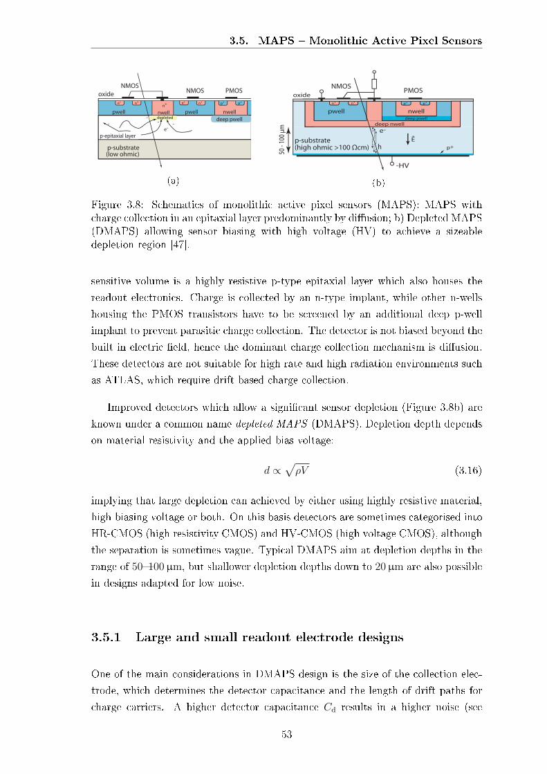
3.5. MAPS Monolithic Active Pixel Sensors
(a) (b)
Figure 3.8: Schematics of monolithic active pixel sensors (MAPS): MAPS withcharge collection in an epitaxial layer predominantly by diusion; b) Depleted MAPS(DMAPS) allowing sensor biasing with high voltage (HV) to achieve a sizeabledepletion region [47].
sensitive volume is a highly resistive p-type epitaxial layer which also houses the
readout electronics. Charge is collected by an n-type implant, while other n-wells
housing the PMOS transistors have to be screened by an additional deep p-well
implant to prevent parasitic charge collection. The detector is not biased beyond the
built in electric eld, hence the dominant charge collection mechanism is diusion.
These detectors are not suitable for high rate and high radiation environments such
as ATLAS, which require drift based charge collection.
Improved detectors which allow a signicant sensor depletion (Figure 3.8b) are
known under a common name depleted MAPS (DMAPS). Depletion depth depends
on material resistivity and the applied bias voltage:
d ∝√ρV (3.16)
implying that large depletion can achieved by either using highly resistive material,
high biasing voltage or both. On this basis detectors are sometimes categorised into
HR-CMOS (high resistivity CMOS) and HV-CMOS (high voltage CMOS), although
the separation is sometimes vague. Typical DMAPS aim at depletion depths in the
range of 50100µm, but shallower depletion depths down to 20µm are also possible
in designs adapted for low noise.
3.5.1 Large and small readout electrode designs
One of the main considerations in DMAPS design is the size of the collection elec-
trode, which determines the detector capacitance and the length of drift paths for
charge carriers. A higher detector capacitance Cd results in a higher noise (see
53

Chapter 3. Silicon particle detectors
(a) (b)
Figure 3.9: Two main approaches to MAPS pixel architecture: a) Large collectionelectrode with CMOS electronics embedded in the collecting n-well; b) Small collec-tion electrode with the readout implemented in a separate well. Concept a) featuresshorter drift paths at the expense of a higher detector capacitance compared to b)[47].
Equation 3.11) as well as in a slower detector response time τCSA:
ENC2th ∝ 1
gmC2
d and τCSA ∝ 1
gmCd. (3.17)
It is therefore desired that the detector capacitance is low. Cd can be compensated
with a higher transconductance of the input transistor gm at the cost of a higher
power consumption of the amplier. The length of the drift path is important
to ensure radiation tolerance of the detector. Charge collection in detectors with
shorter drift paths is completed faster and is therefore less sensitive to trapping
which occurs after irradiation (see Chapter 4.2.3). The choice of pixel architecture
is in general a tradeo between short drift distance and low sensor capacitance.
Two principal DMAPS architectures are called Large and Small collection elec-
trode designs2 shown in Figure 3.9. Both approaches have been investigated for the
ATLAS Phase-II upgrade. In sensors with a large collecting electrode, the electrode
takes up 50% or more of the total pixel area (Figure 3.9a). The readout electronics
is embedded within the collection n-well. This geometry ensures uniform and rela-
tively short drift paths in all parts of the pixel. The pixel capacitance is of the order
of ∼ 100 fF which is relatively high [47]. In addition to pixel-to-back-plane and
pixel-to-pixel capacitances inherent to every pixel detector, CMOS detectors also
feature a capacitance between multiple wells within the collection electrode (Figure
3.10). While its impact on noise and timing performance can be compensated by for
example increasing gm, the inter-well capacitance also acts as a potential coupling
between the wells and the collection electrode. This can cause coupling of digital
signals into the sensing part, thus producing fake signals, and requires special design
2Sometimes referred to as Large and Small ll factor, although in standard terminology bothdesigns aim for a 100% detection eciency, hence a 100% ll factor.
54

3.5. MAPS Monolithic Active Pixel Sensors
Figure 3.10: Contributions to sensor capacitance in a MAPS with a large collectingelectrode, consisting of the capacitance between the pixel and the sensor back sideCb, the inter pixel capacitance Cpp and the capacitance between multiple wells withinthe pixel Cww. The latter can cause coupling of digital signals from the electronicsinto the sensor unless specically prevented [47].
measures.
Small collection electrode approach is based on a collection electrode with a
size of a few µm and a typical capacitance of 23 fF (Figure 3.9b). The readout
electronics is placed in a separate p-well and does not contribute to the sensor
capacitance. Low capacitance results in signicantly lower noise and faster electronic
rise time, which allows amplier design with lower power. The required charge for a
satisfactory S/N ratio is also lower so the collection layer can be thinner. Low noise
means that the readout electronics can be relatively simple taking up only a small
fraction of the pixel area. In general this allows design of smaller pixel pitches.
The main challenge in this geometry is to ensure ecient and fast charge collec-
tion in the entire pixel, which requires strong lateral electric elds on pixel edges.
Since the back plane and the p-well with electronics act as equipotential planes
the generation of lateral elds and full pixel depletion is not straightforward and
requires pixel design in a so called modied process with an additional low doped
planar n-type layer (see Chapter 5.2) The relatively long drift distances also increase
trapping probability in irradiated devices, which is the main limiting factor for ra-
diation hardness of this architecture. This dictates use of small pixels, which on
one hand benets the position resolution, but on the other hand increases charge
sharing (less charge per pixel), constraints the amount of electronics that can be
packaged within the pixel and increases the power density in the detector due to
higher granularity.
3.5.2 SOI sensors
Silicon-on-Insulator (SOI) is an alternative MAPS architecture shown in Figure 3.11
[47, 50]. In SOI devices CMOS circuitry is housed in a dedicated thin silicon layer on
the surface which is grown on top of an insulating layer of silicon oxide, called buried
55

Chapter 3. Silicon particle detectors
Figure 3.11: Schematics of an SOI MAPS. The depleted sensor substrate is separatedfrom the CMOS layer by the buried oxide (BOX). Sucient thickness of the CMOSlayer is required to prevent back-gate eect on the transistors from charged BOXafter irradiation [47].
oxide (BOX). The thick highly resistive substrate acting as a sensor is connected to
the CMOS layer by vertical connections (vias). The separation of the sensor and
CMOS part allows both large and small collection electrode designs. Developments
in vertical (3D) stacking of multiple SOI layers also promise availability of much
higher electronics densities in the future.
SOI has some specics in terms of radiation tolerance due to the BOX layer.
Silicon oxide exposed to ionising radiation obtains a net positive electric charge
(see Chapter 4.1) and the resulting electric eld can change thresholds in adjacent
transistors. This is a so called back-gate eect. In standard SOI the CMOS layer
typically has a thickness of only few 10 nm and is therefore strongly aected by the
charge in the BOX. Radiation hard devices mitigate this by using a so called thick
lm SOI with a thicker CMOS layer (∼ 1µm) or additional implants which screen
the oxide charge [51, 52].
56

Chapter 4
Radiation damage in silicon
In the LHC detectors surrounding the interaction point are exposed to large uxes
of highly energetic particles originating from energy released in proton-proton col-
lisions. These particles cause damage to the detectors and deteriorate their per-
formance. Radiation tolerant detector design to ensure reliable performance until
the end of the detector lifetime is therefore paramount. Radiation damage is sepa-
rated in two main types: ionisation damage and displacement damage. Ionisation
damage, also called surface damage, is caused by ionising energy losses of photons
and charged particles. It aects silicon oxide and the interface between oxide and
silicon on detector surface. Displacement damage is primarily caused by hadrons,
which displace silicon atoms from crystal lattice. This is the main source of radia-
tion damage in the bulk with eects on charge collection and leakage current. One
consequence of displacement damage is eective removal of initial acceptors. This is
an important phenomenon in CMOS detectors and will be discussed in more detail.
4.1 Surface radiation damage
Surface radiation damage or ionisation damage occurs after incident radiation gen-
erate electron-hole pairs and thus ionise the medium. Its extent is measured by the
total ionising dose (TID) absorbed by the material. TID is measured in units of
Gray (Gy = J/kg) or equivalently in rad (1 rad = 0.01Gy). In the silicon lattice the
newly generated charge carriers recombine almost instantaneously, hence no long
term eects take place. On the other hand, persistent defects can be generated
in silicon oxide SiO2 and SiO2-Si interfaces. The decisive factor is extremely low
mobility of holes in SiO2 (µh ≈ 10−410−11 cmV−1 s−1 [53] compared to electron
57

Chapter 4. Radiation damage in silicon
mobility of µe = 20 cmV−1 s−1 [54]) which prevents the holes from leaving the oxide
and recombining [55]. This results in accumulation of trapped holes in the SiO2-Si
interface, which creates a positive space charge in the oxide.
Since SiO2 is used in transistors as insulator between the gate electrode and the
bulk, these changes have a serious eect on eld eect transistor (FET) properties,
including shifts in threshold voltage, shifts in the leakage current and reduction of
transconductance [39]. This causes performance degradation of analogue and digital
parts of the readout chip including risk of false signals and logic failure. In n-in-p
sensors accumulation of space charge in the oxide can cause local type inversion of
the substrate, creating a conductive channel between the electrodes which causes
cross talk between the channels. This behaviour has to be prevented by dedicated
p-type implants called p-stop.
Development of integrated circuits technology trends toward miniaturisation of
its basic unit the transistor which requires thinner gate insulation. This has a
positive eect on TID radiation tolerance. With typical gate oxide thickness reduced
to few nm, there is a signicant probability for trapped holes to escape the traps
via the tunnel eect and thus recover some of the radiation damage. More details
on surface damage can be found for example in [47, 56, 57].
4.2 Displacement damage
Ionisation damage does not play an important role in silicon bulk, as the original
state is recovered as soon as freed charge carriers recombine. The main radiation
eect in the bulk is displacement damage, caused by non ionising energy depositions,
which occur when an incident particle knocks out an atom from its site in the crystal
lattice, creating an interstitial atom (I) and a vacancy (V) a Frenkel pair [58, 59].
A fraction (≈ 60% [60]) of interstitials and vacancies recombine on spot, while
the rest migrate through the lattice and interact with each other or with impurity
atoms, creating point defects (examples shown in Figure 4.1). Point defects result
in additional energy states deep levels in the band gap.
The energy threshold to create a Frenkel pair in silicon is Ed ≈ 20 eV [61]. If
the imparted energy on the displaced atom, called primary knock-on atom (PKA),
is suciently high, the PKA can displace further atoms creating a cluster defect.
Events with 1000 or more interstitial-vacancy pairs commonly occur [59].
Point defects and clusters change electric properties of silicon and are hence the
58

4.2. Displacement damage
VacancyV
VOi
COi i
Frenkel pair
Interstitial
Interstitial impurity
Impurity substitute
Di-vacancyV²
Figure 4.1: Types of point defects in silicon [38].
+
-
donor
acceptor
EC
EV
Leakage current
Increase ofgeneration current
Levels close to midgapare most effective
Depletion voltage Trapping, CCE
Creation of charged defectsupper band: donor
lower band: acceptors
N ; Veff FD⇒
Shockley-Read Hall statistics(standard theory)
Inter-center chargetransfer model(inside clusters only)enhanced after
diffusion - annealing
Enhanced generation
⇒⇒leakage current
space charge
electrons
holes
Shallow levelstrap etrap h
lower CCE⇒
(a) (b) (c) (d)
Figure 4.2: Irradiation induced levels in the band gap and their macroscopic eects:a) increased leakage current with main contribution from current generation centresin the middle of the band gap; b) Changes of eective space charge concentrationNeff , induced by newly introduced deep levels; c) Increased trapping probability; d)Enhanced eects on leakage current and space charge concentration through inter-centre charge transfer taking place within clusters [38].
source of radiation damage in the bulk. The macroscopic eects of displacement
damage (Figure 4.2) are:
• Increase of leakage current;
• Decrease of charge collection eciency due to defects acting as charge traps;
• Change of eective space charge concentration Neff , aecting sensor depletion.
Since the energy level of the induced defects is higher than the energy of a pure
lattice structure, some defects can recover (anneal) with time. Annealing process
59

Chapter 4. Radiation damage in silicon
Figure 4.3: Simulated distribution of vacancies generated within 1µm of silicon by10MeV protons (left), 24GeV/c protons (centre) and 1MeV neutrons (right). Alluences are 1014 neq/cm
2 [61].
is strongly temperature dependent. Some defects also form stable complexes in
combination with oxygen or phosphorus atoms, which do not anneal over time [38,
39].
The frequency of point defects and clusters depends on the type and energy of
the incident particle (Figure 4.3). Hadrons interact via nuclear force with a large
energy transfer, which produces point defects and clusters on the end of heavy
recoil ranges. For neutrons this is the only reaction mechanism. Charged hadrons
in addition interact via long range Coulomb interaction which generates mostly
point defects. Highly energetic (GeV) charged hadrons travel deep into the material
and generate a larger fraction of point defects, while the damage of protons in the
MeV energy range is more similar to neutrons. Displacement damage of electrons is
comparably much lower, as the reaction kinematics allows smaller energy transfer
to the PKA due to the small electron mass [58].
4.2.1 NIEL hypothesis
A common basis to compare the extent of displacement damage from dierent
sources is established by the non ionising energy loss (NIEL) hypothesis. It states
that the extent of displacement damage scales linearly with energy imparted in the
displacing collision, irrespective of the spatial distribution of the ensuing defects.
The total displacement damage cross section for a principal particle of energy E is
given by [58]:
D(E) =∑ν
σν(E)
∫ EmaxR
0
fν(E,ER)P (ER) dER, (4.1)
60

4.2. Displacement damage
where contributions of all possible displacement processes ν, with cross sections
σν(E), are summed. The eects are integrated over all possible PKA recoil energies
ER with fν(E,ER) the probability density to achieve this energy transfer. The
fraction of the recoil energy deposited in form of displacement damage is given by
the Lindhard partition function P (ER) [62].
By the above parametrisation, displacement damage can be expressed with a
standard quantity which is by convention 1MeV neutron equivalent uence, denoted
Φeq. The unit of Φeq is [Φeq] = n1MeV,eq/cm2 or in short neq/cm
2, corresponding to
a displacement damage cross section of Dn(1MeV) = 95Mevmb [58]. The propor-
tion of the damage caused by dierent particles can be expressed by the numerical
hardness factor κ, which is dened as the fraction of displacement damage relative
to the damage caused by the same uence of 1MeV neutrons.
The NIEL hypothesis was originally proposed as a robust standard for mea-
surements of damage in the bulk, but does not hold for all processes. It provides
accurate values for evolution of the leakage current [58, 63], while the changes of
Neff depend signicantly on impurity (C and O) concentration in silicon wafer [63],
and trap introduction rate changes with particle type by 3040% [64]. Acceptor
removal studied in this thesis has also been shown to depend on particle type.
4.2.2 Leakage current
Irradiation introduces new states in the band gap, which act as current generation
centres and contribute to leakage current. Most eective are energy levels in the
middle of the band gap. The leakage current increases linearly with uence and can
for a given volume V be parametrised as:
∆ILV
= αΦeq. (4.2)
Parameter α designates current related damage rate and depends on the annealing
history of the sample and sample temperature. Its value is normally measured at
20C after standard annealing when the eective space charge concentration is min-
imal (see Section 4.2.4). This is achieved after storing the sample at a temperature
of 60C for 80min or equivalently for 10 days at room temperature. Under these
conditions the value is α= (3.99 ± 0.03) × 10−17A/ cm at 20C [63]. The univer-
sal dependence of leakage current on uence holds over many orders of magnitude,
which is used for calibration of dierent irradiations to equivalent uence.
61

Chapter 4. Radiation damage in silicon
Increased leakage current has several adverse consequences for detector opera-
tion. It results in a higher shot noise, scaling with√IL, and consequently in a re-
duced S/N ratio (see Chapter 3.1.5). In addition, increased leakage current causes
higher ohmic losses in the sensor, which can result in uncontrolled sensor heating
due to a positive feedback loop the thermal runaway. To keep the temperature
stable sucient cooling capacities need to be installed.
4.2.3 Charge trapping
Deep levels introduced by irradiation act as traps for drifting charge carriers. If
the time in which the trapped charge is released from a defect is greater than the
shaping time of the electronics, the charge is eectively lost for detection, leading to
a reduced S/N ratio. Irradiation also inhibits charge collection by diusion, which is
in part due to trapping, but also due to increased charge recombination on defects
introduced by radiation. This already occurs at low uences around 1013 neq/cm2.
Trapping is described by the eective trapping time τeff , which is the character-
istic time a charge carrier drifts before being trapped. The trapping rate is to the
rst order proportional to the concentration of trapping centres, which scales linearly
with uence: 1τeff
= β×Φeq, with the proportionality factor β ≈ 4×10⁻¹⁶ cm−2 ns−1
in p-type silicon [65, 66]. The reduction of an initial charge Q0 due to trapping is
Qe,h(t) = Q0e,he− t
τeffe,h . (4.3)
With drift saturation velocity of vsat ∼ 100µm/ns, typical trapping times and cor-
responding drift distances λ = vsat · τeff are:
• τeff(1014 neq/cm
2) = 20 ns, λ≫ 300µm;
• τeff(1015 neq/cm
2) = 2 ns, λ = 200µm;
• τeff(1016 neq/cm
2) = 0.2 ns, λ = 20µm.
In a 300µm thick silicon detector the charge loss due to trapping after a uence of
1014 neq/cm2 is of the order of a few percent, but at uences around 1015 neq/cm
2
the loss becomes signicant (few 10%), since trapping times become too short for
the charge to travel through an entire 300µm thick detector. At extremely high
uences Φeq ≫ 1016 neq/cm2 charge carriers only drift a few 10µm before getting
trapped, making it very challenging to achieve a good S/N.
62

4.2. Displacement damage
4.2.4 Changes of eective doping concentration
Deep levels act as acceptors or donors and change the eective space charge of the
material: |Neff | = |NA − ND|, where NA and ND are concentrations of charged
shallow and deep states acting as acceptors and donors. Typically the majority of
radiation induced defects create acceptor-like states (for example V + V + O →V2O), leading to net increase of NA [38]. According to Eq. 3.8 higher Neff results
in a higher depletion voltage or conversely less depletion at a given voltage. This
is problematic, as the full depletion voltage may not be achievable due to electrical
breakdown, while a smaller depletion zone reduces the S/N ratio and hence degrades
the detector performance.
In addition to creation of new acceptor states, shallow donor states in n-type
material get deactivated (P + V → VP), reducing ND [67]. n-type material may
therefore convert into p-type, undergoing a so called type inversion. n-in-n sensors
exploit type inversion to prolong sensor lifetime, as Neff initially reduces and the
sensor can be fully depleted at lower voltages for a longer time.
The change of eective space charge ∆Neff(Φeq, t, T ) = Neff −Neff,0 also depends
on annealing history of the sample, with the behaviour parametrised by so called
Hamburg model [58, 63]:
∆Neff(Φeq, t, T ) = NC(Φeq) +NA(Φeq, t, T ) +NY(Φeq, t, T ) (4.4)
The rst contribution NC(Φeq) = NC0(1− exp(−cDΦeq)) + gCΦeq is the stable dam-
age, which does not anneal. In n-type material it can be described as an incomplete
donor removal (exponential term) accompanied with acceptor creation with an intro-
duction rate gC (in p-type material donor removal is replaced by acceptor removal).
Short term or benecial annealing NA(Φeq, t, T ) describes initial reduction of Neff
which caps after 10 days at room temperature, followed by the undesired reverse an-
nealing NY(Φeq, t, T ), when Neff starts to increase again and can even exceed stable
damage. In laboratory the annealing process can be quickened by heating up the
sample. An equivalent of benecial annealing (10 days at room temperature) can
be achieved by storing the detector at 60C for 80 minutes this is the so called
standard annealing.
The stable damage introduction rate gC depends on particle type and impurity
concentrations (C and O) in the material and is normally measured after standard
annealing. The stable damage introduction rate with neutrons is gC ≈ 0.02 cm−1
with a 10% spread depending on the material [66]. For charged hadrons this value
63

Chapter 4. Radiation damage in silicon
•• St = 0.0154
•• [O] = 0.0044 •• 0.0053
•• [C] = 0.0437
0
1E+12
2E+12
3E+12
4E+12
5E+12
6E+12
7E+12
8E+12
9E+12
1E+13
0 1E+14 2E+14 3E+14 4E+14 5E+14
Proton fluence (24 GeV/c ) [cm-2]
N|ff
emc[|
3-]
0
100
200
300
400
500
VDF
003rof
••]V[
rotcete
dkci
htm
Standard (P51)O-diffusion 24 hours (P52)O-diffusion 48 hours (P54)O-diffusion 72 hours (P56)Carbon-enriched (P503)
Carbonated
Standard
Oxygenated
Figure 4.4: Increase of Neff for dierent materials after proton irradiation. Neff
increases more slowly in oxygen rich material and faster in carbonated silicon. Dia-gram taken from [38] after [63].
can be up to a factor 3 lower in oxygen rich material (Figure 4.4). On the other hand
high carbon concentrations increase the acceptor introduction rate [63]. Although
more space charge is introduced with irradiation, the ohmic resistivity of irradiated
silicon increases because the Fermi level shifts to the middle of the band gap and
less free charge carriers are available.
Charge state of radiation induced localized energy levels depend also on tem-
perature and on leakage current. Especially at higher uences the approximation
with uniform space charge is not sucient to describe the behaviour of irradiated
detectors. Trapping of thermally generated charge carriers may lead to change of
sign of space charge in a part of the detector phenomenon also known as double
junction eect [68]. This is a state with two depletion zones in the sensor one on
the front and one on the back side with a low electric eld in the middle. Double
junction is a consequence of trapping of thermally generated charge carriers (leakage
current) in the vicinity of their corresponding electrode where their concentration
is the highest. The trapped charge locally changes Neff which leads to a local type
inversion of the material. Hence, two p-n junctions develop in the material. Double
junction is an unwanted eect, as the weighting eld at the back side is small and
does not signicantly contribute to signal, while it reduces the available electric eld
in the front side of the sensor.
64

4.2. Displacement damage
4.2.5 Acceptor removal
Acceptor removal is an important topic in development of advanced silicon detectors
using p-type substrate [66, 69, 70, 71]. Analogically to removal of donors, acceptor
removal describes electrical deactivation of initial shallow acceptors in the material
by irradiation, leading to a reduced Neff [67]. It has recently been established that
the relative removal rate depends on initial doping concentration, with higher doped
materials undergoing a slower removal, as well as on particle type, with charged
hadrons removing the initial acceptors faster.
In standard n-type silicon (ρ ∼ 320 kΩ cm) used for n-in-n detectors the initial
removal process is nished and radiation induced space charge concentration exceeds
the initial concentration already at low uences below 1013 neq/cm2. Meanwhile,
HV-CMOS detectors use intermediate resistivity p-type wafers (ρ ≈ 103000Ω cm),
where space charge concentration is reducing up to uences comparable to the total
expected uence at HL-LHC (10141015 neq/cm2). In this case the benecial eects
of reduced Neff are present for most of the detector lifetime [72]. Acceptor removal
is also a critical topic in LGAD1 detectors used in timing applications, which rely
on charge multiplication in a highly doped p+ layer. These detectors are sensi-
tive to acceptor removal in the multiplication layer, which causes a lower gain and
consequently worse timing resolution [73, 74].
Acceptor removal mechanism
The dependence of active initial acceptor concentration on uence is usually de-
scribed by exponentially decaying term with a removal coecient c. The stable
damage therefore consists of three terms the initial concentration Neff,0, the re-
moval of initial acceptors and generation of deep acceptors:
Neff = Neff,0(1−Nc/Neff,0 · (1− e−cΦeq)) + gCΦeq. (4.5)
The factor Nc/Neff,0 ∈ [0, 1] is introduced to take into account dierent materi-
als with varying fraction of acceptors that get removed, describing either a partial
(Nc/Neff,0 < 1) or a complete removal (Nc/Neff,0 ≈ 1).
On microscopic level the source of acceptor removal is interaction of substitu-
tional boron Bs with interstitial silicon atoms Bs + I → Bi (vacancy interaction
Bs + V → VB generates a complex which anneals out at 0C and plays no role).
1Low gain avalanche detector
65
Chapter 4. Radiation damage in silicon
The boron interstitial Bi is highly reactive and forms complexes with other impuri-
ties [67, 75, 76]:
• BiOi donor in the upper part of band gap;
• BiBsH acceptor in the lower part of band gap;
• electrically neutral defects.
The net outcome after the above processes is electrically neutralised boron atom.
Defects acting as donors contribute a negative space charge, which further enhances
the eective removal rate. Conversely, acceptor-like complexes result in an incom-
plete removal.
Acceptor removal rate depends on the concentration of silicon interstitials, which
can also participate in concurrent reactions:
• I + Cs → Ci reduces the interstitial concentration;
• V+O → VO increases the interstitial concentration due to less recombina-
tion (I + V → Sis is suppressed by absent V).
The removal rate is hence higher in oxygen rich material and lower in carbon rich
material.
Dependence of removal coecient on Neff,0
Recent measurements with CMOS and LGAD detectors have indicated that in ma-
terials with a higher initial doping concentration a higher uence is required to
complete the acceptor removal. This can be explained by the fact that every in-
coming particle can only remove a nite number of initial acceptors. In the limit
of high doping concentrations with abundant acceptors the number of removed ac-
ceptors after a given uence is therefore constant irrespective of the actual acceptor
concentration, i.e. the uence required to remove a given fraction of initial accep-
tors increases in a higher doped material. This implies that acceptor concentration
reduces linearly with uence and not exponentially as presented in Equation 4.5,
however the description with an exponential decay has been well established and is
usually a sucient approximation of the behaviour. In materials with a low acceptor
density the number of removed acceptors per incoming particle is smaller, since the
probability for interstitials to be in sucient proximity for interaction with rela-
tively scarce acceptor atoms is reduced. This results in a slightly modied acceptor
removal regime with a reduced absolute removal rate.
66

4.2. Displacement damage
The above behaviour has been parametrised by a rst order model explaining
the measured acceptor removal in LGAD detectors [77]. Acceptor removal is treated
as a two step process consisting of silicon interstitial generation by irradiation (Φ)
and displacement of substitutional boron:
1. Sis + Φ → I with a constant interstitial generation rate;
2. I + Bs → Bi with the rate depending on boron concentration NA.
Once boron is displaced it is considered removed. The removal rate can be governed
by either of the two reactions. In materials with high boron abundance the absolute
removal rate is limited by interstitial generation and is independent of NA, while in
materials with low NA the bottleneck is the probability of boron interaction.
In the high density regime with NA suciently high that every interstitial has
equal probability to remove an acceptor, the removal rate is
dNA
dΦ= −NSi · σacc = const. (4.6)
with NSi = 5 ·1022 cm−3 the concentration of silicon atoms in the crystal and σacc the
eective cross section to deactivate an acceptor. According to the two step process
described above, this cross section can be parametrised as
σacc = kcap ·NInt · σSi, (4.7)
with NInt the number of interstitials generated in the scattering, σSi the cross section
of radiation with silicon and kcap the probability for interstitial reaction with an
acceptor. The value of kcap encompasses the eects of dierent impurities (carbon,
oxygen, . . . ) that might intercept the interstitial before it reaches an acceptor, as
well as the spatial distribution of interstitials which diers for charged hadrons and
neutrons. The initial acceptor concentration N initA reduces linearly with uence:
NA = N initA −NSi · σacc · Φ. (4.8)
The above dependence holds until the low density regime is reached. This model
can be linked with Eq. 4.5, which describes the removal by an exponential decay
NA = N initA e−cΦ, by introducing a characteristic uence Φ0(N
initA ) = 1/c after which
the acceptor concentration drops by a factor e:
N initA · e−1 = N init
A −NSi · σacc · Φ0, (4.9)
67

Chapter 4. Radiation damage in silicon
or equivalently
Φ0 = 1/c =1− e−1
NSi · σaccN init
A . (4.10)
This parametrisation explains smaller removal coecients c for higher initial doping
concentrations. The value of σacc = 8.3 · 10−22 cm2 was obtained from a t of Eq.
4.10 to data with high N initA [77].
In the low density regime the probability for the I + Bs → Bi process is re-
duced and depends on the boron concentration. In principle the calculation of the
removal rate has to be done dierentially, however measurements indicate a non triv-
ial dependence on NA which would require additional assumptions. The behaviour
is instead modelled by introducing an eective low density correction to the high
density regime (Eq. 4.10) in form of the proximity function D(N initA ), so that:
Φ0 =1− e−1
NSi · σacc ·D(N initA )
N initA . (4.11)
Let a parameter N0 be the boron concentration at the transition point between low
and high density regimes. The proximity function has to have the following limit
behaviour: D(N initA ≫ N0) = 1 and D(N init
A ≪ N0) = 0; which can be described by
the ansatz:
Dn =1
1 + (N0/N initA )n/3
, (4.12)
where n ∈ N is the proximity factor dening the behaviour of the low density regime.
The values of N0 and n were determined from the t of the function 4.11 to measured
values of Φ0 in the doping range N initA = 10121018 cm−3 (Figure 4.5), yielding n = 2
and N0 = 2.5 · 1016 cm−3 [77].
The most intuitive selection of the proximity factor would be n = 3, which
describes a low density regime with dNA
dΦ∝ −NA and a constant removal coecient.
With the actual proximity factor n = 2 the removal is faster, as indicated in Figure
4.5. The reason for this might be that the removed boron forms the donor-like BiOi
complex which further enhances the net removal eect (removal of acceptor and
introduction of donor state) which especially aects low doped materials.
The presented acceptor removal model gives a good qualitative explanation for
the value of the removal coecient. However, the variation between dierent detec-
tor materials shows dierences as high as a factor of 23 at the same Neff,0. Individ-
ual characterisation of each wafer type is therefore necessary for precise knowledge
about the acceptor removal in a given detector. Summarising, the acceptor removal
68
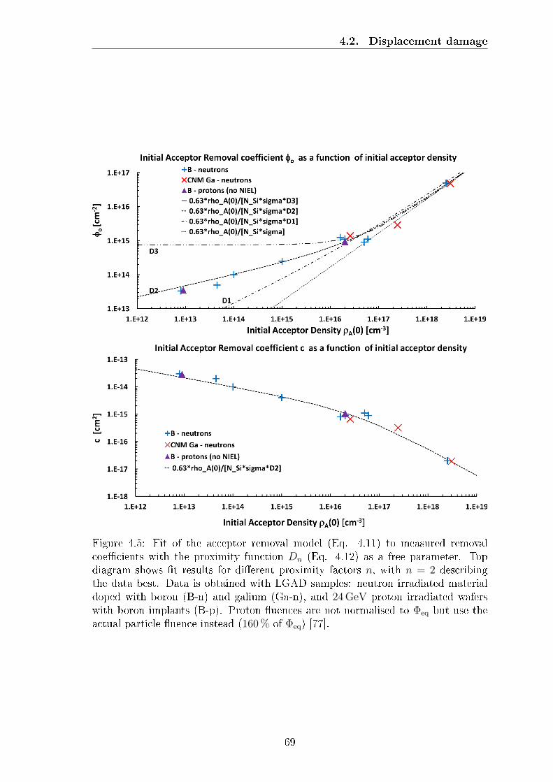
4.2. Displacement damage
Figure 4.5: Fit of the acceptor removal model (Eq. 4.11) to measured removalcoecients with the proximity function Dn (Eq. 4.12) as a free parameter. Topdiagram shows t results for dierent proximity factors n, with n = 2 describingthe data best. Data is obtained with LGAD samples: neutron irradiated materialdoped with boron (B-n) and galium (Ga-n), and 24GeV proton irradiated waferswith boron implants (B-p). Proton uences are not normalised to Φeq but use theactual particle uence instead (160% of Φeq) [77].
69

Chapter 4. Radiation damage in silicon
coecient can be estimated by the formula:
1/c = Φ0 =1− e−1
NSi · σacc
(1 +
(N0
N initA
)2/3)
·N initA (4.13)
NSi = 5 · 1022 cm−3,
N0 = 2.5 · 1016 cm−3,
σacc = 8.3 · 10−22 cm2.
70

Chapter 5
DMAPS prototypes for ATLAS
Phase-II upgrade
At the start of the ATLAS ITk CMOS project DMAPS was a relatively new de-
tector technology. To explore advantages and disadvantages of dierent DMAPS
architectures and establish the optimal detector design the R&D has been divided
into several development lines, with prototype names listed below along with vendors
oering the corresponding CMOS process:
• LFoundry MonoPix 150 nm large electrode;
• TowerJazz MALTA and MonoPix 180 nm small electrode;
• ams/TSI ATLASPix 180/350 nm large electrode;
• ams CHESS 350 nm large electrode, strip CMOS prototype;
• X-FAB XTB 180 nm large electrode SOI.
The original programme has been narrowed to the rst three options listed above.
The X-FAB programme was discontinued in favour of other designs after initial pro-
totyping, while the ams CHESS was a prototype for the ATLAS strip CMOS project,
which was not pursued beyond rst two prototype chips. Each development line
consists of several chips with gradually increasing complexity. Initial submissions
typically only feature analogue active part and are equipped with many test struc-
tures for studies of individual detector properties. Later submissions contain fully
working monolithic chips, although they still consist of several dierent pixel designs
and are not yet nal versions suitable for ITk.
The following chapter gives an overview of dierent development lines. Because
of the large number of dierent chips that have been developed not all are described
71

Chapter 5. DMAPS prototypes for ATLAS Phase-II upgrade
in detail in this text. The focus is on the devices that were studied in the scope of
this thesis. Other chips are also introduced briey, while more details can be found
in the accompanying references.
5.1 LFoundry 150nm development line
The LFoundry (LF) 150 nm development line is focused on a HR-CMOS detector
with a high initial substrate resistivity of > 2 kΩ cm and a large collection electrode.
The design targets a high bias voltage of ≈ 250V, allowing initial depletion depth
to exceed 100µm. The following chips have been developed in the LFoundry line
(Figure 5.1):
• CCPD_LF (2015) prototype chip;
• LF-CPIX (2016) demonstrator chip;
• LF-MonoPix01 (2017) monolithic CMOS chip;
The CCPD_LF [78] is the rst prototype based on a CCPD concept with an in-
pixel analogue amplier. The main part of the chip is an array of 24 × 114 active
analogue pixels with quadruple well structure, while several passive diode arrays are
also included for material studies. The LF-CPIX chip [79] is an upgraded version of
CCPD_LF with improved analogue front end design and additional digital blocks.
Both chips are designed for coupling with the ATLAS readout chip FE-I4 [80], either
by bump bonding or by gluing.
The LF-MonoPix01 [81] is a fully monolithic chip with a size of 10mm× 10mm
based on the previous submissions. The chip uses a digital pixel readout based on
column drain architecture, which is a conservative approach used in hybrid detectors
with a proven and reliable performance. The pixel size is 250µm × 50µm with a
relatively large input capacitance of ≈ 400 fF. The minimal discriminator threshold
which allows operation below the noise level of 10−6/25 ns/pixel is 2500 e− ± 100 e−
after in-pixel threshold tuning. The front end has a noise level of 190 e−±10 e−, and
a power consumption of ≈ 400mW/cm2 [82, 83, 84]. The chip was demonstrated
to maintain a good analogue front end performance after a TID of 50MRad, and to
achieve a detection eciency of 98.9% after a neutron irradiation of 1 · 1015 neq/cm2
[85].
72
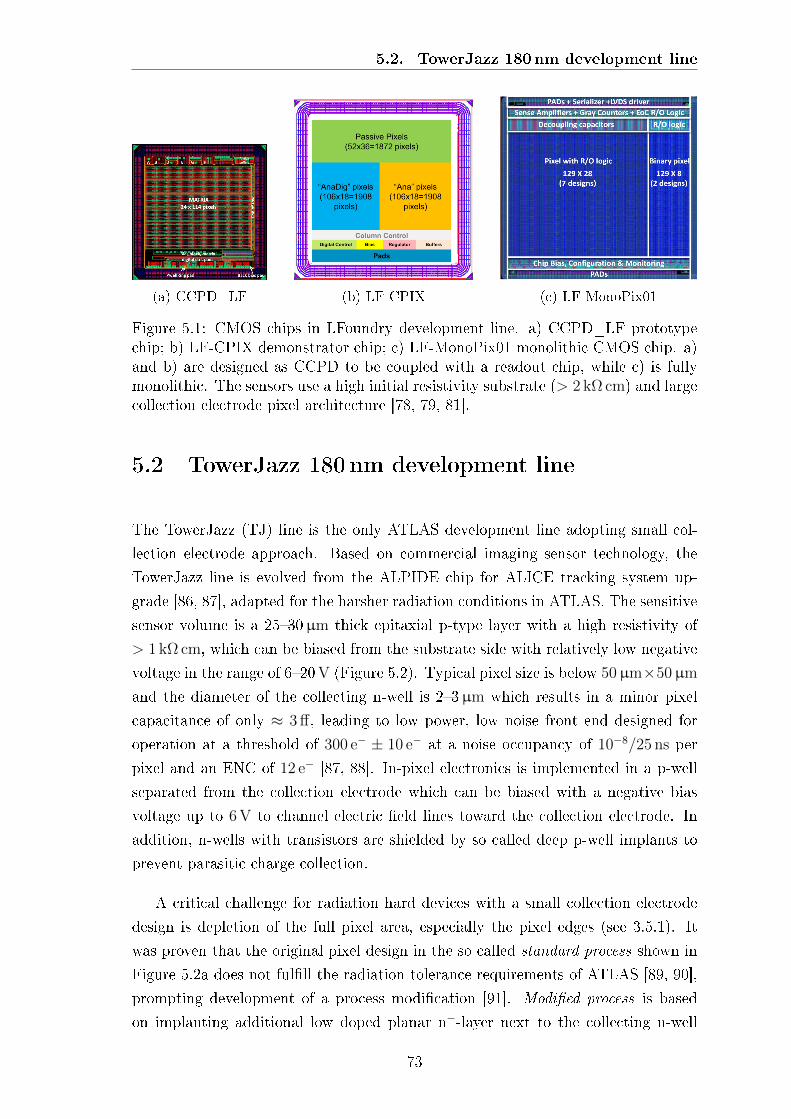
5.2. TowerJazz 180nm development line
(a) CCPD_LF (b) LF-CPIX (c) LF-MonoPix01
Figure 5.1: CMOS chips in LFoundry development line. a) CCPD_LF prototypechip; b) LF-CPIX demonstrator chip; c) LF-MonoPix01 monolithic CMOS chip. a)and b) are designed as CCPD to be coupled with a readout chip, while c) is fullymonolithic. The sensors use a high initial resistivity substrate (> 2 kΩ cm) and largecollection electrode pixel architecture [78, 79, 81].
5.2 TowerJazz 180nm development line
The TowerJazz (TJ) line is the only ATLAS development line adopting small col-
lection electrode approach. Based on commercial imaging sensor technology, the
TowerJazz line is evolved from the ALPIDE chip for ALICE tracking system up-
grade [86, 87], adapted for the harsher radiation conditions in ATLAS. The sensitive
sensor volume is a 2530µm thick epitaxial p-type layer with a high resistivity of
> 1 kΩ cm, which can be biased from the substrate side with relatively low negative
voltage in the range of 620V (Figure 5.2). Typical pixel size is below 50µm×50µm
and the diameter of the collecting n-well is 23µm which results in a minor pixel
capacitance of only ≈ 3 ff, leading to low power, low noise front end designed for
operation at a threshold of 300 e− ± 10 e− at a noise occupancy of 10−8/25 ns per
pixel and an ENC of 12 e− [87, 88]. In-pixel electronics is implemented in a p-well
separated from the collection electrode which can be biased with a negative bias
voltage up to 6V to channel electric eld lines toward the collection electrode. In
addition, n-wells with transistors are shielded by so called deep p-well implants to
prevent parasitic charge collection.
A critical challenge for radiation hard devices with a small collection electrode
design is depletion of the full pixel area, especially the pixel edges (see 3.5.1). It
was proven that the original pixel design in the so called standard process shown in
Figure 5.2a does not fulll the radiation tolerance requirements of ATLAS [89, 90],
prompting development of a process modication [91]. Modied process is based
on implanting additional low doped planar n−-layer next to the collecting n-well
73
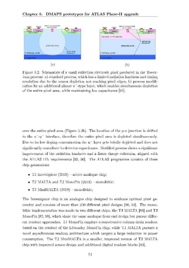
Chapter 5. DMAPS prototypes for ATLAS Phase-II upgrade
(a) (b)
Figure 5.2: Schematics of a small collection electrode pixel produced in the Tower-Jazz process: a) standard process, which has a limited radiation hardness and timingresolution due to the sensor depletion not reaching pixel edges; b) process modi-cation by an additional planar n−-type layer, which enables simultaneous depletionof the entire pixel area, while maintaining low capacitance [91].
over the entire pixel area (Figure 5.2b). The location of the p-n junction is shifted
to the n−-p− interface, therefore the entire pixel area is depleted simultaneously.
Due to its low doping concentration the n− layer gets totally depleted and does not
signicantly contribute to detector capacitance. Modied process shows a signicant
improvement of the radiation hardness and a faster charge collection, aligned with
the ATLAS ITk requirements [89, 90]. The ATLAS programme consists of three
chip generations:
• TJ Investigator (2015) active analogue chip;
• TJ MALTA and TJ MonoPix (2018) monolithic;
• TJ MiniMALTA (2019) monolithic;
The Investigator chip is an analogue chip designed to evaluate optimal pixel ge-
ometry and consists of more than 250 dierent pixel designs [90, 92]. The mono-
lithic implementation was made in two dierent chips, the TJ MALTA [88] and TJ
MonoPix [82, 88], which share the same analogue front end design but pursue dier-
ent readout approaches. TJ MonoPix employs a conservative column drain readout
based on the readout of the LFoundry MonoPix chip, while TJ MALTA pursues a
novel asynchronous readout architecture which targets a large reduction in power
consumption. The TJ MiniMALTA is a smaller, improved version of TJ MALTA
chip with improved sensor design and additional digital readout blocks [93].
74

5.2. TowerJazz 180nm development line
(a)
22bHit info
22bHit info
22bHit info
Hit merger:Time-orders hits from2x22 bits on1x22 bits ++ column identifier ++ delay counter
22bHit info
Hit merger:Time-orders hits from2x22 bits on1x22 bits ++ column identifier ++ delay counter
Hit merger:Time-orders hits from 2x22 bits on1x22 bits + column identifier ++ delay counter
22b + 1c 22b + 1c
22b + 2c
(b)
Figure 5.3: Asynchronous readout architecture in TJ MALTA. a) Double columnreadout: hit pixels in 2× 8 pixel groups instantaneously output hit information onthe shared data bus which is then propagated into chip periphery. The approachminimises power as it does not require digital clock signals. b) Hit merger logic:asynchronous signals simultaneously arriving into the end of column logic from dif-ferent data buses are sorted into a sequence by the hit merger [88].
75
Chapter 5. DMAPS prototypes for ATLAS Phase-II upgrade
5.2.1 Asynchronous readout architecture in TJ MALTA
TJ MALTA employs a novel asynchronous pixel readout which does not require
clock distribution into the pixel matrix [88]. This saves a large amount of power
while also eliminating the possibility of the digital clock signal coupling into the
analogue front end. Low power consumption means that installed cooling power can
be lower, requiring less material and signicantly reducing the impact of multiple
scattering. Simulations of the digital part of the MALTA chip predict a power
consumption of ≈ 10mW/cm2, compared to ≈ 100mW/cm2 in TJ MonoPix which
uses a synchronous column drain architecture. The expected power consumption in
the analogue part of both chips is ≈ 70mW/cm2.
The matrix in TJ MALTA is subdivided into double columns of 2× 512 pixels,
which act as independent readout units sending hit information into chip periphery
for central processing. Each double column is arranged into groups of 2×8 pixels as
shown in Figure 5.3a, which use a 22-bit wide parallel data bus to transmit data to
periphery. Alternating pixel groups, indicated as Red and Blue in the schematics,
share a common data bus in order to signicantly reduce the number of required
data lines. Alternation is necessary to correctly reconstruct hits shared between
two groups and minimise the probability of two groups simultaneously accessing the
data bus. Signals from hit pixels, consisting of 16 bits for the position of the pixel
within a group, one reference bit which is active when any pixel in the group res,
and 5 bits for a static group address within the double column, are transmitted
instantaneously (asynchronously) upon a hit. Short pulses with a programmable
width of 0.5 ns2 ns are essential to prevent overlapping of concurrent signals on the
same data bus, which results in data collisions and corruption. The propagation
time of signals through the data bus has a maximal latency of 7.5 ns which depends
on the group position within the double column, with a given pixel group having a
xed delay that can be compensated for in the chip periphery.
Measurement of deposited charge in MALTA is based on the time-walk of the
signals in the front end, exploiting the fact that of two signals with the same shape,
the higher signal will cross a xed threshold sooner than the lower one. The signal
height can be inferred by measuring the delay of the asynchronous pulse, corrected
for the propagation delay in the double column, relative to an external reference
signal marking the time of arrival (for example bunch crossing signal in LHC). In
the LHC conditions the time walk of the lowest trigerred signals shall not exceed
25 ns in order to assign the event to the correct bunch crossing. Measurements
show that a minimal threshold that guarantees such in-time operation in MALTA
76

5.3. ams/TSI 180/350nm development line pixel
is ≈ 300 e−.
The circuit in the chip periphery merges signals from all data columns onto
a common bus. An arbitration circuit called hit merger is used to time-sort hits
arriving on dierent data buses simultaneously in order to prevent data collisions
which corrupt the data (Figure 5.3b). In this case one signal is processed normally,
while the rest is delayed. The process is repeated on up to 10 levels until all of the
signals have been processed, keeping track of the delays by dedicated delay bits.
Additionally, double column address bits and time stamp information are added
to hit data to correctly identify the event in the reconstruction. The nal data is
formed into a 40-bit word which is asynchronously transmitted o the chip on a
40-bit wide LVDS bus, allowing data rates up to 5Gb/s.
5.3 ams/TSI 180/350nm development line pixel
The high voltage (HV) CMOS processes oered by ams have been developed for
automotive and industrial applications, where HV denotes any voltage level sig-
nicantly above typical supply voltages in integrated circuits. Detectors produced
in the ams 350 nm process in 2007 have been the rst application of HV-CMOS
technology for particle physics [49]. The ams/TSI development line pursues a large
collection electrode design implemented in the following chips:
• CCPDv4 (2015) prototype;
• H35Demo (2017) demonstrator chip;
• ATLASpix1 (2017) monolithic;
The H35Demo has been produced in ams H35 350 nm CMOS process, while the
CCPDv4 and ATLASpix1 have been produced in a 180 nm CMOS process. The
original foundry ams stopped accepting submissions for HEP after the rst version
of the ATLASpix1 had been produced. The chip manufacturing was afterwards
transferred to the TSI foundry, which uses a compatible 180 nm CMOS process.
The standard substrate resistivity in this technology is 20Ω cm, but chips were also
produced on higher resistivity substrates of 50Ω cm, 200Ω cm and 1000Ω cm in order
to achieve larger depletion depths. The samples can be biased with a bias voltage up
to 120V. Tests with the H35Demo chip have been carried out for example in [94].
The monolithic ATLASpix1 has been proven to have a high hit detection eciency
of > 99% after a neutron irradiation of 1 · 1015 neq/cm2 and a timing resolution of
< 10 ns [95].
77
Chapter 5. DMAPS prototypes for ATLAS Phase-II upgrade
5.4 ams 350nm development line strip
ATLAS also investigated the possibility of using active strip sensors in the ITk
and carried out an evaluation programme which resulted in three prototype chips:
HVStrip1, CHESS11 and CHESS2. The chips were manufactured in the ams H35
350 nm CMOS process (the same process as used for production of the ams H35Demo
pixel chip). Chips were produced on wafers with a standard resistivity of 20Ω cm,
while CHESS2 was also produced on 50, 200 and 1000Ω cm substrate. All chips can
be biased from the bias rings on the top and allow bias voltages up to ≈ 100V.
The HVStrip1 and CHESS1 are small chips intended for testing of individual
devices on analogue level. They contain several passive test structures, NMOS and
PMOS transistors for testing, and small analogue active pixel arrays [96, 97, 98].
The second generation CHESS2 chip is a full reticle size (18.6mm × 24.3mm) for
investigations of the readout architecture options in this technology [99]. The chip
has a thickness of 250µm and consists of several striplet arrays with a full digital
encoding and readout, test structures for data transmission and multiple passive
pixel arrays for material studies. Unfortunately, the active functionality of the
CHESS2 chip is compromised by issues in the design. Nevertheless, passive devices
can still be characterised and allow comparison to the results with the H35Demo
chip.
5.5 X-FAB 180nm development line
The X-FAB development line studied the performance of SOI sensors produced in
the X-FAB 180 nm SOI CMOS process using thick-lm SOI technology which makes
the electronics resistant to the back gate eect (Chapter 3.5.2). The design allows
high bias voltages of up to 300V (HV-SOI). Two prototype chips were produced on
a 100Ω cm p-type silicon substrate in the X-FAB process: the XTB01 and XTB02
[52, 100].
The XTB01 is an active analogue chip designed to investigate the feasibility of
the HV-SOI technology for particle detection. The main part of the chip are four
independent active pixel matrices with a standardised 3-transistor readout scheme
[48]. Testing has demonstrated radiation hardness of the design up to a total ionising
dose of 700MRad [101, 102], while good charge collection results have been acquired
in source and test beam measurements with unirradiated and lightly irradiated (5 ·1CHESS: "CMOS HV/HR Evaluation for Strip Sensors"
78

5.5. X-FAB 180nm development line
PWELL NWELL
P-STOP
deep NWELL
BOX
double PWELL
(a)
PWELL NWELL
P-FIELD
deep NWELL
BOX
double PWELL
(b)
Figure 5.4: Pixel design in the XTB02 chip. The deep n-well collects charge andhas to be connected to an external amplier. The surface layer does not containtransistors but can be nevertheless biased to provide realistic electric elds. The p-stop (a) and p-eld (b) implants interrupt a conductive channel which forms underthe BOX after irradiation [100].
1013 neq/cm2 neutrons) chips [100, 102, 103]. The tests revealed an issue with a high
leakage current and an early electrical breakdown of irradiated chips, caused by
creation of a conductive channel under the BOX due to space charge accumulation
on the BOX after TID irradiation.
The subsequently designed XTB02 is intended exclusively for tests of charge
collection in the sensor and is a purely passive chip. It consists of several diode
structures including pixel matrices with dierent pixel sizes. The CMOS layer above
the BOX does not house any transistors, hence the pixel implants act as normal
diodes and have to be connected to an external amplier. To prevent high leakage
current observed in irradiated XTB01 the XTB02 features additional implants called
p-stop or p-eld, depending on the test structure, which interrupt the conductive
channel under the BOX (Figure 5.4). This reduces leakage current after irradiation
by a factor 80 compared to XTB01 [100].
79

Chapter 5. DMAPS prototypes for ATLAS Phase-II upgrade
80

Chapter 6
Laboratory setups for charge
collection measurements
Good sensor performance after irradiation is one of the vital requirements for parti-
cle detectors at colliders, therefore verication of charge collection in prototypes is
necessary before the main production. The standard high resistivity (> 10 kΩ cm)
n-type substrate used in hybrid detectors has a known behaviour after irradiation.
However, DMAPS tend to use commercially easier available intermediate resistive
(10Ω cm3 kΩ cm) p-type wafers, whose properties after irradiation have not been
so well studied in HEP applications. Moreover, pixel structures characteristic for
DMAPS, such as nested wells, BOX layer or dierent collection electrode sizes, may
also impact charge collection and these eects have to be investigated. Combined
with numerous DMAPS designs, the studies of charge collection are a broad and
important topic in the development of these devices.
In this thesis two measurement methods were used to evaluate charge collection
in the substrate and characterise the eects of NIEL damage. The transient current
technique (TCT) uses pulsed laser light to inject charge into the substrate. Focusing
the light spot to a sub-pixel dimension allows studies of positional sensitivity of the
sensor. One of the most commonly used techniques is Edge-TCT where the laser
beam is directed on the thin edge of the detector. This enables measurements of the
sensor response to charge generated at dierent depths and provides information on
the size of the depletion region, as well as response uniformity. Laser intensity is
tunable, but it is not calibrated and it is set to get clear signals well above the noise
level with a wide band amplier. To achieve this laser pulse typically generates
charge several times larger than passage of a MIP.
81

Chapter 6. Laboratory setups for charge collection measurements
The second method applied in this thesis is the measurement of collected charge
deposited by MIP-like β particles from a 90Sr radioactive source. An appropri-
ate trigger conguration allows selection of events with MIP-like charge deposition,
whose signal spectra correspond to those at colliders. However, the method lacks
spatial resolution and can be complemented by TCT measurements for more in-
formation. The relatively short turnaround time of TCT and 90Sr measurements
compared to test beam allows studies with many dierently irradiated samples cov-
ering the entire uence range for the given detectors. This chapter describes the
instrumentation setups, data acquisition and analysis with these two measurement
methods.
6.1 TCT Transient current technique
The transient current technique (TCT) uses short laser pulses with a duration of
several hundred picoseconds to generate free charge carriers in the sensor [104, 105,
106]. The transient signal from the drifting charge can be recorded and allows
studies of the signal formation, charge collection, carrier drift velocity and trapping
mechanisms in the detector. The absorption coecient of light in silicon is strongly
dependent on the wavelength λ (Figure 6.1). The band gap in silicon is 1.12 eV
(corresponding to λ = 1100 nm), therefore visible light is absorbed much more than
infrared. A few examples of absorption depths d for dierent wavelengths are:
• Blue light (λ = 400 nm): d = 0.1µm;
• Red light (λ = 660 nm): d = 5µm;
• Infrared light (λ = 1064 nm): d = 1000µm.
Dierent wavelengths can be used to inject charge into dierent parts of the sensor.
Blue light can probe only the very surface part of the sensor. Red light deposits
energy similarly to an alpha particle close to the entry point which is useful to study
the drift of a single carrier type electrons or holes depending on which side of
the sensor the charge is injected. Meanwhile, infrared light behaves similarly to a
MIP particle (discounting attenuation) and deposits charge along the intersection
of the optical axis with the sensor.
With regard to the orientation of the light source TCT measurements can be
done in two ways (Figure 6.2):
• Surface-TCT with the laser beam oriented perpendicularly to the sensor sur-
face. The method is also called Top-TCT. Schematics 6.2a shows the simplest
82

6.1. TCT Transient current technique
Figure 6.1: Absorption depth of light in silicon [107].
(a) (b) (c)
Figure 6.2: Dierent TCT techniques: a) Top-TCT with uniform illumination; b)Top-TCT with a focused beam, providing position sensitivity; c) Edge-TCT with afocused beam, providing position sensitivity along the sensor depth.
Top-TCT option without any laser focusing. Top-TCT with a focused beam,
shown in Figure 6.2b, can be used to measure position dependence of the
detector response. Top-TCT measurements are often done with a red laser
(absorption depth of few µm), but infrared light can also be used.
• Edge-TCT is a method that has been developed in recent years [108, 109]. Fo-
cused laser light with a large penetration depth (IR) enters the sensor through
the edge, parallel to sensor surface (Figure 6.2c). In this case all e-h pairs are
generated at the same depth in the sensor, allowing measurements of charge
collection and drift velocity as a function of depth. More details are explained
below. Edge-TCT method was the predominantly used TCT method in this
thesis.
83

Chapter 6. Laboratory setups for charge collection measurements
det
Cooledsupport
ytable
Laser
Laser driverdetector HV
Peltier controller
z table x table
1 GHz BWoscilloscopefast current
amplifier
trigger line
optical fiber &focusing system
width of light pulses≈ 300 ps, repetitionrate 500 Hz
beam diameterin siliconFWHM ≈ 10 m
Bias-T
z
y
x
(a)
(b)
Figure 6.3: TCT measurement setup.
6.1.1 TCT setup
Schematics of the TCT measurement system and a photograph of the setup used
in this work are shown in Figures 6.3a and 6.3b. Similar systems produced by
Particulars [110] have been used as well and have the same functionality as the
presented setup. The sample is mounted on a carrier board which can be oriented
either in Top or Edge-TCT position. The carrier is mounted on a support equipped
with a Peltier couple which can cool the sample to temperatures below −10C. The
position of the sample in the laser beam is adjusted by positioning stages in three
dimensions with a sub-micrometer precision.
84

6.1. TCT Transient current technique
The light beam is generated by a laser diode which produces light pulses with a
duration of ≈ 300 ps, repetition rate of a few 100Hz and adjustable intensity which
varies by < 1% during measurements. The light is guided through a single mode
optical bre to an optical system which focuses the beam to a Gaussian shape with a
minimal spot size of ≈ 10µm FWHM1 and a divergence of ≈ 2 . The relative light
intensity can optionally be monitored by splitting the beam with a semi-permeable
mirror and measuring the charge generated by the reected beam on a photodiode.
The laser intensity has to be kept low to avoid the so called plasma eect, which
occurs when the amount of injected charge is so high that it signicantly distorts
the electric eld in the sensor, causing deformed signals.
In the simplest case the investigated detector is a passive diode with two electrical
contacts. The sensor back side is usually connected to ground potential, while the
front side is biased with high voltage (HV). Induced current is measured on the
detector front side, where it is superimposed on a HV baseline. The signal line
connected to the amplier input is capacitively decoupled from the high voltage
DC component using a "bias-T" element. In case of active detectors the electrical
connections are dierent, as additional low voltage levels are required for supplying
the electronics. Since the potential dierence between the sensor front side and the
low voltage usually cannot exceed a few volts, the front side has to be biased close
to the ground potential, while the HV is applied from the back. In this case the
bias-T is not strictly necessary.
Signals are amplied with a high bandwidth (1GHz) current amplier and
recorded by an oscilloscope with an analogue bandwidth of > 700MHz and a sam-
pling rate of > 5GS/s (DRS4 [111] or similar). The signals are averaged over 100
pulse repetitions for every acquisition to reduce the noise. The stage movement
and data acquisition are controlled by Labview software running on a control PC,
allowing automated measurements scanning over dierent sample positions and bias
voltages.
The setup uses a 3-dimensional Cartesian coordinate system with the axes se-
lected as indicated in Figure 6.3a. The xy-axes are dened in the plane perpendicular
to the optical axis. In Edge-TCT mounting convention is that the x-axis is oriented
along the edge of the sample, parallel to sensor surface, while y-axis is oriented
perpendicular to the sensor surface along the sensor depth. The z-axis is oriented
along the optical axis of the system.
1FWHM Full width at half maximum. FWHM = 2.35σ in a Gaussian distribution.
85

Chapter 6. Laboratory setups for charge collection measurements
6.1.2 TCT method and analysis
The underlying equation describing signal formation in silicon detectors is the
Shockley-Ramo theorem (see Section 3.3) which describes the induced current on
an electrode as a sum of the contributions Ie and Ih of drifting electrons and holes
in a weighting eld:
Ie,h(t) = e0 ·Ne,h · e−t/τe,h · ve,h(r, t) · Ew(r), (6.1)
where trapping of charge carriers is also taken into account by introducing the
eective trapping time τe,h. In undepleted volume the velocity of charge carriers is
v ≈ 0 due to the slow diusion transport and, in addition, in irradiated detectors
these charge carriers recombine almost immediately. Consequently, charge generated
in the undepleted region induces no current and does not contribute to the observed
signal. In Edge-TCT this behaviour can be used to estimate the size of the depletion
zone.
Figure 6.4 shows an example of an Edge-TCT measurement made with a pixel
detector. Induced pulses after charge injection at dierent distances y from the
sensor surface are shown in Figure 6.4a. Induced current is the highest when the
charge carriers drift in a large electric and weighting eld close to the pixel. At
larger injection depths the charge carriers reach this region later, hence the signal
peak is delayed. The last waveform measured at injection depth of y = 180µm
does not show a distinguishable pulse, indicating that the material at this depth is
undepleted. Charge collected by the electrode is the integral of the induced current:
q =
∫ tint
0
I(t) dt. (6.2)
The most commonly used integration time in ATLAS applications is tint = 25 ns,
dened by the LHC bunch crossing time. Sometimes shorter integration times can
also be selected to reduce noise, when induced pulses are appropriately short (in
Figure 6.4a tint = 10 ns was used). Figure 6.4b shows collected charge as a function
of injection depth for dierent bias voltages. As for each laser pulse charge carriers
are generated at the same depth in the detector the depletion depth can be simply
determined from the width of the region that produces observable signals. On the
surface side located at y = 0 of laser scan in y-direction the edge of the charge
collection prole has a width of 1020µm which reects the nite beam diameter.
At a xed bias voltage the collected charge is nearly constant as long as the injec-
tion point is well within the depleted region. As the injection point moves towards
the end of the depleted region the collected charge gradually starts to reduce. This
86

6.1. TCT Transient current technique
t [ns]2− 0 2 4 6 8 10
I [ar
b.]
0.1−
0
0.1
0.2
0.3
0.4
0.5
0.6
mµy = 30 mµy = 80
mµy = 105 mµy = 130 mµy = 180
(a)
m)µy (0 50 100 150 200
char
ge (
arb.
)
0
0.1
0.2
0.3
0.4
0.5 = 300 VbiasV = 200 VbiasV = 100 VbiasV = 50 VbiasV = 0 VbiasV
= 300 VbiasV = 200 VbiasV = 100 VbiasV = 50 VbiasV = 0 VbiasV
(b)
Figure 6.4: Example of Edge-TCT measurements with a partially depleted pixeldevice: a) induced current pulses depending on the injection depth. Charge injectionoccurs at t = 0. Oscillations come from non matching impedances of the input lineand the amplier; b) collected charge (integrated induced current) at dierent biasvoltages, providing information on depletion depth. Emphasised coloured spotsindicate the points where pulses shown in a) were measured. Detector surface is aty = 0µm.
is a consequence of the electric eld strength reducing with the distance from the
electrode. In addition the slope is reduced due to the nite beam diameter. Be-
cause of this the depleted depth cannot be unambiguously dened. In this thesis
the depleted depth is by convention measured as the full width at half maximum
(FWHM) of the charge collection prole.
Edge-TCT is also well suited for two dimensional scans in xy directions, which
reveal regions with high and low charge collection eciency within the pixel. More
examples are given in next chapter. Another quantity which may be estimated with
Edge-TCT, although not extensively used in this thesis, is determination of the
charge carrier velocity in heavily irradiated detectors. Since all charge carriers are
generated at the same depth, the velocity at this depth can be extracted from the
induced current using Shockley-Ramo theorem. Immediately after injection trapping
can be neglected (e−t/τe,h ≈ 1) and the induced current on the readout electrode is:
I(y, t ≈ 0) = e0Ne,hEw(ve(y) + vh(y)). (6.3)
The induced current is proportional to the sum of the electron and hole drift ve-
locities at the injection depth. If the velocities are not saturated this measurement
enables probing the electric eld at a given position using relation v = µE, where µ
is the charge carrier mobility. This method is particularly useful in strip detectors,
where the eective weighting eld is approximately that of a pad detector EW = 1d.
This leads to a position independent conversion factor between induced current and
87

Chapter 6. Laboratory setups for charge collection measurements
(a) (b)
Figure 6.5: Focus nding procedure in Edge-TCT: a) Charge collection prole ata selected z-position with tted error function on the surface edge; b) Dependenceof the FWHM extracted from the t on z-position. The optimal focus is in theminimum of the parabolic t, where the charge collection prole has the steepestslope [109].
carrier velocity. In pixel detectors (including CMOS prototypes) the weighting eld
depends on position and deduction of particle velocity is signicantly more complex
[108, 109].
Focus nding procedure
Since the laser beam is slightly divergent (≈ 2 ), the sample has to be rst placed
in the focal plane of the beam to achieve maximal position resolution. This is done
using so called knife edge technique with the beam moving from a non sensitive to
a sensitive region of the sensor. In Edge-TCT this is usually the detector edge in
y-direction, while in Top-TCT the transition between metallised and non-metallised
surfaces is mostly used (metal reects light which prevents generation of e-h pairs).
The resulting S-curve of the collected charge gives information about the FWHM
of the beam spot at the position of the readout electrode. After each such scan
the z-position of the sample is changed by 50100µm in order to nd the optimal
position with the minimal beam FWHM.
At each z-position a charge collection prole like the one shown in Figure 6.5a
is measured. The surface edge of the charge collection prole is tted by the error
function to extract the FWHM of the beam (FWHM equals to 2.35σ of the error
function). Measured dependence of beam FWHM on z-position is then tted by a
parabola as shown in Figure 6.5b. The optimal z-position is in the minimum of the
parabola and corresponds to the maximal slope of the charge collection prole edge.
88

6.2. Charge collection measurement with 90Sr
Typically the beam spot size in this position has a FWHM below 10µm.
6.2 Charge collection measurement with 90Sr
Radioactive strontium-90 (90Sr) is a simple laboratory source of MIP-like particles
that can be used for detector tests. The goal of 90Sr measurements is to generate
charge in exactly the same way as during detector operation at the collider and to
record transient signals, from which charge collection eciency (CCE) can be mea-
sured. Since absolute calibration of measured signals is possible, the results can be
used to qualify the detector performance in terms of charge collection. The amount
of collected charge is one of the main performance parameters for a silicon detector.
Moreover, it allows estimation of the eective depleted depth and comparing the
result with Edge-TCT measurements on the same sample.
90Sr is a pure β emitter. It has a short decay chain consisting of two decays:90Sr →90Y (E = 0.546MeV, t1/2 = 28.8 y) →90Zr (E = 2.28MeV, t1/2 = 64 h).
The MIP-like particles from the 90Sr source are hence fast electrons from the high
energy tail of yttrium decay spectrum. The majority of emitted electrons have
relatively low energies, deposit energy signicantly faster than a MIP, and have to
be excluded from the trigger when measuring MIP spectra.
The measurement setup used for CCE measurements in this thesis is shown in
Figure 6.6 [72, 112]. The detector is mounted in an aluminium housing which is in
contact with a thermally controlled support plate providing sample cooling down to
−10C. The β particles are collimated by two holes on top and bottom of the 1mm
thick aluminium box, and an additional hole in the cooling plate. A small scintillator
with the size of 1 cm × 1 cm is positioned below the cooling plate and coupled to
a photomultiplier to provide trigger signals. The threshold on the photomultiplier
output is selected suciently high that only electrons behaving close to a MIP
when passing through the sample have sucient energy remaining to trigger the
acquisition. This guarantees a high trigger purity, which exceeds 97% if the sample
is larger than the collimator holes so that in all triggered events charge is deposited
in the sensitive volume. This conguration allows measurement of small signal to
noise ratios. The most probable value (MPV) of electrons from 90Sr source selected
in this way is 80 e-h pairs per µm, while the mean energy loss is 98 e-h pairs/µm
[112]. The samples are connected to a custom made single channel charge sensitive
preamplier with a shaping time of 25 ns. The output waveforms are recorded by an
oscilloscope and saved to a computer. The absolute scale of the amplier output has
89

Chapter 6. Laboratory setups for charge collection measurements
long side view
TEX
244.
power6bias linessignal linessensor lines
T controllerUT−x5
warm aluminium plate −watter cooled
cold aluminium plate
peltier cooler
peltier cooler
ORTEC x42B
Pt−x..
Pt−x..light guideMscintilator tip
Photomultiplier
SHAPER
WentzelHVPS
Ortec57.
Ox42Bbias
HV−detectorbias
PM −HV
PM signal −trigger
BIAS FILTER
M466.
M466.measL I
measL U
sample−diode
Al Box 2mm
short−side view
(a)
(b)
preamplifier +25 ns shaper90Sr
water cooled heat sink
cold plate
Peltier cooler scintillator
HVCMOS sample digitaloscilloscope
thermalisolation
(c)
Figure 6.6: Experimental setup for CCE measurements with 90Sr [72, 112].
been calibrated by measuring the deposited charge in a 300µm thick fully depleted
unirradiated silicon diode, where the amount of deposited charge is known (MPV
= 80 e−/µm × 300µm = 24000 e−). In addition, calibration with 59.5 keV photons
from a 241Am source is also possible. The calibration constant for the given setup
is 275 e−/mV.
90

6.2. Charge collection measurement with 90Sr
To achieve a reasonable event rate of a few Hz the test structures have to be
relatively large, of the order of several mm2, to ensure a sucient geometrical ac-
ceptance of the incoming radiation. Therefore the measurements are usually not
made on single pixels or strips, but on dedicated pad test structures. The large de-
tector capacitance arising from the large surface area increases the noise level of the
measurement. A relatively long electrical connection between the sample and the
preamplier further increases the noise level of the setup to approximately 2500 e−,
which is quite high. For example CMOS detectors have a depletion zone with a
thickness as small as 30µm, which corresponds to a deposited charge of ≈ 2500 e−
as well. In such a situation noise and signal can not be separated. However, from a
sample of events with high trigger purity (i.e. if all recorded events are associated
with energy deposition in the DUT) information about the MPV can be extracted
as will be explained below.
An example of a CCE measurement2 with 90Sr is shown in Figure 6.7. At each
setting 2500 individual waveforms, such as one in Figure 6.7a, are acquired. The
signals are sampled at a single point at a xed time in the waveform. To determine
the optimal sampling time the average waveform of all 2500 events is calculated
(Figure 6.7b). The sampling time for the signal is selected as the peaking time of
the average waveform, while noise is sampled before the trigger, where it is causally
independent from the signal. The resulting signal and noise spectra are shown in
Figure 6.7c.
Charge spectra allow extraction of the collected charge. With suciently high
S/N ratio the signal spectrum can be tted with a convolution of a Landau and a
Gaussian function (Figure 6.7c), from which the MPV of the collected charge can
be determined. The Gaussian from the signal t has the same standard deviation
as the noise spectrum, corresponding to the noise level of the setup.
However, signal size in many CMOS detectors is comparable to the noise level
in which case the signal t has a large uncertainty on the MPV. In such cases
the collected charge can be more reliably determined from the shift of the signal
spectrum relative to the noise spectrum, since their mean values dier by the average
value of the deposited charge (Figure 6.7d). The collected charge can be calculated
by taking into account the average charge deposition of 98 e-h pairs/µm. This
method allows measurement of collected charge with a resolution below the noise
level. However, it is essential that in all triggered events charge is deposited within
the sensitive region (high trigger purity), otherwise "empty" events lower the mean
2Detector under test is CHESS2 with an initial resistivity of 1 kΩ cm after 1014 neq/cm2 neutron
irradiation. Measured MPV is 6400 e− corresponding to depletion depth of ≈ 80µm.
91

Chapter 6. Laboratory setups for charge collection measurements
t (bin)400− 200− 0 200 400
U (
V)
0.04−
0.03−
0.02−
0.01−
0
0.01
0.02
0.03
0.04
0.05
0.06
(a)
t (bin)400− 200− 0 200 400
U (
V)
0.04−
0.03−
0.02−
0.01−
0
0.01
0.02
0.03
0.04
0.05
0.06
(b)
charge (e-)10000− 5000− 0 5000 10000 15000 20000 25000
even
ts
0
50
100
150
200
250
300 NoiseSignal
(c)
charge (e-)10000− 5000− 0 5000 10000 15000 20000 25000
even
ts
020406080
100120140160180200220240
NoiseSignalMean
12 elMean2555 el
(d)
Figure 6.7: Example of CCE measurement with 90Sr: a) Individual waveform atthe output of amplication chain. Red and black lines denote the sampling timesfor signal and noise respectively. Note the high noise level; b) Average of 2500waveforms. The sampling time for the signal is selected at the maximum of thiswaveform, while noise sampling time is selected before the pulse; c) Calibratedcharge spectrum of signal (red) and noise (black) tted with a convolution of Landauand Gaussian function, and a Gaussian function respectively. The signal MPV is6300 e−. Due to high trigger purity the signal spectrum has no noise peak aroundzero, i.e. in all events the triggering particle passed through the sensitive region;d) Signal and noise charge spectra in a sample with less collected charge. Due toa large uncertainty of the Landau t the collected charge is determined from theshift of the mean value of the signal spectrum relative to the noise spectrum. Themeasured mean charge is 2500 e−, corresponding to an MPV of ≈ 2000 e−.
92

6.2. Charge collection measurement with 90Sr
value of the spectrum, resulting in a smaller measured value than it actually is. For
this reason the size of the investigated detector has to be large enough compared to
the scintillator to provide a 100% geometrical acceptance of the triggering particles.
93

Chapter 6. Laboratory setups for charge collection measurements
94

Chapter 7
Results of charge collection
measurements
This chapter presents the studies of charge collection in irradiated CMOS detectors
using TCT and 90Sr techniques. Dierent prototypes from four ATLAS CMOS
development lines were evaluated in the scope of this thesis. In the beginning of
the chapter the irradiation process and facilities are briey introduced, followed by
the results from dierent development lines. At the end the results are summarised
and an overview of detector properties, in particular acceptor removal behaviour, is
presented.
7.1 Irradiation of samples
Displacement damage was introduced into the samples by irradiation with neutrons
and with protons. Neutron irradiations were performed at Joºef Stefan Institute's
research TRIGA reactor by inserting the samples into the reactor core through ded-
icated irradiation channels [113, 114]. Free neutrons from nuclear reactions deliver
NIEL radiation damage uniformly over the entire sample volume. The majority of
NIEL damage (> 99%) is introduced by fast neutrons with kinetic energy above
100 keV. Desired uences are achieved by adjusting reactor power, which is pro-
portional to neutron ux, and time of insertion. Irradiations to uences above
1014 neq/cm2 were made with the reactor operating at the maximal thermal power
of 250 kW and at a neutron ux of 1.54 ·1012 neq/cm2/s. For lower uences the reac-
tor power was reduced to lower the neutron ux and increase irradiation time. The
uncertainty on the delivered uence is ≤ 10%. The ux is in addition monitored by
95

Chapter 7. Results of charge collection measurements
standardised measurements of changes of leakage current in dedicated diodes [63].
During the irradiation samples are also exposed to TID from background gamma
rays amounting to 1 kGy per 1014 neq/cm2.
Temperature of silicon during irradiation is over 40C due to background radia-
tion of the reactor. After the sample is recovered from the core it is kept in a freezer
except for brief intervals during transport, mounting and testing, which in total do
not exceed 3 hours at room temperature.
Proton irradiation is performed by inserting the sample in a proton beam gener-
ated by an accelerator. Proton beams typically have a small Gaussian cross section
of σ ∼ 5mm centered to a desired spot on the sample. To achieve a uniform irra-
diation over large detector area the sample can be moved through the beam in a
carefully planned scanning procedure. However, this approach is more complex and
requires a signicantly longer irradiation times, hence it was not applied to samples
in this thesis. With xed samples precise positioning within the beam is vital to
ensure that the desired uence is deposited in the targeted test structure.
Samples in this work were irradiated at two facilities: the PS synchrotron at
CERN with the proton beam energy of 24GeV [115] and the LANSCE linac in
Los Alamos with the proton beam energy of 800MeV [116]. In both facilities the
beam energy is suciently high that a stack of multiple samples can be inserted
in the beam at the same time without attenuating the proton ux. The received
uences were determined after the irradiation from activation of an aluminium foil
irradiated together with the samples. Protons deposit a larger TID than neutrons at
the same equivalent uence because of their electric charge. Typical TID values for
24GeV protons are approximately 30 kGy per 1 · 1014 neq/cm2. Proton irradiations
took several days, during which the samples were held at room temperature. After
irradiation samples were stored in a freezer.
Most measurements with irradiated sample were done twice, before annealing and
after the end of benecial annealing. During the standardised annealing procedure
the samples were heated up to 60C for 80 minutes. This is equivalent to annealing
for approximately 10 days at room temperature which corresponds to the end of so
called benecial annealing when minimum of full depletion voltage in moderately
irradiated silicon pad detectors is observed (Chapter 4.2.4). Proton irradited samples
underwent certain amount of annealing already during irradiation during which they
were held at room temperature.
96

7.2. Results with LFoundry prototypes
7.2 Results with LFoundry prototypes
LFoundry CMOS prototypes (Section 5.1) use the large collection electrode design
and employ both high resistivity and high voltage to achieve a large depletion depth
in the sensor. In the context of this thesis charge collection in passive test structures
was evaluated. Characterisation of two dierent chip versions were made using Edge-
TCT and charge collection measurements with 90Sr.
The rst set of measurements was made with CCPD_LF chips produced on a
substrate with initial resistivity of 2 kΩ cm [117]. Investigated passive test structures
A and F are shown in Figure 7.1. Each test structure was contacted with wire bonds.
Structure A consists of ve n-type implants connected together to form a 250µm×250µm pad-like diode. Structure F consists of 3 × 3 pixels with dimensions of
125µm×33µm, of which the outer eight are grouped together, while the central one
can be connected separately. The goal of this conguration is to enable measurement
at "typical" pixel conditions with minimal eects of the chip edge. Pixels in structure
F have a more complex implant structure with several wells designed for housing
readout electronics in active pixels, but are left empty in this passive device. Samples
were produced on a 700µm thick wafers with two subsets thinned to a thickness of
300µm and 100µm. The unthinned samples can be biased from the top surface
of the sensor through a p-type ring that surrounds all test structures. Thinned
samples have a processed and metallised back plane which allows sensor biasing from
the back. Maximal bias voltage that can be applied before electrical breakdown is
∼ 100V before irradiation and up to 150V in irradiated samples. All test structures
are surrounded by an n-type ring which horizontally constrains the electric eld and
thereby the sensitive volume, and can be biased separately. However, biasing the
n-type ring results in a much higher leakage current which eectively limits the bias
voltage to 40V. Measurements above this voltage had to be done with the n-ring
left oating. This aected the shape of the depletion region which was wider with an
unbiased n-type ring, but it did not signicantly change the depletion depth [117].
The second set of measurements was performed with a "Test Structures" chip
produced at a later point together with the LF MonoPix on a substrate with initial
resistivity of 3 kΩ cm [118, 119]. The investigated passive structure "B", shown in
Figure 7.2 is an array of 15 × 6 pixels with a pixel size of 250µm × 50µm and a
multiple well design. Signal routing is similar as in CCPD_LF with a single pixel
within the matrix that can be contacted separately, while the surrounding pixels are
connected together and routed to another pad. Samples come in two thicknesses:
700µm without processed back plane, and thinned to 200µm with metallised back
97

Chapter 7. Results of charge collection measurements
(a) (b)
Figure 7.1: Passive test structures on LFoundry CCPD_LF: a) Structure A consist-ing of ve pixel implants connected together and surrounded by an n-type ring; b)Structure F, a 3× 3 pixel array. Central pixel can be contacted separately. Implantstructure is more complex as indicated on the cross section below the picture [117].
(a) (b)
Figure 7.2: Passive test structures on LFoundry "Test Structures" chip: a)Detailof the test structure B, showing guard ring geometry and implant cross section; b)Larger section of the test structure B including wire bond pads [118].
98

7.2. Results with LFoundry prototypes
(a) (b)
Figure 7.3: Photograph of LFoundry CMOS prototypes CCPD_LF (a) and theTest Structures chip (b) mounted and wire bonded for measurements. The arrowindicates the laser beam direction in Edge-TCT [118].
plane, which can be biased from the top and from the back respectively. Improved
high voltage tolerance allows bias voltages up to 250V before breakdown. The size
of the test structure B (1.5mm×0.75mm) is sucient to also allow performing 90Sr
measurements with the setup presented in Chapter 6.2.
Detectors were irradiated with neutrons in Ljubljana TRIGA reactor. The
700µm and 300µm thick CCPD_LF samples were irradiated to uences ranging
from 1 · 1014 neq/cm2 to 8 · 1015 neq/cm
2. Since only two samples of each thickness
were available, irradiation was made in steps, taking into account the uence ac-
cumulated during previous irradiation steps. After each step measurements before
and after standard annealing (80min at 60C) were performed. The 100µm thick
CCPD_LF were irradiated to uences between 1 · 1013 neq/cm2 to 1 · 1015 neq/cm
2
(two samples per uence), while the TS samples were irradiated from 1·1013 neq/cm2
to 2 · 1015 neq/cm2 (one sample per uence). Since these samples were available in
greater numbers, dierent samples were used for dierent uences.
7.2.1 Edge-TCT measurements with CCPD_LF
Detectors were mounted and wire bonded on carrier boards as shown in Figure 7.3.
Conductive glue was used to connect the back sides to ground potential, while the
detector front side was biased with high voltage. Samples were moved in the laser
99

Chapter 7. Results of charge collection measurements
(a)
(b)
Figure 7.4: a) Induced current pulses in CCPD_LF for charge injection at twodierent distances from the surface; b) Prole of collected charge in y-direction,calculated as integral of induced pulses over 25 ns. Beam is centered on the middleof the test strucutre in x-direction. Chip surface is around y = 30µm. Data pointsrepresented with full and empty symbols represent measurements with biased andoating n-type ring respectively [117].
100

7.2. Results with LFoundry prototypes
beam focused to a beam spot size of FWHM< 10µm with a step of 5µm in x and
y directions, and transient pulses were recorded. Figure 7.4a shows an example of
two induced pulses recorded in test structure A measured at injection depths of
10µm and 110µm relative to chip surface. In x-direction the beam was positioned
at the centre of the structure. The oscillations observed after injection close to the
surface are caused by non-perfect matching of the cable and amplier impedance.
The pulse originating from injection point close to the surface has a shorter peaking
time and is shorter, reecting a higher charge carrier velocity and larger weighting
eld at this position. However, the integral of both pulses over 25 ns, representing
the collected charge, is almost identical. Figure 7.4b shows an example of resulting
charge collection proles in y-direction. Depletion zone grows from the chip surface
located at y = 30µm. There are only small variations of the amount of collected
charge from dierent depths in the depleted volume which may be the eect of
imperfections on the edge surface, as it was not polished. No signicant dierences
between charge collection proles in thinned and unthinned samples were observed.
The growth of depletion zone with bias voltage is also clearly visible.
One of the main goals of Edge-TCT measurements is a systematic measurement
of depletion depth and its dependence on bias voltage and irradiation uence. Mea-
surements were carried out on test structure A with oating n-ring to allow higher
bias voltages up to ∼ 100V. Laser beam was centered in the middle of the test struc-
ture in x-direction and moved along the y-direction, while bias voltage was varied in
steps of 510V so that a one dimensional scan was performed at each bias voltage.
Charge collection proles for dierent uences measured at a high bias voltage are
shown in Figures 7.5a (700µm and 300µm) and 7.5b (100µm). The sample surface
is located at the left ank of the proles which are rescaled so that they have the
same maximal height. The measurements were done after benecial annealing which
increases the width of the charge collection proles by up to 20% compared to mea-
surements before annealing (Figure 7.5c). The charge collection proles in 700µm
and 300µm thick samples have a width well below sample thickness indicating that
the samples are partially depleted. The prole width is similar in both samples and
decreases with uence which is a consequence of introduction of additional accep-
tor states by irradiation resulting in increased Neff . Even at the highest uence of
8 · 1015 neq/cm2 a sizable collecting region is still visible. In 300µm thick samples
there is an additional charge collecting region around y = 320µm, which appears
due to the electric eld appearing near the back side contact. The eld may be the
consequence of p-p+ doping gradient and/or of the double junction eect (Chapter
4.2.4). The 100µm thick samples up to the uence of 1 · 1014 neq/cm2 are fully de-
pleted at the bias voltage of 70V. At higher uences charge collection eciency at
101

Chapter 7. Results of charge collection measurements
m)µy (0 50 100 150 200 250 300 350
char
ge (
arb.
)
20−
0
20
40
60
80
100
120 = 100 VbiasV
2/cmeq = 0 nΦ2/cmeq = 1e14 nΦ2/cmeq = 5e14 nΦ2/cmeq = 1e15 nΦ2/cmeq = 2e15 nΦ2/cmeq = 5e15 nΦ2/cmeq = 8e15 nΦ
Full symb. no BP
Empty symb. BP
(a)
m)µy (0 50 100 150 200 250 300 350
char
ge (
arb.
)
0
50
100
150
200 = 70 VbiasV
2/cmeq = 0 nΦ2/cmeq = 1e13 nΦ2/cmeq = 5e13 nΦ2/cmeq = 1e14 nΦ2/cmeq = 5e14 nΦ2/cmeq = 1e15 nΦ
Full symb. Device 1
Empty symb. Device 2
(b)
(c)
Figure 7.5: Charge collection proles measured with annealed CCPD_LF chips:a) 700µm and 300µm chips; b) 100µm thick chips; c) proles before and afterannealing [117].
102

7.2. Results with LFoundry prototypes
the back of the device drops and high eciency region starting from top electrode
the gets smaller with increasing uence because depletion zone shrinks due to higher
Neff . Depletion depth was estimated from the width of charge collection proles by
measuring the full width at half maximum (FWHM). Since the proles in Figure
7.5 have a gradual slope on the substrate side, the choice of the cuto fraction in-
troduces a systematic uncertainty on the depletion depth. The magnitude of this
eect was estimated by measuring the full width at two additional threshold values
of 40% and 60% of maximum, yielding dierent depletion depths that were used to
estimate the measurement uncertainty in subsequent analysis.
Depletion depth measured as explained above at dierent bias voltages is shown
in Figure 7.6. Depletion depth increases with bias voltage but, as already observed
in Figure 7.4b, reduces with uence. In 100µm thick samples the depletion depth
grows with bias voltage until full sensor depletion is reached. The full depletion
voltage VFD can be dened as the voltage of the kink between at and increasing
part of the curve in Figure 7.6b. VFD is the lowest after a uence of 5 · 1013 neq/cm2
which is a consequence of initial acceptor removal. At higher uences VFD increases
which is compatible with the measurements on thicker samples. Taking into account
the abrupt junction approximation (Equation 3.8) the dependence of depletion depth
w on bias voltage can be described by the function:
w = w0 +
√2ϵϵSie0Neff
Vbias, (7.1)
where an additional term w0 is introduced based on experimentally observed oset
at 0V [72, 117]. A typical value of w0 ∼ 10µm encompasses several factors: in the
rst place substrate depletion by the built-in voltage and widening of the charge
collection prole due to a nite beam width, but also potential beam reections
on sample surface, non-abrupt doping prole, and in unirradiated detectors charge
collection by diusion. It has been shown that the eect of the nite beam width can
lead to an overestimated depletion depth when depletion depths are small compared
to the beam spot size (w < 1.5 beam FWHM) [120, 121]. However, the scaling of
measured depletion depth with√Vbias is still the same and can be used to extract
Neff .
Equation 7.1 was tted to data with Neff and w0 as free parameters. In unirra-
diated samples the tted value of Neff = 8 · 1012 cm−3 corresponds to the substrate
resistivity of 1.7 kΩ cm which is not far from the nominal wafer resistivity of 2 kΩ cm
and veries the validity of this method. The uncertainty on measured Neff was es-
timated from the variance of the t result when function 7.1 was tted to depletion
depth measured at 40% and 60% of the maximum of the charge collection proles.
103

Chapter 7. Results of charge collection measurements
Bias voltage (V)0 20 40 60 80 100 120 140 160 180 200
m)
µF
WH
M (
0
20
40
60
80
100
120
2/cmeq = 0 nΦ2/cmeq = 1e14 nΦ2/cmeq = 5e14 nΦ2/cmeq = 1e15 nΦ2/cmeq = 2e15 nΦ2/cmeq = 5e15 nΦ2/cmeq = 8e15 nΦ
Full symb. no BP
Empty symb. BP
(a) Sample thickness 700µm (no BP) and 300µm (BP)
Bias voltage (V)0 20 40 60 80 100 120 140
m)
µF
WH
M (
0
20
40
60
80
100
2/cmeq = 0 nΦ2/cmeq = 1e13 nΦ2/cmeq = 5e13 nΦ2/cmeq = 1e14 nΦ2/cmeq = 5e14 nΦ2/cmeq = 1e15 nΦ
Full symb. Device 1
Empty symb. Device 2
(b) Sample thickness 100µm
Figure 7.6: Dependence of depletion depth (FWHM of charge collection proles)on bias voltage in dierently irradiated CCPD_LF samples. 100µm thick samplesshown in gure b) could be fully depleted at uences≤ 5·1014 neq/cm
2. Full depletionvoltage initially decreases with irradiation up to the uence of 5 · 1013 neq/cm
2 dueto acceptor removal. At uences above 1 · 1014 neq/cm
2 the initial acceptor removalis completed and the depletion depth at a given voltage decreases. Data points weretted with the function 7.1 to extract Neff [117].
104

7.2. Results with LFoundry prototypes
]-2cm14[10eqΦ0 20 40 60 80 100
]-3
cm14
[10
eff
N
2−10
1−10
1
10
210
~ 1eff0/NcN2cm-14c ~ 0.36*10
cmΩCHESS 20 cmΩHV2FEI4 10~ 0.97eff0/NcN
2cm-1410×c ~ 0.57
cmΩLF 20000.1)±~ (0.6 eff0/NcN
2cm-1410×4.7) ±c ~ (10.3 -1cm-1410×0.005) ±~ (0.047 cg ]-2cm14[10eqΦ
0 1 2 3 4 5
]-3
cm14
[10
eff
N
2−10
1−10
1
10
210
Figure 7.7: Evolution of Neff with neutron uence in CCPD_LF (black line). Twoother CMOS prototypes with a 100 times lower initial resistivity are included forcomparison [72]. Inset diagram shows low uence behaviour below 1 · 1014 neq/cm
2
where acceptor removal can be observed. At higher uences Neff converges towardssimilar values for all samples. The data was tted with the function 4.5 with the tresults shown in the diagram [117].
105
Chapter 7. Results of charge collection measurements
The measured values of Neff at dierent uences are shown in Figure 7.7. For
comparison the diagram also shows values of Neff in two other CMOS prototypes
produced on low resistivity substrates (10Ω cm and 20Ω cm) [72]. While the initial
Neff diers by two orders of magnitude, it converges to approximately the same
value after a uence of 1 · 1015 neq/cm2 and follows roughly the same trend at higher
uences. Neff in CCPD_LF initially reduces up to the uence of 5 · 1013 neq/cm2.
This is in contrast to the lower resistivity chips where the initial acceptor removal is
nished at a much higher uence above 1015 neq/cm2. This behaviour demonstrates
faster removal in high resistivity material as discussed in Chapter 4.2.5. The data
points are tted with the function 4.5 which parametrises acceptor removal:
Neff = Neff,0(1−Nc/Neff,0 · (1− e−cΦeq)) + gCΦeq.
The free parameters of the t are the fraction of removed initial acceptors Nc/Neff,0,
acceptor introduction rate gC and acceptor removal coecient c. The tted value
of Nc/Neff,0 = 0.6 indicates a partial acceptor removal. The value of the acceptor
introduction rate gC = 0.047 cm−1 is signicantly higher from the value of gC =
0.02 cm−1 found in literature for p-type silicon [66]. However, the t overestimates
the measurements at the two highest uences, which are more compatible with a gCvalue of 0.030.04 cm−1.
7.2.2 Edge-TCT measurements with "Test Structures" chip
Edge-TCT measurements with the "Test Structures" chip was were made on the
1.5mm× 0.75mm test structure B (Figure 7.2a) with the single pixel connected to
the readout. Unthinned samples with a thickness of 700µm were biased through
a p-type ring on the sensor surface, while the thinned samples with a thickness of
200µm were biased through the back plane. Measured Edge-TCT proles depletion
depth are shown in Figure 7.8. The charge collection proles have almost the same
height over the entire probed sensor depth. This is due to the relatively large size of
the test structure which results in more uniform electric elds without edge eects.
The high substrate resistivity and high applicable bias voltage above 250V result in
depletion depth exceeding 80µm even at the highest tested uence of 2·1015 neq/cm2.
Full sample depletion in the 200µm thick sample can also be observed at uences
below 1 ·1014 neq/cm2. The width of the charge collection proles falls monotonously
with the uence. No initial acceptor removal is observed, possibly because the initial
material resistivity is so high that the removal is already nished at uences below
the rst measured point at 1 · 1013 neq/cm2.
106

7.2. Results with LFoundry prototypes
(a)
(b)
Figure 7.8: Edge-TCT measurements with LF "Test Structures" sample: a) Chargecollection proles at dierent uences. The proles are normalised to the sameheight; b) depletion depth. At low uences the 200µm thick samples are fullydepleted. [118].
Figure 7.8b shows the measured depletion depth tted with the function 7.1.
Up to the full depletion voltage the depletion depth is is similar for thinned and
unthinned samples.. The only signicant dierence is the depletion depth at the
uence of 1 ·1015 neq/cm2 where the unthinned sample has a smaller depletion depth.
However, the dierence is probably due to device-to-device variation. The t of
function 7.1 to the measurements with the unirradiated sample yields the value of
Neff corresponding to initial substrate resistivity of 3 kΩ cm, which is compatible
with the specications.
107

Chapter 7. Results of charge collection measurements
)-2 cmeq n14 (10eqΦ0 2 4 6 8 10 12 14 16 18 20 22 24
)-3
cm
14 (
10ef
fN
0
0.1
0.2
0.3
0.4
0.5
0.6
-1 0.003) cm± = (0.028 C
g
Figure 7.9: Evolution of Neff with received neutron uence in LF "Test Structures"chip. Since the initial substrate resistivity is higher than in CCPD_LF (3 kΩ cm),initial acceptor removal is not observed as it is completed below the lowest uence[118].
The values of Neff extracted from the t of the data are shown in Figure 7.9.
Since no acceptor removal can be observed the data were tted only with the linear
term describing introduction of stable eective acceptors:
Neff = Neff,0 + gCΦ, (7.2)
with gC as a free parameter. The tted value of gC = (0.028±0.003) cm−1 is slightly
higher than the literature value of gC = 0.02 cm−1 [66], similarly as measured with
CCPD_LF samples.
7.2.3 Two dimensional Edge-TCT measurements
Figure 7.10 shows a two dimensional scan of test structure F with all nine pixels
connected to the readout. The measurements were made before irradiation (Figure
7.10a) and after irradiation to 5 · 1015 neq/cm2 (Figure 7.10b) at a bias voltage of
40V. In Figure 7.10a the sample surface is at y = 40µm and the depletion zone is
approximately 100µm deep (up to y ≈ 140µm). A uniform response without gaps
between pixels is observed. In the heavily irradiated sample a relatively uniform
response is likewise observed. Depleted zone shrunk to a depth of ≈ 40µm is still
visible. Measured structure size of ≈ 350µm in x-direction is compatible with the
pixel pitch of 3× 125µm = 375µm.
In the unirradiated sample the largest charge is measured at beam positions
108

7.2. Results with LFoundry prototypes
Charge(arb)
0
0.2
0.4
0.6
0.8
1
m)μx (0 50 100 150 200 250 300 350 400 450
m)
μy(
0
20
40
60
80
100
120
140
160
180
200
chip surface
depletion
(a)
Cha
rge
(arb
)
20−
0
20
40
60
80
100
m)µx (0 50 100 150 200 250 300 350 400
m)
µy
(
0
20
40
60
80
100
120
140
(b)
(c) (d)
Figure 7.10: Two dimensional Edge-TCT scan of a 3×3 pixel array F in CCPD_LFat Vbias = 40V: a) Unirradiated sample; b) Sample irradiated to 5 · 1015 neq/cm
2.Sample surface is around position y = 40µm in a) (20µm in b)) and depletedzone grows in y-direction. The response between pixels is relatively uniform withno critical gaps on pixel edges. The depleted zone is still visible even after heavyirradiation. The n-type ring surrounding the test structures to horisontaly constrainthe electric eld was biased in these measurements. Figures c) and d) illustrate thesmall structure eect responsible for larger signals at larger injection depths. Whenthe depletion depth is smaller than the transverse structure size the depletion zonehas a shape as shown in gure d) and the intersection length of the laser beamwith depletion region does not increase with depth. If the depletion depth is largecompared to electrode dimension the depletion zone has a "pear" like shape, socharge from a longer stretch of laser beam is collected at larger y [117].
109
Chapter 7. Results of charge collection measurements
far from the surface between injection depths of 90µm and 130µm. This is an
artifact arising from the relatively small size of the tested structure, which has
also been observed with numerous other samples. An explanation is illustrated in
Figures 7.10d and 7.10c. When the depletion depth is small compared to the lateral
dimensions of the test structure the depletion zone has a roughly constant width,
resulting in a at charge collection prole. However, when the depth of the depletion
zone exceeds the characteristic scale of the test structure the shape of the charge
collecting area of the readout electrode expands in the direction of the laser beam.
In the particular case the characteristic dimension is the array size in z-direction,
which is 3 × 33µm = 100µm. The electric eld starts to expand laterally into
undepleted volume, caused by the repulsion of the electric eld lines, forming a
"pear" shaped depletion zone with a larger width deeper in the sample. Since the
amount of detectable charge in Edge-TCT scales with the length of the laser path in
the depleted zone, more charge is available for collection from deeper in the sample,
hence larger signals are detected. This eect is very specic for small test structures.
In large pixel arrays no such eects are expected, since symmetry dictates a vertical
electric eld with no lateral expansion of the depleted zone.
7.2.4 90Sr measurements with "Test Structures" chip
The "Test Structures" chip was furthermore used for charge collection measurements
with 90Sr setup described in Chapter 6.2. All pixels in the test structure B were
connected together to form a pad detector. Examples of spectra measured with
samples before irradiation and after irradiation to 5 · 1013 neq/cm2 at the maximal
bias voltage before electrical breakdown (≈ 250V) are shown in Figure 7.11. As
the DUT is too small for good collimation in this setup it was not possible to select
clean sample of events, so both signal and noise peaks are visible. But since the
peaks are well separated, reliable estimation of charge collection by 90Sr electrons is
possible. The spectra are tted with a convolution of Landau and Gaussian function
allowing extraction of the most probable value (MPV). In the unirradiated 700µm
thick sample (Figure 7.11a) the MPV is 20 000 e−. Assuming the most probable
charge deposition of 80 e−/µm this corresponds to a depletion depth of ≈ 250µm
which is consistent with Edge-TCT measurements. In the unirradiated 200µm thick
sample (Figure 7.11b) the MPV is 13 700 e−, which is 15% less than expected for a
fully depleted 200µm thick detector. However, Edge-TCT measurements in Figure
7.8b also indicated depletion depth below 200µm. After irradiation the MPV in
the 200µm thick sample (Figure 7.11d) is 13 300 e−, which is only slightly less than
before irradiation. However, the collected charge in the irradiated 700µm thick
110

7.2. Results with LFoundry prototypes
charge (ke-)20− 0 20 40 60 80
En
trie
s
0
20
40
60
80
100 Bias = 250 V
Not Thinned
= 0ΦMPV = 20 kel.
(a) 700µm before irradiation
charge (ke-)20− 0 20 40 60 80
En
trie
s
0
20
40
60
80
100
120 Bias = 250 V
Thinned
= 0ΦMPV = 13.7 kel.
(b) 200µm before irradiation
charge (ke-)20− 0 20 40 60 80
En
trie
s
0
20
40
60
80
100
120
140 Bias = 260 V
Not Thinned2/cmeq n13 10⋅ = 5Φ
MPV = 9.1 kel.
(c) 700µm after 5 · 1013 neq/cm2
charge (ke-)20− 0 20 40 60 80
En
trie
s
0
20
40
60
80
100Bias = 260 V
Thinned2/cmeq n13 10⋅ = 5Φ
MPV = 13.3 kel.
(d) 200µm after 5 · 1013 neq/cm2
Figure 7.11: 90Sr charge spectra measured with LFoundry "Test Structures" samples.Charge in the unthinned sample reduces signicantly after irradiation [118].
sample (Figure 7.11c) reduces by more than 50% to an MPV of only 9 100 e−. This
dierence in behaviour between the unthinned and thinned samples has been consis-
tently observed at all uences as shown in Figure 7.12. The thinned sample could be
fully depleted up to the uence of 1 · 1014 neq/cm2. At higher uences full depletion
could not be achieved, however higher breakdown tolerance after irradiation allowed
higher bias voltages, up to 470V after the highest uence. The collected charge
in a fully depleted sample is around 13 000 e− and slightly reduces by up to 10%
compared to pre-irradiation. A charge above 5 000 e− can be collected in partially
depleted samples at all uences up to 2 · 1015 neq/cm2. In unthinned samples the
collected charge reduces much faster with irradiation from 20 000 e− before irra-
diation to 7 000 e− after a uence of 1 · 1014 neq/cm2. At higher uences the charge
is even smaller so the peak of the Landau distribution cannot be clearly separated
from the noise peak and the MPV cannot be determined.
Since Edge-TCT measurements show no signicant dierence in depletion depth
of thinned and unthinned samples (before full depletion of thinned samples), the
amount of available charge is the same. These results therefore indicate a degraded
111
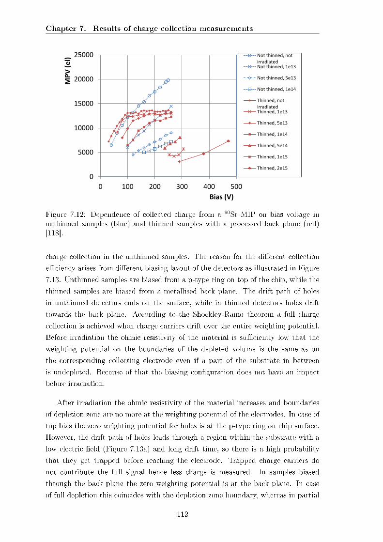
Chapter 7. Results of charge collection measurements
0
5000
10000
15000
20000
25000
0 100 200 300 400 500
MPV(el)
Bias (V)
Not thinned, notirradiatedNot thinned, 1e13
Not thinned, 5e13
Not thinned, 1e14
Thinned, notirradiatedThinned, 1e13
Thinned, 5e13
Thinned, 1e14
Thinned, 5e14
Thinned, 1e15
Thinned, 2e15
Figure 7.12: Dependence of collected charge from a 90Sr MIP on bias voltage inunthinned samples (blue) and thinned samples with a processed back plane (red)[118].
charge collection in the unthinned samples. The reason for the dierent collection
eciency arises from dierent biasing layout of the detectors as illustrated in Figure
7.13. Unthinned samples are biased from a p-type ring on top of the chip, while the
thinned samples are biased from a metallised back plane. The drift path of holes
in unthinned detectors ends on the surface, while in thinned detectors holes drift
towards the back plane. According to the Shockley-Ramo theorem a full charge
collection is achieved when charge carriers drift over the entire weighting potential.
Before irradiation the ohmic resistivity of the material is suciently low that the
weighting potential on the boundaries of the depleted volume is the same as on
the corresponding collecting electrode even if a part of the substrate in between
is undepleted. Because of that the biasing conguration does not have an impact
before irradiation.
After irradiation the ohmic resistivity of the material increases and boundaries
of depletion zone are no more at the weighting potential of the electrodes. In case of
top bias the zero weighting potential for holes is at the p-type ring on chip surface.
However, the drift path of holes leads through a region within the substrate with a
low electric eld (Figure 7.13a) and long drift time, so there is a high probability
that they get trapped before reaching the electrode. Trapped charge carriers do
not contribute the full signal hence less charge is measured. In samples biased
through the back plane the zero weighting potential is at the back plane. In case
of full depletion this coincides with the depletion zone boundary, whereas in partial
112

7.3. Results with CHESS2
n-well (+HV) p-ring (gnd)
electrons
holes
low electric field
(a)
n-well (+HV) p-ring (float)
electrons
holes
back plane (gnd)
(b)
Figure 7.13: Charge carrier drift in a detector biased from the top (a) and from theback plane (b). In a top biased detector holes can be trapped in the low eld regionand do not drift through the entire weighting eld, resulting in less collected charge.
depletion it is still closer to the boundary than in a detector biased from the top.
Trapping therefore does not have so much impact on collected charge as in top
biased samples. The measurements clearly indicate benecial eects of back plane
processing on charge collection. However, the above measurements were made with
a pad structure, where the weighting eld is uniform. In pixel devices the weighting
eld is signicantly dierent the eld is largest close to the readout electrode and
most of the charge is collected from the carrier drift in this region. It is therefore
expected that while thinning and back plane processing is still benecial, top biasing
does not have as large adverse eect as measured here on charge collection in pixel
devices.
7.3 Results with CHESS2
CHESS2 (Section 5.4) has been designed as a prototype of strip detector in CMOS
technology and manufactured by ams [122]. The basic readout unit is an active
striplet, also called pixel, with a size of 630µm×40µm. There are several structures
on the CHESS2 chip. In the three main active arrays multiple (32× 1) striplets are
interconnected to form 20mm long strips. Passive test structures investigated in
this work are located in a dedicated test sector outside of the main arrays as shown
in Figure 7.14. Edge-TCT measurements were made on a 3 × 3 passive striplet
(pixel) array with the standard pixel dimensions of 630µm× 40µm located on the
edge of the device. Charge collection measurements with 90Sr were made with the so
called Large Array of interconnected implants with a total size of 1.2mm× 1.2mm.
Chips are produced on four dierent substrates with initial resistivities of 20, 50, 200
and 1000Ω cm, covering the full resistivity range of CMOS detectors. Samples are
113

Chapter 7. Results of charge collection measurements
(a)
Edge-TCT3 x 3 arrays
Sr90 pad
to external amplifiers
(b)
Figure 7.14: The CHESS2 chip: a) chip layout. The chip consists of three largemonolithic arrays and a collection of test structures located in a test sector in themiddle. The schematics indicates the two test structures used in this work, as wellas the position and size (σ) of the beam during proton irradiation; b) Closeup oftest structures used for Edge-TCT and 90Sr measurements. The sample is glued toa carrier board and test structures connected with wire bonds can be seen in thepicture
thinned to a thickness of 250µm, but the back plane is not processed. The samples
are instead biased from the top via p-type rings surrounding the test structures.
Chips are designed to withstand a high bias voltage of 120V.
CHESS2 samples were used in an extensive irradiation study employing both
neutron and proton irradiation. A summary of the delivered uences is given in
Table 7.1 [123]. Neutron irradiation up to a maximal uence of 2 · 1015 neq/cm2
was performed at Ljubljana TRIGA reactor, while irradiation with protons was per-
formed at CERN PS and LANSCE (see section 7.1) up to a maximal nominal uence
of 3.6 · 1015 neq/cm2. The targeted centre and spot size of the beam during proton
irradiation is shown in Figure 7.14a. However, we suspect that during irradiation
at LANSCE the beam centre was displaced with respect to the targeted position so
that the uence received by the investigated test structures was less than nominal.
This assumption is based on I-V measurements in LANSCE samples which show a
leakage current lower by about an order of magnitude compared to samples irradi-
ated in PS. Moreover, results of Edge-TCT and 90Sr measurements presented below
are also more compatible with lower uences in LANSCE samples.
114
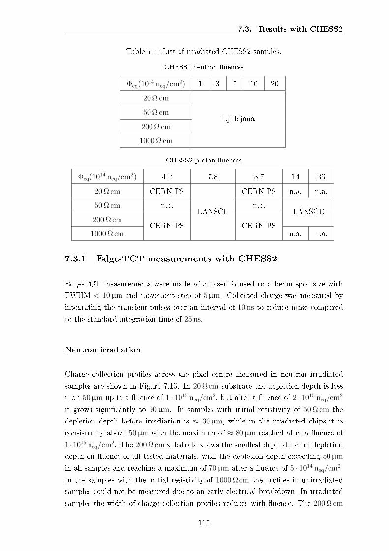
7.3. Results with CHESS2
Table 7.1: List of irradiated CHESS2 samples.
CHESS2 neutron uences
Φeq(1014 neq/cm
2) 1 3 5 10 20
20Ω cm
Ljubljana50Ω cm
200Ω cm
1000Ω cm
CHESS2 proton uences
Φeq(1014 neq/cm
2) 4.2 7.8 8.7 14 36
20Ω cm CERN PS
LANSCE
CERN PS n.a. n.a.
50Ω cm n.a. n.a.LANSCE
200Ω cmCERN PS CERN PS
1000Ω cm n.a. n.a.
7.3.1 Edge-TCT measurements with CHESS2
Edge-TCT measurements were made with laser focused to a beam spot size with
FWHM < 10µm and movement step of 5µm. Collected charge was measured by
integrating the transient pulses over an interval of 10 ns to reduce noise compared
to the standard integration time of 25 ns.
Neutron irradiation
Charge collection proles across the pixel centre measured in neutron irradiated
samples are shown in Figure 7.15. In 20Ω cm substrate the depletion depth is less
than 50µm up to a uence of 1 · 1015 neq/cm2, but after a uence of 2 · 1015 neq/cm
2
it grows signicantly to 90µm. In samples with initial resistivity of 50Ω cm the
depletion depth before irradiation is ≈ 30µm, while in the irradiated chips it is
consistently above 50µm with the maximum of ≈ 80µm reached after a uence of
1 ·1015 neq/cm2. The 200Ω cm substrate shows the smallest dependence of depletion
depth on uence of all tested materials, with the depletion depth exceeding 50µm
in all samples and reaching a maximum of 70µm after a uence of 5 · 1014 neq/cm2.
In the samples with the initial resistivity of 1000Ω cm the proles in unirradiated
samples could not be measured due to an early electrical breakdown. In irradiated
samples the width of charge collection proles reduces with uence. The 200Ω cm
115
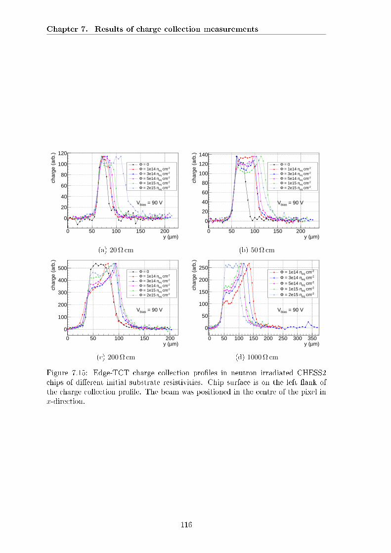
Chapter 7. Results of charge collection measurements
m)µy (0 50 100 150 200
char
ge (
arb.
)
0
20
40
60
80
100
120
= 0 Φ -2 cmeq = 1e14 nΦ -2 cmeq = 3e14 nΦ -2 cmeq = 5e14 nΦ -2 cmeq = 1e15 nΦ -2 cmeq = 2e15 nΦ
= 90 VbiasV
(a) 20Ω cm
m)µy (0 50 100 150 200
char
ge (
arb.
)
0
20
40
60
80
100
120
140
= 0 Φ -2 cmeq = 1e14 nΦ -2 cmeq = 3e14 nΦ -2 cmeq = 5e14 nΦ -2 cmeq = 1e15 nΦ -2 cmeq = 2e15 nΦ
= 90 VbiasV
(b) 50Ω cm
m)µy (0 50 100 150 200
char
ge (
arb.
)
0
100
200
300
400
500 = 0 Φ
-2 cmeq = 1e14 nΦ -2 cmeq = 3e14 nΦ -2 cmeq = 5e14 nΦ -2 cmeq = 1e15 nΦ -2 cmeq = 2e15 nΦ
= 90 VbiasV
(c) 200Ω cm
m)µy (0 50 100 150 200 250 300 350
char
ge (
arb.
)
0
50
100
150
200
250 -2 cmeq = 1e14 nΦ -2 cmeq = 3e14 nΦ -2 cmeq = 5e14 nΦ -2 cmeq = 1e15 nΦ -2 cmeq = 2e15 nΦ
= 90 VbiasV
(d) 1000Ω cm
Figure 7.15: Edge-TCT charge collection proles in neutron irradiated CHESS2chips of dierent initial substrate resistivities. Chip surface is on the left ank ofthe charge collection prole. The beam was positioned in the centre of the pixel inx-direction.
116
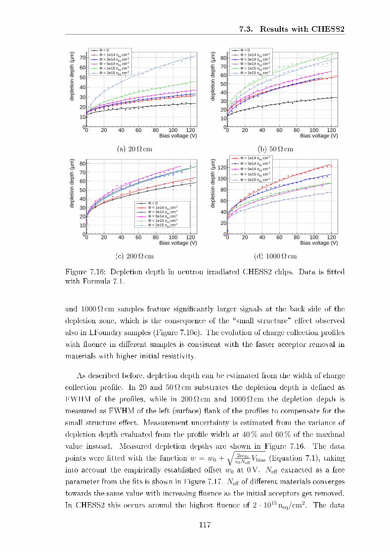
7.3. Results with CHESS2
Bias voltage (V)0 20 40 60 80 100 120
m)
µde
plet
ion
dept
h (
0
10
20
30
40
50
60
70
= 0Φ -2 cmeq = 1e14 nΦ -2 cmeq = 3e14 nΦ -2 cmeq = 5e14 nΦ -2 cmeq = 1e15 nΦ -2 cmeq = 2e15 nΦ
(a) 20Ω cm
Bias voltage (V)0 20 40 60 80 100 120
m)
µde
plet
ion
dept
h (
0
10
20
30
40
50
60
70
80
= 0Φ -2 cmeq = 1e14 nΦ -2 cmeq = 3e14 nΦ -2 cmeq = 5e14 nΦ -2 cmeq = 1e15 nΦ -2 cmeq = 2e15 nΦ
(b) 50Ω cm
Bias voltage (V)0 20 40 60 80 100 120
m)
µde
plet
ion
dept
h (
0
10
20
30
40
50
60
70
80
= 0Φ -2 cmeq = 1e14 nΦ -2 cmeq = 3e14 nΦ -2 cmeq = 5e14 nΦ -2 cmeq = 1e15 nΦ -2 cmeq = 2e15 nΦ
(c) 200Ω cm
Bias voltage (V)0 20 40 60 80 100 120
m)
µde
plet
ion
dept
h (
0
20
40
60
80
100
120
-2 cmeq = 1e14 nΦ -2 cmeq = 3e14 nΦ -2 cmeq = 5e14 nΦ -2 cmeq = 1e15 nΦ -2 cmeq = 2e15 nΦ
(d) 1000Ω cm
Figure 7.16: Depletion depth in neutron irradiated CHESS2 chips. Data is ttedwith Formula 7.1.
and 1000Ω cm samples feature signicantly larger signals at the back side of the
depletion zone, which is the consequence of the "small structure" eect observed
also in LFoundry samples (Figure 7.10c). The evolution of charge collection proles
with uence in dierent samples is consistent with the faster acceptor removal in
materials with higher initial resistivity.
As described before, depletion depth can be estimated from the width of charge
collection prole. In 20 and 50Ω cm substrates the depletion depth is dened as
FWHM of the proles, while in 200Ω cm and 1000Ω cm the depletion depth is
measured as FWHM of the left (surface) ank of the proles to compensate for the
small structure eect. Measurement uncertainty is estimated from the variance of
depletion depth evaluated from the prole width at 40% and 60% of the maximal
value instead. Measured depletion depths are shown in Figure 7.16. The data
points were tted with the function w = w0 +√
2ϵϵSie0Neff
Vbias (Equation 7.1), taking
into account the empirically established oset w0 at 0V. Neff extracted as a free
parameter from the ts is shown in Figure 7.17. Neff of dierent materials converges
towards the same value with increasing uence as the initial acceptors get removed.
In CHESS2 this occurs around the highest uence of 2 · 1015 neq/cm2. The data
117

Chapter 7. Results of charge collection measurements
]-2 cm14 [10eqΦ0 5 10 15 20 25 30 35 40
]-3
cm
14 [1
0ef
fN
1−10
1
10cmΩCHESS2 50
0.02± ~ 0.98 eff0/NcN2 cm-14 10× 0.06) ±c ~ (0.47
(fixed)-1 = 0.020 cmc
g
cmΩCHESS2 200
0.28± ~ 0.95 eff0/NcN2 cm-14 10× 0.08) ±c ~ (0.19
(fixed)-1 = 0.020 cmc
g
cmΩCHESS2 20
0.02± ~ 1.06 eff0/NcN2 cm-14 10× 0.03) ±c ~ (0.14
(fixed)-1 = 0.020 cmc
g
cmΩCHESS2 1000-1 0.003) cm± = (0.020
cg
Figure 7.17: Evolution of Neff with received neutron uence in CHESS2 chips. Ac-ceptor removal is observed in chips with the three lowest initial substrate resistivities.Data is tted with equation 4.5. In samples with the highest initial resistivity onlyacceptor introduction term was taken into account, since initial acceptor removal isalready completed below 1 · 1014 neq/cm
2.
118

7.3. Results with CHESS2
for the 20, 50 and 200Ω cm material is tted with the Equation 4.5 parametrising
acceptor removal:
Neff = Neff,0(1−Nc/Neff,0 · (1− e−cΦeq)) + gCΦeq,
with Neff,0, Nc and c as free parameters and gC = 0.02 cm−1 xed to the literature
value [66]. In all three samples the acceptor removal is complete, i.e. Nc/Neff,0 ≈ 1.
The values of the acceptor removal coecient c are (0.14±0.03)·10−14 cm2 (20Ω cm),
(0.47± 0.06) · 10−14 cm2 (50Ω cm) and (0.19± 0.08) · 10−14 cm2 (200Ω cm). These
values are compatible with c = (0.5± 0.2) · 10−14 cm2 (50Ω cm) and
c = (0.3± 0.3) · 10−14 cm2 (200Ω cm) measured with the ATLASpix pixel chip using
the same substrate [94]. The value of c in the 200Ω cm material is comparatively
small and less than in 50Ω cm material. This indicates a slow removal and hence
a very constant depletion depth in this material. Removal coecients for all three
initial resistivities are by more than an order of magnitude smaller than in the high
resistivity 2000Ω cm LFoundry sample (c = 10.8 ·10−14 cm2), where removal is much
faster. The acceptor removal term is omitted in the t of the data for 1000Ω cm ma-
terial (Nc = 0), due to the lack of measurements below the uence of 1 ·1014 neq/cm2
which is the typical uence where removal is completed in high resistivity material.
Instead the data was tted with the acceptor generation term gC as a free parameter,
yielding a value of gC = (0.020± 0.003) cm−1, which is consistent with literature.
Proton irradiation
Depletion depths in proton irradiated samples are shown in Figure 7.18. Compared
to neutron irradiated samples the depletion depths are much larger, reaching over
100µm at certain uences in all samples. There is a signicant dierence in depletion
depth of samples irradiated to uences of 8.7 · 1014 neq/cm2 (CERN PS) and 7.8 ·
1014 neq/cm2 (LANSCE). This is because the test structures in samples irradiated at
LANSCE probably received a lower uence than quoted. The test structures were
positioned at the fringe of the beam during irradiation (Figure 7.14a) which makes
the delivered uence very sensitive to small displacements in the beam.
The values of Neff from the t of the Equation 7.1 to proton data are shown
in Figure 7.19. In samples irradiated at PS the values of Neff are well below the
values in neutron irradiated samples, indicating a faster acceptor removal with pro-
tons. The eect is most prominent in 20Ω cm samples where Neff in proton and
neutron samples is dierent by a factor of 10. The values of Neff in LANSCE sam-
ples are not always compatible with PS samples, since their uences are probably
119

Chapter 7. Results of charge collection measurements
Bias voltage (V)0 20 40 60 80 100 120
m)
µco
llect
ion
wid
th (
0
50
100
150
200
250 unirradiated = 5e14nΦ = 1e15nΦ = 2e15nΦ = 4.2e14p (PS)Φ = 8.7e14p (PS)Φ = 7.8e14pΦ
(a) 20Ω cm
Bias voltage (V)0 20 40 60 80 100 120
m)
µco
llect
ion
wid
th (
0
50
100
150
200
250 unirradiated = 5e14nΦ = 1e15nΦ = 2e15nΦ = 7.8e14pΦ = 1.4e15pΦ = 3.6e15pΦ
(b) 50Ω cm
Bias voltage (V)0 20 40 60 80 100 120
m)
µco
llect
ion
wid
th (
0
50
100
150
200
250 unirradiated = 5e14nΦ = 1e15nΦ = 2e15nΦ = 4.2e14p (PS)Φ = 8.7e14p (PS)Φ = 7.8e14pΦ = 1.4e15pΦ = 3.6e15pΦ
(c) 200Ω cm
Bias voltage (V)0 20 40 60 80 100 120
m)
µco
llect
ion
wid
th (
0
50
100
150
200
250 = 1e14nΦ = 5e14nΦ = 1e15nΦ = 2e15nΦ = 4.2e14p (PS)Φ = 8.7e14p (PS)Φ = 7.8e14pΦ
(d) 1000Ω cm
Figure 7.18: Depletion depth in CHESS2 samples irradiated with protons at CERNPS (green) and LANSCE (blue), along with data for unirradiated (black) and neu-tron irradiated samples (red). Depletion depth in proton irradiated samples is largerthan in neutron irradiated samples at similar uences.
120
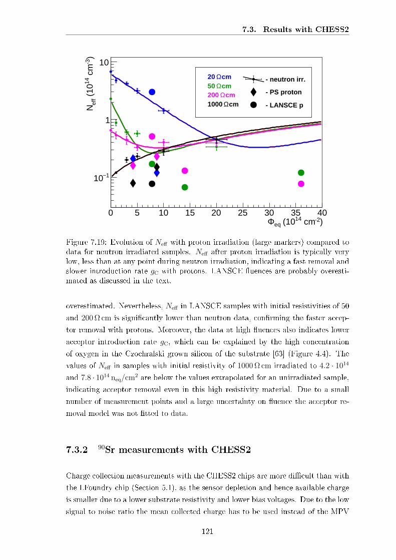
7.3. Results with CHESS2
)-2 cm14 (10eqΦ0 5 10 15 20 25 30 35 40
)-3
cm
14 (
10ef
fN
1−10
1
10
cmΩ20cmΩ50
cmΩ200cmΩ1000
- neutron irr.
- LANSCE p
- PS proton
Figure 7.19: Evolution of Neff with proton irradiation (large markers) compared todata for neutron irradiated samples. Neff after proton irradiation is typically verylow, less than at any point during neutron irradiation, indicating a fast removal andslower introduction rate gC with protons. LANSCE uences are probably overesti-mated as discussed in the text.
overestimated. Nevertheless, Neff in LANSCE samples with initial resistivities of 50
and 200Ω cm is signicantly lower than neutron data, conrming the faster accep-
tor removal with protons. Moreover, the data at high uences also indicates lower
acceptor introduction rate gC, which can be explained by the high concentration
of oxygen in the Czochralski grown silicon of the substrate [63] (Figure 4.4). The
values of Neff in samples with initial resistivity of 1000Ω cm irradiated to 4.2 · 1014
and 7.8 · 1014 neq/cm2 are below the values extrapolated for an unirradiated sample,
indicating acceptor removal even in this high resistivity material. Due to a small
number of measurement points and a large uncertainty on uence the acceptor re-
moval model was not tted to data.
7.3.2 90Sr measurements with CHESS2
Charge collection measurements with the CHESS2 chips are more dicult than with
the LFoundry chip (Section 5.1), as the sensor depletion and hence available charge
is smaller due to a lower substrate resistivity and lower bias voltages. Due to the low
signal to noise ratio the mean collected charge has to be used instead of the MPV
121

Chapter 7. Results of charge collection measurements
charge (e-)10000− 5000− 0 5000 10000 15000 20000 25000
even
ts
0
50
100
150
200
250
300NoiseSignal
cmΩ = 20 init
ρ
= 0Φ = 120 VbiasV
Mean charge2575 el
(a)
charge (e-)10000− 5000− 0 5000 10000 15000 20000 25000
even
ts
0
20
40
60
80
100
120
140
160
180
200 NoiseSignal
cmΩ = 20 init
ρ
-2 cmeq = 2e15 nΦ = 120 VbiasV
Mean charge2143 el
(b)
charge (e-)10000− 5000− 0 5000 10000 15000 20000 25000
even
ts
0
50
100
150
200
250 NoiseSignal
cmΩ = 50 init
ρ
= 0Φ = 120 VbiasV
Mean charge4054 el
(c)
charge (e-)10000− 5000− 0 5000 10000 15000 20000 25000
even
ts
0
50
100
150
200
250NoiseSignal
cmΩ = 50 init
ρ
-2 cmeq = 2e15 nΦ = 75 VbiasV
Mean charge1181 el
(d)
charge (e-)10000− 5000− 0 5000 10000 15000 20000 25000
even
ts
0
100
200
300
400
500 NoiseSignal
cmΩ = 200 init
ρ
= 0Φ = 120 VbiasV
Mean charge5384 el
(e)
charge (e-)10000− 5000− 0 5000 10000 15000 20000 25000
even
ts
0
20
40
60
80
100
120
140
160
180
200
220 NoiseSignal
cmΩ = 200 init
ρ
-2 cmeq = 2e15 nΦ = 90 VbiasV
Mean charge2302 el
(f)
charge (e-)10000− 5000− 0 5000 10000 15000 20000 25000
even
ts
0
50
100
150
200
250
300 NoiseSignal
cmΩ = 1000 init
ρ
-2 cmeq = 1e14 nΦ = 120 VbiasV
Mean charge7787 el
(g)
charge (e-)10000− 5000− 0 5000 10000 15000 20000 25000
even
ts
0
50
100
150
200
250
300
NoiseSignal
cmΩ = 1000 init
ρ
-2 cmeq = 2e15 nΦ = 90 VbiasV
Mean charge1857 el
(h)
Figure 7.20: 90Sr charge spectra measured with CHESS2 chips of dierent initialsubstrate resistivity before and after neutron irradiation to 2 · 1015 neq/cm
2.
122

7.3. Results with CHESS2
0
2000
4000
6000
8000
10000
12000
14000
16000
18000
0 10 20 30 40
Mean
charge
(electrons)
Fluence (1e14 neq/cm2)
Mean charge at 100 V (annealed)
20 Ω·cm50 Ω·cm200 Ω·cm1000 Ω·cm
PSLANSCEprotonsneutrons
Figure 7.21: Mean charge deposited by a 90Sr MIP in dierently irradiated CHESS2chips. Charge collected in proton irradiated samples is consistently larger than inneutron irradiated samples, and at certain uences also larger than before irradia-tion. The 200Ω cm substrate gives the most constant response with the measuredcharge never dropping below 2000 e−. Based on LFoundry data (Section 7.2.4) andEdge-TCT measurements the amount of collected charge in pad structures can besignicantly increased by biasing the sample via back plane.
values. The mean charge deposition with MIP-like 90Sr electrons is 100 e−/µm.
Examples of 90Sr MIP spectra for unirradiated and neutron irradiated samples at a
uence of 2 · 1015 neq/cm2 are presented in Figure 7.20 and show a clear degradation
of collected charge after irradiation.
A summary of the collected charge for all samples and uences for both proton
and neutron irradiation is shown in Figure 7.21. The collected charge after proton
irradiation is signicantly higher than after neutron irradiation to the same uence
in all samples which is consistent with the larger depletion depths observed with
Edge-TCT. After the rst neutron irradiation step the collected charge reduces by
≈ 10002000 e− with respect to unirradiated samples. This is because before ir-
radiation a fraction of charge is collected by diusion, but after the rst uence of
1·1014 neq/cm2 this contribution is already completely suppressed. In neutron irradi-
ated samples with initial resitivities of 20200Ω cm the collected charge temporarily
increases at intermediate uences due to acceptor removal and related increase of
123

Chapter 7. Results of charge collection measurements
depletion depth. The most consistent charge collection is observed in 200Ω cm sam-
ples where a mean charge above 2000 e− is collected at all uences. In samples
with an initial resistivity of 2 kΩ cm a mean charge over 2000 e− is also measured
at all uences, but this material suers an early electrical breakdown before irradi-
ation. The sample also has to be designed for a larger amplitude dynamic range,
since larger signals are expected before irradiation due to higher resistivity. A mean
charge of 2000 e− corresponds to a depletion depth of 20µm, which does not agree
with depletion depths exceeding 50µm measured by Edge-TCT. This inconsistency
can be attributed to the top biasing scheme and was also observed in LFoundry
samples (Section 7.2.4). It is expected that more charge will be collected with a
"real" pixel detector where pixels are not connected together, since the weighting
eld in such devices is more favourable.
7.4 Results with X-FAB XTB02
The test chip X-FAB XTB02 is produced in SOI technology (Chapter 5.5) on a
p-type substrate with an initial resistivity of 100Ω cm. The test structure 2A in-
vestigated in this work (Figure 7.22) is a 4 × 4 pixel array with a pixel size of
110µm× 100µm [124]. The n-type collection electrodes underneath the buried ox-
ide layer (BOX) have a size of 40µm × 50µm. The output signals are routed to
two separate bond pads, one for a single central pixel and the other one for the
remaining 15 pixels. Two additional wire bond contacts are used for biasing of the
p-wells with CMOS electronics (called LOGIC layer), and the P-FIELD structure
used for inter pixel insulation. The chip has a thickness of 700µm with no processed
back plane. The sensor can be biased to a maximal bias voltage of 300V using the
outermost guard ring on the sample surface as the bias electrode. In a standard
biasing conguration the collecting n-well and the LOGIC layer were biased to the
same potential, while the P-FIELD structure was oating. Tests with dierent bi-
asing schemes are presented later in the chapter. A single sample available for tests
was progressively irradiated with neutrons in Ljubljana TRIGA reactor in six steps
up to a nal total uence of 1 · 1016 neq/cm2. Measurements were carried out after
standard annealing (80min at 60C) after every uence step [124].
Measurement of depletion depth and estimation of Neff
Edge-TCT charge collection proles at the bias voltage of 300V are shown in Figure
7.23a and display a behaviour typical for acceptor removal. The width (FWHM)
124

7.4. Results with X-FAB XTB02
(a)
(b)
Figure 7.22: X-FAB XTB02 chip: a) pixel array 2A; b) schematics of the pixel [100].The P-FIELD structure and the layer housing the p-wells (LOGIC) can be biasedseparately [124].
of the prole increases from ≈ 50µm before irradiation to the maximal width of
≈ 150µm after a uence of 5 · 1014 neq/cm2, at which eective space charge concen-
tration stops falling due to initial acceptor removal. At higher uences the width
starts to shrink again due to additional space charge introduction, reaching ≈ 30µm
at the nal uence of 1·1016 neq/cm2. Depletion depth estimated as FWHM of charge
collection proles is shown in Figure 7.23b. In the unirradiated samples the deple-
tion depth scales approximately with√Vbias which is consistent with the abrupt
junction approximation. However, this is not the case in irradiated samples, where
depletion zone grows faster than√Vbias. Moreover, at uences above 1 ·1015 neq/cm
2
a signicant depletion zone is only detected above a threshold voltage of ∼ 30V.
The reason for this behaviour is not understood, but it is probably related to the
eects of electric eld generated by charge trapped in the BOX as a consequence of
irradiation. Since the data does not follow the abrupt junction model, an approx-
imation is used to estimate the space charge concentration: Neff is extracted from
the formula 3.8 evaluated at the maximal bias voltage of 300V:
w =
√2ϵϵSie0Neff
V300V. (7.3)
Applying the above procedure to measurements with the unirradiated sample yields
a value of Neff,0 = 1.3 · 1014 cm−3 which is consistent with the 100Ω cm resistivity of
the substrate. Extracted values of Neff are shown in Figure 7.24 together with the
values for LFoundry CCPD_LF (high substrate resistivity) [117] and ams CHESS
(low substrate resistivity) [72] for comparison. The XTB02 produced on an interme-
diately resistive material features a behaviour midway between the other two sam-
125
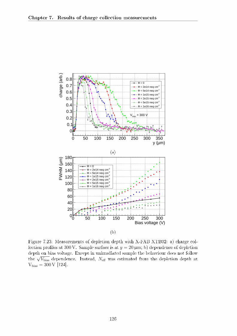
Chapter 7. Results of charge collection measurements
m)µy (0 50 100 150 200 250 300 350
char
ge (
arb.
)
0
0.1
0.2
0.3
0.4
0.5
0.6
0.7
0.8 = 0 Φ
-2 = 2e14 neq cmΦ -2 = 5e14 neq cmΦ -2 = 1e15 neq cmΦ -2 = 2e15 neq cmΦ -2 = 5e15 neq cmΦ -2 = 1e16 neq cmΦ
= 300 VbiasV
(a)
Bias voltage (V)0 50 100 150 200 250 300
m)
µF
WH
M (
0
20
40
60
80
100
120
140
160
180Width of charge collection region at 50% max
= 0Φ -2 = 2e14 neq cmΦ -2 = 5e14 neq cmΦ -2 = 1e15 neq cmΦ -2 = 2e15 neq cmΦ -2 = 5e15 neq cmΦ -2 = 1e16 neq cmΦ
(b)
Figure 7.23: Measurements of depletion depth with X-FAB XTB02: a) charge col-lection proles at 300V. Sample surface is at y = 20µm; b) dependence of depletiondepth on bias voltage. Except in unirradiated sample the behaviour does not followthe
√Vbias dependence. Instead, Neff was estimated from the depletion depth at
Vbias = 300V [124].
126

7.4. Results with X-FAB XTB02
]-2 cm14 [10eqΦ0 20 40 60 80 100
]-3
cm
14 [1
0ef
fN
2−10
1−10
1
10
210
cmΩCHESS 20 ~ 1.0eff0/NcN
2 cm-14 10× 0.03) ±c ~ (0.36
cmΩX-FAB 100 ~ 1.0eff0/NcN
2 cm-14 10× 0.1) ±c ~ (1.1 -1 0.004) cm± ~ (0.036
cg
cmΩLF 2000 0.1)± ~ (0.6 eff0/NcN
2 cm-14 10× 4.7) ±c ~ (10.3
Figure 7.24: Evolution of Neff with neutron uence in X-FAB XTB02 [124]. Twoother CMOS prototypes are included for comparison [72, 117].
ples. The initial acceptor removal is completed around a uence of 5 · 1014 neq/cm2
resulting in Neff reduced by a factor of 10 from the initial value. At higher uences
the space charge introduction rate is similar to the LFoundry CCPD_LF. The data
were tted with the acceptor removal parametrisation 4.5:
Neff = Neff,0(1−Nc/Neff,0 · (1− e−cΦeq)) + gCΦeq,
with Nc/Neff,0, c and gC as free parameters. The results of the t indicate a complete
acceptor removal (Nc/Neff,0 = 1) with a removal constant of c = (1.1±0.1)·10−14 cm2.
Since the procedure of determining Neff from Equation 7.3 depends on an arbitrarily
selected voltage of 300V, the values of Neff are ambiguous. However, the evolution
of Neff with uence shows the same trend for any voltage and extracted value of c
using, for example, a reference voltage of 200V diers from the above value by less
than 10%. The space charge introduction rate gC = (0.036 ± 0.003) cm−1 is larger
than the literature value of 0.02 cm−1 [66]. This could be due to a systematic oset
introduced by the procedure to calculate Neff from depletion depth at 300V, since
the sample does not follow the abrupt junction approximation. However, a similar
value was also measure in LFoundry samples.
127

Chapter 7. Results of charge collection measurements
Cha
rge
(arb
)
20−
0
20
40
60
80
100
CCE at V bias = 100 V
m)µx (0 50 100 150 200 250 300 350 400 450 500
m)
µy
(
0
20
40
60
80
100
120
140
CCE at V bias = 100 V
(a) Vbias = 100V
Cha
rge
(arb
)
0
20
40
60
80
100
120
140
160
180
CCE at V bias = 200 V
m)µx (0 50 100 150 200 250 300 350 400 450 500
m)
µy
(
0
20
40
60
80
100
120
140
CCE at V bias = 200 V
(b) Vbias = 200V
Cha
rge
(arb
)
0
50
100
150
200
CCE at V bias = 300 V
m)µx (0 50 100 150 200 250 300 350 400 450 500
m)
µy
(
0
20
40
60
80
100
120
140
CCE at V bias = 300 V
(c) Vbias = 300V
Figure 7.25: Two dimensional Edge-TCT scans on XTB02 at dierent bias voltages.The sample is irradiated to a uence of 1·1015 neq/cm
2. Chip surface is at y = 25µm.
Two dimensional Edge-TCT measurements
Figure 7.25 shows an example of a two dimensional charge collection map of a
sample irradiated to a uence of 1 · 1015 neq/cm2 at bias voltages between 100V
and 300V. The measurement demonstrates the large increase of depletion depth
with bias voltage which can also be seen in Figure 7.23b. More importantly, the
measurement reveals eciency gaps between pixels whose width coincides with the
size of the area not covered by the charge collecting n-well implant. Further scans
at dierent uences are shown in Figure 7.26. Eciency gaps were observed after
all irradiation steps, but not in an unirradiated sample. The eciency gaps are a
problem in detectors that target near 100% particle detection eciency.
The eciency gaps are related to the SOI pixel architecture with the logic layer
housing the electronics acting as a parasitic collecting electrode. Although the logic
layer is separated from the bulk by the buried oxide (BOX) it can modify the electric
eld in the sensor and collect charge similar to an AC coupled detector. Since the
LOGIC node is not connected to the readout, the collected charge is not detected.
This hypothesis was veried by reading out the induced current on the LOGIC
contact, which yielded an inverse of the charge collection maps shown in Figures
7.25 and 7.26 with highly ecient regions in between pixel implants.
The electrons collected by LOGIC nish their drift on the BOX layer where the
charge transport eectively stops. Accumulated electrons then slowly discharge via
the collection n-wells. The exact mechanism of charge transport on the BOX was
not investigated in this thesis, but measurements indicate it takes place on a time
scale of 1µs and it is sensitive to irradiation. This can be observed in waveforms in
Figure 7.27 showing induced pulses on a µs time scale. The current from the carrier
drift in the substrate takes place in the rst 10 ns and is truncated from the gure
as it is by a factor 100 larger from the scale of the diagram. In the rst 10 ns the
signal from an ecient region directly underneath the BOX (red) is unipolar with
128

7.4. Results with X-FAB XTB02
m)µx (0 100 200 300 400 500 600 700
m)
µy
(0
20
40
60
80
100
120
140
CCE at V bias = 300 V
Cha
rge
(arb
)
0
0.2
0.4
0.6
0.8
1
1.2
CCE at V bias = 300 V
(a) unirradiated
Cha
rge
(arb
)
0
0.1
0.2
0.3
0.4
0.5
m)µx (0 50 100 150 200 250 300 350 400 450 500
m)
µy
(
0
20
40
60
80
100
120
140
CCE at V bias = 300 VCCE at V bias = 300 V
(b) 2 · 1014 neq/cm2
Cha
rge
(arb
)
0
50
100
150
200
250
CCE at V bias = 200 V
m)µx (0 50 100 150 200 250 300 350 400 450 500
m)
µy
(
0
20
40
60
80
100
120
140
CCE at V bias = 200 V
(c) 5 · 1014 neq/cm2 (200V)
Cha
rge
(arb
)
0
50
100
150
200
CCE at V bias = 300 V
m)µx (0 50 100 150 200 250 300 350 400 450 500
m)
µy
(
0
20
40
60
80
100
120
140
CCE at V bias = 300 V
(d) 1 · 1015 neq/cm2
Cha
rge
(arb
)
0
50
100
150
200
CCE at V bias = 300 V
m)µx (0 50 100 150 200 250 300 350 400 450 500
m)
µy
(
0
20
40
60
80
100
120
140
CCE at V bias = 300 V
(e) 2 · 1015 neq/cm2
Cha
rge
(arb
)
0
50
100
150
200
250
CCE at V bias = 300 V
m)µx (0 50 100 150 200 250 300 350 400 450 500
m)
µy
(
0
20
40
60
80
100
120
140
CCE at V bias = 300 V
(f) 5 · 1015 neq/cm2
Cha
rge
(arb
)
0
50
100
150
200
CCE at V bias = 300 V
m)µx (0 50 100 150 200 250 300 350 400 450 500
m)
µy
(
0
20
40
60
80
100
120
140
CCE at V bias = 300 V
(g) 1 · 1016 neq/cm2
Figure 7.26: Two dimensional Edge-TCT scans on XTB02 irradiated to dierentuences. Measurements are made at the maximal bias voltage of 300V (except atthe uence of 5 · 1014 neq/cm
2).
129

Chapter 7. Results of charge collection measurements
Cha
rge
(arb
)
0
100
200
300
400
500
600
700
Integration time 25 ns
m)µx (0 50 100 150 200 250 300 350 400 450 500
m)
µy
(
0
20
40
60
80
100
120
140
Integration time 25 ns
(a)
Cha
rge
(arb
)
500−
0
500
1000
1500
Integration time 800 ns
m)µx (0 50 100 150 200 250 300 350 400 450 500
m)
µy
(
0
20
40
60
80
100
120
140
Integration time 800 ns
(b)
t (ns)0 200 400 600 800
A)
µI (
150−
100−
50−
0
50
m - "inefficient"µm, y = 100 µx = 150
m - "efficient"µm, y = 100 µx = 200
A]µA, + 1000 µPeaks [- 6500
A]µA, + 3000 µPeaks [- 400
(c)
integration time (ns)0 200 400 600 800
char
ge (
arb.
)
1000−
800−
600−
400−
200−
0
200
Collected charge vs. integration time
m - "inefficient"µm, y = 100 µx = 150
m - "efficient"µm, y = 100 µx = 200
Difference
m - "inefficient"µm, y = 100 µx = 150
m - "efficient"µm, y = 100 µx = 200
Difference
(d)
Figure 7.27: Dependence of charge collection uniformity on integration time inXTB02 irradiated to a uence of 5 · 1014 neq/cm
2. Figures a) and b) show chargecollection maps at 25 ns and 800 ns integration times with signicantly better unifor-mity after longer integration. Figure c) shows induced pulses from an ecient (red)and inecient region (black) from gure a). The current in rst 10 ns is truncated.Figure d) shows the integrals of both pulses depending on integration time and theirdierence (green) [124].
130

7.4. Results with X-FAB XTB02
Cha
rge
(arb
)
0.1−
0
0.1
0.2
0.3
0.4
= 200 V, LOGIC and P-FIELD 200 VbiasV
m)µx (0 50 100 150 200 250 300 350 400 450 500
m)
µy
(
0
20
40
60
80
100
120
140
= 200 V, LOGIC and P-FIELD 200 VbiasV
VLOGIC = 200V,VP−FIELD = 200V
Cha
rge
(arb
)
0
0.1
0.2
0.3
0.4
0.5
0.6
0.7
= 200 V, LOGIC and P-FIELD 150 VbiasV
m)µx (0 50 100 150 200 250 300 350 400 450 500
m)
µy
(
0
20
40
60
80
100
120
140
= 200 V, LOGIC and P-FIELD 150 VbiasV
VLOGIC = 150V,VP−FIELD = 150V
Cha
rge
(arb
)
0
0.1
0.2
0.3
0.4
0.5
0.6
0.7
= 200 V, LOGIC 150 V, P-FIELD floatingbiasV
m)µx (0 50 100 150 200 250 300 350 400 450 500
m)
µy
(
0
20
40
60
80
100
120
140
= 200 V, LOGIC 150 V, P-FIELD floatingbiasV
VLOGIC = 150V,VP−FIELD = floating
Figure 7.28: Charge collection maps in XTB02 for dierent congurations of biasvoltages on the LOGIC and P-FIELD implants. Collecting n-wells are biased to200V. Dierent congurations impact the size of eciency gaps between pixels aswell as depletion depth. Sample was irradiated to a uence of 5 · 1014 neq/cm
2.
an integral corresponding to the collected charge, while the bipolar signal from the
inecient region (black) has a vanishing integral. However, over a period of 1µs
the current after charge injection in inecient region is consistently larger, leading
to both integrals equalising after an integration time of 600 ns. At longer integra-
tion times the integral from an inecient region even surpasses the integral from an
ecient region. This leads to a signicantly better charge collection uniformity on
larger time scales. The reason for a sizeable discharge current even after injection
into the ecient region is the segmentation into pixels in z-direction (i.e. along the
laser beam which extends under several pixels in Edge-TCT conguration) with the
inecient volume between the pixels producing the discharge current. The inter-
pixel eciency gaps are not present in the unirradiated sample. The probable reason
is that the BOX layer acquires a positive space charge due to the TID during irradi-
ation. Positively charged BOX attracts negatively charged electrons and eectively
stops their drift. In the original unirradiated material BOX is not charged, hence
the electrons can freely drift to the collection n-well.
A possibility to mitigate the eects of parasitic charge collection is operation at a
dierent biasing conguration. If the logic layer is biased below the n-well potential
the electric eld lines close to the surface bend toward the collection n-wells resulting
in a higher eciency. Figure 7.28 shows tests with dierent bias voltages on LOGIC
and P-FIELD structures. Biasing LOGIC 50V below the n-well potential results
in signicantly smaller eciency gaps, while the biasing of P-FIELD also slightly
modies the shape of the sensitive region. Besides the smaller eciency gaps the
alternative biasing schemes also result in smaller depletion depths. The is probably
related to modications of the electric eld caused by charge trapped in the BOX.
It has to be noted that the above measurements were made with a passive chip
131

Chapter 7. Results of charge collection measurements
with no implemented readout electronics. Operation in one of the alternative biasing
congurations is more complicated in an active device, since the n-well signals have
to be routed to the input transistor, resulting in large potential dierences between
both nodes (∼ 50V in the above case). This could be overcome by AC coupling
of the readout electrode to the electronics. Viability of an AC design sustaining
potential dierence of the order of 50V between the collection electrode and the
electronics has been demonstrated for example in the TowerJazz MonoPix CMOS
chip [83]. Another promising SOI concept is double SOI (DSOI) which employs two
silicon-on-insulator layers separated by two BOX layers [125, 126]. The intermediate
SOI layer screens the substrate from the top SOI housing the electronics, resulting
in reduced cross talk and parasitic charge collection. This approach has not been
investigated in the scope of ATLAS CMOS programme.
7.4.1 Simulation of charge collection in a SOI device
The hypothesis explaining the origin of eciency gaps in XTB02 by parasitic charge
collection of the SOI layer was tested with a simulation of charge collection using the
KDetSim simulation tool [127, 128] a ROOT based library for signal simulation in a
xed detector geometry. KDetSim takes the electrode conguration, boundary con-
ditions and (contrary to several other simulation tools) space charge concentration
as inputs and calculates the electric and weighting potentials by numerically solving
the corresponding Poisson and Laplace equations on an orthogonal mesh using a -
nite element method. Local modications of the electric eld due to injected charge
(plasma eect) are neglected. Injected charge is divided into basic units called buck-
ets, which are individually propagated through the detector as point charges, taking
into account the local electric eld and random diusion. Each bucket contributes
to the induced current according to the Shockley-Ramo theorem. Signals induced
by electrons and holes are treated separately and can be summed in the end.
Simulation of an SOI device was carried out in a simplied geometry (Figure
7.29) to reduce complexity while maintaining the main characteristics of the prob-
lem. The SOI device in simulation is translation invariant in z-direction, i.e. has a
strip geometry, with three readout electrodes with a size of 50µm and a pitch of
100µm. Above the electrodes a 1µm thick insulating layer and a 3µm thick biased
silicon layer representing the BOX and LOGIC layers are situated. The charge car-
rier mobility in the BOX layer is set to zero, so that particles entering the BOX are
stopped. Readout electrodes and LOGIC can be biased separately, while a conduc-
tive back plane at a depth of 100µm acts as a back bias contact. The XTB02 has a
132
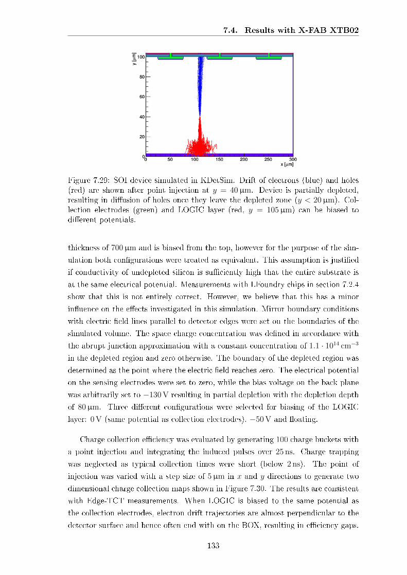
7.4. Results with X-FAB XTB02
Figure 7.29: SOI device simulated in KDetSim. Drift of electrons (blue) and holes(red) are shown after point injection at y = 40µm. Device is partially depleted,resulting in diusion of holes once they leave the depleted zone (y < 20µm). Col-lection electrodes (green) and LOGIC layer (red, y = 105µm) can be biased todierent potentials.
thickness of 700µm and is biased from the top, however for the purpose of the sim-
ulation both congurations were treated as equivalent. This assumption is justied
if conductivity of undepleted silicon is suciently high that the entire substrate is
at the same electrical potential. Measurements with LFoundry chips in section 7.2.4
show that this is not entirely correct. However, we believe that this has a minor
inuence on the eects investigated in this simulation. Mirror boundary conditions
with electric eld lines parallel to detector edges were set on the boundaries of the
simulated volume. The space charge concentration was dened in accordance with
the abrupt junction approximation with a constant concentration of 1.1 · 1014 cm−3
in the depleted region and zero otherwise. The boundary of the depleted region was
determined as the point where the electric eld reaches zero. The electrical potential
on the sensing electrodes were set to zero, while the bias voltage on the back plane
was arbitrarily set to −130V resulting in partial depletion with the depletion depth
of 80µm. Three dierent congurations were selected for biasing of the LOGIC
layer: 0V (same potential as collection electrodes), −50V and oating.
Charge collection eciency was evaluated by generating 100 charge buckets with
a point injection and integrating the induced pulses over 25 ns. Charge trapping
was neglected as typical collection times were short (below 2 ns). The point of
injection was varied with a step size of 5µm in x and y directions to generate two
dimensional charge collection maps shown in Figure 7.30. The results are consistent
with Edge-TCT measurements. When LOGIC is biased to the same potential as
the collection electrodes, electron drift trajectories are almost perpendicular to the
detector surface and hence often end with on the BOX, resulting in eciency gaps.
133

Chapter 7. Results of charge collection measurements
m]µx [0 50 100 150 200 250 300
m]
µy
[
0102030405060708090
100
char
ge (
arb.
)
0
20
40
60
80
= 130 V, logic biased 0 VbiasCCE V
(a) VLOGIC = 0V
m]µx [0 50 100 150 200 250 300
m]
µy
[
0102030405060708090
100
char
ge (
arb.
)
20−
0
20
40
60
80
= 130 V, logic biased 50 VbiasCCE V
(b) VLOGIC = −50V
m]µx [0 50 100 150 200 250 300
m]
µy
[
0102030405060708090
100ch
arge
(ar
b.)
0
20
40
60
80
= 130 V, logic floatingbiasCCE V
(c) VLOGIC = oating
Figure 7.30: Simulated charge carrier trajectories and charge collection eciencyin a SOI device for dierent biasing congurations of the LOGIC layer. Collectionelectrodes are at zero electric potential, while the back plane is at −130V.
134

7.5. Results with TowerJazz Investigator
When LOGIC is biased 50V below the n-well potential or left oating, the charge
carrier trajectories bend in the vicinity of the electrodes, thus improving charge
collection eciency. However, the changes in depletion depth observed at dierent
biasing congurations in Figure 7.28 were not reconstructed in the simulation.
7.5 Results with TowerJazz Investigator
Detectors produced in TowerJazz CMOS technology use a small electrode pixel
design which relies on small pixel sizes in the range of 2050µm and small depletion
depth of ≈ 30µm. Since the beam spot size in conventional TCT measurements has
a FWHM of ≈ 10µm, the measurements are made on the limit of the resolution.
For this reason TCT measurements targeted simpler goals, focusing on qualitative
assessment of charge collection within pixels and its evolution with irradiation.
Edge-TCT measurements in this thesis were made with the TJ Investigator chip
produced in modied TowerJazz process with a 30µm thick sensing layer and an
additional low doped n-type layer to enhance charge collection (discussed in Section
5.2). The chip has a size of 5.722mm × 5mm and consists of 2 × 134 independent
structures called mini matrices (Figure 7.31a) which employ dierent pixel designs
varying in pixel pitch, the size of the collection electrode, the distance between the
electrode and the surrounding electronics (so called spacing) and the shape of the
deep p-well which shields the n-wells with transistors [90, 92]. Each mini matrix
consists of an array of 10 × 10 pixels equipped with a charge sensitive amplier
(current integrator). The central 8× 8 pixels can be read out (Figure 7.31b), while
the outermost pixels are used to eliminate edge eects they are operated under the
same conditions as the rest, but are not read out. All mini matrices are connected in
parallel to 64 readout wire bonds on the chip (one per pixel). A congurable internal
selector circuit is used to switch between the mini matrices, connecting the output
signals from a single matrix at a time to the output. The array of 134 matrices on
the top side of the chip is mirrored on the bottom side with an additional circuitry
which allows electronic charge injection in the pixel. This feature does not work due
to connection problems and was not used in testing.
Chips come in two versions with dierently doped n-type layer (high and low
doping concentration) which is expected to aect charge collection eciency. Mea-
surements were made with unirradiated chips and chips irradiated with neutrons in
Ljubljana to four dierent uences between 1 ·1015 neq/cm2 and 1 ·1016 neq/cm
2. The
investigated structures were pixel arrays 2 and 129 with pixel sizes of 20µm×20µm
135

Chapter 7. Results of charge collection measurements
(a)
7 15 23 31 39 47 55 63
6 14 22 30 38 46 54 62
5 13 21 29 37 45 53 61
4 12 20 28 36 44 52 60
3 11 19 27 35 43 51 59
2 10 18 26 34 42 50 58
1 9 17 25 33 41 49 57
0 8 16 24 32 40 48 56
(b)
(c)
Figure 7.31: TowerJazz Investigator chip: a) chip schematics indicating investigatedpixel arrays 2 (pixel size of 20µm× 20µm) and 129 (50µm× 50µm); b) schematicsof a 10×10 pixel array. Pixels in the outermost frame cannot be read out, while theoutputs of central 64 pixels are routed out in parallel. In Edge-TCT measurementspixels 50, 51 and 52 were read out in separate channels; c) chip mounted on anEdge-TCT test board. Arrows indicate the laser beam direction during tests ofmatrices 2 and 129.
and 50µm × 50µm respectively (Figure 7.31c). Pixels in these arrays have the
largest spacing between the readout electrode and the surrounding p-well, which is
considered to be the worst case in terms of charge collection due to the dicult lat-
eral depletion of the pixel. The pixel arrays consist of 10× 10 pixels of which three
neighbouring pixels were read out in three separate channels. The biasing voltage
for the depletion of sensing epitaxial layer was applied between the collection elec-
trode, which is at ∼ 0V potential, and the back side of the epitaxial layer, as well
as the p-well surrounding the collection electrode. Both structures can be biased to
a maximal voltage of −6V, which is signicantly less than in other CMOS samples.
An example of an Edge-TCT waveform showing the output of the charge sensitive
amplier (integrator) in the pixel is shown in Figure 7.32. A periodic reset signal to
prevent output saturation takes place before t = −150 ns. The oscillation following
the reset signal is stabilised around t = −100 ns. The output signal then linearly
falls due to the integration of a constant leakage current. Charge injection with the
laser pulse occurs at the time t = 25 ns, resulting in a voltage step (modied by
the transfer function of the electronics). The size of the signal can be determined
from a linear t of the waveform before and after charge injection using the slope
of the rst line for both t functions. Signal size is calculated from the dierence
in the vertical intercept of both t results. The output signals from the chip were
connected directly to an oscilloscope without a second stage amplier. A 1MΩ input
impedance had to be used in order not to overload the output current drivers on
136

7.5. Results with TowerJazz Investigator
-150 -125 -100 -75 -50 -25 0 25 50 75 100
300
320
340
360
380
400
420
t (ns)
U(m
V)
charge
Figure 7.32: Output of the charge sensitive amplier in TowerJazz Investigator. Att = −150 ns the amplier is reset resulting in output oscillation until t = −100 ns.The slope in the time interval [−100 ns, 25 ns] is due to integration of the leakagecurrent. Charge injection takes place at t = 25 ns causing the step in the outputwaveform. Collected charge is obtained from a linear t of the waveform beforeand after charge injection using the same slope for both lines. Collected charge isproportional to the dierence of the two intercepts.
the chip.
Charge collection was investigated with two dimensional Edge-TCT scans. Fig-
ure 7.33 shows a measurement on the 20µm× 20µm pixel size array with a sample
irradiated to 1 · 1015 neq/cm2 and biased to the maximal voltage of −6V. Signal
maps of individual channels show a clear separation of pixels. Summed signals from
the three pixels are shown in Figure 7.33d. In x-direction the resulting structure
features a relatively uniform response within the positional resolution of the mea-
surement. In y-direction the highest response comes from a narrow region with a
thickness of 10µm. This is at least in part because on the top and bottom edge the
relatively large beam spot is not fully contained within the epitaxial layer, therefore
producing less signal in the sensitive region. The dimensions of the observed signal
region roughly coincide with the size of three pixels (60µm wide and 30µm deep).
Figures 7.34 and 7.35 show charge collection maps in 50µm × 50µm pixels in
samples with a low and highly doped n-type layer respectively irradiated to 1 ·1015 neq/cm
2. A signicant increase of signal size with bias voltage can be observed
in both samples, indicating that adapting the design to accommodate even higher
bias voltages would benet charge collection. In y-direction both samples feature a
two peak structure with a high collected charge in front and in the back side of the
depletion zone and a less ecient region in between (Figures 7.34f and 7.35f). The
eect is more pronounced in the sample with a low doped n-layer. Measurements
137

Chapter 7. Results of charge collection measurements
CCE at V bias = -6 V
m)µx (20 30 40 50 60 70 80 90 100 110 120
m)
µy
(
20
30
40
50
60
70
80
90
100
Cha
rge
(arb
)
0
2
4
6
8
10
12
14
16
18
20
CCE at V bias = -6 V
(a)
CCE at V bias = -6 V
m)µx (20 30 40 50 60 70 80 90 100 110 120
m)
µy
(
20
30
40
50
60
70
80
90
100
Cha
rge
(arb
)
0
5
10
15
20
25
30
CCE at V bias = -6 V
(b)
CCE at V bias = -6 V
m)µx (20 30 40 50 60 70 80 90 100 110 120
m)
µy
(
20
30
40
50
60
70
80
90
100
Cha
rge
(arb
)
0
2
4
6
8
10
12
14
16
CCE at V bias = -6 V
(c)
CCE at V bias = 6 V
20 30 40 50 60 70 80 90 100 110 12020
30
40
50
60
70
80
90
100
Charge(arb)
0
5
10
15
20
25
30
35
40
45
CCE at V bias = 6 V
x (μm)
y(μm)
chip surface
depletion
(d)
m)µx (20 30 40 50 60 70 80 90 100 110 120
char
ge (
arb.
)
0
5
10
15
20
25
30
35
40
45
mµCCE at y=50
= -6 VbiasV
= -4 VbiasV
= -2 VbiasV
= -0 VbiasV
mµCCE at y=50
(e)
m)µy (20 30 40 50 60 70 80 90 100
char
ge (
arb.
)
02468
10121416182022
mµCCE at x=55
= -6 VbiasV
= -4 VbiasV
= -2 VbiasV
= -0 VbiasV
mµCCE at x=55
(f)
Figure 7.33: Edge-TCT scan on 20µm × 20µm pixels of a 1 · 1015 neq/cm2 sample
(low n-layer doping) biased to 6V. Figures a), b) and c) represent signals fromindividual pixels, which are summed up in Figure d). The size of the signal regionof 60µm × 30µm is consistent with the device dimensions. Figures e) and f) arecross sections of the 2-dimensional signal map along x and y directions for dierentbias voltages.
138

7.5. Results with TowerJazz Investigator
CCE at V bias = 0 V
m)µx (0 20 40 60 80 100 120 140 160 180 200
m)
µy
(
0
10
20
30
40
50
60
70
80
90
100
Cha
rge
(arb
)
0
2
4
6
8
10
12
14
16
CCE at V bias = 0 V
(a) Vbias = 0V
CCE at V bias = 2 V
m)µx (0 20 40 60 80 100 120 140 160 180 200
m)
µy
(
0
10
20
30
40
50
60
70
80
90
100
Cha
rge
(arb
)
0
2
4
6
8
10
12
14
16
CCE at V bias = 2 V
(b) Vbias = 2V
CCE at V bias = 4 V
m)µx (0 20 40 60 80 100 120 140 160 180 200
m)
µy
(
0
10
20
30
40
50
60
70
80
90
100
Cha
rge
(arb
)
0
2
4
6
8
10
12
14
16
CCE at V bias = 4 V
(c) Vbias = 4V
CCE at V bias = 6 V
m)µx (0 20 40 60 80 100 120 140 160 180 200
m)
µy
(
0
10
20
30
40
50
60
70
80
90
100
Cha
rge
(arb
)
0
2
4
6
8
10
12
14
16
CCE at V bias = 6 V
(d) Vbias = 6V
m)µx (0 20 40 60 80 100 120 140 160 180 200
char
ge (
arb.
)
0
2
4
6
8
10
12
14
16
mµCCE at y=35
= -6 VbiasV
= -4 VbiasV
= -2 VbiasV
= -0 VbiasV
mµCCE at y=35
(e)
m)µy (0 10 20 30 40 50 60 70 80 90 100
char
ge (
arb.
)
0
2
4
6
8
10
12
mµCCE at x=55
= -6 VbiasV
= -4 VbiasV
= -2 VbiasV
= -0 VbiasV
mµCCE at x=55
(f)
Figure 7.34: Edge-TCT scan on 50µm × 50µm pixels of a 1 · 1015 neq/cm2 sample
with a low doped n-type layer at dierent bias voltages.
139

Chapter 7. Results of charge collection measurements
CCE at V bias = 0 V
m)µx (0 20 40 60 80 100 120 140 160 180 200
m)
µy
(
0
10
20
30
40
50
60
70
80
90
100
Cha
rge
(arb
)
0
10
20
30
40
50
60
CCE at V bias = 0 V
(a) Vbias = 0V
CCE at V bias = 2 V
m)µx (0 20 40 60 80 100 120 140 160 180 200
m)
µy
(
0
10
20
30
40
50
60
70
80
90
100
Cha
rge
(arb
)
0
10
20
30
40
50
60
CCE at V bias = 2 V
(b) Vbias = 2V
CCE at V bias = 4 V
m)µx (0 20 40 60 80 100 120 140 160 180 200
m)
µy
(
0
10
20
30
40
50
60
70
80
90
100
Cha
rge
(arb
)
0
10
20
30
40
50
60
CCE at V bias = 4 V
(c) Vbias = 4V
CCE at V bias = 6 V
m)µx (0 20 40 60 80 100 120 140 160 180 200
m)
µy
(
0
10
20
30
40
50
60
70
80
90
100
Cha
rge
(arb
)0
10
20
30
40
50
60
CCE at V bias = 6 V
(d) Vbias = 6V
m)µx (0 20 40 60 80 100 120 140 160 180 200
char
ge (
arb.
)
0
10
20
30
40
50
60
mµCCE at y=30
= -6 VbiasV
= -4 VbiasV
= -2 VbiasV
= -0 VbiasV
mµCCE at y=30
(e)
m)µy (0 10 20 30 40 50 60 70 80 90 100
char
ge (
arb.
)
0
10
20
30
40
50
mµCCE at x=65
= -6 VbiasV
= -4 VbiasV
= -2 VbiasV
= -0 VbiasV
mµCCE at x=65
(f)
Figure 7.35: Edge-TCT scan on 50µm × 50µm pixels of a 1 · 1015 neq/cm2 sample
with a highly doped n-type layer at dierent bias voltages.
140

7.5. Results with TowerJazz Investigator
CCE at V bias = 1 V
m)µx (40 60 80 100 120 140 160 180 200 220
m)
µy
(
0
10
20
30
40
50
60
70
80
90
100
Cha
rge
(arb
)
6
8
10
12
14
16
18
20
22CCE at V bias = 1 V
(a) Before irradiation (Vbias = 1V)CCE at V bias = 6 V
m)µx (0 20 40 60 80 100 120 140 160 180 200
m)
µy
(
0
10
20
30
40
50
60
70
80
90
100
Cha
rge
(arb
)0
2
4
6
8
10
12
14
16
CCE at V bias = 6 V CCE at V bias = 6 V
m)µx (0 20 40 60 80 100 120 140 160 180 200
m)
µy
(
0
10
20
30
40
50
60
70
80
90
100
Cha
rge
(arb
)
0
10
20
30
40
50
60
CCE at V bias = 6 V
(b) 1 · 1015 neq/cm2CCE at V bias = 6 V
m)µx (0 20 40 60 80 100 120 140 160 180 200 220
m)
µy
(
0
10
20
30
40
50
60
70
80
90
100
Cha
rge
(arb
)
0
5
10
15
20
25
30
CCE at V bias = 6 V
(c) 2 · 1015 neq/cm2CCE at V bias = 6 V
m)µx (0 20 40 60 80 100 120 140 160 180 200
m)
µy
(
0
10
20
30
40
50
60
70
80
90
100
Cha
rge
(arb
)
02
4
6
8
1012
14
16
18
20
22
CCE at V bias = 6 V CCE at V bias = 6 V
m)µx (0 20 40 60 80 100 120 140 160 180 200
m)
µy
(
0
10
20
30
40
50
60
70
80
90
100
Cha
rge
(arb
)
0
2
4
6
8
10
12
14
16
18
CCE at V bias = 6 V
(d) 5 · 1015 neq/cm2CCE at V bias = 10 V
m)µx (0 50 100 150 200 250
m)
µy
(
0
10
20
30
40
50
60
70
80
90
100
Cha
rge
(arb
)
0
5
10
15
20
25
30
35
40
CCE at V bias = 10 V
(e) 1 · 1016 neq/cm2 (Vbias = 10V)
Figure 7.36: Comparison of charge collection in 50µm×50µm pixels with low doped(left) and high doped n-type layer (right) irradiated to dierent uences. Measure-ments were done at Vbias = 6V unless otherwise noted. Missing measurements aredue to non functional samples. Note dierent scales on the x-axis.
141

Chapter 7. Results of charge collection measurements
also indicate non-uniformity in charge collection between pixels with lower signals
detected on pixel edges. This is the consequence of the inherently challenging sensor
depletion in small electrode design. Regions with the worst charge collection are
probably pixel corners, although sample orientation in Edge-TCT does not enable
to separate the contributions from the corners and the sides of the pixel. The
eciency gaps are slightly larger in the low doped sample (Figures 7.34e and 7.35e),
indicating that higher doping of the n-layer is favourable for charge collection.
Evolution of charge collection with neutron uence is shown in Figure 7.36 for
both low and highly doped samples. Measurements with some of the samples are
missing due to several samples not functioning after being mounted on the sample
board. Eciency gaps on pixel edges become wider with increasing uence. Mea-
surements at uences of 1 · 1015 neq/cm2 and 5 · 1015 neq/cm
2, which could be made
with both low and highly doped samples, conrm that the eciency gaps are smaller
in the samples with the highly doped n-type layer. However, after the uence of
5 · 1015 neq/cm2 the charge collection eciency is already severely degraded.
7.6 Summary of acceptor removal in CMOS detec-
tors
The presented measurements have shown that charge collection in HV-CMOS pro-
totypes can be benecially aected by initial acceptor removal, potentially resulting
in larger depletion depths and more collected charge after irradiation. Measured
values of the acceptor removal coecient c for dierently doped substrates after
neutron irradiation are summarised in Figure 7.37, combining data from this work
and previous research [72, 129]. In general the acceptor removal is completed at
lower uences in higher resistivity materials, although the removal rate can vary
signicantly between dierent materials of similar initial resistivity. This is most
likely due to dierent substrate compositions in wafers from dierent manufactur-
ers. The largest outliers in this work are the 20Ω cm and 200Ω cm substrates of
CHESS2 chip, where acceptor removal is slower than in other similar materials.
Nevertheless, the values are consistent with those from the H35DEMO chips [129]
which are produced by the same manufacturer, demonstrating the consistency of
the Edge-TCT method. The diagram 7.37 also includes prediction of the acceptor
removal coecient by the simple acceptor removal model presented in 4.13. The
predictions of the model are in a rough agreement with most of the measurements.
It has to be noted that this parametrisation is based on empirical assumptions (such
142

7.6. Summary of acceptor removal in CMOS detectors
)-3 (cmeff,0N
1310 1410 1510
)-2
c (c
m
15−10
14−10
13−10LFoundry CCPD_LF
X-FAB XTB02
AMS CHESS2
AMS CHESS1
AMS HV2FEI4
AMS H35DEMO
Figure 7.37: Dependence of acceptor removal coecient on initial space chargeconcentration in HV-CMOS samples characterised in the scope of this thesis (red)and reference measurements with HV-CMOS (blue) [72, 129]. The line is a predictionby the basic acceptor removal model (4.13) [77].
as selection of the density factor) and is extrapolated from larger initial doping con-
centrations, so its predictions have to be taken with a margin of tolerance. In general
the initial resistivity alone is not sucient to predict the acceptor removal rate ex-
actly, but can nevertheless serve as a guideline for a rough approximation. For
proton irradiation the removal coecients could not be determined due to scarcity
of proton irradiated samples and uncertainty of irradiation uence for LANSCE
samples. However, measurements with proton irradiated samples indicate a faster
acceptor removal and a slower space charge introduction rate compared to neutron
irradiation. This is compatible with measurements performed with proton irradiated
LGAD detectors, which show consistently faster acceptor removal than neutron ir-
radiated samples [73, 130]. These eects are favourable in terms of charge collection
in HV-CMOS detectors as they ensure larger depletion depths and hence more avail-
able charge. The dierence in removal rates probably comes from dierent spatial
distribution of defects induced by dierent particles, which changes the probability
for interstitial-boron interaction (the underlying reaction of acceptor removal).
CMOS prototypes for ITk layer 4 have to be designed to withstand a typical
uence of 1 ·1015 neq/cm2. The right choice of initial substrate resistivity can help to
optimally exploit acceptor removal in this uence range. In samples with high initial
resistivity above 1 kΩ cm the removal with neutrons is completed below a uence of
1 ·1014 neq/cm2. Subsequently the depletion depth reduces signicantly compared to
143
Chapter 7. Results of charge collection measurements
unirradiated samples, hence such detectors have to cope with a large drop of charge
with irradiation. Moreover, some highly resistive wafers seem to be less resilient to
electrical breakdown and require more careful high voltage design. In highly doped
materials with initial resistivity around 10Ω cm initial acceptor removal is the main
driver of changes in space charge concentration, but the removal is slower and com-
pletes above 1 ·1015 neq/cm2. Due to the high initial doping concentration the initial
depletion depth is relatively small, but increases with irradiation, which is help-
ful to counter the degradation of charge collection due to radiation damage. The
downside of low resistive materials is the relatively small amount of charge available
initially, which requires electronics adapted for lower signals. The optimal material
for the given uence range in terms of charge collection therefore seems to be inter-
mediately resistive material with initial resistivity around 100Ω cm. This material
provides more charge at low uences compared to the low resistive substrate, while
at higher uences the amount of charge is boosted by acceptor removal. Measure-
ments show that up to a uence of 2 · 1015 neq/cm2 the depletion depth in such
material is larger than in unirradiated samples. Moreover, the relatively constant
signal size throughout the detector life time could also slightly facilitate the design
of readout electronics.
A specic case in terms of material properties are detectors with a small collection
electrode produced on an epitaxial silicon layer of a xed thickness. Such detectors
rely on an additional low doped n-type layer implanted on sensor surface to ensure
depletion of pixel edges. The sensitivity of this implant to irradiation could not
be clearly observed by Edge-TCT due to a limited spatial resolution. However,
since a potential type inversion into p-type material would be detrimental for the
functionality of such detectors, further studies including both neutron and proton
irradiation may be necessary. An alternative method of measuring the eciency of
such detectors with high resolution in a test beam is presented in next chapter.
144

Chapter 8
Test beam eciency measurement
with TowerJazz MALTA
Laboratory measurements provide useful information about detector performance,
however for a full detector qualication measurement of detection eciency in a test
beam is required to determine detection eciency of the entire sensor area. In this
work a test beam measurement with a monolithic TowerJazz MALTA detector was
carried out and is presented in this chapter.
The test beam was performed at CERN SPS North Area H6 beam line. The
SPS is the last preaccelerator stage of the LHC, but also supports other experiments.
For test beam experiments proton beam from the SPS impacts on a xed target,
providing a secondary beam of pions from ensuing collisions. Pions with an energy
of 180GeV were extracted and directed on the detector under test (DUT). At this
energy pions behave like minimum ionising particles (MIP) in terms of energy de-
position in the material. The trajectories of traversing particles were reconstructed
with a beam telescope with a sub pixel precision, allowing a position sensitive mea-
surement of detector response.
8.1 Tested samples
Measurements presented in this chapter were carried out with TowerJazz MALTA
samples with a small collection electrode produced in a modied 180 nm TowerJazz
process with a uniform low doped n-type layer across the entire pixel matrix (Figure
8.1) [131]. The chip consists of an array of 512× 512 pixels with a size of 36.4µm×36.4µm subdivided into eight sectors with dierent pixel types varying in the type
145

Chapter 8. Test beam eciency measurement with TowerJazz MALTA
(a)
(b)
Figure 8.1: Schematics of the TowerJazz MALTA sample: a) Pixel cross section inmodied TowerJazz process; b) Chip layout with eight sectors (64×512 pixels each)with dierent pixel variants. Test beam measurements were primarily made withsectors S2 and S3 [88, 131].
of reset circuit, electrode size, spacing between the electrode and the p-wells with
electronics, and p-well depth. Sectors S2 and S3 have shown the best performance in
the current prototype version of the detector and were in focus of this investigation.
The right side of the chip (S4S7) was not functional in this version. Measurements
presented here were made with two chips from the rst two batches (December
2017 and June 2018): an unirradiated sample (designated W6R6, second batch),
and a sample irradiated with neutrons to a uence of 1 · 1015 neq/cm2 (W4R2, rst
batch). The second batch features improved powering connections in the slow control
circuitry compared to the rst version, but there is no notable dierence in the
functionality of both versions.
Average noise occupancy in the samples operated in normal conguration is of the
order of 10−4/25 ns per pixel, which is signicantly above the design specications
of 10−6/25 ns [30]. This is because samples from the initial submissions suer from
several drawbacks in the chip functionality. Due to a problem in chip powering
scheme, the circuit responsible for chip conguration so called slow control is
not fully functional and does not reliably execute commands sent to the chip. One
of the main issues is inability of masking individual (noisy) pixels. Presence of a
few (≈ 0.01%) noisy pixels in the chip causes extremely high activity level at low
discriminator thresholds. This prevents correct operation of the hit merger circuit
designed for processing simultaneous events from dierent parts of the matrix and
146

8.1. Tested samples
Figure 8.2: Equivalent noise charge in TowerJazz front end. The non-Gaussian tailat high values is due to random telegraph signal noise and forces chip operationat larger thresholds. The measurement is made with TJ MonoPix, but the samebehaviour is observed in TJ MALTA [83].
avoiding data collisions (see Chapter 5.2.1). A solution is to operate the chip with
the merger disabled, accepting the risk of data collisions, and setting the threshold
suciently high to reduce the frequency of noise hits. However, due to inability to
mask noisy pixels the overall noise occupancy is still high. Another problem is the
presence of a non-Gaussian tail in the noise spectrum, caused by random telegraph
signal (RTS) noise in transistors (Figure 8.2) [132]. RTS noise (also called popcorn
noise) is related to trapping of charge carriers in individual defect sites within the
transistor, which causes a transition between two discrete voltage levels. Its impact is
larger in smaller transistors, where single states can inuence the signal substantially.
In MALTA the absence of an in-pixel threshold adjustment circuit forces operation
at higher thresholds. Improvements of these issues are discussed at the end of this
chapter.
The chips were tested under dierent congurations to determine optimal oper-
ating conditions. Bias voltage was varied between −10V and −20V on the sensor
back side (substrate) and 0 to −6V on the p-wells. The front end was operated
at dierent settings corresponding to discriminator thresholds up to 600 e− (high-
est threshold). The lowest threshold was 250 e− in unirradiated chip and 350 e− in
irradiated chip. The threshold levels were determined in laboratory by injecting a
series of voltage pulses into the preamplier input over a known capacitance and
extracting the threshold level, dispersion and noise level from the response S-curve.
147

Chapter 8. Test beam eciency measurement with TowerJazz MALTA
8.2 Experimental setup
Telescope used in this work, called KarTel [133], consists of seven reference detector
planes mounted in two clusters called telescope arms (3 + 4 planes) with the DUT
placed between them (Figure 8.3). Six sensor planes are high resolution Mimosa-26
detectors [134] with a pixel pitch of 18µm × 18µm and a total size of 1152 × 576
pixels. The seventh sensor plane is a silicon sensor coupled to an FEI4 readout
chip with a pixel pitch of 250µm× 50µm and a size of 80× 336 pixels. The FEI4
module is a part of the trigger system, generating a fast trigger signal called HITOR
whenever one of designated pixels is hit. The pixel pattern can be selected, thus
allowing to set up a sensitive area, called region of interest (ROI). ROI can be used
to constrain the trigger to tracks in a certain area, typically a few MALTA sectors.
Data acquisition in the Mimosa-26 planes, the FEI4 module and the DUT is triggered
by a coincidence of the signals from two scintillators coupled to photomultipliers and
the HITOR signal to ensure trigger purity.
Mimosa-26 sensors use a rolling shutter readout scheme with the readout cycle
duration of 115.2µs. In this period multiple particles usually traverse the telescope,
resulting in multiple recorded tracks in reference planes. Since the DUT only records
the response to the particle that triggered data acquisition but not to the others
within the 115.2µs time frame, it is essential to correctly identify the matching
track, while discarding the rest. This is the second use of the FEI4 module, which
time stamps the hits with a precision of 25 ns, providing the necessary time resolution
required to discern between the tracks (anchoring).
The asynchronous digital output of MALTA DUTs, presented in Chapter 5.2.1,
was recorded with a custom readout system based on the Xilinx VC707 FPGA board
and fast algorithms [135, 136, 137]. During the measurements one or two MALTA
DUTs were inserted into the telescope at a time. Unirradiated samples were kept at
room temperature, while irradiated ones were cooled to a temperature of ≈ −20C
with a silicon oil chiller. Cooled samples were kept in a thermally insulated container
ushed with nitrogen to prevent air moisture condensation.
8.2.1 Track reconstruction and selection
Synchronisation of events in the telescope, FEI4 and DUT data streams, and sub-
sequent track reconstruction and analysis were carried out with Judith/Proteus
software framework [133]. An absolute Cartesian coordinate system dened by x-
148

8.2. Experimental setup
1 2 3 7 4 5 6DUT
Test beam
-230 -210 -190 370 415 435 4550
cold box
Figure 8.3: KarTel beam telescope in the test beam. Each telescope arm consists ofthree Mimosa-26 sensors (marked with 16). The FEI4 module (7) for triggering andtime anchoring is located in the downstream arm. The board with an unirradiatedMALTA DUT is in the centre. Thermally insulated housing was used for irradiatedsamples which had to be cooled. Dimensions in the schematics are given in mm.Arrow indicates beam direction.
149

Chapter 8. Test beam eciency measurement with TowerJazz MALTA
hMatchedDeltauEntries 1082636Mean 0.3938RMS 9.648
m)µ Residual X (40− 30− 20− 10− 0 10 20 30 40
hits
n
0
2000
4000
6000
8000
10000 hMatchedDeltauEntries 1082636Mean 0.3938RMS 9.648
(a)
hMatchedDeltavEntries 1082636Mean 0.05355− RMS 9.423
m)µ Residual Y (40− 30− 20− 10− 0 10 20 30 40
hits
n
0
2000
4000
6000
8000
10000 hMatchedDeltavEntries 1082636Mean 0.05355− RMS 9.423
(b)
Figure 8.4: Distribution of residuals between interpolated track position and singlepixel cluster positions on a MALTA DUT in x- and y-directions. The tted Gaussianerror function corresponds to a spatial resolution of 4µm in each direction.
and y-axes perpendicular to beam direction and z-direction along the beam axis
was used throughout the analysis. Hits in adjacent pixels were grouped into clusters
with the cluster position dened as the center of gravity of the deposited charge.
In Mimosa-26 and MALTA binary hit information was used (hit/no hit), while the
FEI4 module measured the deposited charge with a 4-bit resolution. Correlated clus-
ters in telescope planes belonging to the same track were found by taking the hits
in the rst plane and, assuming nearly horisontal tracks, propagating the track seed
to subsequent planes, searching a narrow area around the predicted hit position for
a matching cluster. Tracks were selected by requiring a cluster in all seven reference
planes, thus automatically fullling the anchoring functionality of the FEI4 module.
The majority of events have only one cluster in the FEI4 plane due to its short
readout window, hence at most one track fullls the condition of seven correlated
clusters. The fraction of events with exactly one reconstructed track is approxi-
mately 30%. In the majority of remaining events no track fullls the requirement
for a hit in all seven planes, mostly due to ineciency of Mimosa-26 planes. These
events cannot be used in the analysis. Events with more than one reconstructed
track represent less than 1% of the dataset and were discarded to avoid ambiguity.
Tracks were reconstructed using a straight line t in three dimensions.
Precise positions of the telescope planes relative to each other, vital for pre-
cise track reconstruction, were determined in two alignment stages. The rst stage
called Coarse Alignment is based on comparing the dierences in x- and y-positions
(residuals) of all possible hit combinations in two consecutive reference planes. Clus-
ters belonging to the same track have correlated positions, resulting in a narrow
150

8.2. Experimental setup
(∼ 100µm) residual distribution, while the distribution for random cluster combi-
nations is much wider (∼ 10mm). Coarse Alignment applies a relative oset in
x-and y-directions to each reference plane so that the peak of the residual distribu-
tion is centered at zero. The second stage called Fine Alignment is made for one
plane at a time using tracks reconstructed from the remaining planes as a reference.
Distribution of residuals between the cluster position and track intercept in the
designated plane is minimised using χ2 method, which yields ne tuned positions
in x- and y-directions and the rotation angle around the z-axis. The procedure is
repeated in multiple (≈ 20) iterations to achieve convergence of the position param-
eters. Once the telescope planes are aligned the same procedure is also carried out
for the DUT. The spatial resolution of aligned telescope was estimated from one
dimensional residual distributions between the track intercept and cluster position
on a MALTA DUT, using only clusters with one hit pixel (Figure 8.4). The residual
distribution is a rectangular window with a width of 36.4µm (pixel pitch) convolved
with a Gaussian function due to nite measurement resolution. Left slope of the
distributions was tted with a Gaussian error function, yielding width parameter
(spatial resolution) of σ = 4µm in x- and y-directions.
The distribution of the reduced χ2 value from the track reconstruction t is
shown in Figure 8.5. The distribution has a mean value of 0.9 and a root-mean
square of 1.0, indicating the reliability of the reconstruction procedure. To ensure
precise track reconstruction only tracks with reduced χ2 < 3 were selected for further
analysis. To avoid edge eects on the matrix boundaries events with track position
on an edge pixel in the DUT were discarded, thus the nal size of the ducial area
was 62× 510 pixels per sector.
8.2.2 Eciency calculation
Track positions and detector response were histogrammed in two dimensions repre-
senting the detector area. Hit detection eciency η was measured in each bin as the
ratio of the number of tracks with an associated cluster in the DUT over the total
number of tracks in a given histogram bin:
η(x, y) =Ntracks with cluster(x, y)
Nall tracks(x, y)(8.1)
Clusters were associated with tracks based on spatial proximity: if the distance be-
tween the interpolated track intercept in the DUT and the nearest cluster centre was
below 40µm the events were matched, otherwise the track did not have an associ-
151
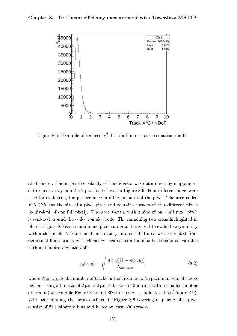
Chapter 8. Test beam eciency measurement with TowerJazz MALTA
hChi2Entries 1657499Mean 0.903RMS 1.019
^2 / NDoFΧ Track 0 1 2 3 4 5 6 7 8 9 10
trac
ks n
0
5000
10000
15000
20000
25000
30000
35000
40000
45000 hChi2Entries 1657499Mean 0.903RMS 1.019
Figure 8.5: Example of reduced χ2 distribution of track reconstruction t.
ated cluster. The in-pixel sensitivity of the detector was determined by mapping an
entire pixel array in a 2× 2 pixel cell shown in Figure 8.6. Four dierent areas were
used for evaluating the performance in dierent parts of the pixel. The area called
Full Cell has the size of a pixel pitch and contains corners of four dierent pixels
(equivalent of one full pixel). The area Centre with a side of one half pixel pitch
is centered around the collection electrode. The remaining two areas highlighted in
blue in Figure 8.6 each contain one pixel corner and are used to evaluate asymmetry
within the pixel. Measurement uncertainty in a selected area was estimated from
statistical uctuations with eciency treated as a binomially distributed variable
with a standard deviation of:
ση(x, y) =
√η(x, y)(1− η(x, y))
Nall tracks
, (8.2)
where Nall tracks is the number of tracks in the given area. Typical numbers of tracks
per bin using a bin size of 2µm× 2µm is between 40 in runs with a smaller number
of events (for example Figure 8.7) and 800 in runs with high statistics (Figure 8.9).
With this binning the areas outlined in Figure 8.6 covering a quarter of a pixel
consist of 81 histogram bins and hence at least 3000 tracks.
152

8.3. Eciency measurement
Figure 8.6: 2× 2 pixel cell used for evaluation of detection eciency. Four outlinedareas were used to determine eciency in dierent parts of the pixel. Collectionelectrodes are located in the corners of the square marked FULL CELL.
8.3 Eciency measurement
8.3.1 Eciency of unirradiated sample
Figure 8.7 shows in-pixel hit detection eciency of sector S3 in unirradiated MALTA
sample operated at the bias voltages of −15V and −6V on the substrate and p-wells
respectively and dierent discriminator thresholds between 250 e− and 600 e−. At
the lowest threshold the eciency is uniform across the entire pixel area with an
average value of 96.4%. At higher threshold levels the eciency starts to decrease
on pixel edges, while eciency in the centre increases, resulting in an average pixel
eciency of 97.2% at threshold value of 400 e− and 94.7% at the threshold value of
600 e−.
The eciency drop on pixel edges is due to charge being distributed between
adjacent pixels so called charge sharing resulting in less charge available in
individual pixels and hence smaller signals which do not exceed the threshold. The
extent of charge sharing can be seen in Figure 8.8 which shows the average cluster
size depending on track position. At the lowest threshold of 250 e− the average
cluster size is slightly above 1 in the pixel centre, around 2 on pixel edges, and
almost 3 in pixel corners. At higher thresholds the average cluster size on the edges
and corners reduces due to signals not exceeding the threshold.
The higher detection eciency in pixel centres at higher thresholds is an un-
common eect caused by the problems in the asynchronous MALTA readout. Since
the chip is operated with the disabled merger module, simultaneous hits from dif-
153

Chapter 8. Test beam eciency measurement with TowerJazz MALTA
m)µ x (0 20 40 60
m)
µ y
(
0
10
20
30
40
50
60
70
0
0.1
0.2
0.3
0.4
0.5
0.6
0.7
0.8
0.9
1
96.4 %±
0.1 %95.9 %
±0.3 %
96.1 %±
0.2 %
96.4 %±
0.2 %
(a) Threshold 250 e−
m)µ x (0 20 40 60
m)
µ y
(
0
10
20
30
40
50
60
70
0
0.1
0.2
0.3
0.4
0.5
0.6
0.7
0.8
0.9
1
97.2 %±
0.1 %98.5 %
±0.2 %
98.7 %±
0.2 %
96.6 %±
0.3 %
(b) Threshold 400 e−
m)µ x (0 20 40 60
m)
µ y
(
0
10
20
30
40
50
60
70
0
0.1
0.2
0.3
0.4
0.5
0.6
0.7
0.8
0.9
1
94.7 %±
0.2 %98.3 %
±0.3 %
97.1 %±
0.4 %
93.1 %±
0.6 %
(c) Threshold 600 e−
Figure 8.7: In-pixel eciency of sector S3 (2× 2 pixel cell) in unirradiated MALTAchip at discriminator thresholds of: a) 250 e−; b) 400 e−; c) 600 e−. Chip is operatedat Vbias = 15V.
154

8.3. Eciency measurement
m)µ x (0 20 40 60
m)
µ y
(
0
10
20
30
40
50
60
70
avg
. clu
ster
siz
e
1
1.2
1.4
1.6
1.8
2
2.2
2.4
2.6
2.8
3
(a) Threshold 250 e−
m)µ x (0 20 40 60
m)
µ y
(
0
10
20
30
40
50
60
70
avg
. clu
ster
siz
e
1
1.2
1.4
1.6
1.8
2
2.2
2.4
2.6
2.8
3
(b) Threshold 400 e−
m)µ x (0 20 40 60
m)
µ y
(
0
10
20
30
40
50
60
70
avg
. clu
ster
siz
e
1
1.5
2
2.5
3
3.5
(c) Threshold 600 e−
Figure 8.8: Dependence of average cluster size on discriminator threshold in unirra-diated MALTA chip.
155

Chapter 8. Test beam eciency measurement with TowerJazz MALTA
m)µ x (0 20 40 60
m)
µ y
(
0
10
20
30
40
50
60
70
0
0.1
0.2
0.3
0.4
0.5
0.6
0.7
0.8
0.9
1
74.2 %±
0.1 %89.6 %
±0.1 %
76.9 %±
0.2 %
70.4 %±
0.2 %
(a) Threshold 350 e−
m)µ x (0 20 40 60
m)
µ y
(
0
10
20
30
40
50
60
70
0
0.1
0.2
0.3
0.4
0.5
0.6
0.7
0.8
0.9
1
72.1 %±
0.1 %97.0 %
±0.1 %
75.0 %±
0.2 %
67.3 %±
0.2 %
(b) Threshold 450 e−
Figure 8.9: In-pixel eciency of sector S3 (2 × 2 pixel cell) in a MALTA chipirradiated to a uence of 1 · 1015 neq/cm
2 at discriminator thresholds of: a) 350 e−;b) 450 e−. Chip is operated at Vbias = 15V. Eciency in the pixel centre is reducedat a lower threshold due to data collisions.
ferent parts of the pixel matrix are not processed correctly and result in wrongly
interpreted hit location. This can for example happen with a signal from a hit pixel
and a random signal from a noisy pixel. In the test beam measurement such data
collisions manifest as detection ineciency. Since the problems in the chip slow con-
trol prevent masking individual noisy pixels such occurrences are relatively frequent.
The probability for a random noise exceeding a given threshold is higher at lower
threshold, hence the eciency drop due to data collisions is higher at low threshold
conguration.
8.3.2 Eciency of irradiated sample
Hit detection eciency in a MALTA sample irradiated to 1 · 1015 neq/cm2 was inves-
tigated at threshold values between 350 e− and 450 e−. Due to an increased noise
level after irradiation the chip could not be operated under lower thresholds without
severely increasing the noise rate. Figure 8.9 shows in-pixel hit detection eciency
of sector S3 with the chip operated at threshold values of 350 e− and 450 e− and the
standard bias voltage of −15V on the substrate and −6V on the p-well.
The results show a signicant degradation of charge collection eciency espe-
cially in the pixel corners where the eciency drops to almost zero. The average
pixel eciency is reduced to 74.2% at the threshold of 350 e− and 72.1% at the
threshold of 450 e−, while the respective eciencies in the pixel centres are 89.6%
and 97.0%. Moreover, the shape of the ecient region is slightly asymmetric with
156

8.3. Eciency measurement
m)µ x (0 20 40 60
m)
µ y
(
0
10
20
30
40
50
60
70
avg
. clu
ster
siz
e
1
1.1
1.2
1.3
1.4
1.5
1.6
1.7
1.8
1.9
2
(a) Threshold 350 e−
m)µ x (0 20 40 60
m)
µ y
(
0
10
20
30
40
50
60
70
avg
. clu
ster
siz
e
1
1.1
1.2
1.3
1.4
1.5
1.6
1.7
1.8
1.9
2
(b) Threshold 450 e−
Figure 8.10: Dependence of average cluster size on discriminator threshold inMALTA chip irradiated to 1 · 1015 neq/cm
2.
the eciency of pixel corners varying by 510%. This is because of the asymmetric
shape of pixel implants which is briey discussed later. The reason for the critically
reduced eciency in the irradiated sample is charge trapping which occurs because
the electric eld strength is insucient for a fast charge collection on pixel edges.
This is augmented by the problems in the detector readout which force operation
at non optimal (high) thresholds and further reduce detector sensitivity to small
signals, which are common on pixel edges due to charge sharing. The eciency
loss in pixel centre at low threshold due to data collisions is similar to the unirradi-
ated chip. Overall the lower threshold outweighs the disadvantage of more frequent
data collisions, as the average pixel eciency is slightly higher at lower thresholds.
The reduced charge collection eciency on pixel boundaries is also reected in the
average cluster size shown in Figure 8.10 which does not exceed the value of 1.6
in any part of the pixel. This is signicantly lower compared to the values in an
unirradiated sample.
The measurements presented above were made with the sector S3 of the MALTA
chip. Measurements were also made with the sector S2 which features a deeper p-
well implant. Figure 8.11 shows a comparison of the performance of both sectors.
The size of the ecient region in S2 is smaller than in sector S3 and has a circular
shape opposed to an asymmetric shape in S3. This is correlated to size and shape
of the gap in the p-well which separates the collection electrode from the readout
electronics in the pixel (black area in Figures 8.11c and 8.11d). The design with
a larger gap displays a better charge collection. This information has motivated
further research how to exploit dierent implant congurations to improve charge
collection [138]. The solutions are presented in Section 8.4.
157

Chapter 8. Test beam eciency measurement with TowerJazz MALTA
m)µ x (0 20 40 60
m)
µ y
(
0
10
20
30
40
50
60
70
effi
cien
cy
0
0.1
0.2
0.3
0.4
0.5
0.6
0.7
0.8
0.9
1
(a) Sector S2
m)µ x (0 20 40 60
m)
µ y
(
0
10
20
30
40
50
60
70
0
0.1
0.2
0.3
0.4
0.5
0.6
0.7
0.8
0.9
1
(b) Sector S3
(c) Pixel design sector S2 (d) Pixel design sector S3
Figure 8.11: Comparison of in-pixel eciency in sectors S2 (a) and S3 (b) of irradi-ated MALTA chip. The shape of highly ecient regions coincides with the shape ofthe gap in the p-well around the collection electrode shown as black area on guresc) and d).
158
8.4. Further development
8.3.3 Dependence of eciency on threshold and bias voltage
A summary of hit detection eciency in sector S3 measured at dierent thresholds
and bias voltages is shown in Figure 8.12. The values are given for the entire pixel
cell and for the central area around the collection electrode. Figure 8.12a gives the
dependence of eciency on threshold at the bias voltage of 15V. In the unirradiated
sample the maximal eciency is reached at a threshold of 400 e− (> 98% in the
centre and > 97% overall). At a threshold of 250 e− the eciency is lower mainly
because of reduced eciency in the centre (96%), which occurs due to data collisions.
At the threshold of 600 e− the central eciency is the same as at 400 e− threshold,
however the overall eciency is reduced to 94.7% due to losses on the edges. These
two competitive eects are more pronounced in the irradiated sample where a similar
behaviour is observed the overall eciency reduces with increasing threshold from
74% at 350 e− to 72% at 450 e−, while the central eciency increases from 89% to
97% at the same respective thresholds. Above measurements were made with p-
wells biased to 6V. Tests with p-wells biased to 3V in irradiated sample have shown
a performance drop with eciency reduced by ∼ 2% in the centre and 510% on
pixel edges.
The dependence of eciency on bias voltage is shown in Figure 8.12b. The mea-
surements were taken at a constant threshold of 250 e− in the unirradiated sample
and 400 e− in the irradiated sample. In the unirradiated sample the overall and cen-
tral eciency have a roughly constant value of ≈ 97% in the entire voltage range
between 12V and 20V. In the irradiated sample the central eciency increases
slightly with voltage from 91% at 8V to 93% at 20V. However, the full pixel
eciency peaks at the bias voltage of 15V. The reason for the eciency drop at
lower voltages is weaker electric eld which results in slower charge collection and
more charge trapping. The behaviour at voltages above 15V is more complicated
and was explained by simulation presented in [138]. For ecient charge collection
from the pixel edges the lateral component of the electric eld is vital. In case the
applied bias voltage is too high the electric eld lines are almost perpendicular to
the detector surface, therefore the lateral component is smaller than at moderate
bias voltages, resulting in a lower eciency on pixel edges.
8.4 Further development
The test beam campaign with TowerJazz MALTA provided initial insights into the
functionality of the chip, but also identied several issues which limit the chip per-
159

Chapter 8. Test beam eciency measurement with TowerJazz MALTA
)-
thr. (e250 300 350 400 450 500 550 600
effic
ienc
y
0.7
0.75
0.8
0.85
0.9
0.95
1
Unirr. - Full Cell
Unirr. - Centre
1e15 - Full Cell
1e15 - Centre
(a)
(V)biasV8 10 12 14 16 18 20
effic
ienc
y
0.65
0.7
0.75
0.8
0.85
0.9
0.95
1
Unirr. - Full Cell
Unirr. - Centre
1e15 - Full Cell
1e15 - Centre
(b)
Figure 8.12: Dependence of in-pixel eciency of sector S3 on a) threshold and b)substrate bias voltage in MALTA chip before and after irradiation. Measurementsin a) were taken at Vbias = 15V and measurements in b) at a threshold of 250 e−
(unirradiated) and 400 e− (irradiated chip).
160
8.4. Further development
formance. These disadvantages were addressed in the next design iteration called
MiniMALTA [93]. The non functional slow control, which was a signicant problem
in MALTA resulting in data losses and forcing operation at high thresholds, has been
xed in MiniMALTA. Additionally, the operation of MALTA at low threshold levels
has been compromised by the random telegraph signal noise in the front end. This
has been attributed to an undersized front end transistor which has been enlarged in
MiniMALTA. This modication together with the ability to mask noisy pixels has
allowed operation at a threshold of 200 e− after a uence of 1 ·1015 neq/cm2, which is
a major improvement complying with the original design specications of the chip.
Another challenge for the small electrode design is ecient charge collection over
the entire pixel. While MALTA introduces process modication with the additional
n− layer, the test beam has shown that inecient regions in pixel corners are still a
problem. The inuence of the p-well shape on charge collection in dierent pixel de-
signs (Figure 8.11) has inspired two further improvements to boost charge collection
shown in Figure 8.13 which have been implemented in MiniMALTA:
• Addition of an extra deep p-well implant on pixel edges;
• Introduction of a gap in the n− layer on pixel edges.
Both modications are aimed at increasing the lateral electric eld near the sensor
surface and thereby improve charge collection on pixel boundaries. Both approaches
require minor adaptations of the production process and are relatively simple to
implement. The time dependence of induced current in dierent designs before
and after irradiation was evaluated in a TCAD simulation [138] summarised in
Figure 8.14. The induced current in the pixel was simulated after charge deposition
by a MIP traversing the pixel corner, which is the worst case scenario in terms
of charge collection. The results indicate signicantly faster charge collection in
both improved pixel designs with peaking time reduced from ≈ 8 ns in the baseline
design to ≈ 3 ns in the improved designs. This is a signicant gain particularly
in the irradiated sample, as such detectors are signicantly less sensitive to charge
trapping. The simulation also shows a signicant eect of pixel size on the speed of
charge collection. For example, a pixel size of 28µm× 28µm results in about twice
shorter peaking times compared to pixels with the original size of 36.4µm×36.4µm
[138], thus reducing the pixel size may be an important element of future designs.
First tests with MiniMALTA have conrmed the benets of the improvements listed
above, indicating an average hit detection eciency of ≈ 98% over the entire pixel
in detectors irradiated to 1 · 1015 neq/cm2 [93].
161

Chapter 8. Test beam eciency measurement with TowerJazz MALTA
(a)
(b) (c)
Figure 8.13: Proposed modication of TowerJazz pixel design to improve charge col-lection in irradiated samples: a) Baseline TowerJazz modied process; b) Additionaldeep p-well implant; c) Gap in the n-layer. Modications b) and c) aim to increaselateral electric eld on pixel borders. Figures made after [138].
(a) Before irradiation (b) 1 · 1015 neq/cm2
Figure 8.14: Simulation of induced current in dierent TowerJazz pixel designs afterMIP equivalent charge is injected into pixel corner: a) unirradiated detector; b) de-tector irradiated to 1·1015 neq/cm
2. Pixels with improved design feature signicantlyfaster pulses which are less aected by trapping [138].
162

Chapter 9
Summary and outlook
The High Luminosity upgrade of the LHC (HL-LHC) scheduled in the years 2024
2026 aims at increasing the instantaneous luminosity up to 7.5 · 1034 cm−2 s−1, ex-
ceeding the original LHC design value by a factor of 7.5, and will result in unprece-
dented collision rates of up to 200 simultaneous proton-proton collisions. ATLAS
experiment at the LHC will undergo an extensive upgrade called Phase-II in order
to prepare for these challenging conditions. A major part of the upgrade will be
the replacement of the existing Inner Detector with a new all-silicon Inner Tracker
(ITk). ATLAS CMOS collaboration was established to evaluate an alternative for
the standard hybrid pixel detector for the outermost ITk Pixel Layer 4, targeting a
simpler approach without the technologically complex bump bonding.
The proposed solution is use of Depleted Monolithic Active Pixel Sensors (DMAPS)
based on industrial high voltage (HV) and/or high resistivity (HR) CMOS technolo-
gies which have seen rapid development for commercial applications in recent years.
These processes allow combination of sensor and readout functionalities in the same
silicon wafer. The HV/HR component provides sensor depletion for drift based
charge collection essential for high radiation environment. ATLAS has focused on
development of a so called monolithic detector containing the sensor together with
the full readout circuitry analogue as well as digital part on a single chip. Such
detectors can be produced in an industrial process which reects in a signicantly
faster and cheaper detector production. In addition, smaller amount of detector
material and lower cooling requirements reduce particle scattering, which can result
in a superior spatial resolution compared to hybrid detectors. With these benets
DMAPS based trackers have a potential to become the main detector technology
for future colliders.
163

Chapter 9. Summary and outlook
For Pixel Layer 4 ATLAS CMOS collaboration has pursued several DMAPS
development lines exploring dierent sensor concepts varying in design approaches
such as readout architecture, pixel pitch and size of collection electrode (large vs.
small electrode design), and choice of initial substrate resistivity. Prototypes of
sensors produced in silicon-on-insulator (SOI) geometry and CMOS strip sensors
have also been developed. Since DMAPS have never been used in high radiation
environment similar to ATLAS ITk, which will receive an expected lifetime uence
of 1.5 · 1015 neq/cm2 in Pixel Layer 4, one of the main concerns is demonstration of
sucient radiation tolerance. Radiation damage in detector bulk caused by neutrons
and protons and its eects on charge collection were studied in this thesis.
In partially depleted silicon detectors depletion depth depends on bias voltage
Vbias and eective space charge concentration Neff and scales as ∝√Vbias/Neff . In
unirradiated material Neff is dened by the initial doping concentration (i.e. initial
resistivity) and changes with generation of electrically active defects by radiation.
In highly resistive material (320 kΩ cm) typical for hybrid detectors the dominant
process is introduction of positive space charge from additional acceptor states with
concentration proportional to received uence. However, in commercially available
p-type material used for DMAPS with initial resistivity ranging between 10Ω cm
and few 1000Ω cm the eect of initial acceptor removal, which describes electrical
deactivation of boron dopants through generation of a BiOi complex, plays an im-
portant role. Acceptor removal reduces Neff which results in increase of depletion
depth and larger signals at a given bias voltage. Removal is completed either with
the removal of all initial acceptors (complete removal) or when no further states
are eectively removed (partial or incomplete removal). The uence at which this
process is nished depends on material, with removal completed faster in higher
resistivity silicon. In DMAPS the acceptor removal may span over a uence range
of 10131015 neq/cm2, which coincides with the expected lifetime uence for Pixel
Layer 4, indicating that benecial eects of acceptor removal can be relevant in the
entire lifespan of this detector.
In this thesis evolution of Neff with uence was evaluated in several DMAPS pro-
totypes irradiated with neutrons or protons in a uence range of 10131016 neq/cm2.
Detectors were characterised with Edge Transient Current Technique (Edge-TCT)
which uses a focused infra red laser beam with a diameter below 10µm to in-
ject charge into the sensor at a xed distance from the surface through the de-
tector edge. Fast readout electronics is used to detect induced current from drifting
charge carriers, providing information on the size of sensitive volume, i.e. depletion
depth, and Neff . Acceptor removal coecients were determined for neutron irradi-
ated prototypes on substrates with initial resistivities of 20, 50, 200 and 1000Ω cm
164

(ams CHESS2), 23 kΩ cm (LFoundry) and 100Ω cm SOI (X-FAB). Near com-
plete or complete removal was observed in most samples. In material with ini-
tial resistivity above 1000Ω cm acceptor removal was nished below a uence of
5 · 1013 neq/cm2, while in 20Ω cm substrate the removal was completed above a
uence of 3 · 1015 neq/cm2. In intermediate resistivity material acceptor removal
was completed at uences within this interval. In proton irradiated samples accep-
tor removal coecient could not be determined due to insucient number of data
points, but measurement indicate that protons remove initial acceptors faster and
introduce less additional deep acceptor states than neutrons. Measurements in this
thesis indicate that detectors with initial resistivity around 100Ω cm have the small-
est variations of Neff with uence in the entire uence range of ITk Layer 4. Despite
a distinct trend of faster acceptor removal in higher resistivity substrate, variations
in materials from dierent vendors are large and dedicated studies are required for
precise determination of Neff evolution in each particular substrate.
Passive pad diodes in LFoundry and CHESS2 samples were further characterised
in a setup with a radioactive 90Sr beta source, which allows selection of events with
MIP-like charge deposition in the sensor. The signal spectra show collected charge
increasing with uence in several samples, indicating larger depletion zone due to
acceptor removal. In detectors with bias voltage applied to structures on sensor
surface, not the backside, the signal size after irradiation is smaller than expected
from the depletion zone size measured with Edge-TCT. This is due to holes getting
trapped in a low electric eld volume and not traversing the full weighting eld. In a
pixel detector with each pixel read out individually the expected degradation would
be signicantly smaller due to a favourable weighting eld.
Edge-TCT was additionally used to assess signal uniformity within the pixel.
Signicant eciency gaps were observed in the X-FAB SOI detector, which suers
from parasitic charge collection by the structure above the buried oxide housing
readout electronics. This hypothesis was conrmed by a simulation. Measurements
were also conducted with TowerJazz Investigator samples with a small collection
electrode geometry and a very small pixel size of ≤ 50µm on the limit of Edge-TCT
resolution. The results show ecient regions in the pixel centre close to collection
electrode, and less ecient regions on pixel edges where signal strongly degrades
with irradiation.
In the scope of this thesis small collection electrode design was further studied
in a test beam with a monolithic TowerJazz MALTA chip. Measurements of hit
detection eciency were made before irradiation and after a neutron irradiation of
1 · 1015 neq/cm2. The detector designed for operation at a threshold of 200 e− had to
165

Chapter 9. Summary and outlook
be operated at a higher threshold of ≥ 250 e− (unirradiated) and ≥ 350 e− (irradi-
ated) due to problems in chip design. In addition, detection eciency was reduced
due to data collisions in the readout arising from the same issues. Unirradiated
sample has a uniform in-pixel eciency of ≈ 97%. After irradiation the detector
shows a critical eciency degradation on pixel boundaries, with the average pixel
eciency below 75%. Meanwhile eciency of the central 25% of pixel area is be-
tween 90% and 97% depending on the threshold, and is limited by the loss due to
data collisions. These results have led to improvements of pixel design with implant
modications aimed at increasing electric eld, and hence eciency, on pixel edges.
These improvements together with the xes of the readout electronics have been
implemented in the TowerJazz MiniMALTA chip.
In March 2019 ATLAS decided against using CMOS option in the ITk, since
none of the detector designs had been developed to a suciently advanced stage
to t into the tight time line for the Phase-II upgrade. Nevertheless, the R&D
within the ATLAS CMOS collaboration has led to a rapid progress of CMOS based
sensors for high radiation environment that has been recognised within and beyond
ATLAS. DMAPS development in TowerJazz, ams and LFoundry processes has been
continued outside ATLAS in order to take advantage of the previous research and
deliver a fully functional DMAPS. For example, recent test beam results with the
ams ATLASpix show promising eciency and timing resolution which would fulll
the specications for ITk Layer 4. The recently submitted TowerJazz MiniMALTA
has also xed the major issues identied in MALTA and shows very promising
performance in the test beam. DMAPS development for ATLAS also synergised
with detector development for future linear colliders such as Compact Linear Collider
(CLIC) and International Linear Collider (ILC) which require high resolution, low
material budget and moderate radiation tolerance. For these applications DMAPS
are a very attractive option.
This work has presented an extensive study of charge collection properties in
numerous irradiated DMAPS prototypes using Edge-TCT, 90Sr and test beam. On
one hand the measurements provided insights into charge collection properties of
these detectors, while on the other hand also generated feedback to chip designers
that led to design improvements. Moreover, the measurements have demonstrated
the importance of acceptor removal which takes place over a large uence range due
to the choice of relatively low substrate resistivity in DMAPS. Acceptor removal
benets DMAPS as it results in increased depletion depth and larger signals, and
might therefore play a considerable role in the design of future silicon detectors.
166

Bibliography
[1] L. R. Evans and P. Bryant, LHC Machine, JINST 3 (2008) S08001. 164 p.
[2] O. Brüning et al., LHC Design Report. CERN Yellow Reports: Monographs.
CERN, Geneva, 2004, 10.5170/CERN-2004-003-V-1.
[3] ALICE Collaboration, The ALICE experiment at the CERN LHC, JINST 3
(2008) S08002. 259 p.
[4] ATLAS Collaboration, The ATLAS Experiment at the CERN Large Hadron
Collider, JINST 3 (2008) S08003. 437 p.
[5] CMS Collaboration, The CMS experiment at the CERN LHC, JINST 3
(2008) S08004. 361 p.
[6] LHCb Collaboration, The LHCb Detector at the LHC, JINST 3 (2008)
S08005. 217 p.
[7] J. Haner, The CERN accelerator complex. Complexe des accélérateurs du
CERN, (2013) , General Photo, https://cds.cern.ch/record/1621894.
[8] HL-LHC Project webpage.
https://project-hl-lhc-industry.web.cern.ch/, (visited on
21/11/2019).
[9] ATLAS Collaboration, ATLAS Public Results, (2018) ,
https://twiki.cern.ch/twiki/bin/view/AtlasPublic/ (visited on
21/11/2019).
[10] S. L. Glashow, Partial-symmetries of weak interactions, Nuclear Physics 22
(1961) 579.
[11] S. Weinberg, A model of leptons, Phys. Rev. Lett. 19 (1967) 1264.
[12] S. Weinberg, The Making of the standard model, Eur. Phys. J. C34 (2004)
513.
167

Bibliography
[13] H. D. Politzer, Asymptotic Freedom: An Approach to Strong Interactions,
Phys. Rept. 14 (1974) 129180.
[14] P. W. Higgs, Broken symmetries and the masses of gauge bosons, Phys. Rev.
Lett. 13 (1964) 508.
[15] P. W. Higgs, Broken symmetries, massless particles and gauge elds, Phys.
Lett. 12 (1964) 132.
[16] F. Englert and R. Brout, Broken symmetry and the mass of gauge vector
mesons, Phys. Rev. Lett. 13 (1964) 321.
[17] G. S. Guralnik, C. R. Hagen and T. W. B. Kibble, Global conservation laws
and massless particles, Phys. Rev. Lett. 13 (1964) 585.
[18] M. Lubej, Study of B → KKℓνℓ decays at Belle. PhD thesis, University of
Ljubljana, Faculty of Mathematics and Physics, 2018.
[19] ATLAS Collaboration, Evidence for light-by-light scattering in heavy-ion
collisions with the ATLAS detector at the LHC, Nature Phys. 13 (2017)
852858, [1702.01625].
[20] LHCb Collaboration, Observation of J/ψp Resonances Consistent with
Pentaquark States in Λ0b → J/ψK−p Decays, Phys. Rev. Lett. 115 (2015)
072001.
[21] ATLAS Collaboration, Observation of a new particle in the search for the
Standard Model Higgs boson with the ATLAS detector at the LHC, Phys.
Lett. B716 (2012) 129, [1207.7214].
[22] CMS Collaboration, Observation of a new boson at a mass of 125 GeV with
the CMS experiment at the LHC, Phys. Lett. B716 (2012) 3061,
[1207.7235].
[23] H. J. W. Muller-Kirsten and A. Wiedemann, Supersymmetry: An
Introduction With Conceptual And Calculational Details. Hackensack, USA:
World Scientic, 1986.
[24] ATLAS Collaboration, ATLAS detector and physics performance: Technical
Design Report, 1, Tech. Rep. CERN-LHCC-99-14, ATLAS-TDR-14, CERN,
Geneva, 1999.
[25] ATLAS Collaboration, ATLAS Insertable B-Layer Technical Design Report,
Tech. Rep. CERN-LHCC-2010-013. ATLAS-TDR-19, CERN, Sep, 2010.
168

Bibliography
[26] ATLAS Collaboration, The ATLAS Inner Detector commissioning and
calibration, The European Physical Journal C 70 (2010) 787821.
[27] ATLAS Collaboration, Track Reconstruction Performance of the ATLAS
Inner Detector at√s = 13 TeV, Tech. Rep. ATL-PHYS-PUB-2015-018,
CERN, Geneva, Jul, 2015.
[28] G. Apollinari, O. Brüning and L. Rossi, High Luminosity LHC Project
Description, Tech. Rep. CERN-ACC-2014-0321, CERN, Geneva, 2014.
[29] ATLAS Collaboration, ATLAS Phase-II Upgrade Scoping Document, Tech.
Rep. CERN-LHCC-2015-020. LHCC-G-166, CERN, Geneva, Sep, 2015.
[30] ATLAS Collaboration, Technical Design Report for the ATLAS Inner
Tracker Pixel Detector, Tech. Rep. CERN-LHCC-2017-021.
ATLAS-TDR-030, CERN, Geneva, Sep, 2017.
[31] ATLAS Collaboration, Expected Tracking Performance of the ATLAS Inner
Tracker at the HL-LHC, Tech. Rep.
https://cds.cern.ch/record/2669540ATL-PHYS-PUB-2019-014, CERN,
Geneva, Mar, 2019.
[32] ATLAS Collaboration, Letter of Intent for the Phase-II Upgrade of the
ATLAS Experiment, Tech. Rep. CERN-LHCC-2012-022. LHCC-I-023,
CERN, Geneva, Dec, 2012.
[33] RD-53 Collaboration Home Page. https://rd53.web.cern.ch/RD53,
(visited on 21/11/2019).
[34] ATLAS Collaboration, Technical Design Report for the ATLAS Inner
Tracker Strip Detector, Tech. Rep. CERN-LHCC-2017-005.
ATLAS-TDR-025, CERN, Geneva, Apr, 2017.
[35] I. Valin et al., A reticle size CMOS pixel sensor dedicated to the STAR HFT,
JINST 7 (2012) C01102C01102.
[36] P. Yang et al., MAPS development for the ALICE ITS upgrade, JINST 10
(2015) C03030C03030.
[37] N. Ashcroft and D. Mermin, Solid state physics. Holt, Rinehart and
Winston, New York, 1976.
[38] F. Hartmann, Evolution of silicon sensor technology in particle physics; 2nd
ed. Springer tracts in modern physics. Springer, Berlin, 2017.
169

Bibliography
[39] H. Kolanoski and N. Wermes, Teilchendetektoren - Grundlagen und
Anwendungen. Springer, Berlin, 2016.
[40] H. Bethe, Zur Theorie des Durchgangs schneller Korpuskularstrahlen durch
Materie, Annalen der Physik 397 (1930) 325400.
[41] Particle Data Group. Berkeley collaboration, J. Beringer et al.,
Review of Particle Physics, 2012-2013. Review of Particle Properties, Phys.
Rev. D 86 (2012) 010001.
[42] L. Landau, On the energy loss of fast particles by ionization, J. Phys.(USSR)
8 (1944) 201205.
[43] J. F. Bak et al., Large departures from Landau distributions for high-energy
particles traversing thin Si and Ge targets, Nuclear Physics B 288 (1987)
681716.
[44] W. Shockley, Currents to Conductors Induced by a Moving Point Charge,
Journal of Applied Physics 9 288 (1938) 635.
[45] S. Ramo, Currents induced by electron motion, Proceedings of the IRE 27
(1939) 584585.
[46] L.-A. Hamel and M. Julien, Generalized demonstration of Ramo's theorem
with space charge and polarization eects, NIM A 597 (2008) 207211.
[47] M. Garcia-Sciveres and N. Wermes, A review of advances in pixel detectors
for experiments with high rate and radiation, Reports on Progress in Physics
81 (2018) 066101.
[48] R. Turchetta and others, A monolithic active pixel sensor for charged particle
tracking and imaging using standard VLSI CMOS technology, NIM A 458
(2001) 677689.
[49] I. Peri¢, A novel monolithic pixelated particle detector implemented in
high-voltage CMOS technology, NIM A 582 (2007) 876885.
[50] Y. Arai et al., Development of SOI pixel process technology, NIM A 636
(2011) S31S36.
[51] R. Ichimiya et al., Reduction techniques of the back gate eect in the SOI
Pixel Detector, in TWEPP 2009, 2009.
[52] T. Hemperek et al., A Monolithic Active Pixel Sensor for ionizing radiation
using a 180nm HV-SOI process, NIM A 796 (2015) 812.
170

Bibliography
[53] H. E. Boesch et al., Role Transport and Charge Relaxation in Irradiated SiO2
MOS Capacitors, IEEE Transactions on Nuclear Science 22 (1975)
21632167.
[54] R. C. Hughes, Charge-Carrier Transport Phenomena in Amorphous SiO2:
Direct Measurement of the Drift Mobility and Lifetime, Physical Review
Letters 30 (1973) 13331336.
[55] T. P. Ma and P. V. Dressendorfer, Ionizing Radiation Eects in MOS
Devices and Circuits. Wiley, New York, Apr, 1989.
[56] F. Faccio and G. Cervelli, Radiation-induced edge eects in deep submicron
CMOS transistors, IEEE Transactions on Nuclear Science 52 (2005)
24132420.
[57] F. Faccio and others, Total ionizing dose eects in shallow trench isolation
oxides, Microelectronics Reliability 48 (2008) 1000 1007.
[58] M. Moll, Radiation Damage in Silicon Particle Detectors - microscopic
defects and macroscopic properties. PhD thesis, University of Hamburg, 1999.
[59] F. Hönniger, Radiation Damage in Silicon - Defect Analysis and Detector
Properties. PhD thesis, University of Hamburg, 2007.
[60] R. Wunstorf, Systematische Untersuchungen zur Strahlenresistenz von
Siliziumdetektoren für die Verwendung von Hochenergie-Experimenten. PhD
thesis, University of Hamburg, 1992.
[61] M. Huhtinen, Simulation of non-ionising energy loss and defect formation in
silicon, NIM A 491 (2002) 194 215.
[62] J. Lindhard and V. Nielsen, Nuclear collisions and ionisation uctuations in
charged particle detectors, Phys. Letters Vol: 2 (10, 1962) .
[63] G. Lindström and others, Radiation hard silicon detectorsdevelopments by
the RD48 (ROSE) collaboration, NIM A 466 (2001) 308 326.
[64] G. Kramberger, Signal development in irradiated silicon detectors. PhD
thesis, University of Ljubljana, 2001.
[65] G. Kramberger et al., Determination of eective trapping times for electrons
and holes in irradiated silicon, NIM A A476 (2002) 645651.
[66] V. Cindro et al., Radiation damage in p-type silicon irradiated with neutrons
and protons, NIM A 599 (2009) 6065.
171

Bibliography
[67] R. Wunstorf et al., Investigations of donor and acceptor removal and long
term annealing in silicon with dierent boron/phosphorus ratios, NIM A 377
(1996) 228233.
[68] G. Kramberger et al., Modeling of electric eld in silicon micro-strip detectors
irradiated with neutrons and pions, JINST 9 (2014) P10016P10016.
[69] G. Kramberger et al., Comparison of pad detectors produced on dierent
silicon materials after irradiation with neutrons, protons and pions, NIM A
612 (2010) 288295.
[70] H. Hoedlmoser et al., CCE measurements and annealing studies on
proton-irradiated p-type MCz silicon diodes, NIM A 583 (2007) 6470.
[71] K. Kaska et al., TCT measurements on MCz n- and p-type after proton and
neutron irradiation, in 13th RD50 Workshop, 2008.
[72] A. Aolder et al., Charge collection studies in irradiated HV-CMOS particle
detectors, JINST 11 (2016) P04007P04007.
[73] G. Kramberger et al., Radiation eects in low gain avalanche detectors after
hadron irradiations, JINST 10 (2015) P07006P07006.
[74] J. Lange et al., Gain and time resolution of 45µm thin Low Gain Avalanche
Detectors before and after irradiation up to a uence of 1015 neq/cm2, JINST
12 (2017) P05003P05003.
[75] J. Adey et al., Interstitial boron defects in Si, Physica B: Condensed Matter
340342 (2003) 505508.
[76] J. Adey, Boron related point defects in silicon. PhD thesis, University of
Exeter, 2004.
[77] M. Ferrero et al., Radiation resistant LGAD design, NIM A A919 (2019)
1626, [1802.01745].
[78] P. Rymaszewski et al., Prototype Active Silicon Sensor in 150 nm HR-CMOS
technology for ATLAS Inner Detector Upgrade, JINST 11 (2016)
C02045C02045.
[79] Y. Degerli et al., Pixel architectures in a HV-CMOS process for the ATLAS
inner detector upgrade, JINST 11 (2016) C12064C12064.
[80] M. Karagounis, Development of the ATLAS FE-I4 pixel readout IC for
b-layer Upgrade and Super-LHC, in TWEPP, 2008.
172
Bibliography
[81] T. Wang et al., Development of a depleted monolithic CMOS sensor in a 150
nm CMOS technology for the ATLAS inner tracker upgrade, JINST 12
(2017) C01039C01039.
[82] T. Wang et al., Depleted fully monolithic CMOS pixel detectors using a
column based readout architecture for the ATLAS inner tracker upgrade,
JINST 13 (2018) C03039C03039.
[83] K. Moustakas et al., CMOS monolithic pixel sensors based on the
column-drain architecture for the HL-LHC upgrade, NIM A (2018) .
[84] F. J. Iguaz et al., Characterization of a depleted monolithic pixel sensors in
150 nm CMOS technology for the ATLAS Inner Tracker upgrade, NIM A
(2018) .
[85] T. Hirono et al., Depleted fully monolithic active CMOS pixel sensors
(DMAPS) in high resistivity 150 nm technology for LHC, NIM A 924 (2019)
8791.
[86] M. Mager, ALPIDE, the Monolithic Active Pixel Sensor for the ALICE ITS
upgrade, NIM A 824 (2016) 434438.
[87] D. Kim et al., Front end optimization for the monolithic active pixel sensor of
the ALICE inner tracking system upgrade, JINST 11 (2016) C02042C02042.
[88] I. Berdalovic et al., Monolithic pixel development in TowerJazz 180 nm
CMOS for the outer pixel layers in the ATLAS experiment, JINST 13 (2018)
C01023C01023.
[89] H. Pernegger et al., First tests of a novel radiation hard CMOS sensor
process for depleted monolithic active pixel sensors, JINST 12 (2017)
P06008P06008.
[90] C. Riegel, Performance tests of depleted CMOS sensors for application at
HL-LHC. PhD thesis, University of Wuppertal, 2018.
[91] W. Snoeys et al., A process modication for CMOS monolithic active pixel
sensors for enhanced depletion, timing performance and radiation tolerance,
NIM A 871 (2017) 9096.
[92] Manual Investigator1, Version 2 (01/08/2014). Internal communication.
[93] M. Dyndal et al., Mini-MALTA: Radiation hard pixel designs for
small-electrode monolithic CMOS sensors for the High Luminosity LHC,
1909.11987.
173

Bibliography
[94] E. Cavallaro, Novel silicon detector technologies for the HL-LHC ATLAS
upgrade. PhD thesis, Autonomous University of Barcelona, 2018.
[95] M. Kiehn et al., Performance of CMOS pixel sensor prototypes in ams H35
and aH18 technology for the ATLAS ITk upgrade, NIM A 924 (2019)
104107.
[96] B. T. Human et al., Radiation hardness of two CMOS prototypes for the
ATLAS HL-LHC upgrade project., JINST 11 (2016) C02005C02005.
[97] L. Vigani, Study of CMOS prototypes for the ATLAS detector upgrade and
searches for invisible decays of the Higgs boson. PhD thesis, University of
Oxford, 2018.
[98] Test chip: CHESS1 V 1.2 (17/09/2015). Internal communication.
[99] Specication of the CHESS2 chip V 1.6 (11/01/2017). Internal
communication.
[100] S. Fernandez-Perez et al., Charge collection properties of a depleted
monolithic active pixel sensor using a HV-SOI process, JINST 11 (2016)
C01063C01063.
[101] S. Fernandez-Perez et al., Radiation hardness of a 180nm SOI monolithic
active pixel sensor, NIM A 796 (2015) 1318.
[102] S. Fernandez-Perez, A novel Depleted Monolithic Active Pixel Sensor for
future High Energy Physics Detectors. PhD thesis, Autonomous University of
Barcelona, 2016.
[103] S. Fernandez-Perez et al., Test beam results of a depleted monolithic active
pixel sensor using an HV-SOI process for the LH-LHC upgrade, JINST 11
(2016) C02083C02083.
[104] A. M. A. Lampert and P. Mark, Current injection in solids. Academic Press
New York, 1970.
[105] Z. L. V. Eremin and I. Iljashenko, Trapping induced Ne and electrical eld
transformation at dierent temperatures in neutron irradiated high resistivity
silicon detectors, NIM A 360 (1995) 458462.
[106] G. Kramberger et al., Determination of eective trapping times for electrons
and holes in irradiated silicon, NIM A 476 (2002) 645651.
174

Bibliography
[107] M. A. Green and M. J. Keevers, Optical properties of intrinsic silicon at 300
k, Progress in Photovoltaics: Research and Applications 3 (1995) 189192.
[108] G. Kramberger et al., Investigation of Irradiated Silicon Detectors by
Edge-TCT, IEEE Transactions on Nuclear Science 57 (2010) 22942302.
[109] M. Milovanovi¢, Electric eld and charge multiplication in radiation-damaged
silicon detectors. PhD thesis, University of Ljubljana, 2015.
[110] Particulars webpage. http://particulars.si/, (visited on 21/11/2019).
[111] DRS4 webpage. https://www.psi.ch/en/drs, (visited on 21/11/2019).
[112] G. Kramberger et al., Charge collection properties of heavily irradiated
epitaxial silicon detectors, NIM A 554 (2005) 212219.
[113] L. Snoj, G. erovnik and A. Trkov, Computational analysis of irradiation
facilities at the JSI TRIGA reactor, Applied Radiation and Isotopes 70
(2012) 483488.
[114] K. Ambroºi£, G. erovnik and L. Snoj, Computational analysis of the dose
rates at JSI TRIGA reactor irradiation facilities, Applied Radiation and
Isotopes 130 (2017) 140152.
[115] F. Ravotti et al., IRRAD: The New 24 GeV/c Proton Irradiation Facility at
CERN, in AccApp 2015, 2015.
[116] LANSCE webpage. https://lansce.lanl.gov/facilities/wnr/
flight-paths/target-2/index.php, (visited on 21/11/2019).
[117] I. Mandi¢ et al., Neutron irradiation test of depleted CMOS pixel detector
prototypes, JINST 12 (2017) P02021P02021.
[118] I. Mandi¢ et al., Charge-collection properties of irradiated depleted cmos pixel
test structures, NIM A 903 (2018) 126133.
[119] Description of Test Structures in LFoundry technology (December 2016).
Internal communication.
[120] M. F. García et al., Radiation hardness studies of neutron irradiated CMOS
sensors fabricated in the ams H18 high voltage process, JINST 11 (2016)
P02016P02016.
[121] M. F. García et al., High-resolution three-dimensional imaging of a depleted
CMOS sensor using an edge Transient Current Technique based on the Two
Photon Absorption process (TPA-eTCT), NIM A 845 (2017) 6971.
175

Bibliography
[122] ams webpage. https://ams.com/process-technology, (visited on
21/11/2019).
[123] B. Hiti et al., Charge collection in irradiated HV-CMOS detectors, NIM A
924 (2019) 214218.
[124] B. Hiti et al., Charge collection properties in an irradiated pixel sensor built
in a thick-lm HV-SOI process, JINST 12 (2017) P10020P10020.
[125] T. Miyoshi, Development and performance of double SOI pixel sensors, in
11th HSTD Conference, 2017.
[126] K. Hara et al., Radiation hardness of silicon-on-insulator pixel devices, NIM
A 924 (2019) 426430.
[127] KDetSim webpage. http://kdetsim.org/, (visited on 21/11/2019).
[128] G. Kramberger, KDetSim: A ROOT based 3D simulation tool for
semiconductor detectors, in 27th RD50 Workshop, 2015.
[129] E. Cavallaro et al., Studies of irradiated AMS H35 CMOS detectors for the
ATLAS tracker upgrade, JINST 12 (2017) C01074, [1611.04970].
[130] G. Kramberger et al., Radiation hardness of thin Low Gain Avalanche
Detectors, NIM A 891 (2018) 6877.
[131] B. Hiti, Development of the monolithic "MALTA" CMOS sensor for the
ATLAS ITK outer pixel layer, in TWEPP, 2018.
[132] M. Deveaux, Progress on the radiation tolerance of CMOS Monolithic Active
Pixel Sensors, JINST 14 (2019) R11001R11001.
[133] G. McGoldrick, M. erv and A. Gori²ek, Synchronized analysis of testbeam
data with the Judith software, NIM A 765 (2014) 140145.
[134] J. Baudot et al., First test results Of MIMOSA-26, a fast CMOS sensor with
integrated zero suppression and digitized output, in 2009 IEEE Nuclear
Science Symposium Conference Record (NSS/MIC), pp. 11691173, 2009.
DOI.
[135] Xilinx Virtex-7 FPGA VC707 Evaluation Kit. https:
//www.xilinx.com/products/boards-and-kits/ek-v7-vc707-g.html,
(visited on 21/11/2019).
[136] C. G. Larrea et al., IPbus: a exible ethernet-based control system for xTCA
hardware, JINST 10 (2015) C02019C02019.
176
Bibliography
[137] J. Elmsheuser et al., Large scale software building with CMake in ATLAS,
Journal of Physics: Conference Series 898 (2017) 072010.
[138] M. Munker et al., Simulations of CMOS pixel sensors with a small collection
electrode, improved for a faster charge collection and increased radiation
tolerance, JINST 14 (2019) C05013C05013.
[139] M. Munker, Simulations of CMOS sensors with a small collection electrode,
improved for a faster charge-collection and increased radiation tolerance, in
Pixel, 2018.
177

Bibliography
178

Raz²irjeni povzetek v slovenskem
jeziku
Veliki hadronski trkalnik (LHC) [1, 2] Evropske organizacije za jedrske raziskave
(CERN) je najve£ji in najmo£nej²i trkalnik delcev kadarkoli zgrajen. LHC med-
sebojno trka protone pospe²ene do teºi²£ne energije√s = 13TeV, iz katere lahko
nastanejo novi, teºji delci, ki jih opisuje standardni model zike delcev [10, 11, 12, 13].
Najve£ji uspeh LHC-ja do sedaj je odkritje Higgsovega bozona [21, 22], ki so ga na-
povedale ºe teorije v 1960-ih letih [14, 15, 16, 17]. Poleg tega pri visokih energijah
trka obstaja moºnost za nastanek novih delcev oziroma procesov, ki jih standardni
model ne opisuje in jih poznamo pod skupnim imenom nova zika. Te pojave pri-
£akujemo glede na nekatera zikalna opazovanja, ki jih standardni model ne more
uspe²no razloºiti, npr. naravo temne snovi in temne energije, kvantno-mehansko
naravo gravitacije, maso nevtrinov in asimetrijo med snovjo in antisnovjo v vesolju.
S trkalnikom LHC so nelo£ljivo povezani zikalni eksperimenti, ki zaznavajo pro-
dukte trkov in nam s tem omogo£ajo vpogled v zikalne procese med interakcijami
delcev. Eden od ²tirih glavnih eksperimentov LHC-ja je detektor ATLAS [4, 24], ki
je izpopolnjen za zaznavanje £im ve£jega nabora procesov pri protonskih trkih.
Ker so pri£akovani sipalni preseki σ pri procesih nove zike zelo majhni, je za
moºnost njihovega zaznavanja potrebno veliko ²tevilo trkov. Sorazmernost med si-
palnim presekom in hitrostjo ustvarjenih dogodkov na trkalniku dNdt
opisuje trenutna
luminoznost L v zvezi dNdt
= L · σ, skupno ²tevilo ustvarjenih dogodkov pa je soraz-
merno z integrirano luminoznostjo Lint =∫Ldt. LHC je zasnovan za delovanje pri
trenutni luminoznosti 1 · 1034 cm−2 s−1, tako do bo trenutnem obdobju delovanja na-
£rtovanem do leta 2024 pri£akovana koli£ina proizvedenih trkov ustrezala integrirani
luminoznosti 400 fb−1. Po tem obdobju bi delovanje pri nespremenjenih pogojih po-
stalo neprakti£no zaradi izredno dolgega £asa potrebnega za statisti£no pomembno
pove£anje obsega podatkov. Z namenom doseganja ²e ve£je koli£ine trkov bo LHC
v letih 20242026 izbolj²an v t.i. Nadgradnji za visoko luminoznost (HL-LHC) [28],
ki bo omogo£ala delovanje pri trenutni luminoznosti 5 · 1034 cm−2 s−1, v skrajnem
179

Raz²irjeni povzetek v slovenskem jeziku
Slika 9.1: Shema razporeditve silicijevih modulov v nagnjeni porazdelitvi v enemkvadrantu detektorja ATLAS ITk. Rde£e plasti predstavljajo blazini£aste, modrepa linijske detektorje [30].
primeru pa celo pri 7,5·1034 cm−2 s−1, in cilja na skupno integrirano luminoznost
4000 fb−1 v desetih letih zbiranja podatkov. Obratovanje pri teh ekstremnih pogojih
bo predstavljalo izredno obremenitev za eksperimente, saj bodo morali v povpre£ju
zaznati produkte kar 200 isto£asnih trkov. Poleg tega bodo zaradi ve£jega ²tevila
trkov po²kodbe detektorja zaradi sevanja znatno ve£je od vrednosti, za katere so
zasnovani trenutni detektorji.
Zaradi omenjenih dejavnikov bo eksperimente na LHC-ju v £asu nadgradnje
HL-LHC potrebno izbolj²ati. Pri detektorju ATLAS bodo v tem obdobju, ime-
novanem nadgradnja Phase-II, izvedene ²tevilne izbolj²ave. Ena najve£jih novosti
bo zamenjava obstoje£ega Notranjega detektorja (ID) [4], namenjenega zaznavanju
sledi nabitih delcev, z novim Notranjim sledilnikom (ITk) [30, 34], ki bo v celoti
zgrajen iz silicijevih detektorjev. ITk bo od vseh detektorskih sistemov najbliºje
to£ki trka in bo pokrival prostor od ºarkovne osi oddaljen med 36mm in 1000mm.
Detektorji v ITk bodo razporejeni plastovito v t.i. nagnjeni ureditvi (Slika 9.1),
ki sestoji iz blazini£astih detektorjev v notranjih plasteh in linijskih detektorjev v
zunanjih plasteh. V osrednjem delu odmaknjenem od ºarkovne osi za kot ve£ji od
1530 bodo detektorji razporejeni v obliki koncentri£nih cevi (5 plasti blazini£astih
in 4 plasti linijskih detektorjev), pri ostrej²ih kotih pa v ²tevilnih obro£ih. Povr²ina
vseh blazini£astih detektorjev v ITk bo s pribliºno 10m2 znatno presegla trenutnih
1.8m2 v ID. Najve£ja povr²ina detektorjev v cevastem delu bo potrebna za zuna-
njo Plast 4 1, ki bo zaradi najve£je oddaljenosti od to£ke trka hkrati izpostavljena
najmanj²emu toku delcev in po²kodbam zaradi sevanja. Zaradi zahtevne in drage
1V cevastem delu ITk so plasti o²tevil£ene od 0 do 4.
180

izdelave velike koli£ine blazini£astih detektorjev potrebnih za Plast 4 je bila znotraj
eksperimenta ATLAS ustanovljena Kolaboracija ATLAS CMOS, ki je preu£evala
moºnost alternativnega postopka izdelave blazini£astih detektorjev.
Obi£ajni blazini£asti detektorji so zgrajeni po hibridnem principu, v katerem sta
senzor za zaznavanje delcev in £italna elektronika izdelana na dveh lo£enih rezinah
silicija naknadno povezanih s krogli£nimi povezavami na nivoju posameznih blazinic
[47]. Postopek krogli£nih povezav je tehnolo²ko zahteven in £asovno potraten, poleg
tega pa so hibridni detektorji dragi zaradi senzorja iz izredno £istega silicija z uporno-
stjo 320 kΩ cm, ki mora biti izdelan v posebnem uporabniku prilagojenem postopku.
Alternativa hibridnim detektorjem, ki jo je raziskovala Kolaboracija ATLAS CMOS,
so osiroma²eni monolitni aktivni blazini£asti senzorji (DMAPS) izdelani v industrij-
skem procesu CMOS [48, 49]. V monolitnem detektorju sta zaznavni del in £italna
elektronika zdruºena na eni sami silicijevi rezini, zato krogli£ne povezave niso po-
trebne. Kompaktna zasnova vezja z manj²im ²umom omogo£a uporabo manj £istega
silicija z upornostjo 103000Ω cm, ki je komercialno bolj razpoloºljiv. V primerjavi
s hibridnimi detektorji DMAPS med drugim omogo£ajo zasnovo manj²ih blazinic in
manj²o porabo mo£i, zaradi £esar je potrebno manj materiala za hlajenje sledilnika
in je posledi£no sipanje delcev manj²e. Te prednosti obetajo izbolj²ano lo£ljivost sle-
denja. Senzorji izdelani v tehnologiji CMOS so v zadnjem desetletju doºiveli velik
razcvet zaradi ²iroke uporabe v potro²ni²ki elektroniki, npr. v kamerah pametnih
telefonov. Zaradi ob£utljivosti na sevalne po²kodbe neposredni prenos te tehnologije
v ziko visokih energij sicer ni moºen, vendar nekateri izdelovalci ponujajo procese,
ki omogo£ajo uporabo visoke napetosti na senzorju in/ali visoko upornega materi-
ala. Tak²ni senzorji imajo veliko osiroma²eno podro£je, v katerem nosilci naboja
potujejo v elektri£nem polju, in so s tem odporni na sevalne po²kodbe. Izdelava de-
tektorjev v industrijskem procesu z velikimi koli£inami omogo£a prihranke pri £asu
izdelave in ceni v primerjavi s hibridnimi detektorji. Ker DMAPS doslej ²e niso bili
uporabljeni v velikem obsegu v okolju z ATLAS-u primerljivo stopnjo sevanja, je ena
glavnih zahtev pred njihovo uporabo prikaz njihove zadostne sevalne odpornosti, kar
je tudi cilj tega doktorata.
Za razumevanje sevalnih po²kodb je najprej potrebno poznavanje na£ina delova-
nja polprevodni²kih detektorjev delcev. Ti temeljijo na zbiranju elektri£nega naboja
v siliciju parov elektron-vrzel (e-h) ki ga nabiti delci ustvarijo z ionizacijo vzdolº
svoje poti skozi material. Hitrost odlaganja energije hitrih nabitih delcev v materi-
alu opisuje Bethejeva formula [40], ki uvede pojem minimalno ionizirajo£ega delca
(MIP) za delce z vrednostjo relativisti£nega faktorja βγ med 2 in nekaj 100. V
siliciju MIP z najve£jo verjetnostjo odloºi energijo 400 eV/µm, ki ustreza 80 parom
e-h/µm. Za zaznavanje te razmeroma majhne koli£ine naboja je potrebno delova-
181
Raz²irjeni povzetek v slovenskem jeziku
nje v stanju z nizko ravnovesno gostoto nosilcev naboja, zato so silicijevi detektorji
izdelani na osnovi p-n stika priklopljenega v zaporni smeri. p-n stik temelji na
dveh razli£no dopiranih plasteh silicija, od katerih ena vsebuje preseºek akceptorjev
(p-tip), druga pa preseºek donorjev (n-tip). Na obmo£ju spoja zaradi selitve no-
silcev naboja pride do nastanka osiroma²enega podro£ja, v katerem prostih nosilcev
naboja prakti£no ni. Zaradi posledi£ne polarizacije materiala se ustvari elektri£no
polje, ki proste nosilce nemudoma odstrani iz osiroma²enega obmo£ja. To lastnost
izkori²£ajo detektorji za zbiranje naboja, ki ga v osiroma²enem obmo£ju ustvarijo
visokoenergijski delci. Ker osiroma²eno obmo£je deluje kot ob£utljivi del, njegova
velikost odlo£ilno vpliva na velikost signala. V detektorjih je navadno ena plast (zbi-
ralna elektroda) bistveno mo£neje dopirana od druge plasti (substrat). V tak²nem
primeru je ²irina osiroma²enega obmo£ja w podana z ena£bo:
w =
√2ϵϵSiVbie0Neff
, (9.1)
kjer je ϵ inuen£na konstanta, ϵSi dielektri£nost silicija, Vbi pritisnjena elektri£na
napetost v zaporni smeri, e0 osnovni naboj in Neff efektivna gostota prostorskega
naboja v substratu. V neobsevanih detektorjih jeNeff sorazmerna z gostoto dopantov
v substratu, oziroma obratno sorazmerna z upornostjo materiala.
V silicijevih detektorjih izpostavljenim visokoenergijskemu sevanju pride do po-
²kodb materiala zaradi tvorjenja defektov. Sevalne po²kodbe delimo v dve glavni
kategoriji:
• po²kodbe zaradi skupne ionizacijske doze (TID), ki jo odloºijo fotoni ter nabiti
delci in povzro£i po²kodbe elektronike zaradi nabijanja SiO2 v tranzistorjih
[55];
• po²kodbe zaradi izbitja atomov iz silicijeve kristalne re²etke, ki jo preteºno
povzro£ijo hadroni [58, 59]. Njene posledice so pove£an temni tok v detek-
torju, pasti, ki ujamejo nosilce naboja preden doseºejo zbiralno elektrodo, in
spremembe Neff . Ti dejavniki vplivajo na koli£ino zbranega naboja v detek-
torju. Merilo za stopnjo po²kodb zaradi izbitja je ekvivalentna uenca Φeq z
enoto 1MeV neq/cm2, ki je ekvivalent po²kodbam, ki jih v materialu povzro£i
tok enega nevtrona z energijo 1MeV na 1 cm2.
Plast 4 sledilnika ITk bo v na£rtovani ºivljenjski dobi predvidoma prejela skupno
ionizacijsko dozo 80MRad in uenco 1,5·1015 neq/cm2. Ta doktorat se osredoto£a
na dolo£itev posledic po²kodb v DMAPS zaradi izbitja atomov v tem obmo£ju
uence. Velik poudarek je na dolo£itvi efektivne gostote prostorskega naboja, ki je
182

(a) (b)
Slika 9.2: Shema detektorjev DMAPS z a) veliko; b) majhno zbiralno elektrodo.Prednost velike elektrode so kraj²e poti potovanja naboja in enakomerna rast osiro-ma²enega podro£ja na ra£un ve£je kapacitete detektorja [47].
v materialu tipa p dolo£ena s tremi prispevki opisanih z ena£bo:
Neff = Neff,0(1−Nc/Neff,0 · (1− e−cΦeq)) + gCΦeq. (9.2)
Prvi prispevek je za£etna koncentracija atomov akceptorja Neff,0 dolo£ena z nivojem
dopiranja substrata. len gCΦeq opisuje ustvarjanje dodatnih akceptorskih stanj
s koncentracijo sorazmerno s prejeto uenco [63, 66]. Tretji prispevek imenovan
efektivna odstranitev za£etnih akceptorjev 2 opisuje elektri£no deaktivacijo atomov
akceptorja, navadno elementa bora, do katere pride zaradi izbitja atoma bora iz
kristalne re²etke in tvorjenja kompleksa BiOi v medkristalnem prostoru. Kompleks
BiOi ima lastnosti donorja [67, 75, 76], zato se Neff zmanj²a, kar je ugodno za de-
tektorje DMAPS, saj se s tem pove£a globina osiroma²enega obmo£ja in velikost
signalov (Ena£ba 9.1). Efektivni deleº vseh za£etnih akceptorjev, ki so odstranjeni,
podaja koecient 0 ≤ Nc/Neff,0 ≤ 1, hitrost odstranitve s prejeto uenco pa opisuje
koecient odstranitve akceptorjev c. Meritve z naprednimi silicijevimi detektorji
[72, 77] nakazujejo, da je c odvisen od za£etnega dopiranja in da je v mo£no dopi-
ranih materialih za odstranitev akceptorjev potrebna vi²ja uenca. Zaradi velikega
u£inka, ki jih lahko ima odstranitev akceptorjev na delovanje DMAPS, je pomembno
natan£no opredeliti njen potek v razli£nih vzorcih.
Vzorci preiskovani v tem delu so bili razviti v okviru Kolaboracije ATLAS CMOS,
ki je v vzporednih razvojnih procesih razvila ve£ vrst DMAPS. Razli£ne zasnove so
bile izdelane pri razli£nih proizvajalcih, med sabo pa se med drugim razlikujejo po
tipu CMOS procesa, geometriji blazinic, vrsti £italne arhitekture in za£etni uporno-
sti substrata. Opravljene so bile tudi ²tudije z detektorji zgrajenimi v arhitekturi
silicij na izolatorju (SOI) in s prototipi linijskih detektorjev v tehnologiji CMOS.
Ena glavnih snovalskih odlo£itev je izbira med t.i. zasnovama z veliko ali majhno
zbiralno elektrodo (Slika 9.2). Detektorji z veliko zbiralno elektrodo, ki zaseda ve£ji
2Kratko odstranitev akceptorjev.
183

Raz²irjeni povzetek v slovenskem jeziku
del povr²ine celotne blazinice, so ustaljen koncept v hibridnih detektorjih, kjer ve-
lika zbiralna elektroda omogo£a enakomerno rast osiroma²enega obmo£ja po celotni
povr²ini blazinice in kratke poti potovanja naboja. Zaradi tega je odziv senzorja
enakomeren in precej odporen na sevanje, vendar je kapaciteta blazinice razmeroma
velika (nekaj 100 fF). To povzro£i po£asnej²i odziv senzorja in vi²ji nivo ²uma, ki ju
je potrebno kompenzirati z vi²jo elektri£no mo£jo, kar lahko predstavlja teºave pri
hlajenju in posledi£no lo£ljivosti sledilnika. Pri detektorjih z majhno zbiralno elek-
trodo velikosti nekaj µm je kapaciteta detektorja minimalna (∼ 5 fF), zaradi £esar
imajo hiter odziv in omogo£ajo uporabo preprostej²ih £italnih vezij z nizko mo£jo.
Njihova slabost je teºavno osiroma²enje celotne prostornine blazinice in dolge poti
potovanja naboja, kar lahko povzro£i neu£inkovitost detektorja, sploh po obsevanju.
Razvojne smeri DMAPS v Kolaboraciji ATLAS CMOS opredeljene s ponudnikom
in vrsto CMOS procesa, za£etno upornostjo substrata in tipom geometrije zbiralne
elektrode so:
• LFoundry 150 nm, 23 kΩ cm, velika zbiralna elektroda [78, 79, 81];
• ams/TSI 180/350 nm, 201000Ωcm, velika zbiralna elektroda [94, 96, 99];
• TowerJazz 180 nm, 1 kΩ cm (epitaksialno), majhna zbiralna elektroda [88, 89];
• X-FAB 180 nm, 100Ω cm (SOI), velika zbiralna elektroda [52, 100].
V tem doktorskem delu so bile opravljene meritve zbiranja naboja z vzorci iz
vsake od zgornjih skupin. Vzorci so bili obsevani z reaktorskimi nevtroni na Insti-
tutu Jozef Stefan [113, 114] v obmo£ju uenc 1 · 1013 neq/cm21 · 1016 neq/cm
2 ter s
hitrimi protoni na pospe²evalnikih PS v CERN-u [115] in LANSCE v Los Alamosu
[116] v obmo£ju uenc 4 ·1014 neq/cm23,5·1015 neq/cm
2. Za meritve zbiranja naboja
v laboratoriju sta se uporabljali tehniki e-TCT3 in meritve zbiranja naboja z radio-
aktivnim virom 90Sr (Slika 9.3). Metoda TCT obsega ²irok nabor tehnik, ki namesto
visokoenergijskih delcev za ustvarjanje naboja v detektorju uporabljajo pulzirano la-
sersko svetlobo [104, 105, 106]. Odziv detektorja se dolo£i iz meritev prehodnega
toka (angl. Transient Current Technique TCT), ki se ga zajame s hitro merilno
elektroniko. Po teoremu Shockleyja in Rama [44, 45] je integral inuenciranega toka
na merilni elektrodi enak naboju, ki ga ta elektroda zbere. Metoda e-TCT temelji
na vbrizgavanju naboja z ozkim ºarkom premera < 10µm, ki v detektor vstopa s
strani (Slika 9.3a) [108, 109]. Na ta na£in se ves odloºeni naboj nahaja na to£no
dolo£eni globini v senzorju, kar omogo£a dolo£itev odziva posameznega dela znotraj
volumna blazinice z visoko lo£ljivostjo. Tako je moºno preprosto izmeriti velikost
osiroma²enega obmo£ja, saj v obsevanih detektorjih le to proizvede znatne signale.
Pomanjkljivost metode TCT je, da koli£ina vbrizganega naboja ni umerjena, saj
3angl. Edge Transient Current Technique
184
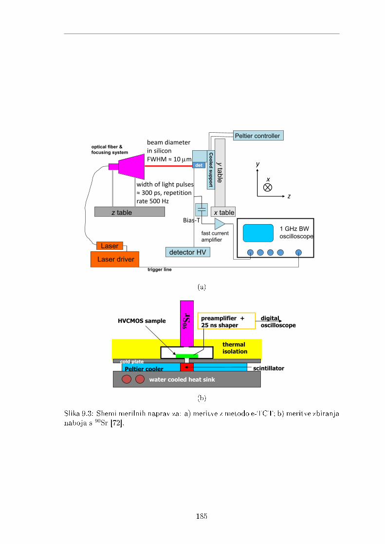
det
Cooledsupport
ytable
Laser
Laser driverdetector HV
Peltier controller
z table x table
1 GHz BWoscilloscopefast current
amplifier
trigger line
optical fiber &focusing system
width of light pulses≈ 300 ps, repetitionrate 500 Hz
beam diameterin siliconFWHM ≈ 10 m
Bias-T
z
y
x
(a)
preamplifier +25 ns shaper90
Sr
water cooled heat sink
cold plate
Peltier cooler scintillator
HVCMOS sample digitaloscilloscope
thermalisolation
(b)
Slika 9.3: Shemi merilnih naprav za: a) meritve z metodo e-TCT; b) meritve zbiranjanaboja s 90Sr [72].
185
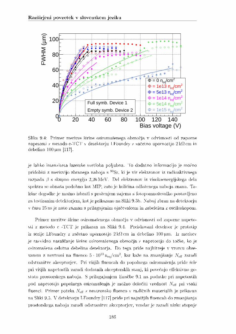
Raz²irjeni povzetek v slovenskem jeziku
Bias voltage (V)0 20 40 60 80 100 120 140
m)
µF
WH
M (
0
20
40
60
80
100
2/cmeq = 0 nΦ2/cmeq = 1e13 nΦ2/cmeq = 5e13 nΦ2/cmeq = 1e14 nΦ2/cmeq = 5e14 nΦ2/cmeq = 1e15 nΦ
Full symb. Device 1
Empty symb. Device 2
Slika 9.4: Primer meritve ²irine osiroma²enega obmo£ja v odvisnosti od zapornenapetosti z metodo e-TCT v detektorju LFoundry z za£etno upornostjo 2 kΩ cm indebelino 100µm [117].
je lahko intenziteta laserske svetloba poljubna. To dodatno informacijo je moºno
pridobiti z meritvijo zbranega naboja s 90Sr, ki je vir elektronov iz radioaktivnega
razpada β s skupno energijo 2,26MeV. Del elektronov iz visokoenergijskega dela
spektra se obna²a podobno kot MIP, zato je koli£ina odloºenega naboja znana. Ta-
k²ne dogodke je moºno izbrati s proºenjem zajema s fotopomnoºevalko postavljeno
za testiranim detektorjem, kot je prikazano na Sliki 9.3b. Naboj zbran na detektorju
v £asu 25 ns je nato zaznan s prilagojenim oja£evalcem in zabeleºen z osciloskopom.
Primer meritve ²irine osiroma²enega obmo£ja v odvisnosti od zaporne napeto-
sti z metodo e -TCT je prikazan na Sliki 9.4. Preiskovani detektor je prototip
iz serije LFoundry z za£etno upornostjo 2 kΩ cm in debelino 100µm. Iz meritev
je razvidno nara²£anje ²irine osiroma²enega obmo£ja z napetostjo do to£ke, ko je
osiroma²ena celotna debelina detektorja. Do tega pride najhitreje v vzorcu obse-
vanem z nevtroni na uenco 5 · 1013 neq/cm2, kar kaºe na zmanj²anje Neff zaradi
odstranitve akceptorjev. Pri vi²jih uencah do popolnega osiroma²enja pride ²ele
pri vi²jih napetostih zaradi dodatnih akceptorskih stanj, ki pove£ajo eektivno go-
stoto prostorskega naboja. S prilagajanjem Ena£be 9.1 na podatke pri napetostih
pod napetostjo popolnega osiroma²enja je moºno dolo£iti vrednost Neff pri vsaki
uenci. Primer poteka Neff z nevtronsko uenco v razli£nih materialih je prikazan
na Sliki 9.5. V detektorju LFoundry [117] pride pri najniºjih uencah do zmanj²anja
prostorskega naboja zaradi odstranitve akceptorjev, vendar je zaradi nizke stopnje
186

]-2 cm14 [10eqΦ0 20 40 60 80 100 120
]-3
cm
14 [1
0ef
fN
2−10
1−10
1
10
210
cmΩCHESS 20 ~ 1eff0/NcN
2 cm-14 10×c ~ 0.36
cmΩX-FAB 100 ~ 1.0eff0/NcN
2 cm-14 10×c ~ 1.1 -1 ~ 0.036 cm
cg
cmΩLF 2000 ~ 0.6eff0/NcN
2 cm-14 10×c ~ 10.3
Slika 9.5: Primer izmerjenih vrednosti Neff v odvisnosti od uence za prototipeDMAPS za razli£nimi za£etnimi upornostmi substrata [72, 117, 124].
dopiranja potek kmalu dominiran z nastankom novih akceptorskih stanj. V vzorcu
X-FAB z za£etno upornostjo 100Ω cm [124] je odstranitev akceptorjev kon£ana pri
vi²ji uenci okrog 5 · 1014 neq/cm2, nato pa je potek Neff podoben kot pri detektorju
LFoundry. Pri detektorju CHESS z za£etno upornostjo 20Ω cm pa je odstranitev
akceptorjev kon£ana ²ele pri uenci 1 · 1015 neq/cm2 [72]. Iz prileganja funkcije 9.2
podatkom je moºno dolo£iti deleº odstranjenih akceptorjev in koecient odstranje-
vanja akceptorjev c. Pri ve£ini preu£evanih vzorcev je deleº odstranjenih akceptorjev
enak 1, pri ostalih pa se giblje med 0,5 in 1. Koecienti odstranitve akceptorjev pri
nevtronskem obsevanju izmerjeni v tem delu so v odvisnosti od za£etne koncentra-
cije dopiranja prikazani na Sliki 9.6, kjer so primerjani z vrednostmi izmerjenimi
v drugih prototipih DMAPS. Opazen je splo²en trend zmanj²evanja vrednosti c z
nara²£ajo£im dopiranjem, vendar zaradi velikih razlik med materiali ni moºno pa-
rametrizirati splo²ne odvisnosti. Izmerjene vrednosti se grobo ujemajo z napovedjo
preprostega modela izdelanega na podlagi meritev z detektorji LGAD, ki so dopirani
v koncentracijah nad 1016 cm−3 (< 1Ω cm) [77]. Podobne meritve so bile izvedene
tudi z vzorci ams CHESS2 obsevanimi s protoni, vendar zaradi manj²ega ²tevila
razpoloºljivih uenc ni bilo mogo£e dolo£iti koecientov odstranitve akceptorjev. V
grobem so meritve pokazale, da protoni za£etne akceptorje odstranijo znatno hitreje
kot nevtroni, poleg tega pa ustvarjajo nova akceptorska stanja po£asneje. Zaradi
tega je Neff v protonsko obsevanih vzorcih veliko niºji kot pri primerljivi nevtronski
uenci, kar je s stali²£a DMAPS ugodno, saj to omogo£a ve£jo ²irino osiroma²enega
187

Raz²irjeni povzetek v slovenskem jeziku
)-3 (cmeff,0N
1310 1410 1510
)-2
c (c
m
15−10
14−10
13−10LFoundry CCPD_LF
X-FAB XTB02
AMS CHESS2
AMS CHESS1
AMS HV2FEI4
AMS H35DEMO
Slika 9.6: Izmerjene vrednosti koecienta odstranitve akceptorjev v odvisnosti od za-£etne koncentracije akceptorjev v materialu. Podatki predstavljeni z rde£imi to£kamiso bili izmerjeni v okviru tega dela [117, 123, 124], modre to£ke pa predstavljajo me-ritve z drugimi prototipi DMAPS [72, 94]. Rde£a £rta predstavlja napoved modelaodstranjevanja akceptorjev izdelanega na podlagi visoko dopiranih (> 1016 cm−3)detektorjev LGAD [77].
obmo£ja.
Poleg meritev z e-TCT je bilo v nekaterih vzorcih izmerjeno ²e zbiranje naboja s90Sr. Slika 9.7 prikazuje tak²no meritev z detektorji ams CHESS2 izdelanih v ²tirih
razli£icah za£etne upornosti. Iz meritve je razvidno, da je v neobsevanih vzorcih
zbranega ve£ naboja kot po prvem koraku nevtronskega obsevanja. Razlog za to je
zbiranje naboja ustvarjenega izven osiroma²enega obmo£ja, ki skozi detektor potuje
z difuzijo. Ta na£in transporta je zelo ob£utljiv na sevalne po²kodbe, zato njegov
prispevek po obsevanju izgine. Pri vi²jih nevtronskih uencah je razvidno nara²£anje
koli£ine zbranega naboja, kar je posledica odstranitve akceptorjev. Od vseh vzorcev
je signal najbolj stabilen v detektorju izdelanem na substratu z upornostjo 200Ω cm,
kjer povpre£ni zbran naboj nikoli ne pade pod 2000 elektronov. Na detektorju
z visoko za£etno upornostjo 1 kΩ cm je sicer pri nizkih uencah na razpolago ve£
naboja, vendar se pri uenci nad 5 · 1014 neq/cm2 ta vrednost izena£i z 200Ω cm
vzorcem. V vzorcih obsevanih s protoni so jasno razvidne posledice manj²e koli£ine
efektivnega prostorskega naboja v primerjavi z nevtronsko obsevanimi vzorci, saj je
koli£ina zbranega naboja veliko ve£ja, celo znatno vi²ja kot v neobsevanih vzorcih.
Metoda e-TCT je bila uporabljena tudi za dolo£itev enakomernosti signala po
celotni blazinici, ki je bila izvedena s premikanjem ºarka v dveh dimenzijah. Primeri
188

0
2000
4000
6000
8000
10000
12000
14000
16000
18000
0 10 20 30 40
Mean
charge
(electrons)
Fluence (1e14 neq/cm2)
Mean charge at 100 V (annealed)
20 Ω·cm50 Ω·cm200 Ω·cm1000 Ω·cm
PSLANSCEprotonsneutrons
Slika 9.7: Povpre£na koli£ina zbranega naboja izmerjena s 90Sr v detektorjih amsCHESS2 z razli£nimi za£etnimi upornostmi v odvisnosti od uence. Polna £rtapredstavlja meritve z nevtronsko obsevanimi vzorci, £rtkana £rta pa s protonskoobsevanimi vzorci [123].
meritev so prikazani na Sliki 9.8. Sliki 9.8a in 9.8b prikazujeta meritev z vzorcem
TowerJazz Investigator z velikostjo blazinice 20µm × 20µm oz. 50µm × 50µm
izdelanega v geometriji z majhno bralno zbiralno elektrodo in obsevanega z nev-
tronsko uenco 1 · 1015 neq/cm2. Na sliki so vidne tri blazinice, ki so bile povezane
na bralno elektroniko. Povr²ina silicijeve rezine se nahaja na spodnjem delu ob-
£utljivega obmo£ja, osiroma²eno podro£je pa nara²£a v smeri osi y. Zaradi zelo
majhnih blazinic je bila meritev izvedena na meji pozicijske ob£utljivosti, vendar
so vseeno razvidna podro£ja z razli£no koli£ino zbranega naboja. Pri blazinicah
z velikostjo 50µm × 50µm je vidna ve£ja koli£ina zbranega naboja v osrednjem
delu blizu zbiralne elektrode, medtem ko je na robovih blazinic ta nekoliko niºja.
Podoben primer je prikazan na Sliki 9.8c narejeni z vzorcem X-FAB z velikostjo
blazinic 110µm × 100µm izdelanega v tehnologiji SOI in obsevanega na uenco
5 ·1014 neq/cm2. Na sliki so ²tiri blazinice, ki jih lo£ujejo podro£ja z majhno koli£ino
zbranega naboja. To je posledica parazitskega zbiranja naboja na delu detektorja
namenjenemu bralni elektroniki, ki pa ni povezan z zbiralno elektrodo. Posledica
tega so navidezno neu£inkovita obmo£ja, ki jih je potrebno odstraniti s prilagodi-
tvijo zasnove. Parazitsko zbiranje naboja je bilo potrjeno tudi z orodjem KDetSim
[127], ki simulira zbiranje naboja v detektorjih s poljubno geometrijo. Rezultati
simulacije prikazani na Sliki 9.8d se kvantitativno ujemajo z meritvijo z e-TCT.
Druga zvrst meritev v okviru tega doktorata je bila dolo£itev u£inkovitosti mo-
189

Raz²irjeni povzetek v slovenskem jeziku
CCE at V bias = 6 V
20 30 40 50 60 70 80 90 100 110 12020
30
40
50
60
70
80
90
100
Charge(arb)
0
5
10
15
20
25
30
35
40
45
CCE at V bias = 6 V
x (μm)
y(μm)
chip surface
depletion
(a) TJ Investigator 20µm× 20µm
CCE at V bias = 6 V
m)µx (0 20 40 60 80 100 120 140 160 180 200
m)
µy
(
0
10
20
30
40
50
60
70
80
90
100
Cha
rge
(arb
)
0
2
4
6
8
10
12
14
16
CCE at V bias = 6 V
(b) TJ Investigator 50µm× 50µm
Cha
rge
(arb
)
0
50
100
150
200
250
CCE at V bias = 200 V
m)µx (0 50 100 150 200 250 300 350 400 450 500
m)
µy
(
0
20
40
60
80
100
120
140
CCE at V bias = 200 V
(c) X-FAB 110µm× 100µm
m]µx [0 50 100 150 200 250 300
m]
µy
[
0102030405060708090
100
char
ge (
arb.
)
0
20
40
60
80
= 130 V, logic biased 0 VbiasCCE V
(d) Simulacija X-FAB
Slika 9.8: Meritve enakomernosti zbranega naboja znotraj polja blazinic z metodo e-TCT: Sliki a) in b) sta narejeni z vzorcem TowerJazz Investigator z majhno zbiralnoelektrodo obsevanem z nevtroni do uence 1 · 1015 neq/cm
2, Slika c) pa z vzorcem X-FAB obsevanem z nevtronsko uenco 5 · 1014 neq/cm
2. Slika d) je rezultat simulacijezbiranja naboja v detektorju podobnem detektorju c) in kaºe enaka obmo£ja z nizkou£inkovitostjo med blazinicami.
190

1 2 3 7 4 5 6DUT
Test beam
-230 -210 -190 370 415 435 4550
cold box
Slika 9.9: Shema ºarkovnega teleskopa KarTel za meritve v testnem ºarku. Prei-skovani detektor (DUT) je name²£en med zaznavnima ravninama 3 in 4 v hlajenemohi²ju. Dimenzije so v mm.
nolitnega detektorja TowerJazz MALTA z visokoenergijskim testnim ºarkom na po-
spe²evalniku SPS v CERN-u. TowerJazz MALTA je izdelan v arhitekturi z majhno
zbiralno elektrodo in velikostjo blazinic 36µm×36µm, za £itanje podatkov pa upo-
rablja inovativen sistem, ki za delovanje ne potrebuje razdeljevanja urinega signala v
polje blazinic in s tem zmanj²a elektri£no mo£ £ipa za ve£ kot 50% [88]. V tem delu
so predstavljene meritve z dvema vzorcema: neobsevanim in nevtronsko obsevanim
na uenco 1 · 1015 neq/cm2. Nepredvidene napake v zasnovi £ipa so povzro£ile, da
vzorci niso mogli delovati v idealnem obmo£ju nastavitev. Zaradi teºav v napaja-
nju vezja za konguracijo £ipa iz £italnega sistema ni bilo moºno izlo£iti blazinic
z visokim ²umom, kar je vodilo v zasi£enost bralnega sistema na £ipu. V izogib
tem teºavam je bilo vzorce treba nastaviti na manj²o ob£utljivost, pri kateri je bil
najniºji zaznavni prag namesto na predvideno vrednost 200 e− nastavljen na 250 e−
v neobsevanem in 350 e− v obsevanem vzorcu.
Meritve so bile opravljene z ºarkom pionov z energijo 180GeV in lastnostmi
delcev MIP. Trajektorije delcev so bile dolo£ene z uporabo ºarkovnega teleskopa
KarTel [133], ki sestoji iz sedmih zaporednih visokolo£ljivostnih zaznavnih ravnin
(6 detektorjev Mimosa-26 [134] + 1 detektor z bralnim £ipom FEI4) postavljenih
na obeh straneh preiskovanega detektorja (Slika 9.9). Prikazana postavitev omo-
go£a dolo£itev prese£i²£a sledi delcev MIP z detektorjem z lo£ljivostjo σ = 5µm. V
rekonstrukciji podatkov s programsko opremo Judith/Proteus [133] so bile izbrane
samo sledi zaznane v vseh sedmih ravninah teleskopa, poleg tega pa so bili izlo£eni
dogodki z ve£ kot eno sledjo, ki je ustrezala temu kriteriju. U£inkovitost vzorca
191

Raz²irjeni povzetek v slovenskem jeziku
m)µ x (0 20 40 60
m)
µ y
(
0
10
20
30
40
50
60
70
0
0.1
0.2
0.3
0.4
0.5
0.6
0.7
0.8
0.9
1
96.4 %±
0.1 %95.9 %
±0.3 %
96.1 %±
0.2 %
96.4 %±
0.2 %
(a)
m)µ x (0 20 40 60
m)
µ y
(
0
10
20
30
40
50
60
70
0
0.1
0.2
0.3
0.4
0.5
0.6
0.7
0.8
0.9
1
74.2 %±
0.1 %89.6 %
±0.1 %
76.9 %±
0.2 %
70.4 %±
0.2 %
(b)
Slika 9.10: Izmerjena u£inkovitost zaznavanja delcev v detektorju TowerJazzMALTA, predstavljena v polju 2× 2 blazinic: a) pred obsevanjem pri pragu 250 e−;b) po obsevanju z 1 · 1015 neq/cm
2 pri pragu 350 e−. Pritisnjena zaporna napetost je15V.
je bila denirana kot razmerje med ²tevilom sledi povezanih z zaznanim dogodkom
v preu£evanem vzorcu in skupnim ²tevilom sledi v izbranem obmo£ju. Za ve£jo
preglednost je bila u£inkovitost celotnega polja preslikana v celico velikosti 2 × 2
blazinici. Primer meritve u£inkovitosti neobsevanega in obsevanega vzorca je prika-
zan na sliki 9.10. V neobsevanem vzorcu je u£inkovitost zaznavanja enakomerna s
povpre£no vrednostjo 96,4% znotraj blazinice, medtem ko so v obsevanem vzorcu
jasno opazna obmo£ja na robovih blazinic z niºjo ob£utljivostjo. Povpre£na u£in-
kovitost blazinice v obsevanem vzorcu je v prikazanem primeru 74,2%, pri £emer
zna²a u£inkovitost v osrednjem delu blazinice, ki predstavlja 25% povr²ine okoli
zbiralne elektrode, 89,6%, v kotih blazinice pa je vzorec skoraj popolnoma neu£in-
kovit. Do neu£inkovitostih na robovih pride zaradi ²ibkega elektri£nega polja, ki ni
zadostno za hitro zbiranje naboja. Posledi£no se nosilci naboja ujamejo v pasti, ki
jih povzro£i sevanje, zato se zbran naboj zmanj²a, kar je splo²en problem zasnove
z majhno zbiralno elektrodo. V osrednjem delu blazinice je izmerjena u£inkovitost
vi²ja pri vi²jem pragu ob£utljivosti. To je moºno razloºiti z izgubo podatkov zaradi
zasi£enosti £italnega sistema, ki se z nara²£anjem praga ob£utljivosti niºa zaradi
niºjega nivoja prepu²£enega ²uma.
U£inkovitosti detektorja MALTA pri razli£nih pragovih zaznave in razli£nih za-
pornih napetostih so prikazane na diagramu 9.11. Neobsevan detektor doseºe naj-
vi²jo u£inkovitost 97,0% pri zaznavnem pragu 400 e−, na razli£ne zaporne napetosti
pa je razmeroma neob£utljiv. V obsevanem detektorju se povpre£na u£inkovitost
celotne blazinice zmanj²uje z ve£anjem praga, u£inkovitost osrednjega dela pa s
192

)-
thr. (e250 300 350 400 450 500 550 600
effic
ienc
y
0.7
0.75
0.8
0.85
0.9
0.95
1
Unirr. - Full Cell
Unirr. - Centre
1e15 - Full Cell
1e15 - Centre
(a)
(V)biasV8 10 12 14 16 18 20
effic
ienc
y
0.65
0.7
0.75
0.8
0.85
0.9
0.95
1
Unirr. - Full Cell
Unirr. - Centre
1e15 - Full Cell
1e15 - Centre
(b)
Slika 9.11: U£inkovitost detektorja TowerJazz MALTA pred in po obsevanju v odvi-snosti od a) praga na predoja£evalcu in b) pritisnjene zaporne napetosti. Meritve a)so bile narejene pri zaporni napetosti 15V in meritve b) pri pragu 250 e− v neobseva-nem in 400 e− v obsevanem vzorcu. Polna £rta predstavlja povpre£no u£inkovitostcelotne blazinice, £rtkana £rta pa povpre£no u£inkovitost osrednjih 25% povr²ineblazinice v okolici zbiralne elektrode.
193

Raz²irjeni povzetek v slovenskem jeziku
pragom nara²£a. To je posledica zgoraj opisanih procesov pri nizkem pragu je za-
znanih ve£ dogodkov na robovih detektorja, kjer je na razpolago manj naboja zaradi
ujetja v pasti. Obenem se z niºanjem praga zvi²uje stopnja izgube podatkov zaradi
zasi£enja £italnega vezja, kar je prevladujo£i proces v osrednjem delu blazinice, kjer
je ujetja v pasti razmeroma malo. Odvisnost u£inkovitosti od zaporne napetosti v
obsevanem detektorju doseºe najvi²jo vrednost 74,2% pri napetosti 15V. Pri vi²jih
napetostih u£inkovitost pade, ker postane elektri£no polje v blazinici slab²e usmer-
jeno proti zbiralni elektrodi in je zato na robovih zaznanih manj signalov. Opisani
rezultati so bili pomemben vir povratnih informacij na£rtovalcem £ipa MALTA, ki so
na podlagi zgornjih meritev predlagali izbolj²ave v zgradbi blazinice. Te temeljijo na
spremembi implantiranih struktur, ki pove£ajo bo£no komponento elektri£nega polja
ter s tem znatno pove£ajo u£inkovitost na robovih blazinic [139]. Te spremembe so
bile skupno z odpravljenimi napakami v elektronskem vezju, ki so onemogo£ale de-
lovanje pri nizkih pragovih zaznavanja, izvedene v £ipu MiniMALTA. Prvi rezultati
meritev v testnem ºarku kaºejo na bistveno izbolj²anje delovanja z u£inkovitostjo
nad 98% v obsevanih vzorcih [93].
Marca 2019 se je kolaboracija ATLAS odlo£ila, da zaradi prekratkih £asovnih
rokov ne bo uporabila detektorjev DMAPS za izgradnjo Plasti 4 v sledilniku ITk,
saj nobena ob razvojnih smeri do takrat ²e ni razpolagala s prototipom s polno funk-
cionalnostjo zahtevano za ATLAS. Nekatere skupine vseeno nadaljujejo z razvojem,
da izkoristijo vloºeno delo in dosedanje raziskave. Detektorji DMAPS imajo kljub
temu svetlo prihodnost, saj so zanimivi tudi za uporabo na prihodnjih pospe²eval-
nikih, kot sta npr. na£rtovana Kompaktni linearni trkalnik (CLIC) in Mednarodni
linearni trkalnik (ILC), ki zahtevata visoko lo£ljivost sledenja in zmerno odpornost
na sevanje.
Obseºna ²tudija detektorjev DMAPS izvedena v okviru tega doktorata je z upo-
rabo merskih metod e-TCT, 90Sr in testni ºarek raziskala lastnosti zbiranja naboja
v obsevanih detektorjih. Hkrati so meritve sluºile kot vir povratnih informacij sno-
valcem detektorjev, ki so na podlagi rezultatov lahko izbolj²ali sevalno odpornost
vzorcev. Ena glavnih tem tega dela je opredelitev odstranitve za£etnih akceptor-
jev, ki lahko odlo£ilno vpliva na velikost osiroma²enega obmo£ja v obmo£ju uenc
10131015 neq/cm2. Zaradi koristnega vpliva na delovanje sledilnih detektorjev bo
upo²tevanje odstranitve akceptorjev verjetno imelo pomembno vlogo v zasnovi pri-
hodnjih detektorjev.
194