Radiation damage induced by swift heavy ions in TiO2 sol–gel films nanocrystallines
7
Radiation damage induced by swift heavy ions in TiO 2 sol–gel films nanocrystallines R. Hazem a , M. Izerrouken b,⇑ , A. Sari c , S. Kermadi d , M. Msimanga e , A. Benyagoub f , M. Maaza g , M. Belgaid a , M. Boumaour d a USTHB, Faculté de Physique, BP. 32 El-Alia, Bab-Ezzouar, Algiers, Algeria b Centre de Recherche Nucléaire de Draria, BP. 43, Sebbala, Draria, Algiers, Algeria c Centre de Recherche Nucléaire de Birine, BP. 108, Ain-Oussara, Djelfa, Algeria d UDTS, 2 Bd Frantz Fanon, BP. 399, Alger gare, Algiers, Algeria e NRF iThemba LABS, Gauteng Private Bag, 11 WITS 2050, Johannesburg, South Africa f CIMAP, (ex-CIRIL-GANIL), CEA-CNRS-ENSICAEN-Université de Caen Basse Normandie, Bd Henri Becquerel, BP. 5133, F-14070 Caen cedex 5, France g iThemba LABS, P.O. Box 722, Somerset West 7129, Cap Town, South Africa article info Article history: Received 14 January 2013 Received in revised form 16 March 2013 Available online 6 April 2013 Keywords: Semiconductors Radiation damage Optical properties Defects Photocatalytic Nanostructure abstract TiO 2 films prepared by sol–gel were irradiated with 25.8 MeV Cu and 90 MeV Xe ions at room tempera- ture under normal incidence. The irradiation with Cu and Xe ions were performed respectively at iThe- mba labs, South Africa and GANIL, Caen, France. The properties of radiation defects induced in TiO 2 nanostructures were investigated using grazing angle X-ray diffraction (GAXRD), atomic force micros- copy (AFM) and UV–visible spectrophotometry. From GAXRD analysis, it is found that anatase (1 0 1) peak intensity decrease with increasing the fluence and disappear completely above a threshold ion fluence of 5 10 12 ion/cm 2 . This indicates that the crystallinity of the TiO 2 film is destroyed upon irradiation due to the amorphous track formation. The track radius estimated from the Poisson’s law is about 2 and 4 nm after irradiation with 25.8 MeV Cu and 90 MeV Xe ions, respectively. According to the AFM analysis, the elaborated TiO 2 films are composed of particles with a triangular shape of a size in the range of 200–500 nm. It is found that the particle size increases after irradiation with both Cu and Xe ions. In addi- tion, the root-mean-square (RMS) surface roughness for 780 nm 780 nm area scans decreases exponen- tially with increasing fluence up to 10 13 ions/cm 2 in the case of Xe irradiation, but increases drastically above 2.68 10 11 ions/cm 2 in the case of Cu ion irradiation and reaches a mean value of 3 nm. The absorption measurements reveal that the optical band gap is not affected by both Xe and Cu ions irradiation. Ó 2013 Elsevier B.V. All rights reserved. 1. Introduction TiO 2 presents several interesting properties: high chemical sta- bility, safety, non-toxicity and good radiation resistance. Thus, crystalline TiO 2 is used as a heterogeneous catalysis in solar cells for the production of electricity and/or hydrogen [1–4]. However, undoped TiO 2 is of n-type semiconductor with a band gap of 3.2 eV (in the case of anatase structure) which is higher com- pared to the sunlight range (1.6–3.3) eV. Thus, only a small fraction of solar energy is converted. Consequently, many efforts have been made to promote the photocatalytic activity and enhance the visi- ble light response. For this purpose, several methods have been used, such as introduction of noble metal in TiO 2 films (see for in- stance [5] and references therein) and ion implantation [6–12]. It is also found that the crystallinity [13] and the crystallite size affect the photocatalytic activity of TiO 2 [14]. It is well known that ion irradiation may induce various types of structural changes which can modify the material properties. The nature of these structural changes depends on the ion energy, flu- ence and ion species. Indeed, it is well established that energetic ions penetrating into matter lose their energy both by elastic collisions with the target atom nuclei (the nuclear stopping power S n ), and by interaction with the target electron (the electronic stopping power S e ). For swift heavy ions with energy above 1 MeV/amu, the energy loss is mainly done through ionization and electronic excita- tion processes and can produce an amorphous track along the ion path. Recently, several authors have investigated the nanostructures observed at the surface after ion irradiation. Atomic force micros- copy (AFM) analysis revealed hillock like features with a height of about a few nanometers in samples irradiated with swift heavy ions [15–18]. Two competing processes have been developed to explain the surface morphology modification: The thermal spike [19] and the coulomb explosion [20] models. According to the thermal spike model, the energy loss of swift heavy ions is first shared between electrons by electron–electron interactions and is then transferred to lattice atoms by electron–phonon coupling, which results in the 0168-583X/$ - see front matter Ó 2013 Elsevier B.V. All rights reserved. http://dx.doi.org/10.1016/j.nimb.2013.03.037 ⇑ Corresponding author. E-mail address: [email protected] (M. Izerrouken). Nuclear Instruments and Methods in Physics Research B 304 (2013) 16–22 Contents lists available at SciVerse ScienceDirect Nuclear Instruments and Methods in Physics Research B journal homepage: www.elsevier.com/locate/nimb
-
Upload
independent -
Category
Documents
-
view
0 -
download
0
Transcript of Radiation damage induced by swift heavy ions in TiO2 sol–gel films nanocrystallines

Nuclear Instruments and Methods in Physics Research B 304 (2013) 16–22
Contents lists available at SciVerse ScienceDirect
Nuclear Instruments and Methods in Physics Research B
journal homepage: www.elsevier .com/locate /n imb
Radiation damage induced by swift heavy ions in TiO2 sol–gel films nanocrystallines
R. Hazem a, M. Izerrouken b,⇑, A. Sari c, S. Kermadi d, M. Msimanga e, A. Benyagoub f, M. Maaza g, M. Belgaid a,M. Boumaour d
a USTHB, Faculté de Physique, BP. 32 El-Alia, Bab-Ezzouar, Algiers, Algeriab Centre de Recherche Nucléaire de Draria, BP. 43, Sebbala, Draria, Algiers, Algeriac Centre de Recherche Nucléaire de Birine, BP. 108, Ain-Oussara, Djelfa, Algeriad UDTS, 2 Bd Frantz Fanon, BP. 399, Alger gare, Algiers, Algeriae NRF iThemba LABS, Gauteng Private Bag, 11 WITS 2050, Johannesburg, South Africaf CIMAP, (ex-CIRIL-GANIL), CEA-CNRS-ENSICAEN-Université de Caen Basse Normandie, Bd Henri Becquerel, BP. 5133, F-14070 Caen cedex 5, Franceg iThemba LABS, P.O. Box 722, Somerset West 7129, Cap Town, South Africa
a r t i c l e i n f o a b s t r a c t
Article history:Received 14 January 2013Received in revised form 16 March 2013Available online 6 April 2013
Keywords:SemiconductorsRadiation damageOptical propertiesDefectsPhotocatalyticNanostructure
0168-583X/$ - see front matter � 2013 Elsevier B.V.http://dx.doi.org/10.1016/j.nimb.2013.03.037
⇑ Corresponding author.E-mail address: [email protected] (M. Izerro
TiO2 films prepared by sol–gel were irradiated with 25.8 MeV Cu and 90 MeV Xe ions at room tempera-ture under normal incidence. The irradiation with Cu and Xe ions were performed respectively at iThe-mba labs, South Africa and GANIL, Caen, France. The properties of radiation defects induced in TiO2
nanostructures were investigated using grazing angle X-ray diffraction (GAXRD), atomic force micros-copy (AFM) and UV–visible spectrophotometry. From GAXRD analysis, it is found that anatase (101) peakintensity decrease with increasing the fluence and disappear completely above a threshold ion fluence of5 � 1012 ion/cm2. This indicates that the crystallinity of the TiO2 film is destroyed upon irradiation due tothe amorphous track formation. The track radius estimated from the Poisson’s law is about 2 and 4 nmafter irradiation with 25.8 MeV Cu and 90 MeV Xe ions, respectively. According to the AFM analysis,the elaborated TiO2 films are composed of particles with a triangular shape of a size in the range of200–500 nm. It is found that the particle size increases after irradiation with both Cu and Xe ions. In addi-tion, the root-mean-square (RMS) surface roughness for 780 nm � 780 nm area scans decreases exponen-tially with increasing fluence up to 1013 ions/cm2 in the case of Xe irradiation, but increases drasticallyabove 2.68 � 1011 ions/cm2 in the case of Cu ion irradiation and reaches a mean value of �3 nm. Theabsorption measurements reveal that the optical band gap is not affected by both Xe and Cu ionsirradiation.
� 2013 Elsevier B.V. All rights reserved.
1. Introduction It is well known that ion irradiation may induce various types of
TiO2 presents several interesting properties: high chemical sta-bility, safety, non-toxicity and good radiation resistance. Thus,crystalline TiO2 is used as a heterogeneous catalysis in solar cellsfor the production of electricity and/or hydrogen [1–4]. However,undoped TiO2 is of n-type semiconductor with a band gap of�3.2 eV (in the case of anatase structure) which is higher com-pared to the sunlight range (1.6–3.3) eV. Thus, only a small fractionof solar energy is converted. Consequently, many efforts have beenmade to promote the photocatalytic activity and enhance the visi-ble light response. For this purpose, several methods have beenused, such as introduction of noble metal in TiO2 films (see for in-stance [5] and references therein) and ion implantation [6–12]. It isalso found that the crystallinity [13] and the crystallite size affectthe photocatalytic activity of TiO2 [14].
All rights reserved.
uken).
structural changes which can modify the material properties. Thenature of these structural changes depends on the ion energy, flu-ence and ion species. Indeed, it is well established that energetic ionspenetrating into matter lose their energy both by elastic collisionswith the target atom nuclei (the nuclear stopping power Sn), andby interaction with the target electron (the electronic stoppingpower Se). For swift heavy ions with energy above 1 MeV/amu, theenergy loss is mainly done through ionization and electronic excita-tion processes and can produce an amorphous track along the ionpath. Recently, several authors have investigated the nanostructuresobserved at the surface after ion irradiation. Atomic force micros-copy (AFM) analysis revealed hillock like features with a height ofabout a few nanometers in samples irradiated with swift heavy ions[15–18]. Two competing processes have been developed to explainthe surface morphology modification: The thermal spike [19] andthe coulomb explosion [20] models. According to the thermal spikemodel, the energy loss of swift heavy ions is first shared betweenelectrons by electron–electron interactions and is then transferredto lattice atoms by electron–phonon coupling, which results in the
R. Hazem et al. / Nuclear Instruments and Methods in Physics Research B 304 (2013) 16–22 17
heating of the lattice. If the electronic energy loss density is suffi-ciently high, the temperature may rise above the melting pointand a molten cylinder along the ion path can be formed. Rapidquenching of the entire cylinder of the melted matter leads to theformation of an amorphous track. In the case of the coulomb explo-sion model, the passage of an energetic heavy ion through the mate-rial induces large positive target ions produced by electronicexcitation-induced ionizations. These positive ions explode radiallydue to Coulomb force, thus causing coherent radial atomic move-ments. According to Skuratov et al. [21], this mechanism may ex-plain the surface effects generated by swift heavy ions.
In the case of thin film, the energetic ions penetrate completelythe film and the energy loss is due mainly to the electronic ioniza-tion and excitation process. This leads consequently to the cata-strophic changes in the thin film properties. Numerous studieswere investigated swift heavy ions modification of TiO2 thin filmnanostructure elaborated by different techniques [22–25]. In thepresent work, we study the effect of ions on structural and mor-phological properties of TiO2 thin film elaborated by the sol–gelmethod. Our aim is to explore the possibility to improve the TiO2
photocatalytic activity by ion irradiation.
2. Experimental
The TiO2 films used in the present work were elaborated by thesol–gel method. They were prepared by addition of Tetra iso-Prop-oxide Ortho-Titanate (TPOT) to a pre-mix of 2-propanol (i-PrOH) assolvent, acetylacetone (AcAc) as ligand and acetic acid as acid cat-alyst at pH 4. After addition of deionised water, the mixture waskept under stirring at ambient temperature for 2 h to completethe hydrolysis process. The final solution was coated by dip-coat-ing at a pulling speed of 5.5 cm/min on both sides of the substrateand then followed by heat treatment for 1 h at 500 �C in air. To in-crease the film thickness, the coating procedure may be repeatedseveral times. According to our previous work, one coating proce-dure produce a film with a thickness of about 40 nm [26]. SeveralTiO2 films were prepared on glass and silicon substrates as given inTable 1. The samples 1–3 were prepared with one and three coat-ing procedure, respectively.
After elaboration, the TiO2 films were irradiated with 25.8 MeVCu and 90 MeV Xe ions at room temperature under normal inci-dence. The irradiations with Cu and Xe ions were performed respec-tively at iThemba labs, South Africa and GANIL, Caen, France usingthe IRRSUD line. The irradiation parameters are presented in Table 1.
The structural and morphological properties were investigatedusing atomic force microscopy (Pacific Nanotechnology), scanningelectronic microscopy (SEM) and Grazing Angle X-ray diffraction(Philips X’PERT PRO MPD). The optical absorption measurementswere carried out using a double beam Cintra 40 spectrophotometerin the range 200–900 nm.
3. Results and discussion
3.1. Characterization of the prepared TiO2 films
Fig. 1 shows the SEM micrographs of sample 3 where the coat-ing procedure was repeated three times. The TiO2 film presents a
Table 1Irradiation conditions of the samples: The electronic stopping power Se, nuclear stopping
Ions species Energy (MeV) Se (keV/nm) Sn (keV/nm) Rp (lm
Cu+7 25.8 10.3 0.078 4.8
Xe 90 20.3 0.16 8.08
uniform and nanometric structure (Fig. 1a) with a crystallite sizeof about 20 nm. The cross-sectional SEM image (Fig. 1b) revealsthat the film consists of a layer with a thickness of �120 nm.
AFM measurements performed in contact mode at room tem-perature show the same particle geometry for all samples. For in-stance, Fig. 2 shows the two- and three-dimentional AFM imagesof samples 1. It is clear that the particles present a triangular shapewith a mean particle size of about 300 nm. Thus, according to SEManalysis, one can say that each particle is made up of severalagglomerated crystallite.
GAXRD patterns collected in the 2h range of 24–50� at a grazingangle of 0.6� indicate that the elaborated samples have the anatasestructure with the main peak at 25.42� corresponding to the (101)plane (see Fig. 3). For each sample, the crystallite size L can be esti-mated from the width of the main (101) peak by using the Scher-rer relation:
L ¼ 0:94kBð2hÞ cosðhÞ ð1Þ
where k is the wavelength of the X-ray beam (Cu Ka, 1.5406 Å),B(2h) is the full-width at half-maximum (FWHM) of the diffractionpeak (in radian) and h is the diffraction angle.
The optical transmission spectra of sample 1 as well as that ofthe substrate are presented in Fig. 4. The transmittance is drasti-cally reduced at wavelength less than 300 nm induced by the lightabsorption in the vicinity of the band gap.
3.2. Radiation effects on structural, morphological and opticalproperties of TiO2 film
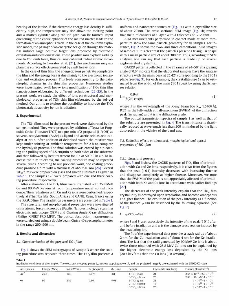
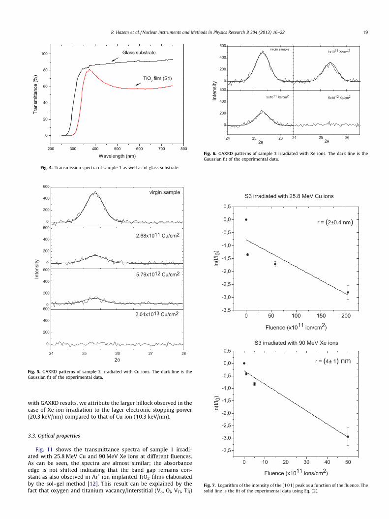
3.2.1. Structural propertyFigs. 5 and 6 show the GAXRD patterns of TiO2 film after irradi-
ation with Cu and Xe ions, respectively. It is clear from the figuresthat the peak (101) intensity decreases with increasing fluenceand disappear completely at higher fluence. Moreover, we notethat the FWHM of the peak is not appreciably affected after irradi-ation with both Xe and Cu ions in accordance with earlier findings[27].
The decreases of the peak intensity explain that the TiO2 filmcrystallinity is destroyed upon irradiation and become amorphousat higher fluence. The evolution of the peak intensity as a functionof the fluence / can be described by the following equation (seeFig. 7).
I ¼ I0 expð�r/Þ ð2Þ
where I and I0 are respectively the intensity of the peak (101) afterand before irradiation and r is the damage cross section induced bythe irradiating ion.
The fit of the experimental data provides a track radius of about2 nm for the Cu irradiation and of about 4 nm for the Xe irradia-tion. The fact that the radii generated by 90 MeV Xe ions is abouttwice those obtained with 25.8 MeV Cu ions can be explained bythe higher electronic energy loss deposited by the Xe ions(20.3 keV/nm) than the Cu ions (10 keV/nm).
power Sn and the projected range Rp are estimated with the SRIM2003 code.
) Sample Crystallite size (nm) Fluence (Ions/cm�2)
1-TiO2/glass 21 2.68 � 1010–7.50 � 1013
3-TiO2/silicon 25 2.68 � 1011–9.14 � 1013
1-TiO2/glass 21 1 � 1010–1 � 1013
2-TiO2/silicon 13 1 � 1010–1 � 1013
3-TiO2/silicon 25 1 � 1011–1 � 1013

(a)
(b)
Fig. 1. SEM micrographs of sample 3. (a) Planar and (b) cross-sectional images.
20 25 30 35 40 45 50
0
200
400
6000
100
200
3000
400
800
1200
2θ
(S 3)anatase (101)
Inte
nsity
(S 2)anatase (101)
(S 1)anatase (101)
Fig. 3. GAXRD patterns of TiO2 film elaborated by sol–gel method and deposited onglass and silicon substrate.
18 R. Hazem et al. / Nuclear Instruments and Methods in Physics Research B 304 (2013) 16–22
3.2.2. Morphological propertiesThe AFM images of samples 1 obtained after 90 MeV Xe ion irra-
diation are presented in Fig. 8. From the images it is clear that theparticle size increases after irradiation. The same results are alsoobserved in sample 1 irradiated with 25.8 MeV Cu ions (seeFig. 9). The increase of the particle size is probably due to theswelling induced by the ions irradiation. It is well known thatthe amorphous track generated by ion irradiation induces volumeexpansion in several oxides (see [28] and references therein).
Fig. 2. Two- and three-dimension
In order to cheek the effect of ion irradiation on individual par-ticle surface, a small area scan of 780 nm � 780 nm was performedfor each sample. The root-mean-square (RMS) surface roughnessobtained from the analysis of one area scan for each irradiatedsample is presented in Fig. 10 as a function of fluence. In the caseof 90 MeV Xe ion irradiation the surface roughness increases littlebite after irradiation at a fluence of 1011 ions cm�2, and then de-creases exponentially with increasing fluence up to 1013 ions cm�2.In the case of 25.8 MeV Cu ions, the RMS surface roughness drasti-cally increases above the fluence of 2.68 � 1011 ions cm�2 andreaches a mean value of about 3 nm at 7 � 1012 ions cm�2. Thissurface roughness evolution after ion irradiation can be explainedby the hillocks formation due to the amorphous track overlapping[29]. In the case of 90 MeV Xe ion irradiation, hillock with largediameters are formed which overlaps at higher fluence and causesthe flattening of the TiO2 surface particle. Whereas, in the case of25.8 MeV Cu ion irradiation, this behavior is not well understood,probably smaller hillocks are produced. With increasing fluence,the hillock height increases without overlapping, this may explainthe drastically surface roughness increases. Further study usinghigh AFM resolution is needed to confirm the result. In accordance
al AFM images of sample 1.
200 300 400 500 600 700 800
0
20
40
60
80
100
Tran
smitt
ance
(%)
Wavelength (nm)
Glass substrate
TiO2 film (S1)
Fig. 4. Transmission spectra of sample 1 as well as of glass substrate.
24 25 26 27 28
0
200
400
6000
200
400
600
0
200
400
6000
200
400
600
2θ
2,04x10¹³ Cu/cm2
5.79x10¹² Cu/cm2
2.68x10¹¹ Cu/cm2
Inte
nsity
virgin sample
Fig. 5. GAXRD patterns of sample 3 irradiated with Cu ions. The dark line is theGaussian fit of the experimental data.
0
200
400
600
24 25 26
0
200
400
600
24 25 26
virgin sample
2θ
5x10¹¹ Xe/cm2
2θ
5x10¹² Xe/cm2Inte
nsity
1x10¹¹ Xe/cm2
Fig. 6. GAXRD patterns of sample 3 irradiated with Xe ions. The dark line is theGaussian fit of the experimental data.
0 50 100 150 200-3,5
-3,0
-2,5
-2,0
-1,5
-1,0
-0,5
0,0
0,5
r = (2±0.4 nm)
S3 irradiated with 25.8 MeV Cu ions
ln(I/
I 0)
Fluence (x1011 ion/cm2)
-2,0
-1,5
-1,0
-0,5
0,0
0,5S3 irradiated with 90 MeV Xe ions
r = (4± 1) nm
ln(I/
I 0)
R. Hazem et al. / Nuclear Instruments and Methods in Physics Research B 304 (2013) 16–22 19
with GAXRD results, we attribute the larger hillock observed in thecase of Xe ion irradiation to the lager electronic stopping power(20.3 keV/nm) compared to that of Cu ion (10.3 keV/nm).
0 10 20 30 40 50
-3,5
-3,0
-2,5
Fluence (x1011 ions/cm2)
Fig. 7. Logarithm of the intensity of the (101) peak as a function of the fluence. Thesolid line is the fit of the experimental data using Eq. (2).
3.3. Optical properties
Fig. 11 shows the transmittance spectra of sample 1 irradi-ated with 25.8 MeV Cu and 90 MeV Xe ions at different fluences.As can be seen, the spectra are almost similar; the absorbanceedge is not shifted indicating that the band gap remains con-stant as also observed in Ar+ ion implanted TiO2 films elaboratedby the sol–gel method [12]. This result can be explained by thefact that oxygen and titanium vacancy/interstitial (Vo, Oi, VTi, Tii)
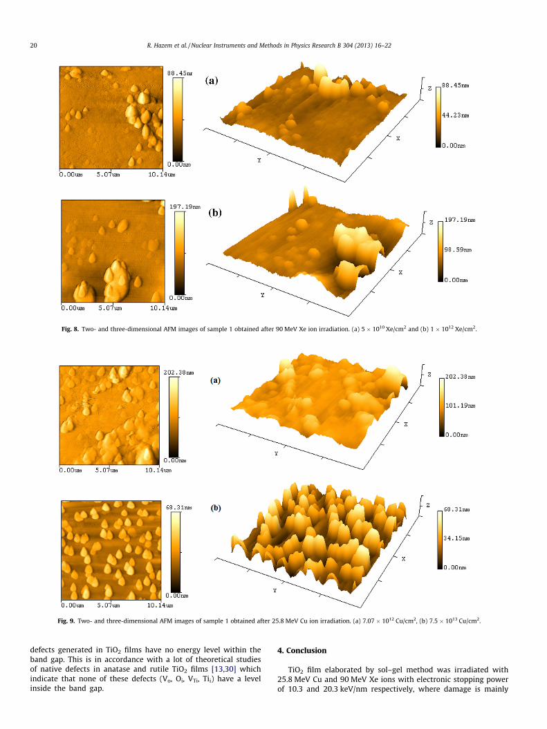
Fig. 8. Two- and three-dimensional AFM images of sample 1 obtained after 90 MeV Xe ion irradiation. (a) 5 � 1010 Xe/cm2 and (b) 1 � 1012 Xe/cm2.
Fig. 9. Two- and three-dimensional AFM images of sample 1 obtained after 25.8 MeV Cu ion irradiation. (a) 7.07 � 1012 Cu/cm2, (b) 7.5 � 1013 Cu/cm2.
20 R. Hazem et al. / Nuclear Instruments and Methods in Physics Research B 304 (2013) 16–22
defects generated in TiO2 films have no energy level within theband gap. This is in accordance with a lot of theoretical studiesof native defects in anatase and rutile TiO2 films [13,30] whichindicate that none of these defects (Vo, Oi, VTi, Tii) have a levelinside the band gap.
4. Conclusion
TiO2 film elaborated by sol–gel method was irradiated with25.8 MeV Cu and 90 MeV Xe ions with electronic stopping powerof 10.3 and 20.3 keV/nm respectively, where damage is mainly

0 10 20 1k 2k 3k 4k 5k 6k 7k 8k0.0
0.5
1.0
1.5
2.0
2.5
3.0
3.5
4.0
0 200 400 600 800 1000
0.4
0.6
0.8
1.0
1.2
1.4
1.6
1.8
2.025.8 MeV Cu ion
RM
S su
rface
roug
hnes
s (n
m)
Fluence (x1010 Cu/cm2)
90 MeV Xe ion
RM
S su
rface
roug
hnes
s (n
m)
Fluence (x1010 Xe/cm2)
Fig. 10. Root-mean square RMS surface roughness of 780 nm � 780 nm area scan as a function the fluence. The solid line is to guide the eye.
300 400 500 600 700 800 900
0
20
40
60
80
100
S1 irradiated with 25.8 MeV Cu ions
Tran
smitt
ance
(%)
Wavelength (nm)
virgin 2.68x10¹⁰ions/cm2
2.68x10¹¹ ions/cm2
1.71x10¹² ions/cm2
7.07x10¹² ions/cm2
1.77x10¹³ ions/cm2
7.50x10¹³ ions/cm2
300 400 500 600 700 800 900
0
20
40
60
80
100
S1 irradiated with 90 MeV Xe ions
Tran
smitt
ance
(%)
Wavelength (nm)
Virgin 1010 ions/cm2
5x10¹⁰ ions/cm2
1011 ions/cm2
5x10¹¹ ions/cm2
1012 ions/cm2
5x10¹² ions/cm2
1013 ions/cm2
Fig. 11. Transmittance spectra of sample 1 irradiated with Cu and Xe ions atdifferent fluences.
R. Hazem et al. / Nuclear Instruments and Methods in Physics Research B 304 (2013) 16–22 21
due to the ionization and excitation, processes. According toGAXRD analysis the crystallinity of the film is completely de-stroyed. Anatase phase disappear after irradiation at higher fluence
(>5 � 1012 ions/cm2) due to the amorphous track formation. Thetrack radius value increases from 2 nm for Cu ions (Se = 10.3 keV/nm) to 4 nm for Xe ions (Se = 20.3 keV/nm). AFM study reveals thatboth 25.8 MeV Cu and 90 MeV Xe ions irradiation increase the par-ticle size due probably to the volume expansion which result fromthe amorphous track induced by irradiation. For 90 MeV Xe ionirradiation, the RMS surface roughness for 780 nm � 780 nm areascan, decreases exponentially above the fluence of 1011 ions/cm2
up to 1013 ions/cm2. For 25.8 MeV Cu ion irradiation, The RMS sur-face roughness drastically increases above a fluence of2.68 � 1011 ions/cm2. This difference in the surface roughnessbehavior is due to the difference in hillock size induced by Xeand Cu ions irradiation which is attributed to the difference inthe electronic stopping power. From spectrophotometry measure-ments, it is found that the optical band gap energy is not affectedafter ion irradiation indicating that none of the Vo, Oi, VTi and Tii
defects have a level inside the band gap.
Acknowledgements
The authors wish to thank the head of optic and mechanicdepartment of faculty of science, University Ferhat Abbas, Setiffor AFM analysis.
References
[1] Meng Ni, Michael K.H. Leung, Dennis Y.C. Leung, K. Sumathy, Renew. Sust.Energ. Rev. 11 (2007) 401–425.
[2] O. Carp, C.L. Huisman, A. Reller, Prog. Solid State Chem. 32 (2004) 33–177.[3] J. Nowotny, T. Bak, M.K. Nowotny, L.R. Sheppard, Int. J. Hydrogen Energ. 32
(2007) 2630–2643.[4] Ulrike Diebold, Surf. Sci. Rep. 48 (2003) 53–229.[5] Xing-Gang Hou, An-Dong Liu, Radiat. Phy. Chem. 77 (2008) 345–351.[6] Li-Zhao Qin, Bin Liao, Xi-Liang Dong, Wu Xian-Ying, Xing-Gang Hou, An-Dong
Liu, Nucl. Instr. Meth. B 267 (2009) 1077–1080.[7] Yaw-Nan Shieh, Yin-Yu Chang, Thin Solid Films 518 (2010) 7464–7467.[8] N. Matsunami, M. Uebayashi, K. Hirooka, T. Shimura, M. Tazawa, Nucl. Instr.
Meth. B 267 (2009) 1654–1657.[9] Tao Yua, Xin Tan, Lin Zhao, Yuxin Yin, Peng Chen, Jing Wei, Chem. Eng. J. 157
(2010) 86–92.[10] S.K. Zheng, T.M. Wang, W.C. Hao, R. Shen, Vacuum 65 (2002) 155–159.[11] J. Jensen, R. Sanz, D. Martin, A. Surpi, T. Kubart, M. Vázquez, M. Hernandez-
Velez, Nucl. Instr. Meth. B 267 (2009) 2725–2730.[12] R. Fernandes, N. Patel, R. Dholam, M. Adami, A. Miotello, Surf. Coat. Technol.
203 (2009) 2579–2583.[13] S.K. Zheng, T.M. Wang, G. Xiang, C. Wang, Vacuum 62 (2001) 361–366.[14] D.G. Syarif, A. Miyashita, T. Yamaki, T. Sumita, Y. Choi, H. Itoh, App. Surf. Sci.
193 (2002) 287–292.[15] A. Audouard, R. Mamy, M. Toulemond, G. Szenes, L. Thomé, Nucl. Instr. Meth. B
146 (1998) 217–221.

22 R. Hazem et al. / Nuclear Instruments and Methods in Physics Research B 304 (2013) 16–22
[16] N. Khalfaoui, C.C. Rotaru, S. Bouffard, E. Jacquet, H. Lebius, M. Toulemond, Nucl.Instr. Meth. B 209 (2003) 165–169.
[17] N. Khalfaoui, C.C. Rotaru, S. Bouffard, M. Toulemond, J.P. Stoquert, F. Haas, C.Trautmann, J. Jensen, A. Dunlop, Nucl. Instr. Meth. B 240 (2005) 819–828.
[18] C. Muller, M. Cranney, A. El-Said, N. Ishikawa, A. Iwase, M. Lang, R. Neumann,Nucl. Instr. Meth. B 191 (2002) 246–250.
[19] G. Szenes, Phys. Rev. B 51 (1995) 8026.[20] D. Lesueur, A. Dunlop, Rad. Eff. Def. Sol. 126 (1993) 163.[21] V.A. Skuratov, S.J. Zinkle, A.E. Efimov, K. Havancsak, Surf. Coat. Technol. 196
(2005) 56–62.[22] S.-Z Chen, P.-Yi Zhang, Da Ming Zhuang, W.P. Zhu, Catal. Commun. 5 (2004)
677–680.[23] Madhavi Thakurdesai, D. Kanjilal, Varsha Bhattacharyya, Vacuum 82 (2008)
639–644.
[24] J. Jensen, D. Martin, A. Surpi, T. Kubart, Nucl. Instr. Meth. B 268 (2010) 1893–1899.
[25] Madhavi Thakurdesai, D. Kanjilal, Varsha Bhattacharyya, Appl. Surf. Sci. 258(2012) 7855–7859.
[26] M. Izerrouken, S. Kermadi, N. Souami, A. Sari, M. Boumaour, Nucl. Instr. Meth.A 611 (2009) 14–17.
[27] N. Ishikawa, S. Yamamoto, Y. Chimi, Nucl. Instr. Meth. B 250 (2006) 250–253.[28] M. Toulemonde, A. Meftah, J.M. Costantini, K. Schvartz, C. Trautmann, Nucl.
Instr. Meth. B 146 (1998) 426–430.[29] M. Thakurdesai, D. Kanjilal, V. Bhattacharyya, Appl. Surf. Sci. 254 (2008) 4695–
4700.[30] T. Bak, J. Nowotny, M. Rekas, C.C. Sorrell, J. Phys. Chem. Solids 64 (2003)
10057–11067.