Optical chemical sensors based on hybrid organic–inorganic sol–gel nanoreactors
Upload
independentCategory
view
0download
0
ISSN:2322-0015VOLUME 2 | ISSUE 6| Nov.- Dec, 2014
INTERNATIONAL RESEARCH JOURNAL OF
SCIENCE &ENGINEERING SCIENCE &ENGINEERING An International Peer Reviewed Open Access Online Journal
Int. Res. J. of Sci & Engg.2014; 2(6) Nov- Dec., 2014
Editor-in- ChiefDr. Arvind Chavhan
STATUTORY WARNINGArticle, data, figures, scientific content and its interpretation and authenticity reported by author (s) and published in IRJSE are the exclusive views of author(s). The editorial board, IRJSE is not responsible for any controversies arising out of them. In case of any plagiarism found, author(s) will have to face its consequences.
All enquiries and Manuscript should be directed to
All the material in this journal is copyright and may not be reproduced except with the return permission of the publisher.© Copyright International Research Journal of Science & Engineering
The Editor-in-Chief, IRJSEG-3, Dattamandir, Vinayak NagarNagpur Road, Amravati -444603India
Contact : +91-942 077 5527+91-997 055 9438
Email : [email protected] : www.irjse.in
IRJSE
© 2014| All right reserved 181
Int. Res. J. of Science & Engineering, 2014; Vol. 2 (6): 181-190 ISSN: 2322-0015
Structural and Optical Properties of TiO2 Thin Films Prepared by
Sol-Gel Process
Mahgoob A and Hudeish AY
Physics Department, Hodeidah University, Hodeidah, Yemen
Corresponding author: [email protected]
Manuscript Details ABSTRACT
Received : 29.09.2014 Accepted : 27.10.2014 Published : 18.11.2014 ISSN: 2322-0015
Editor: Dr. Arvind Chavhan
Cite this article as:
Mahgoob A and Hudeish AY.
Structural and Optical Properties of TiO2 Thin Films Prepared by Sol-Gel Process, Int. Res. J. of Sci. & Engg., 2014; 2 (6): 181-190.
Copyright: © Author(s), This is an open access article under the terms of the Creative Commons Attribution Non-Commercial No Derivs License, which permits use and distribution in any medium, provided the original work is properly cited, the use is non-commercial and no modifications or adaptations are made.
Titanium oxide (TiO2) thin films were synthesized by sol–gel process: titanium tetraisopropoxide was dissolved in isopropanol, and then hydrolyzed by adding a water/isopropanol mixture with a controlled hydrolysis ratio. The resulting sol was deposited by “dip-coating” on a glass substrate with a controlled withdrawal speed. The obtained films were annealed at 350 and 500 oC (2 h). The structural, morphological and optical properties of the prepared films were analyzed by X-Ray Diffraction (XRD), Scanning Electron Microscopy (SEM), and Atomic Force Microscopy (AFM). The Optical Waveguiding properties such as refractive index, thickness, number of propagating modes, and attenuation coefficient were measured at 632.8 nm by m-lines spectroscopy as a function of the elaboration parameters. The films exhibit diffraction pattern consistent with an anatase phase and the TiO2 planar waveguides are multimodes and demonstrate propagation losses as low as 0.3 dB/cm for annealing temperature 350 and 500 °C, respectively. Keywords: Sol–gel, TiO2 thin films, Planar Waveguides, Annealing, Propagation losses.
INTRODUCTION
Titanium dioxide (TiO2) is attracting considerable amount of research interests due to its important chemical, electrical and optical properties. TiO2 has a large refractive index among the transparent metal oxides (>2.5 at anatase phase, and >2.7 at rutile phase). The optical absorption loss of TiO2 is about 10 times lower than silicon at optical communication wavelength of 1.55 μm (Yamasaki et al., 1981). Its thermal expansion coefficient is very small over a wide range from room temperature to 1,000 oC, and it is transparent over a wide range of wavelength. Considering all these advantages, TiO2 has been considered for various optical applications such as high refractive index component of multilayer optical filter (Brudnik et al. 1991), sensors (Garzella et al., 2000), antireflective coating (San Vicente et al., 2001; Wongcahree et al., 2002), photocatalysts (Yang et al., 1994; Znaidi et al., 2001), integrated optical
OPEN ACCESS
RESEARCH ARTICLE
Mahgoob and Hudeish, 2014
182 www.irjse.in
planar waveguides and devices (Bernard et al., 2002; Montagna et al., 2003), solar cell (Yanagida et al., 2004), IR detectors (Shen et al., 2003), optoelectronics and photovoltaics (Pandiyan et al., 2012; Wang et al. 2002), optical amplifiers (Conde-Gallardo et al., 2003), and micro-nano photonic crystal structures (Wijnhoven and Vos, 1998; Cuisin et al., 2000; Shimada et al., 2002).
TiO2 thin films have been prepared by a variety of techniques. The sol–gel method (Uhlman and Teowee, 1998; Znaidi et al. 1999; Kuznetsova, 2007; Nishide et
al. 2000), has been proven to be one of the most promising processing routes as it is particularly a low-cost and versatile technique to produce thin, transparent and homogenous films of many compositions on silicon and glass substrates. It allows the tuning of the refractive index and thickness of the film by varying synthesis parameters. Furthermore, this method offers the possibility to easily incorporate rare-earth ions as optically active centers. Several studies have been reported on the fabrication of TiO2 thin films by sol–gel method using many types of titanium alkoxide as precursors (Nishide et al. 2000; Oh et al. 2003; Hench and West, 1990). These studies showed that structural and optical properties of TiO2 films depend on the materials and synthesis parameters used in the process. In this paper, we report an investigation of the structural, morphological, optical and waveguiding properties of TiO2 thin films deposited on glass substrates by sol–gel process. Previously obtained results (Znaidi et al. 2011) have been completed in order to be sure of the reproducibility of our measurements. Presented results are therefore the average of measurements performed at different places of the same samples and new ones fabricated under different elaboration parameters (e.g., layer number).
MATERIALS AND METHODS
Thin films preparation:
TiO2 thin films were prepared by the sol–gel process according to the following procedure: titanium tetraisopropoxide (TTIP) diluted in isopropanol was hydrolyzed by a water/isopropanol mixture with a controlled hydrolysis ratio (h = [H2O]/[TTIP] = 1.4) and for 1 molar final titanium concentration. Glass substrates were dipped in the freshly prepared sol and then withdrawn at a constant withdrawal speed of 2cm/min (“dip-coating”). Three and four layers were deposited for increasing the thickness after solvent evaporation, at 80 oC, between two coatings. The obtained films were annealed for (2 h) at 350 and 500 oC, respectively.
Characterization of the TiO2 Films:
The films for three layers are denoted by T350 and T500, respectively, and four layers as TA350 and TA500, respectively. The samples were characterized by a curved detector having a 50 cm radius and a 90o aperture in the asymmetrical Bragg–Brentano X-ray diffraction (XRD) using an Inel G3000 diffractometer,
with a monochromated copper radiation [CuKα1 (λ= 1.54056 Å)] and using a grazing incidence (ω = 1o). The detection angles were ranging from 2θ = 20 –110o using geometry. The characterizations by Scanning Electronic Microscopy (SEM) and Atomic Force Microscopy (AFM) images as shown in (Fig. 2 and 3) were performed with a Leica S440 microscope and a Veeco Nanoscope DIM3. Optical characterization of the films has been carried out using m-lines spectroscopy (Ulrich 1970; Thoma et al. 1997). The refractive indices and the film thickness of the waveguides supporting many propagating modes were determined from the measured effective indices.
RESULTS AND DISCUSSION
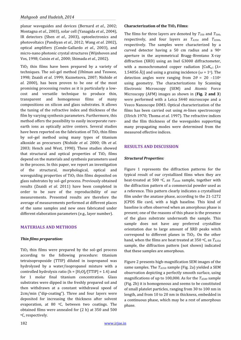
Structural Properties:
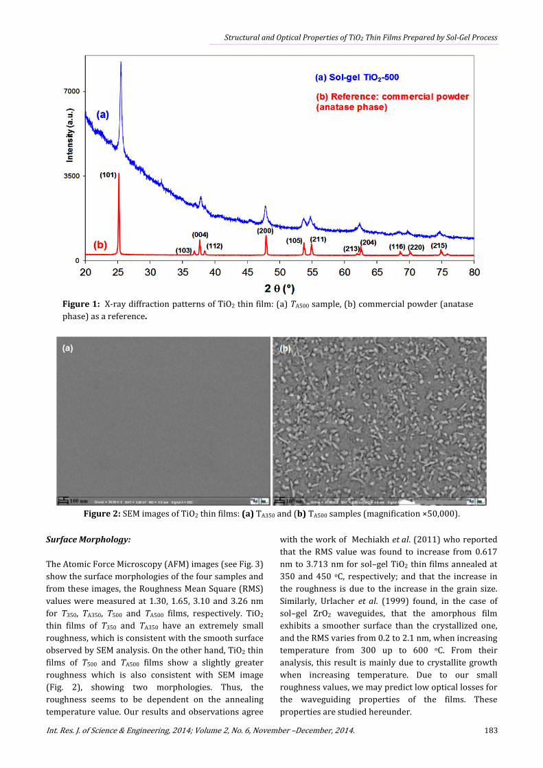
Figure 1 represents the diffraction patterns for the typical result of our crystallized films when they are heat-treated at 500 oC, as TA500 sample, together with the diffraction pattern of a commercial powder used as a reference. This pattern clearly indicates a crystallized film under the anatase phase, according to the 21-1272 JCPDS file card, with a high baseline. This kind of baseline is often observed when an amorphous phase is present; one of the reasons of this phase is the presence of the glass substrate underneath the sample. This sample does not have any preferred crystalline orientation due to large amount of XRD peaks witch correspond to different planes in TiO2. On the other hand, when the films are heat treated at 350 oC, as TA350 sample, the diffraction pattern (not shown) indicated that these samples are amorphous. Figure 2 presents high-magnification SEM images of the same samples. The TA350 sample (Fig. 2a) yielded a SEM observation depicting a perfectly smooth surface, using magnifications of up to 100,000. As for the TA500 sample (Fig. 2b) it is homogeneous and seems to be constituted of small platelet particles, ranging from 30 to 100 nm in length, and from 10 to 20 nm in thickness, embedded in a continuous phase, which may be a rest of amorphous phase.
Structural and Optical Properties of TiO2 Thin Films Prepared by Sol-Gel Process
Int. Res. J. of Science & Engineering, 2014; Volume 2, No. 6, November –December, 2014. 183
Figure 1: X-ray diffraction patterns of TiO2 thin film: (a) TA500 sample, (b) commercial powder (anatase phase) as a reference.
Figure 2: SEM images of TiO2 thin films: (a) TA350 and (b) TA500 samples (magnification ×50,000).
Surface Morphology:
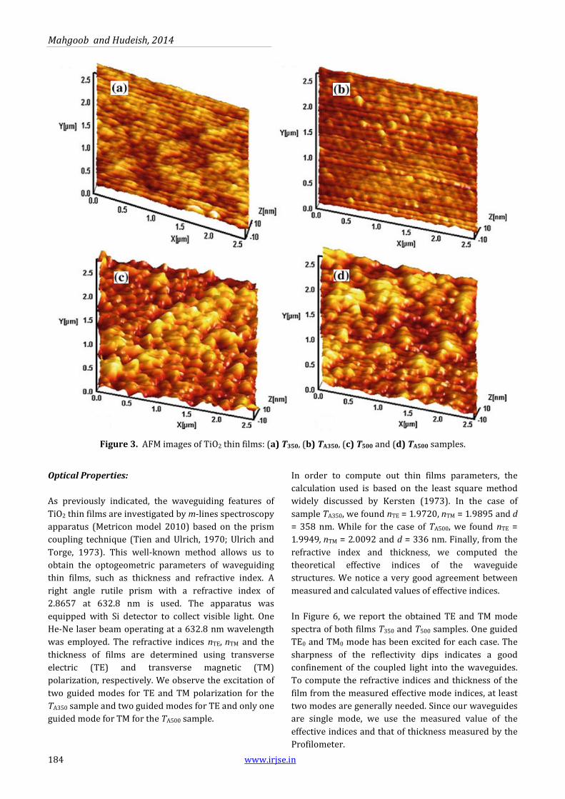
The Atomic Force Microscopy (AFM) images (see Fig. 3) show the surface morphologies of the four samples and from these images, the Roughness Mean Square (RMS) values were measured at 1.30, 1.65, 3.10 and 3.26 nm for T350, TA350, T500 and TA500 films, respectively. TiO2 thin films of T350 and TA350 have an extremely small roughness, which is consistent with the smooth surface observed by SEM analysis. On the other hand, TiO2 thin films of T500 and TA500 films show a slightly greater roughness which is also consistent with SEM image (Fig. 2), showing two morphologies. Thus, the roughness seems to be dependent on the annealing temperature value. Our results and observations agree
with the work of Mechiakh et al. (2011) who reported that the RMS value was found to increase from 0.617 nm to 3.713 nm for sol–gel TiO2 thin films annealed at 350 and 450 oC, respectively; and that the increase in the roughness is due to the increase in the grain size. Similarly, Urlacher et al. (1999) found, in the case of sol–gel ZrO2 waveguides, that the amorphous film exhibits a smoother surface than the crystallized one, and the RMS varies from 0.2 to 2.1 nm, when increasing temperature from 300 up to 600 oC. From their analysis, this result is mainly due to crystallite growth when increasing temperature. Due to our small roughness values, we may predict low optical losses for the waveguiding properties of the films. These properties are studied hereunder.
Mahgoob and Hudeish, 2014
184 www.irjse.in
Figure 3. AFM images of TiO2 thin films: (a) T350, (b) TA350, (c) T500 and (d) TA500 samples.
Optical Properties:
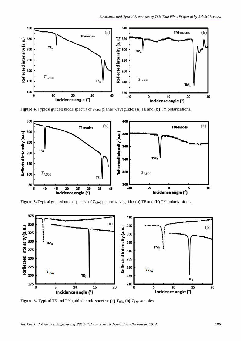
As previously indicated, the waveguiding features of TiO2 thin films are investigated by m-lines spectroscopy apparatus (Metricon model 2010) based on the prism coupling technique (Tien and Ulrich, 1970; Ulrich and Torge, 1973). This well-known method allows us to obtain the optogeometric parameters of waveguiding thin films, such as thickness and refractive index. A right angle rutile prism with a refractive index of 2.8657 at 632.8 nm is used. The apparatus was equipped with Si detector to collect visible light. One He-Ne laser beam operating at a 632.8 nm wavelength was employed. The refractive indices nTE, nTM and the thickness of films are determined using transverse electric (TE) and transverse magnetic (TM) polarization, respectively. We observe the excitation of two guided modes for TE and TM polarization for the TA350 sample and two guided modes for TE and only one guided mode for TM for the TA500 sample.
In order to compute out thin films parameters, the calculation used is based on the least square method widely discussed by Kersten (1973). In the case of sample TA350, we found nTE = 1.9720, nTM = 1.9895 and d = 358 nm. While for the case of TA500, we found nTE = 1.9949, nTM = 2.0092 and d = 336 nm. Finally, from the refractive index and thickness, we computed the theoretical effective indices of the waveguide structures. We notice a very good agreement between measured and calculated values of effective indices. In Figure 6, we report the obtained TE and TM mode spectra of both films T350 and T500 samples. One guided TE0 and TM0 mode has been excited for each case. The sharpness of the reflectivity dips indicates a good confinement of the coupled light into the waveguides. To compute the refractive indices and thickness of the film from the measured effective mode indices, at least two modes are generally needed. Since our waveguides are single mode, we use the measured value of the effective indices and that of thickness measured by the Profilometer.
Structural and Optical Properties of TiO2 Thin Films Prepared by Sol-Gel Process
Int. Res. J. of Science & Engineering, 2014; Volume 2, No. 6, November –December, 2014. 185
Figure 4. Typical guided mode spectra of TA350 planar waveguide: (a) TE and (b) TM polarizations.
Figure 5. Typical guided mode spectra of TA500 planar waveguide: (a) TE and (b) TM polarizations.
Figure 6. Typical TE and TM guided mode spectra: (a) T350, (b) T500 samples.
Mahgoob and Hudeish, 2014
186 www.irjse.in
The thickness of the T350 and T500 samples was measured to be about of 284 and 204 nm, respectively. The thickness measurements of both samples by an Alpha-Step IQ Profilometer. In order to evaluate the accuracy of the refractive index values obtained from experimental measurements, we have first used the values of 280 and 200 nm for film thicknesses and the measured effective indices in the guided mode dispersion equation. Then, the calculations were
repeated assuming a variation of ±5 nm on the thickness of the synthesized films. After an errors’ analysis, the computed refractive indices are found to
be nTE = 1.9798 ± 0.0036, nTM = 2.0043 ± 0.0068 for the
T350 sample and nTE = 2.0063 ± 0.007, nTM = 2.0222 ± 0.016 for the T500 sample. The refractive indices and thickness of the TiO2 thin films samples so obtained by modal and Profilometry measurements are reported in Table 1.
The results show that refractive index increases with annealing temperature while thickness decreases due to shrinkage and densification of the films (Keddie et
al., 1994). These results are in good agreement with the work of (Wang and Hu, 2006) who found, in the case of sol–gel TiO2 waveguides, that the film thickness decreases and the refractive index increases when the heat treatment temperature increases. Urlacher et al. (1999) reported, in the case of ZrO2 film, that the thickness roughly decreases between 300 and 400 oC indicating a high densification of the layer before crystallization. Refractive index simultaneously increases because of densification, organic compound removal and structural change in the material. Bedu et
al. (2010) also reported that the sol–gel TiO2 or ZrO2 films with refractive indices in the 1.7–2.1 range were obtained by varying the annealing conditions.
Table 1: Measured (Nmexp.) and computed (Nmth.) effective mode indices; and films characteristics deduced
from measurements.
Sample Pol. m Nmexp. Nmth. ∆∆∆∆Nm n d (nm)
TA350
TE 0 1.8687 1.8685 2×10⁻⁴ 1.9720 358 TE 1 1.5664 1.5659 5×10⁻⁴ TM 0 1.8444 1.8442 2×10⁻⁴ 1.9895 TM 1 1.5135 1.5134 1×10⁻⁴
TA500
TE 0 1.8816 1.8814 2×10⁻⁴ 1.9949 336 TE 1 1.5532 1.5527 5×10⁻⁴ TM 0 1.8479 1.8475 4×10⁻⁴ 2.0092
T350 TE 0 1.8345 − − 1.9798 280
TM 0 1.7876 − − 2.0043
T500 TE 0 1.7848 − − 2.0063 200
TM 0 1.6782 − − 2.0222
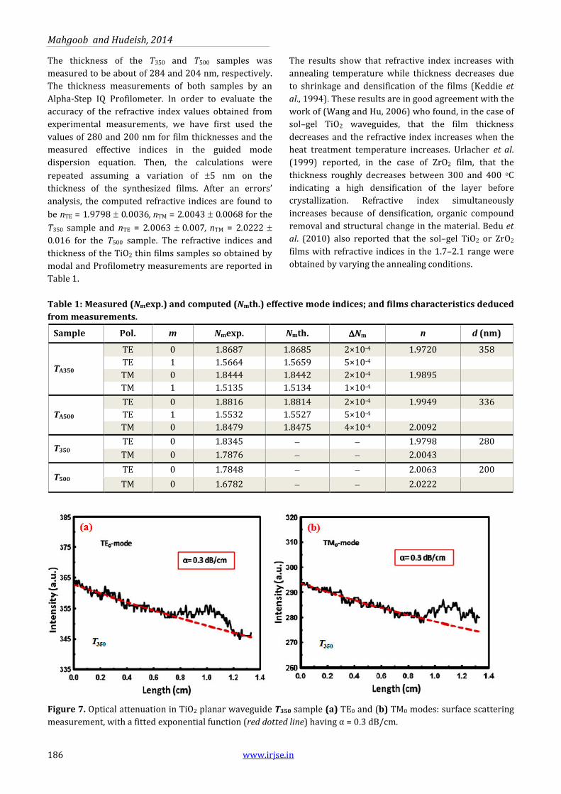
Figure 7. Optical attenuation in TiO2 planar waveguide T350 sample (a) TE0 and (b) TM0 modes: surface scattering measurement, with a fitted exponential function (red dotted line) having α = 0.3 dB/cm.
Structural and Optical Properties of TiO2 Thin Films Prepared by Sol-Gel Process
Int. Res. J. of Science & Engineering, 2014; Volume 2, No. 6, November –December, 2014. 187
The sharpness of the reflectivity dips, observed on Figs. 4, 5 and 6, indicates a good optical confinement of the light beam into the thin film waveguide structures. Measurements of the losses will bring more insight about this point. Indeed, the determination of optical attenuation in waveguides is of great interest for designing integrated optical devices. Practical use of such structures directly depends on the measurement of this parameter. Several techniques have been used for loss measurement among which the end-fire coupling (Strohkendl et al. 1991), the prism coupling method (Weber et al., 1973), and a new approach that uses a prism in coupling method to feed the light into the waveguide and the end-fire coupling to measure the transmitted light (Boudrioua and Loulergue 1997). For optical losses measurements, we used the same m-line apparatus. In order to measure propagation losses the light intensity scattered out of the waveguide plane, which is proportional to the guided intensity, was recorded by a fiber probe scanning down the length of the propagation streak. The losses were evaluated by fitting the intensity to an exponential decay function, assuming a homogenous distribution of the scattering centers in the waveguide, and the loss is calculated in dB/cm. The total loss of a planar waveguide consists of absorption and scattering contributions. The scattering optical loss measured for an amorphous waveguide is the sum of two contributions: volume scattering, due to local fluctuation in the refractive index resulting from density variation, and surface scattering due to surface roughness. The measurements were performed by exciting both the transverse electric TE0 and transverse magnetic TM0 mode of the T350 planar waveguide sample, and the TE0 mode of TA350 and TA500 planar waveguide samples, respectively.
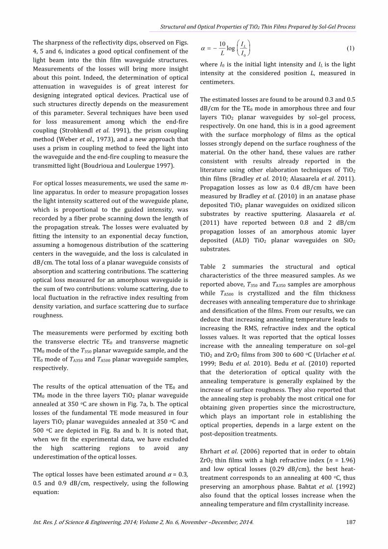
The results of the optical attenuation of the TE0 and TM0 mode in the three layers TiO2 planar waveguide annealed at 350 oC are shown in Fig. 7a, b. The optical losses of the fundamental TE mode measured in four layers TiO2 planar waveguides annealed at 350 oC and 500 oC are depicted in Fig. 8a and b. It is noted that, when we fit the experimental data, we have excluded the high scattering regions to avoid any underestimation of the optical losses. The optical losses have been estimated around α = 0.3,
0.5 and 0.9 dB/cm, respectively, using the following equation:
(1) log10
0
−=
I
I
L
Lα
where I0 is the initial light intensity and IL is the light intensity at the considered position L, measured in centimeters. The estimated losses are found to be around 0.3 and 0.5 dB/cm for the TE0 mode in amorphous three and four layers TiO2 planar waveguides by sol–gel process, respectively. On one hand, this is in a good agreement with the surface morphology of films as the optical losses strongly depend on the surface roughness of the material. On the other hand, these values are rather consistent with results already reported in the literature using other elaboration techniques of TiO2 thin films (Bradley et al. 2010; Alasaarela et al. 2011). Propagation losses as low as 0.4 dB/cm have been measured by Bradley et al. (2010) in an anatase phase deposited TiO2 planar waveguides on oxidized silicon substrates by reactive sputtering. Alasaarela et al. (2011) have reported between 0.8 and 2 dB/cm propagation losses of an amorphous atomic layer deposited (ALD) TiO2 planar waveguides on SiO2 substrates. Table 2 summaries the structural and optical characteristics of the three measured samples. As we reported above, T350 and TA350 samples are amorphous while TA500 is crystallized and the film thickness decreases with annealing temperature due to shrinkage and densification of the films. From our results, we can deduce that increasing annealing temperature leads to increasing the RMS, refractive index and the optical losses values. It was reported that the optical losses increase with the annealing temperature on sol–gel TiO2 and ZrO2 films from 300 to 600 oC (Urlacher et al. 1999; Bedu et al. 2010). Bedu et al. (2010) reported that the deterioration of optical quality with the annealing temperature is generally explained by the increase of surface roughness. They also reported that the annealing step is probably the most critical one for obtaining given properties since the microstructure, which plays an important role in establishing the optical properties, depends in a large extent on the post-deposition treatments. Ehrhart et al. (2006) reported that in order to obtain ZrO2 thin films with a high refractive index (n = 1.96) and low optical losses (0.29 dB/cm), the best heat-treatment corresponds to an annealing at 400 oC, thus preserving an amorphous phase. Bahtat et al. (1992) also found that the optical losses increase when the annealing temperature and film crystallinity increase.
Mahgoob and Hudeish, 2014
188 www.irjse.in
Figure 8. Optical attenuation of the fundamental TE mode in TiO2 planar waveguide (a) TA350 and (b) TA500 samples: surface scattering measurement, with a fitted exponential function (red dotted line) having α = 0.5 and 0.9 dB/cm, respectively.
Table 2: Comparison of films characteristics.
Sample H.T.T
(oC) Structure
Thickness:
d (nm)
RMS
(nm)
Refractive
index: n
Attenuation: α
(dB/cm)
T350 350 Amorphous 280 1.30 1.9798 0.3±0.1
TA350 350 Amorphous 358 1.65 1.9720 0.5±0.1
TA500 500 Crystallized 336 3.26 1.9949 0.9±0.1
They obtained 0.8 and 2.5 dB/cm as attenuation coefficients for ZrO2 monomode amorphous film heat-treated at 300 oC and the crystallized waveguide annealed at 600 oC, respectively. They found that at lower temperatures (450 oC), the films’ structure consists of a mixture of amorphous TiO2 and anatase nanocrystals and its surface is smooth. On the contrary, when increasing the annealing temperature, the nanocrystals grow and the films waveguiding properties disappear. They reported that a high degree of crystallization induces an important porosity, a rough surface and thus dramatically affects the films’ waveguiding properties. Finally, it should be noted that the measured optical thin films parameters have been used to study the optical band structure of photonic crystal (PhC) structures in the sol–gel TiO2 thin films. The plane wave expansion (Ho et al., 1990; Johnson and Joannopoulos, 2001) and the finite differential time domain (FDTD) (Yee, 1966; Yablonovitch et al., 1991) methods are utilized to investigate the light propagation property in the PhC slab. The preliminary obtained results are promising to go for further investigations.
CONCULSION
In this work, we reported the investigation of TiO2 thin films prepared by sol–gel method for optical waveguiding applications. The effect of annealing temperature on the structure and the optical properties is studied. The optical properties determined by m-lines spectroscopy are promising for further waveguiding applications. The fabricated planar waveguides are supporting single and multi-well guided modes meaning that the coupling and confinement of the light in the film is efficient. The results show that the refractive index increases with annealing temperature, while thickness decreases due to shrinkage and higher densification of the films. The optical losses of the amorphous planar waveguides, annealed at 350 oC, and the crystallized waveguides, annealed at 500 oC, were estimated to be around 0.3, 0.5 and 0.9 dB/cm, respectively, from surface scattering measurement using an m-lines apparatus based on the prism coupling technique. This work emphasizes the importance of the film microstructure determination and clearly shows the correlation between structural characteristics and optical properties. The low optical
Structural and Optical Properties of TiO2 Thin Films Prepared by Sol-Gel Process
Int. Res. J. of Science & Engineering, 2014; Volume 2, No. 6, November –December, 2014. 189
losses and the surface morphologies observed by SEM and AFM have put into evidence that the quality of the films synthesized by sol–gel process is well adapted to the waveguiding applications. Work is under progress to improve and reproduce high-quality TiO2 sol–gel thin films by optimizing the synthesis parameters of the process in order to achieve low optical losses at high heat treatment temperatures.
REFERENCES
1. Alasaarela T, Korn D, Alloatti L, Säynätjoki A, Tervonen A, Palmer R, Leuthold J, Freude W, Honkanen S. Reduced propagation loss in silicon strip and slot waveguides coated by atomic layer deposition. Opt. Exp., 2011; 19 (12): 11529-11538.
2. Bahtat M, Mugnier J, Liren L, Serughetti J. Planar TiO2 waveguides by the sol–gel process: the relationship of structure to properties. Proc. SPIE, 1992; 1758: 173-176.
3. Bedu M, Sagarzazu G, Gacoin T, Audebert P, Weisbuch C, Martinelli L. Sol–gel planar waveguides for improved fluorescence microarrays. Thin Solid Films, 2010; 518 (15): 4450–4457.
4. Bernard C, Chaussedent S, Monteil A, Ferrari M. Molecular dynamics simulation of an Er-activated silica-titania glass: composition influence on the structural properties. Philos. Mag. B, 2002; 82 (10): 681–693.
5. Boudrioua A, Loulergue JC. New approach for loss measurements in optical planar waveguides. Opt.
Commun, 1997; 137 (1): 37-40.
6. Bradley JDB, Evans CC, Parsy F, Phillips KC, Senaratne R, Marti E, Mazur E. Low-loss TiO2 planar waveguides for nanophotonic applications. In: 23rd Annual Meeting of the IEEE Photonics Society, pp. 313–314, Denver, CO. 2010; [ISBN 978-1-4244-5368-9].
7. Brudnik A, Cztemastek H, Zakrzewska K, Jachimowski M. Plasma-emission-controlled d.c. magnetron sputtering of TiO2−x thin films. Thin Solid Films, 1991; 199 (1): 45–58.
8. Conde-Gallardo A, García-Rocha M, Palomino-Merino R, Velásquez-Quesada MP, Hernández-Calderón I, Photoluminescence properties of Tb+3 and Eu+3 ions hosted in TiO2 matrix. Appl. Surf. Sci. 2003; 212–213: 583–588.
9. Cuisin C, Chelnokov A, Lourtioz J-M, Decanini D, Chen Y. Fabrication of three-dimensional photonic structures with submicrometer resolution by X-ray lithography. J.
Vac. Sci. Technol. B, 2000; 18 (6): 3505–3509.
10. Ehrhart G, Capoen B, Robbe O, Boy P, Turrell S, Bouazaoui M, Structural and optical properties of n-propoxide sol–gel derived ZrO2 thin films. Thin Solid
Films, 2006; 496 (2): 227–233.
11. Garzella C, Comini E, Tempesti E, Frigeri C, Sberveglieri G. TiO2 thin films by a novel sol–gel processing for gas sensor applications. Sens. Actuators B: Chem., 2000; 68 (1-3): 189–196.
12. Hench LL, West JK. The sol–gel process. Chem. Rev., 1990; 90 (1): 33–72.
13. Ho KM, Chan CT, Soukoulis CM. Existence of a photonic gap in periodic dielectric structures. Phys. Rev. Lett., 1990; 65 (25): 3152–3155.
14. Johnson SG, Joannopoulos JD. Block-iterative frequency-domain methods for Maxwell’s equations in a planewave basis. Opt. Exp., 2001; 8 (3): 173–190.
15. Keddie JL, Braun PV, Giannelis EP. Interrelation between densification, crystallization, and chemical evolution in sol–gel titania thin films. J. Am. Ceram. Soc., 1994; 77 (6): 1592–1596.
16. Kersten RTh, Numerical solution of the mode-equation of planar dielectric waveguides to determine their refractive index and thickness by means of a prism-film coupler. Opt. Com., 1973; 9 (4): 427–431.
17. Kuznetsova IN. Elaboration par procédé sol–gel de couches minces de TiO2 nanostructuré: caractérisations structurale et optique. Ph.D. Thesis, 2007; Université
Paris 13, France.
18. Mechiakh R, Ben Sedrine N, Ben Naceur J, Chtourou R. Elaboration and characterization of nanocrystalline TiO2 thin films prepared by sol–gel dip-coating. Surf. Coat.
Tech. 2011; 206 (2): 243-249.
19. Montagna M, Moser E, Visintain F, Ferrari M, Zampedri L, Martucci A, Guglielmi M, Ivanda M. Nucleation of titania nanocrystals in silica titania waveguides. J. Sol–Gel Sci.
Technol. 2003; 26 (1): 241–244.
20. Nishide T, Sato M, Hara H. Crystal structure and optical property of TiO2 gels and films prepared from Ti-edta complexes as titania precursors. J. Mater. Sci., 2000; 35 (2): 465–469.
21. Oh SH, Kim DJ, Hahn SH, Kim EJ. Comparison of optical and photocatalytic properties of TiO2 thin films prepared by electron-beam evaporation and sol–gel dip-coating. Mater. Lett., 2003; 57 (26-27): 4151–4155.
22. Pandiyan R, MicheliV, Ristic D, Bartali R, Pepponi G, Barozzi M, Gottardi G, Ferrari M, Laidani N. Structural and near-infra red luminescence properties of Nd-doped TiO2 films deposited by RF sputtering. J. Mater. Chem., 2012; 22 (42): 22424–22432.
23. San Vicente G, Morales A, Gutierrez MT. Preparation and characterization of sol–gel TiO2 antireflective coatings for silicon. Thin Solid Films, 2001; 391(1): 133–137.
24. Shen J, Yang T, Zhang Q, Wang J. Nanoporous TiO2 coatings for infrared detectors. J. Sol–Gel Sci. Technol. 2003; 26 (1-3): 1029–1032.
25. Shimada S, Miyazawa K, Kuwabara M. An easy method for fabricating TiO2 gel photonic crystals using molds and highly concentrated alkoxide solutions. Jpn. J. Appl. Phys. 2002; 41 (2): L291–L293.
26. Strohkendl FP, Fluck D, Günter P, Irmsher R, Buchal Ch. Nonleaky optical waveguides in KNbO3 by ultralow dose MeV He ion implantation. Appl. Phys. Lett. 1991; 59 (26): 3354–3356.
27. Thoma F, Langbein U, Mittler-Neher S. Waveguide scattering microscopy. Opt. Commun., 1997; 134 (1-6): 16–20.
28. Tien PK, Ulrich R. Theory of prism-film coupler and thin-film light guides. J. Opt. Soc. Am., 1970; 60 (10): 1325–1337.
29. Uhlman DR, Teowee G. Sol–gel science technology: current state and future prospects. J. Sol–Gel Sci. Technol. 1998; 13 (1): 153–162.
30. Ulrich R. Theory of the prism-film coupler by plane-wave analysis. J. Opt. Soc. Am., 1970; 60 (10): 1337–1350.
Mahgoob and Hudeish, 2014
190 www.irjse.in
31. Ulrich R. Torge R. Measurement of thin-film parameters with prism coupler. Appl. Opt., 1973; 12 (12): 2901–2908.
32. Urlacher C. Dumas J, Serughetti J, Mugnier J, Munoz M. Planar ZrO2 waveguides prepared by the sol–gel process: structural and optical properties. J. Sol–Gel Sci. Technol. 1999; 8 (6): 999–1005.
33. Wang B, Hu L. Optical and surface properties of hybrid TiO2/ormosil planar waveguide prepared by the sol–gel process. Ceram. Int., 2006; 32 (1): 7–12.
34. Wang Z, Helmerson U, Kall PO. Optical properties of anatase TiO2 thin films prepared by aqueous sol–gel process at low temperature. Thin Solid Films, 2002; 405 (1): 50–54.
35. Weber HP, Dunn FA, Leibolt WN. Loss measurements in thin-film optical waveguides. Appl. Opt. 1973; 12 (4): 755–757.
36. Wijnhoven JEGJ, Vos WL. Preparation of photonic crystals made of air spheres in titania. Science, 1998; 281 (5378): 802–804.
37. Wongcahree K, Brungs M, Chapline R, Hong Y, Pilar R, Sizgek E. Sol–gel processing by aging and pore creator addition for porous silica antireflective coatings. J. Sol–
Gel Sci. Technol. 2002; 25: 215–221.
38. Yablonovitch E, Gmitter TJ, Leung KM. Photonic band structure: the face-centered-cubic case employing nonspherical atoms. Phys. Rev. Lett., 1991; 67 (17): 2295–2298.
39. Yamasaki S, Hata N, Yoshida T, Oheda H, Matsuda A, Okushi H, Tanaka K. Annealing studies on low optical absorption of GD a-Si: H using photo-acoustic spectroscopy. J. Phys. Colloq. 1981; 42 (2): C4–297–C4-300.
40. Yanagida S, Senadeera GKR, Nakamura K, Kitamura T, Wada Y. Deposition of polyaniline via molecular self-assembly on TiO2 and its uses as a sensitizer in solid-state solar cells. J. Photochem. Photobiol. A, 2004; 164 (1-3): 61–66.
41. Yang L, Scott Saavedra S, Armstrong NR, Hayes J. Fabrication and characterization of low loss, sol–gel planar waveguides. Anal. Chem. 1994; 66 (8): 1254–1263.
42. Yee KS. Numerical solution of initial boundary value problems involving Maxwell’s equations in isotropic media. IEEE Trans. Antennas Propag. 1966; 14 (3): 302–307.
43. Znaidi L. Bocquet JF, Pommier C. Elaboration of TiO2 nanometric powders and thin films aerogels. In: AIDIC,
Selected Papers, Conference Series of ICheaP-4, 1999; 4 (1-2): 109–112.
44. Znaidi L, Seraphimova R, Bocquet JF, Colbeau-Justin C, Pommier C. A semi-continuous process for the synthesis of nanosize TiO2 powders and their use as photocatalysts. Mat. Res. Bull., 2001; 36 (5-6): 811–825.
45. Znaidi L, Touam T, Vrel D, Kunetsova IN, Fischer A, Boudrioua A. Waveguiding properties of nanostructured TiO2 thin films synthesized by sol–gel process. AIP Conf.
Proc. 2011; 1400: 268–273.
© 2014| Published by IRJSE
Copyright © 2022 FDOKUMEN