
Automatic Generation of Hardware/Software Interface with Product-Specific Debugging Tools
Upload
khangminh22Category
view
5download
0
PSIM-Based Hardware and
Software Design of an
Inverter-Fed Permanent Magnet Synchronous Motor
KJARTAN KRISTIANSEN
KNUT ERLEND STEINSLAND
SUPERVISOR
van Khang Huynh
University of Agder, 2018
Faculty of Engineering and Science

Abstract
The purpose of this research is to design a PSIM based controller for an inverter-fed Permanent MagnetSynchronous Motor (PMSM). The dimensioning and assembly of the controller are presented. The controlalgorithm used for the PMSM is Field Oriented Control (FOC). The report includes the theory of the controlalgorithm and its design. A PSIM based model is designed with the dimensioned components to analysethe behaviour of the controller. The model gives the opportunity of tuning the controller and verifying itwith simulations. The model is then converted to be SimCoder compatible, enabling the simulation to begenerated into a code. A Digital Signal Processing (DSP) development board is provided by Powersim Inc.The generated code is imported to the DSP, enabling it to run the controller. Similar behaviour is observedwhen comparing the test results with the simulations. When simulating the controller with the PMSM, allreference speeds are reached with a maximum deviation of ±0.42%. Using PSIM proved to be an intuitiveand educational way of designing the motor controller.
i

Preface
For this master’s thesis, we would like to express our greatest gratitude to van Khang Huynh for his knowl-edge, time, guidance, and assistance. We would also like to thank Milad Golzar and Flekkefjord Elektro ASfor their guidance and time in the field of electronics and components dimensioning. A special thanks toSteve Schading and Karl-Berge Rød for providing us with the necessary equipment, technical information,and assistance for this project.
University of Agder, Grimstad,Thursday 31st May, 2018
ii

Individual Declaration
The individual student or group of students is responsible for the use of legal tools, guidelines for using theseand rules on source usage. The statement will make the students aware of their responsibilities and theconsequences of cheating. Missing statement does not release students from their responsibility.
1.I hereby declare that my thesis is my own work and that I/We havenot used any other sources or have received any other help than mentioned inthe thesis.
X
2.
I further declare that this thesis:
- not been used for another exam at another department/university/universitycollege in Norway or abroad;
- does not refer to the work of others without it being stated;
- does not refer to own previous work without it being stated;
- have all the references given in the literature list;
- is not a copy, duplicate or copy of another’s work or manuscript.
X
3.
I am aware that violation of the above is regarded as cheating and mayresult in cancellation of exams and exclusion from universities and colleges inNorway, see Universitets- og høgskoleloven §§4-7 og 4-8 og Forskriftom eksamen §§ 31.
X
4. I am aware that all submitted theses may be checked for plagiarism. X
5.I am aware that the University of Agder will deal with all cases wherethere is suspicion of cheating according to the university’s guidelines for dealingwith cases of cheating.
X
6.I have incorporated the rules and guidelinesin the use of sources and references on the library’s web pages.
X
iii

Publishing Agreement
Authorization for electronic publishing ofthe thesis.
Author(s) have copyrights of the thesis.This means, among other things, the exclusive right to make the work availableto the general public (Åndsverkloven. §2).
All theses that fulfill the criteria willbe registered and published in Brage Aura and on UiA’s web pages with author’sapproval.
Theses that are not public or areconfidential will not be published.I hereby give the University of Agder a free right tomake the task available for electronic publishing:
Yes X
Is the thesis confidential?(confidential agreement must be completed)
No X
- If yes:Can the thesis be published when the confidentiality period is over?Is the task except for public disclosure?(contains confidential information. see Offl.§13/Fvl. §13)
No X
iv

Contents
Abstract i
Acknowledgements ii
Individual Declaration iii
Publishing Agreement iv
List of Figures x
List of Tables xi
1 Introduction 11.1 Motivation . . . . . . . . . . . . . . . . . . . . . . . . . . . . . . . . . . . . . . . . . . . . . . 11.2 Problem Statement . . . . . . . . . . . . . . . . . . . . . . . . . . . . . . . . . . . . . . . . . . 21.3 Report Outline . . . . . . . . . . . . . . . . . . . . . . . . . . . . . . . . . . . . . . . . . . . . 2
2 Permanent Magnet Synchronous Motor 32.1 Permanent Magnet Motors Overview . . . . . . . . . . . . . . . . . . . . . . . . . . . . . . . . 3
2.1.1 Induction Motor Comparison . . . . . . . . . . . . . . . . . . . . . . . . . . . . . . . . 42.2 PMSM Control Methods . . . . . . . . . . . . . . . . . . . . . . . . . . . . . . . . . . . . . . . 5
2.2.1 V/f Control . . . . . . . . . . . . . . . . . . . . . . . . . . . . . . . . . . . . . . . . . . 52.2.2 Field Oriented Control . . . . . . . . . . . . . . . . . . . . . . . . . . . . . . . . . . . . 6
3 Choice of Components 73.1 Rectifier . . . . . . . . . . . . . . . . . . . . . . . . . . . . . . . . . . . . . . . . . . . . . . . . 73.2 Filter . . . . . . . . . . . . . . . . . . . . . . . . . . . . . . . . . . . . . . . . . . . . . . . . . 83.3 Inverter and Gate Driver . . . . . . . . . . . . . . . . . . . . . . . . . . . . . . . . . . . . . . . 113.4 Cooling Element . . . . . . . . . . . . . . . . . . . . . . . . . . . . . . . . . . . . . . . . . . . 123.5 Current Sensors . . . . . . . . . . . . . . . . . . . . . . . . . . . . . . . . . . . . . . . . . . . . 123.6 Hardware Setup . . . . . . . . . . . . . . . . . . . . . . . . . . . . . . . . . . . . . . . . . . . . 13
4 Simulation Design 144.1 Rectifier . . . . . . . . . . . . . . . . . . . . . . . . . . . . . . . . . . . . . . . . . . . . . . . . 144.2 Filter . . . . . . . . . . . . . . . . . . . . . . . . . . . . . . . . . . . . . . . . . . . . . . . . . 164.3 Motor . . . . . . . . . . . . . . . . . . . . . . . . . . . . . . . . . . . . . . . . . . . . . . . . . 164.4 Motor Controller . . . . . . . . . . . . . . . . . . . . . . . . . . . . . . . . . . . . . . . . . . . 19
4.4.1 Measuring Motor Data . . . . . . . . . . . . . . . . . . . . . . . . . . . . . . . . . . . . 204.4.2 Reference Frame Transformation . . . . . . . . . . . . . . . . . . . . . . . . . . . . . . 204.4.3 Retrieving Electrical Angle . . . . . . . . . . . . . . . . . . . . . . . . . . . . . . . . . 234.4.4 Speed Controller . . . . . . . . . . . . . . . . . . . . . . . . . . . . . . . . . . . . . . . 244.4.5 Current Controller and Inverse Transformations . . . . . . . . . . . . . . . . . . . . . . 264.4.6 Controller Output . . . . . . . . . . . . . . . . . . . . . . . . . . . . . . . . . . . . . . 26
v

5 SimCoder 285.1 Encoder Conversion . . . . . . . . . . . . . . . . . . . . . . . . . . . . . . . . . . . . . . . . . 28
5.1.1 Angle Calculation . . . . . . . . . . . . . . . . . . . . . . . . . . . . . . . . . . . . . . 285.1.2 Speed Calculation . . . . . . . . . . . . . . . . . . . . . . . . . . . . . . . . . . . . . . 30
5.2 Analog / Digital Converter . . . . . . . . . . . . . . . . . . . . . . . . . . . . . . . . . . . . . 325.3 Pulse Width Modulation . . . . . . . . . . . . . . . . . . . . . . . . . . . . . . . . . . . . . . . 325.4 Motor Controller Overview . . . . . . . . . . . . . . . . . . . . . . . . . . . . . . . . . . . . . 335.5 Hardware Configuration . . . . . . . . . . . . . . . . . . . . . . . . . . . . . . . . . . . . . . . 34
6 Digital Signal Processing 356.1 Development Board . . . . . . . . . . . . . . . . . . . . . . . . . . . . . . . . . . . . . . . . . 356.2 Code Composer Studio . . . . . . . . . . . . . . . . . . . . . . . . . . . . . . . . . . . . . . . . 376.3 Current Sensor Calibration . . . . . . . . . . . . . . . . . . . . . . . . . . . . . . . . . . . . . 38
7 Hardware Configuration 407.1 Circuit Design . . . . . . . . . . . . . . . . . . . . . . . . . . . . . . . . . . . . . . . . . . . . 407.2 Gate Driver and Inverter Test Design . . . . . . . . . . . . . . . . . . . . . . . . . . . . . . . . 427.3 Rectifier and Filter Test Design . . . . . . . . . . . . . . . . . . . . . . . . . . . . . . . . . . . 43
8 Results 448.1 Hardware Setup . . . . . . . . . . . . . . . . . . . . . . . . . . . . . . . . . . . . . . . . . . . . 44
8.1.1 DSP and Gate Driver Test . . . . . . . . . . . . . . . . . . . . . . . . . . . . . . . . . 458.1.2 Inverter Test . . . . . . . . . . . . . . . . . . . . . . . . . . . . . . . . . . . . . . . . . 468.1.3 Rectifier and Filter Test . . . . . . . . . . . . . . . . . . . . . . . . . . . . . . . . . . . 478.1.4 NTC Bypass Circuit Test . . . . . . . . . . . . . . . . . . . . . . . . . . . . . . . . . . 48
8.2 Modelling of FOC-Based-PMSM . . . . . . . . . . . . . . . . . . . . . . . . . . . . . . . . . . 498.2.1 Case 1 (No-Load) . . . . . . . . . . . . . . . . . . . . . . . . . . . . . . . . . . . . . . . 498.2.2 Case 2 (Variable Speed) . . . . . . . . . . . . . . . . . . . . . . . . . . . . . . . . . . . 508.2.3 Case 3 (Full-Load) . . . . . . . . . . . . . . . . . . . . . . . . . . . . . . . . . . . . . . 51
9 Discussion 539.1 Hardware Setup . . . . . . . . . . . . . . . . . . . . . . . . . . . . . . . . . . . . . . . . . . . . 539.2 Modelling Discussion . . . . . . . . . . . . . . . . . . . . . . . . . . . . . . . . . . . . . . . . . 549.3 Future Work . . . . . . . . . . . . . . . . . . . . . . . . . . . . . . . . . . . . . . . . . . . . . 54
10 Conclusion 55
Appendix A Data Sheets 59A.1 Rectifier . . . . . . . . . . . . . . . . . . . . . . . . . . . . . . . . . . . . . . . . . . . . . . . . 59A.2 Capacitor . . . . . . . . . . . . . . . . . . . . . . . . . . . . . . . . . . . . . . . . . . . . . . . 62A.3 Inductor . . . . . . . . . . . . . . . . . . . . . . . . . . . . . . . . . . . . . . . . . . . . . . . . 66A.4 Inverter . . . . . . . . . . . . . . . . . . . . . . . . . . . . . . . . . . . . . . . . . . . . . . . . 67A.5 Gate Driver . . . . . . . . . . . . . . . . . . . . . . . . . . . . . . . . . . . . . . . . . . . . . . 71A.6 Gate Driver: Technical Description . . . . . . . . . . . . . . . . . . . . . . . . . . . . . . . . . 82A.7 Gate Driver: Tips and Tricks for RCIN and ITRIP . . . . . . . . . . . . . . . . . . . . . . . . 85
vi

A.8 Snubber . . . . . . . . . . . . . . . . . . . . . . . . . . . . . . . . . . . . . . . . . . . . . . . . 88A.9 Current Sensor . . . . . . . . . . . . . . . . . . . . . . . . . . . . . . . . . . . . . . . . . . . . 89A.10 NTC Thermistor . . . . . . . . . . . . . . . . . . . . . . . . . . . . . . . . . . . . . . . . . . . 93A.11 DSP Board . . . . . . . . . . . . . . . . . . . . . . . . . . . . . . . . . . . . . . . . . . . . . . 97A.12 ABB PMSM . . . . . . . . . . . . . . . . . . . . . . . . . . . . . . . . . . . . . . . . . . . . . 105A.13 F28035 Piccolo Microcontroller . . . . . . . . . . . . . . . . . . . . . . . . . . . . . . . . . . . 107
Appendix B Hardware Configuration 109B.1 Hardware Config, SCI Config and DSP Clock . . . . . . . . . . . . . . . . . . . . . . . . . . . 109
Appendix C Further Results 110
Appendix D Calculations and Excel Sheets 110D.1 ABB PMSM Calculations . . . . . . . . . . . . . . . . . . . . . . . . . . . . . . . . . . . . . . 110D.2 Calculations of Gate Driver Circuit Components . . . . . . . . . . . . . . . . . . . . . . . . . 111D.3 Transient Calculation . . . . . . . . . . . . . . . . . . . . . . . . . . . . . . . . . . . . . . . . 112

List of Figures
1 PMSM Illustration . . . . . . . . . . . . . . . . . . . . . . . . . . . . . . . . . . . . . . . . . . 32 Permanent Magnet Motors . . . . . . . . . . . . . . . . . . . . . . . . . . . . . . . . . . . . . 43 SPMSM (a) and IPMSM (b) . . . . . . . . . . . . . . . . . . . . . . . . . . . . . . . . . . . . 44 V/f Control System . . . . . . . . . . . . . . . . . . . . . . . . . . . . . . . . . . . . . . . . . 55 Field Oriented Control . . . . . . . . . . . . . . . . . . . . . . . . . . . . . . . . . . . . . . . . 66 Block Diagram of the System . . . . . . . . . . . . . . . . . . . . . . . . . . . . . . . . . . . . 77 Rectifier . . . . . . . . . . . . . . . . . . . . . . . . . . . . . . . . . . . . . . . . . . . . . . . . 78 Filter Test Circuit . . . . . . . . . . . . . . . . . . . . . . . . . . . . . . . . . . . . . . . . . . 89 ICP with and without NTC Thermistors . . . . . . . . . . . . . . . . . . . . . . . . . . . . . . 910 Output Voltage with and without NTC Thermistors . . . . . . . . . . . . . . . . . . . . . . . 1011 Relay Bypass Circuit . . . . . . . . . . . . . . . . . . . . . . . . . . . . . . . . . . . . . . . . . 1012 Inverter . . . . . . . . . . . . . . . . . . . . . . . . . . . . . . . . . . . . . . . . . . . . . . . . 1113 Gate Driver for the Inverter . . . . . . . . . . . . . . . . . . . . . . . . . . . . . . . . . . . . . 1114 Bootstrap Circuit . . . . . . . . . . . . . . . . . . . . . . . . . . . . . . . . . . . . . . . . . . . 1115 IGBT Illustration . . . . . . . . . . . . . . . . . . . . . . . . . . . . . . . . . . . . . . . . . . . 1116 Cooling Element for the Inverter . . . . . . . . . . . . . . . . . . . . . . . . . . . . . . . . . . 1217 Current Sensor . . . . . . . . . . . . . . . . . . . . . . . . . . . . . . . . . . . . . . . . . . . . 1218 Overview of Frequency Converter . . . . . . . . . . . . . . . . . . . . . . . . . . . . . . . . . . 1419 Input AC Voltage of Rectifier . . . . . . . . . . . . . . . . . . . . . . . . . . . . . . . . . . . . 1520 Output DC Voltage of Rectifier . . . . . . . . . . . . . . . . . . . . . . . . . . . . . . . . . . . 1521 Output DC Voltage Filter and Rectifier . . . . . . . . . . . . . . . . . . . . . . . . . . . . . . 1622 Rated Condition Graph for BSM100N-2250 . . . . . . . . . . . . . . . . . . . . . . . . . . . . 1723 Rated Conditions for 545 VDC Bus . . . . . . . . . . . . . . . . . . . . . . . . . . . . . . . . . 1824 Controllers in PSIM . . . . . . . . . . . . . . . . . . . . . . . . . . . . . . . . . . . . . . . . . 1925 Obtaining the Motor Speed . . . . . . . . . . . . . . . . . . . . . . . . . . . . . . . . . . . . . 2026 Transformation Blocks . . . . . . . . . . . . . . . . . . . . . . . . . . . . . . . . . . . . . . . . 2127 Reference Frames . . . . . . . . . . . . . . . . . . . . . . . . . . . . . . . . . . . . . . . . . . . 2128 Clarke Transformation Reference Frame . . . . . . . . . . . . . . . . . . . . . . . . . . . . . . 2229 Park Transformation . . . . . . . . . . . . . . . . . . . . . . . . . . . . . . . . . . . . . . . . . 2230 Electrical Angle . . . . . . . . . . . . . . . . . . . . . . . . . . . . . . . . . . . . . . . . . . . . 2331 Reference Speed . . . . . . . . . . . . . . . . . . . . . . . . . . . . . . . . . . . . . . . . . . . 2432 Speed Controller . . . . . . . . . . . . . . . . . . . . . . . . . . . . . . . . . . . . . . . . . . . 2533 Current Controller, Inverse Park, and SV PWM . . . . . . . . . . . . . . . . . . . . . . . . . . 2634 Output Control Signal . . . . . . . . . . . . . . . . . . . . . . . . . . . . . . . . . . . . . . . . 2735 Switching Frequency of an IGBT . . . . . . . . . . . . . . . . . . . . . . . . . . . . . . . . . . 2736 Speed Measurement Simulation . . . . . . . . . . . . . . . . . . . . . . . . . . . . . . . . . . . 2837 Encoder and Counter for SimCoder . . . . . . . . . . . . . . . . . . . . . . . . . . . . . . . . . 2838 SimCoder Angle Calculation . . . . . . . . . . . . . . . . . . . . . . . . . . . . . . . . . . . . . 2839 Quadrature Encoder Pulses . . . . . . . . . . . . . . . . . . . . . . . . . . . . . . . . . . . . . 2940 SimCoder Speed Calculation . . . . . . . . . . . . . . . . . . . . . . . . . . . . . . . . . . . . 3041 ∆X Pulse Compensation . . . . . . . . . . . . . . . . . . . . . . . . . . . . . . . . . . . . . . 31
viii
42 Speed Estimation with Low-Pass Filter . . . . . . . . . . . . . . . . . . . . . . . . . . . . . . . 3143 Simulation Input Current . . . . . . . . . . . . . . . . . . . . . . . . . . . . . . . . . . . . . . 3244 SimCoder Input Current . . . . . . . . . . . . . . . . . . . . . . . . . . . . . . . . . . . . . . . 3245 PWM Simulation Design . . . . . . . . . . . . . . . . . . . . . . . . . . . . . . . . . . . . . . . 3346 PWM SimCoder Design . . . . . . . . . . . . . . . . . . . . . . . . . . . . . . . . . . . . . . . 3347 SimCoder Design Overview . . . . . . . . . . . . . . . . . . . . . . . . . . . . . . . . . . . . . 3348 Hardware Configuration, SCI Configuration and DSP Clock . . . . . . . . . . . . . . . . . . . 3449 DSP Oscilloscope . . . . . . . . . . . . . . . . . . . . . . . . . . . . . . . . . . . . . . . . . . . 3450 DSP Development Board . . . . . . . . . . . . . . . . . . . . . . . . . . . . . . . . . . . . . . 3551 Development Board Connector Overview . . . . . . . . . . . . . . . . . . . . . . . . . . . . . . 3552 Current Sensor Input Connector J8 . . . . . . . . . . . . . . . . . . . . . . . . . . . . . . . . 3653 Encoder Connector J7 . . . . . . . . . . . . . . . . . . . . . . . . . . . . . . . . . . . . . . . . 3654 Encoder Connector J9 . . . . . . . . . . . . . . . . . . . . . . . . . . . . . . . . . . . . . . . . 3655 Encoder Connections . . . . . . . . . . . . . . . . . . . . . . . . . . . . . . . . . . . . . . . . . 3656 PWM Signal Output Connector . . . . . . . . . . . . . . . . . . . . . . . . . . . . . . . . . . . 3757 CCS Display . . . . . . . . . . . . . . . . . . . . . . . . . . . . . . . . . . . . . . . . . . . . . 3858 Current Calibration . . . . . . . . . . . . . . . . . . . . . . . . . . . . . . . . . . . . . . . . . 3959 System Diagram . . . . . . . . . . . . . . . . . . . . . . . . . . . . . . . . . . . . . . . . . . . 4060 Test Design of Gate Driver and Inverter . . . . . . . . . . . . . . . . . . . . . . . . . . . . . . 4261 Subcircuit of Gate Driver . . . . . . . . . . . . . . . . . . . . . . . . . . . . . . . . . . . . . . 4262 Rectifier and Filter Test Design . . . . . . . . . . . . . . . . . . . . . . . . . . . . . . . . . . . 4363 Hardware Setup . . . . . . . . . . . . . . . . . . . . . . . . . . . . . . . . . . . . . . . . . . . . 4464 Gate Driver Input PWM Signals HIN and LIN Simulation (Phase A) . . . . . . . . . . . . . . 4565 Gate Driver Input PWM Signals HIN and LIN Hardware (Phase A) . . . . . . . . . . . . . . 4566 Simulated Output Gate Driver Signal HO Referenced to VS (Phase A) . . . . . . . . . . . . . 4567 Hardware Output Gate Driver Signal HO Referenced to VS (Phase A) . . . . . . . . . . . . . 4568 HO and LO Referenced to COM (Phase A) . . . . . . . . . . . . . . . . . . . . . . . . . . . . 4669 Simulated HO Referenced to COM . . . . . . . . . . . . . . . . . . . . . . . . . . . . . . . . . 4670 IGBT Measurement . . . . . . . . . . . . . . . . . . . . . . . . . . . . . . . . . . . . . . . . . 4671 Simulated High IGBT Signals . . . . . . . . . . . . . . . . . . . . . . . . . . . . . . . . . . . . 4772 Hardware High IGBT Signal . . . . . . . . . . . . . . . . . . . . . . . . . . . . . . . . . . . . 4773 Simulation Results Rectifier and Filter . . . . . . . . . . . . . . . . . . . . . . . . . . . . . . . 4774 Output Voltage Signal without Filter . . . . . . . . . . . . . . . . . . . . . . . . . . . . . . . . 4875 Output Voltage Signal with Filter . . . . . . . . . . . . . . . . . . . . . . . . . . . . . . . . . 4876 NTC Signal Results . . . . . . . . . . . . . . . . . . . . . . . . . . . . . . . . . . . . . . . . . 4877 Motor Speed at Case 1 . . . . . . . . . . . . . . . . . . . . . . . . . . . . . . . . . . . . . . . . 4978 Deviation of Motor Speed at Case 1 . . . . . . . . . . . . . . . . . . . . . . . . . . . . . . . . 5079 Motor Speed at Case 2 . . . . . . . . . . . . . . . . . . . . . . . . . . . . . . . . . . . . . . . . 5080 Motor Speed at 83.78 rad
s . . . . . . . . . . . . . . . . . . . . . . . . . . . . . . . . . . . . . . 5181 Motor Speed at 167.55 rad
s . . . . . . . . . . . . . . . . . . . . . . . . . . . . . . . . . . . . . 5182 Motor Speed at 260.65 rad
s . . . . . . . . . . . . . . . . . . . . . . . . . . . . . . . . . . . . . 5183 Motor Speed at Case 3 . . . . . . . . . . . . . . . . . . . . . . . . . . . . . . . . . . . . . . . . 5184 Deviation of Motor Speed at Case 3 . . . . . . . . . . . . . . . . . . . . . . . . . . . . . . . . 52
ix

85 LO Referenced to COM (Phase A) . . . . . . . . . . . . . . . . . . . . . . . . . . . . . . . . . 11086 Hardware IGBT Low Signal . . . . . . . . . . . . . . . . . . . . . . . . . . . . . . . . . . . . . 110
x

List of Tables
1 Simulation Results . . . . . . . . . . . . . . . . . . . . . . . . . . . . . . . . . . . . . . . . . . 92 Components for the Frequency Converter . . . . . . . . . . . . . . . . . . . . . . . . . . . . . 133 Motor Parameters with 545 VDC Input . . . . . . . . . . . . . . . . . . . . . . . . . . . . . . . 194 PWM Connector Signals . . . . . . . . . . . . . . . . . . . . . . . . . . . . . . . . . . . . . . . 375 CCS Configuration . . . . . . . . . . . . . . . . . . . . . . . . . . . . . . . . . . . . . . . . . . 376 DSP Board Current Conversion . . . . . . . . . . . . . . . . . . . . . . . . . . . . . . . . . . . 387 Current Calibration Results . . . . . . . . . . . . . . . . . . . . . . . . . . . . . . . . . . . . . 398 Parameters Simulation Gate Driver . . . . . . . . . . . . . . . . . . . . . . . . . . . . . . . . . 439 Simulation and Hardware Comparison . . . . . . . . . . . . . . . . . . . . . . . . . . . . . . . 4810 Hardware Configuration . . . . . . . . . . . . . . . . . . . . . . . . . . . . . . . . . . . . . . . 10911 SCI Configuration . . . . . . . . . . . . . . . . . . . . . . . . . . . . . . . . . . . . . . . . . . 10912 DSP Clock . . . . . . . . . . . . . . . . . . . . . . . . . . . . . . . . . . . . . . . . . . . . . . 109
xi
1 Introduction
Permanent Magnet Synchronous Motors (PMSMs) have been widely used in traction, robotics, and au-tomotive applications due to the advancements and price drop of permanent magnet (PM) materials [1].Furthermore, it is effective in renewable energy applications such as wind turbines [2] and fuel cell vehicles[3]. PMSMs are starting to make an appearance in Full Electrical Vehicles (FEVs). The United StatesEnvironmental Protection Agency (EPA) reports that Tesla model 3 is using PMSMs instead of inductionmotors [4]. Some of the advantages of such changes in FEVs include a higher range of efficiency, high torqueand power per volume, compact design, and low maintenance cost [5]. In general, the PM technology ofthe motor results in a smooth torque production, which makes it suitable in high-performance applications[6].
Power electronics play a significant role in the performance of electric motors. Advances in power semicon-ductor devices, converter topologies, simulation methods, and control technologies have led to substantialprogress in power electronics in recent years [7]. Control technologies play a particularly big role regardingAC drives. Vector control or Field Oriented Control (FOC) is one of the essential innovations in AC motorswhich makes it possible to enhance control performance further [8]. According to Bose, applications such asmachine tools, servos, robotics and transportation drives are using the control method. He also states thatFOC will be universal for electric drives in the future [7].
This thesis describes a software and hardware controller design of an inverter-fed PMSM. This includesdimensioning, purchasing and assembling the necessary electrical components of the control design. Thethesis presents the simulation design needed for verification, and the control algorithm needed to run thePMSM. The control algorithm is converted into a code which is imported into a Digital Signal Processor(DSP). This makes it possible to run the control system through the DSP.
1.1 Motivation
The purpose of this work is to find a convenient and intuitive way of designing and running a PMSM.PSIM is a simulation software specifically designed for electric drives and power electronics and has beenproven effective for research purposes. Both Sira-Ramírez and Donsión uses the software to verify theircontrol schemes [9] [10]. Furthermore, PSIM is able to run motors with its SimCoder module coupled withDSP boards. Morkoç et al. implements this method to run a PMSM with a controller designed in PSIMand imported into a High Voltage Motor Control-PFC Kit [11]. Similar software is provided by Opal-RtTechnologies and Dspace, both of which is used for academic and commercial use. However, the software isin a higher price range than PSIM. In addition, PSIM introduces a more educational approach for the controldesign with the DSP development board and open system design, as opposed to the more fully assembledcontrollers provided by Opal-Rt and dSpace.
PSIM seems to be a good choice for designing and learning the theory of a motor controller due to itseducational approach in the software design and low price. This research investigates the use of PSIMfurther by designing a PSIM based PMSM controller and importing it into a DSP development board, bothprovided by Powersim Inc. Furthermore, the hardware of the controller is designed from the ground up as
1
opposed to purchasing it fully assembled. This makes it possible to to study and learn the principles of thecontroller while building it.
1.2 Problem Statement
The purpose of this thesis is to design a PSIM based controller of an inverter-fed PMSM and investigate itsbehaviour. The main focus will be on power electronics, simulation, and control theory. The project outputsand requirements are summarised below.
1. Determine the dimensions of the electric components needed to build a frequency converter by usingdata sheets and simulation. The converter should be able to run a 2 kW PMSM. Compare the simulationresults with the rated values of the PMSM to verify the components before purchase.
2. Create a PSIM based model of the frequency converter and the FOC design. Implement all the selectedcomponents in the model and tune the controller to run the PMSM.
3. Convert the model to make it compatible with SimCoder. In SimCoder, use the code generationfunction to obtain the code needed to run the control algorithm.
4. Assemble the dimensioned components. This includes the design of Printed Circuit Boards (PCBs)and soldering the necessary electronic components on the PCBs and veroboards.
5. Import the code into Code Composer Studio (CCS) to run the frequency converter through the DSPdevelopment board.
6. Run the selected Frequency converter with the designed controller through the DSP development board.Investigate the signals of the hardware and compare them with the simulation results.
1.3 Report Outline
The structure of the thesis is as follows. Section 2 presents an overview of the theory and behaviour of themotor. In addition, it addresses and discusses the different PMSMs and some of the control theories. Section3 presents the choice of components for the frequency converter. Section 4 discusses PSIM based model ofthe frequency converter and its control algorithm. Also, it describes the FOC theory along with the PSIMbased model to get a better understanding of the correlation between theory and simulation. Section 5 showsthe SimCoder conversion, while Section 6 describes the DSP development board and the necessary softwareneeded to run the hardware. Section 7 presents the hardware and test setups. Section 8 shows the results ofthe thesis and Section 9 discusses the results. Finally, Section 10 presents a conclusion for the report.
2

2 Permanent Magnet Synchronous Motor
Figure 1(a) shows the cross-section of a PMSM and illustrates the rotor, stator, permanent magnets, andstator windings. The permanent magnets and windings are on the rotor and the stator respectively. Theillustration in Figure 1(b) shows a two pole PMSM.
(a) Main Components (b) Windings and Magnetic Axis
Figure 1: PMSM Illustration [12] [6]
The motor torque of the motor is generated as a result of the relation between the magnetic field in the statorwindings and the permanent magnets. The motor will generate maximum torque when the angle betweenthe magnetic fields is 90°. Figure 1(b) illustrates this. The space vectors of the magnets on the rotor ~Br
and the stator winding current ~is are perpendicular to each other. The space vectors represent the peak ofthe magnetic field distribution and its position [6]. The windings in which the current Is is flowing throughare sinusoidal distributed. θm indicates the angle of the rotor flux density ~Br with respect to the a-axis.When the windings are as illustrated in Figure 1(b), the rotor will run in a counterclockwise direction. Themathematical expression of ~is is shown in (1) and (2) [6].
~is(t) = Is(t)∠θis(t) (1)
where:
θis(t) = θm(t) + 90° (2)
The motor generates maximum torque when ~is is (leading) perpendicular to ~Br. Regulating the ~is tomaintain the 90° lead to ~Br makes it possible to control the torque of the motor [6].
2.1 Permanent Magnet Motors Overview
Figure 2 shows an overview of permanent magnet machines. The two main permanent magnet electricmachines are Permanent Magnet DC (PMDC) and Permanent Magnet AC (PMAC) machines. The PMDC
3
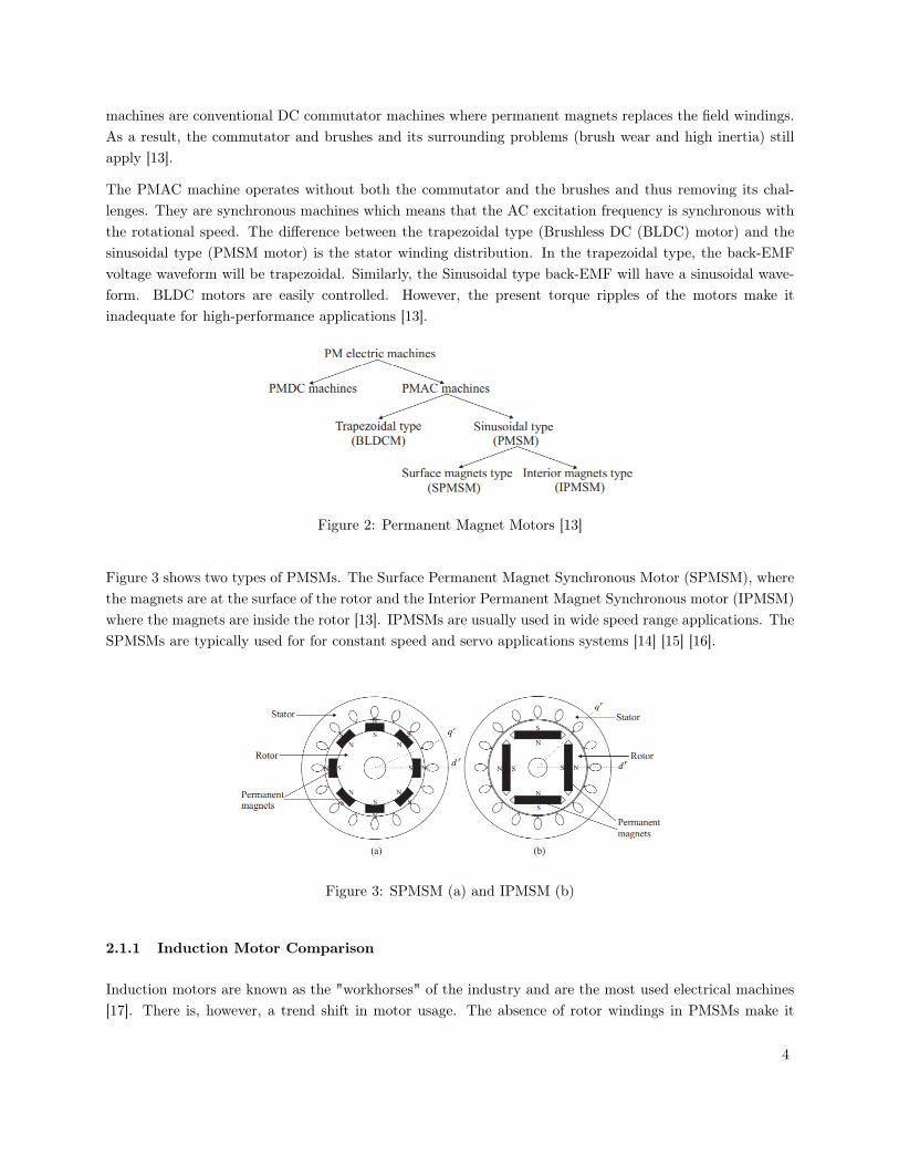
machines are conventional DC commutator machines where permanent magnets replaces the field windings.As a result, the commutator and brushes and its surrounding problems (brush wear and high inertia) stillapply [13].
The PMAC machine operates without both the commutator and the brushes and thus removing its chal-lenges. They are synchronous machines which means that the AC excitation frequency is synchronous withthe rotational speed. The difference between the trapezoidal type (Brushless DC (BLDC) motor) and thesinusoidal type (PMSM motor) is the stator winding distribution. In the trapezoidal type, the back-EMFvoltage waveform will be trapezoidal. Similarly, the Sinusoidal type back-EMF will have a sinusoidal wave-form. BLDC motors are easily controlled. However, the present torque ripples of the motors make itinadequate for high-performance applications [13].
Figure 2: Permanent Magnet Motors [13]
Figure 3 shows two types of PMSMs. The Surface Permanent Magnet Synchronous Motor (SPMSM), wherethe magnets are at the surface of the rotor and the Interior Permanent Magnet Synchronous motor (IPMSM)where the magnets are inside the rotor [13]. IPMSMs are usually used in wide speed range applications. TheSPMSMs are typically used for for constant speed and servo applications systems [14] [15] [16].
Figure 3: SPMSM (a) and IPMSM (b)
2.1.1 Induction Motor Comparison
Induction motors are known as the "workhorses" of the industry and are the most used electrical machines[17]. There is, however, a trend shift in motor usage. The absence of rotor windings in PMSMs make it
4
more efficient than induction motors due to the reduction of copper loss. In addition, it is possible to designPMSMs with lower weight and volume compared to the induction motors. Furthermore, the high torqueto inertia ratio makes it more suitable for high-performance applications [13]. One of the drawbacks of thePMSM motor has been the need of Variable Frequency Drives (VFD) to control the motor. VFDs are oftenused to increase the efficiency in induction motors [18]. Up until this point, the complex control system andVFD requirements prevented the use of PMSM in some applications. That said, new VFDs are availablewith inbuilt controllers as a standard feature, making it more attractive for use in industry [18].
2.2 PMSM Control Methods
V/f control and FOC are the main techniques applied for speed control in PMSM [13]. This section presentsa brief explanation and discussion of the two methods.
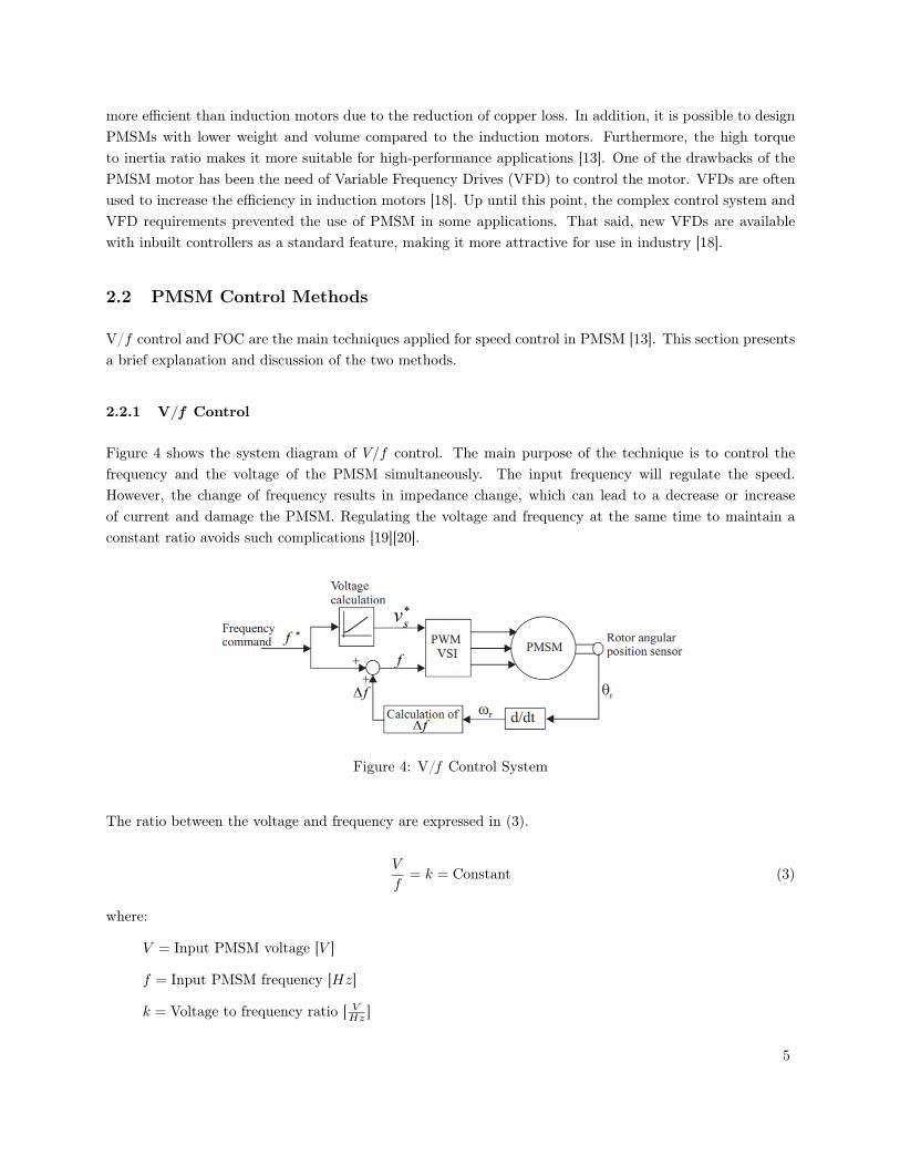
2.2.1 V/f Control
Figure 4 shows the system diagram of V/f control. The main purpose of the technique is to control thefrequency and the voltage of the PMSM simultaneously. The input frequency will regulate the speed.However, the change of frequency results in impedance change, which can lead to a decrease or increaseof current and damage the PMSM. Regulating the voltage and frequency at the same time to maintain aconstant ratio avoids such complications [19][20].
Figure 4: V/f Control System
The ratio between the voltage and frequency are expressed in (3).
V
f= k = Constant (3)
where:
V = Input PMSM voltage [V ]
f = Input PMSM frequency [Hz]
k = Voltage to frequency ratio [ VHz ]
5
A closed-loop system is necessary for the PMSM to be synchronous at all time. Obtaining the rotor positionof the PMSM will lead to synchronisation between AC excitation frequency and rotor frequency [13]. Theposition of the rotor θr is differentiated to obtain the speed of the motor. Furthermore, a comparison betweenthe calculated motor frequency ∆f and the reference frequency signal f∗ makes it possible to adjust thefrequency f and the voltage Vs∗. The Pulse Width Modulation (PWM) and Voltage Source Inversion (VSI)generate the signals.
2.2.2 Field Oriented Control
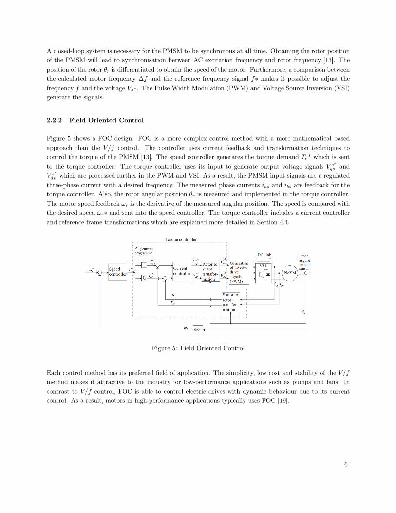
Figure 5 shows a FOC design. FOC is a more complex control method with a more mathematical basedapproach than the V/f control. The controller uses current feedback and transformation techniques tocontrol the torque of the PMSM [13]. The speed controller generates the torque demand Te* which is sentto the torque controller. The torque controller uses its input to generate output voltage signals V s
∗
qs andV s
∗
ds which are processed further in the PWM and VSI. As a result, the PMSM input signals are a regulatedthree-phase current with a desired frequency. The measured phase currents ias and ibs are feedback for thetorque controller. Also, the rotor angular position θr is measured and implemented in the torque controller.The motor speed feedback ωr is the derivative of the measured angular position. The speed is compared withthe desired speed ωr∗ and sent into the speed controller. The torque controller includes a current controllerand reference frame transformations which are explained more detailed in Section 4.4.
Figure 5: Field Oriented Control
Each control method has its preferred field of application. The simplicity, low cost and stability of the V/fmethod makes it attractive to the industry for low-performance applications such as pumps and fans. Incontrast to V/f control, FOC is able to control electric drives with dynamic behaviour due to its currentcontrol. As a result, motors in high-performance applications typically uses FOC [19].
6

3 Choice of Components
This section describes the frequency converter hardware. Furthermore, it describes the considerations andmethods taken into account in the dimensioning process. Figure 6 shows an overview over the design. Athree-phase power supplies the frequency converter (1). The rectifier (2) converts the AC power into to DCpower. The filter (3) are implemented smoothen the DC power. The inverter (4) will convert the DC powerback to AC power. However, the PSIM based control design (5) which is imported into the DSP (6) regulatesthe frequency of the inverter output power through the gate driver (7). Measuring the input current (8) andspeed of the motor (9) is required for the controller to work. The change in frequency in the inverter outputvoltage results in a change of speed in the motor (10).
Figure 6: Block Diagram of the System
3.1 Rectifier
The rectifier converts the AC voltage into DC voltage. Figure 7 shows the rectifier. The maximum voltageand maximum current of the rectifier were taken into account when dimensioning the component. The datasheet of the rectifier is available in [A.1].
Figure 7: Rectifier [21]
7

3.2 Filter
Figure 8 shows the simulation designed for filter dimensioning. The capacitor and inductor attenuatesthe output signal of the rectifier. The capacitor will reduce the voltage ripple and the inductance willsmoothen the current from the rectifier. The design includes a three-phase voltage source AC_source,rectifier, resistance R, inductor L, and capacitor C. The 100 Ω, 0.1 µF snubber limits dv
dt and didt , to protect
the components [22].
The DC bus capacitor C initially has no voltage across it. Therefore, the instant the voltage source is appliedto the system, a large current flows through rectifier to charge the capacitor [23]. This current is referredto as Inrush Current Peak (ICP). A 10 Ω Negative Temperature Coefficient (NTC) thermistors R_NTC isimplemented to reduce the ICP. The current probe, voltage sensor, and voltage probe measures the resultsof the simulation.
Figure 8: Filter Test Circuit
The voltage and current ripple of the filter based on the simulation results are calculated with (4) [24].
Percentage of voltage ripple =rms value of rippleAverage DC output
· 100 =sin(45°) · Vmax−Vmin
2
Vo· 100 (4)
where:
Vmax = Maximum output voltage [V]
Vmin = Minimum output voltage [V]
Vo = Average output voltage [V]
The 3900 µH inductor in the simulation design smoothens the current. Table 1 shows the results of thesimulations completed to determine the capacitor values. The NTC thermistors are not active at thisstage.
8
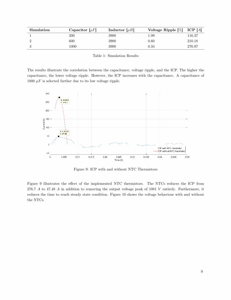
Simulation Capacitor [µF ] Inductor [µH] Voltage Ripple [%] ICP [A]1 200 3900 1.99 116.372 600 3900 0.60 210.183 1000 3900 0.34 276.97
Table 1: Simulation Results
The results illustrate the correlation between the capacitance, voltage ripple, and the ICP. The higher thecapacitance, the lower voltage ripple. However, the ICP increases with the capacitance. A capacitance of1000 µF is selected further due to its low voltage ripple.
Figure 9: ICP with and without NTC Thermistors
Figure 9 illustrates the effect of the implemented NTC thermistors. The NTCs reduces the ICP from276.7 A to 47.48 A in addition to removing the output voltage peak of 1081 V entirely. Furthermore, itreduces the time to reach steady state condition. Figure 10 shows the voltage behaviour with and withoutthe NTCs.
9
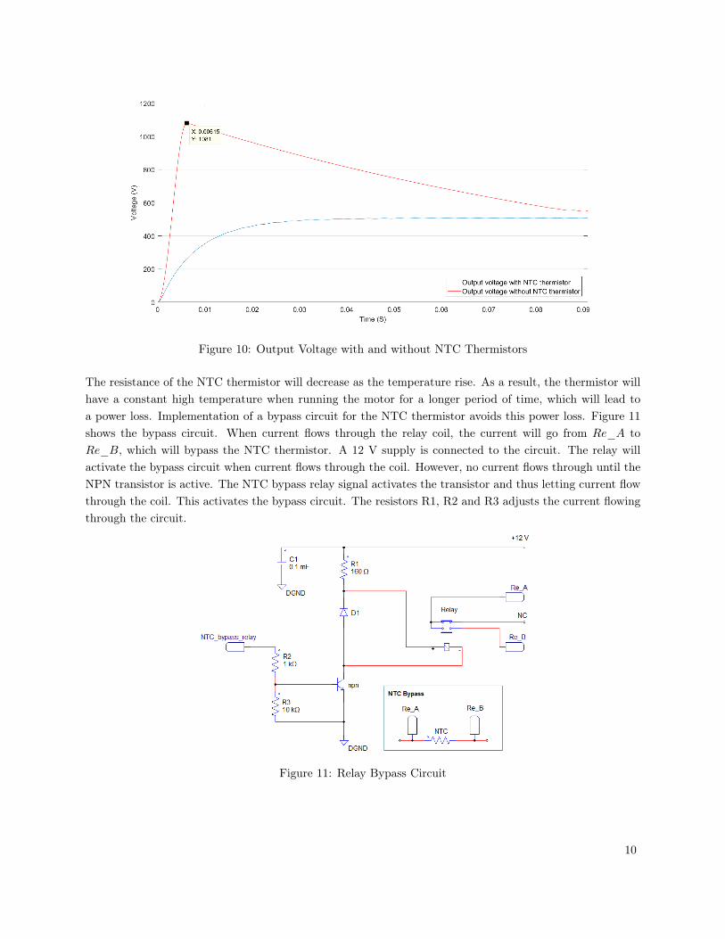
Figure 10: Output Voltage with and without NTC Thermistors
The resistance of the NTC thermistor will decrease as the temperature rise. As a result, the thermistor willhave a constant high temperature when running the motor for a longer period of time, which will lead toa power loss. Implementation of a bypass circuit for the NTC thermistor avoids this power loss. Figure 11shows the bypass circuit. When current flows through the relay coil, the current will go from Re_A toRe_B, which will bypass the NTC thermistor. A 12 V supply is connected to the circuit. The relay willactivate the bypass circuit when current flows through the coil. However, no current flows through until theNPN transistor is active. The NTC bypass relay signal activates the transistor and thus letting current flowthrough the coil. This activates the bypass circuit. The resistors R1, R2 and R3 adjusts the current flowingthrough the circuit.
Figure 11: Relay Bypass Circuit
10
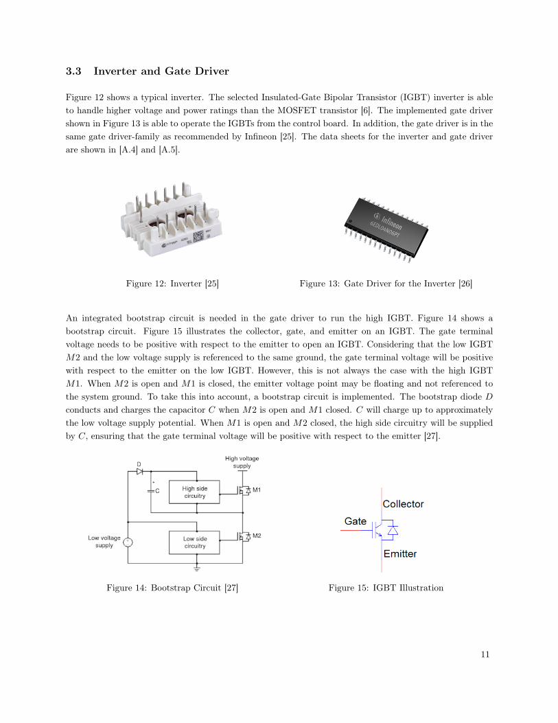
3.3 Inverter and Gate Driver
Figure 12 shows a typical inverter. The selected Insulated-Gate Bipolar Transistor (IGBT) inverter is ableto handle higher voltage and power ratings than the MOSFET transistor [6]. The implemented gate drivershown in Figure 13 is able to operate the IGBTs from the control board. In addition, the gate driver is in thesame gate driver-family as recommended by Infineon [25]. The data sheets for the inverter and gate driverare shown in [A.4] and [A.5].
Figure 12: Inverter [25] Figure 13: Gate Driver for the Inverter [26]
An integrated bootstrap circuit is needed in the gate driver to run the high IGBT. Figure 14 shows abootstrap circuit. Figure 15 illustrates the collector, gate, and emitter on an IGBT. The gate terminalvoltage needs to be positive with respect to the emitter to open an IGBT. Considering that the low IGBTM2 and the low voltage supply is referenced to the same ground, the gate terminal voltage will be positivewith respect to the emitter on the low IGBT. However, this is not always the case with the high IGBTM1. When M2 is open and M1 is closed, the emitter voltage point may be floating and not referenced tothe system ground. To take this into account, a bootstrap circuit is implemented. The bootstrap diode Dconducts and charges the capacitor C when M2 is open and M1 closed. C will charge up to approximatelythe low voltage supply potential. When M1 is open and M2 closed, the high side circuitry will be suppliedby C, ensuring that the gate terminal voltage will be positive with respect to the emitter [27].
Figure 14: Bootstrap Circuit [27] Figure 15: IGBT Illustration
11

3.4 Cooling Element
Under switching conditions, the inverter may reach temperatures up to 150°C. In addition, the temperatureunder the maximum current condition is 175°C. Such high temperatures will cause a power dissipation of 50W on the inverter [A.4].
Figure 16: Cooling Element for the Inverter [28]
Mounting a cooling element on the inverter reduces power dissipation. Figure 16 shows the selected coolingelement. The thermal resistance of the element is 1.5 K
W , meaning that a power dissipation of 50 W willheat the cooling element up to 75°C [28]. The calculation are shown in (5).
1.5K
W· 50 W = 1.5
°CW· 50 W = 75°C (5)
3.5 Current Sensors
Measuring the current going into the PMSM is crucial for controlling purposes. The frequency converterincludes two current sensors. The control design calculates the current of the third phase current. Thesensors has a nominal current of 6 A. However, they generate a proportional voltage of 2.5 ± 0.625 V asan output signal. The current sensor needs to be calibrated to take this into account. Figure 17 shows theselected sensor.
Figure 17: Current Sensor [29]
12

3.6 Hardware Setup
Table 2 shows the selected hardware parameters. Note that the data sheets defines the voltage as V DC,V AC, or V . The table presents the parameters the same way as the data sheets. The inductor, capacitor,and Negative Temperature Coefficient (NTC) thermistor are dimensioned with the help of PSIM simulations.The remaining parameters are obtained from the data sheets.
Component Vmax,c Vmax,p Imax,c Imax,p In L C Re Rt
Rectifier 600 725 25 360 - - - - -Inductor 760 - 8 - - 3.9 - - -Capacitor 400 440 3.38 - - - 1000 - -Inverter 600 - 10 20 - - - - -Gate Driver 600 - - - - - - - -Cooling Element - - - - - - - - 1.5Current Sensor 600 - - - 6 - - - -Snubber 1000 - 12 20 - - 0.1 100 -NTC Thermistor - - - - - - - 10 -
Table 2: Components for the Frequency Converter [A]
where:
Vmax,c = Maximum continuous voltage [V ]
Vmax,p = Maximum peak voltage [V ]
Imax,c = Maximum continuous current [A]
Imax,p = Maximum peak current [A]
In = Nominal current [A]
L = Inductance [mH]
C = Capacitance [µF ]
Re = Electrical resistance [Ω]
Rt = Thermal resistance [KW ]
13

4 Simulation Design
This section introduces the simulation design of the frequency converter. In addition, it describes thesimulation process and the function of the components.
Figure 18: Overview of Frequency Converter
Figure 18 shows an overview of a frequency converter. A three-phase AC power source (A) supplies theconverter. The rectifier (B) converts the voltage from AC to DC. Furthermore, the inductor and capacitorattenuates the voltage (C). The inverter (D) uses six IGBTs to convert the DC signal into an AC signal andsends it into the PMSM (E). The FOC (F) controls the frequency of the inverter (more on this in Section4.4).
4.1 Rectifier
The purpose of the rectifier is to convert the input voltage from AC to DC. The diodes processes a three-phase voltage input to convert the waveform to one constant polarity at its output. The rectifier outputvoltage is calculated in (6).
Vout =3 ·√
3 ·√
2
π· Vin ≈ 2.34 · Vin (6)
where:
Vout = Output voltage of rectifier (rms) [V]
Vin = Input voltage of rectifier (rms) [V]
14
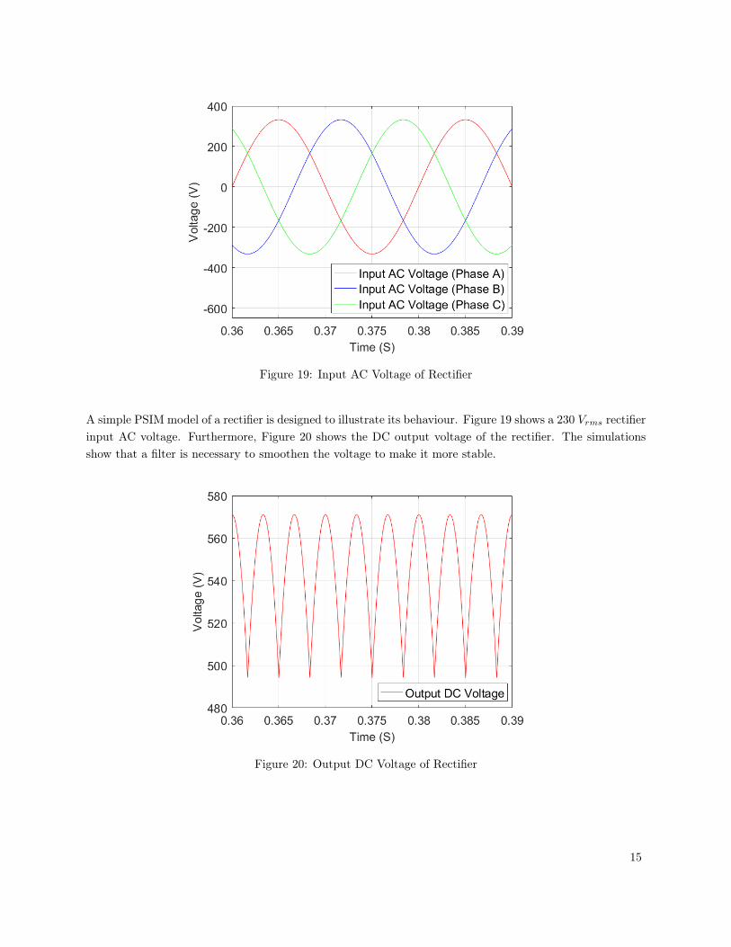
Figure 19: Input AC Voltage of Rectifier
A simple PSIM model of a rectifier is designed to illustrate its behaviour. Figure 19 shows a 230 Vrms rectifierinput AC voltage. Furthermore, Figure 20 shows the DC output voltage of the rectifier. The simulationsshow that a filter is necessary to smoothen the voltage to make it more stable.
Figure 20: Output DC Voltage of Rectifier
15
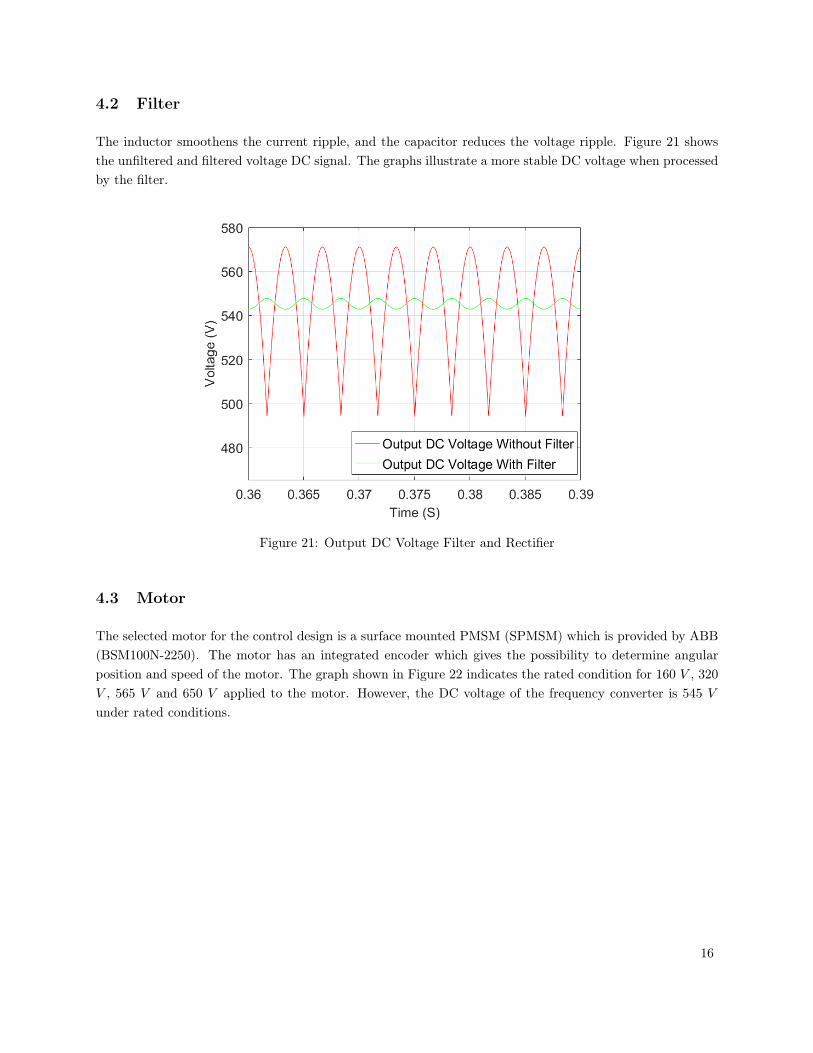
4.2 Filter
The inductor smoothens the current ripple, and the capacitor reduces the voltage ripple. Figure 21 showsthe unfiltered and filtered voltage DC signal. The graphs illustrate a more stable DC voltage when processedby the filter.
Figure 21: Output DC Voltage Filter and Rectifier
4.3 Motor
The selected motor for the control design is a surface mounted PMSM (SPMSM) which is provided by ABB(BSM100N-2250). The motor has an integrated encoder which gives the possibility to determine angularposition and speed of the motor. The graph shown in Figure 22 indicates the rated condition for 160 V , 320V , 565 V and 650 V applied to the motor. However, the DC voltage of the frequency converter is 545 Vunder rated conditions.
16
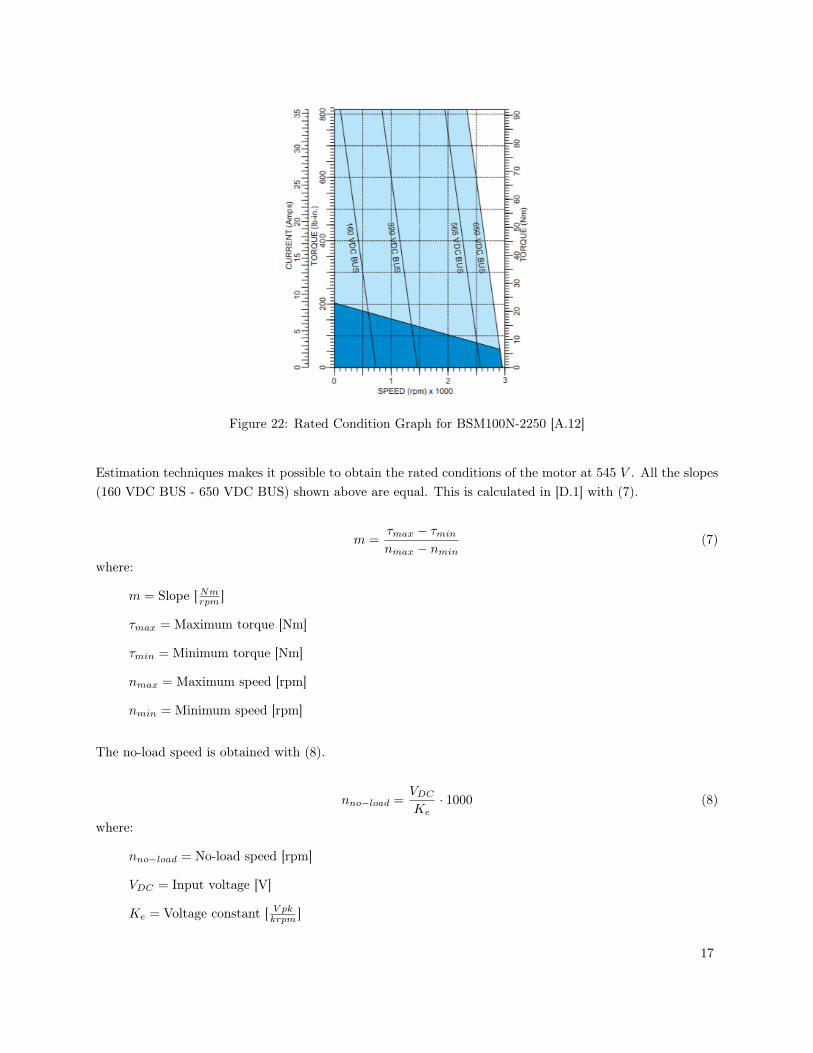
Figure 22: Rated Condition Graph for BSM100N-2250 [A.12]
Estimation techniques makes it possible to obtain the rated conditions of the motor at 545 V . All the slopes(160 VDC BUS - 650 VDC BUS) shown above are equal. This is calculated in [D.1] with (7).
m =τmax − τminnmax − nmin
(7)
where:
m = Slope [Nmrpm ]
τmax = Maximum torque [Nm]
τmin = Minimum torque [Nm]
nmax = Maximum speed [rpm]
nmin = Minimum speed [rpm]
The no-load speed is obtained with (8).
nno−load =VDCKe· 1000 (8)
where:
nno−load = No-load speed [rpm]
VDC = Input voltage [V]
Ke = Voltage constant [ V pkkrpm ]
17
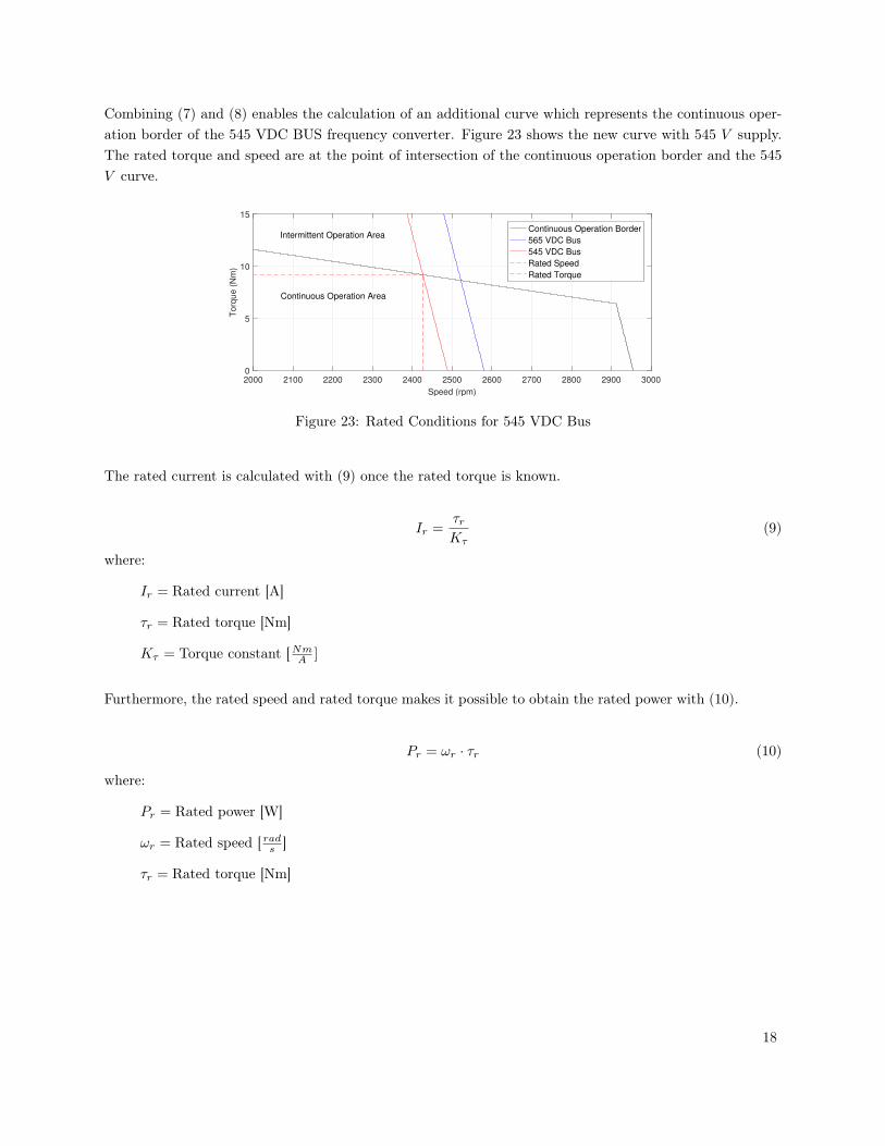
Combining (7) and (8) enables the calculation of an additional curve which represents the continuous oper-ation border of the 545 VDC BUS frequency converter. Figure 23 shows the new curve with 545 V supply.The rated torque and speed are at the point of intersection of the continuous operation border and the 545V curve.
2000 2100 2200 2300 2400 2500 2600 2700 2800 2900 3000
Speed (rpm)
0
5
10
15
Torq
ue (
Nm
)Continuous Operation Border
565 VDC Bus
545 VDC Bus
Rated Speed
Rated Torque
Intermittent Operation Area
Continuous Operation Area
Figure 23: Rated Conditions for 545 VDC Bus
The rated current is calculated with (9) once the rated torque is known.
Ir =τrKτ
(9)
where:
Ir = Rated current [A]
τr = Rated torque [Nm]
Kτ = Torque constant [NmA ]
Furthermore, the rated speed and rated torque makes it possible to obtain the rated power with (10).
Pr = ωr · τr (10)
where:
Pr = Rated power [W]
ωr = Rated speed [ rads ]
τr = Rated torque [Nm]
18

Table 3 shows the calculated rated parameters of the motor with the designed frequency converter.
Parameter Value Unit DescriptionVDC 545 V Input voltagePr 2.332 kW Rated powerτr 9.18 Nm Rated torqueIr 3.59 A Rated currentωr 254.05 rad
s Rated motor speedωmax 260.65 rad
s Maximum motor speed
Table 3: Motor Parameters with 545 VDC Input [A.12]
4.4 Motor Controller
Figure 24 shows an overview of the controllers designed in PSIM. This section describes the principles ofFOC and the simulation controller design.
Figure 24: Controllers in PSIM
Measuring the speed and input current of the motor (A) makes it possible to control the motor. The Clarkeand Park transformation (B) transforms the reference frame of the current. (C) converts the motor speedinto electric angle. Furthermore, (D) converts the reference motor speed into an equivalent current. The PIcontrollers in (E) regulate the current. (F) creates a PWM signal from the regulated current and sends itinto the inverter. Thus regulating the input frequency of the PMSM motor.
19
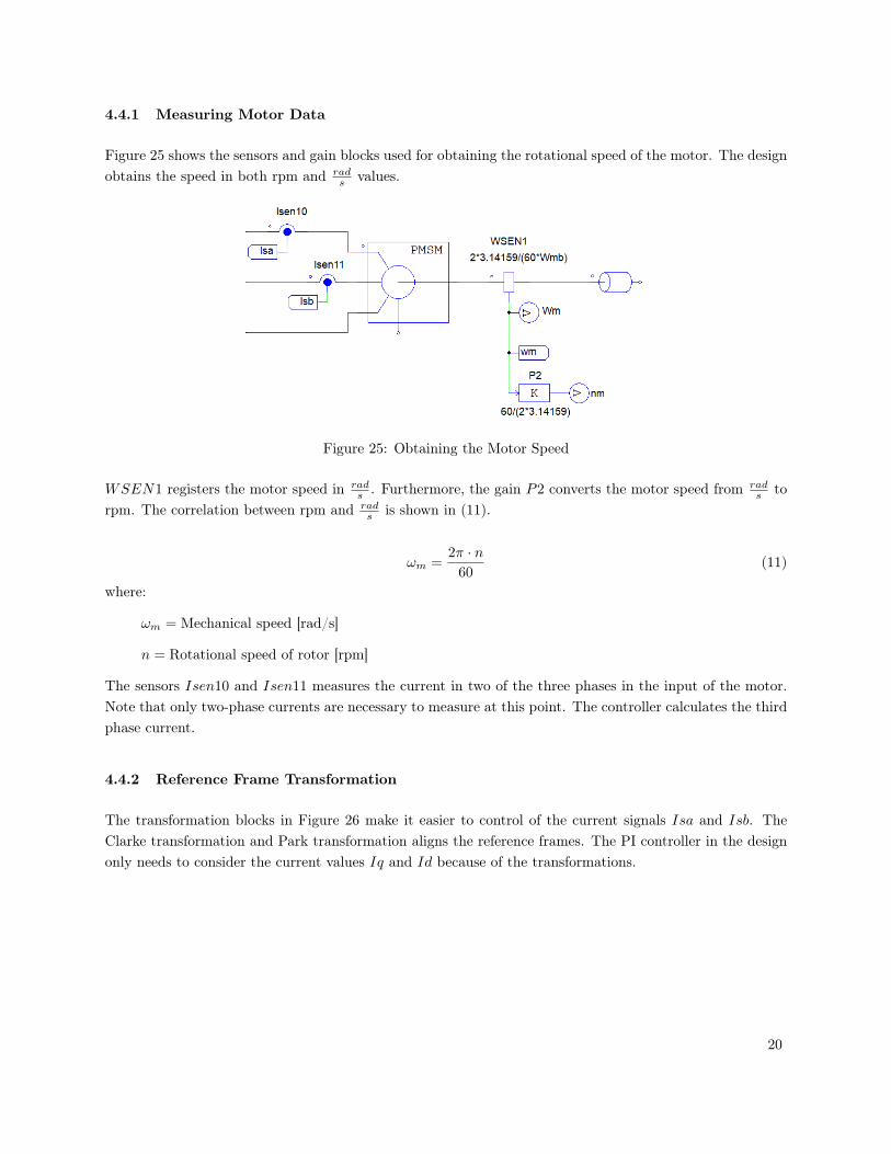
4.4.1 Measuring Motor Data
Figure 25 shows the sensors and gain blocks used for obtaining the rotational speed of the motor. The designobtains the speed in both rpm and rad
s values.
Figure 25: Obtaining the Motor Speed
WSEN1 registers the motor speed in rads . Furthermore, the gain P2 converts the motor speed from rad
s torpm. The correlation between rpm and rad
s is shown in (11).
ωm =2π · n
60(11)
where:
ωm = Mechanical speed [rad/s]
n = Rotational speed of rotor [rpm]
The sensors Isen10 and Isen11 measures the current in two of the three phases in the input of the motor.Note that only two-phase currents are necessary to measure at this point. The controller calculates the thirdphase current.
4.4.2 Reference Frame Transformation
The transformation blocks in Figure 26 make it easier to control of the current signals Isa and Isb. TheClarke transformation and Park transformation aligns the reference frames. The PI controller in the designonly needs to consider the current values Iq and Id because of the transformations.
20
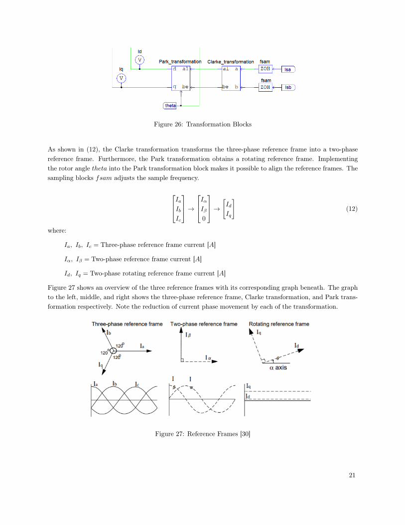
Figure 26: Transformation Blocks
As shown in (12), the Clarke transformation transforms the three-phase reference frame into a two-phasereference frame. Furthermore, the Park transformation obtains a rotating reference frame. Implementingthe rotor angle theta into the Park transformation block makes it possible to align the reference frames. Thesampling blocks fsam adjusts the sample frequency.
IaIbIc
→IαIβ
0
→ [Id
Iq
](12)
where:
Ia, Ib, Ic = Three-phase reference frame current [A]
Iα, Iβ = Two-phase reference frame current [A]
Id, Iq = Two-phase rotating reference frame current [A]
Figure 27 shows an overview of the three reference frames with its corresponding graph beneath. The graphto the left, middle, and right shows the three-phase reference frame, Clarke transformation, and Park trans-formation respectively. Note the reduction of current phase movement by each of the transformation.
Figure 27: Reference Frames [30]
21

Figure 28 illustrates the change in the reference frame during a Clarke transformation. The reference frameto the left shows the initial three-phase coordination of Ia, Ib, and Ic. The coordination system to theright shows the two axis stationary reference frame generated by the Clarke transformation with Iα and Iβdistributed across the α and β axis.
Figure 28: Clarke Transformation Reference Frame
The mathematical expression of the Clarke transformation is shown in (13).
[Iα
Iβ
]=
[1 01√3
2√3
]·
[Ia
Ib
](13)
where:
Iα, Iβ = Two-phase reference frame current [A]
Ia, Ib = Three-phase reference frame current [A]
The torque produced in the synchronous motor is equal to the cross product of the magnetic fields of thestator and rotor. The motor reaches maximum torque generation when the stator and rotor magnetic fieldsare orthogonal. In addition, keeping the magnetic fields constantly orthogonal will reduce torque ripple andimprove the dynamic response [31]. The two axis α − β reference frame from the Clarke transformationare stationary and attached to the stator [32]. Simultaneously, the reference frame of the rotor is rotating,making the task of keeping the magnetic field orthogonal challenging. The Park transformation aligns thesetwo reference frames with each other.
Figure 29: Park Transformation
22
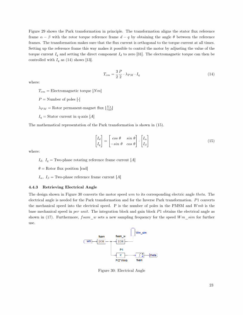
Figure 29 shows the Park transformation in principle. The transformation aligns the stator flux referenceframe α − β with the rotor torque reference frame d − q by obtaining the angle θ between the referenceframes. The transformation makes sure that the flux current is orthogonal to the torque current at all times.Setting up the reference frame this way makes it possible to control the motor by adjusting the value of thetorque current Iq and setting the direct component Id to zero [31]. The electromagnetic torque can then becontrolled with Iq as (14) shows [13].
Tem =3
2
P
2· λPM · Iq (14)
where:
Tem = Electromagnetic torque [Nm]
P = Number of poles [-]
λPM = Rotor permanent-magnet flux [ V srad ]
Iq = Stator current in q-axis [A]
The mathematical representation of the Park transformation is shown in (15).
[Id
Iq
]=
[cos θ sin θ
−sin θ cos θ
]·
[Iα
Iβ
](15)
where:
Id, Iq = Two-phase rotating reference frame current [A]
θ = Rotor flux position [rad]
Iα, Iβ = Two-phase reference frame current [A]
4.4.3 Retrieving Electrical Angle
The design shown in Figure 30 converts the motor speed wm to its corresponding electric angle theta. Theelectrical angle is needed for the Park transformation and for the Inverse Park transformation. P1 convertsthe mechanical speed into the electrical speed. P is the number of poles in the PMSM and Wmb is thebase mechanical speed in per unit. The integration block and gain block P1 obtains the electrical angle asshown in (17). Furthermore, fsam_w sets a new sampling frequency for the speed Wm_sim for furtheruse.
Figure 30: Electrical Angle
23
The correlation between the electrical speed and mechanical speed is shown in (16).
ωe =p · ωm
2(16)
where:
ωe = Electrical speed [rad/s]
ωm = Motor speed [rad/s]
p = Number of poles [-]
θe =
∫ωe dt (17)
where:
θe = Electrical angle [rad]
ωe = Electrical speed [rad/s]
4.4.4 Speed Controller
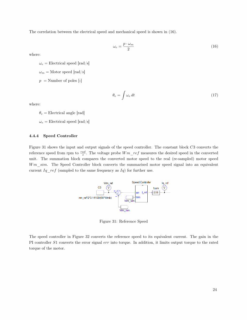
Figure 31 shows the input and output signals of the speed controller. The constant block C3 converts thereference speed from rpm to rad
s . The voltage probe Wm_ref measures the desired speed in the convertedunit. The summation block compares the converted motor speed to the real (re-sampled) motor speedWm_sim. The Speed Controller block converts the summarised motor speed signal into an equivalentcurrent Iq_ref (sampled to the same frequency as Iq) for further use.
Figure 31: Reference Speed
The speed controller in Figure 32 converts the reference speed to its equivalent current. The gain in thePI controller S1 converts the error signal err into torque. In addition, it limits output torque to the ratedtorque of the motor.
24

Figure 32: Speed Controller
Dividing the maximum power C1 with the actual motor speed Wm obtains the maximum torque. Thecorrelation between the electromagnetic torque, maximum motor power, and mechanical speed is shown in(18).
Tem =Pem,maxωm
(18)
where:
Tem = Electromagnetic torque [Nm]
Pem,max = Maximum motor power [W]
ωm = Mechanical speed [rad/s]
The comparator COMP1 compares the limited torque (marked with 1) and the actual torque (marked with2). The MUX function MUX21 will send only one of the two input signals through. The output signal ofMUX21 depends on the output signal of the comparator. If 1 > 2 then signal 2 will pass through. If 2 > 1
then signal 1 will pass through the MUX function. In other words, the signal with lowest value will be theoutput signal of MUX21. The gain P1 converts the torque output signal of MUX21 into a current signal,based on (19). The signal is then limited by the LIM1 (maximum current) and sent as the output signal ofthe speed controller (I_ref in Figure 31).
Is =TemkT
(19)
where:
Is = Magnitude of stator-current space vector [A]
Tem = Electromagnetic torque [Nm]
KT = Torque constant [Nm/A]
25
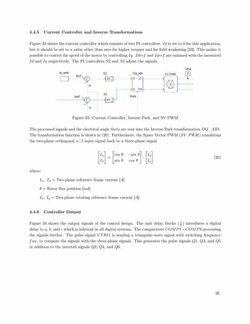
4.4.5 Current Controller and Inverse Transformations
Figure 33 shows the current controller which consists of two PI controllers. Id is set to 0 for this application,but it should be set to a value other than zero for higher torques and for field weakening [33]. This makes itpossible to control the speed of the motor by controlling Iq. Idref and Iqref are summed with the measuredId and Iq respectively. The PI controllers S2 and S3 adjust the signals.
Figure 33: Current Controller, Inverse Park, and SV PWM
The processed signals and the electrical angle theta are sent into the Inverse Park transformation DQ_AB1.The transformation function is shown in (20). Furthermore, the Space Vector PWM (SV PWM ) transformsthe two-phase orthogonal α/β input signal back to a three-phase signal.
[Iα
Iβ
]=
[cos θ −sin θsin θ cos θ
]·
[Id
Iq
](20)
where:
Iα, Iβ = Two-phase reference frame current [A]
θ = Rotor flux position [rad]
Id, Iq = Two-phase rotating reference frame current [A]
4.4.6 Controller Output
Figure 34 shows the output signals of the control design. The unit delay blocks ( 1Z ) introduces a digital
delay to a, b, and c which is inherent in all digital systems. The comparators COMP1−COMP3 processingthe signals further. The pulse signal V TRI1 is sending a triangular-wave signal with switching frequencyfsw, to compare the signals with the three-phase signals. This generates the pulse signals Q1, Q3, and Q5
in addition to the inverted signals Q2, Q4, and Q6.
26
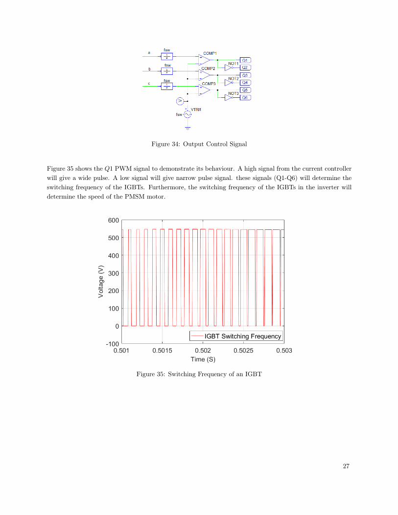
Figure 34: Output Control Signal
Figure 35 shows the Q1 PWM signal to demonstrate its behaviour. A high signal from the current controllerwill give a wide pulse. A low signal will give narrow pulse signal. these signals (Q1-Q6) will determine theswitching frequency of the IGBTs. Furthermore, the switching frequency of the IGBTs in the inverter willdetermine the speed of the PMSM motor.
Figure 35: Switching Frequency of an IGBT
27

5 SimCoderThe simulation design described in Section 4 makes it possible to test different scenarios before runningthe PMSM. However, PSIM provides SimCoder in addition to the simulation software. This module enablesautomatic code generation. The generated code can be imported into the DSP to run the frequency converter.However, generating the code requires some adjustments. This chapter describes these design adjustments.
5.1 Encoder ConversionFigure 36 shows the speed measurement of the simulation design. Furthermore, Figure 37 shows the theSimCoder design. The incremental encoder attached to the available PMSM indicates the motion of themotor shaft. Implementing a corresponding encoder PMSM_Encoder makes it possible to estimate theangle and speed of the system. The Encoder Counter in the simcoder design specifies the input pins on theDSP, as well as counting the PMSM_Encoder output signals.
Figure 36: Speed Measurement Simulation Figure 37: Encoder and Counter for SimCoder
5.1.1 Angle Calculation
The output value of the encoder counter value needs further calculations to retrieve the speed and angle ofthe motor. Figure 38 shows the SimCoder design for the angle conversion.
Figure 38: SimCoder Angle Calculation
The encoder counter value is an indicator of the mechanical angle of the motor. The proportional gainP1 calculates the electrical angle. The relation between the electrical and mechanical angle is shown in(21).
28
θe =P
2· θm (21)
where:
θe = Electrical angle [rad]
P = Number of poles[-]
θm = Mechanical angle [rad]
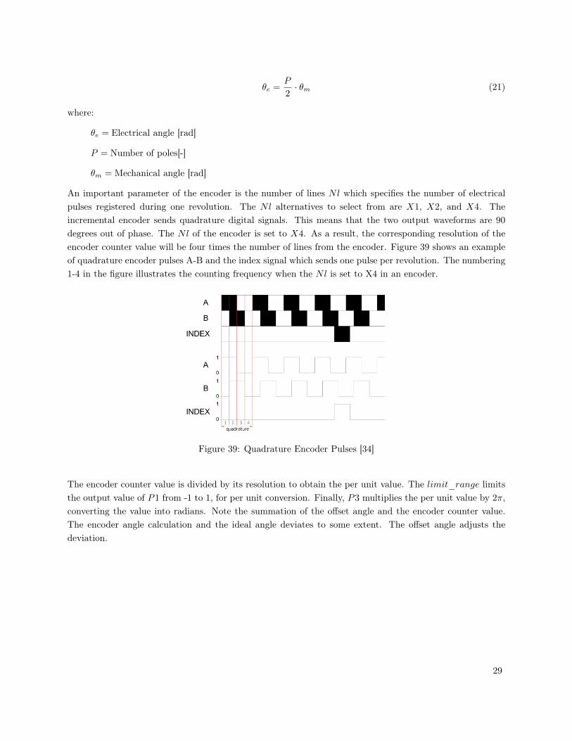
An important parameter of the encoder is the number of lines Nl which specifies the number of electricalpulses registered during one revolution. The Nl alternatives to select from are X1, X2, and X4. Theincremental encoder sends quadrature digital signals. This means that the two output waveforms are 90degrees out of phase. The Nl of the encoder is set to X4. As a result, the corresponding resolution of theencoder counter value will be four times the number of lines from the encoder. Figure 39 shows an exampleof quadrature encoder pulses A-B and the index signal which sends one pulse per revolution. The numbering1-4 in the figure illustrates the counting frequency when the Nl is set to X4 in an encoder.
Figure 39: Quadrature Encoder Pulses [34]
The encoder counter value is divided by its resolution to obtain the per unit value. The limit_range limitsthe output value of P1 from -1 to 1, for per unit conversion. Finally, P3 multiplies the per unit value by 2π,converting the value into radians. Note the summation of the offset angle and the encoder counter value.The encoder angle calculation and the ideal angle deviates to some extent. The offset angle adjusts thedeviation.
29
5.1.2 Speed Calculation
The formula for encoder speed calculation is shown in (22) [35].
v(k) =x(k)− x(k − 1)
T=
∆X
T= ∆X · f (22)
where:
v(k) = Velocity at time instant k [ rads ]
x(k) = Position at time instant k [rad]
x(k − 1) = Position at time instant k-1 [rad]
T = Fixed unit time or inverse of velocity calculation rate [s]
f = Sampling frequency [Hz]
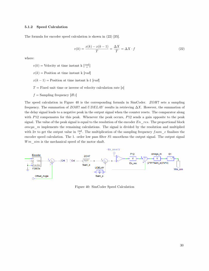
The speed calculation in Figure 40 is the corresponding formula in SimCoder. ZOH7 sets a samplingfrequency. The summation of ZOH7 and UDELAY results in retrieving ∆X. However, the summation ofthe delay signal leads to a negative peak in the output signal when the counter resets. The comparator alongwith P12 compensates for this peak. Whenever the peak occurs, P12 sends a gain opposite to the peaksignal. The value of the peak signal is equal to the resolution of the encoder En_res. The proportional blockomega_m implements the remaining calculations. The signal is divided by the resolution and multipliedwith 2π to get the output value in rad
s . The multiplication of the sampling frequency fsam_e finalises theencoder speed calculation. The 1. order low pass filter S1 smoothens the output signal. The output signalWm_sim is the mechanical speed of the motor shaft.
Figure 40: SimCoder Speed Calculation
30
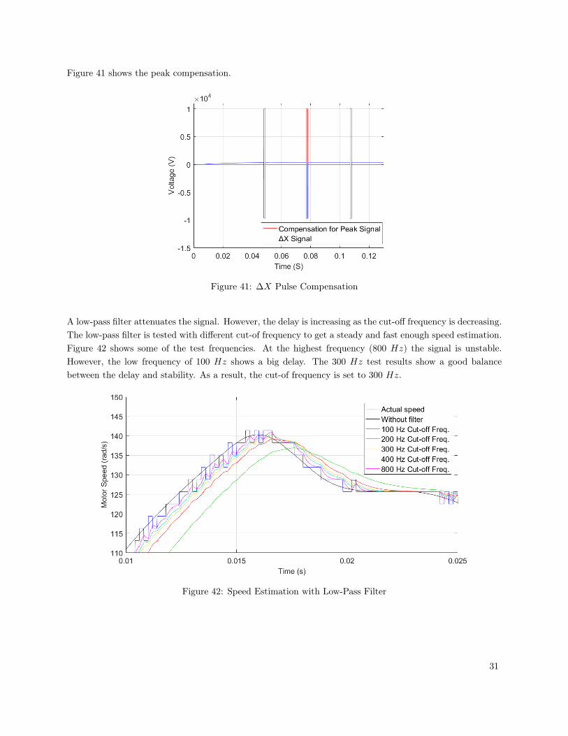
Figure 41 shows the peak compensation.
Figure 41: ∆X Pulse Compensation
A low-pass filter attenuates the signal. However, the delay is increasing as the cut-off frequency is decreasing.The low-pass filter is tested with different cut-of frequency to get a steady and fast enough speed estimation.Figure 42 shows some of the test frequencies. At the highest frequency (800 Hz) the signal is unstable.However, the low frequency of 100 Hz shows a big delay. The 300 Hz test results show a good balancebetween the delay and stability. As a result, the cut-of frequency is set to 300 Hz.
Figure 42: Speed Estimation with Low-Pass Filter
31
5.2 Analog / Digital Converter
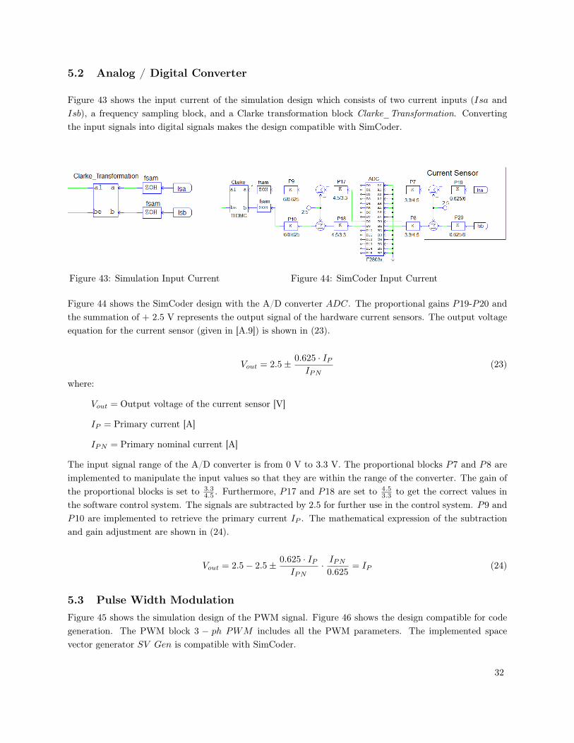
Figure 43 shows the input current of the simulation design which consists of two current inputs (Isa andIsb), a frequency sampling block, and a Clarke transformation block Clarke_Transformation. Convertingthe input signals into digital signals makes the design compatible with SimCoder.
Figure 43: Simulation Input Current Figure 44: SimCoder Input Current
Figure 44 shows the SimCoder design with the A/D converter ADC. The proportional gains P19-P20 andthe summation of + 2.5 V represents the output signal of the hardware current sensors. The output voltageequation for the current sensor (given in [A.9]) is shown in (23).
Vout = 2.5± 0.625 · IPIPN
(23)
where:
Vout = Output voltage of the current sensor [V]
IP = Primary current [A]
IPN = Primary nominal current [A]
The input signal range of the A/D converter is from 0 V to 3.3 V. The proportional blocks P7 and P8 areimplemented to manipulate the input values so that they are within the range of the converter. The gain ofthe proportional blocks is set to 3.3
4.5 . Furthermore, P17 and P18 are set to 4.53.3 to get the correct values in
the software control system. The signals are subtracted by 2.5 for further use in the control system. P9 andP10 are implemented to retrieve the primary current IP . The mathematical expression of the subtractionand gain adjustment are shown in (24).
Vout = 2.5− 2.5± 0.625 · IPIPN
· IPN0.625
= IP (24)
5.3 Pulse Width ModulationFigure 45 shows the simulation design of the PWM signal. Figure 46 shows the design compatible for codegeneration. The PWM block 3 − ph PWM includes all the PWM parameters. The implemented spacevector generator SV Gen is compatible with SimCoder.
32
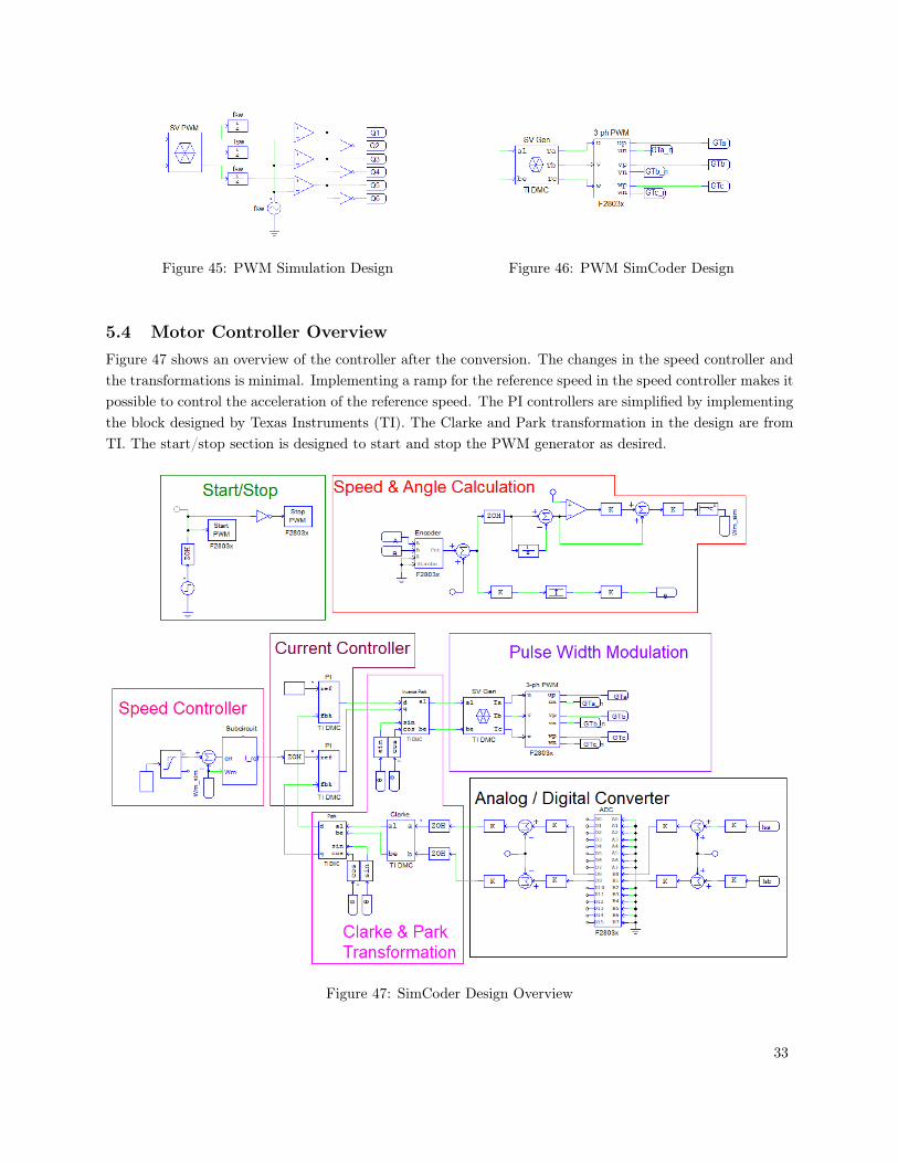
Figure 45: PWM Simulation Design Figure 46: PWM SimCoder Design
5.4 Motor Controller OverviewFigure 47 shows an overview of the controller after the conversion. The changes in the speed controller andthe transformations is minimal. Implementing a ramp for the reference speed in the speed controller makes itpossible to control the acceleration of the reference speed. The PI controllers are simplified by implementingthe block designed by Texas Instruments (TI). The Clarke and Park transformation in the design are fromTI. The start/stop section is designed to start and stop the PWM generator as desired.
Figure 47: SimCoder Design Overview
33
5.5 Hardware ConfigurationFigure 48 shows the hardware configuration, Serial Communication Interface (SCI) configuration, and theDigital Signal Processor (DSP) clock. The hardware configuration defines the input and output ports in aspecific hardware setting. The SCI configuration defines the port selection, speed, and output buffer sizeof the DSP oscilloscope. The DSP clock defines the clock speed of the oscilloscope. Configuring the DSPoscilloscope makes it possible to read the values of the control system on the computer while running thecode. The hardware configuration, SCI configuration, and DSP clock specification are available in [B.1].
Figure 48: Hardware Configuration, SCI Configuration and DSP Clock
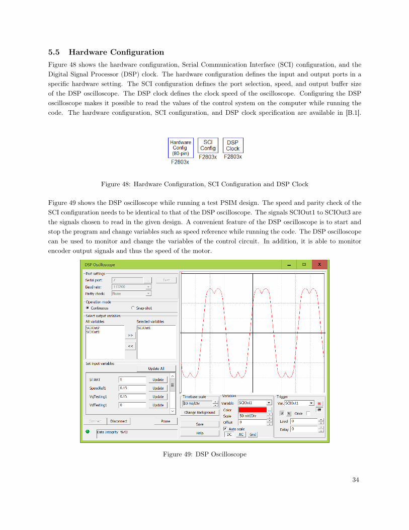
Figure 49 shows the DSP oscilloscope while running a test PSIM design. The speed and parity check of theSCI configuration needs to be identical to that of the DSP oscilloscope. The signals SCIOut1 to SCIOut3 arethe signals chosen to read in the given design. A convenient feature of the DSP oscilloscope is to start andstop the program and change variables such as speed reference while running the code. The DSP oscilloscopecan be used to monitor and change the variables of the control circuit. In addition, it is able to monitorencoder output signals and thus the speed of the motor.
Figure 49: DSP Oscilloscope
34

6 Digital Signal ProcessingThis section describes the components and software needed for digital signal processing. The hardware forsignal processing is a Digital Signal Processing (DSP) development board. Code Composer Studio (CCS) isneeded to import the generated code into the development board. The section describes the configurationof CCS. Furthermore, a brief explanation of the current sensor calibration is given.
6.1 Development Board
A DSP development board processes the signals generated from the SimCoder design. Figure 50 shows theDSP board used in the design. Powesim Inc. provides the DSP development board as a package. Thepackage includes both a DSP control board and a TI controlCARD. The DSP controlCARD used in thisdesign is the F28035 PiccoloTM Family. The pins mounted on the board registers both the output and inputsignals.
Figure 50: DSP Development Board [36]
Figure 51 shows an overview of the pins. When running the code, the analog input connector J8 registersthe motor current signals J7 and J9 registers the encoder signals. The SCI connector J6 sends an enablesignal to the gate driver. Furthermore, the gate driver interface J12 sends the output PWM signals to thegate driver.
Figure 51: Development Board Connector Overview
35

Figure 52 shows the input connector J8 which contains the pins for the measured motor current. Pin number11 and 13 (Iain and Ibin) corresponds to the SimCoder A/D converter input ports B0 and B1 shown inFigure 44. Furthermore, pin number 1 and 2 supplies the current sensors with 5 V .
Figure 52: Current Sensor Input Connector J8
The input connectors J7 and J9 shown in Figure 53 and Figure 54 respectively are used to register theencoder signals.
Figure 53: Encoder Connector J7 Figure 54: Encoder Connector J9
Figure 55 shows how J7 and J9 are connected with the encoder. Pin POSV (EQEP1A) and POSW (EQEP1B)
corresponds to port A and port B in the encoder. The Z signal, which provides one count per revolution,is connected to ground together with POSA(EQEP1S), POSB(EQEP1I), and encoder ground G. Theports of the F28035 piccolo microcontroller (EQEP1X ports) are shown in [A.13].
POSA(EQEP1S)POSB(EQEP1I)
J7
F28035
POSV(EQEP1A)POSW(EQEP1B)
J9
F28035
ABZG
Encoder
Figure 55: Encoder Connections
36

Figure 56 shows the PWM output connector J12. Furthermore, Table 4 describes the applied pins. PhaseA, B, and C all have a top switch (high) signal and a bottom switch (low) signal which acts opposite to eachother. The digital ground is connected to the common ground of the design, and the voltage supply KL_30
in pin 1 supplies the gate driver.
Figure 56: PWM Signal Output Connector
Pin Number Parameter Description1 KL_30 12 V Power Supply4 DGND Digital Ground14 PWMWT PWM Gate High Phase C16 PWMWB PWM Gate Low Phase C18 PWMVT PWM Gate High Phase B20 PWMVB PWM Gate Low Phase B22 PWMUT PWM Gate High Phase A24 PWMUB PWM Gate Low Phase A
Table 4: PWM Connector Signals
6.2 Code Composer StudioCCS processes the generated code from SimCoder. When generating the code, a .pjt file (among other files)is saved in a folder by PSIM. The .pjt file is used to import the code into CCS. The target needs to beconfigured when the project is imported. The configuration defines the control hardware available. Table 5shows the configuration parameters.
Configuration DescriptionExperiment’s Kit - Piccolo F28035 ControlCARD and DSP Development BoardDigital Texas Intruments XDS100v1 USB Debug Probe Internal Debug Probe on the ControlCARDC2000Ware Product Family
Table 5: CCS Configuration
After the target configuration, the project is ready to be built and run. By doing so, the imported code willappear. The time stamp on the code needs to be checked continuously when adjusting the design in PSIM
37

to verify the connection between PSIM and CCS. Figure 57 shows the CCS display when running the code.The "Debug", "Expressions", and "System_v1_3.c" tabs show the debug probe, variable expressions, andthe imported code respectively. The time stamp is printed at the top of the code. The DSP oscilloscope inFigure 49 is used to change the value of the expressions while running the program in CCS.
Figure 57: CCS Display
6.3 Current Sensor CalibrationThe DSP board converts the received input current by default. The current conversion is shown in Table 6.The conversion for the three phases Ia, Ib, and Ic is the same.
Input DescriptionAC When Iin = 5 · sin(ωt), IDSP = 1.5 + 1.5 · sin(ωt)
DC When Iin = 3.5 + 3.5 · sin(ωt), IDSP = 1.5 + 1.5 · sin(ωt)
Table 6: DSP Board Current Conversion [A.11]
The input value of the current sensors needs to be calibrated in SimCoder due to the DSP conversion.
38

Figure 58 shows the proportional gains P9 and P10 which converts the DSP value to the actual currentvalue. Furthermore, the Zero_Adjust adjusts the zero point. The SCI output blocks I_D8 and I_D9
monitors the current before the calibration. Ia and Ib monitors the results after the calibration. Note thatthe SimCoder design in Figure 44 has different proportional gains compared to the one in Figure 58. Theprior is for simulating the design and does not take the DSP conversion into account. The latter takes theDSP conversion into account. This makes it able to run the hardware design.
Figure 58: Current Calibration
First, the Zero_Adjust is adjusted. The value is obtained by monitoring I_D8 and I_D9 with no currentflowing through the hardware sensors. This value is then subtracted to get the zero point in the design.Monitoring I_D8 and I_D9 while measuring 1 A with the current sensors makes it possible to calculatethe calibration gain with (25).
V1A ·K1A = 1 (25)
where:
V1A = Value measured in SimCoder with 1 A going through the sensor [V]
K1A = Proportional gain needed to get 1 A in the SimCoder design [-]
The calibration gain K1A of P9 and P10 is calculated to be 21.62274825 and 21.04230583 respectively. Thecalculated proportional gain is tested with currents ranging from 0 − 4 A, which is the maximum currentof the resistances in the test design (R1 − R3 in Figure 60). Table 7 shows the calibration results. Themaximum deviation is 1.275 % on Ib when testing with 4 A. The accuracy is considered sufficient.
Test Current [A] Current Measured in SimCoder [A] Deviation [%]1 Ia = 0.9997, Ib = 1.0024 Ia = 0.03, Ib = −0.24
2 Ia = 2.0034, Ib = 1.9892 Ia = −0.17, Ib = 0.54
3 Ia = 3.0062, Ib = 2.9736 Ia = −0.207, Ib = 0.88
4 Ia = 4.0094, Ib = 3.9490 Ia = −0.235, Ib = 1.275
Table 7: Current Calibration Results
39
7 Hardware ConfigurationThis section describes the hardware configuration, the circuit design, and its associated calculation. Inaddition, it presents the designed setups for the tests in detail.
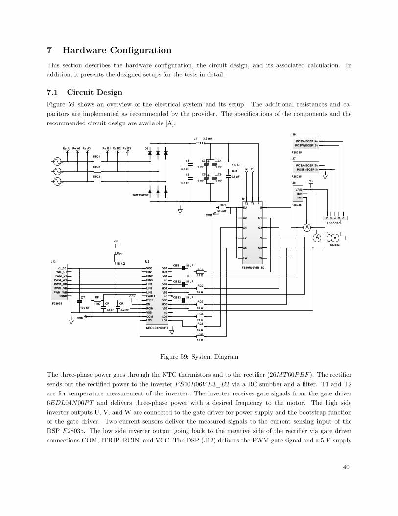
7.1 Circuit DesignFigure 59 shows an overview of the electrical system and its setup. The additional resistances and ca-pacitors are implemented as recommended by the provider. The specifications of the components and therecommended circuit design are available [A].
T1 PT2
G6 G5
V
G3
W
G1
U
EW
EU
G2
G4
EV
U1
FS10R06VE3_B2VB1VCCHIN1HIN2HIN3LIN1LIN2LIN3FAULTITRIPEN
U2
HO1VS1ncVB2HO2VS2ncVB3
nc
HO3VS3
LO1LO2
VSS
LO3
RCIN
COM
6EDL04N06PT
15Ω
RG1
15Ω
RG2
15Ω
RG3
15Ω
RG4
15Ω
RG5
15Ω
RG6
CBS1 1.5μF
1.5μFCBS3
1.5μFCBS2
PWM_UTPWM_VT
PWM_UB
J12
PWM_VB
DGNDPWM_WB
PWM_WT
F28035
KL_30
C7
100nFCR
2.2nF
CF
82pF
RF
1kΩ
PMSM
50mΩ
RSH
A
100Ω
0.1μF
A
RC1
3.9mHL1
T1T2
NTC1
NTC2
NTC3C2
4.7nF
C1
4.7nF
C3
1mF
C4
1mF
C5
1mF
C6
1mF J8
F28035
IbinVA50
Iain
Pin3
J7
POSA(EQEP1S)POSB(EQEP1I)
F28035
ReA1 ReA2 ReA3 ReB1 ReB2 ReB3 D1
26MT60PBF
COM
COM
+3.3V
J9
POSV(EQEP1A)
F28035
POSW(EQEP1B)
+5V
BZ AG5V
Encoder
+5V
18kΩ
Rpu
Figure 59: System Diagram
The three-phase power goes through the NTC thermistors and to the rectifier (26MT60PBF ). The rectifiersends out the rectified power to the inverter FS10R06V E3_B2 via a RC snubber and a filter. T1 and T2are for temperature measurement of the inverter. The inverter receives gate signals from the gate driver6EDL04N06PT and delivers three-phase power with a desired frequency to the motor. The high sideinverter outputs U, V, and W are connected to the gate driver for power supply and the bootstrap functionof the gate driver. Two current sensors deliver the measured signals to the current sensing input of theDSP F28035. The low side inverter output going back to the negative side of the rectifier via gate driverconnections COM, ITRIP, RCIN, and VCC. The DSP (J12) delivers the PWM gate signal and a 5 V supply
40

signal to the gate driver. The shunt resistor RSH is calculated with (26) which is based on equation 3 in[A.6].
RSH =VIT,TH+
IITRIP(26)
where:
RSH = Shunt resistor [Ω]
VIT,TH+ = ITRIP positive going threshold [V ]
IITRIP = Over-current for gate driver shutdown [A]
The over-current is set to minimum 8 A and maximum 10.2 A depending on the threshold of ITRIP . ITRIPresistor RF and pull-up resistor Rpu are calculated with the equations shown in [A.7]. Bootstrap capacitorsCBS are calculated with (27) derived from [A.6]. The voltage ripple is set to 0.1 V .
CBS =iQBS · tP +QG
∆VBS· 1.2 (27)
where:
CBS = Bootstrap capacitor [F ]
iQBS = Quiescent current VBS supply [A]
tP = Swithing period [s]
QG = Total gate charge [C]
∆VBS = Bootstrap voltage ripple [V ]
The purpose of the gate resistor RG is to reduce overshoot and oscillating current waveform. The currentoscillation will be underdamped and the switching time will be extended if the resistor value is to high[37]. The minimum resistor is calculated in (28). The value calculated is rounded up to a standard resistorvalue.
RG,min = 2 ·√
LSCISS
(28)
where:
RG,min = Minimum gate resistor to retain a non-oscillating gate current waveform [Ω]
LS = Stray inductance of the inverter [H]
CISS = Input capacitance of the inverter [F ]
Full calculations for RSH , CBS and RG,min are in [D.2]. The rest of the capacitors are selected withreasonable values and modified after testing.
41
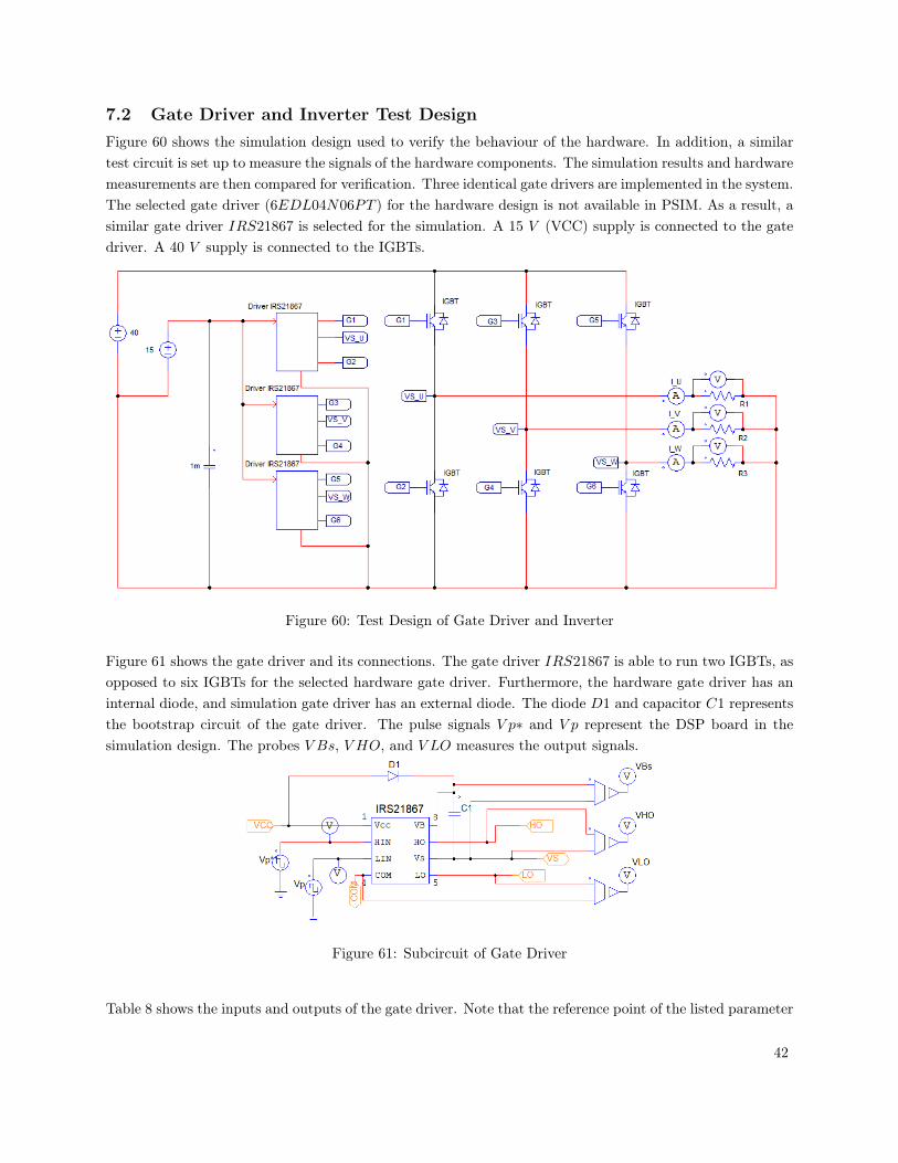
7.2 Gate Driver and Inverter Test DesignFigure 60 shows the simulation design used to verify the behaviour of the hardware. In addition, a similartest circuit is set up to measure the signals of the hardware components. The simulation results and hardwaremeasurements are then compared for verification. Three identical gate drivers are implemented in the system.The selected gate driver (6EDL04N06PT ) for the hardware design is not available in PSIM. As a result, asimilar gate driver IRS21867 is selected for the simulation. A 15 V (VCC) supply is connected to the gatedriver. A 40 V supply is connected to the IGBTs.
Figure 60: Test Design of Gate Driver and Inverter
Figure 61 shows the gate driver and its connections. The gate driver IRS21867 is able to run two IGBTs, asopposed to six IGBTs for the selected hardware gate driver. Furthermore, the hardware gate driver has aninternal diode, and simulation gate driver has an external diode. The diode D1 and capacitor C1 representsthe bootstrap circuit of the gate driver. The pulse signals V p∗ and V p represent the DSP board in thesimulation design. The probes V Bs, V HO, and V LO measures the output signals.
Figure 61: Subcircuit of Gate Driver
Table 8 shows the inputs and outputs of the gate driver. Note that the reference point of the listed parameter
42

varies. The measurement of the simulation and the hardware needs to have the same reference point to getcomparable results. All measurements done when testing the gate driver and IGBT are referenced as listedbelow unless otherwise is specified.
Parameter Description Reference Operating RangeV CC Low Side Power Supply VCC vs. VSS (Ground) 10− 17.5 V
V BS High Side Positive Power Supply VB vs. VS 10− 17.5 V
HIN High Side Logic Input VHIN vs. VSS 0− 5 V
HO High Side Gate Driver Output VHO vs. VS 0− V BSLIN Low Side Logic Input VLIN vs. VS 0− 5 V
V S High Side Negative Power Supply VS vs. VSS Vcc − VBS − 1 to 500 V
LO Low Side Gate Driver Output VLO vs. VCOM 0− V CCCOM Low Side Gate Driver Reference VCOM vs. VSS −2.5− 2.5 V
Table 8: Parameters Simulation Gate Driver [A.5]
7.3 Rectifier and Filter Test DesignFigure 62 shows the PSIM model for the rectifier and filter test setup. Two separate systems are simulatedfor the test. Initially, the system without a filter is simulated. The filter is then implemented into the samesystem and simulated. The results are then compared to analyse the filter and its function. The resistancesR1 and R2 are implemented to make the input rectifier current similar to the one in the hardware testsetup. The forward voltage and resistor of the rectifier diodes are set to 1.26 V and 7.9 mΩ respectively.The specifications of the rectifier are shown in [A.1]. The implemented filter have a 3.9 mH inductor L andfour 1 mF capacitors C which is the same values as the hardware components. The resistances R3 and R4
are implemented as a load.
Figure 62: Rectifier and Filter Test Design
43
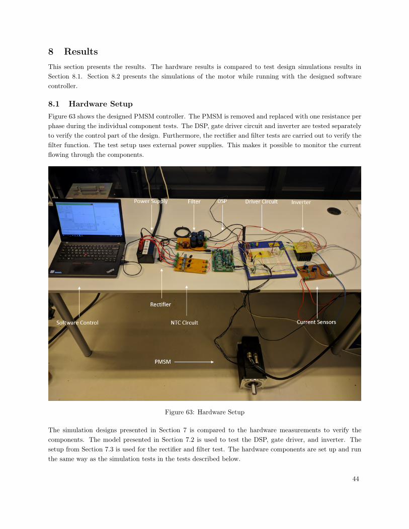
8 ResultsThis section presents the results. The hardware results is compared to test design simulations results inSection 8.1. Section 8.2 presents the simulations of the motor while running with the designed softwarecontroller.
8.1 Hardware SetupFigure 63 shows the designed PMSM controller. The PMSM is removed and replaced with one resistance perphase during the individual component tests. The DSP, gate driver circuit and inverter are tested separatelyto verify the control part of the design. Furthermore, the rectifier and filter tests are carried out to verify thefilter function. The test setup uses external power supplies. This makes it possible to monitor the currentflowing through the components.
Figure 63: Hardware Setup
The simulation designs presented in Section 7 is compared to the hardware measurements to verify thecomponents. The model presented in Section 7.2 is used to test the DSP, gate driver, and inverter. Thesetup from Section 7.3 is used for the rectifier and filter test. The hardware components are set up and runthe same way as the simulation tests in the tests described below.
44

8.1.1 DSP and Gate Driver Test
Figure 64 shows the simulation results of the high input HIN and low input LIN gate driver signals. Asexpected, the simulation shows a high and low input 5 V PWM signal acting opposite to each other. Theinput signal of the hardware gate driver is shown in Figure 65. The DSP Development board sends thePWM signals. The yellow signal is HIN and the blue signal is LIN. Opposite behaviours are observed whilerunning the gate driver. Note that a slightly higher peak signal V pp is measured Figure 65. However, thesignals of 5.6 V and 5.52 V are well within the maximum limits (-1 to 10 V ) of HIN and LIN [A.5]. Thecomparison of the two figures shows that the signal from the DSP into the gate driver runs as expected. Allmeasured values from the figures below are referenced to COM.
6 7 8 9 10 11 12
Time (S)×10
-4
-2
-1
0
1
2
3
4
5
Voltage (
V)
Driver Input PWM High Signal
Driver Input PWM Low Signal
Figure 64: Gate Driver Input PWM Signals HIN andLIN Simulation (Phase A)
Figure 65: Gate Driver Input PWM Signals HIN andLIN Hardware (Phase A)
Figure 66 shows the simulation results of the output PWM gate driver signals HO. The results show a13.64 V output gate driver pulse signal. Figure 67 shows the hardware high output pulse signal HO. Thesimulation results and hardware results show a similar behaviour. However, the hardware voltage shows ahigher amplitude than the simulated voltage. In the simulation, the pulse signal has an amplitude of 13.02 V
and the amplitude of the hardware voltage is 15.4 V for HO. Considering that a different gate driver is usedfor the simulation and that all components and values are considered ideal, some deviation of amplitude isexpected.
0 1 2 3 4
Time (S)×10
-4
0
5
10
15
Voltage (
V)
Driver Output PWM Signal (High)
X: 7.04e-05
Y: 13.02
Figure 66: Simulated Output Gate Driver Signal HOReferenced to VS (Phase A)
Figure 67: Hardware Output Gate Driver Signal HOReferenced to VS (Phase A)
45
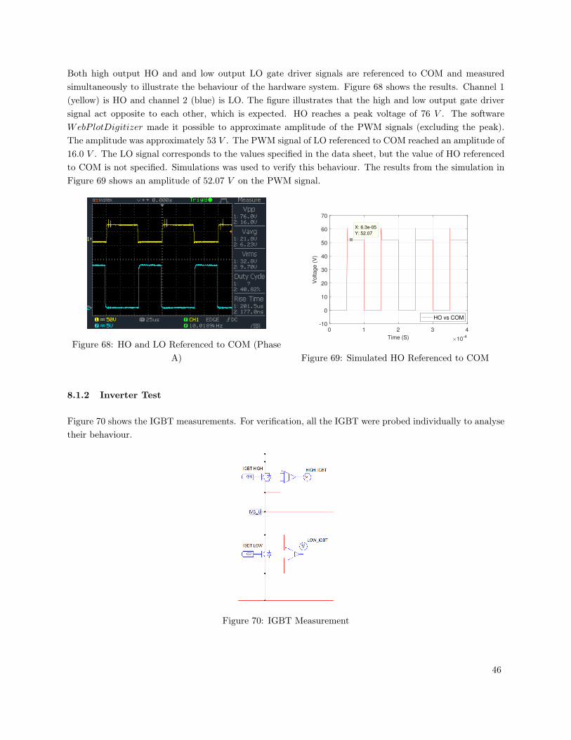
Both high output HO and and low output LO gate driver signals are referenced to COM and measuredsimultaneously to illustrate the behaviour of the hardware system. Figure 68 shows the results. Channel 1(yellow) is HO and channel 2 (blue) is LO. The figure illustrates that the high and low output gate driversignal act opposite to each other, which is expected. HO reaches a peak voltage of 76 V . The softwareWebP lotDigitizer made it possible to approximate amplitude of the PWM signals (excluding the peak).The amplitude was approximately 53 V . The PWM signal of LO referenced to COM reached an amplitude of16.0 V . The LO signal corresponds to the values specified in the data sheet, but the value of HO referencedto COM is not specified. Simulations was used to verify this behaviour. The results from the simulation inFigure 69 shows an amplitude of 52.07 V on the PWM signal.
Figure 68: HO and LO Referenced to COM (PhaseA)
0 1 2 3 4
Time (S)×10
-4
-10
0
10
20
30
40
50
60
70
Voltage (
V)
HO vs COM
X: 6.3e-05
Y: 52.07
Figure 69: Simulated HO Referenced to COM
8.1.2 Inverter Test
Figure 70 shows the IGBT measurements. For verification, all the IGBT were probed individually to analysetheir behaviour.
Figure 70: IGBT Measurement
46
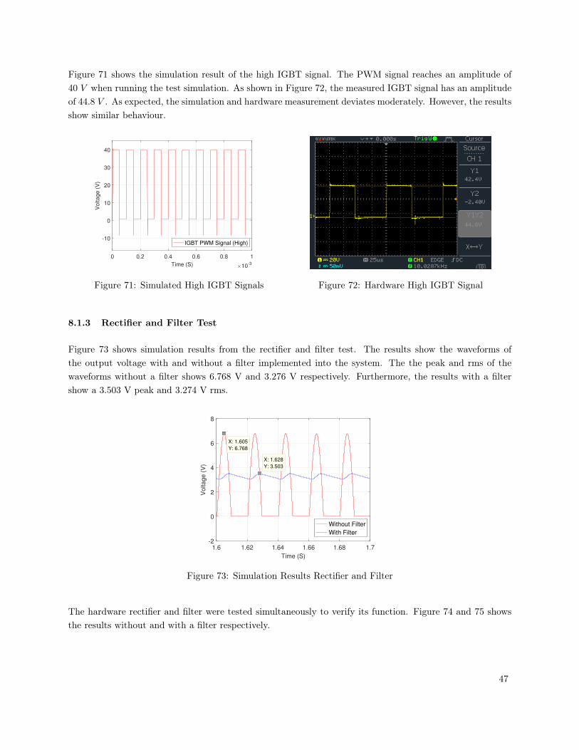
Figure 71 shows the simulation result of the high IGBT signal. The PWM signal reaches an amplitude of40 V when running the test simulation. As shown in Figure 72, the measured IGBT signal has an amplitudeof 44.8 V . As expected, the simulation and hardware measurement deviates moderately. However, the resultsshow similar behaviour.
0 0.2 0.4 0.6 0.8 1
Time (S)×10
-3
-10
0
10
20
30
40
Voltage (
V)
IGBT PWM Signal (High)
Figure 71: Simulated High IGBT Signals Figure 72: Hardware High IGBT Signal
8.1.3 Rectifier and Filter Test
Figure 73 shows simulation results from the rectifier and filter test. The results show the waveforms ofthe output voltage with and without a filter implemented into the system. The the peak and rms of thewaveforms without a filter shows 6.768 V and 3.276 V respectively. Furthermore, the results with a filtershow a 3.503 V peak and 3.274 V rms.
1.6 1.62 1.64 1.66 1.68 1.7
Time (S)
-2
0
2
4
6
8
Voltage (
V)
Without Filter
With Filter
X: 1.605
Y: 6.768
X: 1.628
Y: 3.503
Figure 73: Simulation Results Rectifier and Filter
The hardware rectifier and filter were tested simultaneously to verify its function. Figure 74 and 75 showsthe results without and with a filter respectively.
47
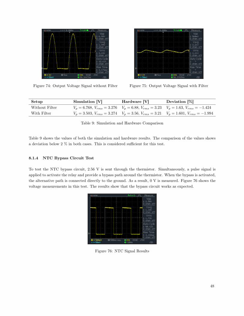
Figure 74: Output Voltage Signal without Filter Figure 75: Output Voltage Signal with Filter
Setup Simulation [V] Hardware [V] Deviation [%]Without Filter Vp = 6.768, Vrms = 3.276 Vp = 6.88, Vrms = 3.23 Vp = 1.63, Vrms = −1.424
With Filter Vp = 3.503, Vrms = 3.274 Vp = 3.56, Vrms = 3.21 Vp = 1.601, Vrms = −1.994
Table 9: Simulation and Hardware Comparison
Table 9 shows the values of both the simulation and hardware results. The comparison of the values showsa deviation below 2 % in both cases. This is considered sufficient for this test.
8.1.4 NTC Bypass Circuit Test
To test the NTC bypass circuit, 2.56 V is sent through the thermistor. Simultaneously, a pulse signal isapplied to activate the relay and provide a bypass path around the thermistor. When the bypass is activated,the alternative path is connected directly to the ground. As a result, 0 V is measured. Figure 76 shows thevoltage measurements in this test. The results show that the bypass circuit works as expected.
Figure 76: NTC Signal Results
48

8.2 Modelling of FOC-Based-PMSM
Three different simulation cases are created to test the motor and the controller. The model consists of thefrequency converter from Figure 18 and the motor controller from Figure 47. A speed ramp with 1000 rpm
s
rise are used in all three cases. A tachometer which only measures rpm is available for the speed measurementin future tests. In addition, the speed specifications in the data sheets are given in rpm. As a result, thecases are defined with rpm values. However, the results are presented in rad
s .
• Case 1 (No-Load): Motor speed from 0 rpm to 2426 rpm. 0 Nm motor load.
• Case 2 (Variable Speed): Motor speed 800 rpm, 1600 rpm and 2489 rpm. 0 Nm motor load.
• Case 3 (Full-Load): Motor speed from 0 rpm to 2426 rpm. 9.18 Nm motor load (rated torque).
8.2.1 Case 1 (No-Load)
Case 1 is created to test the motor’s ability to stabilise at one constant speed, after a speed ramp. This testis without any motor load. Figure 77 shows a 3.5 s simulation of Case 1. The results show that the motorspeed stabilises at 254.05 rad
s (2426 rpm) after 2.426 s.
0 0.5 1 1.5 2 2.5 3 3.5
Time (s)
0
50
100
150
200
250
300
Moto
r S
peed (
rad/s
)
Motor Speed
Figure 77: Motor Speed at Case 1
Figure 78 shows a closer look at constant motor speed. The figure shows two error lines which is a percentageof the reference motor speed. The lines visualises the area of deviation. The deviation of the speed in Case 1is at highest 0.11 %. The motor phase currents Iadc have an average rms of 0.24 A from 0 rad
s to 254.05 rads
and 0.28 A at constant speed.
49
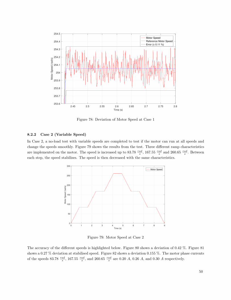
2.45 2.5 2.55 2.6 2.65 2.7 2.75 2.8
Time (s)
253.6
253.7
253.8
253.9
254
254.1
254.2
254.3
254.4
254.5
Moto
r S
peed (
rad/s
)
Motor Speed
Reference Motor Speed
Error (± 0.11 %)
Figure 78: Deviation of Motor Speed at Case 1
8.2.2 Case 2 (Variable Speed)
In Case 2, a no-load test with variable speeds are completed to test if the motor can run at all speeds andchange the speeds smoothly. Figure 79 shows the results from the test. Three different ramp characteristicsare implemented on the motor. The speed is increased up to 83.78 rad
s , 167.55 rads and 260.65 rad
s . Betweeneach step, the speed stabilises. The speed is then decreased with the same characteristics.
0 1 2 3 4 5 6 7 8 9
Time (s)
0
50
100
150
200
250
300
Mo
tor
Sp
ee
d (
rad
/s)
Motor Speed
Figure 79: Motor Speed at Case 2
The accuracy of the different speeds is highlighted below. Figure 80 shows a deviation of 0.42 %. Figure 81shows a 0.27 % deviation at stabilised speed. Figure 82 shows a deviation 0.155 %. The motor phase currentsof the speeds 83.78 rad
s , 167.55 rads , and 260.65 rad
s are 0.20 A, 0.26 A, and 0.30 A respectively.
50
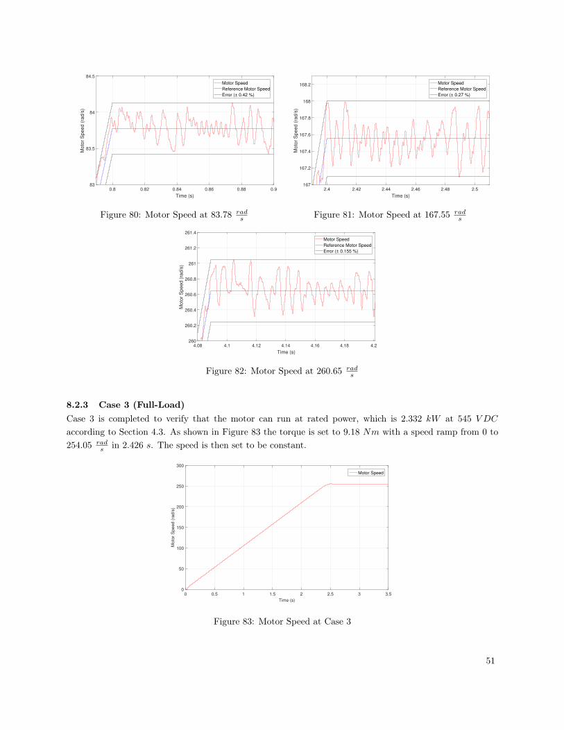
0.8 0.82 0.84 0.86 0.88 0.9
Time (s)
83
83.5
84
84.5
Moto
r S
peed (
rad/s
)Motor Speed
Reference Motor Speed
Error (± 0.42 %)
Figure 80: Motor Speed at 83.78 rads
2.4 2.42 2.44 2.46 2.48 2.5
Time (s)
167
167.2
167.4
167.6
167.8
168
168.2
Moto
r S
peed (
rad/s
)
Motor Speed
Reference Motor Speed
Error (± 0.27 %)
Figure 81: Motor Speed at 167.55 rads
4.08 4.1 4.12 4.14 4.16 4.18 4.2
Time (s)
260
260.2
260.4
260.6
260.8
261
261.2
261.4
Moto
r S
peed (
rad/s
)
Motor Speed
Reference Motor Speed
Error (± 0.155 %)
Figure 82: Motor Speed at 260.65 rads
8.2.3 Case 3 (Full-Load)Case 3 is completed to verify that the motor can run at rated power, which is 2.332 kW at 545 V DC
according to Section 4.3. As shown in Figure 83 the torque is set to 9.18 Nm with a speed ramp from 0 to254.05 rad
s in 2.426 s. The speed is then set to be constant.
0 0.5 1 1.5 2 2.5 3 3.5
Time (s)
0
50
100
150
200
250
300
Moto
r S
peed (
rad/s
)
Motor Speed
Figure 83: Motor Speed at Case 3
51
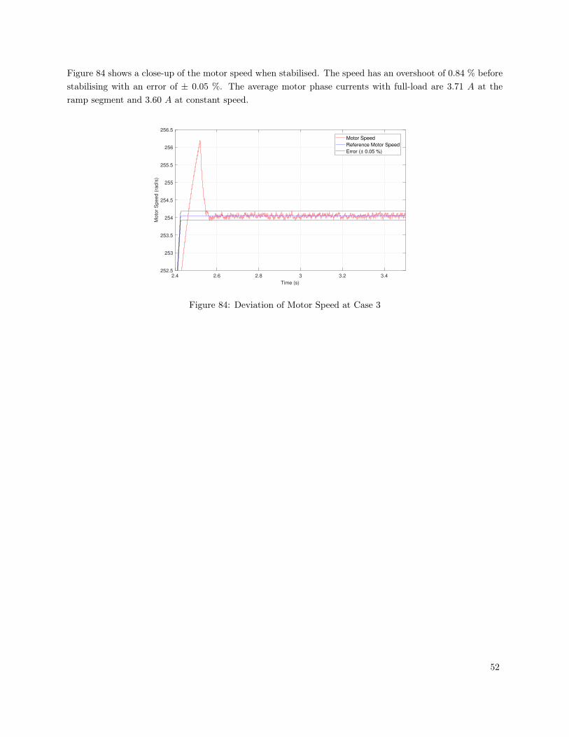
Figure 84 shows a close-up of the motor speed when stabilised. The speed has an overshoot of 0.84 % beforestabilising with an error of ± 0.05 %. The average motor phase currents with full-load are 3.71 A at theramp segment and 3.60 A at constant speed.
2.4 2.6 2.8 3 3.2 3.4
Time (s)
252.5
253
253.5
254
254.5
255
255.5
256
256.5
Mo
tor
Sp
ee
d (
rad
/s)
Motor Speed
Reference Motor Speed
Error (± 0.05 %)
Figure 84: Deviation of Motor Speed at Case 3
52
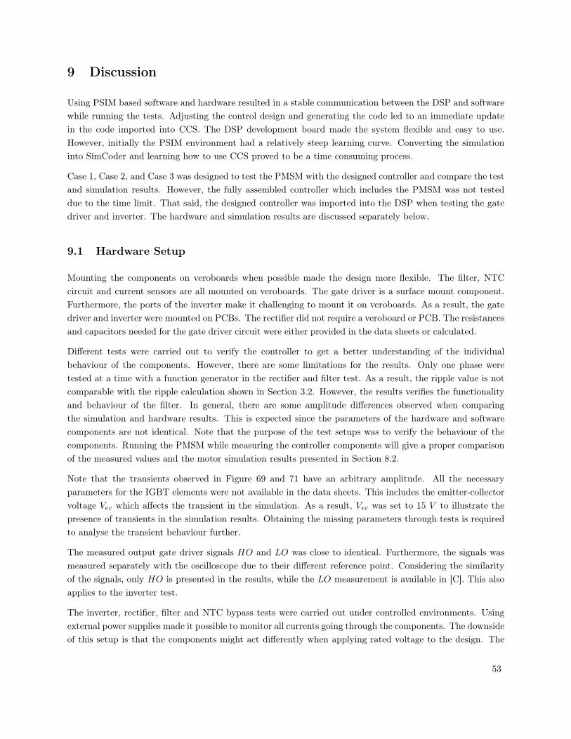
9 Discussion
Using PSIM based software and hardware resulted in a stable communication between the DSP and softwarewhile running the tests. Adjusting the control design and generating the code led to an immediate updatein the code imported into CCS. The DSP development board made the system flexible and easy to use.However, initially the PSIM environment had a relatively steep learning curve. Converting the simulationinto SimCoder and learning how to use CCS proved to be a time consuming process.
Case 1, Case 2, and Case 3 was designed to test the PMSM with the designed controller and compare the testand simulation results. However, the fully assembled controller which includes the PMSM was not testeddue to the time limit. That said, the designed controller was imported into the DSP when testing the gatedriver and inverter. The hardware and simulation results are discussed separately below.
9.1 Hardware Setup
Mounting the components on veroboards when possible made the design more flexible. The filter, NTCcircuit and current sensors are all mounted on veroboards. The gate driver is a surface mount component.Furthermore, the ports of the inverter make it challenging to mount it on veroboards. As a result, the gatedriver and inverter were mounted on PCBs. The rectifier did not require a veroboard or PCB. The resistancesand capacitors needed for the gate driver circuit were either provided in the data sheets or calculated.
Different tests were carried out to verify the controller to get a better understanding of the individualbehaviour of the components. However, there are some limitations for the results. Only one phase weretested at a time with a function generator in the rectifier and filter test. As a result, the ripple value is notcomparable with the ripple calculation shown in Section 3.2. However, the results verifies the functionalityand behaviour of the filter. In general, there are some amplitude differences observed when comparingthe simulation and hardware results. This is expected since the parameters of the hardware and softwarecomponents are not identical. Note that the purpose of the test setups was to verify the behaviour of thecomponents. Running the PMSM while measuring the controller components will give a proper comparisonof the measured values and the motor simulation results presented in Section 8.2.
Note that the transients observed in Figure 69 and 71 have an arbitrary amplitude. All the necessaryparameters for the IGBT elements were not available in the data sheets. This includes the emitter-collectorvoltage Vec which affects the transient in the simulation. As a result, Vec was set to 15 V to illustrate thepresence of transients in the simulation results. Obtaining the missing parameters through tests is requiredto analyse the transient behaviour further.
The measured output gate driver signals HO and LO was close to identical. Furthermore, the signals wasmeasured separately with the oscilloscope due to their different reference point. Considering the similarityof the signals, only HO is presented in the results, while the LO measurement is available in [C]. This alsoapplies to the inverter test.
The inverter, rectifier, filter and NTC bypass tests were carried out under controlled environments. Usingexternal power supplies made it possible to monitor all currents going through the components. The downsideof this setup is that the components might act differently when applying rated voltage to the design. The
53
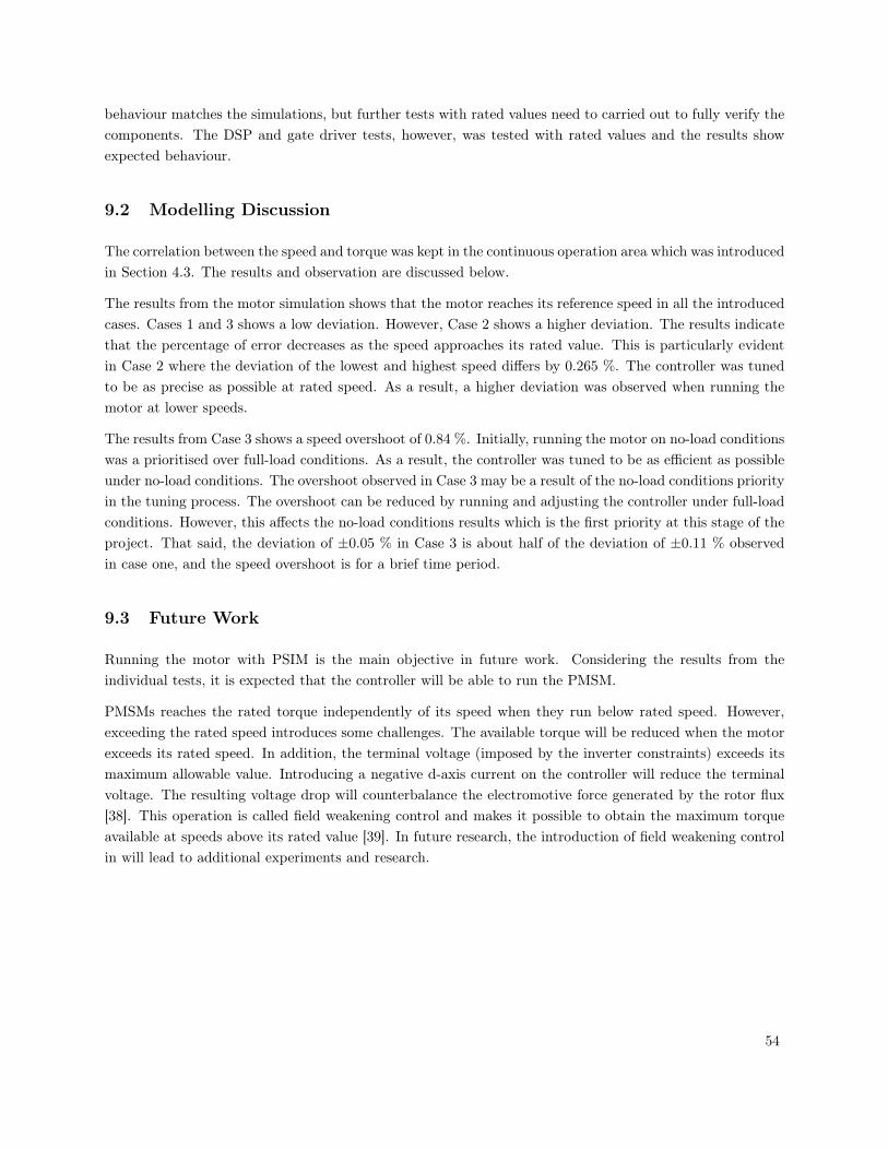
behaviour matches the simulations, but further tests with rated values need to carried out to fully verify thecomponents. The DSP and gate driver tests, however, was tested with rated values and the results showexpected behaviour.
9.2 Modelling Discussion
The correlation between the speed and torque was kept in the continuous operation area which was introducedin Section 4.3. The results and observation are discussed below.
The results from the motor simulation shows that the motor reaches its reference speed in all the introducedcases. Cases 1 and 3 shows a low deviation. However, Case 2 shows a higher deviation. The results indicatethat the percentage of error decreases as the speed approaches its rated value. This is particularly evidentin Case 2 where the deviation of the lowest and highest speed differs by 0.265 %. The controller was tunedto be as precise as possible at rated speed. As a result, a higher deviation was observed when running themotor at lower speeds.
The results from Case 3 shows a speed overshoot of 0.84 %. Initially, running the motor on no-load conditionswas a prioritised over full-load conditions. As a result, the controller was tuned to be as efficient as possibleunder no-load conditions. The overshoot observed in Case 3 may be a result of the no-load conditions priorityin the tuning process. The overshoot can be reduced by running and adjusting the controller under full-loadconditions. However, this affects the no-load conditions results which is the first priority at this stage of theproject. That said, the deviation of ±0.05 % in Case 3 is about half of the deviation of ±0.11 % observedin case one, and the speed overshoot is for a brief time period.
9.3 Future Work
Running the motor with PSIM is the main objective in future work. Considering the results from theindividual tests, it is expected that the controller will be able to run the PMSM.
PMSMs reaches the rated torque independently of its speed when they run below rated speed. However,exceeding the rated speed introduces some challenges. The available torque will be reduced when the motorexceeds its rated speed. In addition, the terminal voltage (imposed by the inverter constraints) exceeds itsmaximum allowable value. Introducing a negative d-axis current on the controller will reduce the terminalvoltage. The resulting voltage drop will counterbalance the electromotive force generated by the rotor flux[38]. This operation is called field weakening control and makes it possible to obtain the maximum torqueavailable at speeds above its rated value [39]. In future research, the introduction of field weakening controlin will lead to additional experiments and research.
54

10 Conclusion
In this thesis, a PSIM-based controller for an inverter-fed PMSM was dimensioned and designed. Themajority of the report addresses the software design needed to implement the controller to the PMSM. Theproject outputs and requirements were listed in the problem statement. The progress of the research issummarised below.
1. The frequency converter was dimensioned for a 2.332 kW PMSM. The simulation model proved to beefficient when dimensioning the inductor, capacitor, NTC element, and the snubber. The data sheetsprovided sufficient information to dimension the rectifier, inverter, gate driver, cooling elements, andcurrent sensors.
2. The PSIM based simulation model was presented in two parts. The first part was the frequencyconverter and motor. The second part was the control algorithm that controls the speed of the motor.The dimensioned components was implemented to get as realistic results as possible. Creating themodel introduced the opportunity of analysing the behaviour of the entire frequency converter bysimulations. Tuning the controller to get adequate results proved to be a comprehensive process.
3. Converting the PSIM model into SimCoder made it possible to run the frequency converter throughthe PSIM model. The conversion included swapping out the PSIM components that were incompatiblewith the code generation with compatible ones. Generally, the conversion process was straightforward.However, implementing the encoder and tuning it was challenging.
4. The filter, NTC circuit, and current sensors were soldered on veroboards. PCB designs were the bestsolution for the gate driver and inverter. The rectifier did not need any board design. Designing thegate driver circuit on a prototype breadboard made the system more flexible and made it possible totest different resistances.
5. Importing the code into CCS required much testing with PSIM example designs to make it work asexpected. The current sensors were calibrated to match the DSP measurements.
6. The components of the frequency converter were tested individually. The measured hardware signalsand the test simulation results show similar behaviour. The amplitudes of the components can beverified by running additional tests in rated conditions.
Using PSIM to design and run the frequency converter was an educational process although the softwarehad a steep learning curve. Running the individual components with PSIM through the DSP developmentboard was easy and intuitive ones the system was designed. The low cost and open system design of thesoftware make it a good alternative in future research.
A full-scale test of the frequency converter with all the rated value can be conducted to fully verify the design.Comparing the measured values with the full-scale simulation results presented in Section 8.2 may verify thedesign functionality further. The design introduces research opportunities for the control algorithm. Thecontroller can be improved by implementing field weakening control into the design to run the PMSM athigher than rated value speeds.
55

References
[1] J. F. Gieras, Permanent magnet motor technology: design and applications. CRC press, 2002, pp. iii–16.
[2] W. Li, C. Abbey, and G. Joós, “Control and performance of wind turbine generators based on perma-nent magnet synchronous machines feeding a diode rectifier,” in IEEE Power Electronics SpecialistsConference, vol. 2, 2006, pp. 1–6.
[3] Z. Jian, W. Xuhui, and Z. Lili, “Optimal system efficiency operation of dual pmsm motor drive forfuel cell vehicles propulsion,” in Power Electronics and Motion Control Conference, 2009. IPEMC’09.IEEE 6th International, IEEE, 2009, pp. 1889–1892.
[4] Certification summary information report, JTSLV00.0L13-002, epa certificate tesla model 3, epa, Dec.2017.
[5] M. T. Elsayed, O. A. Mahgoub, and S. A. Zaid, “Simulation study of a new approach for field weakeningcontrol of pmsm,” Journal of power electronics, vol. 12, no. 1, pp. 136–144, 2012.
[6] N. Mohan, Electric Machines and Drives, 1st ed. 2012, isbn: 9781118074817.
[7] B. K. Bose, “Energy, environment, and advances in power electronics,” IEEE Transactions on PowerElectronics, vol. 15, no. 4, pp. 688–701, 2000.
[8] J. Bocker and S. Mathapati, “State of the art of induction motor control,” in Electric Machines &Drives Conference, 2007. IEMDC’07. IEEE International, IEEE, vol. 2, 2007, pp. 1459–1464.
[9] H. Sira-Ramírez, J. Linares-Flores, C. García-Rodríguez, and M. A. Contreras-Ordaz, “On the controlof the permanent magnet synchronous motor: An active disturbance rejection control approach,” IEEETransactions on Control Systems Technology, vol. 22, no. 5, pp. 2056–2063, 2014.
[10] M. Donsión, “Parameters influence on the control of a pmsm,” in ISEF 2007-XIII International Sympo-sium on Electromagnetic Fields in Mechatronics, Electrical and Electronic Engineering, 2007, pp. 13–15.
[11] C. Morkoç, Y. Önal, and M. Kesler, “Dsp based embedded code generation for pmsm using slidingmode controller,” in Power Electronics and Motion Control Conference and Exposition (PEMC), 201416th International, IEEE, 2014, pp. 472–476.
[12] N. Instruments. (2013). Supported motor types, [Online]. Available: http://zone.ni.com/reference/en-XX/help/374169A-01/lvemsimshared/motor_type/ (visited on 09/27/2017).
[13] P. C. Perera, Sensorless control of permanent-magnet synchronous motor drives. Institute of EnergyTechnology, Aalborg University, 2002.
[14] T. M. Jahns, G. B. Kliman, and T. W. Neumann, “Interior permanent-magnet synchronous motors foradjustable-speed drives,” IEEE Transactions on Industry Applications, no. 4, pp. 738–747, 1986.
[15] K. Akatsu, K. Narita, Y. Sakashita, and T. Yamada, “Characteristics comparison between spmsmand ipmsm under high flux density condition by both experimental and analysis results,” in ElectricalMachines and Systems, 2008. ICEMS 2008. International Conference on, IEEE, 2008, pp. 2848–2853.
[16] L. He, J. Ma, Y. Fang, and S. Liang, “An improved method to estimate initial rotor position for surface-mounted permanent magnet synchronous motors,” in Electrical Machines and Systems (ICEMS), 201417th International Conference on, IEEE, 2014, pp. 2050–2054.
56
[17] W. T. Thomson and M. Fenger, “Current signature analysis to detect induction motor faults,” IEEEIndustry Applications Magazine, vol. 7, no. 4, pp. 26–34, 2001.
[18] E. PUMPS. (2017). Ac induction motors vs. permanent magnet synchronous motors, [Online]. Avail-able: http://empoweringpumps.com/ac-induction-motors-versus-permanent-magnet-synchronous-motors-fuji/ (visited on 11/13/2017).
[19] G. Kohlrusz and D. Fodor, “Comparison of scalar and vector control strategies of induction motors,”Hungarian Journal of Industry and Chemistry, vol. 39, no. 2, pp. 265–270, 2011.
[20] D. Jee and N. Patel, “V/f control of induction motor drive,” PhD thesis, 2013.
[21] E. DISTRELEC. (2017). Brolikeretter, trefaset 600 v 25 a 26mt60pbf, vishay, [Online]. Available:https://www.elfadistrelec.no/no/brolikeretter- trefaset- 600- 25- vishay- 26mt60pbf/p/17036205?q=brolikeretter&page=4&origPos=4&origPageSize=50&simi=95.97 (visited on10/04/2017).
[22] D. Tardiff and T. Barton, “A summary of resonant snubber circuits for transistors and gtos,” inIndustry Applications Society Annual Meeting, 1989., Conference Record of the 1989 IEEE, IEEE,1989, pp. 1176–1180.
[23] N. Mohan, Power electronics: a first course. Wiley, 2011, pp. 113–114.
[24] S. Pyakuryal and M. Matin, “Filter design for ac to dc converter,” International Refereed Journal ofEngineering and Science (IRJES), vol. 2, no. 6, pp. 42–49, 2013.
[25] infineon. (2017). Easypack 750 600v sixpack igbt module with igbt3 and ntc, [Online]. Available: https://www.infineon.com/cms/en/product/power/igbt/igbt-module/igbt-module-600v-650v/FS10R06VE3_B2/productType.html?productType=ff80808112ab681d0112ab6eb4921d7c (visited on10/10/2017).
[26] ——, (2017). Eicedriver compact - full bridge 3 phase gate driver ic with ls-soi technology to controlpower devices like mos-transistors or 600v igbts, [Online]. Available: https://www.infineon.com/cms/en/product/power/gate-driver-ics/level-shift-gate-drivers/three-phase-drivers/6edl04n06pt/?productType=db3a3044300452850130643e046d300b# (visited on 11/07/2017).
[27] M. H. Rashid, Power electronics handbook. Butterworth-Heinemann, 2017, p. 546.
[28] Elfadistrelect. (2017). Kjoleelement 100 mm 1.5 k/w svart anodisert, sk 100/100 sa, fischer elektronik,[Online]. Available: https://www.elfadistrelec.no/no/kjoleelement-100-mm-svart-anodisert-fischer- elektronik- sk- 100- 100- sa/p/17560430?q=kj%5C%C3%5C%B8leelement&page=4&origPos=119&origPageSize=50&simi=95.88 (visited on 10/10/2017).
[29] R. Components. (2018). Lem lts series closed loop current sensor, 0 → ±19.2a, [Online]. Available:https://uk.rs-online.com/web/p/current-transducers/4362330/ (visited on 04/22/2017).
[30] Microsemi. (2013). Park, inverse park and clarke, inverse clarke transformations mss software im-plementation, [Online]. Available: https://www.microsemi.com/document- portal/doc_view/132799-park-inverse-park-and-clarke-inverse-clarke-transformations-mss-software-implementation-user-guide (visited on 11/01/2017).
[31] B. Akin, M. Bhardwaj, and J. Warriner, “Sensorless field oriented control of 3-phase permanent magnetsynchronous motors,” Texas Instruments, Application Notes, 2013.
57

[32] I. Freescale Semiconductor. (2016). Sensorless pmsm field-oriented control, [Online]. Available: https://cache.nxp.com/docs/en/reference-manual/DRM148.pdf (visited on 11/01/2017).
[33] POWERSIM. (2016). Tutorial:motor control design suite, [Online]. Available: https://powersimtech.com/drive/uploads/2017/11/Tutorial-Motor-Control-Design-Suite-11.1.pdf (visited on11/20/2017).
[34] N. Instruments. (2018). Reading encoders, [Online]. Available: https://learn.ni.com/teach/resources/117/reading-encoders (visited on 05/10/2018).
[35] Tms320x280x, 2801x, 2804x enhanced quadrature encoder pulse (eqep) module, SPRU790D, Revised2008, Texas Instruments, Dec. 2008.
[36] Dsp development board user’s manual, Version 1, POWERSIM INC., Nov. 2016.
[37] T. Instruments. (2017). Fundamentals of mosfet and igbt gate driver circuits, [Online]. Available:http://www.ti.com/lit/ml/slua618/slua618.pdf (visited on 05/23/2018).
[38] M. Preindl and S. Bolognani, “Model predictive direct torque control with finite control set for pmsmdrive systems, part 2: Field weakening operation,” IEEE Transactions on Industrial Informatics, vol. 9,no. 2, pp. 648–657, 2013.
[39] M. Zordan, P. Vas, M. Rashed, S. Bolognani, and M. Zigliotto, “Field-weakening in high-performancepmsm drives: A comparative analysis,” vol. 3, pp. 1718–1724, 2000.
58

Appendix A Data Sheets
A.1 Rectifier
Document Number: 93565 For technical questions, contact: [email protected] www.vishay.comRevision: 03-Nov-08 1
Three Phase Bridge(Power Modules), 25/35 A
26MT../36MT.. SeriesVishay High Power Products
FEATURES• Universal, 3 way terminals: push-on, wrap
around or solder• High thermal conductivity package, electrically
insulated case• Center hole fixing• Excellent power/volume ratio• UL E300359 approved • Gold plated terminals solderable using lead (Pb)-free
solder; solder alloy Sn/Ag/Cu (SAC305); soldertemperature 260 to 275 °C
• RoHS compliant• Designed and qualified for industrial and consumer level
DESCRIPTIONA range of extremely compact, encapsulated three phasebridge rectifiers offering efficient and reliable operation. Theyare intended for use in general purpose and instrumentationapplications.
ELECTRICAL SPECIFICATIONS
PRODUCT SUMMARYIO 25/35 A
D-63
MAJOR RATINGS AND CHARACTERISTICSSYMBOL CHARACTERISTICS 26MT 36MT UNITS
IO25 35 A
TC 70 60 °C
IFSM50 Hz 360 475
A60 Hz 375 500
I2t50 Hz 635 1130
A2s60 Hz 580 1030
VRRM 100 to 1600 V
TJ - 55 to 150 °C
VOLTAGE RATINGS
TYPE NUMBERVOLTAGE
CODE
VRRM, MAXIMUM REPETITIVEPEAK REVERSE VOLTAGE
V
VRSM, MAXIMUM NON-REPETITIVE PEAK REVERSE VOLTAGE
V
IRRM MAXIMUM AT TJ MAXIMUM
mA
26MT../36MT..
10 100 150
2
20 200 275
40 400 500
60 600 725
80 800 900
100 1000 1100
120 1200 1300
140 1400 1500
160 1600 1700
59

www.vishay.com For technical questions, contact: [email protected] Document Number: 935652 Revision: 03-Nov-08
26MT../36MT.. SeriesVishay High Power Products Three Phase Bridge
(Power Modules), 25/35 A
FORWARD CONDUCTION
PARAMETER SYMBOL TEST CONDITIONS VALUES
UNITS26MT 36MT
Maximum DC output current at TC IO 120° rect. conduction angle25 35 A
70 60 °C
Maximum peak, one-cycle non-repetitive forward current
IFSM
t = 10 ms No voltage reapplied
InitialTJ = TJ maximum
360 475
At = 8.3 ms 375 500
t = 10 ms 100 % VRRM
reapplied
300 400
t = 8.3 ms 314 420
Maximum I2t for fusing I2t
t = 10 ms No voltage reapplied
635 1130
A2st = 8.3 ms 580 1030
t = 10 ms 100 % VRRM
reapplied
450 800
t = 8.3 ms 410 730
Maximum I2√t for fusing I2√t I2t for time tx = I2√t x √tx; 0.1 ≤ tx ≤ 10 ms, VRRM = 0 V 6360 11 300 A2√s
Low level of threshold voltage VF(TO)1 (16.7 % x π x IF(AV) < I < π x IF(AV)), TJ maximum 0.88 0.86V
High level of threshold voltage VF(TO)2 ( I > π x IF(AV)), TJ maximum 1.13 1.03
Low level forward slope resistance rt1 (16.7 % x π x IF(AV) < I < π x IF(AV)), TJ maximum 7.9 6.3mΩ
High level forward slope resistance rt2 ( I > π x IF(AV)), TJ maximum 5.2 5.0
Maximum forward voltage drop VFM TJ = 25 °C, IFM = 40 Apk - per single junction 1.26 1.19 V
Maximum DC reverse current IRRM TJ = 25 °C, per junction at rated VRRM 100 µA
RMS isolation voltage VINS TJ = 25 °C, all terminal shorted; f = 50 Hz, t = 1 s 2700 V
THERMAL - MECHANICAL SPECIFICATIONS
PARAMETER SYMBOL TEST CONDITIONSVALUES
UNITS26MT 36MT
Maximum junction and storage temperature range
TJ, TStg - 55 to 150 °C
Maximum thermal resistance,junction to case
RthJCDC operation per bridge(based on total power loss of bridge)
1.42 1.35
K/WMaximum thermal resistance, case to heatsink
RthCS Mounting surface, smooth, flat and greased 0.2 0.2
Approximate weight 20 g
Mounting torque ± 10 % Bridge to heatsink with screw M4 2.0 Nm
60

Document Number: 95251 For technical questions, contact: [email protected] www.vishay.comRevision: 04-Nov-08 1
D-63
Outline DimensionsVishay Semiconductors
DIMENSIONS in millimeters (inches)
Not to scale
6.3 x 0.8 (0.25 x 0.03)
0.8 (0.31)
5.2(0.20)
25.3 (0.99) MAX.
Suggested plugging force:400 N maximum; axially applied to fast on terminals
~ ~
~
-
+
23 (0.90)21 (0.83)
10(0.39)
16(0.63)
28.5(1.12)
61
A.2 Capacitor
Aluminum electrolytic capacitors
Snap-in capacitors
Series/Type: B43305
Date: November 2008
© EPCOS AG 2008. Reproduction, publication and dissemination of this publication, enclosures hereto and theinformation contained therein without EPCOS' prior express consent is prohibited.
62

General-purpose grade capacitors
Applications
Switch-mode power supplies in industrial and entertainment
electronics
Uninterruptiple power supplies
Features
Voltage derating (0.93 VR) enables 105 °C operation, more
details available upon request
Extremely high CV product, ultra compact
High ripple current capability
Different case sizes available for each capacitance value
RoHS-compatible
Construction
Charge/discharge-proof, polar
Aluminum case, fully insulated with PVC
Version with PET insulation available
Version with additional PET insulation cap on terminal side
available for insulating the capacitor from the PCB
Snap-in solder pins to hold component in place on PC-board
Minus pole marking on case surface
Minus pole not insulated from case
Overload protection by safety vent on the base
Terminals
Standard version with 2 terminals,
2 lengths available: 6.3 and 4.5 mm
3 terminals to ensure correct insertion: length 4.5 mm
Snap-in capacitors B43305
Ultra compact 85 °C
Page 2 of 20Please read Cautions and warnings andImportant notes at the end of this document. 63

Specifications and characteristics in brief
Rated voltage VR 200 ... 450 V DC
Surge voltage VS 1.15 VR (for VR ≤ 250 V DC)
1.10 VR (for VR ≥ 400 V DC)
Rated capacitance CR 68 ... 3300 µF
Capacitance tolerance ±20% M
Dissipation factor tan δ VR ≤ 250 V DC: tan δ ≤ 0.15
(20 °C, 120 Hz) VR ≥ 400 V DC: tan δ ≤ 0.20
Leakage current Ileak
(5 min, 20 °C)
Self-inductance ESL Approx. 20 nH
Useful life Requirements:
85 °C; VR; IAC,R > 2000 h ∆C/C ≤ ±30% of initial value
40 °C; VR; 1.1 IAC,R > 100000 h tan δ ≤ 3 times initial specified limit
Ileak ≤ initial specified limit
Voltage endurance test Post test requirements:
85 °C; VR 2000 h ∆C/C ≤ ±10% of initial value
tan δ ≤ 1.3 times initial specified limit
Ileak ≤ initial specified limit
Vibration resistance
test
To IEC 60068-2-6, test Fc:
Displacement amplitude 0.35 mm, frequency range 10 Hz ... 55 Hz,
acceleration max. 5 g, duration 3 × 2 h.
Capacitor mounted by its body which is rigidly clamped to the work
surface.
Characteristics at low
temperature Max. impedance ratio
at 100 HzVR ≤ 250 V ≥ 400 V
Z -25 °C / Z 20 °C 3 7
Z -40 °C / Z 20 °C 7 14
IEC climatic category To IEC 60068-1:
VR ≤ 250 V DC: 40/085/56 ( 40 °C/+85 °C/56 days damp heat test)
VR ≥ 400 V DC: 25/085/56 ( 25 °C/+85 °C/56 days damp heat test)
The capacitors can be operated in the temperature range of
40 °C to +85 °C but the impedance at 40 °C should be taken into
consideration.
Detail specification
Sectional specification
Similar to CECC 30301-806
IEC 60384-4
B43305
Ultra compact 85 °C
Page 3 of 20Please read Cautions and warnings andImportant notes at the end of this document. 64
3) 120-Hz conversion factor of ripple current: IAC (120 Hz) = 1.03 IAC (100 Hz)
Technical data and ordering codes
CR
100 Hz
20 °CµF
Case
dimensions
d × l
mm
ESRtyp
100 Hz
20 °CmΩ
Zmax
10 kHz
20 °CmΩ
IAC,max
100 Hz
60 °CA
IAC,R3)
100 Hz
85 °CA
Ordering code
(composition see below)
Composition of ordering code
* = Insulation feature # = Terminal style
0 = PVC insulation
6 = PET insulation
8 = PVC insulation with additional PET insulation
cap on terminal side
0 = snap-in standard terminals (6.3 mm)
2 = snap-in 3 terminals (4.5 mm)
7 = snap-in short terminals (4.5 mm)
VR = 400 V DC
68 22 × 25 1990 2690 1.28 0.65 B43305A9686M0*#
82 22 × 25 1650 2230 1.41 0.72 B43305A9826M0*#
100 22 × 25 1360 1830 1.55 0.79 B43305A9107M0*#
120 22 × 25 1130 1530 1.70 0.87 B43305A9127M0*#
150 22 × 30 900 1220 1.98 1.01 B43305A9157M0*#
180 22 × 30 750 1020 2.17 1.11 B43305A9187M0*#
180 25 × 25 750 1020 2.18 1.11 B43305B9187M0*#
220 22 × 35 620 830 2.49 1.27 B43305A9227M0*#
220 25 × 30 620 830 2.51 1.28 B43305B9227M0*#
270 22 × 45 500 680 2.92 1.49 B43305A9277M0*#
270 25 × 35 500 680 2.89 1.47 B43305B9277M0*#
270 30 × 25 500 680 2.79 1.42 B43305C9277M0*#
330 22 × 50 410 560 3.31 1.69 B43305A9337M0*#
330 25 × 40 410 560 3.29 1.68 B43305B9337M0*#
330 30 × 30 410 560 3.22 1.64 B43305C9337M0*#
330 35 × 25 410 560 3.04 1.55 B43305D9337M0*#
390 25 × 45 350 470 3.68 1.87 B43305A9397M0*#
390 30 × 35 350 470 3.62 1.85 B43305B9397M0*#
390 35 × 30 350 470 3.67 1.87 B43305C9397M0*#
470 25 × 50 290 390 4.14 2.11 B43305A9477M0*#
470 30 × 40 290 390 4.37 2.23 B43305B9477M0*#
470 35 × 30 290 390 4.03 2.05 B43305C9477M0*#
560 30 × 45 240 330 4.91 2.50 B43305A9567M0*#
560 35 × 35 240 330 4.56 2.32 B43305B9567M0*#
680 30 × 50 200 270 5.55 2.83 B43305A9687M0*#
680 35 × 40 200 270 5.18 2.64 B43305B9687M0*#
820 30 × 55 170 230 6.23 3.18 B43305A9827M0*#
820 35 × 45 170 230 5.85 2.98 B43305B9827M0*#
1000 35 × 50 140 190 6.63 3.38 B43305A9108M0*#
B43305
Ultra compact 85 °C
Page 11 of 20Please read Cautions and warnings andImportant notes at the end of this document. 65
A.3 Inductor
Dimensions: [mm]
Scale - 1:1,5
39,5
max
.5,
0±0
,5
39,5 max.
7,0 min.
23,0
max
.
1,0O typ.
25,0 ±0,5
15,0
±0,5
2
34
1
Recommended Hole Pattern: [mm]
Scale - 1:1
15,0
25,0
O 1,4
4
1 2
3
Schematic:
2
1
3
41
2
Properties Test conditions Value Unit Tol.
Inductance 10 kHz/ 0.1 mA L 3.9 mH ±30
Rated Current @ 70 °C IR 8 A max.
DC Resistance @ 20 °C RDC 31 mΩ max.
Rated Voltage 50 Hz UR 760 V (AC) max.
Insulation Test Voltage 50 Hz/ 5 mA/ 2 sec. UT 3000 V (AC)
Electrical Properties:
It is recommeded that the temperature of the component does not exceed +125°C under worstcase conditions
Storage Temperature (in originalpackaging) -20 °C up to +60 °C
Operating Temperature -40 °C up to +125 °C
Temperature Rise < 55K
Test conditions of Electrical Properties: +20°C, 33% RH if not specified differently
General Information:
Würth Elektronik eiSos GmbH & Co. KGEMC & Inductive Solutions
Max-Eyth-Str. 174638 WaldenburgGermanyTel. +49 (0) 79 42 945 - 0
CREATED CHECKED GENERAL TOLERANCE PROJECTIONMETHOD
KaS HasA DIN ISO 2768-1m
DESCRIPTION
WE-CMB HV Common ModePower Line Choke ORDER CODE
744830039080SIZE REVISION STATUS DATE BUSINESS UNIT PAGE
XL 001.000 Valid 2015-11-10 eiSos 1/5
This electronic component has been designed and developed for usage in general electronic equipment only. This product is not authorized for use in equipment where a higher safety standard and reliability standard is especially required or where a failure of the product is reasonably expected to cause severe personal injury or death, unless the parties have executed an agreement specifically governing such use. Moreover Würth Elektronik eiSos GmbH& Co KG products are neither designed nor intended for use in areas such as military, aerospace, aviation, nuclear control, submarine, transportation (automotive control, train control, ship control), transportation signal, disaster prevention, medical, public information network etc.. Würth Elektronik eiSos GmbH & Co KG must be informed about the intent of such usage before the design-in stage. In addition, sufficient reliability evaluation checks for safetymust be performed on every electronic component which is used in electrical circuits that require high safety and reliability functions or performance.
66
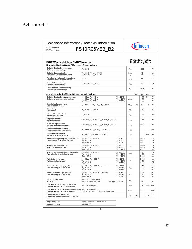
A.4 Inverter
1
TechnischeInformation/TechnicalInformation
FS10R06VE3_B2IGBT-ModuleIGBT-modules
preparedby:DPKapprovedby:RK
dateofpublication:2013-10-03revision:2.0
VorläufigeDatenPreliminaryDataIGBT,Wechselrichter/IGBT,Inverter
HöchstzulässigeWerte/MaximumRatedValuesKollektor-Emitter-SperrspannungCollector-emittervoltage Tvj = 25°C VCES 600 V
Kollektor-DauergleichstromContinuousDCcollectorcurrent
TC = 80°C, Tvj max = 175°CTC = 25°C, Tvj max = 175°C
IC nom
IC 10
16 AA
PeriodischerKollektor-SpitzenstromRepetitivepeakcollectorcurrent tP = 1 ms ICRM 20 A
Gesamt-VerlustleistungTotalpowerdissipation TC = 25°C, Tvj max = 175 Ptot 50,0 W
Gate-Emitter-SpitzenspannungGate-emitterpeakvoltage VGES +/-20 V
CharakteristischeWerte/CharacteristicValues min. typ. max.
Kollektor-Emitter-SättigungsspannungCollector-emittersaturationvoltage
IC = 10 A, VGE = 15 VIC = 10 A, VGE = 15 VIC = 10 A, VGE = 15 V
VCE sat
1,551,701,80
2,00
VVV
Tvj = 25°CTvj = 125°CTvj = 150°C
Gate-SchwellenspannungGatethresholdvoltage IC = 0,30 mA, VCE = VGE, Tvj = 25°C VGEth 4,9 5,8 6,5 V
GateladungGatecharge VGE = -15 V ... +15 V QG 0,10 µC
InternerGatewiderstandInternalgateresistor Tvj = 25°C RGint 0,0 Ω
EingangskapazitätInputcapacitance f = 1 MHz, Tvj = 25°C, VCE = 25 V, VGE = 0 V Cies 0,55 nF
RückwirkungskapazitätReversetransfercapacitance f = 1 MHz, Tvj = 25°C, VCE = 25 V, VGE = 0 V Cres 0,017 nF
Kollektor-Emitter-ReststromCollector-emittercut-offcurrent VCE = 600 V, VGE = 0 V, Tvj = 25°C ICES 1,0 mA
Gate-Emitter-ReststromGate-emitterleakagecurrent VCE = 0 V, VGE = 20 V, Tvj = 25°C IGES 400 nA
Einschaltverzögerungszeit,induktiveLastTurn-ondelaytime,inductiveload
IC = 10 A, VCE = 300 VVGE = ±15 VRGon = 27 Ω
td on
0,0120,0120,012
µsµsµs
Tvj = 25°CTvj = 125°CTvj = 150°C
Anstiegszeit,induktiveLastRisetime,inductiveload
IC = 10 A, VCE = 300 VVGE = ±15 VRGon = 27 Ω
tr
0,0090,0130,014
µsµsµs
Tvj = 25°CTvj = 125°CTvj = 150°C
Abschaltverzögerungszeit,induktiveLastTurn-offdelaytime,inductiveload
IC = 10 A, VCE = 300 VVGE = ±15 VRGoff = 27 Ω
td off
0,100,120,125
µsµsµs
Tvj = 25°CTvj = 125°CTvj = 150°C
Fallzeit,induktiveLastFalltime,inductiveload
IC = 10 A, VCE = 300 VVGE = ±15 VRGoff = 27 Ω
tf
0,0850,130,135
µsµsµs
Tvj = 25°CTvj = 125°CTvj = 150°C
EinschaltverlustenergieproPulsTurn-onenergylossperpulse
IC = 10 A, VCE = 300 V, LS = 60 nHVGE = ±15 VRGon = 27 Ω
Eon 0,140,200,22
mJmJmJ
Tvj = 25°CTvj = 125°CTvj = 150°C
AbschaltverlustenergieproPulsTurn-offenergylossperpulse
IC = 10 A, VCE = 300 V, LS = 60 nHVGE = ±15 VRGoff = 27 Ω
Eoff 0,240,300,32
mJmJmJ
Tvj = 25°CTvj = 125°CTvj = 150°C
KurzschlußverhaltenSCdata
VGE ≤ 15 V, VCC = 360 V VCEmax = VCES -LsCE ·di/dt ISC
50 A
Tvj = 150°C
tP ≤ 6 µs,
Wärmewiderstand,ChipbisGehäuseThermalresistance,junctiontocase proIGBT/perIGBT RthJC 2,70 3,00 K/W
Wärmewiderstand,GehäusebisKühlkörperThermalresistance,casetoheatsink
proIGBT/perIGBTλPaste=1W/(m·K)/λgrease=1W/(m·K) RthCH 1,00 K/W
TemperaturimSchaltbetriebTemperatureunderswitchingconditions Tvj op -40 150 °C
67

2
TechnischeInformation/TechnicalInformation
FS10R06VE3_B2IGBT-ModuleIGBT-modules
preparedby:DPKapprovedby:RK
dateofpublication:2013-10-03revision:2.0
VorläufigeDatenPreliminaryData
Diode,Wechselrichter/Diode,InverterHöchstzulässigeWerte/MaximumRatedValuesPeriodischeSpitzensperrspannungRepetitivepeakreversevoltage Tvj = 25°C VRRM 600 V
DauergleichstromContinuousDCforwardcurrent IF 10 A
PeriodischerSpitzenstromRepetitivepeakforwardcurrent tP = 1 ms IFRM 20 A
GrenzlastintegralI²t-value
VR = 0 V, tP = 10 ms, Tvj = 125°CVR = 0 V, tP = 10 ms, Tvj = 150°C I²t 12,5
9,50 A²sA²s
CharakteristischeWerte/CharacteristicValues min. typ. max.
DurchlassspannungForwardvoltage
IF = 10 A, VGE = 0 VIF = 10 A, VGE = 0 VIF = 10 A, VGE = 0 V
VF
1,601,551,50
2,05
VVV
Tvj = 25°CTvj = 125°CTvj = 150°C
RückstromspitzePeakreverserecoverycurrent
IF = 10 A, - diF/dt = 1500 A/µs (Tvj=150°C)VR = 300 VVGE = -15 V
IRM 18,019,021,0
AAA
Tvj = 25°CTvj = 125°CTvj = 150°C
SperrverzögerungsladungRecoveredcharge
IF = 10 A, - diF/dt = 1500 A/µs (Tvj=150°C)VR = 300 VVGE = -15 V
Qr 0,500,851,10
µCµCµC
Tvj = 25°CTvj = 125°CTvj = 150°C
AbschaltenergieproPulsReverserecoveryenergy
IF = 10 A, - diF/dt = 1500 A/µs (Tvj=150°C)VR = 300 VVGE = -15 V
Erec 0,110,200,26
mJmJmJ
Tvj = 25°CTvj = 125°CTvj = 150°C
Wärmewiderstand,ChipbisGehäuseThermalresistance,junctiontocase proDiode/perdiode RthJC 3,70 4,10 K/W
Wärmewiderstand,GehäusebisKühlkörperThermalresistance,casetoheatsink
proDiode/perdiodeλPaste=1W/(m·K)/λgrease=1W/(m·K) RthCH 1,90 K/W
TemperaturimSchaltbetriebTemperatureunderswitchingconditions Tvj op -40 150 °C
NTC-Widerstand/NTC-ThermistorCharakteristischeWerte/CharacteristicValues min. typ. max.
NennwiderstandRatedresistance TC = 25°C R25 5,00 kΩ
AbweichungvonR100DeviationofR100 TC = 100°C, R100 = 493 Ω ∆R/R -5 5 %
VerlustleistungPowerdissipation TC = 25°C P25 20,0 mW
B-WertB-value R2 = R25 exp [B25/50(1/T2 - 1/(298,15 K))] B25/50 3375 K
B-WertB-value R2 = R25 exp [B25/80(1/T2 - 1/(298,15 K))] B25/80 t.b.d. K
B-WertB-value R2 = R25 exp [B25/100(1/T2 - 1/(298,15 K))] B25/100 t.b.d. K
AngabengemäßgültigerApplicationNote.Specificationaccordingtothevalidapplicationnote.
68
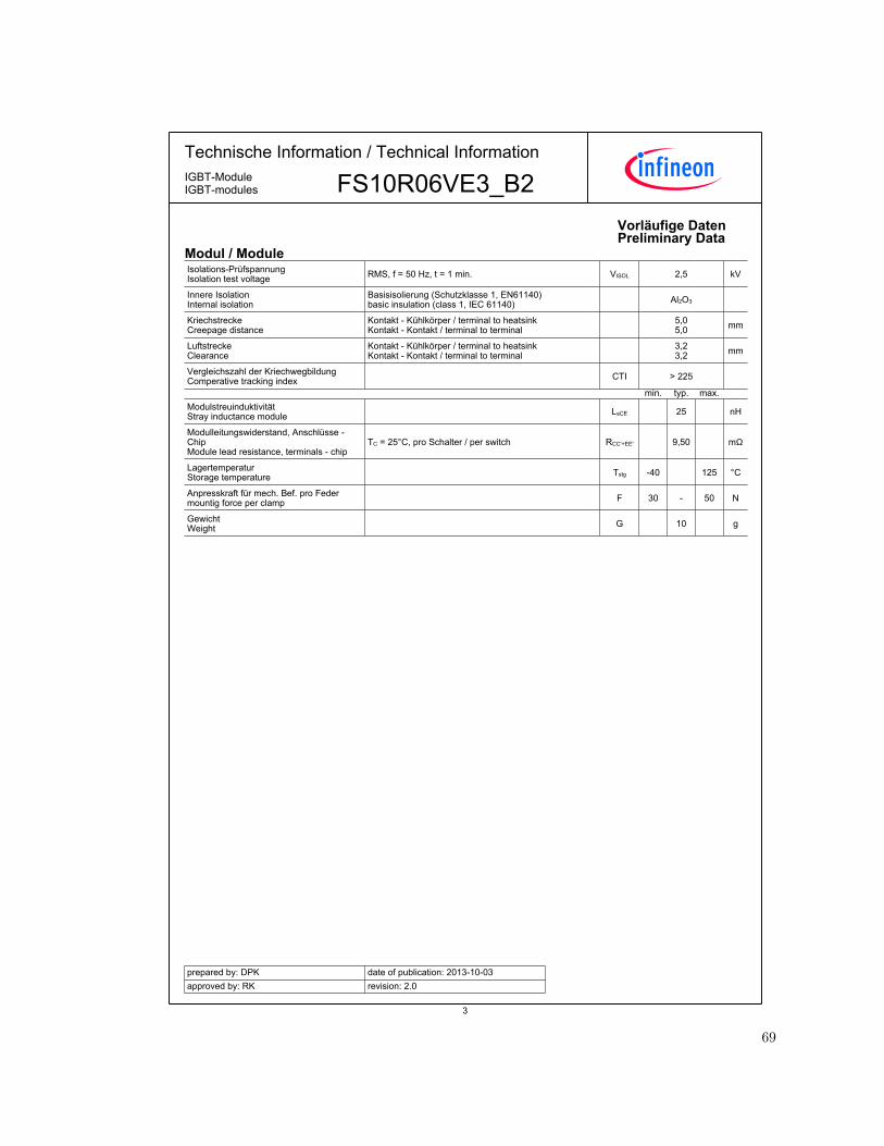
3
TechnischeInformation/TechnicalInformation
FS10R06VE3_B2IGBT-ModuleIGBT-modules
preparedby:DPKapprovedby:RK
dateofpublication:2013-10-03revision:2.0
VorläufigeDatenPreliminaryData
Modul/ModuleIsolations-PrüfspannungIsolationtestvoltage RMS, f = 50 Hz, t = 1 min. VISOL 2,5 kV
InnereIsolationInternalisolation
Basisisolierung(Schutzklasse1,EN61140)basicinsulation(class1,IEC61140) Al2O3
KriechstreckeCreepagedistance
Kontakt-Kühlkörper/terminaltoheatsinkKontakt-Kontakt/terminaltoterminal 5,0
5,0 mm
LuftstreckeClearance
Kontakt-Kühlkörper/terminaltoheatsinkKontakt-Kontakt/terminaltoterminal 3,2
3,2 mm
VergleichszahlderKriechwegbildungComperativetrackingindex CTI > 225
min. typ. max.
ModulstreuinduktivitätStrayinductancemodule LsCE 25 nH
Modulleitungswiderstand,Anschlüsse-ChipModuleleadresistance,terminals-chip
TC=25°C,proSchalter/perswitch RCC'+EE' 9,50 mΩ
LagertemperaturStoragetemperature Tstg -40 125 °C
Anpresskraft für mech. Bef. pro Federmountig force per clamp F 30 - 50 N
GewichtWeight G 10 g
69

7
TechnischeInformation/TechnicalInformation
FS10R06VE3_B2IGBT-ModuleIGBT-modules
preparedby:DPKapprovedby:RK
dateofpublication:2013-10-03revision:2.0
VorläufigeDatenPreliminaryDataSchaltplan/circuit_diagram_headline
J
Gehäuseabmessungen/packageoutlines
70

A.5 Gate Driver
Industr ia l Power Control
EiceDRIVER™ High voltage gate driver IC
datasheet
<Revision 2.6>, 05.08.2016
6ED fami ly - 2nd generat ion 3 phase 200 V and 600 V gate drive IC
6EDL04I06PT
6EDL04I06NT
6EDL04N06PT
6EDL04N02PR
EiceDRIVER™
71

EiceDRIVER™ 6ED family - 2nd generation
datasheet 7 <Revision 2.6>, 05.08.2016
EiceDRIVER™
3 phase 200 V and 600 V gate drive IC
1 Overview
Main features
Thin-film-SOI-technology
Maximum blocking voltage +600V
Separate control circuits for all six drivers
CMOS and LSTTL compatible input (negative logic)
Signal interlocking of every phase to prevent cross-conduction
Detection of over current and under voltage supply
externally programmable delay for fault clear after over current
detection
Product highlights
Insensitivity of the bridge output to negative transient voltages up to -50V given by SOI-technology
Ultra fast bootstrap diodes
'shut down' of all switches during error conditions
Typical applications
Home appliances
Fans, pumps
General purpose drives
Product family
Table 1 Members of 6ED family – 2nd
generation
Sales Name high side control input HIN1,2,3 and LIN1,2,3
typ. UVLO-Thresholds
Bootstrap diode
Package
6EDL04I06NT negative logic 11.7 V / 9.8 V Yes DSO28
6EDL04I06PT positive logic 11.7 V / 9.8 V Yes DSO28
6EDL04N06PT / 6EDL04N02PR positive logic 9 V / 8.1 V Yes DSO28 / TSSOP28
Description
The device 6ED family – 2nd
generation is a full bridge driver to control power devices like MOS-transistors or IGBTs in 3-phase systems with a maximum blocking voltage of +600 V. Based on the used SOI-technology there is an excellent ruggedness on transient voltages. No parasitic thyristor structures are present in the device. Hence, no parasitic latch-up may occur at all temperatures and voltage conditions.
The six independent drivers are controlled at the low-side using CMOS resp. LSTTL compatible signals, down to 3.3 V logic. The device includes an under-voltage detection unit with hysteresis characteristic and an over-current detection. The over-current level is adjusted by choosing the resistor value and the threshold level at pin ITRIP. Both error conditions (under-voltage and over-current) lead to a definite shut down off all six switches. An error signal is provided at the FAULT open drain output pin. The blocking time after over-current can be adjusted with an RC-network at pin RCIN. The input RCIN owns an internal current source of 2.8 µA. Therefore, the resistor RRCIN is optional. The typical output current can be given with 165 mA for pull-up and 375 mA for pull down. Because of system safety reasons a 310 ns interlocking time has been realised. The function of input EN can optionally be extended with an over-temperature detection, using an external NTC-resistor (see Fig.1). The
PG-DSO28
PG-TSSOP28
72
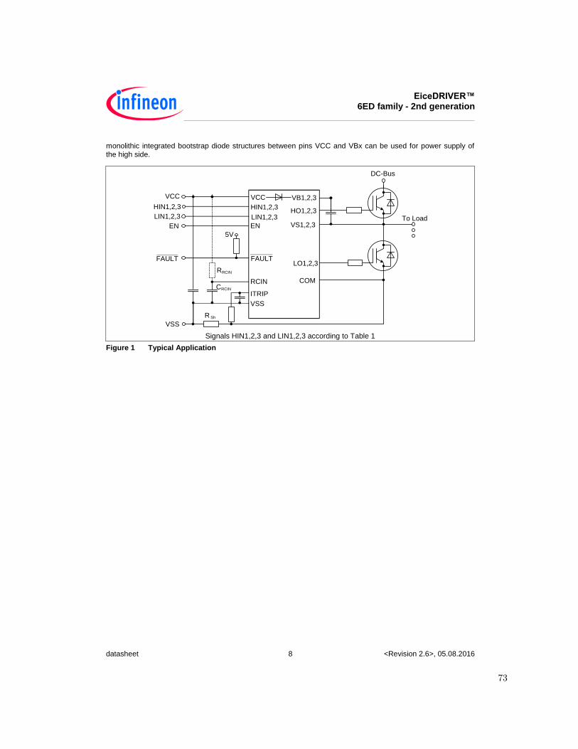
EiceDRIVER™ 6ED family - 2nd generation
datasheet 8 <Revision 2.6>, 05.08.2016
monolithic integrated bootstrap diode structures between pins VCC and VBx can be used for power supply of the high side.
Signals HIN1,2,3 and LIN1,2,3 according to Table 1
Figure 1 Typical Application
VCC
FAULT
LIN1,2,3
EN
RCIN
ITRIP
VSS
VB1,2,3
HO1,2,3
VS1,2,3
LO1,2,3
COM
To Load
VSS
EN
RRCIN
CRCIN
HIN1,2,3HIN1,2,3
LIN1,2,3
FAULT
VCC
DC-Bus
R Sh
5V
73

EiceDRIVER™ 6ED family - 2nd generation
datasheet 11 <Revision 2.6>, 05.08.2016
3 Pin configuration, description, and functionality
Figure 4 Pin Configuration of 6ED family (signals HIN1,2,3 and LIN1,2,3 according to Table 1)
Table 2 xPin Description
Symbol Description
VCC Low side power supply
VSS Logic ground
HIN1,2,3 High side logic input (positive or negative logic according to Table 1)
LIN1,2,3 Low side logic input (positive or negative logic according to Table 1)
/FAULT Indicates over-current and under-voltage (negative logic, open-drain output)
EN Enable I/O functionality (positive logic)
ITRIP Analog input for over-current shut down, activates FAULT and RCIN to VSS
RCIN External RC-network to define FAULT clear delay after FAULT-Signal (TFLTCLR)
COM Low side gate driver reference
VB1,2,3 High side positive power supply
HO1,2,3 High side gate driver output
VS1,2,3 High side negative power supply
LO1,2,3 Low side gate driver output
nc Not connected
3.1 Low Side and High Side Control Pins (Pin 2, 3, 4, 5, 6, 7)
The Schmitt trigger input threshold of them are such to guarantee LSTTL and CMOS compatibility down to 3.3 V controller outputs. Input Schmitt trigger and noise filter provide beneficial noise rejection to short input pulses according to Figure 5 and Figure 6.
1 28
2 27
3 26
4 25
5 24
6 23
7 22
8 21
9 20
10 19
11 18
12 17
13 16
14 15
VCC VB1
HIN1 HO1
HIN2 VS1
HIN3
LIN1 VB2
LIN2 HO2
LIN3 VS2
FAULT
ITRIP VB3
EN HO3
RCIN VS3
VSS
COM LO1
LO3 LO2
nc
nc
nc
74

EiceDRIVER™ 6ED family - 2nd generation
datasheet 14 <Revision 2.6>, 05.08.2016
4 Electrical Parameters
4.1 Absolute Maximum Ratings
All voltages are absolute voltages referenced to VSS -potential unless otherwise specified. All parameters are valid for Ta=25 °C.
Table 3 Abs. maximum ratings
Parameter Symbol Min. Max. Unit
High side offset voltage(Note 1) DSO28 TSSOP28
VS VCC-VBS-6 600 180
V
High side offset voltage (tp<500ns, Note 1) VCC -VBS – 50 –
High side offset voltage(Note 1) DSO28 TSSOP28
VB VCC – 6 620 200
High side offset voltage (tp<500ns, Note 1) VCC – 50 –
High side floating supply voltage (VB vs. VS) (internally clamped) VBS -1 20
High side output voltage (VHO vs. VS) VHO -0.5 VB + 0.5
Low side supply voltage (internally clamped) VCC -1 20
Low side supply voltage (VCC vs. VCOM) VCCOM -0.5 25
Gate driver ground VCOM -5.7 5.7
Low side output voltage (VLO vs. VCOM) VLO -0.5 VCCOM + 0.5
Input voltage LIN,HIN,EN,ITRIP VIN -1 10
FAULT output voltage VFLT -0.5 VCC + 0.5
RCIN output voltage VRCIN -0.5 VCC + 0.5
Power dissipation (to package) Note 2 DSO28 TSSOP28
PD –
– 1.3 0.6
W
Thermal resistance DSO28 (junction to ambient, see section 6) TSSOP28
Rth(j-a) –
– 75 165
K/W
Junction temperature TJ – 125 °C
Storage temperature TS - 40 150
offset voltage slew rate (Note 3) dVS/dt 50 V/ns
Note :The minimum value for ESD immunity is 1.0kV (Human Body Model). ESD immunity inside pins connected to the low side (VCC, HINx, LINx, FAULT, EN, RCIN, ITRIP, VSS, COM, LOx) and pins connected inside each high side itself (VBx, HOx, VSx) is guaranteed up to 1.5kV (Human Body Model).
Note 1 : In case VCC > VB there is an additional power dissipation in the internal bootstrap diode between pins VCC and VBx. Insensitivity of bridge output to negative transient voltage up to –50V is not subject to production test – verified by design / characterization.
Note 2: Consistent power dissipation of all outputs. All parameters inside operating range.
Note 3: Not subject of production test, verified by characterisation
75

EiceDRIVER™ 6ED family - 2nd generation
datasheet 15 <Revision 2.6>, 05.08.2016
4.2 Required operation conditions
All voltages are absolute voltages referenced to VSS -potential unless otherwise specified. All parameters are valid for Ta=25 °C.
Table 4 Required Operation Conditions
Parameter Symbol Min. Max. Unit
High side offset voltage (Note 1) DSO28 TSSOP28
VB 7 620 200
V
Low side supply voltage (VCC vs. VCOM) DSO28
TSSOP28
VCCOM 10 25
4.3 Operating Range
All voltages are absolute voltages referenced to VSS -potential unless otherwise specified. All parameters are valid for Ta=25 °C.
Table 5 Operating range
Parameter Symbol Min. Max. Unit
High side floating supply offset voltage VS VCC -
VBS -1 500
V
High side floating supply offset voltage (VB vs. VCC, statically) VBCC -1.0 500
High side floating supply voltage (VB vs. VS, Note 1) 6EDL04I06NT 6EDL04I06PT
VBS 13 17.5
6EDL04N06PT 6EDL04N02PR
10 17.5
High side output voltage (VHO vs. VS) VHO 0 VBS
Low side output voltage (VLO vs. VCOM) VLO 0 VCC
Low side supply voltage
6EDL04I06NT 6EDL04I06PT
VCC 13 17.5
6EDL04N06PT 6EDL04N02PR
10 17.5
Low side ground voltage VCOM -2.5 2.5
Logic input voltages LIN,HIN,EN,ITRIP (Note 2) VIN 0 5
FAULT output voltage VFLT 0 VCC
RCIN input voltage VRCIN 0 VCC
Pulse width for ON or OFF (Note 3) tIN 1 – µs
Ambient temperature Ta -40 105 °C
Note 1 : Logic operational for VB (VB vs. VS) > 7,0V
Note 2 : All input pins (HINx, LINx) and EN, ITRIP pin are internally clamped (see abs. maximum ratings)
Note 3 : In case of input pulse width at LINx and HINx below 1µ the input pulse may not be transmitted properly
76
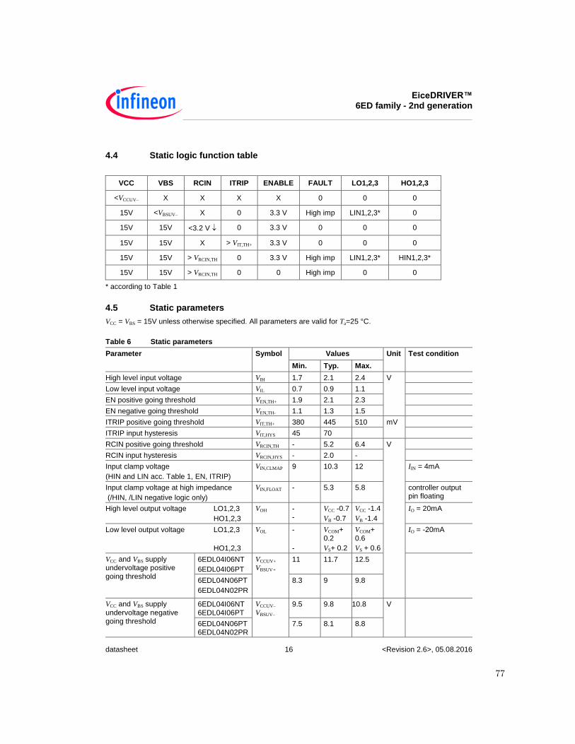
EiceDRIVER™ 6ED family - 2nd generation
datasheet 16 <Revision 2.6>, 05.08.2016
4.4 Static logic function table
VCC VBS RCIN ITRIP ENABLE FAULT LO1,2,3 HO1,2,3
<VCCUV– X X X X 0 0 0
15V <VBSUV– X 0 3.3 V High imp LIN1,2,3* 0
15V 15V <3.2 V 0 3.3 V 0 0 0
15V 15V X > VIT,TH+ 3.3 V 0 0 0
15V 15V > VRCIN,TH 0 3.3 V High imp LIN1,2,3* HIN1,2,3*
15V 15V > VRCIN,TH 0 0 High imp 0 0
* according to Table 1
4.5 Static parameters
VCC = VBS = 15V unless otherwise specified. All parameters are valid for Ta=25 °C.
Table 6 Static parameters
Parameter Symbol Values Unit Test condition
Min. Typ. Max.
High level input voltage VIH 1.7 2.1 2.4 V
Low level input voltage VIL 0.7 0.9 1.1
EN positive going threshold VEN,TH+ 1.9 2.1 2.3
EN negative going threshold VEN,TH- 1.1 1.3 1.5
ITRIP positive going threshold VIT,TH+ 380 445 510 mV
ITRIP input hysteresis VIT,HYS 45 70
RCIN positive going threshold VRCIN,TH - 5.2 6.4 V
RCIN input hysteresis VRCIN,HYS - 2.0 -
Input clamp voltage
(HIN and LIN acc. Table 1, EN, ITRIP)
VIN,CLMAP 9 10.3 12 IIN = 4mA
Input clamp voltage at high impedance
(/HIN, /LIN negative logic only)
VIN,FLOAT - 5.3 5.8 controller output pin floating
High level output voltage LO1,2,3
HO1,2,3
VOH - -
VCC -0.7
VB -0.7
VCC -1.4
VB -1.4
IO = 20mA
Low level output voltage LO1,2,3
HO1,2,3
VOL -
-
VCOM+
0.2
VS+ 0.2
VCOM+
0.6
VS + 0.6
IO = -20mA
VCC and VBS supply undervoltage positive going threshold
6EDL04I06NT
6EDL04I06PT
VCCUV+
VBSUV+ 11 11.7 12.5
6EDL04N06PT
6EDL04N02PR
8.3 9 9.8
VCC and VBS supply
undervoltage negative going threshold
6EDL04I06NT 6EDL04I06PT
VCCUV–
VBSUV–
9.5 9.8 10.8 V
6EDL04N06PT 6EDL04N02PR
7.5 8.1 8.8
77

EiceDRIVER™ 6ED family - 2nd generation
datasheet 17 <Revision 2.6>, 05.08.2016
Table 6 Static parameters
Parameter Symbol Values Unit Test condition
Min. Typ. Max.
VCC and VBS supply
undervoltage lockout hysteresis
6EDL04I06PT 6EDL04I06PT
VCCUVH
VBSUVH 1.2 1.9 - V
6EDL04N06PT 6EDL04N02PR
0.5 0.9 -
High side leakage current betw. VS and VSS ILVS+ 1 12.5 µA VS = 600V
High side leakage current betw. VS and VSS ILVS+1 - 10 - TJ=125°C,VS=600V
High side leakage current between VSx and VSy (x=1,2,3 and y=1,2,3)
ILVS–1 - 10 - TJ = 125°C
VSx - VSy = 600V
Quiescent current VBS supply (VB only) IQBS1 - 210 400 HO=low
Quiescent current VBS supply (VB only) IQBS2 - 210 400 HO=high
Quiescent current VCC
supply (VCC only) 6EDL04I06NT IQCC1 - 1.1 1.8 mA VLIN=float. (all)
VVSx=50V (only
bootstrap types) 6EDL04I06PT 6EDL04N06PT 6EDL04N02PR
- 0.75 1.5
Quiescent current VCC
supply (VCC only) 6EDL04I06NT IQCC2 - 1.3 2 VLIN=0, VHIN=3.3 V
VVSx=50V
6EDL04I06PT 6EDL04N06PT 6EDL04N02PR
0.75 1.5 VLIN=3.3 V, VHIN=0 VVSx=50V
Quiescent current VCC
supply (VCC only) 6EDL04I06NT IQCC3 - 1.3 2 VLIN=3.3 V, VHIN=0
VVSx=50V
6EDL04I06PT 6EDL04N06PT 6EDL04N02PR
0.75 1.5 VLIN=3.3 V, VHIN=0 VVSx=50V
Input bias current 6EDL04I06NT ILIN+ - 70 100 µA VLIN=3.3 V
6EDL04I06PT 6EDL04N06PT 6EDL04N02PR
400 700 1100
Input bias current 6EDL04I06NT ILIN- - 110 200 µA VLIN=0
6EDL04I06PT 6EDL04N06PT 6EDL04N02PR
0
Input bias current 6EDL04I06NT IHIN+ - 70 100 VHIN=3.3 V
6EDL04I06PT 6EDL04N06PT 6EDL04N02PR
400 700 1100
Input bias current 6EDL04I06NT IHIN- - 110 200 VHIN=0
6EDL04I06PT 6EDL04N06PT 6EDL04N02PR
0
Input bias current (ITRIP=high) IITRIP+ 45 120 VITRIP=3.3 V
Input bias current (EN=high) IEN+ - 45 120 VENABLE=3.3 V
Input bias current RCIN (internal current source)
IRCIN 2.8 VRCIN = 2 V
1 Not subject of production test, verified by characterisation
78
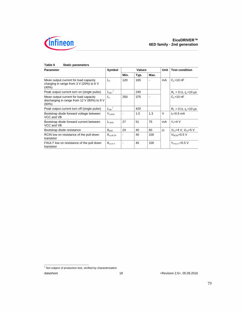
EiceDRIVER™ 6ED family - 2nd generation
datasheet 18 <Revision 2.6>, 05.08.2016
Table 6 Static parameters
Parameter Symbol Values Unit Test condition
Min. Typ. Max.
Mean output current for load capacity charging in range from 3 V (20%) to 6 V (40%)
IO+ 120 165 - mA CL=10 nF
Peak output current turn on (single pulse) IOpk+1
240 RL = 0 , tp <10 µs
Mean output current for load capacity discharging in range from 12 V (80%) to 9 V (60%)
IO- 250 375 - CL=10 nF
Peak output current turn off (single pulse) IOpk-1
420 RL = 0 , tp <10 µs
Bootstrap diode forward voltage between VCC and VB
VF,BSD - 1.0 1.3 V IF=0.5 mA
Bootstrap diode forward current between VCC and VB
IF,BSD 27 51 75 mA VF=4 V
Bootstrap diode resistance RBSD 24 40 60 VF1=4 V, VF2=5 V
RCIN low on resistance of the pull down transistor
Ron,RCIN - 40 100 VRCIN=0.5 V
FAULT low on resistance of the pull down transistor
Ron,FLT - 45 100 VFAULT=0.5 V
1 Not subject of production test, verified by characterisation
79

EiceDRIVER™ 6ED family - 2nd generation
datasheet 19 <Revision 2.6>, 05.08.2016
4.6 Dynamic parameters
VCC = VBS = 15 V, VS = VSS = VCOM unless otherwise specified. All parameters are valid for Ta=25 °C.
Table 7 Dynamic parameters
Parameter Symbol Values Unit Test condition
Min. Typ. Max.
Turn-on propagation delay ton 400 530 800 ns VLIN/HIN = 0 or 3.3 V
Turn-off propagation delay 6EDL04I06NT 6EDL04I06PT
toff 360 490 760
6EDL04N06PT 6EDL04N02PR
400 530 800
Turn-on rise time tr - 60 100 VLIN/HIN = 0 or 3.3 V
CL = 1 nF Turn-off fall time tf - 26 45
Shutdown propagation delay ENABLE tEN - 780 1100 VEN=0
Shutdown propagation delay ITRIP tITRIP 400 670 1000 VITRIP=1 V
Input filter time ITRIP tITRIPMIN 155 230 380
Propagation delay ITRIP to FAULT tFLT - 420 700
Input filter time at LIN/HIN for turn on and off tFILIN 120 300 - VLIN/HIN = 0 & 3.3 V
Input filter time EN tFILEN 300 600 -
Fault clear time at RCIN after ITRIP-fault, (CRCin=1nF)
tFLTCLR 1.0 1.9 3.0 ms VLIN/HIN = 0 & 3.3 V VITRIP = 0
Dead time DT 150 310 - ns VLIN/HIN = 0 & 3.3 V
Matching delay ON, max(ton)-min(ton), ton are applicable to all 6 driver outputs
MTON - 20 100 external dead time > 500 ns
Matching delay OFF, max(toff)-min(toff), toff are applicable to all 6 driver outputs
MTOFF - 40 100 external dead time >500 ns
Output pulse width matching. Pwin-PWout
6EDL04I06NT 6EDL04I06PT
PM 40 100 PW in > 1 µs
6EDL04N06PT 6EDL04N02PR
10 100
80
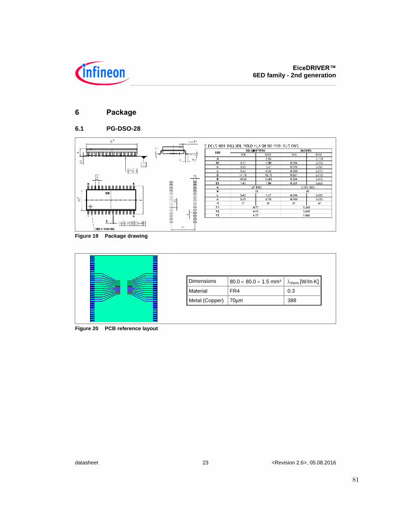
EiceDRIVER™ 6ED family - 2nd generation
datasheet 23 <Revision 2.6>, 05.08.2016
6 Package
6.1 PG-DSO-28
Figure 19 Package drawing
Dimensions 80.0 80.0 1.5 mm³ therm [W/mK]
Material FR4 0.3
Metal (Copper) 70µm 388
Figure 20 PCB reference layout
81
A.6 Gate Driver: Technical Description
Industr ia l Power & Contro l
EiceDRIVER™ High voltage gate drive IC
Appl icat ion Note AN-EICEDRIVER-6EDL04-1
Rev. 1.3, 2014-03-23
6ED fami ly - 2nd generat ion Technical description
82

6ED family - 2nd generation Technical Description
Application Note 15 Rev. 1.3, 2014-03-23 AN-EICEDRIVER-6EDL04-1
This pin is on high potential again after transistor T2 is turned off and either T1 or D1 is conducting current. But now the bootstrap diode DBS blocks a reverse current, so that the charges on the capacitor cannot flow back to the capacitor CVCC. The bootstrap diode DBS also takes over the blocking voltage between pin VB and VCC. It is good engineering to choose the same blocking voltage of power transistor T1 and external bootstrap diode. The voltage of the bootstrap capacitor can now supply the highside gate drive sections.
It is a general design rule for the location of bootstrap capacitors CBS, that they must be placed as close as possible to the IC. Otherwise, parasitic resistors and inductances may lead to voltage spikes, which may trigger the undervoltage lockout threshold of the individual highside driver section. The voltage of bootstrap capacitor is approximately
(1)
A current limiting resistor RLim reduces the peak of the pulse current during the turn-on of transistor T2. The pulse current will occur at each turn-on of transistor T2, so that with increasing switching frequency the capacitor CBS is charged more frequently. Therefore a smaller capacitor is suitable at higher switching frequencies. The bootstrap capacitor is mainly discharged by two effects: The highside quiescent current and the gate charge of the transistor to be turned on. The calculation of the bootstrap capacitor results in
(2)
with iQBS being the quiescent current of the highside section, tP the switching period, QG the total gate charge
and vBS the voltage drop at the bootstrap capacitor within a switching period. An additional margin of 20% is added for the case of tolerances for the bootstrap capacitor.
Figure 11 Size of the bootstrap capacitor as a function of the switching frequency fP for driving IKD10N60R according to equ. (2) with a voltage ripple of 0.1 V
Figure 11 shows the curve corresponding to equ. (2) for a continuous sinusoidal modulation, if the voltage ripple ΔvBS = 0.1 V. The recommended bootstrap capacitance is therefore in the range up to 4.7 μF for most switching frequencies. The performance of the integrated bootstrap diode supports the requirement for small bootstrap capacitances. It is therefore not recommended to exceed a maximum capacitance of CBS = 47 µF. Please note here, that equ. (2) is valid for continuous switching operation according to the switching frequency. The use of space vector modulations can cause periods up to 60° (electrical), in which no switching of the low side transistor of a halfbridge occurs and must be considered seperately. This effects the bootstrap capacitor size, especially for low output current (motor current) frequencies. In this case the variable tP must be set to the longest period of no switching.
0
1
2
3
4
5
0 5 10 15 20
CBS
fP
kHz
µF
83
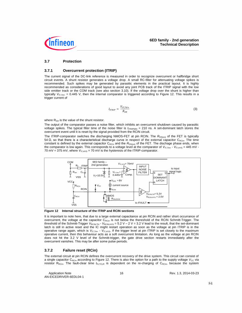
6ED family - 2nd generation Technical Description
Application Note 16 Rev. 1.3, 2014-03-23 AN-EICEDRIVER-6EDL04-1
3.7 Protection
3.7.1 Overcurrent protection (ITRIP)
The current signal of the DC-link reference is measured in order to recognize overcurrent or halfbridge short circuit events. A shunt resistor generates a voltage drop. A small RC-filter for attenuating voltage spikes is recommended. Such spikes may be generated by parasitic elements in the practical layout. It is highly recommended as considerations of good layout to avoid any joint PCB track of the ITRIP signal with the low side emitter track or the COM track (see also section 3.10). If the voltage drop over the shunt is higher than typically VIT,TH+ = 0.445 V, then the internal comparator is triggered according to Figure 12. This results in a trigger current of
(3)
where RSH is the value of the shunt resistor.
The output of the comparator passes a noise filter, which inhibits an overcurrent shutdown caused by parasitic voltage spikes. The typical filter time of the noise filter is tITRIPMIN = 210 ns. A set-dominant latch stores the overcurrent event until it is reset by the signal provided from the RCIN circuit.
The ITRIP-comparator switches the discharging NMOS-FET at pin RCIN. The RDS(on) of the FET is typically 54 Ω, so that there is a characteristical discharge curve in respect of the external capacitor CRCin. The time constant is defined by the external capacitor CRCin and the RDS(on) of the FET. The dischage phase ends, when the comparator is low again. This corresponds to a voltage level at the comparator of VIT,TH+ - VIT,HYS = 445 mV - 70 mV = 375 mV, where VIT,HYS = 70 mV is the hysteresis of the ITRIP-comparator.
RCIN IRCIN
VZ=10.5V
ITRIP
SET
DOMINANT
LATCH
S
R
Q
INPUT
NOISE
FILTERVIT,TH+=
0.445V Comp.
COM
VSS
VDD2 8V
NMOS
RON,RCIN
current source
VSS
VCC
VCC
to /FAULT
6ED family –
2nd generation
RRCin
CRCin
VRCIN,TH= 5.2V
VRCIN,HYS = 2.0V
to input
signal logic
VIT,HYS= 70mV
RSH
RF
CF
Figure 12 Internal structure of the ITRIP and RCIN sections
It is important to note here, that due to a large external capacitance at pin RCIN and rather short occurrance of overcurrent, the voltage at the capacitor CRCin is not below the thereshold of the RCIN Schmitt-Trigger. The threshold of the Schmitt-Trigger VRCIN,TH - VRCIN,HYS = 5.2 V – 2 V = 3.2 V lead to the result, that the set-dominant latch is still in active reset and the IC might restart operation as soon as the voltage at pin ITRIP is in the operative range again, which is VIT,TH+ - VIT,HYS. If the trigger level at pin ITRIP is set closely to the maximum operative current, then this behaviour acts as a soft overcurrent limitation. As long as the voltage at pin RCIN does not hit the 3.2 V level of the Schmitt-trigger, the gate drive section restarts immediately after the overcurrent vanishes. This may be after some pulse periods.
3.7.2 Failure reset (RCin)
The external circuit at pin RCIN defines the overcurrent recovery of the drive system. This circuit can consist of a single capacitor CRCin according to Figure 12. There is also the option for a path to the supply voltage VCC via resistor RRCin. The fault-clear time tFLTCLR is dependent on the re-charging of CRCin, because the system
84
A.7 Gate Driver: Tips and Tricks for RCIN and ITRIP
Application Note AN2015-09 1 <Revision 2>, <2015-07-13>
AN2015-09
About this document
Scope and purpose
The RCIN and ITRIP functions strongly help to reduce the system cost. However, the functions as they are available do have limitations in some applications. This application note helps to understand the function
more in detail and give application support how to overcome these limitations.
Intended audience
The application note addresses experienced hardware engineers who have already basic knowledge of the
6EDL family – 2nd generation.
Table of Contents
1 Introduction ............................................................................................................... 2
2 Overcoming the large tolerance of the RCIN timing ........................................................ 3
3 Overcome the high trigger level of the ITRIP function ..................................................... 7
Ei ceDR I V ER™
Tips & Tr i cks f or R CI N and I TR I P
6EDL family - 2nd generation
Application Note AN2015-09
85
Tips & Tricks for RCIN and ITRIP
Overcome the high trigger level of the ITRIP function
Application Note AN2015-09 7 <Revision 2>, <2015-07-13>
3 Overcome the high trigger level of the ITRIP function This section describes how the high trigger level of the overcurrent shut down function can be adapted
towards lower levels.
3.1 Application problem
The shunt, which is located in the emitter path of a low side IGBT, generates a voltage according to its bias point. This voltage is filtered by means of a RF / CF –combination according to Figure 5.
The ITRIP trigger level of VIT,th+ = 0.445 V is fixed for the 6EDL family – 2nd generation. The adjustment of the triggering current level is done by adjusting the shunt value, so that the shunt’s voltage will trigger the ITRIP event. However, applications with high load currents will dissipate a considerable power in the shunt. For example, a current trigger level of 50 A would dissipate a power of 50 A ∙ 0.445 V = 22.25 W. Therefore, the
current trigger level should result in a low shunt voltage in the area of 100 mV to 200 mV in order to reduce
the power dissipated in the shunt.
3.2 Application solution
The application solution is implemented by an additional voltage drop over the filter resistor RF. The voltage drop is generated by a current added by a pull up-resistor Rpu according to Figure 6.
The required voltage drop of the resistor RF is calculated with
This results in a required pull-up current of
Figure 5 ITRIP function
Figure 6 ITRIP function with pre-bias circuit
𝑉IT,th = 𝑉RF + 𝑉SH,max ⟹ 𝑉RF = 𝑉IT,th − 𝑉SH,max (10)
𝐼RF =𝑉RF
𝑅F (11)
VZ=10.5V
ITRIP INPUT
NOISE
FILTERVIT,TH+=
0.445V Comp.
COM 6ED family –
2nd generationVIT,HYS= 70mV
RSH
RFCF
To
RS-latchvITRIP
VZ=10.5V
ITRIP INPUT
NOISE
FILTERVIT,TH+=
0.445V Comp.
COM 6ED family –
2nd generationVIT,HYS= 70mV
RSH
RFCF
To
RS-latch
+5V
vITRIP
Rpu
86
Tips & Tricks for RCIN and ITRIP
Overcome the high trigger level of the ITRIP function
Application Note AN2015-09 8 <Revision 2>, <2015-07-13>
Now the pull-up resistor value which provides the current IRF can be calculated
3.3 Application example
The example in this document is based on these conditions and assumptions:
The triggering current of an ITRIP event should result in a shunt voltage of 200 mV
The pull-up voltage is 5 V
RF = 1 kW ( RSH )
The execution of equations (10) - (12) is
The pull-up current will be
Now the pull-up resistor value which provides the current IRF can be calculated
A selection of Rpu = 18 kW is possible. The design verification step executes the reworked equations (12) - (10) using the selected component values.
This results in a voltage drop at the resistor RF of
The typical error is smaller than 5% and therefore acceptable with respect to the overall tolerance of the ITRIP function.
3.4 Limitations of the proposed solution
The most dominant limitation is the overall tolerance of the ITRIP function. It is of course possible to reduce the triggering shunt voltage of this function. However, the absolute tolerance of ± 65 mV remains. A very precise overcurrent shut down function can´t be achieved with this proposal. Nevertheless, the secure shut
down of short circuit events is not jeopardized.
Additionally, the ITRIP hysteresis must be considered, so that the largest usable voltage drop over the resistor RF is VIT,th+,min – VIT,hys,typ = 380 mV – 70mV = 310 mV. Therefore, the resulting smallest shunt voltage is 65 mV + 70 mV = 135 mV. An additional margin of approximately 50 mV is recommended in order to ensure a
proper power up.
𝑅pu =𝑉pu − 𝑉IT,th
𝐼RF (12)
𝑉RF = 𝑉IT,th − 𝑉SH,max = 0.445 V − 0.2 V = 0.245 V (13)
𝐼RF =𝑉RF
𝑅F=
0.245 V
1 kΩ= 0.245 mA (14)
𝑅pu =𝑉pu − 𝑉IT,th
𝐼RF=
5 V − 0.445 V
0.245 mA≈ 18.6 kΩ (15)
𝐼RF =𝑉pu − 𝑉IT,th
𝑅pu=
5 V − 0.445 V
18 kΩ= 0.253 mA (16)
𝑉RF = 𝐼RF ∙ 𝑅F = 0.253 mA ∙ 1 kΩ = 0.253 V (17)
87
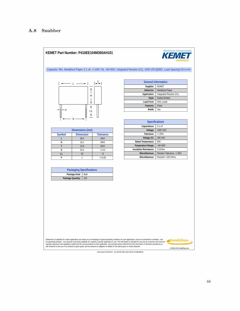
A.8 Snubber
Generated 4/20/2016 - 61c29766-f0f6-45a6-953d-3149fe8ff948
KEMET Part Number: P410EE104M300AH101
Capacitor, film, Metallized Paper, 0.1 uF, +/-20% Tol, -40/+85C, Integrated Resistor (X1), 1000 VDC@85C, Lead Spacing=25.4 mm
L
H
LLF
T
S
Dimensions (mm)Symbol Dimension Tolerance
L 30.5 MAX
H 16.1 MAX
T 10.6 MAX
S 25.4 +/-0.4
LL 30 +5
F 1 +/-0.05
Packaging SpecificationsPackage Kind: Bulk
Package Quantity: 150
General InformationSupplier: KEMET
Dielectric: Metallized Paper
Application: Integrated Resistor (X1)
Style: Radial Molded
Lead Form: Wire Leads
Features: Pulse
RoHS: Yes
SpecificationsCapacitance: 0.1 uF
Voltage: 1000 VDC
Tolerance: +/-20%
Voltage AC: 300 VAC
Rated Temperature: 85C
Temperature Range: -40/+85C
Insulation Resistance: 3 GOhm
Miscellaneous: Resistor Tolerance: +/-30%
Miscellaneous: Resistor= 100 Ohms
© 2006-2016 IntelliData.net
Statements of suitability for certain applications are based on our knowledge of typical operating conditions for such applications, but are not intended to constitute - andwe specifically disclaim - any warranty concerning suitability for a specific customer application or use. This Information is intended for use only by customers who have therequisite experience and capability to determine the correct products for their application. Any technical advice inferred from this Information or otherwise provided by uswith reference to the use of our products is given gratis, and we assume no obligation or liability for the advice given or results obtained.
88
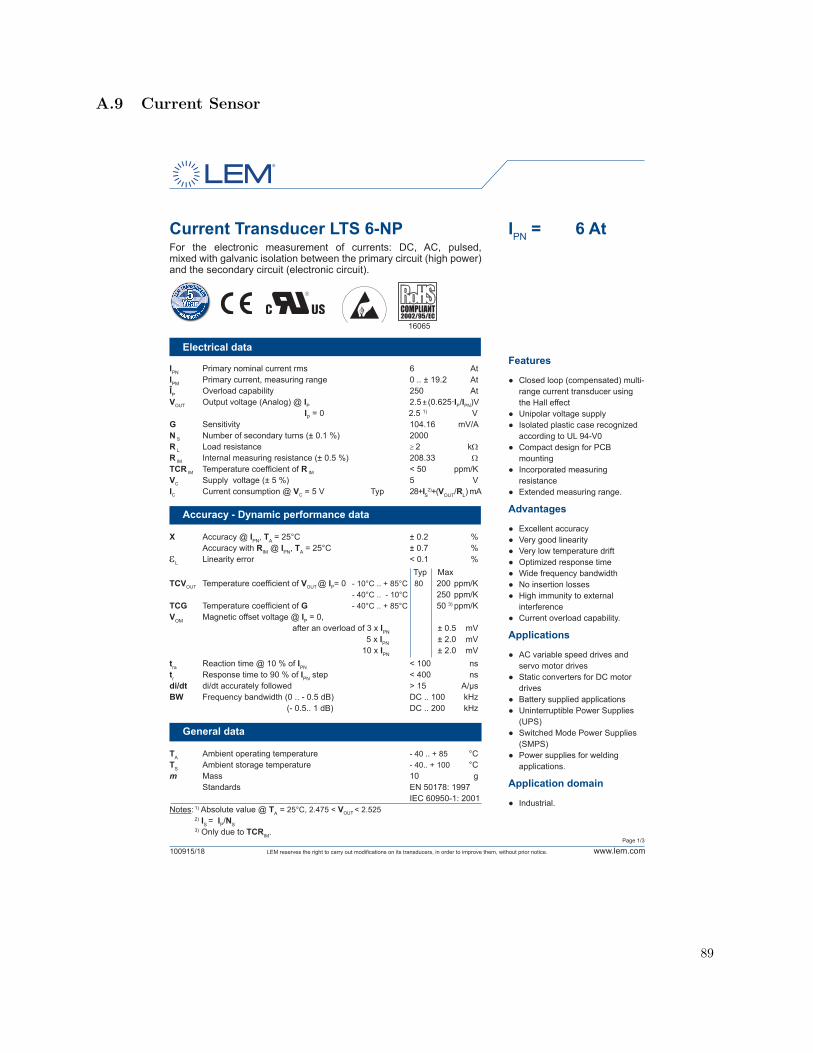
A.9 Current Sensor
LEM reserves the right to carry out modifications on its transducers, in order to improve them, without prior notice.100915/18 www.lem.comPage 1/3
Current Transducer LTS 6-NPFor the electronic measurement of currents: DC, AC, pulsed, mixed with galvanic isolation between the primary circuit (high power) and the secondary circuit (electronic circuit).
Electrical data
IPN Primary nominal current rms 6 AtIPM Primary current, measuring range 0 .. ± 19.2 AtÎP Overload capability 250 AtVOUT Output voltage (Analog) @ IP 2.5 ± (0.625·IP/IPN) V IP = 0 2.5 1) VG Sensitivity 104.16 mV/AN S Number of secondary turns (± 0.1 %) 2000 R L Load resistance ≥ 2 kWR IM Internal measuring resistance (± 0.5 %) 208.33 WTCR IM Temperature coefficient of R IM < 50 ppm/KVC Supply voltage (± 5 %) 5 VIC Current consumption @ VC = 5 V Typ 28+IS2)+(VOUT/RL) mA
X Accuracy @ IPN, TA = 25°C ± 0.2 %
Accuracy - Dynamic performance data
Accuracy with RIM @ IPN, TA = 25°C ± 0.7 %εL Linearity error < 0.1 % Typ MaxTCVOUT Temperature coefficient of VOUT @ IP= 0 - 10°C .. + 85°C 80 200 ppm/K - 40°C .. - 10°C 250 ppm/KTCG Temperature coefficient of G - 40°C .. + 85°C 50 3) ppm/KVOM Magnetic offset voltage @ IP = 0, after an overload of 3 x IPN ± 0.5 mV 5 x IPN ± 2.0 mV 10 x IPN ± 2.0 mVtra Reaction time @ 10 % of IPN < 100 nstr Response time to 90 % of IPN step < 400 nsdi/dt di/dt accurately followed > 15 A/µsBW Frequency bandwidth (0 .. - 0.5 dB) DC .. 100 kHz (- 0.5.. 1 dB) DC .. 200 kHz
General data
TA Ambient operating temperature - 40 .. + 85 °CTS Ambient storage temperature - 40.. + 100 °Cm Mass 10 g Standards EN 50178: 1997 IEC 60950-1: 2001Notes: 1) Absolute value @ TA = 25°C, 2.475 < VOUT < 2.525 2) IS = IP/NS
3) Only due to TCRIM.
IPN = 6 At
Features
Closed loop (compensated) multi- range current transducer using the Hall effectUnipolar voltage supply Isolated plastic case recognized according to UL 94-V0Compact design for PCB mountingIncorporated measuring resistanceExtended measuring range.
Advantages
Excellent accuracy Very good linearity Very low temperature drift Optimized response time Wide frequency bandwidth No insertion losses High immunity to external interferenceCurrent overload capability.
Applications
AC variable speed drives and servo motor drivesStatic converters for DC motor drivesBattery supplied applications Uninterruptible Power Supplies (UPS)Switched Mode Power Supplies (SMPS)Power supplies for welding applications.
Application domain
Industrial.
16065
89

LEM reserves the right to carry out modifications on its transducers, in order to improve them, without prior notice.100915/18 www.lem.comPage 1/3
Current Transducer LTS 6-NPFor the electronic measurement of currents: DC, AC, pulsed, mixed with galvanic isolation between the primary circuit (high power) and the secondary circuit (electronic circuit).
Electrical data
IPN Primary nominal current rms 6 AtIPM Primary current, measuring range 0 .. ± 19.2 AtÎP Overload capability 250 AtVOUT Output voltage (Analog) @ IP 2.5 ± (0.625·IP/IPN) V IP = 0 2.5 1) VG Sensitivity 104.16 mV/AN S Number of secondary turns (± 0.1 %) 2000 R L Load resistance ≥ 2 kWR IM Internal measuring resistance (± 0.5 %) 208.33 WTCR IM Temperature coefficient of R IM < 50 ppm/KVC Supply voltage (± 5 %) 5 VIC Current consumption @ VC = 5 V Typ 28+IS2)+(VOUT/RL) mA
X Accuracy @ IPN, TA = 25°C ± 0.2 %
Accuracy - Dynamic performance data
Accuracy with RIM @ IPN, TA = 25°C ± 0.7 %εL Linearity error < 0.1 % Typ MaxTCVOUT Temperature coefficient of VOUT @ IP= 0 - 10°C .. + 85°C 80 200 ppm/K - 40°C .. - 10°C 250 ppm/KTCG Temperature coefficient of G - 40°C .. + 85°C 50 3) ppm/KVOM Magnetic offset voltage @ IP = 0, after an overload of 3 x IPN ± 0.5 mV 5 x IPN ± 2.0 mV 10 x IPN ± 2.0 mVtra Reaction time @ 10 % of IPN < 100 nstr Response time to 90 % of IPN step < 400 nsdi/dt di/dt accurately followed > 15 A/µsBW Frequency bandwidth (0 .. - 0.5 dB) DC .. 100 kHz (- 0.5.. 1 dB) DC .. 200 kHz
General data
TA Ambient operating temperature - 40 .. + 85 °CTS Ambient storage temperature - 40.. + 100 °Cm Mass 10 g Standards EN 50178: 1997 IEC 60950-1: 2001Notes: 1) Absolute value @ TA = 25°C, 2.475 < VOUT < 2.525 2) IS = IP/NS
3) Only due to TCRIM.
IPN = 6 At
Features
Closed loop (compensated) multi- range current transducer using the Hall effectUnipolar voltage supply Isolated plastic case recognized according to UL 94-V0Compact design for PCB mountingIncorporated measuring resistanceExtended measuring range.
Advantages
Excellent accuracy Very good linearity Very low temperature drift Optimized response time Wide frequency bandwidth No insertion losses High immunity to external interferenceCurrent overload capability.
Applications
AC variable speed drives and servo motor drivesStatic converters for DC motor drivesBattery supplied applications Uninterruptible Power Supplies (UPS)Switched Mode Power Supplies (SMPS)Power supplies for welding applications.
Application domain
Industrial.
16065
90

LEM reserves the right to carry out modifications on its transducers, in order to improve them, without prior notice.100915/18 www.lem.comPage 2/3
Current Transducer LTS 6-NP
Isolation characteristics
Vd Rms voltage for AC isolation test, 50 Hz, 1 min 3 kVVw Impulse withstand voltage 1.2/50 µs > 8 kV MinVe Rms voltage for partial discharge extinction @ 10pC > 1.5 kV
dCp Creepage distance 1) 15.5 mmdCI Clearance distance 2) 6.35 mmCTI Comparative Tracking Index (group IIIa) 175 Notes: 1) On housing 2) On PCB with soldering pattern UTEC93-703.
Applications examples
According to EN 50178 and IEC 61010-1 standards and following conditions:
Over voltage category OV 3 Pollution degree PD2 Non-uniform field
Safety
This transducer must be used in electric/electronic equipment with respect to applicable standards and safety requirements in accordance with the manufacturer’s operating instructions.
Caution, risk of electrical shock
When operating the transducer, certain parts of the module can carry hazardous voltage (eg. primary busbar, power supply). Ignoring this warning can lead to injury and/or cause serious damage. This transducer is a build-in device, whose conducting parts must be inaccessible after installation. A protective housing or additional shield could be used. Main supply must be able to be disconnected.
EN 50178 IEC 61010-1
dCp, dCI, Rated insulation voltage Nominal voltageSingle insulation 600 V 600 VReinforced insulation 300 V 300 V
Vw
91

LEM reserves the right to carry out modifications on its transducers, in order to improve them, without prior notice.100915/18 www.lem.comPage 3/3
Dimensions LTS 6-NP (in mm.)
Number ofprimary turns
Primary nominalcurrent rms
IPN [ A ]
Nominaloutput voltage
VOUT [ V ]
PrimaryresistanceRP [ mW ]
Primary insertioninductanceLP [ µH ]
Recommendedconnections
6 5 4 OUT
1 ± 6 2.5 ± 0.625 0.18 0.013 IN 1 2 3
± 3 6 5 4 OUT
2 2.5 ± 0.625 0.81 0.05 IN 1 2 3
6 5 4 OUT
3 ± 2 2.5 ± 0.625 1.62 0.12 IN 1 2 3
Mechanical characteristicsGeneral tolerance ± 0.2 mm Fastening & connection of primary 6 pins 0.8 x 0.8 mm Recommended PCB hole 1.3 mmFastening & connection of secondary 3 pins 0.5 x 0.35 mm Recommended PCB hole 0.8 mmAdditional primary through-hole Ø 3.2 mm
RemarksV OUT swings above 2.5 V when IP flows from terminals 1, 2, 3 to terminals 6, 5, 4 (with the arrow).Temperature of the primary jumper should not exceed 100°C.
Output Voltage - Primary Current
Operation principle
- IPM - IPN IPM IPN 0
VOUT [ V ]
[ At ] IP
4.5
5
2.5
0.5
3.125
1.825
92

A.10 NTC Thermistor
NTC thermistors for
inrush current limiting
Leaded and coated disks
Series/Type: B57364S0***M0**
Date: May 2013
© EPCOS AG 2013. Reproduction, publication and dissemination of this publication, enclosures hereto and theinformation contained therein without EPCOS' prior express consent is prohibited.
93

1) For details on the capacitance Ctest please refer to "Application notes", chapter 1.6.
Applications
Switch-mode power supplies
Soft-start motors, e.g. in vacuum cleaners
Features
Useable in series connections
up to 265 VRMS
Coated thermistor disk
Kinked leads of tinned copper wire
Wide resistance range
Manufacturer's logo, NTC and resistance value
stamped on
UL approval (E69802)
Options
Resistance tolerance <20% and alternative lead
configurations available on request
Delivery mode
Bulk (standard) or with cardboard tape on 500-mm reel
Dimensional drawing
Dimensions in mm
Approx. weight 4 g
General technical data
Climatic category (IEC 60068-1) 55/170/21
Max. power (at 25 °C) Pmax 5.1 W
Resistance tolerance ∆RR/RR ±20 %
Rated temperature TR 25 °CDissipation factor (in air) δth approx. 24 mW/K
Thermal cooling time constant (in air) τc approx. 100 s
Heat capacity Cth approx. 2400 mJ/K
Electrical specification and ordering codes
R25
Ω
Imax
(0...65 °C)
A
Ctest1)
230 V AC
µF
Ctest1)
110 V AC
µF
Rmin
(@ Imax, 25 °C)
Ω
Ordering code
** = Delivery mode
00 = Bulk
51 = Reel packing
1 16.0 1000 4000 0.021 B57364S0109M0**
2 12.0 1000 4000 0.036 B57364S0209M0**
2.5 11.0 1000 4000 0.044 B57364S0259M0**
4 9.5 1000 4000 0.059 B57364S0409M0**
5 8.5 1000 4000 0.073 B57364S0509M0**
10 7.5 1000 4000 0.098 B57364S0100M0**
Inrush current limiters B57364S0***M0**
ICLs S364
Page 2 of 18Please read Cautions and warnings andImportant notes at the end of this document. 94

Reliability data
Test Standard Test conditions ∆R25/R25
(typical)
Remarks
Storage in
dry heat
IEC
60068-2-2
Storage at upper
category temperature
T: 170 °Ct: 1000 h
< 10% No visible
damage
Storage in damp
heat, steady state
IEC
60068-2-78
Temperature of air: 40 °CRelative humidity of air: 93%
Duration: 21 days
< 5% No visible
damage
Termal schock IEC
60068-2-14
Lower test temperature: 55 °Ct: 30 min
Upper test temperature: 170 °Ct: 30 min
Time to change from lower to
upper temperature: < 30 s
Number of cycles: 10
< 10% No visible
damage
Endurance IEC
60539-1
Ambient temperature: 25 ±5 °CI = Imax
t: 1000 h
< 10% No visible
damage
Cyclic
endurance
IEC
60539-1
Ambient temperature: 25 ±5 °CI = Imax
On-time = 1 min
Cooling time = 5 min
Number of cycles: 1000
< 10% No visible
damage
Maximum
permissible
capacitance test
IEC
60539-1
Ambient temperature: 25 ±5 °CCapacitance = Ctest
Number of cycles: 1000
< 5% No visible
damage
Note
The self-heating of a thermistor during operation depends on the load applied and theapplicable dissipation factor.When loaded with maximum allowable current/power and the specified dissipation factor istaken as a basis, the NTC thermistor may reach a mean temperature of up to 250 °C.The heat developed during operation will also be dissipated through the lead wires. So thecontact areas, too, may become quite hot at maximum load.When mounting NTC thermistors you have to ensure that there is an adequate distancebetween the thermistor and all parts which are sensitive to heat or combustible.
Inrush current limiters B57364S0***M0**
ICLs S364
Page 3 of 18Please read Cautions and warnings andImportant notes at the end of this document. 95

Resistance versus temperature
S364 series
Inrush current limiters B57364S0***M0**
ICLs S364
Page 4 of 18Please read Cautions and warnings andImportant notes at the end of this document. 96

A.11 DSP Board
1
DSP Development BoardUser’s Manual
POWERSIM INC.
97
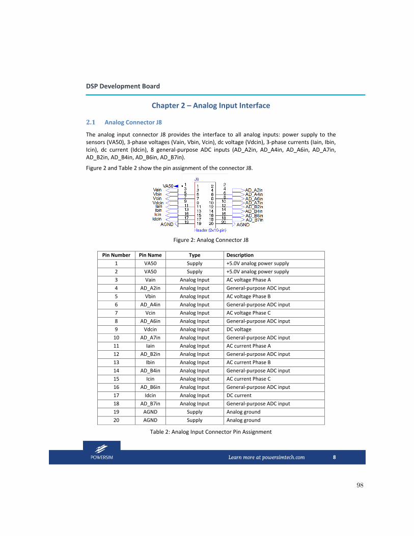
DSP Development Board
8
Chapter 2 – Analog Input Interface
2.1 Analog Connector J8
The analog input connector J8 provides the interface to all analog inputs: power supply to the sensors (VA50), 3‐phase voltages (Vain, Vbin, Vcin), dc voltage (Vdcin), 3‐phase currents (Iain, Ibin, Icin), dc current (Idcin), 8 general‐purpose ADC inputs (AD_A2in, AD_A4in, AD_A6in, AD_A7in, AD_B2in, AD_B4in, AD_B6in, AD_B7in).
Figure 2 and Table 2 show the pin assignment of the connector J8.
Figure 2: Analog Connector J8
Pin Number Pin Name Type Description
1 VA50 Supply +5.0V analog power supply
2 VA50 Supply +5.0V analog power supply
3 Vain Analog Input AC voltage Phase A
4 AD_A2in Analog Input General‐purpose ADC input
5 Vbin Analog Input AC voltage Phase B
6 AD_A4in Analog Input General‐purpose ADC input
7 Vcin Analog Input AC voltage Phase C
8 AD_A6in Analog Input General‐purpose ADC input
9 Vdcin Analog Input DC voltage
10 AD_A7in Analog Input General‐purpose ADC input
11 Iain Analog Input AC current Phase A
12 AD_B2in Analog Input General‐purpose ADC input
13 Ibin Analog Input AC current Phase B
14 AD_B4in Analog Input General‐purpose ADC input
15 Icin Analog Input AC current Phase C
16 AD_B6in Analog Input General‐purpose ADC input
17 Idcin Analog Input DC current
18 AD_B7in Analog Input General‐purpose ADC input
19 AGND Supply Analog ground
20 AGND Supply Analog ground
Table 2: Analog Input Connector Pin Assignment
98

DSP Development Board
13
Chapter 3 – Motor Control Interface
3.1 Encoder Interface Connector J8
Connector J8 is used to interface with an encoder for motor position/speed sensing.
Phase A of the encoder should be connected to pin 1 ; Phase B should be connected to pin 2; and Phase Z (index or zero marker) should be connected to pin 3 as shown in figure 8.
Figure 8: Encoder Interface Connector J8 Pin Assignment
3.2 Encoder Interface Circuit
The encoder interface circuit is shown in Figure 9.
The circuit uses a 1st‐order low‐pass filter with R=33Ω and C=100pf. Please note that input signals POSA, POSB, POSZ should be scaled to 0‐3.3V because these signals are fed into DSP I/O directly.
Figure 9: Encoder Interface Circuit
99

DSP Development Board
15
Chapter 4 – PWM/Digital Signals and Fault Signals
4.1 PWM Signal Connector J12
Figure 12 and Table 3 show the pin assignment of the PWM signal connector J12.
As shown in the figure, pins 1 to 8 provide the power supply.
Pins 1, 2 and 3 are connected to the external 12V dc power supply KL_30.
Pins 4, 5 and 8 provide the digital ground and pin 7 supplies the analog ground.
Pins 14 (phase W, top switch), 16 (phase W, bottom switch), 18 (phase V, top switch), 20 (phase V, bottom switch), 22 (phase U, top switch) and 24 (phase U, bottom switch) are PWM logic signals for 6 IGBT/MOSFET gate drivers. These PWM signals are generated by TI controlCARD.
Pins 12 is a reset signal to control the gate drivers 1ED020I12‐F2.
Pins 13, 17, 21 and 23 are fault detection signals ‐ one for each phase and one as logical “AND” combination of 3 phase fault detection signals.
Figure 12: PWM Signal Connector J12 Pin Assignments
Pin Number Pin Name Type Description
1 KL_30 Supply +12.0V Power Supply
2 KL_30 Supply +12.0V Power Supply
3 KL_30 Supply +12.0V Power Supply
4 DGND Supply Digital Ground
5 DGND Supply Digital Ground
6 DGND Supply Digital Ground
7 AGND Supply Analog Ground
8 NC
9 NC
10 NC
11 NC
WARNING : When making connection or measurement to the connector J12, please handle with extreme care. DO NOT short circuit the power supply pins (Pins 1, 2, and 3) with any other pins. Short‐circuit will damage the board!
100

DSP Development Board
16
12 RST_INn Digital I/O IGBT Gate Driver Reset
13 FLTWn Digital I/O IGBT Fault Phase C
14 PWM_WT PWM I/O PWM Gate High Phase C
15 NC
16 PWM_WB PWM I/O PWM Gate Low Phase C
17 FLTVn Digital I/O IGBT Fault Phase B
18 PWM_VT PWM I/O PWM Gate High Phase B
19 NC
20 PWM_VB PWM I/O PWM Gate Low Phase B
21 FLTUn Digital I/O IGBT Fault Phase A
22 PWM_UT PWM I/O PWM Gate High Phase A
23 FLTn Digital I/O IGBT Fault
24 PWM_UB PWM I/O PWM Gate Low Phase A
Table 3: PWM signal connector J12 pin assignment
4.2 Gate Drive Interface Signals
Figure 13 shows the interface circuit between DSP (0 to 3.3V) and IGBT/MOSFET gate drivers (0 to 5V). This is a level shift circuit with a 16‐bit dual supply translating transceiver IC 74ALVC164245. The 0‐3.3V PWM control signals G1, G2, G3, G4, G5, G6 from DSP are converted to 0‐5V signals PWMUT, PWMUB, PWMVT, PWMVB, PWMWT, PWMWB for gate drivers. The 0‐5V fault signals FLTUn, FLTVn, FLTWn, and FLTn are level shifted to 0‐3.3V for DSP.
Figure 13: Gate drive interface circuit
101

DSP Development Board
21
Figure 15: TI C2000 DSP Family controlCARDs
A brief description of each DSP is given below.
F28335:
The F28335 DSP has following main features:
High‐Performance floating point 32‐Bit CPU (TMS320C28x) with 150 MHz (6.67‐ns Cycle Time)
On‐Chip Memory (256K x 16 Flash, 34K x 16 SARAM, 8K x 16 Boot ROM)
Six‐Channel DMA Controller (for ADC, McBSP, ePWM, XINTF, and SARAM)
Enhanced Control Peripherals o Up to 18 PWM Outputs o Up to 6 HRPWM Outputs With 150 ps MEP Resolution o Up to 6 Event Capture Inputs o Up to 2 Quadrature Encoder Interfaces o Up to 8 32‐Bit Timers (6 for eCAPs and 2 for eQEPs) o Up to 9 16‐Bit Timers (6 for ePWMs and 3 XINTCTRs)
Three 32‐Bit CPU Timers
Serial Port Peripherals o Up to 2 CAN Modules o Up to 3 SCI (UART) Modules o Up to 2 McBSP Modules (Configurable as SPI) o One SPI Module o One Inter‐Integrated‐Circuit (I2C) Module
12‐Bit ADC, 16 Channels o 80‐ns Conversion Rate o x 8 Channel Input Multiplexer o Two Sample‐and‐Hold o Single/Simultaneous Conversions o Internal or External Reference
Up to 88 Individually Programmable, Multiplexed GPIO Pins With Input Filtering
102

DSP Development Board
22
F28035:
The F28035 DSP has following main features:
High‐Efficiency fixed point 32‐Bit CPU (TMS320C28x) with 60 MHz (16.67‐ns Cycle Time)
On‐Chip Memory (64K x 16 Flash, 10K x 16 SARAM, 8K x 16 Boot ROM)
Three 32‐Bit CPU Timers
Independent 16‐Bit Timer in Each Enhanced Pulse Width Modulator (ePWM)
Serial Port Peripherals o One SCI (UART) Module o Two SPI Modules o One Inter‐Integrated‐Circuit (I2C) Bus o One Local Interconnect Network (LIN) Bus o One Enhanced Controller Area Network (eCAN) Bus
Enhanced Control Peripherals o ePWM o High‐Resolution PWM (HRPWM) o Enhanced Capture (eCAP) Module o High‐Resolution Input Capture (HRCAP) Module o Enhanced Quadrature Encoder Pulse (eQEP) Module o On‐Chip Temperature Sensor o Comparator
12‐Bit ADC, 16 Channels o 216‐ns Conversion Rate o x 8 Channel Input Multiplexer o Two Sample‐and‐Hold o Single/Simultaneous Conversions
Up to 45 Individually Programmable, Multiplexed GPIO Pins With Input Filtering
F28027:
The F28027 DSP has following main features:
High‐Efficiency fixed point 32‐Bit CPU (TMS320C28x) with 60 MHz (16.67‐ns Cycle Time)
On‐Chip Memory (Flash, SARAM, OTP, Boot ROM Available)
Three 32‐Bit CPU Timers
Independent 16‐Bit Timer in Each Enhanced Pulse Width Modulator (ePWM)
Serial Port Peripherals o One Serial Communications Interface (SCI) Universal Asynchronous
Receiver/Transmitter (UART) Module o One Serial Peripheral Interface (SPI) Module o One Inter‐Integrated‐Circuit (I2C) Module
Enhanced Control Peripherals o ePWM o High‐Resolution PWM (HRPWM) o Enhanced Capture (eCAP) Module
103

DSP Development Board
24
Chapter 6 – Communication Port and Computer Interface
The DSP board provides a number of communication ports for computer interface and program debugging purposes. These communication interfaces include one CAN BUS, one SCI BUS, one SPI BUS, one USB, and one JTAG.
6.1 CAN BUS Interface J3
Figure 16 shows the pin assignment of the CAN bus connector J3. Pin 1 is CAN high line and pin 2 is CAN low line. Pin 3 is digital ground.
Figure 16: CAN bus connector J3 pin assignment
6.2 SCI Interface J6
Figure 17 shows the pin assignment of the SCI connector J6. Pin 1 is the RS‐232 transmit output, pin 4 is the RS‐232 receive input. Pin 2 is 3.3V power supply, pin 43 is ground.
Figure 17 RS‐232 Connector J6 Pin Assignment
Note that to use the SCI connector J6 for serial communication, the DIP switch S7_4 needs to be in the OFF position.
6.3 USB Interface J1
The USB connector J1 shown in Figure 18 provides the interface to a computer. The built‐in DSP emulator allows users to debug DSP program with TI Code Composer Studio.
Table 5 shows the pin assignment of the connector J5. Pin 2 is data plus and pin 3 is data minus.
Figure 18: USB Connector J1 pin assignment
Pin Number Pin Name Description
1 NC
2 DATA_P Data plus
3 DATA_M Data minus
4 DGND Digital Ground
Table 5: USB Connector J1 pin assignment
104
A.12 ABB PMSM
AC servo motorsBSM Series
Brochure
105
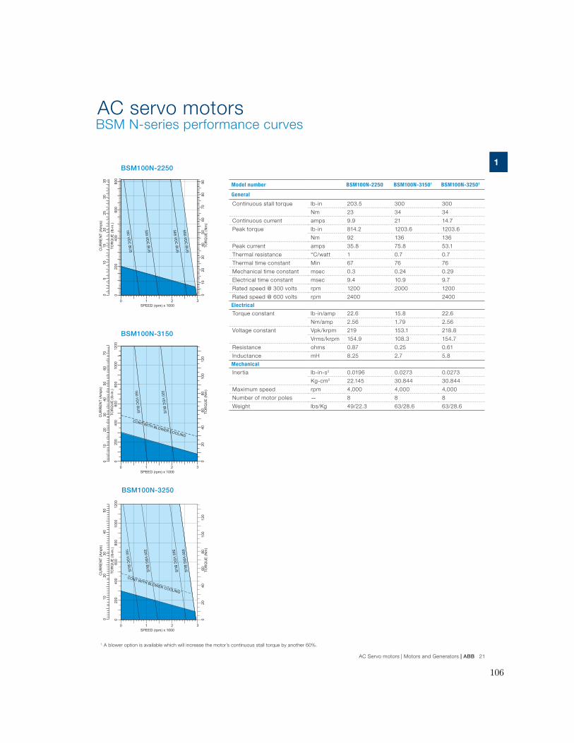
AC Servo motors | Motors and Generators | ABB 21
11
1 A blower option is available which will increase the motor’s continuous stall torque by another 60%.
SPEED (rpm) x 1000
CU
RR
EN
T (A
mps
)
TOR
QU
E (l
b-in
.)
BSM100N-2250
160 VDC
BUS
320 VDC
BUS
650 VDC
BUS
565 VDC
BUS
TOR
QU
E (N
m)
1020
3040
5060
7080
900
200
400
600
800
0
1 2 30
05
1015
20
25
3035
SPEED (rpm) x 1000
CU
RR
EN
T (A
mps
)
TOR
QU
E (l
b-in
.)
BSM100N-3150
160 VDC
BUS
320 VDC
BUS
TOR
QU
E (N
m)
200
400
600
800
1000
1200
0
1 2 30
2040
6080
100
120
0
CONT WITH BLOWER COOLING
010
2030
4050
6070
BSM100N-2250
BSM100N-3150
BSM100N-3250
Model number BSM100N-2250 BSM100N-31501 BSM100N-32501
General
Continuous stall torque lb-in 203.5 300 300
Nm 23 34 34
Continuous current amps 9.9 21 14.7
Peak torque lb-in 814.2 1203.6 1203.6
Nm 92 136 136
Peak current amps 35.8 75.8 53.1
Thermal resistance °C/watt 1 0.7 0.7
Thermal time constant Min 67 76 76
Mechanical time constant msec 0.3 0.24 0.29
Electrical time constant msec 9.4 10.9 9.7
Rated speed @ 300 volts rpm 1200 2000 1200
Rated speed @ 600 volts rpm 2400 2400
Electrical
Torque constant lb-in/amp 22.6 15.8 22.6
Nm/amp 2.56 1.79 2.56
Voltage constant Vpk/krpm 219 153.1 218.8
Vrms/krpm 154.9 108.3 154.7
Resistance ohms 0.87 0.25 0.61
Inductance mH 8.25 2.7 5.8
Mechanical
Inertia lb-in-s2 0.0196 0.0273 0.0273
Kg-cm2 22.145 30.844 30.844
Maximum speed rpm 4,000 4,000 4,000
Number of motor poles — 8 8 8
Weight lbs/Kg 49/22.3 63/28.6 63/28.6
BSM N-series performance curves
SPEED (rpm) x 1000
CU
RR
EN
T (A
mps
)
TOR
QU
E (l
b-in
.)
BSM100N-3250
160 VDC
BUS
320 VDC
BUS
650 VDC
BUS
565 VDC
BUS TO
RQ
UE
(Nm
)20
4060
8010
012
00
200
400
600
800
1000
1200
0
1 2 30
CONT WITH BLOWER COOLING
010
20
3040
50
AC servo motors
106

A.13 F28035 Piccolo Microcontroller
Product
Folder
Order
Now
Technical
Documents
Tools &
Software
Support &Community
An IMPORTANT NOTICE at the end of this data sheet addresses availability, warranty, changes, use in safety-critical applications,intellectual property matters and other important disclaimers. PRODUCTION DATA.
TMS320F28030, TMS320F28031, TMS320F28032TMS320F28033, TMS320F28034, TMS320F28035
SPRS584L –APRIL 2009–REVISED DECEMBER 2017
TMS320F2803x Piccolo™ Microcontrollers
1 Device Overview
1
1.1 Features1
• High-Efficiency 32-Bit CPU (TMS320C28x)– 60 MHz (16.67-ns Cycle Time)– 16 × 16 and 32 × 32 MAC Operations– 16 × 16 Dual MAC– Harvard Bus Architecture– Atomic Operations– Fast Interrupt Response and Processing– Unified Memory Programming Model– Code-Efficient (in C/C++ and Assembly)
• Programmable Control Law Accelerator (CLA)– 32-Bit Floating-Point Math Accelerator– Executes Code Independently of the Main CPU
• Endianness: Little Endian• JTAG Boundary Scan Support
– IEEE Standard 1149.1-1990 Standard TestAccess Port and Boundary Scan Architecture
• Low Cost for Both Device and System:– Single 3.3-V Supply– No Power Sequencing Requirement– Integrated Power-on Reset and Brown-out
Reset– Low Power– No Analog Support Pins
• Clocking:– Two Internal Zero-Pin Oscillators– On-Chip Crystal Oscillator and External Clock
Input– Watchdog Timer Module– Missing Clock Detection Circuitry
• Up to 45 Individually Programmable, MultiplexedGPIO Pins With Input Filtering
• Peripheral Interrupt Expansion (PIE) Block ThatSupports All Peripheral Interrupts
• Three 32-Bit CPU Timers• Independent 16-Bit Timer in Each Enhanced Pulse
Width Modulator (ePWM)• On-Chip Memory
– Flash, SARAM, OTP, Boot ROM Available
• Code-Security Module• 128-Bit Security Key and Lock
– Protects Secure Memory Blocks– Prevents Firmware Reverse Engineering
• Serial Port Peripherals– One Serial Communications Interface (SCI)
Universal Asynchronous Receiver/Transmitter(UART) Module
– Two Serial Peripheral Interface (SPI) Modules– One Inter-Integrated-Circuit (I2C) Module– One Local Interconnect Network (LIN) Module– One Enhanced Controller Area Network (eCAN)
Module• Enhanced Control Peripherals
– ePWM– High-Resolution PWM (HRPWM)– Enhanced Capture (eCAP) Module– High-Resolution Input Capture (HRCAP) Module– Enhanced Quadrature Encoder Pulse (eQEP)
Module– Analog-to-Digital Converter (ADC)– On-Chip Temperature Sensor– Comparator
• Advanced Emulation Features– Analysis and Breakpoint Functions– Real-Time Debug Through Hardware
• Package Options– 56-Pin RSH Very Thin Quad Flatpack (No Lead)
(VQFN)– 64-Pin PAG Thin Quad Flatpack (TQFP)– 80-Pin PN Low-Profile Quad Flatpack (LQFP)
• Temperature Options– T: –40°C to 105°C– S: –40°C to 125°C– Q: –40°C to 125°C
(AEC Q100 Qualification for AutomotiveApplications)
107

20
1 2 3 4 5 6 7 8 9 10
11
12
13
14
15
16
17
18
19
41
60
59
58
57
56
55
54
53
52
51
50
49
48
47
46
45
44
43
42
21
40
39
38
37
36
35
34
33
32
31
30
29
28
27
26
25
24
23
22
80
61
62
63
64
65
66
67
68
69
70
71
72
73
74
75
76
77
78
79
VSSA
GPIO28/SCIRXDA/SDAA/TZ2
GPIO9/EPWM5B/LINTXA/HRCAP1
TEST2
GPIO26/HRCAP1/SPICLKB
VDDIO
VSS
GPIO29/SCITXDA/SCLA/TZ3
GPIO30/CANRXA
GPIO31/CANTXA
GPIO27/HRCAP2/SPISTEB
ADCINB7
ADCINB6/COMP3B/AIO14
ADCINB5
ADCINB4/COMP2B/AIO12
ADCINB3
ADCINB2/COMP1B/AIO10
ADCINB1
ADCINB0
VREFLO
GPIO24/ECAP1/SPISIMOB
GPIO11/EPWM6B/LINRXA/HRCAP2
GPIO5/EPWM3B/SPISIMOA/ECAP1
GPIO4/EPWM3A
GPIO40/EPWM7A
GPIO10/EPWM6A/ADCSOCBO
GPIO3/EPWM2B/SPISOMIA/COMP2OUT
GPIO2/EPWM2A
GPIO1/EPWM1B/COMP1OUT
GPIO0/EPWM1A
VDDIO
VSS
VDD
VREGENZ
GPIO34/COMP2OUT/COMP3OUT
GPIO15/ /LINRXA/TZ1 SPISTEB
GPIO13/ /SPISOMIBTZ2
GPIO14/ /LINTXA/SPICLKBTZ3
GPIO20/EQEP1A/COMP1OUT
GPIO21/EQEP1B/COMP2OUT
VD
DA
GP
IO2
2/E
QE
P1
S/L
INT
XA
GP
IO3
2/S
DA
A/E
PW
MS
YN
CI/A
DC
SO
CA
O
GP
IO3
3/S
CL
A/E
PW
MS
YN
CO
/AD
CS
OC
BO
GP
IO2
3/E
QE
P1
I/L
INR
XA
GP
IO4
2/C
OM
P1
OU
T
GP
IO4
3/C
OM
P2
OU
T
VD
D
VS
S
XR
S
TR
ST
AD
CIN
A7
AD
CIN
A6
/CO
MP
3A
/AIO
6
AD
CIN
A5
AD
CIN
A4
/CO
MP
2A
/AIO
4
AD
CIN
A3
AD
CIN
A2
/CO
MP
1A
/AIO
2
AD
CIN
A1
AD
CIN
A0
VR
EF
HI
GP
IO1
8/S
PIC
LK
A/L
INT
XA
/XC
LK
OU
T
GP
IO3
6/T
MS
GP
IO3
5/T
DI
GP
IO3
7/T
DO
GP
IO3
8/T
CK
/XC
LK
IN
GP
IO3
9
GP
IO1
9/X
CL
KIN
//L
INR
XA
/EC
AP
1S
PIS
TE
A
VD
D
VS
S
X1
X2
GP
IO6
/EP
WM
4A
/EP
WM
SY
NC
I/E
PW
MS
YN
CO
GP
IO7
/EP
WM
4B
/SC
IRX
DA
GP
IO4
1/E
PW
M7
B
GP
IO1
2/
/SC
ITX
DA
/SP
ISIM
OB
TZ
1
GP
IO1
6/S
PIS
IMO
A/T
Z2
GP
IO4
4
GP
IO2
5/S
PIS
OM
IB
GP
IO8
/EP
WM
5A
/AD
CS
OC
AO
GP
IO1
7/S
PIS
OM
IA/T
Z3
12
TMS320F28030, TMS320F28031, TMS320F28032TMS320F28033, TMS320F28034, TMS320F28035
SPRS584L –APRIL 2009–REVISED DECEMBER 2017 www.ti.com
Submit Documentation FeedbackProduct Folder Links: TMS320F28030 TMS320F28031 TMS320F28032 TMS320F28033 TMS320F28034
TMS320F28035
Terminal Configuration and Functions Copyright © 2009–2017, Texas Instruments Incorporated
Figure 4-3. 2803x 80-Pin PN LQFP (Top View)
108
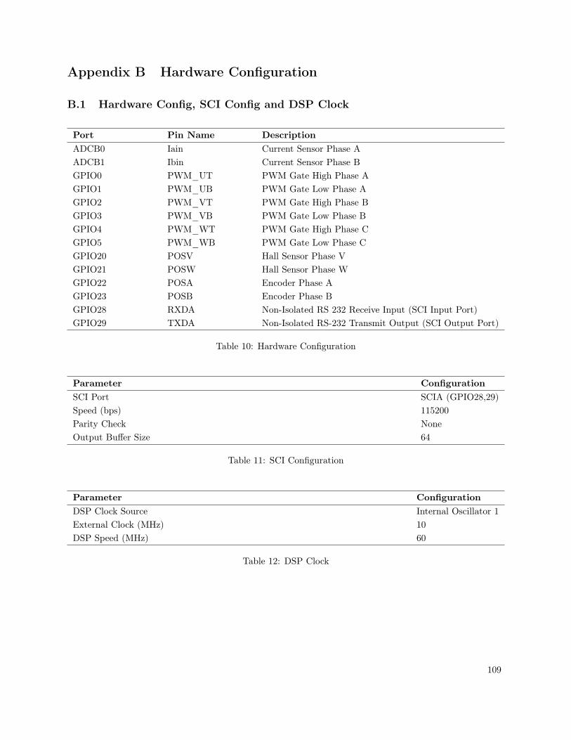
Appendix B Hardware Configuration
B.1 Hardware Config, SCI Config and DSP Clock
Port Pin Name DescriptionADCB0 Iain Current Sensor Phase AADCB1 Ibin Current Sensor Phase BGPIO0 PWM_UT PWM Gate High Phase AGPIO1 PWM_UB PWM Gate Low Phase AGPIO2 PWM_VT PWM Gate High Phase BGPIO3 PWM_VB PWM Gate Low Phase BGPIO4 PWM_WT PWM Gate High Phase CGPIO5 PWM_WB PWM Gate Low Phase CGPIO20 POSV Hall Sensor Phase VGPIO21 POSW Hall Sensor Phase WGPIO22 POSA Encoder Phase AGPIO23 POSB Encoder Phase BGPIO28 RXDA Non-Isolated RS 232 Receive Input (SCI Input Port)GPIO29 TXDA Non-Isolated RS-232 Transmit Output (SCI Output Port)
Table 10: Hardware Configuration
Parameter ConfigurationSCI Port SCIA (GPIO28,29)Speed (bps) 115200Parity Check NoneOutput Buffer Size 64
Table 11: SCI Configuration
Parameter ConfigurationDSP Clock Source Internal Oscillator 1External Clock (MHz) 10DSP Speed (MHz) 60
Table 12: DSP Clock
109

Appendix C Further Results
Figure 85: LO Referenced to COM (Phase A) Figure 86: Hardware IGBT Low Signal
Appendix D Calculations and Excel Sheets
D.1 ABB PMSM Calculations
110
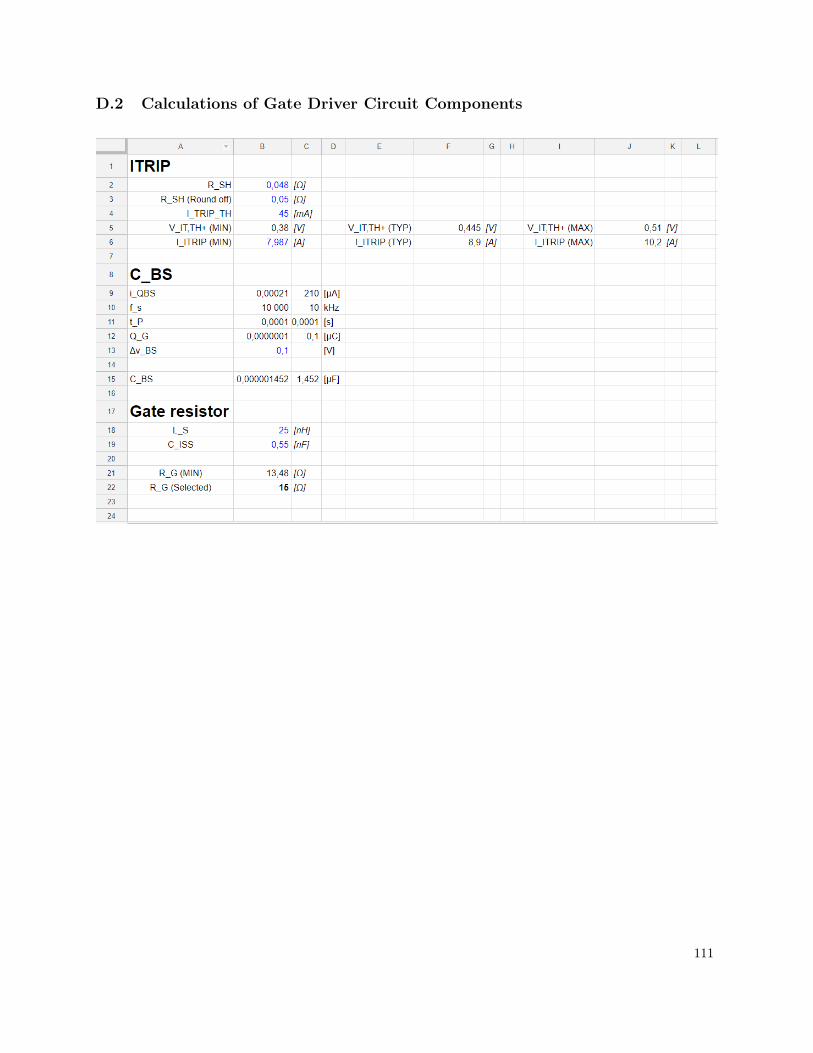
D.2 Calculations of Gate Driver Circuit Components
111
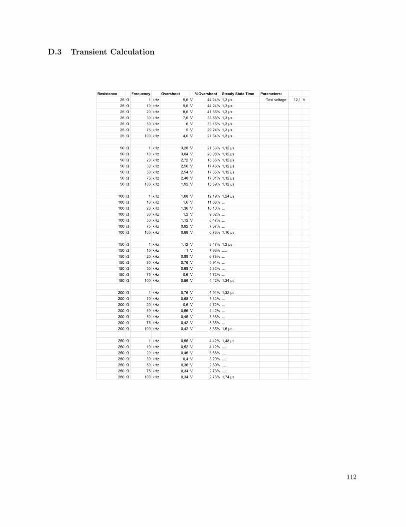
D.3 Transient Calculation
Resistance Frequency Overshoot %Overshoot Steady State Time Parameters:25 Ω 1 kHz 9,6 V 44,24% 1,3 µs Test voltage: 12,1 V25 Ω 10 kHz 9,6 V 44,24% 1,3 µs25 Ω 20 kHz 8,6 V 41,55% 1,3 µs25 Ω 30 kHz 7,6 V 38,58% 1,3 µs25 Ω 50 kHz 6 V 33,15% 1,3 µs25 Ω 75 kHz 5 V 29,24% 1,3 µs25 Ω 100 kHz 4,6 V 27,54% 1,3 µs
50 Ω 1 kHz 3,28 V 21,33% 1,12 µs50 Ω 10 kHz 3,04 V 20,08% 1,12 µs50 Ω 20 kHz 2,72 V 18,35% 1,12 µs50 Ω 30 kHz 2,56 V 17,46% 1,12 µs50 Ω 50 kHz 2,54 V 17,35% 1,12 µs50 Ω 75 kHz 2,48 V 17,01% 1,12 µs50 Ω 100 kHz 1,92 V 13,69% 1,12 µs
100 Ω 1 kHz 1,68 V 12,19% 1,24 µs100 Ω 10 kHz 1,6 V 11,68% ...100 Ω 20 kHz 1,36 V 10,10% ...100 Ω 30 kHz 1,2 V 9,02% ...100 Ω 50 kHz 1,12 V 8,47% ...100 Ω 75 kHz 0,92 V 7,07% ...100 Ω 100 kHz 0,88 V 6,78% 1,16 µs
150 Ω 1 kHz 1,12 V 8,47% 1,2 µs150 Ω 10 kHz 1 V 7,63% .....150 Ω 20 kHz 0,88 V 6,78% ...150 Ω 30 kHz 0,76 V 5,91% ...150 Ω 50 kHz 0,68 V 5,32% ...150 Ω 75 kHz 0,6 V 4,72% ...150 Ω 100 kHz 0,56 V 4,42% 1,34 µs
200 Ω 1 kHz 0,76 V 5,91% 1,32 µs200 Ω 10 kHz 0,68 V 5,32% ...200 Ω 20 kHz 0,6 V 4,72% ...200 Ω 30 kHz 0,56 V 4,42% ...200 Ω 50 kHz 0,46 V 3,66% ...200 Ω 75 kHz 0,42 V 3,35% ...200 Ω 100 kHz 0,42 V 3,35% 1,6 µs
250 Ω 1 kHz 0,56 V 4,42% 1,48 µs250 Ω 10 kHz 0,52 V 4,12% .....250 Ω 20 kHz 0,46 V 3,66% .....250 Ω 30 kHz 0,4 V 3,20% .....250 Ω 50 kHz 0,36 V 2,89% .....250 Ω 75 kHz 0,34 V 2,73% .....250 Ω 100 kHz 0,34 V 2,73% 1,74 µs
112
Copyright © 2022 FDOKUMEN