PROGRESS IN THE SURFACE PASSIVATION OF SILICON SOLAR CELLS
8
PROGRESS IN THE SURFACE PASSIVATION OF SILICON SOLAR CELLS Jan Schmidt, 1 Agnes Merkle, 1 Robert Bock, 1 Pietro P. Altermatt, 1,2 Andres Cuevas, 3 Nils-Peter Harder, 1 Bram Hoex, 4 Richard van de Sanden, 4 Erwin Kessels, 4 Rolf Brendel 1 1 Institute for Solar Energy Research Hameln (ISFH), Am Ohrberg 1, 31860 Emmerthal, Germany 2 Department of Solid-State Physics, Leibniz University Hanover, Appelstr. 2, 30167 Hanover, Germany 3 Department of Engineering, Australian National University, Canberra ACT 0200, Australia 4 Department of Applied Physics, Eindhoven University of Technology, 5600 MB Eindhoven, The Netherlands ABSTRACT: In order to increase the efficiency of silicon-wafer-based solar cells in production well above 20%, it is indispensable to improve the currently applied level of surface passivation at the front as well as at the rear of the cells. This paper focuses on two main challenges: (i) the low-temperature passivation of lowly doped p-type silicon surfaces at the cell rear and (ii) the passivation of highly boron-doped p + emitter surfaces as used at the front of solar cells on high-lifetime n-type silicon wafers. In the past, low surface recombination velocities (< 20 cm/s) have been achieved on low-resistivity (~1 Ωcm) p-type silicon using plasma-enhanced chemical-vapour-deposited (PECVD) silicon nitride (SiN x ) as well as amorphous silicon (a-Si). However, the high density of fixed positive charges within the PECVD-SiN x layer induces an inversion layer at the rear of p-type Si cells, producing a detrimental parasitic shunting, which reduces the short-circuit current density by up to 3 mA/cm 2 . The passivation quality of a-Si on the other hand is very temperature sensitive. More recently it has been shown that atomic-layer-deposited (ALD) alumin- ium oxide (Al 2 O 3 ) provides an outstanding level of surface passivation, which can be attributed to its extremely high negative fixed charge density in combination with the very gentle deposition technique ALD, leading to low inter- face state densities. The application of these ALD-Al 2 O 3 layers to the rear of p-type solar cells shows that this new passivation scheme is indeed suitable for high efficiencies and that due to the large negative fixed charge density no parasitic shunting occurs. We also demonstrate that ALD-Al 2 O 3 seems to be the ideal passivation layer for boron- doped p + emitter surfaces. In a direct comparison with other passivation schemes, it is found that Al 2 O 3 even outper- forms optimized thermally grown SiO 2 and opens the possibility of achieving very large open-circuit voltages up to V oc = 740 mV. Keywords: Silicon, Surface Passivation, Al 2 O 3 1 INTRODUCTION In high-efficiency laboratory silicon solar cells, sur- face recombination is very effectively suppressed by means of silicon dioxide (SiO 2 ) grown in a high- temperature (≥ 900 °C) oxidation process [1]. Very low surface recombination velocities (SRVs) are in particular realized at the lightly doped rear surface, where the com- bination of a thermally grown SiO 2 layer with an evapo- rated film of Al give – after an additional annealing treatment at ~400°C (the so-called ‘alneal’) – SRVs be- low 20 cm/s on un-metallized low-resistivity (~1 Ωcm) p-type silicon wafers [2]. In addition, the SiO 2 /Al stack at the cell rear acts as an excellent reflector for near- bandgap photons, significantly improving the light trap- ping properties and hence the short-circuit current of the cell. One of the main reasons why high-temperature oxi- dation has not been implemented into the majority of in- dustrial cell processes up to now is the high sensitivity of the silicon bulk lifetime to high-temperature processes. In particular in the case of multi-crystalline silicon wafers, thermal processes above 900°C typically lead to a sig- nificant degradation of the bulk lifetime [3]. Hence, low- temperature surface passivation alternatives are required for future industrial high-efficiency silicon solar cells, which should have comparable properties as the alnealed SiO 2 . One intensively investigated low-temperature surface passivation alternative to thermal oxide is silicon nitride (SiN x ) grown by plasma-enhanced chemical vapor depo- sition (PECVD) at ~400°C, which has proven to give comparably low SRVs as thermal SiO 2 on low-resistivity p-type silicon [4,5]. However, when applied to the rear of PERC (Passivated Emitter and Rear Cell)-type solar cells the short-circuit current density is strongly reduced com- pared to the SiO 2 -passivated cell rear [6]. This effect has been attributed to the large density of fixed positive charges within the SiN x layer, inducing an inversion layer in the crystalline silicon underneath the SiN x . The cou- pling of this inversion layer to the base contact leads to a significant loss in the short-circuit current density. This detrimental effect is known as ‘parasitic shunting’ [7]. Another alternative low-temperature passivation scheme resulting in comparable SRVs as alnealed SiO 2 is intrin- sic hydrogenated amorphous silicon (a-Si) deposited by PECVD in the temperature range between 200 and 250°C [8]. Despite the fact that no parasitic shunting occurs in the case of an a-Si passivated cell rear, new problems arise from the high sensitivity of the a-Si passivation to thermal processes. More recently it was shown that thin films of aluminium oxide (Al 2 O 3 ) grown by atomic layer deposition (ALD) provide an excellent level of surface passivation on lowly doped (~1 Ωcm) p- and n-type sili- con wafers [9,10,11] as well as on highly boron-doped p + emitters [12]. In the first part of this contribution, we compare the pas- sivation properties of SiN x , a-Si and ALD-Al 2 O 3 regard- ing the application to the rear of high-efficiency p-type silicon solar cells. The second part of the paper addresses the issue of passivating highly boron-doped p + -emitters, which has been a main obstacle in the past for fabricating high-efficiency cells on high-lifetime n-type silicon wa- fers. 23rd European Photovoltaic Solar Energy Conference, 1-5 September 2008, Valencia, Spain 974
Transcript of PROGRESS IN THE SURFACE PASSIVATION OF SILICON SOLAR CELLS
PROGRESS IN THE SURFACE PASSIVATION OF SILICON SOLAR CELLS
Jan Schmidt,1 Agnes Merkle,1 Robert Bock,1 Pietro P. Altermatt,1,2 Andres Cuevas,3 Nils-Peter Harder,1 Bram Hoex,4 Richard van de Sanden,4 Erwin Kessels,4 Rolf Brendel1
1Institute for Solar Energy Research Hameln (ISFH), Am Ohrberg 1, 31860 Emmerthal, Germany 2Department of Solid-State Physics, Leibniz University Hanover, Appelstr. 2, 30167 Hanover, Germany
3Department of Engineering, Australian National University, Canberra ACT 0200, Australia 4Department of Applied Physics, Eindhoven University of Technology, 5600 MB Eindhoven, The Netherlands
ABSTRACT: In order to increase the efficiency of silicon-wafer-based solar cells in production well above 20%, it is indispensable to improve the currently applied level of surface passivation at the front as well as at the rear of the cells. This paper focuses on two main challenges: (i) the low-temperature passivation of lowly doped p-type silicon surfaces at the cell rear and (ii) the passivation of highly boron-doped p+ emitter surfaces as used at the front of solar cells on high-lifetime n-type silicon wafers. In the past, low surface recombination velocities (< 20 cm/s) have been achieved on low-resistivity (~1 Ωcm) p-type silicon using plasma-enhanced chemical-vapour-deposited (PECVD) silicon nitride (SiNx) as well as amorphous silicon (a-Si). However, the high density of fixed positive charges within the PECVD-SiNx layer induces an inversion layer at the rear of p-type Si cells, producing a detrimental parasitic shunting, which reduces the short-circuit current density by up to 3 mA/cm2. The passivation quality of a-Si on the other hand is very temperature sensitive. More recently it has been shown that atomic-layer-deposited (ALD) alumin-ium oxide (Al2O3) provides an outstanding level of surface passivation, which can be attributed to its extremely high negative fixed charge density in combination with the very gentle deposition technique ALD, leading to low inter-face state densities. The application of these ALD-Al2O3 layers to the rear of p-type solar cells shows that this new passivation scheme is indeed suitable for high efficiencies and that due to the large negative fixed charge density no parasitic shunting occurs. We also demonstrate that ALD-Al2O3 seems to be the ideal passivation layer for boron-doped p+ emitter surfaces. In a direct comparison with other passivation schemes, it is found that Al2O3 even outper-forms optimized thermally grown SiO2 and opens the possibility of achieving very large open-circuit voltages up to Voc = 740 mV. Keywords: Silicon, Surface Passivation, Al2O3
1 INTRODUCTION
In high-efficiency laboratory silicon solar cells, sur-face recombination is very effectively suppressed by means of silicon dioxide (SiO2) grown in a high-temperature (≥ 900 °C) oxidation process [1]. Very low surface recombination velocities (SRVs) are in particular realized at the lightly doped rear surface, where the com-bination of a thermally grown SiO2 layer with an evapo-rated film of Al give – after an additional annealing treatment at ~400°C (the so-called ‘alneal’) – SRVs be-low 20 cm/s on un-metallized low-resistivity (~1 Ωcm) p-type silicon wafers [2]. In addition, the SiO2/Al stack at the cell rear acts as an excellent reflector for near-bandgap photons, significantly improving the light trap-ping properties and hence the short-circuit current of the cell. One of the main reasons why high-temperature oxi-dation has not been implemented into the majority of in-dustrial cell processes up to now is the high sensitivity of the silicon bulk lifetime to high-temperature processes. In particular in the case of multi-crystalline silicon wafers, thermal processes above 900°C typically lead to a sig-nificant degradation of the bulk lifetime [3]. Hence, low-temperature surface passivation alternatives are required for future industrial high-efficiency silicon solar cells, which should have comparable properties as the alnealed SiO2.
One intensively investigated low-temperature surface
passivation alternative to thermal oxide is silicon nitride (SiNx) grown by plasma-enhanced chemical vapor depo-sition (PECVD) at ~400°C, which has proven to give comparably low SRVs as thermal SiO2 on low-resistivity
p-type silicon [4,5]. However, when applied to the rear of PERC (Passivated Emitter and Rear Cell)-type solar cells the short-circuit current density is strongly reduced com-pared to the SiO2-passivated cell rear [6]. This effect has been attributed to the large density of fixed positive charges within the SiNx layer, inducing an inversion layer in the crystalline silicon underneath the SiNx. The cou-pling of this inversion layer to the base contact leads to a significant loss in the short-circuit current density. This detrimental effect is known as ‘parasitic shunting’ [7]. Another alternative low-temperature passivation scheme resulting in comparable SRVs as alnealed SiO2 is intrin-sic hydrogenated amorphous silicon (a-Si) deposited by PECVD in the temperature range between 200 and 250°C [8]. Despite the fact that no parasitic shunting occurs in the case of an a-Si passivated cell rear, new problems arise from the high sensitivity of the a-Si passivation to thermal processes. More recently it was shown that thin films of aluminium oxide (Al2O3) grown by atomic layer deposition (ALD) provide an excellent level of surface passivation on lowly doped (~1 Ωcm) p- and n-type sili-con wafers [9,10,11] as well as on highly boron-doped p+ emitters [12].
In the first part of this contribution, we compare the pas-sivation properties of SiNx, a-Si and ALD-Al2O3 regard-ing the application to the rear of high-efficiency p-type silicon solar cells. The second part of the paper addresses the issue of passivating highly boron-doped p+-emitters, which has been a main obstacle in the past for fabricating high-efficiency cells on high-lifetime n-type silicon wa-fers.
23rd European Photovoltaic Solar Energy Conference, 1-5 September 2008, Valencia, Spain
974

2 PASSIVATION OF UNDIFFUSED p-Si
Injection Density ∆n (cm-3)1012 1013 1014 1015
Effe
ctiv
e S
urfa
ce R
ecom
bina
tion
Vel
ocity
Sef
f (cm
/s)
1
10
100
1-2 Ωcm FZ p-Si
SiNx
a-Si
Al2O3
Figure 1. Comparison of the injection-dependent effec-tive SRVs Seff(∆n) measured on 1-2 Ωcm p-type flotat-zone silicon wafers passivated by (i) SiNx deposited by remote-PECVD [13], (ii) intrinsic a-Si deposited in a parallel-plate PECVD reactor [8] and (iii) Al2O3 depos-ited by means of plasma-assisted ALD [14]. The lines are guides to the eye.
Corona Charge Density Qc (1012 cm-2)-4 -2 0 2 4 6 8 10 12 14 16
Effe
ctiv
e S
urfa
ce R
ecom
bina
tion
Vel
ocity
Sef
f (cm
/s)
100
101
102
103
104
SiNx Al2O3
Qf = -1.3x1013 cm-2
Qf = +2x1012 cm-2
Figure 2. Measured effective SRV Seff as a function of the Corona charge density QC deposited onto dielectric passivation layers of SiNx and Al2O3. The lines are guides to the eye. Figure 1 shows a comparison of the injection-dependent effective SRVs measured on 1-2 Ωcm p-type silicon wafers passivated by (i) SiNx deposited by re-mote-PECVD [13], (ii) intrinsic a-Si deposited in a paral-lel-plate PECVD reactor [8], and (iii) Al2O3 deposited by means of plasma-assisted ALD [14]. The measurements are shown in the injection range between 1012 and 1015 cm-3, which is the most relevant range for the rear of one-sun silicon solar cells. Within this injection range it be-comes obvious from Fig. 1 that the Al2O3 passivation outperforms the well-optimized SiNx as well as the a-Si passivation. Importantly, the Al2O3 passivation results in a very weak injection level dependence in the injection range between 1012 and 1015 cm-3, and the effective SRV stays well below 10 cm/s even at low injection densities < 1013 cm-3. The strong injection level dependence of the
effective SRV measured on SiNx-passivated p-Si surfaces can be attributed to recombination within the space charge region induced by the high fixed positive charge density within the SiNx layer [5]. Note that in the past surface recombination velocities down to ~200 cm/s had already been achieved by Al2O3 films on 1-2 Ωcm p-type silicon deposited by atmospheric-pressure chemical va-pour deposition [15].
Figure 2 shows the measured effective SRV as a
function of the Corona charge density deposited onto di-electric passivation layers of SiNx and Al2O3. In the flat-band case when the deposited Corona charge density equals the fixed charge density within the dielectric layer, the recombination rate shows a maximum. From this maximum the charge density within the layer can be deduced. As can be seen from Fig. 2, the fixed charge density within the SiNx layer is positive and amounts to Qf = +2×10¹² elementary charges/cm2, whereas the fixed charge density within the Al2O3 layer is negative and amounts to Qf = −1.3x1013 cm-2. The fixed negative charge density within the Al2O3 layer induces an accu-mulation layer at the p-type silicon surface in contrast to the SiNx layer inducing and inversion layer. As a conse-quence, the Al2O3 provides a very effective field-effect passivation without the additional contribution of recom-bination in the space charge region, which is the domi-nant recombination channel in the case of the SiNx pas-sivation of p-type silicon surfaces at low injection densi-ties [5]. In addition, due to the formation of an accumula-tion layer instead of an inversion layer at the p-type sili-con surface, the above-mentioned parasitic shunting ef-fect at the solar cell rear is not expected for an Al2O3-rear-passivated cell. In combination with its very high transparency for near-bandgap photons, ALD-deposited Al2O3 should hence be an optimal choice for a dielectric layer at the silicon solar cell rear.
Note that on n-type silicon with a resisitivy of ~2
Ωcm also very low SRVs of 4 cm/s have been measured over the entire relevant injection range [10,14]. Hence ALD-Al2O3 is also excellently suited for passivating the rear of n-type silicon solar cells. In Section 4 the poten-tial of all-Al2O3 passivated n-type cells will be analysed in detail.
Figure 3. PERC-type solar cell structure used to demon-strate the applicability of an Al2O3 rear surface passiva-tion to high-efficiency solar cells.
Front metal grid Random pyramids
n+ emitterN
Pp-Si base
Point contacts
AluminiumAl O or Al O /SiO stack2 3 2 3 x
SiNx
n+ emitter
p-Si base
Front metal grid Random pyramids
n+ emitterN
Pp-Si base
Point contacts
AluminiumAl O or Al O /SiO stack2 3 2 3 x
SiNx
n+ emitter
p-Si base
23rd European Photovoltaic Solar Energy Conference, 1-5 September 2008, Valencia, Spain
975
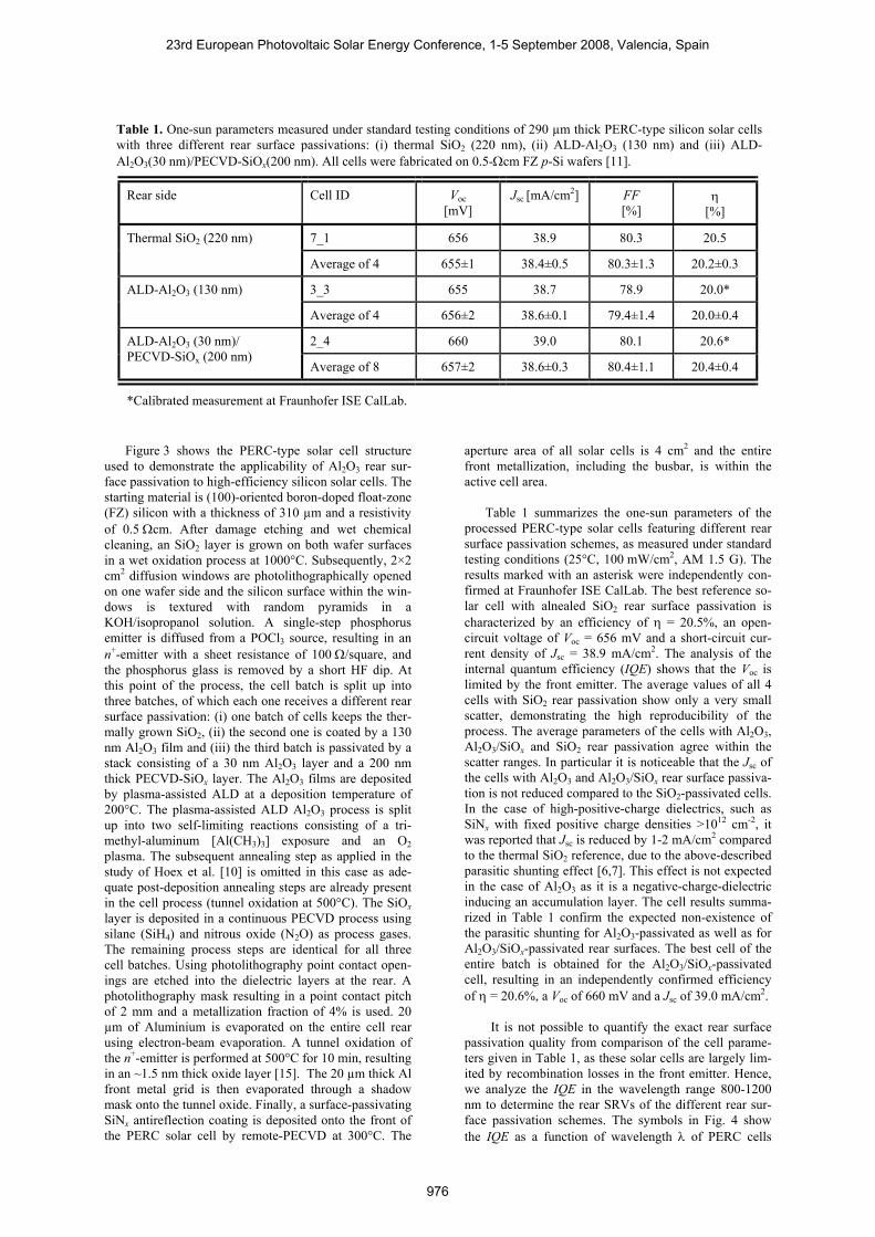
Figure 3 shows the PERC-type solar cell structure used to demonstrate the applicability of Al2O3 rear sur-face passivation to high-efficiency silicon solar cells. The starting material is (100)-oriented boron-doped float-zone (FZ) silicon with a thickness of 310 µm and a resistivity of 0.5 Ωcm. After damage etching and wet chemical cleaning, an SiO2 layer is grown on both wafer surfaces in a wet oxidation process at 1000°C. Subsequently, 2×2 cm2 diffusion windows are photolithographically opened on one wafer side and the silicon surface within the win-dows is textured with random pyramids in a KOH/isopropanol solution. A single-step phosphorus emitter is diffused from a POCl3 source, resulting in an n+-emitter with a sheet resistance of 100 Ω/square, and the phosphorus glass is removed by a short HF dip. At this point of the process, the cell batch is split up into three batches, of which each one receives a different rear surface passivation: (i) one batch of cells keeps the ther-mally grown SiO2, (ii) the second one is coated by a 130 nm Al2O3 film and (iii) the third batch is passivated by a stack consisting of a 30 nm Al2O3 layer and a 200 nm thick PECVD-SiOx layer. The Al2O3 films are deposited by plasma-assisted ALD at a deposition temperature of 200°C. The plasma-assisted ALD Al2O3 process is split up into two self-limiting reactions consisting of a tri-methyl-aluminum [Al(CH3)3] exposure and an O2 plasma. The subsequent annealing step as applied in the study of Hoex et al. [10] is omitted in this case as ade-quate post-deposition annealing steps are already present in the cell process (tunnel oxidation at 500°C). The SiOx layer is deposited in a continuous PECVD process using silane (SiH4) and nitrous oxide (N2O) as process gases. The remaining process steps are identical for all three cell batches. Using photolithography point contact open-ings are etched into the dielectric layers at the rear. A photolithography mask resulting in a point contact pitch of 2 mm and a metallization fraction of 4% is used. 20 µm of Aluminium is evaporated on the entire cell rear using electron-beam evaporation. A tunnel oxidation of the n+-emitter is performed at 500°C for 10 min, resulting in an ~1.5 nm thick oxide layer [15]. The 20 µm thick Al front metal grid is then evaporated through a shadow mask onto the tunnel oxide. Finally, a surface-passivating SiNx antireflection coating is deposited onto the front of the PERC solar cell by remote-PECVD at 300°C. The
aperture area of all solar cells is 4 cm2 and the entire front metallization, including the busbar, is within the active cell area.
Table 1 summarizes the one-sun parameters of the processed PERC-type solar cells featuring different rear surface passivation schemes, as measured under standard testing conditions (25°C, 100 mW/cm2, AM 1.5 G). The results marked with an asterisk were independently con-firmed at Fraunhofer ISE CalLab. The best reference so-lar cell with alnealed SiO2 rear surface passivation is characterized by an efficiency of η = 20.5%, an open-circuit voltage of Voc = 656 mV and a short-circuit cur-rent density of Jsc = 38.9 mA/cm2. The analysis of the internal quantum efficiency (IQE) shows that the Voc is limited by the front emitter. The average values of all 4 cells with SiO2 rear passivation show only a very small scatter, demonstrating the high reproducibility of the process. The average parameters of the cells with Al2O3, Al2O3/SiOx and SiO2 rear passivation agree within the scatter ranges. In particular it is noticeable that the Jsc of the cells with Al2O3 and Al2O3/SiOx rear surface passiva-tion is not reduced compared to the SiO2-passivated cells. In the case of high-positive-charge dielectrics, such as SiNx with fixed positive charge densities >1012 cm-2, it was reported that Jsc is reduced by 1-2 mA/cm2 compared to the thermal SiO2 reference, due to the above-described parasitic shunting effect [6,7]. This effect is not expected in the case of Al2O3 as it is a negative-charge-dielectric inducing an accumulation layer. The cell results summa-rized in Table 1 confirm the expected non-existence of the parasitic shunting for Al2O3-passivated as well as for Al2O3/SiOx-passivated rear surfaces. The best cell of the entire batch is obtained for the Al2O3/SiOx-passivated cell, resulting in an independently confirmed efficiency of η = 20.6%, a Voc of 660 mV and a Jsc of 39.0 mA/cm2.
It is not possible to quantify the exact rear surface
passivation quality from comparison of the cell parame-ters given in Table 1, as these solar cells are largely lim-ited by recombination losses in the front emitter. Hence, we analyze the IQE in the wavelength range 800-1200 nm to determine the rear SRVs of the different rear sur-face passivation schemes. The symbols in Fig. 4 show the IQE as a function of wavelength λ of PERC cells
Table 1. One-sun parameters measured under standard testing conditions of 290 µm thick PERC-type silicon solar cells with three different rear surface passivations: (i) thermal SiO2 (220 nm), (ii) ALD-Al2O3 (130 nm) and (iii) ALD-Al2O3(30 nm)/PECVD-SiOx(200 nm). All cells were fabricated on 0.5-Ωcm FZ p-Si wafers [11].
Rear side Cell ID Voc [mV]
Jsc [mA/cm2] FF [%]
η [%]
7_1 656 38.9 80.3 20.5 Thermal SiO2 (220 nm)
Average of 4 655±1 38.4±0.5 80.3±1.3 20.2±0.3
3_3 655 38.7 78.9 20.0* ALD-Al2O3 (130 nm)
Average of 4 656±2 38.6±0.1 79.4±1.4 20.0±0.4
2_4 660 39.0 80.1 20.6* ALD-Al2O3 (30 nm)/ PECVD-SiOx (200 nm)
Average of 8 657±2 38.6±0.3 80.4±1.1 20.4±0.4
*Calibrated measurement at Fraunhofer ISE CalLab.
23rd European Photovoltaic Solar Energy Conference, 1-5 September 2008, Valencia, Spain
976
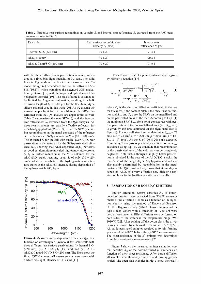
with the three different rear passivation schemes, meas-ured at a fixed bias light intensity of 0.3 suns. The solid lines in Fig. 4 show the fits to the measured data. To model the IQE(λ) dependence we use the software LAS-SIE [16,17], which combines the extended IQE evalua-tion by Basore [18] with the improved optical model de-veloped by Brendel [19]. The bulk lifetime is assumed to be limited by Auger recombination, resulting in a bulk diffusion length of Lb = 1500 µm for the 0.5 Ωcm p-type silicon material used in this work [20]. As we assume the intrinsic upper limit for the bulk lifetime, the SRVs de-termined from the IQE analysis are upper limits as well. Table 2 summarizes the rear SRVs Sr and the internal rear reflectances Rr extracted from the IQE analysis. All three rear structures are equally effective reflectors for near-bandgap photons (Rr = 91%). The rear SRV (includ-ing recombination at the metal contacts) of the reference cell with alnealed SiO2 amounts to Sr = (90 ± 20) cm/s. The extracted Sr for the cell with single-layer Al2O3 rear passivation is the same as for the SiO2-passivated refer-ence cell, showing that ALD-deposited Al2O3 performs as good as aluminium-annealed high-temperature-grown SiO2. A further reduction in the Sr is obtained for the Al2O3/SiOx stack, resulting in an Sr of only (70 ± 20) cm/s, which we attribute to the hydrogenation of inter-face states at the Al2O3/Si interface during deposition of the hydrogen-rich SiOx layer.
Wavelength λ (nm)800 900 1000 1100 1200In
tern
al Q
uant
um E
ffici
ency
IQE
(%)
0
20
40
60
80
100 Al2O3/SiOx
Al2O3
alnealed SiO2
Figure 4. Measured internal quantum efficiency IQE as a function of wavelength λ (symbols) for solar cells with three different rear surface passivations: (i) thermal SiO2 (220 nm), (ii) ALD-Al2O3 (130 nm) and (iii) ALD-Al2O3(30 nm)/PECVD-SiOx(200 nm). The lines show the fitted IQE(λ) curves. All measurements were taken with a white bias light intensity of ~0.3 suns [11].
The effective SRV of a point-contacted rear is given by Fischer’s equation [17]
1
passr
met
2arctan2
,1-
exp
n
n
p Wp f SW fDS
W fDWp fWS
− π π = + − − +
(1)
where Dn is the electron diffusion coefficient, W the wa-fer thickness, p the contact pitch, f the metallization frac-tion and Smet and Spass are the SRVs on the metallized and on the passivated areas of the rear. According to Eqn. (1) the minimum SRV Sr.min for a point-contact rear with per-fect passivation in the non-metallized area (i.e., Spass = 0) is given by the first summand on the right-hand side of Eqn. (1). For our cell structure we determine Sr.min = 73 cm/s (Dn = 23 cm2/s, W = 290 µm, p = 2000 µm, f = 4%, Smet ≥ 105 cm/s). As the Sr of (70 ± 20) cm/s extracted from the IQE analysis is practically identical to the Sr.min calculated using Eq. (1), we conclude that recombination in the passivated area of the cell rear can be completely neglected. Note that, although a slightly better passiva-tion is obtained in the case of the Al2O3/SiOx stacks, the rear SRV of the single-layer Al2O3-passivated cells is also mainly determined by recombination at the metal contacts. The IQE results clearly prove that atomic-layer-deposited Al2O3 is a very effective new dielectric pas-sivation layer for high-efficiency silicon solar cells. 3 PASSIVATION OF B-DOPED p+ EMITTERS Emitter saturation current densities J0e of boron-doped p+ emitters were extracted from QSSPC measure-ments of the effective lifetime as a function of the injec-tion density using the method of Kane and Swanson [21,12]. High-resistivity (20-90 Ωcm) shiny-etched n-type silicon wafers with a thickness of ~260 µm were used as base material. BBr3 diffusions were performed on both sides of the wafers in the temperature range 895-1010°C [22]. After etching off the boron glass, the drive-in was performed by a thermal oxidation at 1050°C [22]. All oxide-passivated samples received a 40-min forming gas anneal at 400°C before the QSSPC measurements. The sheet resistance of the p+ emitters was determined from four-point probe measurements [23]. Figure 5 shows the measured emitter saturation cur-rent densities J0e of the boron-diffused p+ emitters as a function of their sheet resistance. After boron diffusion all samples were thermally oxidized and forming gas an-nealed. The open blue triangles in Fig. 5 show the result-
Table 2. Effective rear surface recombination velocity Sr and internal rear reflectance Rr extracted from the IQE meas-urements shown in Fig. 5.
Rear side Rear surface recombination velocity Sr [cm/s]
Internal rear reflectance Rr [%]
Thermal SiO2 (220 nm) 90 ± 20 91 ± 1
Al2O3 (130 nm) 90 ± 20 90 ± 1
Al2O3(30 nm)/SiOx(200 nm) 70 ± 20 91 ± 1
23rd European Photovoltaic Solar Energy Conference, 1-5 September 2008, Valencia, Spain
977
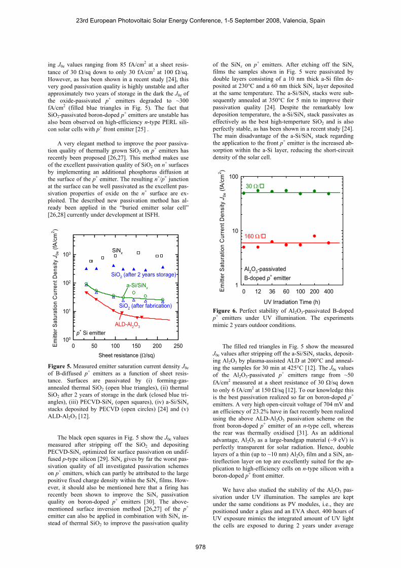
ing J0e values ranging from 85 fA/cm2 at a sheet resis-tance of 30 Ω/sq down to only 30 fA/cm2 at 100 Ω/sq. However, as has been shown in a recent study [24], this very good passivation quality is highly unstable and after approximately two years of storage in the dark the J0e of the oxide-passivated p+ emitters degraded to ~300 fA/cm2 (filled blue triangles in Fig. 5). The fact that SiO2-passivated boron-doped p+ emitters are unstable has also been observed on high-efficiency n-type PERL sili-con solar cells with p+ front emitter [25] . A very elegant method to improve the poor passiva-tion quality of thermally grown SiO2 on p+ emitters has recently been proposed [26,27]. This method makes use of the excellent passivation quality of SiO2 on n+ surfaces by implementing an additional phosphorus diffusion at the surface of the p+ emitter. The resulting n+/p+ junction at the surface can be well passivated as the excellent pas-sivation properties of oxide on the n+ surface are ex-ploited. The described new passivation method has al-ready been applied in the “buried emitter solar cell” [26,28] currently under development at ISFH.
Sheet resistance (Ω/sq)0 50 100 150 200 250Em
itter
Sat
urat
ion
Cur
rent
Den
sity
J0e
(fA/
cm2 )
100
101
102
103 SiNx
SiO2 (after 2 years storage)
SiO2 (after fabrication)
ALD-Al2O3
a-Si/SiNx
p+ Si emitter
Figure 5. Measured emitter saturation current density J0e of B-diffused p+ emitters as a function of sheet resis-tance. Surfaces are passivated by (i) forming-gas-annealed thermal SiO2 (open blue triangles), (ii) thermal SiO2 after 2 years of storage in the dark (closed blue tri-angles), (iii) PECVD-SiNx (open squares), (iv) a-Si/SiNx stacks deposited by PECVD (open circles) [24] and (v) ALD-Al2O3 [12]. The black open squares in Fig. 5 show the J0e values measured after stripping off the SiO2 and depositing PECVD-SiNx optimized for surface passivation on undif-fused p-type silicon [29]. SiNx gives by far the worst pas-sivation quality of all investigated passivation schemes on p+ emitters, which can partly be attributed to the large positive fixed charge density within the SiNx films. How-ever, it should also be mentioned here that a firing has recently been shown to improve the SiNx passivation quality on boron-doped p+ emitters [30]. The above-mentioned surface inversion method [26,27] of the p+ emitter can also be applied in combination with SiNx in-stead of thermal SiO2 to improve the passivation quality
of the SiNx on p+ emitters. After etching off the SiNx films the samples shown in Fig. 5 were passivated by double layers consisting of a 10 nm thick a-Si film de-posited at 230°C and a 60 nm thick SiNx layer deposited at the same temperature. The a-Si/SiNx stacks were sub-sequently annealed at 350°C for 5 min to improve their passivation quality [24]. Despite the remarkably low deposition temperature, the a-Si/SiNx stack passivates as effectively as the best high-temperture SiO2 and is also perfectly stable, as has been shown in a recent study [24]. The main disadvantage of the a-Si/SiNx stack regarding the application to the front p+ emitter is the increased ab-sorption within the a-Si layer, reducing the short-circuit density of the solar cell.
UV Irradiation Time (h)
0 12 36 60 100 200 400Emitt
er S
atur
atio
n C
urre
nt D
ensi
ty J
0e (f
A/cm
2 )
1
10
100
160 Ω/
30 Ω/
Al2O3-passivated B-doped p+ emitter
Figure 6. Perfect stability of Al2O3-passivated B-doped p+ emitters under UV illumination. The experiments mimic 2 years outdoor conditions. The filled red triangles in Fig. 5 show the measured J0e values after stripping off the a-Si/SiNx stacks, deposit-ing Al2O3 by plasma-assisted ALD at 200°C and anneal-ing the samples for 30 min at 425°C [12]. The J0e values of the Al2O3-passivated p+ emitters range from ~50 fA/cm2 measured at a sheet resistance of 30 Ω/sq down to only 6 fA/cm2 at 150 Ω/sq [12]. To our knowledge this is the best passivation realized so far on boron-doped p+ emitters. A very high open-circuit voltage of 704 mV and an efficiency of 23.2% have in fact recently been realized using the above ALD-Al2O3 passivation scheme on the front boron-doped p+ emitter of an n-type cell, whereas the rear was thermally oxidised [31]. As an additional advantage, Al2O3 as a large-bandgap material (~9 eV) is perfectly transparent for solar radiation. Hence, double layers of a thin (up to ~10 nm) Al2O3 film and a SiNx an-tireflection layer on top are excellently suited for the ap-plication to high-efficiency cells on n-type silicon with a boron-doped p+ front emitter. We have also studied the stability of the Al2O3 pas-sivation under UV illumination. The samples are kept under the same conditions as PV modules, i.e., they are positioned under a glass and an EVA sheet. 400 hours of UV exposure mimics the integrated amount of UV light the cells are exposed to during 2 years under average
23rd European Photovoltaic Solar Energy Conference, 1-5 September 2008, Valencia, Spain
978

outdoor conditions. The results of this experiment are shown in Fig. 6. The Al2O3 passivation is found to be perfectly stable and shows no degradation at all during UV exposure. 4 ALL-Al2O3 PASSIVATED CELLS
Thickness W (µm)0 1 2 3
Effic
ienc
y η
(%)
192021222324252627282930
W(µm) vs Eta_CE(%) W(µm) vs Eta_CE(%) W(µm) vs Eta_CE(%)
bulk
bulk + Al2O3
bulk + Al2O3 + contacts
Thickness W (µm)1 10 100 1000
Ope
n-ci
rcui
t Vol
tage
Voc
(mV
)
650
700
750
800
850
bulk
bulk + Al2O3
bulk + Al2O3 + contacts
1-Ωcm n-Si base
(a)
(b)
Figure 7. Calculated limiting (a) 1-sun efficiency η and (b) open-circuit voltage Voc as a function of cell thickness W for a 1-Ωcm n-type silicon base assuming Lambertian light trapping. Black squares: only bulk recombination via Coulomb-enhanced Auger; red circles: additional sur-face recombination at the Al2O3-passivated p+ emitter and Al2O3-passivated n-Si base; blue triangles: additional contact recombination and front-grid shading. Using the measured recombination parameters of Al2O3-passivated p+ emitters and on undiffused Al2O3-passivated n-type Si surfaces we calculate the 1-sun effi-ciency and Voc limits for all-Al2O3 passivated n-type sili-con solar cells. For these calculations we assume an n-type silicon wafer with a base resistivity of 1 Ωcm and Lambertian light trapping [32]. The I-V characteristics is calculated using the expression
L 0 rb
exp 1 ,en qVJ J qW J qS n
kT∆ = − − − − ∆ τ
(2)
where JL is the light-generated current density, W the cell thickness, τb the bulk lifetime, J0e the emitter saturation current density and Sr the rear surface recombination ve-locity. In order to estimate the ultimate efficiency limit
for a 1-sun silicon solar cell we assume a perfectly pas-sivated emitter and rear surface, i.e. J0e = 0 and Sr = 0 in Eq. (2). The cell thickness W is varied between 1 and 1000 µm. The bulk recombination lifetime τb is assumed to be limited by Coulomb-enhanced Auger recombina-tion, and we use a widely accepted parameterization as a function of the carrier densities [33].
Figure 8. The all-Al2O3 passivated n-type silicon solar cell has an efficiency limit of 26.1% including bulk, sur-face and contact recombination as well as shading losses. Table 3. Calculated limiting 1-sun efficiency η and open-circuit voltage Voc as a function of cell thickness W for a 1-Ωcm n-type silicon base assuming Lambertian light trapping.
Losses ηmax (%) Voc @ ηmax
(mV) bulk 28.5 770
bulk + Al2O3 27.5 740 bulk + Al2O3
+ contacts 26.1 720
Figure 7 and Table 3 show the calculated efficiency limit and the corresponding Voc for three different cases. The uppermost curve (black squares) shows that Cou-lomb-enhanced Auger recombination limits the effi-ciency of a silicon solar cell to an ultimate efficiency of 28.5% for a cell thickness of ~50 µm. The red curve (cir-cles) includes recombination in the Al2O3-passivated bo-ron-diffused p+ emitter as well as recombination at the undiffused Al2O3-passivated cell rear. For Al2O3-passivated p+ emitters we have measured a J0e value of 6 fA/cm2 and for undiffused n-type silicon a SRV of Sr = 4 cm/s. These additional recombination channels reduce the efficiency limit to 27.5% for a cell thickness between 100 and 300 µm. Moreover, the all-Al2O3 passivated cell permits open-circuit voltages of up to 755 mV for a cell thickness between 3 and 10 µm. The Voc limit drops to 740 mV at a cell thickness of 100 µm, where the effi-ciency peaks. Adding contact recombination and contact shading in a realistic way reduces the efficiency limit further to 26.1% and the Voc limit to 728 mV (blue trian-gles in Fig. 7). At a cell thickness of 200 µm our calcu-lation gives a maximum efficiency of 26.1% at a Voc of 720 mV. The latter case corresponds to the cell structure shown in Fig. 8. Under the contacts we assume that heavy diffusions reduce the contact recombination. The front p++ diffusion beneath the metal contacts has a sheet resistance of 5 Ω/sq, resulting in an emitter saturation current density of J0e.met = 420 fA/cm2 [34]. The n++ dif-fusion at the rear has a sheet resistance of 30 Ω/sq and a
Al2O3 n-type base
n++ n++
p++ p++
p+
SiNx
Al2O3 n-type base
n++ n++
p++ p++
p+
SiNx
23rd European Photovoltaic Solar Energy Conference, 1-5 September 2008, Valencia, Spain
979
J0r.met of 350 fA/cm2 [35], which corresponds to an Sr.met of 150 cm/s. We use Eqn. (1) to determine the total rear SRV Sr as a function of cell thickness. For the metalliza-tion fraction at the front and the rear we assume a value of f = 3%. We also account for the optical shading losses by reducing JL by 3%. Our calculations clearly show that due to the excellent level of surface passivation, a reduc-tion of the contact recombination remains the major chal-lenge in order to reach highest efficiencies. 5 CONCLUSIONS Atomic layer deposition (ALD) of Al2O3 has been identified as an ideal new passivation scheme for pas-sivating undiffused p- and n-type silicon surfaces as well as for the passivation of boron-doped p+ regions. Our calculations of efficiency and Voc limits of n-type Si solar cells show that all-Al2O3 passivated cells have an effi-ciency limit of 27.5% at a Voc of 740 mV. Including con-tact recombination and optical shading with realistic as-sumptions the efficiency limit drops to 26.1% at a Voc of 720 mV. In addition to the outstanding surface passivation provided by ALD-deposited Al2O3, the deposition proc-ess itself is also beneficial from an application point of view. In contrast to the conventionally applied PECVD, ALD consists of two self-limiting half-reactions, which implies several important advantages: (i) ALD gives highly conformal coatings, which allows to deposit and passivate e.g. deep trenches or even pores in silicon, (ii) pin-hole and particle-free deposition is achieved, (iii) as ALD is a self-limiting process uniform films can be de-posited over large areas with mono-layer growth control and (iv) very low impurity concentrations of deposited films and hence very high film quality is achieved. The main disadvantage of ALD for photovoltaic applications is its relatively low deposition rate. However, this disad-vantage can be overcome by depositing ultrathin (2-30 nm) ALD-Al2O3 films and capping them with a thicker film of e.g. PECVD-SiOx, SiNx or SiCx [36]. Apart of the advantageous optical properties of these stacks, we have demonstrated that the passivation quality of such ALD/PECVD stacks can even be superior to that of sin-gle layers of Al2O3 [11], which we attribute to the hydro-genation of interface states at the Al2O3/Si interface dur-ing deposition of the hydrogen-rich PECVD layer. Com-bination of ALD and PECVD might hence be a key tech-nology for future industrial high-efficiency solar cells. ACKNOWLEDGEMENTS The authors thank all members of the PV department at ISFH for their contributions to this work. Funding was provided by the State of Lower Saxony and the German Ministry for the Environment, Nature Conservation and Nuclear Safety (BMU). REFERENCES
[1] J. Zhao, A. Wang, M.A. Green, Prog. Photovolt. 7, 471 (1999).
[2] M.J. Kerr, A. Cuevas, Sem. Sci. Techn. 17, 35 (2001).
[3] M.J. Stocks, A. Cuevas, A.W. Blakers, Proc. 14th EUPVSEC, Barcelona, Spain (1997), p. 770.
[4] T. Lauinger, J. Schmidt, A.G. Aberle, R. Hezel, Appl. Phys. Lett. 68, 1232 (1996).
[5] J. Schmidt, J.D. Moschner, J. Henze, S. Dauwe, R. Hezel, Proc. 19th EUPVSEC, Paris, France (2004), p. 391.
[6] S. Dauwe, L. Mittelstädt, A. Metz, J. Schmidt, R. Hezel, Proc. 3rd WCPEC, Osaka, Japan (2003), p. 1395.
[7] S. Dauwe, L. Mittelstädt, A. Metz, R. Hezel, Progr. Photovolt. 10, 271 (2002).
[8] S. Dauwe, J. Schmidt, R. Hezel, Proc. 29th IEEE PVSEC, New Orleans, USA (2002), p. 1246.
[9] G. Agostinelli, A. Delabie, P. Vitanov, Z. Alexieva, H.F.W. Dekkers, S. De Wolf, G. Beaucarne, Sol. En. Mat. Sol. Cells 90, 3438 (2006).
[10] B. Hoex, S.B.S. Heil, E. Langereis, M.C.M. van de Sanden, W.M.M. Kessels, Appl. Phys. Lett. 89, 042112 (2006).
[11] J. Schmidt, A. Merkle, R. Brendel, B. Hoex, M.C.M. van de Sanden, W.M.M. Kessels, Progr. Photovolt. (2008), DOI: 10.1002/pip.823.
[12] B. Hoex, J. Schmidt, R. Bock, P. P. Altermatt, M. C. M. van de Sanden, and W. M. M. Kessels, Appl. Phys. Lett. 91, 112107 (2007).
[13] S. Dauwe, Ph.D. thesis, ISFH, University of Hano-ver, Germany, 2003.
[14] B. Hoex, J. Schmidt, P. Pohl, M.C.M. van de Sanden, W.M.M. Kessels, J. Appl. Phys., in press.
[15] R. Hezel and K. Jaeger, J. Electrochem. Soc. 136, 518 (1989).
[16] www.pv-tools.de
[17] B. Fischer, Ph.D. thesis, Univ. Konstanz, 2003.
[18] P.A. Basore, Proc. 23rd IEEE PVSC (1993), p. 147.
[19] R. Brendel, R. Plieninger, Techn. Digest 9th Inter-national PVSEC, Miyazaki, Japan (1996), p. 521.
[20] P.P. Altermatt, J. Schmidt, G. Heiser, A.G. Aberle, J. Appl. Phys. 82, 4938 (1997).
[21] D. E. Kane, R.M. Swanson, Proc. 18th IEEE PVSC, Las Vegas, USA (1985), p. 578.
[22] M. Kerr, Ph.D. thesis, Australian National Univer-sity, Australia, 2002.
[23] R. Bock, P.P. Altermatt, J. Schmidt, this conf.
[24] P.P. Altermatt H. Plagwitz, R. Bock, J. Schmidt, R. Brendel, M.J. Kerr, A. Cuevas, Proc. 21st EUP-VSEC, Dresden, Germany (2006), p. 647.
23rd European Photovoltaic Solar Energy Conference, 1-5 September 2008, Valencia, Spain
980

[25] J. Zhao, J. Schmidt, A. Wang, G. Zhang, B.S. Richards, M.A. Green, Proc. 3rd WCPEC, Osaka, Japan (2003), p. 923.
[26] N.P. Harder, V. Mertens, R. Brendel, phys. stat. sol. (RRL) 2, 148 (2008).
[27] J. Benick, O. Schultz-Wittmann, J. Schön, S.W. Glunz, phys. stat. sol. (RRL) 2, 145 (2008).
[28] Patent pending, ISFH.
[29] J. Schmidt, M.J. Kerr, Solar Energy Materials and Solar Cells 65, 585 (2001).
[30] F.W. Chen, T. Li, J.E. Cotter, Appl. Phys. Lett. 88, 263514 (2006).
[31] J. Benick, B. Hoex, O. Schultz, S. Glunz, Proc. 33rd IEEE PVSC, San Diego, USA (2008).
[32] R. Brendel, Thin-Film Crystalline Silicon Solar Cells, Wiley-VCH (2003).
[33] J. Schmidt, M. Kerr, P.P. Altermatt, J. Appl. Phys. 88, 1494 (2000).
[34] D. E. Swanson, R. Kane, Proc. 18th IEEE PVSC, Las Vegas, USA (1985), p. 578.
[35] M. Kerr, Ph.D. thesis, Australian National Univer-sity (2002).
[36] J. Schmidt, A. Merkle, B. Hoex, M.C.M. van de Sanden, W.M.M. Kessels, R. Brendel, Proc. 33rd IEEE PVSC, San Diego, USA (2008).
23rd European Photovoltaic Solar Energy Conference, 1-5 September 2008, Valencia, Spain
981