The use of hydrogenated Schiff base ligands in the synthesis of multi-metallic compounds II
Upload
independentCategory
view
0download
0
Passivation of surface and bulk defects in p -GaSb by hydrogenatedamorphous silicon treatment
P. S. Dutta, A. K. Sreedhar, and H. L. Bhata)Department of Physics, Indian Institute of Science, Bangalore - 560 012, India
G. C. Dubey and Vikram KumarSolid State Physics Laboratory, Lucknow Road, Delhi - 110 054, India
E. DieguezDepartamento de Fisica de Materiales, Universidad Autonoma, C-IV, 28049 Cantoblanco-Madrid, Spain
U. Pal and J. PiquerasDepartamento de Fisica de Materiales, Facultad de Fisica, Universidad Complutense, 28040 Madrid, Spain
~Received 10 October 1995; accepted for publication 27 November 1995!
Passivation of point and extended defects in GaSb has been observed as a result of hydrogenatedamorphous silicon~a-Si:H! treatment by the glow discharge technique. Cathodoluminescence~CL!images recorded at various depths in the samples clearly show passivation of defects on the surfaceas well as in the bulk region. The passivation of various recombination centers in the bulk isattributed to the formation of hydrogen-impurity complexes by diffusion of hydrogen ions from theplasma.a-Si:H acts as a protective cap layer and prevents surface degradation which is usuallyencountered by bare exposure to hydrogen plasma. An enhancement in luminescence intensity up to20 times is seen due to the passivation of nonradiative recombination centers. The passivationefficiency is found to improve with an increase ina-Si:H deposition temperature. The relativepassivation efficiency of donors and acceptors by hydrogen in undoped and Te-compensatedp-GaSb has been evaluated by CL and by the temperature dependence of photoluminescenceintensities. Most notably, effective passivation of minority dopants in tellurium compensatedp-GaSb is evidenced for the first time. ©1996 American Institute of Physics.@S0021-8979~96!03105-4#
of an
l inde-therof
l inlson ben-
ptedes-
ive-toter-
Te-he-Ini-er
I. INTRODUCTION
In recent times, extensive research has been carriedon defect passivation in various elemental and composemiconductors. This is interesting both for understandthe physics of the material as well as from the point of vieof technological applications. Several techniques have bused for passivating the bulk as well as surface defects. Ually, chemical treatment with sulfur-containing compounlike ~NH4!2Sx , Na2S, H2S results in surface reconstructiodue to which the surface recombination rate decreases.1–3Onthe other hand, defects in the bulk are passivated by indision of light elements like lithium, hydrogen, etc.4 Theseelements reduce the concentration of various defect cenby forming complexes with them. Passivation by hydrogplasma has been widely used in the recent past.4 Even thoughpassivation of bulk defects by hydrogen is now well estalished, avoiding surface degradation during plasma exposis not trivial.4 The surface defect layer thus created adversaffects the electrical and optical properties of the materialot of effort has been made to avoid the formation of tdefect layer in various materials~see Ref. 4 and referencetherein!. Recently, we have been investigating the applicabity of various surface passivation methods to GaSb,5,6 aIII–V compound semiconductor that is gaining importanc7
A previous investigation on hydrogenation of GaSb by a
a!Author to whom all correspondence should be addressed; Electronic [email protected]
3246 J. Appl. Phys. 79 (6), 15 March 1996 0021-8979/9
Downloaded¬14¬Dec¬2004¬to¬128.113.30.116.¬Redistribution¬subje
outundingweensu-dsn
ffu-
tersen
b-ureelyl. Ahesil-
e.rf
plasma technique has already demonstrated the existencesurface defect layer.8 By slow chemical etching, it has beefound possible to remove this defect layer.9 But this ap-proach is limited only to basic research and is impracticadevice fabrication processes. Hence, it would be highlysirable to develop some dry processing techniques for eiremoving or passivating the surface defects. Depositionthe surface layer of a different material can be beneficiathis respect, which along with its passivating effect can aact as a stable, protective layer. One such candidate caa-Si:H, which has been extensively used for thin film trasistors and high efficiency solar cell applications.10 To thebest of our knowledge, such a study has not been attemuntil now on GaSb. This article discusses the photolumincence ~PL! and cathodoluminescence~CL! properties ofa-Si:H treated undoped and tellurium-compensatedp-GaSb.The results obtained herein clearly demonstrate the effectness of this treatment in achieving bulk passivation duethe plasma hydrogen in addition to a defect-free surfaceminated bya-Si:H.
II. EXPERIMENTAL DETAILS
The single-crystal substrates of undoped andcompensatedp-GaSb used for our studies were grown by tvertical Bridgman technique.11 Various degrees of Te compensation were obtained by a repeated dilution process.tially, Te-dopedn-GaSb crystals were grown with the carri
ail:
6/79(6)/3246/7/$10.00 © 1996 American Institute of Physics
ct¬to¬AIP¬license¬or¬copyright,¬see¬http://jap.aip.org/jap/copyright.jsp

as-
ln-
re
ote--estur-re.er--ere
sr-d
s
vi-
concentration;1017 cm23. Then, a small weighed quantitof a Te-dopedn-GaSb ingot was added to a fresh chargeundoped GaSb for the next growth run. This dilution procdure was repeated for successive growth experiments uthe required level of net acceptor concentration wastained. Layers ofa-Si:H with thicknesses in the range o100–200 Å were deposited on the substrates using a rfrequency plasma glow discharge system12with a rf power of6 W/cm2. Substrate temperatures in the range of 150–300were employed. A mixture of 1% SiH4 in 99% H2 with aflow rate of 1 cc/min was found to be optimal for obtaininhigh quality amorphous films.
The CL measurements were carried out using a HitaS-2500 scanning electron microscope in the emissive andmodes at 80 K.13 The advantage of CL, in addition to thhigh spatial resolution, is its ability to obtain more detailedepth-resolved information by varying the electron beaenergy.14 The accelerating voltage was in the range of 10–keV. The beam current was kept constant at 100 nA. Thbeam parameters were found sufficient to give enough lunescence intensity to carry out the measurements withcausing excessive heating and self-absorption.15 The pan-chromatic CL images were recorded using a system coning of an optical focusing lens and a liquid-nitrogen-coolNorth Coast EO-817 germanium detector attached to thecroscope. To record the CL spectra, an optical fiber gufeeding the light to an Oriel 78215 computer-controllemonochromator was used. From previous studies, it has bfound that by defocusing the electron beam, it is possibleobserve centers with low concentrations.16 For this reason,CL spectra were recorded both under focusing and defocing conditions of the electron beam.
The PL measurements were carried out using MIDAFourier transform photoluminescence spectrometer. An arion laser operating at 5145 Å was used as the excitasource with excitation levels in the range of 0.166–3W/cm2. A liquid-nitrogen-cooled germanium photodetectwas employed for signal detection. A resolution of 0.5 mewas used in our measurements. For low temperature msurements, the samples were freely suspended in liquid H4.2 K. To study the temperature dependence of PL, the stra were recorded during the natural heating cycle afterevaporation of liquid He. The temperature variation durithe data acquisition for any spectrum was less than 0.5The carrier concentrations of various samples used instudies were evaluated by the room temperature Hall msurements.
III. RESULTS AND DISCUSSION
A. Panchromatic cathodoluminescence images
Figure 1 shows a typical CL image recorded on a pished GaSb wafer prepared from the as-grown sample.fects typical of melt grown crystals have been identified amarked. These include cellular dislocation network~D!, pre-cipitates or impurity clusters~P!, and twin boundaries~par-allel lines marked T!. The distribution of defects in thesamples remains the same irrespective of the depth. Aa-Si:H treatment, there was a complete disappearance o
J. Appl. Phys., Vol. 79, No. 6, 15 March 1996
Downloaded¬14¬Dec¬2004¬to¬128.113.30.116.¬Redistribution¬subje
yofe-ntilob-fadio
°C
g
chiCLedm20esemi-out
sist-edmi-idedeento
us-
Cgontion.5orVea-e atpec-theng°C.ourea-
ol-De-nd
fterf the
dislocation network. Here, it is worth mentioning that thedisappearance of these nonradiative centers is a result of psivation by hydrogen rather than their elimination. To ruleout the possibility of reduction in dislocation due to thermaeffects during the glow discharge treatment, some of the utreated samples~as grown! were annealed at 300 °C for 1 h.The CL images recorded before and after the treatment weexactly identical, verifying that the passivation of disloca-tions in the treated samples is caused by hydrogen and ndue to mere thermal annealing. Passivation of extended dfects like grain boundaries and dislocations in GaSb by hydrogen has been observed in our previous electrical studialso.9 From the contrast of the CL images it was inferred thathe samples are better passivated at higher temperatures. Fthermore, some of the samples passivated at 300 °C weannealed in N2 atmosphere at the same temperature for 1 hNo changes were observed in the images recorded after thmal treatment. This shows high thermal stability of the passivated extended defects. This is in agreement with earlimeasurements carried out on hydrogenated polycrystallinGaSb.9
To evaluate the depth of which hydrogen passivation haoccurred, CL images were recorded with increasing acceleating voltages up to 20 keV. The general expression deriveby Kanaya and Okayama17 for the range of electron penetra-tion Re as a function of electron beam energyEb is
Re5~0.0276 A/rZ0.889!Eb1.67~mm!,
whereEb is in keV,A is the atomic weight in g/mol,r is ing/cm3, andZ is the atomic number. TheRe in our case withEb varying from 10 to 20 keV lies in the range of 0.87–2.78mm. Typical CL images recorded with accelerating voltageof 10 and 20 keV for the Te-compensated GaSb witha-Si:Hdeposited at 150 °C are shown in Figs. 2~a! and 2~b!, respec-tively. Complete passivation of the dislocations and twinboundaries can be seen in Fig. 2~a! even at higher magnifi-cation. At lowEb , the penetration depth of the electrons isless and hence the surface-related recombination can besualized better. With an increase inEb to 20 keV ~corre-
FIG. 1. Typical CL image of a polished GaSb wafer from an as-growncrystal recorded withEb510 keV. The labels marked as T, D, and P repre-sent twins, dislocation networks, and precipitates, respectively.
3247Dutta et al.
ct¬to¬AIP¬license¬or¬copyright,¬see¬http://jap.aip.org/jap/copyright.jsp

oell
re
a
ei-ent
dndnd
sponding to a depth of 2.8mm!, defects in the bulk are re-vealed@image 2~b!#. The dislocation network as observed ithe CL image of the passivated sample at higher acceleravoltage@image 2~b!# is similar to that observed in an unpassivated sample~Fig. 1!. The depth to which passivation occurs has been found to depend on thea-Si:H deposition tem-perature. The CL images of the sample passivated at 300are shown in Figs. 2~c! and 2~d! for the same region with anEb of 10 and 20 keV, respectively. A comparison of the Cimages recorded at the same depth@Figs. 2~b! and 2~d!# forthe samples passivated at 150 and 300 °C show thatdepth of passivation increases with increase in deposittemperature. Even at 2.8mm, the effect of passivation can beseen in the sample treated at 300 °C.
B. Cathodoluminescence spectra
The CL spectra recorded at 10 keV for the undopsamples before and aftera-Si:H treatment at 150 °C areshown in Fig. 3. The broad spectrum for the unpassivasample@spectrum~i!# has been deconvoluted into four maipeaks at 704, 775, 805, and 830 meV. The above-band-peak at 830 meV is an~e,h! transition including tail statesand shallow acceptors18 arising due to high excitation inten-sities in CL. The 805 meV is the band-gap-related peak. T775 and 704 meV peaks are due to the transitions fromconduction band to neutral state and singly ionized statethe native acceptor level, respectively. The passivated sam@spectrum~ii !# shows an overall enhancement in the CL intensity along with an increase in the relative intensity of th704 meV peak compared to the 775 meV transition. T
FIG. 2. Panchromatic CL images of Te-compensatedp-GaSb with ~a!a-Si:H deposited at 150 °C~Eb : 10 keV!; ~b! a-Si:H deposited at 150 °C~Eb : 20 keV!; ~c! a-Si:H deposited at 300 °C~Eb : 10 keV!; ~d! a-Si:Hdeposited at 300 °C~Eb : 20 keV!.
3248 J. Appl. Phys., Vol. 79, No. 6, 15 March 1996
Downloaded¬14¬Dec¬2004¬to¬128.113.30.116.¬Redistribution¬subjec
nting--
°C
L
theion
ed
tedngap
hetheofple-ehe
higher CL intensity of the passivated sample is attributed tthe reduction in nonradiative recombination channels. Threason for the relative increase in the 704 meV transition wibe discussed later.
The CL spectra of the Te-compensated samples befoand aftera-Si:H treatment at 150 °C are shown in Fig. 4.Apart from the four peaks seen in the undoped samples,new peak at 730 meV appears@spectrum~i!#. The 730 meVtransition is intrinsic to tellurium and is attributed to a tran-sition from the conduction band to the deep VGaGaSbTeSbcenter.19 After a-Si:H treatment, the CL intensity increasesby at least five times due to passivation of the nonradiativrecombination centers. Apart from the increase in the lumnescence efficiency, the peaks at 704 and 730 meV are absin the passivated sample in the near-surface region@spectrum~ii !#. Also, the broad peak encompassing the 775, 805, an830 meV transitions is better resolved. With an increase iEb to 20 keV, luminescence from the bulk region is observeand the CL spectrum show a reappearance of the 704 a730 meV peaks@spectrum~iii !#. Also a slight decrease in the
FIG. 3. CL spectra of undopedp-GaSb:~i! without ana-Si:H layer;~ii ! withan a-Si:H layer deposited at 150 °C~Eb510 keV!. The dashed curves arethe deconvoluted peaks of spectrum~i!.
FIG. 4. CL spectra of Te-compensatedp-GaSb:~i! beforea-Si:H deposi-tion; ~ii ! aftera-Si:H deposited at 150 °C andEb510 keV!; ~iii ! aftera-Si:Hdeposited at 150 °C andEb520 keV!. The dashed curves are the deconvo-luted peaks of spectrum~i!.
Dutta et al.
t¬to¬AIP¬license¬or¬copyright,¬see¬http://jap.aip.org/jap/copyright.jsp

Ts
r
s
a
tsnd
t
d
-ofanusenfd inPLu-nd-terseyri-e-ctesech-ng
toate
i-
d
dominant peak intensity is observed. This is expected ascorresponding CL image@Fig. 2~b!# shows unpassivated defects in the bulk. However, the intensities of the 704 and 7meV peaks do not attain their original level, indicating ththese centers are only partially passivated. For the sampassivated at higher temperatures, say 200–300 °C, ewith anEb of 20 keV, the peaks at 704 and 730 meV do nappear indicating effective passivation to greater depths.
The CL spectra recorded for the unpassivatedcompensated GaSb~i! and the corresponding samples pasvated at 250 °C~ii ! and 300 °C~iii ! employing a defocusedelectron beam are shown in Fig. 5. For the sake of compson, the CL spectra for the unpassivated sample recowith focused as well as defocused beams are shown ininsert of Fig. 5. As can be seen from the insert, the unpavated sample shows an increase in the intensities of the dlevels at 704 and 730 meV on defocusing. Referring to sptra ~i!, ~ii !, and ~iii ! of Fig. 5, thea-Si:H treated samplesshow complete passivation of the deep centers. It shouldnoted that the defocused spectra for the passivated samshown here are essentially similar to those observed unfocused conditions. A focused electron beam results in sration of the emission. At high levels of excitation, the lumnescent centers become filled by capturing minority carrieAs the centers are filled, the excess minority carriers inconduction band recombine through nonradiative centerthe bulk. In the absence of the bulk nonradiative recombition centers, the diffusion length increases and carriersfuse to the surface and recombine. However, by defocusthe electron beam, the saturation of the recombination cters can be avoided and thus recombination centers withconcentrations in the material can be seen.16 The very factthat there are no observable centers with low concentrain the a-Si:H treated samples confirms the passivationbulk defects by hydrogen.
FIG. 5. CL spectra of Te-compensatedp-GaSb recorded with a defocuseelectron beam:~i! without ana-Si:H layer,~ii ! with ana-Si:H layer depos-ited at 250 °C;~iii ! with an a-Si:H layer deposited at 300 °C. The dashecurves are the deconvoluted peaks of spectrum~i!. The insert in this figureshows the CL spectra of the unpassivated sample with focused and dcused electron beams.
J. Appl. Phys., Vol. 79, No. 6, 15 March 1996
Downloaded¬14¬Dec¬2004¬to¬128.113.30.116.¬Redistribution¬subjec
the-30atplesvenot
e-i-
ari-dedthesi-eepec-
beplesdertu-i-rs.heina-if-ingen-low
ionof
C. Photoluminescence spectra
The PL spectra recorded at 4.2 K for the undopesamples before and aftera-Si:H deposition at 200 °C areshown in Fig. 6~a!. An increase in PL intensity of the domi-nant transition by;12 times is seen after passivation. Moreover, several near-band-edge excitonic peaks in the range792–808 meV and a peak at 717 meV corresponding toexciton bound to the ionized native acceptor appear. Variopeaks appearing in the PL spectrum of bulk GaSb have beassigned earlier18,20and are given in Table I. For the sake ocompleteness, the peaks observed in CL spectra discussethe previous section are also listed. The enhancement inintensity and the appearance of additional peaks is a cumlative effect of defect passivation in the bulk as well as othe surface as discussed below. It is known from earlier stuies that plasma hydrogen passivates shallow and deep cenin the bulk.9 However, at the same time, the sample surfacdegrades.8 The defective surface layer had to be removed bchemical etching before carrying out any optical and electcal characterization. Thus, even though an overall improvment in the luminescence intensity as a result of bulk defepassivation was seen, the well-resolved excitonic featurwere absent.9 This simply reflects the presence of surfacrecombination centers in these samples left behind after eting. On the other hand, passivation of the surface danglibonds by either~NH4!2Sx ~Ref. 5! or RuCl3 ~Ref. 6! results inwell-resolved near-band-edge excitonic peaks. This is duethe reduction in the recombination centers of the excitonsthe surface. The improvement in overall PL intensity and thpresence of well-resolved excitonic peaks ina-Si:H treatedsamples@Fig. 6~a!# clearly demonstrates the efficient passvation of both surface and bulk defects.
d
efo-
FIG. 6. PL spectra of undopedp-GaSb recorded at~a! 4.2 K and~b! 80 K:~i! without ana-Si:H layer; ~ii ! with ana-Si:H layer.
3249Dutta et al.
t¬to¬AIP¬license¬or¬copyright,¬see¬http://jap.aip.org/jap/copyright.jsp
o
o
t
f
i
o
i
the
ted
vel
ral-al--
e
e
V
ofndof
In Fig. 6~a!, the dominant peak is the donor–accept~D–A! pair transition at 777 meV~see Table I!. In the un-passivated sample, this peak was found to shift towahigher energy by 2–3 meV per decade increase in lapower density. However in the passivated sample, theserved peak shift is around 8–9 meV per decade increasexcitation intensity. This large D–A pair peak shift is duean increase in compensation21 resulting from more efficientpassivation of acceptors compared to donors. At 80 K,the unpassivated sample, the intensity of 704 meV~710 meVat 4.2 K! peak is slightly lower than that of 775 meV~777meV at 4.2 K!. However, in passivated samples, the intensof the 704 meV peak is higher than that of 775 meV. Alsnote that there is an overall increase in the intensity by;10times as a result of passivation. The relative increase of704 meV peak after passivation was also seen in CL msurements~Fig. 3!.
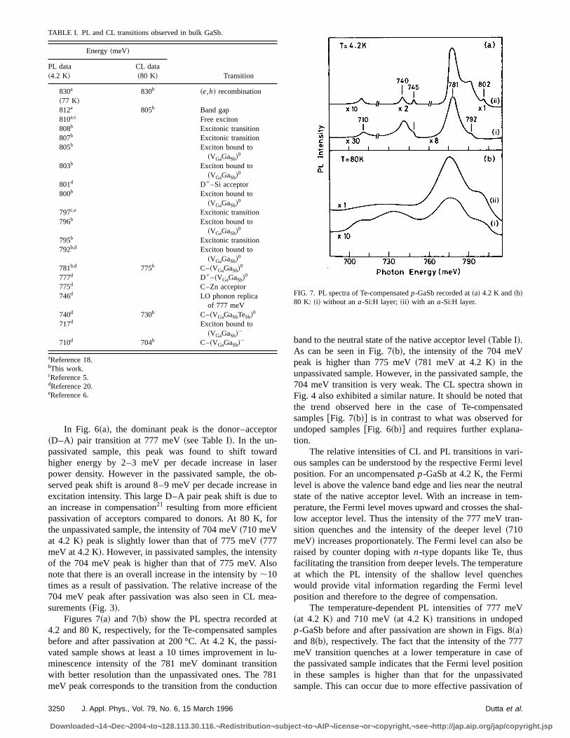
Figures 7~a! and 7~b! show the PL spectra recorded a4.2 and 80 K, respectively, for the Te-compensated sampbefore and after passivation at 200 °C. At 4.2 K, the pasvated sample shows at least a 10 times improvement inminescence intensity of the 781 meV dominant transitiwith better resolution than the unpassivated ones. The 7meV peak corresponds to the transition from the conduct
TABLE I. PL and CL transitions observed in bulk GaSb.
Energy~meV!
PL data~4.2 K!
CL data~80 K! Transition
830a
~77 K!830b ~e,h! recombination
812a 805b Band gap810a,c Free exciton808b Excitonic transition807b Excitonic transition805b Exciton bound to
~VGaGaSb!0
803b Exciton bound to~VGaGaSb!
0
801d D1–Si acceptor800b Exciton bound to
~VGaGaSb!0
797c,e Excitonic transition796b Exciton bound to
~VGaGaSb!0
795b Excitonic transition792b,d Exciton bound to
~VGaGaSb!0
781b,d 775b C–~VGaGaSb!0
777d D1–~VGaGaSb!0
775d C–Zn acceptor746d LO phonon replica
of 777 meV740d 730b C–~VGaGaSbTeSb!
0
717d Exciton bound to~VGaGaSb!
2
710d 704b C–~VGaGaSb!2
aReference 18.bThis work.cReference 5.dReference 20.eReference 6.
3250 J. Appl. Phys., Vol. 79, No. 6, 15 March 1996
Downloaded¬14¬Dec¬2004¬to¬128.113.30.116.¬Redistribution¬subjec
r
rdserb-e ino
or
tyo
theea-
tlessi-lu-n81on
band to the neutral state of the native acceptor level~Table I!.As can be seen in Fig. 7~b!, the intensity of the 704 meVpeak is higher than 775 meV~781 meV at 4.2 K! in theunpassivated sample. However, in the passivated sample,704 meV transition is very weak. The CL spectra shown inFig. 4 also exhibited a similar nature. It should be noted thathe trend observed here in the case of Te-compensatsamples@Fig. 7~b!# is in contrast to what was observed forundoped samples@Fig. 6~b!# and requires further explana-tion.
The relative intensities of CL and PL transitions in vari-ous samples can be understood by the respective Fermi leposition. For an uncompensatedp-GaSb at 4.2 K, the Fermilevel is above the valence band edge and lies near the neutstate of the native acceptor level. With an increase in temperature, the Fermi level moves upward and crosses the shlow acceptor level. Thus the intensity of the 777 meV transition quenches and the intensity of the deeper level~710meV! increases proportionately. The Fermi level can also braised by counter doping withn-type dopants like Te, thusfacilitating the transition from deeper levels. The temperaturat which the PL intensity of the shallow level quencheswould provide vital information regarding the Fermi levelposition and therefore to the degree of compensation.
The temperature-dependent PL intensities of 777 me~at 4.2 K! and 710 meV~at 4.2 K! transitions in undopedp-GaSb before and after passivation are shown in Figs. 8~a!and 8~b!, respectively. The fact that the intensity of the 777meV transition quenches at a lower temperature in casethe passivated sample indicates that the Fermi level positioin these samples is higher than that for the unpassivatesample. This can occur due to more effective passivation
FIG. 7. PL spectra of Te-compensatedp-GaSb recorded at~a! 4.2 K and~b!80 K: ~i! without ana-Si:H layer; ~ii ! with ana-Si:H layer.
Dutta et al.
t¬to¬AIP¬license¬or¬copyright,¬see¬http://jap.aip.org/jap/copyright.jsp

e
xe
n
e
n
s-r
he
e
si-
eh
-dk
el-
ds.
s-bc-r
the native acceptors than the unintentional donors whwould lead to increased compensation and hence the risFermi level position. This upward shift in the Fermi leveposition would account for the increase in relative PL intesity of the 704 meV peak with respect to the 775 meV trasition seen in Fig. 6~b!. For the Te-compensated samples, aopposite trend is observed as shown in Fig. 9 whichclearly due to more effective passivation of donors than tacceptors. As a result of effective passivation of Te donothe Fermi level shifts down due to which the levels at 70and 730 meV are not seen in the CL spectra~Fig. 4!. Thisdownward shift in Fermi level position after passivation eplains the decrease in relative PL intensity of the 704 mpeak with respect to the 775 meV shown in Fig. 7~b!.
It is worth mentioning here that the donors are minoricharges inp-GaSb and usually passivation of minority dopants is not common in III–V compounds. However, iheavily compensated materials or under conditions of minity carrier injection, one can observe minority dopapassivation.22–25 In previous studies on hydrogenated Te–Zcodopedn-GaSb, we have shown efficient passivation of thminority dopant.9 In the present study, the possibility of morefficient passivation of the Te donors compared to the natacceptors can be due to two reasons. First, telluriumpresent in large concentration~;1017 cm23! in the sample.Second, the passivation efficiency is more for the hydrogedefects like the Te donor rather than the native defect whact as heliumlike centers.
Last, the passivation efficiency of the nonradiative ceters by hydrogen has been evaluated as a function ofa-Si:Hdeposition temperature. The CL intensity increases motonically with increase in deposition temperature. This fact
FIG. 8. Temperature dependence of PL intensities for~i! 777 meV and~ii !710 meV transitions in undopedp-GaSb:~a! without ana-Si:H layer, ~b!with ana-Si:H layer.
J. Appl. Phys., Vol. 79, No. 6, 15 March 1996
Downloaded¬14¬Dec¬2004¬to¬128.113.30.116.¬Redistribution¬subjec
ichin
ln-n-nishers,4
-V
ty-nor-tne
iveis
nicich
n-
o-is
also substantiated by the defect contrast in the CL imageshown in Fig. 2. The PL intensity also increases with temperature initially, but shows a decreasing trend at highetemperature.26 The decrease in PL intensity for higher depo-sition temperatures is due to the increased absorption in ta-Si:H layer.27 When the correction for the absorption is ac-counted for, the PL intensity exhibits a similar trend as thCL intensity. This indicates that the passivation efficiencyincreases with increase in deposition temperature. The pasvation of surface and bulk defects would certainly influencethe electrical properties of the material. The details of thcurrent transport properties of GaSb diodes fabricated witan interfaciala-Si:H layer are presented elsewhere.28
IV. CONCLUSIONS
In conclusion, we have investigated the CL and PL properties of a-Si:H coated undoped and Te-compensatep-GaSb. Efficient passivation of the surface as well as buldefects up to;3 mm is observed. An overall improvement inluminescence intensity by;20 times and well-resolved ex-citonic features are observed as a result of bulk deep levpassivation by hydrogen and the reduction of surface recombination centers by thea-Si:H layer, respectively. The passi-vation of shallow impurities in the bulk by hydrogen hasbeen found to depend on the sample type. In undopep-GaSb, a more efficient passivation of acceptors occurHowever, in Te-compensatedp-GaSb, passivation of Te, theminority dopant is favored. The present study shows the pasible effects of unintentional hydrogen passivation in GaSduring encapsulation with amorphous Si. These dopant deativation effects may be quite general and applicable for othe
FIG. 9. Temperature dependence of PL intensities for~i! 781 meV and~ii !710 meV transitions in Te-compensatedp-GaSb: ~a! without an a-Si:Hlayer, ~b! with ana-Si:H layer.
3251Dutta et al.
t¬to¬AIP¬license¬or¬copyright,¬see¬http://jap.aip.org/jap/copyright.jsp

o
P
t
t
h
ll.
ys.
l.
s.
.
d
.
semiconductors too, and can be expected especially whehydrogen-containing plasma is employed for the surfadeposition. From the technological point of view, thisa-Si:Hlayer deposition can be used as a single-step processwhich both passivation of bulk defects by hydrogen plasmand a surface protective layer can be achieved. Furthermthis process is compatible for large scale device fabricatio
ACKNOWLEDGMENTS
One of the authors~P.S.D.! would like to thank CSIR~India! for the award of a senior research fellowship. U.gratefully acknowledges MEC~Spain! for the postdoctoralfellowship. This work was partially supported by the Universidad Autonoma de Madrid, Spain, through a visiting scietist fellowship and by DGICYT Project Nos. PB93-1256 anESP95-0148.
1B. J. Skromme, C. J. Sandroff, E. Yablonovitch, and T. Gmitter, AppPhys. Lett.51, 2022~1987!.
2R. N. Nottenburg, C. J. Sandroff, D. A. Humphrey, T. H. Hollenbeck, anR. Bhat, Appl. Phys. Lett.52, 218 ~1988!.
3L. Koenders, U. Blomachez, and W. Monch, J. Vac. Sci. Technol. B6,1416 ~1988!.
4S. J. Pearton, J. W. Corbett, and M. Stavola,Hydrogen in CrystallineSemiconductors~Springer, Heidelberg, 1992!.
5P. S. Dutta, K. S. Sangunni, H. L. Bhat, and V. Kumar, Appl. Phys. Le65, 1695~1994!.
6P. S. Dutta, K. S. R. Koteswara. Rao, H. L. Bhat, and V. Kumar, J. AppPhys.77, 4825~1995!.
7A. G. Milnes and A. Y. Polyakov, Solid State Electron.36, 803 ~1993!.8P. S. Dutta, K. S. Sangunni, H. L. Bhat, and V. Kumar, Appl. Phys. Le66, 1986~1995!.
3252 J. Appl. Phys., Vol. 79, No. 6, 15 March 1996
Downloaded¬14¬Dec¬2004¬to¬128.113.30.116.¬Redistribution¬subjec
n ace
byare,n.
.
-n-d
l.
d
t.
l.
t.
9P. S. Dutta, K. S. Sangunni, H. L. Bhat, and V. Kumar, Phys. Rev. B51,2153 ~1995!.
10Hydrogenated Amorphous Silicon, Semiconductors and Semimetals, Vol.21, edited by J. I. Pankove~Academic, New York, 1984!, Parts A, B, C,and D.
11P. S. Dutta, H. L. Bhat, K. S. Sangunni, and V. Kumar, J. Cryst. Growt141, 44 ~1994!.
12G. C. Dubey, R. A. Singh, S. N. Mukherjee, S. Pal, and M. G. Rao, BuMater. Sci.8, 267 ~1986!.
13F. Dominguez-Adame, J. Piqueras, and P. Fernandez, Appl. Phys. Lett.58,257 ~1991!.
14B. G. Yacobi and D. B. Holt, J. Appl. Phys.59, R1 ~1986!.15C. H. Gatos, J. J. Vaughan, J. Lagowski, and H. C. Gatos, J. Appl. Ph52, 1464~1981!.
16H. C. Casey, Jr. and J. S. Jayson, J. Appl. Phys.42, 2774~1971!.17K. Kanaya and S. Okayama, J. Phys. D5, 43 ~1972!.18G. Benz and R. Conradt, Phys. Rev. B16, 843 ~1977!.19A. I. Lebedev and I. A. Strel’nikova, Sov. Phys. Semicond.13, 229
~1979!.20P. S. Dutta, K. S. R. Koteswara. Rao, H. L. Bhat, and V. Kumar, AppPhys. A61, 149 ~1995!.
21V. Swaminathan and A. T. Macrander,Materials Aspects of GaAs and InPBased Structures~Prentice-Hall, Englewood Cliffs, NJ, 1991!.
22C. H. Seager, R. A. Anderson, and D. K. Brice, J. Appl. Phys.68, 3268~1990!.
23A. J. Tavendale, A. A. Williams, D. Alexiev, and S. J. Pearton, Mater. ReSoc. Symp. Proc.59, 469 ~1986!.
24A. J. Tavendale, D. Alexiev, and A. A. Williams, Appl. Phys. Lett.47, 316~1985!.
25A. J. Tavendale, S. J. Pearton, A. A. Williams, and D. Alexiev, Appl. PhysLett. 56, 1457~1990!.
26P. S. Dutta, Ph.D. thesis, Indian Institute of Science, May 1995.27E. Demichelis, E. Minetti-Mezetti, A. Tageiaferro, E. Tresso, P. Rava, anN. M. Ravindra, J. Appl. Phys.59, 611 ~1986!.
28P. S. Dutta, A. K. Sreedhar, H. L. Bhat, G. C. Dubey, V. Kumar, and EDieguez, Appl. Phys. Lett.67, 1001~1995!.
Dutta et al.
t¬to¬AIP¬license¬or¬copyright,¬see¬http://jap.aip.org/jap/copyright.jsp
Copyright © 2022 FDOKUMEN