Analyze the effect of window layer (AlAs) for increasing the efficiency of GaAs based solar cell
Upload
independentCategory
view
2download
0
Surface Science 172 (1986) 47-56 47 North-Holland, Amsterdam
ANION-INDUCED SURFACE STATES FOR THE IDEAL (100) FACES OF GaAs, AlAs AND GaSb
G. PLATERO, J. S~,NCHEZ-DEHESA, C. TEJEDOR, F. FLORES and A. MUNOZ
Departamento de Ftsica del Estado Sblido, Unioersidad Autbnoma, Cantoblanco, 28049 Madrid, Spain
Received 4 December 1985; accepted for publication 30 January 1986
We present a simple consistent fight-binding method to calculate the electronic properties of ionic semiconductor surfaces. The method is applied to calculate the anion-induced surface states of the ideal (100) faces of GaAs, AlAs and GaSb. It is shown that consistency is crucial to obtain the surface state levels and the Fermi energy, and that the surface perturbation penetrates three layers in the crystal.
1. Introduction
Many different theoretical and experimental works have been devoted to the understanding of the surface states of clean semiconductors [1,2]. Most of the work has been done on covalent surfaces and GaAs [3]. Specific work on the (100) surfaces of ionic crystals has been stimulated by molecular beam epitaxy (MBE) and the growing of superlattices.
The main experimental data for the (100) surface haye been accumulated on GaAs [4,5], but interesting information for other semiconductors (GaSb and InAs) is also available [6,7].
From a theoretical point of view, let us mention the early work of Appel- baum et al. [8], where a self-consistent solution for the cation-like (100) surface of GaAs is presented. Ivanov et al. [3] have calculated the cation-like and the anion-like surface states of the GaAs(100) face by means of a tight-binding approach, but no kind of consistency is provided in this calculation.
In this paper we have addressed the problem of calculating the anion-like surface states of GaAs, AlAs and GaSb. It is well known that the (100) faces of these crystals present different reconstructions depending on the kind of preparation [4-7]. It has been suggested [7] that the different GaAs surface reconstructions are associated with a kind of metal-insulator transition: this means that dangling bonds are paired to produce bonds having no density of states at the Fermi level. For GaSb(100) surfaces, however, the reconstructions seem to be related with a three-fold or a five-fold periodicity [7]: unless
0039-6028/86/$03.50 © Elsevier Science Publishers B.V. (North-Holland Physics Publishing Division)

48 G. Platero et al. / Anion-induced surface states
vacancies are involved, this means that the electronic properties of these surfaces must differ markedly from the GaAs(100) faces.
In spite of these comments, we have only considered in this paper the ideal anion-like (100) surfaces of GaAs, AlAs and GaSb [9]; we consider these surfaces to be of interest in themselves, mainly considering that ideal crystals (with no reconstruction) appear in a superlattice built up with these semicon- ductors. The purpose of this paper is to present, for these surfaces, a simple method which includes the basic consistent properties associated with charge neutrality conditions. By means of the self-consistent conditions imposed at the surface we also analyse how deep in the crystal the surface perturbation penetrates, and we analyse the Fermi level position, a quantity very sensitive to the charge neutrality conditions and intimately related to the charge neutrality level of the semiconductor [10].
The calculation presented in this paper for the anion-like surfaces has been done by using a simple tight-binding approach (similar to Ivanov et al.'s calculation [3]), but supplemented by a kind of self-consistency appropriate for this model. This consistency, and the charge neutrality conditions, have been proved to be crucial for the understanding of other interfaces [11,12]. The main idea is to introduce diagonal perturbations at several layers (the layers affected are determined specifically at each case) at the interface. These perturbations are determined by introducing self-consistency between the potentials and the surface charges.
In section 2 we discuss our model, our method of calculation and how self-consistency is introduced into the problem. In section 3 we present our results and our conclusions.
2. The model, method of calculation and consistency
We describe the semiconductors by means of a tight-binding model, using sp3s * hybrids [13] in each atom and include interaction parameters extending up to the first nearest neighbours. Table 1 gives the parameters used in our calculation for GaAs, AlAs and GaSb. We assume that, except for the diagonal perturbations commented on above, at the interface the same parameters obtain as in the bulk. In our calculation we have also included the spin-orbit interaction [14] that appears to be important for Sb. The parameters given in table 1 are similar to the ones proposed by Vogl et al. [13] except for small corrections introduced to allow for the spin-orbit interaction (the parameters given in table 1 have been chosen to give the right levels at the symmetric points F and X).
The Hamiltonian defining our surface model is, therefore, well known except for the diagonal perturbations applied at some layers of the interface (see below).

G. Platero et aL / Anion-induced surface states 49
Tab le 1
T igh t -b ind ing and s p i n - o r b i t pa rame te r s ( in eV); no t a t i on is E~ ~ (al H la), lea = (a[ HIB) and
As°= (x tlH~ol~,)
G a A s A l A s G a S b
Esa - 8.345 - 7.525 - 7.305 Epa 0.985 0.940 0.720
Ese - 2.655 - 1.165 - 3.885
Ep~ 3.615 3.540 2.780
Es, a 8.591 7.483 6.635
Es, c 6.739 6.727 5.985 V~s - 1.613 - 1.666 - 1.543 Vxx 0.505 0.483 0.434
Vxy 1.255 1.061 0.997
V~,p 1.117 1.276 1.238
Vsc p 2.240 1.369 1.159 V~I p 1.210 1.130 1.247 V~p 1.202 1.249 1.054 ~ 0.140 0.140 0.324
~ 0.058 0.008 0.058
As regards our method of calculation, we follow the procedure explained in ref. [15]. In summary, our method consists in looking for the surface compo- nents of the Green function of the system. By means of a decimation technique, we can project the bulk components of the Green function onto a few layers of the interface. In our actual case, we have projected all the electronic bulk structure onto the last three semiconductor surface layers. This means that the whole Hamiltonian is reduced to an effective matrix Hamilto- nian having 30 × 30 elements (including spin and five orbitals per layer). This matrix defines the effective interactions for the surface atoms, in such a way that now we analyse the surface by introducing in this effective Hamiltonian the diagonal perturbations to be discussed just below.
Turning our attention to self-consistency, let us start our discussion by considering the electrostatic potential associated with the ideal charges existing in the bulk when assumed to be extended up to the same surface. Fig. 1 shows this situation after averaging in the plane parallel to the surface. Notice that for a cation we assume to have 3 + a units of charge per atom, and 5 - a units of charge per a tom for an anion except for the last layer. It is well known [16] that for a (100) ionic face, the charge of the last anion must be (5 - l a ) , this value being determined by the condition of having a finite potential inside and outside the crystal. Let us also remark that this surface charge is also associated with the surface state occupancy; for the (100) anion surface we find two surface states (see below) with a total occupancy of 5 (one is fully occupied and the other one only for -~).

50 G. Platero et al. / Anion-induced surface states
5 _o( 3+ oc 5- ~ 3+o~ 2
o,-,---d---,-o o o
V III V Ill
V(z)
Loyers 1 2 3 L
Fig. 1. Schematic representation of charges and electrostatic potentials at the surface.
However, the ideal charges shown in fig. 1 are not consistent with the potentials of an ideal semiconductor extending unperturbed up to the surface. Instead, charges are transferred, in our case, to the last three layers, say, 1, 2 and 3. Now, we introduce two diagonal perturbations, V 1 and V z, at layers 1 and 2, and look for a kind of Hartree self-consistency between these potentials and the charges transferred to the layers. Thus, calling 8nl, 8n 2 and ~ n 3
(Sn 1 + 8n 2 + 8n 3 = 0), the changes in the layer charges measured with respect to the ideal values shown in fig. 1, we write down the following equations of consistency:
V, = (4~r/A) d ~n 1, (1)
V 2 = (4~r/A) d(Sn I + Sn2), (2)
where A is the surface area per atom. (Notice that the charge neutrality condition 8n 1 + 8n 2 + 8n 3 = 0 is automatically satisfied, up to a given accu- racy, by imposing the appropriate surface state occupancies.) Eqs. (1) and (2) have been obtained by assuming that the charges 6n 1, 8n 2 and 8n3 are located at the ideal crystal planes 1, 2 and 3, respectively. In a more realistic calculation, we would have to consider the size of the different atoms of the crystal; in practice, this would amount to reducing a little the factor (4~r/A)d in eqs. (1) and (2). This effect is not very important, however, the reason being that (4 , r /A)d is a large quantity, about 30 eV per electron, in such a way that V 1 and V 2 can be obtained in a good approximation by looking for values, say V(°) and V2(°), such that 8 n I ~ ~ n 2 ~ 0. The idea behind this approximation is that a very small change in6n l and 6n 2 introduces very large variations in Va and V 2 through the induced potentials given by eqs. (1) and (2). This shows that small changes in the factor (4 , r /A)d in eqs. (1) and (2) have a negligible effect in the consistent solution.
Let us mention that eqs. (1) and (2) introduce the self-consistency through the total change in the electrostatic potential created by all the charges 8n t.

G. Platero et aL / Anion-induced surface states 51
This means that we consider not only the Coulomb interaction associated with the change in the charges of each atom [17] alone, but the electrostatic interaction among all the charges in the crystal. We believe this is an important effect that has to be added to the intraatomic Coulomb repulsion introduced by Harrison [17].
Summarizing this section, eqs. (1) and (2) yield the consistent equations to be used in order to determine V 1 and V 2. Notice that on the other hand, V 1 and V 2 are the diagonal perturbations to be introduced in the effective Hamiltonian (a 30 × 30 matrix) discussed above.
3. Resu l t s and c o m m e n t s
Fig. 2a shows the local density of states for the last As layer of GaAs, as calculated by using non-consistency (V 1 = V 2 = 0). Figs. 2b and 2c show the local density of states projected onto the Px + P y (bridge bond) and s + p~
LU
L..
a Surf. atom
b Px'Py
C s+Pz
Ecj
EF Ec ' I I
-3,~ -2.0 -1.0 0.0 1.0 2.0 E(eV)
Fig. 2. Local density of states (in an) for the last As layer of the anion-terminated (100) surface of GaAs with no shift of the surface atomic potentials with respect to those of the bulk. (a) Local density projected on the five atomic orbitals of As. (b) Local density projected on the bridge-bond Px +Py. (c) Local density projected on the dangling-bond s+pz.

52 G. Platero et a L / Anion-induced surface states
(dangling bond) orbitals of As. From these figures we see that the ~-occupied surface state band is a bridge-like state, while the occupied surface state band is a dangling-bond state, in agreement with Ivanov et al.'s results [3]. Notice that the Fermi level is inside the -~-occupied band and is located, for this non-consistent case, at 0.77 eV above the valence band top. It is of interest to remark that the 1_occupied surface band offers a check to the accuracy of our calculations, and to the number of layers to be used in order to obtain a good consistent result. In our actual case, layers 1, 2 and 3 yield 0.74 electrons (instead of 0.75) for the empty number of states in the partially occupied surface band; had we used only two layers, instead of three, we would have obtained 0.67 electrons. This shows that using three layers gives an accuracy better than 0.01 electrons for the total number of electrons in the surface band. On the other hand, this discussion shows that the surface perturbation penetrates three layers in the crystal.
Fig. 3a shows the local density of states for the As layer of GaAs, as
a Surf. a tom
b px÷Py [
c S÷Pz S÷Pz
EF Ec
-~i( -2.0 q.O 0.0 -1.0 2.0
E (eVl
Fig 3. Local density of states (in au) for the last As layer of the anion-terminated (100) surface of GaAs with consistent potentials V 1 = -0 .52 eV and V 2 = 0.17 eV. (a) Local density projected on the five atomic orbitals of As. (b) Local density projected on the bridge-bond Px + Py- (c) Local density projected on the dangling-bond s + Pz.
G. Platero et al. / Anion-induced surface states
a Surf. atom
c S+ Pz
53
-3.0 -2.0 -1.0 0.0 1.0 2.0 E(eV)
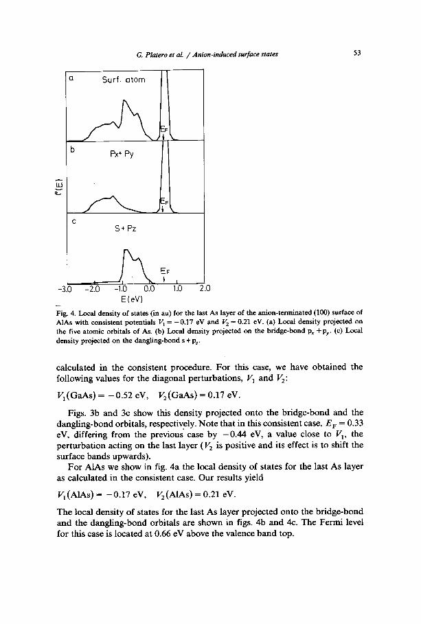
Fig. 4. Local density of states (in au) for the last As layer of the anion-terminated (100) surface of AlAs with consistent potentials V 1 = - 0 . 1 7 eV and V 2 = 0.21 eV. (a) Local density projected on the five atomic orbitals of As. (b) Local density projected on the bridge-bond Px + Py- (c) Local density projected on the dangling-bond s + Pz.
calculated in the consistent procedure. For this case, we have obtained the following values for the diagonal perturbations, V 1 and 112:
V,(GaAs) = - 0 . 5 2 eV, V2(GaAs ) = 0.17 eV.
Figs. 3b and 3c show this density projected onto the bridge-bond and the dangling-bond orbitals, respectively. Note that in this consistent case, E F = 0.33 eV, differing from the previous case by - 0 . 4 4 eV, a value close to V 1, the perturbation acting on the last layer (V 2 is positive and its effect is to shift the surface bands upwards).
For AlAs we show in fig. 4a the local density of states for the last As layer as calculated in the consistent case. Our results yield
V 1 (AlAs) = - 0.17 eV, V 2 (AlAs) = 0.21 eV.
The local density of states for the last As layer projected onto the bridge-bond and the dangling-bond orbitals are shown in figs. 4b and 4c. The Fermi level for this case is located at 0.66 eV above the valence band top.

54 G. Platero et al. / Anion-induced surface states
t~
q__
-3,0 -2.0 -1.0 0.0 1.0 2.0
E (eV) Fig. 5. Local density of states (in au) for the last Sb layer of the anion-terminated (100) surface of GaSb with consistent potentials V 1 = - 0 . 2 3 eV and V 2 = 0.25 eV. (a) Local density projected on the five atomic orbitals of As. (b) Local density projected on the bridge-bond Px + Py. (c) Local density projected on the dangling-bond s + Pz-
For GaSb we show in fig. 5a the local density of states for the last Sb layer, as calculated in the self-consistent case. Here:
V 1 (GaSb) = - 0.23 eV, V 2 (GaSb) = 0.25 eV.
Figs. 5b and 5c show the local density of states for the last Sb layer projected onto the bridge-bond and the dangling-bond orbitals. The Fermi level for this case is located at 0.35 eV above the valence band top. On the other hand, effects associated with the spin-orbi t coupling are small, as can be seen by comparing results for GaAs and AlAs (small spin-orbi t coupling) and GaSb (large spin-orbi t coupling).
Let us finally remark that the partially occupied bands for the three semiconductors, GaAs, AlAs and GaSb, are located around the mid-gap, and that their band widths are similar, = 0.5 eV. These states correspond to bridge

G. Platero et al. / Anion-induced surface states 55
orbitals; for this case, other people have found broader bands [3,8]. This is related to the kind of approximation used in our initial Hamiltonian; we have taken a spas * basis with interaction up to first nearest neighbours only. When these interactions are extended up to second nearest neighbours, the bridge-like surface band broadens [3]. However, we can expect, from the results for other interfaces [10-12], the surface Fermi energy and the charge neutrality level to be practically independent of the Hamiltonian parameters, depending mainly on the semiconductor electronic structure for the bulk. This seems to be the case even for reconstructed surfaces; indeed, the experimental evidence shows that the surface Fermi level for GaAs is practically independent of the actual reconstruction: E v = 0.4 + 0.1 eV [4], or 0.55 + 0.1 eV [5] above the valence band top. These values are, strikingly, in very good agreement with the value obtained above, E F = 0.33 eV.
In conclusion, we have presented a simple consistent tight-binding calcula- tion for the (100) faces of ionic semiconductors. The method has been applied to the anion faces of GaAs, AlAs and GaSb, our results showing that the surface perturbation generates three layers in the crystal. Self-consistency is shown to be crucial in order to obtain appropriate values for the Fermi energy (and the charge neutrality level), our results showing differences of 0.4 eV between the results for the Fermi energy of consistent and non-consistent calculations.
Acknowledgements
This work has been partially supported by the European Research Office of the US Army, under contract No. DAJA45-84-M-0378, and by the Comisibn Asesora de Investigacibn Cientifica y Tdcnica (Spain).
References
[1] J.E. Inglesfield and B.W. Holland, in: Clean Solid Surfaces, Vol. 1 of The Chemical Physics of Solid Surfaces and Heterogeneous Catalysis, Eds. D.A. King and D.P. Woodruff (Elsevier, Amsterdam, 1981).
[2] F. Flores, Surfaces and Interfaces, Trieste Spring College on Crystalline Semiconducting Materials and Devices, 1985, in press.
[3] I. Ivanov, A. Mazur and J. Pollmann, Surface Sci. 92 (1980) 365. [4] P.K. Larsen, J.H. Neave, J.F. van der Veen, P.J. Dobson and B.A. Joyce, Phys. Rev. B27
(1983) 4966. [5] T.C. Chiang, R. Ludeke, M. Aono, (3. Landgren, F.J. Himpsel and D.E. Eastman, Phys. Rev.
B27 (1983) 4770. [6] R. Ludeke, IBM J. Res. Develop. 22 (1978) 304. [7] R. Ludeke, Phys. Rev. Letters 39 (1977) 1042. [8] J.A. Appelbanm, G.A. Baraff and D.R. Hamann, Phys. Rev. B14 (1976) 1623.

56 G. Platero et al. / /An ion- inducedsur face states
[9] D.J. Chadi, C. Tanner and J. Ibm, Surface Sci. 120 (1982) L425. [10] C. Tejedor, F. Flores and E. Louis, J. Phys. C10 (1977) 2163;
E. Luis and F. Flores, J. Phys. (Paris) 42 (1981) 1313; J. Tersoff, Phys. Rev. Letters 52 (1984) 465.
[11] F. Guinea, J. Shnchez-Dehesa and F. Flores, J. Phys. C17 (1984) 2039. [12] B. Djafari-Rouhani, L. Dobrzynski, F. Flores, M. Larmoo and C. Tejedor, Solid Stat~
Commun. 27 (1978) 29. [13] P. Vogl, H.P. Hjalmaron and J.D. Dow, J. Phys. Chem. Solids 44 (1983) 365. [14] D.J. Chadi, Phys. Rev. B16 (1977) 790. [15] F. Guinea, C. Tejedor, F. Flores and E. Louis, Phys. Rev. B28 (1983) 4397. [16] F. Garcia-Moliner and F. Fiores, Introduction to the Theory of Solid Surfaces (Cambridg~
Univ. Press, Cambridge, 1979). [17] W.A. Harrison, in: Proc. 17th Intern. Conf. on the Physics of Semiconductors (Springer,
Berlin, 1984) p. 989.
Copyright © 2022 FDOKUMEN