
Processing of photosensitive APEX™ glass structures with smooth and transparent sidewalls
7
3URFHVVLQJ RI SKRWRVHQVLWLYH $3(;റ JODVV VWUXFWXUHV ZLWK VPRRWK DQG WUDQVSDUHQW VLGHZDOOV This article has been downloaded from IOPscience. Please scroll down to see the full text article. 2011 J. Micromech. Microeng. 21 017001 (http://iopscience.iop.org/0960-1317/21/1/017001) Download details: IP Address: 146.229.122.33 The article was downloaded on 30/08/2012 at 14:48 Please note that terms and conditions apply. View the table of contents for this issue, or go to the journal homepage for more Home Search Collections Journals About Contact us My IOPscience
-
Upload
independent -
Category
Documents
-
view
13 -
download
0
Transcript of Processing of photosensitive APEX™ glass structures with smooth and transparent sidewalls

3URFHVVLQJ�RI�SKRWRVHQVLWLYH�$3(;റ�JODVV�VWUXFWXUHV�ZLWK�VPRRWK�DQG�WUDQVSDUHQW�VLGHZDOOV
This article has been downloaded from IOPscience. Please scroll down to see the full text article.
2011 J. Micromech. Microeng. 21 017001
(http://iopscience.iop.org/0960-1317/21/1/017001)
Download details:IP Address: 146.229.122.33The article was downloaded on 30/08/2012 at 14:48
Please note that terms and conditions apply.
View the table of contents for this issue, or go to the journal homepage for more
Home Search Collections Journals About Contact us My IOPscience

IOP PUBLISHING JOURNAL OF MICROMECHANICS AND MICROENGINEERING
J. Micromech. Microeng. 21 (2011) 017001 (6pp) doi:10.1088/0960-1317/21/1/017001
TECHNICAL NOTE
Processing of photosensitive APEXTM
glass structures with smooth andtransparent sidewallsKhalid H M Tantawi, Janeczka Oates, Reza Kamali-Sarvestani,Nathan Bergquist and John D Williams1
Electrical and Computer Engineering Department, University of Alabama in Huntsville, Huntsville,AL 35899, USA
E-mail: [email protected]
Received 11 August 2010, in final form 7 October 2010Published 21 December 2010Online at stacks.iop.org/JMM/21/017001
AbstractImprovement of the surface roughness and optical transparency of microstructureslithographically fabricated in APEXTM glass was accomplished through a post-etch anneal.An optimal dose of UV radiation is found to be 24 J g!1 for a wavelength of 280 nm, afterwhich etch rate in HF acid and selectivity saturate. The anneal process, while originallydesigned to improve the surface roughness by reflowing, can be used to join multiplestructures for the creation of optically transparent three-dimensional devices. The resultingglass microstructures demonstrate an average sidewall RMS surface roughness that is reducedfrom 0.7 µm to 32.7 nm which is adequate for optical signal detection across a wide frequencyband that includes the visible spectrum.
(Some figures in this article are in colour only in the electronic version)
1. Introduction
Glass is superior, when compared to semiconductors andmetals, for many applications due to its optical transparency,thermal insulation, chemical inertness, and electrical isolation.As such, a variety of different glass fabrication processeshave been developed. These vary between etching oflithographically defined patterns on the surface of glass[1, 2], laser drilling [3] and photodefinable glass [4–7].There are very few procedures that lend themselves to theproduction of optically smooth and transparent sidewalls. Forexample, dry etching of borosilicate glasses has achievedoptical quality sidewalls for etch depths of approximately1 µm [1], but this process has not been extended to devicesseveral hundreds of microns deep. Similarly wet etchingof fused silica has recently demonstrated the ability to
1 Assistant Professor and Associate Director of NMDC, Dept. of ElectricalEngineering, University of Alabama in Huntsville, OB 406 Huntsville, AL35899.
pattern optically smooth wells at the bottom of 60 µmchannels isotropically [2]. However this technique is notamenable to directional etching of vertical sidewalls in thepattern. Furthermore, these processes do not allow for thefabrication of embedded channels such as those demonstratedusing interference techniques coupled with femto-second laserexposure of photodefinable glass [4]. Very deep channels canbe drilled using a laser, but the surface roughness is often onthe order of microns [3]. To date, few glass microfabricationprocedures have demonstrated a sidewall thicker than 100 µmsmooth enough for true optical transparency [8–10]. Theseprocedures have been demonstrated for FoturanTM glass usingphotolithographic techniques coupled with a post-etch annealthat reflows the surface of the glass. This note demonstratessuch a process using a new photodefinable glass material,APEXTM, developed by Life Bioscience Inc. This new glassis superior to conventional photolithographic glass due to itslower exposure dose, lower baking temperature, faster etchrate, and lower sidewall surface roughness [7, 8].
0960-1317/11/017001+06$33.00 1 © 2011 IOP Publishing Ltd Printed in the UK & the USA

J. Micromech. Microeng. 21 (2011) 017001 Technical Note
High-aspect-ratio photolithographically structured glassfrom FoturanTM produced by Schott Corporation, APEXTM,and other photosensitive glasses are commonly presented inthe literature [11–13]. Typical aspect ratios demonstrated inFoturanTM are approximately 30:1 [10–13] when exposed tomid-ultraviolet (UV) light. It was reported that APEXTM isprocessed with aspect ratios up to 50:1 [13]. It is argued thatthe improved aspect ratio is due, in part, to a higher selectivityto hydrofluoric acid attributed to the lower concentration ofsilica in APEXTM glass as compared to other photodefinableglasses [14]. However, this work is not focused on the aspectratio of APEXTM, but rather on the surface quality of patternsgenerated from it.
Photosensitive glass is typically processed in three steps.First, a lithographic exposure is made using a mid-UV contactaligner or a femtosecond laser source. After exposure,the substrate is baked at temperatures exceeding the glasstransition temperature. Finally, the sample is etched inhydrofluoric acid (HF) to remove the exposed regions of theglass substrate.
As is the case with FoturanTM glass, the surface roughnessof the sidewalls of APEXTM glass structures, after a typicalthree-step process, limits their optical applications. The keyfactor in this research effort is to reduce the root mean square(RMS) surface roughness of the glass as compared to theoptical wavelength of interest, thereby reducing scatteringof incident light on the structure. A surface is considerednearly smooth if the RMS of the surface roughness, ! , is one-tenth the wavelength, ", of the incident light [15, 16]. Foroptical light, the surface roughness should therefore be lessthan 40 nm. The results presented below demonstrate opticallytransparent microstructures for use with laser systems, imagingand sensing optics, and other optical devices that require verylow RMS surface roughness for operation.
Conventional photolithography processes onphotosensitive glass have yielded 0.7 µm surface roughness inAPEXTM, which does not permit optical transmission of lightwithout significant scattering. This is significantly less thanthe 5 µm average surface roughness reported for FoturanTM
[17]. One important reason for this surface roughness isthe size of lithium-metasilicate crystals formed around thesilver nanoclusters during the post-exposure bake process[17]. This in turn is dependent on the concentration of silverin the glass [14], the exposure, and the bake process [17].APEXTM has a higher concentration of silver in the glassmatrix than FoturanTM, thereby yielding an increased numberof nanoclusters generated by the absorption of mid-UV light[14]. This leads to a larger number and subsequently smallersize of nanoscrytallites than present in FoturanTM. Furtherreduction of crystal sizes is achieved by tuning the bakingprocess to increase the number of silver nanoclusters thatare formed. The result is a smoother, but not quite optical,finish in APEXTM glass. Thus, a post-etch technique such asannealing must be done after the etch in order to reflow thesurface of the completed microstructure.
(a) (b)
Figure 1. (a) Absorption bands of the two commercially availablephotosensitive glasses. (b) Impact of the radiation dose (measured at" = 280 nm) on the crystallized-glass etch rate and selectivity in 5%(by volume) HF acid at room temperature for a 500 ± 50 µm thickwafer.
2. Photolithography and post-etch annealing ofAPEXTM glass
The fabrication procedure presented in this note consists of theconventional three-stage photodefinable glass process as wellas an added fourth stage of thermal annealing treatment. Theprocedure described below uses a standard UV contact alignerand conventional thermal oven to significantly lower surfaceroughness below that of the process outlined in [8, 9].
The first stage of the process is to photodefine the patternin glass. An APEXTM glass sample of a 500 ± 50 µm waferwas exposed to mid-UV (280–312 nm) [6, 14] light through anAB-M semi-automatic UV contact aligner. The wavelengthrange was chosen to match the absorption band present (seefigure 1(a)) in APEXTM and FoturanTM glass. The poweroutput of the contact aligner at the 280 nm wavelength usingan AB-M mid-UV filter was 0.24 mW cm!2. Measurementstaken at 254, 310, and 365 nm lamp lines were 0.15, 0.07,and 0.01 mW cm!2, respectively. A quartz mask was used tomeet the transmission requirements for mid-UV exposure. Theetch rate and selectivity of the exposed to unexposed regionsetched in 5% (by volume) hydrofluoric acid were measured asa function of dose. The results are presented in figure 1(b).Dose measurements were taken at 280 nm. To account for thedifferent wafer thicknesses, the dose unit was converted to Jg!1 based on the glass density ("2 g cm!3) supplied by themanufacturer’s datasheet. As the dose increases, the exposedregion acquires a darker color, and the etch rate increases inan exponential pattern up to a point of saturation. At thesaturation point, the exposed regions become dark brown incolor, and the change in etch rate and selectivity plateaus withincreasing radiation dose. The optimal radiation dose is thepoint of saturation which was found to be about 24 J g!1.Overexposure beyond the optimal radiation dose minimallyenhances the selectivity and causes widening of the exposedarea due to diffraction and light scattering. This optimal doseis then used to calculate the corresponding optimal exposure(in J cm!2) for different glass thicknesses as shown in table 1.Experimental verification of the optical exposure for variousthicknesses was performed using both 500 µm and 1 mm thickAPEXTM substrates.
2
J. Micromech. Microeng. 21 (2011) 017001 Technical Note
(a) (b) (c) (d)
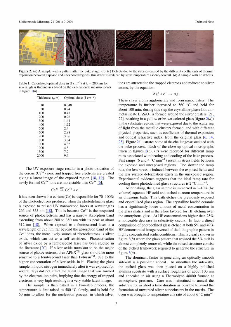
Figure 2. (a) A sample with a pattern after the bake stage. (b), (c) Defects due to the stresses caused by the different coefficients of thermalexpansion between exposed and unexposed regions, this defect is reduced by slow temperature ascent/descent. (d) A sample with no defects.
Table 1. Calculated optimal dose in (J cm!2) at " = 280 nm forseveral glass thicknesses based on the experimental measurementsin figure 1(b).
Thickness (µm) Optimal dose (J cm!2)
10 0.04850 0.24
100 0.48200 0.96300 1.44400 1.92500 2.4600 2.88700 3.36800 3.84900 4.32
1000 4.81500 7.22000 9.6
The UV exposure stage results in a photo-oxidation ofthe cerous (Ce3+) ions, and trapped free electrons are createdgiving a latent image of the exposed region [18, 19]. Thenewly formed Ce4+ ions are more stable than Ce3+ [6]:
Ce3+ #UVCe4+ + e!.
It has been shown that cerium (Ce) is responsible for 70–100%of the photoelectrons produced when the photodefinable glassis exposed to pulsed UV nanosecond lasers at wavelengths266 and 355 nm [18]. This is because Ce3+ is the suspectedsource of photoelectrons and has a narrow absorption bandextending from about 280 to 350 nm with its peak at about312 nm [18]. When exposed to a femtosecond laser at awavelength of 775 nm, far beyond the absorption band of theCe3+ ions, the more likely source of photoelectrons is silveroxide, which can act as a self-sensitizer. Photoactivationof silver oxide by a femtosecond laser has been studied inthe literature [20]. If silver oxide turns out to be the majorsource of photoelectrons, then APEXTM glass should be moresensitive to a femtosecond laser than FoturanTM, due to thehigher concentration of silver oxide in it. Placing the glasssample in liquid nitrogen immediately after it was exposed forseveral days did not affect the latent image that was formedby the electron–ion pairs, implying that the energy of trappedelectrons is very high resulting in a very stable latent image.
The sample is then baked in a two-step process, thetemperature is first raised to 500 $C slowly, and is held for60 min to allow for the nucleation process, in which silver
ions are attracted to the trapped electrons and reduced to silveratoms, by the equation:
Ag+ + e! # Ag.
These silver atoms agglomerate and form nanoclusters. Thetemperature is further increased to 560 $C and held forabout 100 min; during this step the crystalline-phase lithium-metasilicate Li2SiO3 is formed around the silver clusters [21,22], resulting in a yellow or brown-colored glass (figure 2(a))in the substrate regions that were exposed due to the scatteringof light from the metallic clusters formed, and with differentphysical properties, such as coefficient of thermal expansionand optical refractive index, from the original glass [6, 14,23]. Figure 2 illustrates some of the challenges associated withthe bake process. Each of the close-up optical micrographstaken in figures 2(c), (d) were recorded for different ramprates associated with heating and cooling of the bake process.Fast ramps (6 and 4 $C min!1) result in stress fields betweenthe exposed and unexposed regions. The slower the ramprate, the less stress is induced between the exposed fields andthe less surface deformation exists in the unexposed region.Experimental evidence suggests that the ideal ramp rate forcooling these photodefined glass structures is 2 $C min!1.
After baking, the glass sample is immersed in 3–10% (byvolume) aqueous HF acid and etched at room temperature inan ultrasonic bath. This bath etches the previously exposedand crystallized glass region. The crystalline loaded ceramichas a significantly lower amount of metal concentration inthe glass matrix and is therefore favored for HF etching overthe amorphous glass. At HF concentrations higher than 25%a noticeable decrease in selectivity occurs. In fact, a directcomparison of photodefined glass etched at both 5% and 49%HF demonstrated image reversal of the lithographic pattern inhighly concentrated acidic conditions. This is clearly shown infigure 3(b) where the glass pattern that resisted the 5% etch isalmost completely removed, while the raised structure consistof the etched framework required to generate the structure infigure 3(a).
The dominant factor in generating an optically smoothsidewall is a post-etch anneal. To smoothen the sidewalls,the etched glass was then placed on a highly polishedalumina substrate with a surface roughness of about 100 nmand annealed in air using a Thermolyne 48000 furnace atatmospheric pressure. Care was maintained to anneal thesubstrate for as short a time duration as possible to avoid theformation of unwanted silver nanoclusters in the matrix. Theoven was brought to temperature at a rate of about 6 $C min!1
3

J. Micromech. Microeng. 21 (2011) 017001 Technical Note
Figure 3. Lithographic image reversal between two structuresexposed and baked under identical conditions, but etched in 5% HFacid (left) and in 49% HF acid (right) both at room temperature. Theminimum feature size (left) is 30 µm.
Figure 4. Two APEXTM substrates thermally bonded during thepost-etch anneal.
and held at 530–545 $C. The applied temperature depends onthe size and geometry of the structure. The optimal conditionswere 10 h at 530 $C or 6 h at 545 $C. After completion, thetemperature was then ramped down to room temperature at arate of 2 $C min!1. The result is a glass microstructure that isoptically smooth and transparent on every surface.
Annealing two or more glass structures in contact reflowsthe surface layers between them while maintaining the opticaltransparency of the glass surfaces. This bonds the glassstructures together. A scanning electron micrograph of abonded sample is provided in figure 4. No weights are neededover the glass structures for generating a glass-to-glass bondusing the bond anneal process described. Lower temperatures
(a) (b) (c) (d)
Figure 5. (a) A SEM image of a sample sidewall before the post-etch annealing stage. (b) Optical micrograph of the sidewall. (c) A SEMimage of a sidewall after annealing. (d) Optical graph of the sidewall. Scale bars in images (a) and (c) are 100 µm.
and shorter annealing times will require additional loading toform a strong bond. The authors recommend using polishedalumina plates placed top and bottom of the glass stackwhen bonding two or more substrates. Polished aluminaprovides both a high surface finish and a uniform temperaturedistribution throughout the glass structure.
3. Results of the post-etch anneal
A comparison of the surface roughness between etched andannealed glass samples was performed qualitatively usingscanning electron and optical microscopy and quantitativelyusing optical interferometry. All experiments used a 0.5 mmthick substrate with the same exposure, bake, and etchconditions. Figures 5(a) and (b) show lithographicallypatterned sidewalls after the etch stage. The sample clearlyhas a rough nodular surface with near vertical walls. Thereis also some angular dependence due to optical diffractionduring the exposure and etch selectivity present in figure 5(b).Annealed samples like the one presented in figures 5(c) and (d)do not show any nodules on the patterned sidewall of the glassstructure. An optical examination provided in 5 (d) showsonly local area defects.
The average surface roughness of the sidewalls of four0.5 mm substrates immediately after the HF etch weremeasured to be 0.70 µm with a standard deviation of0.35 µm using an Olympus Lext OLS 4000 laser confocalmicroscope. The thickness of the etched microstructureswas 400 µm. Several glass microstructures were post-etchannealed at temperatures between 525 and 630 $C with noapplied weight. Structural deformation was observed whenthe anneal temperature exceeded 565 $C. Samples annealed at630 $C for 7–15 min resulted in sidewalls with a high degreeof curvature and an average surface roughness of 193 nm anda standard deviation of 40 nm. The curvature measurementsby the Lext system showed a radius of curvature of about775 µm for annealed sidewalls at 630 $C for 10 min, and1300 µm for the un-annealed glass microstructures.
The optimal conditions for annealing were found to be inthe range 530–545 $C for 10 to 6 h using a Zygo New View5000 Optical interferometer. Figure 6 shows the comparisonof the sidewalls of two identically patterned glass sidewalls.Measurements were taken at random locations on the sidewallof similarly patterned devices. Large area scans (0.5 %0.5 mm2) provided sufficient information to extract the
4

J. Micromech. Microeng. 21 (2011) 017001 Technical Note
(a)(b)
Figure 6. RMS sidewall surface roughness of APEXTM microstructures: (a) unnanealed and (b) annealed at 545 $C for 6 h.
400 µm
(a)
400 µm
(b)
Figure 7. Micrographs of wires suspending glass frames:(a) sidewall of a FoturanTM glass microstructure following theannealing procedure outlined in [8]. (b) The sidewall of an annealedAPEXTM glass microstructure.
sidewall curvature over a 0.1 % 0.1 mm2 field. Thisallowed for evaluation of the local area surface roughness.Figure 6(a) shows an interferogram of an unannealed etchedsidewall with a measured RMS surface roughness of 0.532 µm.The second interferogram in figure 6(b) provides measureddata for the sidewall of an annealed microstructure. Themeasured sidewall RMS surface roughness of three randomsamples were 36, 35, and 27 nm, respectively. Sampleschosen for the experiment were of similar size, identicalprocess conditions, and annealed at different times. Themean and standard deviation between three optical surfacemeasurements were 32.7 and 3 nm, respectively. Thesemeasurements provide sufficient criteria for the developmentof microdevices with optical sidewall quality.
To compare this procedure with other previousphotodefinable glass results, the process outlined by Chengin [8] was followed. A FoturanTM structure annealed at 570oCfor 5 h and an APEXTM structure annealed at 535 $C for7 h are shown in figure 7. The same mid-UV flood lamp wasused for both samples, and both received the same dose ofUV radiation. A superior surface quality is observed for theAPEXTM glass that followed the procedure outlined here.
This annealing temperature range and duration are alsosuited for bonding of glass structures with no need of additionalload forces. Thus multilayer devices can be created in whichdifferent layers are patterned in different substrates and thenfused together during a single annealing step that is also usedto smoothen the sidewall for use as an optically transparentsurface. In this experiment, samples of different geometriesthat were annealed at 530–545 $C for a duration of 10 h (at530 $C) to 6 h (at 545 $C) were strongly bonded with the
(a) (b)
Figure 8. Optical micrographs through the lithographicallypatterned sidewall of annealed glass at 545 $C for 6 h andun-annealed glass over a patterned chrome mask plate. (a) Focalplane is on the top surface of the glass, (b) focal plane is on thechrome pattern beneath the glass.
significant improvement of the surface roughness. The bondwas stronger for the higher temperatures and longer annealingtimes. Samples that were annealed at below 520 $C, failedto bond without the use of additional weights, even whenprocessed for up to 15 h. As stated before, it is believed thatthe bond forms as glass at the interface between two surfacesmelts to fuse both pieces together. It should be noted thatthere is a small processing window present in which boththermal fusion and surface melting allow for the production oftransparent multilayer devices without optical lensing of thesidewall profile.
Figure 8 illustrates a qualitative test for sidewalltransparency of the glass following the post-etch thermalannealing treatment. A post-etch annealed sample and an un-annealed sample were placed on a prepatterned optical platewith evenly spaced lines. Both samples are otherwise identicalin size and composition. When the microscope is focused onthe top surface of the glass, the un-annealed sidewall scattersthe light, and the pattern could not be distinguished throughit. Better image definition is observed from the annealedsurface. However when focused through the material onto thesurface underneath, the pattern was clearly observed throughthe annealed sidewall, yet surface scattering still preventspattern definition through the unannealed microstructure.
4. Conclusion and future perspectives
A four-step process was demonstrated on APEXTM
photosensitive glass to reduce surface roughness and provideoptical transparency in microfabricated sidewalls. The
5

J. Micromech. Microeng. 21 (2011) 017001 Technical Note
photolithography process was optimized for a dose of24 J g!1 of mid UV light quantified by measurements at" = 280 nm. Photodefined glass was then post-exposure bakedin a two-step process optimized to reduce the local stresses.Etching was most effective using 5% aqueous hydrofluoricacid, at room temperature, in an ultrasonic bath. Finally, post-etch annealing was performed at a temperature in the range530–545 $C (depending on the geometry and size of the glassstructure) for 10 h (at the lower temperatures) to 6 h (for thehigher temperatures). The etch rate and selectivity increasewith dose up to a certain point after which they saturate.The saturation point is the optimal dose. The average of theRMS surface roughness obtained was 32.7 nm with a standarddeviation of 3 nm. The surface roughness prior to post-etchannealing was about 0.70 µm with a standard deviation of0.35 µm. The temperature and duration are equally suited forbonding of glass structures without the need for weights ontop. The improvement of sidewall surface roughness permitsthe glass structures to be transparent over the entire visiblespectrum, and hence has possible use for microfluidic devicescomposed of coplanar channels observable from the sidewallsrather than from the top [24]. Future work will investigate theuse of this process for the development of microcuvettes assubstrates for optical applications and the study of the strengthof the glass–glass bonds that form as a function of temperatureand duration.
Acknowledgments
The authors would like to thank Jay Hammer and Gregg Borekof Jenoptik Optical Systems, Inc. in Huntsville, AL, for the useof their white light interferometer. This work was funded bythe Office of the Vice President for Research at UAHuntsville,and the Alabama EPSCoR GRSP program.
References
[1] Bhatnagar P, Panda S, Edleman N, Allen S, Wise Rand Mahorowala A 2007 Controlling line-edge roughnessand reactive ion etch lag in sub-150 nm features inborophosphosilicate glass J. Appl. Phys. 101 076102
[2] Zhu H, Holl M, Ray T, Bhushan S and Meldrum D 2009Characterization of deep wet etching of fused silica glassfor single cell and optical sensor deposition J. Micromech.Microeng 19 065013
[3] Kim T, Campbell K, Groisman A, Kleinfeld D and Schaffer C2005 Femtosecond laser-drilled capillary integrated into amicrofluidic device Appl. Phys. Lett. 86 201106
[4] Cheng Y, Sugioka K, Masuda M, Toyoda K, Kawachi M,Shihoyama K and Midorikawa K 2003 3D microstructuringinside Foturan glass by femtosecond laser RIKEN Rev.50 101–6
[5] Hansen W, Janson S W and He1vajian H 1997 Direct-writeUV laser microfabrication of 3D structures inlithium-alumosilicate glass Proc. SPIE 2991 104–12
[6] Dietrich T R, Ehrfeld W, Lacher M, Kramer M and Speit B1996 Fabrication technologies for microsystems utilizingphotoetchable glass Microelectron. Eng. 30 497–504
[7] Cho Y-R, Oh J-Y, Kim H-S and Jeong H-S 1999Micro-etching technology of high aspect ratio frameworksfor electronic devices Mater. Sci. Eng. B 64 79–83
[8] Cheng Y, Tsai H L, Sugioka K and Midorikawa K 2006Fabrication of 3D microoptical lenses in photosensitiveglass using femtosecond laser micromachining Appl. Phys.A 85 11–4
[9] Cheng Y, Sugioka K, Masuda M, Shihoyama K, Toyoda Kand Bellingham K M 2003 Three-dimensional microopticalcomponents embedded in Foturan glass by a femtosecondlaser Proc. SPIE 5063 103–7
[10] Williams J D, Schmidt C and Serkland D 2010 Processingadvances in transparent Foturan glass MEMS J. Appl. Phys.A 99 777–82
[11] Freitag A, Vogel D, Scholz R and Dietrich T R 2001Microfluidic devices made of glass J. Assoc. Lab.Autom. 6 45–9
[12] Anthony C J, Docker P T, Prewett P D and Jiang K C 2007Focused ion beam microfabrication in FoturanTM
phototsensitive glass J. Micromech. Microeng. 17 115–9[13] Flemming J H, Mack R and Buckley C 2009 Photosensitive
glass for ultra high aspect ratio features Nanotech 2009Conf. and Expo (Houston, TX, 3–7 March 2009)
[14] Flemming J H, Buckley C T and Schmidt C 2008Compositions and methods to fabricate a photoactivesubstrate suitable for shaped structures US PatentApplication 2008/0248250 A1
[15] Davies H 1954 The reflection of electromagnetic waves from arough surface Proc. IEEE 101 209–14
[16] Guenther K, Wierer P and Bennett J 1984 Surface roughnessmeasurements of low-scatter mirrors and roughnessstandards Appl. Opt. 23 3820–36
[17] Dietrich T, Abraham M, Diebel J, Lacher M and Ruf A 1993Photoetchable glass for microsystems: tips for atomic forcemicroscopy J. Micromech. Microeng. 3 187–9
[18] Livingston F, Adams P and Helvajian H Influence of ceriumon the pulsed UV nanosecond laser processing ofphotostructurable glass ceramic materials Appl. Surf. Sci.247 526–36
[19] Cheng Y, Sugioka K, Masuda M, Shihoyama K, Toyoda Kand Midorikawa K 2003 Optical gratings embedded inphotosensitive glass by photochemical reaction using afemtosecond laser Opt. Express 11 1809–16
[20] Gleitsmann T, Stegemann B and Bernhardt T 2004Femtosecond-laser-activated fluorescence from silver oxidenanoparticles Appl. Phys. Lett. 84 4050–2
[21] Fernandez-Prades J M, Serrano D, Serra P and Morenza J L2009 Laser fabricated microchannels insidephotostructurable glass-ceramic Appl. Surf. Sci.255 5499–502
[22] Becker H, Arundell M, Harnisch A and Hulsenberg D 2002Chemical analysis in photostructurable glass chips SensorsActuators B 86 271–9
[23] Gomez-Morilla I, Abraham M H, de Kerckhove D Gand Grime G W 2005 Micropatterning of Foturanphotosensitive glass following exposure to MeV protonbeams J. Micromech. Microeng. 15 706
[24] Sugioka K, Wang Z and Midorikawa K 2008 3D integration ofmicrofluidics and microoptics inside photosensitive glass byfemtosecond laser direct writing for photonic biosensingProc. SPIE 6879 68790M
6