
PROCESS VARIATION-AWARE TIMING OPTIMIZATION WITH ...
140
PROCESS VARIATION-AWARE TIMING OPTIMIZATION WITH LOAD BALANCE OF MULTIPLE PATHS IN DYNAMIC AND MIXED-STATIC- DYNAMIC CMOS LOGIC A dissertation submitted in partial fulfillment of the requirements for a degree of Doctor of Philosophy By KUMAR YELAMARTHI B.E. Instrumentation & Control Engineering, University of Madras, 2000 M.S. Electrical Engineering, Wright State University, 2004 ______________________________________ 2008 Wright State University
-
Upload
khangminh22 -
Category
Documents
-
view
0 -
download
0
Transcript of PROCESS VARIATION-AWARE TIMING OPTIMIZATION WITH ...

PROCESS VARIATION-AWARE TIMING OPTIMIZATION WITH LOAD
BALANCE OF MULTIPLE PATHS IN DYNAMIC AND MIXED-STATIC-
DYNAMIC CMOS LOGIC
A dissertation submitted in partial fulfillment of the
requirements for a degree of
Doctor of Philosophy
By
KUMAR YELAMARTHI
B.E. Instrumentation & Control Engineering, University of Madras, 2000
M.S. Electrical Engineering, Wright State University, 2004
______________________________________
2008
Wright State University

ii
COPYRIGHT BY
KUMAR YELAMARTHI
2008

iii
WRIGHT STATE UNIVERSITY
SCHOOL OF GRADUATE STUDIES
June 16, 2008
I HEREBY RECOMMEND THAT THE DISSERTATION PREPARED UNDER MY
SUPERVISION BY Kumar Yelamarthi ENTITLED Process Variation-Aware Timing
Optimization with Load Balance of Multiple Paths in Dynamic and Mixed-Static-
Dynamic CMOS Logic BE ACCEPTED IN PARTIAL FULFILLMENT OF THE
REQUIREMENTS FOR THE DEGREE OF Doctor of Philosophy.
____________________________________
Chien-In Henry Chen, Ph.D.
Dissertation Director
____________________________________
Ramana V. Grandhi, Ph.D.
Director, Engineering Ph.D. Program
____________________________________
Joseph F. Thomas, Jr., Ph.D.
Dean, School of Graduate Studies
Committee on
Final Examination
____________________________________
Chien-In Henry Chen, Ph.D.
____________________________________
Raymond E. Siferd, Ph.D.
____________________________________
John Marty Emmert, Ph.D.
____________________________________
Marian K. Kazimierczuk, Ph.D.
____________________________________
Wen-Ben Jone, Ph.D.

iv
Abstract Yelamarthi, Kumar Engineering Ph.D. Program, Department of Electrical
Engineering, Wright State University, 2008. Process Variation-Aware Timing
Optimization with Load Balance of Multiple Paths in Dynamic and Mixed-Static-
Dynamic CMOS Logic.
The semiconductor technology has been advancing rapidly over the past decade to
result in the design of several innovative applications. This advancement of technology
with the shrinking device has allowed for placement of billions of transistor on a single
microprocessor chip. On the other hand, this shrinking device sizes has presented the
design engineers with two major challenges: timing optimization at multiple giga-hertz
frequencies, and reducing the daunting effects of semiconductor process variations.
Failure to account for these process variations often results in loss of design productivity
by one generation, and might even result in design failure.
This research presents two timing optimization algorithms while accounting for
process variations. The process variation-aware Load Balance of Multiple Paths (LBMP)
algorithm is designed for timing optimization of dynamic CMOS circuits. Implemented
on several dynamic CMOS circuits, the LBMP algorithm has demonstrated an average
reduction in delay, uncertainty, and sensitivity from process variations by 48%, 57% and
14% respectively. The process variation-aware Path Oriented IN Time (POINT)
optimization flow for mixed-static-dynamic CMOS circuits partitions a design based on
critical paths, chooses effective circuit style, and performs switch level timing
optimization using the LBMP algorithm. Verified through implementation on several
standard benchmark circuits, the POINT optimization flow has demonstrated an average
reduction in delay and uncertainty from process variations by 17% and 13% over state-
of-the-art commercial optimization tools.

v
Table of Contents
1 Introduction................................................................................................................1
1.1 Problem Statement .............................................................................................. 1
1.2 Dissertation Scope and Methodology ................................................................. 4
1.3 Summary............................................................................................................. 5
2 Timing Analysis in CMOS Circuit Design...............................................................7
2.1 Circuit Design Styles .......................................................................................... 8
2.1.1 Static CMOS Logic..................................................................................... 8
2.1.2 Dynamic CMOS Logic ............................................................................... 9
2.2 Timing Analysis in Combinational Circuits ..................................................... 13
3 Process Variations and Timing Optimization in CMOS Circuits .......................17
3.1 Process Variations in CMOS Technology ........................................................ 17
3.2 Effect of Process Variations on Delay and Power of CMOS Circuits.............. 20
3.3 Impact of Process Variations on Delay of a CMOS Circuit ............................. 22
3.4 Previous Research in Process Variations.......................................................... 23
3.5 Timing and Optimization Algorithms............................................................... 27
3.6 Significance of Dynamic CMOS Circuits on Timing....................................... 29
3.7 Previous Work on Transistor Sizing................................................................. 31
4 Process Variation-Aware Transistor Sizing in Dynamic CMOS Circuits..........35
4.1 Process Variation Aware Load Balance of Multiple Paths (LBMP) Transistor
Sizing Algorithm............................................................................................... 35
4.2 LBMP Implementation on a 2-b Weighted BTC.............................................. 42
4.3 LBMP implementation on a 4-b Unity Weight BTC........................................ 49

vi
4.4 LBMP Implementation on ISCAS Benchmark Circuits................................... 54
4.5 Summary........................................................................................................... 57
5 Process Variation-Aware Timing optimization in Mixed-Static-Dynamic Logic60
5.1 Challenges in Mixed-Static-Dynamic Circuit Implementation ........................ 60
5.2 64-b Mixed-Static-Dynamic Adder .................................................................. 62
5.3 Conventional Timing Optimization Flow......................................................... 67
5.4 Process Variation-Aware POINT Timing Optimization Flow ......................... 69
5.5 POINT Optimization Flow Automation Framework........................................ 72
5.6 POINT Optimization on ISCAS 74181 – 4bit ALU......................................... 75
5.7 POINT Optimization on ISCAS benchmark circuits........................................ 82
5.8 Summary........................................................................................................... 91
6 Conclusions...............................................................................................................92
6.1 Summary........................................................................................................... 92
6.2 Research Contributions..................................................................................... 93
6.3 Future Research ................................................................................................ 94
Appendix...........................................................................................................................96
Appendix-A: Synopsys Design Vision Script for Synthesis and Optimization............ 96
Appendix-B: Synopsys PrimeTime Pre Optimization Static Timing Analysis Script . 97
Appendix-C: Perl script for Process Variation-Aware Load Balance of Multiple Paths
Algorithm................................................................................................ 98
Appendix-D: Perl Script to perform LBMP Algorithm at multiple temperatures ...... 112
Appendix-E: Perl Script to update transistor sizes in hspice netlist ........................... 113
Appendix-F: PathMill Script to perform switch level Static Timing Analysis .......... 114

vii
Appendix-F: PathMill Script to perform switch level Static Timing Analysis .......... 114
Appendix-G: Perl Script to create Model and Data Files ........................................... 116
Appendix-H: Synopsys PrimeTime script for Post Optimization Static Timing Analysis
120
References.......................................................................................................................121

viii
List of Figures
Figure 1-1: Conventional Design Optimization Flow ........................................................ 3
Figure 2-1: An AMS-SoC Example [27] ............................................................................ 8
Figure 2-2: Static CMOS Logic Gate ................................................................................. 9
Figure 2-3: Dynamic CMOS logic gate ............................................................................ 10
Figure 2-4: Precharge and evaluate phases in dynamic logic gate ................................... 11
Figure 2-5: Pseudocode for Critical Path Method ............................................................ 14
Figure 2-6: Combinational Circuit to illustrate application of Critical Path Method ....... 14
Figure 3-1: Cross-section of an nmos device.................................................................... 19
Figure 3-2: Classification of Process Variations .............................................................. 19
Figure 3-3: Variation in Leakage Current and Frequency due to Process Variations [4]. 20
Figure 3-4: Simple Transistor Chain................................................................................. 21
Figure 3-5: 3bit Programmable Keeper [26]..................................................................... 24
Figure 3-6: CPU time vs. number of sources of variation [22] ........................................ 26
Figure 3-7: Monte Carlo Simulation Methodology .......................................................... 27
Figure 3-8: The effect of hardware constraints on: (a) HW/SW prototyping costs, and (b)
Software Schedule [30]................................................................................. 29
Figure 3-9: Simple Transistor Chain................................................................................. 32
Figure 3-10: Chain of Inverters......................................................................................... 33
Figure 3-11: New Half-space using Convex Optimization method.................................. 34
Figure 4-1: RC Tree Network ........................................................................................... 36
Figure 4-2: 2-b weighted Binary-to-Thermometric Converter ......................................... 39
Figure 4-3: Comparison of delay distribution of two paths.............................................. 39

ix
Figure 4-4: LBMP Transistor Sizing Algorithm considering process variations ............. 40
Figure 4-5: Delay convergence profile of 2-b WBTC...................................................... 46
Figure 4-6: 4-b Unity Weighted Binary to Thermometric Converter............................... 52
Figure 4-7: Delay convergence profile of 4-b UWBTC ................................................... 53
Figure 4-8: Transistor level schematic of C5315-M6-GLC4_2 ....................................... 55
Figure 4-9: Transistor level schematic of C7552-M5-CGC34_4 ..................................... 55
Figure 4-10: Delay convergence profile of various designs using LBMP Algorithm...... 57
Figure 4-11: Delay Optimization results from LBMP Algorithm .................................... 58
Figure 4-12: Percentage Sensitivity Reduction from LBMP Algorithm at different
temperatures................................................................................................ 59
Figure 4-13: Delay Uncertainty Reduction from LBMP Algorithm ................................ 59
Figure 5-1: Dynamic logic gate ........................................................................................ 61
Figure 5-2: 64-b Adder Architecture ................................................................................ 64
Figure 5-3: Block-1 of 64-b Adder ................................................................................... 64
Figure 5-4: 2-b Thermometric Adder ............................................................................... 65
Figure 5-5: TAC with add-1 logic .................................................................................... 66
Figure 5-6: TAC with add-0 logic .................................................................................... 67
Figure 5-7: Abacus-to-Binary Converter .......................................................................... 67
Figure 5-8: Conventional Optimization Flow................................................................... 69
Figure 5-9: Process Variation-Aware Path Oriented IN Time Optimization Flow .......... 71
Figure 5-10: High level data dependency graph ............................................................... 74
Figure 5-11: Data dependency in LBMP Optimization Algorithm .................................. 75
Figure 5-12: ISCAS 74181 in static CMOS logic ............................................................ 76
x
Figure 5-13: Pre-POINT Optimization STA report of ISCAS 74181 .............................. 77
Figure 5-14: Gate level schematic of CLA module in C74181 ........................................ 78
Figure 5-15: Transistor level schematic of block-1 in CLA module of ISCAS 74181 .... 78
Figure 5-16: Transistor level schematic of block-2 in CLA module of ISCAS 74181 .... 79
Figure 5-17: Updated ISCAS 74181 with Mixed-Static-Dynamic implementation......... 79
Figure 5-18: Post-POINT optimization STA report of ISCAS 74181 with new worst case
path.............................................................................................................. 80
Figure 5-19: Post-POINT Optimization STA report of ISCAS 74181 with old worst case
path.............................................................................................................. 81
Figure 5-20: Top level schematic of ISCAS C7552, 34-b adder and magnitude
comparator .................................................................................................. 84
Figure 5-21: Schematic of M5/UM5_1/CC_1/CGC34_0 in ISCAS C7552..................... 85
Figure 5-22: Gate level schematic of M5/UM5_1/CC_1/CGC34_4 in ISCAS C7552.... 86
Figure 5-23: Pre-POINT Optimization STA report of ISCAS C7552.............................. 87
Figure 5-24: Top level schematic of ISCAS C2670 ......................................................... 88
Figure 5-25: Top level schematic of ISCAS C3540 ......................................................... 88
Figure 5-26: Top level schematic of ISCAS C5315 ......................................................... 89
Figure 5-27: Delay reduction in ISCAS benchmarks through POINT optimization flow 90
Figure 5-28: Process variation uncertainty reduction in ISCAS benchmarks through
POINT optimization flow ........................................................................... 90

xi
List of Tables
Table 3-1: CMOS Technology Roadmap for Process Variations [59] ............................. 18
Table 4-1: Timing Paths in 2-b weighted BTC................................................................. 44
Table 4-2: Repeat and Weight Profiles of Transistors in 2-b WBTC............................... 44
Table 4-3: Critical path order in 2-b WBTC..................................................................... 45
Table 4-4: Delay Convergence of 2-b WBTC .................................................................. 46
Table 4-5: Percentage delay sensitivity reduction of 2-b WBTC at different temperatures
........................................................................................................................................... 48
Table 4-6: 2-b WBTC path ranks at different iterations and temperatures....................... 49
Table 4-7: LBMP implementation on a 2-b WBTC ......................................................... 49
Table 4-8: Timing paths in 4-b UWBTC.......................................................................... 51
Table 4-9: Delay convergence profile of 4-b UWBTC .................................................... 53
Table 4-10: Optimization results from LBMP Algorithm ................................................ 56
Table 5-1: Partition of 64-b Adder for Mixed Dynamic Static CMOS Styles.................. 66
Table 5-2: Delay profiles of 64-b Adder (w/ and w/o considering process variations).... 66
Table 5-3: Tools used in the POINT optimization flow ................................................... 73
Table 5-4: POINT Optimization Results on ISCAS Benchmark circuits......................... 83

xii
Acronyms
ABB Adaptive Body Biasing
BTC Binary to Thermometric Converter
CAD Computer Aided Design
CE Cadence Encounter
CV Cadence Virtuoso
EDA Electronic Design Automation
LBMP Load Balance of Multiple Paths
PDP Power Delay Product
POINT Path Oriented IN Time
SDV Synopsys Design Vision
SoC System-on-Chip
SPM Synopsys PathMill
SPT Synopsys PrimeTime
STA Static Timing Analysis
TTM Time to Market
UWBTC Unity Weight Binary to Thermometric Converter
VDSM Very Deep Sub-Micron
WBTC Weighted Binary to Thermometric Converter

xiii
Acknowledgements
This Doctoral dissertation would not have been possible without the encouragement
and support from many people. First, I take this opportunity to acknowledge and extend
my heartfelt gratitude to my dissertation advisor, Dr. Chien-In Henry Chen for his
guidance, patience, encouragement and unconditional support. This research would not
have been accomplished on time without his kind assistance.
Next, I express my sincere gratitude to Dr. Raymond E. Siferd, Dr. Marian K.
Kazimierczuk, Dr. John M. Emmert and Dr. Wen-Ben Jone for evaluating my
dissertation and serving on my dissertation examination committee. Further, the
software/technical difficulties that rose during this research would not have been resolved
without the support of our network administrator, Sheila Hollenbaugh. I sincerely thank
her for all the support she has extended over the years.
I also thank the Dean’s Office in the College of Engineering and Computer Science
for providing me the financial support to complete this research, and for providing
resources to attend several technical meetings and conferences. In specific, I take this
opportunity to thank one key individual. The inexhaustible support and advice I received
from Dr. P. Ruby Mawasha over the years cannot be expressed in words. I am indebted
forever, and can never repay him for the support he has extended.
This research would not have been possible with the encouragement from friends and
family. I thank my friends Sanjay Boddhu, Raghu Vongole, Prahlad Kondapally,

xiv
Swaroop Guttenahalli, Bharath Venugopal Chengappa, Vishnu Kesaraju, Suman
Niranjan, Sridhar Ramachandran, Mike Myers, Saiyu Ren, and George Lee for their
academic advice and friendship.
My greatest thanks and appreciation goes to my family members who has always
believed in me and provided with me unconditional love and support. In specific, I thank
my uncle and aunt, Chalam and Renu for their love and supporting me in difficult times. I
specially admire my brother Sreeram, who has always believed in me and provided
boundless support to my parents during all the times I have been away from home.
Finally, my utmost gratitude goes to my parents who have provided me with
unconditional love, guidance, encouragement and taught me everything I know. They
have always been with me and supported in what ever I set to do in my life. I am a lucky
person to be born as their son, and thank them for everything.

xv
Dedicated to
My parents, Venkateswararao and Ramasundari

1
1 Introduction The advent of very deep sub-micron (VDSM) technology has been both exciting and
challenging for circuit design engineers. This VDSM technology has allowed for
placement of billions of transistors on a single chip to develop high performance
integrated circuits (IC) in a broad spectrum of areas such as microprocessors, digital
signal processing, communication and networking. This advancement when combined
with the advancement in Complementary Metal Oxide Semiconductor (CMOS)
technology has made feasible the design of applications with very low area, while at the
same time operating at high speeds. However, this continuous scaling of CMOS
technology towards 32 nanometer (nm) channel length caused a significant increase in
the number and magnitude of relevant sources of environmental and semiconductor
process variations. These uncertainties from process variations have led the designer to
allow for large design margins to ensure meeting design specifications, and are often
pessimistic. However, failure to account for these process variations results in
performance degradation by one generation, and might even result in design failure.
Therefore, a key challenge in increasing the performance of a VDSM CMOS circuit is
timing optimizing while accounting for process variations to reduce the design margin,
and result in optimistic results.
1.1 Problem Statement
Successful implementation of complex Integrated Circuits (IC) rests equally on three
pillars of support: electronic design automation (EDA) tools, advanced IC technology,

2
and powerful design flow methodology. In an ideal case, these three factors advance at an
equal pace to result in superior design performance. In reality, it is different with IC
technology advancing at a much rapid pace than EDA tools and design flow
methodology, resulting in a gap in the design productivity.
Design engineers are now stonewalled by lost productivity brought by current archaic
optimization tools. The current shortcoming of timing optimization flows is caused by the
EDA tools inability to advance at the same rate with IC technology, and failure to
account for process variations. This resulted in process variations causing about 30%
variation in chip frequency, and a 20X variation in chip leakage [4]. Most of the current
EDA tools perform numerous iterations between timing optimization and checking for
design sensitivity for process variations, often squandering the real benefits provided by
VDSM technology.
Figure 1-1 shows the current optimization flow where a high-level description of the
design and constraints are input into the optimization tools. The tool iteratively performs
synthesis and optimization to generate a design. Only at the end of optimization phase, a
design is tested for delay uncertainty. If the design fails to meet the timing constraints, it
is fed back to the synthesis tools to generate new design, and the optimization process
repeats all over. Often, it is the case that most of the designs fail to see the tape-out phase
in the first iteration as they do not meet the timing requirements from process variations
uncertainties [16]. This poses significant challenges to the design engineer during the last

3
phase of design tape-out in meeting the timing constraints while accounting for process
variations.
No
Yes
Yes
No
HDL Files
Apply Optimization Settings
Synthesize
Analyze
Meet
Constraints?
Export to Place and Route
Design Tape-Out
Test for Delay Uncertainty
Meet
Constraints?
Elaborate Design
Apply Constraints
Figure 1-1: Conventional Design Optimization Flow
With the trend of electronics industry moving towards portable devices and
applications, circuit designers are required to improve circuit performance to a major
extent. One of the methods used to improve this performance is use of custom dynamic
CMOS circuits. This method is not only used in portable devices, but also in
microprocessors. One of the major challenges in the design of dynamic CMOS circuits is

4
transistor sizing, due to many reasons such as charge sharing, load distribution from
channel connected components, and sensitivity to process variations.
Although dynamic CMOS circuits has allowed for significant performance
improvement in speed, their usage in portable applications is limited due to their high
power consumption. Performance of a design is now defined not only by speed, but also
by power-delay-product (PDP). So, designs should now be optimized for both speed and
power-delay-product. All these challenges put together calls for advanced EDA
algorithms that can perform design optimization in terms of both speed and power-delay-
product while accounting for process variations.
1.2 Dissertation Scope and Methodology
Several existing timing optimization schemes were investigated, and a new method
for timing optimization of dynamic and mixed-static-dynamic circuits is presented. This
research presents a process variation-aware Path Oriented In Time (POINT) optimization
flow that partitions a design, chooses efficient circuit styles (static or dynamic) for each
partition, and performs timing optimization while accounting for semiconductor and
environmental process variations. Also, the process variation-aware Load Balance of
Multiple Paths (LBMP) transistor sizing algorithm presented is an attempt to realize an
efficient scheme to size transistors in dynamic CMOS circuits while accounting for
semiconductor and environmental process variations. The major advantages of these
algorithms are simplicity and efficiency. Unlike the other existing timing optimization
algorithms, the process variation-aware LBMP transistor sizing algorithm does not

5
require optimization packages, integer programming, generation of directed acyclic
graphs, while at the same time it accounts for process variations in its timing optimization
flow. Overall, the proposed method can be used as a tape-out rescue mechanism for
timing optimization, and can be easily extended for many of the existing timing
optimization flows followed by the industries.
1.3 Summary
The research goal is to present a timing optimization method for high performance
CMOS designs that can a) be easily incorporated into the many existing timing
optimization flows; b) account for limitations from the shrinking feature size such as
process variations; c) optimize for a balance in delay and power. This research is
accomplished by exploring innovative and efficient algorithms coupled with simulations
and analysis.
The dissertation report is organized as follows. Chapter 2 introduces the different
CMOS circuit logic styles, and the fundamental methods used for timing analyzing of
static CMOS circuits. Chapter 3 provides an overview of semiconductor process
variations and timing optimization methods in CMOS circuits, followed by literature
review of previous work done in these areas.
Chapter 4 introduces the process variation-aware Load Balance of Multiple Paths
(LBMP) transistor sizing algorithm for dynamic CMOS circuits, and validates the
algorithm through implementation on several benchmark circuits. Chapter 5 presents the

6
challenges faced in optimizing a design with mixed-static-dynamic logic, and introduces
the process variation-aware Path Oriented IN Time (POINT) Optimization flow for
mixed-static-dynamic CMOS circuits. This is followed by validating the POINT
optimization flow through implementation on several benchmark circuits.
Chapter 6 concludes this research through summarizing the research performed,
outlining the research contributions, a brief overview of extension for future research in
this area.

7
2 Timing Analysis in CMOS Circuit Design
The consumer marketplace is posing an increased pressure on the electronic
marketplace requiring design engineers to develop low-cost high-volume products very
rapidly. This, combined with advances in the VDSM technology has allowed the circuit
designers to place the major functional elements of a complete end-product into a single
chip or chipset, termed as System-on-Chip (Soc).
The advent of SoC technology has created a wide range of new prospects, along
many new challenges. It is estimated that by the year 2010, the transistor count for typical
SoC solutions will approach 3 billion, with corresponding expected clock speeds of over
100 GHz, and transistor densities of 660 million transistors/cm2[20]. At the same time,
this will result in high power dissipation, cost and the Time-To-Market (TTM) a design.
Fig. 2-1 shows architecture of one such Analog Mixed Signal (AMS) AMS-SoC [27]
which is very similar to current designs in production whose complexity in signal paths
through both analog and digital blocks is very high. Examples of these designs include
partial response maximum likelihood disk drive controllers, xDSL front-ends, and RF
front-ends [27]. This type of SoC designs has allowed the design engineer to integrate
several functional units, which constitute the hardware and software units necessary for
operation of the electronic design. Along with the advantages this methodology has

8
provided, it also poses significant design challenges such as timing and sensitivity to
process variations.
Figure 2-1: An AMS-SoC Example [27]
2.1 Circuit Design Styles
The CMOS designs are implemented in different circuit styles, and they are broadly
classified into two categories; Static CMOS logic and Dynamic CMOS logic. With each
logic style having their respective advantages and disadvantages, appropriate usage of the
same results in superior design performance. This section introduces each logic styles,
and presents the advantages and limitations in each.
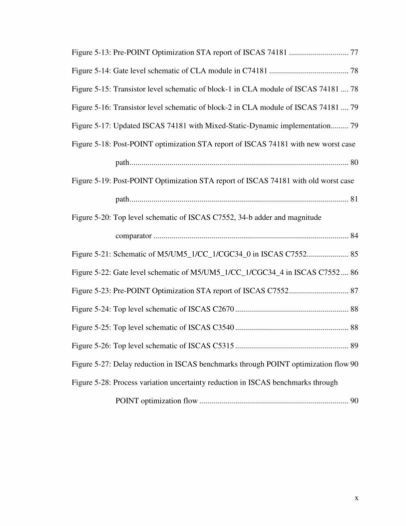
2.1.1 Static CMOS Logic
The most common logic family, Static CMOS logic is a combination of two
networks, Pull Up Network (PUN) and Pull Down Network (PDN) as in Figure 2-2 [39].
The PUN only consists of pmos transistors and provides a low ON resistance path
between Vdd and the output. It’s counterpart, PDN only consists of nmos transistors and
provides a low ON resistance path between the output and ground. The Static CMOS
logic in designed in way that there exists one and only one of the networks is conducting
in steady state.
9
The primary advantage in static CMOS logic is lower switching activity to result in
low power consumption. This advantage comes at the cost of speed, high area (logic
designed using both pmos and nmos transistors), and static leakage power.
A B
A
B
Pull Up
Network
Pull Down
Network
Vdd
Gnd
Y
Figure 2-2: Static CMOS Logic Gate
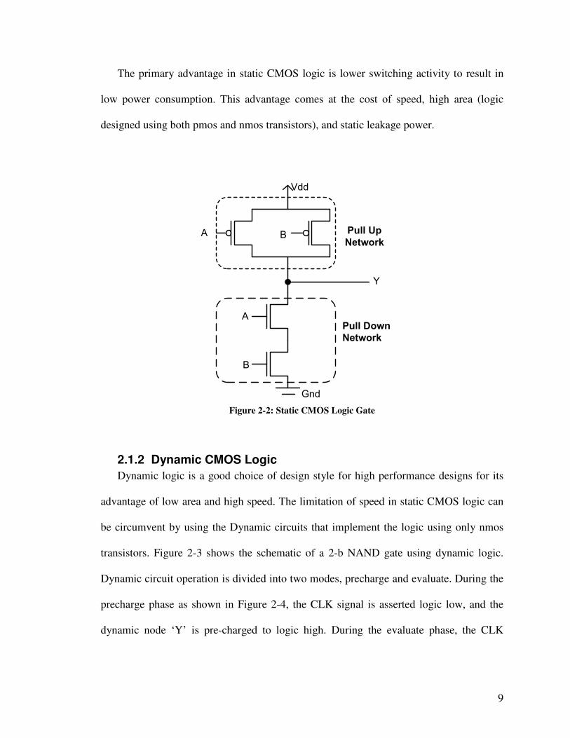
2.1.2 Dynamic CMOS Logic
Dynamic logic is a good choice of design style for high performance designs for its
advantage of low area and high speed. The limitation of speed in static CMOS logic can
be circumvent by using the Dynamic circuits that implement the logic using only nmos
transistors. Figure 2-3 shows the schematic of a 2-b NAND gate using dynamic logic.
Dynamic circuit operation is divided into two modes, precharge and evaluate. During the
precharge phase as shown in Figure 2-4, the CLK signal is asserted logic low, and the
dynamic node ‘Y’ is pre-charged to logic high. During the evaluate phase, the CLK
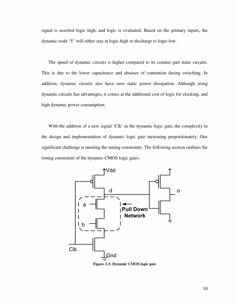
10
signal is asserted logic high, and logic is evaluated. Based on the primary inputs, the
dynamic node ‘Y’ will either stay at logic-high or discharge to logic-low.
The speed of dynamic circuits is higher compared to its counter part static circuits.
This is due to the lower capacitance and absence of contention during switching. In
addition, dynamic circuits also have zero static power dissipation. Although using
dynamic circuits has advantages, it comes at the additional cost of logic for clocking, and
high dynamic power consumption.
With the addition of a new signal ‘Clk’ in the dynamic logic gate, the complexity in
the design and implementation of dynamic logic gate increasing proportionately. One
significant challenge is meeting the timing constraints. The following section outlines the
timing constraints of the dynamic CMOS logic gates.
d
Clk
Vdd
Gnd
a
b
Pull Down
Network
o
Figure 2-3: Dynamic CMOS logic gate
11
Figure 2-4: Precharge and evaluate phases in dynamic logic gate
2.1.2.1 Timing constraints in Dynamic CMOS Logic
The node timing constraints for dynamic logic can be expressed in terms of signal and
clock arrival times. The first constraint addresses the arrival time of a falling transition at
any data input of the domino gate [41]. Any such falling event should meet the set-up
time requirement to the rising edge of the evaluate clock to ensure that the dynamic node
is not inadvertently discharged by a late arriving signal. If Tf(in) refers to the falling event
time of the input node, then it is required that the system follow the relation in Eq. 2.1,
where the setup time Tsetup is a constant that acts as a safety margin.
( )setuprcf TTinT −≤ , (2.1)
The second set of constraints is related to the arrival time of a rising transition at the
output of the dynamic gate. The rising event of the output node of the domino gate must
be completed before the falling edge of evaluate clock as in Eq. 2.2. In other words, the
result from the evaluation cycle must have reached the output before the beginning of the
precharge for next cycle.
( )( ) ( ) ( )
( ) ( )( )odD
dclkDTdbD
bTdaDaToT r
frclkf
rfr
r ,,,,
,,max
,
+
+
++= (2.2)

12
Where,
Tr(a) and Tr(b) are the rising event times at inputs A and B respectively.
Df(i,d) represents the delay of a falling transition at the dynamic node d due to a rising
transition at input bai ,∈
Dr(d,o) represents the rise delay of the inverter feeding the gate output node o
Df(clk,d) is the delay from the clock node clk to the dynamic node d
Therefore for bai ,∈
( ) ( ) ( )iTTPodDdiD rfclkrf −≤−+ ,,, (2.3)
( ) ( )rcfclkrf TTPodDdiD ,,,, −≤−+ (2.4)
The relation in Eq. 2.3 corresponds to the requirement that the rising edge of each
input should appear in time for the falling edge of the evaluate clock so as to allow
sufficient time for the output to be discharged. The relation in Eq 2.4 ensures that the
pulse width of the evaluate clock is sufficient for pulling down the output node when the
last transistor to switch is the lowermost one, connected to the clock node.
The third set of constraints addresses the timing requirements on rise transitions at the
dynamic node The rising event of the domino gate must be completed before the rising
edge of the evaluation clock, i.e.,
( )rclkr TdT ,≤ (2.5)
If the rise time of the dynamic node through the fed by the clock is denoted by then
the rising event time can be expressed as:
( ) ( )dclkDTdT rfclkr ,, += (2.6)

13
This leads to the constraint given by
( )fclkrclkr TTdclkD ,,, −≤ (2.7)
This implies that the pulse width of precharge must be capable of pulling up the
output node. Note that unlike (2.2) above, the delay to only node is considered here, and
not to the output node.
2.2 Timing Analysis in Combinational Circuits
A combinational circuit consists of several gates (two to several thousands), and one
metric used to evaluate its performance is delay. Several methods have been proposed to
compute the delay. With the number of inputs in a design increasing with proportion to
the number of gates, it is becoming extremely difficult to perform dynamic timing
analysis for every input pattern. One alternative solution for this is static timing analysis,
which is performed in an input-independent manner to find the worst-case delay over all
the possible input combinations. This section presents outline of fundamental static
timing analysis method of combinational circuits, the Critical Path Method (CPM) as
shown in Fig 2-5 [41].
Figure 2-6 shows a simple combinational block with a series of inverting logic gates.
The numbers dr/df inside each gate represents the rising and falling delays of the gate
respectively. It is presumed that all the primary inputs are available at time zero. The
CPM proceeds from the primary inputs to the primary outputs in topological order,
computing the worst-case rise and fall arrival times at each intermediate node, and
eventually at the outputs of the circuit.

14
Figure 2-5: Pseudocode for Critical Path Method
i
j
k
l
m
n
o
p
0/0
0/0
0/0
0/0
0/0
0/0
0/0
0/0
a
b
c
d
e
f
g
h
4/2
3/2
4/1
3/4
4/2
3/2
4/1
3/4
1/2
2/3
4/3
3/23/6
8/7
10/6
10/12
Figure 2-6: Combinational Circuit to illustrate application of Critical Path Method

15
The algorithm is executed on the circuit in Fig 2-6 as follows:
1. In the initial step gates lkji ,,, are placed on the queue since the input arrival
times at all of their inputs are available.
2. Gate i , at the head of the queue, is scheduled. Since the inputs transition at time
0, and the rise and fall delays are, respectively, 4 and 2 units, the rise and fall
arrival times at the output are computed as 0+4=4 and 0+2=2, respectively.
After processing no new blocks can be added to the queue.
3. Gate j is scheduled, and the rise and fall arrival times are similarly found to be
3 and 2, respectively. Again, no additional elements can be placed in the queue.
4. Gate k is processed, and its output rise and fall arrival times are computed as 4
and 1, respectively. After this computation, we see that all arrival times at the
input to gate m have been determined. Therefore, it is deemed ready for
processing, and is added to the tail of the queue.
5. Gate l is now scheduled, and the rise and fall arrival times are similarly found
to be 3 and 4, respectively, and no additional elements can be placed in the
queue.
6. Gate m , which is at the head of the queue, is scheduled. Since this is an
inverting gate, the output falling transition is caused by the latest input rising
transition, which occurs at time max(3,4) = 4. As a consequence, the fall arrival
time at is given by max(3, 4)+2 = 6. Similarly, the rise arrival time at m is
max(2,1)+1=3. At the end of this step, both n and o are ready for processing
and are added to the queue.

16
7. Gate n is scheduled, and its rise and fall arrival times are calculated,
respectively, as max(2,6)+2=8 and max(4,3)+3=7.
8. Gate o is now processed, and its rise and fall arrival times are found to be
max(6,4)+4=10 and max(3,3)+3 = 6 respectively. This sets the stage for adding
gate o to the queue.
9. Gate p is scheduled, and its rise and fall arrival times are max(7,6)+3=10 and
max(8,10)+2=12, respectively. The queue is now empty and the algorithm
terminates.
The worst-case delay for the combinational circuit in Fig 2-6 is therefore max(10,12) =
12 units.

17
3 Process Variations and Timing Optimization in
CMOS Circuits
3.1 Process Variations in CMOS Technology
CMOS technology has been advancing at a swift pace as predicted by the Moore’s
law [32] resulting in cost-effective design solutions, and allowed for a rapid shift towards
larger wafers. Along with these improvements, design complexity has also increased
dramatically resulting in challenging issues such as semiconductor process variations.
Semiconductor process variations occur when the parameters deviate from the ideal
values. They are a result of perturbations during the fabrication process, and changes in
the operating environment of the circuit. These process variations have been a key
concern for manufacturability and circuit design. With the CMOS technology migrating
towards 32 nm channel length, the significance of accounting for process variations in
circuit design has been increasing. Failure to account for the process variations might
result in designer setting large design margins, under utilizing the design performance.
One other additional challenge is that, parameter variations are not scaling down as fast
as the nominal values, resulting in the ratio between variations to nominal value
becoming higher and higher as shown in Table 3-1.

18
Table 3-1: CMOS Technology Roadmap for Process Variations [59]
Parameters Nominal Values 3σ Values
Leff [nm] 250 180 130 100 70 250 180 130 100 70
Tox [nm] 5 4.5 4 3.5 3 0.4 0.36 0.39 0.42 0.48
Vdd [V] 2.5 1.8 1.5 1.2 0.9 0.25 0.15 0.15 0.12 0.09
Vth [V] 0.5 0.45 0.4 0.35 0.3 0.05 0.045 0.04 0.04 0.04
W [nm] 800 550 500 400 300 200 170 140 120 100
H [µm] 1.2 1 0.9 0.8 0.7 0.3 0.3 0.27 0.27 0.25
ρ [mΩ/] 45 50 55 60 75 10 12 15 19 25
Some of the parameters of variations in a CMOS device include gate length (Leff),
gate width (Weff), gate oxide thickness (Tox), doping concentration etc., All of these
parameters of variations not only change the device properties, but might effect the
circuit performance. At the VDSM level, this increased magnitude of fluctuations might
lower the performance of the circuit by one generation [6], and might even result in
design failure [60]. The magnitude of intra-die channel length variations has been
estimated to increase from 35% of total variation at 130nm, to 60% in 70nm technology;
and variation in wire width, height, and thickness is also expected to increase from 25%
to 35% [60]. This results in overall design performance variation and degradation.
Process variations are broadly classified into two types, die-to-die (inter-die)
variations and within-die (intra-die) variations. The inter-die variations represent the
process variations from chip to chip for the same circuit. The intra-die variations
represent the process variations at different locations on the same chip. A pictorial
representation of the same is shown in Figure 3-1, and Figure 3-2.
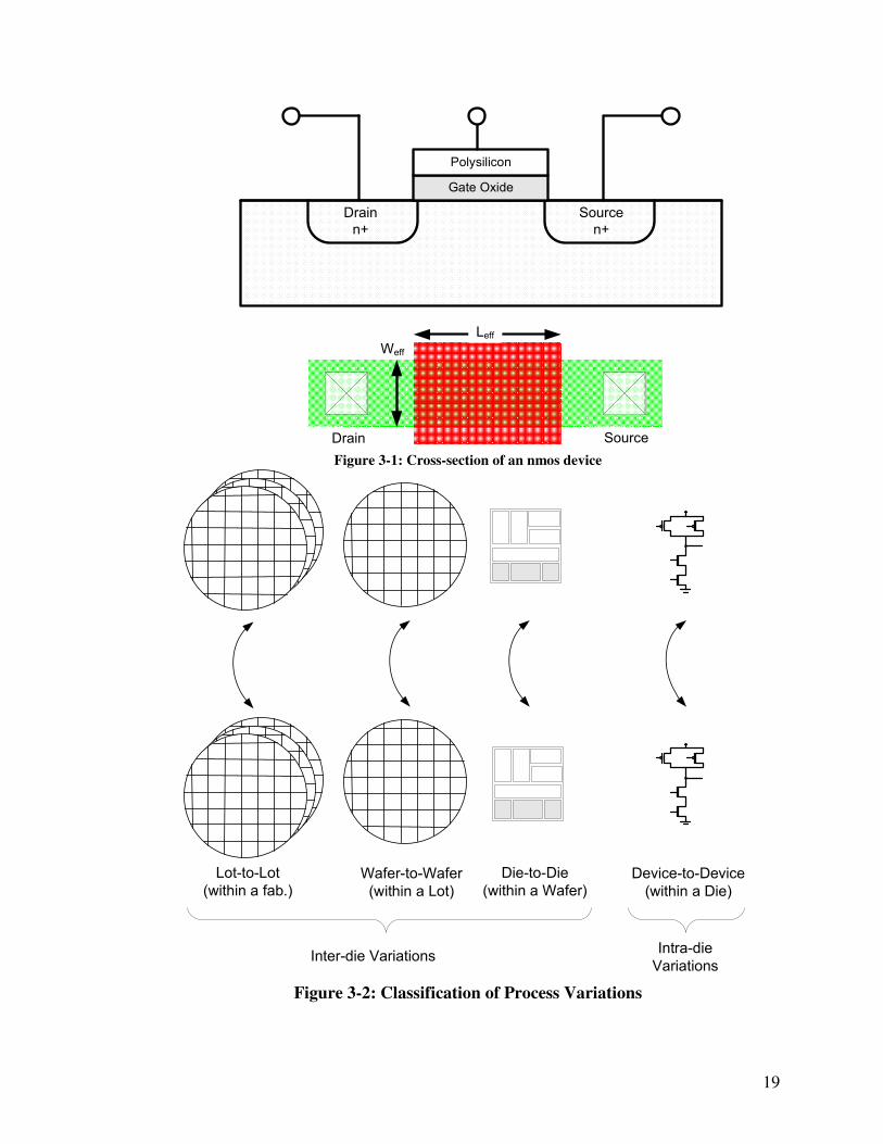
19
Drain
n+
Source
n+
Gate Oxide
Polysilicon
Leff
Weff
Drain Source
Figure 3-1: Cross-section of an nmos device
Lot-to-Lot
(within a fab.)Wafer-to-Wafer
(within a Lot)
Die-to-Die
(within a Wafer)Device-to-Device
(within a Die)
Intra-die
VariationsInter-die Variations
Figure 3-2: Classification of Process Variations

20
3.2 Effect of Process Variations on Delay and Power of CMOS Circuits
The magnitude of the process variations depends on critical path depth, where paths
with fewer logic stages experience less averaging of random variations resulting in larger
variability. Due to increasing complexity in microprocessor designs, the number of
critical paths increases with each generation while logic depth typically decreases. This
trend worsens the impact of within-die variations [60]. As shown in Figure 3-3, process
variations have caused about 30% variation in chip frequency, along with 20X variation
in chip leakage current. This amplifies the importance of meeting timing constraints as
the functionality of a system depends on the operating delay. For some variation-sensitive
circuits such as SRAM arrays, and dynamic logic circuits, process variations may results
in functionality issues and yield loss [60].
Figure 3-3: Variation in Leakage Current and Frequency due to Process Variations [4]
One of these parameters that accounts for major intra-die variation is device threshold
voltage due to quantization effect of dopant atoms with increasingly smaller silicon
structures [15], [45]. From Eq. 3.1 – 3.4, it is evident that the threshold voltage is

21
dependent on oxide thickness. Variation in threshold voltage not only effects the delay of
a CMOS transistor, but also leakage current in OFF state as in Eq. 3.5.
( )FSBFTT VVV φφγ 220 −−+−+= (3.1)
oxox
ox
ox
BFmsT
C
Q
C
Q
C
QV 10
0 2 −−−−= φφ (3.2)
ox
Asi
C
Nqεγ
2= (3.3)
ox
oxox
tC
ε= (3.4)
)10ln//(SVoff
TeI−∝ (3.5)
One of the methods used to reduce delay and power of CMOS designs is transistor
sizing. However, designs optimized for power by transistor sizing are more susceptible to
frequency impact due to within-die variations as they sharpen path delay distributions
making a large number of paths and transistors critical [35].
avg
ddLd
I
VCt = (3.6)
)1()(.2
2DSTGS
oxnD VVV
L
WCI λ
µ+−= (3.7)
Figure 3-4: Simple Transistor Chain

22
3.3 Impact of Process Variations on Delay of a CMOS Circuit
Figure 3-4 shows a simple transistor chain with three timing paths, Path-A: T0, T1, T2,
T3; Path-B: T0, T1, T4; and Path-C: T0, T1, T2, T5, T6. In an ideal case, without any
process variations, the drain currents 321 ,, DDD III in saturation can be depicted as in Eq.
3.8 - Eq. 3.10. Consider a case where there exists variation in oxide thickness of
transistors T2, and T3. The variation in oxide thickness of transistor T3 results in gate
oxide capacitance, and drain voltage of transistor T3 to change. This leads to the
saturation drain current ID3 to change as in Eq. 3.11. Similarly, a variation in oxide
thickness of transistor T2 causes the saturation drain current, ID2 to change as in Eq. 3.12.
These variations in saturation drain currents ID2, ID3 will further result in drain current ID1
to change as in Eq. 3.13. A significant point that needs to be observed here is that
transistor T1 is present in all the three timing paths (Path-A, Path-B, Path-C) in the
circuit. A variation in the saturation drain current, ID1 will not only change the delay of
the path (Path-A) with variation in process parameters, but will also vary the delay
characteristics of other paths (Path-B, Path-C) in the design. This example further
highlights the significance of process variations while accounting for delay and power
consumption in a design.
( ) ( )DSTGSoxn
D VVVL
WcI λ
µ+−= 1
2
2
11
1
111 (3.8)
( ) ( )2
2
22
2
222 1
2DSTGS
oxnD VVV
L
WcI λ
µ+−= (3.9)
( ) ( )3
2
33
3
333 1
2DSTGS
oxnD VVV
L
WcI λ
µ+−= (3.10)

23
( )
( )( ) ( ) ( )( )( )33333
2
3333
3
3333
1
2
SDDTTSG
oxoxnD
VVVVVVV
L
WccI
−∆+∆++∆+−−
×∆+
=
λλ
µ
(3.11)
( )
( )( ) ( ) ( ) ( )( )( )222222
2
2222
2
2222
1
2
SSDDTTSG
oxoxnD
VVVVVVVV
L
WccI
∆+−∆+∆++∆+−−
×∆+
=
λλ
µ
(3.12)
( )( ) ( ) ( )( )( )11111
2
1111
1
111 1
2SSDDTSSG
oxnD VVVVVVVV
L
WcI ∆+−∆++−∆+−= λ
µ (3.13)
For digital circuits, the influence of inter-die variations on circuit performance is
crucial. So, most circuit simulators with statistical modeling capability for digital
applications ignore intra-die variations when simulating circuit. However, the effect of
intra-die variations is high in analog designs such as current mirror, and therefore cannot
be ignored. With technology advancing towards mixed-signal designs, both intra-die and
inter-die variations play prominent roles and they should be considered during the
optimization process.
3.4 Previous Research in Process Variations
Substantial research [4][6][15][26][33][45][48][60] was performed to understand the
significance of process variations, and many techniques have been portrayed to mitigate
them. Many of the proposed methods deal with statistical variations and are not optimal
for designs with large number of parameter variations [42].
A variable strength keeper that is programmed based on die leakage was proposed as
shown in Fig. 3-5 [26]. The keeper logic designed utilizes three keeper transistors in
parallel with widths of W, 2W and 4W. Based on the digital bit input

24
000,001,010,011,100,101,110,111, appropriate keepers are turned on and mapped to
creative an effective keeper width of W, 2W, 3W, 4W, 5W, 6W, 7W. This keeper logic
works for designs with a large number of parallel stacks similar to NOR gates, but is not
optimal for designs without parallel stacks as this method requires additional hardware to
program the keeper transistor.
Figure 3-5: 3bit Programmable Keeper [26]
Authors in [24] showed that series stack of transistors are less susceptible to process
variations when compared to parallel stacks. This research suggests insertion of a series
dummy transistor in the whole parallel stack to reduce the impact of process variations.
A technique called Adaptive Body Biasing (ABB) was presented in [48] to compensate
for variation tolerance. The ABB technique is implemented post-silicon where each die
receives a unique bias voltage, reducing variance of frequency variation. Although this
method is feasible for inter-die variations, it is not practical for intra-die variations as
each block in the design requires a unique bias voltage. Another limitation in this method
is the increased leakage power due to reduction in threshold voltage.

25
On the other hand, substantial literature exists on selecting multiple corners to
simulate a design, and they account for systematic variations but not random variations.
With the continuous scaling in CMOS technology, the number of sources of variations is
increasing very rapidly. One of the methods that accounts for increased number of
variations is Monte-Carlo method [22]. Monte-Carlo method results in narrow design
margins for random variations, and as variations in DL and DW are random and are
predicted to be the major contributors towards total variations [60], it is an ideal method.
Although there are misconceptions that Monte-Carlo method is slow, it is ideal when the
number of sources of variations is significantly high [35]. Fig 3-6 compares CPU time vs.
number of sources of variations for various methods [34]. The advantage of using Monte-
Carlo method is that, it is theoretically accurate and is commonly used as a golden
reference. This method can be used to clearly explain the behavior of a gate or circuit and
does not require any characterization. It can be easily extended to incorporate DSM
effects such as crosstalk and IR drop [42].
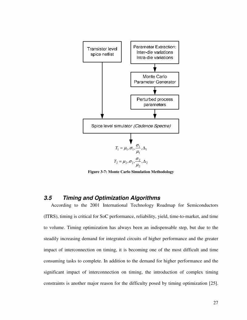
Figure 3-7 shows the methodology used in Monte-Carlo method where circuit netlist
is input along with various sources of variations specified in the process file. Some of the
sources of variations considered during Monte-Carlo simulations are gate oxide thickness
( oxt ), threshold voltage ( tV ), mobility variation due to dopant mismatch, FET variation
due to across chip variation in gate length ( DL ) and gate width ( DW ), FET length
variation due to nesting, FET length variation due to gate orientation, FET resistance,

26
drain overlap capacitance, junction area capacitance, source/drain sidewall capacitance,
source/drain sidewall junction capacitance.
Research has shown that intra-die variations primarily impact the frequency
maximum (FMAX) mean, and inter-die variations primarily impact the FMAX variance
[6]. So, design tools aimed towards optimization of timing and yield should consider both
inter-die variations and intra-die variations. The mean and standard deviation of different
paths in the designs can be computed using Eq.3.14 and Eq. 3.15 respectively.
∑=
=n
i
i
1
τµ (3.14)
( )∑=
−−
=n
i
in
1
2
1
1µτσ (3.15)
Figure 3-6: CPU time vs. number of sources of variation [22]
27
11
1111 ,,, ∆=
µ
σσµT
22
2222 ,,, ∆=
µ
σσµT
Figure 3-7: Monte Carlo Simulation Methodology
3.5 Timing and Optimization Algorithms
According to the 2001 International Technology Roadmap for Semiconductors
(ITRS), timing is critical for SoC performance, reliability, yield, time-to-market, and time
to volume. Timing optimization has always been an indispensable step, but due to the
steadily increasing demand for integrated circuits of higher performance and the greater
impact of interconnection on timing, it is becoming one of the most difficult and time
consuming tasks to complete. In addition to the demand for higher performance and the
significant impact of interconnection on timing, the introduction of complex timing
constraints is another major reason for the difficulty posed by timing optimization [25].
28
Reducing the cost of timing optimization is now a top priority in modern CMOS designs.
Far from being a discrete step in the design flow or, worse yet, an afterthought, timing
optimization has become the heartbeat of a design cycle.
Design cycle is currently performed at many abstraction levels such as architecture,
system, RTL, gate, and transistor. In the near future, more circuits will be designed and
analyzed at the transistor level [2]. Research performed by a leading company stated that,
managers in several companies follow a iteration in timing, “Reduce the design to a
lower level of abstraction, estimate timing as precisely as possible based on that level of
abstraction, set margins to minimize failing nets, fix the outlying nets, and repeat.” [51]
This shows the importance of advanced timing optimization algorithms for lower levels
of abstraction. The objective is to design an advanced timing optimization algorithm to
meet timing constraints as early in the design cycle as possible.
Fig. 3-8 depicts a software prototyping principle. Graphs (a) and (b) show that
software dominates system development cost and time where CPU and memory
utilization are high [30]. This domination of software for the system development has
caused a gap in the design productivity. This gap prevails due to the limitations of
semiconductor manufacturing technology that cannot be fully exploited by the current
state-of-the-art design technology, and will continue to widen due to inefficiency in the
available automated design methodologies [30]. Also, software availability, support and
knowledge base are the bane of product schedules [20]. All this put together calls for

29
advanced timing optimization methods to close this gap between the CAD tools and
current CMOS manufacturing technology.
Figure 3-8: The effect of hardware constraints on: (a) HW/SW prototyping costs, and (b) Software
Schedule [30]
3.6 Significance of Dynamic CMOS Circuits on Timing
Recent improvements in fabrication technology have enabled the feasibility of
integrating devices on increasingly smaller scales. The semiconductor industry is
currently transitioning to a 32 nanometer (nm) process with a reduction to a 22 nm on the
horizon. Whether in a standard alone PC, a high-performance workstation, a PC cluster,
or a multiprocessor system, microprocessors have been the heart of computational
systems for decades. The performance of microprocessors has been driven traditionally
by CMOS technology and micro architectural improvements [2]. This performance can
be improved to a major extent at the circuit level through design and physical
organization. One such modification that be done to improve design performance in
timing is using dynamic CMOS circuits.

30
With the trend of electronics industry moving towards portable devices and
applications, circuit designers are required to design applications with significant
performance in speed, while at the same time consuming low power. With the static and
dynamic circuits having their limitations of speed and power respectively, an optimal
balance between speed and power can be achieved at the design level by partitioning the
design to a mixed dynamic-static circuit style [58]. However, implementation of dynamic
CMOS circuits is still limited by one challenge, transistor sizing. This is due to many
limitations such as charge sharing, noise immunity, leakage and semiconductor process
variations.
At the circuit level, the dynamic logic style has been pre-dominantly used in
microprocessors and the use of custom dynamic circuits in microprocessors has allowed
for significant performance improvement in timing over static CMOS circuits [2]. With
the importance of timing increasing, the number of custom circuits with a high ratio
between the number of paths, to number of transistors are increasing rapidly. This adds
more complexity to sizing devices in the already complex nanometer CMOS process.
This complexity when combined with the necessity for custom dynamic circuits
emphasizes the imperative necessity for novel transistor sizing algorithms that are
compliant for both static and dynamic CMOS logic styles.

31
3.7 Previous Work on Transistor Sizing
Transistor sizing is one of the key techniques used for timing optimization in
microprocessors and CMOS circuit designs. The transistor sizing problem in general can
be stated as in Eq 3.16.
minT)xDelay()xArea( ≤ subject to minimize (3.16)
Substantial research was performed in the area of transistor sizing, and several
methods have been proposed to improve timing performance in static CMOS circuits.
However, not many methods were presented to automate the process of timing
optimization in dynamic CMOS circuits. This section outlines some of the well known
transistor sizing algorithms for timing optimization.
Fishburn [11] has presented the TImed LOgic Synthesis (TILOSTM
) algorithm where
the sizes of the transistors are increased based on the significance of each path. It is based
on the principle that, as the minimum value is unique, a simple method should find it.
The sizes of all the transistors in the design are set to minimum, and the path with the
largest delay is found. Accordingly, sizes of transistors in this path are increased by a
factor to reduce the overall delay. Figure 3-9 shows a simple transistor chain with three
timing paths, Path-A: T0, T1, T2, T3; Path-B: T0, T1, T4; and Path-C: T0, T1, T2, T5, T6.

32
Figure 3-9: Simple Transistor Chain
One limitation in the TILOSTM
algorithm is that, increasing the size of transistors in
path might increase the load of the neighboring paths, and cause the delay of the design
to increase. In the design in Figure 3-9, if Path-A is found to be critical, TILOSTM
increases sizes of transistors T1, T2, T3. This increased transistor size of T2 and T3 will
increase the channel loading capacitance on transistors T4 and T5, and will increase
delays of Path-B and Path-C.
One other limitation in TILOSTM
algorithm is its inability to deal with interacting
paths. For the design in Figure 3-10, TILOSTM
increases sizes of gates B, C, and D, rather
than just increasing the size of inverter-A, increasing the overall area and capacitance.
The overall drawback of TILOS is that it does not guarantee the convergence of timing
optimization and hence is not a deterministic optimization technique [43].

33
Figure 3-10: Chain of Inverters
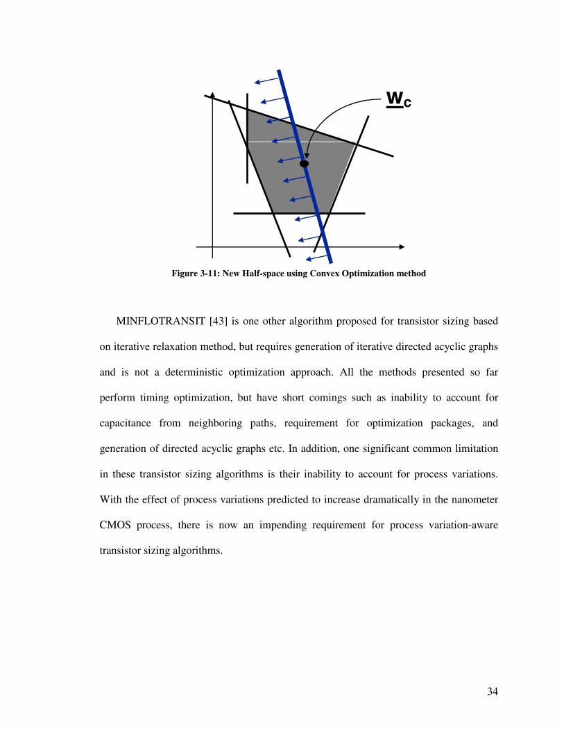
One other popular method of transistor sizing is the convex optimization method as
proposed by Vaidya [49]. The convex optimization method works on the principle of
identifying the design space using hyperplanes in the design space. A design space with
bound WMax and WMin based on the constraints as shown in Eq. 3.17 are chosen, and the
center of polytope, cW is found to determine the half-space. Later, static timing analysis
is performed based on the transistor widths corresponding to cW as in Fig 3-11.
MiniMaxi WWandWW ≥≤ (3.17)
( ) ( ) ccc WWfWWfspaceHalf ...: ∇≥∇− (3.18)
If cW is found to be feasible, gradient of the area function is found and the design
space is reduced to find the new half-space. Major limitations here are the complexity in
finding the half-space for design with large number of transistors, requirement for
optimization packages, and inability to account for process variations. Also, this method
relies on data from static timing analysis, which does not account for accurate
capacitance loading in the design.
34
wc
Figure 3-11: New Half-space using Convex Optimization method
MINFLOTRANSIT [43] is one other algorithm proposed for transistor sizing based
on iterative relaxation method, but requires generation of iterative directed acyclic graphs
and is not a deterministic optimization approach. All the methods presented so far
perform timing optimization, but have short comings such as inability to account for
capacitance from neighboring paths, requirement for optimization packages, and
generation of directed acyclic graphs etc. In addition, one significant common limitation
in these transistor sizing algorithms is their inability to account for process variations.
With the effect of process variations predicted to increase dramatically in the nanometer
CMOS process, there is now an impending requirement for process variation-aware
transistor sizing algorithms.
35
4 Process Variation-Aware Transistor Sizing in Dynamic CMOS Circuits
4.1 Process Variation Aware Load Balance of Multiple Paths (LBMP) Transistor Sizing Algorithm
Assuming that there exists a circuit topology, a design can be translated into an RC
tree circuit, from which delays can be estimated by using a spectrum of approximation
methods [36]. When the Elmore delay model is implemented, the overall delay is seen to
be a posynomial function of transistor widths [9]. In particular, the Elmore delay model
[10] can be used for timing analysis as it provides an upper bound on the delay for any
input pattern. The primary advantage of the Elmore delay model is that its simple, closed
form expression for delay can be presented in terms of the RC tree parameter values [36].
However, Elmore model faces a limitation that it does not account for the resistance
shielding of downstream capacitances. An algorithm that accounts for this downstream
capacitance can be readily extended to estimate the RC effects of a transistor that be later
used for efficient transistor sizing.
The Elmore delay model is a fitting metric for RC tree because its delay calculation is
simple and fairly accurate for any RC circuit topology. The Elmore delay model is
proved to be an absolute upper bound on the 50% delay of any RC tree response. In an
RC tree of N nodes, the Elmore delay for node-i can be depicted as in Eq. 4.1.
∑=
=N
k
kkiD CRT1
(4.1)
36
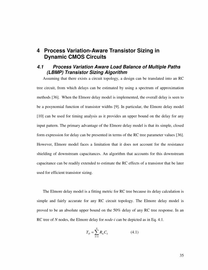
In Eq. 4.1, Rki is the resistance of the portion of path between the input and node-i,
that is common with the path between the input and node-k, and Ck is the capacitance at
node-k. From the RC tree network shown in Fig 4-1, using Elmore model, delay at node-
1 and node-5 can be computed as in Eq. 4.2 and Eq. 4.3, respectively. Eq. 4.2 shows that
the delay at node-1 is independent of R2-R6. Increasing values of R2-R6 would decrease
the downstream capacitances, and reduce the delay at node-1. However, this would
increase delays at other nodes and result in even worse delays in other paths. So, sizing
has to be performed while accounting for this downstream capacitance.
( )65432111 CCCCCCRT +++++= (4.2)
( ) ( ) ( )
( ) 6155421
4421321221115
CRCRRRR
CRRRCRRCRRCRT
+++++
+++++++= (4.3)
Figure 4-1: RC Tree Network
It can be observed from Eq. 4.3 that R1, R2, R4, R5 appears 6, 4, 2, 1 times
respectively while calculating the delay at node-5. Also, it is clear that R1 has a major
effect on the delay compared to R5. This case is very similar for a dynamic CMOS
circuit. Increasing width of the transistor that appears in the most number of paths would
reduce the overall delay of the circuit.

37
The delay of dynamic CMOS circuit is highly dependent on the number and size of
transistors in the critical path. Increasing size of transistor in a path will increase the
discharging current and reduce the path delay. However, increasing transistor sizes to
reduce one path delay might increase the load capacitance of channel-connected
transistors on other paths and substantially increase their delays. This level of complexity
increases along with the number of paths in the design.
Figure 4-2 highlights two timing paths: path-A (T28 -T7 - T8 - T12 - T18 – T32) and
path-B (T28 - T0 - T4 - T11 - T15 – T16 – T31) in a 2-b Weighted Binary-to-Thermometric
Converter (WBTC). An experiment of optimizing path-A was performed by gradually
increasing sizes of T7, T8, T12 and T18. It was observed that the delay of path-A reduced
by 4%, but delay of path-B increased by 9.3%. This is a result of transistors on path-B
being channel-connected to the transistors on path-A. For instance, T4 and T11 are
channel-connected to T7 and T8, and T15 and T16 are channel-connected to T12 and T18.
Increasing widths of T7, T8, T12 and T18 in path-A increases the capacitive load of T4, T11,
T15 and T16, and increases the delay of path-B.
Conventionally worst-case path is identified based on the mean value from delay
distribution, accounting only for intra-die variations. As inter-die variations are equally
important, standard deviation should be considered as well. Delay distributions of two
paths, path-A and path-B in Fig 4-2 are shown in Fig 4-3. Here, path-A has high mean
and path-B has higher standard deviation. From Fig. 4-3 and Eqs.4.4 – 4.6, path-B is
38
worst-case path when mean from the delay distribution is considered. Optimizing a
design by increasing size of transistors in path-B might reduce the overall mean of worst-
case path delay, but will not reduce the standard deviation. So, the path appropriate for
timing optimization has to be chosen with care.
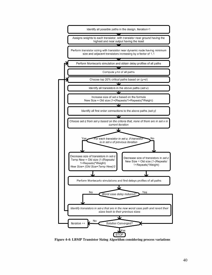
The process variation-aware Load Balance of Multiple Paths (LBMP) transistor
sizing for dynamic CMOS circuits is depicted in Fig. 4-4. As both inter-die and intra-die
variations are to be considered during optimization, the proposed LBMP algorithm ranks
the critical paths based on the sum of mean and standard deviation ( )σµ + . As shown in
Fig. 4-2, discharge time of transistors near Gnd is longer compared to the transistors near
Vdd as transistors near Gnd are usually driven by many paths. Therefore, path delay is
optimized by increasing size of transistor near Gnd the most and the size of transistor
near Vdd the least.
21 µµ < (4.4)
21 σσ > (4.5)
2211 σµσµ +>+ (4.6)

39
Figure 4-2: 2-b weighted Binary-to-Thermometric Converter
Figure 4-3: Comparison of delay distribution of two paths
40
Figure 4-4: LBMP Transistor Sizing Algorithm considering process variations

41
As increasing the size of transistor that appears in the most number of paths would
reduce delays of most paths, the process variation-aware LBMP algorithm computes the
number of paths each transistor is present in and denotes this number as “repeats”. The
initial step in the process variation-aware LBMP algorithm is to size adjacent transistors
on every path with a fixed size ratio ‘r’ for faster convergence. Thereafter, a weight is
assigned to each transistor with the transistor near Gnd having the highest weight and the
one near output having the least. After the repeats and the weight profiles are computed,
Monte-Carlo simulations are performed to obtain delay profiles documenting the worst-
case paths and their delays ( )σµ + . The transistors in the top 20% critical paths are
grouped to a path set called set-x, and their sizes are increased and calculated by Eq. 4.7.
×
++×= Weight
Repeats1
RepeatsSizeOldSizeNew 1__ (4.7)
It has been shown in Fig. 4-2 that increasing size of transistors on path-A to reduce its
delay will increase delay of path-B due to the increased capacitive load. Therefore,
reducing size of transistors that are not on the worst-case path, but are channel-connected
to the transistors on the worst-case path will reduce the capacitive load and the overall
delay. For example, T0, T2, T4 and T5 are 1st order connection transistors to T1 in the 2-b
WBTC circuit shown in Fig. 4-2. The 1st order connection transistors in the set-x are
identified and grouped to a path set termed as set-y. Then, transistors in set-y that are not
in set-x of the current iteration are grouped to set-z. For each transistor in set-z, it is
checked if the transistor is present in set-x of previous iteration. If so, its size is decreased
and calculated by Eq. 4.8 and Eq. 4.9. If not, its size is decreased and calculated by Eq.
4.10.

42
×
+−×= Weight
Repeats1
RepeatsSizeOldNewTemp 1__ (4.8)
2
___
NewTempSizeOldSizeNew
+= (4.9)
×
+−×= Weight
Repeats1
RepeatsSizeOldSizeNew 1__ (4.10)
Once new transistor sizes are determined, process variations are induced and Monte-
Carlo simulations are performed to identify the new top 20% critical paths. If the new
worst-case path delay is higher than in the previous iteration, sizes of transistors in set-z
of the new worst-case path are reverted back to their previous sizes to reduce the worst-
case path delay. Iterations are repeated until the solution converges to an optimum.
4.2 LBMP Implementation on a 2-b Weighted BTC
Fig. 4-2 depicts a 2-b weighted binary-to-thermometric-converter (WBTC) used in
parallel adders. The 2-b WBTC has two 2-b inputs, (a1 a0) and (b1 b0) and of each the
LSB a0 and b0 has a unity weight and the MSB a1 and b1 has a weight of two. The 6-b
thermometric output can represent any number from 0 to 6. This design adds two 2-b
binary values and generates a thermometric output and of which the number of ‘1’ equals
to its binary input. For example, with an input of (a1 a0) = (1 0) and (b1 b0) = (0 1), the
output is (c5 c4 c3 c2 c1 c0) = (0 0 0 1 1 1). The 2-b WBTC is chosen as a benchmark due
to its complexity in transistor sizing. With just about 50 transistors, the WBTC has 34
timing paths and of which the delays change dramatically with different transistor sizes.
43
The 34 timing paths in 2-b WBTC are presented in Table 4-1. The transistor repeats
and weight profile are shown in Table 4-2. Using minimum size transistors, the worst-
case delay of WBTC was 355 psec from path-1. Sizes of all transistors are initially
increased on a ratio of 1.1, and simulations are performed to identify the critical paths.
The top 20% critical paths are path-1, 2, 5, 8, 26, and 29. The set-x transistors and their
initial sizes on these critical paths are T0 (311 nm), T4 (283 nm), T7 (311 nm), T11 (283
nm), T15 (212 nm), T16 (176 nm), T17 (234 nm), T22 (234 nm), T23 (193 nm), and T26 (193
nm). With these set-x transistors identified, based on repeats and weight profiles, sizes of
transistors in set-x are increased by Eq. 4.7 to T0 (454 nm), T4 (383 nm), T7 (454 nm), T11
(389 nm), T15 (239 nm), T16 (183 nm), T17 (274 nm), T22 (274 nm), T23 (209 nm), and T26
(208 nm). The 1st order connection transistors of set-x that are not in the top 20% critical
paths are grouped to set-z. They are T1 (257 nm), T8 (257 nm), T12 (234 nm), T13 (193
nm), T14 (257 nm), T18 (193 nm), T19 (257 nm), T20 (212 nm), T21 (176 nm), T24 (212
nm), T25 (176 nm), and T27 (176 nm). Based on the repeat and weight profiles, these
transistor sizes are reduced by Eq. 4.10 to T1 (195 nm), T8 (195 nm), T12 (202 nm), T13
(180 nm), T14 (195 nm), T18 (177 nm), T19 (195 nm), T20 (184 nm), T21 (168 nm), T24
(190 nm), T25 (168 nm), and T27 (171 nm). After the transistor sizing is complete,
simulations are performed to obtain the new critical path order.
The critical path order profile over a few iterations is shown in Table 4-3. With
minimum size transistors, the worst-case path is path-1. After the first iteration of the
process variation-aware LBMP algorithm, its delay reduced from 355 psec to 244 psec.
However, path-17 of which the transistor (T20, T21) sizes were reduced came into the set

44
of new critical paths. Repeated iterations of the process variation-aware LBMP algorithm
reduced the worst-case path delay and solution finally converged to an optimum of 157
psec, accounting for a 55.77% delay improvement.
Table 4-1: Timing Paths in 2-b weighted BTC
Path No. Transistors Path No. Transistors
1 T28, T0, T4, T11, T22, T26 18 T28, T7, T8, T12, T18
2 T28, T7, T11, T22, T26 19 T28, T7, T11, T15, T18
3 T28, T19, T22, T26 20 T28, T7, T11, T17, T21
4 T28, T24, T26 21 T28, T7, T11, T20, T21
5 T28, T0, T4, T11, T17, T23 22 T28, T14, T15, T18
6 T28, T0, T4, T11, T20, T23 23 T28, T14, T17, T21
7 T28, T0, T4, T11, T22, T25 24 T28, T19, T20, T21
8 T28, T7, T11, T17, T23 25 T28, T0, T1, T5, T13
9 T28, T7, T11, T20, T23 26 T28, T0, T4, T11, T15, T16
10 T28, T7, T11, T22, T25 27 T28, T7, T8, T9, T13
11 T28, T14, T17, T23 28 T28, T7, T8, T12, T16
12 T28, T19, T20, T23 29 T28, T7, T11, T15, T16
13 T28, T19, T22, T25 30 T28, T14, T15, T16
14 T28, T24, T25 31 T28, T0, T1, T2, T6
15 T28, T0, T4, T11, T15, T18 32 T28, T0, T1, T5, T10
16 T28, T0, T4, T11, T17, T21 33 T28, T7, T8, T9, T10
17 T28, T0, T4, T11, T20, T21 34 T28, T0, T1, T2, T3
Table 4-2: Repeat and Weight Profiles of Transistors in 2-b WBTC
Repeats Near
Gnd
Near
Vdd
16 T11
12 T0,T7
8 T4
6 T17, T22 T15, T20 T23 T21
4 T1, T8,
T14, T19
2 T5, T12 T2, T9,
T24 T13 T10
1 T6 T3, T27
Weights 0.5 0.4 0.3 0.2 0.15 0.1 0.05

45
Table 4-3: Critical path order in 2-b WBTC
Min. size Iter-1 Iter-2 Iter-4 Iter-6 Iter-10 Path Rank
Path # Path # Path # Path # Path # Path #
1 1 1 1 25 15 25
2 2 2 2 31 19 31
3 5 17 18 3 5 30
4 8 21 17 34 8 34
5 26 15 21 23 26 32
6 29 19 15 24 29 26
7 17 16 19 22 18 29
8 21 20 16 11 22 22
9 15 5 20 30 33 4
10 19 8 25 32 30 24
11 6 26 5 18 1 14
12 9 29 8 1 2 13
13 20 6 26 2 31 5
14 16 9 29 33 11 8
15 7 7 3 5 25 23
16 10 10 33 8 27 33
17 25 18 27 13 34 15
18 18 25 7 27 16 19
19 33 33 10 15 20 11
20 31 3 31 19 17 27
21 27 31 28 4 21 1
22 34 27 34 16 32 2
23 28 32 32 20 23 3
24 32 34 24 12 3 7
25 3 28 6 17 28 10
26 11 24 9 21 4 18
27 30 22 22 26 7 17
28 24 23 23 29 10 21
29 12 30 30 28 24 16
30 22 11 13 7 6 20
31 4 4 11 10 9 28
32 23 12 12 14 13 12
33 13 13 4 6 12 6
34 14 14 14 9 14 9
Delay
(psec) 355 244 209 171 166 157

46
Table 4-4: Delay Convergence of 2-b WBTC
Iteration Critical
Path
Min Delay
(psec)
Max Delay
(psec)
µ + σ
(psec)
0 1 252 410 355
1 1 178 290 244
2 1 156 247 209
3 3 131 215 185
4 25 124 201 171
5 19 119 195 170
6 25 121 193 166
7 21 126 191 166
8 25 119 186 161
9 8 119 176 157
10 25 117 179 157
Table 4-4 shows the delay convergence profile of 2-b WBTC over 10 iterations. The
first column represents the iteration number, the second column represents the worst-case
critical path number, the third column represents the minimum delay of the worst-case
path due to process variations, the fourth column represents the maximum delay of the
worst-case path due to process variations, and the fifth column represents the delay ( )σµ +
of the worst-case path.
100
150
200
250
300
350
400
0 1 2 3 4 5 6 7 8 9 10
Iteration
De
lay
(p
sec
)
Figure 4-5: Delay convergence profile of 2-b WBTC

47
µ
στ =s (4.11)
minmax TTyUncertaint −= (4.12)
From Table 4-4 and Fig 4-5, it is evident that the process variation-aware LBMP
algorithm is a deterministic approach always moving towards the optimum solution.
Further, the efficiency of the process variation-aware LBMP algorithm is illustrated
through reduction in delay sensitivity (Eq. 4.11) of each path in the design. Table 4-5 lists
the reduction in delay sensitivity over four different temperatures from 27 oC to 120
oC.
This table further highlights the efficiency of the process variation-aware LBMP
algorithm. Table 4-5 shows that although delay sensitivity has reduced in majority of the
paths, it has also slightly increased for a few paths (4, 5, 13, 14, 18, 28 and 31). Ranks of
these paths based on their delays are shown in Table 4-6. The increase in delay sensitivity
of these paths is very much acceptable as most of the paths except path-31 do not fall in
the set of critical paths.
A comparison of applying the LBMP algorithm to a 2-b WBTC with and without
consideration of process variation in the timing optimization is shown in Table 4-7. The
2-b WBTC optimized without considering process variations has the delay of 161.37 ps,
while occupying an area of 2.054 µm2. By accounting for process variations in the
optimization flow, delay was reduced from 161.37 psec to 144 psec (average), and area
occupied reduced from 2.054 µm2 to 1.695 µm
2. This accounts for further improvement
in delay by 10.8%, and area by 17.4%.

48
Table 4-5: Percentage delay sensitivity reduction of 2-b WBTC at different temperatures
Temp=27 O
C Temp=75 O
C Temp=100 O
C Temp=120 O
C
Path-1 21.86 20.48 19.74 18.9
Path-2 21.86 20.48 19.74 18.9
Path-3 17.6 21.24 16.12 17.07
Path-4 -6.89 13.93 -6.39 -7.03
Path-5 16.26 -9.08 14.88 15.03
Path-6 14.36 17.12 14.02 13.87
Path-7 6.23 14.68 6.89 7.78
Path-8 16.26 3.98 14.88 15.03
Path-9 14.36 17.12 14.02 13.87
Path-10 6.23 14.68 6.89 7.78
Path-11 6.93 1.62 5.62 5.75
Path-12 6.31 6.94 4.25 4.19
Path-13 -0.97 6.52 -1.23 -1.03
Path-14 -10.86 -9.35 -11.03 -10.6
Path-15 14.95 5.97 14.45 14.58
Path-16 15.16 14.5 15.09 14.94
Path-17 15.2 11.84 14.71 14.22
Path-18 15.19 -0.17 10.01 9.92
Path-19 14.95 29.77 14.45 14.58
Path-20 15.16 14.5 15.09 14.94
Path-21 15.2 11.84 14.71 14.22
Path-22 7.9 14.88 8.91 9.01
Path-23 9.81 6.87 9.84 10.29
Path-24 8.37 4.9 8.51 8.4
Path-25 4.45 6.92 2.52 1.72
Path-26 10.7 14.37 12.87 12.49
Path-27 4.38 2.57 3.79 3.58
Path-28 4.14 -5.07 5.97 6.18
Path-29 10.7 17.49 12.87 12.49
Path-30 4.29 7.48 7.91 8.71
Path-31 2.27 -7.1 1.78 1.29
Path-32 5.43 6.77 4.62 4.58
Path-33 7.7 1.85 7.1 6.82
Path-34 2.49 3.06 2.68 2.94
Average 9.35 8.92 9.00 8.98

49
Table 4-6: 2-b WBTC path ranks at different iterations and temperatures
Temp=27 Temp=75 Temp=100 Temp=120
Iter-1 Iter-10 Iter-1 Iter-10 Iter-1 Iter-10 Iter-1 Iter-10
Path-4 23 8 24 9 25 10 25 10
Path-5 5 12 5 15 5 16 5 17
Path-13 25 11 25 10 24 9 24 9
Path-14 26 10 26 11 26 11 26 13
Path-18 9 21 9 22 9 4 9 4
Path-28 17 24 17 24 17 23 17 23
Path-31 13 2 13 2 13 2 14 2
Ratio did not decrease Ratio did not decrease and path became critical
Table 4-7: LBMP implementation on a 2-b WBTC
w/o Process Variations w/ Process Variations Improvement
Delay 161.37 ps 144 ps 10.8 %
σ/µ Ratio 7.87 % 7.4 % 6 %
Area 2.054 µm2 1.695 µm
2 17.4 %
Average Power 16.9 µW 16.4 µW 3 %
4.3 LBMP implementation on a 4-b Unity Weight BTC
Another complex circuit used to validate the process variation-aware LBMP
algorithm is the 4-b Unity Weight BTC (UWBTC) used in digital-to-analog-converters as
shown in Fig. 4-6. The UWBTC takes a 4-b binary input and generates a thermometric
output and of which the number of ‘1’ equals to its binary input. For example, for a
binary input (b3 b2 b1 b0) = (0 1 0 1), the 4-b UWBTC generates an output (c14 c13 c12 c11
c10 c9 c8 c7 c6 c5 c4 c3 c2 c1 c0) = (0 0 0 0 0 0 0 0 0 1 1 1 1 1 1). Along with the increase in
the number of transistors in this 4-b UWBTC, the number of timing paths has also
increased to 82. The 82 timing paths in the 4-b UWBTC are shown in Table 4-8.
With minimum size transistors, the worst-case delay of the 4-b UWBTC was 152 ps.
The repeat and weight profiles of transistors in the 4-b UWBTC are computed, and after

50
the first iteration of the process variation-aware LBMP algorithm, the worst-case delay
reduced from 152 ps to 114 ps. Repeated iterations of the algorithm has reduced its delay
from 152 ps to 103 ps, accounting for a 32.23% delay improvement. Table 4-9 and Fig
4-7 shows the delay convergence profile of the 4-b UWBTC, demonstrating that the
process variation-aware LBMP algorithm works efficiently for complex designs with
large number of timing paths.
51
Table 4-8: Timing paths in 4-b UWBTC
Path # Transistors Path # Transistors
1 T83,T0,T1,T2,T3 42 T83,T49,T50,T51,T55
2 T83,T0,T1,T2,T6 43 T83,T56,T57,T58
3 T83,T7,T8,T9,T10 44 T83,T14,T18,T47,T60
4 T83,T0,T1,T5,T17 45 T83,T21,T25,T54,T63
5 T83,T7,T8,T9,T13 46 T83,T28,T32,T57,T60
6 T83,T14,T15,T16,T17 47 T83,T35,T39,T62,T63
7 T83,T0,T1,T5,T20 48 T83,T42,T43,T47,T60
8 T83,T14,T15,T16,T20 49 T83,T49,T50,T54,T63
9 T83,T21,T22,T23,T24 50 T83,T56,T57,T60
10 T83,T0,T4,T30,T31 51 T83,T61,T62,T63
11 T83,T7,T8,T12,T27 52 T83,T21,T25,T54,T65
12 T83,T14,T15,T19,T31 53 T83,T28,T32,T59,T68
13 T83,T21,T22,T23,T27 54 T83,T35,T39,T62,T65
14 T83,T28,T29,T30,T31 55 T83,T42,T46,T67,T68
15 T83,T0,T4,T30,T34 56 T83,T56,T59,T68
16 T83,T7,T11,T37,T38 57 T83,T61,T62,T65
17 T83,T14,T15,T19,T34 58 T83,T66,T67,T68
18 T83,T21,T22,T26,T38 59 T83,T28,T32,T59,T70
19 T83,T28,T29,T30,T34 60 T83,T35,T39,T64,T73
20 T83,T35,T36,T37,T38 61 T83,T42,T46,T67,T70
21 T83,T0,T4,T33,T45 62 T83,T49,T53,T72,T73
22 T83,T7,T11,T37,T41 63 T83,T56,T59,T70
23 T83,T14,T18,T44,T45 64 T83,T61,T64,T73
24 T83,T21,T22,T26,T41 65 T83,T66,T67,T70
25 T83,T28,T29,T33,T45 66 T83,T71,T72,T73
26 T83,T35,T36,T37,T41 67 T83,T35,T39,T64,T75
27 T83,T42,T43,T44,T45 68 T83,T42,T46,T69,T77
28 T83,T0,T4,T33,T48 69 T83,T49,T53,T72,T75
29 T83,T7,T11,T40,T52 70 T83,T61,T64,T75
30 T83,T14,T18,T44,T48 71 T83,T66,T69,T77
31 T83,T21,T25,T51,T52 72 T83,T71,T72,T75
32 T83,T28,T29,T33,T48 73 T83,T76,T77
33 T83,T35,T36,T40,T52 74 T83,T42,T46,T69,T78
34 T83,T42,T43,T44,T48 75 T83,T49,T53,T74,T80
35 T83,T49,T50,T51,T52 76 T83,T66,T69,T78
36 T83,T7,T11,T40,T55 77 T83,T71,T74,T80
37 T83,T14,T18,T47,T58 78 T83,T76,T78
38 T83,T21,T25,T51,T55 79 T83,T79,T80
39 T83,T28,T32,T57,T58 80 T83,T49,T53,T74,T81
40 T83,T35,T36,T40,T55 81 T83,T71,T74,T81
41 T83,T42,T43,T47,T58 82 T83,T79,T81

52
T0 T1T2 T3
T4 T5 T6
T83
T84
T7 T8T9 T10
T11 T12 T13
T14 T15T17
T18 T19 T20
T21 T22T23 T24
T25 T26 T27
T28 T29T30 T31
T32 T33 T34
T35 T36T37 T38
T39 T40 T41
T42 T43T44 T45
T46 T47 T48
T49 T50 T51 T52
T53 T54 T55
T56 T57 T58
T59 T60
T61 T62 T63
T64 T65
T66 T67 T68
T69 T70
T76 T77
T78
T79 T80
T81
T82
T71 T72 T73
T74 T75
T85
T86
T87
T88
T89
T90
T91
T92
T93
T94
T95
T96
T97
T98
T16
b0b0b1b1b2b2b3 clk
c14
c13
c12
c11
c10
c9
c8
c7
c6
c5
c4
c3
c2
c1
c0
Figure 4-6: 4-b Unity Weighted Binary to Thermometric Converter

53
Table 4-9: Delay convergence profile of 4-b UWBTC
Iteration Critical
Path
µ + σ
(psec)
Uncertainty
(psec)
0 28 152 75
1 36 114 27
2 28 111 28
3 27 110 34
4 51 109 29
5 52 107 42
6 58 103 28
7 35 103 27
8 35 104 28
9 35 103 28
10 35 103 27.3
Improvement (%) 32.23 63.6
80
100
120
140
160
0 1 2 3 4 5 6 7 8 9 10
Iteration
De
lay
(p
se
c)
Figure 4-7: Delay convergence profile of 4-b UWBTC
54
4.4 LBMP Implementation on ISCAS Benchmark Circuits
The efficiency of the LBMP algorithm on multiple input, multiple output circuits has
been validated in the above two sections. The process variation-aware LBMP algorithm
was also implemented on several ISCAS benchmarks and other circuits (example Fig 4-8,
4-9) with a low ratio between number of paths to number of transistors in a design.
Implemented and verified on both IBM 130nm and TSMC 130nm CMOS technology, the
optimization results are shown in Table 4-10.
Automation of process variation-aware LBMP algorithm is performed using Perl
scripts. This program inputs transistor level netlist with minimum sizes in SPICE format
and outputs the optimized netlist. The program also outputs other text files such as: 1)
output profile with minimum and maximum delays due to process variations in each
iteration; 2) list and size of transistors in each iteration; 3) delay profiles of every path
due to process variations in all the iterations; 4) list of critical and non critical paths in
each iteration etc., The Perl script for the same are included in the Appendix for further
reference.

55
Figure 4-8: Transistor level schematic of C5315-M6-GLC4_2
Figure 4-9: Transistor level schematic of C7552-M5-CGC34_4

56
Table 4-10: Optimization results from LBMP Algorithm
Design #
Inputs
#
Outputs
#
Paths
#
Tran-
sistors
Initial
Delay
(ps)
Final
Delay
(ps)
Impro-
vement
(%)
CCT-2 8 6 6 7 226 109 52
2-b WBTC 4 6 34 28 355 157 55
4-b UWBTC 4 15 83 83 152 103 33
74181 – CLA 10 6 18 24 209 103 51
74181 –
E mod 8 6 6 7 225 110 51
C2670 -CLA 24 1 15 39 391 206 47
C3540- CC5 7 1 4 7 144 77 46
C3540-CC8 7 3 17 35 427 216 50
C3540-CC9 8 3 22 47 341 202 41
C3540-
UM12-7 9 1 24 50 485 178 63
C5315-M4-
CalP2 6 1 7 14 230 137 39
C5315-M6-
GLC4_2 8 1 5 8 197 122 38
C5315-M6-
CB4 9 1 5 9 243 134 45
C7552-M5-
GLC5_1 8 1 4 9 196 95 52
C7552-M5-
CGC34_4 9 4 14 9 468 161 65
C7552-M5-
CGC17 6 1 3 5 136 84 39
C7552-M5-
CGC20 7 1 4 7 144 78 46

57
0.4
0.5
0.6
0.7
0.8
0.9
1
1.1
0 1 2 3 4 5 6 7 8 9 10
Iteration
No
rma
lize
d D
ela
y
CCT-2 2-b WBTC 4-b UWBTC
Figure 4-10: Delay convergence profile of various designs using LBMP Algorithm
4.5 Summary
The significance and complexity in timing optimization of dynamic CMOS circuits
due to the increased number of channel-connected transistors and process variations is
presented. A solution addressing these issues is presented through a process variation
aware transistor sizing algorithm for dynamic CMOS circuits while considering the load
balance of multiple paths in the design.
A 2-b Weighted Binary-to-Thermometric converter was first analyzed; of whose the
worst-case delay was reduced from 355 ps to 157 ps while accounting for 55.77% delay
improvement. A 4-b unity weight Binary-to-Thermometric converter used in digital-to-
analog converters was also analyzed, of which the worst-case path delay was reduced
from 152 ps to 103 ps, while accounting for 32.23% delay improvement.

58
Figure 4-11 shows the delay optimization results from implementation of the process
variation-aware LBMP algorithm on several benchmark circuits. In addition to delay, the
process variation-aware LBMP algorithm also reduces the sensitivity and uncertainty
from process variations as shown in Fig 4-12, and Fig 4-13 respectively. From these
figures, it is clear that the process variation-aware LBMP algorithm is an ideal choice of
transistor sizing in dynamic CMOS circuits.
0
0.2
0.4
0.6
0.8
1
1.2
CCT-2
2-b
WBTC
4-b
UW
BTC
7418
1-CLA
C26
70-C
LA
C35
40-C
C9
C35
40-U
M12
_7
No
rma
lize
d D
ela
y
Initial Final
Figure 4-11: Delay Optimization results from LBMP Algorithm

59
0
5
10
15
20
25
Senstivity R
eduction (
%)
CCT-2 C3540 -
CC5
74181 –
CLA
2-b
WBTC
C2670 –
CLA
C3540 –
CC9
4-b
UWBTC
δ(27C) δ(75C) δ(100C) δ(120C)
Figure 4-12: Percentage Sensitivity Reduction from LBMP Algorithm at different temperatures
0 0.2 0.4 0.6 0.8 1 1.2
CCT-2
74181 – CLA
2-b WBTC
C2670 – CLA
C3540 – CC9
4-b UWBTC
Normalized Delay Uncertainty
Final Initial
Figure 4-13: Delay Uncertainty Reduction from LBMP Algorithm

60
5 Process Variation-Aware Timing optimization in Mixed-Static-Dynamic Logic
Dynamic CMOS circuits are effective logic styles in terms of timing and area, when
compared to static CMOS circuits due to the absence of requirement for logic
implementation in complementary pmos transistors. However, power consumption of
dynamic CMOS circuits is high compared to static CMOS circuits due to charge sharing,
noise-immunity and leakage, etc. With the trend of electronics industry moving towards
portable devices and applications, circuit designers are required to design applications
with significant performance increase in speed, while at the same time limiting power
consumption. An optimal balance of delay and power can be achieved at the architecture
level by partitioning the design to a mixed static- dynamic circuit style [58]. This chapter
presents a process variation-aware Path Oriented IN Time (POINT) optimization flow for
mixed-static-dynamic logic. Before delving into the details of the algorithm, some of the
challenges faced in the mixed-static-dynamic logic are presented first, followed by the
current optimization flows. Later, the process variation-aware POINT optimization flow
is preseneted, followed by validating the algorithm through implementation on several
benchmark circuits.
5.1 Challenges in Mixed-Static-Dynamic Circuit Implementation
Figure 5-1 shows a basic CMOS dynamic logic gate with its logic function
implemented in the nmos evaluation network and a pre-charge transistor implemented

61
using pmos transistors. During the pre-charge phase, the Clock signal is low and the
output F is pre-charged to logic high, Vdd. During the evaluation phase, the Clock signal
is high and the output F will either remain at logic high or discharge to low based on the
nmos evaluation network. Consequently, the output F will remain at low or be charged
to high, Vdd. In a cascaded set of dynamic logic blocks, each block evaluates and causes
the next block to evaluate the logic function. In this manner, any number of logic blocks
cane be cascaded as long as the whole sequence can evaluate the logic in one evaluation
clock cycle.
Figure 5-1: Dynamic logic gate
The absence of complementary PMOS logic in the domino logic results in
substantially lower capacitance at the output, compared to its static logic counterpart
resulting in performance improvement. However, as the clock signal needs to be pre-
charged and evaluated in every cycle, the switching activity in the dynamic logic
increases, increasing the power consumption. One method that can be used to reduce
power consumption, while at the same time retain timing performance is use of mixed-
static-dynamic implementation. However, performance of dynamic logic will be limited

62
from the presence of static logic blocks causing stringent constraints imposed on the
mixed design implementation [38].
On the other hand, static logic gates are not glitch-free unlike dynamic gates, and
result in output switching multiple times before settling. Therefore, a static signal arriving
at the input of the dynamic gate at incorrect time may result in wrong value at the output
of dynamic gate.
5.2 64-b Mixed-Static-Dynamic Adder
The semiconductor industry is currently transitioning to a 32 nm process with a
reduction to a 22 nanometer on the horizon. Whether in a standard alone PC, a high-
performance workstation, a PC cluster, or a multiprocessor system, microprocessors have
been the heart of computational systems for decades and binary addition is a fundamental
operation performed in microprocessors. Statistics presented in [12], [20] show that
approximately 72% of the instructions performed in a prototypical RISC machine are
binary additions. This demonstrates a continuous demand in increasing the overall
performance of binary adders. This section presents a 64-b adder design with the
performance metric of timing.
The 64-b adder architecture used as a test case for mixed-static-dynamic timing
optimization is shown in Fig. 5-2. This 64-b adder is divided into two blocks operating in
parallel, block-1 comprising a 64-b Carry Convergent Tree (CCT) and a Carry Generator
(CG) as shown in Fig. 5-3 and block-2 comprising eight 8-b carry-select adders. Each of
the 8-b carry select adders comprises of four 2-b Thermometric Adders (TA) as in Fig. 5-

63
4. Block-1 of 64-b adder computes the seven intermediate carry outputs (C8, C16, C24,
C32, C40, C48, C56) which are the select lines of carry-select adders in Block-2. Upon
receiving the intermediate carry inputs from Block-1, Block-2 selects the corresponding
pre-computed partial sum as the end result. The 2-b TA consists of an improved
Weighted Binary to Thermometric Converter (WBTC) [31] and a Final Sum (FS) block.
The FS block contains a Thermometric-to-Abacus Converter (TAC) with add-1 logic
(Fig. 5-5), a TAC with add-0 logic (Fig. 5-6), two Abacus-to-Binary Converters (ABC)
(Fig. 5-7) and multiplexers.
The 64-b adder is partitioned to a mixed dynamic-static circuit style in four
combinations, as shown in Table 5-1 with results on delay, power and power-delay-
product (PDP) of all four combinations. The 64-b adder designed with CCT, CG and
WBTC using dynamic style and FS using static style has the least delay of 632 ps and
PDP of 84.17 pJ. By changing the WBTC to static CMOS, power is reduced from 133.19
mW to 125.34 mw which accounts for a 5.8% power improvement. However, delay
increased from 632 psec to 1462.33 psec, accounting for a 131.38% increase.
Furthermore, changing the CG to static style, power reduced from 133.19 mW to 125.02
mw, accounting for a 6.3% improvement. However, delay increased from 632 psec to
1646.5 psec, accounting for 160.52% increase. Keeping CCT and WBTC in dynamic
style and CG and FS in static style, power is 133.45 mw which is nearly same as the
original 133.5 mW, however the delay increased from 632 ps to 862.4 ps, accounting for
36.45% increase. This shows that mixed-static-dynamic logic implementation results in
superior performance with optimal transistor sizing.

64
Figure 5-2: 64-b Adder Architecture
Figure 5-3: Block-1 of 64-b Adder

65
A comparison of applying the LBMP algorithm to the CCT blocks and 2-b weighted
WBTC of the 64-b adder with and without consideration of process variations in the
timing optimization is shown in the Table 5-2. When the CCT block and 2-b WBTC are
optimized without considering process variations, the worst-case delay of 64-b adder in
case-1 was 686 ps. Considering process variations in LBMP resulted in further reduction
of delay from 686 ps to 632 ps, and PDP from 91.6 pJ to 84.17 pJ, which accounts for an
8% improvement in both delay and PDP. Similarly, accounting for process variations
resulted in the worst-case delay of 64-b adder in case-4 reduced from 890.56 ps to 862.4
ps, and PDP reduced from 118.98 pJ to 115.08 pJ, which accounts for a 3.16%
improvement in delay and a 3.36% improvement in PDP. This clearly demonstrates the
performance advantage in using the mixed-static-dynamic logic. However, the current
optimization flows lacks a systematic approach in accomplishing the same.
Figure 5-4: 2-b Thermometric Adder

66
Table 5-1: Partition of 64-b Adder for Mixed Dynamic Static CMOS Styles
CCT CG WBTC FS Delay
(psec)
Power
(mW)
PDP
(pJ)
Case-1 Dy Dy Dy St 632.0 133.19 84.17
Case-2 Dy Dy St St 1462.23 125.34 183.28
Case-3 Dy St St St 1646.5 125.02 206.37
Case-4 Dy St Dy St 862.4 133.45 115.08
Note: Dy-Dynamic, St-Static
Table 5-2: Delay profiles of 64-b Adder (w/ and w/o considering process variations)
Without
Process Variations
With Process
Variations
Improvement
(%)
Delay (psec) 686.11 632.0 8
Avg Power (µW) 133.5 133.2 - Case-1
PDP (pJ) 91.6 84.17 8
Delay (psec) 890.56 862.4 3.16
Avg Power (µW) 133.6 133.45 - Case-4
PDP (pJ) 118.98 115.08 3.36
Figure 5-5: TAC with add-1 logic

67
Figure 5-6: TAC with add-0 logic
Figure 5-7: Abacus-to-Binary Converter
5.3 Conventional Timing Optimization Flow
Figure 5-8 shows the conventional timing optimization flow for static CMOS logic
where a high-level description of the design and constraints are input into the
optimization tools [45]. The tool iteratively performs synthesis and optimization based on

68
the constraints, and generates a design. At the end of the optimization, it is tested for
delay uncertainty from process variations and exported to place and route tools if it
passes the test. If the design fails the test, it is fed back to the synthesis tools and the
optimization flow iterates. All the conventional tools available as of date perform
synthesis and create design in static CMOS logic, resulting in high area and delay. Also,
the current optimization flows do not account for process variations in the optimization
flow. One challenge faced by design engineers using this process is the absence of rescue
mechanism from timing failure. This puts additional burden on the designer for not being
certain if design can meet the timing constraints. Often, it is the case that designs have
not seen the tape-out phase as they have not met the timing requirements. This calls for
advanced process variation-aware for timing optimization methods that can serve as
rescue mechanisms from timing failure.

69
No
Yes
Yes
No
HDL Files
Apply Optimization Settings
Synthesize
Analyze
Meet
Constraints?
Export to Place and Route
Design Tape-Out
Test for Delay Uncertainty
Meet
Constraints?
Elaborate Design
Apply Constraints
Figure 5-8: Conventional Optimization Flow
5.4 Process Variation-Aware POINT Timing Optimization Flow
At the architecture level, one of the common limitations in most of current design
optimization flows is their inability to account for process variations in timing analysis
and optimization. Process variations are considered only at placement and route. After
placement and route, if the design fails to meet the timing constraints, the entire flow is
re-iterated. Also, this process may result in design failing to meet timing, and may end up
in timing failure and might miss the time-to-market window. The proposed process

70
variation-aware Path Oriented IN Time (POINT) optimization flow as shown in Fig. 5-9
answers these challenges of accounting for process variations during timing optimization.
Research [58] has shown that Mixed-Static-Dynamic (MSD) logic results in better timing
over conventional static CMOS circuits alone. The process variation-aware POINT
optimization relies on this principle, and performs timing optimization through effective
partition of the design between static and dynamic logic.
Initially, a high-level description of a design is input to a synthesis and optimization.
Following synthesis and optimization, Static Timing Analysis (STA) is performed on the
static CMOS circuits to identify the timing critical modules. A strategy similar to LBMP
algorithm is followed here to find the timing critical modules. These modules are
identified based on the number and significance of critical delay paths flowing through
them. Once these timing critical modules are identified, dynamic CMOS circuits for the
same are designed, and timing optimization is performed using the process variation-
aware LBMP algorithm.
The next step in the algorithm is replacement of static CMOS timing critical modules
with the performance optimized dynamic CMOS circuits in the critical paths. With the
updated MSD circuit design, the next step in the POINT optimization flow is clock tree
design and timing verification. After the design is checked for clock signal timing
constraints, STA is further performed to verify timing convergence. If timing is not met,
new timing critical modules are identified and the MSD circuit is further optimized using
the process variation-aware LBMP algorithm. Following the timing convergence, the
MSD circuit design is exported for placement and route. Overall, the POINT optimization

71
flow is a deterministic approach always moving towards an optimum solution. Overall,
the POINT optimization flow is a deterministic approach moving towards an optimal
solution.
Figure 5-9: Process Variation-Aware Path Oriented IN Time Optimization Flow

72
5.5 POINT Optimization Flow Automation Framework
The previous sections have defined our timing optimization algorithms. This section
presents details of our prototype automation framework. The purpose of this detail is not
to document the flow, but rather to document the flow development process.
The basic job of the automated flow is to invoke commercial tools in the correct
order. Table 5-2 outlines the commercial tools used for the respective task in the
optimization flow. Since each commercial tool has its unique input and output formats,
the flow cannot be completed automated without some tweaking. Bridge scripts written
in Perl are used here to modify the design data between tools. These scripts are also able
to invoke other scripts, allowing the flow to be expressed in a modular fashion. These
bridge-scripts and the commercial tools are the major steps of the automation framework.
This section presents the steps in our process variation-aware POINT optimization
flow. Figure 5-10 shows a high-level dependency graph. The flow begins with the high
level description files for any circuit design. A bridge script for the commercial tool-
optimization ct-opt is invoked to perform initial synthesis and optimization using
Synopsys Design VisionTM
. The updated design is written in hierarchical format that is
mapped to the respective CMOS technology being used. With the number of gates in a
design increasing rapidly, and due to the complexity involved for extensive timing
analysis, the next step in the algorithm is gate level Static Timing Analysis. A bridge
script, pre-opt-sta is invoked to perform STA using Synopsys PrimeTimeTM
(SPT) and
timing report is generated with top 20 critical paths. With the infeasibility to automate the
design of dynamic circuits for the timing critical modules, the intervention of the designer

73
is required to design the dynamic circuits required here. Once the dynamic circuits are
designed, the lbmp-opt script is invoked to perform process variation-aware timing
optimization on the design. Figure 5-11 shows a detailed step in the process variation-
aware LBMP timing optimization flow.
The next step in the optimization flow is performing switch level STA on the
dynamic circuit to generate the timing report. The runpm script is invoked to perform this
operation of switch level STA. Later, the gen-mod-data script is invoked to generate the
timing report and create the model and data files necessary for STAMPTM
model files in
Synopsys PrimeTimeTM
. Once the necessary files are created, the post-opt-sta script is
invoked to perform post optimization STA using Synopsys PrimeTimeTM
. This script
replaces the original timing critical modules with the new STAMP model files, performs
post optimization STA and generates the critical path timing report. Examples of these
scripts are included in the appendix of this document.
Table 5-3: Tools used in the POINT optimization flow
Task Tool used
Design Synthesis Synopsys Design Vision
Cadence Encounter RC Compiler
Gate level Static Timing Analysis Synopsys PrimeTime
Switch level Static Timing Analysis Synopsys PrimeTime
Transistor level circuit design Cadence Schematic Composer
Transistor level design verification Cadence Spectre
Bridge Scripts Perl
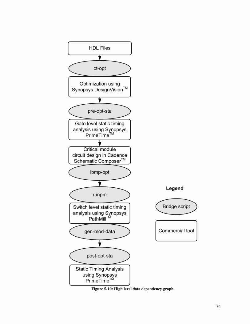
74
HDL Files
ct-opt
Optimization using
Synopsys DesignVisionTM
lbmp-opt
Critical module
circuit design in Cadence
Schematic ComposerTM
Gate level static timing
analysis using Synopsys
PrimeTimeTM
pre-opt-sta
Switch level static timing
analysis using Synopsys
PathMillTM
runpm
gen-mod-data
Static Timing Analysis
using Synopsys
PrimeTimeTM
post-opt-sta
Bridge script
Commercial tool
Legend
Figure 5-10: High level data dependency graph

75
lbmp-opt
Critical module
circuit design in Cadence
Schematic ComposerTM
Platform : UNIX, Perl
Input : Spice netlist
Output : Spice netlist
Text files Cadence Schematic
ComposerTM
MonteCarlo
simulation using
Cadence SpectreTM
Compute delay &
update netlist
Output netlist &
design profile
Figure 5-11: Data dependency in LBMP Optimization Algorithm
5.6 POINT Optimization on ISCAS 74181 – 4bit ALU
This section outlines the implementation of the POINT optimization algorithm on an
ISCAS benchmark circuit 74181, a 4-b ALU. Figure 5-12 shows the module level
representation of ISCAS 74181, with four modules, D module, E module, CLA module,
and Sum module. The hierarchical netlist of the design is input to Synopsys Design
VisionTM
(SDV) for synthesis and optimization. Following the optimization using SDV,
the pre-opt-sta script is invoked to perform process variation-aware pre-optimization
static timing analysis. Figure 5-13 shows the timing report with the worst case path in the
design, with a delay of 0.91 nsec. After considering majority of the critical paths in the
design, the CLA module was found to be critical with a delay of 0.44 nsec. So, CLA
module was chosen for timing optimization.

76
Figure 5-14 shows the gate level schematic of CLA module in the design. Dynamic
logic circuits for the same have been designed as depicted in Fig 5-15 and Fig. 5-16. The
process variation-aware LBMP timing optimization algorithm was implemented on the
CLA module, and the delay was reduced by 52%, uncertainty from process variations by
46% and sensitivity to process variations by 16%.
Following the process variation-aware timing optimization of CLA module, switch-
level STA was performed, and timing models were generated using the gen-mod-data
bridge script. Later, the static CMOS circuits of CLA module are replaced by the timing
models and process variation-aware gate level STA was performed on the overall design.
This optimization has reduced the path delay from 0.91nsec to 0.63nsec, a performance
improvement of 30.7% in delay. This update of the CLA module in dynamic logic has
caused the critical path order to change, and the delay of the new worst-case path is
0.71nsec, which is still a 22% improvement in performance compared to the optimization
results from commercial tools.
Figure 5-12: ISCAS 74181 in static CMOS logic

77
Figure 5-13: Pre-POINT Optimization STA report of ISCAS 74181

78
Figure 5-14: Gate level schematic of CLA module in C74181
Figure 5-15: Transistor level schematic of block-1 in CLA module of ISCAS 74181

79
Figure 5-16: Transistor level schematic of block-2 in CLA module of ISCAS 74181
4
4
4E Module
D Module CLA Module
A
B
S
C’n
M
E
D
A=B
F
Y
X
C’n+4
4
4
4
44
4
4
4
Sum Module
Dynamic
Logic
Static
Logic
Figure 5-17: Updated ISCAS 74181 with Mixed-Static-Dynamic implementation
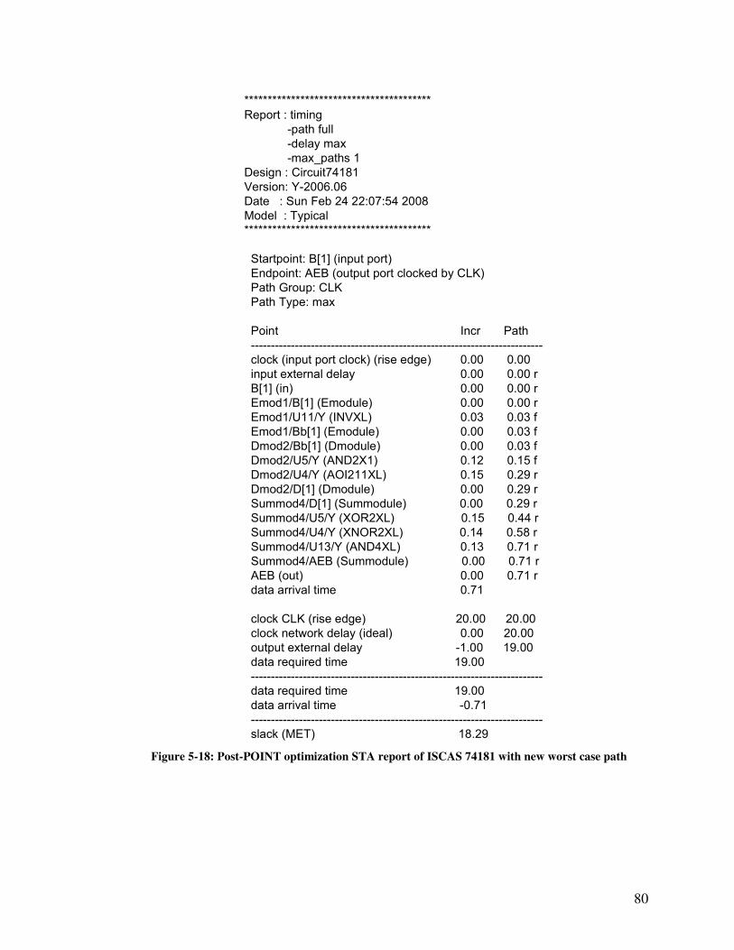
80
****************************************
Report : timing
-path full
-delay max
-max_paths 1
Design : Circuit74181
Version: Y-2006.06
Date : Sun Feb 24 22:07:54 2008
Model : Typical
****************************************
Startpoint: B[1] (input port)
Endpoint: AEB (output port clocked by CLK)
Path Group: CLK
Path Type: max
Point Incr Path
-------------------------------------------------------------------------
clock (input port clock) (rise edge) 0.00 0.00
input external delay 0.00 0.00 r
B[1] (in) 0.00 0.00 r
Emod1/B[1] (Emodule) 0.00 0.00 r
Emod1/U11/Y (INVXL) 0.03 0.03 f
Emod1/Bb[1] (Emodule) 0.00 0.03 f
Dmod2/Bb[1] (Dmodule) 0.00 0.03 f
Dmod2/U5/Y (AND2X1) 0.12 0.15 f
Dmod2/U4/Y (AOI211XL) 0.15 0.29 r
Dmod2/D[1] (Dmodule) 0.00 0.29 r
Summod4/D[1] (Summodule) 0.00 0.29 r
Summod4/U5/Y (XOR2XL) 0.15 0.44 r
Summod4/U4/Y (XNOR2XL) 0.14 0.58 r
Summod4/U13/Y (AND4XL) 0.13 0.71 r
Summod4/AEB (Summodule) 0.00 0.71 r
AEB (out) 0.00 0.71 r
data arrival time 0.71
clock CLK (rise edge) 20.00 20.00
clock network delay (ideal) 0.00 20.00
output external delay -1.00 19.00
data required time 19.00
-------------------------------------------------------------------------
data required time 19.00
data arrival time -0.71
-------------------------------------------------------------------------
slack (MET) 18.29
Figure 5-18: Post-POINT optimization STA report of ISCAS 74181 with new worst case path

81
****************************************
Report : timing
-path full
-delay max
-max_paths 1
Design : Circuit74181
Version: Y-2006.06
Date : Thu Apr 17 13:34:14 2008
****************************************
Startpoint: B[0] (input port)
Endpoint: AEB (output port clocked by CLK)
Path Group: CLK
Path Type: max
Point Incr Path
-----------------------------------------------------------------------------------
clock (input port clock) (rise edge) 0.00 0.00
input external delay 0.00 0.00 f
B[0] (in) 0.00 0.00 f
Emod1/B[0] (Emodule) 0.00 0.00 f
Emod1/U5/Y (INVXL) 0.07 0.07 r
Emod1/Bb[0] (Emodule) 0.00 0.07 r
Dmod2/Bb[0] (Dmodule) 0.00 0.07 r
Dmod2/U7/Y (AND2X1) 0.10 0.16 r
Dmod2/U6/Y (AOI211XL) 0.04 0.21 f
Dmod2/D[0] (Dmodule) 0.00 0.21 f
CLAmod3/Pb[0] (CLAmodule) 0.00 0.21 f
CLAmod3/core/C[3] (CLAmodule_core) 0.21 0.42 r
CLAmod3/C[3] (CLAmodule) 0.00 0.42 r
Summod4/C[3] (Summodule) <- 0.00 0.42 r
Summod4/U12/Y (NOR2XL) 0.05 0.46 f
Summod4/U10/Y (XNOR2XL) 0.08 0.54 r
Summod4/U13/Y (AND4XL) 0.13 0.67 r
Summod4/AEB (Summodule) 0.00 0.67 r
AEB (out) 0.00 0.67 r
data arrival time 0.67
clock CLK (rise edge) 20.00 20.00
clock network delay (ideal) 0.00 20.00
output external delay -1.00 19.00
data required time 19.00
-----------------------------------------------------------------------------------
data required time 19.00
data arrival time -0.67
-----------------------------------------------------------------------------------
slack (MET) 18.33
Figure 5-19: Post-POINT Optimization STA report of ISCAS 74181 with old worst case path

82
5.7 POINT Optimization on ISCAS benchmark circuits
Following the implementation of the POINT optimization flow on ISCAS 74181, it is
further validated through implementation on other ISCAS benchmark circuits. One of the
test cases was the ISCAS C7552, a 34-b adder and magnitude comparator as shown in
Fig. 5-20. Synthesis and optimization was performed using Synopsys Design VisionTM
and pre-optimization STA was performed using Synopsys PrimeTimeTM
. The worst-case
path was found to have a delay of 3.01 nsec. From the STA report, the critical module in
terms of delay was found to be M5/UM5_1/CC_1/CGC34_0 as shown in Fig 5-21 with a
delay of 960 psec. As it is not beneficial to replace the entire block with dynamic logic to
improve timing, only the sub-modules that appear in majority of the critical paths were
chosen; M5/UM5_1/CC_1/CGC34_0/CGC20 with a delay of 559 psec, and
M5/UM5_1/CC_1/CGC34_0/CGC17 with a delay of 390 psec. In addition to these two
sub-modules, other sub-modules chosen based on the STA report are
M5/UM5_1/CC_0/GLC34_0/GLC9_0/GLC5_1 with a delay of 720 psec and
M5/UM5_1/CC_1/CGC34_4 with a delay of 660 psec. Gate level schematic of
M5/UM5_1/CC_1/CGC34_4 is shown in Fig 5-22.
Once the critical sub-modules are found, custom dynamic circuits were designed and
process variation-aware timing optimization was performed using the LBMP algorithm.
Through implementation of the LBMP algorithm, delays of
M5/UM5_1/CC_1/CGC34_0/CGC20, M5/UM5_1/CC_1/CGC34_0/CGC17,
M5/UM5_1/CC_0/GLC34_0/GLC9_0/GLC5_1, and M5/UM5_1/CC_1/CGC34_4 were
reduced by 46%, 39%, 52% and 65% respectively.

83
Later, switch level STA was performed on these sub-modules and timing models
were generated using the gen-mod-data bridge script. The static CMOS circuits of these
sub-modules in the top module are replaced by the timing models generated and post-
optimization STA was performed using Synopsys PrimeTimeTM
. The pre-POINT
optimization STA report is shown in Fig 5-23. After POINT optimization, the benchmark
circuit was tested at various corners of operation and its uncertainty from process
variations was found to have reduced by 22.02%.
Similarly, the process variation-aware POINT optimization flow was implemented on
ISCAS C2670 (Fig 5-25), ISCAS C3540 (Fig 5-26), ISCAS C5315 (Fig 5-27) and results
obtained are presented in Table 5-4. Figure 5-28 shows the delays of these benchmark
circuits before and after the process variation-aware POINT optimization, with an
average delay improvement of 16.94% over state-of-the-art commercial optimization
tools. Similarly, Fig. 5-29 shows the uncertainty from process variations of these
benchmark circuits before and after POINT optimization, with an average improvement
of 13.14% over state-of-the-art commercial optimization tools.
Table 5-4: POINT Optimization Results on ISCAS Benchmark circuits
Pre-Optimization (psec) Post-Optimization (psec) Improvement Design
Delay Uncertainty Delay Uncertainty Delay Uncertainty
74181 996.67 880 753.33 750 24.41 14.77
C2670 1293.34 850 1106.66 810 14.43 4.7
C3540 3500.00 3220 3030.00 2590 13.42 19.56
C5315 2253.34 1990 1903.33 1720 15.53 13.56
C7552 3001.02 2651 2371.20 2067 20.59 22.02
Average 16.94 13.14

84
Figure 5-20: Top level schematic of ISCAS C7552, 34-b adder and magnitude comparator

85
Figure 5-21: Schematic of M5/UM5_1/CC_1/CGC34_0 in ISCAS C7552
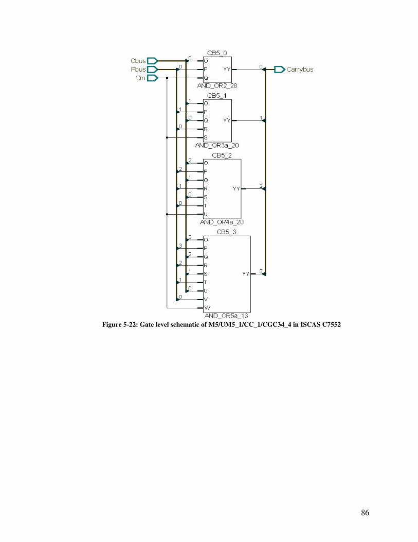
86
Figure 5-22: Gate level schematic of M5/UM5_1/CC_1/CGC34_4 in ISCAS C7552

87
Figure 5-23: Pre-POINT Optimization STA report of ISCAS C7552

88
Figure 5-24: Top level schematic of ISCAS C2670
Figure 5-25: Top level schematic of ISCAS C3540

89
Figure 5-26: Top level schematic of ISCAS C5315

90
0
1000
2000
3000
4000
74181 C2670 C3540 C5315 C7552
De
lay
(p
se
c)
Pre-Optimization Post-Optimization
Figure 5-27: Delay reduction in ISCAS benchmarks through POINT optimization flow
0 0.2 0.4 0.6 0.8 1 1.2
74181
C2670
C3540
C5315
C7552
Normalized Uncertainty
Post-Optimization Pre-Optimization
Figure 5-28: Process variation uncertainty reduction in ISCAS benchmarks through POINT
optimization flow

91
5.8 Summary
The limitations in the current timing optimization flow are presented, along with a
method to address the same. A process variation-aware Path Oriented IN Time (POINT)
optimization flow for mixed-static-dynamic is presented. Advantages of the POINT
optimization flow was demonstrated to be: a) its ability to aid as a tape-out rescue method
from timing failure; b) adaptability to fit into the diverse optimization approaches
followed by others; and c) ability to account for process variations in the timing
optimization flow.
In addition, the significance and complexity in timing optimization for mixed-static-
dynamic implementation was shown through implementation on a 64-b adder and several
ISCAS benchmark circuits.

92
6 Conclusions
6.1 Summary
The significance and complexity in timing optimization of dynamic and mixed-static-
dynamic CMOS circuits from increased number of channel-connected transistors and
increased process variations is presented. A solution addressing these issues is presented
through a process variation-aware Load Balance of Multiple Paths (LBMP) transistor
sizing algorithm for dynamic CMOS circuits.
The process-variation aware LBMP algorithm uses existing CAD tools for circuit
simulation and performance estimation, given a netlist and technology information. In
addition to improving the performance of a design, it was shown that the process
variation-aware LBMP algorithm also reduces the uncertainty and sensitivity to process
variations at various operating temperatures. Validated through implementation on
several circuits, the process variation-aware LBMP algorithm has demonstrated an
average delay reduction by 48%, uncertainty and sensitivity from process variation
reduction by 57% and 14% respectively.
A process variation-aware Path Oriented IN Time (POINT) optimization flow for
optimization of mixed-static-dynamic logic is presented. The process variation-aware
POINT optimization flow uses existing commercial tools for synthesis, optimization and
Static Timing Analysis (STA). The STA report is used to find the timing critical modules

93
in the design, and process variation-aware LBMP algorithm is used to design dynamic
circuits with minimal delay and uncertainty from process variations. The process
variation-aware LBMP algorithm along with a collection of bridge scripts are used in the
POINT optimization flow.
Some of the advantages of the POINT optimization flow are its ability to act as a
tape-out rescue method from timing failure; ability to adapt to the diverse approaches
followed by the industry in timing optimization; and accounting for process variations
during the timing optimization flow. Validated through implementation on several
circuits, the process variation-aware POINT optimization flow has demonstrated an
average delay reduction by 17%, uncertainty from process variation reduction by 13%
over state-of-the-art commercial optimization tools.
6.2 Research Contributions
The advent of very deep sub-micron technology has been exciting and challenging at
the same time for circuit design engineers. This technology has allowed for placement of
billions of transistors on a single chip to develop high performance ICs in a broad
spectrum of areas such as microprocessors, digital signal processing, communication and
networking. In addition, the continuous scaling of CMOS technology towards 32 nm
channel length caused a significant increase in the number and magnitude of relevant
sources of environmental and semiconductor process variations. Failure to account for
these process variations result in performance degradation by one generation, and might
even result in design failure.

94
Addressing these challenges, research performed in this dissertation is categorized
into three significant contributions.
• Design and implementation of high performance 64-b adders [56], [57].
• A circuit level process variation-aware Load Balance of Multiple Paths (LBMP)
transistor sizing algorithm for dynamic logic circuits [53], [54], [55].
• An architecture level process variation-aware Path Oriented IN Time (POINT)
optimization flow for mixed-static-dynamic logic [52].
6.3 Future Research
Substantial work was performed in this research of timing optimization while
accounting for process variations. However, delving into this area of process variations
has shown us that there is even more work yet to be done to understand the implications
of process variations. This research has presented us with several avenues to pursue in the
near future.
The process variation-aware LBMP algorithm was presented for transistor sizing in
dynamic logic. This algorithm can be extended to perform timing optimization in other
circuit styles such as static CMOS, CPL, DVSL, DCVSL etc., During our research, we
have not found any detailed research and statistical analysis performed in the process
variation-aware timing optimization in analog circuits. This is one other avenue to pursue
in the near future.

95
The work presented in this research is the first to include process variations in the
timing optimization flow for dynamic circuits. With the shrinking device sizes, one
challenge faced by in the industry is increasing yield to increase profitability. One other
extension to our work is accounting for yield in the process variation-aware timing
optimization flow.
Also, there are several extensions possible for the POINT optimization flow.
Currently the bridge scripts interface only with the commercial tools, and require user
intervention to initiate the next step. An update to the optimization flow is circumventing
the necessity for user intervention. One other extension to the POINT optimization flow
is accounting for yield to improve profitability.
Finally, the research performed in this dissertation answers two significant challenges
in the CMOS technology, timing optimization and process variations. These areas are
crucial in the future technologies, and are already gaining significant attention of many
others.

96
Appendix
Appendix-A: Synopsys Design Vision Script for Synthesis and Optimization
####################################################################
# Set the search path for all the model files and symbol libraries #
####################################################################
set search_path . ../*
/nfs/ecsnas1/users/eegrad/kumar/tsmc_013_library/artisan/SAGE/aci/sc-
x/synopsys
set link_path * ../*
/nfs/ecsnas1/users/eegrad/kumar/tsmc_013_library/artisan/SAGE/aci/sc-
x/synopsys/typical.db
#########################################################
# Read, Elaborate and synthesize the design #
#########################################################
read_file -format verilog
/nfs/ecsnas1/users/eegrad/kumar/Synopsys/Design_Vision/tsmc_130nm/Circ
uit2670.v
elaborate Circuit2670 -architecture verilog -library WORK
uniquify
current_design Circuit2670
remove_constraint -all
set_max_delay 10 -to [all_outputs]
compile -map_effort high -verify -verify_effort high
#######################################################################
#Write the updated design in Verilog format for Static Timing Analysis#
#######################################################################
write -format verilog -hierarchy -output Circuit2670 + "_DC.v"

97
Appendix-B: Synopsys PrimeTime Pre Optimization Static Timing Analysis Script
####################################################################
# Set the search path for all the model files and symbol libraries #
####################################################################
set search_path . ../*
/nfs/ecsnas1/users/eegrad/kumar/tsmc_013_library/artisan/SAGE/aci/sc-
x/synopsys
set link_path * ../*
/nfs/ecsnas1/users/eegrad/kumar/tsmc_013_library/artisan/SAGE/aci/sc-
x/synopsys/typical.db
#########################################################
# Read, link and setup constraints on the design #
#########################################################
read_verilog Circuit3540_DC.v
current_design TopLevel3540
link_design -keep_sub_designs TopLevel3540
check_timing
report_timing
create_clock -period 20 -name CLOCK
check_timing
set_output_delay 1.0 -clock CLOCK [all_outputs]
####################################
# Report timing information #
####################################
report_timing
report_timing -max_paths 10 > Circuit3540_pre_sta_timing.txt
###########################
# Exit the Program #
###########################
exit

98
Appendix-C: Perl script for Process Variation-Aware Load Balance of Multiple Paths Algorithm
#This program is for ISCAS Benchmark Circuit - C7552 GLC5_1
$iteration=1;
$max_iter=20;
$max_size = 1500;
$a=0;
$ratio=1.1;
#System commands to remove and create input files
system("rm perl*/delay_array_file_$max_size.txt");
system("rm perl*/tr_decrease_array_file_$max_size.txt");
system("rm perl*/tr_size_array_file_$max_size.txt");
system("rm perl*/total_area_profile_file_$max_size.txt");
system("rm perl*/output_profile_iteration_file_$max_size.txt");
system("rm perl_output/path_increase_file_$max_size.txt");
system("rm perl_output/path_delay_variance_profile_$max_size.txt");
#system("rm ../monteCarlo/m*");
system("rm input_*.scs");
#Transistors in each path
@tr_path = (
[0,0], #Path-0 has to be here
# Define the paths in the above manner
);
#First order connections for each transistor
@tr_first_connec = (
[1,2,4,6,8],
# List the first order connections for every transistor in the
above manner
);
#Creating the initial netlist
#Assign transistor Initial ratio to an array
open tr_initial_ratio_data, "tr_profiles/tr_initial_ratio" || die
"Error: Could not open tr weights data file\n";
@info_ratio =<tr_initial_ratio_data>;
for($i=0;$i<=$#info_ratio;$i++)
$aabb=$info_ratio[$i];
($aa,$bb)=split(/\n/,$aabb);
$tr_initial_ratio[$i]=$aa;
close tr_initial_ratio_data;
for($i=0;$i<=$#tr_initial_ratio;$i++)
$tr_size[0][$i]=int(160*($ratio**$tr_initial_ratio[$i]));
#Snippet to write the Initial netlist

99
#This snippet takes any netlist, and writes a new netlist with
incremental
#transistor sizes based on a ratio specified at the start of this
program
$infile = "input_0.scs_0";
open (infile) or die("Could not open file.");
open outfile, "+>input_0.scs" or die "Error: Could not write to
file\n";
foreach $line (<infile>)
if ($line=~/(M\d).*(nch)/)
#Reads the information from the original netlist and splits the data
$line =~ /M(.*)(\s\()(.*)(w=)(.*)(n|u)(\sl=)(.*)$/;
#Writes information to the new netlist
#Writes information to the new netlist
if($1 == 9)
$tr_size_1=3000;
elsif($1 == 99)
$tr_size_1=640;
else
$tr_size_1=$tr_size[0][$1];
$line= M.$1.$2.$3.$4.$tr_size_1.n.$7.$8."\n";
syswrite outfile, $line;
close (infile);
close (outfile);
#End creating initial netlist
#Snippet to compute the total area occupied by nmos transistors
$total_area[$iteration-1]=0;
for($i=0;$i<=$#tr_initial_ratio;$i++)
$total_area[$iteration-1]=$total_area[$iteration-
1]+$tr_initial_size[$i];
#Write the initial transistor sizes to a file
open tr_size_array, ">> perl_output/tr_size_array_file_$max_size.txt"
or die "Error: Could not write to file\n";
for($j=0;$j<=$#tr_initial_ratio;$j++)
syswrite tr_size_array, $tr_size[0][$j];
syswrite tr_size_array, " ", 2;
syswrite tr_size_array, "\n";
close tr_size_array;
#Start for loop with iterations of the complete program
for($iteration=1;$iteration<=$max_iter;$iteration++)
$ttt=$iteration-1;
#Run Spectre to find delay data

100
system("source
/nfs/ecsnas1/users/eegrad/kumar/Cadence/Virtuoso/TSMC_130nm/set_icfb");
system("spectre -env artist5.1.0 +escchars +log ../psf/spectre.out -
format sst2 -raw ../psf +lqtimeout 900 input_$ttt.scs");
system("cp ../m*/mcdata monteCarloresults/mcdata_$ttt");
open delay_data, "../monteCarlo/mcdata" || die "Error: Could not open
raw delay data file\n";
@info_1 =<delay_data>;
for ($i=0;$i<=$#info_1;$i++)
@value=split(/\s+/,$info_1[$i]);
for ($j=0;$j<=$#value;$j++)
$aabb=$value[$j];
($aa,$bb)=split(/e-/,$aabb);
for($aaa=1;$aaa<=$bb;$aaa++)
$aa= $aa/10;
$raw_delay[$i+1][$j+1]=$aa;
$paths=$#value;
#print "The number of paths in the design is $paths\n";
$runs=$#info_1+1;
close delay_data;
open tr_repeat_data, "tr_profiles/tr_repeats" || die "Error: Could not
open tr repeats data file\n";
@info_repeats =<tr_repeat_data>;
for($i=0;$i<=$#info_repeats;$i++)
$aabb=$info_repeats[$i];
($aa,$bb)=split(/\n/,$aabb);
$tr_repeats[$i]=$aa;
close tr_repeat_data;
open tr_weight_data, "tr_profiles/tr_weights" || die "Error: Could not
open tr weights data file\n";
@info_weights =<tr_weight_data>;
for($i=0;$i<=$#info_weights;$i++)
$aabb=$info_weights[$i];
($aa,$bb)=split(/\n/,$aabb);
$tr_weights[$i]=$aa;
close tr_weights_data;
open tr_path_count_data, "tr_profiles/tr_path_count" || die "Error:
Could not open tr path count data file\n";
@info_path_count =<tr_path_count_data>;
for($i=0;$i<=$#info_path_count;$i++)
$aabb=$info_path_count[$i];
($aa,$bb)=split(/\n/,$aabb);
$tr_path_count[$i]=$aa;

101
close tr_path_count_data;
#Snippet to compute average and standard deviation from the raw delays
for($p=1;$p<=$paths;$p++)
for($i=1;$i<=$#raw_delay;$i++)
$b[$i]=$raw_delay[$i][$p];
#Statements to compute average and stddev
$raw_delay[$runs+2][$p]=&average; #call subroutine average
#print "Average delay of path-$p is ", $raw_delay[$runs+2][$p],
"\n";
$raw_delay[$runs+3][$p]=&stddev; #call subroutine standard
deviation
#print "Std Dev of path-$p is ", $raw_delay[$runs+3][$p], "\n";
$raw_delay[$runs+4][$p]=$raw_delay[$runs+2][$p]-
$raw_delay[$runs+3][$p];
#print "Min Delay for path-$p is ", $raw_delay[$runs+4][$p],
"\n";
$raw_delay[$runs+5][$p]=$raw_delay[$runs+2][$p]+$raw_delay[$runs+
3][$p];
#print "Max Delay for path-$p is ", $raw_delay[$runs+5][$p],
"\n";
#print "\n";
$delay_array[$p][0]=$p; #Writes the path number
$delay_array[$p][1] = $raw_delay[$runs+5][$p]; #Writes the Delay "Avg
+Stddev" is considered now for path ranking
$delay_array[$p][2]=$iteration; #Writes the iteration number
#Column-3 is used to write the rank based on average delay
$delay_array[$p][4]=$raw_delay[$runs+3][$p]; #Writes the path delay
'stdev'
$delay_array[$p][5]=100*($raw_delay[$runs+3][$p])/($raw_delay[$runs+2][
$p]);
#End of snippet to compute average and standard deviation
#Snippet to compute the average power consumption
for($i=1;$i<=$#raw_delay;$i++)
$b[$i]=$raw_delay[$i][$paths+1];
$average_power[$iteration]= &average;
#Snippet to see if the worst case delay has increased in the current
iteration
if($iteration > 2)
if($max_delay_rank_1[$iteration] gt $max_delay_rank_1[$iteration-1])
for($j=0; $j<=$#tr_repeats;$j++)
$tr_size[$iteration][$j]=$tr_size[$iteration-1][$j];

102
for($i=0;$i<=$#tr_to_decrease;$i++)
$transistor=$tr_to_decrease[$i];
$tr_size[$iteration][$transistor]=$tr_size[$iteration-
2][$transistor];
$max_iter++; #Increase the number of iterations by one.
else
#Implement the loop to increase and decrease the transistor sizes
&sizing; #Call Subroutine sizing
#End loop for iteration > 2
else #If iteration is < 2
&sizing; #Call Subroutine sizing
#End loop if iteration < 2
#print the delays array
#for ($i=1;$i<=$paths;$i++)
# print "Path-$i delay is ", $delay_array[$i][1]," iteration is ",
$delay_array[$i][2]," rank is ", $delay_array[$i][3],"\n";
#Write the delay array to a file
open delay_array, ">> perl_output/delay_array_file_$max_size.txt" or
die "Error: Could not write to file\n";
for ($i=1;$i<=$#delay_array;$i++)
for($j=0;$j<=5;$j++)
syswrite delay_array, $delay_array[$i][$j];
syswrite delay_array, " ", 2;
syswrite delay_array, "\n";
close delay_array;
#Writes the Min and Max delays of each path in the iteration to a file
open path_delay_variance_profile, ">>
perl_output/path_delay_variance_profile_file_$max_size.txt" or die
"Error: Could not write to a file \n";
for( $i=1; $i<=$paths; $i++)
syswrite path_delay_variance_profile, $iteration, 10;
syswrite path_delay_variance_profile, " ", 2;
syswrite path_delay_variance_profile, $i, 10;
syswrite path_delay_variance_profile, " ", 2;
syswrite path_delay_variance_profile, $raw_delay[$runs+4][$i],
25; #Min delay for path-i

103
syswrite path_delay_variance_profile, " ", 2;
syswrite path_delay_variance_profile, $raw_delay[$runs+5][$i],
25; #Max delay for path-i
syswrite path_delay_variance_profile, "\n";
close path_delay_variance_profile;
#Write the transistor sizes to a file
open tr_size_array, ">> perl_output/tr_size_array_file_$max_size.txt"
or die "Error: Could not write to file\n";
for($j=0;$j<=$#tr_repeats;$j++)
syswrite tr_size_array, $tr_size[$iteration][$j];
syswrite tr_size_array, " ", 2;
syswrite tr_size_array, "\n";
close tr_size_array;
#writes the list of paths to increase sizes to a file
open path_increase_size,
">>perl_output/path_increase_file_$max_size.txt" or die "Error: Could
not write to file\n";
syswrite path_increase_size, $iteration;
syswrite path_increase_size, " ", 2;
for($i=1;$i<=$#path_to_increase;$i++)
syswrite path_increase_size, $path_to_increase[$i];
syswrite path_increase_size, " ", 2;
syswrite path_increase_size, "\n";
close path_increase_file;
#Write the list of transistors to decrease array to a file
open tr_decrease_array, ">>
perl_output/tr_decrease_array_file_$max_size.txt" or die "Error: Could
not write to file\n";
syswrite tr_decrease_array, $iteration;
syswrite tr_decrease_array, " ", 2;
for($j=0;$j<=$#tr_to_decrease;$j++)
syswrite tr_decrease_array, $tr_to_decrease[$j];
syswrite tr_decrease_array, " ", 4;
syswrite tr_decrease_array, "\n";
close tr_decrease_array;
#Snippet to compute the total area occupied by nmos transistors
$total_area[$iteration]=0;

104
for($i=0;$i<=$#tr_weights;$i++)
$total_area[$iteration]=$total_area[$iteration]+$tr_size[$iteration][
$i];
#Snippet to write the new netlist
$infile = "input_$ttt.scs";
open (infile) or die("Could not open file.");
open outfile, "+>input_$iteration.scs" or die "Error: Could not write
to file\n";
foreach $line (<infile>)
if ($line=~/(M\d).*(nch)/)
#Reads the information from the original netlist and splits the data
$line =~ /M(.*)(\s\()(.*)(w=)(.*)(n|u)(\sl=)(.*)$/;
#Writes information to the new netlist
#Writes information to the new netlist
if($1 == 9)
$tr_size_1=3000;
elsif($1 == 99)
$tr_size_1=640;
else
$tr_size_1=$tr_size[$iteration][$1];
$line= M.$1.$2.$3.$4.$tr_size_1.n.$7.$8."\n";
syswrite outfile, $line;
close (infile);
close (outfile);
#End for loop for runs of the complete program
#writes the output profiles of each iteration to a file
open output_profile_iteration, ">>
perl_output/output_profile_iteration_file_$max_size.txt" or die "Error:
Could not write to a file \n";
for ($i=1; $i<=$max_iter; $i++)
$iteration=$i;
syswrite output_profile_iteration, $iteration;
syswrite output_profile_iteration, " ", 2;
syswrite output_profile_iteration,
$max_path_rank_1[$iteration];
syswrite output_profile_iteration, " ", 2;
syswrite output_profile_iteration, $min_delay_iter[$iteration];
syswrite output_profile_iteration, " ", 2;
syswrite output_profile_iteration, $max_delay_iter[$iteration];
syswrite output_profile_iteration, " ", 2;
syswrite output_profile_iteration,
$path_rank_1_average[$iteration];
syswrite output_profile_iteration, " ", 2;

105
syswrite output_profile_iteration,
$path_rank_1_stddev[$iteration];
syswrite output_profile_iteration, " ", 2;
syswrite output_profile_iteration,
$path_rank_1_avg_stddev[$iteration];
syswrite output_profile_iteration, " ", 2;
syswrite output_profile_iteration,
(100*$path_rank_1_stddev[$iteration])/$path_rank_1_average[$iteration];
syswrite output_profile_iteration, " ", 2;
syswrite output_profile_iteration, $average_power[$iteration];
syswrite output_profile_iteration, "\n";
close output_profile_iteration;
#writes the Total Area in each iteration to a file
open total_area_profile, ">>
perl_output/total_area_profile_file_$max_size.txt" or die "Error: Could
not write to a file \n";
for ($i=0; $i<=$max_iter; $i++)
syswrite total_area_profile, $i; #Writes the iteration number
syswrite total_area_profile, " ", 2;
syswrite total_area_profile, $total_area[$i];
syswrite total_area_profile, "\n";
close total_area_profile;
#Subroutines
#Subroutine to find the average
sub average
$avg_total=0;
$size_array_1=$runs;
for($i=1; $i<=$runs; $i++)
$avg_total = $avg_total + $b[$i];
$avg=($avg_total/$size_array_1);
#Start subroutine for standard deviation
sub stddev
$std_total=0;
$diff_sq=0;
$sq_total=0;
$size_array_2=$runs;
for($i=1; $i<=$runs; $i++)
$std_total = $std_total + $b[$i];
$std_avg=($std_total/$size_array_2);

106
#Finding the sum of squares for (xi-average) for all elements in the
array
for ($j=1; $j<=$size_array_2;$j++)
$diff[$j]=$b[$j]-$std_avg;
$diff_sq[$j] = $diff[$j]*$diff[$j];
$sq_total = $sq_total +$diff_sq[$j];
$std_dev = sqrt($sq_total/($runs-1));
#End of subroutine for Standard deviation
sub numerically $b <=> $a #Subroutine to perform numerical sorting
in descending order
#Start subroutine for increasing and decreasing transistor sizes
sub sizing
#Start snippet for numerical sorting and redundancy removal
for ($i=1;$i<=$paths;$i++)
$temp_1[$i]=$delay_array[$i][1];
$temp_2[$i]=$delay_array[$i][1];
#print "$temp_2[$i]\n";
@temp_1= sort numerically @temp_1;
#print "The size of delay_array is:", $#delay_array, "\n";
for ($i=1; $i<=$#temp_1-1;$i++)
for ($l=$i+1;$l<=$#temp_1;$l++)
if($temp_1[$i] == $temp_1[$l])
for ($k=$l;$k<=$#temp_1;$k++)
$temp_1[$k-1]=$temp_1[$k];
pop @temp_1;
$l=$l-1;
#End of snippet to sort and remove redundancy
#Snippet to assign ranks to elements in the main array
for ($i=1;$i<=$paths;$i++)
for ($j=1;$j<=$#temp_1;$j++)
if($temp_2[$i]==$temp_1[$j])
$delay_array[$i][3]=$j;

107
#End ranking snippet
#Find the path with rank of 1
for ($i=1;$i<=$paths;$i++)
if($delay_array[$i][3] eq 1)
$max_path_rank_1[$iteration]=$i;
$path_highest_rank[$iteration] = $i;
#End snippet to find path with rank-1
#Assign delays of path with rank-1 to find min and max delay
$path_rank_iter=$max_path_rank_1[$iteration];
for($i=1; $i<=$runs; $i++)
$b[$i]=$raw_delay[$i][$path_rank_iter];
$max_delay_rank_1[$iteration]=&average+&stddev; #This is to decide
the maximum number of iterations to be performed
#Snippet to compute the minimum delay due to process variations for
path with highest rank
$minm=100;
for ($i=1;$i<=$runs;$i++)
# print "The minimum-1 delay is $minm \n";
if($b[$i] < $minm)
$minm = $b[$i];
# print "The minimum-2 delay is $minm \n";
$min_delay_iter[$iteration]=$minm; #Assign minimum delay to an array
for storage
#End Snippet to compute the min delay in iteration
#Snippet to compute the maximum delay due to process variations for
path with highest rank
$maxm=0;
for ($i=1;$i<=$runs;$i++)
if($b[$i] > $maxm)
$maxm= $b[$i];
# print "The maximum is $maxm \n";
$max_delay_iter[$iteration]=$maxm; #Assign maximum delay to an array
for storage
#End Snippet to compute the max delay in iteration
108
#Compute average and std dev due to process variations for path with
highest rank
$path_rank_1_average[$iteration]=&average;
$path_rank_1_stddev[$iteration]=&stddev;
$path_rank_1_avg_stddev[$iteration]=$path_rank_1_average[$iteration]+$p
ath_rank_1_stddev[$iteration];
#End computation of average and stddev
#total number of paths to change size in design
$to_size= 1+ int($paths/5); #Considering top 20% paths
#print "To size paths till rank of $to_size in the given design\n";
#Compile the list of paths to increase sizes
$#path_to_increase=0;
#print "The number of elements in path_to_increase is
$#path_to_increase\n";
$path_increase = 1;
for($i=1;$i<=$paths;$i++)
if($delay_array[$i][3] <= $to_size)
$path_to_increase[$path_increase]=$i;
$path_increase++;
#print the path numbers of which transistor sizes need to be increased
#for($i=1;$i<=$#path_to_increase;$i++)
# print "Path in which transistor sizes need to be increased is
",$path_to_increase[$i],"\n";
#Snippet to compile list of transistors to increase sizes (set-x)
$temp_3=1;
$temp_4=1;
for($h=1;$h<=$#path_to_increase;$h++)
$current_to_size=$path_to_increase[$temp_3];
#print "Current path is ", $current_to_size,"\n";
for($hh=0;$hh<=$tr_path_count[$current_to_size];$hh++)
$tr_to_increase[$temp_4]=$tr_path[$current_to_size][$hh];
$temp_4++;
$temp_3++;
@tr_to_increase=sort numerically @tr_to_increase;
for ($i=0; $i<=$#tr_to_increase-1;$i++)
for ($l=$i+1;$l<=$#tr_to_increase;$l++)
if($tr_to_increase[$i] == $tr_to_increase[$l])

109
for ($k=$l;$k<=$#tr_to_increase;$k++)
$tr_to_increase[$k]=$tr_to_increase[$k+1];
pop @tr_to_increase;
$l=$l-1;
for($i=0;$i<$#tr_to_increase;$i++)
print "Transistor to increase is ",$tr_to_increase[$i],"\n";
#Snippet to calculate the new transistor sizes that needs to be
increased
for($i=0;$i<=$#tr_repeats;$i++)
$tr_size[$iteration][$i]=$tr_size[$iteration-1][$i];
for($i=0;$i<$#tr_to_increase;$i++)
$transistor = int($tr_to_increase[$i]);
$ina=int($tr_size[$iteration-
1][$transistor]*(1+(($tr_repeats[$transistor]*$tr_weights[$transistor])
/(1+$tr_repeats[$transistor]))));
if($ina >= $max_size)
$tr_size[$iteration][$transistor]= $max_size;
else
$tr_size[$iteration][$transistor]= $ina;
#Snippet to calculate the new transistor sizes that needs to be
decreased
$temp_5=0;
$temp_6=0;
for($g=0;$g<=$#tr_to_increase;$g++)
$current_tr_decrease=$tr_to_increase[$temp_5];
for($gg=0;$gg<=20;$gg++)
$tr_to_decrease[$temp_6]=$tr_first_connec[$current_tr_decrease][$
gg];
$temp_6++;
$temp_5++;
@tr_to_decrease=sort numerically @tr_to_decrease;
for ($i=0; $i<=$#tr_to_decrease-1;$i++)
for ($l=$i+1;$l<=$#tr_to_decrease;$l++)
if($tr_to_decrease[$i] == $tr_to_decrease[$l])
for ($k=$l;$k<=$#tr_to_decrease;$k++)

110
$tr_to_decrease[$k]=$tr_to_decrease[$k+1];
pop @tr_to_decrease;
$l=$l-1;
#Snippet to compile set-z from set-y, and reduce their sizes
accordingly
for($i=0;$i<=$#tr_to_decrease;$i++)
for ($j=0;$j<=$#tr_to_increase;$j++)
if($tr_to_decrease[$i]==$tr_to_increase[$j])
$tr_to_decrease[$i]=0;
@tr_to_decrease=sort numerically @tr_to_decrease;
for ($i=0; $i<=$#tr_to_decrease-1;$i++)
for ($l=$i+1;$l<=$#tr_to_decrease;$l++)
if($tr_to_decrease[$i] == $tr_to_decrease[$l])
for ($k=$l;$k<=$#tr_to_decrease;$k++)
$tr_to_decrease[$k]=$tr_to_decrease[$k+1];
pop @tr_to_decrease;
$l=$l-1;
for($i=0;$i<$#tr_to_decrease;$i++)
$transistor = int($tr_to_decrease[$i]);
$ava=int($tr_size[$iteration-1][$transistor]*(1-
(($tr_repeats[$transistor]*$tr_weights[$transistor])/(1+$tr_repeats[$tr
ansistor]))));
if($ava <= 160)
$tr_size[$iteration][$transistor]= 160;
#print "tr_size[$iteration][$transistor]=
$tr_size[$iteration][$transistor]\n";
else
$tr_size[$iteration][$transistor]= $ava;
#print "tr_size[$iteration][$transistor]=
$tr_size[$iteration][$transistor]\n";
#Snippet to compute whether to decrease the size of transistors or not
if($iteration ge 2)

111
for($i=0;$i<=$#tr_repeats;$i++)
if(($tr_size[$iteration-2][$i] lt $tr_size[$iteration-1][$i]) &&
($tr_size[$iteration-1][$i] gt $tr_size[$iteration][$i]))
$tr_size[$iteration][$i]= (($tr_size[$iteration-
1][$i]+$tr_size[$iteration][$i])/2) ;
#End loop of deciding whether to decrease sizes or revert them back to
previous sizes
#end subroutine sizing
112
Appendix-D: Perl Script to perform LBMP Algorithm at multiple temperatures #Filename: lbmp_multiple_temp.perl
$temperature[0] = 27;
$temperature[1] = 50;
$temperature[2] = 75;
$temperature[3] = 100;
$temperature[4] = 120;
$module = "C3540.CC5.";
system("source
/nfs/ecsnas1/users/eegrad/kumar/Cadence/Virtuoso/TSMC_130nm/set_icfb");
system ("rm -r temp*");
for($i=0;$i<=$#temperature;$i++)
$infile = "input_0.scs_00";
open (infile) or die("Could not open file.");
open outfile, "+>input_0.scs_0" or die "Error: Could not write to
file\n";
foreach $line (<infile>)
if ($line =~ /(.*)(temp=27)(.*)/)
$line =~ /(simulator)(.*)(temp=)(\d+)(.*)/;
$line = $1.$2.$3.$temperature[$i].$5."\n";
syswrite outfile, $line;
close (infile);
close (outfile);
#Perform LBMP Algorithm for Temperature = $temperature[$i]
system ("perl mcdata_input_new_tr_sizes_output.perl");
#Snippet to copy all the files in this temperature iteration
system ("mkdir temp_$temperature[$i]
mkdir temp_$temperature[$i]/netlists
mkdir temp_$temperature[$i]/perl_output
mkdir temp_$temperature[$i]/tr_profiles
mkdir temp_$temperature[$i]/monteCarloresults
cp input*.scs temp_$temperature[$i]/netlists/.
cp -r perl_output/. temp_$temperature[$i]/perl_output/.
cp -r tr_profiles/. temp_$temperature[$i]/tr_profiles/.
cp -r monteCarloresults/. temp_$temperature[$i]/monteCarloresults/.
tar -cvf $module$temperature[$i]_temp.tar temp_$temperature[$i]");
system ("rm -r temp*");
system ("rm -r *ahdlcmi");
system ("cp input_0.scs_00 input_0.scs_0");

113
Appendix-E: Perl Script to update transistor sizes in hspice netlist
$module = "74181_ALU_CORE_C0-3_Y";
$spectre_netlist = "input_20.scs";
$initial_hspice_netlist = "hspiceFinal";
#Read spectre netlist for transistor sizes
$infile = "$spectre_netlist";
open (infile) or die("Could not open file.");
foreach $line (<infile>)
if ($line=~/(M\d).*(nch)/)
#Reads the information from the original netlist and splits the
data
$line =~ /M(.*)(\s\()(.*)(w=)(.*)(n|u)(\sl=)(.*)$/;
$tr_size[$1]=$5;
close (infile);
for($i=0;$i<=$#tr_size;$i++)
print "Size of transistor $i is $tr_size[$i]\n";
#Update hspice netlist with transistor sizes
$infile = "$initial_hspice_netlist";
open (infile) or die("Could not open file.");
open outfile, "+>$module.spi" or die "Error: Could not write to
file\n";
foreach $line (<infile>)
if ($line=~/(M\d).*(VSS\sNCH)/)
#Reads the information from the original netlist and splits the data
$line =~ /M(.*)(\s)(.*)(W=)(.*)(E-9)(\sAD=)(.*)$/;
#Writes information to the new netlist
$line= M.$1.$2.$3.$4.$tr_size[$1].$6.$7.$8."\n";
syswrite outfile, $line;
close (infile);
close (outfile);

114
Appendix-F: PathMill Script to perform switch level Static Timing Analysis
;Set to PathMill to be case insensitive
case L
;Set Input and Source Nodes
input_node P3 P2 P1 P0 G3 G2 G1 G0 CN
source_node P3 P2 P1 P0 G3 G2 G1 G0 CN
;Set Output Nodes
sink_node Y C3 C2 C1 C0
;Define the Clock signal
clock_node CLK rise_delay=0.05 fall_delay=0.05 slope=0.01 period=0.5
;Set Supply Voltages
set_vdd vdd
set_voltage vdd 1.2
set_gnd vss
set_voltage vss 0.0
dont_stop_at_inputs
;Trade-off between speed and accuracy
spd 0.1
;Setting Transistor Direction
default_direction s2d
;Setting Domino Gates
;domino_gate -type n -latch_type none -evaluate_nodes
domino_gate -type n -latch_type none -evaluate_nodes net158 -
precharge_clock_devices m17 -evaluate_clock_devices m15 \
-evaluate_data_devices m0
domino_gate -type n -latch_type none -evaluate_nodes net142 -
precharge_clock_devices m18 -evaluate_clock_devices m15 \
-evaluate_data_devices m1 m2 m3 m4
domino_gate -type n -latch_type none -evaluate_nodes net134 -
precharge_clock_devices m19 -evaluate_clock_devices m15 \
-evaluate_data_devices m1 m2 m3 m4 m5 m6
domino_gate -type n -latch_type none -evaluate_nodes net130 -
precharge_clock_devices m20 -evaluate_clock_devices m15 \
-evaluate_data_devices m1 m2 m3 m4 m5 m6 m7
domino_gate -type n -latch_type none -evaluate_nodes net102 -
precharge_clock_devices m21 -evaluate_clock_devices m16 \
-evaluate_data_devices m8 m9 m10 m11 m12 m13 m14
;Report in Logfile
;The below command prints the transistors whose directions are not set
print_unset_transistors

115
log_on warn_false_path mux warn_delay_calculation
;Report in *.out file
report_paths critical max min 40

116
Appendix-G: Perl Script to create Model and Data Files
# This script reads the setup and hold constraints data from PathMill
report
# and creates the Model and data files for generate STAMP models
$time=localtime(time());
$design = "74181";
$module = "CLAmodule";
$module_inputs = "inputs";
$module_outputs = "outputs";
$setup_cons_file = "Setup_constraints_sample.txt";
$hold_cons_file = "Hold_constraints_sample.txt";
$model_file = "$module.mod";
$data_file = "$module.data";
$capacitance = 0.001; #picofarads
$transition_max = 1.00;
#Snippet to read input and output port data from files
open module_inputs, "$module_inputs.txt" || die "Error: Could not open
Input Port data file\n";
@info_input_port =<module_inputs>;
for($i=0;$i<=$#info_input_port;$i++)
$aabb=$info_input_port[$i];
($aa,$bb)=split(/\n/,$aabb);
$module_input_port[$i]=$aa;
close module_inputs;
open module_outputs, "$module_outputs.txt" || die "Error: Could not
open Output Port data file\n";
@info_output_port =<module_outputs>;
for($i=0;$i<=$#info_output_port;$i++)
$aabb=$info_output_port[$i];
($aa,$bb)=split(/\n/,$aabb);
$module_output_port[$i]=$aa;
close module_outputs;
#Snippet to read the setup constraints data from Pathmill
$infile = $setup_cons_file;
open (infile) or die("Could not open file.");
$i=0;
foreach $line (<infile>)
#Reads the information from the original netlist and splits the
data
# $line =~
/(\d+)(\s+)(\d+)(.\d+)(\s+)(\d+)(.\d+)(\s+)(\d)(\s+)(([A-
Z]+)|(\w+))(\s\()(R|F)(\)\s+)(\w+)(\s\()(R|F)(\).*)$/;

117
$line =~
m/(\d+)(\s+)(\d+)(.\d+)(\s+)(\d+)(.\d+)(\s+)(\d)(\s+)(.*)(\s\()(R|F)(\)
\s+)(.*)(\s\()(R|F)(\).*)$/;
$setup_delay[$i]=$3.$4;
$setup_from_pin[$i]=$11;
$setup_from_edge[$i]=$13;
$setup_to_pin[$i]=$15;
$setup_to_edge[$i]=$17;
$i++;
close (infile);
$no_setup_arcs=$i-1;
#Snippet to replace "R" with "RISE" and "F" with "FALL" in all the
edges
for($i=0;$i<=$#setup_from_edge;$i++)
$temp_edge= ord $setup_from_edge[$i];
if($temp_edge == 70) #70 is the ASCII code for "F"
$setup_from_edge[$i]="FALL";
elsif ($temp_edge == 82) #82 is the ASCII code for "R"
$setup_from_edge[$i]= "RISE";
for($i=0;$i<=$#setup_to_edge;$i++)
$temp_edge= ord $setup_to_edge[$i];
if($temp_edge == 82)
$setup_to_edge[$i]="FALL";
elsif ($temp_edge == 70)
$setup_to_edge[$i]= "RISE";
#for ($j=0; $j<=$#setup_delay;$j++)
# print "The Setup constraint is
$setup_delay[$j],$setup_from_pin[$j],$setup_from_edge[$j],$setup_to_pin
[$j],$setup_to_edge[$j] \n";
###########################################
#Snippet to write the model file
open outfile, "+>$module.mod" or die "Error: Could not write to model
file\n";
syswrite outfile, "/* Stamp Model file for the $module in
$design*/\n\n";
syswrite outfile, "MODEL\n\n";
syswrite outfile, "/* This is the header for the Stamp Model
file*/\n\n";
syswrite outfile, "DESIGN \"$module\";\n";
syswrite outfile, "DATE \"$time\";\n";
syswrite outfile, "VERSION \"1.0\";\n\n";
syswrite outfile, "/* This section defines the input and output ports
*/\n";

118
for($i=0;$i<=$#module_input_port;$i++)
syswrite outfile, "INPUT $module_input_port[$i];\n";
syswrite outfile, "\n\n";
for($i=0;$i<=$#module_output_port;$i++)
syswrite outfile, "OUTPUT $module_output_port[$i];\n";
syswrite outfile, "\n\n";
syswrite outfile, "/*This section defines the arcs for the
model*/\n\n";
syswrite outfile, "/* These are the timing constraints*/\n";
for($i=0;$i<=$no_setup_arcs;$i++)
syswrite outfile, "$setup_from_pin[$i]_$setup_to_pin[$i]: DELAY
($setup_from_edge[$i]_$setup_to_edge[$i]) $setup_from_pin[$i]
$setup_to_pin[$i];\n"
syswrite outfile, "\n/* The Timing Arcs end here */\n";
syswrite outfile, "\nENDMODEL\n";
close (outfile);
#End writing the model file
#######################################################################
#Snippet to write the Data file
open outfile, "+>$module.data" or die "Error: Could not write to Data
file\n";
syswrite outfile, "/* Stamp Data file for the $module in
$design*/\n\n";
syswrite outfile, "MODELDATA\n\n";
syswrite outfile, "/* This is the header for the Stamp Data
file*/\n\n";
syswrite outfile, " DESIGN \"$module\";\n DATE \"$time\";\n VERSION
\"1.0\";\n\n";
syswrite outfile, "/* This section defines the Operating Conditions
*/\n";
syswrite outfile, " VOLTAGE 1.2;\n PROCESS 1.5;\n TEMPERATURE
27.00;\n\n";
syswrite outfile, " CELLDATA \n area: 500;\n ENDCELLDATA \n\n";
syswrite outfile, "/* This section defines the port data, such as \n
cap and max transition times */\n\n";
syswrite outfile, "PORTDATA\n";
for($i=0;$i<=$#module_input_port;$i++)
syswrite outfile, "$module_input_port[$i]:
CAP($capacitance),MAXTRANS($transition_max);\n";
syswrite outfile, "\n";
for($i=0;$i<=$#module_output_port;$i++)
syswrite outfile, "$module_output_port[$i]:
MAXTRANS($transition_max);\n";

119
syswrite outfile, "\nENDPORTDATA\n\n";
syswrite outfile, "/* This section defines the delay lookup table
\ntemplates for the various delay and timing check arcs*/\n\n
TIMINGDATA\n GLOBAL\n\n";
syswrite outfile, "/*This template indicates that the delay for a
delay_data arc \n is indexed by the transition timing of input
net*/\n\n";
syswrite outfile, "
LU_TABLE_TEMPLATE( delay_data ) variable_1:input_net_transition \n\n"
;
syswrite outfile, "/*This template indicates that the delay for a
constraint_data arc \n is indexed by the transition timing of input
net*/\n\n";
syswrite outfile, "
LU_TABLE_TEMPLATE( constraint_data ) variable_1:constrained_pin_transi
tion\n\n";
syswrite outfile, "/*This template indicates that the delay for a
driver_data arc \n is indexed by the load capacitance of output
net*/\n\n";
syswrite outfile, "
LU_TABLE_TEMPLATE( driver_data ) variable_1:output_net_capacitance\n\
n";
syswrite outfile, "ENDGLOBAL\n\n";
for($i=0;$i<=$no_setup_arcs;$i++)
syswrite outfile, "\nARCDATA\n $setup_from_pin[$i]_$setup_to_pin[$i]:
\n CELL_RISE ( delay_data )\n \n VARIABLE_1:OUTPUT_NET_CAPACITANCE\n";
syswrite outfile, " INDEX_1 (\"0.00, $capacitance\"); \n
VALUES(\"$setup_delay[$i], $setup_delay[$i]\");\n \n\n";
syswrite outfile, " RISE_TRANSITION ( delay_data )\n \n
VARIABLE_1:OUTPUT_NET_CAPACITANCE\n";
syswrite outfile, " INDEX_1 (\"0.00, $capacitance\"); \n
VALUES(\"$setup_delay[$i], $setup_delay[$i]\");\n \n\n";
syswrite outfile, " CELL_FALL ( delay_data )\n \n
VARIABLE_1:OUTPUT_NET_CAPACITANCE\n";
syswrite outfile, " INDEX_1 (\"0.00, $capacitance\"); \n
VALUES(\"$setup_delay[$i], $setup_delay[$i]\");\n \n\n";
syswrite outfile, " FALL_TRANSITION ( delay_data )\n \n
VARIABLE_1:OUTPUT_NET_CAPACITANCE\n";
syswrite outfile, " INDEX_1 (\"0.00, $capacitance\"); \n
VALUES(\"$setup_delay[$i], $setup_delay[$i]\");\n \nENDARCDATA \n\n";
syswrite outfile, "ENDTIMINGDATA\n\nENDMODELDATA\n";
close (outfile);
#End writing the Data file

120
Appendix-H: Synopsys PrimeTime script for Post Optimization Static Timing Analysis
####################################################################
# Set the search path for all the model files and symbol libraries #
####################################################################
set search_path . ./../*
/nfs/ecsnas1/users/eegrad/kumar/tsmc_013_library/artisan/SAGE/aci/sc-
x/synopsys
set link_path * ./../*
/nfs/ecsnas1/users/eegrad/kumar/tsmc_013_library/artisan/SAGE/aci/sc-
x/synopsys/typical.db
####################################################################
# Compile the STAMP models for circuits from LBMP Algorithm #
####################################################################
compile_stamp -model_file AND_OR4a_0.mod -data_file AND_OR4a_0.data -
output AND_OR4a_0
compile_stamp -model_file CLAblock_1.mod -data_file CLAblock_1.data -
output CLAblock_1
#######################################################################
# Set link path between stamp models generated and the original design#
#######################################################################
set link_path * CLAblock_1_lib.db CLAblock_1.db AND_OR4a_0_lib.db
AND_OR4a_0.db
/nfs/ecsnas1/users/eegrad/kumar/tsmc_013_library/artisan/SAGE/aci/sc-
x/synopsys/typical.db
#########################################################
# Read, link and setup constraints on the design #
#########################################################
read_verilog Circuit3540_DC.v
current_design TopLevel3540
link_design -keep_sub_designs TopLevel3540
check_timing
report_timing
create_clock -period 20 -name CLOCK
check_timing
set_output_delay 1.0 -clock CLOCK [all_outputs]
####################################
# Report timing information #
####################################
report_timing
report_timing -max_paths 10 >
Circuit3540_sta_timing_post_opt_typical.txt
# Exit the Program
exit

121
References [1]. R. C. Aitken, “Defect or Variation? Characterizing Standard Cells Behavior at 90
nm and Below,” IEEE Transactions on Semiconductor Manufacturing, vol. 21, no.
1, pp. 46-54, Feb 2008.
[2]. D. H. Allen, S. H. Dhong, H. P. Hofstee, J. Leenstra, K. J. Nowka, D. L. Stasiak,
and D. F.Wendel, Custom Circuit Design as a Driver of Microprocessor
Performance, IBM Journal of Research and Development, vol. 44, no. 6, pp. 799-
822, Nov 2000.
[3]. H. Bhatnagar, “Advanced ASIC Chip Synthesis: Using Synopsys Design Compiler
and Primetime,” Springer Publications, Second edition, Dec 2001.
[4]. S. Borkar, T. Karnik, S. Narendra, J. Tschanz, A. Keshavarzi, and V. De,
“Parameter Variations and Impact on Circuits and Microarchitecture”, Proceedings
of Design Automation Conference, Jun 2003.
[5]. K. A. Bowman, S. G. Duvall, and J. D. Meindl, “Impact of die-to-die and within-die
parameter fluctuations on the maximum clock frequency distribution for gigascale
integration,” IEEE J. Solid-State Circuits, vol. 37, no. 2, pp. 183–190, Feb 2002.
[6]. D. Burnett, K. Erington, C. Subramanian, and K. Baker, “Implications of
fundamental threshold voltage variations for high-density SRAM and logic circuits”,
Symposium on VLSI Technology, pp. 15-16, June 1994.
[7]. V. Chandrasekhar, C-I. H. Chen and K. Yelamarthi, “Low-Cost Low-Power Self-
Test Design and Verification for On-Chip ADC in System-On-a-Chip Applications,”
Proceedings of IEEE Instrumentation and Measurement Technology Conference,
Apr 2006.
[8]. P. Chen, D. A. Kirkpatrick, and K. Keutzer, “Scripting for EDA Tools: A Case
Study,” IEEE International Symposium on Quality Electronic Design, pp. 87-93,
2001.
[9]. A. R. Conn, I. M. Elfadel, W. W. Molzen, Jr., P. R. O'Brien, P. N. Strenski, C.
Visweswariah, and C. B. Whan, "Gradient-based Optimization of Custom Circuits
Using a Static-Timing Formulation," Design Automation Conference, pp. 452-459,
Jun 1999.
[10]. W. C. Elmore, “The Transient Response of Damped Linear Networks with
Particular Regard to Wideband Amplifiers,” Journal of Applied Physics, vol. 19, no.
1, pp: 55-63, 1948.
122
[11]. J. P. Fishburn, and A. E. Dunlop, “TILOS: A Posynomial Programming Approach to
Transistor Sizing,” International Conf. Computer Aided Design, pp. 326-328, 1985.
[12]. M.A. Franklin and T. Pan, “Performance Comparison of Asynchronous Adders,”
Proceedings of International Symposium Advanced Research in Asynchronous
Circuits and Systems, pp. 117, 1994.
[13]. J. E. F. Friedl, “Mastering Regular Expressions,” O’Reilly Publications, First
edition, Jan 1997.
[14]. B. Fu, Q. Yu, and P. Ampadu, “Energy-Delay Minimization in Nanoscale Domino
Logic,” IEEE Great Lakes Symposium on VLSI, pp. 316-319, 2006.
[15]. H. Geng, “Semiconductor Manufacturing Handbook,” McGraw-Hill Professional,
Apr 2005.
[16]. A. de Geus, “Tough Techonomics!,” Keynote speech, Synopsys User Group
Conference, Boston, 2003.
[17]. P. E. Gronowski, W. J. Bowhill, R. P. Preston, M. K. Gowan, and R. L. Allmon,
High-Performance Microprocessor Design, IEEE J. Solid-State Circuits, vol. 33, no.
5, pp. 676 – 686, May 1998.
[18]. R. Gupta, B. Tutuianu and L. Pileggi, “The Elmore Delay as a Bound for RC Trees
with Generalized Input Signals,” IEEE Transaction on Computer-Aided Design, vol.
16, no. 1, pp. 95-104, Jan 1997.
[19]. M. Hansen, H. Yalcin, and J. P. Hayes, "Unveiling the ISCAS-85 Benchmarks: A
Case Study in Reverse Engineering," IEEE Design and Test, vol. 16, no. 3, pp. 72-
80, July-Sept. 1999.
[20]. J.L. Hennessy and D.A. Patterson, “Computer Architecture: A Quantitative
Approach”, Morgan Kaufmann Publications, 1990
[21]. C. Herring, Microprocessors, Microcontrollers, and Systems in the New Millenium,
IEEE Micro, vol. 20, no. 6, pp. 45-51, Nov-Dec 2000.
[22]. G. Jensen, B. Lund, T. A. Fjeldly, and M. Shur, “Monte Carlo Simulation of
Semiconductor Devices”, Computer Physics Communications, vol. 67, Issue 1, pp.
1-61, Aug 1991.
[23]. J. A. G. Jess, K. Kalafala, S. R. Naidu, R. H. J. M. Otten, and C. Visweswariah,
“Statistical timing for parametric yield prediction of digital integrated circuits”,
Proceedings of Design Automation Conference, pp. 932-937, June 2003.

123
[24]. S. Kakulavarapu, K. Yelamarthi, and C-I. H. Chen, “Signed Multiplier Using
Baugh-Wooley and On-The-Fly Conversion Algorithms,” Proceedings of IEEE
International Conference on Computers and Devices for Communication, Dec 2006.
[25]. Y. Kanazawa, and H. Higuchi, CAD Tools for Early Timing Closure in System-on-
a-Chip Design, Fujitsu Science and Technology Journal, vol. 42, no. 2, pp. 258-265,
Apr 2006.
[26]. C. H. Kim, K. Roy, S. Hsu, R. Krishnamurthy, and S. Borkar, “A Process Variation
Compensating Technique with an On-Die Leakage Current Sensor for Nanometer
Scale Dynamic Circuits”, IEEE Trans. VLSI Systems, vol. 14, no. 6, pp. 646-649,
June 2006.
[27]. K. Kundert, H. Chang, D. Jefferies, G. Lamant, E. Malavasi, and F. Sendig, Design
of Mixed-Signal System on Chip, IEEE Tran. Computer Aided Design of Integrated
Circuits and Systems, vol. 19, no. 12, pp. 1561-1571, Dec 2000.
[28]. I. Lin, and C-I. H. Chen, “Timing challenges for Very Deep Sub-micron (VDSM)
IC,” VLSI Design, vol. 15, no. 3, pp. 557-562, Jan 2002.
[29]. J. Lin, “Challenges for SoC Design in Very Deep Submicron Technologies,”
International Conference on Hardware/Software Codesign & System Synthesis, Oct
2003.
[30]. V. Madisetti, and C. Arpinkanondt, “A Platform-Centric Approach to System-on-a-
Chip (SoC) Design”, Springer Publications, 2004.
[31]. F. Maloberti, and C. Gang, “Performing Arithmetic Functions Using Chinese
Abacus Approach”, IEEE Trans. Circuits and Systems-II, vol. 46, no.12, pp. 1512-
1515, Dec 1999.
[32]. G. E. Moore, “Cramming more components onto integrated circuits,” Electronics
Magazine, 1965.
[33]. G. Nabaa. And F. N. Najm, “Minimization of delay sensitivity to process induced
voltage threshold variations”, Northeast Workshop on Circuits and Systems
(NEWCAS-05), Quebec City, QC, Canada, pp. 171-174, June 19-22, 2005
[34]. M. Orshansky, “Increasing Circuit Performance through Statistical Design
Techniques”, Closing the Gap Between ASIC & Custom, Kluwer Academic
Publishers, 2003.
[35]. C. Piguet, “Low-Power Electronics Design”, CRC Press, 2004.
[36]. L. Pileggi, “Timing Metrics for Physical Design of Deep Submicron Technologies,”
Proc. International Symposium on Physical Design, pp. 28-33. Apr 1998.

124
[37]. R. Puri, “Design Issues in Mixed Static-Domino Circuit Implementations,”
Proceedings of the International Conference on Computer Design, Oct 1998.
[38]. R. Puri, and K. Shepard, “Timing Issues in Static-Dynamic Synthesis,” Proceedings
of ACM/IEEE International Workshop on Timing Issues in the Specification and
Synthesis of Digital Systems, Dec 1997.
[39]. J. M. Rabaey, A. Chandrakasan, and B. Nikolic´, “Digital Integrated Circuits: A
Design Perspective,” Second Edition, Prentice Hall, 2003.
[40]. J. M. Rabaey, “Ultra Deep-submicron Design Challenges,” Tutorial, Asia and South
Pacific Design Automation Conference, Jan 2000.
[41]. S. Sapatnekar, “Timing,” Kluwer Academic Publishers, Boston, 2004.
[42]. L. Scheffer, “The Count of Monte Carlo”, Proceedings of ACM/IEEE TAU
Workshop, Feb 2004.
[43]. V. Sundararajan. S. S. Sapatnekar, and K. K. Parhi, “Fast and Exact Transistor
Sizing Based on Iterative Relaxation,” IEEE Trans. CAD, vol. 21, no. 5, pp. 568-
581, May 2002.
[44]. D. Sylvester, and K. Keutzer, “Getting to the Bottom of Deep Submicron,”
Proceedings of IEEE/ACM International Conference on Computer-Aided Design,
pp 203-211, Nov 1998
[45]. Synopsys, “Design Vision User Guide,” September 2005.
[46]. K. Takeuchi, T. Tatsumi, and A. Furukawa, “Channel engineering for the reduction
of random-dopant-placement-induced threshold voltage fluctuations,” International
Electron Devices Meeting, Digest of Technical Papers, 1997
[47]. B. Taskin, “Advanced Timing and Synchronization Methodologies for Digital VLSI
Integrated Circuits,” PhD Dissertation, University of Pittsburgh, 2005.
[48]. J. Tschanz, K. Bowman, and V. De, “Variation-tolerant circuits: circuit solutions
and techniques”, Proceedings of Design Automation Conference, pp. 762-763, June
2005.
[49]. P. M. Vaidya, “A New Algorithm for Minimizing Convex Functions Over Convex
Sets,” Proceedings of IEEE Foundations of Computer Science, pp. 332–337,
October 1989.
[50]. L. Wall, T. Christiansen, and J. Orwant, “Programming Perl,” O’Reilly Publications,
July 2000.

125
[51]. R. Wilson, “Timing is everything in SoC Design,” Electronic Design Network, Jan
2007.
[52]. K. Yelamarthi and C-I. H. Chen, “A Path Oriented In Time Optimization Flow for
Mixed-Static-Dynamic CMOS Logic,” Proceedings of IEEE International Midwest
Symposium on Circuits and Systems, Aug 2008. (in-press)
[53]. K. Yelamarthi and C-I. H. Chen, “Process Variation Aware Transistor Sizing for
Load Balance of Multiple Paths in Dynamic CMOS for Timing Optimization,”
Journal of Computers, Academy Publishers, pp.21-28, vol. 3, no. 2, Feb 2008.
[54]. K. Yelamarthi and C-I. H. Chen, “Process Variation Aware Timing Optimization
through Transistor Sizing in Dynamic CMOS Logic,” Proceedings of IEEE
International Symposium on Quality Electronic Design, Mar 2008.
[55]. K. Yelamarthi and C-I. H. Chen, “Transistor Sizing for Load Balance of Multiple
Paths in Dynamic CMOS for Timing Optimization,” Proceedings of IEEE/ACM
International Symposium on Quality Electronic Design, pp. 426-431, Mar 2007.
[56]. K. Yelamarthi and C-I. H. Chen, “A Sub-nanosecond Low-Power High-
Performance 64-bit Adder,” Proceedings of IEEE International Conference on
Computers and Devices for Communication, Dec 2006.
[57]. K. Yelamarthi and C-I. H. Chen, “Performance Optimization of Re-Convergent
Manchester Carry Chain Adders,” Proceedings of Fifth IEEE Dallas Circuits and
Systems Workshop, Oct 2006.
[58]. M. Zhao and S. S. Sapatnekar, “Timing-driven Partitioning and Timing
Optimization of Mixed Static-Domino Implementations,” IEEE Trans. CAD of
Integrated Circuits and Systems, vol. 19, no. 11, pp. 1322 – 1336, Nov 2000.
[59]. L. Zhang, “Statistical Timing Analysis for Digital Circuit Design,” PhD
Dissertation, December 2005.
[60]. P. S. Zuchowski, P. A. Habitz, J. D. Hayes, and J. H. Oppold, “Process and
Environmental Variation Impacts on ASIC Timing”, Proceedings of IEEE/ACM
International Conference on Computer Aided Design, pp.336-342, Nov 2004.