Precision Unity Gain DIFFERENTIAL AMPLIFIER INA105
18
© 1985 Burr-Brown Corporation PDS-617G Printed in U.S.A. August, 1993 Precision Unity Gain DIFFERENTIAL AMPLIFIER INA105 DESCRIPTION The INA105 is a monolithic Gain = 1 differential amplifier consisting of a precision op amp and on-chip metal film resistors. The resistors are laser trimmed for accurate gain and high common-mode rejection. Excellent TCR tracking of the resistors maintains gain accuracy and common-mode rejection over temperature. The differential amplifier is the foundation of many commonly used circuits. The INA105 provides this precision circuit function without using an expensive precision resistor network. The INA105 is available in 8-pin plastic DIP, SO-8 surface-mount and TO-99 metal packages. Sense V+ Output V– Ref –In +In 5 7 6 4 1 2 3 25kΩ 25kΩ 25kΩ 25kΩ ® FEATURES ● CMR 86dB min OVER TEMPERATURE ● GAIN ERROR: 0.01% max ● NONLINEARITY: 0.001% max ● NO EXTERNAL ADJUSTMENTS REQUIRED ● EASY TO USE ● COMPLETE SOLUTION ● HIGHLY VERSATILE ● LOW COST ● PLASTIC DIP, TO-99 HERMETIC METAL, AND SO-8 SOIC PACKAGES APPLICATIONS ● DIFFERENTIAL AMPLIFIER ● INSTRUMENTATION AMPLIFIER BUILDING BLOCK ● UNITY-GAIN INVERTING AMPLIFIER ● GAIN-OF-1/2 AMPLIFIER ● NONINVERTING GAIN-OF-2 AMPLIFIER ● AVERAGE VALUE AMPLIFIER ● ABSOLUTE VALUE AMPLIFIER ● SUMMING AMPLIFIER ● SYNCHRONOUS DEMODULATOR ● CURRENT RECEIVER WITH COMPLIANCE TO RAILS ● 4mA TO 20mA TRANSMITTER ● VOLTAGE-CONTROLLED CURRENT SOURCE ● ALL-PASS FILTERS International Airport Industrial Park • Mailing Address: PO Box 11400, Tucson, AZ 85734 • Street Address: 6730 S. Tucson Blvd., Tucson, AZ 85706 • Tel: (520) 746-1111 • Twx: 910-952-1111 Internet: http://www.burr-brown.com/ • FAXLine: (800) 548-6133 (US/Canada Only) • Cable: BBRCORP • Telex: 066-6491 • FAX: (520) 889-1510 • Immediate Product Info: (800) 548-6132 SBOS145
-
Upload
khangminh22 -
Category
Documents
-
view
4 -
download
0
Transcript of Precision Unity Gain DIFFERENTIAL AMPLIFIER INA105

©1985 Burr-Brown Corporation PDS-617G Printed in U.S.A. August, 1993
Precision Unity GainDIFFERENTIAL AMPLIFIER
INA105
DESCRIPTIONThe INA105 is a monolithic Gain = 1 differentialamplifier consisting of a precision op amp and on-chipmetal film resistors. The resistors are laser trimmedfor accurate gain and high common-mode rejection.Excellent TCR tracking of the resistors maintainsgain accuracy and common-mode rejection overtemperature.
The differential amplifier is the foundation of manycommonly used circuits. The INA105 provides thisprecision circuit function without using an expensiveprecision resistor network. The INA105 is available in8-pin plastic DIP, SO-8 surface-mount and TO-99metal packages.
Sense
V+
Output
V–
Ref
–In
+In
5
7
6
4
1
2
325kΩ 25kΩ
25kΩ25kΩ
®
FEATURES CMR 86dB min OVER TEMPERATURE
GAIN ERROR: 0.01% max
NONLINEARITY: 0.001% max
NO EXTERNAL ADJUSTMENTSREQUIRED
EASY TO USE
COMPLETE SOLUTION
HIGHLY VERSATILE
LOW COST
PLASTIC DIP, TO-99 HERMETIC METAL,AND SO-8 SOIC PACKAGES
APPLICATIONS DIFFERENTIAL AMPLIFIER
INSTRUMENTATION AMPLIFIERBUILDING BLOCK
UNITY-GAIN INVERTING AMPLIFIER
GAIN-OF-1/2 AMPLIFIER
NONINVERTING GAIN-OF-2 AMPLIFIER
AVERAGE VALUE AMPLIFIER
ABSOLUTE VALUE AMPLIFIER
SUMMING AMPLIFIER
SYNCHRONOUS DEMODULATOR
CURRENT RECEIVER WITH COMPLIANCETO RAILS
4mA TO 20mA TRANSMITTER
VOLTAGE-CONTROLLED CURRENTSOURCE
ALL-PASS FILTERS
International Airport Industrial Park • Mailing Address: PO Box 11400, Tucson, AZ 85734 • Street Address: 6730 S. Tucson Bl vd., Tucson, AZ 85706 • Tel: (520) 746-1111 • Twx: 910-952-1111Internet: http://www.burr-brown.com/ • FAXLine: (800) 548-6133 (US/Canada Only) • Cable: BBRCORP • Telex: 066-6491 • FA X: (520) 889-1510 • Immediate Product Info: (800) 548-6132
SBOS145

®
INA105 2
INA105AM INA105BM INA105KP, KU
PARAMETER CONDITIONS MIN TYP MAX MIN TYP MAX MIN TYP MAX UNITS
SPECIFICATIONSELECTRICALAt +25°C, VCC = ±15V, unless otherwise noted.
The information provided herein is believed to be reliable; however, BURR-BROWN assumes no responsibility for inaccuracies or omissions. BURR-BROWN assumesno responsibility for the use of this information, and all use of such information shall be entirely at the user’s own risk. Prices and specifications are subject to changewithout notice. No patent rights or licenses to any of the circuits described herein are implied or granted to any third party. BURR-BROWN does not authorize or warrantany BURR-BROWN product for use in life support devices and/or systems.
GAINInitial(1) 1 V/VError 0.005 0.01 0.01 0.025 %
vs Temperature 1 5 ppm/°CNonlinearity(2) 0.0002 0.001 %
OUTPUTRated Voltage IO = +20mA, –5mA 10 12 VRated Current VO = 10V +20, –5 mAImpedance 0.01 ΩCurrent Limit To Common +40/–10 mACapacitive Load Stable Operation 1000 pF
INPUTImpedance(3) Differential 50 kΩ
Common-Mode 50 kΩVoltage Range(4) Differential ±10 V
Common-Mode ±20 VCommon-Mode Rejection(5) TA = TMIN to TMAX 80 90 86 100 72 dB
OFFSET VOLTAGE RTO(6), (7)
Initial 50 250 500 µVvs Temperature 5 20 5 10 µV/°Cvs Supply ±VS = 6V to 18V 1 25 15 µV/Vvs Time 20 µV/mo
OUTPUT NOISE VOLTAGE RTO(6), (8)
fB = 0.01Hz to 10Hz 2.4 µVp-pfO = 10kHz 60 nV/√Hz
DYNAMIC RESPONSESmall Signal Bandwidth –3dB 1 MHzFull Power Bandwidth VO = 20Vp-p 30 50 kHzSlew Rate 2 3 V/µsSettling Time: 0.1% VO = 10V Step 4 µs
0.01% VO = 10V Step 5 µs0.01% VCM = 10V Step, VDIFF = 0V 1.5 µs
POWER SUPPLYRated ±15 VVoltage Range Derated Performance ±5 ±18 VQuiescent Current VO = 0V ±1.5 ±2 mA
TEMPERATURE RANGESpecification –40 +85 °COperation –55 +125 –40 +85 °CStorage –65 +150 –40 +125 °C
Specification same as for INA105AM.
NOTES: (1) Connected as difference amplifier (see Figure 4). (2) Nonlinearity is the maximum peak deviation from the best-fit straight line as a percent of full-scale peak-to-peak output. (3) 25kΩ resistors are ratio matched but have ±20% absolute value. (4) Maximum input voltage without protection is 10V more than either ±15V supply(±25V). Limit IIN to 1mA. (5) With zero source impedance (see “Maintaining CMR” section). (6) Referred to output in unity-gain difference configuration. Note that thiscircuit has a gain of 2 for the operational amplifier’s offset voltage and noise voltage. (7) Includes effects of amplifier’s input bias and offset currents. (8) Includes effectsof amplifier’s input current noise and thermal noise contribution of resistor network.

®
INA1053
PIN CONFIGURATIONS
Top View TO-99
INA105AMINA105BM
NOTE: (1) Performance grade identifier box for small outline surface mount.Blank indicates K grade. Part is marked INA105U.
Ref
–In
+In
V–
No Internal Connection
V+
Output
Sense
1
2
3
4
8
7
6
5
(1)
8
7
62
1
3
4
5
Tab No InternalConnection
Output
V+
V–
Sense
Ref
–In
+In
Case internally connected to V–. Make no connection.
Top View DIP/SOIC
ELECTROSTATICDISCHARGE SENSITIVITY
This integrated circuit can be damaged by ESD. Burr-Brownrecommends that all integrated circuits be handled withappropriate precautions. Failure to observe proper handlingand installation procedures can cause damage.
ESD damage can range from subtle performance degradationto complete device failure. Precision integrated circuits maybe more susceptible to damage because very small parametricchanges could cause the device not to meet its publishedspecifications.
ABSOLUTE MAXIMUM RATINGS
Supply ................................................................................................ ±18VInput Voltage Range ............................................................................ ±VS
Operating Temperature Range: M .................................. –55°C to +125°CP, U ................................ –40°C to +85°C
Storage Temperature Range: M ..................................... –65°C to +150°C P, U ................................. –40°C to +125°CLead Temperature (soldering, 10s) M, P ....................................... +300°CWave Soldering (3s, max) U .......................................................... +260°COutput Short Circuit to Common .............................................. Continuous
PACKAGEDRAWING TEMPERATURE
PRODUCT PACKAGE NUMBER (1) RANGE
INA105AM TO-99 Metal 001 –40°C to +85°CINA105BM TO-99 Metal 001 –40°C to +85°CINA105KP 8-Pin Plastic DIP 006 –40°C to +85°CINA105KU 8-Pin SOIC 182 –40°C to +85°C
NOTE: (1) For detailed drawing and dimension table, please see end of datasheet, or Appendix C of Burr-Brown IC Data Book.
PACKAGE/ORDERING INFORMATION

®
INA105 4
SMALL SIGNAL RESPONSE(No Load)
Time (µs)
Out
put V
olta
ge (
mV
)
0 5 10
+50
0
–50
STEP RESPONSE
Time (µs)
Out
put V
olta
ge (
V)
–10
to +
10
0 4 8 12 16
SMALL SIGNAL RESPONSE(RLOAD = , CLOAD = 1000pF)
Time (µs)
Out
put V
olta
ge (
mV
)
0 5 10
+50
0
–50
Ω∞MAXIMUM VOUT vs IOUT
(Negative Swing)
–IOUT (mA)0
VO
UT (
V)
–17.5
–15
–12.5
–10
–7.5
–5
–2.5
0–2 –4 –6 –8 –10 –12
VS = ±5V
VS = ±12V
VS = ±15V
VS = ±18V
CMR vs FREQUENCY
Frequency (Hz)10
CM
R (
dB)
110
100
90
80
70
60100 1k 10k 100k
AM, KP, U
BM
MAXIMUM VOUT vs IOUT(Positive Swing)
IOUT (mA)0
VO
UT (
V)
17.5
15
12.5
10
7.5
5
2.5
06 12 18 24 30 36
VS = ±5V
VS = ±12V
VS = ±15V
VS = ±18V
TYPICAL PERFORMANCE CURVESAt TA = 25°C, VS = ±15V, unless otherwise noted.

®
INA1055
COMMON-MODE INPUT RANGE vs SUPPLY(Difference Amplifier Connected, VOUT = 0)
Supply Voltage (V)±3
Inpu
t Ran
ge (
V)
36
30
24
18
12
6
0±6 ±9 ±12 ±15 ±18 ±21
Negative CMV
Positive CMV
POWER SUPPLY REJECTIONvs FREQUENCY
Frequency (Hz)1
PS
RR
(dB
)
140
120
100
80
60
4010 100 1k 10k 100k
V–
V+
TYPICAL PERFORMANCE CURVES (CONT)At TA = 25°C, VS = ±15V, unless otherwise noted.
APPLICATION INFORMATIONFigure 1 shows the basic connections required for operationof the INA105. Power supply bypass capacitors should beconnected close to the device pins.
The differential input signal is connected to pins 2 and 3 asshown. The source impedances connected to the inputs mustbe nearly equal to assure good common-mode rejection. A5Ω mismatch in source impedance will degrade the com-mon-mode rejection of a typical device to approximately80dB. If the source has a known mismatch in source imped-ance, an additional resistor in series with one input can beused to preserve good common-mode rejection.
The output is referred to the output reference terminal (pin1) which is normally grounded. A voltage applied to the Refterminal will be summed with the output signal. This can beused to null offset voltage as shown in Figure 2. The sourceimpedance of a signal applied to the Ref terminal should beless than 10Ω to maintain good common-mode rejection.
Do not interchange pins 1 and 3 or pins 2 and 5, even thoughnominal resistor values are equal. These resistors are lasertrimmed for precise resistor ratios to achieve accurate gainand highest CMR. Interchanging these pins would not pro-vide specified performance.
FIGURE 1. Basic Power Supply and Signal Connections.
V3
5
6
3
INA105
VOUT = V3 – V2
2
R3
R1 R2
R4
V225kΩ 25kΩ
25kΩ
25kΩ
1µF
V–
4
1µF
V+
7
1

®
INA105 6
FIGURE 2. Offset Adjustment.
FIGURE 3. Precision Difference Amplifier.
For low source impedance applications, an input stage using OPA27 opamps will give the best low noise, offset, and temperature drift performance.At source impedances above about 10kΩ, the bias current noise of theOPA27 reacting with the input impedance begins to dominate the noiseperformance. For these applications, using the OPA111 or dual OPA2111FET input op amp will provide lower noise performance. For lower cost usethe OPA121 plastic. To construct an electrometer use the OPA128.
R1 R2 GAIN CMRR MAX NOISE AT 1kHzA1, A2 (Ω) (Ω) (V/V) (dB) IB (nV/√HZ)
OPA27A 50.5 2.5k 100 128 40nA 4OPA111B 202 10k 100 110 1pA 10OPA128LM 202 10k 100 118 75fA 38
FIGURE 4. Precision Instrumentation Amplifier.
5
6
3
INA105
2
V1
1
V00utput
A2
A1
R2
R2
R1
–In
V1
+In
VO = (1 + 2R2/R1) (V2 –V1)
FIGURE 5. Current Receiver with Compliance to Rails.
V3
5
6
3
VO
INA105
VO = V3 – V3Offset AdjustmentRange = ±300µV
2
R3
R1 R2
R4
V2
10Ω
499kΩ
10Ω
100kΩ
+15V
–15V
1
V3
5
6
3
V0
INA105BM
V0 = V3 – V2Gain Error = 0.005%CMR = 100dBNonlinearity = 0.0002%
2
R3
R1 R2
V2
25kΩ
+In
–In
25kΩ
R4
25kΩ 25kΩ
1
V–
5
6
3
INA105
2
1001%
Ω
1
V00 to 2V
IIN0 to 20mA
1001%
Ω

®
INA1057
FIGURE 6. Precision Unity-Gain Inverting Amplifier.
FIGURE 7. ±10V Precision Voltage Reference.
FIGURE 8. ±5V Precision Voltage Reference.
FIGURE 9. Precision Unity-Gain Buffer.
FIGURE 10. Pseudoground Generator.
5
6
2
(V+)/2
INA105
V+
1
7
4
V+
CommonCommon
3
FIGURE 11. Precision Average Value Amplifier.
5
6V0
INA105
V0 = – V2Gain Error = 0.01% maximumNonlinearity = 0.001% maximumGain Drift = 2ppm/°C
2V2
1 3
V1
5
6
1
3
2
V0
INA105
V0 = V1Gain Error = 0.001% maximum
5
6
1
3
INA1052
4
2+15V
6
–10V Out
+10V Out
REF10
5
6
V+
INA105
1 3
REF10+5V Out
–5V Out
2
6
4
2V1
5
6
1
3
2
V0
INA105
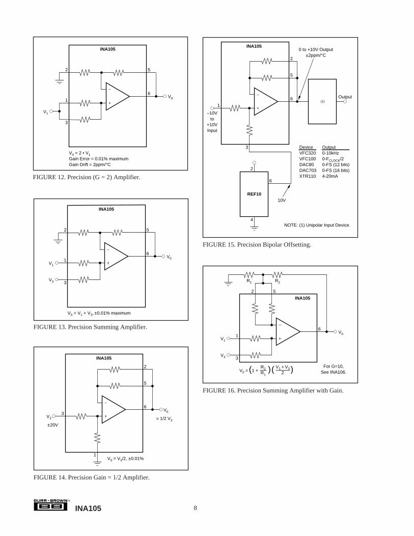
V0 = (V1 + V3)/2, ±0.01% maximum
V3
®
INA105 8
FIGURE 15. Precision Bipolar Offsetting.
–10Vto
+10VInput
5
6
1
3
2
Output
INA105
4
2
6
(1)
0 to +10V Output±2ppm/°C
10VREF10
DeviceVFC320VFC100DAC80DAC703XTR110
Output0-10kHz0-FCLOCK/20-FS (12 bits)0-FS (16 bits)4-20mA
NOTE: (1) Unipolar Input Device.
FIGURE 12. Precision (G = 2) Amplifier.
V1
5
6
1
3
V0
INA105
V0 = 2 • V1Gain Error = 0.01% maximumGain Drift = 2ppm/°C
2
FIGURE 16. Precision Summing Amplifier with Gain.
V1
6
1
3
V0
INA105
V3
2 5
R1 R2
V0 = 1 + R2R1
V1 + V32( )( ) For G=10,
See INA106.
FIGURE 13. Precision Summing Amplifier.
V1
5
6
1
3
V0
INA105
V0 = V1 + V3, ±0.01% maximum
2
V3
FIGURE 14. Precision Gain = 1/2 Amplifier.
V3
5
6
3
2
INA105
1
V0
V0 = V3/2, ±0.01%
= 1/2 V3
±20V

®
INA1059
FIGURE 17. Instrumentation Amplifier Guard Drive Generator.
FIGURE 18. Precision Summing Instrumentation Amplifier.
V1
5
6
3
1
INA105
V0 = V3 + V4 – V1 – V2
2
V2
V3
5
6
3
1
V0
INA105
2
V4
Shield
5
6
1
2
INA105
A1
A2
1A3 Output
3
Noise (60Hz hum)
Noise (60Hz hum)
Transducer orAnalog Signal
2+VCC
13–VCC
9 14 Common
10kΩ
10kΩ
10kΩ
10kΩ
INA101AG
876
20kΩ
20kΩ
3
4
5
10
11
12
RG
100kΩ
OffsetAdjust

®
INA105 10
FIGURE 22. Differential Output Difference Amplifier.
5
6
3
INA105
2
V01
1
5
6
3
INA105
2
V01 – V02 = 2 (V2 – V1)
V02
1
V2
V1
FIGURE 19. Precision Voltage-to-Current Converter withDifferential Inputs.
FIGURE 21. Isolating Current Source.
FIGURE 23. Isolating Current Source with Buffering Ampli-fier for Greater Accuracy.
FIGURE 20. Differential Input Voltage-to-Current Converterfor Low IOUT.
5
6
3
INA1052
1V1
V2
LoadIO = (V1 – V2) (1/25k + 1/R)For R 200 , Figure 24 willprovide superior performance.
IOΩ
R
R
≅
5
6
3
INA105
2
1V3
V2
LoadIO = (V3 – V2)/R
IO
R
5
6
3
INA105
2
1V3
V2
Load IO
R
R
Gate can be+VS –5V
IO = (V3 – V2) (1/25k + 1/R)
R < 200Ω
5
6
3
INA1052
1V3
V2
Load IO
R
Gate can be+VCC –5V
IO = (V3 – V2)/R
R 200 Ω≥

®
INA10511
FIGURE 25. Precision Voltage-Controlled Current Source with Buffered Differential Inputs and Gain.
FIGURE 24. Window Comparator with Window Span and Window Center Inputs.
FIGURE 26. Digitally Controlled Gain of ±1 Amplifier.
5
6
3
2
1
8
9
Window Center + Window Span
5
6
3
1
HI
INA105
2GO
LO
10
7
VIN
Lower Limit 5
3
2Upper Limit
INA105
4115Window
Comparator
Window Span0 to +5V
WindowCenter±10V
Window Center–Window Span
5
6
3
INA105
2
1
Load
IO = (E2 – E1) (1 +2R2/R1) (1/25k + 1/R)NOTE: (1) See Figure 5 for op amp recommendation.
IO
R
(1)
V1
V2
+In
–In
(1)
R1
R2
R2
R
V+
1kΩ
5
6
3
1
INA105
2
1
VODG188
V1
LogicIn
Logic In
0
1
VO
–V1
+V1

®
INA105 12
FIGURE 27. Boosting Instrumentation Amplifier Common-Mode Range From ±5 to ±7.5V with 10V Full-Scale Output.
FIGURE 28. Precision Absolute Value Buffer.
FIGURE 29. Precision 4-20mA Current Transmitter.
V1Input
5
6
3
1
V0 = |V1|
INA105
2
R4
R3
R1 R2
OPA111
10pFD1
D2
R52kΩ
5
6
3
INA1052
1
4
2+15V OPA27
REF10 610V
4 to 20mAOut
0 to 10VIn
12.5kΩ 1kΩ
50kΩ
50.1Ω
50.1Ω
RLOAD
INA105
A1
V1
V2
A2
R1
5
6
1
3
2
V0 = 200 (V2 – V1)A3
R149.5Ω
R2 R2
R2 R2
ConventionalInstrumentation
Amplifier (e.g., INA101 or INA102)A = 100
INA105A = 2
R149.5Ω

PACKAGE OPTION ADDENDUM
www.ti.com 7-Oct-2021
Addendum-Page 1
PACKAGING INFORMATION
Orderable Device Status(1)
Package Type PackageDrawing
Pins PackageQty
Eco Plan(2)
Lead finish/Ball material
(6)
MSL Peak Temp(3)
Op Temp (°C) Device Marking(4/5)
Samples
INA105AM NRND TO-99 LMC 8 1 RoHS & Green Call TI N / A for Pkg Type INA105AM
INA105BM NRND TO-99 LMC 8 1 RoHS & Green Call TI N / A for Pkg Type INA105BM
INA105KP ACTIVE PDIP P 8 50 RoHS & Green NIPDAU N / A for Pkg Type INA105KP
INA105KPG4 ACTIVE PDIP P 8 50 RoHS & Green NIPDAU N / A for Pkg Type INA105KP
INA105KU ACTIVE SOIC D 8 75 RoHS & Green NIPDAU Level-3-260C-168 HR -40 to 85 INA105U
INA105KU/2K5 ACTIVE SOIC D 8 2500 RoHS & Green NIPDAU Level-3-260C-168 HR -40 to 85 INA105U
INA105KU/2K5E4 ACTIVE SOIC D 8 2500 RoHS & Green NIPDAU Level-3-260C-168 HR -40 to 85 INA105U
INA105KUE4 ACTIVE SOIC D 8 75 RoHS & Green NIPDAU Level-3-260C-168 HR -40 to 85 INA105U
(1) The marketing status values are defined as follows:ACTIVE: Product device recommended for new designs.LIFEBUY: TI has announced that the device will be discontinued, and a lifetime-buy period is in effect.NRND: Not recommended for new designs. Device is in production to support existing customers, but TI does not recommend using this part in a new design.PREVIEW: Device has been announced but is not in production. Samples may or may not be available.OBSOLETE: TI has discontinued the production of the device.
(2) RoHS: TI defines "RoHS" to mean semiconductor products that are compliant with the current EU RoHS requirements for all 10 RoHS substances, including the requirement that RoHS substancedo not exceed 0.1% by weight in homogeneous materials. Where designed to be soldered at high temperatures, "RoHS" products are suitable for use in specified lead-free processes. TI mayreference these types of products as "Pb-Free".RoHS Exempt: TI defines "RoHS Exempt" to mean products that contain lead but are compliant with EU RoHS pursuant to a specific EU RoHS exemption.Green: TI defines "Green" to mean the content of Chlorine (Cl) and Bromine (Br) based flame retardants meet JS709B low halogen requirements of <=1000ppm threshold. Antimony trioxide basedflame retardants must also meet the <=1000ppm threshold requirement.
(3) MSL, Peak Temp. - The Moisture Sensitivity Level rating according to the JEDEC industry standard classifications, and peak solder temperature.
(4) There may be additional marking, which relates to the logo, the lot trace code information, or the environmental category on the device.
(5) Multiple Device Markings will be inside parentheses. Only one Device Marking contained in parentheses and separated by a "~" will appear on a device. If a line is indented then it is a continuationof the previous line and the two combined represent the entire Device Marking for that device.

PACKAGE OPTION ADDENDUM
www.ti.com 7-Oct-2021
Addendum-Page 2
(6) Lead finish/Ball material - Orderable Devices may have multiple material finish options. Finish options are separated by a vertical ruled line. Lead finish/Ball material values may wrap to twolines if the finish value exceeds the maximum column width.
Important Information and Disclaimer:The information provided on this page represents TI's knowledge and belief as of the date that it is provided. TI bases its knowledge and belief on informationprovided by third parties, and makes no representation or warranty as to the accuracy of such information. Efforts are underway to better integrate information from third parties. TI has taken andcontinues to take reasonable steps to provide representative and accurate information but may not have conducted destructive testing or chemical analysis on incoming materials and chemicals.TI and TI suppliers consider certain information to be proprietary, and thus CAS numbers and other limited information may not be available for release.
In no event shall TI's liability arising out of such information exceed the total purchase price of the TI part(s) at issue in this document sold by TI to Customer on an annual basis.

TAPE AND REEL INFORMATION
*All dimensions are nominal
Device PackageType
PackageDrawing
Pins SPQ ReelDiameter
(mm)
ReelWidth
W1 (mm)
A0(mm)
B0(mm)
K0(mm)
P1(mm)
W(mm)
Pin1Quadrant
INA105KU/2K5 SOIC D 8 2500 330.0 12.4 6.4 5.2 2.1 8.0 12.0 Q1
PACKAGE MATERIALS INFORMATION
www.ti.com 5-Jan-2022
Pack Materials-Page 1

*All dimensions are nominal
Device Package Type Package Drawing Pins SPQ Length (mm) Width (mm) Height (mm)
INA105KU/2K5 SOIC D 8 2500 853.0 449.0 35.0
PACKAGE MATERIALS INFORMATION
www.ti.com 5-Jan-2022
Pack Materials-Page 2

TUBE
*All dimensions are nominal
Device Package Name Package Type Pins SPQ L (mm) W (mm) T (µm) B (mm)
INA105AM LMC TO-CAN 8 1 532.13 21.59 889 NA
INA105BM LMC TO-CAN 8 1 532.13 21.59 889 NA
INA105KP P PDIP 8 50 506 13.97 11230 4.32
INA105KPG4 P PDIP 8 50 506 13.97 11230 4.32
INA105KU D SOIC 8 75 506.6 8 3940 4.32
INA105KUE4 D SOIC 8 75 506.6 8 3940 4.32
PACKAGE MATERIALS INFORMATION
www.ti.com 5-Jan-2022
Pack Materials-Page 3
IMPORTANT NOTICE AND DISCLAIMERTI PROVIDES TECHNICAL AND RELIABILITY DATA (INCLUDING DATA SHEETS), DESIGN RESOURCES (INCLUDING REFERENCE DESIGNS), APPLICATION OR OTHER DESIGN ADVICE, WEB TOOLS, SAFETY INFORMATION, AND OTHER RESOURCES “AS IS” AND WITH ALL FAULTS, AND DISCLAIMS ALL WARRANTIES, EXPRESS AND IMPLIED, INCLUDING WITHOUT LIMITATION ANY IMPLIED WARRANTIES OF MERCHANTABILITY, FITNESS FOR A PARTICULAR PURPOSE OR NON-INFRINGEMENT OF THIRD PARTY INTELLECTUAL PROPERTY RIGHTS.These resources are intended for skilled developers designing with TI products. You are solely responsible for (1) selecting the appropriate TI products for your application, (2) designing, validating and testing your application, and (3) ensuring your application meets applicable standards, and any other safety, security, regulatory or other requirements.These resources are subject to change without notice. TI grants you permission to use these resources only for development of an application that uses the TI products described in the resource. Other reproduction and display of these resources is prohibited. No license is granted to any other TI intellectual property right or to any third party intellectual property right. TI disclaims responsibility for, and you will fully indemnify TI and its representatives against, any claims, damages, costs, losses, and liabilities arising out of your use of these resources.TI’s products are provided subject to TI’s Terms of Sale or other applicable terms available either on ti.com or provided in conjunction with such TI products. TI’s provision of these resources does not expand or otherwise alter TI’s applicable warranties or warranty disclaimers for TI products.TI objects to and rejects any additional or different terms you may have proposed. IMPORTANT NOTICE
Mailing Address: Texas Instruments, Post Office Box 655303, Dallas, Texas 75265Copyright © 2022, Texas Instruments Incorporated