
Precision Engineering Consortium - NC State University
288
Proprietary Release subject to the terms and conditions of the Precision Engineering Consortium Membership Agreement and the North Carolina State University Office of Technology Transfer nondisclosure agreements. PRECISION ENGINEERING CONSORTIUM 2019 & 2020 ANNUAL REPORT VOLUME XXXIV
-
Upload
khangminh22 -
Category
Documents
-
view
2 -
download
0
Transcript of Precision Engineering Consortium - NC State University

Proprietary Release subject to the terms and conditions of the Precision Engineering Consortium Membership Agreement and the North Carolina State University Office of Technology Transfer nondisclosure agreements.
PRECISION
ENGINEERING
CONSORTIUM
2019 & 2020 ANNUAL REPORT
VOLUME XXXIV

ii Proprietary Release subject to the terms and conditions of the Precision Engineering Consortium Membership Agreement and the North Carolina State University Office of Technology Transfer nondisclosure agreements.
2019 & 2020
ANNUAL REPORT
VOLUME XXXIV
July 2021
Faculty: Mark Pankow
Scott Ferguson Paul Cohen
Thomas Dow
Graduate Usama Alfarid Dingankar
Students: Sumit Gundyal
Noa McNutt
Jacob Guymon
Parker Eaton
Tyler Young
Staff: Kenneth Garrard
Jacob Marx
Consultants: Karl Falter Stephen Furst
Sponsors

i Proprietary Release subject to the terms and conditions of the Precision Engineering Consortium Membership Agreement and the North Carolina State University Office of Technology Transfer nondisclosure agreements.
Table of Contents Summary i
1. Sub Aperture Polishing of Millimeter Sized Polymer Optics Usama Alfarid Dingankar and Thomas Dow 1
2. Sub Aperture Polishing Optimization Jacob Guymon, Tyler Young, and Mark Pankow 85
3. Multi-Lens Array: Modeling of the Microindentation Process to Create Lens Array Features
on a Mold Sumit Gundyal and Mark Pankow 73
4. Novel Manufacturing Methods of Microscale Lens Arrays Anthony Wong and Mark Pankow 127
5. Reducing Microlens Array Indentation Form Error Via Testing and Simulation Parker Eaton and Mark Pankow 187
6. Mechanochemical Effects on Aluminum 1100, 6061, and 7075 Abdullah Elkodsi, Anthony Wong, and Mark Pankow 204
7. Mechanical and Electrical Properties of Single Crystal Silicon under External Electric
Fields using Nanoindentation Anthony Wong and Mark Pankow 221
8. Development of a Novel Modular Monopolar and Bipolar Surgical Forceps Nehemiah Macdonald and Mark Pankow 239
9. Deployable Structures
Greyson Hodges and Mark Pankow 245
Personnel 239
Graduates of the PEC 274
Academic Program 276
Fact Sheet 278

ii Proprietary Release subject to the terms and conditions of the Precision Engineering Consortium Membership Agreement and the North Carolina State University Office of Technology Transfer nondisclosure agreements.
Letter from the Director
In January of 2020, we celebrated the retirement of our founding director, Dr. Thomas Dow. Since
establishing the Precision Engineering Center in 1982 he has helped guide the PEC through
multiple decades of continued success and we cannot thank him enough for all that he has done.
I was named as the new director of the center with the intent of continuing the current work and
maintaining the center’s core ideologies Dr. Dow had established. A couple short months later we
were all trying to figure out how handle the COVID-19 pandemic as it raced across the world. The
past year had been exceptionally difficult, and everyone has been impacted by COVID. We hope
that everyone is doing well and healthy and that things are starting to improve. As the pandemic
continued to worsen, North Carolina State University suspended on-campus work and research
on March 20th, 2020. The PEC is built around hands-on research that was indefinitely interrupted
and delayed during that time. This presented new challenges for students and staff as it was
pertinent to maintain progress despite the interruption to normal operations.
Students were committed to maintaining progress in their work and explored means to transfer
their experimental work to modeling and designing experiments as access to the lab was limited.
This avoided any large-scale setbacks and allowed them to easily pick their work back up from
where they left off once limited access to the facilities was restored in the beginning of June, 2020.
I am proud of our students, staff, and faculty’s dedication to their work through this unprecedented
period. As we continue to adhere safety standards set by the university, I would like to assure our
sponsors and collaborators that the advancement of our research projects remains our top
priority.
The PEC also underwent staff changes as it hired Dr. Jacob Marx to the Research Assistant
position replacing Anthony Wong who recently began his work with the Army Research Office.
The addition of new staff broadens the current research focus and resources of the PEC as we
continue to open our doors to potential opportunities for collaboration. The past year proved
exceptionally difficult for recruiting new students. Yet, we are excited to welcome new graduate
and undergraduate students joining us in the fall with the ability to perform research in the labs.
In the report that follows we are excited to also include chapters covering work that occurs in the
Blast Lab also under the direction of Dr. Pankow. The recent changes in director and staff do not
change the fact that the PEC will continue its research focus on metrology, precision
manufacturing, and actuation controls for industry and national laboratories.
Mark Pankow
Director of the PEC

iii Proprietary Release subject to the terms and conditions of the Precision Engineering Consortium Membership Agreement and the North Carolina State University Office of Technology Transfer nondisclosure agreements.
Summary
The goals of the Precision Engineering Consortium (PEC) are: 1) to develop new technology in
the areas of precision metrology, actuation, manufacturing and assembly; and 2) to train a new
generation of engineers and scientists with the background and experience to transfer this
technology to industry. Because the problems related to precision engineering originate from a
variety of sources, significant progress can only be achieved by applying a multidisciplinary
approach; one in which the faculty, students, staff and sponsors work together to identify
important research issues and find the optimum solutions. Such an environment has been created
and nurtured at the PEC for 34 years and the 100+ graduates attest to the quality of the results.
The 2020 Annual Report summarizes the progress over the past two years by the faculty, students
and staff in the Precision Engineering Consortium. During the past two years, this group included
4 faculty, 6 graduate students, 7 undergraduate students, 2 technical staff members, and 1
administrative staff member. The diverse group of scientists and engineers provides a wealth of
experience to address precision engineering problems. The format of this Annual Report
separates the research effort into individual projects but there is significant interaction that occurs
among the faculty, staff and students. Teamwork and group interactions are a hallmark of
research at the PEC and this contributes to both the quality of the results as well as the education
of the graduates.
A brief abstract follows for each of the projects and the details of the progress in each is described
in the remainder of the report.
1. Sub Aperture Polishing of Millimeter Sized Polymer Optics
Sub aperture polishing is a deterministic polishing process in which the polishing tool produces
a contact patch that is smaller than overall dimension of the workpiece, such it is able to carry
out localized polishing action and corrections within the body of the workpiece in specific areas
of interest, whilst at the same time not altering the noninterest regions. The objective of this
research project is to design and setup a sub aperture polishing system utilizing a soft silicone
rubber based polishing tool attached to a high speed spindle drive, in order to produce a
polished surface with a RMS surface roughness measuring 2 nm, and the ability to create and
correct a free form feature on the workpiece surface measuring 6x6 mm in area, with a form
PV of 15 microns. Polycarbonate (PC) and Polymethylmethacrylate (PMMA) are the two
polymers that have been studied as workpieces, and Alumina suspension was utilized as the
polishing abrasive. The effects of input variables namely – RPM, feed rate, normal load,
polishing passes, toolpath strategy on the surface roughness RMS were studied and the
results were reported.
2. Sub Aperture Polishing Optimization
Elastic emission machining (EEM) is a high-accuracy sub-nanometer polishing process that is useful for removing unwanted material and refining surface finish. While many prior studies have examined aspects of EEM and tested its polishing ability, few have gone in depth on

iv Proprietary Release subject to the terms and conditions of the Precision Engineering Consortium Membership Agreement and the North Carolina State University Office of Technology Transfer nondisclosure agreements.
how different paths impact the surface finish or how those effects relate to a wide range of EEM polishing parameters. This study investigates the effects of the tool path determine the optimal parameters achieve a desired finish without compromising the portions of the surface that are already within the specified margin. This work couples tool pathing with a study on how different combinations of parameters such as lubrication viscosity, applied force, and rotation speed can affect surface finish. EEM of polycarbonate is investigated in this study using a silicone ball and alumina slurry. The resulting surface is imaged using an optical interferometer to measure the surface finish. The applied load is found to have a direct impact on the machining process and final surface roughness.
3. Multi-Lens Array: Modeling of the Microindentation Process to Create Lens Array
Features on a Mold
This report addresses the design of multi-indenter die and development of indentation
strategies to create the negative features of a microlens array on a mold. A material parameter
study is performed using the commercial finite element analysis software AbaqusTM to
understand the effects of different indent patterns and processes on the pile-up and the
maximum force required and shape error. Al 1100 is selected as the mold material based on
this study. Glassy carbon is used as the die material. Multiple Indentation strategies are
explored to understand the best die shape to reduce form error.
4. Novel Manufacturing Methods of Microscale Lens Arrays
In order to build off of the work outlined in the previous chapter, this work explores
manufacturing a mold and die that can be used to create an optimal indent pattern for
microlens arrays. This study details the steps taken to manufacture a mold and die from
aluminum and diamond, respectively. The Al 1100 H14 was first characterized through
nanoindentation and diamond turning. Indentation grids were effectively created using a
Berkovich and conical nanoindenter. The diamond die was FIB milled and analyzed using
surface interferometry. The FIB dwell time for 1 nA and 0.50 nA beam currents used to create
a consistent parabolic array is documented.
5. Reducing Microlens Array Indentation Form Error via Testing and Simulation
This report addresses the initial methods involved in reducing the geometric form errors that
occur when indenting microlens arrays. The microlens arrays are rapidly indented on a variety
of metallic negative molds. A proprietary indent force and indent depth measurement
technique is employed to aid in the characterization and control of the microindenting process.
Insights from form error analysis and finite element simulations can then be used to make
informed decisions to redefine die geometry and microindentation strategies in the pursuit of
minimized geometric form error.

v Proprietary Release subject to the terms and conditions of the Precision Engineering Consortium Membership Agreement and the North Carolina State University Office of Technology Transfer nondisclosure agreements.
6. Mechanical and Electrical Properties of Single Crystal Silicon under External Electric
Fields using Nanoindentation
Silicon is widely used for electronics and modern day technology. Phase changes within the
silicon structure can reduce machining forces and reduce material springback for electronics
manufacturing. Single crystal silicon was tested under electrical contact nanoindentation at
voltages between -10 and 10 V. The modulus and hardness of the silicon is measured during
indentation and the effect of the voltage is used to determine potential phase changes in the
single crystal silicon wafer. Large negative voltages have been shown to increase the reduced
modulus of the silicon. The external electric field was found to have no effect on the hardness.
Future work can focus on measuring the topography of the indented regions and resistivity
while also exploring other materials.
7. Development of a Novel Modular Monopolar and Bipolar Forceps
Electrosurgery devices can offer multi-use capabilities when paired with a surgical forceps design. Such a device can reduce surgical time by limiting the need to transfer between surgical tools. This project is set out to design, manufacture, and test a surgical forceps tool that can act as both a mono- and bipolar electrosurgery tool. Initial ideas were analyzed using a design matrix and with consultation with medical professionals. First steps have been taken to prototype and determine the next steps for material manufacturing and electronics. Future work will include manufacturing, wiring, and testing of the device followed by iterative improvements to the design.
8. Deployable Structures
This report addresses the development of various deployable technologies for aerospace systems and their current status. There are two main research areas: Deployable booms with different mechanisms: both powered and unpowered, and Deployable Composite Origami. This work discusses the manufacturing and testing of each system. Both systems have or have ongoing zero-gravity flight demonstrations to understand their deployment characteristics in a relevant space environment. The Boom project has an ongoing collaboration with NASA Langley.


1 Proprietary Release subject to the terms and conditions of the Precision Engineering Consortium Membership Agreement and the North Carolina State University Office of Technology Transfer nondisclosure agreements.
SUB APERTURE POLISHING OF MILLIMETER
SIZED POLYMER OPTICS
Usama Alfarid Dingankar
Graduate Student, Department of Mechanical Engineering
Dr. Thomas Dow
Dean F. Duncan Distinguished University Professor
Department of Mechanical Engineering
ABSTRACT
Sub aperture polishing is a deterministic polishing process in which the polishing tool produces a
contact patch that is smaller than overall dimension of the workpiece, such it is able to carry out
localized polishing action and corrections within the body of the workpiece in specific areas of
interest, whilst at the same time not altering the noninterest regions. The objective of this research
project is to design and setup a sub aperture polishing system utilizing a soft silicone rubber based
polishing tool attached to a high speed spindle drive, in order to produce a polished surface with
a RMS surface roughness measuring 2 nm, and the ability to create and correct a free form feature
on the workpiece surface measuring 6x6 mm in area, with a form PV of 15 microns. Polycarbonate
(PC) and Polymethylmethacrylate (PMMA) are the two polymers that have been studied as
workpieces, and Alumina suspension was utilized as the polishing abrasive. The effects of input
variables namely – RPM, feed rate, normal load, polishing passes, toolpath strategy on the
surface roughness RMS were studied and the results were reported.

2 Proprietary Release subject to the terms and conditions of the Precision Engineering Consortium Membership Agreement and the North Carolina State University Office of Technology Transfer nondisclosure agreements.
INTRODUCTION
Optical devices such as lenses are crucial with a varied usage in differing industries ranging from
microscopy, laser processing equipment, imaging, defense sector, aerospace, medical and bio
industry, projection visual devices like virtual reality headsets and in usual corrective spectacles
[1]. The basic functionality of a lens, is to change the path profile of light by converging, diverging,
or dispersing, magnifying to form an image of the object being viewed [2]. Optical lenses can be
in many forms including convex, concave plano concave, plano convex etc. In today’s advanced
technical environment, many new technologies, such as concept of virtual reality, have started
making a solid mark in the industry. The advent of such industries has led to a meteoric rise of
the quality standards in the manufacturing and precision processing of optical devices. Two key
metrics to measure the quality of the lenses are surface finish and surface form. A better surface
finish and exacting form of these lenses will improve the overall performance of the lenses.
Many optical lenses are manufactured from polymer plastics like PMMA (Polymethylmethacrylate)
and PC (Polycarbonate) and use manufacturing processes like injection molding or compression
molding. Utilizing polymer optics is advantageous because they offer design flexibility in terms of
cost, weight, shape, design, and transmittance of light, as compared to glass optics. The
fabrication of glass optics is a slow and costly affair as compared to the polymer counterparts [1],
[3]. But being an optical device, these lenses need to have a high level of surface finish, form and
optical properties. These parameters can be achieved by utilizing the polishing process as a key
finishing step in the lens manufacturing process. Polishing is routinely performed to improve the
finishing of surfaces, to remove scratches and to reduce the surface roughness [4]. In layman’s
terms, polishing is the process of creating an improved surface by the means of mechanical or
chemical interaction between the polishing tool and the workpiece, either in the presence of a free
or fixed abrasive. Any given surface on a magnified scale has a system of crests and troughs
present on it. The frequency of these features and the difference in the heights of these crests
and troughs can be used as the description for the surface roughness.
Figure 1-1: Sample measurement depicting the surface roughness profile in a trace [5].
DETAILS OF THE PROJECT

3 Proprietary Release subject to the terms and conditions of the Precision Engineering Consortium Membership Agreement and the North Carolina State University Office of Technology Transfer nondisclosure agreements.
This research project deals with the computer controlled sub-aperture polishing process for
polymers like Polycarbonate (PC) and Polymethylmethacrylate (PMMA). Sub-aperture polishing
refers to the type of polishing in which the polishing contact patch which is the zone in which the
actual polishing takes place, is much smaller than the overall lens diameter and dimension and
allows the polishing of selective areas of the workpiece without affecting the form and finish of the
noninterest regions. In the case where we need to polish flat, plano, or spherical surfaces, full
aperture polishing is a preferred process, but since this project deals with the creation of a free
form 3D sine wave surface, sub aperture polishing process is most effective, as due to the change
of local curvature full aperture polishing is not a possible measure [6]. It provides a deterministic
approach to obtain an improved surface finish and desired surface form in specific areas on the
lens surface without any kind of damage to the remaining lens areas.
Figure 1-2: Diagrammatic representation of the elastic emission polishing process [7].
The process of sub aperture polishing can be described by using the concepts of elastic emission
machining. Elastic emission machining is a non-contact machining process that utilizes a three
way contact between the polishing tool, the abrasive grain, and the workpiece surface. The
polishing process depends on the contact between abrasive particles and the workpiece surface
[7]. A diagrammatic representation of the elastic emission polishing process is shown above in
Figure 1-2. The polishing process is based on the free abrasive model wherein an abrasive fluid
containing suspended abrasive particles is utilized which consists of a mixture of deionized water
that acts as a vehicle to sustain and transport the aluminum oxide grains (abrasive) into the
polishing zone. The polishing tool is a silicone rubber ball in this project. It is the driver of this
system as shown above in the Figure 1-2, in the sense that it directs the abrasive fluid to the
polishing zone and facilitates the motion of the polishing fluid (thereby the abrasive grains) on the
workpiece thereby causing the material removal action, hence polishing the surface.
In this research, the effects of the sub-aperture polishing on surface roughness and surface form
in Polycarbonate (PC) and Polymethylmethacrylate (PMMA) are studied and analyzed.

4 Proprietary Release subject to the terms and conditions of the Precision Engineering Consortium Membership Agreement and the North Carolina State University Office of Technology Transfer nondisclosure agreements.
PMMA is an optically clear thermoplastic with a high impact strength, relatively low density, and
is shatter-resistant. It has a low elongation at break point and has a high Young’s modulus [8]
compared to the polishing tool i.e. the silicone ball. These outstanding properties also include high
optical clarity, weather resistance and scratch resistance. A refractive index of 1.490, and a high
resistance to sunshine exposure (UV resistance) making PMMA a promising polymer for optical
applications. PMMA also displays an inherent dependency on temperature in the case of material
deformation. As the temperature increases the Young’s modulus of the material decreases and
thereby the material deforms easily [9]. PC is highly transparent, transmitting approximately 90%
of visible light. It displays exceptional impact resistance, tensile strength, ductility, dimensional
stability, and optical clarity. It is marketed under trademarks such as Lexan and Makrolon [10].
Polycarbonate is manufactured primarily as a transparent material and has very good light
transmission and optical properties. Just like PMMA, Polycarbonate has a temperature dependent
deformation mechanism. As the temperature is increased the material gets relatively easy to
deform. As the temperature goes higher, the Young’s modulus decreases and the material hence
becomes easier to deform. The characteristics of Polycarbonate (PC) are quite like those of
Polymethylmethacrylate (PMMA), but PC is stronger and more expensive, though its more prone
to surface scratches, thereby making the precise handling of this polymer imperative.
EXPERIMENTAL SETUP In the experimental setup, a silicone rubber ball of diameter 3 mm and shore hardness value of
70A was utilized, Figure 1-3. The silicone rubber ball was mounted on a brass spindle shaft to
form the polishing tool head, shown in Figure 1-4 and 1-5.
Figure 1-3: Silicone rubber tool size representation.
Silicone Rubber is a thermoset elastomer, and is usually non-reactive, stable, and resistant to
extreme environments and temperatures. It is also stable at low and high temperatures [11]. The
working temperature range for Silicone rubber is from −55 °C to 300 °C. The material has a
Young’s modulus of 50 MPa, with a yield strength of 7 MPa. The size of the silicone rubber ball
was chosen based on the overall size of the features to be created.
5 Proprietary Release subject to the terms and conditions of the Precision Engineering Consortium Membership Agreement and the North Carolina State University Office of Technology Transfer nondisclosure agreements.
The polishing fluids utilized in the project were supplied by Baikowksi International, Universal
Photonics, and Buehler. Baikowksi Baikalox Aluminum Oxide (𝐴𝑙2𝑂3) based fluid with a varying
abrasive grain size of 0.05 µm, 0.1 µm, 0.3 µm, 0.5 µm was utilized to carry out the primary
surface improvement experiments. Kontax 602 – an ultra-pure alumina polishing powder was
also used for polishing experiments as it is known to give excellent results with Polycarbonate
workpieces. The Kontax was used in 3 types of slurries with a varying abrasive concentration of
10%, 15%, 40% on the Baume scale.
The measurement of the surface finish and the surface form are of prime importance in the
research project, as these output parameters form the backbone of the research objectives. An
accurate and precise measurement of these parameters is needed to characterize the polishing
process. Three different apparatuses have been used in order to obtain and record these
measurements. In order to measure the surface roughness and form on a 3D scale the Zygo
NewView 5000 3D surface profiler is used and the Keyence VKX1100 3D laser scanning confocal
microscope, for the 2D cross sectional measurements the Taylor - Hobson Talysurf apparatus
has been utilized.
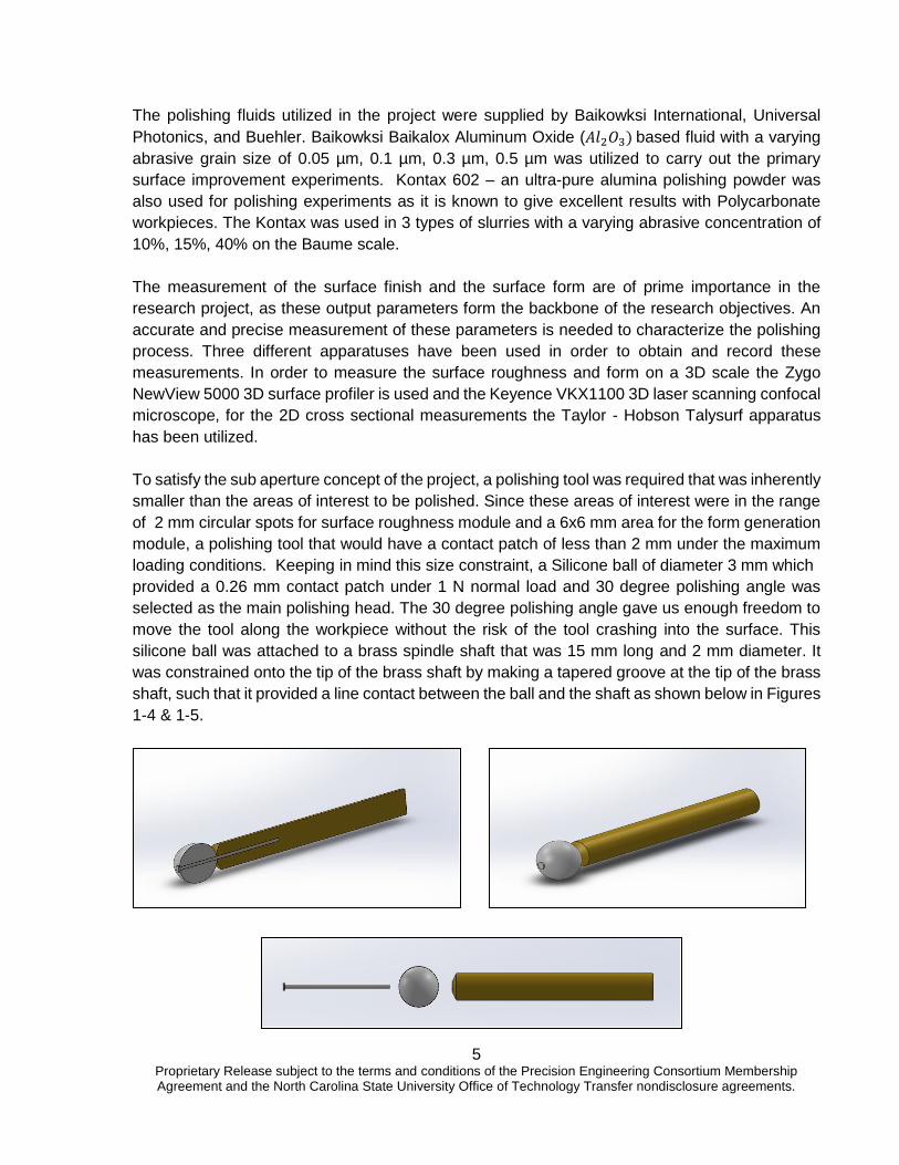
To satisfy the sub aperture concept of the project, a polishing tool was required that was inherently
smaller than the areas of interest to be polished. Since these areas of interest were in the range
of 2 mm circular spots for surface roughness module and a 6x6 mm area for the form generation
module, a polishing tool that would have a contact patch of less than 2 mm under the maximum
loading conditions. Keeping in mind this size constraint, a Silicone ball of diameter 3 mm which
provided a 0.26 mm contact patch under 1 N normal load and 30 degree polishing angle was
selected as the main polishing head. The 30 degree polishing angle gave us enough freedom to
move the tool along the workpiece without the risk of the tool crashing into the surface. This
silicone ball was attached to a brass spindle shaft that was 15 mm long and 2 mm diameter. It
was constrained onto the tip of the brass shaft by making a tapered groove at the tip of the brass
shaft, such that it provided a line contact between the ball and the shaft as shown below in Figures
1-4 & 1-5.

6 Proprietary Release subject to the terms and conditions of the Precision Engineering Consortium Membership Agreement and the North Carolina State University Office of Technology Transfer nondisclosure agreements.
Figure 1-4: Image showing the a) cross section view, b) isometric view and c) exploded view of
the polishing tool head assembly.
This assembly of the brass shaft, the silicone ball, and the stainless steel pin was attached to the
spindle of a Medicool devices Pro-Power 40K dentist’s drill, providing a working RPM range from
1000 to 40000. This RPM range covered all the experimental needs of the project. The drill had
a control system that could be used to vary the RPM’s in increments of 1000 RPM.
Figure 1-5: The 3mm Silicone Ball attached to the Brass spindle shaft.
A 3-axis micro-mill CNC machine was deemed feasible to be utilized as the main control setup.
The mill provided access to the 3 degrees of freedom – namely the X, Y, Z axis. To ensure a sub
aperture polishing of free form surfaces, a degree of freedom in the ϴ axis was required as well,
the ϴ axis being the one that controlled the precess angle or the spindle angle with respect to the
contact point on the workpiece surface. The fixture shown in Figure 1-6 was designed to satisfy
these needs of obtaining 4 degrees of freedom for the polishing system.

7 Proprietary Release subject to the terms and conditions of the Precision Engineering Consortium Membership Agreement and the North Carolina State University Office of Technology Transfer nondisclosure agreements.
Figure 1-6: CAD Model of the polishing fixture.
ANALYTICAL APPROACH
In the case of sub aperture polishing the basic arrangement is that a polishing sphere is made to
contact a workpiece (that could be flat, concave, convex) a force is applied on the polishing sphere
to maintain the contact and the sphere is then rotated in a polishing slurry to carry out the polishing
action. In order to model this contact the Hertzian contact theory has been utilized in this research.
A few assumptions that need to be made to study the contact model are that the contact is non
adhesive, meaning the contacting bodies can be separated without adhesion forces acting
between them. Another important assumption is that the polishing tool is considered to be a
sphere of a given diameter, and the workpiece is considered to be flat to begin with, hence has a
diameter amounting to ∞. When these two solid bodies of are pressed together with a force F, a
circular area of contact of radius ‘a’ is obtained, which leads to our next assumption that the
contact area formed between the spherical polishing sphere and the flat workpiece is circular.
The next assumption is the normal loading force acting on the polishing sphere/tool. Hertzian
contact model is based on the logic that pressure (contact stress) is developed when two curved
bodies are brought in contact with each other and undergo slight deformation when the normal
force is applied. This deformation is directly proportional to the Young’s modulus of the materials
in contact.

8 Proprietary Release subject to the terms and conditions of the Precision Engineering Consortium Membership Agreement and the North Carolina State University Office of Technology Transfer nondisclosure agreements.
Figure 1-7: Image depicting the Hertzian contact between polishing sphere and workpiece
In the experimental setup a deadweight loading system has been used to maintain a constant
force throughout the polishing process. The contact pressure (contact stress) is what determines
the polishing action on the workpiece rather than the direct force which is exerted on the surface
[12]. Meaning although the force applied might be constant, but the pressure and stresses
developed might vary due to change in geometry shape being polished [12]. The contact stress
values can be calculated about z -axis. The deformation of the polishing tool is one of the crucial
factors in the polishing process, at it is hinged on the material properties of the polishing tool,
since the Young’s modulus of the polishing tool (Silicone Rubber) is 60 times lower than that of
the workpiece (PMMA), the workpiece has been assumed to be rigid, whereas the polishing tool
is deformable, this causes the polishing tool to flatten out on the workpiece when it is in contact
and a normal load is applied to it. The more it flattens out the higher will be the contact radius and
at a constant normal load, a higher contact patch radius would lead to a decrease in the contact
pressure, directly reducing the polishing rates in the contact zone and increasing the polishing
times. In a study carried out by Su et al. [13] it was discussed that the hardness of the polishing
tool and the elastic deflection it undergoes determines the lubrication regime for the polishing
process. It was observed that if the tool were made out of a soft material as compared to the
workpiece and the loading is on the lower side in terms of magnitude the lubrication regime would
lie in the IE or IR regimes. Hence it is imperative to figure out the deflection of the polishing tool
itself as it rotates and contacts the surface.
Polishing Tool Contact Analysis – Theoretical
Now moving onto the case where the tool makes contact with the workpiece surface. According
to the Hertzian contact model, the contact patch size is quantified by using the radius metric, the

9 Proprietary Release subject to the terms and conditions of the Precision Engineering Consortium Membership Agreement and the North Carolina State University Office of Technology Transfer nondisclosure agreements.
radius of the contact patch is based upon the effective Young’s modulus of the contacting bodies,
E, effective diameter of the contacting bodies, d, and normal force acting in the contact situation,
F [14]. The contact patch radius ‘a’ can be calculated as follows in equation 1 –
𝑎 = √3 ∗ F ∗ Eeffective
8 ∗ (1 deffective)⁄
3 (1)
Eeffective = (1−ν1
2)
E1 +
(1−ν22)
E2 (2)
deffective = (1
d1+
1
d2) (3)
In this research the polishing tool that has been used is a Silicone rubber based ball and
Polycarbonate (PC), Polymethylmethacrylate (PMMA) workpieces. The calculations have been
shown for Polycarbonate (PC).
Contact patch radius - 𝑎 = √3 ∗ 1 ∗ 0.0168
8 ∗ 0.333
3 = 0.266 mm
Figure 1-8: Plot depicting variation in the contact patch radius for differing normal loads.
According to the calculations at 10000 rpm, at a 1 N normal load, the theoretical contact patch
would measure 0.266 mm in radius, and as the normal loading is increased, meaning as the force
applied on the polishing tool is increased, it compresses more against the workpiece, and contact
patch begins to flatten out, thereby causing an increase in the contact patch radius. The trend for
the variation of the contact patch radius with the normal load as shown above in Figure 1-8 is
0
0.05
0.1
0.15
0.2
0.25
0.3
0.35
0.4
0.45
0.5
0.55
0.6
0 0.25 0.5 0.75 1 1.25 1.5 1.75 2 2.25
Co
nta
ct
Pa
tch
Rad
ius
(m
m)
Normal Load Applied (N)
Theoritical(Hertzian)
Simulated(Axisymmetric)

10 Proprietary Release subject to the terms and conditions of the Precision Engineering Consortium Membership Agreement and the North Carolina State University Office of Technology Transfer nondisclosure agreements.
comparable to the results achieved by Dintwa et al. in their analysis of Hertzian theory for elastic
sphere contact [15].
Now for any given contact the peak pressure value is calculated below using equation (4) –
Pmax = 3 ∗ F
2 ∗ π ∗ a2 = 6.74 MPa (4)
Where – F – Normal force applied on the polishing tool
a – Contact patch radius
𝑃𝑚𝑎𝑥 – Peak pressure in contact zone.
Figure 1-9: Plot depicting variation in maximum Hertzian pressure with normal loads.
According to the Hertzian contact theory the pressure variation across the contact patch is in
accordance with Gaussian distribution. Now under a contact scenario between the two bodies in
contact, the pressure distribution is symmetric about a centerline passing through the center of
the point of contact in the XY plane [14]. In this research work the normal load range that is being
utilized is from 0.25 N to 1.5 N as this range provides a small enough contact patch that is in line
with overall size of the features that are being polished. This would give an expected peak
pressure range of 5.28 MPa to 7.62 MPa. The pressure distribution along the contact patch [16]
is given by equation (5) below –
σz = 1.5 ∗ Pmean ∗ √1 − r2
a2 (5)
0
2
4
6
8
10
12
14
0 0.5 1 1.5 2 2.5 3 3.5 4 4.5 5 5.5 6 6.5 7 7.5
Ma
xim
um
Pre
ss
ure
(M
Pa
)
Normal Force (N)

11 Proprietary Release subject to the terms and conditions of the Precision Engineering Consortium Membership Agreement and the North Carolina State University Office of Technology Transfer nondisclosure agreements.
Figure 1-10: Plot depicting theoretical Hertzian contact pressure for varying normal loads.
Using a normal load (F) of 1 N and corresponding contact patch radius of 0.266 mm, a peak
pressure of 6.65 MPa is obtained at the center of the contact zone. The Hertzian contact pressure
distribution acts equally across the contact zone and with opposing directions on the polishing
ball and the workpiece [14][16]. The theoretical pressure distribution across the contact patch for
the case of varying normal loads was plotted as shown above in Figure 1-10. As it can be seen
from the pressure distribution, it is distributed symmetrically across the contact patch.
Polishing Tool Contact Analysis – Simulation
Next moving onto the case wherein the polishing tool deflection is studied when the tool is
normally loaded and rotated at the same time. Theoretically for the general case of a non-rigid
workpiece and a non-rigid polishing tool (sphere), for a Hertzian contact, Fischer-Cripps et al. [16]
stated that the deformation can be obtained by using the following equation (6) –
𝑢𝑧′ + 𝑢𝑧 = [
(1−𝜈1)
𝐸1 + (
(1−𝜈2)
𝐸2] ∗
𝜋
(4∗𝑎) ∗ 1.5 ∗ 𝑃𝑚𝑒𝑎𝑛 ∗ ((2 ∗ 𝑎2 − 𝑟2) (6)
0
1
2
3
4
5
6
7
8
-0.4 -0.3 -0.2 -0.1 0 0.1 0.2 0.3 0.4
He
rtzia
n P
res
su
re (
MP
a)
Contact Patch Distance (mm)
Normal Force(0.5N)
Normal Force(1.0N)
Normal Force(1.5N)

12 Proprietary Release subject to the terms and conditions of the Precision Engineering Consortium Membership Agreement and the North Carolina State University Office of Technology Transfer nondisclosure agreements.
Where 𝑢𝑧′ and 𝑢𝑧 as the deflections of the polishing tool (sphere) and the workpiece, respectively.
Since the polishing tool is made out of Silicone rubber and the workpiece is made out of
PC/PMMA, the polishing tool (sphere) is taken as deformable and the workpiece is assumed to
be rigid. Thus 𝑢𝑧 would equal to zero, hence the equation (6) can be re written as follows, and
this would provide us the theoretical deflection profile along the contact patch.
𝑢𝑧 = [(1−𝜈1)
𝐸1 + (
(1−𝜈2)
𝐸2] ∗
𝜋
(4∗𝑎) ∗ 1.5 ∗ 𝑃𝑚𝑒𝑎𝑛 ∗ (2 ∗ 𝑎2 − 𝑟2) (7)
A finite element study was performed using the ANSYS Workbench suite to gauge the deflection
of the polishing tool when the tool is modelled as a hyperelastic material and is made to contact
the polishing work. The tool was angled at 30 degrees and allowed to rotate at an RPM of 10000,
and a normal load of 1N was applied in a contact zone as a reaction force acting against the ball.
Figure 1-11: Side view of the finite element result for polishing tool deflection.
The below plot represents the variation in the deflection profile of the soft polishing tool along the
contact patch – wherein the blue line is indicative of the deflection profile obtained by using the
equation (7), and the red line in the Figure 1-12 is the finite element result of the deflection. The
difference in the value between the two results can be attributed to the fact that the theoretical
formulation does not consider the polishing tool rotation, it only considers the deflection due to
the application of the normal force on the ball. Whereas the finite element model considers both
the rotation of the tool and the normal force being applied, while also utilizing the hyperelastic
properties of Silicone.
Contact
Zone

13 Proprietary Release subject to the terms and conditions of the Precision Engineering Consortium Membership Agreement and the North Carolina State University Office of Technology Transfer nondisclosure agreements.
Figure 1-12: Plot depicting the deflection values for the polishing ball along contact patch.
In the process of sub aperture polishing there is a presence of three distinct systems, the polishing
tool, the workpiece to be polished and the polishing slurry that separates the tool and the
workpiece. Now the material removal in the polishing process takes place predominantly in the
contact zone. The Hertzian theory of calculating the contact area doesn’t involve the presence of
a fluid film in the contact zone. However, a study done by Loewenthal et al. suggested that it can
be assumed that even though the fluid film separates the two surfaces of the tool and the
workpiece, the conjunction zone or the contact zone can be calculated using Hertzian theory, and
the zone can then be projected through the film thickness of the polishing slurry and would
determine the material removal
In order to simulate the Hertzian contact, a finite element analysis was modelled using a nonlinear
solver by MSC Corporation called Marc/Mentat. The Hertzian contact was simulated in 2D first,
in order to save computation time, and then was run in 3D to analyze the differences between the
result. Within 2D the contact was analyzed using both the popular plain strain model for contact,
and the axisymmetric model which would be more applicable for this project. The overall polishing
system was reduced to a basic model for the FEA analysis. It is a clear observation that the overall
model can be reduced to an axisymmetric model and also since the PMMA/PC workpiece is
orders harder than the soft polishing tool, it can be assumed to be a rigid body it will not undergo
0
0.005
0.01
0.015
0.02
0.025
0.03
0.035
0.04
0.045
-0.3 -0.2 -0.1 0 0.1 0.2 0.3
Defl
ecti
on
Pro
file
Contact Patch Distance (mm)
FiniteElementDeflection
TheoriticalDeflection

14 Proprietary Release subject to the terms and conditions of the Precision Engineering Consortium Membership Agreement and the North Carolina State University Office of Technology Transfer nondisclosure agreements.
any noticeable deformations or stresses due to pressing of the soft tool and can be neglected
from the model for contact analysis and is modelled as a geometric entity instead.
Figure 1-13: Contour plot for contact pressure at 0.25 N normal load.
Figure 1-13 above shows the contour plot of the contact pressure at 0.25 N normal load, which is
loading range of the experiment set. It can be observed from the plots that the ball deflection and
the contact pressure is proportional to the normal load applied on the polishing tool. The contact
pressure distribution follows a Gaussian curve across the contact patch. The simulation result as
shown in the Figure 1-14 vary slightly as compared to the maximum pressure values which were
obtained using the Fischer Cripps model [16] for Hertzian contact of deformable tools, this can be
explained as the simulation for the polishing tool considers the large strains and hyperelastic
properties that associated with a soft material like Silicone Rubber, whereas the Fischer Cripps
model for Hertzian contact doesn’t account for the hyperelastic properties of the polishing tool.
Contact Patch

15 Proprietary Release subject to the terms and conditions of the Precision Engineering Consortium Membership Agreement and the North Carolina State University Office of Technology Transfer nondisclosure agreements.
Figure 1-14: Plot depicting maximum contact variation with normal load.
Figure 1-15: Plot depicting contact pressure profile along the half contact width.
The contact pressure profiles for the contact of the polishing were obtained from the simulations
and the result were compared to the theoretically calculated pressure profiles the maximum
contact pressure was found to be 6.65 MPa theoretically, while at the same normal load the
contact pressure was found to be 7.86 MPa through the FEA simulation, that gives us an error
percent of around 18%. This difference in the pressure profiles can be accounted by the fact that
the due to the softness and the hyper elastic nature of the Silicone rubber tool, as the normal load
0
1
2
3
4
5
6
7
8
9
10
11
12
0 0.25 0.5 0.75 1 1.25 1.5 1.75 2 2.25
Co
nta
ct
Pre
ssu
re (
MP
a)
Normal Load Applied (N)
Theoritical
Simulated(Axisymmetric)
Simulated (3D)
0
1
2
3
4
5
6
7
0 0.05 0.1 0.15 0.2 0.25 0.3
Hert
zia
n P
ressu
re
(MP
a)
Contact Patch Distance (mm)
ContactPressure(Theoritical)at 1N
ContactPressure(Simulated)at 1N

16 Proprietary Release subject to the terms and conditions of the Precision Engineering Consortium Membership Agreement and the North Carolina State University Office of Technology Transfer nondisclosure agreements.
is applied it compresses more than what can be expected from a general elastic material, meaning
the compression of the body of a hyperelastic material will be larger than normal elastic body, and
will have a lower body stiffness. As the polishing tool compresses more readily, it will lead to a
lower pressure profile than a standard elastic tool.
The 3D model was setup in the same way as the axisymmetric model, with the polishing tool
defined as a deformable body and assigned the material properties of Silicone Rubber. The
polishing workpiece was setup as a rigid body and assigned the material properties of PMMA for
the sake of the simulation. The workpiece base in this case was fixed in the x,y,z directions, and
the polishing ball was constrained to move freely in the y axis. A normal load was applied on the
ball as per the volumetric loading criteria.
Figure 1-16: Figure depicting the contour plot for contact pressure at 0.25 N normal load.
From the simulation result it was observed that the maximum contact pressure at 1N was found
to be 6.29 MPa as compared to the theoretical contact pressure value which was 6.65 MPa which
is in good agreement with each other.
Abrasive Fluid Film Analysis
In the process of sub aperture, the polishing fluid film is what separates the rotating polishing tool
from the workpiece. In a usual experiment the area of interest, which is to be polished, is flooded
with the polishing fluid to ensure complete coverage of the polishing zone. As the polishing tool
starts rotating and feeding into the polishing zone, it pulls in and drags the polishing fluid into the

17 Proprietary Release subject to the terms and conditions of the Precision Engineering Consortium Membership Agreement and the North Carolina State University Office of Technology Transfer nondisclosure agreements.
polishing zone. This polishing fluid forms a thin layer between the tool and the workpiece, the film
thickness of which is paramount, as it affects what type of contact there will be between the tool
and the workpiece, and it also affects what type of lubrication regime would be present in the
process. Loewenthal et al. in their work suggested that the lubrication regime of
elastohydrodynamic applies to the process of elastic emission polishing, since the polishing tool
that is being used is made up of a soft material with a low Young’s modulus. In this project the
polishing tool is made out of Silicone rubber which has a Young’s modulus of 50 MPa, which is
orders less as compared to the workpiece (PMMA/PC). Dowson et al. [17] in their study presented
a discussion on the effect of the deflection of soft polishing tool on the polishing fluid in the contact
region. The following equation (8) derived from the Dowson et al. [17] was used to calculate the
minimum film thickness 𝐻𝑚𝑖𝑛 for the contact of a spherical polishing tool with a low elastic modulus
on a flat surface –
𝐻𝑚𝑖𝑛 = 7.43 ∗ 𝑈0.65 ∗ 𝑊−0.21 ∗ (1 − 0.85 ∗ 𝑒−0.31∗𝐾) ∗ 𝑅 (8)
𝐻𝑚𝑖𝑛 0 – Dimensional minimum film thickness parameter
𝐻𝑚𝑖𝑛 – Minimum film thickness (mm)
K – Ellipticity parameter
R – Radius of the polishing tool
U – Dimensionless speed parameter
W – Dimensionless load parameter
The minimum film thickness value was calculated to be 𝐻𝑚𝑖𝑛 = 0.014 mm at 10000 rpm and 1N
normal load for the Aluminium Oxide (Alumina) polishing fluid with an abrasive grain size of 0.01
μm (the Aluminium Oxide abrasives are dispersed in a deionized water solvent medium.
Figure 1-17: Figure depicting the two modes of polishing contacts [18].
The minimum film thickness value has to be greater than the size of the polishing abrasives and
the inherent surface roughness of the workpiece so that the abrasives will be able to flow in and
out of the zone with ease, and lead to effective polishing action as shown above in Figure 1-17B.
In this project the polishing abrasives measure 0.01 μm which makes them small enough to flow
through the thin film created in the contact zone. If the film thickness is smaller than the abrasive

18 Proprietary Release subject to the terms and conditions of the Precision Engineering Consortium Membership Agreement and the North Carolina State University Office of Technology Transfer nondisclosure agreements.
particle size it could lead to the indentation and damage of the surface as shown above in Figure
1-17A. The polishing tool surface roughness was measured using the Keyence laser confocal
microscope, the average surface roughness value was found to be 9.8 μm over a sampling length
of 1.6 mm and a cutoff frequency of 0.8 mm.
Figure 1-18: Laser image depicting the polishing tool surface at 10X magnification.
With a minimum film thickness value of 14 μm, which is greater than the surface roughness of the
polishing ball, it can be said that the lubrication type is synonymous to Elasto-Hydrodynamic
lubrication in accordance with the Stribeck curve. The metric used was the comparison of the film
thickness height to the surface roughness value and was adapted from a study done by Bart et
al. [19].
It can also be said that when the polishing tool used has a low Young’s modulus value and the
loads applied are on the lower magnitude, in accordance with the study performed by Su et al.
[13], the fluid can either lie in IE (isoviscous elastic) or IR (isoviscous rigid) regime. Now to figure
out whether the regime would be in IE or IR, the polishing tool deformation which is an important
metric that defines the lubrication [13]. From prior simulations carried out on the polishing tool
which can be seen in the Hertz contact section of chapter 5, the deflection of the polishing tool
was found out to be 0.03 mm, which is significant and comparable to the film thickness calculated
which was 0.011 mm, it can be said the fluid film between the polishing tool and the workpiece
would lie in the IE (isoviscous elastic) regime From equation (12) it can be said that the minimum
film thickness is greatly affected by the polishing tool rotation, as is evident by the dimensionless
velocity parameter which has the highest power in the formulae. As shown in the Figure 1-19
below the minimum film thickness increases almost linearly as the polishing tool rotational velocity
is increased, this is in line with results obtained in studies done by Loewenthal et al.

19 Proprietary Release subject to the terms and conditions of the Precision Engineering Consortium Membership Agreement and the North Carolina State University Office of Technology Transfer nondisclosure agreements.
From the Figure 1-19 below it can be seen that the minimum fluid film thickness decreases the
most when the load is increased from 0.1 N to 0.8 N, with minimum film thickness decrease of
33.33% observed from the plot, thereafter as the load is further increased it doesn’t affect the film
thickness by much.
Figure 1-19: Plot depicting the variation of minimum film thickness with polishing tool RPM and
normal load.
Coming over to the FEA analysis of the setup of polishing tool, fluid film and the workpiece, this
is an integral simulation as it will help to obtain an understanding of how the soft polishing tool
deflects real time in the presence of a flowing abrasive fluid and will help to analyze the fluid
pressure, flow velocity profiles across the contact zone during polishing. In order to do this, a
coupled 2 way fluid – structural interaction (FSI) simulation was carried out using the ANSYS
software package. For this the entire polishing system was reduced down to the main components
0
0.005
0.01
0.015
0.02
0 0.2 0.4 0.6 0.8 1 1.2 1.4 1.6 1.8 2 2.2
Min
imu
m F
ilm
Th
ickn
ess
(mm
)
Normal Load
0
0.005
0.01
0.015
0.02
0 2500 5000 7500 10000 12500 15000 17500 20000 22500
Min
imu
m F
ilm
Th
ick
ne
ss
(m
m)
Polishing Tool RPM

20 Proprietary Release subject to the terms and conditions of the Precision Engineering Consortium Membership Agreement and the North Carolina State University Office of Technology Transfer nondisclosure agreements.
(which are the polishing tool, abrasive fluid, workpiece). The free body diagram with the main
forces for the system can be seen below in the Figure 1-20.
Figure 1-20: Free body diagram for the polishing system showing the main forces.
In order to carry out the simulation the full 3D model was further reduced to a half model and was
made symmetric along the X-Y plane. The basic idea behind a FSI analysis is to carry out a
coupled analysis wherein the deformations and stresses developed in the structural (solid bodies)
are transmitted to the fluid flow around those solid bodies, and the complimentary reaction forces
developed in the fluid like fluid pressure, shear stresses are transmitted to the structural side. In
this project the polishing tool and workpiece form the structural side of the simulation and the
polishing fluid flowing through the contact patch forms the fluid side of the simulation. In the Figure
1-21 below we can observe the fluid velocity profiles, as the abrasive fluid flows in the polishing
zone, due to the rotational velocity of the polishing tool, a centrifugal force acts on the polishing
fluid thereby pulling the fluid along the surface of the tool. We have the peak velocity of the fluid
on the center line of the tool, with a maximum fluid velocity of 1.549 m/s at the polishing tool wall
boundary, which is equivalent to the surface velocity of the rotating tool at 10,000 rpm.

21 Proprietary Release subject to the terms and conditions of the Precision Engineering Consortium Membership Agreement and the North Carolina State University Office of Technology Transfer nondisclosure agreements.
Figure 1-21: Image depicting the polishing fluid velocity contour.
Now as the fluid flows through the contact zone, it can be imagined as the fluid being forced
through a narrow opening, which has a converging inlet and a diverging outlet. As the fluid enters
this contact zone between the rotating tool and the workpiece, we see an increase in the velocity
of the fluid – same as when a fluid enters a converging section, and as per the Bernoulli equation,
the velocity increases the pressure should reduce, but since the fluid impacts the rotating tool at
the inlet, and since the boundary wall of the fluid isn’t stationary, but is the rotating tool boundary,
the pressure value goes up as the fluid starts applying an upward pressure on the soft tool surface.
Figure 1-22: Image depicting the fluid pressure distribution along the contact zone

22 Proprietary Release subject to the terms and conditions of the Precision Engineering Consortium Membership Agreement and the North Carolina State University Office of Technology Transfer nondisclosure agreements.
In the center of the contact zone, as expected the fluid velocity is at its peak, while the pressure
value reduces as seen in Figure 1-22. Then as the fluid starts exiting the contact zone, the fluid
velocity starts to drop, and the pressure value starts to increase (on the exit side of the contact),
we observe a negative pressure value on the exit side, this is due to the fact that as the fluid is
exiting the contact at a high velocity, it tends to create a pressure gradient that pulls on the
polishing tool surface, i.e. a fluid pressure acting downward away from the polishing tool body is
generated, as it can be observe the pressure profile across the contact zone in Figure 1-22.
The result of this kind of pressure distribution can be observed in the section 1.5.2 we see flat
profile tool influence profiles (which were made by allowing the tool to rotate at a given spot, for
a given time t), which are indicative of the pressure distribution observed in Figure 1-30. Figure
1-23 depicts the contour map of the pressure distribution just discussed, in the contour maps it
can be seen that the pressure undergoes an inflection at the center point of the contact, wherein
it changes the direction. In the contour map in Figure 1-23 the red and blue regions are regions
with a highest pressure magnitude, but opposite directions.
Figure 1-23: Image showing the fluid pressure contours.
Now discussing the fluid film characteristic in the contact zone, the average fluid film thickness
was calculated using the Dowson and Higgins film thickness formulae. In this project the polishing
tool is made out of a soft material Silicone rubber, and the workpiece is Polycarbonate which is
orders harder as compared. When the polishing fluid flows through the contact zone, it imparts
an upward normal force on the soft polishing tool due to pressure of the fluid, hence causing it to
deflect and leading to the development of a film thickness profile as seen below in Figure 1-24. It
can be observed in Figure 1-24 that there is a deflection in the tool surface towards the outlet side
of the flow, this deflection causes the further constricting of the fluid film at the outlet side thereby
leading to spike in the reducing pressure as it can be observed in the pressure gradient plot. This
result is in line with previous work done by Dowson et al. on EHL film analysis. The film more or
Contact Zone

23 Proprietary Release subject to the terms and conditions of the Precision Engineering Consortium Membership Agreement and the North Carolina State University Office of Technology Transfer nondisclosure agreements.
less maintains a constant central film thickness except for the deflection of the film on the outlet
side of the polishing fluid flow.
Figure 1- 24: Plot depicting fluid film thickness profile on the zoomed in contact zone scale.
The deflection of the polishing tool is an integral part of the elastohydrodynamic polishing principle
as was discussed in the works of Dowson et al. [17] and also governs the regime of the fluid
lubrication as discussed in the works of Su at al [13]. The advantage of running this kind of
simulation ( 2 way FSI ) is that we can couple the pressure values generated by the fluid flow right
back onto the solid body in contact with fluid, thereby causing the deflection in real time. It was
seen in the simulation that the polishing tool deflects maximum in the contact zone, although the
deflection value in itself is small, measuring about 0.006228 mm in the upward direction as seen
below in Figure 1-25.
Deflection
in the film

24 Proprietary Release subject to the terms and conditions of the Precision Engineering Consortium Membership Agreement and the North Carolina State University Office of Technology Transfer nondisclosure agreements.
Figure 1-25: Contour map of the polishing tool deflection due to fluid pressure.
EXPERIMENTAL RESULTS The basis of this project was to create an initial knowledge base for the sub aperture polishing
project line at the Precision Engineering Center, NCSU. The problem statement was to carry out
sub aperture polishing of polymer lenses in order to attain a surface roughness finish of 2-3 nm
in RMS scale and to showcase the ability to be able to create a surface form spread over a 6x6
mm area with a max amplitude measuring 5 µm peak to valley. In this project, the study was
performed on two polymers – Polycarbonate and Polymethylmethacrylate. The input parameters
were selected and their effect on the surface roughness and the material removal rates were
characterized. Studies were also carried out to gauge the effect different toolpaths used in the
polishing have on the surface roughness improvement of the polymer surfaces.
Polishing Tool Influence without Abrasive Fluid
The first experiment carried out to was analyze the effect the material removal when the Silicone
ball is made to touch the workpiece surface naked, without the presence of any polishing fluid. It
was observed that when the contact occurs without the presence of the polishing fluid, due to the
high rotational velocity of the polishing tool, there is a lot of heat generated due to the friction
present between the rotating polishing tool and the workpiece, which leads to a rise in

25 Proprietary Release subject to the terms and conditions of the Precision Engineering Consortium Membership Agreement and the North Carolina State University Office of Technology Transfer nondisclosure agreements.
temperature, as the temperature rises above the heat deflection temperature of the polymer, the
surface melts, which leads to very high and uncontrolled material removal rate, this molten layer
on the surface is smeared across the indent and then is displaced to the outlet region of the indent
as observed in Figure 1-26 below. The molten material along with the worn off material from the
polishing tool aggregates near the outlet region of the feature created, forming a bead like
structure.
At the inlet region of the indent, there was also the presence of a heat affected zone, where the
heat generated due to the initial contact of the rotating tool with the workpiece takes place, the
initial contact causes generation a lot of heat, that causes blister like features prior to inlet zone.
Figure 1-26: Image depicting the material removal in an indent A for a naked contact of the
rotating polishing tool on the workpiece at 25000 RPM.
In the image above it can be observed that the profile of the indent is deeper in the middle and
assumes a concave shape, which is in line of what is to be expected. When the rotating tool
contacts the polymer surface, the contact pressure would be maximum in the center of the contact
as per the Hertzian contact criteria. The volume of the molten bead which is formed in the outlet
zone was found out to be 0.232 𝑚𝑚3, while the volume of the material removed (i.e. the cavity)
was found out to be 0.59 𝑚𝑚3. The molten bead has a lower volume as compared to the volume
removed from the cavity, this can be attributed to the fact that some of the material which gets
heated up in the contact zone gets smeared on in the indent itself, which would raise the height
of the indent cavity.
The major disadvantage for running an experiment set without any abrasive fluid is that the
polishing tool will get worn quickly and is not feasible for multiple runs. Three experiment sets
were performed at varying loads to gauge the effect of naked contact of the polishing tool with the
Outlet
region
Inlet
Heat affected zone
Molten material
bead

26 Proprietary Release subject to the terms and conditions of the Precision Engineering Consortium Membership Agreement and the North Carolina State University Office of Technology Transfer nondisclosure agreements.
workpiece surface. The Table 1-1 below shows the input parameter levels utilized for the naked
contact of the polishing tool.
SET RPM DWELL TIME
(seconds)
LOAD (grams) SPINDLE ANGLE
(ϴ)
A 25000 10 150 15
B 25000 10 100 15
C 25000 10 50 15
Table 1- 1: Data set for the naked contact experiment set.
The surface roughness was measured at the base of all the 3 indent sets. The average surface
roughness was measured at 10 different points, and the points were spaced at 5 pixel points from
each other.
Set Load Ra (Average surface roughness) (μm) Std Dev
A 150 5.608 0.45
B 100 5.899 0.512
C 50 7.496 0.713
Table 1- 2: Surface roughness measurement for the naked contact.
It was observed from the surface roughness measurements in Table 1-2, that the surface
roughness values obtained are not in the acceptable range and are on the higher side. It should
also be noted that the surface roughness values increase as the normal load goes down, which
leads to a contact pressure reduction and in turn leads to an increase in the roughness.
A study was also performed gauging the surface roughness variation along the polished indent.
From Figure 1-27 below it can be seen that the average surface roughness is best (lowest) at the
center of the indent, as the center of the contact has the peak contact pressure, causing maximum
polishing action that zone, as the tool moves away from the center towards the periphery the
surface roughness keeps worsening (increases) this observation is in line with prior studies
carried out by Hu et al. [20].

27 Proprietary Release subject to the terms and conditions of the Precision Engineering Consortium Membership Agreement and the North Carolina State University Office of Technology Transfer nondisclosure agreements.
Figure 1-27: Plot depicting the variation of surface roughness variation along the indent.
Polishing Tool Influence with Abrasive Fluid
Next the experiment set was performed using the abrasive fluid, the rotating polishing tool was
made to contact the polymer surface in the presence of an abrasive fluid, in the scope of this
project the abrasive fluid used was Aluminum Oxide solution, which consisted of 𝐴𝑙2𝑂3 grains
suspended in a deionized water medium, manufactured and supplied by Baikowski Inc.
When a polishing tool is made to rotate at a high RPM value, and is made to contact the surface,
it tends to leave behind an indent at the point the contact was made, this region/indent is basically
the footprint of the polishing tool which is unique to that tool, in technical terms this is referred to
as the tool influence function of the polishing tool. The tool influence function can be of two types:
Static tool influence and Dynamic tool influence function, where the static functions are basically
allowing the tool to rotate at a given spot for time interval t. The tool influence function is also a
way of measuring how much material is being removed by the polishing tool per unit time.
Figure 1-28 below shows the tool influence function (TIF) of a worn ball. The worn ball TIF tends
to leave behind a set of significant ridges in the TIF. The deepest ridge measured was found to
be 1 μm, as compared to the overall depth of the TIF which was measured to be 3 μm thereby
the ridges were around 33% of the total depth of the profile of the TIF which is not acceptable, as
5
5.5
6
6.5
7
7.5
b b b b b b b
Su
rfa
ce
Ro
ug
hn
es
s (
μm
)
Location in the indent
A
B
C
D
E

28 Proprietary Release subject to the terms and conditions of the Precision Engineering Consortium Membership Agreement and the North Carolina State University Office of Technology Transfer nondisclosure agreements.
it means that the ridges are significant but unwanted. The case of tool influence function of a new
ball (unused), there were still some ridges present but in this case the deepest ridge measured
was around 0.08 μm, as compared to the overall depth of the TIF which was measured to be 1μm,
thereby the ridges were 8% of the total depth, which can be neglected.
Figure 1-28: Tool influence function of a worn ball at 10 seconds dwell time.
The tool influence experiments were run for differing dwell times to measure the material removal
rates, and to gauge the effect of dwell time of the polishing tools on the profile of the material
removed. The experiment set was performed at selected time intervals of 5, 10, 15, 20 seconds.
Table 1-3 below shows the parameter set selected for running the experiments.
Set RPM Load (N) Abrasive Size (μm) Ball Type Dwell Time (s)
A 10000 1 0.05 Old 5
B 10000 1 0.05 Old 10
C 10000 1 0.05 Old 15
D 10000 1 0.05 Old 20
Table 1- 3: Table depicting the parameters levels for the dwell time TIF experiment set.
Ridges formed in
the TIF due to the
worn ball surface.

29 Proprietary Release subject to the terms and conditions of the Precision Engineering Consortium Membership Agreement and the North Carolina State University Office of Technology Transfer nondisclosure agreements.
In the below Figure 1-29 it can be seen that, as the dwell time of the polishing tool increases, so
does the depth of the TIF created. As the tool is allowed to stay at the spot for a larger duration
the polishing action of the tool increases, meaning it removes more material at a higher time
interval leading to deeper TIF profiles. This explanation matches the work done by Yamauchi et
al. and Su et al. [18], [13] in their study of sub aperture polishing. This explanation is in line with
the Preston’s equation for material removal –
∆ℎ = 𝑘𝑝 ∗ 𝑃 ∗ 𝑉𝑟 ∗ ∆𝑡 (1)
From the Preston’s equation (1) above it can be inferred that the material removal is directly
proportional to the contact pressure, relative velocity, and the dwell time.
Figure 1-29: Averaged out 2D profiles of TIF of worn tool at varying dwell times showing the
material removal variation.
-0.2 0.0 0.2 0.4 0.6 -0.4 -0.6
x10-3
mm
-2.5
-1.5
-2.0
-0.5
-1.0
0.5
0.0

30 Proprietary Release subject to the terms and conditions of the Precision Engineering Consortium Membership Agreement and the North Carolina State University Office of Technology Transfer nondisclosure agreements.
Figure 1-30: Averaged out 2D profiles of TIF of worn tool at varying abrasive sizes.
Figure 1-30 above shows the profiles of the TIF created using varying abrasive grain sizes, the
abrasive grain sizes used were 0.05 μm, 0.1 μm, and 0.3 μm 𝐴𝑙2𝑂3 polishing abrasive fluids. It
was observed that as the grain size of the abrasive increases the depth of the TIF profile increases
and the contact patch grows wider.
Now there is a lot of contradicting literature that diverges into two theories, the first theory being
that as the abrasive grain size increases it causes a decrease in the material removal rate, this
was stated in the works done by Jianfeng et al., Bielmann et al., and Bhasin et al. [21], [22]. The
theory behind that being, as the grains become bigger in size at a given abrasive fluid
concentration the number of abrasive grains entering the contact zone reduces if the film
thickness is smaller than the abrasive size, thereby reducing the removal rates. But in our case
the film thickness is bigger than the abrasive size, so it doesn’t hamper the particles from entering
the contact zone during polishing.
The second theory states that as the abrasive grain size increases the material removal rates
also increases. This was stated in the works done by Yongsong et al, Tamboli et al. and Lie et al.
[23]–[25]. This is because of the fact in the case of larger abrasive particles the material removed
per single grain of larger abrasive is more as compared to the material removed per single grain
of smaller abrasive. This contradiction is due to the fact that the material removal mechanisms

31 Proprietary Release subject to the terms and conditions of the Precision Engineering Consortium Membership Agreement and the North Carolina State University Office of Technology Transfer nondisclosure agreements.
vary greatly in sub aperture polishing process and depend on the materials being used as
polishing tool and workpiece, the abrasive fluid being used and the abrasive grain type [26].
Next an experiment set was performed at the same dwell time levels of 5, 10, 15, 20 seconds but
using a new polishing tool ball, to see the difference in the tool influence profiles between the
worn tool and the new polishing tool. In the case of the new tool, it was observed that the TIF
profiles generated were deeper as compared to the ones generated using a worn ball. This result
was in line to what was seen in the studies carried out by Pan et al. [27]. This was attributed to
the fact that due to continuous use of over 25 experimental runs the old polishing tool had
undergone a reduction in size. When measured using a micrometer this reduction was found out
to be of the order of 0.001 mm. Another aspect that is being postulated in this work is that due to
undergoing multiple cycles of polishing runs, the surface of the polishing tool itself undergoes a
reduction in the surface roughness value – smoothens out, and as the tool surface roughness
directly relates to the fluid film thickness as proven by the works of Loewenthal et al. When the
surface roughness of the tool increases the film thickness decreases, which in turn reduces the
amount of abrasives entering the polishing region and thereby causing a lesser polishing action.
This is evident from Figure 1-29, as one can notice that the TIF’s of the new tool are much deeper
as compared to the TIF’s of the worn tool which were seen in Figure 1-31.
Figure 1-31: Image depicting the 2D profiles for the TIF of the new tool.

32 Proprietary Release subject to the terms and conditions of the Precision Engineering Consortium Membership Agreement and the North Carolina State University Office of Technology Transfer nondisclosure agreements.
Surface Roughness Improvement Experiments
In the previous section a discussion was presented on the generation of the tool influence
functions of the soft polishing tool and have analyzed how it is affected by the abrasive grain size,
dwell time of the polishing tool, the presence of the abrasive fluid, and the effect of using a new
tool over a worn tool, the next section would deal with the characterization of the input parameters,
and the effect they have on the surface roughness of the polished surface. The input parameters
selected for the study were the polishing tool RPM, feed rate, normal load, abrasive grain size,
abrasive grain concentration, polishing tool offset (path overlap), polishing tool type.
The experiment sets were performed individually for each of the input parameters as a separate
study. The materials studied in this experiment set were Polycarbonate (PC) and
Polymethylmethacrylate (PMMA). The experiments were also duplicated on both the diamond
turned surfaces and as manufactured surfaces. In order to maintain a standardized study, all
experiments for the input parameters were performed utilizing the spiral toolpath to polish a 3 mm
area on the polymer workpiece.
Toolpath Planning for Surface Roughness Improvement
In the process of sub-aperture polishing, toolpaths form an important part of the polishing strategy.
The toolpaths decide which area is to be polished, how the area of polishing would be covered
during the polishing process. The basic requirement for a polishing toolpath is to ensure a total
coverage of the desired area of interest [28]. In the case of an automated polishing process, the
trajectory of the toolpath is a vital factor affecting the quality and form of the surface being
produced [29]. The toolpath strategy employed is integral to the process in the sense that it affects
the amount of material removal in the polishing zone [28], and affect the surface finish attained.
It helps to maintain a uniform material removal rate over the polishing area. This is achieved by
making sure that the toolpath uniformly covers the polishing region and is well distributed, also
the direction of the toolpath lines should be balanced throughout the surface in order to achieve
a uniform material removal rate [29]. Also the polishing toolpath strategy should be devised such
that it provides a multidirectional coverage of the surface, as it ensures that majority of the
asperities are processed by the polishing grains [30]. Each of the toolpath strategy have their own
sets of advantages and disadvantages associated with them, and some of them are utilized in
specific applications.
The toolpath strategies that are studied in this project are the unidirectional raster, bidirectional
raster, cross hatching scan, spiral scan, and special space covering fractal toolpaths like the
Hilbert’s fractal toolpath strategies. All the toolpaths are studied and compared at a constant
stepover or offset distance. A finer step or offset size would lead to a more uniform polishing of
the surface, as the toolpath passes will start blending or overlapping with the adjacent
passes/grooves, although a finer offset value would increase the overall toolpath length and
polishing time, but the area coverage would be the same irrespective of the offset value. Using a

33 Proprietary Release subject to the terms and conditions of the Precision Engineering Consortium Membership Agreement and the North Carolina State University Office of Technology Transfer nondisclosure agreements.
finer offset size would lead to denser toolpath, which provides a surface with lower peak to valley
values over the polished surface as was found in the works of Hon-Yuen Tam et al. [28].
A regular toolpath like spiral and raster toolpath tend to leave behind a repetitive tool signature
on the polished surface when used over a large cycle time, or when utilized over a large number
of polishing passes which is a direct result of the imposition of the Gaussian tool influence
functions as the tool passes over the same tracks repeatedly as in the case of a spiral or a raster
toolpath [31]. This effect was also observed in few of the experiment sets where the spiral toolpath
was utilized at a high number of polishing passes as seen below in Figure 1-32. Such signatures
can cause unwanted diffraction effects in critical applications [31].
Figure 1-32: Image showing the trace signature of the toolpath in the case of using a spiral
toolpath for multiple polishing passes.
In the case of the space filling fractal toolpaths, which are paths that cover the entire area of
interest by the means of non-intersecting lines. Hilbert fractal toolpaths were studied for the scope
of this project. It has been also been noted that the use of Hilbert and Peano polishing strategies
is better than conventional raster toolpaths as these toolpaths maintains a balanced direction over
the surface as compared to the usual raster scan strategies which usually go back and forth over
the area of interest [32]. The Hilbert’s toolpath is a result of extrapolation of a repeating unit over
the entire polishing area of interest, this is explained in Figure 1-33 below, where the repeating
unit shape is the same.

34 Proprietary Release subject to the terms and conditions of the Precision Engineering Consortium Membership Agreement and the North Carolina State University Office of Technology Transfer nondisclosure agreements.
Figure 1-33: Image showing the Hilbert’s toolpath and the repeating unit.
The Hilbert’s toolpath density can be modified as shown in Figure 1-34 depending on the
magnitude of polishing action which is needed during the polishing run. A higher density toolpath
would tend to cover a specific region on the workpiece a larger number of times thereby causing
an increased polishing action.
Figure 1-34: Image showing Hilbert’s toolpath at various toolpath density levels.
The levels of the Hilbert’s toolpath are directly related to how dense the toolpath is, as is seen in
Figure 1-34 above, a level 3 iteration of Hilbert’s is very sparse as compared to a level 6 Hilbert’s
which is very dense – both being spread over the same area measuring 6x6 mm. In the
subsequent experimental runs for surface roughness improvement the spiral toolpath has been
utilized extensively, specific experiments have also been carried out using the linear raster
toolpath and Hilbert’s toolpath strategy.
Repeating unit

35 Proprietary Release subject to the terms and conditions of the Precision Engineering Consortium Membership Agreement and the North Carolina State University Office of Technology Transfer nondisclosure agreements.
Effect of RPM on the Surface Roughness
It can be seen in Figure 1-35 that for a diamond turned surface, as the RPM increases, the surface
roughness starts improving. The best finish recorded was 6.6 nm for Polycarbonate (PC) down
from the initial roughness value of 45 nm, and 4.733 nm for Polymethylmethacrylate (PMMA)
down from the initial roughness value of 25 nm. The inverse proportionality which was seen in the
case of both PC and PMMA could be attributed to the fact that, as the RPM of the polishing tool
increases, it causes the increase the relative surface velocity of the polishing system, and as the
relative surface velocity increases, the number and frequency of particles entering the polishing
zone increases and hence the polishing action increases and a better surface finish is obtained,
this result is in line with the study done by Singh et al. [33].
At high rotational velocities, the fluid film thickness increases [17], as the fluid film thickness
increases the conjunction region where the polishing also increases, leading to larger zone where
the abrasive grains can enter easily, as a result the better surface finishes are achieved. Another
phenomenon that allows to achieve better surface finished at higher RPM’s is the friability and
evolution of abrasive grains during polishing. Cumbo et al. [34] in their work discussed the
evolution of abrasive grains during polishing, the alumina abrasive grains are friable in nature
which leads to the grains breaking into smaller particles and achieving finer cuts on the surface,
on account of which a better surface finish is achieved. It was also observed in the experiment
that as the RPM keeps on increasing, the surface finish peaks and then starts to deteriorate,
which can be attributed to the fact that at very high RPM values, there is a tendency of the
polishing fluid to spill and spray away from the contact, leading to a possible naked contact of the
polishing tool on the workpiece surface leading to a worse surface finish.
Figure 1-35: Plot depicting the surface roughness variation with the polishing tool RPM for a
diamond turned surface.

36 Proprietary Release subject to the terms and conditions of the Precision Engineering Consortium Membership Agreement and the North Carolina State University Office of Technology Transfer nondisclosure agreements.
Figure 1-36 below shows the trend of the surface roughness improvement as the polishing tool
RPM is increased on an already smooth surface. It can be seen that the result contradicts the
trend that was seen in the case of polishing diamond turned surfaces. This can be explained as
– as manufactured surface is already smooth and doesn’t have distinct peaks and valleys as
observed on a diamond turned surface, so when the polishing tool rotates on a smooth surface,
the abrasive grains actual start attacking the smooth surface, and instead of improving it, start
worsening it, leading to an increased surface roughness.
Figure 1-36: Plot depicting the surface roughness variation with the polishing tool RPM for as
manufactured surface.
The diamond turned surface has peaks and valleys at constant frequencies, it can be observed
from Figure 1-37 that as the polishing tool RPM is gradually increased the peaks on the surface
start getting shaved off by the abrasive grains, at the low level of 2000 RPM almost no effect is
seen on the peaks on the surface as observed, but as the RPM is increase to 15000, there is a
major change as the peaks get almost shaved off and start blending into the flat surface as
observed in Figure 1-37.

37 Proprietary Release subject to the terms and conditions of the Precision Engineering Consortium Membership Agreement and the North Carolina State University Office of Technology Transfer nondisclosure agreements.
Figure 1-37: Image depicting the surface roughness measurement of the polycarbonate (PC) at
15000 rpm level of polishing.
Effect of Normal Load on the Surface Roughness
The normal load was varied from a minimum level of 0.25N all the way up to a maximum level of
1.5N. The abrasive fluid used was an Alumina based polishing suspension. The grain size of the
abrasive used was 0.05 μm. There is an inverse proportionality which exists between the normal
load and the surface roughness as it can be seen in Figure 1-38, it can be explained as, when
the normal loading is increased, the contact pressure increases, this leads to a higher material
removal rate as dictated by the Preston’s equation, which states that the material removal rate is
directly proportional to the normal load applied. In the study done on material removal model in
polishing by Jiunyulai et al, microcutting due to abrasive particles occurs in process of polishing,
In the work it was theorized that the surface roughness is directly proportional to the depth of the
groove cut by the particles, this would relate to the fact that a deeper groove would have a superior
finish at the groove center. Now the as the normal load applied increases the material removal
rate goes up, and which leads to deeper grooves, and a better surface finish, which is what was
observed in the experiment set.

38 Proprietary Release subject to the terms and conditions of the Precision Engineering Consortium Membership Agreement and the North Carolina State University Office of Technology Transfer nondisclosure agreements.
Figure 1-38: Plot depicting the surface roughness variation with the normal load for a diamond
turned surface.
Figure 1-39: Plot depicting the surface roughness variation with the normal load for an as
manufactured surface.
Effect of Feed Rate on the Surface Roughness
The feed rate was varied from a minimum level of 50 mm/min all the way up to a maximum level
of 500 mm/min, the feed rate was capped at 500 mm/min, as above this value the polishing action
reduces a lot, and in order to get measurable result, the number of passes would have to be

39 Proprietary Release subject to the terms and conditions of the Precision Engineering Consortium Membership Agreement and the North Carolina State University Office of Technology Transfer nondisclosure agreements.
increased to get a region which is polished and can be measured. The abrasive fluid used was
an Alumina based polishing suspension. The grain size of the abrasive used was 0.05 μm. It was
seen from Figure 1-40, for a diamond turned surface, as the feed rate decreases the surface
roughness starts improving. The best finish recorded was 4.661 nm for Polycarbonate (PC) down
from the initial roughness value of 45 nm, and 3.558 nm for Polymethylmethacrylate (PMMA)
down from the initial roughness value of 25 nm.
Figure 1-40: Plot depicting the surface roughness variation with the feed rate for a diamond
turned surface.
The direct proportionality which was seen in the case of both PC and PMMA could be attributed
to the fact the relative velocity is an influencing parameter in the Preston’s equation, and is directly
proportional to the material removed. The Preston’s equation has a term for relative velocity in a
polishing system –
∆ℎ
∆𝑡 = 𝐾𝑝 ∗ 𝑃 ∗ 𝑉𝑟 (2)
The equation (2) can be rearranged to include the feed rate velocity as follows [35] –
∆ℎ
∆𝑡 = 𝐾𝑝 ∗ 𝑃 ∗
(𝑉𝑓+𝑉𝑟𝑜𝑡)
𝑉𝑓 (3)
Where 𝑉𝑓 is the feed rate velocity, 𝑉𝑟𝑜𝑡 is the polishing tool rotational velocity and P is the contact
pressure, and 𝐾𝑝 is the Preston’s coefficient.
From the equation (3) above it can be seen that the feed rate velocity is directly proportional to
the material removal, now as the feed rate velocity is increased the material removed is increased,

40 Proprietary Release subject to the terms and conditions of the Precision Engineering Consortium Membership Agreement and the North Carolina State University Office of Technology Transfer nondisclosure agreements.
this would lead to the diamond turned peaks on the surface to be removed and sheared off at a
faster rate, this is the logical reasoning, but this reasoning contradicts the results that were
obtained in the experiment. The results show that as the feed rate is increased, it reduces the
dwell time per abrasive particle in the polishing zone, as its obvious that as the feed rate is
increased, the relative velocity goes up, this means that the polishing abrasive grains are not
allowed enough time to carry out the localized polishing in the area that specific grain covers,
hence the surface isn’t improved at higher feed rates. This result is in line with those obtained in
the work performed by Tong et al. [36], the technical terminology for this phenomenon is termed
as undercutting [35], or in scope of this project it can be referred to as under polishing. It is
important to note that as you reduce the feed rate substantially, it could lead to overcutting, as
the number of abrasive grains entering the polishing zone increase, this could possibly lead to
the indentation of workpiece.
In Figure 1-41 below it depicts the result of the experiment on an already smooth surface, it can
be seen that the result contradicts the trend that was observed in the case of polishing diamond
turned surfaces. This can be explained as – as manufactured surface is already smooth and
doesn’t have distinct peaks and valleys as observed on a diamond turned surface, so when the
feed rate is increased on a smooth surface the abrasive grains do not get enough time to actually
polish the surface (under polishing) and normally in case of rough surfaces or like the diamond
turn surfaces which have distinct peaks on the surface, this would lead to not enough polishing
and surface roughness is not improved by a lot. But in the case of smooth as manufactured
surfaces, this scenario of under polishing is advantageous, as at higher feed rates the abrasive
grains don’t get enough dwell time to worsen the surface. Hence when the feed rate is low in the
case of smooth surface it results in the surface actually worsening and leading to high surface
roughness values.

41 Proprietary Release subject to the terms and conditions of the Precision Engineering Consortium Membership Agreement and the North Carolina State University Office of Technology Transfer nondisclosure agreements.
Figure 1-41: Plot depicting the surface roughness variation with the feed rate for an as
manufactured surface.
In the Fig 1-42 below shows the measurement of the polished diamond turned surface for 50
mm/min feed rate. It can be seen that the peaks of the diamond turned surface are sheared off
due to the polishing action as seen in the figure below.
Figure 1-42: Image depicting the surface roughness measurement of the polycarbonate (PC) at
50 mm/min feed level of polishing.
Peaks
sheared at
low feed
rates

42 Proprietary Release subject to the terms and conditions of the Precision Engineering Consortium Membership Agreement and the North Carolina State University Office of Technology Transfer nondisclosure agreements.
Effect of the Offset on the Surface Roughness
The offset distance was varied from a minimum level of 0.01 mm all the way up to a maximum
level of 0.3 mm. The offset distance was lower bound at 0.01mm as going below this would lead
to an increase in polishing times by a lot and would also lead to over polishing, and the offset
distance was capped at 0.3 mm as above this value the polishing action reduces a lot, and there
would a few patches unpolished in the polishing region. The abrasive fluid used was an Alumina
based polishing suspension. The grain size of the abrasive used was 0.05 μm. It can be seen
from Figure 1-43 that for a diamond turned surface, as the offset distance is increased the surface
roughness worsens. The best finish recorded was 1.805 nm for Polycarbonate (PC) down from
the initial roughness value of 45 nm, and 1.95 nm for Polymethylmethacrylate (PMMA) down from
the initial roughness value of 25 nm.
Figure 1-43: Plot depicting surface roughness variation with offset distance for a diamond turned
surface.
It can be observed from Figure 1-43 above that as the offset distance is reduced, the surface
roughness values decrease, and consequently when the offset distance is increased the surface
roughness keeps on increasing. There is a sudden jump in the surface roughness in the case of
Polycarbonate as the offset value was increased from 0.05 mm to 0.1 mm, this could be a result
of the fact that at 0.5 mm there might be some region which was under polished during the process
leading to an unusually higher roughness value, but this can be brushed aside as an anomaly.
When the polishing is done using a low offset value, this would result in the adjacent toolpath
passes overlapping with each other, and this would in turn cause an increased polishing action in
zone where the toolpath passes are overlapping and leading to the surface roughness reduction,
because the polishing tool crosses the same area again and again. When higher offset values

43 Proprietary Release subject to the terms and conditions of the Precision Engineering Consortium Membership Agreement and the North Carolina State University Office of Technology Transfer nondisclosure agreements.
are used, it would mean the toolpath are further spaced out from each other, meaning the overlaps
between the adjacent polishing tool passes is lower leading to higher surface roughness values.
Also, there always a cause of concern that using very high offset values could result in some
patches in the area of interest to be unpolished. Figure 1-45 below depicts the polished surface
measurement at 0.01 mm (low offset), and it can be seen that at lower offset values the peaks
are sheared off and are completely blended into the surface and smoothened.
Figure 1-44: Image depicting the offset distance explanation A) depicting a low offset distance
and B) depicting the higher offset.
Figure 1-45: Image depicting the surface roughness measurement of the polycarbonate (PC) at
0.01 mm offset level of polishing.

44 Proprietary Release subject to the terms and conditions of the Precision Engineering Consortium Membership Agreement and the North Carolina State University Office of Technology Transfer nondisclosure agreements.
Effect of Number of Passes on Surface Roughness
The number of passes was varied from a minimum level of 1 pass all the way up to a maximum
level of 15 passes, the number of passes capped at 15 passes, as above this value the polishing
action increases a lot, and as the number of polishing passes increase, the overall cycle time for
the process increases by a huge margin. The abrasive fluid used was an Alumina based polishing
suspension. The grain size of the abrasive used was 0.05 μm.
It was seen from Figure 1-46 that for a diamond turned surface, as the number of polishing passes
increase, the surface roughness starts improving. The best finish recorded was 1.148 nm for PC
using a raster toolpath, and 5.78 nm using a spiral toolpath down from 45 nm initial surface
roughness finish. The best finish recorded was 1.027 nm for PMMA using raster toolpath, and
3.987 nm using a spiral toolpath.
The number of polishing passes dictate how many times the polishing tool will cross a given area
and carry out the polishing action, higher the number of time the tool passes over a region, higher
would be the polishing action, and better would be the surface finish, as the effectively the
increase in the number of passes increases the overall dwell time the polishing tool get in a region,
and as this effective dwell time increases, the material removal rates increase as per the Preston
criteria. At a higher material removal rate the peaks of the diamond turned surface would be
sheared off much easily and at a faster rate thereby improving the surface finish and smoothening
capabilities of a polishing system. From Figure 1-46 it can be observed that major change in the
surface roughness occurred when the number of passes were increased from 0 to 3 passes, the
roughness dropped from 45 nm RMS finish to around 2.5 nm RMS finish in the case of
Polycarbonate and using a Raster toolpath, which gave us a surface improvement percentage of
94%. After the 3rd pass the surface roughness still improves a bit, but the magnitude of
improvement is greatly reduced, and is almost constant. This phenomenon occurs because of the
fact that when we begin with the polishing process, the surface has distinct peaks and valleys
from the diamond turning, so there is a lot of opportunity for the polishing tool and the abrasive
grains to attack these high points, and shear them off, as the polishing passes continue the peaks
continue to get sheared off, and consequently in the end almost get blended into the flat surface,
this instance from the point where the peaks were at their maximum amplitude, to the point where
they get blended into the surface, gives us the maximum surface improvement percentage. Once
the peaks are almost sheared off and blended, there are no distinct high points which the tool can
polish down to the surface level, hence after about 3-4 passes the change in the surface
roughness is almost negligible.

45 Proprietary Release subject to the terms and conditions of the Precision Engineering Consortium Membership Agreement and the North Carolina State University Office of Technology Transfer nondisclosure agreements.
Figure 1-46: Plot depicting the surface roughness variation of PC and PMMA with number of
passes for a diamond turned surface.

46 Proprietary Release subject to the terms and conditions of the Precision Engineering Consortium Membership Agreement and the North Carolina State University Office of Technology Transfer nondisclosure agreements.
Figure 1-47: Image depicting the surface roughness measurement of the polycarbonate (PC) at
15 passes of polishing.
Effect of the Abrasive Grain Size on Surface Roughness
The abrasive suspension was supplied by Baikowski Inc. The abrasive grain size was varied from
a minimum level of 0.01 μm all the way up to a maximum level of 0.3 μm. Figure 1-48 depicts the
variation of the surface roughness variation along with the abrasive grain size.

47 Proprietary Release subject to the terms and conditions of the Precision Engineering Consortium Membership Agreement and the North Carolina State University Office of Technology Transfer nondisclosure agreements.
Figure 1-48: Plot depicting the surface roughness variation of PMMA with abrasive grain size for
a diamond turned surface.
It can be observed that as the abrasive grain size decreases the surface roughness improves.
The abrasive grain size dictates the number of the active abrasive grain in the given volume of
the abrasive fluid, a smaller grain size abrasive will have a larger number of grains in a given fluid
volume, at a given instantaneous time as hypothesized by Singh et al. Now under a given normal
load and RPM, if we consider an amount of polishing fluid V, the smaller grain cause finer cuts on
the surface, leading to low surface roughness values, and a better surface finish [33]. It can also
be said that when smaller abrasive grains are used the effective surface area available for the
chemical reaction between the slurry and the polymer workpiece surface increases, note that this
will only be the case when the slurry used has either a basic or acidic pH value – in this project a
neutral slurry [37] was used so as to focus only on the mechanical aspect of the polishing. This
trend of the surface roughness increase along with the increase in the abrasive grain size was
also previously documented in the works done by Yongsong et al. [23].
Surface Form Generation Experiments
The sub aperture polishing process can also be utilized to create specific surface forms and
profiles. This can be done by using specific polishing toolpath strategies to create specific shapes
like a concave or a concave surface can be generated by utilizing a spiral toolpath, and a raster
toolpath or a Hilbert’s fractal toolpath can be used to create flat surfaces with exceptional surface
finish. Another way of generating a surface profile could be using the dwell time approach, wherein
the shape is created by controlling how much time the polishing tool spends at a discrete point on
the surface.

48 Proprietary Release subject to the terms and conditions of the Precision Engineering Consortium Membership Agreement and the North Carolina State University Office of Technology Transfer nondisclosure agreements.
Toolpath Strategy
In the toolpath approach the tool will simply follow the profile shape to be generated, the material
removal rate would be controlled by varying z – levels in accordance with the shape to be
polished. Suppose if the shape to be polished is a concave shape, the z – level would have the
maximum depth/ or maximum sag in the center of the concave shape, below the origin plane, this
would result in the polishing tool being pushed down, as the tool is pushed down it will lead to the
flattening of the soft tool, leading to a wider contact patch and a higher contact pressure leading
to a higher material removal rate, which will create a deeper feature section. On the other hand,
if say a convex shape needs to be polished onto a flat surface the maximum sag or the maximum
depth would again be in the center of the profile but in this case above the origin plane, this would
mean pulling up the tool to reduce the contact pressure and contact patch so that the material
removal rate is reduced. Using this logic different toolpath strategies were used to create some
basic shapes which are explained in the following section.
Hilbert’s Fractal Toolpath Experiment
Hilbert fractal toolpath was utilized at different toolpath densities to run an experiment set to polish
the diamond turned Polycarbonate surface in order to improve the surface. The area of interest
was polished 3 times in a continual manner. It was observed that the polished surface didn’t show
a major change in the shape before and after being polished in terms of presence of major
curvature, instead as expected this toolpath strategy resulted in the generation of a flat surface,
in layman’s terms the polished surface was observed to be pushed down from the original height
uniformly throughout the polished region. Exceptional surface finish was observed in this case,
with the polished surface measuring 0.823 nm RMS surface finish and had a PV value of 8.02
nm, down from the initial surface roughness of 45 nm RMS surface finish, which is an
improvement of around 98% in terms of surface finish. The volume of material removed is 0.077
𝑚𝑚3 for the case of level 6 Hilbert’s path densities and goes down to 0.00861 𝑚𝑚3 for the case
of level 4 Hilbert’s path density. At a higher path densities, the features produced are deeper and
smoother. It can also be observed that the features produced using Hilbert’s toolpath are smooth
and flat with the best peak to valley achieved measuring 8.02 nm.

49 Proprietary Release subject to the terms and conditions of the Precision Engineering Consortium Membership Agreement and the North Carolina State University Office of Technology Transfer nondisclosure agreements.
Figure 1-49: Image showing measurement of surface polished using Lvl 6 Hilbert path.
Figure 1-50: Image showing 2D cross section of the surface polished using Level 6 Hilbert.
Linear Raster Toolpath Experiment
Another polishing experiment set was also carried out using the linear raster toolpath. The area
of polishing was a 3mm x 3mm square, and the area was polished 15 times in a continual manner.
It was observed that the polished surface didn’t show a major change in the shape before and
after being polished in terms of presence of major curvature, instead as expected this toolpath
strategy resulted in the generation of a flat surface. This profile is what was achieved even when
the Hilbert’s toolpath was utilized to carry out the polishing.

50 Proprietary Release subject to the terms and conditions of the Precision Engineering Consortium Membership Agreement and the North Carolina State University Office of Technology Transfer nondisclosure agreements.
Figure 1-51: Image showing the measurement of surface polished using a raster toolpath.
Figure 1-52: Image showing 2D cross section of surface polished using raster toolpath.
The designed shape of the profile for the linear raster strategy was a 3x3 mm square patch, which
was supposed to have a depth of 15 μm. In the measured result it was observed that the depth
of the polished surface achieved was around 6 μm after 15 polishing passes, which gives us a
removal of around 0.4 μm depth per polishing pass. There was a difference of 9 μm in the
expected depth and the polished depth. The volume of material removed during the polishing
process was 0.03 𝑚𝑚3 after 15 polishing passes, this volume removed is lesser than the volume
removed when using Hilbert’s toolpath which was 0.07 𝑚𝑚3 after 3 polishing passes. The reason
for this difference in the volumes removed could be attributed to the fact that the Hilbert’s toolpath,
has a very dense toolpath distribution over the same area as compared to a raster toolpath,
leading to more material removal in lesser number of polishing passes. The surface finish of the
polished surface measured 12 nm RMS surface finish and had a PV value of 22 nm, down from
the initial surface roughness of 45 nm RMS surface finish, which is an improvement of around
73% in terms of surface finish. It can also be observed in Figure 1-51 and 1-52 that the features
produced using a raster toolpath are smooth and flat with the best peak to valley achieved
measuring 20 nm.

51 Proprietary Release subject to the terms and conditions of the Precision Engineering Consortium Membership Agreement and the North Carolina State University Office of Technology Transfer nondisclosure agreements.
Spiral Toolpath Experiment
The next toolpath which was analyzed was the spiral toolpath. The area of polishing was a 3mm
x 3mm area, and the area was polished 15 times in a continual manner. It was observed that the
profile obtained for polished surface was a concave profile, this is to be expected as the toolpath
used was spiral toolpath with the tool starting from the outside groove and moving inwards
towards the center at a constant cross feed and up feed. Now at a constant feed, when the tool
is on the outer diameter of the polished region it will tend to travel a larger distance, with the
distance being equal to the circumference of the polished area, the larger distance the tool has to
travel would mean a lower removal of material, as the tool spends less time per unit area on the
outer periphery. Now as the tool is fed in towards the center the distance that the tool has to travel
decreases and tends to zero at the center of the polished region, this would mean that as the tool
moves towards the center the amount of time it spends per unit area increases leading to higher
material removal and deeper profile in the center region as compared to the outer periphery,
leading to the development of a concave profile.
Figure 1-53: Image showing the measurement of surface polished using a spiral toolpath.
Figure 1-54: Image showing 2D cross section of surface polished using spiral toolpath.

52 Proprietary Release subject to the terms and conditions of the Precision Engineering Consortium Membership Agreement and the North Carolina State University Office of Technology Transfer nondisclosure agreements.
The designed shape of the profile for the spiral toolpath strategy was a 3mm diameter patch,
which was designed to have a depth of 15 μm. In the measured result it was observed that the
depth of the polished surface achieved was around 6 μm after 15 polishing passes, this removal
rate was similar to was what was observed in the case of a raster toolpath, which is a removal of
around 0.4 μm depth per polishing pass. There was a difference of 9 μm in the expected depth
and the polished depth. The volume of material removed during the polishing process was 0.017
𝑚𝑚3 after 15 polishing passes, this volume removed is lesser than the volume removed when
using Hilbert’s toolpath which was 0.07 𝑚𝑚3 after 3 polishing passes. The reason for this
difference in the volumes removed could be attributed to the fact that the Hilbert’s toolpath, has a
very dense toolpath distribution over the same area as compared to a spiral toolpath, leading to
more material removal in lesser number of polishing passes.
The surface finish of the polished surface measured 14 nm RMS surface finish, had a PV value
of 38 nm, averaged over 10 measurements down, from the initial surface roughness of 45 nm
RMS surface finish, which is an improvement of around 68% in terms of surface finish. It can also
be observed in Figure 1-53 and 1-54 that the features produced using Spiral toolpath are smooth
and flat with the best peak to valley achieved measuring 38 nm.
Groove Profile Polishing Experiments
Now as the polishing tool static influence profiles have been analyzed, an experiment set was
carried out to study the effect of the dynamic influence of the tool, this was done by allowing the
polishing tool to move along a straight line, and then the grooves generated are then analyzed for
surface roughness. The experiment set was carried out both with and without any abrasive fluid
present in the polishing zone. First analyzing the groove made by the polishing tool in the absence
of any polishing fluid. The experiment was carried out by allowing the ball to rotate and then
feeding it along the straight line, there were two test cases studied – one wherein the rotation and
the feed of the ball were perpendicular to each other, second wherein the rotation and the feed of
the ball were parallel to each other, as shown in Figure 1-55.

53 Proprietary Release subject to the terms and conditions of the Precision Engineering Consortium Membership Agreement and the North Carolina State University Office of Technology Transfer nondisclosure agreements.
Figure 1-55: Image depicting the rotation and feed motion direction of the polishing tool.
Figure 1-56: Image depicting the measured surface polished by using the (a) perpendicular and
(b) parallel feed modes.
The surface generated by the two modes of the tool feeding perpendicular to the tool rotation
direction and parallel to the rotation direction is shown above in Figure 1-56. It can be observed
that the in the above Figure 1-56a the texture obtained is smoother, more uniform and is aligned
to the direction of the rotation of the polishing tool, the surface texture appears to be blended due
to the polishing tool moving perpendicular to the rotation direction. Whereas in Figure 1-56b it can
be observed that the texture of the surface is visibly very rough, with presence of small scale like
structures formed. This can be attributed to the fact that as this experiment set was performed in
the absence of any polishing fluid, so as the tool feeds along the direction its rotating it heats up
the polymer, and pushes it back as it moves forward, where the semi-solid polymer now cools
down, creating the scale like structures. This observation was then verified by measuring the
surface roughness of the two surfaces using the laser confocal microscope.
The surface roughness observed in the case of parallel tool feed was measured to be 2.8 microns,
and the surface roughness in the case of perpendicular tool feed was measured to be 2.69
(a) Tool feed perpendicular to
tool rotation
A
Tool
rotating
into the
plane
(b) Tool feed parallel to tool
rotation
B
F
E
E
D

54 Proprietary Release subject to the terms and conditions of the Precision Engineering Consortium Membership Agreement and the North Carolina State University Office of Technology Transfer nondisclosure agreements.
microns, meaning the surface generated using the perpendicular toolpath is around 6.5%
smoother as compared to the one generated by using the parallel toolpath, but visually the surface
texture was much better in case of the perpendicular tool feed.
Next an experiment set was performed to gauge the combined effect of the tool rotation and feed
direction in the presence of abrasive fluid. The tool was fed parallel, perpendicular, and at 45
degree angle to the polishing tool rotation. From the measurements it was observed that the best
surface finish was observed for the case of 45 degree tool feed, followed by perpendicular tool
feed, and the worst finish was observed for the case of parallel tool feed. It was also observed in
the case of parallel tool feed as seen in Figure 1-57, there were presence of small grooves
artifacts at the bottom of the main groove, the smaller grooves were formed aligned to the tool
rotation direction. These periodic small groove artifacts weren’t observed in the case of 45 degree
and perpendicular tool feed. One explanation for these small groove artifacts could be that there
could be a small imperfection of the order of 10−5 mm on the ball surface, as a result when the
tool rotates at a high RPM and feeds in, it imprints this imperfection onto the surface, leading to
the formation of those small groovy artifacts on the base of the main groove. In the case of both
the perpendicular and 45 degree feeds there was no presence of the periodic small groove
artifacts observed in the measurements. In both cases the base of the measured grooves showed
a flat profile, with no visible change in shape observed. In terms of the polishing depth the
maximum depth of the profile was measured to be 0.35 microns which was observed in the case
of perpendicular feed profile. The polishing depths were pretty much in the similar range for both
the perpendicular and parallel tool feed. The lowest polished depth was found to be in the case
of the 45 degree tool feed which was 0.3 microns.
Now a single groove can be imagined as a series of individual spots that have been polished at
very short distances to each other, leading to the spots blending in together and forming a
continuous groove. According to the Hertzian contact theory, for the operating conditions that
were used to create these grooves, the contact patch should measure 0.52 mm in diameter –
leading to the ideal groove width being 0.52 mm assuming that each groove is a series of very
closely placed spots. Now in all the three cases of parallel, perpendicular and 45 degree tool feed
it was observed that the actual width of the profile was higher than the expected width as shown
below in the Table 1-4.
Groove Type
Parallel Feed Perpendicular Feed 45 Degree Feed
Measured Profile Width 0.86 mm 0.9 mm 0.88 mm
Expected Profile Width 0.61 mm
Table 1- 4: Profile width comparisons between expected and measured results.

55 Proprietary Release subject to the terms and conditions of the Precision Engineering Consortium Membership Agreement and the North Carolina State University Office of Technology Transfer nondisclosure agreements.
There is a difference of around 32% in the expected width and the measured width which can be
accounted to the fact that the Hertzian formulation which was used to calculate the theoretical
(expected) contact width doesn’t account for the softness and the hyperelastic properties of the
Silicone rubber tool. The properties of the Silicone rubber allow it compress more readily under
an applied load leading to a wider contact patch – which is what was observed in the measured
experimental results. One more observation made was that the grooves made by the
perpendicular tool feed were the widest amongst the three types of tool feeds, this is because of
the fact that during the tool rotation, the polishing tool tends to expand diametrically, and in the
case of the perpendicular tool feed, the tool motion would be perpendicular to this tool expansion
caused by the tool rotation, hence leading to a bigger contact patch. This expansion results in a
wider groove, which is what was observed in the measurement. Hence to conclude this section it
can be surmised that to obtain the best result it should be noted that the perpendicular feed type
must be utilized, as it provides a profile which doesn’t have any kind of periodic polishing artifact,
and it has the best surface finish amongst all the other feed types tested in the experiment.
Figure 1-57: Image depicting measured surface polished using parallel tool feed.
Small groove
artifacts present on
the base of the main
groove.

56 Proprietary Release subject to the terms and conditions of the Precision Engineering Consortium Membership Agreement and the North Carolina State University Office of Technology Transfer nondisclosure agreements.
Figure 1-58: Image depicting measured surface polished using perpendicular feed.
Figure 1-59: Image depicting measured surface polished using 45 degree tool feed.
No polishing artifacts
observed
No polishing artifacts
observed

57 Proprietary Release subject to the terms and conditions of the Precision Engineering Consortium Membership Agreement and the North Carolina State University Office of Technology Transfer nondisclosure agreements.
Figure 1-60: 2D cross section of the surface polished using differing feed direction type.
Next an experiment set was carried out to analyze the surface created when two grooves intersect
with each other, for which the adjacent grooves were polished to the same length and were made
to overlap each other by a fixed value, for the experiment set this value was chosen such as the
grooves would be overlapping each other by 25%, 50% and 90% overlap in three distinct
experiments. The toolpath for the experiment set was generated using Autodesk Fusion 360, the
grooves were designed to be of 10 mm in total length, and the overlap between each adjacent
groove was kept at a constant 0.25 mm which is around 25% overlap for a 1 mm groove width. 4
grooves were polished in the experiment set, and a feed perpendicular to the direction of tool
rotation was utilized for this experiment.
In Figure 1-61 and 1-62 below, the cross section of the profile produced when the grooves are
polished using a 25% overlap can be observed. It was seen in the figure that there are 3 distinct
zones A, B, C wherein the adjacent grooves overlap. These zones are the region wherein the tool
tends to pass twice due to the overlap causing a higher material removal, hence they are deeper
than the surrounding regions which is what was expected. Another reason for this could be the
fact that the pressure gradient is skewed towards the outlet side, and the fluid film tends to
constrict towards the outlet side as explained in the fluid film section of this report. The pressure
is on decline before these regions as they all lie on the outlet side of the polishing tool rotation,
Perpendicular
45 Degree
Parallel

58 Proprietary Release subject to the terms and conditions of the Precision Engineering Consortium Membership Agreement and the North Carolina State University Office of Technology Transfer nondisclosure agreements.
but due to the ball deflection and the elastohydrodynamic effects of the fluid film, there is a slight
pressure spike at the outlet. The deflection coincides with the reduction in the film thickness at
the exact location (A, B, C – the deeper sections in Figure 1-62), leading to a higher material
removal, and hence those deep set features are produced at the end point (side periphery of each
groove).
Figure 1-61: Image showing the measurement of surface polished with a 25% overlap.
Groove overlap
region

59 Proprietary Release subject to the terms and conditions of the Precision Engineering Consortium Membership Agreement and the North Carolina State University Office of Technology Transfer nondisclosure agreements.
Figure 1-62: 2D cross section profile of entire polished patch with 25% groove overlap.
One more thing to notice are the extremities of the profile, both the beginning and the end section
of the overall profile shows a curved boundary which is again indicative of the tool influence as it
creates the first groove. One more thing to note is that when viewed on this page the tool is being
fed into the page but is rotating in the plane of the page.
Now in order to further understand how exactly the grooves are overlapping each other so,
another experiment set was run using a 50% overlap of the adjacent grooves, but this time the
grooves were kept discontinuous, meaning the adjacent grooves weren’t of the same length, but
the overlap between each adjacent groove was kept at a constant 0.5 mm which is around 50%
overlap for a 1 mm groove width. 4 grooves were polished in the experiment set, and a feed
perpendicular to the direction of tool rotation was utilized for this experiment. Even in this case it
can be seen from Figure 1-65 that there were deep regions observed in region A and B, as these
were the regions where the tool overlapped the previous toolpath, similar to what was observed
in the case of 25% overlap.
A C B

60 Proprietary Release subject to the terms and conditions of the Precision Engineering Consortium Membership Agreement and the North Carolina State University Office of Technology Transfer nondisclosure agreements.
Figure 1-63: Image showing the measurement of surface polished with a 50% overlap.
Figure 1-64: Top view of the polished discontinuous grooves showing the overlap.

61 Proprietary Release subject to the terms and conditions of the Precision Engineering Consortium Membership Agreement and the North Carolina State University Office of Technology Transfer nondisclosure agreements.
Figure 1-65: Image showing the region of overlap in the polished groove.
It can be observed from Figure 1-65 that the measurement clearly shows darker contour zones in
the region of overlap between the adjacent grooves, which is indicative of the fact due to the
polishing tool passing the overlap region multiple times, causes a higher material removal rate.
Another thing which was observed is the presence of deep set features at the end of each groove
as seen in Figure 1-65, these were attributed to the fact that the tool tends to sit at the end point
for some time before lifting up to make a new groove, and this issue can be possibly solved by
using a higher ramp feed, which will prevent the tool from stalling at the end points.
STATISTICAL ANALYSIS OF POLISHING PROCESS In the previous sections a discussion was carried out on how the input parameters like RPM,
normal load, toolpath offset, abrasive grain size, abrasive concentration, feed rate affect the
surface roughness and the material removal rate during the polishing process, but one point to
note is that those experiments were singular factor experiments wherein only a single input
parameter was varied and its effect on the surface roughness and material removal rate was
analyzed. But this approach doesn’t give us an idea of how these input parameters interact with

62 Proprietary Release subject to the terms and conditions of the Precision Engineering Consortium Membership Agreement and the North Carolina State University Office of Technology Transfer nondisclosure agreements.
each other, and how they affect the output variable when they are varied together. For this reason,
a full statistical study was carried out so as to observe and analyze these multi variable
interactions and their effect. Design of experiment theory was used to create the statistical model
that was used to define the polishing process and its underlying parameters. Now a usual design
of experiment study consists of two types of factors – controllable and uncontrollable input factors,
as the name suggest the controllable factors are the ones which can be varied or controlled which
in our case are RPM, normal load, feed rate, offset, abrasive concentration, and abrasive grain
size. Uncontrollable factors could be the ambient temperature of the room, machine vibration etc.
The statistical study in this project aims at creating a base for correlating the polishing input
parameters with the surface roughness. The response which is the surface roughness was
analyzed using the mean square value metric (𝑅𝑞). The response surface method was chosen
as the statistical study model. This method was chosen as it enabled the capturing of the quadratic
effects of the input variable interactions. Response surface method enables the analysis of one
or more input variable and their corresponding one or more responses or output variable, and
also helps to include the quadratic terms in the interactions.
LOW MID HIGH
RPM 5000 10000 15000
Normal Load (N) 0.5 1 1.5
Feed Rate (mm/min) 50 275 500
Toolpath Offset (mm) 0.01 0.105 0.2
Table 1- 5: Table depicting input parameters and parameter levels selected for the study.
The Minitab LLC package was used to design and analysis of the statistical model. As it can be
seen in Table 1-5 above there are 4 factors to be studied, and each factor has 3 levels. Depending
on this data we obtained 27 experimental runs using the Box Behnken design. In the 27
experiments there 3 center points were designed which were basically repeat experiments to
check for variability, and the remaining 24 were the edge points.
After running the experiments an ANOVA (analysis of variance) was performed to figure out which
parameter and which interactions are significant in the polishing process. It was observed that the
linear term - Feed rate and the linear interaction between RPM and Tool offset are most significant
terms in this polishing process, with p-values of 0.015 and 0.001 respectively, with both the values
being less than 0.05 (using a 95% confidence level). It was also observed that the Feed rate
affects the surface roughness by 47%, while the combination of RPM and Offset affects the
surface roughness the highest by 69%, indicating that each of these parameters have a significant
effect on the surface roughness quality.

63 Proprietary Release subject to the terms and conditions of the Precision Engineering Consortium Membership Agreement and the North Carolina State University Office of Technology Transfer nondisclosure agreements.
In Figure 1-66 below shows the Pareto chart for the polishing parameters, this chart is used to
confirm the ANOVA results. The Pareto chart shows which parameters have the maximum effect
on the output variable which is the surface roughness. From the chart it can be seen that the
combination of RPM and Tool offset has the maximum effect on the surface roughness, followed
by the polishing tool feed rate, RPM, Offset. A confidence interval of 95% was used to analyze
the effect of the parameters on the surface roughness.
Figure 1-66: Image depicting the Pareto chart for the original model.
Next a regression analysis was performed to model the relation between the input parameters
and the output variables. The input parameters are the independent variables and the output
parameter which is Surface roughness is the dependent variable. The equation was coded for
ease – where:
RPM – A
Load – B
Feed – C
Offset – D
SR-RMS (nm) =
4.0 + 0.000906*A - 1.269*B + 0.01780*C + 100.8*C – 0.000001*A*C – 0.00879*A*D
The above equation was obtained by carrying out a regression analysis of the measured result,
and it explains the current measured data with an 86.32% accuracy and is able to predict with an
accuracy of 72.78%. This accuracy is basically the 𝑅2 value and 𝑅2 (𝑝𝑟𝑒𝑑) values, respectively.
R-sq R-sq(adj) R-sq(pred)
86.32% 82.22% 72.78%
Statistically
significant
parameters

64 Proprietary Release subject to the terms and conditions of the Precision Engineering Consortium Membership Agreement and the North Carolina State University Office of Technology Transfer nondisclosure agreements.
Table 1- 6: Table depicting the 𝑅2 for the reduced model.
The initial 𝑅2 value of the model was 87% and 𝑅2 (pred) was 61.86%, this was due to the fact
that there was a presence of factors which were statistically insignificant, hence the model had to
be reduced by removing these insignificant terms leading to a reduced model with better
prediction accuracy.
To validate the prediction ability of the regression equation an experiment was conducted at a
given parameter level, with the theoretical surface roughness was calculated using the regression
equation mentioned above, the actual surface roughness was measured, and the error between
the predicted and the actual was calculated.
Figure 1-67: Data depicting the validation experiment results.
From Figure 1-67 above it can be seen that the regression equation predicted the surface
roughness value to be 13.96 nm, while the measured value was found out to be 10.78 nm, which
is an error percent in the predictability of 22%, which is to be expected as the 𝑅2 (pred) for the
statistical model was at 72.78, meaning that model can predict the surface roughness with an
accuracy of 72.78%.
Next the response surface model was used to identify the optimal parameter range to carry out
the polishing process for the current data set. The workpiece had an initial surface roughness
value of 25 nm, and all the experiments were performed using single polishing passes. In the
measured result the lowest roughness obtained was 10.46 nm for a single polishing pass. The
response optimization process yielded the optimal setting to perform the experiments, which were
10000 RPM, 1.5N normal load, 50mm/min feed rate, 0.01mm feed rate, which gave us a
desirability of 0.9 on a scale of 0-1 to obtain the best surface finish.
Now coming over to the multi variable effect on the surface, contour graphs were used to
understand how the change in one or more response affects the surface roughness. The contour
graphs were generated by varying the two factors, keeping the third factor constant and their
corresponding response was studied. These contour graphs also allowed to obtain the optimum
operating region for the polishing process. The contour graphs are depicted below in Figure 1-68
to 1-72.
RPM LOAD FEED OFFSET SR-RMS (Predicted) SR-RMS (Measured) ERROR PERCENT
10000 1 100 0.1 13.96 nm 10.78 nm 22%

65 Proprietary Release subject to the terms and conditions of the Precision Engineering Consortium Membership Agreement and the North Carolina State University Office of Technology Transfer nondisclosure agreements.
Figure 1-68: Contour plot of surface roughness variation with normal load and RPM
Figure 1-68 shows the variation of the surface roughness variation at feed rate of 275 mm/min
and a 0.105 mm tool offset distance. The blue contours in the graph shows the best surface finish
region or the optimal region for varying the normal load and the polishing tool RPM, the green
region is the region where the finish obtained was not good. From the graph it can be observed
that the best finish is obtained at high polishing tool RPM’s and high normal loads, this could be
because of the fact that at higher polishing RPM, a given point on the polishing tool would come
in contact with the workpiece surface more often, leading to an increased polishing action and
hence a better surface finish. A higher polishing RPM would also denote a larger film thickness
for the polishing fluid thereby allowing more abrasive grains to enter the polishing zone and
increasing the polishing action. A higher load enables us to get better surface finish because as
the normal load applied increases the contact pressure goes up, as the contact pressure rises, a
higher material removal rate is attained in accordance with the Preston’s equation which leads to
an increase in the polishing action, leading to better surface finishes.

66 Proprietary Release subject to the terms and conditions of the Precision Engineering Consortium Membership Agreement and the North Carolina State University Office of Technology Transfer nondisclosure agreements.
Figure 1-69: Contour plot of surface roughness variation with feed rate and RPM
Figure 1-69 shows the variation of the surface roughness variation at normal load of 1N and a
0.105 mm tool offset distance. The blue contours in the graph shows the best surface finish region
or the optimal region for varying the feed rate and the polishing tool RPM, the green region is the
region where the finish obtained was not good. From the graph it can be observed that the best
finish is obtained at high polishing tool RPM’s and low feed rates, this is because of the fact that
at lower feed rates the time the polishing tool spends at a given points is higher, leading to the
removal of more material and hence leading to better surface finishes. This explanation is in line
with Preston’s equation for polishing material removal.
Figure 1-70: Contour plot of surface roughness variation with toolpath offset and RPM
Figure 1-70 shows the variation of the surface roughness variation at normal load of 1N and a
275 mm/min feed rate. The blue contours in the graph shows the best surface finish region or the
optimal region for varying the polishing tool offset distance and the polishing tool RPM, the green
region is the region where the finish obtained was not good. From the graph it can be observed
that the best finish is obtained at high polishing tool RPM’s and high polishing tool offset distances,
and at low polishing tool RPM’s and low polishing tool offset distances. This is because of the fact
that a low offset distance would mean that the polishing tool would overlap its previous passes
much closely, leading to the presence of regions where the polishing action occurs multiple times,
thereby giving a better surface finish. Hence the best way to achieve a good surface finish would
be to combine a high polishing tool RPM with a smaller overlap, or a low polishing tool RPM with
a larger overlap or offset.

67 Proprietary Release subject to the terms and conditions of the Precision Engineering Consortium Membership Agreement and the North Carolina State University Office of Technology Transfer nondisclosure agreements.
Figure 1-71: Contour plot of surface roughness variation with feed rate and normal load
Figure 1-71 shows the variation of the surface roughness variation at normal load of 10000 rpm
and a 0.105 mm tool offset distance. From the graph it can be observed that the best finish is
obtained at high normal loads and low feed rates, this is because at this combination the tool
would have the highest contact pressure in the contact zone due to the higher normal load, leading
to a higher material removal rate and a low feed would allow the tool to dwell at specific points on
the surface for a longer duration of time leading to again a higher material removal rate and hence
an improved surface finish due to more polishing action.
Figure 1-72: Contour plot of surface roughness variation with offset and feed rate
Figure 1-72 shows the variation of the surface roughness variation at 10,000 RPM and a 1N
normal load. From the graph it can be observed that the best finish is obtained at low feed rates
and low offset distances, this is because at this combination the tool would spend an increased
amount of time per unit point on the workpiece surface owing to the low feed rate and a low offset

68 Proprietary Release subject to the terms and conditions of the Precision Engineering Consortium Membership Agreement and the North Carolina State University Office of Technology Transfer nondisclosure agreements.
distance would allow a higher overlap between adjacent polishing passes, both these actors
combined would lead to higher polishing action and a better surface finish.
CONCLUSION
1. The experimental results reported in this thesis provided an understanding of the process of
sub-aperture polishing of polymers using a soft rubber tool.
2. Theoretical models were used to predict the terms involved in the polishing process - contact
patch width, contact pressures. It was found that the contact pressure profile follows a Gaussian
distribution across the contact patch. The contact patch and the contact pressure variation with
the normal load and tool material properties was also studied for both Polycarbonate and
Polymethylmethacrylate. Finite element simulation was carried out to compare the theoretical
formulation of the Hertzian contact and the effect the hyper elasticity property (which is the special
property of elastomers like Silicone rubber. The contact pressures and the contact width were
predicted and compared with the theoretical profiles.
3. Fluid film thickness was analyzed using Dowson’s equations and the effect of RPM and normal
load on the fluid film thickness was studied and reported.
4. Experiments were carried out to observe the effect of the presence of the abrasive fluid in the
contact zone and how it affects the material removal rates and the shape of the polished profile
produced. It was found that in the absence of polishing fluid in the contact zone created deeper
polished profiles, owing to a larger material removal rate as the tool would directly make contact
with the surface. It was also seen that the lack of a fluid medium in the contact zone led to
generation of a large amount of heat, which in turn lead to the presence of beads of molten
polymer.
5. Tool influence experiments were carried out to measure the material removal rates and the
shape of the profile that the polishing tool generates when it is allowed to dwell on the workpiece
surface. The effect of varying the normal load and the abrasive grain size on the tool influence
function was also studied. It was observed that as the normal load increased, the tool leaves
behind deeper and much wider profiles with a poorer surface finish (a surface with high RMS
values). The effect of using a new polishing ball vs using an old worn ball on the profiles generated
was also studied.
6. Surface roughness experiments were carried out to characterize the input parameters and their
effect on the resulting surface roughness of the workpiece. Singular experiments were carried out
to analyze the effect of varying one variable on the surface roughness. Single variable
experiments were carried out by changing input variables like RPM, Normal load, Feed rate,

69 Proprietary Release subject to the terms and conditions of the Precision Engineering Consortium Membership Agreement and the North Carolina State University Office of Technology Transfer nondisclosure agreements.
Polishing tool offset, Abrasive concentration, Abrasive grain size, and Number of polishing
passes. These studies were carried out on both Polycarbonate and Polymethylmethacrylate
surfaces, two types of surfaces were polished – diamond turned surfaces and as manufactured
smooth surfaces.
8. Experiments were also performed to analyze the shape of grooves produced by the polishing
tool. This was important because in order to create any type of shape or form, one needs to know
how the polishing tool reacts with the surface. Multiple experiments were performed to polish
grooves onto the workpiece surface at 25% and 50% toolpath overlap. This experiment provided
the data on how the tool polishes the surface in terms of how much material is being removed by
the polishing tool in unit time, ‘t’, and the surface finish of the polished surface inside the groove.
A study was also carried out which compared the different angles of tool feed motion on the
workpiece surface – with the feed motions being parallel, perpendicular, and at an angle of 45
degrees with the polishing tool rotation direction.
9. A statistical response surface study was done to measure the response of varying multiple
parameters on the surface roughness, and the interactions of these parameters with the surface
roughness. A regression analysis was done to relate the RMS surface roughness with the RPM,
Load, Offset and Feed rate. This model was able to explain the variation in the RMS surface
roughness with an accuracy of 86% and was able to predict the theoretical surface roughness
value with an accuracy of 72%. The response surface model was also used to determine the
optimum parameter values to carry out the polishing process which are mentioned in Table 1-7
(One point to note is that number of polishing passes is very subjective, it will depend upon how
rough the initial surface was to begin with which will decide the number of polishing passes) .
Polishing Parameter Optimum Setting
Polishing Tool RPM 10000
Feed Rate (mm/min) 50
Offset distance (mm) 0.01
Normal load (N) 1.5
Abrasive Grain Size (nm) 10
Table 1- 7: Optimal settings to achieve the best surface finish.
As a rule of thumb, it is advised to use the following settings as shown in Table 1-8 to get improved
results in the case of sub-aperture polishing of polymers. (As manufactured surface were sourced
commercially and were cell casted blocks of PC and PMMA).

70 Proprietary Release subject to the terms and conditions of the Precision Engineering Consortium Membership Agreement and the North Carolina State University Office of Technology Transfer nondisclosure agreements.
For a diamond turned
surface
For an as manufactured
surface
Polishing Tool RPM High (<15000) Low
Feed Rate (mm/min) Low High
Offset distance (mm) Low High
Normal load (N) High Low
Abrasive Grain Size (nm) Low Low
Abrasive Concentration (%) High High
Table 1- 8: Suggested parameter level to obtain good polishing action.

71 Proprietary Release subject to the terms and conditions of the Precision Engineering Consortium Membership Agreement and the North Carolina State University Office of Technology Transfer nondisclosure agreements.
REFERENCES [1] V. Doushkina and E. Fleming, “Optical and mechanical design advantages using polymer
optics,” Adv. Optomech., vol. 7424, no. September 2009, p. 74240Q, 2009. [2] T. E. of E. Britannica, “Lens,” Encyclopedia Britannica. Encylopaedia Britannica, Inc., 2019. [3] S. Powell and D. Fisher, “Polymer optics gain increased precison,” Laser Focus World, vol.
43, no. 6, pp. 111–117, 2007. [4] L. Zhang, H. Y. Tam, C. M. Yuan, Y. P. Chen, Z. D. Zhou, and L. Zheng, “On the removal
of material along a polishing path by fixed abrasives,” Proc. Inst. Mech. Eng. Part B J. Eng. Manuf., vol. 216, no. 9, pp. 1217–1225, 2002.
[5] Mitutoyo, “General Social Survey , 1972-2010 [ Cumulative File ],” Mitutoyo Am. Corp., vol. 1, no. 2229, pp. 1–8, 2010.
[6] S. Mishra, R. Singh, and A. Ghosh, “A study of material removal response of various glasses in computer controlled sub-aperture polishing,” Int. Conf. Opt. Photonics 2015, vol. 9654, no. June 2015, p. 96540O, 2015.
[7] M. Kanaoka, H. Takino, K. Nomura, H. Mimura, K. Yamauchi, and Y. Mori, “FACTORS AFFECTING CHANGES IN REMOVAL RATE OF ELASTIC EMISSION MACHINING Nikon Corporation Department of Precision Science and Technology Research Center for Ultra-Precision Science and Technology,” pp. 3–6.
[8] U. Ali, K. J. B. A. Karim, and N. A. Buang, “A Review of the Properties and Applications of Poly (Methyl Methacrylate) (PMMA),” Polym. Rev., vol. 55, no. 4, pp. 678–705, 2015.
[9] G. Palm, R. B. Dupaix, and J. Castro, “Large strain mechanical behavior of poly (methyl methacrylate) (PMMA) near the glass transition temperature,” J. Eng. Mater. Technol. Trans. ASME, vol. 128, no. 4, pp. 559–563, 2006.
[10] T. E. of E. Britannica, “Polycarbonate,” Encyclopedia Britannica. Encylopaedia Britannica, Inc., 2017.
[11] T. P. Elastomers, “10 Elastomers and Rubbers,” 2017. [12] A. Roswell, F. Xi, and G. Liu, “Modelling and analysis of contact stress for automated
polishing,” Int. J. Mach. Tools Manuf., vol. 46, no. 3–4, pp. 424–435, 2006. [13] Y. T. Su, S. Y. Wang, P. Y. Chao, Y. D. Hwang, and J. S. Hsiau, “Investigation of elastic
emission machining process: lubrication effects,” Precis. Eng., vol. 17, no. 3, pp. 164–172, 1995.
[14] R. G. (Richard G. Budynas, J. K. Nisbett, and J. E. Shigley, Shigley’s mechanical engineering design. New York: New York : McGraw-Hill, [2011], 2011.
[15] E. Dintwa, E. Tijskens, and H. Ramon, “On the accuracy of the Hertz model to describe the normal contact of soft elastic spheres,” Granul. Matter, vol. 10, no. 3, pp. 209–221, 2007.
[16] A. C. Fischer-Cripps, “The Hertzian contact surface,” J. Mater. Sci., vol. 34, no. 1, pp. 129–137, 1999.
[17] B. J. Hamrock and D. Dowson, “Elastohydrodynamic Lubrication of Elliptical Contacts for Materials of Low Elastic Modulus.,” Am. Soc. Mech. Eng., vol. 100, no. 78-Lub-1, 1978.
[18] Y. Mori, K. Yamauchi, and K. Endo, “Elastic emission machining,” Precis. Eng., vol. 9, no. 3, pp. 123–128, 1987.
[19] J. C.J. Bart, E. Gucciardi, and S. Cavallaro, “Properties of Lubricants,” no. 2013, Elsevier Science & Technology, 2013, pp. 10–23.
[20] L. Hu, J. Zhan, and D. Zheng, “Study on the influence of the rotational speed of polishing disk on material removal in aspheric surface compliant polishing,” Adv. Mech. Eng., vol. 7, no. 3, pp. 1–8, 2015.
[21] J. Luo and D. A. Dornfeld, “Effects of abrasive size distribution in chemical mechanical planarization: Modeling and verification,” IEEE Trans. Semicond. Manuf., vol. 16, no. 3, pp. 469–476, 2003.
[22] M. Bielmann, U. Mahajan, and R. K. Singh, “Effect of particle size during tungsten chemical

72 Proprietary Release subject to the terms and conditions of the Precision Engineering Consortium Membership Agreement and the North Carolina State University Office of Technology Transfer nondisclosure agreements.
mechanical polishing,” Mater. Res. Soc. Symp. - Proc., 1999. [23] Y. Xie and B. Bhushan, “Effects of particle size, polishing pad and contact pressure in free
abrasive polishing Yongsong,” vol. 200, pp. 281–295, 1996. [24] H. Lei and J. Luo, “CMP of hard disk substrate using a colloidal SiO2 slurry: Preliminary
experimental investigation,” Wear, 2004. [25] D. Tamboli, G. Banerjee, and M. Waddell, “Novel interpretations of CMP removal rate
dependencies on slurry particle size and concentration,” Electrochem. Solid-State Lett., 2004.
[26] J. Seo and U. Paik, “Preparation and characterization of slurry for chemical mechanical planarization (CMP),” in Advances in Chemical Mechanical Planarization, Hanyang University, Seoul, South Korea: Elsevier Ltd, 2016, pp. 274–298.
[27] R. Pan, B. Zhong, Z. Wang, S. Ji, D. Chen, and J. Fan, “Influencing mechanism of the key parameters during bonnet polishing process,” Int. J. Adv. Manuf. Technol., vol. 94, no. 1–4, pp. 643–653, 2018.
[28] H. yuen Tam and H. Cheng, “An investigation of the effects of the tool path on the removal of material in polishing,” J. Mater. Process. Technol., vol. 210, no. 5, pp. 807–818, 2010.
[29] Y. Sun, D. Feng, and D. Guo, “An adaptive uniform toolpath generation method for the automatic polishing of complex surfaces with adjustable density,” Int. J. Adv. Manuf. Technol., vol. 80, no. 9–12, pp. 1673–1683, 2015.
[30] H. Y. Tam, H. Cheng, and Z. Dong, “Peano-like paths for subaperture polishing of optical aspherical surfaces,” Appl. Opt., vol. 52, no. 15, pp. 3624–3636, 2013.
[31] D. D. Walker and C. Dunn, “Pseudo-random tool paths for CNC sub-aperture polishing and other applications,” Opt. InfoBase Conf. Pap., vol. 16, no. 23, pp. 18942–18949, 2008.
[32] Y. Mizugaki, M. Sakamoto, and T. Sata, “Fractal Path Generation for a Metal-Mold Polishing Robot System and Its Evaluation by the Operability,” CIRP Ann. - Manuf. Technol., vol. 41, no. 1, pp. 531–534, 1992.
[33] A. Singh, H. Garg, P. Kumar, and A. K. Lall, “Analysis and optimization of parameters in optical polishing of large diameter BK7 flat components,” Mater. Manuf. Process., 2017.
[34] M. J. Cumbo, D. Fairhurst, S. D. Jacobs, and B. E. Puchebner, “Slurry particle size evolution during the polishing of optical glass,” Appl. Opt., 1995.
[35] X. J. Wu, X. Tong, H. Sun, H. Jia, and L. Zhang, “Parameter Optimization of Polishing M300 Mold Steel with an Elastic Abrasive,” Math. Probl. Eng., 2018.
[36] X. Tong et al., “Mechanism and parameter optimization in grinding and polishing of M300 steel by an elastic abrasive,” Materials (Basel)., vol. 12, no. 3, 2019.
[37] T. B. and Q. Yuminami, “Baikalox Alumina Polishing Suspensions.”

73 Proprietary Release subject to the terms and conditions of the Precision Engineering Consortium Membership Agreement and the North Carolina State University Office of Technology Transfer nondisclosure agreements.
SUB APERTURE POLISHING Optimization
Jacob Guymon
Graduate Student
Tyler Young
Graduate Student
Dr. Mark Pankow
Director of the PEC
Assistant Professor
Mechanical and Aerospace Engineering
Elastic emission machining (EEM) is a high-accuracy sub-nanometer polishing process that is useful for removing unwanted material and refining surface finish. While many prior studies have examined aspects of EEM and tested its polishing ability, few have gone in depth on how different paths impact the surface finish or how those effects relate to a wide range of EEM polishing parameters. This study investigates the effects of the tool path determine the optimal parameters achieve a desired finish without compromising the portions of the surface that are already within the specified margin. This work couples tool pathing with a study on how different combinations of parameters such as lubrication viscosity, applied force, and rotation speed can affect surface finish. EEM of polycarbonate is investigated in this study using a silicone ball and alumina slurry. The resulting surface is imaged using an optical interferometer to measure the surface finish. The applied load is found to have a direct impact on the machining process and final surface roughness.

74 Proprietary Release subject to the terms and conditions of the Precision Engineering Consortium Membership Agreement and the North Carolina State University Office of Technology Transfer nondisclosure agreements.
INTRODUCTION
Elastic Emission Machining (EEM) process uses a lubrication film or slurry in conjunction with a
rotating elastic sphere to polish a given surface. EEM allows for material removal at the atomic
level for ultra-precision machining. Surface atoms are picked up by the particles in the slurry, and
do not inflict traditional abrasion defects on the surface as a result. However, the film thickness
between the sphere and the surface must be maintained in order to ensure that no damage to the
surface is inflicted [1]. Many studies have been conducted in the past to characterize the removal
properties of EEM and its effect on various materials. For example, a study was conducted on
Zerodur to see the impact that EEM would have on a material with a low coefficient of thermal
expansion [2]. In this study, it was found that removal rate is negatively related to tool rotation
speed and positively related to total load [2]. When considering surface finishes on the order of
nanometers, accurate depictions of removal rate and appropriate tool pathing are necessary to
produce the desired result. EEM using a spherical tool tends to create grooves along the toolpath.
Some of these toolpath grooves are the desired surface figure while others are undesirable results
of uncontrolled or unaccounted motion. Common toolpaths include raster patterns, spirals, and
pseudo random toolpaths. Common undesired features can be categorized as deep sub-contact
patch grooves and entrance/exit effects. EEM processes are often polished and measured
several times. The repeatability problem must be addressed in order to fix near perfect surfaces
without damaging them and creating a reliable system that can consistently yield desired surface
finish.
DETAILS OF THE PROJECT
In the previous chapter, initial steps were taken to build and test for optimal parameters that can
produce the best surface finish. This chapter will continue to build on the project by attempting to
consistently produce a sub-nanometer surface finish free of defects commonly seen in EEM. The
experimental setup is similar to that of Chapter 1, but includes advancements made to the tool
and work surface fixtures for refined accuracy. In this work, the EEM process is studied for
polishing polycarbonate by varying a number of machining parameters and investigating their
impact on the surface quality. The polishing setup is modified in order to improve accuracy and
be easily transferable to industrial applications.
Sub-contact Patch Grooves
Tool path strategy was discussed in the previous chapter as one method for mitigation of defects
and improving the surface finish of EEM. Two overarching challenges exist in EEM: sub-contact
patch grooves and entrance/exit features. The EEM process using a spherical tool often results
in grooves that are perpendicular to the tool axis of rotation. The sub-contact patch grooves can
vary depending on the toolpath direction in reference to the axis of rotation. Grooves are different

75 Proprietary Release subject to the terms and conditions of the Precision Engineering Consortium Membership Agreement and the North Carolina State University Office of Technology Transfer nondisclosure agreements.
and more severe for perpendicular toolpaths (path is perpendicular to the axis of rotation), vs
parallel toolpath. An example of sub-contact patch grooves can be seen formed in Figure 1 where
distinct tool path lines are formed. These grooves create peaks independent of the starting
surface due to material removal at the point of contact and lack of polishing at the ridges between
tool passes.
Figure 1. A polished groove where the toolpath was perpendicular to the axis of rotation. Arrow
highlights deep grooves unique to perpendicular toolpaths.
Repeatability of Measurements and Polishing
One difficulty of polishing and measuring the polished surface is the ability to easily move the
sample between the polishing machine and the measuring machine with a useful degree of
accuracy and precision. In order to do so, a method must be devised so that the part can be
moved between the machine used for imaging and the other used to polish the surface. This
project proposes a part fixture that will allow the polished piece to be repeatedly placed, removed
and replaced on both the polishing machine and the measuring machine (Zygo NewView 5000
Optical Interferometer) with limited movement from its intended position. Testing has also been
completed to measure the accuracy of the process and quantify variations in measurements.
Entrance and Exit Features

76 Proprietary Release subject to the terms and conditions of the Precision Engineering Consortium Membership Agreement and the North Carolina State University Office of Technology Transfer nondisclosure agreements.
Another defect commonly associated with EEM is the formation of valleys at the entrance and
exit path of the tool. EEM material removal rate is distinctly tied to the dwell time of the tool at any
given point. Extra dwell time not accounted for creates features that are unplanned and undesired.
The locations where the tool enters and exits its polishing path are subject to unplanned dwell
time as the stage remains static in the x-y plane and moves vertically away from the surface of
the part. The result is that relatively deep holes are created at the entrance and exit points. Dwell
time is also dependent on the acceleration and deceleration of the machine. (i.e. dwell time can
be different in the center of the path from the ends) This project proposes unique toolpath, control,
and machine configuration solutions that smooth these unwanted dwell time related features. See
Figure 2 for an example of the entrance and exit features.
Figure 2. EEM polished surface with distinct entrance (right) and exit (left) grooves.
EXPERIMENTAL SETUP AND METHODS
Polycarbonate and acrylic plastic workpieces are fixed to the XY table of a 3 axis stage and
polished with a rubber ball tool driven by a dental drill. The stage has a powerful customizable
ACS controller. The XY table has 150 mm of travel in each direction. The dental drill is set at a 30
degree angle from the polishing surface. The dental drill is fixed to the Z axis (100 mm travel) of
the stage and uses a seamless silicon ball with a .125 inch diameter. The dental drill can run from
1k to 40k rpm in 1k rpm increments. The drill uses feedback control to maintain rpm even under
load although this tool is not capable of high torque. The work pieces are pre-turned on the
Nanoform diamond turning machine to a 10-30 nm RMS surface finish. The polishing process is
accomplished by pulling the rotating silicon ball through a slurry of aluminum oxide polishing
compound. The polishing compound used is made of alumina particles with a 0.05 µm diameter.
The workpiece is rinsed with water and then cleaned in the ultrasonic. Compressed air is used to
dry the sample prior to surface roughness measurements. The sample is placed on a Zygo
NewView 5000 scanning white light interferometer for surface measurement. The NewView
software, Metropro, is used to take surface point data and can be exported to MATLAB for

77 Proprietary Release subject to the terms and conditions of the Precision Engineering Consortium Membership Agreement and the North Carolina State University Office of Technology Transfer nondisclosure agreements.
additional analysis. A 50x objective with zoom set to 1.3x was used for all specimens. The RMS
and PV values were calculated over the full field of view and averaged using four randomly
selected areas. The spike removal feature was enabled. Figure 2 above is a polished
measurement from Metropro.
Experimental Setup for Location and Repeatability of Measurements
The pallets and base plates we prepared by pre machining a center and offset hole in a .25 thick
plate. The pallet pieces and stage base were fastened to a lathe with a locating pin in the center
and a machine screw in the offset hole. The outer diameter was turned on the lathe. The base
pieces were placed on a CNC fixture with the locating pin in the center. The magnet holes were
machined, and the part was flipped to machine the locating grooves. This process was repeated
for the pallets, but with machine screw holes and locating cones, respectively.
Magnets were glued into the base pieces under the locating grooves. Precision 440C bearing
balls were epoxied into the cones on the pallets. The assembled pallets were re- faced with
locating on the bearing balls for parallelism. Pallets were vibro-engraved with a separate number
each for organization.
The Plastic work pieces for polishing were centered and epoxied to the top of the pallets. The
assembled workpiece and pallet have the following naming convention. “PC_1” for polycarbonate
workpiece number 1. Acrylic pieces are named “A_1”, etc. The polish tests are numbered 1,2,3..
Each test is distinguished by the workpiece and test number. Ex: “PC_2_53”.
Experimental Setup for Entrance and Exit Features
The baseline comparison for entrance and exit defects will be a linear z movement. Each line test
will be 10 mm long. The tests will include radius, elliptical, diagonal, and interrupted straight line
approaches. Tool RPM and load (z height) will be constant for all tests. 10k RPM and .5N will be
used.
For each test the actual Z height will be recorded out of the controller. This will quantify the
overshoot and therefore the load variation over the tool path. Load cell data will be recorded for
each test and the z height and load cell data can be correlated.
Tests will be measured and analyzed on the Zygo NewView for comparison. The tests will be
measured with a stitching function that will allow a measurement of the entire toolpath. The XYZ
positional and load data will be analyzed vs time and vs NewView surface plot to correlate a map
of tool location and load to material removal, and surface finish.

78 Proprietary Release subject to the terms and conditions of the Precision Engineering Consortium Membership Agreement and the North Carolina State University Office of Technology Transfer nondisclosure agreements.
Experimental Setup for sub-contact patch grooves
Several toolpath varieties will be tested in comparison to each other. Each of these will be
compared to a standard straight line tool path. Each of the tool path tests will be 10 mm long. The
straight line equivalent feed rate will be calculated in order to control for dwell time. Each tool path
will run with an equivalent straight line feedrate. Each tool path test will run with several loads,
.5N and 1N. Each tool path test will be run with 5k and 10k tool RPM.
Each tool path test will be measured on a Zygo NewView optical profiler. Each test will be
measured with 10x and 50x lenses. This will provide a surface form and finish comparison for
each toolpath. The measurements will be taken at the midway point on the toolpath. This will keep
the entrance and exit form defects out of the tool path measurements.
EXPERIMENTAL RESULTS
Repeatability of Measurements and Polishing Plan
The repeatability and measurement challenges of the system are addressed by designing and
building a precise pallet system to allow removal and replacement of parts on the polishing stage
and on the Zygo NewView 5000. The pallets form a kinematic coupling system that constrains 6
degrees of freedom. Kinematic coupling systems eliminate the rocking and sliding issues common
in statically indeterminate systems. The system used for this project consists of a bottom fixture
with grooves set at 120° from each other. Behind the grooves are glued neodymium magnets.
The top pallet has three cones machined 120 degrees apart. These cones will have a tight
tolerance 440C stainless steel bearing ball epoxied in each. The top pallet bearing balls sit in the
grooves of the bottom fixture. The magnets in the bottom fixture provide a hold down force to
keep the pallet on the fixture. See Figure 3 below for details on the kinematic coupling system.
Figure 3. Kinematic coupling system. A: Bottom fixture for XY stage. (Bottom fixture for NewView
is not pictured but has the same 3 grooves). The plate for the stage (pictured) matches the hole
pattern on the b-axis. The plate for inspection (not pictured) will match the NewView stage hole
A B

79 Proprietary Release subject to the terms and conditions of the Precision Engineering Consortium Membership Agreement and the North Carolina State University Office of Technology Transfer nondisclosure agreements.
pattern. B: Top Pallet fixed to the bottom of each part to be polished. Pallets will be numbered for
organization.
In order to determine the effectiveness of the kinematic coupling system, multiple images of the
surface were taken on the NewView and repeatability was measured. A MATLAB code was
developed to analyze the surface and compare the data to existing measurements from the
NewView. These codes can remove outlier data, measure surface characteristics, and compare
measurements. The code can import the data in Cartesian or polar coordinates. Figure 4 shows
sample output from this plotting code. The code is used to measure the repeatability of the pallet
system and the noise floor of the NewView by comparing similar measurements and determining
the offset between the results.
Figure 4. Polar Data Based Plotting Results for a Line Polishing Test. The results from this
method closely match the form and color scheme of the output shown in the NewView.
The Cartesian import method is simpler to index and manipulate than the polar method. To
analyze and measure the noise floor a single spot on an unpolished surface is measured several
times over a span of time without moving the workpiece on the NewView. The measurements are
subtracted from each other to calculate the noise floor. It was found that the noise floor of the
NewView is around 2 nm. See Figure 5 and Figure 6 for noise floor results.

80 Proprietary Release subject to the terms and conditions of the Precision Engineering Consortium Membership Agreement and the North Carolina State University Office of Technology Transfer nondisclosure agreements.
Figure 5. Noise Floor Measurements. The noise floor (Right) is a subtraction of the two
measurements taken of the same point (Left). The code was tested by subtracting one
measurement from itself. This resulted in a zero matrix. The calculated noise floor is ~2 nm.
Figure 6. Noise Floor Measurement Cross Section. The noise floor measurement was
sectioned at several x values and observed. Noise floor data points were within ~± 1nm.
For repeatability tests the measurements were taken in the same manner as the noise floor tests,
but the workpiece was removed and reattached repeatedly to gather data on the consistency of
the kinematic coupling setup. The code took this data and compared each sequential
measurement to the initial reference measurement for the given test. The repeatability is
consistent in the Z around 5nm. The XY repeatability of the kinematic coupling system was found

81 Proprietary Release subject to the terms and conditions of the Precision Engineering Consortium Membership Agreement and the North Carolina State University Office of Technology Transfer nondisclosure agreements.
to be around 2-3 µm for each axis. Sample output for this code is shown in Figure 7 and Figure 8
below.
Figure 7. Repeatability Measurements. The repeatability (Right) is a subtraction of the two
measurements taken of the same point(Left) after the pallet was removed and replaced again on
the NewView. The measured and calculated repeatability was ~2-3um in the X and Y, and ~5 nm
in the Z.
Figure 8. Repeatability Measurement Cross Section. The noise floor measurement was
sectioned at several x values and observed. Repeatability data points were within ~ +2nm/-3nm.

82 Proprietary Release subject to the terms and conditions of the Precision Engineering Consortium Membership Agreement and the North Carolina State University Office of Technology Transfer nondisclosure agreements.
Entrance and Exit Features
The undesirable entrance and exit features will be remedied by redesigning the polishing motor/
tool setup. The entrance and exit toolpaths will also be adjusted to eliminate these features. The
XYZ stage acceleration will be studied and adjusted to optimize dwell time over the surface. The
Proportional gain of the PID controller will be optimized to eliminate motion overshoot. This
overshoot translates to increased load in entrance locations along the toolpath.
Preliminary results for tool path adjustments are promising. Several entrance strategies were
tested and the load cell data was recorded. In comparison to the straight z motion, a simple radius
entrance yielded significantly more consistent load. This strategy was effective for slower relative
motion, but struggled to eliminate overshoot for faster motion. See Figure 9 below for a
comparison of load profiles between straight and curved entrance paths.
Figure 9. Load Cell Comparison for Straight and Curved Entrance Paths. The load profiles
A and C are straight line Z motions. B and D are from curved paths. A and B are from relatively
slow motion compared to the faster motion in C and D. B shows the curved path's ability to
alleviate overshoot effects for slow motions. D shows that the curved path still had overshoot for
fast motions.
The stage position was recorded for the straight line and curved entrance paths. The position data
was tabulated and plotted to show the reduction in overshoot for curved entrance paths. For slow
motion the overshoot was not observed on the curved toolpath. See Figure 10 below for positional
data straight and curved entrance paths.

83 Proprietary Release subject to the terms and conditions of the Precision Engineering Consortium Membership Agreement and the North Carolina State University Office of Technology Transfer nondisclosure agreements.
The curved paths show promise for slower motions, but the load profile will need to be more
consistent for straight lines and faster motion. The Stage controller’s PID gains are being explored
and adjusted for better system response.
Figure 10. XZ Positional Comparison for Straight and Curved Entrance Paths. The curved
entrance path did not have significant initial overshoot of steady state positional error. The straight
line Z motion had both significant overshoot and steady state error was also observed.
Sub-contact Patch Grooves
Sub-contact patch groove correction experiments are underway. In order to reduce the size of the
grooves, optimally eliminating them, various tool pathing options are being investigated. This
experimentation will result in building unique toolpath solutions that smooth these sub-contact
patch grooves.
CONCLUSION
Preliminary findings have been reported on building a sub aperture polishing machine that can be
easily transferable to industrial applications. EEM, though well documented in finishing
operations, is further explored on a small scale with corrective precision. Fixture manufactured
and tested, showing necessary repeatability and accuracy. Undesirable entrance and tool
features alteration is in work and show improvement from previous work by investigating different
tool paths and compensations. Tool path modification and machine motion for better surface finish
and figure are being demonstrated. These controller parameters and toolpath modifications will
be optimized for manufacturing efficiency. Additional work to be completed in order to build an
“all-in-one” measuring and polishing setup that can isolate defects and repair surfaces effectively.

84 Proprietary Release subject to the terms and conditions of the Precision Engineering Consortium Membership Agreement and the North Carolina State University Office of Technology Transfer nondisclosure agreements.
REFERENCES
1. Mori, Y, Elastic Emission Machining. Precision Engineering, Vol 9, pp 123-128, (1987).
2. Ando, M, Processing Efficiency of Elastic Emission Machining for Low-Thermal-Expansion
Material. Surface and Interface Analysis, Vol 40, pp 6-7, (2008).

85 Proprietary Release subject to the terms and conditions of the Precision Engineering Consortium Membership Agreement and the North Carolina State University Office of Technology Transfer nondisclosure agreements.
MULTI-LENS ARRAY: MODELING OF THE
MICROINDENTATION PROCESS TO CREATE LENS
ARRAY FEATURES ON A MOLD Sumit Gundyal
Graduate Student
Dr. Mark Pankow
Director of the PEC
Assistant Professor
Mechanical and Aerospace Engineering
ABSTRACT
This report addresses the design of multi-indenter die and development of indentation strategies to create the negative features of a microlens array on a mold. A material parameter study is performed using the commercial finite element analysis software AbaqusTM to understand the effects of different indent patterns and processes on the pile-up and the maximum force required and shape error. Al 1100 is selected as the mold material based on this study. Glassy carbon is used as the die material. Multiple Indentation strategies are explored to understand the best die shape to reduce form error.

86 Proprietary Release subject to the terms and conditions of the Precision Engineering Consortium Membership Agreement and the North Carolina State University Office of Technology Transfer nondisclosure agreements.
INTRODUCTION
Microlens arrays have a series of miniature lenses that are arranged in a two-dimensional grid on
a supporting substrate. Individual lenses can have circular apertures with no overlap between
each other and can be placed in a hexagonal or square packed arrangement. If an overlap is
allowed between each of the individual lenses, square apertures and hexagonal apertures can be
formed. Fill-factor (active refracting area) up to 100 % can be achieved by increasing the overlap
between each individual lenses. Figure 1 (a) and Figure 1 (b) shows an example of a square
packed lens arrays and hexagonally packed lens arrays [1].
Figure 1. FE-SEM images of (a) square packed microlens arrays and (b) hexagonally packed
microlens array with overlap between each individual lens [1].
Figure 2 shows the cross-section of microlens arrays and a trace of collimated light rays through
a medium of lower refractive index to a point behind the lens. Depending on the application,
microlens arrays can act as light collectors or beam collimators. As beam collimators, microlens
arrays find applications in display screens or high power lasers by producing higher output
intensity, while lowering the power consumption. Microlens arrays are used as light collectors in
Charge-Coupled Device (CCD) image sensors which are used for digital imaging technologies.
Microlens arrays are also used in light field technology which is used to create a virtual reality
which a human eye cannot distinguish from the real world. The main motivation of this work is to
devise a method to fabricate microlens arrays for the Virtual Reality (VR) headsets.

87 Proprietary Release subject to the terms and conditions of the Precision Engineering Consortium Membership Agreement and the North Carolina State University Office of Technology Transfer nondisclosure agreements.
Figure 2. Trace of light rays through microlens arrays.
Two methods are used to fabricate these lens arrays: direct and indirect methods. In the direct
method, surface tension is utilized in the formation of the lens surface at the liquid-air interface.
The material is usually heated until it reaches a thermoplastic or liquid state. Thermal reflow
method, microplastic embossing method, and microdroplet jetting method are some of the direct
methods to fabricate a microlens array. Some examples of the direct method include thermal
reflow, microplastic embossing, and microdroplet jetting. However, this method has its limitations.
The shape of these lenses can only be minimally controlled which makes it difficult to achieve the
required form accuracy of the features [2, 3, 4]. These methods are simple and cost-effective but
come with a trade-off in precision.
The indirect method of microlens fabrication requires the fabrication of the mold with concave
features. This mold is then used to create the final lens array using techniques such as injection
molding, hot embossing or UV molding. The form accuracy of the final microlens array is directly
dependent on the precision of the geometry of these concave features. Microelectromechanical
system (MEMS) based technologies and ultraprecision machining are two categories in which
these methods are classified. The standard MEMS methods utilize photolithography to generate
patterns on the mask layer and chemical reactions to etching the curvature of microlens onto the
substrate [5, 6, 7]. However, this approach requires expensive equipment and complicated
procedures. Ultraprecision machining technologies utilize diamond micro-milling and single point
diamond turning to fabricate microstructures and nanostructures with good uniformity in a large
area [8, 9, 10]. Good surface roughness of Ra 5 nm is achieved. However, this method requires
each microlens to be prepared one by one which increases the operation time and cost. An

88 Proprietary Release subject to the terms and conditions of the Precision Engineering Consortium Membership Agreement and the North Carolina State University Office of Technology Transfer nondisclosure agreements.
alternative of high-speed indentation using spherical convex dies is one of the methods to create
concave spherical features on the mold.
This work specifically focuses on investigating the process of fabricating a mold by indentation of
convex spherical dies to create concave spherical features. Indentations at a frequency of 1 KHz
are being aimed. This work, however, investigates indentations carried out quasi-statically. Figure
3 shows the required specifications of the microlens arrays. Finite element analysis is used to
perform indentation simulations to understand the plastic flow of the mold material and to study
the form accuracy of the indents formed. The indentation process involves many factors that affect
the form accuracy of the indent. During the indentation process, the die experiences a reaction
force which causes the die to compress elastically changing the actual indent depth and thus the
indent shape at the end of loading. As the mold undergoes elastic-plastic deformation during
indentation, the shape of the indent changes due to elastic springback. The volume of the material
displaced during indentation accumulates as pile-up surrounding the indent. For a single indent
this is not an issue, however, for multiple indents the pile-up will build-up to the point where it
could impede the movement of the impactor and change the final shape of the indent. Also, the
pile-up from one indent will change the shape of previously made indents in that area. Some
researchers have attempted to solve the form errors due to the elastic deformation of the die and
the elastic springback of the mold. However, the issue of compressional deformation of the
surrounding indents caused due to the close-packed arrangement of the lens features is not yet
studied.
Figure 3. A 6x6 concave spherical lens features on a mold. Diameter of each feature = 15.84
μm, pitch = 25 μm, depth = 15.84 μm.

89 Proprietary Release subject to the terms and conditions of the Precision Engineering Consortium Membership Agreement and the North Carolina State University Office of Technology Transfer nondisclosure agreements.
RESEARCH BACKGROUND
Jiwang Yan et al. [11] in his paper has proposed a way of creating concave spherical features on
metal materials made of oxygen-free copper and electroless - plated nickel using piezo actuated
high-speed repetitive indentation and then diamond turning the pile-ups generated around the
indents. The spherical die was made of a tungsten carbide ball (tip radius = 500 μm, roundness
tolerance within 0.1 μm, surface roughness is 155nmRz and 18nmRa). The authors have shown
clearly in Figure 4 (a) the depth error of the indent formed after 5 indentations in the same place
due to the springback of the mold material and the elastic deformation of the machine elements
including the die holder and the tool post. The nominal indentation depth is 20 μm, but the actual
depth achieved is 11 μm. Figure 4 (b) also shows that a form error of approximately 0.65 μm is
evident by fitting a curve of the same radius to the indent profile. The effect of diamond turning to
remove the material pile-ups at different depth of cuts is also discussed. It is shown that diamond
turning at higher depth of cut leads to the formation of exit burrs as shown in Figure 5(a) and
Figure 5(b). The pitch of the indents studied in this paper is high enough so that no interference
is caused between adjacent indents. This ensures that the shape of the surrounding indents is
not disturbed.
(a) (b)
Figure 4 (a) Indent profile showing depth error (b) comparison of indent profile and best fitted
curve of the same radius [11].

90 Proprietary Release subject to the terms and conditions of the Precision Engineering Consortium Membership Agreement and the North Carolina State University Office of Technology Transfer nondisclosure agreements.
(a) (b)
Figure 5. SEM micrographs of indents after diamond turning: (a) depth of cut = 2 μm and (b)
depth of cut = 1 μm [11].
Yaqun Bai et al. [12] investigated using finite element analysis technique to study both single-
indentation and multi-indentation on copper to a depth of 0.1 mm using tungsten steel balls of
diameter 1.0 mm. Though the die size and the depth of the indent in the study of Yaqun Bai et al.
are much larger compared to the requirements for this study, it gives some important insights.
Based on the author’s study, factors affecting the form accuracy, such as springback at the
compressed area of single indent and compressional deformation at the adjacent area of indent
arrays were determined and were verified with the experimental results. A critical pitch necessary
to prevent compressional deformation of adjacent indents was found by conducting a series of
seven experiments involving three adjacent indents. The distance between two adjacent indents,
pitch (t) was defined by a coefficient k multiplied by the indent diameter (t = kd) [12]. Figure 6
shows the contour plot of a set of seven indents using finite element analysis, each set having
three indents at different pitches. Figure 7 shows matching results for a similar experiment
conducted. Thus, a critical pitch for a k value of 2.36 showed no compressional deformation in
the adjacent indents. These experiments and simulations were conducted by indenting a die of
1.0 mm diameter to a depth of 0.1 mm. A die compensation method was also proposed. The form
error was calculated by subtracting the ideal indent profile from the actual indent profile. By
compensating the form error to the die shape the maximum form error was reduced from 2.6% of
the indent depth to 0.0075% of the indent depth.

91 Proprietary Release subject to the terms and conditions of the Precision Engineering Consortium Membership Agreement and the North Carolina State University Office of Technology Transfer nondisclosure agreements.
Figure 6. Contour plot of seven indents with different pitches in simulation. Coefficient k is the
ratio of pitch (t) and final indent diameter (d) (k = t/d) [12].
Figure 7. Contour plot of indents made at different pitches in the experiment after the pileups
were removed using micro-grinding process. Coefficient k is the ratio of pitch (t) and final indent
diameter (d) (k = t/d) [12].
Although, compared to the current requirements for our work, Jiwang Yan et al. [11] and Yaqun
Bai et al. [12] used a die diameter around 30 times greater and an indent depth around 6 times
greater, they provide important insights which is also applicable to the scale of the indents
required for our work. However, the work by the above authors does not propose any method to
create features which are tightly packed with a pitch less than the diameter of a single indent. To
create arrays of closely packed indents, a die with a single feature will not help as it would not
prevent the compressional deformation of adjacent indents. A die having multiple features which
implements novel indentation strategies must be explored.
E Zdanowicz et al. [13] used a diamond die having structured nanofeatures in an area of 20 μm
x 20 μm to transfer features to a mold surface. The nanocoining process was carried out on a 6
mm wide ring on a 1.25” diameter stainless steel plated with a 380 μm thick layer of electroless
nickel sample at a rate of 1 kHz by using an actuating system.
To carry out finite element simulation study of the microindentation procedure it is important that
the FEA models are validated against well-calibrated experimental tests. Nanoindentation test is
a good calibration experiment. A. Karimzadeh et al. [14] and S.W. Moore et al. [15] had performed
finite element simulations of nanoindentation on elastoplastic materials Al 1100 and Al 6061. A

92 Proprietary Release subject to the terms and conditions of the Precision Engineering Consortium Membership Agreement and the North Carolina State University Office of Technology Transfer nondisclosure agreements.
Berkovich indenter is typically simplified to a theoretically equivalent 70.3o conical die. They
compared the results obtained from the simulation by modeling the Berkovich die as an axis-
symmetric conical rigid die and as a 3D Berkovich die and found conflicting results. They also
investigated the validation tests of the finite element simulations. A. Karimzadeh et al. and S.W.
Moore et al. used a non-sharp conical die to conduct the simulations. A. Karimzadeh et al. found
good agreement between the values of Young’s modulus obtained from the nanoindentation test
and the uniaxial tensile test. Good agreement was also found for the force-displacement curves.
However, the force-displacement curves obtained by S.W. Moore et al. in the simulations had
significantly lower loads than the experiments. Warren and Guo [16] attributes the lower loads to
the machining-induced residual stresses that significantly affects the force-displacement curves.
H. Lee et al. [18] showed that friction coefficient does not affect the force-displacement curves.
Electronics in today’s age with their continued reduction in size demand for small size optics.
Digital projectors use microlens array to focus light to generate the image to be projected.
Similarly, 3D displays free of 3D glasses also use the arrays of microlens to create the desired
effect. Section 2.1 Figure 1 shows the cross-sectional view of a microlens array and a ray trace
of a single lens. To create such a lens array, a male die made of a hard material with around 4-
9 lens features shown in Section 3.1 Figure 2 needs to be pushed rapidly into a mold specimen
by an actuator to plastically deform the surface and transfer the die features on to the mold. This
mold will be used in a conventional compression or injection molding machine to create the final
lens array that will be like as shown in Section 1 Figure 1.
The aim of this report is to develop a validated FEA model to understand this microindentation
process to fabricate the microlens array. Glassy carbon is used as the die material owing to its
high compressive yield stress and ease of carrying out focused ion beam (FIB) milling process to
create micron length features on it. This process involves problems: spring back of the indents;
shape distortion of the surrounding indents due to plastic flow of successive indents; deformation
of the die during the indentation; and pile-up of the mold material around the indents. These issues
negatively affect the optical performance of the microlens array. This report attempts to study
these issues in more detail and mitigate them by designing a die and developing indentation
strategies.
To create around 4 million lenses quickly the indentations must be done fast. Strain rate
dependency of the mold material must be accounted for to understand the effect of fast
indentation. Currently, due to limitations in data acquisition from high-velocity indentation
experiments, correlation of FEA models to fast indentation experiments is not addressed in this
report. Although, the effect of dynamic indentation is presented.
OVERVIEW OF MULTI-INDENT PROCESS
To fabricate a mold with millions of lens features on it, the indentation process has to be done
fast. An indentation rate of 1 KHz will be used to create microlens arrays (3840 x 2160 pixels, 4K
resolution) which is a total of 8294400 pixels. Indenting with a die having multiple lens features
on it helps to transfer the features on to the mold in a faster and efficient way. The specifications

93 Proprietary Release subject to the terms and conditions of the Precision Engineering Consortium Membership Agreement and the North Carolina State University Office of Technology Transfer nondisclosure agreements.
of the desired multi-lens array mold are shown in Figure 1. The radius of the spherical lens is
15.84 μm, the pitch is 25 μm and the indent depth is 15.84 μm. A 3x3 die was designed as shown
in Figure 2. As the features on this die have uniform size, this die will be referred as 3x3 die (U)
in the rest of the thesis for convenience. Each hemisphere is of radius 15.84 μm with a pitch of
25 μm and a fillet radius of 5 μm at the intersection of the spheres. The edges in the desired mold
have mathematically sharp edges which is not possible to be fabricated due to manufacturing
limitations. For the same reason, the die is modelled with filleted edges which also aids in carrying
out FEA simulations without causing any element distortion and singularity issues.
Figure 1. A 6x6 concave spherical lens features on a mold. Diameter of each feature = 15.84
μm, pitch = 25 μm, depth = 15.84 μm.
Figure 2. CAD model of the 3x3 die. Die referred as 3x3 die (U).

94 Proprietary Release subject to the terms and conditions of the Precision Engineering Consortium Membership Agreement and the North Carolina State University Office of Technology Transfer nondisclosure agreements.
Terminologies to refer indents in an indent array is important to avoid any ambiguity. For this
purpose, the vertical array of indents would be called ‘columns’ and the horizontal array would be
called ‘rows’. Figure 3 shows a schematic of a sample lens array. Three preliminary indentation
strategies as shown in Figure 4 are discussed and analyzed. In the first indentation strategy, the
3x3 die skips three columns of features for every successive indentation without any overlap of
indents. This would account for a 3x6 lens arrays in two indentation steps. A total of 921,600
indentation steps would be required to create arrays for a 4K resolution display and the total time
of fabrication at a rate of 1 KHz would be around 15 minutes. In the second indentation strategy,
the 3x3 die skips two features for every successive indentation with one column overlap of
indents. This would account for a 3x5 lens arrays in two indentation steps and a total of 2,073,600
indentation steps for a 4K resolution display would require a total time of around 34 minutes. In
the third indentation strategy, the 3x3 die skips one column of features for every successive indent
with a two column overlap of indents. This would account for a 3x4 lens arrays in two indentation
steps. This strategy will take 8,294,400 indentation steps, the most compared to the previous two
strategies which accounts for a total fabrication time of 138 minutes.
Figure 3. Plan view explaining the terminologies of column and rows to refer to indent.
Figure 4. Preliminary indentation strategies where each square represents one lens feature. The
number represents the indent order and the gray represents the current indent. 3x3 die (U) is
used for the indentation.

95 Proprietary Release subject to the terms and conditions of the Precision Engineering Consortium Membership Agreement and the North Carolina State University Office of Technology Transfer nondisclosure agreements.
Finite element model setup for the preliminary indentation strategies
Abaqus/Explicit which implements the explicit solution method to solve the model was used for
this simulation as it solves contact problems with greater ease as compared to implicit procedure.
Since a quasi-static process is, by definition, a long-time solution, it is often computationally
expensive to simulate an event in its natural time scale. The advantage of using Abaqus/Explicit
is that the event can be accelerated while keeping inertial forces very low leading to faster solution
times [17].
A finite element model of the indentation procedure using a 3x3 die was developed. The die was
meshed with C3D10M (10 noded tetrahedral quadratic elements) as this is the preferred element
to model finite sliding surface to surface contact conditions to get accurate results. The mold
specimen was meshed with C3D8R: 3D continuum 8 noded reduced integration elements. Figure
5 shows the meshed 3x3 die and mold specimen. The mesh on the mold was made finer in the
central region where the indentations would be made as compared to a coarser mesh in the
remaining region to save some computational time. Non-linear geometry option was used in the
finite element simulation. Arbitrary Lagrangian Eulerian (ALE) adaptive mesh domains was
defined for the mold specimen as it involved large deformations. The mold specimen was fixed at
the bottom.
Figure 5. Mesh pattern of the 3x3 die and the mold specimen: Die meshed with C3D10M
elements and Mold specimen meshed with C3D8R elements.
Surface-to-surface contact condition was used with the die as the master surface and the mold
surface as the slave surface since a master surface can penetrate the slave surface. The
mechanical properties of Al 1100 H14 obtained from the correlation of nanoindentation
experiments and FEA modeling and are presented in Table 3-1. These properties were used for

96 Proprietary Release subject to the terms and conditions of the Precision Engineering Consortium Membership Agreement and the North Carolina State University Office of Technology Transfer nondisclosure agreements.
the material definition of the mold. Isotropic hardening material behavior was employed to model
the plasticity region of the mold material. The 3x3 die was modeled as a perfectly linear elastic
material with glassy carbon properties obtained from the nanoindentation experiments in section
2.1.2. As Abaqus / Explicit solver was used for the analysis, a load step and an unload step time
of 1.2 e-5 seconds was employed. Mass scaling with a factor of 1000 was used to artificially
decrease the computational time needed for the simulation. The loading rate and the mass scaling
value chosen were suitable enough to ensure that the kinetic energy was always below 5% of the
internal energy of the whole model during the simulation, thus satisfying the conditions for the
simulation to remain quasi-static. An indent depth of 8 μm was used for all the indent strategies.
Penalty based friction formulation was employed as the interaction between the die surface and
the mold surface in simulations with frictional contact.
Table 3-1: Aluminum alloy 1100 H14 used for FEA modeling.
Modulus (GPa) Yield Stress
(MPa) Tangent
Modulus (MPa)
Al 1100 H14 60 120 102
Finite element analysis results for the preliminary indentation strategies
Figure 6 (a) shows the Z contour plot of a desired indent arrays formed with the three feature
stepover method. Figure 6 (d) shows the cross section view A-A’ of the desired indent plot. Figure
6 (b) shows the Z contour plot of the indents formed in the simulation with the three feature
stepover method. The maximum depth achieved in the simulation was around 7.1 μm. Elastic
deformation of the die and the springback experienced by the indent after unloading causes the
decrease in the maximum depth achieved. The third column of indents experienced
compressional deformation as shown in Figure 6 (b) which is clearly visible in the cross section
view of the indents in Figure 6 (e). Figure 6 (c) shows the error plot (actual profile – desired profile)
of a three feature stepover method. Areas with black color are close to zero error. The third column
of indents shows significant error due to compressional deformation. The error in the remaining
indents shown in the shade of red is due to the the elastic deformation of the die and the
springback of the indent after unloading. These errors can be easily visualized with the cross
section view of the error plot across A-A’ shown in Figure 6 (f).
Similar sets of plot are shown in Figure 7 for a two feature stepover method. The compressional
deformation in the case of a two feature stepover is less intense compared to that in a three
feature stepover. The overlap in the third column of indents reduces the compressional
deformation in the second and first column of indents. The error in the remaining indents shown

97 Proprietary Release subject to the terms and conditions of the Precision Engineering Consortium Membership Agreement and the North Carolina State University Office of Technology Transfer nondisclosure agreements.
in the shade of red is due to the the elastic deformation of the die and the springback back of the
indent after unloading.
Finally, Figure 8 shows a similar set of plots for a one feature stepover method. The
compressional deformation in the first column of indents is considerably reduced and is not clearly
visible in the simulation contour plot in Figure 8 (b) nor in the cross section across A-A’ of the
simulation plot in Figure 8 (e). However, the compressional deformation can be noticed in the
error plot (actual profile – desired profile) in Figure 8 (c) and the cross section across A-A’ of the
error plot in Figure 8 (f). The compressional deformation is considerably reduced in the case of
the one feature stepover method.
The one feature stepover method appears to be the most promising in terms of reducing the
compressional deformation, but this method takes the most amount of fabrication time. As
compared to the three feature stepover method, the maximum error in the one feature stepover
method is reduced by about 75%. An indentation scheme to create a 2D array to understand the
complete effect of this method on the quality of the indents will be discussed further.

98 Proprietary Release subject to the terms and conditions of the Precision Engineering Consortium Membership Agreement and the North Carolina State University Office of Technology Transfer nondisclosure agreements.
Figure 6. Three feature step over. (a) Desired contour plot. (b) Simulation contour plot. (c) Error
plot (actual profile – desired profile). (d) The cross-section view across A-A’ of desired plot
shown in (a). (e) The cross-section view across A-A’ of simulation plot shown in (b). (f)
Comparison of the desired, simulation and error plot across cross-section across A-A’.

99 Proprietary Release subject to the terms and conditions of the Precision Engineering Consortium Membership Agreement and the North Carolina State University Office of Technology Transfer nondisclosure agreements.
Figure 7. Two feature step over. (a) Desired contour plot. (b) Simulation contour plot. (c) Error
plot (actual profile – desired profile). (d) The cross-section view across A-A’ of desired plot
shown in (a). (e) The cross-section view across A-A’ of simulation plot shown in (b). (f)
Comparison of the desired, simulation and error plot across cross-section across A-A’.

100 Proprietary Release subject to the terms and conditions of the Precision Engineering Consortium Membership Agreement and the North Carolina State University Office of Technology Transfer nondisclosure agreements.
Figure 8. One feature step over. (a) Desired contour plot. (b) Simulation contour plot. (c) Error
plot (actual profile – desired profile). (d) The cross-section view across A-A’ of desired plot
shown in (a). (e) The cross-section view across A-A’ of simulation plot shown in (b). (f)
Comparison of the desired, simulation and error plot across cross-section across A-A’.

101 Proprietary Release subject to the terms and conditions of the Precision Engineering Consortium Membership Agreement and the North Carolina State University Office of Technology Transfer nondisclosure agreements.
To understand the cause of the compressional deformations two simulations with a 4x4 die and
a 1x3 with a one feature stepover were performed. Figure 9 (a) shows the design of a 1x3 die
with each feature of radius 15.84 μm and a pitch of 25 μm. Figure 9 (b) shows the indentation
scheme used for the simulation with the 1x3 die. Figure 10 (a) shows the design of the 4x4 die
with each feature of radius 15.84 μm and a pitch of 25 μm. Figure 10 (b) shows the indentation
scheme used for the simulation with the 4x4 die.
(a) (b)
Figure 9. (a) 1x3 die with each feature of radius 15.84 μm and the center to center distance
between each feature 25 μm (b) one feature stepover indentation strategy with the 1x3 die.

102 Proprietary Release subject to the terms and conditions of the Precision Engineering Consortium Membership Agreement and the North Carolina State University Office of Technology Transfer nondisclosure agreements.
(a) (b)
Figure 10. (a) 4x4 die with each feature of radius 15.84 μm and the center to center distance
between each feature 25 μm (b) one feature stepover indentation strategy with the 4x4 die.
Figure 11 and Figure 13 shows the simulation contour plot for the 1x3 die indentation and 4x4 die
simulation. Figure 12 and Figure 14 shows the error contour plot of the 1x3 die indentation and
4x4 die indentation. Figure 12 shows very little compressional deformation in the first indent
whereas, Figure 14 shows significant compressional deformation in the first column of indents. It
can be concluded that the cause of compressional deformation is higher volume of material
displaced in case of a 4x4 die indentation compared to that of a 1x3 die indentation. For a 4x4 die
indentation, during, the second indentation step, four features on the right are pushing the material
down. The material flows in the direction of least resistance i.e. towards the already formed
indents. As the indentation progresses the overlapping features of the die restore the
compressional deformation in the adjacent indents. However, as there are no die features to hold
the first column of indents, compressional deformation occurs in them. This explains, the cause
for compressional deformation in the 3x3 die indentation.

103 Proprietary Release subject to the terms and conditions of the Precision Engineering Consortium Membership Agreement and the North Carolina State University Office of Technology Transfer nondisclosure agreements.
Figure 11. Simulation contour plot for a 1x3 die indentation using the indentation strategy in
Figure 9 (b).
Figure 12. Error contour plot for a 1x3 die indentation using the indentation strategy in Figure 9
(b).

104 Proprietary Release subject to the terms and conditions of the Precision Engineering Consortium Membership Agreement and the North Carolina State University Office of Technology Transfer nondisclosure agreements.
Figure 13. Simulation contour plot for a 4x4 die indentation using the indentation strategy in
Figure 10 (b).
Figure 14. Error contour plot for a 1x3 die indentation using the indentation strategy in Figure 10
(b).

105 Proprietary Release subject to the terms and conditions of the Precision Engineering Consortium Membership Agreement and the North Carolina State University Office of Technology Transfer nondisclosure agreements.
ADVANCED STUDY
For one feature stepover method, the compressional deformation is less severe as compared to
the other two indentation strategies. To study the indents formed due to this indentation strategy
the indentation scheme shown in Figure 15 was perfomed. This scheme proposes a total of
sixteen indentation steps with one feature stepover every successive indentation to get 6x6 indent
arrays. The red dashed box shown in the sixteenth indentation step is the indent that will be
repeated and represents all the indents in the array. The simulation failed to complete beyond the
12th indentation step and therefore, contour plots and various cross sections across the indent
arrays were studied at indentation steps 4, 8, and 12 to get some important insights about the
behaviour of material flow of the mold. The indentation steps from 13 to 16 will be conducted in
the future.

106 Proprietary Release subject to the terms and conditions of the Precision Engineering Consortium Membership Agreement and the North Carolina State University Office of Technology Transfer nondisclosure agreements.
Figure 15. Indentation scheme A: Schematic of a one feature stepover indentation strategy with
a total of sixteen indentations steps to form a 6x6 arrays of indents. The grey shade represents
the current position of the die and the number in the cells represents the order of the indentation
step. 3x3 die (U) is used for the indentation.
Finite element model setup for the indentation scheme A
The simulation was carried out by dividing the indentation scheme into individual indentation
steps. Each indentation step was run as a separate simulation. The same finite element setup
and mesh patterns as seen in section 3.2.1 were used for this indentation scheme. The mold
instances in the any indentation step is associated with an initial state field of the mold instance
from the previous indentation step. This procedure applies a deformed mesh and its associated
material state from the previous indentation step to the mold instance in the current indentation
step allowing the simulation to be continued after each indentation step. Abaqus/CAE imposes
many restrictions and limitations when applying an initial state field which are mentioned in the
section ‘Transferring results between Abaqus analyses’ of the Abaqus User’s Manual [17]. It also
provides a detailed step by step approach to carry out the import analysis. This procedure helps

107 Proprietary Release subject to the terms and conditions of the Precision Engineering Consortium Membership Agreement and the North Carolina State University Office of Technology Transfer nondisclosure agreements.
in simplifying the FEA simulation by dividing the entire indentation scheme into separate individual
indentation steps which helps distributing the memory required for the entire indentation scheme
into 16 simulations. Also, it becomes convenient to debug any issues that arise during the
simulations and make necessary changes after every indentation step.
Finite element analysis results for the indentation scheme A
Figure 2.16 shows the contour plot of the desired indent arrays for the indentation scheme A. The
desired contour plot which has 6x6 indent arrays with a maximum depth of 8 μm of each indent,
will be used to compare with the simulation plots at different indentation steps. An ideal desired
indent array would have mathematically sharp edges at the intersection of the indents. It is not
possible to fabricate a mold which has sharp edges and for the same reason the die used in the
simulation has filleted edges and therefore significant errors can be expected at these
intersections. These errors are not significant for the study as they are unavoidable and lie on the
periphery of each lens feature far away from the central lens region of the lens aperture.

108 Proprietary Release subject to the terms and conditions of the Precision Engineering Consortium Membership Agreement and the North Carolina State University Office of Technology Transfer nondisclosure agreements.
Figure 2.16. 6x6 desired indent arrays plot for the indentation scheme A.
Indentation step 4: Form error study
Figure 17 shows the contour plot of the simulation at the end of indentation step 4. Figure 18
shows error contour plot at the end of indentation step 4 along with the comparison of the desired
plot, simulation plot and the error plot across different cross sections parallel to X axis. There is
no compressional deformation visible along this cross section. However, there exists the error
due to the the elastic deformation of the die and the springback back of the indent after unloading.
Figure 19 shows error contour plot at the end of indentation step 4 along with the comparison of
the desired plot, simulation plot and the error plot across different cross sections parallel to Y axis.
Compressional deformation is visible across these cross sections in the first three indents and
the error due to the elastic deformation of the die and the springback back of the indents after
unloading of step 4 is visible in the last three indents.
Figure 20 explains the flow of material during indentation steps 1 to 4. The green dashed box
represents the region of the mold where no indent cavities are present. The arrows indicate the
direction of the material flow that is causing the compressional deformation during the
indentation. In each of these indentation steps, three of the features on the die indent in the region
of the mold where no indent cavity is present, causing the material displaced to flow in the
direction of the least resistance, i.e along the positive Y direction. This leads to the formation of
compressional deformation in the indents shown in the red dashed box. The compressional

109 Proprietary Release subject to the terms and conditions of the Precision Engineering Consortium Membership Agreement and the North Carolina State University Office of Technology Transfer nondisclosure agreements.
deformation in these indents decreases in the direction of the arrow and are therefore visible in
the cross sections parallel to the Y axis and not in the cross sections parallel to the X axis.
Figure 17. Simulation contour plot of the indent arrays for indentation scheme A at the end of
the indentation step 4.

110 Proprietary Release subject to the terms and conditions of the Precision Engineering Consortium Membership Agreement and the North Carolina State University Office of Technology Transfer nondisclosure agreements.
Figure 18. Error contour plot and comparison of different cross section views parallel to the X-
axis using the indentation scheme A at the end of indentation step 4.

111 Proprietary Release subject to the terms and conditions of the Precision Engineering Consortium Membership Agreement and the North Carolina State University Office of Technology Transfer nondisclosure agreements.
Figure 19. Error contour plot and comparison of different cross section views parallel to the Y-
axis using the indentation scheme A at the end of indentation step 4.

112 Proprietary Release subject to the terms and conditions of the Precision Engineering Consortium Membership Agreement and the North Carolina State University Office of Technology Transfer nondisclosure agreements.
Figure 20. Schematic of the indentation steps 1 to 4 of the indentation scheme A, explaining the
behavior of the material flow. Green dashed box indicates no indent cavity below it. Red dashed
box indicates the compressional deformation in the indents formed due to that indentation step.
Arrows indicate the direction of the material flow causing compressional deformation during
indentation.
Indentation step 8: Form error study
Figure 21 shows the simulation plot of the indent arrays at the end of the indentation step 8. Figure
22 shows the error plot of the indent arrays across cross sections parallel to the X axis at the end
of the indentation step 8. Compressional deformation is visible across these cross sections in the
first indents. Figure 23 shows the error plot of the indent array across cross sections parallel to
the Y axis. The compressional deformation present across these cross sections is less as
compared to that across the cross sections parallel to the X axis.
Figure 24 explains the flow of the material during indentation steps 5 to 8. The green dashed box
represents the region of the mold where no indent cavities are present. The arrows indicate the
direction of the material flow during the indentation. In the indentation step 5, three of the features
in the third column of the die indent in the region where no indent cavity is present, causing the
material displaced to flow in the direction of the least resistance, i.e along the negative X direction.
This leads to the formation of compressional deformation in the three indents of the first column
shown in the red dashed box. The compressional deformation in these indents decreases in the
direction of the arrow and are visible in the cross sections parallel to the X axis. The material also
flows diagonally upwards causing compressional deformation to occur in the indent above. The
compressional deformation in this indent decreases in the direction of the arrow. In the
subsequent indentation steps 6, 7, and 8 one feature on the die pushes in the region of the mold
where there is no indent cavity present shown in the green dashed box and one feature pushes
in the region where compressional deformation is present in the indent as shown in the blue
dashed box. As more material is displaced along the arrow in the negative X direction than in the
negative Y direction, the compressional deformation along the former direction is more severe
than in the later direction which can be observed by comparing the cross sectional error plots
parallel to the X axis and Y axis in Figure 22 and Figure 23 respectively.

113 Proprietary Release subject to the terms and conditions of the Precision Engineering Consortium Membership Agreement and the North Carolina State University Office of Technology Transfer nondisclosure agreements.
Figure 21. Simulation contour plot for indentation scheme A at the end of the indentation step 8.

114 Proprietary Release subject to the terms and conditions of the Precision Engineering Consortium Membership Agreement and the North Carolina State University Office of Technology Transfer nondisclosure agreements.
Figure 22. Error contour plot and comparison of different cross section views parallel to the X-
axis using the indentation scheme A at the end of indentation step 8.

115 Proprietary Release subject to the terms and conditions of the Precision Engineering Consortium Membership Agreement and the North Carolina State University Office of Technology Transfer nondisclosure agreements.

116 Proprietary Release subject to the terms and conditions of the Precision Engineering Consortium Membership Agreement and the North Carolina State University Office of Technology Transfer nondisclosure agreements.
Figure 23. Error contour plot and comparison of different cross section views parallel to the Y-
axis using the indentation scheme A at the end of indentation step 8.
Figure 24. Schematic of the indentation steps 5 to 8 of the indentation scheme A, explaining the
behavior of the material flow. Green dashed box indicates no indent cavity below it. Blue dashed
box indicated the presence of compressional deformation in the indent caused in the previous
indentation step. Red dashed box indicates the compressional deformation in the indents
formed due to that indentation step. Arrows indicate the direction of the material flow causing
compressional deformation during the indentation.
Indentation step 12: Form error study
Figure 25 shows the simulation plot of the indent arrays at the end of the indentation step 12.
Figure 26 shows the error plot of the indent arrays across cross sections parallel to the X axis at
the end of the indentation step 12. Compressional deformation is visible across these cross
sections in the first indents. Figure 27 shows the error plot of the indent array across cross
sections parallel to the Y axis. Similar, pattern of compressional deformation is evident as seen
in the indentation steps 5 to 8. Figure 28 explains the material flow during indentation steps 8 to
indentation steps 12. It follows the same rules as explained before for the indentation steps 5 to
8.

117 Proprietary Release subject to the terms and conditions of the Precision Engineering Consortium Membership Agreement and the North Carolina State University Office of Technology Transfer nondisclosure agreements.
Figure 25. Simulation contour plot for indentation scheme A at the end of the indentation step
12.

118 Proprietary Release subject to the terms and conditions of the Precision Engineering Consortium Membership Agreement and the North Carolina State University Office of Technology Transfer nondisclosure agreements.
Figure 26. Error contour plot and comparison of different cross section views parallel to the X-
axis using indentation scheme A at the end of indentation step 12.

119 Proprietary Release subject to the terms and conditions of the Precision Engineering Consortium Membership Agreement and the North Carolina State University Office of Technology Transfer nondisclosure agreements.

120 Proprietary Release subject to the terms and conditions of the Precision Engineering Consortium Membership Agreement and the North Carolina State University Office of Technology Transfer nondisclosure agreements.
Figure 27. Error contour plot and comparison of different cross section views parallel to the Y-
axis using indentation scheme A at the end of indentation step 12.
Figure 28. Schematic of the indentation steps 8 to 12 of the indentation scheme A, explaining
the flow of material. Green dashed box indicates no indent cavity below it. Blue dashed box
indicates the presence of compressional deformation in the indent caused in the previous
indentation step. Red dashed box indicates the compressional deformation in the indents
formed due to that indentation step. Arrows indicate the direction of the material flow causing
compressional deformation during indentation.
The repeatability of the form error of the indents is necessary so that a die shape
compensation method can be applied successfully to account for these errors. Figure 29 shows
the comparison of the form errors of the indents across cross sections parallel to the X axis. The
form error of the first column of indents is not considered because the compressional deformation
formed in these indents are not repeated in the rest of the indents in the arrays. Figure 30 shows
the comparison of the form errors of the indents across cross sections parallel to the Y axis. The
form errors have good repeatability.
Figure 29. Comparison of the form error of indents across cross sections parallel to the X axis
using the indentation scheme A.

121 Proprietary Release subject to the terms and conditions of the Precision Engineering Consortium Membership Agreement and the North Carolina State University Office of Technology Transfer nondisclosure agreements.
Figure 30. Comparison of the form error of indents across cross sections parallel to the Y axis
using the indentation scheme A.
CONCLUSIONS
Preliminary studies which employed simple indentation strategies using multi-featured dies were
explored. The three feature stepover method, had the highest “number of indents per indentation
step” (9 indents per indentation step) but lead to severe compressional deformation in the indents.
The two feature stepover method had lesser “number of indents per indentation step” (4 indents
per indentation step) but the form accuracy of indents was better than the three feature stepover
method. A modified two feature stepover scheme was explored which proposed using higher
dimension dies (4x4 die or 5x5 die) to carry out the indentation procedure. This modified scheme
involved two indentation stages: the first stage to create initial microlens arrays and the second
stage to recover the compressional deformation in the indents. Form accuracy of indents better
than the one feature stepover can be anticipated by this method. Finally, the one feature stepover
method provided the best form accuracy of the indents but was the slowest of the other two
indentation strategies. The maximum form error of the indents using this method was still 12 % of
the maximum indent depth, which is significant in terms of the optical quality of the lens. When,
the one feature stepover method was extended to create full two dimensional microlens arrays,
the compressional deformation was more dominating along the X direction than the Y direction.
A modified multi-featured die was proposed to carry out this indentation scheme. With this
modified die, form accuracy better than all the indentation strategies can be expected.
The multi-featured progressive dies which employed the one feature stepover method
experienced much worse compressional deformation in the indents as compared to the multi-
featured die. The progressive dies has an advantage that it experiences less reaction forces each
indentation step, thus increasing the life of the die. Future work would involve resizing the features
of the progressive die with the aim to improve the form accuracy of the indents.
Once the form accuracy of the indents is improved by reducing or completely eliminating the
compressional deformation of the indents, the next step would be to solve the form errors due to
the elastic deformation of the die and the springback of the mold during indentation. This can be

122 Proprietary Release subject to the terms and conditions of the Precision Engineering Consortium Membership Agreement and the North Carolina State University Office of Technology Transfer nondisclosure agreements.
achieved by correcting the shape of the features of the die by compensating for the errors. Table
1 shows a summary of all the advantages of the die designs and indentation strategies in terms
of the indentation time required and form accuracy achieved.
Figure 31. Design of new die with three features added to the 3x3 die (U). This modified die is
referred as 3x3 die (M).

123 Proprietary Release subject to the terms and conditions of the Precision Engineering Consortium Membership Agreement and the North Carolina State University Office of Technology Transfer nondisclosure agreements.
Figure 32. Indentation scheme using the 3x3 die (M).

124 Proprietary Release subject to the terms and conditions of the Precision Engineering Consortium Membership Agreement and the North Carolina State University Office of Technology Transfer nondisclosure agreements.
Table 1. Summary of the die designs and indentation strategies for a 4K resolution display. Indentation frequency is 1 KHz.
Three feature stepover
Two feature stepover
One feature stepover
One feature stepover – 3x3 die (M)
Modified two feature stepover scheme – higher dimension dies
Progressive dies - one features stepover method
Indentation steps
921,600 2,073,600 8,294,400 8,294,400 4,147,200 8,294,400
Indentation time
≈ 15 minutes
≈ 35 minutes
≈ 138 minutes
≈ 138 minutes
≈ 70 minutes
≈ 138 minutes
Form error
Worst (≈96% of
max indent depth)
Better (≈ 25% of
max indent depth)
Good (≈ 12 % of maximum
indent depth)
Form accuracy
expected to be better
than all the other
indentation schemes
Form accuracy expected
to be better than
one feature
stepover method
Bad (> 31% of the
maximum indent depth)
Resizing of features to
improve form
accuracy
Number of indents per indentation steps
Nine
Four
One
One
Two
One

125 Proprietary Release subject to the terms and conditions of the Precision Engineering Consortium Membership Agreement and the North Carolina State University Office of Technology Transfer nondisclosure agreements.
REFERENCES
[1] F. Chen, H. Liu and Q. Yang, "Maskless Fabrication of Concave Microlens Arrays on Silica
Glasses by a Femtosecond-Laser-Enhanced Local Wet Etching Method," Optics Express,
vol. 18, no. 19, pp. 20334-20343, 2010.
[2] R. Syms, E. Yeatman and B. V.M., "Surface Tension-Powered Self-Assembly of
Microstructures - the State-of-the-Art," Journal of Microelectromechanical Systems, vol. 12,
no. 4, pp. 387-417, 2003.
[3] H. Yang, C. Chao and M. Wei, "High Fill-Factor Microlens Array Mold Insert Fabrication
using a Thermal Reflow Process," Journal of Micromechanics and Microengineering, vol.
14, no. 8, pp. 1197-1204, 2004.
[4] S. Moore, J. Gomez and D. Lek, "Experimental Study of Polymer Microlens Fabrication using
Partial-Filling Hot Embossing Technique," Microelectronic Engineering, vol. 162, pp. 57-62,
2016.
[5] J. Albero, L. Nieradko and G. C., "Fabrication of Spherical Microlenses by a Combination of
Isotropic Wet Etching of Silicon and Molding Techniques," Optics Express, vol. 17, no. 8,
pp. 6283-6292, 2009.
[6] K. J.Y., N. Brauer and F. V., "Hybrid Polymer Microlens Arrays with High Numerical
Apertures Fabricated using Simple Ink-Jet Printing Technique," Optical Materials Express,
vol. 1, no. 2, p. 259, 2011.
[7] P. Nussbaum, R. Volkel and H. Herzig, "Design, Fabrication and Testing of Microlens Arrays
for Sensors and Microsystems," Pure and Applied Optics: Journa of the European Optical
Society Part A, vol. 6, no. 6, pp. 617-636, 1997.
[8] A. Yi and L. Li, "Design and Fabrication of a Microlens Array by use of a Slow Tool Servo,"
Optics Letters, vol. 30, no. 13, pp. 1707-1709, 2005.
[9] X. Zhang, F. Fang and L. Yu, "Slow Slide Servo Turning of Compound Eye Lens," Optical
Engineering, vol. 52, no. 2, p. 023401, 2013.
[10] J. Yan, Z. Zhang and T. Kuriyagawa, "Fabricating Micro-Structured Surface by using Single-
Crystalline Diamond Endmill," The International Journal of Advanced Manufacturing
Technology, vol. 51, no. 9, pp. 957-964, 2010.
[11] J. Yan, A. Horikoshi and T. Kuriyagawa, "Manufacturing Structured Surface by Combining
Microindentation and Ultraprecision Cutting," CIRP Journal of Manufacturing Science and
Technology, vol. 5, no. 1, pp. 41-47, 2012.
[12] Y. Bai, X. Wang, T. Zhou, Z. Liang and G. Li, "Compressional Deformation in Indentation
Process for Microlens Array Mold," Journal of Beijing Institute of Technology, no. 1, pp. 15-
21, 2018.
[13] E. Zdanowicz, T. Dow and S. R.O., "Rapid Fabrication of Nanostructured Surfaces using
Nanocoining," Nanotechnology, vol. 23, no. 41, p. 415303, 2012.

126 Proprietary Release subject to the terms and conditions of the Precision Engineering Consortium Membership Agreement and the North Carolina State University Office of Technology Transfer nondisclosure agreements.
[14] A. Karimzadeh, M. Ayatollahi and M. Alizadeh, "Finite Element Simulation of Nano-
Indentation Experiment on Aluminum 1100," Computational Materials Science, vol. 81, pp.
595-600, 2014.
[15] S. Moore, M. Manzari and Y. Shen, "Nanoindentation in Elastoplastic Materials: Insights
from Numerical Simulations," International Journal of Smart and Nano Materials, vol. 1, no.
2, pp. 95-114, 2010.
[16] A. Warren and Y. Guo, "Machined Surface Properties Determined by Nanoindentation:
Experimental and FEA Studies on the Effects of Surface Integrity and Tip Geometry,"
Surface & Coatings Technology , vol. 201, no. 1, pp. 423-433, 2006.
[17] Anonymous, ABAQUS/Standard User's Manual, Version 6.9, Providence, RI: Simulia, 2016.
[18] D. T.A., J. Nowak and J. Kessing, "Design of Elliptically-Vibrating Ultrasonic Actuator for
Nanocoining," Precision Engieering, vol. 45, pp. 301-310, 2016.

127 Proprietary Release subject to the terms and conditions of the Precision Engineering Consortium Membership Agreement and the North Carolina State University Office of Technology Transfer nondisclosure agreements.
Novel Manufacturing Methods of Microscale Lens
Arrays Anthony Wong
Research Associate, Precision Engineering Consortium
Dr. Mark Pankow
Director of the PEC
Assistant Professor
Department of Mechanical and Aerospace Engineering
ABSTRACT
In order to build off of the work outlined in the previous chapter, this work explores manufacturing a mold and die that can be used to create an optimal indent pattern for microlens arrays. This study details the steps taken to manufacture a mold and die from aluminum and diamond, respectively. The Al 1100 H14 was first characterized through nanoindentation and diamond turning. Indentation grids were effectively created using a Berkovich and conical nanoindenter. The diamond die was FIB milled and analyzed using surface interferometry. The FIB dwell time for 1 nA and 0.50 nA beam currents used to create a consistent parabolic array is documented. Future testing using an iterative analysis can be used to optimize the die shape and mold indentation schemes.

128 Proprietary Release subject to the terms and conditions of the Precision Engineering Consortium Membership Agreement and the North Carolina State University Office of Technology Transfer nondisclosure agreements.
INTRODUCTION
The goal of this work is to investigate a novel manufacturing method for lens arrays using a mold
and die manufactured from aluminum and diamond, respectively. For proof of concept the target
geometry changed a few times over the course of the project. Initially, the target geometry was
hemispherical features 3 µm apart, but not close packed. Thus, the radius must be less than 1.5
µm for the features not to be close packed. The top of Figure 1 shows a plan view of the array,
while the bottom portion shows the cross section of what a single concave feature would look like.
Later the feature spacing was changed to 2 µm.
Figure 4-1: Microlens Array Diagram
Ultimately, it was decided to target a paraboloid (conic constant of -1) with a radius of curvature
of 1 µm over a Ø1.5 µm aperture. Figure 2 shows a surface plot of a single feature. The maximum
height is .281 µm. The maximum angle of the surface is 36.9° as shown in the cross section in
Figure 3. This angle corresponds to the angle at which a degradation of the surface finish has
been reported in diamond [1]. Figure 5 shows a 3 x 3 grid of the features with a 2 µm pitch.

129 Proprietary Release subject to the terms and conditions of the Precision Engineering Consortium Membership Agreement and the North Carolina State University Office of Technology Transfer nondisclosure agreements.
Figure 4-2. Surface plot of the proposed die geometry
Figure 4-3. Cross section of the proposed die geometry (maximum slope shown with the dashed
line)

130 Proprietary Release subject to the terms and conditions of the Precision Engineering Consortium Membership Agreement and the North Carolina State University Office of Technology Transfer nondisclosure agreements.
Figure 4-4. Surface roughness dependence on angle of incidence in diamond [1]
Figure 4-5. Surface plot of die geometry on a 2 µm grid
For a single feature, 0.9 µm3 needs to be removed assuming the apex of the feature is level with
the original virgin surface of the material.
NANOINDENTATION

131 Proprietary Release subject to the terms and conditions of the Precision Engineering Consortium Membership Agreement and the North Carolina State University Office of Technology Transfer nondisclosure agreements.
As described in the proposal, one of the first tasks in the project is to use the Bruker Hysitron
TI980 at the AIF to conduct single indent experiments on the correct length scale and characterize
the indentation process as a means of creating an array. The AIF has a conical indenter tip with
a 90° cone angle and 1 µm radius available for general use. A drawing of the nominal dimensions
of this tip is shown in Figure 6. This tip should yield indentations of the correct length scale.
Figure 4-6: Nanoindenter tip geometry (tangents shown for clarity)
Diamond Turning 1100 Aluminum for Surface Finish
1100 Al was characterized with experimental data in previous work with Sumit Gundyal. In Sumit’s
nanoindentation experiments and analysis, the need for high quality surfaces was identified.
Previously, surface finish on the order of 15-20 nm RMS was used for the larger scale indentation
tests (~R15 µm hemispheres). However, better surface finish is needed for the much shallower
nanoindentation experiments. Particularly challenging are streaks caused by chip striking. A Ø19
x 6.35 mm 1100 Al sample was mounted to a large aluminum disc with double-sided tape off of
the spindle axis. The large disc was vacuumed to the chuck of the Nanoform. Experiments were
conducted with various cutting fluids and feeds to determine parameters to achieve the best finish.
The experiments were conducted with a 521 µm radius diamond tool (serial number 21256). For
all experiments the spindle speed was 1000 rpm. Chips were managed with shop vac crevice tool
setup near the cutting zone or a 1/8” tube spraying compressed air at the tool. The idea of the
shop air spray is that the compressed air will blow the chips away from the part and prevent chip
striking. Figure 30 shows the setup with the compressed air on the left.

132 Proprietary Release subject to the terms and conditions of the Precision Engineering Consortium Membership Agreement and the North Carolina State University Office of Technology Transfer nondisclosure agreements.
Figure 4-7: Diamond Turning Setup. Note the tube on the left side of the tool post.
Table 1 shows the results of the experiments. The vacuum is not controlling the chips adequately.
With the compressed air both a 5 µm/rev and 1 µm/rev crossfeed yielded similar average RMS
surface finish. However, the slower crossfeed led to a more consistent finish and lighter streaks
from chip damage. The undamaged surface did not show cutting marks. An example of the
surface cut with a 1 µm/rev crossfeed is shown in Figure 31. The compressed air will influence
the form of the part, but these parameters should be adequate for an indentation sample.
Table 4-1: 1100 Al Cutting Experiment
Feed (µm/rev) Depth of Cut (µm)
Cutting Fluid Chip Management
RMS Finish (nm)
5 21.5 Continuous Tap Magic Aqueous
Drip
Vacuum ~ 20
1 20 Wiped with Tap Magic Aqueous before cutting
Vacuum Visibly bad
1 20 Sprayed with WD-40 before cutting
Vacuum >20, Visibly bad

133 Proprietary Release subject to the terms and conditions of the Precision Engineering Consortium Membership Agreement and the North Carolina State University Office of Technology Transfer nondisclosure agreements.
5 20 Wiped with Tap Magic Aqueous before cutting
Compressed Air
9, Noticeable streaks
1 20 Wiped with Tap Magic Aqueous before cutting
Compressed Air
10, more consistent,
smaller and fewer streaks
Figure 4-8: Diamond Turned 1100 Al with a 1 µm/rev crossfeed
The piece of 1100 Al used for nanoindentation was diamond turned. A surface finish of 9 nm
RMS, as averaged over 7 locations, was achieved. The piece was turned on the Nanoform with
a diamond tool with radius 521 µm (SN 21256). The spindle speed was set to 1000 RPM, with a
cross feed of 1 µm/rev and depth of cut of 20 µm. The cut was lubricated with Tap Magic Aqueous
which was wiped onto the part before commencing the CNC program. A continuous stream of
compressed air was blown on the tool tip to remove chips from the cutting zone. Figure 7 shows
an example measurement of the surface from the New View 5000 scanning white light
interferometer.

134 Proprietary Release subject to the terms and conditions of the Precision Engineering Consortium Membership Agreement and the North Carolina State University Office of Technology Transfer nondisclosure agreements.
Figure 4-9. New View measurement of the diamond turned 1100 Al surface
This diamond turned surface was nanoindented with the conical and Berkovich tips. Figure 6
shows the nominal geometry of the conical indenter tip. The depth of the spherical portion of the
tip is 293 nm.
A series of indents with the conical tip were conducted with forces of 1, 1.5 and 2 mN. The
indentation profile had a 10 s load and unload time. Figure 8 shows the measured load profile for
the first three indents. Each indentation force was replicated 5 times. The indents were placed 20
µm apart in a grid pattern. Figure 9 shows a picture of the indented area. The conical indents are
the faint 3x5 grid labeled “Conical Indent.”

135 Proprietary Release subject to the terms and conditions of the Precision Engineering Consortium Membership Agreement and the North Carolina State University Office of Technology Transfer nondisclosure agreements.
Figure 4-10. Load-time curve for the conical indents in 1100 Al

136 Proprietary Release subject to the terms and conditions of the Precision Engineering Consortium Membership Agreement and the North Carolina State University Office of Technology Transfer nondisclosure agreements.
Figure 4-11. Overview 1100AL indents
The load displacement curves for the indents were captured during the indentation process.
Figure 10, Figure 11, and Figure 12 show the load displacement curves for each maximum load
with the replicates. These three figures all use a common axis range. For some reason the lower
load indents have more variability. The cause for this variability is unknown at this time.
From the plots, a maximum load of 1.5 mN appears to yield depths that are close to 293 nm but
does not exceed that depth value. 1.5 mN should be the target force for indents that seek to leave
depression from only the spherical face of the indenter.

137 Proprietary Release subject to the terms and conditions of the Precision Engineering Consortium Membership Agreement and the North Carolina State University Office of Technology Transfer nondisclosure agreements.
Figure 4-12. Load-displacement data for 1 mN conical indents in 1100 Al
Figure 4-13. Load-displacement data for 1.5 mN conical indents in 1100 Al

138 Proprietary Release subject to the terms and conditions of the Precision Engineering Consortium Membership Agreement and the North Carolina State University Office of Technology Transfer nondisclosure agreements.
Figure 4-14. Load-displacement data for 2 mN conical indents in 1100 Al
Berkovich indents were repeated for this aluminum sample. The load profile is shown in Figure
13. The maximum load was 10 mN with a 30s load and unload time. These are parameters which
were used in previous indentation experiments. The indent was replicated 5 times and spaced 20
µm apart. An image of the indents are shown in Figure 9 in the region labeled “Berkovich Indents.”
The load-displacement curves for the five indents are shown in Figure 14. Indent 5 appears to
have some issue. These indents were supposed to be compared to previous Berkovich indents
in 1100 Al in Sumit Gundyal’s thesis, but that analysis never happened.

139 Proprietary Release subject to the terms and conditions of the Precision Engineering Consortium Membership Agreement and the North Carolina State University Office of Technology Transfer nondisclosure agreements.
Figure 4-15. Load profile for Berkovich indents in 1100 Al
Figure 4-16. Load-displacement curves for Berkovich indents in 1100 Al

140 Proprietary Release subject to the terms and conditions of the Precision Engineering Consortium Membership Agreement and the North Carolina State University Office of Technology Transfer nondisclosure agreements.
A 10 x 10 array of indents spaced 2 µm apart were created on the Nanoindenter to make it easier
to find the array with metrology instruments. Figure 15 shows a low magnification (120x) image
of the array of indents. Even at this low magnification the 10 x 10 array is visible. A 2 µm spacing
was used because by that time the target maximum spacing had been reduced from 3 µm to 2
µm.
Figure 4-17. 10 x 10 array of indents in 1100 Al (120x magnification)
The load profile was chosen to be a 10 second load and unload time with no hold time, similar to
previous experiments. However, the load profile was not setup correctly, and a load and unload
time of 3.75 s was used for the experiment. This difference in load time is not thought to be a
significant difference. 1.5 mN was used as the max force. A load of 1.5 mN will yield an indent
that will replicate only the spherical surface of the conical tip and not penetrate deep enough to
indent with the conical face. Figure 16 shows the load profile of the first indent in the array. Due
to the incorrect load and unload time, the total time of the indent is 7.5 s instead of 20 s.

141 Proprietary Release subject to the terms and conditions of the Precision Engineering Consortium Membership Agreement and the North Carolina State University Office of Technology Transfer nondisclosure agreements.
Figure 4-18. Load profile of the first indent in the 10 x 10 array
The indents were conducted in a raster pattern, and the order is shown in Figure 17. As seen in
the figure, the first indent occurred in the lower left corner. A horizontal row was indented from left
to right. Then the pattern was repeated after traversing 2 µm in the vertical direction, and so forth.
As can be seen from the images, there is some variability in the size of the indents. This
phenomenon is also seen in the load data. Figure 18 shows the load displacement curves for the
first ten indents. Notice that indent 1 is much shallower, and accordingly indent 1 in Figure 17 also
appears smaller. The reason for the variability is not known at this time. It could be caused by
material inhomogeneity causing differing hardness within the sample. Alternatively, it could be
caused by dirt or debris on the tip or the sample surface changing the contact.

142 Proprietary Release subject to the terms and conditions of the Precision Engineering Consortium Membership Agreement and the North Carolina State University Office of Technology Transfer nondisclosure agreements.
Figure 4-19. 10x10 Array of indents in 1100 Al (numbers indicate the sequence of the corner
indents)

143 Proprietary Release subject to the terms and conditions of the Precision Engineering Consortium Membership Agreement and the North Carolina State University Office of Technology Transfer nondisclosure agreements.
Figure 4-20. Load-displacement curves for the first ten indents in 1100 Al
For comparison, Figure 19 shows the load displacement curves for indents 21-30. As might be
expected the first indent for the row is slightly different as it does not have a preexisting neighbor
to its left. Otherwise, the indents all going to the same depth within 25 nm. Figure 17 also shows
that the third row of indents look uniform. The load-displacement curves for the subsequent row
is shown in Figure 20. The curves for indents 34, 36 and 39 look very different from the rest, and
accordingly, the indents look shallower in Figure 17.
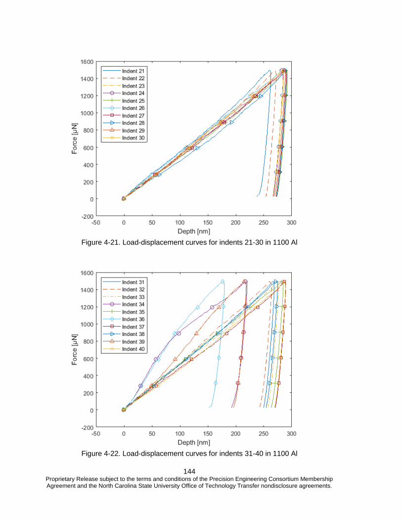
144 Proprietary Release subject to the terms and conditions of the Precision Engineering Consortium Membership Agreement and the North Carolina State University Office of Technology Transfer nondisclosure agreements.
Figure 4-21. Load-displacement curves for indents 21-30 in 1100 Al
Figure 4-22. Load-displacement curves for indents 31-40 in 1100 Al

145 Proprietary Release subject to the terms and conditions of the Precision Engineering Consortium Membership Agreement and the North Carolina State University Office of Technology Transfer nondisclosure agreements.
The array was imaged with the SEM and two representative images are shown in Figure 21 and
Figure 22. These images, like the microscope images, confirm the non-uniformity of the indents.
The non-uniformity was also quantitatively measured in the force-displacement data which
showed varying depth for the same maximum load. The SEM images do not show any obvious
issues with the sample preparation such as irregularities in the surface. The non-uniformity in the
indents may be caused by material inhomogeneity.
Figure 4-23. 10 x 10 array of indents in 1100 Al

146 Proprietary Release subject to the terms and conditions of the Precision Engineering Consortium Membership Agreement and the North Carolina State University Office of Technology Transfer nondisclosure agreements.
Figure 4-24. Another view of the 10 x 10 array of indents in 1100 Al
One issue that arose when imaging the aluminum sample was charging. Charging appears as
sample drift when an unwanted electromagnetic field distorts the path of the electrons. Typically,
this occurs in non-conductive samples as the electron beam begins to impart a negative charge
on the sample over time. However, charging is not expected in a properly grounded aluminum
sample. After consulting Roberto Garcia, this might have been caused by the magnetic stainless
steel specimen disc used in the nanoindenter. These discs are held in the nanoindenter with a
magnetic preload, which may be imparting a small amount of residual magnetism to the stainless
steel. Roberto Garcia suggested degaussing the samples next time. The AIF has a machine to
degauss samples.
METROLOGY
Indents were measured with the New View 5000 scanning white light interferometer (SWLI) at the
highest magnification possible. The results are shown in Figure 23 and Figure 24. As can be seen
in the figures, the New View cannot get data in the sloped portion of the indents. A few data points
appear at the bottom of the indent, but not enough to characterize the indentation.
147 Proprietary Release subject to the terms and conditions of the Precision Engineering Consortium Membership Agreement and the North Carolina State University Office of Technology Transfer nondisclosure agreements.
Figure 4-25: New View measurement of the single indent
Figure 4-26: New View measurement of two indents

148 Proprietary Release subject to the terms and conditions of the Precision Engineering Consortium Membership Agreement and the North Carolina State University Office of Technology Transfer nondisclosure agreements.
The indents were also measured in the Keyence laser confocal microscope at the highest
magnification. Figure 25 and Figure 26 show a cross section from the laser confocal microscope
measurements. As can been seen from the figures, the laser confocal measurements can capture
data across the entire indent. However, the laser confocal is limited to 0.08 µm/pixel. As seen in
Figure 6, the tip geometry has a spherical aperture of 1.4 µm. This means that there will be about
17 pixels across the spherical portion of the indentation. Figure 27 shows a profile of the spherical
portion of the single indent. About 17 points can be counted across the radius, and the profile
does not look smooth due to the low resolution.
Figure 4-27: Laser confocal microscope measurement of the single indent

149 Proprietary Release subject to the terms and conditions of the Precision Engineering Consortium Membership Agreement and the North Carolina State University Office of Technology Transfer nondisclosure agreements.
Figure 4-28: Laser confocal microscope measurement of two indents
Figure 4-29: Close up of the trough of the single indent

150 Proprietary Release subject to the terms and conditions of the Precision Engineering Consortium Membership Agreement and the North Carolina State University Office of Technology Transfer nondisclosure agreements.
The AFM has an optical microscope for finding features of interest, but it is not very high
magnification, which made it difficult to find the small indents. Indents should be done in arrays to
make them easier to find. Figure 28 shows a topographical map of the AFM data after it was
imported into Matlab. Due to the pixels not being square (128 x 256 pixels covering a 10 x 10 µm
area), it has some issues with sectioning in the Slicer Matlab tool. However, the AFM software
was able to provide a section of the indent shown in Figure 29. The AFM appears to be the only
instrument capable of providing sufficient resolution to measure the form if an indent.
Figure 4-30. AFM measurement of an indent in 1100Al
Figure 4-31. Section of the AFM data

151 Proprietary Release subject to the terms and conditions of the Precision Engineering Consortium Membership Agreement and the North Carolina State University Office of Technology Transfer nondisclosure agreements.
FIB CHARACTERIZATION
Next, an investigation of machining the die into diamond using FIB milling was completed. First a
sample A nominally 1 x 1 x 5 mm diamond post was purchased from Chardon tool. Though the
specifications say it was to be polished on both ends, only one end is polished. The diamond
sample was super glued to a 90° SEM mount, and the super glue bond was bridged with
conductive tape. Then the surface was sputter coated with Au-Pd. Finally, a dab of cutting oil was
placed in the corner of the diamond. Figure 32 shows the prepared diamond sample with the
SEM pin mount. Figure 33 shows an SEM image of the diamond sample. Note the oil
contamination in the upper right corner of the sample. The right side of the image is the conductive
tape.
Figure 4-32. Prepared diamond sample

152 Proprietary Release subject to the terms and conditions of the Precision Engineering Consortium Membership Agreement and the North Carolina State University Office of Technology Transfer nondisclosure agreements.
Figure 4-33. SEM image of the prepared diamond sample
A basic cutting test looking at the material removal rate was conducted. Based on previous results
reported in the 2018 PEC annual report, the ion beams with currents above 5 nA were determined
to not be axisymmetric. These initial cutting tests were conducted with 5 nA and 3 nA beams.
According to Table 2 from the manual for the FIB, these currents have a nominal beam diameter
of 85 nm and 66 nm respectively. Based on previous work, bitmap patterns work best when the
overlap is about the same as the beam diameter. For this cutting test, bitmap patterns were
created for a 10 µm square. For the 5 nA beam, a 100 nm overlap was used. For the 3 nA beam
a 50 nm overlap was used. Other test parameters are summarized in Table 3.

153 Proprietary Release subject to the terms and conditions of the Precision Engineering Consortium Membership Agreement and the North Carolina State University Office of Technology Transfer nondisclosure agreements.
Table 4-2. Ion beam currents and corresponding beam diameters from the FIB manual (Table 5-
4).
Table 4-3. Other Parameters used for the 3 and 5 nA beam material removal rate test
Parameter 5 nA 3 nA
Magnification 8000x
Dwell Time 100 µs
Passes 1000 250
Total Time 16:40
Bitmap File Name bmp_Square_100nm.bmp bmp_Square_50nm.bmp
It should be noted that after the sample was tilted in the stage to conduct the FIB milling operation
that the oil contamination dripped down the sample due to gravity. Figure 34 shows an image
taken by the laser confocal microscope of the diamond sample after all the FIB milling was
completed. The spot of oil is now much larger after the part had been tilted 52°.

154 Proprietary Release subject to the terms and conditions of the Precision Engineering Consortium Membership Agreement and the North Carolina State University Office of Technology Transfer nondisclosure agreements.
Figure 4-34 . Diamond sample after FIB milling
FIB cutting experiments with the 0.5 nA and 1.0 nA beams were conducted later. The oil and
sputtered Au-Pd layer from the previous experiments were removed by wiping the diamond tip
with an acetone soaked nonwoven lab tissue. The sample was very difficult to clean. While the
sample looked fairly clean in the optical microscope, it was revealed to still have a significant
amount of debris when it was examined in the SEM. In the future, the diamond should be
completely removed from the SEM pin mount and ultrasonicated in acetone to clean it. It is simply
very difficult to effectively clean such a large area by wiping it. The sample was then prepared
again with conductive tape to bridge the adhesive joint, and a layer of Au-Pd was sputtered onto
the top surface.
Similar experiments were conducted for these lower current beams. For both currents a 10 x 10
µm square was milled with a 50 nm overlap. According to the manual, the 0.5 nA beam has a
nominal beam diameter of 35 nm, and the 1 nA beam has a diameter of 44 nm, so a 50 nm overlap
is about right for the beam size.

155 Proprietary Release subject to the terms and conditions of the Precision Engineering Consortium Membership Agreement and the North Carolina State University Office of Technology Transfer nondisclosure agreements.
Table 4-4. Parameters used for the 0.5 and 1 nA beam material remove rate test
Parameter 0.5 nA 1 nA
Magnification 8000x
Dwell Time 100 µs
Passes 500
Total Time 33:20
Bitmap File Name bmp_Square_50nm.bmp
Figure 35 and Figure 36 show the results of the FIB milling operation. The 1 nA beam was able
to mill a noticeably deeper square in the same amount of time compared to the 0.5 nA beam. Also
prior to milling the squares, the entire viewing area was exposed to the ion beam to remove the
conductive Au-Pd layer that was sputtered onto the surface.
Figure 4-35. 10 x 10 µm square FIB milled into diamond with a 0.5 nA beam

156 Proprietary Release subject to the terms and conditions of the Precision Engineering Consortium Membership Agreement and the North Carolina State University Office of Technology Transfer nondisclosure agreements.
Figure 4-36. 10 x 10 µm square FIB milled into diamond with a 1 nA beam
Finally, FIB milling experiments were conducted on diamond with a 0.3 and 0.5 nA beams. A 0.5
nA beam was used to mill a 10 x 10 µm square to calculate the material removal rate (MRR) and
took 33 minutes. After being measured, the square was less than 1 µm deep. For the investigation
of the 0.3 nA beam, a smaller square was milled to make the cutting time lower. A bitmap for a 5
x 5 µm square was made with Matlab. This new square pattern has a 25 nm overlap and pixel
size of 25 nm. The parameters for the test are shown in Table 5. The test was also repeated for
the 0.5 nA beam to confirm that it is comparable to the other MRR experiments.
Table 4-5. Parameter for square test in diamond
Current 0.3 nA 0.5 nA
Magnification 15,000x
Dwell Time 100 µs
Passes 100
Total Time 26:40
Bitmap File Name bmp_Square_25nm.bmp
All the squares were measured with the Keyence laser confocal. The measured volumes were
divided by the total FIB milling time to yield a material removal rate (MRR). Table 6 shows the
results for the material removal rate study. The results from the 5 x 5 µm squares are shown
highlighted in gray. The 10 x 10 µm and 5 x 5 µm square patterns yield similar results with the 0.5
nA beam. Figure 37 shows the results as a scatter plot along with a linear trend line. The linear

157 Proprietary Release subject to the terms and conditions of the Precision Engineering Consortium Membership Agreement and the North Carolina State University Office of Technology Transfer nondisclosure agreements.
fit describes the relationship between current and material removal rate well with a coefficient of
determination of 0.9978. This linear relationship makes sense given that the current is essentially
a measure of the Gallium ion flow rate. The sputtering yield (atoms removed per incident Ga ion)
is considered to be constant for a fixed angle of incidence assuming no redeposition. Thus, the
slope of the linear fit could be converted to sputtering yield if the atomic density of diamond were
known.
Table 4-6. Result of the diamond material removal rate (MRR) study
Figure 4-37. Plot of the results of the diamond material removal rate study
Single-pixel-wide line tests were conducted with the 5nA beam. The parameters for the line test
are shown in Table 7. A contamination line was then deposited across the lines and processed in
Matlab to create a profile of the line. Figure 38 shows an example of one of the lines with the
contamination line.
Beam
Current [nA]
Volume
Removed [µm3] Time [s]
MRR
[µm3/s]
5 413.695 1000 0.41
3 261.151 1000 0.26
1 187.529 2000 0.09
0.5 78.752 2000 0.04
0.5 59.088 1600 0.04
0.3 31.887 1600 0.02

158 Proprietary Release subject to the terms and conditions of the Precision Engineering Consortium Membership Agreement and the North Carolina State University Office of Technology Transfer nondisclosure agreements.
Table 4-7. Parameters for the 5nA line test
Line 1 Line 2
Magnification 10,000x
Dwell Time 100 µs
Passes 250 500
Total Time 627.1 ms 1 s
Figure 4-38. 5nA line after 500 passes with EBID line
Figure 39 and Figure 40 shows the profiles of the two lines along with a fitted Gaussian curve.
The Gaussian curve has the following equation.
The c1 coefficient corresponds to the half width at 36.7% amplitude. The c1 for the 250 pass line
was 0.27 µm, and 0.32 µm for the 500 pass line. This agrees with previous measurements for the
5 nA beam of about 0.3 µm. It should also be noted that if the profile of the line were axisymmetric,

159 Proprietary Release subject to the terms and conditions of the Precision Engineering Consortium Membership Agreement and the North Carolina State University Office of Technology Transfer nondisclosure agreements.
as in the beam dwelled in a spot instead of a line, the shape would be roughly the negative of
desired lens shape. To make a positive version of the desired lens shape, a smaller beam will
need to be used.
Figure 4-39. Profile of 5 nA line after 250 passes
Figure 4-40. Profile of 5 nA line after 500 passes

160 Proprietary Release subject to the terms and conditions of the Precision Engineering Consortium Membership Agreement and the North Carolina State University Office of Technology Transfer nondisclosure agreements.
FIB SURFACE GENERATION
A bitmap was generated for a 5 x 5 array of convex features spaced 2 µm apart. A 5 x 5 array
was chosen to try to make the features large enough to find later with the AFM. This bitmap has
a 40 nm overlap and 20 nm pixels. The minimum dwell at the peak of the bumps is 0. The dwell
time distribution was arbitrarily chosen to be elliptical. The purpose of the experiment was to
confirm that a field of convex features could successfully be made at this length scale in a
reasonable amount of time.
Figure 4-41. Dwell time distribution of the bitmap
The bitmap was FIB milled with a 1 nA beam. The total size of the array is 10 x 10 µm. Other
parameters used for this FIB milling operation are shown in Table 8. Figure 42 and Figure 43
show the resulting surface. Like results from 25 µm pitch features in the previous project shown
in Figure 44, the step or terrace errors are present at the base of the convex features. However,
the bumps are thought to be more axisymmetric as the terraces appear around the entire base of
the bump in Figure 43 whereas in the previous project the terraces only appears in the quadrants
in Figure 44.

161 Proprietary Release subject to the terms and conditions of the Precision Engineering Consortium Membership Agreement and the North Carolina State University Office of Technology Transfer nondisclosure agreements.
Table 4-8. Other parameters used for FIB milling the 5 x 5 array of convex features
Parameter Value
Magnification 8000x
Dwell Time 100 µs
Passes 200
Total Time 12:50
Bitmap File Name bmp_D1.bmp
Figure 4-42. 5 x 5 Array of convex features in diamond

162 Proprietary Release subject to the terms and conditions of the Precision Engineering Consortium Membership Agreement and the North Carolina State University Office of Technology Transfer nondisclosure agreements.
Figure 4-43. Top view of the 5 x 5 array of convex features in diamond
Figure 4-44. 3 x 3 array of convex features on a 25 µm pitch in glassy carbon

163 Proprietary Release subject to the terms and conditions of the Precision Engineering Consortium Membership Agreement and the North Carolina State University Office of Technology Transfer nondisclosure agreements.
A 5 x 5 array of convex features was FIB milled into diamond with the 0.5 nA beam. This is a
replication of the array milled with the 1 nA beam to examine the difference of milling features
with the different beams. Because the 0.5 nA beam has roughly half the removal rate of the 1 nA
beam, the number of passes was double. The resulting surface can be compared in Figure 45
and Figure 46. Figure 45 shows the surface made with the 0.5 nA beam while Figure 46 shows
the results of the 1 nA beam. Qualitatively, the 0.5 nA surface looks smoother, but that could be
a result of not producing steep enough slopes to develop the terrace morphology.
Table 4-9. Parameters used to make the 5 x 5 array in diamond
Current 0.5 nA 1 nA
Magnification 8000x
Dwell Time 100 µs
Passes 400 200
Total Time 23:40 12:50
Bitmap File Name bmp_D1.bmp
Figure 4-45. 5 x 5 array FIB milled with a 0.5 nA beam in diamond

164 Proprietary Release subject to the terms and conditions of the Precision Engineering Consortium Membership Agreement and the North Carolina State University Office of Technology Transfer nondisclosure agreements.
Figure 4-46. 5 x 5 array FIB milled with a 1 nA beam in diamond
The diamond surface was also measured with the AFM. The AFM measurement was conducted
with 1024 lines and 1024 points per line to yield 14.7 nm pixels. The scan was conducted over a
15 x 15 µm area at an excitation frequency of 0.4 Hz. Figure 47 shows the surface of the 5 x 5
array that was FIB milled with the 0.5 nA beam. This is the raw unprocessed data. Typically, AFM
measurements are post-processed to correct the AFM measurements. However, since how those
corrections are calculated is not understood at this time, no post-processing was conducted. As
can be seen from the AFM measurement the features appear to be longer perpendicular to the
scan direction as the features do not appear to be axisymmetric. Looking at the SEM images, this
does not appear to be the case in actuality. A similar effect appears in the measurement of the
surface made with the 1 nA beam shown in Figure 48. This is likely an artifact of the AFM
measurement.

165 Proprietary Release subject to the terms and conditions of the Precision Engineering Consortium Membership Agreement and the North Carolina State University Office of Technology Transfer nondisclosure agreements.
Figure 4-47. AFM measurement of the 5 x 5 array created with the 0.5 nA beam in diamond

166 Proprietary Release subject to the terms and conditions of the Precision Engineering Consortium Membership Agreement and the North Carolina State University Office of Technology Transfer nondisclosure agreements.
Figure 4-48. AFM measurement of the 5 x 5 array created with the 1 nA beam in diamond
Due to other priorities, the diamond sample had sat in the lab for about 6 weeks in a closed
container before it could be measured again in the AFM. In the intervening time the sample was
contaminated, and the sample was not able to be cleaned successfully.
The diamond sample was removed from the holder by dissolving the adhesive bonding it to the
SEM pin mount with Acetone. The diamond was then ultrasonicated in Acetone. Finally, the
diamond was inspected under 500x magnification in an optical microscope and wiped with a
Texwipe soaked in Acetone. It was difficult to adequately clean the polished diamond as the area
of interest is relatively large. As could be seen in the SEM, debris and residue were still present
on the sample.
The sample was then bonded to the SEM pin mount with Gorilla brand super glue. The polished
diamond surface was electrically grounded by bridging the glue joint with conductive tape, then
sputter coating Au-Pd over both the diamond surface and the conductive tape.
The goal of this FIB experiment is to measure the form produced by the pattern in the FIB. The
pattern was repeated 3 times to gain some understanding of the variability. Prior to FIB milling
each pattern the focus and stigmation of the ion beam was adjusted. Table 10 shows the
significant parameters used for the FIB pattern.

167 Proprietary Release subject to the terms and conditions of the Precision Engineering Consortium Membership Agreement and the North Carolina State University Office of Technology Transfer nondisclosure agreements.
Table 4-10. Parameters used to make the 5 x 5 array in diamond
Current 1 nA
Magnification 8000x
Dwell Time 100 µs
Passes 200
Total Time 12:50
Bitmap File Name bmp_D1.bmp
An overview of the resulting features in diamond are shown in Figure 49. The three newly FIB
milled features are boxed in red. There are some FIB experiments visible outside the red box.
Also note the debris and residue left on the surface from the attempts to clean the surface. Figure
50 shows a magnified SEM image of the leftmost structure in Figure 49. Note the rings at the
base of the convex features which indicates the beginning of the terrace structure previously
reported in literature.
Figure 4-49. FIB milled patterns in diamond

168 Proprietary Release subject to the terms and conditions of the Precision Engineering Consortium Membership Agreement and the North Carolina State University Office of Technology Transfer nondisclosure agreements.
Figure 4-50. Magnified SEM image of the leftmost FIB milled structure in diamond
Figure 51 shows a cross section of the features shown in Figure 50. The features are about 850
nm tall and spaced 2 µm apart (2.8 µm across the diagonal). There appears to be an issue with
the AFM measurements in the lower left quadrant of each convex feature. As can be seen in the
trace of the cross section. The left side of each bump has a different slope than the right side. A
cross section in another direction does not show this asymmetry in Figure 52. Each convex feature
in each of the three replicates displays the same issue. This is likely an issue with the tip shape.

169 Proprietary Release subject to the terms and conditions of the Precision Engineering Consortium Membership Agreement and the North Carolina State University Office of Technology Transfer nondisclosure agreements.
Figure 4-51. Cross section of FIB milled features in diamond (all dimensions in nm)

170 Proprietary Release subject to the terms and conditions of the Precision Engineering Consortium Membership Agreement and the North Carolina State University Office of Technology Transfer nondisclosure agreements.
Figure 4-52. Orthogonal cross section of FIB milled features in diamond (all dimensions in nm)
For reference, the tip used for all AFM measurements thus far have been taken with a Tap300AL-
G tip from budgetsensors.com. More information can be found at
<https://www.budgetsensors.com/tapping-mode-afm-probe-aluminum-tap300al>. Table 11
shows the specifications for the tip from the product information. Figure 53 shows an image of
one of the tips also taken from the product information web page. Given that the tip has a half
angle of 30°, the highest slope that could be measured with a perfect tip is 60°.
Table 4-11. AFM tip specifications

171 Proprietary Release subject to the terms and conditions of the Precision Engineering Consortium Membership Agreement and the North Carolina State University Office of Technology Transfer nondisclosure agreements.
Figure 4-53. AFM tip
Before each FIB milling operation the focus and stigmation of the beam was adjusted to simulate
approaching a machine for the first time and setting it up. An SEM image of the resulting surface
is shown in Figure 49. The three FIB milled regions are labeled “Exp 1”, “Exp 2” and “Exp 3”,
denoting the order in which the experiments were conducted.
Figure 4-54. FIB milled patterns in diamond

172 Proprietary Release subject to the terms and conditions of the Precision Engineering Consortium Membership Agreement and the North Carolina State University Office of Technology Transfer nondisclosure agreements.
The AFM measurements were compared in Matlab using the surfer.m script. Exp 1 was used as
the reference data set for Exp 2 and Exp 3. The surfer.m tool was used to align the two data sets
to reduce the RMS of the difference between them. The resulting difference plots are shown in
Figure 55 and Figure 56. For both figures, the Z scale is the same. As can be seen from the plots,
Exp 1 and Exp 2 are very similar to each other, with a RMS difference of .005 nm. Exp 3 is very
different with an RMS difference of 64 nm. The plan view of the difference between Exp 1 and
Exp 3 shown in the bottom part of Figure 56 shows that most of the error is localized in the bottom
of the square array. The localization on one side indicates that this is not an alignment error. I
suspect this is due to being damaged and changing shape when attempting to measure the steep
dropoff at the edge of the pattern. This could be addressed by using a softer AFM tip or FIB milling
a slope down to the lens features.
Figure 4-55. Difference plot between Exp 1 and Exp 2

173 Proprietary Release subject to the terms and conditions of the Precision Engineering Consortium Membership Agreement and the North Carolina State University Office of Technology Transfer nondisclosure agreements.
Figure 4-56. Difference plot between Exp 1 and Exp 3
A new bitmap was developed to match the new targeted paraboloid geometry. A plot of the relative
dwell time is shown in Figure 57. Some of the parameters to develop this pattern are shown in
Table 12.

174 Proprietary Release subject to the terms and conditions of the Precision Engineering Consortium Membership Agreement and the North Carolina State University Office of Technology Transfer nondisclosure agreements.
Figure 4-57. Relative dwell time plot for the new bitmap (zero values removed for clarity)
Table 4-12. Bitmap parameters
Bitmap XY Size 10 µm
Pixel Size 20 nm
Overlap 40 nm
Pixels per feature 100
This pattern was FIB milled 3 times with both 1 nA and 0.5 nA. The intention was to check the
repeatability of the FIB milling process and begin developing compensation methods. Figure 58
shows an overview of these experiments. A 0.5 nA beam was used on the areas marked D2_1
through D2_3, while a 1 nA beam was used on D2_4 through D2_6. While trying to measure
these features with the AFM the tips broke easily, and I was never able to measure all three
replicates with a single tip. The hardness of the diamond is a problem for the durability of the
silicon AFM tips.

175 Proprietary Release subject to the terms and conditions of the Precision Engineering Consortium Membership Agreement and the North Carolina State University Office of Technology Transfer nondisclosure agreements.
Figure 4-58. FIB milled arrays of paraboloids
To address the issue of the AFM tip damage, I added a conical sloped surface to the bitmap file.
Figure 59 shows the modified bitmap. I added a Ø14.142 µm circular flat region around the
paraboloids as well as a conical surface. The conical surface was targeted to have a half cone
angle of about 60° to accommodate the geometry of the AFM tip.

176 Proprietary Release subject to the terms and conditions of the Precision Engineering Consortium Membership Agreement and the North Carolina State University Office of Technology Transfer nondisclosure agreements.
Figure 4-59. Relative dwell time plot for the new bitmap with conical depression
I FIB milled this pattern with a 1 nA beam three times. Table 13 shows some additional parameters
used for this experiment. Figure 60 shows an example of the resulting surface.
Table 4-13. Parameters used to make the 5 x 5 array of paraboloids in diamond
Current 1 nA
Magnification 5000x
Dwell Time 100 µs
Passes 53
Total Time 8:40
Bitmap File Name bmp_mask_D2.bmp

177 Proprietary Release subject to the terms and conditions of the Precision Engineering Consortium Membership Agreement and the North Carolina State University Office of Technology Transfer nondisclosure agreements.
Figure 4-60. FIB milled paraboloids in diamond
Figure 61 and Figure 62 show the AFM measurements of the array of features shown in Figure
60. Figure 61 is the first measurement of the array. Figure 62 is a repeat measurement of the
same surface with the same measurement setup (same AFM tip without moving the sample) after
measuring the two other arrays. Figure 62 shows a ridge on the side of each convex feature at
about the 6 o’clock position. This feature is not present in the first measurement in Figure 61
indicating that the AFM tip shape has likely changed. While the conical depression around the
array has improved the life of the AFM tips such that there are no longer gross error after
measuring one or two arrays, the tips are still getting damaged.

178 Proprietary Release subject to the terms and conditions of the Precision Engineering Consortium Membership Agreement and the North Carolina State University Office of Technology Transfer nondisclosure agreements.
Figure 4-61. AFM measurement of FIB milled diamond
Figure 4-62. AFM measurement of the same surface after measuring two other arrays

179 Proprietary Release subject to the terms and conditions of the Precision Engineering Consortium Membership Agreement and the North Carolina State University Office of Technology Transfer nondisclosure agreements.
The middle 9 lens features were extracted from the AFM measurements of each FIB milled array
and compared to the desired paraboloid shape in MATLAB. Figure 63 shows an example of the
error map created by this analysis. Figure 64 shows a plot of the absolute height error averaged
over the 9 paraboloids.
Figure 4-63. Z height error of paraboloids FIB milled in diamond

180 Proprietary Release subject to the terms and conditions of the Precision Engineering Consortium Membership Agreement and the North Carolina State University Office of Technology Transfer nondisclosure agreements.
Figure 4-64. Average absolute z error of the FIB milled paraboloids
I then resampled the data into the bitmap pixel spacing and shifted the data to force the error at
the center to be zero. I averaged the error over the 9 features and converted the error to a
percentage of the maximum depth. Figure 65 shows a plot of this average % error map. Finally, I
multiplied the original bitmap by this percentage to attempt to compensate for error in the FIB
milling process. Figure 66 shows the error compensated dwell time map. The conical depression
is not shown for clarity (such as in Figure 59).

181 Proprietary Release subject to the terms and conditions of the Precision Engineering Consortium Membership Agreement and the North Carolina State University Office of Technology Transfer nondisclosure agreements.
Figure 4-65. Average % error of the FIB milled paraboloids

182 Proprietary Release subject to the terms and conditions of the Precision Engineering Consortium Membership Agreement and the North Carolina State University Office of Technology Transfer nondisclosure agreements.
Figure 4-66. Error compensated relative dwell time map
This compensated bitmap pattern was used to FIB mill a new set of features. I used the
parameters shown in Table 14. Figure 67 shows an image of the resulting surface in diamond.
Table 4-14. Parameters used to make the compensated 5 x 5 array of paraboloids in diamond
Current 1 nA
Magnification 5000x
Dwell Time 100 µs
Passes 55
Total Time 8:38
Bitmap File Name bmp_mask_D2_comp.bmp

183 Proprietary Release subject to the terms and conditions of the Precision Engineering Consortium Membership Agreement and the North Carolina State University Office of Technology Transfer nondisclosure agreements.
Figure 4-67. FIB milled error compensated pattern in diamond
A similar analysis was done to average the error over the 9 central paraboloid features. The
resulting average absolute height error is shown in Figure 68. Compared to Figure 64 the error in
the compensated surface is worse than the uncompensated. Figure 69 shows a meridian of the
center paraboloid of the 5 x 5 pattern along with the desired surface after calculating the best fit
transformation matrix. It appears that the error is primarily caused by not removing enough volume
of material. In the future, a study of total length of FIB milling time should be conducted to see
how it affects the shape fidelity.

184 Proprietary Release subject to the terms and conditions of the Precision Engineering Consortium Membership Agreement and the North Carolina State University Office of Technology Transfer nondisclosure agreements.
Figure 4-68. Average absolute z error of the error compensated pattern

185 Proprietary Release subject to the terms and conditions of the Precision Engineering Consortium Membership Agreement and the North Carolina State University Office of Technology Transfer nondisclosure agreements.
Figure 4-69. Vertical slice through the center feature of the 5 x 5 error compensated pattern
CONCLUSIONS
In this study the manufacturing of a microlens array mold and die were explored using Aluminum
1100 H14 and diamond for the mold and die respectively. Manufacturing of the array mold was
explored using nanoindentation. Nanoindentation tests were completed on the Al 1100 using a
Berkovich tip. The indentation method was used to create 10 x 10 arrays and characterized using
the New View 500 SWLI and the Keyence laser confocal microscope in order to measure the
indentation depth and form. The New View was unable to give enough data points along the slope
and base of the indentations, however the Keyence microscope gives high enough resolution to
analyze the cross-section of the indentations. The die was FIB milled with a 1 nA and 0.5 nA
beam to explore the material removal rate and effectiveness of each beam. No dramatic
differences were noticed between the two currents and a 1 nA was used for creating some of the
final parabolic features. During measuring of the die grid, it was found that the AFM tip would
easily damage when measuring the peak heights. In order to reduce tip damage, a conical slope
was added to the surrounding of the grid. This has helped reduce damage to the AFM tip, although
some artifacts still exist when taking multiple measurements.

186 Proprietary Release subject to the terms and conditions of the Precision Engineering Consortium Membership Agreement and the North Carolina State University Office of Technology Transfer nondisclosure agreements.
REFERENCES
[1] X. Ding, G.C. Lim, C.K. Cheng, D.L. Butler, K.C. Shaw, K. Liu and W.S. Fong, "Fabrication of a micro-size diamond tool using a focused ion beam," Journal of Micromechanics and Microengineering, vol. 18, pp. 075017, Jul 1,. 2008.

187 Proprietary Release subject to the terms and conditions of the Precision Engineering Consortium Membership Agreement and the North Carolina State University Office of Technology Transfer nondisclosure agreements.
REDUCING MICROLENS ARRAY INDENTATION
FORM ERROR VIA TESTING AND SIMULATION Parker Eaton
Graduate Student
Dr. Mark Pankow
Director of the PEC
Assistant Professor
Mechanical and Aerospace Engineering
ABSTRACT
This report addresses the initial methods involved in reducing the geometric form errors that occur when indenting microlens arrays. The microlens arrays are rapidly indented on a variety of metallic negative molds. A proprietary indent force and indent depth measurement technique is employed to aid in the characterization and control of the microindenting process. Insights from form error analysis and finite element simulations can then be used to make informed decisions to redefine die geometry and microindentation strategies in the pursuit of minimized geometric form error.

188 Proprietary Release subject to the terms and conditions of the Precision Engineering Consortium Membership Agreement and the North Carolina State University Office of Technology Transfer nondisclosure agreements.
INTRODUCTION
Microlens arrays are typically composed of a grid of micrometer-scale lenses that are formed onto
a substrate. The lenses may be positives or negatives of the desired lens geometry. In the context
of this research, these lenses will serve as a negative mold for a final product. Traditionally, the
arrays are laid out in a two-dimensional grid with lenses being aligned in two orthogonal directions.
In some applications, alternative lens layouts may be used such as a hexagonal packing of lens
or a stochastic layout. Figure 5.1 illustrates both an orthogonal array as well as a hexagonal array.
An orthogonal lens layout will be used for the entirety of this project.
Figure 5.1. FE-SEM images of (a) orthogonal microlens arrays and (b) hexagonal microlens
arrays [1].
Microlens arrays may be employed in numerous optical applications including but not limited to:
LCD displays, anti-reflective coatings, photovoltaics, and virtual reality. A microlens operates
under similar principles as a full-size optical lens by directing light rays to coincide on a designed
focal point. Figure 5.2 illustrates the trace that the light rays follow through a convex microlens to
meet at the focal point of the lens.

189 Proprietary Release subject to the terms and conditions of the Precision Engineering Consortium Membership Agreement and the North Carolina State University Office of Technology Transfer nondisclosure agreements.
Figure 5.2. Illustration of light rays traveling through microlens.
Microlens arrays are nothing new to the worlds of industry and academia. As such, several
manufacturing techniques exist. These methods can be broken down into two categories: direct
and indirect. The direct method pertains to processes that involve the fabrication of convex lenses
directly onto the substrate. In these methods, the lens material is typically heated to a
thermoplastic or liquid state and then shaped into the desired geometry. These methods include
thermal reflow, microplastic embossing, and microdroplet jetting. Alternatively, the indirect
method of manufacturing involves the creation of a negative mold. A microlens array is then
fabricated by injection molding, hot embossing, or UV molding. While the direct methods typically
result in a better geometry than the indirect methods, the quality of the final microlens array relies
heavily on the form of the negative mold.
Traditionally, microlens array molds have been manufactured via photolithography or ultra-high
precision machining operations such as focused ion beam (FIB) milling. Both methods are
associated with high costs and are very time-consuming if a mold of a useful scale is to be
manufactured. Nanocoining, a recent technology developed at the Precision Engineering
Consortium (PEC) at North Carolina State University [3], significantly reduces these costs and
allows for a very short turnaround time. Nanocoining makes use of a resonant actuator to achieve
a microindenting rate up to 45 kHz. A diamond die patterned with positive microlens features
(Figure 5.3) impacts the mold surface at a very high frequency. Operations that could take days
with traditional methods are completed in hours with nanocoining. To fully realize the benefits of
this technology, the form error of the indented microlens negatives or “features” must be studied
and compensated for to ensure the final microlens array behaves as designed. This report will
describe the initial methods that are being used to analyze and account for form errors in indented
molds.
Light Rays
Focal Point

190 Proprietary Release subject to the terms and conditions of the Precision Engineering Consortium Membership Agreement and the North Carolina State University Office of Technology Transfer nondisclosure agreements.
Figure 5.3. Schematic of a diamond die with parabolic features.
DATA ACQUISITION AND PHYSICAL TESTING
Up to this point, little has been completed experimentally to validate the finite element simulations.
This work uses a comprehensive process that would use insights from validated simulation to
drive die design and indenting strategies. The alterations to die geometry and indenting strategy
can then be tested and their effectiveness analyzed for future testing. This closed-loop process
will converge in a die geometry and indenting strategy that will minimize feature form error in the
mold of a specified material. Through many repetitions of this design process, data will be
gathered to enable faster convergence in future projects. For this goal to be realized, the
simulation must first be validated for multiple mold materials and die layouts of interest. In the
context of this project, the investigated mold materials will be Cu 110, electroplated Cu, and NiP
(Nickel Phosphorus). To begin, a 3x3 feature die will be manufactured and used for the sake of
continuity. To validate the simulation, the microlens array indenting process must be
characterized in-house through accurate and reliable metrology. This is possible thanks to a
proprietary force and indent depth sensing technology. In conjunction with atomic force
microscopy (AFM), a detailed picture of the indenting process may be developed and used for
error analysis. This section will cover the steps taken to initialize the proposed closed-loop form
error minimization process pictured below in Figure 5.4.
Figure 5.4. Proposed closed-loop form error minimization process.
Simulation
Die/Strategy Design
Testing/Error Analysis

191 Proprietary Release subject to the terms and conditions of the Precision Engineering Consortium Membership Agreement and the North Carolina State University Office of Technology Transfer nondisclosure agreements.
Setup and validation of metrology
Physical testing is carried out at Raleigh-based nanofabrication startup, Smart Material Solutions,
Inc. A testing stage with integrated indent force and indent depth sensing capabilities was
developed and installed into an existing microindenting setup. This configuration is not capable
of ultra-high frequency nanocoining operations but can indent at a frequency up to 10 Hz. Indent
force vs. depth curves may be obtained using this sensor. Indent force vs. indent depth curves
are very useful for characterizing the indenting process. For example, as the die indents the mold,
the contact area will increase, thus increasing the required indenting force. The slope of this
loading curve will vary from die to die and material to material. To validate the metrology, two
experiments were conducted. The first experiment involved the recreation of a control
nanoindentation experiment and comparison of the indent force vs indent depth curves of the
recreation against the control. A Berkovich indenter was fabricated by Chardon Tool onto a 5mm
x 1mm x 1mm single crystal diamond shank. This indenter was easily installed onto the indenting
device.
Figure 5.5. Schematic of Berkovich Indenter tip (65.35 degree half angle).
Figure 5.6. Chardon Tool Berkovich indenter (estimated 65.145 degree half angle).

192 Proprietary Release subject to the terms and conditions of the Precision Engineering Consortium Membership Agreement and the North Carolina State University Office of Technology Transfer nondisclosure agreements.
Figure 5.6 demonstrates the quality of the Berkovich tip manufactured by Chardon Tool. An ideal
Berkovich indenter has a half angle of 65.35 degrees whereas the provided Berkovich indenter
has an estimated half angle of 65.145 degrees. This small discrepancy is acceptable given the
nature of the test and the accuracy of the digital microscope measurement.
A nanoindentation experiment on a diamond-turned Cu 110 foil was carried out at the Analytical
Instrumentation Facility (AIF) at North Carolina State University. The maximum load was set to
be 10mN. Figure 5.7 presents the outputted indent force vs indent depth curve from one of the
nanoindentation tests. The indenter reached a maximum indent depth of 467 nm before the force
was held at constant for 10 seconds prior to retraction. This depth of 467 nm is the control depth
for the in-house experiments. The resultant depth of the indentation can be understood to be the
indent depth when the indent force becomes zero. This is the “final” indent depth after any elastic
rebound during the unloading phase of the indent. In this case of the control experiment, this
resultant indent depth was 434 nm. For the sake of accuracy, a force hold control feature was
implemented into the control algorithm to recreate the plateau observed in the nanoindentation
loading curve.
Figure 5.7. Control Berkovich Cu 110 nanoindentation curve.
Three indents were completed in a Cu 110 foil and are pictured in Figure 5.8. The loading curves
obtained from these experiments are plotted against the control curve in Figure 5.9. It is important
to note that both the forces and indent depths observed in the control nanoindentation experiment
are at the very bottom of the range expected under typical microlens array indentation. As such,
the measurements of force and indent depth are subject to a noticeable amount of noise. With
this considered, the results are very promising. All three loading curves align relatively well with
the control despite the loads and depths being on the mN and nm scale, respectively. A later
improvement in the proprietary force and depth measurement system increased the resolution,
thus reducing noise in this indent force and indent depth range.

193 Proprietary Release subject to the terms and conditions of the Precision Engineering Consortium Membership Agreement and the North Carolina State University Office of Technology Transfer nondisclosure agreements.
Figure 5.8. Three in-house Berkovich indents as viewed through a digital microscope.
Figure 5.9. Berkovich nanoindentation loading curves.
An important metric to consider when conducting indents is the amount of normal elastic
“springback”. As the die exits the mold, there is some elastic rebound or springback that occurs
in the mold material. This springback can be defined as the difference between the resultant
indent depth and the maximum indent depth achieved at peak force. To quantify springback, the
measurement of the resultant indent depth must be accurate. The second validation experiment
compares the measured resultant indent depths of in-house Berkovich indents against AFM
measurements of these same indents.

194 Proprietary Release subject to the terms and conditions of the Precision Engineering Consortium Membership Agreement and the North Carolina State University Office of Technology Transfer nondisclosure agreements.
Figure 5.10. Indent depth experiment measurements. (a) Indent force curve where the red circle
highlights the resultant indent depth. (b) AFM image of the corresponding indent.
A total of 12 indents were completed ranging in peak force from 10mN to 1N. For the sake of time,
only 8 were imaged. The resultant indent depth derived from the loading curve is the depth at
which the indent force returns to zero. The indent depth derived from the AFM image data is
calculated by first zeroing the height data in reference to the bottom of the indent and then probing
a flat point near the edge of the indent. The reading of this probing point is understood to be the
resultant indent depth. Table 1.1 highlights the results of this experiment. The results of this
experiment may be visualized in Figure 5.11.
Table 1.1. Summary of resultant indent depth validation experiment
(a) (b)

195 Proprietary Release subject to the terms and conditions of the Precision Engineering Consortium Membership Agreement and the North Carolina State University Office of Technology Transfer nondisclosure agreements.
Figure 5.11. Visualization of the resultant indent depth measurements obtained from AFM and
the proprietary indent depth sensor.
The results of these two experiments validate the proprietary indent force and indent depth
measurement technique. Data obtained from in-house experiments can now be used to
characterize and interpret the microlens array indenting process. Please note that the indent force
and indent depth sensor has since been improved in function.
3x3 Diamond Die
A 3x3 feature diamond die was designed and FIB milled for the purposes of initial testing. The
features’ dimensions were on a similar scale to that expected of a future microlens array and are
much smaller than the 2x2 die fabricated in previous research [2]. The features have a radius of
curvature of 1 µm and a pitch (distance between feature vertices) of 2 µm. The die features were
FIB milled onto a standard 5mm x 1mm x 1mm single crystal diamond shank. After FIB milling,
SEM and AFM images were taken of the die. AFM images of the die indicate that debris was
present around the central feature during the imaging (as seen in Figure 5.13). As such, the die
is set to be reimaged. AFM images of the die carry a lot of value. For one, the AFM image of the
die may be referenced against an AFM image of an indent. This allows for an analysis of material
flow and elastic springback. Secondly, the die may be imported into a finite element solver where
indents under varying conditions may be simulated, validated, and used to motivate design and
process changes for that particular die.

196 Proprietary Release subject to the terms and conditions of the Precision Engineering Consortium Membership Agreement and the North Carolina State University Office of Technology Transfer nondisclosure agreements.
Figure 5.12. SEM images of the FIB milled diamond die.
Figure 5.13. (a) Raw AFM xyz data plotted in MATLAB (note debris indicated by red arrow). (b)
Die AFM data imported into Abaqus™ and meshed.
Indent Process Control
Additional control has been implemented into the indent controller at Smart Material Solutions,
Inc. Currently, the operator of the indenting machine may control to several indent parameters
such as the indent machine axis infeed, indent depth, die tip velocity, indent strain rate, indent
force, stepover between indents, and holding periods (holding time at peak indent force or indent
depth). These controls give the operator the ability to study the effects of various indent
(a) (b)

197 Proprietary Release subject to the terms and conditions of the Precision Engineering Consortium Membership Agreement and the North Carolina State University Office of Technology Transfer nondisclosure agreements.
parameters on the resultant quality of the indent. For example, some mold materials may respond
better to a slower indent velocity and shallower indent depth while others may react better to a
high velocity indent programmed to a deeper indent depth. Indent controls may be fine-tuned to
any die and material pairing through testing. In addition to controlling individual indents, entire
two-dimensional arrays may be created and controlled by the same parameters. These arrays
may be manufactured at a rate up to approximately 10 Hz (10 indents per second) while retaining
the indent force and indent depth sensing capabilities. This enables findings from studies
conducted on single indents to be applied to large scale arrays for further analysis. The wide
variety of control and depth of data acquisition allows the operator of the indenting machine the
ability to both replicate simulation conditions in real life and replicate real life conditions in the
simulation. For the closed-loop form error minimization process to truly work, simulation must be
able to match reality and vice versa.
Figure 5.14. Digital microscope images of indents in electroplated Copper using the 3x3 die. (a)
Individual indents of varying depths. (b) 10x10 indent array.
(a) (b)

198 Proprietary Release subject to the terms and conditions of the Precision Engineering Consortium Membership Agreement and the North Carolina State University Office of Technology Transfer nondisclosure agreements.
Figure 5.15. Indent loading curves from the right-hand group of five indents in Figure 5.14.a
CURRENT WORK
Several projects are currently ongoing as the closed-loop form error minimization process is now
being entered. As data is collected from simulation and testing it can be used to compare and
analyze die geometry and indenting process. Changes will begin to take place in the effort to
converge on an indent with minimized form error. Once this is accomplished and the findings
documented, the same process will begin for large scale arrays and indenting procedures. In
order to accurately model the microlens array indentation process for Cu 110, electroplated Cu,
and NiP metallic molds, the plasticity properties of each mold material must be obtained and
implemented into the simulation. An indent form error quantification algorithm must be developed
in order to compare AFM images of real indents to a reference geometry. Doing so will allow for
an evaluation of the effectiveness of die geometry and/or indenting process control parameters.
Additionally, mold material flow may be studied, and insight gained to drive die geometry and
indent process modifications. Lastly, interesting behaviors have been observed in indent loading
curves that warrant further investigation.
Simulation Enhancements
To properly simulate the microlens indentation process and validate the simulation for each mold
material used, plasticity properties must be derived and then used in the simulation. For the case
of an Abaqus™ Explicit analysis, this comes in the form of capturing the plastic region of the
stress strain curve. Dao et al derives dimensionless equations that compute parameters such as
the strain hardening exponent from nanoindentation loading curves [4]. These parameters are
then used to reconstruct the stress strain curve. Points in the plastic region are sampled and then

199 Proprietary Release subject to the terms and conditions of the Precision Engineering Consortium Membership Agreement and the North Carolina State University Office of Technology Transfer nondisclosure agreements.
imported into the simulation. Nanoindentation testing is currently underway for each of the
materials used in this study. Additionally, using single crystal diamond dies allows for the
simulated die to be treated as a rigid body. This allows for a decreased computational time. On
average, the previously developed simulations [2] took around one day per indent to solve. With
the simulations being so computationally expensive, any reduction in complexity will be well
received. The ability to import the as-manufactured die geometry into the finite element model will
aid in further validation of the simulation.
Figure 5.16. Abaqus™ FEM modeling the testing 3x3 die indenting a mold material.
Form Error Quantification
Microlens form error quantification is critical for the validation of die geometry and indentation
process changes. A form error surface may be computed so that regions of large form error may
be identified and compensated for. An algorithm is currently being developed to import,
manipulate, and operate on AFM data of any die, indent, and target microlens array geometry.
The program will automatically identify the vertices of the imported AFM images and perform
iterative coordinate transformations on the coordinate points until the vertices are aligned with the
global coordinate system (see Figure 5.17 and Figure 5.18). Following this, form error may be
computed and analyzed via the subtraction of the aligned indent surface from the aligned die or
target microlens array geometry surface. Various cross-sectional views may be taken to observe
the flow of mold material within the indent (Figure 5.19). The error surface may be used to
influence die geometry changes to compensate for regions of over or under-indenting. These
metrics allow for the user to observe where and how indent geometry differs from the target
geometry. These findings can then be used to modify die geometry to counter the observed errors.
For example, the radius of the bottom of an indent might be too large while the indent itself is also
too shallow in depth. This might suggest that the height of the die features be lengthened while
the pitch between the features remains constant. In theory, making these modifications to die

200 Proprietary Release subject to the terms and conditions of the Precision Engineering Consortium Membership Agreement and the North Carolina State University Office of Technology Transfer nondisclosure agreements.
geometry will deepen the indent and decrease the radius at the bottom of the feature. Over
multiple iterations, the original geometric error may be significantly reduced. In addition, this tool
will also be used to validate the finite element simulation results against physical indents in a
similar manner. The AFM image of an indent may be compared to a digital recreation of it.
Conveniently, all surfaces (including the form error surface) may be exported to .stl format for
easy importation into CAD and FEA software.
Figure 5.17. Window allowing operator monitoring of the overlay of die and indent surfaces.
Figure 5.18. AFM data before (top) and after (bottom) iterative auto-alignment.

201 Proprietary Release subject to the terms and conditions of the Precision Engineering Consortium Membership Agreement and the North Carolina State University Office of Technology Transfer nondisclosure agreements.
Figure 5.19. Sample output of error analysis algorithm.
Indent Loading Curves
The 3x3 die was tested under a variety of circumstances. During testing on a NiP mold, an
interesting trend was observed in the loading curves. Figure 5.20 presents the loading curves
obtained from this test. This experiment involved varying the indenting machine axis infeed which
in turn varies the depth of the indent. Axis infeeds of 1 µm to 5 µm in steps of 1 µm were used in
the experiment. Please note that “F5” is the internal name of the 3x3 die. A defined increase in
the loading curve slope (indicated by the red arrow) occurs at an indent depth of approximately
1.1 µm. Let this loading curve slope be understood as the “indenting stiffness” or the indenting
force required per unit indent depth. The indenting stiffness increases from approximately 0.08
N/µm to approximately 0.20 N/µm. Following this change in slope, no matter how deep the die
penetrated the mold, the unloading path remained nearly identical, resulting in very similar
resultant indent depths (indicated by the red circle). It is speculated that at this point, mold material
has flowed fully into the valleys of the die and the contact area has increased to a nearly constant
value, resulting in a larger, and approximately constant, indenting stiffness. Alternatively, the
sharp increase in indenting stiffness may be due to feature-less portions of the die contacting the
mold surface. To discern between the two possibilities, an experiment will be conducted to
quantify the indenting stiffness of a feature-less die against a NiP mold. If this stiffness is close to
0.20 N/µm, then it can be assumed that the stiffness change is due to contact of feature-less
portions of the die against the mold material. Should this stiffness be significantly greater than
0.20 N/µm, then it may be accepted that the change in indenting stiffness is due to complete filling
of the valleys in the 3x3 die.

202 Proprietary Release subject to the terms and conditions of the Precision Engineering Consortium Membership Agreement and the North Carolina State University Office of Technology Transfer nondisclosure agreements.
Figure 5.20. Indent loading curves of 3x3 die test on NiP Mold.
FUTURE WORK Once all components of the closed-loop form error minimization process are established and
vetted, many loops of simulation, testing, and design tweaking will be undergone in the effort to
converge to an error-minimized die geometry and indenting process for a singular indent. The
insights gained during this exercise will be used to drive a similar process to converge to an error-
minimized microlens array. The data gathered can then be applied to future microlens array
geometries, creating a large collection of data. This data will be used to establish a process for
creating error-minimized microlens arrays in metallic molds at a frequency of approximately 10
Hz. Testing will then be conducted using the high strain rate nanocoining process in the effort to
significantly reduce the manufacturing time of error-minimized microlens arrays by indenting at a
frequency on the order of 45 kHz. High-speed, high-accuracy nanocoining will enable
extraordinarily fast production of high quality molds for the manufacturing of microlens arrays.

203 Proprietary Release subject to the terms and conditions of the Precision Engineering Consortium Membership Agreement and the North Carolina State University Office of Technology Transfer nondisclosure agreements.
REFERENCES [1] F. Chen, H. Liu and Q. Yang, "Maskless Fabrication of Concave Microlens Arrays on Silica
Glasses by a Femtosecond-Laser-Enhanced Local Wet Etching Method," Optics Express,
vol. 18, no. 19, pp. 20334-20343, 2010.
[2] Gundyal, Sumit Anand 2019, “Modeling of the Micro-indentation Process to Create
Microlens Array Features on a Mold”, MS thesis, North Carolina State University.
[3] E. Zdanowicz, T. Dow and S. R.O., "Rapid Fabrication of Nanostructured Surfaces using
Nanocoining," Nanotechnology, vol. 23, no. 41, p. 415303, 2012.
[4] Dao, M., Chollacoop, N., Van Vliet, K., Venkatesh, T., & Suresh, S. (2001). Computational
modeling of the forward and reverse problems in instrumented sharp indentation. Acta
Materialia, 49(19), pp. 3899-3918.

204 Proprietary Release subject to the terms and conditions of the Precision Engineering Consortium Membership Agreement and the North Carolina State University Office of Technology Transfer nondisclosure agreements.
Mechanochemical Effects on Aluminum 1100, 6061,
and 7075
Abduallah Elkodsi
Undergraduate Researcher
Dr. Mark Pankow
Director of the PEC
Assistant Professor
Mechanical and Aerospace Engineering
Abstract The Rehbinder effect can help reduce the forces required to machine certain metals. The reduced
forces can improve surface finish while also avoiding flooding of hazardous commercial coolants.
In this work, SharpieTM markers were investigated as a minimum quantity lubricant to reduce
cutting forces in turning certain aluminum alloys. Aluminum alloys 1100, 6061, and 7075 were
turned using SharpieTM and its individual chemical constituents in order to determine which
chemical causes the highest force reduction. The cutting and thrust forces were measured for
various cutting depths and speeds and compared to dry cutting conditions. Aluminum 1100 was
somewhat unaffected by the lubricants due to its inherent “gumminess”. Diacetone and propanol
were found to reduce the cutting and thrust force compared to dry conditions for aluminum alloy
6061 and 7075. Ethanol was found to increase cutting forces while each of the lubricants had
varying effects depending on the alloy.

205 Proprietary Release subject to the terms and conditions of the Precision Engineering Consortium Membership Agreement and the North Carolina State University Office of Technology Transfer nondisclosure agreements.
INTRODUCTION
The Rehbinder effect is a machining method discovered in the early 1990s that reduces the cutting
forces of a material by creating a thin surface film [1]. Depending on the material and the surface-
active media, the Rehbinder effect can reduce the cutting forces up to 50 percent [2]. The
lubricants used are in such small quantities that they do not need to be regularly disposed, unlike
metal working fluid lubricants (MWFL). The lubricants used range from glues, inks, alcohols and
have been seen to function as surface-active (SA) chemical media [3]. Utilizing this effect, one is
able to change the cutting flow mode of the work piece from a sinuous to segmented chip
formation. This, in turn, is what causes the reduced cutting forces required. The use of a thin
surface film also results in an enhanced surface finish and chip thickness and further improves
rough surfaces with tear and cracks [3].
The Rehbinder effect is categorized into three types, depending on the lubricant selection: the
first type consists of media that show strong physical adsorption to the metals, such as glue and
ink; the second consists of media that show chemical affinity (specificity) for Al only, as
established by their ability to react with oxide-free Al surfaces, such as isopropyl alcohol and
ethanol; the last type consists of media that are not known for any significant adsorptive or other
similar interactions with any of the metals, such as distilled water and diacetone alcohol [3].
Figure 6-1: Chip formation of an annealed copper alloy (a) as a bare surface without lubricant and (b) with glue added to the surface. Chip formation can be seen occurring for the sample in
(b) with the added glue surface film [4].
The effects of surface lubricants differ based on the machining technique. For instance, deep-
hole drilling is very demanding due to the challenge of chip removal. The heat input onto the work
piece is particularly higher in drilling than in other machining operations because the chip
formation process takes place within the part and continues to remove material from the bulk,

206 Proprietary Release subject to the terms and conditions of the Precision Engineering Consortium Membership Agreement and the North Carolina State University Office of Technology Transfer nondisclosure agreements.
rather than from the treated surface. Prior studies using aluminum alloys and single point diamond
turning have shown SA media reduces the cutting forces [3]. It is still unexplored how these (SA)
chemical media are affecting the machinability and surface roughness of aluminum alloys (1100,
6061, and 7075) when they are turned using a carbide insert compared to diamond. It has yet to
be seen whether these alloys are affected by Rehbinder effect during turning operations or if it
acts similarly to conventional lubricants.
In this project, commercial aluminum 6061, 1100, and 7075 alloys are subjected to parallel and
perpendicular cutting forces while utilizing SA media. The lubricants chosen for this work is a
sharpie marker and its individual constituents. Prior studies have shown SharpieTM acts as an
MQL and can improve cuts for soft metals such as aluminum alloys. A precision diamond turning
(DT) machine was used to turn various aluminum alloys with a carbide insert tool. The experiment
is conducted multiple times by varying different parameters such as cut depths and speeds. Three
aluminum alloys will be tested using SharpieTM and each of its individual chemical constituents. A
load cell is used to measure the forces applied on the system, while the high-speed camera will
be used to visualize the chip thickness and the flow mode type that the surface will undergo during
the deformation based on the test parameters. These tests will help determine the effects of each
constituent on reducing the cutting force and thrust for each aluminum alloy.
EXPERIMENTAL DETAILS AND SETUP
Aluminum alloys 1100, 6061, and 7075 were turned using a diamond turning machine (DTM)
using a carbide turning insert. Commercially available Sharpie ink markers and its individual
ingredients: Butanol, Propanol, Diacetone Alcohol, and 96% Ethanol, were separately tested on
the aluminum alloys OD work piece. A carbide triangle turning insert without a chip breaker is
used in this experiment to view the chip formation throughout the high speed camera. Each edge
of the tool is used only for one specific coolant, in order to avoid any cross contamination.
Aluminum 1100 is known to be much softer and more difficult to machine than 6061 and 7075,
therefore the depth of cut and cutting speeds tested are slightly different. The chosen depths of
cut and speeds tested are listed for each alloy in Table 1.
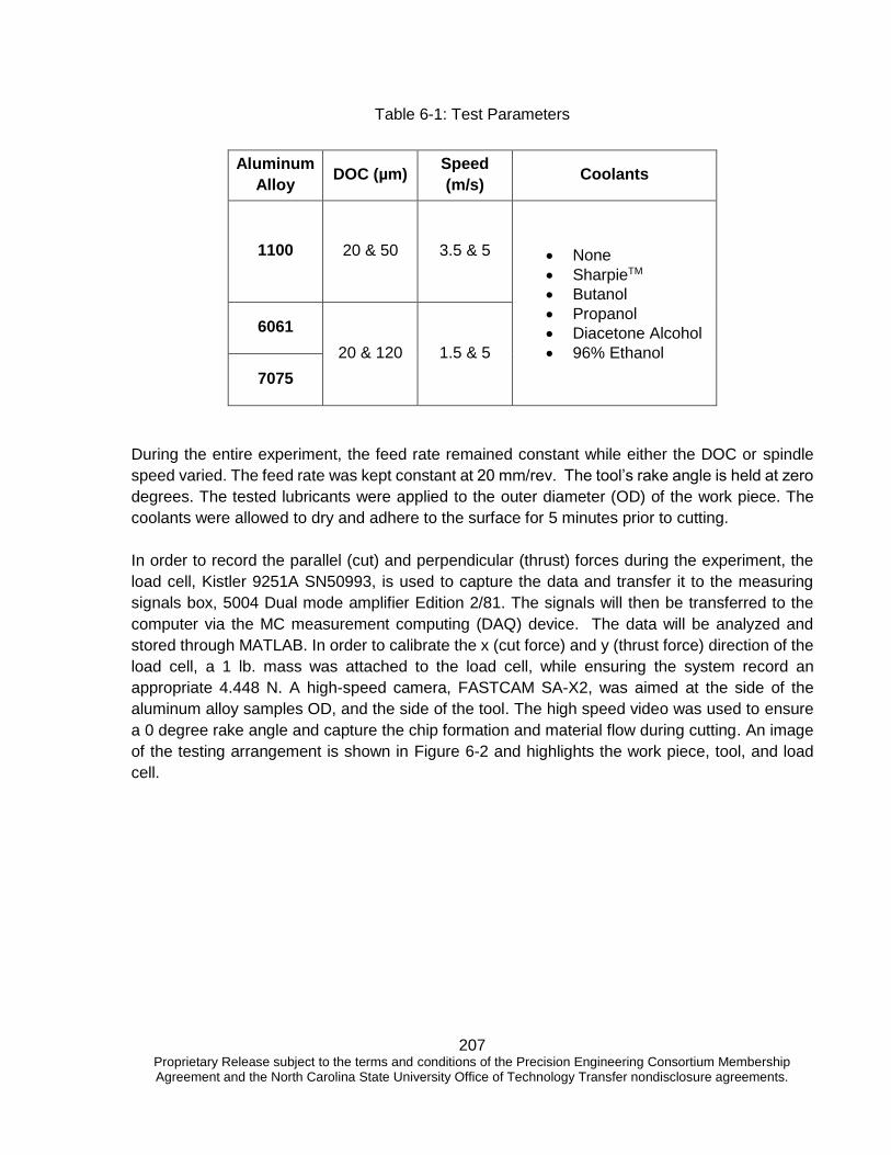
207 Proprietary Release subject to the terms and conditions of the Precision Engineering Consortium Membership Agreement and the North Carolina State University Office of Technology Transfer nondisclosure agreements.
Table 6-1: Test Parameters
Aluminum
Alloy DOC (µm)
Speed
(m/s) Coolants
1100 20 & 50 3.5 & 5 None
SharpieTM
Butanol
Propanol
Diacetone Alcohol
96% Ethanol
6061
20 & 120 1.5 & 5
7075
During the entire experiment, the feed rate remained constant while either the DOC or spindle
speed varied. The feed rate was kept constant at 20 mm/rev. The tool’s rake angle is held at zero
degrees. The tested lubricants were applied to the outer diameter (OD) of the work piece. The
coolants were allowed to dry and adhere to the surface for 5 minutes prior to cutting.
In order to record the parallel (cut) and perpendicular (thrust) forces during the experiment, the
load cell, Kistler 9251A SN50993, is used to capture the data and transfer it to the measuring
signals box, 5004 Dual mode amplifier Edition 2/81. The signals will then be transferred to the
computer via the MC measurement computing (DAQ) device. The data will be analyzed and
stored through MATLAB. In order to calibrate the x (cut force) and y (thrust force) direction of the
load cell, a 1 lb. mass was attached to the load cell, while ensuring the system record an
appropriate 4.448 N. A high-speed camera, FASTCAM SA-X2, was aimed at the side of the
aluminum alloy samples OD, and the side of the tool. The high speed video was used to ensure
a 0 degree rake angle and capture the chip formation and material flow during cutting. An image
of the testing arrangement is shown in Figure 6-2 and highlights the work piece, tool, and load
cell.

208 Proprietary Release subject to the terms and conditions of the Precision Engineering Consortium Membership Agreement and the North Carolina State University Office of Technology Transfer nondisclosure agreements.
Figure 6-2: Setup for MQL testing where the aluminum alloy sample is sandwiched in the fixture and cut using carbide insert. Also highlighted are is the vacuum chuck where the fixture is
attached, and the three-axis load cell used to measure force.
As the sample is cut, the RPM will increase, which also can be demonstrated by the equation
RPM= (𝑣𝑒𝑙𝑜𝑐𝑖𝑡𝑦∗60)/(𝐷𝑖𝑎𝑚𝑒𝑡𝑒𝑟∗𝜋). Therefore, to maintain a constant experimental behavior for
all test samples, as the test sample’s diameter decreases the RPM will be decreased manually to
maintain a constant spindle speed. From Table 1, there will be three different types of materials,
two different DOC, two different spindle speeds (SS), and six different coolants for the experiment.
This leads to a total of 72 experiments being conducted. However, due to the softness of Al 1100
compared to Al 6061 and 7075, the DOC and SS were different than the other materials. In order
to avoid contamination between lubricants, a 10 µm deep cut was made to level and smooth the
OD surface for the next test. The cutting force data is collected and compared to determine the
effects of each lubricant.
Carbide Tool
Workpiece
Vacuum Chuck
Three-Axis
Load Cell

209 Proprietary Release subject to the terms and conditions of the Precision Engineering Consortium Membership Agreement and the North Carolina State University Office of Technology Transfer nondisclosure agreements.
RESULTS
Al 6061
The cutting and thrust forces for aluminum alloy 6061 for each lubricant is plotted in Figure 6-3 at
a cut speed of 1.5 m/s and 120 µm depth of cut. The force values for all of the other cutting
parameters are summarized in the bar chart plotted in Figure 6-4. It was found that the added
lubricants had little effect on reducing the cutting forces for all of the cutting parameters on alloy
6061. However, it can be seen that the measured force was affected by the cutting parameters
as would be expected. The cutting force increases as both the speed and cutting depth increases.
Ethanol seems to cause an increase in both the cut and thrust force, even more so than dry cutting
conditions. This could be due to the ethanol removing residual fingerprints and oil from the surface
of the aluminum, leading to a cleaner surface free of contaminants. The removed oils and
contaminants would have potentially applied their own subtle MQL effect, but by removing them
from the surface of the aluminum, the cutting forces are slightly higher. An interesting slope can
be seen for the diacetone and propanol cuts as the force peaks and then continues to fall off as
the cut continues across the surface of the part. This type of response occurs on more than one
occasion for each alloy and is to be investigated further. The thrust force remains stable, while
the cutting axes slopes as the tool crosses the material’s surface. This sloping remains constant
for alloy 7075 and may actually be due to the improved chipping action of the harder alloy.
As seen in Figure 6-4, the cutting force increases with increasing depth of cut but reduces at
higher cut speeds. Ethanol consistently has some of the highest measured cutting and thrust
forces for all of the different parameters. Propanol and diacetone seem to provide the lowest
forces for aluminum 6061. The MQL effect was most accentuated for the higher cut depth and
lower speeds due to the higher forces.

210 Proprietary Release subject to the terms and conditions of the Precision Engineering Consortium Membership Agreement and the North Carolina State University Office of Technology Transfer nondisclosure agreements.
Figure 6-3: Cut and Thrust forces plotted for 6061 cut at a speed of 1.5 m/s and depth of 120µm
for each lubricant type.

211 Proprietary Release subject to the terms and conditions of the Precision Engineering Consortium Membership Agreement and the North Carolina State University Office of Technology Transfer nondisclosure agreements.
Figure 6-4: Cut forces measured for Al 6061 for all lubrications and cutting parameters.
Al 7075
The results for turning of aluminum alloy 7075 are plotted in Figure 6-5 for a cut depth of 120µm
at 1.5 m/s. These are the same parameters plotted for 6061 in Figure 6-3. Aluminum alloy 7075
is harder and stronger than aluminum alloy 6061 but has similar machining characteristics [8]. As
can be seen from the figure, the slope of the cut is not constant across the sample, as was seen
for diacetone and propanol on 6061. The force peaks at the start of the cut and continues to
reduce as the cut moves across the surface. Once again, the peak force for ethanol was found to
be much higher than all other surface additives. The cutting and thrust force is approximately four
times higher than each of the other lubricants. It can be seen that each of the lubricants presented
at 120µm depth and 1.5 m/s speed reduce the cutting force by up to 50% and reduced even
further for the measured thrust (except for ethanol). There does not seem to be much to
distinguish between each of the lubricants for alloy 7075.
0
5
10
15
20
25
Nothing Sharpie Ethanol Butanol Diacetone Propanol
Forc
e (
N)
Peak Cut Forces Al 6061
1.5 m/s 20 µm
1.5 m/s 120 µm
5 m/s 20 µm
5 m/s 120 µm

212 Proprietary Release subject to the terms and conditions of the Precision Engineering Consortium Membership Agreement and the North Carolina State University Office of Technology Transfer nondisclosure agreements.
Figure 6-5: Cut and Thrust forces plotted for 7075 cut at a speed of 1.5 m/s and depth of 120µm
for each lubricant type.

213 Proprietary Release subject to the terms and conditions of the Precision Engineering Consortium Membership Agreement and the North Carolina State University Office of Technology Transfer nondisclosure agreements.
Figure 6-6: Cut forces measured for Al 7075 for all lubrications and cutting parameters.
Al 1100
Aluminum alloy 1100 is more difficult to machine when compared to 6061 and 7075. The depth
of cut and speed were run at 20/50 µm at 3.5/5 m/s. The results had a much larger variation in
findings due to inconsistent chip formation. The cutting and thrust force measured at a cut depth
of 50 µm and speed of 5 m/s is plotted in Figure 6-7. Visual inspection of the samples shows
limited chip formation and damage to the surface using the current cutting parameters. An image
of the surface following cutting is shown in Figure 6-8 where material It is difficult to obtain a
consistent cut force across the surface of the aluminum 1100 and the decrease in forces is not
consistent with the other two alloys. The material seems to buildup and push across the surface,
rather than form consistent chips using the current setup. Additional testing can incorporate the
effects of rake angle and chip breaker tool inserts that may help improve the machinability of alloy
1100.
0
5
10
15
20
25
Nothing Sharpie Ethanol Butanol Diacetone Propanol
Forc
e (
N)
Peak Cut Forces Al 7075
1.5 m/s 20 µm
1.5 m/s 120 µm
5 m/s 20 µm
5 m/s 120 µm

214 Proprietary Release subject to the terms and conditions of the Precision Engineering Consortium Membership Agreement and the North Carolina State University Office of Technology Transfer nondisclosure agreements.
Figure 6-7: Cut and Thrust forces plotted for 1100 cut at a speed of 5 m/s and depth of 50µm for
each lubricant type.
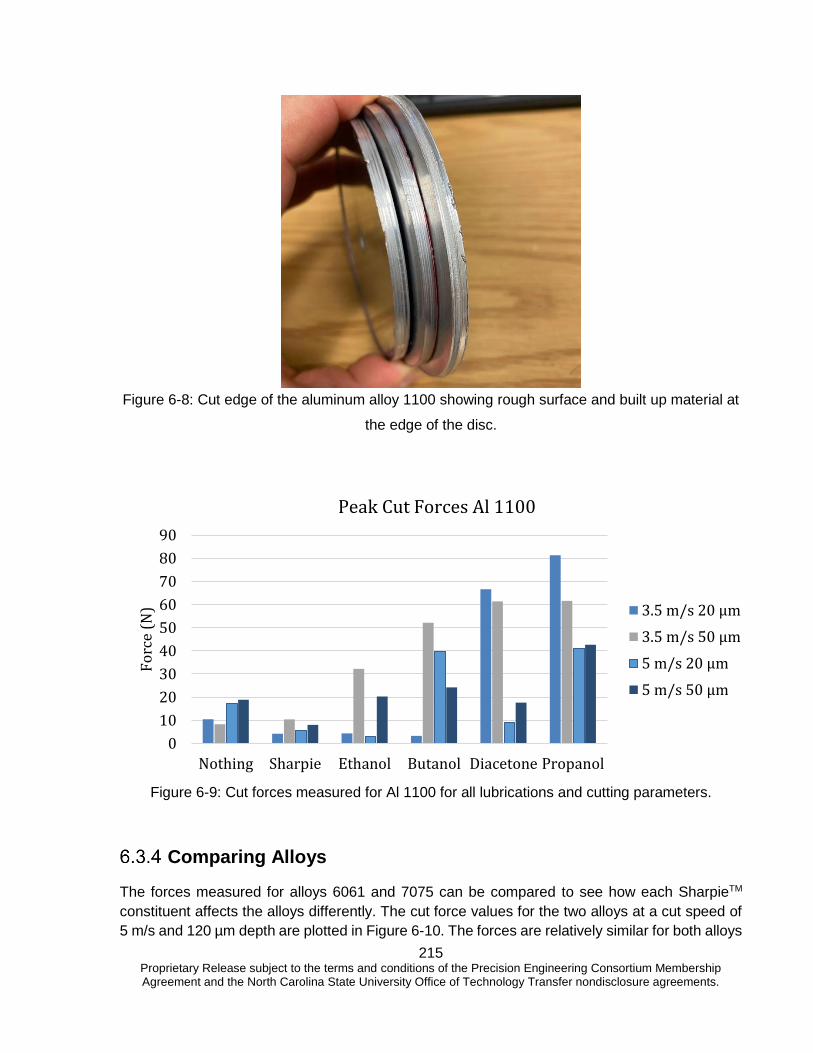
215 Proprietary Release subject to the terms and conditions of the Precision Engineering Consortium Membership Agreement and the North Carolina State University Office of Technology Transfer nondisclosure agreements.
Figure 6-8: Cut edge of the aluminum alloy 1100 showing rough surface and built up material at
the edge of the disc.
Figure 6-9: Cut forces measured for Al 1100 for all lubrications and cutting parameters.
Comparing Alloys
The forces measured for alloys 6061 and 7075 can be compared to see how each SharpieTM
constituent affects the alloys differently. The cut force values for the two alloys at a cut speed of
5 m/s and 120 µm depth are plotted in Figure 6-10. The forces are relatively similar for both alloys
0
10
20
30
40
50
60
70
80
90
Nothing Sharpie Ethanol Butanol Diacetone Propanol
Fo
rce
(N)
Peak Cut Forces Al 1100
3.5 m/s 20 µm
3.5 m/s 50 µm
5 m/s 20 µm
5 m/s 50 µm

216 Proprietary Release subject to the terms and conditions of the Precision Engineering Consortium Membership Agreement and the North Carolina State University Office of Technology Transfer nondisclosure agreements.
except for the drastic rise measured for ethanol on alloy 7075. Generally, these two alloys preform
similarly [8], as expected, and will be used in the future to test the surface roughness created by
each lubricant.
Figure 6-10: Comparison between cut forces for aluminum alloys 6061 and 7075.
FUTURE WORK
The effects of the lubricants can be further investigated using surface roughness measurements
following machining. The next steps plan to use a handheld surface roughness tester to measure
the OD of the discs following turning. The profilometer will allow for direct measurement of surface
roughness following machining and correlate improvements to the measured tool force. Additional
lubricants and application methods are expected to be explored on similar alloys.
CONCLUSION
For Al 1100:
There remained multiple difficulties in machining the aluminum 1100 alloy. The sharpie showed
a slight decrease in the cutting forces while each individual constituent varied in its measured
Rehbinder effect. Sharpie showed the lowest measured forces followed by ethanol and butanol
for low depth of cut. Further testing is required to confirm the increased force measurements of
alloy 1100 as improvements should be made to the sample setup in order to improve chipping
action.
For Al 6061:
In Al 6061, sharpie ink gave the lowest forces behavior, while multiple lubricants matched the
sharpie effect based on the cutting conditions. Ethanol showed very similar cutting force behavior
to dry cutting for all cutting parameters. Therefore, performing a dry cut is cheaper than using
ethanol as a coolant/treatment for Al 6061. At 5 m/s and (120 & 20) 𝜇𝑚 all coolants gave an
0
5
10
15
Forc
e (
N)
Al 6061 vs Al 7075
6061: 5 m/s 120 µm
7075: 5 m/s 120µm

217 Proprietary Release subject to the terms and conditions of the Precision Engineering Consortium Membership Agreement and the North Carolina State University Office of Technology Transfer nondisclosure agreements.
identical cutting forces behavior. This tells us at high spindle speed, none of the coolants has any
effect on the cutting forces behavior. At 1.5 m/s and 120 𝜇𝑚, diacetone is giving the closest
behavior of the sharpie effect, where it decreased the cutting forces by 60% compared to the dry
cutting.
For Al 7075:
At high spindle speed, performing a dry cut is better than using Ethanol as a coolant/treatment for
Al 7075. Ethanol was found to increase the cutting forces instead of decreasing it. At a (5 m/s) &
(120 and 20) 𝝁𝒎, all coolants are giving the sharpie behavior expect for ethanol, where it increase
the cutting forces instead of decreasing it. At a (1.5 m/s) & (120 𝝁𝒎): Butanol, Diacetone, and
Propanol give the closest behavior of Sharpie at high DOC.

218 Proprietary Release subject to the terms and conditions of the Precision Engineering Consortium Membership Agreement and the North Carolina State University Office of Technology Transfer nondisclosure agreements.
REFERENCES
1. Tai BL, Dasch JM, Shih AJ. EVALUATION AND COMPARISON OF LUBRICANT PROPERTIES IN MINIMUM QUANTITY LUBRICATION MACHINING. DOI: 10.1080/10910344.2011.620910.
2. Yeung H, Viswanathan K, Compton WD, et al. Sinuous flow in metals. Proc Natl Acad Sci U S A 2015; 112: 9828–9832.
3. Udupa A, Viswanathan K, Davis JM, et al. A Mechanochemical Route to Cutting Highly Strain-Hardening Metals. Tribol Lett 2019; 67: 4.
4. Udupa A, Viswanathan K, Saei M, et al. Material-Independent Mechanochemical Effect in the Deformation of Highly-Strain-Hardening Metals. Phys Rev Appl 2018; 10: 14009.
5. Biermann D, Blum H, Iovkov I, et al. Modelling, Simulation and Compensation of Thermomechanically Induced Deviations in Deep-Hole Drilling with Minimum Quantity Lubrication. 2018, pp. 181–218.
6. Cui X, Zhao J, Zhou Y. Comparison of tool life and surface roughness with MQL, flood cooling, and dry cutting conditions with P20 and D2 steel Related content Tool Life Prediction for Ceramic Tools in Intermittent Turning of Hardened Steel Based on Damage Evolution Model. DOI: 10.1088/1757-899X/244/1/012006.
7. Najiha MS, Rahman MM, Kadirgama K. Machining performance of aluminum alloy 6061-T6 on surface finish using minimum quantity lubrication. Int J Automot Mech Eng 2015; 11: 2699–2712.
8. Khettabi R, Nouioua M, Djebara A, et al. Effect of MQL and dry processes on the particle emission and part quality during milling of aluminum alloys. Int J Adv Manuf Technol 2017; 92: 2593–2598.

219 Proprietary Release subject to the terms and conditions of the Precision Engineering Consortium Membership Agreement and the North Carolina State University Office of Technology Transfer nondisclosure agreements.
Appendix
Table 6-2: Maximum cutting and thrust force for the 6061 aluminum alloy.
6061 Nothing Sharpie Ethanol Butanol Diacetone Propanol
1.5 m/s,
20µm
Cut (N)
Thrust (N)
10.05
11.19
5.06
5.96
9.73
11.56
5.44
8.16
5.06
7.27
5.87
9.40
1.5 m/s,
120µm
Cut (N)
Thrust (N)
19.00
19.88
18.03
18.11
20.09
21.91
20.62
22.74
13.62
20.33
14.36
19.14
5 m/s,
20µm
Cut (N)
Thrust (N)
2.00
2.58 1.80
2.57 3.45
5.89 1.82
2.70 1.98
2.77
1.35
2.50
5 m/s,
120µm
Cut (N)
Thrust (N)
5.50
5.87
6.08
6.99
6.96
9.03
5.78
6.70
5.73
6.20
4.33
6.59
Table 6-3: Maximum cutting and thrust force for the 7075 aluminum alloy.
7075 Nothing Sharpie Ethanol Butanol Diacetone Propanol
1.5 m/s,
20µm
Cut (N)
Thrust (N)
14.85
36.66
3.31
4.31
13.24
33.21
4.75
3.12
2.92
3.15
2.73
3.42
1.5 m/s,
120µm
Cut (N)
Thrust (N)
22.91
41.74
11.46
7.36
12.21
30.05
12.21
6.87
11.61
7.22
11.67
7.37
5 m/s,
20µm
Cut (N)
Thrust (N)
1.09
1.84
1.42
2.27
10.33
24.28
1.13
1.61
1.33
1.93
1.29
1.91
5 m/s,
120µm
Cut (N)
Thrust (N)
3.77
3.21
4.29
3.98
16.11
33.00
3.96
3.02
4.03
3.18
4.19
3.60
Table 6-4: Maximum cutting and thrust force for the 1100 aluminum alloy.
1100 Nothing Sharpie Ethanol Butanol Diacetone Propanol
3.5 m/s,
20µm
Cut (N)
Thrust (N)
10.45
11.85
4.14
8.39
4.40
7.26
3.30
4.74
66.64
59.72
81.31
63.16
3.5 m/s,
50µm
Cut (N)
Thrust (N)
8.29
12.29
10.35
10.30
32.24
41.97
52.16
98.78
61.42
72.36
61.64
53.21

220 Proprietary Release subject to the terms and conditions of the Precision Engineering Consortium Membership Agreement and the North Carolina State University Office of Technology Transfer nondisclosure agreements.
5 m/s,
20µm
Cut (N)
Thrust (N)
17.42
16.92
5.48
8.31
2.83
5.11
39.67
44.91
8.84
8.55
40.91
31.52
5 m/s,
50µm
Cut (N)
Thrust (N)
18.83
23.91
8.01
11.93
20.29
26.63
24.22
26.29
17.64
19.06
42.67
31.34

221 Proprietary Release subject to the terms and conditions of the Precision Engineering Consortium Membership Agreement and the North Carolina State University Office of Technology Transfer nondisclosure agreements.
Mechanical and Electrical Properties of Single
Crystal Silicon under External Electric Fields using
Nanoindentation Anthony Wong
Research Associate, Precision Engineering Consortium
Dr. Mark Pankow
Director of the PEC
Assistant Professor
Department of Mechanical and Aerospace Engineering
ABSTRACT
Silicon is widely used for electronics and modern day technology. Phase changes within the silicon structure can reduce machining forces and reduce material springback for electronics manufacturing. Single crystal silicon was tested under electrical contact nanoindentation at voltages between -10 and 10 V. The modulus and hardness of the silicon is measured during indentation and the effects of the voltage is used to determine potential phase changes in the single crystal silicon wafer. Large negative voltages have been shown to increase the reduced modulus of the silicon. The external electric field was found to have no effect on the hardness. Future work can focus on measuring the topography of the indented regions and resistivity while also exploring other materials.

222 Proprietary Release subject to the terms and conditions of the Precision Engineering Consortium Membership Agreement and the North Carolina State University Office of Technology Transfer nondisclosure agreements.
BACKGROUND
Silicon is an important material in modern society and has a significant role in electronics. Most
electronics manufacturing is focused on lithography processes. However, deformation processing
may also be useful for other purposes such as silicon molds or optics.
Silicon has historically been viewed as a brittle material. It inherently shows little plasticity and
can only handle small strains to failure, 0.3-0.5%. Under nanoscale deformations Silicon is known
to change phases under high hydrostatic pressure [1, 2]. At 0-11 GPa, Si is stable in a Si-I (fcc)
phase. At 11-15 GPa Si-II forms, a ductile, body-centered tetragonal phase, also known as β-Sn.
Si-II will also form at lower pressures when under shear stress. For comparison, Si is reported to
have a compressive strength of 120 MPa. This transformation to Si-II is irreversible, and the
material will not return to the Si-I phase. Upon unloading, the Si-II phase is unstable and forms
amorphous silicon, Si-III or Si-XII phases. The particular phase the silicon transforms into is
dependent on the load and unloading rate. This high pressure phase transformation (HPPT) from
Si-I to Si-II has been investigated by applying pressure through diamond anvil cells or
nanoindentation.
Many researchers have used molecular dynamics models to further understand of the phase
change during indentation. Molecular dynamics simulations have shown that for the same
indentation depth, a spherical indenter transforms a larger volume of material than a Berkovich
(pyramidal) tip while the distribution of Si-III and Si-XII in the unloaded condition remains similar
[3].
In scratch tests, the formation of metallic Si-II is thought to be critical for the ductile response that
is observed [4]. This phase change and the ductile transition in single point diamond turning of Si
has been extensively studied [5-8] as well.
The various lattice structures can be identified through Raman spectroscopy as well as selective
area diffraction in cross-sectional transmission electron microscopy. More recently, the change in
electrical measurements during nanoindentation has been used to identify the phases formed in-
situ [9, 10]. Figure 1a shows a schematic of the nanoindentation experimental apparatus. A
voltage is applied across the conductive diamond indenter tip and stage. During indentation, the
voltage is swept from -8V to 8V and the resulting current is measured. Figure 2 shows an example
of the data collected in this process. The resistivity of the system is calculated by applying a linear
fit to the data. The resistance of the various phases of Si are different, so changes in the resistivity
are interpreted as changes in the phases under the nanoindentation tip. Bruker has
commercialized this experimental setup as the NanoECR module (Electrical Contact Resistance).

223 Proprietary Release subject to the terms and conditions of the Precision Engineering Consortium Membership Agreement and the North Carolina State University Office of Technology Transfer nondisclosure agreements.
Figure 7-1. (a) Schematic of the electrical contact in a nanoindentation. (b) Circuit diagram of
the equivalent circuit [9].
Figure 7-2. I-V curve for an indentation in Si. Load versus depth is shown inset [9].

224 Proprietary Release subject to the terms and conditions of the Precision Engineering Consortium Membership Agreement and the North Carolina State University Office of Technology Transfer nondisclosure agreements.
Other researchers used the NanoECR to investigate the properties of phosphor-doped nano-
silicon films. These researchers applied different voltages while indenting silicon and measured
both the hardness and elastic modulus and found that they vary with the applied voltage. The
results are shown in Figure 3. While the trend is not very clear, the authors speculate that the
external electric field induces a rearrangement of the atoms and changes the tribological
properties [11].
Figure 7-3. Hardness and Elastic Modulus of Si as a function of applied voltage [11]
The same researchers published a study of an alloy of Germanium, Antimony and Tellurium
(GST). In this work, they applied a voltage through the NanoECR module during nanoindentation
of GeSb2Te4. The resulting load displacement curves are shown in Figure 4. While the curves for
-6V, -5V, and +8V look very similar, the curves for -7V and -8V are significantly different. The
authors attribute this change to an external voltage past a critical value driving a phase change
in the material [12].

225 Proprietary Release subject to the terms and conditions of the Precision Engineering Consortium Membership Agreement and the North Carolina State University Office of Technology Transfer nondisclosure agreements.
Figure 7-4. Load displacement curves for nanoindentation of GeSb2Te4 at with an external
electrical field [12]
This work investigates whether or not there is a critical voltage that changes the nanoindentation
properties of single crystal Si similar to GeSb2Te4. While there is some indication that the
properties of silicon change with voltage as shown in Figure 3, the voltage levels were limited and
a more thorough investigation with a NanoECR module may show a critical voltage. Such a
phenomenon could facilitate reduced springback, improved plasticity, or reduced forces in tooling
in a deformation process.
EXPERIMENTAL SETUP
A 4 inch silicon wafer sample was purchased from SPI Supplies (PN 4137SC-AB). The P-type
silicon has a <100> orientation and is precut into 5 x 7 mm pieces. The vendor advertises the
wafer to be 460-530 µm thick with a 2nm polished surface. Figure 6 shows an image of the wafer
as received from the vendor.

226 Proprietary Release subject to the terms and conditions of the Precision Engineering Consortium Membership Agreement and the North Carolina State University Office of Technology Transfer nondisclosure agreements.
Figure 7-5. Silicon wafer sample
A sample was cleaned by ultrasonicating in methanol and drying with compressed Nitrogen gas.
The sample was adhered with silver paint to the conductive plate of a NanoECR module installed
on a Bruker Hysitron TI850.
The nanoindenter was programmed to conduct indents with a 10 mN max load. The loading time
was 30 s followed by a 30 s hold time and a 30 s unloading time. A plot of a representative load
function is shown in Figure 6.

227 Proprietary Release subject to the terms and conditions of the Precision Engineering Consortium Membership Agreement and the North Carolina State University Office of Technology Transfer nondisclosure agreements.
Figure 7-6. Loading function
A standard Berkovich nanoindentation tip was used for all indents. A constant voltage was applied
during the indentation process. Voltages from -10 V to 10 V were applied in 2 V increments. Also
-0.25, -0.1, 0.1 and 0.25 V were applied as well to investigated effect of small applied external
electric fields. For each voltage setting nine indents were programmed to be spaced 10 µm apart
in a 3 by 3 grid.
RESULTS AND DISCUSSION
The reduced modulus and hardness were calculated for each indent. Figure 7 shows the average
reduced modulus of the nine indents for each voltage setting. The standard deviation is shown by
the error bars. Similarly, Figure 8 shows the hardness results. From the plots, -10V has a clear
effect on the reduced modulus, while voltage has little effect on hardness.
Hardness is based on the maximum depth of the indent. The limited effect on hardness suggests
that the voltage is not changing the loading phase of the indent to allow the indenter to penetrate
deeper into the silicon. As the reduced modulus is calculated from the unloading portion of the
force-displacement curve, the voltage influence on reduced modulus suggests the voltage is
influencing what the unstable Si-II transforms into upon unloading. These results also show that
there is a critical voltage around -8-10 V at which the reduced modulus begins to change.

228 Proprietary Release subject to the terms and conditions of the Precision Engineering Consortium Membership Agreement and the North Carolina State University Office of Technology Transfer nondisclosure agreements.
Figure 7-7. The effect of applied voltage on reduced modulus
140
145
150
155
160
165
170
-15 -10 -5 0 5 10 15
Reduced M
odulu
s [
GP
a]
Voltage [V]

229 Proprietary Release subject to the terms and conditions of the Precision Engineering Consortium Membership Agreement and the North Carolina State University Office of Technology Transfer nondisclosure agreements.
Figure 7-8. The effect of applied voltage on hardness
Figure 9 and Figure 10 shows the same data zoomed in around the origin. The original intention
was to investigate whether or not the mere presence of an electric field caused any changes.
These figures show that it is only the large negative voltage which has an effect.
Figure 7-9. The effect of applied voltage on reduced modulus around 0 V
140
145
150
155
160
165
170
-0.3 -0.2 -0.1 0 0.1 0.2 0.3
Reduced M
odulu
s [
GP
a]
Voltage [V]

230 Proprietary Release subject to the terms and conditions of the Precision Engineering Consortium Membership Agreement and the North Carolina State University Office of Technology Transfer nondisclosure agreements.
Figure 7-10. The effect of applied voltage on hardness around 0 V
The force-displacement curves are consistent with literature. Figure 11 shows a representative
set of force-displacement curves. These plots are for a -10 V applied external electric field. Very
little creep occurs during the hold time. Also, some indents, such as Indent 7 in Figure 11, show
a distinct pop out event in which the depth changes with no reduction in force during the unloading
curve. In literature these pop out events are thought to be related to a transformation from Si-II to
Si-XII [2].
11
11.25
11.5
11.75
12
-0.3 -0.2 -0.1 0 0.1 0.2 0.3
Hard
ness [
GP
a]
Voltage [V]

231 Proprietary Release subject to the terms and conditions of the Precision Engineering Consortium Membership Agreement and the North Carolina State University Office of Technology Transfer nondisclosure agreements.
Figure 7-11. Representative force-displacement curves
The indents were also imaged with a scanning electron microscope (SEM). Figure 11, Figure 12,
and Figure 13 show SEM images of the indents with -10, 0 and 10 V applied. It is notable that
occasionally extruded material similar to machining chips appears at the edges of the indents.
Figure 14 shows a close up of the bottom indent in Figure 11. It is unknown why this appears on
some indents but not others. This could be the result of machine vibration during the indentation
process, but there is no obvious difference in the force-displacement data to indicate that the
indenter tip is touching a different surface. Aside from the chips, qualitatively there is no obvious
difference between the indents with different voltages applied.

232 Proprietary Release subject to the terms and conditions of the Precision Engineering Consortium Membership Agreement and the North Carolina State University Office of Technology Transfer nondisclosure agreements.
Figure 7-12. SEM image of indents with -10 V applied (highlighted in the red box)
Figure 7-13. SEM image of indents with 0 V applied (highlighted in the red box)

233 Proprietary Release subject to the terms and conditions of the Precision Engineering Consortium Membership Agreement and the North Carolina State University Office of Technology Transfer nondisclosure agreements.
Figure 7-14. SEM image of indents with 10 V applied (highlighted in the red box)

234 Proprietary Release subject to the terms and conditions of the Precision Engineering Consortium Membership Agreement and the North Carolina State University Office of Technology Transfer nondisclosure agreements.
Figure 7-15. Close up image of an indent with -10 V applied
The sign of the applied voltage had a significant effect on the current during the indentations.
Figure 16 shows the current during the indents with 10 V applied, while Figure 17 shows the data
for the indents with -10 V applied. Figure 18 shows a simpler comparison of Indent 1 from figures
Figure 16 and Figure 17 on the same axes. Under both voltage settings the current increases in
a similar manner during the loading phase on the indentation. However, the peak current is lower
for the positive voltage. There is also much more variability in the peak current under the negative
voltage. During the hold, the current under negative voltage drops and then remains steady for
the rest of the hold. This behavior is not seen under positive voltages. This behavior in the current
during the hold is consistent for all the voltage levels as seen in Figure 19 and Figure 20. During
the unloading phase of the indent, the current decreases significantly faster under the negative
voltage. Ruffel conducted a similar experiment with 1 and -1 V applied and reported a similar
phenomenon while unloading the indenter [10]. These differences in current indicate that different
phases with different resistivity are being developed during the indentation.

235 Proprietary Release subject to the terms and conditions of the Precision Engineering Consortium Membership Agreement and the North Carolina State University Office of Technology Transfer nondisclosure agreements.
Figure 7-16. Current plots during indentation with 10 V
Figure 7-17. Current plots during indentation with -10 V

236 Proprietary Release subject to the terms and conditions of the Precision Engineering Consortium Membership Agreement and the North Carolina State University Office of Technology Transfer nondisclosure agreements.
Figure 7-18. Comparison of current with -10 and 10 V
Figure 7-19. Comparison of current with negative voltages

237 Proprietary Release subject to the terms and conditions of the Precision Engineering Consortium Membership Agreement and the North Carolina State University Office of Technology Transfer nondisclosure agreements.
Figure 7-20. Comparison of current with positive voltages
CONCLUSION
External electric fields have been applied to nanoindents in single crystal silicon. Large negative
voltages have been shown to increase the reduced modulus of the silicon. The external electric
field has no effect on the hardness. The sign of the voltage leads to very different behaviors in
the current as well.
We have shown that the mechanical properties of silicon can be manipulated by applying an
external electric field. The differences in electrical response during indentation implies that the
external electric field is altering the phases being developed during the high pressure phase
transformation as well as during the unloading.
Possible future investigations include measuring the indented surfaces and comparing the
resulting surface topographies. Cross sectional transmission electron microscopy can be used to
examine the phases in the indented material. The voltage could be swept at various points during
the indent to characterize the resistivity of the silicon during the indentation process. Finally,
similar materials could be investigated such as Germanium.

238 Proprietary Release subject to the terms and conditions of the Precision Engineering Consortium Membership Agreement and the North Carolina State University Office of Technology Transfer nondisclosure agreements.
REFERENCES
[1] M.M. Khayyat, G.K. Banini, D.G. Hasko and M.M. Chaudhri, "Raman microscopy investigations of structural phase transformations in crystalline and amorphous silicon due to indentation with a Vickers diamond at room temperature and at 77 K," Journal of Physics D: Applied Physics, vol. 36, pp. 1300-1307, Jun 7,. 2003.
[2] V. Domnich and Y. Gogotsi, "Phase transformations in silicon under contact loading," Reviews on Advanced Materials Science, vol. 3, 2002.
[3] Y. Lin, S. Jian, Y. Lai and P. Yang, "Molecular Dynamics Simulation of Nanoindentation-induced Mechanical Deformation and Phase Transformation in Monocrystalline Silicon," Nanoscale Res Lett, vol. 3, pp. 71-75, Feb. 2008.
[4] Y. Gogotsi, G. Zhou, S. Ku and S. Cetinkunt, "Raman microspectroscopy analysis of pressure-induced metallization in scratching of silicon," Semiconductor Science and Technology, vol. 16, pp. 345-352, May 1,. 2001.
[5] P.N. Blake and R.O. Scattergood, "Ductile-regime machining of germanium and silicon," Journal of the American Ceramic Society, vol. 73, pp. 949-957, Apr. 1990.
[6] J.C. Morris, D.L. Callahan, J. Kulik, J.A. Patten and R.O. Scattergood, "Origins of the ductile regime in single-point diamond turning of semiconductors," Journal of the American Ceramic Society, vol. 78, pp. 2015-2020, Aug. 1995.
[7] B.V. Tanikella, A.H. Somasekhar, A.T. Sowers, R.J. Nemanich and R.O. Scattergood, "Phase transformations during microcutting tests on silicon," Applied Physics Letters, vol. 69, pp. 2870-2872, Nov 4,. 1996.
[8] T.J. Randall, "Characterizing the ductile response of brittle semiconductor materials to dynamic contact processes," 2004.
[9] S. Ruffell, J.E. Bradby, J.S. Williams and O.L. Warren, "An in situ electrical measurement technique via a conducting diamond tip for nanoindentation in silicon," Journal of Materials Research, vol. 22, pp. 578-586, Mar 1,. 2007.
[10] S. Ruffell, J.E. Bradby, N. Fujisawa and J.S. Williams, "Identification of nanoindentation-induced phase changes in silicon by in situ electrical characterization," Apr 30,. 2007.
[11] G.G. Cheng, J.N. Ding, G.X. Xie, B. Kan, Z.Y. Ling and Z. Fan, "Mechanical and electrical properties of the phosphor-doped nano-silicon film under an external electric field," Surface and Interface Analysis, vol. 41, pp. 384-388, May. 2009.
[12] G. Cheng, Z. Zhang, J. Ding, Z. Ling and Y. Chen, "Mechanical and electrical properties of GeSb2Te4 film with external voltage applied," Applied Surface Science, vol. 285, pp. 532-537, Nov 15,. 2013.

239 Proprietary Release subject to the terms and conditions of the Precision Engineering Consortium Membership Agreement and the North Carolina State University Office of Technology Transfer nondisclosure agreements.
Development of a Novel Monopolar and Bipolar
Electrosurgical Forceps Nehemiah MacDonald
Undergraduate Student
Dr. Mark Pankow
Director of the PEC
Assistant Professor
Department of Mechanical and Aerospace Engineering
Abstract
Electrosurgery devices can offer multi-use capabilities when paired with a surgical forceps design. Such a device can reduce surgical time by limiting the need to transfer between surgical tools. This project is set out to design, manufacture, and test a surgical forceps tool that can act as both a mono- and bipolar electrosurgery tool. Initial ideas were analyzed using a design matrix and with consultation with medical professionals. First steps have been taken to prototype and determine the next steps for material manufacturing and electronics. Future work will include manufacturing, wiring, and testing of the device followed by iterative improvements to the design.

240 Proprietary Release subject to the terms and conditions of the Precision Engineering Consortium Membership Agreement and the North Carolina State University Office of Technology Transfer nondisclosure agreements.
BACKGROUND
Electrosurgery was introduced in the early 1900s and has become essential to modern surgery.
The devices used to conduct electrosurgery are typically divided into two subcategories:
monopolar and bipolar electrosurgery. The monopolar variety typically takes the form of a cautery
pen which is a handheld medical device used to stop bleeding via heat conducted through the tip.
The use of a cautery pen is classified as monopolar electrocautery because it directs heat and
electricity to the surgical site through a single electrode. The direct electrical current channeled
through this electrode can cut and/or cauterize blood vessels and tissue. The current does so by
passing through living tissue to a return electrode in the form of a grounding plate that is placed
on the patient. Heat is then created by the resistance of the tissue to the current. Monopolar
electrosurgery can reach temperatures between 1400°F and 2000°F [1].
Figure 8-1. Covidien Valleylab monopolar electrosurgical pencil [2].
The second type of electrosurgery is bipolar electrosurgery which directs electric current
interchangeably through a set of forceps with an electrode on each end of the forceps serving as
the active and return electrode, eliminating the need for a grounding plate. When compared to
monopolar electrosurgery, this form offers the user more precision. High frequency current of
approximately 500,000Hz [3] is supplied to both types of devices through an electrosurgical unit
(ESU) which is activated using either a foot pedal or buttons on the device.
Another necessary piece of equipment for surgeons are surgical forceps or scissors which are
metal instruments used during surgical procedures to tweeze, clamp, and apply pressure.
Surgical scissors have a variety of designs such as curved or straight blades and differing lengths
that are adjusted to fit the specific needs of different surgeons. Many bipolar electrosurgical
devices take the form of tweezer-like forceps that are able to grab tissue to cauterize.
Electrosurgery is involved in many surgeries, which are often costly and lengthy procedures. A
part of this cost can be attributed to the time surgeons take to switch tools during a surgery [4,5].
The development of a device that combines the use of two or more tools would save time as
doctors as they are not required to switch tools as often and improve the overall surgical efficiency.

241 Proprietary Release subject to the terms and conditions of the Precision Engineering Consortium Membership Agreement and the North Carolina State University Office of Technology Transfer nondisclosure agreements.
A 2007 study found that each minute of unused operative time cost the University of Rochester
Medical Center $60 [4]. As such, the purpose of this project is to propose a multi-use device that
works simultaneously as a set of surgical forceps and an electrosurgery tool that could be used
in a medical environment.
EXPERIMENTAL SETUP
In the early stages of this project, numerous design ideas for a product that could simultaneously
function as both an electrosurgical device and surgical forceps were created. These designs were
then evaluated using a matrix containing seven design criteria of varying weights. The criteria and
weight (in parentheses) were as follows: could perform monopolar and bipolar cautery (5), weight
(2), cost (2), temperature over time (5), sharpness (3), power requirements (4), ease of use (5).
Following this evaluation, the highest rated ideas were presented to an endocrine surgeon at
University of North Carolina Medical Center, after which the designs were edited to fit within the
parameters given by the surgeon and evaluated using a second matrix. The criterion and weight
(in parentheses) of the second matrix are as follows: insulating material used for the device
handles (3), connecting method to ensure the instrument can handle monopolar and bipolar
cautery (4), ergonomics of activation button/pedal (2), temperature over time (4), and
manufacturability (3). The highest rated designs as determined by the second evaluation were
made into 3D models that were again assessed by the endocrine surgeon. Further edits were
then made to the designs that were more feasible for use by surgeons and carried through to the
next stages of prototyping and manufacturing of a device.
RESULTS & DISCUSSION
Although a working prototype that can be used in surgery has not yet been created, an initial body
(see figure 2) has been developed to use for the multi-use device following the second evaluation
of design ideas and subsequent feedback from the consulted surgeon, which has led to many
crucial realizations as well. To have a tool that can switch between both monopolar and bipolar
electrosurgery, there must be one blade that is completely metal with an electrode on the tip that
can be used for monopolar electrosurgery. The second blade will be ceramic to ensure it is
insulated from the monopolar side of the device as the return electrode for the device will be a
grounding plate when monopolar electrosurgery is being used. The ceramic blade will then have
a small amount of exposed metal attached to the tip with another electrode that will allow bipolar
electrosurgery to be used when the blades are squeezed together. Provided the blades are not
squeezed together, this design will ensure the metal blade does not come into contact with the
electrode on the opposing blade when monopolar electrosurgery is being used. Proposed
methods for achieving such a design are a brazing solution, electrolysis metal plating, or “painting”
a ceramic material onto metal. The next steps of this work are to investigate each method of
incorporating a metal and ceramic blade while also developing the electronics necessary for
electrosurgery function.
This project will take advantage of existing electronics in mono- and bipolar electrosurgery to
integrate into this device. A monopolar electrosurgical pencil and a bipolar electrosurgical device

242 Proprietary Release subject to the terms and conditions of the Precision Engineering Consortium Membership Agreement and the North Carolina State University Office of Technology Transfer nondisclosure agreements.
have each been purchased and much of the wiring from these devices such as the plugs for the
Bovie machine will be used during the prototyping process. Integrating each of these electronics
into one device with a singular activation system either using a foot pedal or buttons placed on
the device itself continues to be investigated.
Figure 8-2. CAD Model for the initial design of the device’s body with a metal & ceramic
blade and plastic handles.
Figure 8-3. Blades of the 3D printed body for the device.
CONCLUSION AND FUTURE WORK

243 Proprietary Release subject to the terms and conditions of the Precision Engineering Consortium Membership Agreement and the North Carolina State University Office of Technology Transfer nondisclosure agreements.
A multi-use device that can transition from electrosurgery to be used as surgical forceps will save
surgeons and hospitals time and money. Initial designs have been modeled for the shell of such
a device. The final designs have been settled upon by considering a weighted design matrix and
input from medical professionals. Important considerations for the future of this project would be
to determine the best method to simultaneously insulate one blade from the other while allowing
an electric current to pass through the tips of both blades. Work must also be done to determine
the most efficient process for printing a ceramic blade that meets the sharpness standards set for
surgical scissors and has high thermal and electrical insulating properties. After establishing the
best method for printing the ceramic material, the proposed methods for joining ceramic to metal
will be tested to decide which method is the most feasible. In addition, further investigation needs
to be done into how the device will be wired so that it can effectively switch between monopolar
and bipolar electrosurgery.

244 Proprietary Release subject to the terms and conditions of the Precision Engineering Consortium Membership Agreement and the North Carolina State University Office of Technology Transfer nondisclosure agreements.
REFERENCES [1.] USA Medical and Surgical Supplies. (2020, April 22). 10 procedures that use a Medical
Cautery Pen. Retrieved January 2021, from <https://www.usamedicalsurgical.com/blog/10-procedures-use-medical-cautery-pen/>
[2.] Medtronic. Electrosurgical pencils. Retrieved January 2021, from <https://www.medtronic.com/covidien/en-us/products/electrosurgical-instruments/pencils.html>
[3.] Cordero, Ismael. “Electrosurgical units - how they work and how to use them safely.” Community eye health vol. 28,89 (2015): 15-6.
[4.] Girotto JA, Koltz PF, Drugas G. Optimizing your operating room: Or, why large, traditional hospitals don’t work. Int J Surg 2010; 8: 359–367. https://doi.org/10.1016/j.ijsu.2010.05.002
[5.] Marsano, L. S., MD. (n.d.). Principles of Electrocautery. Lecture presented at University of Louisville. Retrieved from <https://louisville.edu/medicine/departments/medicine/divisions/gimedicine/physician-resources/lectures/procedures/electrocautery>

245 Proprietary Release subject to the terms and conditions of the Precision Engineering Consortium Membership Agreement and the North Carolina State University Office of Technology Transfer nondisclosure agreements.
Deployable Structures Greyson Hodges
Graduate Student
Dr. Mark Pankow
Director of the PEC
Assistant Professor
Mechanical and Aerospace Engineering
ABSTRACT
This report addresses the development of various deployable technologies for aerospace systems and their current status. There are two main research areas: Deployable booms with different mechanisms: both powered and unpowered, and Deployable Composite Origami. This work discusses the manufacturing and testing of each system. Both systems have or have ongoing zero-gravity flight demonstrations to understand their deployment characteristics in a relevant space environment. The Boom project has an ongoing collaboration with NASA Langley.

246 Proprietary Release subject to the terms and conditions of the Precision Engineering Consortium Membership Agreement and the North Carolina State University Office of Technology Transfer nondisclosure agreements.
INTRODUCTION
Space structures are volumetrically limited by the cargo capacity of their launch vehicle. Satellites,
antenna, and solar arrays that deploy to many times larger than their launch vehicle require
complex packaging or secondary assembly once in orbit. Historically this has been solved by
mechanical hinges or modular designs. For efficiency, it is advantageous to launch using the
smallest possible cargo volume. Engineering research into structural packaging efficiencies and
deployment methods has become crucial to send larger structures into and beyond orbit without
relying on larger and larger launch vehicles.
Mechanical hinges are a costly method for deployable structures due to the increased number of
high-precision moving parts and their associated mass. This mass also contributes to a dynamic
challenge as it is often swung outward from the center of mass. Although mechanical performance
and analytical predictions of metallic hinges are well understood there are two major drawbacks.
First, they are relatively heavy when comparing strength to weight ratios with fiber reinforced
composites. Second, they are thermally expansive and exhibit high deformations when exposed
to a thermal gradient [1].
High strain composites (HSC) have been proposed as a light weight and thermally stable solution
to replace metallic hinges. HSC are ultra-thin laminates cable of being deformed to a small radius
of curvature. These thin fiber reinforced substrates allow coiling or folding for efficient storage of
structures while providing the ability for low energy deployment through exploiting elastically
stored strain energy. Many applications using HSC in deployable space structures have been
proposed as solutions to deploy spacecraft optics, antenna, tension solar sails, or for creating
heavy duty hinges [1, 2, 3, 4]. The first deployable structure investigated is a conformal tube mast
(CTM) boom and its various release dynamics.
DEPLOYABLE CONFORMAL TUBE MAST (CTM) BOOMS
CTM booms suffer from weak interfaces which often lead to failure where the two halves of the
boom come together. To increase the strength of the tab bond, a single cure cycle was
investigated to simultaneously cure together the two halves in their closed form shape. A silicone
plug matching the inside geometry of the whole boom would be used to manufacture the closed
cross section. This plug was created by pouring a two-part silicone rubber into the cavity made
between two negative molds, as shown in Figure 9-1.

247 Proprietary Release subject to the terms and conditions of the Precision Engineering Consortium Membership Agreement and the North Carolina State University Office of Technology Transfer nondisclosure agreements.
Figure 9-1 Silicone Mold Forming for Whole Boom Fabrication
The plug was then used to lay-up both sides of the boom simultaneously while the entire
laminate was vacuum bagged, Figure 9-2.
Figure 9-2. Internal Silicone Plug for Whole Boom Fabrication
Easy removal of the plug was possible to due to the smooth, non-stick surface of the silicone
and by pulling one exposed end of the plug it would slide out, Figure 9-3.

248 Proprietary Release subject to the terms and conditions of the Precision Engineering Consortium Membership Agreement and the North Carolina State University Office of Technology Transfer nondisclosure agreements.
Figure 9-3. Silicone Plug Removal
At the NASA Langley Research Center in Hampton, VA the plug method manufacturing was
improved upon by using a spread-tow woven carbon measuring 0.004 inches thick and infused
with an out-gassed approved resin film. Six molds designed to connect linearly, as the smaller
aluminum molds had, were CNC machined at 4 foot lengths from a high density foam. The molds
were then coated in a Teflon sticker to provide a tooling surface and a silicone plug was poured.
Cured under vacuum at elevated temperature for several hours in an oven, 4 foot long booms
were manufactured to test the process and performance of the new material, Figure 9-4. After
curing, the tabs were cut to their appropriate width using a precision straight edge.
Figure 9-4 Whole boom manufacturing process
The molds were aligned using two rods which fit into channels that had been cut on the underside
of the mold. Two sets of three molds were aligned and coated with a Teflon sticker to provide a

249 Proprietary Release subject to the terms and conditions of the Precision Engineering Consortium Membership Agreement and the North Carolina State University Office of Technology Transfer nondisclosure agreements.
continuous 12 foot tooling surface and a 12 foot silicone plug was poured. The same vacuum
bagging and lay-up as the 4 foot boom was repeated here and a 12 foot section cured in an
autoclave was successfully manufactured in a single cure cycle.
Figure 9-5 12 ft. section of boom
Once manufactured, mechanical characterization of the boom was performed to understand the
mechanical response and the means through which strain energy can be stored. Flattening and
bending are the two primary mechanisms for energy storage. Figure 9-6 shows some
characterization tests and the associated method for calculating the energy stored in the booms
during each operation.
Figure 9-6 Mechanical Characterization of Composite Booms
Higher temperature thermoplastic resins such as PPS and PEKK have been investigated to show
the ability to develop more stable creep resistant booms. The tight temperature control during

250 Proprietary Release subject to the terms and conditions of the Precision Engineering Consortium Membership Agreement and the North Carolina State University Office of Technology Transfer nondisclosure agreements.
fabrication is the major hurdle that one needs to overcome. Figure 9-7 shows an example of short
sections of booms that were fabricated and tested in bending to understand the structural
response, comparing the various resins.
Figure 9-7 Examples of Thermoplastic resin systems.
DEPLOYABLE BOOMS MECHANISMS
The next step for CTM booms was to determine an appropriate means of deployment. The
challenge of designing a boom deployment mechanism is creating a simple and lightweight
mechanism that can ensure predictable, reliable, and jam-free operation. There are two main
deployment failure modes for rollable booms. The first is uncoiling within the deployment
mechanism, known as blossoming, which will lead to the boom becoming irreversibly jammed.
The second failure mechanism is chaotic boom deployment, shown in Figure 9-8. Either failure
mode can damage the instrument, boom, and/or spacecraft, ultimately ending a mission.
The challenge of storing energy in the boom systems is after long term storage the polymer matrix
will relax (creep) over time and release the strain energy. Figure 9-8 shows an extreme example
of this with the boom permanently deformed in the coiled configuration. The shown damage would
render the device inoperable in orbit. From previous flight tests it has been observed that the
booms can experience a reduction in strain energy. It is believed that this loss in energy is due to
the relaxation of the boom during storage. Because of these findings, the focus of future tests will
0 2 4 6 8 10 12
Displacement (mm)
0
1
2
3
4
5
6
Lo
ad (
N)
Epoxy
PPS
PEKK

251 Proprietary Release subject to the terms and conditions of the Precision Engineering Consortium Membership Agreement and the North Carolina State University Office of Technology Transfer nondisclosure agreements.
be on characterizing the effects of long-term storage and improving the creep characteristics of
the composite.
Figure 9-8 NCSU replicated the chaotic nature of a freely deploying boom in a one-G lab environment by suspending a boom vertically (top). Bottom image is a boom that is permanently
deformed after long term storage due to creep and relaxation.
Dual Pull Mechanism
The first CTM boom deployment mechanism investigated is a dual-pull system. The dual-pull
mechanism is named for the tension provided by a Kapton tape, which is co-wound with the boom.
This tape is pulled from both ends to maintain tension in the coiled boom, eliminating blossoming
to produce a high packing efficiency and reliably jam-free operation in both directions. Because
the boom is constrained in a tight coil, the extension distance can be known accurately, which will
allow precise deployment and tuning of boom length on orbit. One end of the tape is attached to
the deployment motor, and the other end is attached to the central hub. A torsion spring in the
hub maintains tension on the tape. This design is conceptually similar to NASA’s CS3 spacecraft.
However, where CS3 used a low-torque power spring, the dual-pull mechanism uses a high-
torque torsion spring. The dual-pull mechanism is shown in Figure 9-9.
A co-wound tape must be thin to avoid wasting unnecessary space in the coiled boom. De-Orbit
sail and CS3 used a series of guides to move the tape from the hub to the coaxial spool, which
was not in the same plane. The additional drag created by these pulleys required a stronger tape,

252 Proprietary Release subject to the terms and conditions of the Precision Engineering Consortium Membership Agreement and the North Carolina State University Office of Technology Transfer nondisclosure agreements.
up to 43% stronger in the case of De-Orbit sail [5]. De-Orbit sail and CS3 both used a stainless-
steel ribbon to satisfy their strength requirements with a tape that was both thin and narrow. The
dual-pull mechanism avoids pulleys by using a coplanar spool. This allows the use of a wide tape.
The tape was made from Kapton, which is often used in space applications because of its low
vacuum outgassing [6]. Kapton is a suitable tape choice because it has a strength-to-weight ratio
2.5 times greater than stainless steel. Furthermore, Kapton is easy to work with and is
commercially available in a wide range of widths and thicknesses. Kapton can stretch up to 4%
under load at high temperatures and can creep an additional 100% of initial stretch under
prolonged loading. However, stretch and creep in the tape can be accommodated by the hub-
mounted spring of the dual-pull mechanism.
A small torsion spring cannot accommodate the revolutions required for full boom deployment,
and so the spring is attached to a gear instead of directly to the spacecraft. The gear and the hub
turn in the same direction during boom deployment, which reduces the compliance required from
the spring. The linkage reduces the spring’s angular displacement by up to 90% compared to a
body-fixed spring. This reduction allows the use of a spring with sufficient stiffness to eliminate
blossoming. It also eliminates the motor’s requirement to produce a holding torque.
The dual-pull mechanism can be used with any rollable boom. The boom used for this reference
design is a CTM-type boom with a subtended angle θ1 = θ2 = 75 deg, radius r1 = r = 7.62 mm,
and a flattened width of 50 mm. It was made from 1 K plain weave carbon fiber sourced from The
Composite Store with 7.5 threads per centimeter and an areal mass of 98 g/cm2. The boom was
laid up at an orientation of 45 deg, and Fiberglast’s 2000 system epoxy with 2060 hardener was
used as the resin system. The complete boom was cured in a single 24 h cycle under vacuum
with a small heater maintaining a temperature of approximately 45°C. The mold consists of two
identical machined aluminum exterior molds, with a silicone rubber interior plug [7].
This boom configuration is relatively easy to manufacture and works well for the mechanism
development work described here. However, it would not be a good choice for use in space. The
45 deg fibers are susceptible to creep, and long-term storage would leave the boom with a
significant curve. Moreover, the room temperature epoxy is not intended for use in space. Its glass
transition is too low for the space environment, and it is not outgas approved. The two-ply boom
used for CS3 would be a good choice for use with this mechanism in space.
A prototype of the dual-pull mechanism was built to support the testing. The reference design for
this research is a 2x scale 1U CubeSat (20 x 20 cm). A mechanism sized for a 1x scale 1U
CubeSat could accommodate up to four booms with a total length of 5 m. The structure and gears
were cut from 5.6 mm acrylic using a Universal Laser Systems VLS 6.60. Spacers and the hub
assembly were extruded from Acrylonitrile butadiene styrene using a Flash Forge Creator Pro.
The final assembly is shown in Fig. 6. This prototype was used for the functional tests described
in this work.

253 Proprietary Release subject to the terms and conditions of the Precision Engineering Consortium Membership Agreement and the North Carolina State University Office of Technology Transfer nondisclosure agreements.
Figure 9-9 Dual- Pull Mechanism
Further details of this can be found in the following publication J. Firth, M. Pankow Advanced
Dual-Pull Mechanism For Deployable Spacecraft Booms Journal of Spacecraft and Rockets.
The mechanism can be scaled to different sizes and a more refined version has been prototyped as
can be seen in Figure 9-10.
Figure 9-10 More developed Dual-Pull Deployment mechanism
MUSE Mechanisms
Other deployment mechanisms can utilize the stored strain energy of the boom through a
controlled speed and direction. A minimal unpowered strain-energy mechanism (MUSE) has been
built as a means of avoiding additional mechanical components and motors. The MUSE
mechanism holds a rollable monostable boom tightly wrapped around its hub. This mechanism
controls the boom’s deployment rate and speed using an internal rotary dampener. A single roller
is connected to the hub with two springs to prevent the boom from unwinding. The springs must

254 Proprietary Release subject to the terms and conditions of the Precision Engineering Consortium Membership Agreement and the North Carolina State University Office of Technology Transfer nondisclosure agreements.
be compliant enough to accommodate the thickness of a fully wound boom and strong enough to
prevent blossoming throughout deployment. Bearings ensure that the mechanism does not cause
blossoming. A bracket keeps the axles aligned so the boom does not drift off of the rollers and
get jammed in the springs. The bracket has a hole on one end and a slot on the other to allow the
roller to maintain close contact with the coiled boom throughout deployment. The bracket also
holds a rotary damper, which meshes with a hub-fixed gear to limit deployment speed. The
mechanism is shown in Figure 9-11. The photograph also shows acrylic guards installed on each
side of the hub. These guards ensure that the boom does not slide into the springs, and they
make it easier to keep the boom straight as it is rolled onto the hub.
The mechanism relies on inter-layer friction to prevent slip that would lead to blossoming. The
sprung roller creates a localized normal force, Fn, in one location on the coiled boom, thereby
increasing the force of friction, Ff, between adjacent layers in the coiled boom. This is shown in
Figure 9-12.
If the boom is used to hold an instrument away from the spacecraft, the instrument can be
integrated into the mechanism. If there is no tip-mounted instrument, the mechanism can be
retained or jettisoned, depending on debris requirements. If the mechanism is jettisoned, an
undamped mechanism may be sufficient. Opening shock will be minimal because only a small
portion of the boom is traveling at the end of deployment.

255 Proprietary Release subject to the terms and conditions of the Precision Engineering Consortium Membership Agreement and the North Carolina State University Office of Technology Transfer nondisclosure agreements.
Figure 9-11 MUSE mechanism
Figure 9-12 Interlayer Friction prevents blossoming
The MUSE mechanism uses a rotary damper to limit deployment speed. An ideal damper for this
application would maintain deployment speed at exactly the desired rate. The ideal torque curve
would be a step function. Two dampers were used during this test. The first was a commercial
viscous fluid damper with a maximum specified torque of 0.8 oz/in (5.65N/mm). This damper was
intended for speeds up to 50 rpm. It consists of a rotating paddle that moves through a grease-
filled housing. The other damper was a custom centrifugal damper adapted from a music box
mechanism. Both dampers are shown in Figure 9-13. The rubber arms of the centrifugal damper
experience a centrifugal force as the damper spins.
Below the damper's critical speed, the damper's brake tips deflect outward as damper speed
increases. Above the critical speed, the brake tips make contact with the damper's cylindrical
walls. The normal force between the brake and the walls increases at faster damper speeds. The
friction force between the brake and the damper walls is proportional to the normal force. The

256 Proprietary Release subject to the terms and conditions of the Precision Engineering Consortium Membership Agreement and the North Carolina State University Office of Technology Transfer nondisclosure agreements.
damping torque depends on the friction force and the damper's radius. The forces on the damper's
brake are shown in Figure 9-13.

257 Proprietary Release subject to the terms and conditions of the Precision Engineering Consortium Membership Agreement and the North Carolina State University Office of Technology Transfer nondisclosure agreements.
Figure 9-13 Damper Design and friction diagram
Deployment tests were performed to validate the model and ensure that the boom deploys
successfully. For each test, the boom was deployed sideways away from a fixed mechanism. An

258 Proprietary Release subject to the terms and conditions of the Precision Engineering Consortium Membership Agreement and the North Carolina State University Office of Technology Transfer nondisclosure agreements.
array of four cameras recorded images throughout deployment. The boom deployed through a
transparent tube to ensure that it remained within the field of view of the cameras. Images from
the cameras were combined, and the tip was tracked frame-by-frame to determine deployment
speed. Figure 9-14 shows a composite image of each boom's deployment along with its position
and speed. Each boom was tracked through two deployments. The second deployment had
higher image quality and a higher framerate, so the remainder of the paper will use data from the
second deployment. Boom deployment was successful with an undamped mechanism and with
both types of dampers.
The MUSE mechanism successfully deployed a CTM boom in multiple configurations. In all cases
the boom reached full deployment without blossoming. Each deployment was slower than
predicted. Observed deployment speeds and times were very close to those predicted for a boom
with 50% of nominal strain energy, as shown in Figure 9-15. Multiple strain energy test cycles
revealed no progressive damage, and booms tested after deployment exhibited nearly identical
strain energy. However, the close fit of the 50% energy model indicates that only half of the boom's
energy is harnessed during deployment. The remainder is dissipated through unmodeled effects.
Possible means of energy dissipation include friction, viscoelasticity, and imperfect boom rolling.
The results of the deployment tests and conclusions for each type of dampening mechanism are
discussed below.
CONCLUSIONS
Deployment Mechanisms
Undamped: The deployment speed of an undamped boom is limited only by boom length. If the
mechanism must remain attached to the spacecraft, it will experience severe opening shock when
the boom reaches full deployment. In fact, the opening shock was too much during this
deployment test. The boom was attached to the hub with tape, and at full deployment the tape
peeled off of the hub and the boom kept going at its full speed. A tip-mounted captive deployment
would suffer even worse opening shock due to its higher moving mass. However, an undamped
mechanism would be suitable for deploying a tip mounted boom if the mechanism could be
jettisoned.
Viscous damper: Boom deployment with the viscous damper was slower than deployment using
the undamped mechanism the damper successfully limited deployment speed. Opening shock
was also lower this boom did not peel the tape from the hub. The viscous damper's relatively at
high-speed torque curve makes deployment speed sensitive to small changes in input energy.
This could be problematic if the boom's post storage strain energy is unknown. The viscous
damper likely produces less torque at higher temperatures as the viscosity decreases. This could
cause higher-than-desired deployment speeds. At cold temperatures the increased viscosity
could prevent deployment altogether. In fact, less energetic booms used with an earlier version
of the MUSE mechanism had trouble deploying because the viscous damper stalled, even at

259 Proprietary Release subject to the terms and conditions of the Precision Engineering Consortium Membership Agreement and the North Carolina State University Office of Technology Transfer nondisclosure agreements.
room temperature. A damper with lower low-speed torque would be more reliable and less likely
to prevent deployment.
Centrifugal Damper: Deployment with the centrifugal damper was slower than deployment with
the viscous damper and much slower than deployment using the undamped mechanism. After
quickly reaching its top speed, the boom continued to deploy at a nearly constant rate. Opening
shock was roughly halved compared to the viscous damper. The centrifugal damper will likely
produce more torque at higher temperatures. The rubber will be more flexible, which will lower
the critical speed at which the brake arms contact the braking surface. Lower temperatures would
make the brake stiffer and lower the torque produced. However, both of these effects would only
change deployment speed slightly because the torque curve is so steep. The centrifugal damper's
relatively steep high-speed torque curve provides a close approximation of the ideal deployment
damper described in earlier. This makes deployment speed predictable even with widely varying
boom strain energies. Furthermore, the centrifugal damper produces very little torque in the low-
speed region. This is beneficial because the damper is less likely to cause stalling. If a damper is
required to limit boom deployment speed, a centrifugal damper is better than a viscous damper.
It is stiffer at high speeds and less stiff at low speeds, making it less sensitive to variations in
strain energy and less likely to prevent deployment initiation. It may also work better in varying
temperatures.

260 Proprietary Release subject to the terms and conditions of the Precision Engineering Consortium Membership Agreement and the North Carolina State University Office of Technology Transfer nondisclosure agreements.
Figure 9-14 Boom Deployment

261 Proprietary Release subject to the terms and conditions of the Precision Engineering Consortium Membership Agreement and the North Carolina State University Office of Technology Transfer nondisclosure agreements.
Figure 9-15 Observed Deployment speeds for a 2 m boom.
Previous tests showed the system could easily deploy under controlled circumstances. Figure
9-16 shows deployment of a boom during a flight test along with a tested end of travel mechanism
that allowed us to test some integrated electronics that were run down the center of the boom
using a flex circuit. Further details about the MUSE mechanism can be found in J. Firth, M.
Pankow. Minimal Unpowered Strain-Energy Deployment Mechanism for Rollable Spacecraft
Booms: Ground Test, Journal of Spacecraft and Rockets 57(2) 2020.

262 Proprietary Release subject to the terms and conditions of the Precision Engineering Consortium Membership Agreement and the North Carolina State University Office of Technology Transfer nondisclosure agreements.
Figure 9-16 NCSU deployment testing from previous funding in Zero-G showing successful
deployment. Right is the mechanism that is used for stopping the boom at end of travel.
9.4.2 Composite Origami
Composite Origami offers a new method to be able to efficiently package large structures with
integrated hinges that are structurally very efficient and strong due to the integrated carbon fiber.
If successful, this technology can replace complex hinged arrays that have many potential failure
points and require extensive testing. The scalability of the system enables many possible
infusions including large solar arrays and deployable habitats.
The challenge of designing a deployable structure is that it must be structurally strong, ensure
predictable, reliable, and jam-free operation, with minimal power input. There are two main
deployment failure modes for hinged structures. The first is hinge binding, where the hinge has
too much friction and prevents it from achieving full deployment. The second type of failure is
where a part fails because of force or deflection incompatibilities.
Figure 9-17 Example of Composite Origami Hinge and The Structures that can be fabricated
Composite Origami offers an integrated structural element that can store energy elastic while also
acting as an integrated hinge material, see Figure 9-17 and Figure 9-18. The advantages of this
technology extend to benefits associated with: deployment mechanism design (passively
deployed integrated hinges), deployability (more predictable and controllable), and strain
relaxation over time (reduce creep and less relaxation when stored). In general, this yields more

263 Proprietary Release subject to the terms and conditions of the Precision Engineering Consortium Membership Agreement and the North Carolina State University Office of Technology Transfer nondisclosure agreements.
reliable (capable of reaching a deployment reliability of 0.999), lighter, and less complex designs
compared to other array designs or inflatable structures.
Current solar array and deployable technologies usually rely on both a soft flexible material and
a separate mechanism for deployment. This adds complexity and affects reliability. This proposal
aims to demonstrate that all of these components can be integrated into a single element which
will simplify the complexity of systems and increase reliability and structural integrity, using an
iterative flight test approach.
Figure 9-18 Examples of Composite Origami showing the ability to fold and unfold (top), and flasher type
model (middle) miura-ori fold (bottom left) and Origami Crane (bottom right) have been fabricated at NCSU.
The current technology is considered a TRL of level 4 based on the fact that NCSU has developed
composite origami in the past using High Strain Composites and tested in a lab level setting [8,
9]. Several variations of the composite origami structures have successfully deployed in a one-g
environment. The dynamic response of the deploying origami structure now needs to be
characterized in a zero-g environment, to understand what the differences are and how it affects
the design. By the end of this flight test campaign, the composite origami will be at TRL 5 based
on testing in a representative environment. This will be accomplished by conducting deployment
tests on an aircraft flying parabolic arcs. A zero-g flight very nearly replicates the space
environment for composite origami. For the observed deployment speeds, air resistance in an
aircraft cabin will not cause significant dynamic differences from the space environment. We will
replicate the thermal environment of space by testing both hot and cold, to understand how this
affects the stored strain energy.

264 Proprietary Release subject to the terms and conditions of the Precision Engineering Consortium Membership Agreement and the North Carolina State University Office of Technology Transfer nondisclosure agreements.
We have currently demonstrated manufacturability of these composite and performed mechanical
characterization of the joints and impact of the joints on the overall strength of the laminates [8].
We also developed a method to accurately and reliably create the integrated hinges in these
composites, through a 3D printer that can lay the traces of the silicone precisely [9]. Mechanical
characterization of these composites has been performed and an example can be seen in Figure
9-19.
Figure 9-19 Mechanical Characterization of Composite Origami Hinge.
This work will specifically look at validating zero-g deployment along with determining variations
that may occur in deployment due to thermal loading. This is especially important since many
applications may not be able to control the temperature when deployment occurs.
Flight Tests are scheduled for May 2021.
Before the first test flight relevant non-zero-g data will be gathered to further classify the system
prior to each zero-g flight to increase the effectiveness of the science gathered. Ongoing ground
testing includes the force available from the hinges strain energy and the dynamics of deployment
in 1-g ground testing so that we can compare it to our Zero-G flight.
Round one of zero-g testing will be used to perform verification and validation of the origami along
with trials to understand the impact of manufacturing variations on the performance in zero-g and
at different temperatures. The results of this testing will enable us to optimize the composite
origami in round 2 of testing, which will include the modified origami based on flight 1 testing,
along with integrated flexible electronics to simulate the effective integration of solar cells to create
solar arrays.

265 Proprietary Release subject to the terms and conditions of the Precision Engineering Consortium Membership Agreement and the North Carolina State University Office of Technology Transfer nondisclosure agreements.
REFERENCES
[1] P. Warren, B. Dobson, J. Hinkle and M. Silver, "Experimental Characterization of Light
Weight Strain Energy Deployment Hinges," in 46th AIAA/ASME/ASCE/AHS/ASC
Structures, Structural Dynamics & Materials Conference, Austin, Texas, 2005.
[2] J. Domber, J. Hinkle, L. Peterson and P. Warren, "Dimensional Repeatability of an Elastically
Folded Composite Hinge for Deployed Spacecraft Optics," Journal of Spacecraft and
Rockets, vol. 39, no. 5, 2002.
[3] M. Silver and P. Warren, "The Strain Energy Deployed High Expansion Outer Barrel
Assembly," in 2nd AIAA Spacecraft Structures Conference, 2015.
[4] J. Block, M. Staubel and M. Wiedemann, "Ultralight Deployable Booms for Solar Sails and
Other Large Gossamer Structures in Space," Acta Astronautica, vol. 68, no. 7-8, pp. 984-
992, 2011.
[5] S. Meyer, M. Hillebrandt, M. Straubel and H. Christian, "Design of the De-Orbit Sail Boom
Deployment Unit,” 13th European Conference on Spacecraft Structures, Materials &
Environmental Testing," in ESA Communications, Noordwijk, The Netherlands, 2014.
[6] A. Laikhtman, I. Gouzman, R. Verker and E. Grossman, "Contamination Produced by
Vacuum Outgassing of Kapton Acrylic Adhesive Tape," Journal of Spacecraft and Rockets,
vol. 46, no. 2, pp. 236-240, 2009.
[7] S. West, C. White, C. Celestino, S. Philpott and M. Pankow, "Design and Testing of
Deployable Carbon Fiber Booms for CubeSat Non-Gossamer Applications.," in AIAA
SciTech, Kissimmee Florida, 2015.
[8] C. White, "Manufacturing and Structural Characterization of Flexible and Dual-Matrix
Deployable Composites for Space Application," North Carolina State University, Raleigh,
2016.
[9] A. Gay, "Fabrication and Classification of Dual-Matrix Composites for Deployable Space
Applications," North Carolina State University, Raleigh, 2017.
[10] F. Chen, H. Liu and Q. Yang, "Maskless Fabrication of Concave Microlens Arrays on Silica
Glasses by a Femtosecond-Laser-Enhanced Local Wet Etching Method," Optics Express,
vol. 18, no. 19, pp. 20334-20343, 2010.
[11] R. Syms, E. Yeatman and B. V.M., "Surface Tension-Powered Self-Assembly of
Microstructures - the State-of-the-Art," Journal of Microelectromechanical Systems, vol. 12,
no. 4, pp. 387-417, 2003.
[12] H. Yang, C. Chao and M. Wei, "High Fill-Factor Microlens Array Mold Insert Fabrication
using a Thermal Reflow Process," Journal of Micromechanics and Microengineering, vol.
14, no. 8, pp. 1197-1204, 2004.
[13] S. Moore, J. Gomez and D. Lek, "Experimental Study of Polymer Microlens Fabrication using
Partial-Filling Hot Embossing Technique," Microelectronic Engineering, vol. 162, pp. 57-62,
2016.

266 Proprietary Release subject to the terms and conditions of the Precision Engineering Consortium Membership Agreement and the North Carolina State University Office of Technology Transfer nondisclosure agreements.
[14] J. Albero, L. Nieradko and G. C., "Fabrication of Spherical Microlenses by a Combination of
Isotropic Wet Etching of Silicon and Molding Techniques," Optics Express, vol. 17, no. 8,
pp. 6283-6292, 2009.
[15] K. J.Y., N. Brauer and F. V., "Hybrid Polymer Microlens Arrays with High Numerical
Apertures Fabricated using Simple Ink-Jet Printing Technique," Optical Materials Express,
vol. 1, no. 2, p. 259, 2011.
[16] P. Nussbaum, R. Volkel and H. Herzig, "Design, Fabrication and Testing of Microlens Arrays
for Sensors and Microsystems," Pure and Applied Optics: Journa of the European Optical
Society Part A, vol. 6, no. 6, pp. 617-636, 1997.
[17] A. Yi and L. Li, "Design and Fabrication of a Microlens Array by use of a Slow Tool Servo,"
Optics Letters, vol. 30, no. 13, pp. 1707-1709, 2005.
[18] X. Zhang, F. Fang and L. Yu, "Slow Slide Servo Turning of Compound Eye Lens," Optical
Engineering, vol. 52, no. 2, p. 023401, 2013.
[19] J. Yan, Z. Zhang and T. Kuriyagawa, "Fabricating Micro-Structured Surface by using Single-
Crystalline Diamond Endmill," The International Journal of Advanced Manufacturing
Technology, vol. 51, no. 9, pp. 957-964, 2010.
[20] J. Yan, A. Horikoshi and T. Kuriyagawa, "Manufacturing Structured Surface by Combining
Microindentation and Ultraprecision Cutting," CIRP Journal of Manufacturing Science and
Technology, vol. 5, no. 1, pp. 41-47, 2012.
[21] Y. Bai, X. Wang, T. Zhou, Z. Liang and G. Li, "Compressional Deformation in Indentation
Process for Microlens Array Mold," Journal of Beijing Institute of Technology, no. 1, pp. 15-
21, 2018.
[22] E. Zdanowicz, T. Dow and S. R.O., "Rapid Fabrication of Nanostructured Surfaces using
Nanocoining," Nanotechnology, vol. 23, no. 41, p. 415303, 2012.
[23] D. T.A., J. Nowak and J. Kessing, "Design of Elliptically-Vibrating Ultrasonic Actuator for
Nanocoining," Precision Engieering, vol. 45, pp. 301-310, 2016.
[24] A. Karimzadeh, M. Ayatollahi and M. Alizadeh, "Finite Element Simulation of Nano-
Indentation Experiment on Aluminum 1100," Computational Materials Science, vol. 81, pp.
595-600, 2014.
[25] S. Moore, M. Manzari and Y. Shen, "Nanoindentation in Elastoplastic Materials: Insights
from Numerical Simulations," International Journal of Smart and Nano Materials, vol. 1, no.
2, pp. 95-114, 2010.
[26] A. Warren and Y. Guo, "Machined Surface Properties Determined by Nanoindentation:
Experimental and FEA Studies on the Effects of Surface Integrity and Tip Geometry,"
Surface & Coatings Technology , vol. 201, no. 1, pp. 423-433, 2006.
[27] Anonymous, ABAQUS/Standard User's Manual, Version 6.9, Providence, RI: Simulia, 2016.

267 Proprietary Release subject to the terms and conditions of the Precision Engineering Consortium Membership Agreement and the North Carolina State University Office of Technology Transfer nondisclosure agreements.
FACULTY
MARK R. PANKOW Director, Precision Engineering Center
Director, Ballistic Loading and Structural Testing Laboratory
Assistant Professor, Department of Mechanical and Aerospace Engineering
BS, Mechanical Engineering, California Polytechnic State University, San Luis Obispo, 2005
MS, Mechanical Engineering, University of Michigan, 2007
PhD, Mechanical Engineering, University of Michigan, 2010
After receiving his PhD degree from the University of Michigan in 2010, Dr. Pankow joined the
Army Research Laboratories and worked there for two years. His research interests were in the
areas of dynamic failure of composite materials. His work was both experimental and
computational in nature. Dr. Pankow joined the faculty at North Carolina State University in 2012.
His current research interests include dynamic testing (ballistic, blast, impact), computational
modeling of composites, and deployable structures. He is the editor for the American Society for
Composites.

268 Proprietary Release subject to the terms and conditions of the Precision Engineering Consortium Membership Agreement and the North Carolina State University Office of Technology Transfer nondisclosure agreements.
DAVID C. MUDDIMAN
Jacob and Betty Belin Distinguished Professor of Chemistry
Founder and Director of the W.M. Keck FTMS Laboratory for Human Health Research
B.S., Chemistry, Gannon University, 1990
Ph.D., Analytical Chemistry, University of Pittsburgh, 1995
Prior to moving his research group to North Carolina State University in 2006, David was a
Professor of Biochemistry and Molecular Biology and Founder and Director of the Proteomics
Research Center at the Mayo Clinic College of Medicine in Rochester, MN. Prior to this
appointment, David was an Associate Professor of Chemistry at Virginia Commonwealth
University. It was there that he began his professional career as an assistant professor with an
adjunct appointment in the Department of Biochemistry and Molecular Biophysics and as a
member of the Massey Cancer Center in 1997. These academic appointments followed a
postdoctoral fellowship at Pacific Northwest National Laboratory in the Environmental Molecular
Sciences Laboratory under Richard D. Smith from 1995-1997. David was born in Long Beach,
CA in 1967 but spent most of his formative years in a small town in Pennsylvania. Dr. Muddiman
is Editor of Analytical and Biological Chemistry and Associate Editor of the Encyclopedia of
Analytical Chemistry as well as on the Editorial Advisory Board of Mass Spectrometry Reviews,
Molecular and Cellular Proteomics, Rapid Communications in Mass Spectrometry, and the
Journal of Chromatography B. He also serves on the advisory board of the NIH Funded Complex
Carbohydrate Research Center, University of Georgia and the Yale/NIDA Neuroproteomics
Center, Yale University. Dr. Muddiman has served as a member of the ASMS Board of Directors
and Treasurer of US-HUPO, and he is currently the President of US HUPO. His group has
presented over 500 invited lectures and presentations at national and international meetings
including 20 plenary/keynote lectures. His group has published over 250 peer-reviewed papers
and has received four US patents in addition to two patents pending. He is the recipient of the
2015 ACS Award in Chemical Instrumentation, 2010 Biemann Medal (American Society for Mass
Spectrometry), 2009 NCSU Alumni Outstanding Research Award, the 2004 ACS Arthur F. Findeis
Award, the 1999 American Society for Mass Spectrometry Research Award, and the
1990-1991 Safford Award for Excellence in Teaching (University of Pittsburgh). Dr. Muddiman’s
research is at the intersection of innovative mass spectrometry technologies, systems biology,
and model organisms for diseases and bioenergy, and is funded by the National Institutes of
Health, the National Science Foundation, the Department of Energy, and The United States
Department of Agriculture.

269 Proprietary Release subject to the terms and conditions of the Precision Engineering Consortium Membership Agreement and the North Carolina State University Office of Technology Transfer nondisclosure agreements.
BRENDAN T. O’CONNOR
Associate Professor
Department of Mechanical and Aerospace Engineering
BS, Mechanical Engineering, Marquette University, 2000
MS, Mechanical Engineering, University of Massachusetts, 2004
PhD, Mechanical Engineering, University of Michigan, 2009
After receiving his BS from Marquette University, Dr. O’Connor joined Norian/Siani Engineering,
an engineering consulting firm in Boston MA. He then returned to the University of Massachusetts
and joined the Industrial Assessment Center, conducting energy audits of industrial facilities.
During his PhD, Dr. O’Connor turned his research towards solar power, with a focus on organic
electronic materials processing. After his graduation, Dr. O’Connor joined the Polymers Division
at the National Institute of Science and Technology as an NRC-NIST Postdoctoral Fellow. At
NIST, Dr. O’Connor conducted research on processing and mechanical properties of organic
electronic films, primarily for flexible transistor applications. He then joined NC State University in
2011. At NC State, Dr. O’Connor’s research interests are focused on polymer semiconductor
device processing and characterization. His research efforts include developing plastic solar cells
with unique optoelectronic characteristics and developing mechanically robust flexible and
stretchable electronic devices.

270 Proprietary Release subject to the terms and conditions of the Precision Engineering Consortium Membership Agreement and the North Carolina State University Office of Technology Transfer nondisclosure agreements.
RONALD O. SCATTERGOOD
Professor
Materials Science and Engineering Department
BS, Metallurgical Engineering, Lehigh University, 1961
MS, Metallurgy, Massachusetts Institute of Technology, 1963
PhD, Metallurgy, Massachusetts Institute of Technology, 1968
R.O. Scattergood is a Professor in the Department of Materials Science and Engineering. He
received BS degrees in Mining Engineering and Metallurgical Engineering from Lehigh University.
His MS and PhD degrees were obtained in Metallurgy from M.I.T. In 1968 he became a member
of the basic research staff in the Materials Science Division at the Argonne National Laboratory.
In 1981, he joined the faculty as a Professor of Materials Engineering at North Carolina State
University.
Professor Scattergood's major research interests have been focused on the mechanical behavior
of solids. He has worked in the areas of strengthening mechanisms in solids, mechanical testing,
fracture and toughening in ceramics, tribology, processing, properties and thermal stability of
nanocrystaline materials and precision machining processes. He has published over 250 papers.

271 Proprietary Release subject to the terms and conditions of the Precision Engineering Consortium Membership Agreement and the North Carolina State University Office of Technology Transfer nondisclosure agreements.
STAFF
KENNETH P. GARRARD
Senior Research Scholar
Precision Engineering Consortium and
FTMS Laboratory for Human Health Research
BS, Computer Science, North Carolina State University, 1979
MS, Computer Studies, North Carolina State University, 1983
As a full-time researcher at the Precision Engineering Consortium for over 32 years, Mr. Garrard's
interests and duties have included the development of high performance control systems for
ultraprecision machines and software for custom, multiprocessor computer systems. He
participated in the development of the original PEC fast tool servo as well as three other fast tool
servo systems that have been delivered to commercial and government sponsors. One of these
systems was built specifically for the machining of off-axis segments of conic surfaces of
revolution and another was used for the fabrication of inertial confinement fusion targets. He has
performed numerous prototype fabrication projects that required unique machine configurations
and controller software. He is also co-inventor of the spherical coordinate measurement machine,
Polaris3D, and was the developer of algorithms for its control and for the analysis of measurement
data.
Since 2012 he has collaborated with the FTMS Laboratory for Human Health Research to assist
with the implementation of video system directed sample stage motion control, region of interest
selection, laser optics and instrument synchronization for IR-MALDESI imaging. This led to the
development of the widely-used, open-source MSiReader software package for analysis and
visualization of Mass Spectrometry Imaging data sets.
Mr. Garrard has a long-standing interest in the analysis of scientific data, computational geometry,
signal processing, programming language structures, sorting and searching algorithms,
multiprocessor computer architecture and the design and implementation of hard real-time
systems. He is a regular contributor to the Mathworks user community web site.

272 Proprietary Release subject to the terms and conditions of the Precision Engineering Consortium Membership Agreement and the North Carolina State University Office of Technology Transfer nondisclosure agreements.
ANTHONY R. WONG
Research Associate
BS, Mechanical Engineering, NC State University, 2005
MS, Mechanical Engineering, Massachusetts Institute of Technology, 2012
Mr. Wong joined the Precision Engineering Consortium in 2017 as a member of the technical
staff. His current research interests include machine design and metrology. Prior to coming to
the PEC, he had 7 years of industry experience including positions at Caterpillar, AKG of America,
ShopBot Tools and Keystone Tower Systems.
JACOB MARX
Research Associate
BA, Physics, Case Western Reserve University, 2013
ME, Nuclear Engineering, North Carolina State University, 2015
PhD, Mechanical Engineering, North Carolina State University, 2020
Dr. Marx joined the Precision Engineering Consortium as a member of the technical staff after
graduating with his doctorate degree. During his PhD he worked on manufacturing and testing of
metal foam technologies for a variety of engineering applications. He has helped develop
composite metal foam armors to protect against ballistic threats and blast and fragment impact
as well as investigate their use for aerospace and tank car applications. He joins the PEC with an
interest in material manufacturing and testing. Outside of work he enjoys hiking with his wife,
daughter, and dog.

273 Proprietary Release subject to the terms and conditions of the Precision Engineering Consortium Membership Agreement and the North Carolina State University Office of Technology Transfer nondisclosure agreements.
GRADUATE STUDENTS
USAMA DINGANKAR obtained his Bachelor’s in Mechanical Engineering from SRM University,
Chennai, India. He is currently pursuing his M.S. degree in Mechanical Engineering at North Carolina State
University at Raleigh. Outside of work Usama is actively involved in the Fantasy Football (Soccer) setup,
as he is a huge Football (Soccer) fan. Usama joined the PEC as a graduate researcher in July 2019.
SUMIT GUNDYAL obtained his B.S. degree in Mechanical Engineering at University of Pune,
Pune, India. He worked for 2 years at Dassault Systèmes, Pune, India before starting as a
graduate student at NC State University. Sumit joined the BLAST lab in February 2018, working
on the modeling and the simulation aspect of the microlens array project. He enjoys swimming,
basketball, and tennis outside of the lab.
JACOB GUYMON received his B.S. degree in Mechanical Engineering from Utah State
University in Logan Utah. He received his MBA from Weber State University in Ogden Utah. He
has worked in manufacturing and mechanical design for over 8 years. Jacob joined the PEC in
December of 2019, working on the sub-aperture polishing project. Outside of the PEC he enjoys
soccer, sailing and spending time with his wife and daughter.
PARKER EATON received his B.S. in Mechanical Engineering from North Carolina State
University in May 2020. He is currently pursuing his M.S. degree in Mechanical Engineering at
North Carolina State University. Parker joined the PEC in August of 2020, working on minimizing
form error in the high-frequency manufacturing of microlens array molds. Outside of the lab,
Parker is an avid fan of motorsports, having spent his college career competing with NCSU’s
Formula SAE team and participating in autocross events.

274 Proprietary Release subject to the terms and conditions of the Precision Engineering Consortium Membership Agreement and the North Carolina State University Office of Technology Transfer nondisclosure agreements.
GRADUATES OF THE PRECISION ENGINEERING
CONSORTIUM 2019
Noa Mcnutt 2018 Charan Bodlapati
2016 Brandon Suit 2014 David Gebb Sean Gunning David Brehl John Nowak
2012 Brandon Lane
Zachary Marston 2010
Meirong Shi
2009 Qunyi Chen Erik Zdanowicz 2008 Lucas Lamonds Stephen Furst 2006 Nadim Wanna Robert Woodside
2005 Brett Brocato Nathan Buescher Karalyn Folkert
2004
Karl P. Freitag Simon Halbur Witoon Panusittikorn Travis Randall
2003 Stuart Clayton David Hood Patrick Morrissey Nobu Negishi Tao Wu 2002
David Gill David Kametz
2001 Markus Bauer Matthew Cerniway
Matias Heinrich Bryan Love
2000 Brad Austin Byoung Loh Michael Long Edward Miller Wonbo Shim 1999 Konrad Jarausch Bradley Jared Edward Marino

275 Proprietary Release subject to the terms and conditions of the Precision Engineering Consortium Membership Agreement and the North Carolina State University Office of Technology Transfer nondisclosure agreements.
1998
Robert Day John Fasick Paul Minor Keith Sharp 1997 Eugenio Decrescenzo Hector Gutierrez Ayodele Oyewole John Richards
Robert Skolnick 1996
Chris Arcona Christian Haeuber Bradley Jared Quan Ma Alex Ruxton Anthony Santavy Brent Stancil Anand Tanikella Donna Thaus
1995 Konrad Jarausch Charles Mooney Keith Sharp John Tyner 1994 Jeffrey Abler William Allen James Cuttino Michele Miller Ganesh Rao
1990
Scott Blackley Byron Knight John Pellerin Mary Beth Smith 1989 Joseph Drescher Karl Falter David Grigg Michael Luh
Hakan Ozisik Denise Skroch Elizabeth Smith
1988 Thomas Bifano Peter Blake Steven Fawcett Michael Loewenthal 1987 John Carroll Dan Luttrell
Gary Mitchum Larry Mosley 1986 Mark Cagle James Gleeson Jerry Kannel Mark Landy 1985 Damon Christenbury

276 Proprietary Release subject to the terms and conditions of the Precision Engineering Consortium Membership Agreement and the North Carolina State University Office of Technology Transfer nondisclosure agreements.
ACADEMIC PROGRAMS
Problems and limitations associated with precision manufacturing can originate in the machine,
the process, or the material. In fact, most problems will probably be caused by a combination of
these factors. Therefore, improvement of current processes and development of new
manufacturing methods will require knowledge of a multi-disciplinary array of subjects. The
educational goal of the Precision Engineering Consortium is to develop an academic program
which will educate scientists and engineers in metrology, control, materials, and the
manufacturing methods of precision engineering.
The graduate students involved in the Precision Engineering Consortium have an annual stipend
as research assistants. They can take up to 3 classes each semester while spending about 20
hours per week on their research projects. These students also work in the Consortium full-time
during the summer months.
The Precision Engineering Consortium began in 1982 with an emphasis on the mechanical
engineering problems associated with precision engineering. As a result, the original academic
program proposed was biased toward courses related to mechanical design and analysis.
However, as the research program has developed, the need for complementary research in
sensors, materials, and computers has become obvious. A graduate student capable of making
valuable contributions in the computer area, for example, will require a significantly different
academic program than in mechanical engineering. For this reason, the Consortium faculty has
set a core curriculum and each student in the program is required to take at least 2 of these core
courses. The remainder of the courses for the MS or the PhD degree are determined by the
university or department requirements and the faculty committee of the student.
The core courses are:
MAE 545 Metrology in Precision Manufacturing
PY 516 Physical Optics
MSE 500 Modern Concepts in Materials Science
CSC (ECE) 714 Real Time Computer Systems

277 Proprietary Release subject to the terms and conditions of the Precision Engineering Consortium Membership Agreement and the North Carolina State University Office of Technology Transfer nondisclosure agreements.
PHD DEGREE PROGRAM
The PhD program in Precision Engineering has been set up as a multi-disciplinary program,
drawing upon courses throughout the University to provide background and expertise for the
students. It should contain required courses to ensure solid grounding in the fundamentals plus
electives to prepare the student in his area of specialization. Because Precision Engineering is
concerned with an integrated manufacturing process, students interested in computer control,
materials, machine structure, and measurement and actuation systems are involved in the
program. Student research projects include the wide variety of topics addressed in this report.
Each student's thesis should have an experimental component because Precision Engineering is
basically a hands-on technology.
MS DEGREE PROGRAM
The Master of Science degree will have a higher percentage of application courses than the PhD
degree. The emphasis will be to develop the foundation for involvement in precision engineering
research and development. A total of 30 credits, including 6 credits for the MS thesis, are
required. The thesis, while less comprehensive than the PhD dissertation, will be directed at
important problems in Precision Engineering. Typically, the MS program will take four semesters
plus one summer.
UNDERGRADUATE PROGRAM
The undergraduate degree broadly prepares an engineering student for industrial activities
ranging from product design and engineering sales to production implementation. Because a
large share of engineers only have the BS degree, these will be the people who must implement
the new technology developed in research programs like the Precision Engineering Consortium.
Therefore, a way must be found to acquaint engineers at the BS level with the techniques,
problems, and potential of precision manufacturing.
In most undergraduate degree programs only limited time is available for technical electives.
However, these electives offer the student the opportunity to expand his knowledge in many
different directions. Beginning graduate courses (such as metrology) can be used as
undergraduate electives.

278 Proprietary Release subject to the terms and conditions of the Precision Engineering Consortium Membership Agreement and the North Carolina State University Office of Technology Transfer nondisclosure agreements.
FACT SHEET – PRECISION ENGINEERING
CONSORTIUM (PEC)
HISTORY
1982-1985 ONR Selected Research Opportunity
Based on several years of evaluation of the state of the field known as precision engineering in
Europe and Japan, the Office of Naval Research decided to ask for proposals in this area. Ralph
Burton, the head of Mechanical and Aerospace Engineering at NC State, and Thomas Dow, who
had just joined the University from the Battelle Research Labs, headed a proposal team consisting
of faculty from NC State and the Research Triangle Institute. The proposal involved research in
the areas of metrology, fabrication and controls. The proposal from NCSU was funded along with
proposals from Purdue, Stanford and Maryland.
1985 PEC Affiliate Meeting
Buoyed by the success of the SRO project and interactions with precision engineering industries
across the country, a meeting was held in Raleigh with 31 representatives from 26 potential
industrial affiliates of the PEC. At the end of this meeting, the 5 original members - Kodak, Moore,
General Motors, Texas Instruments and Livermore National Labs - signed up to provided $25K
each to help support the Center. Support from these and other Affiliates, along with new projects
funded by ONR, NSF and others, has allowed the PEC to educate a new generation of precision
engineers and scientists. Our web site is www.pec.ncsu.edu
1986 ASPE Founded
The success of the PEC and the need to provide a forum for communication within this broad field
led to the formation of the American Society for Precision Engineering in 1986. The impetus was
a meeting held one year earlier in Raleigh that was jointly organized by Lawrence Livermore Labs
and the PEC. There were about 60 attendees at that meeting and the question was posed - should
a new society be created to serve the field? A majority of the attendees indicated “yes” and a
notfor-profit corporation was chartered in North Carolina by Tom Dow, Ron Scattergood and John
Strenkowski. The first meeting was held in Dallas, Texas in the fall of 1886 with Tom’s wife as a
voluntary staff member. Currently the ASPE has offices in Raleigh and a worldwide membership
of 800. ASPE headquarters will be relocating to Charlotte in 2019. The 2018 Annual Meeting was
held in Las Vegas, Nevada and had more than 225 attendees and over 40 exhibiting companies.
Web site: www.aspe.net
1986-1991 University Research Initiative
In 1986, a new DOD initiative was announced and NC State submitted a multi-disciplinary
proposal with faculty from mechanical engineering, materials science, physics, computer science,
and electrical engineering. There were 35 proposals submitted in the manufacturing area and
only the NC State concept was funded. This project was funded at $1M per year for 5 years.

279 Proprietary Release subject to the terms and conditions of the Precision Engineering Consortium Membership Agreement and the North Carolina State University Office of Technology Transfer nondisclosure agreements.
1988 First Building on Centennial Campus
The $5M URI grant to the PEC was the largest single research grant received by the University
up to that time. This grant came at a time when the University acquired a 1000 acre research
campus from the state named Centennial Campus. Based on the space need for this program as
well as the desire to begin development of the CC, a building for the PEC was started in April of
1987 and the Center was moved to Centennial Campus in February of 1988. This building was
inaugurated in April of 1988 with Dr. Saalfeld, Technical Director of ONR, as one of the guest
speakers.

280 Proprietary Release subject to the terms and conditions of the Precision Engineering Consortium Membership Agreement and the North Carolina State University Office of Technology Transfer nondisclosure agreements.
PEC Affiliates
Numerous companies and government organizations have been members of the PEC and
supported specific research projects with additional support. Membership fees partially support
the administrative staff as well as the two research engineers.
1. Aerotech, Inc 21. Materials Analytical Services 2. Biomachines 22. Missile Defense Agency 3. Burleigh Instruments 23. Moore Special Tool 4. Chardon Tool 24. NASA National Institutes of Health 5. Corning, Inc 25. National Institute of Justice 6. Cummins Engine Co. 26. National Institute of Standards and Technology 7. Department of Energy 27. National Science Foundation 8. Digital Instruments 28. Oak Ridge National Labs 9. Eastman Kodak 29. Optical Research Associates 10. Electro-Optics Center 30. Facebook VR 11. General Motors 31. Office of Naval Research 12. Hughes Danbury 32. Panasonic 13. IBM 33. Precitech 14. Johnson & Johnson 34. Pneumo Precision Inc 15. Lexmark 35. Rank Taylor Hobson , Inc. 16. Livermore National Labs 36. Sandia National Labs 17. Lockheed Martin 37. StorageTek 18. Los Alamos National Labs 38. Teledyne, Inc. 19. 3M Company 39. Texas Instruments 20. Martin Marietta