
PISCES-II Input Specification
76
PISCES-II Input Specification CHECK ............................................. 4 METHOD .......................................... 36 COMMENT ...................................... 5 MODELS .......................................... 40 CONTACT ......................................... 6 OPTIONS .......................................... 43 CONTOUR ........................................ 9 PLOT.1D ........................................... 45 DOPING ............................................ 13 PLOT.2D ........................................... 49 ELECTRODE .................................... 19 PRINT ............................................... 51 ELIMINATE ...................................... 20 REGION ............................................ 54 END ................................................... 21 REGRID ............................................ 56 EXTRACT ......................................... 22 SOLVE .............................................. 59 IMPACT ............................................ 24 SPREAD ............................................ 65 INCLUDE ......................................... 25 SYMBOLIC ...................................... 69 INTERFACE ..................................... 26 TITLE ................................................ 71 LOAD ................................................ 27 VECTOR ........................................... 72 LOG ................................................... 29 X.MESH ............................................ 74 MATERIAL ....................................... 30 Y.MESH ............................................ 74 MESH ................................................ 33
-
Upload
khangminh22 -
Category
Documents
-
view
1 -
download
0
Transcript of PISCES-II Input Specification

PISCES-II Input Specification
CHECK .............................................4 METHOD ..........................................36COMMENT ...................................... 5 MODELS ..........................................40CONTACT ......................................... 6OPTIONS ..........................................43CONTOUR ........................................ 9 PLOT.1D ...........................................45DOPING ............................................13 PLOT.2D ...........................................49ELECTRODE ....................................19 PRINT ............................................... 51ELIMINATE ...................................... 20REGION ............................................54END ...................................................21 REGRID............................................ 56EXTRACT .........................................22 SOLVE ..............................................59IMPACT ............................................ 24SPREAD ............................................65INCLUDE .........................................25 SYMBOLIC ...................................... 69INTERFACE ..................................... 26TITLE ................................................71LOAD ................................................27 VECTOR ...........................................72LOG ...................................................29 X.MESH............................................ 74MATERIAL .......................................30 Y.MESH ............................................74MESH ................................................33

− 2 −
Overview
1. Card format
PISCES-II takes its input from a user specified disk file.The input is read byGENII, the same input processor that is used in SUPREM and other Stanford programs.Each line is a particular statement, identified by the first word on the card. The remain-ing parts of the line are the parameters of that statement.The words on a line are sepa-rated by blanks or tabs. If more than one line of input is necessary for a particular state-ment, it may be continued on subsequent lines by placing a plus sign (+) as the firstnon-blank character on the continuation lines.Parameter names do not need to betyped in full; only enough characters to ensure unique identification is necessary.
Parameters may be one of three types : numerical, logical or character. Numericalparameters are assigned values by following the name of the parameter by an equal sign(=) and the value. Character parameters are assigned values by following the name ofthe parameter by an equal sign (=) and a sequence of characters. The first blank or tabdelimits the string.The presence of a logical value indicates TRUE while a logicalvalue preceded by a caret (ˆ) indicates FALSE.
In the card descriptions which follow, the letters required to identify a parameterare printed in upper case, and the remainder of the word in lower case. A phraseenclosed in angle brackets <...> represents a parameter list to be explained in furtherdetail. Barsin the right-hand margin denote changes in this version of the manual.
2. Card sequence
The order of occurrence of cards is significant in some cases.Be aware of the fol-lowing dependencies:
→ The MESH card must precede all other cards, except TITLE, COMMENT andOPTIONS.
→ When defining a rectangular mesh, the order of specification is
MESH
X.MESH (all)
Y.MESH (all)
ELIMINATE
SPREAD
REGION
ELECTRODEELIMINATE and SPREAD cards are optional but if they occur they must be inthat order.
→ DOPING cards must follow directly after the mesh definition
→ Before a solution, a symbolic factorization is necessary. Unless solving for theequilibrium condition, a previous solution must also be loaded to provide an ini-tial guess.
→ Any CONTACT cards must precede the SYMBOLIC card.
→ Physical parametersmay not be changed using the MATERIAL, CONTACT orMODEL cards after the first SOLVE or LOAD card is encountered.The MATE-RIAL and CONTACT cards precede the MODEL card.

− 3 −
→ A PLOT.2D must precede a contour plot, to establish the plot bounds.
→ PLOT.2D, PLOT.1D, REGRID or EXTRACT cards which access solution quanti-ties ( , n, p, n, p, currents, recombination) must be preceded somewhere in theinput deck by a LOAD or SOLVE card to provide those quantities.
3. References (used below)
[1] Mark R. Pinto, Conor S. Rafferty and Robert W. Dutton, ‘‘PISCES-II - Poissonand Continuity Equation Solver,’’ Stanford Electronics Laboratory TechnicalReport, Stanford University, September 1984.
[2] J. T. Watt, "Improved Surface Mobility Models in PISCES," presented at Com-puter-Aided Design of IC Fabrication Processes, Stanford University, August 6,1987.
[3] J. T. Watt and J. D. Plummer, "Universal Mobility-Field Curves for Electrons andHoles in MOS Inversion Layers," presented at 1987 Symposium on VLSI Tech-nology, Karuizawa, Japan.
[4] W. N. Grant, "Electron and Hole Ionization Rates in Epitaxial Silicon at HighElectric Fields,"Solid State Electron., vol. 16, pp. 1189-1203, 1973.
[5] S. E. Laux, "A General Control-volume Formulation for Modeling Impact Ioniza-tion in Semiconductor Transport," IEEE Trans. Computer-Aided Design, vol.CAD-4, pp. 520-526, Oct., 1985.
[6] G. A. Baraff, "Distribution Functions and Ionization Rates for Hot Electrons inSemiconductors,"Physical Review, vol. 128, pp. 2507-2517, 1962.
[7] C. R. Crowell, and S. M. Sze, "Temperature Dependence of Avalanche Multipli-cation in Semiconductors,"Applied Physics Letters, 9, pp. 242-244, 1966.
[8] N. Arora, J. Hauser and D. Roulston, "Electron and Hole Mobilities in Silicon as aFunction of Concentration and Temperature,"IEEE Trans. Electron Devices, vol.ED-29, pp. 292-295, 1982.
[9] J. M. Dorkel and P. Leturcq, "Carrier Mobilities in Silicon Semi-EmpiricallyRelated to Temperature, Doping and Injection Level," Solid State Electron., vol.24, pp. 821-825, 1981.
[10] H. Shin, A. Tasch, C. Maziar and S. Banerjee, "A New Approach to Verify andDerive a Transverse-Field-Dependent Mobility Model for Electrons in MOSInversion Layers,"IEEE Trans. Electron Devices, vol. ED-36, pp. 1117-1123,1989.
[11] V.M. Agostinelli, H. Shin, A. Tasch, "A Comprehensive Model of Inversion LayerHole Mobility for Simulation of Submicron Mosfets," NUPAD III TechnicalDigest, pp. 39-40, 1990.
[12] S. Schwarz and S. Russek, "Semi-Empirical Equations for Electron Velocity inSilicon: Part II--MOS Inversion Layer," IEEE Trans. Electron Devices, vol.ED-30, pp. 1634-1639, 1983.
† Note: All equations referenced in this appendix can be found in the PISCES-IIA manual [1] unless oth-erwise stated (eg. an equation suffixed with ‘‘IIB-sm’’ can be found in the PISCES-IIB supplementary manu-al).

− 4 −
The CHECK card
1. Syntax
CHeck <file specification>
2. Description
The CHECK card compares a specified solution against the current solution, returning themaximum and average difference in electrostatic and quasi-fermi potentials.The checkcard is particularly useful for comparing solutions that have been obtained on different gen-erations of regrids.
3. Parameters
<file specification>
Infile \= <filename>Mesh \= <filename>Samemesh \= <logical> (default is false)
INFILE specifies the name of the solution file to compare.MESH is the name of the filecontaining the mesh for that solution.SAMEMESH indicates the the solution in INFILEused the same mesh as the current solution.
4. Examples
Compare solution ‘‘sol1’’ obtained using mesh ‘‘mesh1’’ against the current solution.
CHECK INFILE=sol1 MESH=mesh1

− 5 −
The COMMENT card
1. Syntax
COMment <character string>
or
$ <character string>
2. Description
The COMMENT card allows comments to be placed in thePISCES-II input file.PISCES-II ignores the information on the COMMENT card.
3. Examples
$ **** This is a comment - wow! * ***

− 6 −
The CONTACT card
1. Syntax
CONTAct <number><workfunction> <special conditions>
2. Description
The CONTACT card defines the physical parameters of an electrode.If no contactcard is supplied for an electrode, it is assumed to be charge-neutral (ohmic).Lumped elements are also specified here.
3. Parameters
<number>
NUmber \= <integer>or
ALL \= <logical>
The number must be that of a previously defined electrode.Using ALLinstead of <number> defines the same properties for all electrodes.
<workfunction>
One of :
Material Work function usedNEutral (calculatedfrom doping)ALUminum 4.17P.polysilicon 4.17+ EgapN.polysilicon 4.17MOLybdenum 4.53TUNgsten 4.63MO.disilicide 4.80TU.disilicide 4.80
or
Workfunction \= <real>
The work function is set to the above values for the standard materials, or tothe given value. The value is interpreted in volts. NEUTRAL (the default)stands for charge-neutral (ohmic).
− 7 −
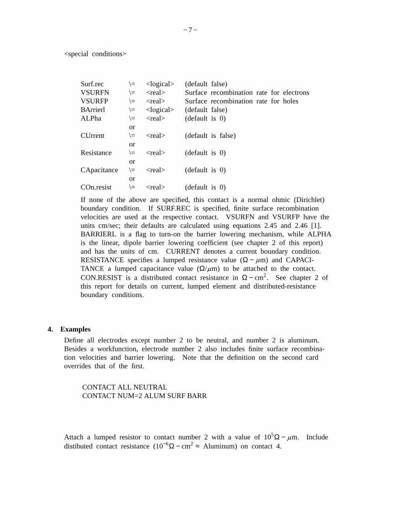
<special conditions>
Surf.rec \= <logical> (default false)VSURFN \= <real> Surface recombination rate for electronsVSURFP \= <real> Surface recombination rate for holesBArrierl \= <logical> (default false)ALPha \= <real> (default is 0)
orCUrrent \= <real> (default is false)
orResistance \= <real> (default is 0)
orCApacitance \= <real> (default is 0)
orCOn.resist \= <real> (default is 0)
If none of the above are specified, this contact is a normal ohmic (Dirichlet)boundary condition. If SURF.REC is specified, finite surface recombinationvelocities are used at the respective contact. VSURFNand VSURFP have theunits cm/sec; their defaults are calculated using equations 2.45 and 2.46 [1].BARRIERL is a flag to turn-on the barrier lowering mechanism, while ALPHAis the linear, dipole barrier lowering coefficient (see chapter 2 of this report)and has the units of cm.CURRENT denotes a current boundary condition.RESISTANCE specifies a lumped resistance value (Ω − m) and CAPACI-TANCE a lumped capacitance value (Ω/ m) to be attached to the contact.CON.RESIST is a distributed contact resistance inΩ − cm2. See chapter 2 ofthis report for details on current, lumped element and distributed-resistanceboundary conditions.
4. Examples
Define all electrodes except number 2 to be neutral, and number 2 is aluminum.Besides a workfunction, electrode number 2 also includes finite surface recombina-tion velocities and barrier lowering. Notethat the definition on the second cardoverrides that of the first.
CONTACT ALL NEUTRALCONTACT NUM=2 ALUM SURF BARR
Attach a lumped resistor to contact number 2 with a value of 105Ω − m. Includedistibuted contact resistance (10−6Ω − cm2 ≈ Aluminum) on contact 4.

− 8 −
CONTACT NUM=2 RESIS=1E5CONTACT NUM=4 CON.RES=1E-6

− 9 −
The CONTOUR card
1. Syntax
CONTOur <plotted quantity> <range definition> <control>
2. Description
The CONTOUR card plots contours on a plotted two-dimensional area of the device,as specified by the most recent PLOT.2D card.
3. Parameters
<plotted quantity>
One of:
POtential \= <logical> Mid-gap potentialQFN \= <logical> Electronquasi-fermi levelQFP \= <logical> Holequasi-fermi levelValenc.b \= <logical> Valence band potentialCONduc.b \= <logical> Conductionband potentialDOping \= <logical> DopingELectrons \= <logical> ElectronconcentrationHoles \= <logical> HoleconcentrationNET.CHarge \= <logical> Netcharge concentrationNET.CArrier \= <logical> Netcarrier concentrationJ.Conduc \= <logical> ConductioncurrentJ.Electr \= <logical> ElectroncurrentJ.Hole \= <logical> HolecurrentJ.Displa \= <logical> DisplacementcurrentJ.Total \= <logical> Total currentE.field \= <logical> ElectricfieldRecomb \= <logical> NetrecombinationFlowlines \= <logical> Currentflow linesALPHAN \= <logical> Ionizationrate for electrons (/cm)ALPHAP \= <logical> Ionizationrate for holes (/cm)IMPACT \= <logical> Generatedcarrier density due to impact ionization (/cm2)
The above parameters specify the quantity to be plotted.For vector quantities the magni-tude is plotted. Model dependent parameters (current and recombination) are calculatedwith the models currently defined,not with the models that were defined when the solu-tion was computed. This allows the display of, for instance, Auger and Shockley-Read-Hall components of recombination separately. For consistent values of current, the mod-els used in the solution should be specified.The quantity to be plotted has no default.

− 10 −
<range definition>
MIn.value \= <real>MAx.value \= <real>DEl.value \= <real>NContours \= <integer>
MIN.VALUE and MAX.VALUE specify the minimum and maximum contours to be plot-ted. MIN.VALUE and MAX.VALUE default to the minimum and maximum values of thequantity to be plotted over the device (these are printed during execution). DEL.VALUEspecifies the interval between contours.Alternatively, NCONTOURS specifies the numberof contours to be plotted.If the plot is logarithmic, the minimum and maximum should begiven as the logarithmic bounds.
− 11 −
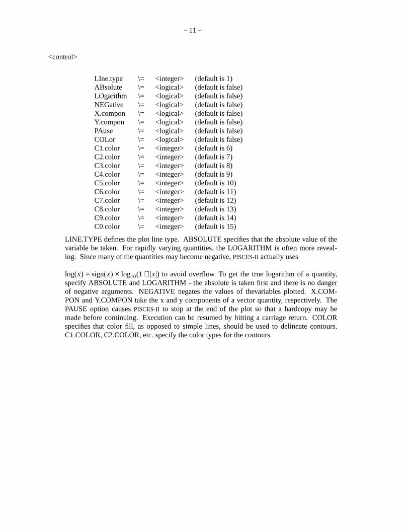
<control>
LIne.type \= <integer> (default is 1)ABsolute \= <logical> (default is false)LOgarithm \= <logical> (default is false)NEGative \= <logical> (default is false)X.compon \= <logical> (default is false)Y.compon \= <logical> (default is false)PAuse \= <logical> (default is false)COLor \= <logical> (default is false)C1.color \= <integer> (default is 6)C2.color \= <integer> (default is 7)C3.color \= <integer> (default is 8)C4.color \= <integer> (default is 9)C5.color \= <integer> (default is 10)C6.color \= <integer> (default is 11)C7.color \= <integer> (default is 12)C8.color \= <integer> (default is 13)C9.color \= <integer> (default is 14)C0.color \= <integer> (default is 15)
LINE.TYPE defines the plot line type.ABSOLUTE specifies that the absolute value of thevariable be taken. For rapidly varying quantities, the LOGARITHM is often more reveal-ing. Sincemany of the quantities may become negative, PISCES-IIactually uses
log(x) = sign(x) × log10(1 + |x|) to avoid overflow. To get the true logarithm of a quantity,specify ABSOLUTE and LOGARITHM - the absolute is taken first and there is no dangerof negative arguments. NEGATIVE negates the values of thevariables plotted.X.COM-PON and Y.COMPON take the x and y components of a vector quantity, respectively. ThePA USE option causesPISCES-II to stop at the end of the plot so that a hardcopy may bemade before continuing.Execution can be resumed by hitting a carriage return.COLORspecifies that color fill, as opposed to simple lines, should be used to delineate contours.C1.COLOR, C2.COLOR, etc. specify the color types for the contours.

− 12 −
4. Examples
The following plots the contours of potential from -1 volts to 3 volts in steps of .25 volts:
CONTOUR POTEN MIN=-1 MAX=3 DEL=.25
In the next example, the log of the doping concentration is plotted from 1.0e10 to 1.0e20 insteps of 10.By specifying ABSOLUTE, both the n-type and p-type contours are shown.
CONTOUR DOPINGMIN=10 MAX=20 DEL=1 LOG ABS
In the following, current flow lines are plotted.The number of flow lines is 11 so that 10%of the current flows between adjacent lines.
CONTOUR FLOW NCONT=11

− 13 −
The DOPING card
1. Syntax
DOping <profile type> <location> <region> <profile specification> <save>
2. Description
The DOPING card dopes selected regions of the device.
3. Parameters
<profile type>One of the following types must be selected.
ErfcGaussianUniformSUprem3OLD.Suprem3ASciiS4geomSImpldop
ERFC, GAUSSIAN and UNIFORM are used to analytically describe profileshapes. SUPREM3reads data files produced by the more recent release ofSUPREM-III, which supports the ‘‘export’’ output file format. The default is toread binary formatted export files. If the ASCII parameter is also specified,then ASCII (text) formatted SUPREM-III export files will be expected.OLD.SUPREM3 is used to get profile information from the original version ofthe SUPREM-III process modeling program.This reads the binary structure file.ASCII without the SUPREM3 parameter allows for input of simple ascii datafiles containing concentration versus depth information. The format of theASCII input file is a depth in m followed by a concentration incm−3 − onepair per line. By convention, positive concentrations refer to donors (n-type),while negative concentration values refer to acceptors (p-type).S4GEOMallows doping from a SUPREM-IV file (using the struct pisces=foo commandin SUPREM-IV) to be interpolated onto an existing PISCES-II mesh. SIM-PLDOP takes doping from a SIMPL-2 file (rectangular grid of doping values)to be interpolated onto an existing PISCES-II mesh.
− 14 −
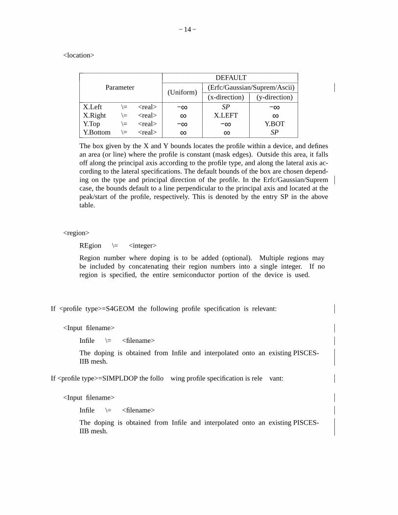
<location>
DEFAULT(Erfc/Gaussian/Suprem/Ascii)Parameter
(Uniform)(x-direction) (y-direction)
X.Left \= <real> −∞ SP −∞X.Right \= <real> ∞ X.LEFT ∞Y.Top \= <real> −∞ −∞ Y.BOTY.Bottom \= <real> ∞ ∞ SP
The box given by the X and Y bounds locates the profile within a device, and definesan area (or line) where the profile is constant (mask edges).Outside this area, it fallsoff along the principal axis according to the profile type, and along the lateral axis ac-cording to the lateral specifications. The default bounds of the box are chosen depend-ing on the type and principal direction of the profile. In the Erfc/Gaussian/Supremcase, the bounds default to a line perpendicular to the principal axis and located at thepeak/start of the profile, respectively. This is denoted by the entry SP in the abovetable.
<region>
REgion \= <integer>
Region number where doping is to be added (optional).Multiple regions maybe included by concatenating their region numbers into a single integer. If noregion is specified, the entire semiconductor portion of the device is used.
If <profile type>=S4GEOM the following profile specification is relevant:
<Input filename>
Infile \= <filename>
The doping is obtained from Infile and interpolated onto an existing PISCES-IIB mesh.
If <profile type>=SIMPLDOP the follo wing profile specification is relevant:
<Input filename>
Infile \= <filename>
The doping is obtained from Infile and interpolated onto an existing PISCES-IIB mesh.

− 15 −
If <profile type>=SUPREM3 or OLD.SUPREM3, the following profile specifications arerelevant:
<Input filename>
Infile \= <filename>
<dopant>: Oneof
Boron \= <logical>PHosphorus \= <logical>ARsenic \= <logical>ANtimony \= <logical>
The selected dopant profile will be extracted from theSUPREM-III save file.
<Two-dimensional spread>
Parameter DefaultDIrection \= x or y ySTart \= <real> 0RAtio.Lateral \= <real> 0.8
This group of parameters specifies where to locate the one-dimensional profilein the 2-dimensional device and how to extend it to the second dimension.DIRECTION is the axis along which the profile is directed. START is thedepth in the specified direction where the profile should start, and should nor-mally be at the surface. The lateral profile is assumed to have the same formas the principal profile, but shrunk/expanded by the factor RATIO.LATERAL.The defaults for the location box are set up as a line, parallel to the surface,and located at START.
If <profile type>=ASCII the following profile specifications are relevant:
<Input filename>
Infile \= <filename>
The ascii concentrations in INFILE are read and added to the impurity profiles.
<Two-dimensional spread>
As above - see description for SUPREM3 and OLD.SUPREM3.

− 16 −
If <profile type>= GAUSSIAN, the following profile specifications are relevant:
<profile>
COncentration \= <real> (nodefault) (cm−3)JUnction \= <real> (nodefault) ( m)SLice.lat \= <real> (seebelow) ( m)
or
DOSe \= <real> (nodefault) (cm−2)CHaracteristic \= <real> (nodefault) ( m)
or
COncentration \= <real> (nodefault) (cm−3)CHaracteristic \= <real> (nodefault) ( m)
and one of :
N.type/DONor \= <logical> (nodefault)P.type/ACceptor \= <logical> (no default)
and any combination of :
RAtio.Lateral \= <real> (default: 0.8)Erfc.Lateral \= <logical> (default: false)Lat.char \= <real> (seebelow)PEak \= <real> (default: 0) ( m)DIrection \= <character> (default: y)
If <profile type>= ERFC, the following profile specifications are relevant:
<profile>
COncentration \= <real> (nodefault) (cm−3)JUnction \= <real> (nodefault) ( m)J.Conc \= <real> (CO/100) (cm−3)SLice.lat \= <real> (seebelow) ( m)
or
COncentration \= <real> (nodefault) (cm−3)CHaracteristic \= <real> (nodefault) ( m)
and one of :
N.type/DONor \= <logical> (nodefault)

− 17 −
P.type/ACceptor \= <logical> (no default)
and any combination of :
RAtio.Lateral \= <real> (default: 0.8)Erfc.Lateral \= <logical> (default: false)Lat.char \= <real> (seebelow)PEak \= <real> (default: 0) ( m)DIrection \= <character> (default: y)
These parameters govern the profile outside the constant box.DIRECTION definesthe principal axis of the profile.CONCENTRATION is the peak concentration,DOSE the total dose.J.CONC is the concentration at the junction, JUNCTION is thelocation of the junction and must be in silicon, outside the constant box; CHARAC-TERISTIC is the principal characteristic length.The peak concentration and principalcharacteristic length are computed from the given combination of the first four param-eters. WhenJUNCTION is used,PISCES-IIcomputes the characteristic length by ex-amining thedoping at a point half way between the ends of the constant box and atthe given depth; if some other lateral position is desired for the computation, use theparameter SLICE.LATERAL=<real>. Thelateral impurity profile may be an errorfunction insteadof gaussian, and its characteristic length is either the product of RA-TIO.LATERAL and the principal characteristic length (default) or can be specified us-ing LAT.CHAR. PEAK specifies the position of the peak. The defaults for the con-stant box are set up as a line, parallel to the surface and located at PEAK.
If <type>=UNIFORM the following parameters are relevant:
<concentration>
COncentration \= <real>N.type/DONor \= <logical>P.type/ACceptor \= <logical>
Concentration is the value of the uniform doping level. It should be given in units ofatoms/cm3 and be positive. The polarity is given by the logical parameters.Doping isintroduced in the intersection of the box and the region selected.The default box isset up to include the entire region.
<save>
Outfile \= <filename>
The save option allows the user to save a machine-readable copy of all the DOP-ING cards in a file. The first DOPING card should have the OUTFILE parameter,so that the doping information on it and all subsequent DOPING cards are saved inthat file. The file can be reread after regrid to calculate the doping on the newgrid.

− 18 −
4. Examples
A one-dimensional diode with substrate doping 1016 cm−3 and Gaussian profile.
DOP UNIFCONC=1E16 P.TYPEDOP GAUSS CONC=1E20 JUNC=0.85 N.TYPE PEAK=0
An n-channel MOSFET with Gaussian source and drain.Because the default X.RIGHT is+∞, for the source we must limit the constant part to X.RIGHT=4, and conversely for thedrain. Thus the profile has a constant part along the surface, falls off as an error function to-wards the gate, and as a gaussian in the direction of the bulk. In both cases, the verticaljunction is at 1.3 m.
DOP UNIFCONC=1E16 P.TYPEDOP GAUSS CONC=9E19 N.TYPE+ X.RIGHT=4 JUNC=1.3 R.LAT=0.6 ERFC.LATDOP GAUSS CONC=9E19 N.TYPE+ X.LEFT=12 JUNC=1.3 R.LAT=0.6 ERFC.LAT
Read a Suprem bipolar profile and add it to a uniform substrate concentration.Add dopingonly to those points lying in region 1.
COM *** SUBSTRATE ***DOP REGION=1UNIF CONC=1E16 N.TYPECOM *** BASE ***DOP REGION=1ASCII SUPREM BORON R.LAT=0.7 INF=plt3.out1+ START=0COM *** EMITTER ***DOP REGION=1ASCII SUPREM PHOS R.LAT=0.8 INF=plt3.out1+ X.LEFT=12.0 X.RIGHT=13.0 START=0
Simulate a triple diffused bipolar by using a mixture of analytic and SUPREM-III profiles.Use an erfc for the emitter, a SUPREM-III profile for the base, a gaussian for the collector,and add it to a uniform substrate concentration.Add doping only to those points lying in re-gion 1.
COM *** SUBSTRATE ***DOP REGION=1 UNIFORM CONC=9.999463e+14 p.typeCOM *** EMITTER ***DOP REGION=1 ERFC N.TYPE CON=1e20 CHAR=0.1+ X.LEF=-1 X.RIG=0 R.LAT=0.8COM *** B ASE ***DOP REGION=1 SUPREM3 INFILE=base.exp BORON+ X.LEF=-4 X.RIG=0 R.LAT=0.8COM *** COLLECTOR ***DOP REGION=1 GAUSS PHOS CON=1e17 CHAR=0.8+ X.LEF=-7 X.RIG=0 R.LAT=0.8

− 19 −
The ELECTRODE card
1. Syntax
ELEctrode <number> <position>
2. Description
The ELECTRODE card specifies the location of electrodes in a rectangular mesh.
3. Parameters
<number>
Number \= <integer>
There may be up to ten electrodes, numbered 1,2,3,...,9,0.They may beassigned in any order, but if there are N electrodes, none can have an elec-trode number above N.
<location>
IX.Low \= <integer>IX.High \= <integer>IY.Low \= <integer>IY.High \= <integer>
Nodes having x and y indices between IX.LOW and IX.HIGH and betweenIY.LOW and IY.HIGH respectively are designated electrode nodes.
4. Examples
Define a typical back-side contact.
ELEC N=1 IX.LOW=1 IX.HIGH=40 IY.LOW=17 IY.HIGH=17
− 20 −
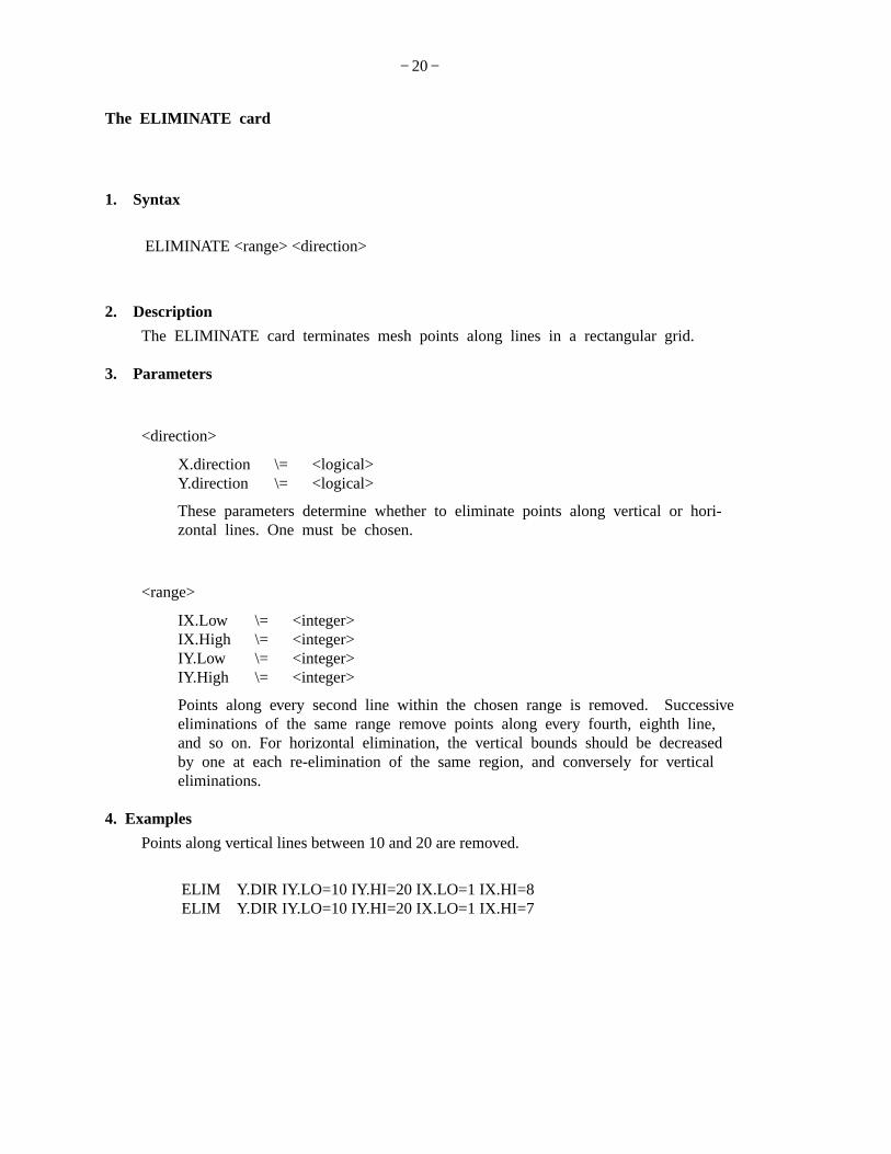
The ELIMINATE card
1. Syntax
ELIMINATE <range> <direction>
2. Description
The ELIMINATE card terminates mesh points along lines in a rectangular grid.
3. Parameters
<direction>
X.direction \= <logical>Y.direction \= <logical>
These parameters determine whether to eliminate points along vertical or hori-zontal lines. One must be chosen.
<range>
IX.Low \= <integer>IX.High \= <integer>IY.Low \= <integer>IY.High \= <integer>
Points along every second line within the chosen range is removed. Successiveeliminations of the same range remove points along every fourth, eighth line,and so on. For horizontal elimination, the vertical bounds should be decreasedby one at each re-elimination of the same region, and conversely for verticaleliminations.
4. Examples
Points along vertical lines between 10 and 20 are removed.
ELIM Y.DIR IY.LO=10 IY.HI=20 IX.LO=1 IX.HI=8ELIM Y.DIR IY.LO=10 IY.HI=20 IX.LO=1 IX.HI=7

− 21 −
The END card
1. Syntax
ENd
2. Description
The END card specifies the end of a set ofPISCES-II input cards. The END cardmay be placed anywhere in the input deck; all input lines below the occurrence ofthe END card will be ignored. If an END card is not included, all cards in theinput file are processed.
− 22 −
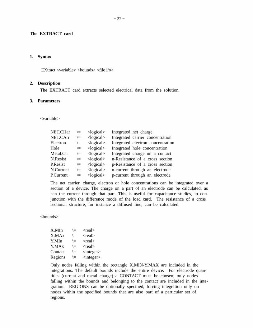
The EXTRACT card
1. Syntax
EXtract <variable> <bounds> <file i/o>
2. Description
The EXTRACT card extracts selected electrical data from the solution.
3. Parameters
<variable>
NET.CHar \= <logical> Integrated net chargeNET.CArr \= <logical> Integrated carrier concentrationElectron \= <logical> Integrated electron concentrationHole \= <logical> Integrated hole concentrationMetal.Ch \= <logical> Integrated charge on a contactN.Resist \= <logical> n-Resistanceof a cross sectionP.Resist \= <logical> p-Resistanceof a cross sectionN.Current \= <logical> n-currentthrough an electrodeP.Current \= <logical> p-currentthrough an electrode
The net carrier, charge, electron or hole concentrations can be integrated over asection of a device. The charge on a part of an electrode can be calculated, ascan the current through that part. This is useful for capacitance studies, in con-junction with the difference mode of the load card.The resistance of a crosssectional structure, for instance a diffused line, can be calculated.
<bounds>
X.MIn \= <real>X.MAx \= <real>Y.MIn \= <real>Y.MAx \= <real>Contact \= <integer>Regions \= <integer>
Only nodes falling within the rectangle X.MIN-Y.MAX are included in theintegrations. The default bounds include the entire device. For electrode quan-tities (current and metal charge) a CONTACT must be chosen; only nodesfalling within the bounds and belonging to the contact are included in the inte-gration. REGIONScan be optionally specified, forcing integration only onnodes within the specified bounds that are also part of a particular set ofregions.

− 23 −
<file i/o>
Outfile \= <filename>
An optional ascii OUTPUT file can be specified to which the result and biasinfor will be written.
4. Examples
The following extracts the resistance of a p-type line diffused into a lightly doped nsubstrate. Since the p-conductivity of the substrate is negligible, the bounds of theintegration can include the whole device.
EXTRACT P.RESIST
In the next example, the charge on the lower surface of a gate electrode is inte-grated. There is 0.05 m of gate oxide on the surface, which is at y=0.
EXTRACT METAL.CH CONT=1 X.MIN=-2.0 X.MAX=2.0+ Y.MAX=-0.0499 Y.MIN=-0.0501

− 24 −
The IMPACT card
1. Syntax
IMpact <parameters>
2. Description
The IMPACT card specifies the use of the impact ionization model.For manydevices, the impact ionization model for continuity equations allows the accurate pre-diction of a valanche breakdown. Baraff’s model ([6]) has been approximated withcompact formulae by Crowell and Sze ([7]). The current models are for Si only.See also, the IMPACT parameter to the MODEL card and the impact parameters tothe CONTOUR card.
3. Parameters
CRowell \= <logical> (default is false)MOnte \= <logical> (default is false)LAMDAE \= <real> (default is 6.2e-7)LAMDAH \= <real> (default is 3.8e-7)
CROWELL specifies the use of Crowell and Sze formulae. if MONTE is giventhen the alpha values are extracted by Monte Carlo simulation.If CROWELL isnot specified, Grant’s model [4] is used. The basic implementation idea followsLaux [5], but using Scharfetter-Gummel current discretization formula without aweighting scheme. LAMBDAE and LAMDAH specify the mean free path incmfor electrons and holes respectively.
Also the Newton method with 2-carrier must be specified on the METHODcard since impact ionization is a 2-carrier process.
4. Examples
Use the Crowell and Sze formulae with the default mean free paths.
IMPACT CRO WELL LAMD AE=6.2e-7 LAMDAH=3.8e-7

− 25 −
The INCLUDE card
1. Syntax
INClude <filename>
or
SOURCE <filename>
2. Description
The INCLUDE statement provides a shorthand way to include information fromother files in thePISCES-II input file. The statements in the INCLUDEd file will beinserted into thePISCES-II input file in place of the INCLUDE statement when theinput file is processed.The statements in the INCLUDEd file must use correctPISCES-II input syntax, and they must be in correct order with respect to the otherstatements in thePISCES-II input file when the INCLUDEd file is expanded by theinput parser. This is most useful for libraries of material and model parameters.
3. Examples
INCLUDE MAT.init

− 26 −
The INTERFACE card
1. Syntax
Interface <parameters> <location>
2. Description
The INTERFACE card allows the specification of interface parameters (recombinationvelocities and fixed charges) at semiconductor-insulator boundaries.
3. Parameters
<parameters>
S.N \= <real> Electronsurface recombination velocity (cm/sec)S.P \= <real> Hole surface recombination velocity (cm/sec)Qf \= <real> Fixed charge density (cm−2).
See chapter 2 of this report for a description of interface surface recombinationvelocities.
<location>
X.Min \= <real>X.Max \= <real>Y.Min \= <real>Y.Max \= <real>
X.MIN, X.MAX, Y .MIN and Y.MAX define a bounding box, measured in m.Any oxide/semiconductor interfaces found within this region are charged. Anon-planar surface may be defined by using a box which contains the wholedevice, provided there is only one interface in the device.
4. Examples
Define an interface with both fixed charge and recombination velocities.
INTERFACE X.MIN=-4 X.MAX=4 Y.MIN=-0.5 Y.MAX=4+ QF=1E10 S.N=1E4 S.P=1E4
− 27 −
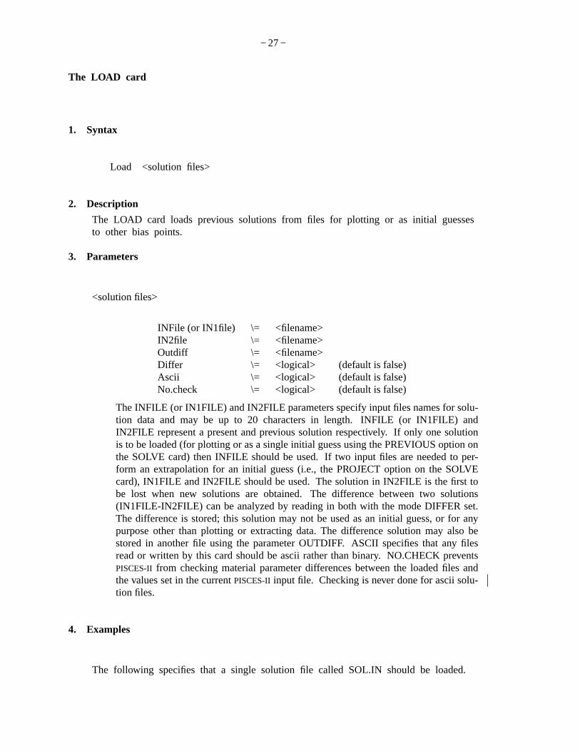
The LOAD card
1. Syntax
Load <solutionfiles>
2. Description
The LOAD card loads previous solutions from files for plotting or as initial guessesto other bias points.
3. Parameters
<solution files>
INFile (or IN1file) \= <filename>IN2file \= <filename>Outdiff \= <filename>Differ \= <logical> (default is false)Ascii \= <logical> (default is false)No.check \= <logical> (default is false)
The INFILE (or IN1FILE) and IN2FILE parameters specify input files names for solu-tion data and may be up to 20 characters in length.INFILE (or IN1FILE) andIN2FILE represent a present and previous solution respectively. If only one solutionis to be loaded (for plotting or as a single initial guess using the PREVIOUS option onthe SOLVE card) then INFILE should be used.If two input files are needed to per-form an extrapolation for an initial guess (i.e., the PROJECT option on the SOLVEcard), IN1FILE and IN2FILE should be used.The solution in IN2FILE is the first tobe lost when new solutions are obtained.The difference between two solutions(IN1FILE-IN2FILE) can be analyzed by reading in both with the mode DIFFER set.The difference is stored; this solution may not be used as an initial guess, or for anypurpose other than plotting or extracting data. The difference solution may also bestored in another file using the parameter OUTDIFF. ASCII specifies that any filesread or written by this card should be ascii rather than binary. NO.CHECK preventsPISCES-II from checking material parameter differences between the loaded files andthe values set in the currentPISCES-IIinput file. Checking is never done for ascii solu-tion files.
4. Examples
The following specifies that a single solution file called SOL.IN should be loaded.

− 28 −
LOAD INF=SOL.IN
In the next example, two solutions are loaded.The present solution is to SOL1.INand the previous solution is SOL2.IN. We intend to use SOL1.IN and SOL2.IN toproject an initial guess for a third bias point.
LOAD IN1F=SOL1.IN IN2F=SOL2.IN
Finally, two solutions are loaded, and the difference calculated and stored in a thirdfile.
LOAD IN1F=SOL1.IN IN2F=SOL2.IN DIFF OUTD=SOL1-2

− 29 −
The LOG card
1. Syntax
LOG <file specification>
2. Description
The LOG card allows the I-V and/or AC characteristics of a run to be logged todisk. Any I-V or AC data subsequent to the card is saved. If a log file is alreadyopen, it is closed and a new file opened.
3. Parameters
<file specification>
Outfile or Ivfile \= <filename>Acfile \= <filename>
OUTFILE or IVFILE specify the log file for I-V information. ACFILE specifies thefile for AC data.
4. Examples
Save the I-V data in a file called IV1 and AC data in AC1.
LOG OUTF=IV1 ACFILE=AC1

− 30 −
The MATERIAL card
1. Syntax
MAterial <region> <material definitions>
2. Description
The material card associates physical parameters with the materials in the mesh.Many of the parameters are default for standard materials.Any equation numbersreferred to below correspond to [1].
3. Parameters
<region>
NUmber \= <integer>or
Region \= <integer>
NUMBER (or REGION) specifies the region number to which these parametersapply. Only one set of semiconductor parameters is allowed. Therefore,if theregion specified is a semiconductor region, all other semiconductor regions (ifthere are any) will be changed as well.
<material definitions>
EG300 \= <real> : Energy gap at 300K (eq. 2.16) (eV)EGAlpha \= <real> : Alpha (eq. 2.16)EGBeta \= <real> : Beta (eq. 2.16)AFfinity \= <real> : Electron affinity (eV)Permittivity \= <real> : Dielectric permittivity (F/cm)Vsaturation \= <real> : Saturation velocity (eq. 2.34, 2.35) (cm/s)MUN \= <real> : Low-field electron mobility (cm2/s)MUP \= <real> : Low-field hole mobility (cm2/s)G.surface \= <real> : surface mobility reduction (eq. 2.33)TA UP0 \= <real> : SRH Electron lifetime (eq. 2.6, 2.8) (s)TA UN0 \= <real> : SRH Hole lifetime (eq. 2.6, 2.9) (s)
...continued...

− 31 −
NSRHN \= <real> : SRH conc. parameter - electrons (eq. 2.8) (cm−3)NSRHP \= <real> : SRH conc. parameter - holes (eq. 2.9) (cm−3)ETrap \= <real> : Trap level = Et − Ei (eq. 2.6)AUGN \= <real> : Auger coefficient (cn) (eq. 2.7) (cm6/s)AUGP \= <real> : Auger coefficient (cp) (eq. 2.7) (cm6/s)NC300 \= <real> : Conduction band density at 300K (eq. 2.17) (cm−3)NV300 \= <real> : Valence band density at 300K (eq. 2.18) (cm−3)ARICHN \= <real> : Richardson constant for electrons (eq. 2.45)ARICHP \= <real> : Richardson constant for holes (eq. 2.46)GCb \= <real> : Conduction-band degeneracy factor (eq. 2.33a,IIB-sm)GVb \= <real> : Valence-band degeneracy factor (eq. 2.33b,IIB-sm)EDb \= <real> : Donor energy level (eq. 2.34a,IIB-sm)EAb \= <real> : Acceptor energy level (eq. 2.34b,IIB-sm)
Defaults:
Semiconductors
Constant Silicon Gallium Arsenide ArbitraryEnergy gap (300K) 1.08 1.43 0.0Alpha 4.73× 10⁻⁴ 5. 405× 10−4 0.0Beta 636. 204 0.0Electron affinity 4.17 4.07 0.0Permittivity 11.8 10.9 0.0Saturation velocity (eq.2.36) (eq.2.37) 0.0Electron mobility 1000 5000 0.0Hole mobility 500 400 0.0Surface mobility reduction 1. 0 1.0 0.0SRH Electron lifetime 1. 0× 10−7 1. 0× 10−7 0.0SRH Hole lifetime 1. 0× 10−7 1. 0× 10−7 0.0Auger coefficient (n) 2. 8× 10⁻³¹ 2. 8× 10⁻³¹ 0.0Auger coefficient (p) 9. 9× 10⁻³² 9. 9× 10⁻³² 0.0Cond band density (300K) 2. 8× 10¹⁹ 4. 7× 10¹⁷ 0.0Val band density (300K) 1. 04× 1019 7. 0× 1018 0.0Eff Richardson const (n) 110 6.2857 0.0Eff Richardson const (p) 30 105 0.0SRH conc. parameter (n) 5. 0× 1016 5. 0× 1016 0.0SRH conc. parameter (p) 5. 0× 1016 5. 0× 1016 0.0Trap level 0. 0 0. 0 0.0Cond band degen factor 2.0 2. 0 0.0Val band degen factor 4.0 2. 0 0.0Donor energy level (eV) 0.044 0.005 0.0Acceptor energy level (eV) 0.045 0.005 0.0
Insulators
Constant Silicondioxide Siliconnitride Sapphire ArbitraryPermittivity 3.9 7.5 12.0 0.0

− 32 −
4. Examples
The following defines SRH lifetimes and concentration-independent low-field mobilities forall the semiconductor regions within the device (all the other parameters are assumed to betheir default, consistent with the semiconductor type chosen):
MATERIAL TAUN0=5.0e-6 TAUP0=5.0e-6 MUN=3000 MUP=500

− 33 −
The MESH card
1. Syntax
MESh <type> <cylindrical> <output files> <smoothing key>
2. Description
The mesh card either initiates the mesh generation phase or reads a previously gen-erated mesh.
3. Parameters
<type>: One of
<Previous>
Previous \= <logical>Infile \= <filename>ASCII.In \= <logical> (default is false)
Reads a previously generated mesh from a save file. ASCII.IN is a flagto indicate if the save file is ascii as opposed to binary.
<Rectangular>
Rectangular \= <logical>NX \= <integer>NY \= <integer>Diag.fli \= <logical> (default is false)
These parameters initiate the generation of a rectangular mesh.NX isthe number of nodes in the x-direction, NY the number in the y-direction.DIAG.FLIP which if set, flips the diagonals in a square mesh about thecenter of the grid. If DIAG.FLIP is false, all the diagonals will be in thesame direction.

− 34 −
<Geometry>
Geometry \= <logical>Infile \= <filename>Flip.y \= <logical> (default is false)SCale \= <integer> (default is 1)
This reads a mesh (ascii) generated by an external grid editor. FLIP.Y isa flag which will reverse the sign of the y-coordinate.SCALE is a fac-tor by which all the coordinates read are multiplied by.
<Output files>
<PISCES-II format>
OUTFile \= <filename>ASCII.Out \= <logical> (default is false)
OUTFILE is the PISCES-II format output file to be read by a later run.If ASCII.OUT is set, OUTFILE will be written in ascii, otherwise it willbe binary.
<Grid editor>
OUT.asc \= <filename>Flip.y \= <logical> (default is false)SCale \= <integer> (default is 1)
OUT.ASC is an ascii output file intended to be read by an external grid editor.See appendix B of [1] for details of the format.FLIP.Y and SCALE are asabove.
<smoothing key>
SMooth.key \= <integer>
This causes mesh smoothing as described in section 4.6 of [1].The digits ofthe integer are read in reverse order and decoded as follows:
1 Triangle smoothing, maintaining all region boundaries fixed.2 Triangle smoothing, maintaining only material boundaries.3 Node averaging.
Options 1 and 3 are the most common; 2 is used only if a device has severalregions of the same material and the border between the different regions isunimportant.

− 35 −
<Cylindrical coordinates>
CYLindrical \= <logical>
Using the CYL parameter specifies that the mesh, whether generated in the currentinput deck or read from a file, is to be rotated about the y-axis to permit the simu-lation of c ylindrically symmetrical devices. This information is NOT written to themesh file; it must be specified in the input deck which calculates a solution.
4. Examples
Initiate a rectangular mesh and request it to be stored in mesh1.pg :
MESH RECTANGULAR NX=40 NY=17 OUTF=mesh1.pg
Read a previously generated mesh and generate an ascii file for a grid editor (the yaxis is inverted because the grid editor obeys the convention that positive y isupward, while PISCES-II follows the semiconductor convention of positive y beinginto the bulk) :
MESH INF=mesh1.pgOUT.ASC=mesh1.pa FLIP ASCII.OUT
Read a geometry file, smooth the mesh, and store the file for a later run (ascii for-mat):
MESH GEOM INF=geom1 SMOOTH.K=13131 OUTF=mesh1.pg
The smoothing does several averaging and flipping steps. The digits are read inreverse order, so that the flipping comes first, followed by node averaging, and soon.

− 36 −
The METHOD card
1. Syntax
METhod <general parameters> <method-dependent parameters>
2. Description
The METHOD card sets parameters associated with the particular solution algorithmchosen on the SYMBOLIC card.There can be more than one METHOD card in asingle simulation, so that parameters can be altered.The default values of theparameters are used on the first occurrence of the METHOD card; subsequentMETHOD cards only alter those coefficients specified.
3. Parameters
<general parameters>
Parameter DefaultITlimit \= <integer> 15Xnorm \= <logical> trueRhsnorm \= <logical> falseP.toler \= <real> Dependson choice of normC.toler \= <real> Dependson choice of normLImit \= <logical> falsePRint \= <logical> falseFix.qf \= <logical> falseTRap \= <logical> falseAT rap \= <real> 0.5
The above parameters are used to determine the convergence of the solutionmethods. ITLIMIT is the maximum number of allowed outer loops (i.e., New-ton loops or Gummel continuity iterations).P.TOL and C.TOL are the termi-nation criteria for the Poisson and continuity equations, respectively. IfXNORM is chosen as the error norm, the Poisson updates are measured inunits of kT/q, and carrier updates are measured relative to the local carrierconcentration. In this case the default value for both P.TOL and C.TOL is1 × 10−5. If RHSNORM is selected, the Poisson error is measured in C/ mand the continuity error in A/ m. P.TOL then defaults to 1× 10⁻²⁶C/ m, andC.TOL to 5× 10⁻¹⁸A/ m.
LIMIT indicates that the convergence criterion should be ignored, and iterationsare to proceed until ITLIMIT is reached.PRINT prints the terminal fluxes/cur-rents after each continuity iteration; if this parameter is not set, the terminalfluxes/currents are only printed after the solution converges. FIX.QFfixes thequasi-Fermi potential of each non-solved for carrier to a single value, insteadof picking a value based on local bias (see section 5 of chapter 2 [1] and the‘‘ p.bias’’ and ‘‘n.bias’’ parameters on the SOLVE card). TRAP specifies that if

− 37 −
a solution process starts to diverge, the electrode bias steps taken from the ini-tial guess are reduced by the multiplicative factor ATRAP.
<method-dependent parameters>
For the Gummel method:
The following parameters are for damping the Poisson updates.
DVlimit \= <real> (default is 0.1)or
DAMPEd \= <logical> (default is false)DElta \= <real> (default is 0.5)DAMPLoop \= <integer> (default is 10)DFactor \= <real> (default is 10.0)
The DVLIMIT parameter limits the maximum update for a singleloop. The DAMPED parameter indicates the use of a more sophisti-cated damping scheme proposed by Bank and Rose (this is the rec-ommended option, particularly for large bias steps).The remainingdamping parameters are only interpreted if the DAMPED parameter isspecified. DELTA is the threshold for determining the damping factorfor ∆ and must be between 0 and 1.DAMPLOOP is the maxi-mum number of damping loops allowed to find a suitable dampingcoefficient. DFACTOR is a factor which serves to increase the initialdamping coefficient for the next Newton loop.
The following parameters select acceleration methods for the Gummeliteration.
SInglepoisson \= <logical> (default is false)ICcg \= <logical> (default is false)LU1cri \= <real> (default is 3× 10⁻³)
LU2cri \= <real> (default is 3× 10⁻²)
Maxinner \= <integer> (default is 25)ACCEleration \= <logical> (default is false)ACCSTArt \= <real> (default is 0.3)ACCSTOp \= <real> (default is 0.6)ACCSTEp \= <real> (default is 0.04)
The first two parameters specify how the Poisson equation iterationsare to be performed.The SINGLEPOISSON option indicates thatonly a single Poisson iteration is to be performed per Gummel loopas opposed to the default where the continuity equation is onlytreated after Poisson has fully converged. TheICCG parameterchooses whether or not to use iteration to solve the multi-Poissonloops. It should be set whenever doing multi-Poisson. The next twoparameters specify how much work is done per Poisson loop (cf. Sec-tion 3.3 [1]). The inner norm is required to decrease by at leastLU1CRI before returning, or to reach a factor of LU2CRI below the
− 38 −
projected Newton error, whichever is the smaller. (If the inner normis allowed to exceed the projected Newton error, quadratic conver-gence is lost). MAXINNER sets the maximum number of ICCG iter-ations. Theremaining parameters deal with an acceleration methodfor attaining faster overall convergence in the single-Poisson mode.The ACCELERATION option specifies that acceleration is to be used.ACCSTART is the starting value of the acceleration parameter, ACC-STOP is the final (limiting) value of the acceleration parameter andACCSTEP is the step to be added to the value of the accelerationparameter after each iteration [1].
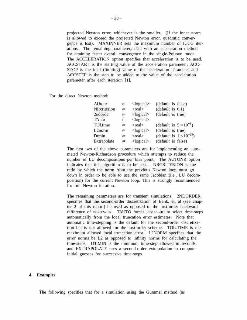
For the direct Newton method:
AUtonr \= <logical> (default is false)NRcriterion \= <real> (default is 0.1)2ndorder \= <logical> (default is true)TAuto \= <logical>TOl.time \= <real> (default is 5× 10⁻³)L2norm \= <logical> (default is true)Dtmin \= <real> (default is 1× 10⁻²⁵)Extrapolate \= <logical> (default is false)
The first two of the above parameters are for implementing an auto-mated Newton-Richardson procedure which attempts to reduce thenumber of LU decompositions per bias point.The AUTONR optionindicates that this algorithm is to be used.NRCRITERION is theratio by which the norm from the previous Newton loop must godown in order to be able to use the same Jacobian (i.e., LU decom-position) for the current Newton loop. This is strongly recommendedfor full Newton iteration.
The remaining parameters are for transient simulations.2NDORDERspecifies that the second-order discretization of Bank, et. al (see chap-ter 2 of this report) be used as opposed to the first-order backwarddifference ofPISCES-IIA. TAUTO forces PISCES-IIB to select time-stepsautomatically from the local truncation error estimates.Note thatautomatic time-stepping is the default for the second-order discretiza-tion but is not allowed for the first-order scheme.TOL.TIME is themaximum allowed local truncation error. L2NORM specifies that theerror norms be L2 as opposed to infinity norms for calculating thetime-steps. DT.MIN is the minimum time-step allowed in seconds,and EXTRAPOLATE uses a second-order extrapolation to computeinitial guesses for successive time-steps.
4. Examples
The following specifies that for a simulation using the Gummel method (as

− 39 −
previously specified by an appropriate symbolic card), that damping is to beemployed and the Poisson error tolerance should be 1× 10⁻³⁰ coul/ m. Note thatbecause XNORM defaults to true, XNORM must be turned off to use the rhs normas a convergence criterion. If XNORM=FALSE had not been specified, the rhsnorm and the update norm would have both been printed, but only the update normwould have been used to determine convergence.
METHOD DAMPED P.TOL=1.e-30 RHSNORM XNORM=FALSE
The next example illustrates the trap feature, which can be quite useful for capturingknees of IV curves for devices such as SCRs.The first SOLVE card solves for theinitial, zero bias case.On the second SOLVE card, we attempt to solve for V2=3volts V3=5 volts. If such a large bias change caused the solution algorithms todiverge for this bias point, the bias steps would be multiplied by ATRAP(0.5); i.e.,an intermediate point (V2=1.5 volts, V3=2.5 volts) would be attempted before tryingto obtain V2=3 volts and V3=5 volts again. If the intermediate point can not besolved for either, PISCES-II will continue to reduce the bias step (the next would beV2=0.75 volts and V3=1.25 volts) up to 4 times. Note also that the intermediatesolutions will be saved in output files in a manner similar to voltage stepping usingthe VSTEP parameter on the SOLVE card; i.e., if two intermediate steps toV2/V3=3/5 volts were required, they would be stored in ‘‘outa’’ and ‘‘outb’’ whileV2/V3=3/5 volts would be stored in ‘‘outc’’.
METHOD TRAP ATRAP=0.5SOLVE INITSOLVE V2=3 V3=5 OUTFILE=outa
Finally, an example of transient simulation.By default, the second-order discretiza-tion is used, but the required LTE, 1× 10⁻³, is smaller than the default. Newton-Richardson is also used.Note that because the Jacobian is exact for the secondpart (BDF-2) of the composite time-step, there should be very few factorizations forthe BDF-2 interval when AUTONR is specified (see chapter 2 of this report).
METHOD TOL.TIME=1E-3 AUTONR

− 40 −
The MODELS card
1. Syntax
MOdels <modelflags> <numerical parameters>
2. Description
The model card sets the temperature for the simulation and specifies model flags toindicate the inclusion of various physical mechanisms and models.
3. Parameters
<model flags>
Srh \= <logical> (default is false)CONSrh \= <logical> (default is false)AUger \= <logical> (default is false)BGn \= <logical> (default is false)CONMob \= <logical> (default is false)ANalytic \= <logical> (default is false)ARORA \= <logical> (default is false)FLdmob \= <logical> (default is false)SURFmob \= <logical> (default is false)TFLDmob \= <logical> (default is false)OLDtfld \= <logical> (default is false)CCSmob \= <logical> (default is false)USER1 \= <logical> (default is false)IMPAct \= <logical> (default is false)BOltzmann \= <logical> (default is true)FErmidirac \= <logical> (default is false)Incomplete \= <logical> (default is false)Photogen \= <logical> (default is false)Print \= <logical> (default is false)
CONSRH/SRH and AUGER specify Shockley-Read-Hall (eq. 2.6 [1]) and Augerrecombination (eq. 2.7 [1]) respectively. SRH uses fixed lifetimes and CONSRHuses concentration-dependent lifetimes.(eq. 2.8, 2.9 [1]). BGN is band-gap nar-rowing (eq. 2.20 [1]). CONMOB is concentration dependent mobility from tablesfor 300K (currently only silicon and gallium arsenide have been implemented).ANALYTIC is an analytical concentration dependent mobility model for silicon only(see chapter 1, section 3 of [1]) which will include temperature dependence.ARORA specifies an alternative concentration dependent mobility model for silicon[8]. FLDMOB specifies a lateral field-dependent model (eq. 2.34, 2.35 [1]).SURFMOB invokes the effective field based surface mobility model. ([2] [3]) Thecurrent implementation accounts only for phonon scattering at room temperature,
− 41 −
restricting it to effective fields of less than 0.5 MV/cm.CCSMOB invokes themobility model of Dorkel and Leturcq[9], which includes carrier-carrier scatteringeffects, temperature dependence and concentration dependence.TFLDMOB invokesthe transverse-field mobility model whose derivation is described in [10]. OLDT-FLD specifies the use of the Schwarz-Russek formulation [12], while TFLDMOBinvokes an extended version of the Schwarz-Russek formulation for both holes andelectrons [10][11]. USER1 specifies the user-customizable concentration-dependentmobilty model. Only one of AN ALYTIC, ARORA, CCSMOB or USER1 may bespecified. IMPACT inv okes the empirical impact ionization model. ([4] [5])Amore rigorous impact ionization model can be specified with IMPACT command.BOLTZMANN and FERMIDIRAC indicate the carrier statistics to be used (eq. 2.13,2.14 and 2.10, 2.11 [1]), while INCOMPLETE indicates that incomplete-ionization ofimpurities should be accounted for (eq. 2.31, 2.32 [1]).PHOTOGEN specifies thatphotogeneration is to be used; FLUX and ABS.COEF must also be specified to usethis model. PRINT prints the status of all models and a v ariety of coefficients andconstants.
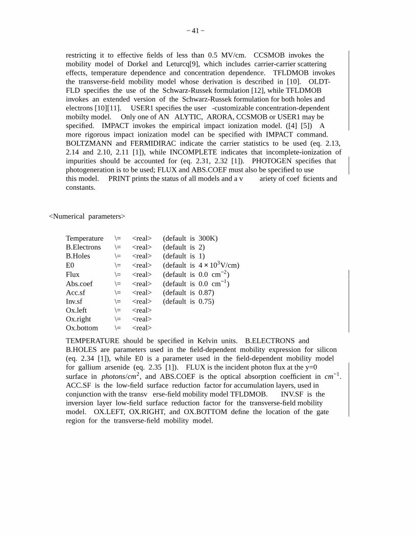
<Numerical parameters>
Temperature \= <real> (default is 300K)B.Electrons \= <real> (default is 2)B.Holes \= <real> (default is 1)E0 \= <real> (default is 4× 10³V/cm)Flux \= <real> (default is 0.0 cm−2)Abs.coef \= <real> (default is 0.0 cm−1)Acc.sf \= <real> (default is 0.87)Inv.sf \= <real> (default is 0.75)Ox.left \= <real>Ox.right \= <real>Ox.bottom \= <real>
TEMPERATURE should be specified in Kelvin units. B.ELECTRONS andB.HOLES are parameters used in the field-dependent mobility expression for silicon(eq. 2.34 [1]), while E0 is a parameter used in the field-dependent mobility modelfor gallium arsenide (eq. 2.35 [1]).FLUX is the incident photon flux at the y=0surface in photons/cm2, and ABS.COEF is the optical absorption coefficient in cm−1.ACC.SF is the low-field surface reduction factor for accumulation layers, used inconjunction with the transverse-field mobility model TFLDMOB. INV.SF is theinversion layer low-field surface reduction factor for the transverse-field mobilitymodel. OX.LEFT, OX.RIGHT, and OX.BOTTOM define the location of the gateregion for the transverse-field mobility model.

− 42 −
4. Examples
The following example selects concentration dependent mobility and SRH recombina-tion. Fermi-diracstatistics are used, and the simulation is specified to be performedat 290K.
MODELS CONMOB SRH FERMI TEMP=290

− 43 −
The OPTIONS card
1. Syntax
Options <runcontrol> <plot control>
2. Description
The OPTIONS card sets options for an entire run.
3. Parameters
<run control>
G.debug or Debug \= <logical> (default is false)N.debug \= <logical> (default is false)CPUStat \= <logical> (default is false)CPUFile \= <character> (default is pisces.cpu)
G.DEBUG (or DEBUG) and N.DEBUG print debugging information to thePISCES-II standard output. G.DEBUG (or DEBUG) prints general information,N.DEBUG more specifically numerical parameters. CPUSTAT is a flag to indi-cate that a cpu profile of the solution process is to be printed to the file spec-ified by CPUFILE.
<Plot control>
PLOTDevice \= <character> (default login terminal)PLOTFile \= <character> (default device specific)X.Screen \= <real> (default devices size)Y.Screen \= <real> (default devices size)X.Offset \= <real> (default 0 inches)Y.Offset \= <real> (default 0 inches)
The first parameter specifies the output plot device. If no device is given, adefault (usually the user’s graphics terminal) will be used.Most versions ofPISCES-II use the PLOTCAP graphics package from Stanford.Please refer tothe PLOTCAP documents for further details. The full set of supported devicesis contained in the PLOTCAP data base. Possibilities include:
hp2648 hp2623 tek4107 vt240laserwriter ditroff latex xwindowshp9873 printronix sunview sav e
Plots will be scaled to the size of the specific device. Also note that on colorgraphics terminals, the different line types are implemented as different colors;on the black and white monitors they are implemented as dot and line
− 44 −
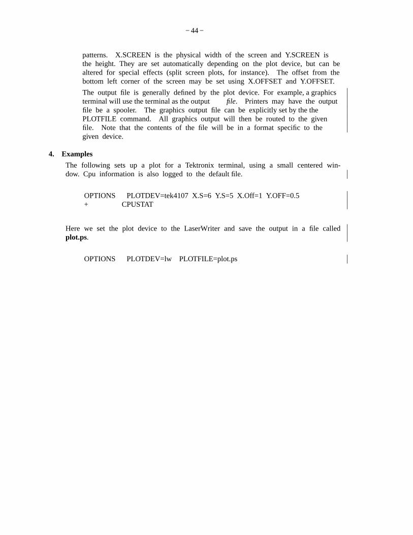
patterns. X.SCREENis the physical width of the screen and Y.SCREEN isthe height. They are set automatically depending on the plot device, but can bealtered for special effects (split screen plots, for instance).The offset from thebottom left corner of the screen may be set using X.OFFSET and Y.OFFSET.
The output file is generally defined by the plot device. For example, a graphicsterminal will use the terminal as the output file. Printers may have the outputfile be a spooler. The graphics output file can be explicitly set by the thePLOTFILE command. All graphics output will then be routed to the givenfile. Note that the contents of the file will be in a format specific to thegiven device.
4. Examples
The following sets up a plot for a Tektronix terminal, using a small centered win-dow. Cpu information is also logged to the default file.
OPTIONS PLOTDEV=tek4107 X.S=6 Y.S=5 X.Off=1 Y.OFF=0.5+ CPUSTAT
Here we set the plot device to the LaserWriter and save the output in a file calledplot.ps.
OPTIONS PLOTDEV=lw PLOTFILE=plot.ps

− 45 −
The PLOT.1D card
1. Syntax
PLOT.1d <line segment definition> <plotted quantity> <control>
2. Description
The PLOT.1D card plots a specific quantity along a line segment through the device(mode A), or plots an I-V curve of data (mode B).
3. Parameters
<line segment definition>
X.Start or A.X \= <real>Y.Start or A.Y \= <real>X.End or B.X \= <real>Y.End or B.Y \= <real>
The above parameters define the Cartesian coordinates of the start (A.X,A.Y)and the end (B.X,B.Y) of the line segment along which the specified quantityis to be plotted. The data is plotted as a function of distance from the start(A). The line segment may not be defaulted. It is required in mode A.
<plotted quantity>
One of:
POTential \= <logical> Mid-gap potentialQFN \= <logical> Electronquasi-fermi levelQFP \= <logical> Hole quasi-fermi levelDoping \= <logical> DopingELectrons \= <logical> ElectronconcentrationHoles \= <logical> Hole concentrationNET.CHarge \= <logical> Net charge concentrationNET.CArrier \= <logical> Netcarrier concentrationJ.Conduc \= <logical> ConductioncurrentJ.Electr \= <logical> ElectroncurrentJ.Hole \= <logical> Hole currentJ.Displa \= <logical> DisplacementcurrentJ.Total \= <logical> Total currentE.Field \= <logical> Electric fieldRecomb \= <logical> Net recombination

− 46 −
BAND.Val \= <logical> Valence band potentialBAND.Con \= <logical> Conductionband potential
or :
X.Axis \= <character>Y.Axis \= <character>INFile \= <character>
The above parameters specify the quantity to be plotted.There is no default.In mode A, one of the solution variables is plotted versus distance into thedevice. For vector quantities, the magnitude is plotted.In mode B, terminalcharacteristics can be plotted against each other by choosing the value to beplotted on each axis (XAXIS=,YAXIS=). Quantitiesavailable for plottinginclude applied biases (XAXIS/YAXIS=VA1, VA2, ..., VA9, VA0), actual con-tact bias which may differ from applied bias in the case of lumped elementboundary conditions (V1, V2, etc.), terminal current (I1, I2, etc.), AC capaci-tances (C11, C12, C21, etc.), AC conductance (G11, G12, G21, etc.)and ACadmittance (Y11, Y12, Y21, etc.).Additionally, any of the voltages or cur-rents can be plotted versus time for transient simulations, and any AC quantitycan be plotted versus frequency. The values plotted are the I-V or AC data ofthe present run, provided a log is being kept (see the LOG card). Alternatively,a different log file can be loaded with INFILE.
<control>
LOgarithm or Y.Log \= <logical> (default is false)X.Log \= <logical> (default is false)ABsolute \= <logical> (default is false)NO.Clear \= <logical> (default is false)NO.Axis \= <logical> (default is false)Unchanged \= <logical> (default is false)INTegral \= <logical> (default is false)NEGative \= <logical> (default is false)NO.Order \= <logical> (default is false)POInts \= <logical> (default is false)PAuse \= <logical> (default is false)LIne.type \= <integer> (default is 1)MIn.value \= <real>MAx.value \= <real>X.Max \= <real>X.Component \= <logical> (default is false)Y.Component \= <logical> (default is false)Spline \= <logical> (default is false)NSpline \= <logical> (default is 100)OUTFile \= <character> (default from OPTION card)AScii \= <logical> (default is false)
ABSOLUTE specifies that the absolute value of the variable be taken. Forrapidly varying quantities, the LOGARITHM (Y.LOG, X.LOG) is often morerevealing. Sincemany of the quantities may become negative, PISCES-II

− 47 −
actually uses
log(x) = sign(x) × log10(1 + |x|) to avoid overflow. To get the true logarithm of aquantity, specify ABSOLUTE and LOGARITHM - the absolute is taken firstand there is no danger of negative arguments. NO.CLEARindicates that thescreen is not to be cleared before the current plot so that several curves canbe plotted on the same axis.NO.AXIS indicates that the axes for the graphare not to be plotted.UNCHANGED is a synonym for NO.AXIS andNO.CLEAR, but additionally it forces the use of the previous axis bounds sothat a number of curves can easily be put on the same axis.INTEGRALplots the integral of the specified ordinate.NEGATIVE negates the ordinatevalues. PISCES-II by default will order the plot coordinates by abscissa value;this ordering will result in unusual plots for IV curves with negative resistance,for example. TheNO.ORDER parameter forcesPISCES-II to plot the datapoints as they naturally occur. POINTS marks the data points on the plottedcurve. The PA USE option causesPISCES-II to stop at the end of the plot sothat a hardcopy may be made before continuing.Execution can be resumedby hitting a carriage return.LINE.TYPE specifies the line type for the plottedcurve. MIN.VALUE and MAX.VALUE specify minimum and maximum valuesfor the ordinate of the graph; their defaults are found automatically from thedata to be plotted. X.MAX allows a maximum value for the abscissa to bespecified (default is just the maximum abscissa value in the data to be plotted).X.COMPONENT and Y.COMPONENT force the x and y components respec-tively of any vector quantities to be plotted as opposed to the default totalmagnitude. TheSPLINE option indicates that spline-smoothing should be per-formed on the data using NSPLINE interpolated points (maximum is 500).The default plot device is generally the user’s terminal but may be reset withthe OPTION card. If OUTFILE is specified, the graphics output will bedirected to that file. For further discussion, see the OPTION card.

− 48 −
4. Examples
The following plots a graph of potential along a straight line from (0.0,0.0) to(5.0,0.0):
PLOT.1D POTEN A.X=0 A.Y=0 B.X=5 B.Y=0
In the next example, the log of the electron concentration is plotted from (1.0,-0.5)to (1.0,8.0) with bounds on the plotted electron concentration of 1.0e10 and 1.0e20.A spline interpolation is performed with 300 interpolated points. The non-spline-in-terpolated points are marked.
PLOT.1D ELECT LOG A.X=1 A.Y=-.5 B.X=1 B.Y=8+ MIN=10 MAX=20 SPLINE NSPL=300 POINTS
In the following example, the current in contact 1 is plotted as a function of con-tact 2 voltage, then the curve is compared with a previous run.
PLOT.1D X.AXIS=V2 Y.AXIS=I1PLOT.1D X.AXIS=V2 Y.AXIS=I1 INF=logf0 UNCH
The following plots the actual contact voltage on a contact versus the applied volt-age.
PLOT.1D X.AXIS=V3 Y.AXIS=VA3 OUTFILE=save.plot
Finally, the following shows a plot of two capacitance components versus the log offrequency. A different line type is chosen for the second component.
PLOT.1D X.AXIS=FREQ Y.AXIS=C21 X.LOGPLOT.1D X.AXIS=FREQ Y.AXIS=C31 X.LOG UNCH LINE=4

− 49 −
The PLOT.2D card
1. Syntax
PLOT.2d <area definition> <plotted quantity> <control>
2. Description
The PLOT.2D card plots quantities in a specified two-dimensional area of thedevice. A PLOT.2D card is required before performing a contour plot (see CON-TOUR card) in order to obtain the plot boundaries.
3. Parameters
<area definition>
X.MIn \= <real>X.MAx \= <real>Y.MIn \= <real>Y.MAx \= <real>
The above parameters define the rectangular area of the device to be plotted.The default area is a rectangle around the entire device.
<plotted quantity>
Grid or Mesh \= <logical> (default is false)Crosses \= <logical> (default is false)Boundary \= <logical> (default is false)Depl.edg \= <logical> (default is false)Junction \= <logical> (default is false)
The GRID option plots the grid, including lines delineating elements.CROSSES plots crosses at the locations of grid points.BOUNDARY indicatesthat the boundaries around the device and between regions are to be plotted.DEPL.EDG indicates that depletion edges are to be plotted (note: depletionedges can only be plotted after a solution is present).The JUNCTION optionspecifies that the junctions from the doping profiles are to be plotted.

− 50 −
<control>
NO.TIc \= <logical> (default is false)NO.TOp \= <logical> (default is false)NO.Fill \= <logical> (default is false)NO.Clear \= <logical> (default is false)LAbels \= <logical> (default is false)Flip.x \= <logical> (default is false)Pause \= <logical> (default is false)L.Elect \= <integer>L.Deple \= <integer>L.Junct \= <integer>L.Bound \= <integer>L.Grid \= <integer>Outfile \= <character> (default from OPTION card)
NO.TIC indicates that tic marks are not to be included around the plotted area.NO.TOP indicates that tic marks are not to be put on the top of the plottedregion. The NO.FILL option will force PISCES-II to draw the device area plot-ted to scale; if this option is not specified, the plot will fill the screen, andthe triangles will appear distorted.NO.CLEAR specifies that the screen is notto be cleared before plotting.LABELS makes room for color contour labelson the right side of the plot device. FLIP.X flips the plot about the y-axis;i.e., it negates all x coordinates so that the plot is mirrored.The PAUSE op-tion causesPISCES-II to stop at the end of the plot so that a hardcopy may bemade before continuing. Execution can be resumed by hitting a carriage re-turn. L.ELECT, L.DEPLE, L.JUNCT, L.BOUND and L.GRID set line typesfor electrodes, depletion edges, junctions, region boundaries and grid, respec-tively. The default plot device is generally the user’s terminal but may be re-set with the OPTION card. If OUTFILE is specified, the graphics output willbe directed to that file.For further discussion, see the OPTION card.
4. Examples
The following plots the entire grid to scale with tic marks:
PLOT.2D GRID NO.FILL
In the next example, the device and region boundaries, junctions and depletion edgesare plotted in the rectangular area bounded by 0< x < 5 and 0< y < 10 . Theplot is allowed to fill the screen and tic marks are not included along the top ofthe plot.
PLOT.2D X.MIN=0 X.MAX=5 Y.MIN=0 Y.MAX=10+ JUNCT BOUND DEPL NO.TOP
− 51 −
The PRINT card
1. Syntax
PRint <location> <quantity> <flags>
2. Description
The PRINT card prints specific quantities at points within a defined area of thedevice.
3. Parameters
<location>
X.MIn \= <real>X.MAx \= <real>Y.MIn \= <real>Y.MAx \= <real>
or
IX.Low \= <integer>IX.High \= <integer>IY.Low \= <integer>IY.High \= <integer>
The above parameters define area in which the points of interest lie.X.MIN,X.MAX, Y.MIN and Y.MAX specify an area in physical coordinates (in m).IX.LOW, IX.HIGH, IY.LOW and IY.HIGH specify the area by the boundingindices (valid only for rectangular meshes).The default area is the entiredevice.

− 52 −
<quantity>
POints \= <logical>Elements \= <logical>Geometry \= <logical>Solution \= <logical>P.SOL1 \= <logical>P.SOL2 \= <logical>Current \= <logical>P.CURR1 \= <logical>P.CURR2 \= <logical>Que \= <logical>P.QUE1 \= <logical>P.QUE2 \= <logical>Material \= <logical>
The above parameters specify the quantities to be plotted.Any or all may bespecified, and each defaults to false. POINTSprints node information (coordi-nates, doping, etc.).ELEMENTS prints information on the triangular elements(number, nodes, material). GEOMETRY prints geometrical information on thetriangles. SOLUTIONprints the present solution ( , n, p and quasi-fermi po-tentials), while P.SOL1 and P.SOL2 print the previous two solutions. CUR-RENT prints currents (electron, hole, conduction, displacement and total) ateach node for the present solution; P.CURR1 and P.CURR2 print currents forprevious solutions. QUE prints space charge, recombination and electric fieldfor the present solution; P.QUE1 and P.QUE print the same quantities for theprevious two solutions. MATERIAL prints material information (permittivity,band-gap, etc.), including the value of the concentration dependent mobility andlifetime (if specified) at each point.
<flags>
X.Component \= <logical> (default is false)Y.Component \= <logical> (default is false)
X.COMPONENT and Y.COMPONENT specify how any of the various vectorquantities (currents, fields) should be printed.The default is the magnitude ofthe vector as a whole. X.COMPONENT specifies that the magnitude of the x-component of all vectors be printed, while Y.COMPONENT specifies the y-component. Onlyone of these (or neither) can be specified on a single card.

− 53 −
4. Examples
The following prints the physical coordinates, doping and region/electrode informa-tion for points along the 10th x grid line, from the 1st to the 20th y grid lines.
PRINT POINTS IX.LO=10 IX.HI=10 IY.LO=1 IY.HI=20
In the next example, solution information is printed for0 < x < 1 m and 0 < y < 2 m.
PRINT SOLUTION X.MIN=0 X.MAX=1 Y.MIN=0 Y.MAX=2

− 54 −
The REGION card
1. Syntax
REGIon <number> <position> <material>
2. Description
The region card defines the location of materials in a rectangular mesh. Every trian-gle must be defined to be some material.
3. Parameters
<number>
NUmber \= <integer>
This parameter selects the region in question. There is a maximum of eightregions in aPISCES-II structure.
<position>
IX.Low \= <integer>IX.High \= <integer>IY.Low \= <integer>IY.High \= <integer>
These parameters are the indices of a box in the rectangular mesh.
<material>One of:
SILiconGaasSEmiconductorOxide or SIO2NItride or SI3n4SApphireINsulator
4. Examples
The following defines a silicon region extending from nodes 1 to 25 in the x direc-tion and nodes 4 to 20 in the y direction :

− 55 −
REGION NUM=1 IX.LO=1 IX.HI=25 IY.LO=4 IY.HI=20 SIL
Note that region cards are cumulative in effect :
REGION NUM=1 IX.LO=4 IX.HI=5 IY.LO=1 IY.HI=20 OXIDEREGION NUM=1 IX.LO=36 IX.HI=37 IY.LO=1 IY.HI=40 OXIDE
defines one region comprised of two separate strips.
− 56 −
The REGRID card
1. Syntax
REGRid <location><variable> <control> <files>
2. Description
The REGRID card allows refinement of a crude mesh. Any triangle across whichthe chosen variable changes by more than a specified tolerance, or in which thechosen variable exceeds a given value, is refined.
3. Parameters
<location>
One of :
X.MIn \= <real>X.MAx \= <real>Y.MIn \= <real>Y.MAx \= <real>REGion \= <integer> default:allIGnore \= <integer> default:none
The bounds X.MIN-Y.MAX are used to limit the refinement; only triangleswhich have nodes which fall inside the box are considered for refinement. TheREGION parameter has a similar use; only regions specified are refined accord-ing to the user criterion. (Others may be refined as a side effect, to maintainwell-shaped triangles).The default is to refine all regions for potential andelectric field regrids, and all semiconductor regions for regrids which dependon the other variables. The parameter IGNORE is similar to REGION, butopposite in effect. Ignored regions are not regridded either according to theuser criterion or according to the ‘‘obtuse criterion’’ (see below); nor are theysmoothed after regrid. The default is not to ignore any region.
<variable>
One of :
Potential \= <logical> Mid-gap potential (Volts)EL.field \= <logical> Electric-field (Volts/cm)QFN \= <logical> Electronquasi-fermi level (Volts)QFP \= <logical> Hole quasi-fermi level (Volts)DOPIng \= <logical> Net doping (cm−3)ELEctron \= <logical> Electronconcentration (cm−3)
− 57 −
Hole \= <logical> Hole concentration (cm−3)NET.CHrg \= <logical> Net charge (cm−3)NET.CArr \= <logical> Net carrier concentration (cm−3)MIn.carr \= <logical> Minority carrier conc. (cm−3)
This parameter selects the discriminatory variable.
<control>
STep or RAtio \= <real> no defaultCHange \= <logical> default : trueABsolute \ <logical default: falseLOGarithm \= <logical> default: falseMAx.level \= <integer> default: dynamicSMooth.k \= <integer> default: 0LOCaldop \= <logical> default: falseCOs.ang \= <real> default:2.0
CHANGE determines whether to use the magnitude or the difference of a vari-able in a triangle as the criterion of refinement. It is normally set to true (dif-ference). STEPis the numerical criterion for refining a triangle. RATIO is asynonym. If the variable ranges across many orders of magnitude, it is advis-able to examine its logarithmic variation, using the LOG flag. In this caseSTEP will be interpreted as the step in the logarithm. ABSOLUTE specifiesthat the absolute value of the quantity is to be used.Since many of thequantities may become negative, PISCES-II actually uses
log(x) = sign(x) × log10(1 + |x|) to avoid overflow. To get the true logarithm of aquantity, specify ABSOLUTE and LOGARITHM - the absolute is taken firstand there is no danger of negative arguments. LOCALDOPis used withminority carrier regrids, and specifies that if the minority carrier concentrationexceeds the local doping, the grid is to be refined.MAX.LEVEL is the maxi-mum level of any triangle relative to the original mesh. It defaults to onemore than the maximum level of the grid, but can be set to a smaller value tolimit refinement. Values less than or equal to zero are interpreted relative tothe current maximum level. SMOOTH.K has the same meaning as on themesh card. COS.ANGLE defines the ‘‘obtuse criterion’’ to limit the creationof obtuse angles in the mesh.If regrid would create a triangle with an anglewhose cos is less than -COS.ANGLE, nodes are added so that this does notoccur. The test can be turned off locally by using the ignore parameter; itcan be turned off everywhere by using a value of COS.ANG greater than 1.The default is to turn it off everywhere.

− 58 −
<files>
OUTFile \= <filename>OUT.green \= <filename>IN.green \= <filename>DOPFile \= <filename>AScii \= <logical> (default is false)
OUTFILE is the binary output mesh file, and is necessary if the mesh is to beused for subsequent runs. A history of the triangle tree is always generated toassist further regriding steps. Its name can be specified by OUT.GREEN, andits default is generated from OUTFILE by concatenating the letters ‘‘tt’ ’ to theend. Additionally, a triangle tree for the previous mesh (if a tree exists) isused for this regrid. By default, PISCES-II will look for a file with the samename as the current mesh plus ‘‘tt’ ’ at the end as above. Alternatively,IN.GREEN can be used to implement a different file name. DOPFILE is thename of a file (up to 20 characters) which contains the doping for the device(see DOPING card). Specifying DOPFILE avoids interpolating doping valuesat any newly created grid points (the default), by using the initial doping spec-ification to redope the structure.ASCII specifies that all mesh files and trian-gle trees (not DOPFILE) for this card should be done in ascii rather than thedefault - binary.
4. Examples
Starting with an initial grid, we refine twice, requesting that all triangles withlarge doping steps be refined:
REGRID LOG DOPING STEP=6 OUTF=grid1 DOPF=dopxx1REGRID LOG DOPING STEP=6 OUTF=grid2 DOPF=dopxx1
A similar effect could be obtained with just one regrid statement:
REGRID LOG DOPING STEP=6 OUTF=grid2 DOPF=dopxx1+ MAX.LEVEL=2
In both cases two lev els of refinement are done. The first choice is preferablehowever, because new doping information is introduced at each level of refine-ment. This gives a better criterion for refinement, and fewer triangles.Now we perform an initial solution and refine triangles which exhibitlarge potential steps:
SOLVE INIT OUT=grid2.siREGRID POTENTIAL STEP=0.2 OUTF=grid3

− 59 −
The SOLVE card
1. Syntax
SOlve <estimate> <dc bias> <transient> <ac> <files>
2. Description
The SOLVE card instructsPISCES-II to perform a solution for one or more specifiedbias points.
3. Parameters
<estimate>
INitial \= <logical>PREvious \= <logical>PROject \= <logical>LOcal \= <logical>
The above parameters are used to specify how the initial guess for the solutionis to be obtained. The first bias point for a given structure must have theINITIAL parameter specified. From thenPISCES-II will either use the previoussolution (PREVIOUS), or if there are two previous solutions present and equiv-alent bias steps are taken on any electrodes that are changed (see chapter 3 inthis report and the example below), an extrapolation (PROJECT) from the pre-ceding two solutions will be used to get an improved initial guess. After theinitial bias point, PISCES-II will automatically use extrapolation wherever possi-ble if no estimate parameter is supplied. A different type of previous guess isavailable by using LOCAL values of the quasi-fermi levels.

− 60 −
<bias conditions>
V1 \= <real>I1 \= <real>V2 \= <real>I2 \= <real>
.
.
.V9 \= <real>I9 \= <real>V0 \= <real>I0 \= <real>VStep \= <real> (default is 0.0)IStep \= <real> (default is 0.0)NSteps \= <integer> (default is 0)Electrode \= <integer>N.bias \= <real>P.bias \= <real>
The parameters V1, V2,...,V9, V0 represent the bias voltages (for non-currentboundaries only) and I1, I2,...,I9, I0 represent the terminal currents in units ofAmps/ m (for current boundary contacts only - see CONTACT card) applied atcontacts 1, 2,...,9, 0.The defaults for these parameters are normally the poten-tials (currents) from the previous bias point. However, if the INITIAL flags isspecified on the solve card, then all contact potentials that are not specified onthe curent contact card will be reset to 0.0v. This reset holds even if a contactpotential has been set on a previous solve card. VSTEP(ISTEP) is a voltage(current) increment to be added to one or more electrodes, as specified by theinteger assigned to ELECTRODE. If more than one electrode is to bestepped, ELECTRODE should then be an n-digit integer, where each of the n-digits is a separate electrode number (and if there are 10 electrodes, don’t putelectrode 0 first in the sequence!).NSTEPS is the number of bias increments(steps) to be taken; i.e., if VSTEP (ISTEP) is specified, the specified electrodeis incremented NSTEPS times.Finally, N.BIAS and P.BIAS specify fixedquasi-Fermi potentials for carriers (electrons and holes, respectively) that arenot being solved for. If N.BIAS or P.BIAS are not specified, thenPISCES-II
either will choose local quasi-Fermi potentials based on bias and doping (seechapter 2 of [1]) or if ‘‘fix.qf ’ ’ i s set on the METHOD card, will set thequasi-Fermi levels where applicable to values which produce the least amountof free carriers (maximum bias for electrons and minimum bias for holes).

− 61 −
<transient>
Dt or TSTEp \= <real> (default is 0)TSTOp or TFinal \= <real>Ramptime \= <real> (default is 0)ENdramp \= <real> (default is 0)
DT (or TSTEP) is the time-step to be taken. For automatic time-step runs(see the METHOD card), DT (TSTEP) is used to select the first time step on-ly. TSTOP (or TFINAL) specifies the end of the time interval to be simulatedso that if the simulation begins at t = t0, it will end at t = TSTOP (TFINAL).Alternatively, NSTEPS can be used to signal the end of the run; i.e., the finaltime would be t = t0 + NSTEPS * TSTEP. RAMPTIME and ENDRAMP applyany bias changes as linear ramps.RAMPTIME specifies a ramp interval inseconds; i.e., the ramp will begin at t = t0 and end att = t0 + RAMPTIME.Alternatively, ENDRAMP specifies the exact end of the ramp in running time;i.e. the ramp will start att = t0 and end att = ENDRAMP.

− 62 −
<ac>
AC.analysis \= <logical> (default is false)FRequency \= <real>FStep \= <real> (default is 0)MUlt.freq \= <logical> (default is false)NFsteps \= <integer> (default is 0)VSs \= <real> (default is 0.1*kT/q)TErminal \= <integer> (default is all)S.omega \= <real> (default is 1.0)MAx.inner \= <integer> (default is 25)TOlerance \= <real> (default is 1x10⁻⁵)
AC.ANALYSIS is a flag to indicate that AC sinusoidal small-signal analysis(see chapter 2 of this report) be performed after the DC condition is solvedfor. Note that the full Newton method (2 carriers) must be used for this anal-ysis. FREQUENCY is the frequency (in Hz) at which this analysis is to beperformed. Theanalysis can be repeated at a number of different frequencies(without resolving the DC condition) by selecting an FSTEP. FSTEP is a fre-quency increment which is added to the previous frequency by default, or itmay be multiplied by setting MULT.FREQ. The number of increments isgiven by NFSTEPS. VSSis the magnitude of the applied small-signal bias(Vi in equation (2.19)). TERMINAL is the contact to which this AC bias willbe applied. More than one contact number may be specified (via concatena-tion), but each will be solved separately. Each contact that is specified yieldsa column of the admittance matrix as defined by equation (2.17).The analysismakes use SOR to solve a linear system. S.OMEGA is the relaxation parame-ter for SOR (it is NOT a frequency), MAX.INNER is the maximum number ofSOR iterations and TOLERANCE is the SOR convergence criterion. Specifica-tion of the ‘‘g.debug’’ fl ag on the OPTIONS card will provide some detailedinformation on the AC solution procedure.
<files> (optional)
Outfile \= <filename>Currents \= <logical> (default is false)AScii \= <logical> (default is false)
The OUTFILE parameter specifies the name of the binary output file for thesolution of this bias point. The file names may contain up to 20 characters.If an electrode is stepped so that more than one solution is generated by thiscard, the last non-blank character of the supplied file name will have its asciicode incremented by one for each bias point in succession, resulting in aunique file per bias point. If CURRENTS is specified, the electron, hole, anddisplacement currents, and the electric field, will be computed and stored withthe solution. IF ASCII is specified, OUTFILE will be ascii as opposed to bi-nary.

− 63 −
4. Examples
The following performs an initial bias point, saving the solution to the data fileOUT0:
SOLVE INIT OUTF=OUT0
In the next example, bias stepping is illustrated.The two solve cards produce thefollowing bias conditions:
Bias point # V1 V2 V31 0.0 0.5 -0.52 1.0 0.5 0.03 2.0 0.5 0.04 3.0 0.5 0.05 4.0 0.5 0.06 5.0 0.5 0.0
The solutions for these bias points will be saved to the files OUT1, OUTA, OUTB,OUTC, OUTD and OUTE. Note that the initial guess for the first bias point is ob-tained directly from the preceding solution because the PREVIOUS option was spec-ified. The initial guesses for bias points 2 and 3 will also be obtained as if PRE-VIOUS had been specified since two electrodes (numbers 1 and 3) had their biaseschanged on bias point 2.However, for bias points 4, 5 and 6,PISCES-II will use aprojection to obtain an initial guess since starting with bias point 4, both of its pre-ceding solutions (bias points 2 and 3) only had the same electrode bias (number 1)altered.
SOLVE PREV V1=0 V2=.5 V3=-.5 OUTF=OUT1SOLVE V1=1 V2=.5 V3=0 VSTEP=1 NSTEPS=4+ ELECT=1 OUTF=OUTA
Here is a case where two electrodes are stepped (2 and 3).The bias points solvedfor will be (0,0,1), (0,.5,1.5), (0,1,2) and (0,2,3).PISCES-II will use the PROJECToption to predict an initial guess for the third and fourth bias points since the biasvoltages on both electrodes 2 and 3 have been altered by the same amount betweeneach point.
SOLVE V1=0 V2=0 V3=1 VSTEP=.5 NSTEPS=2+ ELECT=23SOLVE V2=2 V3=3
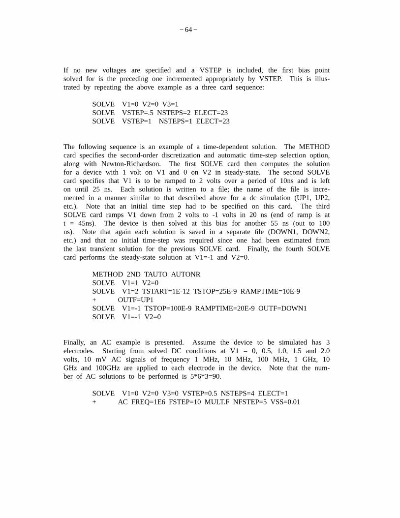
− 64 −
If no new voltages are specified and a VSTEP is included, the first bias pointsolved for is the preceding one incremented appropriately by VSTEP. This is illus-trated by repeating the above example as a three card sequence:
SOLVE V1=0 V2=0 V3=1SOLVE VSTEP=.5 NSTEPS=2 ELECT=23SOLVE VSTEP=1 NSTEPS=1ELECT=23
The following sequence is an example of a time-dependent solution.The METHODcard specifies the second-order discretization and automatic time-step selection option,along with Newton-Richardson. Thefirst SOLVE card then computes the solutionfor a device with 1 volt on V1 and 0 on V2 in steady-state.The second SOLVEcard specifies that V1 is to be ramped to 2 volts over a period of 10ns and is lefton until 25 ns. Each solution is written to a file; the name of the file is incre-mented in a manner similar to that described above for a dc simulation (UP1, UP2,etc.). Note that an initial time step had to be specified on this card.The thirdSOLVE card ramps V1 down from 2 volts to -1 volts in 20 ns (end of ramp is att = 45ns). The device is then solved at this bias for another 55 ns (out to 100ns). Note that again each solution is saved in a separate file (DOWN1, DOWN2,etc.) and that no initial time-step was required since one had been estimated fromthe last transient solution for the previous SOLVE card. Finally, the fourth SOLVEcard performs the steady-state solution at V1=-1 and V2=0.
METHOD 2ND TAUTO AUTONRSOLVE V1=1 V2=0SOLVE V1=2 TSTART=1E-12 TSTOP=25E-9 RAMPTIME=10E-9+ OUTF=UP1SOLVE V1=-1 TSTOP=100E-9 RAMPTIME=20E-9 OUTF=DOWN1SOLVE V1=-1 V2=0
Finally, an AC example is presented.Assume the device to be simulated has 3electrodes. Startingfrom solved DC conditions at V1 = 0, 0.5, 1.0, 1.5 and 2.0volts, 10 mV AC signals of frequency 1 MHz, 10 MHz, 100 MHz, 1 GHz, 10GHz and 100GHz are applied to each electrode in the device. Note that the num-ber of AC solutions to be performed is 5*6*3=90.
SOLVE V1=0 V2=0 V3=0 VSTEP=0.5 NSTEPS=4 ELECT=1+ AC FREQ=1E6 FSTEP=10 MULT.F NFSTEP=5 VSS=0.01

− 65 −
The SPREAD card
1. Syntax
SPread <direction> <region> <specifics>
2. Description
The SPREAD card provides a way to distort rectangular grids in the vertical direc-tion to follow surface and junction contours.SPREAD is very useful in reducingthe amount of grid for some specific problems, most notably MOSFET’s. TheSPREAD card is somewhat complicated; it is suggested to follow the suppliedexamples very carefully (particularly the MOSFET example in Chapter 5 in [1]).
3. Parameters
<direction>
One of:
LEft \= <logical> (default is false)Right \= <logical> (default is false)
LEFT and RIGHT specify that the left and right-hand sides of the grid respec-tively be distorted.
<region>
Width \= <real>Upper \= <integer>LOwer \= <integer>
WIDTH specifies the width from the left or right edge (depending on theLEFT and RIGHT parameters) of the distorted area.The actual x-coordinatespecified by WIDTH (min[x] + WIDTH for LEFT, max[x] - WIDTH forRIGHT) will lie in the middle of the transition region between the distortedand undistorted grid regions. UPPERand LOWER specify the upper andlower y-grid lines between which the distortion will take place.

− 66 −
<specifics>
One of:
Y.Lower \= <real>Thickness \= <real>
And:
Vol.ratio \= <real> (default is 0.44)Encroach \= <real> (default is 1.0)GRAding \= <real> (default is 1.0)GR1 \= <real> (default is 1.0)GR2 \= <real> (default is 1.0)Middle \= <real>Y.Middle \= <real>
The Y.LOWER and THICKNESS parameters define the distorted grid region;only one should be supplied.Y.LOWER is the physical location in the distort-ed region at which the line specified by LOWER will be moved. The linespecified by UPPER is not moved. THICKNESS is the thickness of the dis-torted region; THICKNESS will usually move the positions of both the UPPERand LOWER grid lines (unless VOL.RATIO is set to 0 or 1). VOL.RATIOspecifies the ratio of the downward displacement of the lower grid line to thenet increase in thickness.The default is 0.44 so that oxide-silicon interfacesare correct. VOL.RATIO is ignored if Y.LOWER is specified. ENCROACH isa factor which defines the abruptness of the transition between distorted andnon-distorted grid. The transition region becomes more abrupt with smallerENROACH factors (the minimum is 0.1). An important note: depending onthe characteristics of the undistorted grid, very bad triangles (long, thin and ob-tuse) may result if ENCROACH is set too low. GRADING specifies a gridratio (identical to the RATIO parameter on the X.MESH and Y.MESH cards)to produce a non-uniform grid in the distorted region. As alternative to a sin-gle grading parameter, GR1 and GR2 can be specified along with the y gridline MIDDLE and location Y.MIDDLE so that GR1 is used as the grading inthe spread region from UPPER to MIDDLE and GR2 is the grading fromMIDDLE to LOWER.

− 67 −
4. Examples
The following spreads what was previously a uniform 400 Angstroms of oxide to1000 Angstroms on the left side of the device. This will result in a net increase inthickness of 600 Angstroms of oxide.Because the default VOL.RATIO is used,0.44*(600) = 264 Angstroms of the net increase will lie below the original 400Angstroms and 0.56*(600) = 336 Angstroms of the net increase will lie above theoriginal 400 Angstroms. The width of the spread region is 0.5 m and the oxidetaper is quite gradual because of the high encroachment factor. The grid is leftuniform in the spread region.
$ *** Mesh definition ***MESH NX=30 NY=20 RECTX.M N=1 L=0X.M N=30 L=2Y.M N=1 L=-.04Y.M N=5 L=0Y.M N=20 L=1 R=1.4
$ *** Thin oxide ***REGION X.L=1 X.H=30 Y.L=1 Y.H=5
$ *** Silicon substrate ***REGION X.L=1 X.H=30 Y.L=5 Y.H=20
$ *** Spread ***SPREAD LEFTWIDTH=0.5 UP=1 LO=5 THICK=0.1 ENC=1.3

− 68 −
In the next example, the right side of the grid is distorted in order to follow ajunction contour. Assume that the initial grid is defined as above. Y.LOWER isused so that there is no increase in the size of the device, just grid redistribution.With Y.LOWER set to the junction, the ENCROACH parameter should be chosensuch that the lower grid line (LOWER=10) follows the junction as closely as possi-ble. Note that the grid is graded so that the grid lines are spaced closer togetheras they approach the junction. Because the point specified by WIDTH on thespread card lies in the middle of the transition region, it should be chosen to beslightly larger than the width of the doping ‘‘box’’ (WIDTH < X.LEFT - X.RIGHT= 0.5 m).
$ *** Doping ***DOPING UNIFORM N.TYPE CONC=1E15DOPING GAUSS P.TYPE X.LEFT=1.5 X.RIGHT=2+ PEAK=0 CONC=1e19 RATIO=.75 JUNC=0.3
$ *** Spread ***SPREAD RIGHTWIDTH=0.7 UP=5 LO=10 Y.LO=0.3+ ENC=1.2 GRAD=0.7

− 69 −
The SYMBOLIC card
1. Syntax
SYmbolic <solution method> <carriers> <options>
2. Description
The symbolic card performs a symbolic factorization in preparation for the LUdecompositions in the solution phase ofPISCES-II. Because each of the availablenumerical solution techniques used byPISCES-II may result in entirely different linearsystems, the method used and the number of carriers to be simulated must be speci-fied at this time. The symbolic factorization may be optionally read from or writ-ten to a file; if an input file is specified, the symbolic factorization information inthat file must be consistent with the method specified on the present card.
3. Parameters
<solution method>
One of:
Newton \= <logical>Gummel \= <logical>
The solution method must always be specified, except for the Poisson onlycase (carriers = 0). The different methods and their applications are discussedin Chapter 3 of [1] and this report.
<carriers>
Carriers \= <integer> (default is 1)Electrons \= <logical> (default is true)Holes \= <logical> (default is false)
The CARRIERS parameter specifies the number of carriers to be simulated.Ifonly one carrier is to be simulated,the specific carrier can be specified byincluding either HOLES or ELECTRONS.

− 70 −
<options>
Min.degree \= <logical> (default is true)Strip \= <logical> (default is true)Infile \= <character string>Outfile \= <character string>Print \= <logical> (default is false)
MIN.DEGREE uses a minimum degree ordering of the pivots for decomposi-tion in order to reduce the size of the generated L and U and hence, to re-duce the amount of cpu spent in solving linear systems.This parameter isdefinitely recommended. STRIP specifies that redundancy (zero couplings) beremoved from the symbolic map, and is naturally on.The INFILE and OUT-FILE parameters specify input/output files names for the symbolic factorization.The file names may contain up to 20 characters. Note that these binary filescan be quite large, so it may be advisable not to use this feature. (In somecomputing environments it is also faster to compute the symbolic informationthan to read it from disk). The PRINT parameter indicates that informationabout the memory allocated for the run should be printed to thePISCES-II stan-dard output file.
4. Examples
The following specifies a symbolic factorization for a simulation with only holes andusing the Gummel method (the symbolic factorization is saved in a file calledSYMB.OUT):
SYMBOLIC GUMMEL CARR=1 HOLES OUTF=SYMB.OUT
In the next example, a previously generated symbolic factorization is read in from afile called SYMB.IN. The method used is the full Newton method, and both carri-ers are included in the simulation.Additionally, the sizes and dimensions of allarrays associated with the sparse matrix solution are printed:
SYMBOLIC NEWTON CARR=2 INF=SYMB.IN PRINT

− 71 −
The TITLE card
1. Syntax
Title <character string>
2. Description
The TITLE card specifies a title (up to 60 characters) to be used inPISCES-II stan-dard output.
3. Examples
TITLE *** CMOS p-channel device ***

− 72 −
The VECTOR card
1. Syntax
Vector <plotted quantity> <control>
2. Description
The VECTOR card plots vector quantities over an area of the device defined by theprevious PLOT.2D card.
3. Parameters
<plotted quantity>
One of:
J.Conduc \= <logical> ConductioncurrentJ.Electr \= <logical> ElectroncurrentJ.Hole \= <logical> Hole currentJ.Displa \= <logical> DisplacementcurrentJ.Total \= <logical> Total currentE.field \= <logical> Electric field
The above parameters specify the quantity to be plotted.There is no default.

− 73 −
<control>
LOgarithm \= <logical> (default is false)MInimum \= <real> (default is 0)MAximum \= <real> (default is 0)Scale \= <real> (default is 1)Clipfact \= <real> (default is 0.1)LIne.type \= <integer> (default is 1)
LOGARITHM specifies logarithmically-scaled magnitudes.By default, all vec-tors in a linear plot are scaled by the maximum magnitude of the quantity ofinterest over the grid, while if LOGARITHM is set, the default scaling usesthe minimum (non-zero) magnitude.The minimum and maximum values, bothof which are printed during execution of a plot, can be arbitrarily set using theMINIMUM and MAXIMUM parameters, so that it is possible to plot two biasconditions or devices with the same scaling.SCALE a constant scale factor tobe multiply all magnitudes by. CLIPFACT is a threshold below which vectorsare not plotted. LINE.TYPE specifies the vector line type for plotting.
4. Examples
Plot electron and hole currents over a device :
PLOT.2D BOUN NO.FILLVECTOR J.ELEC LINE=2VECTOR J.HOLE LINE=3

− 74 −
The X.MESH card
The Y.MESH card
1. Syntax
X.Mesh <node> <location> <ratio>Y.Mesh <node> <location> <ratio>
2. Description
The X.MESH and Y.MESH cards specify the location of lines of nodes in a rectan-gular mesh.
3. Parameters
<node>
Node \= <integer>
This is the number of the line in the mesh. There can be at most 120 lines ineither direction. Lines are assigned consecutively, beginning with the first andending with the last.
<location>
Location \= <real>
This is where to locate the line. The location is interpreted in microns.
<ratio>
Ratio \= <real>
This gives the ratio to use when interpolating lines between the given lines.The spacing grows/shrinks by ratio in each subinterval, and the ratio shouldusually lie between 0.667 and 1.5.

− 75 −
4. Examples
Space grid lines closely around a junction in a 1-d diode with the junction at 0.85microns:
Y.MESH N=1 LOC=0.0Y.MESH N=20 LOC=0.85 RATIO=0.75Y.MESH N=40 LOC=2 RATIO=1.333

− 76 −