A phenomenological investigation of "good" supervision events
Upload
independentCategory
view
0download
0
IOP PUBLISHING JOURNAL OF PHYSICS D: APPLIED PHYSICS
J. Phys. D: Appl. Phys. 40 (2007) 2615–2623 doi:10.1088/0022-3727/40/9/S01
Photonic crystal defect mode cavitymodelling: a phenomenologicaldimensional reduction approachWeidong Zhou, Zexuan Qiang and Li Chen
Department of Electrical Engineering, Nanofab Center, University of Texas at Arlington,Arlington, TX 76019-0072, USA
E-mail: [email protected]
Received 20 July 2006Published 19 April 2007Online at stacks.iop.org/JPhysD/40/2615
AbstractA phenomenological dimensional reduction approach (PDRA) for the cavitycharacteristics in defect mode based photonic crystal (PC) lasers ispresented. Based on the fully vectorial three-dimensional finite-differencetime-domain (3D FDTD) technique, simultaneous enhancement andsuppression in spontaneous emission and absorption were obtained in anabsorptive photonic crystal slab (PCS) cavity. Effective index perturbation(EIP) was proposed for fast and accurate determination of the effective indexand the dominant resonant cavity frequency in a 3D PCS structure, withtwo-dimensional (2D) FDTD simulation. Further dimensional reductionfrom 2D to one-dimensional planar cavity enables phenomenologicalmodelling of lasing characteristics via the effective reflectivity calculationand rate equation analysis. Very fast and accurate results have been achievedwith this PDRA approach. A high spontaneous emission factor and cavityquality factor Q were obtained in a single defect cavity, which led to over anorder reduction in lasing gain threshold. The model offers a fast andaccurate tool for the design and modelling of PC defect mode cavity baseddevices and aids the research in the proposed novel defect mode baseddevices such as ultra-compact light sources on Si and spectrally resolved PCinfrared photodetectors.
(Some figures in this article are in colour only in the electronic version)
1. Introduction
Owing to the ability of photon density manipulation and light-matter interaction alternation, photonic crystals (PCs or PhCs)[1, 2] offer a disruptive platform for nanophotonics, whereultra-compact, high performance light sources, modulators,detectors and sensors can all be realized, potentially onthe same chip monolithically integrated [3]. Variousdevice configurations based on PC cavities have beenproposed and demonstrated experimentally, mostly based onplanar two-dimensional (2D) air hole lattice PC slab (PCS)structures [4–11].
Significant progress has also been made in thecomputational techniques for the design of PCS basedmicrocavity and in the understanding of these cavity
characteristics [12–15]. Works reported to date are mostlybased on the three-dimensional (3D) finite-difference time-domain (FDTD) technique. 3D FDTD is a powerful tool toaccurately simulate the characteristics of photonic crystal SEL(PCSEL) based on 2D PCS or quasi-3D structure, taking intoaccount the finite thickness in the vertical direction. However,the fully vectorial 3D FDTD approach is extremely time andcomputer memory consuming.
The effective index method (EIM) [12, 16] has provedto be very effective and efficient/fast in predicting the cavityproperties with reduced dimensionality (from 3D to 2D), whereonly the effective index of fundamental guided mode of theunperturbed slab is considered. EIM is most effective for thelow index contrast PCS. However, it becomes less accuratewhen it is applied to high index contrast PCS, where high
0022-3727/07/092615+09$30.00 © 2007 IOP Publishing Ltd Printed in the UK 2615
W Zhou et al
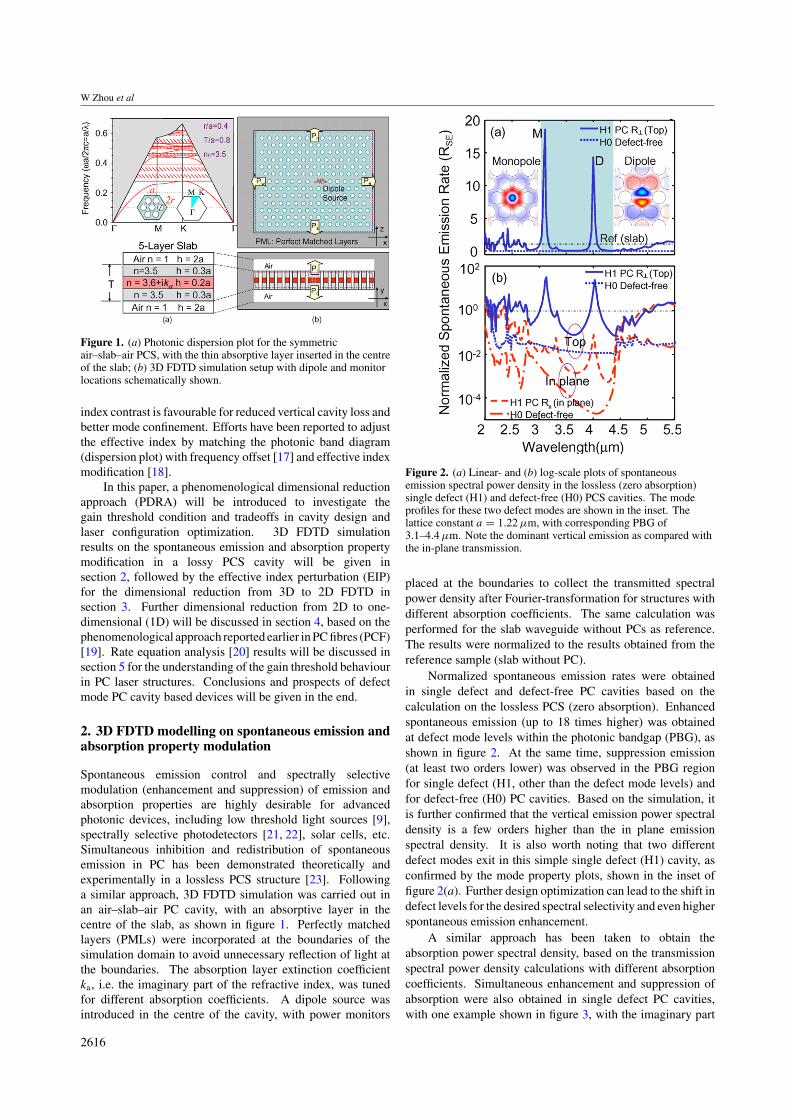
Figure 1. (a) Photonic dispersion plot for the symmetricair–slab–air PCS, with the thin absorptive layer inserted in the centreof the slab; (b) 3D FDTD simulation setup with dipole and monitorlocations schematically shown.
index contrast is favourable for reduced vertical cavity loss andbetter mode confinement. Efforts have been reported to adjustthe effective index by matching the photonic band diagram(dispersion plot) with frequency offset [17] and effective indexmodification [18].
In this paper, a phenomenological dimensional reductionapproach (PDRA) will be introduced to investigate thegain threshold condition and tradeoffs in cavity design andlaser configuration optimization. 3D FDTD simulationresults on the spontaneous emission and absorption propertymodification in a lossy PCS cavity will be given insection 2, followed by the effective index perturbation (EIP)for the dimensional reduction from 3D to 2D FDTD insection 3. Further dimensional reduction from 2D to one-dimensional (1D) will be discussed in section 4, based on thephenomenological approach reported earlier in PC fibres (PCF)[19]. Rate equation analysis [20] results will be discussed insection 5 for the understanding of the gain threshold behaviourin PC laser structures. Conclusions and prospects of defectmode PC cavity based devices will be given in the end.
2. 3D FDTD modelling on spontaneous emission andabsorption property modulation
Spontaneous emission control and spectrally selectivemodulation (enhancement and suppression) of emission andabsorption properties are highly desirable for advancedphotonic devices, including low threshold light sources [9],spectrally selective photodetectors [21, 22], solar cells, etc.Simultaneous inhibition and redistribution of spontaneousemission in PC has been demonstrated theoretically andexperimentally in a lossless PCS structure [23]. Followinga similar approach, 3D FDTD simulation was carried out inan air–slab–air PC cavity, with an absorptive layer in thecentre of the slab, as shown in figure 1. Perfectly matchedlayers (PMLs) were incorporated at the boundaries of thesimulation domain to avoid unnecessary reflection of light atthe boundaries. The absorption layer extinction coefficientka, i.e. the imaginary part of the refractive index, was tunedfor different absorption coefficients. A dipole source wasintroduced in the centre of the cavity, with power monitors
Figure 2. (a) Linear- and (b) log-scale plots of spontaneousemission spectral power density in the lossless (zero absorption)single defect (H1) and defect-free (H0) PCS cavities. The modeprofiles for these two defect modes are shown in the inset. Thelattice constant a = 1.22 µm, with corresponding PBG of3.1–4.4 µm. Note the dominant vertical emission as compared withthe in-plane transmission.
placed at the boundaries to collect the transmitted spectralpower density after Fourier-transformation for structures withdifferent absorption coefficients. The same calculation wasperformed for the slab waveguide without PCs as reference.The results were normalized to the results obtained from thereference sample (slab without PC).
Normalized spontaneous emission rates were obtainedin single defect and defect-free PC cavities based on thecalculation on the lossless PCS (zero absorption). Enhancedspontaneous emission (up to 18 times higher) was obtainedat defect mode levels within the photonic bandgap (PBG), asshown in figure 2. At the same time, suppression emission(at least two orders lower) was observed in the PBG regionfor single defect (H1, other than the defect mode levels) andfor defect-free (H0) PC cavities. Based on the simulation, itis further confirmed that the vertical emission power spectraldensity is a few orders higher than the in plane emissionspectral density. It is also worth noting that two differentdefect modes exit in this simple single defect (H1) cavity, asconfirmed by the mode property plots, shown in the inset offigure 2(a). Further design optimization can lead to the shift indefect levels for the desired spectral selectivity and even higherspontaneous emission enhancement.
A similar approach has been taken to obtain theabsorption power spectral density, based on the transmissionspectral power density calculations with different absorptioncoefficients. Simultaneous enhancement and suppression ofabsorption were also obtained in single defect PC cavities,with one example shown in figure 3, with the imaginary part
2616

Photonic crystal defect mode cavity modelling
Figure 3. (a) Photonic band diagram calculated by the PWEtechnique with a = 1.22 µm; (b) linear- and (c) log-scale plots ofabsorption power at ka = 0.16 for single defect (H1), defect-free(H0) and slab without PC structures.
5000
10-4
10-2
100
102
Absorption Coefficient (cm-1)1000200
Top
Top
In Plane
In Plane
H1
H0
Abs
orpt
ion
Enh
ance
men
t F
acto
r
λ=4µm (defect)
5000
10-4
10-2
100
102
Absorption Coefficient (cm-1)1000200
Top
Top
In Plane
In Plane
H1
H0
Abs
orpt
ion
Enh
ance
men
t F
acto
r
λ=4µm (defect)
Figure 4. Absorption enhancement factors in absorptive PCS defectcavities at the defect level (dipole mode, λ = 4 µm) for a largerange of absorption coefficients.
of the refractive index ka = 0.16 (corresponding to absorptioncoefficient of 5 × 103 cm−1 at λ = 4 µm).
The absorption enhancement factor, defined as the relativeabsorption power spectral density compared with that obtainedfrom the reference slab (without PC) with the same absorp-tion coefficient, can be derived from the normalized absorp-tion power spectral density. The absorption change (absorp-tion enhancement factor) due to the presence of the PC cavityis shown in figure 4, at the defect-level wavelength (4 µm),for different absorption coefficients. Enhanced absorption canbe obtained with the enhancement factor greater than 36. Thehigh enhancement factor can be obtained for a large range ofabsorption coefficients. High spectral selectivity is enabled
Figure 5. Proposed procedure for accurate computation of PCdefect-cavity resonant mode location based on EIP. Theconventional EIM approach is shown with dashed lines.
due to the spectrally selective enhancement and suppressionof absorption. Similar to the spontaneous emission case, thedominant absorption occurs at the surface normal vertical di-rection (R⊥), due to the high in plane cavity Q. Further in-vestigation reveals drastically different properties in emissionand absorption due to the complicated mode properties in othertypes of defect cavities, such as multi-defects and coupled cav-ities (distributed defects).
3. From 3D PCS to 2D PC: EIP
We introduced an EIP technique [24] in determining thesuitable effective index for the accurate prediction of cavitymodal property and defect mode locations based on 2D and3D plane wave-expansion (PWE) techniques and 2D FDTDmethod. In donor-like defect mode cavities formed in air-column based PCSs, very good agreement in defect modelocations was obtained with the EIP technique by matchingthe dielectric band edges simulated from 2D and 3D PWEtechniques. The highest Q mode can also be correctlypredicted, which is also very important in PC microcavitydesign, where the mode with the highest cavityQ could be mostimportant in determining the cavity characteristics, includinglasing and sensing.
It is well known that the air-band mode is more affectedby removing an air hole and finally a donor state is excited andpulled into the bandgap from the air band [25]. In standardEIM, a relatively large error in predicting the resonant modelocations is often seen as a result of the large offset in simulatedPBG. This leads us to believe an accurate prediction of resonantpeak locations from 2D FDTD is feasible by properly adjustingthe effective index to match the simulation PBGs. In this study,we found that suitable perturbation in effective index (neff )can lead to very small computation errors in resonant peaklocations for these donor-like modes by matching the dielectricband edge. The procedure to choose the suitable neff isillustrated in figure 5. First, the dielectric band edge of 2D PCSwithout defect, f 3D
d , is calculated by 3D PWE. The standardeffective refractive index of unperturbed slab waveguide is alsodone at this step by conventional methods [26]. Secondly, the2D PCS is transformed into an ideal 2D PC structure with thehigh refractive index nh replaced by the slab effective refractive
2617

W Zhou et al
r =0.32a; a=0.525µmt =0.409a; nh=3.4
2.35 2.40 2.45 2.50 2.55 2.60 2.65-8
-4
0
4
8
12
a
2r
Cal
cula
tio
n E
rro
r (%
)
Effective Refractive Index neff
Air bandMid gapDielectric bandDipole frequency
2.25 2.35 2.45 2.55 2.65-8
-4
0
4
8
12
2r
a
2r’
Cal
cula
tio
n E
rro
r (%
)
Effective Refractive Index neff
Air bandMid gapDielectric bandQuadrupole frequency
r =0.35a; a=0.57µmt =0.40a; nh=3.4
r’=0.2a
r =0.32a; a=0.525µmt =0.409a; nh=3.4
2.35 2.40 2.45 2.50 2.55 2.60 2.65-8
-4
0
4
8
12
a
2r
Cal
cula
tio
n E
rro
r (%
)
Effective Refractive Index neff
Air bandMid gapDielectric bandDipole frequency
r =0.32a; a=0.525µmt =0.409a; nh=3.4
2.35 2.40 2.45 2.50 2.55 2.60 2.65-8
-4
0
4
8
12
a
2r
Cal
cula
tio
n E
rro
r (%
)
Effective Refractive Index neff
Air bandMid gapDielectric bandDipole frequency
2.35 2.40 2.45 2.50 2.55 2.60 2.65-8
-4
0
4
8
12
a
2r
Cal
cula
tio
n E
rro
r (%
)
Effective Refractive Index neff
Air bandMid gapDielectric bandDipole frequency
2.25 2.35 2.45 2.55 2.65-8
-4
0
4
8
12
2r
a
2r’
Cal
cula
tio
n E
rro
r (%
)
Effective Refractive Index neff
Air bandMid gapDielectric bandQuadrupole frequency
r =0.35a; a=0.57µmt =0.40a; nh=3.4
r’=0.2a
2.25 2.35 2.45 2.55 2.65-8
-4
0
4
8
12
2r
a
2r’
Cal
cula
tio
n E
rro
r (%
)
Effective Refractive Index neff
Air bandMid gapDielectric bandQuadrupole frequency
2.25 2.35 2.45 2.55 2.65-8
-4
0
4
8
12
2r
a
2r’
Cal
cula
tio
n E
rro
r (%
)
Effective Refractive Index neff
Air bandMid gapDielectric bandQuadrupole frequency
r =0.35a; a=0.57µmt =0.40a; nh=3.4
r’=0.2a
Figure 6. Calculation errors for the band gap and resonant frequencies with perturbated effective indexes in two different structures: (a)standard single defect cavity reported by Painter et al [27]; (b) modified single defect cavity reported by Park et al [28] where t is the slabthickness.
index neff . The dielectric band edge of 2D PC without defect,f 2D
d , is calculated by 2D PWE. The calculated frequency erroris computed as δf = (f 2D
d − f 3Dd )/f 3D
d . If δf is greaterthan 2%, an effective index perturbation is done to adjust theeffective index neff based on δf (with sign): neff = (1+δf )·neff .Step 2 is repeated with perturbated neff until δf is less than 2%.Finally, we use the satisfied neff to calculate the quality factorand resonant wavelength by using the 2D FDTD method in 2DPCs with defect. Note that the criterion of 2% is set so that onlyone or two iterations are needed to get the accurate effectiveindex. Higher accuracy with smaller tolerance could translateinto more computation times with more iteration steps. It isalso worth noting that in the process of finding proper neff ,the defect-free structure can be used for 3D and 2D PWEbased bandgap calculations, which can greatly simplify thesupercell construction, and thus reduce the computation time.This is valid in the air-column based PC structures with defectformed by removing/modifying the air hole sizes in the cavityregion [25].
2D air–slab–air high index contrast PCS structures withsingle defect in the centre of the air-column PCs are consideredhere, as shown in the insets of figure 6. To validate theproposed EIP approach, simulations were done based on thestructural parameters reported by Painter et al [27] and Parket al [28], where both 3D FDTD simulation results as well asexperimental results were reported for the effective validationof our approach. In addition to the effective index obtainedbased on the standard EIM (denoted as case I in figure 7),three additional effective indexes were obtained by matchingthe PBG obtained from 2D PWE with the PBG obtained from3D PWE, where matching criteria were set to be the dielectricband edge (case II), middle gap position (case III) and air bandedge (case IV), respectively. The calculation errors for theband gap position are calculated based on the 2D and 3D PWEtechnique with different effective indexes (cases I to IV). Notethat a large frequency offset (red-shift in the bandgap centrefrequency) is seen with standard EIM. It is mainly due to thefact that the standard EIM approach only considers the slabwithout PCs, which leads to an overestimate of the effectiveindex since the average index for the real slab is indeed smaller.Perturbation in the effective index (reducing it in this case)should lead to a better match in bandgap position and thus abetter match in resonant peaks. 2D FDTD computation wascarried out to find the defect mode locations and quality factors.The calculation error for the computed resonant peak locations
for different effective indexes is derived by comparing thedefect mode frequency simulated from 2D FDTD (f 2D
r ) tothe frequency simulated based on 3D FDTD (f 3D
r ) with thefollowing formula (δfr = (f 2D
r − f 3Dr )/f 3D
r ). Only the defectmode with the highest Q is shown in figure 6. Note that verygood agreement is obtained in the highest Q mode location(δfr < 2%) for case IV, where the effective index is takensuch that the calculation error for the dielectric band edge isapproaching zero.
In cases where multiple modes exist in the defect cavity,it is very important that the modal property does not changewith the perturbation of effective index. Detailed modalproperty simulations were carried out for the structure shownin figure 6(b), where monopole (M), dipole (D), quadrupole(Q), and hexapole (H ) co-exist. The cavity mode profiles areshown on top of figure 7, with vertical dashed lines markingthe corresponding defect mode locations based on 3D FDTDsimulations. The normalized Q values for different cavitymodes are plotted for four cases I to IV. Based on figure 7, itis seen (dotted lines connecting four different modes for eachcase) that the relative Q values (normalized to the maximumQ value in each case) remain unchanged for four differentmodes (M, Q, H, D), with quadrupole mode being the highestQ mode for all cases. It can also be seen (dotted linesconnecting the same modes in four cases with four differenteffective indexes) that all the modes within the cavity shiftproportionally with respect to the band gap positions. Avery good match in the mode location is evident for case II,where defect mode frequencies match the target frequenciessimulated from 3D FDTD. In this case II, the effective indexis adjusted to have the dielectric band edge matched (neff =2.54). It is also worth noting that the adjustment in effectiveindex only changes the defect mode location and the absoluteQ values. The absolute Q for the highest Q cavity mode(quadrupole as shown) is shown in the inset, where Q valueincreases with the increase in effective index.
Further validation is done by varying the radius r ′
for the structure shown in figure 6(b). Calculation errorsfor the quadrupole mode frequency are within 2% for theperturbated effective index of 2.54 for different r ′/a values (seefigure 8). Further fine tuning is possible for even more accuratecalculation in the resonant peak locations (<1% error), withbetter matched (dielectric) band edge.
2618

Photonic crystal defect mode cavity modelling
Figure 7. Normalized quality factors for four different modes in themodified single defect cavity (figure 2(b)) for cases I to IV, wherethe modal profiles are shown on top of the plot, along with the targetfrequencies based on 3D FDTD simulation shown as the verticaldotted lines. The perturbated effective indexes are shown in theinset with the absolute cavity Q for the highest cavity Q mode(quadrupole mode in this case). A very good frequency match isseen for the quadrupole mode (the highest cavity Q mode) for caseII (neff = 2.54).
0.30 0.25 0.20 0.15-6
-4
-2
0
2
4
6
Cal
cula
tio
n e
rro
r (%
)
r'/a
neff=2.65
Quadrupoleneff=2.54
EIM
EIP
neff=2.55
0.30 0.25 0.20 0.15-6
-4
-2
0
2
4
6
Cal
cula
tio
n e
rro
r (%
)
r'/a0.30 0.25 0.20 0.15
-6
-4
-2
0
2
4
6
Cal
cula
tio
n e
rro
r (%
)
r'/a
neff=2.65
Quadrupoleneff=2.54
EIM
EIP
neff=2.55
Figure 8. Reduced calculation errors are plotted for modified singledefect cavity structure shown in figure 2(b) with different inner holeradii (r′), based on standard EIM and proposed EIP approaches.
4. From 2D PC to 1D planar cavity: transfer matrixmethod and effective reflectivity
Rate equations have been proven to be a very powerful tool inthe semiconductor laser research, for both edge-emitting lasers(EELs) and vertical-cavity surface-emitting lasers (VCSELs)[20]. The gain threshold condition based on the total cavity lossin 1D cavity analysis offers an intuitive and accurate tool forthe lasing behaviour study. The lasing mechanism in PC defectmode cavity based lasers differs from that in the conventionallaser cavities. While lasing in DBR based vertical cavity
ar
2r 2b a r= −
2 2L a r= −
airn2r b
L
hn
R R
x
y
z
x
y
xyz
z
/2T
nλ
=
x
z
yT →∞
Figure 9. PCSEL model simplification process: (a) 2D PCS PCSELstructure (nh/nl) cross-sectional view; (b) top view of equivalentideal 2D PC with nh = neff ; (c) top view of equivalent 1D circularPC structure; (d) simplified 1D planar structure cross-sectional view.The relations of the structural parameters are also shown.
surface-emitting lasers (SEL) (VCSEL) is due to the high Q
cavity in the vertical direction, lasing in PCSEL is primarilydue to the high Q in plane microresonator. The verticalconfinement is simply based on waveguide and total internalreflection (TIR) principles. Due to its ability of spontaneousemission control, an ultra-small (subwavelength size) high Q
microcavity can be formed in a centre of the PC, where thedefect is intentionally introduced to create a localized defectmode. Most of the energy of the defect mode leaks vertically,rather than being guided by the slab waveguide.
1D method for the analysis of 2D PC structures has alsobeen investigated in the research of PC fibres [19]. Herewe attempt to build a new model for relaxed computationalrequirement in order to offer phenomenological analysis ofthe properties of PCSELs, mainly through the dimensionalequivalence and reduction. The PCSEL model is illustratedin figure 9. First, the 2D PCS waveguide (3D structure)(figure 9(a)) is transformed into an ideal 2D PC structurewith the high refractive index nh replaced by the slab effectiverefractive index neff for a guided slab mode (figure 9(b)) [12],based on the EIP technique discussed earlier. Effective indexand cavity (lasing) resonance can be determined. Secondly, theideal 2D PC structure is converted to 1D circular distributedperiodic structure, with dimensions defined in the figure(figure 9(c)). Finally its 1D equivalent planar waveguidestructure (figure 9(d)) is obtained by slicing the 1D circularstructure through its centre along the dotted line shown infigure 9(c). Based on the transfer matrix element method(TMM) [20,29], we can easily obtain the effective reflectivityR, cavity length Leff , total cavity quality factor QT and photonlifetime τp. This model can then effectively predict thelasing performance of PCSELs, employing the conventionalFabry–Perot cavity theory for the gain threshold condition andspontaneous emission factor calculations [30]. Note that thismodel cannot reveal the detailed modal properties, which have
2619

W Zhou et al
Figure 10. Proposed PDRA for the cavity characteristics in defectmode based PC lasers.
to be calculated with 3D computation methods (e.g. FDTD). Itis also best suitable for PCSELs with single defect symmetricalconfigurations.
4.1. EIP for the determination of effective index and cavityresonant frequency
Detailed transmission characteristics were first studied tovalidate the proposed model, based on the PWE techniqueand TMM. Nearly identical bandgaps were obtained for the 2DPCS structure (nh = 3.4) and 1D planar structure (neff = 2.65),respectively. All the design parameters are normalized to thelattice constant a of the air hole structure.
Typically the resonant modes of H1 cavity can becalculated with the 3D PWE [31], 3D FDTD [32] and 2D PWEplus the effective refractive index method [28]. Generally, 3Dmethods occupy lots of time and the PWE method could notcalculate the quality factor of cavity. Thus, the 2D FDTDplus the effective refractive perturbation method is consideredhere. Then quality factor, Q, can be calculated by usingQ = ω0(t − t0)/[ln U(t0) − ln U(t)] where ω0 is the resonantfrequency, U(t) is the stored electromagnetic energy at time t
and t0 is the switch off time of the dipole oscillation (Gaussianfrequency profile). It should be mentioned that the qualityfactor (in plane Q‖) calculated by the 2D FDTD methodis different from the in plane Q‖ obtained by 3D FDTDowing to neglecting the vertical loss. However, it is stilluseful in determining a suitable configuration to perform highquality factor. Plus, the total cavity QT obtained from thisapproach agrees very well with the values reported, basedon the vertical Q⊥ and lateral Q‖ calculations in 3D FDTD(Q−1
T = Q−1⊥ + Q−1
‖ ). The proposed procedure is outlined infigure 10.
4.2. Calculations of the quality factor and spontaneousemission factor
Once the effective index and the resonant wavelength is setwith EIP technique we can easily use TMM to calculate theeffective R and Leff . From equations (1) and (2), we can obtainthe values of the total cavity quality factor QT and photon
lifetime τp.
1
τp= vg(〈αi〉 + αm) = vg
(〈αi〉 +
1
Leffln
1
R
), (1)
Q = ω0τp = 2πc
λ0τp, (2)
where c is the speed of vacuum, λ0 is the resonant wavelength.The spontaneous emission factor or sometimes spontaneousemission coupling efficiency, β, is defined as the ratio ofradiation energy coupled to a lasing mode to the total radiationenergy [20]. Two approaches can be used to estimate β such as3D FDTD methods [13] and rate equations [30]. Actually, thespontaneous emission factor is related to carrier density [33]and determined mostly by the shape of the light-current curvebelow and near threshold [8].
5. Rate equation analysis and gain thresholdreduction
In general, the carrier density N in the active region Va and thephoton density NP in the photon cavity VP can be described bythe following rate equations [20]:
dN
dt= ηin
Ia
qVa−
(Sa
VavsN + BN2 + CN3
)−G(N)NP, (3)
dNP
dt= G(N)NP + βBN2 − NP
τP, (4)
where Ia is the injection current, q is the electron charge,ηin is the injection efficiency, vs is the non-radiativevelocity, B is bimolecular radiative coefficient, Sa is thesurface recombination area, C is the Auger non-radiativerecombination coefficient, is the confinement factorproportional to the ratio Va/Vp, τp is the photon lifetime andG(N) is the stimulated emission carrier dependent gain andcan be expressed with three-parameter model as
G(N) = vgg(N) = c
neff· g0
1 + εNPln
(N + Ns
N0 + Ns
), (5)
where vg is the group velocity, g0 is the gain coefficient, ε is thegain compression factor, N0 is the transparent carrier densityand Ns is the offset carrier density.
According to the definition of threshold injection currentwhich is defined as the injection current where the photonnumber inside the optical mode volume is equal to 1 [34, 35],the threshold current and threshold gain can be thus derivedfrom equations (3)–(5) and expressed as
Ith = qVa
ηin
[BN2
th +Sa
VavsNth + CN3
th +1
vg(〈αi〉 + 1L
ln 1R)
VP
−β(Nth)BN2th
], (6)
g(Nth) = 〈αi〉 +1
Leffln
1
R− β(Nth)BN2
thVP
vg, (7)
where Nth is the threshold carrier density.It is worth noting that the simplified 1D structure is
not necessarily quarter wavelength distributed Bragg reflector
2620

Photonic crystal defect mode cavity modelling
Table 1. Simulation parameters for the modelling.
Parameters Symbol Unit Value
Wavelength λ nm 1550Transparent carrier density N0 cm−3 1.5 × 10¹⁸
Offset carrier density Ns cm−3 1 × 10¹⁸
Gain coefficient g0 cm−1 1700Gain compression factor ε cm3 1.5 × 10⁻¹⁷
Surface recombination velocity vs cm s−1 1.2 × 10⁴
Bimolecular B cm3 s−1 1.6 × 10⁻¹⁰
Auger C cm6 s−1 5.0 × 10⁻²⁹
Internal cavity loss α cm−1 30Injection efficiency ηin — 0.75Extraction efficiency ηo — 0.25
(DBR). It may not preserve the modal properties in the 2DPCS structure. Nevertheless, it is a simple and effective modelto investigate the gain threshold conditions and the trade-offsamong various design parameters.
Simulation parameters are given in table 1. Single defectcavity was studied with focus on the impact of number ofsurrounding air hole period Nperiod. The R, Leff , QT and τp
are computed based on the TMM method, with calculated totalcavity quality factor QT and effective reflectivity R shown infigure 11(a). For simplicity, here we assume a cavity lossof 30 cm−1. From figure 11(a), it is obvious that QT andR increase with the increase in surrounding air hole periodNperiod and saturate for Nperiod larger than 6, mainly limited bythe vertical Q⊥. This agrees very well with the total cavityQT calculated based on the 3D FDTD simulations reported byPainter et al [12].
It is worth noting that in our 1D planar cavity modelling,we assume the lasing mode (and corresponding wavelength)is always the one with the highest QT. The FDTD methodwas carried out to investigate the correlations between thecavity mode and cavity QT. As shown in figure 11 twodifferent configurations were calculated, considering differentair fill factors (r/a) and reduced radius for the first period ofsurrounding air holes. The total quality factor of the cavityincreases as the resonant frequency approaches the centre ofthe PBG, which could be monopole, dipole or other higherorder modes.
Lasing performance was evaluated based on rate equationanalysis, based on the 1D planar cavity and effective cavitylength, reflectivity and quality factor, based on the TMMmethod mentioned earlier. The threshold carrier density Nth
and threshold current Ith for single defect PCSEL cavity wereobtained. No lasing was observed forNperiod less than three. Asshown in the inset of figure 11(b), the spontaneous emissionfactor β increases with the increase in Nperiod and saturatesfor Nperiod larger than 7, owing to the spontaneous emissioncontrol. Similar behaviour in the lasing threshold currentwas observed as well, which agree very well with previouslyreported data. It is also worth noting that the minimal thresholdcurrent of 50 µA is largely limited by the non-radiative surfacerecombination current (Inr), which can be further reduced tobelow 10 µA with efficient electrical injection for minimalInr [36].
The lasing threshold gain coefficient reduces with theincrease in surrounding air hole period Nperiod. Minimal gainthreshold of 30 cm−1 was obtained when Nperiod is larger than 7,
Figure 11. Calculated cavity parameter and gain thresholdconditions: (a) cavity quality factor QT and effective reflectivity R,with inset showing the QT for two different defect configurations;(b) spontaneous emission factor β and total cavity QT. Note theoptimal period for the surrounding air hole is ∼7.
based on the conventional gain threshold conditions (neglectβ term in equation (6)). However, in high Q microcavities,where spontaneous emission factor is large, it is necessary totake into account the gain threshold reduction due to increasedspontaneous emission rate (equation (6)). It is experimentallyproved that the spontaneous emission rate enhancement canbe one order higher in these single defect PC cavities [23,34].For simplicity, we consider gth without β item in this work.Further work will be reported later by taking into account thespontaneous emission rate change through FDTD simulationand Fermi’s golden rule analysis.
Owing to the spontaneous emission control, relaxed gainthreshold requirement is expected, as shown in figure 12.It is worth noting that the reduction in gain thresholdopens a door for novel lasers based on relatively low gainmaterials, including nanocrystal quantum dot systems. Forconventional lasers (EELs and VCSELs), the spontaneousemission factor β is in the range 10−5–10−3 (inset of figure 12).Lasing is achieved with relatively high gain III–V materials(103–104 cm−1 for GaAs, InAs, InP, etc). On the other hand,one order lower gain threshold is anticipated in PCSELs, wherethe spontaneous emission factor β can be higher than 0.1.Such a reduction in gain threshold provides an effective meansto achieve lasing based on relatively low gain medium withtypical gain values of 102–103 cm−1.
2621

W Zhou et al
Figure 12. Gain threshold conditions for different spontaneousemission factors β, based on PCSEL simulations. Note thereduction in gain threshold from 103–104 cm−1 in conventional lasercavities to 102–103 cm−1 in PC cavities.
6. Conclusions
In summary, a PDRA is proposed to study the defect-cavity characteristics and lasing threshold behaviour in theotherwise complicated 2D PCS structures. Spectrally selectiveabsorption enhancement/suppression was investigated for thefirst time in defect mode cavities. EIP technique was proposedand validated for accurately correlating the effective index withthe PBG and defect mode locations. Based on the derived1D planar cavity mode with PDRA, the threshold currentreduction and relaxed gain threshold were achieved in singledefect PCSELs with air hole periods larger than 7. Overone order reduction in lasing gain threshold is demonstrated,making lasing in PC defect cavities feasible with relativelylow gain medium. Based on the work reported here, wepropose the following devices for research: (1) nanoparticle(e.g. silica) back filled PC cavities for efficient electricalinjection. This so-called encapsulated PC structure offersan excellent platform for flexible integration with mechanicalstability and for efficient charge injection with optimal contactplacement [36]; (2) replacing silica nanoparticle with otherfunctional nanostructures (e.g. colloidal quantum dots), it isfeasible to develop high performance light sources (and lasers)on Si. Excellent lasing cavity based defect mode PC cavitiescan open a promising path towards Si lasers with relative lowgain medium (e.g. PbSe colloidal quantum dots), due to therelaxed gain threshold requirement in PC cavities; (3) theincorporation of PCs into infrared (IR) photodetectors (e.g.quantum well and quantum dot infrared photodetectors) canpotentially lead to IR photodetectors with higher operationtemperature due to enhanced spectrally selective absorption.The spectral resolution and tunability can be accomplishedthrough PC defect engineering.
Acknowledgments
The authors acknowledge the support from the Air Force Officeof Scientific Research (AFOSR) under the SPRING and Nanoprograms and from the University of Texas Arlington REPprogram.
References
[1] Yablonovitch E 1987 Inhibited spontaneous emission insolid-state physics and electronics Phys. Rev. Lett.58 2059–62
[2] Joannopoulos J D, Meade R D and Winn J N 1995 PhotonicCrystals (Princeton: Princeton University Press)
[3] Noda S and Baba T 2003 Roadmap on Photonic Crystals(Berlin: Springer)
[4] Johnson S G, Shanhui F, Villeneuve P R, Joannopoulos J Dand Kolodziejski L A 1999 Guided modes in photoniccrystal slabs Phys. Rev. (Conden. Matter) B60 5751–8
[5] Painter O, Lee R K, Scherer A, Yariv A, O’Brien J D,Dapkus P D and Kim I 1999 Two-dimensional photonicband-gap defect mode laser Science 284 1819–21
[6] Hwang J K, Ryu H Y, Song D S, Han I Y, Park H K, Jang D Hand Lee Y H 2000 Continuous room-temperature operationof optically pumped two-dimensional photonic crystallasers at 1.6 µm IEEE Photon. Technol. Lett.12 1295–7
[7] Zhou W D, Sabarinathan J, Kochman B, Berg E, Qasaimeh O,Pang S and Bhattacharya P 2000 Electrically injectedsingle-defect photonic bandgap surface-emitting laser atroom temperature Electron. Lett. 36 1541–2
[8] Park H G, Kim S H, Kwon S H, Ju Y G, Yang J K, Baek J H,Kim S B and Lee Y-H 2004 Electrically driven single-cellphotonic crystal laser Science 305 1444
[9] Bhattacharya P, Sabarinathan J, Topol’ancik J, Chakravarty S,Yu P-C and Zhou W D 2005 Quantum dot photonic crystallight sources Proc. IEEE 93 1825–38
[10] Zhou W D, Sabarinathan J, Bhattacharya P, Kochman B,Berg E W, Pei-Chen Y and Pang S W 2001 Characteristicsof a photonic bandgap single defect microcavityelectroluminescent device IEEE J. Quantum Electron.37 1153–60
[11] Ryu H Y, Notomi M, Kuramoti E and Segawa T 2004 Largespontaneous emission factor (>0.1) in the photonic crystalmonopole-mode laser Appl. Phys. Lett. 84 1067–9
[12] Painter O, Vuckovic J and Scherer A 1999 Defect modes of atwo dimensional photonic crystal in optical microcavitiesJ. Opt. Soc. Am. B 16 275–85
[13] Vuckovic J, Painter O, Yong X, Yariv A and Scherer A 1999Finite-difference time-domain calculation of thespontaneous emission coupling factor in opticalmicrocavities IEEE J. Quantum Electron. 35 1168–75
[14] Ryu H Y, Park H G and Lee Y H 2002 Two-dimensionalphotonic crystal semiconductor lasers: computationaldesign, fabrication, and characterization IEEE J. Sel. Top.Quantum Electron. 8 891
[15] Yokoyama M and Noda S 2005 Finite-difference time-domainsimulation of two-dimensional photonic crystalsurface-emitting laser Opt. Express 13 2869
[16] Qiu M 2003 Effective index method forheterostructure-slab-waveguide-based two-dimensionalphotonic crystals Appl. Phys. Lett. 81 1163–5
[17] Witzens J, Loncar M and Scherer A 2002 Self-collimation inplanar photonic crystals IEEE J. Sel. Top. in QuantumElectron. 8 1246–57
[18] Yang L, Motohisa J and Fukui T 2005 Suggested procedure forthe use of the effective-index method forhigh-index-contrast photonic crystal slabs Opt. Eng.44 078002
[19] Abeeluck A K, Litchinitser N, Headley C and Eggelton B2002 Analysis of spectral characteristics of photonicbandgap waveguides Opt. Express 10 1320–33
[20] Coldren L A and Corzine S W 1995 Diode Lasers andPhotonic Integrated Circuits (New York: Wiley)
[21] Posani K T, Tripathi V, Annamalai S, Weisse-Bernstein N R,Krishna S, Perahia R, Crisafulli O and Painter O 2006Nanoscale quantum dot infrared sensors with photoniccrystal cavity Appl. Phys. Lett. 88 151104
2622

Photonic crystal defect mode cavity modelling
[22] Chen L, Zhou W D and Brown G J 2006 Spectral selectivity ofphotonic crystal infrared photodetctors Optics East (Boston:SPIE)
[23] Fujita M, Takahashi S, Tanaka Y, Asano T and Noda S 2005Simultaneous inhibition and redistribution of spontaneouslight emission in photonic crystals Science308 1296–8
[24] Qiang Z and Zhou W D 2006 Fast calculation of cavity-modecharacteristics of photonic crystal cavities IEEE Photon.Technol. Lett. 18 1940–2
[25] Ionue K and Ohtaka K 2004 Photonic Crystals: Physics,Fabrication and Applications (Berlin: Springer)
[26] Graham T R and Andrew P K 2004 Silicon Photonics: anIntroduction (New York: Wiley)
[27] Painter O J, Husain A, Scherer A, O’Brien J D, Kim I andDapkus P D 1999 Room temperature photonic crystaldefect lasers at near-infrared wavelengths in InGaAsP J.Light. Technol. 17 2082–8
[28] Park H G, Kwang J K, Huh J, Ryu H Y, Kim S H, Kim J S andLee Y H 2002 Characterization of modified single-defecttwo-dimensional photonic crystal lasers IEEE J. QuantumElectron. 38 1353–65
[29] Katsidis C C and Siapkas D I 2002 General transfer-matrixmethod for optical multilayer systems with coherent,partially coherent, and incoherent interference Appl. Opt. 413978–87
[30] Baba T 1997 Photonic crystals and microdisk cavities basedon GaInAsP-InP system IEEE J. Sel. Top. QuantumElectron. 3 808
[31] Monat C et al 2003 Two-dimensional hexagonal-shapedmicrocavities formed in a two-dimensional photonic crystalon an InP membrane J. Appl. Phys. 93 23
[32] Huh J, Kwang J K, Ryu H Y and Lee Y H 2002 Nondegeneratemonopole mode of single defect two-dimensional triangularphotonic band-gap cavity J. Appl. Phys. 92 654
[33] Ram R J 1996 Spontaneous emission factor in postmicrocavity lasers IEEE Photon. Technol. Lett. 8 599–601
[34] Altug H and Vuckovic J 2004 Two-dimensional coupledphotonic crystal resonator arrays Appl. Phys. Lett. 84 161–3
[35] Imamoglu A and Yamamoto Y 1999 Mesoscopic QuantumOptics (New York: Wiley)
[36] Zhou W D 2006 Encapsulation for efficient electrical injectionof photonic crystal surface emitting lasers Appl. Phys. Lett.88 051106
2623
Copyright © 2022 FDOKUMEN