Photocurrent from a carbon nanotube diode with split-gate and
11
This content has been downloaded from IOPscience. Please scroll down to see the full text. Download details: IP Address: 221.118.174.102 This content was downloaded on 21/05/2014 at 06:50 Please note that terms and conditions apply. Photocurrent from a carbon nanotube diode with split-gate and asymmetric contact geometry View the table of contents for this issue, or go to the journal homepage for more 2014 Mater. Res. Express 1 026304 (http://iopscience.iop.org/2053-1591/1/2/026304) Home Search Collections Journals About Contact us My IOPscience
-
Upload
independent -
Category
Documents
-
view
2 -
download
0
Transcript of Photocurrent from a carbon nanotube diode with split-gate and

This content has been downloaded from IOPscience. Please scroll down to see the full text.
Download details:
IP Address: 221.118.174.102
This content was downloaded on 21/05/2014 at 06:50
Please note that terms and conditions apply.
Photocurrent from a carbon nanotube diode with split-gate and asymmetric contact geometry
View the table of contents for this issue, or go to the journal homepage for more
2014 Mater. Res. Express 1 026304
(http://iopscience.iop.org/2053-1591/1/2/026304)
Home Search Collections Journals About Contact us My IOPscience

Photocurrent from a carbon nanotube diode with split-gate and asymmetric contact geometry
M A Hughes1, K P Homewood1, R J Curry1, Y Ohno2 and T Mizutani21Advanced Technology Institute, Department of Electronic Engineering, University of Surrey,Guildford GU2 7XH, UK2Department of Quantum Engineering, Nagoya University, Furo-cho, Nagoya 464-8603, JapanE-mail: [email protected]
Received 11 March 2014, revised 10 April 2014Accepted for publication 16 April 2014Published 20 May 2014
Materials Research Express 1 (2014) 026304
doi:10.1088/2053-1591/1/2/026304
AbstractWe fabricated a Ti/Pd asymmetrically contacted single carbon nanotube (CNT)field-effect transistor (FET) with split-gates. Transfer characteristics can beexplained if the Schottky barrier for electrons is lower at the Pd contact than it isat the Ti contact. Strong rectification is observed when the gates are unbiased,and the rectification direction can be inverted with the appropriate gate bias.When operated as an FET the device has an on/off ratio of 1 × 10⁷. Underillumination, photocurrent can only be observed with opposite split-gate bias.Open circuit voltage (VOC) and short circuit current (ISC) increase withincreasing opposite polarity split-gate bias, representing the first demonstrationof the modulation of VOC and ISC in an asymmetric contact CNT FET.
Keywords: carbon nanotubes, asymmetric, photocurrent
1. Introduction
Near infrared (NIR) detection has applications in communication, sensing, spectroscopy andbiomedicine. Compared to conventional planar detectors, carbon nanotube (CNT) baseddetectors could have lower carrier scattering rates [1], reduced reflection and increasedabsorption [2]. In fact the absorption coefficient of single walled carbon nanotubes (SWNTs) isat least one order of magnitude larger than that of mercury-cadmium-telluride, one of the mostcommonly used materials for planar NIR detectors [3]. CNT field-effect transistors (FETs) withsplit-gate geometries utilize the electrostatic doping technique to form a rectifying p–n junctionby doping adjacent sections of a CNT p or n type through application of opposite bias to thesplit-gates. These p–n junctions can produce both electroluminescence [4] and photocurrent [5].Asymmetrically contacted CNT FETs, where the source and drain contacts are different metals,can produce rectifying Schottky diodes [6]. While Schottky barriers can limit carrier injection
Materials Research Express 1 (2014) 0263042053-1591/14/026304+10$33.00 © 2014 IOP Publishing Ltd
from the contacts into the CNT, they permit photo-generated carriers to leave the CNT and becollected [7]. Using asymmetric contacts can result in a 140 fold sensitivity (dark-current tophotocurrent ratio) enhancement for CNT FET photodiodes [1]. The effect of split-gates on Al/Au asymmetrically contacted CNT FET photodiodes has been investigated previously [1], butonly the photocurrent transfer characteristics which showed little dependence of the gatelocation. In this work we report photocurrent from CNT FETs with split-gates and Ti/Pdasymmetric contacts. For the first time, to the best of our knowledge, we demonstratemodification of the open circuit voltage (VOC), and the short circuit current (ISC) of a CNT FETphotodiode with asymmetric contacts.
2. Experimental
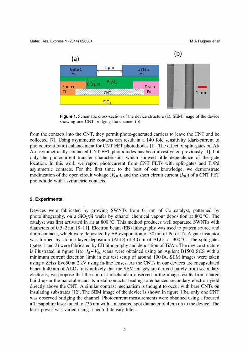
Devices were fabricated by growing SWNTs from 0.1 nm of Co catalyst, patterned byphotolithography, on a SiO2/Si wafer by ethanol chemical vapour deposition at 800 °C. Thecatalyst was first activated in air at 800 °C. This method produces well separated SWNTs withdiameters of 0.5–2 nm [8–11]. Electron beam (EB) lithography was used to pattern source anddrain contacts, which were deposited by EB evaporation of 30 nm of Pd or Ti. A gate insulatorwas formed by atomic layer deposition (ALD) of 40 nm of Al2O3 at 300 °C. The split-gates(gates 1 and 2) were fabricated by EB lithography and deposition of Ti/Au. The device structureis illustrated in figure 1(a). Id −Vds scans were obtained using an Agilent B1500 SCS with aminimum current detection limit in our test setup of around 100 fA. SEM images were takenusing a Zeiss Evo50 at 2 kV using in-line lenses. As the CNTs in our devices are encapsulatedbeneath 40 nm of Al2O3, it is unlikely that the SEM images are derived purely from secondaryelectrons; we propose that the contrast mechanism observed in the image results from chargebuild up in the nanotube and its metal contacts, leading to enhanced secondary electron yielddirectly above the CNT. A similar contrast mechanism is thought to occur with bare CNTs oninsulating substrates [12]. The SEM image of the device is shown in figure 1(b), only one CNTwas observed bridging the channel. Photocurrent measurements were obtained using a focuseda Ti:sapphire laser tuned to 735 nm with a measured spot diameter of 4 μm on to the device. Thelaser power was varied using a neutral density filter.
Mater. Res. Express 1 (2014) 026304 M A Hughes et al
2
Figure 1. Schematic cross-section of the device structure (a). SEM image of the deviceshowing one CNT bridging the channel (b).

3. Results and discussion
Transfer characteristics of the device, taken in the dark, are shown in figure 2. These allowed usto make deductions about the metal-CNT contacts. The hysteresis in the transfer characteristicsindicates the presence of trapped charges (holes or electrons) in the substrate and/or gateinsulator [13, 14]. Applying positive bias to gate 1 only (above the Ti contact) results inmaximum current flow, indicating electrons are the majority carrier through the Ti contact. Yetfigure 3(a) shows that with zero gate bias and Vds =−1 V there is essentially no current flow.Electrons should therefore be injected from the Pd contact with their return to the sourceelectrode regulated by gate 1, which implies they are trapped by a potential well at the Ticontact. Modulation of gate 2 only (above Pd contact) shows there is essentially no holeinjection and a small amount of electron injection when modulating this gate. This supports thecounterintuitive idea that the Pd contact has a lower Schottky barrier height for electrons (Φbe)than the Ti contact, even though Pd and Ti have work functions of 5.12 and 4.33 eV,respectively. It is known that Schottky barrier height in CNTs has only a weak dependence oncontact metal work function [15]. N-type characteristics have previously been observed fromsymmetric Pd-contacted devices [16], which was attributed to the small diameter of thenanotube used which increased the work function of the CNT due to hybridization to above thatof Pd. Au has a work function similar to that of Pd and it has also been observed that n-typeconduction, due to oxygen desorption, can occur in Au-contacted CNT FETs after annealing ina vacuum [17, 18]. The n-type conduction is retained after exposure to oxygen only if the CNTswere encapsulated in PMMA or SiO2 [17]. We suggest that the annealing in vacuum process is
Mater. Res. Express 1 (2014) 026304 M A Hughes et al
3
Figure 2. Dark transfer characteristic of an asymmetric contact CNT device with equalsplit-gate bias (gate 1 = gate 2), biasing gate 1 only and biasing gate 2 only; Vds =−1 V.The inset shows a band diagram which illustrates how applying a positive bias to thegate above the Ti contact only can generate an electron current. Electrons are shown inblue, and curved arrows represent tunnelling transport. With zero gate bias, electronscan be injected from the Pd contact. The electrons then accumulate behind the large Φbe
at the Ti contact, as illustrated by the black band diagram. With positive bias applied togate 1, the Schottky barrier at the Ti contact is thinned allowing accumulated electronsto flow, as illustrated in the red dashed band diagram.

analogous to the ALD process we used to form the Al2O3 gate insulator in our devices, becauseit involved heating the CNTs at 300 °C in a vacuum for around 1 h before they were sealed fromthe atmosphere below a layer of Al2O3. Negatively charged oxygen molecules can dope CNTsp-type and induce a positive balancing charge in the CNT and electrode at their interface [19]. Ifthe CNT is doped p-type, the negative oxygen charge reduces the negative dopant charge in theCNT to satisfy the charge-neutrality condition, this results in reduced band bending and a lowerSchottky barrier height for holes (Φbh). If the CNT is doped n-type, the negative oxygen chargerequires more positive dopant charge in the CNT to satisfy the charge-neutrality condition, thisresults in increased positive band bending and a larger Φbe. If the oxygen is removed, thepositive band bending and Φbe are reduced, resulting in n-type conduction after annealing in avacuum [19]. Since our device should have electron conduction with zero gate bias, see inset offigure 2, we proposed the mechanism discussed above to be the origin of the low Φbe at the Pdcontact in our device. Neutral polarized molecules such as NH3 can weaken hole transport dueto their preferred dipole direction with respect to the gold electrode surface [20], and thedominant mechanism for sensitivity to NH3 is, similarly to oxygen, Schottky barrier modulationat the contacts [21]. If source and drain contacts are asymmetric, resulting in more oxygenadsorption at one of the contacts, positive charges induced by oxygen at one end of a CNT willbe balanced by opposite charges at the other end of the CNT [22]. This is known as dipolepolarization and can result in n-type conduction in air. Since our device is ambipolar and we
Mater. Res. Express 1 (2014) 026304 M A Hughes et al
4
Figure 3. Dark Id−Vds characteristics (symbols) of the asymmetric contact CNT deviceat various split-gate biases fitted to the explicit solution of the diode equation (solidlines). No gate bias applied, the rectification direction is forward, and η= 2.2 ± 0.05 (a).Gate 1, 2 =−3, +3 V, causing inversion of the rectification direction, η= 2.1 ± 0.1 (b).Gate 1, 2 = +3, −3 V results in no inversion and η= 1.9 ± 0.02 (c). Gate 1, 2 =−3, −3 Vresults in inversion and η= 2.0 ± 0.01 (d).

expect it to retain a vacuum condition because of encapsulation of the CNT, dipole polarizationshould not occur in our device. On the basis of this discussion we propose the band diagrammodel in the inset of figure 2. Owing to a difference in work function between the CNT and thecontacts, the bands bend towards lower energy in between the contacts [23]. At equal split-gatebias the on/off ratio, shown in figure 2, is ∼1 × 10⁷ with Vds =−1 V, which is one of the highestreported for a CNT FET. An on/off ratio of 1 × 10⁵ was reported in high κ dielectric CNT FETswith Vds = 10 mV [24], 1 × 10² in a CNT thin film LED with split-gates with Vds = 1 V [25], andmodelling indicates that Au contacted CNT FETs are capable of an on/off ratio of up to 1 × 10⁶
[26].In order to investigate the rectifying behaviour of the device, we measured the dark Id−Vds
characteristics at various applied split-gate biases, as shown in figure 3. IdVds and transfercharacteristics were stable and repeatable to within∼±10% and changed little after annealing at300 °C for 1 h, indicating stable electrode contacts. The device displays strong rectificationwithout any split-gate bias which shows that it behaves as a Schottky diode, with forward biasat positive Vds in this configuration. Applying opposite bias to a split-gate CNT FET canproduce rectification from a pn junction [27], therefore one might conceive we have a Schottky/p–n junction hybrid diode when opposite split-gate bias is applied, as in figure 3(b). However,we fabricated devices with the same structure but with symmetric Ti contacts and observednegligible rectification when applying opposite split-gate bias. Therefore, we are dealing with apurely Schottky diode where all split-gate bias configurations simply modify the Schottkybarrier heights. We expect the device to be in forward bias when gate 2 has an opposite polarityto Vds, and in reverse bias when gate 2 has the same polarity as Vds; in figures 3(b)–(d) this isindeed what we find. The reason for this is that total deflection of the valance and conductionbands is at a maximum when gate 2 has the opposite polarity to Vds and at a minimum whengate 2 has the same polarity as Vds. To extract diode parameters, I0 (saturation current), η(ideality factor) and Rs (series resistance), Id−Vds curves were fitted to equation (1), commonlyknown as the diode equation, using the method detailed elsewhere [28]
⎡⎣⎢
⎛⎝⎜
⎞⎠⎟
⎤⎦⎥η
=−
−I IIR
Vexp
V1 . (1)0
s
T
The fits are shown as solid lines. The extracted η values of ∼2 indicate that tunnellingdominates the current transport in our device [29], errors were estimated from the standard errorof the fit. We fabricated and measured the IdVds and transfer characteristics of ∼100 devices, allhad rectifying IdVds and ∼90% had similar ambipolar transfer characteristics as the devicepresented in this paper, ∼10% had n-type transfer characteristics.
At zero gate bias, shown in figure 3(a), fitting the diode equation indicated an extremelylow reverse bias saturation current of 2 × 10⁻¹⁷ A. This situation is illustrated in the banddiagram in figure 4(a) where we explain the low reverse bias from trapping of electrons in apotential well created at the Ti contact. In the reverse bias region the detection limit of ourmeasurement system was much larger than this. Additionally, Id starts to increase at Vds <−2 V,we propose this due to tunnelling of electrons trapped at the Ti contact, as shown in figure 4(a),which have sufficient energy to tunnel through the Schottky barrier. In forward bias with zerogate bias, the Schottky barrier at the Ti contact is thinned allowing electrons to tunnel through.Our device shows inversion of the rectification direction with gate 1, 2 =−3, +3 V, and gate 1,2 =−3, −3 V, as shown in figures 3(b) and (d). This ability of the gates to induce inversion of
Mater. Res. Express 1 (2014) 026304 M A Hughes et al
5

the rectification direction is due their ability to affect the Schottky barrier height at the CNT-metal contacts which in turn changes the Vds polarity that results in reverse bias, as shown infigures 4(a)–(d). Other Schottky barrier diodes based on asymmetrically contacted CNTs havebeen demonstrated [6, 30–35]. However, none of these works reported the ability to invert therectification direction, and to the best of our knowledge we have reported the firstasymmetrically contacted CNT diode in which the rectification direction can be inverted. Wemeasured Id−Vds characteristics for a series of gate bias configurations and calculated therectification ratio from Iforward(Vds)/Ireverse(−Vds) and found a maximum rectification ratio of3 × 105 with gate 1,2 =−1, −1 V and Vds = ±1.5 V. This compares to a maximum rectificationratio 1 × 10³ for Ca and Pd asymmetrically contacted CNT diodes with Vds = ±1 V [36], and∼103 for Al and Pd asymmetrically contacted CNTs encapsulated in PMMA, with Vg = +10 V,Vds = ±0.5 V [6].
Illumination of a photodiode allows photocurrent to be measured. To be used as aphotodetector, the photodiode should be operated in reverse bias to allow discriminationbetween dark current and photocurrent. We measured photocurrent for various reverse biasconfigurations, but were only able to measure significant photocurrent for gate 1, 2 =−ve, +ve
Mater. Res. Express 1 (2014) 026304 M A Hughes et al
6
Figure 4. Band diagrams of various reverse bias configurations (a)–(d) corresponding,respectively, to the reverse bias regions of the Id−Vds characteristics shown infigures 3(a)–(d). Gate 1, 2 = 0, 0 and Vds =−ve, no photocurrent measured (a). Gate 1,2 =−ve, +ve and Vds = +ve, strong photocurrent measured (b). Gate 1, 2 = +ve, −ve andVds =−ve, weak photocurrent measured (c). Gate 1, 2 =−ve, −ve and Vds = +ve, nophotocurrent measured (d). Red sinusoidal arrows represent an absorbed photon.Electrons are shown as blue circles, holes as red circles.

and Vds = +ve. We measured weak photocurrent for gate 1,2 = +ve, −ve and Vds =−ve. We couldnot measure any photocurrent for gate 1, 2 = 0, 0 and Vds =−ve or gate 1, 2 =−ve, −ve andVds = +ve. Band diagrams representing these various reverse bias configurations are illustratedin figures 4(a)–(d). For the device configuration represented in figure 4(a), the large Schottkybarrier for electrons at the Ti contact creates a potential well to trap photo-excited electrons,resulting in no detectable photocurrent. For the configuration in figure 4(b), there is no longer apotential well to trap photo-excited electrons or holes and we are able to detect strongphotocurrent. For the configuration in figure 4(c), the Schottky barrier at the Ti contact isthinned by the positive gate 1 bias [37], which allows tunnelling of photo-excited electrons andthe detection of a weak photocurrent. For the configuration in figure 4(d), the negative gatebiases create a potential well that traps photo-excited holes, resulting in no detectablephotocurrent.
By measuring Id−Vds characteristics of a photodiode at various illumination powers, VOC
and ISC can be extracted. These are important parameters for photodiodes: VOC approximatesthe built-in potential (Vbi), which in our device originates from the difference in work functionof the asymmetric contacts, and ISC can indicate the quantum efficiency of the photocurrent.Id −Vds characteristics at various illumination powers for our device with gate1, 2 =−4, +4V areshown in figure 5(a), which are typical of a photodiode. Photocurrent steps indicating chargecarriers in the second nanotube subband [38] can be observed in figure 5(a) with 30 mW ofillumination power. The average period of the step is 0.43 V. Figure 5(b) shows the dependenceof VOC and ISC on illumination power. Inspection indicates that VOC and ISC have the samedependence on incident laser power, both plateauing at 0.28 V and 41 pA, respectively, after thelaser power density is increased above 250 kW cm−2. This is probably due to saturation of thediode. Since VOC is dependent on ISC [5], the plateauing of VOC is therefore caused bysaturation of the photocurrent which should saturate above a certain exciton generation rate[39]. The nonlinear dependence of VOC on laser power may be due to unaccounted experimentalerror.
We also measured Id−Vds at various opposite split-gate biases with the laser power fixed at30 mW. Some examples are shown in figure 5(c). Figure 5(d) shows VOC and ISC versusopposite split-gate bias. VOC increases super-linearly until at around gate 1, 2 =−3, +3 V itreaches a maximum of 0.34 V before plateauing. ISC has a similar dependence to VOC:plateauing at gate 1, 2 =−3, +3 V and reaching a maximum of 41 pA. In a symmetricallycontacted split-gate CNT diode, ISC showed either no dependence or a small increase withincreased split-gate bias [5]. In an asymmetrically contacted CNT FET with split-gates,applying opposite polarity bias to the split-gates resulted in photocurrent characteristics similarto those without any gate bias [1]. In a symmetrically contacted single gate CNT FET, ISC couldbe modulated with the gate bias [40]. This report represents the first demonstration of themodulation of VOC and ISC in an asymmetrical contacted CNT FET.
4. Conclusions
We fabricated a Ti/Pd asymmetrically contacted CNT FET with split-gates. This novel structureresulted in a an on/off ratio of 1 × 10⁷ when the device was operated as an FET, and arectification ratio of 3 × 10⁵ when the device was operated as a diode. Transfer characteristicsresulting from biasing the split-gates individually, or together, and the Id−Vds characteristics
Mater. Res. Express 1 (2014) 026304 M A Hughes et al
7

can be explained if the Schottky barrier for electrons is lower at the Pd contact than it is at the Ticontact. When operated as a diode, without any gate bias, it has an I0 and η of 2 × 10⁻¹⁷ A and2.2, respectively. Applying opposite polarity biases to gates 1 and 2, respectively, causesinversion of the diode, which we believe to be the first reported inversion of an asymmetricallycontacted CNT diode. When operated as a photodiode with gate 1, 2 =−4, +4 V, ISC and VOC
plateau at 41 pA and 0.28 V, respectively, when the laser power density is increased above240 kW cm−2. This is caused by saturation of the diode. Steps with a period of 0.43 V can beobserved in Id−Vds when the laser power density is 240 kW cm−2. Photocurrent can only beobserved with opposite split-gate bias, which is due to the trapping of photo-excited carriers bypotential wells at other bias configurations. With a laser power density of 240 kW cm−2
increasing opposite polarity split-gate bias causes ISC and VOC to increase, then plateau at 41 pAand 0.34 V respectively at gate 1,2 =−3, +3 V. We believe this to be the first demonstration ofthe modulation of VOC and ISC in an asymmetrical contacted CNT FET.
Mater. Res. Express 1 (2014) 026304 M A Hughes et al
8
Figure 5. Id−Vds photocurrent characteristics at various laser illumination powers(λ= 735 nm) with gate1, 2 =−4, +4 V, the step region for 30 mW of illumination ismarked (a). VOC and ISC as a function of laser power with gate1, 2 =−4, +4 V (b).Id−Vds photocurrent characteristics at various split-gate biases with a laser power of30 mW (c). VOC and ISC as a function of split-gate bias with a laser power of 30 mW (d).
References
[1] Chen H Z, Xi N, Lai K W C, Chen L L, Yang R G and Song B 2012 Nanotechnology 23 385203[2] Fan Z et al 2010 Nano Lett. 10 3823–7[3] Itkis M E, Borondics F, Yu A P and Haddon R C 2006 Science 312 413–6[4] Mueller T, Kinoshita M, Steiner M, Perebeinos V, Bol A A, Farmer D B and Avouris P 2010 Nat.
Nanotechnology 5 27–31[5] Lee J U 2005 Appl. Phys. Lett. 87 073101[6] Yang M H, Teo K B K, Milne W I and Hasko D G 2005 Appl. Phys. Lett. 87 253116[7] Freitag M, Martin Y, Misewich J A, Martel R and Avouris P H 2003 Nano Lett. 3 1067–71[8] Fukuoka N, Mizutani Y, Naritsuka S, Maruyama T and Iijima S 2012 Japan J. Appl. Phys. 51 06FD23[9] Mizutani T, Nosho Y and Ohno Y 2008 J. Phys. Conf. Ser. 109 012002
[10] Mizutani Y, Fukuoka N, Naritsuka S, Maruyama T and Iijima S 2012 Diam. Relat. Mater. 26 78–82[11] Noda S, Sugime H, Osawa T, Tsuji Y, Chiashi S, Murakami Y and Maruyama S 2006 Carbon 44 1414–9[12] Brintlinger T, Chen Y-F, Durkop T, Cobas E, Fuhrer M S, Barry J D and Melngailis J 2002 Appl. Phys. Lett.
81 2454–6[13] Kim W, Javey A, Vermesh O, Wang O, Li Y M and Dai H J 2003 Nano Lett. 3 193–8[14] Fuhrer M S, Kim B M, Dürkop T and Brintlinger T 2002 Nano Lett. 2 755–9[15] Svensson J and Campbell E E B 2011 J. Appl. Phys. 110 111101[16] Jejurikar S, Casterman D, Pillai P B, Petrenko O, Souza M M D, Tahraoui A, Durkan C and Milne W I 2010
Nanotechnology 21 215202[17] Derycke V, Martel R, Appenzeller J and Avouris P 2001 Nano Lett. 1 453–6[18] Imaeda H, Ishii S, Kishimoto S, Ohno Y and Mizutani T 2012 Japan J. Appl. Phys. 51 02BN6[19] Yamada T 2004 Phys. Rev. B 69 125408[20] Yamada T 2006 Appl. Phys. Lett. 88 083106[21] Peng N, Zhang Q, Chow C L, Tan O K and Marzari N 2009 Nano Lett. 9 1626–30[22] Peng N, Li H and Zhang Q 2009 ACS Nano 3 4117–21[23] Tans S J, Verschueren A R M and Dekker C 1998 Nature 393 49–52[24] Javey A, Kim H, Brink M, Wang Q, Ural A, Guo J, McIntyre P, McEuen P, Lundstrom M and Dai H J 2002
Nat. Mater. 1 241–6[25] Kinoshita M, Steiner M, Engel M, Small J P, Green A A, Hersam M C, Krupke R, Mendez E E and
Avouris P 2010 Opt. Express 18 25738–45[26] Rochefort A, Ventra M D and Avouris P 2001 Appl. Phys. Lett. 78 2521–3[27] Lee J U, Gipp P P and Heller C M 2004 Appl. Phys. Lett. 85 145–7[28] Hughes M A, Homewood K P, Curry R J, Ohno Y and Mizutani T 2013 Appl. Phys. Lett. 103 133508[29] Sze S M and Ng K K 2006 Physics of Semiconductor Devices (New York: Wiley)[30] Wang S, Zhang Z, Ding L, Liang X, Shen J, Xu H, Chen Q, Cui R, Li Y and Peng L-M 2008 Adv. Mater. 20
3258–62[31] Xie X, Islam A E, Wahab M A, Ye L, Ho X, Alam M A and Rogers J A 2012 ACS Nano 6 7981–8[32] Wang S et al 2011 Nano Lett. 11 23–9[33] Perello D, Dong J B, Kim M J, Dongkyu C, Seung Y J, Bo Ram K, Woo J Y, He Y L and Minhee Y 2009
IEEE Trans. Nanotechnology 8 355–60[34] Lu C G, An L, Fu Q A, Liu J, Zhang H and Murduck J 2006 Appl. Phys. Lett. 88 133501[35] Zeng Q et al 2012 Opt. Mater. Express 2 839–48[36] Nosho Y, Ohno Y, Kishimoto S and Mizutani T 2006 Nanotechnology 17 3412[37] Yamada T 2002 Appl. Phys. Lett. 80 4027–9
Mater. Res. Express 1 (2014) 026304 M A Hughes et al
9

[38] Gabor N M, Zhong Z H, Bosnick K, Park J and McEuen P L 2009 Science 325 1367–71[39] Mohammad S N and Abidi S T H 1987 J. Appl. Phys. 61 4909–19[40] Ahn Y H, Tsen A W, Kim B, Park Y W and Park J 2007 Nano Lett. 7 3320–3
Mater. Res. Express 1 (2014) 026304 M A Hughes et al
10