Phase preserving amplification near the quantum limit with a Josephson Ring Modulator
20
Phase preserving amplification near the quantum limit with a Josephson Ring Modulator N. Bergeal 1,2 , F. Schackert 1 , M. Metcalfe 1,3 , R. Vijay 1,4 , V. E. Manucharyan 1 , L. Frunzio 1 , D. E. Prober 1 , R. J. Schoelkopf 1 , S. M. Girvin 1 , M. H. Devoret 1 1 Department of Physics and Applied Physics, Yale University, New Haven, CT, 06520-8284 USA. 2 Laboratoire Photons Et Mati` ere - UPR5-CNRS, ESPCI ParisTech, 10 Rue Vauquelin 75005 Paris, France. 3 The Joint Quantum Institute, University of Maryland and the National Institute of Standards and Technology, College Park, MD 20742 USA. and 4 Department of Physics, University of California, Berkeley CA 94720-7300, USA. (Dated: December 17, 2009) Recent progress in solid state quantum information processing has stimulated the search for ultra- low-noise amplifiers and frequency converters in the microwave frequency range, which could attain the ultimate limit imposed by quantum mechanics. In this article, we report the first realization of an intrinsically phase-preserving, non-degenerate superconducting parametric amplifier, a so far missing component. It is based on the Josephson ring modulator, which consists of four junctions in a Wheatstone bridge configuration. The device symmetry greatly enhances the purity of the amplification process and simplifies both its operation and analysis. The measured characteristics of the amplifier in terms of gain and bandwidth are in good agreement with analytical predictions. Using a newly developed noise source, we also show that our device operates within a factor of three of the quantum limit. This development opens new applications in the area of quantum analog signal processing. In this article, we focus on parametric amplifiers which are powered by an ac source with frequency f p also known as the “pump”. Such amplifiers operate with a minimal number of degrees of freedom and are the natural candidates for ultra low noise operation [1, 2]. A single spatial and temporal mode of the electromagnetic field with carrier frequency f can be decomposed into its in-phase A k cos 2πft arXiv:0912.3407v1 [cond-mat.mes-hall] 17 Dec 2009
Transcript of Phase preserving amplification near the quantum limit with a Josephson Ring Modulator
Phase preserving amplification near the quantum limit with a Josephson Ring
Modulator
N. Bergeal1,2, F. Schackert1, M. Metcalfe1,3, R. Vijay1,4, V. E. Manucharyan1,
L. Frunzio1, D. E. Prober1, R. J. Schoelkopf1, S. M. Girvin1, M. H. Devoret1
1Department of Physics and Applied Physics, Yale University, New Haven, CT, 06520-8284 USA.
2Laboratoire Photons Et Matiere - UPR5-CNRS,
ESPCI ParisTech, 10 Rue Vauquelin 75005 Paris, France.
3The Joint Quantum Institute, University of Maryland and the National
Institute of Standards and Technology, College Park, MD 20742 USA. and
4Department of Physics, University of California, Berkeley CA 94720-7300, USA.
(Dated: December 17, 2009)
Recent progress in solid state quantum information processing has stimulated the search for ultra-
low-noise amplifiers and frequency converters in the microwave frequency range, which could attain
the ultimate limit imposed by quantum mechanics. In this article, we report the first realization
of an intrinsically phase-preserving, non-degenerate superconducting parametric amplifier, a so far
missing component. It is based on the Josephson ring modulator, which consists of four junctions
in a Wheatstone bridge configuration. The device symmetry greatly enhances the purity of the
amplification process and simplifies both its operation and analysis. The measured characteristics
of the amplifier in terms of gain and bandwidth are in good agreement with analytical predictions.
Using a newly developed noise source, we also show that our device operates within a factor of three
of the quantum limit. This development opens new applications in the area of quantum analog
signal processing.
In this article, we focus on parametric amplifiers which are powered by an ac source with frequency
fp also known as the “pump”. Such amplifiers operate with a minimal number of degrees of freedom
and are the natural candidates for ultra low noise operation [1, 2]. A single spatial and temporal mode
of the electromagnetic field with carrier frequency f can be decomposed into its in-phase A‖ cos 2πft
arX
iv:0
912.
3407
v1 [
cond
-mat
.mes
-hal
l] 1
7 D
ec 2
009
2
and out-of-phase A⊥ sin 2πft quadratures. Linear amplifiers can be classified into two categories from
the way they treat these two quadratures. On one hand, a phase-preserving amplifier treats both
quadrature components with the same gain (√G) as an ordinary op-amp would do (A‖ →
√GA‖
; A⊥ →√GA⊥). On the other hand, in a phase-sensitive amplifier, the gains of the quadratures
are inverse of each other (A‖ →√GX‖; A⊥ → 1√
GA⊥). Regarding their noise properties, there is a
fundamental difference between these two types of amplifiers. The minimum noise energy added by a
phase-preserving amplifier to the input signal amounts to half a photon at the signal frequency 12hf ,
where h is Planck’s constant [3, 4, 5]. On the other hand, a phase-sensitive amplifier is submitted
to only a lower limit on the product of the noise added to the two quadratures and can thus squeeze
the quantum noise on one quadrature at the expense of extra noise in the other [4, 6]. Although such
amplifiers can look rather appealing because of their ability to operate potentially below the quantum
limit, they are only useful in cases where a reference phase is attached to the signal, like in homodyne
detection. In the majority of cases, where the information carried by the signal is contained in both
quadratures, or equivalently in both amplitude and phase, a phase-preserving amplifier is preferable.
However, so far, little attention has been devoted to non-degenerate, intrinsically phase-preserving,
parametric amplifiers operating near the quantum limit in the microwave frequency range. They
involve two distinct internal resonant modes of the circuit, conventionally called the “signal” with
center frequency fs and the “idler”, whose frequency fi differs from fs by at least the sum of the
bandwidth of the two resonances. This is in contrast with phase-sensitive degenerate parametric
amplifiers which operate with one internal resonant mode only [7, 8, 9, 10, 11]. The challenge
of building phase-preserving amplifiers arises from the difficulty of controlling the two modes and
coupling them together with the pump.
Description of the Josephson Parametric Converter
The circuit nicknamed Josephson Parametric Converter (JPC) has been theoretically described
in reference [12]. A schematic description can be found in the red solid line box of Fig. 1a. Its
3
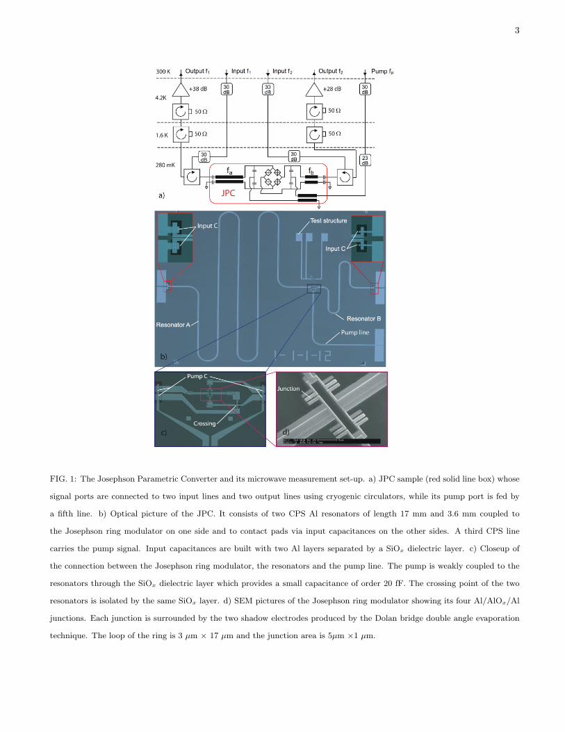
FIG. 1: The Josephson Parametric Converter and its microwave measurement set-up. a) JPC sample (red solid line box) whose
signal ports are connected to two input lines and two output lines using cryogenic circulators, while its pump port is fed by
a fifth line. b) Optical picture of the JPC. It consists of two CPS Al resonators of length 17 mm and 3.6 mm coupled to
the Josephson ring modulator on one side and to contact pads via input capacitances on the other sides. A third CPS line
carries the pump signal. Input capacitances are built with two Al layers separated by a SiOx dielectric layer. c) Closeup of
the connection between the Josephson ring modulator, the resonators and the pump line. The pump is weakly coupled to the
resonators through the SiOx dielectric layer which provides a small capacitance of order 20 fF. The crossing point of the two
resonators is isolated by the same SiOx layer. d) SEM pictures of the Josephson ring modulator showing its four Al/AlOx/Al
junctions. Each junction is surrounded by the two shadow electrodes produced by the Dolan bridge double angle evaporation
technique. The loop of the ring is 3 µm × 17 µm and the junction area is 5µm ×1 µm.
4
operation is based on a novel non-linear device, the Josephson ring modulator, consisting of four
nominally identical Josephson junctions forming a superconducting loop [12]. It has the minimal
number of electromagnetic spatial modes required to perform 3-wave mixing: two differential ones,
called X and Y , and a common one, called Z. In the JPC, two superconducting resonators, A and
B, couple to the differential modes X and Y of the ring, respectively. In the following, fa(b) and Qa(b)
denote the resonant frequencies and quality factors of the resonators. An additional transmission line
carries the pump signal at frequency fp, and is weakly coupled to the common mode Z of the ring
through capacitances. From the point of view of the signals, the device has two ports: port 1, driven
at frequency f1, feeds resonator A and port 2, driven at frequency f2, feeds resonator B. In contrast
with previous Josephson parametric amplifier, we have here a complete separation of the signal and
idler modes both spatially and temporally. The JPC can be operated as a phase-preserving amplifier
when fp = f1 + f2 or as a unity photon gain frequency converter when fp = |f2 − f1|. In this paper,
we will focus only on the amplification mode, in which case the JPC is described by the input-output
relation [12]
aout1 = r1ain
1 + s1a†in2 (1)
aout2 = r2ain
2 + s2a†in1 (2)
The a1(2) and a†1(2) are annihilation and creation operators at port 1 (frequency f1) and port 2
(frequency f2), expressed in units of the square root of photon number per unit time. Relations (1)
and (2) thus determine the properties of the amplifier including its noise in the quantum limit.
The coefficients r1(2) and s1(2) satisfy the symplectic relation |r1(2)|2 − |s1(2)|2 = 1. They are given
by
r1(2) = −(ϑ2(1) + i)(ϑ1(2) + i)− |ρ|2
(ϑ2(1) + i)(ϑ1(2) − i)− |ρ|2and s1(2) =
−2iρ
(ϑ2(1) + i)(ϑ1(2) − i)− |ρ|2(3)
where ϑ1 = Qaf2
a−f21
f1fa, and ϑ2 = Qb
f2b−f
22
f2fb.
5
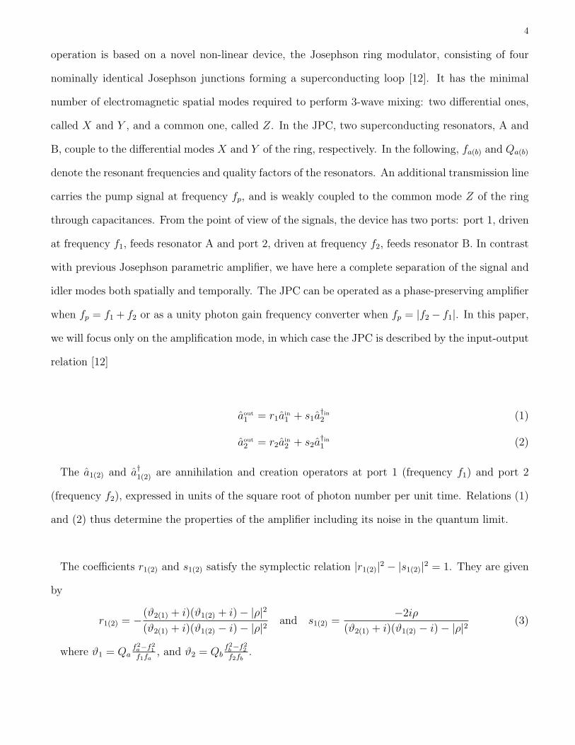
Phase (°)
!2" 0!" " 2"
FIG. 2: Modulation of resonance frequency with magnetic field. Phase of the reflected signal at port 2 (color), as a function
of the drive frequency and magnetic flux through the loop, for two directions of the magnetic field sweep.
Here, we have introduced the dimensionless pump current |ρ|
|ρ| = 1
4
√QaQbpapb
IpI ′0
(4)
where Ip is the pump current, I ′0 is the Z mode critical current and pa(b) = LJ
LJ+La(b)are the partic-
ipation ratios of the inductance of the Josephson ring modulator LJ to the resonator inductances
La(b) [12]. At the resonant tuning f1 = fa and f2 = fb, the expressions of the coefficients reduce to
r1 = r2 =√G = 1+|ρ|2
1−|ρ|2 and s1 = s2 = −i√G− 1 = −2iρ
1−|ρ|2 . The symbol G refers to the power gain at
the band center.
The diagonal term r1(2) can be seen as a photon “cis-gain”, characteristic of the 1-port reflection
amplifier operation : the incoming wave at either port is reflected with a power gain |r1(2)|2 and
its phase is preserved. The non-diagonal term s1(2) can be seen as a photon “trans-gain” between
the two ports, and describes the behaviour of a frequency converter (f1 → f2 or f2 → f1) with
power gain |s1(2)|2 = |r1(2)|2 − 1. The possibility of performing the important function of up- and

6
down-conversion is another feature that distinguishes the non-degenerate parametric amplifier from
the degenerate one. It arises from the presence in the circuit of two different spatial modes with
different frequencies, whose sum is equal to the pump frequency. The “cis-gain” and “trans-gain” can
be varied simply by changing the pump power through the |ρ| parameter, |r1(2)| ' |s1(2)| −→|ρ|→1−
∞.
In the large gain limit, the expressions of |r1,2| and |s1,2| reduce to a Lorentzian form
|r1,(2)| ' |s1(2)| '√G√
1 +G(Qa
fa+ Qb
fb
)2(f1,2 − fa,b
)2(5)
The -3dB bandwidth of the amplifier is thus
B =2√G
(Qa
fa+Qb
fb
)−1
(6)
Implementation and characterisation of the JPC
Fig. 1b-d show pictures of our JPC sample made of Aluminium on a Si wafer, using a three-step
fabrication process combining optical and e-beam lithography. The details of fabrication are given
in the Methods section. The two resonators A and B are 17 mm and 3.6 mm long. The four
junctions of the ring have nominally identical critical currents with values in the range 3-6µA. Tests
have shown that these values vary from one junction of the ring to another by less than 5 %. The
center frequencies of the resonators are slightly renormalized by the Josephson inductance LJ of
the ring and are, in absence of flux through the ring, fa=1.6 GHz and fb=7.3 GHz. The choice of
these frequencies results from a compromise between separation of signal and idler for frequency
conversion, and complexity of microwave engineering. Our resonators are both in the overcoupled
regime and the quality factors are therefore determined by the overlap coupling capacitances
connecting the resonators to the external circuit. Here, the values Qa=450 and Qb=120 result from
favouring capacitor reliability and have not been optimized for maximum amplifier performances.
After fabrication, the JPC chip is mounted on a microwave circuit board and housed in a copper
sample box equipped with a superconducting coil. The sample box is anchored to the 280 mK cold
stage of a 3He refrigerator and placed in a magnetic shield. Although similar embedding of µA
critical current junctions inside microwave resonators have recently been employed for bifurcation

7
FIG. 3: Gain of the JPC. a) Power “cis-gain” of the JPC as a function of the drive frequency for different values of the pump
power measured at port 1 (left) and port 2 (right). The solid lines correspond to the theoretical expressions of |r1|2 and |r2|2
(3) obtained for the different values of the fit parameter |ρ|. Inset: curves obtained at larger gain. The fits correspond to
|ρ| = 0.994 (left) and |ρ| = 0.992 (right). b) Photon “trans-gain” of the JPC as a function of the drive frequency (bottom
axis) and the converted frequency (top axis) for different values of the pump power measured between port 1 and port 2 (left)
and between port 2 and port 1 (right). The solid lines correspond to the theoretical expressions |s1|2 and |s2|2 (3) obtained
for the different values of the parameter |ρ|. c) Photon “cis-gain” of the JPC plotted in color scale as a function of the drive
frequencies and the pump power measured at port 1(left) and port 2 (right). Note that the data shown in the different panels
a, b, c correspond to different runs.
readout of qubits [13, 14] and RF magnetometry [15], the ring modulator device investigated
here works in the weakly non-linear regime, with the pump amplitude well below the bifurcation
threshold. In other words, the currents in the ring modulator remain small enough that only second
order correction to the Josephson inductance need to be considered.

8
A schematic description of our measurement set-up is shown in Fig. 1a. Two attenuated input
lines carry the signal from the microwave generators to the JPC. Circulators separate the output
signal reflected by the JPC from the input signal at the coldest stage. The output signals are first
amplified by HEMT cryogenic amplifiers at the 4.2K stage. Two isolators are placed at the 4.2K
and 1.6K stages to minimize the backaction of the amplifier on the sample. In this arrangement,
the incoming noise at the input ports of the JPC arises from the 50 Ω resistance presented by the
last attenuator in the input lines. At room temperature, the signal is further amplified by about 60
dB before being measured. The frequency bands of the output lines are limited by the isolators,
circulators and amplifiers: 1.2-1.8 GHz for the low frequency (f1) line and 4-8 GHz for the high
frequency (f2) line.
We characterized our resonators with a vector network analyzer. In the reflection measurements,
there was no amplitude response and the resonance frequencies, showed up only in the phase response
which displayed a complete 2π phase shift, confirming the completely dispersive nature of the device.
Then, we followed the phase response as a function of the dc current applied to the coil which is
proportional to magnetic flux Φ through the ring. As expected, we observe Φ0-periodic modulations
of the resonance frequency (Fig. 2) which are hysteretic with the magnetic field (Φ0 denotes the
superconducting flux quantum). According to Fig. 1b of reference [12], the two lower energy states
cross each other for a flux bias Φ0
2. However, as the two states are separated by an energy barrier,
the system initially in the ground state for Φ = 0 becomes metastable when the flux is increased
beyond Φ0
2. As the barrier is maximum at the degeneracy point and decreases to zero at Φ0, the
system remains in the metastable state until its environment (noise, measurement signal) provides
a sufficient amount of energy to activate the transition. The operation of the JPC is optimal when
biased in the vicinity of Φ0
2[12]. In the following, we will focus on measurements performed at this
bias point where the resonance frequencies where found to be fa=1.631 GHz and fb=7.219 GHz.
Operation of the JPC
9
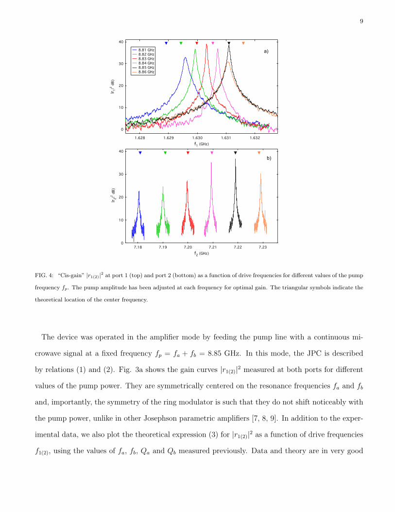
a)
b)
FIG. 4: “Cis-gain” |r1(2)|2 at port 1 (top) and port 2 (bottom) as a function of drive frequencies for different values of the pump
frequency fp. The pump amplitude has been adjusted at each frequency for optimal gain. The triangular symbols indicate the
theoretical location of the center frequency.
The device was operated in the amplifier mode by feeding the pump line with a continuous mi-
crowave signal at a fixed frequency fp = fa + fb = 8.85 GHz. In this mode, the JPC is described
by relations (1) and (2). Fig. 3a shows the gain curves |r1(2)|2 measured at both ports for different
values of the pump power. They are symmetrically centered on the resonance frequencies fa and fb
and, importantly, the symmetry of the ring modulator is such that they do not shift noticeably with
the pump power, unlike in other Josephson parametric amplifiers [7, 8, 9]. In addition to the exper-
imental data, we also plot the theoretical expression (3) for |r1(2)|2 as a function of drive frequencies
f1(2), using the values of fa, fb, Qa and Qb measured previously. Data and theory are in very good
10
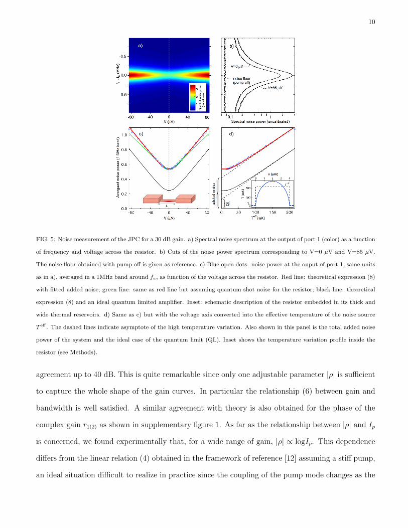
FIG. 5: Noise measurement of the JPC for a 30 dB gain. a) Spectral noise spectrum at the output of port 1 (color) as a function
of frequency and voltage across the resistor. b) Cuts of the noise power spectrum corresponding to V=0 µV and V=85 µV.
The noise floor obtained with pump off is given as reference. c) Blue open dots: noise power at the ouput of port 1, same units
as in a), averaged in a 1MHz band around fa, as function of the voltage across the resistor. Red line: theoretical expression (8)
with fitted added noise; green line: same as red line but assuming quantum shot noise for the resistor; black line: theoretical
expression (8) and an ideal quantum limited amplifier. Inset: schematic description of the resistor embedded in its thick and
wide thermal reservoirs. d) Same as c) but with the voltage axis converted into the effective temperature of the noise source
T eff . The dashed lines indicate asymptote of the high temperature variation. Also shown in this panel is the total added noise
power of the system and the ideal case of the quantum limit (QL). Inset shows the temperature variation profile inside the
resistor (see Methods).
agreement up to 40 dB. This is quite remarkable since only one adjustable parameter |ρ| is sufficient
to capture the whole shape of the gain curves. In particular the relationship (6) between gain and
bandwidth is well satisfied. A similar agreement with theory is also obtained for the phase of the
complex gain r1(2) as shown in supplementary figure 1. As far as the relationship between |ρ| and Ip
is concerned, we found experimentally that, for a wide range of gain, |ρ| ∝ logIp. This dependence
differs from the linear relation (4) obtained in the framework of reference [12] assuming a stiff pump,
an ideal situation difficult to realize in practice since the coupling of the pump mode changes as the

11
gain increases. When the gain is further increased to a maximum of 44 dB, the curves deviates from
the model as reported in insets of Fig. 3a, showing that saturation effects are becoming important,
as discussed below. These effects occur within a fraction of a percent from the theoretical onset
of self-oscillations of the system corresponding to |ρ| = 1. Moreover, as shown in Fig. 3c, after
reaching its maximum value the gain starts to decrease when further increasing the pump power
and finally collapses when the critical current of the junctions is reached. We attribute the failure to
observe parametric self-oscillations to the saturation of the device by the signal resulting from the
amplification of the noise, whose peak amplitude reaches the critical current.
A practical amplifier must have a minimum gain to beat the noise of the following amplifier in the
measurement chain. Assuming the best “state-of-the-art” commercial device as a following amplifier
with a noise temperature of a few K, we are led to a requirement of at least 20 dB of power gain,
satisfied with a comfortable margin by the present JPC. This is in contrast with recent results
obtained with other parametric amplifiers [7, 8] or dc SQUID microwave amplifiers [16, 17]. We
believe that the differences in gain performances between our JPC and other Josephson amplifiers
originate in the purity of the non linear XY Z coupling of signal, idler and pump offered by the
ring modulator. Indeed, the observed maximum gain is compatible with the order-of-magnitude
theoretical prediction given by
G <I0
2πe(pafa + pbfb)(7)
where the participation ratio pa and pb are 0.02 and 0.09 respectively and I0 is 3-6 µA [12].
The same consideration based on the maximum output power that the Josephson ring modulator can
deliver also explains the dynamic range of our amplifier (supplementary figure 2). In addition to the
1-port amplifier operation corresponding to the diagonal terms r1(2), the JPC also performs 2-ports
frequency conversion with gain corresponding to the non-diagonal terms s1(2). Fig. 3b shows the
typical gain curves measured between the two ports both in the cases of up conversion (f1 → f2) and
down conversion (f2 → f1). Like with |r1(2)| we obtain an excellent agreement with the theoretical

12
expression of |s1(2)|.
In Fig. 4, we show that we can adjust the center frequency of the signal bandwidth by detuning
the pump frequency. Thus, the tuning bandwidth is found to be given by the intrinsic resonator
bandwidthfa(b)
Qa(b)as expression (3) predicts. For the high frequency port of our device, there is a ratio
of 95 between the tuning and signal bandwidth if we limit the gain to 20 dB. For the low frequency
port, this ratio is much smaller (5.7) since fa
Qa fb
Qb. Finally, let us note that the relatively small
signal bandwidth of the present device is due to the small intrinsic bandwidth of the low frequency
resonator and could be greatly enhanced by increasing its coupling capacitance and the working
frequency. The optimum bandwidth configuration occurs when the signal and idler bandwidth are
equal.
Noise measurement
To measure the noise of the JPC we have developed a source of noise based on the hot-electron
shot noise regime of a R=50±1 Ω mesoscopic copper resistor of length L = 4µm embedded between
two cold reservoirs (inset Fig. 5a). It is inspired by a previous work in which this system was used
to calibrate an infrared photon detector [18]. A detailed description of the device is given in the
Methods section. This noise source has the following advantages : (i) no macroscopic heating of the
sample and thus no perturbation of the JPC operating point (ii) self-calibration (iii) response time
in the microsecond range [18] (iv) control by a dc current Idc. The Johnson noise spectral power
produced by the resistor is given by
Sns(f, V ) =hf
2coth
(hf
2kBT eff(V )
)(8)
where T eff is the effective electronic temperature of the resistor, a function of the voltage V = RIdc
across the resistor, and kB the Boltzmann constant. For kBTeff hf this expression reduces to the
well known classical Johnson spectral noise power kBTeff .

13
In this experiment, both the noise source and the JPC were anchored to the mixing chamber of
a dilution refrigerator with base temperature T0 = 17 mK and connected to port 1 via a circulator
(supplementary figure 3). Fig. 5a shows the noise in color as a function of frequency and voltage
V , with the gain of the JPC set to 30 dB. A cut of data taken at V=0 µV and V=85 µV is shown
is Fig. 5b in dB scale. Fig. 5c shows the noise averaged on a 1MHz band around the resonance
frequency. In the same figure, we compare the data with the theoretical expression
Sth = Gt
(Sns(V, f1) + Sadd
)(9)
where Gt is the total gain of the measurement chain and Sadd is the noise added by the amplifier. In
the case of a perfect quantum limited (QL) amplifier, Sadd = SQL = hf1
2, which corresponds to the
noise brought in by the idler when the load at port 2 is at a temperature T0 such that hf2 kBT0.
Note that the vertical axis in Fig 5c is the total noise of the system. Yet, it entirely measures the
output noise of the JPC since the noise added by the following stages is 17 dB lower, as shown in
Fig 5b. There is a good agreement between theory and experimental data if Sadd = 3.37× SQL (red
curve). In the same figure, for comparison we plot the theoretical result corresponding to the ideal
case of both perfect nanowire and amplifier (black curve). The quality of the fit confirms that the
resistor is well in the hot electron regime. For instance, the expression for quantum shot noise (green
curve in Fig. 5c, see Methods) cannot been reconciled with the experimental data. In Fig. 5d the
voltage axis has been converted into a temperature scale using the expression for T eff (see Methods).
In this figure, we can read directly the noise added by the amplifier as the vertical intercept of the
dashed line corresponding to the asymptotic variation of noise with temperature. Converting the
added noise Sadd into the system noise temperature, we found TN = 125 mK which makes the JPC
20-40 times better than the best commercial HEMT amplifier. We attribute the difference between
the system noise temperature and the ideal quantum limit TN = 37 mK to incomplete isolation of
the JPC from spurious noise coming through the post-amplifiers and possibly to imperfections in
the line connecting the nanowire to the JPC, which incorporates a circulator and a bias tee.
14
In conclusion, we have implemented and demonstrated the operation of a new phase-preserving
amplifier, the Josephson Parametric Converter, whose main element is the nonlinear, nondissipative
inductance of a Josephson ring modulator. Our results concerning the gain, bandwidth and
dynamic range can be understood quantitatively using a simple analytical model involving a
minimum number of parameters. We have achieved a power gain amplification of at least 40 dB,
which opens the possibility of practical applications like single photon detection based on microwave
readout [28] or any applications involving the measurement of very low microwave power in a
limited bandwidth. Our device is also useful as a frequency up-or-down converter. Using a newly
developed self-calibrating noise source, we obtained an upper bound on the noise added by the JPC
which is three times the quantum limit. Extrapolating the present results to an optimal choice
of parameters, we should be able to build a quantum limited amplifier with 20 dB gain in a 10
MHz bandwidth, allowing dispersive single shot readout of solid state qubits with an irradiation of
only a few photons [23, 24, 25, 26, 27]. Our results also open the way for production of entangled
microwave signal pairs through two-mode squeezing operation.
Correspondence and requests for material should be address to M. H. D. and N. B.
This work was supported by NSA through ARO Grant No. W911NF-05-01-0365, the Keck foun-
dation, and the NSF through Grant No. DMR-032-5580. M. H. D. acknowledges partial support
from College de France.
15
Methods
Fabrication of the device
Each quarter wave resonator is built from a Coplanar Strip Line (CPS) structure consisting of two
15 µm wide parallel lines separated by a 4 µm gap. In the first step of fabrication, a 110 nm thick
Al layer is evaporated onto a high resistivity Si wafer through an optical bilayer resist. A slope edge
is obtained by tilting the sample holder with an angle of 4 and rotating the stage at the speed of
10/s during the evaporation. This process defines the CPS resonators and the bottom layer of the
input capacitances. Then a 270 nm thick SiOx layer is deposited through a second optical resist to
form in a single step, the dielectric layer of the input capacitances, the pump coupling capacitances
and the isolation at the crossing of the two resonators line. Finally a second layer of Al (240 nm)
is evaporated to form the pump line, the top layer of the input capacitances connected to contact
pads, and the bridge on the top of the isolation. After the optical processes, the wafer is diced
into 50 chips of size 5×4 mm2. Next, the Josephson ring modulator is integrated to the device
using electron beam lithography, MMA/ PMMA resist bilayer and the Dolan bridge double angle
evaporation technique. A gentle hollow cathode ion gun milling was employed between deposition
of metallic layers. The nominal size of each junction is 5×1 µm2 yielding a resistance of tunnel
resistance of 40/80Ω depending on oxidation conditions.
Noise measurement with a mesoscopic resistor
A metallic resistor exhibits several regimes of shot noise depending on the relation between its
length L and the characteristic length scales involved in the motion of electrons [19]. In the regime
where L is longer than the inelastic electron scattering length Le−e, but shorter than the electron-
phonon interaction length Le−ph, the electrons travelling through the resistor redistribute the excess
kinetic energy gained from the voltage via electron-electron interactions only [19]. The cooling of
the electrons system thus occurs only by diffusion to the cold reservoirs and is controlled by the

16
Wiedemann-Franz law. As a result, an equilibrium electronic temperature profile establishes itself
over the length of the microbridge (inset Fig. 5b) [20]
T (x) =
√1 +
x
L
(1− x
L
) 3e2V 2
π2k2BT
20
(10)
An effective temperature for the nanowire can be obtained by integrating over its length T eff =
1L
∫ L0T (x) = T0
2
[1 +
(v + 1
v
)arctan(v)
]where v =
√3
2πeVkBT0
. We have verified that when computing
the effect of shot noise, using this effective temperature and the formula for the Johnson noise gave,
at the percent precision level, the same result as when the full space dependent spectral density of
noise is taken into account.
Our 50 Ω Cu nanowire resistor is 4 µm long, 80 nm wide, and 20 nm thick. Using a double angle
evaporation technique, the resistor is embedded into a 500 nm thick 50 Ω CPW transmission line
of 400 µm width providing good thermal reservoirs. The noise source chip is bonded with gold wire
on a sample holder itself thermally anchored to the mixing chamber of the dilution fridge with base
temperature T0=17 mK. According to previous studies [21], the 4 µm length ensures that the resistor
is in the hot electron regime Le−e < L < Le−ph at the working temperature. The sample holder is
connected to the high-frequency port of a bias tee. Dc current is applied to the noise source using a
cold current divider connected to the dc port of the bias tee. Finally, the dc-blocked high frequency
port of the bias tee is connected to the port 1 of the JPC via a circulator.
[1] Louisell, W. H., Yariv, A. and Siegman, A. E. Quantum Fluctuations and Noise in Parametric Processes. I. Phys. Rev.
124, 1646-1654 (1961).
[2] Gordon, J. P., Louisell, W. H. and Walker, L. R. Quantum Fluctuations and Noise in Parametric Processes. II. Phys. Rev.
129, 481-485 (1963).
[3] Haus, H. A. and Mullen, J. A. Quantum Noise in Linear Amplifiers. Phys. Rev. 128, 2407-2413 (1962).
[4] Caves, C. M. Quantum limits on noise in linear amplifiers. Phys. Rev. D 26, 1817-1839 (1982).
[5] Clerk, A.A., Devoret, M.H., Girvin, S.M., Marquardt, F., Schoelkopf, R.J. Introduction to Quantum Noise, Measurement
and Amplification. arXiv 0810.4729 to be published in Rev. Mod. Phys. (2009).
[6] Castellanos-Beltrana, M. A., Irwin, K. D., Hilton, G. C., Vale, L. R., Lehnert, K. W. Amplification and squeezing of
quantum noise with a tunable Josephson metamaterial. Nature Phys. 4, 928-931 (2008).
17
[7] Castellanos-Beltrana, M. A. and Lehnert, K. W. Widely tunable parametric amplifier based on a superconducting quantum
interference device array resonator. Appl. Phys. Lett. 91, 083509 (2007).
[8] Yamamoto, T., Inomata, K., Watanabe, M., Matsuba, K., Miyazaki, T., Oliver, W. D., Nakamura, Y. and Tsai, J. S.
Flux-driven Josephson parametric amplifier. Appl. Phys. Lett. 93, 042510 (2008).
[9] Yurke, B. et al. Observation of parametric amplification and deamplification in a Josephson parametric amplifier. Phys.
Rev. A 39, 2519-2533 (1989).
[10] Yurke, B. Observation of 4.2-K equilibrium-noise squeezing via a Josephson-parametric amplifier. Phys. Rev. Lett. 60,
764-767 (1988).
[11] Movshovich, R. et al. Observation of zero-point noise squeezing via a Josephson-parametric amplifier. Phys. Rev. Lett. 65,
1419-1422 (1990).
[12] Bergeal, N., Vijay, R., Manucharyan, V. E., Siddiqi, I., Schoelkopf, R. J., Girvin, S. M., Devoret, M. H. Analog information
processing at the quantum limit with a Josephson ring modulator. arXiv:0805.3452, to be published in Nature Physics
(2009).
[13] Metcalfe, M., Boaknin, E., Manucharyan, V. , Vijay, R., Siddiqi, I., Rigetti, C., Frunzio, L., Schoelkopf, R. J., Devoret,
M. H. Measuring the decoherence of a quantronium qubit with the cavity bifurcation amplifier. Phys. Rev. B, 76, 174516
(2007).
[14] Boulant, N., Ithier, G., Meeson, P., Nguyen, F., Vion, D., Esteve, D., Siddiqi, I., Vijay, R., Rigetti, C., Pierre, F. Quantum
nondemolition readout using a Josephson bifurcation amplifier. Phys. Rev. B 76, 014525 (2007).
[15] Vijay, R., Devoret, M. H., Siddiqi, I. Invited review article : The Josephson bifurcation amplifier. Rev. Sci. Instrum., 80
(2009) to be published
[16] Spietz, L., Irwin, K., Aumentado, J. Input impedance and gain of a gigahertz amplifier using a dc superconducting quantum
interference device in a quarter wave resonator. Appl. Phys. Lett. 93, 082506 (2008).
[17] Kinion. D and Clarke, J. Microstrip superconducting quantum interference device radio-frequency amplifier: Scattering
parameters and input coupling. Appl. Phys. Lett. 92, 172503 (2008).
[18] Prober, D. E., Teufel, J. D., Wilson, C. M., Frunzio, L., Shen, M., Schoelkopf, R. J., Stevenson, T. R., Wollack, T. R.
Ultrasensitive Quantum-Limited Far-Infrared STJ Detectors IEEE Trans. Appl. Superconduct. 17, 241-245 (2007).
[19] Steinbach, A. H., Martinis, J. M. and Devoret, M. H. Observation of hot-electron Shot Noise in a metallic resistor. Phys.
Rev. Lett. 76, 3806-3809 (2004).
[20] Nagaev. K. E. Influence on electron-electron scattering on shot noise in diffusive contact. Phys. Rev. B 52, 4740-4743
(1995).
[21] Pothier H., Gueron S., Birge N.O., Esteve D., Devoret M. H., Energy distribution function of quasiparticles in mesoscopic
wires. Phys. Rev. Lett. 79, 3490-3493 (1997).
[22] Andre, M-O., Muck, M., Clarke, J., Gail, J., Heiden, C. Radio-frequency amplifier with tenth-kelvin noise temperature
based on a microstrip direct current superconducting quantum interference device. Appl. Phys. Lett. 75, 698-700 (1999).
[23] Wallraff, A. et al. Strong coupling of a single photon to a superconducting qubit using circuit quantum electrodynamics.
Nature 431, 162-167 (2004).

18
[24] Lupascu, A., Saito, S., Picot, T., de Groot, P. C., Harmans, C. J. P. M., Mooij, J. E. Quantum non-demolition measurement
of a superconducting two-level system. Nature Phys. 3, 119-125 (2007).
[25] Mika A. Sillanpaa, M. A., Park, J. I., Simmonds, R. W. Coherent quantum state storage and transfer between two phase
qubits via a resonant cavity. Nature 449, 438-442 (2007).
[26] Majer, J. et al. Coupling superconducting qubits via a cavity bus. Nature, 449, 443-447 (2007).
[27] Manucharyan, V. E., Koch, J. Glazman, L. I., Devoret M. H. Single Cooper-pair circuit free of charge offsets. Science,
326, 113-116 (2009).
[28] Santavicca, D. F., Reulet, B., Karasik, B. S., Pereverzev, S. V., Olaya, D., Gershenson, M. E., Frunzio, L., Prober D. E.
Energy resolution of terahertz single-photon-sensitive bolometric detectors. arXiv:0906.1205 (2009).

19
Supplementary Figures
Supplementary figure 1. Phase of the “cis-gain” r1 of the JPC as a function of the drive frequency for different values
of the pump power measured at port 1. Solid lines correspond to the theoretical expressions of the phase extracted from
expression (3) and obtained for different values of the fit parameter |ρ|.
Supplementary figure 2. Dynamic range of the amplifier. The figure shows the reflected power at port 1 of a continuous
microwave of frequency f1=1.631 GHz as a function of its input power for different value of the gain G. The gain G=0
(pump off) is given as reference. The solid lines of slope one show the regime where the gain is independent of the input
20
power. The curves start to saturate when the output power reach approximatively -105 dB, corresponding to an estimate
of the microwave current in the junction taken of order of their critical current [12].
to amplifier
!
I
bias-tee
current
divider
!
R1
!
R2
nanowire
nanowire
thick CPW
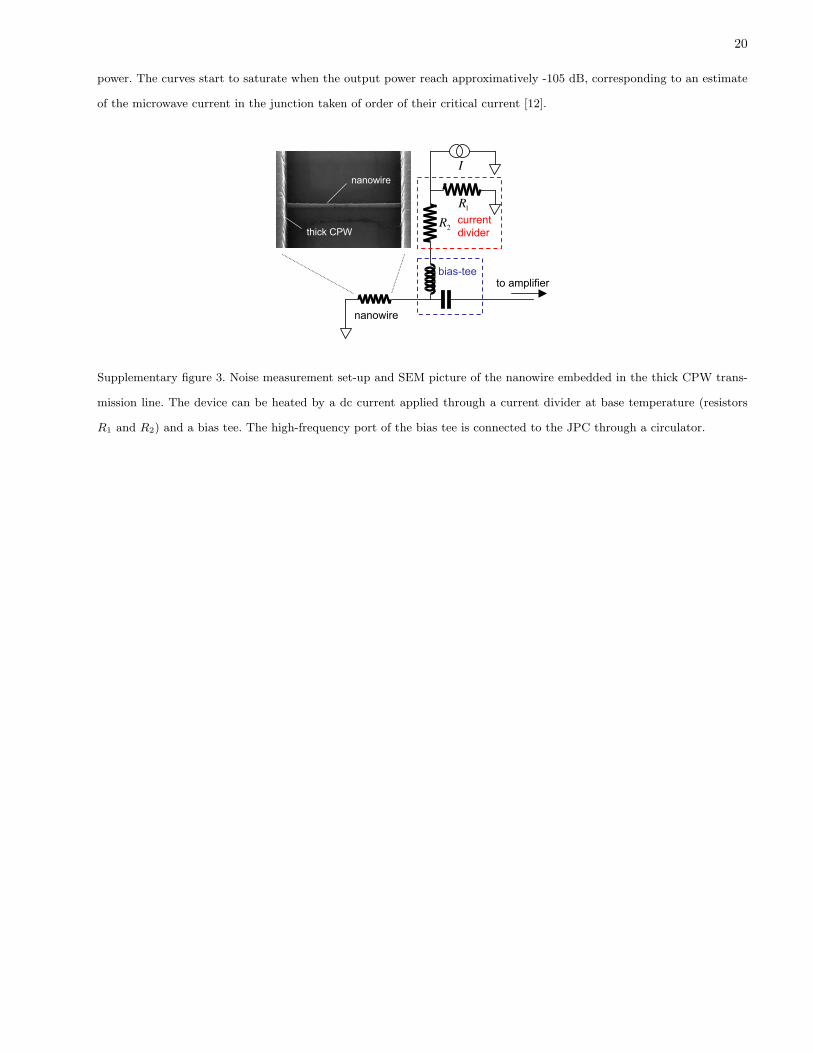
Supplementary figure 3. Noise measurement set-up and SEM picture of the nanowire embedded in the thick CPW trans-
mission line. The device can be heated by a dc current applied through a current divider at base temperature (resistors
R1 and R2) and a bias tee. The high-frequency port of the bias tee is connected to the JPC through a circulator.