The Upgraded Outer Tracker for the CMS Detector at the ... - IIHE
Performance studies of the CMS Strip Tracker before installation
40
Available on CMS information server CMS NOTE 2008/032 The Compact Muon Solenoid Experiment Mailing address: CMS CERN, CH-1211 GENEVA 23, Switzerland CMS Note 18 March 2008 Performance studies of the CMS Strip Tracker before installation W. Adam, T. Bergauer, M. Dragicevic, M. Friedl, R. Fr¨ uhwirth, S. H¨ ansel, J. Hrubec, M. Krammer, M.Oberegger, M. Pernicka, S. Schmid, R. Stark, H. Steininger, D. Uhl, W. Waltenberger, E. Widl Institut f¨ ur Hochenergiephysik der ¨ Osterreichischen Akademie der Wissenschaften (HEPHY), Vienna, Austria P. Van Mechelen, M. Cardaci, W. Beaumont, E. de Langhe, E. A. de Wolf, E. Delmeire Universiteit Antwerpen, Belgium O. Bouhali, O. Charaf, B. Clerbaux, J.-P. Dewulf. S. Elgammal, G. Hammad, G. de Lentdecker, P. Marage, C. Vander Velde, P. Vanlaer, J. Wickens Universit´ e Libre de Bruxelles, ULB, Bruxelles, Belgium V. Adler, O. Devroede, S. De Weirdt, J. D’Hondt, R. Goorens, J. Heyninck, J. Maes, M. Mozer, S. Tavernier, L. Van Lancker, P. Van Mulders, I. Villella, C. Wastiels Vrije Universiteit Brussel, VUB, Brussel, Belgium J.-L. Bonnet, G. Bruno, B. De Callatay, B. Florins, A. Giammanco, G. Gregoire, Th. Keutgen, D. Kcira, V. Lemaitre, D. Michotte, O. Militaru, K. Piotrzkowski, L. Quertermont, V. Roberfroid, X. Rouby, D. Teyssier, M. Vander Donckt Universit´ e catholique de Louvain, UCL, Louvain-la-Neuve, Belgium E. Daubie Universit´ e de Mons-Hainaut, Mons, Belgium E. Anttila, S. Czellar, P. Engstr¨ om, J. H¨ ark¨ onen, V. Karim¨ aki, J. Kostesmaa, A. Kuronen, T. Lamp´ en, T. Lind´ en, P. -R. Luukka, T. M¨ aenp¨ a¨ a, S. Michal, E. Tuominen, J. Tuominiemi Helsinki Institute of Physics, Helsinki, Finland M. Ageron, G. Baulieu, A. Bonnevaux, G. Boudoul, E. Chabanat, E. Chabert, R. Chierici, D. Contardo, R. Della Negra, T. Dupasquier, G. Gelin, N. Giraud, G. Guillot, N. Estre, R. Haroutunian, N. Lumb, S. Perries, F. Schirra, B. Trocme, S. Vanzetto Universit´ e de Lyon, Universit´ e Claude Bernard Lyon 1, CNRS/IN2P3, Institut de Physique Nucl´ eaire de Lyon, France J.-L. Agram, R. Blaes, F. Drouhin a) , J.-P. Ernenwein, J.-C. Fontaine Groupe de Recherches en Physique des Hautes Energies, Universit´ e de Haute Alsace, Mulhouse, France 1 arXiv:0901.4316v1 [physics.ins-det] 27 Jan 2009
-
Upload
independent -
Category
Documents
-
view
0 -
download
0
Transcript of Performance studies of the CMS Strip Tracker before installation

Available on CMS information server CMS NOTE 2008/032
The Compact Muon Solenoid Experiment
Mailing address: CMS CERN, CH-1211 GENEVA 23, Switzerland
CMS Note18 March 2008
Performance studies of the CMS Strip Trackerbefore installation
W. Adam, T. Bergauer, M. Dragicevic, M. Friedl, R. Fruhwirth, S. Hansel, J. Hrubec, M. Krammer, M.Oberegger,M. Pernicka, S. Schmid, R. Stark, H. Steininger, D. Uhl, W. Waltenberger, E. Widl
Institut fur Hochenergiephysik der Osterreichischen Akademie der Wissenschaften (HEPHY), Vienna, Austria
P. Van Mechelen, M. Cardaci, W. Beaumont, E. de Langhe, E. A. de Wolf, E. Delmeire
Universiteit Antwerpen, Belgium
O. Bouhali, O. Charaf, B. Clerbaux, J.-P. Dewulf. S. Elgammal, G. Hammad, G. de Lentdecker, P. Marage,C. Vander Velde, P. Vanlaer, J. Wickens
Universite Libre de Bruxelles, ULB, Bruxelles, Belgium
V. Adler, O. Devroede, S. De Weirdt, J. D’Hondt, R. Goorens, J. Heyninck, J. Maes, M. Mozer, S. Tavernier,L. Van Lancker, P. Van Mulders, I. Villella, C. Wastiels
Vrije Universiteit Brussel, VUB, Brussel, Belgium
J.-L. Bonnet, G. Bruno, B. De Callatay, B. Florins, A. Giammanco, G. Gregoire, Th. Keutgen, D. Kcira,V. Lemaitre, D. Michotte, O. Militaru, K. Piotrzkowski, L. Quertermont, V. Roberfroid, X. Rouby, D. Teyssier, M.
Vander Donckt
Universite catholique de Louvain, UCL, Louvain-la-Neuve, Belgium
E. Daubie
Universite de Mons-Hainaut, Mons, Belgium
E. Anttila, S. Czellar, P. Engstrom, J. Harkonen, V. Karimaki, J. Kostesmaa, A. Kuronen, T. Lampen, T. Linden,P. -R. Luukka, T. Maenpaa, S. Michal, E. Tuominen, J. Tuominiemi
Helsinki Institute of Physics, Helsinki, Finland
M. Ageron, G. Baulieu, A. Bonnevaux, G. Boudoul, E. Chabanat, E. Chabert, R. Chierici, D. Contardo, R. DellaNegra, T. Dupasquier, G. Gelin, N. Giraud, G. Guillot, N. Estre, R. Haroutunian, N. Lumb, S. Perries, F. Schirra,
B. Trocme, S. Vanzetto
Universite de Lyon, Universite Claude Bernard Lyon 1, CNRS/IN2P3, Institut de Physique Nucleaire de Lyon, France
J.-L. Agram, R. Blaes, F. Drouhina), J.-P. Ernenwein, J.-C. Fontaine
Groupe de Recherches en Physique des Hautes Energies, Universite de Haute Alsace, Mulhouse, France
1
arX
iv:0
901.
4316
v1 [
phys
ics.
ins-
det]
27
Jan
2009

J.-D. Berst, J.-M. Brom, F. Didierjean, U. Goerlach, P. Graehling, L. Gross, J. Hosselet, P. Juillot, A. Lounis,C. Maazouzi, C. Olivetto, R. Strub, P. Van Hove
Institut Pluridisciplinaire Hubert Curien, Universite Louis Pasteur Strasbourg, IN2P3-CNRS, France
G. Anagnostou, R. Brauer, H. Esser, L. Feld, W. Karpinski, K. Klein, C. Kukulies, J. Olzem, A. Ostapchuk,D. Pandoulas, G. Pierschel, F. Raupach, S. Schael, G. Schwering, D. Sprenger, M. Thomas, M. Weber,
B. Wittmer, M. Wlochal
I. Physikalisches Institut, RWTH Aachen University, Germany
F. Beissel, E. Bock, G. Flugge, C. Gillissen, T. Hermanns, D. Heydhausen, D. Jahn, G. Kaussenb), A. Linn,L. Perchalla, M. Poettgens, O. Pooth, A. Stahl, M. H. Zoeller
III. Physikalisches Institut, RWTH Aachen University, Germany
P. Buhmann, E. Butz, G. Flucke, R. Hamdorf, J. Hauk, R. Klanner, U. Pein, P. Schleper, G. Steinbruck
University of Hamburg, Institute for Experimental Physics, Hamburg, Germany
P. Blum, W. De Boer, A. Dierlamm, G. Dirkes, M. Fahrer, M. Frey, A. Furgeri, F. Hartmanna), S. Heier,K.-H. Hoffmann, J. Kaminski, B. Ledermann, T. Liamsuwan, S. Muller, Th. Muller, F.-P. Schilling,
H.-J. Simonis, P. Steck, V. Zhukov
Karlsruhe-IEKP, Germany
P. Cariola, G. De Robertis, R. Ferorelli, L. Fiore, M. Preda,c), G. Sala, L. Silvestris, P. Tempesta, G. Zito
INFN Bari, Italy
D. Creanza, N. De Filippisd), M. De Palma, D. Giordano, G. Maggi, N. Manna, S. My, G. Selvaggi
INFN and Dipartimento Interateneo di Fisica, Bari, Italy
S. Albergo, M. Chiorboli, S. Costa, M. Galanti, N. Giudice, N. Guardone, F. Noto, R. Potenza, M. A. Saizuc),V. Sparti, C. Sutera, A. Tricomi, C. Tuve
INFN and University of Catania, Italy
M. Brianzi, C. Civinini, F. Maletta, F. Manolescu, M. Meschini, S. Paoletti, G. Sguazzoni
INFN Firenze, Italy
B. Broccolo, V. Ciulli, R. D’Alessandro. E. Focardi, S. Frosali, C. Genta, G. Landi, P. Lenzi, A. Macchiolo,N. Magini, G. Parrini, E. Scarlini
INFN and University of Firenze, Italy
G. Cerati
INFN and Universita degli Studi di Milano-Bicocca, Italy
P. Azzi, N. Bacchettaa), A. Candelori, T. Dorigo, A. Kaminsky, S. Karaevski, V. Khomenkovb), S. Reznikov,M. Tessaro
INFN Padova, Italy
D. Bisello, M. De Mattia, P. Giubilato, M. Loreti, S. Mattiazzo, M. Nigro, A. Paccagnella, D. Pantano,N. Pozzobon, M. Tosi
INFN and University of Padova, Italy
G. M. Bileia), B. Checcucci, L. Fano, L. Servoli
INFN Perugia, Italy
F. Ambroglini, E. Babucci, D. Benedettie), M. Biasini, B. Caponeri, R. Covarelli, M. Giorgi, P. Lariccia,G. Mantovani, M. Marcantonini, V. Postolache, A. Santocchia, D. Spiga
2

INFN and University of Perugia, Italy
G. Bagliesi , G. Balestri, L. Berretta, S. Bianucci, T. Boccali, F. Bosi, F. Bracci, R. Castaldi, M. Ceccanti,R. Cecchi, C. Cerri, A .S. Cucoanes, R. Dell’Orso, D .Dobur, S .Dutta, A. Giassi, S. Giusti, D. Kartashov,
A. Kraan, T. Lomtadze, G. A. Lungu, G. Magazzu, P. Mammini, F. Mariani, G. Martinelli, A. Moggi, F. Palla,F. Palmonari, G. Petragnani, A. Profeti, F. Raffaelli, D. Rizzi, G. Sanguinetti, S. Sarkar, D. Sentenac, A. T. Serban,
A. Slav, A. Soldani, P. Spagnolo, R. Tenchini, S. Tolaini, A. Venturi, P. G. Verdinia), M. Vosf), L. Zaccarelli
INFN Pisa, Italy
C. Avanzini, A. Basti, L. Benuccig), A. Bocci, U. Cazzola, F. Fiori, S. Linari, M. Massa, A. Messineo, G. Segneri,G. Tonelli
University of Pisa and INFN Pisa, Italy
P. Azzurri, J. Bernardini, L. Borrello, F. Calzolari, L. Foa, S. Gennai, F. Ligabue, G. Petrucciani , A. Rizzih),Z. Yangi)
Scuola Normale Superiore di Pisa and INFN Pisa, Italy
F. Benotto, N. Demaria, F. Dumitrache, R. Farano
INFN Torino, Italy
M.A. Borgia, R. Castello, M. Costa, E. Migliore, A. Romero
INFN and University of Torino, Italy
D. Abbaneo, M. Abbas,I. Ahmed, I. Akhtar, E. Albert, C. Bloch, H. Breuker, S. Butt,O. Buchmuller j), A. Cattai,C. Delaerek), M. Delattre,L. M. Edera, P. Engstrom, M. Eppard, M. Gateau, K. Gill, A.-S. Giolo-Nicollerat,R. Grabit, A. Honma, M. Huhtinen, K. Kloukinas, J. Kortesmaa, L. J. Kottelat, A. Kuronen, N. Leonardo,
C. Ljuslin, M. Mannelli, L. Masetti, A. Marchioro, S. Mersi, S. Michal, L. Mirabito, J. Muffat-Joly, A. Onnela,C. Paillard, I. Pal, J. F. Pernot, P. Petagna, P. Petit, C. Piccut, M. Pioppi, H. Postema, R. Ranieri, D. Ricci,G. Rolandi, F. Rongal), C. Sigaud, A. Syed, P. Siegrist, P. Tropea, J. Troska, A. Tsirou, M. Vander Donckt,
F. Vasey
European Organization for Nuclear Research (CERN), Geneva, Switzerland
E. Alagoz, C. Amsler, V. Chiochia, C. Regenfus, P. Robmann, J. Rochet, T. Rommerskirchen, A. Schmidt,S. Steiner, L. Wilke
University of Zurich, Switzerland
I. Church, J. Colem), J. Coughlan, A. Gay, S. Taghavi, I. Tomalin
STFC, Rutherford Appleton Laboratory, Chilton, Didcot, United Kingdom
R. Bainbridge, N. Cripps, J. Fulcher, G. Hall, M. Noy, M. Pesaresi, V. Radiccin), D. M. Raymond, P. Sharpa),M. Stoye, M. Wingham, O. Zorba
Imperial College, London, United Kingdom
I. Goitom, P. R. Hobson, I. Reid, L. Teodorescu
Brunel University, Uxbridge, United Kingdom
G. Hanson, G.-Y. Jeng, H. Liu, G. Pasztoro), A. Satpathy, R. Stringer
University of California, Riverside, California, USA
B. Mangano
University of California, San Diego, California, USA
K. Affolder, T. Affolderp), A. Allen, D. Barge, S. Burke, D. Callahan, C. Campagnari, A. Crook, M. D’Alfonso,J. Dietch, J. Garberson, D. Hale, H. Incandela, J. Incandela, S. Jaditz q), P. Kalavase, S. Kreyer, S. Kyre, J. Lamb,
C. Mc Guinnessr), C. Millss), H. Nguyen, M. Nikolicm), S. Lowette, F. Rebassoo, J. Ribnik, J. Richman,
3
N. Rubinstein, S. Sanhueza, Y. Shah, L. Simmsr), D. Staszakt), J. Stoner, D. Stuart, S. Swain, J.-R. Vlimant,D. White
University of California, Santa Barbara, California, USA
K. A. Ulmer, S. R. Wagner
University of Colorado, Boulder, Colorado, USA
L. Bagby, P. C. Bhat, K. Burkett, S. Cihangir, O. Gutsche, H. Jensen, M. Johnson, N. Luzhetskiy, D. Mason,T. Miao, S. Moccia, C. Noeding, A. Ronzhin, E. Skup, W. J. Spalding, L. Spiegel, S. Tkaczyk, F. Yumiceva,
A. Zatserklyaniy, E. Zerev
Fermi National Accelerator Laboratory (FNAL), Batavia, Illinois, USA
I. Anghel, V. E. Bazterra, C. E. Gerber, S. Khalatian, E. Shabalina
University of Illinois, Chicago, Illinois, USA
P. Baringer, A. Bean, J. Chen, C. Hinchey, C. Martin,T. Moulik, R. Robinson
University of Kansas, Lawrence, Kansas, USA
A. V. Gritsan, C. K. Lae, N. V. Tran
Johns Hopkins University, Baltimore, Maryland, USA
P. Everaerts, K. A. Hahn, P. Harris, S. Nahn, M. Rudolph, K. Sung
Massachusetts Institute of Technology, Cambridge, Massachusetts, USA
B. Betchart, R. Demina, Y. Gotra, S. Korjenevski, D. Miner, D. Orbaker
University of Rochester, New York, USA
L. Christofek, R. Hooper, G. Landsberg, D. Nguyen, M. Narain,T. Speer, K. V. Tsang
Brown University, Providence, Rhode Island, USA
a) Also at CERN, European Organization for Nuclear Research, Geneva, Switzerlandb) Now at University of Hamburg, Institute for Experimental Physics, Hamburg, Germanyc) On leave from IFIN-HH, Bucharest, Romaniad) Now at LLR-Ecole Polytechnique, Francee) Now at Northeastern University, Boston, USAf) Now at IFIC, Centro mixto U. Valencia/CSIC, Valencia, Spaing) Now at Universiteit Antwerpen, Antwerpen, Belgiumh) Now at ETH Zurich, Zurich, Switzerlandi) Also Peking University, Chinaj) Now at Imperial College, London, UKk) Now at Universite catholique de Louvain, UCL, Louvain-la-Neuve, Belgiuml) Now at Eidgenossische Technische Hochschule, Zurich, Switzerland
m) Now at University of California, Davis, California, USAn) Now at Kansas University, USAo) Also at Research Institute for Particle and Nuclear Physics, Budapest, Hungaryp) Now at University of Liverpool, UKq) Now at Massachusetts Institute of Technology, Cambridge, Massachusetts, USAr) Now at Stanford University, Stanford, California, USAs) Now at Harvard University, Cambridge, Massachusetts, USA
4
Abstract
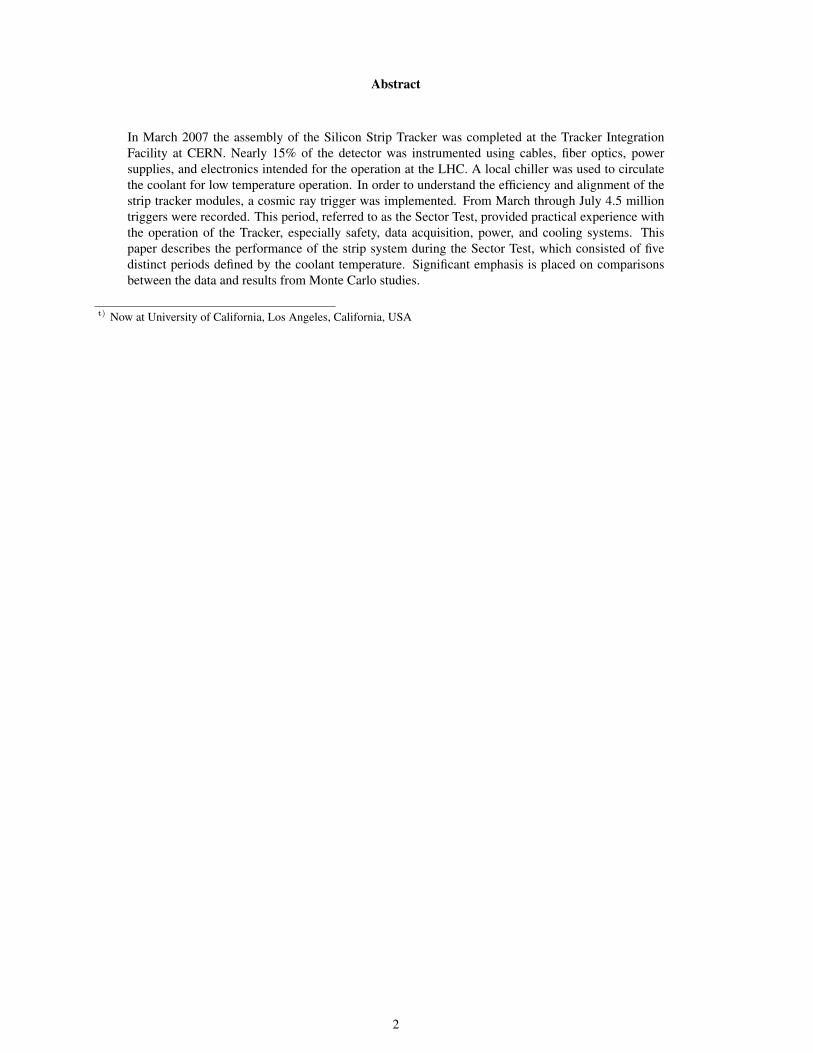
In March 2007 the assembly of the Silicon Strip Tracker was completed at the Tracker IntegrationFacility at CERN. Nearly 15% of the detector was instrumented using cables, fiber optics, powersupplies, and electronics intended for the operation at the LHC. A local chiller was used to circulatethe coolant for low temperature operation. In order to understand the efficiency and alignment of thestrip tracker modules, a cosmic ray trigger was implemented. From March through July 4.5 milliontriggers were recorded. This period, referred to as the Sector Test, provided practical experience withthe operation of the Tracker, especially safety, data acquisition, power, and cooling systems. Thispaper describes the performance of the strip system during the Sector Test, which consisted of fivedistinct periods defined by the coolant temperature. Significant emphasis is placed on comparisonsbetween the data and results from Monte Carlo studies.
t) Now at University of California, Los Angeles, California, USA
2

Contents
1 Introduction 4
2 Sector Test description 4
2.1 The Tracker Safety and Control Systems . . . . . . . . . . . . . . . . . . . . . . . . . . . . . . . 5
2.2 Cosmic Muon Trigger . . . . . . . . . . . . . . . . . . . . . . . . . . . . . . . . . . . . . . . . . 6
3 Data sets and reconstruction 8
3.1 Reconstruction . . . . . . . . . . . . . . . . . . . . . . . . . . . . . . . . . . . . . . . . . . . . 8
3.2 Data Quality Monitoring . . . . . . . . . . . . . . . . . . . . . . . . . . . . . . . . . . . . . . . 9
3.3 Data Processing . . . . . . . . . . . . . . . . . . . . . . . . . . . . . . . . . . . . . . . . . . . . 9
4 Detector Performance based on Calibration Data 10
4.1 Electronic Gain Measurements . . . . . . . . . . . . . . . . . . . . . . . . . . . . . . . . . . . . 11
4.2 Noise Performance Studies . . . . . . . . . . . . . . . . . . . . . . . . . . . . . . . . . . . . . . 13
4.3 Detector quality . . . . . . . . . . . . . . . . . . . . . . . . . . . . . . . . . . . . . . . . . . . . 16
5 Detector Performance based on Cosmic Ray Data 17
5.1 Latency Scan . . . . . . . . . . . . . . . . . . . . . . . . . . . . . . . . . . . . . . . . . . . . . 19
5.2 The signal-to-noise . . . . . . . . . . . . . . . . . . . . . . . . . . . . . . . . . . . . . . . . . . 20
5.3 Signal calibration . . . . . . . . . . . . . . . . . . . . . . . . . . . . . . . . . . . . . . . . . . . 23
5.4 Validation of Online Zero Suppression . . . . . . . . . . . . . . . . . . . . . . . . . . . . . . . . 25
5.5 Hit Occupancy . . . . . . . . . . . . . . . . . . . . . . . . . . . . . . . . . . . . . . . . . . . . 25
5.6 Hit Reconstruction Efficiency . . . . . . . . . . . . . . . . . . . . . . . . . . . . . . . . . . . . . 27
6 Simulation 27
7 Simulation Tuning 28
7.1 Signal and Noise . . . . . . . . . . . . . . . . . . . . . . . . . . . . . . . . . . . . . . . . . . . 29
7.2 Capacitive Coupling . . . . . . . . . . . . . . . . . . . . . . . . . . . . . . . . . . . . . . . . . 30
7.3 Cluster width studies . . . . . . . . . . . . . . . . . . . . . . . . . . . . . . . . . . . . . . . . . 31
8 Conclusions 34
3

1 IntroductionThe CMS Tracker [1] is the inner tracking detector built for the CMS experiment at the CERN Large HadronCollider. It is a unique instrument in both size and complexity: it contains two systems based on silicon sensortechnology, one employing pixels and another using silicon microstrips. The Pixel Detector, which surrounds thebeam pipe, consists of three barrel layers and four disk detectors, two on each side of the barrel. It contains 64million detector channels. The Silicon Strip Tracker, the subject of this paper, surrounds the pixel system andconsists of four major subsystems: the Inner Barrel (TIB), Inner Disks (TID), an Outer Barrel (TOB) and twoEnd Caps (TEC). It is the largest silicon detector ever built, with almost 10 million sensor channels coveringa surface area of over 200 m2. The Silicon Strip Tracker (referred to simply as the Tracker in this note) wasdesigned to measure charged particles with high efficiency and spatial resolution over wide range of momenta,and to operate with minimal intervention for the nominal LHC lifetime of 10 years. Consequently, the quality ofthe construction, and the performance of the components contained within it, are of vital importance and must bethoroughly evaluated under realistic conditions before operation at LHC.
First experience of the operation and detector performance of the Tracker was gained during summer 2006, with asmall fraction ( 1%) of the detector inserted in the CMS experiment. Cosmic rays were detected in the presence ofa 4 T solenoidal field and all the CMS sub-detectors were read out. The results are summarized in Ref. [2].
Silicon Strip Tracker construction proceeded during 2006 and 2007: a brief account of the integration and assemblyprocesses can also be found in [3]; it was an endeavour shared by the entire Tracker collaboration and tasks weredistributed throughout much of the world. The final assembly of the Tracker was carried out in a large, purpose-built, clean area at CERN: the Tracker Integration Facility (TIF). This facility was instrumented with a significantfraction of the final infrastructure and services needed to operate, control and read out a sector of the Tracker thatcorresponds to 15% of the entire detector: cables, patch panels, optical fibers, cooling manifolds and rack mountedpower supplies and off-detector electronics were installed to allow connection to data acquisition; cooling, controland safety systems were implemented; a trigger system was devised to detect cosmic rays traversing the Tracker,and dedicated computing resources were provided.
Following assembly of the sub-system and prior to the installation into CMS, the detector was commissioned andoperated for several months at the TIF, a period referred to as the Sector Test. The goals of this test includedcommissioning the active sector of the Tracker under realistic cabling and grounding conditions, establishingthe data acquisition, and confirming stable and safe operation under the supervision of the dedicated monitoringsystems. The objectives were also to develop and validate monitoring tools, to identify issues in service routingor connections, to establish stable and safe running at low temperature, and to demonstrate operating procedures.Finally, the acquisition of cosmic ray data allowed the measurement of the detector performance, the understandingof tracking algorithms, and to perform an initial alignment of the active modules.
The test progressed in an incremental way, beginning with testing of parts of the sub-systems, then proceeding to atest of the barrel systems, and finally incorporating one endcap. There were also short system tests to check for anyinterference between the Tracker and a small fraction of the forward pixels: these tests, which are not described inthis note, did not show any interference effects.
The Sector Test provided an important opportunity to evaluate Tracker performance in some detail and address anyweak points. Several million cosmic ray events were taken under a range of conditions, operating the Tracker overa range of temperatures, from 15 ◦C down to −15 ◦C.
The results obtained from the Sector Test are described in three dedicated papers. This note documents results onthe detector performance while results on track reconstruction and alignment are described in Ref. [4] and Ref. [5]respectively.
The Sector Test setup is described in Section 2. The data sets, reconstruction and processing are presented inSection 3, while Sections 4 and 5 are concerned with the detector performance. Section 6 covers the generationof the cosmic muons in the Tracker and the simulation of the detector response. The tuning of key parameters inMonte Carlo simulation studies to match the data is the subject of Section 7.
2 Sector Test descriptionThe Silicon Strip Tracker has a barrel region with four layers in the TIB and six layers in the TOB, and a forwardregion with three disks in the TID and nine in the TEC on each side of the Tracker. Each TID and each TECdisk is organized in three and seven rings respectively, where each ring corresponds to a different radial range and
4

Table 1: Composition of the Sector Test with the different subdetector layers/disks.
Tracker Number of Number of FractionSub-detector Modules Channels of Tracker
TIB 438 282 624 16%TID 204 141 312 25%TOB 720 476 460 15%TEC 800 483 328 13%Total 2162 1 383 424 15%
different module geometries. For the Sector Test a fraction of the Tracker was powered and read out using theAPV25 front-end chip [6, 7], selected so as to maximize the crossing of all the different layers or rings by cosmicrays. The first quadrant in the Z+ side of the Tracker was chosen. Details of Sector Test sub-detectors are shownin Table 1. Sensors were biased with a voltage of 300 V for TIB, TID and TOB, and 250 V for TEC.
The analog signal from the silicon sensors is amplified, shaped and stored in a 192 element deep analogue pipelineevery 25 ns. A subsequent stage can either pass directly the pipeline signal (Peak mode) or form a weighted sumof three consecutive samples effectively reducing the shaping time to 25 ns (Deconvolution mode): only resultsobtained with APV25 in Peak mode have been thoroughly studied at the Sector Test and therefore no Deconvolutionmode results will be described. The signal is then multiplexed by the front-end chip APV25. In order to approachthe behavior of an ideal CR-RC circuit with a 50 ns shaper, the APV25 settings can be optimized depending on thevalue of input capacitance and operating temperature. Laboratory studies [7] were made to evaluate the optimalsettings for specific geometries over a range of temperatures which were used during the Sector Test.
The signals from each APV25 channel are amplified, converted to light by an Analog Opto Hybrid (AOH) [8] andsent via optical fibers to the Front End Driver board (FED) [9, 10] where they are digitized and further processed,prior to transmission to the central DAQ system. Data can be taken in two different modes: Virgin Raw (VR) orZero Suppressed (ZS). In VR mode, all channels are read out with the full 10 bits ADC resolution. In ZS mode, theFED applies pedestal subtraction, common mode rejection and a fast clustering algorithm, using signal height witha reduced 8 bits resolution: only channels forming a cluster are output. Almost all cosmic ray data were taken inVirgin Raw mode since the low cosmic trigger rate did not require data reduction, and VR running allowed offlineoptimization of thresholds.
Clock, trigger signals, and slow control communication with the front-end electronics are managed by the FrontEnd Controller (FEC) boards [11] and sent via optical fibers to the Digital Opto Hybrid (DOH) [12, 13] for eachcontrol ring of the Tracker: signals are distributed by the DOH to every Communication Control Unit (CCU) [14]in a control ring. Finally each CCU sends signals to Tracker modules, in particular clock and triggers via a PhaseLocked Loop (PLL) circuit on each module [15]. It receives monitoring data provided by each module from theDetector Control Unit (DCU) chip [16].
FEDs and FECs were read out during the Sector Test via VME bus, rather than the high speed S-Link interfaceto be utilised in CMS. The DAQ software developed to configure and manage readout of Tracker data is based onXDAQ applications [17] which also provided algorithms to commission the detector [18].
The services needed consisted of 277 LV/HV cables, 52 control cables, 73 optical fiber cables and 32 coolingloops. The electronics racks required 145 power supply modules, 17 power supply control modules, all of whichwere units from the final system [19], 65 FEDs and 8 FECs for a total of 41 control rings.
The cooling plant used for the Sector Test was simpler than the final system and its cooling power limited. A min-imum operating temperature of −10 ◦C was obtained, compared to −25 ◦C in the final system. The temperaturesmeasured at the cooling tubes proved to be very stable with variations of less than 0.1 ◦C. A test was possible at atemperature of −15 ◦C but only by limiting power to half of the Sector Test modules.
Dry air was supplied inside to maintain a sufficiently low dew point to avoid condensation; it flowed in a semi-hermetic tent that contained the Tracker.
2.1 The Tracker Safety and Control SystemsThe Tracker Safety system (TSS) [20] is designed to guarantee protection of the Tracker. It is self-containedand operates on information provided by a thousand hardwired sensors. A system based on Programmable Logic
5

Controllers (PLC) handles the process of monitoring those sensors and taking actions depending on the monitoredvalues, which consist of digital values of temperatures, humidities and TIF, or CMS cavern, information. The TSSwill interlock the Tracker power according to a user defined scheme when either a single temperature sensor ora group of sensors varies outside user-defined safety limits, or when the TIF or cavern systems fail to respond.During the Sector Test two TSS sections, out of the final six, were fully functional and the Tracker was reliablyinterlocked on several occasions on over-temperature, cooling plant failure, power cuts, or other alarm conditions.
The Tracker Control System (TCS) [20, 21] handles all interdependencies of control, low and high voltages, as wellas fast ramp-downs in case of higher than allowed temperatures and currents in the detector, or in case of generalunsafe conditions detected in the experiment cavern. The size and complexity of the CMS Tracker imposes severaldemands on the control system to ensure the safety and operation of the modules; the TCS evaluates about 10 000power supply parameters, nearly 1000 parameters from TSS and 100 000 parameters from the DCUs situated onall front hybrids and CCU modules. The TCS should intervene before the TSS system enters into action, allowinga gentle switch off of parts under risk, and with a finer granularity than the TSS. During the Sector Test about20-25% of the final system was controlled by the TCS/TSS.
The basic software building block is the commercial SCADA (Supervisory Control And Data Acquisition) softwarePVSS (Prozess- visualisierungs- und Steuerungssystem by ETM [22]). This has been greatly extended by CERN ina common LHC framework, adapting it to the needs of individual experiments by incorporating local modifications.The LHC features also extend functionalities such as archiving of values and the treatment of alarms, warnings anderror messages.
The Sector Test enabled final implementation of the full TCS to PLC communication including the downloadingof parameters, such as sensor limits and sensor-group to interlock-grouping, to the PLC. Complete calibrationsinside PVSS were established, including all ADC to physical value conversions. Several additional checks wereintroduced from PVSS to PLC programming: for example, a minimal number of sensors should participate ininterlock voting or limits required to stay in a sensible region. A full checkout interlock routine was developed.
The complexity of the TCS system required a network of PCs for the distribution of requests. The Sector Test wasthe perfect test bed to establish, check, and tune the distribution needed for the final system as performance needsfor the Sector Test were very close to those of the final system. The main bottleneck was found to be memory butthe OPC performance of the CAEN system was also identified as a critical item.
2.2 Cosmic Muon TriggerThe cosmic trigger configuration was designed to allow studies of tracking performance and detector alignment.The trigger design was constrained by space above and below the Tracker; in particular clearance below the Trackerallowed only 5 cm lead bricks for filtering low momentum tracks. Six scintillators (T1, T2, T3, T4, T5, T6) wereplaced above the Tracker, in a fixed position; below the Tracker there was initially only one scintillator (B0)mounted on a movable support structure; later a further set of four scintillators was added (B1, B2, B3, B4)to increase the trigger acceptance. The dimensions and the single trigger rates of all scintillators are shown inTable 2.
The upper scintillator signals were synchronized by simple NIM logic using cosmic rays and put in a logical-ORto obtain a Top-scintillator signal. This was put in coincidence with the lower scintillator signal. The coincidencerates are shown in Table 2. From the entries it can be seen that efficiency of the upper scintillators was not uniform.
In the same way from synchronized logical-OR signals of scintillators B1, B2, B3, B4 a Bottom-scintillator signalwas obtained and was put in coincidence with the Top-scintillator signal. The rates are shown in Table 2. Theyshow good performance: the discriminator threshold allowed to obtain a very uniform coincidence rate.
Three main trigger configurations have been used at the Sector Test: (TA)= (Top-Scintillator & B0) vertical po-sition; (TB)= (Top-Scintillator & B0) slanted position; (TC) = (TA) plus (Top-Scintillator & Bottom-scintillator)slanted position. The schematic representations of these three configurations are shown in Fig. 1. The rate ofspurious coincidences relative to the true level was of order 10−9. The trigger rates achieved were: 3.5 Hz (TA),1.5 Hz (TB), and 6.5 Hz (TC). Since the DAQ rate was limited to about 3 Hz by the FED readout via VME, atrigger veto was implemented to keep the rate under this level.
6

(a)
(b)
(c)
Figure 1: Layout of the various trigger scintillator configurations used during the cosmic data taking at the TIF (inchronological order): (a) configuration TA; (b) configuration TB; (c) configuration TC. The xy view is shown onthe left side, the rz view is shown on the right. The straight lines connecting the active areas of the top and bottomscintillation counters indicate the acceptance region.
7

Table 2: Dimensions of scintillators used at Sector Test; single and coincidence rates.Scintillator DX DY Thickness Single Rate Rate on coincidence
(cm) (cm) (cm) (Hz) (Ti & B0) (Hz)T1 30 100 0.8 80 0.42T2 30 100 0.8 60 0.93T3 40 80 0.8 72 1.67T4 30 100 0.8 85 0.42T5 30 100 0.8 97 0.18T6 40 80 0.8 110 0.62B0 75 85 2 235 -
Scintillator DX DY thickness Single Rate Rate on coincidence(cm) (cm) (cm) (Hz) (Bi & Top-Scint.)(Hz)
B1 40 110 2 260 0.45B2 40 110 2 275 0.45B3 40 110 2 290 0.45B4 40 110 2 240 0.45
3 Data sets and reconstructionThe division of the data in different sets, is detailed in Table 3, where run number intervals are specified for theparticipating detectors, the trigger configurations, and the operating temperatures. The APV25 parameters listed inthe table are for specific hybrid temperatures (TAPV25) and were studied for TIB and TOB detector modules only.For the TID and the TEC (where a large number of variants exist) the APV25 parameters have not been optimizedfor each module type. Instead the TID used the TIB parameters while the TEC used parameters very close to thoseof the TOB.
Each run was checked using online and offline data quality monitoring tools. If a run did not meet the qualityrequirements or if a configuration or hardware problem was discovered, it was flagged as bad and excluded fromthe offline analysis.
Table 3: Sector Test data sets.
Run Detector Trigger Operating T (◦C) Total Events Good Events TAPV25(◦C)6203-6930 TIB TID TOB A 15 703 996 665 409 307277-7296 TIB TID TOB TEC A 14 191 154 189 925 307635-8055 TIB TID TOB TEC B 14 193 337 177 768 309255-9341 TIB TID TOB TEC C 14 132 311 129 378 30
10145-10684 TIB TID TOB TEC C 10 992 997 534 759 3010848-11274 TIB TID TOB TEC C -1 893 474 886 801 1011316-11915 TIB TID TOB TEC C -10 923 571 902 881 1012045-12585 TIB TID TOB TEC C -15 656 923 655 301 012599-12656 TIB TID TOB TEC C 14 112 139 112 134 30
3.1 ReconstructionEvent reconstruction, event selection, data quality monitoring, simulation and analysis of the Tracker Sector Test atthe TIF were performed within the CMS software framework known as CMSSW[23]. Hit and track reconstructionwas performed offline taking the raw data or the simulation data as input. A reconstruction job is composed of aseries of applications executed for each event in the order specified by a configuration file. A fundamental part ofthe processing is the availability of non-event data such as cable map, pedestal, alignment constants and calibrationinformation.
The first step consists in mapping ADC counts for individual strips as they are coming from the FED output, intoobjects that are uniquely assigned to a specific detector module exploiting the cabling map information stored inthe configuration database. In the case of data collected without performing online zero-suppression (VR), thenecessary pedestal information must be acquired from the database. At this point, the input data files, whether realdata or Monte Carlo simulated events, contain the same information and can be further processed with identical
8

code.
A three-threshold algorithm, described in detail in the CMS Physics TDR[23], is used to form clusters. The clusterseed is defined as a strip whose charge is at least three times greater than the strip noise, while neighboring stripsare added if their charge exceeds twice their strip noise. The cluster is kept if the total cluster charge is more thanfive times the cluster noise level, defined as the quadratic sum of all the strip noise values. Finally, the position ofthe cluster is calculated as the centroid of the individual strip charges.
Three tracking algorithms have been applied: the Combinatorial Track Finder, the Road Search and the CosmicTrack Finder. The Combinatorial Track Finder and the Road Search are reconstruction algorithms developed forp − p collisions, while the Cosmic Track Finder is a specialized code for reconstruction of single cosmic trackevents [4]. The input to the tracking algorithms are reconstructed hits as described above and information from thealignment constants (either from survey or from alignment calibration studies).
All the tracking algorithms employ the same three steps: seeding, pattern recognition and track fitting. The seedingand the pattern recognition are specific to each algorithm, while the final fit is the same for all of them. Since nomagnetic field was present the tracks are extrapolated as straight lines. Material effects, energy loss and multipleCoulomb scattering are estimated each time a track crosses an active layer. The amount of material at normalincidence is estimated via the reconstruction geometry developed for p− p collisions. Since the momentum of thetrack is not measured, a constant value of 1 GeV/c is assigned, close to the expected average from simulation.
More detailed information about the algorithms and their performance can be found in Ref. [4]. All the resultspresented in sections 5, 6 and 7 of this paper refer to tracks obtained only with the Combinatorial Track Finderalgorithm to avoid duplication of information.
3.2 Data Quality MonitoringThe Data Quality Monitoring (DQM) system for the Tracker is designed to ensure that good quality data arerecorded and detector problems are spotted very early on. The system is based on the “Physics and Data QualityMonitoring” framework [24] of CMS. The task is fulfilled in three steps : (a) histograms, called Monitoring Ele-ments (MEs), are defined and filled with relevant event information by the “Producer” (DQM Source) application;(b) a “Consumer” (DQM Client) application accesses the MEs, performs further analysis and generates alarms;and (c) the “Graphical User Interface” (GUI) provides tools for visualization of the MEs.
The MEs are defined in the DQM source at various levels of data reconstruction chain. Starting from the levelof pedestal, noise, digitization, cluster reconstruction and finally track-related properties are defined and filled invarious MEs.
The DQM Client accesses low-level MEs and performs further analysis on them and creates summary MEs, per-forms quality tests comparing MEs with references to generate alarms. The summary plots are important as itwould be too time consuming to check each of the huge set of MEs in the Tracker, which consists of over fifteenthousand detector modules. The information from detector level MEs is accessed and summarized in MEs at higherlevels following the geometrical structure. Similarly the detector level MEs are compared with reference MEs orparameters and “Ok”, “Warning”, and “Error” alarms are generated, as appropriate, based on the comparisons.
The DQM system was operational with full functionality during TIF data taking. Events were accessed from theon-line data and full reconstruction was performed on an event by event basis and provided to the DQM sources.The system was stable during operations and the Tracker DQM GUI, which is a web based application, wasaccessible from CERN as well as from other institutes involved in the Tracker activities.
3.3 Data ProcessingThe tracker data processing consisted of the following steps: data archiving, conversion of data from the rawformat to the CMS Event data Model (EDM) format based on ROOT[23], registration in the CMS official databookkeeping services, transfer to remote computing tiers, data reconstruction and analysis in a distributed comput-ing environment.
Data taking and analysis needed a large amount of available disk space, since both raw data and on-site localanalysis results had to be stored centrally in a safe way. The design chosen for the computing model was acentralized one, where all the data are stored on a single machine which is connected via NFS to the local network.A room containing all PCs and local storage was equipped to allow the data taking control, monitoring and firstanalysis of the data and it is referred to as the Tracker Analysis Center (TAC).
9

All the data collected by the tracker detector were written into a main storage machine at the TAC, which behavedlike a temporary data buffer. Data were backed-up to CASTOR storage at CERN every five minutes, copying datafiles only when they did not exist on CASTOR side and had not been accessed in the last hour (to prevent the copyof data still being modified). Once all the files belonging to a run were copied to CASTOR, a catalog was preparedfor that run after a few checks. Because of the limited resources at TAC and following the CMS computing andanalysis model, most of the processing of the data was done in remote sites as soon as data were officially publishedand transferred to them. The transfer was performed to remote sites using the CMS official data movement toolPhEDEx . Tracker data were transferred and registered successfully at Bari, Pisa and FNAL.
The datasets have been reprocessed several times to feed back into the reconstruction phase the improvements inthe alignment and calibration corrections obtained from the analysis. The final reprocessing was performed inFNAL in December 2007.
4 Detector Performance based on Calibration Data
Figure 2: Hybrid temperature distributions for TIB, TID, TOB, and TEC at a coolant temperature of 14 ◦C.
The performance of the Tracker depends on front end electronics supply voltage and operating temperature. Thesequantities are measured by the DCU chip located on each module hybrid, which can be read out digitally via thecontrol ring protocol through the electronic chain (DCU, CCU, DOH, FEC).
Results obtained for the hybrid temperature are shown in Fig. 2 and for sensor temperature in Fig. 3 for 14 ◦Ccoolant temperature. All TOB layers show the same temperature, while for TIB, TID and TEC differences arevisible: TIB layers 1 and 2, TID ring 1 and 2, and TEC ring 1, 2 and 5 are double-sided layers and have atemperature substantially higher compared with single-sided layers; the effect is more pronounced for the hybridthan for the sensor. These differences are expected to be lower with the final cooling system.
It is also apparent that three modules of TIB layer 3 have a higher temperature of about 15 ◦C; they are in astring where the cooling pipe was blocked. Results from the other operating temperatures are consistent with thoseobtained at 14 ◦C.
The power supply system provides 2.5 V and 1.25 V lines to the modules, correcting for voltage drops along thelong power supply cables by sensing the voltage levels as close to the modules as possible. Nevertheless, there stillremains a small cable resistance which causes a non-negligible voltage drop. The operating voltage of the modulesis measured by the DCU and results are shown in Fig. 4 for the 2.5 V line and in Fig. 5 for the 1.25 line. Theaverage is below nominal for all layers of sub-detectors. These measurements show that it is possible to evaluatethese voltage drops and therefore to eventually better equalize the module voltages to match the requirements.
10

Figure 3: Sensor temperature distributions at a coolant temperature of 15 ◦C for TIB, TID, TOB, and TEC.
Figure 4: 2.5 V voltage line value measured at the module for TOB, TIB, TEC, and TID.
4.1 Electronic Gain MeasurementsThis section describes how the electrical gain of the Tracker system is both determined and adjusted, that is, theprocedures by which the gains of individual APV25s are adjusted to a common and known value. The readoutchain for the Tracker involves pairs of adjacent APV25s, the hybrid MUX, the AOH [8], an optical fiber, and theFED [9]. Instabilities in the low or high voltages or changes in temperature can affect the gain. Measuring theelectrical stability of the Tracker as a function of time, voltage, temperature, and other variables, should lead to animproved understanding of the likely performance of the full Tracker system during actual LHC operations.
The commissioning procedure [18] determines optimal settings of the electronics to achieve a uniform electronic
11

Figure 5: 1.25 voltage line value measured at the module for TOB, TIB, TEC, and TID.
gain. This is obtained by measuring the value of the height of synchronization pulses, referred to as tick-marks,generated by the APV25 which provide a stable value that can be used as reference to equalize the response of thefull electronic chain. It is required that the tick-mark height of each APV25 be within the FED dynamic range and,by varying the AOH offset and gain, should correspond closely to the target value of 640 ADC channels. The fullcommissioning procedure was consistently applied whenever there were changes in coolant temperature, changesin APV25 parameters, or in the hardware configuration. Commissioning runs, referred to as timing runs, provideprecise measurements of the tick-mark heights, therefore of the electronics gain, and were repeated at intervalsbetween full commissioning runs to get more statistics on stability of the system.
Tick-mark height distributions obtained after the commissioning procedures are shown in Fig. 6. The several graylevels represent the components with different AOH gain settings (called 0, 1, 2, 3 from lower to higher gain): thedifference between the left and right distributions is mainly due to the strong dependence on the temperature of theAOH gain. The effect is manifest by the increased number of AOH with gain equal to 0 at lower temperature. Thisimplies that the average values of the tickmark height distribution changes when varying the temperature.
Figure 6: APV25 tickmark height distribution after commissioning procedure: run 7096, taken at T = 14 ◦C (left),and run 11176, taken at T = −10 ◦C (right).
Even after the commissioning procedure the tickmark height distributions still indicate about a 10% spread inelectrical gain. This variation is consistent with the coarse precision of the AOH laser gain settings. An offline
12

calibration of the electronic gain is necessary to improve the precision of the measurement of noise and signal.This is achieved by normalizing to an assumed digital header of 640 ADC counts. In the following sections, theanalysis of signal and noise will take into account this calibration if not otherwise stated, by applying a correctionfactor of
Ccorr =640
TickMark; (1)
One limitation in the use of this equation is due to the different module operating voltages for different layers. Itwas known that the tick-mark amplitude is linearly proportional to the 2.5 V operating voltage, therefore tickmarksfrom different modules can be compared only if they operate at the same voltage. The signal at the APV25amplifier output is not much affected by changes in the supply voltage. Therefore to make a more precise estimateof the electronic gain it is necessary either to equalize all the operating voltages or to correct the tick-mark valuefor the difference compared to 2.5 V. In this paper this correction was not applied therefore the electronic gain canbe considered having a systematic variation of about 5% that affects direct comparison between different layers.
Run Number6000 7000 8000 9000 10000 11000 12000
AD
C c
ou
nts
600
610
620
630
640
650
660
670
Mean Tick Height
TIB/TID
TOB
TEC
Figure 7: Tickmark height distribution versus run number. Error bars represent the statistical error of the averagevalue.
It is important to understand the stability of the electronics gain, since calibration runs are taken only at selectedtimes. In the analysis of the timing runs, bad modules have been discarded and a selection of good commissioningruns have been made. Figure 7 shows average tick-mark heights for individual sub-detectors as a function of runnumber (with the help of Table 3 the period at different temperatures can be identified). At least one timing runwas taken as part of the commissioning procedure whenever the coolant temperature changed. During the periodat T = 14− 15 ◦C, in particular, there were several timing runs, which provide information on the stability of thesystem.
TOB shows, in 7 runs, variations of ±0.6%. The TIB/TID shows a large discrepancy in the first run (6094), whereresults are lower by 5%, but this is due to the fact that the modules were operating at low electrical gain andtherefore that was corrected by a very high AOH gain: after removing this run the TIB shows, in 6 runs, variationsof ±0.6%. The TEC shows, in 4 runs, ±0.4% variations.
4.2 Noise Performance StudiesPrior to irradiation, the noise of a module is almost completely determined by the input capacitance load at theAPV25, which in turn is dominated by the silicon strips. Thus, within 8%, one expects a linear dependence of thenoise on the length of the silicon strip for all modules.
In the Sector Test, modules were mounted on the final support structures and therefore were in close proximity toeach other, which could have exposed APV25 inputs to other sources of noise. In particular grounding loops, cross-talk from neighboring modules or other noise sources, (digital noise, cables, power supply) could have affected
13

Figure 8: TIB noise profile for T= −10 ◦C for layers 1, 2, 3, and 4. Gaussian fit is shown. X axis is ADC value.
Figure 9: TOB noise profile for T= −10 ◦C for layers 1, 2, 3, 4, 5 and 6. Gaussian fit is shown. X axis is ADCvalue
the final noise performance. Moreover, a study of the temperature dependence is important. The commissioningprocedure plays an important role, since it optimizes many system parameters and consequences are observed
14
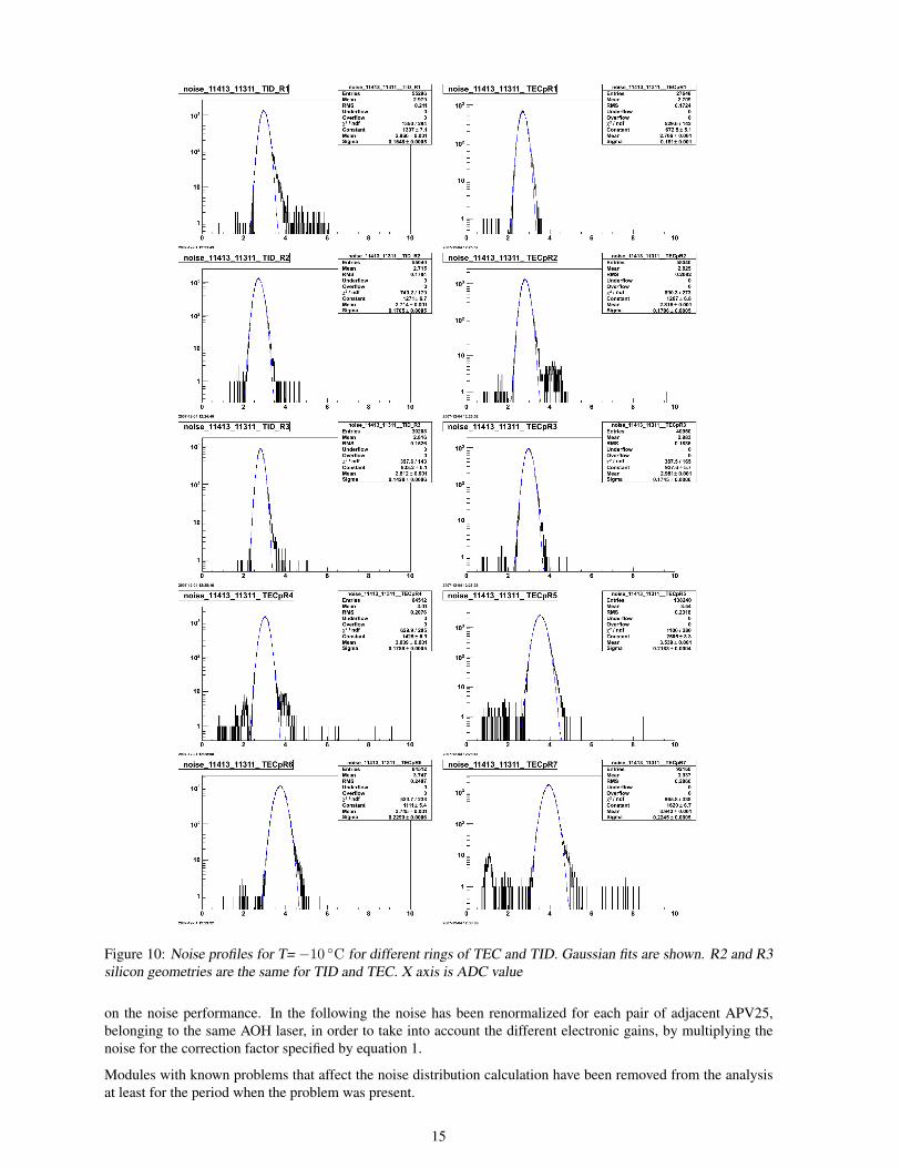
Figure 10: Noise profiles for T= −10 ◦C for different rings of TEC and TID. Gaussian fits are shown. R2 and R3silicon geometries are the same for TID and TEC. X axis is ADC value
on the noise performance. In the following the noise has been renormalized for each pair of adjacent APV25,belonging to the same AOH laser, in order to take into account the different electronic gains, by multiplying thenoise for the correction factor specified by equation 1.
Modules with known problems that affect the noise distribution calculation have been removed from the analysisat least for the period when the problem was present.
15

Strip noise distributions for runs taken at −10 ◦C are shown for each layer for TIB and TOB in Fig. 8 and Fig. 9respectively, while for TEC and TID are shown in Fig. 10. For each distribution, a fit to a Gaussian has beenperformed and results are shown. For most of the layers the noise distribution is very well represented by aGaussian, and fitted values and sigmas are almost identical for identical layers, showing extra noise sources do notaffect the detector performance significantly.
The only relevant non-Gaussian tails at high values are visible for TOB layers 2, 3 and 4. They are mainly due tochannels close to APV25 edges and only for modules at specific positions within a rod, closer to a clock distributionboard and a power cable. This noise pickup does not affect the TOB performance, given its high signal to noiseratio, as shown in the next section. Nevertheless, during the Sector Test many possible grounding and filteringschemes were investigated in order to minimize this extra noise. A solution which was found to be very effectiveconsisted in grounding the TOB power cable shields at the patch panel close to the Tracker. This groundingimplementation was possible on the Sector Test setup only for a fraction of the TOB, therefore the tails remainedfor most of the module rods. This grounding scheme has subsequently been implemented during installation of theTracker inside CMS.
Stability of the noise performance was studied by taking pedestal and noise runs at different times when theTracker was running in a stable conditions with fixed electronics configuration settings. Results are shown inFig. 11 displaying noise of all layers/rings versus the run number for TIB and TOB: the steps in values representthe different temperatures considered, 10 ◦C,0 ◦C, −10 ◦C and −15 ◦C. The data average and mean value of aGaussian fit are displayed as solid and open symbols respectively. For constant coolant temperature the noise isstable to better than±0.5%. Most importantly, the noise decreases with decreasing temperature as expected by thelaboratory studies made on the APV25 performance.
Figure 11: Noise vs run number for TIB on the left and for TOB on the right. Four periods at different temperaturesare visible: 10 ◦C, 0 ◦C, −10 ◦C and −15 ◦C
.
The (Gaussian fit) mean strip noise obtained for each different type of module has been correlated with the modulestrip length. Results are shown in Fig. 12 for a run taken at −10 ◦C, but similar results are obtained at the othertemperatures. Error bars represent the spread of the mean module noise for each module type. As expected thebehavior is well represented by a linear behavior, within statistical fluctuation, for modules from the same layer,although the average values show differences for the same strip length but different module geometries. This can beexplained by the difference in supply voltage and by the different APV25 settings used for different sub-detectors.
4.3 Detector qualityFaulty channels have been studied both from the perspective of badly behaving modules or missing fibers and ofindividual bad channels.
Modules with known problems or that were badly behaving were removed either from DAQ or from the data anal-yses. The resulting fraction of missing modules was at the 0.5% level. Dead fibers were identified during timingruns based on low tick-mark heights. They correspond to the broken fibers whose channels showed problemsduring the timing runs. The number of missing fibers in the Tracker was at the 0.1% level.
Remaining isolated bad channels were identified having higher than five sigmas, referred as noisy, or lower than
16

Figure 12: Noise vs strip length for T= −10 ◦C.
five sigmas, referred as dead, noise compared to the average noise per module, and this was done for each modulegeometry of the Tracker.
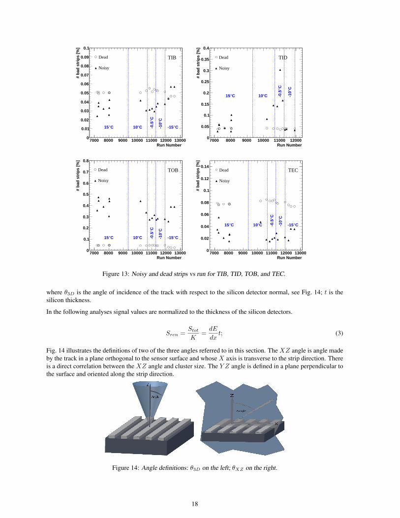
The results of this analysis as a function of the run number are shown in Fig. 13. The number of dead channelsis almost constant among several runs for all sub-detectors, showing that the identification of dead channels isclear and stable. The noisy components are instead subject to fluctuations, in particular for TOB and TID. Thefraction of dead (noisy) strips is 0.05% (0.04%) for TIB, 0.04% (0.15%) for TID, 0.04% (0.3%) for TOB, and0.08% (0.02%) for TEC.
Since the analysis of defective strips is made on a per run basis, it is important to understand the number of runsin which a strip was identified to be bad. Dead strip identification is stable: the majority of dead strips (70%) wereflagged in all runs. About 30% of the classified dead strips appear only in a single run which likely had a timingissue or other unusual problem. On the contrary, only a small fraction of the noisy strips were noisy throughoutthe Sector Test. In most cases anomalous noise persists for one or two runs at the most. These runs may reflectspecial operating conditions or non-optimal system configuration.
Finally, a comparison of the identified faulty channels with data from the Tracker construction database shows that90% of the dead channels and 40% of the noisy channels had been flagged as such by the end of the constructionperiod.
5 Detector Performance based on Cosmic Ray DataThe signal performance of the Tracker is very important; it depends on several factors: charge collection of thesilicon sensors, performance of the APV25 with well defined parameters, performance of the full electronic chain.
A study of cosmic trigger timing is presented in the first subsection, to verify that the maximum signal was taken forall the runs. As tracking efficiency relies on a sufficiently large signal to noise ratio (S/N) on all Tracker modules,it is important to measure the S/N on a layer by layer basis. Moreover, S/N analysis does not depend on the gaincalibration. Lastly, analysis of the signal size allows a straightforward comparison of the performance of differentlayers as a means of determining the absolute gain calibration and measurements of temperature dependence.
In order to obtain a high purity signal, only those hits that are associated with a reconstructed track have been used.The CTF track algorithm was used and only tracks with χ2/d.o.f. < 30 were considered. Only events with lowtrack multiplicity (less than three) and with a low hit multiplicity (less than 100) were considered.
The energy (Stot) deposited in Tracker modules can be parameterized:
Stot =dE
dxtK;K =
1cos(θ3D)
(2)
17
Run Number7000 8000 9000 10000 11000 12000 13000
# b
ad s
trip
s [%
]
0
0.01
0.02
0.03
0.04
0.05
0.06
0.07
0.08
0.09
0.1
Dead
Noisy
TIB
C°15 C°10
C°-0
.5
C°-1
0
C°-15
Run Number7000 8000 9000 10000 11000 12000
# b
ad s
trip
s [%
]
0
0.05
0.1
0.15
0.2
0.25
0.3
0.35
0.4
Dead
Noisy
TID
C°15 C°10
C°-0
.5
C°-1
0
Run Number7000 8000 9000 10000 11000 12000 13000
# b
ad s
trip
s [%
]
0
0.1
0.2
0.3
0.4
0.5
0.6
0.7
0.8
Dead
Noisy
TOB
C°15 C°10
C°-0
.5
C°-1
0
C°-15
Run Number7000 8000 9000 10000 11000 12000 13000
# b
ad s
trip
s [%
]
0
0.02
0.04
0.06
0.08
0.1
0.12
0.14Dead
Noisy
TEC
C°15 C°10
C°-0
.5
C°-1
0
C°-15
Figure 13: Noisy and dead strips vs run for TIB, TID, TOB, and TEC.
where θ3D is the angle of incidence of the track with respect to the silicon detector normal, see Fig. 14; t is thesilicon thickness.
In the following analyses signal values are normalized to the thickness of the silicon detectors.
Sren =StotK
=dE
dxt; (3)
Fig. 14 illustrates the definitions of two of the three angles referred to in this section. The XZ angle is angle madeby the track in a plane orthogonal to the sensor surface and whose X axis is transverse to the strip direction. Thereis a direct correlation between the XZ angle and cluster size. The Y Z angle is defined in a plane perpendicular tothe surface and oriented along the strip direction.
Figure 14: Angle definitions: θ3D on the left; θXZ on the right.
18
5.1 Latency ScanThe response of CMS silicon modules to signals is detailed in [25], and only some key points are highlighted inthis section. Ideally, the analytical form of the pulse shape in peak mode is the transfer function in the time domainof a CR-RC circuit:
Speak(t) ∝ t
τe−t/τ , (4)
where τ is the rise time, and the time t is positive. The pulse from the APV25 amplifier lasts about 300 ns, whichis large with respect to the 25 ns time which separates two bunch crossings.
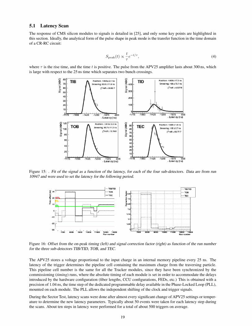
Figure 15: . Fit of the signal as a function of the latency, for each of the four sub-detectors. Data are from run10947 and were used to set the latency for the following period.
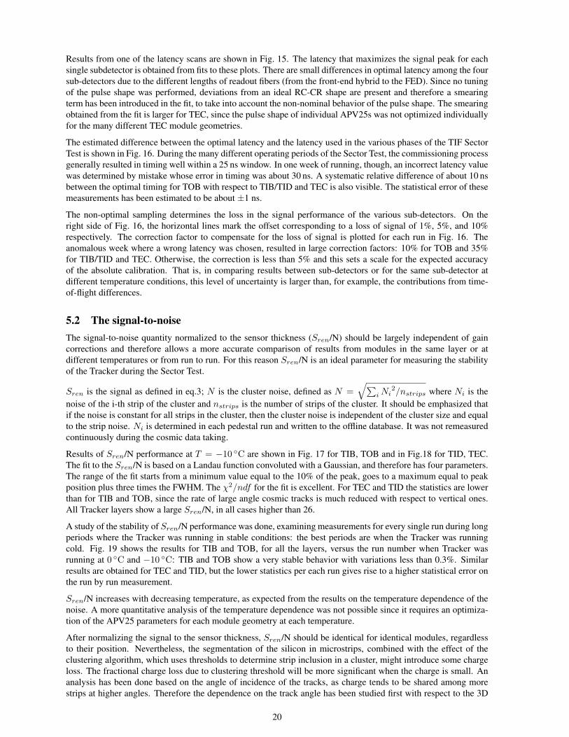
Figure 16: Offset from the on-peak timing (left) and signal correction factor (right) as function of the run numberfor the three sub-detectors TIB/TID, TOB, and TEC.
The APV25 stores a voltage proportional to the input charge in an internal memory pipeline every 25 ns. Thelatency of the trigger determines the pipeline cell containing the maximum charge from the traversing particle.This pipeline cell number is the same for all the Tracker modules, since they have been synchronized by thecommissioning (timing) runs, where the absolute timing of each module is set in order to accommodate the delaysintroduced by the hardware configuration (fiber lengths, CCU configurations, FEDs, etc.) This is obtained with aprecision of 1.04 ns, the time step of the dedicated programmable delay available in the Phase-Locked Loop (PLL),mounted on each module. The PLL allows the independent shifting of the clock and trigger signals.
During the Sector Test, latency scans were done after almost every significant change of APV25 settings or temper-ature to determine the new latency parameters. Typically about 50 events were taken for each latency step duringthe scans. About ten steps in latency were performed for a total of about 500 triggers on average.
19
Results from one of the latency scans are shown in Fig. 15. The latency that maximizes the signal peak for eachsingle subdetector is obtained from fits to these plots. There are small differences in optimal latency among the foursub-detectors due to the different lengths of readout fibers (from the front-end hybrid to the FED). Since no tuningof the pulse shape was performed, deviations from an ideal RC-CR shape are present and therefore a smearingterm has been introduced in the fit, to take into account the non-nominal behavior of the pulse shape. The smearingobtained from the fit is larger for TEC, since the pulse shape of individual APV25s was not optimized individuallyfor the many different TEC module geometries.
The estimated difference between the optimal latency and the latency used in the various phases of the TIF SectorTest is shown in Fig. 16. During the many different operating periods of the Sector Test, the commissioning processgenerally resulted in timing well within a 25 ns window. In one week of running, though, an incorrect latency valuewas determined by mistake whose error in timing was about 30 ns. A systematic relative difference of about 10 nsbetween the optimal timing for TOB with respect to TIB/TID and TEC is also visible. The statistical error of thesemeasurements has been estimated to be about ±1 ns.
The non-optimal sampling determines the loss in the signal performance of the various sub-detectors. On theright side of Fig. 16, the horizontal lines mark the offset corresponding to a loss of signal of 1%, 5%, and 10%respectively. The correction factor to compensate for the loss of signal is plotted for each run in Fig. 16. Theanomalous week where a wrong latency was chosen, resulted in large correction factors: 10% for TOB and 35%for TIB/TID and TEC. Otherwise, the correction is less than 5% and this sets a scale for the expected accuracyof the absolute calibration. That is, in comparing results between sub-detectors or for the same sub-detector atdifferent temperature conditions, this level of uncertainty is larger than, for example, the contributions from time-of-flight differences.
5.2 The signal-to-noiseThe signal-to-noise quantity normalized to the sensor thickness (Sren/N) should be largely independent of gaincorrections and therefore allows a more accurate comparison of results from modules in the same layer or atdifferent temperatures or from run to run. For this reason Sren/N is an ideal parameter for measuring the stabilityof the Tracker during the Sector Test.
Sren is the signal as defined in eq.3; N is the cluster noise, defined as N =√∑
iNi2/nstrips where Ni is the
noise of the i-th strip of the cluster and nstrips is the number of strips of the cluster. It should be emphasized thatif the noise is constant for all strips in the cluster, then the cluster noise is independent of the cluster size and equalto the strip noise. Ni is determined in each pedestal run and written to the offline database. It was not remeasuredcontinuously during the cosmic data taking.
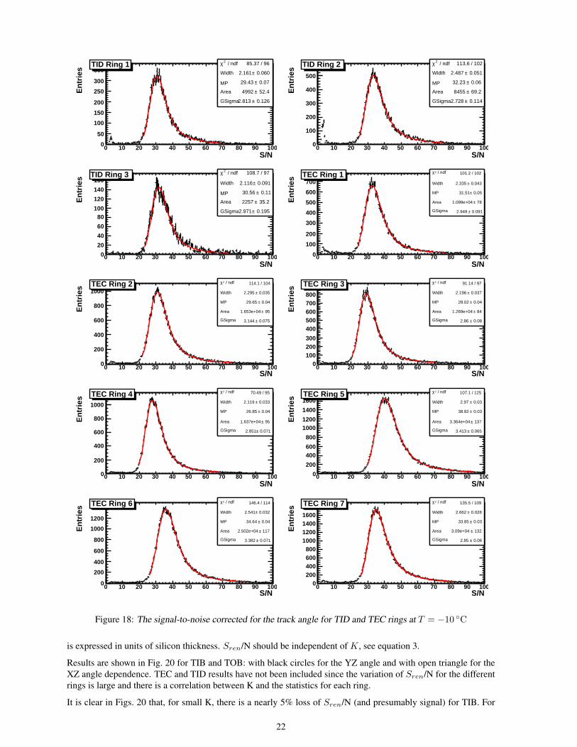
Results of Sren/N performance at T = −10 ◦C are shown in Fig. 17 for TIB, TOB and in Fig.18 for TID, TEC.The fit to the Sren/N is based on a Landau function convoluted with a Gaussian, and therefore has four parameters.The range of the fit starts from a minimum value equal to the 10% of the peak, goes to a maximum equal to peakposition plus three times the FWHM. The χ2/ndf for the fit is excellent. For TEC and TID the statistics are lowerthan for TIB and TOB, since the rate of large angle cosmic tracks is much reduced with respect to vertical ones.All Tracker layers show a large Sren/N, in all cases higher than 26.
A study of the stability of Sren/N performance was done, examining measurements for every single run during longperiods where the Tracker was running in stable conditions: the best periods are when the Tracker was runningcold. Fig. 19 shows the results for TIB and TOB, for all the layers, versus the run number when Tracker wasrunning at 0 ◦C and −10 ◦C: TIB and TOB show a very stable behavior with variations less than 0.3%. Similarresults are obtained for TEC and TID, but the lower statistics per each run gives rise to a higher statistical error onthe run by run measurement.
Sren/N increases with decreasing temperature, as expected from the results on the temperature dependence of thenoise. A more quantitative analysis of the temperature dependence was not possible since it requires an optimiza-tion of the APV25 parameters for each module geometry at each temperature.
After normalizing the signal to the sensor thickness, Sren/N should be identical for identical modules, regardlessto their position. Nevertheless, the segmentation of the silicon in microstrips, combined with the effect of theclustering algorithm, which uses thresholds to determine strip inclusion in a cluster, might introduce some chargeloss. The fractional charge loss due to clustering threshold will be more significant when the charge is small. Ananalysis has been done based on the angle of incidence of the tracks, as charge tends to be shared among morestrips at higher angles. Therefore the dependence on the track angle has been studied first with respect to the 3D
20

/ ndf 2χ 87.78 / 92
Width 0.017± 2.208
MP 0.02± 28.47
Area 178± 5.826e+04
GSigma 0.038± 2.524
S/N0 10 20 30 40 50 60 70 80 90 100
En
trie
s
0
500
1000
1500
2000
2500
3000
3500
4000 / ndf 2χ 87.78 / 92
Width 0.017± 2.208
MP 0.02± 28.47
Area 178± 5.826e+04
GSigma 0.038± 2.524
TIB Layer 1 / ndf 2χ 95.57 / 90
Width 0.015± 2.188
MP 0.02± 28.17
Area 208± 7.793e+04
GSigma 0.03± 2.49
S/N0 10 20 30 40 50 60 70 80 90 100
En
trie
s
0
1000
2000
3000
4000
5000
/ ndf 2χ 95.57 / 90
Width 0.015± 2.188
MP 0.02± 28.17
Area 208± 7.793e+04
GSigma 0.03± 2.49
TIB Layer 2
/ ndf 2χ 82.94 / 92
Width 0.02± 2.29
MP 0.02± 29.57
Area 190± 6.531e+04
GSigma 0.038± 2.405
S/N0 10 20 30 40 50 60 70 80 90 100
En
trie
s
0
50010001500
20002500
300035004000
4500 / ndf 2χ 82.94 / 92
Width 0.02± 2.29
MP 0.02± 29.57
Area 190± 6.531e+04
GSigma 0.038± 2.405
TIB Layer 3 / ndf 2χ 94.54 / 94
Width 0.015± 2.319
MP 0.0± 29.8
Area 211± 8.065e+04
GSigma 0.034± 2.493
S/N0 10 20 30 40 50 60 70 80 90 100
En
trie
s
0
1000
2000
3000
4000
5000
/ ndf 2χ 94.54 / 94
Width 0.015± 2.319
MP 0.0± 29.8
Area 211± 8.065e+04
GSigma 0.034± 2.493
TIB Layer 4
/ ndf 2χ 141.5 / 107
Width 0.009± 2.571
MP 0.0± 33.6
Area 396± 2.784e+05
GSigma 0.020± 2.912
S/N0 10 20 30 40 50 60 70 80 90 100
En
trie
s
0
2000
4000
6000
8000
10000
12000
14000
16000 / ndf 2χ 141.5 / 107
Width 0.009± 2.571
MP 0.0± 33.6
Area 396± 2.784e+05
GSigma 0.020± 2.912
TOB layer 1 / ndf 2χ 163.7 / 107
Width 0.009± 2.568
MP 0.01± 33.48
Area 390± 2.762e+05
GSigma 0.021± 2.963
S/N0 10 20 30 40 50 60 70 80 90 100
En
trie
s
0
2000
4000
6000
8000
10000
12000
14000
16000 / ndf 2χ 163.7 / 107
Width 0.009± 2.568
MP 0.01± 33.48
Area 390± 2.762e+05
GSigma 0.021± 2.963
TOB layer 2
/ ndf 2χ 153.9 / 109
Width 0.013± 2.568
MP 0.01± 32.65
Area 284± 1.455e+05
GSigma 0.029± 3.053
S/N0 10 20 30 40 50 60 70 80 90 100
En
trie
s
0
1000
20003000
4000
50006000
7000
8000
/ ndf 2χ 153.9 / 109
Width 0.013± 2.568
MP 0.01± 32.65
Area 284± 1.455e+05
GSigma 0.029± 3.053
TOB layer 3 / ndf 2χ 121.5 / 110
Width 0.012± 2.511
MP 0.01± 32.46
Area 304± 1.616e+05
GSigma 0.025± 3.184
S/N0 10 20 30 40 50 60 70 80 90 100
En
trie
s
0100020003000400050006000700080009000
/ ndf 2χ 121.5 / 110
Width 0.012± 2.511
MP 0.01± 32.46
Area 304± 1.616e+05
GSigma 0.025± 3.184
TOB layer 4
/ ndf 2χ 100.9 / 105
Width 0.012± 2.491
MP 0.01± 31.58
Area 278± 1.423e+05
GSigma 0.026± 2.903
S/N0 10 20 30 40 50 60 70 80 90 100
En
trie
s
0
10002000
3000
4000
5000
60007000
8000 / ndf 2χ 100.9 / 105
Width 0.012± 2.491
MP 0.01± 31.58
Area 278± 1.423e+05
GSigma 0.026± 2.903
TOB layer 5 / ndf 2χ 84.44 / 104
Width 0.013± 2.489
MP 0.01± 31.38
Area 278± 1.397e+05
GSigma 0.029± 2.883
S/N0 10 20 30 40 50 60 70 80 90 100
En
trie
s
0
1000
2000
3000
4000
5000
6000
7000
8000 / ndf 2χ 84.44 / 104
Width 0.013± 2.489
MP 0.01± 31.38
Area 278± 1.397e+05
GSigma 0.029± 2.883
TOB layer 6
Figure 17: The signal-to-noise corrected for the track angle for TIB and TOB layers at T = −10 ◦C.
angle. In order to separate the effect of illuminating more strips from that of increasing the charge the study hasbeen done for: the dependence on the XZ local angle for tracks perpendicular to the silicon strips (YZ local angleless than 6 degrees), referred as transverse tracks, where the sharing among strips is maximized; the dependence onthe YZ local angle for tracks that come along the direction of the silicon strip (XZ local angle less than 6 degrees),referred as longitudinal tracks, where the sharing among strips is almost independent of the angle. These studieshave been performed by looking at the dependence in Sren/N on track path (K) within the silicon, where the path
21
/ ndf 2χ 85.37 / 96
Width 0.060± 2.161
MP 0.07± 29.43
Area 52.4± 4992
GSigma 0.126± 2.813
S/N0 10 20 30 40 50 60 70 80 90 100
En
trie
s
0
50
100
150
200
250
300
350 / ndf 2χ 85.37 / 96
Width 0.060± 2.161
MP 0.07± 29.43
Area 52.4± 4992
GSigma 0.126± 2.813
TID Ring 1 / ndf 2χ 113.6 / 102
Width 0.051± 2.487
MP 0.06± 32.23
Area 69.2± 8455
GSigma 0.114± 2.728
S/N0 10 20 30 40 50 60 70 80 90 100
En
trie
s
0
100
200
300
400
500
/ ndf 2χ 113.6 / 102
Width 0.051± 2.487
MP 0.06± 32.23
Area 69.2± 8455
GSigma 0.114± 2.728
TID Ring 2
/ ndf 2χ 108.7 / 97
Width 0.091± 2.116
MP 0.11± 30.56
Area 35.2± 2257
GSigma 0.195± 2.971
S/N0 10 20 30 40 50 60 70 80 90 100
En
trie
s
0
20
40
60
80100
120
140
160 / ndf 2χ 108.7 / 97
Width 0.091± 2.116
MP 0.11± 30.56
Area 35.2± 2257
GSigma 0.195± 2.971
TID Ring 3 / ndf 2χ 101.2 / 102
Width 0.043± 2.335
MP 0.05± 31.51
Area 78± 1.099e+04
GSigma 0.091± 2.949
S/N0 10 20 30 40 50 60 70 80 90 100
En
trie
s
0
100
200
300
400
500
600
700
/ ndf 2χ 101.2 / 102
Width 0.043± 2.335
MP 0.05± 31.51
Area 78± 1.099e+04
GSigma 0.091± 2.949
TEC Ring 1
/ ndf 2χ 114.1 / 104
Width 0.035± 2.295
MP 0.04± 29.65
Area 95± 1.653e+04
GSigma 0.075± 3.144
S/N0 10 20 30 40 50 60 70 80 90 100
En
trie
s
0
200
400
600
800
1000
/ ndf 2χ 114.1 / 104
Width 0.035± 2.295
MP 0.04± 29.65
Area 95± 1.653e+04
GSigma 0.075± 3.144
TEC Ring 2 / ndf 2χ 91.14 / 97
Width 0.037± 2.196
MP 0.04± 28.02
Area 84± 1.269e+04
GSigma 0.08± 2.86
S/N0 10 20 30 40 50 60 70 80 90 100
En
trie
s
0100200300
400500600700800
900 / ndf 2χ 91.14 / 97
Width 0.037± 2.196
MP 0.04± 28.02
Area 84± 1.269e+04
GSigma 0.08± 2.86
TEC Ring 3
/ ndf 2χ 70.49 / 95
Width 0.033± 2.119
MP 0.04± 26.85
Area 95± 1.637e+04
GSigma 0.071± 2.851
S/N0 10 20 30 40 50 60 70 80 90 100
En
trie
s
0
200
400
600
800
1000
/ ndf 2χ 70.49 / 95
Width 0.033± 2.119
MP 0.04± 26.85
Area 95± 1.637e+04
GSigma 0.071± 2.851
TEC Ring 4 / ndf 2χ 107.1 / 125
Width 0.03± 2.97
MP 0.03± 38.82
Area 137± 3.364e+04
GSigma 0.065± 3.413
S/N0 10 20 30 40 50 60 70 80 90 100
En
trie
s
0
200
400600
800
10001200
1400
1600
/ ndf 2χ 107.1 / 125
Width 0.03± 2.97
MP 0.03± 38.82
Area 137± 3.364e+04
GSigma 0.065± 3.413
TEC Ring 5
/ ndf 2χ 146.4 / 114
Width 0.032± 2.541
MP 0.04± 34.64
Area 117± 2.502e+04
GSigma 0.071± 3.382
S/N0 10 20 30 40 50 60 70 80 90 100
En
trie
s
0
200
400
600
800
1000
1200
1400 / ndf 2χ 146.4 / 114
Width 0.032± 2.541
MP 0.04± 34.64
Area 117± 2.502e+04
GSigma 0.071± 3.382
TEC Ring 6 / ndf 2χ 135.5 / 109
Width 0.028± 2.662
MP 0.03± 33.85
Area 132± 3.09e+04
GSigma 0.06± 2.85
S/N0 10 20 30 40 50 60 70 80 90 100
En
trie
s
0200400600800
10001200140016001800
/ ndf 2χ 135.5 / 109
Width 0.028± 2.662
MP 0.03± 33.85
Area 132± 3.09e+04
GSigma 0.06± 2.85
TEC Ring 7
Figure 18: The signal-to-noise corrected for the track angle for TID and TEC rings at T = −10 ◦C
is expressed in units of silicon thickness. Sren/N should be independent of K, see equation 3.
Results are shown in Fig. 20 for TIB and TOB: with black circles for the YZ angle and with open triangle for theXZ angle dependence. TEC and TID results have not been included since the variation of Sren/N for the differentrings is large and there is a correlation between K and the statistics for each ring.
It is clear in Figs. 20 that, for small K, there is a nearly 5% loss of Sren/N (and presumably signal) for TIB. For
22
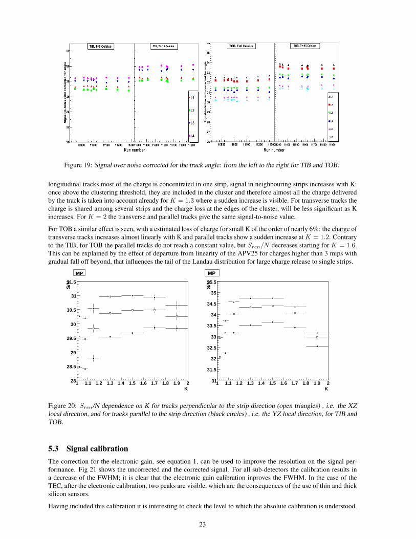
Figure 19: Signal over noise corrected for the track angle: from the left to the right for TIB and TOB.
longitudinal tracks most of the charge is concentrated in one strip, signal in neighbouring strips increases with K:once above the clustering threshold, they are included in the cluster and therefore almost all the charge deliveredby the track is taken into account already for K = 1.3 where a sudden increase is visible. For transverse tracks thecharge is shared among several strips and the charge loss at the edges of the cluster, will be less significant as Kincreases. For K = 2 the transverse and parallel tracks give the same signal-to-noise value.
For TOB a similar effect is seen, with a estimated loss of charge for small K of the order of nearly 6%: the charge oftransverse tracks increases almost linearly with K and parallel tracks show a sudden increase atK = 1.2. Contraryto the TIB, for TOB the parallel tracks do not reach a constant value, but Sren/N decreases starting for K = 1.6.This can be explained by the effect of departure from linearity of the APV25 for charges higher than 3 mips withgradual fall off beyond, that influences the tail of the Landau distribution for large charge release to single strips.
K1 1.1 1.2 1.3 1.4 1.5 1.6 1.7 1.8 1.9 2
S/N
28
28.5
29
29.5
30
30.5
31
31.5
MP
K1 1.1 1.2 1.3 1.4 1.5 1.6 1.7 1.8 1.9 2
S/N
31
31.5
32
32.5
33
33.5
34
34.5
35
35.5
MP
Figure 20: Sren/N dependence on K for tracks perpendicular to the strip direction (open triangles) , i.e. the XZlocal direction, and for tracks parallel to the strip direction (black circles) , i.e. the YZ local direction, for TIB andTOB.
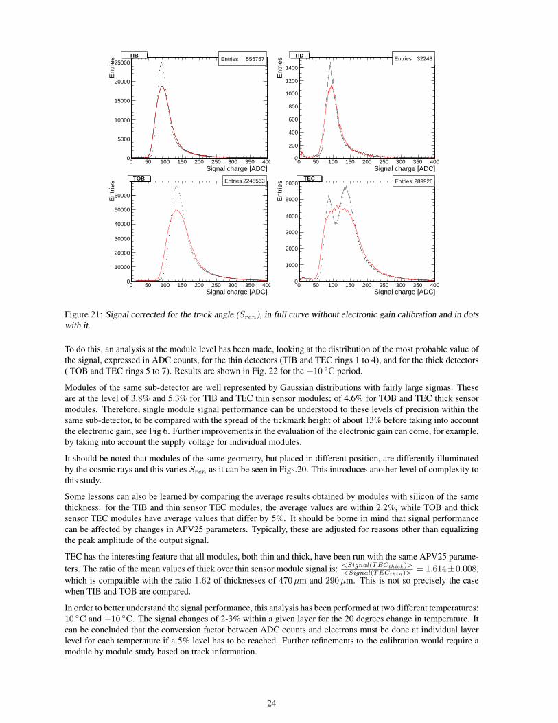
5.3 Signal calibrationThe correction for the electronic gain, see equation 1, can be used to improve the resolution on the signal per-formance. Fig 21 shows the uncorrected and the corrected signal. For all sub-detectors the calibration results ina decrease of the FWHM; it is clear that the electronic gain calibration inproves the FWHM. In the case of theTEC, after the electronic calibration, two peaks are visible, which are the consequences of the use of thin and thicksilicon sensors.
Having included this calibration it is interesting to check the level to which the absolute calibration is understood.
23
Entries 555757
Signal charge [ADC]0 50 100 150 200 250 300 350 400
Ent
ries
0
5000
10000
15000
20000
25000Entries 555757
TIB Entries 32243
Signal charge [ADC]0 50 100 150 200 250 300 350 400
Ent
ries
0
200
400
600
800
1000
1200
1400
Entries 32243TID
Entries 2248563
Signal charge [ADC]0 50 100 150 200 250 300 350 400
Ent
ries
0
10000
20000
30000
40000
50000
60000
Entries 2248563TOB Entries 289926
Signal charge [ADC]0 50 100 150 200 250 300 350 400
Ent
ries
0
1000
2000
3000
4000
5000
6000 Entries 289926TEC
Figure 21: Signal corrected for the track angle (Sren), in full curve without electronic gain calibration and in dotswith it.
To do this, an analysis at the module level has been made, looking at the distribution of the most probable value ofthe signal, expressed in ADC counts, for the thin detectors (TIB and TEC rings 1 to 4), and for the thick detectors( TOB and TEC rings 5 to 7). Results are shown in Fig. 22 for the −10 ◦C period.
Modules of the same sub-detector are well represented by Gaussian distributions with fairly large sigmas. Theseare at the level of 3.8% and 5.3% for TIB and TEC thin sensor modules; of 4.6% for TOB and TEC thick sensormodules. Therefore, single module signal performance can be understood to these levels of precision within thesame sub-detector, to be compared with the spread of the tickmark height of about 13% before taking into accountthe electronic gain, see Fig 6. Further improvements in the evaluation of the electronic gain can come, for example,by taking into account the supply voltage for individual modules.
It should be noted that modules of the same geometry, but placed in different position, are differently illuminatedby the cosmic rays and this varies Sren as it can be seen in Figs.20. This introduces another level of complexity tothis study.
Some lessons can also be learned by comparing the average results obtained by modules with silicon of the samethickness: for the TIB and thin sensor TEC modules, the average values are within 2.2%, while TOB and thicksensor TEC modules have average values that differ by 5%. It should be borne in mind that signal performancecan be affected by changes in APV25 parameters. Typically, these are adjusted for reasons other than equalizingthe peak amplitude of the output signal.
TEC has the interesting feature that all modules, both thin and thick, have been run with the same APV25 parame-ters. The ratio of the mean values of thick over thin sensor module signal is: <Signal(TECthick)>
<Signal(TECthin)> = 1.614±0.008,which is compatible with the ratio 1.62 of thicknesses of 470µm and 290µm. This is not so precisely the casewhen TIB and TOB are compared.
In order to better understand the signal performance, this analysis has been performed at two different temperatures:10 ◦C and −10 ◦C. The signal changes of 2-3% within a given layer for the 20 degrees change in temperature. Itcan be concluded that the conversion factor between ADC counts and electrons must be done at individual layerlevel for each temperature if a 5% level has to be reached. Further refinements to the calibration would require amodule by module study based on track information.
24

/ ndf 2χ 11.13 / 8
Constant 3.66± 47.93
Mean 0.22± 85.97
Sigma 0.140± 3.317
Signal charge [ADC]60 70 80 90 100 110 120
Ent
ries
0
10
20
30
40
50 / ndf 2χ 11.13 / 8
Constant 3.66± 47.93
Mean 0.22± 85.97
Sigma 0.140± 3.317
MP ScorDet001
TIB / ndf 2χ 7.308 / 12
Constant 2.15± 16.25
Mean 0.45± 84.08
Sigma 0.442± 4.529
Signal charge [ADC]60 70 80 90 100 110
Ent
ries
0
5
10
15
20
25 / ndf 2χ 7.308 / 12
Constant 2.15± 16.25
Mean 0.45± 84.08
Sigma 0.442± 4.529
MP ScorDet301
TEC thin
/ ndf 2χ 18.81 / 17
Constant 2.73± 40.56
Mean 0.4± 129
Sigma 0.284± 6.164
Signal charge [ADC]100 110 120 130 140 150 160
Ent
ries
0
10
20
30
40
50 / ndf 2χ 18.81 / 17
Constant 2.73± 40.56
Mean 0.4± 129
Sigma 0.284± 6.164
MP ScorDet201
TOB
/ ndf 2χ 18.52 / 16
Constant 1.45± 11.53
Mean 0.8± 135.7
Sigma 0.678± 6.709
Signal charge [ADC]100 110 120 130 140 150 160
Ent
ries
0
2
4
6
8
10
12
14
16
18
20 / ndf 2χ 18.52 / 16
Constant 1.45± 11.53
Mean 0.8± 135.7
Sigma 0.678± 6.709
MP ScorDet301
TEC thick
Figure 22: Distribution of signal (Sren) most probable value, module per module for TIB (top left), TEC thinsensors (top right), TOB (bottom left), and TEC thick (bottom right).
5.4 Validation of Online Zero SuppressionThe correct functioning of the FED clustering algorithm and its simulation was validated in the Sector Test throughthe study of cosmic data runs and special configuration runs.
Special runs were taken in which the data from a single TOB rod was optically split and sent simultaneously totwo FEDs. One FED passed the data in VR mode, and the other applied ZS. Offline analysis of the output fromeach FED allowed a direct comparison of the FED ZS output with a simulation of the ZS algorithm applied to theVR data. Only small differences, consistent with gain variation between the two data paths, were observed.
Cosmic data was further used to validate the functionality of the FED. Several consecutive runs, one with ZSenabled and the second without ZS enabled, were taken and the data from these to check for global FED failures,to further validate the offline algorithm, and to study the effect of varying the thresholds.
The only significant difference, an excess at about 128 counts, is due to a small number of channels that hadpedestals outside the range allowed by the FED.
5.5 Hit OccupancyOccupancy for a given strip is defined as the fraction of events in which it registers a signal exceeding the thresholdrequired to be “hit”. When LHC is running at high luminosity, the occupancy of the innermost strip layer (TIB L1)is estimated to be a few percent [1]. As described in the reconstruction section, seed strips and the cluster requirea signal-to-noise value greater than 3 and 5 respectively. If strip noise is purely Gaussian then the probability of astatistical fluctuation to become a cluster is very low, less than 5 · 10−5, and is therefore negligible. It is interestingto measure the subdetector occupancy during the Sector Test, by taking the mean value of the distribution of theprobability of a strip to be in a cluster, that is, the strip occupancy distribution.
In order to separate the contribution coming from real tracks, the strip occupancy has been studied for clusterswith S/N higher or lower than 20. Results are shown in Fig. 23 for TIB and TEC. Cosmic rays account for an
25

occupancy of 3.5 · 10−6 (TIB) and 1.1 · 10−6 (TEC) with no tails in the distribution. Clusters from statisticalfluctuations accounts instead for occupancy of 2.5 · 10−6 and 1.9 · 10−6 and show much longer tails. It is apparentthat there are strips that are more active than others, with strip occupancies up to 5% or larger.
It seems clear that the tails observed in some of the occupancy distributions are the result of active (“hot”) strips.These strips have not to be confused with the noisy strips described in Sect 4.3 since these “hot” strips are charac-terized by non-Gaussian fluctuations, above five times the noise value. The number of the “hot” strips with stripoccupancy above 1% is below 0.05% and therefore does not significantly affect module occupancy. Similar resultshave been obtained for TOB and TID sub-detectors.
Strip occupancy [%]-210 -110 1 10
1
10
210
310
410
510
610
710
Mean = 0.0002479TIB
S/N<20
Strip occupancy [%]-210 -110 1 10
1
10
210
310
410
510
610
710
Mean = 0.000193TEC
S/N<20
Strip occupancy [%]-210 -110 1 10
1
10
210
310
410
510
610
710
Mean = 0.0003523TIB
S/N>20
Strip occupancy [%]-210 -110 1 10
1
10
210
310
410
510
610
710
Mean = 0.0001116TEC
S/N>20
Figure 23: Distribution of strip occupancy for TIB and TEC: upper (lower) plots for S/N below (above) 20.
Figure 24: Summary of layer efficiency at room temperature (left) and at T = −10 ◦C (right).
26

5.6 Hit Reconstruction EfficiencyThe efficiency of a Tracker module to observe a hit when traversed by a particle, is one of the most importantcharacteristics of the detector performance as this can be affected by losses in the silicon, electronic chain, ordata acquisition and analysis. Efficiency has been measured by modifying the track reconstruction algorithm toskip the layer under study during the pattern recognition phase. A sample of high quality events was selectedby requiring only one track reconstructed by the CTF algorithm, one hit in the first TIB layer, one hit in the twooutermost TOB layers, and at least four reconstructed hits (of which at least three matched from stereo layers).Tracks were required to have no more than five lost hits during the pattern recognition phase and not more thanthree consecutive ones; finally an upper cut of 30,◦ on θ3D was applied to select tracks almost perpendicular to themodules.
In order to avoid genuine inefficiencies present at the edge of the sensor and in the bonded region between twosensors, additional cuts have been applied to restrict the regions in which efficiency is measured. With this eventselection criteria and fiducial area restrictions, the efficiency exceeds 99.8% for all measured layers as is shown inFig. 24. Additional details on the tracking and analysis procedures can be found in Ref. [4].
6 SimulationCosmic ray muons are simulated with the CMSCGEN generator[26] and the parameterizations of the energydependence and incident angle are based on a generator developed for the L3+Cosmics experiment. The muonenergy spectrum at the surface level TIF contains very soft muons and simulation is needed down to 0.2 GeV asthis is the cutoff imposed by the 5 cm of lead. The uncertainties in the cosmic ray spectrum in this low energy rangeare very high and the CMSCGEN parameterizations do not permit an accurate simulation of muons below 2 GeV.For the TIF data simulation, the events with cosmic muons below 2 GeV are produced according to the energyspectrum measured by the CAPRICE[27] experiment that describes cosmic muons down to 0.3 GeV. The angulardependencies in this simulation are taken to be the same as for muons at 2 GeV. Using the CAPRICE energyspectrum, the remaining uncertainties at this low energy are largely due to solar modulation, angular correlations,latitude dependencies, altitude effects, the earth’s magnetic field, and specifics of the building ceiling structurewhere the tests take place. However, this approximation of the energy spectrum seems satisfactory for Trackercommissioning purposes.
Figure 25: The CMSCGEN cosmic muons energy spectrum. Below 2 GeV the events are reweighted according tothe CAPRICE spectrum.
Before the simulation stage, the generated cosmic muons are filtered in order to mimic the experimental triggersetup described in Section 2.6, where triggering was based on the coincidence of separated scintillation counterarrays. In order to simulate the effect of the trigger, the scintillators, three or four depending on the configuration,have been modeled as simple 1×1 m2 surfaces. Muons are initially extrapolated to the outer radius of the Tracker,the intersection points with the scintillator surfaces calculated, and the trigger logic applied. No materials otherthan those known to be present in the Tracker were taken into account in the simulation process. The φ and theη distributions of the simulated cosmic tracks for the two scintillator configurations are shown in Figure 26. Thesimulation includes the information of the Tracker region actually connected for the readout, this can be seen inFig. 27 for the trigger Configuration TC.
27
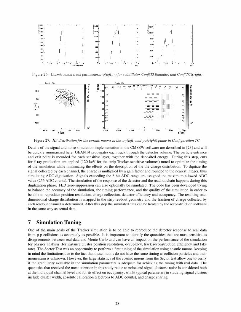
Figure 26: Cosmic muon track parameters: φ(left), η for scintillator Conf(TA)(middle) and Conf(TC)(right)
Figure 27: Hit distribution for the cosmic muons in the x-y(left) and y-z(right) plane in Configuration TC
Details of the signal and noise simulation implementation in the CMSSW software are described in [23] and willbe quickly summarized here. GEANT4 propagates each track through the detector volume. The particle entranceand exit point is recorded for each sensitive layer, together with the deposited energy. During this step, cutsfor δ-ray production are applied (120 keV for the strip Tracker sensitive volumes) tuned to optimize the timingof the simulation while minimizing the effects on the description of the the charge distribution. To digitize thesignal collected by each channel, the charge is multiplied by a gain factor and rounded to the nearest integer, thussimulating ADC digitization. Signals exceeding the 8-bit ADC range are assigned the maximum allowed ADCvalue (256 ADC counts). The simulation of the response of the detector and the readout chain happens during thisdigitization phase. FED zero-suppression can also optionally be simulated. The code has been developed tryingto balance the accuracy of the simulation, the timing performance, and the quality of the simulation in order tobe able to reproduce position resolution, charge collection, detector efficiency and occupancy. The resulting one-dimensional charge distribution is mapped to the strip readout geometry and the fraction of charge collected byeach readout channel is determined. After this step the simulated data can be treated by the reconstruction softwarein the same way as actual data.
7 Simulation TuningOne of the main goals of the Tracker simulation is to be able to reproduce the detector response to real datafrom p-p collisions as accurately as possible. It is important to identify the quantities that are most sensitive todisagreements between real data and Monte Carlo and can have an impact on the performance of the simulationfor physics analysis (for instance cluster position resolution, occupancy, track reconstruction efficiency and fakerate). The Sector Test was an opportunity to perform a first tuning of the simulation using cosmic muons, keepingin mind the limitations due to the fact that these muons do not have the same timing as collision particles and theirmomentum is unknown. However, the large statistics of the cosmic muons from the Sector test allow one to verifyif the granularity available in the simulation parameters is adequate for achieving the tuning with real data. Thequantities that received the most attention in this study relate to noise and signal clusters: noise is considered bothat the individual channel level and for its effect on occupancy; whilst typical parameters in studying signal clustersinclude cluster width, absolute calibration (electrons to ADC counts), and charge sharing.
28

7.1 Signal and NoiseThe noise simulation in the CMS Tracker, as explained in [23] is based on a parametrization of the equivalent noisecharge (ENC) as a function of the strip length L and corresponds to:
ENC(Peak) = (38.8± 2.1)e−cm−1 × L+ (414± 29)e− (5)
The noise measured with the data, as explained in Section 4, is compared with the parametrization in the simulationin Fig. 28. In the real data, effects such as temperature changes, can give rise to significant differences of the noiseeven for sensors of the same length. Other effects can also come into play (such as different APV settings) anda slight disagreement is present between the real and the simulated noise for the long sensors. One learns that anexact parametrization of the noise is not possible. To achieve a perfect simulation of it, the rms noise values usedin the simulation, will have to be taken strip-by-strip from those measured with real data.
For the comparison with the simulation, it should be noted that both the noise and the signal generation is performedin terms of electrons and then converted in ADC counts using a factor that depends on the absolute calibration ofthe signal peak in data and MonteCarlo (for this analysis e−/ADC = 250). It is important to emphasize thefact that an absolute calibration is meaningful only for a specific configuration of the APV parameters, runningtemperature etc. From signal studies presented earlier we can expect that an agreement around 5%-10% of themost probable value between data and simulation is satisfactory for our present purposes. The signal-to-noise ofthe Tracker is so large that such a difference in the simulation has nonetheless a negligible effect on macroscopicquantities related to physics, such as cluster or track reconstruction efficiency. This will not be true once the signal-to-noise drops due to irradiation. Hence, the tuning needs to be a continuous effort that follows the changes in thedetector operation as a function of the integrated luminosity. The comparison for the Landau distribution obtainedfor clusters on tracks normalized to the angle of incidence on the sensor is shown in Fig. 29. The correspondingcomparison for the signal-to-noise distributions is shown in Fig. 30. The bump that can be observed in the TOBsignal and signal-to-noise distribution in the Monte Carlo is due to the fact that the Monte Carlo data are zerosuppressed and saturate beyond 255 ADC counts, while the data used for this plot are in VR mode where there isno saturation effect until 1023 ADC counts. The effect is present also in the TIB and TEC detectors but is simplyless visible in the plots. The discrepancy observed in the distribution of the signal charge in the case of the TECdetectors is due primarily to residual differences in the tracks impact angle in data and Monte Carlo and to thecrude approximation of having in the simulation a single number to describe the interstrip capacitance couplingfor the whole Tracker.
Strip length [cm]8 10 12 14 16 18 20
CM
S N
ois
e [A
DC
co
un
ts]
1
1.5
2
2.5
3
3.5
4
4.5
5
TIB L1L2, L3L4
TOB L1L2, L3L4, L5L6
TID R1 - R3
TEC R1 - R7
MC
1 RMS±
C°Peak mode, 10
Figure 28: Measured noise in the various sub-detectors as a function of strip length compared with the MonteCarlo parameterization. The band corresponds to the spread of the mean noise in the layer.
29

Figure 29: Signal distribution for clusters on tracks in data (dashed line) and Monte Carlo (solid line). From leftto right: TIB, TOB and TEC
Figure 30: Signal to noise distribution for clusters on tracks in data (dashed line) and Monte Carlo (solid line).From left to right: TIB, TOB and TEC
7.2 Capacitive CouplingThe capacitive coupling is defined as the fraction of signal charge that is transferred from a signal strip (crossedby the minimum ionizing particle) to each of its neighbors. An important part of the simulation of the detector re-sponse is the simulation of the capacitive coupling of a strip with its nearest neighbour. The value is a configurableparameter of the simulation and at the time of this analysis, the default value used for the peak mode of operationwas 7%, a preliminary value obtained from previous, low statistics, studies with cosmic muons [2]. In order tomeasure properly the capacitive coupling, one needs to disentangle it from other effects of charge sharing thatare position dependent (such as diffusion, track inclination, Lorentz angle). A response function that can be usedto extract the value of the capacitive coupling has been devised, that applies to the cases where the other chargesharing effects are minimized, that is for perpendicular tracks (XZangle ≤ 0.1 rad):
η(symm) =Qleft +Qright
2 ·Qseed
where Qseed is the charge of the highest strip in the cluster and Qleft and Qright the charges of its neighbors.
The measurement is performed on the Virgin Raw datasets that contain the information of the charge (positive ornegative) for all the strips after pedestal subtraction. This allows one to define the eta functions also for single stripclusters using the charge of neighboring strips, even when below threshold. Clusters containing up to three stripshave been considered for this analysis. This distribution is well modeled by a Gaussian plus a tail at positive value.The tail is due to the residual charge sharing and the width is due to the noise of the side strips. The η function iscorrelated in an analytical way to the value of the coupling:
CC =η
1 + 2 · η
Fig. 31 shows the distribution of the “XZ” impact angle (defined in Section 5) between a track and a sensor indata and Monte Carlo (in Configuration TC). The difference in the angular distribution is due to the a shift inthe position of the scintillator triggers between simulation and data. The distribution for the cluster width in databefore and after the perpendicularity requirement is shown in Figure 32.
30
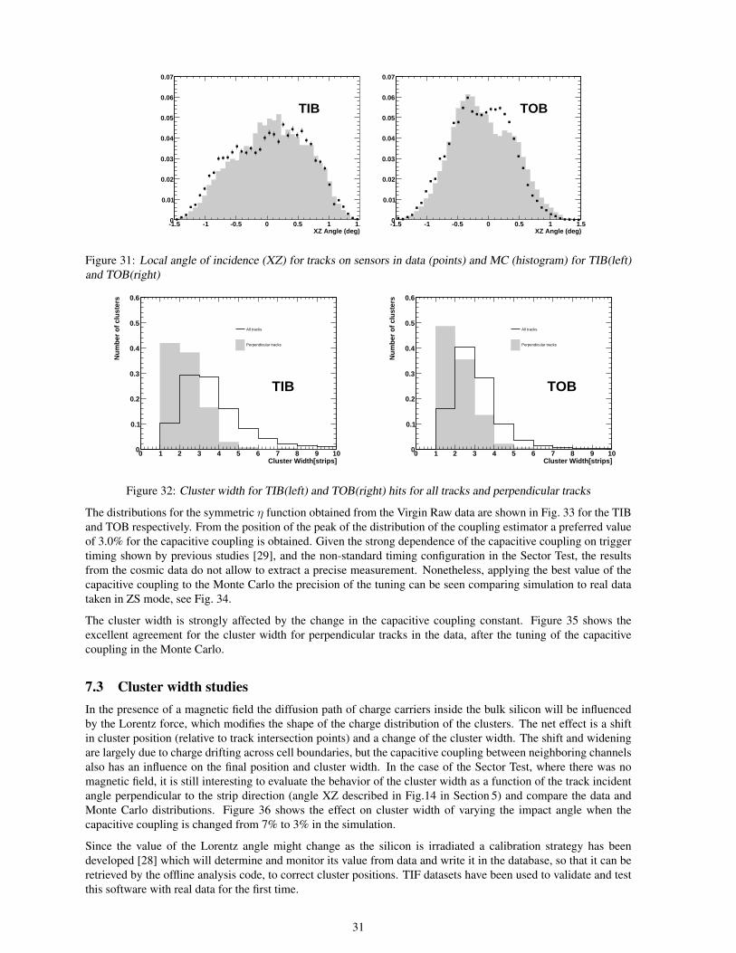
XZ Angle (deg)-1.5 -1 -0.5 0 0.5 1 1.50
0.01
0.02
0.03
0.04
0.05
0.06
0.07
TIB
XZ Angle (deg)-1.5 -1 -0.5 0 0.5 1 1.50
0.01
0.02
0.03
0.04
0.05
0.06
0.07
TOB
Figure 31: Local angle of incidence (XZ) for tracks on sensors in data (points) and MC (histogram) for TIB(left)and TOB(right)
Cluster Width[strips]0 1 2 3 4 5 6 7 8 9 10
Nu
mb
er o
f cl
ust
ers
0
0.1
0.2
0.3
0.4
0.5
0.6
All tracks
Perpendicular tracks
TIB
Cluster Width[strips]0 1 2 3 4 5 6 7 8 9 10
Nu
mb
er o
f cl
ust
ers
0
0.1
0.2
0.3
0.4
0.5
0.6
All tracks
Perpendicular tracks
TOB
Figure 32: Cluster width for TIB(left) and TOB(right) hits for all tracks and perpendicular tracks
The distributions for the symmetric η function obtained from the Virgin Raw data are shown in Fig. 33 for the TIBand TOB respectively. From the position of the peak of the distribution of the coupling estimator a preferred valueof 3.0% for the capacitive coupling is obtained. Given the strong dependence of the capacitive coupling on triggertiming shown by previous studies [29], and the non-standard timing configuration in the Sector Test, the resultsfrom the cosmic data do not allow to extract a precise measurement. Nonetheless, applying the best value of thecapacitive coupling to the Monte Carlo the precision of the tuning can be seen comparing simulation to real datataken in ZS mode, see Fig. 34.
The cluster width is strongly affected by the change in the capacitive coupling constant. Figure 35 shows theexcellent agreement for the cluster width for perpendicular tracks in the data, after the tuning of the capacitivecoupling in the Monte Carlo.
7.3 Cluster width studiesIn the presence of a magnetic field the diffusion path of charge carriers inside the bulk silicon will be influencedby the Lorentz force, which modifies the shape of the charge distribution of the clusters. The net effect is a shiftin cluster position (relative to track intersection points) and a change of the cluster width. The shift and wideningare largely due to charge drifting across cell boundaries, but the capacitive coupling between neighboring channelsalso has an influence on the final position and cluster width. In the case of the Sector Test, where there was nomagnetic field, it is still interesting to evaluate the behavior of the cluster width as a function of the track incidentangle perpendicular to the strip direction (angle XZ described in Fig.14 in Section 5) and compare the data andMonte Carlo distributions. Figure 36 shows the effect on cluster width of varying the impact angle when thecapacitive coupling is changed from 7% to 3% in the simulation.
Since the value of the Lorentz angle might change as the silicon is irradiated a calibration strategy has beendeveloped [28] which will determine and monitor its value from data and write it in the database, so that it can beretrieved by the offline analysis code, to correct cluster positions. TIF datasets have been used to validate and testthis software with real data for the first time.
31
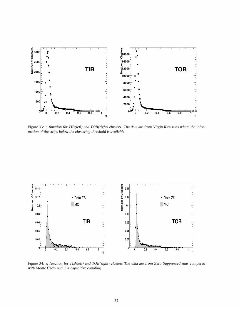
Figure 33: η function for TIB(left) and TOB(right) clusters. The data are from Virgin Raw runs where the infor-mation of the strips below the clustering threshold is available.
Figure 34: η function for TIB(left) and TOB(right) clusters The data are from Zero Suppressed runs comparedwith Monte Carlo with 3% capacitive coupling.
32

Cluster width [strips]0 5 10 15 20
No
rmal
ized
nu
mb
er o
f cl
ust
ers
0
0.1
0.2
0.3
0.4
0.5
0.6
Data
MC
TIB
Cluster width [strips]0 5 10 15 20
No
rmal
ized
nu
mb
er o
f cl
ust
ers
0
0.1
0.2
0.3
0.4
0.5 Data
MC
TOB
Figure 35: Cluster width for TIB(left) and TOB(right) hits on perpendicular tracks. The black points represent thedata, the histogram is obtained from simulation with a 3% capacitive coupling where the gray band represents thestatistical uncertainty.
Angle (deg)-30 -20 -10 0 10 20 30
Clus
ter W
idth
(stri
p)
00.5
1
1.52
2.53
3.54
4.55 TIB 1+2 / ndf 2! 53.2 / 27
Tan(Angle) 0.002876± -3.991e-05
Const 0.01349± 0.7797
Y-Int 0.01534± 1.218
/ ndf 2! 53.2 / 27
Tan(Angle) 0.002876± -3.991e-05
Const 0.01349± 0.7797
Y-Int 0.01534± 1.218
TIB 1+2
Angle (deg)-30 -20 -10 0 10 20 30
Clus
ter W
idth
(stri
p)
00.5
1
1.52
2.53
3.54
4.55 TIB 3+4 / ndf 2! 39.48 / 27
Tan(Angle) 0.004911± -0.002925
Const 0.019± 0.7284
Y-Int 0.01609± 1.237
/ ndf 2! 39.48 / 27
Tan(Angle) 0.004911± -0.002925
Const 0.019± 0.7284
Y-Int 0.01609± 1.237
TIB 3+4
Angle (deg)-30 -20 -10 0 10 20 30
Clus
ter W
idth
(stri
p)
00.5
1
1.52
2.53
3.54
4.55 TOB 1-4 / ndf 2! 84.92 / 27
Tan(Angle) 0.002527± 0.01829
Const 0.00791± 0.7372
Y-Int 0.006447± 1.331
/ ndf 2! 84.92 / 27
Tan(Angle) 0.002527± 0.01829
Const 0.00791± 0.7372
Y-Int 0.006447± 1.331
TOB 1-4
Angle (deg)-30 -20 -10 0 10 20 30
Clus
ter W
idth
(stri
p)
00.5
1
1.52
2.53
3.54
4.55 TOB 5+6 / ndf 2! 157.3 / 27
Tan(Angle) 0.003014± 0.009682
Const 0.008394± 0.7585
Y-Int 0.01088± 1.326
/ ndf 2! 157.3 / 27
Tan(Angle) 0.003014± 0.009682
Const 0.008394± 0.7585
Y-Int 0.01088± 1.326
TOB 5+6
Figure 36: Cluster width versus θt for barrel layers on Monte Carlo simulated data using capacitive coupling of7%(triangles) and 3% (crosses).
The average cluster width for tracks incident with an angle θt with respect to the detector normal is given by:
< cluster width >= a+ | tp· b · (tan θt − tan ΘL)|
where t is the detector thickness, p is the pitch, a and b are coefficients expressing the carrier diffusion and theelectronic capacitive coupling between nearby channels, and ΘL is the Lorentz angle. Therefore, plots of meancluster width as a function of tan(θt) are produced for each layer and the Lorentz angle is obtained fitting themwith the function above. In this fit the parameters are: the estimate of the Lorentz angle (tan ΘL), the slopenormalized to the ratio of thickness over pitch (that should be constant), and the average cluster width at theminimum. Of course in the TIF setup there is no magnetic field and the Lorentz angle determination should returnzero. The plots for each layer of the barrel detectors are shown in Figs. 37 and 38. The result from the data,grouped by layer with similar characteristics, has been overlaied by Monte Carlo result with a capacitive coupling
33

of 3% in Fig.39. The fitted Lorentz angles are consistent with zero as expected inside the statistical uncertainties,and with a disagreement of 2% at the most in some cases likely due to systematic misalignment effects. Thecomparison between distributions in real and simulated data indicates also that the granularity of the capacitivecoupling constant in the simulation should be increased from the single value present now, to at the level of aparameter for each layer or even for each different type of module.
Angle (deg)-30 -20 -10 0 10 20 30
Clus
ter W
idth
(stri
p)
00.5
1
1.52
2.53
3.54
4.55 TIB 1 / ndf 2! 44.91 / 27
Tan(Angle) 0.006225± -0.02447
Constant 0.02196± 0.5925
Y Intercept 0.03078± 1.669
/ ndf 2! 44.91 / 27
Tan(Angle) 0.006225± -0.02447
Constant 0.02196± 0.5925
Y Intercept 0.03078± 1.669
TIB 1
Angle (deg)-30 -20 -10 0 10 20 30
Clus
ter W
idth
(stri
p)
00.5
1
1.52
2.53
3.54
4.55 TIB 2 / ndf 2! 51.21 / 27
Tan(Angle) 0.00531± -0.004056
Constant 0.01843± 0.5854
Y Intercept 0.02524± 1.686
/ ndf 2! 51.21 / 27
Tan(Angle) 0.00531± -0.004056
Constant 0.01843± 0.5854
Y Intercept 0.02524± 1.686
TIB 2
Angle (deg)-30 -20 -10 0 10 20 30
Clus
ter W
idth
(stri
p)
00.5
1
1.52
2.53
3.54
4.55 TIB 3 / ndf 2! 40.44 / 27
Tan(Angle) 0.006356± 0.005333
Constant 0.02572± 0.6691
Y Intercept 0.0242± 1.428
/ ndf 2! 40.44 / 27
Tan(Angle) 0.006356± 0.005333
Constant 0.02572± 0.6691
Y Intercept 0.0242± 1.428
TIB 3
Angle (deg)-30 -20 -10 0 10 20 30
Clus
ter W
idth
(stri
p)
00.5
1
1.52
2.53
3.54
4.55 TIB 4 / ndf 2! 24.73 / 27
Tan(Angle) 0.005946± -0.00488
Constant 0.02313± 0.6531
Y Intercept 0.02211± 1.47
/ ndf 2! 24.73 / 27
Tan(Angle) 0.005946± -0.00488
Constant 0.02313± 0.6531
Y Intercept 0.02211± 1.47
TIB 4
Figure 37: Cluster width versus θt for TIB layers.
8 ConclusionsThe CMS Silicon Strip Tracker construction was completed in March 2007 at the CERN Tracker IntegrationFacility.
During the Sector Test, which spanned a period of about four months, the Tracker was operated in a stable andcontinuous manner for periods up to few consecutive weeks. Safe operations were established while running indifferent configurations and over a wide range of temperatures, from 15 ◦C to −15 ◦C. The 4.5 million cosmicrays events collected demonstrate the successful operation of the entire electronic chain of data acquisition systemand the commissioning of such a large fraction of the detector for the first time.
The results of the data analyses here described show the excellent detector performance. The behavior of the noiseand signal-to-noise has been very stable for all sub-detectors, better than 0.6%. In particular, the signal-to-noise inpeak mode is larger than 26 for all layers or rings and the hit reconstruction efficiency is above 99.8%. The fractionof bad strips is 0.2% and of bad components is 0.6%.
Comparing the data with the expectations from the simulation for signal, noise, cluster width and capacitive cou-pling has allowed a preliminary tuning of the simulation input parameters. The agreement between data andsimulation is at a level to allow large production of datasets to be used for early physics studies to be carried outwith the first collision data in 2008.
The sector test has been a very important milestone achieved by the Silicon Strip Tracker and can be consideredone of the best reference points for operating the full detector and understand its performance even after completionof the CMS experiment in 2008.
34

Angle (deg)-30 -20 -10 0 10 20 30
Clus
ter W
idth
(stri
p)
0
0.5
1
1.5
2
2.5
3
3.5
4
4.5
5 TOB 1 / ndf 2! 81.15 / 27
Tan(Angle) 0.004583± -0.0409
Constant 0.01431± 0.5067
Y Intercept 0.01399± 1.691
/ ndf 2! 81.15 / 27
Tan(Angle) 0.004583± -0.0409
Constant 0.01431± 0.5067
Y Intercept 0.01399± 1.691
TOB 1
Angle (deg)-30 -20 -10 0 10 20 30
Clus
ter W
idth
(stri
p)
0
0.5
1
1.5
2
2.5
3
3.5
4
4.5
5 TOB 2 / ndf 2! 39.5 / 27
Tan(Angle) 0.003575± -0.033
Constant 0.01343± 0.592
Y Intercept 0.01247± 1.572
/ ndf 2! 39.5 / 27
Tan(Angle) 0.003575± -0.033
Constant 0.01343± 0.592
Y Intercept 0.01247± 1.572
TOB 2
Angle (deg)-30 -20 -10 0 10 20 30
Clus
ter W
idth
(stri
p)
0
0.5
1
1.5
2
2.5
3
3.5
4
4.5
5 TOB 3 / ndf 2! 39.06 / 27
Tan(Angle) 0.004284± -0.01913
Constant 0.01977± 0.6735
Y Intercept 0.01983± 1.415
/ ndf 2! 39.06 / 27
Tan(Angle) 0.004284± -0.01913
Constant 0.01977± 0.6735
Y Intercept 0.01983± 1.415
TOB 3
Angle (deg)-30 -20 -10 0 10 20 30
Clus
ter W
idth
(stri
p)
0
0.5
1
1.5
2
2.5
3
3.5
4
4.5
5 TOB 4 / ndf 2! 57.38 / 27
Tan(Angle) 0.003686± -0.02032
Constant 0.01622± 0.6646
Y Intercept 0.01551± 1.412
/ ndf 2! 57.38 / 27
Tan(Angle) 0.003686± -0.02032
Constant 0.01622± 0.6646
Y Intercept 0.01551± 1.412
TOB 4
Angle (deg)-30 -20 -10 0 10 20 30
Clus
ter W
idth
(stri
p)
0
0.5
1
1.5
2
2.5
3
3.5
4
4.5
5 TOB 5 / ndf 2! 47.01 / 27
Tan(Angle) 0.002438± -0.0004361
Constant 0.01127± 0.7021
Y Intercept 0.01479± 1.412
/ ndf 2! 47.01 / 27
Tan(Angle) 0.002438± -0.0004361
Constant 0.01127± 0.7021
Y Intercept 0.01479± 1.412
TOB 5
Angle (deg)-30 -20 -10 0 10 20 30
Clus
ter W
idth
(stri
p)
0
0.5
1
1.5
2
2.5
3
3.5
4
4.5
5 TOB 6 / ndf 2! 43.23 / 27
Tan(Angle) 0.002603± -0.0097
Constant 0.01179± 0.6675
Y Intercept 0.01486± 1.483
/ ndf 2! 43.23 / 27
Tan(Angle) 0.002603± -0.0097
Constant 0.01179± 0.6675
Y Intercept 0.01486± 1.483
TOB 6
Figure 38: Cluster width versus θt for TOB layers.
Angle (deg)-30 -20 -10 0 10 20 30
Clus
ter W
idth
(stri
p)
00.5
1
1.52
2.53
3.54
4.55 TIB 1+2 / ndf 2! 40.45 / 27
Tan(Angle) 0.004182± -0.008832
Constant 0.01448± 0.5894
Y Intercept 0.01986± 1.688
/ ndf 2! 40.45 / 27
Tan(Angle) 0.004182± -0.008832
Constant 0.01448± 0.5894
Y Intercept 0.01986± 1.688
TIB 1+2
Angle (deg)-30 -20 -10 0 10 20 30
Clus
ter W
idth
(stri
p)
00.5
1
1.52
2.53
3.54
4.55 TIB 3+4 / ndf 2! 34.8 / 27
Tan(Angle) 0.004457± -0.001143
Constant 0.01754± 0.6613
Y Intercept 0.0166± 1.457
/ ndf 2! 34.8 / 27
Tan(Angle) 0.004457± -0.001143
Constant 0.01754± 0.6613
Y Intercept 0.0166± 1.457
TIB 3+4
Angle (deg)-30 -20 -10 0 10 20 30
Clus
ter W
idth
(stri
p)
00.5
1
1.52
2.53
3.54
4.55 TOB 1-4 / ndf 2! 98.31 / 27
Tan(Angle) 0.002085± -0.0299
Constant 0.007877± 0.586
Y Intercept 0.007597± 1.56
/ ndf 2! 98.31 / 27
Tan(Angle) 0.002085± -0.0299
Constant 0.007877± 0.586
Y Intercept 0.007597± 1.56
TOB 1-4
Angle (deg)-30 -20 -10 0 10 20 30
Clus
ter W
idth
(stri
p)
00.5
1
1.52
2.53
3.54
4.55 TOB 5+6 / ndf 2! 59.47 / 27
Tan(Angle) 0.001803± -0.005204
Constant 0.00823± 0.6845
Y Intercept 0.0106± 1.451
/ ndf 2! 59.47 / 27
Tan(Angle) 0.001803± -0.005204
Constant 0.00823± 0.6845
Y Intercept 0.0106± 1.451
TOB 5+6
Figure 39: Cluster width versus θt for barrel layers on real data (crosses) compared with Monte Carlo (triangles)using capacitive coupling of 3%.
35
AcknowledgmentsWe thank the administrative staff at CERN and other Tracker Institutes. This work was supported by: the AustrianFederal Ministry of Science and Research; the Belgium Fonds de la Recherche Scientifique and Fonds voor Weten-schappelijk Onderzoek; the Academy of Finland and Helsinki Institute of Physics; the Institut National de PhysiqueNucleaire et de Physique des Particules / CNRS, France; the Bundesministerium fur Bildungund Forschung, Ger-many; the Istituto Nazionale di Fisica Nucleare, Italy; the Swiss Funding Agencies; the Science and TechnologyFacilities Council, UK; the US Department of Energy, and National Science Foundation. Individuals have receivedsupport from the Marie-Curie IEF program (European Union) and the A.P. Sloan Foundation.
References[1] The CMS Collaboration, CMS: The Tracker Project Technical Design Report, CERN-LHCC-98-06 (1998)
Addendum to CMS Tracker TDR, CERN-LHCC-2000-016 (2000)
[2] W.Adam et al., CMS Tracker Collaboration, Tracker Operation and Performance at the Magnetic Test andCosmic Challenge, CMS Note 2007/029.
[3] CERN Courier 48 (2008) 22
[4] Track Reconstruction with Cosmic Rays Data at the Tracker Integration Facility, CMS-CR 2008/006
[5] CMS Tracker Alignment at the Tracker Integration Facility, CMS-CR 2007/081.
[6] M.J. French et al., Design and results from the APV25, a deep sub-micron CMOS front-end chip for the CMStracker, Nucl. Inst. and Methods A466 359–365 (2001).
[7] M. Raymond et al., Final Results from the APV25 Production Wafer Testing, 11th Workshop on Electronicsfor LHC and Future Experiments, Heidelberg, Germany (2005) 453–457.
[8] M.-T. Brunetti, B. Checcucci, V. Postolache, D. Ricci, Electrical Qualification of the Pre-production of Ana-logue Opto-Hybrid Circuits for the CMS Tracker Inner Barrel and Inner Disks, CMS Note 2003/027
[9] C. Foudas et al., The CMS Tracker Readout Front End Driver, IEEE Trans. Nucl. Sci. 52 2836–2840 (2005).
[10] G. Iles et al., Performance of the CMS silicon tracker front-end driver, 10th Workshop on Electronics forLHC and Future Experiments, Boston, USA (2004) 222–226.
[11] K. Kloukinas et al., FEC-CCS: A common front-end controller card for the CMS detector electronics, 12thWorkshop on Electronics For LHC and Future Experiments, Spain (2006) 179–184.
[12] J. Troska et al., Optical readout and control systems for the CMS tracker, IEEE Trans. Nucl. Sci. 50 1067–1072 (2003).
[13] E. Noah et al., Qualification of the CMS Tracker Control Link Digital Optohybrid, 10th Workshop on Elec-tronics for LHC and Future Experiments, Boston, USA (2004) 169–173.
[14] C. Paillard, C. Ljuslin, A. Marchioro, The CCU25 : a network oriented communication and control unitintegrated circuit in a 0.25 µm CMOS technology, 8th Workshop on Electronics for LHC Experiments, Colmar,France (2002) 174–178.
[15] P. Moreira, A. Marchioro, P. Placidi, CMS Tracker PLL Reference Manual, CERN Report cer-002725460(2000).
[16] G. Magazzu, A. Marchioro, P. Moreira, The detector control unit : an ASIC for the monitoring of the CMSsilicon tracker, IEEE Trans. Nucl. Sci. 51 1333–1336 (2004).
[17] J. Gutleber, L. Orsini, Software Architecture for Processing Cluster Based on I2O, Cluster Computing 555–64 (2002).
[18] R. Bainbridge et al., Commissioning and Calibrating the CMS Silicon Strip Tracker, 12th Workshop onElectronics For LHC and Future Experiments, Valencia (2006) 419–423.
36

[19] S. Paoletti et al., The Powering Scheme of the CMS Silicon Strip Tracker, Proceeding of the 10th Workshopon Electronics for LHC and future Experiments, Boston, USA (2004).
[20] Frank Hartmann for the CMS Tracker Control Safety Group, The CMS Tracker Control & Safety System,Proceedings Vienna Conference on Instrumentation 2007. Submitted to NIM.
[21] M. Frey for the CMS Tracker Collaboration, The CMS-tracker detector control system., Prepared for 9thICATPP Conference on Astroparticle, Particle, Space Physics, Detectors and Medical Physics Applications,Villa Erba, Como, Italy, 17-21 Oct 2005. Published in Como 2005, Astroparticle, Particle and Space Physics,Detectors and Medical Physics Applications, Oct (2005) 1067–1071.
[22] ETM professional control GmbH, www.etm.at
[23] The CMS Collaboration, Detector Performance and Software Physics Technical Design Report, Vol. 1,CERN/LHCC 2006/001, CMSTDR 8.1
[24] C. Leonidopoulus, Physics and Data Quality Monitoring at CMS, Proceedings of CHEP06, Mumbai, India(2006).
[25] C. Delaere, L. Mirabito, Timing of the CMS tracker. Study of module properties., CMS Note 2007/027
[26] P. Biallass, T. Hebbeker, Improved parameterization of the Cosmic Muon Flux for the Generator CMSCGEN,CMS Note 2007/033
[27] M. Boezio et al., (CAPRICE Collaboration) Phys. Rev. D¯
67, 072003 (2003)
[28] Ciulli V., D’Alessandro R., Frosali S., Genta C. Determination of the Lorentz Angle in Microstrip SiliconDetectors with Cosmic Muons CMS Note 2008/006
[29] Studies for the commisioning of the CERN CMS Silicon Strip Tracker C. Bloch, Ph.D. Thesis,
Technische Universitat Wien, Fakultat fur Technische Physik, December 17 2007
37